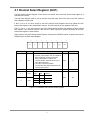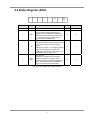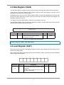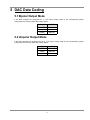
1
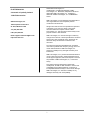
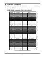
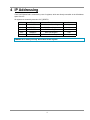
IP-OPTODA16CH4
4 Channels of
Optically Isolated 16-Bit D/A Conversion
User Manual
©SBS Technologies, Inc.
Subject to change without notice.
Part Number: 89004589 Rev. 1.0
20030410
IP-OPTODA16CH4
4 channels of optically isolated
16-bit D/Aconversion
SBS Technologies, Inc.
1284 Corporate Center Drive
St. Paul, MN 55121-1245
Tel: (651) 905-4700
FAX: (651) 905-4701
Email: [email protected]
http://www.sbs.com
©2003 SBS Technologies, Inc.
IndustryPack is a registered trademark of SBS
Technologies, Inc. QuickPack, SDpacK and Unilin are
trademarks SBS Technologies, Inc. PC•MIP is a
trademark of SBS Technologies, Inc. and MEN Mikro
GmbH.
SBS Technologies, Inc acknowledges the trademarks of
other organizations for their respective products
mentioned in this document.
All rights are reserved: No one is permitted to reproduce
or duplicate, in any form, the whole or part of this
document without the express consent of SBS
Technologies, Inc. This document is meant solely for the
purpose in which it was delivered.
SBS Technologies, Inc. reserves the right to make any
changes in the devices or device specifications contained
herein at any time and without notice. Customers are
advised to verify all information contained in this
document.
The electronic equipment described herein generates,
uses and may radiate radio frequency energy, which can
cause radio interference. SBS Technologies, Inc.
assumes no liability for any damages caused by such
interference.
SBS Technologies, Inc.’s products are not authorized for
use as critical components in medical applications such
as life support equipment, without the express consent of
the president of SBS Technologies, Inc., Commercial
Group.
This product has been designed to operate with
IndustryPack, PC•MIP or PMC modules or carriers and
compatible user-provided equipment. Connection of
incompatible hardware is likely to cause serious damage.
SBS Technologies, Inc. assumes no liability for any
damages caused by such incompatibility.
2
Table of Contents
1
2
PRODUCT DESCRIPTION ........................................................................................ 5
TECHNICAL SPECIFICATION .................................................................................. 6
2.1 Analog Output................................................................................................................................. 7
2.2 Data Correction............................................................................................................................... 7
2.2.1 DAC Correction Formula for 0V to +10V Output Voltage Range ........................................ 7
2.2.2 DAC Correction Formula for +/-10V Output Voltage Range ............................................... 8
3
ID PROM CONTENTS................................................................................................ 9
3.1 ID PROM Contents IP-OPTODA16CH4 ......................................................................................... 9
4
IP ADDRESSING ..................................................................................................... 10
4.1
4.2
4.3
4.4
5
Channel Select Register (0x01)................................................................................................... 11
Status Register (0x03).................................................................................................................. 12
Data Register (0x04) ..................................................................................................................... 13
Load Register (0x07) .................................................................................................................... 13
DAC DATA CODING................................................................................................ 14
5.1 Bipolar Output Mode.................................................................................................................... 14
5.2 Unipolar Output Mode.................................................................................................................. 14
6
7
JUMPER CONFIGURATION.................................................................................... 15
IP I/O CONNECTOR ................................................................................................ 16
7.1 Analog Output Connections........................................................................................................ 16
7.2 Power Input Connections ............................................................................................................ 16
3
Table of Figures
FIGURE 1-1: BLOCK DIAGRAM ....................................................................................................................... 5
FIGURE 2-1: TECHNICAL SPECIFICATION FUNCTIONAL DESCRIPTION .................................................. 6
FIGURE 3-1: ID PROM CONTENTS IP-OPTODA16CH4................................................................................. 9
FIGURE 4-1: CHANSEL DAC CHANNEL SELECT REGISTER..................................................................... 11
FIGURE 4-2: STATREG DAC STATUS REGISTER....................................................................................... 12
FIGURE 4-3: DATAREG DAC DATA REGISTER........................................................................................... 13
FIGURE 4-4: LOADREG DAC LOAD REGISTER .......................................................................................... 13
FIGURE 6-1: JUMPER CONFIGURATION FOR OUTPUT VOLTAGE RANGE IP-OPTODA16CH4 ............ 15
FIGURE 7-1: ANALOG OUTPUT CONNECTIONS IP-OPTODA16CH4 ........................................................ 16
FIGURE 7-2: POWER INPUT CONNECTIONS IP-OPTODA16CH4.............................................................. 16
4
1 Product Description
The IP-OPTODA16CH4 is an IndustryPack® compatible module providing 4 channels of isolated 16 bit
analog outputs. Settling time to 0.003%is typical 10µs. The programmable output voltage range is +/-10V
or 0 to +10V selectable by jumper configuration. The DAC resets to 0V output voltage in both unipolar and
bipolar output voltage range. The isolated DACs and the output buffers are powered by an on board
DC/DC converter. Optocouplers are used for the DACs digital interfaces.
16 bit DAC
16 bit DAC
ID-PROM
16 bit DAC
16 bit DAC
DC/DC
Converter
Figure 1-1: Block Diagram
5
Industry Pack I/O Interface
Control &
Interface
Optocoupler
Industry Pack logic Interface
Each IP-OPTODA16CH4 is factory calibrated. The calibration information is stored in the IdentificationPROM unique to each IP and voltage range.
2 Technical Specification
Logic Interface
IndustryPack® Logic Interface
Size
Single wide IP
I/O Interface
50-conductor flat cable
Analog Outputs
4 D/A channels
Isolation
All D/A channels are galvanically isolated from the IP
interface
Output Voltage Range
+/-10V or 0V to 10V (selectable by jumper), common for
all 4 channels
Settling Time of DAC
To 0.003%in 10µs typical
Calibration Data
In ID PROM for gain and offset correction for each
channel
Output Current
+/-4mA for each channel
Load Capacitance
1nF typical
Accuracy
INL +/-4LSB typical after calibration
Linearity
DNL +/-0.5LSB
Monotonicity
16 bit over the specified temperature range
Wait States
IDSEL: 1 wait state
IOSEL: no wait states
Power Requirements
400mA typical @+5V, no load
430mA typical l@+5V with 4mA output current for each
channel
Temperature Range
Operating -40°C to +85°C
Storage -45°C to +125°C
Humidity
5 - 95% non-condensing
MTBF
283318h
Figure 2-1: Technical Specification Functional Description
6
2.1 Analog Output
The IP-OPTODA16CH4 includes 4 channels of analog outputs with a resolution of 16 bits and a voltage
range of +/-10V or 0V to +10V. The maximum output current for each channel is +/-4mA. Each channel
has a settling time to 0.003%of typical 10µs.
Two voltage ranges are jumper selectable: +/-10V or 0V to +10V. Voltage range selection covers all 4
channels.
The 4 analog outputs of the IP-OPTODA16CH4 are galvanically isolated from the IndustryPack logic
interface by optocoupler.
2.2 Data Correction
There are two errors which affect the DC accuracy of the DAC. The first is the zero error (offset). For the
DAC this is the data value required to produce a zero voltage output signal. This error is corrected by
subtracting the known error from all readings.
The second error is the gain error. Gain error is the difference between the ideal gain and the actual gain
of the DAC. It is corrected by multiplying the data value by a correction factor.
The data correction values are obtained during factory calibration and are stored in the modules individual
version of the ID PROM. The DAC has a pair of offset and gain correction values for each single output
channel. The correction values are stored in the ID PROM as two’s complement byte wide values in the
range -32768 to 32767. For higher accuracy they are scaled to ¼ LSB.
Because offset and gain correction values are dependent on the selected output voltage range the IPOPTODA16CH4 has 2 different sets of ID PROM data. Depending on the jumper settings for the voltage
range the corresponding set of correction values is automatically selected.
2.2.1 DAC Correction Formula for 0V to +10V Output Voltage Range
The basic formula for correcting unipolar DAC output value is:
Data = Value * ( 1 - Gaincorr / 262144 ) - Offsetcorr / 4
Data is the (corrected) digital value that should be sent to the DAC, Value is the desired output value,
Gaincorr and Offsetcorr are the correction factors from the ID PROM.
7
2.2.2 DAC Correction Formula for +/-10V Output Voltage Range
The basic formula for correcting bipolar DAC output value is:
Data = Value * ( 1 - Gaincorr / 131072 ) - Offsetcorr / 4
Data is the (corrected) digital value that should be sent to the DAC, Value is the desired output value,
Gaincorr and Offsetcorr are the correction factors from the ID PROM.
Gaincorr and Offsetcorr correction factors are stored separately for each for the four DAC outputs.
Floating point arithmetic or scaled integer arithmetic is necessary to avoid rounding error while
computing above formula.
8
3 ID Prom Contents
The Voltage Range bit of the DAC Status Register is used to select the correct set of data correction
values for the actual selected voltage range (transparent for the user).
3.1 ID PROM Contents IP-OPTODA16CH4
ADDRESS
FUNCTION
Content
0x01
ASCII ’I’
0x49
0x03
ASCII ’P’
0x50
0x05
ASCII ’A’
0x41
0x07
ASCII ’C’
0x43
0x09
Manufacturer ID
0xB3
0x0B
Model Number
0x23
0x0D
Revision
0x10
0x0F
reserved
0x00
0x11
Driver-ID low-byte
0x00
0x13
Driver-ID high-byte
0x00
0x15
number of bytes used
0x1D
0x17
CRC
variable
0x19
Version -10
0x0A
0x1B
DAC1 Offset
Ch.1 Low Byte
board dependent
0x1D
DAC1 Offset
Ch.1 High Byte
board dependent
0x1F
DAC2 Offset
Ch.2 Low Byte
board dependent
0x21
DAC2 Offset
Ch.2 High Byte
board dependent
0x23
DAC3 Offset
Ch.3 Low Byte
board dependent
0x25
DAC3 Offset
Ch.3 High Byte
board dependent
0x27
DAC4 Offset
Ch.4 Low Byte
board dependent
0x29
DAC4 Offset
Ch.4 High Byte
board dependent
0x2B
DAC1 Gain
Ch.1 Low Byte
board dependent
0x2D
DAC1 Gain
Ch.1 High Byte
board dependent
0x2F
DAC2 Gain
Ch.2 Low Byte
board dependent
0x31
DAC2 Gain
Ch.2 High Byte
board dependent
0x33
DAC3 Gain
Ch.3 Low Byte
board dependent
0x35
DAC3 Gain
Ch.3 High Byte
board dependent
0x37
DAC4 Gain
Ch.4 Low Byte
board dependent
0x39
DAC4 Gain
Ch.4 High Byte
board dependent
......
Not used
.......
0x3F
0x00
Figure 3-1: ID PROM Contents IP-OPTODA16CH4
9
4 IP Addressing
The IP-OPTODA16CH4 is controlled by a set of registers, which are directly accessible in the I/O address
space of the IP.
All registers are cleared by assertion of IP_RESET#.
Address
Name
Function
Size
0x01
CHANSEL
DAC Channel Select Register
byte
0x03
STATUS
DAC Status Register
byte
0x04
DATAREG
DAC Data Register
word
0x07
LOADDAC
DAC Load Register
byte
0x09
IDWRENA
ID Write Enable Register
byte
IDWRENA is for factory use only. Do not write to this register!
10
4.1 Channel Select Register (0x01)
The DAC Channel Select Register is used to load conversion data to the DAC internal data register of a
selected DAC channel.
The DAC Data Register must be set up with the conversion data, before the write to the DAC Channel
Select Register is performed.
If Bit 7 is set to '0', the write access to the DAC Channel Select Register does only update the DAC
internal data register of the selected DAC channel. The DAC outputs are not updated in this case.
If Bit 7 is set to '1', the write access to the DAC channel Select Register first updates the DAC internal
data register of the selected channel. After that all 4 DAC outputs are updated according to the DAC
internal data register of each channel.
Write access to the DAC Channel Select Register during active DACBUSY status is ignored and sets the
ERROR flag in the DAC Status Register.
7
AL
Bit Number
6
0
4
5
0
3
0
0
1
2
0
CS1
Symbol
Description
7
AL
Automatic Load after Data Transfer
0 = No DAC output update. User can update all
DAC outputs with a write access to the
DAC Load Register or with the next
channel selection write with AL bit set to ‘1’
after data transmission.
1 = All 4 DAC outputs are updated
automatically after data transmission to the
selected DAC channel
6:2
-
0
CS0
Access Reset Value
R/W
0
-
-
R/W
00
Always read as 0
Output Channel Selection
1
0
CS1
CS0
CS1
CS0
Channel
0
0
1
0
1
2
1
0
3
1
1
4
Figure 4-1: CHANSEL DAC Channel Select Register
11
4.2 Status Register (0x03)
7
6
0
0
Bit Number
Symbol
7:3
-
2
1
0
ERR
VR
DAC
BUSY
4
5
0
3
0
0
1
2
ERR
VR
0
DAC
BUSY
Description
Access
Reset Value
Always read as 0
-
-
Error flag
Write access to the DAC Channel Select
Register or DAC Load Register during active
DACBUSY status is ignored and sets this flag
to ‘1‘. Any write access to the DAC Status
Register clears the ERROR flag.
R
0
Voltage Range flag
Indicates the selected Voltage Range according
to the jumper setting for the output voltage
ranges.
Reading as ’0’ means +/- 10V output range and
binary two‘s complement as output code
Reading as’1’ means 0V to +10V output range
and straight binary as output code
R
x
DAC Busy flag
Reading as ‘1‘ indicates that a serial data
transfer to the DAC is in progress. Write
access to the DAC Channel Select Register or
DAC Load Register during active DACBUSY
status is ignored and sets the Error flag.
R
0
Figure 4-2: STATREG DAC Status Register
12
4.3 Data Register (0x04)
The DAC Data Register contains the DAC conversion data, used by the DAC Channel Select command.
A write access to the DAC Channel Select Register starts the serial data transfer to the DAC (and if
selected the conversion into an analog value).
Immediately after a write to the DAC Channel Select register, the DAC Data Register may be written with
the next conversion data value. However, before the next write to the DAC Channel Select Register, the
DACBUSY status bit must be '0'.
The content of the DAC Data Register is valid until it is re-written by the user.
The DAC Data Register does not need to be updated if the DAC conversion data value for the next DAC
Channel Select command should be the same.
15
14
12
13
11
9
10
8
7
6
4
5
3
2
1
0
16 Bit DAC value
Bit Number
Symbol
15:0
-
Description
Access
Reset Value
R/W
0x0000
This register contains the desired DAC
conversion data value used by the DAC
Channel Select command..
Figure 4-3: DATAREG DAC Data Register
For data coding see chapter “DAC Data Coding”.
4.4 Load Register (0x07)
Every write access to the DAC Load Register updates all 4 DAC outputs with the last value written into the
DACs internal data register.
Write access to the DAC Load Register during active DACBUSY status is ignored and sets the ERROR
flag in the DAC Status Register.
7
Bit Number
7:0
6
5
4
3
2
Symbol
Description
-
Write access updates all 4 DAC outputs with
the conversion data stored in the DACs internal
data register.
DACBUSY status must be '0' before are write
to the DAC Load Register.
Figure 4-4: LOADREG DAC Load Register
13
1
0
Access Reset Value
W
-
5 DAC Data Coding
5.1 Bipolar Output Mode
If the DAC channels are configured for +/- 10V output voltage range by the corresponding jumper
configuration the following DAC data coding applies:
DATAREG
OUTPUT
0x7FFF
+ Full-scale
0x8000
- Full-scale
0x0000
Midscale
5.2 Unipolar Output Mode
If the DAC channels are configured for 0V to +10V output voltage range by the corresponding jumper
configuration the following DAC data coding applies:
DATAREG
OUTPUT
0xFFFF
+ Full-scale
0x8000
Midscale
0x0000
Zero-scale
14
6 Jumper Configuration
On the IP-OPTODA16CH4 the desired DAC output voltage range is configured by a 3-pin jumper field.
The configured DAC output voltage range applies to all four DAC channels.
Jumper Configuration:
Voltage range 0V to +10V :
J1 1-2 installed
Voltage range +/- 10V :
J1 2-3 installed
J1
3
1
Industry Pack I/O Interface
Industry Pack logic Interface
2
Figure 6-1: Jumper Configuration for Output Voltage Range IP-OPTODA16CH4
Factory configuration is 0V to +10V output voltage range for all DAC channels.
15
7 IP I/O connector
7.1 Analog Output Connections
Pin-Number
Signal
01
DAC_OUT1
02
AGND
03
DAC_OUT2
04
AGND
05
DAC_OUT3
06
AGND
07
DAC_OUT4
08
AGND
Figure 7-1: Analog Output Connections IP-OPTODA16CH4
7.2 Power Input Connections
Pin-Number
Function
44
AGND
45
-15V
46
AGND
47
+15V
48
AGND
49
+5V
50
AGND
Figure 7-2: Power Input Connections IP-OPTODA16CH4
The power input connections are reserved for special versions of the card without on-board
DC/DC converter. Do not supply any voltage to these pins for the IP-OPTODA16CH4.
16