1
llllllllllllllllllllllIllllIllllllllllllllIlllllllllllllllllllllllIllllllll
USOO5297272A
United States Patent [191
[11] Patent Number:
5,297,272
Lu et a1.
[45]
Date of Patent:
Mar. 22, 1994
[54] APPARATUS FOR AUTOMATICALLY
DISABLING AND ISOLATING A
COMPUTER’S ORIGINAL PROCESSOR
UPON INSTALLATION OF A PROCESSOR
UPGRADE CARD
[75] Inventors: Gene Y. Lu, San Clemente; David L.
Kelly, Mission Viejo; Norman M.
Hack, Tustin; Scott R. Rushford,
Huntington Beach, all of Calif.
[73] Assignee: Advanced Logic Research, Inc.,
[51]
Int. Cl.5 ............................................ .. G06F 15/76
[52]
US. Cl. .................................. .. 395/500; 395/800;
364/DIG. 2; 364/929.2; 364/929.5; 364/929.71
[58] Field of Search 364/200 MS File, 900 MS File;
395/800, 500
References Cited
U.S. PATENT DOCUMENTS
4,530,066
7/1985
Ohwaki et a]. ................... .. 364/708
4,531,198
7/1985
Matsuda
.. . .. . . . . . . .
4,562,535 12/1985
Vincent et a1.
4,680,674
Moore ............. ..
4,703,419 10/1987 Krause et a1.
. . . . ..
.. 361/395
364/200
Mori et a1.
.. 364/200
4,794,523 12/1988
Adan et a1. ..... ..
.. 364/200
4,882,702 11/1989 Struger et al.
4,885,482 12/1989
4,967,346 10/ 1990
Sharp et a1. ..... ..
Freidin ........ ..
4,997,377
Goto et a1. . . . .
5,040,990 8/1991 Suman et al.
5,109,517
4/1992
Neat
and
Chips and Technologies, Inc., 1989.
“Gal ® Data Book”, Lattice Semiconductor Corpora
tion, Spring 1988, pp. l-3l.
Y. Shimazu, et al., LSI Research and Development
Laboratory, Mitsubishi Electroc Corporation, “24-bit
Floating Point Digital Signal Processor/mSPZ", Mar.
25, 1988, pp. 49-54.
Primary Examiner-Parshotam S. Lall
Assistant Examiner—Richard Lee Ellis
Attorney, Agent, or Firm-Mason, Fenwick 8: Lawrence
[57]
ABSTRACT
395/575
.... .. 395/325
4,716,526 12/1987
3/1991
with
“Update on Neat Plus SX Module”, Product Alert,
[21] Appl. No: 388,445
[22] Filed:
Aug. 2, 1989
7/1987
Dec. 1984, pp. A38-A43.
“386SX/387SX Board Design
Chips/250” Product Alert, Chips and Technologies,
Inc., Sep. 1988.
Irvine, Calif.
[56]
Computer & Software News, vol. 6, Issue 32, p. 26,
Aug. 8, 1988.
Peck, Robert A., “Expanding Your Apple’s Applica
tions,” Byte, Dec. 1984, pp. A45-A47, A122-Al26.
Moskowitz, Robert, “Appli-card-Enhancing Your
Apple,” Interface Age, Aug. 1983, pp. 107-111.
Heck, Mike, “Quadlink, Running Apple Software on an
IBM PC,” Interface Age, May 1984, pp. 108-110.
Morganstein, David, “ALF’s 8088 coprocessor,” Byte,
.. 364/900
307/465
364/ 200
. . . .. 439/68
439/34
Houda et a1. ..................... .. 395/800
OTHER PUBLICATIONS
A system and method for upgrading a computer is dis
closed. Certain essential chips present in the original
computer system are functionally, but not physically,
removed from the computer system. The functions
which would otherwise be performed by the original
chips are instead performed by higher-performance
chips on a plug-in module which is plugged into the
computer system. The functional removal of the certain
chips from the original computer system is achieved
through simple insertion of the plug-in module. No
replacement or substitution of original chips or boards is
necessary.
Intel, “iAPX 86/88, 186/188 User’s Manual, Hardware
Reference,” 1985, pp. l-63, l-65 and l-1l0 to l-112.
104
63 Claims, 7 Drawing Sheets
US. Patent
Mar. 22, 1994
Sheet 2 of 7
5,297,272
28H6.TO
VC
US. Patent
Mar. 22, 1994
Sheet 3 of 7
5,297,272
<N6E20m
xwhmo
MON
mvjuwnNvjuhm mi, Zwkw m az
qovm
W"
QN@k
US. Patent
Mr. 2 2, 1 9 9 4
Sh
5,297,272
f
24. E0
e
2
m7
k." 2 2 O:
2 I N" n_ 2: 2 m: :
N: vju
US. Patent
‘Mar. 22, 1994
Sheet 6 of 7
CONNECTOR
?it
5,297,272
5,297,272
1
2
original processor’s socket may even cause physical or
APPARATUS FOR AUTOMATICALLY DISABLING
AND ISOLATING A COMPUTER'S ORIGINAL
PROCESSOR UPON INSTALLATION OF A
PROCESSOR UPGRADE CARD
electronic damage, if not performed properly._
Furthermore, it is generally known that increased
performance may be obtained through increasing CPU
clock speed. These two methods, involving insertion of
a cable or board into the CPU socket, do not provide
BACKGROUND OF THE INVENTION
I. Field Of The Invention
The present invention relates to computer systems
which are performance upgrades of other computer
systems. More speci?cally, the invention relates to com
for changing the clock speed. To change clock speeds
using either of these two known methods, the crystal
itself must be replaced. Replacement of a crystal is both
inconvenient and dangerous to components.
Both of the above-described methods may decrease
reliability due to introduction of unwanted signal noise
puter systems in which one or more important elements,
such as the central processing unit, of a known com
into signals entering and leaving the CPU socket. Also,
puter system are replaced with elements having higher
15
performance characteristics.
2. Related Art
It is known in the art that given computer systems
may be upgraded in performance through substitution
of elements. The new elements have higher perfor
mance capabilities than elements in the original system.
For example, in the ?eld of personal computers, the
IBM @ AT TM computer (available from International
boards or cables plugged directly into the CPU socket
may vibrate loose, causing intermittent connections.
A third upgrade method involves placement of an
add-in board into the AT TM slot, but in which the
80286 processor is not removed from the system board.
The system powers up with the 80286 as the CPU. After
powering up, however, system control is relinquished
to the processor on the new board through what is
commonly known as the “master mode”. The master
mode involves use of the DMA controller to request
Business Machines Corporation, Armonk, NY.) is
known. This known computer operates using an 80286
processor and an 80287 math co-processor available 25 control of the external. AT TM bus, allowing the card
to be “master” of the system.
from, for example, INTEL Inc. of Santa Clara, Calif.
This third method possesses the drawback that true
Other manufacturers have since designed computer
AT TM system compatibility is sacri?ced. True com
systems which, although still compatible with the origi
patibility cannot be maintained because the card is func
nal 80286-based AT TM computer, are considered in
tioning on an external bus, and not directly on the CPUI
some respects to be enhancements of it.
bus.
One manufacturer, Chips & Technologies, Inc.
Therefore, there is a need in the computer industry
for systems and methods for upgrading known com
puter systems which do not involve unnecessary cost,
(C&T), 3050 Zanker Road, San Jose, Calif. 95134, has
developed a chip set known as the NEAT TM chip set.
The NEAT TM chip get is described in data sheets
entitled “CS-8221 New Enhanced AT TM (NEAT TM 35 inconvenience for the user or customer, or introduction
Data Book”, (part/catalog no. 222l-B 10M 3/88 Rev. 2,
which, like all technical documents cited in this speci?‘
cation, is incorporated by reference as if reproduced in
of features which are incompatible with any industry
standards adhered to by the original computer system.
Further, it is desirable to provide a system and method
whereby a given computer system may be upgraded
full below. See also C&T PRODUCT ALERT
PA76.2/9-88,
UPDATE-—Sep.
21,
1988,
40
without the necessity of physically removing or replac
“386SX/387SX BOARD DESIGN WITH NEAT
ing any portion of the original computer system, so as to
AND CHIPS/250,” and PAl15/3-89, “UPDATE ON
minimize inconvenience and possibility of electronic or
NEAT PLUS SX MODULE.”
physical damage. It is further desirable to achieve these
The C&T NEAT TM chip set has allowed develop
goals while maintaining compatibility with industry
ment of AT TM -compatible computer systems. Among 45 standards and maintaining system reliability.
the systems which are AT TM -compatible is the 80286
based POWERFLEX TM system from Advanced
Logic Research, Inc. (ALR), 9401 Jeronimo, Irvine,
SUMMARY OF THE INVENTION
The present invention provides a system and method
Calif. 92718. As will be better appreciated by a reading
of the Detailed Description of the Preferred Embodi 50 for overcoming the disadvantages of known computer
upgrade systems. The present invention provides a sys
ments of the present invention (below), this computer
tem and method for upgrading a computer in which
system may advantageously be used in conjunction with
certain essential chips present in the original computer
the present invention.
system are functionally, but not physically, removed
There are several known methods of upgrading an
AT TM -compatible 80286-based computer systems.
55 from the computer system. The functions which would
otherwise be performed by the original chips are instead
A first upgrade method involves an “add-in card”
performed by higher-performance chips on a plug-in
which is inserted into the AT TM bus, and in which a
module which is plugged into the computer system.
cable is extended form the add-in card to the CPU (cen
Advantageously, the mere insertion of the plug-in
tral processor unit) socket on the system board. In a
module ensures that the original chips are disabled in
second upgrade method, a circuit board containing a
favor of the enhanced chips present on the plug-in mod
higher performance CPU is inserted into the CPU
ule. Also advantageously, no chips from the original
socket. Both these methods involve the physical re
computer system need be removed or replaced. Of still
moval of the 80286 processor from its socket.
further advantage is the full compatibility with industry
These known methods possess several disadvantages.
The removal of a chip from the original processor 65 standards which were adhered to by the original com
board is not convenient for the user or customer. In
puter system. Another advantage is the ability to effect
fact, physical removal of the 80286 and insertion of the
a change in clock speed through mere insertion of the
intercardconnecting cable (or second board) into the
plug-in module.
5,297,272
3
Thus, the present invention envisions a computer
system, taken as a whole, which is an upgrade of an
earlier computer system. The present invention also
encompasses a plug-in module which is capable of up
grading a given computer system. Furthermore, the
invention encompasses methods for upgrading a given
computer system using a plug-in module which easily
and quickly replaces the functions of certain essential
chips in the given computer system.
Other features and advantages of the present inven
tion will become apparent to those skilled in the art
upon a reading of the following Detailed Description of
the Preferred Embodiments in conjunction with the
accompanying drawings, Tables and Appendices.
4
Brie?y, the preferred embodiments involve the use of
the C&T NEAT TM .chip set processor and, possibly
also, a co-processor, and replacement of their function
ing with either an 80386SX-based plug-in module or a
80486-based plug-in module (processor chips and docu
mentation available from INTEL, order numbers
240187-002 and 240225-002, respectively). However,
the teachings of the present invention should not be
limited to these particular applications. The breadth and
import of the present invention should be ascertained
only in accordance with the claims.
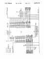
Referring now to FIG. 1, a computer system 100 with
certain components are illustrated schematically. A
system board 104 is illustrated as comprising a central
BRIEF DESCRIPTION OF THE DRAWINGS
processing unit (or “processor”) 106 operating in con
junction with other essential chip elements 110. The
The invention is better understood while reading the
following Detailed Description in conjunction with a
review of the accompanying drawings, in which like
reference designators refer to like elements throughout,
essential chip elements 110 may include, for example, a
math co-processor.
Before the present invention, a computer system
would have comprised a processor chip, such as an
and in which:
FIG. 1 is a schematic diagram illustrating the advan
tages of a preferred embodiment of the present inven
tion in allowing a plug~in module 102 to assume the
function of certain chips (such as 106 and 110) on the
system board 104 of a computer system 100.
FIG. 2 shows the connection of FIGS. 2A and 2B.
FIGS. 2A and 2B, collectively referred to hereinafter as
FIG. 2, are logical diagrams illustrating the 80386SX
processor 204 and 80387SX co-processor 203 as imple
mented in a plug-in module according to a ?rst embodi
ment of the invention.
,
80286, and a co-processor such as an 80287. These two
chips would have adhered to an industry standard, such
as the IBM ® AT TM standard.
The present invention provides that the computer
system comprising system board 104 may be upgraded
without removal or replacement of any chips or boards,
or addition of any substitute boards, to the system. The
present invention provides for the addition of an inven
tive plug-in module 102 into a connector 114. The pres
ent invention provides that the mere fact that the plug
in module 102 is installed insures that the system perfor
mance will be enhanced, in accordance with the perfor
mance characteristics of the circuit elements on the
FIG. 3 shows the connection of FIGS. 3A and 3B.
FIGS. 3A and 3B, collectively referred to hereinafter as 5 plug-in module 102.
FIG. 3, illustrate the Generic Array Logic (GAL ®),
In one preferred embodiment, for example, the 80286
processor 106 on the existing system board 104 is func
chips and the numeric processor interrupt logic as used
in the ?rst embodiment of the plug-in module according
tionally replaced by an 80386SX processor 108. Also,
to the present invention
FIG. 4 illustrates a connector 114 and part of the
the 80287 co-processor 110 may be functionally re
placed by an 80387SX co-processor 112. The connector
114 may be, for example, a connector, available from
clock selection logic from the ?rst embodiment of the
plug-in module according to the present invention.
FIG. SA illustrates a preferred implementation of a
logic con?guration on the 80286 system board, for al
lowing the 80286 processor to be functionally removed 45
from the computer system when a plug-in module ac
cording to the present invention is installed.
FIG. 5B illustrates a preferred implementation of
another portion of the system board’s clock selection
logic, and numeric processor interrupt control logic.
DETAILED DESCRIPTION OF THE
PREFERRED EMBODIMENTS
Burndy Corporation of Norwalk, Connecticut. In this
manner, the simple addition of a plug-in module 102
enhances system performance, while not sacri?cing the
AT TM -compatibility of the system as originally con?g
ured with only system board 104.
It is understood that partial functional replacement is
encompassed by the present invention. That is, not
every essential chip on the system board 104 need be
replaced, functionally, by a corresponding enhanced
circuit on the plug-in module 102. Certain sub-sets of
the essential chips may be enhanced.
Also, the simple insertion of the plug-in module need
not be the only means of communicating to the rest of
In describing the preferred embodiments of the in
vention, speci?c terminology will be used, for the sake 55 the system that the function of certain elements of the
system board 104 are being usurped. It lies within the
of clarity in describing the speci?c embodiments to
contemplation of the present invention that hybrid up
those skilled in the art. However, the invention is not
intended to be limited to the speci?c terms so selected,
grades, involving combinations of the plug-in module
and/or replacement or modi?cation of the system board
and it is understood that each speci?c term includes all
technical equivalents which operate in a similar manner 60 and/or addition of a supplementary board with a cable
leading to the original processor slot, and so forth. In
to accomplish a similar purpose. Also, particular chips,
this manner, "upgrades of upgrades” are possible. The
chip sets, industry standards, computer systems and
invention is not to be limited to a system con?guration
other elements are presented and described in detail, so
containing only the elements shown in FIG. 1. Addi
as to describe the particular embodiments presented.
However, the invention is not to be limited by the par 65 tional elements may be present and still fall within the
scope of the appended claims, even if the additional
ticular embodiments contained herein, but should be
elements are involved in other performance enhance
de?ned only in accordance with the claims which fol
low and their equivalents.
ment schemes.
5
5,297,272
6
A third input to the combinatorial logic is the signal
The details of operation of the embodiments of the
present invention will next be presented.
Shown in FIG. 3 are two logic devices 206 and 202.
These logic devices may be implemented using a variety
output f rom pin 14 of the GAL ® 206. As can be seen
f rom the 206 logic equations (Appendix A), this signal
is activated during a halt instruction or a shut-clown.
This signal is needed because the NEAT TM chip set
would not provide a signal in these circumstances, caus
of circuits, but generic array logic (GAL® ) and pro
grammable array logic (PAL @ ) chips are preferred. In
the exemplary illustrated embodiment, GAL chips 206
ing the system to hang inde?nitely. The system would
and 202 are GAL l6V8-l5 and GAL 20V8-15, respec
hang, were it not for the fact that the SXREADY#
signal can be activated by the signal from pin 14 of the
tively, available from Lattice Semiconductor Corpora
tion, PO. Box 2500, Portland, Ore. 97208; 555 N. E.
Moore Court, Hillsboro, Ore. 97l24. See “GAL ®
DATA BOOK,” (Lattice, 1988). As is known in the art,
206 GAL @ .
In the preferred embodiment, the function of a three
input, active-low OR gate is implemented using two
two-input 74FO8 NAND gates, connected in series.
The output of gate 222 is input to the ?rst input of the
second gate 221. The second input of gate 221 receives
the READY# signal. Gate 222 receives the 387
READY# signal and the signal from pin 14 of the 206
certain GAL @ chips, such as the V series from Lattice
Semiconductor Corporation advantageously allow the
outputs to be either combinatorial or registered, allow
ing design ?exibility and minimization of IC count.
Briefly, GAL ® 206 converts signals (such as status
and control signals) from the 80386SX format and tim
ing into other (e.g., status and control) signals which are
readily usable by circuits expecting format and timing
GAL ® . The output of gate 221 constitutes the
20
from an 80286 processor. This allows the rest of the
computer system to be “spoofed” into believing that an
80286 processor may still be present and operating in
the computer system. In particular, the computer sys
tem is still AT TM -compatible.
The following is a description of the signals which
are input and output to GAL ® 206. A brief description
of the origin, function and destination of certain signals
25
SXREADY# signal.
Pin 5: SXM/IO#; Pin 6: D/C#; and Pin 8: W/R#:
These three status signals, generated by the 80386SX,
de?ne which category of the eight cycle categories is
presently being executed. A de?nition of the cycle cate
gories is published, and therefore available to those
skilled in the art.
Pin 7: SCLK: A signal generated at pin 18 of the
second GAL @ 202, used to maintain the phase rela
tionship for generating signals SO# and SI# at pins 16
and 17 of the ?rst GAL ® 206. The SCLK signal pro
vides for a division by two of the clock signal from, in
manner consonant with their use on the 80286 system
the preferred embodiment, 32 MHz to 16 MHz.
board, so that those skilled in the art would readily
Pin 9: 386 BHE#: A Byte High Enable signal, gener
appreciate the implementation and use of the signals on
ated by the 80386SX, governing a choice of operating
the preferred plug-in module according to the present
invention.
35 on only 8 of 16 bits, for example, on devices having only
8-bit data lines.
Referring to FIG. 3, the input and output signals of
Pin 11: HLDA: A Hold Acknowledge signal gener
GAL @ 206 will ?rst be described.
ated by the 80386SX, causes the outputs of GAL @ 206
Pins 1 through 9, 11 and 12 are input signals; pins 13
to enter a high-impedance state.
through 19 are output signals.
Pin 12: NPCS: This input to the ?rst GAL ® 206 is
Pin 1: 386 CLKZ: An inverted form of the signal
identi?ed at pin 22 of the second GAL® 202. The
PROCCLK from the system board. In inverter 211
signal, described below, is active only if the present
(FIG. 3) inverts PROCCLK to account for the fact that
cycle is a co-processor cycle and a 387 processor is
the 80286 processor triggers on the negative edge of its
installed. Ultimately, this prevents the chip set on the
clock signal, while the 80386SX triggers on its positive
is presented. However, most of the signals are used in a
edge.
Pin 2: RESET 386: A clock reset signal originating
45 system board from responding when it should not re
spond.
directly from the second GAL® 202, described in
The outputs of GAL ® 206 will next be described.
greater detail below.
Pin 3: ADS#: An address strobe signal generated by
Pin 13: NA#: This “Next Address” signal is impor
Pin 4: SXREADY#: A signal, also input to the
80386SX, indicating that a cycle is over. The signal is
menting the plug-in card for the 80386SX upgrade
generated by combinatorial logic in FIG. 3, illustrated
55 de?nition of the status signals output by the 80386SX
tant to an understanding of an advantage of the present
the 80386SX, used to indicate that a new cycle has 50 invention.
As a background to understanding the importance of
begun, or that a new address and status signals have
the NA# signal, it should be appreciated that imple
been presented on the bus.
causes a problem to arise because of the difference in the
as logic elements 221 and 222. Briefly, the purpose of
which start its cycles. A certain known system trans
logic elements 221 and 222 are to govern the state of the
lates the 80386SX status signals to an 80286 format.
SXREADY# signal. This signal is governed by three
_However, this known implementation of the status sig
inputs. The two gates, 221 and 222, function equiva
lently to a S-input, active-low OR gate.
The ?rst input is the READY#signal generated from
duced system performance.
the chip set on the system board. The function of this
READY# is published and, therefore, readily available
to those skilled in the art.
nal translation causes time to be lost, resulting in re
The 80386SX has an input signal, named /NA, which
can be used to request the CPU place the “Next Ad
dress” onto the bus to begin the next cycle before the
current cycle has completed. In the known translation
The second input is the 387RDY# signal, which is a 65 scheme referred to immediately above, the /NA signal
signal output by the 80387SX chip at pin 57, signal
is either active all of the time, or is never active. When
READYO-. Its function, similarly, is published, and is
/NA is always active, it is necessary to employ four
therefore available to those skilled in the art.
74F373 latches, with latch control logic, so as to latch
7
5,297,272
8
address and status signals to maintain them in proper
time relation for the system board chip set.
This known translation scheme does not utilize the
stepping information (p. 11) describes the use of this
/NA signal to its fullest advantage. As appreciated by
80387SX, and functions in a manner known to those
skilled in the art.
signal.
Pin 6: 387BUSY#: This signal is generated by the
the present invention, the function of beginning the next
cycle before the current cycle has completed can be
Pin 7: REFREQ: This signal is generated on the
used to save the time lost in translating 80386SX status
signals to status signals having the 80286 format. In
designs according to the present invention, the /NA
signal is controlled to allow the release of the next ad
system board, and functions in a manner known to those
skilled in the art.
Pin 8: 387PEREQ: This signal is generated by the
O 80387SX, and functions in a manner known to those
dress when the changing of the address will not ad
skilled in the art.
versely effect the functioning of the system board chip
set. This selective control of the /NA input (here fed
directly from the NA#output of ?rst GAL® 206) is
achieved by simulating the timing of the 80286 proces
80387SX, and functions in a manner known to those
skilled in the art.
Pin 9: 387ERROR#: This signal is generated by the
-5
sor which only guarantees the address to be valid dur
ing limited timing periods. In this manner, the present
invention provides an implementation of the status sig
nal translation circuit using fewer lC’s, while not sacri
?cing the speed which would otherwise be lost due to
Pin 10: ERRLTCH: This signal is a latched error
signal which is generated at the data output of a second
D-type flip-?op 232, to be described in greater detail
below.
Pin 11: NPPRES#: This signal is normally pulled
high by means of a 10K pull-up resistor on a single
in-line package 201 (FIG. 3). The signal is also con
the translation process.
Pin 14: As described above, with respect to the
nected to ground signal 66 on the 80387SX socket. In
the preferred embodiment, this is used as a signal to
inform the rest of the circuit of the presence of an
SXREADY# input on pin 4, the output of pin 14 is fed
back to a gate 222, for ultimate generation of the
of the 206
according to
80387SX chip in the socket.
Pin 14: SXM/IO#: This signal is one of the three
signals de?ning the present cycle as belonging to one of
signal is also
Appendix A,
eight categories, described above, with respect to pin 5
of the ?rst GAL ® 206.
and is sent to the system bus for governing cycles where
only one of the two bytes is to be transferred.
Pin 16: SO# and Pin 17: Sl#: These status bits are
Pin 13: GND: The output enable signal is always
active (low), so that the output of the second GAL ®
generated according to the GAL® equations in Ap
202 are not forced to a high-impedance state.
pendix A, and are sent to the system board for control
of the function of de?ning the status of new cycles.
The outputs of second GAL® 202 will now be de
scribed.
Pins 18 and 19: These two signals are associated with
the state machine, and serve the function of maintaining
Pin 22: NPCS: This signal prevents improper control
of the 80387SX co-processor, speci?cally preventing
time relationship throughout the cycle.
As can be seen on FIG. A2, the two signals NA# f
the system board chips at from controlling it. The
NPCS signal is directly input to pin 12 of the ?rst
rom pin 13 of GAL® 206, and the signal from pin 14 of
GAL® 206, are connected to respective resistors of
GAL® 206. The NPCS signal, like all other signals
output from the second GAL® 202, are generated in
value lK-ohms to VCC.
accordance with GAL ® equations reproduced in Ap
pendix B.
SXREADY# signal. The generation
GAL® output on pin 14 is determined
the GAL ® equations in Appendix A.
Pin 15: BHE#: The byte high enable
generated according to the equations in
Pin 23: A23: This input is tied to A23.
The signals entering and leaving second GAL ® 202
will next be described.
Pins 1 through 11, 13, 14 and 23 are inputs, and pins
15 through 22 are outputs. The inputs will ?rst be de
scribed.
Pin 1: 387 CLKZ: This signal is an inverted form of
the PROCCLK signal generated on the system board. It
is essentially the same signal as the corresponding pin on
?rst GAL ® 206.
Pin 2: CHOLD: The CHOLD signal, generated by
the data output of a D-type tlip‘flop 231, allows mainte
45
Pin 21: RSTERR#: This signal resets the second
D-type f lip-f lop 232, and serves to reset a latched error
signal relating to the co-processor interface. It is di
rectly connected to the pre-set input pin 1 of the ?ip
flop 232.
Pin 20: HOLD386: This signal is input to the HOLD
input of the 80386SX.
Pin 19: RESET386: This signal is input to the
RESET input of the 80386SX.
Pin 18: SLCK: This clock signal is input to pin 7 of
nance of the proper clock relationships. As will be de 55 the ?rst GAL® 206. As described above, it serves to
divide by two a clock signal ultimately involved in the
scribed below, the CHOLD signal is a delayed form of
generation of the SO# and Sl# signals output from ?rst
GAL ® 206.
Pin 17: RESET387: This signal is input to the
hold acknowledge, and relinquish the data bus for such
functions as direct memory accesses and refresh cycles.
RESET input of the 80387SX.
Pins 3 and 4: RESET3 and RESET4: These signals
Pin 16: PEREQ386: This signal is input to the
are generated on the system board, and, generally, serve
PEREQ input of the 80386SX.
as software-invoked reset signals to the 386, and as
Pin 15: BUSY386#: This signal is input to the BUSY~
input of the 80386SX.
power-up signals to the 386 and 387, respectively.
Equations for generation of the above output signals
Pin 5: OUTFO#: This signal is generated on the 65
system board, and is involved in the write cycle of the
from second GAL ® 202 are presented in the equations
the HOLD signal generated on the system board. This
signal functions as a request to the 80386SX to give a
I/O Port F0. Here, it is used as a co-processor status
signal. The INTEL Application Note B3-STEP 80387
of Appendix B. Those skilled in the art are readily able
to understand and implement a GAL ® performing the
5,297,272
above functions, given the present description and the
10
Pins 112 and 113 of connector 114 receive the
accompanying equations.
ENCLK32MB# and ENCLK2SMB# signals, respec
tively. In the preferred embodiment, each of these two
signal lines are tied directly to ground during operation.
Referring now to the logic components 213, 223 and
214, which are connected to D-type ?ip-flops 231 and
232 (entry listed above), the control of the numeric
Jumpers 241 and 242 are not needed, operationally, but
are used during the development phase for flexibility.
In the preferred embodiment, when the signals are
low (tied to ground), the corresponding clock, either 32
processor interface for the 80387SX will now be de
scribed.
The data input of flip-flop 231 receives the HOLD
signal from the system board. The HOLD input is
clocked into 231 by signal 386CLK2, which is an in
verted version of the clock PROCCLK, itself generated
MHz or 25 MHz, is disabled. These signals are used on
the system board to enable a desired clock. For exam
ple, the 80286 processor functions on a 12.5 MHz clock
on the system board. The active-low clear input of the
which is derived from the 25 MHz clock enabled by the
?ip-?op 231 is tied high. Flip-flop 231 produces the
ENCLK25MB# signal. Conversely, when an 80386SX
CHOLD signal which is input to pin 2 of second
GAL ® 202.
Second ?ip-?op 232 receives its data input from the
15 MHz clock derived from a 32 MHz clock is enabled by
processor from the plug-in module is active, then a 16
the ENCLK32MB# signal. The preferred circuitry by
387BUSY# signal generated by the 80387SX /BUSY
output. The clock input of ?ip-?op 232 is received from
the output of inverter 213. The input of inverter 213
receives its input from the 387ERROR# signal output
from the /ERROR output pin 35 of the 80387SX. The
clear input of the second ?ip-?op 232 is tied high. As
described above, the preset input of second flip-flop
232 is driven by the RSTERR# signal generated by pin
21 of second GAL® 202. The second ?ip-?op 232
generates a data output signal ERRLTCH which drives
two inputs. The ?rst input has already been described
above, the pin 10 input to second CAL® 202. The
second input of NAND gate 223. The ?rst input of gate
223 is the 387ERROR# signal which is generated by
the output pins ERROR on the 80387SX. The output of
NAND gate 223 drives the input of inverter 214. The
which the proper clock signal is selected is described in
this speci?cation in detail, in the section relating to the
system board circuitry illustrated in FIG. B2.
Referring now to FIG. 2, the 80386SX processor and
the 80387SX co-processor are illustrated in a preferred
con?guration. Table II and Table III recite the pin
connections which are shown in FIG. A1. Generally,
25
the signals are used in a manner known to those skilled
in the art. The accompanying drawings, Table II and
Table III, and the accompanying text allow those
skilled in the art to implement the plug-in module and
the enhanced computer system according to the present
invention.
Referring more speci?cally to FIG. 2 it is seen that
the following connections are made. The active-low
ERROR input signal on pin 36 of the 80386SX proces
output of inverter 214 produces signal NPINT (numeric
sor is tied to VCC through a 1K resistor. Similarly, the
processor interrupt), which is sent to the system board, 35 STEN and CKM inputs of the 80387SX co-processor
tied to the output of a tri-state buffer 324 (FIG. B2).
are also tied high to VCC, also through the 1K resistor.
Speaking conceptually, the ?ip-?op and logic ar
The CLKZ input of the 80386SX processor receives
rangement just described causes a numeric processor
the 386CLK2 signal from the output of inverter 211
interrupt immediately if there is an error detected, be
(FIG. 3), driven through a 33-ohm series resistor. The
cause of the direct connection of the 387ERROR# 40 386 CLKZ signal is the inverted version of the
signal to the input of NAND gate 223. Also, an inter
PROCCLK signal generated on the system board.
rupt is generated if the 387BUSY# signal is clocked into
Similarly, the 386CLK2 input on pin 54 of the
the ?ip-?op 232 by the rising edge of the inverted
80387SX co-processor receives the 387CLK2 signal
387ERROR# signal as it becomes active. As described
which was generated by inverter 212 (FIG. 3), which
above, the latch 232 is pre-set by the RSTERR# signal, 45 signal is also driven through a 33-ohm series resistor.
This 387CLK2 signal is the inverted form of the
generated at pin 21 of second GAL® 202.
Next, the clock selection arrangement and the con
PROCCLK clock signal generated on the system
nector for the preferred plug-in module for the
board. The two signals, 386CLK2 and 387CLK2, are
80386SX upgrade. These features are illustrated in FIG.
advantageously ?ltered to remove noise from the clock
4.
signal. Such ?lters are advantageously implemented
Referring now to FIG. 4, a commonly employed 32
MHZ high-frequency crystal oscillator is shown at loca
tion 209. The 32 MHz clock oscillator at 209 produces
using a series combination of an 82 picofarad capacitor
and a 240-ohm resistor to ground. Separate capacitor
resistor ?lters should be used for the two clock signals
the CLKZOUT signal which drives pin 106 of the plug
(386CLK2 and CLKZ). It is advantageous to pull up
in rnodule’s connector 114. Preferably, a l2~ohm resis 55 certain signals to insure that they are at required levels.
tor is inserted in series to provide proper loading char
acteristics.
A connection of signals from the 80386SX plug-in
module and the system board is made through the con
It is preferable to implement the pull up function using
a single in-line package (SIP) of 10K resistors with one
common end tied to VCC. The signals which are indi~
vidually tied to respective lOK resistors include the
nector which is shown as 114 in FIG. 4. Also, Table I
following:
presents the connector pin connections in conjunction
with the schematic signal names and source/destination
W/R# output from the W/R- signal on pin 25 of the
80386SX processor;
The D/C# signal output f rom the D/C- signal on pin
24 of the 80386SX processor;
art, upon inspection of the ?gures and associated tables, 65 The SXM/IO# signal output from the M/IO- pin 23 of
are able to implement the preferred embodiment of the
the 80386SX processor;
enhanced computer system according to the present
The ADS# signal output from the ADS- output pin 16
invention.
of the 80386SX processor;
names of the signals as they are generated or received
on the plug-in and system boards. Those skilled in the
11
5,297,272
The 386BHE# signal output from the BHE- pin 19 of
the 80386SX processor;
The 387RDY# signal output from the READYO- out
put pin 57 of the 80387SX co-processor;
The 387BUSY# signal output from the BUSY- output
pin 36 of the 80387SX co-processor;
The 387ERROR# signal output from the PEREQ out
put pin 56 of the 80387SX co-processor; and
The NPRES# which is treated as effectively being an
12
by the simple insertion of a plug-in module is a central
feature of the present invention. Using a very small
number of logic gates, as shown in FIG. 5A, the func
tional removal of the 80286 processor (without necessi
tating its physical removal from the system board) con
stitutes a signi?cant advance in the art.
The placement into the hold state of the 80286 pro
cessor causes the HLDA output signal on pin 65 to
output from the normally grounded input pin 66 of
become active. The activation of the HLDA signal
should be masked, to prevent any circuits receiving it
the 80387SX co-processor (used as an input to pin 11
from believing that no processor at all was in control of
of second GAL® 202 (FIG. 3) to report the pres
the system. In f act, according to the teachings of the
present invention, the functional disablement of the
80286 processor on the system board is accompanied by
ence of an 80387SX processor in the co-processor
socket 203 on the plug-in module).
The 387PEREQ signal normally output from the
PEREQ output pin 56 of the 80387SX co-processor is
tied low through a 10K resistor to ground, so as to put
the signal in a known low state when the 80387SX
co-processor chip is not inserted. The default low state
of this 387PEREQ signal is designed to insure AT TM 20
compatibility.
the simple insertion of another processor, such as an
80386SX, on a separate plug-in module.
The presence of the 80386SX processor masks the
activated HLDA signal from the 80286 processor on
the system board in the following manner.
Referring again to FIG. 5A, the SXINST# signal
generated near the plug-in board connector 114 as a
The connections between the 80386SX processor and
the 80387SX co-processor will next be presented.
The W/R- output pin 25 of the 80386SX processor
result of the plug-in module’s insertion is fed to inverter
312. Inverter 312 produces an active-high SXINST
signal to indicate that the 80386SX plug-in module is
generates the W/R# signal which is input to the W/R 25 installed. When the SXINST signal is active (high), it
pin 41 of the 80387SX co-processor. The M/IO- output
disables the output of a tristate buffer 321, whose input
pin 23 generates the SXM/IO# signal which is input to
is the HLDA signal. In this manner, when the 80386SX
the NPS] input pin 44 of the 80387SX co-processor.
plug-in module is installed, the HLDA signal output
The ADS- output pin 16 of the 80386SX processor
from 321 is governed by the HLDA output pin 3 of the
generates the ADS# signal which is input to the ADS
80386SX processor (FIG. 2). By virtue of the bus con
input pin 47 of the 80387SX co‘processor.
nection in which the HLDA signal from the 80386SX
Any other connections of the input or output pins of
and the HLDA signal, which may be output from buffer
the 80386SX processor or the 80387SX co-processor
321, the disablement of buffer 321 relinquishes control
may be found through inspection of FIG. 2 and/or
of the hold acknowledge function to the new (80386SX)
Tables II and III.
35 module.
Referring now to FIGS. 5A and 5B, the portions of
On the other hand, when the 80386SX module is not
the circuitry of the system board, which are of special
installed, the SXINST signal (FIG. 5A) is low, allowing
interest to the present invention, will next be described.
the HLDA signal output from the 80286 processor on
FIG. 5A illustrates a preferred mechanism in which
the system board to control the system-wide HLDA
the 80286 processor on the system board is placed in a
signal shown at the far right of FIG. 5A.
hold state, so as to allow the 80386SX processor on the
FIG. 5B illustrates the preferred method of generat
plug-in module to take control of the system.
ing clocks for the system, and the method for genera
FIG. 5A illustrates the 80286 processor as element
tion of the numeric processor interrupt signal (N PINT).
358. Inverter 311 (preferably a 74F04), NAND gate 331
In particular, when the 80386SX plug-in module is in
(preferably a 74F00), inverter 312 (preferably a 74F04) 45 stalled into connector 114, the numeric processor inter
and tristate buffer 321 (preferably a 74Fl25) are illus
rupt signal NPINT is governed from that module, as
trated in the following configuration. The HOLD sig
described above, with respect to FIG. A2.
nal output from HOLD output pin 55 of the NEAT TM
Generally, the 80387SX co-processor on the plug-in
82C211 (FIG 5B) is input to inverter 311. The inverted
module is completely isolated from the chip set on the
HOLD signal from inverter 311 is input to the active
system board, with the exception of the interrupt (the
low input of gate 331. @20 The other input of gate 331
interrupt is generated for numeric co-processing er
is governed by the SXINST# signal generated on the
rors).
plug-in module, when inserted into connector 114. As
shown in FIG. 4, the SXINST# indicates to gate 331
processor, substantially more circuitry is required, and
In known techniques to support an 80387SX co
(FIG. 5A) when the 80386SX plug-in module is in 55 there still remains a question as to whether the known
stalled. When the 80386SX plug-in module is installed,
solution yields a machine which is fully AT TM com
pin 114 of connector 114 is grounded, so that the second
input of gate 331 is driven low, into its active state.
patible.
The output of gate 331, signal NHOLD, drives the.
HOLD input pin 64 of the 80286 processor.
timing and logic elements to achieve the timing and
interrupt functions described above. The third input of
the jumper 304 is driven by The CLKZOUT signal is
generated on the plug-in module. A middle conductor
In this manner, either an activated SXINST# signal
from the plugged-in 80386SX module (when installed),
‘
Referring now to FIG. 5B the 82C2ll is shown with
or the HOLD signal from the 82C2ll chip, can force
on the jumper 304 functions as the output of the jumper,
the 80286 processor into a hold state. Placing the 80286
so that the jumper effectively functions as a selector,
processor into the hold state effectively removes it from 65 choosing either the 32 MHz crystal locally generated
the system.
(for developmental testing) not, or (operationally) the
As described more generally above, the effective
CLK20UT clock generated on the plug-in module by
removal of the 80286 processor from the system board
the 32 MHz crystal oscillator 209 (FIG. 4). The middle
5,297,272
13
14
(output) pin of jumper 304, connected during operation
to the clock from the. plug-1n module, drives the input of
a
non-inverting
tristate
buffer _ 322
(preferably
_
TABLE I
concordancc For signals For 80386“ plug“
a
.
.
Connector
Signal
Plug~1n Module
Pin
Nam:
Connection
74Fl25). The output of buffer 322 is connected in common to the output of another tristate buffer 323. At any
given time, at most one of these two buffers is activated
so as to control their common output.
1
BHE#
GAL @ 206-15
2
S0#
GAL @ 20646
1
glc?fc
A crystal oscillator 306 with 25 MHz frequency
5
__
_
drives the input of second tristate buffer 323, preferably 10
through a 33-ohm series resistor. An inverter 313 (pref-
6
M/l0#
80386SX-23 (M/lO-);
631 ® 2065
erably a 74FO4) rece1ves the ENCLK25MB# signal
Z
__cc
v
_CC
generated on the 80386SX plugged-in module. The 313
inverter enables the local 25 MHz signal to reach the
9
10
_
_
.
.
.»
.
output of tristate buffer 323 when the system 15 to operate with a 12.5 MHz clock.
15
11
® 20647
v
12
13
RESET;
RESET4
vcc
vcc
GAL @ 2023
GAL @ 2024
The output node of the two tristate buffers 322 and
1‘;
vcc
gcc
323 drives the CLKZIN input pin 5 of the 82C211 pref-
16
_
_
erably through a 33-ohm series resistor.
20
In the above-described manner, the preferred cir-
17
18
_
—
—
.
.
.
cuitry selectwely chooses between a 25 MHz oscillator
(306) local to the System board (when no plug-in module is present), a 32 MHz oscillator (305) also local to
.
19
vcc
vcc
20
21
22
OUTFO#
3371mREFREQ
GAL ® 20”
INVERTER 214 (NPINT)
GAL @ 202-7
vcc
23
vcc
the system board (used, e.g., during development), or 25
24
_
_
the 32 MHz clock signal generated on the plug-in board
25
-
-
27
26
..
vcc
vcc
_
.
-
-
(advantageously used during operation when the plug
_
in module is installed.
_
28
_
Referring to FIG. 5B, the NPINT output pin 4 of the
29
-
-
82C2ll generates the 2871NT signal. For reasons analo- 30
3°
_
_
31
vcc
vcc
gous to those discussed above, with respect to the
.
.
32
_
_
HLDA hold acknowledge signal generated by the
80286 processor, it is desirable to remove the 287INT
33
34
DO
~
(DATA)
35
vcc
vcc
s1gnal from the system when the 80386SX plug-1n mod- 35
36
D1
(DATA)
ule is installed. The functional removal of the 287INT
37
D2
(DATA)
signal is achieved using a tri-state buffer 324, to whose
23
132C
vmc‘zTA)
input the 287INT signal from the 82C2ll is fed. The
SXINST signal (generated on FIG. B1) is high when
40
41
D4
D5
(DATA)
(DATA)
the 80386SX plug-in module is installed, thereby dis- 40
1%
82C
VOéAC-FA)
abling tristate buffer 324. Control of the NPINT net
connected to the output of the tristate buffer 324 is thus
44
45
D7
D8
(DATA)
(DATA)
surrendered to the inverter 214 (FIG. 3), described
is
:
_
42
D10
(DATA)
49
D11
.
.
above-
45
As described above, the flip-?ops 231 and 232, and
'
(DATA)
gates 213, 222 and 214 contribute to control the co-
2?
processor interface, handling error conditions and re-
52
D13
(DATA)
clocking the signals as needed for proper functioning
53
D14
(DATA)
_-
-
-
when the _80386SX plug in module is installed.
50
54
vmécTA)
D15
(DATA)
55
vcc
vcc
In addition to the systems described above, the pres-
56
D9
(DATA)
ent invention also provides a method for upgrading a
57
-
-
computer
processor,system
the ?rsthaving
processor
a system
having
board
a first
including
input which,
a ?rst
60
g3
A0
(ADDRESS)
when activated, causes the ?rst processor to be dis- 55
61
A1
(ADDRESS)
abled, the method comprising retaining the ?rst proces-
2g
gin)
(C‘XPSRESS)
sor on the system board; retaining the system board in
the computer system; and installing a plug-in module
64
65
A3
A4
(ADDRESS)
(ADDRESS)
into
the computer system, the plug _-in module. compris' _ 6O
66
67
A5
GND
(ADDRESS)
GND
mg a second processor, havlng at least certain performance characteristics different than performance char-
68
69
A6
A7
(ADDRESS)
(ADDRESS)
acteristics of the ?rst processor, and an installation an-
3(1)
gin)
855311555)
nouncement circuit for generating an installation an-
72
A9
(ADDRESS).
nouncement signal when the plug-in module is installed 65
73
A10
(ADDRESS)
in the computer system, in which method the installa-
z‘;
23D
(CQYDSRESS)
tion of the plug-in. module into the computer system
76
A12
(ADDRESS)
causes functional disablement of the ?rst processor.
77
AB
(ADDRESS)
5,297,272
19
pin [19. .16]
pin [15..13]
20
= llpipecyc, lbuscyc,lmods1, lmodsO];
= llmodbhe, lhltrdy, Ina];
Sdefine idle
"b'OO
$define active
,'b' 10
Sdefine pipelined 'b'11
Sdefine notall
'b'01
memr=
menu =
:
; I’ memory write or halt (‘I
mio &
ur
halt =
mic &
wr 8- !dc ;
-
id!" = lmio & lur
;
it»! = lmio & Hr
;
inta = lmio & lur & !dc ;
field buutate = l [buscyc,pipecyc] ,
sequence busstate C
present idle
if
9 & ads 8. sclk & lreset
next active
default
, ..
next idle
present active
if
reset
lads & sclk & lreset &
next idle
;
ready next idle
;
if
‘
if
g & ads & sclk & lreset & lready next pipelined ;
default
'
_
next active
;
present pipelined
_. if: _.__\_'__,; ' 4 ready & sclk & lreset
next active
t if - '- :
next idle
reset
default‘:
present notall
;
next pipelined ;
'
-
.
next idle
;
. )
mods0.d = ‘menu Z busstate: idle
- & ads & sclk
& lreset & g
# menu 8- busstatezactive - &v ads & sell: 8. ready & lreset & 9
{menu & busstateipipelined '
8. sclk 8. ready & !reset 8. g
# halt &__bl.nsstate:_idle - -_ -. & ads & sclk
&' lreseti g
# halt‘ & busstate:activ_e ' & ads & sell: 8. ready & lreset & g
5,297,272
_
22
21
ready
8
!reset
8
# halt 8 busstatupipelined - '
8 set): 8
8 !reset 8
# inta 8 busstate?dleua ' 8 ads 8 sclk
# inta 8 busstateactiye __ 8 ads 8 sell: 8 ready 8 !reset 8
# inta :. busstatezpipelined . ‘
8
I
8
#
__:. sclk a ready 8 lreset 8
ion. 8 busstatuidle
' 8 ads '8 sell:
8 lreset‘8
ready
8 !reset 8
iou 8 busstatemctive 8 ads- 8 sell: 8
iou 8 busstate=pipelined
8 sclk 8 ready 8 !reset 8
modsO 8 isclk 8 ireset;
mds1.d
na.d
= memr 8 busstatezidle
8 ads 8 sell:
8 !reset 8 g
# memr 8 busstateactive
8 ads 8 sell: 8 ready 8 Reset 8 g
# memr 8 busstatupipelined I -
8 sell: 8 ready 8 !reset '8 g
1
#
#
#
#
#
a:
#
#
#
8
8
8
8
8
8
:.
8
8
halt 8 busstate=idle
8 ads
halt 8 busstateactive 8 ads
halt 8 busstate:pipelined
inta 8 busstatezidle
8 ads
inta 8 busstatezactive 8 ads
inta 8 busstatupipel ined _
ior :- busstatezidle
:. ‘m
ior 8 busstateactive 8 ads
for 8 busstate:pipelined
mods‘! 8 !sclk 8 lreset ;
sell:
sell:
sclk
sclk
soil:
sell:
sclk
sell:
sclk
8 ready
8 ready
8 ready
8' ready
8 ready
8 ready
=
busstate: [idle,active] 8 ads 8 sell: 8 !reset
#
na 8 lsclk 8 I reset ; _
8
8
8
8
8
8
&
8
8
!reset
lreset
!reset
lreset
lreset
!reset
mm
lreset
!reset
8
8
8
8
8
8
a
8
8
g
g
g
g
g
g
9
9
g
8 g
hltrdy.d = |nods1 8 modsO 8 mio 8 HI‘ 8 !dc 8 sell: 8 !reset
# hltrdy 8 lsclk 8 lreset ;
modbhe.d
*%l
bhe 8 busstate: idle
8 ads 8 scUR
bhe 8 busstatemctive ,
8 ads 8 sclk '8 ready 8\!reset
bhe 8 busstatezpipelined
I
8 !reset
8 sclk 8 ready 8 {reset
modbhe 8 !ready 8 lreset _
# modbhe 8 !sclk 8 lreset ;
APPENDIX B
3
cu“) Equations for Second GAL“) 202 ' (Figure I)
module HUMSX
FLAG '-R2'
title ‘3879: