1
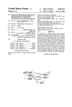
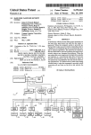
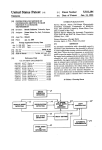
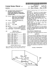
United States Patent [19]
[11] Patent Number:
Shenk
[45]
[54]
4.165531
4,210,959
METHOD AND APPARATUS FOR
DEFINING MAGNETIC DISK TRACK FIELD
LENGTHS USING A PROGRAMMABLE
COUNTER
Inventor: William H. Shenk, Acton, Mass.
[75]
[73] Assignee:
8/1979
7/1980
Apr. 2, 1985
Krause .............................. .. 364/200
Wozniak ........................... .. 364/200
Primary Examiner—Thomas M. Heckler
Honeywell Information Systems Inc.,
[57]
ABSTRACT
A method and apparatus for de?ning magnetic disk
track ?eld lengths using a programmable counter. Use
[21] Appi. No: 382,000
May 25, 1982
[22] Filed:
....................................... .. G06F 13/08
[51] US.
Int. Cl.~‘
Cl.
.............................................. .. 364/200
[52]
[53] Field of Search 364/200 MS File, 900 MS File
References Cited
[56]
of a programmable counter in a disk controller permits
a reduction in the amount of combinational logic that
would otherwise be required to be able to perform the
various formatting, reading and writing operations in
volved in use of just one type of disk and makes it possi
ble to perform these operations on a wide variety of
disks having different track and sector formats‘
U.S. PATENT DOCUMENTS
4/1978
Date of Patent:
Attorney, Agent, or Firm—Wil1iam A. Linnell; Nicholas
Prasinos
Waltham, Mass.
4,086,659
4,509,118
Cizmic et al. ..................... .. 364/900
4,148,098 4/1979 McCreight et a1.
364/200
11 Claims, 6 Drawing Figures
norm
574
556‘
stcmu
WW
ADDRESS
578
cum
596
\SELECT
y
L572
239
‘
568
ml
,
241
1
nuu PORTED
1
i
L m mans:
m
m
SECTOR
BYTEGIMK mu?
1
5707
'
m
:
249
9502
II scam 0m
243
U.S. Patent Apr. 2, 1985
Sheet 1 of6
m:
__
_
2.5
51
235 0 .5 5.3 28 moi 15:2 “. 82%;. Q63
rm:
81
$5
5,32
$5
4,509,118
U.S. Patent Apr. 2, 1985
Sheet2of6
“E852
35
LIv
mo /k
4,509,118
k33
$3.:
U.S. Patent Apr. 2, 1985
MEMORY
ADDRESS
(DEOIMAL)
Sheet4of6
4,509,118
MEMORY
CONTENTS
(HEXIDEOIMAL)
SYNO
LNUI“"OQDC
IDAM
—— CYLINDER NO‘
—- HEAD NO.
ID FIELD
—— SEOTOR NO,
-— ORO l
——— CRC 2
GAP 2
_]'— REPEAT FOR: END OF GAPZ,
DATA FIELD, GAP 3, GAP 4
F76‘. 4/1
U.S. Patent Apr. 2, 1985
MEMORY
ADDRESS
IDEDINALI
Sheet 5 of6
4,509,118
NENDRY
CONTENTS
(HEIIIDECINAL)
ID AN
—-—- CYLINDER N0.
—— HEAD N0,
ID FIELD
——- SECTOR ND.
—-— CRO I
_ CRC 2
GAP 2
N 1504M
DATA AM
256 BYTES
DSER DATA
279
280
28I
282
283
284
DATA FIELD
CNC I
—-—- CR0 2
BEGINNING OF GAP3
4,509,118
1
METHOD AND APPARATUS FOR DEFINING
MAGNETIC DISK TRACK FIELD LENGTHS
USING A PROGRAMMABLE COUNTER
RELATED APPLICATIONS
The following patent applications, which are as
signed to the same assignee as the instant application,
have related subject matter and are incorporated herein
by reference.
TITLE
Method and Apparatus For
vices can be classi?ed as to whether they are hard sec
tored or soft sectored.
A disk device is referred to as being a hard sectored
device if the information is recorded in physically de
?ned blocks of data, referred to as sectors, on the re
cording media. For example, in a hard sectored disk, the
disk may contain a series of holes which are detected by
the disk drive and one sector of information is recorded
INVENTORS
SERIAL
NUMBER
William H. Shenk
373,062
William H, Shenk
381,999
Addressing A Peripheral
Interface By Mapping Into
Memory Address Space
Method and Apparatus For
2
Although most disks have used this index mark to
indicate the beginning of a track, there is a wide variety
of formats used for recording data on disk devices.
These various methods of recording data on disk de
Generating A Repetitive
Serial Pattern Using A
Recirculating Shift Register
between a starting and ending sector hole. Therefore, in
a hard sector disk there is a sector hole which de?nes
the beginning of each sector such that a single sector
may consist of an identi?cation (ID) ?eld and a data
?eld contained in the sector between two sector holes.
In a soft sectored disk format there is usually an ID
?eld delineated by a unique address mark for each sec
20 tor on the disk. The address mark is actually detected by
the hardware by violating the coding rules for encoding
the information that is written on the disk. For example,
if the information is recorded on the disk using a modi
BACKGROUND OF THE INVENTION
?ed frequency modulation (MFM) technique, the ad
25 dress mark will be recorded on the disk in violation of
1. Field of the Invention
the MFM recording rules such that the violation will be
This invention relates to data processing systems; and
detected by the hardware. In disks which are soft sec
more speci?cally to a method of controlling the trans
tored, the identi?cation ?eld which is preceeded by an
ferring of data between a peripheral device and a pc
address mark is usually followed by a data ?eld which is
ripheral controller in a data processing system.
also preceeded by an address mark. This results in an
2. Description of the Prior Art
address (ID) ?eld and a data ?eld associated with each
Current data processing systems have a wide variety
soft sector. Using this soft sectored format, it is possible
of peripheral devices which are used to input, output
to have any number of sectors per track since there is no
and store information processed by the system. These
hardware mark on the disk to indicate the beginning of
peripheral devices include CRT terminals, card readers,
a
sector. This soft sectored format permits many sectors
magnetic tape units and various types of disk devices.
having short data ?elds or a few sectors having long
Among the disk peripheral devices, there are various
data ?elds to be recorded within a given track. Using
types including those which have rigid platters, and
those which have ?exible platters on which the infor
mation is recorded. Among the rigid disk devices there
exists several types-those which permit the recording
media to be removed from the drive unit and those
which have a non-removable recording media. A disk
device may contain both a removable and a non-remov
able recording media. A recent development in the rigid
disk device category includes a non-removable car
tridge in which the recording surface is enclosed and
some of these devices are known as Winchester type
disks. The ?exible disks are also known as ?oppy disks
and are usually removable from the disk drive itself.
These disk drives are usually interfaced to the data
processing system via means of a peripheral controller
which contains the logic which controls the reading
the soft sectored format, the identi?cation ?eld usually
contains information which uniquely identi?es the sec
tor by recording a sector number within the ID ?eld.
Therefore, using the soft sectored format, the periph
eral disk controller must be able to read the ID ?eld and
detect when the sector of interest is being read as deter
mined by the ID ?eld which is recorded within the
45 sector. This is to be contrasted with the hard sector
format in which the number of sector holes past the
index mark can be used to determine which sector is
currently being accessed.
Before a disk can be used to perform normal reads
and writes of user data, the disk must usually be initial
ized by a formatting operation which lays down on the
disk the initial values of the identi?cation ?elds, data
?elds and gaps between ?elds or sectors. This is particu
larly the case for soft sectored disks which require that
and writing of information from or to the recording
media.
55 the identi?cation ?elds and data ?elds be initialized so
Information is recorded on a disk in units of data
known as sectors. Depending upon the exact format
used to record the data, usually more than one sector is
recorded in a given track of the disk. The beginning and
ending of the track is usually determined by a track
index mark which is a notch on the edge of the disk.
Therefore, logic is usually provided such that upon the
detection of the track index mark, the sector to be read
will be located by reading the information on the track
that a normal read or write operation can locate the
speci?ed sector. One technique for formatting soft sec
tored disks is to write the complete track at one time
initializing all sectors within that track in one revolution
of the disk. This technique can require that suf?cient
memory to contain one complete track’s worth of infor
mation be available so that the memory can be initial
ized with the information required to write one com
plete track. Once the memory is initialized, a block
until the proper sector is found. Once the proper sector 65 transfer write to the disk is initiated upon the detection
is located, the information to be transferred will either
of the track index mark. This transfers consecutive
be written onto the disk or read from the disk in the
words, often containing a repetitive data pattern, from
located sector.
the memory to the disk until the complete track has
3
4,509,118
been written out from the beginning of the detection of
the track index mark until its second occurrence as the
disk revolves. Unfortunately, this technique requires a
memory sufficiently large to hold multiple sectors of
4
A triple programmable counter is used in a micro
processor based disk controller to de?ne the lengths of
the various track ?elds. For a soft sectored format, the
ID ?eld, data field and overall sector length. including
information and results in a memory which is under
all gaps, are de?ned. For a hard sectored format, a
utilized because, in the performance of normal read or
single ID ?eld and data field combination must be de
?ned. All of these ?elds can vary depending upon the
particular format used on a disk drive and the type of
write operations, a single sector disk read or write can
be done using a much smaller memory containing a
single sector of information.
Another problem which is often encountered in disk
controllers is the requirement that a single disk control~
ler handle a wide variety of disk devices. For example,
operation being performed. For example, data ?elds
may be de?ned to be different lengths depending on the
storage capacity requirements of the disk device and
depending upon whether a read or write operation is
being performed. During a read operation, data ?elds
a controller may be required to be able to read or write
do not include the gaps whereas during a write opera
from a Winchester type disk and also be required to
read or write from a ?oppy disk. In addition, there may 5 tion the gaps are included so that they are written onto
the disk.
be a variety of densities which can be used to record the
information on the disk media. For example, it is now
BRIEF DESCRIPTION OF THE DRAWINGS
common to have both single and double density ?oppy
disks within a single system and the format used to
record the information on a single density ?oppy disk
may vary from that of a double density ?oppy disk and
will be different from that of a Winchester type disk.
The requirement that a single controller handle this
wide variety of disk formats can require that very com
plex logic be provided to handle the various counting
operations which are required to detect the beginning
and end of various ID, data and gap ?elds that are re
corded on the disk. Therefore, what is required is a
technique which will allow a single disk controller to be
used with a wide variety of formats. This same tech
nique can be used to perform the various formatting
read and write operations found even within a single
disk format.
OBJECTS OF THE INVENTION
Accordingly, it is an object of the present invention
to provide a system in which a block of data containing
a repeated pattern can be transferred to a peripheral
device without requiring the complete block to be pres 40
ent before the transfer is initiated.
It is another object of the present invention to pro
vide logic that allows different formats of blocks of data
to be transferred with a minimal number of combina
tional logic elements to control the transfers as a func 45
The manner in which the method of the present in
vention is performed and the manner in which the appa
ratus of the present invention is constructed and its
mode of operation can best be understood in light of the
following detailed description together with the accom
panying drawings in which like reference numbers iden
tify like elements in the several ?gures and in which:
FIG. 1 is a block diagram of a clustered display con
troller system containing the present invention;
FIG. 2 is a logic block diagram of the disk controller
of the system shown in FIG. 1;
FIG. 3 illustrates the track format of a soft sectored
Winchester type disk that is used by the system shown
in FIGS. 1 and 2;
FIG. 4A illustrates the memory contents during pass
1 of a formatting operation used to initialize the track
format shown in FIG. 3;
FIG. 4B illustrates the memory contents during
passes 2 and 3 of a formatting operation used to com
plete the initialization of the track format shown in
FIG. 3; and
FIG. 5 is a more detailed logic block diagram of a
portion of the system shown in FIGS. 1 and 2 and illus
trates the present invention.
DESCRIPTION OF THE PREFERRED
EMBODIMENT
tion of the different block formats.
It is a further object of the present invention to pro
vide logic that allows for flexible block formats to be
utilized but yet still allows for the fast transfers of
blocks of data.
It is a still further object of the present invention to
provide a low cost peripheral controller.
This invention is pointed out with particularity in the
appended claims. An understanding of the above and
further objects and advantages of this invention can be
The method and apparatus of the present invention is
incorporated into the disk controller of the system illus
trated in FIG. 1. FIG. 1 illustrates a clustered display
obtained by referring to the following description taken
in conjunction with the drawings.
displays 1 through 16 via display controller 107. Clus
tered display controller 107 may be located in relatively
SUMMARY OF THE INVENTION
A method and apparatus for defining magnetic disk
track ?eld lengths using a programmable counter. Use
of a programmable counter in a disk controller permits
a reduction in the amount of combinational logic that
would otherwise be required to perform the various
formatting, reading and writing operations involved in
use of just one type of disk and makes it possible to
perform these operations on a wide variety of disks
having different track and sector formats.
system capable of controlling up to 16 displays, display
1 111, display 2 113 through display 16 115. Displays 1
through 16 are connected to clustered display control
ler 107 such that data entered from a keyboard of the
display may be transmitted via clustered display con
troller 107 to a host computer 117. Conversely, the data
originated in host computer 117 may be displayed on
close proximity to host computer 117 or may be re
motely located with transmission between the clustered
display controller 107 and host computer 117 taking
place over telephone lines connecting the two.
Disk controller 105 is coupled to clustered display
controller 107 to provide local storage of information
and programs used by the clustered display controller
107. The transfer of information to and from the disk
controller 105 to clustered display controller 107 takes
place via peripheral interface logic 109 within clustered
display controller 107. In the preferred embodiment,
5
4,509,118
disk controller 105 is capable of having one or two disk
devices, disk 1 101 and disk 2 103. In the preferred
embodiment, disk 1 101 and disk 2 103 may be con?g
ured as follows: a single Winchester type disk drive, one
Winchester type disk drive and one ?oppy disk drive,
or two ?oppy disk drives.
In the preferred embodiment, disk controller 105 is a
microprocessor based controller which may be up to
ten feet from the clustered display controller 107. Disk
controller 105 does all of the data retrieval, read/write
6
disk subsystem, and to reset the disk controller and
cause the microprocessor 231 to begin executing the
disk controller ?rmware at location 0.
Bus 229 represents the data, address and control bus
ses which connect microprocessor 231 with other com
ponents of disk controller 105. Random access memory
(RAM) 235 is a writable memory used as a workspace
by the disk controller operating system ?rmware. This
1K by 8 bit memory is used to contain images of the
control area found in the dual ported memory located in
head positioning, and status updating required by the
the peripheral interface logic 109 of the clustered dis
disk operating system software which is resident and
play controller 107. Disk data timing and control logic
executes in the clustered display controller 107. Com
239 provides the timing and control of data going to or
munications between the clustered display controller
from disks 201 and 203. Dual ported sector RAM 241 is
107 and disk controller 105 is done via by a byte parallel 15 a 1K by 8 bit memory that is used to store sectors of disk
interface 119 which is protected by a parity bit. Periph
data which are being written onto disk 201 or 203 or
eral interface logic 109 in clustered display controller
sectors of disk data read from disk 201 or 203. Dual
107 acts as an instruction decoder and a dual ported
ported sector RAM 241 is used as an intermediate stor
memory. An application program executing in the clus
age of the disk data as it is transferred between clustered
tered display controller 107 may access a command area
or a status in the buffer memory of peripheral interface
logic 109 as well as the data area. This dual ported
memory is shared between disk controller 105 and the
display controller 107 and disks 102 and 103.
Parallel/serial bidirectional shift register 243 is used
disk controller 105. Disc controller 105 periodically
scans the dual ported memory in the peripheral inter
face logic 109 for new commands and updates the status
201 and 203 and is stored in dual ported sector RAM
241. Comparator and CRC logic 249 is used to check
accordingly.
ters as the data is transferred between the disk and the
to convert the data from 8 parallel bits to a serial bit
stream as the data goes from dual ported sector RAM
clustered display controller 107 and is the vehicle by
241 to disks 201 and 203 and to convert it from a serial
which all but the most basic commands are passed to 25 bit stream to 8 parallel bits as the data comes from disks
and generate cyclic redundancy checks (CRC) charac
Disk controller 105 will now be described in more 30 dual ported sector RAM 241 and also allows a compari
son between the data stored in dual ported RAM 241
and the data from either disk 201 or 203. Winchester
functions to the disk drives attached to disk controller
data interface logic 251 is the interface logic which
105. In FIG. 2, disk drive 1 is shown as being an Win
contains differential drivers and receivers for data being
detail with reference to FIG. 2. Microprocessor 231
controls all head positioning, data transfer and status
chester disk 201 and disk drive 2 is shown as being a 35 written onto or being written read from Winchester
?oppy disk 203. Microprocessor 231, in addition to
controlling disk 201 and 203, also controls the interface
logic 263 which controls the transfer of commands and
data between disk controller 105 and clustered display
disk 201. Floppy data separation and precompensation
logic 253 performs the data separation and precompen
sation functions required of data going to or from
?oppy disk 203 in either single or double density mode.
controller 107.
As discussed hereinbefore, disk 201 is illustrated in
In the preferred embodiment, microprocessor 231 is
FIG. 2 as being a Winchester type disk and disk 203 is
an Intel 8085A microprocessor which is an S‘bit parallel
illustrated as being a ?oppy disk. In the preferred em
central processing unit and is described in the Intel
bodiment as described hereinbefore, disk controller 105
publication entitled, MCS-80/85 Family User's Manual,
can be configured to have either a single Winchester
copyrighted 1979, which is incorporated herein by ref 45 disk and/or a single ?oppy disk or it can be con?gured
erence. Clock 233 is coupled to microprocessor 231 and
to have two ?oppy disk drives. If two ?oppy disk drives
provides the basic clock frequency utilized by micro
are con?gured in the system, disk 201 would be the
processor 231. Read only memory (ROM) 237 is an 8K
second ?oppy disk and, instead of being connected to
(1K equals l024) by weight bit memory which contains
Winchester data interface logic 251, it would be con
programs (or microprograms) executed by micro 50 nected to ?oppy disk separation and precompensation
processor 231. 2K of ROM 237 is used for diagnostic
logic 253.
programs and the remaining 6K of ROM 237 is used for
Drive status ports 247 provide status information
the disk controller operating system firmware.
from disk drives 201 and 203 which consists of drive
Con?guration switches 255 are manually set when
ready, track 0 detection, and write protection indica
the disk subsystem is con?gured to indicate the types of 55 tors. Drive control ports 245 contain the logic associ
disk drives (Winchester or ?oppy disk) actually at
ated with stepping the disk read/write heads, the write
tached to the disk controller 105. Diagnostic light emit
gate, the read gate, and the in case of the Winchester
ting diodes (LEDs) 257 are 8 diagnostic indicators that
disk which can have up to 4 read/ write heads, the selec
are used to indicate the status of the disk subsystem as
tion of the read/ write head.
determined by the execution of the diagnostic programs
The operation of the logic illustrated in FIG. 5 will
stored in ROM 237. Panel LEDs 261 are indicating
now be discussed in conjunction with the formatting of
lights located on the front panel which are used to indi
a Winchester type disk. The format of the data on Win
cate whether the disk subsystem is in a bootstrap mode,
chester disk 201 is illustrated in FIG. 3. The Winchester
which of the two possible disk drives is selected and
drive 201 consists of either one or two non-removable
error conditions. Panel switches 259 are operator select 65 platters. Each platter provides two usable surfaces, each
able switches which are used to write protect informa
with its own read/write head. A single platter unit
tion stored on the disks, to indicate which of the two
contains two heads (1 for the top surface and l for the
possible disk drives are to be used for bootstrapping the
bottom surface), a two platter unit contains four heads.
7
4,509,118
The platters are composed of 256 cylinders. A cylinder
is the path over which the heads pass during one revolu‘
tion of the platters. One cylinder contains all the data
that can be accessed without moving the read/write
lead radially on the platters. The cylinder closest to the
outside edge of the platter is cylinder 00. The innermost
cylinder is 255. A track contains all the data accessed by
a single head in a single cylinder.
8
normal read or write operation from or to the disk, the
disk must be completely initialized. Initialization con
sists of writing on the disk, the track format illustrated
in Hg. 3 so that each sector of each track of each cylin
der is written onto the disk. During this formatting
operation, it is necessary that during one pass of the
track under the write head to write all of the ID ?elds
and gaps associated with that track onto the disk.
As mentioned before, this could be done by having a
Each track is divided into 32 sectors which are num
bered sequentially 0 to 31. The format is a soft sectored 0 memory with suf?cient capacity to hold all of the bytes
associated with one track and initializing the memory to
format (i.e., sectors are delineated by information re
contain the image of the track format. Then, on the
corded on the track and not by physical sector index
detection of the track's index mark, the ?rst word could
marks). Each sector is divided into an (ID) ?eld fol
be read from the memory and written onto the disk and
lowed by a data ?eld. Each of these ?elds is preceeded
by a unique address mark (AM). The encoding method 5 consecutive words read and written until the index
used is modi?ed frequency modulation.
FIG. 3 shows the track/sector format. A description
mark is again detected. However, this approach would
of each of the ?elds follows: The SYNC ?eld is a stable
ferred embodiment, a memory containing 10,416 bytes
of data. In the preferred embodiment this required ca
data pattern of all Us to allow the phased locked loop
require, in the case of a Winchester disk, in the pre
data separator to acquire lock on the read data. An 20 pacity of 10,416 bytes greatly exceeds the 1,024 bytes of
memory available in dual ported sector RAM 241.
address mark preceeds both the ID and data ?elds. It is
2 bytes in length with the ?rst byte always an A1 (hex
idecimal, base 16 notation indicated in FIGS. 3, 4A and
Therefore, in the preferred embodiment instead of writ
ing the total track format in one single pass, all of the ID
4B by signal quotes around the numbers) followed ei
?elds are written in a ?rst pass and the even sector data
number ?elds are written during a second pass and the
odd numbered sector data ?elds are written in a third
ther by an FE(16) which de?nes an ID address mark.
The A1(l6), i.e., base 16, pattern is made unique to any
other serial bit combination, violating the encoding
rules of MFM by omitting one clock bit. CYL is a single
pass. By splitting the format operation into three passes,
the l,024 bytes of information available in the dual
byte which indicates the cylinder address. 00(16) indi
cates the outermost cylinder and FF(l6) the innermost
cylinder for a total of 256 cylinders. HD is a single byte
ported sector RAM 241 is more than sufficient to for
which indicates the head address. A one platter disk has
2 heads, and a 2 platter disk has four heads. The head
address range is 00(16) to 03(16) for a total of 4 heads.
initializing individual tracks using less memory than
contained in one track and is made possible by the logic
illustrated in FIG. 5.
mat the disk and to do normal read and write operations
from and to the disk. This ability to format a disk by
SEC is a single byte indicating the sector address. The
In the preferred embodiment, incrementing address
number of sectors per track is 32. The sector address
range is 00(16) to 1F(l6). CRC 1 and CRC 2 are two
register 566 is comprised of 3 cascaded Texas Instru
ments type SN74LS193 synchronous 4-bit up/down
counters to form a 10-bit address register and shift/stor
bytes of cyclic redundancy check bits generated by the
age register 504 is a Texas Instruments type SN74LSl99
controller in order to detect errors. The polynomial
used is X(16)+X(l5)+X(2)+ 1 on both the ID ?eld and 40 8-bit universal shift/storage register. Both of these com
ponents are described in the Texas Instruments publica
the data ?eld. The data field is 256 bytes of user pro
tion entitled, The TTL Data Book For Design Engineers,
vided data.
Gap 1 immediately follows the track index mark.
This ?eld consists of 15 bytes of 4E(l6). The trace index
Second Edition, copyrighted 1976, which is incorpo
rated herein by reference. In the preferred embodiment,
mark is generated by photo electrically detecting a 45 CRC generator 528 is a Fairchild type 9411 CRC
generator/checker described in their data sheet entitled,
notch in the edge of the platter. This track index signal
9411 CRC Generator/Checker, copyrighted 1978, which
as illustrated in FIG. 3 is supplied by the disk drive once
is incorporated herein by reference.
each revolution to indicate the beginning of all tracks
The logic illustrated in FIG. 5 permits the dual
on a disk drive. Gap 2 separates the ID ?eld from the
data ?eld. It provides a known area for the data ?eld
write update splice to occur. The remainder of this ?eld
ported sector RAM 241 to be initialized to the contents
shown in FIG. 4A for writing the ID ?elds during the
also serves as the synchronization area for the data ?eld
?rst pass and to the contents shown in FIG. 4B to write
address mark. This gap contains 15 bytes of 00(16). Gap
the second portion of gap 2, the data ?eld, and the ?rst
portion of gap 3 as shown by the amount of data written
during a write update in FIG. 3.
3 is a speed variation tolerance area for the sector. It
consists of 15 bytes of 4E(16). Gap 4 is the speed toler
ance area for the entire track. It consists nominally of
FIG. 4A will now be discussed in detail. FIG. 4A
illustrates the contents of dual ported sector RAM 241
as set up for the ?rst pass of a formatting operation
The total nominal track capacity is l04l6 bytes. The
being performed on a Winchester disk 201. Prior to the
minimum track is the nominal track capacity adjusted
for a minimum 3 percent speed variance and is therefore 60 initiation of the ?rst pass of the formatting operation,
microprocessor 231 initializes dual ported sector RAM
10102 bytes. The write update signal illustrated in FIG.
353 bytes of 4E(l6).
3 shows the among of data within a sector that is up
dated each time a sector of data is written on the disk.
During normal read or write operations from or to
241 to contain the information shown in FIG. 4A in
memory location 0 through 39. After the microproces
sor has set up dual ported sector RAM 241 to contain
the disk, data is read from the disk or written to the disk 65 the data shown in FIG. 4A, the microprocessor initial
izes a series of counters in disk/data timing control logic
one sector at a time. For the Winchester disk, this al
239 and initializes incementing address register 566 to
lows the user to read or write 256 bytes of information
address location 0 of dual ported sector RAM 241.
at one time. However, before a user can perform a
9
4,509,118
Once these preliminary steps are completed, micro
processor 231 is placed in the hold mode thereby pre
venting it from doing further operations on dual ported
sector RAM 241 and also tri-stating the bus 229. The
actual data transferred to the disk then begins under the
control of disk/data timing and control logic 239 in
10
the binary ONE state. This same signal is connected to
the select (SEL) input and used to select between the A
and B inputs of multiplexer 542 so that as long as the
CRC is being generated, the data on line 506 is multi
plexed onto line 544 as data to the disk and after the
CRC is computed, the data from the output of CRC
conjunction with parallel/serial bidirectional shift regis
generator 528 on line 540 will be multiplexed onto line
544 as the data to the disk.
ter 243 and compare and CRC logic 249 which is shown
in greater detail in FIG. 5.
Having initiated the computation of the cyclical re
Once the microprocessor is put in the hold state and 10 dundancy check for characters, bytes 29 through 33 are
the writing of the ?rst pass of the format initiated, the
disk controller waits until Winchester data interface
logic 251 signals the detection of the track index mark
transferred to the disk a bit at a time as described above.
When byte 34 is to be transferred, which is initialized to
a 00(16) byte in dual ported sector RAM 241, instead of
taking the data from line 506 which appears at the A
on the disk. Once the track index mark is detected, the
8-bit byte of the ?rst location from dual ported sector
RAM 241 as addressed by incrementing address register
input of multiplexer 242, signal CRCCNTRL on line
532 which appears at the select (SEL) input of multi
plexer 241 selects that the B input data appear at the Y
outputs thereof such that the bits of data generated by
the CRC generator 258 which appear at the Q output
thereof will be transferred to the Winchester disk. After
566 is transferred via line 502 to be loaded into shift/s
torage register 504 by the load/shift signal on line 510 at
the function select (S0) input being in the load state and
the S1 input on line 514 being in the binary ONE state.
Once loaded with the ?rst byte of data, shift/storage
the ?rst byte of the two byte cyclical redundancy check
register 504 is clocked by bit clock signal on line 512 at
the clock (CLK) input and the serial data stream ap
has been transferred to the disk, the second byte is out
put by CRC generator 528 and is written onto the disk
pears on line 506 one bit at a time at the QAO output.
in place of word 35 which is a 00(16) byte as initialized
The serial bit stream on line 506 is fed to the data (D) 25 in dual ported sector RAM 241.
input of cyclical redundancy check generator 528 and
Having written CRC 1 and CRC 2 for the ID ?eld,
to the A input of 2 to l multiplexer 542. The clear
the process then continues to write out three bytes of
(CLR) input of shift/storage register 504 is not used and
00(l6)’s from locations 36 through 38 which are the ?rst
is therefore connected to a binary ONE on line 516. The
three bytes of gap 2. When word 39, which contains a
output control inputs G1 and G2 are respectively con
4E(l6) data byte is loaded into shift/storage register
nected to signals HLDAFFQ and SZODSB on lines
504, a counter in disk/data timing and control logic 239
518 and 520 and are used to disable the eight input/out
expires indicating that the last byte of data loaded into
put terminals QA to QH by placing them in the high
shift/storage register 504 is to be recirculated and be
impedance when data is not being transferred between
continually written onto the disk until the expiration of
shift/storage register 504 and dual ported sector RAM 35 another counter. This byte of 4E(l6) is chosen for the
241.
gaps because it is a good pattern on which to lock the
At this point in time, multiplexer 542 is selected such
phased locked loop data separator used in Winchester
data interface logic 251. The recirculation of the last
that the data at the A input appears at the Y output
thereof and therefore the serial data stream appears on
line 544 as data to the disk which is then processed by
byte of data from dual ported sector 241 is accom
plished by recirculating signal RECIR on line 508 se
lecting the A input of 2 to 1 multiplexer 254 such that
Winchester data interface logic 251 which performs the
modi?ed frequency modulation function before it is
the data appearing on the A input will appear on the Y
output on line 522 and be entered into the serial input
written onto Winchester disk 201. As each bit of the
data is written onto the disk, the bit clock signal on line
512 clocks shift/storage register 504 and performs the
parallel to serial conversion by shifting one bit of data
out. After eight bits have been shifted out of shift/stor
age register 504, the byte clock signal on line 570 at the
count-up (CNTUP) input of incrementing address reg
45
(SL) of shift/storage register 504. This recirculation has
been occurring for all previous words of data loaded
into shift/storage register 504 but was overridden by
the loading of a fresh byte of data from dual ported
sector RAM 241 by the load/shift signal on line 510
every eight bit clocks. Therefore, when the ?rst counter
ister 566 and increments to the next memory location so 50 expires upon the loading of the byte 39 into shift/stor
that the next memory location from dual ported RAM
241 will be available for loading into shift/storage regis
age register 504, the periodic loading is inhibited and
the recirculating mode of operation is entered.
ter 504 under the control of load/shift signal on line 510.
This process continues until location 29 starts to be
hold state and is free to update the contents of dual
At this time, microprocessor 231 is removed form the
transferred bit by bit to the disk. Location 29, which 55 ported sector RAM 241. Microprocessor 231 goes back
contains Al(l6), is the ?rst byte of the ID ?eld and
and increments byte 33 to the next sector number of the
requires that CRC generator 528 is reset by signal CRC
sector which will be formatted on the disk. Once this
RESET on line 598 at the master reset (MR) input so
incrementing of the sector number in location 33 has
that the cyclical redundancy check may be computed
been accomplished, the microprocessor is again placed
on the ID ?eld. The binary ZERO signals on lines 534
in the hold state while the 4E(l6) byte of data from
and 538 at the S0 and S2 polynominal select inputs
location 39 is written on to the disk for the completion
along with signal 0P08 on line 536 at the S1 polynomi
of gap 2, all of the data ?eld and the ?rst three bytes of
nal input selects which polynominal is used to compute
gap 3. After the ?rst three bytes of gap 3 have been
the cyclic redundancy check characters. The CRC
written onto the disk another counter expires indicating
generator 528 is clocked by signal bit clocking signal
PLOLR on line 530 at the clock (CLK) input. Compu
tation of the CRC is enabled by signal CRC CNTRL on
line 532 at the check word enable (EWE) input being in
65 that all but the end of gap 3 of one sector of data has
been written to the disk.
At this point, incrementing address register 566 is
reset by the reset signal on line 568 at the clear (CLR)
11
4,509,118
12
example, during pass 2 the data ?elds of all of the even
numbered sectors are written and during pass 3 the data
fields of all of the odd numbered sectors are written.
During passes 2 and 3, in addition to writing the data
?elds, the end of gap 2's and the beginning of gap 3’s are
input and the process is started over with location 0 of
dual ported sector RAM 241 being loaded into shift/s
torage register 504. The second sector of data is then
formatted onto the Winchester disk 201. This process is
repeated until 32 sectors of data have been written in
written as can be seen by the amount of data that is
the track being formatted on the disk. During the sec
written during a write update as illustrated in FIG. 3.
ond and subsequent sectors within the track, bytes 0
Prior to the beginning pass 2 of the format operation,
through 14 are used to complete the writing of gap 3
microprocessor 231 initializes dual ported sector RAM
instead of the writing of gap 1 which appear only at the
beginning of a track. After 32 sectors have been written 0 241 to contain the data pattern illustrated in FIG. 4B.
The data in dual ported sector 241 is used in two ways
on the track, a further counter expires and instead of
in passes 2 and 3. Bytes 0 through 9 are used to locate
inhibiting the circulation of the last byte of data and
the sector to be written and bytes 10 through 284 are
resetting incrementing address register to location 0 the
used to write the sector onto the disk. Locations 0
recirculation is allowed to continue such that 4E(16)
bytes will be written until the track index mark is en . .a 5 through 6 contain the ID ?eld of the sector which is to
be written and are initialized to contain the ID address
countered. The track index mark terminates the writing
mark, the cylinder number of the cylinder which is to be
of the track with the writing of gap 4 and takes micro
written, the head number of the head which is to be
processor 231 out of the hold mode.
used to write on one surface of the cylinder and the
Placing microprocessor 231 in the hold mode places
sector number of the sector within the track which is to
bus outputs of the microprocessor in the high impe
be written. Locations 5 and 6 are initialized to contain
dance state so that bus 229 can be used b other logic in
00(l6)’s for the cyclical redundancy check character
but these bytes are effectively ignored and the cyclical
redundancy check character generated by CRC genera
ory 241 is being accessed by parallel/ serial bidirectional
shift register 243 also guarantees that there will never 25 tor 528 is compared with the cyclical redundance check
disk controller 105 without interference. Placing micro
processor 231 in the hold mode when duel ported mem
character read from the disk. Locations 7 through 9
contain the 00(16) bytes which are the ?rst part of gap
2. Locations 10 through 21 contain twelve 00(16) bytes
arise a condition in which access by register 243 to
memory 241 will be inhibited because of a memory
access being made by microprocessor 231. This simpli
?es the logic and reduces the need for any buffering
between memory 241 and register 243 that would other
wise be required due to the fast disk transfer data rates.
A comparison of FIG. 4A with the track format
shown in FIG. 3 will show that upon the completion of
the ?rst pass of the formatting operation, the gap 1 has
been written with the ?nal data, the sync ?eld has been
written with the ?nal data, the ID ?eld has been written
which are to be written onto the disk to complete the
end of gap 2. Locations 22 and 23 contain the data
address mark. Locations 24 through 279 contain 256
bytes of 00(16) data which are to be written as the user
data within the data ?eld so that the user data will be
initially set to all zeros. Locations 280 and 281 are ini
tialized to 00(l6)’s but will be replaced in the data
stream to the disk with the cyclical redundancy check
character generated by CRC generator 528 which will
with the ?nal data including the proper generation of
the CRC 1 and CRC 2 cyclical redundancy checks, the
be the actual information written onto the disk. Loca
tions 282 through 284 contain three bytes of 00(16) data
?rst three bytes of gap 2 have been written with the
?nal data. The remainder of gap 2, the complete data 40 which are written onto the disk to initialize the begin
ning of gap 3 to its ?nal value.
?eld including CRC 1 and CRC 2 and the ?rst three
During passes 2 and 3 of a disk formatting operation,
bytes of gap 3 have been written with the value of
which is similar to a disk normal write operation and
415(16). The remainder of gap 3 has been written with
normal read operation, the disk/data timing and control
its final data and gap 4 has been written with its ?nal
logic 239 controls the locating of the sector to be writ
data. Therefore, what remains to be written with the
ten or read. This sector locating operation takes place
?nal data is the end of gap 2, the data ?eld and the
after the microprocessor 231 has initialized dual ported
beginning of gap 3. All of this data is updated during a
sector RAM 241 to contain the ID ?eld of the sector to
write update operation which will be done during sec
be located and the user data to be written on memory if
ond and third pass of the format operation.
a write is involved. Once microprocessor 231 is placed
In reviewing FIG. 4A, it can be seen that locations
in the hold mode, the sector locating operation begins.
3i, 32 and 33 must be initialized by the microprocessor
During the sector locate phase of passes 2 and 3, the
231 to contain variable data. Location 31 contains the
read head within Winchester disk 201 associated with
cylinder number of the track that is being written and it
the track on which the sector that is to be located re
is a value of 00(16) to FF(16) (i.e., 0 to the 255 decimal).
sides, is turned to the read mode. As data is read from
Location 32 contains the head number of the surface
the disk, Winchester data interface logic 251 detects the
being written and will contain a value for 00(16) to
occurrence of both gap 1 or the end of gap 3 both of
03(16). Location 33 will contain the sector number of
the sector that is being written and will contain a value
which consists of 15 bytes of 4E(l6) data. This 4E(16)
bit pattern is chosen because it is a good pattern for the
of 00(16) to 1F(l6) (i.e., O to 31 decimal). During the
formatting of any given track which takes place in the
phased locked loop circuitry within the Winchester
three passes, only location 33 which contains the sector
number needs to be updated as each sector is written
during the writing of any one track because the cylinder
data interface logic 251 to become locked onto. This
same 4E(l6) bit pattern was used to temporarily initial
ize the data ?eld of the sectors during pass 1 for this
and head numbers of all sectors within one track are the
same.
After pass 1 of the disk formatting operation is com
pleted, passes 2 and 3 are written.‘During pass 2 and 3,
the data ?eld of half of the sectors are written. For
same reason.
65
Once the phased locked loop circuitry becomes
locked onto the data being read from the disk, the Win
chester data interface logic 251 begins to look for the
occurrence of the “Al" address mark. When this oc
13
4,509,118
curs, the Winchester data interface logic 251 signals
compare and CRC logic 249 that a comparison should
begin between the ID ?eld being read from the disk
which appears on line 526 and the data coming from
dual ported sector RAM 241 which will appear on line
544. Therefore, once the end of the sync field is de
tected, incrementing address register 566 is reset so that
it addresses location 0 of dual ported sector RAM 241
which loads the shift/storage register 504 via line 50
with the ?rst byte of data of the ID ?eld. As each bit
clock occurs, the data is shifted out on line 506 which is
selected as the input of multiplexer 542 and therefore
appears on line 544 as data to the disk. However, in this
case of sector locating, the data is not actually trans
14
the disk, after receiving the three 00(16) bytes which
comprise the beginning of gap 2 and match the data
stored in locations 7 through l0 of dual ported sector
RAM 241, the disk/data timing and control logic 239
can safely assume that the current sector being read
from Winchester disk 201 is the same as the sector ad
dressed by the ID ?eld stored in dual ported sector
RAM 241.
At this point in time, disk/data timing and control
logic 239 changes the mode of operation from a read
mode which occurs during the sector locate phase of
passes 2 and 3 to a write mode of operation and the data
in locations 10 through 284 is written onto the disk in a
manner similar to that used to write the data during pass
ferred to the disk because a read operation is in
1 of the format operation. During this portion of pass 2
progress.
and pass 3, the second part of gap 2 is initialized to its
During this sector locate phase of a pass, the data
?nal 00(16) value, by writing the words in locations 10
from the disk appearing on line 526 at one input of
through 2l onto the disk, the data address mark con
exclusive OR 564 can be compared with the data which
tained in locations 22 and 23 is written on the disk, and
is coming from memory 241 and appearing on line 544 20 a user data ?eld of 256 bytes in initialized to an all zero
at the other input of exclusive OR 564. As long as there
value. After writing location 279 onto the disk, the
is a bit for bit match of the data to the disk with the data
output of CRC 528 is multiplexed onto line 544 and the
from the disk, the output of exclusive OR 564 on line
two byte (16 bit) cyclical redundancy check is written
562, signal DCMPRG, will be a binary ZERO and the
onto the disk. Following the writing of the cyclical
output of AND gate 558 on line 554, signal 25 redundancy check, the three bytes of 00(16) are written
CMPENBG, will be a binary ZERO.
onto the disk from locations 282 through 284 thus com
The output of AND gate 558 is enabled by compare
pleting the initialization of the beginning of gap 3 to its
begin signal COMPBEBQ on line 560 being a binary
?nal value.
ONE during the time that a comparison is to be made
At this point in time, the one completed sector has
between the data from the disk with the data to the disk.
been initialized and the microprocessor 231 is removed
As each bit of data is read from the disk, bit clock
form its hold mode and allowed to update location 4 to
(CLK) signal on line 556 at the clock (CLK) input of
indicate the next sector to be initialized. Because of the
compare flip-?op 546 clocks the output of the compara
relative speeds between the rate at which the data is
tor which appears at the data (D) input thereof thus
transferred to or from the disk and the speed of the
assuring that ?ip-?op 546 will remain in the reset state
microprocessor in its ability to update location 4 in dual
so that the compare error signal COMPERR on line 548
ported sector RAM 241, every other sector is written
at the Q output will remain a binary ZERO as long as
during pass 2 and pass 3 such that when microprocessor
there is a bit by bit match of the data coming from dual
231 updates the location 4 it increments it by 2 so that
ported sector RAM 241 with the data coming from
during pass 2 all of the even numbered sectors are writ
Winchester disk 201.
ten and during pass 3 all of the odd numbered sectors
Once there is a mismatch, compare ?ip-?op 546 will
are written.
become set and the Q-bar output signal DFENL on line
Once having updated location 4 in dual ported sector
550, which is connected back to the preset (PR) input,
RAM 241, the microprocessor is again put in the hold
will assure that the compare ?ip-flop remains set until
mode and a sector locate operation is initialized. When
cleared by a signal AMFH appearing at the clear (CLR) 45 the next sector to be written is located, the writing of
input on line 552. It being noted that before the sector
the data field takes place as described above. Once all 16
locate operation was begun, compare ?ip-?op 546 was
of the even numbered sectors are written during pass 2
cleared by signal AMFH on line 552. The occurrence of
the 16 odd numbered sectors are written during pass 3.
the compare error signal on line 548 is used to reset the
Once the disk is completed formatted by performing all
Winchester data interface logic 551 to again look for a
three passes on each track within the disk, the disk is
gap 1 or a gap 3 data pattern followed by a sync pattern
then available to perform normal read and write opera
and then followed by and ID ?eld from the disk which
tions. A normal write operation is very similar to that
matches the ID ?eld from dual ported sector RAM 241.
described above for pass 2 and pass 3 of the format
This mismatch of data will occur during a pass 2 or pass
operation with the exception that locations 24 through
3 of the formatting operation if the sector number of the 55 279 will contain the actual user data which is to be
sector currently being read from the disk is not the same
written within a sector as shown in FIG. 4B.
as the sector number contained in location 4 of the dual
As described above, each sector locate operation is
ported sector RAM 241.
performed during pass 2 or pass 3 of a format operation
If location 0 through 4 in dual ported sector RAM
or during the single pass of a normal read or write oper
241 match the data coming from the disk, which ap
ation. Each time a mismatch is found between the ID
pears on line 526, the output of CRC generator 528 is
?eld located in dual ported sector RAM 241 and the
multiplexed onto line 544 by the CRC control signal on
data coming from Winchester disk 201, the increment
line 532 selecting the B input to be output to the Y
ing address register 566 is reset to address memory
output of multiplexer 542. It being noted that CRC
location 0 by the reset signal on line 568 which appears
generator 528 was generating the CRC based upon the 65 at its clear input. During a normal sector read or a
data received at the data input from lines 506 for bytes
normal sector write operation, the logic in FIG. 5 oper
0 through 4. If the CRC characters generated by CRC
ates in a manner same as that described above for passes
generator 528 match the CRC found in the data from
2 and 3 of the disk formatting operation.
15
4,509,118
During a normal sector write operation, the write
head is activated and locations 10 through 284 contain
ing the end of gap 2, the actual user data and the begin
ning of gap 3 are written onto the disk along with the
16
TABLE l-continued
Floppy Disk Single Density Format
Frequency Modulation (FM) Encoding
FF(l6)
Address mark (1 byte).
cyclical redundancy check characters generated by
TRK
CRC generator 528 which are also written onto the
Track number byte
between 00(16) to 4C(l6) for
single sided media and
00(16) to 99(l6) for double
disk. Thus, during a normal sector write operation, dual
ported sector RAM 241 need contain only the contents
being initialized in locations 0 through 284 (see FIG.
48). During a normal sector read operation which is
SEC
similar to the normal write operation, for locations 0 to
9 at which point the logic looks for the data address
Data
sided media (1 byte).
Sector number byte
between 00(16) to lF(l6)
(1 byte)
mark. Upon detection of the data address mark, the data
input multiplexer 524 is selected to multiplex the B input
onto the Y output such that the data coming from the 15
disk on line 526 will enter the serial input (SL) of
shift/storage register 504 and once the full eight bits of
128 bytes of user data
(128 bytes).
Cyclic redundancy check
CRC l
CRC 2
bits created by controller
using a polynominal
X(l6) +X(l5) +X(l4) +X +1
on address mark, track,
sector, and data bytes (2
one byte have been assembled in it, the data is trans
ferred over line 502 to be written into dual ported sector
RAM 241. Thus, the data from the disk will be written
bytes),
Gap 2 of 00(l6)
generated by controller.
The gap length is determined
by drive and media
into locations 10 through 265 of dual ported sector
RAM 241 with the 12 bytes of 00(16) at the end of gap
2 not being written (see FIG. 4B). During a normal
sector read operation, after all 256 bytes of the user data
have been read into dual ported sector RAM 241, the
TABLE 2
error (ER) output of the CRC generator 528 on line 541
Floppy Disk Double Density Format
tolerances.
will be checked to see if a CRC error occurred.
Modi?ed Frequency Modulation (MF M) Encoding
From the above discussion, it can be appreciated that
the present invention in which a parallel to binary shift
register is used in a recirculating mode allows access to
32XFF(16)
the dual ported sector RAM 241 during portions of the
passes l, 2 and 3 of the format operation under condi
separator (32 byte).
D006)
Address mark (1 byte).
TRK
Track number byte between
00(16) and 4C(l6) for single
tions that would normally not be available to micro
sided media and 0006) to
99(16) for double sided
processor 231 if the recirculating mode of operation
was not employed. Thus, by recirculating the pattern
within shift/storage register 504, the microprocessor
231 can access dual ported sector RAM 241 and update
the sector number so that sequential sectors may be
written with correct sector numbers in one continuous
write operation. This freeing up of memory 241 for
updating by microprocessor 231 allows dual ported
sector RAM 241 to be considerably smaller than would
otherwise be required if it was necessary to contain a
Gap 1 sync bytes for
phased locked loop data
media (1 byte).
SEC
Sector number byte
between 00(16) and 1F(l6) (1
byte).
Data
CRC l
CRC 2
256 bytes of user data
(256 bytes).
Cyclic redundancy check
bits created by controller
using polynominal
X(l6) +X(l$) +X(2) +l 0n
address mark, track, sector
and data bytes (2 bytes).
Gap 2 of FF(16)
generated by controllerv
complete track’s worth of information in order to write
45
pass 1 of a format operation.
The gap length is determined
The above discussion has been in terms of the formats
by drive and media
used on the Winchester disk 201. In addition to the
tolerances.
Winchester disk 201, the disk controller 105 is capable
of having a ?oppy disk 203 attached to it. Floppy disk
By examining Tables 1 and 2 and comparing their
203 may be either a single density or double density
format with the format for the Winchester disk shown
?oppy disk. Whereas the Winchester disk described
in FIG. 3, it can be appreciated that for a single control
above has a soft sectored format (i.e., the beginning of
ler to be able to write all three formats a large amount
the sectors are not de?ned by holes in the platter), the
of logic would be required to enable the various count
floppy disk has a hard sectored format. The format used
ing operations required to write and read these differing
on the single density diskette, which is recorded using a
formats. In addition, even to write a single format
frequency modulation (FM) encoding technique, is
would require a wide variety of counters just to per
different from that found on the double density diskette
form the various formatting, reading and writing opera
which is encoded using a modi?ed frequency modula
tions used in a single format.
tion (MFM) encoding technique. Table 1 below shows
the sector format for the single density floppy disk and
Table 2 shows the format of a sector of the double
density diskettes.
within disk/ data timing and control logic 239. Turning
TABLE 1
Floppy Disk Single Density Format
Frequency Modulation (FM) Encoding
l5XOO(l6)
In the preferred embodiment, this problem of having
to provide for the writing of a wide variety of sector
formats is solved by the use of a programmable counter
Gap 1 allows for drive
tolerance (15 bytes).
now to FIG. 5, the operation of programmable counter
65 572 will be discussed in greater detail. In the preferred
embodiment programmable counter 572 is at Intel type
8253 programmable counter/timer chip which is de
signed for use as an Intel microcomputer peripheral.
17
4,509,l 18
This counter is described in the Intel publication enti
tied, Intel Component Data Catalogue 1979, copyrighted
1979, which is incorporated herein by reference.
Programmable counter 572 is organized as three inde
pendent 16-bit counter each of which counts at a rate up
to 2 megahertz. Various modes of operation of the
counter are programmable. Data bus 590 is an 8 bit
bidirectional tristatable bus that is used to interface
program counter 572 with the data bus portion of bus
229 of disk controller 105. Data bus 590 is used to pro
gram the modes of programmable counter 572 under
the control of microprocessor 231. Data bus 590, con
nected to the D0 to D7 inputs/outputs, is also used to
load each of the three 16-bit counters and to read each
of the three count values. Read/write logic within pro
grammable counter 572 accepts inputs from the data bus
and in turn generates control signals for overall counter
operation. This read/write logic is enabled or disabled
by a select signal on line 580 appearing at the CS input
of programmable counter 572 so that no operation can 20
occur or change the function of the programmable
counter unless the counter has been selected by the disk
controller logic. When signal MPRD on line 592 at the
18
the sync ?eld to the end of the gap 3 ?eld but in actual
ity counter l is used to count from the beginning of gap
1 through the 3 zeros at the beginning of gap 3. Counter
2 is used in a normal read or write operation of a soft
sectored disk to determine the length of the data ?eld.
that is, from the beginning of the data address mark
through the end of the cyclic redundancy check charac
ter 2 in FIG. 3. Counter 2 is not used in a hard sectored
format because in the hard sectored format the sector
consists of a single ?eld that is a combined ID and data
?eld so that the sector is treated as if it as one long ID
?eld and counter 0 is used to determine its length. Dur
ing a format operation of a soft sectored disk, counter 1
and counter 2 are the only counters that are used. The
values placed in counter 1 and counter 2 determine the
sector length that is formatted on the disk and by setting
them to predetermined values, the variable sector
lengths can be formatted onto a soft sectored disk.
This ability to use counters in programmable counter
572 in the manner of formatting in reading and writing
to the disk allows a great deal of ?exibility with a mini
mum of other hardware being required within disk/data
timing and control logic 239. Therefore, the counters in
read (RD) input is in the binary ZERO state, it indicates
that microprocessor 231 is reading data from one of the 25 programmable counter 572 are set up depending upon
the type of operation and the type of device that is
three counter values in programmable counter 572.
going to be accessed. The count values normally will be
When signal MPWR on line 594 at the write (WR)
different for the different types of operations. During a
input is in the binary ZERO state, it indicates that mi
read operation, the counts are different than when
croprocessor 231 is outputting data in the form of mode
doing a write operation to the same disk because the
information or loading one of the three independent
amount of data that is transferred. This can be seen from
counters in programmable counter 572. Signal CNTRA
the above discussion of the second and third passes of a
on line 596 at the A0 and Al input is a 2-bit address
formatting operation to a Winchester type disk and the
signal which is used to select one of the three counters
difference between a read and write operation.
to be operated on and to address the control word regis
For example, in a write operation to the soft sectored
ter for mode selection of programmable counter 572. 35
disk, not only is the data ?eld transferred to the disk but
When the select signal on line 580 is in the binary
the end of gap 2 and the beginning of gap 3 are also
ZERO state, it enables the programmable counter 572
transferred to the disk, whereas during a read operation
to perform a read or write of information onto data bus
590.
only the data address mark and the data field itself in
cluding the CRC are transferred. Read operations nor
Counters 0, 1 and 2 of programmable counter 592 are
mally transfer less data than write operations. This is
three independent 16 bit counters which are identical in
because that during a read operation the gaps which
operation. Each counter consists of a single, 16-bit,
preceed the data address mark are not read and they
pre-settable, down counter. Each counter is enabled by
serve the purpose of synchronizing the phase locked
an enable signal appearing at its gate (G0, G1 or G2)
input. Each counter decrements by one each time a 45 loop data separators so the data can be recovered from
the disk. In the preferred embodiment, the counts for
clocking signal appears at its clock (CLKO, CLKI, or
programmable counter 572 are loaded by microproces
CLKZ) input. When a counter counts down to zero, the
signal appearing at its output (Q0, Q1 or Q2) changes
sor 231 from a table that is stored in the controller pro
state. In the preferred embodiment of disk controller
gram in ROM 237. It is the responsibility of the control
105, programmable counter 572 is used to count the 50 ler ?rmware to determine the type of operation to be
number of bytes that are being read from or to dual
performed and to load counters 0, 1 and 2 from a table
ported sector RAM 241. Each of these counters is
in ROM 237 depending upon the type of disk and the
clocked by the byte clocking signal appearing on line
type of operation to be performed on that disk.
584.
Returning now to FIG. 5 and a discussion of the use
In the preferred embodiment, counter zero is used to 55 of programmable counter 572. Counter 0 is enabled by
determine the length of the ID ?eld if a soft sectored
signal ID enable on line 582. Once enabled, counter 0
format is being used (i.e., a Winchester type disk) and it
counts the number of byte clock signals occurring on
is used to determine the length of the entire data ?eld if
line 584 and when the predetermined count is reached,
a hard sectored format is being used (i.e., a ?oppy disk).
the output signal ID terminate on line 574 from the Q0
In the case of a ?oppy disk, counter zero can be set up
output goes to a binary ZERO indicating the count has
either to 128 or to 256 characters depending upon
been reached. Similarly, sector enable signal on line 586
whether a single or double density disk, counter zero is
is used to enable counter l and when its predetermined
being written. Counter 1 of programmable counter 572
count is reached, the sector terminate signal on line 576
is used when performing a format operation on a double
from the Q1 output goes to the binary ZERO state. In
density hard sectored disk or in a soft sectored disk. 65 a similar manner, the data enable signal on line 588
Counter 1 determines the length of the entire sector
enables counter 2 which when its predetermined count
~ field. For the Winchester disk format shown in FIG. 3
is reached, the data terminates on line 578 from the Q2
a sector length of 314 bytes goes from the beginning of
output goes to the binary ZERO state.
19
4,509,118
Although each of the three independent counters are
clocked by the byte clocking signal on line 586, all three
20
ing input and an expiration output, the signal pro
duced at the expiration output changing state once
a predetermined count has been reached after the
counter is clocked the predetermined number of
counters are not enabled simultaneously. Enabling of
the individual counters depends upon the events that
they are being used to count and the various enabling
signals on line 582, 586 and 588 are generated by other
b. enabling each of the plurality of independent
logic in the disk/data timing and control logic 239,
counters during the period of time in which a disk
which is not shown in FIG. 5.
For example, during a transfer operation to soft sec
tored Winchester type disk, counter 0 is used to count O
dent counter is being written on or read from the
times;
?eld associated with the corresponding indepen
disk;
the bytes of information in the ID ?eld and when the ID
terminate signal on line 574 goes to the binary ZERO
state, it goes into additional combinational logic which
c. clocking each independent counter each time one
unit of data of a plurality of units of data is accessed
from or to a memory the data inputs/outputs of
depending on the type of disk operation being per
which are coupled to the parallel inputs/outputs of
a parallel to serial shift register;
. loading said parallel to serial shift register with one
unit of data of said plurality of units of data from
formed will enable counter 2 which is used to count the 5
number of bytes of information in the data ?eld. For
example, if a disk read or write operation is being per
formed to a soft sectored disk, counter 0 is used to select
length of the ID ?eld. Each ID ?eld, as it is read from
the disk, is compared with the ID ?eld stored in dual 20
ported sector RAM 241 to see whether it is the desired
sector. If a favorable comparison between the ID ?eld
on the disk and the ID ?eld stored dual ported sector
RAM 241 is made, then counter 2 is enabled to either
transfer the information from dual ported sector RAM
241 to the disk during a write operation or to read the
information from the disk and write it into dual ported
sector RAM 241.
Because the counters in programmable counter 572
cannot keep up with the data rate at which individual
bits of data are transferred to and from the disk, count
ers within programmable counter 572 are used only to
count byte transfers. Therefore, the outputs of program
mable counter S72 appearing on lines 574, 576 and 578
are used to enable ?ner granularity bit counters which
can be then fully decoded to determine ?ner bit posi
said memory every time one unit of data is trans
ferred between said memory and said parallel to
serial shift register;
e. inhibiting the transfer of further units of data be
tween said memory and said parallel to serial shift
register upon the expiration of the appropriate one
of said independent counters.
2. The method of claim 1 further comprising the step
f. after step e, recirculating the bit pattern in said
parallel to serial shift register until a second
counter of said independent counters expires.
. The method of claim 2 further comprising the step
g. after step f, updating the contents of said memory
during the time that said bit pattern is recirculating
in said parallel to serial shift register.
. The method of claim 3 further comprising the step
tions within bytes of interest. These ?ner granularity bit
after step g, resetting an address register to address
a
?rst unit of data of said plurality of units of data
logic 239 when high resolution is needed and program
of said memory and returning to step b.
mable counter 572 is used to set up the gross timing and 40
5. The method of claim 1 wherein the programmable
control signals.
counter is initialized by a microprocessor.
As can be appreciated from the above discussion, the
6. The method of claim 5 wherein the serial bit pat
use of programmable counter 572 within the peripheral
tem
is written onto disk during a disk formatting opera
controller allows great ?exibility in the various formats
tion.
of sectors that can be read or written by a single periph
7. The method of claim 6 wherein the independent
eral device controller. This gives a single device con
counters are initialized from a table stored in a second
troller the ability to write variable length sectors or
memory where the values in the tables are predeter
write a wide variety of sector lengths. In addition, it
counters are used within disk/data timing and control
permits all different types of peripheral operations (for
matting, reading and writing) to be handled with the
minimum amount of combinational logic.
Although the preferred embodiment has been de
scribed primarily in terms of a disk controller, the pres
ent invention can be used in other applications where
there are multiple units of data to be transferred.
While the invention has been shown and described
with reference to the preferred embodiment thereof, it
will be understood by those skilled in the art that the
above and other changes in form and detail may be
made therein without departing from the spirit and
scope of the invention.
What is claimed is:
1. A method for de?ning magnetic disk track ?eld
lengths using a programmable counter comprising the
65
steps of:
a. initializing the programmable counter having a
plurality of independent counters, each of the inde
pendent counters having an enable input, a clock
mined for each of said plurality of independent counters
as a function of the disk type and the type of operation
to be performed.
8. The method of claim 7 wherein the types of disk
operations to be performed comprise: formatting a
track, reading a sector and writing a sector.
9. An apparatus for de?ning magnetic disk track ?eld
lengths comprising:
a. a programmable counter having a plurality of inde
pendent counters, each of said plurality of indepen
dent counters having an enable input, a clock input
and an expiration output;
b. a plurality of enable counter means. each of said
plurality of enable counter means connected to said
enable input of a corresponding one of said plural
ity of said independent counters;
c. a unit data clocking means connected to the clock
input of each of said plurality of independent
counters;
d. an incrementing address register;
4,509,118
21
e. a memory for containing a plurality of units of data,
an address input of said memory coupled to an
22
reaches its predetermined count its expiration out
put inhibits the further transfer of information from
address output of said incrementing address regis
said memory to said shift register and causes a last
unit of data transferred from said memory to be
ter;
- ? Parana] ‘0 serial Shift resist? having a Parallel 5
recirculated within said shift register and written to
"mm/output °,°“Pl°d '°adat?mpu_t/°ut1?m°fsa'd
memory’ a 5.6m? output 9f Sal? sh'ft. register con’
said disk until the expiration output of a second
counter of said plurality of independent counters
.
causes said incrementing address register to be
pled to a serial input of said shift register and to an
.
.
.
input for data to be written on a disk; and
. a bit clocking means coupled to a clocking input of i0
r
856
t t
0
10
-
-
-
ti
2 r0 ausin a ?rst um-t of data
ca 0“ e
c
g
from said memory to be transferred from said mem
said shift register, whereby as each unit of data is
transfered from said memory to said shift register
each of said plurality of independent counters is
‘
docked by Said unit clocking means and those
is initialized by a microprocessor to contain a subset of
ory to said shift register.
in)‘: apparatus- as in claim 9 WheTemFaid memory
independent counters of said plurality of indepen- 15 a dlsk track fQTmat'
dent counters enabled by its corresponding enable
counter means are incremented toward its corre-
_
_
~
I
11- The apparatus as 1" claim 10 wherein 531d Pro‘
grammable counter iS initialized by said microprocessor
using a table stored in a second memory.
sponding predetermined count, when a first
counter of said plurality of independent counters
25
30
35
45
50
55
65