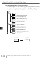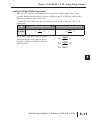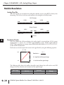
1
F0-04DAH-2 4-CH.
ANALOG VOLTAGE OUTPUT
CHAPTER
9
In This Chapter...
Module Specifications . . . . . . . . . . . . . . . . . . . . . . . . . . . . . . . . . . . . . . . . . . . . . . . .9–2
Connecting and Disconnecting the Field Wiring . . . . . . . . . . . . . . . . . . . . . . . . . . .9–4
Wiring Diagram . . . . . . . . . . . . . . . . . . . . . . . . . . . . . . . . . . . . . . . . . . . . . . . . . . . . .9–5
Module Operation . . . . . . . . . . . . . . . . . . . . . . . . . . . . . . . . . . . . . . . . . . . . . . . . . . .9–6
Special V-memory Locations . . . . . . . . . . . . . . . . . . . . . . . . . . . . . . . . . . . . . . . . . . .9–7
Using the Pointer in Your Control Program . . . . . . . . . . . . . . . . . . . . . . . . . . . . . .9–9
Output Scale Conversion . . . . . . . . . . . . . . . . . . . . . . . . . . . . . . . . . . . . . . . . . . . .9–11
Module Resolution . . . . . . . . . . . . . . . . . . . . . . . . . . . . . . . . . . . . . . . . . . . . . . . . .9–14
Chapter 9: F0-04DAH-2 4-Ch. Analog Voltage Output
1
2
3
4
5
6
7
8
9
10
11
12
13
14
A
B
C
D
Module Specifications
9–2
The F0–04DAH–2 analog output module offers the following
features:
• The DL05 and DL06 will update all four channels in one scan.
• The removable terminal block simplifies module replacement.
• Full 16-bit resolution.
NOTE: The DL05 CPU’s analog feature for this module requires DirectSOFT32 Version 3.0c (or later) and
firmware version 5.20 (or later). The DL06 requires DirectSOFT32 version V4.0, build 16 (or later) and
firmware version 2.30 (or later). See our website for more information: www.automationdirect.com.
DL05/06 Option Modules User Manual; 7th Ed. Rev. A, 08/11
Chapter 9: F0-04DAH-2 4-Ch. Analog Voltage Output
The following tables provide the specifications for the F0–04DAH–2 Analog Output Module.
Review these specifications to make sure the module meets your application requirements.
Output Specifications
Outputs per module
Output Range
Resolution
Output Type
PLC Data Format
Output value in program mode
Output Impedance
Load Impedance
Maximum Capacitive Load
Allowed load type
Maximum Inaccuracy
Maximum Full Scale Calibration Error
(including offset error)
Maximum Offset Calibration Error
Accuracy vs. Temperature
Maximum Crosstalk
4
0-10VDC
16-bit, 152µV/bit
Voltage sourcing/sinking at 5mA max.
1
16-bit, Unsigned Integer, 0–FFFF (binary) or 0–65535 (BCD)
0V (excluding PID, independent mode)
0.5 Ohms typical
>2000 Ohms
0.01 µF maximum
Grounded
0.2% of range (including temperature changes)
±.025% of range maximum
Linearity Error (End to End)
Output Stability and Repeatability
Output Ripple
Output Settling Time
All Channel Update Rate
Maximum Continuous Overload
Type of Output Protection
Output signal at power-up and power-down
External 24VDC Power Required
Base Power Required (5.0V)
1
±.025% of range maximum
±50 ppm/ °C maximum full scale calibration change
±10 counts
±16 count maximum (±0.025% of full scale)
Monotonic with no missing codes
±10 counts after 10 min. warm-up typical
.05% of Full Scale
.5 ms maximum, 5 µs minimum (full scale change)
100µs
Outputs current limited to 40mA typical. A continuous short
circuit will damage the output.
24VDC Peak Output Voltage
(capacitor transient voltage suppressor)
0V
45mA
25mA
Each channel requires 2 words of V-memory irrespective of the format used.
General Specifications
Operating Temperature
Storage Temperature
Humidity
Environmental air
Vibration
Shock
Field to Logic side Isolation
Insulation Resistance
Noise Immunity
Agency Approvals
Module Location
Field Wiring
Weight
0 to 55°C (32 to 131°F)
-20 to 70°C (-4 to 158°F)
5 to 95% (non-condensing)
No corrosive gases permitted
(EN61131-2 pollution degree 1)
MIL STD 810C 514.2
MIL STD 810C 516.2
1800VAC applied for 1 second (100% tested)
>10M ohms @ 500VDC
NEMA ICS3-304; Impulse 1000V @ 1mS pulse; RFI,
(145MHz, 440Mhz 5W @ 15cm); Worst case error during
noise disturbance is .5% of full scale
UL508; UL60079-15 Zone 2
Any slot in a DL05 or DL06 System
Removable Terminal Block
49 g (1.7 oz.)
DL05/06 Option Modules User Manual; 7th Ed. Rev. A, 08/11
1
2
3
4
5
6
7
8
9
10
11
12
13
14
A
B
C
D
9–3
Chapter 9: F0-04DAH-2 4-Ch. Analog Voltage Output
1
2
3
4
5
6
7
8
9
10
11
12
13
14
A
B
C
D
Connecting and Disconnecting the Field Wiring
9–4
WARNING: Before removing the analog module or the terminal block on the face of the module,
disconnect power to the PLC and all field devices. Failure to disconnect power can result in damage to
the PLC and/or field devices.
Wiring Guidelines
Your company may have guidelines for wiring and cable installation. If so, you should check
those before you begin the installation. Here are some general things to consider:
• Use the shortest wiring route whenever possible.
• Use shielded wiring and ground the shield at the transmitter source. Do not ground the shield at both
the module and the source.
• Do not run the signal wiring next to large motors, high current switches, or transformers. This may
cause noise problems.
• Route the wiring through an approved cable housing to minimize the risk of accidental damage.
Check local and national codes to choose the correct method for your application.
The F0–04DAH–2 does not supply power to field devices. You will need to power transmitters
separately from the PLC.
To remove the terminal block, disconnect power to the PLC and the field devices. Pull the
terminal block firmly until the connector separates from the module.
You can remove the analog module from the PLC by folding out the retaining tabs at the top
and bottom of the module. As the retaining tabs pivot upward and outward, the module’s
connector is lifted out of the PLC socket. Once the connector is free, you can lift the module
out of its slot.
Terminal Block Specifications
Number of Positions
Re-Order Number
Pitch
Wire Range
Screwdriver Size (Slotted)
Screw Size
Screw Torque
13
D0-ACC-4
.2 inch (5.08 mm)
28-16AWG Solid or Stranded Conductor;
Wire strip length 5/16" (7-8mm)
0.4T x 2.5W mm (part number DN-SS1)
M2.5 size
4.5 inch-pounds (.52 Nm)
DL05/06 Option Modules User Manual; 7th Ed. Rev. A, 08/11
Chapter 9: F0-04DAH-2 4-Ch. Analog Voltage Output
Wiring Diagram
Use the following diagram to connect the field wiring. If necessary, the F0–04DAH–2 terminal
block can be removed to make removal of the module possible without disturbing field wiring.
Typical User Wiring
Voltage Output
Ch. 1
Internal Module Circuitry
CH1
CH2
Voltage Output
Ch. 2
CH3
CH4
Voltage Output
Ch. 3
COM
voltage
sink / source
voltage
sink / source
voltage
sink / source
voltage
sink / source
CH1 DAC
CH2 DAC
CH3 DAC
CH4 DAC
OUT
ANALOG
0–10VDC
CH1
CH2
CH3
Voltage Output
Ch. 4
CH4
COM
COM
COM
SHIELD CONNECTED TO SIGNAL
SOURCE COMMON (1 OF 4 SHOWN)
COM
COM
COM
COM
+24VDC
ISOLATED ANALOG
CIRCUIT POWER
0VDC
24VDC
Power Supply
+24V
0V
F0-04DAH-2
isolated analog
circuit common
DL05/06 Option Modules User Manual; 7th Ed. Rev. A, 08/11
1
2
3
4
5
6
7
8
9
10
11
12
13
14
A
B
C
D
9–5
Chapter 9: F0-04DAH-2 4-Ch. Analog Voltage Output
1
2
3
4
5
6
7
8
9
10
11
12
13
14
A
B
C
D
Module Operation
9–6
Channel Scanning Sequence
The DL05 and DL06 will read all four channels of output data during each scan. Each CPU
supports special V-memory locations that are used to manage the data transfer. This is discussed
in more detail beginning in the section on “Special V–memory Locations”.
Scan
DL05/DL06 PLC
Read Inputs
Execute Application Program
Read the data
Store data
Scan N
Ch 1, 2, 3, 4
Scan N+1
Ch 1, 2, 3, 4
Scan N+2
Ch 1, 2, 3, 4
Scan N+3
Ch 1, 2, 3, 4
Scan N+4
Ch 1, 2, 3, 4
Write to Outputs
DL05/06 Option Modules User Manual; 7th Ed. Rev. A, 08/11
Chapter 9: F0-04DAH-2 4-Ch. Analog Voltage Output
Special V-memory Locations
Formatting the Analog Module Data
The DL05 and DL06 PLCs have special V-memory locations assigned to their respective option
slots. These V-memory locations allow you to:
• specify the data format (binary or BCD)
• specify the number of channels to scan (up to 4 channels for the F0–04DAH–2)
• specify the V-memory locations where the user program will store the output data pending
distribution to the output module
DL05 Data Formatting
The table below shows the special V-memory locations used by the DL05 PLC for the
F0–04DAH–2.
Analog Output Module
DL05 Special V-memory Locations
Data Type and Number of Channels
Storage Pointer
V7700
V7702
Data Type and Number of Active Channels Setup
System memory location V7700 is used to set the data
format either to BCD or binary and to set the number of
channels that will be active.
For example, loading a constant of 0004 (BCD) into
V7700 sets four channels active and causes the output
data value to be read from pointer-designated V–memory
as a BCD number.
Alternatively, loading a constant of 0084 (BCD) into
V7700 sets four channels active and causes the output
data value to be read from pointer-designated V–memory
as a binary number.
V7700 BCD setup
MSB
LSB
1 1 1 1 1 1 9 8 7 6 5 4 3 2 1 0
5 4 3 2 1 0
V7700 binary setup
MSB
LSB
1 1 1 1 1 1 9 8 7 6 5 4 3 2 1 0
5 4 3 2 1 0
Storage Pointer Setup
System memory location V7702 is used as a pointer. It points to a user memory location
where the analog output data is stored by the user program, pending distribution to the
output module. An octal number is loaded to the pointer memory to identify the beginning
of a block of user memory where output values are stored.
For example, loading O2100 into V7702 causes the CPU to look for Ch 1’s output data value
in V2100 – 2101, Ch 2’s data value in V2102 – 2103, Ch 3’s data value in V2104 – 2105,
and Ch 4’s data value in V2106 – 2107.
You will find an example program that loads appropriate values to V7700 and V7702 on
page 9–9.
DL05/06 Option Modules User Manual; 7th Ed. Rev. A, 08/11
1
2
3
4
5
6
7
8
9
10
11
12
13
14
A
B
C
D
9–7
Chapter 9: F0-04DAH-2 4-Ch. Analog Voltage Output
DL06 Data Formatting
1
2
3
4
5
6
7
8
9
10
11
12
13
14
A
B
C
D
9–8
Special V–memory locations are assigned to the four option slots of the DL06 PLC. The table
below shows these V-memory locations which can be used to setup the F0–04DAH–2.
Analog Output Module
DL06 Special V-memory Locations
Slot No.
Data Type and Number of Channels
Output Pointer
1
V700
V702
2
V710
V712
3
V720
V722
4
V730
V732
Data Type and Number of Active Channels Setup
System memory locations V700, 710, 720, and 730 are
V700 BCD setup
used to set the data format either to BCD or binary and to
MSB
LSB
set the number of channels that will be active.
1 1 1 1 1 1 9 8 7 6 5 4 3 2 1 0
For example, loading a constant of 0004 (BCD) into
5 4 3 2 1 0
V700 sets four channels active and causes the output data
V700 binary setup
value to be read from pointer-designated V–memory as a
MSB
LSB
BCD number.
Alternatively, loading a constant of 0084 (BCD) into
1 1 1 1 1 1 9 8 7 6 5 4 3 2 1 0
5 4 3 2 1 0
V700 sets four channels active and causes the output data
value to be read from pointer-designated V–memory as a binary number.
Storage Pointer Setup
System memory locations V702, 712, 722, and 732 are used as pointers. They point to user
memory locations where the analog output data is stored by the user program, pending
distribution to the output module. An octal number is loaded to the pointer memory to
identify the beginning of a block of user memory where output values are stored.
For example, loading O2100 into V702 causes the CPU to look for Ch 1’s output data value
in V2100 – 2101, Ch 2’s data value in V2102 – 2103, Ch 3’s data value in V2104 – 2105,
and Ch 4’s data value in V2106 – 2107.
You will find an example program that loads appropriate values to V7700 and V7702 on
page 9–10.
DL05/06 Option Modules User Manual; 7th Ed. Rev. A, 08/11
Chapter 9: F0-04DAH-2 4-Ch. Analog Voltage Output
Using the Pointer in Your Control Program
DL05 Pointer Method Using Conventional Ladder Logic
NOTE: The proper use of the DL05 pointer requires that the V–memory address be written to the special
memory location on the first scan only. Use the SP0 bit as a permissive contact when using the code shown
below.
The example program below shows how to setup the special V–memory locations. This rung
can be placed anywhere in the ladder program or in the initial stage if you are using stage
programming instructions.
This is all that is required to read the analog output data from V-memory locations. In the
example, V2100 is used, but you can use any user V-memory location.
SP0
LD
K4
Loads a constant that specifies the number of channels to scan and the
data format. The lower byte selects the data format (i.e. 0=BCD, 8=Binary)
and the number of channels (set to 4 for the F0-04DAH-2).
- or LD
K84
The binary format is used for displaying data on some operator
interface units. The DL05 PLCs support binary math functions.
OUT
V7700
Special V-memory location assigned to the option slot contains the
data format and the number of channels to scan.
LDA
O2100
This loads an octal value for the first V-memory location that will hold the data
to send to the output module. For example, the O2100 entered here would
designate the following addresses:
Ch1 – V2100-2101, Ch2 – V2102-V2103, Ch3 – V2104-V2105, Ch 4 – V2106-2107
OUT
V7702
The octal address (O2100) is stored here. V7702 is assigned to the option slot
and acts as a pointer, which means the CPU will use the octal value in this location
to determine exaclty where to get the data to send to the output module.
DL05 Pointer Method Using the IBox Instruction Available in DirectSOFT5
The following logic accomplishes the same thing as the previous ladder example, but it uses
the IBox instruction ANLGOUT.
Analog Output Module Pointer Setup
ANLGOUT
No permissive contact or input logic
is used with this instruction.
Base # (K0 - Local)
Slot #
Number of Output Channels
Output Data Format (0 - BCD 1 - BIN)
Output Data Address
DL05/06 Option Modules User Manual; 7th Ed. Rev. A, 08/11
IB-461
K0
K1
K4
K0
V2100
1
2
3
4
5
6
7
8
9
10
11
12
13
14
A
B
C
D
9–9
Chapter 9: F0-04DAH-2 4-Ch. Analog Voltage Output
DL06 Pointer Method Using Conventional Ladder Logic
1
2
3
4
5
6
7
8
9
10
11
12
13
14
A
B
C
D
9–10
NOTE: The proper use of the DL06 pointer requires that the V–memory address be written to the special
memory location on the first scan only. Use the SP0 bit as a permissive contact when using the code shown
below.
Use the special V–memory table below as a guide to setup the storage pointer in the following
Analog Output Module
DL06 Special V-memory Locations
Slot No.
No. of Channels
Output Pointer
1
V700
V702
2
V710
V712
3
V720
V722
4
V730
V732
example for the DL06. Slot 1 is the left most option slot.
The F0–04DAH–2 can be installed in any available DL06 option slot. The ladder diagram
below shows how to setup these locations with the module installed in slot 1 of the DL06. Use
the above table to determine the pointer values if locating the module in any of the other slot
locations. Place this rung anywhere in the ladder program or in the initial stage if you are using
stage programming instructions.
This logic is all that is required to write the analog output data from V-memory locations. In
the example, V2100 is used, but you can use any user V-memory location.
SP0
LD
K4
Loads a constant that specifies the number of channels to scan and the
data format. The lower byte selects the data format (i.e. 0=BCD, 8=Binary)
and the number of channels (set to 4 for the F0-04DAH-2).
- or LD
K84
The binary format is used for displaying data on some operator
interface units and the DL06 display. The DL06 PLCs support
binary math functions.
OUT
V700
Special V-memory location assigned to the first option slot contains the
data format and the number of channels to scan.
LDA
O2100
This loads an octal value for the first V-memory location that will hold the data
to send to the output module. For example, the O2100 entered here would
designate the following addresses:
Ch1 – V2100-2101, Ch2 – V2102-V2103, Ch3 – V2104-V2105, Ch 4 – V2106-2107.
OUT
V702
The octal address (O2100) is stored here. V702 is assigned to the first option slot
and acts as a pointer, which means the CPU will use the octal value in this location
to determine exaclty where to get the data to send to the output module.
DL05/06 Option Modules User Manual; 7th Ed. Rev. A, 08/11
Chapter 9: F0-04DAH-2 4-Ch. Analog Voltage Output
DL06 Pointer Method Using the IBox Instruction Available in DirectSOFT5
The following logic accomplishes the same thing as the previous ladder example, but it uses
the IBox instruction ANLGOUT.
Analog Output Module Pointer Setup
IB-461
ANLGOUT
No permissive contact or input logic
is used with this instruction.
Base # (K0 - Local)
Slot #
Number of Output Channels
Output Data Format (0 - BCD 1 - BIN)
Output Data Address
K0
K1
K4
K0
V2100
Output Scale Conversion
Calculating the Digital Output Value
Your program has to calculate the digital value to
U–L
send to the analog output module. Most A = H – L 65535
applications use measurements in engineering U = Engineering units to output
units, so it is usually necessary to convert from
engineering units to a suitable output value. The H = High limit of the engineering
unit range
conversion to an output value can be accomplished
by using the conversion formula shown.
L = Low limit of the engineering
unit range
You will need to substitute the engineering units for
A = Analog value (0 – 65535)
your scale into the formula to the right.
For example, if you want to output pressure (PSI)
between 0.0 and 100.0, you may multiply the pressure value by 10 to store in a V-memory
location and eliminate the decimal point. Notice how the calculations differ when you use the
multiplier.
The following example demonstrates how to output 49.4 PSI.
Example without multiplier
Example with multiplier
A=
U–L
H–L
65535
A=
U–L
H–L
A=
49 – 0
100 – 0
65535
A=
494 – 0
1000 – 0
A = 32112
65535
65535
A = 32374
DL05/06 Option Modules User Manual; 7th Ed. Rev. A, 08/11
1
2
3
4
5
6
7
8
9
10
11
12
13
14
A
B
C
D
9–11
Chapter 9: F0-04DAH-2 4-Ch. Analog Voltage Output
The Conversion Program in Standard Ladder Logic
1
2
3
4
5
6
7
8
9
10
11
12
13
14
A
B
C
D
9–12
The following example shows how you would write the program to perform the engineering
unit conversion. This example assumes you have BCD data loaded into the appropriate Vmemory locations using instructions that apply for the model of CPU you are using.
_First Scan
SP0
LDD
K100
Loads the constant 100 to the accumulator.
OUTD
V3000
Copies the constant 100 from the accumulator
to the memory location V3000 and V3001.
LDD
K65535
Loads the constant 65535 to the accumulator.
OUTD
V3002
Copies the content from the accumulator to the
memory location V3002 and V3003.
LDD
V2200
Loads data from V2200 and V2201.
MULD
V3002
Multiplies the accumulator value by 65535
(previously loaded into V3002 and V3003).
DIVD
V3000
Divides the accumulator value by 100
(previously loaded into V3000 and V3001).
OUTD
V2100
Copies the content of the accumulator to the memory
location V2100 and V2101.
_On
SP1
V2200/2201
V2100/2101
49
32112
DL05/06 Option Modules User Manual; 7th Ed. Rev. A, 08/11
Chapter 9: F0-04DAH-2 4-Ch. Analog Voltage Output
Analog and Digital Value Conversions
Sometimes it is useful to convert between the signal levels and the digital values. This is
especially helpful during machine startup or troubleshooting. The following table provides
formulas to make this conversion easier.
The formulas in the table show the relationship between A, the analog value, and D, the
digital value.
Range
0 to 10VDC
If you know the digital value
A=
10
. D
65535
For example, if you need a 6VDC signal to
achieve the desired result, you can use the
formula to determine the digital value that
should be used.
If you know the analog signal level
D=
D = 65535
10
D = 65535
10
D = 39321
65535 .
A
10
A
6V
DL05/06 Option Modules User Manual; 7th Ed. Rev. A, 08/11
1
2
3
4
5
6
7
8
9
10
11
12
13
14
A
B
C
D
9–13
Chapter 9: F0-04DAH-2 4-Ch. Analog Voltage Output
1
2
3
4
5
6
7
8
9
10
11
12
13
14
A
B
C
D
Module Resolution
9–14
Analog Data Bits
Two 16-bit words are reserved for the analog data whether you are using BCD or binary data
formatting. The 16 bits in the low word represent the analog data in binary format.
BCD Example
V2001
MSB
LSB
V2000
MSB
LSB
3 2 1 0 3 2 1 0 3 2 1 0 3 2 1 0
3 2 1 0
Binary Example
V2001
MSB
LSB
1 1 1 1 1 1 9 8 7 6 5 4 3 2 1 0
5 4 3 2 1 0
V2000
MSB
LSB
1 1 1 1 1 1 9 8 7 6 5 4 3 2 1 0
5 4 3 2 1 0
= data bits
Resolution Details
Since the module has 16-bit resolution, the analog signal is converted into 65,536 counts
ranging from 0 - 65,535 (216). A 0VDC signal would be 0 and a 10VDC signal would be
65535. This is equivalent to a binary value of 0000 0000 0000 0000 to 1111 1111 1111 1111,
or 000 to FFFF hexadecimal.
Each count can also be expressed in terms of the signal level by using the following equation:
0 – 10V
10V
Resolution =
H–L
65535
H = high limit of the signal range
L = low limit of the signal range
0V
0
65535
The following table shows the smallest detectable signal change that will result in one LSB
change in the data value for each increment of the signal change.
VDC Range
0 to 10VDC
Signal Span
(H – L)
Divide By
Smallest Detectable
Change
10 VDC
65535
153µV
DL05/06 Option Modules User Manual; 7th Ed. Rev. A, 08/11