1
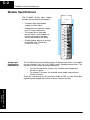
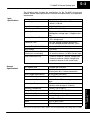
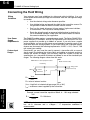
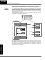
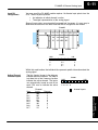
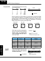
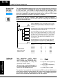
F4-08AD
8-Channel
Analog Input
In This Chapter. . . .
Ċ Module Specifications
Ċ Setting the Module Jumpers
Ċ Connecting the Field Wiring
Ċ Module Operation
Ċ Writing the Control Program
5
5–2
F4–08AD 8-Channel Analog Input
Module Specifications
ANALOG
The F4-08AD Analog Input module
provides several features and benefits.
S
S
S
S
It accepts eight single-ended
voltage or current inputs.
Analog inputs are optically isolated
from PLC logic components.
The module has a removable
terminal block, so the module can
be easily removed or changed
without disconnecting the wiring.
All eight analog inputs may be read
in one CPU scan (DL440 and
DL450 CPUs only).
INPUT
8 CHANNELS
F4–08AD
0–10VDC
0–5VDC
1–5VDC
±10VDC
±5VDC
4–20mA
CH1
COM
CH2
COM
CH3
COM
CH4
COM
CH5
COM
CH6
COM
CH7
COM
CH8
COM
CH1
IN
CH2
IN
CH3
IN
CH4
IN
CH5
IN
CH6
IN
CH7
IN
CH8
IN
24VDC 0.1A
0
V
F4–08AD
8-Channel Analog Input
Analog Input
Configuration
Requirements
24
V
The F4–08AD Analog Input module requires 16 discrete input points. The module
can be installed in any slot of a DL405 system, including remote bases. The
limitations on the number of analog modules are:
S For local and expansion systems, the available power budget and
discrete I/O points.
S For remote I/O systems, the available power budget and number of
remote I/O points.
Check the user manual for your particular model of CPU for more information
regarding power budget and number of local or remote I/O points.
F4–08AD 8-Channel Analog Input
5–3
The following table provides the specifications for the F4–08AD Analog Input
Module. Review these specifications to ensure the module meets your application
requirements.
Input
Specifications
General
Specifications
Number of Channels
8, single ended (one common)
Input Ranges
0–5V, 0–10V, 1–5V, $5V, $10V,
0–20 mA, 4–20 mA
Resolution
12 bit (1 in 4096)
Active Low-pass Filtering
–3 dB at 20Hz, –12 dB per octave
Input Impedance
250 ohms $0.1%, 1/2W current input
>20 Megohms voltage input, 1 Megohm minimum
Absolute Maximum Ratings
$ 45 mA, current input
$75V, voltage input
Conversion Time
0.4ms per channel (module conversion)
1 ms per selected channel minimum (CPU)
Linearity Error (End to End)
$1 count (0.025% of full scale) maximum
Input Stability
$1/2 count
Full Scale Calibration Error
(Offset error not included)
$12 counts maximum , voltage input
$12 counts maximum, @ 20mA current input
Offset Calibration Error
$2 counts maximum, unipolar voltage input
$4 counts maximum, bipolar voltage input
$4 counts maximum, 4 mA current input
PLC Update Rate
8 Channel per scan max.
Digital Input Points Required
16 (X) input points total
12 binary data bits, 3 active channel bits,
Power Budget Requirement
75 mA (power from base)
External Power Supply
18–30 VDC, 120 mA, class 2
Recommended Fuse
0.032 A, Series 217 fast-acting, current
inputs
Accuracy vs. Temperature
$50 ppm / _C maximum full scale (including
maximum offset change of 2 counts)
0 to 60_C (32 to 140° F)
Storage Temperature
–20 to 70_C (–4° F to 158° F)
Relative Humidity
5 to 95% (non-condensing)
Environmental Air
No corrosive gases permitted
Vibration
MIL STD 810C 514.2
Shock
MIL STD 810C 516.2
Noise Immunity
NEMA ICS3–304
One count in the specification table is equal to one least significant bit of the analog data (1 in 4096).
F4–08AD
8-Channel Analog Input
Operating Temperature
5–4
F4–08AD 8-Channel Analog Input
Setting the Module Jumpers
Jumper
Locations
If you examine the rear of the module, you will notice four banks of jumpers. The
module has several options that you can select by installing or removing these
jumpers:
S A bank of eight jumpers to set voltage or current input for each
channel.
S A bank of four jumpers to select the signal range for all active channels.
S A bank of three jumpers to select the number of channels used.
S A bank of two jumpers to select unipolar or bipolar signal range for all
active channels.
The module is set at the factory for a 4–20 mA signal range on all eight channels
with unipolar polarity. The following diagram shows how the jumpers are set at the
factory and describes the function of each jumper. When removing a jumper, store it
by placing it on a single pin to prevent losing it.
Voltage or Current Selection
For Each Channel
Jumper Locations
1
+4
+2
+1
2
3
4
5
6
7
Signal Range
Selection
8
Jumper on = Current
off = Voltage
BI
Number of
Channels
F4–08AD
8-Channel Analog Input
Selecting the
Number of
Channels
Polarity
The jumpers labeled +1, +2 and +4 are
used to select the number of channels
that will be used.
Any unused channels are not
processed. For example, if you only
select the first four channels, then the
last four channels will not be active. Use
this table to determine jumper settings.
Number of
Channels
Selected
1
2
3
4
5
6
7
8
UNI
Yes = jumper installed
No = jumper removed
+4
+2
+1
No
No
No
No
No
Yes
No
Yes
No
No
Yes
Yes
Yes
No
No
Yes
No
Yes
Yes
Yes
No
Yes
Yes
Yes
+4
+2
+1
Number of
Channels
Jumpers installed as
shown selects 8-channel
operation.
For example: To select
3-channel operation, remove
the +4 and +1 jumpers and
install the +2 jumper.
F4–08AD 8-Channel Analog Input
5–5
Selecting
Current or
Voltage
Notice the eight jumpers for selecting current or voltage settings for each individual
channel. For each channel install the jumper when you are using a current input or
remove the jumper if using a voltage input.
Selecting Input
Signal and
Ranges
The following table shows the jumper selections for the various ranges and are
grouped by bipolar and unipolar. The top portion of the table shows signal range
settings for when the polarity jumper is installed in the Bi (bipolar) position, and the
lower portion of the table shows settings for when the polarity jumper is installed in
the Uni (unipolar) position. These settings will apply to all active channels.
Bipolar Signal Range
Jumper Settings
–2 VDC to +2 VDC
(–8mA to +8 mA)
Signal Range
–2.5 VDC to +2.5 VDC
(–10mA to +10 mA)
Signal Range
–5 VDC to +5 VDC
(–20mA to +20 mA)
Signal Range
–10 VDC to +10 VDC
Polarity
Bi
Polarity
Bi
Uni
Polarity
Bi
Unipolar Signal Range
Uni
Polarity
Bi
Signal Range
Uni
Uni
Jumper Settings
Signal Range
0 to +5 VDC
(0 to +20 mA)
Signal Range
0 to +10 VDC
Signal Range
Polarity
Bi
Uni
Polarity
Bi
Uni
Polarity
Bi
Uni
F4–08AD
8-Channel Analog Input
4 to 20mA
(1 VDC to 5 VDC)
5–6
F4–08AD 8-Channel Analog Input
Connecting the Field Wiring
Wiring
Guidelines
Your company may have guidelines for wiring and cable installation. If so, you
should check those before you begin the installation. Here are some general things
to consider.
S Use the shortest wiring route whenever possible.
S Use shielded wiring and ground the shield at the transmitter source. Do
not ground the shield at both the module and the source.
S Don’t run the signal wiring next to large motors, high current switches,
or transformers. This may cause noise problems.
S Route the wiring through an approved cable housing to minimize the
risk of accidental damage. Check local and national codes to choose
the correct method for your application.
User Power
Supply
Requirements
The F4-08AD module requires a separate power supply. The Series DL405 CPUs,
D4-RS Remote I/O Controller, and D4-EX Expansion Units have built-in 24 VDC
power supplies that provide up to 400mA of current. If you only have a couple
analog modules, you can use this power source instead of a separate supply. If you
have more than four analog modules, or you would rather use a separate supply,
choose one that meets the following requirements: 24 VDC $10%, Class 2, 100
mA current (per module).
Occasionally you may have the need to connect a transmitter with an unusual
signal range. By changing the wiring slightly and adding an external resistor to
convert the current to voltage, you can easily adapt this module to meet the
specifications for a transmitter that does not adhere to one of the standard input
ranges. The following diagram shows how this works.
Custom Input
Ranges
NOTE: Remove current jumper in module.
Module internal circuitry
Field wiring
IN
Analog switch
+
50mA
Current
Transmitter
0V
R
–
R=
(Jumper removed)
250 ohms
Vmax
F4–08AD
8-Channel Analog Input
Imax
R = value of external resistor
Vmax = high limit of selected voltage range (5V or 10V)
Imax = maximum current supplied by the transmitter
Example: current transmitter capable of 50mA, 0 – 10V range selected.
10V
R=
R = 200 ohms
50mA
NOTE: Your choice of resistor can affect the accuracy of the module. A resistor that
has $0.1% tolerance and a $50ppm / _C temperature coefficient is
recommended.
F4–08AD 8-Channel Analog Input
Current Loop
Transmitter
Impedance
5–7
Standard 4 to 20 mA transmitters and transducers can operate from a wide variety
of power supplies. Not all transmitters are alike and the manufacturers often specify
a minimum loop or load resistance that must be used with the transmitter.
The F4-08AD provides 250 ohm resistance for each channel. If your transmitter
requires a load resistance below 250 ohms, then you do not have to make any
adjustments. However, if your transmitter requires a load resistance higher than
250 ohms, then you need to add a resistor in series with the module.
Consider the following example for a transmitter being operated from a 36 VDC
supply with a recommended load resistance of 750 ohms. Since the module has a
250 ohm resistor, you need to add an additional resistor.
R + Tr * Mr
R + 750 * 250
R w 500
R – resistor to add
Tr – Transmitter Requirement
Mr – Module resistance (internal 250 ohms)
DC Supply
0V
+36V
Module Channel 1
–
R
+
250
ohms
+
–
Two-wire Transmitter
Removable
Connector
The F4–08AD module has a removable connector to make wiring easier. Simply
remove the retaining screws and gently pull the connector from the module.
F4–08AD
8-Channel Analog Input
5–8
F4–08AD 8-Channel Analog Input
Wiring Diagram
NOTE 1: Shields should be grounded at the signal source.
NOTE 2: Unused channels should be connected to 0V
or have current jumpers installed.
Internal
Module
Wiring
See NOTE 1
+
CH2
Voltage
Transmitter
+
CH1
0V
–
CH2
0V
–
Channels 3–6 are not used,
See NOTE 2
CH3
CH3
0V
CH4
CH4
0V
CH5
CH5
0V
CH6
CH6
0V
CH7
2-wire
4–20mA
Transmitter
CH8
3-wire
4–20mA
Transmitter
CH7
0V
CH8
CH1
IN
250 ohms
IN
250 ohms
CH3
IN
250 ohms
CH4
IN
250 ohms
CH5
IN
CH6
IN
CH7
IN
250 ohms
F4–08AD
250 ohms
250 ohms
IN
+
(24VDC
typical)
+
–
CH1
COM
CH2
COM
CH3
COM
CH4
COM
250 ohms
CH6
COM
Jumpers for
CH5, 7 & 8
are installed
24V
–
A to D
Convertor
0–10VDC
0–5VDC
1–5VDC
+10VDC
+5VDC
4–20mA
CH5
COM
CH8
0V
Optional
External
P/S
0V
CH7
COM
CH8
COM
0
V
18-30VDC
CH1
IN
CH2
IN
CH3
IN
CH4
IN
CH5
IN
CH6
IN
CH7
IN
CH8
IN
24VDC 0.1A
OV
More than one external power supply can be used (see channel 8).
If the power supply common of an external power supply is not connected to 0V on the
module, then the output of the external transmitter must be isolated. To avoid “ground loop”
errors, recommended 4–20mA transmitter types are:
2 or 3 wire: Isolation between input signal and power supply.
4 wire: Isolation between input signal, power supply, and 4–20mA output.
F4–08AD
8-Channel Analog Input
8 CHANNELS
CH2
Analog Switch
CH1
Voltage
Transmitter
ANALOG
24
V
INPUT
5–9
F4–08AD 8-Channel Analog Input
Module Operation
DL430 Special
Requirements
Even though the module can be placed in any slot, it is important to examine the
configuration if you are using a DL430 CPU. As you will see in the section on writing
the program, you use V-memory locations to extract the analog data. As shown in
the following diagram, if you place the module so the input points do not start on a
V-memory boundary, the instructions cannot access the data.
F4–08AD
Correct!
8pt
Input
8pt
Input
16pt
Input
X0
–
X7
X10 X20 X40
–
–
–
X17 X37 X57
V40400
16pt
Input
16pt
Output
V40402
V40401
MSB
16pt
Output
X
3
7
LSB
X X
3 2
0 7
Wrong!
X
2
0
F4–08AD
8pt
Input
16pt
Input
8pt
Input
16pt
Input
X0
–
X7
X10 X30 X40
–
–
–
X27 X37 X57
16pt
Output
16pt
Output
Data is split over two locations, so instructions cannot access data from a DL430.
MSB
XX
3 2
0 7
LSB
X
2
0
MSB
X
1
7
V40400
XX
1 7
0
LSB
X
0
F4–08AD
8-Channel Analog Input
X
3
7
V40401
5–10
F4–08AD 8-Channel Analog Input
Channel
Scanning
Sequence
Before you begin writing the control program, it is important to take a few minutes to
understand how the module processes and represents the analog signals.
The F4-08AD module supplies one channel of data per each CPU scan. Since
there are eight channels, it can take up to eight scans to get data for all channels.
Once all channels have been scanned the process starts over with channel 1.
There are ways around this. Later we’ll show you how to write a program that will get
all eight channels in one scan.
Unused channels are not processed, so if you select only two channels, then each
channel will be updated every other scan.
Scan
Read inputs
Scan N
Channel 1
Scan N+1
Channel 2
Execute Application Program
Read the data
.
.
.
Store data
.
.
.
Scan N+7
Channel 8
Scan N+8
Channel 1
F4–08AD
8-Channel Analog Input
Write to outputs
Even though the channel updates to the CPU are synchronous with the CPU scan,
the module asynchronously monitors the analog transmitter signal and converts
the signal to a 12-bit binary representation. This enables the module to
continuously provide accurate measurements without slowing down the discrete
control logic in the RLL program.
5–11
F4–08AD 8-Channel Analog Input
Input Bit
Assignments
You may recall the F4–08AD module requires 16 discrete input points from the
CPU. These 16 points provide:
S An indication of which channel is active.
S The digital representation of the analog signal.
Since all input points are automatically mapped into V-memory, it is very easy to
determine the location of the data word that will be assigned to the module.
F4-08AD
8pt
Input
8pt
Input
16pt
Input
16pt
Input
X0
–
X7
X10 X20 X40
–
–
–
X17 X37 X57
V40400
16pt
Output
16pt
Output
V40402
V40401
MSB
Bit 15 14 13 12 11 10 9
X
3
7
LSB
8
7
6
X X
3 2
0 7
5
4
3
2
1
0
X
2
0
Within this word location, the individual bits represent specific information about the
analog signal.
Active Channel
Indicator Inputs
V40401
MSB
LSB
1 1 1 1 11 9 8 7 6 5 4 3 2 1 0
5 4 3 2 10
– channel inputs
F4–08AD
8-Channel Analog Input
The bits (inputs) shown in the diagram
indicate the active channel. The next to
last three bits of the V-memory location
indicate the active channel. The inputs
are automatically turned on and off on
each CPU scan to indicate the active
channel.
Channel
Scan
Inputs
Channel
N
000
1
N+1
001
2
N+2
010
3
N+3
011
4
N+4
100
5
N+5
101
6
N+6
110
7
N+7
111
8
5–12
F4–08AD 8-Channel Analog Input
Analog Data Bits
The first twelve bits represent the analog
data in binary format.
Bit
Value
Bit
Value
0
1
6
64
1
2
7
128
2
4
8
256
3
8
9
512
4
16
10
1024
5
32
11
2048
V40401
MSB
LSB
1 1 1 1 1 1 9 8 7 6 5 4 3 2 1 0
5 4 3 2 1 0
– data bits
Since the module has 12-bit resolution, the analog signal is converted into 4096
counts ranging from 0-4095 (212). For example, with a 0 to 10V scale, a 0V signal
would be 0, and a 10V signal would be 4095. This is equivalent to a a binary value of
0000 0000 0000 to 1111 1111 1111, or 000 to FFF hexadecimal. The following
diagram shows how this relates to each signal range.
–10V to +10V
–5V to +5V
+V
+V
0V – 10V
0V – 5V
4 – 20mA
1V – 5V
+5V
20mA
1V
4mA
0V
–V
0V
0
4095
0
4095
0
Each count can also be expressed in
terms of the signal level by using the
equation shown. The following table
shows the smallest signal levels that will
result in a change in the data value for
each signal range.
F4–08AD
8-Channel Analog Input
Range
0
4095
Resolution + H * L
4095
H = high limit of the signal
range
L = low limit of the signal range
Signal Span
(H - L)
Divide By
Smallest Detectable
Change
$10V
20 V
4095
4.88 mV
$5V
10 V
4095
2.44 mV
0 to 5V
5V
4095
1.22 mV
0 to 10V
10 V
4095
2.44 mV
1 to 5V
4V
4095
0.98 mV
16 mA
4095
3.91 mA
4 to 20mA
Unusable
MSB Bit
4095
When using some instructions, the most
significant bit (MSB) is read along with
the three active channel bits, and is not
available for other uses.
– unusable bit
V40401
MSB
LSB
1 1 1 1 11 9 8 7 6 5 4 3 2 1 0
5 4 3 2 10
Active Channel Bits
F4–08AD 8-Channel Analog Input
5–13
Writing the Control Program
If you have configured the F4–08AD module, use the following examples to get
started writing the control program.
Multiple
Channels
Selected
Since all channels are multiplexed into a single data word, the control program must
be set up to determine which channel is being read. Since the module appears as X
input points to the CPU, it is very easy to use the active channel status bits to
determine which channel is being monitored.
F4-08AD
8pt
Input
X0
–
X7
8pt
Input
16pt
Input
16pt
16pt
16pt
Input Output Output
X10 X20 X40
–
–
–
X17 X37 X57
V40400
V40402
V40401
MSB
Active
Unusable
Channel Bits
Bit
LSB
Data Bits
F4–08AD
8-Channel Analog Input
5–14
F4–08AD 8-Channel Analog Input
Reading Values,
DL430 CPU
4 4 4
430 440 450
The following program example shows how to read the analog data into V-memory
locations with the DL430 CPU. Since the DL430 does not support the LDF
instruction, you can use the LD instruction instead as shown. The example also
works for DL440 and DL450 CPUs. This example will read one channel per scan, so
it will take eight scans to read all eight channels. Contact SP1 is used in the example
because the inputs are continually being updated.
SP1
LD
V40401
ANDD
KFFF
BCD
LD
V40401
ANDD
K7000
SHFR
K12
OUTX
V3000
Loads the complete channel data word from the module into the
accumulator. The V-memory location depends on the I/O
configuration. See Appendix A for the memory map.
This instruction masks the channel identification bits. Without this,
the values used will not be correct, so do not forget to include it.
Since the DL405 CPUs perform math operations in BCD, it is usually
best to convert the data to BCD immediately. You can leave out this
instruction if your application does not require it (such as for PID
loops, which require the process variable to be in binary format).
This load instruction reads the data into the accumulator again. The
channel data will be pushed into the first level of the stack.
This instruction masks the analog data values and leaves the
channel ID bits in the accumulator.
Now you have to shift the accumulator bits so the channel ID bits will
result in a value between 0 and 7 (binary format). This value is the
offset and indicates which channel is being processed in that scan.
OUTX copies the value from the first level of the accumulator
stack to a source address offset by the value in the accumulator.
In this case it adds the above binary value (0–7) to V3000. The
particular channel data is then stored in its respective location:
For example, if the binary value of the channel select bits is 0,
then channel 1 data is stored in V-memory location V3000
(V3000 + 0) and if the binary value is 6, then the channel 7 data
is stored in location V3006 (V3000 + 6). See the following table.
Module Reading
Stored in ...
F4–08AD
8-Channel Analog Input
Note, this example
uses SP1, which is
always on. You could
also use an X, C, etc.
permissive contact.
Acc. Bits
Offset
Data
Channel 1
000
0
V3000
Channel 2
001
1
V3001
Channel 3
010
2
V3002
Channel 4
011
3
V3003
Channel 5
100
4
V3004
Channel 6
101
5
V3005
Channel 7
110
6
V3006
Channel 8
111
7
V3007
F4–08AD 8-Channel Analog Input
Single Channel
Selected
4 4 4
430 440 450
5–15
Since you do not have to determine which channel is selected, the single channel
program is even more simple.
SP1
LD or LDF
BCD
OUT
V3000
When X34 is on, channel 1 data is being sent to the CPU. Use the
LD instruction when using a DL430 CPU.*
The BCD instruction converts the data from binary to BCD.
You can leave out this instruction if your application does not
require it.
The OUT instruction stores the data in V3000.
Note: This example uses SP1, which is always on. You
could also use an X, C, etc. permissive contact.
* Remember, before the BCD instruction is executed, the DL430 requires an additional
instruction to mask out the first four bits that are brought in with the LD instruction. An example
of how to do this using an ANDD instruction is shown in the previous section.
Reading Values,
DL440/450
5 4 4
430 440 450
The following program example shows how to read the analog data into V-memory
locations with DL440 and DL450 CPUs. Once the data is in V-memory, you can
perform math on the data, compare the data against preset values, and so forth.
This example will read one channel per scan, so it will take eight scans to read all
eight channels.
SP1
LDF X20
K12
BCD
Loads the first 12 bits of channel data (starting with location X20) from
the module into the accumulator.
Converts the binary value in the accumulator to BCD and stores the
result in the accumulator. Use this BCD conversion if you want the
channel data to be stored as BCD. Do not use this instruction if you
are going to send the data to an internal PID loop because the PID
loop requires the PV (process variable) to be in binary format.
Loads the binary value of the three channel indicator bits, plus the
MSB, into the accumulator and pushes the channel data loaded into
the accumulator from the first LDF instruction into the first level of
the stack. X34 = X20 + 14.
OUTX
V3000
OUTX copies the 16 bit value from the first level of the accumulator stack
to a source address offset by the value in the accumulator. In this case
it adds the above binary value (which is the offset) to V3000. The particular channel data is then stored in its respective location: For example,
if the binary value of the channel select bits is 0, then channel 1 data is
stored in V-memory location V3000 (V3000 + 0) and if the binary value
is 6, then the channel 7 data is stored in location V3006 (V3000 + 6). See
the following table.
Module Reading
Note: This example uses
SP1, which is always on.
You could also use an X, C,
etc. permissive contact.
Acc. Bits
Offset
Data Stored in ...
Channel 1
000
0
V3000
Channel 2
001
1
V3001
Channel 3
010
2
V3002
Channel 4
011
3
V3003
Channel 5
100
4
V3004
Channel 6
101
5
V3005
Channel 7
110
6
V3006
Channel 8
111
7
V3007
F4–08AD
8-Channel Analog Input
LDF X34
K3
5–16
F4–08AD 8-Channel Analog Input
Reading Eight
Channels in
One Scan,
DL440/450
5 4 4
430 440 450
The following program example shows how to read all eight channels in one scan
by using a FOR/NEXT loop. Before you choose this method, do consider its impact
on CPU scan time. The FOR/NEXT routine shown here will add about 16ms
(2ms/loop) to the overall scan time. If you do not need to read the analog data on
every scan, change SP1 to a permissive contact (such as an X input, CR, or stage
bit) to only enable the FOR/NEXT loop when it is required.
NOTE: Do not use this FOR/NEXT loop program to read the module in a
remote/slave arrangement; it will not work. Use one of the programs shown that
reads one channel per scan.
K8
SP1
FOR
SP1
LDIF X20
K12
Immediately loads the first 12 bits of the data word (starting with X20)
into the accumulator. The LDIF instruction will retreive the I/O points
without waiting on the CPU to finish the scan.
BCD
Since the DL405 CPUs perform math operations in BCD, it is usually
best to convert the data to BCD immediately. You can leave out this
instruction if your application does not require it (such as PID loops).
LDIF X34
K4
This LDIF instruction immediately loads the three channel indicator
bits into the accumulator. (For this module, the last bit in the word
must be read also, that’s why the K4 is used. Otherwise, only one
channel will be read).
OUTX
V3000
NEXT
Note, this example
uses SP1, which is
always on. You could
also use an X, C, etc.
permissive contact.
F4–08AD
8-Channel Analog Input
Scaling the
Input Data
Starts the FOR/NEXT loop. The constant (K8) specifies how many
times the loop will execute. Enter a constant equal to the number of
channels you are using. For example, enter K4 if you’re using 4
channels.
The OUTX instruction stores the channel data to an address that
starts at V3000 plus the channel offset. For example, if channel 3
was being read, the data would be stored in V3002 (V3000 + 2).
Module Reading
Acc. Bits
Offset
Channel 1
000
0
V3000
Channel 2
001
1
V3001
Channel 3
010
2
V3002
Channel 4
011
3
V3003
Channel 5
100
4
V3004
Channel 6
101
5
V3005
Channel 7
110
6
V3006
Channel 8
111
7
V3007
Most applications usually require
measurements in engineering units,
which provide more meaningful data.
This is accomplished by using the
conversion formula shown.
You may have to make adjustments to
the formula depending on the scale you
choose for the engineering units.
Data Stored in ...
Units + A H * L
4095
H = high limit of the Engineering
unit range
L = low limit of the Engineering
unit range
A = Analog value (0 – 4095)
For example, if you wanted to measure pressure (PSI) from 0.0 to 99.9 then you
would have to multiply the analog value by 10 in order to imply a decimal place when
you view the value with the programming software or a handheld programmer.
Notice how the calculations differ when you use the multiplier.
F4–08AD 8-Channel Analog Input
5–17
Analog Value of 2024, slightly less than half scale, should yield 49.4 PSI
Example without multiplier
Units + A H * L
4095
Units + 2024 100 * 0
4095
Example with multiplier
Units + 10 A H * L
4095
Units + 20240 100 * 0
4095
Units + 49
Units + 494
Handheld Display
Handheld Display
V 3101 V 3100
V MON 0000 0049
V 3101 V 3100
V MON 0000 0494*
*Value is more accurate
Here’s how you would write the program to perform the engineering unit
conversion. This example uses SP1 which is always on. You could also use an X, C,
etc. permissive contact.
SP1
LDF X20
K12
Since we are going to perform some math operations in BCD, this
instruction converts the data format.
BCD
LDF
K4
OUTX
V3000
X1
Loads the first 12 bits of the channel data word into the accumulator.
The X address depends on the I/O configuration.
X34
This LDF instruction loads the three channel indicator bits, plus the
MSB, into the accumulator. The channel data from the first LDF
instruction is pushed into the stack. X34 = X20 + 14.
The OUTX instruction stores the channel data to an address that
starts at V3000 plus the channel offset. For example, if channel two
was being read, the data would be stored in V3001.
LD
V3000
When X1 is on, channel 1 data is loaded into the accumulator.
MUL
K1000
Multiplies the accumulator data by 1000 (to start the conversion).
DIV
K4095
Divides the accumulator data by 4095.
OUT
V3100
Stores the result in location V3100.
F4–08AD
8-Channel Analog Input
5–18
F4–08AD 8-Channel Analog Input
Analog and
Digital Value
Conversions
Sometimes it is helpful to be able to quickly convert between the signal levels and
the digital values. This is especially useful during machine startup or
troubleshooting. The following table provides formulas to make this conversion
easier.
Range
If you know the digital value ...
If you know the signal level ...
–10V to + 10V
A + 20D * 10
4095
D + 4095 (A ) 10)
20
–5V to + 5V
A + 10D * 5
4095
D + 4095 (A ) 5)
10
0 to 5V
A + 5D
4095
D + 4095 (A)
5
0 to 10V
A + 10D
4095
D + 4095 (A)
10
1 to 5V
A + 4D ) 1
4095
D + 4095 (A * 1)
4
4 to 20mA
A + 16D ) 4
4095
D + 4095 (A * 4)
16
For example, if you are using the –10V to
+10V range and you have measured the
signal at 6V, you would use the following
formula to determine the digital value
that should be stored in the V-memory
location that contains the data.
D + 4095 (A ) 10)
20
D + 4095 (6V ) 10)
20
D + (204.75) (16)
F4–08AD
8-Channel Analog Input
D + 3276