1
User’s Manual
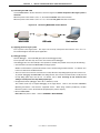
QB-MINI2
On-Chip Debug Emulator with Programming
Function
Target Devices
V850 Microcontrollers
78K0R Microcontrollers
78K0 Microcontrollers
78K0S Microcontrollers
Document No. U18371EJ1V0UM00 (1st edition)
Date Published November 2006 NS CP(K)
© NEC Electronics Corporation 2006
Printed in Japan
[MEMO]
2
User’s Manual U18371EJ1V0UM
MINICUBE is a registered trademark of NEC Electronics Corporation in Japan and Germany and Germany or a
trademark in the United States of America.
Windows is either a registered trademarks or a trademark of Microsoft Corporation in the United States
and/or other countries.
PC/AT is a trademark of International Business Machines Corporation.
• The information in this document is current as of November, 2006. The information is subject to
change without notice. For actual design-in, refer to the latest publications of NEC Electronics data
sheets or data books, etc., for the most up-to-date specifications of NEC Electronics products. Not
all products and/or types are available in every country. Please check with an NEC Electronics sales
representative for availability and additional information.
• No part of this document may be copied or reproduced in any form or by any means without the prior
written consent of NEC Electronics. NEC Electronics assumes no responsibility for any errors that may
appear in this document.
• NEC Electronics does not assume any liability for infringement of patents, copyrights or other intellectual
property rights of third parties by or arising from the use of NEC Electronics products listed in this document
or any other liability arising from the use of such products. No license, express, implied or otherwise, is
granted under any patents, copyrights or other intellectual property rights of NEC Electronics or others.
• Descriptions of circuits, software and other related information in this document are provided for illustrative
purposes in semiconductor product operation and application examples. The incorporation of these
circuits, software and information in the design of a customer's equipment shall be done under the full
responsibility of the customer. NEC Electronics assumes no responsibility for any losses incurred by
customers or third parties arising from the use of these circuits, software and information.
• While NEC Electronics endeavors to enhance the quality, reliability and safety of NEC Electronics products,
customers agree and acknowledge that the possibility of defects thereof cannot be eliminated entirely. To
minimize risks of damage to property or injury (including death) to persons arising from defects in NEC
Electronics products, customers must incorporate sufficient safety measures in their design, such as
redundancy, fire-containment and anti-failure features.
• NEC Electronics products are classified into the following three quality grades: "Standard", "Special" and
"Specific".
The "Specific" quality grade applies only to NEC Electronics products developed based on a customerdesignated "quality assurance program" for a specific application. The recommended applications of an NEC
Electronics product depend on its quality grade, as indicated below. Customers must check the quality grade of
each NEC Electronics product before using it in a particular application.
"Standard": Computers, office equipment, communications equipment, test and measurement equipment, audio
and visual equipment, home electronic appliances, machine tools, personal electronic equipment
and industrial robots.
"Special": Transportation equipment (automobiles, trains, ships, etc.), traffic control systems, anti-disaster
systems, anti-crime systems, safety equipment and medical equipment (not specifically designed
for life support).
"Specific": Aircraft, aerospace equipment, submersible repeaters, nuclear reactor control systems, life
support systems and medical equipment for life support, etc.
The quality grade of NEC Electronics products is "Standard" unless otherwise expressly specified in NEC
Electronics data sheets or data books, etc. If customers wish to use NEC Electronics products in applications
not intended by NEC Electronics, they must contact an NEC Electronics sales representative in advance to
determine NEC Electronics' willingness to support a given application.
(Note)
(1) "NEC Electronics" as used in this statement means NEC Electronics Corporation and also includes its
majority-owned subsidiaries.
(2) "NEC Electronics products" means any product developed or manufactured by or for NEC Electronics (as
defined above).
M8E 02. 11-1
User’s Manual U18371EJ1V0UM
3
General Precautions for Handling This Product
1. Circumstances not covered by product guarantee
• If the product was disassembled, altered, or repaired by the customer
• If it was dropped, broken, or given another strong shock
• Use at overvoltage, use outside guaranteed temperature range, storing outside guaranteed
temperature range
• If power was turned on while the USB cable or connection to the target system was in an
unsatisfactory state
• If the cable of the USB cable, the target cable, or the like was bent or pulled excessively
• If the product got wet
• If this product is connected to the target system when there is a potential difference between the
GND of this product and GND of the target system.
• If the connectors or cables are plugged/unplugged while this product is in the power-on state.
• If excessive load is applied to the connectors or sockets.
• If a metal part of the interface connector or another such part comes in contact with an electrostatic
charge
• If specifications other than those specified are used for the USB port
2. Safety precautions
• The product may become hot depending on the status of use. Be careful of low temperature burns
and other dangers due to the product becoming hot.
• Be careful of electrical shock. There is a danger of electrical shock if the product is used as
described above in 1 Circumstances not covered by product guarantee.
• Do not use a device that was used for on-chip debugging as the official product.
4
User’s Manual U18371EJ1V0UM
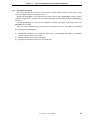
INTRODUCTION
Readers
This manual is intended for users who wish to perform debugging using the QB-MINI2
(generic name: MINICUBE2).
The readers of this manual are assumed to be familiar with the device functions and
usage, and to have knowledge of debuggers and flash programming.
Purpose
This manual is intended to give users an understanding of the basic specifications and
correct use of MINICUBE2.
Organization
This manual is divided into the following sections.
• General
• Names and functions of hardware
• Self-testing
• Firmware update
How to Read This Manual
It is assumed that the readers of this manual have general knowledge in the fields of
electrical engineering, logic circuits, and microcontrollers.
This manual describes the basic setup procedures.
To understand the basic specifications and usages of MINICUBE2
→ Read this manual according to the CONTENTS.
To know the manipulations, command functions, and other software-related settings
of MINICUBE2
→ See the user’s manual of the debugger to be used.
Conventions
Note:
Footnote for item marked with Note in the text
Caution:
Information requiring particular attention
Remark:
Supplementary information
Numeric representation:
Binary ... xxxx or xxxxB
Decimal ... xxxx
Hexadecimal ... xxxxH
Prefix indicating power of 2
(address space, memory
capacity):
K (kilo): 210 = 1,024
M (mega): 220 = 1,0242
User’s Manual U18371EJ1V0UM
5
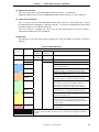
Terminology
The meanings of the terms used in this manual are described in the table below.
Term
Meaning
MINICUBE2
Generic name of QB-MINI2
Target device
This is the device to be emulated.
Target system
This is the system to be debugged (user-created system).
It includes software and hardware created by the user.
OCD unit
OCD is an abbreviation of On-Chip Debug
The OCD unit means the debug function block embedded in the
target device.
Firmware
Program embedded in the device for controlling MINICUBE2
QB-Programmer GUI software used to perform flash programming
Related Documents
Please use the following documents in conjunction with this manual.
The related documents listed below may include preliminary versions. However,
preliminary versions are not marked as such.
Documents Related to Development Tools (User’s Manuals)
Document Name
Document Number
QB-MINI2 On-Chip Debug Emulator with Programming Function
This document
ID850QB Ver. 3.20 Integrated Debugger
Operation
U17964E
ID78K0-QB Ver. 2.90 Integrated Debugger
Operation
U17437E
ID78K0S-QB Ver. 2.81 Integrated Debugger
Operation
U17287E
ID78K0R-QB Ver. 3.20 Integrated Debugger
Operation
U17839E
Caution
The related documents listed above are subject to change without notice. Be sure to use the latest
version of each document for designing, etc.
Documents Related to Development Tools (Documents except User’s Manuals)
Document Name
QB-MINI2 Operating Precautions
ZUD-CD-06-0046-E
QB-Programmer Programming GUI Operation
ZUD-CD-06-0006-E
MINICUBE2 Diagnostic Tool
ZUD-CD-06-0044-E
MINICUBE OCD Checker
ZUD-CD-06-0045-E
Caution
The related documents listed above are subject to change without notice. Be sure to use the latest
version of each document for designing, etc.
6
Document Number
User’s Manual U18371EJ1V0UM
CONTENTS
CHAPTER 1 OVERVIEW........................................................................................................................... 10
1.1
1.2
1.3
1.4
Features ........................................................................................................................................ 10
Notes Before Using MINICUBE2 ................................................................................................. 11
Supported Devices....................................................................................................................... 11
Hardware Specifications ............................................................................................................. 12
CHAPTER 2 NAMES AND FUNCTIONS OF HARDWARE ..................................................................... 13
2.1 Names of Supplied Hardware ..................................................................................................... 13
2.2 Part Names and Functions of MINICUBE2 ................................................................................ 14
2.3 Part Names and Functions of 78K0-OCD Board ....................................................................... 16
CHAPTER 3 HOW TO USE MINICUBE2 WITH V850 MICROCONTROLLER ........................................ 17
3.1 Target System Design ................................................................................................................. 18
3.1.1 Pin assignment ..............................................................................................................................19
3.1.2 Circuit connection examples ........................................................................................................20
3.1.3 Connection of reset pin.................................................................................................................23
3.1.4 Mounting connector onto target system .....................................................................................26
3.2 On-Chip Debugging ..................................................................................................................... 27
3.2.1 Debug functions.............................................................................................................................27
3.2.2 System configuration ....................................................................................................................28
3.2.3 System startup procedure ............................................................................................................29
3.2.4 System shutdown procedure........................................................................................................31
3.2.5 Securing of user resources and setting of security ID...............................................................32
3.2.6 Cautions on debugging.................................................................................................................38
3.3 Flash Programming ..................................................................................................................... 40
3.3.1 Specifications of programming function .....................................................................................40
3.3.2 System configuration ....................................................................................................................40
3.3.3 System startup procedure ............................................................................................................41
3.3.4 Usage examples.............................................................................................................................43
3.3.5 System shutdown procedure........................................................................................................49
3.3.6 Cautions on flash programming...................................................................................................49
CHAPTER 4 HOW TO USE MINICUBE2 WITH 78K0 MICROCONTROLLER........................................ 50
4.1 Target System Design ................................................................................................................. 51
4.1.1 Pin assignment ..............................................................................................................................52
4.1.2 Circuit connection examples ........................................................................................................54
4.1.3 Connection of reset pin.................................................................................................................64
4.1.4 Cautions on target system design ...............................................................................................69
4.1.5 Mounting connector onto target system .....................................................................................70
4.2 On-Chip Debugging ..................................................................................................................... 71
4.2.1 Debug functions.............................................................................................................................71
4.2.2 System configuration ....................................................................................................................72
4.2.3 System startup procedure ............................................................................................................73
4.2.4 System shutdown procedure........................................................................................................76
User’s Manual U18371EJ1V0UM
7
4.2.5 Clock setting.................................................................................................................................. 77
4.2.6 Securing of user resources and setting of security ID .............................................................. 80
4.2.7 Cautions on debugging ................................................................................................................ 86
4.3 Flash Programming...................................................................................................................... 90
4.3.1 Specifications of programming function .................................................................................... 90
4.3.2 System configuration ................................................................................................................... 90
4.3.3 System startup procedure............................................................................................................ 91
4.3.4 Usage examples ............................................................................................................................ 93
4.3.5 System shutdown procedure ....................................................................................................... 99
4.3.6 Cautions on flash programming .................................................................................................. 99
CHAPTER 5 HOW TO USE MINICUBE2 WITH 78K0S MICROCONTROLLER.................................... 100
5.1 Target System Design................................................................................................................ 101
5.1.1 Pin assignment.............................................................................................................................102
5.1.2 Circuit connection example ........................................................................................................103
5.1.3 Connection of reset pin ...............................................................................................................104
5.1.4 Connection of INTP pin ...............................................................................................................107
5.1.5 Connection of X1 and X2 pins.....................................................................................................109
5.1.6 Mounting connector onto target system....................................................................................110
5.2 On-Chip Debugging.................................................................................................................... 111
5.2.1 Debug functions...........................................................................................................................111
5.2.2 System configuration ..................................................................................................................112
5.2.3 System startup procedure...........................................................................................................113
5.2.4 System shutdown procedure ......................................................................................................115
5.2.5 Securing of user resources.........................................................................................................116
5.2.6 Debugging of alternate-functions of X1 and X2 pins ................................................................120
5.2.7 Cautions on debugging ...............................................................................................................121
5.3 Flash Programming.................................................................................................................... 123
5.3.1 Specifications of programming function ...................................................................................123
5.3.2 System configuration ..................................................................................................................123
5.3.3 System startup procedure...........................................................................................................124
5.3.4 Usage examples ...........................................................................................................................126
5.3.5 System shutdown procedure ......................................................................................................132
5.3.6 Cautions on flash programming .................................................................................................132
CHAPTER 6 HOW TO USE MINICUBE2 WITH 78K0R MICROCONTROLLER ................................... 133
6.1 Target System Design................................................................................................................ 134
6.1.1 Pin assignment.............................................................................................................................135
6.1.2 Circuit connection example ........................................................................................................136
6.1.3 Connection of reset pin ...............................................................................................................137
6.1.4 Mounting connector onto target system....................................................................................140
6.2 On-Chip Debugging.................................................................................................................... 141
6.2.1 Debug functions...........................................................................................................................141
6.2.2 System configuration ..................................................................................................................142
6.2.3 System startup procedure...........................................................................................................143
6.2.4 System shutdown procedure ......................................................................................................145
6.2.5 Securing of user resources and setting of security ID and on-chip debug option byte........146
6.2.6 Cautions on debugging ...............................................................................................................152
8
User’s Manual U18371EJ1V0UM
6.3 Flash Programming ................................................................................................................... 155
6.3.1 Specifications of programming function ...................................................................................155
6.3.2 System configuration ..................................................................................................................155
6.3.3 System startup procedure ..........................................................................................................156
6.3.4 Usage examples...........................................................................................................................158
6.3.5 System shutdown procedure......................................................................................................164
6.3.6 Cautions on flash programming.................................................................................................164
CHAPTER 7 SELF-TESTING .................................................................................................................. 165
7.1 System Configuration................................................................................................................ 165
7.2 Self-Testing Procedure.............................................................................................................. 166
CHAPTER 8 FIRMWARE UPDATE ........................................................................................................ 167
8.1 System Configuration................................................................................................................ 167
8.2 Firmware Update Procedure ..................................................................................................... 168
User’s Manual U18371EJ1V0UM
9
CHAPTER 1
OVERVIEW
MINICUBE2 is an on-chip debug emulator with flash programming function, which is used for debugging and
programming a program to be embedded in on-chip flash memory microcontrollers.
1.1
Features
• On-chip debugging
Can debug with the target microcontroller connected to the target system.
• Flash memory programming
Can write programs to the on-chip flash memory of microcontrollers.
• USB connection
Can be connected to the host machine via USB interface 2.0 or 1.1.
Since MINICUBE2 operates on power supplied via USB, an external power supply is unnecessary.
• Variety of supported devices and expandability
MINICUBE2 supports a wide variety of NEC Electronics 8- to 32-bit on-chip flash memory
microcontrollers. More devices can be supported by upgrading firmware embedded in MINICUBE2.
• Self-testing function
MINICUBE2 has a self-testing function, which is used to detect faults in MINICUBE2 and perform
maintenance.
10
User’s Manual U18371EJ1V0UM
CHAPTER
1.2
1
OVERVIEW
Notes Before Using MINICUBE2
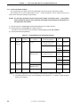
Chapters 1 and 2 present an overview and the basic specifications of MINICUBE2, and the following chapters
provide separate descriptions for the target devices and the purpose of use. To utilize this manual effectively,
refer to the following table and see the relevant chapter for your target device and purpose of use.
Table 1-1. Chapters Corresponding to Usage
Target Device
Purpose of Use
V850
Relevant Chapter
CHAPTER 3
HOW TO USE MINICUBE2 WITH
V850 MICROCONTROLLER
Target system design
3.1
Target System Design
On-chip debugging
3.2
On-Chip Debugging
Flash memory programming
3.3
Flash Programming
78K0
CHAPTER 4
HOW TO USE MINICUBE2 WITH
78K0 MICROCONTROLLER
Target system design
4.1
Target System Design
On-chip debugging
4.2
On-Chip Debugging
Flash memory programming
4.3
Flash Programming
78K0S
CHAPTER 5
HOW TO USE MINICUBE2 WITH
78K0S MICROCONTROLLER
Target system design
5.1
Target System Design
On-chip debugging
5.2
On-Chip Debugging
Flash memory programming
5.3
Flash Programming
78K0R
CHAPTER 6 HOW TO USE MINICUBE2 WITH
78K0R MICROCONTROLLER
1.3
Target system design
6.1
Target System Design
On-chip debugging
6.2
On-Chip Debugging
Flash memory programming
6.3
Flash Programming
-
MINICUBE2 self-testing
CHAPTER 7
SELF-TESTING
-
Expansion of supported devices
CHAPTER 8
FIRMWARE UPDATE
Supported Devices
Access the following MINICUBE2 information site or refer to the document for details on the devices that
support debugging and flash programming with MINICUBE2. The document describes the development tools
that are required as the support conditions, serial interface and operating precautions, so be sure to read the
document, in addition to this manual.
• MINICUBE2 information site
URL: http://www.necel.com/micro/english/product/sc/allflash/minicube2.html
Remark This website just posts the supported target devices. For details on the development tools that are
required as the support conditions, refer to the document below.
• Document
Document name: QB-MINI2 Operating Precautions
User’s Manual U18371EJ1V0UM
11
CHAPTER
1.4
1
OVERVIEW
Hardware Specifications
This section describes the MINICUBE2 hardware specifications.
The specifications related to the on-chip debug and flash memory programming functions are described in the
following chapters.
Table 1-2. Hardware Specifications
Classification
MINICUBE2
Host machine interface
Target interface
Item
Specifications
Operating power supply
Supplied via USB interface (5 V)
Operating environment
Temperature: ±0 to +40°C
conditions
Humidity: 10 to 80% RH (no condensation)
Storage environment
Temperature: -15 to +60°C
conditions
Humidity: 10 to 80% RH (no condensation)
External dimensions
48 × 48 × 13.9 mm
Weight
Approximately 40 g
Target host machine
PC98-NX Series, IBM PC/AT
TM
TM
Target OS
Windows
USB
2.0 (1.1 compatible)
USB cable
2m
compatibles
98, Windows Me, Windows 2000, Windows XP
Current consumption
500 mA max.
Target cable length
16-pin cable: 10 cm
10-pin cable: 10 cm
12
Supported connector
2.54 mm pitch general-purpose connector
Supply voltage
3.1 V (typ.) or 5.0 V (typ.)
Supply current
100 mA max.
Current consumption
8 mA (typ.)
Voltage range
1.65 to 5.5 V
User’s Manual U18371EJ1V0UM
CHAPTER 2
NAMES AND FUNCTIONS OF HARDWARE
This chapter describes the part names and functions of MINICUBE2 and its accessories.
The part names described in this chapter are used throughout this document.
This chapter provides an
overview of the various functions. Reading it through, the reader will gain a basic grasp of MINICUBE2 and the
self-check board that will facilitate reading of subsequent chapters. While reading this chapter, also check if the
hardware has a defect.
2.1
Names of Supplied Hardware
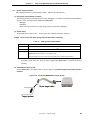
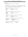
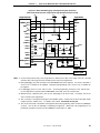
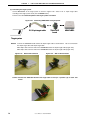
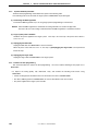
Figure 2-1 shows the names of hardware supplied with MINICUBE2.
Figure 2-1.
Names of Supplied Hardware
USB cable
MINICUBE2
10-pin target cable
16-pin target cable
78K0-OCD board
(A 20 MHz oscillator mounted)
User’s Manual U18371EJ1V0UM
13
CHAPTER
2.2
2
NAMES AND FUNCTIONS OF HARDWARE
Part Names and Functions of MINICUBE2
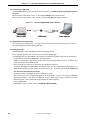
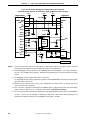
Figure 2-2 shows the part names of the MINICUBE2 main unit. For their functions, refer to (1) to (5) below.
Figure 2-2. Part Names of MINICUBE2
USB interface
connector
Target interface
connector
Mode LED
Mode select switch
Power select switch
(1) Mode select switch
This switch is used to select the target device. Table 2-1 describes the setting details. This switch is set to
″M2″ at shipment.
Table 2-1. Description of Mode Select Switch
Setting
Description
M1
Sets 78K0S or 78K0R microcontroller as target device
M2
Sets V850 or 78K0 microcontroller as target device (factory setting)
(2) Power select switch
This switch is used to set the power supplied to the target system.
Table 2-2 describes the setting details.
This switch is set to ″3″ at shipment.
Caution Do not change the switch setting while the USB cable is connected.
Table 2-2. Setting of Power Select Switch
Setting
Description
3 V is supplied from MINICUBE2 to the target system
3
Note
. (Factory setting)
The supplied power is fed back to MINICUBE2 and used only for power detection.
5
5 V is supplied from MINICUBE2 to the target system
T
Power supply of the target system is used.
Note
.
The supplied power is fed back to MINICUBE2 and used only for power detection.
MINICUBE2 only detects the power for the target system.
Note
The maximum rating of the current is 100mA, so do not use MINICUBE2 with the target system with
the higher current rating.
The power is always supplied after MINICUBE2 is connected to the host
machine.
14
User’s Manual U18371EJ1V0UM
CHAPTER
2
NAMES AND FUNCTIONS OF HARDWARE
(3) USB interface connector
This is a connector used to connect MINICUBE2 with the host machine, via a USB cable.
A USB 2.0 compliant mini-B connector (UX60A-MB-5ST: Made by Hirose Electric Co., Ltd.) is employed.
(4) Target interface connector
This is a connector used to connect MINICUBE2 with the target system, via a 16-pin target cable.
Connect
the 78K0-OCD board for debugging a 78K0 microcontroller. To prevent the 78K0-OCD board from being
inserted by mistake, pin 11 is removed at shipment.
Since this connector is compatible with 16-core 2.54 mm pitch general-purpose connectors (female), a
commercially available cable can be substituted.
(5) Mode LED
The appearance of the mode LED changes according to the status of hardware and software, as shown in
Table 2-3.
Table 2-3. Mode LED Status
Mode LED
Appearance
Description
Color
-
Extinguished
USB
Target VDD
Connection
Detection
Not
Software Operation Status
Not detected
Not yet started
Not detected
Not yet started
Detected
Not yet started
connected
White
Flashing
Connected
Glowing
Blue
A debugger for V850 microcontrollers has been started and
Glowing
CPU is in the break mode.
Flashing
A debugger for V850 microcontrollers has been started and
Glowing
A debugger for 78K0 microcontrollers has been started and
the CPU is running, or a program is being downloaded.
Orange
the CPU is in the break mode.
Flashing
A debugger for 78K0 microcontrollers has been started and
Glowing
A debugger for 78K0S microcontrollers has been started and
the CPU is running, or a program is being downloaded.
Green
the CPU is in the break mode. The QB-Programmer has
been started and is waiting for execution processing.
Alternatively, execution processing has been completed.
A debugger for 78K0S microcontrollers has been started and
Flashing
the CPU is running, or a program is being downloaded.
Yellow
A debugger for 78K0R microcontrollers has been started and
Glowing
the CPU is in the break mode.
A debugger for 78K0R microcontrollers has been started and
Flashing
the CPU is running, or a program is being downloaded.
A command from the QB-Programmer is being executed for
the flash memory.
Red
Glowing
A command from the QB-Programmer is ended abnormally
(results in error)
Illumination
The illumination mode is entered when MINICUBE2 is connected to a USB interface and 15
seconds or longer have elapsed. This mode is also entered when the debugger is terminated
normally.
User’s Manual U18371EJ1V0UM
15
CHAPTER
2
NAMES AND FUNCTIONS OF HARDWARE
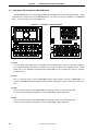
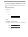
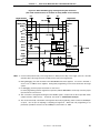
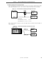
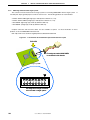
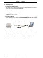
2. 3 Part Names and Functions of 78K0-OCD Board
The 78K0-OCD board is used for debugging a 78K0 microcontroller (not used for flash programming).
2-3 illustrates the external view of the 78K0-OCD board.
Figure
The name of each part is printed on the 78K0-OCD
board. For each function, refer to (1) to (4), below.
Figure 2-3. Part Names of 78K0-OCD Board
(1) CLK1
For clock supply to the target device, a 14-pin DIP socket is implemented as CLK1. A 14-pin type oscillator (5
V) or a parts board that can configure an oscillation circuit can be mounted on the 14-pin DIP socket. A parts
board such as the 160-90-314 (manufactured by PRECI-DIP) can be used with this socket to configure
oscillation circuit.
(2) CN1
This is a connector used to connect MINICUBE2 with the target interface connector of MINICUBE2. To
prevent the 78K0-OCD board from being inserted by mistake, a dummy pin is mounted in the place of pin 11 in
CN1.
(3) CN2
This is a connector used to connect MINICUBE2 with the target system, via a 10-pin target cable.
A 10-core 2.54 mm pitch general-purpose connector (TSM-105-01-L-DV) is employed.
(4) CN3
This is a connector used to connect MINICUBE2 with the target system, via a 16-pin target cable.
A 16-core 2.54 mm pitch general-purpose connector (TSM-108-01-L-DV) is employed.
16
User’s Manual U18371EJ1V0UM
CHAPTER 3
HOW TO USE MINICUBE2 WITH V850 MICROCONTROLLER
This chapter describes how to use MINICUBE2 when performing on-chip debugging and flash programming for
a V850 microcontroller.
On-chip debugging is a method to debug a microcontroller mounted on the target system, using a debug
function implemented in the device.
Since debugging is performed with the target device operating on the board,
this method is suitable for field debugging.
Flash programming is a method to write a program to the flash memory embedded in a device.
Erasing,
writing and verifying the program can be performed on-board with the device.
Read the following chapters if you are using MINICUBE2 for the first time with a V850 microcontroller as the
target device.
• 3.1
Target System Design
For communication between MINICUBE2 and the target system, communication circuits must be mounted on
the target system. This section describes the circuit design and mounting of connectors.
• 3.2 On-Chip Debugging
This section describes the system configuration and startup method to perform on-chip debugging with
MINICUBE2.
• 3.3 Flash Programming
This section describes the system configuration and startup method to perform flash programming with
MINICUBE2.
User’s Manual U18371EJ1V0UM
17
CHAPTER
3.1
3
HOW TO USE MINICUBE2 WITH V850 MICROCONTROLLER
Target System Design
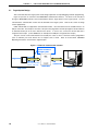
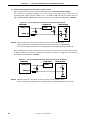
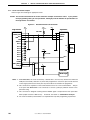
This section describes the target system circuit design required for on-chip debugging and flash programming.
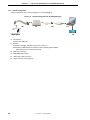
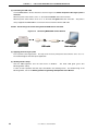
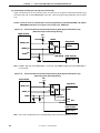
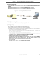
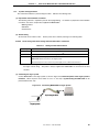
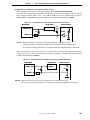
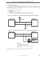
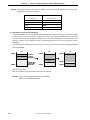
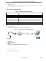
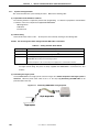
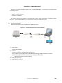
Figure 3-1 presents an overview of the MINICUBE2 communication interface. As shown on the left side of
the figure, MINICUBE2 performs serial communication with the target device on the target system. For this
communication, communication circuits must be mounted on the target system. Refer to this section to design
circuits appropriately.
UART and CSI-H/S are supported as communication modes. Note that CSI-H/S is not available if there is no
H/S pin connection. The H/S pin is the name of the pin for the programmer and this pin might not be described as
an alternate-function pin in the user's manual of the device. In such a case, connect the relevant port that is
assigned to the H/S pin. (In the V850ES/JJ, for example, the PCM0 pin is assigned to the H/S pin.)
The pins used for serial communication are basically the same as those of the flash memory programmer
(such as PG-FP4), but some devices do not support some of them.
Refer to the document ″QB-MINI2
Operating Precautions″ and check the supported pins.
Figure 3-1. Outline of Communication Interface
Communication circuits
must be mounted on
the target system.
Target device
Serial communication
(UART, CSI-H/S)
USB
communication
MINICUBE2
Target system
18
User’s Manual U18371EJ1V0UM
Host machine
CHAPTER
3
HOW TO USE MINICUBE2 WITH V850 MICROCONTROLLER
3.1.1 Pin assignment
This section describes the interface signals used between MINICUBE2 and the target system. Table 3-1 lists
the pin assignment. Table 3-2 describes the functions of each pin. The pin assignment varies depending on
whether CSI-H/S or UART is used, so design the circuit appropriately according to the circuit connection examples
described on the following sections.
Table 3-1. Pin Assignment
Pin No.
Pin Name
CSI-H/S Used
TOP VIEW
Note
UART Used
1
GND
2
RESET_OUT
3
SI
4
VDD
5
SO
6
R.F.U.
7
SCK
R.F.U.
8
H/S
R.F.U.
9
CLK
10
R.F.U.
11
R.F.U.
12
FLMD1
13
R.F.U.
14
FLMD0
15
RESET_IN
16
R.F.U.
Pin 1
RXD
TXD
Target system
15 13 11
9
7
5
3
1
16 14 12 10
8
6
4
2
Pin assignment of target connector
to be mounted on target system
Note Signal names in MINICUBE2
Table 3-2. Pin Functions
Note
Pin Name
IN/OUT
Description
RESET_IN
IN
Pin used to input reset signal from the target system
RESET_OUT
OUT
Pin used to output reset signal to the target device
CLK
OUT
Pin used to output clock signal to the target device
FLMD0
OUT
Pin used to set the target device to debug mode or
FLMD1
OUT
Pin used to set programming mode
RxD/SI
IN
Pin used to receive command/data from the target device
TxD/SO
OUT
Pin used to transmit command/data to the target device
SCK
OUT
Pin used to output clock signal for 3-wire serial communication
H/S
IN
Pin used to input handshake signal from the target device
R.F.U.
-
This pin is not used, so leave it open.
programming mode
Note As seen from MINICUBE2
User’s Manual U18371EJ1V0UM
19
CHAPTER
3
HOW TO USE MINICUBE2 WITH V850 MICROCONTROLLER
3.1.2 Circuit connection examples
The circuit design on the target system varies depending on the communication interface mode. Refer to the
following table and see the relevant circuit connection example.
Caution The constants described in the circuit connection example are reference values.
If you perform
flash programming aiming at mass production, thoroughly evaluate whether the specifications of
the target device are satisfied.
Table 3-3. Corresponding Circuit Connection Diagrams
Communication Interface Mode
20
Refer to:
UART
Figure 3-2
CSI-H/S
Figure 3-3
User’s Manual U18371EJ1V0UM
CHAPTER
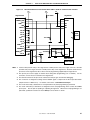
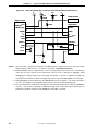
Figure 3-2.
3
HOW TO USE MINICUBE2 WITH V850 MICROCONTROLLER
Recommended Circuit Connection When UART Is Used for Communication Interface
VDD
VDD
3 to 10 kΩ
Target connector
GND
RESET_OUT
RXDNote 1
VDD
TXDNote 1
R.F.U.
R.F.U.
R.F.U.
CLKNote 2
R.F.U.
R.F.U.
FLMD1Note 3
R.F.U.
FLMD0Note 3
RESET_INNote 4
R.F.U.
VDD
Target device
1
GND
2
_RESET
3
TXD
4
VDD
5
RXD
6
7
X1
8
9
X2
1 to 10 kΩ
10
Clock
circuit
11
12
FLMD1
13
14
15
FLMD0
Note 5
VDD
16
1 to 10 kΩ
10 kΩ
Note 6
100 Ω
Port X
10 kΩ
1 kΩ
Reset connector
RESET signal
Notes 1. Connect TxD (transmit side) of the target device to RxD (receive side) of the target connector, and TxD
(transmit side) of the target connector to RxD (receive side) of the target device. Read the serial interface
pin names on the target device side as those for flash programming supported by the target device.
2. This pin may be used to supply an external clock during flash programming (4, 8 or 16 MHz). For the
connection, refer to the user's manual for the target device.
3. The alternate function of this pin can be used because this pin goes to Hi-Z when debugging.
4. This connection is designed assuming that the RESET signal is output from the N-ch open-drain buffer
(output resistance: 100Ω or less).
For details, refer to 3.1.3 Connection of reset pin.
5. The circuit enclosed by a dashed line is not required when only flash programming is performed.
6. The circuit enclosed by a dashed line is designed for flash self programming, which controls the FLMD0
pin via ports. Use the port for inputting or outputting the high level. When flash self programming is not
performed, a pull-down resistance for the FLMD0 pin can be within 1 to 10 kΩ.
User’s Manual U18371EJ1V0UM
21
CHAPTER
Figure 3-3.
3
HOW TO USE MINICUBE2 WITH V850 MICROCONTROLLER
Recommended Circuit Connection When CSI-H/S Is Used for Communication Interface
VDD
VDD
1 to 10 kΩ
Target connector
GND
RESET_OUT
SINote 1
VDD
SONote 1
R.F.U.
SCK
H/S
CLKNote 2
R.F.U.
R.F.U.
FLMD1Note 3
R.F.U.
FLMD0Note 3
RESET_INNote 4
R.F.U.
VDD
VDD
3 to 10 kΩ
Target device
1
GND
2
_RESET
3
SO
4
VDD
5
SI
6
7
SCK
8
H/S
9
1 to 10 kΩ
10
X1
1 to 10 kΩ
11
Clock
circuit
X2
12
FLMD1
13
14
15
FLMD0
Note 5
16
1 to 10 kΩ
10 kΩ
VDD
10 kΩ
Note 6
100 Ω
Port X
1 kΩ
Reset connector
RESET signal
Notes 1. Connect SO (transmit side) of the target device to SI (receive side) of the target connector, and SO
(transmit side) of the target connector to SI (receive side) of the target device. Read the serial interface
pin names on the target device side as those for flash programming supported by the target device.
2. This pin may be used to supply an external clock during flash programming (4, 8 or 16 MHz). For the
connection, refer to the user's manual for the target device.
3. The alternate function of this pin can be used because this pin goes to Hi-Z when debugging.
4. This connection is designed assuming that the RESET signal is output from the N-ch open-drain buffer
(output resistance: 100Ω or less). For details, refer to 3.1.3
Connection of reset pin.
5. The circuit enclosed by a dashed line is not required when only flash programming is performed.
6. The circuit enclosed by a dashed line is designed for flash self programming, which controls the FLMD0
pin via ports. Use the port for inputting or outputting the high level. When flash self programming is not
performed, a pull-down resistance for the FLMD0 pin can be within 1 to 10 kΩ
22
User’s Manual U18371EJ1V0UM
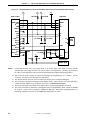
CHAPTER
3.1.3
3
HOW TO USE MINICUBE2 WITH V850 MICROCONTROLLER
Connection of reset pin
This section describes the connection of the reset pin, for which special attention must be paid, in circuit
connection examples shown in the previous section.
During on-chip debugging, a reset signal from the target system is input to MINICUBE2, masked, and then
output to the target device.
Therefore, the reset signal connection varies depending on whether MINICUBE2 is
connected.
For flash programming, the circuit must be designed so that the reset signals of the target system and
MINICUBE2 do not conflict.
Select one of the following methods and connect the reset signal in the circuit. The details of each method
are described on the following pages.
(1)
Automatically switching the reset signal via series resistor (recommended; described in recommended
(2)
Manually switching the reset signal with jumper
(3)
Resetting the target device by power-on clear (POC) only
circuit connection in the previous section)
User’s Manual U18371EJ1V0UM
23
CHAPTER
(1)
3
HOW TO USE MINICUBE2 WITH V850 MICROCONTROLLER
Automatically switching the reset signal via series resistor
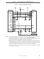
Figure 3-4 illustrates the reset pin connection described in 3.1.2 Circuit connection examples.
This connection is designed assuming that the reset circuit on the target system contains an N-ch
open-drain buffer (output resistance: 100Ω or less). The VDD or GND level may be unstable when the
logic of RESET_IN/OUT of MINICUBE2 is inverted, so observe the conditions described below in Remark.
Figure 3-4. Circuit Connection with Reset Circuit That Contains Buffer
MINICUBE2
Target device
Reset connector
VDD
_RESET
RESET_OUT
R2
R1
VDD
Buffer
RESET_IN
Remark
Make the resistance of at least R1 ten times that of R2, R1 being 10 kΩ or more.
Pull-up resistor R2 is not required if the buffer of the reset circuit consists of CMOS output.
The circuit enclosed by a dashed line is not required when only flash programming is performed.
Figure 3-5 illustrates the circuit connection for the case where the reset circuit on the target system contains
no buffers and the reset signal is only generated via resistors or capacitors. Design the circuit, observing
the conditions described below in Remark.
Figure 3-5. Circuit Connection with Reset Circuit That Contains No Buffers
MINICUBE2
Target device
_RESET
RESET_OUT
R1
Reset connector
VDD
R2
RESET_IN
Remark
Make the resistance of at least R1 ten times that of R2, R1 being 10 kΩ or more.
The circuit enclosed by a dashed line is not required when only flash programming is performed.
24
User’s Manual U18371EJ1V0UM
CHAPTER
(2)
3
HOW TO USE MINICUBE2 WITH V850 MICROCONTROLLER
Manually switching the reset signal with jumper
Figure 3-6 illustrates the circuit connection for the case where the reset signal is switched using the jumper,
with or without MINICUBE2 connected. This connection is simple, but the jumper must be set manually.
Figure 3-6. Circuit Connection for Switching Reset Signal with Jumper
Target connector
Jumper
1
RESET_OUT
Target device
_RESET
2
3
Reset connector
RESET signal
RESET_IN
* Jumper setting
(3)
When MINICUBE2 is connected:
1-2 shorted
When MINICUBE2 is not connected:
2-3 shorted
Resetting the target device by power-on clear (POC) only
Figure 3-7 illustrates the circuit connection for the case where the target device is only reset via POC
without using the reset pin.
RESET_OUT is valid only when the debugger is running or during flash
programming.
The operation is not guaranteed if the power to the target system is shut down during debugging. Note that
the POC function cannot be emulated.
Figure 3-7. Circuit Connection for the Case Where Target Device Is Only Reset via POC
VDD
1 to 10 kΩ
Target connector
Target device
_RESET
RESET_OUT
RESET_IN
User’s Manual U18371EJ1V0UM
25
CHAPTER
3.1.4
3
HOW TO USE MINICUBE2 WITH V850 MICROCONTROLLER
Mounting connector onto target system
The connector must be mounted on the target system for connecting MINICUBE2 with the target system. A
2.54 mm pitch 16-pin general-purpose connector can be used. The following products are recommended.
• HIF3FC-16PA-2.54DS (right-angle type, made by Hirose Electric Co., Ltd.)
• HIF3FC-16PA-2.54DSA (straight type, made by Hirose Electric Co., Ltd.)
• 7616-5002PL (right-angle type, made by Sumitomo 3M, Ltd.)
• 7616-6002PL (straight type, made by Sumitomo 3M, Ltd.)
Compact connectors and loose-wire cables are also available as options. For more information on these
products, access the MINICUBE2 information site.
URL: http://www.necel.com/micro/english/product/sc/allflash/minicube2.html
Figure 3-8. 2.54 mm Pitch 16-Pin General-Purpose Connector Pin Layout
TOP VIEW
Pin assignment when MINICUBE2
is connected in this direction
Pin 1
Target system
15 13 11
9
7
5
3
1
16 14 12 10
8
6
4
2
Pin assignment of target connector
to be mounted on target system
26
User’s Manual U18371EJ1V0UM
CHAPTER
3
HOW TO USE MINICUBE2 WITH V850 MICROCONTROLLER
3.2 On-Chip Debugging
This section describes the system configuration, startup/shutdown procedure and cautions for debugging when
on-chip debugging is performed with MINICUBE2.
3.2.1
Debug functions
Table 3-4 lists the debug functions when a V850 microcontroller is the target device and the ID850QB is used.
If a debugger other than the ID850QB (made by partner manufacturer) is used, the available functions may differ,
so check the specifications of the debugger used.
Table 3-4. Debug Functions
Functions
Specifications
Security
10-byte ID code authentication
Download
Available
Execution
Go & Go, Start from Here, Come Here, Restart, step execution
Hardware break
2 points
Software break
Note 1
ROM area
4 points
RAM area
2,000 points
(commonly used by execution and access)
Note 2
Forced break
Available
RAM monitoring
Available
DMM (writing to memory during RUN)
Available
Pin masking
Available (reset pin only)
Time measurement
Measurement resolution: 100 µs
(from execution start to break)
Max. measurement time: Approximately 100 hours
User spaces used for debugging
Internal ROM: 2 K bytes+12 bytes
Internal RAM: 16 bytes max.
Function pins used for debugging
UART selected: RXD, TXD
CSI-H/S selected: SI, SO, SCK, H/S
Notes 1.
The following devices are not yet supported.
V850ES/KE2, V850ES/KF2, V850ES/KG2, µPD70F3733, V850ES/IE2
2.
Available with restrictions. For details, refer to 3.2.6
Cautions on debugging.
User’s Manual U18371EJ1V0UM
27
CHAPTER
3
HOW TO USE MINICUBE2 WITH V850 MICROCONTROLLER
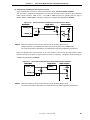
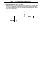
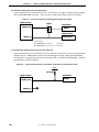
3.2.2 System configuration
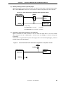
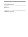
Figure 3-9 illustrates the system configuration for on-chip debugging.
Figure 3-9.
System Configuration for On-Chip Debugging
<5>
<4>
<3>
<1>
<6>
<2>
Target system
<1> Host machine
Products with USB ports
<2> Software
Includes the debugger, USB driver, device files, and so on.
Download these NEC Electronics software from the following website (ODS).
URL: http://www.necel.com/micro/ods/eng/
<3> USB cable (accessory)
<4> MINICUBE2 (this product)
<5> 16-pin target cable (accessory)
<6> Target connector (sold separately)
28
User’s Manual U18371EJ1V0UM
CHAPTER
3
HOW TO USE MINICUBE2 WITH V850 MICROCONTROLLER
3.2.3 System startup procedure
This section describes the system startup procedure. Observe the following order.
(1) Preparation and installation of software
The following software is required to perform on-chip debugging. For details on preparation and installation of
software, refer to the setup manual supplied with MINICUBE2.
• Debugger
• USB driver
• Device file (may be unnecessary when using a partner manufacture’s debugger)
(2) Switch setting
Set the mode select switch to ″M2″. Set the power select switch by referring to Table 3-5.
Caution
Do not change the switch setting while the USB cable is connected.
Table 3-5. Setting of Power Select Switch
Setting
Description
Note
3
3 V is supplied from MINICUBE2 to the target system
5
5 V is supplied from MINICUBE2 to the target system
T
Power supply of the target system is used.
.
Note
.
MINICUBE2 detects the power for the target system.
The detected power is also used as the power supply for the communication interface.
Note The maximum rating of the current is 100 mA, so do not use MINICUBE2 with the target system with
the higher current rating. The power is always supplied after MINICUBE2 is connected to the host
machine.
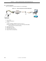
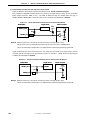
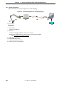
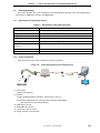
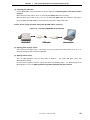
(3) Connecting the target system
Connect MINICUBE2 to the target system as shown in Figure 3-10, before the power to the target system is
turned on.
Figure 3-10. Connecting MINICUBE2 to Target System
16-pin target cable
MINICUBE2
Target system
User’s Manual U18371EJ1V0UM
29
CHAPTER
3
HOW TO USE MINICUBE2 WITH V850 MICROCONTROLLER
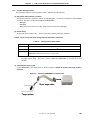
(4) Connecting the USB cable
Connect MINICUBE2 to the host machine as shown in Figure 3-11, before the power to the target system is
turned on.
When the power select switch is set to ″T″, the mode LED flashes white after connection.
When the power select switch is set to ″3″ or ″5″, the mode LED glows white after connection.
Figure 3-11. Connecting MINICUBE2 to Host Machine
MINICUBE2
USB cable
Host machine
(5) Applying power to target system
Turn on power to the target system. This step is not necessary if the power select switch is set to ″3″ or ″5″.
The mode LED glows white after power application.
(6) Debugger startup
Start the debugger. The mode LED glows blue after debugger startup.
For the operation after this step, refer to the user's manual for the debugger.
If the debugger does not start normally or the operation is unstable, the possible causes may be the following.
• Communication error between MINICUBE2 and target system
Whether communication is performed normally can be checked using the OCD Checker. For details, refer
to the user's manual for the OCD Checker.
• The user resource has not been secured or the security ID has not been set
To perform debugging with MINICUBE2, the debug monitor area and communication serial interface for
communication must be secured and the security ID must be set. For details, refer to 3.2.5 Securing of
user resources and setting of security ID.
• Unsupported software (debugger, device file, or firmware) is used
The software used may not support debugging of the target device.
Operating Precautions″ and check the supported version.
Refer to the document ″QB-MINI2
When using software provided by an NEC
Electronics partner, refer to the documents prepared by the partner company.
• Defect of MINICUBE2
MINICUBE2 may have a defect. Refer to CHAPTER 7 SELF-TESTING.
30
User’s Manual U18371EJ1V0UM
CHAPTER
3
HOW TO USE MINICUBE2 WITH V850 MICROCONTROLLER
3.2.4 System shutdown procedure
Terminate debugging and shutdown the system in the following order.
If the following order is not observed, the target system or MINICUBE2 may be damaged.
(1) Debugger termination
Terminate the debugger.
(2) Target system power shutdown
Shutdown the power supplied to the target system. This step is not necessary if the power select switch is
set to ″3″ or ″5″.
(3) Unplugging the USB cable
Unplug the USB cable from MINICUBE2 or the host machine.
(4) Unplugging the target cable
Unplug the target cable from MINICUBE2 or the target system.
User’s Manual U18371EJ1V0UM
31
CHAPTER
3
HOW TO USE MINICUBE2 WITH V850 MICROCONTROLLER
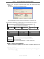
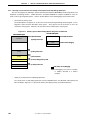
3.2.5 Securing of user resources and setting of security ID
The user must prepare the following to perform communication between MINICUBE2 and the target device and
implement each debug function. Refer to the descriptions on the following pages and set these items in the user
program or using the compiler options.
•
Securement of memory space
The shaded portions in Figure 3-12 are the areas reserved for placing the debug monitor program, so user
programs and data cannot be allocated in these spaces. These spaces must be secured so as not to be used
by the user program.
Figure 3-12. Memory Spaces Where Debug Monitor Programs Are Allocated
Internal RAM space
Internal ROM space
Internal ROM end address
10 to 16 bytes
Internal RAM end address
2 KB
4 bytes
10 bytes
4 bytes
4 bytes
•
CSI or UART receive interrupt vector
0x70 (security ID area)
0x60 (interrupt vector for debugging)
: Debugging area
0x0 (reset vector)
Securement of serial interface for communication
The register settings, concerning UART or CSI-H/S used for communication between MINICUBE2 and the
target device, performed by the debug monitor program must not be changed.
•
Security ID setting
The ID code must be embedded in the area filled with yellow (0x70 to 0x79) in Figure 3-12, to prevent the
memory from being read by an unauthorized person.
32
User’s Manual U18371EJ1V0UM
CHAPTER
3
HOW TO USE MINICUBE2 WITH V850 MICROCONTROLLER
(a) Reset vector
A reset vector includes the jump instruction for the debug monitor program.
[How to secure areas]
It is not necessary to secure this area intentionally. When downloading a program, however, the debugger
rewrites the reset vector in accordance with the following cases. If the rewritten pattern does not match the
following cases, the debugger generates an error (F0c34 when using the ID850QB).
•
When two nop instructions are placed in succession from address 0
Before writing
0x0 nop
0x2 nop
0x4 xxxx
•
When two 0xFFFF are successively placed from address 0 (already erased device)
Before writing
0x0 0xFFFF
0x2 0xFFFF
0x4 xxxx
•
After writing
Jumps to debug monitor program at 0x0
0x4 jr disp22 - 4
→
mov32 and jmp are placed in succession from address 0 (when using IAR compiler ICCV850)
Before writing
0x0 mov imm32,reg1
0x6 jmp [reg1]
•
After writing
Jumps to debug monitor program at 0x0
0x4 xxxx
→
The jr instruction is placed at address 0 (when using NEC Electronics compiler CA850)
Before writing
0x0 jr disp22
•
After writing
Jumps to debug monitor program at 0x0
0x4 xxxx
→
→
After writing
Jumps to debug monitor program at 0x0
0x4 mov imm32,reg1
0xa jmp [reg1]
The jump instruction for the debug monitor program is placed at address 0
Before writing
Jumps to debug monitor program at 0x0
→
After writing
No change
User’s Manual U18371EJ1V0UM
33
CHAPTER
3
HOW TO USE MINICUBE2 WITH V850 MICROCONTROLLER
(b) Securement of area for debug monitor program
The shaded portions in Figure 3-12 are the areas where the debug monitor program is allocated. The monitor
program performs initialization processing for debug communication interface and RUN or break processing
for the CPU.
The internal ROM area must be filled with 0xFF.
This area must not be rewritten by the user
program.
[How to secure areas]
It is not necessarily required to secure this area if the user program does not use this area.
To avoid problems that may occur during the debugger startup, however, it is recommended to secure this
area in advance, using the compiler.
The following shows examples for securing the area, using the NEC Electronics compiler CA850.
Add the
assemble source file and link directive code, as shown below.
•
Assemble source (Add the following code as an assemble source file.)
-- Secures 2 KB space for monitor ROM section
.section "MonitorROM", const
.space
0x800, 0xff
-- Secures interrupt vector for debugging
.section "DBG0"
.space
4, 0xff
-- Secures interrupt vector for serial communication
-- Change the section name according to serial communication mode used
.section "INTCSI00"
.space
4, 0xff
-- Secures 16 byte space for monitor ROM section
.section "MonitorRAM", bss
.lcomm monitorramsym, 16, 4
/* defines monitorramsym symbol */
•
Link directive (Add the following code to the link directive file.)
The following shows an example when the internal ROM end address is 0x3ffff and internal RAM end
address is 0x3ffefff.
34
MROMSEG : !LOAD ?R V0x03f800{
MonitorROM
= $PROGBITS
};
?A MonitorROM;
MRAMSEG : !LOAD ?RW V0x03ffeff0{
MonitorRAM
= $NOBITS
};
?AW MonitorRAM;
User’s Manual U18371EJ1V0UM
CHAPTER
3
HOW TO USE MINICUBE2 WITH V850 MICROCONTROLLER
(c) Securement of communication serial interface
UART or CSI-H/S is used for communication between MINICUBE2 and the target system. The settings
related to the serial interface modes are performed by the debug monitor program, but if the setting is changed
by the user program, a communication error may occur.
To prevent such a problem from occurring, communication serial interface must be secured in the user
program.
[How to secure communication serial interface]
Create the user program observing the following points.
• Serial interface registers
Do not set the registers related to UART and CSI-H/S in the user program.
• Interrupt mask register
When UART is used, do not mask receive end interrupts
end interrupts.
Note
. When CSI-H/S is used, do not mask transmit
The following shows an example.
Example Setting other than below is prohibited when the target device is the V850ES/KJ2 and CSI00 is
used.
CSI0IC0
7
6
5
4
3
2
1
0
x
0
x
x
x
x
x
x
x: Any
Note
When the target device is the V850ES/IE2, do not mask receive error interrupts.
• Port registers
When UART is used, do not set port registers to make the TxD and RxD pins invalid.
When CSI-H/S is
used, do not set port registers to make the SI, SO, SCK and H/S pins invalid. The H/S pin is used as the
port output for debugging. The following shows two examples.
Example 1 Setting other than below is prohibited when the target device is the V850ES/KJ2 and UART0 is
used.
PFC3
PMC3L
7
6
5
4
3
2
1
0
x
x
x
x
x
x
0
0
7
6
5
4
3
2
1
0
x
x
x
x
x
x
1
1
x: Any
User’s Manual U18371EJ1V0UM
35
CHAPTER
3
HOW TO USE MINICUBE2 WITH V850 MICROCONTROLLER
Example 2 Setting other than below is prohibited when the target device is the V850ES/HG2 and CSIB0 is
used.
PMC4
PMCCM
PMCM
PCM
7
6
5
4
3
2
1
0
x
x
x
x
x
1
1
1
7
6
5
4
3
2
1
0
x
x
x
x
x
x
x
0
7
6
5
4
3
2
1
0
x
x
x
x
x
x
x
0
7
6
5
4
3
2
1
0
x
x
x
x
x
x
x
Read-onlyNote
x: Any
Note
The port values corresponding to the H/S pin are changed by the monitor program according to the
debugger status. To perform port register settings in 8-bit units, usually the user program can use
read-modify-write. If an interrupt for debugging occurs before writing, however, an unexpected
operation may be performed.
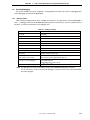
(d) Security ID setting
This setting is required to prevent the memory from being read by an unauthorized person. Embed a security
ID at addresses 0x70 to 0x79 in the internal flash memory. The debugger starts only when the security ID
that is set during debugger startup and the security ID set at addresses 0x70 to 0x79 match.
If bit 7 of address 0x79 is ″0″, however, debugging is disabled. In such a case, there are no methods to start
the debugger.
Debugging is mainly disabled for mass-produced devices.
If the user has forgotten the security ID or to enable debugging, erase the flash memory and set the security ID
again.
[How to set security ID]
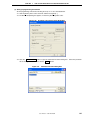
Embed a security ID at addresses 0x70 to 0x79 in the user program.
If the security ID is embedded as follows, for example, the security ID set by the debugger is
″123456789ABCDEF123D4″ (not case-sensitive).
36
User’s Manual U18371EJ1V0UM
CHAPTER
3
HOW TO USE MINICUBE2 WITH V850 MICROCONTROLLER
Address
Value [7:0]
0x70
0x12
0x71
0x34
0x72
0x56
0x73
0x78
0x74
0x9A
0x75
0xBC
0x76
0xDE
0x77
0xF1
0x78
0x23
0x79
0xD4
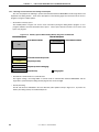
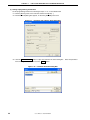
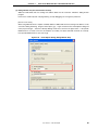
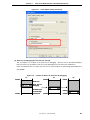
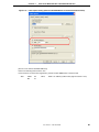
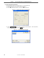
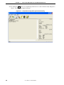
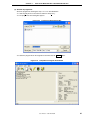
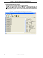
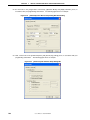
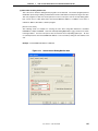
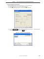
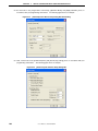
If NEC Electronics compiler CA850 is used, the security ID can be set using the Compiler Common Options
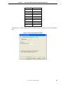
menu.
Figure 3-13. Security ID Setting with CA850
User’s Manual U18371EJ1V0UM
37
CHAPTER
3.2.6
3
HOW TO USE MINICUBE2 WITH V850 MICROCONTROLLER
Cautions on debugging
This section describes cautions on performing on-chip debugging for a V850 microcontroller.
Be sure to read the following to use MINICUBE2 properly.
(1) Handling of device that was used for debugging
Do not mount a device that was used for debugging on a mass-produced product, because the flash memory
was rewritten during debugging and the number of rewrites of the flash memory cannot be guaranteed.
Moreover, do not embed the debug monitor program into mass-produced products.
(2) When breaks cannot be executed
Forced breaks cannot be executed if one of the following conditions is satisfied.
• Interrupts are disabled (DI)
• Interrupts issued for the serial interface, which is used for communication between MINICUBE2 and the
target device, are masked
• Standby mode is entered while standby release by a maskable interrupt is prohibited
• Mode for communication between MINICUBE2 and the target device is UART, and the main clock has been
stopped
(3) When pseudo real-time RAM monitor (RRM) function and DMM function do not operate
The pseudo RRM function and DMM function do not operate if one of the following conditions is satisfied.
• Interrupts are disabled (DI)
• Interrupts issued for the serial interface, which is used for communication between MINICUBE2 and the
target device, are masked
• Standby mode is entered while standby release by a maskable interrupt is prohibited
• Mode for communication between MINICUBE2 and the target device is UART, and the main clock has been
stopped
• Mode for communication between MINICUBE2 and the target device is UART, and a clock different from the
one specified in the debugger is used for communication
(4) Standby release with pseudo RRM and DMM functions enabled
The standby mode is released by the pseudo RRM function and DMM function if one of the following
conditions is satisfied.
• Mode for communication between MINICUBE2 and the target device is CSI-H/S
• Mode for communication between MINICUBE2 and the target device is UART, and the main clock has been
supplied
(5) Writing to peripheral I/O registers that requires a specific sequence, using DMM function
Peripheral I/O registers that requires a specific sequence cannot be written with the DMM function.
38
User’s Manual U18371EJ1V0UM
CHAPTER
3
HOW TO USE MINICUBE2 WITH V850 MICROCONTROLLER
(6) Device with which the debugger startup is slowed
When the debugger is started for the first time, chip erasure and writing of debug monitor program are
performed. The following devices require about a dozen seconds for these operations.
V850ES/JG2, V850ES/JJ2
V850ES/HE2, V850ES/HF2, V850ES/HG2, V850ES/HJ2
V850ES/IE2
(7) Writing of debug monitor program
If the CPU operating clock setting is changed by the debugger, the debugger rewrites the debug monitor
program. At this time, it takes about a dozen seconds for this operation. When using NEC Electronics
debugger ID850QB, this specification applies when the setting in the Clock area in the Configuration dialog
box.
(8) Flash self programming
If a space where the debug monitor program is allocated is rewritten by flash self programming, the debugger
can no longer operate normally.
(9) Emulation of POC function
The POC function of the target device cannot be emulated. Make sure that the power to the target system is
not shut down during debugging.
(10) Operation after reset
After an external pin reset or internal reset, the monitor program performs debug initialization processing.
Consequently, the time from reset occurrence until user program execution differs from that in the actual
device operation.
(11) Debugging with real machine running without using MINICUBE2
If debugging is performed with a real machine running, without using MINICUBE2, write the user program
using the QB-Programmer.
Programs downloaded by the debugger include the monitor program, and such a
program malfunctions if it is not controlled via MINICUBE2.
User’s Manual U18371EJ1V0UM
39
CHAPTER
3.3
3
HOW TO USE MINICUBE2 WITH V850 MICROCONTROLLER
Flash Programming
This section describes the system configuration and startup/shutdown procedure when flash programming is
performed for a V850 microcontroller, using MINICUBE2.
3.3.1
Specifications of programming function
Table 3-6.
Specifications of Programming Function
Functions
Specifications
Host interface
USB 2.0 (compatible with 1.1)
Target interface
UART or CSI-H/S
Target system voltage
2.7 to 5.5 V (depends on the target device)
Clock supply
16, 8, or 4 MHz clock can be supplied
Clock mounted on the target system can be used
Power supply
3 or 5 V (maximum current rating: 100 mA)
Acquisition of device-specific
Parameter file for NEC Electronics PG-FP4 is used
information
Security flag setting
Available
Standalone operation
Unavailable (must be connected to host machine)
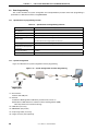
3.3.2 System configuration
Figure 3-14 illustrates the system configuration for flash programming.
Figure 3-14.
<5>
System Configuration for Flash Programming
<4>
<3>
<1>
<6>
<2>
Target system
<1> Host machine
Products with USB ports
<2> Software
Includes the QB-Programmer USB driver, parameter files, and so on.
Download these NEC Electronics software from the following website (ODS).
URL: http://www.necel.com/micro/ods/eng/
<3> USB cable (accessory)
<4> MINICUBE2 (this product)
<5> 16-pin target cable (accessory)
<6> Target connector (sold separately)
40
User’s Manual U18371EJ1V0UM
CHAPTER
3.3.3
3
HOW TO USE MINICUBE2 WITH V850 MICROCONTROLLER
System startup procedure
This section describes the system startup procedure. Observe the following order.
(1) Preparation and installation of software
The following software is required to perform flash programming.
For details on preparation and installation
of software, refer to the setup manual supplied with MINICUBE2.
• QB-Programmer
• USB driver
• Parameter file
(2) Switch setting
Set the mode select switch to ″M2″.
Caution
Set the power select switch by referring to Table.
Do not change the switch setting while the USB cable is connected.
Table 3-7. Setting of Power Select Switch
Setting
Description
Note
3
3 V is supplied from MINICUBE2 to the target system
5
5 V is supplied from MINICUBE2 to the target system
T
Power supply of the target system is used.
Note
.
MINICUBE2 detects the power for the target system.
The detected power is also used as the power supply for the communication interface.
Note The maximum rating of the current is 100 mA, so do not use MINICUBE2 with the target system with
the higher current rating. The power is always supplied after MINICUBE2 is connected to the host
machine.
(3) Connecting the target system
Connect MINICUBE2 to the target system as shown in Figure 3-15, before the power to the target system is
turned on. When the power select switch is set to ″T″, the step of (4) Connecting the USB cable can be
performed before this step.
Figure 3-15. Connecting MINICUBE2 to Target System
16-pin target cable
MINICUBE2
Target system
User’s Manual U18371EJ1V0UM
41
CHAPTER
3
HOW TO USE MINICUBE2 WITH V850 MICROCONTROLLER
(4) Connecting the USB cable
Connect MINICUBE2 to the host machine as shown in Figure 3-16, before the power to the target system is
turned on.
When the power select switch is set to ″T″, the mode LED flashes white after connection.
When the power select switch is set to ″3″ or ″5″, the mode LED glows white after connection. The power is
always supplied after MINICUBE2 is connected to the host machine with the USB cable.
Caution Do not change the switch setting while the USB cable is connected.
Figure 3-16. Connecting MINICUBE2 to Host Machine
MINICUBE2
USB cable
Host machine
(5) Applying power to target system
Turn on power to the target system. This step is not necessary if the power select switch is set to ″3″ or ″5″.
The mode LED glows white after power application.
(6) QB-Programmer startup
Start the QB-Programmer from the Start menu of Windows.
The mode LED glows green after
QB-Programmer startup.
A series of basic operations after this step is described in the following section. For detailed usage of the
QB-Programmer, refer to the QB-Programmer Programming GUI Operation User's Manual.
42
User’s Manual U18371EJ1V0UM
CHAPTER
3.3.4
3
HOW TO USE MINICUBE2 WITH V850 MICROCONTROLLER
Usage examples
This section describes a series of basic operations using the QB-Programmer, using the µPD70F3732 as an
example.
The operations from execution of the [Autoprocedure (EPV)] command to programming for the target
device are described.
For other commands and their applications, refer to the QB-Programmer Programming
GUI Operation User's Manual.
The conditions used for a series of operations in this section are as follows.
<Target system>
Target device:
µPD70F3732
Power supply voltage:
5 V (supplied from MINICUBE2)
Communication channel:
CSI-H/S, 2 MHz
<MINICUBE2>
Switches:
Mode select switch: M2
Power select switch: 5
<QB-Programmer>
Parameter file:
70F3732.PRM
Clock setting:
5 MHz, x4 (oscillator on the target system side)
Operation mode:
chip
Program file:
sample.hex
Command options:
[Blank check before Erase] selected
[Read verify after Program] selected
[Security flag after Program] selected
Security function:
[Disable Read] selected
User’s Manual U18371EJ1V0UM
43
CHAPTER
3
HOW TO USE MINICUBE2 WITH V850 MICROCONTROLLER
(1) Setting of programming environment
Set the programming environment, following the steps <1> to <7> described below.
<1> Click the [Device] menu on the menu bar and then click [Setup...].
<2> The Device Setup dialog box appears, in which the [Standard] tab is active.
Figure 3-17. [Standard] Tab of Device Setup Dialog Box
<3> Click the
PRM File Read
button to open the Parameter File Select dialog box. Select the parameter
file for the target device and then click the
Open
button.
Figure 3-18. Parameter File Select Dialog Box
44
User’s Manual U18371EJ1V0UM
CHAPTER
3
HOW TO USE MINICUBE2 WITH V850 MICROCONTROLLER
<4> Set the items in the [Target Device Connection], [Operation Mode] and [Supply Oscillator] areas, in
accordance with your programming environment. The following figure shows an example.
Figure 3-19.
[Standard] Tab of Device Setup Dialog Box After Setting
<5> The µPD70F3732 can use the [Get Security Settings] command, so click the
OK
button to return to
the main window, click the [Device] menu and then click [Get Security Settings...]. After execution of this
command, the security functions and boot area settings for the target device can be checked in the
[Security flag settings] area on the [Advanced] tab in the Device Setup dialog box. For details, refer to
the QB-Programmer Programming GUI Operation User's Manual.
Figure 3-20. [Advanced] Tab of Device Setup Dialog Box After [Get Security Settings...] Execution
User’s Manual U18371EJ1V0UM
45
CHAPTER
3
HOW TO USE MINICUBE2 WITH V850 MICROCONTROLLER
<6> Next, set the items in the [Command options] and [Security flag settings] areas, in accordance with your
programming environment.
The following figure shows an example.
Figure 3-21. [Advanced] Tab of Device Setup Dialog Box
<7> By clicking the
OK
button, the programming environment is set and the Device Setup dialog box is
closed. The main window appears as follows.
Figure 3-22.
46
Completion of Programming Environment Setting
User’s Manual U18371EJ1V0UM
CHAPTER
3
HOW TO USE MINICUBE2 WITH V850 MICROCONTROLLER
(2) Selection of program file
Select the program file, following the steps <1> to <3> described below.
<1> Click the [File] menu on the menu bar and then click [Load...].
<2> The program file select dialog box appears.
Figure 3-23. Program File Select Dialog Box
<3> Select the program file for the target device and then click the
Figure 3-24.
Open
button.
Completion of Program File Selection
User’s Manual U18371EJ1V0UM
47
CHAPTER
3
HOW TO USE MINICUBE2 WITH V850 MICROCONTROLLER
(3) Execution of [Autoprocedure (EPV)] command
Click the [Device] menu on the menu bar and then click [Autoprocedure (EPV)].
The [Blank Check], [Erase] (if the flash memory in the target device is not blank), [Program], [Verify], and
[Security] commands are executed for the target device sequentially. The mode LED on MINICUBE2 flashes
yellow during execution. When the command execution is completed normally, the mode LED glows green
and the following window appears.
Figure 3-25.
48
Completion of [Autoprocedure (EPV)] Command Execution
User’s Manual U18371EJ1V0UM
CHAPTER
3
HOW TO USE MINICUBE2 WITH V850 MICROCONTROLLER
3.3.5 System shutdown procedure
Terminate flash programming and shutdown the system in the following order.
If the following order is not observed, the target system or MINICUBE2 may be damaged.
(1) Terminating the QB-Programmer
Terminate the QB-Programmer if you are not going to perform programming to other devices.
Remark
When the QB-Programmer is terminated, the setting information is saved in the qbp.ini file. Due to
this file, the same setting is maintained when the QB-Programmer is started the next time.
(2) Target system power shutdown
Shutdown the power supplied to the target system. This step is not necessary if the power select switch is
set to ″3″ or ″5″.
(3) Unplugging the USB cable
Unplug the USB cable from MINICUBE2 or the host machine.
When the power select switch is set to ″T″, the step of (4) Unplugging the target cable can be performed
before this step.
(4) Unplugging the target cable
Unplug the target cable from MINICUBE2 or the target system.
3.3.6
Cautions on flash programming
This section describes the cautions for flash programming.
Be sure to read the following for the proper use of
MINICUBE2.
• To improve the writing quality, fully understand, verify, and evaluate the following items before using
MINICUBE2.
• Circuits are designed as described in the user's manuals for the device and MINICUBE2.
• The device, QB-Programmer and MINICUBE2 are used as described in each user's manual.
• The power supplied to the target system is stable.
User’s Manual U18371EJ1V0UM
49
CHAPTER 4 HOW TO USE MINICUBE2 WITH 78K0 MICROCONTROLLER
This chapter describes how to use MINICUBE2 when performing on-chip debugging and flash programming for a
78K0 microcontroller.
On-chip debugging is a method to debug a microcontroller mounted on the target system, using a debug function
implemented in the device. Since debugging is performed with the target device operating on the board, this method
is suitable for field debugging.
Flash programming is a method to write a program to the flash memory embedded in a device. Erasing, writing
and verifying the program can be performed on-board with the device.
Read the following chapters if you are using MINICUBE2 for the first time with a 78K0 microcontroller as the target
device.
• 4.1 Target System Design
For communication between MINICUBE2 and the target system, communication circuits must be mounted on
the target system. This section describes the circuit design and mounting of connectors.
• 4.2 On-Chip Debugging
This section describes the system configuration and startup method to perform on-chip debugging with
MINICUBE2.
• 4.3 Flash Programming
This section describes the system configuration and startup method to perform flash programming with
MINICUBE2.
50
User’s Manual U18371EJ1V0UM
CHAPTER
4
HOW TO USE MINICUBE2 WITH 78K0 MICROCONTROLLER
4.1 Target System Design
This section describes the target system circuit design required for on-chip debugging and flash programming.
Figure 4-1 and Figure 4-2 present overviews of the MINICUBE2 communication interface.
For communication
between MINICUBE2 and the target system, communication circuits must be mounted on the target system, as
shown on the left side of the figure.
Refer to this section to design circuits appropriately.
Figure 4-1. Outline of Communication Interface for On-Chip Debugging
Communication circuits
must be mounted on
the target system.
Communication via
X1/X2 or OCD1A/OCD1B
Target device
USB
communication
Target system
78K0-OCD
board
MINICUBE2
Host machine
Figure 4-2. Outline of Communication Interface for Flash Programming
Communication circuits
must be mounted on
the target system.
UART communication
Target device
USB
communication
MINICUBE2
Target system
User’s Manual U18371EJ1V0UM
Host machine
51
CHAPTER
4
HOW TO USE MINICUBE2 WITH 78K0 MICROCONTROLLER
4.1.1 Pin assignment
This section describes the interface signals used between MINICUBE2 and the target system. Table 4-1 lists
the pin assignment when a 16-pin target cable is used.
Table 4-2 describes the functions of each pin.
The pin
assignment varies depending on whether the operation is debugging or programming, so design the circuit
appropriately according to the circuit connection examples described on the following sections.
Table 4-1.
Pin No.
Pin Name
For Debugging
Pin Assignment When Using 16-Pin Target Cable
TOP VIEW
Note
For Programming
(with 78K0-OCD
78K0-OCD board is not
required for programming.
Board Connected)
1
Pin 1
GND
2
RESET_OUT
3
R.F.U.
4
VDD
5
R.F.U.
6
R.F.U.
7
R.F.U.
8
R.F.U.
9
CLK
RXD
Target system
TXD
15 13 11
10
R.F.U.
11
R.F.U.
12
R.F.U.
FLMD1
13
DATA
R.F.U.
14
FLMD0
15
RESET_IN
16
R.F.U.
9
7
5
3
1
16 14 12 10
8
6
4
2
Pin assignment of target connector
to be mounted on target system
R.F.U.
Note Signal names in MINICUBE2
Table 4-2. Pin Functions
Pin Name
Note 1
IN/OUT
Description
RESET_IN
IN
Pin used to input reset signal from the target system
RESET_OUT
OUT
Pin used to output reset signal to the target device
CLK
OUT
Pin used to output clock signal to the target device
DATA
IN/OUT
Pin used to input/output for data communication during debugging
FLMD0
OUT
Pin used to set the target device to debug mode or programming mode
FLMD1
OUT
Pin used to set programming mode
RxD
IN
Pin used to receive command/data from the target device
TxD
OUT
Pin used to transmit command/data to the target device
R.F.U.
-
Note 2
This pin is not used, so leave it open.
Notes 1. As seen from MINICUBE2.
2. Not used in some devices.
52
User’s Manual U18371EJ1V0UM
CHAPTER
4
HOW TO USE MINICUBE2 WITH 78K0 MICROCONTROLLER
Table 4-3 lists the pin assignment when a 10-pin target cable is used. The 10-pin target cable is dedicated for
debugging. Use this cable if the target system is designed for MINICUBE (QB-78K0MINI) or in order to limit the
usage of the connector mounted on the target system only for debugging.
Table 4-3. Pin Assignment When Using 10-Pin Target Cable
Pin No.
1
Pin Name
TOP VIEW
Note
RESET_IN
2
RESET_OUT
3
FLMD0
4
VDD
5
DATA
6
GND
7
CLK
8
GND
9
R.F.U.
10
Pin 1
Target system
-
Note Signal names in MINICUBE2
9
7
5
3
1
10
8
6
4
2
Pin assignment of target connector
to be mounted on target system
Table 4-4. Pin Functions
Pin Name
Note
IN/OUT
Description
RESET_IN
IN
Pin used to input reset signal to the target system
RESET_OUT
OUT
Pin used to output reset signal to the target device
CLK
OUT
Pin used to output clock signal to the target device
DATA
IN/OUT
Pin used to input/output for data communication during debugging
FLMD0
OUT
Pin used to set the target device to debug mode or programming mode
R.F.U.
Note
-
This pin is not used, so leave it open.
As seen from MINICUBE2.
User’s Manual U18371EJ1V0UM
53
CHAPTER
4
HOW TO USE MINICUBE2 WITH 78K0 MICROCONTROLLER
4.1.2 Circuit connection examples
The circuit design on the target system varies depending on the used connector and interface signals.
The following (1) to (3) are the major purpose of use.
Confirm the purpose, refer to Table 4-5 and see the
relevant circuit connection example for specifications.
Caution The constants described in the circuit connection example are reference values.
If you perform
flash programming aiming at mass production, thoroughly evaluate whether the specifications of
the target device are satisfied.
(1) Used to perform on-chip debugging and flash programming via one 16-pin connector.
(2) Used to perform on-chip debugging via a 10-pin connector.
* This type of circuit connection can be used with on-chip debugging emulator QB-78K0MINI.
(3) Used to perform flash programming.
Table 4-5.
Usage
Connector
Used
(1)
16-pin
Corresponding Circuit Connection Diagrams
Programming
Interface
UART
Debug
Operating Clock Source
Interface
X1, X2
connector
Used by Target Device
FLMD1
pin
Refer to:
Note1
Internal high-speed oscillator
Not
Figure 4-3
(X1 oscillator not used)
provided
X1 oscillator
Not
Figure 4-4
provided
OCD1A (P31),
OCD1B (P32)
Note2
Provided
Figure 4-5
Internal high-speed oscillator
Not
Figure 4-6
(X1 oscillator not used)
provided
X1 oscillator
Not
Figure 4-7
provided
Provided
(2)
10-pin
-
connector
-
X1, X2
OCD1A (P31),
OCD1B (P32)
(3)
16-pin
UART
Figure 4-8
-
Figure 4-9
-
Figure 4-10
-
Figure 4-11
Note2
-
-
connector
Notes 1.
2.
Refer to the target device’s user’s manual to confirm whether an FLMD1 pin is provided.
The debug interface pin name varies depending on the target device.
device’s user’s manual.
54
User’s Manual U18371EJ1V0UM
For details, confirm the target
CHAPTER
4
HOW TO USE MINICUBE2 WITH 78K0 MICROCONTROLLER
Figure 4-3. When Both Debugging and Programming Are Performed
(with X1/X2 Communication, Only Internal High-Speed Oscillator Is Used)
VDD
VDD
VDD
Target connector
GND
RESET_OUT
RxDNote 1
VDD
Note 1
TxD
R.F.U.
R.F.U.
R.F.U.
CLKNote 2
R.F.U.
R.F.U.
R.F.U.
DATA
FLMD0
Note 5
RESET_IN
R.F.U.
Target device
1
3 to 10 kΩ
GND
2
_RESET
3
TxD
4
VDD
5
RxD
6
1 to 10 kΩ
7
8
Note 3
9
X1
10
11
10 kΩ
JP1
1
JP2
1
2
2
12
OCD1ANote 4
1 to
10 kΩ
1 to
10 kΩ
13
X2
14
FLMD0
15
VDD
16
10 kΩ
Note 6
1 kΩ
Note 5
Port X
1 kΩ
Reset connector
RESET signal
Notes 1. Connect TxD (transmit side) of the target device to RxD (receive side) of the target connector, and TxD
(transmit side) of the target connector to RxD (receive side) of the target device.
2. During debugging, the clock mounted on the 78K0-OCD board can be supplied. If no clock is mounted, a
clock of 4, 8, or 16 MHz can be supplied.
During flash programming, only a clock of 4, 8, or 16 MHz can
be supplied.
3. For debugging, short 1-2 of JP1 and 1-2 of JP2. For flash programming, short pin 2 of JP1 and JP2 only.
For the target device operation (without MINICUBE2 connected), leave JP1 and JP2 open.
4. OCD1A may be a different name, such as P31, depending on the device used. For details, refer to the
user's manual for the target device.
5. This connection is designed assuming that the RESET signal is output from the N-ch open-drain buffer
(output resistance: 100Ω or less).
For details, refer to 4.1.3 Connection of reset pin.
6. The circuit enclosed by a dashed line is designed for flash self programming, which controls the FLMD0 pin
via ports. Use the port for inputting or outputting the high level. When flash self programming is not
performed, a pull-down resistance for the FLMD0 pin can be within 1 to 10kΩ.
User’s Manual U18371EJ1V0UM
55
CHAPTER
4
HOW TO USE MINICUBE2 WITH 78K0 MICROCONTROLLER
Figure 4-4. When Both Debugging and Programming Are Performed
(with X1/X2 Communication, X1 Oscillator Is Used) (FLMD1 Pin Is Not Provided)
VDD
VDD
VDD
Target connector
GND
RESET_OUT
Note 1
RxD
VDD
Note 1
TxD
R.F.U.
R.F.U.
R.F.U.
Note 2
CLK
R.F.U.
R.F.U.
R.F.U.
DATA
FLMD0
Note 5
RESET_IN
R.F.U.
Target device
1
3 to 10 kΩ
GND
2
_RESET
3
TxD
4
VDD
5
RxD
6
1 to 10 kΩ
7
8
Note 3
9
X1
10
11
OCD1ANote 4
10 kΩ
Clock
circuit
12
1 to 10 kΩ
13
X2
14
FLMD0
15
VDD
16
10 kΩ
Note 6
1 kΩ
Note 5
Port X
1 kΩ
Reset connector
RESET signal
Notes 1. Connect TxD (transmit side) of the target device to RxD (receive side) of the target connector, and TxD
(transmit side) of the target connector to RxD (receive side) of the target device.
2. During debugging, the clock mounted on the 78K0-OCD board can be supplied. If no clock is mounted, a
clock of 4, 8, or 16 MHz can be supplied. During flash programming, use the clock mounted on the target
system.
3. For debugging, short the jumper and mount no clock circuit.
For flash programming and the target device operation (without MINICUBE2 connected), leave the jumper
open and mount a clock circuit.
4. OCD1A may be a different name, such as P31, depending on the device used. For details, refer to the
user's manual for the target device.
5. This connection is designed assuming that the RESET signal is output from the N-ch open-drain buffer
(output resistance: 100 Ω or less).
For details, refer to 4.1.3 Connection of reset pin.
6. The circuit enclosed by a dashed line is designed for flash self programming, which controls the FLMD0 pin
via ports. Use the port for inputting or outputting the high level. When flash self programming is not
performed, a pull-down resistance for the FLMD0 pin can be within 1 to 10kΩ.
56
User’s Manual U18371EJ1V0UM
CHAPTER
4
HOW TO USE MINICUBE2 WITH 78K0 MICROCONTROLLER
Figure 4-5. When Both Debugging and Programming Are Performed
(with X1/X2 Communication, X1 Oscillator Is Used) (FLMD1 Pin Is Provided)
VDD
VDD
VDD
Target connector
GND
RESET_OUT
Note 1
RxD
VDD
TxDNote 1
R.F.U.
R.F.U.
R.F.U.
CLKNote 2
R.F.U.
R.F.U.
FLMD1
DATA
FLMD0
Note 4
RESET_IN
R.F.U.
Target device
1
3 to 10 kΩ
GND
2
_RESET
3
TxD
4
VDD
5
RxD
6
1 to 10 kΩ
7
8
9
X1
10
11
Note 3
10 kΩ
Clock
circuit
P31
1 to 10 kΩ
X2
12
13
FLMD1
14
FLMD0
15
VDD
16
1 to
10 kΩ
10 kΩ
Note 5
1 kΩ
Port X
1 kΩ
Reset connector
RESET signal
Notes 1. Connect TxD (transmit side) of the target device to RxD (receive side) of the target connector, and TxD
(transmit side) of the target connector to RxD (receive side) of the target device.
2. During debugging, the clock mounted on the 78K0-OCD board can be supplied. If no clock is mounted, a
clock of 4, 8, or 16 MHz can be supplied. During flash programming, use the clock mounted on the target
system.
3. For debugging, short the jumper and mount no clock circuit.
For flash programming and the target device operation (without MINICUBE2 connected), leave the jumper
open and mount a clock circuit.
4. This connection is designed assuming that the RESET signal is output from the N-ch open-drain buffer
(output resistance: 100 Ω or less).
For details, refer to 4.1.3 Connection of reset pin.
5. The circuit enclosed by a dashed line is designed for flash self programming, which controls the FLMD0 pin
via ports. Use the port for inputting or outputting the high level. When flash self programming is not
performed, a pull-down resistance for the FLMD0 pin can be within 1 to 10kΩ.
User’s Manual U18371EJ1V0UM
57
CHAPTER
4
Figure 4-6.
HOW TO USE MINICUBE2 WITH 78K0 MICROCONTROLLER
When Both Debugging and Programming Are Performed
(with OCD1A/OCD1B Communication, Only Internal High-Speed Oscillator Is Used)
VDD
VDD
VDD
Target connector
GND
RESET_OUT
RxDNote 1
VDD
TxDNote 1
R.F.U.
R.F.U.
R.F.U.
CLKNote 2
R.F.U.
R.F.U.
R.F.U.
DATA
FLMD0
RESET_INNote 4
R.F.U.
Target device
1
3 to 10 kΩ
GND
2
_RESET
3
TxD
4
VDD
5
RxD
6
7
1 to 10 kΩ
10 kΩ
8
9
10
OCD1ANote 3
VDD
11
X1
3 to
10 kΩ
12
1 to
10 kΩ
1 to
10 kΩ
X2
13
OCD1BNote 3
14
FLMD0
15
16
VDD
10 kΩ
Note 5
1 kΩ
Note 4
Port X
1 kΩ
Reset connector
RESET signal
Notes 1. Connect TxD (transmit side) of the target device to RxD (receive side) of the target connector, and TxD
(transmit side) of the target connector to RxD (receive side) of the target device.
2. During debugging, the clock mounted on the 78K0-OCD board can be supplied. If no clock is mounted, a
clock of 4, 8, or 16 MHz can be supplied (neither of them is used for the CPU operating clock). During
flash programming, only a clock of 4, 8, or 16 MHz can be supplied.
3. OCD1A (OCD1B) may be a different name, such as P31, depending on the device used. Check the pin
name with the user's manual for the target device.
Since this pin is dedicated to debugging during
debugging, port settings made by the user program are ignored. If this pin is assigned to an input port,
the pin must be connected as shown in this figure, because it is open when MINICUBE2 is not connected.
4. This connection is designed assuming that the RESET signal is output from the N-ch open-drain buffer
(output resistance: 100 Ω or less).
For details, refer to 4.1.3 Connection of reset pin.
5. The circuit enclosed by a dashed line is designed for flash self programming, which controls the FLMD0 pin
via ports. Use the port for inputting or outputting the high level. When flash self programming is not
performed, a pull-down resistance for the FLMD0 pin can be within 1 to 10 kΩ.
58
User’s Manual U18371EJ1V0UM
CHAPTER
Figure 4-7.
4
HOW TO USE MINICUBE2 WITH 78K0 MICROCONTROLLER
When Both Debugging and Programming Are Performed
(with OCD1A/OCD1B Communication, X1 Oscillator Is Used) (FLMD1 Pin Is Not Provided)
VDD
VDD
Target connector
GND
RESET_OUT
RxDNote 1
VDD
TxD
Note 1
R.F.U.
R.F.U.
R.F.U.
CLKNote 2
R.F.U.
R.F.U.
R.F.U.
DATA
FLMD0
RESET_INNote 4
R.F.U.
VDD
Target device
3 to 10 kΩ
1
GND
2
_RESET
3
TxD
4
VDD
5
RxD
6
1 to 10 kΩ
7
8
9
OCD1ANote 3
10
11
VDD
10 kΩ
12
X1
3 to
10 kΩ
1 to 10 kΩ
13
X2
OCD1BNote 3
14
FLMD0
15
16
Clock
circuit
VDD
Note 5
1 kΩ
10 kΩ
Note 4
Port X
1 kΩ
Reset connector
RESET signal
Notes 1. Connect TxD (transmit side) of the target device to RxD (receive side) of the target connector, and TxD
(transmit side) of the target connector to RxD (receive side) of the target device.
2. During debugging, the clock mounted on the 78K0-OCD board can be supplied. If no clock is mounted, a
clock of 4, 8, or 16 MHz can be supplied (neither of them is used for the CPU operating clock). During
flash programming, only a clock of 4, 8, or 16 MHz can be supplied.
3. OCD1A (OCD1B) may be a different name, such as P31, depending on the device used. Check the pin
name with the user's manual for the target device.
Since this pin is dedicated to debugging during
debugging, port settings made by the user program are ignored. If this pin is assigned to an input port,
the pin must be connected as shown in this figure, because it is open when MINICUBE2 is not connected.
4. This connection is designed assuming that the RESET signal is output from the N-ch open-drain buffer
(output resistance: 100 Ω or less).
For details, refer to 4.1.3 Connection of reset pin.
5. The circuit enclosed by a dashed line is designed for flash self programming, which controls the FLMD0 pin
via ports. Use the port for inputting or outputting the high level. When flash self programming is not
performed, a pull-down resistance for the FLMD0 pin can be within 1 to 10 kΩ.
User’s Manual U18371EJ1V0UM
59
CHAPTER
Figure 4-8.
4
HOW TO USE MINICUBE2 WITH 78K0 MICROCONTROLLER
When Both Debugging and Programming Are Performed
(with OCD1A/OCD1B Communication, X1 Oscillator Is Used) (FLMD1 Pin Is Provided)
VDD
VDD
Target connector
GND
RESET_OUT
RxD
Note 1
VDD
TxDNote 1
R.F.U.
R.F.U.
R.F.U.
CLKNote 2
R.F.U.
R.F.U.
FLMD1
DATA
FLMD0
RESET_IN
Note 4
R.F.U.
VDD
Target device
3 to 10 kΩ
1
GND
2
_RESET
3
TxD
4
VDD
5
RxD
6
1 to 10 kΩ
7
8
9
P31Note 3
10
11
VDD
10 kΩ
3 to
10 kΩ
12
X1
1 to
10 kΩ
X2
Clock
circuit
FLMD1
13
P32Note 3
14
FLMD0
15
VDD
16
1 to
10 kΩ
10 kΩ
Note 5
1 kΩ
Port X
1 kΩ
Reset connector
RESET signal
Notes 1. Connect TxD (transmit side) of the target device to RxD (receive side) of the target connector, and TxD
(transmit side) of the target connector to RxD (receive side) of the target device.
2. During debugging, the clock mounted on the 78K0-OCD board can be supplied. If no clock is mounted, a
clock of 4, 8, or 16 MHz can be supplied (neither of them is used for the CPU operating clock). During
flash programming, use the clock mounted on the target system.
3. Since this pin is dedicated to debugging during debugging, port settings made by the user program are
ignored. If this pin is assigned to an input port, the pin must be connected as shown in this figure,
because it is open when MINICUBE2 is not connected.
4. This connection is designed assuming that the RESET signal is output from the N-ch open-drain buffer
(output resistance: 100 Ω or less).
For details, refer to 4.1.3 Connection of reset pin.
5. The circuit enclosed by a dashed line is designed for flash self programming, which controls the FLMD0 pin
via ports. Use the port for inputting or outputting the high level. When flash self programming is not
performed, a pull-down resistance for the FLMD0 pin can be within 1 to 10 kΩ.
60
User’s Manual U18371EJ1V0UM
CHAPTER
Figure 4-9.
4
HOW TO USE MINICUBE2 WITH 78K0 MICROCONTROLLER
When Only Debugging Is Performed (with X1/X2 Communication)
VDD
VDD
VDD
1 kΩ
Reset connector
RESET signal
Target connector
RESET_INNote 1
RESET_OUT
FLMD0
VDD
DATA
GND
CLKNote 3
GND
R.F.U.
R.F.U.
10 kΩ
1
Target device
2
_RESET
3
FLMD0
4
VDD
Note 2
5
X2
6
7
X1
8
1 kΩ
10 kΩ
9
10
Port X
Note 4
OCD1ANote 5
1 to 10 kΩ
GND
Notes 1. This connection is designed assuming that the RESET signal is output from the N-ch open-drain buffer
(output resistance: 100 Ω or less).
For details, refer to 4.1.3 Connection of reset pin.
2. For debugging, mount no clock circuit. For flash programming, mount a clock circuit.
3. During debugging, the clock mounted on the 78K0-OCD board can be supplied. If no clock is mounted, a
clock of 4, 8, or 16 MHz can be supplied.
4. The circuit enclosed by a dashed line is designed for flash self programming, which controls the FLMD0 pin
via ports. Use the port for inputting or outputting the high level. When flash self programming is not
performed, a pull-down resistance for the FLMD0 pin can be within 1 to 10 kΩ.
5. OCD1A may be a different name, such as P31, depending on the device used. For details, refer to the
user's manual for the target device.
User’s Manual U18371EJ1V0UM
61
CHAPTER
Figure 4-10.
4
HOW TO USE MINICUBE2 WITH 78K0 MICROCONTROLLER
When Only Debugging Is Performed (with OCD1A/OCD1B Communication)
VDD
VDD
VDD
3 to
10 kΩ
VDD
1 kΩ
Reset connector
RESET signal
Target connector
RESET_INNote 1
RESET_OUT
FLMD0
VDD
DATA
GND
CLKNote 3
GND
R.F.U.
R.F.U.
10 kΩ
1
Target device
2
_RESET
3
FLMD0
4
VDD
5
OCD1BNote 2
6
7
OCD1ANote 2
8
10 kΩ
9
1 kΩ
10
Port X
Note 4
GND
1 to 10 kΩ
Notes 1. This connection is designed assuming that the RESET signal is output from the N-ch open-drain buffer
(output resistance: 100 Ω or less).
For details, refer to 4.1.3 Connection of reset pin.
2. OCD1A (OCD1B) may be a different name, such as P31, depending on the device used. Check the pin
name with the user's manual for the target device. Since this pin is dedicated to debugging during
debugging, port settings made by the user program are ignored. If this pin is assigned to an input port,
the pin must be connected as shown in this figure, because it is open when MINICUBE2 is not connected.
3. During debugging, the clock mounted on the 78K0-OCD board can be supplied. If no clock is mounted, a
clock of 4, 8, or 16 MHz can be supplied (neither of them is used for the CPU operating clock).
4. The circuit enclosed by a dashed line is designed for flash self programming, which controls the FLMD0 pin
via ports. Use the port for inputting or outputting the high level. When flash self programming is not
performed, a pull-down resistance for the FLMD0 pin can be within 1 to 10 kΩ.
62
User’s Manual U18371EJ1V0UM
CHAPTER
4
HOW TO USE MINICUBE2 WITH 78K0 MICROCONTROLLER
Figure 4-11.
VDD
When Only Programming Is Performed
VDD
3 to 10 kΩ
Target connector
GND
RESET_OUTNote 1
Note 2
RxD
VDD
TxDNote 2
R.F.U.
R.F.U.
R.F.U.
CLKNote 3
R.F.U.
R.F.U.
FLMD1Note 4
DATA
FLMD0
RESET_IN
R.F.U.
VDD
Target device
1
GND
2
_RESET
3
TxD
4
VDD
5
RxD
6
1 to 10 kΩ
7
8
9
10
11
12
FLMD1
13
14
FLMD0
15
VDD
16
10 kΩ
1 to
1 to
10 kΩ
10 kΩ
1 kΩ
Reset connector
RESET signal
Notes 1. This connection is designed assuming that the RESET signal is output from the N-ch open-drain buffer
(output resistance: 100 Ω or less).
For details, refer to 4.1.3 Connection of reset pin.
2. Connect TxD (transmit side) of the target device to RxD (receive side) of the target connector, and TxD
(transmit side) of the target connector to RxD (receive side) of the target device.
3. When the input clock to the target device is generated on the target system, CLK does not need to be
connected. Please leave it open when no connection is made. When no input clock is generated, or the
dedicated program adapter (FA series) is used, CLK can be used as a pin to feed the external clock (4/8/16
MHz) to the target device. For the connection, refer to the user's manual for the target device.
4. If FLMD1 pin is provided on the target device, the connection must be made. If FLMD1 pin is not provided
on the target device, leave it open.
User’s Manual U18371EJ1V0UM
63
CHAPTER
4.1.3
4
HOW TO USE MINICUBE2 WITH 78K0 MICROCONTROLLER
Connection of reset pin
This section describes the connection of the reset pin, for which special attention must be paid, in circuit
connection examples shown in the previous section.
During on-chip debugging, a reset signal from the target system is input to MINICUBE2, masked, and then
output to the target device.
Therefore, the reset signal connection varies depending on whether MINICUBE2 is
connected.
For flash programming, the circuit must be designed so that the reset signals of the target system and
MINICUBE2 do not conflict.
Select one of the following methods and connect the reset signal in the circuit.
The details of each method are
described on the following pages.
(1) Automatically switching the reset signal via resistor (recommended; described in recommended circuit
connection in the previous section)
(2) Automatically switching the reset signal via selector logic
(3) Manually switching the reset signal with jumper
(4) Resetting the target device by power-on clear (POC) only
64
User’s Manual U18371EJ1V0UM
CHAPTER
4
HOW TO USE MINICUBE2 WITH 78K0 MICROCONTROLLER
(1) Automatically switching the reset signal via resistor
Figure 4-10 illustrates the reset pin connection described in 4.1.2 Circuit connection examples.
This connection is designed assuming that the reset circuit on the target system contains an N-ch open-drain
buffer (output resistance: 100Ω or less).
The VDD or GND level may be unstable when the logic of
RESET_IN/OUT of MINICUBE2 is inverted, so observe the conditions described below in Remark.
Figure 4-12.
Circuit Connection with Reset Circuit That Contains Buffer
MINICUBE2
Target device
Reset connector
VDD
_RESET
RESET_OUT
VDD
Buffer
R2
R1
RESET_IN
Remark
Make the resistance of at least R1 ten times that of R2, R1 being 10 kΩ or more.
Pull-up resistor R2 is not required if the buffer of the reset circuit consists of CMOS output.
The circuit enclosed by a dashed line is not required when only flash programming is performed.
Figure 4-11 illustrates the circuit connection for the case where the reset circuit on the target system contains
no buffers and the reset signal is only generated via resistors or capacitors.
Design the circuit, observing the
conditions described below in Remark.
Figure 4-13.
Circuit Connection with Reset Circuit That Contains No Buffers
MINICUBE2
Target device
_RESET
RESET_OUT
R1
Reset connector
VDD
R2
RESET_IN
Remark
Make the resistance of at least R1 ten times that of R2, R1 being 10 kΩ or more.
The circuit enclosed by a dashed line is not required when only flash programming is performed.
User’s Manual U18371EJ1V0UM
65
CHAPTER
4
HOW TO USE MINICUBE2 WITH 78K0 MICROCONTROLLER
(2) Automatically switching the reset signal via selector logic
Figure 4-14 illustrates the circuit connection for the case where the reset signal is switched automatically using
the selector logic, with or without MINICUBE2 connected. When using flash self programming, refer to Figure
4-15.
Caution The reset circuit is disconnected if flash self programming is performed (FLMD0 = HI) without
MINICUBE2 connected, so no signals can be input to the _RESET pin.
Figure 4-14.
Circuit Connection for Automatically Switching Reset Signal with Selector Logic
(When Not Using Flash Self Programming)
Target connector
VDD
Selector
1 to 10 kΩ
A
RESET_OUT
Target device
_RESET
B
RESET_IN
FLMD0Note
HI: Side A
LOW: Side B
1 to 10 kΩ
Reset connector
RESET signal
Note FLMD0 is high level when MINICUBE2 is connected, and FLMD0 is pulled down when MINICUBE2 is
not connected.
Figure 4-15.
Circuit Connection for Automatically Switching Reset Signal with Selector Logic
(When Using Flash Self Programming)
VDD
Target connector
10 kΩ
Target device
A
RESET_OUT
_RESET
B
RESET_IN
HI: Side A
LOW: Side B
FLMD0
10 kΩ
1 kΩ
FLMD0
Port X
Note
Reset connector
RESET signal
Note This circuit is designed for flash self programming, which controls the FLMD0 pin via ports.
66
User’s Manual U18371EJ1V0UM
CHAPTER
4
HOW TO USE MINICUBE2 WITH 78K0 MICROCONTROLLER
(3) Manually switching the reset signal with jumper
Figure 4-16 illustrates the circuit connection for the case where the reset signal is switched using the jumper,
with or without MINICUBE2 connected. This connection is simple, but the jumper must be set manually.
Figure 4-16.
Circuit Connection for Switching Reset Signal with Jumper
Target connector
Jumper
1
RESET_OUT
Target device
_RESET
2
3
Reset connector
RESET signal
RESET_IN
* Jumper setting
When MINICUBE2 is connected:
1-2 shorted
When MINICUBE2 is not connected:
2-3 shorted
When a 10-pin connector is used, pins 1 and 2 of the target connector can also be used as the jumper, as
shown in Figure 4-17.
Figure 4-17.
Jumper Connection When 10-Pin Connector Is Used
Target connector
Target device
RESET_IN
9
7
5
3
1
10
8
6
4
2
_RESET
Reset connector
RESET_OUT
User’s Manual U18371EJ1V0UM
RESET signal
67
CHAPTER
4
HOW TO USE MINICUBE2 WITH 78K0 MICROCONTROLLER
(4) Resetting the target device by power-on clear (POC) only
Figure 4-18 illustrates the circuit connection for the case where the target device is only reset via POC without
using the reset pin. RESET_OUT is valid only when the debugger is running or during flash programming.
The operation is not guaranteed if the power to the target system is shut down during debugging. Note that
the POC function cannot be emulated.
Figure 4-18. Circuit Connection for the Case Where Target Device Is Only Reset via POC
VDD
1 to 10 kΩ
Target connector
Target device
_RESET
RESET_OUT
RESET_IN
68
User’s Manual U18371EJ1V0UM
CHAPTER
4.1.4
4
HOW TO USE MINICUBE2 WITH 78K0 MICROCONTROLLER
Cautions on target system design
Note the following cautions when designing the target system.
• Do not place X1/OCD1A and X2/OCD1B next to each other on the target system.
If the layout requires this,
they should be made as short as possible.
• Make the distance between the target connector and the target device as short as possible.
• Since the X1/OCD1A and X2/OCD1B lines are used for clock supply, be sure to shield them, such as with a
GND pattern.
• Before shipping the product, use jumpers or other means to physically separate the X1/OCD1A and X2/OCD1B
pins from the target connector in order to ensure normal clock oscillation.
• When debugging, remove capacitors, feedback resistors, and other elements for the resonator in order to
prevent signal degradation due to the load placed on the X1/OCD1A and X2/OCD1B pins.
Figure 4-19. Reference Diagram of Target System
Target device
X1
X2
Make the pattern where X1 and X2 are
next to each other as short as possible, or
make the space wider
Connect to the connector by using
tin plating when debugging
Shield both sides of the line to
reduce noise
To debug
connector
GND pattern
User’s Manual U18371EJ1V0UM
69
CHAPTER
4
HOW TO USE MINICUBE2 WITH 78K0 MICROCONTROLLER
4.1.5 Mounting connector onto target system
The connector must be mounted on the target system for connecting MINICUBE2 with the target system.
2.54 mm pitch 10- or 16-pin general-purpose connector can be used.
A
The following products are recommended.
• HIF3FC-10PA-2.54DS (10-pin right-angle type, made by Hirose Electric Co., Ltd.)
• HIF3FC-10PA-2.54DSA (10-pin straight type, made by Hirose Electric Co., Ltd.)
• HIF3FC-16PA-2.54DS (16-pin right-angle type, made by Hirose Electric Co., Ltd.)
• HIF3FC-16PA-2.54DSA (16-pin straight type, made by Hirose Electric Co., Ltd.)
• 7616-5002PL (16-pin right-angle type, made by Sumitomo 3M, Ltd.)
• 7616-6002PL (16-pin straight type, made by Sumitomo 3M, Ltd.)
Compact connectors and loose-wire cables are also available as options.
For more information on these
products, access the MINICUBE2 information site.
URL: http://www.necel.com/micro/english/product/sc/allflash/minicube2.html
Figure 4-20. 2.54 mm Pitch 10-/16-Pin General-Purpose Connector Pin Layout
TOP VIEW
Pin assignment when MINICUBE2
is connected in this direction
Pin 1
Target system
16-pin
15 13 11
10-pin
9
7
5
3
1
9
7
5
3
1
16 14 12 10
8
6
4
2
10
8
6
4
2
Pin assignment of target connector
to be mounted on target system
70
User’s Manual U18371EJ1V0UM
CHAPTER
4
HOW TO USE MINICUBE2 WITH 78K0 MICROCONTROLLER
4.2 On-Chip Debugging
This section describes the system configuration, startup/shutdown procedure and cautions for debugging when
on-chip debugging is performed with MINICUBE2.
4.2.1
Debug functions
Table 4-6 lists the debug functions when a 78K0 microcontroller is the target device and the ID78K0-QB is used.
If a debugger other than the ID78K0-QB (made by partner manufacturer) is used, the available functions may differ,
so check the specifications of the debugger used
Table 4-6. Debug Functions
Functions
Security
Specifications
10-byte ID code authentication
Download
Available
Execution
Go & Go, Start from Here, Come Here, Restart, step execution
Hardware break
Break before execution: 1 point (unavailable when using software break)
Access break: 1 point
Software break
2,000 points
Forced break
Available
Pseudo real-time RAM monitoring
Available
DMM (writing to memory during RUN)
Available
Pin masking
Available (reset pin only)
Time measurement
Resolution: 100 µs
(from execution start to break)
Max. measurement time: Approximately 100 hours
User spaces used for debugging
Internal ROM: 270 to 526 bytes
Internal RAM: 7 to 16 bytes
Function pins used for debugging
X1, X2 or OCD1A, OCD1B
User’s Manual U18371EJ1V0UM
71
CHAPTER
4
HOW TO USE MINICUBE2 WITH 78K0 MICROCONTROLLER
4.2.2 System configuration
Figure 4-19 illustrates the system configuration for on-chip debugging.
Figure 4-21.
System Configuration for On-Chip Debugging
<6>
or
<5>
<4>
<3>
<1>
<7>
<2>
<8>
Target system
<1> Host machine
Products with USB ports
<2> Software
Includes the debugger, USB driver, device files, and so on.
Download these NEC Electronics software from the following website (ODS).
URL: http://www.necel.com/micro/ods/eng/
<3> USB cable (accessory)
<4> MINICUBE2 (this product)
<5> 78K0-OCD board (accessory)
<6> 10-pin target cable (accessory)
<7> 16-pin target cable (accessory)
<8> Target connector (sold separately)
72
User’s Manual U18371EJ1V0UM
CHAPTER
4
HOW TO USE MINICUBE2 WITH 78K0 MICROCONTROLLER
4.2.3 System startup procedure
This section describes the system startup procedure.
Observe the following order.
(1) Preparation and installation of software
The following software is required to perform on-chip debugging. For details on preparation and installation of
software, refer to the setup manual supplied with MINICUBE2.
• Debugger
• USB driver
• Device file (may be unnecessary when using a partner manufacture's debugger)
(2) Switch setting
Set the mode select switch to ″M2″. Set the power select switch by referring to Table 4-7.
Caution
Do not change the switch setting while the USB cable is connected.
Table 4-7. Setting of Power Select Switch
Setting
Description
Note
3
3 V is supplied from MINICUBE2 to the target system
5
5 V is supplied from MINICUBE2 to the target system
T
Power supply of the target system is used.
.
Note
.
MINICUBE2 detects the power for the target system.
The detected power is also used as the power supply for the communication interface.
Note The maximum rating of the current is 100 mA, so do not use MINICUBE2 with the target system with
the higher current rating. The power is always supplied after MINICUBE2 is connected to the host
machine.
(3) 78K0-OCD board setting
The settings of the 78K0-OCD board vary depending on how clock is supplied to the target device. A 20 MHz
oscillator is mounted on the 78K0-OCD board at shipment. If either of the following conditions applies, the
factory setting must be changed. Refer to 4.2.5 Clock setting and set the clock.
• The target device does not operate with a 20 MHz clock, or the target voltage that does not operate with 20
MHz clock is used
• A clock frequency other than 20 MHz is needed as the high-speed system clock.
User’s Manual U18371EJ1V0UM
73
CHAPTER
4
HOW TO USE MINICUBE2 WITH 78K0 MICROCONTROLLER
(4) Connecting the target system
Connect MINICUBE2 to the target system as shown in Figure 4-20. Select a 10- or 16-pin target cable
according to the target system circuit (refer to Remark below).
Perform connection before the power to the target system is turned on
Figure 4-22. Connecting MINICUBE2 to Target System
10-/16-pin target cable
78K0-OCD
board
MINICUBE2
Target system
Remark
Connect the 78K0-OCD board and the 10-/16-pin target cable as shown below. Do not connect both
the 10-pin target cable and 16-pin target cable.
With 10-pin cable: Connect CN2 on the 78K0-OCD board to the 10-pin target cable (Figure 4-23).
With 16-pin cable: Connect CN3 on the 78K0-OCD board to the 16-pin target cable (Figure 4-24).
Figure 4-23. With 10-Pin Connector
Figure 4-24. With 16-Pin Connector
Caution Connect the 78K0-OCD board to the target cable so that pin 1 position (▲) on each side
match.
74
User’s Manual U18371EJ1V0UM
CHAPTER
4
HOW TO USE MINICUBE2 WITH 78K0 MICROCONTROLLER
(5) Connecting the USB cable
Connect MINICUBE2 to the host machine as shown in Figure 4-25, before the power to the target system is
turned on.
When the power select switch is set to ″T″, the mode LED flashes white after connection.
When the power select switch is set to ″3″ or ″5″, the mode LED glows white after connection.
Figure 4-25. Connecting MINICUBE2 to Host Machine
MINICUBE2
USB cable
Host machine
(6) Applying power to target system
Turn on power to the target system. This step is not necessary if the power select switch is set to ″3″ or ″5″.
The mode LED glows white after connection after power application.
(7) Debugger startup
Start the debugger. The mode LED glows orange after debugger startup.
For the operation after this step, refer to the user's manual for the debugger.
If the debugger does not start normally or the operation is unstable, the possible causes may be the following.
• Communication error between MINICUBE2 and target system
Whether communication is performed normally can be checked using the OCD Checker.
For details, refer
to the user's manual for the OCD Checker.
• The user resource has not been secured or the security ID has not been set
To perform debugging with MINICUBE2, the user resource must be secured and the security ID must be set.
For details, refer to 4.2.6
Securing of user resources and setting of security ID.
• Unsupported software (debugger, device file, or firmware) is used
The software used may not support debugging of the target device.
Operating Precautions″ and check the supported version.
Refer to the document ″QB-MINI2
When using software provided by an NEC
Electronics partner, refer to the documents prepared by the partner company.
• Defect of MINICUBE2
MINICUBE2 may have a defect.
Refer to CHAPTER 7 SELF-TESTING.
User’s Manual U18371EJ1V0UM
75
CHAPTER
4
HOW TO USE MINICUBE2 WITH 78K0 MICROCONTROLLER
4.2.4 System shutdown procedure
Terminate debugging and shutdown the system in the following order.
If the following order is not observed, the target system or MINICUBE2 may be damaged.
(1) Debugger termination
Terminate the debugger.
(2) Target system power shutdown
Shutdown the power supplied to the target system. This step is not necessary if the power select switch is
set to ″3″ or ″5″.
(3) Unplugging the USB cable
Unplug the USB cable from MINICUBE2 or the host machine.
(4) Unplugging the target cable
Unplug the target cable from MINICUBE2 or the target system.
76
User’s Manual U18371EJ1V0UM
CHAPTER
4
HOW TO USE MINICUBE2 WITH 78K0 MICROCONTROLLER
4.2.5 Clock setting
MINICUBE2 can supply a clock to be used as the high-speed system clock.
The setting of the 78K0-OCD
board must be performed according to the following clock supply methods (1) to (3).
(1) Using a clock mounted on the 78K0-OCD board
(2) Using a clock (4, 8, or 16 MHz) generated in MINICUBE2
(3) Using a clock mounted on the target system
(4) Using an internal high-speed oscillator generated in the target device only
The settings for (1) to (4) are described below.
Supplying a clock used as the subsystem clock is not supported.
(1) Using a clock mounted on the 78K0-OCD board
Mount an oscillator or oscillation circuit in CLK1 of the 78K0-OCD board (Clock Board is automatically selected
as the Main Clock in the Configuration dialog box of the debugger). The usable frequency is the same as that
of the target device. Refer to (a) when using the oscillator, or (b) when mounting an oscillator.
The clock mounted on the 78K0-OCD board can be used only when the X1 and X2 pins are used as the
communication interface. When OCD1A and OCD1B are used as the communication interface, the clock is
supplied from the oscillation circuit connected to the X1 and X2 pins of the target device.
However, for program download at debugger startup, the clock set by the debugger is used.
Therefore, for example, when set to 16 MHz of the System, the time required for download can be shortened
as when set to 4 MHz.
(a) When using oscillator
Mount the 14-pin oscillator (5 V, CMOS type) in CLK1 of the 78K0-OCD board, as shown in Figure 4-26.
TXC-1, manufactured by Tokyo Quartz Co., Ltd. is recommended as an oscillator.
Figure 4-26.
CLK1
Mounting Oscillator
5V
14-pin type
N.C.
Clock
User’s Manual U18371EJ1V0UM
77
CHAPTER
4
HOW TO USE MINICUBE2 WITH 78K0 MICROCONTROLLER
(b) When mounting an oscillator by using resonator
Refer to Figure 4-27 and mount an oscillator in CLK1 of the 78K0-OCD board. Figure 4-27 shows the
appearance after mounting the oscillator.
″160-90-314″ (made by PRECI-DIP) can be used as the parts board to be mounted in the socket.
Figure 4-27.
78K0-OCD Board Mounting Diagram and CLK1 Equivalent Circuit
Parts Mounting Diagram
Pin Number
Connection
2-13
Capacitor CB
3-12
Capacitor CA
4-11
Ceramic resonator or crystal resonator
5-10
Resistance Rx
8-9
Shorted
Figure 4-28.
78
CLK1 Equivalent
Appearance After Mounting Oscillator
User’s Manual U18371EJ1V0UM
CHAPTER
4
HOW TO USE MINICUBE2 WITH 78K0 MICROCONTROLLER
(2) Using a clock (4, 8, or 16 MHz) generated in MINICUBE2
Remove the oscillator or oscillation circuit on the 78K0-OCD board (System is automatically selected as the
Main Clock in the Configuration dialog box of the debugger).
For the settings, refer to the user's manual for the debugger.
The clock generated in MINICUBE2 can be used only when the X1 and X2 pins are used as the
communication interface. When OCD1A and OCD1B are used as the communication interface, the clock is
supplied from the oscillation circuit connected to the X1 and X2 pins of the target device.
However, for program download at debugger startup, the clock set by the debugger is used.
Therefore, for example, when set to 16 MHz of the System, the time required for download can be shortened
as when set to 4 MHz.
(3) Using a clock mounted on the target system
Remove the oscillator or oscillation circuit on the 78K0-OCD board (System is automatically selected as the
Main Clock in the Configuration dialog box of the debugger).
The clock on the target system can be used only when the OCD1A and OCD1B pins are used as the
communication interface. When the X1 and X2 pins are used as the communication interface, no oscillation
circuits can be connected to the X1 and X2 pins of the device.
However, for program download at debugger startup, the clock set by the debugger is used.
Therefore, for example, when set to 16 MHz of the System, the time required for download can be shortened
as when set to 4 MHz.
(4) Using an internal high-speed oscillator generated in the target device only
The target device operates by an internal high-speed oscillator, regardless of the Main Clock setting in the
Configuration dialog box of the debugger.
However, for program download at debugger startup, the clock set by the debugger is used.
Therefore, for example, when set to 16 MHz of the System, the time required for download can be shortened
as when set to 4 MHz.
User’s Manual U18371EJ1V0UM
79
CHAPTER
4.2.6
4
HOW TO USE MINICUBE2 WITH 78K0 MICROCONTROLLER
Securing of user resources and setting of security ID
MINICUBE2 uses the user memory spaces (shaded portions in Figure 4-29) to implement communication with
the target device, or each debug functions.
The areas marked with a dot (•) are always used for debugging, and
other areas are used for each debug function used.
Refer to the descriptions of (a) to (f) on the following pages
and secure these spaces in the user program or using the compiler options.
Figure 4-29. Reserved Area Used by MINICUBE2
Internal RAM space
Internal ROM space
Max. 16 bytes
(d) Stack area for debugging
16 bytes
F7FFH
F7F0H (f) Pseudo RRM area
290H
256 bytes
190H (f) Pseudo RRM area
257 bytes
8FH (a) Debug monitor area
10 bytes
80
1 byte
85H (c) Security ID area
84H (b) Option byte area
2 bytes
7EH (e) Software break area
2 bytes
02H (a) Debug monitor area
00H
User’s Manual U18371EJ1V0UM
: Area that must be reserved
CHAPTER
4
HOW TO USE MINICUBE2 WITH 78K0 MICROCONTROLLER
(a) Debug monitor area (this area must be secured)
Addresses 0x02, 0x03 and area starting from address 0x8F must be secured to embed the debug monitor
program.
If this area is rewritten by flash self programming, on-chip debugging can no longer be performed.
[How to secure areas]
When using NEC Electronics compiler CC78K0, addresses 0x02, 0x03 and area starting from address can be
secured for debug monitoring, using the linker option (-go).
Figure 4-28 shows the Linker Options dialog box
of the project manager. Select the ″On-Chip Debug″ check box as shown in the figure below. If the pseudo
RRM function is not used, set the size to 256 bytes (in actuality, 257 bytes from 0x8F to 0x18F are secured).
If the pseudo RRM function is used, refer to (f).
Figure 4-30.
Linker Option Setting (Debug Monitor Area)
User’s Manual U18371EJ1V0UM
81
CHAPTER
4
HOW TO USE MINICUBE2 WITH 78K0 MICROCONTROLLER
(b) Option byte area (essential)
This is the area for the security setting to prevent the flash memory from being read by an unauthorized person.
The target device operates in accordance with the set value, as shown below.
Table 4-8.
Option Byte Setting and Operation
Set Value
0x00
0x02
Description
Remark
Debugging is unavailable even if an on-chip debug emulator
This setting is available
(such as MINICUBE2) is connected.
only for flash programming.
The on-chip flash memory is not erased no matter how many
-
times the security ID code authentication fails.
0x03
All on-chip flash memory areas are erased if the security ID
-
code authentication fails.
Other than above
Setting prohibited
-
[How to set]
Describe the code for setting the option byte in the user program. Refer to the following and add a code to
the assembler source.
Example When setting 0x02
SSS
CSEG
AT
DB
2H
084H;
″SSS″ is an arbitrary symbol name (eight characters or less)
Caution If address 0x84 is overwritten by 0x00 by self programming, communication is disabled, and
debugging and connection can no longer be performed even if the debugger is restarted. In
such as case, erase the memory via flash programming.
(c) Security ID area (essential)
This is the area for the security setting to prevent the flash memory from being read by an unauthorized person.
The security ID functions as a password for starting the debugger.
The debugger starts only when the
security ID that is input during debugger startup and the security ID embedded in this area match.
[How to set]
When using NEC Electronics assembler RA78K0, an ID code is generated in this area, using the linker option
(-gi). Figure 4-31 shows the Linker Options dialog box of the project manager. Select the ″Security ID″
check box as shown in the figure below and set an arbitrary ID code (10 bytes).
82
User’s Manual U18371EJ1V0UM
CHAPTER
4
HOW TO USE MINICUBE2 WITH 78K0 MICROCONTROLLER
Figure 4-31.
Linker Option Setting (Security ID)
(d) Stack area for debugging (this area must be secured)
This area requires 7 to 16 bytes as the stack area for debugging. Since this area is allocated immediately
before the stack area, the address of this area varies depending on the stack increase and decrease.
Figure 4-32 illustrates the case where the stack area is increased when the internal high-speed RAM starts
from 0xFB00.
Figure 4-32.
<1>
Variation of Address of Stack Area for Debugging
<2>
0xFEDF
0xFEDF
<3>
0xFEDF
Stack area
7 bytes
Stack area for
debugging
7 bytes
0xFB00
Available space
in internal high0xFB00
speed RAM
User’s Manual U18371EJ1V0UM
0xFB07
0xFB00
7 bytes
83
CHAPTER
4
HOW TO USE MINICUBE2 WITH 78K0 MICROCONTROLLER
The size of this area also varies depending on whether software breaks or pseudo real-time RAM monitor is
used.
Table 4-9. Size of Stack Area for Debugging
Item
Size of Stack Area for Debugging
Standard
7 bytes
When software breaks are used
9 bytes
When pseudo RRM is used
14 bytes
When software breaks and
16 bytes
pseudo RRM are used
[How to secure areas]
Refer to the address range shown below and set the stack pointer.
Example When internal high-speed RAM starts from 0xFB00
- Standard
Within the range 0xFB07 to 0xFEDF
Note
- When software breaks are used (also refer to (e))
Within the range 0xFB09 to 0xFEDF
Note
- When pseudo real-time RAM monitor is used (also refer to (f))
Note
Within the range 0xFB0E to 0xFEDF
- When software breaks and pseudo real-time RAM monitor is used (also refer to (e) and (f))
Within the range 0xFB10 to 0xFEDF
Note
Note Because the area 0xFEDF is used by MINICUBE2 during a break, set the initial value of the stack
pointer to 0xFEDF, not 0xFEE0 (when the initial value is set to 0xFEDF, the actual value used for the
stack is 0xFEDE, so there will be no problems).
Furthermore, 0xFEDF is prohibited for use as stack area, but it can be used as variable area.
(e) Software break area
This area is used for software breaks.
[How to secure areas]
Refer to the following and secure the area.
SSS
CSEG
AT
07EH;
DB
0FFH, 0FFH
″SSS″ is an arbitrary symbol name (eight characters or less)
(f) Pseudo real-time RAM monitor (RRM) area
When pseudo real-time RAM monitor is used, the area of ″debug monitor area (refer to (a) ) + 256 bytes″
and internal extended area from 0xF7F0 to 0xF7FF must be reserved.
[How to secure ″debug monitor area + 256 bytes″]
When using NEC Electronics compiler CC78K0, the area used for pseudo real-time RAM monitoring can be
secured using the linker option (-go). Figure 4-33 shows the Linker Options dialog box of the project manager.
Add 256 bytes to the area specified in (a) (to make the area 512 bytes in total).
84
User’s Manual U18371EJ1V0UM
CHAPTER
Figure 4-33.
4
HOW TO USE MINICUBE2 WITH 78K0 MICROCONTROLLER
Linker Option Setting (When Pseudo RAM Monitor and Software Break Are Used)
[How to secure internal extended RAM area]
Refer to the following and secure the area.
If this area does not exist in the target device, pseudo real-time RAM monitor cannot be used.
SSS
CSEG
AT
DS
16
07F0;
″SSS″ is an arbitrary symbol name (eight characters or less)
User’s Manual U18371EJ1V0UM
85
CHAPTER
4.2.7
4
HOW TO USE MINICUBE2 WITH 78K0 MICROCONTROLLER
Cautions on debugging
This section describes cautions on performing on-chip debugging for a 78K0 microcontroller.
Be sure to read the following to use MINICUBE2 properly.
(1) Handling of device that was used for debugging
Do not mount a device that was used for debugging on a mass-produced product, because the flash memory
was rewritten during debugging and the number of rewrites of the flash memory cannot be guaranteed.
(2) Overwriting flash memory during on-chip debugging
If the following operations are performed during on-chip debugging, the flash memory in the device is
overwritten.
<1> Downloading a program
<2> Manipulation in Memory Fill dialog box
<3> Manipulation in Memory Copy dialog box
<4> Manipulation to change memory in Memory window
<5> Online assembly in Assemble window
<6> Settings when using software breaks
<7> Program execution or software reset operation, while ″Permit″ has been selected for the Target Power Off
setting in the Configuration dialog box
<8> Operation that uses pseudo real-time RAM monitor function
It takes time from completion of flash memory programming until the control is passed to GUI.
(3) Software break (1)
During program running, do not rewrite the data at the address where a software break is set. This includes
self programming and rewriting to RAM. If performed, the instruction placed at the address may be invalid.
(4) Boot swapping during self programming
The boot swapping function cannot be emulated. This is because boot swapping moves the memory spaces
used for debugging, and thus the debug communication can no longer be performed.
86
User’s Manual U18371EJ1V0UM
CHAPTER
4
HOW TO USE MINICUBE2 WITH 78K0 MICROCONTROLLER
(5) Emulation in self programming mode
For self programming, the mode is switched from normal mode to self programming mode.
MOV PFCMD,#0A5H
MOV FLPMC,#1H
← (1)
MOV FLPMC,#0FEH
MOV FLPMC,#1H
----------------------- From this position
CALL !08100H
← (2)
↑
MOV PFCMD,#0A5H
MOV FLPMC,#0H
Mode A1
MOV FLPMC,#0FFH
MOV FLPMC,#0H
← (3)
↓
----------------------- To this position
The section between (2) and (3) is in self programming mode A1. Step execution or debug operations, such
as stopping program execution, cannot be performed in this section.
In addition, do not set a software break in the section between (1) and (3); otherwise the execution continues
without a break but emulation is not performed normally.
(6) Break function for stack pointer initialization failure
This function executes a break when an interrupt occurs or a PUSH instruction is executed while the initial
setting has not been made for the stack pointer.
If the manipulation or instruction shown below is executed immediately after a reset operation, the break
function for stack pointer initialization failure becomes invalid.
• Setting a software break
• Write to the stack pointer from the Register window
• Write to the flash memory from the Memory window, etc
If a software break occurs while the initial setting has not been made for the stack pointer, the message
″Uninitialized Stack Pointer″ is displayed on the status bar.
The subsequent operations are not performed normally, so make sure to set the SP value in the user program.
(7) Caution on downloading a HEX file
When downloading a HEX file, do not set specify a filling value other than 0xFF for the object converter option
(-U).
User’s Manual U18371EJ1V0UM
87
CHAPTER
4
HOW TO USE MINICUBE2 WITH 78K0 MICROCONTROLLER
(8) Software break (2)
If the debugger does not terminate normally due to a factor such as a freeze while a software break is set, the
instruction for which the software break is set and that has been substituted by a debug instruction remains as
is. To avoid this, select ″Object″ in the Download dialog box and download the load module. In particular,
take care regarding this point when starting the debugger using a project file, as well as when using PM+.
Select the Object check box and
then download the project file
(9) Caution on performing step execution
Some SFRs (special function registers) remain stopped during step execution. In such a case, execute the
instruction with the real-time execution function.
(10) Cautions when using pseudo real-time RAM monitor function
<1> The user program is stopped while the pseudo real-time RAM monitor function processing is being
performed.
<2> If the pseudo real-time RAM monitor function is executed during a standby state, the standby state is
released.
<3> The program temporarily operates with PCC = 0 during a break.
This break time is extended when the
system clock frequency is low or when the CPU operating speed is lowered.
<4> When the pseudo real-time RAM monitor function processing is performed, the IXS value is forcibly set as
shown below, so that the internal low-speed RAM area size becomes the maximum.
Note 1
Device with OCD control code
V1.xx: 0Ah
Device with OCD control code V2.00 or later: 00h
<5> If the interrupt disabled state (DI setting) is set or the operating clock is switched to internal oscillation
clock
Note 2
or subclock by the user program during the pseudo real-time RAM monitor function processing,
the pseudo real-time RAM monitor function processing is suspended. A break occurs in the user program,
for approximately 40 µs, due to the pseudo real-time RAM monitor function processing.
User program stop period: Approximately 40 µs
Notes 1. Version can be checked by selecting [About…] from the [Help] menu in the debugger.
2. Devices with OCD control code V1.xx
88
User’s Manual U18371EJ1V0UM
CHAPTER
4
HOW TO USE MINICUBE2 WITH 78K0 MICROCONTROLLER
(11) Period in which user program is stopped while pseudo real-time RAM monitor function is being
processed
The sampling time can be set in the Extended Option dialog box.
The following shows the execution time, whereas the operating frequency = 5 MHz and PCC = 0.
<When interrupts are enabled (EI) (with an RRM generated while a user program main routine is running)>
Redraw Interval (sampling time)
One cycle = Several tens ms to several hundreds ms
A
B
A
B
A
B
… A
C
A
B
The A period occurs for the number of the RRM point bytes + 1.
RRM Function Sampling Range
Break Time per Cycle
Max. Interrupt Pending Time
2 bytes
110 + 110 × 2 = 330 µs
110 µs
4 bytes
110 + 110 × 4 = 440 µs
110 µs
16 bytes
110 + 110 × 16 = 1,870 µs
110 µs
A (approx. 110 µs)
: Pseudo real-time RAM monitor function processing in progress
(during a break: RRM data collection and RRM data transmission)
B (approx. 1 ms)
: User program is running.
C
: User program is running (sampling time − A − (A + B) × sampling range).
(12) Caution on mounting a clock on 78K0-OCD board
When a clock is mounted on the 78K0-OCD board, power supply may not become the GND level even if the
power to the target system is shut down.
(13) Emulation of POC function
The POC function of the target device cannot be emulated. Make sure that the power to the target system is
not shut down during debugging
User’s Manual U18371EJ1V0UM
89
CHAPTER
4.3
4
HOW TO USE MINICUBE2 WITH 78K0 MICROCONTROLLER
Flash Programming
This section describes the system configuration and startup/shutdown procedure when flash programming is
performed for a 78K0 microcontroller, using MINICUBE2.
4.3.1
Specifications of programming function
Table 4-10.
Specifications of Programming Function
Functions
Specifications
Host interface
USB 2.0 (compatible with 1.1)
Target interface
UART
Target system voltage
2.7 to 5.5 V (depends on the target device)
Clock supply
16, 8, or 4 MHz clock can be supplied
Clock mounted on the target system can be used
Power supply
3 or 5 V (maximum current rating: 100 mA)
Acquisition of device-specific
Parameter file for NEC Electronics PG-FP4 is used
information
4.3.2
Security flag setting
Available
Standalone operation
Unavailable (must be connected to host machine)
System configuration
Figure 4-34 illustrates the system configuration for flash programming.
Figure 4-34.
<5>
System Configuration for Flash Programming
<4>
<3>
<1>
<6>
<2>
Target system
<1> Host machine
Products with USB ports
<2> Software
Includes the QB-Programmer USB driver, parameter files, and so on.
Download these NEC Electronics software from the following website (ODS).
URL: http://www.necel.com/micro/ods/eng/
<3> USB cable (accessory)
<4> MINICUBE2 (this product)
<5> 16-pin target cable (accessory)
<6> Target connector (sold separately)
90
User’s Manual U18371EJ1V0UM
CHAPTER
4.3.3
4
HOW TO USE MINICUBE2 WITH 78K0 MICROCONTROLLER
System startup procedure
This section describes the system startup procedure. Observe the following order.
(1) Preparation and installation of software
The following software is required to perform flash programming.
For details on preparation and installation
of software, refer to the setup manual supplied with MINICUBE2.
• QB-Programmer
• USB driver
• Parameter file
(2) Switch setting
Set the mode select switch to ″M2″.
Caution
Set the power select switch by referring to the following table.
Do not change the switch setting while the USB cable is connected.
Table 4-11. Setting of Power Select Switch
Setting
3
Description
3 V is supplied from MINICUBE2 to the target system
5
5 V is supplied from MINICUBE2 to the target system
T
Power supply of the target system is used.
Note
.
Note
.
MINICUBE2 detects the power for the target system.
The detected power is also used as the power supply for the communication interface.
Note The maximum rating of the current is 100 mA, so do not use MINICUBE2 with the target system with
the higher current rating. The power is always supplied after MINICUBE2 is connected to the host
machine.
(3) Connecting the target system
Connect MINICUBE2 to the target system as shown in Figure 4-35, before the power to the target system is
turned on. When the power select switch is set to ″T″, the step of (4) Connecting the USB cable can be
performed before this step.
Figure 4-35. Connecting MINICUBE2 to Target System
16-pin target cable
MINICUBE2
Target system
User’s Manual U18371EJ1V0UM
91
CHAPTER
4
HOW TO USE MINICUBE2 WITH 78K0 MICROCONTROLLER
(4) Connecting the USB cable
Connect MINICUBE2 to the host machine as shown in Figure 4-36, before the power to the target system is
turned on.
When the power select switch is set to ″T″, the mode LED flashes white after connection.
When the power select switch is set to ″3″ or ″5″, the mode LED glows white after connection.
The power is always supplied after MINICUBE2 is connected to the host machine with the USB cable.
Caution Do not change the switch setting while the USB cable is connected.
Figure 4-36. Connecting MINICUBE2 to Host Machine
MINICUBE2
USB cable
Host machine
(5) Applying power to target system
Turn on power to the target system. This step is not necessary if the power select switch is set to ″3″ or ″5″.
The mode LED glows white after power application.
(6) QB-Programmer startup
Start the QB-Programmer from the Start menu of Windows.
The mode LED glows green after
QB-Programmer startup.
A series of basic operations after this step is described in the following section. For detailed usage of the
QB-Programmer, refer to the QB-Programmer Programming GUI Operation User's Manual.
92
User’s Manual U18371EJ1V0UM
CHAPTER
4
HOW TO USE MINICUBE2 WITH 78K0 MICROCONTROLLER
4.3.4 Usage examples
This section describes a series of basic operations using the QB-Programmer, using the µPD78F0547D as an
example.
The operations from execution of the [Autoprocedure (EPV)] command to programming for the target
device are described.
For other commands and their applications, refer to the QB-Programmer Programming
GUI Operation User's Manual.
The conditions used for a series of operations in this section are as follows.
<Target system>
Target device:
µPD78F0547D
Power supply voltage:
5 V (supplied from MINICUBE2)
Communication channel: UART, 115,200 bps
<MINICUBE2>
Switches:
Mode select switch: M2
Power select switch: 5
<QB-Programmer>
Parameter file:
78F0547D.PRM
Clock setting:
20 MHz, x1 (oscillator on the target system side)
Operation mode:
chip
Program file:
sample.hex
Command option:
[Blank check before Erase] selected
[Read Verify after Program] selected
User’s Manual U18371EJ1V0UM
93
CHAPTER
4
HOW TO USE MINICUBE2 WITH 78K0 MICROCONTROLLER
(1) Setting of programming environment
Set the programming environment, following the steps <1> to <6> described below.
<1> Click the [Device] menu on the menu bar and then click [Setup...].
<2> The Device Setup dialog box appears, in which the [Standard] tab is active.
Figure 4-37. [Standard] Tab of Device Setup Dialog Box
<3> Click the
PRM File Read
button to open the Parameter File Select dialog box. Select the parameter
file for the target device and then click the
Open
button.
Figure 4-38. Parameter File Select Dialog Box
94
User’s Manual U18371EJ1V0UM
CHAPTER
4
HOW TO USE MINICUBE2 WITH 78K0 MICROCONTROLLER
<4> Set the items in the [Target Device Connection], [Operation Mode] and [Supply Oscillator] areas, in
accordance with your programming environment. The following figure shows an example.
Figure 4-39.
[Standard] Tab of Device Setup Dialog Box After Setting
<5> Switch to the [Advanced] tab.
Set the items in the [Command options] and [Security flag settings] areas,
in accordance with your programming environment. The following figure shows an example.
Figure 4-40. [Advanced] Tab of Device Setup Dialog Box
User’s Manual U18371EJ1V0UM
95
CHAPTER
<6> By clicking the
OK
4
HOW TO USE MINICUBE2 WITH 78K0 MICROCONTROLLER
button, the programming environment is set and the Device Setup dialog box is
closed. The main window appears as follows.
Figure 4-41.
96
Completion of Programming Environment Setting
User’s Manual U18371EJ1V0UM
CHAPTER
4
HOW TO USE MINICUBE2 WITH 78K0 MICROCONTROLLER
(2) Selection of program file
Select the program file, following the steps <1> to <3> described below.
<1> Click the [File] menu on the menu bar and then click [Load...].
<2> The program file select dialog box appears.
Figure 4-42. Program File Select Dialog Box
<3> Select the program file for the target device and then click the
Figure 4-43.
Open
button.
Completion of Program File Selection
User’s Manual U18371EJ1V0UM
97
CHAPTER
4
HOW TO USE MINICUBE2 WITH 78K0 MICROCONTROLLER
(3) Execution of [Autoprocedure (EPV)] command
Click the [Device] menu on the menu bar and then click [Autoprocedure (EPV)].
The [Blank Check], [Erase] (if the flash memory in the target device is not blank), [Program], [Verify], and
[Security] commands are executed for the target device sequentially. The mode LED on MINICUBE2 flashes
yellow during execution. When the command execution is completed normally, the mode LED glows green
and the following window appears.
Figure 4-44.
98
Completion of [Autoprocedure (EPV)] Command Execution
User’s Manual U18371EJ1V0UM
CHAPTER
4
HOW TO USE MINICUBE2 WITH 78K0 MICROCONTROLLER
4.3.5 System shutdown procedure
Terminate flash programming and shutdown the system in the following order.
If the following order is not observed, the target system or MINICUBE2 may be damaged.
(1) Terminating the QB-Programmer
Terminate the QB-Programmer if you are not going to perform programming to other devices.
Remark
When the QB-Programmer is terminated, the setting information is saved in the qbp.ini file. Due to
this file, the same setting is maintained when the QB-Programmer is started the next time.
(2) Target system power shutdown
Shutdown the power supplied to the target system. This step is not necessary if the power select switch is
set to ″3″ or ″5″.
(3) Unplugging the USB cable
Unplug the USB cable from MINICUBE2 or the host machine.
When the power select switch is set to ″T″, the step of (4) Unplugging the target cable can be performed
before this step.
(4) Unplugging the target cable
Unplug the target cable from MINICUBE2 or the target system.
4.3.6
Cautions on flash programming
This section describes the cautions for flash programming.
Be sure to read the following for the proper use of
MINICUBE2.
• To improve the writing quality, fully understand, verify, and evaluate the following items before using
MINICUBE2.
• Circuits are designed as described in the user's manuals for the device and MINICUBE2.
• The device, QB-Programmer and MINICUBE2 are used as described in each user's manual.
• The power supplied to the target system is stable.
User’s Manual U18371EJ1V0UM
99
CHAPTER 5 HOW TO USE MINICUBE2 WITH 78K0S MICROCONTROLLER
This chapter describes how to use MINICUBE2 when performing on-chip debugging and flash programming for
a 78K0S microcontroller.
To perform on-chip debugging for a 78K0S microcontroller, a specific program (debug function) must be
downloaded to the device, and then debug the device mounted on the target system.
Since debugging is
performed with the target device operating on the board, this method is suitable for field debugging.
Flash programming is a method to write a program to the flash memory embedded in a device.
Erasing and
writing the program can be performed on-board with the device.
Read the following chapters if you are using MINICUBE2 for the first time with a 78K0S microcontroller as the
target device.
• 5.1
Target System Design
For communication between MINICUBE2 and the target system, communication circuits must be mounted on
the target system.
• 5.2
This section describes the circuit design and mounting of connectors.
On-Chip Debugging
This section describes the system configuration and startup method to perform on-chip debugging with
MINICUBE2.
• 5.3
Flash Programming
This section describes the system configuration and startup method to perform flash programming with
MINICUBE2.
100
User’s Manual U18371EJ1V0UM
CHAPTER
5
HOW TO USE MINICUBE2 WITH 78K0S MICROCONTROLLER
5.1 Target System Design
This section describes the target system circuit design required for on-chip debugging and flash programming.
Figure 5-1 presents an overview of the MINICUBE2 communication interface.
As shown on the left side of the
figure, MINICUBE2 performs serial communication with the target device on the target system.
communication, communication circuits must be mounted on the target system.
For this
Refer to this section to design
circuits appropriately.
Figure 5-1.
Outline of Communication Interface
Communication circuits
must be mounted on
the target system.
Target device
USB
communication
Serial communication
(INTP)
MINICUBE2
Target system
User’s Manual U18371EJ1V0UM
Host machine
101
CHAPTER
5
HOW TO USE MINICUBE2 WITH 78K0S MICROCONTROLLER
5.1.1 Pin assignment
This section describes the interface signals used between MINICUBE2 and the target system. Table 5-1 lists
the pin assignment. Table 5-2 describes the functions of each pin.
The pin assignment varies depending on
whether the operation is debugging or programming, so design the circuit appropriately according to the circuit
connection examples described on the following sections.
Table 5-1.
Pin No.
Pin Name
For Debugging
1
GND
2
RESET_OUT
3
DATA
4
VDD
Pin Assignment
TOP VIEW
Note
For Programming
Pin 1
5
DATA
6
R.F.U.
7
R.F.U.
8
H/S
9
CLK
10
R.F.U.
11
R.F.U.
12
INTP
13
R.F.U.
14
CLK
15
RESET_IN
16
R.F.U.
Target system
15 13 11
R.F.U.
9
7
5
3
1
16 14 12 10
8
6
4
2
Pin assignment of target connector
to be mounted on target system
R.F.U.
Note Signal names in MINICUBE2
Table 5-2.
Pin Name
Pin Functions
Note
IN/OUT
Description
RESET_IN
IN
Pin used to input reset signal from the target system
RESET_OUT
OUT
Pin used to output reset signal to the target device
CLK
OUT
Pin used to output clock signal to the target device and to set the target device to
programming mode
DATA
IN/OUT
Pin used to receive commands or data from the target device and to transmit commands
or data to the target device
H/S
IN
Pin used to input handshake signal from the target device
INTP
OUT
Pin used to set the target device to debug mode
R.F.U.
-
This pin is not used, so leave it open.
Note As seen from MINICUBE2
102
User’s Manual U18371EJ1V0UM
CHAPTER
5
HOW TO USE MINICUBE2 WITH 78K0S MICROCONTROLLER
5.1.2 Circuit connection example
Refer to Figure 5-2 and design an appropriate circuit.
Caution The constants described in the circuit connection example are reference values.
If you perform
flash programming aiming at mass production, thoroughly evaluate whether the specifications of
the target device are satisfied.
Figure 5-2.
Recommended Circuit Connection
VDD
VDD
Target connector
Target device
GND
RESET_OUT
DATA
VDD
DATA
R.F.U.
R.F.U.
H/SNote 4
CLK
R.F.U.
R.F.U.
INTP
R.F.U.
CLK
RESET_IN
R.F.U.
3 to 10 kΩ
1
2
_RESETNote 1
3
X2Note 2
4
Note 3
5
VDD
6
VDD
7
1 kΩ
8
VDD
9
X1Note 2
Note 3
10
GND
11
12
INTPNote 5
13
10 kΩ
14
15
1 to 10 kΩ
VDD
16
1 kΩ
Reset circuit
RESET signal
Notes 1. The RESET pin is used to download the monitor program at debugger startup or to implement
forced reset. Therefore, a pin that alternately functions as the RESET pin cannot be used. For
reset pin connection, refer to 5.1.3 Connection of reset pin.
2. This is the pin connection when the X1 and X2 pins are not used in the target system. When
using the X1 and X2 pins, refer to 5.1.5 Connection of X1 and X2 pins.
3. No problem will occur if the dashed line portions are connected.
4. This pin is connected to enhance the accuracy of time measurement between run and break during
debugging. Debugging is possible even if this pin is left open, but measurement error occurs in
several ms units.
5. The INTP pin is used for communication between MINICUBE2 and the target device during
debugging.
When debugging is performed with MINICUBE2, therefore, the INTP pin and its
alternate-function pin cannot be used. For INTP pin connection, refer to 5.1.4
Connection of
INTP pin.
For details on the INTP pin to be used, refer to the document indicated in 1. 3 Supported Devices.
User’s Manual U18371EJ1V0UM
103
CHAPTER
5.1.3
5
HOW TO USE MINICUBE2 WITH 78K0S MICROCONTROLLER
Connection of reset pin
This section describes the connection of the reset pin, for which special attention must be paid, in the circuit
connection example shown in the previous section.
During on-chip debugging, a reset signal from the target system is input to MINICUBE2, masked, and then
output to the target device.
Therefore, the reset signal connection varies depending on whether MINICUBE2 is
connected.
For flash programming, the circuit must be designed so that the reset signals of the target system and
MINICUBE2 do not conflict.
Select one of the following methods and connect the reset signal in the circuit. The details of each method are
described on the following pages.
(1) Automatically switching the reset signal via series resistor (recommended; described in recommended circuit
connection in the previous section)
(2) Manually switching the reset signal with jumper
(3) Resetting the target device by power-on clear (POC) only
104
User’s Manual U18371EJ1V0UM
CHAPTER
5
HOW TO USE MINICUBE2 WITH 78K0S MICROCONTROLLER
(1) Automatically switching the reset signal via series resistor
Figure 5-3 illustrates the reset pin connection described in 5.1.2 Circuit connection example.
This connection is designed assuming that the reset circuit on the target system contains an N-ch open-drain
buffer (output resistance: 100Ω or less).
The VDD or GND level may be unstable when the logic of
RESET_IN/OUT of MINICUBE2 is inverted, so observe the conditions described below in Remark.
Figure 5-3. Circuit Connection with Reset Circuit That Contains Buffer
MINICUBE2
Target device
Reset connector
VDD
_RESET
RESET_OUT
VDD
Buffer
R2
R1
RESET_IN
Remark
Make the resistance of at least R1 ten times that of R2, R1 being 10 kΩ or more.
Pull-up resistor R2 is not required if the buffer of the reset circuit consists of CMOS output.
The circuit enclosed by a dashed line is not required when only flash programming is performed.
Figure 5-4 illustrates the circuit connection for the case where the reset circuit on the target system contains
no buffers and the reset signal is only generated via resistors or capacitors.
Design the circuit, observing the
conditions described below in Remark.
Figure 5-4. Circuit Connection with Reset Circuit That Contains No Buffers
MINICUBE2
Target device
_RESET
RESET_OUT
R1
Reset connector
VDD
R2
RESET_IN
Remark
Make the resistance of at least R1 ten times that of R2, R1 being 10 kΩ or more.
The circuit enclosed by a dashed line is not required when only flash programming is performed.
User’s Manual U18371EJ1V0UM
105
CHAPTER
5
HOW TO USE MINICUBE2 WITH 78K0S MICROCONTROLLER
(2) Manually switching the reset signal with jumper
Figure 5-5 illustrates the circuit connection for the case where the reset signal is switched using the jumper,
with or without MINICUBE2 connected. This connection is simple, but the jumper must be set manually.
Figure 5-5. Circuit Connection for Switching Reset Signal with Jumper
Target connector
Jumper
1
RESET_OUT
Target device
_RESET
2
3
Reset connector
RESET signal
RESET_IN
* Jumper setting
When MINICUBE2 is connected:
1-2 shorted
When MINICUBE2 is not connected:
2-3 shorted
(3) Resetting the target device by power-on clear (POC) only
Figure 5-6 illustrates the circuit connection for the case where the target device is only reset via POC without
using the reset pin. RESET_OUT is valid only when the debugger is running or during flash programming.
The operation is not guaranteed if the power to the target system is shut down during debugging. Note that
the POC function cannot be emulated.
Figure 5-6. Circuit Connection for the Case Where Target Device Is Only Reset via POC
VDD
1 to 10 kΩ
Target connector
Target device
_RESET
RESET_OUT
RESET_IN
106
User’s Manual U18371EJ1V0UM
CHAPTER
5.1.4
5
HOW TO USE MINICUBE2 WITH 78K0S MICROCONTROLLER
Connection of INTP pin
The INTP pin is used only for communication between MINICUBE2 and the target device during debugging.
Design circuits appropriately according to the relevant case among the cases shown below.
(1) INTP pin is not used in target system (as is illustrated in Figure 5-2.
Recommended Circuit Connection)
→ See Figure 5-7.
(2) MINICUBE2 is used only for programming, not for debugging
→ See Figure 5-8.
(3) MINICUBE2 is used for debugging and debugging of the INTP pin is performed only with a real machine
→ See Figure 5-9.
Figure 5-7.
Circuit Connection for the Case Where INTP Pin Is Not Used in Target System
VDD
Target connector
Target device
1 kΩ
INTP
12
INTP
Figure 5-8. Circuit Connection for the Case Where MINICUBE2 Is Used Only for Programming
Target device
Target connector
INTP
12
INTP
User’s Manual U18371EJ1V0UM
107
CHAPTER
5
HOW TO USE MINICUBE2 WITH 78K0S MICROCONTROLLER
Figure 5-9. Circuit Connection for the Case Where MINICUBE2 Is Used for Debugging and
Debugging of INTP Pin Is Performed Only with Real Machine
VDD
1 kΩ
Target connector
Jumper
INTP
Target device
1
12
2
3
INTP
External device
I/O to INTP
* Jumper setting
When debugging with MINICUBE2 connected: 1-2 shorted
Other than above:
2-3 shorted
Caution If debugging is performed with a real machine running, without using MINICUBE2, write the user
program using the QB-Programmer.
Programs downloaded by the debugger include the monitor
program, and such a program malfunctions if it is not controlled via MINICUBE2.
108
User’s Manual U18371EJ1V0UM
CHAPTER
5.1.5
5
HOW TO USE MINICUBE2 WITH 78K0S MICROCONTROLLER
Connection of X1 and X2 pins
The X1 and X2 pins are used when the debugger is started for the first time (when downloading the monitor
program) and when programming is performed with the QB-Programmer.
Design circuits appropriately according
to the relevant case among the cases shown below.
(1) X1 and X2 pins are not used in target system
→ See Figure 5-10.
(2) X1 and X2 pins are used in target system
→ See Figure 5-11 and 5.2.6
Debugging of alternate-functions of X1 and X2 pins.
Figure 5-10. Circuit Connection for the Case Where X1 and X2 Pins Are Not Used in Target System
VDD
Target device
Target connector
3 to 10 kΩ
X2
X1
3
X2
9
X1
1 to 10 kΩ
Figure 5-11. Circuit Connection for the Case Where X1 and X2 Pins Are Used in Target System
Target connector
X2
X1
Target device
3
X2
9
X1
Jumper
Oscillator or
external device
* Jumper setting
When debugger is started for the first time
(downloading the monitor program) or when
Remark
programming is performed with QB-Programmer:
1-2 shorted
Other than above:
2-3 shorted
Refer to the pin connection in Figure 5-10 when the X1 or X2 pin is not used.
User’s Manual U18371EJ1V0UM
109
CHAPTER
5
HOW TO USE MINICUBE2 WITH 78K0S MICROCONTROLLER
5.1.6 Mounting connector onto target system
The connector must be mounted on the target system for connecting MINICUBE2 with the target system.
2.54 mm pitch 16-pin general-purpose connector can be used.
A
The following products are recommended.
• HIF3FC-16PA-2.54DS (right-angle type, made by Hirose Electric Co., Ltd.)
• HIF3FC-16PA-2.54DSA (straight type, made by Hirose Electric Co., Ltd.)
• 7616-5002PL (right-angle type, made by Sumitomo 3M, Ltd.)
• 7616-6002PL (straight type, made by Sumitomo 3M, Ltd.)
Compact connectors and loose-wire cables are also available as options.
For more information on these
products, access the MINICUBE2 information site.
URL: http://www.necel.com/micro/english/product/sc/allflash/minicube2.html
Figure 5-12. 2.54 mm Pitch 16-Pin General-Purpose Connector Pin Layout
TOP VIEW
Pin assignment when MINICUBE2
is connected in this direction
Pin 1
Target system
15 13 11
9
7
5
3
1
16 14 12 10
8
6
4
2
Pin assignment of target connector
to be mounted on target system
110
User’s Manual U18371EJ1V0UM
CHAPTER
5
HOW TO USE MINICUBE2 WITH 78K0S MICROCONTROLLER
5.2 On-Chip Debugging
This section describes the system configuration, startup/shutdown procedure and cautions for debugging when
on-chip debugging is performed with MINICUBE2.
5.2.1
Debug functions
Table 5-3 lists the debug functions when a 78K0S microcontroller is the target device and the ID78K0S-QB is
used.
If a debugger other than the ID78K0S-QB (made by partner manufacturer) is used, the available functions
may differ, so check the specifications of the debugger used.
Table 5-3. Debug Functions
Functions
Security ID
Specifications
Unavailable
Download
Available
Execution
Go & Go, Start from Here, Come Here, Restart, step execution
Hardware break
Unavailable
Software break
2,000 points
Forced break
Available except while interrupts are disabled
RAM monitoring
Unavailable
DMM (writing to memory during RUN)
Unavailable
Pin masking
Available (external reset pin only)
Time measurement
Measurement resolution: 100 µs
(from execution start to break)
Max. measurement time: Approximately 100 hours
User spaces used for debugging
Internal ROM: 308 bytes
Internal RAM: 5 bytes (used as stack)
Function pins used for debugging
INTP
Note
, X1
Note
, X2
Note
, RESET
Note The INTP pins to be used are described in the document ″QB-MINI2 Operating Precautions″.
The X1 and X2 pins are used only when the debugger is started for the first time (when downloading
the monitor program).
User’s Manual U18371EJ1V0UM
111
CHAPTER
5
HOW TO USE MINICUBE2 WITH 78K0S MICROCONTROLLER
5.2.2 System configuration
Figure 5-13 illustrates the system configuration for on-chip debugging.
Figure 5-13.
<5>
System Configuration for On-Chip Debugging
<4>
<3>
<1>
<6>
<2>
Target system
<1> Host machine
Products with USB ports
<2> Software
Includes the debugger, USB driver, device files, and so on.
Download these NEC Electronics software from the following website (ODS).
URL: http://www.necel.com/micro/ods/eng/
<3> USB cable (accessory)
<4> MINICUBE2 (this product)
<5> 16-pin target cable (accessory)
<6> Target connector (sold separately)
112
User’s Manual U18371EJ1V0UM
CHAPTER
5
HOW TO USE MINICUBE2 WITH 78K0S MICROCONTROLLER
5.2.3 System startup procedure
This section describes the system startup procedure.
Observe the following order.
(1) Preparation and installation of software
The following software is required to perform on-chip debugging. For details on preparation and installation of
software, refer to the setup manual supplied with MINICUBE2.
• Debugger
• USB driver
• Device file (may be unnecessary when using a partner manufacture•fs debugger)
(2) Switch setting
Set the mode select switch to ″M1″. Set the power select switch by referring to Table 5-4.
Caution Do not change the switch setting while the USB cable is connected.
Table 5-4. Setting of Power Select Switch
Setting
Description
Note
3
3 V is supplied from MINICUBE2 to the target system
5
5 V is supplied from MINICUBE2 to the target system
T
Power supply of the target system is used.
.
Note
.
MINICUBE2 only detects the power for the target system.
Note The maximum rating of the current is 100 mA, so do not use MINICUBE2 with the target system with
the higher current rating. The power is always supplied after MINICUBE2 is connected to the host
machine.
(3) Connecting the target system
Connect MINICUBE2 to the target system as shown in Figure 5-14, before the power to the target system is
turned on.
Figure 5-14. Connecting MINICUBE2 to Target System
16-pin target cable
MINICUBE2
Target system
User’s Manual U18371EJ1V0UM
113
CHAPTER
5
HOW TO USE MINICUBE2 WITH 78K0S MICROCONTROLLER
(4) Connecting the USB cable
Connect MINICUBE2 to the host machine as shown in Figure 5-15, before the power to the target system is
turned on.
When the power select switch is set to ″T″, the mode LED flashes white after connection.
When the power select switch is set to ″3″ or ″5″, the mode LED glows white after connection.
Figure 5-15. Connecting MINICUBE2 to Host Machine
MINICUBE2
USB cable
Host machine
(5) Applying power to target system
Turn on power to the target system. This step is not necessary if the power select switch is set to ″3″ or ″5″.
The mode LED glows white after power application.
(6) Debugger startup
Start the debugger. The mode LED glows green after debugger startup.
For the operation after this step, refer to the user's manual for the debugger.
If the debugger does not start normally or the operation is unstable, the possible causes may be the following.
• Communication error between MINICUBE2 and target system
Whether communication is performed normally can be checked using the OCD Checker.
For details, refer
to the user's manual for the OCD Checker.
• The user resource has not been secured
To perform debugging with MINICUBE2, the debug monitor area must be secured.
5.2.5
For details, refer to
Securing of user resources.
• Unsupported software (debugger, device file, or firmware) is used
The software used may not support debugging of the target device.
Operating Precautions″ and check the supported version.
Refer to the document ″QB-MINI2
When using software provided by an NEC
Electronics partner, refer to the documents prepared by the partner company.
• Defect of MINICUBE2
MINICUBE2 may have a defect.
114
Refer to CHAPTER 7 SELF-TESTING.
User’s Manual U18371EJ1V0UM
CHAPTER
5
HOW TO USE MINICUBE2 WITH 78K0S MICROCONTROLLER
5.2.4 System shutdown procedure
Terminate debugging and shutdown the system in the following order.
If the following order is not observed, the target system or MINICUBE2 may be damaged.
(1) Debugger termination
Terminate the debugger.
(2) Target system power shutdown
Shutdown the power supplied to the target system. This step is not necessary if the power select switch is
set to ″3″ or ″5″.
(3) Unplugging the USB cable
Unplug the USB cable from MINICUBE2 or the host machine.
(4) Unplugging the target cable
Unplug the target cable from MINICUBE2 or the target system.
User’s Manual U18371EJ1V0UM
115
CHAPTER
5
HOW TO USE MINICUBE2 WITH 78K0S MICROCONTROLLER
5.2.5 Securing of user resources
The user must prepare the following to perform communication between MINICUBE2 and the target device and
implement each debug function.
Refer to the descriptions on the following pages and set these items in the user
program or using the compiler options.
• Securement of memory space
The shaded portions in Figure 5-16 are the areas reserved for placing the debug monitor program, so user
programs cannot be allocated in these spaces.
Figure 5-16. Memory Spaces Where Debug Monitor Programs Are Allocated
Internal RAM space
Internal ROM space
Internal RAM end address
Internal ROM end address
304 bytes
5 bytes
2 bytes
0x7E (for software break)
2 bytes
0x0A or 0x18 (INTP interrupt vector)
Stack area for debugging
: Debug monitor program area
• Securement of serial interface for communication
The register settings, concerning the INTP pin used for communication between MINICUBE2 and the target
device, performed by the debug monitor program must not be changed.
116
User’s Manual U18371EJ1V0UM
CHAPTER
5
HOW TO USE MINICUBE2 WITH 78K0S MICROCONTROLLER
(1) Securement of area for debug monitor program
In the internal ROM space of the target device, the shaded portions in Figure 5-16 are the areas where the
debug monitor program is allocated. The monitor program performs initialization processing for debug
communication interface and RUN or break processing for the CPU. The internal ROM area must be filled
with 0xFF. This area must not be rewritten by the user program.
[How to secure areas]
It is not necessarily required to secure this area if the user program does not use this area.
To avoid problems that may occur during the debugger startup, however, it is recommended to secure this
area in advance, using the compiler.
The following shows examples for securing the area, using the NEC Electronics assembler RA78K0S.
Add
the assemble source code, as shown below.
• Assemble source example that securse INTP interrupt vector
SSS
CSEG
DB
AT
0ffh,
0018h;
″SSS″ is an arbitrary symbol name (eight characters or less)
0ffh
Remark Describe the INTP interrupt vector address to the portion of ″0018h″.
The following shows
examples of the 78K0S/Kx1+.
When using 78K0S/KU1+ or 78K0S/KY1+: INTP1 (000ah)
When using 78K0S/KA1+ or 78K0S/KB1+: INTP3 (0018h)
• Assemble source example that secures an area for software break
SSS
CSEG
DB
AT
0ffh,
007eh;
″SSS″ is an arbitrary symbol name (eight characters or less)
0ffh
• Assemble source example that secures monitor program area lower than internal ROM end address
SSS
CSEG
AT
0ed0h;
″SSS″ is an arbitrary symbol name (eight characters or less)
DB
0ffh,
0ffh,0ffh,0ffh,0ffh,0ffh,0ffh,0ffh,0ffh,0ffh,0ffh,0ffh,0ffh,0ffh,0ffh,0ffh
DB
0ffh,
0ffh,0ffh,0ffh,0ffh,0ffh,0ffh,0ffh,0ffh,0ffh,0ffh,0ffh,0ffh,0ffh,0ffh,0ffh
:
19 lines
:
DB
0ffh,
0ffh,0ffh,0ffh,0ffh,0ffh,0ffh,0ffh,0ffh,0ffh,0ffh,0ffh,0ffh,0ffh,0ffh,0ffh
User’s Manual U18371EJ1V0UM
117
CHAPTER
Remark
5
HOW TO USE MINICUBE2 WITH 78K0S MICROCONTROLLER
Describe the address to the portion of ″0ed0h″ in accordance with the flash memory capacity of the
target device (see the following table).
Flash Memory Capacity of
Value Described in
Target Device
Assembler Source
1 KB
0x2D0
2 KB
0x6D0
4 KB
0xED0
8 KB
0x1ED0
(2) Securement of stack area for debugging
In the internal RAM space of the target device, the shaded portion in Figure 5-16 are the area where the debug
monitor program uses as the stack area (5 bytes). Since this area is allocated immediately before the stack
area that is used by the user program, the address of this area varies depending on the stack increase and
decrease. Therefore, the stack pointer must be set by making allowances for the stack size (5 bytes) used for
debugging.
The following figure illustrates the case where the stack area is increased when the internal high-speed RAM
starts from 0xFE00.
<1>
0xFEFF
<2>
0xFEFF
Stack area
5 bytes
<3>
0xFEFF
Stack area
for debugging
5 bytes
Available space
in internal highspeed RAM
0xFE00
0xFE05
0xFE00
[How to secure areas]
Refer to the address range shown below and set the stack pointer.
Example When internal high-speed RAM starts from 0xFE00
Within the range 0xFE05 to 0xFEFF
118
User’s Manual U18371EJ1V0UM
0xFE00
5 bytes
CHAPTER
5
HOW TO USE MINICUBE2 WITH 78K0S MICROCONTROLLER
(3) Securement of communication serial interface
The INTP pin is used for communication between MINICUBE2 and the target system. The settings related to
the INTP pin are performed by the debug monitor program, but if the setting is changed by the user program, a
communication error may occur.
To prevent such a problem from occurring, communication serial interface must be secured in the user
program.
[How to secure communication serial interface]
Create the user program observing the following points.
• Interrupt mask flag register
Do not disable interrupts using the interrupt mask flag register corresponding to the INTP pin used.
Example
Setting other than below is prohibited when the target device is the 78K0S/KB1+ and INTP3 is
used.
MK1
7
6
5
4
3
2
1
0
1
x
x
x
x
0
x
1
x: Any
• Port mode registers of alternate-function ports
Do not set to the output mode the alternate-function port corresponding to the INTP pin used.
Example
Setting other than below is prohibited when the target device is the 78K0S/KB1+ and INTP3 is
used.
PM4
7
6
5
4
3
2
1
0
x
x
x
x
x
x
1
x
x: Any
• External interrupt mode registers
Do not set to other than the rising edge the external interrupt mode register corresponding to the INTP
pin used.
Example
Setting other than below is prohibited when the target device is the 78K0S/KB1+ and INTP3 is
used.
INTM1
7
6
5
4
3
2
1
0
x
x
x
x
x
x
0
1
x: Any
User’s Manual U18371EJ1V0UM
119
CHAPTER
5.2.6
5
HOW TO USE MINICUBE2 WITH 78K0S MICROCONTROLLER
Debugging of alternate-functions of X1 and X2 pins
The X1 and X2 pins are used when the debugger is started for the first time (when downloading the monitor
program) and when programming is performed with the QB-Programmer.
It is not necessary to use the X1 and X2 pins if the monitor program has already been downloaded to the target
device, so the X1 and X2 pins and their alternate functions can be debugged by using the following procedures.
To implement debugging of the X1 and X2 pins, the circuit must be designed appropriately.
5.1.5
For details, refer to
Connection of X1 and X2 pins.
(1) Disconnect the external parts connected to the X1 and X2 pins in the target device. (If the circuit is designed
as shown in Figure 5-11, short jumper pins 1 and 2.)
(2) Turn on power to the target system and MINICUBE2 in accordance with 5.2.3 System startup procedure.
Note
(3) Start the debugger. At this time, do not download the load module . (The monitor program will be
downloaded automatically immediately after startup.)
(4) Terminate the debugger.
(5) Turn off power to the target system and MINICUBE2 in accordance with 5.2.4
System shutdown
procedure.
(6) Connect the external parts to the X1 and X2 pins in the target device. (If the circuit is designed as shown in
Figure 5-11, short jumper pins 2 and 3.)
(7) Turn on power to the target system and MINICUBE2 in accordance with 5.2.3 System startup procedure.
(8) Start the debugger.
Note If a project has already been created in the project manager (PM+), the load module will automatically be
downloaded. In this case, terminate PM+ and then start the debugger.
Remark
The next time the debugger is started, perform the procedure from step (7).
However, if the program is
written via the QB-Programmer and the monitor program is erased, the procedure must be performed
from step (1) again.
120
User’s Manual U18371EJ1V0UM
CHAPTER
5.2.7
5
HOW TO USE MINICUBE2 WITH 78K0S MICROCONTROLLER
Cautions on debugging
This section describes cautions on performing on-chip debugging for a 78K0S microcontroller.
Be sure to read the following to use MINICUBE2 properly.
(1) Handling of device that was used for debugging
Do not mount a device that was used for debugging on a mass-produced product, because the flash memory
was rewritten during debugging and the number of rewrites of the flash memory cannot be guaranteed.
(2) Cases where debugger operation speed is degraded
The debugger operation speed may be degraded when too many contents of the memory or registers are
displayed in a debugger window, particularly when using a host machine with a USB 1.1 interface.
The debugger response is also slowed while the flash memory is being overwritten.
This phenomenon may be improved to some extent by raising the CPU operation clock frequency, by setting
the PCC or PPCC register.
(3) Reset processing
If the RESET pin of the target device alternately functions as a port, enable the RESET pin by the user
program settings, such as option byte setting.
(4) When breaks cannot be executed
Forced breaks cannot be executed if one of the following conditions is satisfied.
• Interrupts are disabled (DI)
• Interrupts issued for the INTP pin, which is used for communication between MINICUBE2 and the target
device, are masked
• The alternate-function port corresponding to the INTP pin is not set to the input mode
• The external interrupt edge corresponding to the INTP pin is not set to the rising edge
• Standby mode is entered while standby release by a maskable interrupt is prohibited
(5) Flash self programming
If a space where the debug monitor program is allocated is rewritten by flash self programming, the debugger
can no longer operate normally.
(6) Operation after reset
After an external pin reset or internal reset, the monitor program performs debug initialization processing.
Consequently, the time from reset occurrence until user program execution differs from that in the actual
device operation.
User’s Manual U18371EJ1V0UM
121
CHAPTER
5
HOW TO USE MINICUBE2 WITH 78K0S MICROCONTROLLER
(7) Emulation of POC function
The POC function of the target device cannot be emulated. Make sure that the power to the target system is
not shut down during debugging.
(8) Debugging with real machine running without using MINICUBE2
If debugging is performed with a real machine running, without using MINICUBE2, write the user program
using the QB-Programmer.
Programs downloaded by the debugger include the monitor program, and such a
program malfunctions if it is not controlled via MINICUBE2.
(9) Caution on protect byte
Set the protect byte so as to permit programming to the entire block and erasing of the entire block.
122
User’s Manual U18371EJ1V0UM
CHAPTER
5
HOW TO USE MINICUBE2 WITH 78K0S MICROCONTROLLER
5.3 Flash Programming
This section describes the system configuration and startup/shutdown procedure when flash programming is
performed for a 78K0S microcontroller, using MINICUBE2.
5.3.1
Specifications of programming function
Table 5-5.
Specifications of Programming Function
Functions
Specifications
Host interface
USB 2.0 (compatible with 1.1)
Target interface
UART
Target system voltage
2.7 to 5.5 V (depends on the target device)
Clock supply
8 MHz clock can be supplied
Power supply
3 or 5 V (maximum current rating: 100 mA)
Acquisition of device-specific
Parameter file for NEC Electronics PG-FP4 is used
information
Security flag setting
Available
Standalone operation
Unavailable (must be connected to host machine)
5.3.2 System configuration
Figure 5-17 illustrates the system configuration for flash programming.
Figure 5-17.
<5>
System Configuration for Flash Programming
<4>
<3>
<1>
<6>
<2>
Target system
<1> Host machine
Products with USB ports
<2> Software
Includes the QB-Programmer USB driver, parameter files, and so on.
Download these NEC Electronics software from the following website (ODS).
URL: http://www.necel.com/micro/ods/eng/
<3> USB cable (accessory)
<4> MINICUBE2 (this product)
<5> 16-pin target cable (accessory)
<6> Target connector (sold separately)
User’s Manual U18371EJ1V0UM
123
CHAPTER
5.3.3
5
HOW TO USE MINICUBE2 WITH 78K0S MICROCONTROLLER
System startup procedure
This section describes the system startup procedure. Observe the following order.
(1) Preparation and installation of software
The following software is required to perform flash programming.
For details on preparation and installation
of software, refer to the setup manual supplied with MINICUBE2.
• QB-Programmer
• USB driver
• Parameter file
(2) Switch setting
Set the mode select switch to ″M1″.
Caution
Set the power select switch by referring to the following table.
Do not change the switch setting while the USB cable is connected.
Table 5-6. Setting of Power Select Switch
Setting
Description
Note
3
3 V is supplied from MINICUBE2 to the target system
5
5 V is supplied from MINICUBE2 to the target system
T
Power supply of the target system is used.
.
Note
.
MINICUBE2 detects the power for the target system.
The detected power is also used as the power supply for the communication interface.
Note The maximum rating of the current is 100 mA, so do not use MINICUBE2 with the target system with
the higher current rating. The power is always supplied after MINICUBE2 is connected to the host
machine.
(3) Connecting the target system
Connect MINICUBE2 to the target system as shown in Figure 5-18, before the power to the target system is
turned on. When the power select switch is set to ″T″, the step of (4) Connecting the USB cable can be
performed before this step.
Figure 5-18. Connecting MINICUBE2 to Target System
16-pin target cable
Target system
124
User’s Manual U18371EJ1V0UM
MINICUBE2
CHAPTER
5
HOW TO USE MINICUBE2 WITH 78K0S MICROCONTROLLER
(4) Connecting the USB cable
Connect MINICUBE2 to the host machine as shown in Figure 5-19, before the power to the target system is
turned on.
When the power select switch is set to ″T″, the mode LED flashes white after connection.
When the power select switch is set to ″3″ or ″5″, the mode LED glows white after connection. The power is
always supplied after MINICUBE2 is connected to the host machine with the USB cable.
Caution Do not change the switch setting while the USB cable is connected.
Figure 5-19. Connecting MINICUBE2 to Host Machine
MINICUBE2
USB cable
Host machine
(5) Applying power to target system
Turn on power to the target system. This step is not necessary if the power select switch is set to ″3″ or ″5″.
The mode LED glows white after power application.
(6) QB-Programmer startup
Start the QB-Programmer from the Start menu of Windows.
The mode LED glows green after
QB-Programmer startup.
A series of basic operations after this step is described in the following section. For detailed usage of the
QB-Programmer, refer to the QB-Programmer Programming GUI Operation User's Manual.
User’s Manual U18371EJ1V0UM
125
CHAPTER
5.3.4
5
HOW TO USE MINICUBE2 WITH 78K0S MICROCONTROLLER
Usage examples
This section describes a series of basic operations using the QB-Programmer, using the µPD78F9234 as an
example.
The operations from execution of the [Autoprocedure (EPV)] command to programming for the target
device are described.
For other commands and their applications, refer to the QB-Programmer Programming
GUI Operation User's Manual.
The conditions used for a series of operations in this section are as follows.
<Target system>
Target device:
µPD78F9234
Power supply voltage:
5 V (supplied from MINICUBE2)
Communication channel:
UART, 115,200 bps
<MINICUBE2>
Switches:
Mode select switch: M1
Power select switch: 5
<QB-Programmer>
Parameter file:
78F9234.PRM
Clock setting:
8 MHz (supplied from MINICUBE2)
Operation mode:
chip
Program file:
sample.hex
Command options:
[Blank check before Erase] selected
[Checksum flag after Program] selected
126
User’s Manual U18371EJ1V0UM
CHAPTER
5
HOW TO USE MINICUBE2 WITH 78K0S MICROCONTROLLER
(1) Setting of programming environment
Set the programming environment, following the steps <1> to <6> described below.
<1> Click the [Device] menu on the menu bar and then click [Setup...].
<2> The Device Setup dialog box appears, in which the [Standard] tab is active.
Figure 5-20. [Standard] Tab of Device Setup Dialog Box
<3> Click the
PRM File Read
button to open the Parameter File Select dialog box. Select the parameter
file for the target device and then click the
Open
button.
Figure 5-21. Parameter File Select Dialog Box
User’s Manual U18371EJ1V0UM
127
CHAPTER
5
HOW TO USE MINICUBE2 WITH 78K0S MICROCONTROLLER
<4> Set the items in the [Target Device Connection], [Operation Mode] and [Supply Oscillator] areas, in
accordance with your programming environment. The following figure shows an example.
Figure 5-22.
[Standard] Tab of Device Setup Dialog Box After Setting
<5> Next, set the items in the [Command options] and [Security flag settings] areas, in accordance with your
programming environment.
The following figure shows an example.
Figure 5-23. [Advanced] Tab of Device Setup Dialog Box
128
User’s Manual U18371EJ1V0UM
CHAPTER
<6> By clicking the
OK
5
HOW TO USE MINICUBE2 WITH 78K0S MICROCONTROLLER
button, the programming environment is set and the Device Setup dialog box is
closed. The main window appears as follows.
Figure 5-24.
Completion of Programming Environment Setting
User’s Manual U18371EJ1V0UM
129
CHAPTER
5
HOW TO USE MINICUBE2 WITH 78K0S MICROCONTROLLER
(2) Selection of program file
Select the program file, following the steps <1> to <3> described below.
<1> Click the [File] menu on the menu bar and then click [Load...].
<2> The program file select dialog box appears.
Figure 5-25. Program File Select Dialog Box
<3> Select the program file for the target device and then click the
Figure 5-26.
130
Open
button.
Completion of Program File Selection
User’s Manual U18371EJ1V0UM
CHAPTER
5
HOW TO USE MINICUBE2 WITH 78K0S MICROCONTROLLER
(3) Execution of [Autoprocedure (EPV)] command
Click the [Device] menu on the menu bar and then click [Autoprocedure (EPV)].
The [Blank Check], [Erase] (if the flash memory in the target device is not blank), [Program], [Verify], and
[Security] commands are executed for the target device sequentially. The mode LED on MINICUBE2 flashes
yellow during execution. When the command execution is completed normally, the mode LED glows green
and the following window appears.
Figure 5-27.
Completion of [Autoprocedure (EPV)] Command Execution
User’s Manual U18371EJ1V0UM
131
CHAPTER
5
HOW TO USE MINICUBE2 WITH 78K0S MICROCONTROLLER
5.3.5 System shutdown procedure
Terminate flash programming and shutdown the system in the following order.
If the following order is not observed, the target system or MINICUBE2 may be damaged.
(1) Terminating the QB-Programmer
Terminate the QB-Programmer if you are not going to perform programming to other devices.
Remark
When the QB-Programmer is terminated, the setting information is saved in the qbp.ini file. Due to
this file, the same setting is maintained when the QB-Programmer is started the next time.
(2) Target system power shutdown
Shutdown the power supplied to the target system. This step is not necessary if the power select switch is
set to ″3″ or ″5″.
(3) Unplugging the USB cable
Unplug the USB cable from MINICUBE2 or the host machine.
When the power select switch is set to ″T″, the step of (4) Unplugging the target cable can be performed
before this step.
(4) Unplugging the target cable
Unplug the target cable from MINICUBE2 or the target system.
5.3.6
Cautions on flash programming
This section describes the cautions for flash programming.
Be sure to read the following for the proper use of
MINICUBE2.
• To improve the writing quality, fully understand, verify, and evaluate the following items before using
MINICUBE2.
• Circuits are designed as described in the user's manuals for the device and MINICUBE2.
• The device, QB-Programmer and MINICUBE2 are used as described in each user's manual.
• The power supplied to the target system is stable.
132
User’s Manual U18371EJ1V0UM
CHAPTER 6 HOW TO USE MINICUBE2 WITH 78K0R MICROCONTROLLER
This chapter describes how to use MINICUBE2 when performing on-chip debugging and flash programming for a
78K0R microcontroller.
On-chip debugging is a method to debug a microcontroller mounted on the target system, using a debug function
implemented in the device. Since debugging is performed with the target device operating on the board, this method
is suitable for field debugging.
Flash programming is a method to write a program to the flash memory embedded in a device. Erasing, writing
and verifying the program can be performed on-board with the device.
Read the following chapters if you are using MINICUBE2 for the first time with a 78K0R microcontroller as the
target device.
• 6.1 Target System Design
For communication between MINICUBE2 and the target system, communication circuits must be mounted on
the target system. This section describes the circuit design and mounting of connectors.
• 6.2 On-Chip Debugging
This section describes the system configuration and startup method to perform on-chip debugging with
MINICUBE2.
• 6.3 Flash Programming
This section describes the system configuration and startup method to perform flash programming with
MINICUBE2.
User’s Manual U18371EJ1V0UM
133
CHAPTER
6
HOW TO USE MINICUBE2 WITH 78K0R MICROCONTROLLER
6.1 Target System Design
This section describes the target system circuit design required for on-chip debugging and flash programming.
Figure 6-1 presents an overview of the MINICUBE2 communication interface.
As shown on the left side of the
figure, MINICUBE2 performs serial communication with the target device on the target system.
communication, communication circuits must be mounted on the target system.
Refer to this section to design
circuits appropriately.
Figure 6-1.
Outline of Communication Interface
Communication circuits
must be mounted on
the target system.
USB
communication
Target device
Single-wire UART communication
(1-wire/2-wire mode)Note
MINICUBE2
Host machine
Target system
Note 1-wire mode: Single-wire UART communication using TOOL0 pin
2-wire mode: Single-wire UART communication using TOOL0 and TOOL1 pins
Table 6-1. Differences Between 1-Wire Mode and 2-Wire Mode
Communication
Flash Programming
Mode
Function
1-wire mode
Available
Debugging Function
• Pseudo real-time RAM monitor (RRM) function:
Unavailable
• DMM function (writing to memory during RUN): Unavailable
2-wire mode
Available
• Pseudo real-time RAM monitor (RRM) function: Available
• DMM function (writing to memory during RUN): Available
134
User’s Manual U18371EJ1V0UM
For this
CHAPTER
6
HOW TO USE MINICUBE2 WITH 78K0R MICROCONTROLLER
6.1.1 Pin assignment
This section describes the interface signals used between MINICUBE2 and the target system. Table 6-2 lists
the pin assignment. Table 6-3 describes the functions of each pin. The pin assignment varies between 1-wire
and 2-wire modes, so design the circuit appropriately according to the circuit connection examples described on
the following sections.
Table 6-2.
Pin No.
Pin Name
For 1-Wire Mode
1
GND
2
RESET_OUT
3
RXD
4
VDD
Pin Assignment
TOP VIEW
Note
For 2-Wire Mode
Pin 1
5
TXD
6
R.F.U.
7
R.F.U.
8
R.F.U.
9
R.F.U.
10
R.F.U.
11
R.F.U.
12
R.F.U.
15 13 11
9
7
5
3
1
13
R.F.U.
16 14 12 10
8
6
4
2
14
FLMD0
15
RESET_IN
16
R.F.U.
Target system
Pin assignment of target connector
to be mounted on target system
CLK_IN
Note Signal names in MINICUBE2
Table 6-3.
Pin Name
Pin Functions
Note 1
IN/OUT
Description
RESET_IN
IN
Pin used to input reset signal from the target system
RESET_OUT
OUT
Pin used to output reset signal to the target device
FLMD0
OUT
Pin used to set the target device to debug mode or programming mode
Note 2
RXD
IN/OUT
Pin used to transmit/receive command/data between the target device
TXD
IN/OUT
Pin used to transmit/receive command/data between the target device
CLK_IN
IN
Pin used to input handshake signal from the target device
Note 2
R.F.U.
-
This pin is not used, so leave it open.
Notes 1. As seen from MINICUBE2
2. The RXD and TXD pins are internally shorted by setting the mode select switch to M1.
User’s Manual U18371EJ1V0UM
135
CHAPTER
6
HOW TO USE MINICUBE2 WITH 78K0R MICROCONTROLLER
6.1.2 Circuit connection example
Refer to Figure 6-2 and design an appropriate circuit.
Caution The constants described in the circuit connection example are reference values.
If you perform
flash programming aiming at mass production, thoroughly evaluate whether the specifications of
the target device are satisfied.
Figure 6-2.
Recommended Circuit Connection
VDD
VDD
VDD
Target connector
GND
RESET_OUT
RXDNote 1
VDD
TXDNote 1
R.F.U.
R.F.U.
R.F.U.
R.F.U.
R.F.U.
R.F.U.
Target device
1
3 to 10 kΩ
GND
2
_RESET
3
TOOL0
4
VDD
5
6
7
X1
8
VDD
9
Clock
circuit
X2
10
0 to 10 kΩ
11
R.F.U. 12
R.F.U. 13
FLMD0 14
RESET_INNote 3 15
TOOL1Note 2
FLMD0
Note 4
VDD
CLK_IN 16
10 kΩ
1 kΩ
Reset circuit
RESET signal
Notes 1. With MINICUBE2, the circuit enclosed by a dashed line is not necessary because the RXD and
TXD pins are internally shorted. If any other flash programmer is used, these pins must be shorted
on the target system because these pins may not be able to be shorted in the programmer.
2. This connection is required for 2-wire communication, but not for 1-wire communication. This pin
is left open when MINICUBE2 is not connected, so connect a pull-up or pull-down resistor to this
pin before using.
3. This connection is designed assuming that the RESET signal is output from the N-ch open-drain
buffer (output resistance: 100Ω or less). For details, refer to 6.1.3
Connection of reset pin.
4. The circuit enclosed by a dashed line is not required when only flash programming is performed.
136
User’s Manual U18371EJ1V0UM
CHAPTER
6.1.3
6
HOW TO USE MINICUBE2 WITH 78K0R MICROCONTROLLER
Connection of reset pin
This section describes the connection of the reset pin, for which special attention must be paid, in the circuit
connection example shown in the previous section.
During on-chip debugging, a reset signal from the target system is input to MINICUBE2, masked, and then
output to the target device.
Therefore, the reset signal connection varies depending on whether MINICUBE2 is
connected.
For flash programming, the circuit must be designed so that the reset signals of the target system and
MINICUBE2 do not conflict.
Select one of the following methods and connect the reset signal in the circuit. The details of each method are
described on the following pages.
(1) Automatically switching the reset signal via series resistor (recommended; described in recommended circuit
connection in the previous section)
(2) Manually switching the reset signal with jumper
(3) Resetting the target device by power-on clear (POC) only
User’s Manual U18371EJ1V0UM
137
CHAPTER
6
HOW TO USE MINICUBE2 WITH 78K0R MICROCONTROLLER
(1) Automatically switching the reset signal via series resistor
Figure 6-3 illustrates the reset pin connection described in 6.1.2 Circuit connection example.
This connection is designed assuming that the reset circuit on the target system contains an N-ch open-drain
buffer (output resistance: 100Ω or less).
The VDD or GND level may be unstable when the logic of
RESET_IN/OUT of MINICUBE2 is inverted, so observe the conditions described below in Remark.
Figure 6-3. Circuit Connection with Reset Circuit That Contains Buffer
MINICUBE2
Target device
Reset connector
VDD
_RESET
RESET_OUT
VDD
Buffer
R2
R1
RESET_IN
Remark
Make the resistance of at least R1 ten times that of R2, R1 being 10 kΩ or more.
Pull-up resistor R2 is not required if the buffer of the reset circuit consists of CMOS output.
The circuit enclosed by a dashed line is not required when only flash programming is performed.
Figure 6-4 illustrates the circuit connection for the case where the reset circuit on the target system contains
no buffers and the reset signal is only generated via resistors or capacitors.
Design the circuit, observing the
conditions described below in Remark.
Figure 6-4. Circuit Connection with Reset Circuit That Contains No Buffers
MINICUBE2
Target device
_RESET
RESET_OUT
R1
Reset connector
VDD
R2
RESET_IN
Remark
Make the resistance of at least R1 ten times that of R2, R1 being 10 kΩ or more.
The circuit enclosed by a dashed line is not required when only flash programming is performed.
138
User’s Manual U18371EJ1V0UM
CHAPTER
6
HOW TO USE MINICUBE2 WITH 78K0R MICROCONTROLLER
(2) Manually switching the reset signal with jumper
Figure 6-5 illustrates the circuit connection for the case where the reset signal is switched using the jumper,
with or without MINICUBE2 connected. This connection is simple, but the jumper must be set manually.
Figure 6-5. Circuit Connection for Switching Reset Signal with Jumper
Target connector
Jumper
1
RESET_OUT
Target device
_RESET
2
3
Reset connector
RESET signal
RESET_IN
* Jumper setting
When MINICUBE2 is connected:
1-2 shorted
When MINICUBE2 is not connected:
2-3 shorted
(3) Resetting the target device by power-on clear (POC) only
Figure 6-6 illustrates the circuit connection for the case where the target device is only reset via POC without
using the reset pin. RESET_OUT is valid only when the debugger is running or during flash programming.
Figure 6-6. Circuit Connection for the Case Where Target Device Is Only Reset via POC
VDD
1 to 10 kΩ
Target connector
Target device
_RESET
RESET_OUT
RESET_IN
User’s Manual U18371EJ1V0UM
139
CHAPTER
6.1.4
6
HOW TO USE MINICUBE2 WITH 78K0R MICROCONTROLLER
Mounting connector onto target system
The connector must be mounted on the target system for connecting MINICUBE2 with the target system. A
2.54 mm pitch 16-pin general-purpose connector can be used. The following products are recommended.
• HIF3FC-16PA-2.54DS (right-angle type, made by Hirose Electric Co., Ltd.)
• HIF3FC-16PA-2.54DSA (straight type, made by Hirose Electric Co., Ltd.)
• 7616-5002PL (right-angle type, made by Sumitomo 3M, Ltd.)
• 7616-6002PL (straight type, made by Sumitomo 3M, Ltd.)
Compact connectors and loose-wire cables are also available as options. For more information on these
products, access the MINICUBE2 information site.
URL: http://www.necel.com/micro/english/product/sc/allflash/minicube2.html
Figure 6-7. 2.54 mm Pitch 16-Pin General-Purpose Connector Pin Layout
TOP VIEW
Pin assignment when MINICUBE2
is connected in this direction
Pin 1
Target system
15 13 11
9
7
5
3
1
16 14 12 10
8
6
4
2
Pin assignment of target connector
to be mounted on target system
140
User’s Manual U18371EJ1V0UM
CHAPTER
6
HOW TO USE MINICUBE2 WITH 78K0R MICROCONTROLLER
6.2 On-Chip Debugging
This section describes the system configuration, startup/shutdown procedure and cautions for debugging when
on-chip debugging is performed with MINICUBE2.
6.2.1
Debug functions
Table 6-4 lists the debug functions when a 78K0R microcontroller is the target device and the ID78K0R-QB is
used.
Table 6-4. Debug Functions
Functions
Specifications
Security
10 byte ID code authentication
Download
Available
Execution
Go & Go, Start from Here, Come Here, Restart, step execution
Hardware break
1 point (commonly used by execution and access)
Software break
2,000 points
Forced break
Available
Pseudo real-time RAM monitoring
Available in 2-wire mode
RRM)
DMM (writing to memory during RUN)
Available in 2-wire mode
Reset masking
Available (internal/external reset)
Time measurement
Measurement resolution: 100 µs
(from execution start to break)
Max. measurement time: Approximately 100 hours
User spaces used for debugging
Internal ROM: 1024 bytes + 22 bytes
Note
Internal RAM: 6 bytes
Function pins used for debugging
1-wire mode: TOOL0
2-wire mode: TOOL0, TOOL1
Note
For details, refer to 6.2.5 Securing of user resources and setting of security ID and on-chip debug option
byte.
User’s Manual U18371EJ1V0UM
141
CHAPTER
6
HOW TO USE MINICUBE2 WITH 78K0R MICROCONTROLLER
6.2.2 System configuration
Figure 6-8 illustrates the system configuration for on-chip debugging.
Figure 6-8.
System Configuration for On-Chip Debugging
<5>
<4>
<3>
<1>
<6>
<2>
Target system
<1> Host machine
Products with USB ports
<2> Software
Includes the debugger, USB driver, device files, and so on.
Download these NEC Electronics software from the following website (ODS).
URL: http://www.necel.com/micro/ods/eng/
<3> USB cable (accessory)
<4> MINICUBE2 (this product)
<5> 16-pin target cable (accessory)
<6> Target connector (sold separately)
142
User’s Manual U18371EJ1V0UM
CHAPTER
6.2.3
6
HOW TO USE MINICUBE2 WITH 78K0R MICROCONTROLLER
System startup procedure
This section describes the system startup procedure. Observe the following order.
(1) Preparation and installation of software
The following software is required to perform on-chip debugging.
For details on preparation and installation
of software, refer to the setup manual supplied with MINICUBE2.
• Debugger
• USB driver
• Device file (may be unnecessary when using a partner manufacture's debugger)
(2) Switch setting
Set the mode select switch to ″M1″. Set the power select switch by referring to Table 6-5.
Caution
Do not change the switch setting while the USB cable is connected.
Table 6-5. Setting of Power Select Switch
Setting
Description
Note
3
3 V is supplied from MINICUBE2 to the target system
5
5 V is supplied from MINICUBE2 to the target system
T
Power supply of the target system is used.
.
Note
.
MINICUBE2 only detects the power for the target system.
Note The maximum rating of the current is 100 mA, so do not use MINICUBE2 with the target system with
the higher current rating. The power is always supplied after MINICUBE2 is connected to the host
machine.
(3) Connecting the target system
Connect MINICUBE2 to the target system as shown in Figure 6-9, before the power to the target system is
turned on.
Figure 6-9. Connecting MINICUBE2 to Target System
16-pin target cable
MINICUBE2
Target system
User’s Manual U18371EJ1V0UM
143
CHAPTER
6
HOW TO USE MINICUBE2 WITH 78K0R MICROCONTROLLER
(4) Connecting the USB cable
Connect MINICUBE2 to the host machine as shown in Figure 6-10, before the power to the target system is
turned on.
When the power select switch is set to ″T″, the mode LED flashes white after connection.
When the power select switch is set to ″3″ or ″5″, the mode LED glows white after connection.
Figure 6-10. Connecting MINICUBE2 to Host Machine
MINICUBE2
USB cable
Host machine
(5) Applying power to target system
Turn on power to the target system. This step is not necessary if the power select switch is set to ″3″ or ″5″.
The mode LED glows white after power application.
(6) Debugger startup
Start the debugger. The mode LED glows yellow after debugger startup.
For the operation after this step, refer to the user's manual for the debugger.
If the debugger does not start normally or the operation is unstable, the possible causes may be the following.
• Communication error between MINICUBE2 and target system
Whether communication is performed normally can be checked using the OCD Checker. For details, refer
to the users manual for the OCD Checker.
• The user resource has not been secured or the security ID and on-chip debug option byte have not been set
To perform debugging with MINICUBE2, the debug monitor area must be secured and the security ID and
on-chip debug option byte must be set.
For details, refer to 6.2.5
Securing of user resources and
setting of security ID and on-chip debug option byte.
• Unsupported software (debugger, device file, or firmware) is used
The software used may not support debugging of the target device. Refer to the document ″QB-MINI2
Operating Precautions″ and check the supported version.
When using software provided by an NEC
Electronics partner, refer to the documents prepared by the partner company.
• Defect of MINICUBE2
MINICUBE2 may have a defect. Refer to CHAPTER 7 SELF-TESTING.
144
User’s Manual U18371EJ1V0UM
CHAPTER
6
HOW TO USE MINICUBE2 WITH 78K0R MICROCONTROLLER
6.2.4 System shutdown procedure
Terminate debugging and shutdown the system in the following order.
If the following order is not observed, the target system or MINICUBE2 may be damaged.
(1) Debugger termination
Terminate the debugger.
(2) Target system power shutdown
Shutdown the power supplied to the target system. This step is not necessary if the power select switch is
set to ″3″ or ″5″.
(3) Unplugging the USB cable
Unplug the USB cable from MINICUBE2 or the host machine.
(4) Unplugging the target cable
Unplug the target cable from MINICUBE2 or the target system.
User’s Manual U18371EJ1V0UM
145
CHAPTER
6
HOW TO USE MINICUBE2 WITH 78K0R MICROCONTROLLER
6.2.5 Securing of user resources and setting of security ID and on-chip debug option byte
The user must prepare the following to perform communication between MINICUBE2 and the target device and
implement each debug function. If NEC Electronics assembler RA78K0R or compiler CC78K0R is used, the
items can be set by using linker options. Refer to the descriptions on the following pages and set these items.
•
Securement of memory space
The shaded portions in Figure 6-11 are the areas reserved for placing the debug monitor program, so user
programs or data cannot be allocated in these spaces.
These spaces must be secured so as not to be
used by the user program. Moreover, this area must not be rewritten by the user program.
Figure 6-11. Memory Spaces Where Debug Monitor Programs Are Allocated
Internal RAM space
Internal ROM space
Internal RAM end address
Internal ROM end address
1024 bytes
(a) Debug monitor area
6 bytes
D8H
D7H
10 bytes
10 bytes
1 byte
2 bytes
(d) Stack area for debugging
(a) Debug monitor area
CEH
CDH
(c) Security ID area
C4H
C3H (b) On-chip debug option byte area
03H
(a) Debug monitor area
02H
Note
: Area used for on-chip debugging
Note In debugging, reset vector is rewritten
to address allocated to a monitor
program.
•
Setting of security ID and on-chip debug option byte
The security ID or on-chip debug option byte must be embedded in the area filled with yellow (0xC3 and
0xC4 to 0xCD) in Figure 6-11, to prevent the memory from being read by an unauthorized person.
146
User’s Manual U18371EJ1V0UM
CHAPTER
6
HOW TO USE MINICUBE2 WITH 78K0R MICROCONTROLLER
(a) Securement of debug monitor area
This is the area to which the debug monitor program is to be allocated. The monitor program performs
initialization processing for debug communication interface and RUN or break processing for the CPU.
This user programs or data must not be placed in an area of 22 bytes near the on-chip debug option
byte, and an area of 1,024 bytes before the internal ROM end address. In addition, reset vector is
rewritten to address allocated to a monitor program.
[How to secure areas]
The following shows an example for securing the area when using NEC Electronics assembler
RA78K0R or compiler CC78K0R. Select the ″On-Chip Debug Option Bytes [-go]″ check box as shown
in the figure below. An area of 22 bytes is thus secured near the on-chip debug option byte. An area
of 1,024 bytes before the internal ROM end address is also secured by setting the start address and
size.
Example Internal ROM end address is 0x3FFFF
Figure 6-12. Securement of Debug Monitor Area
User’s Manual U18371EJ1V0UM
147
CHAPTER
6
HOW TO USE MINICUBE2 WITH 78K0R MICROCONTROLLER
(b) On-chip debug option byte area
This is the area for the security setting to prevent the flash memory from being read by an unauthorized
person. The debugger manipulates the target device in accordance with the set value, as shown
below.
Table 6-6. On-Chip Debug Option Byte Setting and Operation
Set Value
0x04
Description
Remark
Debugging is disabled even if an on-chip debug
This setting is available only
emulator (such as MINICUBE2) is connected.
for flash programming and self
programming.
0x85
The on-chip flash memory is not erased no matter
-
how many times the security ID code authentication
fails.
0x84
All on-chip flash memory areas are erased if the
-
security ID code authentication fails.
Other than above
Setting prohibited
-
Caution Values can be set only to bits 7 and 0 (OCDENSET and OCDERSD). Be sure to write
000010B to bits 6 to 1.
Remark Values set to bits 3 to 1 are changed during on-chip debugging, so values of these bits are
undefined after setting. However, be sure to set these bits to initial values (0, 1, 0).
[How to set]
The following shows a setting example when using NEC Electronics assembler RA78K0R or compiler
CC78K0R. Set a value for the Control Value text box under the ″On-Chip Debug Option Bytes [-go]″
check box as shown in the figure below.
Example Setting 0x85 for control value
148
User’s Manual U18371EJ1V0UM
CHAPTER
6
HOW TO USE MINICUBE2 WITH 78K0R MICROCONTROLLER
Figure 6-13.
On-Chip Debug Option Byte Setting Example
Caution If bit 7 (OCDENSET) of the on-chip debug option byte area (address 0xC3) is set to ″0″
by flash programming or self programming, debugging is disabled and the debugger
can no longer start unconditionally. To enable debugging, erase the flash memory by
flash programming.
(c) Security ID area
This is the area for the security setting to prevent the flash memory from being read by an unauthorized person.
The security ID functions as a password for starting the debugger.
The debugger starts only when the
security ID that is input during debugger startup and the security ID embedded in this area match. If the ID
codes do not match, the debugger manipulates the target device in accordance with the value set to the
on-chip debug option byte area (refer to Table 6-6).
[How to set]
An ID code is generated in the security ID area by setting the security ID when using NEC Electronics
assembler RA78K0R or compiler CC78K0R. Select the ″Security ID [-gi]″ check box and set an arbitrary ID
code (10 bytes) as shown in the figure below.
User’s Manual U18371EJ1V0UM
149
CHAPTER
6
HOW TO USE MINICUBE2 WITH 78K0R MICROCONTROLLER
Figure 6-14.
Security ID Setting Example
Caution If you have forgotten the security ID, erase the flash memory by flash programming or
self programming and then set the security ID again.
150
User’s Manual U18371EJ1V0UM
CHAPTER
6
HOW TO USE MINICUBE2 WITH 78K0R MICROCONTROLLER
(d) Securement of stack area for debugging
This area requires 6 bytes as the stack area for debugging. Since this area is allocated immediately before
the stack area, the address of this area varies depending on the stack increase and decrease. That is, 6
extra bytes are consumed for the stack area used.
Figure 6-15 illustrates the case where the stack area is increased when the internal high-speed RAM starts
from 0xFCF00.
Figure 6-15.
Variation of Address of Stack Area for Debugging
<1>
0xFFEDF
<2>
Stack area
6 bytes
<3>
0xFFEDF
0xFFEDF
Stack area for
debugging
6 bytes
Available space
In internal highspeed RAM
0xFCF00
0xFCF06
0xFCF00
0xFCF00
6 bytes
[How to secure areas]
Set the stack pointer by estimating the stack area consumed by the user program + 6 bytes. Make sure that
the stack pointer does not extend beyond the internal high-speed RAM start address.
Remark
Refer to the self programming manual for how to secure the stack area for self programming.
User’s Manual U18371EJ1V0UM
151
CHAPTER
6.2.6
6
HOW TO USE MINICUBE2 WITH 78K0R MICROCONTROLLER
Cautions on debugging
This section describes cautions on performing on-chip debugging for a 78K0R microcontroller.
Be sure to read the following to use MINICUBE2 properly.
(1) Handling of device that was used for debugging
Do not mount a device that was used for debugging on a mass-produced product, because the flash memory
was rewritten during debugging and the number of rewrites of the flash memory cannot be guaranteed.
Moreover, do not embed the debug monitor program into mass-produced products.
(2) Flash self programming
If a space where the debug monitor program is allocated is rewritten by flash self programming, the debugger
can no longer operate normally. This caution also applies to boot swapping for such an area.
(3) Operation after reset
After an external pin reset or internal reset, the monitor program performs debug initialization processing.
Consequently, the time from reset occurrence until user program execution differs from that in the actual
device operation. If Not Permit is selected in the Flash Programming area in the Configuration dialog box of
the debugger, the time until the user program is executed compared with the time when Permit is selected is
delayed several 100 ms.
(4) Debugging with real machine running without using MINICUBE2
If debugging is performed with a real machine running, without using MINICUBE2, write the user program
using the QB-Programmer.
Programs downloaded by the debugger include the monitor program, and such a
program malfunctions if it includes processing to make the TOOL0 pin low level.
(5) Step execution
If step execution is performed for the following instructions, an extra instruction is executed.
a. RETI/RETB instruction
Immediately after returning from the interrupt servicing, an instruction is executed and then the execution
breaks.
b. Conditional skip instruction (condition is not satisfied)
The instruction following the conditional skip instruction is executed and then the execution breaks.
(6) Operation when debugger starts
When the debugger is started, if the Target Device Connection setting in the Configuration dialog box of the
debugger is different from the setting for the previous debugging, the internal flash memory is erased.
(7) Debugging after program is written by flash programming
If a program is written to the internal flash memory using the QB-Programmer or PG-FP4, on-chip debugging
is disabled even if it is enabled in the on-chip debugging option byte setting. To perform debugging of the
target device after that, erase the internal flash memory using the QB-Programmer or PG-FP4 and then
download the program using the debugger.
(8) LVI default start function setting (address C1H)
The LVI setting at address C1H in the internal flash memory during debugging is set as follows.
- When MINICUBE2 is connected: The LVI default start function is available.
- When MINICUBE2 is not connected: The LVI default start function is unavailable.
152
User’s Manual U18371EJ1V0UM
CHAPTER
6
HOW TO USE MINICUBE2 WITH 78K0R MICROCONTROLLER
(9) On-chip debugging option byte setting (address C3H)
The on-chip debugging option byte setting is rewritten arbitrarily by the debugger.
(10) FLMD0 pin output status while debugger is running
In accordance with the setting in the Flash Programming area in the Configuration dialog box of the debugger,
the FLMD0 pin output status while the debugger is running changes as follows. Rewriting by flash
self-programming is not possible when the output status is low level.
- When Permit is selected: High level (low level for about 100 µs after reset release)
- When Not Permit is selected: Low level
(11) Operation at voltage with which flash memory cannot be written
Do not perform the following operations at a voltage with which flash memory cannot be written. Otherwise,
the subsequent operation may be unstable.
<1> Writing to internal flash memory
<2> Setting or canceling of software breakpoint
<3> Starting execution at the set software breakpoint position
<4> Step execution at the set software breakpoint position
<5> Step-over execution, Return Out execution
<6> Come Here
<7> If Permit is selected in the Flash Programming area in the Configuration dialog box, the following
operations cannot be performed.
a) Setting, changing, or canceling of hardware breaks
b) Masking/unmasking of internal reset
c) Switching of peripheral breaks
User’s Manual U18371EJ1V0UM
153
CHAPTER
6
HOW TO USE MINICUBE2 WITH 78K0R MICROCONTROLLER
(12) Debugging in 1-wire mode
Note the following points when debugging is performed in 1-wire mode (selected by choosing TOOL0 in the
Target Device Connection area in the Configuration dialog box of the debugger).
<1> The debugger operation speed is two to four times slower than that in 2-wire mode.
<2> When the internal high-speed oscillator is used for the CPU operating clock, breaks may not occur
normally if the frequency variation between debugger startup and break occurrence (except for when
changing the CKC register) is too large. This situation may occur when the variation of operating voltage
or temperature is too large.
(13) Pseudo real-time monitor function
Note the following points when using the pseudo real-time monitor function.
<1> The HALT mode is released during monitoring.
<2> The pseudo real-time monitor function does not operate while the CPU operating clock is stopped.
<3> A break may occur if the STOP mode is entered while the pseudo real-time monitor function being used.
154
User’s Manual U18371EJ1V0UM
CHAPTER
6.3
6
HOW TO USE MINICUBE2 WITH 78K0R MICROCONTROLLER
Flash Programming
This section describes the system configuration and startup/shutdown procedure when flash programming is
performed for a 78K0R microcontroller, using MINICUBE2.
6.3.1
Specifications of programming function
Table 6-7.
Specifications of Programming Function
Functions
Specifications
Host interface
USB 2.0 (compatible with 1.1)
Target interface
UART (1-wire mode)
Target system voltage
2.7 to 5.5 V (depends on the target device)
Clock supply
Internal high-speed oscillation clock is used
Power supply
3 or 5 V (maximum current rating: 100 mA)
Acquisition of device-specific
Parameter file for NEC Electronics PG-FP4 is used
information
Security flag setting
Available
Standalone operation
Unavailable (must be connected to host machine)
6.3.2 System configuration
Figure 6-16 illustrates the system configuration for flash programming.
Figure 6-16.
<5>
System Configuration for Flash Programming
<4>
<3>
<1>
<6>
<2>
Target system
<1> Host machine
Products with USB ports
<2> Software
Includes the QB-Programmer USB driver, parameter files, and so on.
Download these NEC Electronics software from the following website (ODS).
URL: http://www.necel.com/micro/ods/eng/
<3> USB cable (accessory)
<4> MINICUBE2 (this product)
<5> 16-pin target cable (accessory)
<6> Target connector (sold separately)
User’s Manual U18371EJ1V0UM
155
CHAPTER
6.3.3
6
HOW TO USE MINICUBE2 WITH 78K0R MICROCONTROLLER
System startup procedure
This section describes the system startup procedure. Observe the following order.
(1) Preparation and installation of software
The following software is required to perform flash programming.
For details on preparation and installation
of software, refer to the setup manual supplied with MINICUBE2.
• QB-Programmer
• USB driver
• Parameter file
(2) Switch setting
Set the mode select switch to ″M1″.
Caution
Set the power select switch by referring to the following table.
Do not change the switch setting while the USB cable is connected.
Table 6-8. Setting of Power Select Switch
Setting
Description
Note
3
3 V is supplied from MINICUBE2 to the target system
5
5 V is supplied from MINICUBE2 to the target system
T
Power supply of the target system is used.
.
Note
.
MINICUBE2 detects the power for the target system.
The detected power is also used as the power supply for the communication interface.
Note The maximum rating of the current is 100 mA, so do not use MINICUBE2 with the target system with
the higher current rating. The power is always supplied after MINICUBE2 is connected to the host
machine.
(3) Connecting the target system
Connect MINICUBE2 to the target system as shown in Figure 6-17, before the power to the target system is
turned on. When the power select switch is set to ″T″, the step of (4) Connecting the USB cable can be
performed before this step.
Figure 6-17. Connecting MINICUBE2 to Target System
16-pin target cable
Target system
156
User’s Manual U18371EJ1V0UM
MINICUBE2
CHAPTER
6
HOW TO USE MINICUBE2 WITH 78K0R MICROCONTROLLER
(4) Connecting the USB cable
Connect MINICUBE2 to the host machine as shown in Figure 6-18, before the power to the target system is
turned on.
When the power select switch is set to ″T″, the mode LED flashes white after connection.
When the power select switch is set to ″3″ or ″5″, the mode LED glows white after connection. The power is
always supplied after MINICUBE2 is connected to the host machine with the USB cable.
Caution Do not change the switch setting while the USB cable is connected.
Figure 6-18. Connecting MINICUBE2 to Host Machine
MINICUBE2
USB cable
Host machine
(5) Applying power to target system
Turn on power to the target system. This step is not necessary if the power select switch is set to ″3″ or ″5″.
The mode LED glows white after power application.
(6) QB-Programmer startup
Start the QB-Programmer from the Start menu of Windows.
The mode LED glows green after
QB-Programmer startup.
A series of basic operations after this step is described in the following section. For detailed usage of the
QB-Programmer, refer to the QB-Programmer Programming GUI Operation User's Manual.
User’s Manual U18371EJ1V0UM
157
CHAPTER
6.3.4
6
HOW TO USE MINICUBE2 WITH 78K0R MICROCONTROLLER
Usage examples
This section describes a series of basic operations using the QB-Programmer, using the µPD78F1166 as an
example.
The operations from execution of the [Autoprocedure (EPV)] command to programming for the target
device are described.
For other commands and their applications, refer to the QB-Programmer Programming
GUI Operation User's Manual.
The conditions used for a series of operations in this section are as follows.
<Target system>
Target device:
µPD78F1166
Power supply voltage:
5 V (supplied from MINICUBE2)
Communication channel:
UART, 1 Mbps
<MINICUBE2>
Switches:
Mode select switch: M1
Power select switch: 5
<QB-Programmer>
Parameter file:
78F1166.PRM
Clock setting:
None (internal high-speed oscillation clock is used)
Operation mode:
chip
Program file:
sample.hex
Command options:
[Blank check before Erase] selected
[Read verify after Program] selected
158
User’s Manual U18371EJ1V0UM
CHAPTER
6
HOW TO USE MINICUBE2 WITH 78K0R MICROCONTROLLER
(1) Setting of programming environment
Set the programming environment, following the steps <1> to <6> described below.
<1> Click the [Device] menu on the menu bar and then click [Setup...].
<2> The Device Setup dialog box appears, in which the [Standard] tab is active.
Figure 6-19. [Standard] Tab of Device Setup Dialog Box
<3> Click the
PRM File Read
button to open the Parameter File Select dialog box. Select the parameter
file for the target device and then click the
Open
button.
Figure 6-20. Parameter File Select Dialog Box
User’s Manual U18371EJ1V0UM
159
CHAPTER
6
HOW TO USE MINICUBE2 WITH 78K0R MICROCONTROLLER
<4> Set the items in the [Target Device Connection], [Operation Mode] and [Supply Oscillator] areas, in
accordance with your programming environment. The following figure shows an example.
Figure 6-21.
[Standard] Tab of Device Setup Dialog Box After Setting
<5> Next, set the items in the [Command options] and [Security flag settings] areas, in accordance with your
programming environment.
The following figure shows an example.
Figure 6-22. [Advanced] Tab of Device Setup Dialog Box
160
User’s Manual U18371EJ1V0UM
CHAPTER
<6> By clicking the
OK
6
HOW TO USE MINICUBE2 WITH 78K0R MICROCONTROLLER
button, the programming environment is set and the Device Setup dialog box is
closed. The main window appears as follows.
Figure 6-23.
Completion of Programming Environment Setting
User’s Manual U18371EJ1V0UM
161
CHAPTER
6
HOW TO USE MINICUBE2 WITH 78K0R MICROCONTROLLER
(2) Selection of program file
Select the program file, following the steps <1> to <3> described below.
<1> Click the [File] menu on the menu bar and then click [Load...].
<2> The program file select dialog box appears.
Figure 6-24. Program File Select Dialog Box
<3> Select the program file for the target device and then click the
Figure 6-25.
162
Open
button.
Completion of Program File Selection
User’s Manual U18371EJ1V0UM
CHAPTER
6
HOW TO USE MINICUBE2 WITH 78K0R MICROCONTROLLER
(3) Execution of [Autoprocedure (EPV)] command
Click the [Device] menu on the menu bar and then click [Autoprocedure (EPV)].
The [Blank Check], [Erase] (if the flash memory in the target device is not blank), [Program], and [Verify]
commands are executed for the target device sequentially. The mode LED on MINICUBE2 flashes yellow
during execution. When the command execution is completed normally, the mode LED glows green and the
following window appears.
Figure 6-26.
Completion of [Autoprocedure (EPV)] Command Execution
User’s Manual U18371EJ1V0UM
163
CHAPTER
6.3.5
6
HOW TO USE MINICUBE2 WITH 78K0R MICROCONTROLLER
System shutdown procedure
Terminate flash programming and shutdown the system in the following order.
If the following order is not observed, the target system or MINICUBE2 may be damaged.
(1) Terminating the QB-Programmer
Terminate the QB-Programmer if you are not going to perform programming to other devices.
Remark
When the QB-Programmer is terminated, the setting information is saved in the qbp.ini file.
Due to this file, the same setting is maintained when the QB-Programmer is started the next time.
(2) Target system power shutdown
Shutdown the power supplied to the target system. This step is not necessary if the power select switch is
set to ″3″ or ″5″.
(3) Unplugging the USB cable
Unplug the USB cable from MINICUBE2 or the host machine.
When the power select switch is set to ″T″, the step of (4) Unplugging the target cable can be performed
before this step.
(4) Unplugging the target cable
Unplug the target cable from MINICUBE2 or the target system.
6.3.6
Cautions on flash programming
This section describes the cautions for flash programming.
Be sure to read the following for the proper use of
MINICUBE2.
• To improve the writing quality, fully understand, verify, and evaluate the following items before using
MINICUBE2.
• Circuits are designed as described in the user's manuals for the device and MINICUBE2.
• The device, QB-Programmer and MINICUBE2 are used as described in each user's manual.
• The power supplied to the target system is stable.
164
User’s Manual U18371EJ1V0UM
CHAPTER 7 SELF-TESTING
This section describes the method to perform self-testing with MINICUBE2.
The MINICUBE2 diagnostic tool can be used to find if the reason that the debugger does not operate normally
derives from a MINICUBE2 defect or from other hardware
7.1
System Configuration
Figure 7-1 illustrates the system configuration for self-testing.
Figure 7-1.
<4>
System Configuration for Self-Testing
<3>
<1>
<2>
<1> Host machine
Products with USB ports
<2> Software
Includes the USB driver and MINICUBE2 diagnostic tool.
These software can be installed when an NEC Electronics debugger or QB-Programmer is installed.
Download these NEC Electronics software from the following website (ODS).
URL: http://www.necel.com/micro/ods/eng/
<3> USB cable (accessory)
<4> MINICUBE2 (this product)
User’s Manual U18371EJ1V0UM
165
CHAPTER
7
SELF-TESTING
7.2 Self-Testing Procedure
(1) Preparation and installation of software
The following software is required to perform self-testing.
For details on preparation and installation of
software, refer to the setup manual supplied with MINICUBE2.
• MINICUBE2 diagnostic tool
• USB driver
(2) Switch setting
The mode select switch can be set to ″M1″ or ″M2″.
Set the power select switch to ″3″ or ″5″.
(3) Connecting the USB cable
Connect MINICUBE2 to the host machine. Do not connect MINICUBE2 to the target system. The mode
LED glows white after connection.
Figure 7-2. Connecting MINICUBE2 to Host Machine
MINICUBE2
USB cable
Host machine
(4) Startup of MINICUBE2 diagnostic tool
Start the MINICUBE2 diagnostic tool.
If the MINICUBE2 diagnostic tool was installed when NEC Electronics software was installed, the diagnostic
tool is registered on the Start menu as follows.
•
″NEC Electronics″→″MINICUBE Utilities″→″Vx.xx (version)″
For the operation after this step, refer to the user's manual for the MINICUBE2 diagnostic tool.
166
User’s Manual U18371EJ1V0UM
CHAPTER 8 FIRMWARE UPDATE
Firmware is a program embedded in the device for controlling MINICUBE2.
The following can be implemented
by updating firmware.
• Addition of supported devices
• Correction of restrictions
This chapter describes the method for checking firmware version, system configuration, and firmware update
procedure.
8.1
Note that MINICUBE2 may no longer operate if firmware is updated incorrectly.
System Configuration
Figure 8-1 illustrates the system configuration for updating firmware.
Figure 8-1.
<4>
System Configuration for Firmware Update
<3>
<1>
<2>
<1> Host machine
Products with USB ports
<2> Software
Includes the USB driver and MINICUBE2 diagnostic tool.
These software can be installed when an NEC Electronics debugger or QB-Programmer is installed.
Download these NEC Electronics software from the following website (ODS).
URL: http://www.necel.com/micro/ods/eng/
<3> USB cable (accessory)
<4> MINICUBE2 (this product)
User’s Manual U17866EJ2V0UM
167
CHAPTER
8
FIRMWARE UPDATE
8.2 Firmware Update Procedure
(1) Preparation and installation of software
The following software is required to update firmware.
For details on preparation and installation of software,
refer to the setup manual supplied with MINICUBE2.
• MINICUBE2 diagnostic tool
• USB driver
(2) Switch setting
The mode select switch and power select switch may be set to any position.
(3) Connecting the USB cable
Connect MINICUBE2 to the host machine. Do not connect MINICUBE2 to the target system. The mode
LED glows white after connection.
Figure 8-2. Connecting MINICUBE2 to Host Machine
MINICUBE2
USB cable
Host machine
(4) Startup of MINICUBE2 diagnostic tool
Start the MINICUBE2 diagnostic tool.
If the MINICUBE2 diagnostic tool was installed when NEC Electronics software was installed, the diagnostic
tool is registered on the Start menu as follows.
•
″NEC Electronics″→″MINICUBE Utilities″→″Vx.xx (version)″
For the operation after this step, refer to the user's manual for the MINICUBE2 diagnostic tool.
168
User’s Manual U17866EJ2V0UM
For further information,
please contact:
NEC Electronics Corporation
1753, Shimonumabe, Nakahara-ku,
Kawasaki, Kanagawa 211-8668,
Japan
Tel: 044-435-5111
http://www.necel.com/
[America]
[Europe]
[Asia & Oceania]
NEC Electronics America, Inc.
2880 Scott Blvd.
Santa Clara, CA 95050-2554, U.S.A.
Tel: 408-588-6000
800-366-9782
http://www.am.necel.com/
NEC Electronics (Europe) GmbH
Arcadiastrasse 10
40472 Düsseldorf, Germany
Tel: 0211-65030
http://www.eu.necel.com/
NEC Electronics (China) Co., Ltd
7th Floor, Quantum Plaza, No. 27 ZhiChunLu Haidian
District, Beijing 100083, P.R.China
Tel: 010-8235-1155
http://www.cn.necel.com/
Hanover Office
Podbielskistrasse 166 B
30177 Hannover
Tel: 0 511 33 40 2-0
Munich Office
Werner-Eckert-Strasse 9
81829 München
Tel: 0 89 92 10 03-0
Stuttgart Office
Industriestrasse 3
70565 Stuttgart
Tel: 0 711 99 01 0-0
United Kingdom Branch
Cygnus House, Sunrise Parkway
Linford Wood, Milton Keynes
MK14 6NP, U.K.
Tel: 01908-691-133
Succursale Française
9, rue Paul Dautier, B.P. 52
78142 Velizy-Villacoublay Cédex
France
Tel: 01-3067-5800
Sucursal en España
Juan Esplandiu, 15
28007 Madrid, Spain
Tel: 091-504-2787
NEC Electronics Shanghai Ltd.
Room 2511-2512, Bank of China Tower,
200 Yincheng Road Central,
Pudong New Area, Shanghai P.R. China P.C:200120
Tel: 021-5888-5400
http://www.cn.necel.com/
NEC Electronics Hong Kong Ltd.
12/F., Cityplaza 4,
12 Taikoo Wan Road, Hong Kong
Tel: 2886-9318
http://www.hk.necel.com/
NEC Electronics Taiwan Ltd.
7F, No. 363 Fu Shing North Road
Taipei, Taiwan, R. O. C.
Tel: 02-8175-9600
http://www.tw.necel.com/
NEC Electronics Singapore Pte. Ltd.
238A Thomson Road,
#12-08 Novena Square,
Singapore 307684
Tel: 6253-8311
http://www.sg.necel.com/
NEC Electronics Korea Ltd.
11F., Samik Lavied’or Bldg., 720-2,
Yeoksam-Dong, Kangnam-Ku,
Seoul, 135-080, Korea
Tel: 02-558-3737
http://www.kr.necel.com/
Tyskland Filial
Täby Centrum
Entrance S (7th floor)
18322 Täby, Sweden
Tel: 08 638 72 00
Filiale Italiana
Via Fabio Filzi, 25/A
20124 Milano, Italy
Tel: 02-667541
Branch The Netherlands
Steijgerweg 6
5616 HS Eindhoven
The Netherlands
Tel: 040 265 40 10
G06.11A