1
Evaluation Module
The Evaluation Module contains the CC2400 chip together with the needed external circuitry
for operation. Not all components are needed in an actual application. Please see the
datasheet for a typical application circuit.
The CC2400 operates in the 2.4 GHz frequency band. Although this frequency band is
usually described as “world-wide”, some countries do not allow unlicensed operation in this
band. Please refer to application note AN001 for more information about applicable
regulations.
Important: Contact your local telecommunication authorities before transmitting an RF signal.
Circuit description
The CC2400 RF section includes all the necessary components for correct operation.
The CC2400 is connected to a 16 MHz crystal.
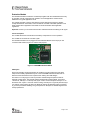
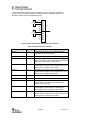
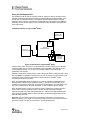
The Evaluation Module can be plugged into the Evaluation Board. Two 2x10 pin pin row
connectors with 0.050-inch pitch are used for this purpose.
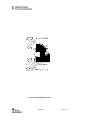
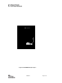
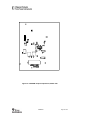
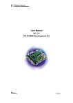
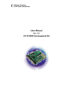
Figure 1: CC2400EM Evaluation Module
PCB layout
RF circuits operating at high frequencies are sensitive to the physical layout of the PCB.
Chipcon has carefully optimized the layout of the CC2400EM evaluation module and we
therefore recommend that the user copies it when making own PCB designs.
The PCB is of a 4-layer type in order to provide a well-defined ground plane as well as
adequate routing space. The laminate used is standard FR-4 board material. The PCB is
1.0mm thick, with layer 1 on the top side, layers 2 and 3 are internal layers and layer 4 is on
the bottom side. Layers 1 and 4 are used for routing, while layer 2 is a ground plane and layer
3 is used for power routing. All areas not utilized for routing are filled with copper connected
to ground to provide RF shielding. The ground planes on all layers are stitched together with
closely spaced vias.
SWRU050
Page 4 of 35