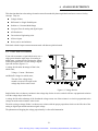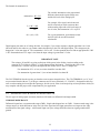
1
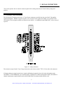
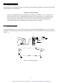
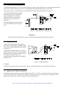
Artisan Technology Group is your source for quality
new and certified-used/pre-owned equipment
• FAST SHIPPING AND
DELIVERY
• TENS OF THOUSANDS OF
IN-STOCK ITEMS
• EQUIPMENT DEMOS
• HUNDREDS OF
MANUFACTURERS
SUPPORTED
• LEASING/MONTHLY
RENTALS
• ITAR CERTIFIED
SECURE ASSET SOLUTIONS
SERVICE CENTER REPAIRS
Experienced engineers and technicians on staff
at our full-service, in-house repair center
WE BUY USED EQUIPMENT
Sell your excess, underutilized, and idle used equipment
We also offer credit for buy-backs and trade-ins
www.artisantg.com/WeBuyEquipment
InstraView REMOTE INSPECTION
LOOKING FOR MORE INFORMATION?
Visit us on the web at www.artisantg.com for more
information on price quotations, drivers, technical
specifications, manuals, and documentation
SM
Remotely inspect equipment before purchasing with
our interactive website at www.instraview.com
Contact us: (888) 88-SOURCE | [email protected] | www.artisantg.com
CIO-DAS16/330
USERS MANUAL
Revision 5
April, 2001
Artisan Technology Group - Quality Instrumentation ... Guaranteed | (888) 88-SOURCE | www.artisantg.com
LIFETIME WARRANTY
Every hardware product manufactured by Measurement Computing Corp. is warranted against defects in materials or
workmanship for the life of the product, to the original purchaser. Any products found to be defective will be
repaired or replaced promptly.
LIFETIME HARSH ENVIRONMENT WARRANTYTM
Any Measurement Computing Corp. product which is damaged due to misuse may be replaced for only 50% of the
current price. I/O boards face some harsh environments, some harsher than the boards are designed to withstand.
When that happens, just return the board with an order for its replacement at only 50% of the list price. Measurement
Computing Corp. does not need to profit from your misfortune. By the way, we will honor this warranty for any other
manufacture’s board that we have a replacement for!
30 DAY MONEY-BACK GUARANTEE
Any Measurement Computing Corp. product may be returned within 30 days of purchase for a full refund of the
price paid for the product being returned. If you are not satisfied, or chose the wrong product by mistake, you do not
have to keep it. Please call for a RMA number first. No credits or returns accepted without a copy of the original
invoice. Some software products are subject to a repackaging fee.
These warranties are in lieu of all other warranties, expressed or implied, including any implied warranty of
merchantability or fitness for a particular application. The remedies provided herein are the buyer’s sole and
exclusive remedies. Neither Measurement Computing Corp., nor its employees shall be liable for any direct or
indirect, special, incidental or consequential damage arising from the use of its products, even if Measurement
Computing Corp. has been notified in advance of the possibility of such damages.
MEGA-FIFO, the CIO prefix to data acquisition board model numbers, the PCM prefix to data acquisition board
model numbers, PCM-DAS08, PCM-D24C3, PCM-DAC02, PCM-COM422, PCM-COM485, PCM-DMM,
PCM-DAS16D/12, PCM-DAS16S/12, PCM-DAS16D/16, PCM-DAS16S/16, PCI-DAS6402/16, Universal Library,
InstaCal, Harsh Environment Warranty and Measurement Computing Corp. are registered trademarks of
Measurement Computing Corp.
IBM, PC, and PC/AT are trademarks of International Business Machines Corp. Windows is a trademark of
Microsoft Corp. All other trademarks are the property of their respective owners.
Information furnished by Measurement Computing Corp. is believed to be accurate and reliable. However, no
responsibility is assumed by Measurement Computing Corp. neither for its use; nor for any infringements of patents
or other rights of third parties, which may result from its use. No license is granted by implication or otherwise under
any patent or copyrights of Measurement Computing Corp.
All rights reserved. No part of this publication may be reproduced, stored in a retrieval system, or transmitted, in any
form by any means, electronic, mechanical, by photocopying, recording or otherwise without the prior written
permission of Measurement Computing Corp.
Notice
Measurement Computing Corp. does not authorize any Measurement Computing Corp. product for
use in life support systems and/or devices without the written approval of the President of
Measurement Computing Corp. Life support devices/systems are devices or systems which, a) are
intended for surgical implantation into the body, or b) support or sustain life and whose failure to
perform can be reasonably expected to result in injury. Measurement Computing Corp. products
are not designed with the components required, and are not subject to the testing required to
ensure a level of reliability suitable for the treatment and diagnosis of people.
© Copyright 2001 Measurement Computing Corp.
HM CIO-DAS16_330.lwp
Artisan Technology Group - Quality Instrumentation ... Guaranteed | (888) 88-SOURCE | www.artisantg.com
Table of Contents
1 INTRODUCTION . . . . . . . . . . . . . . . . . . . . . . . . . . . . . . . . . . . . . . . . . . . . . . . . . . . . . . . . . . 1
1.1 INITIATING ENHANCED MODE . . . . . . . . . . . . . . . . . . . . . . . . . . . . . . . . . . . . . . . . . . 1
1.2 THIRD PARTY SOFTWARE . . . . . . . . . . . . . . . . . . . . . . . . . . . . . . . . . . . . . . . . . . . . . 1
2 INSTALLATION . . . . . . . . . . . . . . . . . . . . . . . . . . . . . . . . . . . . . . . . . . . . . . . . . . . . . . . . . .
2.1 SOFTWARE . . . . . . . . . . . . . . . . . . . . . . . . . . . . . . . . . . . . . . . . . . . . . . . . . . . . . . . . . .
2.2 HARDWARE . . . . . . . . . . . . . . . . . . . . . . . . . . . . . . . . . . . . . . . . . . . . . . . . . . . . . . . . .
2.2.1 BASE ADDRESS . . . . . . . . . . . . . . . . . . . . . . . . . . . . . . . . . . . . . . . . . . . . . . . . . . .
2.2.2 MODE SWITCH . . . . . . . . . . . . . . . . . . . . . . . . . . . . . . . . . . . . . . . . . . . . . . . . . . . .
2.2.3 DMA LEVEL SELECT . . . . . . . . . . . . . . . . . . . . . . . . . . . . . . . . . . . . . . . . . . . . . . .
2.2.4 1/10 MHz XTAL JUMPER . . . . . . . . . . . . . . . . . . . . . . . . . . . . . . . . . . . . . . . . . . . .
2.2.5 8/16 CHANNEL SELECT . . . . . . . . . . . . . . . . . . . . . . . . . . . . . . . . . . . . . . . . . . . . .
2.2.6 INSTALLING THE BOARD IN THE COMPUTER . . . . . . . . . . . . . . . . . . . . . . . . . . .
2
2
2
2
2
3
3
4
4
..................................................
3 SIGNAL CONNECTION
3.1 CONNECTOR DIAGRAM . . . . . . . . . . . . . . . . . . . . . . . . . . . . . . . . . . . . . . . . . . . . . . . .
3.2 ANALOG INPUTS . . . . . . . . . . . . . . . . . . . . . . . . . . . . . . . . . . . . . . . . . . . . . . . . . . . . .
3.3 SINGLE-ENDED . . . . . . . . . . . . . . . . . . . . . . . . . . . . . . . . . . . . . . . . . . . . . . . . . . . . . .
3.4 FLOATING DIFFERENTIAL . . . . . . . . . . . . . . . . . . . . . . . . . . . . . . . . . . . . . . . . . . . . .
3.5 DIFFERENTIAL . . . . . . . . . . . . . . . . . . . . . . . . . . . . . . . . . . . . . . . . . . . . . . . . . . . . . . .
3.6 DIGITAL OUTPUTS & INPUTS . . . . . . . . . . . . . . . . . . . . . . . . . . . . . . . . . . . . . . . . . . .
5
5
6
6
7
7
7
............................................. 8
4 REGISTER ARCHITECTURE
4.1 DATA TRANSFERS . . . . . . . . . . . . . . . . . . . . . . . . . . . . . . . . . . . . . . . . . . . . . . . . . . . . 8
4.2 FIFO DATA BUFFER . . . . . . . . . . . . . . . . . . . . . . . . . . . . . . . . . . . . . . . . . . . . . . . . . . . 8
4.3 CONTROL & DATA REGISTERS . . . . . . . . . . . . . . . . . . . . . . . . . . . . . . . . . . . . . . . . . . 8
4.4 A/D DATA & CHANNEL REGISTERS . . . . . . . . . . . . . . . . . . . . . . . . . . . . . . . . . . . . . 10
4.5 CHANNEL MUX SCAN LIMITS REGISTER . . . . . . . . . . . . . . . . . . . . . . . . . . . . . . . . 10
4.6 FOUR-BIT DIGITAL I/O REGISTERS . . . . . . . . . . . . . . . . . . . . . . . . . . . . . . . . . . . . . . 11
4.7 STATUS REGISTER . . . . . . . . . . . . . . . . . . . . . . . . . . . . . . . . . . . . . . . . . . . . . . . . . . . 11
4.8 DMA, INTERRUPT & TRIGGER CONTROL . . . . . . . . . . . . . . . . . . . . . . . . . . . . . . . . 12
4.9 PACER CLOCK CONTROL REGISTER . . . . . . . . . . . . . . . . . . . . . . . . . . . . . . . . . . . . 12
4.10 ANALOG INPUT RANGE REGISTER . . . . . . . . . . . . . . . . . . . . . . . . . . . . . . . . . . . . . 13
4.11 PACER CLOCK DATA & CONTROL REGISTERS . . . . . . . . . . . . . . . . . . . . . . . . . . . 15
4.12 ENHANCED FEATURES PACER CLOCK DATA & CONTROL REGISTERS . . . . . . . 16
4.13 ANALOG INPUT . . . . . . . . . . . . . . . . . . . . . . . . . . . . . . . . . . . . . . . . . . . . . . . . . . . . 16
4.14 DIGITAL INPUT & OUTPUT . . . . . . . . . . . . . . . . . . . . . . . . . . . . . . . . . . . . . . . . . . . . 17
4.14.1 OUTPUT . . . . . . . . . . . . . . . . . . . . . . . . . . . . . . . . . . . . . . . . . . . . . . . . . . . . . . . . 17
4.14.2 INPUT . . . . . . . . . . . . . . . . . . . . . . . . . . . . . . . . . . . . . . . . . . . . . . . . . . . . . . . . . . 17
4.15 INTERRUPT & TRIGGER CONTROL . . . . . . . . . . . . . . . . . . . . . . . . . . . . . . . . . . . . . 17
4.16 DMA CONTROL LOGIC . . . . . . . . . . . . . . . . . . . . . . . . . . . . . . . . . . . . . . . . . . . . . . 18
5 SPECIFICATIONS
. . . . . . . . . . . . . . . . . . . . . . . . . . . . . . . . . . . . . . . . . . . . . . . . . . . . . . 19
...............................................
6 ANALOG ELECTRONICS
6.1 VOLTAGE DIVIDERS . . . . . . . . . . . . . . . . . . . . . . . . . . . . . . . . . . . . . . . . . . . . . . . . . .
6.2 DIFFERENTIAL & SINGLE ENDED INPUTS . . . . . . . . . . . . . . . . . . . . . . . . . . . . . . . .
6.3 LOW PASS FILTERS . . . . . . . . . . . . . . . . . . . . . . . . . . . . . . . . . . . . . . . . . . . . . . . . . .
6.4 A/D RESOLUTION & ENGINEERING UNITS . . . . . . . . . . . . . . . . . . . . . . . . . . . . . . .
6.5 ENGINEERING UNITS . . . . . . . . . . . . . . . . . . . . . . . . . . . . . . . . . . . . . . . . . . . . . . . . .
6.6 CURRENT LOOP 4-20 mA . . . . . . . . . . . . . . . . . . . . . . . . . . . . . . . . . . . . . . . . . . . . . .
Artisan Technology Group - Quality Instrumentation ... Guaranteed | (888) 88-SOURCE | www.artisantg.com
21
21
22
25
25
26
26
Table of Contents
6.7 NOISE . . . . . . . . . . . . . . . . . . . . . . . . . . . . . . . . . . . . . . . . . . . . . . . . . . . . . . . . . . . . .
6.7.1 SOURCES OF NOISE . . . . . . . . . . . . . . . . . . . . . . . . . . . . . . . . . . . . . . . . . . . . . . .
6.7.2 SIGNAL WIRE NOISE . . . . . . . . . . . . . . . . . . . . . . . . . . . . . . . . . . . . . . . . . . . . . .
6.7.3 SENSOR NOISE . . . . . . . . . . . . . . . . . . . . . . . . . . . . . . . . . . . . . . . . . . . . . . . . . . .
6.7.4 SMOOTHING DATA . . . . . . . . . . . . . . . . . . . . . . . . . . . . . . . . . . . . . . . . . . . . . . .
Artisan Technology Group - Quality Instrumentation ... Guaranteed | (888) 88-SOURCE | www.artisantg.com
27
27
27
28
28
1 INTRODUCTION
The CIO-DAS16/330 is two architectures on one A/D board; one having standard DAS-16 registers and one having
extended registers.
To maintain compatibility with existing software written for the DAS-16, a complete set of DAS-16 (CIO-DAS16)
compatible registers exists at BASE + 0 through BASE + 15. When in Compatible Mode, the CIO-DAS16/330 behaves
as a CIO-DAS16 (DAS-16G) would except that it is capable of a much faster sample rate.
A second set of registers exists at BASE + 16 through BASE + 24.
In addition, a special register at BASE + 11 opens up when the CIO-DAS16/330 is in the Enhanced mode.
1.1 INITIATING ENHANCED MODE
The CIO-DAS16/330 is placed in enhanced mode by setting one switch, then by writing to a specific address. When in
enhanced mode, the CIO-DAS16/330 occupies 32 I/O addresses and so may only be placed on even hex 20 I/O address
boundaries. Examples of achievable base addresses are; 300h, 320h, 340h. Addresses such as 310h and 330h are not
possible in enhanced mode.
Enhanced mode opens up additional counters and control registers which allow:
y
16-bit bus transfers.
y
Transfer rates of 330 kHz using the REP-INSW command.
y
Pre-trigger and post-trigger sample buffers.
Enhanced mode is fully supported by the optional Universal Library™. Using it, you can acquire data at rates to 330 kHz
and store pre/post trigger buffers limited only by system RAM size.
1.2 THIRD PARTY SOFTWARE
Software packages such as Labtech Notebook support the enhanced features of the CIO-DAS16/330.
Because the CIO-DAS16/330 remains compatible with the DAS-16 even when the enhanced mode features are activated,
all third party software compatible with the DAS-16 will operate regardless of the mode switch position.
1
Artisan Technology Group - Quality Instrumentation ... Guaranteed | (888) 88-SOURCE | www.artisantg.com
2 INSTALLATION
2.1 SOFTWARE
Before you open your computer and install the board, install and run InstaCal™, the installation, calibration and test
utility included with your board. InstaCal™ will guide you through switch and jumper settings for your board. Detailed
information regarding these settings can be found below. Refer to the Software Installation manual for InstaCal™
installation instructions.
2.2 HARDWARE
The CIO-DAS16/330 has one bank of base address plus mode switches, two single function switches and one jumper
block which must be set before installation of the board inside your computer.
2.2.1 BASE ADDRESS
8 BIT
The base address is set at the factory to 300 hex as
shown in figure 2.1. Unless there is already a board
in your system which uses address 300h (768
decimal), leave the switches as they are set at the
factory.
The switch numbers here refer to the number
printed on the board itself, not the switch body.
The “8 BIT” switch is a MODE SWITCH and has
no effect on the base address itself, only the address
boundary as detailed below.
& MODE
ES
h
Set the “8 BIT” mode switch up for compatibility.
Set it down for enhanced mode.
Figure 2-1. Base Address and Mode Select Switches
2.2.2 MODE SWITCH
The “8-bit” switch of the base address switch block is the mode switch. The mode switch enables and disables extended
addresses and other features of the CIO-DAS16/330. The extended features are those associated with addresses base +
15 through base + 31. When the mode switch is up, no features associated with those registers are available.
NOTE: When the mode switch is DOWN (enhanced mode), the address 4 switch must be UP (zero).
The state of the mode switch can be read back at Base Address + 11. When the mode switch is UP, Base Address + 11,
BIT 4 reads back as a zero. When the mode switch is down, Base Address + 11, BIT 4 reads back as a one.
When the switch is UP, the board is compatible with the MetraByte DAS-16 and Measurement Computings CIO-DAS16.
Because only 16 I/O addresses are used when the mode switch is UP, the board can be placed on 16-bit boundaries, such
as 300h, 310h 320h, 330h and 340h.
When the mode switch is DOWN, the board is in extended features mode, or full PC/AT mode. Additional control bits
are present in the upper nibble of Base Address + 11 and a second 8254 counter is addressable for pre/post trigger
control. When the mode switch is down, base addresses such as 300h, 320h and 340h are available while addresses such
as 310h and 330h are not. In enhanced mode, the CIO-DAS16/330 occupies 32 I/O addresses.
2
Artisan Technology Group - Quality Instrumentation ... Guaranteed | (888) 88-SOURCE | www.artisantg.com
2.2.3 DMA LEVEL SELECT
First, determine the kind of computer you installing the board
in. If it is an XT, there are only two DMA levels available and
level 3 is probably used by the hard disk controller in your XT
computer. Set the DMA level switch to the level 1 position.
If you have an AT or 386 type computer the hard disk controller
is not at level 1 or 3 so either level may be used.
There are other boards that use DMA levels. Some network
boards do and so do some IEEE-488 interface boards. If you
have other boards in your computer with DMA level switches
on them, make sure they don’t conflict.
Figure 2-2. DMA Level Select Jumper
2.2.4 1/10 MHz XTAL JUMPER
The 1/10 MHz XTAL jumper selects the frequency of the source applied to the on board pacer (Counter 2).
This jumper is on the board because the original DAS-16,
designed in 1984, had a 1 MHz crystal. When MetraByte
redesigned the DAS-16 and added the faster 10 MHz
crystal, a jumper was provided to maintain compatibility
with older software. The CIO-DAS16/330 has the jumper
because the DAS-16 has the jumper and some software
requires the jumper to be in the 1 MHz position and some
software requires the 10 MHz position.
Figure 2-3. Pacing Frequency Select Jumper
The CIO-DAS16/330 is shipped with the jumper in the 1 MHz position.
Older software programs may require that the jumper be in the 1 MHz position. Please refer to the software program
user's manual for guidance. Use the 10 MHz setting for any new development for better rate resolution when
programming the on board pacer.
3
Artisan Technology Group - Quality Instrumentation ... Guaranteed | (888) 88-SOURCE | www.artisantg.com
2.2.5 8/16 CHANNEL SELECT
The CIO-DAS16/330 can be configured for eight differential or 16
single-ended analog inputs. Using differential inputs allows up to 10
volts of common mode (ground loop) rejection and is more immune to
RFI and EMI.
The board comes from the factory with the 8/16 Channel Select switch
set for eight differential inputs (Figure 2-4). Set it for the type (and
number) of inputs you require.
Figure 2-4. 8 or 16 Channels Select Switch
2.2.6 INSTALLING THE BOARD IN THE COMPUTER
1. Turn the power off.
2. Remove the cover of your computer. Please be careful not to dislodge any of the cables installed on the boards in
your computer as you slide the cover off.
3. Locate an empty expansion slot in your computer.
4. Push the board firmly down into the expansion bus connector. If it is not seated fully it may fail to work and
could short circuit the PC bus power onto a PC bus signal. This could damage the motherboard in your PC as
well as the CIO-DAS16/330.
5. Turn the PC power back on and verify proper installation by running InstaCal Test (refer to the Software
Installation Manual for information on running InstaCal.
4
Artisan Technology Group - Quality Instrumentation ... Guaranteed | (888) 88-SOURCE | www.artisantg.com
3 SIGNAL CONNECTION
This section presents 'how to connect' common signals while avoiding discussion of electrical theory and special
symbols.
3.1 CONNECTOR DIAGRAM
The CIO-DAS16/330 analog connector is a 37-pin, D-type connector accessible from the rear of the PC through the
expansion backplate. With the exception of pins 8, 9, 10, 26 and 27 (D/A signals on the DAS-16, no connect on the
CIO-DAS16/330), the signals available are identical to the DAS-16. An additional signal, SS&H OUT, can be accessed
at pin 26.
/ CTR0 GATE
Figure 3-1. Analog Connector
The connector accepts female 37-pin, D-type connectors, such as those on the C73FF-2, 2 foot cable with connectors.
If frequent changes to signal connections or signal conditioning is required, please refer to the information on the
CIO-MINI37 or CIO-TERMINAL screw terminal boards, CIO-EXP32 32 channel analog MUX/AMP, CIO-SSH16 16
channel simultaneous sample & hold board or the ISO-RACK08 5B isolation module interface rack.
5
Artisan Technology Group - Quality Instrumentation ... Guaranteed | (888) 88-SOURCE | www.artisantg.com
3.2 ANALOG INPUTS
Analog inputs to the CIO-DAS16/330 may be connected in three different configurations. These are single-ended,
floating differential, and differential.
WARNING - PLEASE READ
Measure the voltage between the ground signal at the signal source and the PC. Use a volt meter and
place the red probe on the PC ground and the black probe on the signal ground. If the voltage is more
than 10 volts, do not connect the CIO-DAS16/330 to this signal source because you will not be able to
make a valid reading. If the difference is more than 30 volts, DO NOT connect this signal to the
CIO-DAS16/330 because it will damage the board and possibly the computer.
3.3 SINGLE ENDED
A single ended input is two wires connected to the board; a channel high (CH# HIGH) and a Low Level Ground
(LLGND). The LLGND signal must be the same ground the PC is on. The CH# HIGH is the voltage signal source
(Figure 3-2).
8
16
Figure 3-2. Single-Ended Input
6
Artisan Technology Group - Quality Instrumentation ... Guaranteed | (888) 88-SOURCE | www.artisantg.com
3.4 FLOATING DIFFERENTIAL
A floating differential input is two wires from the signal source and a 10K ground reference resistor installed at the board
input. The two signals from the signal source are Signal High (CH# HIGH) and Signal Low (CH# LOW).
The reference resistor is connected between the CIO-DAS16/330 CH# LOW and LLGND pins (Figure 3-3).
A floating differential hookup is handy
when the signal source is floating with
respect to ground, such as a battery,
4-20 mA transmitter or and the lead
lengths are long or subject to EMI
interference.
The floating differential input will reject
up to 10V of EMI energy on the signal
wires.
Figure 3-3. Differential Input - Floating Source
WARNING!
Is the signal source really floating? Check it with an ohmmeter before risking the board and the PC!
3.5 DIFFERENTIAL
A differential signal has three wires from the
signal source; Signal High (CH# HIGH), Signal
Low (CH# LOW) and Signal Ground (LLGND)
See Figure 3-4.
A differential connection allows you to connect
the board to a signal source with a ground that is
different than the PC ground, but has less than a
10V difference, and still make a true
measurement of the signal between CH# HIGH
and CH# LOW.
Figure 3-4. Differential Input
EXAMPLE:
A laboratory instrument with its own wall plug. There are sometimes differences in wall GND between outlets.
3.6 DIGITAL OUTPUTS & INPUTS
All the digital inputs and outputs on the CIO-DAS16/330 are TTL level. TTL is an electronics industry term, short for
Transistor Transistor Logic, with describes a standard for digital signals which are either at 0V or 5V (nominal). The
binary logic inside the PC is all TTL or LSTTL (Low power Schotky TTL).
7
Artisan Technology Group - Quality Instrumentation ... Guaranteed | (888) 88-SOURCE | www.artisantg.com
4
REGISTER ARCHITECTURE
4.1 DATA TRANSFERS
The CIO-DAS16/330 bus interface is a PC/XT/AT bus interface. In compatibility mode (mode switch up) it interfaces to
the XT bus only. In enhanced mode (mode switch DOWN), the CIO-DAS16/330 employs the full 16-bit PC/AT bus.
Because 16-bit data transfers are faster, the CIO-DAS16/330 can transfer A/D samples taken with old DAS-16 software
at speeds over 150 kHz. Old DAS-16 software uses DMA to transfer A/D data.
Of course, using the REP INS command (which can only be done by the CIO-DAS16/330), data transfers of 330 kHz and
sample sets of any size up to the size of available memory may be taken.
4.2 FIFO DATA BUFFER
The First In First Out (FIFO) buffer is a specialized memory 1024 samples deep. After each conversion, the A/D data is
transferred to the FIFO memory. Samples are retrieved from the FIFO data buffer by the computer program which stores
the data in the PC's memory. This may be a language program, or an application program.
The FIFO is active all the time, regardless of mode. The FIFO does not affect compatibility with existing software, in
fact, it does enhance it by allowing data to be transferred asynchronously, therefore at higher speeds.
In addition to enhancing standard interrupt and DMA operations, the FIFO makes possible the use of advanced
instructions like REP-INSW, a block transfer.
4.3 CONTROL & DATA REGISTERS
The CIO-DAS16/330 is controlled and monitored by writing to and reading from 16 or 20 consecutive 8-bit I/O
addresses. The first address, or BASE ADDRESS, is determined by setting a bank of switches on the board.
Usually, register manipulation is best left to experienced programmers with a specific need for low level control as most
of the CIO-DAS16/330 possible functions are implemented in the easy to use Universal Library™ for DOS and Windows
languages.
The register descriptions have the following format:
7
A/D9
6
A/D10
5
A/D11
4
A/D12
3
CH8
2
CH4
1
CH2
0
CH1
LSB
Where the numbers along the top row are the bit positions within the 8-bit byte and the numbers and symbols in the
bottom row are the functions associated with that bit.
To write to or read from a register in decimal or HEX, the weights in Table 4-1 apply.
8
Artisan Technology Group - Quality Instrumentation ... Guaranteed | (888) 88-SOURCE | www.artisantg.com
Table 4-1. Bit Weights
BIT POSITION
0
1
2
3
4
5
6
7
DECIMAL VALUE
1
2
4
8
16
32
64
128
HEX VALUE
1
2
4
8
10
20
40
80
To write control or data to a register, the individual bits are set to 0 or 1 then combined to form a Byte. The method of
programming required to set/read bits from bytes is beyond the scope of this manual.
The board registers and their function are listed on Table 4-2.
Table 4-2. Register Functions
ADDRESS
BASE
BASE + 1
BASE + 2
BASE + 3
BASE + 4
BASE + 5
BASE + 6
BASE + 7
BASE + 8
BASE + 9
BASE + 10
BASE + 11
BASE + 12
BASE + 13
BASE + 14
BASE + 15
BASE + 11
BASE + 16
BASE + 17
BASE + 18
BASE + 19
READ FUNCTION - ALL MODES
A/D Bits 9-12 (LSB) & Channel #
A/D Bits 1 (MSB) - 8
Channel MUX
Digital 4 Bit Input
None
None
None
None
Status EOC, UNI/BIP, Current Ch.
DMA, Interrupt & Trigger Control
None
Gain setting read-back
Counter 0 Data
CTR 1 Data - A/D Pacer Clock
CTR2 Data - A/D Pacer Clock
None. No read back on 8254
ENHANCED MODE ONLY
Upper nibble, enhanced features
status
Total sample MS Counter
Total sample LS Counter
Pre-trigger count
None. No read back on 8254
WRITE FUNCTION
Start A/D Conversion
None
Channel MUX Set, Clear FIFO
Digital 4 Bit Output
None
None
None
None
None
Set DMA, INT etc
Pacer clock control register
Gain, Enhanced Mode, DT Conn.
Counter 0 Data
CTR 1 Data - A/D Pacer
CTR 2 Data - A/D Pacer
Pacer Clock Control (8254)
Upper nibble, enhanced features
control
CTR 0. Total counter (1/2)
CTR 1. Total counter (1/2)
CTR 2. Pre-trigger counter
Advanced features counter control
(8254)
9
Artisan Technology Group - Quality Instrumentation ... Guaranteed | (888) 88-SOURCE | www.artisantg.com
4.4 A/D DATA & CHANNEL REGISTERS
Note: When in enhanced mode, the bus interface is 16 bits wide and BASE +0 and BASE +1 should be read as a 16 bit
pair. To whit, the register at BASE + 1 should be read as the most significant eight bits of a 16-bit read to BASE + 0.
BASE ADDRESS
7
A/D9
6
A/D10
5
A/D11
4
A/D12
3
CH8
2
CH4
1
CH2
0
CH1
LSB
A read/write register.
READ
On read, it contains two types of data. The least significant four digits of the analog input data and the associated
channel number.
These four bits of analog input data must be combined with the eight bits of analog input data in BASE + 1, forming
a complete 12-bit number. The data is in the format 0 = minus full scale. 4095 = +FS.
The channel number is binary. The weights are shown in the table above. If the current channel were 5, then bits
CH4 and CH1 would be high, CH8 and CH2 would be low.
WRITE
Writing any data to the register causes an immediate A/D conversion.
BASE ADDRESS +1
7
A/D1
6
A/D2
5
A/D3
4
A/D4
3
A/D5
2
A/D6
1
A/D7
0
A/D8
2
CH L4
1
CH L2
0
CH L1
MSB
A Read-only register.
On read, the most significant A/D byte is read.
4.5 CHANNEL MUX SCAN LIMITS REGISTER
BASE ADDRESS +2
7
CH H8
6
CH H4
5
CH H2
4
CH H1
3
CH L8
A read and write register.
READ
The current channel scan limits are read as one byte. The high channel number scan limit is in the most significant
four bits. The low channel scan limit is in the least significant four bits.
WRITE
The channel scan limits desired are written as one byte. The high channel number scan limit is in the most significant
four bits. The low channel scan limit is in the least significant four bits.
10
Artisan Technology Group - Quality Instrumentation ... Guaranteed | (888) 88-SOURCE | www.artisantg.com
Bits 3-0 contain the starting channel number and bits 7-4 contain the ending channel number. If you wanted to scan
channels 1, 2, 3 in that order, you could do so by placing the 3 in bits 7-4 and the 1 in bits 3-0.
NOTE
Every write to this register sets the current A/D channel MUX setting to the number in bits 0-3. See
BASE + 8. Every write to this register clears the FIFO buffer.
4.6 FOUR- BIT DIGITAL I/O REGISTERS
BASE ADDRESS +3
When read...
7
0
6
0
5
0
4
0
3
DI3
2
DI2,
1
DI1
CTR0
0
DI0,
TRIG
GATE
READ
The signals present at the inputs are read as one byte, the most significant four bits of which are always zero. The
pins 25 (digital input 0) and 24 (digital input 2) digital inputs have two functions each.
The TRIG function of digital input 0 may be used to hold off the first sample of an A/D set by holding it low (0V)
until you are ready to take samples, which are then paced by the 8254. It can also be used as the source of an external
start conversion pulse, synchronizing A/D conversions to some external event.
When written to...
7
X
6
X
5
X
4
X
3
DO3
2
DO2
1
DO1
0
DO0
WRITE
The upper four bits are ignored. The lower four bits are latched TTL outputs. Once written, the state of the inputs
cannot be read back because a read back would read the separate digital input lines (see above).
4.7 STATUS REGISTER
BASE ADDRESS +8
7
EOC
6
U/B
5
MUX
4
INT
3
CH8
2
CH4
1
CH2
0
CH1
A read mostly, one-function-write register.
READ
EOC = 1, the A/D converter is busy. EOC = 0, it is free.
U/B = 1, the amplifier is in Unipolar mode. U/B = 0, is bipolar.
MUX = 1, Channels are configured 16 single ended. MUX = 0, 8 differential.
INT = 1, an external pulse has been received. INT = 0, the flip-flop is ready to receive a pulse.
There is a flip-flop on the TRIGGER input (pin 25) which will latch a pulse as short as 200 ns. After being triggered, this
flip-flop must be reset by a write to this register. Your interrupt service routine must do this before another interrupt
trigger can be received.
11
Artisan Technology Group - Quality Instrumentation ... Guaranteed | (888) 88-SOURCE | www.artisantg.com
CH8, CH4, CH2 & CH1 are a binary number between 0 and 15 indicating the channel number that the MUX is currently
set to and is valid only when EOC = 0. The channel MUX increments shortly after EOC = 1 so may be in a state of
transition when EOC = 1. The binary weight of each bit is shown in the table above.
WRITE
A write of any data to this register resets the flip-flop on the pin 25 input and sets the INT bit to 0.
4.8 DMA, INTERRUPT & TRIGGER CONTROL
BASE ADDRESS +9
7
INTE
6
IR4
5
IR2
4
IR1
3
Don’t Care
2
DMA
1
TS1
0
TS0
A read and write register.
READ
INTE = 1, Interrupts are enabled. An interrupt generated will be placed on the PC bus interrupt level selected by IR4,
IR2 & IR1. INTE = 0, interrupts are disabled.
IR4, IR2, IR1 are bits in a binary number between 0 and 7 which map interrupts onto the PC bus interrupt levels 2 - 7.
Interrupts 0 & 1 map into interrupts 10 and 11.
DMA = 1, DMA transfers are enabled. DMA = 0, DMA transfers are disabled. It is worth noting that this bit only
allows the CIO-DAS16/330 to assert a DMA request to the PC on the DMA request level selected by the DMA
switch on the CIO-DAS16/330. Before this bit is set to 1, the PC's 8237 (or appropriate) DMA controller chip must
be set up.
TS1 & TS0 control the source of the A/D start conversion trigger according to Table 4-4.
4.9 PACER CLOCK CONTROL REGISTER
BASE ADDRESS +10
7
X
6
X
5
X
4
X
3
X
2
X
1
CTR0
0
TRIG0
Write only
CTR0 = 1. When CTR0 = 1, an on-board 100 kHz clock signal is ANDed with the COUNTER 0 CLOCK INPUT
(pin 21). A high on pin 21 will allow pulses from the on-board source into the 8254 Counter 0 input.
CTR0 = 0. When CTR0 = 0, the input to 8254 Counter 0 is entirely dependent on pulses at pin 21, COUNTER 0
CLOCK INPUT.
TRIG0 = 1. When TRIG0 = 1, the TRIGGER input at pin 25 is ANDed with TRIG0 which must be high for the
pulses from the on-board pacer clock (8254) to start A/D conversions. The input at pin 25 is pulled up and will
always be high unless pulled low externally.
TRIG0 = 0. When TRIG0 = 0, the GATEs of counter 1 & 2 are held high, preventing signals at pin 25 from gating
off the on board pacer.
12
Artisan Technology Group - Quality Instrumentation ... Guaranteed | (888) 88-SOURCE | www.artisantg.com
Figure 4-1 may help understand these registers, and is further explained in the section covering the 8254.
+5V
+5V
CONTROL REGISTER
BASE + 10
TRIG
10K
24
GATE 0
21
CTR 0 IN
10K
CTR0
OUT
COUNTER 0
2
CTR 0 OUT
20
CTR 2 OUT
25
TRIGGER
GATE
10 MHz
1 /10
OUT
COUNTER 1
10 MHz
GATE
1MHz
COUNTER 2
1 /10
OUT
GATE
+5V
10K
A/D PACER
CIO-AD16 8254 PACER CLOCK & CONTROL
Figure 4-1. Pacer Clock and Control
4.10 ANALOG INPUT RANGE REGISTER
BASE ADDRESS +11 - Compatible Mode
7
X
6
X
5
X
4
X
3
Range
2
Uni/Bip
1
G1
0
G0
A write to this register sets the analog input range for all 8/16 analog inputs. The lower four bits set the analog input
range. The upper four bits are not used in compatible mode (Table 4-3).
13
Artisan Technology Group - Quality Instrumentation ... Guaranteed | (888) 88-SOURCE | www.artisantg.com
Table 4- 3. Input Range Coding
Range
1
0
0
0
0
0
0
0
0
Uni/Bip
0
0
0
0
0
1
1
1
1
G1
0
0
0
1
1
0
0
1
1
G0
0
0
1
0
1
0
1
0
1
Input Range
+/-10V
+/-5V
+/-2.5V
+/-1.25V
+/-0.625
0 to 10V
0 to 5V
0 to 2.5V
0 to 1.25V
Decimal
8
0
1
2
3
4
5
6
7
To set the analog input range of the CIO-DAS16/330 programmatically, write the correct input range code to the base
address + 11. For example, from BASIC:
If the board's base address is 300h (768 decimal), then the gain register is at 768 + 11 = 779
100
OUT 779, 5
'Set analog output range to 0 to 5V
The decimal range codes are in the far right column above.
BASE ADDRESS +11 - Enhanced Mode
A write to this register sets the analog input range for all 8/16 analog inputs as well as enabling and disabling extended
features and controlling extended features for pre-triggering and DT-CONNECT. The lower four bits set the analog input
range. The upper four bits control and provide status of enhanced features.
7
DT-
6
Pre-
5
Overrun
4
Set/Read
Connect
Trigger
Status
Mode
Enable
Enable
3
Range
2
Uni/Bip
1
G1
0
G0
GAINS: Gain control is identical in both compatible and enhanced mode.
BIT 4 - Set Compatible/Enhanced Mode. Read Mode Status
WRITE: 0 = disable enhanced mode. 1 = enable enhanced mode (mode switch must be down).
READ: 0 = Switch 7 of base address switch, the mode switch, is up. It is not possible to enable enhanced features
when the mode switch is up. When Bit 4 = 1, the mode switch is down and enhanced features can be enabled.
BIT 5 - Set Pretrigger, DT-Connect. Read FIFO, Overrun
READ: 0 = No overrun. 1 = FIFO buffer full (> 1024 samples) or DT-CONNECT overrun if DT-CONNECT is
enabled. This signal is the logical OR of these two possible overrun signals. To determine the source of the overrun
error: If DT-Connect is not enabled then the overrun is FIFO. If DT-CONNECT is enabled, issue a clear to the FIFO
then reread the status bit. If still active, the overrun was at the DT-CONNECT.
WRITE: Enable channel gain queue mode. Access to Base + 2 is inhibited when the channel gain queue is enabled.
14
Artisan Technology Group - Quality Instrumentation ... Guaranteed | (888) 88-SOURCE | www.artisantg.com
BIT 6 - Pre-Trigger Enable. Trigger Status.
WRITE: 0 = Disable pre-trigger mode. 1 = enable pre-trigger. The trigger index counter (CTR 2 of 2nd 8254) is
gated to the packet interrupt. Because it is gated to the FIFO packet interrupt, the trigger flushes the FIFO at the
instant of the trigger, ensuring the only samples prior to and all samples prior to the trigger are in the pre-trigger
buffer.
READ: Valid only when pre-trigger is enabled. 0 = Trigger has not yet occurred. 1 = Trigger occurred.
BIT 7 - DT-CONNECT Enable/Disable & Status
WRITE: 0 = Disable DT-Connect. 1 = Enable DT-CONNECT.
For DT-Connect to operate, the Total Counter output must be forced low. The simplest way to do this is to write the
value 16 to Base +19 (both decimal).
READ: 0 = DT-CONNECT is disabled. 1 = DT-CONNECT is enabled.
4.11 PACER CLOCK DATA & CONTROL REGISTERS
8254 COUNTER 0 DATA
BASE ADDRESS + 12
7
D8
6
D7
5
D6
4
D5
3
D4
2
D3
1
D2
0
D1
5
D6
4
D5
3
D4
2
D3
1
D2
0
D1
5
D6
4
D5
3
D4
2
D3
1
D2
0
D1
8254 COUNTER 1 DATA
BASE ADDRESS + 13
7
D8
6
D7
8254 COUNTER 2 DATA
BASE ADDRESS + 14
7
D8
6
D7
The three 8254 counter/timer data registers may be written to and read from. Because each counter will count to 65,535,
loading or reading the counter data is a multi-step process. The operation of the 8254 is explained in the section on the
counter/time and the Intel 8254 data sheet.
8254 COUNTER CONTROL
BASE ADDRESS + 15
7
D8
6
D7
5
D6
4
D5
3
D4
2
D3
1
D2
0
D1
This register controls the operation and loading/reading of the counters. The configuration of the 8254 codes which
control the 8254 chip is explained in the section on the counter timer and the Intel 8254 data sheet.
15
Artisan Technology Group - Quality Instrumentation ... Guaranteed | (888) 88-SOURCE | www.artisantg.com
4.12 ENHANCED FEATURES PACER CLOCK DATA & CONTROL REGISTERS
8254 COUNTER 0 DATA - Total Count MS Counter
Chained from counter 1
BASE ADDRESS +16
7
D8
6
D7
5
D6
4
D5
3
D4
2
D3
1
D2
0
D1
3
D4
2
D3
1
D2
0
D1
3
D4
2
D3
1
D2
0
D1
8254 COUNTER 1 DATA - Total Count LS Counter
Clocked by Pacer (See XTAL jumper) - Chained to counter 0
BASE ADDRESS +17
7
D8
6
D7
5
D6
4
D5
8254 COUNTER 2 DATA - Pretrigger Index Counter
BASE ADDRESS +18
7
D8
6
D7
5
D6
4
D5
The three 8254 counter/timer data registers may be written to and read from. Because each counter will count to 65,535,
loading or reading the counter data is a multi-step process. The operation of the 8254 is explained in the section on the
counter/time and the Intel 8254 data sheet.
8254 COUNTER CONTROL
BASE ADDRESS + 19
7
D8
6
D7
5
D6
4
D5
3
D4
2
D3
1
D2
0
D1
This register controls the operation and loading/reading of the counters. The configuration of the 8254 codes which
control the 8254 chip is explained in the Intel 8254 data sheet.
4.13 ANALOG INPUT
Analog signals connected to P3, the 37-pin, D-type connector, are first fed into the two HI-0508 analog multiplexers. A
multiplexer's function is to select one of eight inputs and connect that input to the MUX output. MUX U27 connects
CH0-CH7 high inputs. MUX U28 connects CH0-CH7 Low input (differential input mode) or CH8-CH15 High inputs
(single-ended mode) depending on the state of the channel configuration switch located at the upper right of the board
and marked 8/16.
From the output of the MUX, the analog signal is fed into a programmable differential amplifier.
The A/D converter chip has an integral sample & hold circuit, greatly simplifying design and improving signal integrity.
The A/D converter is capable of sampling rates to 330 kHz.
16
Artisan Technology Group - Quality Instrumentation ... Guaranteed | (888) 88-SOURCE | www.artisantg.com
4.14 DIGITAL INPUT & OUTPUT
There are four bits of output only and four bits of input only on the CIO-DAS16/330 analog connector. From the original
DAS-16 design, these were the only eight bits of digital I/O.
For complete programming information refer to the section on CIO-DAS16/330 registers.
4.14.1 OUTPUT
The output bits are part of chip U39, a 74LS197 output buffer. The other half of the chip is used for on-board control. If
the digital output lines are blown by overload or high voltage connection, you can replace the chip.
4.14.2 INPUT
The input bits are part of chip U38, a 74LS244 buffer. The other half of this chip is used for on-board functions. This
chip is socketed.
4.15 INTERRUPT & TRIGGER CONTROL
The interrupt and trigger control is accessible via programming at register BASE + 9. Interrupts are enabled by setting
bit 7. The PC bus interrupt number, 2 to 7, 10, and 11, is register-programmed. The source, either from the 8254 or
external, is programmed also.
BASE ADDRESS +9
7
INTE
6
IR4
5
IR2
4
IR1
3
Don’t Care
2
DMA
1
TS1
0
TS0
A read and write register.
READ
INTE = 1, Interrupts are enabled. An interrupt generated will be placed on the PC bus interrupt level selected by IR4,
IR2, and IR1. When INTE = 0, interrupts are disabled.
IR4, IR2, IR1 are bits in a binary number between 0 and 7 which map interrupts onto the PC bus interrupt levels 2 - 7.
Interrupts 0 maps into 10 and interrupt 1 maps into 11.
TS1 & TS0 control the source of the A/D start conversion trigger according to Table 4-4 below.
Table 4- 4. A/D Start Conversion Source Coding
TS1
0
1
1
TS0
X
0
1
Software triggered A/D only.
Start on rising TRIGGER (Digital input 0, Pin 25)
Start on Pacer Clock Pulse (CTR 2 OUT, no external access)
17
Artisan Technology Group - Quality Instrumentation ... Guaranteed | (888) 88-SOURCE | www.artisantg.com
4.16 DMA CONTROL LOGIC
The Direct Memory Access (DMA) controller is on the personal computer
CPU board, not on the CIO-DAS16/330. The CIO-DAS16/330 has the logic
on board to request a DMA transfer. In addition to the on board logic, the
DMA controller must be programmed.
Complete register specifications for the CIO-DAS16/330 DMA control
registers will be found in the previous section on the CIO-DAS16/330 control
registers.
Figure 4-2. DMA Level Select Switch
18
Artisan Technology Group - Quality Instrumentation ... Guaranteed | (888) 88-SOURCE | www.artisantg.com
5 SPECIFICATIONS
Power consumption
+5V:
Analog input section
A/D converter type
Resolution
Number of channels
Programmable ranges
Polarity
A/D pacing
A/D Trigger sources
A/D Triggering Modes
Digital:
900 mA typical, mA max
AD7800
12 bits
8 differential or 16 single-ended, switch-selectable
±10V, ±5V, ±2.5V, ±1.25V , ±0.625V, 0 to 10V, 0 to 5V, 0 to 2.5V,
0 to 1.25V, 0 to 0.625V, fully programmable
Unipolar/Bipolar, software-selectable
Programmable: internal counter or external source (DIG. IN 0 / TRIGGER,
rising edge) or software-polled
External hardware/software (DIG. IN 0 / TRIGGER, active high)
Data transfer
DMA
A/D conversion time
Throughput
Gated pacer, software polled. (Gate must be disabled by software after
trigger event.)
From 1024 sample FIFO via REPINSW, interrupt, DMA or software polled
Channel 1 or 3, switch-selectable
3 µs
330 kHz
Absolute accuracy
Differential Linearity error
Integral Linearity error
No missing codes guaranteed
Gain drift (A/D specs)
Zero drift (A/D specs)
0.01% of reading ±1 LSB
±1 LSB
±1 LSB
12 bits
±25 ppm/°C
±10 ppm/°C
Common Mode Range
CMRR @ 60 Hz
Input leakage current (@25 Deg C)
Input impedance
Absolute maximum input voltage
±10V
−72dB
200 nA
10 MegOhms min
±35V
Digital Input / Output
Digital type
Configuration
Input: 74LS367
Output: 74LS197
Two ports, 4 input bits and 4 output bits
Input low voltage
0.8V max
Input high voltage
2.0V min
Output low voltage (IOL = 8 mA)
0.5V max
Output high voltage (IOH = −0.4 mA) 2.7V min
Absolute maximum input voltage
−0.5V, +7V
Interrupts
Interrupt enable
Interrupt sources
2 through 7, 10 and 11, programmable
Programmable
A/D End-of-conversion, A/D FIFO-half-full, Residual counter, DMA
terminal count
19
Artisan Technology Group - Quality Instrumentation ... Guaranteed | (888) 88-SOURCE | www.artisantg.com
Counter section
Counter type
Configuration
82C54
Two 82C54 devices, 3 down counters each device, 16 bits each
82C54A:
Counter 0 - Independent, available to user
Source: 100 kHz on board clock or external (CTR 0 Clock In)
Gate:
External (Dig In 2 / CTR 0 Gate)
Output: Available at user connector (CTR 0 Out)
Counter 1 - ADC Pacer Lower Divider
Source: 1 or 10 MHz oscillator, jumper-selectable
Gate:
Tied to Counter 2 gate, programmable source (internal or external
(Dig In 0 / Trigger).
Output: Chained to Counter 2 Clock.
Counter 2 - ADC Pacer Upper Divider
Source: Counter 1 Output.
Gate:
Tied to Counter 1 gate, programmable source: internal or external
(Dig In 0 / Trigger).
Output: ADC Pacer clock, available at user connector (CTR 2 Out)
82C54B:
Counter 0 - Total samples (residual) counter upper divider
Source: Counter 1 output (total samples lower divider)
Gate:
Internal
Output: Internal
Counter 1 - Total samples (residual) counter lower divider
Source: ADC conversion complete
Gate:
Tied to Counter 2 gate, internal source.
Output: Counter 0 input (total samples upper divider)
Counter 2 - Trigger index counter
Source: ADC conversion complete
Gate:
Tied to Counter 1 gate, internal source.
Output: Not used
Clock input frequency
High pulse width (clock input)
Low pulse width (clock input)
Gate width high
Gate width low
Input low voltage
Input high voltage
Output low voltage
Output high voltage
10 MHz max
30 ns min
50 ns min
50 ns min
50 ns min
0.8V max
2.0V min
0.4V max
3.0V min
Crystal oscillator
Frequency
Frequency accuracy
10 MHz
100 ppm
Environmental
Operating temperature range
Storage temperature range
Humidity
0 to 50°C
−20 to 70°C
0 to 90% non-condensing
20
Artisan Technology Group - Quality Instrumentation ... Guaranteed | (888) 88-SOURCE | www.artisantg.com
6 ANALOG ELECTRONICS
This short introduction to the analog electronics most often needed by data acquisition board users covers a few key
concepts. They are:
y
Voltage dividers.
y
Differential vs. Single Ended Inputs.
y
Isolation vs. Common Mode Range
y
Low pass filters for analog and digital inputs.
y
A/D Resolution
y
Conversion to Engineering units.
y
4-20 mA inputs
y
Noise; sources and solutions.
Each deals with the impact on measurements made with data acquisition boards.
6.1 VOLTAGE DIVIDERS
If you wish to measure a signal which varies over a
range greater than the input range of an analog or
digital input, a voltage divider can drop the voltage
of the input signal to the level the analog or digital
input can measure (Figure 6-1).
A voltage divider takes advantage of Ohm's law,
which states,
Voltage = Current * Resistance
and Kirkoff's voltage law which states,
The sum of the voltage drops
around a circuit will be equal to the
voltage drop for the entire circuit.
Figure 6-1. Voltage Divider
Implied in the above is that any variation in the voltage drop for the circuit as a whole will have a proportional variation
in all the voltage drops in the circuit.
A voltage divider takes advantage of the fact that the voltage across one of the resistors in a circuit is proportional to the
voltage across the total resistance in the circuit.
The trick to using a voltage divider is to choose two resistors with the proper proportions relative to the full scale of the
analog or digital input and the maximum signal voltage.
The phenomena of dropping the voltage proportionally is often called attenuation.
21
Artisan Technology Group - Quality Instrumentation ... Guaranteed | (888) 88-SOURCE | www.artisantg.com
The formula for attenuation is:
Attenuation = R1 + R2
The variable Attenuation is the proportional
difference between the signal voltage max
and the full scale of the analog input.
R2
2 = 10K + 10K
10K
R1 = (A-1) * R2
For example, if the signal varies between 0
and 20 volts and you wish to measure that
with an analog input with a full scale range of
0 to 10 volts, the Attenuation is 2:1 or just 2.
For a given attenuation, pick a handy resistor
and call it R2, the use this formula to
calculate R1.
Digital inputs also make use of voltage dividers, for example, if you wish to measure a digital signal that is at 0 volts
when off and 24 volts when on, you cannot connect that directly to the CIO-AD digital inputs. The voltage must be
dropped to 5 volts max when on. The Attenuation is 24:5 or 4.8. Use the equation above to find an appropriate R1 if R2
is 1K. Remember that a TTL input is 'on' when the input voltage is greater than 2.5 volts.
IMPORTANT NOTE
The resistors, R1 and R2, are going to dissipate all the power in the divider circuit according to the
equation W=I2 x R (Power (Watts) = Current Squared times Resistance). The higher the value of the
resistance (R1 + R2) the less power dissipated by the divider circuit. Here is a simple rule:
For Attenuation of 5:1 or less, no resistor should be less than 10K.
For Attenuation of greater than 5:1, no resistor should be less than 1K.
The CIO-TERMINAL has the circuitry on board to create custom voltage dividers. The CIO-TERMINAL is a 16" by 4"
screw terminal board with two 37 pin D type connectors and 56 screw terminals (12 - 22 AWG). Designed for table top,
wall or rack mounting, the board provides prototype, divider circuit, filter circuit and pull-up resistor positions which you
may complete with the proper value components for your application.
6.2 DIFFERENTIAL & SINGLE ENDED INPUTS
The two types of analog inputs commonly found on A/D boards are differential and single-ended.
COMMON MODE RANGE
Differential inputs have a common mode range (CMR). Single-ended inputs have no CMR . Common mode range is the
voltage range over which differences in the low side of the signal and A/D input ground have no impact on the A/D's
measurement of the signal voltage. A differential input can reject voltage differences between signal ground and PC
ground.
22
Artisan Technology Group - Quality Instrumentation ... Guaranteed | (888) 88-SOURCE | www.artisantg.com
Figure 6-2. Differential Input
Figure 6-2 shows the differential mode (multiplexer not shown).
A single-ended input has no common mode range because there is only one LOW wire, the level of which is assumed to
be the same, signal source and A/D board (Figure 6-3).
Figure 6-3. Single-Ended Input
The maximum difference which can be rejected is the CMR.
For example, the CIO-DAS16/330 has a common mode plus signal range of 11.5 volts, common mode not to exceed 10
volts.
23
Artisan Technology Group - Quality Instrumentation ... Guaranteed | (888) 88-SOURCE | www.artisantg.com
This specification is illustrated graphically in Figure 6-4 and is referred to as Cumulative Signal Range (CSR).
Figure 6-4. Cumulative Signal Range
Most manufactures of A/D boards specify the CMR directly from the component data sheet, ignoring the effect of the
board level system on that specification. A data sheet of that type might claim 10 volts of CMR. Although this is a
factual specification and the designer of the board (or other EE) would be able to translate that into a systems
specification, most A/D board owners are confused or mislead by such specs.
COMMON MISUNDERSTANDINGS
The CMR specification of a differential input is often confused with an isolation specification, which it is not. It makes
sense. doesn't it, that 10 volts of CMR is the same as 10 volts of isolation? No. The graph above shows why.
Also, failure to specify the common mode plus signal system specification leads people to believe that a DC offset equal
to the component CMR can be rejected regardless of the input signal voltage. It cannot as the graph above illustrates.
When is a differential input useful? The best answer is whenever electromagnetic interference (EMI) or radio frequency
interference (RFI) may be present in the path of the signal wires. EMI and RFI can induce voltages on both signal wires
and the effect on single ended inputs is generally a voltage fluctuation between signal high and signal ground.
A differential input is not affected in that way. When the signal high and signal low of a differential input have EMI or
RFI voltage induced on them, that common mode voltage is rejected, subject to the system constraint that common mode
plus signal not exceed the A/D board's CSR specification.
GROUND LOOPS
Ground loops are circuits (E=I*R) created when the signal ground and the PC ground are not the same. Ground loop
inducing voltage differential may be a few volts of hundreds of volts. They may be constant or transient (spikes). A
differential input will prevent a ground loop as long as the CSR specifications is not exceeded.
If ground differences greater than the CMR are encountered, isolation is required.
WHY USE SINGLE ENDED?
The reason is connector space. Single ended inputs require one analog high input per channel and one LLGND shared by
all inputs. Differential inputs require signal high and signal low inputs for each channel and one common shared
LLGND.
Single ended inputs save connector space, parts cost and in all cases where there is no common mode or EMI/RFI they
work just as well as differential inputs and are less complex to wire up.
24
Artisan Technology Group - Quality Instrumentation ... Guaranteed | (888) 88-SOURCE | www.artisantg.com
6.3 LOW PASS FILTERS
A low pass filter is placed on the signal wires between a signal and an A/D board. It stops frequencies greater than the
cut-off frequency from entering the A/D board's analog or digital inputs.
The key term in a low pass filter circuit is cut off frequency. The cut-off frequency is that frequency above which no
variation of voltage with respect to time may enter
the circuit. For example, if a low pass filter had a
cut off frequency of 30 Hz, the kind of
interference associated with line voltage (60 Hz)
would be filtered out but a signal of 25 Hz would
be allowed to pass.
Also, in a digital circuit, a low pass filter might be
used to de-bounce an input from a mechanical
switch.
A low pass filter may be constructed from one
resistor (R) and one capacitor (C) (Figure 6-5).
Figure 6-5. Low Pass Filter
The cut-off frequency is determined according to the formula:
Fc =
1
2*Pi*R*C
R=
1
2*Pi*C*Fc
6.4 A/D RESOLUTION & ENGINEERING UNITS
Resolution is determined by the number of bits of data, such as 8, 10 or 12 bits. The 12 bits are a power of two indicating
the number of divisions of full scale the converter can resolve. For example, a 12-bit converter can resolve (2^12 - 1) =
4095 divisions of full scale. If the input of the board were +/- 5 volts full scale (10V span), each of the 4095 steps is
equal to 0.00244 volts (10/4096).
Examples of readings from a 12 bit A/D converter are in Table 6-1.
Table 6-1. Examples of Converter Output vs Input Volts
Converter #
4095
4094
4093
2048
1
0
Volts
4.9976
4.9951
4.9927
0.0
-4.9976
-5.0
The specification of resolution is the ability to differentiate between one voltage and another. Thus, the more bits of
resolution (13 bits = 8192 counts), the more divisions of full scale. The more divisions of full scale, the higher the
resolution
25
Artisan Technology Group - Quality Instrumentation ... Guaranteed | (888) 88-SOURCE | www.artisantg.com
6.5 ENGINEERING UNITS
When a program uses an A/D board to acquire data, the data file is filled with numbers like those above.
To translate the A/D numbers back into the engineering units of the original measurement, we need to know:
The sensor's voltage output per engineering unit.
The full scale range of the board at the time the measurement was made.
The resolution of the converter.
Here is an example from the application note on interfacing a Voland TA to a PC found elsewhere in this manual.
The TA measures resistance in grams between +500 and -500 grams.
The voltage output of the instruments is +2.5 volts to -2.5 volts.
The voltage output corresponds to the grams of pressure exactly, so:
Span = +/- 500 grams = 1000 grams.
Span +/- 2.5 volts = 5 volts.
5 volts / 1000 grams = 0.005 volts per gram.
The A/D was set for +/- 2.5 volts = 5 volts full scale.
5 volts / 4096 counts = 0.00122 volts per bit.
If the number in the file for one reading was 3061, then
3061 * 0.00122 = 3.7632 volts.
3.7632 volts / 0.005 volts per gram = 735 grams.
Now shift from full scale to +/- scale.
735 grams full scale - 500 = 235 grams of positive pressure.
It may look like a lot of steps because it is presented that way here for clarity only. It could be expressed as a single
equation in a spreadsheet.
6.6 CURRENT LOOP 4-20 MA
Although the inputs of a CIO-AD board are voltage inputs,
it is easy to convert a current to a proportional voltage
which may be measured by the CIO-AD board. The current
is converted to a proportional voltage by the formula
V=I*R.
For example, if the CIO-AD board is set up to read 0 to 5
volts, then:
5 volts / 0.02 Amps = 250 Ohm shunt resistor (Figure 6-6).
So a full 20 mA will register 5 volts and 4 mA will register 1 volt.
Figure 6-6. Current to Voltage Conversion
26
Artisan Technology Group - Quality Instrumentation ... Guaranteed | (888) 88-SOURCE | www.artisantg.com
To hook up the CIO-AD analog inputs to a 4-20 mA transducer or signal source, place the shunt resistor across the plus
and minus terminals or signal wires of the 4-20 mA. After the resistor is in place, connect the analog input CH# HIGH to
the plus terminal and the analog input CH# LOW to the minus input.
If they are backward, the A/D reading will be 0 or minus volts. Reverse the connection.
6.7 NOISE
Noise is unavoidable in PC-based data acquisition systems. There is board induced noise which can be measured by
shorting an analog input to ground and taking a series of readings and plotting them in a histogram. There is EMI and
RFI induced noise along the path of the signal wires. There is also noise at the signal source itself. All these sources of
noise combine to create a region of uncertainty around the signal value.
Our objective here is to discover the sources of noise and discuss the means to reduce it.
6.7.1 SOURCES OF NOISE
The first source of noise is the board itself. Manufacturers of A/D boards quote component specifications in their data
sheets but rarely quote a system specification for general accuracy and noise. The reasons the system is not specified are
that the system specification would be less accurate than component specification and that system specifications must
also specify the conditions under which the specification was made. That means the PC, the PC's power supply and the
connection to the front end.
Take some very good components, put them on a circuit board and place that board in a PC and the system will be less
accurate than the individual components.
The system specification for the CIO-DAS16/330 is plus or minus 1 LSB. That means that if an analog input is tied to
ground and the CIO-DAS16/330 is on a bipolar scale, the reading will be 2048 90% of the time. The other 10% of the
readings will be 2047 and 2049, which is +/- count (LSB). This is actually not very different from the component
specifications.
You can verify this by grounding an analog input channel to LLGND and taking 1000 readings then plotting a histogram
of those readings.
If your histogram is not +/- 1 LSB, check the +/- 12V PC power supply voltages.
6.7.2 SIGNAL WIRE NOISE
Signal wires, especially single-ended inputs, are subject to EMI and RFI, both of which can induce noise on the wires
carrying the transducer signal to the CIO-AD board. Fortunately, signal wire noise is often localized and can be reduced
by repositioning the signal wire run, shielding the wires and using twisted-pairs.
To check for signal wire noise, first, short analog channel 0 to low level ground at the connector and take 10,000 samples
and plot the histogram. This is the best the signal can be and is what you will try to achieve with the signal wires in
place.
After you have an ideal case histogram, remove the short between analog input 0 and low level ground. Attach the signal
wires to the CIO-AD board inputs and run them to the sensor. Do not connect the sensor yet, just short the analog
input(s) to LLGND.
Take data for the histogram and compare it to the best case data taken previously. If it shows noise, you can try to
eliminate the noise by doing the following:
y
Move the signal wires, trying to locate a 'quiet' run.
y
Use a shielded twisted pair as the signal wire. Attach the shield at the PC only. If the shield is attached at both
the PC and the sensor it may create a ground loop and add to signal interference.
27
Artisan Technology Group - Quality Instrumentation ... Guaranteed | (888) 88-SOURCE | www.artisantg.com
6.7.3 SENSOR NOISE
When the signal wires have been tested and characterized for signal quality, connect the sensor and provide a known
level to the sensor (ice bath for temp., etc.) then take data for the histogram plot. If additional noise has been introduced
by the sensor which exceeds the sensor specifications, you can try moving the sensor or electrically isolating it from the
device it is measuring.
6.7.4 SMOOTHING DATA
It is not always possible to eliminate all noise, especially with very low level sensors, but noise when plotted is
undesirable and can raise doubts about otherwise excellent data.
There are two simple ways to eliminate noise from the data:
1) Apply a moving average to the data if you want to retain the same apparent accuracy.
2) Remove the information from the noisy range. For example, if the A/D is capable of , or, shift the data by the number
of counts of noise. For example, if a 12-bit A/D converter is at +/- 5Volts (10Volts full scale) then one LSB = 10 / 4095
= 0.00244mV. If your system is inducing +/- 0.007mV of noise (+/- 3 counts), then round all the readings by +/- 3
counts. In this way the reading's value reflects the true accuracy of the system.
28
Artisan Technology Group - Quality Instrumentation ... Guaranteed | (888) 88-SOURCE | www.artisantg.com
EC Declaration of Conformity
We, Measurement Computing Corp., declare under sole responsibility that the product:
CIO-DAS16/330
Part Number
Description
to which this declaration relates, meets the essential requirements, is in conformity with, and CE marking has been applied according to
the relevant EC Directives listed below using the relevant section of the following EC standards and other normative documents:
EU EMC Directive 89/336/EEC: Essential requirements relating to electromagnetic compatibility.
EU 55022 Class B: Limits and methods of measurements of radio interference characteristics of information technology equipment.
EN 50082-1: EC generic immunity requirements.
IEC 801-2: Electrostatic discharge requirements for industrial process measurement and control equipment.
IEC 801-3: Radiated electromagnetic field requirements for industrial process measurements and control equipment.
IEC 801-4: Electrically fast transients for industrial process measurement and control equipment.
Carl Haapaoja, Director of Quality Assurance
Artisan Technology Group - Quality Instrumentation ... Guaranteed | (888) 88-SOURCE | www.artisantg.com
Measurement Computing Corporation
16 Commerce Boulevard,
Middleboro, Massachusetts 02346
(508) 946-5100
Fax: (508) 946-9500
E-mail: [email protected]
www. measurementcomputing.com
Artisan Technology Group - Quality Instrumentation ... Guaranteed | (888) 88-SOURCE | www.artisantg.com
Artisan Technology Group is your source for quality
new and certified-used/pre-owned equipment
• FAST SHIPPING AND
DELIVERY
• TENS OF THOUSANDS OF
IN-STOCK ITEMS
• EQUIPMENT DEMOS
• HUNDREDS OF
MANUFACTURERS
SUPPORTED
• LEASING/MONTHLY
RENTALS
• ITAR CERTIFIED
SECURE ASSET SOLUTIONS
SERVICE CENTER REPAIRS
Experienced engineers and technicians on staff
at our full-service, in-house repair center
WE BUY USED EQUIPMENT
Sell your excess, underutilized, and idle used equipment
We also offer credit for buy-backs and trade-ins
www.artisantg.com/WeBuyEquipment
InstraView REMOTE INSPECTION
LOOKING FOR MORE INFORMATION?
Visit us on the web at www.artisantg.com for more
information on price quotations, drivers, technical
specifications, manuals, and documentation
SM
Remotely inspect equipment before purchasing with
our interactive website at www.instraview.com
Contact us: (888) 88-SOURCE | [email protected] | www.artisantg.com