1
56852
User Manual
56852
Digitial Signal Controller
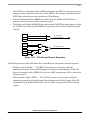
12
13
14
15
16
DSP56852UM
Rev. 4
06/2005
freescale.com
17
18
This manual is one of a set of three documents. For complete product information, it is necessary
to have all three documents. They are: 56800E Reference Manual, 56852 User Manual, and
Technical Data Sheet.
HOME PAGE: http://www.freescale.com
Order this document as DSP56F852UM - Rev 4.0
June, 2005
Summary of Changes and Updates:
Clarified SPI Chapter Section 12.9.1.5 and 12.9.2.7
Appendix C Packaging and Pin Information was removed and is now contained in the 56852 Data Sheet
Converted to Freescale format
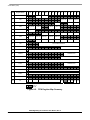
TABLE OF CONTENTS
Chapter 1
56852 Overview
1.1
Introduction. . . . . . . . . . . . . . . . . . . . . . . . . . . . . . . . . . . . . . . . . . . . . . . . . . . . . . . . . . 1-3
1.2
56800E Core Description . . . . . . . . . . . . . . . . . . . . . . . . . . . . . . . . . . . . . . . . . . . . . . . 1-4
1.2.1
Key Features. . . . . . . . . . . . . . . . . . . . . . . . . . . . . . . . . . . . . . . . . . . . . . . . . . . . . . 1-4
1.2.2
56800E Core Enhancements . . . . . . . . . . . . . . . . . . . . . . . . . . . . . . . . . . . . . . . . . 1-4
1.2.3
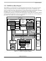
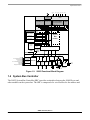
System Architecture and Peripheral Interface. . . . . . . . . . . . . . . . . . . . . . . . . . . . . 1-5
1.2.4
56800E Core Block Diagram. . . . . . . . . . . . . . . . . . . . . . . . . . . . . . . . . . . . . . . . . . 1-7
1.2.5
Address Buses . . . . . . . . . . . . . . . . . . . . . . . . . . . . . . . . . . . . . . . . . . . . . . . . . . . . 1-8
1.2.6
Data Buses . . . . . . . . . . . . . . . . . . . . . . . . . . . . . . . . . . . . . . . . . . . . . . . . . . . . . . . 1-9
1.2.7
Data Arithmetic Logic Unit (Data ALU) . . . . . . . . . . . . . . . . . . . . . . . . . . . . . . . . . 1-10
1.2.8
Address Generation Unit (AGU) . . . . . . . . . . . . . . . . . . . . . . . . . . . . . . . . . . . . . . 1-10
1.2.9
Program Controller and Hardware Looping Unit . . . . . . . . . . . . . . . . . . . . . . . . . . 1-11
1.2.10
Bit Manipulation Unit . . . . . . . . . . . . . . . . . . . . . . . . . . . . . . . . . . . . . . . . . . . . . . . 1-12
1.2.11
Programmable Chip Selects . . . . . . . . . . . . . . . . . . . . . . . . . . . . . . . . . . . . . . . . . 1-12
1.2.12
Enhanced On-Chip Emulation (EOnCE) Module . . . . . . . . . . . . . . . . . . . . . . . . . 1-13
1.2.13
Clocks . . . . . . . . . . . . . . . . . . . . . . . . . . . . . . . . . . . . . . . . . . . . . . . . . . . . . . . . . . 1-13
1.2.13.1
On-Chip Clock Synthesis Block . . . . . . . . . . . . . . . . . . . . . . . . . . . . . . . . . . . . 1-13
1.2.13.2
Oscillators . . . . . . . . . . . . . . . . . . . . . . . . . . . . . . . . . . . . . . . . . . . . . . . . . . . . 1-14
1.2.13.3
PLL . . . . . . . . . . . . . . . . . . . . . . . . . . . . . . . . . . . . . . . . . . . . . . . . . . . . . . . . . 1-14
1.2.13.4
Clock Control . . . . . . . . . . . . . . . . . . . . . . . . . . . . . . . . . . . . . . . . . . . . . . . . . . 1-14
1.3
56852 Architectural Overview. . . . . . . . . . . . . . . . . . . . . . . . . . . . . . . . . . . . . . . . . . . 1-15
1.4
System Bus Controller . . . . . . . . . . . . . . . . . . . . . . . . . . . . . . . . . . . . . . . . . . . . . . . . 1-16
1.4.1
Operation Method . . . . . . . . . . . . . . . . . . . . . . . . . . . . . . . . . . . . . . . . . . . . . . . . . 1-16
1.4.2
IPBus Bridge (IPBB) . . . . . . . . . . . . . . . . . . . . . . . . . . . . . . . . . . . . . . . . . . . . . . . 1-17
1.4.2.1
System Side Operation . . . . . . . . . . . . . . . . . . . . . . . . . . . . . . . . . . . . . . . . . . 1-17
1.4.2.2
Peripheral Side Operation . . . . . . . . . . . . . . . . . . . . . . . . . . . . . . . . . . . . . . . . 1-18
1.5
56852 Memory . . . . . . . . . . . . . . . . . . . . . . . . . . . . . . . . . . . . . . . . . . . . . . . . . . . . . . 1-19
1.6
56852 Peripheral Blocks. . . . . . . . . . . . . . . . . . . . . . . . . . . . . . . . . . . . . . . . . . . . . . . 1-19
1.6.1
Energy Information . . . . . . . . . . . . . . . . . . . . . . . . . . . . . . . . . . . . . . . . . . . . . . . . 1-19
1.6.2
COP/Watchdog Timer Module . . . . . . . . . . . . . . . . . . . . . . . . . . . . . . . . . . . . . . . 1-19
1.6.3
Peripheral Interrupts/Interrupt Controller Module . . . . . . . . . . . . . . . . . . . . . . . . . 1-20
1.6.4
Serial Communications Interface Module (SCI) . . . . . . . . . . . . . . . . . . . . . . . . . . 1-20
1.6.5
Serial Peripheral Interface Module (SPI). . . . . . . . . . . . . . . . . . . . . . . . . . . . . . . . 1-20
1.6.6
Improved Synchronous Serial Interface Module (ISSI) . . . . . . . . . . . . . . . . . . . . . 1-21
1.6.7
Quad Timer Module (TMR) . . . . . . . . . . . . . . . . . . . . . . . . . . . . . . . . . . . . . . . . . . 1-22
1.6.8
General Purpose Input/Output Port (GPIO) . . . . . . . . . . . . . . . . . . . . . . . . . . . . . 1-22
1.6.9
Resets . . . . . . . . . . . . . . . . . . . . . . . . . . . . . . . . . . . . . . . . . . . . . . . . . . . . . . . . . . 1-22
Table of Contents, Rev. 4
i
Freescale Semiconductor
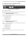
Chapter 2
Pin Descriptions
2.1
2.2
2.3
Introduction. . . . . . . . . . . . . . . . . . . . . . . . . . . . . . . . . . . . . . . . . . . . . . . . . . . . . . . . . . 2-3
Features . . . . . . . . . . . . . . . . . . . . . . . . . . . . . . . . . . . . . . . . . . . . . . . . . . . . . . . . . . . . 2-3
Signal and Package Information. . . . . . . . . . . . . . . . . . . . . . . . . . . . . . . . . . . . . . . . . . 2-6
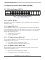
Chapter 3
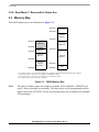
Memory (MEM)
3.1
Introduction. . . . . . . . . . . . . . . . . . . . . . . . . . . . . . . . . . . . . . . . . . . . . . . . . . . . . . . . . . 3-3
3.2
Program Boot ROM . . . . . . . . . . . . . . . . . . . . . . . . . . . . . . . . . . . . . . . . . . . . . . . . . . . 3-3
3.2.1
Boot Mode 0: Bootstrap From Byte-Wide External Memory . . . . . . . . . . . . . . . . . . 3-4
3.2.2
Boot Mode 1: Bootstrap From SPI . . . . . . . . . . . . . . . . . . . . . . . . . . . . . . . . . . . . . 3-4
3.2.3
Boot Mode 2: Normal Expanded Mode . . . . . . . . . . . . . . . . . . . . . . . . . . . . . . . . . . 3-5
3.2.4
Boot Mode 3: Development Expanded Mode . . . . . . . . . . . . . . . . . . . . . . . . . . . . . 3-5
3.2.5
Boot Mode 4: Bootstrap From Host Port–Single Strobe Clocking. . . . . . . . . . . . . . 3-5
3.2.6
Boot Mode 5: Bootstrap From Host Port–Dual Strobe Clocking . . . . . . . . . . . . . . . 3-5
3.2.7
Boot Mode 6: Bootstrap From SCI . . . . . . . . . . . . . . . . . . . . . . . . . . . . . . . . . . . . . 3-5
3.2.8
Boot Mode 7: Reserved for Future Use . . . . . . . . . . . . . . . . . . . . . . . . . . . . . . . . . 3-6
3.3
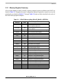
Memory Map. . . . . . . . . . . . . . . . . . . . . . . . . . . . . . . . . . . . . . . . . . . . . . . . . . . . . . . . . 3-6
3.3.1
Memory Register Summary . . . . . . . . . . . . . . . . . . . . . . . . . . . . . . . . . . . . . . . . . . 3-7
3.3.1.1
Peripheral Mapped Registers . . . . . . . . . . . . . . . . . . . . . . . . . . . . . . . . . . . . . . 3-8
3.3.2
Interrupt Vectors . . . . . . . . . . . . . . . . . . . . . . . . . . . . . . . . . . . . . . . . . . . . . . . . . . 3-12
Chapter 4
System Integration Module (SIM)
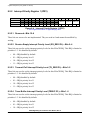
4.1
Introduction. . . . . . . . . . . . . . . . . . . . . . . . . . . . . . . . . . . . . . . . . . . . . . . . . . . . . . . . . . 4-3
4.2
Features . . . . . . . . . . . . . . . . . . . . . . . . . . . . . . . . . . . . . . . . . . . . . . . . . . . . . . . . . . . . 4-3
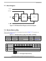
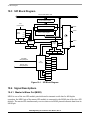
4.3
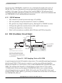
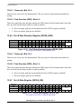
SIM Block Diagram. . . . . . . . . . . . . . . . . . . . . . . . . . . . . . . . . . . . . . . . . . . . . . . . . . . . 4-5
4.4
Signal Description. . . . . . . . . . . . . . . . . . . . . . . . . . . . . . . . . . . . . . . . . . . . . . . . . . . . . 4-6
4.4.1
SIM Interface Signals . . . . . . . . . . . . . . . . . . . . . . . . . . . . . . . . . . . . . . . . . . . . . . . 4-6
4.5
Module Memory Map . . . . . . . . . . . . . . . . . . . . . . . . . . . . . . . . . . . . . . . . . . . . . . . . . . 4-8
4.6
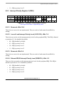
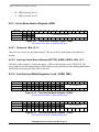
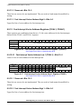
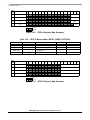
Register Descriptions (SYS_BASE = $1FFF08) . . . . . . . . . . . . . . . . . . . . . . . . . . . . . 4-9
4.6.1
SIM Control Register (SCR) . . . . . . . . . . . . . . . . . . . . . . . . . . . . . . . . . . . . . . . . . . 4-9
4.6.1.1
Reserved—Bit 15. . . . . . . . . . . . . . . . . . . . . . . . . . . . . . . . . . . . . . . . . . . . . . . . 4-9
4.6.1.2
Boot Mode—Bits 14–12. . . . . . . . . . . . . . . . . . . . . . . . . . . . . . . . . . . . . . . . . . . 4-9
4.6.1.2.1
Boot Mode 0: Bootstrap from Byte Wide External Memory . . . . . . . . . . . . 4-10
4.6.1.2.2
Boot Mode 1: Bootstrap from SPI Port . . . . . . . . . . . . . . . . . . . . . . . . . . . . 4-10
4.6.1.2.3
Boot Mode 2: Normal Expanded Mode . . . . . . . . . . . . . . . . . . . . . . . . . . . 4-11
4.6.1.2.4
Boot Mode 3: Development Expanded Mode. . . . . . . . . . . . . . . . . . . . . . . 4-11
56852 Digital Signal Controller User Manual, Rev. 4
Freescale Semiconductor
ii
4.6.1.2.5
Boot Modes 4–5: Reserved . . . . . . . . . . . . . . . . . . . . . . . . . . . . . . . . . . . . 4-11
4.6.1.2.6
Boot Mode 6: Bootstrap from SCI Port. . . . . . . . . . . . . . . . . . . . . . . . . . . . 4-11
4.6.1.2.7
Reserved: Boot Mode 7 . . . . . . . . . . . . . . . . . . . . . . . . . . . . . . . . . . . . . . . 4-11
4.6.1.3
Reserved—Bits 11–7. . . . . . . . . . . . . . . . . . . . . . . . . . . . . . . . . . . . . . . . . . . . 4-11
4.6.1.4
Enhanced OnCE Enable (OnCE_EBL)—Bit 6. . . . . . . . . . . . . . . . . . . . . . . . . 4-12
4.6.1.5
CLKOUT Disable (CLKOUT_DBL)—Bit 5 . . . . . . . . . . . . . . . . . . . . . . . . . . . . 4-12
4.6.1.6
Program RAM Disable (PRAM_DBL)—Bit 4 . . . . . . . . . . . . . . . . . . . . . . . . . . 4-12
4.6.1.7
Data RAM Disable (DRAM_DBL)—Bit 3 . . . . . . . . . . . . . . . . . . . . . . . . . . . . . 4-12
4.6.1.8
Software Reset (SW_RST)—Bit 2 . . . . . . . . . . . . . . . . . . . . . . . . . . . . . . . . . . 4-12
4.6.1.9
Stop Disable (STOP_DBL)—Bit 1 . . . . . . . . . . . . . . . . . . . . . . . . . . . . . . . . . . 4-12
4.6.1.10
Wait Disable (WAIT_DBL)—Bit 0 . . . . . . . . . . . . . . . . . . . . . . . . . . . . . . . . . . 4-12
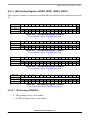
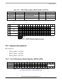
4.6.2
SIM Software Control Data 1 (SCD1) . . . . . . . . . . . . . . . . . . . . . . . . . . . . . . . . . . 4-13
4.6.2.1
Software Control Data 1 (SSCR1)—Bits 15–0 . . . . . . . . . . . . . . . . . . . . . . . . 4-13
4.6.3
Software Control Data 2 (SCD2). . . . . . . . . . . . . . . . . . . . . . . . . . . . . . . . . . . . . . 4-13
4.6.3.1
Software Control Data 2 (SCD2)—Bits 15–0. . . . . . . . . . . . . . . . . . . . . . . . . . 4-13
4.6.4
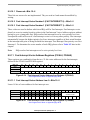
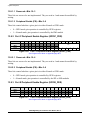
SIM Configuration Register (SCFGR) . . . . . . . . . . . . . . . . . . . . . . . . . . . . . . . . . . 4-14
4.6.4.1
Reserved—Bits 15–8. . . . . . . . . . . . . . . . . . . . . . . . . . . . . . . . . . . . . . . . . . . . 4-14
4.6.4.2
Configure Clock Out (CFG_CLKOUT)—Bit 7 . . . . . . . . . . . . . . . . . . . . . . . . . 4-14
4.6.4.3
Configure A[19] Output (CFG_A[19])—Bit 6 . . . . . . . . . . . . . . . . . . . . . . . . . . 4-14
4.6.4.4
Configure A[18] Output (CFG_A[18])—Bit 5 . . . . . . . . . . . . . . . . . . . . . . . . . . 4-14
4.6.4.5
Configure A[17] Output (CFG_A[17])—Bit 4 . . . . . . . . . . . . . . . . . . . . . . . . . . 4-14
4.6.4.6
Configure Serial Clock (CFG_SCLK)—Bit 3 . . . . . . . . . . . . . . . . . . . . . . . . . . 4-14
4.6.4.7
Configure Slave Select Output (CFG_SS)—Bit 2 . . . . . . . . . . . . . . . . . . . . . . 4-15
4.6.4.8
Configure Master In/Slave Out (CFG_MISO)—Bit 1 . . . . . . . . . . . . . . . . . . . . 4-15
4.6.4.9
Configure Master Out/Slave In (CFG_MOSI)—Bit 0 . . . . . . . . . . . . . . . . . . . . 4-15
4.7
Implementation . . . . . . . . . . . . . . . . . . . . . . . . . . . . . . . . . . . . . . . . . . . . . . . . . . . . . . 4-15
4.7.1
Clock Generation Concepts . . . . . . . . . . . . . . . . . . . . . . . . . . . . . . . . . . . . . . . . . 4-15
4.7.2
Clock Hold-Off. . . . . . . . . . . . . . . . . . . . . . . . . . . . . . . . . . . . . . . . . . . . . . . . . . . . 4-16
4.7.3
Core Stall . . . . . . . . . . . . . . . . . . . . . . . . . . . . . . . . . . . . . . . . . . . . . . . . . . . . . . . 4-16
4.7.4
Wait Request. . . . . . . . . . . . . . . . . . . . . . . . . . . . . . . . . . . . . . . . . . . . . . . . . . . . . 4-16
4.7.5
Transaction Abort . . . . . . . . . . . . . . . . . . . . . . . . . . . . . . . . . . . . . . . . . . . . . . . . . 4-16
4.7.6
Coordination of Peripheral and System Buses by IPBB . . . . . . . . . . . . . . . . . . . . 4-17
4.7.7
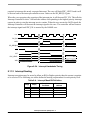
Clock Waveforms . . . . . . . . . . . . . . . . . . . . . . . . . . . . . . . . . . . . . . . . . . . . . . . . . 4-17
4.8
Generated Clocks. . . . . . . . . . . . . . . . . . . . . . . . . . . . . . . . . . . . . . . . . . . . . . . . . . . . 4-18
4.9
Generated Resets . . . . . . . . . . . . . . . . . . . . . . . . . . . . . . . . . . . . . . . . . . . . . . . . . . . 4-18
4.10 Power Mode Controls . . . . . . . . . . . . . . . . . . . . . . . . . . . . . . . . . . . . . . . . . . . . . . . . . 4-19
Table of Contents, Rev. 4
iii
Freescale Semiconductor
Chapter 5
External Memory Interface (EMI)
5.1
Introduction. . . . . . . . . . . . . . . . . . . . . . . . . . . . . . . . . . . . . . . . . . . . . . . . . . . . . . . . . . 5-3
5.2
Features . . . . . . . . . . . . . . . . . . . . . . . . . . . . . . . . . . . . . . . . . . . . . . . . . . . . . . . . . . . . 5-3
5.3
Functional Description . . . . . . . . . . . . . . . . . . . . . . . . . . . . . . . . . . . . . . . . . . . . . . . . . 5-4
5.3.1
Core Interface Detail . . . . . . . . . . . . . . . . . . . . . . . . . . . . . . . . . . . . . . . . . . . . . . . . 5-4
5.4
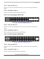
Block Diagram . . . . . . . . . . . . . . . . . . . . . . . . . . . . . . . . . . . . . . . . . . . . . . . . . . . . . . . 5-5
5.5
Module Memory Map . . . . . . . . . . . . . . . . . . . . . . . . . . . . . . . . . . . . . . . . . . . . . . . . . . 5-5
5.6
Register Descriptions (EMI_BASE = $1FFE40) . . . . . . . . . . . . . . . . . . . . . . . . . . . . . . 5-7
5.6.1
Chip Select Base Address Registers 0–3 (CSBAR0–CSBAR3) . . . . . . . . . . . . . . . 5-7
5.6.2
Chip Select Option Registers 0–3 (CSOR0–CSOR3). . . . . . . . . . . . . . . . . . . . . . . 5-8
5.6.2.1
Read Wait States (RWS)—Bits 15–11 . . . . . . . . . . . . . . . . . . . . . . . . . . . . . . . 5-9
5.6.2.2
Upper/Lower Byte Option (BYTE_EN)—Bits 10–9 . . . . . . . . . . . . . . . . . . . . . . 5-9
5.6.2.3
Read/Write Enable (R/W)—Bits 8–7 . . . . . . . . . . . . . . . . . . . . . . . . . . . . . . . . . 5-9
5.6.2.4
Program/Data Space Select (PS/DS)—Bits 6–5 . . . . . . . . . . . . . . . . . . . . . . . 5-10
5.6.2.5
Write Wait States (WWS)—Bits 4–0 . . . . . . . . . . . . . . . . . . . . . . . . . . . . . . . . 5-10
5.6.3
Chip Select Timing Control Registers 0–3 (CSTC0–CSTC3) . . . . . . . . . . . . . . . . 5-10
5.6.3.1
Write Wait States Setup Delay (WWSS)—Bits 15–14. . . . . . . . . . . . . . . . . . . 5-10
5.6.3.2
Write Wait States Hold Delay (WWSH)—Bits 13–12. . . . . . . . . . . . . . . . . . . . 5-11
5.6.3.3
Read Wait States Setup Delay (RWSS)—Bits 11–10 . . . . . . . . . . . . . . . . . . . 5-11
5.6.3.4
Read Wait States Hold Delay (RWSH)—Bits 9–8 . . . . . . . . . . . . . . . . . . . . . . 5-11
5.6.3.5
Reserved—Bits 7–3. . . . . . . . . . . . . . . . . . . . . . . . . . . . . . . . . . . . . . . . . . . . . 5-11
5.6.3.6
Minimal Delay After Read (MDAR)—Bits 2–0 . . . . . . . . . . . . . . . . . . . . . . . . . 5-11
5.6.4
Bus Control Register (BCR) . . . . . . . . . . . . . . . . . . . . . . . . . . . . . . . . . . . . . . . . . 5-12
5.6.4.1
Drive (DRV)—Bit 15. . . . . . . . . . . . . . . . . . . . . . . . . . . . . . . . . . . . . . . . . . . . . 5-12
5.6.4.2
Base Minimal Delay After Read (BMDAR)—Bits 14–12 . . . . . . . . . . . . . . . . . 5-13
5.6.4.3
Reserved—Bits 11–10. . . . . . . . . . . . . . . . . . . . . . . . . . . . . . . . . . . . . . . . . . . 5-13
5.6.4.4
Base Write Wait States (BWWS)—Bits 9–5 . . . . . . . . . . . . . . . . . . . . . . . . . . 5-13
5.6.4.5
Base Read Wait States (BRWS)—Bits 4–0. . . . . . . . . . . . . . . . . . . . . . . . . . . 5-13
5.7
Timing Specifications . . . . . . . . . . . . . . . . . . . . . . . . . . . . . . . . . . . . . . . . . . . . . . . . . 5-13
5.7.1
Read Timing . . . . . . . . . . . . . . . . . . . . . . . . . . . . . . . . . . . . . . . . . . . . . . . . . . . . . 5-13
5.7.1.1
Consecutive Mode Operation . . . . . . . . . . . . . . . . . . . . . . . . . . . . . . . . . . . . . 5-13
5.7.1.2
Read Setup and Hold Timing. . . . . . . . . . . . . . . . . . . . . . . . . . . . . . . . . . . . . . 5-15
5.7.2
Write Timing . . . . . . . . . . . . . . . . . . . . . . . . . . . . . . . . . . . . . . . . . . . . . . . . . . . . . 5-17
5.7.2.1
Write Setup and Hold Timing. . . . . . . . . . . . . . . . . . . . . . . . . . . . . . . . . . . . . . 5-19
5.7.2.2
WWS = 0 . . . . . . . . . . . . . . . . . . . . . . . . . . . . . . . . . . . . . . . . . . . . . . . . . . . . . 5-19
5.7.2.3
WWS > 0 . . . . . . . . . . . . . . . . . . . . . . . . . . . . . . . . . . . . . . . . . . . . . . . . . . . . . 5-21
5.8
Clocks. . . . . . . . . . . . . . . . . . . . . . . . . . . . . . . . . . . . . . . . . . . . . . . . . . . . . . . . . . . . . 5-23
5.9
Interrupts . . . . . . . . . . . . . . . . . . . . . . . . . . . . . . . . . . . . . . . . . . . . . . . . . . . . . . . . . . 5-23
5.10 Resets . . . . . . . . . . . . . . . . . . . . . . . . . . . . . . . . . . . . . . . . . . . . . . . . . . . . . . . . . . . . 5-23
56852 Digital Signal Controller User Manual, Rev. 4
Freescale Semiconductor
iv
Chapter 6
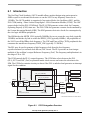
On-Chip Clock Synthesis (OCCS)
6.1
Introduction. . . . . . . . . . . . . . . . . . . . . . . . . . . . . . . . . . . . . . . . . . . . . . . . . . . . . . . . . . 6-3
6.1.1
OCCS Features. . . . . . . . . . . . . . . . . . . . . . . . . . . . . . . . . . . . . . . . . . . . . . . . . . . . 6-4
6.2
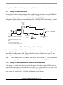
OSC (Oscillator) Circuit Detail . . . . . . . . . . . . . . . . . . . . . . . . . . . . . . . . . . . . . . . . . . . 6-4
6.2.1
Using an External Crystal . . . . . . . . . . . . . . . . . . . . . . . . . . . . . . . . . . . . . . . . . . . . 6-4
6.2.2
Using an External Active Clock Source Below 4MHz . . . . . . . . . . . . . . . . . . . . . . . 6-5
6.2.3
Using an External Active Clock Source Above 4MHz . . . . . . . . . . . . . . . . . . . . . . . 6-6
6.2.4
STOP Mode Features . . . . . . . . . . . . . . . . . . . . . . . . . . . . . . . . . . . . . . . . . . . . . . . 6-7
6.3
Phase Locked Loop (PLL) Circuit Detail. . . . . . . . . . . . . . . . . . . . . . . . . . . . . . . . . . . . 6-8
6.3.1
Phase Frequency Detector . . . . . . . . . . . . . . . . . . . . . . . . . . . . . . . . . . . . . . . . . . . 6-8
6.3.2
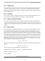
Charge Pump . . . . . . . . . . . . . . . . . . . . . . . . . . . . . . . . . . . . . . . . . . . . . . . . . . . . . 6-8
6.3.3
Loop Filter . . . . . . . . . . . . . . . . . . . . . . . . . . . . . . . . . . . . . . . . . . . . . . . . . . . . . . . . 6-9
6.3.4
Voltage Controlled Oscillator. . . . . . . . . . . . . . . . . . . . . . . . . . . . . . . . . . . . . . . . . . 6-9
6.3.5
Down Counter . . . . . . . . . . . . . . . . . . . . . . . . . . . . . . . . . . . . . . . . . . . . . . . . . . . . . 6-9
6.3.6
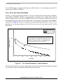
PLL Lock Time User Notes . . . . . . . . . . . . . . . . . . . . . . . . . . . . . . . . . . . . . . . . . . . 6-9
6.3.6.1
PLL Lock Time Determination . . . . . . . . . . . . . . . . . . . . . . . . . . . . . . . . . . . . . 6-10
6.3.6.2
PLL Parametric Influences on Reaction Time . . . . . . . . . . . . . . . . . . . . . . . . . 6-11
6.4
CGM Functional Detail . . . . . . . . . . . . . . . . . . . . . . . . . . . . . . . . . . . . . . . . . . . . . . . . 6-11
6.4.1
PLL Frequency Lock Detector. . . . . . . . . . . . . . . . . . . . . . . . . . . . . . . . . . . . . . . . 6-11
6.5
Module Memory Map . . . . . . . . . . . . . . . . . . . . . . . . . . . . . . . . . . . . . . . . . . . . . . . . . 6-12
6.6
Register Descriptions (CGM_BASE = $1FFF10) . . . . . . . . . . . . . . . . . . . . . . . . . . . . 6-12
6.6.1
Clock Generation Module (CGM) Control Register . . . . . . . . . . . . . . . . . . . . . . . 6-12
6.6.1.1
Reserved—Bits 15–14. . . . . . . . . . . . . . . . . . . . . . . . . . . . . . . . . . . . . . . . . . . 6-12
6.6.1.2
Lock 1 Status (LCK1)—Bit 13 . . . . . . . . . . . . . . . . . . . . . . . . . . . . . . . . . . . . . 6-12
6.6.1.3
Lock 0 Status (LCK0)—Bit 12 . . . . . . . . . . . . . . . . . . . . . . . . . . . . . . . . . . . . . 6-13
6.6.1.4
Clock Source Select (SEL)—Bit 11 . . . . . . . . . . . . . . . . . . . . . . . . . . . . . . . . . 6-13
6.6.1.5
Reserved—Bits 10–7. . . . . . . . . . . . . . . . . . . . . . . . . . . . . . . . . . . . . . . . . . . . 6-13
6.6.1.6
Lock 1 Interrupt Enable (LCK1_IE)—Bits 6–5 . . . . . . . . . . . . . . . . . . . . . . . . . 6-13
6.6.1.7
Lock 0 Interrupt Enable (LCK0_IE)—Bits 4–3 . . . . . . . . . . . . . . . . . . . . . . . . . 6-13
6.6.1.8
Lock Detector On (LCKON)—Bit 2 . . . . . . . . . . . . . . . . . . . . . . . . . . . . . . . . . 6-13
6.6.1.9
Time-of-Day Clock Source Select (TOD_SEL)—Bit 1 . . . . . . . . . . . . . . . . . . 6-14
6.6.1.10
PLL Power-Down (PDN)—Bit 0 . . . . . . . . . . . . . . . . . . . . . . . . . . . . . . . . . . . . 6-14
6.6.2
Clock Generation Module (CGM) Divide-By Register . . . . . . . . . . . . . . . . . . . . . 6-14
6.6.2.1
PLL Post Scaler (POST)—Bits 15–13 . . . . . . . . . . . . . . . . . . . . . . . . . . . . . . . 6-14
6.6.2.2
Reserved—Bits 12–7. . . . . . . . . . . . . . . . . . . . . . . . . . . . . . . . . . . . . . . . . . . . 6-15
6.6.2.3
PLL Divide-By (PLLDB)—Bits 6–0. . . . . . . . . . . . . . . . . . . . . . . . . . . . . . . . . . 6-15
6.6.3
Clock Generation Module (CGM) Time-of-Day Register. . . . . . . . . . . . . . . . . . . . 6-15
Table of Contents, Rev. 4
v
Freescale Semiconductor
6.6.3.1
Reserved—Bits 15–12. . . . . . . . . . . . . . . . . . . . . . . . . . . . . . . . . . . . . . . . . . .
6.6.3.2
TOD Scale Factor (TOD)—Bits 11–0 . . . . . . . . . . . . . . . . . . . . . . . . . . . . . . .
6.7
OCCS Resets . . . . . . . . . . . . . . . . . . . . . . . . . . . . . . . . . . . . . . . . . . . . . . . . . . . . . . .
6.8
OCCS Interrupts . . . . . . . . . . . . . . . . . . . . . . . . . . . . . . . . . . . . . . . . . . . . . . . . . . . . .
6-15
6-15
6-15
6-15
Chapter 7
Power-On Reset (POR) and
Computer Operating Properly (COP)
7.1
Introduction. . . . . . . . . . . . . . . . . . . . . . . . . . . . . . . . . . . . . . . . . . . . . . . . . . . . . . . . . . 7-3
7.2
Features . . . . . . . . . . . . . . . . . . . . . . . . . . . . . . . . . . . . . . . . . . . . . . . . . . . . . . . . . . . . 7-3
7.3
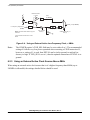
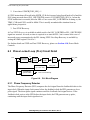
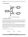
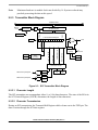
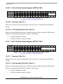
Block Diagram . . . . . . . . . . . . . . . . . . . . . . . . . . . . . . . . . . . . . . . . . . . . . . . . . . . . . . . 7-4
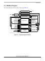
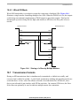
7.4
Method of Operation. . . . . . . . . . . . . . . . . . . . . . . . . . . . . . . . . . . . . . . . . . . . . . . . . . . 7-4
7.5
Computer Operating Properly (COP) Module. . . . . . . . . . . . . . . . . . . . . . . . . . . . . . . . 7-5
7.5.1
COP Functional Description . . . . . . . . . . . . . . . . . . . . . . . . . . . . . . . . . . . . . . . . . . 7-5
7.5.2
Time-Out Specifications . . . . . . . . . . . . . . . . . . . . . . . . . . . . . . . . . . . . . . . . . . . . . 7-5
7.5.3
COP After Reset . . . . . . . . . . . . . . . . . . . . . . . . . . . . . . . . . . . . . . . . . . . . . . . . . . . 7-6
7.5.4
Wait Mode Operation . . . . . . . . . . . . . . . . . . . . . . . . . . . . . . . . . . . . . . . . . . . . . . . 7-6
7.5.5
Stop Mode Operation . . . . . . . . . . . . . . . . . . . . . . . . . . . . . . . . . . . . . . . . . . . . . . . 7-6
7.5.6
Debug Mode Operation. . . . . . . . . . . . . . . . . . . . . . . . . . . . . . . . . . . . . . . . . . . . . . 7-6
7.6
Operating Modes . . . . . . . . . . . . . . . . . . . . . . . . . . . . . . . . . . . . . . . . . . . . . . . . . . . . . 7-6
7.7
Block Diagram . . . . . . . . . . . . . . . . . . . . . . . . . . . . . . . . . . . . . . . . . . . . . . . . . . . . . . . 7-7
7.8
Module Memory Map . . . . . . . . . . . . . . . . . . . . . . . . . . . . . . . . . . . . . . . . . . . . . . . . . . 7-7
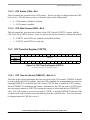
7.9
Register Descriptions (COP_BASE = $1FFFD0) . . . . . . . . . . . . . . . . . . . . . . . . . . . . . 7-8
7.9.1
COP Control Register (COPCTL) . . . . . . . . . . . . . . . . . . . . . . . . . . . . . . . . . . . . . . 7-8
7.9.1.1
Reserved—Bits 15–5. . . . . . . . . . . . . . . . . . . . . . . . . . . . . . . . . . . . . . . . . . . . . 7-8
7.9.1.2
Bypass (BYPS)—Bit 4 . . . . . . . . . . . . . . . . . . . . . . . . . . . . . . . . . . . . . . . . . . . . 7-8
7.9.1.3
COP Stop Mode Enable (CSEN)—Bit 3 . . . . . . . . . . . . . . . . . . . . . . . . . . . . . . 7-8
7.9.1.4
COP Wait Mode Enable (CWEN)—Bit 2 . . . . . . . . . . . . . . . . . . . . . . . . . . . . . . 7-8
7.9.1.5
COP Enable (CEN)—Bit 1 . . . . . . . . . . . . . . . . . . . . . . . . . . . . . . . . . . . . . . . . . 7-9
7.9.1.6
COP Write Protect (CWP)—Bit 0. . . . . . . . . . . . . . . . . . . . . . . . . . . . . . . . . . . . 7-9
7.9.2
COP Time-Out Register (COPTO) . . . . . . . . . . . . . . . . . . . . . . . . . . . . . . . . . . . . . 7-9
7.9.2.1
COP Time-Out Period (TIMEOUT)—Bits 15–0 . . . . . . . . . . . . . . . . . . . . . . . . . 7-9
7.9.3
COP Counter Register (COPCTR) . . . . . . . . . . . . . . . . . . . . . . . . . . . . . . . . . . . . 7-10
7.9.3.1
COP Count (COUNT)—Bits 15–0 . . . . . . . . . . . . . . . . . . . . . . . . . . . . . . . . . . 7-10
7.9.3.2
COP Service (SERVICE)—Bits 15–0 . . . . . . . . . . . . . . . . . . . . . . . . . . . . . . . 7-10
7.10 Clocks. . . . . . . . . . . . . . . . . . . . . . . . . . . . . . . . . . . . . . . . . . . . . . . . . . . . . . . . . . . . . 7-10
7.11 Resets . . . . . . . . . . . . . . . . . . . . . . . . . . . . . . . . . . . . . . . . . . . . . . . . . . . . . . . . . . . . 7-10
7.12 Interrupts . . . . . . . . . . . . . . . . . . . . . . . . . . . . . . . . . . . . . . . . . . . . . . . . . . . . . . . . . . 7-10
56852 Digital Signal Controller User Manual, Rev. 4
Freescale Semiconductor
vi
Chapter 8
Interrupt Controller (ITCN)
8.1
Introduction. . . . . . . . . . . . . . . . . . . . . . . . . . . . . . . . . . . . . . . . . . . . . . . . . . . . . . . . . . 8-3
8.2
Features . . . . . . . . . . . . . . . . . . . . . . . . . . . . . . . . . . . . . . . . . . . . . . . . . . . . . . . . . . . . 8-4
8.3
ITCN Module Signal Description . . . . . . . . . . . . . . . . . . . . . . . . . . . . . . . . . . . . . . . . . 8-5
8.4
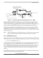
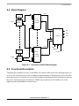
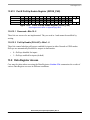
Block Diagram . . . . . . . . . . . . . . . . . . . . . . . . . . . . . . . . . . . . . . . . . . . . . . . . . . . . . . . 8-5
8.5
Functional Description . . . . . . . . . . . . . . . . . . . . . . . . . . . . . . . . . . . . . . . . . . . . . . . . . 8-6
8.5.1
Interrupt Vector Map . . . . . . . . . . . . . . . . . . . . . . . . . . . . . . . . . . . . . . . . . . . . . . . . 8-6
8.6
Operating Modes . . . . . . . . . . . . . . . . . . . . . . . . . . . . . . . . . . . . . . . . . . . . . . . . . . . . . 8-8
8.7
Wait and Stop Modes Operations. . . . . . . . . . . . . . . . . . . . . . . . . . . . . . . . . . . . . . . . . 8-8
8.8
Module Memory Map . . . . . . . . . . . . . . . . . . . . . . . . . . . . . . . . . . . . . . . . . . . . . . . . . . 8-9
8.9
Register Descriptions (ITCN_BASE = $1FFF20) . . . . . . . . . . . . . . . . . . . . . . . . . . . . 8-11
8.9.1
Interrupt Priority Register 0 (IPR0) . . . . . . . . . . . . . . . . . . . . . . . . . . . . . . . . . . . . 8-11
8.9.1.1
Reserved—Bit 15–14. . . . . . . . . . . . . . . . . . . . . . . . . . . . . . . . . . . . . . . . . . . . 8-11
8.9.1.2
Breakpoint Unit 0 EOnCE Interrupt Priority Level
(BKPT_U0 IPL)—Bits 13–12 . . . . . . . . . . . . . . . . . . . . . . . . . . . . . . . . . . . 8-11
8.9.1.3
EOnCE Step Counter Interrupt Priority Level
(STPCNT IPL)—Bits 11–10 . . . . . . . . . . . . . . . . . . . . . . . . . . . . . . . . . . . . 8-11
8.9.1.4
Reserved—Bits 9–0. . . . . . . . . . . . . . . . . . . . . . . . . . . . . . . . . . . . . . . . . . . . . 8-11
8.9.2
Interrupt Priority Register 1 (IPR1) . . . . . . . . . . . . . . . . . . . . . . . . . . . . . . . . . . . . 8-12
8.9.2.1
Reserved—Bits 15–6. . . . . . . . . . . . . . . . . . . . . . . . . . . . . . . . . . . . . . . . . . . . 8-12
8.9.2.2
Receive Empty Interrupt Priority Level (RX_REG IPL)—Bits 5–4 . . . . . . . . . . 8-12
8.9.2.3
Transmit Full Interrupt Priority Level (TX_REG IPL)—Bits 3–2 . . . . . . . . . . . . 8-12
8.9.2.4
Trace Buffer Interrupt Priority Level (TRBUF IPL)—Bits 1–0 . . . . . . . . . . . . . 8-12
8.9.3
Interrupt Priority Register 2 (IPR2) . . . . . . . . . . . . . . . . . . . . . . . . . . . . . . . . . . . . 8-13
8.9.3.1
Reserved—Bits 15–8. . . . . . . . . . . . . . . . . . . . . . . . . . . . . . . . . . . . . . . . . . . . 8-13
8.9.3.2
Loss of Lock Interrupt Priority Level (LOCK IPL)—Bits 7–6 . . . . . . . . . . . . . . 8-13
8.9.3.3
Reserved—Bits 5–4. . . . . . . . . . . . . . . . . . . . . . . . . . . . . . . . . . . . . . . . . . . . . 8-13
8.9.3.4
External IRQ B Interrupt Priority Level (IRQB IPL)—Bits 3–2 . . . . . . . . . . . . . 8-13
8.9.3.5
External IRQ A Interrupt Priority Level (IRQA IPL)—Bits 1–0 . . . . . . . . . . . . . 8-14
8.9.4
Interrupt Priority Register 3 (IPR3) . . . . . . . . . . . . . . . . . . . . . . . . . . . . . . . . . . . . 8-14
8.9.4.1
Transmit Data Interrupt Priority Level (SSI_TD IPL)—Bits 15–14 . . . . . . . . . . 8-14
8.9.4.2
Transmit Data with Exception Status Interrupt Priority Level
(SSI_TDES IPL)—Bits 13–12. . . . . . . . . . . . . . . . . . . . . . . . . . . . . . . . . . . 8-14
8.9.4.3
Reserved—Bits 11–10. . . . . . . . . . . . . . . . . . . . . . . . . . . . . . . . . . . . . . . . . . . 8-15
8.9.4.4
Receive Data Interrupt Priority Level (SSI_RD IPL)—Bits 9–8 . . . . . . . . . . . . 8-15
8.9.4.5
Receive Data with Exception Status Interrupt Priority Level
(SSI_RDES IPL)—Bits 7–6 . . . . . . . . . . . . . . . . . . . . . . . . . . . . . . . . . . . . 8-15
8.9.4.6
Reserved—Bits 5–0. . . . . . . . . . . . . . . . . . . . . . . . . . . . . . . . . . . . . . . . . . . . . 8-15
8.9.5
Interrupt Priority Register 4 (IPR4) . . . . . . . . . . . . . . . . . . . . . . . . . . . . . . . . . . . . 8-15
8.9.5.1
Receiver Full Interrupt Priority Level (SPI_RCV IPL)—Bits 15–14 . . . . . . . . . 8-16
Table of Contents, Rev. 4
vii
Freescale Semiconductor
8.9.5.2
Reserved—Bits 13–0. . . . . . . . . . . . . . . . . . . . . . . . . . . . . . . . . . . . . . . . . . . . 8-16
8.9.6
Interrupt Priority Register 5 (IPR5) . . . . . . . . . . . . . . . . . . . . . . . . . . . . . . . . . . . . 8-16
8.9.6.1
Reserved—Bits 15–12. . . . . . . . . . . . . . . . . . . . . . . . . . . . . . . . . . . . . . . . . . . 8-16
8.9.6.2
Receiver Full Interrupt Priority Level (SCI_RCV IPL)—Bits 11–10 . . . . . . . . . 8-16
8.9.6.3
Receiver Error Interrupt Priority Level (SCI_RERR IPL)—Bits 9–8. . . . . . . . . 8-17
8.9.6.4
Receiver Idle Interrupt Priority Level (SCI_RIDL IPL)–Bits 7–6. . . . . . . . . . . . 8-17
8.9.6.5
Transmitter Idle Interrupt Priority Level (SCI_TIDL IPL)—Bits 5–4 . . . . . . . . . 8-17
8.9.6.6
Transmitter Empty Interrupt Priority Level (SCI_XMIT IPL)—Bits 3–2 . . . . . . 8-17
8.9.6.7
Transmitter Empty Interrupt Priority Level (SPI_XMIT IPL)—Bits 1–0 . . . . . . 8-18
8.9.7
Interrupt Priority Register 6 (IPR6) . . . . . . . . . . . . . . . . . . . . . . . . . . . . . . . . . . . . 8-18
8.9.7.1
Timer Overflow Interrupt Priority Level (TOVF1 IPL)—Bits 15–14 . . . . . . . . . 8-18
8.9.7.2
Timer Compare Interrupt Priority Level (TCMP1 IPL)—Bits 13–12 . . . . . . . . . 8-18
8.9.7.3
Timer Input Edge Interrupt Priority Level (TINP0 IPL)—Bits 11–10 . . . . . . . . 8-19
8.9.7.4
Timer Overflow Interrupt Priority Level (TOVF0 IPL)—Bits 9–8 . . . . . . . . . . . 8-19
8.9.7.5
Timer Compare Interrupt Priority Level (TCMP0 IPL)—Bits 7–6 . . . . . . . . . . . 8-19
8.9.7.6
Reserved—Bits 5–0. . . . . . . . . . . . . . . . . . . . . . . . . . . . . . . . . . . . . . . . . . . . . 8-19
8.9.8
Interrupt Priority Register 7 (IPR7) . . . . . . . . . . . . . . . . . . . . . . . . . . . . . . . . . . . . 8-20
8.9.8.1
Reserved—Bits 15–14. . . . . . . . . . . . . . . . . . . . . . . . . . . . . . . . . . . . . . . . . . . 8-20
8.9.8.2
Timer Input Edge Interrupt Priority Level (TINP3 IPL)—Bits 13–12 . . . . . . . . 8-20
8.9.8.3
Timer Overflow Interrupt Priority Level (TOVF3 IPL)—Bits 11–10 . . . . . . . . . 8-20
8.9.8.4
Timer Compare Interrupt Priority Level (TCMP3 IPL)—Bits 9–8 . . . . . . . . . . . 8-20
8.9.8.5
Timer Input Edge Interrupt Priority Level (TINP2 IPL)—Bits 7–6 . . . . . . . . . . 8-21
8.9.8.6
Timer Overflow Interrupt Priority Level (TOVF2 IPL)—Bits 5–4 . . . . . . . . . . . 8-21
8.9.8.7
Timer Compare Interrupt Priority Level (TCMP2 IPL)—Bits 3–2 . . . . . . . . . . . 8-21
8.9.8.8
Timer Input Edge Interrupt Priority Level (TINP1 IPL)—Bits 1–0 . . . . . . . . . . 8-21
8.9.9
Vector Base Address Register (VBA) . . . . . . . . . . . . . . . . . . . . . . . . . . . . . . . . . . 8-22
8.9.9.1
Reserved—Bits 15–13. . . . . . . . . . . . . . . . . . . . . . . . . . . . . . . . . . . . . . . . . . . 8-22
8.9.9.2
Interrupt Vector Base Address (VECTOR_BASE_ADDR)—Bits 12–0 . . . . . . 8-22
8.9.10
Fast Interrupt Match Registers 0 and 1 (FIM0, FIM1) . . . . . . . . . . . . . . . . . . . . . . 8-22
8.9.10.1
Reserved—Bits 15–6. . . . . . . . . . . . . . . . . . . . . . . . . . . . . . . . . . . . . . . . . . . . 8-23
8.9.10.2
Fast Interrupt Vector Number 0 (FAST INTERRUPT 0)—Bits 5–0 . . . . . . . . . 8-23
8.9.10.3
Fast Interrupt Vector Number 1 (FAST INTERRUPT 1)—Bits 5–0 . . . . . . . . . 8-23
8.9.11
Fast Interrupt Vector Address Registers (FIVAL0, FIVAH0) . . . . . . . . . . . . . . . . . 8-23
8.9.11.1
Fast Interrupt Vector Address Low 0—Bits 15–0. . . . . . . . . . . . . . . . . . . . . . . 8-23
8.9.11.2
Reserved—Bits 15–5. . . . . . . . . . . . . . . . . . . . . . . . . . . . . . . . . . . . . . . . . . . . 8-24
8.9.11.3
Fast Interrupt Vector Address High 0—Bits 4–0 . . . . . . . . . . . . . . . . . . . . . . . 8-24
8.9.12
Fast Interrupt Vector Address Registers (FIVAL1, FIVAH1) . . . . . . . . . . . . . . . . . 8-24
8.9.12.0.1
Fast Interrupt Vector Address Low 1 (FIVAL1)—Bits 15–0 . . . . . . . . . . . . 8-24
8.9.12.1
Reserved—Bits 15–5. . . . . . . . . . . . . . . . . . . . . . . . . . . . . . . . . . . . . . . . . . . . 8-24
8.9.12.2
Fast Interrupt Vector Address High 1—Bits 4–0 . . . . . . . . . . . . . . . . . . . . . . . 8-24
8.9.13
IRQ Pending Registers (IRQP0, IRQP1, IRQP2, IRQP3). . . . . . . . . . . . . . . . . . . 8-25
8.9.13.1
IRQ Pending (PENDING) . . . . . . . . . . . . . . . . . . . . . . . . . . . . . . . . . . . . . . . . 8-25
8.9.14
Interrupt Control Register (ICTL). . . . . . . . . . . . . . . . . . . . . . . . . . . . . . . . . . . . . . 8-26
56852 Digital Signal Controller User Manual, Rev. 4
Freescale Semiconductor
viii
8.9.14.1
Interrupt (INT)—Bit 15 . . . . . . . . . . . . . . . . . . . . . . . . . . . . . . . . . . . . . . . . . . . 8-26
8.9.14.2
Interrupt Priority Level Core (IPLC)—Bit 14–13. . . . . . . . . . . . . . . . . . . . . . . . 8-26
8.9.14.3
Vector Number (VN)—Bits 12–6 . . . . . . . . . . . . . . . . . . . . . . . . . . . . . . . . . . . 8-26
8.9.14.4
Interrupt Disable (INT_DIS)—Bit 5 . . . . . . . . . . . . . . . . . . . . . . . . . . . . . . . . . 8-27
8.9.14.5
Reserved—Bit 4. . . . . . . . . . . . . . . . . . . . . . . . . . . . . . . . . . . . . . . . . . . . . . . . 8-27
8.9.14.6
State of IRQB (IRQB STATE)—Bit 3 . . . . . . . . . . . . . . . . . . . . . . . . . . . . . . . . 8-27
8.9.14.7
State of IRQA (IRQA STATE)—Bit 2 . . . . . . . . . . . . . . . . . . . . . . . . . . . . . . . . 8-27
8.9.14.8
IRQB Edge (IRQB EDG)—Bit 1. . . . . . . . . . . . . . . . . . . . . . . . . . . . . . . . . . . . 8-27
8.9.14.9
IRQA Edge (IRQA EDG)—Bit 0. . . . . . . . . . . . . . . . . . . . . . . . . . . . . . . . . . . . 8-27
8.10 Resets . . . . . . . . . . . . . . . . . . . . . . . . . . . . . . . . . . . . . . . . . . . . . . . . . . . . . . . . . . . . 8-28
8.10.1
Reset Handshake Timing . . . . . . . . . . . . . . . . . . . . . . . . . . . . . . . . . . . . . . . . . . . 8-28
8.10.2
ITCN After Reset. . . . . . . . . . . . . . . . . . . . . . . . . . . . . . . . . . . . . . . . . . . . . . . . . . 8-28
8.11 Interrupts . . . . . . . . . . . . . . . . . . . . . . . . . . . . . . . . . . . . . . . . . . . . . . . . . . . . . . . . . . 8-28
8.11.1
Interrupt Handshake Timing . . . . . . . . . . . . . . . . . . . . . . . . . . . . . . . . . . . . . . . . . 8-28
8.11.2
Interrupt Nesting . . . . . . . . . . . . . . . . . . . . . . . . . . . . . . . . . . . . . . . . . . . . . . . . . . 8-29
Chapter 9
Serial Communications Interface (SCI)
9.1
Introduction. . . . . . . . . . . . . . . . . . . . . . . . . . . . . . . . . . . . . . . . . . . . . . . . . . . . . . . . . . 9-3
9.2
Features . . . . . . . . . . . . . . . . . . . . . . . . . . . . . . . . . . . . . . . . . . . . . . . . . . . . . . . . . . . . 9-3
9.3
Block Diagram . . . . . . . . . . . . . . . . . . . . . . . . . . . . . . . . . . . . . . . . . . . . . . . . . . . . . . . 9-4
9.4
Signal Descriptions. . . . . . . . . . . . . . . . . . . . . . . . . . . . . . . . . . . . . . . . . . . . . . . . . . . . 9-4
9.4.1
Transmit Data (TXD) Pin. . . . . . . . . . . . . . . . . . . . . . . . . . . . . . . . . . . . . . . . . . . . . 9-4
9.4.2
Receiver Data (RXD) Pin . . . . . . . . . . . . . . . . . . . . . . . . . . . . . . . . . . . . . . . . . . . . 9-4
9.5
Functional Description . . . . . . . . . . . . . . . . . . . . . . . . . . . . . . . . . . . . . . . . . . . . . . . . . 9-5
9.5.1
Data Frame Format. . . . . . . . . . . . . . . . . . . . . . . . . . . . . . . . . . . . . . . . . . . . . . . . . 9-5
9.5.2
Baud Rate Generation . . . . . . . . . . . . . . . . . . . . . . . . . . . . . . . . . . . . . . . . . . . . . . 9-6
9.5.3
Transmitter Block Diagram . . . . . . . . . . . . . . . . . . . . . . . . . . . . . . . . . . . . . . . . . . . 9-7
9.5.3.1
Character Length . . . . . . . . . . . . . . . . . . . . . . . . . . . . . . . . . . . . . . . . . . . . . . . . 9-7
9.5.3.2
Character Transmission. . . . . . . . . . . . . . . . . . . . . . . . . . . . . . . . . . . . . . . . . . . 9-7
9.5.3.3
Break Characters. . . . . . . . . . . . . . . . . . . . . . . . . . . . . . . . . . . . . . . . . . . . . . . . 9-9
9.5.3.4
Preambles . . . . . . . . . . . . . . . . . . . . . . . . . . . . . . . . . . . . . . . . . . . . . . . . . . . . . 9-9
9.5.3.5
Receiver. . . . . . . . . . . . . . . . . . . . . . . . . . . . . . . . . . . . . . . . . . . . . . . . . . . . . . . 9-9
9.5.4
Receiver Block Diagram . . . . . . . . . . . . . . . . . . . . . . . . . . . . . . . . . . . . . . . . . . . . 9-10
9.5.4.1
Character Length . . . . . . . . . . . . . . . . . . . . . . . . . . . . . . . . . . . . . . . . . . . . . . . 9-10
9.5.4.2
Character Reception . . . . . . . . . . . . . . . . . . . . . . . . . . . . . . . . . . . . . . . . . . . . 9-10
9.5.4.3
Data Sampling . . . . . . . . . . . . . . . . . . . . . . . . . . . . . . . . . . . . . . . . . . . . . . . . . 9-11
9.5.4.4
Framing Errors. . . . . . . . . . . . . . . . . . . . . . . . . . . . . . . . . . . . . . . . . . . . . . . . . 9-15
9.5.4.5
Baud Rate Tolerance. . . . . . . . . . . . . . . . . . . . . . . . . . . . . . . . . . . . . . . . . . . . 9-15
9.5.4.6
Slow Data Tolerance . . . . . . . . . . . . . . . . . . . . . . . . . . . . . . . . . . . . . . . . . . . . 9-16
9.5.4.7
Fast Data Tolerance . . . . . . . . . . . . . . . . . . . . . . . . . . . . . . . . . . . . . . . . . . . . 9-17
Table of Contents, Rev. 4
ix
Freescale Semiconductor
9.5.4.8
Receiver Wake Up. . . . . . . . . . . . . . . . . . . . . . . . . . . . . . . . . . . . . . . . . . . . . . 9-18
9.5.5
Single-Wire Operation. . . . . . . . . . . . . . . . . . . . . . . . . . . . . . . . . . . . . . . . . . . . . . 9-19
9.5.6
Loop Operation . . . . . . . . . . . . . . . . . . . . . . . . . . . . . . . . . . . . . . . . . . . . . . . . . . . 9-19
9.6
Low Power Modes . . . . . . . . . . . . . . . . . . . . . . . . . . . . . . . . . . . . . . . . . . . . . . . . . . . 9-20
9.6.1
Run Mode . . . . . . . . . . . . . . . . . . . . . . . . . . . . . . . . . . . . . . . . . . . . . . . . . . . . . . . 9-20
9.6.2
Wait Mode . . . . . . . . . . . . . . . . . . . . . . . . . . . . . . . . . . . . . . . . . . . . . . . . . . . . . . . 9-20
9.6.3
Stop Mode. . . . . . . . . . . . . . . . . . . . . . . . . . . . . . . . . . . . . . . . . . . . . . . . . . . . . . . 9-20
9.6.4
Wait Mode Recovery . . . . . . . . . . . . . . . . . . . . . . . . . . . . . . . . . . . . . . . . . . . . . . 9-20
9.7
Module Memory Map . . . . . . . . . . . . . . . . . . . . . . . . . . . . . . . . . . . . . . . . . . . . . . . . . 9-21
9.8
Register Descriptions (SCI_BASE = $1FFFE0) . . . . . . . . . . . . . . . . . . . . . . . . . . . . . 9-21
9.8.1
SCI Baud Rate (SCIBR) . . . . . . . . . . . . . . . . . . . . . . . . . . . . . . . . . . . . . . . . . . . . 9-21
9.8.2
SCI Control Register (SCICR). . . . . . . . . . . . . . . . . . . . . . . . . . . . . . . . . . . . . . . . 9-22
9.8.2.1
Loop Select Bit (LOOP)—Bit 15 . . . . . . . . . . . . . . . . . . . . . . . . . . . . . . . . . . . 9-22
9.8.2.2
Stop in Wait Mode Bit (SWAI)—Bit 14. . . . . . . . . . . . . . . . . . . . . . . . . . . . . . . 9-23
9.8.2.3
Receiver Source (RSRC)— Bit 13. . . . . . . . . . . . . . . . . . . . . . . . . . . . . . . . . . 9-23
9.8.2.4
Data Format Mode (M)—Bit 12 . . . . . . . . . . . . . . . . . . . . . . . . . . . . . . . . . . . . 9-23
9.8.2.5
Wake up Condition (WAKE)—Bit 11 . . . . . . . . . . . . . . . . . . . . . . . . . . . . . . . . 9-23
9.8.2.6
Polarity (POL)—Bit 10 . . . . . . . . . . . . . . . . . . . . . . . . . . . . . . . . . . . . . . . . . . . 9-23
9.8.2.7
Parity Enable (PE)—Bit 9 . . . . . . . . . . . . . . . . . . . . . . . . . . . . . . . . . . . . . . . . 9-24
9.8.2.8
Parity Type (PT)—Bit 8 . . . . . . . . . . . . . . . . . . . . . . . . . . . . . . . . . . . . . . . . . . 9-24
9.8.2.9
Transmitter Empty Interrupt Enable (TEIE)—Bit 7. . . . . . . . . . . . . . . . . . . . . . 9-24
9.8.2.10
Transmitter Idle Interrupt Enable (TIIE)—Bit 6 . . . . . . . . . . . . . . . . . . . . . . . . 9-24
9.8.2.11
Receiver Full Interrupt Enable (RFIE)—Bit 5. . . . . . . . . . . . . . . . . . . . . . . . . . 9-24
9.8.2.12
Receive Error Interrupt Enable (REIE)—Bit 4 . . . . . . . . . . . . . . . . . . . . . . . . . 9-25
9.8.2.13
Transmitter Enable (TE)—Bit 3 . . . . . . . . . . . . . . . . . . . . . . . . . . . . . . . . . . . . 9-25
9.8.2.14
Receiver Enable (RE)—Bit 2 . . . . . . . . . . . . . . . . . . . . . . . . . . . . . . . . . . . . . . 9-25
9.8.2.15
Receiver Wake Up (RWU)—Bit 1 . . . . . . . . . . . . . . . . . . . . . . . . . . . . . . . . . . 9-25
9.8.2.16
Send Break (SBK)—Bit 0. . . . . . . . . . . . . . . . . . . . . . . . . . . . . . . . . . . . . . . . . 9-25
9.8.3
SCI Status Register (SCISR) . . . . . . . . . . . . . . . . . . . . . . . . . . . . . . . . . . . . . . . . 9-26
9.8.3.1
Transmit Data Register Empty Flag (TDRE)—Bit 15. . . . . . . . . . . . . . . . . . . . 9-26
9.8.3.2
Transmitter Idle Flag (TIDLE)—Bit 14 . . . . . . . . . . . . . . . . . . . . . . . . . . . . . . . 9-26
9.8.3.3
Receive Data Register Full Flag (RDRF)—Bit 13 . . . . . . . . . . . . . . . . . . . . . . 9-26
9.8.3.4
Receiver Idle Line Flag (RIDLE)—Bit 12 . . . . . . . . . . . . . . . . . . . . . . . . . . . . . 9-27
9.8.3.5
Overrun Flag (OR)—Bit 11 . . . . . . . . . . . . . . . . . . . . . . . . . . . . . . . . . . . . . . . 9-27
9.8.3.6
Noise Flag (NF)—Bit 10. . . . . . . . . . . . . . . . . . . . . . . . . . . . . . . . . . . . . . . . . . 9-27
9.8.3.7
Framing Error Flag (FE)—Bit 9 . . . . . . . . . . . . . . . . . . . . . . . . . . . . . . . . . . . . 9-27
9.8.3.8
Parity Error Flag (PF)—Bit 8 . . . . . . . . . . . . . . . . . . . . . . . . . . . . . . . . . . . . . . 9-28
9.8.3.9
Reserved—Bits 7–1. . . . . . . . . . . . . . . . . . . . . . . . . . . . . . . . . . . . . . . . . . . . . 9-28
9.8.3.10
Receiver Active Flag (RAF)—Bit 0 . . . . . . . . . . . . . . . . . . . . . . . . . . . . . . . . . 9-28
9.8.4
SCI Data Register (SCIDR). . . . . . . . . . . . . . . . . . . . . . . . . . . . . . . . . . . . . . . . . . 9-28
9.8.4.1
Reserved—Bits 15–9. . . . . . . . . . . . . . . . . . . . . . . . . . . . . . . . . . . . . . . . . . . . 9-28
9.8.4.2
Receive Data—Bits 8–0. . . . . . . . . . . . . . . . . . . . . . . . . . . . . . . . . . . . . . . . . . 9-28
9.8.4.3
Transmit Data—Bits 8–0 . . . . . . . . . . . . . . . . . . . . . . . . . . . . . . . . . . . . . . . . . 9-28
56852 Digital Signal Controller User Manual, Rev. 4
Freescale Semiconductor
x
9.9
Clocks. . . . . . . . . . . . . . . . . . . . . . . . . . . . . . . . . . . . . . . . . . . . . . . . . . . . . . . . . . . . . 9-29
9.10 Resets . . . . . . . . . . . . . . . . . . . . . . . . . . . . . . . . . . . . . . . . . . . . . . . . . . . . . . . . . . . . 9-29
9.11 Interrupts . . . . . . . . . . . . . . . . . . . . . . . . . . . . . . . . . . . . . . . . . . . . . . . . . . . . . . . . . . 9-29
9.11.1
Transmitter Empty Interrupt . . . . . . . . . . . . . . . . . . . . . . . . . . . . . . . . . . . . . . . . . 9-29
9.11.2
Transmitter Idle Interrupt. . . . . . . . . . . . . . . . . . . . . . . . . . . . . . . . . . . . . . . . . . . . 9-29
9.11.3
Receiver Full Interrupt. . . . . . . . . . . . . . . . . . . . . . . . . . . . . . . . . . . . . . . . . . . . . . 9-30
9.11.4
Receive Error Interrupt . . . . . . . . . . . . . . . . . . . . . . . . . . . . . . . . . . . . . . . . . . . . . 9-30
9.11.5
Receiver Idle Interrupt. . . . . . . . . . . . . . . . . . . . . . . . . . . . . . . . . . . . . . . . . . . . . . 9-30
Chapter 10
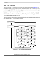
Serial Peripheral Interface (SPI)
10.1 Introduction. . . . . . . . . . . . . . . . . . . . . . . . . . . . . . . . . . . . . . . . . . . . . . . . . . . . . . . . . 10-3
10.2 Features . . . . . . . . . . . . . . . . . . . . . . . . . . . . . . . . . . . . . . . . . . . . . . . . . . . . . . . . . . . 10-3
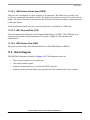
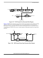
10.3 SPI Block Diagram . . . . . . . . . . . . . . . . . . . . . . . . . . . . . . . . . . . . . . . . . . . . . . . . . . . 10-4
10.4 Signal Descriptions. . . . . . . . . . . . . . . . . . . . . . . . . . . . . . . . . . . . . . . . . . . . . . . . . . . 10-4
10.4.1
Master In/Slave Out (MISO) . . . . . . . . . . . . . . . . . . . . . . . . . . . . . . . . . . . . . . . . . 10-4
10.4.2
Master Out/Slave In (MOSI) . . . . . . . . . . . . . . . . . . . . . . . . . . . . . . . . . . . . . . . . . 10-5
10.4.3
Serial Clock (SCLK) . . . . . . . . . . . . . . . . . . . . . . . . . . . . . . . . . . . . . . . . . . . . . . . 10-5
10.4.4
Slave Select (SS) . . . . . . . . . . . . . . . . . . . . . . . . . . . . . . . . . . . . . . . . . . . . . . . . . 10-5
10.5 External I/O Signals . . . . . . . . . . . . . . . . . . . . . . . . . . . . . . . . . . . . . . . . . . . . . . . . . . 10-6
10.6 Operating Modes . . . . . . . . . . . . . . . . . . . . . . . . . . . . . . . . . . . . . . . . . . . . . . . . . . . . 10-6
10.6.1
Master Mode . . . . . . . . . . . . . . . . . . . . . . . . . . . . . . . . . . . . . . . . . . . . . . . . . . . . . 10-7
10.6.2
Slave Mode . . . . . . . . . . . . . . . . . . . . . . . . . . . . . . . . . . . . . . . . . . . . . . . . . . . . . . 10-8
10.6.3
Wired OR Mode . . . . . . . . . . . . . . . . . . . . . . . . . . . . . . . . . . . . . . . . . . . . . . . . . . 10-9
10.7 Transmission Formats . . . . . . . . . . . . . . . . . . . . . . . . . . . . . . . . . . . . . . . . . . . . . . . . 10-9
10.7.1
Data Transmission Length . . . . . . . . . . . . . . . . . . . . . . . . . . . . . . . . . . . . . . . . . 10-10
10.7.2
Data Shift Ordering . . . . . . . . . . . . . . . . . . . . . . . . . . . . . . . . . . . . . . . . . . . . . . . 10-10
10.7.3
Clock Phase and Polarity Controls . . . . . . . . . . . . . . . . . . . . . . . . . . . . . . . . . . . 10-10
10.7.4
Transmission Format When CPHA = 0. . . . . . . . . . . . . . . . . . . . . . . . . . . . . . . . 10-10
10.7.5
Transmission Format When CPHA = 1. . . . . . . . . . . . . . . . . . . . . . . . . . . . . . . . 10-12
10.7.6
Transmission Initiation Latency. . . . . . . . . . . . . . . . . . . . . . . . . . . . . . . . . . . . . . 10-13
10.8 Transmission Data . . . . . . . . . . . . . . . . . . . . . . . . . . . . . . . . . . . . . . . . . . . . . . . . . . 10-14
10.9 Error Conditions . . . . . . . . . . . . . . . . . . . . . . . . . . . . . . . . . . . . . . . . . . . . . . . . . . . . 10-16
10.9.1
Overflow Error . . . . . . . . . . . . . . . . . . . . . . . . . . . . . . . . . . . . . . . . . . . . . . . . . . . 10-16
10.9.2
Mode Fault Error . . . . . . . . . . . . . . . . . . . . . . . . . . . . . . . . . . . . . . . . . . . . . . . . . 10-18
10.10 Module Memory Map . . . . . . . . . . . . . . . . . . . . . . . . . . . . . . . . . . . . . . . . . . . . . . . . 10-20
10.11 Registers Descriptions (SPI_BASE = $1FFFE8) . . . . . . . . . . . . . . . . . . . . . . . . . . . 10-20
10.11.1 SPI Status and Control Register (SPSCR) . . . . . . . . . . . . . . . . . . . . . . . . . . . . . 10-21
10.11.1.1
SPI Baud Rate Select Bits (SPR)—Bits 15–13 . . . . . . . . . . . . . . . . . . . . . . . 10-21
10.11.1.2
Data Shift Order (DSO)—Bit 12. . . . . . . . . . . . . . . . . . . . . . . . . . . . . . . . . . . 10-22
10.11.1.3
Error Interrupt Enable (ERRIE)—Bit 11 . . . . . . . . . . . . . . . . . . . . . . . . . . . . . 10-22
Table of Contents, Rev. 4
xi
Freescale Semiconductor
10.11.1.4
Mode Fault Enable (MODFEN)—Bit 10. . . . . . . . . . . . . . . . . . . . . . . . . . . . . 10-23
10.11.1.5
SPI Receiver Interrupt Enable (SPRIE)—Bit 9 . . . . . . . . . . . . . . . . . . . . . . . 10-23
10.11.1.6
SPI Master (SPMSTR)—Bit 8 . . . . . . . . . . . . . . . . . . . . . . . . . . . . . . . . . . . . 10-23
10.11.1.7
Clock Polarity (CPOL)—Bit 7. . . . . . . . . . . . . . . . . . . . . . . . . . . . . . . . . . . . . 10-23
10.11.1.8
Clock Phase (CPHA)—Bit 6 . . . . . . . . . . . . . . . . . . . . . . . . . . . . . . . . . . . . . 10-23
10.11.1.9
SPI Enable (SPE)—Bit 5 . . . . . . . . . . . . . . . . . . . . . . . . . . . . . . . . . . . . . . . . 10-24
10.11.1.10 SPI Transmit Interrupt Enable (SPTIE)—Bit 4. . . . . . . . . . . . . . . . . . . . . . . . 10-24
10.11.1.11 SPI Receiver Full (SPRF)—Bit 3 . . . . . . . . . . . . . . . . . . . . . . . . . . . . . . . . . . 10-24
10.11.1.12 Overflow (OVRF)—Bit 2 . . . . . . . . . . . . . . . . . . . . . . . . . . . . . . . . . . . . . . . . 10-24
10.11.1.13 Mode Fault (MODF)—Bit 1 . . . . . . . . . . . . . . . . . . . . . . . . . . . . . . . . . . . . . . 10-25
10.11.1.14 SPI Transmitter Empty (SPTE)—Bit 0 . . . . . . . . . . . . . . . . . . . . . . . . . . . . . . 10-25
10.11.2 SPI Data Size and Control Register (SPDSCR) . . . . . . . . . . . . . . . . . . . . . . . . . 10-25
10.11.2.1
Wired OR Mode (WOM)—Bit 15 . . . . . . . . . . . . . . . . . . . . . . . . . . . . . . . . . . 10-26
10.11.2.2
Reserved—Bits 14-4 . . . . . . . . . . . . . . . . . . . . . . . . . . . . . . . . . . . . . . . . . . . 10-26
10.11.2.3
Transmission Data Size (TDS)—Bits 3-0 . . . . . . . . . . . . . . . . . . . . . . . . . . . 10-26
10.11.3 SPI Data Receive Register (SPDRR) . . . . . . . . . . . . . . . . . . . . . . . . . . . . . . . . . 10-27
10.11.3.1
Data Receive—Bits 15–0. . . . . . . . . . . . . . . . . . . . . . . . . . . . . . . . . . . . . . . . 10-27
10.11.4 SPI Data Transmit Register (SPDTR). . . . . . . . . . . . . . . . . . . . . . . . . . . . . . . . . 10-27
10.11.4.1
Data Transmit—Bits 15–0 . . . . . . . . . . . . . . . . . . . . . . . . . . . . . . . . . . . . . . . 10-27
10.12 Resets . . . . . . . . . . . . . . . . . . . . . . . . . . . . . . . . . . . . . . . . . . . . . . . . . . . . . . . . . . . 10-28
10.13 Interrupts . . . . . . . . . . . . . . . . . . . . . . . . . . . . . . . . . . . . . . . . . . . . . . . . . . . . . . . . . 10-28
Chapter 11
Improved Synchronous Serial Interface (ISSI)
11.1 Introduction. . . . . . . . . . . . . . . . . . . . . . . . . . . . . . . . . . . . . . . . . . . . . . . . . . . . . . . . . 11-3
11.2 Features . . . . . . . . . . . . . . . . . . . . . . . . . . . . . . . . . . . . . . . . . . . . . . . . . . . . . . . . . . . 11-3
11.3 Signal Descriptions. . . . . . . . . . . . . . . . . . . . . . . . . . . . . . . . . . . . . . . . . . . . . . . . . . . 11-4
11.3.1
Signal Properties. . . . . . . . . . . . . . . . . . . . . . . . . . . . . . . . . . . . . . . . . . . . . . . . . . 11-4
11.3.2
External Signal Descriptions . . . . . . . . . . . . . . . . . . . . . . . . . . . . . . . . . . . . . . . . 11-4
11.3.2.1
ISSI Transmit Clock (STCK) . . . . . . . . . . . . . . . . . . . . . . . . . . . . . . . . . . . . . . 11-4
11.3.2.2
ISSI Transmit Frame Sync (STFS) . . . . . . . . . . . . . . . . . . . . . . . . . . . . . . . . . 11-4
11.3.2.3
ISSI Receive Clock (SRCK). . . . . . . . . . . . . . . . . . . . . . . . . . . . . . . . . . . . . . . 11-4
11.3.2.4
ISSI Receive Frame Sync (SRFS). . . . . . . . . . . . . . . . . . . . . . . . . . . . . . . . . . 11-5
11.3.2.5
ISSI Transmit Data (STX) . . . . . . . . . . . . . . . . . . . . . . . . . . . . . . . . . . . . . . . . 11-5
11.3.2.6
ISSI Receive Data (SRX). . . . . . . . . . . . . . . . . . . . . . . . . . . . . . . . . . . . . . . . . 11-5
11.4 Block Diagram . . . . . . . . . . . . . . . . . . . . . . . . . . . . . . . . . . . . . . . . . . . . . . . . . . . . . . 11-5
11.5 ISSI Configurations. . . . . . . . . . . . . . . . . . . . . . . . . . . . . . . . . . . . . . . . . . . . . . . . . . . 11-6
11.6 Module Memory Map . . . . . . . . . . . . . . . . . . . . . . . . . . . . . . . . . . . . . . . . . . . . . . . . . 11-9
11.7 Register Descriptions (ISSI_BASE = $1FFE20). . . . . . . . . . . . . . . . . . . . . . . . . . . . 11-10
11.7.1
ISSI Transmit Data Register (STX) . . . . . . . . . . . . . . . . . . . . . . . . . . . . . . . . . . . 11-10
11.7.2
ISSI Transmit FIFO Register (TXFIFO). . . . . . . . . . . . . . . . . . . . . . . . . . . . . . . . 11-10
56852 Digital Signal Controller User Manual, Rev. 4
Freescale Semiconductor
xii
11.7.3
11.7.4
11.7.5
11.7.6
11.7.7
11.7.7.1
11.7.7.2
11.7.7.3
11.7.7.4
11.7.8
11.7.8.1
11.7.8.2
11.7.8.3
11.7.8.4
11.7.8.5
11.7.8.6
11.7.8.7
11.7.8.8
11.7.8.9
11.7.8.10
11.7.8.11
11.7.8.12
11.7.8.13
11.7.8.14
11.7.8.15
11.7.9
11.7.9.1
11.7.9.2
11.7.9.3
11.7.9.4
11.7.9.5
11.7.9.6
11.7.9.7
11.7.9.8
11.7.9.9
11.7.9.10
11.7.9.11
11.7.9.12
11.7.9.13
11.7.9.14
11.7.9.15
11.7.9.16
ISSI Transmit Shift Register (TXSR). . . . . . . . . . . . . . . . . . . . . . . . . . . . . . . . . . 11-11
ISSI Receive Data Register (SRX) . . . . . . . . . . . . . . . . . . . . . . . . . . . . . . . . . . . 11-12
ISSI Receive FIFO Register (RXFIFO) . . . . . . . . . . . . . . . . . . . . . . . . . . . . . . . . 11-12
ISSI Receive Shift Register (RXSR) . . . . . . . . . . . . . . . . . . . . . . . . . . . . . . . . . . 11-13
ISSI Transmit and Receive Control Registers (STXCR, SRXCR) . . . . . . . . . . . 11-14
Prescaler Range (PSR)—Bit 15 . . . . . . . . . . . . . . . . . . . . . . . . . . . . . . . . . . 11-14
Word Length Control (WL)—Bits 14–13 . . . . . . . . . . . . . . . . . . . . . . . . . . . . 11-15
Frame Rate Divider Control (DC)—Bit 12–8 . . . . . . . . . . . . . . . . . . . . . . . . . 11-15
Prescaler Modulus Select (PM)—Bits 7–0. . . . . . . . . . . . . . . . . . . . . . . . . . . 11-15
ISSI Control/Status Register (SCSR) . . . . . . . . . . . . . . . . . . . . . . . . . . . . . . . . . 11-17
Divider 4 Disable (DIV4DIS)—Bit 15 . . . . . . . . . . . . . . . . . . . . . . . . . . . . . . . 11-17
Receive Shift Direction (RSHFD)—Bit 14 . . . . . . . . . . . . . . . . . . . . . . . . . . . 11-17
Receive Clock Polarity (RSCKP)—Bit 13 . . . . . . . . . . . . . . . . . . . . . . . . . . . 11-17
Reserved—Bits 12–11. . . . . . . . . . . . . . . . . . . . . . . . . . . . . . . . . . . . . . . . . . 11-18
Receive Frame Sync Invert (RFSI)—Bit 10 . . . . . . . . . . . . . . . . . . . . . . . . . . 11-18
Receive Frame Sync Length (RFSL)—Bit 9 . . . . . . . . . . . . . . . . . . . . . . . . . 11-18
Receive Early Frame Sync (REFS)—Bit 8 . . . . . . . . . . . . . . . . . . . . . . . . . . 11-18
Receive Data Ready Flag (RDR)—Bit 7 . . . . . . . . . . . . . . . . . . . . . . . . . . . . 11-18
Transmit Data Register Empty (TDE)—Bit 6 . . . . . . . . . . . . . . . . . . . . . . . . . 11-19
Receive Overrun Error (ROE)—Bit 5. . . . . . . . . . . . . . . . . . . . . . . . . . . . . . . 11-19
Transmitter Underrun Error (TUE)—Bit 4 . . . . . . . . . . . . . . . . . . . . . . . . . . . 11-19
Transmit Frame Sync (TFS)—Bit 3 . . . . . . . . . . . . . . . . . . . . . . . . . . . . . . . . 11-20
Receive Frame Sync (RFS)—Bit 2 . . . . . . . . . . . . . . . . . . . . . . . . . . . . . . . . 11-20
Receive FIFO Full (RFF)—Bit 1. . . . . . . . . . . . . . . . . . . . . . . . . . . . . . . . . . . 11-20
Transmit FIFO Empty (TFE)—Bit 0 . . . . . . . . . . . . . . . . . . . . . . . . . . . . . . . . 11-21
ISSI Control Register 2 (SCR2) . . . . . . . . . . . . . . . . . . . . . . . . . . . . . . . . . . . . . 11-22
Receive Interrupt Enable (RIE)—Bit 15 . . . . . . . . . . . . . . . . . . . . . . . . . . . . . 11-22
Transmit Interrupt Enable (TIE)—Bit 14 . . . . . . . . . . . . . . . . . . . . . . . . . . . . 11-23
Receive Enable (RE)—Bit 13 . . . . . . . . . . . . . . . . . . . . . . . . . . . . . . . . . . . . 11-24
Transmit Enable (TE)—Bit 12 . . . . . . . . . . . . . . . . . . . . . . . . . . . . . . . . . . . . 11-24
Receive FIFO Enable (RFEN)—Bit 11 . . . . . . . . . . . . . . . . . . . . . . . . . . . . . 11-25
Transmit FIFO Enable (TFEN)—Bit 10 . . . . . . . . . . . . . . . . . . . . . . . . . . . . . 11-25
Receive Clock Direction (RXDIR)—Bit 9 . . . . . . . . . . . . . . . . . . . . . . . . . . . . 11-25
Transmit Clock Direction (TXDIR)—Bit 8. . . . . . . . . . . . . . . . . . . . . . . . . . . . 11-26
Synchronous Mode (SYN)—Bit 7 . . . . . . . . . . . . . . . . . . . . . . . . . . . . . . . . . 11-26
Transmit Shift Direction (TSHFD)—Bit 6 . . . . . . . . . . . . . . . . . . . . . . . . . . . . 11-26
Transmit Clock Polarity (TSCKP)—Bit 5 . . . . . . . . . . . . . . . . . . . . . . . . . . . . 11-27
ISSI Enable (ISSIEN)—Bit 4 . . . . . . . . . . . . . . . . . . . . . . . . . . . . . . . . . . . . . 11-27
Network Mode (NET)—Bit 3 . . . . . . . . . . . . . . . . . . . . . . . . . . . . . . . . . . . . . 11-27
Transmit Frame Sync Invert (TFSI)—Bit 2 . . . . . . . . . . . . . . . . . . . . . . . . . . 11-27
Transmit Frame Sync Length (TFSL)—Bit 1 . . . . . . . . . . . . . . . . . . . . . . . . . 11-28
Transmit Early Frame Sync (TEFS)—Bit 0 . . . . . . . . . . . . . . . . . . . . . . . . . . 11-28
Table of Contents, Rev. 4
xiii
Freescale Semiconductor
11.7.10 ISSI Time-Slot Register (STSR) . . . . . . . . . . . . . . . . . . . . . . . . . . . . . . . . . . . . . 11-28
11.7.11 ISSI FIFO Control/Status Register (SFCSR) . . . . . . . . . . . . . . . . . . . . . . . . . . . 11-28
11.7.11.1
Receive FIFO Counter (RFCNT)—Bits 15–12. . . . . . . . . . . . . . . . . . . . . . . . 11-29
11.7.11.2
Transmit FIFO Counter (TFCNT)—Bits 11–8 . . . . . . . . . . . . . . . . . . . . . . . . 11-29
11.7.11.3
Receive FIFO Full WaterMark (RFWM)—Bits 7–4 . . . . . . . . . . . . . . . . . . . . 11-30
11.7.11.4
Transmit FIFO Empty WaterMark (TFWM)—Bits 3-0 . . . . . . . . . . . . . . . . . . 11-31
11.7.12 ISSI Option Register (SOR) . . . . . . . . . . . . . . . . . . . . . . . . . . . . . . . . . . . . . . . . 11-32
11.7.12.1
Reserved—Bits 15–6. . . . . . . . . . . . . . . . . . . . . . . . . . . . . . . . . . . . . . . . . . . 11-32
11.7.12.2
Receive Frame Direction (RFDIR)—Bit 5 . . . . . . . . . . . . . . . . . . . . . . . . . . . 11-32
11.7.12.3
Transmit Frame Direction (TFDIR)—Bit 4 . . . . . . . . . . . . . . . . . . . . . . . . . . . 11-33
11.7.12.4
Reserved—Bits 3–0. . . . . . . . . . . . . . . . . . . . . . . . . . . . . . . . . . . . . . . . . . . . 11-33
11.8 ISSI Operating Modes . . . . . . . . . . . . . . . . . . . . . . . . . . . . . . . . . . . . . . . . . . . . . . . 11-33
11.8.1
Normal Mode. . . . . . . . . . . . . . . . . . . . . . . . . . . . . . . . . . . . . . . . . . . . . . . . . . . . 11-34
11.8.1.1
Normal Mode Transmit . . . . . . . . . . . . . . . . . . . . . . . . . . . . . . . . . . . . . . . . . 11-34
11.8.1.2
Normal Mode Receive . . . . . . . . . . . . . . . . . . . . . . . . . . . . . . . . . . . . . . . . . . 11-36
11.8.1.3
Gated Clock Operation . . . . . . . . . . . . . . . . . . . . . . . . . . . . . . . . . . . . . . . . . 11-37
11.8.2
Network Mode . . . . . . . . . . . . . . . . . . . . . . . . . . . . . . . . . . . . . . . . . . . . . . . . . . . 11-40
11.8.2.1
Network Mode Transmit. . . . . . . . . . . . . . . . . . . . . . . . . . . . . . . . . . . . . . . . . 11-41
11.8.2.2
Network Mode Receive . . . . . . . . . . . . . . . . . . . . . . . . . . . . . . . . . . . . . . . . . 11-43
11.8.2.3
Synchronous/Asynchronous Operating Modes . . . . . . . . . . . . . . . . . . . . . . . 11-44
11.9 Clocks. . . . . . . . . . . . . . . . . . . . . . . . . . . . . . . . . . . . . . . . . . . . . . . . . . . . . . . . . . . . 11-45
11.10 Clock Operation Description. . . . . . . . . . . . . . . . . . . . . . . . . . . . . . . . . . . . . . . . . . . 11-46
11.10.1 ISSI Clock and Frame Sync Generation . . . . . . . . . . . . . . . . . . . . . . . . . . . . . . . 11-46
11.11 Resets . . . . . . . . . . . . . . . . . . . . . . . . . . . . . . . . . . . . . . . . . . . . . . . . . . . . . . . . . . . 11-48
11.12 Interrupts . . . . . . . . . . . . . . . . . . . . . . . . . . . . . . . . . . . . . . . . . . . . . . . . . . . . . . . . . 11-50
11.12.1 Interrupt Operation Description . . . . . . . . . . . . . . . . . . . . . . . . . . . . . . . . . . . . . . 11-50
11.12.1.1
Receive Data With Exception . . . . . . . . . . . . . . . . . . . . . . . . . . . . . . . . . . . . 11-50
11.12.1.2
Receive Data . . . . . . . . . . . . . . . . . . . . . . . . . . . . . . . . . . . . . . . . . . . . . . . . . 11-50
11.12.1.3
Transmit Data With Exception . . . . . . . . . . . . . . . . . . . . . . . . . . . . . . . . . . . . 11-50
11.12.1.4
Transmit Data . . . . . . . . . . . . . . . . . . . . . . . . . . . . . . . . . . . . . . . . . . . . . . . . 11-51
11.13 User Notes . . . . . . . . . . . . . . . . . . . . . . . . . . . . . . . . . . . . . . . . . . . . . . . . . . . . . . . . 11-51
11.13.1 External Frame Sync Setup . . . . . . . . . . . . . . . . . . . . . . . . . . . . . . . . . . . . . . . . 11-51
11.13.2 Maximum External Clock Rate . . . . . . . . . . . . . . . . . . . . . . . . . . . . . . . . . . . . . . 11-51
Chapter 12
Quad Timer (TMR)
12.1
12.2
12.3
12.4
12.5
Introduction. . . . . . . . . . . . . . . . . . . . . . . . . . . . . . . . . . . . . . . . . . . . . . . . . . . . . . . . . 12-3
Features . . . . . . . . . . . . . . . . . . . . . . . . . . . . . . . . . . . . . . . . . . . . . . . . . . . . . . . . . . . 12-3
Operating Modes . . . . . . . . . . . . . . . . . . . . . . . . . . . . . . . . . . . . . . . . . . . . . . . . . . . . 12-4
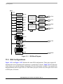
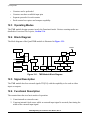
Block Diagram . . . . . . . . . . . . . . . . . . . . . . . . . . . . . . . . . . . . . . . . . . . . . . . . . . . . . . 12-4
Signal Description. . . . . . . . . . . . . . . . . . . . . . . . . . . . . . . . . . . . . . . . . . . . . . . . . . . . 12-4
56852 Digital Signal Controller User Manual, Rev. 4
Freescale Semiconductor
xiv
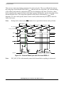
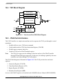
12.6 Functional Description . . . . . . . . . . . . . . . . . . . . . . . . . . . . . . . . . . . . . . . . . . . . . . . . 12-4
12.7 Counting Modes Definitions . . . . . . . . . . . . . . . . . . . . . . . . . . . . . . . . . . . . . . . . . . . . 12-5
12.7.1
Stop Mode. . . . . . . . . . . . . . . . . . . . . . . . . . . . . . . . . . . . . . . . . . . . . . . . . . . . . . . 12-5
12.7.2
Count Mode. . . . . . . . . . . . . . . . . . . . . . . . . . . . . . . . . . . . . . . . . . . . . . . . . . . . . . 12-6
12.7.3
Edge Count Mode . . . . . . . . . . . . . . . . . . . . . . . . . . . . . . . . . . . . . . . . . . . . . . . . . 12-6
12.7.4
Gated Count Mode . . . . . . . . . . . . . . . . . . . . . . . . . . . . . . . . . . . . . . . . . . . . . . . . 12-6
12.7.5
Quadrature Count Mode . . . . . . . . . . . . . . . . . . . . . . . . . . . . . . . . . . . . . . . . . . . . 12-6
12.7.6
Signed Count Mode . . . . . . . . . . . . . . . . . . . . . . . . . . . . . . . . . . . . . . . . . . . . . . . 12-7
12.7.7
Triggered Count Mode . . . . . . . . . . . . . . . . . . . . . . . . . . . . . . . . . . . . . . . . . . . . . 12-7
12.7.8
One-Shot Mode. . . . . . . . . . . . . . . . . . . . . . . . . . . . . . . . . . . . . . . . . . . . . . . . . . . 12-7
12.7.9
Cascade Count Mode . . . . . . . . . . . . . . . . . . . . . . . . . . . . . . . . . . . . . . . . . . . . . . 12-7
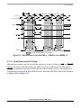
12.7.10 Pulse Output Mode . . . . . . . . . . . . . . . . . . . . . . . . . . . . . . . . . . . . . . . . . . . . . . . . 12-8
12.7.11 Fixed Frequency PWM Mode . . . . . . . . . . . . . . . . . . . . . . . . . . . . . . . . . . . . . . . . 12-8
12.7.12 Variable Frequency PWM Mode . . . . . . . . . . . . . . . . . . . . . . . . . . . . . . . . . . . . . . 12-8
12.7.13 Compare Registers Use . . . . . . . . . . . . . . . . . . . . . . . . . . . . . . . . . . . . . . . . . . . . 12-9
12.7.14 Capture Register Use . . . . . . . . . . . . . . . . . . . . . . . . . . . . . . . . . . . . . . . . . . . . . . 12-9
12.8 Module Memory Map . . . . . . . . . . . . . . . . . . . . . . . . . . . . . . . . . . . . . . . . . . . . . . . . . 12-9
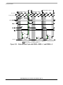
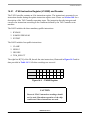
12.9 Register Descriptions (TMR_BASE = $1FFE80) . . . . . . . . . . . . . . . . . . . . . . . . . . . 12-11
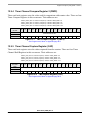
12.9.1
Timer Control Registers (CTL) . . . . . . . . . . . . . . . . . . . . . . . . . . . . . . . . . . . . . . 12-11
12.9.1.1
Count Mode (CM)—Bits 15–13 . . . . . . . . . . . . . . . . . . . . . . . . . . . . . . . . . . . 12-11
12.9.1.2
Primary Count Source (PCS)—Bits 12–9 . . . . . . . . . . . . . . . . . . . . . . . . . . . 12-11
12.9.1.3
Secondary Count Source (SCS)—Bits 8–7 . . . . . . . . . . . . . . . . . . . . . . . . . . 12-12
12.9.1.4
Count Once (ONCE)—Bit 6 . . . . . . . . . . . . . . . . . . . . . . . . . . . . . . . . . . . . . . 12-12
12.9.1.5
Count Length (LENGTH)—Bit 5 . . . . . . . . . . . . . . . . . . . . . . . . . . . . . . . . . . 12-13
12.9.1.6
Count Direction (DIR)—Bit 4 . . . . . . . . . . . . . . . . . . . . . . . . . . . . . . . . . . . . . 12-13
12.9.1.7
External Initialization (EXT INIT)—Bit 3. . . . . . . . . . . . . . . . . . . . . . . . . . . . . 12-13
12.9.1.8
Output Mode (OM)—Bits 2–0 . . . . . . . . . . . . . . . . . . . . . . . . . . . . . . . . . . . . 12-13
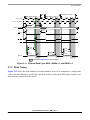
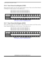
12.9.2
Timer Channel Status and Control Registers (SCR). . . . . . . . . . . . . . . . . . . . . . 12-14
12.9.2.1
Timer Compare Flag (TCF)—Bit 15. . . . . . . . . . . . . . . . . . . . . . . . . . . . . . . . 12-14
12.9.2.2
Timer Compare Flag Interrupt Enable (TCFIE)—Bit 14. . . . . . . . . . . . . . . . . 12-14
12.9.2.3
Timer Overflow Flag (TOF)—Bit 13 . . . . . . . . . . . . . . . . . . . . . . . . . . . . . . . . 12-14
12.9.2.4
Timer Overflow Flag Interrupt Enable (TOFIE)—Bit 12 . . . . . . . . . . . . . . . . . 12-14
12.9.2.5
Input Edge Flag (IEF)—Bit 11 . . . . . . . . . . . . . . . . . . . . . . . . . . . . . . . . . . . . 12-14
12.9.2.6
Input Edge Flag Interrupt Enable (IEFIE)—Bit 10 . . . . . . . . . . . . . . . . . . . . . 12-15
12.9.2.7
Input Polarity Select (IPS)—Bit 9. . . . . . . . . . . . . . . . . . . . . . . . . . . . . . . . . . 12-15
12.9.2.8
External Input Signal (INPUT)—Bit 8. . . . . . . . . . . . . . . . . . . . . . . . . . . . . . . 12-15
12.9.2.9
Input Capture Mode (Capture Mode)—Bits 7–6 . . . . . . . . . . . . . . . . . . . . . . 12-15
12.9.2.10
Master Mode (MSTR)—Bit 5 . . . . . . . . . . . . . . . . . . . . . . . . . . . . . . . . . . . . . 12-15
12.9.2.11
Enable External OFLAG Force (EEOF)—Bit 4 . . . . . . . . . . . . . . . . . . . . . . . 12-15
12.9.2.12
Forced OFLAG Value (VAL)—Bit 3 . . . . . . . . . . . . . . . . . . . . . . . . . . . . . . . . 12-15
12.9.2.13
Force OFLAG Output (FORCE)—Bit 2 . . . . . . . . . . . . . . . . . . . . . . . . . . . . . 12-16
Table of Contents, Rev. 4
xv
Freescale Semiconductor
12.9.2.14
Output Polarity Select (OPS)—Bit 1 . . . . . . . . . . . . . . . . . . . . . . . . . . . . . . .
12.9.2.15
Output Enable (OEN)—Bit 0 . . . . . . . . . . . . . . . . . . . . . . . . . . . . . . . . . . . . .
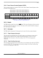
12.9.3
Timer Channel Compare Register 1 (CMP1) . . . . . . . . . . . . . . . . . . . . . . . . . . .
12.9.4
Timer Channel Compare Register 2 (CMP2) . . . . . . . . . . . . . . . . . . . . . . . . . . .
12.9.5
Timer Channel Capture Register (CAP) . . . . . . . . . . . . . . . . . . . . . . . . . . . . . . .
12.9.6
Timer Channel Load Register (LOAD) . . . . . . . . . . . . . . . . . . . . . . . . . . . . . . . .
12.9.7
Timer Channel Hold Register (HOLD) . . . . . . . . . . . . . . . . . . . . . . . . . . . . . . . .
12.9.8
Timer Channel Counter Register (CNTR) . . . . . . . . . . . . . . . . . . . . . . . . . . . . . .
12.10 Resets . . . . . . . . . . . . . . . . . . . . . . . . . . . . . . . . . . . . . . . . . . . . . . . . . . . . . . . . . . .
12.11 Interrupts . . . . . . . . . . . . . . . . . . . . . . . . . . . . . . . . . . . . . . . . . . . . . . . . . . . . . . . . .
12.11.1 Timer Compare Interrupts . . . . . . . . . . . . . . . . . . . . . . . . . . . . . . . . . . . . . . . . . .
12.11.2 Timer Overflow Interrupts . . . . . . . . . . . . . . . . . . . . . . . . . . . . . . . . . . . . . . . . . .
12.11.3 Timer Input Edge Interrupts . . . . . . . . . . . . . . . . . . . . . . . . . . . . . . . . . . . . . . . .
12-16
12-16
12-16
12-17
12-17
12-18
12-18
12-19
12-19
12-19
12-19
12-19
12-20
Chapter 13
General Purpose Input/Output (GPIO)
13.1 Introduction. . . . . . . . . . . . . . . . . . . . . . . . . . . . . . . . . . . . . . . . . . . . . . . . . . . . . . . . . 13-3
13.2 Features . . . . . . . . . . . . . . . . . . . . . . . . . . . . . . . . . . . . . . . . . . . . . . . . . . . . . . . . . . . 13-3
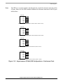
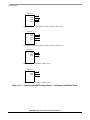
13.3 GPIO Block Diagram . . . . . . . . . . . . . . . . . . . . . . . . . . . . . . . . . . . . . . . . . . . . . . . . . 13-3
13.4 Functional Description . . . . . . . . . . . . . . . . . . . . . . . . . . . . . . . . . . . . . . . . . . . . . . . . 13-4
13.5 Modes of Operation . . . . . . . . . . . . . . . . . . . . . . . . . . . . . . . . . . . . . . . . . . . . . . . . . . 13-4
13.5.1
Normal Mode. . . . . . . . . . . . . . . . . . . . . . . . . . . . . . . . . . . . . . . . . . . . . . . . . . . . . 13-4
13.5.2
GPIO Mode . . . . . . . . . . . . . . . . . . . . . . . . . . . . . . . . . . . . . . . . . . . . . . . . . . . . . . 13-4
13.6 GPIO Configurations . . . . . . . . . . . . . . . . . . . . . . . . . . . . . . . . . . . . . . . . . . . . . . . . . 13-5
13.7 Module Memory Maps . . . . . . . . . . . . . . . . . . . . . . . . . . . . . . . . . . . . . . . . . . . . . . . . 13-5
13.8 Register Descriptions . . . . . . . . . . . . . . . . . . . . . . . . . . . . . . . . . . . . . . . . . . . . . . . . . 13-7
13.8.1
Port A Peripheral Enable Register (GPIOA_PER) . . . . . . . . . . . . . . . . . . . . . . . . 13-7
13.8.1.1
Reserved—Bits 15–3. . . . . . . . . . . . . . . . . . . . . . . . . . . . . . . . . . . . . . . . . . . . 13-8
13.8.1.2
Peripheral Enable (PE)—Bits 2–0 . . . . . . . . . . . . . . . . . . . . . . . . . . . . . . . . . . 13-8
13.8.2
Port C Peripheral Enable Register (GPIOC_PER) . . . . . . . . . . . . . . . . . . . . . . . . 13-8
13.8.2.1
Reserved—Bits 15–6. . . . . . . . . . . . . . . . . . . . . . . . . . . . . . . . . . . . . . . . . . . . 13-8
13.8.2.2
Peripheral Enable (PE)—Bits 5–0 . . . . . . . . . . . . . . . . . . . . . . . . . . . . . . . . . . 13-8
13.8.3
Port E Peripheral Enable Register (GPIOE_PER) . . . . . . . . . . . . . . . . . . . . . . . . 13-8
13.8.3.1
Reserved—Bits 15–2. . . . . . . . . . . . . . . . . . . . . . . . . . . . . . . . . . . . . . . . . . . . 13-9
13.8.3.2
Peripheral Enable (PE)—Bits 1–0 . . . . . . . . . . . . . . . . . . . . . . . . . . . . . . . . . . 13-9
13.8.4
Port A Data Direction Register (GPIOA_DDR) . . . . . . . . . . . . . . . . . . . . . . . . . . . 13-9
13.8.4.1
Reserved—Bits 15–3. . . . . . . . . . . . . . . . . . . . . . . . . . . . . . . . . . . . . . . . . . . . 13-9
13.8.4.2
Data Direction (DDR)—Bits 2–0 . . . . . . . . . . . . . . . . . . . . . . . . . . . . . . . . . . . 13-9
13.8.5
Port C Data Direction Register (GPIOC_DDR) . . . . . . . . . . . . . . . . . . . . . . . . . . . 13-9
13.8.5.1
Reserved—Bits 15–6. . . . . . . . . . . . . . . . . . . . . . . . . . . . . . . . . . . . . . . . . . . 13-10
13.8.5.2
Data Direction (DDR)—Bits 5–0 . . . . . . . . . . . . . . . . . . . . . . . . . . . . . . . . . . 13-10
56852 Digital Signal Controller User Manual, Rev. 4
Freescale Semiconductor
xvi
13.8.6
Port E Data Direction Register (GPIOE_DDR) . . . . . . . . . . . . . . . . . . . . . . . . . . 13-10
13.8.6.1
Reserved—Bits 15–2. . . . . . . . . . . . . . . . . . . . . . . . . . . . . . . . . . . . . . . . . . . 13-10
13.8.6.2
Data Direction (DDR)—Bits 1–0 . . . . . . . . . . . . . . . . . . . . . . . . . . . . . . . . . . 13-10
13.8.7
Port A Data Register (GPIOA_DR) . . . . . . . . . . . . . . . . . . . . . . . . . . . . . . . . . . . 13-10
13.8.7.1
Reserved—Bits 15–3. . . . . . . . . . . . . . . . . . . . . . . . . . . . . . . . . . . . . . . . . . . 13-11
13.8.7.2
Data (DATA)—Bits 2–0 . . . . . . . . . . . . . . . . . . . . . . . . . . . . . . . . . . . . . . . . . 13-11
13.8.8
Port C Data Register (GPIOC_DR). . . . . . . . . . . . . . . . . . . . . . . . . . . . . . . . . . . 13-11
13.8.8.1
Reserved—Bits 15–6. . . . . . . . . . . . . . . . . . . . . . . . . . . . . . . . . . . . . . . . . . . 13-11
13.8.8.2
Data (DATA)—Bits 5–0 . . . . . . . . . . . . . . . . . . . . . . . . . . . . . . . . . . . . . . . . . 13-11
13.8.9
Port E Data Register (GPIOE_DR) . . . . . . . . . . . . . . . . . . . . . . . . . . . . . . . . . . . 13-11
13.8.9.1
Reserved—Bits 15–2. . . . . . . . . . . . . . . . . . . . . . . . . . . . . . . . . . . . . . . . . . . 13-11
13.8.9.2
Data (DATA)—Bits 1–0 . . . . . . . . . . . . . . . . . . . . . . . . . . . . . . . . . . . . . . . . . 13-11
13.8.10 Port A Pull-Up Enable Register (GPIOA_PUE). . . . . . . . . . . . . . . . . . . . . . . . . . 13-12
13.8.10.1
Reserved—Bits 15–3. . . . . . . . . . . . . . . . . . . . . . . . . . . . . . . . . . . . . . . . . . . 13-12
13.8.10.2
Pull-Up Enable (PULLUP)—Bits 2–0. . . . . . . . . . . . . . . . . . . . . . . . . . . . . . . 13-12
13.8.11 Port C Pull-Up Enable Register (GPIOC_PUE) . . . . . . . . . . . . . . . . . . . . . . . . . 13-12
13.8.11.1
Reserved—Bits 15–6. . . . . . . . . . . . . . . . . . . . . . . . . . . . . . . . . . . . . . . . . . . 13-12
13.8.11.2
Pull-Up Enable (PULLUP)—Bits 5–0. . . . . . . . . . . . . . . . . . . . . . . . . . . . . . . 13-12
13.8.12 Port E Pull-Up Enable Register (GPIOE_PUE). . . . . . . . . . . . . . . . . . . . . . . . . . 13-13
13.8.12.1
Reserved—Bits 15–2. . . . . . . . . . . . . . . . . . . . . . . . . . . . . . . . . . . . . . . . . . . 13-13
13.8.12.2
Pull-Up Enable (PULLUP)—Bits 1–0. . . . . . . . . . . . . . . . . . . . . . . . . . . . . . . 13-13
13.9 Data Register Access . . . . . . . . . . . . . . . . . . . . . . . . . . . . . . . . . . . . . . . . . . . . . . . . 13-13
13.10 Resets . . . . . . . . . . . . . . . . . . . . . . . . . . . . . . . . . . . . . . . . . . . . . . . . . . . . . . . . . . . 13-14
13.11 Interrupts . . . . . . . . . . . . . . . . . . . . . . . . . . . . . . . . . . . . . . . . . . . . . . . . . . . . . . . . . 13-14
Chapter 14
JTAG Port
14.1 Introduction. . . . . . . . . . . . . . . . . . . . . . . . . . . . . . . . . . . . . . . . . . . . . . . . . . . . . . . . . 14-3
14.2 Features . . . . . . . . . . . . . . . . . . . . . . . . . . . . . . . . . . . . . . . . . . . . . . . . . . . . . . . . . . . 14-4
14.3 Master Test Access Port (TAP) . . . . . . . . . . . . . . . . . . . . . . . . . . . . . . . . . . . . . . . . . 14-4
14.3.1
Signal Description . . . . . . . . . . . . . . . . . . . . . . . . . . . . . . . . . . . . . . . . . . . . . . . . . 14-5
14.4 TAP Block Diagram . . . . . . . . . . . . . . . . . . . . . . . . . . . . . . . . . . . . . . . . . . . . . . . . . . 14-6
14.5 JTAG Port Architecture. . . . . . . . . . . . . . . . . . . . . . . . . . . . . . . . . . . . . . . . . . . . . . . . 14-6
14.5.1
JTAG Instruction Register (JTAGIR) and Decoder . . . . . . . . . . . . . . . . . . . . . . . . 14-7
14.5.1.1
External Test Instruction (EXTEST). . . . . . . . . . . . . . . . . . . . . . . . . . . . . . . . . 14-8
14.5.1.2
Bypass Instruction (BYPASS) . . . . . . . . . . . . . . . . . . . . . . . . . . . . . . . . . . . . . 14-8
14.5.2
Sample and Preload Instructions (SAMPLE/PRELOAD) . . . . . . . . . . . . . . . . . . . 14-9
14.5.2.1
Identification Code Instruction (IDCODE) . . . . . . . . . . . . . . . . . . . . . . . . . . . . 14-9
14.5.2.2
TAP Linking Module Select Instruction (TLM_SEL). . . . . . . . . . . . . . . . . . . . . 14-9
14.5.2.3
High-Z Instruction (HIGHZ) . . . . . . . . . . . . . . . . . . . . . . . . . . . . . . . . . . . . . . 14-10
14.5.3
JTAG Chip Identification (CID) Register . . . . . . . . . . . . . . . . . . . . . . . . . . . . . . . 14-10
Table of Contents, Rev. 4
xvii
Freescale Semiconductor
14.6 JTAG Bypass Register (JTAGBR) . . . . . . . . . . . . . . . . . . . . . . . . . . . . . . . . . . . . . .
14.7 JTAG Boundary Scan Register (BSR) . . . . . . . . . . . . . . . . . . . . . . . . . . . . . . . . . . .
14.8 TAP Controller . . . . . . . . . . . . . . . . . . . . . . . . . . . . . . . . . . . . . . . . . . . . . . . . . . . . .
14.8.1
Operation . . . . . . . . . . . . . . . . . . . . . . . . . . . . . . . . . . . . . . . . . . . . . . . . . . . . . .
14.8.1.1
Test Logic Reset (pstate = F) . . . . . . . . . . . . . . . . . . . . . . . . . . . . . . . . . . . .
14.8.1.2
Run-Test-Idle (pstate = C) . . . . . . . . . . . . . . . . . . . . . . . . . . . . . . . . . . . . . . .
14.8.1.3
Select Data Register (pstate = 7) . . . . . . . . . . . . . . . . . . . . . . . . . . . . . . . . .
14.8.1.4
Select Instruction Register (pstate = 4) . . . . . . . . . . . . . . . . . . . . . . . . . . . . .
14.8.1.5
Capture Data Register (pstate = 6) . . . . . . . . . . . . . . . . . . . . . . . . . . . . . . . .
14.8.1.6
Shift Data Register (pstate = 2) . . . . . . . . . . . . . . . . . . . . . . . . . . . . . . . . . . .
14.8.1.7
Exit1 Data Register (pstate = 1) . . . . . . . . . . . . . . . . . . . . . . . . . . . . . . . . . .
14.8.1.8
Pause Data Register (pstate = 3) . . . . . . . . . . . . . . . . . . . . . . . . . . . . . . . . .
14.8.1.9
Exit2 Data Register (pstate = 0) . . . . . . . . . . . . . . . . . . . . . . . . . . . . . . . . . .
14.8.1.10
Update Data Register (pstate = 5). . . . . . . . . . . . . . . . . . . . . . . . . . . . . . . . .
14.8.1.11
Capture Instruction Register (pstate = E) . . . . . . . . . . . . . . . . . . . . . . . . . . .
14.8.1.12
Shift Instruction Register (pstate = A) . . . . . . . . . . . . . . . . . . . . . . . . . . . . . .
14.8.1.13
Exit1 Instruction Register (pstate = 9) . . . . . . . . . . . . . . . . . . . . . . . . . . . . . .
14.8.1.14
Pause Instruction Register (pstate = B). . . . . . . . . . . . . . . . . . . . . . . . . . . . .
14.8.1.15
Exit2 Instruction Register (pstate = 8) . . . . . . . . . . . . . . . . . . . . . . . . . . . . . .
14.8.1.16
Update Instruction Register (pstate = D) . . . . . . . . . . . . . . . . . . . . . . . . . . . .
14.9 56852 Restrictions . . . . . . . . . . . . . . . . . . . . . . . . . . . . . . . . . . . . . . . . . . . . . . . . . .
14-11
14-11
14-16
14-17
14-17
14-17
14-18
14-18
14-18
14-18
14-18
14-18
14-19
14-19
14-19
14-19
14-19
14-19
14-20
14-20
14-20
Appendix A
Glossary
A.1
Glossary . . . . . . . . . . . . . . . . . . . . . . . . . . . . . . . . . . . . . . . . . . . . . . . . . . . . . . . . . . . . A-3
Appendix B
Programmer’s Sheets
B.1
B.2
Introduction. . . . . . . . . . . . . . . . . . . . . . . . . . . . . . . . . . . . . . . . . . . . . . . . . . . . . . . . . . B-3
Programmer’s Sheets. . . . . . . . . . . . . . . . . . . . . . . . . . . . . . . . . . . . . . . . . . . . . . . . . . B-3
56852 Digital Signal Controller User Manual, Rev. 4
Freescale Semiconductor
xviii
LIST OF FIGURES
1-1
1-2
1-3
1-1
2-1
3-1
4-1
4-2
5-1
5-2
5-6
5-8
5-9
5-10
5-11
5-12
5-13
5-14
5-15
5-16
5-17
6-1
6-2
6-3
6-4
6-5
6-6
6-7
6-8
7-1
7-2
8-1
8-2
8-23
8-24
56800E Chip Architecture with External Bus . . . . . . . . . . . . . . . . . . . . . . . . . . . . . 1-6
56800E Core Block Diagram. . . . . . . . . . . . . . . . . . . . . . . . . . . . . . . . . . . . . . . . . . 1-7
56852 Functional Block Diagram . . . . . . . . . . . . . . . . . . . . . . . . . . . . . . . . . . . . . 1-15
IPBus Bridge Interface With Other Main Components
System Side Operation . . . . . . . . . . . . . . . . . . . . . . . . . . . . . . . . . . . . . . . 1-18
56852 Signals Identified by Functional Group . . . . . . . . . . . . . . . . . . . . . . . . . . . . 2-5
56852 Memory Map . . . . . . . . . . . . . . . . . . . . . . . . . . . . . . . . . . . . . . . . . . . . . . . . 3-6
System Integration Module . . . . . . . . . . . . . . . . . . . . . . . . . . . . . . . . . . . . . . . . . . . 4-5
SCI Register Map Summary . . . . . . . . . . . . . . . . . . . . . . . . . . . . . . . . . . . . . . . . . . 4-9
EMI Block Diagram . . . . . . . . . . . . . . . . . . . . . . . . . . . . . . . . . . . . . . . . . . . . . . . . . 5-5
EMI Register Map Summary . . . . . . . . . . . . . . . . . . . . . . . . . . . . . . . . . . . . . . . . . . 5-7
Data Bus Contention Timing Requiring MDAR Field Assertion . . . . . . . . . . . . . . 5-12
External Read Cycle with Clock and RWS = 0 . . . . . . . . . . . . . . . . . . . . . . . . . . . 5-14
External Read Cycle with RWS = 1, RWSH = 0 and RWSS = 0 . . . . . . . . . . . . . 5-15
External Read Cycle with RWSS = RWS = 1, and RWSH = 0 . . . . . . . . . . . . . . . 5-16
External Read Cycle RWS = RWSH = 1 and RWSS = 0 . . . . . . . . . . . . . . . . . . . 5-17
External Write Cycle . . . . . . . . . . . . . . . . . . . . . . . . . . . . . . . . . . . . . . . . . . . . . . . 5-18
External Write Cycle with WWS = 1, WWSH = 0, and WWSS = 0 . . . . . . . . . . . . 5-19
External Write Cycle with WWSS = 1, WWS = 0 and WWSH = 0 . . . . . . . . . . . . 5-20
External Write Cycle with WWS = 0, WWSH = 1, WWSS = 0 . . . . . . . . . . . . . . . 5-21
External Write Cycle with WWSS = WWS = 1 and WWSH = 0 . . . . . . . . . . . . . . 5-22
External Write Cycle with WWS = WWSH = 1 (WWSS = 0) . . . . . . . . . . . . . . . . . 5-23
OCCS Integration Overview . . . . . . . . . . . . . . . . . . . . . . . . . . . . . . . . . . . . . . . . . . 6-3
OSC Supplying Clocks to PLL/CGM . . . . . . . . . . . . . . . . . . . . . . . . . . . . . . . . . . . . 6-4
Using an External Crystal . . . . . . . . . . . . . . . . . . . . . . . . . . . . . . . . . . . . . . . . . . . . 6-5
Using an External Active Low Frequency Clock, < 4MHz . . . . . . . . . . . . . . . . . . . . 6-6
Using an External Active High Frequency Clock, > 4MHz . . . . . . . . . . . . . . . . . . . 6-7
PLL Block Diagram . . . . . . . . . . . . . . . . . . . . . . . . . . . . . . . . . . . . . . . . . . . . . . . . . 6-8
PLL Output Frequency vs. Input Frequency . . . . . . . . . . . . . . . . . . . . . . . . . . . . . 6-10
CGM Register Map Summary . . . . . . . . . . . . . . . . . . . . . . . . . . . . . . . . . . . . . . . . 6-12
POR Module Block Diagram . . . . . . . . . . . . . . . . . . . . . . . . . . . . . . . . . . . . . . . . . . 7-4
COP Register Map Summary . . . . . . . . . . . . . . . . . . . . . . . . . . . . . . . . . . . . . . . . . 7-7
Interrupt Controller Block Diagram . . . . . . . . . . . . . . . . . . . . . . . . . . . . . . . . . . . . . 8-5
ITCN Register Map Summary . . . . . . . . . . . . . . . . . . . . . . . . . . . . . . . . . . . . . . . . 8-10
Reset Interface . . . . . . . . . . . . . . . . . . . . . . . . . . . . . . . . . . . . . . . . . . . . . . . . . . . 8-28
Interrupt Handshake Timing . . . . . . . . . . . . . . . . . . . . . . . . . . . . . . . . . . . . . . . . . 8-29
List of Figures, Rev. 4
Freescale Semiconductor
xix
9-1
9-2
9-3
9-4
9-5
9-6
9-7
9-8
9-9
9-10
9-11
9-12
9-13
9-14
9-15
9-16
10-1
10-2
10-3
10-4
10-5
10-6
10-7
10-8
10-9
10-10
10-11
10-12
10-17
11-1
11-2
11-3
11-4
11-6
11-7
11-9
11-10
SCI Block Diagram . . . . . . . . . . . . . . . . . . . . . . . . . . . . . . . . . . . . . . . . . . . . . . . . . 9-4
SCI Data Frame Formats . . . . . . . . . . . . . . . . . . . . . . . . . . . . . . . . . . . . . . . . . . . . 9-5
SCI Transmitter Block Diagram. . . . . . . . . . . . . . . . . . . . . . . . . . . . . . . . . . . . . . . . 9-7
SCI Receiver Block Diagram. . . . . . . . . . . . . . . . . . . . . . . . . . . . . . . . . . . . . . . . . 9-10
Receiver Data Sampling . . . . . . . . . . . . . . . . . . . . . . . . . . . . . . . . . . . . . . . . . . . . 9-11
Start Bit Search Example 1 . . . . . . . . . . . . . . . . . . . . . . . . . . . . . . . . . . . . . . . . . . 9-13
Start Bit Search Example 2 . . . . . . . . . . . . . . . . . . . . . . . . . . . . . . . . . . . . . . . . . . 9-13
Start Bit Search Example 3 . . . . . . . . . . . . . . . . . . . . . . . . . . . . . . . . . . . . . . . . . . 9-14
Start Bit Search Example 4 . . . . . . . . . . . . . . . . . . . . . . . . . . . . . . . . . . . . . . . . . . 9-14
Start Bit Search Example 5 . . . . . . . . . . . . . . . . . . . . . . . . . . . . . . . . . . . . . . . . . . 9-15
Start Bit Search Example 6 . . . . . . . . . . . . . . . . . . . . . . . . . . . . . . . . . . . . . . . . . . 9-15
Slow Data . . . . . . . . . . . . . . . . . . . . . . . . . . . . . . . . . . . . . . . . . . . . . . . . . . . . . . . 9-16
Fast Data. . . . . . . . . . . . . . . . . . . . . . . . . . . . . . . . . . . . . . . . . . . . . . . . . . . . . . . . 9-17
Single-Wire Operation (LOOP = 1, RSRC = 1) . . . . . . . . . . . . . . . . . . . . . . . . . . . 9-19
Loop Operation (LOOP = 1, RSRC = 0) . . . . . . . . . . . . . . . . . . . . . . . . . . . . . . . . 9-19
SCI Register Map Summary . . . . . . . . . . . . . . . . . . . . . . . . . . . . . . . . . . . . . . . . . 9-21
SPI Block Diagram . . . . . . . . . . . . . . . . . . . . . . . . . . . . . . . . . . . . . . . . . . . . . . . . 10-4
CPHA/SS Timing. . . . . . . . . . . . . . . . . . . . . . . . . . . . . . . . . . . . . . . . . . . . . . . . . . 10-5
Full-Duplex Master/Slave Connections . . . . . . . . . . . . . . . . . . . . . . . . . . . . . . . . . 10-7
Sharing of a Slave by Multiple Masters. . . . . . . . . . . . . . . . . . . . . . . . . . . . . . . . . 10-9
Transmission Format (CPHA = 0). . . . . . . . . . . . . . . . . . . . . . . . . . . . . . . . . . . . 10-11
CPHA/SS Timing. . . . . . . . . . . . . . . . . . . . . . . . . . . . . . . . . . . . . . . . . . . . . . . . . 10-11
Transmission Format (CPHA = 1). . . . . . . . . . . . . . . . . . . . . . . . . . . . . . . . . . . . 10-12
Transmission Start Delay (Master) . . . . . . . . . . . . . . . . . . . . . . . . . . . . . . . . . . . 10-14
SPRF/SPTE Interrupt Timing . . . . . . . . . . . . . . . . . . . . . . . . . . . . . . . . . . . . . . . 10-15
Missed Read of Overflow Condition . . . . . . . . . . . . . . . . . . . . . . . . . . . . . . . . . . 10-17
Clearing SPRF When OVRF Interrupt Is Not Enabled . . . . . . . . . . . . . . . . . . . . 10-18
SPI Register Map Summary . . . . . . . . . . . . . . . . . . . . . . . . . . . . . . . . . . . . . . . . 10-20
SPI Interrupt Request Generation. . . . . . . . . . . . . . . . . . . . . . . . . . . . . . . . . . . . 10-29
ISSI Block Diagram . . . . . . . . . . . . . . . . . . . . . . . . . . . . . . . . . . . . . . . . . . . . . . . . 11-6
Asynchronous (SYN=0) ISSI Configurations—Continuous Clock. . . . . . . . . . . . . 11-7
Synchronous ISSI Configurations—Continuous and Gated Clock . . . . . . . . . . . . 11-8
ISSI Register Map Summary. . . . . . . . . . . . . . . . . . . . . . . . . . . . . . . . . . . . . . . . . 11-9
Transmit Data Path (TSHFD = 0) . . . . . . . . . . . . . . . . . . . . . . . . . . . . . . . . . . . . 11-11
Transmit Data Path (TSHFD = 1) . . . . . . . . . . . . . . . . . . . . . . . . . . . . . . . . . . . . 11-12
Receive Data Path (RSHFD=0) . . . . . . . . . . . . . . . . . . . . . . . . . . . . . . . . . . . . . 11-13
Receive Data Path (RSHFD=1) . . . . . . . . . . . . . . . . . . . . . . . . . . . . . . . . . . . . . 11-13
56852 Digital Signal Controller User Manual, Rev. 4
xx
Freescale Semiconductor
11-14
11-19
11-20
11-21
11-22
11-23
11-24
11-25
11-26
11-27
11-28
12-1
12-2
12-3
13-1
13-2
13-3
13-4
14-1
14-2
14-3
14-4
14-5
14-6
14-7
Frame Sync Timing Options . . . . . . . . . . . . . . . . . . . . . . . . . . . . . . . . . . . . . . . . 11-21
Normal Mode Transmit Timing—Continuous Clock
(WL=8 bit words, DC=1) . . . . . . . . . . . . . . . . . . . . . . . . . . . . . . . . . . . . . 11-35
Normal Mode Receive Timing—Continuous Clock (WL=8 bit words, DC=1) . . . 11-36
Normal Mode Timing—Gated Clock . . . . . . . . . . . . . . . . . . . . . . . . . . . . . . . . . . 11-38
Network Mode Transmit Timing . . . . . . . . . . . . . . . . . . . . . . . . . . . . . . . . . . . . . 11-41
Network Mode Receive Timing . . . . . . . . . . . . . . . . . . . . . . . . . . . . . . . . . . . . . . 11-43
Synchronous Mode Interrupt Timing . . . . . . . . . . . . . . . . . . . . . . . . . . . . . . . . . . 11-45
ISSI Clocking (8-bit words, 3 time-slots / frame) . . . . . . . . . . . . . . . . . . . . . . . . . 11-45
ISSI Clock Generation. . . . . . . . . . . . . . . . . . . . . . . . . . . . . . . . . . . . . . . . . . . . . 11-46
ISSI Transmit Clock Generator Block Diagram. . . . . . . . . . . . . . . . . . . . . . . . . . 11-47
ISSI Transmit Frame Sync Generator Block Diagram . . . . . . . . . . . . . . . . . . . . 11-47
TMR Module Block Diagram . . . . . . . . . . . . . . . . . . . . . . . . . . . . . . . . . . . . . . . . . 12-4
Quadrature Incremental Position Encoder . . . . . . . . . . . . . . . . . . . . . . . . . . . . . . 12-6
TMR Register Map Summary . . . . . . . . . . . . . . . . . . . . . . . . . . . . . . . . . . . . . . . 12-10
Bit-Slice View of GPIO Logic. . . . . . . . . . . . . . . . . . . . . . . . . . . . . . . . . . . . . . . . . 13-3
GPIO A Register Map Summary . . . . . . . . . . . . . . . . . . . . . . . . . . . . . . . . . . . . . . 13-6
GPIO C Register Map Summary. . . . . . . . . . . . . . . . . . . . . . . . . . . . . . . . . . . . . . 13-6
GPIO E Register Map Summary . . . . . . . . . . . . . . . . . . . . . . . . . . . . . . . . . . . . . . 13-7
Test Access Port (TAP) Block Diagram . . . . . . . . . . . . . . . . . . . . . . . . . . . . . . . . 14-6
JTAGIR Register . . . . . . . . . . . . . . . . . . . . . . . . . . . . . . . . . . . . . . . . . . . . . . . . . . 14-7
Bypass Register . . . . . . . . . . . . . . . . . . . . . . . . . . . . . . . . . . . . . . . . . . . . . . . . . . 14-8
JTAG Chip Identification (CID) Register . . . . . . . . . . . . . . . . . . . . . . . . . . . . . . . 14-10
JTAG Bypass Register (JTAGBR) . . . . . . . . . . . . . . . . . . . . . . . . . . . . . . . . . . . 14-11
Boundary Scan Register (BSR) . . . . . . . . . . . . . . . . . . . . . . . . . . . . . . . . . . . . . 14-11
TAP Controller State Diagram. . . . . . . . . . . . . . . . . . . . . . . . . . . . . . . . . . . . . . . 14-16
List of Figures, Rev. 4
Freescale Semiconductor
xxi
56852 Digital Signal Controller User Manual, Rev. 4
xxii
Freescale Semiconductor
LIST OF TABLES
0-1
2-1
2-2
3-1
3-2
3-3
3-4
3-5
3-6
3-7
3-8
3-9
3-10
3-11
3-12
4-1
4-2
4-3
4-4
4-5
4-6
4-7
4-12
5-1
5-2
5-3
Pin Conventions . . . . . . . . . . . . . . . . . . . . . . . . . . . . . . . . . . . . . . . . . . . . . . . . . . .xxxi
Functional Group Pin Allocations . . . . . . . . . . . . . . . . . . . . . . . . . . . . . . . . . . . . . . 2-4
56852 Signal and Package Information for the 81-pin MAPBGA . . . . . . . . . . . . . . 2-6
EOnCE Memory Map (EOnCE_BASE = $FFFF00) . . . . . . . . . . . . . . . . . . . . . . . . 3-7
System Integration Module Registers Address Map
(SYS_BASE = $1FFF08) . . . . . . . . . . . . . . . . . . . . . . . . . . . . . . . . . . . . . . . 3-8
External Memory Interface Registers Address Map
(EMI_BASE = $1FFE40) . . . . . . . . . . . . . . . . . . . . . . . . . . . . . . . . . . . . . . . 3-8
Clock Generation Module Registers Address Map
(CGM_BASE = $1FFF10) . . . . . . . . . . . . . . . . . . . . . . . . . . . . . . . . . . . . . . 3-8
Interrupt Control Registers Address Map
(ITCN_BASE = $1FFF20) . . . . . . . . . . . . . . . . . . . . . . . . . . . . . . . . . . . . . . 3-8
Serial Communications Interface Registers Address Map
(SCI_BASE = $1FFFE0) . . . . . . . . . . . . . . . . . . . . . . . . . . . . . . . . . . . . . . . 3-9
Serial Peripheral Interface Registers Address Map
(SPI_BASE =$1FFFE8) . . . . . . . . . . . . . . . . . . . . . . . . . . . . . . . . . . . . . . . 3-10
Improved Synchronous Serial Interface Registers Address Map
(ISSI_BASE = $1FFE20) . . . . . . . . . . . . . . . . . . . . . . . . . . . . . . . . . . . . . . 3-10
Quad Timer Registers Address Map
(TMR_BASE = $1FFE80). . . . . . . . . . . . . . . . . . . . . . . . . . . . . . . . . . . . . . 3-11
General Purpose Input/Output Port A Register Map
(GPIOA_BASE = $1FFE60) . . . . . . . . . . . . . . . . . . . . . . . . . . . . . . . . . . . . 3-12
General Purpose Input/Output Port C Register Map
(GPIOC_BASE = $1FFE68). . . . . . . . . . . . . . . . . . . . . . . . . . . . . . . . . . . . 3-12
General Purpose Input/Output Port E Register Map
(GPIOE_BASE = $1FFE70) . . . . . . . . . . . . . . . . . . . . . . . . . . . . . . . . . . . . 3-12
IPBus Signals . . . . . . . . . . . . . . . . . . . . . . . . . . . . . . . . . . . . . . . . . . . . . . . . . . . . . 4-6
Reset Generator Inputs/Outputs . . . . . . . . . . . . . . . . . . . . . . . . . . . . . . . . . . . . . . . 4-6
Register Inputs/Outputs . . . . . . . . . . . . . . . . . . . . . . . . . . . . . . . . . . . . . . . . . . . . . 4-7
Power Mode Control Inputs/Outputs . . . . . . . . . . . . . . . . . . . . . . . . . . . . . . . . . . . . 4-7
Test Inputs/Outputs. . . . . . . . . . . . . . . . . . . . . . . . . . . . . . . . . . . . . . . . . . . . . . . . . 4-8
Derived Clock Inputs . . . . . . . . . . . . . . . . . . . . . . . . . . . . . . . . . . . . . . . . . . . . . . . . 4-8
SIM Module Memory Map (SIM_BASE =$FFF08) . . . . . . . . . . . . . . . . . . . . . . . . . 4-8
SIM Clock Signals . . . . . . . . . . . . . . . . . . . . . . . . . . . . . . . . . . . . . . . . . . . . . . . . . 4-18
EMI Module Memory Map (EMI_BASE = $1FFE40). . . . . . . . . . . . . . . . . . . . . . . . 5-6
CSBAR Encoding of the BLKSZ Field. . . . . . . . . . . . . . . . . . . . . . . . . . . . . . . . . . . 5-8
CSOR Encoding BYTE_EN Values . . . . . . . . . . . . . . . . . . . . . . . . . . . . . . . . . . . . 5-9
List of Tables, Rev. 4
Freescale Semiconductor
xxiii
5-4
5-5
5-6
6-1
7-1
7-2
8-1
8-2
8-3
8-4
8-5
9-1
9-2
9-3
9-4
9-5
9-6
9-7
9-8
9-9
9-10
10-1
10-2
10-3
10-4
10-5
10-6
11-1
11-2
11-3
11-4
11-5
11-6
11-7
11-8
11-9
11-10
CSOR Encoding of Read/Write Values. . . . . . . . . . . . . . . . . . . . . . . . . . . . . . . . . . 5-9
CSOR Encoding of PS/DS Values . . . . . . . . . . . . . . . . . . . . . . . . . . . . . . . . . . . . 5-10
Operation with DRV . . . . . . . . . . . . . . . . . . . . . . . . . . . . . . . . . . . . . . . . . . . . . . . 5-13
CGM Memory Map (CGM_BASE = $1FFF10). . . . . . . . . . . . . . . . . . . . . . . . . . . 6-12
COP Time-Out Ranges as a Function of Oscillator Frequency . . . . . . . . . . . . . . . 7-5
COP Module Memory Map (COP_BASE = $1FFFD0) . . . . . . . . . . . . . . . . . . . . . . 7-7
Interrupt Priority Level . . . . . . . . . . . . . . . . . . . . . . . . . . . . . . . . . . . . . . . . . . . . . . . 8-3
Interrupt Vector Table Contents . . . . . . . . . . . . . . . . . . . . . . . . . . . . . . . . . . . . . . . 8-6
Module Memory Map (ITCN_BASE = $FFF20) . . . . . . . . . . . . . . . . . . . . . . . . . . . 8-9
Interrupt Mask Bit Definition . . . . . . . . . . . . . . . . . . . . . . . . . . . . . . . . . . . . . . . . . 8-29
Interrupt Priority Encoding. . . . . . . . . . . . . . . . . . . . . . . . . . . . . . . . . . . . . . . . . . . 8-30
External I/O Signals . . . . . . . . . . . . . . . . . . . . . . . . . . . . . . . . . . . . . . . . . . . . . . . . 9-5
Example 8-Bit Data Frame Formats . . . . . . . . . . . . . . . . . . . . . . . . . . . . . . . . . . . . 9-5
Example 9-Bit Data Frame Formats . . . . . . . . . . . . . . . . . . . . . . . . . . . . . . . . . . . . 9-6
Example Baud Rates (Module Clock = 60Mhz) . . . . . . . . . . . . . . . . . . . . . . . . . . . 9-6
Start Bit Verification. . . . . . . . . . . . . . . . . . . . . . . . . . . . . . . . . . . . . . . . . . . . . . . . 9-11
Data Bit Recovery . . . . . . . . . . . . . . . . . . . . . . . . . . . . . . . . . . . . . . . . . . . . . . . . . 9-12
Stop Bit Recovery . . . . . . . . . . . . . . . . . . . . . . . . . . . . . . . . . . . . . . . . . . . . . . . . . 9-12
SCI Module Memory Map (SCI_BASE = $1FFFE0) . . . . . . . . . . . . . . . . . . . . . . . 9-21
Loop Functions . . . . . . . . . . . . . . . . . . . . . . . . . . . . . . . . . . . . . . . . . . . . . . . . . . . 9-22
SCI Interrupt Sources . . . . . . . . . . . . . . . . . . . . . . . . . . . . . . . . . . . . . . . . . . . . . . 9-29
SPI I/O Configuration . . . . . . . . . . . . . . . . . . . . . . . . . . . . . . . . . . . . . . . . . . . . . . 10-6
External I/O Signals . . . . . . . . . . . . . . . . . . . . . . . . . . . . . . . . . . . . . . . . . . . . . . . 10-6
SPI Module Memory Map (SPI_BASE = $1FFFE8) . . . . . . . . . . . . . . . . . . . . . . 10-20
SPI Master Baud Rate Selection. . . . . . . . . . . . . . . . . . . . . . . . . . . . . . . . . . . . . 10-22
Transmission Data Size . . . . . . . . . . . . . . . . . . . . . . . . . . . . . . . . . . . . . . . . . . . 10-26
SPI Interrupts . . . . . . . . . . . . . . . . . . . . . . . . . . . . . . . . . . . . . . . . . . . . . . . . . . . 10-28
Signal Properties. . . . . . . . . . . . . . . . . . . . . . . . . . . . . . . . . . . . . . . . . . . . . . . . . . 11-4
ISSI Module Memory Map (ISSI_BASE = $1FFE20) . . . . . . . . . . . . . . . . . . . . . . 11-9
WL Encoding. . . . . . . . . . . . . . . . . . . . . . . . . . . . . . . . . . . . . . . . . . . . . . . . . . . . 11-15
SSI Bit Clock As a Function Of Peripheral
Clock and Prescale Modulus . . . . . . . . . . . . . . . . . . . . . . . . . . . . . . . . . . 11-16
ISSI Receive Data Interrupts. . . . . . . . . . . . . . . . . . . . . . . . . . . . . . . . . . . . . . . . 11-23
ISSI Transmit Data Interrupts . . . . . . . . . . . . . . . . . . . . . . . . . . . . . . . . . . . . . . . 11-24
Clock Pin Configuration. . . . . . . . . . . . . . . . . . . . . . . . . . . . . . . . . . . . . . . . . . . . 11-26
RFCNT[3:0] Encoding . . . . . . . . . . . . . . . . . . . . . . . . . . . . . . . . . . . . . . . . . . . . . 11-29
TFCNT[3:0] Encoding . . . . . . . . . . . . . . . . . . . . . . . . . . . . . . . . . . . . . . . . . . . . . 11-29
RFWM Encoding . . . . . . . . . . . . . . . . . . . . . . . . . . . . . . . . . . . . . . . . . . . . . . . . . 11-30
56852 Digital Signal Controller User Manual, Rev. 4
xxiv
Freescale Semiconductor
11-11
11-12
11-13
11-14
11-15
11-16
11-17
11-18
11-19
11-20
11-21
11-22
11-23
12-1
13-1
13-2
13-3
13-4
13-5
13-6
14-1
14-2
14-3
14-4
14-5
Status of Receive FIFO Full Flag . . . . . . . . . . . . . . . . . . . . . . . . . . . . . . . . . . . . 11-31
TFWM Encoding . . . . . . . . . . . . . . . . . . . . . . . . . . . . . . . . . . . . . . . . . . . . . . . . . 11-31
Status of Transmit FIFO Empty Flag. . . . . . . . . . . . . . . . . . . . . . . . . . . . . . . . . . 11-32
ISSI Operating Modes. . . . . . . . . . . . . . . . . . . . . . . . . . . . . . . . . . . . . . . . . . . . . 11-33
Normal Mode Transmit Operations . . . . . . . . . . . . . . . . . . . . . . . . . . . . . . . . . . . 11-35
Normal Mode Receive Operations . . . . . . . . . . . . . . . . . . . . . . . . . . . . . . . . . . . 11-37
Transmit and Receive Enables in Gated Clock Mode. . . . . . . . . . . . . . . . . . . . . 11-38
Gated Clock Operations . . . . . . . . . . . . . . . . . . . . . . . . . . . . . . . . . . . . . . . . . . . 11-39
Notes for Transmit Timing in Figure 11-22 . . . . . . . . . . . . . . . . . . . . . . . . . . . . . 11-42
Notes for Receive Timing in Figure 11-23. . . . . . . . . . . . . . . . . . . . . . . . . . . . . . 11-44
Clock Summary. . . . . . . . . . . . . . . . . . . . . . . . . . . . . . . . . . . . . . . . . . . . . . . . . . 11-46
ISSI Control Bits Requiring Reset Before Change . . . . . . . . . . . . . . . . . . . . . . . 11-49
Interrupt Summary . . . . . . . . . . . . . . . . . . . . . . . . . . . . . . . . . . . . . . . . . . . . . . . 11-50
TMR Module Memory Map (TMR_BASE = $1FFE80) . . . . . . . . . . . . . . . . . . . . 12-10
Mapping of External Signals to GPIO Ports . . . . . . . . . . . . . . . . . . . . . . . . . . . . . 13-4
GPIO Registers Functions . . . . . . . . . . . . . . . . . . . . . . . . . . . . . . . . . . . . . . . . . . 13-5
GPIO A Memory Map (GPIOA_BASE = $1FFE60) . . . . . . . . . . . . . . . . . . . . . . . 13-5
GPIO C Memory Map (GPIOC_BASE = $1FFE68) . . . . . . . . . . . . . . . . . . . . . . . 13-6
GPIO E Memory Map (GPIOE_BASE = $1FFE70) . . . . . . . . . . . . . . . . . . . . . . . 13-7
Data Register Access . . . . . . . . . . . . . . . . . . . . . . . . . . . . . . . . . . . . . . . . . . . . . 13-14
JTAG Pin Descriptions . . . . . . . . . . . . . . . . . . . . . . . . . . . . . . . . . . . . . . . . . . . . . 14-5
Master TAP Instructions Opcode . . . . . . . . . . . . . . . . . . . . . . . . . . . . . . . . . . . . . 14-8
TLM Register. . . . . . . . . . . . . . . . . . . . . . . . . . . . . . . . . . . . . . . . . . . . . . . . . . . . 14-10
Device ID Register Bit Assignment . . . . . . . . . . . . . . . . . . . . . . . . . . . . . . . . . . . 14-11
BSR Contents for 56852 . . . . . . . . . . . . . . . . . . . . . . . . . . . . . . . . . . . . . . . . . . . 14-12
List of Tables, Rev. 4
Freescale Semiconductor
xxv
56852 Digital Signal Controller User Manual, Rev. 4
xxvi
Freescale Semiconductor
Preface
About This Manual
Features of the 56852 16-bit digital signal controllers (DSCs) are described in this preliminary
manual release. Details of memory, operating modes, and peripheral modules are documented
here. This manual is intended to be used with the 56800E Reference Manual (56800ERM),
describing the Central Processing Unit (CPU), programming models, and instruction set details.
The DSP56852 Technical Data Sheet provides electrical specifications as well as timing, pinout,
and packaging descriptions.
Audience
Information in this manual is intended to assist design and software engineers to integrate the
56852 digital signal controllers into a design and/or while developing application software.
Manual Organization
This manual is arranged in sections described here:
•
Chapter 1, 56852 Overview—provides a brief overview, describes the structure of this
document and lists other documentation necessary to use these chips.
•
Chapter 2, Pin Descriptions—describes the 56852 pins and how the pins are grouped
into various interfaces.
•
Chapter 3, Memory (MEM)—depicts the on-chip memory, structures, registers, and
interfaces.
•
Chapter 4, System Integration Module (SIM)—documents the module responsible for
system control functions.
•
Chapter 5, External Memory Interface (EMI)—defines specifications for the
IPBus-based External Memory Interface module.
•
Chapter 6, On-Chip Clock Synthesis (OCCS)—elaborates about the internal oscillator,
Phase Lock Loop (PLL), and timer distribution chain for the 56852.
Preface, Rev. 4
Freescale Semiconductor
xxvii
•
Chapter 7, Power-On Reset (POR) and Computer Operating Properly
(COP)—narrates the on-chip Watchdog timer and the real-time interrupt generator, as
well as the modes of operation.
•
Chapter 8, Interrupt Controller (ITCN)—describes how the IPBus Interrupt Controller
accepts interrupt requests from IPBus-based peripherals and presents them to the 56800E
core.
•
Chapter 9, Serial Communications Interface (SCI)—presents the Serial
Communications Interface, communicating with devices such as codecs, other DSCs,
microprocessors, and peripherals to provide the primary data input path.
•
Chapter 10, Serial Peripheral Interface (SPI)—describes the Serial Peripheral
Interface, the communicator with external devices, such as Liquid Crystal Displays
(LCDs) and Microcontroller Units (MCUs).
•
Chapter 11, Improved Synchronous Serial Interface (ISSI)—details the Synchronous
Serial Interface, the communicator with devices such as industry-standard codecs, other
DSCs, microprocessors, and peripherals to implement the Serial Peripheral Interface
(SPI).
•
Chapter 12, Quad Timer (TMR)—outlines the available internal Quad Timer devices,
including features and registers.
•
Chapter 13, General Purpose Input/Output (GPIO)—describes how peripheral pins
are multiplexed with GPIO functions.
•
Chapter 14, JTAG Port—explains the Joint Test Action Group (JTAG) testing
methodology and its capabilities with Test Access Port (TAP) and Enhanced OnCE
(explained in the Reference Manual).
•
Appendix A, Glossary—provides definitions of terms, acronyms, and register names
used in this manual.
•
Appendix B, Programmer’s Sheets—expands on reference tables placing all relevant
data on one page; intended to be a convenient guide in programming the 56852.
56852 Digital Signal Controller User Manual, Rev. 4
xxviii
Freescale Semiconductor
Suggested Reading
A list of related books is provided here as an aid those who may be new to Digital Signal
Controllers:
Advanced Topics in Signal Processing, Jae S. Lim and Alan V. Oppenheim (Prenignal tice-Hall:
1988).
Applications of Digital Signal Processing, A. V. Oppenheim (Prentice-Hall: 1978).
Digital Processing of Signals: Theory and Practice, Maurice Bellanger (John Wiley and Sons:
1984).
Digital Signal Processing, Alan V. Oppenheim and Ronald W. Schafer (Prentice-Hall: 1975).
Digital Signal Processing: A System Design Approach, David J. DeFatta, Joseph G. Lucas, and
William S. Hodgkiss (John Wiley and Sons: 1988).
Discrete-Time Signal Processing, A. V. Oppenheim and R.W. Schafer (Prentice-Hall: 1989).
Foundations of Digital Signal Processing and Data Analysis, J. A. Cadzow (Macmillan: 1987).
Handbook of Digital Signal Processing, D. F. Elliott (Academic Press: 1987).
Introduction to Digital Signal Processing, John G. Proakis and Dimitris G. Manolakis
(Macmillan: 1988).
IP Bus Specifications, Semiconductor Reuse Standard, SRSIPB1, v 2.0, Draft 1.6.
Multirate Digital Signal Processing, R. E. Crochiere and L. R. Rabiner (Prentice-Hall: 1983).
Signal Processing Algorithms, S. Stearns and R. Davis (Prentice-Hall: 1988).
Signal Processing Handbook, C. H. Chen (Marcel Dekker: 1988).
Signal Processing: The Modern Approach, James V. Candy (McGraw-Hill: 1988).
Theory and Application of Digital Signal Processing, Lawrence R. Rabiner and Bernard Gold
(Prentice-Hall: 1975).
Manual Conventions
Conventions used in this manual:
•
•
Bits within registers are always listed from Most Significant Bit (MSB) to Least Significant
Bit (LSB).
Bits within a register are formatted AA[n:0] when more than one bit is involved in a
description. For purposes of description, the bits are presented as if they are contiguous
within a register. However, this is not always the case. Refer to the programming model
diagrams or to the programmer’s sheets to see the exact location of bits within a register.
Preface, Rev. 4
Freescale Semiconductor
xxix
•
•
•
•
When a bit is described as set, its value is set to 1. When a bit is described as cleared, its
value is set to 0.
Pins or signals asserted low, made active when pulled to ground, have an overbar above
their name. For example, the SS0 pin is asserted low.
Hex values are indicated with a dollar sign ($) preceding the hex value, as follows: $FFFB
is the X memory address for the Interrupt Priority Register (IPR).
Code examples follow in a single spaced font.
BFSET #$0007,X:PCC ; Configure:
•
•
•
line 1
; MISO0, MOSI0, SCK0 for SPI master
line 2
; ~SS0 as PC3 for GPIO
line 3
Pins or signals listed in code examples asserted as low have a tilde in front of their names.
In the previous example, line three refers to the SS0 pin, shown as ~SS0.
The word reset is used in three different contexts in this manual. The word pin is a generic
term for any pin on the chip. They are described as:
— a reset pin is always written as RESET, in uppercase, using the over bar
— the processor state occurs when the RESET pin is asserted. It is always written as Reset,
with a capitalized first letter
— the word reset refers to the reset function. It is written in lowercase, without italics, used
here only for differentiation. The word may require a capital letter as style dictates, such
as in headings and captions
The word assert means a high true (active high) signal is pulled high to VDD, or a low true
(active low) signal is pulled low to ground. The word deassert means a high true signal is
pulled low to ground, or a low true signal is pulled high to VDD.
56852 Digital Signal Controller User Manual, Rev. 4
xxx
Freescale Semiconductor
Table 0-1. Pin Conventions
Signal/Symbol
Logic State
Signal State
Voltage1
PIN
True
Asserted
VIL/VOL
PIN
False
Deasserted
VIH/VOH
PIN
True
Asserted
VIH/VOH
PIN
False
Deasserted
VIL/VOL
1.Values for VIL, VOL, VIH, and VOH are defined by individual product specifications.
Registers and tables displaying a grayed area designate reserved or unimplemented bits or
registers.
= Reserved or unimplemented bit/register
The following standards are recognized in choosing block I/O signal names for the bridge:
•
For clarity, all signals are referenced with capital letters throughout this document.
•
Descriptive functionality of signals is taken into account when choosing signal names.
This may imply names for system bus interface signals different from those defined in the
56800E specification documents.
•
All efforts are made to maintain compliance with Semiconductor Reuse Standards
guidelines.
•
The prefix IPBB_ is used for all signals initiated from the IPBus Bridge.
•
A prefix symbolizing a specific block’s name is used to distinguish input signals (point to
point signals).
•
All signals initiated from a particular bus will contain a prefix signifying that bus, i.e.
CLK_IPB (originating from the clock).
Preface, Rev. 4
Freescale Semiconductor
xxxi
56852 Digital Signal Controller User Manual, Rev. 4
xxxii
Freescale Semiconductor
Chapter 1
56852 Overview
56852 Overview, Rev. 4
Freescale Semiconductor
1-1
56852 Digital Signal Controller User Manual, Rev. 4
1-2
Freescale Semiconductor
Introduction
1.1 Introduction
This manual describes the 56852 device. The design of the 56852 is based on the 56800E core
architecture, providing more processing power than any other controller. A primary advantage
of the 56852 is it can be used to support microcontroller functions ordinarily requiring a separate
microcontroller. This saves designers both space and money.
The 56852 is a member of the 56800E core-based family of Digital Signal Controllers (DSCs).
On a single chip, it combines the processing power of a DSP and the functionality of a
microcontroller with a flexible set of peripherals to create an extremely cost-effective solution.
Because of its low cost, configuration flexibility, and compact program code, the 56852 is
well-suited for many applications. The chip includes many peripherals especially useful for
low-end Internet appliance applications and low-end client applications such as:
•
Telephony
•
Portable devices
•
Internet audio
•
Point-of-sale systems such as noise suppression
•
ID tag readers
•
Sonic/subsonic detectors
•
Security access devices
•
Remote metering
•
Sonic alarms
The 56800E core is based on a Harvard-style architecture consisting of three execution units
operating in parallel, allowing as many as six operations per instruction cycle. The
microprocessor-style programming model and optimized instruction set allow straightforward
generation of efficient, compact code for both DSP and MCU applications. The instruction set is
also highly efficient for C Compilers, enabling rapid development of optimized control
applications.
The 56852 supports program execution from either internal or external memories. Two data
operands can be accessed from the on-chip Data RAM per instruction cycle. The 56852 also
provides two external dedicated interrupt lines, and up to 11 General Purpose Input/Output
(GPIO) lines, depending on peripheral configuration.
The 56852 controller includes 6K words of Program RAM, 4K words of Data RAM and 1K of
Boot ROM. This controller also provides a full set of standard programmable peripherals
including one Improved Synchronous Serial Interface (ISSI), or one Serial Peripheral Interface
(SPI), one improved Serial Communications Interface (SCI), and one Quad Timer (TMR). The
56852 Overview, Rev. 4
Freescale Semiconductor
1-3
56800E Core Description
ISSI, SPI, SCI I/O and three chip selects can be used as General Purpose Input/Outputs (GPIOs)
when its primary function is not required. The ISSI and SPI share I/O. At most, one of these two
peripherals can be in use at any time.
1.2 56800E Core Description
This section provides a brief overview of the 56800E core. For a more thorough description refer
to the 56800E Reference Manual (DSP56800ERM).
1.2.1 Key Features
The 56800E architecture provides a variety of features to enhance performance, reduce
application cost, and ease product development. The architectural features making these benefits
possible include:
•
Efficient 16-bit engine with dual Harvard architecture
•
120 Million Instructions Per Second (MIPS) at 120MHz core frequency
•
Single-cycle 16 × 16-bit parallel Multiplier-Accumulator (MAC)
•
Four 36-bit accumulators including extension bits
•
16-bit bidirectional shifter
•
Parallel instruction set with unique addressing modes
•
Hardware DO and REP loops
•
Three internal address buses and one external address bus
•
Four internal data buses and one external data bus
•
Instruction set supports both DSP and controller functions
•
Four hardware interrupt levels
•
Five software interrupt levels
•
Controller-style addressing modes and instructions for compact code
•
Efficient C Compiler and local variable support
•
Software sub routine and interrupt stack with depth limited only by memory
•
JTAG/Enhanced OnCE™ debug programming interface
1.2.2 56800E Core Enhancements
The 56800E core architecture extends the 56800 family architecture. It is source-code compatible
with 56800devices, adding these new features:
•
Byte and long data types, supplementing the 56800’s word data type
56852 Digital Signal Controller User Manual, Rev. 4
1-4
Freescale Semiconductor
56800E Core Description
•
24-bit data memory address space
•
21-bit program memory address space
•
Two additional 24-bit pointer registers
•
Two additional 36-bit accumulator registers
•
Full-precision integer multiplication
•
32-bit logical and shifting operations
•
Second read in dual read instruction can access off-chip memory
•
Loop Count (LC) register extended to 16 bits
•
Support for nested DO looping through additional loop address and count registers
•
Loop address and hardware stack extended to 24 bits
•
Three additional interrupt levels with a software interrupt for each level
•
Enhanced On-Chip Emulation (EOnCE) with three debugging modes:
— non-intrusive real-time debugging
— minimally intrusive real-time debugging
— breakpoint and step mode (core is halted)
1.2.3 System Architecture and Peripheral Interface
The 56800E system architecture encompasses all the on-chip components, including the core,
on-chip memory, peripherals, and the buses necessary to connect them. Figure 1-1 shows the
overall system architecture for a device with an external bus.
56852 Overview, Rev. 4
Freescale Semiconductor
1-5
56800E Core Description
Peripheral
Peripheral
Peripheral
IP-BUS
Program
Memory
Data
Memory
PAB
PDB
XAB1
56800E
Core
IP-BUS
Interface
CDBR
CDBW
XAB2
External
Address
External
Bus
Interface
External
Data
XDB2
Figure 1-1. 56800E Chip Architecture with External Bus
The complete architecture includes the following components:
•
56800E core
•
On-chip program memory
•
On-chip data memory
•
On-chip peripherals
•
IPBus peripheral interface
•
External bus interface
Some 56800E devices might not implement an external bus interface. Regardless of the
implementation, all peripherals communicate with the 56800E core via the IPBus interface.
The IPBus interface standard connects the two data address buses and the CDBR, CDBW,
and XDB2 unidirectional data buses to the corresponding bus interfaces on the peripheral
devices. The program memory buses are not connected to peripherals.
56852 Digital Signal Controller User Manual, Rev. 4
1-6
Freescale Semiconductor
56800E Core Description
1.2.4 56800E Core Block Diagram
The 56800E core is composed of several independent functional units. The program controller,
Address Generation Unit (AGU), and data Arithmetic Logic Unit (ALU) contain their own
register sets and control logic, allowing them to operate independently and in parallel, increasing
throughput. There is also an independent bit-manipulation unit, enabling efficient
bit-manipulation operations. Each functional unit interfaces with the other units, memory, and the
memory-mapped peripherals over the core’s internal address and data buses. A block diagram of
the 56800E core architecture is shown in Figure 1-2.
56800E Core
Program Control Unit
PC
LA
LA
LA2
HWS0
HWS1
FIRA
OMR
SR
LC
LC2
FISR
Address
Generation
Unit
(AGU)
Instruction
Decoder
Interrupt
Unit
ALU1
ALU2
R0
R1
Program
Memory
R2
R3
R4
R5
N
SP
M01
N3
Looping
Unit
XAB1
Data
Memory
XAB2
PAB
PDB
CDBW
CDBR
XDB2
A2
B2
C2
D2
BitManipulation
Unit
Y
EOnCE
JTAG
A1
B1
C1
D1
Y1
Y0
X0
A0
B0
C0
D0
IPBus
Interface
External
Bus
Interface
Data
Arithmetic
Logic Unit
(ALU)
MAC and ALU
Figure 1-2. 56800E Core Block Diagram
56852 Overview, Rev. 4
Freescale Semiconductor
1-7
56800E Core Description
Instruction execution is pipelined to take advantage of the parallel units, significantly decreasing
the execution time for each instruction. For example, all within a single execution cycle, it is
possible for the data ALU to perform a multiplication operation, for the AGU to generate up to
two addresses, and for the program controller to prefetch the next instruction.
The major components of the 56800E core include:
•
Address buses
•
Data buses
•
Data Arithmetic Logic Unit (ALU)
•
Address Generation Unit (AGU)
•
Program controller and hardware looping unit
•
Bit-manipulation unit
•
Enhanced OnCE debugging module
•
Clock generation
•
Reset circuitry
1.2.5 Address Buses
The core contains three address buses:
1. Program Memory Address Bus (PAB)
2. Primary Data Address Bus (XAB1)
3. Secondary Data Address Bus (XAB2)
The program address bus is 21 bits wide and is used to address (16-bit) words in program
memory. The two 24-bit data address buses allow for two simultaneous accesses to data (X)
memory. The XAB1 bus can address byte, word, and long data types. The XAB2 bus is limited to
(16-bit) word accesses.
All three buses address on-chip memory. They can also address off-chip memory on devices
containing an external bus interface unit. (The 56852 does not provide for external addressing.)
56852 Digital Signal Controller User Manual, Rev. 4
1-8
Freescale Semiconductor
56800E Core Description
1.2.6 Data Buses
Data transfers inside the chip occur over these buses:
•
Two unidirectional 32-bit buses:
— core data bus for reads (CDBR)
— core data bus for writes (CDBW)
•
Two unidirectional 16-bit buses:
— secondary X data bus (XDB2)
— program data bus (PDB)
•
IPBus interface
Data transfers between the data ALU and data memory use the CDBR and CDBW when a single
memory read or write is performed. When two simultaneous memory reads are performed, the
transfers use the CDBR and XDB2 buses. All other data transfers to core blocks occur using the
CDBR and CDBW buses. Peripheral transfers occur through the IPBus interface. Instruction
word fetches occur over the PDB.
This bus structure supports up to three simultaneous 16-bit transfers. Any one of the following
can occur in a single clock cycle:
•
One instruction fetch
•
One read from data memory
•
One write to data memory
•
Two reads from data memory
•
One instruction fetch and one read from data memory
•
One instruction fetch and one write to data memory
•
One instruction fetch and two reads from data memory
An instruction fetch will take place on every clock cycle, although it is possible for data memory
accesses to be performed without an instruction fetch. Such accesses typically occur when a
hardware loop is executed and the repeated instruction is only fetched on the first loop iteration.
56852 Overview, Rev. 4
Freescale Semiconductor
1-9
56800E Core Description
1.2.7 Data Arithmetic Logic Unit (Data ALU)
The data Arithmetic Logic Unit (ALU) performs all of the arithmetic, logical, and shifting
operations on data operands. The data ALU contains the following components:
•
Three 16-bit data registers (X0, Y0, and Y1)
•
Four 36-bit accumulator registers (A, B, C, and D)
•
One multiply-accumulator (MAC) unit
•
A single-bit accumulator shifter
•
One arithmetic and logical multi-bit shifter
•
One MAC output limiter
•
One data limiter
All in a single instruction cycle, the data ALU can perform multiplication,
multiply-accumulation (with positive or negative accumulation), addition, subtraction,
shifting, and logical operations. Division and normalization operations are provided by
iteration instructions. Signed and unsigned multiple precision arithmetic is also supported.
All operations are performed using two’s-complement fractional or integer arithmetic.
Data ALU source operands can be 8, 16, 32, or 36 bits in size and can be located in
memory, in immediate instruction data, or in the data ALU registers. Arithmetic
operations and shifts can have 16-, 32-, or 36-bit results. Logical operations are performed
on 16- or 32-bit operands and yield results of the same size. The results of data ALU
operations are stored either in one of the data ALU registers or directly in memory.
1.2.8 Address Generation Unit (AGU)
The Address Generation Unit (AGU) performs all of the calculations of effective
addresses for data operands in memory. It contains two address ALUs, allowing up to two
24-bit addresses to be generated every instruction cycle:
•
One for either the Primary Data Address Bus (XAB1) or the Program Address Bus
(PAB)
•
One for the Secondary Data Address Bus (XAB2)
The address ALU can perform both linear and modulo address arithmetic. The AGU
operates independently of the other core units, minimizing address-calculation overhead.
The AGU can directly address 224 (16M) words on the XAB1 and XAB2 buses. It can
access 221 (2M) words on the PAB. The XAB1 bus can address byte, word, and long data
operands. The PAB and XAB2 buses can only address words in memory.
56852 Digital Signal Controller User Manual, Rev. 4
1-10
Freescale Semiconductor
56800E Core Description
The AGU consists of the following registers and functional units:
•
Seven 24-bit address registers (R0–R5 and N)
•
Four 24-bit shadow registers for address registers (for R0, R1, M, and M01
•
A 24-bit dedicated Stack Pointer (SP) register
•
Two offset registers (N and N3)
•
A 16-bit modifier register (M01)
•
A 24-bit adder unit
•
A 24-bit modulo arithmetic unit
Each of the address registers, R0–R5, can contain either data or an address. All of these registers
can provide an address for the XAB1 and PAB address buses; addresses on the XAB2 bus are
provided by the R3 register. The N offset register can be used either as a general-purpose address
register or as an offset or update value for the addressing modes that support those values. The
second 16-bit offset register, N3, is used only for offset or update values. The modifier register,
M01, selects between linear and modulo address arithmetic.
1.2.9 Program Controller and Hardware Looping Unit
The program controller is responsible for instruction fetching and decoding, interrupt processing,
hardware interlocking, and hardware looping. Actual instruction execution takes place in the
other core units, such as in the data ALU, AGU, or bit-manipulation unit.
The program controller contains the following:
•
An instruction latch and decoder
•
The hardware looping control unit
•
Interrupt control logic
•
A Program Counter (PC)
•
Two special registers for Fast Interrupts:
— Fast Interrupt Return Address (FIRA) register
— Fast Interrupt Status (FISR) register
•
Seven user-accessible Status and Control registers
— Two-level deep Hardware Stack (HWS)
— Loop Address (LA) register
— Loop Address 2 (LA2) register
— Loop Count (LC) register
— Loop Count 2 (LC2) register
56852 Overview, Rev. 4
Freescale Semiconductor
1-11
56800E Core Description
— Status Register (SR)
— Operating Mode Register (OMR)
The Operating Mode Register (OMR) is a programmable register controlling the operation of the
56800E core, including the memory-map configuration. The initial operating mode is typically
latched on reset from an external source; it can subsequently be altered under program control.
The Loop Address (LA) register and Loop Count (LC) register work in conjunction with the
Hardware Stack (HWS) to support no-overhead hardware looping. The hardware stack is an
internal Last-In-First-Out (LIFO) buffer consisting of two 24-bit words to store the address of the
first instruction of a hardware DO loop. When executing the DO instruction begins a new
hardware loop, the address of the first instruction in the loop is pushed onto the HWS. When a
loop finishes normally or an ENDDO instruction is encountered, the value is popped from the
HWS. This process allows for one hardware DO loop to be nested inside another.
1.2.10 Bit Manipulation Unit
The bit-manipulation unit performs bit field operations on data memory words, peripheral
registers, and registers within the 56800E core. It is capable of testing, setting, clearing, or
inverting individual or multiple bits within a 16-bit word. The bit-manipulation unit can also test
bytes for branch-on-bit field instructions.
1.2.11 Programmable Chip Selects
The primary function of the Chip Selects (CS) is to provide the chip enables for external memory
and peripheral devices.
There are up to four programmable chip select signals available. All chip select pins can be
programmed using appropriate software.
•
Reduced system complexity
•
Up to four programmable active-low chip selects
•
Control for external boot device
•
PCS0 is assigned as both read/write program memory of size 64K upon reset (CS).
•
PCS1 is assigned as both read/write data memory of size 64K upon reset (CS).
•
Programmable base addresses with programmable block sizes
•
Maximum block size = 8K (16-bit) words
•
Minimum block size = 4K (16-bit) words
•
Wait states programmable through the CSOR register of 56800E core, changing the
number of Wait states affecting all chip selects.
56852 Digital Signal Controller User Manual, Rev. 4
1-12
Freescale Semiconductor
56800E Core Description
•
Each CS can be assigned either program memory, data memory, or both.
•
All CSs are assigned for both read/write purposes.
•
Each CS can be individually enabled or disabled.
1.2.12 Enhanced On-Chip Emulation (EOnCE) Module
The Enhanced On-Chip Emulation (EOnCE) module allows interaction in a debug environment
with the 56800E core and its peripherals. Its capabilities include:
•
Examining registers
•
Accessing memory, or on-chip peripherals
•
Setting breakpoints in memory
•
Stepping or tracing instructions
The EOnCE module provides simple, inexpensive, and speed independent access to the 56800E
core for sophisticated debugging and economical system development. The JTAG port allows
access to the EOnCE module and through the 56852 device to its target system, retaining debug
control without sacrificing other user accessible on-chip resources. This technique eliminates the
costly cabling and access to processor pins required by traditional emulator systems. The EOnCE
interface is fully described in the 56800E Reference Manual (DSP56800ERM).
1.2.13 Clocks
1.2.13.1 On-Chip Clock Synthesis Block
The clock synthesis module generates the clocking for the 56852. Three different clocks are
generated and used by the core and the 56852 peripherals. The clocking module contains a PLL
capable of multiplying-up the frequency. Additionally, it can also be bypassed as well as being a
prescaler/divider used to distribute clocks to peripherals and to lower power consumption on the
56852. There are separate power and ground for the oscillator and PLL.
1.2.13.2 Oscillators
The 56852 is clocked either from an external crystal or external clock generator input:
56852 Overview, Rev. 4
Freescale Semiconductor
1-13
56852 Architectural Overview
•
Crystal oscillator uses an 2-4MHz crystal
•
Ceramic resonator can be used in place of the crystal
•
Oscillator output can be divided down by a programmable prescaler
1.2.13.3 PLL
Features of the PLL core provides:
•
The PLL generates an interrupt to instruct the controller to gracefully shut down the
system in the event the crystal is damaged or destroyed.
•
The PLL continues to run for at least 100 instruction cycles if the oscillator source is
removed.
•
The PLL generates output frequencies up to 240MHz.
•
The PLL can be bypassed to use oscillator or prescalar outputs directly.
1.2.13.4 Clock Control
A clock gear shifter guarantees smooth transition from one clock source to the next during
normal operation. Clock sources available for normal operation include:
•
Crystal oscillator output
•
PLL output
•
Programmable PLL postscaler output, a divided down version of the PLL output clock;
legal divisors are 1, 2, 4, 8, 16, 32, 64, or 128.
1.3 56852 Architectural Overview
The 56852 consists of the 56800E core, program and data memory, and peripherals useful for
embedded control applications. A block diagram of the 56852 is shown in Figure 1-3.
56852 Digital Signal Controller User Manual, Rev. 4
1-14
Freescale Semiconductor
System Bus Controller
6
VDDIO
VDD
6
3
VSSIO
6
JTAG/
Enhanced
OnCE
Program Controller
and
Hardware Looping Unit
VSS VDDA
VSSA
3
16-Bit
Core
Data ALU
16 x 16 + 36 → 36-Bit MAC
Three 16-bit Input Registers
Four 36-bit Accumulators
Address
Generation Unit
Bit
Manipulation
Unit
PAB
PDB
CDBR
CDBW
R/W Control
Memory
XDB2
Program Memory
6144 x 16 SRAM
Boot ROM
1024 x 16 ROM
XAB1
XAB2
System
Bus
Control
PAB
PDB
Data Memory
4096 x 16 SRAM
System
Address
Decoder
Peripheral
Address
Decoder
Decoding
Peripherals
A0-16
A17-18 muxed (timer pins)
A19 muxed (CS3)
D0-D12[12:0]
D13-15 muxed (Mode A,B,C)
WR Enable
RD Enable
CS[2:0] muxed (GPIOA)
CDBR
CDBW
System
Device
IPBus Bridge (IPBB)
Peripheral
Device
Selects
RW
Control
IPAB
IPWDB
IPRDB
Clock
resets
External Address
Bus Switch
External Data
Bus Switch
External Bus
Interface Unit
SCI or
GPIOE
Bus Control
2
1 Quad
Timer
or A17,
A18
2
SSI or
SPI or
GPIOC
COP/
Watchdog
Interrupt
Controller
6
IRQA
IRQB
PLL
P
O
R
System
Integration
Module
Clock
Generator
O
S
C
XTAL
EXTAL
3
CLKO
RESET
muxed (A20)
MODE
muxed (D13-15)
Figure 1-3. 56852 Functional Block Diagram
1.4 System Bus Controller
The 56852 System Bus Controller (SBC) provides an interface between the 56800E core and
other modules on the system bus. The SBC is composed of a set of buffers for the address and
56852 Overview, Rev. 4
Freescale Semiconductor
1-15
System Bus Controller
control signals originating at the core, and a separate set of multiplexers, routing data from each
memory-mapped block back to the core.
The 56852 architecture includes two separate bus models:
1. System bus
2. IPBus
Internal memories and the core are located on the system buses. All peripherals and the external
memory interface connect to the IPBus. Access to the IPBus by the core is facilitated by the
IPBus bridge. The system bus controller does not participate in IPBus transactions. Within this
document, all descriptions of bus operations pertain only to the system bus.
For performance reasons, all system bus signals in the 56852 architecture have a single driver, as
opposed to the more common three-state bus configurations. Read data from each
memory-mapped device is multiplexed to avoid contention. Since the core is the only system bus
master, there is no need for multiplexers on the address, control or write data buses.
1.4.1 Operation Method
The 56800E system utilizes a pipelined memory architecture and separate program and X data
buses. Each memory cycle is completed in three or more system clock cycles. During the first of
these cycles, the core presents an address, along with control signals, to indicate the type of
memory cycle being initiated. This clock cycle is referred to as the address phase of a memory
cycle. The following cycle is an intermediate step not involving bus activity related to the
memory cycle in progress. Finally, the data phase occurs. During this phase data is transferred to
or from the master, depending upon the type of cycle initiated during the address phase.
Memory cycles can overlap in each clock cycle, a new address phase can begin while the data
phase for a preceding memory cycle occurs. In certain cases, memory devices or the core may
require additional time to complete operations. When this occurs, clock edges to other modules
are withheld by the clock generation circuitry. This activity is transparent to the operation of the
SBC.
1.4.2 IPBus Bridge (IPBB)
The IPBus Bridge (IPPB) provides a means for communication between the high speed core and
the low-bandwidth devices on the IP peripheral bus. Among other functions, the bridge is
56852 Digital Signal Controller User Manual, Rev. 4
1-16
Freescale Semiconductor
System Bus Controller
responsible for maintaining an orderly and synchronized communication between devices on
both sides running at two different clock frequencies.
The IPBus architecture supports a variety of on-chip peripherals. Among those peripherals
available are:
•
Phase-Locked Loop (PLL) module
•
16-bit Quad Timer (TMR) module
•
Computer Operating Properly (COP) module
•
Improved Synchronous Serial Interface (ISSI) module
•
Serial Peripheral Interface (SPI) module
•
Serial Communication Interface (SCI/UART) module
•
Programmable General-Purpose I/O (GPIO) module
Figure 1-1 denotes the position and interface of the IPBus Bridge with other main blocks within
the chip.
Other connections in the figure not pertaining to the primary function of the bridge are omitted
for clarity; nevertheless, they will be discussed as appropriate. A brief description of bridge’s
interface with various main components on both sides is also provided.
1.4.2.1 System Side Operation
On the system side, the IPBus Bridge operates at core frequency and fully supports pipelined
communication with the core. The bridge acts as a slave device on this bus. The bridge is
responsible for initiating IPBus transactions only per requests initiated by the core, or other
system bus masters.
56852 Overview, Rev. 4
Freescale Semiconductor
1-17
System Bus Controller
PAB
PDB
21
16
PROGRAM
XAB1 24
56800E
CORE
RAM
CDBR 32
CDBW 32
XAB2
X1 DATA
RAM
24
XDB2 16
X2 DATA
RAM
1-1/2 PORT
IPBus
BRIDGE
IPDP
IPB_ADDR
IPB_WDATA
IPB_RDATA
RD
EMI
WR INTERFACE
CS
4
A
IP
IP
IP
IP
D
21 16
Figure 1-1. IPBus Bridge Interface With Other Main Components
System Side Operation
1.4.2.2 Peripheral Side Operation
On the peripheral side, the IPBus Bridge accesses various devices through a standard
non-pipelined IPBus interface. Separate bus lines are used for read and write transactions. The
IPBus Bridge also interfaces with an External Memory Interface (EMI) block. The IPBus
operates at half of the core frequency.
56852 Digital Signal Controller User Manual, Rev. 4
1-18
Freescale Semiconductor
56852 Peripheral Blocks
1.5 56852 Memory
The 56852 Memory module features:
•
Harvard architecture permits as many as three simultaneous accesses to program and data
memory
•
On-chip memory includes:
— 6K × 16-bit Program SRAM
— 4K × 16-bit Data SRAM
— 1K × 16-bit Boot ROM
•
Up to 21-External Memory Address lines, 16-data lines and up to 4-programmable chip
select signals
1.6 56852 Peripheral Blocks
The peripheral blocks on the 56852 provide:
•
Four general purpose, 16-bit timers with two external pins*
•
One Serial Communication Interface (SCI)*
•
One Serial Port Interface (SPI)*
•
Interrupt Controller
•
Watchdog Timer (COP)
•
JTAG/Enhanced On-Chip Emulation (EOnCE) for unobtrusive, real-time debugging
•
Up to 11-GPIO
* Each peripheral I/O can be used alternately as a general purpose I/O if they are not needed
1.6.1 Energy Information
•
Fabricated in high-density CMOS with 3.3V, TTL-compatible digital inputs
•
Wait and Stop modes available
1.6.2 COP/Watchdog Timer Module
The Computer Operating Properly (COP) module provides the Watchdog timer functions. This
function monitors processor activity and provides an automatic reset signal if a failure occurs.
•
160-bit counter, providing (65536)10 different time-out periods
•
COP timebase is the OSC clock divided by 128
•
At 4MHz, minimum time-out period is 32µs, maximum is 2.1sec, with a resolution of
32µs
56852 Overview, Rev. 4
Freescale Semiconductor
1-19
56852 Peripheral Blocks
1.6.3 Peripheral Interrupts/Interrupt Controller Module
The peripherals on the 56852 use the interrupt channels found on the 56800E core. Each
peripheral has its own interrupt vector (often more than one interrupt vector for each peripheral),
and can selectively be enabled or disabled via the IPR found on the core. The Interrupt Controller
(ITCN) module design includes these distinctive features:
•
Programmable priority levels for each IRQ
•
Two programmable Fast Interrupts
•
Notification to the SIM module to restart clocks out of Wait and Stop modes.
1.6.4 Serial Communications Interface Module (SCI)
The SCI module allows asynchronous serial communications with peripheral devices and other
Microcontroller Units (MCUs). SCI features include:
•
Full-duplex or single wire operation
•
Standard mark/space Non-Return-to-Zero (NRZ) format
•
13-bit baud rate selection
•
Programmable 8-bit or 9-bit data format
•
Separately enabled transmitter and receiver
•
Separate receiver and transmitter CPU interrupt requests
•
Programmable polarity for transmitter and receiver
•
Two receiver wake up methods
•
Interrupt-driven operation with seven flags
•
Receiver framing error detection
•
Hardware parity checking
•
1/16 bit-time noise detection
1.6.5 Serial Peripheral Interface Module (SPI)
The Serial Peripheral Interface (SPI) is an independent serial communications subsystem
allowing full-duplex, synchronous, serial communication between the controller and peripheral
devices, including other controllers. Software can poll SPI status flags or SPI operation can be
interrupt driven. This block contains four 16-bit memory mapped registers for control
parameters, status, and data transfer.
The 56852 has one, 4-pin SPI alternately used as GPIO when the SPI is not required. The SPI
features include:
56852 Digital Signal Controller User Manual, Rev. 4
1-20
Freescale Semiconductor
56852 Peripheral Blocks
•
•
•
•
•
•
•
•
•
•
•
•
Full-duplex operation
Master and Slave modes
Double-buffered operation with separate transmit and receive registers
Programmable length transmissions (2 to 16 bits)
Programmable transmit and receive shift order (MSB first or last bit transmitted)
Eight Master mode frequencies (maximum = IPBus frequency ÷ 2)
Maximum Slave mode frequency = IPBus frequency
Clock ground for reduced Radio Frequency (RF) interference
Serial clock with programmable polarity and phase
Two separately enabled interrupts
— SPRF (SPI Receiver Full)
— SPTE (SPI Transmitter Empty)
Mode fault error flag interrupt capability
Wired OR mode functionality to enabling connection to multiple SPIs
1.6.6 Improved Synchronous Serial Interface Module (ISSI)
The ISSI is a full-duplex serial port designed to allow Digital Signal Controllers (DSCs) to
communicate with a variety of serial devices, including industry-standard codecs, other
controllers, microprocessors, and peripherals, including those implementing the Serial Peripheral
Interface (SPI). It is typically used to transfer samples in a periodic manner. The ISSI consists of
independent transmitter and receiver sections with independent clock generation and frame
synchronization. Independent (asynchronous) or shared (synchronous) transmit and receive
sections with separate or shared internal, external clocks and frame syncs. The Improved SSI
(ISSI) features include:
•
Independent (asynchronous) or shared (synchronous) transmit and receive sections with
separate or shared internal/external clocks and frame syncs
•
Normal mode operation using frame sync
•
Network mode operation allowing multiple devices to share the port with as many as
32-time slots
•
Gated Clock mode operation requiring no frame sync
•
Programmable internal clock divider
•
Programmable word length (8, 10, 12, or 16 bits)
56852 Overview, Rev. 4
Freescale Semiconductor
1-21
56852 Peripheral Blocks
•
Program options for frame sync and clock generation
•
ISSI power down feature
•
Completely separate clock and frame sync selections for the receive and transmit sections
1.6.7 Quad Timer Module (TMR)
The Quad Timer (TMR) module has two external signals only available when the EMI A17/A18
are not in use. Otherwise, the two external signals of the module are capable of being used as
either inputs or outputs. The two-pin Quad Timer provides the following features:
•
Four 16-bit counters/timers
•
Count up/down
•
Counters can be cascaded
•
Count modulo can be programmed
•
Maximum count rate equals peripheral IPBus clock for external clocks
•
Maximum count rate equals peripheral IPBus clock for internal clocks
•
Count once or repeatedly
•
Counters can be preloaded
•
Counters can share available input pins
•
Separate prescaler for each counter
•
Each counter has capture and compare capability
1.6.8 General Purpose Input/Output Port (GPIO)
There are no GPIO interrupts on the 56852.
•
Up to 11 shared GPIO, multiplexed with other peripherals
•
Each bit can be individually configured as an input or output
•
Selectable enable for pull-up resistors
1.6.9 Resets
The 56852 chip reset circuitry features:
•
Integrated POR release occurs when the core VDD exceeds 1.8V.
56852 Digital Signal Controller User Manual, Rev. 4
1-22
Freescale Semiconductor
Chapter 2
Pin Descriptions
Pin Descriptions, Rev. 4
Freescale Semiconductor
2-1
56852 Digital Signal Controller User Manual, Rev. 4
2-2
Freescale Semiconductor
Features
2.1 Introduction
The 56852 is available in an 81-pin MAPBGA package. There are 10-power pins, 10-ground
pins, and 61-signal pins. Eleven of the signal pins can function either as a peripheral pin or a
General Purpose Input/Output (GPIO) pin. The input and output signals of the 56852 are
organized into functional groups, described in Table 2-1 and illustrated in Figure 2-1. Each table
row in Table 2-2 describes the package pin and the signal(s) present.
2.2 Features
The interface signals have the following general characteristics:
•
Pins pulled high with an on-chip resistor: TDI, TMS, TRST, and DE
•
Pins pulled low with an on-chip resistor: TCK
•
Pins pulled high by the device during hardware reset: RD, WR
All power and ground pins should be connected to the appropriate low-impedance power and
ground paths.
Pin Descriptions, Rev. 4
Freescale Semiconductor
2-3
Features
Table 2-1. Functional Group Pin Allocations
Functional Group
Number of Pins
Power (VDD, VDDIO, or VDDA)
101
Ground (VSS, VSSIO,or VSSA)
101
Phase Lock Loop (PLL) and Clock
22
External Bus Signals
393
External Chip Select*
34
Interrupt and Program Control
35
Synchronous Serial Interface (SSI) Port*
6
Serial Communications Interface (SCI) Port*
2
Serial Peripheral Interface (SPI) Port
06
Quad Timer Module Port
07
JTAG/Enhanced On-Chip Emulation (EOnCE)
6
*Alternately, GPIO pins
1. VDD = VDD CORE, VSS = VSS CORE, VDDIO= VDD IO, VSSIO = VSS IO, VDDA = VDD ANA, VSSA = VSS ANA
2. CLKOUT is muxed Address pin A20.
3. Four Address pins are multiplexed with the timer, CS3 and CLKOUT pins.
4. CS3 is multiplexed with external Address Bus pin A19.
5. Mode pins are multiplexed with External Data pins D13-D15 like A17and A18.
6. Four of these pins are multiplexed with SSI.
7. Two of these pins are multiplexed with 2 bits of the External Address Bus A17and A18.
56852 Digital Signal Controller User Manual, Rev. 4
2-4
Freescale Semiconductor
Features
3
1
VSS
3
1
VDDIO
6
1
VSSIO
6
1
VDD
Logic
Power
I/O
Power
1
1
Analog
1
Power
VDDA
1
VSSA
1
1
1
RXD(GPIOE0)
TXD(GPIOE1)
SCI
GPIOC0(STXD)
GPIOC1(SRXD)
SCLK(GPIOC2)(STCK)
SSI
SS(GPIOC3)(STFS)
MISO(GPIOC4)(SRCK)
SPI
MOSI(GPIOC5)(SRFS)
56852
A0–16
A17(TI/O)
A18(TI/O)
Address
Bus
A19(CS3)
CLKO(A20)
1
17
1
GPIOA1(CS1)
Chip
Select
GPIOA2(CS2)
1
1
1
1
D13-D15/MODEA-C
RD
Oscillator
RESET
Reset
1
13
3
1
1
1
WR
EXTAL
1
1
Bus
Control
XTAL
1
1
Data
Bus
Interrupt
Request
1
1
D0-D12
IRQB
1
1
GPIOA0(CS0)
IRQA
TCK
TDI
TDO
TMS
JTAG/Enhanced
OnCE
TRST
DE
1
1
Figure 2-1. 56852 Signals Identified by Functional Group
1. Specifically for PLL, OSC, and POR.
2. Alternate pin functions are shown in parentheses.
Pin Descriptions, Rev. 4
Freescale Semiconductor
2-5
Signal and Package Information
2.3 Signal and Package Information
All digital inputs have a weak internal pull-up circuit associated with them. These pull-up circuits are
enabled by default. Exceptions:
1. When a pin has GPIO functionality, the pull-up may be disabled under software control.
2. Mode pins D13, D14 and D15 have no pull-up.
3. TCK has a weak pull-down circuit always active.
4. Bidirectional I/O pullups automatically disable when the output is enabled.
This table is presented consistently with the Signals Identified by Functional Group figure.
1. BOLD entries in the Type column represents the state of the pin just out of reset.
2. Ouput(Z) means an output in a High-Z condition.
Table 2-2. 56852 Signal and Package Information for the 81-pin MAPBGA
Pin No.
Signal
Name
Type
E1
VDD
VDD
J5
VDD
Logic Power —These pins provide power to the internal
structures of the chip, and should all be attached to VDD.
E9
VDD
D1
VSS
VSS
J4
VSS
Logic Power - GND—These pins provide grounding for the
internal structures of the chip and should all be attached to
VSS.
F9
VSS
C1
VDDIO
VDDIO
H1
VDDIO
I/O Power —These pins provide power for all I/O and ESD
structures of the chip, and should all be attached to VDDIO.
J7
VDDIO
G9
VDDIO
B9
VDDIO
A4
VDDIO
B1
VSSIO
VSSIO
G1
VSSIO
I/O Power - GND—These pins provide grounding for all I/O
and ESD structures of the chip and should all be attached to
VSS.
J6
VSSIO
J9
VSSIO
C9
VSSIO
A5
VSSIO
B5
VDDA
VDDA
Analog Power—These pins supply an analog power source
B6
VSSA
VSSA
Analog Ground—This pin supplies an analog ground.
Description
56852 Digital Signal Controller User Manual, Rev. 4
2-6
Freescale Semiconductor
Signal and Package Information
Table 2-2. 56852 Signal and Package Information for the 81-pin MAPBGA
Pin No.
Signal
Name
Type
E4
A0
Output(Z)
F2
A1
Address Bus (A0–A16)—These pins specify a word
address for external program or data memory addresses.
F3
A2
F4
A3
F1
A4
G3
A5
G2
A6
J1
A7
H2
A8
H3
A9
J2
A10
H4
A11
G4
A12
J3
A13
F5
A14
H5
A15
E5
A16
F6
A17
Output(Z)
Address Bus (A17)
TIO0
Input/Output
A18
Output(Z)
TIO1
Input/Output
A19
Output(Z)
CS3
Output
External Chip Select 3 —When enabled, a CSx signal is
asserted for external memory accesses that fall within a
programmable address range.
CLKO
Output
Output clock (CLKO)—User programmable clock out
reference
A20
Output
G5
H6
J8
Description
Timer I/O (0)—Can be programmed as either a timer input
source or as a timer output flag.
Address Bus (A18)
Timer I/O (1)—Can be programmed as either a timer input
source or as a timer output flag.
Address Bus (A19)
Address Bus—A20
D2
CS0
Output
GPIOA0
Input/Output
Chip Select 0 (CS0) —When enabled, a CSx signal is
asserted for external memory accesses that fall within a
programmable address range.
Port A GPIO (0) —A general purpose IO pin.
Pin Descriptions, Rev. 4
Freescale Semiconductor
2-7
Signal and Package Information
Table 2-2. 56852 Signal and Package Information for the 81-pin MAPBGA
Pin No.
Signal
Name
Type
D3
CS1
Output
GPIOA1
Input/Output
CS2
Output
GPIOA2
Input/Output
Port A GPIO (2) —A general purpose IO pin.
G7
D0
Input/Output
H7
D1
Data Bus (D0–D12) —specify the data for external program or
data memory accesses. D0–D15 are tri-stated when the
external bus is inactive.
H8
D2
G8
D3
H9
D4
F8
D5
F7
D6
G6
D7
E8
D8
E7
D9
E6
D10
D8
D11
D7
D12
D9
D13
MODE A
Input/Output
C8
D14
MODE B
Data Bus (D13–D15) — specify the data for external program
or data memory accesses. D0–D15 are tri-stated when the
external bus is inactive.
A9
D15
MODE C
C3
Description
Chip Select 1 (CS1) —When enabled, a CSx signal is
asserted for external memory accesses that fall within a
programmable address range.
Port A GPIO (1) —A general purpose IO pin.
Chip Select 2 (CS2)—When enabled, a CSx signal is
asserted for external memory accesses that fall within a
programmable address range.
Mode Select—During the bootstrap process the MODE A,
MODE B, and MODE C pins select one of the eight
bootstrap modes. These pins are sampled at the end of
reset.
Note: Any time POR and EXTERNAL resets are active, the
state of MODE A, B and C pins get asynchronously
transferred to the SIM Control Register [14:12] ($1FFF08)
respectively. These bits determine the mode in which the
part will boot up.
Note: Software and COP resets do not update the SIM
Control Register.
56852 Digital Signal Controller User Manual, Rev. 4
2-8
Freescale Semiconductor
Signal and Package Information
Table 2-2. 56852 Signal and Package Information for the 81-pin MAPBGA
Pin No.
Signal
Name
Type
Description
E2
RD
Output
Bus Control– Read Enable (RD)—is asserted during
external memory read cycles. When RD is asserted low,
pins D0–D15 become inputs and an external device is
enabled onto the data bus. When RD is deasserted high, the
external data is latched inside the controller. RD can be
connected directly to the OE pin of a Static RAM or ROM.
E3
WR
Output
Bus Control–Write Enable (WR)— is asserted during
external memory write cycles. When WR is asserted low,
pins D0–D15 become outputs and the controller puts data
on the bus. When WR is deasserted high, the external data
is latched inside the external device. When WR is asserted,
it qualifies the A0–A15 pins. WR can be connected directly
to the WE pin of a Static RAM.
B4
RXD
Input
SCI Receive Data (RXD)—This input receives
byte-oriented serial data and transfers it to the SCI receive
shift register.
GPIOE0
Input/Output
Port E GPIO (0)—A general purpose I/O pin.
D4
B2
A2
TXD
Output(Z)
GPIOE1
Input/Output
Port E GPIO (1)—A general purpose I/O pin.
GPIOC0
Input/Output
Port C GPIO (0)—This pin is a General Purpose I/O (GPIO)
pin when the SSI is not in use.
STXD
Output
SSI Transmit Data (STXD)—This output pin transmits serial
data from the SSI Transmitter Shift Register.
GPIOC1
Input/Output
Port C GPIO (1)—This pin is a General Purpose I/O (GPIO)
pin when the SSI is not in use.
SRXD
Input
SCLK
Input/Output
SPI Serial Clock (SCLK)—In Master mode, this pin serves
as an output, clocking slaved listeners. In Slave mode, this
pin serves as the data clock input.
GPIOC2
Input/Output
Port C GPIO (2)—This pin is a General Purpose I/O (GPIO)
pin that can individually be programmed as input or output
pin.
STCK
Input/Output
SSI Serial Transfer Clock (STCK)—This bidirectional pin
provides the serial bit rate clock for the transmit section of
the SSI. The clock signal can be continuous or gated.
A3
SCI Transmit Data (TXD)—This signal transmits data from
the SCI transmit data register.
SSI Receive Data (SRXD)—This input pin receives serial
data and transfers the data to the SSI Receive Shift
Register.
Pin Descriptions, Rev. 4
Freescale Semiconductor
2-9
Signal and Package Information
Table 2-2. 56852 Signal and Package Information for the 81-pin MAPBGA
Pin No.
Signal
Name
Type
Description
B3
SS
Input
SPI Slave Select (SS)—In Master mode, this pin is used to
arbitrate multiple masters. In Slave mode, this pin is used to
select the slave.
GPIOC3
Input/Output
Port C GPIO (3)—This pin is a General Purpose I/O (GPIO)
pin that can individually be programmed as input or output
pin.
STFS
Input/Output
SSI Serial Transfer Frame Sync (STFS) —This
bidirectional pin is used to count the number of words in a
frame while transmitting. A programmable frame rate divider
and a word length divider are used for frame rate sync signal
generation.
MISO
Input/Output
SPI Master In/Slave Out (MISO)—This serial data pin is an
input to a master device and an output from a slave device.
The MISO line of a slave device is placed in the
high-impedance state if the slave device is not selected.
GPIOC4
Input/Output
Port C GPIO (4)—This pin is a General Purpose I/O (GPIO)
pin that can individually be programmed as input or output
pin.
SRCK
Input/Output
SSI Serial Receive Clock (SRCK)—This bidirectional pin
provides the serial bit rate clock for the receive section of the
SSI. The clock signal can be continuous or gated.
MOSI
Input/
Output (Z)
SPI Master Out/Slave In (MOSI)—This serial data pin is an
output from a master device and an input to a slave device.
The master device places data on the MOSI line a half-cycle
before the clock edge that the slave device uses to latch the
data.
GPIOC5
Input/Output
Port C GPIO (5)—This pin is a General Purpose I/O (GPIO)
pin that can individually be programmed as input or output
pin.
SRFS
Input/Output
SSI Serial Receive Frame Sync (SRFS)— This
bidirectional pin is used to count the number of words in a
frame while receiving. A programmable frame rate divider
and a word length divider are used for frame rate sync signal
generation.
A1
IRQA
Input
External Interrupt Request A (IRQA)—The IRQA Schmitt
trigger input is a synchronized external interrupt request that
indicates that an external device is requesting service. It can
be programmed to be level-sensitive or negative-edgetriggered.
C2
IRQB
Input
External Interrupt Request B (IRQB)—The IRQB Schmitt
trigger input is an external interrupt request that indicates
that an external device is requesting service. It can be
programmed to be level-sensitive or
negative-edge-triggered.
C4
C5
56852 Digital Signal Controller User Manual, Rev. 4
2-10
Freescale Semiconductor
Signal and Package Information
Table 2-2. 56852 Signal and Package Information for the 81-pin MAPBGA
Pin No.
Signal
Name
Type
A6
EXTAL
Input
External Crystal Oscillator Input (EXTAL)—This input
should be connected to an external crystal. If an external
clock source other than a crystal oscillator is used, EXTAL
must be tied off.
A7
XTAL
Input/Output
Crystal Oscillator Output (XTAL)—This output connects
the internal crystal oscillator output to an external crystal. If
an external clock source other than a crystal oscillator is
used, XTAL must be used as the input.
D5
RESET
Input
Reset (RESET)—This input is a direct hardware reset on the
processor. When RESET is asserted low, the controller is
initialized and placed in the Reset state. A Schmitt trigger
input is used for noise immunity. When the RESET pin is
deasserted, the initial Chip Operating mode is latched from
the D[15:13] pins. The internal reset signal will be
deasserted synchronous with the internal clocks, after a
fixed number of internal clocks.
Description
To ensure complete hardware reset, RESET and TRST
should be asserted together. The only exception occurs in a
debugging environment when a hardware reset is required
and it is necessary not to reset the JTAG/Enhanced OnCE
module. In this case, assert RESET, but do not assert
TRST.
C6
TCK
Input
Test Clock Input (TCK)—This input pin provides a gated
clock to synchronize the test logic and shift serial data to the
JTAG/Enhanced OnCE port. The pin is connected internally
to a pull-down resistor.
B7
TDI
Input
Test Data Input (TDI)—This input pin provides a serial input
data stream to the JTAG/Enhanced OnCE port. It is sampled
on the rising edge of TCK and has an on-chip pull-up
resistor.
A8
TDO
Output
Test Data Output (TDO)—This tri-statable output pin
provides a serial output data stream from the
JTAG/Enhanced OnCE port. It is driven in the Shift-IR and
Shift-DR controller states, and changes on the falling edge
of TCK.
C7
TMS
Input
Test Mode Select Input (TMS)—This input pin is used to
sequence the JTAG TAP controller’s state machine. It is
sampled on the rising edge of TCK and has an on-chip
pull-up resistor.
Pin Descriptions, Rev. 4
Freescale Semiconductor
2-11
Signal and Package Information
Table 2-2. 56852 Signal and Package Information for the 81-pin MAPBGA
Pin No.
Signal
Name
Type
Description
D6
TRST
Input
Test Reset (TRST)—As an input, a low signal on this pin
provides a reset signal to the JTAG TAP controller. To
ensure complete hardware reset, TRST should be asserted
whenever RESET is asserted. The only exception occurs in
a debugging environment, since the Enhanced OnCE/JTAG
module is under the control of the debugger. In this case it is
not necessary to assert TRST when asserting RESET .
Outside of a debugging environment RESET should be
permanently asserted by grounding the signal, thus
disabling the Enhanced OnCE/JTAG module on the
controller.
B8
DE
Input/Output
Debug Even (DE)— is an open-drain, bidirectional, active
low signal. As an input, it is a means of entering Debug
mode of operation from an external command controller. As
an output, it is a means of acknowledging that the chip has
entered Debug mode.
56852 Digital Signal Controller User Manual, Rev. 4
2-12
Freescale Semiconductor
Chapter 3
Memory (MEM)
Memory (MEM), Rev. 4
Freescale Semiconductor
3-1
56852 Digital Signal Controller User Manual, Rev. 4
3-2
Freescale Semiconductor
Program Boot ROM
3.1 Introduction
The 56800E core provides separate memory areas for program and data. The program area has a
21-bit address range; the data area has a 24-bit address range. Each area has a data width of 16
bits. The active areas in the 56852 memory include:
•
6K × 16-bit Program SRAM
•
4K × 16-bit Data SRAM
•
1K × 16-bit Boot ROM
•
Up to 21 external memory address lines and 16-data lines, with up to four programmable
chip select signals.
•
Off-chip memory expansion capability up to 2M words × 16 program or 6M words × 16
data
3.2 Program Boot ROM
The 56852 has 1K-word × 16-bit on-chip Program ROM. The program ROM contains the
bootstrap firmware program performing initial loading of the internal program RAM. It is located
in program memory space at locations $1F0000-$1F03FF. The bootstrap program can load any
Program RAM segment from an external memory or serial EEPROM. On exiting the reset state
the first instruction is fetched from the program ROM ($1F0000) to start execution of the
bootstrap program.
This boot loader assumes the external clock is being applied at a frequency between 2MHz and
4MHz. For some external devices, it enables the PLL during boot loading but always leaves the
PLL off when complete.
The bootstrap program will perform one of several boot actions based on the value of
BOOT_MODE in the SIM Control (SIM_CNTL) register. The value of this field is modified in
two ways. First, it can be written by application code. Second, it is set to the three bit value of the
input pins, MODA, MODB, and MODC at power-on or any time the RESET input is asserted.
Other causes of reset including software reset and COP reset, being under the control of the
application’s software, will therefore boot according to the value in the BOOT_MODE field prior
to the assertion of that reset.
Boot modes 0, 1, and 6 transfer code to internal PRAM for execution and require header data to
synchronize the peripheral, define the transfer start address in PRAM, defining the number of
words to load. The following four points describe the data sequence when downloading the user
program:
Memory (MEM), Rev. 4
Freescale Semiconductor
3-3
Program Boot ROM
1. The 4-byte ASCII sequence BOOT (Boot mode 1 only)
2. Two words (4 bytes) defining the number of program words to be loaded (Boot modes 0,
1, and 6 only)
3. The number of program words (two bytes for each 16-bit program word) specified in Step
1 will be loaded into internal program memory starting at the address specified in Step 2
and continuing incrementally.
4. Once the bootstrap program completes loading the specified number of words, it jumps to
the starting address and executes the loaded program.
The four-byte string BOOT, $42, $4F, and $54, loads B first in Boot mode 1. The bytes/words for
the remaining data are loaded least significant byte/word first. The boot code is general-purpose
and assumes the number of program words and starting address are valid for the users system. If
the values are invalid, unpredictable results will occur. If a reserved mode is specified, the
debughlt instruction will be executed, causing the software to enter an infinite loop.
Once the bootstrap program completes loading the specified number of words, if applicable to
that Boot mode, it jumps to the starting address to execute the loaded program.
Some of the bootstrap routines reconfigure the memory map by setting the PRAMDBL and/or
DRAMDBL fields. Some bootstrap routines also make specific assumptions about the external
clock frequency being applied to the part. For some Boot modes, it enables the PLL during boot
loading but always leaves the PLL off when complete.
3.2.1 Boot Mode 0: Bootstrap From Byte-Wide External Memory
The bootstrap program loads program memory from a byte-wide memory located at $040000
using CS0 as the chip select, before jumping to the start of the user code.
3.2.2 Boot Mode 1: Bootstrap From SPI
The PRAMDBL and DRAMDBL remain zero, leaving both internal program and data RAM
enabled. The bootstrap program loads program memory from a serial EEPROM via the SPI.
GPIOC3 is an alternative function of the Slave Select (SS). When configured and programmed,
the alternative function can be used as the SS output. This mode is compatible with ATMEL
AT25xxx and AT45xxx series serial EEPROMs.
In order to determine the correct SPI configuration, the first four bytes in the serial memory must
be the string BOOT in ASCII. They are: $42, $4F, $4F, and $54. If, after trying all three
configurations, BOOT is not read, the debughlt instruction will be executed causing the software
to enter an infinite loop. After the string BOOT, the data should continue as described in the data
sequence above. After loading the user program, GPIOC3 is returned to its Power-On Reset
56852 Digital Signal Controller User Manual, Rev. 4
3-4
Freescale Semiconductor
Program Boot ROM
state—input under peripheral control—and the bootstrap program jumps to the start of the user
code. This boot loader assumes the external clock is being applied at a frequency between 2MHz
and 4MHz.
3.2.3 Boot Mode 2: Normal Expanded Mode
No code is loaded. The bootstrap program simply vectors to external program memory location
P:$040000 using CS0 as the chip select.
3.2.4 Boot Mode 3: Development Expanded Mode
The PRAMDBL will be set to one and the DRAMDBL will remain zero, leaving internal data
RAM enabled, but the internal program RAM is disabled. All references to internal program
memory space are subsequently directed to external program memory. No code is loaded. The
bootstrap program simply vectors to program memory location P:$000000 using CS0 as the chip
select.
3.2.5 Boot Mode 4: Bootstrap From Host Port–Single Strobe Clocking
The PRAMDBL and DRAMDBL remain zero, leaving both internal program and data RAM
enabled. The bootstrap program configures the host port for single strobe access, loading
program memory from the host port before jumping to the start of the user code.
3.2.6 Boot Mode 5: Bootstrap From Host Port–Dual Strobe Clocking
The bootstrap program configures the host port for dual strobe access, loading program memory
from the host port before jumping to the start of the user code.
3.2.7 Boot Mode 6: Bootstrap From SCI
It configures the SCI for 38400 baud transfers with a 4MHz or 19200 with 2MHz crystals. It also
enables the PLL to operate during the boot process. The bootstrap program then loads program
memory from the SCI port and jumps to the start of the user code. External clocking must be
between 2MHz and 4MHz. It uses the PLL but leaves it off when complete. The data format is:
•
One start bit
•
Eight-data bits
•
No parity bit
•
One Stop bit
•
Flow Control off
Memory (MEM), Rev. 4
Freescale Semiconductor
3-5
Memory Map
3.2.8 Boot Mode 7: Reserved for Future Use
3.3 Memory Map
The 56852 memory areas are illustrated in Figure 3-1.
$FFFFFF
EOnCE
$FFFF00
External
Memory
$1FFFFF
$1FFFFF
On-Chip
Peripherals 4
Reserved
$1F0400
$1F0000
Program
ROM (1K)
$1FFC00
External
Memory 2
External
Memory 3
$001800
Internal
Program
RAM (6K)1
$000000
$001000
$000000
Program Space
Data RAM
(4K)
Data Space
1. In operating mode three, chip select zero is initially set to P:$000000 - $07FFFF and the internal PRAM will be disabled.
2. In operating mode two, chip select zero is initially set to P:$040000 - $7FFFF.
3. In operating mode zero, chip select zero is initially set to X:$040000 - $07FFFF.
4. The range of short I/O space is: $1FFFC0 - $1FFFFF.
Figure 3-1. 56852 Memory Map
Note:
The data (X) address space for all parts is actually 24 bits ($000000 - $FFFFFF) but
only 21 bits are brought out externally. The chip selects can be programmed to allow
data accesses above $1FFFFF. In this case the data space can be thought of as multiple
2M word pages.
56852 Digital Signal Controller User Manual, Rev. 4
3-6
Freescale Semiconductor
Memory Map
3.3.1 Memory Register Summary
All accessible Enhanced OnCE (EOnCE) memory mapped registers available in the 56852 are
listed in Table 3-1. Peripheral System Configuration registers required to control or access the
peripherals are detailed in Table 3-7 through Table 3-8, and are fully described in the each of
their individual peripheral chapters.
Table 3-1. EOnCE Memory Map (EOnCE_BASE = $FFFF00)
Register
Acronym
Address
Offset
OTX1/ORX1
$FF
Transmit Register Upper Word
Receive Register Upper Word
OTX/ORX
$FE
Transmit Register
Receive Register
OTXRXSR
$FD
Transmit and Receive Status and Control Register
OCLSR
$FC
Core Lock/Unlock Status Register
Register Description
Reserved
OCR
$A0
Control Register
—
$9F
Instruction Step Counter
OSCNTR
$9E
Instruction Step Counter
OSR
$9D
Status Register
OBASE
$9C
Peripheral Base Address Register
OTBCR
$9B
Trace Buffer Control Register
OTBPR
$9A
Trace Buffer Pointer Register
—
$99
Trace Buffer Register Stages
OTB
$98
Trace Buffer Register Stages
—
$97
Breakpoint Unit [0] Control Register
OBCR
$96
Breakpoint Unit [0] Control Register
—
$95
Breakpoint 1 Unit [0] Address Register
OBAR1
$94
Breakpoint 1 Unit [0] Address Register
—
$93
Breakpoint 2 Unit [0] Address Register
OBAR2
$92
Breakpoint 2 Unit [0] Address Register
—
$91
Breakpoint 1 Unit [0] Mask Register
OBMSK
$90
Breakpoint 1 Unit [0] Mask Register
Reserved
OBCNTR
$8E
EOnCE Breakpoint Unit [0] Counter
Reserved
Memory (MEM), Rev. 4
Freescale Semiconductor
3-7
Memory Map
3.3.1.1
Peripheral Mapped Registers
Table 3-7 through Table 3-8 lists all individual Peripheral Memory mapped registers in the
56852 package. Individual peripheral register address maps are located in the following tables.
Table 3-2. System Integration Module Registers Address Map
(SYS_BASE = $1FFF08)
Register Acronym Address Offset
SIMCTL
$0
Register Description
SIM Control Register
Reserved
Reserved
SIMCR
$3
SIM Configuration Register
Table 3-3. External Memory Interface Registers Address Map
(EMI_BASE = $1FFE40)
Register Acronym Address Offset
Register Description
CSBAR_0
$0
CS Base Address & Block Size Register
CSBAR_1
$1
CS Base Address & Block Size Register
CSBAR_2
$2
CS Base Address & Block Size Register
CSBAR_3
$3
CS Base Address & Block Size Register
CSOR_0
$8
CS Options Register
CSOR_1
$9
CS Options Register
CSOR_2
$A
CS Options Register
CSOR_3
$B
CS Options Register
BCR
$10
Bus Control Register
Table 3-4. Clock Generation Module Registers Address Map
(CGM_BASE = $1FFF10)
Register Acronym Address Offset
CGMCR
$0
Register Description
CGM Control Register
CGMDB
$1
CGM Divide-By Register
CGMTOD
$2
CGM Time of Day Register
CGMTST
$3
CGM Test Register
Table 3-5. Interrupt Control Registers Address Map
(ITCN_BASE = $1FFF20)
Register Acronym Address Offset
IPR0
$0
Register Description
Interrupt Priority Register 0
56852 Digital Signal Controller User Manual, Rev. 4
3-8
Freescale Semiconductor
Memory Map
Table 3-5. Interrupt Control Registers Address Map
(ITCN_BASE = $1FFF20)
Register Acronym Address Offset
Register Description
IPR1
$1
Interrupt Priority Register 1
IPR2
$2
Interrupt Priority Register 2
IPR3
$3
Interrupt Priority Register 3
IPR4
$4
Interrupt Priority Register 4
IPR5
$5
Interrupt Priority Register 5
IPR6
$6
Interrupt Priority Register 6
IPR7
$7
Interrupt Priority Register 7
VBA
$8
Vector Base Address Register
FIM0
$9
Fast Interrupt Match Register 0
FIVAL0
$A
Fast Interrupt Vector Address Low 0 Register
FIVAH0
$B
Fast Interrupt Vector Address High 0 Register
FIM1
$C
Fast Interrupt Match Register 1
FIVAL1
$D
Fast Interrupt Vector Address Low 1
FIVAH1
$E
Fast Interrupt Vector Address High 1
IRQP0
$F
IRQ Pending Register 0
IRQP1
$10
IRQ Pending Register 1
IRQP2
$11
IRQ Pending Register 2
IRQP3
$12
IRQ Pending Register 3
ICTL
$17
Interrupt Control Register
Table 3-6. Serial Communications Interface Registers Address Map
(SCI_BASE = $1FFFE0)
Register Acronym Address Offset
Register Description
SCIBR
$0
SCI Baud Rate Register
SCICR
$1
SCI Control Register
SCISR
$3
SCI Status Register
SCIDR
$4
SCI Data Register
Memory (MEM), Rev. 4
Freescale Semiconductor
3-9
Memory Map
Table 3-7. Serial Peripheral Interface Registers Address Map
(SPI_BASE =$1FFFE8)
Register Acronym Address Offset
Register Description
SPSCR
$0
SPI Status and Control Register
SPDSCR
$1
SPI Data Size and Control Register
SPDRR
$2
SPI Data Receive Register
SPDTR
$3
SPI Data Transmit Register
Table 3-8. Improved Synchronous Serial Interface Registers Address Map
(ISSI_BASE = $1FFE20)
Register Acronym Address Offset
Register Description
STX
$0
ISSI Transmit Register
SRX
$1
ISSI Receive Register
SCSR
$2
ISSI Control/StatusRegister
SCR2
$3
ISSI Control Register 2
STXCR
$4
ISSI Transmit Control Register
SRXCR
$5
ISSI Receive Control Register
STSR
$6
ISSI Time-Slot Register
SFCSR
$7
ISSI FIFO Control/Status Register
SOR
$9
ISSI Option Register
56852 Digital Signal Controller User Manual, Rev. 4
3-10
Freescale Semiconductor
Memory Map
Table 3-9. Quad Timer Registers Address Map
(TMR_BASE = $1FFE80)
Register Acronym Address Offset
Register Description
TmrA0_Cmp1
$0
Compare Register 1
TmrA0_Cmp2
$1
Compare Register 2
TmrA0_Cap
$2
Capture Register
TmrA0_Load
$3
Load Register
TmrA0_Hold
$4
Hold Register
TmrA0_Cntr
$5
Counter Register
TmrA0_Ctrl
$6
Control Register
TmrA0_SCR
$7
Status and Control
TmrA1_Cmp1
$8
Compare Register 1
TmrA1_Cmp2
$9
Compare Register 2
TmrA1_Cap
$A
Capture Register
TmrA1_Load
$B
Load Register
TmrA1_Hold
$C
Hold Register
TmrA1_Cntr
$D
Counter Register
TmrA1_Ctrl
$E
Control Register
TmrA1_SCR
$F
Status and Control
TmrA2_Cmp1
$10
Compare Register 1
TmrA2_Cmp2
$11
Compare Register 2
TmrA2_Cap
$12
Capture Register
TmrA2_Load
$13
Load Register
TmrA2_Hold
$14
Hold Register
TmrA2_Cntr
$15
Counter Register
TmrA2_Ctrl
$16
Control Register
TmrA2_SCR
$17
Status and Control
TmrA3_Cmp1
$18
Compare Register 1
TmrA3_Cmp2
$19
Compare Register 2
TmrA3_Cap
$1A
Capture Register
TmrA3_Load
$1B
Load Register
TmrA3_Hold
$1C
Hold Register
TmrA3_Cntr
$1D
Counter Register
TmrA3_Ctrl
$1E
Control Register
TmrA3_SCR
$1F
Status and Control
Memory (MEM), Rev. 4
Freescale Semiconductor
3-11
Memory Map
Table 3-10. General Purpose Input/Output Port A Register Map
(GPIOA_BASE = $1FFE60)
Register Acronym Address Offset
Register Description
GPIO_A_PER
$0
Peripheral Enable Register
GPIO_A_DDR
$1
Data Direction Register
GPIO_A_DR
$2
Data Register
GPIO_A_PUR
$3
Pull-Up Enable Register
Table 3-11. General Purpose Input/Output Port C Register Map
(GPIOC_BASE = $1FFE68)
Register Acronym Address Offset
Register Description
GPIO_C_PER
$0
Peripheral Enable Register
GPIO_C_DDR
$1
Data Direction Register
GPIO_C_DR
$2
Data Register
GPIO_C_PUR
$3
Pull-Up Enable Register
Table 3-12. General Purpose Input/Output Port E Register Map
(GPIOE_BASE = $1FFE70)
Register Acronym Address Offset
Register Description
GPIO_E_PER
$0
Peripheral Enable Register
GPIO_E_DDR
$1
Data Direction Register
GPIO_E_DR
$2
Data Register
GPIO_E_PUR
$3
Pull-Up Enable Register
3.3.2 Interrupt Vectors
The interrupt vectors for the 56852 reside in program memory area. Default addresses of each
vector is listed in the ITCN Chapter, Section 8.9.9.
Reset is considered to be the highest priority interrupt, taking precedence over all other interrupts.
If the reset pin is pulled low, the interrupt controller generates a reset vector address for the core.
The reset vector for the 56852 is $1F0000, the start address of the internal boot ROM.
56852 Digital Signal Controller User Manual, Rev. 4
3-12
Freescale Semiconductor
Chapter 4
System Integration Module (SIM)
System Integration Module (SIM), Rev. 4
Freescale Semiconductor
4-1
56852 Digital Signal Controller User Manual, Rev. 4
4-2
Freescale Semiconductor
Features
4.1 Introduction
The System Integration Module (SIM) is responsible for system control functions listed below:
•
Clock generation
•
Reset generation
•
Power mode control
•
Boot mode control
•
Memory map control
•
Integrated Circuit (IC) configuration control
•
External I/O configuration control
•
Software control registers
4.2 Features
The SIM module provides these listed qualities:
•
Four system bus clocks with pipeline hold-off support
– Data RAM clock with hold-off control
– IPBus Interface clock with hold-off control
– Core system clock
– General purpose clock (both standard and inverted versions)
•
Three system clocks for non-pipelined interfaces
– PCLK clock for core
– NCLK clock for core
– A continuously running system clock
•
A peripheral bus (IPBus) clock, both standard and inverted versions
•
An external clock output with disable
•
A peripheral bus clock phase indicator
•
Three power modes to control power utilization:
– Stop mode shuts down core, system clocks, and peripheral bug clocks. Stop mode entry
can optionally disable PLL and Oscillator (lowest power vs. fast restart).
– Wait mode shuts down the core, and unnecessary system clock operation while
peripherals continue to operate.
System Integration Module (SIM), Rev. 4
Freescale Semiconductor
4-3
Features
– Run mode supports full part operation
•
Controls to enable/disable the core Wait and Stop instructions
•
32-cycle extended synchronous resets for CGM, the core, and other system blocks
•
Software initiated reset
•
Controls to redirect internal data and/or program RAM accesses to the external memory
interface
•
Software Boot mode control register (initialized at any reset except COP reset from external
pads)
•
A hold-off output to coordinate the system and peripheral buses
•
Two 16-bit software control registers reset only by a power-on reset usable for general
purpose software control
•
Eight bits to control external I/O configurations
•
Features to support testing of the SIM and the IC
– Scan test support
– JTAG boundary scan
– Peripheral Broadside Test mode
56852 Digital Signal Controller User Manual, Rev. 4
4-4
Freescale Semiconductor
SIM Block Diagram
4.3 SIM Block Diagram
The System Integration Module (SIM) is depicted in Table 4-1.
Configuration Register
CFG_*
Software Control Reg 1
IPBus
Bus
Interface
Software Control Reg 2
SIM Control Register
Master CLK
Scan CLK
IPBB Hold-Off
XRAM Hold-Off
Core Stall
CLKOUT Disable
NCLK Enable
POR Disable
Reset SW
Reset Pin
Reset POR
Reset COP
Bscan Enable
Clock Generator
Reset Generator
Modes A, B, C
P/D RAM Disable
Stop/Wait Disable
IPBus Slow Write
Pipelined Sys Clks
Other Sys Clks
56800E Clks
Periph Bus Clk
Periph Bus Phase
Hold-Off
Cont Sys Clk*
Internal Clk
Reset POR
Reset Internal
Reset Core
Reset Peripheral
Cont Sys Clk In
Power Modes: Run, Wait, Pre-Stop, Stop
P5STOP
P5WAIT
Int Pending
JTDEBREQ/DE
OMR6_SD
Power Mode
Control
Cont Sys Clk In
OSC_LOPWR
PLL Shutdown
*Cont SYS_CLK_IN is a synthesized clock tree fed by CLK_SYS Cont output of SIM
Figure 4-1. System Integration Module
System Integration Module (SIM), Rev. 4
Freescale Semiconductor
4-5
Signal Description
4.4 Signal Description
A description of the System Integration Module (SIM) signals is listed in Tables 4-1 through
Tables 4-6.
4.4.1 SIM Interface Signals
Table 4-1. IPBus Signals
Name
Type
Clock Domain
Function
CLK_IPB
Input
—
RD_DATA_Z
Output
CLK_IPB
Read data (tri-stateable)
WR_DATA
Input
CLK_IPB
Write data
ADDR
Input
CLK_IPB
R/W address (two LSBs of IPBus Address)
RWB
Input
CLK_IPB
Write enable (active low)
MODULE_EN
Input
CLK_IPB
Module enable (active low)
Peripheral bus clock
Table 4-2. Reset Generator Inputs/Outputs
Name
Type
Clock Domain
Function
RST_CORE
Output
CLK_SYS_CONT Synchronized and extended reset to core
RST_PERIPH
Output
CLK_SYS_CONT
RST_CGM
Output
CLK_OSC
RST_PIN
Input
—
Reset request from external reset pin
RST_POR
Input
—
Reset request from power-on reset module
RST_COP
Input
—
Reset request from COP module
Synchronized and extended reset to general peripheral
logic
Synchronized and extended reset to CGM module
56852 Digital Signal Controller User Manual, Rev. 4
4-6
Freescale Semiconductor
Signal Description
Table 4-3. Register Inputs/Outputs
Name
Type
Clock Domain
MODE_CBA[2:0]
Input
—
Function
From [15:13] input pads, captured at reset in SIM control
register to indicate software boot mode
PRAM_DBL
Output
CLK_IPB
Redirect program RAM accesses to external memory IF
DRAM_DBL
Output
CLK_IPB
Redirect data RAM accesses to external memory IF
STOP_DBL
Output
CLK_IPB
Direct the core to disable the Stop instruction
WAIT_DBL
Output
CLK_IPB
Direct the core to disable the Wait instruction
CFG_CO
Output
CLK_IPB
Replace CLKOUT output with A[20] output
CFG_A19
Output
CLK_IPB
Replace A[19] output with CS3 output
CFG_A18
Output
CLK_IPB
Replace A[18] output withTIO[1] output
CFG_A17
Output
CLK_IPB
Replace A[17] output with TIO[0] output
CFG_SCK
Output
CLK_IPB
Replace SCK output with STCK output
CFG_SSB
Output
CLK_IPB
Replace SS output with STFS output
CFG_MISO
Output
CLK_IPB
Replace MISO output with SRCK output
CFG_MOSI
Output
CLK_IPB
Replace MOSI output with SRFS output
Table 4-4. Power Mode Control Inputs/Outputs
Name
Type
Clock Domain
Function
STOPMD
Output
CLK_SYS_CONT Indicates SIM is in Stop mode
WAITMD
Output
CLK_SYS_CONT Indicates SIM is in Wait mode
RUNMD
Output
CLK_SYS_CONT Indicates SIM is in Run mode
OSC_LOPWR
Output
CLK_SYS_CONT
Puts oscillator into Low Power mode configuration during
Stop mode
PLL_SHUTDOWN
Output
CLK_SYS_CONT
Shuts down PLL and puts it into Bypass mode when
entering Stop mode
P5STOP
Input
CLK_SYS_CONT Input from the core indicating Stop instruction executed
P5WAIT
Input
CLK_SYS_CONT Input from the core indicating Wait instruction executed
INT_PEND
Input
CLK_SYS_CONT Input from INTC indicating interrupt is pending
JTDEBREQ
Input
CLK_SYS_CONT Input from core indicating a JTAG Debug mode request
DE
Input
CLK_SYS_CONT Input from DE input pad used to enter OnCE Debug mode
OMR6_SD
Input
CLK_SYS_CONT From core omr6 register to enable fast Stop mode recovery
BSCAN_EBL
Input
—
From external TAP controller indicating Boundary Scan
mode
System Integration Module (SIM), Rev. 4
Freescale Semiconductor
4-7
Module Memory Map
Table 4-5. Test Inputs/Outputs
Name
Type
Clock Domain
TMODE_PSCAN
Input
CLK_SCAN
Function
Indicates part is in peripheral Scan mode
TMODE_CSCAN
Input
CLK_SCAN
Indicates part is in core Scan mode
TMODE_BIST
Input
CLK_MSTR
Indicates part is in memory BIST Test mode
POR_DBL
Input
CORE_STALL_TST
Input
CLK_MSTR
Disable core clock for test purposes
IPB_BTM_MODE
Input
CLK_MSTR
Indicates part is in IPBus Broadside Test mode
CLK_SYS_CONT Override RST_POR with RST_PIN signal for test
Table 4-6. Derived Clock Inputs
Name
Type
Clock Domain
Function
CLK_SYS_CONT_IN
Input
CLK_SYS_CONT
Continuous clock fed by synthesized clock tree originating
at SIM output CLK_SYS_CONT
4.5 Module Memory Map
The System Integration Module (SIM) contains four programmable 16-bit registers. The address
range from X:$1FFF08 to X:$1FFF0F is allocated to the SIM. The register accessed by each of
the eight-memory mapped addresses is indicated in Table 4-7. A write to an address without an
associated register is a NOOP. A read from an address without an associated register returns
unknown data.
Table 4-7. SIM Module Memory Map (SIM_BASE =$FFF08)
Address Offset Register Acronym
Register Name
Access Type
Chapter Location
Base + $0
SCR
SIM Control Register
Read/Write
Section 4.6.1
Base + $1
SCD1
Software Control Data Reg 1
Read/Write
Section 4.6.2
Base + $2
SCD2
Software Control Data Reg 2
Read/Write
Section 4.6.3
Base + $3
SCFGR
SIM Configuration Register
Read/Write
Section 4.6.4
56852 Digital Signal Controller User Manual, Rev. 4
4-8
Freescale Semiconductor
Register Descriptions (SYS_BASE = $1FFF08)
Add.
Offset
Register Name
$0
SCR
$1
SCD1
$2
SCD2
$3
SCFGR
15
R
14
0
13
12
11
9
8
CHIIP REV
BOOT MODE
W
10
R
7
0
6
5
4
3
EONCE CLKOUT PRAM DRAM
DBL
EBL
DBL
DBL
2
SW
RST
1
0
STOP WAIT
DBL
DBL
SOFTWARE CONTROL DATA 1
W
R
SOFTWARE CONTROL DATA 2
W
R
CFG
W
CLKOUT
R
0
CFG CFG CFG CFG CFG CFG CFG
A[19] A[18] A[17] SCLK SS MISO MOSI
Read as 0
W
Reserved
Figure 4-2. SCI Register Map Summary
4.6 Register Descriptions (SYS_BASE = $1FFF08)
4.6.1 SIM Control Register (SCR)
Base + $0
15
Read
0
Write
Reset
0
14
13
12
11
10
9
8
BOOT MODE
0
0
0
0
0
0
7
0
CHIIP REV
1
0
6
5
4
3
2
1
0
EOnCE CLKOUT PRAM DRAM SW STOP WAIT
EBL
DBL
DBL
DBL RST DBL DBL
0
0
0
0
0
0
0
Figure 4-8. SIM Control Register (SCR)
See Programmer’s Sheet on Appendix page B-6
4.6.1.1 Reserved—Bit 15
This bit is reserved or not implemented. It is read as 0, but cannot be modified by writing.
4.6.1.2 Boot Mode—Bits 14–12
Note:
This field replaces the mode bits in the 56852 OMR.
This field is set to the value of external pads D[15:13] when the last active reset source reset pin,
power-on reset, or software reset deasserts.
Note:
A COP reset via RST_COP does not alter these registers since a COP reset by
definition occurs unexpectedly during system operation. Users may no longer be
providing the required MODE_CBA inputs.
Note:
A software reset via RST_SW does not alter these registers, thereby allowing a reboot
in a different mode without altering the hardware.
System Integration Module (SIM), Rev. 4
Freescale Semiconductor
4-9
Register Descriptions (SYS_BASE = $1FFF08)
The 56800E core always begins execution from the base of the on-chip ROM. The software in
ROM will perform one of several boot actions based on the value of BOOT MODE.
The bootstrap program expects the following prefix data-sequence when downloading the user
program through an external port.
1. The 4-byte string $43, $4F, $4F, $54 (Boot mode 1 only)
2. Two words (4 bytes) defining the number of program words to be loaded (Boot modes 0,
1, and 6)
3. Two words (4 bytes) starting address the program memory will be loaded in by the user
program (Boot modes 0, 1, and 6)
The user program follows two bytes for each 16-bit program word.
The bytes/words for each data sequence are loaded least significant byte/word first. The boot
code is general-purpose and assumes the number of program words and starting address are valid
for the users system. If the values are invalid then unpredictable results will occur. If a Reserved
mode is specified, the 56800E DEBUGHLT instruction will be executed to place the core in
Debug mode.
Once the bootstrap program completes loading the specified number of words, it jumps to the
starting address to execute the loaded program. Some of the bootstrap routines also reconfigure
the memory map by setting the PRAM Disable and/or DRAM Disable fields.
4.6.1.2.1 Boot Mode 0: Bootstrap from Byte Wide External Memory
The PRAM DISABLE and DRAM DISABLE fields are both left zero, leaving both internal
program and Data RAM enabled. The Bootstrap program loads program memory from a
byte-wide memory located at X:$040000 then jumps to the start of the user code.
4.6.1.2.2 Boot Mode 1: Bootstrap from SPI Port
The PRAM DISABLE and DRAM DISABLE remains zero, leaving both internal program and
Data RAM enabled. The bootstrap program loads program memory from a serial EEPROM via
the SPI. GPIOC3 is an alternative function of the SS, which when configured and programmed,
can be used as the SS output. This mode is compatible with ATMEL AT25xxx, AT25xxxx, and
AT45xxx series serial EEPROMs. After loading the user program, GPIOC3 is returned to its
power on reset state (input under peripheral control) and the Bootstrap program jumps to the start
of the user code. Boot Mode 1 requires extra header data described in Section 4.6.1.2.
56852 Digital Signal Controller User Manual, Rev. 4
4-10
Freescale Semiconductor
Register Descriptions (SYS_BASE = $1FFF08)
4.6.1.2.3 Boot Mode 2: Normal Expanded Mode
The PRAM DISABLE and DRAM DISABLE fields are both left zero, leaving both internal
program and Data RAM enabled. No code is loaded. The Bootstrap program simply vectors to
external program memory location P:$040000.
4.6.1.2.4 Boot Mode 3: Development Expanded Mode
The DRAM DISABLE field is left zero, but PRAM DISABLE is set to 1. This leaves the Internal
Data RAM enabled but the Internal Program RAM disabled. All references to internal program
memory space are subsequently directed to the external program memory. No code is loaded. The
Bootstrap program simply vectors to program memory location P:$000000.
4.6.1.2.5 Boot Modes 4–5: Reserved
These bits are reserved for future use.
4.6.1.2.6 Boot Mode 6: Bootstrap from SCI Port
Mode 6 is one of the Bootstrap mode having all internal program and data RAM memories
enabled. In Mode 6, the bootstrap program loads program memory from an asynchronous serial
peripheral device via the SCI. This mode requires a specific crystal to be used with the PLL for
clock generation. If a 4MHz crystal is used, the data rate of the SCI is 38400. Consequently, a
2MHz crystal yields a data rate of 19200. In future versions, a baud detection program with
handshaking should be added. The data format is:
•
One start bit
•
Eight-data bits
•
No parity bit
•
One Stop bit
•
Flow Control off
After loading the user program, the bootstrap program jumps to the start of the user code.
4.6.1.2.7 Reserved: Boot Mode 7
This bit is reserved for future use.
4.6.1.3 Reserved—Bits 11–7
Bits 11–8 are read only 0 and cannot be modified. Bit 7, however, can be modified and initializes
to 1. It currently serves no functional purpose.
System Integration Module (SIM), Rev. 4
Freescale Semiconductor
4-11
Register Descriptions (SYS_BASE = $1FFF08)
4.6.1.4 Enhanced OnCE Enable (OnCE_EBL)—Bit 6
Set if the Enhanced OnCE register I/O or other Enhanced OnCE features to be used from
application software rather than the external debugger attached to the TAP interface.
•
0 = Enhanced OnCE clock to core enabled when the core TAP is enabled
•
1 = Enhanced OnCE clock to core is always enabled
4.6.1.5 CLKOUT Disable (CLKOUT_DBL)—Bit 5
• 0 = CLKOUT output pin presents CLK_MSTR/8 (this is half the peripheral bus clock
frequency)
•
1 = CLKOUT output presents static zero
4.6.1.6 Program RAM Disable (PRAM_DBL)—Bit 4
• 0 = Internal program RAM enabled
•
1 = Internal program RAM disabled and accesses redirected to external memory
4.6.1.7 Data RAM Disable (DRAM_DBL)—Bit 3
• 0 = Internal data RAM enabled
•
1 = Internal data RAM disabled and accesses redirected to external memory
4.6.1.8 Software Reset (SW_RST)—Bit 2
Writing 1 to this field resets the part.
4.6.1.9 Stop Disable (STOP_DBL)—Bit 1
The Stop mode will be entered when the core executes a Stop instruction.
• 0 = The Stop instruction will cause entry into Stop mode
•
1 = The Stop instruction will not cause entry into Stop mode
4.6.1.10 Wait Disable (WAIT_DBL)—Bit 0
The Wait mode will be entered when the core executes a Wait instruction.
• 0 = The Wait instruction will cause entry into the Wait mode
•
1 = The Wait instruction will not cause entry into the Wait mode
56852 Digital Signal Controller User Manual, Rev. 4
4-12
Freescale Semiconductor
Register Descriptions (SYS_BASE = $1FFF08)
4.6.2 SIM Software Control Data 1 (SCD1)
15
Base + $1
14
13
12
11
10
Read
9
8
7
6
5
4
3
2
1
0
0
0
0
0
0
SOFTWARE CONTROL DATA 1
Write
Reset
0
0
0
0
0
0
0
0
0
0
0
Figure 4-9. SIM Software Control Data Register 1 (SCD1)
See Programmer’s Sheet on Appendix page B-7
4.6.2.1 Software Control Data 1 (SSCR1)—Bits 15–0
This register is reset only by the Power-On Reset (POR). It has no part specific functionality and
is intended for use by software developers to contain data to be unaffected by the other reset
sources:
•
Reset pin
•
Software reset
•
COP reset
4.6.3 Software Control Data 2 (SCD2)
15
Base + $2
14
13
12
11
10
Read
9
8
7
6
5
4
3
2
1
0
0
0
0
0
0
SOFTWARE CONTROL DATA 2
Write
Reset
0
0
0
0
0
0
0
0
0
0
0
Figure 4-10. SIM Software Control Data Register 2 (SCD2)
See Programmer’s Sheet on Appendix page B-7
4.6.3.1 Software Control Data 2 (SCD2)—Bits 15–0
This register is reset only by the Power-on Reset (POR). It has no part specific functionality and
is intended for use by software developers to contain data to be unaffected by the other reset
sources:
•
Reset pin
•
Software reset
•
COP reset
System Integration Module (SIM), Rev. 4
Freescale Semiconductor
4-13
Register Descriptions (SYS_BASE = $1FFF08)
4.6.4 SIM Configuration Register (SCFGR)
7
6
5
4
3
2
1
0
Read
CFG
CFG
A[18]
CFG
A[17]
CFG
CLKOUT
CFG
A[19]
CFG
Write
SCLK
SS
CFG
MISO
CFG
MOSI
0
01
0
0
0
0
0
0
Base + $3
Reset
1.
15
0
14
13
0
0
12
0
11
0
10
0
9
0
8
0
Since date code 0302, the ROM Bootcode of the device will change the setting of CFG A[19} to one. It will then
be configured as CS3 and be set to the inactive state, 1. Exercise care when using Boot Mode 2 taking this into
consideration.
Figure 4-11. SIM Configuration Register (SCFGR)
See Programmer’s Sheet on Appendix page B-8
The Configuration register determines which of two functional signals is connected to a specific
bidirectional external I/O device during the normal (functional) operating mode of the part. These
external I/O and the Configuration register bit fields are named for the signal connected to that
I/O by default.
4.6.4.1 Reserved—Bits 15–8
These bits are reserved or not implemented. They cannot be read nor modified by writing.
4.6.4.2 Configure Clock Out (CFG_CLKOUT)—Bit 7
• 0 = CLKOUT (SIM)
•
1 = A[20] (EMI)
4.6.4.3 Configure A[19] Output (CFG_A[19])—Bit 6
• 0 = A[19] (EMI)
•
1 = CS3 (EMI)
4.6.4.4 Configure A[18] Output (CFG_A[18])—Bit 5
• 0 = A[18] (EMI)
•
1 = TIO1 (TMR)
4.6.4.5 Configure A[17] Output (CFG_A[17])—Bit 4
• 0 = A[17] (EMI)
•
1 = TIO0 (TMR)
4.6.4.6 Configure Serial Clock (CFG_SCLK)—Bit 3
• 0 = SCK (SPI)
•
1 = STCK (SSI)
56852 Digital Signal Controller User Manual, Rev. 4
4-14
Freescale Semiconductor
Implementation
4.6.4.7 Configure Slave Select Output (CFG_SS)—Bit 2
• 0 = SS (SPI)
•
1 = STFS (SSI)
4.6.4.8 Configure Master In/Slave Out (CFG_MISO)—Bit 1
• 0 = MISO (SPI)
•
1 = SRCK (SSI)
4.6.4.9 Configure Master Out/Slave In (CFG_MOSI)—Bit 0
• 0 = MOSI (SPI)
•
1 = SRFS (SSI)
4.7 Implementation
This section describes various implementation details of the SIM module. Specific sections are
devoted to describing clock generation concepts, generated clocks, generated reset signals, and
power mode control.
4.7.1 Clock Generation Concepts
The 56852 system bus is pipelined. The data cycle is when data is read or written. It occurs two
system clock cycles after the address cycle with a between cycle separating the two. The SIM
also supports the 56800E core system bus master. The SIM contains features to maintain the
integrity of this continuous pipeline during the operation of the system. A hold-off mechanism is
furnished to provide system bus slaves extra clock cycles when needed to maintain
synchronization with the pipeline. All system bus clocks operate at one-half the frequency of
CLK_MSTR.
The peripheral bus clock has no hold-off or stall. It runs at one-half the frequency of the system
bus. The peripheral bus reads and writes are normally single cycle. The IPBB is the only master
on the peripheral bus. A peripheral bus transaction is two system bus-cycles long. The first half
of a peripheral bus-cycle is the address phase when the address is presented to the peripheral. The
second half is the data phase when data is presented to or received from the peripheral. A Wait
state mechanism provides peripherals the option to request external cycles to complete a
transaction.
The IPBus Bridge has the unique problem of coordinating the system and peripheral buses. It
presents hold-off requests to the system bus pipeline when the peripheral bus can’t keep up,
either due to Wait states, or when the phase alignment of the system bus and peripheral bus
clocks require it. A transaction abort mechanism is provided to retry a peripheral bus transaction
which is unable to complete, because the system bus is being held-off by another device.
System Integration Module (SIM), Rev. 4
Freescale Semiconductor
4-15
Implementation
4.7.2 Clock Hold-Off
If a system bus device is unable to keep up with the pipeline, the only way to handle it is to stall
the pipeline. Stalling provides that device extra system clock cycles, or cycles outside of normal
pipeline processing, to catch-up. Each system bus device may have an optional hold-off control
output specifically for this purpose.
When a device asserts its hold-off control, the pipeline will be halted in the next cycle. That
device will be clocked in the next cycle but any device not having an asserted hold- off control
will not be clocked. The system bus devices with a hold-off control are the Data RAM and the
IPBus Bridge.
The Data RAM requires one hold-off when an X2 data bus read immediately follows an X1 data
bus write. The IPBus Bridge generates hold-off when an IPBB transaction begins out-of-phase
with the peripheral bus clock, when a system bus transaction generates multiple IPBus
transactions, and when IPBus transactions generate Wait states.
Other system bus devices, including the program RAM, share a general purpose system clock.
There is no hold-off control for the general purpose system clock because it never requires extra
clocks. The general purpose system clock, however, can be held off by other system bus devices.
4.7.3 Core Stall
The 56852 system bus has one master, the 56800E core. Therefore, it does not use the core stall
mechanism.
4.7.4 Wait Request
A Wait Request is a peripheral bus concept. Peripheral bus transactions are all single cycle. If a
peripheral can’t respond in one cycle, it asserts a Wait Request output to the Intellectual
Properties Bus Bridge (IPBB), thereby causing it to extend the duration of the current transaction
into the next peripheral bus cycle. Thus, each Wait state will result in the IPBB generating two
additional system bus hold-offs. These Wait states are typically user-configured, utilizing the
programming features of the supporting peripherals.
4.7.5 Transaction Abort
A Transaction Abort occurs when a peripheral bus transaction can’t complete because a hold-off
request is asserted during the second half (data phase) of the peripheral bus transaction. This
hold-off request will inhibit the next clock to the core, thus preventing it from completing the
transaction.
56852 Digital Signal Controller User Manual, Rev. 4
4-16
Freescale Semiconductor
Implementation
The SIM provides an output to the IPBB and to the peripheral bus address decoder, indicating
when a system bus hold-off has occurred. In such cycles, the peripheral bus address decoder will
deassert all peripheral bus selects. By deasserting the peripheral select during the data phase of a
peripheral bus transaction, the peripheral does not see a valid transaction, thereby it is unaffected.
By sensing a hold-off occurred during the data phase of a peripheral bus transaction, the IPBB
will retry the peripheral bus transaction in the next peripheral bus cycle.
4.7.6 Coordination of Peripheral and System Buses by IPBB
When system bus transactions are directed to the IPBB, the IPBB will generate hold-offs on the
system bus as needed to coordinate peripheral and system bus activity. The number of hold-offs
is influenced by:
•
Phase alignment of the system and peripheral buses
•
Number of peripheral bus transactions required to process the system bus transaction
•
Number of Wait states requested by the peripheral when processing each of the peripheral
bus transactions.
4.7.7 Clock Waveforms
All generated clocks are true for the first half period and false for the second half period. Any
mechanism inhibiting a clock, such as hold-off, core stall, and so on, causes the clock to remain
low during the entire period.
The CLK_MSTR input can be fed by the:
•
PLL output
•
Oscillator running with a crystal
•
Oscillator input being clocked externally
Clock frequencies follow:
•
System bus clock frequency is always CLK_MSTR/2
•
Peripheral bus clock frequency is always CLK_MSTR/4
•
CLKOUT frequency is always CLK_MSTR/8
System Integration Module (SIM), Rev. 4
Freescale Semiconductor
4-17
Generated Clocks
4.8 Generated Clocks
A description of the System Integrated Module (SIM) clock signals is delineated in Table 4-12.
Table 4-12. SIM Clock Signals
Clock Output
Frequency
Enable Condition
Used By
CLK_MSTR/2 ((~Hold-off) | HOLD_DRAM) and (Run mode)
Data RAM
CLK_MSTR/2 ((~Hold-off) | HOLD_IPBB) and (Run mode)
IPBus Bridge
CLK_MSTR/2 (~c7waitst) and Run mode
Core
CLK_CPU_PCLK
(~Stop mode) and ((~RST_CORE) | jhawkcoretap_en
CLK_MSTR/2 | EOnCE ebl)
Note: jhawkcoretap_en is resynchronized before use
Core
EOnCE clock
CLK_CPU_NCLK
CLK_MSTR/2
CLK_CPU_WCLK
CLK_SCAN
CLK_SYS_DRAM
CLK_SYS_IPBB
CLK_SYS_CPUCLK
(~Stop mode) and ((~RST_CORE) | n1clken)
Core
EOnCE clock
Core scan
clock
Always Enabled
CLK_MSTR/2 (~Hold-off) and (Run mode)
SIM, Program
RAM, SBC,
SAD, ROM
CLK_MSTR/2 (~Hold-off) and (Run mode) & (TMODE_BIST)
RAM and ROM
BIST
CLK_SYS_CONT
CLK_MSTR/2 Always Enabled
SIM
CLK_PER_CONT
CLK_MSTR/4 ~Stop mode
Peripherals
CLK_PER_CONT_INV
CLK_MSTR/4 ~Stop mode
EMI
CLK_MSTR/8 ~CLKOUT Disable
Output pad
CLKOUT
CLK_SYS_GENRL
CLK_SYS_GENRL_INV
CLK_CLKOUT
PCLK_PHASE
—
Identical to CLK_PER_CONT, but phase shifted to rise
earlier
DMA, IPBB
HOLD-OFF
—
HOLD_DRAM | HOLD_IPBB
PAD, IPBB
C7WAITST
—
(Hold-off | CORE_STALL) and RST_CORE
Core
4.9 Generated Resets
The SIM supports four sources of reset.
•
Two asynchronous sources are:
— External reset pin
— Power-On Reset (POR)
•
The two synchronous sources are:
— Software reset, generated within the SIM itself
— COP reset
56852 Digital Signal Controller User Manual, Rev. 4
4-18
Freescale Semiconductor
Power Mode Controls
The reset generation module has two reset detectors:
1. A chip internal reset is detected when any of the sources assert.
2. A POR reset is detected only when the Power-On Reset input asserts and 32-input clocks
have been observed.
The detectors assert asynchronously to asynchronous sources and synchronously to synchronous
sources. They always deassert synchronously. They remain asserted until the last active reset
source deasserts. The chip-internal reset detector output is the primary reset used within the SIM.
The software control registers are reset by the POR reset detector.
The SIM generates four reset outputs. All are active low. These all are activated by one of the two
detectors but remain asserted for 32-system clock cycles after the detector deasserts. This permits
the SIM to generate 32-system clock cycles of continuous clocking to the part while the reset
remains asserted. This is required to clear synchronous resets within the core and elsewhere in the
part. The RST_CORE, RST_PERIPH. RST_CGM outputs are activated by the chip-internal reset
detector. The RST_CORE output is used to reset the core. The RST_CGM is used to reset the
CGM module. The RST_PERIPH reset is used to reset everything else.
JTAG standards require the part to be held in reset during external boundary scan operations.
When the BSCAN_EBL input is asserted, all resets used within the SIM and all reset outputs of
the SIM will go to their active asserted state. This prevents accidental damage due to random
inputs applied during boundary scan testing.
The Software Reset is only operable in the Run mode when the CPU is able to write to the SIM
control register to activate the Software Reset.
4.10 Power Mode Controls
The Power Mode Control module controls movement between the three power modes supported
by the core:
•
Run mode provides full functionality
•
Wait mode disables
— execution of the core
— any unnecessary system clocks
•
Stop mode disables
— 56800E core
— all system clocks
— peripheral bus clock
System Integration Module (SIM), Rev. 4
Freescale Semiconductor
4-19
Power Mode Controls
— PLL optionally
— OSC optionally
The time-based clock generated by the oscillator and Clock Generation Module (CGM) are not
affected by Low Power modes. Time based functions such as the Computer Operating Properly
(COP) module must be individually disabled for maximum low-power effects. Likewise, Power
Mode Controls do not affect pull-up/pull-down resistor enabling. Power loss through input and
bidirectional I/O cell pull-up/pull-down resistors can be eliminated by disabling the resistor in the
software where supported, or in the case of bidirectional I/O, by putting the cell in an output state
and avoiding external contention.
When the core executes a Stop or Wait instruction it will wait until any stall or hold-off activity
has completed (c7WAITST has deasserted) then assert the p5STOP or p5WAIT SIM input and
the SIM will enter the corresponding Low Power mode. The SIM Control register also contains
Stop and Wait disable bits. When asserted, these cause the core to ignore Stop and Wait
instructions.
Recovery from the Stop or Wait modes automatically reverts to the Run mode if there is a:
•
Pending enabled interrupt (INT_PEND input asserts) e.g. Level Sensitive IRQA/IRQB
asserts
•
Debug mode request from the core due to a JTAG initiated the Debug mode entry request
(jtdebreq input asserts)
•
Debug mode entry request from the DE input pad (DE asserts)
•
COP Time-out
The SIM has special control relationships with both the Oscillator (OSC) module and the Phase
Locked Loop (PLL) module, used in the Stop mode. By default, the SIM provides an extremely
low power Stop mode (when OMR6_SD set to zero) by shutting down the PLL and, if possible,
the oscillator master clock output. Optionally, (when OMR6_SD set to one) the SIM supports
fast Stop mode recovery by leaving the PLL and oscillator output stage alone when entering the
Stop mode.
Extreme low power Stop mode works as follows. Upon entering the Stop mode, the SIM asserts
its PLL_SHUTDOWN output, causing the PLL to be disabled and bypassed. After one cycle, it
asserts its OSC_LOPWR output, feeding the LOW_PWR_MODE input of OSC.
56852 Digital Signal Controller User Manual, Rev. 4
4-20
Freescale Semiconductor
Power Mode Controls
When a fast Stop mode recovery is used (i.e. the OMR6_SD bit in the core is set), neither
OSC_LOPWR nor PLL_SHUTDOWN will assert during the Stop mode entry. In this case, the
Stop mode entry leaves the clock generation system alone. When there is a return to the Run
mode, the clock (PLL based or direct) will be just as it was when Stop was entered. This
consumes more power, but it avoids the delay associated with restarting the PLL and waiting for
it to lock.
Note:
The TAP must be reset (TRST set low) prior to the first functional reset of the part.
The TAP reset musts be asserted at power-on for the POR reset to work correctly.
The SIM does not automatically restart or select the PLL upon recovery from Low Power mode.
This choice is left to the applications software. Refer to the documentation of the oscillator
module for details on its Low Power mode input.
System Integration Module (SIM), Rev. 4
Freescale Semiconductor
4-21
Power Mode Controls
56852 Digital Signal Controller User Manual, Rev. 4
4-22
Freescale Semiconductor
Chapter 5
External Memory Interface (EMI)
External Memory Interface (EMI), Rev. 4
Freescale Semiconductor
5-1
56852 Digital Signal Controller User Manual, Rev. 4
5-2
Freescale Semiconductor
Features
5.1 Introduction
The External Memory Interface (EMI) provides an interface allowing 56800E core to utilize
external asynchronous memory. The EMI for the 56800E core operates from the system bus.
The 56800E core EMI is implemented as a core bus peripheral. Data can be transferred through
the EMI to the core directly.
The EMI described in this document is intended to be interfaced to 16-bit wide external memory.
External arrays may be implemented either using single 16-bit wide parts or pairs of 8-bit wide
memories. An external data space memory interface to the 56800E core accommodating single
8-bit wide external data memories could be implemented (at a substantial performance penalty)
with appropriate programming of the CSOR register(s).
5.2 Features
The External Memory Interface supports the following general characteristics:
•
Can convert any internal bus memory request to a request for external memory
•
Can manage multiple internal bus requests for external memory access
•
Has up to four CSn configurable outputs for external device decoding
— each CS can be configured for Program or Data space
— each CS can be configured for Read only, Write only, or Read/Write access
— each CS can be configured for the number of wait states required for device access
— each CS can be configured for the size and location of its activation
— each CS is independently configured for setup and hold timing controls for both read
and write
External Memory Interface (EMI), Rev. 4
Freescale Semiconductor
5-3
Functional Description
5.3 Functional Description
The 56800E core architecture contains three separate buses for access to memory/peripherals.
The EMI attaches to all of these buses and provides an interface to external memory over a single
external bus. The EMI serializes these internal requests to external memory in a manner avoiding
conflicts and contention.
5.3.1 Core Interface Detail
Managing the core access to the external memory consists of four issues: (Please refer to
Figure 5-1.)
1. Any of the three buses can request external access at any time. This means the EMI can
potentially have three requests it must be completed before the core can proceed. The EMI
must hold-off further execution of the core until it can serialize the requests over the
external bus. This provides simultaneous data for all buses to the core for read operations.
2. There may be a mixture of read and write requests on the core buses. For instance, the
program memory bus may request a read operation while the primary data bus (XAB1) is
requesting a write operation.
3. The primary data bus (XAB1) may request an 8-bit transfer. This request must access the
appropriate external byte.
4. The primary data bus (XAB1) may request a 32-bit transfer. This request requires two
accesses of the external bus. The EMI must hold-off further core execution until all 32 bits
have been transferred. This action may happen in conjunction with item one above.
56852 Digital Signal Controller User Manual, Rev. 4
5-4
Freescale Semiconductor
Module Memory Map
5.4 Block Diagram
A simplified block diagram illustrating the connections to the EMI is illustrated in Figure 5-1.
The left side of the figure shows connections to the 56800E core buses and clocks. All available
external EMI signals are shown on the right side of the figure. In some cases, pin count
restrictions may limit the number of EMI signals brought out of the package.
PRIMARY DATA ACCESS
FLASH_SECURITY_EN
XAB1[23:0]
XAB1[23:0]
CBW[31:0]
CDBW[31:0]
CDBR_M[31:0]
CDBR_M[31:0]
SECONDARY DATA READ
OPTIONAL
A[23:0]
D[16:0]
XAB2[23:0]
XAB2[23:0]
XDB2_m[15:0]
XDB2_M[15:0]
RD
WR
PROGRAM MEMORY ACCESS
PAB[20:0]
PAB[20:0]
CDBW[15:0]
PDB_M[31:0]
PDB_M[31:0]
CS[7:0]
HOLDOFF
CLK
C7WAITST
56800E CORE
CLOCK
GEN.
EMI
Figure 5-1. EMI Block Diagram
5.5 Module Memory Map
The address of a register is the sum of a base address and an address offset. The base address is
defined at the device level. Registers are summarized in Table 5-1.
External Memory Interface (EMI), Rev. 4
Freescale Semiconductor
5-5
Module Memory Map
Table 5-1. EMI Module Memory Map (EMI_BASE = $1FFE40)
Address Offset
Register Acronym
Register Name
Base + $0
CSBAR0
Chip Select Base Address Register 0
Base + $1
CSBAR1
Chip Select Base Address Register 1
Base + $2
CSBAR2
Chip Select Base Address Register 2
Base + $3
CSBAR3
Chip Select Base Address Register 3
Base + $8
CSOR0
Chip Select Option Register 0
Base + $9
CSOR1
Chip Select Option Register 1
Base + $A
CSOR2
Chip Select Option Register 2
Base + $B
CSOR3
Chip Select Option Register 3
Base + $10
CSTC0
Chip Select Timing Control Register 0
Base + $11
CSTC1
Chip Select Timing Control Register 1
Base + $12
CSTC2
Chip Select Timing Control Register 2
Base + $13
CSTC3
Chip Select Timing Control Register 3
Base + $18
BCR
Bus Control Register
Chapter Location
Section 5.6.1
Section 5.6.2
Section 5.6.3
Section 5.6.4
56852 Digital Signal Controller User Manual, Rev. 4
5-6
Freescale Semiconductor
Register Descriptions (EMI_BASE = $1FFE40)
Add. Register
Offset
Name
$0
CSBAR0
$1
CSBAR1
$2
CSBAR2
$3
CSBAR3
$8
CSOR0
$9
CSOR1
$A
CSOR2
$B
CSOR3
$10
CSTC0
$11
CSTC1
$12
CSTC2
$13
$18
CSTC3
R
W
R
W
R
W
R
W
14
13
12
11
10
9
8
7
6
5
4
ADR
23
ADR
22
ADR
21
ADR
20
ADR
19
ADR
18
ADR
17
ADR
16
ADR
15
ADR
14
ADR
13
ADR
12
BLKSZ
ADR
23
ADR
22
ADR
21
ADR
20
ADR
19
ADR
18
ADR
17
ADR
16
ADR
15
ADR
14
ADR
13
ADR
12
BLKSZ
ADR
23
ADR
22
ADR
21
ADR
20
ADR
19
ADR
18
ADR
17
ADR
16
ADR
15
ADR
14
ADR
13
ADR
12
BLKSZ
ADR
23
ADR
22
ADR
21
ADR
20
ADR
19
ADR
18
ADR
17
ADR
16
ADR
15
ADR
14
ADR
13
ADR
12
BLKSZ
R
W
R
W
R
W
R
W
R
W
R
W
R
W
R
W
BCR
15
R
W
R
W
1
BYTE_EN
R/W
PS/DS
WWS
RWS
BYTE_EN
R/W
PS/DS
WWS
RWS
BYTE_EN
R/W
PS/DS
WWS
RWS
BYTE_EN
R/W
PS/DS
WWS
WWSH
RWSS
RWSH
WWSS
WWSH
RWSS
RWSH
WWSS
WWSH
RWSS
RWSH
WWSS
WWSH
RWSS
RWSH
0
2
RWS
WWSS
DRV
3
BMDAR
0
0
0
0
0
0
0
0
0
0
0
0
0
0
0
0
0
0
0
0
0
0
BWWS
0
MDAR
MDAR
MDAR
MDAR
BRWS
Read as 0
Reserved
Figure 5-2. EMI Register Map Summary
5.6 Register Descriptions (EMI_BASE = $1FFE40)
5.6.1 Chip Select Base Address Registers 0–3 (CSBAR0–CSBAR3)
The CSBAR registers are defined in Figure 5-3. It determines the active address range of
a given CSn. The Block Size (BLKSZ) field determines the size of the memory map
covered by the CSn. This field also determines which of the address bits to use when
specifying the base address of the CSn. This encoding is detailed in Table 5-2. When the
active bits match the address and the constraints specified in the CSOR are also met, the
CSn is asserted.
The chip-select address compare logic uses only the most significant bits to match an
address within a block. The value of the base address must be an integer multiple of the
block size (i.e., the base address can be at block size boundaries only). For example, for a
block size of 64k, the base address can be 64k, 128k, 192k, 256k, 320k, etc.
External Memory Interface (EMI), Rev. 4
Freescale Semiconductor
5-7
Register Descriptions (EMI_BASE = $1FFE40)
Note:
The default reset value for CSn will enable a 32K block of external memory starting at
address zero. This may be defined to be something else for a specific chip in which
case the chip user manual will detail the specific reset value.
Base + $0 - $3
Read
Write
Reset
15
14
13
12
11
10
9
8
7
6
5
4
3
ADR23 ADR22 ADR21 ADR20 ADR19 ADR18 ADR17 ADR16 ADR15 ADR14 ADR13 ADR12
0
0
0
0
0
0
0
0
0
0
0
0
2
1
0
BLKSZ
0
0
1
1
Figure 5-3. Chip Select Base Address Registers 0–3 (CSBAR0–CSBAR3)
See Programmer’s Sheet on Appendix page B-9
Table 5-2. CSBAR Encoding of the BLKSZ Field
BLKSZ
Block Size
0000
4K
X: ADR[23:12], P: ADR[20:12]
Address Lines Compared
0001
8K
X: ADR[23:13], P: ADR[20:13]
0010
16K
X: ADR[23:14], P: ADR[20:14]
0011
32K
X: ADR[23:15], P: ADR[20:15]
0100
64K
X: ADR[23:16], P: ADR [20:16]
0101
128K
X: ADR[23:17], P: ADR[20:17]
0110
256K
X: ADR[23:18], P: ADR[20:18]
0111
512K
X: ADR[23:19], P: ADR [20:19]
1000
1M
X: ADR[23:20], P: ADR[20:20]
1001
2M
X: ADR[23:21]. All program address space decoded.
1010
4M
X: ADR[23:22]. No program address space decoded.
1011
8M
X: ADR[23:23]. No program address space decoded.
1100
16M
All data address space decoded. No program address space decoded.
1101
Reserved
No data address space decoded. No program address space decoded.
1110
Reserved
No data address space decoded. No program address space decoded.
1111
Reserved
No data address space decoded. No program address space decoded.
5.6.2 Chip Select Option Registers 0–3 (CSOR0–CSOR3)
A Chip Select Option Register is required for every chip select. This register specifies the mode
of operation of the chip select and the timing requirements of the external memory.
Note:
The CSn logic can be used to define external memory wait states even if the CSn pin is
used as GPIO.
Note:
The CSn output can be disabled by setting either the PS/DS, R/W or BYTE_EN fields
to zero.
56852 Digital Signal Controller User Manual, Rev. 4
5-8
Freescale Semiconductor
Register Descriptions (EMI_BASE = $1FFE40)
Base + $8 - $B
15
14
Read
12
11
10
RWS
Write
Reset
13
1
0
1
9
8
BYTE_EN
1
1
0
7
R/W
0
0
6
5
4
3
PS/DS
0
0
0
2
1
0
1
1
WWS
1
0
1
Figure 5-4. Chip Select Option Registers 0–3 (CSOR0–CSOR3)
See Programmer’s Sheet on Appendix page B-10
5.6.2.1 Read Wait States (RWS)—Bits 15–11
The RWS field specifies the number of additional system clocks, 0-30 (31 is invalid) to delay for
read access to the selected memory. The value of RWS should be set as indicated in Section
5.7.1.
5.6.2.2 Upper/Lower Byte Option (BYTE_EN)—Bits 10–9
This field specifies whether the memory is 16 bits wide or one byte wide. If the memory is byte
wide, the option of upper or lower byte of a 16-bit word is selectable. Table 5-3 provides the
encoding of this field.
Table 5-3. CSOR Encoding BYTE_EN Values
Value
Meaning
00
Disable
01
Lower Byte Enable
10
Upper Byte Enable
11
Both Bytes Enable
5.6.2.3 Read/Write Enable (R/W)—Bits 8–7
This field determines the read/write capabilities of the associated memory as shown in Table 5-4.
Table 5-4. CSOR Encoding of Read/Write Values
Value
Meaning
00
Disable
01
Write-Only
10
Read-Only
11
Read / Write
External Memory Interface (EMI), Rev. 4
Freescale Semiconductor
5-9
Register Descriptions (EMI_BASE = $1FFE40)
5.6.2.4 Program/Data Space Select (PS/DS)—Bits 6–5
The mapping of a chip select to program and/or data space is shown in Table 5-5.
Table 5-5. CSOR Encoding of PS/DS Values
Meaning
Value
Flash_Security_Enable = 0
Flash_Security_Enable = 1
00
Disable
Disable
01
DS Only
DS Only
10
PS Only
Disable
11
Both PS and DS
DS Only
5.6.2.5 Write Wait States (WWS)—Bits 4–0
The WWS field specifies the number of additional system clocks 0-30 (31 is invalid) to delay for
write access to the selected memory. The value of WWS should be set as indicated in Section
5.7.2.
5.6.3 Chip Select Timing Control Registers 0–3 (CSTC0–CSTC3)
A Chip Select Timing Control (CSTC) register is required for every chip select. This register
specifies the detailed timing required for accessing devices in the selected memory map. At reset,
these registers are configured for minimal timing in the external access waveforms. Therefore,
these registers need only be adjusted if required by slower memory/peripheral devices.
Base + $10 - $13
Read
Write
Reset
15
14
13
12
WWSS
WWSH
0
0
0
0
11
10
RWSS
0
0
9
8
RWSH
0
0
7
6
5
4
3
0
0
0
0
0
0
0
0
0
0
2
1
0
MDAR
0
1
1
Figure 5-5. Chip Select Timing Control Registers 0–3 (CSTC0–CSTC3)
See Programmer’s Sheet on Appendix page B-11
5.6.3.1 Write Wait States Setup Delay (WWSS)—Bits 15–14
This field affects the write cycle timing diagram, illustrated in Figure 5-16. Additional time
(clock cycles) is provided between the assertion of CSn and address lines and the assertion of
WR. The value of WWSS should be set as indicated in Section 5.7.2.
56852 Digital Signal Controller User Manual, Rev. 4
5-10
Freescale Semiconductor
Register Descriptions (EMI_BASE = $1FFE40)
5.6.3.2 Write Wait States Hold Delay (WWSH)—Bits 13–12
This field affects the write cycle timing diagram, illustrated in Figure 5-17. The WWSH field
specifies the number of additional system clocks to hold the address, data, and CSn signals after
the WR signal is deasserted. The value of WWSH should be set as indicated in Section 5.7.2.
5.6.3.3 Read Wait States Setup Delay (RWSS)—Bits 11–10
This field affects the read cycle timing diagram, illustrated in Figure 5-10. Additional time
(clock cycles) is provided between the assertion of CSn and address lines and the assertion of
RD. The value of RWSS should be set as indicated in Section 5.7.1.
5.6.3.4 Read Wait States Hold Delay (RWSH)—Bits 9–8
This field affects the read cycle timing diagram, illustrated in Figure 5-11. The RWSH field
specifies the number of additional system clocks to hold the address, data, and CSn signals after
the RD signal is deasserted. The value of RWSH should be set as indicated in Section 5.7.1.
Note:
If both, the RWSS and RWSH fields are set to zero the EMI read timing is set for
consecutive mode. In this mode the RD signal will remain active during back-to-back
reads from the same CSn controlled memory space.
5.6.3.5 Reserved—Bits 7–3
This bit field is reserved or not implemented. It is read as 0 and cannot be modified by writing.
5.6.3.6 Minimal Delay After Read (MDAR)—Bits 2–0
This field specifies the number of system clocks to delay between reading from memory in a CSn
controlled space and reading from another device. Since a write to the device implies activating
the controller on the bus, this is also considered a read from another device.
Figure 5-6 illustrates the timing issue requiring the introduction of the MDAR field. In this
diagram, CS1 is assumed to operate a slow flash memory in P-space while CS2 is operating a
faster RAM in X-space. In some bus contention cases, it is possible to encounter data integrity
problems where the contention is occurring at the time the data bus is sampled.
External Memory Interface (EMI), Rev. 4
Freescale Semiconductor
5-11
Register Descriptions (EMI_BASE = $1FFE40)
RAM READ
FLASH READ
INT_SEMI_CLK
tCS_FLASH
tCS_FLASH
FLASH CS1
tCE
tOHZ
FLASH_DATA
tCS_RAM
tCS_RAM
RAM CS2
Bus CONTENTION
tHZOE
tACE
RAM_DATA
Bus Contention with two devices driving data at the same time.
Figure 5-6. Data Bus Contention Timing Requiring MDAR Field Assertion
5.6.4 Bus Control Register (BCR)
The BCR register defines the default read timing for external memory accesses to addresses not
covered by the CS/CSOR/CSTC registers. The timing specified by the BCR register applies to
both program and data space accesses because the PS and DS control signals are not directly
available on the chip pinouts.
Note:
Any of the CSn signals can be configured to mirror the PS and/or DS function, but then
the associated CSn configuration registers control the timing.
Base + $18
Read
Write
Reset
15
14
DRV
0
13
12
BMDAR
0
0
0
11
10
0
0
0
0
9
8
7
6
5
4
3
BWWS
0
0
0
2
1
0
1
1
BRWS
1
1
1
1
0
Figure 5-7. Bus Control Register (BCR)
See Programmer’s Sheet on Appendix page B-12
5.6.4.1 Drive (DRV)—Bit 15
The Drive (DRV) control bit is used to specify what occurs on the external memory port pins
when no external access is performed (whether the pins remain driven or are placed in tri-state).
Table 5-6 summarizes the action of the EMI when the DRV bit is cleared or is set. DRV bit is
cleared on hardware reset, but should be set in most customer applications.
56852 Digital Signal Controller User Manual, Rev. 4
5-12
Freescale Semiconductor
Timing Specifications
Table 5-6. Operation with DRV
800E Core Operating State
DRV
EMI is Between External Memory Accesses
Reset Mode
EMI is Between External Memory Accesses
Reset Mode
0
1
Pins
A23:A0
RD, WR, CSn
D15:D0
Tri-stated
Tri-stated
Tri-stated
Tri-stated
Pulled High Internally
Tri-stated
Driven
Driven (RD, WR, CSn are Deasserted) Tri-stated
Tri-stated
Pulled High Internally
Tri-stated
5.6.4.2 Base Minimal Delay After Read (BMDAR)—Bits 14–12
This bit field specifies the number of system clocks to delay after reading from memory not in CS
controlled space. Since a write to the device implies activating the controller on the bus, this is
also considered a read from another device, therefore activating the BMDAR timing control.
Please see the description of the MDAR field of the CSTC registers for a discussion of the
function of this control.
5.6.4.3 Reserved—Bits 11–10
This bit field is reserved or not implemented. It is read as 0 and cannot be modified by writing.
5.6.4.4 Base Write Wait States (BWWS)—Bits 9–5
This bit field specifies the number of additional system clocks 0-30 (31 is invalid) to delay for
write access to the selected memory when the memory address does not fall within CS controlled
range. The value of BWWS should be set as indicated in Section 5.7.
5.6.4.5 Base Read Wait States (BRWS)—Bits 4–0
This bit field specifies the number of additional system clocks 0-30 (31 is invalid) to delay for
read access to the selected memory when the memory address does not fall within CS controlled
range. The value of BRWS should be set as indicated in Section 5.7.
5.7 Timing Specifications
5.7.1 Read Timing
5.7.1.1 Consecutive Mode Operation
Figure 5-8 illustrates the read timing for external memory access. For comparison, a single read
cycle is illustrated followed by a null cycle and then a back-to-back read.
Figure 5-8 assumes zero wait states are required for the access. Figure 5-9 illustrates a timing
diagram with one wait state added.
External Memory Interface (EMI), Rev. 4
Freescale Semiconductor
5-13
Timing Specifications
There are two read setup timing parameters for each read cycle. The core will latch the data on
the rising edge of the internal clock while tRSD indicates the core setup time. The external timing
of the address and controls is adjusted so they may be changing at this time. Therefore, a data
latch is introduced to capture the data (at the pin) a quarter clock earlier, on the rising edge of the
internal delayed clock. The setup time required for this latch is illustrated by tRSDP in the
diagrams. For slow clock speeds, tRSDP is more critical, while tRSD may be harder to meet for
faster clock rates.
Note:
During back-to-back reads, RD remains low to provide the fastest read cycle time.
Read (RWS = 0)
tC
IDLE
Read (RWS = 0)
Read (RWS = 0)
int_sys_clk
int_sys_clk_delay
tRC
tAV
tAV
tCLKA
A[23:0]
tCSRH
tCSV
CS[7:0]
tRL
tRH
RD, OE
WR
tRSDP
tRSD
tOEV
tACCESS
D[15:0]
Data In
tRHD
tOHZ
tRSDP
tRSD
Data In
tRSDP
tRSD
tACCESS
Data In
Figure 5-8. External Read Cycle with Clock and RWS = 0
Note:
INT_SYS_CLK is the internal system clock from which everything is referenced.
56852 Digital Signal Controller User Manual, Rev. 4
5-14
Freescale Semiconductor
Timing Specifications
tC
Read (RWS = 1)
IDLE
Read (RWS = 1)
Read (RWS = 1)
int_sys_clk
int_sys_clk_delay
tRC
tAV
tAV
tCLKA
A[23:0], PS, DS
tCSV
tCSRH
CS[7:0]
tRDH
tRL
tRH
RD, OE
WR
tRSDP
tRSD
tOEV
tACCESS
D[15:0]
tOHZ
tRHD
Data In
tRSDP
tRSD
Data In
tRSDP
tRSD
tACCESS
Data In
Time added to Figure 5-8 by setting RWS = 1
Figure 5-9. External Read Cycle with RWS = 1, RWSH = 0 and RWSS = 0
5.7.1.2 Read Setup and Hold Timing
Although most memory devices can perform consecutive reads by holding the CSn and RD(OE)
signals in the active state and changing the address, there are peripheral devices that require
RD(OE) to transition to the inactive state between reads of certain registers. This timing can be
accommodated with the Read Setup (RWSS) and/or Read Hold (RWSH) control fields illustrated
in Figure 5-10 and Figure 5-11.
External Memory Interface (EMI), Rev. 4
Freescale Semiconductor
5-15
Timing Specifications
IDLE
Read (RWSS = RWS = 1)
Read (RWSS = RWS = 1)
Read (RWSS = RWS = 1)
int_sys_clk
int_sys_clk_delay
tRC
tAV
tAV
A[23:0], PS, DS
tCSRH
tCSV
CS[7:0]
tRL
tRH
RD, OE
WR
tOEV
tRSD
tRSDP
tACCESS
D[15:0]
Data In
tOHZ
tRSD
tRSDP
Data In
tOEV
tRSD
tRSDP
tACCESS
Data In
Time added to by setting RWSS = 1
Figure 5-10. External Read Cycle with RWSS = RWS = 1, and RWSH = 0
56852 Digital Signal Controller User Manual, Rev. 4
5-16
Freescale Semiconductor
Timing Specifications
IDLE
Read (RWS = RWSH = 1)
Read (RWS = RWSH = 1)
Read (RWS = RWSH = 1)
int_sys_clk
int_sys_clk_delay
tRC
tAV
tAV
A[23:0], PS, DS
tCSRH
tCSV
CS[7:0]
tRL
tRH
RD, OE
WR
tRSDP
tRSD
tRSDP
tRSD
tOEV
tACCESS
D[15:0]
tOHZ
Data In
tRSDP
tRSD
Data In
tOEV
tACCESS
Data In
Time added to Figure 5-10 by setting RWSH = 1
Figure 5-11. External Read Cycle RWS = RWSH = 1 and RWSS = 0
5.7.2 Write Timing
Figure 5-12 shows the write timing for external memory access. For comparison, a single write
cycle is shown followed by a null cycle and then a back-to-back write.This figure assumes zero
wait states are required for the access.
External Memory Interface (EMI), Rev. 4
Freescale Semiconductor
5-17
Timing Specifications
IDLE
tC
IDLE
Write (WWS = 0)
Write (WWS = 0)
Write (WWS = 0)
int_sys_clk(core)
int_delay_SEMI_clk
tWC
tAV
tAV
A[23:0]
RD = OE
tWHZ
tWDE
tWDO
tWDO
tWDE
tWHZ
D[16:0]
tCSL
tCSV
tCSV
CS2
tDH
tDW
tAVW
tDH
tWRH
tDW
tWRL
tCWH
tCWL
tAVW
tCWL
tAVW
tWAC
tCWH
WR
Figure 5-12. External Write Cycle
Note:
When WWS = 0 the timing of the WR strobe is generated from different clock edges
than when it is set to some other value. This change in timing allows the possibility of
single cycle write operation, but reduces the pulse width of WR to one quarter clock.
This may make it difficult to meet write timing requirements for most devices when
operating at normal clock rates.
56852 Digital Signal Controller User Manual, Rev. 4
5-18
Freescale Semiconductor
Timing Specifications
Write (WWS = 1)
tC
IDLE
Write (WWS = 1)
Write (WWS = 1)
IDLE
int_sys_clk(core)
int_delay_SEMI_clk
tAV
tWC
tAV
A[23:0]
RD = OE
tWHZ
tWDE
tWDO
tWHZ
tWDO
D[16:0]
tCSL
tCSV
tCSV
CS2
tDH
tCWH
tCWH
tDW
tWRL
tCWL
tAVW
tDW
tDH
tCWL
tAVW
tWAC
tWRL
tWRH
tCWH
tAVW
WR
Time added to Figure 5-12 by setting WWS = 1
Figure 5-13. External Write Cycle with WWS = 1, WWSH = 0, and WWSS = 0
5.7.2.1 Write Setup and Hold Timing
Since the timing of the strobes is different when WWS = 0 than it is when WWS > 0, two sets of
timing diagrams are illustrated in Figure 5-14, Figure 5-15, Figure 5-16, and Figure 5-17.
5.7.2.2 WWS = 0
Although most memory devices require a zero setup and hold time, there are some peripheral
devices where a setup/hold time is required. The WWSS and WWSH field of the CSTC register
provides the ability to allow for a write setup and/or hold time requirement as shown in
Figure 5-14 and Figure 5-15.
External Memory Interface (EMI), Rev. 4
Freescale Semiconductor
5-19
Timing Specifications
tC
IDLE
Write (WWSS=1,WWS=0)
IDLE
Write (WWSS=1,WWS=0)
Write (WWSS=1,WWS=0)
35.7 MHz INT_SYS_CLK(core)
int_delay_SEMI_clk
tAV(4.3)
tWC
tAV(4.3)
A[23:0]
RD_B
= OE_B
tWDE
tWHZ(3)
tWDO(6.5+6.3)
tWDO(6.5+6.3) tWHZ(3)
D[16:0]
tCSV(4.3)
tCSL
tCSV(4.3)
CS2_B
tDH(0)
tWRL(7)
tCWH(4.3)
tDW(3)
tAVW(0)
tCWL(4.3)
tAVW(0)
tDH(0)
tDW(3)
tWRH(7)
tAVW(0)
tCWL(4.3)
tCWH(4.3)
tWAC
WR_B
Time added to Figure 5-12 by setting WWSS = 1
Figure 5-14. External Write Cycle with WWSS = 1, WWS = 0 and WWSH = 0
56852 Digital Signal Controller User Manual, Rev. 4
5-20
Freescale Semiconductor
Timing Specifications
tC
int_sys_clk(core)
IDLE
IDLE
Write (WWS=0,WWSH=1)
Write (WWS=0,
Write (WWS=0,WWSH=1)
WWSH=1)
int_delay_SEMI_clk
tAV
tWC
tAV
tWDE
tWDO
tWHZ
tCSL
tCSV
A[23:0]
RD = OE
tWHZ
tWDE
tWDO
D[16:0]
tCSV
CS2
tCWH
tDH
tDW
tCWL
tWRL
tAVW
tDW
tCWL
tAVW
tDH
tWRH
tCWH
tWAC
tAVW
WR
Time added to Figure 5-12 by setting WWSS = 1
Figure 5-15. External Write Cycle with WWS = 0, WWSH = 1, WWSS = 0
5.7.2.3 WWS > 0
Although most memory devices require a zero setup and hold time, there are some peripheral
devices where a setup/hold time is required. The WWSS and WWSH field of the CSTC register
provides the ability to allow for a write setup and/or hold time requirement as shown in
Figure 5-16 and Figure 5-17 respectively.
External Memory Interface (EMI), Rev. 4
Freescale Semiconductor
5-21
Timing Specifications
Write (WWSS = WWS = 1)
IDLE
Write(WWSS = WWS = 1)
IDLE
Write (WWSS = WWS = 1)
INT_SYS_CLK(core)
int_delay_SEMI_clk
tAV
tAV
A[23:0]
RD = OE
tWDE
tWDO
tWHZ
tWHZ
tWDO
D[16:0]
tCSL
CS2
tCSV
tCSV
tDH
tWRL
tWRH
tAVW
tCWL
tDW
WR
tAVW
tDH
tWAC
tCWL
tAVW
tCWH
tDW
tDH
tWRL
tDW
Time added to Figure 5-13 by setting WWSS = 1
Figure 5-16. External Write Cycle with WWSS = WWS = 1 and WWSH = 0
56852 Digital Signal Controller User Manual, Rev. 4
5-22
Freescale Semiconductor
Resets
Write (WWS = WWSH = 1)
IDLE
IDLE
Write (WWS = WWSH = 1)
Write(WWS = WWSH = 1)
INT_SYS_CLK (core)
int_delay_SEMI_clk
tAV
tAV
A[23:0]
RD = OE
tWDE
tWHZ
tWHZ
tWDO
tWDO
D[16:0]
tCSL
tCSV
tCSV
CS2
tDH
tCWH
tDW
tWRL
tCWL
tAVW
tWRH
tDH
tWAC
tDH
tDW
tWRL
tDW
tCWL
tAVW
tAVW
WR
Time added to Figure 5-13 by setting WWSH = 1
Figure 5-17. External Write Cycle with WWS = WWSH = 1 (WWSS = 0)
5.8 Clocks
The EMI operates from clocks internal to the chip and does not require/provide clocks external to
the chip.
5.9 Interrupts
There are no interrupts generated by this module.
5.10 Resets
All reset types are equivalent for the EMI and therefore have the same effect. The EMI outputs
during reset are controlled by the DRV bit of the BCR. During reset this bit is set to zero.
Therefore, Table 5-6 defines the reset state of all EMI pins.
External Memory Interface (EMI), Rev. 4
Freescale Semiconductor
5-23
Resets
56852 Digital Signal Controller User Manual, Rev. 4
5-24
Freescale Semiconductor
Chapter 6
On-Chip Clock Synthesis (OCCS)
On-Chip Clock Synthesis (OCCS), Rev. 4
Freescale Semiconductor
6-1
56852 Digital Signal Controller User Manual, Rev. 4
6-2
Freescale Semiconductor
Introduction
6.1 Introduction
The On-Chip Clock Synthesis (OCCS) module allows product design using an inexpensive
4MHz crystal or an external clock source to run the 56852 at any frequency from zero to
120MHz. The OCCS module is comprised of two major blocks: the Oscillator (OSC), and the
PLL/CGM (analog - Phase Locked Loop/digital - Clock Generation Module (CGM)). The OSC
output clocks feed the PLL/CGM block. The PLL/CGM generates a time clock for Computer
Operating Properly (COP) timer use. The PLL/CGM also generates a master clock consumed by
the System Integration Module (SIM). The SIM generates derivative clocks for consumption by
the core logic and IPBus peripherals.
The SIM divides the MSTR_CLK (typically 240MHz) by two to create the core clock (typically
120MHz) and divides by four to create the IPBUS_CLK (typically 60MHz). All peripherals on
the 56852 run off the IPBus clock frequency. The COP and Time-of-Day (TOD) peripherals also
consumes the much lower frequency TIME_CLK (typically 31.25KHz).
The PLL may be used to generate a high frequency clock from the low-frequency
crystal-referenced (or external clock driven) OSC circuit. The PLL provides an exact integer
multiple of the oscillator’s output Reference Frequency (Fref). The frequency multiplication is in
the range of 20 to 120.
The CGM controls the PLL’s output frequency. The CGM also selects between the PLL
(PLL_OUT) and OSC (Fref) as potential master clock sources and routes the selection to the
SIM. The CGM also contains circuitry to detect if the PLL is unlocked and generates an interrupt
signal for the condition.
4 MHz
OSC
Oscillator
COP
Loss_Of_Lock_Interrupt
PLL / CGM
Fref
(4 MHz)
IP B U S _ C L K
(6 0 M H z )
EXTAL
TIME_CLK (31.25 KHz)
Phase Locked Loop
Clock Generation Module
PLL_OUT
(240 MHz)
(60 MHz)
SIM
1
P LL _ S H U T D O W N *
O S C _L O P W R *
(4 MHz)
Ftime
(31.25 KHz)
Time Of Day
XTAL
IPBB
IP Bus Bridge
(120 MHz)
0
MSTR_CLK
System
Integration
Module
other peripherals
Core
divide
by 4
OCCS
On-Chip Clock Synthesis
CGMCR[SEL]
CLKOUT (30 MHz)
BOLD represents default states or typical
conditions.
* see STOP Mode Features for further details
Figure 6-1. OCCS Integration Overview
On-Chip Clock Synthesis (OCCS), Rev. 4
Freescale Semiconductor
6-3
OSC (Oscillator) Circuit Detail
Out of reset, the CGMCR[SEL] control bit is zero, selecting the Fref path as the source of
MSTR_CLK. The core will proceed to execute code using a clock divided down from the
oscillator’s Fref output. The core will run at Fref/2 and the IPBUS_CLK will run at Fref/4.
Among the first things applications typically do is turn on the PLL, wait for lock indication and
set CGMCR[SEL] to one, enabling high speed operation.
6.1.1 OCCS Features
•
OSC connects to external crystals in the range of 2 to 4MHz
•
OSC can optionally accept an external active clock (0 to 240MHz)
•
PLL generates any integer multiple frequency, allowing DC to 120MHZ execution
•
CGM provides glitch-free transition between OSC and PLL clock sources
•
CGM provides digital loss of lock detection
•
Ultra Low Power modes are available while COP timer and TOD are kept alive
6.2 OSC (Oscillator) Circuit Detail
Oscillator
Bandwidth limited
to 4 MHz
(1)
. 128
.
PLL / CGM
Ftime
(31.25 KHz)
0
EXTAL
CL1
TIME_CLK (31.25 KHz)
Rbias
. CGMTOD[TOD]
.
XTAL
CL2
Rs
BOLD represents default states and typical
conditions.
OSC_LOPWR
Notes (1) & (2)
Fref
(4 MHz)
.
.
2
1
4 MHz
TIME_CLK feeds
the TOD and COP
watchdog timer.
CGMCR[TOD_SEL]
“0” is default path
Note (1)
1) See STOP Mode Features for further details
2) When OSC_LOPWR is asserted, this grayed
portion of the OCCS is disabled. OSC_LOPWR
assertion is prevented whenever CGMCR[TOD_SEL]
= 1. This automatic interlock prevents TIME_CLK from
being killed accidentally.
Figure 6-2. OSC Supplying Clocks to PLL/CGM
A typical connection for the OSC module is shown above. The weak differential signal coming in
directly from EXTAL/XTAL pin pair is routed to a very low power differential amplifier.
Because the amplifier is so low in power, it has a usable bandwidth limit somewhat above just
4MHz. The resulting clock frequency is divided down by a fixed value of 128 to yield a
31.25KHz clock. Out of reset, the register CGMCR[TOD_SEL] is zero, so this is the path
selected through the mux to create the TIME_CLK used by the COP and TOD. If the signal
present on XTAL is above 4MHz (e.g. driven by an external active clock) then it is necessary to
set CGMCR[TOD_SEL] to 1.
56852 Digital Signal Controller User Manual, Rev. 4
6-4
Freescale Semiconductor
OSC (Oscillator) Circuit Detail
The signal from XTAL is buffered up (becoming Fref) and is consumed everywhere else.
6.2.1 Using an External Crystal
The figure below shows the typical application details for using an external crystal. A 4MHz, AT
cut, parallel resonant crystal is mounted across XTAL and EXTAL pins. A one Mohm bias
resistor is paralleled to that connection. The default path for TIME_CLK generation (the
differential amplifier path) is recommended; therefore CGMCR[TOD] register setting is a don’t
care. Please see Section 6.2.4 for further details.
Bandwidth
limited
to 4 MHz
(1)
.. 128
Ftime
(31.25 KHz)
0
EXTAL
CL1
CL2
1 Mohm
.
.
XTAL
Rs
.
.
TIME_CLK (31.25 KHz)
1
4 MHz
Note (2)
2
CGMCR[TOD] = (don’t care)
BOLD represents default states and typical
conditions.
OSC_LOPWR
Notes (1)
Fref
(4 MHz)
CGMCR[TOD_SEL] = 0
Note (1)
1) See STOP Mode Features for further
details
2) AT cut quartz crystal or ceramic
resonator. Crystal vendor to supply values
for Rs, CL1 and CL2
Figure 6-3. Using an External Crystal
The values of Rs, CL1 and CL2 are determined with assistance of your crystal manufacturer. In
general, CL1 and CL2 are used to pull the crystal to the intended frequency and establish the
Equivalent Series Resistance (ESR). Rs is used to kill off some of the inverter’s gain (by an
amount appropriate for the resulting ESR).
Note:
The CGMCR register’s TOD_SEL field may be set to either 0 or 1. The recommended
setting of 0 allows very low power operation when executing a STOP instruction.
6.2.2 Using an External Active Clock Source Below 4MHz
When using an external active clock source of a frequency less then or equal to 4MHz then the
connections shown below are recommended. Here the EXTAL pin is biased to 1.65V and XTAL
is driven with a 0 to 3.3V square wave clock signal. The TIME_CLK source path is the same as
above, using the fixed divide by 128 block and channel zero of the mux.
On-Chip Clock Synthesis (OCCS), Rev. 4
Freescale Semiconductor
6-5
OSC (Oscillator) Circuit Detail
Bandwidth limited
to 4 MHz
. 128
.
Ftime
(31.25 KHz)
Low Frequency Digital Clock
(4 MHz)
0
EXTAL
.
.
XTAL
.
.
TIME_CLK (31.25 KHz)
2
1
(1)
CGMCR[TOD] = (don’t care)
BOLD represents default states and typical
conditions.
OSC_LOPWR
Notes (1)
Fref
(4 MHz)
CGMCR[TOD_SEL] = 0
Note (1)
1) See STOP Mode Features for further
details
Figure 6-4. Using an External Active Low Frequency Clock, < 4MHz
Note:
The CGMCR register’s TOD_SEL field may be set to either 0 or 1. The recommended
setting of 0 allows very low power operation when executing a STOP instruction. If,
however, a setting of 1 is used, then EXTAL can be tied to ground, to mid-rail (as
shown), or high. If TOD_SEL is set to 1, then the optimal connection of EXTAL is to
ground.
6.2.3 Using an External Active Clock Source Above 4MHz
When using an external active clock source that is of a higher frequency than 4MHz (up to
240MHz is allowable) the settings detailed below should be used.
56852 Digital Signal Controller User Manual, Rev. 4
6-6
Freescale Semiconductor
OSC (Oscillator) Circuit Detail
The amplifier’s bandwidth is limited to 4 MHz, so its
output is invalid in a High Frequency input scenario.
CGMCR[TOD] must be set to 1 and the CGMCR[TOD]
divider must be set to a reasonable value in order to
enable a valid TIME_CLK signal.
(1)
.
.
128
Ftime
(invalid signal)
High Frequency Digital Clock
(30 MHz)
0
EXTAL
..
TIME_CLK (31.25 KHz)
1
..
XTAL
2
CGMCR[TOD] = 480
BOLD represents default states and typical
conditions.
OSC_LOPWR
Notes (1)
Fref
(30 MHz)
CGMCR[TOD_SEL] = 1
Note (1)
1) See STOP Mode Features for further details
Figure 6-5. Using an External Active High Frequency Clock, > 4MHz
Since the differential amplifier is band limited to just over 4MHz, in this example the default
TIME_CLK path’s divide by 128 counter will no longer have an adequate signal for proper
operation. Instead, the user programmable divide by circuit should be used. This requires correct
setting of both the CGMCR[TOD] and [TOD_SEL] register fields illustrated in the figure.
In this particular example, the externally applied clock, and hence Fref are running at 30 MHz.
This requires TOD_SEL be set to 1 and the TOD register set to 480. The input frequency of
30MHz divided down by 480 and then again by a fixed value of two yields the desired 31.25KHz
TIME_CLK frequency.
Note:
With the CGMCR register’s TOD_SEL field set to 1, EXTAL can be tied to ground (as
shown), to mid-rail, or high. The optimal connection of EXTAL is to ground.
6.2.4 STOP Mode Features
In an attempt to conserve power, applications may power the device down by executing STOP or
WAIT instructions. The 56852 OCCS module supports three variants of STOP mode processing.
1. Case where CGMCR[TOD_SEL] = 0
A STOP instruction will result in the MSTR_CLK clock source being forced back to Fref and the
PLL being powered down (PLL_SHUTDOWN asserts. If CGMCR[TOD_SEL] is 0, then
OSC_LOWPWR will assert, bringing the OSC module into its lowest power alive state. Only the
inverter, differential amplifier and the fixed divide by 128 block remain enabled, but that is
enough to keep TIME_CLK and the associated COP counter alive and running. Fref is held
quiescent.
When waking up from this deep stop, the PLL will need to be re-started, lock status re-queried
and the PLL output re-selected to source MSTR_CLK.
On-Chip Clock Synthesis (OCCS), Rev. 4
Freescale Semiconductor
6-7
Phase Locked Loop (PLL) Circuit Detail
2. Case where CGMCR[TOD_SEL] =1
A STOP instruction will result in the MSTR_CLK clock source being forced back to Fref and the
PLL being powered down (PLL_SHUTDOWN asserts). If CGMCR[TOD_SEL] is 1 when the
STOP instruction is executed, then the SIM will not assert OSC_LOWPWR for in doing so, the
TIME_CLK (and COP) would be killed. This is usually an undesirable situation from an
applications perspective.
3. Fast STOP Recovery
A Fast STOP Recovery is available in which neither the OSC_LOWPWR or PLL_SHUTDOWN
signal are asserted. As such, no time is required to re-start the PLL, but it comes at the cost of
increased power consumption by the PLL during STOP. Fast Stop Recovery is available by
setting the OMR register’s bit 6 to 1.
For further details on STOP and Fast STOP Recovery, please see Section 4.10, Power Mode
Controls.
6.3 Phase Locked Loop (PLL) Circuit Detail
Fref
UP
Phase/Freq
Detector
Charge
Pump
PLL_OUT
Loop
Filter
VCO
POSTSCALER
DOWN
Down Counter
(n = 19 to 119)
Lock Detector
(part of CGM)
VCO_OUT
Loss of Lock Interrupt
Figure 6-6. PLL Block Diagram
6.3.1 Phase Frequency Detector
The Phase Frequency Detector (PFD) compares the clock signal from the feedback divider to the
input clock. When the input clock comes before the feedback clock the PFD generates a down
pulse signal. The down pulse signal continues until the feedback clock signal arrives. If the
feedback clock arrives at the PFD before the input clock, the PFD generates an up pulse,
continuing until the input clock signal arrives.
56852 Digital Signal Controller User Manual, Rev. 4
6-8
Freescale Semiconductor
Phase Locked Loop (PLL) Circuit Detail
6.3.2 Charge Pump
The Charge Pump draws charge into or out of the Loop Filter depending upon the signals from
the Phase Frequency Detector. As charge is added to the Loop Filter the Voltage Controlled
Oscillator (VCO) control voltage increases. As charge is pulled out of the Loop Filter, the VCO
control voltage decreases.
6.3.3 Loop Filter
The Loop Filter produces a voltage proportional to the amount of charge pumped into or out of
the Loop Filter by the charge pump. The Loop Filter is a single pole RC filter.
6.3.4 Voltage Controlled Oscillator
The Voltage Controlled Oscillator (VCO) produces a frequency inversely proportional to the
value of the control voltage signal coming out of the Loop Filter. The VCO gain is approximately
109MHz/Volt. The VCO has a frequency range of 80MHz to 380MHz with a center frequency of
240MHz.
6.3.5 Down Counter
The Down Counter is a programmable divide by n counter where the divide integer n is user-set
to develop the PLL output frequency of interest. By presenting only one return pulse out of n
input pulses to the return clock of the phase frequency detector, the PFD will drive the charge
pump to raise the VCO frequency until the Down Counter return signal is in frequency and phase
lock with the input clock signal. The output of the VCO will, therefore, be n times the frequency
of the input clock signal. The value of n has a valid range of 19 to 119. The selected value of n
depends upon the desired VCO output frequency and the input clock frequency (Fref). For the
2MHz input crystal the valid range of n will range from 39 to 119, producing a VCO frequency
output of 80MHz to 240MHz according to the formula:
Fvco_out = Fref × (n+1)
The VCO’s output frequency is routed through a postscaler so the final PLL output frequency is
given by:
Fpll_out = Fvco_out / 2m
where m is the value on the postscaler and can range from 0 to 7.
Example: Let Fref = 32 MHz, n = 4, and m = 3, using the formulas gives:
Fpll_out = (32 MHz × (4+1)) / 8
Fpll_out = 20MHz.
On-Chip Clock Synthesis (OCCS), Rev. 4
Freescale Semiconductor
6-9
Phase Locked Loop (PLL) Circuit Detail
For the 4MHz input crystal the valid range of n will be from 19 to 59, producing the same VCO
output range, 80MHz to 240MHz.
6.3.6 PLL Lock Time User Notes
The PLL’s Voltage Controlled Oscillator (VCO) has a characterized operating range extending
from 80MHz to 240MHz. The PLL is programmable via a divide by n+1 register, able to take on
values varying between 1 and 128. For higher values of n, PLL lock time becomes an issue. It is
recommended to avoid values of n resulting in the VCO frequency being greater than 240MHz.
The graphic in Figure 6-7 depicts the range of recommended output frequencies of VCO_OUT,
plotting n versus the input frequency (Fref). The lower the value of n, the quicker the PLL will be
able to lock.
1000
Fvco_out = 80
CGMDB[PLLDB] or "n"
Fvco_out = 240
The recommended VCO output range is bounded by
a high frequency of 240 MHz and a low frequency of
80 MHz. The lower the value of CGMDB[PLLDB]
("n"), the faster the lock time for the PLL.
100
10
1
0
5
10
15
20
25
30
35
40
Fref [MHz]
Figure 6-7. PLL Output Frequency vs. Input Frequency
The lock time of the PLL is, in many applications, the most critical PLL design parameter. Proper
use of the PLL ensures the highest stability and lowest lock time.
56852 Digital Signal Controller User Manual, Rev. 4
6-10
Freescale Semiconductor
CGM Functional Detail
6.3.6.1 PLL Lock Time Determination
Typical control systems refer to the lock time as the reaction time, within specified tolerances, of
the system to a step input. In a PLL the step input occurs when the PLL is turned on or when it
suffers a noise hit. The tolerance is usually specified as a percent of the step input or when the
output settles to the desired value plus or minus a percent of the frequency change. Therefore, the
reaction time is constant in this definition regardless of the size of the step input.
When the PLL is coming from a powered down state (PDN is high) to a powered up condition
(PDN is low) the maximum lock time is 10msec.
Other systems refer to lock time as the time the system takes to reduce the error between the
actual output and the desired output to within specified tolerances. Therefore, the lock time varies
according to the original error in the output. Minor errors may be shorter or longer in many cases.
6.3.6.2 PLL Parametric Influences on Reaction Time
Lock time is designed to be as short as possible while still providing the highest possible stability.
Many factors directly and indirectly affect the lock time.
The most critical parameter affecting the reaction time of the PLL, is the Reference Frequency
(Fref). This frequency is the input to the phase detector and controls how often the PLL makes
corrections. For stability, the corrections must be small compared to the desired frequency, so
several corrections are required to reduce the frequency error. Therefore, the slower the Fref, the
longer it takes to make these corrections.
Temperature and processing also can affect acquisition time because the electrical characteristics
of the PLL change. The part operates as specified as long as these influences stay within the
specified limits.
6.4 CGM Functional Detail
The CGM controls the PLL, detects PLL lock, and is used to generate the master clock to the
SIM. The CPU clock is one half the frequency of the master clock and the IPBus clock is one
fourth the frequency. The SIM handles these clock divisions. The master clock source can be
either the oscillator output or the analog PLL output. The oscillator output (Fref) will typically be
4MHz, but a faster active clock can be driven into the XTAL pin at speeds of up to 240MHz. The
PLL output can be up to 240MHz.
In order to use the PLL, the proper divide by factor and post scaler values should be programmed
into the CGMDB register. Next, the PLL is turned on by setting the Power-Down (PDN) bit in
the CGMCR to zero. The user should then wait for the PLL to achieve lock before changing the
SEL bit to select the PLL output as the master clock.
On-Chip Clock Synthesis (OCCS), Rev. 4
Freescale Semiconductor
6-11
Module Memory Map
6.4.1 PLL Frequency Lock Detector
This CGM function monitors the VCO output clock and sets the LCK1 and LCK0 bits in the
CGM Control register based on the frequency accuracy. The lock detector is enabled with the
LCKON bit of the CGMCR as well as the PDN bit. Once enabled, the detector starts two
counters whose outputs are periodically compared. The input clocks to these counters are the
VCO output clock divided by the divide-by factor, feedback, and the crystal reference clock,
Fref. The period of the pulses being compared cover one whole period of each clock because the
feedback clock doesn’t guarantee a 50 percent duty cycle.
Counts are compared after 16, 32, and 64 cycles. If the counts match after 32 cycles, the LCK0
bit is set to 1. If the counts match after 64 cycles, the LCK1 bit is also set. The LCK bits stay set
until the counts fail to match or if a new value is written to the PLLDB field or on reset caused by
LCKON, PDN, or chip level reset. When the circuit sets LCK1, the two counters are reset and
start the count again. The lock detector is designed so if LCK1 is reset to 0 because the counts did
not match when checked after 64 cycles, the LCK0 bit can remain high if the counts matched
after 32 cycles. This provides the processor the accuracy of the two clocks with respect to each
other.
6.5 Module Memory Map
There are three registers on the CGM peripheral outlined in Table 6-1.
Table 6-1.
CGM Memory Map (CGM_BASE = $1FFF10)
Address Offset Register Acronym
Base + $0
Register Name
Access Type
Chapter Location
CGMCR
Control Register
Read/Write
Section 6.6.1
Base + $1
CGMDB
Divide-By Register
Read/Write
Section 6.6.2
Base + $2
CGMTOD
Time-of-Day Register
Read/Write
Section 6.6.3
Add.
Offset
Register Name
$0
CGMCR
$1
CGMDB
$2
CGMTOD
R
15
14
0
0
W
R
0
0
0
0
W
R
0
W
12
11
LCK1 LCK0 SEL
POST
W
R
13
0
0
10
9
8
7
0
0
0
0
0
0
0
0
6
5
LCK1_IE
4
3
LCK0_IE
2
1
0
LCK TOD_
PDN
ON SEL
PLLDB
TOD
Read as 0
Reserved
Figure 6-8. CGM Register Map Summary
56852 Digital Signal Controller User Manual, Rev. 4
6-12
Freescale Semiconductor
Register Descriptions (CGM_BASE = $1FFF10)
6.6 Register Descriptions (CGM_BASE = $1FFF10)
6.6.1 Clock Generation Module (CGM) Control Register
Base + $0
Read
15
14
0
0
0
0
13
12
LCK1 LCK0
11
SEL
10
9
8
7
0
0
0
0
0
0
0
0
6
5
4
3
LCK1_IE
LCK0_IE
0
0
2
1
0
LCKON TOD_SEL PDN
Write
Reset
0
0
0
0
0
0
0
1
Figure 6-9. CGM Control Register (CGMCR)
See Programmer’s Sheet on Appendix page B-13
6.6.1.1 Reserved—Bits 15–14
This bit field is reserved or not implemented. It is read as 0 and cannot be modified by writing.
6.6.1.2 Lock 1 Status (LCK1)—Bit 13
This bit shows the status of the lock detector state for the LCK1 circuit. Changes in the state of
this bit can be used to cause interrupts in conjunction with the LCK1 Interrupt Enable bits. The
LCK1 interrupt is cleared by writing 1 to this bit.
•
0 = PLL not locked
•
1 = PLL locked
6.6.1.3 Lock 0 Status (LCK0)—Bit 12
This bit shows the status of the lock detector state for the LCK0 circuit. Changes in the state of
this bit can be used to cause interrupts in conjunction with the LCK0 Interrupt Enable bits. The
LCK0 interrupt is cleared by writing 1 to this bit.
•
0 = PLL not locked
•
1 = PLL locked
6.6.1.4 Clock Source Select (SEL)—Bit 11
This bit is used to control the source of the master clock to the SIM.
•
0 = Oscillator output selected by default
•
1 = PLL output selected
6.6.1.5 Reserved—Bits 10–7
This bit field is reserved or not implemented. It is read as 0, and cannot be modified by writing.
On-Chip Clock Synthesis (OCCS), Rev. 4
Freescale Semiconductor
6-13
Register Descriptions (CGM_BASE = $1FFF10)
6.6.1.6 Lock 1 Interrupt Enable (LCK1_IE)—Bits 6–5
An optional interrupt can be generated if the PLL lock status bit (LCK1) changes.
•
00 = Disable interrupt by default
•
01 = Enable interrupt on rising edge of LCK1
•
10 = Enable interrupt on falling edge of LCK1
•
11 = Enable interrupt on any edge of LCK1
6.6.1.7 Lock 0 Interrupt Enable (LCK0_IE)—Bits 4–3
An optional interrupt can be generated if the PLL Lock (LCK0) status bit changes.
•
00 = Disable interrupt by default
•
01 = Enable interrupt on rising edge of LCK0
•
10 = Enable interrupt on falling edge of LCK0
•
11 = Enable interrupt on any edge of LCK0
6.6.1.8 Lock Detector On (LCKON)—Bit 2
• 0 = Lock detector disabled by default
•
1= Lock detector enabled
6.6.1.9
Time-of-Day Clock Source Select (TOD_SEL)—Bit 1
This bit is used to select between two possible TIME_CLK sources. The oscillator can generate
the TIME_CLK only when the input clock on either the EXTAL or XTAL pins in 4MHz or less.
When driving high speed clocks into XTAL, the CGM must generate the TIME_CLK using the
CGMTOD register. This bit is only reset by Power-On Reset (POR) conditions.
•
0 = TIME_CLK is generated by oscillator as default
•
1 = TIME_CLK is generated by CGM
6.6.1.10 PLL Power-Down (PDN)—Bit 0
The PLL can be turned off by setting the PDN bit to 1. There is a four IPBus clock delay from
changing the bit to signaling the PLL. When the PLL is powered down, the clock select logic
automatically switches to the oscillator output in order to prevent loss of clock to the core.
•
0 = PLL turned on
•
1 = PLL powered down by default
56852 Digital Signal Controller User Manual, Rev. 4
6-14
Freescale Semiconductor
Register Descriptions (CGM_BASE = $1FFF10)
6.6.2 Clock Generation Module (CGM) Divide-By Register
Base + $1
15
Read
14
13
POST
12
11
10
9
8
7
0
0
0
0
0
0
0
0
0
0
0
0
6
5
4
3
2
1
0
0
1
1
PLLDB
Write
Reset
0
0
0
0
1
1
1
Figure 6-10. CGM Divide-By Register (CGMDB)
See Programmer’s Sheet on Appendix page B-15
6.6.2.1 PLL Post Scaler (POST)—Bits 15–13
The output of the PLL is postscaler by one to 128 based on this field. When changing this field, it
is recommended the SEL bit is set to choose the oscillator output, changing this field, then the
SEL bit is returned to selecting the PLL’s postscaler output.
•
000 = PLL output is divided by one by default
•
001 = PLL output is divided by two
•
010 = PLL output is divided by four
•
011 = PLL output is divided by eight
•
100 = PLL output is divided by 16
•
101 = PLL output is divided by 32
•
110 = PLL output is divided by 64
•
111 = PLL output is divided by 128
6.6.2.2 Reserved—Bits 12–7
This bit field is reserved or not implemented. It is read as 0 and cannot be modified by writing.
6.6.2.3 PLL Divide-By (PLLDB)—Bits 6–0
The VCO output frequency is controlled by the PLL divide-by value. Each time a new value is
written into the PLLDB field, the Lock Detector circuit is reset. Before changing the divide-by
value, it is recommended the SEL bit be set to choose the oscillator output. The VCO output
frequency is determined by using the following formula:
Fvco_out = Fref × (PLLDB + 1)
On-Chip Clock Synthesis (OCCS), Rev. 4
Freescale Semiconductor
6-15
OCCS Resets
6.6.3 Clock Generation Module (CGM) Time-of-Day Register
Base + $2
Read
15
14
13
12
0
0
0
0
0
0
0
0
11
10
9
8
7
6
5
4
3
2
1
0
0
0
0
0
0
0
TOD
Write
Reset
0
0
0
0
0
0
Figure 6-11. CGM Time-of-Day Register (CGMTOD)
See Programmer’s Sheet on Appendix page B-16
6.6.3.1 Reserved—Bits 15–12
This bit field is reserved or not implemented. It is read as 0 and cannot be modified by writing.
6.6.3.2 TOD Scale Factor (TOD)—Bits 11–0
The output of the oscillator is divided by (TOD + 1) and then divided by 2, generating the
TIME_CLK used by the COP module when TOD_SEL is high. The value of TOD should be
chosen to result in a TOD clock frequency in the range of 15.12KHz to 31.25KHz. This register
is only reset during Power-On Reset (POR).
6.7 OCCS Resets
The CGM registers are reset by a chip level reset. This forces all registers to their reset state and
selects the oscillator output as the master clock source for the SIM.
6.8 OCCS Interrupts
The CGM generates a single interrupt request to the INTC. This interrupt is generated by the lock
detector circuitry LCK0 and LCK1 outputs and is enabled by the LCK0 Interrupt Enable and
LCK1 Interrupt Enable bits in the CGMCR. This interrupt can be used to detect when the PLL
goes into lock or when it falls out of lock. The interrupt is cleared by writing 1 to the LCK0
and/or LCK1 bits of the CGMCR.
56852 Digital Signal Controller User Manual, Rev. 4
6-16
Freescale Semiconductor
Chapter 7
Power-On Reset (POR) and
Computer Operating Properly (COP)
Power-On Reset (POR) and Computer Operating Properly (COP), Rev. 4
Freescale Semiconductor
7-1
56852 Digital Signal Controller User Manual, Rev. 4
7-2
Freescale Semiconductor
Features
7.1 Introduction
The Power-on Reset (POR) function monitors the core power supply, the I/O, and analog power
supply. If either of those power supplies are below their thresholds, the POR output for each
respective supply is held high. Once the power supply goes above the thresholds, the POR
outputs are held low.
Computer Operating Properly (COP) is also discussed in this chapter as it relates to resets.
7.2 Features
•
The circuit monitors both the core power supply and peripheral power supply
•
Holds a wide chip reset once either of these supply voltages are below the thresholds
•
Generates the address of the reset vector provided to the core after exit Reset
•
The address of reset vector (same as the COP Reset) is located at $1F0000
The COP module design features include:
•
Programmable time-out period = (COP_PRESCALER × (CT + 1)) oscillator clock cycles,
where CT can be from $0000 to $FFFF
•
Programmable Wait and Stop mode operations
•
COP timer is disabled while host CPU is in Debug mode
Power-On Reset (POR) and Computer Operating Properly (COP), Rev. 4
Freescale Semiconductor
7-3
Block Diagram
7.3 Block Diagram
Analog Power
+
Bandgap
Voltage
Reference
Voltage
Level
Shifter
POR_3.3
GND
Digital Power
+
–
Voltage
Level
Shifter
POR_1.8
GND
Figure 7-1. POR Module Block Diagram
7.4 Method of Operation
Starting with the chip unpowered, the analog and digital power supplies turned on, the bandgap
voltage reference and the comparators will begin to function. The bandgap voltage reference will
apply a temperature and supply stable voltage reference to the positive inputs of the comparators.
Negative inputs of the comparators are connected to voltage points that move proportionately
with respect to the analog and digital power supplies.
Initially, the bandgap voltage reference point is greater than the power supply reference signals
and the output of the comparators is high. As each power supply goes above it’s trip point, the
voltage on the respective comparators negative input will become higher in value than the
bandgap voltage reference voltage on the positive input to the comparator and the output of the
comparator will go low. If either power supply drops below the trip point the respective POR
output will again go high.
For the analog power supply, the POR trip point is:
Absolute Minimum
Nominal
Absolute Maximum
2.8V
2.85V
2.9V
56852 Digital Signal Controller User Manual, Rev. 4
7-4
Freescale Semiconductor
Computer Operating Properly (COP) Module
For the digital power supply the POR trip point is:
Absolute Minimum
Nominal
Absolute Maximum
1.62V
1.66V
1.7V
This means, as long as the analog power supply is below 2.8V, the POR_3p3 will be high. When
the analog power supply exceeds 2.9V the POR_3p3 output will be low. Respectively, for the
digital power supply, when the digital power supply is below 1.62V the POR_1p8 output will be
high. When the digital power supply is above 1.7V the POR_1p8 output will be low.
7.5 Computer Operating Properly (COP) Module
The Computer Operating Properly (COP) module is used to help software recover from runaway
code. The COP is a free-running down counter, once enabled is designed to generate a Reset
upon reaching zero. Software must periodically service the COP in order to clear the counter and
prevent a reset.
7.5.1 COP Functional Description
When the COP is enabled, each positive edge of OSCCLK will cause the counter to decrement by
one. If the count reaches a value of $0000, then the COP_RST signal is asserted and the chip is
reset. In order for the CPU to show it is operating properly, it must perform a service routine
prior to the count reaching $0000. The service routine consists of writing $5555 followed by
$AAAA to COPCTR.
7.5.2 Time-Out Specifications
The COP uses a 16-bit counter, being clocked by the crystal oscillator clock prescaled by 128.
Table 7-1 presents the range of time-out values supported as a function of oscillator frequency.
Table 7-1. COP Time-Out Ranges as a Function of Oscillator Frequency
CT
2 MHz
4MHz
$0000
64 µsec
32 µsec
$FFFF
4.2 sec
2.1 sec
For a crystal operating at 4MHz the clock to the COP counter will be 31.25KHz. The value of
the COPTO register can be programmed from 1 to 65535 giving a time-out period range from
32µsec minimum to 2.1sec maximum.
Power-On Reset (POR) and Computer Operating Properly (COP), Rev. 4
Freescale Semiconductor
7-5
Operating Modes
7.5.3 COP After Reset
COPCTL is cleared out of reset. Thus the counter is disabled by default. In addition, COPTO is
set to it’s maximum value of $FFFF during reset so the counter is loaded with a maximum
time-out period when reset is released.
7.5.4 Wait Mode Operation
If both CEN and CWEN are set to one and the Wait mode is entered, the COP counter will
continue to count down. If either CEN or CWEN is set to 0 when Wait mode is entered, the
counter will be disabled and will reload using the value in the COPTO register.
7.5.5 Stop Mode Operation
If both CEN and CSEN set to one and the Stop mode is entered, the COP counter will continue to
count down. If either CEN or CSEN is set to 0 when Stop mode is entered, the counter will be
disabled and will reload using the value in the COPTO register.
7.5.6 Debug Mode Operation
The COP counter does not count when the chip is in the Debug mode. Additionally, the CEN bit
in the COPCTL always reads as 0 when the chip is in the Debug mode. The actual value of CEN
is unaffected by debug however, and it resumes it’s previously set value upon exiting Debug.
7.6 Operating Modes
The COP module design contains two major modes of operation:
•
Functional mode
The COP by default is in this mode and will remain in this mode for as long as the
SCANTESTMODE input remains low.
•
Debug mode
The COP timer is stopped while the processor is in the Debug mode. If the COP is
enabled, the timer will resume, counting upon exiting Debug mode. The CEN bit in
COPCTL register always reads as 0 when in the Debug mode, even when it has a value of
one.
56852 Digital Signal Controller User Manual, Rev. 4
7-6
Freescale Semiconductor
Module Memory Map
7.7 Block Diagram
OSCCLK
IPBus CLK
IPBus
I/F
IPBus
Registers
Counter
COP_RST
Figure 7-2. COP Module Block Diagram and Interface Signals
7.8 Module Memory Map
There are three registers on the COP peripheral described in Table 7-2. The registers are
summarized in Figure 7-2.
Table 7-2. COP Module Memory Map (COP_BASE = $1FFFD0)
Address Offset
Register Acronym
Base + $0
COPCTL
Base + $1
COPTO
Base + $2
COPCTR
Add.
Offset
Register Name
$0
COPCTL
$1
COPTO
$2
COPCTR
R
Register Name
Access Type
Chapter Location
Control Register
Read/Write
Section 7.9.1
Time-Out Register
Read/Write
Section 7.9.2
Counter Register
Read/Write
Section 7.9.3
15
14
13
12
11
10
9
8
7
6
5
0
0
0
0
0
0
0
0
0
0
0
W
R
R
COUNT
W
SERVICE
R
3
2
BYPS CSEN CWEN
1
0
CEN
CWP
TIMEOUT
W
W
4
0
Read as 0
Reserved
Figure 7-2. COP Register Map Summary
Power-On Reset (POR) and Computer Operating Properly (COP), Rev. 4
Freescale Semiconductor
7-7
Register Descriptions (COP_BASE = $1FFFD0)
7.9 Register Descriptions (COP_BASE = $1FFFD0)
7.9.1 COP Control Register (COPCTL)
Base + $0
15
14
13
12
11
10
9
8
7
6
5
Read
0
0
0
0
0
0
0
0
0
0
0
0
0
0
0
0
0
0
0
0
0
0
4
3
2
1
BYPS CSEN CWEN CEN
0
CWP
Write
Reset
0
0
0
0
0
Figure 7-3. COP Control Register (COPCTL)
See Programmer’s Sheet on Appendix page B-18
7.9.1.1 Reserved—Bits 15–5
This bit field is reserved or not implemented. Each bit in the field is read as 0 and cannot be
modified by writing.
7.9.1.2 Bypass (BYPS)—Bit 4
This bit is intended for factory use only. Setting this bit allows testing time of the COP to be
accelerated by routing the IPBus clock to the counter instead of the OSCCLK. This bit should
not be set during normal operation of the chip. If this bit is used, however, it should only be
changed while the CEN bit is set to 0.
•
0 = Counter uses OSCCLK (default)
•
1 = Counter uses IPBus clock
7.9.1.3 COP Stop Mode Enable (CSEN)—Bit 3
This bit controls the operation of the COP counter in the Stop mode. This bit can only be
changed when the CWP bit is set to 0.
•
0 = COP counter will stop in the Stop mode (default)
•
1 = COP counter will run in the Stop mode if CEN is set to 1
7.9.1.4 COP Wait Mode Enable (CWEN)—Bit 2
This bit controls the operation of the COP counter in the Wait mode. This bit can only be
changed when the CWP bit is set to 0.
•
0 = COP counter will stop in the Wait mode (default)
•
1 = COP counter will run in the Wait mode if CEN is set to 1
56852 Digital Signal Controller User Manual, Rev. 4
7-8
Freescale Semiconductor
Register Descriptions (COP_BASE = $1FFFD0)
7.9.1.5 COP Enable (CEN)—Bit 1
This bit controls the operation of the COP counter. This bit can only be changed when the CWP
bit is set to 0. This bit always reads as 0 when the chip is in the Debug mode.
•
0 = COP counter is disabled (default)
•
1 = COP counter is enabled
7.9.1.6 COP Write Protect (CWP)—Bit 0
This bit controls the write protection feature of the COP Control (COPCTL) register and the
COP Time-Out (COPTO) register. Once set, this bit can only be cleared by resetting the module.
•
0 = COPCTL and COPTO are readable and writable (default)
•
1 = COPCTL and COPTO are read only
7.9.2 COP Time-Out Register (COPTO)
Base + $1
15
14
13
12
11
10
9
Read
8
7
6
5
4
3
2
1
0
1
1
1
1
1
1
1
TIMEOUT
Write
Reset
1
1
1
1
1
1
1
1
1
Figure 7-4. COP Time-Out Register (COPTO)
See Programmer’s Sheet on Appendix page B-19
7.9.2.1 COP Time-Out Period (TIMEOUT)—Bits 15–0
The value in this register determines the time-out period of the COP counter. TIMEOUT should
be written before the COP is enabled. Once the COP is enabled, the recommended procedure for
changing TIMEOUT is to disable the COP, write to COPTO, then re-enable the COP, ensuring
the new TIMEOUT is loaded into the counter. Alternatively, the CPU can write to COPTO, then
write the proper patterns to COPCTR, causing the counter to reload with the new TIMEOUT
value. The COP counter is not reset by a write to COPTO. Changing TIMEOUT while the COP
is enabled will result in a time-out period differing from the expected value. These bits can only
be changed when the CWP bit is set to 0.
Power-On Reset (POR) and Computer Operating Properly (COP), Rev. 4
Freescale Semiconductor
7-9
Clocks
7.9.3 COP Counter Register (COPCTR)
Base + $2
15
14
13
12
11
10
9
7
6
5
4
3
2
1
0
1
1
1
1
1
1
1
COUNT
Read
Write
Reset
8
SERVICE
1
1
1
1
1
1
1
1
1
Figure 7-5. COP Counter Register (COPCTR)
See Programmer’s Sheet on Appendix page B-20
7.9.3.1 COP Count (COUNT)—Bits 15–0
This is the current value of the COP counter as it counts down from the time-out value to zero. A
reset is issued when this count reaches zero.
7.9.3.2 COP Service (SERVICE)—Bits 15–0
When enabled, the COP requires a service sequence be performed periodically in order to clear
the COP counter and prevent a reset from being issued. This routine consists of writing $5555 to
the COPCTR followed by writing $AAAA before the time-out period expires. The writes to
COPCTR must be performed in the correct order, but any number of other instructions, and
writes to other registers, may be executed between the two writes.
7.10 Clocks
The COP timer base is the oscillator clock divided by a fixed prescalar value. The prescalar
divisor for this chip is 128.
7.11 Resets
Any system reset forces all registers to their reset state, clearing the COP_RST signal when it is
asserted. The counter will be loaded with its maximum value of $FFFF, but it will not start when
Reset is released because the CEN bit is disabled by default.
7.12 Interrupts
The COP module does not generate any interrupts. It does generate the COP_RST signal when
the counter reaches a value of $0000, causing a chip wide reset.
56852 Digital Signal Controller User Manual, Rev. 4
7-10
Freescale Semiconductor
Chapter 8
Interrupt Controller (ITCN)
Interrupt Controller (ITCN), Rev. 4
Freescale Semiconductor
8-1
56852 Digital Signal Controller User Manual, Rev. 4
8-2
Freescale Semiconductor
Introduction
8.1 Introduction
The Interrupt Controller (ITCN) is responsible for arbitrating all interrupt requests according to
the priority level of the each request. This includes all external interrupt sources, such as IRQA,
IRQB, and so on, peripheral generated interrupt requests and core generated interrupt requests.
After arbitration, the interrupt controller will compare the priority of the current interrupt request
with the current priority level of the core and if the request has higher priority to generate a single
enabled interrupt request signal to the core.
There are five levels of interrupt priority provided by the56800E core, illustrated in Table 8-1.
1. LP = the lowest level is generated by the SWILP instruction
2. Level 0 = maskable with the lowest priority of the three maskable interrupts
3. Level 1 = maskable
4. Level 2 = maskable
5. Level 3 = the highest priority is a non-maskable interrupt
Device interrupt priority levels are programmable via the Interrupt Priority Register (IPR).
The interrupt controller is also responsible for generating the vector address of the current
interrupt request. This is based on the Vector Address Base (VAB) register and the event
initiating the request. The interrupt controller predefines the Vector Table offsets for all possible
interrupt sources and will generate the Vector Address of the request by adding the
programmable VAB register to the Vector Table offset.
Table 8-1. Interrupt Priority Level
IPL
Description
Priority
Interrupt Sources
LP
Maskable
Lowest
0
Maskable
—
On-chip peripherals, IRQA and IRQB,
SWI #0 instruction
1
Maskable
—
On-chip peripherals, IRQA and IRQB,
SWI #1 instruction, EOnCE interrupts
2
Maskable
—
On-chip peripherals, IRQA and IRQB,
SWI #2 instruction, EOnCE interrupts
3
Non-Maskable
Highest
SWILP instruction
Illegal instruction, HWS overflow,
SWI #3 instruction, EOnCE interrupts, Misaligned data access
External interrupt sources such as IRQA and IRQB are programmable to either level sensitive or
edge triggered. Level sensitive interrupts remain active as long as the input remains low and are
cleared when the input level goes high. The edge sensitive interrupts are latched as pending on
the high-to-low transition of the interrupt input and are cleared when the interrupt is serviced.
Interrupt Controller (ITCN), Rev. 4
Freescale Semiconductor
8-3
Features
The Vector Table is structured as two words per vector. This implies the interrupt vector offset,
added to the vector base address, will be the vector number multiplied by two. If the first
instruction of an interrupt vector is a JSR or BSR, the core assumes a standard long interrupt.
This is the normal case.
The core then saves the status register and program counter and vectors to the address pointed to
by the JSR. The interrupt is cleared by executing the Return from Interrupt Instruction (RTI or
RTID) at the end of the interrupt service routine.
The interrupt controller can support up to two fast interrupts. There are four programmable
registers in the controller, two for each fast interrupt, allowing set-up of a vector number to be
configured as a fast interrupt, and a 21-bit absolute vector address pointing to the interrupt
service routine.
When the Fast Interrupt Vector Number register is programmed, the Interrupt Controller will
intercept the normal vector table, processing and insert the absolute address into the core via the
VAB bus. As long as the first instruction of the interrupt service routine is not a JSR or a BSR,
the core will interpret the interrupt as a fast interrupt and begin inserting the code into the
pipeline until a Fast Return from Interrupt (FRTID) is executed. The interrupt priority must be set
to level two for the fast interrupt to operate properly. Further, there can not be a JSR or BSR as
the first instruction of the fast interrupt service routine. The return from interrupt must use the
fast return from interrupt instruction (FRTID) to clear the interrupt.
Reset is considered to be the highest priority interrupt and will take precedence over all other
interrupts. If the reset pin is pulled low the interrupt controller will generate a reset vector address
for the core and assert the re-signal in the core.
8.2 Features
The ITCN module design includes these distinctive features:
•
Programmable priority levels for each IRQ
•
Two programmable Fast Interrupts
•
Notification to SIM module to restart clocks out of Wait and Stop modes
8.3 ITCN Module Signal Description
The ITCN module interfaces with the IPBus, the 56800E core, and the IRQ sources. There are no
chip outputs driven directly by this module, but the IRQA and IRQB chip inputs do come to the
ITCN where they are re-synchronized to the system clock before use.
56852 Digital Signal Controller User Manual, Rev. 4
8-4
Freescale Semiconductor
Functional Description
8.4 Block Diagram
any 0
Priority
Level
Level 0
64 >6
INT1
6
Priority
Encoder
2 >4
Decode
INT
VAB
Control
any 3
Level 3
IPIC
IACK
SR[9:8]
Priority
Level
64 >6
6
PIC_EN
Priority
Encoder
INT64
2 >4
Decode
Figure 8-1. Interrupt Controller Block Diagram
8.5 Functional Description
The Interrupt Controller is a slave on the IPBus. Its registers allow each of the interrupt sources to
be set to one of four priority levels, excluding certain interrupts of fixed priority. Next, all of the
interrupt requests of a given level are priority encoded to determine the lowest numerical value of
the active interrupt requests for that level. Within a given priority level, number zero is the
highest priority and number 64 is the lowest.
Interrupt Controller (ITCN), Rev. 4
Freescale Semiconductor
8-5
Functional Description
8.5.1 Interrupt Vector Map
Table 8-2 shows the list of interrupt vectors on the 56852 device. As can be seen from the table,
the total vector table size is 64 vectors or 128 words of memory. This table also shows the
allowable priority range or fixed priority for each IRQ.
Table 8-2. Interrupt Vector Table Contents
Peripheral
Vector
Number
Priority
Level
Vector Base
Address +
core
0
3
P:$00
Reserved
core
core
1
3
P:$02
Reserved
2
3
P:$04
Illegal Instruction
core
3
3
P:$06
SW Interrupt 3
core
4
3
P:$08
HW Stack Overflow
core
5
3
P:$0A
Misaligned Long Word Access
core
6
1-3
P:$0C
EOnCE Step Counter
core
7
1-3
P:$0E
EOnCE Breakpoint Unit 0
core
8
1-3
P:$10
Reserved
core
9
1-3
P:$12
EOnCE Trace Buffer
core
10
1-3
P:$14
EOnCE Transmit Register Empty
core
11
1-3
P:$16
EOnCE Receive Register Full
Interrupt Function
core
12
0-3
P:$18
Reserved
core
13
0-3
P:$1A
Reserved
core
14
2
P:$1C
SW Interrupt 2
core
15
1
P:$1E
SW Interrupt 1
core
16
0
P:$20
SW Interrupt 0
core
17
0-2
P:$22
IRQA
core
18
0-2
P:$24
IRQB
core
19
0-2
P:$26
Reserved
PLL
20
0-2
P:$28
PLL Loss Of Lock
—
21
0-2
P:$2A
Reserved
—
22
0-2
P:$2C
Reserved
—
23
0-2
P:$2E
Reserved
—
24
0-2
P:$30
Reserved
—
25
0-2
P:$32
Reserved
—
26
0-2
P:$34
Reserved
—
27
0-2
P:$36
Reserved
ISSI
28
0-2
P:$38
SSI Receive Data with Exception Status
ISSI
29
0-2
P:$3A
SSI Receive Data
—
30
0-2
P:$3C
Reserved
ISSI
31
0-2
P:$3E
SSI Transmit Data with Exception Status
ISSI
32
0-2
P:$40
SSI Transmit Data
—
33
0-2
P:$42
Reserved
56852 Digital Signal Controller User Manual, Rev. 4
8-6
Freescale Semiconductor
Operating Modes
Table 8-2. Interrupt Vector Table Contents (Continued)
Peripheral
Vector
Number
Priority
Level
Vector Base
Address +
—
34
0-2
P:$44
Reserved
—
35
0-2
P:$46
Reserved
Interrupt Function
—
36
0-2
P:$48
Reserved
—
37
0-2
P:$4A
Reserved
—
38
0-2
P:$4C
Reserved
—
39
0-2
P:$4E
Reserved
SPI
40
0-2
P:$50
SPI Receiver Full
SPI
41
0-2
P:$52
SPI Transmitter Empty
SCI
42
0-2
P:$54
SCI Transmitter Empty
SCI
43
0-2
P:$56
SCI Transmitter Idle
SCI
44
0-2
P:$58
SCI Receiver Idle
SCI
45
0-2
P:$5A
SCI Receiver Error
SCI
46
0-2
P:$5C
SCI Receiver Full
—
47
0-2
P:$5E
Reserved
—
48
0-2
P:$60
Reserved
—
49
0-2
P:$62
Reserved
—
—
50
0-2
P:$64
Reserved
51
0-2
P:$66
Reserved
Timer
52
0-2
P:$68
Timer Compare 0
Timer
53
0-2
P:$6A
Timer Overflow 0
Timer
54
0-2
P:$6C
Timer Input Edge Flag 0
Timer
55
0-2
P:$6E
Timer Compare 1
Timer
56
0-2
P:$70
Timer Overflow 1
Timer
57
0-2
P:$72
Timer Input Edge Flag 1
Timer
58
0-2
P:$74
Timer Compare 2
Timer
59
0-2
P:$76
Timer Overflow 2
Timer
60
0-2
P:$78
Timer Input Edge Flag 2
Timer
61
0-2
P:$7A
Timer Compare 3
Timer
62
0-2
P:$7C
Timer Overflow 3
Timer
core
63
0-2
P:$7E
Timer Input Edge Flag 3
64
-1
P:$80
SW Interrupt LP
8.6 Operating Modes
The ITCN module design contains two major modes of operation:
1. Functional Mode
The ITCN is in this mode by default.
2. Test Mode
Interrupt Controller (ITCN), Rev. 4
Freescale Semiconductor
8-7
Wait and Stop Modes Operations
This mode is entered by setting the proper bits within the Control register. This mode
allows the IRQ sources to be overridden by values in the test registers and also to override
the values of the current interrupt priority level, PIC_EN, and IACK from the 56800E core.
8.7 Wait and Stop Modes Operations
During Wait and Stop modes the system clocks and the 56800E core are turned off. ITCN will
signal a pending IRQ to the System Integration Module (SIM) to restart the clocks and service
the IRQ. An IRQ can only wake up the core if the IRQ is enabled prior to entering the Wait or
Stop mode. Also, the IRQA and IRQB signals automatically become low level sensitive in these
modes even if the Control register bits are set to make them falling edge sensitive. This is because
there is no clock available to detect the falling edge.
56852 Digital Signal Controller User Manual, Rev. 4
8-8
Freescale Semiconductor
Module Memory Map
8.8 Module Memory Map
There are 18 registers on the ITCN peripheraldescribed in Table 8-3.
Table 8-3. Module Memory Map (ITCN_BASE = $FFF20)
Address Offset Register Acronym
Register Name
Access Type Chapter Location
Base + $0
IPR0
Interrupt Priority Register 0
Read/Write
Section 8.9.1
Base + $1
IPR1
Interrupt Priority Register 1
Read/Write
Section 8.9.2
Base + $2
IPR2
Interrupt Priority Register 2
Read/Write
Section 8.9.3
Base + $3
IPR3
Interrupt Priority Register 3
Read/Write
Section 8.9.4
Base + $4
IPR4
Interrupt Priority Register 4
Read/Write
Section 8.9.5
Base + $5
IPR5
Interrupt Priority Register 5
Read/Write
Section 8.9.6
Base + $6
IPR6
Interrupt Priority Register 6
Read/Write
Section 8.9.7
Base + $7
IPR7
Interrupt Priority Register 7
Read/Write
Section 8.9.8
Base + $8
VBA
Vector Base Address Register
Read/Write
Section 8.9.9
Base + $9
FIM0
Section 8.9.10
Fast Interrupt Match Register 0
Read/Write
FIVAL0
Fast Interrupt Vector Address Low 0
Read/Write
FIVAH0
Fast Interrupt Vector Address High 0
Read/Write
Fast Interrupt Match Register 1
Read/Write
FIVAL1
Fast Interrupt Vector Address Low 1
Read/Write
Base + $E
FIVAH1
Fast Interrupt Vector Address High 1
Read/Write
Base + $F
IRQP0
IRQ Pending Register 0
Read-Only
Base + $30
IRQP1
IRQ Pending Register 1
Read-Only
Base + $31
IRQP2
IRQ Pending Register 2
Read-Only
Base + $32
IRPQ3
ICTL
IRQ Pending Register 3
Read-Only
Interrupt Control Register
Read/Write
Base + $A
Base + $B
Base + $C
FIM1
Base + $D
Base + $37
Section 8.9.11
Section 8.9.10
Section 8.9.12
Section 8.9.13
Section 8.9.14
Interrupt Controller (ITCN), Rev. 4
Freescale Semiconductor
8-9
Module Memory Map
Add.
Offset
Register Name
$0
IPR0
$1
IPR1
$2
IPR2
$3
IPR3
$4
IPR4
$5
IPR5
$6
IPR6
$7
IPR7
$8
VBA
$9
FIM0
$A
FIVAL0
$B
FIVAH0
$C
FIM1
$D
FIVAL1
$E
FIVAH1
$F
IRQP0
$30
IRQP1
$31
IRQP2
$32
IRQP3
$37
ICTL
R
15
14
0
0
12
11
0
0
0
0
0
0
0
0
0
10
9
8
7
6
5
4
3
2
1
0
0
0
0
0
0
0
0
0
0
0
0
0
0
0
0
0
0
0
0
0
0
0
0
BKPT_U0 IPL STPCNT IPL
W
R
13
W
R
W
R
W
R
W
R
SSI_TD IPL SSI_TDES IPL
SPI_RCV IPL
0
0
0
0
0
0
W
R
W
R
TOVF1 IPL
LOCK IPL
SSI_RD IPL SSI_RDES IPL
0
0
0
0
TCMP1 IPL
TINP0 IPL
TOVFO IPL
TCMP0 IPL
TINP3 IPL
TOVF3 IPL
TCMP3 IPL
TINP2 IPL
0
0
0
0
R
0
0
0
0
0
0
0
0
0
0
W
0
0
0
0
0
0
0
0
0
0
R
0
0
0
0
IRQB IPL
IRQA IPL
0
0
0
0
0
0
0
0
0
0
SCI_RCV IPL SCI_RERR IPL SCI_RIDL IPLSCI_TIDL IPL SCI_XMIT IPL SPI_XMIT IPL
0
W
RX_REG IPL TX_REG IPL TRBUF IPL
0
0
TOVF2 IPL
0
0
TCMP2 IPL
0
0
TINP1 IPL
VECTOR BASE ADDRESS
W
R
FAST INTERRUPT 0
FAST INTERRUPT 0 VECTOR ADDRESS LOW
W
R
0
0
0
0
0
0
0
0
0
0
0
W
0
0
0
0
0
0
0
0
0
0
0
R
0
0
0
0
0
0
0
0
0
0
W
0
0
0
0
0
0
0
0
0
0
R
FAST INTERRUPT 0 VECTOR
ADDRESS HIGH
FAST INTERRUPT 1
FAST INTERRUPT 1 VECTOR ADDRESS LOW
W
R
0
0
0
0
0
0
0
0
0
0
0
W
0
0
0
0
0
0
0
0
0
0
0
R
FAST INTERRUPT 1 VECTOR
ADDRESS HIGH
PENDING [ 16:1]
W
R
PENDING [ 32:17]
W
R
PENDING [ 48:33]
W
R
PENDING [ 64:49]
W
R
INT
IPIC
W
R
0
W
VN
INT_
DIS
IRQB IRQA
STATE STATE IRQB IRQA
EDG EDG
Read as 0
Reserved
Figure 8-2. ITCN Register Map Summary
56852 Digital Signal Controller User Manual, Rev. 4
8-10
Freescale Semiconductor
Register Descriptions (ITCN_BASE = $1FFF20)
8.9 Register Descriptions (ITCN_BASE = $1FFF20)
8.9.1 Interrupt Priority Register 0 (IPR0)
Base + $0
15
14
Read
0
0
0
0
Write
Reset
13
12
11
10
BKPT_U0 IPL STPCNT IPL
0
0
0
0
9
8
7
6
5
4
3
2
1
0
0
0
0
0
0
0
0
0
0
0
0
0
0
0
0
0
0
0
0
0
Figure 8-3. Interrupt Priority Register 0 (IPR0)
See Programmer’s Sheet on Appendix page B-20
8.9.1.1 Reserved—Bit 15–14
This bit field is reserved or not implemented. It is read as 0 and cannot be modified by writing.
8.9.1.2 Breakpoint Unit 0 EOnCE Interrupt Priority Level
(BKPT_U0 IPL)—Bits 13–12
This bit field is used to set the interrupt priority levels for this EOnCE IRQ. This IRQ is limited to
priorities 1-3. It is disabled by default.
•
00 = IRQ disabled by default
•
01 = IRQ is priority level 1
•
10 = IRQ is priority level 2
•
11 = IRQ is priority level 3
8.9.1.3 EOnCE Step Counter Interrupt Priority Level
(STPCNT IPL)—Bits 11–10
This bit field is used to set the interrupt priority levels for this EOnCE IRQ. This IRQ is limited to
priorities 1-3. It is disabled by default.
•
00 = IRQ disabled by default
•
01 = IRQ is priority level 1
•
10 = IRQ is priority level 2
•
11 = IRQ is priority level 3
8.9.1.4 Reserved—Bits 9–0
These bits are reserved or not implemented. They are read as 0 and cannot be modified by
writing.
Interrupt Controller (ITCN), Rev. 4
Freescale Semiconductor
8-11
Register Descriptions (ITCN_BASE = $1FFF20)
8.9.2 Interrupt Priority Register 1 (IPR1)
Base + $1
15
14
13
12
11
10
9
8
7
6
Read
0
0
0
0
0
0
0
0
0
0
0
0
0
0
0
0
0
0
0
0
Write
Reset
5
4
3
2
1
0
RX_REG IPL TX_REG IPL TRBUF IPL
0
0
0
0
0
0
Figure 8-4. Interrupt Priority Register 1 (IPR1)
See Programmer’s Sheet on Appendix page B-21
8.9.2.1 Reserved—Bits 15–6
These bits are reserved or not implemented. They are read as 0 and cannot be modified by
writing.
8.9.2.2 Receive Empty Interrupt Priority Level (RX_REG IPL)—Bits 5–4
These bits are used to set the interrupt priority levels for this EOnCE IRQ. This IRQ is limited to
priorities 1-3. It is disabled by default.
•
00 = IRQ disabled by default
•
01 = IRQ is priority level 1
•
10 = IRQ is priority level 2
•
11 = IRQ is priority level 3
8.9.2.3 Transmit Full Interrupt Priority Level (TX_REG IPL)—Bits 3–2
These bits are used to set the interrupt priority levels for this EOnCE IRQ. This IRQ is limited to
priorities 1-3. It is disabled by default.
•
00 = IRQ disabled by default
•
01 = IRQ is priority level 1
•
10 = IRQ is priority level 2
•
11 = IRQ is priority level 3
8.9.2.4 Trace Buffer Interrupt Priority Level (TRBUF IPL)—Bits 1–0
These bits are used to set the interrupt priority levels for this EOnCE IRQ. This IRQ is limited to
priorities 1-3. It is disabled by default.
•
00 = IRQ disabled by default
•
01 = IRQ is priority level 1
•
10 = IRQ is priority level 2
56852 Digital Signal Controller User Manual, Rev. 4
8-12
Freescale Semiconductor
Register Descriptions (ITCN_BASE = $1FFF20)
•
11 = IRQ is priority level 3
8.9.3 Interrupt Priority Register 2 (IPR2)
Base + $2
15
14
13
12
11
10
9
8
Read
0
0
0
0
0
0
0
0
0
0
0
0
0
0
0
0
Write
Reset
7
6
LOCK IPL
0
0
5
4
0
0
0
0
3
2
1
0
IRQB IPL
IRQA IPL
0
0
0
0
Figure 8-5. Interrupt Priority Register 2 (IPR2)
See Programmer’s Sheet on Appendix page B-22
8.9.3.1 Reserved—Bits 15–8
These bits are reserved or not implemented. They are read as 0 and cannot be modified by
writing.
8.9.3.2 Loss of Lock Interrupt Priority Level (LOCK IPL)—Bits 7–6
These bits are used to set the interrupt priority levels for this peripheral IRQ. This IRQ is limited
to priorities 0-2. It is disabled by default.
•
00 = IRQ disabled by default
•
01 = IRQ is priority level 0
•
10 = IRQ is priority level 1
•
11 = IRQ is priority level 2
8.9.3.3 Reserved—Bits 5–4
These bits are reserved or not implemented. They are read as 0 and cannot be modified by
writing.
8.9.3.4 External IRQ B Interrupt Priority Level (IRQB IPL)—Bits 3–2
These two bits are used to set the interrupt priority levels for this peripheral IRQ. This IRQ is
limited to priorities 0-2. It is disabled by default.
•
00 = IRQ disabled by default
•
01 = IRQ is priority level 0
•
10 = IRQ is priority level 1
•
11 = IRQ is priority level 2
Interrupt Controller (ITCN), Rev. 4
Freescale Semiconductor
8-13
Register Descriptions (ITCN_BASE = $1FFF20)
8.9.3.5 External IRQ A Interrupt Priority Level (IRQA IPL)—Bits 1–0
These two bits are used to set the interrupt priority levels for this peripheral IRQ. This IRQ is
limited to priorities 0-2. It is disabled by default.
•
00 = IRQ disabled by default
•
01 = IRQ is priority level 0
•
10 = IRQ is priority level 1
•
11 = IRQ is priority level 2
8.9.4 Interrupt Priority Register 3 (IPR3)
Base + $3
Read
Write
Reset
15
14
13
12
ISSI_TD IPL ISSI_TDES IPL
0
0
0
0
11
10
0
0
0
0
9
8
7
6
ISSI_RD IPL ISSI_RDES IPL
0
0
0
0
5
4
3
2
1
0
0
0
0
0
0
0
0
0
0
0
0
0
Figure 8-6. Interrupt Priority Register 3 (IPR3)
See Programmer’s Sheet on Appendix page B-23
8.9.4.1 Transmit Data Interrupt Priority Level (SSI_TD IPL)—Bits 15–14
These bits are used to set the interrupt priority levels for this peripheral IRQ. This IRQ is limited
to priorities 0-2. It is disabled by default.
•
00 = IRQ disabled by default
•
01 = IRQ is priority level 0
•
10 = IRQ is priority level 1
•
11 = IRQ is priority level 2
8.9.4.2 Transmit Data with Exception Status Interrupt Priority Level (SSI_TDES
IPL)—Bits 13–12
These bits are used to set the interrupt priority levels for this peripheral IRQ. This IRQ is limited
to priorities 0-2. It is disabled by default.
•
00 = IRQ disabled by default
•
01 = IRQ is priority level 0
•
10 = IRQ is priority level 1
•
11 = IRQ is priority level 2
56852 Digital Signal Controller User Manual, Rev. 4
8-14
Freescale Semiconductor
Register Descriptions (ITCN_BASE = $1FFF20)
8.9.4.3 Reserved—Bits 11–10
These bits are reserved or not implemented. They are read as 0 and cannot be modified by
writing.
8.9.4.4 Receive Data Interrupt Priority Level (SSI_RD IPL)—Bits 9–8
These bits are used to set the interrupt priority levels for this peripheral IRQ. This IRQ is limited
to priorities 0-2. It is disabled by default.
•
00 = IRQ disabled by default
•
01 = IRQ is priority level 0
•
10 = IRQ is priority level 1
•
11 = IRQ is priority level 2
8.9.4.5 Receive Data with Exception Status Interrupt Priority Level (SSI_RDES
IPL)—Bits 7–6
These bits are used to set the interrupt priority levels for this peripheral IRQ. This IRQ is limited
to priorities 0-2. It is disabled by default.
•
00 = IRQ disabled by default
•
01 = IRQ is priority level 0
•
10 = IRQ is priority level 1
•
11 = IRQ is priority level 2
8.9.4.6 Reserved—Bits 5–0
These bits are reserved or not implemented. They are read as 0 and cannot be modified by
writing.
8.9.5 Interrupt Priority Register 4 (IPR4)
Base + $4
Read
Write
Reset
15
14
SPI_RCV IPL
0
0
13
12
11
10
9
8
7
6
5
4
3
2
1
0
0
0
0
0
0
0
0
0
0
0
0
0
0
0
0
0
0
0
0
0
0
0
0
0
0
0
0
0
Figure 8-7. Interrupt Priority Register 4 (IPR4)
See Programmer’s Sheet on Appendix page B-24
Interrupt Controller (ITCN), Rev. 4
Freescale Semiconductor
8-15
Register Descriptions (ITCN_BASE = $1FFF20)
8.9.5.1 Receiver Full Interrupt Priority Level (SPI_RCV IPL)—Bits 15–14
These bits are used to set the interrupt priority levels for this peripheral IRQ. This IRQ is limited
to priorities 0-2. It is disabled by default.
•
00 = IRQ disabled by default
•
01 = IRQ is priority level 0
•
10 = IRQ is priority level 1
•
11 = IRQ is priority level 2
8.9.5.2 Reserved—Bits 13–0
These bits are reserved or not implemented. They are read as 0 and cannot be modified by
writing.
8.9.6 Interrupt Priority Register 5 (IPR5)
Base + $5
15
14
13
12
Read
0
0
0
0
0
0
0
0
Write
Reset
11
10
9
8
7
6
5
4
3
2
1
0
SCI_RCV IPL SCI_RERR IPL SCI_RIDL IPL SCI_TIDL IPL SCI_XMIT IPL SPI_XMIT IPL
0
0
0
0
0
0
0
0
0
0
0
0
Figure 8-8. Interrupt Priority Register 5 (IPR5)
See Programmer’s Sheet on Appendix page B-25
8.9.6.1 Reserved—Bits 15–12
These bits are reserved or not implemented. They are read as 0 and cannot be modified by
writing.
8.9.6.2 Receiver Full Interrupt Priority Level (SCI_RCV IPL)—Bits 11–10
These bits are used to set the interrupt priority levels for this peripheral IRQ. This IRQ is limited
to priorities 0-2. It is disabled by default.
•
00 = IRQ disabled by default
•
01 = IRQ is priority level 0
•
10 = IRQ is priority level 1
•
11 = IRQ is priority level 2
56852 Digital Signal Controller User Manual, Rev. 4
8-16
Freescale Semiconductor
Register Descriptions (ITCN_BASE = $1FFF20)
8.9.6.3 Receiver Error Interrupt Priority Level (SCI_RERR IPL)—Bits 9–8
These bits are used to set the interrupt priority levels for this peripheral IRQ. This IRQ is limited
to priorities 0-2. It is disabled by default.
•
00 = IRQ disabled by default
•
01 = IRQ is priority level 0
•
10 = IRQ is priority level 1
•
11 = IRQ is priority level 2
8.9.6.4 Receiver Idle Interrupt Priority Level (SCI_RIDL IPL)–Bits 7–6
These bits are used to set the interrupt priority levels for this peripheral IRQ. This IRQ is limited
to priorities 0-2. It is disabled by default.
•
00 = IRQ disabled by default
•
01 = IRQ is priority level 0
•
10 = IRQ is priority level 1
•
11 = IRQ is priority level 2
8.9.6.5 Transmitter Idle Interrupt Priority Level (SCI_TIDL IPL)—Bits 5–4
These bits are used to set the interrupt priority levels for this peripheral IRQ. This IRQ is limited
to priorities 0-2. It is disabled by default.
•
00 = IRQ disabled by default
•
01 = IRQ is priority level 0
•
10 = IRQ is priority level 1
•
11 = IRQ is priority level 2
8.9.6.6 Transmitter Empty Interrupt Priority Level (SCI_XMIT IPL)—Bits 3–2
These bits are used to set the interrupt priority levels for this peripheral IRQ. This IRQ is limited
to priorities 0-2. It is disabled by default.
•
00 = IRQ disabled by default
•
01 = IRQ is priority level 0
•
10 = IRQ is priority level 1
•
11 = IRQ is priority level 2
Interrupt Controller (ITCN), Rev. 4
Freescale Semiconductor
8-17
Register Descriptions (ITCN_BASE = $1FFF20)
8.9.6.7 Transmitter Empty Interrupt Priority Level (SPI_XMIT IPL)—Bits 1–0
These bits are used to set the interrupt priority levels for this peripheral IRQ. This IRQ is limited
to priorities 0-2. It is disabled by default.
•
00 = IRQ disabled by default
•
01 = IRQ is priority level 0
•
10 = IRQ is priority level 1
•
11 = IRQ is priority level 2
8.9.7 Interrupt Priority Register 6 (IPR6)
Base + $6
Read
Write
Reset
15
14
TOVF1 IPL
0
0
13
12
TCMP1 IPL
0
0
11
10
TINP0 IPL
0
0
9
8
TOVF0 IPL
0
0
7
6
TCMP0 IPL
0
0
5
4
3
2
1
0
0
0
0
0
0
0
0
0
0
0
0
0
Figure 8-9. Interrupt Priority Register 6 (IPR6)
See Programmer’s Sheet on Appendix page B-27
8.9.7.1 Timer Overflow Interrupt Priority Level (TOVF1 IPL)—Bits 15–14
These bits are used to set the interrupt priority levels for this peripheral IRQ. This IRQ is limited
to priorities 0-2. It is disabled by default.
•
00 = IRQ disabled by default
•
01 = IRQ is priority level 0
•
10 = IRQ is priority level 1
•
11 = IRQ is priority level 2
8.9.7.2 Timer Compare Interrupt Priority Level (TCMP1 IPL)—Bits 13–12
These bits are used to set the interrupt priority levels for this peripheral IRQ. This IRQ is limited
to priorities 0-2. It is disabled by default.
•
00 = IRQ disabled by default
•
01 = IRQ is priority level 0
•
10 = IRQ is priority level 1
•
11 = IRQ is priority level 2
56852 Digital Signal Controller User Manual, Rev. 4
8-18
Freescale Semiconductor
Register Descriptions (ITCN_BASE = $1FFF20)
8.9.7.3 Timer Input Edge Interrupt Priority Level (TINP0 IPL)—Bits 11–10
These bits are used to set the interrupt priority levels for this peripheral IRQ. This IRQ is limited
to priorities 0-2. It is disabled by default.
•
00 = IRQ disabled by default
•
01 = IRQ is priority level 0
•
10 = IRQ is priority level 1
•
11 = IRQ is priority level 2
8.9.7.4 Timer Overflow Interrupt Priority Level (TOVF0 IPL)—Bits 9–8
These bits are used to set the interrupt priority levels for this peripheral IRQ. This IRQ is limited
to priorities 0-2. It is disabled by default.
•
00 = IRQ disabled by default
•
01 = IRQ is priority level 0
•
10 = IRQ is priority level 1
•
11 = IRQ is priority level 2
8.9.7.5 Timer Compare Interrupt Priority Level (TCMP0 IPL)—Bits 7–6
These bits are used to set the interrupt priority levels for this peripheral IRQ. This IRQ is limited
to priorities 0-2. It is disabled by default.
•
00 = IRQ disabled by default
•
01 = IRQ is priority level 0
•
10 = IRQ is priority level 1
•
11 = IRQ is priority level 2
8.9.7.6 Reserved—Bits 5–0
These bits are reserved or not implemented. They are read as 0 and cannot be modified by
writing.
Interrupt Controller (ITCN), Rev. 4
Freescale Semiconductor
8-19
Register Descriptions (ITCN_BASE = $1FFF20)
8.9.8 Interrupt Priority Register 7 (IPR7)
Base + $7
15
14
Read
0
0
0
0
Write
Reset
13
12
TINP3 IPL
0
0
11
10
TOVF3 IPL
0
0
9
8
TCMP3 IPL
0
0
7
6
TINP2 IPL
0
0
5
4
TOVF2 IPL
0
0
3
2
TCMP2 IPL
0
0
1
0
TINP1 IPL
0
0
Figure 8-10. Interrupt Priority Register 7 (IPR7)
See Programmer’s Sheet on Appendix page B-29
8.9.8.1 Reserved—Bits 15–14
These bits are reserved or not implemented. They are read as 0 and cannot be modified by
writing.
8.9.8.2 Timer Input Edge Interrupt Priority Level (TINP3 IPL)—Bits 13–12
These bits are used to set the interrupt priority levels for this peripheral IRQ. This IRQ is limited
to priorities 0-2. It is disabled by default.
•
00 = IRQ disabled by default
•
01 = IRQ is priority level 0
•
10 = IRQ is priority level 1
•
11 = IRQ is priority level 2
8.9.8.3 Timer Overflow Interrupt Priority Level (TOVF3 IPL)—Bits 11–10
These bits are used to set the interrupt priority levels for this peripheral IRQ. This IRQ is limited
to priorities 0-2. It is disabled by default.
•
00 = IRQ disabled by default
•
01 = IRQ is priority level 0
•
10 = IRQ is priority level 1
•
11 = IRQ is priority level 2
8.9.8.4 Timer Compare Interrupt Priority Level (TCMP3 IPL)—Bits 9–8
These bits are used to set the interrupt priority levels for this peripheral IRQ. This IRQ is limited
to priorities 0-2. It is disabled by default.
•
00 = IRQ disabled by default
•
01 = IRQ is priority level 0
•
10 = IRQ is priority level 1
56852 Digital Signal Controller User Manual, Rev. 4
8-20
Freescale Semiconductor
Register Descriptions (ITCN_BASE = $1FFF20)
•
11 = IRQ is priority level 2
8.9.8.5 Timer Input Edge Interrupt Priority Level (TINP2 IPL)—Bits 7–6
These bits are used to set the interrupt priority levels for this peripheral IRQ. This IRQ is limited
to priorities 0-2. It is disabled by default.
•
00 = IRQ disabled by default
•
01 = IRQ is priority level 0
•
10 = IRQ is priority level 1
•
11 = IRQ is priority level 2
8.9.8.6 Timer Overflow Interrupt Priority Level (TOVF2 IPL)—Bits 5–4
These bits are used to set the interrupt priority levels for this peripheral IRQ. This IRQ is limited
to priorities 0-2. It is disabled by default.
•
00 = IRQ disabled by default
•
01 = IRQ is priority level 0
•
10 = IRQ is priority level 1
•
11 = IRQ is priority level 2
8.9.8.7 Timer Compare Interrupt Priority Level (TCMP2 IPL)—Bits 3–2
These two bits are used to set the interrupt priority levels for this peripheral IRQ. This IRQ is
limited to priorities 0-2. It is disabled by default.
•
00 = IRQ disabled by default
•
01 = IRQ is priority level 0
•
10 = IRQ is priority level 1
•
11 = IRQ is priority level 2
8.9.8.8 Timer Input Edge Interrupt Priority Level (TINP1 IPL)—Bits 1–0
These two bits are used to set the interrupt priority levels for this peripheral IRQ. This IRQ is
limited to priorities 0-2. It is disabled by default.
•
00 = IRQ disabled by default
•
01 = IRQ is priority level 0
Interrupt Controller (ITCN), Rev. 4
Freescale Semiconductor
8-21
Register Descriptions (ITCN_BASE = $1FFF20)
•
10 = IRQ is priority level 1
•
11 = IRQ is priority level 2
8.9.9 Vector Base Address Register (VBA)
Base + $8
15
14
13
Read
0
0
0
0
0
0
12
11
10
9
7
6
5
4
3
2
1
0
0
0
0
0
0
VECTOR BASE ADDRESS
Write
Reset
8
0
0
0
0
0
0
0
0
Figure 8-11. Vector Base Address Register (VBA)
See Programmer’s Sheet on Appendix page B-31
8.9.9.1 Reserved—Bits 15–13
These bits are reserved or not implemented. They are read as 0 and cannot be modified by
writing.
8.9.9.2 Interrupt Vector Base Address (VECTOR_BASE_ADDR)—Bits 12–0
The value in this register is used as the upper 13 bits of the interrupt vector VBA[20:0]. The
lower eight bits are determined based on the highest priority interrupt and are then appended onto
VBA before presenting the full VBA to the core.
8.9.10 Fast Interrupt Match Registers 0 and 1 (FIM0, FIM1)
Base + $9
15
14
13
12
11
10
9
8
7
6
Read
0
0
0
0
0
0
0
0
0
0
0
0
0
0
0
0
0
0
0
0
5
3
2
1
0
FAST INTERRUPT 0
Write
Reset
4
0
0
0
0
0
0
2
1
0
Figure 8-12. Fast Interrupt Match Register 0 (FIM0)
See Programmer’s Sheet on Appendix page B-32
Base + $C
15
14
13
12
11
10
9
8
7
6
Read
0
0
0
0
0
0
0
0
0
0
0
0
0
0
0
0
0
0
0
0
5
3
FAST INTERRUPT 1
Write
Reset
4
0
0
0
0
0
0
Figure 8-13. Fast Interrupt Match Register 1 (FIM1)
See Programmer’s Sheet on Appendix page B-33
56852 Digital Signal Controller User Manual, Rev. 4
8-22
Freescale Semiconductor
Register Descriptions (ITCN_BASE = $1FFF20)
8.9.10.1 Reserved—Bits 15–6
These bits are reserved or not implemented. They are read as 0 and cannot be modified by
writing.
8.9.10.2 Fast Interrupt Vector Number 0 (FAST INTERRUPT 0)—Bits 5–0
8.9.10.3 Fast Interrupt Vector Number 1 (FAST INTERRUPT 1)—Bits 5–0
These values are used to declare which two IRQs will be Fast Interrupts. Fast Interrupts vector
directly to a service routine based on values in the Fast Interrupt Vector Address registers without
having to go to a jump table first. IRQs used as fast interrupts must be set to priority level two.
Unexpected results will occur if a fast interrupt vector is set to any other priority. Fast interrupts
automatically become the highest priority level two interrupts regardless of their actual location
in the interrupt table prior to being declared fast interrupts. Fast Interrupt 0 has priority over Fast
Interrupt 1. To determine the vector number of each IRQ, please refer to Table 8-2 later in this
chapter.
Note:
IRQs used as fast interrupts must be set to priority level two.
8.9.11 Fast Interrupt Vector Address Registers (FIVAL0, FIVAH0)
These registers are combined to form the two, 21-bit vector addresses for the fast interrupts
defined in the FIVAL0 and FIVAH0 registers.
Base + $A
15
14
13
12
Read
10
9
8
7
6
5
4
3
2
1
0
0
0
0
0
0
1
0
FAST INTERRUPT 0 VECTOR ADDRESS LOW
Write
Reset
11
0
0
0
0
0
0
0
0
0
0
0
Figure 8-14. Fast Interrupt Vector Address Low Register 0 (FIVAL0)
See Programmer’s Sheet on Appendix page B-34
8.9.11.1 Fast Interrupt Vector Address Low 0—Bits 15–0
Lower 16 bits of vector address for fast interrupt zero.
Base + $B
15
14
13
12
11
10
9
8
7
6
5
4
Read
0
0
0
0
0
0
0
0
0
0
0
FAST INTRRUPT 0 VECTOR
ADDRESS HIGH
0
0
0
0
0
0
0
0
0
0
0
0
Write
Reset
3
0
2
0
0
0
Figure 8-15. Fast Interrupt Vector Address High Register 0 (FIVAH0)
See Programmer’s Sheet on Appendix page B-34
Interrupt Controller (ITCN), Rev. 4
Freescale Semiconductor
8-23
Register Descriptions (ITCN_BASE = $1FFF20)
8.9.11.2 Reserved—Bits 15–5
These bits are reserved or not implemented. They are read as 0 and cannot be modified by
writing.
8.9.11.3 Fast Interrupt Vector Address High 0—Bits 4–0
Upper five bits of vector address for fast interrupt zero.
8.9.12 Fast Interrupt Vector Address Registers (FIVAL1, FIVAH1)
These registers are combined to form the two, 21-bit vector addresses for the fast interrupts
defined in the FIVAL1 and FIVAL1 registers.
Base + $D
15
14
13
12
Read
10
9
8
7
6
5
4
3
2
1
0
0
0
0
0
0
1
0
FAST INTERRUPT 1 VECTOR ADDRESS LOW
Write
Reset
11
0
0
0
0
0
0
0
0
0
0
0
Figure 8-16. Fast Interrupt Vector Address Low Register 1 (FIVAL1)
See Programmer’s Sheet on Appendix page B-35
8.9.12.0.1 Fast Interrupt Vector Address Low 1 (FIVAL1)—Bits 15–0
Lower 16 bits of vector address for fast interrupt one.
Base + $E
15
14
13
12
11
10
9
8
7
6
5
Read
0
0
0
0
0
0
0
0
0
0
0
0
0
0
0
0
0
0
0
0
0
0
Write
Reset
4
3
2
FAST INTERRUPT 1 VECTOR
ADDRESS HIGH
0
0
0
0
0
Figure 8-17. Fast Interrupt Vector Address High 1 Register (FIVAH1)
See Programmer’s Sheet on Appendix page B-35
8.9.12.1 Reserved—Bits 15–5
These bits are reserved or not implemented. They are read as 0 and cannot be modified by
writing.
8.9.12.2 Fast Interrupt Vector Address High 1—Bits 4–0
Upper five bits of vector address for fast interrupt one.
56852 Digital Signal Controller User Manual, Rev. 4
8-24
Freescale Semiconductor
Register Descriptions (ITCN_BASE = $1FFF20)
8.9.13 IRQ Pending Registers (IRQP0, IRQP1, IRQP2, IRQP3)
These registers combine to represent the pending IRQs for interrupt vector numbers two through
64.
Base + $F
15
14
13
12
11
10
Read
9
8
7
6
5
4
3
2
1
PENDING [16:1]
0
1
Write
Reset
1
1
1
1
1
1
1
1
1
1
1
1
1
1
1
1
Figure 8-18. IRQ Pending Register 0 (IRQP0)
See Programmer’s Sheet on Appendix page B-36
Base + $10
15
14
13
12
11
10
9
Read
8
7
6
5
4
3
2
1
0
1
1
1
1
1
1
1
PENDING [32:17]
Write
Reset
1
1
1
1
1
1
1
1
1
Figure 8-19. IRQ Pending Register 1 (IRQP1)
See Programmer’s Sheet on Appendix page B-36
Base + $11
15
14
13
12
11
10
9
Read
8
7
6
5
4
3
2
1
0
1
1
1
1
1
1
1
PENDING [48:33]
Write
Reset
1
1
1
1
1
1
1
1
1
Figure 8-20. IRQ Pending Register 2 (IRQP2)
See Programmer’s Sheet on Appendix page B-36
Base + $12
15
14
13
12
11
10
9
Read
8
7
6
5
4
3
2
1
0
1
1
1
1
1
1
1
PENDING [64:49]
Write
Reset
1
1
1
1
1
1
1
1
1
Figure 8-21. IRQ Pending Register 3 (IRQP3)
See Programmer’s Sheet on Appendix page B-36
8.9.13.1 IRQ Pending (PENDING)
•
0 = IRQ pending for this vector number
•
1 = No IRQ pending for this vector number
Interrupt Controller (ITCN), Rev. 4
Freescale Semiconductor
8-25
Register Descriptions (ITCN_BASE = $1FFF20)
8.9.14 Interrupt Control Register (ICTL)
Base + $17
15
Read
INT
14
13
12 11 10
IPLC
9
8
7
6
VN
INT_DIS
Write
Reset
0
0
0
0
0
0
0
5
0
0
0
0
4
0
0
3
2
1
IRQB STATE IRQA STATE
1
1
0
IRQB EDG IRQAEDG
0
0
Figure 8-22. Interrupt Control Register (ICTL)
See Programmer’s Sheet on Appendix page B-37
8.9.14.1 Interrupt (INT)—Bit 15
This bit reflects the state of the interrupt to the core.
• 0 = An interrupt is being sent to the core
•
1 = No interrupt is being sent to the core
8.9.14.2 Interrupt Priority Level Core (IPLC)—Bit 14–13
These bits reflect the state of the new interrupt priority level bits being presented to the core at the
time the last IRQ was taken. This field is only updated when the core jumps to a new interrupt
service routine.
Note:
Nested interrupts may cause this field to be updated before the original interrupt
service routine can read it.
•
00 = Required nested exception priority levels are 0, 1, 2, or 3
•
01 = Required nested exception priority levels are 1, 2, or 3
•
10 = Required nested exception priority levels are 2 or 3
•
11 = Required nested exception priority level is 3
8.9.14.3 Vector Number (VN)—Bits 12–6
This field shows the Vector Number (VN), illustrated in Table 8-2, of the last IRQ taken. This
field is only updated when the core jumps to a new interrupt service routine.
Note:
Nested interrupts may cause this field to be updated before the original interrupt
service routine can read it.
56852 Digital Signal Controller User Manual, Rev. 4
8-26
Freescale Semiconductor
Register Descriptions (ITCN_BASE = $1FFF20)
8.9.14.4 Interrupt Disable (INT_DIS)—Bit 5
This bit allows disable of all interrupts.
•
All interrupts disabled
•
Normal operation (default)
8.9.14.5 Reserved—Bit 4
These bits are reserved or not implemented. They are read as 0 and cannot be modified by
writing.
8.9.14.6 State of IRQB (IRQB STATE)—Bit 3
This bit reflects the state of the external IRQB pin.
8.9.14.7 State of IRQA (IRQA STATE)—Bit 2
This bit reflects the state of the external IRQA pin.
8.9.14.8 IRQB Edge (IRQB EDG)—Bit 1
This bit controls whether the external IRQB interrupt is edge or level sensitive. During the Stop
and Wait modes it is automatically level sensitive.
•
IRQB interrupt is falling edge sensitive
•
IRQB interrupt is low level sensitive (default)
8.9.14.9 IRQA Edge (IRQA EDG)—Bit 0
This bit controls whether the external IRQA interrupt is edge or level sensitive. During the Stop
and Wait modes it is automatically level sensitive.
•
IRQA interrupt is falling edge sensitive
•
IRQA interrupt is low level sensitive (default)
Interrupt Controller (ITCN), Rev. 4
Freescale Semiconductor
8-27
Resets
8.10 Resets
8.10.1 Reset Handshake Timing
The ITCN provides the 56800E core with a reset vector address on the VAB pins whenever RST
is asserted. The reset vector will be presented until the second rising clock edge after RST is
released. The general timing is illustrated in the following diagram.
RES
CLK
reset_vector_adr
VAB
PAB
read_adr
Figure 8-23. Reset Interface
8.10.2 ITCN After Reset
After reset, all of the ITCN registers are in their default states. This means all interrupts are
disabled except the core IRQs with fixed priorities. Those core IRQs are:
•
Illegal Instruction
•
SW Interrupt 3
•
HW stack overflow
•
Misaligned long word access
•
SW Interrupt 2
•
SW Interrupt 1
•
SW Interrupt 0
•
SW Interrupt LP
These exceptions are enabled at their fixed priority levels.
8.11 Interrupts
8.11.1 Interrupt Handshake Timing
The control logic looks at the current interrupt processing level using the SR_REG[9:8] bits from
the 56800E core and determines if an interrupt request of sufficient priority exists to assert the
interrupt output to the core. Please see Figure 8-24. Upon asserting INT to the core, the interrupt
controller also asserts new values for the IPIC_LEVEL pins. These pins indicate the priority level
56852 Digital Signal Controller User Manual, Rev. 4
8-28
Freescale Semiconductor
Interrupts
required to interrupt this newly requested interrupt. The core will latch IPIC_LEVEL and it will
be driven back to the interrupt controller as new values on the SR_REG[9:8] pins.
When the core recognizes the assertion of the interrupt pin, it will deassert PIC_EN. This tells the
Interrupt Controller to drive VAB with the address corresponding to the highest priority interrupt
request in order to start the interrupt service routine. When the core asserts the IACK signal, the
Interrupt Controller will deassert the interrupt signal to the core. The controller will not reassert
the interrupt signal until PIC_EN is asserted by the 56800E core.
CLK
PIC_EN
IACK
01
00
00
SR_REG[9:8]
IRQ
INT
00
IPIC_LEVEL
01
v0
VAB
01
01
v0
Figure 8-24. Interrupt Handshake Timing
8.11.2 Interrupt Nesting
Interrupt exceptions may be nested to allow an IRQ of higher priority than the current exception
to be serviced. The following two tables define the nesting requirements for each priority level.
Table 8-4. Interrupt Mask Bit Definition
Exceptions
Permitted
Exceptions
Masked
SR[9]
SR[8]
0
0
Priorities 0, 1, 2, 3
None
0
1
Priorities 1, 2, 3
Priority 0
1
0
Priorities 2,3
Priorities 0, 1
1
1
Priority 3
Priorities 0, 1, 2
Interrupt Controller (ITCN), Rev. 4
Freescale Semiconductor
8-29
Interrupts
Table 8-5. Interrupt Priority Encoding
IPIC_LEVEL[1:0]
Current Interrupt
Priority Level
Required Nested
Exception
Priority
00
No interrupt or SWILP
Priorities 0, 1, 2, 3
01
Priority 0
Priorities 1, 2, 3
10
Priority 1
Priorities 2, 3
11
Priorities 2 or 3
Priority 3
56852 Digital Signal Controller User Manual, Rev. 4
8-30
Freescale Semiconductor
Chapter 9
Serial Communications Interface (SCI)
Serial Communications Interface (SCI), Rev. 4
Freescale Semiconductor
9-1
56852 Digital Signal Controller User Manual, Rev. 4
9-2
Freescale Semiconductor
Features
9.1 Introduction
This chapter describes the Serial Communications Interface (SCI) module. The module allows
asynchronous serial communications with peripheral devices and other controllers.
9.2 Features
•
Full-duplex or single wire operation
•
Standard mark/space Non-Return-to-Zero (NRZ) format
•
Thirteen-bit baud rate selection
•
Programmable 8-bit or 9-bit data format
•
Separately enabled transmitter and receiver
•
Separate receiver and transmitter CPU interrupt requests
•
Programmable polarity for transmitter and receiver
•
Two receiver wake up methods:
— Idle line
— Address mark
•
Interrupt-driven operation with seven flags:
— Transmitter empty
— Transmitter idle
— Receiver full
— Receiver overrun
— Noise error
— Framing error
— Parity error
•
Receiver framing error detection
•
Hardware parity checking
•
1/16 bit-time noise detection
Serial Communications Interface (SCI), Rev. 4
Freescale Semiconductor
9-3
Block Diagram
9.3 Block Diagram
SCI Data
Register
RIDLE
Receive
Shift Register
RXD
PIN
Receive
and Wake up
Control
SBR12–SBR0
NF
RE
FE
RWU
PF
LOOP
RAF
RSRC
RERR
REIE
RDRF
M
Module
Clock
Buad Rate
Generator
RDRF/OR
INTERRUPT
REQUEST
OR
WAKE
Data Format
Control
RERR
INTERRUPT
REQUEST
RFIE
POL
PE
PT
TE
÷16
Transmit
Control
Transmit
Shift Register
TEIE
LOOP
SBK
TDRE
RSRC
TIDLE
TIIE
TDRE
INTERRUPT
REQUEST
TIDLE
INTERRUPT
REQUEST
SCI Data
Register
TXD
PIN
Figure 9-1. SCI Block Diagram
9.4 Signal Descriptions
9.4.1 Transmit Data (TXD) Pin
The Transmit Data Pin (TXD) is the SCI transmitter pin. TXD is available for general- purpose
I/O when it is not configured for transmitter operation (TE = 0).
9.4.2 Receiver Data (RXD) Pin
The Receiver Data Pin (RXD) is the SCI receiver pin. RXD is available for general-purpose I/O
when it is not configured for receiver operation (RE = 0).
The data in Table 9-1 are external I/O signals for the chip interface.
56852 Digital Signal Controller User Manual, Rev. 4
9-4
Freescale Semiconductor
Functional Description
Table 9-1. External I/O Signals
Signal Name
I/O Type
Description
Reset State
TXD
Output
Transmit Data Pin
1
RXD
Input
Receiver Data Pin
—
9.5 Functional Description
Figure 9-1explains the structure of the SCI module. The SCI allows full duplex, asynchronous,
NRZ serial communication between the controller and remote devices, including other
controllers. The SCI transmitter and receiver operate independently, although they use the same
baud rate generator. The controller monitors the status of the SCI, writes the data to be
transmitted, and processes received data.
When initializing the SCI, be sure to set the proper peripheral enable bits in the GPIO registers as
well as any pull-up enables.
9.5.1 Data Frame Format
The SCI uses the standard Non-Return-to-Zero (NRZ) mark/space data frame format illustrated
in Figure 9-2.
Parity
or Data
Bit
8-BIT DATA FORMAT
BIT M IN SCICR CLEAR
Start
Bit
Bit 0
Bit 1
Bit 2
Bit 3
Bit 5
Bit 4
Bit 6
Bit 7
PARITY
OR DATA
BIT
9-BIT DATA FORMAT
BIT M IN SCICR SET
Start
Bit
Bit 0
Bit 1
Bit 2
Bit 3
Bit 4
Bit 5
Bit 6
Stop
Bit
Next
Start
Bit
Bit 7
Bit 8
Stop
Bit
Next
Start
Bit
Figure 9-2. SCI Data Frame Formats
Each data character is contained in a frame including a Start bit, eight or nine Data bits, and a
Stop bit. Clearing the M bit in the SCI Control Register (SCICR) configures the SCI for 8-bit
data characters. A frame with eight Data bits has a total of 10 bits.
Table 9-2. Example 8-Bit Data Frame Formats
Start
Bit
Data
Bits
Address
Bit
Parity
Bit
Stop
Bit
1
8
0
0
1
1
7
0
1
1
1
7
11
0
1
1. The address bit identifies the frame as an address character.
Please see Section 9.5.4.8, Receiver Wake Up
Serial Communications Interface (SCI), Rev. 4
Freescale Semiconductor
9-5
Functional Description
Setting the M bit configures the SCI for 9-bit data characters. A frame with nine Data bits has a
total of 11 bits.
Table 9-3. Example 9-Bit Data Frame Formats
Start
Bit
Data
Bits
Address
Bit
Parity
Bit
Stop
Bit
1
9
0
0
1
1
8
0
0
2
1
8
0
1
1
8
11
0
1
1
1. The address bit identifies the frame as an address character.
Please see Section 9.5.4.8, Receiver Wake Up
9.5.2 Baud Rate Generation
A 13-bit modulus counter in the baud rate generator derives the baud rate for both the receiver
and the transmitter. A value of one to 8191 written to the SBR bits determines the module clock
divisor. A value of 0 disables the baud rate generator. The SBR bits are bits 12:0 of the SCI Baud
Rate (SCIBR) register. The baud rate clock is synchronized with the bus clock, driving the
receiver. The baud rate clock, divided by 16, drives the transmitter. The receiver has an
acquisition rate of 16 samples per bit time.
Baud rate generation is subject to two sources of error:
1. Integer division of the module clock may not give the exact target frequency.
2. Synchronization with the bus clock can cause phase shift.
Table 9-4 lists examples of achieving target baud rates with a module clock frequency of
60MHz.
Table 9-4. Example Baud Rates (Module Clock = 60Mhz)
SBR Bits
Receiver Clock (Hz) Transmitter Clock (Hz) Target Baud Rate
Error (%)
98
612,320
38,270
38,400
0.34
195
307,692
19,230.8
19,200
-0.15
391
157,734
9.591
9,600
-0.10
781
76,824
4,801.5
4,800
0.03
1562
38,412
2,400.8
2,400
0.03
3125
19,200
1,200
1,200
0.00
6250
9,600
600.0
600
0.00
56852 Digital Signal Controller User Manual, Rev. 4
9-6
Freescale Semiconductor
Functional Description
Note:
Maximum baud rate is module clock rate divided by 16. System overhead may
preclude processing the data at this speed.
9.5.3 Transmitter Block Diagram
INTERNAL BUS
Module
Clock
÷ 16
Baud Divider
SCI Data Register
11-Bit Transmit Shift Register
H
8
7
6
5
4
3
2
1
0
L
TXD
MSB
M
Start
Stop
SBR12–SBR0
Loop
Control
Break (All 0s)
Preamble (All 1S)
Parity
Generation
PT
Shift Enable
PE
Load From SCIDR
POL
To
Receiver
LOOP
RSRC
Transmitter Control
TIDLE
TIDLE Interrupt Request
TE
SBK
TIIE
TDRE
TDRE Interrupt Request
TEIE
Figure 9-3. SCI Transmitter Block Diagram
9.5.3.1 Character Length
The SCI transmitter can accommodate either 8- or 9-bit data characters. The state of the M bit in
the SCI Control Register (SCICR) determines the length of data characters.
9.5.3.2 Character Transmission
During an SCI transmission, the Transmit Shift Register shifts a frame out to the TXD pin. The
data is writen through the SCI data register.
Serial Communications Interface (SCI), Rev. 4
Freescale Semiconductor
9-7
Functional Description
To initiate a SCI transmission:
1. Enable the transmitter by writing a Logic 1 to the Transmitter Enable (TE) bit in the SCI
Control Register (SCICR).
2. Clear the Transmit Data Register Empty (TDRE) flag by first reading the SCI Status
Register (SCISR) and then writing to the SCI Data Register (SCIDR).
3. Repeat step two above for each subsequent transmission.
Modifying the TE bit from zero to a one automatically loads the Transmit Shift Register with a
preamble of 10 Logic 1s (if M = 0) or 11 Logic 1s (if M = 1). After the preamble shifts out,
control logic automatically transfers the data from the SCI Data Register into the Transmit Shift
Register. A Logic 0 Start bit automatically goes into the least significant bit position of the
Transmit Shift Register. A Logic 1 Stop bit goes into the Most Significant Bit (MSB) position of
the frame.
Hardware supports odd or even parity. When parity is enabled, the MSB of the data character is
replaced by the parity bit.
The Transmit Data Register Empty (TDRE) flag in the SCI Status Register (SCISR) becomes set
when the SCI Data Register transfers a character to the Transmit Shift Register. The TDRE flag
indicates when the SCI Data Register can accept new data from the internal data bus. If the
Transmitter Empty Interrupt Enable (TEIE) bit in the SCI Control Register (SCICR) is also set,
the TDRE flag generates a transmitter interrupt request.
When the Transmit Shift Register is not transmitting a frame and TE = 1, the TXD pin goes to the
idle condition, Logic 1. If at any time software clears the TE bit in the SCI Control Register
(SCICR), the transmitter relinquishes control of the port I/O pin upon completion of the current
transmission causing the TXD pin to go to a HighZ state.
If software clears TE while a transmission is in progress (TIDLE = 0), the frame in the Transmit
Shift Register continues to shift out. Then transmission stops even if there is data pending in the
SCI Data Register. To avoid accidentally cutting off the last frame in a message, always wait for
TDRE to go high after the last frame before clearing TE.
To separate messages with preambles with minimum idle line time, use this sequence between
messages:
1. Write the last character of the first message to SCIDR.
2. Wait for the TDRE flag to go high, indicating the transfer of the last frame to the Transmit
Shift Register.
3. Queue a preamble by clearing and then setting the TE bit.
4. Write the first character of the second message to SCIDR.
56852 Digital Signal Controller User Manual, Rev. 4
9-8
Freescale Semiconductor
Functional Description
9.5.3.3 Break Characters
Writing Logic 1 to the Send Break (SBK) bit in the SCI Control Register (SCICR) loads the
Transmit Shift Register with a break character. A break character contains all logic zeros and has
no Start, Stop, or Parity bit. Break character length depends on the M bit in the SCI Control
Register (SCICR). As long as SBK is at Logic 1, transmitter logic continuously loads break
characters into the Transmit Shift Register. After software clears the SBK bit, the Shift register
finishes transmitting the last break character and then transmits at least one Logic 1. The
automatic Logic 1 at the end of the last break character guarantees the recognition of the Start bit
of the next frame.
The SCI recognizes a break character when a start bit is followed by eight or nine logic zero data
bits and a logic zero where the Stop bit should be. Receiving a break character has these effects
on SCI registers:
•
Sets the Framing Error flag (FE)
•
Sets the Receive Data Register Full flag (RDRF)
•
Clears the SCI Data Register (SCIDR)
•
May set the Overrun (OR) flag, Noise Flag (NF), Parity Error (PE) flag, or the Receiver
Active Flag (RAF). Please see the SCI Status Register in Section 9.8.3.
9.5.3.4 Preambles
A preamble contains all logic ones and has no Start, Stop, or Parity bit. A preamble length
depends on the M bit in the SCI Control Register (SCICR). The preamble is a synchronizing
mechanism that begins the first transmission initiated after modifying the TE bit from zero to one.
If the TE bit is cleared during a transmission, the TXD pin becomes idle after completion of the
transmission in progress. Clearing and then setting the TE bit during a transmission queues a
preamble to be sent after the frame currently being transmitted.
Note:
Toggle the TE bit for a queued preamble when the TDRE flag becomes set and
immediately before writing the next character to the SCI Data Register.
When queueing a preamble, return the TE bit to Logic 1 before the Stop bit of the
current frame shifts out to the TXD pin. Setting TE after the Stop bit appears on TXD
causes data previously written to the SCI Data Register to be lost.
9.5.3.5 Receiver
Figure 9-4 explains the block diagram of the SCI receiver with detailed discussion of the receiver
function in the following paragraphs.
Serial Communications Interface (SCI), Rev. 4
Freescale Semiconductor
9-9
Functional Description
9.5.4 Receiver Block Diagram
INTERNAL BUS
SBR12–SBR0
POL
Data
Recovery
RXD
H
Loop
Control
All 1s
From TXD Pin
or Transmitter
RE
Start
Stop
Baud Divider
11-Bit Receive Shift Register
8
7
6
5
4
3
2
1
0
L
MSB
MODULE
CLOCK
SCI Data Register
RAF
LOOP
FE
M
RSRC
NF
WAKE
Wake Up
Logic
PE
Parity
Checking
PT
Error Interrupt Request
RWU
PE
RERR
REIE
RDRF
RDRF/or Interrupt Request
OR
RFIE
Figure 9-4. SCI Receiver Block Diagram
9.5.4.1 Character Length
The SCI receiver can accommodate either 8- or 9-bit data characters. The state of the M bit in the
SCI Control Register (SCICR) determines the length of data characters.
9.5.4.2 Character Reception
During an SCI reception, the Receive Shift Register shifts a frame in from the RXD pin. The data
is read from the SCI Data Register (SCIDR).
After a complete frame shifts into the Receive Shift Register, the data portion of the frame
transfers to the SCI Data Register. The Receive Data Register Full (RDRF) flag in the SCI Status
Register (SCISR) becomes set, indicating the received character can be read. If the Receive Full
Interrupt Enable (RFIE) bit in the SCI Control Register (SCICR) is also set, the RDRF flag
generates an RDRF interrupt request.
56852 Digital Signal Controller User Manual, Rev. 4
9-10
Freescale Semiconductor
Functional Description
9.5.4.3 Data Sampling
The receiver samples the RXD pin at the RT clock rate. The RT clock is an internal signal with a
frequency 16 times the baud rate. To adjust for baud rate mismatch, the RT clock illustrated in
Figure 9-5 is resynchronized:
•
After every start bit
•
After the receiver detects a data bit change from Logic 1 to Logic 0 (after the majority of
data bit samples at RT8, RT9, and RT10 returns a valid Logic 1 and the majority of the next
RT8, RT9, and RT10 samples returns a valid Logic 0)
To locate the start bit, data recovery logic does an asynchronous search for a Logic 0 preceded by
three logic ones. When the falling edge of a possible start bit occurs, the RT clock begins to count
to 16.
LSB
START BIT
RXD
SAMPLES
1
1
1
1
1
1
1
1
0
0
0
Start Bit
Qualification
0
Start Bit
Verification
0
0
0
Data
Sampling
RT4
RT3
RT2
RT1
RT16
RT15
RT14
RT13
RT12
RT11
RT9
RT10
RT8
RT7
RT6
RT5
RT4
RT3
RT2
RT1
RT1
RT1
RT1
RT1
RT1
RT1
RT1
RT CLOCK COUNT
RT1
RT CLOCK
RESET RT CLOCK
Figure 9-5. Receiver Data Sampling
To verify the start bit and to detect noise, data recovery logic takes samples at RT3, RT5, and
RT7. Table 9-5 summarizes the results of the Start bit verification samples. If the start bit
verification is not successful, the RT clock is reset and a new search for a start bit begins.
Table 9-5. Start Bit Verification
RT3, RT5, and RT7 Samples
Start Bit Verification
Noise Flag
000
Yes
0
001
Yes
1
010
Yes
1
011
No
0
100
Yes
1
101
No
0
110
No
0
111
No
0
Serial Communications Interface (SCI), Rev. 4
Freescale Semiconductor
9-11
Functional Description
If start bit verification is not successful, the RT clock is reset and a new search for a start bit
begins.
To determine the value of a data bit and to detect noise, recovery logic takes samples at RT8,
RT9, and RT10. Table 9-6 summarizes the results of the data bit samples.
Table 9-6. Data Bit Recovery
Note:
RT8, RT9, and RT10 Samples
Data Bit Determination
Noise Flag
000
0
0
001
0
1
010
0
1
011
1
1
100
0
1
101
1
1
110
1
1
111
1
0
The RT8, RT9, and RT10 samples do not affect start bit verification. If any or all of the
RT8, RT9, and RT10 Start bit samples are logic ones following a successful start bit
verification, the Noise Flag (NF) is set and the receiver assumes that the bit is a Start
bit (Logic 0).
To verify a Stop bit and to detect noise, recovery logic takes samples at RT8, RT9, and RT10.
Table 9-7 summarizes the results of the Stop bit samples.
Table 9-7. Stop Bit Recovery
RT8, RT9, and RT10 Samples
Framing Error Flag
Noise Flag
000
1
0
001
1
1
010
1
1
011
0
1
100
1
1
101
0
1
110
0
1
111
0
0
Figure 9-6 illustrates the verification samples RT3 and RT5 determine the first low detected was
noise and not the beginning of a start bit. The RT clock is reset and the start bit search begins
again. The noise flag is not set because the noise occurred before the start bit was found.
56852 Digital Signal Controller User Manual, Rev. 4
9-12
Freescale Semiconductor
Functional Description
LSB
START BIT
0
0
0
0
0
0
0
RT9
1
RT10
1
RT8
1
RT7
RT1
0
RT1
1
RT1
1
RT5
1
RT1
SAMPLES
RT1
RXD
RT3
RT2
RT1
RT16
RT15
RT14
RT13
RT12
RT11
RT6
RT5
RT4
RT3
RT2
RT4
RT3
RT2
RT CLOCK COUNT
RT1
RT CLOCK
RESET RT CLOCK
Figure 9-6. Start Bit Search Example 1
Figure 9-7 shows noise is perceived as the beginning of a start bit although the verification
sample at RT3 is high. The RT3 sample sets the noise flag. Although the perceived bit time is
misaligned, the data samples RT8, RT9, and RT10 are within the bit time and data recovery is
successful.
PERCEIVED START BIT
ACTUAL START BIT
LSB
1
0
0
0
0
0
RT10
0
RT9
1
RT8
RT1
1
RT7
1
RT1
1
RT1
SAMPLES
RT1
1
RT1
RXD
RT7
RT6
RT5
RT4
RT3
RT2
RT1
RT16
RT15
RT14
RT13
RT12
RT11
RT6
RT5
RT4
RT3
RT2
RT CLOCK COUNT
RT1
RT CLOCK
RESET RT CLOCK
Figure 9-7. Start Bit Search Example 2
Figure 9-8 illustrates a large burst of noise is perceived as the beginning of a start bit, although
the test sample at RT5 is high. The RT5 sample sets the noise flag. Although this is a worst-case
misalignment of perceived bit time, the data samples RT8, RT9, and RT10 are within the bit time
and data recovery is successful.
Serial Communications Interface (SCI), Rev. 4
Freescale Semiconductor
9-13
Functional Description
PERCEIVED START BIT
ACTUAL START BIT
LSB
RT1
0
1
0
0
0
0
RT10
RT1
0
RT9
1
RT8
1
RT7
1
RT1
RXD
SAMPLES
RT9
RT8
RT7
RT6
RT5
RT4
RT3
RT2
RT1
RT16
RT15
RT14
RT13
RT12
RT11
RT6
RT5
RT4
RT3
RT2
RT CLOCK COUNT
RT1
RT CLOCK
RESET RT CLOCK
Figure 9-8. Start Bit Search Example 3
Figure 9-9 illustrates the effect of noise early in the start bit time. Although this noise does not
affect proper synchronization with the start bit time, it does set the noise flag.
PERCEIVED AND ACTUAL START BIT
LSB
1
1
1
1
0
RT1
RT1
RT1
RT1
1
RT1
RT1
1
RT1
1
RT1
1
RT1
1
RT1
RXD
SAMPLES
1
0
RT3
RT2
RT1
RT16
RT15
RT14
RT13
RT12
RT11
RT10
RT9
RT8
RT7
RT6
RT5
RT4
RT3
RT CLOCK COUNT
RT2
RT CLOCK
RESET RT CLOCK
Figure 9-9. Start Bit Search Example 4
Figure 9-10 demonstrates a burst of noise near the beginning of the start bit, resetting the RT
clock. The sample after the reset is low but is not preceded by three high samples qualifying as a
falling edge. Depending on the timing of the start bit search and on the data, the frame may be
missed entirely or it may set the framing error flag.
56852 Digital Signal Controller User Manual, Rev. 4
9-14
Freescale Semiconductor
Functional Description
1
0
0
0
0
0
0
0
0
RT1
RT1
RT1
1
RT1
RT1
0
RT1
0
RT1
1
RT1
1
RT1
1
RT1
1
RT1
RT1
1
RT1
RT1
1
RT1
1
RT1
1
RT1
1
RT1
SAMPLES
LSB
RT7
START BIT
NO START BIT FOUND
RXD
RT1
RT1
RT1
RT1
RT6
RT5
RT3
RT4
RT CLOCK COUNT
RT2
RT CLOCK
RESET RT CLOCK
Figure 9-10. Start Bit Search Example 5
Figure 9-11 shows a noise burst makes the majority of data samples RT8, RT9, and RT10 high.
This sets the noise flag but does not reset the RT clock. In start bits only, the RT8, RT9, and
RT10 data samples are ignored.
START BIT
LSB
1
0
RT1
RT1
0
0
0
1
0
1
RT10
1
RT9
1
RT8
1
RT7
1
RT1
RT1
1
RT1
1
RT1
1
RT1
1
RT1
SAMPLES
RT1
RXD
RT3
RT2
RT1
RT16
RT15
RT14
RT13
RT12
RT11
RT6
RT5
RT4
RT3
RT2
RT CLOCK COUNT
RT1
RT CLOCK
RESET RT CLOCK
Figure 9-11. Start Bit Search Example 6
9.5.4.4 Framing Errors
If the data recovery logic does not detect a Logic 1 where the Stop bit should be in an incoming
frame, it sets the Framing Error (FE) flag in the SCI Status Register (SCISR). A break character
also sets the FE flag because a break character has no Stop bit. The FE flag is set at the same time
that the RDRF flag is set. The FE flag inhibits further data reception until it is cleared.
9.5.4.5 Baud Rate Tolerance
A transmitting device may be operating at a baud rate below or above the receiver baud rate.
Accumulated bit time misalignment can cause one of the three Stop bit data samples to fall
Serial Communications Interface (SCI), Rev. 4
Freescale Semiconductor
9-15
Functional Description
outside the actual Stop bit. Then a noise error occurs. If more than one of the samples is outside
the Stop bit, a framing error occurs. In most applications, the baud rate tolerance is much more
than the degree of misalignment that is likely to occur.
As the receiver samples an incoming frame, it re synchronizes the RT clock on any valid falling
edge within the frame. Re-synchronization within frames corrects misalignments between
transmitter bit times and receiver bit times.
9.5.4.6 Slow Data Tolerance
Figure 9-12 explains how much a slow received frame can be misaligned without causing a noise
error or a framing error. The slow Stop bit begins at RT8 instead of RT1, but it arrives in time for
the Stop bit data samples at RT8, RT9, and RT10.
MSB
STOP
RT16
RT15
RT14
RT13
RT12
RT11
RT10
RT9
RT8
RT7
RT6
RT5
RT4
RT3
RT2
RT1
RECEIVER
RT CLOCK
DATA
SAMPLES
Figure 9-12. Slow Data
For an 8-bit data character, data sampling of the Stop bit takes the receiver 9-bit
× 16 RT cycles + 10 RT cycles = 154 RT cycles.
With the misaligned character shown in Figure 9-12, the receiver counts 154 RT cycles at the
point when the count of the transmitting device is 9-bit × 16 RT cycles + 3 RT
cycles = 147 RT cycles.
The maximum percent difference between the receiver count and the transmitter count of a slow
8-bit data character with no errors is:
154 – 147 × 100 = 4.54%
-----------------------154
For a 9-bit data character, data sampling of the Stop bit takes the receiver
10-bit × 16 RT cycles + 10 RT cycles = 170 RT cycles.
With the misaligned character shown in Figure Table 9-12, the receiver counts 170 RT cycles at
the point when the count of the transmitting device is
10 bit × 16 RT cycles + 3 RT cycles = 163 RT cycles.
56852 Digital Signal Controller User Manual, Rev. 4
9-16
Freescale Semiconductor
Functional Description
The maximum percent difference between the receiver count and the transmitter count of a slow
9-bit character with no errors is:
170 – 163 × 100 = 4.12%
-----------------------170
9.5.4.7 Fast Data Tolerance
Figure 9-13 demonstrates how much a fast received frame can be misaligned without causing a
noise error or a framing error. The fast Stop bit ends at RT10 instead of RT16 but it is still
sampled at RT8, RT9, and RT10.
STOP
IDLE OR NEXT FRAME
RT16
RT15
RT14
RT13
RT12
RT11
RT10
RT9
RT8
RT7
RT6
RT5
RT4
RT3
RT2
RT1
RECEIVER
RT CLOCK
DATA
SAMPLES
Figure 9-13. Fast Data
For an 8-bit data character, data sampling of the Stop bit takes the receiver 9-bit × 16 RT
cycles + 10 RT cycles = 154 RT cycles.
With the misaligned character shown in Figure 9-13, the receiver counts 154 RT cycles at the
point when the count of the transmitting device is 10 bit × 16 RT cycles = 160 RT cycles.
The maximum percent difference between the receiver count and the transmitter count of a fast
8-bit character with no errors is:
154 – 160 × 100 = 3.90%
-----------------------154
For a 9-bit data character, data sampling of the Stop bit takes the receiver 10 bit × 16 RT
cycles + 10 RT cycles = 170 RT cycles.
With the misaligned character shown in Figure 9-13, the receiver counts 170 RT cycles at the
point when the count of the transmitting device is 11 bit × 16 RT cycles = 176 RT cycles.
Serial Communications Interface (SCI), Rev. 4
Freescale Semiconductor
9-17
Functional Description
The maximum percent difference between the receiver count and the transmitter count of a fast
9-bit character with no errors is:
170 – 176 × 100 = 3.53%
-----------------------170
9.5.4.8 Receiver Wake Up
In order for the SCI to ignore transmissions intended only for other receivers in multiple-receiver
systems, the receiver can be put into a standby state. Setting the Receiver Wake Up (RWU) bit in
the SCI Control Register (SCICR) puts the receiver into a standby state while receiver interrupts
are disabled.
The transmitting device can address messages to selected receivers by including addressing
information in the initial frame or frames of each message.
The WAKE bit in the SCI Control Register (SCICR) determines how the SCI is brought out of
the standby state to process an incoming message. The WAKE bit enables either idle line wake
up or address mark wake up:
•
Idle Input Line Wake Up (WAKE = 0)—In this wake up method, an idle condition on the
RXD pin clears the RWU bit and wakes up the SCI. The initial frame or frames of every
message contains addressing information. All receivers evaluate the addressing information
and receivers the message addresses, process the following frames. Any receiver a message
does not address can set its RWU bit and return to the standby state. The RWU bit remains
set and the receiver remains on standby until another preamble appears on the RXD pin.
Idle line wake up requires messages be separated by at least one preamble. No message
contains preambles.
The receiver-waking preamble does not set the receiver Idle (IDLE) bit or the Receive Data
Register Full (RDRF) flag.
•
Address Mark Wake up (WAKE = 1)—In this wake up method, a Logic 1 in the MSB
position of a frame clears the RWU bit and wakes up the SCI. The Logic 1 in the MSB
position marks a frame as an address frame that contains addressing information. All
receivers evaluate the addressing information, and the receivers for which the message is
addressed process the frames that follow. Any receiver for which a message is not addressed
can set its RWU bit and return to the standby state. The RWU bit remains set and the
receiver remains on standby until another address frame appears on the RXD pin.
The Logic 1 MSB of an address frame clears the receiver’s RWU bit before the Stop bit is
received and sets the RDRF flag.
56852 Digital Signal Controller User Manual, Rev. 4
9-18
Freescale Semiconductor
Functional Description
Address mark wake up allows messages to contain preambles but requires the MSB to be
reserved for use in address frames.
Note:
With the WAKE bit clear, setting the RWU bit after the RXD pin has been idle can
cause the receiver to wake up immediately.
9.5.5 Single-Wire Operation
Normally, the SCI uses two pins for transmitting and receiving. In the single-wire operation, the
RXD pin is disconnected from the SCI and is available as a General Purpose I/O (GPIO) pin. The
SCI uses the TXD pin for both receiving and transmitting.
Setting the TE bit in the SCI Control Register (SCICR) configures TXD as the output for
transmitted data. Clearing the TE bit configures TXD as the input for received data.
Transmitter
TXD
TE
Receiver
RXD
General-Purpose I/O
Figure 9-14. Single-Wire Operation (LOOP = 1, RSRC = 1)
Enable single-wire operation by setting the LOOP bit and the Receiver Source (RSRC) bit in the
SCI Control Register (SCICR). Setting the LOOP bit disables the path from the RXD pin to the
receiver. Setting the RSRC bit connects the receiver input to the output of the TXD pin driver.
9.5.6 Loop Operation
In Loop operation the transmitter output goes to the receiver input. The RXD pin is disconnected
from the SCI and is available as a GPIO pin.
Setting the TE bit in the SCI Control Register (SCICR) connects the transmitter output to the
TXD pin. Clearing the TE bit disconnects the transmitter output from the TXD pin.
Transmitter
TXD
TE
Receiver
RXD
General-Purpose I/O
Figure 9-15. Loop Operation (LOOP = 1, RSRC = 0)
Serial Communications Interface (SCI), Rev. 4
Freescale Semiconductor
9-19
Low Power Modes
Enable Loop operation by setting the LOOP bit and clearing the RSRC bit in the SCI Control
Register (SCICR). Setting the LOOP bit disables the path from the RXD pin to the receiver.
Clearing the RSRC bit connects the transmitter output to the receiver input. Both the transmitter
and receiver must be enabled (TE = 1 and RE = 1).
9.6 Low Power Modes
9.6.1 Run Mode
Clearing the Transmitter Enable (TE) or Receiver Enable (RE) bits (X or RE) in the SCI Control
Register (SCICR), reduces power consumption in the Run mode. SCI registers are still accessible
when TE or RE is cleared, but clocks to the core of the SCI are disabled.
9.6.2 Wait Mode
SCI operation in the Wait mode depends on the state of the SWAI bit in the SCI Control Register
(SCICR).
•
If SWAI is clear, the SCI operates normally when the Central Processing Unit (CPU) is in
the Wait mode.
•
If SWAI is set, SCI clock generation ceases and the SCI module enters a
power-conservation state when the CPU is in the Wait mode. In this condition, SCI registers
are not accessible. Setting SWAI does not affect the state of the Receiver Enable (RE) bit or
the Transmitter Enable (TE) bit.
If SWAI is set, any transmission or reception in progress stops at the Wait mode entry. The
transmission or reception resumes when either an internal or external interrupt brings the
device out of the Wait mode. Exiting the Wait mode by reset aborts any transmission or
reception in progress and resets the SCI.
9.6.3 Stop Mode
The SCI is inactive in the Stop mode for reduced power consumption. The STOP instruction does
not affect SCI register states. SCI operation resumes after an external interrupt brings the CPU
out of the Stop mode. Exiting the Stop mode by reset aborts any transmission or reception in
progress and resets the SCI.
9.6.4 Wait Mode Recovery
Any enabled SCI interrupt request can bring the CPU out of the Wait mode.
56852 Digital Signal Controller User Manual, Rev. 4
9-20
Freescale Semiconductor
Register Descriptions (SCI_BASE = $1FFFE0)
9.7 Module Memory Map
There are four accessible registers on the SCI outlined in Table 9-8.
Table 9-8. SCI Module Memory Map (SCI_BASE = $1FFFE0)
Address Offset Register Acronym
Register Name
Access Type
Chapter Location
$1FFFE0
SCIBR
Baud Rate Register
Read/Write
Section 9.8.1
$1FFFE1
SCICR
Control Register
Read/Write
Section 9.8.2
$1FFFE3
SCISR
Status Register
Read-Only
Section 9.8.3
$1FFFE4
SCIDR
Data Register
Read/Write
Section 9.8.4
Add.
Offset
Register Name
$0
SCIBR
$1
SCICR
$3
SCISR
$4
SCIDR
15
14
13
0
0
0
R
12
11
10
9
8
7
R
LOOP SWAI RSRC
5
4
3
2
TE
RE
0
0
1
0
SBR
W
W
6
M
WAKE POL
R TDRE TIDLE RDRF RIDLE OR
PE
PT
TEIE
TIIE
NF
FE
PF
0
0
0
0
RFIE REIE
0
0
RWU SBK
0
RAF
W
R
0
0
0
0
0
RECEIVE DATA
W
TRANSMIT DATA
0
R
W
Read as 0
Reserved
Figure 9-16. SCI Register Map Summary
9.8 Register Descriptions (SCI_BASE = $1FFFE0)
9.8.1 SCI Baud Rate (SCIBR)
This register can be read at anytime. Bits 12 through zero can be written at any time, but bits 15
through 13 are reserved and can be modified only in special modes.
Base + $0
15
14
13
Read
0
0
0
0
0
0
12
11
10
9
8
7
5
4
3
2
1
0
0
0
0
0
0
0
SBR
Write
Reset
6
0
0
0
0
0
0
0
Figure 9-17. SCI Baud Rate Register (SCIBR)
See Programmer’s Sheet on Appendix page B-39
Serial Communications Interface (SCI), Rev. 4
Freescale Semiconductor
9-21
Register Descriptions (SCI_BASE = $1FFFE0)
The count in this register determines the baud rate of the SCI. The formula for calculating baud
rate is:
SCI baud rate = SCI module clock
16 × SBR
SBR = contents of the baud rate registers, a value of one to 8191
Note:
The baud rate generator is disabled until the TE or the RE bits are set for the first time
after reset. The baud rate generator is disabled when SBR = 0.
9.8.2 SCI Control Register (SCICR)
The SCI Control Register can be read/written at anytime.
Base + $1
Read
Write
Reset
15
14
13
12
LOOP SWAI RSRC
0
0
0
11
M
10
WAKE POL
0
0
0
9
8
7
6
PE
PT
TEIE
TIIE
0
0
0
0
5
4
RFIE REIE
0
0
3
2
TE
RE
0
0
1
0
RWU SBK
0
0
Figure 9-18. SCI Control Register (SCICR)
See Programmer’s Sheet on Appendix page B-40
9.8.2.1 Loop Select Bit (LOOP)—Bit 15
This bit enables Loop operation. The Loop operation disconnects the RXD pin from the SCI and
the transmitter output goes into the receiver input. Both the transmitter and the receiver must be
enabled to use the internal loop function as opposed to single-wire operation, requiring only one
or the other to be enabled. Please see Table 9-9.
•
0 = Normal operation enabled
•
1 = Loop operation enabled
The receiver input is determined by the RSRC bit. The transmitter output is controlled by the TE
bit.
If the TE bit is set and LOOP = 1, the transmitter output appears on the TXD pin. If the TE bit is
clear and LOOP = 1, the TXD pin is high-impedance.
Table 9-9. Loop Functions
LOOP
RSRC
Function
0
X
Normal operation
1
0
Loop mode with internal TXD fed back to RXD
1
1
Single-wire mode with TXD output fed back to RXD
56852 Digital Signal Controller User Manual, Rev. 4
9-22
Freescale Semiconductor
Register Descriptions (SCI_BASE = $1FFFE0)
9.8.2.2 Stop in Wait Mode Bit (SWAI)—Bit 14
The SWAI bit disables the SCI in the Wait mode.
•
0 = SCI enabled in Wait mode
•
1 = SCI disabled in Wait mode
9.8.2.3 Receiver Source (RSRC)— Bit 13
When LOOP = 1, the RSRC bit determines the internal feedback path for the receiver.
•
0 = Receiver input internally connected to transmitter output
•
1 = Receiver input connected to TXD pin
9.8.2.4 Data Format Mode (M)—Bit 12
This bit determines whether data characters are eight or nine bits long.
•
0 = One Start bit, eight data bits, one Stop bit
•
1 = One Start bit, nine data bits, one Stop bit
9.8.2.5 Wake up Condition (WAKE)—Bit 11
This bit determines which condition wakes up the SCI: Logic 1 (address mark) in the MSB
position of a received data character or an idle condition on the RXD pin.
•
0 = Idle line wake up
•
1 = Address mark wake up
9.8.2.6 Polarity (POL)—Bit 10
This bit determines whether to invert the data as it goes from the transmitter to the TXD pin and
from the RXD pin to the receiver. All bits, Start, Data, and Stop, will be inverted as they leave the
Transmit Shift Register and before they enter the Receive Shift Register.
•
0 = Doesn’t invert transmit and receive data bits (Normal mode)
•
1 = Invert transmit and receive data bits (Inverted mode)
Note:
It is recommended the POL bit be toggled only when both TE and RE = 0.
Serial Communications Interface (SCI), Rev. 4
Freescale Semiconductor
9-23
Register Descriptions (SCI_BASE = $1FFFE0)
9.8.2.7 Parity Enable (PE)—Bit 9
This bit enables the parity function. When enabled, the parity function replaces the MSB of the
data character with a parity bit.
•
0 = Parity function disabled
•
1 = Parity function enabled
9.8.2.8 Parity Type (PT)—Bit 8
This bit determines whether the SCI generates and checks for even parity or odd parity of the data
bits. With even parity, an even number of ones clears the parity bit and an odd number of ones
sets the parity bit. With odd parity, an odd number of ones clears the parity bit and an even
number of ones sets the parity bit.
•
0 = Even parity
•
1 = Odd parity
9.8.2.9 Transmitter Empty Interrupt Enable (TEIE)—Bit 7
This bit enables the Transmit Data Register Empty (TDRE) flag to generate interrupt requests.
•
0 = TDRE interrupt requests disabled
•
1 = TDRE interrupt requests enabled
9.8.2.10 Transmitter Idle Interrupt Enable (TIIE)—Bit 6
This bit enables the Transmitter Idle (TIDLE) flag to generate interrupt requests.
•
0 = TIDLE interrupt requests disabled
•
1 = TIDLE interrupt requests enabled
9.8.2.11 Receiver Full Interrupt Enable (RFIE)—Bit 5
This bit enables the Receive Data Register Full (RDRF) flag, or the Overrun (OR) flag to
generate interrupt requests.
•
0 = RDRF and OR interrupt requests disabled
•
1 = RDRF and OR interrupt requests enabled
56852 Digital Signal Controller User Manual, Rev. 4
9-24
Freescale Semiconductor
Register Descriptions (SCI_BASE = $1FFFE0)
9.8.2.12 Receive Error Interrupt Enable (REIE)—Bit 4
This bit enables the Receive Error (RE) flags (NF, PF, FE, and OR) to generate interrupt
requests.
•
0 = Error interrupt requests disabled
•
1 = Error interrupt requests enabled
9.8.2.13 Transmitter Enable (TE)—Bit 3
This bit enables the SCI transmitter and configures the TXD pin as the SCI transmitter output.
The TE bit can be used to queue an idle preamble.
•
0 = Transmitter disabled
•
1 = Transmitter enabled
9.8.2.14 Receiver Enable (RE)—Bit 2
This bit enables the SCI Receiver.
•
0 = Receiver disabled
•
1 = Receiver enabled
9.8.2.15 Receiver Wake Up (RWU)—Bit 1
This bit enables the wake up function, inhibiting further receiver interrupt requests. Normally,
hardware wakes the receiver by automatically clearing the RWU. Please refer to Section 9.5.4.8
for a description of Receive Wake Up.
•
0 = Normal operation
•
1 = Standby state
9.8.2.16 Send Break (SBK)—Bit 0
Toggling SBK sends one break character (10 or 11 logic zeros). As long as SBK is set, the
transmitter sends logic zeros.
•
0 = No break characters
•
1 = Transmit break characters
Serial Communications Interface (SCI), Rev. 4
Freescale Semiconductor
9-25
Register Descriptions (SCI_BASE = $1FFFE0)
9.8.3 SCI Status Register (SCISR)
This register can be read at anytime; however, it cannot be modified by writing. Writes clear
flags.
Base + $3
Read
15
14
13
12
TDRE TIDLE RDRF RIDLE
11
10
9
8
7
6
5
4
3
2
1
0
OR
NF
FE
PF
0
0
0
0
0
0
0
RAF
0
0
0
0
0
0
0
0
0
0
0
0
Write
Reset
0
0
0
0
Figure 9-19. SCI Status Register (SCISR)
See Programmer’s Sheet on Appendix page B-43
9.8.3.1 Transmit Data Register Empty Flag (TDRE)—Bit 15
This bit is set when the Transmit Shift Register receives a character from the SCI Data Register
(SCIDR). Clear TDRE by reading SCISR with TDRE set and then writing to the SCI Data
Register in normal mode or by writing the SCIDR with TDE set.
•
0 = No character transferred to transmit Shift Register
•
1 = Character transferred to transmit Shift Register; transmit data register empty
9.8.3.2 Transmitter Idle Flag (TIDLE)—Bit 14
This bit is set when the TDRE flag is set and no data, preamble, or break character is being
transmitted. When TIDLE is set, the TXD pin becomes idle (Logic 1). Clear TIDLE by reading
the SCI Status Register (SCISR) with TIDLE set and then writing to the SCI Data Register
(SCIDR). TIDLE is not generated when a data character, a preamble, or a break is queued and
ready to be sent.
•
0 = Transmission in progress
•
1 = No transmission in progress
9.8.3.3 Receive Data Register Full Flag (RDRF)—Bit 13
This bit is set when the data in the Receive Shift Register transfers to the SCI Data Register
(SCIDR). Clear RDRF by reading the SCI Status Register (SCISR) with RDRF set and then
reading the SCI Data Register in Normal mode or by reading the SCIDR with RDE set.
•
0 = Data not available in SCI Data register
•
1 = Received data available in SCI Data register
56852 Digital Signal Controller User Manual, Rev. 4
9-26
Freescale Semiconductor
Register Descriptions (SCI_BASE = $1FFFE0)
9.8.3.4 Receiver Idle Line Flag (RIDLE)—Bit 12
This bit is set when 10 consecutive Logic 1s (if M = 0) or 11 consecutive Logic 1s (if M = 1)
appear on the receiver input. Once the RIDLE flag is cleared (the receiver detects a logic zero), a
valid frame must again set the RDRF flag before an idle condition can set the RIDLE flag.
•
0 = Receiver input is either active now or has never become active since the RIDLE flag
was last cleared
•
1 = Receiver input has become idle (after receiving a valid frame)
Note:
When the Receiver Wake up (RWU) bit is set, an idle line condition does not set the
RIDLE flag.
9.8.3.5 Overrun Flag (OR)—Bit 11
This bit is set when software fails to read the SCI Data Register (SCIDR) before the Receive
Shift Register receives the next frame. The data in the Shift Register is lost, but the data already
in the SCI Data Register is not affected. Clear OR by reading the SCI Status Register (SCISR)
with OR set, then write the SCI Status Register with any value.
•
0 = No overrun
•
1 = Overrun
9.8.3.6 Noise Flag (NF)—Bit 10
This bit is set when the SCI detects noise on the receiver input. The NF bit is set during the same
cycle as the RDRF flag but is not set in the case of an overrun. Clear NF by reading the SCI
Status Register (SCISR) then write the SCI Status Register with any value.
•
0 = No noise
•
1 = Noise
9.8.3.7 Framing Error Flag (FE)—Bit 9
This bit is set when Logic 0 is accepted as the Stop bit. FE bit is set during the same cycle as the
RDRF flag but it is not set in the case of an overrun. FE inhibits further data reception until it is
cleared. Clear FE by reading the SCISR with FE set, then write the SCISR with any value.
•
0 = No framing error
•
1 = Framing error
Serial Communications Interface (SCI), Rev. 4
Freescale Semiconductor
9-27
Register Descriptions (SCI_BASE = $1FFFE0)
9.8.3.8 Parity Error Flag (PF)—Bit 8
This bit is set when the parity enable bit, PE, is set and the parity of the received data does not
match its parity bit. Clear PF by reading the SCISR then write the SCISR with any value.
•
0 = No parity error
•
1 = Parity error
9.8.3.9 Reserved—Bits 7–1
These bits are reserved or not implemented. They are read as 0 and cannot be modified by
writing.
9.8.3.10 Receiver Active Flag (RAF)—Bit 0
This bit is set when the receiver detects a Logic 0 during the RT1 time period of the Start bit
search. RAF is cleared when the receiver detects false Start bits (usually from noise or baud rate
mismatch) or when the receiver detects a preamble.
•
0 = No reception in progress
•
1 = Reception in progress
9.8.4 SCI Data Register (SCIDR)
The SCI Data Register can be read and modified at any time. Reading accesses SCI Receive Data
Register (SRDR). Writing to the register accesses SCI Transmit Data Register (STDR).
Base + $4
15
14
13
12
11
10
9
Read
0
0
0
0
0
0
0
8
7
6
4
3
2
1
0
0
0
0
RECEIVE DATA
Write
Reset
5
TRANSMIT DATA
0
0
0
0
0
0
0
0
0
0
0
0
0
Figure 9-20. SCI Data Register (SCIDR)
See Programmer’s Sheet on Appendix page B-46
9.8.4.1 Reserved—Bits 15–9
These bits are reserved or not implemented. They are read as, and written with 0.
9.8.4.2 Receive Data—Bits 8–0
Data received.
9.8.4.3 Transmit Data—Bits 8–0
Data to be transmitted.
56852 Digital Signal Controller User Manual, Rev. 4
9-28
Freescale Semiconductor
Interrupts
9.9 Clocks
All timing is derived from the IPBus clock at half of the system clock for this module. Please see
Section 9.5.2 for a description of how the data rate is determined.
9.10 Resets
Reset characteristics are determined by the state of Control register bit settings. Therefore, the
register descriptions comprising Section 9.8 cover all reset functions.
9.11 Interrupts
Table 9-10. SCI Interrupt Sources
Interrupt Source
Flag
Local Enable
Transmitter
TDRE
TEIE
Transmitter
TIDLE
RDRF
OR
FE
PE
NF
OR
TIIE
Receiver
Receiver
RFIE
REIE
9.11.1 Transmitter Empty Interrupt
This interrupt is enabled by setting the TEIE bit of the SCICR. When this interrupt is enabled an
interrupt is generated when data is transferred from the SCI Data Register to the Transmit Shift
Register. The interrupt service routine should read the SCISR and verify the TDRE bit is set, and
then write the next data to be transmitted to the SCIDR, will clear the TDRE bit.
9.11.2 Transmitter Idle Interrupt
This interrupt is enabled by setting the TIIE bit of the SCICR. This interrupt indicates the TDRE
flag is set and the transmitter is no longer sending data, preamble, or break characters. The
interrupt service routine should read the SCISR and verify the TIDLE bit is set and then initiate a
preamble, break, or write a data character to the SCIDR. Any of these actions will clear the
TIDLE bit since the transmitter will then be busy.
Serial Communications Interface (SCI), Rev. 4
Freescale Semiconductor
9-29
Interrupts
9.11.3 Receiver Full Interrupt
This interrupt is enabled by setting the RIE bit of the SCICR. This interrupt indicates Receive
Data is available in the SCIDR. The interrupt service routine should read the SCISR and verify
that the RDRF bit is set and then read the data from the SCISR, will clear the RDRF bit.
9.11.4 Receive Error Interrupt
This interrupt is enabled by setting the REIE bit of the SCICR. This interrupt indicates any of the
listed errors was detected by the receiver
1. Noise Flag (NF) set
2. Parity error Flag (PF) set
3. Framing Error (FE) flag set
4. OverRun (OR) flag set
The interrupt service routine should read the SCISR to determine which of the error flags was set.
The error flag is set by writing (anything) to the SCISR. Then the appropriate action should be
taken by the software to handle the error condition.
9.11.5 Receiver Idle Interrupt
When this interrupt occurs the appropriate response of the interrupt service routine would be to
disable the RIIE until the next message receive sequence occurs.
56852 Digital Signal Controller User Manual, Rev. 4
9-30
Freescale Semiconductor
Chapter 10
Serial Peripheral Interface (SPI)
Serial Peripheral Interface (SPI), Rev. 4
Freescale Semiconductor
10-1
56852 Digital Signal Controller User Manual, Rev. 4
10-2
Freescale Semiconductor
Features
10.1 Introduction
This chapter describes the Serial Peripheral Interface (SPI) module. The module allows
full-duplex, synchronous, serial communication between the controller and peripheral devices,
including other controllers. Software can poll SPI status flags or SPI operation can be interrupt
driven. This block contains four 16-bit memory mapped registers for control parameters, status,
and data transfer.
10.2 Features
Features of the SPI module include:
•
•
•
•
•
•
•
•
•
•
•
•
Full-duplex operation
Master and slave modes
Double-buffered operation with separate transmit and receive registers
Programmable length transmissions (2 to 16 bits)
Programmable transmit and receive shift order (MSB first or last bit transmitted)
Eight master mode frequencies (maximum = bus frequency ÷ 2)
Maximum slave mode frequency = bus frequency
Clock ground for reduced radio frequency (RF) interference
Serial clock with programmable polarity and phase
Two separately enabled interrupts
— SPRF (SPI Receiver Full)
— SPTE (SPI Transmitter Empty)
Mode fault error flag interrupt capability
Wired OR mode functionality to enabling connection to multiple SPIs
Serial Peripheral Interface (SPI), Rev. 4
Freescale Semiconductor
10-3
SPI Block Diagram
10.3 SPI Block Diagram
IPBus PERIPHERAL BUS
Transmit Data Register
CLK
(From IPBus)
Shift Register
MISO
2–16 Bits
Clock
Divider
÷2
÷8
÷ 16
÷ 32
SPMSTR
SPE
MOSI
Receive Data Register
Pin
Control
Logic
Clock
Select
SPR1
SCLK
M
Clock
Logic
S
SS
SPR0
SPMSTR
CPHA
CPOL
MODFEN
Transmitter
Interrupt Request
ERRIE
SPI
Control
SPTIE
Receiver / Error
Interrupt Request
SPRIE
DSO
SPE
SPRF
SPTE
OVRF
MODF
Figure 10-1. SPI Block Diagram
10.4 Signal Descriptions
10.4.1 Master In/Slave Out (MISO)
MISO is one of the two SPI module pins dedicated to transmit serial data. In full duplex
operation, the MISO pin of the master SPI module is connected to the MISO pin of the slave SPI
module. The master SPI simultaneously receives data on its MISO pin and transmits data from its
MOSI pin.
56852 Digital Signal Controller User Manual, Rev. 4
10-4
Freescale Semiconductor
Signal Descriptions
Slave output data on the MISO pin is enabled only when the SPI is configured as a slave. The SPI
is configured as a slave when the SPMSTR bit, illustrated in Figure 10-13, is Logic 0 and its SS
pin is at Logic 0. To support a multiple slave system, a Logic 0 on the SS pin puts the MISO pin
in a High-Z state.
10.4.2 Master Out/Slave In (MOSI)
MOSI is the other SPI module pin dedicated to transmit serial data. In full duplex operation, the
MOSI pin of the master SPI module is connected to the MOSI pin of the slave SPI module. The
master SPI simultaneously transmits data from its MOSI pin and receives data on its MISO pin.
10.4.3 Serial Clock (SCLK)
The serial clock synchronizes data transmission between master and slave devices. In a master
controller, the SCLK pin is the clock output. In a slave controller, the SCLK pin is the clock
input. In full duplex operation, the master and slave controller exchange data in the same number
of clock cycles as the number of bits of transmitted data.
10.4.4 Slave Select (SS)
The SS pin has various functions depending on the current state of the SPI. For an SPI configured
as a slave, the SS is used to select a slave. When the Clock Phase (CPHA) bit in the SPSCR is
cleared, the SS is used to define the start of a transmission, so it must be toggled high and low
between each full length data transmitted for the CPHA = 0 format. However, it can remain low
between transmissions for the CPHA = 1 format as illustrated in Figure 10-2.
MISO/MOSI
Data 1
Data 2
Data 3
Master SS
Slave SS
(CPHA = 0)
Slave SS
(CPHA = 1)
Figure 10-2. CPHA/SS Timing
When an SPI is configured as a slave, the SS pin is always configured as an input. The MODFEN
bit can prevent the state of the SS from creating a MODF error.
Note:
A Logic 1 voltage on the SS pin of a slave SPI puts the MISO pin in a high impedance
state. The slave SPI ignores all incoming SCLK clocks, even if it was already in the
middle of a transmission. A mode fault occurs if the SS pin changes state during a
transmission.
Serial Peripheral Interface (SPI), Rev. 4
Freescale Semiconductor
10-5
External I/O Signals
When an SPI is configured as a master, the SS input can be used in conjunction with the MODF
flag to prevent multiple masters from driving MOSI and SCLK. For the state of the SS pin to set
the MODF flag, the MODFEN bit in the SCLK register must be set.
Table 10-1. SPI I/O Configuration
SPE
SPMSTR
MODFEN
0
X
X
Not Enabled
SS ignored by SPI
1
0
X
Slave
Input-only to SPI
1
1
0
Master without MODF
SS ignored by SPI
1
1
Master with MODF
Input-only to SPI
1
X = Don’t care
SPI Configuration
State of SS Logic
10.5 External I/O Signals
There are four external SPI pins. Each is summarized in Table 10-2.
Table 10-2. External I/O Signals
Signal Name
Description
Direction
MOSI
Master-Out Slave-In Pad Pin
Bi-Directional
MISO
Master-In Slave-Out Pad Pin
Bi-Directional
SCLK
Slack Clock Pad Pin
Bi-Directional
SS
Slave Select Pad Pin (Active Low)
Input
10.6 Operating Modes
The SPI has two operating modes:
1. Master
2. Slave
An operating mode is selected by the SPMSTR bit in the SPSCR as follows:
•
•
Note:
SPMSTR = 0 Slave mode
SPMSTR = 1 Master mode
The SPMSTR bit should be configured before enabling the SPI, setting the SPE bit in
the SPSCR. The master SPI should be enabled before enabling any slave SPI. All slave
SPIs should be disabled before disabling the master SPI.
56852 Digital Signal Controller User Manual, Rev. 4
10-6
Freescale Semiconductor
Operating Modes
10.6.1 Master Mode
The SPI operates in Master mode when the SPI master bit, SPMSTR, is set.
Note:
Configure the SPI module as master or slave before enabling the SPI. Enable the
master SPI before enabling the slave SPI. Disable the slave SPI before disabling the
master SPI.
Only a Master SPI module can initiate transmissions. With the SPI enabled, software begins the
transmission from the master SPI module by writing to the SPI Data Transmit Register (SPDTR).
If the Shift Register is empty, the data immediately transfers to the Shift Register, setting the SPI
Transmitter Empty (SPTE) bit. The data begins shifting out on the MOSI pin under the control of
the SPI Serial Clock (SCLK).
The SPR1 and SPR0 bits in the SPSCR control the baud rate generator and determine the speed
of the Shift Register. The baud rate generator of the master also controls the Shift Register of the
slave peripheral via the SCLK pin.
As the data shifts out on the MOSI pin of the master, external data shifts in from the slave on the
master’s MISO pin. The transmission ends when the SPI Receiver Full (SPRF) bit in the SPSCR
becomes set. At the same time the SPRF becomes set, the data from the slave transfers to the SPI
Data Receive Register (SPDRR). In a normal operation, SPRF signals the end of a transmission.
Software clears the SPRF by reading the SPSCR register with SPRF set and then reading the SPI
Data Receive register, SPDRR. Writing to the SPI Data Transmit register, SPDTR, clears the
SPTE bit.
Figure 10-3 is an example configuration for a Full-Duplex Master-Slave Configuration. Having
the SS bit of the Master controller held high is only necessary if MODFEN = 1. Tying the Slave
controller SS bit to ground should only be executed if CPHA = 1.
Master Controller
Shift Register
Baud Rate
Generator
Slave Controller
MISO
MISO
MOSI
MOSI
SCLK
SCLK
SS
VDD
Shift Register
SS
Figure 10-3. Full-Duplex Master/Slave Connections
Serial Peripheral Interface (SPI), Rev. 4
Freescale Semiconductor
10-7
Operating Modes
10.6.2 Slave Mode
The SPI operates in the Slave mode when the SPMSTR bit is cleared. While in the Slave mode,
the SCLK pin acts as the input for the serial clock from the master controller. Before a data
transmission occurs, the SS pin of the slave SPI must be at Logic 0. SS must remain low until the
transmission is complete or a Mode Fault error occurs.
Note:
The SPI must be enabled (SPE = 1) for slave transmissions to be received.
Note:
Data in the transmitter Shift Register will be unaffected by SCLK transitions in the
event the SPI is operating as a slave but is deselected.
In a slave SPI module, data enters the Shift Register under the control of the serial clock, SCLK,
from the master SPI module. After a full length data transmission enters the Shift Register of a
slave SPI, it transfers to the SPDRR and the SPRF bit in the SPSCR is set. If the Receive
Interrupt Enable (SPRIE) bit in the SPSCR has been set, a receive interrupt is also generated. To
prevent an overflow condition, slave software must read the SPDRR before another full length
data transmission enters the Shift Register.
The maximum frequency of the SCLK for an SPI configured as a slave is the bus clock speed.
The bus clock speed is twice as fast as the fastest master SCLK potential generation. Frequency
of the SCLK for an SPI configured as a slave does not have to correspond to any particular SPI
baud rate. The baud rate only controls the speed of the SCLK generated by an SPI configured as
a master. Therefore, the frequency of the SCLK for an SPI configured as a slave can be any
frequency less than or equal to the bus speed.
When the master SPI starts a transmission, the data in the slave Shift Register begins shifting out
on the MISO pin. The slave can load its Shift Register with new data for the next transmission by
writing to its Transmit Data Register. The slave must write to its Transmit Data Register at least
one bus cycle before the master starts the next transmission. Otherwise, the data already in the
slave Shift Register shifts out on the MISO pin. Data written to the slave Shift Register during a
transmission remains in a buffer until the end of the transmission.
When the CPHA bit is set, the first edge of SCLK starts a transmission. When CPHA is cleared,
the falling edge of SS starts a transmission.
Note:
SCLK must be in the proper idle state before the slave is enabled to prevent SCLK
from appearing as a clock edge.
56852 Digital Signal Controller User Manual, Rev. 4
10-8
Freescale Semiconductor
Transmission Formats
10.6.3 Wired OR Mode
Wired-OR functionality is provided to permit the connection of multiple SPIs. Figure 10-4
illustrates a single master controlling multiple slave SPIs. When the WOM bit is set, the outputs
switch from conventional complementary CMOS output to open drain outputs. This lets the
internal pull-up resistor bring the line high, and whichever SPI drives the line pulls it low as
needed.
MASTER DEVICE 1
MASTER DEVICE 2
MISO
MISO
MOSI
MOSI
SCLK
SCLK
SSl
VDD
VDD
SS
SLAVE DEVICE
MISO
MOSI
SCLK
SS
Figure 10-4. Sharing of a Slave by Multiple Masters
10.7 Transmission Formats
During an SPI transmission, data is simultaneously transmitted, or shifted out serially, and
received, that is shifted in serially. A serial clock synchronizes shifting and sampling on the two
serial data lines. A slave select line allows selection of an individual slave SPI device; slave
devices not selected do not interfere with SPI bus activities. On a master SPI device, the Slave
Select line can optionally be used to indicate multiple-master bus contention.
Serial Peripheral Interface (SPI), Rev. 4
Freescale Semiconductor
10-9
Transmission Formats
10.7.1 Data Transmission Length
The SPI can support data lengths from one to 16 bits. This can be configured in the Data Size
Register (SPDSR). When the data length is less than 16 bits, the Receive Data register will pad
the upper bits with zeros. It is the responsibility of the software to remove these upper bits since
16 bits will be read when reading the Receive Data Register (SPDRR).
Note:
Data can be lost if the data length is not the same for both master and slave devices.
10.7.2 Data Shift Ordering
The SPI can be configured to transmit or receive the MSB of the desired data first or last. This is
controlled by the Data Shift Order (DSO) bit in the SPSCR. Regardless which bit is transmitted
or received first, the data shall always be written to the SPI Data Transmit Register (SPDTR) and
read from the Receive Data Register (SPDRR) with the LSB in bit 0 and the MSB in the correct
position, depending on the data transmission size.
10.7.3 Clock Phase and Polarity Controls
Software can select any of four combinations of Serial Clock (SCLK) phase and polarity using
two bits in the SPI Status and Control Register (SPSCR). The Clock Polarity is specified by the
(CPOL) control bit. In turn, it selects an active high or low clock and has no significant effect on
the transmission format.
The Clock Phase (CPHA) control bit selects one of two fundamentally different transmission
formats. The clock phase and polarity should be identical for the master SPI device and the
communicating slave device. In some cases, the phase and polarity are changed between
transmissions to allow a master device to communicate with peripheral slaves having different
requirements.
Note:
Before writing to the CPOL bit or the CPHA bit, disable the SPI by clearing the SPI
Enable (SPE) bit.
10.7.4 Transmission Format When CPHA = 0
Figure 10-5 exhibits an SPI transmission with CPHA as Logic 0. The figure should not be used
as a replacement for data sheet parametric information. Two waveforms for the SCLK:
1. CPOL = 0
2. CPOL = 1
The diagram may be interpreted as a master or slave timing diagram since the Serial Clock
(SCLK), Master In/Slave Out (MISO), and Master Out/Slave In (MOSI) pins are directly
56852 Digital Signal Controller User Manual, Rev. 4
10-10
Freescale Semiconductor
Transmission Formats
connected between the master and the slave. The MISO signal is the output from the slave, and
the MOSI signal is the output from the master.
The SS line is the slave select input to the slave. The slave SPI drives its MISO output only when
its slave select input (SS) is at Logic 0, because only the selected slave drives to the master. The
SS pin of the master is not shown, but it is assumed to be inactive. The SS pin of the master must
be high or a mode fault error will occur. When CPHA = 0, the first SCLK edge is the MSB
capture strobe. Therefore, the slave must begin driving its data before the first SCLK edge and a
falling edge on the SS pin is used to start the slave data transmission. The slave’s SS pin must be
toggled back to high and then low again between each full length data transmitted as depicted in
Figure 10-6.
Note:
Figure 10-5 assumes 16-bit data lengths and the MSB shifted out first.
SCLK CYCLE #
(FOR REFERENCE)
1
2
3
4
5
6
7
8
MSB
BIT 14
BIT 13
...
BIT 3
BIT 2
BIT 1
LSB
BIT 14
BIT 13
...
BIT 3
BIT 2
BIT 1
LSB
SCLK (CPOL = 0)
SCLK (CPOL =1)
MOSI
(FROM MASTER)
MISO
(FROM SLAVE)
MSB
SS (TO SLAVE)
CAPTURE STROBE
Figure 10-5. Transmission Format (CPHA = 0)
MISO/MOSI
DATA 1
DATA 2
DATA 3
MASTER SS
SLAVE SS
(CPHA = 0)
SLAVE SS
(CPHA = 1)
Figure 10-6. CPHA/SS Timing
When CPHA = 0 for a slave, the falling edge of SS indicates the beginning of the transmission.
This causes the SPI to leave its idle state and begin driving the MISO pin with the first bit of its
data. Once the transmission begins, no new data is allowed into the Shift Register from the
Transmit Data Register. Therefore, the SPI Data Register of the slave must be loaded with
Serial Peripheral Interface (SPI), Rev. 4
Freescale Semiconductor
10-11
Transmission Formats
transmit data before the falling edge of SS. Any data written after the falling edge is stored in the
Transmit Data Register and transferred to the Shift Register after the current transmission.
When CPHA = 0 for a master, normal operation would begin by the master initializing the SS pin
of the slave high. A transfer would then begin by the master setting the SS pin of the slave low and
then writing the SPDTR register. After completion of a data transfer, the SS pin would be put back
into the high state by the master device.
10.7.5 Transmission Format When CPHA = 1
A SPI transmission is shown in Figure 10-7 where CPHA is Logic 1. The figure should not be
used as a replacement for data sheet parametric information. Two waveforms are shown for
SCLK: 1 for CPOL = 0 and another for CPOL = 1. The diagram may be interpreted as a master or
slave timing diagram since the serial clock (SCLK), Master In/Slave Out (MISO), and Master
Out/Slave In (MOSI) pins are directly connected between the master and the slave. The MISO
signal is the output from the slave, and the MOSI signal is the output from the master. The SS
line is the slave select input to the slave. The slave SPI drives its MISO output only when its slave
select input (SS) is at Logic 0, so only the selected slave drives to the master. The SS pin of the
master is not shown but is assumed to be inactive. The SS pin of the master must be high or a
mode fault error will occur. When CPHA = 1, the master begins driving its MOSI pin on the first
SCLK edge. Therefore, the slave uses the first SCLK edge as a start transmission signal. The SS
pin can remain low between transmissions. This format may be preferable in systems having only
one master and slave driving the MISO data line.
Note:
Figure 10-7 assumes 16-bit data lengths and the MSB shifted out first.
SCLK CYCLE #
(FOR REFERENCE)
1
2
3
4
5
6
7
8
MSB
BIT 14
BIT 13
...
BIT 3
BIT 2
BIT 1
LSB
MSB
BIT 14
BIT 13
...
BIT 3
BIT 2
BIT 1
SCLK (CPOL = 0)
SCLK (CPOL =1)
MOSI
(FROM MASTER)
MISO
(FROM SLAVE)
LSB
SS (TO SLAVE)
CAPTURE STROBE
Figure 10-7. Transmission Format (CPHA = 1)
56852 Digital Signal Controller User Manual, Rev. 4
10-12
Freescale Semiconductor
Transmission Formats
When CPHA = 1 for a slave, the first edge of the SCLK indicates the beginning of the
transmission. This causes the SPI to leave its idle state and begin driving the MISO pin with the
first bit of its data. Once the transmission begins, no new data is allowed into the Shift Register
from the Transmit Data Register. Therefore, the SPI Data Register of the slave must be loaded
with transmit data before the first edge of SCLK. Any data written after the first edge is stored in
the Transmit Data Register and transferred to the Shift Register after the current transmission.
10.7.6 Transmission Initiation Latency
When the SPI is configured as a master (SPMSTR = 1), writing to the SPDTR starts a
transmission. CPHA has no effect on the delay to the start of the transmission, but it does affect
the initial state of the SCLK signal. When CPHA = 0, the SCLK signal remains inactive for the
first half of the first SCLK cycle. When CPHA = 1, the first SCLK cycle begins with an edge on
the SCLK line from its inactive to its active level. The SPI clock rate, selected by SPR1:SPR0,
affects the delay from the write to SPDTR and the start of the SPI transmission. The internal SPI
clock in the master is a free-running derivative of the internal clock. To conserve power, it is
enabled only when both the SPE and SPMSTR bits are set. Since the SPI clock is free-running, it
is uncertain where the write to the SPDTR occurs relative to the slower SCLK. This uncertainty
causes the variation in the initiation delay, demonstrated in Figure 10-8. This delay is no longer
than a single SPI bit time. That is, the maximum delay is two bus cycles for DIV2, four bus
cycles for DIV4, eight bus cycles for DIV8, and so on up to a maximum of 128 cycles for
DIV128.
Note:
Figure 10-8 assumes 16-bit data lengths and the MSB shifted out first.
Serial Peripheral Interface (SPI), Rev. 4
Freescale Semiconductor
10-13
Transmission Data
WRITE
TO
SPDTR
INITIATION DELAY
BUS
CLOCK
MOSI
MSB
BIT 15
BIT 14
SCLK
(CPHA = 1)
SCLK
(CPHA = 0)
SCLK CYCLE
NUMBER
1
3
2
INITIATION DELAY FROM WRITE SPDTR TO TRANSFER BEGIN
⎧
⎨
⎩
WRITE
TO SPDTR
BUS
CLOCK
(SCLK = INTERNAL CLOCK ÷ 2;
EARLIEST LATEST 2 POSSIBLE START POINTS)
WRITE
TO SPDTR
BUS
CLOCK
EARLIEST
WRITE
TO SPDTR
(SCLK = INTERNAL CLOCK ÷ 8;
8 POSSIBLE START POINTS)
LATEST
(SCLK = INTERNAL CLOCK ÷ 16;
16 POSSIBLE START POINTS)
LATEST
(SCLK = INTERNAL CLOCK ÷ 32;
32 POSSIBLE START POINTS)
LATEST
BUS
CLOCK
EARLIEST
WRITE
TO SPDTR
BUS
CLOCK
EARLIEST
Figure 10-8. Transmission Start Delay (Master)
10.8 Transmission Data
The double-buffered Transmit Data Register (TDR) allows data to be queued and transmitted.
For an SPI configured as a master, the queued data is transmitted immediately after the previous
transmission has completed. The SPI Transmitter Empty (SPTE) flag indicates when the transmit
data buffer is ready to accept new data. Write to the TDR only when the SPTE bit is high. Figure
10-9 illustrates the timing associated with doing back-to-back transmissions with the SPI (SCLK
has CPHA: CPOL = 1:0).
Note:
Figure 10-9 assumes 16-bit data lengths and the MSB shifted out first.
56852 Digital Signal Controller User Manual, Rev. 4
10-14
Freescale Semiconductor
Transmission Data
WRITE TO SPDTR
SPTE
1
3
8
10
5
2
SCLK (CPHA:CPOL = 1:0)
MOSI
MSB BIT BIT BIT BIT BIT BIT LSB MSB BIT BIT BIT BIT BIT BIT LSB MSB BIT BIT BIT
14 13 ...
14 13 ... 3 2 1
14 13 ... 3 2 1
DATA 1
DATA 2
4
SPRF
11
7
READ SPDRR
1
CONTROLLER WRITES DATA 1 TO SPDTR,
CLEARING THE SPTE BIT.
2
DATA 1TRANSFERS FROM TRANSMIT DATA
REGISTER TO SHIFT REGISTER, SETTING SPTE
BIT.
3
CONTROLLER WRITES DATA 2 TO SPDTR,
QUEUEING DATA 2 AND CLEARING SPTE BIT.
4
FIRST INCOMING WORD TRANSFERS FROM THE
SHIFT REGISTER TO THE RECEIVE DATA
REGISTER, SETTING THE SPRF BIT.
5
DATA 2 TRANSFERS FROM THE TRANSMIT DATA
REGISTER TO SHIFT REGISTER, SETTING THE
SPTIR BIT.
6
9
6
READ SPSCR
DATA 3
12
7
CONTROLLER READS SPDRR, CLEARING SPRF BIT.
8
CONTROLLER WRITES DATA 3 TO SPDTR,
QUEUEING DATA 3 AND CLEARING THE SPTE BIT.
9
SECOND INCOMING DATA TRANSFERS FROM
SHIFT REGISTER TO RECEIVE DATA REGISTER
SETTING THE SPRF BIT.
10
DATA 3 TRANSFERSF ROM THE TRANSMIT DATA
REGISTER TO THE SHIFT REGISTER, SETTING
THE SPTE BIT.
11
CONTROLLER READS SPSCR WITH THE SPRF BIT.
12
CONTROLLER READS SPDRR, CLEARING THE SPRF
BIT.
CONTROLLER READS SPSCR WITH THE SPRF
BIT SET.
Figure 10-9. SPRF/SPTE Interrupt Timing
The transmit data buffer permits back-to-back transmissions without the slave precisely timing its
writes between transmissions as is necessary in a system with a single data buffer. Also, if no
new data is written to the data buffer, the last value contained in the Shift Register is the next data
to be transmitted.
Serial Peripheral Interface (SPI), Rev. 4
Freescale Semiconductor
10-15
Error Conditions
An idle master or idle slave without loaded data in its transmit buffer, sets the SPTE again no
more than two bus cycles after the transmit buffer empties into the Shift Register. This allows a
queue to send up to a 32-bit value. For an already active slave, the load of the Shift Register
cannot occur until the transmission is completed. This implies a back-to-back write to the
Transmit Data Register is not possible. The SPTE indicates when the next write can occur.
10.9 Error Conditions
The following flags signal SPI error conditions:
•
Overflow (OVRF) — Failing to read the SPI Data Register before the next full length data
enters the Shift Register sets the OVRF bit. The new data will not transfer to the Receive
Data Register, and the unread data can still be read. OVRF is in the SPI Status and Control
Register.
•
Mode fault error (MODF) — The MODF bit indicates the voltage on the Slave Select pin
(SS) is inconsistent with the mode of the SPI. MODF is in the SPI Status and Control
Register.
10.9.1 Overflow Error
The Overflow Flag (OVRF) becomes set if the Receive Data Register still has unread data from a
previous transmission and when bit one’s capture strobe of the next transmission occurs. Bit one
capture strobe occurs in the middle of SCLK when the data length equals, transmission data
length (-) one. If an overflow occurs, all data received after the overflow, and before the OVRF
bit is cleared, does not transfer to the Receive Data Register. It does not set the SPI Receiver Full
(SPRF) bit. The unread data transferred to the Receive Data Register before the overflow
occurred can still be read. Therefore, an overflow error always indicates the loss of data. Clear
the overflow flag by reading the SPI Status and Control Register, then read the SPI Data Register.
OVRF generates a receiver/error interrupt request if the error interrupt enable bit (ERRIE) is also
set. It is not possible to enable MODF or OVRF individually to generate a receiver/error interrupt
request. However, leaving MODFEN low prevents MODF from being set.
If the SPRF interrupt is enabled and the OVRF interrupt is not, watch for an overflow condition.
Figure 10-10 explains how it is possible to miss an overflow. The first element of the same figure
illustrates how it is possible to read the SPSCR and SPDRR to clear the SPRF without problems.
However, as illustrated by the second transmission example, the OVRF bit can be set between the
time SPSCR and SPDRR are read.
56852 Digital Signal Controller User Manual, Rev. 4
10-16
Freescale Semiconductor
Error Conditions
In this case, an overflow can easily be missed. Since no more SPRF interrupts can be generated
until this OVRF is serviced, it is not obvious data is being lost as more transmissions are
completed. To prevent this loss, either enable the OVRF interrupt or take another read of the
SPSCR following the read of the SPDRR. This ensures the OVRF was not set before the SPRF
was cleared. Future transmissions can set the SPRF bit.
DATA 1
DATA 2
DATA 3
4
1
DATA 4
6
8
SPRF
OVRF
2
READ SPSCR
5
3
READ SPDRR
1
DATA 1 SETS SPRF BIT.
2
CONTROLLER READS SPSCR WITH
SPRF BIT SET AND OVRF BIT CLEAR.
CONTROLLER READS DATA 1
IN SPDRR, CLEARING SPRF BIT.
DATA 2 SETS SPRF BIT.
3
4
7
5
CONTROLLER READS SPSCR WITH SPRF BIT SET
AND OVRF BIT CLEAR.
6
DATA 3 SETS OVRF BIT. DATA 3 IS LOST.
7
CONTROLLER READS DATA 2 IN SPDRR,
CLEARING SPRF BIT BUT NOT THE OVRF BIT.
8
DATA 4 FAILS TO SET SPRF BIT BECAUSE
OVRF BIT IS NOT CLEARED. DATA 4 IS LOST.
Figure 10-10. Missed Read of Overflow Condition
Figure 10-11 illustrates the described process. Generally, to avoid a second SPSCR read, enable
the OVRF to the core by setting the ERRIE bit.
Serial Peripheral Interface (SPI), Rev. 4
Freescale Semiconductor
10-17
Error Conditions
DATA 1
SPI RECEIVE
COMPLETE
DATA 2
DATA 3
5
1
DATA 4
7
11
SPRF
OVRF
2
READ SPSCR
4
6
9
3
READ SPDRR
8
8
1
DATA 1 SETS SPRF BIT.
2
CONTROLLER READS SPSCR WITH SPRF
9
BIT SET AND OVRF BIT CLEAR.
CONTROLLER READS DATA 1 IN SPDRR,
CLEARING SPRF BIT.
10
CONTROLLER READS SPSCR AGAIN
TO CHECK OVRF BIT.
11
3
4
12
10
14
13
CONTROLLER READS DATA 2 IN SPDRR,
CLEARING SPRF BIT.
CONTROLLER READS SPSCR AGAIN
TO CHECK OVRF BIT.
CONTROLLER READS DATA 2 SPDRR,
CLEARING OVRF BIT.
DATA 4 SETS SPRF BIT.
5
DATA 2 SETS SPRF BIT.
6
CONTROLLER READS SPSCR WITH SPRF 13 CONTROLLER READS DATA 4 IN SPDRR,
BIT SET AND OVRF BIT CLEAR.
CLEARING SPRF BIT.
DATA 3 SETS OVRF BIT. DATA 3 IS LOST. 14
CONTROLLER READS SPSCR AGAIN
TO CHECK OVRF BIT.
7
12 CONTROLLER READS SPSCR.
Figure 10-11. Clearing SPRF When OVRF Interrupt Is Not Enabled
10.9.2 Mode Fault Error
Setting the SPMSTR bit selects the Master mode, configuring the SCLK and MOSI pins as
outputs and the MISO pin as an input. Clearing SPMSTR selects the Slave mode, configuring the
SCLK and MOSI pins as inputs and the MISO pin as an output. The Mode Fault (MODF) bit
becomes set any time the state of the slave select pin (SS) is inconsistent with the mode selected
by SPMSTR. To prevent SPI pin contention and damage to the controller, a mode fault error
occurs if:
•
The SS pin of a slave SPI goes high during a transmission.
•
The SS pin of a master SPI goes low at any time.
To set the MODF flag, the Mode Fault Error Enable (MODFEN) bit must be set. Clearing the
MODFEN bit does not clear the MODF flag but it does prevent the MODF from being set again
after the MODF is cleared.
MODF generates a receiver/error interrupt request if the Error Interrupt Enable (ERRIE) bit is
also set. It is not possible to enable MODF or OVRF individually to generate a receiver/error
interrupt request. However, leaving MODFEN low prevents MODF from being set.
56852 Digital Signal Controller User Manual, Rev. 4
10-18
Freescale Semiconductor
Error Conditions
In a master SPI with the Mode Fault Enable (MODFEN) bit set, the Mode Fault (MODF) flag is
set if SS goes to Logic 0. A mode fault in a Master SPI causes the following events to occur:
•
If ERRIE = 1, the SPI generates an SPI receiver/error interrupt request.
— The SPE bit is cleared
— The SPTE bit is set
— The SPI state counter is cleared
When configured as a slave (SPMSTR = 0), the MODF flag is set if the SS goes high during a
transmission. When CPHA = 0, a transmission begins when SS goes low and ends once the
incoming SCLK goes back to its idle level, following the shift of the last data bit. When CPHA =
1, the transmission begins when the SCLK leaves its idle level and SS is already low. The
transmission continues until the SCLK returns to its idle level following the shift of the last data
bit.
Note:
Setting the MODF flag does not clear the SPMSTR bit. The SPMSTR bit has no
function when SPE = 0. Reading SPMSTR when MODF = 1 shows the difference
between a MODF occurring when the SPI is a master and when it is a slave.
When CPHA = 0, a MODF occurs if a slave is selected (SS is at Logic 0) and later
unselected (SS is at Logic 1) even if no SCLK is sent to that slave. This happens
because SS at Logic 0 indicates the start of the transmission (MISO driven out with
the value of MSB) for CPHA = 0. When CPHA = 1, a slave can be selected and then
later unselected with no transmission occurring. Therefore, MODF does not occur
since a transmission was never begun.
In a slave SPI (MSTR = 0), the MODF bit generates an SPI Receiver/Error Interrupt request if the
ERRIE bit is set. The MODF bit does not clear the SPE bit or reset the SPI in any way. Software
can abort the SPI transmission by clearing the SPE bit of the slave.
Note:
A Logic 1 voltage on the SS pin of a slave SPI puts the MISO pin in a high impedance
state. Also, the slave SPI ignores all incoming SCLK clocks, even if it was already in
the middle of a transmission.
In a master SPI, the MODF flag will not be cleared until the SS pin is at a Logic 1 or the SPI is
configured as a slave.
In a slave SPI, if the MODF flag is not cleared by writing 1 to the MODF bit, the condition causing
the mode fault still exists. The MODF flag and corresponding interrupt can be cleared by disabling
the EERIE or MODFEN bits (if set) or by disabling the SPI. It is possible to clear the MODF error
condition by disabling the SPE or MODFEN bits. Disabling the SPI using the SPE bit will cause
a partial reset of the SPI and may cause the loss of a message currently being received or
transmitted.
Serial Peripheral Interface (SPI), Rev. 4
Freescale Semiconductor
10-19
Module Memory Map
To clear the MODF flag, write a one to the MODF bit in the SPSCR register. The clearing
mechanism must occur with no MODF condition existing or else the flag is not cleared.
10.10 Module Memory Map
Four registers control and monitor SPI operations, and are provided in Table 10-6. These
read/write registers should be accessed only with word accesses. Accesses other than word
lengths result in undefined results.
Table 10-3. SPI Module Memory Map (SPI_BASE = $1FFFE8)
Address Offset Register Acronym
Register Name
Access Type
Chapter Location
Status and Control Register
Read/Write
Section 10.11.1
Data Size and Control Register
Read/Write
Section 10.11.2
Base + $0
SPSCR
Base + $1
SPDSCR
Base + $2
SPDRR
Data Receive Register
Read-Only
Section 10.11.3
Base + $3
SPDTR
Data Transmit Register
Write-Only
Section 10.11.4
Add.
Offset
Register Name
$0
SPSCR
$1
SPDSCR
$2
SPDRR
$3
SPDTR
15
R
R
R
13
SPR
W
W
14
WOM
R15
12
11
10
9
8
7
6
5
4
DSO ERRIE MODFEN SPRIE SPMSTR CPOL CPHA SPE SPTIE
0
0
0
0
0
0
0
0
0
0
0
R14
R13
R12
R11
R10
R9
R8
R7
R6
R5
R4
3
2
1
0
SPRF OVRF MODF SPTE
TDS
R3
R2
R1
R0
W
R
0
0
0
0
0
0
0
0
0
0
0
0
0
0
0
0
W
T15
T14
T13
T12
T11
T10
T9
T8
T7
T6
T5
T4
T3
T2
T1
T0
R
0
W
Read as 0
Reserved
Figure 10-12. SPI Register Map Summary
10.11 Registers Descriptions (SPI_BASE = $1FFFE8)
Table 10-6 lists the SPI registers in ascending address, including the acronym, bit names, and
address of each register. These read/write registers should be accessed only with word accesses.
Accesses other than word lengths result in undefined results.
56852 Digital Signal Controller User Manual, Rev. 4
10-20
Freescale Semiconductor
Registers Descriptions (SPI_BASE = $1FFFE8)
10.11.1 SPI Status and Control Register (SPSCR)
The SPSCR register:
•
Enables SPI module interrupt requests
•
Selects interrupt requests
•
Configures the SPI module as Master or Slave
•
Selects serial clock polarity and phase
•
Enables the SPI module Receive Data Register full
•
Fails to clear SPRF bit before next full length data is received (overflow error)
•
Has inconsistent logic level on SS pin (mode fault error)
•
Transmits Data Register Empty
•
Selects Master SPI baud rate
Base + $0
15
Read
13
SPR
Write
Reset
14
0
1
12
11
10
9
8
7
6
5
4
DSO ERRIE MODFEN SPRIE SPMSTR CPOL CPHA SPE SPTIE
1
0
0
0
0
1
0
1
0
0
3
2
1
0
SPRF OVRF MODF SPTE
0
0
0
0
Figure 10-13. SPI Status and Control Register (SPSCR)
See Programmer’s Sheets on Appendix page B-49
Note:
Using BFCLR or BFSET instructions to modify SPSCR can cause unintended side
effects on the status bits.
10.11.1.1 SPI Baud Rate Select Bits (SPR)—Bits 15–13
While in the Master mode, these read/write bits select one of eight baud rates depicted in Table
10-4. SPR2:0 have no effect in Slave mode. Reset clears SPR2:0 to b011. Use the formula below
to calculate the SPI baud rate.
SPR1 and SPR0 have no effect in Slave mode. Reset clears SPR1 and SPR0. Use the formula
below to calculate the SPI baud rate.
Baud Rate = CLK
BD
CLK =Peripheral Bus Clock BD = Baud Rate Divisor
Serial Peripheral Interface (SPI), Rev. 4
Freescale Semiconductor
10-21
Registers Descriptions (SPI_BASE = $1FFFE8)
Table 10-4. SPI Master Baud Rate Selection
Note:
SPR[2:0]
Baud Rate Divisor (BD)
000
001
010
011
100
101
110
111
2
4
8
16
32
64
128
256
The maximum data transmission rate for the SPI is typically limited by the bandwidth
of the I/O drivers on the chip. Typical limits for our technologies are normal at 40MHz
and 10MHz for Wired OR. These apply to both master and slave modes. The BD field
needs to be set to keep the module within these ranges.
10.11.1.2 Data Shift Order (DSO)—Bit 12
This read/write bit determines whether the MSB or LSB bit is transmitted or received first. Both
Master and Slave SPI modules must transmit and receive the same length packets. Regardless
how this bit is set, when reading from the SPDRR or writing to the SPDTR, the LSB will always
be at bit location zero. If the data length is less than 16 bits, the data will be zero padded on the
upper bits.
•
0 = MSB transmitted first (MSB > LSB)
•
1 = LSB transmitted first (LSB > MSB)
10.11.1.3 Error Interrupt Enable (ERRIE)—Bit 11
This read/write bit enables the MODF and OVRF bits to generate interrupt requests. Reset clears
the ERRIE bit. The Error Interrupt Enable (ERRIE) bit enables both the MODF and OVRF bits to
generate a receiver/error interrupt request.
•
0 = MODF and OVRF cannot generate interrupt requests
•
1 = MODF and OVRF can generate interrupt requests
56852 Digital Signal Controller User Manual, Rev. 4
10-22
Freescale Semiconductor
Registers Descriptions (SPI_BASE = $1FFFE8)
10.11.1.4 Mode Fault Enable (MODFEN)—Bit 10
This read/write bit, when set to 1, allows the MODF flag to be set. If the MODF flag is set,
clearing the MODFEN does not clear the MODF flag.
If the MODFEN bit is low, the level of the SS pin does not affect the operation of an enabled SPI
configured as a master. For an enabled SPI configured as a slave, having MODFEN low only prevents the MODF flag from being set. It does not affect any other part of SPI operation.
The Mode Fault Enable (MODFEN) bit can retard the MODF flag from being set. The retarded
bit results in only the OVRF bit being enabled by the ERRIE bit. This enabling generates
receiver/error interrupt requests.
10.11.1.5 SPI Receiver Interrupt Enable (SPRIE)—Bit 9
This read/write bit enables interrupt requests generated by the SPRF bit. The SPRF bit is set
when a full data length transfers from the Shift Register to the Receive Data Register. The SPI
Receiver Interrupt Enable (SPRIE) bit enables the SPRF bit to generate receiver interrupt
requests regardless of the state of the SPE bit. The clearing mechanism for the SPRF flag is
always just a read to the Receive Data Register.
•
0 = SPRF interrupt requests disabled
•
1 = SPRF interrupt requests enabled
10.11.1.6 SPI Master (SPMSTR)—Bit 8
This read/write bit selects Master mode operation or Slave mode operation.
•
0 = Slave mode
•
1 = Master mode (default)
10.11.1.7 Clock Polarity (CPOL)—Bit 7
This read/write bit determines the logic state of the SCLK pin between transmissions. To transmit
data between SPI modules, the SPI modules must have identical CPOL values. Please see Figure
10-5 and Figure 10-7.
10.11.1.8 Clock Phase (CPHA)—Bit 6
This read/write bit controls the timing relationship between the serial clock and SPI data. To
transmit data between SPI modules, the SPI modules must have identical CPHA
values. When CPHA = 0, the SS pin of the Slave SPI module must be set to Logic 1 between full
length data transmissions.
Serial Peripheral Interface (SPI), Rev. 4
Freescale Semiconductor
10-23
Registers Descriptions (SPI_BASE = $1FFFE8)
10.11.1.9 SPI Enable (SPE)—Bit 5
This read/write bit enables the SPI module. Clearing SPE causes a partial reset of the SPI. When
setting/clearing this bit, no other bits in the SPSCR should be changed. Failure to following this
statement may result in spurious clocks.
•
0 = SPI module disabled
•
1 = SPI module enabled
10.11.1.10 SPI Transmit Interrupt Enable (SPTIE)—Bit 4
This read/write bit enables interrupt requests generated by the SPTE bit. SPTE is set when a full
data length transfers from the Transmit Data Register to the Shift Register. The SPI Transmitter
Interrupt Enable (SPTIE) bit enables the SPTE flag to generate transmitter interrupt requests,
provided the SPI is enabled (SPE = 1). The clearing mechanism for the SPTE flag is always just a
write to the Transmit Data Register.
•
0 = SPTE interrupt requests disabled
•
1= SPTE interrupt requests enabled
10.11.1.11 SPI Receiver Full (SPRF)—Bit 3
This read-only flag is set each time full length data transfers from the Shift Register to the
Receive Data Register. SPRF generates an interrupt request if the SPRIE bit in the SPI Control
Register is set also. This bit may not be cleared.
•
0 = Receive Data Register not full
•
1 = Receive Data Register full
10.11.1.12 Overflow (OVRF)—Bit 2
This read-only flag is set if software does not read the data in the Receive Data Register before
the next full data enters the Shift Register. In an overflow condition, the data already in the
Receive Data Register is unaffected, and the data shifted in last is lost. Clear the OVRF bit by
reading the SPI Status and Control Register with OVRF set and then
reading the Receive Data Register. This bit may be cleared using the proper software sequence.
•
0 = No overflow
•
1 = Overflow
56852 Digital Signal Controller User Manual, Rev. 4
10-24
Freescale Semiconductor
Registers Descriptions (SPI_BASE = $1FFFE8)
10.11.1.13 Mode Fault (MODF)—Bit 1
This read-only flag is set in a slave SPI if the SS pin goes high during a transmission with the
MODFEN bit set. In a master SPI, the MODF flag is set if the SS pin goes low at any time with
the MODFEN bit set. Clear the MODF bit by writing 1 to the MODF bit when it is set. The
delayed bit results in only the OVRF interrupt being enabled by the ERRIE bit. This enabling
generates receiver/error interrupt requests.
•
0 = SS pin at appropriate logic level
•
1 = SS pin at inappropriate logic level
10.11.1.14 SPI Transmitter Empty (SPTE)—Bit 0
This read-only flag is set each time the Transmit Data Register transfers a full data length into the
Shift Register. SPTE generates an interrupt request if the SPTIE bit in the SPI Control Register is
set also. This bit may be cleared using the proper software sequence.
•
0 = Transmit Data Register not empty
•
1 = Transmit Data Register empty
Note:
Do not write to the SPI Data Register unless the SPTE bit is high.
10.11.2 SPI Data Size and Control Register (SPDSCR)
This read/write register determines the data length for each transmission. The master and slave
must transfer the same size data on each transmission. A new value will only take effect at the
time the SPI is enabled (SPE bit in SPSCR register set from zero to one). In order to have a new
value take effect, disable then re-enable the SPI with the new value in the register. The SPDSCR:
•
Enables Wired OR mode on SPMISO and SPIMOSI
•
Configures the size of the transmission
Base +$1
Read
Write
Reset
15
WOM
0
14
13
12
11
10
9
8
7
6
5
4
0
0
0
0
0
0
0
0
0
0
0
0
0
0
0
0
0
0
0
0
0
0
3
2
1
0
1
1
TDS
1
1
Figure 10-14. SPI Data Size and Control Register (SPDSCR)
See Programmer’s Sheet on Appendix page B-50
Serial Peripheral Interface (SPI), Rev. 4
Freescale Semiconductor
10-25
Registers Descriptions (SPI_BASE = $1FFFE8)
10.11.2.1 Wired OR Mode (WOM)—Bit 15
This control bit is used to select the nature of the SPI pins. When enabled, the WOM bit is set, the
SPI pins are configured as open-drain drivers with the pull-ups disabled. However, when
disabled, the WOM bit is cleared, and the SPI pins are configured as push-pull drivers.
•
0 = Wired OR mode disabled
•
1 = Wired OR mode enabled
10.11.2.2 Reserved—Bits 14-4
These bits are reserved or not implemented. They are read as 0 and cannot be modified by
writing.
10.11.2.3 Transmission Data Size (TDS)—Bits 3-0
Please see Table 10-5 for detailed transmission data.
Table 10-5. Transmission Data Size
DS3 - DS0
Size of Transmission
$0
$1
$2
$3
$4
$5
$6
$7
$8
$9
$A
$B
$C
$D
$E
$F
Not Allowed
2 Bits
3 Bits
4 Bits
5 Bits
6 Bits
7 Bits
8 Bits
9 Bits
10 Bits
11 Bits
12 Bits
13 Bits
14 Bits
15 Bits
16 Bits
56852 Digital Signal Controller User Manual, Rev. 4
10-26
Freescale Semiconductor
Registers Descriptions (SPI_BASE = $1FFFE8)
10.11.3 SPI Data Receive Register (SPDRR)
This read-only register will show the last full data received after a complete transmission while
the SPRF bit will set when new data has been transferred to this register.
Base + $2
15
14
13
12
11
10
9
8
7
6
5
4
3
2
1
0
Read
R15
R14
R13
R12
R11
R10
R9
R8
R7
R6
R5
R4
R3
R2
R15
R0
0
0
0
0
0
0
0
0
0
0
0
0
0
0
0
0
Write
Reset
Figure 10-15. SPI Data Receive Register (SPDRR)
See Programmer’s Sheet on Appendix page B-51
10.11.3.1 Data Receive—Bits 15–0
10.11.4 SPI Data Transmit Register (SPDTR)
This write-only register modifies the data to the transmit data buffer. When the SPTE bit is set,
new data should be written to this register. If new data is not written while in the Master mode, a
new transaction will not be initiated until this register is written. When in Slave mode, the old
data will be re-transmitted. All data should be written with the LSB at bit zero.
Base + $3
15
14
13
12
11
10
9
8
7
6
5
4
3
2
1
0
Read
0
0
0
0
0
0
0
0
0
0
0
0
0
0
0
0
Write
T15
T14
T13
T12
T11
T10
T9
T8
T7
T6
T5
T4
T3
T2
T1
T0
Reset
0
0
0
0
0
0
0
0
0
0
0
0
0
0
0
0
Figure 10-16. SPI Data Transmit Register (SPDTR)
See Programmer’s Sheet on Appendix page B-52
10.11.4.1 Data Transmit—Bits 15–0
To clear the MODF flag, read the SPSCR with the MODF bit set and then write to the SPSCR
Register. This entire clearing mechanism must occur with no MODF condition existing or else
the flag is not cleared.
Serial Peripheral Interface (SPI), Rev. 4
Freescale Semiconductor
10-27
Resets
10.12 Resets
Any system reset completely resets the SPI. Partial resets occur whenever the SPI enable bit
(SPE) is low. Whenever SPE is low, the following will occur:
•
The SPTE flag is set.
•
Any slave mode transmission currently in progress is aborted.
•
Any master mode transmission currently in progress is continued to completion.
•
The SPI state counter is cleared, making it ready for a new complete transmission.
•
All the SPI port logic is disabled.
The following items are reset only by a system reset:
•
•
•
The SPDTR and SPDRR Registers
All control bits in the SPSCR Register (MODFEN, ERRIE, SPR1, and SPR0)
The status flags SPRF, OVRF, and MODF
By not resetting the control bits when SPE is low, it is possible to clear SPE between
transmissions without having to set all control bits again when SPE is set back high for the next
transmission.
By not resetting the SPRF, OVRF, and MODF flags, it is possible to service the interrupts after
the SPI has been disabled. Disable SPI by writing 0 to the SPE bit. SPI can also be disabled by a
Mode Fault occurring in a SPI configured as a master with MODF.
10.13 Interrupts
Four SPI status flags can be enabled to generate interrupt requests.
Table 10-6. SPI Interrupts
Flag
Request
SPTE (Transmitter Empty)
SPI Transmitter Interrupt Request (SPTIE = 1,SPE = 1)
SPRF (Receiver Full)
SPI Receiver Interrupt Request (SPRIE = 1)
OVRF (Overflow)
SPI Receiver/Error Interrupt Request (ERRIE = 1)
MODF (Mode Fault)
SPI Receiver/Error Interrupt Request (ERRIE = 1)
The following sources in the SPI Status and Control Register can generate interrupt requests:
•
The SPI Transmitter Interrupt Enable (SPTIE) bit enables the SPTE flag to generate
transmitter interrupt requests provided the SPI is enabled (SPE = 1). The clearing
mechanism for the SPTE flag is always just a write to the transmit data register.
56852 Digital Signal Controller User Manual, Rev. 4
10-28
Freescale Semiconductor
Interrupts
•
The SPI Receiver Interrupt Enable (SPRIE) bit enables the SPRF bit to generate receiver
interrupt requests regardless of the state of the SPE bit. The clearing mechanism for the
SPRF flag is always just a read to the Receive Data Register.
•
The Error Interrupt Enable (ERRIE) bit enables both the MODF and OVRF bits to
generate a receiver/error controller interrupt request.
•
The Mode Fault Enable (MODFEN) bit can prevent the MODF flag from being set so only
the OVRF bit is enabled by the ERRIE bit to generate receiver/error controller interrupt
requests.
SPTE
SPTIE
SPI Transmitter
Interrupt Request
SPE
SPRIE
SPRF
ERRIE
SPI Receiver/Error
Interrupt Request
MODF
OVRF
Figure 10-17. SPI Interrupt Request Generation
The following sources in the SPI Status and Control Register can generate interrupt requests:
•
SPI Receiver Full (SPRF) — The SPRF bit becomes set every time a full data
transmission transfers from the Shift Register to the Receive Data Register. If the SPI
Receiver Interrupt Enable (SPRIE) bit is also set, SPRF can generate a SPI receiver/error
interrupt request.
•
SPI Transmitter Empty (SPTE) — The SPTE bit becomes set every time a full data
transmission transfers from the Transmit Data Register to the Shift Register. If the SPI
Transmit Interrupt Enable (SPTIE) bit is also set, SPTE can generate a SPTE interrupt
request.
Serial Peripheral Interface (SPI), Rev. 4
Freescale Semiconductor
10-29
Interrupts
56852 Digital Signal Controller User Manual, Rev. 4
10-30
Freescale Semiconductor
Chapter 11
Improved Synchronous Serial Interface
(ISSI)
Improved Synchronous Serial Interface (ISSI), Rev. 4
Freescale Semiconductor
11-1
56852 Digital Signal Controller User Manual, Rev. 4
11-2
Freescale Semiconductor
Features
11.1 Introduction
This chapter describes the Improved Synchronous Serial Interface (ISSI), by discussing the
architecture, programming model, operating modes, and initialization of the ISSI. The ISSI is a
full-duplex, serial port allowing Digital Signal Controller (DSCs) to communicate with a variety
of serial devices, including industry-standard codecs, other DSCs, microprocessors, and
peripherals implementing the Serial Peripheral Interface (SPI). It is typically used to transfer
samples in a periodic manner. The ISSI consists of independent transmitter and receiver sections
with independent clock generation and frame synchronization.
11.2 Features
ISSI features include:
•
Independent (asynchronous) or shared (synchronous) transmit and receive sections with
separate or shared internal/external clocks and frame syncs
•
Normal mode operation using frame sync
•
Network mode operation allowing multiple devices to share the port with as many as
thirty-two time-slots
•
Gated Clock mode operation requiring no frame sync
•
Programmable internal clock divider
•
Programmable word length (8, 10, 12, or 16 bits)
•
Program options for frame sync and clock generation
•
ISSI power down feature
Improved Synchronous Serial Interface (ISSI), Rev. 4
Freescale Semiconductor
11-3
Signal Descriptions
11.3 Signal Descriptions
11.3.1 Signal Properties
Table 11-1. Signal Properties
Notes
I/O Type
STCK
I/O
ISSI Transmit Clock
Input
Controlled by reset state of TXDIR bit in STXCR
STFS
I/O
ISSI Transmit Frame Sync
Input
Controlled by reset state of TFDIR bit in SOR
SRCK
I/O
ISSI Receive Clock
Input
Controlled by reset state of RXDIR bit in STXCR
SRFS
I/O
ISSI Receive Frame Sync
Input
Controlled by reset state of RFDIR bit in SOR
STX
Output
ISSI Transmit Data
High Z
SRX
Input
ISSI Receive Data
—
11.3.2
Function
Reset
State
Name
Since ISSIEN bit of STXCR is reset to 0
—
External Signal Descriptions
11.3.2.1 ISSI Transmit Clock (STCK)
This pin can be configured as either an input or an output pin. This clock signal is used by the
transmitter. It can be either continuous or gated. During Gated Clock mode, the STCK pin is
active only during the transmission of data, otherwise it is inactive (low). In the Synchronous
mode, this pin is used by both the transmit and receive sections.
11.3.2.2 ISSI Transmit Frame Sync (STFS)
This pin can be configured as either an input or an output pin. The frame sync is used by the
transmitter to synchronize the transfer of data. The frame sync signal can be one bit or one word
in length. The start of the frame sync can occur one bit before the transfer of data or right at the
start of the data transfer.
In the Synchronous mode this pin is used by both the transmit and receive sections. Frame sync
signals are not used in the Gated Clock mode.
11.3.2.3 ISSI Receive Clock (SRCK)
This pin can be configured as either an input or an output pin. This clock signal is used by the
receiver. It can be either continuous or gated. During the Gated Clock mode, the STFS pin is
active only during the reception of data, otherwise it is inactive, or low.
In the Synchronous mode, this pin is not used and can be configured as a GPIO pin.
56852 Digital Signal Controller User Manual, Rev. 4
11-4
Freescale Semiconductor
Block Diagram
11.3.2.4 ISSI Receive Frame Sync (SRFS)
This pin can be configured as either an input or an output pin. The frame sync is used by the
receiver to synchronize the transfer of data. The frame sync signal can be one bit or one word in
length. The start of the frame sync can occur one bit before the transfer of data or right at the start
of the data transfer.
In the Synchronous mode, this pin is not used and can be configured as a GPIO pin.
11.3.2.5 ISSI Transmit Data (STX)
This pin transmits data from the Serial Transmit Shift Register (STSR). The STXD pin is an
output pin when data is being transmitted. It is inactive (High-Z) between data word
transmissions.
11.3.2.6 ISSI Receive Data (SRX)
This pin is used to bring serial data into the Receive Data Shift Register (RXSR).
11.4 Block Diagram
The ISSI block diagram is detailed in Figure 11-1. The diagram consists of:
•
Three control registers to set up the port
•
One status/control register
•
Separate transmit and receive circuits with FIFO registers
•
Separate serial clock and frame sync generation for the transmit and receive sections
Improved Synchronous Serial Interface (ISSI), Rev. 4
Freescale Semiconductor
11-5
ISSI Configurations
IPBus
16-bit
Transmit
Control Reg
STXCR
Receive
Control Reg
SRXCR
Control /
Status Reg
SCSR
Control
Reg 2
SCR2
Time-Slot
Reg
STSR
Option
Reg
SOR
FIFO Control
Status Reg
Transmit
Data Reg
Tx Clock
Generator
STCK
Tx Sync
Generator
STFS
Rx Clock
Generator
SRCK
Rx Sync
Generator
SRFS
Tx Control and
State Machines
Rx Control and
State Machines
SFCSR
STX
TXFIFO
Transmit
Shift Reg
Receive
Data Reg
TXSR
STXD
SRX
RXFIFO
Receive
Shift Reg
RXSR
SRXD
Figure 11-1. ISSI Block Diagram
11.5 ISSI Configurations
Figure 11-21 and Figure 11-22 illustrate the main ISSI configurations. These pins support all
transmit and receive functions with continuous or gated clock as shown. Table 11-5 describes the
clock, frame sync, and data timing relationships in each of the modes available. Note gated clock
implementations do not require the use of the frame sync pins. In this case, these pins can be used
as GPIO pins, if desired.
56852 Digital Signal Controller User Manual, Rev. 4
11-6
Freescale Semiconductor
ISSI Configurations
Note:
The GPIO is a separate module, and alternatively controls the function and state of the
I/O pins. Please see the GPIO module definition for alternate functions of the I/O pins
defined here.
ISSI+GPIO
STXD
SRXD
STCK
STFS
SRCK
SRFS
ISSI Internal Continuous Clock (RXDIR=1,TXDIR=1,RFDIR=1,TFDIR=1,SYN=0)
ISSI+GPIO
STXD
SRXD
STCK
STFS
SRCK
SRFS
ISSI External Continuous Clock (RXDIR=0,TXDIR=0,RFDIR=0,TFDIR=0,SYN=0)
ISSI+GPIO
STXD
SRXD
STCK
STFS
SRCK
SRFS
ISSI Continuous Clock (RXDIR=1, TXDIR=0,RFDIR=1,TFDIR=0, SYN=0)
ISSI+GPIO
STXD
SRXD
STCK
STFS
SRCK
SRFS
ISSI Continuous Clock (RXDIR=0, TXDIR=1, RFDIR=0, TFDIR=1, SYN=0)
Figure 11-2. Asynchronous (SYN=0) ISSI Configurations—Continuous Clock
Improved Synchronous Serial Interface (ISSI), Rev. 4
Freescale Semiconductor
11-7
ISSI Configurations
ISSI+GPIO
STXD
SRXD
STCK
STFS
ISSI Internal Continuous Clock (RXDIR=0, TXDIR=1, RFDIR=X, TFDIR=1, SYN=1)
ISSI+GPIO
STXD
SRXD
STCK
STFS
ISSI External Continuous Clock (RXDIR=0, TXDIR=0, RFDIR=X, TFDIR=0,SYN=1)
ISSI+GPIO
STXD
SRXD
STCK
ISSI Internal Gated Clock (RXDIR=1, TXDIR=1, SYN=1)
ISSI+GPIO
STXD
SRXD
STCK
ISSI External Gated Clock (RXDIR=1, TXDIR=0, SYN=1)
Figure 11-3. Synchronous ISSI Configurations—Continuous and Gated Clock
56852 Digital Signal Controller User Manual, Rev. 4
11-8
Freescale Semiconductor
Module Memory Map
11.6 Module Memory Map
Table 11-2 details the ISSI memory map. Please note there are four inaccessible registers.
Table 11-2. ISSI Module Memory Map (ISSI_BASE = $1FFE20)
Address Offset Register Acronym
Register Name
Access Type
Chapter Location
Read/Write
Section 11.7.1
Base + $0
STX
Transmit Data
Base + $1
SRX
Receive Data
Read-Only
Section 11.7.4
Control/Status Register
Read-only in
lower bytes
Section 11.7.8
Section 11.7.9
Base + $2
SCSR
Base + $3
SCR2
Control Register 2
Read/Write
Base + $4
STXCR
Transmit Control Register
Read/Write
Base + $5
SRXCR
Receive Control Register
Read/Write
Base + $6
STSR
Time-Slot Register
Write-Only
Section 11.7.10
Base + $7
SFCSR
FIFO Control/Status Register
Read-Only
Section 11.7.11
Base + $9
SOR
Option Register
Read/Write
Section 11.7.12
Add.
Offset
Register Name
$0
STX
$1
SRX
$2
SCSR
$3
SCR2
$4
STXCR
$5
SRXCR
$6
STSR
$7
SFCSR
$9
SOR
15
14
13
12
11
10
9
R
8
7
6
5
Section 11.7.7
4
3
2
1
0
TFS
RFS
RFF
TFE
NET
TFSI TFSL TEFS
DATA
W
R
HIGH BYTE
LOW BYTE
W
R
W
R
W
R
W
R
W
DIV4DIS RSHFD RSCKP RDMAE TDMAE
RIE
TIE
RE
TE
RFSI RFSL REFS
RFEN TFEN
RXDIR
RDR
TXDIR SYN
TDE
ROE
TUE
TSHFD TSCKP ISSIEN
PSR
WL
DC
PM
PSR
WL
DC
PM
R
W
DUMMY REGISTER, WRITTEN DURING INACTIVE TIME-SLOTS (NETWORK MODE)
R
RFCNT
TFCNT
RFWM
W
R
0
0
0
W
R
W
0
0
0
0
0
0
0
0
RFDIR TFDIR
TFWM
0
0
0
0
Read as 0
Reserved
Figure 11-4. ISSI Register Map Summary
Improved Synchronous Serial Interface (ISSI), Rev. 4
Freescale Semiconductor
11-9
Register Descriptions (ISSI_BASE = $1FFE20)
11.7 Register Descriptions (ISSI_BASE = $1FFE20)
11.7.1 ISSI Transmit Data Register (STX)
The STX Register is a 16-bit, read/write register. Data to be transmitted is written into this
register. If the Transmit FIFO is enabled, data is transferred from this register to the Transmit
FIFO Register when the FIFO can accommodate the data. Otherwise, data written to this register
is transferred to the Transmit Shift Register (TXSR) when shifting of previous data is completed.
The written data occupies the most significant portion of the STX Register. Unused bits, the least
significant portion of the STX Register, are ignored.
If the transmit interrupt is enabled, the interrupt is asserted when the STX Register becomes
empty (TDE = 1). When the transmit FIFO is also enabled, the transmit FIFO must be below its
watermark for the interrupt to assert.
Note:
Enable ISSI (ISSI_EN = 1) before writing to STX.
Base + $0
15
14
13
12
11
10
9
Read
8
7
6
5
4
3
2
1
0
0
0
0
0
0
0
0
DATA
Write
Reset
0
0
0
0
0
0
0
0
0
Figure 11-5. ISSI Transmit Data Register (STX)
See Programmer’s Sheet on Appendix page B - 53
11.7.2 ISSI Transmit FIFO Register (TXFIFO)
The TXFIFO is a 8 × 16-bit register used to buffer samples written to the ISSI Transmit Data
(STX) register. It is written by the contents of STX whenever the transmit FIFO feature is
enabled. When enabled, the Transmit Shift Register (TXSR) receives its values from this FIFO
Register. If the transmit FIFO feature is not enabled, this register is bypassed and the contents of
STX are transferred into the TXSR.
When the Transmit Interrupt Enable (TIE) bit in the SCR2 and Transmit Data Empty (TDE)
Register bit in the SCSR are set, the transmit interrupt is asserted whenever STX is empty and the
data level in the ISSI transmit FIFO falls below the selected threshold.
When both TXFIFO and STX are full, any further write will over-write the content of TXFIFO
and STX.
Note:
Enable ISSI before writing to TXFIFO and STX.
56852 Digital Signal Controller User Manual, Rev. 4
11-10
Freescale Semiconductor
Register Descriptions (ISSI_BASE = $1FFE20)
11.7.3 ISSI Transmit Shift Register (TXSR)
TXSR is a 16-bit Shift Register. It contains data being transmitted. When a continuous clock is
used, data is shifted out to the Serial Transmit Data (STX) pin by the selected (internal/external)
bit clock when the associated (internal/external) frame sync is asserted.
When a gated clock is used, data is shifted out to the STXD pin by the selected (internal/external)
gated clock. The Word Length (WL) control bits in the SSI Transmit Control Register (STXCR)
determines the number of bits to be shifted out of the TXSR before it is considered empty, and
before it can be written to again. Please refer to Section 11.7.7 for more information. Word
length can be 8, 10, 12, or 16 bits. The data to be transmitted occupies the most significant
portion of the Shift Register. The unused portion of the register is ignored. Data is always shifted
out of this register with the Most Significant Bit (MSB) first, and upon the SHFD bit of the SCR2
being cleared. If this bit is set, the Least Significant Bit (LSB) is shifted out first.
Please see Figure 11-9 and Figure 11-10 for more information.
15
8
7 6
5
4
0
STX
8 bits
10 bits
12 bits
16 bits
15
8
7
0
TXSR
STXD
Figure 11-6. Transmit Data Path (TSHFD = 0)
Improved Synchronous Serial Interface (ISSI), Rev. 4
Freescale Semiconductor
11-11
Register Descriptions (ISSI_BASE = $1FFE20)
15
8
7 6
5
4
0
STX
8 bits
10 bits
12 bits
16 bits
15
8
7
0
16 bits
TXSR
8 bits
10 bits
STXD
12 bits
Figure 11-7. Transmit Data Path (TSHFD = 1)
11.7.4 ISSI Receive Data Register (SRX)
The SRX is a 16-bit, read-only register. It always accepts data from the Receive Shift Register
(RXSR) as it becomes full. The data read occupies the most significant portion of the SRX
Register. Unused bits, least significant portion, are read as zeros.
If the Receive Data Full interrupt is enabled, the interrupt is asserted whenever the SRX Register
becomes full. If the receive FIFO is also enabled, the receive FIFO must be above its watermark
before the interrupt is asserted.
Base + $1
15
14
13
Read
12
11
10
9
8
7
6
5
HIGH BYTE
4
3
2
1
0
0
0
0
LOW BYTE
Write
Reset
0
0
0
0
0
0
0
0
0
0
0
0
0
Figure 11-8. ISSI Receive Data Register (SRX)
See Programmer’s Sheet on Appendix page B - 54
11.7.5 ISSI Receive FIFO Register (RXFIFO)
The RXFIFO is a 8 × 16-bit FIFO Register used to buffer samples received in the ISSI Receive
Data Register (SXR). The receive FIFO is enabled by setting the RFEN bit of the SCR2.
Received data is then held in the FIFO if the data in the SRX has not yet been read.
56852 Digital Signal Controller User Manual, Rev. 4
11-12
Freescale Semiconductor
Register Descriptions (ISSI_BASE = $1FFE20)
If the Receive Interrupt is enabled, it is asserted whenever the SRX is full and the data level in the
ISSI receive FIFO reaches the selected threshold. However, if the receive FIFO feature is not
enabled, this register is bypassed and the Receive Shift Data Register (RXSR) data is
automatically transferred into the SRX.
11.7.6 ISSI Receive Shift Register (RXSR)
RXSR is a 16-bit Shift Register. It receives incoming data from the Serial Receive Data
(SRXD) pin. When a continuous clock is used, data is shifted in by the selected
(internal/external) bit clock when the associated (internal/external) frame sync is asserted. When
a gated clock is used, data is shifted in by the selected (internal/external) gated clock. Data is
assumed to be received MSB first if the SHFD bit of the SCR2 is cleared. When this bit is set, the
data is received LSB first. Data is transferred to the ISSI Receive Data (SRX) Register, or receive
FIFO (if the receive FIFO is enabled and SRX is full) after 8, 10, 12, or 16 bits have been shifted
in depending on the WL control bits. For receiving 8, 10, or 12 bits data, LSB bits are set to 0.
Please refer to Figure 11-12 and Figure 11-13 for more information.
15
0
SRX
15
8
7
0
16 bits
RXSR
8 bits
10 bits
SRXD
12 bits
Figure 11-9. Receive Data Path (RSHFD=0)
15
0
SRX
15
8
7
0
16 bits
SRXD
Figure 11-10. Receive Data Path (RSHFD=1)
Improved Synchronous Serial Interface (ISSI), Rev. 4
Freescale Semiconductor
11-13
Register Descriptions (ISSI_BASE = $1FFE20)
11.7.7 ISSI Transmit and Receive Control Registers (STXCR, SRXCR)
STXCR and SRXCR are 16-bit, read/write control registers used to direct the operation of the
ISSI. These registers control the ISSI clock generator bit and frame sync rates, word length, and
number of words per frame for the serial data. The STXCR is dedicated to the transmit section.
The SRXCR is dedicated to the receive section except in the Synchronous mode, where the
STXCR controls both the receive and transmit sections. Power-On Reset clears all STXCR and
SRXCR bits. ISSI reset does not affect the STXCR and SRXCR bits.
The control bits are described in the following paragraphs. Although the bit patterns of the
SRXCR and SCTRX Registers are the same, the contents of these two registers can be
programmed differently.
Base + $4
Read
Write
Reset
15
14
PSR
0
13
12
11
WL
0
10
9
8
7
6
5
4
DC
0
0
0
0
3
2
1
0
0
0
0
0
3
2
1
0
0
0
0
0
PM
0
0
0
0
0
0
Figure 11-11. SSI Transmit Control Register (STXCR)
See Programmer’s Sheet on Appendix page B - 55
Base + $5
Read
Write
Reset
15
14
PSR
0
13
12
11
WL
0
10
9
8
7
6
5
4
DC
0
0
0
0
PM
0
0
0
0
0
0
Figure 11-12. ISSI Receive Control Register (SRXCR)
See Programmer’s Sheet on Appendix page B - 56
11.7.7.1 Prescaler Range (PSR)—Bit 15
This bit controls a fixed divide-by-eight prescaler in series with the variable prescaler. It extends
the range of the prescaler for those cases where a slower bit clock is desired.
When the PSR bit is set, the fixed divide-by-eight prescaler is operational. This allows a 128kHz
master clock to be generated for MC1440x series codecs. The maximum internally generated bit
clock frequency is FIP_CLK/(2x2) and the minimum internally generated bit clock frequency is
FIP_CLK/(4 × 2 × 8 × 256 x 2).
When the PSR bit is cleared, the fixed prescaler is bypassed.
56852 Digital Signal Controller User Manual, Rev. 4
11-14
Freescale Semiconductor
Register Descriptions (ISSI_BASE = $1FFE20)
11.7.7.2 Word Length Control (WL)—Bits 14–13
This bit field is used to select the length of the data words being transferred by the ISSI. Word
lengths of 8, 10, 12, or 16 bits can be selected. Table 11-3 depicts WL bit field encoding.
Table 11-3. WL Encoding
WL[1:0]
Number of Bits/Word
00
8
01
10
10
12
11
16
These bits control the Word Length Divider shown in the ISSI Clock Generator. The WL control
bits also control the frame sync pulse length when the TFSL bit is cleared.
11.7.7.3 Frame Rate Divider Control (DC)—Bit 12–8
This bit field controls the divide ratio for the programmable frame rate dividers. The divide ratio
operates on the word clock.
In the Normal mode, this ratio determines the word transfer rate. The divide ratio ranges from
one to 32 (DC = 00000 to 11111) in the Normal mode. A divide ratio of one (DC=00000)
provides continuous periodic data word transfer. A bit-length sync must be used in this case.
In the Network mode, this ratio sets the number of words per frame. The divide ratio ranges from
two to 32 (DC = 00001 to 11111) in the Network mode. A divide ratio of one (DC=00000) in the
Network mode is a special case, in the Demand mode. It is not supported in this implementation.
11.7.7.4 Prescaler Modulus Select (PM)—Bits 7–0
This bit field specifies the divide ratio of the prescale divider in the SSI clock generator. This
prescaler is used only in Internal Clock mode to divide the internal clock of the core. A divide
ratio from one to 256 (PM = $00 to $FF) can be selected. The bit clock output is available at the
STCK or SRCK clock pins. The bit clock on the SSI can be calculated from the peripheral clock
value using the following equation:
fFIX_CLK = fIP_Bus_CLK/4if DIV4DIS = 0
fFIX_CLK = fIP_Bus_CLKif DIV4DIS = 1
fINT_BIT_CLK = fFIX_CLK/[4 x (7 x PSR + 1) x (PM + 1)] where PM = PM[7:0]
fFRAME_SYN_CLK = (fINT_BIT_CLK)/[(DC + 1) x WL] where DC = DC[4:0] and WL
= 8, 10, 12, or 16
Improved Synchronous Serial Interface (ISSI), Rev. 4
Freescale Semiconductor
11-15
Register Descriptions (ISSI_BASE = $1FFE20)
For example, with 8-bit words operating in the Normal mode, if an 8kHz sampling rate is desired
the following parameters can be used:
fIP_Bus_CLK = fSYSTEM_CLK / 2 = 120MHz / = 60MHz
fFIX_CLK = fIP_Bus_CLK = 60MHzDIV4DIS = 1
fINT_BIT_CLK = fFIX_CLK/[4 x (7 x PSR + 1) x (PM + 1)]= 60MHz /
[4 x 1 x 117] = 128.2kHzPS = 0, PM = 116
fFRAME_SYN_CLK = (fINT_BIT_CLK)/[(DC + 1) x WL]DC = 1 = 128kHz /
[2 x 8] = 8.012kHz
The bit clock output is also available internally for use as the bit clock to shift the transmit and
Receive Shift Registers. Careful choice of the crystal oscillator frequency and the prescaler
modulus allows the telecommunication industry standard codec master clock frequencies of
2.048MHz, 1.544MHz, and 1.536MHz to be generated. For example, a 24.576MHz clock
frequency can be used to generate the standard 2.048MHz and 1.536MHz rates, and a
24.704MHz clock frequency can be used to generate the standard 1.544MHz rate. Table 11-4
provides examples of PM values. These values can be used to generate different bit clocks.
Table 11-4. SSI Bit Clock As a Function Of Peripheral
Clock and Prescale Modulus
PM[7:0] Values For Different SCK
ip_clk
(MHz)
fix_clk=
ip_clk/4
(MHz)
Max Bit
Clock,
fix_clk/
4 (MHz)
2.048
MHz
1.544
MHz
1.536
MHz
128kHz
(PSR=0)
64kHz
(PSR=0)
8kHz
(PSR=1)
65.536
16.384
4.096
1
—
—
31 ($1F)
63 ($3F)
63 ($3F)
73.728
18.432
4.608
—
—
2
35 ($23)
71 ($47)
71 ($47)
81.920
20.480
5.12
—
—
—
39 ($27)
79 ($4F)
79 ($4F)
106.496
26.624
6.656
—
—
—
51 ($33)
103 ($67)
103 ($67)
98.304
24.576
6.144
2
—
3
47 ($2F)
95 ($5F)
95 ($5F)
98.816
24.704
6.176
—
3
—
—
—
—
—
32.768
8.192
3
—
—
63 ($3F)
127 ($7F)
127 ($7F)
—
36.864
9.216
—
—
5
71 ($47)
143 ($8F)
143 ($8F)
56852 Digital Signal Controller User Manual, Rev. 4
11-16
Freescale Semiconductor
Register Descriptions (ISSI_BASE = $1FFE20)
11.7.8 ISSI Control/Status Register (SCSR)
The SCSR is a 16-bit register used to set-up and monitor the ISSI. The top half of the register
(bits [15:8]) is the read/write portion. It is used for ISSI set-up. The bottom half of the register
(bits [7:0]) is read-only. It is used to interrogate the status and serial input flags of the ISSI. The
control and status bits are described in the following paragraphs.
Note:
ISSI Status flag is updated when SSI is enabled.
Note:
All the flags in the status portion of the SCSR are updated after the first bit of the next
ISSI word has completed transmission or reception. Receiver Overrun (ROE) and
Transmitter Underrun Error (TUE) status bits are cleared by reading the SCSR
followed by a read or write to either the SRX or STX Registers.
Base + $2
Read
Write
Reset
15
14
13
12
11
0
0
DIV4DIS RSHFD RSCKP
0
0
0
10
9
8
RFSI RFSL REFS
0
0
0
0
7
6
5
4
RDR TDE ROE TUE
0
0
1
0
0
3
2
1
0
TFS
RFS
RFF
TFE
0
0
0
1
Figure 11-13. ISSI Control/Status Register (SCSR)
See Programmer’s Sheet on Appendix page B - 57
11.7.8.1 Divider 4 Disable (DIV4DIS)—Bit 15
• 0 = FIX_CLK = IP_CLK/4 for both transmitter and receiver clock generator circuits
•
1 = FIX_CLK is equal to IP_CLK
11.7.8.2 Receive Shift Direction (RSHFD)—Bit 14
This bit controls whether the MSB or LSB is received first as the receive section. If the RSHFD
bit is cleared, data is received MSB first. When the RSHFD bit is set, the LSB is received first.
Note:
The codec device labels the MSB as bit zero, whereas the SSI labels the LSB as bit
zero. Therefore, when using a standard codec, the SSI MSB (or codec bit 0) is shifted
out first, and the RSHFD bit should be cleared.
11.7.8.3 Receive Clock Polarity (RSCKP)—Bit 13
This bit controls which bit clock edge is used to latch in data for the receive section.
•
0 = The data is captured in on the falling edge of the clock
•
1 = The rising edge of the clock is used to captured the data in
Improved Synchronous Serial Interface (ISSI), Rev. 4
Freescale Semiconductor
11-17
Register Descriptions (ISSI_BASE = $1FFE20)
11.7.8.4 Reserved—Bits 12–11
These bits are reserved or not implemented. They are read as 0 and cannot be modified by
writing.
11.7.8.5 Receive Frame Sync Invert (RFSI)—Bit 10
This bit selects the logic of frame sync I/O for the receive section.
•
0 = The frame sync is active high
•
1 = The frame sync is active low
11.7.8.6 Receive Frame Sync Length (RFSL)—Bit 9
This bit selects the length of the frame sync signal to be generated or recognized for the receive
section. Please see Figure 11-14 for an example timing diagram of the FS options.
•
0 = A one word-long frame sync is selected
•
1 = A one clock bit-long frame sync is selected
The length of a word-long frame sync is the same as the length of the data word selected by WL.
11.7.8.7 Receive Early Frame Sync (REFS)—Bit 8
This bit controls when the frame sync is initiated for the receive section. Please refer to
Figure 11-14 for an example timing diagram of the FS options.
•
0 = When the REFS bit is cleared, the frame sync is initiated as the first bit of data is
received.
•
1 = The frame sync is initiated one bit prior to received data. The frame sync is disabled
after one bit-for-bit length frame sync and after one word-for-word length frame sync.
11.7.8.8 Receive Data Ready Flag (RDR)—Bit 7
This flag bit is set when Receive Data (SRX) Register, or Receive FIFO (RXFIFO) is loaded with
a new value.
RDR is cleared when the CPU reads the SRX Register. If RXFIFO is enabled, RDR is cleared
when receive FIFO is empty.
When the RIE bit is set, a receive data interrupt request is issued when the RDR bit is set. The
interrupt request vector depends on the state of the Receiver Overrun (ROE) bit (in the SCSR).
The RDR bit is cleared by POR and SSI reset.
56852 Digital Signal Controller User Manual, Rev. 4
11-18
Freescale Semiconductor
Register Descriptions (ISSI_BASE = $1FFE20)
11.7.8.9 Transmit Data Register Empty (TDE)—Bit 6
This flag bit is set when there is no data waiting to be transferred to the TXSR. If the Transmit
FIFO (TXFIFO) is enabled, this occurs when there is at least one empty slot in STX or TXFIFO.
If the TXFIFO is not enabled, this occurs when the STX is empty. That is, when the contents of
the STX Register are transferred into the Transmit Shift Register (TXSR). When set, the TDE bit
indicates data should be written to the STX Register or to the STSR before the TXSR becomes
empty, or an underrun error will occur.
The TDE bit is cleared when data is written to the STX Register or to the STSR to disable
transmission of the next time-slot. If the TIE bit is set, an ISSI transmit data interrupt request is
issued when the TDE bit is set. The vector of the interrupt depends on the state of the TUE bit (in
the SCSR). The TDE bit is set by power-on and ISSI reset.
11.7.8.10 Receive Overrun Error (ROE)—Bit 5
This flag bit is set when the Receive Shift Register (RXSR) is filled and ready to transfer to the
SRX Register or the RXFIFO Register (when enabled). These registers are already full. If the
receive FIFO is enabled, it is indicated by the Receive FIFO Full (RFF) bit. This is indicated by
the Receive Data Ready (RDR) bit being set. The RXSR is not transferred in this case.
Note:
When using the RXFIFO with a watermark other than eight, the ROE bit does not
mean data has been lost. The RXCNT field of the SFCSR should be checked to
determine the likelihood of actual data loss.
A receive overrun error does not cause interrupts. However, when the ROE bit is set, it causes a
change in the interrupt vector used, allowing the use of a different interrupt handler for a receive
overrun condition.
If a receive interrupt occurs with the ROE bit set, the receive data with exception status interrupt
is generated. If a receive interrupt occurs with the ROE bit cleared, the receive data interrupt is
generated. The ROE bit is cleared by power-on or ISSI reset. It is cleared by reading the SCSR
with the ROE bit set, followed by reading the SRX Register. Clearing the RE bit does not affect
the ROE bit.
11.7.8.11 Transmitter Underrun Error (TUE)—Bit 4
This flag bit is set when the TXSR is empty (no data to be transmitted), as indicated by the TDE
bit being set, and a transmit time-slot occurs. When a transmit underrun error occurs, the
previously sent data is retransmitted.
A transmit time-slot in the Normal mode occurs when the frame sync is asserted. In the Network
mode, each time-slot requires data transmission. Therefore, the time-slot may cause a TUE error.
Improved Synchronous Serial Interface (ISSI), Rev. 4
Freescale Semiconductor
11-19
Register Descriptions (ISSI_BASE = $1FFE20)
The TUE bit does not cause interrupts. However, the TUE bit does cause a change in the interrupt
vector used for transmit interrupts resulting in a different interrupt handler being used for a
transmit underrun condition. If a transmit interrupt occurs with the TUE bit set, the transmit data
with exception status interrupt is generated. If a transmit interrupt occurs with the TUE bit
cleared, the transmit data interrupt is generated.
The TUE bit is cleared by power-on or ISSI reset. The TUE bit is also cleared by reading the
SCSR with the TUE bit set, followed by writing to the STX Register or to the STSR.
11.7.8.12 Transmit Frame Sync (TFS)—Bit 3
When set, this flag bit indicates a frame sync occurred during transmission of the last word
written to the STX Register. As shown in Figure 11-14, data written to the STX Register during
the time-slot when the TFS bit is set is transmitted during the second time-slot (in the Network
mode) or in the next first time-slot (in the Normal mode). While in the Network mode, the TFS
bit is set during transmission of the first slot of the frame. It is then cleared when starting
transmission of the next slot. The TFS bit is cleared by power-on or ISSI reset.
11.7.8.13 Receive Frame Sync (RFS)—Bit 2
When set, this flag bit indicates a frame sync occurred during receiving of the next word into the
SRX Register, as shown in Figure 11-14. While in the Network mode, the RFS bit is set as the
first slot of the frame is being received. It is cleared when the next slot of the frame begins to be
received. The RFS bit is cleared by power-on or ISSI reset.
11.7.8.14 Receive FIFO Full (RFF)—Bit 1
This flag bit is set when the receive section is programmed with the receive FIFO enabled, and
the data level in the RXFIFO reaches the selected Receive FIFO WaterMark (RFWM) threshold.
When set, RFF indicates data can be read via the SRX Register.
Note:
An interrupt is only generated if both the RFF and RIE bits are set if RXFIFO is
enabled.
The RFF bit is cleared in normal operation by reading the SRX Register. The RFF is also cleared
by Power-On Reset or disabling the ISSI.
When RXFIFO is completely full, all further received data is ignored until data is read.
56852 Digital Signal Controller User Manual, Rev. 4
11-20
Freescale Semiconductor
Register Descriptions (ISSI_BASE = $1FFE20)
11.7.8.15 Transmit FIFO Empty (TFE)—Bit 0
This flag bit is set when the transmit section is programmed with the TXFIFO enabled and the
data level in the TXFIFO falls below the selected Transmit FIFO WaterMark (TFWM) threshold.
When set, the TFE bit indicates data can be written to the TXFIFO Register. The TFE bit is
cleared by writing data to the STX Register until the TXFIFO data content level reaches the
watermark level.
Note:
An interrupt is generated only if both the TFE and the TIE bits are set if transmit FIFO
is enabled.
The TFE bit is set by Power-On Reset (POR) and when ISSI is disabled.
STCK, SRCK
Bit-Length FS
Early Bit-Length FS
Word-Length FS
Early Word-Length FS
Time-Slots
TS n
TS 0
TS 1
a) Frame Sync Timing Options
STX Register
TFS
STXD Pin
b) TFS Status Flag Operation
SRXD Pin
RFS
SRX Register
c) RFS Status Flag Operation
Valid
Invalid
Indefinite transition depends on SW interrupt processing
Figure 11-14. Frame Sync Timing Options
Improved Synchronous Serial Interface (ISSI), Rev. 4
Freescale Semiconductor
11-21
Register Descriptions (ISSI_BASE = $1FFE20)
11.7.9 ISSI Control Register 2 (SCR2)
SCR2, one of three 16-bit control registers, selects the Operating mode for the ISSI.
Interrupt enable bits for the receive and transmit sections are provided in this control register.
Before they can function the chip level Interrupt Priority Register (IPR) must be set to enable SSI
interrupts.
Power-On Reset clears all SCR2 bits. However, SSI reset does not affect the SCR2 bits. The
SCR2 bits are described in the following paragraphs.
Base + $3
Read
Write
Reset
15
14
13
RIE TIE RE
0
0
0
12
11
10
9
8
7
6
5
4
3
2
1
0
TE RFEN TFEN RXDIR TXDIR SYN TSHFD TSCKP ISSIEN NET TFSI TFSL TEFS
0
0
0
0
0
0
0
0
0
0
0
0
0
Figure 11-15. ISSI Control Register 2 (SCR2)
See Programmer’s Sheet on Appendix page B - 59
11.7.9.1 Receive Interrupt Enable (RIE)—Bit 15
This control bit allows interrupting the program controller. When the RIE and RE bits are set, the
program controller is interrupted when the ISSI receives data. As shown in Table 11-4, the
interrupt trigger depends on whether the receive FIFO is enabled.
If the receive FIFO is disabled:
•
0 = No interrupt is generated.
•
1 = An interrupt is generated when the RDR flag (in the SCSR) is set. One value can be
read from the SRX Register. Reading the SRX Register clears the RDR bit, thus
clearing the interrupt.
If the receive FIFO is enabled:
•
0 = No interrupt is generated
•
1 = An interrupt is generated when the RFF flag (in the SCSR) is set. A maximum of eight
values are available to be read from the SRX Register. Reading the SRX Register to
remove data from the receive FIFO allowing the level to fall below the watermark
clearing the RFF bit, thus clearing the interrupt.
Two receive data interrupts with separate interrupt vectors are available: receive data with
exception status, and receive data without exception. Table 11-5 illustrates these vectors and the
conditions under which these interrupts are generated.
56852 Digital Signal Controller User Manual, Rev. 4
11-22
Freescale Semiconductor
Register Descriptions (ISSI_BASE = $1FFE20)
Table 11-5. ISSI Receive Data Interrupts1
Interrupt
RIE
Selection Control
RFEN = 0
RFEN = 1
ROE
Receive Data with Exception Status
1
RDR = 1
RFF = 1
1
Receive Data (without exception)
1
RDR = 1
RFF = 1
0
1. See Table 11-23 for a complete list of interrupts.
11.7.9.2 Transmit Interrupt Enable (TIE)—Bit 14
This control bit allows interrupting the program controller. When the TIE and TE bits are set, the
program controller is interrupted when the ISSI needs more transmit data. Table 11-6 exhibits
the interrupt trigger depends on whether the transmit FIFIO is enabled.
If the transmit FIFO is disabled:
•
0 = No interrupt is generated.
•
1 = An interrupt is generated when the TDE flag (in the SCSR) is set. One value can be
written to the STX Register when this interrupt occurs.
If the transmit FIFO is enabled:
•
0 = No interrupt is generated.
•
1 = An interrupt is generated when the TFE flag (in the SCSR) is set. When this interrupt
occurs, up to eight values can be written to the STX, depending on the level of the
TXFIFO watermark.
The TDE bit always indicates the STX Register empty condition, even when the transmitter is
disabled by the transmit enable (TE) bit in the SCR2. Writing data to the STX or STSR clears the
TDE bit, thus clearing the interrupt. Two transmit data interrupts with separate interrupt vectors
are available:
1. Transmit data with exception status
2. Transmit data without exceptions
Table 11-5 shows the conditions under which these interrupts are generated and lists the interrupt
vectors.
Improved Synchronous Serial Interface (ISSI), Rev. 4
Freescale Semiconductor
11-23
Register Descriptions (ISSI_BASE = $1FFE20)
Table 11-6. ISSI Transmit Data Interrupts1
Interrupt
TIE
Selection Control
TFEN = 0
TFEN = 1
TUE
Transmit Data with Exception Status
1
TDE = 1
TFE = 1
1
Transmit Data (without exception)
1
TDE = 1
TFE = 1
0
1. See Table 11-23 for a complete list of interrupts.
11.7.9.3 Receive Enable (RE)—Bit 13
This control bit enables the receive portion of the ISSI.
•
0 = The receiver is disabled by inhibiting data transfer into the SRX. If data is being
received when this bit is cleared, the rest of the word is not shifted in nor is it
transferred to the SRX Register. If the RE bit is re-enabled during a time-slot before
the second to last bit, then the word will be received.
•
1 = The receive portion of the ISSI is enabled and receive data will be processed starting
with the next receive frame sync.
Note:
This bit should be cleared when clearing SSIEN.
11.7.9.4 Transmit Enable (TE)—Bit 12
This control bit enables the transfer of the contents of the STX Register to the Transmit Shift
Register (TXSR) and also enables the internal gated clock.
•
0 = The transmitter continues to send the data currently in the TXSR and then disables the
transmitter. The serial output enable signal is disabled and any data present in the STX
Register is not transmitted. In other words, data can be written to the STX Register
with the TE bit cleared, and the TDE bit is cleared but data is not transferred to the
TXSR.
•
1 = On the next frame boundary, the transmit portion of the ISSI is enabled. With
internally generated clocks, the frame boundary will occur within a word time. If the
TE bit is cleared and set again during the same transmitted word, the data continues to
be transmitted. If the TE bit is set again during a different time-slot, data is not
transmitted until the next frame boundary.
The normal transmit enable sequence is to write data to the STX Register or to the STSR before
setting the TE bit. The normal transmit disable sequence is to clear the TE bit and the TIE bit
after the TDE bit is set.
56852 Digital Signal Controller User Manual, Rev. 4
11-24
Freescale Semiconductor
Register Descriptions (ISSI_BASE = $1FFE20)
When an internal gated clock is being used, the gated clock runs during valid time-slots if the TE
bit is set. If the TE bit is cleared, the transmitter continues to send the data currently in the TXSR
until it is empty. Then the clock stops. When the TE bit is set again, the gated clock starts
immediately and runs during any valid time-slots.
Note:
This bit should be cleared when clearing SSIEN.
11.7.9.5 Receive FIFO Enable (RFEN)—Bit 11
This control bit enables the FIFO Register for the receive section.
•
0 = Disables receive FIFO.
•
1 = Allows eight samples (depending on the receive watermark set in the SFCSR) to be
received by the ISSI (a ninth sample can be shifting in) before the RFF bit is set and
an interrupt request generated when enabled by the RIE bit.
11.7.9.6 Transmit FIFO Enable (TFEN)—Bit 10
This control bit enables the FIFO Register for the transmit section.
•
0 = Disables transmit FIFO.
•
1 = A maximum of eight samples can be written to the STX (a ninth sample can be
shifting out).
11.7.9.7 Receive Clock Direction (RXDIR)—Bit 9
This control bit selects the direction and source of the clock signal used to clock the Receive Shift
Register (RXSR).
•
0 = The internal clock generator is disconnected from the SRCK pin and an external clock
source can drive this pin to clock the RXSR.
•
1 = The clock is generated internally and output to the SRCK pin.
Table 11-7 provides clock pin configuration options.
Note:
RXDIR and SYN must both be high for the ISSI to be in Gated Clock mode.
Improved Synchronous Serial Interface (ISSI), Rev. 4
Freescale Semiconductor
11-25
Register Descriptions (ISSI_BASE = $1FFE20)
Table 11-7. Clock Pin Configuration
SYN
RXDIR
TXDIR
RFDIR
TFDIR
SRFS
STFS
SRCK
STCK
Asynchronous Mode
0
0
0
0
0
RFS In
TFS In
RCK In
TCK In
0
0
1
0
1
RFS In
TFS Out
RCK In
TCK Out
0
1
0
1
0
RFS Out
TFS In
RCK Out
TCK In
0
1
1
1
1
RFS Out
TFS Out
RCK Out
TCK Out
Synchronous Mode
1
0
0
x
0
GPIO
FS In
GPIO
CK In
1
0
1
x
1
GPIO
FS Out
GPIO
CK Out
1
1
0
x
x
GPIO
GPIO
GPIO
Gated In
1
1
1
0
x
GPIO
GPIO
GPIO
Gated Out
11.7.9.8 Transmit Clock Direction (TXDIR)—Bit 8
This control bit selects the direction and source of the clock used to clock the TXSR.
•
0 = The internal clock generator is disconnected from the STFS pin and an external clock
source can drive this pin to clock the TXSR.
•
1 = The clock is generated internally and is output to the STFS pin.
Table 11-7 illustrates the clock configuration options.
11.7.9.9 Synchronous Mode (SYN)—Bit 7
This control bit enables the Synchronous mode of operation. In this mode, the transmit and
receive sections share a common clock pin and frame sync pin.
SYN and RXDIR control Gated Clock mode. The ISSI is in Gated Clock mode when both SYN
and RXDIR are high.
Table 11-7 illustrates the clock configuration options.
•
0 = Other mode
•
1 = Synchronous mode
11.7.9.10 Transmit Shift Direction (TSHFD)—Bit 6
This bit controls whether the MSB or LSB is transmitted first for the transmit section.
•
0 = MSB data is transmitted first.
•
1 = LSB data is transmitted first.
56852 Digital Signal Controller User Manual, Rev. 4
11-26
Freescale Semiconductor
Register Descriptions (ISSI_BASE = $1FFE20)
Note:
The codec device labels the MSB as bit zero, whereas the ISSI labels the LSB as bit
zero. Therefore, when using a standard codec, the ISSI MSB (or codec bit 0) is shifted
out first, and the TSHFD bit should be cleared.
11.7.9.11 Transmit Clock Polarity (TSCKP)—Bit 5
This control bit determines which bit clock edge is used to clock out data in the transmit section.
•
0 = The data is clocked out on the rising edge of the bit clock.
•
1 = The falling edge of the bit clock is used to clock out the data.
11.7.9.12 ISSI Enable (ISSIEN)—Bit 4
This control bit enables and disables the ISSI.
•
0 = The ISSI is disabled and held in a reset condition. When disabled, all output pins are
tri-stated, the Status Register bits are preset to the same state produced by the
Power-On Reset, and the Control register bits are unaffected. The contents of the
STX, TXFIFO and RXFIFO are cleared when this bit is reset. When ISSI is disabled,
all internal clocks are disabled except clocks required for register access. When
clearing SSIEN, it is recommended to also clear RE and TE.
•
1 = The ISSI is enabled, causing an output frame sync to be generated when set up for
internal frame sync or causes the ISSI to wait for the input frame sync when set up for
external frame sync.
11.7.9.13 Network Mode (NET)—Bit 3
This control bit selects the Operational mode of the ISSI.
•
0 = Normal mode is selected.
•
1 = Network mode is selected.
11.7.9.14 Transmit Frame Sync Invert (TFSI)—Bit 2
This control bit selects the logic of frame sync I/O.
•
0 = The frame sync is active high.
•
1 = The frame sync is active low.
Improved Synchronous Serial Interface (ISSI), Rev. 4
Freescale Semiconductor
11-27
Register Descriptions (ISSI_BASE = $1FFE20)
11.7.9.15 Transmit Frame Sync Length (TFSL)—Bit 1
This control bit selects the length of the frame sync signal to be generated or recognized. Please
see Figure 11-14 for an example timing diagram of the FS options.
•
0 = A one word-long frame sync is selected. The length of this word-long frame sync is
the same as the length of the data word selected by WL.
•
1 = A one clock bit-long frame sync is selected.
The frame sync is deasserted after one bit for bit length frame sync and after one word for word
length frame sync.
11.7.9.16 Transmit Early Frame Sync (TEFS)—Bit 0
This bit controls when the frame sync is initiated for the transmit and receive sections. See
Figure 11-14 for an example timing diagram of the FS options.
•
0 = The frame sync is initiated as the first bit of data is transmitted.
•
1 = The frame sync is initiated one bit before the data is transmitted. The frame sync is
disabled after one bit-for-bit length frame sync and after one word-for-word length
frame sync.
11.7.10 ISSI Time-Slot Register (STSR)
The STSR is used when data is not to be transmitted in an available transmit time-slot. For the
purposes of timing, the Time-Slot Register is a write-only register. The register behaves like an
alternate Transmit Data Register, except instead of transmitting data, the STFS signal is
tri-stated. Using this register is important for avoiding overflow/underflow during inactive
time-slots.
Base + $6
15
14
x
x
13
12
11
10
9
8
7
6
5
4
3
2
1
0
x
x
Read
Write
Reset
DUMMY REGISTER, WRITTEN DURING INACTIVE TIME-SLOTS (NETWORK MODE)
x
x
x
x
x
x
x
x
x
x
x
x
Figure 11-16. ISSI Time-Slot Register (STSR)
See Programmer’s Sheet on Appendix page B - 61
11.7.11 ISSI FIFO Control/Status Register (SFCSR)
This register provides for configuration of the transmit and receive FIFO Registers and allows for
reporting of the amount of data contained in each FIFO.
56852 Digital Signal Controller User Manual, Rev. 4
11-28
Freescale Semiconductor
Register Descriptions (ISSI_BASE = $1FFE20)
Base + $7
15
Read
14
13
12
11
RFCNT
10
9
8
7
6
TFCNT
0
0
0
0
Figure 11-17.
0
0
4
3
RFWM
Write
Reset
5
0
0
1
0
0
2
1
0
TFWM
0
0
0
0
0
ISSI FIFO Control/Status Register (SFCSR)
See Programmer’s Sheet on Appendix page B - 62
11.7.11.1 Receive FIFO Counter (RFCNT)—Bits 15–12
This read-only bit field indicates the number of data words in the RXFIFO. Table 11-8 provides
the RFCNT bit field encoding.
.
Table 11-8. RFCNT[3:0] Encoding
Bits
Description
0000
0 data words in RXFIFO
0001
1 data word in RXFIFO
0010
2 data words in RXFIFO
0011
3 data words in RXFIFO
0100
4 data words in RXFIFO
0101
5 data words in RXFIFO
0110
6 data words in RXFIFO
0111
7 data words in RXFIFO
1000
8 data words in RXFIFO
11.7.11.2 Transmit FIFO Counter (TFCNT)—Bits 11–8
This read-only bit field indicates the number of data words in the TXFIFO. Table 11-8 exhibits
the TFCNT bit field encoding.
Table 11-9. TFCNT[3:0] Encoding
Bits
Description
0000
0 data words in TXFIFO
0001
1 data word in TXFIFO
0010
2 data words in TXFIFO
0011
3 data words in TXFIFO
0100
4 data words in TXFIFO
0101
5 data words in TXFIFO
0110
6 data words in TXFIFO
0111
7 data words in TXFIFO
1000
8 data words in TXFIFO
Improved Synchronous Serial Interface (ISSI), Rev. 4
Freescale Semiconductor
11-29
Register Descriptions (ISSI_BASE = $1FFE20)
11.7.11.3 Receive FIFO Full WaterMark (RFWM)—Bits 7–4
This bit field controls the threshold where the Receive FIFO Full (RFF) flag will be set. RFF is
set whenever the data level in the RXFIFO reaches the selected threshold. For example, if
RFWM = 1, RFF will be set after the SSI received two data words (one in SRX and the other in
RXFIFO). Table 11-10 provides RFWM bit field encoding. Table 11-11 shows the status of RFF
for all data levels of the RXFIFO.
Table 11-10. RFWM Encoding
Bits
Description
0000
Reserved
0001
RFF set when at least one data word has been written to the RXFIFO. Set when RXFIFO = 1, 2, 3, 4, 5,
6, 7, or 8 data words
0010
RFF set when 2 or more data words have been written to the RXFIFO. Set when RXFIFO = 2, 3, 4, 5, 6,
7, or 8 data words
0011
RFF set when 3 or more data words have been written to the RXFIFO. Set when RXFIFO = 3, 4, 5, 6, 7,
or 8 data words
0100
RFF set when 4 or more data words have been written to the RXFIFO. Set when RXFIFO = 4, 5, 6, 7, or
8 data words
0101
RFF set when 5 or more data words have been written to the RXFIFO. Set when RXFIFO = 5, 6, 7, or 8
data words
0110
RFF set when 6 or more data words have been written to the RXFIFO. Set when RXFIFO = 6, 7, or 8 data
words
0111
RFF set when 7 or more data words have been written to the RXFIFO. Set when RXFIFO = 7 or 8 data
words
1000
RFF set when 8 data words have been written to the RXFIFO. Set when RXFIFO = 8 data words
56852 Digital Signal Controller User Manual, Rev. 4
11-30
Freescale Semiconductor
Register Descriptions (ISSI_BASE = $1FFE20)
Table 11-11. Status of Receive FIFO Full Flag
Receive FIFO Watermark (RFWM)
Number of Data in RXFIFO
0
1
2
3
4
5
6
7
8
1
0
1
1
1
1
1
1
1
1
2
0
0
1
1
1
1
1
1
1
3
0
0
0
1
1
1
1
1
1
4
0
0
0
0
1
1
1
1
1
5
0
0
0
0
0
1
1
1
1
6
0
0
0
0
0
0
1
1
1
7
0
0
0
0
0
0
0
1
1
8
0
0
0
0
0
0
0
0
1
11.7.11.4 Transmit FIFO Empty WaterMark (TFWM)—Bits 3-0
This bit field controls the threshold where the Transmit FIFO Empty (TFE) flag is set. TFE is set
whenever the data level in the TXFIFO falls below the selected threshold. Table 11-12 provides
TFWM bit field encoding. Table 11-13 shows the status of TFE for all data levels of the
TXFIFO.
Table 11-12. TFWM Encoding
Bits
Description
0000
Reserved
0001
TFE set when there is 1 empty slot in TXFIFO. (default) Transmit FIFO empty is set when TXFIFO <= 7
data.
0010
TFE set when there are 2 or more empty slots in TXFIFO. Transmit FIFO empty is set when TXFIFO <= 6
data.
0011
TFE set when there are 3 or more empty slots in TXFIFO. Transmit FIFO empty is set when TXFIFO <= 5
data.
0100
TFE set when there are 4 or more empty slots in TXFIFO. Transmit FIFO empty is set when TXFIFO <= 4
data.
0101
TFE set when there are 5 or more empty slots in TXFIFO. Transmit FIFO empty is set when TXFIFO <= 3
data.
0110
TFE set when there are 6 or more empty slots in TXFIFO. Transmit FIFO empty is set when TXFIFO <= 2
data.
0111
TFE set when there are 7 or more empty slots in TXFIFO. Transmit FIFO empty is set when TXFIFO = 1
data.
1000
TFE set when there are 8 empty slots in TXFIFO. Transmit FIFO empty is set when TXFIFO = 0 data.
Improved Synchronous Serial Interface (ISSI), Rev. 4
Freescale Semiconductor
11-31
Register Descriptions (ISSI_BASE = $1FFE20)
Table 11-13. Status of Transmit FIFO Empty Flag
Number of Data in TXFIFO
Transmit FIFO Watermark (TFWM)
0
1
2
3
4
5
6
7
8
1
1
1
1
1
1
1
1
1
1
2
1
1
1
1
1
1
1
0
0
3
1
1
1
1
1
1
0
0
0
4
1
1
1
1
1
0
0
0
0
5
1
1
1
1
0
0
0
0
0
6
1
1
1
0
0
0
0
0
0
7
1
1
0
0
0
0
0
0
0
8
1
0
0
0
0
0
0
0
0
11.7.12 ISSI Option Register (SOR)
Base + $9
15
14
13
12
11
10
9
8
7
6
Read
0
0
0
0
0
0
0
0
0
0
0
0
0
0
0
0
0
0
0
0
Write
Reset
5
4
RFDIR TFDIR
0
0
3
2
1
0
0
0
0
0
0
0
0
0
Figure 11-18. ISSI Option Register (SOR)
See Programmer’s Sheet on Appendix page B - 64
11.7.12.1 Reserved—Bits 15–6
These bits are reserved or not implemented. They are read as 0 and cannot be modified by
writing.
11.7.12.2 Receive Frame Direction (RFDIR)—Bit 5
This control bit selects the direction and source of the Receive Frame Sync signal.
•
0 = The Receive Frame Sync is external, meaning the receive frame sync is supplied from
an external source.
•
1 = The Receive Frame Sync is generated internally and output to the SRFS pin.
56852 Digital Signal Controller User Manual, Rev. 4
11-32
Freescale Semiconductor
ISSI Operating Modes
11.7.12.3 Transmit Frame Direction (TFDIR)—Bit 4
This control bit selects the direction and source of the Transmit Frame Sync signal.
•
0 = The Transmit Frame Sync is external, meaning the Receive Frame Sync is supplied
form an external source.
•
1 = The Transmit Frame Sync is generated internally and output to the STFS pin.
The ISSI has two basic operating modes. Table 11-14 lists those operating modes and some of
the typical applications when they can be used. These distinctions result in the basic operating
modes, allowing the ISSI to communicate with a wide variety of devices. These modes can be
programmed by several bits in the ISSI Control Registers. Please see Table 11-8.
11.7.12.4 Reserved—Bits 3–0
These bits are reserved or not implemented. They are read as 0 and cannot be modified by
writing.
11.8 ISSI Operating Modes
The ISSI supports both Normal and Network modes. Either can be selected independently of
whether the transmitter and receiver are synchronous or asynchronous. Typically, these protocols
are used in a periodic manner where data is transferred at regular intervals, such as at the
sampling rate of an external codec. Both modes use the concept of a frame. The beginning of the
frame is marked with a frame sync when programmed with continuous clock. The frame sync
occurs at a periodic interval. The length of the frame is determined by the DC and WL bits in
either the SRXCR or STXCR, depending on whether data is being transmitted or received.
Table 11-14. ISSI Operating Modes
TX, RX Sections1
Serial Clock2
Mode3
Asynchronous
Continuous
Normal
Multiple synchronous codecs
Asynchronous
Continuous
Network
TDM codec or Controller networks
Synchronous
Continuous
Normal
Multiple synchronous codecs
Synchronous
Continuous
Network
TDM codec or Controller network
Synchronous
Gated4
Normal
SPI-type devices; Controller to MCU
Typical Application
1. In the Synchronous mode, the transmitter and receiver use a common clock and frame synchronization
signal. In the Asynchronous mode, the transmitter and receiver operate independently, on their own clocks
and frame syncs.
2. In Continuous mode the clocks run all the time. In the Gated Clock mode the clock operates only when
there is data to exchange.
Improved Synchronous Serial Interface (ISSI), Rev. 4
Freescale Semiconductor
11-33
ISSI Operating Modes
3. In the Normal mode, the SSI only transmits during the first time-slot of each I/O frame. In the Network
mode, any number from 1 to 32 data words of I/O per frame can be used. The Network mode is typically used
in star or ring time division multiplex networks with other processors or codecs, allowing interface to TDM
networks without additional logic.
4. Use of gated clock is not allowed in the Network mode.
11.8.1 Normal Mode
The Normal mode is the simplest mode of the ISSI. It is used to transfer one word per frame. In
the Continuous Clock mode, a frame sync occurs at the beginning of each frame. The length of
the frame is determined by the following factors:
•
The period of the serial bit clock (PSR, PM bits for internal clock or the frequency of the
external clock on the STCK or SRCK pins)
•
The number of bits per sample (WL bits)
•
The number of time-slots per frame (DC bits)
If the Normal mode is configured to provide more than one time-slot per frame, data is
transmitted only in the first time-slot. No data is transmitted in subsequent time-slots.
Figure 11-19 and Figure 11-20 provide sample timing of the Normal mode transfers.
11.8.1.1 Normal Mode Transmit
The conditions for data transmission from the ISSI in the Normal mode are as follows:
1. Set the SCSR, STXCR, SCR2, and SOR to select the Normal mode operation, define the
transmit clock, transmit frame sync and frame structure required for proper system
operation.
2. ISSI Enabled (ISSIEN = 1)
3. Enable TXFIFO (TFEN=1) and configure the transmit watermark (TFWM = n) if this
TXFIFO is used.
4. Write data to Transmit Data (STX) Register.
5. Enable transmit interrupts.
6. Set the TE bit (TE = 1) to enable the transmitter on the next frame sync boundary.
Figure 11-25 and Table 11-15 describe the functions performed during transmit operation in this
mode.
56852 Digital Signal Controller User Manual, Rev. 4
11-34
Freescale Semiconductor
ISSI Operating Modes
Continuous STCK
1
STFS
STX Register
2
TDE Status Bit / Interrupt
4
TXSR
STXD
6
Valid
7
Invalid
Indefinite transition depends on SW interrupt processing
Figure 11-19. Normal Mode Transmit Timing—Continuous Clock
(WL=8 bit words, DC=1)
Table 11-15. Normal Mode Transmit Operations
Step
1
Rising edge of STFS. Note that a word
length frame sync is shown. This only
works if DC>0.
2
Data transferred to TXSR
3
TXFIFO Disabled
(See Figure 11-24)
TXFIFO Enabled
(No Figure Available)
—
—
From STX
1
STXD output pin is enabled and the first
bit of the TXSR appears on the output
Flag status update
From TXFIFO
—
The TDE bit is set
4
—
The TFE bit is set if the level of data in
the TXFIFO falls below the watermark
level.
5
If the TIE bit is set, enabling transmit
Transmit interrupt occurs
interrupts, then:
when TDE set.
(Other options for processing the data
transfer is either polling or DMA transfers.)
6
The TXSR is shifted on the next rising
edge of STCK and the next bit appears on
the STXD pin.
—
—
7
When WL bits (see Section 11.7.7) have
been sent the STXD is tri-stated.
—
—
Transmit under-run (setting the TUE bit of
the SCSR) is prevented by2:
New data is written to the
STX before the TXSR
tries to obtain new
transmit data at the next
frame sync.
New data is written to the STX before
the TXSR tries to obtain data from an
empty TXFIFO (this can be several
frame times).
Repeat at step 1 on the next frame sync.3
—
—
8
9
Transmit interrupt occurs when TFE
set.
1. The STXD output signal is disabled except during the data transmission period.
2. See the description of the TUE bit in Section 11.7.8 for a description of what happens when the TUE bit is
set.
3. The frame sync must not occur earlier than what is configured in the STXCR as documented in Section 11.7.7.
Improved Synchronous Serial Interface (ISSI), Rev. 4
Freescale Semiconductor
11-35
ISSI Operating Modes
11.8.1.2 Normal Mode Receive
The conditions for data reception from the ISSI are as follows:
1. Set the SCSR, SRXCR, SCR2, and SOR to select the Normal mode operation, define the
receive clock, receive frame sync and frame structure required for proper system
operation.
2. ISSI Enabled (ISSIEN = 1)
3. Enable RXFIFO (RFEN=1) and configure Receive WaterMark (RFWM = n) if RXFIFO
is used.
4. Enable receive interrupts
5. Set the RE bit (RE = 1) to enable the receiver operation on the next frame sync boundary.
Figure 11-20 and Table 11-16 describes the functions performed during receive operation in this
mode.
Continuous SRCK
SRFS
1
SRXD
2
RXSR
3
SRX Register
4
RDR Status Bit / Interrupt
Valid
Invalid
Indefinite transition depends on SW interrupt processing
Figure 11-20. Normal Mode Receive Timing—Continuous Clock (WL=8 bit words, DC=1)
56852 Digital Signal Controller User Manual, Rev. 4
11-36
Freescale Semiconductor
ISSI Operating Modes
Table 11-16. Normal Mode Receive Operations
Step
RXFIFO Disabled
(See Figure 11-20)
RXFIFO Enabled
(No Figure Available)
1
Leading edge of frame sync occurs on the
SRFS pin
—
—
2
Falling edge of receive clock occurs on the
SRCK pin and the next bit of data is shifted
into the RXSR
—
—
3
When WL bits (see Section 11.7.7) have
been received RXSR contents are
transferred to the SRX Register on the next
falling edge of the receive clock. Note that
the SRX Register is actually loaded during
the middle of the last receive bit.
—
—
Flag status update
The RDR bit is set
The RFF bit is set if the level of data in
the RXFIFO rises above the
watermark level.
5
If the RIE bit is set, enabling receive
interrupts, then:
(Other options for processing the data
transfer is either polling or DMA transfers.)
Receive interrupt occurs
when RDR set.
Receive interrupt occurs when RFF
set.
6
Receive over-run (setting the ROE bit of the Data is read from the
SRX before the RXSR
SCSR) is prevented by1:
tries to write new transmit
data at the next frame
sync.
7
Repeat at step 1 on the next frame sync.2
4
Data is read from the SRX before the
RXSR tries to provide more data to a
full RXFIFO (it can take several frame
times to fill the RXFIFO).
—
—
1. See the description of the ROE bit in Section 11.7.8 for a description of what happens when the ROE bit is
set.
2. The frame sync must not occur earlier than what is configured in the SRXCR as documented in Section
11.7.7.
11.8.1.3 Gated Clock Operation
Gated Clock mode is often used to hook-up to SPI-type interfaces on microcontroller units
(MCU’s) or external peripheral chips. In the Gated Clock mode, the presence of the clock
indicates valid data is on the STXD or SRXD pins. For this reason, no frame sync is required in
this mode. Once transmission of data has completed, the clock is stopped.
Because the Gated Clock mode is a synchronous mode, only the STCK is used. Please see Table
11-13. This clock can be generated internally using the Master mode, or externally, using the
Slave mode. Several operating modes are possible as detailed in Table 11-17.
Improved Synchronous Serial Interface (ISSI), Rev. 4
Freescale Semiconductor
11-37
ISSI Operating Modes
Table 11-17. Transmit and Receive Enables in Gated Clock Mode
Enables
TE
RE
Possible Clock
Source
0
0
—
0
1
External
1
0
Internal or External Transmit only -- data transfer as clocks occur
1
1
Internal or External Transmit and receive operate synchronously -- data is transferred as clocks
occur.
Operating Mode
Not operational
Receive only -- receiver gets data when clocks occur
For the case of internally generated clock, all internal bit clocks, word clocks, and frame
clocks continue to operate (although the frame clock is ignored). When data is written to
the STX Register, the clock will operate starting when the next word clock (time-slot)
occurs. This allows data to be transferred out in periodic intervals in the Gated Clock
mode.
With an external clock, the ISSI waits for a clock signal to be received. Once the clock
begins, valid data is shifted in/out.
Note:
The bit clock pins must be kept free of timing glitches. If a single glitch occurs,
all ensuing transfers will be out of synchronization.
Figure 11-26 shows a gated clock timing diagram with comments in Table 11-18.
1
2
Gated_STCK
STX Register
9
TDE Status Bit / Interrupt
8
TXSR
STXD
7
SRXD
RXSR
4
SRX Register
5
RDR Status Bit / Interrupt
Valid
Invalid
Indefinite transition depends on SW interrupt processing
Figure 11-21. Normal Mode Timing—Gated Clock
56852 Digital Signal Controller User Manual, Rev. 4
11-38
Freescale Semiconductor
ISSI Operating Modes
Table 11-18. Gated Clock Operations
Step
FIFOs Disabled
(See Figure 11-26)
FIFOs Enabled
(No Figure Available)
1
Clocks occur on STCK to clock data out on
the STXD pin and in on the SRXD pin.
—
—
2
Clocks stop on STCK and no data is
transferred. Note that the idle time is a
multiple of word times, when the clock is
generated internally.
—
—
3
All other timing of transmit and receive
functions continue as in the Normal mode.
—
—
4
Receive flag status update. The last bit of The RDR bit is set
the receive data is captured on the last
falling clock edge before the clock is gated
off. The receive interrupt does not occur at
the same time as the transmit interrupt, if
both are enabled.
The RFF bit is set if the level of data in
the RXFIFO rises above the
watermark level.
5
If the RIE bit is set, enabling receive
interrupts, then:
(Other options for processing the data is
either polling or DMA transfers.)
Receive interrupt occurs
when RDR set.
Receive interrupt occurs when RFF
set.
Receive over-run (setting the ROE bit of
the SCSR) is prevented by1:
Data is read from the
SRX before the RXSR
tries to write new transmit
data at the next frame
sync.
Data is read from the SRX before the
RXSR tries to provide more data to a
full RXFIFO (it can take several frame
times to fill the RXFIFO).
—
—
6
7
At the end of the transmit word, the STXD
pin continues to drive. In the general case
where STCK is driven externally, the
transmitter does not know when the
normal end of the list bit time is.
Transmit status flag update
TDE bit is set
The TFE bit is set if the level of data in
the TXFIFO falls below the watermark
level.
If the TIE bit is set, enabling transmit
interrupts, then:
(Other options for processing the data is
either polling or DMA transfers.)
Transmit interrupt occurs
when TDE set.
Transmit interrupt occurs when TFE
set.
8
9
Repeat at step 1 on the next frame sync.2
—
—
1. See the description of the ROE bit in Section 11.7.8 for a description of what happens when the ROE bit
is set.
2. The frame sync must not occur earlier than what is configured in the SRXCR as documented in Section
11.7.7.
Improved Synchronous Serial Interface (ISSI), Rev. 4
Freescale Semiconductor
11-39
ISSI Operating Modes
11.8.2 Network Mode
The Network mode is used for creating a Time Division Multiplexed (TDM) network, such as a
TDM codec network or a network of Controllers. This mode only operates with the Continuous
Clock mode. A frame sync occurs at the beginning of each frame. In this mode, the frame is
divided into more than one time-slot. During each time-slot, one data word can be transferred.
Each time-slot is then assigned to an appropriate codec or Controller on the network. The
Controller can be a master device controlling its own private network, or a slave device
connected to an existing TDM network and occupies a few time-slots.
The frame sync signal indicates the beginning of a new data frame. Each data frame is divided
into time-slots and transmission and/or reception of one data word can occur in each time-slot
(rather than in just the frame sync time-slot as in the Normal mode). The frame rate dividers,
controlled by the DC bits, select two to thirty-two time-slots per frame. The length of the frame is
determined by the following factors:
•
The period of the serial bit clock (PSR, PM bits for internal clock, or the frequency of the
external clock on the STCK and/or SRCK pins)
•
The number of bits per sample (WL bits)
•
The number of time-slots per frame (DC bits)
While in the Network mode, data can be transmitted in any time-slot. The distinction of the
Network mode is that each time a slot is identified with respect to the frame sync (data word
time). This time-slot identification allows the option of transmitting data during the time-slot by
writing to the STX Register, or ignoring the time-slot by writing to STSR. The receiver is treated
in the same manner, except data is always being shifted into the RXSR and transferred to the
SRX Register. The core reads the SRX Register and either uses it or discards it.
Figure 11-27 and Figure 11-23 show sample timing of Network mode transfers. The figures
illustrate receive and transmit frames of five time-slots for each. The numbered circles and
arrows in the figure identify discussion notes contained in Table 11-19 and Table 11-20.
56852 Digital Signal Controller User Manual, Rev. 4
11-40
Freescale Semiconductor
ISSI Operating Modes
11.8.2.1 Network Mode Transmit
The transmit portion of the ISSI is enabled when the ISSIEN and the TE bits in the SCR2 are
both set. However, when the TE bit is set, the transmitter is enabled only after detection of a new
frame boundary. Software must find the start of the next frame by checking the TFS bit of the
SCSR. A normal start-up sequence for transmission is:
1. Set the SCSR, STXCR, SCR2 and SOR to select the Network mode operation, define the
transmit clock, transmit frame sync and frame structure required for proper system
operation.
2. ISSI Enabled (ISSIEN = 1)
3. Enable TXFIFO (TFEN=1) and configure the Transmit WaterMark (TFWM = n) if this
TXFIFO is used.
4. Write data to Transmit Data (STX) Register
5. Enable transmit interrupts.
6. Set the TE bit (TE = 1) to enable the transmitter on the next frame sync boundary.
The transmitter timing for an 8-bit word with continuous clock, FIFO disabled, five words per
frame sync, in the Network mode shown in Figure 11-26. The explanatory notes for the transmit
portion of the figure are shown in Table 11-19.
Time-slot
TS 0
TS 1
TS 2
1
TS 3
TS 4
TS 0
Continuous STCK
Internal Word Clock
STFS
2
TFS Bit of SCSR
3
TDE Status Bit / Interrupt
STX Register
4
4
STSR
TXSR
5
STXD
Valid
Invalid
Indefinite transition depends on SW interrupt processing
Figure 11-22. Network Mode Transmit Timing
Improved Synchronous Serial Interface (ISSI), Rev. 4
Freescale Semiconductor
11-41
ISSI Operating Modes
Table 11-19. Notes for Transmit Timing in Figure 11-22
Note
Source
Signal
Destination
Signal
1
—
—
Example of a five time-slot frame, transmitting in time-slots 0 and 3.
2
STFS
—
Example with word-length frame sync and standard timing (TFSI=0, TFSL=0,
and TEFS=0). Frame timing begins with the rising edge of SC2.
3
—
Description
This flag is set at the beginning of each word to indicate another data word
TDE Status Flag should be supplied by the software. When the transmit interrupt is enabled,
the processor is interrupted to request the data. The flag and interrupt are
and Interrupt
cleared when data is written to either the STX or STSR.1
On each word clock boundary a decision is made concerning what to
transmit on the next time-slot.
If the STSR was written during the previous time-slot the STXD pin is
tri-stated.
STX /
STSR
4
TXSR
If the STSR was NOT written during the previous time-slot the contents of
the STX Register is transferred to the TXSR and this data is shifted out. If the
STX Register has not been written in the previous time-slot the previous data
is reused.
If neither of these registers were written in the previous time-slot the TUE
status bit will be set and the hardware will operate as if the STX Register had
been written. The STXD pin will be enabled and the contents of the STX will
be transmitted again. This may lead to drive conflicts on the transmit data
line.
TXSR
5
On active time-slots, the TXSR contents are shifted out on the STXD pin,
one bit per rising edge of SCK.
STXD Pin
On inactive time-slots, the STXD pin is tri-stated so it can be driven by
another device.
1.
Section 11.12.1 provides a complete description of interrupt processing.
The operation of clearing the TE bit disables the transmitter after completion of transmission of
the current data word. Setting the TE bit again enables transmission of the next word. During the
time TE = 0, the STXD signal is tri-stated. The TE bit should be cleared after the TDE bit is set,
ensuring all pending data is transmitted.
In summary, the Network mode transmitter generates interrupts every time-slot, requiring the
Controller program to respond to each time-slot. These responses may be one of the following:
•
Write the Data Register with data to enable transmission in the next time-slot.
•
Write the Time-Slot Register to disable transmission in the next time-slot.
•
Do nothing—transmit underrun occurs at the beginning of the next time-slot and the
previous data is re-transmitted.
56852 Digital Signal Controller User Manual, Rev. 4
11-42
Freescale Semiconductor
ISSI Operating Modes
11.8.2.2 Network Mode Receive
The receiver portion of the ISSI is enabled when both the ISSIEN and the RE bits in the SCR2
are set. However, when the RE bit is set, the receiver is enabled only after detection of a new
frame boundary. Software has to find the start of the next frame. Locating the start of the next
frame is achieved by checking the RFS bit in the SCSR. A normal start-up sequence for receive
operation is to do the following:
1. Set the SCSR, SRXCR, SCR2, and SOR to select the Network mode operation, define the
receive clock, receive frame sync and frame structure required for proper system
operation.
2. ISSI Enabled (ISSIEN = 1)
3. Enable RXFIFO (RFEN=1) and configure receive watermark (RFWM = n) if RXFIFO is
used.
4. Enable receive interrupts.
5. Set the RE bit (RE = 1) to enable the receiver operation on the next frame sync boundary.
The receiver timing for an 8-bit word with continuous clock, FIFO disabled, five words per frame
sync, in the Network mode is shown in Figure 11-23. The explanatory notes for the receive
portion of the figure are shown in Table 11-20.
Time-Slot
TS 0
TS 1
TS 2
5 TS 3
TS 4
TS 0
Continuous SRCK
Internal Word Clock
SRFS
8
6
RFS Bit of SCSR
SRXD
9
RXSR
10
SRX
RDR Status Bit / Interrupt
11
Valid
Invalid
Indefinite transition depends on SW interrupt processing
Figure 11-23. Network Mode Receive Timing
Improved Synchronous Serial Interface (ISSI), Rev. 4
Freescale Semiconductor
11-43
ISSI Operating Modes
Table 11-20. Notes for Receive Timing in Figure 11-23
Note
Source
Signal
Destination
Signal
Description
6
—
—
Example of a 5 time-slot frame, receiving data from time-slots 0 and 2. Note that
the receive hardware will obtain data on the pin every bit time. The software must
determine which data belongs to each time-slot and discard the unwanted
time-slot data.
7
STFS
—
The figure shows the transmit and receive timing as the same, although this is
not the general case.
8
STFS
—
Example with bit-length frame sync and standard timing (RFSI=0, RFSL=1,
REFS=0). Frame timing begins with the rising edge of STFS.
9
STFS
RXSR
10
RXSR
11
RDR Status
Flag and
Receive
Interrupt
Data on the STFS pin is sampled on the falling edge of STFS and shifted into the
RXSR.
SRX Register At the word clock, the data in the RXSR is transferred to the SRX Register.
This flag is set for each word clock (time-slot) to indicate that data is available to
be processed. The software must keep track of the time-slots as they occur so it
knows which data to keep.
If the receive interrupts are enabled (RIE=1) an interrupt will be generated when
this status flag is set. The software reads the SRX Register to clear the interrupt
(see Section 11.12.1 for a complete description of interrupt processing).
—
An interrupt can occur after the reception of each data word or the programmer can poll the RDR
flag. The ISSI program response can be one of the following:
•
Read SRX and use data
•
Read SRX and ignore data
•
Do nothing–the receiver overrun exception occurs at the end of current time-slot
11.8.2.3 Synchronous/Asynchronous Operating Modes
The transmit and receive sections of the ISSI may be synchronous or asynchronous. During
asynchronous operation the transmitter and receiver have their own separate clock and sync
signals. When operating in Synchronous mode, the transmitter and receiver use common clock
and synchronization signals, as specified by the transmitter configuration. The SYN bit in SCR2
selects synchronous or asynchronous operation.
Since the SSI is designed to operate either synchronously or asynchronously, separate receive
and transmit interrupts are provided. During synchronous operation, the receiver and transmitter
operate in lock step with each other. The software designer may want to reduce overhead by
eliminating either the receive or transmit interrupts, driving both channels from the same set of
interrupts. If this decision is made, the software designer needs to be aware of the specific timing
of the receive and transmit interrupts since the interrupts are not generated at the same exact point
in the frame timing, depicted in Figure 11-14. If it is desired to run off a single set of interrupts,
the TX interrupts should be used. If RX interrupts are used, there may be timing problems with
56852 Digital Signal Controller User Manual, Rev. 4
11-44
Freescale Semiconductor
Clocks
the transmit data because this interrupt occurs a half-bit time before the transmit data is used by
the hardware.
Continuous STCK
STFS
STX Register
TDE Status Bit / Interrupt
RDR Status Bit / Interrupt
TX interrupt
RX interrupt
Valid
Invalid
TX interrupt
RX interrupt
Indefinite transition depends on SW interrupt processing
Figure 11-24. Synchronous Mode Interrupt Timing
11.9 Clocks
The ISSI uses the following three clocks, illustrated in Figure 11-5 and Figure 11-26:
•
Bit clock—Used to serially clock the data bits in and out of the ISSI port
•
Word clock—Used to count the number of data bits per word (8, 10, 12, or 16 bits)
•
Frame clock—Used to count the number of words in a frame
The bit clock is used to serially clock the data. It is visible on the Serial Transmit Clock (STCK)
and Serial Receive Clock (SRCK) pins. The word clock is an internal clock used to determine
when transmission of an 8, 10, 12, or 16 bit word has completed. The word clock in turn then
clocks the frame clock, marking the beginning of each frame. The frame clock can be viewed on
the Serial Transmit Frame Sync (STFS) and Serial Receive Frame Sync (SRFS) pins. The bit
clock can be received from an ISSI clock pin or can be generated from the peripheral clock
passed through a divider, as shown in Figure 11-25.
STCK, SRCK
Word_Clock
STFS, SRFS
Data
Frame n
TS0
TS1
Frame n+1
TS2
TS0
TS1
TS2
Figure 11-25. ISSI Clocking (8-bit words, 3 time-slots / frame)
Improved Synchronous Serial Interface (ISSI), Rev. 4
Freescale Semiconductor
11-45
Clock Operation Description
Serial Bit Clock
(STCK, SRCK)
Word Divider
(/8, /10, /12, /16)
Word clock
Frame Divider
(/1 to /32)
Frame clock
STFS, SRFS
Figure 11-26. ISSI Clock Generation
Table 11-21. Clock Summary
Clock
Source
Characteristics
STCK
Internal /
External
Transmit data is changed on the rising edge of this clock. The
TSCKP bit of the SCR2 can invert the clock if required.
SRCK
Internal /
External
Receive data is captured on the falling edge of this clock. The
RSCKP bit of the SCSR can invert the clock if required.
SRFS
Internal /
External
Receive frames begin with the rising edge of this signal. See the
definition of the REFS bit of the SCSR for timing options.
STFS
Internal /
External
Transmit frames begin with the rising edge of this signal. See the
definition of the TEFS bit of the SCR2 for timing options. The TFSI
bit can invert this signal if required.
11.10 Clock Operation Description
11.10.1 ISSI Clock and Frame Sync Generation
Data clock and frame sync signals can be generated internally by the ISSI or can be obtained from
external sources. If internally generated, the ISSI clock generator is used to derive bit clock and
frame sync signals from the peripheral clock. The ISSI clock generator consists of a selectable,
fixed prescaler and a programmable prescaler for bit rate clock generation. In Gated Clock mode,
the data clock is valid only when data is being transmitted. Please review Section 11.8.1.3 for
additional information about Gated Clock Operation. A programmable frame rate divider and a
word length divider are used for frame rate sync signal generation.
Figure 11-27 shows a block diagram of the clock generator for the transmit section. The serial bit
clock can be internal or external, depending on the Transmit Direction (TXDIR) bit in the ISSI
Control Register 2 (SCR2). The receive section contains an equivalent clock generator circuit.
56852 Digital Signal Controller User Manual, Rev. 4
11-46
Freescale Semiconductor
Clock Operation Description
PSR
PM
Prescaler
(/1 or /8)
Divider
(/1 to /256)
FIX_CLK
IP_CLK
/4
/2
DIV4DIS
/2
TXDIR(1=output)
WL
TXDIR(1=output)
Word Length
Divider
STFS
Word Clock
TXDIR(0=input)
Serial Bit Clock
Figure 11-27. ISSI Transmit Clock Generator Block Diagram
Figure 11-28 illustrates the frame sync generator block for the transmit section. When internally
generated, both receive and transmit frame sync are generated from the word clock and are
defined by the frame rate divider (DC) bits and the word length (WL) bits of the ISSI Transmit
Control Register (STXCR). The receive section contains an equivalent circuit for its frame sync
generator.
DC
Word Clock
Frame
Rate
Frame
Sync
TFSL
TFSI
STFS
Tx Frame Sync Out
Tx
Control
TFSI
Tx Frame Sync In
Figure 11-28. ISSI Transmit Frame Sync Generator Block Diagram
Improved Synchronous Serial Interface (ISSI), Rev. 4
Freescale Semiconductor
11-47
Resets
11.11 Resets
The ISSI is affected by Power-On Reset and ISSI reset.
Power-On Reset is generated by asserting either the RESET pin or the Computer Operating
Properly (COP) timer reset. The Power-On Reset initializes all control registers. The reset also
clears the ISSIEN bit in SCR2 and disables the ISSI.
The SSI reset is generated when the ISSIEN bit in the SCR2 is cleared. The ISSI status bits are
preset to the same state produced by the Power-On Reset. The ISSI control bits are unaffected.
The control bits in the top half of the SCSR are also unaffected. The ISSI reset is useful for
selective reset of the ISSI without changing the present ISSI control bits and without affecting the
other peripherals.
The correct sequence to initialize the ISSI is as follows:
1. Issue a power-on or ISSI reset.
2. Program the ISSI control registers.
3. Set the ISSIEN bit in SCR2.
To ensure proper operation of the ISSI, the programmer should use the power-on or ISSI reset
before changing any of the following control bits listed in Table 11-14.
Note:
These control bits should not be changed during ISSI operation.
56852 Digital Signal Controller User Manual, Rev. 4
11-48
Freescale Semiconductor
Resets
Note:
The ISSI bit clock must go low for at least one complete period to ensure proper ISSI
reset.
Table 11-22. ISSI Control Bits Requiring Reset Before Change
Control Register
Bit
SRXCR
STXCR
PSR
WL
DC
PM
SCR2
TEFS
TFSL
TFSI
NET
TSCKP
TSHFD
SYN
SCSR
REFS
RFSL
RFSI
RSCKP
RSHFD
DIV4DIS
Improved Synchronous Serial Interface (ISSI), Rev. 4
Freescale Semiconductor
11-49
Interrupts
11.12 Interrupts
The ISSI can generate up to six interrupt vectors, illustrated in Table 11-23. Some
implementations of the SSI do not included the last slot interrupts; therefore, those
implementations only generate four interrupts.
Table 11-23. Interrupt Summary
Interrupt
Source
Description
INTR+0
Receiver
Receive Data with Exception
INTR+2
Receiver
Receive Data
INTR+4
Receiver
Receive Last Slot Interrupt - this interrupt may not be present in all
implementations of the ISSI.
INTR+6
Transmitter
Transmit Data with Exception
INTR+8
Transmitter
Transmit Data
INTR+10
Transmitter
Transmit Last Slot Interrupt - this interrupt may not be present in all
implementations of the ISSI.
11.12.1 Interrupt Operation Description
11.12.1.1 Receive Data With Exception
This interrupt can occur when receive interrupts are enabled via the RIE bit of the SCR2. When a
data word is ready to transfer from the RXSR to the SRX and the previous SRX data has not been
read yet the ROE bit is set and the exception interrupt will occur instead of the normal receive
data interrupt.
11.12.1.2 Receive Data
An interrupt can occur when receive interrupts are enabled via the RIE bit of the SCR2. When a
data word is ready to transfer from the RXSR to the SRX, and the ROE bit is not set, this
interrupt will occur indicating received data is available for processing. When the receive FIFO is
enabled, this interrupt will not occur until the receive watermark level of the FIFO is reached. If
the FIFO is not enabled this interrupt will occur for each data word received.
11.12.1.3 Transmit Data With Exception
This interrupt can occur when transmit interrupts are enabled via the TIE bit of the SCR2. When
it is time to transfer data to the TXSR and no data is available in the STX or TXFIFO (if enabled)
the TUE status bit is set and the transmit data exception interrupt occurs.
56852 Digital Signal Controller User Manual, Rev. 4
11-50
Freescale Semiconductor
User Notes
11.12.1.4 Transmit Data
This interrupt can occur when transmit interrupts are enabled via the TIE bit of the SCR2. When
data is transferred to the TXSR, this interrupt will develop if more data is needed. If the transmit
FIFO is not enabled, this interrupt will occur for each data word transmitted. When the transmit
FIFO is enabled, the interrupt will not occur until the transmit watermark level is reached.
11.13 User Notes
11.13.1 External Frame Sync Setup
When using external frame syncs, there must be at least four clocks after enabling the
transmitter/receiver and before the first frame sync.
11.13.2 Maximum External Clock Rate
The maximum allowable rate for an external clock source is one fourth of the peripheral clock.
Improved Synchronous Serial Interface (ISSI), Rev. 4
Freescale Semiconductor
11-51
User Notes
56852 Digital Signal Controller User Manual, Rev. 4
11-52
Freescale Semiconductor
Chapter 12
Quad Timer (TMR)
Quad Timer (TMR), Rev. 4
Freescale Semiconductor
12-1
56852 Digital Signal Controller User Manual, Rev. 4
12-2
Freescale Semiconductor
Features
12.1 Introduction
The Quad Timer (TMR) module contains four identical counter/timer groups. Each 16-bit
counter/timer group contains a
•
Prescaler
•
Counter
•
Load register
•
Hold register
•
Capture register
•
Two Compare registers
•
Two Status and Control registers
All except the prescaler are read/write registers.
Note:
This document uses the terms Timer and Counter interchangeably because the
counter/timers may perform either or both tasks.
The Load Register provides the initialization value to the counter when the counter’s terminal
value has been reached. The Hold registers capture the counter’s value the instant any counter
register is read. This feature supports the reading of cascaded counters. The Capture Register
enables an external signal to take a snapshot of the counter’s current value. The TMR_CMP1 and
TMR_CMP2 registers provide the values to which the counter is compared. If a match occurs, the
OFLAG signal can be set, cleared, or toggled. At match time, an interrupt is generated if enabled.
The Prescaler provides different IPBus Clock time bases useful for clocking the counter. The
Counter provides the ability to count internal or external events. Input pins are shared within a
Timer module.
12.2 Features
The Quad TMR module design includes these distinctive capabilities:
•
Four, 16-bit counters/timers
•
Count up/down
•
Counters are cascadable
•
Count modulo can be programmed
•
Maximum count rate equals peripheral clock for external clocks
•
Maximum count rate equals peripheral clock for internal clocks
•
Count once or repeatedly
Quad Timer (TMR), Rev. 4
Freescale Semiconductor
12-3
Operating Modes
•
Counters can be preloaded
•
Counters can share available input pins
•
Separate prescaler for each counter
•
Each counter has capture and compare capability
12.3 Operating Modes
The TMR module design operates in only the Functional mode. Various counting modes are
detailed in Functional Description, Section 12.6.
12.4 Block Diagram
The block diagram of the Quad TMR module is illustrated in Figure 12-1.
OUPUT
Prescaler
MUX
Inputs
Other Counters
OFLAG
MUX
Counter
Comparator
Comparator
Control
Load
Hold
Status &
Control
Capture
CMP1
CMP2
DATA BUS
Figure 12-1. TMR Module Block Diagram
12.5 Signal Description
The TMR module has four external signals TIO[3:0] with the capability to be used as either
inputs or outputs.
12.6 Functional Description
The counter/timer has two basic modes of operation:
1. Count internal or external events
2. Count an internal clock source while an external input signal is asserted, thus timing the
width of the external input signal
56852 Digital Signal Controller User Manual, Rev. 4
12-4
Freescale Semiconductor
Counting Modes Definitions
The counter can count the rising, falling, or both edges of the selected input pin. The counter can
decode and count quadrature encoded input signals. The counter can count up and down using
dual inputs in a count with direction format. The counter’s terminal count value (modulo) is
programmable. The value loaded into the counter after reaching its terminal count is
programmable. The counter can count repeatedly, or it can stop after completing one count cycle.
The counter can be programmed to count to a programmed value and then immediately
reinitialize, or it can count through the compare value until the count rolls over to zero.
The external inputs to each counter/timer can be shared among each of the four counter/timers
within the module. The external inputs can be used as:
•
Count commands
•
Timer commands
•
Trigger current counter value to be captured
•
Generate interrupt requests
The polarity of the external inputs can be selected. For this implementation of the Timer (TMR),
there are four input pins. The primary output of each timer/counter is the output signal, OFLAG.
The OFLAG output signal can be set, cleared, or toggled when the counter reaches the
programmed value. The OFLAG output signal may be output to an external pin shared with an
external input signal (TIOx).
The OFLAG output signal enables each counter to generate square waves (PWM) or pulse stream
outputs. The polarity of the OFLAG output signal is selectable.
Any counter/timer can be assigned as a Master (MSTR). A master’s compare signal can be
broadcasted to the other counter/timers within the module. The other counters can be configured
to reinitialize their counters and/or force their OFLAG output signals to predetermined values
when a Master’s Counter/Timer compare event occurs.
12.7 Counting Modes Definitions
The selected external count signals are sampled at the TMR’s base clock rate (60MHz) and then
run through a transition detector. The maximum count rate is one-half of the base peripheral
clock rate. Internal clock sources can be used to clock the counters at the peripheral clock rate.
If a counter is programmed to count to a specific value and then stop, the Count mode in the
TMR_CTRL register is cleared when the count terminates.
12.7.1 Stop Mode
If the Count mode field is set to 000, the counter is inert. No counting will occur.
Quad Timer (TMR), Rev. 4
Freescale Semiconductor
12-5
Counting Modes Definitions
12.7.2 Count Mode
If the Count mode field is set to 001, the counter will count the rising edges of the selected clock
source. This mode is useful for generating periodic interrupts for timing purposes, or counting
external events such as widgets on a conveyor belt passing a sensor. If the selected input is
inverted by setting the Input Polarity Select (IPS) bit, the negative edge of the selected external
input signal is counted.
12.7.3 Edge Count Mode
If the Count mode field is set to 010, the counter will count both edges of the selected external
clock source. This mode is useful for counting the changes in the external environment such as a
simple encoder wheel.
12.7.4 Gated Count Mode
If the Count mode field is set to 011, the counter will count while the selected secondary input
signal is high. This mode is used to time the duration of external events. If the selected input is
inverted by setting the Input Polarity Select (IPS) bit, the counter will count while the selected
secondary input is low.
12.7.5 Quadrature Count Mode
When the Count mode field is set to 100, the counter will decode the primary and secondary
external inputs as quadrature encoded signals. Quadrature signals are usually generated by rotary
or linear sensors used to monitor movement of motor shafts or mechanical equipment. The
quadrature signals are square waves, 90 degrees out-of-phase. The decoding of quadrature signal
provides both count and direction information. A timing diagram illustrating the basic operation
of a quadrature incremental position encoder is provided in Figure 12-2.
PHASEA
PHASEB
COUNT
+1
+1
+1
+1
+1
+1
+1
+1
-1
-1
-1
-1
-1
-1
-1
UP/DN
Figure 12-2. Quadrature Incremental Position Encoder
56852 Digital Signal Controller User Manual, Rev. 4
12-6
Freescale Semiconductor
Counting Modes Definitions
12.7.6 Signed Count Mode
If the Count mode field is set to 101, the counter counts the primary clock source while the
selected secondary source provides the selected count direction (up/down).
12.7.7 Triggered Count Mode
If the Count mode field is set to 110, the counter will begin counting the primary clock source
after a positive transition (Negative Edge if IPS = 1) of the secondary input occurs. The counting
will continue until a compare event occurs, or another positive input transition is detected. If a
second input transition occurs before a terminal count was reached, counting will stop.
Subsequent odd numbered edges of the secondary input will restart counting, while even
numbered edges will stop counting. This will continue until a compare event occurs.
12.7.8 One-Shot Mode
This is a sub mode of triggered event Count mode if the count mode field is set to 110 while:
•
Count Length (LENGTH) is set
•
OFLAG Output mode is set to 101
•
ONCE bit of the Control Register (CTRL) is set to 1
In the above setting, the counter works in a One-Shot mode. An external event causes the counter
to count. When terminal count is reached, the OFLAG output is asserted. This delayed output
assertion can be used to provide timing delays.
12.7.9 Cascade Count Mode
If the Count mode field is set to 111, the counter’s input is connected to the output of another
selected counter. The counter will count up and down as compare events occur in the selected
source counter. This Cascade or Daisy-Chained mode enables multiple counters to be cascaded in
order to yield longer counter lengths. When operating in the Cascade mode, a special high speed
signal path is used not using the OFLAG Output signal. If the Selected Source Counter is
counting up, and it experiences a compare event, the counter will be incremented. If the selected
source counter is counting down and it experiences a compare event, the counter will be
decremented. Up to four counters may be cascaded to create a 64-bit wide synchronous counter.
Whenever any counter is read within a Counter module, all of the counters’ values within the
module are captured in their respective Hold Registers. This action supports the reading of a
cascaded counter chain. First read any counter of a cascaded counter chain, then read the Hold
Registers of the other counters in the chain. The Cascaded Counter mode is synchronous.
Quad Timer (TMR), Rev. 4
Freescale Semiconductor
12-7
Counting Modes Definitions
Note:
It is possible to connect counters together by using the other (non-cascade) Counter
modes and selecting the outputs of other counters as a clock source. In this case, the
counters are operating in a ripple mode, where higher order counters will transition a
clock later than a purely synchronous design.
12.7.10 Pulse Output Mode
The Counter will output a pulse stream of pulses with the same frequency of the selected clock
source (can not be IPBus clock divided by one) if the counter is setup for:
•
Count mode (mode = 001)
•
The OFLAG Output mode is set to 111 (Gated Clock Output)
•
The Count Once bit is set
The number of output pulses is equal to the compare value minus the initial value. This mode is
useful for driving step motor systems.
Note:
Primary Count Source must be set to one of the counter outputs for gated clock output
mode.
12.7.11 Fixed Frequency PWM Mode
The Counter output yields a Pulse Width Modulated (PWM) signal with a frequency equal to the
count clock frequency divided by 65,536. It has a pulse width duty cycle equal to the compare
value divided by 65,536 if the counter is setup for:
•
Count mode (mode = 001)
•
Count through roll-over (Count Length = 0)
•
Continuous count (Count Once = 0)
•
OFLAG Output mode is 110 (set on compare, cleared on counter rollover)
This mode of operation is often used to drive PWM amplifiers used to power motors and
inverters.
12.7.12 Variable Frequency PWM Mode
If the counter is setup for:
•
Count mode (Mode = 001)
•
Count till compare (Count Length = 1)
•
Continuous count (Count Once = 0)
•
OFLAG Output mode is 100 (toggle OFLAG and alternate compare registers)
56852 Digital Signal Controller User Manual, Rev. 4
12-8
Freescale Semiconductor
Module Memory Map
the counter output yields a Pulse Width Modulated (PWM) signal whose frequency and pulse
width is determined by the values programmed into the TMR_CMP1 and TMR_CMP2 registers,
and the input clock frequency. This method of PWM generation has the advantage of allowing
almost any desired PWM frequency and/or constant on or off periods. This mode of operation is
often used to drive PWM amplifiers used to power motors and inverters.
12.7.13 Compare Registers Use
The dual Compare registers (TMR_CMP1 and TMR_CMP2) provide a bidirectional modulo
count capability. The CMP1 Register is used when the counter is counting up, and the CMP2
Register is used when the counter is counting down. The only exception is when the counter is
operating with alternating compare registers. The CMP1 Register should be set to the desired
maximum count value or $FFFF to indicate the maximum unsigned value prior to roll-over, and
the CMP2 Register should be set to the maximum negative count value or $0000 indicating the
maximum unsigned value prior to roll-under.
If the Output mode is set to 100, the OFLAG will toggle while using alternating Compare
registers. In this Variable Frequency PWM mode, the CMP2 value defines the desired pulse
width of the on-time, and the CMP1 Register defines the off-time. The Variable Frequency PWM
mode is defined for positive counting only.
One must be careful when changing CMP1 and CMP2 while the counter is active. If the counter
has already passed the new value, it will count to $FFFF or $0000, roll over/under, and then
begin counting toward the new value. (The check is for Count = Cmpx, not Count> = Cmp1 or
Count < = Cmp2).
12.7.14 Capture Register Use
The Capture Register stores a copy of the counter’s value when an input edge (positive, negative,
or both) is detected. Once a capture event occurs, no further updating of the Capture Register will
occur until the Input Edge Flag (IEF) is cleared by writing 0 to the IEF.
12.8 Module Memory Map
There are eight registers on the TMR peripheral described in Table 12-1.
Quad Timer (TMR), Rev. 4
Freescale Semiconductor
12-9
Module Memory Map
Table 12-1. TMR Module Memory Map (TMR_BASE = $1FFE80)
Address Offset Register Acronym
Register Name
Access Type Chapter Location
Base + $0, $8,
$10, $18
CMP1
Timer Channel 0 Compare Register 1
Read/Write
Section 12.9.3
Base + $1, $9,
$11, $19
CMP2
Timer Channel 0 Compare Register 2
Read/Write
Section 12.9.4
Base + $2, $A,
$12, $1A
CAP
Timer Channel 0 Capture Register
Read/Write
Section 12.9.5
Base + $3, $B,
$13, $1B
LOAD
Timer Channel 0 Load Register
Read/Write
Section 12.9.6
Base + $4, $C,
$14, $1C
HOLD
Timer Channel 0 Hold Register
Read/Write
Section 12.9.7
Base + $5, $D,
$15, $1D
CNTR
Timer Channel 0 Counter Register
Read/Write
Section 12.9.8
Base + $6, $E,
$16, $1E
CTRL
Timer Channel 0 Control Register
Read/Write
Section 12.9.1
Base + $7, $F,
$17, $1F
SCR
Timer Channel 0 Status/Control Reg.
Read/Write
Section 12.9.2
Add.
Offset
Register Name
$0, $8,
$10, $18
CMP1
$1, $9,
$11, $19
CMP2
$2, $A,
$12, $1A
CAP
$3, $B,
$13, $1B
LOAD
$4, $C,
$14, $1C
HOLD
$5, $D,
$15, $1D
CNTR
$6, $E,
$16, $1E
CTL
$7, $F,
$17, $1F
SCR
15
14
13
12
11
10
R
9
R
R
5
4
3
2
1
0
LENGTH
DIR
EXT
INIT
OUTPUT (OFLAG)
MODE
CAPTURE
MSTR EEOF VAL
MODE
OPS OEN
CAPTURE VALUE
W
R
LOAD VALUE
W
R
HOLD VALUE
W
R
COUNTER
W
R
6
COMPARISON VALUE
W
R
7
COMPARISON VALUE
W
W
8
COUNT MODE
PRIMARY COUNT
SOURCE
TCF TCFIE TOF TOFIE IEF
IEFIE
SECONDARY
ONCE
SOURCE
IPS INPUT
FORCE
R
W
0
Read as 0
Reserved
Figure 12-3. TMR Register Map Summary
56852 Digital Signal Controller User Manual, Rev. 4
12-10
Freescale Semiconductor
Register Descriptions (TMR_BASE = $1FFE80)
12.9 Register Descriptions (TMR_BASE = $1FFE80)
12.9.1 Timer Control Registers (CTL)
There are four Timer Control Registers in this occurrence. Their addresses are:
TMRA0_CTRL (Timer A, Channel 0 Control)—Address: TMRA_BASE + $6
TMRA1_CTRL (Timer A, Channel 1 Control)—Address: TMRA_BASE + $E
TMRA2_CTRL (Timer A, Channel 2 Control)—Address: TMRA_BASE + $16
TMRA3_CTRL (Timer A, Channel 3 Control)—Address: TMRA_BASE + $1E
Base + $6, $E,
$16, $1E
15
Read
13
12
11
CM
Write
Reset
14
0
10
9
8
PCS
0
0
0
0
7
SCS
0
0
0
6
5
4
ONCE LENGTH DIR
0
0
0
0
3
EXT
INIT
0
2
1
0
OM (OFLAG)
0
0
0
Figure 12-4. TMR Control Register (CTL)
See Programmer’s Sheet on Appendix page B-65
12.9.1.1 Count Mode (CM)—Bits 15–13
These bits control the basic counting behavior of the counter.
•
000 = No operation
•
001 = Count rising edges of primary source1
•
010 = Count rising and falling edges of primary source
•
011 = Count rising edges of primary source while secondary input high active1
•
100 = Quadrature count mode, uses primary and secondary sources
•
101 = Count rising edges of primary source; secondary source specifies direction
(1 = minus)1
•
110 = Edge of secondary source triggers primary count until compare
•
111 = Cascaded Counter mode (up/down)2
12.9.1.2 Primary Count Source (PCS)—Bits 12–9
These bits select the Primary Count Source.
•
0000 = Counter 0 pin (TIO0)
•
0001 = Counter 1 pin (TIO1)
•
0010 = Counter 2 pin (TIO2)
1. Rising edges counted only when IPS = 0. Falling edges counted when IPS = 1.
2. Primary Count Source must be set to one of the counter outputs.
Quad Timer (TMR), Rev. 4
Freescale Semiconductor
12-11
Register Descriptions (TMR_BASE = $1FFE80)
•
0011 = Counter 3 pin (TIO3)
•
0100 = Counter 0 OFLAG
•
0101 = Counter 1 OFLAG
•
0110 = Counter 2 OFLAG
•
0111 = Counter 3 OFLAG
•
1000 = Prescaler (IPBus clock divide by 1)
•
1001 = Prescaler (IPBus clock divide by 2)
•
1010 = Prescaler (IPBus clock divide by 4)
•
1011 = Prescaler (IPBus clock divide by 8)
•
1100 = Prescaler (IPBus clock divide by 16)
•
1101 = Prescaler (IPBus clock divide by 32)
•
1110 = Prescaler (IPBus clock divide by 64)
•
1111 = Prescaler (IPBus clock divide by 128)
Note:
A timer selecting its own output for input is not a legal choice. The result is no
counting.
12.9.1.3 Secondary Count Source (SCS)—Bits 8–7
These bits provide additional information, such as direction, used for counting. They also define
the source used by both the Capture mode bits and the Input Edge Flag in the Channel Status and
Control register.
•
00 = Counter 0 pin (TIO0)
•
01 = Counter 1 pin (TIO1)
•
10 = Counter 2 pin (TIO2)
•
11 = Counter 3 pin (TIO3)
12.9.1.4 Count Once (ONCE)—Bit 6
This bit select continuous or one shot counting mode.
•
0 = Count repeatedly
•
1 = Count until compare and then stop. If counting up, successful compare occurs when
counter reaches CMP1 value. If counting down, successful compare occurs when
counter reaches CMP2 value. When the compare occurs the timer is stopped by
changing the timer’s Count mode to Stop Mode (CM=0).
56852 Digital Signal Controller User Manual, Rev. 4
12-12
Freescale Semiconductor
Register Descriptions (TMR_BASE = $1FFE80)
12.9.1.5 Count Length (LENGTH)—Bit 5
This bit determines whether the counter counts to the compare value and then reinitializes itself,
or the counter continues counting past the compare value (binary roll-over).
•
0 = Roll-over
•
1 = Count till compare, then reinstalled. If counting up, successful compare occurs when
counter reaches CMP1 value. If counting down, successful compare occurs when
counter reaches CMP2 value.1
12.9.1.6 Count Direction (DIR)—Bit 4
This bit selects either the normal count up direction, or the reverse down direction.
•
0 = Count Up
•
1 = Count Down
12.9.1.7 External Initialization (EXT INIT)—Bit 3
This bit enables another counter/timer within the same module to force the re-initialization of this
counter/timer when the other counter has an active compare event.
•
0 = External counter/timers can not force a re-initialization of this counter/timer.
•
1 = External counter/timers may force a re-initialization of this counter/timer.
12.9.1.8 Output Mode (OM)—Bits 2–0
These bits determine the mode of operation for the OFLAG output signal.
•
000 = Asserted while counter is active
•
001 = Clear OFLAG output on successful compare
•
010 = Set OFLAG output on successful compare
•
011 = Toggle OFLAG output on successful compare
•
100 = Toggle OFLAG output using alternating compare registers
•
101 = Set on compare, cleared on secondary source input edge
•
110 = Set on compare, cleared on counter rollover
•
111 = Enable Gated Clock output while counter is active2
1. When the Output mode 0×4 is used, alternating values of CMP1 and CMP2 are used to generate successful compares. For example, when the Output
mode is 0×4, the counter counts until CMP1 value is reached, reinitializes, then counts until CMP2 value is reached, reinitializes, then counts until CMP1
value is reached, and so on.
2. Primary Count Source must be set to one of the counter outputs
2. Primary Count Source must be set to one of the counter outputs.
Quad Timer (TMR), Rev. 4
Freescale Semiconductor
12-13
Register Descriptions (TMR_BASE = $1FFE80)
Note:
Unexpected results may occur if the Output mode field is set to use alternating
Compare registers (mode 100) and the Count Once bit is set.
12.9.2 Timer Channel Status and Control Registers (SCR)
There are four Timer Status and Control Registers in this occurrence. Their addresses are:
TMRA0_SCR (Timer A, Channel 0 Status and Control)—Address: TMRA_BASE + $7
TMRA1_SCR (Timer A, Channel 1 Status and Control)—Address: TMRA_BASE + $F
TMRA2_SCR (Timer A, Channel 2 Status and Control)—Address: TMRA_BASE + $17
TMRA3_SCR (Timer A, Channel 3 Status and Control)—Address: TMRA_BASE + $1F
Base + $7, $F,
$17, $1F
Read
Write
Reset
15
14
13
12
TCF TCFIE TOF TOFIE
0
0
0
0
11
10
9
IEF IEFIE IPS
0
0
8
INPUT
0
0
7
6
CAPTURE
MODE
0
0
5
4
3
MSTR EEOF VAL
0
0
2
0
FORCE
0
0
1
0
OPS OEN
0
0
Figure 12-5. TMR Status and Control Register (SCR)
See Programmer’s Sheet on Appendix page B-68
12.9.2.1 Timer Compare Flag (TCF)—Bit 15
This bit is set when a successful compare occurs. Clear the bit by writing 0 to it.
12.9.2.2 Timer Compare Flag Interrupt Enable (TCFIE)—Bit 14
When set, this bit enables interrupts when the TCF bit is set.
12.9.2.3 Timer Overflow Flag (TOF)—Bit 13
This bit is set when the counter rolls over its maximum value $FFFF or $0000, depending on
count direction. Clear the bit by writing 0 to it.
12.9.2.4 Timer Overflow Flag Interrupt Enable (TOFIE)—Bit 12
When set, this bit enables interrupts when the TOF bit is set.
12.9.2.5 Input Edge Flag (IEF)—Bit 11
This bit is set when a positive input transition occurs while the counter is enabled. Clear the bit by
writing 0 to it.
Note:
Setting the input polarity select (IPS) bit enables the detection of negative input edge
transitions detection. Also, the control register’s Secondary Count Source determines
which external input pin is monitored by the detection circuitry.
56852 Digital Signal Controller User Manual, Rev. 4
12-14
Freescale Semiconductor
Register Descriptions (TMR_BASE = $1FFE80)
12.9.2.6 Input Edge Flag Interrupt Enable (IEFIE)—Bit 10
When set, this bit enables interrupts when the IEF bit is set
12.9.2.7 Input Polarity Select (IPS)—Bit 9
When set, this bit inverts the polarity of both the primary and secondary inputs..
12.9.2.8 External Input Signal (INPUT)—Bit 8
This bit reflects the current state of the external input pin selected via the Secondary Count
Source after application of the IPS bit. This is a read-only bit.
12.9.2.9 Input Capture Mode (Capture Mode)—Bits 7–6
These bits specify the operation of the Capture Register as well as the operation of the input edge
flag.
•
00 = Capture function is disabled.
•
01 = Load Capture register on rising edge of input
•
10 = Load Capture Register on falling edge of input
•
11 = Load Capture Register on any edge of input
12.9.2.10 Master Mode (MSTR)—Bit 5
When set, this bit enables the Compare function’s output to be broadcasted to the other
counter/timers in the module. This signal then can be used to reinitialize the other counters and/or
force their OFLAG signal outputs.
12.9.2.11 Enable External OFLAG Force (EEOF)—Bit 4
When set, this bit enables the compare from another counter/timer within the same module to
force the state of this counters’ OFLAG Output signal.
12.9.2.12 Forced OFLAG Value (VAL)—Bit 3
This bit determines the value of the OFLAG Output signal when a software triggered FORCE
command occurs.
Quad Timer (TMR), Rev. 4
Freescale Semiconductor
12-15
Register Descriptions (TMR_BASE = $1FFE80)
12.9.2.13 Force OFLAG Output (FORCE)—Bit 2
This write-only bit forces the current value of the VAL bit to be written to the OFLAG Output.
Always read this bit as 0. The VAL and FORCE bits can be written simultaneously in a single
write operation. Write to the FORCE bit only if the counter is disabled.
•
0 = No action
•
1 = Forces the current value of the VAL bit to be written to OFLAG Output
Note:
Setting this bit while the counter is enabled may yield unpredictable results.
12.9.2.14 Output Polarity Select (OPS)—Bit 1
This bit determines the polarity of the OFLAG Output signal.
•
0 = True polarity
•
1 = Inverted polarity
12.9.2.15 Output Enable (OEN)—Bit 0
When set, this bit enables the OFLAG Output signal to be put on the external pin. Additionally,
setting this bit connects a timer’s output pin to its input. The polarity of the signal will be
determined by the OPS bit.
12.9.3 Timer Channel Compare Register 1 (CMP1)
These read/write registers store the value used for comparison with counter value. There are four
Timer Channel Compare Registers in this occurrence. Their addresses are:
TMRA0_CMP1 (Timer A, Channel 0 Compare 1)—Address:TMRA_BASE + $0
TMRA1_CMP1 (Timer A, Channel 1 Compare 1)—Address: TMRA_BASE + $8
TMRA2_CMP1 (Timer A, Channel 2 Compare 1)—Address:TMRA_BASE + $10
TMRA3_CMP1 (Timer A, Channel 3 Compare 1)—Address: TMRA_BASE + $18
Base + $0. $8,
$10, $18
15
14
13
12
11
10
Read
8
7
6
5
4
3
2
1
0
0
0
0
0
0
0
COMPARISON VALUE 1
Write
Reset
9
0
0
0
0
0
0
0
0
0
0
Figure 12-6. TMR Compare Register 1 (CMP1)
See Programmer’s Sheet on Appendix page B-70
56852 Digital Signal Controller User Manual, Rev. 4
12-16
Freescale Semiconductor
Register Descriptions (TMR_BASE = $1FFE80)
12.9.4 Timer Channel Compare Register 2 (CMP2)
These read/write registers store the value used for comparison with counter value. There are four
Timer Compare Registers in this occurrence. Their addresses are:
TMRA0_CMP2 (Timer A, Channel 0 Compare 2)—Address: TMRA_BASE + $1
TMRA1_CMP2 (Timer A, Channel 1 Compare 2)—Address: TMRA_BASE + $9
TMRA2_CMP2 (Timer A, Channel 2 Compare 2)—Address: TMRA_BASE + $11
TMRA3_CMP2 (Timer A, Channel 3 Compare 2)—Address: TMRA_BASE + $19
Base + $1, $9,
$11, $19
15
14
13
12
11
10
Read
8
7
6
5
4
3
2
1
0
0
0
0
0
0
0
COMPARISON VALUE 2
Write
Reset
9
0
0
0
0
0
0
0
0
0
0
Figure 12-7. TMR Compare Register 2 (CMP2)
See Programmer’s Sheet on Appendix page B-71
12.9.5 Timer Channel Capture Register (CAP)
These read/write registers store the values captured from the counters. There are four Timer
Channel Hold Registers in this occurrence. Their addresses are:
TMRA0_CAP (Timer A, Channel 0 Capture)—Address: TMRA_BASE + $2
TMRA1_CAP (Timer A, Channel 1 Capture)—Address: TMRA_BASE + $A
TMRA2_CAP (Timer A, Channel 2 Capture)—Address: TMRA_BASE + $12
TMRA3_CAP (Timer A, Channel 3 Capture)—Address: TMRA_BASE + $1A
Base + $2, $A,
$12, $1A
15
14
13
12
11
10
9
Read
7
6
5
4
3
2
1
0
0
0
0
0
0
0
0
CAPTURE VALUE
Write
Reset
8
0
0
0
0
0
0
0
0
0
Figure 12-8. TMR Capture Register (CAP)
See Programmer’s Sheet on Appendix page B-72
Quad Timer (TMR), Rev. 4
Freescale Semiconductor
12-17
Register Descriptions (TMR_BASE = $1FFE80)
12.9.6 Timer Channel Load Register (LOAD)
These read/write registers store the value used to load the counter. There are four Timer Channel
Load Registers in this occurrence. Their addresses are:
TMRA0_LOAD (Timer A, Channel 0 Load)—Address: TMRA_BASE + $3
TMRA1_LOAD (Timer A, Channel 1 Load)—Address: TMRA_BASE + $B
TMRA2_LOAD (Timer A, Channel 2 Load)—Address: TMRA_BASE + $13
TMRA3_LOAD (Timer A, Channel 3 Load)—Address: TMRA_BASE + $1B
Base + $3, $B,
$13, $1B
15
14
13
12
11
10
9
Read
7
6
5
4
3
2
1
0
0
0
0
0
0
0
0
LOAD VALUE
Write
Reset
8
0
0
0
0
0
0
0
0
0
Figure 12-9. TMR Load Register (LOAD)
See Programmer’s Sheet on Appendix page B-73
12.9.7 Timer Channel Hold Register (HOLD)
These read/write registers store the channel’s value whenever any counter is read. There are four
Timer Channel Hold Registers in this occurrence. Their addresses are:
TMRA0_HOLD (Timer A, Channel 0 Load)—Address: TMRA_BASE + $4
TMRA1_HOLD (Timer A, Channel 1 Load)—Address: TMRA_BASE + $C
TMRA2_HOLD (Timer A, Channel 2 Load)—Address: TMRA_BASE + $14
TMRA3_HOLD (Timer A, Channel 3 Load)—Address: TMRA_BASE + $1C
Base + $4, $C,
$14, $1C
15
14
13
12
11
10
9
Read
7
6
5
4
3
2
1
0
0
0
0
0
0
0
0
HOLD VALUE
Write
Reset
8
0
0
0
0
0
0
0
0
0
Figure 12-10. TMR Hold Register (HOLD)
See Programmer’s Sheet on Appendix page B-74
56852 Digital Signal Controller User Manual, Rev. 4
12-18
Freescale Semiconductor
Interrupts
12.9.8 Timer Channel Counter Register (CNTR)
These read/write registers are counters. There are four Timer Channel Counter Registers in this
occurrence. Their addresses are:
TMRA0_CNTR (Timer A, Channel 0 Counter)—Address: TMRA_BASE + $5
TMRA1_CNTR (Timer A, Channel 1 Counter)—Address: TMRA_BASE + $D
TMRA2_CNTR (Timer A, Channel 2 Counter)—Address: TMRA_BASE + $15
TMRA3_CNTR (Timer A, Channel 3 Counter)—Address: TMRA_BASE + $1D
Base + $5. $D,
$15, $1D
15
14
13
12
11
10
9
Read
7
6
5
4
3
2
1
0
0
0
0
0
0
0
0
COUNTER
Write
Reset
8
0
0
0
0
0
0
0
0
0
Figure 12-11. TMR Counter Register (CNTR)
See Programmer’s Sheet on Appendix page B-75
12.10 Resets
The TMR module can only be reset by the RST signal. This forces all registers to their reset state
and clears the OFLAG signal if it is asserted. The counter will be turned off until the settings in
the Control register are changed.
12.11 Interrupts
The TMR module can generate 12 interrupts, three for each of the four counters/channels.
12.11.1 Timer Compare Interrupts
These interrupts are generated when a successful compare occurs between a counter and it’s
compare registers while the Timer Compare Flag Interrupt Enable (TCFIE) is set in the
TMR_SCR. These interrupts are cleared by writing 0 to the TCF bit in the appropriate
TMR_SCR.
12.11.2 Timer Overflow Interrupts
These interrupts are generated when a counter rolls over its maximum value while the TCFIE bit
is set in the TMR_SCR. These interrupts are cleared by writing 0 to the Timer Overflow Flag
(TOF) bit of the appropriate TMR_SCR.
Quad Timer (TMR), Rev. 4
Freescale Semiconductor
12-19
Interrupts
12.11.3 Timer Input Edge Interrupts
These interrupts are generated by a transition of the input signal (either positive or negative
depending on IPS setting) while the Input Edge Flag Interrupt Enable (IEFIE) bit is set in the
TMR_SCR. These interrupts are cleared by writing 0 to the IEF bit of the appropriate
TMR_SCR.
56852 Digital Signal Controller User Manual, Rev. 4
12-20
Freescale Semiconductor
Chapter 13
General Purpose Input/Output (GPIO)
General Purpose Input/Output (GPIO), Rev. 4
Freescale Semiconductor
13-1
56852 Digital Signal Controller User Manual, Rev. 4
13-2
Freescale Semiconductor
GPIO Block Diagram
13.1 Introduction
The 56852 General Purpose Input/Output (GPIO) is designed to share package pins with other
peripheral modules on the chip. If a peripheral normally controlling a given pin is not required,
then the pin can be programmed to be a GPIO with programmable pull-up.
13.2 Features
The GPIO module design includes:
•
Individual control for each pin to be in either Normal or GPIO mode
•
Individual direction control for each pin in GPIO mode
•
Individual pull-up enable control for each pin in either Normal or GPIO mode
13.3 GPIO Block Diagram
I/O Cell
PE
DD
GPIO
Pin
0
D_OUT
PE
1
D_IN
Data Register
On-Chip Peripheral
Peripheral Data Out
0
1
Peripheral Data In
PE
Peripheral Out Enable
1
DD
0
PU
Figure 13-1. Bit-Slice View of GPIO Logic
General Purpose Input/Output (GPIO), Rev. 4
Freescale Semiconductor
13-3
Functional Description
Table 13-1. Mapping of External Signals to GPIO Ports
Peripheral
Functional
Signal
GPIO Port
GPIO Bit
EMI
CS2
A
2
EMI
CS1
A
1
EMI
CS0
A
0
SPI
MOSI
C
5
SPI
MISO
C
4
SPI
SS
C
3
ISSI
SCLK
C
2
ISSI
SRXD
C
1
ISSI
STXD
C
0
SCI
TXD
E
1
SCI
RXD
E
0
13.4 Functional Description
Each GPIO pin can be configured as either an input, with or without pull-up, or an output.
Pull-ups are configured by writing to the Pull-Up Registers and are automatically disabled when
the pin is being used as an output in either the Normal or GPIO modes of operation.
13.5 Modes of Operation
The GPIO module design contains two major modes of operation:
13.5.1 Normal Mode
This can also be thought of as Peripheral Controlled mode. The peripheral module controls the
output enable and any output data to the I/O pad and any input data from the pad is passed to the
peripheral. Pull-up enables are controlled by a GPIO register.
13.5.2 GPIO Mode
In this mode, the GPIO module controls the output enable to the pad and supplies any data to be
output. Also, any input data can be read from a GPIO memory mapped register. Pull-up enables
are controlled by a GPIO register.
56852 Digital Signal Controller User Manual, Rev. 4
13-4
Freescale Semiconductor
Module Memory Maps
In the GPIO mode, the Data Direction Register (DDR) supplies the output enable to the I/O pad
to control its direction. The DR supplies the output data if DDR is asserted. The value of the data
on the I/O pad can be read by reading Data Register (DR) when DDR is zero. When in GPIO
mode the output data from the GPIO to the peripheral module will be driven high and the output
data and enable from the peripheral are ignored. The pull-up resistor can be enabled by writing to
the PUE Register. The pull-up resistor will be disabled as long as the DDR is set to the Output
mode.
13.6 GPIO Configurations
Each GPIO port is controlled by the registers listed in Section 13-2. Each register bit corresponds
to a GPIO pin. Figure 13-1 illustrates the logic associated with one GPIO bit.
Table 13-2. GPIO Registers Functions
Register
Description
Function
PER
Peripheral Enable Register
Determines if pin functions as GPIO or associated peripheral pin
DDR
Data Direction Register
Determines pin direction (input or output) when pin functions as GPIO
Data Register
Data interface between the GPIO pin and the IPBus
Pull-Up Enable Register
Enables internal pull-up, qualified by other factors
DR
PUER
13.7 Module Memory Maps
There are three GPIO mapped modules listed in the following in tables, Section 13-3 through
Section 13-5. The GPIO peripherals are summarized in Figure 13-2 through Figure 13-4.
Table 13-3. GPIO A Memory Map (GPIOA_BASE = $1FFE60)
Address Offset
Register Acronym
Base + $0
GPIO_A_PER
Base + $1
GPIO_A_DDR
Base + $2
GPIO_A_DR
Base + $3
GPIO_A_PUR
Register Name
Access Type
Chapter Location
Peripheral Enable Register
Read/Write
Section 13.8.1
Data Direction Register
Read/Write
Section 13.8.4
Data Register
Read/Write
Section 13.8.7
Pull-Up Enable Register
Read/Write
Section 13.8.10
General Purpose Input/Output (GPIO), Rev. 4
Freescale Semiconductor
13-5
Module Memory Maps
Add.
Offset
Register Name
$0
PER
$1
DDR
$2
DR
$3
PUR
15
14
13
12
11
10
9
8
7
6
5
4
3
1
1
1
1
1
1
1
1
1
1
1
1
1
0
0
0
0
0
0
0
0
0
0
0
0
0
0
0
0
0
0
0
0
0
0
0
0
0
0
R
W
1
1
1
1
1
1
1
1
1
1
1
1
1
R
W
0
R
W
R
2
0
PE
DD
W
R
1
DATA
W
1
PUE
Read as 0
Reserved
Figure 13-2. GPIO A Register Map Summary
Table 13-4. GPIO C Memory Map (GPIOC_BASE = $1FFE68)
Address Offset
Register Acronym
Base + $8
GPIO_C_PER
Base + $9
GPIO_C_DDR
Base + $A
GPIO_C_DR
Base + $B
GPIO_C_PUR
Add.
Offset
Register Name
$8
PER
$9
DDR
$A
DR
$B
PUR
Register Name
Access Type
Chapter Location
Peripheral Enable Register
Read/Write
Section 13.8.2
Data Direction Register
Read/Write
Section 13.8.5
Data Register
Read/Write
Section 13.8.8
Pull-Up Enable Register
Read/Write
Section 13.8.11
15
14
13
12
11
10
9
8
7
6
1
1
1
1
1
1
1
1
1
1
0
0
0
0
0
0
0
0
0
0
0
0
0
0
0
0
0
0
0
0
R
W
1
1
1
1
1
1
1
1
1
1
R
W
0
R
W
R
5
W
R
W
4
3
2
1
0
PE
DD
DATA
PUE
Read as 0
Reserved
Figure 13-3. GPIO C Register Map Summary
56852 Digital Signal Controller User Manual, Rev. 4
13-6
Freescale Semiconductor
Register Descriptions
Table 13-5. GPIO E Memory Map (GPIOE_BASE = $1FFE70)
Address Offset
Register Acronym
Base + $16
GPIO_E_PER
Base + $17
GPIO_E_DDR
Base + $18
GPIO_E_DR
Base + $19
GPIO_E_PUR
Add.
Offset
Register Name
$16
PER
$17
DDR
$18
DR
$19
PUR
Register Name
Access Type
Chapter Location
Peripheral Enable Register
Read/Write
Section 13.8.3
Data Direction Register
Read/Write
Section 13.8.6
Data Register
Read/Write
Section 13.8.9
Pull-Up Enable Register
Read/Write
Section 13.8.12
15
14
13
12
11
10
9
8
7
6
5
4
3
2
1
1
1
1
1
1
1
1
1
1
1
1
1
1
0
0
0
0
0
0
0
0
0
0
0
0
0
0
DD
R
0
0
0
0
0
0
0
0
0
0
0
0
0
0
DATA
W
R
1
1
1
1
1
1
1
1
1
1
1
1
1
1
PUE
R
W
R
1
0
PE
W
W
R
W
0
Read as 0
Reserved
Figure 13-4. GPIO E Register Map Summary
13.8 Register Descriptions
Base Addresses:
•
GPIOA_BASE = $1FFE60
•
GPIOC_BASE = $1FFE68
•
GPIOE_BASE = $1FFE70
13.8.1 Port A Peripheral Enable Register (GPIOA_PER)
Base + $0
15
14
13
12
11
10
9
8
7
6
5
4
3
Read
1
1
1
1
1
1
1
1
1
1
1
1
1
1
1
1
1
1
1
1
1
1
1
1
1
1
2
0
PE
Write
Reset
1
1
1
1
Figure 13-5. Port A Peripheral Enable Register (GPIOA_PER)
See Programmer’s Sheet on Appendix page B-76
General Purpose Input/Output (GPIO), Rev. 4
Freescale Semiconductor
13-7
Register Descriptions
13.8.1.1 Reserved—Bits 15–3
These bits are reserved or not implemented. They are read as 1 and cannot be modified by
writing.
13.8.1.2 Peripheral Enable (PE)—Bits 2–0
These bits control whether a given pin is in either Normal or GPIO mode.
•
•
0 = GPIO mode; pin operation is controlled by GPIO registers
1 = Normal mode; pin operation is controlled by the EMI module
13.8.2 Port C Peripheral Enable Register (GPIOC_PER)
Base + $8
15
14
13
12
11
10
9
8
7
6
Read
1
1
1
1
1
1
1
1
1
1
1
1
1
1
1
1
1
1
1
1
5
4
3
1
0
1
1
1
PE
Write
Reset
2
1
1
1
Figure 13-6. Port C Peripheral Enable Register (GPIOC_PER)
See Programmer’s Sheet on Appendix page B-77
13.8.2.1 Reserved—Bits 15–6
These bits are reserved or not implemented. They are read as 1 and cannot be modified by
writing.
13.8.2.2 Peripheral Enable (PE)—Bits 5–0
These bits control whether a given pin is in either Normal or GPIO mode.
•
•
0 = GPIO mode; pin operation is controlled by GPIO registers
1 = Normal mode; pin operation is controlled by the SPI or ISSI modules
13.8.3 Port E Peripheral Enable Register (GPIOE_PER)
Base + $16
15
14
13
12
11
10
9
8
7
6
5
4
3
2
Read
1
1
1
1
1
1
1
1
1
1
1
1
1
1
1
1
1
1
1
1
1
1
1
1
1
1
1
1
1
PE
Write
Reset
0
1
1
Figure 13-7. Port E Peripheral Enable Register (GPIOE_PER)
See Programmer’s Sheet on Appendix page B-78
56852 Digital Signal Controller User Manual, Rev. 4
13-8
Freescale Semiconductor
Register Descriptions
13.8.3.1 Reserved—Bits 15–2
These bits are reserved or not implemented. They are read as 1 and cannot be modified by
writing.
13.8.3.2 Peripheral Enable (PE)—Bits 1–0
These bits control whether a given pin is in either Normal or GPIO mode.
•
•
0 = GPIO mode; pin operation is controlled by GPIO registers
1 = Normal mode; pin operation is controlled by the SCI module
13.8.4 Port A Data Direction Register (GPIOA_DDR)
Base + $1
15
14
13
12
11
10
9
8
7
6
5
4
3
Read
0
0
0
0
0
0
0
0
0
0
0
0
0
0
0
0
0
0
0
0
0
0
0
0
0
0
2
0
DD
Write
Reset
1
0
0
0
Figure 13-8. Port A Data Direction Register (GPIOA_DDR)
See Programmer’s Sheet on Appendix page B-79
13.8.4.1 Reserved—Bits 15–3
These bits are reserved or not implemented. They are read as 0 and cannot be modified by
writing.
13.8.4.2 Data Direction (DDR)—Bits 2–0
These bits control the pins direction when in GPIO mode. In the Normal mode, these bits have no
effect on the output enables or pull-up enables.
•
0 = Pin is an input; pull-ups are dependent on value of PUE registers (default)
•
1 = Pin is an output; pull-ups are disabled
13.8.5 Port C Data Direction Register (GPIOC_DDR)
Base + $9
15
14
13
12
11
10
9
8
7
6
Read
0
0
0
0
0
0
0
0
0
0
0
0
0
0
0
0
0
0
0
0
5
4
3
1
0
0
0
0
DD
Write
Reset
2
0
0
0
Figure 13-9. Port C Data Direction Register (GPIOC_DDR)
See Programmer’s Sheet on Appendix page B-80
General Purpose Input/Output (GPIO), Rev. 4
Freescale Semiconductor
13-9
Register Descriptions
13.8.5.1 Reserved—Bits 15–6
These bits are reserved or not implemented. They are read as 0 and cannot be modified by
writing.
13.8.5.2 Data Direction (DDR)—Bits 5–0
These bits control the pins direction when in the GPIO mode. In the Normal mode, these bits
have no effect on the output enables or pull-up enables.
•
0 = Pin is an input; pull-ups are dependent on value of PUE registers (default)
•
1 = Pin is an output; pull-ups are disabled
13.8.6 Port E Data Direction Register (GPIOE_DDR)
Base + $17
15
14
13
12
11
10
9
8
7
6
5
4
3
2
Read
0
0
0
0
0
0
0
0
0
0
0
0
0
0
0
0
0
0
0
0
0
0
0
0
0
0
0
0
1
DD
Write
Reset
0
0
0
Figure 13-10. Port E Data Direction Register (GPIOE_DDR)
See Programmer’s Sheet on Appendix page B-79
13.8.6.1 Reserved—Bits 15–2
These bits are reserved or not implemented. They are read as 0 and cannot be modified by
writing.
13.8.6.2 Data Direction (DDR)—Bits 1–0
These bits control the pins direction when in the GPIO mode. In the Normal mode, these bits
have no effect on the output enables or pull-up enables.
•
0 = Pin is an input; pull-ups are dependent on value of PUE registers (default)
•
1 = Pin is an output; pull-ups are disabled
13.8.7 Port A Data Register (GPIOA_DR)
Base + $2
15
14
13
12
11
10
9
8
7
6
5
4
3
Read
0
0
0
0
0
0
0
0
0
0
0
0
0
0
0
0
0
0
0
0
0
0
0
0
0
0
2
0
DATA
Write
Reset
1
0
0
0
Figure 13-11. Port A Data Register (GPIOA_DR)
See Programmer’s Sheet on Appendix page B-82
56852 Digital Signal Controller User Manual, Rev. 4
13-10
Freescale Semiconductor
Register Descriptions
13.8.7.1 Reserved—Bits 15–3
These bits are reserved or not implemented. They are read as 0 and cannot be modified by
writing.
13.8.7.2 Data (DATA)—Bits 2–0
These bits control the output data when in the GPIO mode.
13.8.8 Port C Data Register (GPIOC_DR)
Base + $A
15
14
13
12
11
10
9
8
7
6
Read
0
0
0
0
0
0
0
0
0
0
0
0
0
0
0
0
0
0
0
0
5
4
2
1
0
0
0
DATA
Write
Reset
3
0
0
0
0
Figure 13-12. Port C Data Register (GPIOC_DR)
See Programmer’s Sheet on Appendix page B-83
13.8.8.1 Reserved—Bits 15–6
These bits are reserved or not implemented. They are read as 0 and cannot be modified by
writing.
13.8.8.2 Data (DATA)—Bits 5–0
These bits control the output data when in the GPIO mode.
13.8.9 Port E Data Register (GPIOE_DR)
Base + $18
15
14
13
12
11
10
9
8
7
6
5
4
3
2
Read
0
0
0
0
0
0
0
0
0
0
0
0
0
0
0
0
0
0
0
0
0
0
0
0
0
0
0
0
Write
Reset
1
0
DATA
0
0
Figure 13-13. Port E Data Register (GPIOE_DR)
See Programmer’s Sheet on Appendix page B-84
13.8.9.1 Reserved—Bits 15–2
These bits are reserved or not implemented. They are read as 0 and cannot be modified by
writing.
13.8.9.2 Data (DATA)—Bits 1–0
These bits control the output data when in the GPIO mode.
General Purpose Input/Output (GPIO), Rev. 4
Freescale Semiconductor
13-11
Register Descriptions
13.8.10 Port A Pull-Up Enable Register (GPIOA_PUE)
Base + $3
15
14
13
12
11
10
9
8
7
6
5
4
3
Read
1
1
1
1
1
1
1
1
1
1
1
1
1
1
1
1
1
1
1
1
1
1
1
1
1
1
2
0
PE
Write
Reset
1
1
1
1
Figure 13-14. Port A Pull-Up Enable Register (GPIOA_PUE)
See Programmer’s Sheet on Appendix page B-85
13.8.10.1 Reserved—Bits 15–3
These bits are reserved or not implemented. They are read as 1 and cannot be modified by
writing.
13.8.10.2 Pull-Up Enable (PULLUP)—Bits 2–0
These bits control whether pull-ups are enabled for inputs in either Normal or GPIO modes.
Pull-ups are automatically disabled for outputs in both modes.
•
0 = Pull-ups disabled for inputs
•
1 = Pull-ups enabled for inputs (default)
13.8.11 Port C Pull-Up Enable Register (GPIOC_PUE)
Base + $B
15
14
13
12
11
10
9
8
7
6
Read
1
1
1
1
1
1
1
1
1
1
1
1
1
1
1
1
1
1
1
1
5
4
3
1
0
1
1
1
PE
Write
Reset
2
1
1
1
Figure 13-15. Port C Pull-Up Enable Register (GPIOC_PUE)
See Programmer’s Sheet on Appendix page B-86
13.8.11.1 Reserved—Bits 15–6
These bits are reserved or not implemented. They are read as 1 and cannot be modified by
writing.
13.8.11.2 Pull-Up Enable (PULLUP)—Bits 5–0
These bits control whether pull-ups are enabled for inputs in either Normal or GPIO modes.
Pull-ups are automatically disabled for outputs in both modes.
•
0 = Pull-ups disabled for inputs
•
1 = Pull-ups enabled for inputs (default)
56852 Digital Signal Controller User Manual, Rev. 4
13-12
Freescale Semiconductor
Data Register Access
13.8.12 Port E Pull-Up Enable Register (GPIOE_PUE)
Base + $19
15
14
13
12
11
10
9
8
7
6
5
4
3
2
Read
1
1
1
1
1
1
1
1
1
1
1
1
1
1
1
1
1
1
1
1
1
1
1
1
1
1
1
1
1
PE
Write
Reset
0
1
1
Figure 13-16. Port E Pull-Up Enable Register (GPIOE_PUE)
See Programmer’s Sheet on Appendix page B-87
13.8.12.1 Reserved—Bits 15–2
These bits are reserved or not implemented. They are read as 1 and cannot be modified by
writing.
13.8.12.2 Pull-Up Enable (PULLUP)—Bits 1–0
These bits control whether pull-ups are enabled for inputs in either Normal or GPIO modes.
Pull-ups are automatically disabled for outputs in both modes.
•
0 = Pull-ups disabled for inputs
•
1 = Pull-ups enabled for inputs (default)
13.9 Data Register Access
Care must be taken when accessing the Data Registers. Section 13-6 summarizes the results of
various Data Register accesses in different conditions.
General Purpose Input/Output (GPIO), Rev. 4
Freescale Semiconductor
13-13
Resets
Table 13-6. Data Register Access
Output
Enable from
Peripheral
PER
DDR
Pin State
Access Type
Data Access Result
X
0
0
Input
Write to DR
Data is written into DR by IPBus. No effect on
the pin value.
X
0
1
Output
Write to DR
Data is written into the DR by the IPBus. DR
value seen at pin.
X
0
0
Input
Read from DR
pin state is read by the IPBus. No effect on
DR value.
X
0
1
Output
Read from DR
DR value is read by the IPBus. DR value
seen at pin.
1
1
X
Input
Write to DR
Data is written into the DR by the IPBus. No
effect on pin value.
0
1
X
Output
Write to DR
Data is written into the DR by the IPBus.
Peripheral output data is seen at pin.
1
1
X
Input
Read from DR
DR value is read by the IPBus. No effect on
the pin or DR value.
0
1
X
Output
Read from DR
DR value is read by the IPBus. Peripheral
output data is seen at the pin.
13.10 Resets
The GPIO module can only be reset by the RST signal. This forces all registers to their reset
state, setting the chip pins to be peripheral controlled with pull-ups enabled.
13.11 Interrupts
The GPIO module does not generate interrupts.
56852 Digital Signal Controller User Manual, Rev. 4
13-14
Freescale Semiconductor
Chapter 14
JTAG Port
JTAG Port, Rev. 4
Freescale Semiconductor
14-1
56852 Digital Signal Controller User Manual, Rev. 4
14-2
Freescale Semiconductor
Introduction
14.1 Introduction
This chapter describes the 56800E core-based family of chips, providing board and chip-level
debugging and high-density circuit board testing specific to Joint Test Action Group (JTAG).
The 56852 provides board and chip-level testing capability through two on-chip modules, both
accessed through the JTAG port/EOnCE module interface:
•
Enhanced On-chip Emulation (EOnCE) module
•
Test Access Port (TAP) and 16-state controller, also known as the JTAG port
Presence of the JTAG port/EOnCE module interface permits insertion of the device into a target
system while retaining debug control. This capability is especially important for devices without
an external bus, because it eliminates the need for an expensive cable to bring out the chip
footprint required by a traditional emulator system.
The Enhanced OnCE (EOnCE) module is used in Digital Signal Controller (DSC) chips to debug
application software employed with the chip. The port is a separate, on-chip block, allowing
non-intrusive interaction with accessibility through the pins of the JTAG interface. The EOnCE
module makes it possible to examine registers, memory, or on-chip peripherals’ contents in a
special debug environment. This avoids sacrificing any user-accessible, on-chip resources to
perform debugging procedures. Please refer to the 56F800E Core-Based Reference Manual
(DSP56800ERM) for details about implementation of the 56852 EOnCE module.
The JTAG port is a dedicated user-accessible TAP compatible with the IEEE 1149.1a-1993
Standard Test Access Port and Boundary Scan Architecture. Problems associated with testing
high-density circuit boards have led to the development of this proposed standard under the
sponsorship of the Test Technology Committee of IEEE and the JTAG. 56852 supports circuit
board test strategies based on this standard.
Six dedicated pins interface to the TAP containing a 16-state controller. The TAP uses a
boundary scan technique to test the interconnections between integrated circuits after they are
assembled onto a Printed Circuit Board (PCB). Boundary scans allow observation and control
signal levels at each component pin through a Shift Register placed next to each pin. This is
important for testing continuity and determining if pins are stuck at a one or zero level.
JTAG Port, Rev. 4
Freescale Semiconductor
14-3
Features
14.2 Features
Features of the Test Access Port (TAP) port include:
•
Perform boundary scan operations to test circuit board electrical continuity
•
Bypass the TAP for a given circuit board test by replacing the Boundary Scan Register
(BSR) with a single-bit register
•
Sample system pins during operation and transparently shift-out the results in the BSR
•
Preload output pins prior to invoking the EXTEST instruction
•
Disable the output drive to pins during circuit board testing
•
Provide a means of accessing the EOnCE module controller and circuits to control a target
system
•
Query the IDCODE from any TAP in the system
•
Force test data onto the peripheral outputs while replacing its BSR with a single bit
register
•
Enable/disable pull-up devices on peripheral boundary scan pins
14.3 Master Test Access Port (TAP)
The Master TAP consists of:
•
Synchronous finite 16-bit state machine
•
Eight-bit Instruction Register (IR)
•
Chip Identification Register (CID)
•
Bypass Register (BYPASS)
•
Boundary Scan Register (BSR).
Please see Table 14-1 for additional information.
56852 Digital Signal Controller User Manual, Rev. 4
14-4
Freescale Semiconductor
Master Test Access Port (TAP)
14.3.1 Signal Description
As described in IEEE 1149.1a, the JTAG port requires a minimum of four pins to support TDI,
TDO, TCK, and TMS signals. The 56852 also uses the optional TRST input signal and the DE
output signal used by the EOnCE module interface. Pin functions are described in Table 14-1.
Table 14-1. JTAG Pin Descriptions
Pin Name
Pin Description
TDI
Test Data Input—This input pin provides a serial input data stream to the JTAG and the EOnCE
modules. It is sampled on the rising edge of TCK and has an on-chip pull-up resistor.
TDO
Test Data Output—This tri-state output pin provides a serial output data stream from the JTAG
and the EOnCE modules. It is driven in the Shift-IR and Shift-DR controller states of the JTAG
state machine and changes on the falling edge of TCK.
TCK
Test Clock Input—This input pin provides a gated clock to synchronize the test logic and shift
serial data to and from the JTAG/EOnCE port. If the EOnCE module is not being accessed, the
maximum TCK frequency is 1/4 the maximum frequency for the 56800E core. When accessing the
EOnCE module through the JTAG TAP, the maximum frequency for TCK is 1/8 the maximum
frequency specified for the 56800E core.
The TCK pin has an on-chip pull-down resistor.
TMS
Test Mode Select Input—This input pin is used to sequence the JTAG TAP Controller’s state
machine. It is sampled on the rising edge of TCK and has an on-chip pull-up resistor.
TRST
Test Reset—This input provides a reset signal to the JTAG TAP Controller. The TRST pin has an
on-chip pull-up resistor.
DE
Debug Event—This bidirectional signal debugs events detected on a trigger condition.
JTAG Port, Rev. 4
Freescale Semiconductor
14-5
TAP Block Diagram
14.4 TAP Block Diagram
Bypass Register
IDCode Register
Boundary Scan Register
Instruction Decode
TDI
TDO
Instruction Register
TMS
TAP
Controller
TCK
TRST
Figure 14-1. Test Access Port (TAP) Block Diagram
14.5 JTAG Port Architecture
The TAP Controller is a simple state machine used to sequence the JTAG port through its varied
operations:
•
•
•
•
Note:
Serially shift in or out a JTAG port command
Update and decode the JTAG port Instruction Register (JTAGIR)
Serially input or output a data value
Update a JTAG port or EOnCE module register
The JTAG port supervises the shifting of data into and out of the EOnCE module
through TDI and TDO pins respectively. In this case, the shifting is guided by the same
controller used when shifting JTAG information.
The JTAG block diagram is illustrated in Figure 14-1. The JTAG port has four read/write
registers:
1. Instruction Register (JTAGIR)
2. Chip Identification Register (CID)
3. Bypass Register (JTAGBR)
4. Boundary Scan Register (BSR)
Access to the EOnCE registers is described in the 56800E Reference Manual (DSP56800ERM).
56852 Digital Signal Controller User Manual, Rev. 4
14-6
Freescale Semiconductor
JTAG Port Architecture
14.5.1 JTAG Instruction Register (JTAGIR) and Decoder
The TAP Controller contains an 8-bit instruction register. The instruction is presented to an
instruction decoder during the update-instruction register state. Please see Section 14.8 for a
description of the TAP Controller operating states. The instruction decoder interprets and
executes the instructions according to the conditions defined by the TAP Controller state
machine.
The 56852 includes the three mandatory public instructions:
1. BYPASS
2. SAMPLE/PRELOAD
3. EXTEST
The 56852 includes four public instructions:
1. CLAMP
2. HIGH-Z
3. IDCODE
4. TLM_SELECT
The eight bits B[7:0] of the IR, decode the nine instructions, illustrated in Figure 14-2 and its
data provided in Table 14-2. All other encodings are reserved.
IR
7
6
5
4
3
2
1
0‘
Read/Write
B7
B6
B5
B4
B3
B2
B1
B0
Reset
0
0
0
0
0
0
1
0
Figure 14-2. JTAGIR Register
CAUTION
Reserved JTAG instruction encodings should
not be used. Hazardous operation of the chip
could occur if these instructions are used.
JTAG Port, Rev. 4
Freescale Semiconductor
14-7
JTAG Port Architecture
Table 14-2. Master TAP Instructions Opcode
Instruction
Target Register
Opcode
EXTEST
Boundary
00000000
BYPASS
Bypass
11111111
SAMPLE_PRELOAD
Boundary
00000001
IDCODE
IDCode
00000010
TLM_SEL
TLM
00000101
HIGH-Z
Bypass
00000110
CLAMP
Bypass
00000111
Reserved
Reserved
00000011
Reserved
Reserved
00000100
Reserved
Reserved
00001000
14.5.1.1 External Test Instruction (EXTEST)
The External Test (EXTEST) instruction enables the BSR between TDI and TDO, including cells
for all digital device signals and associated control signals. The EXTAL, RESET pins, and any
codec pins associated with analog signals, are not included in the BSR path.
In EXTEST, the BSR is capable of scanning user-defined values onto output pins, capturing
values presented to input signals and controlling the direction and value of bidirectional pins.
EXTEST instruction asserts internal system reset for the controller system logic during its run in
order to force a predictable internal state while performing external boundary scan operations.
14.5.1.2 Bypass Instruction (BYPASS)
The BYPASS instruction enables the single-bit bypass register between TDI and TDO, illustrated
in Figure 14-3. This creates a Shift Register path from TDI to the bypass register and finally to
TDO, circumventing the BSR. This instruction is used to enhance test efficiency by shortening
the overall path between TDI and TDO when no test operation of a component is required. In this
instruction, the controller system logic is independent of the TAP. When this instruction is
selected, the test logic has no effect on the operation of the on-chip system logic, required in
IEEE 1149.1-1993a.
TDI
D
SHIFT_DR
CLOCK_DR
Q
To TDO MUX
CK
Figure 14-3. Bypass Register
56852 Digital Signal Controller User Manual, Rev. 4
14-8
Freescale Semiconductor
JTAG Port Architecture
14.5.2 Sample and Preload Instructions (SAMPLE/PRELOAD)
The SAMPLE/PRELOAD instruction enables the BSR between TDI and TDO. When this
instruction is selected, the test logic operation has no effect on the operation of the on-chip
system logic. Nor does it have an effect on the flow of a signal between the system pin and the
on-chip system logic, specified by IEEE 1149.1-1993a. This instruction provides two separate
functions.
1. First, it provides a means to obtain a snapshot of system data and control signals
(SAMPLE). The snapshot occurs on the rising edge of TCK in the Capture-DR controller
state. The data can be observed by shifting it transparently through the BSR.
In a normal system configuration, many signals require external pull-ups assuring proper
system operation. Consequently, the same is true for the SAMPLE/PRELOAD
functionality. Data latched into the BSR during the Capture-DR controller state may not
match the drive state of the package signal if the system requiring pull-ups are not present
within the test environment.
2. The second function of the SAMPLE/PRELOAD instruction is to initialize the BSR
output cells (PRELOAD) prior to selection of the CLAMP or EXTEST instruction. This
initialization ensures known data appears on the outputs when executing EXTEST. The
data held in the Shift Register stage is transferred to the output latch on the falling edge of
TCK in the update Data Register (DR) controller state. Data is not presented to the pins
until the CLAMP or EXTEST instruction is executed.
Note:
Since there is no internal synchronization between the JTAG clock (TCK) and the
system Clock (CLK), some form of external synchronization to achieve meaningful
results when sampling system values using the SAMPLE/PRELOAD instruction must
be provided.
14.5.2.1 Identification Code Instruction (IDCODE)
The IDCODE instruction enables the IDREGISTER between TDI and TDO. It is provided as a
public instruction to allow the manufacturer part number and version of a component to be
determined through the TAP.
14.5.2.2 TAP Linking Module Select Instruction (TLM_SEL)
TLM_SEL instruction is a user-defined JTAG instruction. It is used to disable the Master TAP
and enable the TAP Linking Module (TLM). The TLM provides a means of connecting one or
more TAPs in a multi-TAP design, responding to the IC’s test pins in IEEE 1149.1 scan
operations. TLM serves as a community data register used to set the TAP linking configuration
JTAG Port, Rev. 4
Freescale Semiconductor
14-9
JTAG Port Architecture
desired. The TLM Register is a 4-bit register, illustrated in Table 14-3, and enabled between TDI
and TDO during a shift Data Register (DR) operation. It is updated on the Update DR operation.
Table 14-3. TLM Register
Update DR (Load)
Shift DR (Capture)
Bit
Master TAP
N/A
0
56800E TAP
N/A
1
N/C
N/A
2
N/C
N/A
3
14.5.2.3 High-Z Instruction (HIGHZ)
The HIGHZ instruction enables the single-bit bypass register between TDI and TDO. It is
provided as a public instruction in order to prevent having to drive the output signals back during
circuit board testing. When the HIGHZ instruction is invoked, all output drivers are placed in an
inactive-drive state. HIGHZ asserts internal system reset for the controller system logic for the
duration of HIGHZ in order to force a predictable internal state while performing external
boundary scan operations.
14.5.3 JTAG Chip Identification (CID) Register
The Chip Identification (CID) register is a 32-bit register providing a unique JTAG ID for the
56852. It is offered as a public instruction to allow the manufacturer, part number, and version of
a component to be determined through the TAP. Figure 14-4 illustrates the CID register
configuration.
CIR = $2
Read
15
14
13
12
PNUM PNUM PNUM PNUM
3
2
1
0
11
10
9
8
7
6
5
4
3
2
1
0
MFG
ID 11
MFG
ID 10
MFG
ID 9
MFG
ID 8
MFG
ID 7
MFG
ID 6
MFG
ID 5
MFG
ID 4
MFG
ID 3
MFG
ID 2
MFG
ID 1
MFG
ID 0
Write
Reset
0
1
0
0
0
0
0
0
0
0
0
1
1
1
0
1
CIR = $2
31
30
29
28
27
26
25
24
23
22
21
20
19
18
17
16
Read
PNUM PNUM PNUM PNUM PNUM PNUM PNUM PNUM PNUM PNUM PNUM PNUM
VER 3 VER 2 VER 1 VER 0
15
14
13
12
11
10
9
8
7
6
5
4
Write
Reset
0
0
0
0
0
0
0
1
1
1
1
1
0
1
0
1
Figure 14-4. JTAG Chip Identification (CID) Register
The device identification number for the initial release of the 56852 is $01F5401D.
56852 Digital Signal Controller User Manual, Rev. 4
14-10
Freescale Semiconductor
JTAG Boundary Scan Register (BSR)
Table 14-4. Device ID Register Bit Assignment
Bit No.
Code Use
56852 Values
31–28
Version Number
27–22
Freescale Design Center ID
21–12
Family and part ID
11 0101 0100
11-1
Freescale Manufacturer ID
000 0000 1110
0
IEEE Requirement
0000 (For initial version only—these bits may vary)
00 0111
Always 1
14.6 JTAG Bypass Register (JTAGBR)
The JTAG bypass register is a one-bit register used to provide a simple, direct path from the TDI
pin to the TDO pin. This is useful in boundary scan applications where many chips are serially
connected in a daisy-chain. Individual DSCs, or other devices, can be programmed with the
BYPASS instruction so individually they become pass-through devices during testing. This
allows testing of a specific chip, while still having all of the chips connected through the JTAG
ports.
IR = $6, $7, $FF
Read/Write
Reset
0
Figure 14-5. JTAG Bypass Register (JTAGBR)
14.7 JTAG Boundary Scan Register (BSR)
The JTAG Boundary Scan Register (BSR) is configured as described in Figure 14-6. This
register is enabled via the JTAG Master TAP by issuing the EXTEST, or SAMPLE_PRELOAD
instructions enabling the boundary scan registers between TDI and TDO. Boundary Scan
Register cell number one is connected to TDO making it the first data bit shifted into TDI. It is
the first bit shifted out of TDO when loading and unloading the boundary scan chain. For the
most current BSDL files, please refer to www.freescale.com. Figure 14-6 illustrates the register,
while Table 14-5 provides the contents of the BSR for the 56852.
IR = $0, $1, $3
337
336
335
334
333
Bits 332 through 5
4
3
2
1
0
Read-Only
Figure 14-6. Boundary Scan Register (BSR)
JTAG Port, Rev. 4
Freescale Semiconductor
14-11
JTAG Boundary Scan Register (BSR)
Table 14-5. BSR Contents for 56852
Bit Number
0
1
2
Pin/Bit Name
IRQA
Pin Type
BSR Cell
Input
BC_1
Pull-up
BC_1
Input
BC_1
Pull-up
BC_1
Input/Output
BC_7
Pull-up
BC_1
6
Enable
BC_2a
7
Input/Output
BC_7
Pull-up
BC_1
Enable
BC_2a
3
IRQB
4
5
8
CS0
CS1
9
Input/Output
BC_7
Pull-up
BC_1
12
Enable
BC_2a
13
Input/Output
BC_7
10
11
14
CS2
Pull-up
BC_1
15
Enable
BC_2a
16
Input/Output
BC_7
Pull-up
BC_1
18
Enable
BC_2a
19
Input/Output
BC_7
Pull-up
BC_1
Enable
BC_2a
17
20
RD
WR
A0
21
22
Input/Output
BC_7
Pull-up
BC_1
24
Enable
BC_2a
25
Input/Output
BC_7
23
26
A1
Pull-up
BC_1
27
Enable
BC_2a
28
Input/Output
BC_7
Pull-up
BC_1
30
Enable
BC_2a
31
Input/Output
BC_7
Pull-up
BC_1
Enable
BC_2a
29
32
A2
A3
A4
33
34
35
36
A5
Input/Output
BC_7
Pull-up
BC_1
Enable
BC_2a
Pin Number
A1
C2
D2
D3
C3
E2
E3
E4
F2
F3
F4
F1
G3
56852 Digital Signal Controller User Manual, Rev. 4
14-12
Freescale Semiconductor
JTAG Boundary Scan Register (BSR)
Table 14-5. BSR Contents for 56852 (Continued)
Bit Number
Pin/Bit Name
37
38
A6
39
40
Pin Type
BSR Cell
Input/Output
BC_7
Pull-up
BC_1
Enable
BC_2a
Input/Output
BC_7
Pull-up
BC_1
42
Enable
BC_2a
43
Input/Output
BC_7
41
44
A7
Pull-up
BC_1
45
Enable
BC_2a
46
Input/Output
BC_7
Pull-up
BC_1
48
Enable
BC_2a
49
Input/Output
BC_7
Pull-up
BC_1
Enable
BC_2a
47
50
A8
A9
A10
51
52
Input/Output
BC_7
Pull-up
BC_1
54
Enable
BC_2a
55
Input/Output
BC_7
53
56
A11
Pull-up
BC_1
57
Enable
BC_2a
58
Input/Output
BC_7
Pull-up
BC_1
60
Enable
BC_2a
61
Input/Output
BC_7
Pull-up
BC_1
Enable
BC_2a
59
62
A12
A13
A14
63
64
Input/Output
BC_7
Pull-up
BC_1
66
Enable
BC_2a
67
Input/Output
BC_7
65
68
A15
Pull-up
BC_1
69
Enable
BC_2a
70
Input/Output
BC_7
Pull-up
BC_1
72
Enable
BC_2a
73
Input/Output
BC_7
Pull-up
BC_1
Enable
BC_2a
71
74
75
A16
A17
A18
Pin Number
G2
J1
H2
H3
J2
H4
G4
J3
F5
H5
E5
F6
G5
JTAG Port, Rev. 4
Freescale Semiconductor
14-13
JTAG Boundary Scan Register (BSR)
Table 14-5. BSR Contents for 56852 (Continued)
Bit Number
Pin/Bit Name
76
77
A19
Pin Type
BSR Cell
Input/Output
BC_7
Pull-up
BC_1
Enable
BC_2a
Input/Output
BC_7
Pull-up
BC_1
81
Enable
BC_2a
82
Input/Output
BC_7
Pull-up
BC_1
Enable
BC_2a
Input/Output
BC_7
Pull-up
BC_1
87
Enable
BC_2a
88
Input/Output
BC_7
78
79
80
83
A20
(CLK0)
D0
84
85
86
89
D1
Pull-up
BC_1
90
Enable
BC_2a
91
Input/Output
BC_7
Pull-up
BC_1
93
Enable
BC_2a
94
Input/Output
BC_7
Pull-up
BC_1
Enable
BC_2a
Input/Output
BC_7
Pull-up
BC_1
99
Enable
BC_2a
100
Input/Output
BC_7
92
95
D2
D3
D4
96
97
98
101
D5
Pull-up
BC_1
102
Enable
BC_2a
103
Input/Output
BC_7
Pull-up
BC_1
105
Enable
BC_2a
106
Input/Output
BC_7
Pull-up
BC_1
Enable
BC_2a
Input/Output
BC_7
Pull-up
BC_1
111
Enable
BC_2a
112
Input/Output
BC_7
104
107
D6
D7
D8
108
109
110
113
114
D9
D10
Pull-up
BC_1
Enable
BC_2a
Pin Number
B8
J8
G7
H7
H8
G8
H9
E8
F7
G6
E8
E7
E6
56852 Digital Signal Controller User Manual, Rev. 4
14-14
Freescale Semiconductor
JTAG Boundary Scan Register (BSR)
Table 14-5. BSR Contents for 56852 (Continued)
Bit Number
Pin/Bit Name
Pin Type
BSR Cell
Input/Output
BC_7
Pull-up
BC_1
117
Enable
BC_2a
118
Input/Output
BC_7
115
116
119
D11
Pull-up
BC_1
120
Enable
BC_2a
121
Input/Output
BC_7
Pull-up
BC_1
123
Enable
BC_2a
124
Input/Output
BC_7
Pull-up
BC_1
Enable
BC_2a
Input/Output
BC_7
Pull-up
BC_1
129
Enable
BC_2a
130
Input/Output
BC_7
122
125
D12
D13
D14
126
127
128
131
D15
Pull-up
BC_1
132
Enable
BC_2a
133
Input/Output
BC_7
Pull-up
BC_1
135
Enable
BC_2a
136
Input/Output
BC_7
Pull-up
BC_1
Enable
BC_2a
Input/Output
BC_7
Pull-up
BC_1
141
Enable
BC_2a
142
Input/Output
BC_7
134
137
DE
TXD
RXD
138
139
140
143
MOSI
Pull-up
BC_1
144
Enable
BC_2a
145
Input/Output
BC_7
Pull-up
BC_1
147
Enable
BC_2a
148
Input/Output
BC_7
Pull-up
BC_1
Enable
BC_2a
Input/Output
BC_7
Pull-up
BC_1
Enable
BC_2a
Input/Output
BC_7
146
149
MISO
SS
SCK
150
151
152
SRXD
(GPIOC1)
153
154
155
156
STXD
(GPIOC0)
Pull-up
BC_1
Enable
BC_2a
Pin Number
D8
D7
D9
C8
A9
B8
D4
B4
C5
C4
B3
A3
A2
B2
JTAG Port, Rev. 4
Freescale Semiconductor
14-15
TAP Controller
14.8 TAP Controller
The TAP Controller is a synchronous 16-bit finite state machine illustrated in Figure 14-7. It
responds to changes at the TMS and TCK pins. Transitions from one state to another will occur
on the rising edge of TCK. The value shown adjacent to each state transition represents the signal
present on TMS at the time of a rising edge of TCK.
The TDO pin will remain in the high impedance state except during the Shift-DR and Shift-IR
TAP Controller states. In these controller states, TDO will update on the falling edge of TCK.
TDI is sampled on the rising edge of TCK.
The TAP Controller will execute the last instruction decoded until a new instruction is entered at
the Update-IR state, or Test-Logic-Reset is entered.
Test-Logic-Reset F
1
0
Run-Test/Idle C
1
1
Select-DR-Scan
0
Select-IR-Scan 4
7
0
1
0
1
1
6
Capture-DR
Capture-IR E
0
0
2
Shift-DR
Shift-IR
0
1
A
0
1
1
Exit1-DR
1
Exit1-IR
0
Pause-DR
0
3
Pause-IR
0
1
Exit2-DR
9
B
0
1
Exit2-IR
0
8
0
0
1
1
Update-DR
1
5
0
Update-IR
1
D
0
Figure 14-7. TAP Controller State Diagram
56852 Digital Signal Controller User Manual, Rev. 4
14-16
Freescale Semiconductor
TAP Controller
The TAP Controller will execute the last instruction decoded until a new instruction is entered at
the Update-IR state, or Test-Logic-Reset is entered.
There are two paths through the 16-state machine. The shift-IR-scan path captures and loads
JTAG instructions into the JTAGIR. The shift-DR-scan path captures and loads data into the
other JTAG registers. The TAP Controller executes the last instruction decoded until a new
instruction is entered at the update-IR state, or until the test-logic-reset state is entered. When
using the JTAG port to access EOnCE module registers, follow these four steps:
1. Enable the TLM by shifting the TLM_SEL instruction into the JTAGIR.
2. When selected, the TLM must enable the 56800E TAP by shifting in the appropriate value
into the TLM Register.
3. When the 56800E TAP is selected, the EOnCE module is selected by shifting the
ENABLE_EOnCE instruction.
4. The EOnCE module registers and commands are read and written through the JTAG pins
using the shift-DR-scan path.
Asserting the JTAG’s TRST pin asynchronously forces the JTAG state machine into the
test-logic-reset state.
14.8.1 Operation
All state transitions of the TAP Controller occur based on the value of TMS at the time of a rising
edge of TCK. Actions of the instructions occur on the falling edge of TCK in each controller state
illustrated in Figure 14-7.
14.8.1.1 Test Logic Reset (pstate = F)
During Test-Logic-Reset all JTAG test logic is disabled so the chip can operate in a normal
mode. This is achieved by initializing the Instruction Register (IR) with the IDCODE instruction.
By holding TMS high for five rising edges of TCK, the device will always remain in
Test-Logic-Reset no matter what state the TAP Controller was in previously.
14.8.1.2 Run-Test-Idle (pstate = C)
Run-Test-Idle is a controller state between scan operations. EOnCE entered, the controller will
remain in the Run-Test-Idle mode as long as TMS is held low. When TMS is high and a rising
edge of TCK occurs, the controller moves to the Select-DR state.
JTAG Port, Rev. 4
Freescale Semiconductor
14-17
TAP Controller
14.8.1.3 Select Data Register (pstate = 7)
The Select-DR state is a temporary state. In this state, all Test Data Registers selected by the
current instruction retains their previous states. If TMS is held low and a rising edge of TCK
occurs when the controller is in this state, the controller moves into the Capture-DR state and a
scan sequence for the selected Test Data Register is initiated. If TMS is held high and a rising
edge of TCK occurs, the controller moves to the Select-IR state.
14.8.1.4 Select Instruction Register (pstate = 4)
The Select-IR state is a temporary state. In this state, all Test Data Registers selected by a current
instruction retain their previous states. If TMS is held low and a rising edge of TCK occurs when
the controller is in this state, the controller moves into the Capture-IR state and a scan sequence
for the Instruction Register is initiated. If TMS is held high and a rising edge of TCK occurs, the
controller moves to the Test-Logic-Reset state.
14.8.1.5 Capture Data Register (pstate = 6)
In this controller state, data may be parallel loaded into test registers selected by the current
instruction on the rising edge of TCK. If a test data register selected by the current instruction
does not have a parallel input, the register retains its previous value.
14.8.1.6 Shift Data Register (pstate = 2)
In this controller state, the Test Data Register is connected between TDI and TDO. This data is
then shifted one stage towards its serial output on each rising edge of TCK. The TAP Controller
will remain in this state while TMS is held at a low. When a one is applied to TMS and a positive
edge of TCK occurs, the controller will move to the Exit1-DR state.
14.8.1.7 Exit1 Data Register (pstate = 1)
This is a temporary controller state. If TMS is held high, and a rising edge is applied to TCK
while in this state, it causes the controller to advance to the Update-DR state. This terminates the
scanning process.
14.8.1.8 Pause Data Register (pstate = 3)
This controller state allows shifting of the Test Data Register in the serial path between TDI and
TDO to be temporarily halted. All test data registers selected by the current instruction retain
their previous state unchanged. The controller remains in this state while TMS is held low. When
TMS goes high and a rising edge is applied to TCK, the controller advances to the Exit2-DR
state.
56852 Digital Signal Controller User Manual, Rev. 4
14-18
Freescale Semiconductor
TAP Controller
14.8.1.9 Exit2 Data Register (pstate = 0)
This is a temporary controller state. If TMS is held high, and a rising edge is applied to TCK
while it is in this state, the scanning process terminates and the TAP Controller advances to the
Update-DR state. If TMS is held low and a rising edge of TCK occurs, the controller advances to
the Shift-DR state.
14.8.1.10 Update Data Register (pstate = 5)
All boundary scan registers contain a two stage data register. It isolates the shifting and capturing
of data on the peripheral from what is applied to internal logic during scan mode. This register is
the second stage, or parallel output, and it is used to apply a stimulus to internal logic. Data is
latched on the parallel output of these Test Data Registers from the Shift Register path on the
falling edge of TCK in the Update-DR state. On a rising edge of TCK, the controller advances to
the Select_DR state if TMS is held high or the Run-Test-Idle state If TMS is held low.
14.8.1.11 Capture Instruction Register (pstate = E)
When the TAP Controller is in this state and a rising edge of TCK occurs, the controller advances
to the Exit1-IR state if TMS is held at a one or the Shift-IR state if TMS is held at a zero.
14.8.1.12 Shift Instruction Register (pstate = A)
In this controller state, the Shift Register contained in the Instruction Register (IR) is connected
between TDI and TDO and shifts data one stage towards it’s serial output on each rising edge of
TCK. When the TAP Controller is in this state and a rising edge of TCK occurs, the controller
advances to the Exit1-IR state if TMS is held at a one or remains in the Shift-IR state if TMS is
held at a zero.
14.8.1.13 Exit1 Instruction Register (pstate = 9)
This is a temporary controller state. If TMS is held high, and a rising edge is applied to TCK
while in this state causes the controller to advance to the Update-IR state. This terminates the
scanning process. If TMS is held low and a rising edge of TCK occurs the controller advances to
the Pause-IR state.
14.8.1.14 Pause Instruction Register (pstate = B)
This controller state allows shifting of the Instruction Register (IR) in the serial path between
TDI and TDO to be temporarily halted. All Test Data Registers selected by the current instruction
retain their previous state unchanged. The controller remains in this state while TMS is held low.
When TMS goes high and a rising edge is applied to TCK, the controller advances to the
Exit2-IR state.
JTAG Port, Rev. 4
Freescale Semiconductor
14-19
56852 Restrictions
14.8.1.15 Exit2 Instruction Register (pstate = 8)
This is a temporary controller state. If TMS is held high, and a rising edge is applied to TCK
while in this state, the scanning process terminates and the TAP Controller advances to the
Update-IR state. If TMS is held low and a rising edge of TCK occurs, the controller advances to
the Shift-IR state.
14.8.1.16 Update Instruction Register (pstate = D)
During this state, instruction shifted into the Instruction Register (IR) is latched from the Shift
Register path on the falling edge of TCK and into the instruction latch. It becomes the current
instruction. On a rising edge of TCK, the controller advances to the Select_IR state if TMS is
held high or the Run-Test-Idle state If TMS is held low.
14.9 56852 Restrictions
The control afforded by the output enable signals using the BSR and the EXTEST instruction
requires a compatible circuit board test environment to avoid any device-destructive
configurations. Avoid situations when the 56852 output drivers are enabled into actively driven
networks.
During power-up, the TRST pin must be externally asserted to force the TAP Controller into this
state. After power-up is concluded, TMS must be sampled as a Logic 1 for five consecutive TCK
rising edges. If TMS either remains unconnected or is connected to VDD, then the TAP Controller
cannot leave the test-logic-reset state, regardless of the state of TCK.
56852 features a low-power Stop mode invoked using the stop instruction. JTAG interaction with
low-power Stop mode is as follows:
1. The TAP Controller must be in the test-logic-reset state to either enter or remain in Stop
mode. Leaving the TAP Controller test-logic-reset state negates the ability to achieve
low-power, but does not otherwise affect device functionality.
2. The TCK input is not blocked in low-power Stop mode. To consume minimal power, the
TCK input should be tied to ground only.
3. The TMS and TDI pins include On-Chip Pull-Up resistors. In low-power Stop mode, these
two pins should remain either unconnected or connected to VDD to achieve minimal
power consumption.
Because all 56852 clocks are disabled during Stop state, the JTAG interface provides the means
of polling the device status, sampled in the Capture-IR state.
56852 Digital Signal Controller User Manual, Rev. 4
14-20
Freescale Semiconductor
Appendix A
Glossary
Appendix - A Glossary, Rev. 4
Freescale Semiconductor
A-1
56852 Digital Signal Controller User Manual, Rev. 4
A-2
Freescale Semiconductor
A.1 Glossary
This glossary is intended to reduce confusion potentially caused by the use of many acronyms
and abbreviations throughout this manual.
ACIM
A/C Induction Motors
A/D
Analog-to-Digital
ADC
Analog to Digital Converter
ADCR
ADC Control Registe
ADDR
Address
ADHLMT
ADC High Limit Registers
ADLLMT
ADC Low Limit Registers
ADLST
ADC Channel List Registers
ADLSTAT
ADC Limit Status Register
ADM
Application Development Module
ADOFS
ADC Offset Registers
ADR PD
Address Bus Pull-up Disable
ADRSLT
ADC Result Registers
ADSDIS
ADC Sample Disable Register
ADSTAT
ADC Status Register
ADZCC
ADC Zero Crossing Control Register
ADZCSTAT
ADC Zero Crossing Status Register
AGU
Address Generation Unit
ALU
Arithmetic Logic Unit
API
Application Program Interface
Barrel Shifter
Part of the ALU that allows single cycle shifting and rotating of data word
BCR
Bus Control Register
BDC
Brush DC Motor
BE
Breakpoint Enable
BFIU
Boot Flash Interface Unit
BFLASH
Boot Flash
BK
Breakpoint Configuration Bit
BLDC
Brushless DC Motor
BLKSZ
Base Address and Block Size Register in the EMI peripherial
Appendix - A Glossary, Rev. 4
Freescale Semiconductor
A-3
BOTNEG
Bottom-side PWM Polarity Bit
BS
Breakpoint Selection
BSDL
Boundary Scan Description Language
BSR
Boundary Scan Register
CAN
Controller Area Network
CC
Condition Codes
CAP
Capture
CDBR
Core Data Bus Read
CDBW
Core Data Bus Write
CEN
COP Enable Bit
CFG
Config
CGDB
Core Global Data Bus
CGM
Clock Generator Module
CGMDB
Clock Generator Module Divide-By Register in the OCCS Module
CGMTOD
Clock Generator Module Time of Day Register in the OCCS Module
CGMTST
Clock Generator Module Test Register in the OCCS Module
CHCNF
Channel Configure
CID
Chip Identification Register
CKDIVISOR
Clock Divisor
CLKO
Clock Output pin
CLKOSEL
CLKO Select
CLKOSR
Clock Select Register
CMOS
Complementary metal oxide semiconductor. (A form of digital logic that is characterized by
low power consumption, wide power suppply range, and high noise immunity.)
CMP
Compare
CNT
Count
CNTR
Counter
Codec
Coder/Decoder
COP
Computer Operating Properly
COP/RTI
Computer Operating Properly/Real Time Interface
COPCTL
COP Control
COPDIS
COP Timer Disable
COPR
COP Reset
56852 Digital Signal Controller User Manual, Rev. 4
A-4
Freescale Semiconductor
COPSRV
COP Service
COPTO
COP Time Out
CP
Charge Pump
CPHA
Clock Phase
CPOL
Clock Polarity
CPU
Central Processing Unit
CRC
Cyclic Redundancy Code
CS
Chip Select
CSEN
Cop Stop Enable
CSOR
Chip Select Option Register in the EMI peripheral
CTRL
Control
CTRL PD
Control signal Pull-up Disable
CVR
Command Vector Regsiter
CWEN
COP Wait Enable Bit
CWP
COP Write Protect
DAC
Digital to Analog Converter
DAT
Data/Address Select
DATA ALU
Data Address Limit
DATA PD
Data bus I/O Pull-up Disable
DC
Down Counter programmable divide by n counter
DDA
Analog Power
DDR
Data Direction Register
DEC
Quadrature Decoder Module
DEE
Dumb Erase Enable
DFIU
Data Flash Interface Unit
DFLASH
Data Flash
DIE
Watchdog Time-Out Interrupt Enable
DIRQ
Watchdog Time-Out Interrupt Request
DM
Data Memory
DMA
Direct Memory Access
DMADR
Data Memory Address
DMW
Data Memory Write
Appendix - A Glossary, Rev. 4
Freescale Semiconductor
A-5
DPE
Dumb Programming Enable
DR
Data Register
DRV
Drive Control Bit
DSC
Digital Signal Controller
DSO
Data Shift Order
DSP
Digital Signal Processor
EDG
Edge-Aligned or Center-Aligned PWMs
EE
Erase Enable
EEOF
Enable External OFLAG Force
EM
Event Modifier
EMI
External Memory Interface
EN
Enable3
ENA
Enables (TAP TLM)
ENCR
Encoder Control Register
EOSI
End of Scan Interrupt
EOSIE
End of Scan Interrupt Enable
ERASE
Erase Cycle
ERRIE
Error Interrupt Enable
EX
External X Memory
EXTBOOT
External Boot
EXTR
External Reset
FAULT
Fault Input to PWM
FE
Framing Error Flag
FLAGx
FAULTx Pin Flag
FH
FIFO Halt
FIEx
Faultx Pin Interrupt Enable
FSM
Finite State Machine
FIR
Filter Interval Register
FLOCI
Force Loss of Clock
FLOLI
Force Loss of Lock
FMODEx
FAULTx Pin Clearing Mode
FOSC
Oscillator Frequency
56852 Digital Signal Controller User Manual, Rev. 4
A-6
Freescale Semiconductor
FPINx
FAULTx Pin
FREF
Reference Frequency
FTACKx
FAULTx Pin Acknowledge
GPIO
General Purpose Input/Output
GPR
Group Priority Register
Harvard
Architecture
A microprocessor architecture using separate buses for program and data. This is
data is typically used on controllers to optimise the data throughput.
HACK
Host Acknowledge Input Pin
HBO
Hardware Breakpoint Occurrence
HC
Host Command Bit
HCIE
Host Command Interrupt Enable Bit
HCP
Host Command Pending Bit
HCR
Host Interface Control Register
HDDS
Host Dual Data Strobe Bit
HDMA
Host DMA Status Bit
HF0
Host Flag 0 Bit (general-purpose flag)
HF1
Host Flag 1 Bit (general-purpose flag)
HF2
Host Flag 2 Bit (general-purpose flag)
HF3
Host Flag 3 Bit (general-purpose flag)
HLEND
Host Little Endian Bit
HLMTI
High Limit Interrupt Bit
HLMTIE
High Limit Interrupt Enable Bit
HM0
Host Mode Control 0 Bit
HM1
Host Mode Control 1 Bit
HOLD
Hold Register
HOME
Home Switch Input
HRDF
Host Status Receive Data Full Bit
HREQ
Host Request Output Bit
HRIE
Host Receive Interrupt Enable Bit
HRMS
Host Request Mode Select Bit
HRRQ
Host Receive Request Bit
HRX
Host Interface Data Register
Appendix - A Glossary, Rev. 4
Freescale Semiconductor
A-7
HSR
Host Interface Status Register
HTDE
Host Transmit Data Empty Bit
HTIE
Host Transmit Interrupt Enable Bit
HTRQ
Host Transmit Request Bit
HTX
Host Transmit Data Register
HV
Host Vector Bits
IA
Interrupt Assert
IC
Integrated Circuit
ICR
Interface Control Register
IE
Interrupt Enable
IEE
Intelligent Erase Enable
IEF
Input Edge Flag
IEFIE
Input Edge Flag Interrupt Enable
IENR
Interrupt Enable Register
IES
Interrupt Edge Sensitive
IFREN
Information Block Enable
IMR
Input Monitor Register
INDEP
Independent or Complimentary Pair Operation
INDEX
Index Input
INIT
Initialize Bit
INPUT
External Input Signal
INV
Invert
I/O
Input/Output
IP
Interrupt Pending
IPBus
Intellectual Properties Bus
IPE
Intelligent Program Enable
IPOL
Current Polarity
IPOLR
Interrupt Polarity Register
IPBBA
Interrupt Properties Bus Bridge Address
IPBB
Interrupt Pending Bus Bridge
IPR
Interrupt Pending Register (in GPIO)
IPR
Interrupt Priority Register (in the Core)
56852 Digital Signal Controller User Manual, Rev. 4
A-8
Freescale Semiconductor
IPS
Input Polarity Select
IRQ
Interrupt Request
IS
Interrupt Source
ISC
In Select Control (TAP TLM)
ISR
Interface Status Register
IVR
Interrupt Vector Regsiter
ITCN
Interrupt Controller
JTAG
Joint Test Action Group
JTAGBR
JTAG Bypass Register
JTAGIR
JTAG Instruction Register
LC
Link Controls
LCD
Liquid Crystal Display
LCK
Loss of Lock
LDOK
Load OKay
LF
Loop Filter
LIR
Lower Initialization Register
LLMTI
Low Limit Interrupt
LLMTIE
Low Limit Interrupt Enable
LOAD
Load Register
LOCI
Loss of Clock
LOCIE
Los of Clock Interrupt Enable
LOLI
PLL Lock of Lock Interrupt
LOOP
Loop Select Bit
LPOS
Lower Position Counter Register
LPOSH
Lower Position Hold Register
LSB
Least Significant Bit
LSH_ID
Most Significant Half of JTAG_ID
LVD
Low Voltage Detect
LVIE
Low Voltage Interrupt Enable
LVIS
Low Voltage Interrupt Source
M
Mode
MA
Mode A
Appendix - A Glossary, Rev. 4
Freescale Semiconductor
A-9
MAC
Multiply and Accumulate
MAS
Mass Cycle Erase
MB
Mode B
MCU
Microcontroller Unit
MHz
Megahertz
MIPS
Million Instructions Per Second
MISO
Master In/Slave Out
MODF
Mode Fault Error
MODFEN
Mode Fault Enable
MOSI
Master Out/Slave In
MPIO
Multi-Purpose Input/Output (A, B, C, D, E or F)
MSB
Most Significant Bit
MSH_ID
Most Significant Half of JTAG ID
MSTR
Master Mode
MUX
Multiplexer
NF
Noise Flag
NL
Nested Looping
NOR
An inversion of the logical OR function
NVSTR
Non-volatile Store Cycle Definition
OBAR
OnCE Breakpoint Address Register
OBCTL
OnCE Breakpoint Control Register
OBMSK
OnCE Breakpont Mask Register
OCMDR
OnCE Command Register
OCCS
On-Chip Clock Synthesis
OCNTR
OnCE Count Register
OCR
OnCE Control Register
ODEC
OnCE Decoder
OEN
Output Enable
OMAC
OnCE Memory Address Comparator
OMAL
OnCE Memory Address Latch
OMR
Operating Mode Register
OnCE
On-Chip Emulation (unit)
56852 Digital Signal Controller User Manual, Rev. 4
A-10
Freescale Semiconductor
OPABDR
OnCE Program Address Bus Decode Register
OPABER
OnCE Program Address Bus Execute Register
OPABFR
OnCE Program Address Bus Fetch Register
OPDBR
OnCE Program Data Bus Register
OPFIFO
OnCE PAB Change of Flow
OPGDBR
OnCE Program Global Data Bus Register
OPS
Output Polarity Select
OR
Overrun
OSHR
OnCE Shift Register
OSR
OnCE Status Register
OVRF
Overflow
PAB
Program Address Bus
PD
Permanent STOP/WAIT Disable
PDB
Program Data Bus
PE
Program Enable
PE
Parity Enable Bit
PER
Peripheral Enable Register
PF
Parity Error Flag
PFD
Phase Frequency Detector
PFIU
Program Flash Interface Unit
PFLASH
Program Flash
PGDB
Peripheral Global Data Bus
PLL
Phase Locked Loop Module
PLLCID
PLL Clock In Divide
PLLCOD
PLL Clock Out Divide
PLLDB
PLL Divide-by
PLLCR
PLL Control Register
PLLPDN
PLL Power Down
PLLSR
PLL Status Register
PLR
Priority Level Register
PMCCR
PWM Channel Control Register
PMCFG
PWM Configuration Register
Appendix - A Glossary, Rev. 4
Freescale Semiconductor
A-11
PMCNT
PWM Counter Register
PMCTL
PWM Control Register
PMDEADTM
PWM Deadtime Register
PMDISMAP
PWM Disable Mapping Registers
PMFCTL
PWM Fault Control Register
PMFSA
PWM Fault Status Acknowledge
PMOUT
PWM Output Control Register
PMPORT
PWM Port Register
POL
Polarity
POR
Power on Reset
PRAM
Program RAM
PROG
Program Cycle
PSR
Processor Status Register
PT
Parity Type
PTM
Peripheral Test Mode
PUR
Pull-up Enable Register
PWD
Power Down Mode
PWM
Pulse Width Modulator
PWMEN
PWM Enable
PWMF
PWM Reload Flag
PWMRIE
PWM Reload Interrupt Enable
PWMVAL
PWM Value Registers
QE
Quadrature Encoder
QDN
Quadrature Decoder Negative Signal
RAF
Receiver Active Flag
RAM
Random Access Memory
RDRF
Receive Data Register Full
RE
Receiver Enable
REIE
Receive Error Interrupt Enable
REV
Revolution Counter Register
REVH
Revolution Hold Register
RDMAEN
Receive DMA Enable Bit
56852 Digital Signal Controller User Manual, Rev. 4
A-12
Freescale Semiconductor
RIDLE
Receiver Idle Line
RIE
Receiver Full Interrupt Enable
ROM
Read Only Memory
RPD
Re-programmable STOP/WAIT Disable
RREQ
Receive Request Bit
RSRC
Receiver Source Bit
RWU
Receiver Wake up
RXDF
Receive Data Register Full Bit
RXH
Receive Byte High Register
RXL
Receive Byte Low Register
SA
Saturation
Sample
A word or time-slot of data to be transferred in a frame
SBK
Send Break
SBO
Software Breakpoint Occurrence
SBR
SCI Baud Rate
SCI
Serial Communications Interface3
SCIBR
SCI Baud Rate Register
SCICR
SCI Control Register
SCIDR
SCI Data Register
SCISR
SCI Status Register
SCLK
Serial Clock
SCR
Status and Control
SD
Stop Delay
SDK
Software Development Kit
SEL
Selects (TAP TLM)
SEXT
Sign Extend
SIM
System Integration Module
SMODE
Scan Mode
SPDRR
SPI Data Receive Register
SPDSR
SPI Data Size Register
SPDTR
SPI Data Transmit Register
SP
SPI Enable
Appendix - A Glossary, Rev. 4
Freescale Semiconductor
A-13
SPI
Serial Peripheral Interface
SPMSTR
SPI Master
SPRF
SPI Receiver Full
SPRIE
SPI Receiver Interrupt Enable
SPSCR
SPI Status Control Register
SPTE
SPI Transmitter Empty
SPTIE
SPI Transmit Interrupt Enable
SR
Status Register
SRM
Switched Reluctance Motor
SS
Slave Select
SSI
Synchronous Serial Interface
SWAI
Stop in Wait Mode
SYS_CNTL
System Control Register
SYS_STS
System Status Register
TAP
Test Access Port
TCSR
Text Control and Status Register
TCE
Test Counter Enable
TCF
Timer Compare Flag
TCFIE
Timer Compare Flag Interrupt Enable
TCK
TAP Clock
TDI
TAP Data In
TDO
TAP Data Out
TDMAEN
Transmit DMA Enable Bit
TDRE
Transmit Date Register Empty
TE
Transmitter Enable
TEIE
Transmitter Empty Interrupt Enable
TEN
Test Mode Enable
TERASEL
Terase Limit
TESTR
Test Register
TFDBK
Test Feedback Clock
TFREF
Test Reference Frequency Clock
TIDLE
Transmitter Idle
56852 Digital Signal Controller User Manual, Rev. 4
A-14
Freescale Semiconductor
TIIE
Transmitter Idle Interrupt Enable
Time-Slot
A frame divided into time-slots, allowing for the transfer of a word of data
TIRQ
Test Interrupt Request Register
TISR
Test Interrupt Source Register
TM
Test Mode bit
TMEL
Time Limit
TMODE
Test Mode bit
TMR
Quadrature Timer
TMR PD
Timer I/O Pull-up Disable
TNVHL
TNVH Limit
TNVSL
TNVS Limit
TO
Trace Occurrence
TOD
Time of Day Module
TOF
Timer Overflow Flag
TOFIE
Timer Oerflow Flag Interrupt Enable
TOPNEG
Top-side PWM Polarity Bit
TPROGL
Tprog Limit
TPGSL
TPGS Limit
TRCVL
TRCV Limit
TRDY
Transmit Ready Flag Bit
TREQ
Transmit Reuest Enable Bit
TSTREG
Test Register
TXDE
Transmit Data Register Empty Bit
UIR
Upper Initialization Register
UPOS
Upper Position Hold Register
UPOSH
Upper Position Hold Register
VAB
Vector Address Bus
VBA
Vector Base Address are pins on the 56800E core
VCO
Voltage Controlled Oscillator
VDD
Power
VDDA
Analog Power
VEL
Velocity Counter Register
Appendix - A Glossary, Rev. 4
Freescale Semiconductor
A-15
VELH
Velocity Hold Register
VLMODE
Value Register Load Mode
VREF
Voltage Reference
VRM
Variable Reluctance Motor
VSS
Ground
VSSA
Analog Ground
WAKE
Wake up Condition
WDE
Watchdog Enable
WP
Write Protect
WSPM
Wait State P Memory
WSX
Wait State Data Memory
WTR
Watchdog Timeout Register
WWW
World Wide Web
XDB2
X Data Bus
XE
X Address Enable
XIE
Index Pulse Interrupt Enable
XIRQ
Index Pulse Interrupt Request
XNE
Use Negative Edge of Index Pulse
XRAM
Data RAM
YE
Y Address Enable
ZCI
Zero Crossing Interrupt
ZCIE
Zero Crossing Interrupt Enable
ZCS
Zero Crossing Status
ZSRC
Zclock Source
56852 Digital Signal Controller User Manual, Rev. 4
A-16
Freescale Semiconductor
Appendix B
Programmer’s Sheets
Appendix - B Programmer’s Sheets, Rev. 4
Freescale Semiconductor
B-1
56852 Digital Signal Controller User Manual, Rev. 4
B-2
Freescale Semiconductor
B.1 Introduction
The following pages provide a set of reference tables and programming sheets intended to
simplify programming the 56852. The programming sheets provide room to add the value of each
bit and the hexadecimal value for each register. These pages may be photocopied.
For complete instruction set details, please refer to Chapter 4 of the 56800E Reference Manual
(DSP56800ERM).
B.2 Programmer’s Sheets
The following pages provide programmer’s sheets summarizing functions of the bits in various
registers in the 56852. The programmer’s sheets provide room to write the value of each bit and
the hexadecimal value for each register. These sheets may be photocopied.
The programmer’s sheets are arranged corresponding with the sections in this document. Table
B-1 lists the programmer’s sheets by module, the registers in each module, and the appendix
pages where the programmer’s sheets are located.
Note: Reserved bits should always be set to zero unless otherwise stated.
Table B-1. List of Programmer’s Sheets
Register Type
Register
Page/Figure
SYSTEM INTEGRATION MODULE (SIM)
BASE = $1FFF08
SIM Control Register
(SCR)
B-6
SIM Control Data Registers 1 & 2
(SCD1-2)
B-7
EXTERNAL MEMORY INTERFACE (EMI)
BASE = $1FFE40
Base Address/Block Size Register
(CSBAR)
B-9
Chip Select Option Register
(CSOR)
B-10
Bus Control Register
(BCR)
B-12
ON CHIP CLOCK SYNTHESIS (OCCS)
BASE = $1FFFF10
CGM Control Register
(CGMCR)
B-13- B-14
CGM Divide-By Register
(CGMDB)
B-15
CGM Time of Day Register
(CGMTOD)
B-16
Appendix - B Programmer’s Sheets, Rev. 4
Freescale Semiconductor
B-3
Table B-1. List of Programmer’s Sheets
Register Type
Register
Page/Figure
INTERRUPT CONTROL (ITCN)
BASE = $1FFF20
Interrupt Priority Register 0
(IPR0)
B-20
Interrupt Priority Register 1
(IPR1)
B-21
Interrupt Priority Register 2
(IPR2)
B-22
Interrupt Priority Register 3
(IPR3)
B-23
Interrupt Priority Register 4
(IPR4)
B-24
Interrupt Priority Register 5
(IPR5)
B-25 - B-26
Interrupt Priority Register 6
(IPR6)
B-27 - B-28
Interrupt Priority Register 7
(IPR7)
B-29 - B-30
Vector Base Address Register
(VBA)
B-31
Fast Interrupt Match Register 0
(FIM0)
B-32
Fast Interrupt Match Register 1
(FIM1)
B-33
Fast Interrupt Vector Address Low 0 and High 0
(FIVAL0 and FIVAH0)
B-34
Fast Interrupt Vector Address Low 1 and High 1
(FIVAL1 and FIVAH1)
B-35
Interrupt Request Pending Register 0-3
(IRQP0-3)
B-36
Interrupt Control Register
(ICTL)
SERIAL COMMUNICATION INTERFACE (SCI)
BASE = $1FFFE0
B-37 - B-38
Baud Rate Register
(SCIBR)
B-39
Control Register
(SCICR)
B-40 - B-42
Status Register
(SCISR)
B-43 - B-45
Data Register
(SCIDR)
B-46
SERIAL PERIPHERAL INTERFACE (SPI)
BASE = $1FFFE8
Status and Control Register
(SPSCR)
B-47 - B-49
Data Size and Control Register
(SPDSCR)
B-50
Data Receive Register
(SPDRR)
B-51
Data Transmit Register
(SPDTR)
B-52
IMPROVED SYNCHRONOUS SERIAL INTERFACE (ISSI)
BASE = $1FFE20
Transmit Data Register
(STX)
B-53
Receive Data Register
(SRX)
B-54
Transmit Control Register
(STXCR)
B-55
Receive Control Register
(SRXCR)
Control/Status Register
(SCSR)
B-57 - B-58
B-59 - B-60
Control/Status Register 2
(SCSR2)
Time Slot Register
(STSR)
FIFO Control/Status Register
(SFCSR)
Option Register
(SOR)
B-56
B-61
B-62 - B-63
B-64
56852 Digital Signal Controller User Manual, Rev. 4
B-4
Freescale Semiconductor
Table B-1. List of Programmer’s Sheets
Register Type
Register
Page/Figure
QUAD TIMER (TMR)
BASE = $1FFE80
Control Register
(CTL)
B-65 - B-67
Status and Control Register
(SCR)
B-68 - B-69
Compare Register 1
(CMP1)
B-70
Compare Register 2
(CMP2)
B-71
Capture Register
(CAP)
B-72
Load Register
(LOAD)
B-73
Hold Register
(HOLD)
B-74
Counter Register
(CNTR)
B-75
GENERAL PURPOSE IN/OUT (GPIO)
BASE = $1FFE60
Port A Peripheral Enable Register
(MPA_PER)
B-76
Port C Peripheral Enable Register
(MPC_PER)
B-77
Port E Peripheral Enable Register
(MPE_PER)
B-78
Port A Data Direction Register
(MPA_DDR)
B-79
Port C Data Direction Register
(MPC_DDR)
B-80
Port E Data Direction Register
(MPE_DDR)
B-81
Port A Data Register
(MPA_DR)
B-82
Port C Data Register
(MPC_DR)
B-83
Port E Data Register
(MPE_DR)
B-84
Port A Pull-Up Enable Register
(MPA_PUR)
B-85
Port C Pull-Up Enable Register
(MPC_PUR)
B-86
Port E Pull-Up Enable Register
(MPE_PUR)
B-87
Appendix - B Programmer’s Sheets, Rev. 4
Freescale Semiconductor
B-5
Application:
Date:
Programmer:
Sheet 1 of 3
SIM
System Integration Module Control Register (SCR)
Bits
Name
14 - 12
BOOT MODE
Description
Boot Mode
This bit field is set to the value on the input pins, MODC, MODB, and MODA when the last active
reset source (accept COP reset) deasserts. Its value determines boot mode executed upon reset.
6
5
4
3
EOnCE EBL
CLKOUT DBL
PRAM DBL
DRAM DBL
2
SW RST
1
STOP DBL
Boot Mode 0
Bootstrap from byte-wide external memory
Boot Mode 1
Bootstrap from SPI
Boot Mode 2
Normal expanded mode
Boot Mode 3
Development expanded mode
Boot Mode 4
Bootstrap from Host Port-Single Strobe Clocking
Boot Mode 5
Bookstrap from Host Port-Dual Strobe Clocking
Boot Mode 6
Bootstrap from SCI
Boot Mode 7
Reserved
Enhanced OnCE Enable
0
OnCE clock to core is enabled only when the core TAP is enabled
1
OnCE clock to core is always enabled
Clock Out Disable
0
CLKOUT output presents CLKMSTR/8 (this is half the peripheral bus clock frequency)
1
CLKOUT output pin presents static 0
Program RAM Disable
0
Internal program RAM enabled
1
Internal program RAM disabled and accesses redirected to external memory
Data RAM Disable
0
Internal data RAM enabled
1
Internal data RAM disabled and accesses redirected to external memory
Software Reset
To reset part, write a 1 to this bit
0
WAIT DBL
SIM Control
Register (SCR)
$1FFF08 + $0
Stop Disable
0
The Stop mode will be entered when the core executes a Stop instruction
1
The core Stop instruction will not cause entry into the Stop mode
Wait Disable
0
The Wait mode will be entered when the core executes a Wait instruction
1
The core Wait instruction will not cause entry into the Wait mode
Bits
15
Read
0
13
12
11
10
9
8
CHIP REV
7
0
BOOT MODE
Write
Reset
14
0
0
0
0
0
0
0
1
0
6
5
4
3
2
1
0
CLK
EOnCE
PRAM DRAM SW STOP WAIT
OUT
EBL
DBL DBL RST DBL DBL
DBL
0
0
0
0
0
0
0
denotes Reserved Bits
Appendix B - Programmer’s Sheets, Rev. 4
Freescale Semiconductor
B-6
Application:
Date:
Programmer:
Sheet 2 of 3
SIM
Bits
Name
15-0
SCD1
System Integration Module Control Data Registers 1-2 (SCD1-2)
Description
Software Control Data One
This register is reset only by the POR and is intended for use by software developers to place data
to be unaffected by other reset sources.
15-0
SCD2
Software Control Data Two
This register is reset only by the POR and is intended for use by software developers to place data
to be unaffected by other reset sources.
Bits
15
14
13
12
11
SIM Control Data
Read
Register 1 (SCD1)
Write
$1FFF08 + $1
10
9
8
7
6
5
4
3
2
1
0
SOFTWARE CONTROL DATA 1
Reset
0
0
0
0
0
0
0
0
0
0
0
0
0
0
0
0
Bits
15
14
13
12
11
10
9
8
7
6
5
4
3
2
1
0
0
0
0
0
0
SIM Control Data
Read
Register 2 (SCD2)
Write
$1FFF08 + $2
Reset
SOFTWARE CONTROL DATA 2
0
0
0
0
0
0
0
0
0
0
0
C
56852 Digital Signal Controller User Manual, Rev. 4
B-7
Freescale Semiconductor
Application:
Date:
Programmer:
3 of 3
Sheet
SIM
System Integration Module Configuration Register (SCR)
Bits
Name
7
CFG CLKOUT
6
5
4
3
2
1
0
Description
CFG_A[19]
Configure Clock-out
0
CLKOUT (SIM)
1
A[20] (EMI)
Configure A[19] Output
CFG_A[18]
0
A[19] (EMI)
1
CS3 (EMI)
Configure A[18] Output
CFG_A[17]
0
A[18] (EMI)
1
TIO1 (TMR)
Configure A[17] Output
CFG_SCLK
0
A[17] (EMI)
1
TIO0 (TMR)
Configure Serial Clock
0
SCK (SPI)
1
STCK (SSI)
Configure Slave Select Output
CFG_SS
CFG_MISO
0
SS (SPI)
1
STFS (SSI)
Configure Master In/Slave Out
CFG_MOSI
0
MISO (SPI)
1
SRCK (SSI)
Configure Master Out/Slave In
Bits
0
MOSI
1
SRFS (SSI)
15
14
13
12
11
10
9
8
SIM Configuration
Read
Register (SCFGR)
Write
$1FFF08 + $3
Reset
7
6
5
4
3
2
1
0
CFG
CFG CFG CFG CFG CFG CFG CFG
CLKOUT A[19] A[18] A[17] SCLK SS MISO MOSI
0
0
0
0
0
0
0
0
0
01
0
0
0
0
0
0
1. Since date code 0302, the ROM Bootcode of the device will change the setting of CFG A[19} to one. It will then be
configured as CS3 and be set to the inactive state, 1. Exercise care when using Boot Mode 2 taking this into
consideration.
denotes Reserved Bits
Appendix B - Programmer’s Sheets, Rev. 4
Freescale Semiconductor
B-8
Application:
Date:
Programmer:
Sheet
EMI
Bits
Name
15
ADDR23
14
ADDR22
13
ADDR21
12
ADDR20
11
ADDR19
10
ADDR18
9
ADDR17
8
ADDR16
7
ADDR15
6
ADDR14
5
ADDR13
4
ADDR12
3-0
BLKSZ
Chip Select Base
Address Registers
(CSBAR0-CSBAR3 )
$1FFE40 + $0 - $3
1 of 4
Chip Select Register Base Address and Block Size (CSBAR )
Description
Determines the memory map start address where the chip select is active.
Determines which bits in the base address field are compared to corresponding bits on the
address bus during an access.
Bits
15
14
13
12
11
10
9
8
7
6
5
4
3
Read ADDR ADDR ADDR ADDR ADDR ADDR ADDR ADDR ADDR ADDR ADDR ADDR
Write
23
22
21
20
19
18
17
16
15
14
13
12
Reset
0
0
0
0
0
0
0
0
0
0
0
0
2
1
0
BLKSZ
0
0
1
1
C
56852 Digital Signal Controller User Manual, Rev. 4
B-9
Freescale Semiconductor
Application:
Date:
Programmer:
Sheet
EMI
Bits
Name
15-11
RWS
2 of 4
Chip Select Option Register (CSOR0-3)
Description
Read Wait States
The RWS field specifies the number of additional system clocks, 0-30 (31 is invalid) to delay for read
access to the selected memory. The value of RWS should be set as indicated in the Timing
Specifications, Section 5.7.1.
10-9
BYTE_EN
Upper/Lower Byte Enable (UBS and LBS)
Accesses to external data memory are typically through the use of a word. For data memory
access, the 56800 core can also access bytes, yielding the upper and loRWSwer half of a word.
8-7
6-5
4-0
R/W
PS/DS
WWS
CSOR Encoding of CS UBS Functionality
CSOR Encoding of CS LBS Functionality
00
Disabled
00
Disabled
01
Lower Byte Enabled
01
Lower Byte Enabled
10
Upper Byte Enabled
10
Upper Byte Enabled
11
Both Bytes Enabled
11
Both Bytes are Enabled
Read/Write
00
The chip select will be disabled
01
The chip select will be enabled for both read/write
10
The chip select will allow read only
11
The chip select will allow read/write
Program/Data Space Select
00
The chip select will be disabled
01
The chip select will allow Data Space only
10
The chip select will allow Program Space only
11
The chip select will be enabled
Write Wait State
Specifies minimum number of IPBus_CLK Wait states required by an EMI access.
Bits
Chip Select
Read
Option Register
(CSOR0-CSOR3) Write
$1FFE40 + $8 - $B Reset
15
14
13
12
11
RWS
1
0
1
10
9
8
BYTE_EN
1
1
0
0
7
R/W
0
6
5
4
3
PS/DS
0
0
0
2
1
0
1
1
WWS
1
0
1
Appendix B - Programmer’s Sheets, Rev. 4
Freescale Semiconductor
B-10
Application:
Date:
Programmer:
Sheet
EMI
Bits
Name
15-14
WWSS
3 of 4
Chip Select Timing Control Registers (CSTC0–3)
Description
Write Wait States Setup Delay
This field affects the write cycle timing diagram. Additional time (clock cycles) is provided between
the assertion of CSn and address lines and the assertion of WR. The value of WWSS should be set
as indicated in Section 5.7.2.
13-12
WWSH
Write Wait States Hold Delay
This field affects the write cycle timing diagram. The WWSH field specifies the number of additional
system clocks to hold the address, data, and CSn signals after the WR signal is deasserted. The
value of WWSH should be set as indicated in Section 5.7.2.
11-10
RWSS
Read Write States Setup Delay
This field affects the read cycle timing diagram. Additional time (clock cycles) is provided between
the assertion of CSn and address lines and the assertion of RD. The value of RWSS should be set
as indicated in Section 5.7.1.
9-8
RWSH
Read Wait States Hold Delay
This field affects the read cycle timing diagram. The RWSH field specifies the number of additional
system clocks to hold the address, data, and CSn signals after the RD signal is deasserted. The
value of RWSH should be set as indicated in Section 5.7.1.
Note: If both, the RWSS and RWSH fields are set to zero the EMI read timing is set for
consecutive mode. In this mode the RD signal will remain active during back-to-back reads
from the same CSn controlled memory space.
2-0
MDAR
Minimal Delay After Read
This field specifies the number of system clocks to delay between reading from memory in a CSn
controlled space and reading from another device. Since a write to the device implies activating the
Controller on the bus, this is also considered a read from another device.
Figure 5-6 illustrates the timing issue requiring the introduction of the MDAR field. In this diagram,
CS1 is assumed to operate a slow flash memory in P-space while CS2 is operating a faster RAM in
X-space. In some bus contention cases, it is possible to encounter data integrity problems where
the contention is occurring at the time the data bus is sampled.
Chip Select
Timing Control
Registers
(CSTC0-CSOR3)
$1FFE40 + $10 - $13
C
Bits
Read
Write
Reset
15
14
13
12
11
10
9
8
WWSS
WWSH
RWSS
RWSH
0
0
0
0
0
0
0
0
7
6
5
4
3
0
0
0
0
0
0
0
0
0
0
2
1
0
MDAR
0
1
1
denotes Reserved Bits
56852 Digital Signal Controller User Manual, Rev. 4
B-11
Freescale Semiconductor
Application:
Date:
Programmer:
Sheet
EMI
4 of 4
Bus Control Register (BCR)
Bits
Name
15
DRV
Description
Drive
This control bit is used to specify what occurs on the external memory port pins when no
external access is performed. For example, it determines whether pins are placed in tri-state
or remain driven.
14-12
BMDAR
Base Minimal Delay After Read
This bit field specifies the number of system clocks to delay after reading from memory not
in CS controlled space. Since a write to the device implies activating the Controller on the
bus, this is also considered a read from another device, therefore activating the BMDAR
timing control. Please see the description of the MDAR field of the CSTC registers for a
discussion of the function of this control.
9-5
BWWS
Base Write Wait States
This bit field specifies the number of additional system clocks 0-30 (31 is invalid) to delay
for write access to the selected memory when the memory address does not fall within CS
controlled range. The value of BWWS should be set as indicated in Section 5.7.
4-0
BRWS
Base Read Wait States
This bit field specifies the number of additional system clocks 0-30 (31 is invalid) to delay for
read access to the selected memory when the memory address does not fall within CS
controlled range. The value of BRWS should be set as indicated in Section 5.7.
Bits
Bus Control
Register (BCR)
$1FFE40 + $18
Read
Write
Reset
15
14
DRV
0
13
12
BMDAR
0
0
0
11
10
0
0
0
0
9
8
7
6
5
4
3
BWWS
0
0
1
2
1
0
1
1
BRWS
0
1
1
1
0
C
denotes Reserved Bits
56852 Digital Signal Controller User Manual, Rev. 4
B-12
Freescale Semiconductor
Application:
Date:
Programmer:
Sheet 1 of 4
OCCS
Bits
Name
13
LCK1
CGM Control Register (CGMCR)
Description
Lock 1 Status
This bit shows the status of the lock detector state for the LCK1 circuit.
12
LCK0
0
PLL not locked
1
PLL locked
Lock 0 Status
This bit shows the status of the lock detector state for the LCK0 circuit.
11
SEL
0
PLL not locked
1
PLL locked
Clock Source Select
This bit is used to control the source of the master clock to the SIM.
6-5
LCK1_IE
0
Oscillator output selected (default)
1
PLL output selected
Lock 1 Interrupt Enable
This is an optional interrupt bit.
CGM Control
Register (CGMCR)
$1FFF10 + $0
00
Disable interrupt (default)
01
Enable interrupt on rising edge of LCK1
10
Enable interrupt on falling edge of LCK1
11
Enable interrupt on any edge of LCK1
Bits
15
14
Read
0
0
13
12
11
10
9
8
7
0
0
0
0
LCK1 LCK0 SEL
6
5
4
3
LCK1_IE
LCK0_IE
0
0
2
1
0
LCKON TOD_SEL PDN
Write
Reset
denotes Reserved Bits
0
0
0
0
0
0
0
0
0
0
0
0
0
1
See the following page for continuation of this register
Appendix B - Programmer’s Sheets, Rev. 4
Freescale Semiconductor
B-13
Application:
Date:
Programmer:
Sheet 2 of 4
OCCS
Bits
Name
4-3
LCK0_IE
CGM Control Register (CGMCR) continued
Description
Lock 0 Interrupt Enable
This is an optional interrupt bit.
2
LCKON
00
Disable interrupt (default)
01
Enable interrupt on rising edge of LCK0
10
Enable interrupt on falling edge of LCK0
11
Enable interrupt on any edge of LCK0
Lock Detector On
This is an optional interrupt bit.
1
TOD_SEL
0
Lock detector disabled (default)
1
Lock detector enabled
Time of Day Select
This bit is used to select between the two possible TOD_SEL sources.
0
PDN
0
TOD_CLK is generated by the oscillator (default)
1
TOD_CLK is generated by the CGM
The PLL Power-Down
This bit can be turned off by setting the power-down bit to 1.
CGM Control
Register (CGMCR)
$1FFF10 + $0
0
PLL turned on
1
PLL powered down (default)
Bits
15
14
Read
0
0
13
12
11
10
9
8
7
0
0
0
0
LCK1 LCK0 SEL
6
5
4
3
LCK1_IE
LCK0_IE
0
0
2
1
0
LCKON TOD_SEL PDN
Write
Reset
0
0
0
0
0
0
0
0
0
0
0
0
0
1
C
denotes Reserved Bits
56852 Digital Signal Controller User Manual, Rev. 4
B-14
Freescale Semiconductor
Application:
Date:
Programmer:
Sheet 3 of 4
OCCS
Bits
Name
15-13
POST
CGM Divide-By Register (CGMDB)
Description
PLL Post Scaler
The output of the PLL is postscaled by 1-128 based on this field. To change this field, set the SEL
bit to choose the oscillator output, then this field is changed. The SEL bit is then returned to
selecting the PLL postscaled output.
6-0
PLLDB
000
PLL output is divided by 1 (default)
001
PLL output is divided by 2
010
PLL output is divided by 4
011
PLL output is divided by 8
100
PLL output is divided by 16
101
PLL output is divided by 32
110
PLL output is divided by 64
111
PLL output is divided by 128
PLL Divide-By
The PLL output frequency is controlled by the PLL divide-by value. Each time a new value is written
into the PLLDB field, the Lock Detector circuit is reset. Before changing the divide-by, set the SEL
bit to choose the oscillator output.
Bits
CGM Divide-By
Register (CGMDB)
$1FFF10 + $1
15
Read
13
POST
Write
Reset
14
0
0
12
11
10
9
8
7
0
0
0
0
0
0
6
5
4
3
2
1
0
0
1
1
PLLDB
0
0
0
0
0
0
0
0
1
1
1
denotes Reserved Bits
Appendix B - Programmer’s Sheets, Rev. 4
Freescale Semiconductor
B-15
Application:
Date:
Programmer:
Sheet 4 of 4
OCCS
Bits
Name
11 - 0
TOD
CGM Time-of-Day Register (CGMTOD)
Description
Time-of-Day
The output of the oscillator is divided by (TOD + 1) and then divided by 2 to generate the TOD clock
used by the COP module when TOD_SEL is high. The value of TOD should be chosen to result in
a TOD clock frequency in the range of 15.12KHz to 31.25KHz. This register is only reset during
Power-On Reset (POR).
Bits
CGM Time-of-Day
Read
Register (CGMTOD)
Write
$1FFF10 + $2
Reset
15
14
13
12
0
0
0
0
11
10
9
8
7
6
5
4
3
2
1
0
0
0
0
0
0
0
TOD
0
0
0
0
0
0
0
0
0
0
C
denotes Reserved Bits
56852 Digital Signal Controller User Manual, Rev. 4
B-16
Freescale Semiconductor
Application:
Date:
Programmer:
Sheet 1 of 3
COP
Bits
Name
4
BYPS
COP Control Register (COPCTL)
Description
BYPASS (For factory use only)
When this bit is set, it allows factory testing of the COP is accelerated by routing the IPBus clock
to the counter instead of the OSCCLK. This bit should not be set during normal chip operation.
3
CSEN
COP Stop Enable
This bit controls the operation of the COPcounter Stop mode. It can be changed only when the
CWP bit is set to zero.
2
CWEN
COP Wait Enable
This bit controls the operation of the COP counter in the Wait mode. It can be changed only when
the CWP bit is set to zero.
1
CEN
COP Enable
This bit controls the operation of the COP counter. This bit can only be changed when CWP is set
to zero. This bit always reads as zero when the chip is in the Debug mode.
0
CWP
COP Write Protect
This bit controls the write protection feature of the COP Control (COPCTL) and the COP Timeout
(COPTO) registers. Once set, this bit can only be cleared by resetting the module.
Bits
COP Control
Read
Register (COPCTL)
Write
$1FFFD0 + $0
Reset
15
14
13
12
11
10
9
8
7
6
5
0
0
0
0
0
0
0
0
0
0
0
0
0
0
0
0
0
0
0
0
0
0
4
3
2
1
BYPS CSEN CWEN CEN
0
0
0
0
0
CWP
0
denotes Reserved Bits
Appendix B - Programmer’s Sheets, Rev. 4
Freescale Semiconductor
B-17
Application:
Date:
Programmer:
Sheet 2 of 3
COP
Bits
Name
15 - 0
TIMEOUT
COP Time-out Register (COPTO)
Description
COP Time-Out Period
This register determines the timeout period of the COP counter. TIMEOUT should be written before
the COP is enabled. Once the COP is enabled, the recommended procedure for changing
TIMEOUT is to disable the COP, write to COPTO, then re-enable the COP, ensuring the new
TIMEOUT is loaded into the counter. Alternatively, the CPU can write to COPTO, then write the
proper patterns to COPCTR, causing the counter to reload with the new TIMEOUT value. The
COP counter is not reset by a write to COPTO. Changing TIMEOUT while the COP is enabled will
result in a timeout period differing from the expected value. These bits can only be changed when
the CWP bit is set to zero.
Bits
COP Timeout
Register (COPTO)
$1FFFD0 + $1
15
14
13
12
11
10
9
8
Read
6
5
4
3
2
1
0
1
1
1
1
1
1
TIMEOUT
Write
Reset
7
1
1
1
1
1
1
1
1
1
1
C
56852 Digital Signal Controller User Manual, Rev. 4
B-18
Freescale Semiconductor
Application:
Date:
Programmer:
Sheet 3 of 3
COP
Bits
Name
15 - 0
COPCTR
COP Counter Register (COPCTR)
Description
COP Counter(Count)
This is the current value of the COP counter as it counts down from the timeout value to zero. A
reset is issued when this count reaches zero.
15 - 0
COPCTR
COP Counter (Service)
When enabled, the COP requires a service sequence be performed periodically in order to clear the
COP counter and prevent a reset from being issued. This routine consists of writing $5555 to the
COPCTR followed by writing $AAAA before the timeout period expires. The writes to COPCTR
must be performed in the correct order, but any number of other instructions, and writes to other
registers, may be executed between the two writes.
Bits
15
14
13
12
11
10
9
8
COP Counter
Read
Register (COPCTR)
Write
$1FFFD0 + $2
Reset
7
6
5
4
3
2
1
0
1
1
1
1
1
1
COUNT
SERVICE
1
1
1
1
1
1
1
1
1
1
Appendix B - Programmer’s Sheets, Rev. 4
Freescale Semiconductor
B-19
Application:
Date:
Programmer:
Sheet 1 of 19
ITCN
Interrupt Priority Register 0 (IPR0)
Bits
Name
13-12
BKPT_U0 IPL
Description
Breakpoint Unit 0 EOnCE Interrupt Priority Level
This bit field is used to set the interrupt priority levels for this EOnCE IRQ.
11-1 0
STPCENT IPL
00
IRQ disabled by default
01
IRQ is priority level 1
10
IRQ is priority level 2
11
IRQ is priority level 3
EOnCE Step Counter Interrupt Priority Level
This bit field is used to set the interrupt priority levels for this EOnCE IRQ.
Interrupt Priority
Register 0 (IPR0)
$1FFF20 + $0
00
IRQ disabled by default
01
IRQ is priority level 1
10
IRQ is priority level 2
11
IRQ is priority level 3
Bits
15
14
Read
0
0
13
12
11
10
9
8
7
6
5
4
3
2
1
0
0
0
0
0
0
0
0
0
0
0
0
0
0
0
0
0
0
0
0
0
BKPT_U0 IPL STPCNT IPL
Write
Reset
0
0
0
0
0
0
denotes Reserved Bits
Appendix B - Programmer’s Sheets, Rev. 4
Freescale Semiconductor
B-20
Application:
Date:
Programmer:
Sheet 2 of 19
ITCN
Interrupt Priority Register 1 (IPR1)
Bits
Name
5-4
RX_REG IPL
Description
Receive Data Empty Register Interrupt Priority Level
This bit field is used to set the interrupt priority levels for this OnCE IRQ.
3-2
TX_REG IPL
00
IRQ disabled by default
01
IRQ is priority level 1
10
IRQ is priority level 2
11
IRQ is priority level 3
Transmit Data Full Interrupt Priority Level
This bit field is used to set the interrupt priority levels for this OnCE IRQ.
1-0
TRBUF IPL
00
IRQ disabled by default
01
IRQ is priority level 1
10
IRQ is priority level 2
11
IRQ is priority level 3
Trace Buffer Interrupt Priority Level
This bit field is used to set the interrupt priority levels for this OnCE IRQ.
Interrupt Priority
Register 1 (IPR1)
$1FFF20 + $1
00
IRQ disabled by default
01
IRQ is priority level 1
10
IRQ is priority level 2
11
IRQ is priority level 3
Bits
15
14
13
12
11
10
9
8
7
6
Read
0
0
0
0
0
0
0
0
0
0
5
4
3
2
1
0
RX_REG IPL TX_REG IPL TRBUF IPL
Write
Reset
0
0
0
0
0
0
0
0
0
0
0
0
0
0
0
0
C
denotes Reserved Bits
56852 Digital Signal Controller User Manual, Rev. 4
B-21
Freescale Semiconductor
Application:
Date:
Programmer:
Sheet 3 of 19
ITCN
Bits
Name
7-6
LOCK IPL
Interrupt Priority Register 2 (IPR2)
Description
Loss of Lock Interrupt Priority Level
This bit field is used to set the interrupt priority levels for this peripheral IRQ.
3-2
IRQB IPL
00
IRQ disabled by default
01
IRQ is priority level 0
10
IRQ is priority level 1
11
IRQ is priority level 2
External IRQB Interrupt Priority Level
This bit field is used to set the interrupt priority levels for this peripheral IRQ.
1-0
IRQA IPL
00
IRQ disabled by default
01
IRQ is priority level 0
10
IRQ is priority level 1
11
IRQ is priority level 2
External IRQA Interrupt Priority Level
This bit field is used to set the interrupt priority levels for this peripheral IRQ.
Interrupt Priority
Register 2 (IPR2)
$1FFF20 + $2
00
IRQ disabled by default
01
IRQ is priority level 0
10
IRQ is priority level 1
11
IRQ is priority level 2
Bits
15
14
13
12
11
10
9
8
Read
0
0
0
0
0
0
0
0
7
6
5
4
0
0
LOCK IPL
3
2
IRQB IPL
1
0
IRQA IPL
Write
Reset
0
0
0
0
0
0
0
0
0
0
0
0
0
0
0
0
denotes Reserved Bits
Appendix B - Programmer’s Sheets, Rev. 4
Freescale Semiconductor
B-22
Application:
Date:
Programmer:
Sheet 4 of 19
ITCN
Interrupt Priority Register 3 (IPR3)
Bits
Name
15-14
ISSI_TD IPL
Description
ISSI Transmit Data Interrupt Priority Level
This bit field is used to set the interrupt priority levels for this peripheral IRQ.
13-12
ISSI_TDES IPL
00
IRQ disabled by default
01
IRQ is priority level 0
10
IRQ is priority level 1
11
IRQ is priority level 2
ISSI Transmit Data with Exception Status Interrupt Priority Level
This bit field is used to set the interrupt priority levels for this peripheral IRQ.
9-8
ISSI_RD IPL
00
IRQ disabled by default
01
IRQ is priority level 0
10
IRQ is priority level 1
11
IRQ is priority level 2
ISSI Receive Data Interrupt Priority Level
This bit field is used to set the interrupt priority levels for this peripheral IRQ.
7-6
ISSI_RDES IPL
00
IRQ disabled by default
01
IRQ is priority level 0
10
IRQ is priority level 1
11
IRQ is priority level 2
ISSI Receive Data with Exception Status Interrupt Priority Level
This bit field is used to set the interrupt priority levels for this peripheral IRQ.
Bits
Interrupt Priority
Register 3 (IPR3)
$1FFF20 + $3
Read
Write
Reset
00
IRQ disabled by default
01
IRQ is priority level 0
10
IRQ is priority level 1
11
IRQ is priority level 2
15
14
13
12
ISSI_TD IPL ISSI_TDES IPL
0
0
0
0
11
10
0
0
9
8
7
6
5
4
3
2
1
0
0
0
0
0
0
0
0
0
0
0
0
0
ISSI_RD IPL ISSI_RDES IPL
0
0
0
0
0
0
C
denotes Reserved Bits
56852 Digital Signal Controller User Manual, Rev. 4
B-23
Freescale Semiconductor
Application:
Date:
Programmer:
Sheet 5 of 19
ITCN
Interrupt Priority Register 4 (IPR4)
Bits
Name
Description
15-14
SPI_RCV IPL
SPI Receiver Full Interrupt Priority Level
This bit field is used to set the interrupt priority levels for this peripheral IRQ.
Bits
Interrupt Priority
Register 4 (IPR4)
$1FFF20 + $4
Read
Write
Reset
00
IRQ disabled by default
01
IRQ is priority level 0
10
IRQ is priority level 1
11
IRQ is priority level 2
15
14
SPI_RCV IPL
0
0
13
12
11
10
9
8
7
6
5
4
3
2
1
0
0
0
0
0
0
0
0
0
0
0
0
0
0
0
0
0
0
0
0
0
0
0
0
0
0
0
0
0
denotes Reserved Bits
Appendix B - Programmer’s Sheets, Rev. 4
Freescale Semiconductor
B-24
Application:
Date:
Programmer:
Sheet 6 of 19
ITCN
Interrupt Priority Register 5 (IPR5)
Bits
Name
Description
11-10
SCI_RCV IPL
SCI Receive Full Interrupt Priority Level
This bit field is used to set the interrupt priority levels for this peripheral IRQ.
9-8
SCI_RERR IPL
00
IRQ disabled by default
01
IRQ is priority level 0
10
IRQ is priority level 1
11
IRQ is priority level 2
SCI Receive Error Interrupt Priority Level
This bit field is used to set the interrupt priority levels for this peripheral IRQ.
7 -6
SCI_RIDL IPL
00
IRQ disabled by default
01
IRQ is priority level 0
10
IRQ is priority level 1
11
IRQ is priority level 2
SCI Receive Idle Interrupt Priority Level
This bit field is used to set the interrupt priority levels for this peripheral IRQ.
Interrupt Priority
Register 5 (IPR5)
$1FFF20 + $5
00
IRQ disabled by default
01
IRQ is priority level 0
10
IRQ is priority level 1
11
IRQ is priority level 2
Bits
15
14
13
12
Read
0
0
0
0
11
10
9
8
7
6
5
4
3
2
1
0
SCI_RCV IPL SCI_RERR IPL SCI_RIDL IPL SCI_TDL IPLSCI_XMIT IPLSPI_XMIT IPL
Write
Reset
0
0
0
0
0
0
0
0
0
0
0
0
0
0
0
0
C
denotes Reserved Bits
See the following page for continuation of this register
56852 Digital Signal Controller User Manual, Rev. 4
B-25
Freescale Semiconductor
Application:
Date:
Programmer:
Sheet 7 of 19
ITCN
Interrupt Priority Register 5 (IPR5) continued
Bits
Name
5-4
SCI_TIDL IPL
Description
SCI Transmitter Idle Interrupt Priority Level
This bit field is used to set the interrupt priority levels for this peripheral IRQ.
3-2
SCI_XMIT IPL
00
IRQ disabled by default
01
IRQ is priority level 0
10
IRQ is priority level 1
11
IRQ is priority level 2
SCI Transmitter Empty Interrupt Priority Level
This bit field is used to set the interrupt priority levels for this peripheral IRQ.
1-0
SPI_XMIT IPL
00
IRQ disabled by default
01
IRQ is priority level 0
10
IRQ is priority level 1
11
IRQ is priority level 2
SPI Transmitter Empty Interrupt Priority Level
This bit field is used to set the interrupt priority levels for this peripheral IRQ.
Interrupt Priority
Register 5 (IPR5)
$1FFF20 + $5
00
IRQ disabled by default
01
IRQ is priority level 0
10
IRQ is priority level 1
11
IRQ is priority level 2
Bits
15
14
13
12
Read
0
0
0
0
10
9
8
7
6
5
4
3
2
1
0
SCI_RCV IPL SCI_RERR IPL SCI_RIDL IPL SCI_TDL IPLSCI_XMIT IPLSPI_XMIT IPL
Write
Reset
11
0
0
0
0
0
0
0
0
0
0
0
0
0
0
0
0
denotes Reserved Bits
Appendix B - Programmer’s Sheets, Rev. 4
Freescale Semiconductor
B-26
Application:
Date:
Programmer:
Sheet 8 of 19
ITCN
Bits
Name
15-14
TOVF1 IPL
Interrupt Priority Register 6 (IPR6)
Description
Timer Overflow 1 Interrupt Priority Level
This bit field is used to set the interrupt priority levels for this peripheral IRQ.
13-12
TCMP1 IPL
00
IRQ disabled by default
01
IRQ is priority level 0
10
IRQ is priority level 1
11
IRQ is priority level 2
Timer Compare 1 Interrupt Priority Level
This bit field is used to set the interrupt priority levels for this peripheral IRQ.
11-10
TINP0 IPL
00
IRQ disabled by default
01
IRQ is priority level 0
10
IRQ is priority level 1
11
IRQ is priority level 2
Timer Input Edge 0 Interrupt Priority Level
This bit field is used to set the interrupt priority levels for this peripheral IRQ.
Bits
Interrupt Priority
Register 6 (IPR6)
$1FFF20 + $6
00
IRQ disabled by default
01
IRQ is priority level 0
10
IRQ is priority level 1
11
IRQ is priority level 2
15
14
13
12
11
10
9
8
7
6
Read
Write
Reset
TOVF1 IPL
0
0
TCMP1 IPL
0
0
TINP0 IPL
0
0
TOVF0 IPL
0
0
5
4
3
2
1
0
0
0
0
0
0
0
0
0
0
0
0
0
TCMP0 IPL
0
0
C
denotes Reserved Bits
See the following page for continuation of this register
56852 Digital Signal Controller User Manual, Rev. 4
B-27
Freescale Semiconductor
Application:
Date:
Programmer:
Sheet 9 of 19
ITCN
Bits
Name
9-8
TOVF0 IPL
Interrupt Priority Register 6 (IPR6) continued
Description
Timer Overflow 0 Interrupt Priority Level
This bit field is used to set the interrupt priority levels for this peripheral IRQ.
7 -6
TCMP0 IPL
00
IRQ disabled by default
01
IRQ is priority level 0
10
IRQ is priority level 1
11
IRQ is priority level 2
Timer Compare 0 Interrupt Priority Level
This bit field is used to set the interrupt priority levels for this peripheral IRQ.
Bits
Interrupt Priority
Register 6 (IPR6)
$1FFF20 + $6
00
IRQ disabled by default
01
IRQ is priority level 0
10
IRQ is priority level 1
11
IRQ is priority level 2
15
14
13
12
11
10
9
8
7
6
Read
TOVF1 IPL
TCMP1 IPL
TINP0 IPL
TOVF0 IPL
5
4
3
2
1
0
0
0
0
0
0
0
0
0
0
0
0
0
TCMP0 IPL
Write
Reset
0
0
0
0
0
0
0
0
0
0
denotes Reserved Bits
Appendix B - Programmer’s Sheets, Rev. 4
Freescale Semiconductor
B-28
Application:
Date:
Programmer:
Sheet 10 of 19
ITCN
Bits
Name
13-12
TINP3 IPL
Interrupt Priority Register 7 (IPR7)
Description
Timer Input Edge 3 Interrupt Priority Level
This bit field is used to set the interrupt priority levels for this peripheral IRQ.
11-10
TOVF3 IPL
00
IRQ disabled by default
01
IRQ is priority level 0
10
IRQ is priority level 1
11
IRQ is priority level 2
Timer Overflow 3 Interrupt Priority Level
This bit field is used to set the interrupt priority levels for this peripheral IRQ.
9-8
TCMP3 IPL
00
IRQ disabled by default
01
IRQ is priority level 0
10
IRQ is priority level 1
11
IRQ is priority level 2
Timer Compare 3 Interrupt Priority Level
This bit field is used to set the interrupt priority levels for this peripheral IRQ.
7-6
TINP2 IPL
00
IRQ disabled by default
01
IRQ is priority level 0
10
IRQ is priority level 1
11
IRQ is priority level 2
Timer Input Edge 2 Interrupt Priority Level
This bit field is used to set the interrupt priority levels for this peripheral IRQ.
Interrupt Priority
Register 7 (IPR7)
$1FFF20 + $7
00
IRQ disabled by default
01
IRQ is priority level 0
10
IRQ is priority level 1
11
IRQ is priority level 2
Bits
15
14
Read
0
0
13
12
TINP3 IPL
11
10
TOVF3 IPL
9
8
TCMP3 IPL
7
6
TINP2 IPL
5
4
TOVF2 IPL
3
2
TCMP2 IPL
1
0
TINP1 IPL
Write
Reset
0
0
0
0
0
0
0
0
0
0
0
0
0
0
0
0
C
denotes Reserved Bits
See the following page for continuation of this register
56852 Digital Signal Controller User Manual, Rev. 4
B-29
Freescale Semiconductor
Application:
Date:
Programmer:
Sheet 11 of 19
ITCN
Bits
Name
5-4
TOVF2 IPL
Interrupt Priority Register 7 (IPR7) continued
Description
Timer Overflow 2 Interrupt Priority Level
This bit field is used to set the interrupt priority levels for this peripheral IRQ.
3-2
TCMP2 IPL
00
IRQ disabled by default
01
IRQ is priority level 0
10
IRQ is priority level 1
11
IRQ is priority level 2
Timer Compare 2 Interrupt Priority Level
This bit field is used to set the interrupt priority levels for this peripheral IRQ.
1-0
TINP1 IPL
00
IRQ disabled by default
01
IRQ is priority level 0
10
IRQ is priority level 1
11
IRQ is priority level 2
Timer Input Edge 1 Interrupt Priority Level
This bit field is used to set the interrupt priority levels for this peripheral IRQ.
Interrupt Priority
Register 7 (IPR7)
$1FFF20 + $7
00
IRQ disabled by default
01
IRQ is priority level 0
10
IRQ is priority level 1
11
IRQ is priority level 2
Bits
15
14
Read
0
0
12
TINP3 IPL
Write
Reset
13
0
0
0
0
11
10
TOVF3 IPL
0
0
9
8
TCMP3 IPL
0
0
7
6
TINP2 IPL
0
0
5
4
TOVF2 IPL
0
0
3
2
TCMP2 IPL
0
0
1
0
TINP1 IPL
0
0
denotes Reserved Bits
Appendix B - Programmer’s Sheets, Rev. 4
Freescale Semiconductor
B-30
Application:
Date:
Programmer:
Sheet 12 of 19
ITCN
Bits
Name
12 - 0
VBA
Vector Base Address Register (VBA)
Description
Vector Base Address
The value in this register is used as the upper 13 bits of the interrupt vector VAB[20:0]. The lower
eight bits are determined based on the highest priority interrupt, which are appended onto VBA
before presenting the full VAB to the core.
Vector Base
Address Register
(VBA)
$1FFF20 + $8
Bits
15
14
13
Read
0
0
0
12
11
10
9
8
7
6
5
4
3
2
1
0
0
0
0
0
VECTOR BASE ADDRESS
Write
Reset
0
0
0
0
0
0
0
0
0
0
0
0
C
denotes Reserved Bits
56852 Digital Signal Controller User Manual, Rev. 4
B-31
Freescale Semiconductor
Application:
Date:
Programmer:
Sheet 13 of 19
ITCN
Bits
Name
5-0
FIM0
Fast Interrupt Match Register 0 (FIM0)
Description
Fast Interrupt Match 0
This value is used to declare which two IRQs will be Fast Interrupts. Fast Interrupt vector directly
to a service routine based on values in the Fast Interrupt Vector Address registers without having
to go to a jump table first. IRQs used as fast interrupts must be set to priority level two.
Unexpected results will occur if a fast interrupt vector is set to any other priority. Fast interrupts
automatically become the highest priority level two interrupts regardless of their actual location in
the interrupt table prior to being declared fast interrupts. Fast Interrupt 0 has priority over Fast
Interrupt 1.
Bits
Fast Interrupt Match
Read
Register 0 (FIM0)
Write
$1FFF20 + $9
Reset
15
14
13
12
11
10
9
8
7
6
0
0
0
0
0
0
0
0
0
0
5
4
3
2
1
0
FAST INTERRUPT 0
0
0
0
0
0
0
0
0
0
0
0
0
0
0
0
0
denotes Reserved Bits
Appendix B - Programmer’s Sheets, Rev. 4
Freescale Semiconductor
B-32
Application:
Date:
Programmer:
Sheet 14 of 19
ITCN
Bits
Name
5-0
FIM1
Fast Interrupt Match Register 1 (FIM1)
Description
Fast Interrupt Match 1
This value is used to declare which two IPQs will be Fast Interrupts. Fast Interrupt vector directly
to a service routine based on values in the Fast Interrupt Vector Address registers without having
to go to a jump table first. IRQs used as fast interrupts must be set to priority level two.
Unexpected results will occur if a fast interrupt vector is set to any other priority. Fast interrupts
automatically become the highest priority level two interrupts regardless of their actual location in
the interrupt table prior to being declared fast interrupts. Fast Interrupt 0 has priority over Fast
Interrupt 1.
Bits
Fast Interrupt Match
Read
Register 1 (FIM1)
Write
$1FFF20 + $C
Reset
15
14
13
12
11
10
9
8
7
6
0
0
0
0
0
0
0
0
0
0
5
4
3
2
1
0
FAST INTERRUPT 1
0
0
0
0
0
0
0
0
0
0
0
0
0
0
0
0
C
denotes Reserved Bits
56852 Digital Signal Controller User Manual, Rev. 4
B-33
Freescale Semiconductor
Application:
Date:
Programmer:
Sheet 15 of 19
ITCN
Bits
Name
15 - 0
FIVAL0
Fast Interrupt Vector Address Low 0 and High 0 (FIVAL0, FIVAH0)
Description
Fast Interrupt Vector Address Low 0
This register is combined with the FIVAH0 register to forma 21-bit vector address for the fast
interrupt defined in the FIVAL0 and FIVAH0 registers. Lower 16 bits of vector address for fast
interrupt 0.
Fast Interrupt Vector
Address Low 0
(FIVAL0)
$1FFF20 + $A
BITS
NAME
4-0
FIVAH0
Bits
15
14
13
12
11
10
9
8
7
6
5
4
3
2
1
0
0
0
0
0
Read
FAST INTERRUPT 0 VECTOR ADDRESS LOW
Write
Reset
0
0
0
0
0
0
0
0
0
0
0
0
Description
Fast Interrupt Vector Address High 0
This register is combined with the FIVAL0 register to form a 21-bit vector address for the fast
interrupt defined in the FIVAL0 and FIVAH0 registers. Upper 5 bits of vector address for fast
interrupt 0.
Fast Interrupt Vector
Address High 0
(FIVAH0)
$1FFF20 + $B
Bits
15
14
13
12
11
10
9
8
7
6
5
Read
0
0
0
0
0
0
0
0
0
0
0
0
0
0
0
0
0
0
0
0
0
0
Write
Reset
4
3
2
1
0
FAST INTERRUPT 0 VECTOR
ADDRESS HIGH
0
0
0
0
0
denotes Reserved Bits
Appendix B - Programmer’s Sheets, Rev. 4
Freescale Semiconductor
B-34
Application:
Date:
Programmer:
Sheet 16 of 19
ITCN
Bits
Name
15 - 0
FIVAL1
Fast Interrupt Vector Address Low 1 and High 1 (FIVAL1, FIVAH1)
Description
Fast Interrupt Vector Address Low 1
This register is combined with the FIVAH1 register to form A21-bit vector address for the fast
interrupt defined in the FIVAL1 and FIVAH1 registers. Lower 16 bits of vector address for fast
interrupt 1.
Fast Interrupt Vector
Address Low 1
(FIVAL1)
$1FFF20 + $D
Bits
Name
4-0
FIVAH1
Bits
15
14
13
12
11
10
9
8
7
6
5
4
3
2
1
0
0
0
0
0
Read
FAST INTERRUPT 1 VECTOR ADDRESS LOW
Write
Reset
0
0
0
0
0
0
0
0
0
0
0
0
Description
Fast Interrupt Vector Address High 1
This register is combined with the FIVAL1 register to form A 21-bit vector address for the fast
interrupt defined in the FIVAL1 and FIVAH1 registers. Upper 5 bits of vector address for fast
interrupt 1.
Fast Interrupt Vector
Address High 1
(FIVAL1)
$1FFF20 + $E
Bits
15
14
13
12
11
10
9
8
7
6
5
Read
0
0
0
0
0
0
0
0
0
0
0
0
0
0
0
0
0
0
0
0
0
0
Write
Reset
4
3
2
1
0
FAST INTERRUPT 1 VECTOR
ADDRESS HIGH
0
0
0
0
0
C
denotes Reserved Bits
56852 Digital Signal Controller User Manual, Rev. 4
B-35
Freescale Semiconductor
Application:
Date:
Programmer:
Sheet 17 of 19
ITCN
Bits
Name
64 - 1
IRQP0 - 3
IRQ Pending Registers 0 - 3 (IRQP0 - IRQP3)
Description
IRQ Pending Registers
These registers combine to show the status of interrupt requests 2 through 64.
Bits
0
IRQ pending for this vector number
1
No IRQ pending for this vector number
15
14
13
12
11
10
IRQ Pending
Read
Register 0 (IRQP0)
Write
$1FFF20 + $F
9
IRQ Pending
Register 3 (IRQP3)
$1FFF20 + $12
7
6
5
4
3
2
1
PENDING [16:1]
Reset
1
1
1
1
1
1
1
Bits
15
14
13
12
11
10
9
IRQ Pending
Read
Register 1 (IRQP1)
Write
$1FFF20 + $10
IRQ Pending
Register 2 (IRQP2)
$1FFF20 + $11
8
0
1
1
1
1
1
1
1
1
1
1
8
7
6
5
4
3
2
1
0
PENDING [32:17]
Reset
1
1
1
1
1
1
1
1
1
1
1
1
1
1
1
1
Bits
15
14
13
12
11
10
9
8
7
6
5
4
3
2
1
0
Read
PENDING [48:33]
Write
Reset
1
1
1
1
1
1
1
Bits
15
14
13
12
11
10
9
Read
1
1
1
1
1
1
1
1
1
8
7
6
5
4
3
2
1
0
1
1
1
1
1
1
1
PENDING [64:49]
Write
Reset
1
1
1
1
1
1
1
1
1
denotes Reserved Bits
Appendix B - Programmer’s Sheets, Rev. 4
Freescale Semiconductor
B-36
Application:
Date:
Programmer:
Sheet 18 of 19
ITCN
Bits
Name
15
INT
14-13
Interrupt Control Register (ICTL)
Description
Interrupt
IPLC
0
No interrupt is being presented to the core
1
An interrupt is being presented to the core
Interrupt Priority Level Core
This bit field reflects the state of the new interrupt priority level bits being presented to the core at
the time the last IRQ was taken.
12 - 6
VN
00
Required nested exception priority levels are 0, 1, 2, or 3
01
Required nested exception priority levels are 1, 2, or 3
10
Required nested exception priority levels are 2 or 3
11
Required nested exception priority level is 3
Vector Number
This field shows bits [7:1] of the Vector Number of the last IRQ. The field is only updated when
the core jumps to a new interrupt service routine.
5
INT_DIS
Interrupt Disable
Disables all interrupts
Bits
IRQ Control
Register (ICTL)
$1FFF20 + $17
0
Normal operation (default)
1
All interrupts disabled
15 14 13 12 11 10 9
Read INT IPLC
8
7
6
4
3
2
INT_DIS
0
0
0
0
0
0
0
1
0
0 IRQA STATE IRQB STATE
Write
Reset
5
VN
0
0
0
0
IRQB EDG IRQA EDG
0
1
1
0
0
C
denotes Reserved Bits
See the following page for continuation of this register
56852 Digital Signal Controller User Manual, Rev. 4
B-37
Freescale Semiconductor
Application:
Date:
Programmer:
Sheet 19 of 19
ITCN
Interrupt Control Register (ICTL) continued
Bits
Name
Description
3
IRQB STATE
State of IRQB
This bit reflects the state of the external IRQB
2
IRQA STATE
1
IRQB EDG
State of IRQA
This bit reflects the state of the external IRQA
IRQB Edge
This bit controls whether the external IRQB interrupt is edge or level sensitive. Automatically
level sensitive during Stop and Wait modes.
0
IRQA EDG
0
IRQB interrupt is level sensitive (default)
1
IRQB interrupt is falling edge sensitive
IRQA Edge
This bit controls whether the external IRQA interrupt is edge or level sensitive. Automatically
level sensitive during Stop and Wait modes.
Bits
IRQ Control
Register (ICTL)
$1FFF20 + $17
0
IRQA interrupt is low level sensitive (default)
1
IRQA interrupt is falling edge sensitive
15 14 13 12 11 10 9
Read INT IPLC
8
7
6
4
3
2
INT_DIS
0
0
0
0
0
0
0
1
0
0 IRQA STATE IRQB STATE
VN
Write
Reset
5
0
0
0
0
IRQB EDG IRQA EDG
0
1
1
0
0
denotes Reserved Bits
Appendix B - Programmer’s Sheets, Rev. 4
Freescale Semiconductor
B-38
Application:
Date:
Programmer:
Sheet 1 of 10
SCI
Bits
Name
12 - 0
SBR
SCI Baud Rate Register (SCIBR)
Description
SCI Baud Register
This register may be read at any time. Bits 12 through 0 can be written at any time. (SBR =
contents of the baud rate registers, a value from 1 to 8191.)
SCI Baud Rate
Register (SCIBR)
$1FFFE0 + $0
Bits
15
14
13
Read
0
0
0
12
11
10
9
8
7
5
4
3
2
1
0
0
0
0
0
0
0
SBR
Write
Reset
6
0
0
0
0
0
0
0
0
0
0
C
denotes Reserved Bits
56852 Digital Signal Controller User Manual, Rev. 4
B-39
Freescale Semiconductor
Application:
Date:
Programmer:
Sheet 2 of 10
SCI
SCI Control Register (SCICR)
Bits
Name
15
LOOP
Description
Loop Select
This bit enables loop operation. Loop operation disconnects the RXD pin from the SCI and the
transmitter output goes into the receiver input. Both transmitter and receiver must be enabled to
use the internal loop function as opposed to single wire operation, requiring only one or the other
to be enabled.
14
SWAI
0
Normal operation enabled
1
Loop operation enabled
Stop in Wait Mode
This bit disables the SCI in the Wait mode.
13
RSRC
0
SCI enabled in Wait mode
1
SCI disabled in Wait mode
Receiver Source
When LOOP = 1, the RSRC bit determines the internal feedback path for the receiver.
12
M
0
Receiver input internally connected to transmitter output
1
Receiver input connected to TXD pin
Data Format Mode
The Mode bit determines whether data characters are eight or nine bits long.
11
WAKE
0
One start bit, eight data bits, one stop bit
1
One start bit, nine data bits, one stop bit
Wake up Condition
This bit determines which condition wakes up the SCI.
10
POL
0
Idle line wake up
1
Address mark wake up
Polarity
This bit determines whether to invert the data as it goes from the transmitter to the TXD pin and
from the RXD pin to the receiver. All bits (Start, Data, and Stop) will be inverted as they leave the
transmit shift register and before they enter the receive shift register.
Bits
SCI Control
Register (SCICR)
$1FFFE0 + $1
0
Doesn’t invert transmit and receive data bits (Normal mode)
1
Invert transmit and receive data bits (Inverted mode)
15
14
13
12
11
10
9
8
7
6
PE
PT
TEIE
TIIE
0
0
0
0
5
4
3
2
TE
RE
0
0
1
0
Read
LOOP SWAI RSRC
M
WAKE POL
RFIE REIE
RWU SBK
Write
Reset
0
0
0
0
0
0
0
0
0
0
See the following page for continuation of this register
Appendix B - Programmer’s Sheets, Rev. 4
Freescale Semiconductor
B-40
Application:
Date:
Programmer:
Sheet 3 of 10
SCI
Bits
Name
9
PE
SCI Control Register (SCICR) continued
Description
Parity Enable
This bit enables the parity function. When enabled, the function replaces the most significant bit
of the data character with a parity bit.
8
PT
0
Parity function disabled
1
Parity function enabled
Parity Type
This bit determines if the SCI generates and checks for even or odd parity of the data bits.
7
TEIE
0
Even Parity
1
Odd parity
Transmitter Empty Interrupt Enable
This bit enables Transmit Data Register Empty (TDRE) flag to generate interrupt requests.
6
TIIE
0
TDRE interrupt requests disabled
1
TDRE interrupt requests enabled
Transmitter Idle Interrupt Enable
This bit enables the Transmitter Idle (TIDLE) flag to generate interrupt requests.
5
RFIE
0
TIDLE interrupt requests disabled
1
TIDLE interrupt requests enabled
Receiver Full Interrupt Enable
This bit enables the Receive Data Register Full (RDRF) flag, or the Overrun (OR) flag to generate
interrupt requests.
Bits
SCI Control
Register (SCICR)
$1FFFE0 + $1
0
RDRF and OR interrupt requests disabled
1
RDRF and OR interrupt requests enabled
15
14
13
12
11
10
9
8
7
6
PE
PT
TEIE
TIIE
0
0
0
0
5
4
3
2
TE
RE
0
0
1
0
Read
LOOP SWAI RSRC
M
WAKE POL
RFIE REIE
RWU SBK
Write
Reset
0
0
0
0
0
0
0
0
0
0
C
See the following page for continuation of this register
56852 Digital Signal Controller User Manual, Rev. 4
B-41
Freescale Semiconductor
Application:
Date:
Programmer:
Sheet 4 of 10
SCI
Bits
Name
4
REIE
SCI Control Register (SCICR) continued
Description
Receiver Error Interrupt Enable
This bit enables Receive Error (RE) flags (NF, PF, FE, an OR) to create interrupt requests.
3
TE
0
Error interrupt requests disabled
1
Error interrupt requests enabled
Transmitter Enable
This bit enables the SCI transmitter, configuring the TXD pin as the SCI transmitter output.
2
RE
0
Transmitter disabled
1
Transmitter enabled
Receiver Enable
This bit enables the SCI receiver.
1
RWU
0
Receiver disabled
1
Receiver enabled
Receiver Wake up
This bit enables the wake up function and inhibits further receiver interrupt requests.
0
SBK
0
Standby state
1
Normal operation
Send Break
Toggling SBK sends one break character (10 or 11 Logic 0s). As long as SBK is set, the
transmitter sends Logic 0s.
Bits
SCI Control
Register (SCICR)
$1FFFE0 + $1
0
No break characters
1
Transmit break characters
15
14
13
12
11
10
9
8
7
6
PE
PT
TEIE
TIIE
0
0
0
0
5
4
3
2
TE
RE
0
0
1
0
Read
Write
Reset
LOOP SWAI RSRC
0
0
0
M
0
WAKE POL
0
0
RFIE REIE
0
0
RWU SBK
0
0
Appendix B - Programmer’s Sheets, Rev. 4
Freescale Semiconductor
B-42
Application:
Date:
Programmer:
Sheet 6 of 10
SCI
Bits
Name
15
TDRE
SCI Status Register (SCISR)
Description
Transmit Data Register Empty
This bit is set when the transmit shift register receives a character from the SCI Data Register
(SCIDR). Clear TDRE by reading SCISR with TDRE set and then writing to SCI data register in
normal mode or by writing the SCIDR with TDE set.
14
TIDLE
0
No character transferred to transmit shift register
1
Character transferred to transmit shift register; transmit data register empty
Transmitter llde
This bit is set when the TDRE flag is set and not data, preamble, or break character is being
transmitted. When TIDLE is set, the TXD pin becomes idle (Logic 1). Clear TIDLE by reading the
SCI Status Register (SCISR) with TIDLE set and then writing to the SCI Data Register (SCIDR).
TIDLE is not generated when a data character, a preamble, or a break is queued and ready to be
sent.
13
RDRF
0
Transmission in progress
1
No transmission in progress
Receive Data Register Full
This bit is set when the data in the receive shift register transfers to the SCI Data Register
(SCIDR) Clear RDRF by reading the SCI Status Register (SCISR) with RDRF set and then
reading the SCI data register in normal mode or by reading the SCIDR with RDE set.
Bits
SCI Status Register
Read
(SCISR)
Write
$1FFFE0 + $3
Reset
0
Data not available in SCI data register
1
Received data available in SCI data register
15
11
10
9
8
7
6
5
4
3
2
1
0
TDRE TIDLE RDRF RIDLE OR
NF
FE
PF
0
0
0
0
0
0
0
RAF
0
0
0
0
0
0
0
0
0
0
0
0
14
0
13
0
12
0
0
C
See the following page for continuation of this register
denotes Reserved Bits
56852 Digital Signal Controller User Manual, Rev. 4
B-43
Freescale Semiconductor
Application:
Date:
Programmer:
Sheet 8 of 10
SCI
Bits
Name
12
RIDLE
SCI Status Register (SCISR) continued
Description
Receiver Idle Line
This bit is set when 10 consecutive Logic 1s (if M = 0) or 11 consecutive Logic 1s (if M = 1) appear
on the receiver input. Once the RIDLE flag is cleared (the receiver detects a Logic 0), a valid
frame must again set the RDRF flag before an idle condition can set the RIDLE flag.
11
OR
0
Receiver input is either active now or has never become active since the RIDLE flag was
last cleared
1
Receiver input has become idle (after receiving a valid frame)
Overrun
This bit is set when software fails to read the SCI Data Register (SCIDR) before the receive shift
register receives the next frame. The data in the shift register is lost, but the data already in the
SCI data register is not affected. Clear OR by reading the SCI Status Register (SCISR) with OR
set and then writing the SCI status register with any value.
Bits
SCI Status Register
Read
(SCISR)
Write
$1FFFE0 + $3
Reset
0
No overrun
1
Overrun
15
11
10
9
8
7
6
5
4
3
2
1
0
TDRE TIDLE RDRF RIDLE OR
NF
FE
PF
0
0
0
0
0
0
0
RAF
0
0
0
0
0
0
0
0
0
0
0
0
14
0
13
0
12
0
0
See the following page for continuation of this register
denotes Reserved Bits
Appendix B - Programmer’s Sheets, Rev. 4
Freescale Semiconductor
B-44
Application:
Date:
Programmer:
Sheet 9 of 10
SCI
Bits
Name
10
NF
SCI Status Register (SCISR) continued
Description
Noise Flag
This bit is set when the SCI detects noise on the receiver input. The NF bit is set during the same
cycle as the RDRF flag but does not get set in the case of an overrun. Clear NF by reading the
SCI Status Register (SCISR) and then writing the SCI status register with any value.
9
FE
0
No noise
1
Noise
Framing Error
This bit is set when a Logic 0 is accepted as the stop bit. The FE bit is set during the same cycle
as the RDRF flag but does not get set in the case of an overrun. FE inhibits further data reception
until it is cleared. Clear FE by reading the SCI Status Register (SCISR) with FE set and then
writing the SCI status register with any value.
8
PF
0
No framing error
1
Framing error
Parity Error Flag
This bit is set when the parity enable PE bit is set and the parity of the received data does not
match its parity bit. Clear PF by reading the SCI Status Register (SCISR) and then writing the SCI
status register with any value.
0
RAF
0
No parity error
1
Parity error
Receiver Active Flag
This bit is set when the receiver detects a Logic 0 during the RT1 time period of the start bit
search. RAF is cleared when the receiver detects false start bits (usually from noise or baud rate
mismatch) or when the receiver detects a preamble.
Bits
SCI Status Register
Read
(SCISR)
Write
$1FFFE0 + $3
Reset
0
No reception in progress
1
Reception in progress
11
10
9
8
7
6
5
4
3
2
1
0
TDRE TIDLE RDRF RIDLE OR
15
NF
FE
PF
0
0
0
0
0
0
0
RAF
0
0
0
0
0
0
0
0
0
0
0
0
14
0
13
0
12
0
0
C
denotes Reserved Bits
56852 Digital Signal Controller User Manual, Rev. 4
B-45
Freescale Semiconductor
Application:
Date:
Programmer:
Sheet 10 of 10
SCI
Bits
SCI Data Register (SCIDR)
Name
Description
8-0
Receive Data
Receive Data
8-0
Transmit Data
Data to be Transmitted
SCI Data Register
(SCIDR)
$1FFFE0 + $4
Bits
15
14
13
12
11
10
9
Read
0
0
0
0
0
0
0
0
0
0
0
0
0
0
8
7
6
Write
Reset
5
4
3
2
1
0
0
0
0
RECEIVE DATA
TRANSMIT DATA
0
0
0
0
0
0
denotes Reserved Bits
Appendix B - Programmer’s Sheets, Rev. 4
Freescale Semiconductor
B-46
Application:
Date:
Programmer:
Sheet 1 of 6
SPI
SPI Status and Control Register (SPSCR)
Bits
Name
15-13
SPR
SPI Baud Rate
Description
12
DSO
Data Shift Order
These are read/write bits while in Master mode, selects one of four baud rates.
This read/write bit determines whether the MSB or LSB bit is transmitted or received first.
11
ERRIE
0
MSB transmitted first (MSB->LSB)
1
LSB transmitted first (LSB->MSB)
Error Interrupt Enable
This read/write bit enables the MODF and OVRF bits to generate interrupt requests. Reset clears
the ERRIE bit. ERRIE bit enables both the MODF and OVRF bits to generate a receiver/error
interrupt request.
10
MODFEN
0
MODF and OVRF cannot generate interrupt requests
1
MODF and OVRF can generate interrupt requests
Mode Fault Enable
This read/write bit when set to one allows the MODF flag to be set. If the MODF flag is set,
clearing the MODFEN does not clear the MODF flag.
9
SPRIE
SPI Receiver Interrupt Enable
This read/write bit enables interrupt requests generated by the SPRF bit. The SPRF bit is set
when a full data length transfers from the Shift Register to the Receive Data Register.
8
SPMSTR
0
SPRF interrupt requests disabled
1
SPRF interrupt requests enabled
SPI Master
This read/write bit selects Master mode operation or slave mode operation.
SPI Status and
Control Register
(SPSCR)
$1FFFE8 + $0
Bits
0
Slave mode
1
Master mode
15 14 13
12
11
10
9
8
7
6
5
4
Read
3
2
1
0
SPRF OVRF MODF SPTE
SPR
DSO ERRIE MODFEN SPRIE SPMSTR CPOL CPHA SPE SPTIE
Write
Reset 0 1 1
0
0
0
0
1
0
1
0
0
0
0
0
0
C
See the following page for continuation of this register
denotes Reserved Bits
56852 Digital Signal Controller User Manual, Rev. 4
B-47
Freescale Semiconductor
Application:
Date:
Programmer:
Sheet 2 of 6
SPI
Bits
Name
7
CPOL
SPI Status and Control Register (SPSCR) continued
Description
Clock Parity
This read/write bit determines the logic state of the SCLK pin between transmissions. To transmit
data between SPI modules, the SPPI modules musts have identical CPOL values.
6
CPHA
0
Falling edge of SCLK starts transmission
1
Rising edge of the SCLK starts transmission
Clock Phase
This read/write bit controls the timing relationship between the serial clock and SPI data. To
transmit data between SPI modules, there must be identical CPHA values. When CPHA = 0, the
SS pin of the Slave SPI module musts be set to Logic 1 between full length data transmissions.
5
SPE
SPI Enable
This read/write bit enables the SPI module. Clearing SPE causes a partial reset of the SPI. When
setting/clearing this bit, no other bits in the SPSCR should be changed. Failure to following this
statement may result in spurious clocks.
4
SPTIE
0
SPI module disabled
1
SPI module enabled
SPI Transmit Interrupt Enable
This read/write bit enables interrupt requests generated by the SPTE bit. SPTE is set when a full
data length transfers from the Transmit Data Register to the Shift Register.
3
SPRF
0
SPTE interrupt requests disabled
1
SPTE interrupt request enabled
SPI Receiver Full
This read-only flag enables interrupt requests generated by the SPTE bit.
SPI Status and
Control Register
(SPSCR)
$1FFFE8 + $0
Bits
0
Receive Data Register not full
1
Receive Data Register full
15 14 13
12
11
10
9
8
7
6
5
4
Read
2
1
0
SPRF OVRF MODF SPTE
SPR
Write
Reset
3
0
1
DSO ERRIE MODFEN SPRIE SPMSTR CPOL CPHA SPE SPTIE
1
0
0
0
0
1
0
1
0
0
0
0
0
0
See the following page for continuation of this register
denotes Reserved Bits
Appendix B - Programmer’s Sheets, Rev. 4
Freescale Semiconductor
B-48
Application:
Date:
Programmer:
Sheet 3 of 6
SPI
Bits
Name
2
OVRF
SPI Status and Control Register (SPSCR) continued
Description
Overflow
This read-only flag is set if software does not read the data in the Receive Data Register before
the next full data enters the Shift Register.
1
MODF
0
No overflow
1
Overflow
Mode Fault
This read-only flag is set in a slave SPI if the SS pin goes high during a transmission with the
MODFEN bit set.
0
SPTE
0
SS pin at appropriate logic level
1
SS pin at inappropriate logic level
SPI Transmitter Empty
This read-only flag is set each time the Transmit Data Register transfers a full data length into the
Shift Register.
SPI Status and
Control Register
(SPSCR)
$1FFFE8 + $0
Bits
0
Transmit Data Register not empty
1
Transmit Data Register empty
15 14 13
12
11
10
9
8
7
6
5
4
Read
3
2
1
0
SPRF OVRF MODF SPTE
SPR
DSO ERRIE MODFEN SPRIE SPMSTR CPOL CPHA SPE SPTIE
Write
Reset
0
1
1
0
0
0
0
1
0
1
0
0
0
0
0
0
C
denotes Reserved Bits
56852 Digital Signal Controller User Manual, Rev. 4
B-49
Freescale Semiconductor
Application:
Date:
Programmer:
Sheet 4 of 6
SPI
Bits
Name
15
WOM
3-0
TDS
SPI Data Size and Control Register (SPDSCR)
Description
Wired OR Mode
0
Wired OR mode disabled
1
Wired OR mode enabled
Transmission Data Size
Detailed transmission data provided in the following table:
SPI Data Size and Bits
Control Register Read
(SPDSCR)
Write
$1FFFE8 + $1
Reset
DS3 - DS0
Size of Transmission
DS3 - DS0
Size of Transmission
$0
Not Allowed
$8
9 Bits
$1
2 Bits
$9
10 Bits
$2
3 Bits
$A
11 Bits
$3
4 Bits
$B
12 Bits
$4
5 Bits
$C
13 Bits
$5
6 Bits
$D
14 Bits
$6
7 Bits
$E
15 Bits
$7
8 Bits
$F
16 Bits
15
14
13
12
11
10
9
8
7
6
5
4
0
0
0
0
0
0
0
0
0
0
0
3
2
WOM
0
1
0
1
1
TDS
0
0
0
0
0
0
0
0
0
0
0
1
1
denotes Reserved Bits
Appendix B - Programmer’s Sheets, Rev. 4
Freescale Semiconductor
B-50
Application:
Date:
Programmer:
Sheet 5 of 6
SPI
SPI Data Receive Register (SPDRR)
Bits
Name
15 - 0
R
Description
Receive
This is a read-only data register. Reading data from the register will show the last full data received
after a complete transmission. The SPRF bit will set when new data transfers to this register.
Bits
SPI Data Receive
Register (SPDRR)
$1FFFE8 + $2
15
14
13
12
11
10
Read R15 R14 R13 R12 R11 R10
9
8
7
6
5
4
3
2
1
0
R9
R8
R7
R6
R5
R4
R3
R2
R15
R0
0
0
0
0
0
0
0
0
0
0
Write
Reset
0
0
0
0
0
0
C
denotes Reserved Bits
56852 Digital Signal Controller User Manual, Rev. 4
B-51
Freescale Semiconductor
Application:
Date:
Programmer:
Sheet 6 of 6
SPI
SPI Data Transmit Register (SPDTR)
Bits
Name
15 - 0
T
Description
Transmit
This is a write-only data register. Writing data to the register modifies data to the transmit data
buffer. When the SPTE bit is set, new data should be written to this register. If new data is not
written while in the Master mode, a new transaction will not be initiated until this register is written.
When in the Slave mode, the old data will be re-transmitted. All data should be written with the LSB
at bit 0.
Bits
15
14
13
12
11
10
SPI Data Transmit
Read
0
0
0
0
0
0
Register (SPDTR)
Write T15 T14 T13 T12 T11 T10
$1FFFE8 + $3
Reset
0
0
0
0
0
0
9
8
7
6
5
4
3
2
1
0
0
0
0
0
0
0
0
0
0
0
T9
T8
T7
T6
T5
T4
T3
T2
T1
T0
0
0
0
0
0
0
0
0
0
0
denotes Reserved Bits
Appendix B - Programmer’s Sheets, Rev. 4
Freescale Semiconductor
B-52
Application:
Date:
Programmer:
Sheet 1 of 12
ISSI
Bits
Name
15 -0
DATA
ISSI Transmit Data Register (STX)
Description
Read Data
STX is a 16-bit read/write data register.
Bits
15
14
13
12
11
10
9
ISSI Transmit Data
Read
Register (STX)
Write
$1FFE20 + $0
Reset
8
7
6
5
4
3
2
1
0
0
0
0
0
0
0
0
DATA
0
0
0
0
0
0
0
0
0
C
denotes Reserved Bits
56852 Digital Signal Controller User Manual, Rev. 4
B-53
Freescale Semiconductor
Application:
Date:
Programmer:
Sheet 2 of 12
ISSI
ISSI Receive Data Register (SRX)
Bits
Name
15 -8
HIGH BYTE
Description
7 -0
LOW BYTE
Bits
ISSI Receive Data
Register (SRX)
$1FFE20 + $1
SRX is a read-only register. The register always accepts data from the Receiver Shift Register as
it becomes full.
15
14
13
Read
12
11
10
9
8
7
6
5
HIGH BYTE
4
3
2
1
0
0
0
0
LOW BYTE
Write
Reset
0
0
0
0
0
0
0
0
0
0
0
0
0
denotes Reserved Bits
Appendix B - Programmer’s Sheets, Rev. 4
Freescale Semiconductor
B-54
Application:
Date:
Programmer:
Sheet 3 of 12
ISSI
ISSI Transmit Control Register (STXCR)
Bits
Name
15
PSR
14 - 13
WL
12 - 8
DC
7-0
PM
ISSI Transmit
Control Register
(STXCR)
$1FFE20 + $4
Description
Prescaler Range
0
Prescaler is bypassed
1
Divide-by-eight prescaler is operational
Word Length Control
Used to select the length of the data words. See the following table
00 Number of bits/words 8
01 Number of bits/words 10
10 Number of bits/words 12
11 Number of bits/words 16
Frame Rate Divider Control
Control the divide ratio for programmable frame rate dividers. The divide ratio ranges from 1
to 32 (DC[4:0]=00000 to 11111) in Normal mode and from 2 to 32 (DC[4:0]=00001 to 11111)
in Network mode.
Prescaler Modulus Select
Specify the divide ratio of the prescale divider in the SSI clock generator. A divide ratio from 1
to 256 (PM[7:0]=$00 to $FF) can be selected.
Bits
15
14
13
12
11
10
9
8
7
6
5
4
3
2
1
0
0
0
0
0
Read
Write
Reset
PSR
0
WL
0
DC
0
0
0
0
PM
0
0
0
0
0
0
C
56852 Digital Signal Controller User Manual, Rev. 4
B-55
Freescale Semiconductor
Application:
Date:
Programmer:
Sheet 4 of 12
ISSI
ISSI Receive Control Register (SRXCR)
Bits
Name
15
PSR
14 - 13
WL
12 - 8
DC
7-0
PM
ISSI Receive
Control Register
(SRXCR)
$1FFE20 + $5
Bits
Description
Prescaler Range
0
Fixed prescaler if bypassed
1
Fixed divide-by-eight prescaler is operational
Word Length Control
Used to select the length of the data words. See the following table.
WL1
WL0
Number of Bits/Word
0
0
8
0
1
10
1
0
12
1
1
16
Frame Rate Divider Control
Control the divide ratio for programmable frame rate dividers. The divide ratio ranges
from 1 to 32 in Normal mode and from 2 to 32 in Network mode.
Prescaler Modulus Select
Specify the divide ratio of the prescale divider in the SSI clock generator. A divide ratio
from 1 to 256 (PM[7:0]=$00 to $FF) can be selected.
15
14
13
12
11
10
9
8
7
6
5
4
3
2
1
0
0
0
0
0
Read
Write
Reset
PSR
0
WL
0
DC
0
0
0
0
PM
0
0
0
0
0
0
Appendix B - Programmer’s Sheets, Rev. 4
Freescale Semiconductor
B-56
Application:
Date:
Programmer:
Sheet 5 of 12
ISSI
Bits
Name
15
DIV4DIS
14
13
10
9
8
7
ISSI Control/Status Register (SCSR)
Description
Divider 4 Disable
RSHFD
0
FIX_CLK is equal to the IP_CLK/4
1
FIX_CLK is equal to the IP_CLK
Receive Shift Direction
RSCKP
0
Data received MSB first
1
Data received LSB first
Receive Clock Polarity
RFSI
0
Falling edge of the CLK is used to capture data
1
Rising edge of the CLK is used to capture the data
Receive Frame Sync Invert
RFSL
0
Receive frame sync is active high
1
Receive frame sync is active low
Receive Frame Sync Length
REFS
0
One-word long frame sync is selected
1
One clock-bit long frame sync is selected
Receive Early Frame Sync
RDR
0
Frame sync intiated as first bit of received data
1
Frame sync initiated one bit prior to received data
Receive Data Ready Flag
Bits
ISSI Control/Status
Read
Register (SCSR)
Write
$1FFE20 + $2
Reset
0
—
1
ISSI Receive Data (SRX) register or Receive FIFO loaded with a new value
15
14
13
12
11
0
0
DIV4DIS RSHFD RSCKP
0
0
0
10
9
8
7
6
5
4
3
2
1
RDR TDE ROE TUE TFS RFS RFF
0
TFE
RFSI RFSL REFS
0
0
0
0
0
0
0
0
0
0
0
0
0
C
denotes Reserved Bits
See the following page for continuation of this register
56852 Digital Signal Controller User Manual, Rev. 4
B-57
Freescale Semiconductor
Application:
Date:
Programmer:
Sheet 6 of 12
ISSI
Bits
Name
6
TDE
5
4
3
2
1
0
ISSI Control/Status Register (SCSR) continued
Description
Transmit Data Register Empty
ROE
0
Data written to the STX or the STSR
1
No data waiting to be transferred to STX
Receive Overrun Error
TUE
0
Power-on, or ISSI reset, is also cleared by reading the SCSR with the ROE bit set, followed
by reading the SRX register. Cleaning the RE bit does not affect the ROE bit.
1
Set when the RXSR Register is filled and ready to transfer to the SRX of Receive FIFO
register, these registers are already full.
Transmitter Underrun Error
TFS
0
This bit is cleared by power-on, or ISSI reset and is cleared by reading the SCSR with the
TUE bit set followed by writing to the STX register or to the STSR.
1
When TXSR is empty and a transmit time slot occurs
Transmit Frame Sync
RFS
0
During power-on, ISSI reset, or when starting transmission of next slot in Network mode
1
Frame sync occurred during transmission of last word written to STX register
Receive Frame Sync
RFF
0
During power-on, ISSI reset, or next slot of frame begins to receive in Network mode
1
Frame sync occurred during receiving the next word into SRX
Receive FIFO Full
TFE
0
Cleared by normal operation by reading the SRX register
1
Data level in Receive FIFO reaches selected Receive FIFO Watermark (RFWM) threshold
Transmit FIFO Empty
Bits
ISSI Control/Status
Read
Register (SCSR)
Write
$1FFE20 + $2
Reset
0
Power-on resets when ISSI is disabled transmit FIFO has more than threshold values
1
Set when transmit section is programmed with TXFIFO enabled and data level falls below
the selected TXFIFO threshold
15
14
13
12
11
0
0
0
0
9
8
7
6
5
4
3
2
1
RDR TDE ROE TUE TFS RFS RFF
0
TFE
RFSI RFSL REFS
DIV4DIS RSHFD RSCKP
0
10
0
0
0
0
0
0
0
0
0
0
0
0
0
denotes Reserved Bits
Appendix B - Programmer’s Sheets, Rev. 4
Freescale Semiconductor
B-58
Application:
Date:
Programmer:
Sheet 7 of 12
ISSI
Bits
Name
15
RIE
14
13
12
11
10
9
8
ISSI Control/Status Register 2 (SCSR2)
Description
Receive Interrupt Enable
TIE
0
Disables the receive interrupt
1
Allows interrupt of program controller if ROE or RFF/RDF bit is set
Transmit Interrupt Enable
RE
0
Disables the transmit interrupt
1
Allows interrupt of program controller in TUE or TFE/TDE bit is set
Receive Enable
TE
0
Receiver is disabled
1
Receiver in enabled
Transmit Enable
RFEN
0
Transmitter is disabled
1
Transmitter is enabled
Receive FIFO Enable
TFEN
0
Disables receive FIFO
1
Enables receive FIFO
Transmit FIFO Enable
RXDIR
0
Disables transmit FIFO
1
Enable transmit FIFO
Receive Clock Direction
TXDIR
0
Clock source is external
1
Clock is generated internally
Transmit Clock Direction
Bits
ISSI Control/Status
Read
Register 2 (SCSR2)
Write
$1FFE20 + $3
Reset
0
Clock source is external
1
Clock is generated internally
15
14
13
12
RIE
TIE
RE
TE RFEN TFEN RXDIR TXDIR SYN TSHFD TSCKP SSIEN NET TFSI TFSL TEFS
0
0
0
0
11
0
10
0
9
0
8
0
7
0
6
0
5
0
4
0
3
0
2
0
1
0
0
0
C
See the following page for continuation of this register
56852 Digital Signal Controller User Manual, Rev. 4
B-59
Freescale Semiconductor
Application:
Date:
Programmer:
Sheet 8 of 12
ISSI
Bits
Name
7
SYN
6
5
4
3
2
1
0
ISSI Control/Status Register 2 (SCSR2) continued
Description
Synchronous Mode
TSHFD
0
Asynchronous mode
1
Synchronous mode
Transmit Shift Direction
TSCKP
0
MSB is transmitted first
1
LSB is transmitted first
Transmit Clock Polarity
ISSIEN
0
Rising edge of the bit clock is used to clock the data out
1
Falling edge of the bit clock is used to clock the data out
ISSI Enable
NET
0
ISSI is disabled
1
ISSI is enabled
Network Mode
TFSI
0
Normal mode of operation selected
1
Network mode of operation selected
Transmit Frame Sync Invert
TFSL
0
Frame sync is active high
1
Frame sync is active low
Transmit Frame Sync Length
TEFS
0
One word long frame sync is selected
1
One clock-bit long frame sync is selected
Transmit Early Frame Sync
Bits
ISSI Control/Status
Read
Register 2 (SCSR2)
Write
$1FFE20 + $3
Reset
0
Frame sync is intiated as the first bit of data is transmitted
1
Frame sync is initiated one bit prior to the data being transmitted
15
14
13
12
RIE
TIE
RE
TE RFEN TFEN RXDIR TXDIR SYN TSHFD TSCKP SSIEN NET TFSI TFSL TEFS
0
0
0
0
11
0
10
0
9
0
8
0
7
0
6
0
5
0
4
0
3
0
2
0
1
0
0
0
Appendix B - Programmer’s Sheets, Rev. 4
Freescale Semiconductor
B-60
Application:
Date:
Programmer:
Sheet 9 of 12
ISSI
Bits
Name
15 - 0
STSR
ISSI Time-Slot Register (STSR)
Description
ISSI Time-Slot Register
Used when data is not to be transmitted in an available transmit time slot. The time-slot register
is a write-only register. It behaves like an alternative transmit data register.
Bits
ISSI Time Slot
Register (STSR)
$1FFE20 + $6
15
14
x
x
13
12
11
10
9
8
7
6
5
4
3
2
1
0
x
x
Read
Write
Reset
DUMMY REGISTER, WRITTEN DURING INACTIVE TIME-SLOTS (NETWORK MODE)
x
x
x
x
x
x
x
x
x
x
x
x
C
denotes Reserved Bits
56852 Digital Signal Controller User Manual, Rev. 4
B-61
Freescale Semiconductor
Application:
Date:
Programmer:
Sheet 10 of 12
ISSI
ISSI FIFO Control/Status Register (SFCSR)
Bits
Name
15 - 12
RFCNT
11 - 8
TFCNT
ISSI FIFO
Control/Status
Register (SFCSR)
$1FFE20 + $7
Description
Receive FIFO Counter
0000 0 Data words in RXFIFO
0001 1 Data word in RXFIFO
0010 2 Data words in RXFIFO
0011 3 Data words in RXFIFO
0100 4 Data words in RXFIFO
0101 5 Data words in RXFIFO
0110 6 Data words in RXFIFO
0111 7 Data words in RXFIFO
1000 8 Data words in RXFIFO
Transmit FIFO Counter
0000 0 Data words in TXFIFO
0001 1 Data word in TXFIFO
0010 2 Data words in TXFIFO
0011 3 Data words in TXFIFO
0100 4 Data words in TXFIFO
0101 5 Data words in TXFIFO
0110 6 Data words in TXFIFO
0111 7 Data words in TXFIFO
1000 8 Data words in TXFIFO
Bits
15
Read
14
13
12
11
RFCNT
10
9
8
7
denotes Reserved Bits
5
4
3
RFWM
0
0
0
2
1
0
TFCNT
Write
Reset
6
0
0
0
0
0
1
0
0
TFWM
0
0
0
0
0
See the following page for continuation of this register
Appendix B - Programmer’s Sheets, Rev. 4
Freescale Semiconductor
B-62
Application:
Date:
Programmer:
Sheet
ISSI
7-4
RFWM
3-0
TDWM
ISSI FIFO
Control/Status
Register (SFCSR)
$1FFE20 + $7
C
11 of 12
ISSI FIFO Control/Status Register (SFCSR) continued
Receive FIFO Full Watermark
This bit field controls the threshold setting of the transmit FIFO empty flag. (The table below
provides this bit field’s encoding)
0000 Reserved
RFF set when at least 1 data word has been written to the RXFIFO. Set when RXFIFO
0001
= 1, 2, 3, 4, 5, 6, 7, or 8 data words
RFF set when 2 or more data word has been written to the RXFIFO.
0010
Set when RXFIFO = 2, 3, 4, 5, 6, 7, or 8 data words
RFF set when 3 or more data word has been written to the RXFIFO.
0011
Set when RXFIFO = 3, 4, 5, 6, 7, or 8 data words
RFF set when 4 or more data word has been written to the RXFIFO.
0100
Set when RXFIFO = 4, 5, 6, 7, or 8 data words
RFF set when 5 or more data word has been written to the RXFIFO.
0101
Set when RXFIFO = 5, 6, 7, or 8 data words
RFF set when 6 or more data word has been written to the RXFIFO.
0110
Set when RXFIFO = 6, 7, or 8 data words
RFF set when 7 or more data word has been written to the RXFIFO.
0111
Set when RXFIFO = 7, or 8 data words
RFF set when 8 data word has been written to the RXFIFO.
1000
Set when RXFIFO = 8 data words
Transmit FIFO Empty Watermark
This bit field controls the threshold where the Transmit FIFO Empty is set. (The table below
provides this bit field’s encoding)
0000 Reserved
TFE set when there is 1 empty slot in TXFIFO. (Default) Transmit FIFO empty is set
0001
when TXFIFO = <7 data
TFE set when there is 2 or more empty slots in TXFIFO. Transmit FIFO empty is set
0010
when TXFIFO = <6 data
TFE set when there is 3 empty slot in TXFIFO. Transmit FIFO empty is set when
0011
TXFIFO = <5 data
TFE set when there is 4 empty slot in TXFIFO. Transmit FIFO empty is set when
0100
TXFIFO = <4 data
TFE set when there is 5 empty slot in TXFIFO. Transmit FIFO empty is set when
0101
TXFIFO = <3 data
TFE set when there is 6 empty slot in TXFIFO. Transmit FIFO empty is set when
0110
TXFIFO = <2 data
TFE set when there is 7 empty slot in TXFIFO. Transmit FIFO empty is set when
0111
TXFIFO = <1 data
TFE set when there is 8 empty slot in TXFIFO. Transmit FIFO empty is set when
1000
TXFIFO = <0 data
Bits
15
Read
14
13
12
11
RFCNT
10
9
8
7
5
4
3
RFWM
0
0
0
2
1
0
TFCNT
Write
Reset
6
0
0
0
0
0
1
0
0
TFWM
0
0
0
0
0
denotes Reserved Bits
56852 Digital Signal Controller User Manual, Rev. 4
B-63
Freescale Semiconductor
Application:
Date:
Programmer:
Sheet
ISSI
Bits
Name
6
RFDIR
12 of 12
ISSI Option Register (SOR)
Description
Receive Frame Direction
This control bit selects the direction and source of the Receive Frame sync signal
5
TFDIR
Transmit Frame Direction
This control bit selects the direction and source of the Transmit Frame sync signal
ISSI Option
Register (SOR)
$1FFE20 + $9
Bits
15
14
13
12
11
10
9
8
7
Read
0
0
0
0
0
0
0
0
0
5
4
3
2
1
0
0
0
0
0
0
0
0
0
0
0
RFDIR TFDIR
Write
Reset
6
0
0
0
0
0
0
0
0
0
0
0
denotes Reserved Bits
Appendix B - Programmer’s Sheets, Rev. 4
Freescale Semiconductor
B-64
Application:
Date:
Programmer:
Sheet
TMR
Bits
Name
15 - 13
CM
12 - 9
1 of 11
TMR Channel Control Register (CTL)
Description
Count Mode
PCS
000
No operation
001
Count rising edges of primary source.
010
Count rising and falling edges of primary source.
011
Count rising edges of primary source while secondary input is active high
100
Quadrature Count mode uses primary and secondary sources
101
Count primary source rising edges, secondary source specifies direction (1=minus)
110
Edge of secondary source triggers primary count until compared
111
Cascaded Counter mode (up/down)
Primary Count Source
0000
Counter 0 input pin
0001
Counter 1 input pin
0010
Counter 2 input pin
0011
Counter 3 input pin
0100
Counter 0 output
0101
Counter 1 output
0110
Counter 2 output
0111
Counter 3 output
1000
Prescaler (IPBus clock divide by 1)
1001
Prescaler (IPBus clock divide by 2)
1010
Prescaler (IPBus clock divide by 4)
1011
Prescaler (IPBus clock divide by 8)
1100
Prescaler (IPBus clock divide by 16)
1101
Prescaler (IPBus clock divide by 32)
1110
Prescaler (IPBus clock divide by 64)
1111
Prescaler (IPBus clock divide by 128)
TMRA0_CTRL (Timer A, Channel 0 Control)—Address: TMRA_BASE + $6
TMRA1_CTRL (Timer A, Channel 1 Control)—Address: TMRA_BASE + $E
TMRA2_CTRL (Timer A, Channel 2 Control)—Address: TMRA_BASE + $16
TMRA3_CTRL (Timer A, Channel 3 Control)—Address: TMRA_BASE + $1E
TMR Control
Register (CTL)
$1FFE80 + $6, $E,
$16, $1E
C
Bits
15
14
13
12
11
10
9
8
7
6
5
4
Read
CM
PCS
SCS
ONCE LENGTH DIR
Write
Reset
0
0
0
0
0
0
0
0
0
0
0
0
3
EXT
INIT
0
2
1
0
OM (OFLAG)
0
0
0
See the following page for continuation of this register
56852 Digital Signal Controller User Manual, Rev. 4
B-65
Freescale Semiconductor
Application:
Date:
Programmer:
Sheet
TMR
Bits
Name
8-7
SCS
2 of 11
TMR Control Register (CTL) continued
Description
Secondary Count Source
This bit field provides additional information used for counting, such as direction.
6
CO
00
Counter 0 input pin
01
Counter 1 input pin
10
Counter 2 input pin
11
Counter 3 input pin
Count Once
This bit selects continuous or one-shot counting mode.
5
CL
0
Count repeatedly
1
Count until compare, then stop. Counting up: compares when counter reaches CMP1
value. Counting down: compares when counter reaches CMP2 value.
Count Length
Determines whether counter counts to the compare value, reinitializing itself.
0
Rollover
1
Count until compare, then reinitialize
TMRA0_CTRL (Timer A, Channel 0 Control)—Address: TMRA_BASE + $6
TMRA1_CTRL (Timer A, Channel 1 Control)—Address: TMRA_BASE + $E
TMRA2_CTRL (Timer A, Channel 2 Control)—Address: TMRA_BASE + $16
TMRA3_CTRL (Timer A, Channel 3 Control)—Address: TMRA_BASE + $1E
TMR Control
Register (CTL)
$1FFE80 + $6, $E,
$16, $1E
Bits
15
14
13
12
11
10
9
8
7
6
5
4
3
ONCE
CL
DIR
EI
0
0
0
0
2
1
0
Read
CM
PCS
SCS
OM (OFLAG)
Write
Reset
0
0
0
0
0
0
0
0
0
0
0
0
See the following page for continuation of this register
Appendix B - Programmer’s Sheets, Rev. 4
Freescale Semiconductor
B-66
Application:
Date:
Programmer:
Sheet
TMR
Bits
Name
4
DIR
3 of 10
TMR Control Register (CTL) continued
Description
Direction
Bit selects either normal count up direction, or count down direction.
3
2-0
EXT INIT
0
Count up
1
Count down
External Initialization
OM
0
External counter/timers cannot force a reinitialization of this counter/timer
1
External counter/timers may force reinitialization of this counter/timer
Output Mode
These bits determine the mode of operation.
000
Asserted while counter is active
001
Clear OFLAG output on successful compare
010
Set OFLAG output on successful compare
011
Toggle OFLAG output on successful compare
100
Toggle OFLAG output using alternating compare registers
101
Set on compare, cleared on secondary source input edge
110
Set on compare, cleared on counter roll over
111
Enable Gated Clock output while counter is active
TMRA0_CTRL (Timer A, Channel 0 Control)—Address: TMRA_BASE + $6
TMRA1_CTRL (Timer A, Channel 1 Control)—Address: TMRA_BASE + $E
TMRA2_CTRL (Timer A, Channel 2 Control)—Address: TMRA_BASE + $16
TMRA3_CTRL (Timer A, Channel 3 Control)—Address: TMRA_BASE + $1E
TMR Control
Register (CTL)
$1FFE80 + $6, $E,
$16, $1E
Bits
15
14
13
12
11
10
9
8
7
6
5
4
3
ONCE
CL
DIR
EI
0
0
0
0
2
1
0
Read
CM
PCS
SCS
OM (OFLAG)
Write
Reset
0
0
0
0
0
0
0
0
0
0
0
0
C
56852 Digital Signal Controller User Manual, Rev. 4
B-67
Freescale Semiconductor
Application:
Date:
Programmer:
Sheet 4 of 11
TMR
Bits
Name
15
TCF
TMR Status and Control Register (SCR)
Description
Timer Compare Flag
This bit is set when a successful compare occurs. Cleared by writing a 0 to it.
14
TCFIE
13
TOF
Timer Compare Flag Interrupt Enable
When set, this bit enables interrupts when the TCF bit is set.
Timer Overflow Flag
Depending on count direction, bit is set when controller rolls over to maximum values of $FFFF or
$0000
12
TOFIE
Timer Overflow Flag Interrupt Enable
When set, this bit enables interrupts when the TOF bit is set.
11
IEF
10
IEFIE
Input Edge Flag
This bit is set when a positive input transition occurs. Clear the bit by writing 0 to it.
Input Edge Flag Interrupt Enable
When set, this bit enables interrupts when the IEF bit is set.
9
IPS
8
INPUT
Input Polarity Select
When set, this bit inverts the input signal polarity.
External Input Signal
This read-only bit reflects the current state of the external input pin.
TMRA0_SCR (Timer A, Channel 0 Status/Control)—Address: TMRA_BASE + $7
TMRA1_SCR (Timer A, Channel 1 Status/Control)—Address: TMRA_BASE + $F
TMRA2_SCR (Timer A, Channel 2 Status/Control)—Address: TMRA_BASE + $17
TMRA3_SCR (Timer A, Channel 3 Status/Control)—Address: TMRA_BASE + $1F
TMR Status and Control
Register (SCR)
$1FFE80 + $7, $F,
$17, $1F
Bits
15
14
13
12
11
10
9
Read
8
denotes Reserved Bits
6
5
4
3
INPUT
CM MSTR EEOF VAL
TCF TCFIE TOF TOFIE IEF IEFIE IPS
Write
Reset
7
2
1
0
0
OPS OEN
FORCE
0
0
0
0
0
0
0
0
0
0
0
0
0
0
0
0
See the following page for continuation of this register
Appendix B - Programmer’s Sheets, Rev. 4
Freescale Semiconductor
B-68
Application:
Date:
Programmer:
Sheet 5 of 11
TMR
TMR Status/Control Register (SCR) continued
Bits
Name
7-6
CAPTURE MODE
Description
Input Capture Mode
These bits specify the operation of the Capture register and the operation of the input edge flag.
5
MSTR
00
Capture function is disabled
01
Load Capture register on rising edge of input
10
Load Capture register on falling edge of input
11
Load Capture register on any edge of input
Master Mode
When set, this bit enables Compare function’s output to be broadcasted to the other
counter/timers in the module.
4
EEOF
Enable External OFLAG Force
When set, this bit enables the compare from another counter/timer within the same module to
force the state of this counter’s OFLAG output signal.
3
VAL
Forced OFLAG Value
This bit determines the value of the OFLAG output signal when a software triggered FORCE
command, or another counter/timer set as a master, issues a FORCE command.
2
FORCE
Force OFLAG Output
This write-only bit forces the current value of the VAL bit to be written to the OFLAG output. This
bit is read as 0. The VAL and FORCE bits can be written simultaneously in a single write
operation. Write to the FORCE bit only when the counter is disabled.
1
OPS
Output Polarity Select
This bit determines the polarity of the OFLAG output signal.
0
OEN
0
True polarity
1
Inverted polarity
Output Enable
When set, this bit enables the OFLAG output signal to be placed on the external pin. Setting this
bit connects a timer’s output pin to its input.
TMRA0_SCR (Timer A, Channel 0 Status/Control)—Address: TMRA_BASE + $7
TMRA1_SCR (Timer A, Channel 1 Status/Control)—Address: TMRA_BASE + $F
TMRA2_SCR (Timer A, Channel 2 Status/Control)—Address: TMRA_BASE + $17
TMRA3_SCR (Timer A, Channel 3 Status/Control)—Address: TMRA_BASE + $1F
TMR Status and Control
Register (SCR)
$1FFE80 + $7, $F,
$17, $1F
C
Bits
15
14
13
12
11
10
9
Read
8
6
5
4
3
CM MSTR EEOF VAL
TCF TCFIE TOF TOFIE IEF IEFIE IPS
Write
Reset
7
INPUT
2
1
0
0
OPS OEN
FORCE
0
0
0
0
0
0
0
0
0
0
0
0
0
0
0
0
denotes Reserved Bits
56852 Digital Signal Controller User Manual, Rev. 4
B-69
Freescale Semiconductor
Application:
Date:
Programmer:
Sheet
TMR
6 of 11
TMR Compare Register 1 (CMP1)
Bits
Name
15 - 0
COMPARISON1
Description
Timer Compare 1
This read/write register stores the value used for comparison with counter value.
TMRA0_CMP1 (Timer A, Channel 0 Compare 1)—Address: TMRA_BASE + $0
TMRA1_CMP1 (Timer A, Channel 1 Compare 1)—Address: TMRA_BASE + $8
TMRA2_CMP1 (Timer A, Channel 2 Compare 1)—Address: TMRA_BASE + $10
TMRA3_CMP1 (Timer A, Channel 3 Compare 1)—Address: TMRA_BASE + $18
TMR Compare Register1
(CMP1)
$1FFE80 + $0, $8,
$10, $18
Bits
15
14
13
12
11
10
9
8
7
6
5
4
3
2
1
0
0
0
0
0
0
0
Read
COMPARISON VALUE 1
Write
Reset
0
0
0
0
0
0
0
0
0
0
Appendix B - Programmer’s Sheets, Rev. 4
Freescale Semiconductor
B-70
Application:
Date:
Programmer:
7 of 11
Sheet
TMR
TMR Compare Register 2 (CMP2)
Bits
Name
15 - 0
COMPARISON2
Description
Timer Compare 2
This read/write register stores the value used for comparison with counter value.
TMRA0_CMP2 (Timer A, Channel 0 Compare 2)—Address: TMRA_BASE + $1
TMRA1_CMP2 (Timer A, Channel 1 Compare 2)—Address: TMRA_BASE + $9
TMRA2_CMP2 (Timer A, Channel 2 Compare 2)—Address: TMRA_BASE + $11
TMRA3_CMP2 (Timer A, Channel 3 Compare 2)—Address: TMRA_BASE + $19
TMR Compare Register2
(CMP2)
$1FFE80 +$1, $9
$11, $19
Bits
15
14
13
12
11
10
9
8
7
6
5
4
3
2
1
0
0
0
0
0
0
0
Read
COMPARISON VALUE 2
Write
Reset
0
0
0
0
0
0
0
0
0
0
C
56852 Digital Signal Controller User Manual, Rev. 4
B-71
Freescale Semiconductor
Application:
Date:
Programmer:
Sheet 8 of 11
TMR
TMR Capture Register (CAP)
Bits
Name
Description
15 - 0
CAPTURE
Timer Capture
This read/write register stores the value captured from the counter.
TMRA0_CAP (Timer A, Channel 0 Capture)—Address: TMRA_BASE + $2
TMRA1_CAP (Timer A, Channel 1 Capture)—Address: TMRA_BASE + $A
TMRA2_CAP (Timer A, Channel 2 Capture—Address: TMRA_BASE + $12
TMRA3_CAP (Timer A, Channel 3 Capture)—Address: TMRA_BASE + $1A
TMR Capture Register Bits 15
Read
(CAP)
$1FFE80 + $2, $A
Write
$12, $1A
Reset 0
14
13
12
11
10
9
8
7
6
5
4
3
2
1
0
0
0
0
0
0
0
CAPTURE VALUE
0
0
0
0
0
0
0
0
0
Appendix B - Programmer’s Sheets, Rev. 4
Freescale Semiconductor
B-72
Application:
Date:
Programmer:
Sheet 9 of 11
TMR
Bits
Name
15 - 0
LOAD
TMR Load Register (LOAD)
Description
Timer Load
This read/write register stores the value used to load the counter
TMRA0_LOAD (Timer A, Channel 0 Load)—Address: TMRA_BASE + $3
TMRA1_LOAD (Timer A, Channel 1 Load)—Address: TMRA_BASE + $B
TMRA2_LOAD (Timer A, Channel 2 Load)—Address: TMRA_BASE + $13
TMRA3_LOAD (Timer A, Channel 3 Load)—Address: TMRA_BASE + $1B
TMR Load Register
(LOAD)
$1FFE80 + $3, $B
$13, $1B
Bits
15
14
13
12
11
10
9
8
7
6
5
4
3
2
1
0
0
0
0
0
0
0
0
Read
LOAD VALUE
Write
Reset
0
0
0
0
0
0
0
0
0
C
56852 Digital Signal Controller User Manual, Rev. 4
B-73
Freescale Semiconductor
Application:
Date:
Programmer:
Sheet
TMR
Bits
Name
15 - 0
HOLD
10 of 11
TMR Hold Register (HOLD)
Description
Timer Hold
This read/write register stores the channel’s value whenever any counter is read.
TMRA0_HOLD (Timer A, Channel 0 Hold)—Address: TMRA_BASE + $4
TMRA1_HOLD (Timer A, Channel 1 Hold)—Address: TMRA_BASE + $C
TMRA2_HOLD (Timer A, Channel 2 Hold)—Address: TMRA_BASE + $14
TMRA3_HOLD (Timer A, Channel 3 Hold)—Address: TMRA_BASE + $1C
TMR Hold Register
(HOLD)
$1FFE80 + $4, $C
$14, $1C
Bits
15
14
13
12
11
10
9
8
7
6
5
4
3
2
1
0
0
0
0
0
0
0
0
Read
HOLD VALUE
Write
Reset
0
0
0
0
0
0
0
0
0
Appendix B - Programmer’s Sheets, Rev. 4
Freescale Semiconductor
B-74
Application:
Date:
Programmer:
Sheet
TMR
Bits
Name
15 - 0
COUNTER
11 of 11
TMR Counter Register (CNTR)
Description
Timer Counter
This read/write register is the counter.
TMRA0_CNTR (Timer A, Channel 0 Counter)—Address: TMRA_BASE + $5
TMRA1_CNTR (Timer A, Channel 1 Counter)—Address: TMRA_BASE + $D
TMRA2_CNTR (Timer A, Channel 2 Counter)—Address: TMRA_BASE + $15
TMRA3_CNTR (Timer A, Channel 3 Counter)—Address: TMRA_BASE + $1D
TMR Counter Register Bits 15
Read
(CNTR)
$1FFE80 + $5, $D
Write
$15, $1D
Reset 0
14
13
12
11
10
9
8
7
6
5
4
3
2
1
0
0
0
0
0
0
0
0
COUNTER
0
0
0
0
0
0
0
0
C
56852 Digital Signal Controller User Manual, Rev. 4
B-75
Freescale Semiconductor
Application:
Date:
Programmer:
Sheet
GPIO
GPIO Port A Peripheral Enable Register (GPIOA_PER)
Bits
Name
2-0
PE
Peripheral Enable
Register
(GPIOA_PER)
$1FFE60 + $0
1 of 12
Description
Port A Peripheral Enable
0
GPIO mode; pin operation is controlled by GPIO registers
1
Normal mode; pin operation is controlled by the EMI module
Bits
15
14
13
12
11
10
9
8
7
6
5
4
3
Read
1
1
1
1
1
1
1
1
1
1
1
1
1
2
1
0
PE
Write
Reset
1
1
1
1
1
1
1
1
1
1
1
1
1
1
1
1
denotes Reserved Bits
Appendix B - Programmer’s Sheets, Rev. 4
Freescale Semiconductor
B-76
Application:
Date:
Programmer:
Sheet
GPIO
GPIO Port C Peripheral Enable Register (GPIOC_PER)
Bits
Name
5-0
PE
Peripheral Enable
Register
(GPIOC_PER)
$1FFE68 + $8
2 of 12
Description
Port C Peripheral Enable
0
GPIO mode; pin operation is controlled by GPIO registers
1
Normal mode; pin operation is controlled by the SPI and SSI modules
Bits
15
14
13
12
11
10
9
8
7
6
Read
1
1
1
1
1
1
1
1
1
1
5
4
3
2
1
0
1
1
1
PE
Write
Reset
1
1
1
1
1
1
1
1
1
1
1
1
1
C
denotes Reserved Bits
56852 Digital Signal Controller User Manual, Rev. 4
B-77
Freescale Semiconductor
Application:
Date:
Programmer:
Sheet 3 of 12
GPIO
GPIO Port E Peripheral Enable Register (GPIOE_PER)
Bits
Name
1-0
PE
Peripheral Enable
Register
(GPIOE_PER)
$1FFE70 + $16
Description
Port E Peripheral Enable Register
0
GPIO mode; pin operation is controlled by GPIO registers
1
Normal mode; pin operation is controlled by the SCI module
Bits
15
14
13
12
11
10
9
8
7
6
5
4
3
2
Read
1
1
1
1
1
1
1
1
1
1
1
1
1
1
1
0
PE
Write
Reset
1
1
1
1
1
1
1
1
1
1
1
1
1
1
1
1
denotes Reserved Bits
Appendix B - Programmer’s Sheets, Rev. 4
Freescale Semiconductor
B-78
Application:
Date:
Programmer:
Sheet 4 of 12
GPIO
GPIO Port A Data Direction Register (GPIOA_DDR)
Bits
Name
2-0
DD
Description
Port A Data Direction
These bits control the pins’ direction when in GPIO mode. In the Normal mode, these bits have
no effect on the output enables or pull-up enables.
Data Direction
Register
(GPIOA_DDR)
$1FFE60 + $1
0
Pin is an output; pull-ups are dependent on value of PUE registers. (default)
1
Pin is an output; pull-ups are disabled
Bits
15
14
13
12
11
10
9
8
7
6
5
4
3
Read
0
0
0
0
0
0
0
0
0
0
0
0
0
2
0
DD
Write
Reset
1
0
0
0
0
0
0
0
0
0
0
0
0
0
0
0
0
C
denotes Reserved Bits
56852 Digital Signal Controller User Manual, Rev. 4
B-79
Freescale Semiconductor
Application:
Date:
Programmer:
Sheet 5 of 12
GPIO
GPIO Port C Data Direction Register (GPIOC_DDR)
Bits
Name
5-0
DD
Description
Port C Data Direction
These bits control the pins’ direction when in GPIO mode. In the Normal mode, these bits have
no effect on the output enables or pull-up enables.
Data Direction
Register
(GPIOC_DDR)
$1FFE68 + $9
0
Pin is an output; pull-ups are dependent on value of PUE registers. (default)
1
Pin is an output; pull-ups are disabled
Bits
15
14
13
12
11
10
9
8
7
6
Read
0
0
0
0
0
0
0
0
0
0
5
4
3
2
1
0
0
0
0
DD
Write
Reset
0
0
0
0
0
0
0
0
0
0
0
0
0
denotes Reserved Bits
Appendix B - Programmer’s Sheets, Rev. 4
Freescale Semiconductor
B-80
Application:
Date:
Programmer:
Sheet 6 of 12
GPIO
GPIO Port E Data Direction Register (GPIOE_DDR)
Bits
Name
1-0
DD
Description
Port E Data Direction
These bits control the pins’ direction when in GPIO mode. In the Normal mode, these bits have
no effect on the output enables or pull-up enables.
Data Direction
Register
(GPIOE_DDR)
$1FFE70 + $17
0
Pin is an output; pull-ups are dependent on value of PUE registers. (default)
1
Pin is an output; pull-ups are disabled
Bits
15
14
13
12
11
10
9
8
7
6
5
4
3
2
Read
0
0
0
0
0
0
0
0
0
0
0
0
0
0
1
0
DD
Write
Reset
0
0
0
0
0
0
0
0
0
0
0
0
0
0
0
0
C
denotes Reserved Bits
56852 Digital Signal Controller User Manual, Rev. 4
B-81
Freescale Semiconductor
Application:
Date:
Programmer:
Sheet 7 of 12
GPIO
GPIO Port A Data Register (GPIOA_DR)
Bits
Name
2-0
DATA
Description
Port A Data
These bits control the output data while in the GPIO mode.
Data Register
(GPIOA_DR)
$1FFE60 + $2
Bits
15
14
13
12
11
10
9
8
7
6
5
4
3
Read
0
0
0
0
0
0
0
0
0
0
0
0
0
2
1
0
DATA
Write
Reset
0
0
0
0
0
0
0
0
0
0
0
0
0
0
0
0
denotes Reserved Bits
Appendix B - Programmer’s Sheets, Rev. 4
Freescale Semiconductor
B-82
Application:
Date:
Programmer:
Sheet 8 of 12
GPIO
GPIO Port C Data Register (GPIOC_DR)
Bits
Name
5-0
DATA
Description
Port C Data
These bits control the output data while in the GPIO mode.
Data Register
(GPIOC_DR)
$1FFE68 + $A
Bits
15
14
13
12
11
10
9
8
7
6
Read
0
0
0
0
0
0
0
0
0
0
5
4
3
2
1
0
0
0
DATA
Write
Reset
0
0
0
0
0
0
0
0
0
0
0
0
0
0
C
denotes Reserved Bits
56852 Digital Signal Controller User Manual, Rev. 4
B-83
Freescale Semiconductor
Application:
Date:
Programmer:
Sheet 9 of 12
GPIO
GPIO Port E Data Register (GPIOE_DR)
Bits
Name
1-0
DATA
Description
Port E Data
These bits control the output data while in the GPIO mode.
Data Register
(GPIOE_DR)
$1FFE70 + $18
Bits
15
14
13
12
11
10
9
8
7
6
5
4
3
2
Read
0
0
0
0
0
0
0
0
0
0
0
0
0
0
1
0
DATA
Write
Reset
0
0
0
0
0
0
0
0
0
0
0
0
0
0
0
0
denotes Reserved Bits
Appendix B - Programmer’s Sheets, Rev. 4
Freescale Semiconductor
B-84
Application:
Date:
Programmer:
Sheet 10 of 12
GPIO
GPIO Port A Pull-Up Enable Register (GPIOA_PUE)
Bits
Name
2-0
PE
Description
Port E Pull-Up Enable
These bits control whether pull-ups are enabled for inputs in either Normal or GPIO mode.
Pull-Up Enable
Register
(GPIOA_PUE)
$1FFE60 + $3
0
Pull-ups disabled for inputs
1
Pull-ups enabled for inputs (default)
Bits
15
14
13
12
11
10
9
8
7
6
5
4
3
Read
1
1
1
1
1
1
1
1
1
1
1
1
1
2
1
0
PE
Write
Reset
1
1
1
1
1
1
1
1
1
1
1
1
1
1
1
1
C
denotes Reserved Bits
56852 Digital Signal Controller User Manual, Rev. 4
B-85
Freescale Semiconductor
Application:
Date:
Programmer:
Sheet 11 of 12
GPIO
GPIO Port C Pull-Up Enable Register (GPIOC_PUE)
Bits
Name
5-0
PE
Description
Port C Pull-Up Enable
These bits control whether pull-ups are enabled for inputs in either Normal or GPIO mode.
Pull-Up Enable
Register
(GPIOC_PUE)
$1FFE68 + $B
0
Pull-ups disabled for inputs
1
Pull-ups enabled for inputs (default)
Bits
15
14
13
12
11
10
9
8
7
6
Read
1
1
1
1
1
1
1
1
1
1
5
4
3
1
0
1
1
1
PE
Write
Reset
2
1
1
1
1
1
1
1
1
1
1
1
1
1
denotes Reserved Bits
Appendix B - Programmer’s Sheets, Rev. 4
Freescale Semiconductor
B-86
Application:
Date:
Programmer:
Sheet 12 of 12
GPIO
GPIO Port E Pull-Up Enable Register (GPIOE_PUE)
Bits
Name
1-0
PE
Description
Port E Pull-up Enable
These bits control whether pull-ups are enabled for inputs in either Normal or GPIO mode.
Pull-Up Enable
Register
(GPIOE_PUE)
$1FFE70 + $19
0
Pull-ups disabled for inputs
1
Pull-ups enabled for inputs (default)
Bits
15
14
13
12
11
10
9
8
7
6
5
4
3
2
Read
1
1
1
1
1
1
1
1
1
1
1
1
1
1
1
0
PE
Write
Reset
1
1
1
1
1
1
1
1
1
1
1
1
1
1
1
1
C
denotes Reserved Bits
56852 Digital Signal Controller User Manual, Rev. 4
B-87
Freescale Semiconductor
56F8300 Peripheral User Manual, Rev. 4
B-88
Freescale Semiconductor
Preliminary
INDEX
Symbols
(BSR) JTAG Boundary Scan Register 14-11
(CAP) Timer Channel Capture Register 12-17
(CGMDB) CGM Divide-By Register 6-14
(CGMTOD) Time of Day CGM Register 6-15
(CMP1) Timer Channel Compare Register 1 12-16
(CMP2) Timer Channel Compare Register 2 12-17
(CNTR) Timer Channel Counter Register 12-19
(CTL) Timer Control Registers 12-11
(FIM0) (FIM1) Fast Interrupt Match Registers 8-22
(FIVAL0, FIVAH0) Fast Interrupt Vector Address
Registers 8-23
(FIVAL1, FIVAH1) Fast Interrupt Vector Address
Registers 8-24
(HOLD) Timer Channel Hold Register 12-18
(ICTL) Control Register 8-26
(IPR1) Interrupt Priority Register ITCN 8-12
(IPR2) Interrupt Priority Regsiter 2 ITCN 8-13
(IPR3) Interrupt Priority Register ITCN 8-14
(IPR4) Interrupt Priority Register 4 8-15
(IPR5) Interrupt Priority Register 5 8-16
(IPR6) Interrupt Priority Register 6 8-18
(IPR7) Interrupt Priority Register 7 8-20
(IRQP0, IRQP1, IRQP2, IRQP3) IRQ Pending Registers 8-25
(JTAGBR) JTAG Bypass Register 14-11
(JTAGIR) Instruction Register and Decoder 14-7
(LOAD) Timer Channel Load Register 12-18
(RXFIFO) Receive FIFO Register 11-12
(RXSR) Receive Shift Register 11-13
(SAMPLE/PRELOAD) Sample and Preload Instructions 14-9
(SCD1) Software Control Data 1 SIM 4-13
(SCD2) Software Control Data 2 SIM 4-13
(SCFGR) Configuration Register SIM 4-14
(SCICR) Control Register 9-22
(SCIDR) Data Register 9-28
(SCISR) Status Register 9-26
(SCLK) Serial Clock 10-5
(SCR) Control Register SIM 4-9
(SCR) Timer Channel Status and Control Registers 12-14
(SCR2) Control Register 11-22
(SCSR) Status/Control Register 11-17
(SFCSR) FIFO Control/Status Register 11-28
(SOR) Option Register 11-32
(SPDRR) Data Receive Register 10-27
(SPDSCR) Data Size and Control Register 10-25
(SPDTR) Data Transmit Register 10-27
(SPSCR) Status and Control Register 10-21
(SRX) Receive Data Register 11-12
(STSR) Time Slot Register 11-28
(STX) Transmit Data Register 11-10
(STXCR, SRXCR) Transmit and Receive Control
Registers 11-14
(TAP) Master Test Acccess 14-4
(TXFIFO) Transmit FIFO Register 11-10
(TXSR) Transmit Shift Register 11-11
A
A/D A-3
ACIM A-3
ADC A-3
ADCR A-3
ADDLMT A-3
ADDR A-3
ADHLMT A-3
ADLST A-3
ADLSTAT A-3
ADM A-3
ADOFS A-3
ADR PD A-3
ADRSLT A-3
ADSDIS A-3
ADSTAT A-3
ADZCC A-3
ADZCSTAT A-3
After Reset ITCN 8-28
AGU A-3
ALU A-3
API A-3
B
Barrel Shifter A-3
Baud Rate Generation SCI 9-6
BCR A-3
BDC A-3
BE A-3
BFIU A-3
BFLASH A-3
BK A-3
BLDC A-3
Block Diagram SIM 4-5
BOTNEG A-4
BS A-4
BSDL A-4
BSR A-4
C
CAN A-4
CAP A-4
Capture Register Use TMR 12-9
Cascade Count Mode TMR 12-7
Index, Rev. 4
Freescale Semiconductor
Index -i
CC A-4
CEN A-4
CFG A-4
CGDB A-4
CGM
Divide-By Register (CGMDB) 6-14
Interrupts 6-15
Module Memory Map 6-12
Resets 6-15
Time of Day Register (CGMTOD) 6-15
Charge Pump PLL 6-8
CHCNF A-4
CKDIVISOR A-4
CLKO A-4
CLKOSEL A-4
CLKOSR A-4
Clock and Frame Sync Generation ISSI 11-46
Clock Generation Concepts SIM 4-15
Clock Hold Off SIM 4-16
Clock Operation Description ISSI 11-46
Clock Phase and Polarity Controls SPI 10-10
Clock Waveforms SIM 4-17
Clocks ISSI 11-45
CMOS A-4
CMP A-4
CNT A-4
CNTR A-4
Codec A-4
Compare Registers Use TMR 12-9
Configurations ISSI 11-6
Controller TAP 14-16
Coordination of Peripheral and System Buses by IPBB
SIM 4-17
COP A-4
COP/RTI A-4
COPCTL A-4
COPDIS A-4
COPR A-4
COPSRV A-5
COPTO A-5
Count Mode TMR 12-6
Counting Modes Descriptions GPIO 13-4
Counting Modes of Definitions TMR 12-5
CPHA A-5
CPOL A-5
CPU A-5
CRC A-5
CSEN A-5
CTRL A-5
CTRL PD A-5
CWEN A-5
CWP A-5
D
DAC A-5
DAT A-5
Data Frame Format SCI 9-5
DATA PD A-5
Data Register Access GPIO 13-13
Data Shift Ordering SPI 10-10
Data Transmission Length SPI 10-10
DDA A-5
DDR A-5
DEC A-5
DEE A-5
DFIU A-5
DFLASH A-5
DIRQ A-5
DPE A-6
DR A-6
DRV A-6
DSC A-6
DSO A-6
DSP A-6
DSP56852 Memory Map 3-6
E
EDG A-6
Edge Count Mode TMR 12-6
EE A-6
EEOF A-6
EM A-6
EN A-6
ENCR A-6
Enhanced On-Chip Emulation (EOnCE) Module 1-13
EOnCE (Enhanced On-Chip Emulation Module) 1-13
EOSI A-6
EOSIE A-6
ERASE A-6
ERRIE A-6
Error Conditions SPI 10-16
EX A-6
EXTBOOT A-6
External Frame Sync Setup ISSI 11-51
External I/O Signals SPI 10-6
External Pin Descriptions SCI 9-4
External Signal Descriptions ISSI 11-4
EXTR A-6
F
FAULT A-6
FE A-6
FH A-6
Index, Rev. 4
Index - ii
Freescale Semiconductor
Preliminary
FIEx A-6
FIR A-6
Fixed Frequency PWM Mode TMR 12-8
Flash memory A-6
FLOCI A-6
FLOLI A-6
FMODEx A-6
FPINx A-7
FTACKx A-7
Functional Description GPIO 13-4
Functional Description ITCN 8-6
Functional Description SCI 9-5
Functional Description TMR 12-4
G
Gated Clock Operation ISSI 11-37
Gated Count Mode TMR 12-6
Generataed Resets SIM 4-18
Generated Clocks SIM 4-18
GPIO A-7
Block Diagram 13-3
Configurations 13-5
Counting Modes Descriptions 13-4
Data Register Access 13-13
Features 13-3
Functional Description 13-4
GPIO Mode 13-4
Memory Map 13-5
Normal Mode 13-4
Port A Data Direction Register 13-9
Port A Data Register 13-10
Port A Pull-Up Enable Register 13-12
Port C Data Direction Register 13-9
Port C Data Register 13-11
Port C Pull-Up Enable Register 13-12
Port E Data Direction Register 13-10
Port E Data Register 13-11
Port E Peripheral Enable Register 13-8
Register Descriptions 13-7
Register Map GPIO A 13-5, 13-6
GPIO Port A Peripheral Enable Register 13-7
GPIO Port C Peripheral Enable Register 13-8
GPR A-7
H
Harvard architecture A-7
HBO A-7
HLMTI A-7
HLMTIE A-7
HOLD A-7
HOME A-7
I
I/O A-8
IA A-8
IC A-8
IE A-8
IEE A-8
IEF A-8
IEFIE A-8
IENR A-8
IES A-8
IFREN A-8
IMR A-8
INDEP A-8
INDEX A-8
INPUT A-8
Interface Signals SIM 4-6
Interrupt Handshake Timing ITCN 8-28
Interrupt Operation Description ISSI 11-50
Interrupt Vector Map ITCN 8-6
INV A-8
IP A-8
IPBus A-8
IPE A-8
IPOL A-8
IPOLR A-8
IPR A-8
IPS A-9
IRQ A-9
IS A-9
ISSI
Clock and Frame Sync Generation 11-46
Clock Operation Description 11-46
Clocks 11-45
Configurations 11-6
Control Register 2 (SCR2) 11-22
Control/Status Register (SCSR) 11-17
External Frame Sync Setup 11-51
External Signal Descriptions 11-4
FIFO Control/Status Register (SFCSR) 11-28
Gated Clock Operation 11-37
Interrupt Operation Description 11-50
Interrupts 11-50
Maximum External Clock Rate 11-51
Network Mode 11-40
Normal Mode 11-34
Operating Modes 11-33
Option Register (SOR) 11-32
Receive Data Register (SRX) 11-12
Receive FIFO Register (RXFIFO) 11-12
Receive Shift Register (RXSR) 11-13
Register Descriptions 11-10
Index, Rev. 4
Freescale Semiconductors
Preliminary
Index - iii
Resets 11-48
Signal Descriptions 11-4
Signal Properties 11-4
Time Slot Register (STSR) 11-28
Transmit and Receive Control Registers (STXCR,
SRXCR) 11-14
Transmit Data Register (STX) 11-10
Transmit FIFO Register (TXFIFO) 11-10
TransmitShift Register (TXSR) 11-11
ISSI Register Descriptions
Register Descriptions ISSI 11-10
ITCN A-9
After Reset 8-28
Control Register (ICTL) 8-26
Fast Interrupt Match Registers 0 and 1 (FIM0)
(FIM1) 8-22
Fast Interrupt Vector Address Registers (FIVAL0,
FIVAH0) 8-23
Fast Interrupt Vector Address Registers (FIVAL1,
FIVAH1) 8-24
Features 8-4
Functional Description 8-6
Interrupt Handshake Timing 8-28
Interrupt Nesting 8-29
Interrupt Priority Register 1 (IPR1) 8-12
Interrupt Priority Register 2 (IPR2) 8-13
Interrupt Priority Register 3 (IPR3) 8-14
Interrupt Priority Register 4 (IPR4) 8-15
Interrupt Priority Register 5 (IPR5) 8-16
Interrupt Priority Register 6 (IPR6) 8-18
Interrupt Priority Register 7 (IPR7) 8-20
Interrupt Vector Map 8-6
Interrupts 8-28
IRQ Pending Registers (IRQP0, IRQP1, IRQP2,
IRQP3) 8-25
Memory Map 8-9
Modes of Operation 8-8
Register Descriptions 8-11
Reset Handshake Timing 8-28
Resets 8-28
Signal Description 8-5
Vector Base Address Register (VBA) 8-22
Wait and Stop Modes Operations 8-8
J
JTAG A-9
Boundary Scan Register (BSR) 14-11
Bypass Register (JTAGBR) 14-11
56852 Restrictions 14-20
Instruction Register (JTAGIR) and Decoder 14-7
Master Test Access Port (TAP) 14-4
Operation of TAP Controller 14-17
Sample and Preload Instructions
(SAMPLE/PRELOAD) 14-9
Signal Decription 14-5
TAP Controller 14-16
TCK pin 14-5
TDI pin 14-5
TDO pin 14-5
Test Clock Input pin (TCK) 14-5
Test Data Input pin (TDI) 14-5
Test Data Output pin (TDO) 14-5
Test Mode Select Input pin (TMS) 14-5
Test Reset/Debug Event pin (TRST/DE) 14-5
TMS pin 14-5
TRST/DE pin 14-5
JTAG instruction
SAMPLE/PRELOAD 14-9
JTAGBR A-9
JTAGIR A-9
L
LCD A-9
LCK A-9
LDOK A-9
LIR A-9
LLMTI A-9
LLMTIE A-9
LOAD A-9
LOCI A-9
LOCIE A-9
LOLI A-9
LOOP A-9
Loop Operation SCI 9-19
Low-Power Options SCI 9-20
LPOS A-9
LPOSH A-9
LSB A-9
LSH_ID A-9
LVD A-9
LVIE A-9
LVIS A-9
M
MA A-9
MAC A-10
MAS A-10
Master Mode SPI 10-7
Maximum External Clock Rate ISSI 11-51
MB A-10
MCU A-10
Memory Map CGM 6-12
Index, Rev. 4
Index - iv
Freescale Semiconductor
Preliminary
Memory Map 56852 3-6
Memory Map ITCN 8-9
Method of Operation POR 7-4
MHz A-10
MIPS A-10
MISO A-10
MISO Master In/Slave Out 10-4
Mode Fault Error SPI 10-18
Modes of Operation SPI 10-6
MODF A-10
MODFEN A-10
MOSI A-10
MOSI Master Out/Slave In SPI 10-5
MPIO A-10
MSB A-10
MSH_ID A-10
MSTR A-10
MUX A-10
N
Nesting Interrupt ITCN 8-29
Network Mode ISSI 11-40
NL A-10
NOR A-10
Normal Mode GPIO 13-4
Normal Mode ISSI 11-34
NVSTR A-10
O
OBAR A-10
OBCTL A-10
OBMSK A-10
OCCS A-10
OCMDR A-10
OCNTR A-10
OCR A-10
ODEC A-10
OEN A-10
OMAC A-10
OMAL A-10
OMR A-10
OnCE A-10
One-Shot Mode TMR 12-7
OP A-11
OPABDR A-11
OPABER A-11
OPABFR A-11
OPDBR A-11
Operating Modes ISSI 11-33
OPFIFO A-11
OPGDBR A-11
OR A-11
OSHR A-11
OSR A-11
Overflow Error SPI 10-16
OVRF A-11
P
PAB A-11
PD A-11
PDB A-11
PE A-11
PER A-11
PF A-11
PFIU A-11
PFLASH A-11
PGDB A-11
Phase Frequency Detector PLL 6-8
Pin Descriptions SPI 10-4
PLL A-11
Block Diagram 6-8
Charge Pump 6-8
Phase Frequency Detector 6-8
PLLCID A-11
PLLCOD A-11
PLLCR A-11
PLLDB A-11
PLLPDN A-11
PLR A-11
PMCCR A-11
PMCFG A-11
PMCNT A-12
PMCTL A-12
PMDEADTM A-12
PMDISMAP A-12
PMFCTL A-12
PMFSA A-12
PMOUT A-12
PMPORT A-12
POL A-12
POR A-12
Block Diagram 7-4
Features 7-3
Method of Operation 7-4
Port A Data Direction Register GPIO 13-9
Port A Data Register GPIO 13-10
Port A Peripheral Enable Register GPIO 13-7
Port C Data Direction Register GPIO 13-9
Port C Data Register GPIO 13-11
Port C Peripheral Enable Register GPIO 13-8
Port E Data Direction Register GPIO 13-10
Port E Data Register GPIO 13-11
Index, Rev. 4
Freescale Semiconductors
Preliminary
Index - v
Port E Peripheral Enable Register GPIO 13-8
Power Mode Controls SIM 4-19
PRAM A-12
PROG A-12
PSR A-12
PT A-12
PTM A-12
Pull-Up Enable Register Port A GPIO 13-12
Pull-Up Enable Register Port C GPIO 13-12
Pulse Output Mode TMR 12-8
PUR A-12
PWD A-12
PWM A-12
PWMEN A-12
PWMF A-12
PWMRIE A-12
PWMVAL A-12
Q
QDN A-12
QE A-12
Quadrature Count Mode TMR 12-6
R
RAF A-12
RAM A-12
RDRF A-12
RE A-12
Receiver Block Diagram SCI 9-10
Recovery From Wait Mode SCI 9-20
Register Map SIM 4-8
REIE A-12
Reset Handshake Timing ITCN 8-28
Restrictions of 56852 14-20
REV A-12
REVH A-12
RIDLE A-13
RIE A-13
ROM A-13
RPD A-13
RSRC A-13
Run Mode SCI 9-20
RWU A-13
RXD Receiver Data Pin SCI 9-4
S
SA A-13
SAMPLE/PRELOAD instruction 14-9
SBK A-13
SBO A-13
SBR A-13
SC
Features 9-3
SCI A-13
Baud Rate Generation 9-6
Control Register (SCICR) 9-22
Data Frame Format 9-5
Data Register (SCIDR) 9-28
External Pin Descriptions 9-4
Functional Description 9-5
Interrupt Sources 9-29
Loop Operation 9-19
Low-Power Options 9-20
Memory Map 9-21
Receiver Block Diagram 9-10
Reciever Data Pin (RXD) 9-4
Recovery From Wait Mode 9-20
Recovery from Wait Mode 9-29
Register Descriptions 9-21
Run Mode 9-20
Single-Wire Operation 9-19
Status Register (SCISR) 9-26
Stop Mode 9-20
Transmit Data Pin (TXD) 9-4
Transmitter Block Diagram 9-7
Wait Mode 9-20
SCI baud rate
misalignment tolerance 9-15
SCI Framing Errors
Framing Errors (SCI) 9-15
SCIBR A-13
SCICR A-13
SCIDR A-13
SCISR A-13
SCLK A-13
SCR A-13
SD A-13
SDK A-13
SEXT A-13
Signal Description ITCN 8-5
Signal Description JTAG 14-5
Signal Description SIM 4-6
Signal Descriptions ISSI 11-4
Signal Properties ISSI 11-4
Signed Count Mode TMR 12-7
SIM A-13
Block Diagram 4-5
Clock Generation Concepts 4-15
Clock Hold Off 4-16
Clock Waveforms 4-17
Configuration Register (SCFGR) 4-14
Control Register (SCR) 4-9
Index, Rev. 4
Index - vi
Freescale Semiconductor
Preliminary
Coordination of Peripheral and System Buses by
IPBB 4-17
Core Stall 4-16
Features 4-3
Generated Clocks 4-18
Generated Resets 4-18
Implementation 4-15
Interface Signals 4-6
Power Mode Controls 4-19
Register Descriptions 4-9
Signal Desription 4-6
Software Control Data 1 (SCD1) 4-13
Transaction Abort 4-16
Wait Request 4-16
SIM Software Control Data 2 (SCD2)
(SCD2) Software Control Data 2 SIM 4-13
Single-Wire Operation SCI 9-19
Slave Mode SPI 10-8
Slave Select SS SPI 10-5
SMODE A-13
SP A-13
SPDRR A-13
SPDSR A-13
SPDTR A-13
SPI A-14
Block Diagram 10-6
Clock Phase and Polarity Controls 10-10
Data Receive Register (SPDRR) 10-27
Data Shift Ordering 10-10
Data Size and Control Register (SPDSCR) 10-25
Data Transmission Length 10-10
Data Transmit Register (SPDTR) 10-27
Error Conditions 10-16
External I/O Signals 10-6
Features 10-3
Interrupts 10-28
Master In/Slave Out (MISO) 10-4
Master Mode 10-7
Master Out/Slave In (MOSI) 10-5
Mode Fault Error 10-18
Modes of Operation 10-6
Overflow Error 10-16
Registers Descriptions 10-20
Resets 10-28
Serial Clock (SCLK) 10-5
Slave Mode 10-8
Slave Select SS 10-5
Status and Control Register (SPSCR) 10-21
Transmission Data 10-14
Transmission Format When CPHA = 0 10-10
Transmission Format When CPHA = 1 10-12
Transmission Formats 10-9
TransmissionInitiation Latency 10-13
Wired-OR Mode 10-9
SPI BLock Diagram 10-4
SPI Block Diagram 10-4
SPMSTR A-14
SPRF A-14
SPRIE A-14
SPSCR A-14
SPTE A-14
SPTIE A-14
SR A-14
SRM A-14
SS A-14
SSI A-14
start bit
in SCI data 9-8
stop bit
in SCI data 9-8
Stop Mode SCI 9-20
Stop Mode TMR 12-5
SWAI A-14
SYS_CNTL A-14
SYS_STS A-14
T
TAP A-14
TAP Controller Operation 14-17
TCE A-14
TCF A-14
TCFIE A-14
TCK pin 14-5
TCSR A-14
TDI pin 14-5
TDO pin 14-5
TDRE A-14
TE A-14
TEIE A-14
TERASEL A-14
Test Clock Input pin (TCK) 14-5
Test Data Input pin (TDI) 14-5
Test Data Output pin (TDO) 14-5
Test Mode Select Input pin (TMS) 14-5
Test Reset/Debug Event pin (TRST/DE) 14-5
TESTR A-14
TFDBK A-14
TFREF A-14
TIDLE A-14
TIIE A-15
Timer Compare Interrupts 12-19
Timer Input Edge Interrupts 12-20
Timer Overflow Interrupts 12-19
Index, Rev. 4
Freescale Semiconductors
Preliminary
Index - vii
TIRQ A-15
TM A-15
TMEL A-15
TMODE A-15
TMR
Block Diagram 12-4
Capture Register Use 12-9
Cascade Count Mode 12-7
Compare Registers Use 12-9
Count Mode 12-6
Counting Modes Definitions 12-5
Edge Count Mode 12-6
Features 12-3
Fixed Frequency PWM Mode 12-8
Functional Description 12-4
Gated Count Mode 12-6
Interrupts 12-19
Memory Map 12-9
Modes of Operation 12-4
One-Shot Mode 12-7
Pulse Output Mode 12-8
Quadrature Count Mode 12-6
Register Descriptions 12-11
Resets 12-19
Signed Count Mode 12-7
Stop Mode 12-5
Timer Channel Capture Register (CAP) 12-17
Timer Channel Compare Register 1 (CMP1) 12-16
Timer Channel Compare Register 2 (CMP2) 12-17
Timer Channel Counter Register (CNTR) 12-19
Timer Channel Hold Register (HOLD) 12-18
Timer Channel Load Register (LOAD) 12-18
Timer Channel Status and Control Registers (SCR)
( 12-14
Timer Compare Interrupts 12-19
Timer Control Registers (CTL) 12-11
Timer Input Edge Interrupts 12-20
Timer Overflow Interrupts 12-19
Triggered Count Mode 12-7
Variable Frequency PWM Mode 12-8
TMR Module Memory Map
Memory Map TMR Module 12-3
TMR PD A-15
TMS pin 14-5
TNVHL A-15
TNVSL A-15
TO A-15
TOFIE A-15
TOPNEG A-15
TPGSL A-15
TPROGL A-15
Transaction Abort SIM 4-16
Transmission Data SPI 10-14
Transmission Format When CPHA = 0 SPI 10-10
Transmission Format When CPHA = 1 SPI 10-12
Transmission Formats SPI 10-9
Transmission Initiation Latency SPI 10-13
Transmitter Block Diagram SCI 9-7
TRCVL A-15
Triggered Count Mode TMR 12-7
TRST/DE pin 14-5
TSTREG A-15
TXD Transmit Data Pin SCI 9-4
U
UIR A-15
UPOS A-15
UPOSH A-15
V
Variable Frequency PWM Mode TMR 12-8
VDD A-15
VDDA A-15
Vector Base Address Register (VBA) 8-22
VEL A-15
VELH A-16
VLMODE A-16
VREF A-16
VRM A-16
VSS A-16
VSSA A-16
W
Wait and Stop Modes Operations ITCN 8-8
Wait Mode SCI 9-20
Wait Request SIM 4-16
WAKE A-16
WDE A-16
Wired-PR Mode SPI 10-9
WP A-16
WSPM A-16
WSX A-16
WTR A-16
WWW A-16
X
XDB2 A-16
XE A-16
XIE A-16
XIRQ A-16
XNE A-16
Index, Rev. 4
Index - viii
Freescale Semiconductor
Preliminary
XRAM A-16
Y
YE A-16
Z
ZCI A-16
ZCIE A-16
ZCS A-16
ZSRC A-16
Index, Rev. 4
Freescale Semiconductors
Preliminary
Index - ix
How to Reach Us:
Home Page:
www.freescale.com
E-mail:
[email protected]
USA/Europe or Locations Not Listed:
Freescale Semiconductor
Technical Information Center, CH370
1300 N. Alma School Road
Chandler, Arizona 85224
+1-800-521-6274 or +1-480-768-2130
[email protected]
Europe, Middle East, and Africa:
Freescale Halbleiter Deutschland GmbH
Technical Information Center
Schatzbogen 7
81829 Muenchen, Germany
+44 1296 380 456 (English)
+46 8 52200080 (English)
+49 89 92103 559 (German)
+33 1 69 35 48 48 (French)
[email protected]
Japan:
Freescale Semiconductor Japan Ltd.
Headquarters
ARCO Tower 15F
1-8-1, Shimo-Meguro, Meguro-ku,
Tokyo 153-0064, Japan
0120 191014 or +81 3 5437 9125
[email protected]
Asia/Pacific:
Freescale Semiconductor Hong Kong Ltd.
Technical Information Center
2 Dai King Street
Tai Po Industrial Estate
Tai Po, N.T., Hong Kong
+800 2666 8080
[email protected]
For Literature Requests Only:
Freescale Semiconductor Literature Distribution Center
P.O. Box 5405
Denver, Colorado 80217
1-800-441-2447 or 303-675-2140
Fax: 303-675-2150
[email protected]
Information in this document is provided solely to enable system and
software implementers to use Freescale Semiconductor products. There are
no express or implied copyright licenses granted hereunder to design or
fabricate any integrated circuits or integrated circuits based on the
information in this document.
Freescale Semiconductor reserves the right to make changes without further
notice to any products herein. Freescale Semiconductor makes no warranty,
representation or guarantee regarding the suitability of its products for any
particular purpose, nor does Freescale Semiconductor assume any liability
arising out of the application or use of any product or circuit, and specifically
disclaims any and all liability, including without limitation consequential or
incidental damages. “Typical” parameters that may be provided in Freescale
Semiconductor data sheets and/or specifications can and do vary in different
applications and actual performance may vary over time. All operating
parameters, including “Typicals”, must be validated for each customer
application by customer’s technical experts. Freescale Semiconductor does
not convey any license under its patent rights nor the rights of others.
Freescale Semiconductor products are not designed, intended, or authorized
for use as components in systems intended for surgical implant into the body,
or other applications intended to support or sustain life, or for any other
application in which the failure of the Freescale Semiconductor product could
create a situation where personal injury or death may occur. Should Buyer
purchase or use Freescale Semiconductor products for any such unintended
or unauthorized application, Buyer shall indemnify and hold Freescale
Semiconductor and its officers, employees, subsidiaries, affiliates, and
distributors harmless against all claims, costs, damages, and expenses, and
reasonable attorney fees arising out of, directly or indirectly, any claim of
personal injury or death associated with such unintended or unauthorized
use, even if such claim alleges that Freescale Semiconductor was negligent
regarding the design or manufacture of the part.
Freescale™ and the Freescale logo are trademarks of Freescale Semiconductor, Inc.
All other product or service names are the property of their respective owners.
This product incorporates SuperFlash® technology licensed from SST.
© Freescale Semiconductor, Inc. 2005. All rights reserved.
DSP56852UM
Rev. 4
6/2005