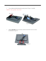
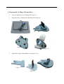
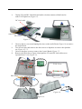
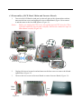
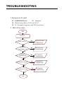
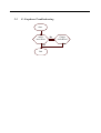
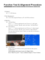
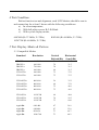
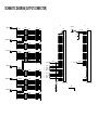
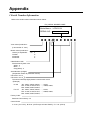
1
PART NO. 599910617 SERVICE MANUAL COLOR MONITOR LCD1511M (UK)/(CE) Model Series 758 NEC-MITSUBISHI ELECTRIC VISUAL SYSTEMS CORPORATION NOVEMBER 2002 200212 08E01ABM 08E02ABM WARNING The SERVICE PERSONNEL should have the appropriate technical training, knowledge and experience necessary to: • Be familiar with specialized test equipment, and • Be careful to follow all safety procedures to minimize danger to themselves and their coworkers. To avoid electrical shocks, this equipment should be used with an appropriate power cord. This equipment utilized a micro-gap power switch. Turn off the set by first pushing power switch. Next, remove the power cord from the AC outlet. To prevent fire or shock hazards, do not expose this unit to rain or moisture. This symbol warns the personnel that un-insulated voltage within the unit may have sufficient magnitude to cause electric shock. This symbol alerts the personnel that important literature concerning the operation and maintenance of this unit has been included. Therefore, it should be read carefully in order to avoid any problems. PRODUCT SAFETY CAUTION 1. When parts replacement is required for servicing, always use the manufacturer's specified replacement. 2. When replacing the component, always be certain that all the components are put back in the place. 3. As for a connector, pick and extract housing with fingers properly since a disconnection and improper contacts may occur, when wires of the connector are led. 4. Use a proper screwdriver. If you use screwdriver that does not fit, you may damage the screws. CONTENTS Page No. USER'S MANUAL -------------------------------------------------------------------- 1-1 MECHANICAL CONSTRUCTION ------------------------------------------------ 2-1 DISASSEMBLY ----------------------------------------------------------------------- 3-1 TROUBLESHOOTING --------------------------------------------------------------- 4-1 ALIGNMENT PROCEDURE ---------------------------------------------------------- 5-1 DDC KEY-IN PROCEDURE -------------------------------------------------------- 6-1 LCD SPECIFICATION --------------------------------------------------------------- 7-1 BLOCK DIAGRAM ------------------------------------------------------------------- 8-1 SCHEMATIC DIAGRAMS ---------------------------------------------------------- 9-1 REPLACEMENT PARTS LIST --------------------------------------------------- 10-1 APPENDIX ------------------------------------------------------------------------------ 11-1 User’s Manual LCD1511M User’s Manual Bedienerhandbuch Manual del usuario Manuel Utilisateur Manuale utente Table of Contents English Recommended Use .............................................................................2 Safety Precautions and Maintenance ............................................. 2 Introduction .......................................................................................... 4 About the Product ........................................................................... 4 Package Overview ..........................................................................5 Declaration of the Manufacturer .......................................................... 5 Installation ........................................................................................... 6 Product Overview ........................................................................... 6 VESA Mount on your monitor ......................................................... 7 User Controls ......................................................................................9 Front Panel Controls .......................................................................9 How to Use the OSD Menus ......................................................... 10 On-Screen Display Menus ............................................................ 10 Appendix ........................................................................................... 12 Troubleshooting ............................................................................ 12 Warning Signal ............................................................................. 13 Product Dimensions ..................................................................... 14 Compatibility Modes ..................................................................... 15 TCO’99 .............................................................................................. 80 FCC Statement .................................................................................. 82 1 – User’s Manual Recommended Use FOR OPTIMUM PERFORMANCE, PLEASE NOTE THE FOLLOWING WHEN SETTING UP AND USING THE LCD COLOR MONITOR: • DO NOT OPEN THE MONITOR. There are no user serviceable parts inside and opening or removing covers may expose you to dangerous shock hazards or other risks. Refer all servicing to qualified service personnel. • Do not spill any liquids into the cabinet or use your monitor near water. • Do not insert objects of any kind into the cabinet slots, as they may touch dangerous voltage points, which can be harmful or fatal or may cause electric shock, fire or equipment failure. • Do not place any heavy objects on the power cord. Damage to the cord may cause shock or fire. • Do not place this product on a sloping or unstable cart, stand or table, as the monitor may fall, causing serious damage to the monitor. • Do not place any objects onto the monitor and do not use the monitor outdoors. • The inside of the flourescent tube located within the LCD monitor contains mercury. Please follow the bylaws or rules of your municipality to dispose of the tube properly. Immediately unplug your monitor from the wall outlet and refer servicing to qualified service personnel under the following conditions: • When the power supply cord or plug is damaged. • If liquid has been spilled, or objects have fallen into the monitor. • If the monitor has been exposed to rain or water. • If the monitor has been dropped or the cabinet damaged. • If the monitor does not operate normally by following operating instructions. • Do not bend power cord. • Do not use monitor in high temperatured, humid, dusty, or oily areas. • If monitor or glass is broken, do not come in contact with the liquid crystal and handle with care. • Allow adequate ventilation around the monitor so that heat can properly dissipate. Do not block ventilated openings or place the monitor near a radiator or other heat sources. Do not put CAUTION anything on top of monitor. • The power cable connector is the primary means of detaching the system from the power supply. The monitor should be installed close to a power outlet which is easily accessible. • Handle with care when transporting. Save packaging for transporting. LCD1511M – 2 English Safety Precautions and Maintenance English Recommended Use - continued • Image Persistence: Image persistence is when a residual or “ghost” image of a previous image remains visible on the screen. Unlike CRT monitors, LCD monitors’ image persistence is not permanent, but constant images being displayed for a long period of time should be avoided. To alleviate image persistence, turn off the monitor for as long as the previous image was displayed. For example, if an image was on the monitor for one hour and a residual image remains, the monitor should be turned off for one hour to erase the image. NOTE: As with all personal display devices, NEC-Mitsubishi Electronics DisplayEurope recommends using a moving screen saver at regular intervals whenever the screen is idle or turning off the monitor when not in use. • • • • • • • • • • • • CORRECT PLACEMENT AND ADJUSTMENT OF THE MONITOR CAN REDUCE EYE, SHOULDER AND NECK FATIGUE. CHECK THE FOLLOWING WHEN YOU POSITION THE MONITOR. For optimum performance, allow 20 minutes for warm-up. Adjust the monitor height so that the top of the screen is at or slightly below eye level. Your eyes should look slightly downward when viewing the middle of the screen. Position your monitor no closer than 40 cm and no further away than 70 cm from your eyes. The optimal distance is 50 cm. Rest your eyes periodically by focusing on an object at least 6 m away. Blink often. Position the monitor at a 90° angle to windows and other light sources to minimize glare and reflections. Adjust the monitor tilt so that ceiling lights do not reflect on your screen. If reflected light makes it hard for you to see your screen, use an anti-glare filter. Clean the LCD monitor surface with a lint-free, non-abrasive cloth. Avoid using any cleaning solution or glass cleaner! Adjust the monitor ’s brightness and contrast controls to enhance readability. Use a document holder placed close to the screen. Position whatever you are looking at most of the time (the screen or reference material)directly in front of you to minimize turning your head while you are typing. Avoid displaying fixed patterns on the monitor for long periods of time to avoid image persistence (after-image effects). Get regular eye checkups. Ergonomics To realize the maximum ergonomics benefits, we recommend the following: • Use the preset Size and Position controls with standard signals • Use the preset Color Setting • Use non-interlaced signals with a vertical refresh rate between 60 - 75 Hz • Do not use primary color blue on a dark background, as it is difficult to see and may produce eye fatigue to insufficient contrast 3 – User’s Manual Introduction This 15” flat panel screen with an active matrix, thin-film transistor (TFT), liquid crystal display (LCD). The monitor features include: • • Direct Analog signal input • 1024 x 768 resolution • 15” viewable display area • 31.5 ~ 60 kHz horizontal scan • 56 ~ 75 Hz refresh rate • VESA wall mountable, foldable stand for flexible mounting solutions • Auto-adjustment function • Foldable stand design brings users the conveniences for easy storage and VESA Mounting applications • Multilingual OSD user controls • VESA DPMS power saving • Built-in speakers for multimedia application • Kensington security lock slot Active matrix TFT LCD technology LCD1511M – 4 English About the Product English Package Overview Power Adapter Power Cord LCD Display LCD1511M User’s Manual Bedienerhandbuch Manual del usuario Manuel Utilisateur Manuale utente Audio-In Cable CD ROM User’s Manual Declaration of the Manufacturer We hereby certify that the monitor LCD1511M is in compliance with Council Directive 73/23/EEC: – EN 60950 Council Directive 89/336/EEC: – EN 55022 – EN 61000-3-2 – EN 61000-3-3 – EN 55024 5 – User’s Manual and marked with: NEC-Mitsubishi Electric Visual Systems Corporation 4-13-23, Shibaura, Minato-Ku Tokyo 108-0023, Japan Installation English Product Overview Front View LCD Display Panel Controls Speakers Stand Rear View Audio Connector Headphone Audio-In Kensington Lock VGA Cable Power Connector LCD1511M – 6 English VESA Mount on your monitor This monitor conforms to the VESA Flat Panel Mounting Physical Mounting Interface Standard which defines a physical mounting interface for flat panel monitors, and corresponding standards for flat panel monitor mounting devices, such as wall and table arms. The VESA mounting interface is located on the back of your monitor. To mount the monitor on a swing arm or other mounting fixture, follow the instruction included with the mounting fixture to be used. Two VESA Mounting Interfaces are included in this model; one is located behind the monitor (see figure 1), and the other is located under the foldable stand. (See figure 2.) Slots (Figure 1) 75 mm VESA Mounting Interface 75 mm (Figure 2) 75 mm VESA Mounting Interface Caution! Slots 75 mm Please select the proper screws! The depth from plastic back cover to the bottom of the screw hole is 8 mm. The spec is M4 screw. To fulfil the safety requirements the monitor must be mounted to an arm which guarantees the necessary stability under consideration of the weight of the monitor. The LCD monitor shall only be used with an approved arm (e.g. GS mark). 7 – User’s Manual Connecting the Display (Figure 8.1) 1. Make sure that the entire equipment is turned off. 2. Connect one end of the power adapter to the power connector; plug one end of the AC power cord into the power adapter, and then the other end into an electrical outlet (1). 3. Connect the VGA signal cable to the 15-pin connector of your host computer and tighten the screws (2). 4. Connect the Audio-In cable from audio input port of your display to the Audioout port of your computer (3). 5. Connect your headphone to the Headphone port (4). 6. Turn on your computer and display. Figure 8.1 (4) Headphone (optional) (3) Audio-In cable (1) Power Adapter & Power Cord (2) VGA Cable Notice: To ensure the LCD display can work well with your computer, please configure the display mode of your graphic card to make it less than or equal to 1024 x 768 resolution and make sure timing of the display mode is compatible with the LCD display. We have listed the "Compatibility Modes" of this LCD display in appendices for your reference. LCD1511M – 8 English To set up this display, please refer to the following figure and procedures. User Controls English Front Panel Controls (4) (1) No. / Icon Display the OSD menus. M Menu Button S Select /Auto (3) Power (4) Power LED (6) + (5) Function (1) – (3) Control (2) (5) (2) 1. Minus / 2. Brightness 1. Plus / 2. Mute On/Off 9 – User’s Manual (6) 1. To select the adjustment items from OSD menus. 2. To activate the “Auto Adjustment” function to obtain an optimum image. Switch on/off the power of the LCD display. 1. Green indicates the display is turned on. 2. Amber indicates the display is in power-saving mode. 1. Decrease value of the adjustments items. 2. Adjust the brightness of image. 1. Increase value of the adjustment items. 2. Make the volume function Ineffective/effective. 1. Press the "M" button to display the OSD Menus. Press the "S" button to move between the OSD Menus. Press "M" to enter the function to be adjusted and then press "S" to move between setting options. 2. Adjust the value of the option by pressing "–" and "+". Press "S" to confirm your choice. 3. To exit the OSD Menus, move to Exit and press "M". On-Screen Display Menus First OSD Menu: • Auto-Adjustment Choose this function to obtain an optimum image. • Contrast This function allows you to adjust the image crispness. Contrast adjusts the difference between white and black shades. • Horizontal Position Changes the horizontal position of the image. • Vertical Position Changes the vertical position of the image. • Frequency Changes the display data frequency to match the frequency of your graphic card. When you are experiencing vertical flickering bar, use this function to make an adjustment. • Tracking Synchronizes the signal timing of the display to that of the graphic card. When you are experiencing unstable to flickering image, use this function to make an adjustment. LCD1511M – 10 English How to Use the OSD Menus On-Screen Display Menus – continued English Second OSD Menu: • Display Mode The display mode shows the display resolution, horizontal scan frequency, vertical refresh of the current mode. • OSD Off-Time Adjusts the time period for OSD menu disappear. • Language You are able to select the language of all menu items. • Text-Graphic Toggles between VGA text mode (mode M03H) and graphic mode (mode M13H). • Reset Returns the display parameters of the current mode to its factory default settings. Third OSD Menu: • Volume It allows you to control the volume sound. • Mute It allows you to disable the sound immediately. Fourth OSD Menu: • Color Setting Adjusts the color temperature. • Color Adjustment-Red It allows you to adjust the red color of the display. • Color Adjustment-Green It allows you to adjust the green color of the display. • Color Adjustment-Blue It allows you to adjust the blue color of the display. 11 – User’s Manual Appendix If you are experiencing trouble with the LCD display, refer to the following. If the problem persists, please contact your local dealer or our service center. Problem: No image appears on screen. • Check that all the I/O and power connectors are correctly and well connected as described in the "Installation" section. • Make sure the pins of the connectors are not crooked or broken. Problem: Partial image or incorrectly displayed image. • Check to see if the resolution of your computer is higher than that of the LCD display. • Reconfigure the resolution of your computer to make it less than or equal to 1024 x 768. Problem: Image has vertical flickering line bars. • Use "Frequency" to make an adjustment. • Check and reconfigure the display mode of the vertical refresh rate of your graphic card to make it compatible with the LCD display. Problem: Image is unstable and flickering. • Use "Tracking" to make an adjustment. Problem: Image is scrolling. • Check and make sure the VGA signal cable (or adapter) is well connected. • Check and reconfigure the display mode of the vertical refresh rate of your graphic card to make it compatible with the LCD display. Problem: Vague image (characters and graphics). • Use "Frequency" to make an adjustment. If this problem still exists, use "Tracking" to make an adjustment. LCD1511M – 12 English Troubleshooting English Appendix – continued Warning Signal Sometimes you probably will see the warning messages from this LCD screen. This means that the LCD display cannot exactly receive the signal from the computer graphic card. There are three kind of situations that may happen. Please check the connected cables or contact your local dealer for more information. • No Signal This message means that the LCD display has been powered on but it cannot receive any signal from the computer graphic card. Check all the power switches, power cables, and VGA signal cable. • Going to Sleep This message means that the LCD display is under the power saving mode. In addition, the LCD display will go to this sleeping mode when experiencing a sudden signal disconnecting problem. • Out of Range This message means that the signal of the computer graphic card is not compatible with the LCD display. When the signal is not included in the compatibility mode we have listed in the Appendices of this manual, the LCD will display this message. 13 – User’s Manual Product Dimensions 346 mm/13.6” English Front View 341.2 mm/13.43” Side View 41.9 mm/1.65” Top View 171 mm/6.73” LCD1511M – 14 Mode Resolution V. Frequency (Hz ) H. Frequency (kHz ) IBM VGA 640 x 350 70 31.5 IBM VGA 640 x 400 70 31.5 IBM VGA 640 x 480 60 31.5 IBM VGA 720 x 400 70 31.5 VESA VGA 640 x 480 72 37.9 VESA VGA 640 x 480 75 37.5 VESA SVGA 800 x 600 56 35.2 VESA SVGA 800 x 600 60 37.9 VESA SVGA 800 x 600 72 48.1 VESA SVGA 800 x 600 75 46.9 VESA XGA 1024 x 768 60 48.4 VESA XGA 1024 x 768 70 56.5 VESA XGA 1024 x 768 75 60.0 Apple GA 640 x 480 67 34.9 Apple GA 640 x 480 67 35.0 Apple GA 832 x 624 75 49.7 Apple GA 1024 x 768 75 60.2 15 – User’s Manual English Compatibility Modes TCO’99 LCD1511M Congratulations! You have just purchased a TCO’99 approved and labeled product! Your choice has provided you with a product developed for professional use. Your purchase has also contributed to reducing the burden on the environment and also to the further development of environmentally adapted electronics products. Why do we have environmentally labelled computers? In many countries, environmental labelling has become an established method for encouraging the adaptation of goods and services to the environment. The main problem, as far as computers and other electronics equipment are concerned, is that environmentally harmful substances are used both in the products and during the manufacturing. Since it has not been possible for the majority of electronics equipment to be recycled in a satisfactory way, most of these potentially damaging substances sooner or later enter Nature. There are also other characteristics of a computer, such as energy consumption levels, that are important from the viewpoints of both the work (Internal) and natural (external) environments. Since all methods of conventional electricity generation have a negative effect on the environment (acidic and climate-influencing emissions, radioactive waste, etc.), it is vital to conserve energy. Electronics equipment in offices consume an enormous amount of energy since they are often left running continuously. What does labelling involve? This product meets the requirements for the TCO’99 scheme which provides for international and environmental labelling of personal computers. The labelling scheme was developed as a joint effort by the TCO (The Swedish Confederation of Professional Employees), Svenska Naturskyddsforeningen (The Swedish Society for Nature Conservation) and Statens Energimyndighet (The Swedish National Energy Administration). The requirements cover a wide range of issues: environment, ergonomics, usability, emission of electrical and magnetic fields, energy consumption and electrical and fire safety. The environmental demands concern restrictions on the presence and use of heavy metals, brominated and chlorinated flame retardants, CFCs (freons) and chlorinated solvents, among other things. The product must be prepared for recycling and the manufacturer is obliged to have an environmental plan which must be adhered to in each country where the company implements its operational policy. The energy requirements include a demand that the computer and/or display, after a certain period of inactivity, shall reduce its power consumption to a lower level in one or more stages. The length of time to reactivate the computer shall be reasonable for the user. Labelled products must meet strict environmental demands, for example, in respect of the reduction of electric and magnetic fields, physical and visual ergonomics and good usability. LCD1511M – 80 TCO’99 Environmental Requirements Flame retardants Flame retardants are present in printed circuit boards, cables, wires, casings and housings. In turn, they delay the spread of fire. Up to thirty percent of the plastic in a computer casing can consist of flame retardant substances. Most flame retardants contain bromine or chloride and these are related to another group of environmental toxins, PCBs, which are suspected to give rise to severe health effects, including reproductive damage in fisheating birds and mammals, due to the bioaccumulative* processes. Flame retardants have been found in human blood and researchers fear that disturbances in foetus development may occur. TCO’99 demand requires that plastic components weighing more than 25 grams must not contain flame retardants with organically bound chlorine and bromine. Flame retardants are allowed in the printed circuit boards since no substitutes are available. Lead** Lead can be found in picture tubes, display screens, solders and capacitors. Lead damages the nervous system and in higher doses, causes lead poisoning. TCO’99 requirement permits the inclusion of lead since no replacement has yet been developed. Cadmium** Cadmium is present in rechargeable batteries and in the colourgenerating layers of certain computer displays. Cadmium damages the nervous system and is toxic in high doses. TCO’99 requirement states that batteries, the colourgenerating layers of display screens and the electrical or electronics components must not contain any cadmium. Mercury** Mercury is sometimes found in batteries, relays and switches, Mercury damages the nervous system and is toxic in high doses. TCO’99 requirement states that batteries may not contain any Mercury. It also demands that no mercury is present in any of the electrical or electronics components associated with the display unit. CFCs (freons) CFCs (freons) are sometimes used for washing printed circuit boards. CFCs break down ozone and thereby damage the ozone layer in the stratosphere, causing increased reception on Earth of ultraviolet light with consequent increased risks of skin cancer (malignant melanoma). The relevant TCO’99 requirement; Neither CFCs nor HCFCs may be used during the manufacturing and assembly of the product or its packaging. * Bio-accumulative is defined as substances which accumulate within living organisms. ** Lead, Cadmium and Mercury are heavy metals which are Bio-accumulative. To obtain complete information on the environmental criteria document, order from: TCO Development Unit SE-114 94 Stockholm SWEDEN FAX Number: +46 8 782 92 07 E-mail (Internet): [email protected] You may also obtain current information on TCO’99 approved and labelled products by visiting their website at: http://www.tcodevelopment.com 81 FCC Information 1. Use the attached specified cable with the LCD1511M color monitor so as not to interfere with radio and television reception. (1) Please use the supplied power cord or equivalent to ensure FCC compliance (2) Please use the supplied AC Adapter. (3) Please use the supplied Audio Cable. Use of other cables and adapters may cause interference with radio and television receiption. 2. This equipment has been tested and found to comply with thie limits for a Class B digital device, pursuant to part 15 of the FCC Rules. These limits are designed to provide reasonable protection against harmful interference in a residential installtion. This equipment generates, uses, and can radiate radio frequency energy, and if not installed and used in accordance with the instructions, may cause harmful interference to radio communications. However, there is no guarantee that interference will not occur in a particular installation. If this equipment does cause harmful interference to radio or television reception, which can be determined by turning the equipment off and on, the user is encouraged to try to correct the interference by one or more of the following measures: w Reorient or relocate the receiving antenna. w Increase the separation between the equipment and receiver. w Connect the equipment into an outlet on a circuit different from that to which the receiver is connected. w Consult your dealer or an experienced radio/TV technician for help. If necessary, the user should contact the dealer or an experienced radio/television technician for additional suggestions. The user may find the following booklet, prepared by the Federal Communications Commission, helpful: How to Identify and Resolve Radio-TV Interference Problems. This booklet is available from the U.S. Government Printing Office, Washington, D.C., 20402, Stock No. 004-000-00345-4. DECLARATION OF CONFORMITY This device complies with Part 15 of FCC Rules. Operation is subject to the following two conditions. (1) This device may not cuase harmful interference, and (2) this device must accept any interference received, including interference that may cause undesired operation. U.S. Responsible Party: NEC-Mitsubishi ElectronicsDisplay of America, Inc. Address: 1250 North Arlington Heights Road, Suite 500 Tel. No.: Itasca, Illinois 60143-1248 (630) 467-3000 Type of Product: Equipment Classification: Model: Display Monitor Class B peripheral LCD1511M we hereby declare that the equipment specified above conforms to the technical standards as specified in the FCC Rules. Windows is a registered trademark of Microsoft Corporation. NEC is a registered trademark of NEC Corporation. ENERGY STAR® is a U.S. registered trademark. All other brands and product names are trademarks or registered trademarks of their respective owners. As an ENERGY STAR® partner, NEC-Mitsubishi Electronics Display of America has determined that this product meets the Energy Star guidelenes for energy efficiency. The ENERGY STAR emblem does not represent EPA endorsement of any product or service. LCD1511M - 82 Printed on recycling paper Printed in China 36.59106.001 Rev.A Mechanical Construction 1. Package overview AUDIO CABLE (6) TAPE POWER CABLE (7) PE BAG Adhesion on HDPE bag outside CUSHION R (2) TAPE USER'S MAMUAL (9) SET UP SHEET (10) LCD MONITOR (5) HDPE BAG (8) ADAPTER (4) CUSHION L (3) FRONT CARTON LABEL CARTON (1) 1.1 Replacement Part List Item P/N Description 1 55.59101.021 CARTON AB(A%)-16 428*98*455 LCD1511M 2 56.59101.001 CUSHION-R EPS PV758A 3 56.59102.001 CUSHION-L EPS PV758A 4 47.59101.001 ADAPTER IN:100-240V OUT:12V/2.5A;FOR NMV;"L 5 DC.59101.021 D.C. LCD1511M,HANNSTAR,CP02,AUDIO 6 42.59903.002 CABLE AUDIO 1.8M FOR PC99+MARK 7 42.53506.001 CABLE POWER-CORD AC SP60+AS14 1.8M BLACK PV (UK ver Only) 7 42.50112.001 CABLE POWER CORD 1830mm SP-023+IS14 EUR. (CE ver Only) 8 51.59103.001 PE BAG HDPE 390*600*0.04t PV758 "NMV" 9 36.59106.002 USER'S MAMUAL LCD1511M(CD-ROM),UK(w/WWARRANT (UK ver Only) 9 36.59106.003 USER'S MANUAL LCD1511M(CD-ROM),EUROPE,W/SAL (CE ver Only) 10 36.59105.001 SET UP SHEET LCD1511M 2. Exploded Overview 2.1 Replacement Part List Item P/N Description 1 42.59102.001 CABLE DC JACK to 5P HOUSING 1-CORE PV758A 2 42.59103.001 CABLE VGA 15P to 13P 1-CORE PV758A 3 44.59101.001 PCBA INVERTER PLCD2815202A-REV1 FOR NMV 4 48.59102.001 TFT LCD 15" XGA HANNSTAR HSD150SX84-A 5 49.59901.003 ASS'Y SPEAKER POD 8Ω PV890C 6 51.55311.001 SR LOCKER N66+V2/N PV755ASIP 7 75.59101.021 ASSY FRONTCOVER PC+ABS VS07 LCD1511M 8 51.59111.003 BASE PC+ABS-CP02 PV758A 9 51.59112.003 DRAW PLATE PC+ABS-CP02 PV758A 10 61.59101.001 REAR BUCKET SECC 1t PV758A 11 61.59102.001 R-HOLDER SECC 1t PV758A 12 61.59103.001 L-HOLDER SECC 1t PV758A 13 61.59111.003 ASSY HINGE TILT PV758A 14 80.59101.011 PCBA MAIN BD FOR LCD1511M 15 80.59102.011 PCBA AUDIO BD LCD1511M "NMV" 16 80.59103.001 PCBA CTRL BD PV758A 17 85.1F125.060 SCREW PAN MECH W/SF M2.5*6 Ni 18 85.1F122.060 SCREW PAN MECH W/SF M2*6 Ni 19 85.1F123.100 SCREW PAN MECH W/SF M3*10 Ni 20 85.1F323.080 SCREW PAN MECH W/SF M3*8 BLACK 21 85.UA123.080 DOUBLE THREADS SCREW PAN TAP M3*8 Ni 22 85.AA323.060 SCREW PAN TAPPING M3*6 BLACK 23 85.YA323.080 SCREW FLAT TAP M3*8 BLACK 24 51.56504.001 SELECT KNOB PC+ABS\VS07 PV920 25 51.56505.001 LED LENS PMMA PV920 26 52.56101.001 RUBBER FOOT PG-GF-20A-R1B 20*20*1.5t 27 35.59103.001 Rating Label LCD1511M 28 41.80301.001 EMI CORE-A5-FS-31*5*12-1.0 EzPro 550A 29 42.59101.002 FFC 40P 28mm FOR HANNSTAR PANEL PV758A 30 61.59701.002 M/B SPACER 3mm Cu-Ni PV755ASIP/PV758A 31 42.59104.001 W.A. 12/10P UL1571 #28 PV758A 32 42.59701.001 W.A. 8P UL1571 #28 180mm PV758A/PV755ASIP 33 42.57702.002 W.A. 10P/5P UL1007 #24 100mm PV755A DISASSEMBLY Procedure of Disassembly This section provides disassembly procedures for 15 Flat Panel Monitor with XGA resolution (1024*768) TFT LCD. Before you begin any of these procedures, be sure to turn off the power, computer system, and other attached devices; then disconnect the power cable from the electronically outlet. Moreover, when you disassemble the monitor, be sure to put the screws in a safe place and separate them according to grouping. 1 Disassembly of Stand Unit from Monitor 1. Make LCD1511M face down as figure 1, and put your hands to lift the stand up as figure 2. Figure 1 Figure 2 2. Use your hand to pull the Stand unit toward yourself (Figure 3) carefully. NOTICE: Dont pull the Draw Plate. Draw Plate Figure 3 3. Make LCD1511M monitor face down, and unscrew the four screws to remove the Stand unit. (Figure 4) Figure 4 2 Disassembly of Hinge Tilt and Base 1. Unscrew the two screws of Hinge Tilt (Figure 5). 2. Open the join to separate Base and Hinge Tilt (Figure 6). Figure 5 3. Figure 6 Draw Plate, Hinge Tilt and Base are as figure 7, 8, 9. Figure 7 Figure 9 Figure 8 3 Disassembly of Front Cover, Rear Cover, Control and Audio Boards 1. Unscrew the two screws of Rear cover. Make the monitor unit face up, pull the latches out between Front cover and Rear cover (Figure10). 2. Pull the latches out between Monitor unit two sides to lift up the Front Cover (Figure 11). Figure 10 Screw Figure 11 3. Unplug Control wire (Figure 12), push Front cover out (Figure 13). In compliance with the direction to lift up Front Cover (Figure 14). Unscrew the four screws of LCD panel. Figure 12 Figure 13 Screw Figure 14 Screw 4. Unplug VGA and DC Jack cables and audio wire that connect to Main board to remove LCD panel set (Figure 15). DC Jack cable Audio wire VGA cable Figure 15 5. 6. 7. 8. Unscrew the two screws and unplug the wires on the Audio Board (Figure 16) to remove the Audio Board. Tear off two tapes and unscrew the four screws on Speakers to remove the Speakers set (Figure 16, 17). Unscrew the three screws to remove the Control Board (Figure 17). Remove the SR locker as Figure 18 and pull the VGA and DC Jack cables out to separate Rear Cover (Figure 19). Audio Board Tapes SR lockers Front Cover Figure 16 Figure 17 Figure 19 Figure 18 4 Disassembly of LCD Panel, Main and Inverter Boards 1. Turn over the LCD Panel set and put it on the safe place with a foam-rubber cushion, unscrew the four screws and unplug all wires on Main Board (Figure 20) to remove it and then remove the four M/B Spacers (Figure 21). Notice: Before you unplug the FFC wires, tear off the tape on FFC wire first. Then open the connector caps on panel carefully. Pull out the connectors caps on Main Board carefully (Figure 20). Main Board Figure 20 FFC wires Figure 21 2. Unplug all wires on inverter board and unscrew the four screws to remove the left and right holders (Figure 22). 3. Unscrew the two screws on Inverter Board to remove Inverter Board (Figure 23). Right Holder Figure 23 Left Holder Figure 22 LCD Panel TROUBLESHOOTING Troubleshooting Procedure 1 Equipment Needed q LCD1511M Machine q Earphone q Philips Screw Driver #101 and #107 q PC (Personal Computer) with XGA resolution 2 Main Procedure Start Power-on Power LED ok ? No A. Power Circuit Troubleshooting No B. Performance Troubleshooting No C. Function Troubleshooting No D. Speakers Troubleshooting Yes Is display performance ok ? Yes Is function adjustment ok ? Yes Are Speakers all right? Yes Is Earphone all right ? Yes End No E. Earphone Troubleshooting 2.1 A. Power Circuit Troubleshooting Start Change AC/DC Adapter No Change Main Board Yes Yes End 2.2 B. Performance Troubleshooting Start Is screen black ? Yes No Is screen white ? No 1 No Yes Yes Yes Change Main Board Yes Change Main Board No Change Main Board Yes No Change LCD Panel Yes Change LCD Panel Yes Yes Yes Replace/Change No FPC Cable No Abnormal Color ? Change Inverter Board No Change LCD Panel Yes 1 Is screen scrolling ? Yes No Is screen flickering ? Yes Yes Yes No End Adjust Freq. Tracking or Auto Adjustment Change LCD Panel Change Inverter Board Yes Adjust Freq. Tracking or Auto Adjustment Yes No Change LCD Panel Change Main Board Yes Check the Compatibility on the computer Yes Feedback info. to Coretronic Change Main Board Yes Yes Connect VGA No cable to the PC directly Yes No Yes Yes Yes Change LCD Panel Yes Yes No Ghost image ? No Yes No Have line bar or noise? Change Main Board Change Main Board Yes Yes No Bad Uniformity ? No Yes No Is LCD line defective ? Change VGA Cable No 2.3 C. Function Troubleshooting Start Change Control Board No Change Main Board Yes Yes End 2.4 D. Speakers Troubleshooting Start Change Speakers Yes End No Change Main Board Yes No Change Audio Board Yes 2.5 E. Earphone Troubleshooting Start Change Main Board Yes End No Change Audio Board Yes Function Test & Alignment Procedure Function Test & Alignment Procedure 1 Product q 15 LCD Monitor 2 Test Equipment: q Color Video Signal & Pattern (or PC with XGA resolution) 3 Hot Key: q q q All Mode Reset: Press +, - buttons simultaneously and Power on with signal, hold on for 3 seconds. Then the screen will show All Mode Reset. Burn In Mode: Press +, - buttons simultaneously and Power on without signal, hold on for 3 seconds. Then the screen will show Burn In Mode. Press any button besides power button, you can find the information about this monitor. White Balance: Set the screen on 640*480 resolution pure black and white pattern, no other color. OSD is displayed and cursor is moved to Display Mode. Press "Menu" key and "-" key is continued, and press "Power" button. 4 Test Condition: Before function test and alignment, each LCD Monitor should be run-in and warmed-up for at least 2 hours with the following conditions: a). In room temperature, b). With full-white screen, R.G.B. Black c). With cycled display modes, 640*480 (H=37.5kHz, V=75Hz) 1024*768 (H=60.0kHz, V=75Hz) 800*600 (H=46.9kHz, V=75Hz) 5 Test Display Modes & Pattern 5.1 Compatible Modes Standrad Resolution Vertical Horizontal Refresh(Hz) Scan(kHz) IBM VGA IBM VGA IBM VGA IBM VGA VESA VGA VESA VGA 640*350 640*400 720*400 640*480 640*480 640*480 70 70 70 60 72 75 31.5 31.5 31.5 31.5 37.9 37.5 VESA SVGA VESA SVGA VESA SVGA VESA SVGA 800*600 800*600 800*600 800*600 56 60 72 75 35.2 37.9 48.1 46.9 VESA XGA VESA XGA VESA XGA 1024*768 1024*768 1024*768 60 70 75 48.4 56.5 60.0 Apple GA Apple GA Apple GA Apple GA 640*480 640*480 832*624 1024*768 67 67 75 75 34.9 35.0 49.7 60.2 5.2 Function Test Display Pattern It em Test Cont ent Pat t ern Speci fi cat i on Remark 1 Frequency & Tracking Fine Line Moire Eliminate visual wavy noise. Figure 1 2 Contrast/Brightness 16 Gray Scale 16 gray levels should be distinguishable. Figure 2 3 Boundary Horz. and Vert. position of video shuld Horizontal & Vertical be adjustable to be within the screen Thickness frame. Figure 3 4 R,G,B, Color Performance R.G.B Color Intensities Contrast of each R,G,B, color should be normal. Figure 4,5,6 5 Screen Uniformity & Flicker Full White Should be compliant with the spec. Fgure 7 6 Dead Pixel/Line White Screen Dark Screen The numbers of dead pixels should be compliant with the spec. Figure 8 7 White Balance White & Black Pattern The screen must have the pure white and black pattern, no other color. Figure 9 Fine Line Morie Pattern (Figure 1) Horizontal & Vertical Thickness Pattern (Figure 3) Gray Scale Pattern (Figure 2) R. Color Pattern (Figure 4) G. Color Pattern (Figure 5) B. Color Pattern (Figure 6) Full White Pattern (Figure 7) Dark Screen Pattern (Figure 8) Black-White Pattern (Figure 9) 6 Function Test and Alignment Procedure 6.1 All Modes Reset You should do All Mode Reset (Refer to Chapter 3) first. This action will allow you to erase all end-users settings and restore the factory defaults. 6.2 Auto Adjustment Please select and enter Auto Adjustment function on Main Menu or press Auto button on the select knob to see if it is workable. The Auto Adjustment function is aimed to offer a better screen quality by built-in ASIC. For optimum screen quality, the user has to adjust each function manually. 6.3 DDC Test Pattern: Burn In Mode (Refer to Chapter 3) v Make sure the model name is correct. 6.4 Tracking and Frequency Test Signal: 1024*768@75Hz Test Pattern: Line Moire Pattern v Check and see if the image has noise and focus performs well. eliminate visual line bar. v If not, readjust by the following steps : (a) Select and enter Tracking function on Image Screen to adjust the image to eliminate visual wavy noise. (b) Then, select and enter Frequency function to adjust the image to eliminate visual line bar. 6.5 Boundary Test Signal : 1024*768@75Hz Test Pattern : Horizontal & Vertical Line Thickness Pattern v Check and see if the image boundary is within the screen frame. v If not, readjust by the following steps : (a) Select and enter Image screen function on OSD Main Menu. (b) Then, select and enter Horizontal Position and Vertical Position function to adjust the video boundary to be full scanned and within screen frame. 6.6 White Balance Test Signal : 640*480@60Hz Test Pattern: Full White and Black Pattern v Refer to Chapter 3 6.7 R,G,B, Colors Contrast Test Signal: 1024*768@75Hz Test Pattern: R,G,B Color Intensities Pattern and 16 Gray Scale Pattern v Check and see if each color is normal and distinguishable. v If not, please return the unit to repair area. 6.8 Screen Uniformity and Flicker Test Signal: 1024*768@75Hz Test Pattern: Full White Pattern v Check and see if it is in normal condition. 6.9 Dead Pixel and Line Test Signal: 1024*768@75Hz Test Pattern: Dark and White Screen Pattern v Check and see if there are dead pixels on LCD panel. v The total numbers and distance of dead pixels should be compliant with the spec. 6.10 Audio (Optional, depend on Model) Test Signal: Voice signal Test Pattern: liberty v Make sure that Audio function is working without noise. 6.11 Check for Secondary Display Modes Test Signal: 640*350@70Hz; 640*480@60/72/75Hz; 720*400@70Hz; 800*600@56/60/72/75Hz; 1024*768@60/70/75Hz; v Normally when the primary mode 1024*768@75Hz is well adjusted and compliant with the specification, the secondary display modes will be great possibile to be compliant with the spec. But we still have to check with the general test pattern to make sure every secondary is compliant with the specification. 6.12 All Modes Reset After final QC step, we have to erase all saved changes again and restore the factory defaults. You should do All Mode Reset (Refer to Chapter 3) again. 7 Cleaning Please use non-alcohol cleanser to clean LCD panel and cosmetics material with soft cotton. 8 Inspection Standard Y Appearance Inspection: Scratches/Abrasions a.) Mechanical: Face A: Not Acceptance Figure 1: Face A View Face B: Length:12.7mm, Width: 0.25mm (2 lines,scrapes) Figure 2: Face B View Face C: Length:76mm Width:0.76mm (2 lines,scrapes) Figure 3: Face C View Face D: Length:89mm Width:0.76mm (2 lines,scrapes) Figure 4: Face D View DDC Key-in Procedure 1. System connection This system should be connected as shown below. DDC Communication I/F BOARD 2. Input signal Horizontal synchronization frequency : Not specified. Vertical synchronization frequency : Not specified. 3. Program Service tool Ver. 3.14 (Parameter ver. 2.0-S5) (Part No. 599910612) 4. Operation 1) Connect the EDID data writing unit with jigs, etc. 2) Copy all the files of the service tool Ver. 3.14 (Parameter ver. 2.0-S5) in a proper directory. 3) Start [Service2.EXE] of the service tool Ver. 3.14. 4) When the screen as shown below appears, give a check to [LCD] of [Monitor Type] and press the [START] button. 5) When the screen as shown below appears, adjust the cursor to [LCD1511M] and make a double click. 6) When the screen as shown below appears, give a check to [EDID_READ] and press the [OK] button. 7) When the screen as shown below appears, confirm that the correct data are displayed in the columns of EDID DATA CONTENTS and Serial information. If all the displayed data are [FF] or the like, or if the serial number is different from that of the corresponding unit, then EDID data writing should be carried out. 8) When a screen of Item 6 is displayed by pressing the [BACK] button, give a check to [EDID_WRITE] and press the [OK] button. 9) When the screen as shown below appears, examine the serial number of the unit, enter an input in the column of [Input Serial No.] through the keyboard, and press the [Input OK] button. Enter an input in the column of [.Year=> ] in manufactured year(A.D. four digits) and [Month=>] in manufactured month through the keyboard, and press the [Input OK] button. 10) When the [WRITE EDID] button is pressed, writing of the EDID data only is carried out. Upon the completion of correct writing, a display of [EDID Monitor Write OK] is presented in the column of [STATUS]. 11) Upon the normal completion of EDID data writing, press the [Exit] button to close the program. 5. EDID data file EDID date: LCD1511M.edi 0 1 2 3 4 5 6 7 8 9 A B C D E F 00 00 FF FF FF FF FF FF 00 38 A3 07 66 00 00 00 00 10 2C 0C 01 03 08 1E 17 78 AA B1 CD 9F 55 4B 99 24 20 1D 50 55 BF EE 00 01 01 01 01 01 01 01 01 01 01 30 01 01 01 01 01 01 C3 1E 00 20 41 00 20 30 10 60 40 13 00 30 E4 10 00 00 1E 00 00 00 FD 00 38 4B 1F 50 3C 08 00 0A 20 20 20 20 20 20 00 00 00 FC 00 4E 60 45 43 20 4C 43 44 31 35 31 31 4D 0A 00 00 00 FF 70 00 32 59 31 30 30 30 30 31 4D 42 0A 20 20 00 BD Note 1: address 10h Week of manufacture = Month of manufacture × 4 Note 2: address 11h Year of manufacture - 1990 Note 3: address 71h ~ 7Dh Serial Number (ASCII coded) If less than 13 char, terminate with 0Ah and fill the rests with 20h. Note 4: address 7Fh Checksum The sum of entire 128 byte shall be equal to 00h. LCD Specification 1. General Information LCD Active matrix thin-film-transistor (TFT) Effective display size 12.0”(H) x 9.0”(V) / 304.1(H) x 228.1(V) mm 15.0” / 38.016 cm. diagonal Pixel number 1024 x 3 (H) x 768 (V) pixels Color filter arrangement R.G.B. vertical stripe Display method Conventional TFT with retardation film, Normally white Drive method Active matrix (Amorphous Si TFT) Dot pitch 0.099(H) x 0.297(V) mm Pixel pitch 0.297(H) x 0.297(V) mm Dot number 1024 x 768 x 3 dots Backlight The backlight system is an edge-lighting type with 2 CCFLs Luminance 250 cd/m^2 (typical: center / all white) Contrast ratio 400:1 (typical.) Display color 16,194,277 colors (6bit/color) (Depend on graphics interface and / or Application) Viewing angle Up 45 deg. / Down 55 deg. / Right 65 deg. / Left 65 deg. (Typical, Contrast ratio > 10 at Ta=25 deg C) Response time (on + off) 35 ms (typical.) Backlight Life Term 30,000 hours (min) , 40,000 hours (typ) (IL=6.0mA, Continuous operation, Ta=25 deg C) 2. Defect, Scratch and Dust Inspection conditions: (a) Viewing distance is approximately 15~50cm (b) Ambient illuminant is from 300 to 500lux. (c) Viewing angle is normal to the LCD panel. (d) Ambient temperature is approximately 25deg C. (e) Input signal clock frequency: 40MHz VISUAL DEFECT ELECTRICAL DEFECT DEFECT TYPE Dark/ Bright Spot Circular Foreign Material Bright or Dark Line Foreign Material Polarizer/ Linear Scratch Polarizer- Bubble/ Peeling Maximum Allowable Defect Count All Types Bright Dot Random Bright Dot – Green Bright Dot – 2 Adjacent Dark Dots – Random Dark Dots – 2 Adjacent Dark Dots – 3 or More adjacent Total Bright and Dark Dots Minimum Distance Between Bright Dots Minimum Distance Between Bright and Dark Dots Minimum Distance Between Dark Dots LIMIT 0.2mm ≤ D ≤ 0.5mm N≤7 0.05mm ≤ W ≤ 0.2mm 0.3mm ≤ L ≤ 3mm, N ≤ 5 0.01mm ≤ W ≤ 0.5mm 1.0mm ≤ L ≤ 10mm, N ≤ 5 Average D ≤ 0.5mm, N ≤ 6 N≤7 N≤4 N≤3 N≤2 N≤6 N≤3 N=0 N≤6 15 mm 10 mm 5 mm 1) D: diameter, W: horizontal width, L: vertical high, N: number 2) Bright dot defect description - Two adjacent 3) Dark dot defect description - Two adjacent 4) Dark dot defect description - Three adjacent 5) Minimum distance between dot defects Bright dot to bright dot Dark dot to dark dot BLOCK DIAGRAM R/G/B D_SUB INPUT ASIC HS/VS MASCOT VZ DDC_IIC DATA BUS RA/GA/BA/RB/GB/BB[2~7] PANEL TCON HannStar VOLUME XTAL 12MHz DDC VH BLON SDA SCL /IRQ EEPROM CPU VL INVERTER VOLUME W78E62B AUDIO SCL SDA AC (110-240V) (50-60Hz) ADAPTER +12V DPMS +12A +5V +3.3V +2.5V OUTPUT EEPROM 24LC16B R 8 ohm L 8 ohm SCHEMATIC DIAGRAM (POWER SUPPER) +12VA L2 1 C5 0.1u TU2001WNR-5P C5 C134 C135 C4 0.1u 0.01u 100p 0.1u SI-8050S +VIN C6 100uF/16V L1 VOUT S.S 1 2 3 4 5 U1 22uH VOS GND L3 C13 GND GND L4 C7 0.1u 5V_MAIN=2.5A D1 1 2 3 4 5 6 7 8 9 10 VCC 22uH 4 0.1u GND VCC-AUDIO 150uH 2 C9 C8 0.1u 1000uF/16V C10 100uF/16V GND GND C15 U2 AIC1084-CM 3 OUT C IN R79 1 TO263 C18 GND 200 1% C19 0.1u 100uF/16V C22 R80 GND L8 NC 100uF/16V GND C132 GND GND GND U10 AIC1084-CM 3 IN OUT VADCA C125 C126 100uF/16V 0.1u TO263 L16 2 0 R91 200 1% R90 C23 C24 0.1u 100uF/16V 330 1% 3A VDD3.3 GND L6 GND GND 0 VCC BE0805 C30 100uF/16V XC6201 VI C31 0.1u VO L10 1 C36 0.1u VADCP BE0805 0.1u C32 C33 0.1u 100uF/16V R81 0 R82 0 VDDCTRL 1 2.2K 0.1u 3,4 R3 3 VDDCTRL 1 R4 1K GND R2 C27 2 C29 1 LCDVDD Q2 MMBT3904 C28 0.1u R5 100K D 3 JP1 R97 0 R98 0 1 2 3 4 USB CNNT GND SYSTEM GND CHASSIS GND B 1 100uF/16V Q1 SI2302DS 100K 0.1u C 3 VCC C26 C25 3 3 4 0.1u VADCP U3 1 2 C14 10uF/25V VADCA GND INV_CTRL BRIGHTNESS 2 L9 GND 2 BE0805 C17 0.1u 1K GND VDD C16 R1 GND 2 VCC L7 0.1u 330 1% 3A BE0805 0.1u VDD3.3 2 100uF/16V On/Off C VCC C3 0.1u INVERTER I/F VCC L5 C2 BRIGHTNESS TU2001WNR-10P IN5822 GND 100uF/16V 1 +12VA +12VA 5 CN1 3 +12VA 22uH C1 CN2 2 E G 1 2 S C34 C35 0.1u 1000uF/16V SCHEMATIC DIAGRAM (MCU & LCD POWER CTRL) XT-2 Q3 SST3906 VCC R32 2 C129 0.1UF 12MHz 21 4 RESET RESET IRQ- IRQ- RESET\ O S D_POWER VCC R40 MUTE RP3 5 6 7 8 R45 R46 10K 1 2 3 4 R0*4 O SD_MUTE SW_UP SW_DOWN OSD_SELECT OSD_MENU 8 7 6 5 UP 8 7 6 5 DOWN SELECT MENU MUTE OSD_POWER LED_R LED_G INT0 / P3.2 INT1 / P3.3 T0 / P3.4 T1 / P3.5 P1.0 / T2 P1.1 / T2EX P1.2 P1.3 P1.4 P1.5 P1.6 P1.7 / / / / / / / / P0.0 P0.1 P0.2 P0.3 P0.4 P0.5 P0.6 P0.7 A8 A9 A10 A11 A12 A13 A14 A15 / / / / / / / / P2.0 P2.1 P2.2 P2.3 P2.4 P2.5 P2.6 P2.7 P3.7/ RD P3.6 / WR PSEN ALE P3.1 / TXD P3.0 / RXD 2 2 R47 100 LED_RED L E D_GREEN DSUB_5V VDDCTRL INVCTRL NC 33 33 R36 R37 R38 C55 C56 C57 C58 C59 C60 C61 0.1u 0.1u 0.1u 0.1u 0.1u 0.1u 0.1u C62 10u/16V C63 R48 33 6 5 R51 SCL SDA 33 19 18 32 33 13 11 TxD R43 RxD 100 R44 100 SCL-VGA SCL-VGA SDA-VGA SDA-VGA CN5 U7 4 3 2 1 TxD RxD C54 0.1u VSS A0 A1 A2 WP 4 1 2 3 7 R49 R50 10K SCL VOLUME C133 100uF/16V C68 1000uF/16V SCL C69 0.1u 1 3 5 7 2 4 6 8 H E A D E R 4x2/SM SDA C66 C67 22p 22p 4 3 2 1 JWT-A2001WV2-06 DEBUG PORT 10K VCC-AUDIO VOLUME 2 2 VCC 24LC16B CN6 LED_RED LED_GREEN 24 25 26 27 28 29 30 31 VCC C64 10u/16V 10u/16V 0.1u 4 2 1,4 2,4 PLCC-44SOCKET ISP LED_R LED_G 43 42 41 40 39 38 37 36 VCC C65 CN4 5 6 7 8 RESET 12 1 2 3 4 R0*4 1 2 3 4 RP5 10K 8 7 6 5 1K 8 RP4 UP DOWN SELECT MENU 1K*4 R42 2 3 4 5 6 7 8 9 SW_UP SW_DOWN OSD_SELECT OSD_MENU X2 VCC 1 2 3 4 5 6 7 8 9 10 11 12 F/W RESET RP2 10K*4 TU2001WNR-12P NC 4 3 2 1 VCC 14 15 16 17 POWER 1K R41 10 NC P4.0 4 44 68K 20 0 AD0 AD1 AD2 AD3 AD4 AD5 AD6 AD7 23 R35 R39 X1 R33 10K*4 U6 VCC 1N4148 RP1 0.1u P4.1 10K C53 VSS D10 22p Y1 35 R34 C52 4 3 2 1 C51 22p RESET\ 34 0 22 C50 10u/16V R93 10K C128 1UF/0805 VCC VCC EA/VP R94 5.6K INT3 / P4.2 D11 1N4148 INT2 / P4.3 R92 100K 1 C127 0.1UF 4 RESET\ 1 VCC SCL 4 SDA 4 2 2 SCMATIC DIAGRAM (MASCOT VZ) VDD R55 10K R57 10K STV3 R52 33 STV1 R53 33 STV2-A STV1-A CPV R54 33 CPV-A OE1 R56 33 OE-A PWM0 R59 1K R60 1K NC R62 NC C71 C72 INVCTRL 1u 1u IRQ- 100 5 GREEN-B[2..7] GREEN-B3 GREEN-B2 3 R65 GREEN-B7 GREEN-B6 GREEN-B5 GREEN-B4 SDA BLUE-B3 BLUE-B2 SCL 3 100 5 5 VDD 1 2 3 4 5 6 7 8 9 10 11 12 13 14 15 16 17 18 19 20 21 22 23 24 25 26 27 28 29 30 31 32 33 34 35 36 37 38 39 40 VADCA C80 C81 C82 C83 0.1u 0.1u 0.1u 0.1u 2 PA-VSYNC 2 PA-HSYNC U8 Mascot VZ DOBVSS BLU_OUTB_7 BLU_OUTB_6 BLU_OUTB_5 BLU_OUTB_4 DOBVDD BLU_OUTB_3 BLU_OUTB_2 BLU_OUTB_1 BLU_OUTB_0 DOBVSS RED_OUTA_7 RED_OUTA_6 RED_OUTA_5 RED_OUTA_4 DCVDD RED_OUTA_3 RED_OUTA_2 RED_OUTA_1 RED_OUTA_0 DCVSS GRN_OUTA_7 GRN_OUTA_6 GRN_OUTA_5 GRN_OUTA_4 DOBVDD GRN_OUTA_3 GRN_OUTA_2 GRN_OUTA_1 GRN_OUTA_0 DOBVSS BLU_OUTA_7 BLU_OUTA_6 BLU_OUTA_5 BLU_OUTA_4 DOBVDD BLU_OUTA_3 BLU_OUTA_2 BLU_OUTA_1 BLU_OUTA_0 VADCP RED-B7 RED-B6 RED-B5 RED-B4 RED-B3 RED-B2 BLUE-A[2..7] BLUE-A3 BLUE-A2 GREEN-A[2..7] 3 2 1 5.6K U9 R70 2.2K C102 C103 0.1u 1 2 3 4 10u/16V Cathoed R E F . A N O E DA N O E D A N O E DA N O E D NC NC LM431 GREEN-A3 GREEN-A2 PA-BLUE 2 PA-GREEN 2 PA-RED 5 RED-A7 RED-A6 RED-A5 RED-A4 RED-A3 RED-A2 8 7 6 5 Vref C93 150pF 39nF 1K C104 0.1u C105 10u/16V C96 4.7n 4.7n 4.7n INV1 R66 33 REV-A CPH1 R68 33 CPH1-A POL R69 33 POL-A 10n P2 GND-CONN C95 C101 R150 8.2K R71 C94 VADCA VADCA C106 10n C97 C98 C99 C100 22p 22p 22p 22p 0.1u C84 0.1u C85 0.1u C86 0.1u C87 0.1u C88 0.1u C89 0.1u C90 0.1u C91 0.1u C111 0.1u C112 0.1u C113 0.1u LP R72 33 LOAD-A STH1 R73 33 STH-A C107 2 5 GREEN-A7 GREEN-A6 GREEN-A5 GREEN-A4 GND-PLL C92 R67 BE0805 0.1u C79 5 BLUE-A7 BLUE-A6 BLUE-A5 BLUE-A4 RED-A[2..7] C78 VADCP VADCP L14 VDD 5 41 42 43 44 45 46 47 48 49 50 51 52 53 54 55 56 57 58 59 60 61 62 63 64 65 66 67 68 69 70 71 72 73 74 75 76 77 78 79 80 U9 LM431 DIBVDD CAP_HREF CAP_HSYNC CAP_VSYNC DIBVSS BLU_INB_0 BLU_INB_1 BLU_INB_2 BLU_INB_3 BLU_INB_4 BLU_INB_5 BLU_INB_6 BLU_INB_7 DCVDD GRN_INB_0 GRN_INB_1 GRN_INB_2 GRN_INB_3 GRN_INB_4 GRN_INB_5 GRN_INB_6 GRN_INB_7 DCVSS RED_INB_0 RED_INB_1/UV1 RED_INB_2 RED_INB_3 RED_INB_4 RED_INB_5 RED_INB_6 RED_INB_7 DIBVDD DVDD DVSS DTEST DVCC DGND VGA_VSYNC VGA_HSYNC SOGI RED-B[2..7] 120 119 118 117 116 115 114 113 112 111 110 109 108 107 106 105 104 103 102 101 100 99 98 97 96 95 94 93 92 91 90 89 88 87 86 85 84 83 82 81 AVCC AGND VREF CP CZ VCCAB BI GNDAB BCLP VTOP VBOT VCCAG GI GNDAG GCLP TOUTP TOUTM VCCAR RI GNDAR RCLP PLLVDD PLLVSS DCVSS GPIO2 GPIO1 GPIO0 STH1 STH8 LP DCVDD SHC XTAL XTALI DIBVSS RLS POL CPH INV1 DCVSS SOG Cathode Anode REF 2 TVCLK IRQ# SCS# SDA SCL RST STV3 STV1 DCVSS CPV OE3 OE2 OE1 CPH2 PWM0 PWM1 DCVDD INV2 LCD_VDD LCD_VBL DCVSS RED_OUTB_7 RED_OUTB_6 RED_OUTB_5 RED_OUTB_4 DOBVDD RED_OUTB_3 RED_OUTB_2 RED_OUTB_1 RED_OUTB_0 DOBVSS GRN_OUTB_7 GRN_OUTB_6 GRN_OUTB_5 GRN_OUTB_4 DOBVDD GRN_OUTB_3 GRN_OUTB_2 GRN_OUTB_1 GRN_OUTB_0 160 159 158 157 156 155 154 153 152 151 150 149 148 147 146 145 144 143 142 141 140 139 138 137 136 135 134 133 132 131 130 129 128 127 126 125 124 123 122 121 3 R64 PANELVDD-ON INVERTER-ON RESET BLUE-B[2..7] BLUE-B7 BLUE-B6 BLUE-B5 BLUE-B4 3 5 OE-A C73 C74 C75 C76 22p 22p 22p 22p R63 1K 5 CPV-A VOLUME VDDCTRL 1,3 2,3 5 STV1-A BRIGHTNESS 1 PWM1 R61 STV2-A 22p C109 22p R75 1M Y2 12MHz C110 22p XT-2 XT-2 3 C108 22p REV-A 5 CPH1-A 5 POL-A 5 LOAD-A 5 STH-A 5 3 SCHEMATIC DIAGRAM (VGA INPUT) DSUB_5V CN3 RED DDC_SCL VGA_VSYNC VGA_HSYNC DDC_SDA 13 12 11 10 9 8 7 6 5 4 3 2 1 GREEN L11 BEAD 30 C38 0.1u L12 BEAD 30 C39 0.1u DSUB_5V 3 PA-RED 4 PA-GREEN 4 PA-BLUE 4 SOG 4 DSUB_5V L13 BLUE RED BEAD 30 C40 GREEN BLUE R6 TU2001WNR-13P R7 75 1% C41 C42 C43 NC NC NC R8 75 1% C44 75 1% 0.1u NC GND-ANA NC R9 NC R10 C45 DAN217K RED D2 DAN217K GREEN 3 D3 DAN217K BLUE 3 D4 DAN217K V GA_HSYNC 3 D5 DAN217K VGA_VSYNC 3 2 2 2 2 2 2 U4E 2 VCC D6 DAN217K DDC_SDA 3 D7 DAN217K DDC_SCL 3 D8 3,4 INVCTRL INVCTRL 11 10 INV_CTRL INV_CTRL 3 74LVC14 1 1 1 1 1 1 1 0.1u ALL ESD DIODE NC U4A 1 R11 VGA_HSYNC VGA_VSYNC 3 2 R14 SOT23 R15 R16 2.2K 2.2K 33 1 C46 33 R12 U4B 0 2 74LVC14 100 4 PA-HSYNC 4 C47 74LVC14 R17 NC R13 3 NC P1 33p GND-CONN PA-VSYNC DSUB_5V D9 BAV70 SOT23 2 C48 VCC R18 33p 1 3 C49 R21 U4C R22 3 0.1u U5 R25 R26 R27 10K 10K 10K 1 2 3 4 NC NC NC VSS 24LC21 VCC VCLK SCK SDA 8 7 6 5 10K 4 LED_RED LED_RED NC 74LVC14 5 6 R19 0 R20 200 10K DDC_SCL DDC_SDA LED_R LED_R 3 LED_G 3 R95 R28 100 SCL-VGA SDA-VGA R29 100 3 3 U4D 3 LED_GREEN LED_GREEN 74LVC14 9 8 10K R23 0 R24 200 LED_G R96 R30 NC 10K 1 SCHEMATIC DIAGRAM (OUTPUT CONNECTOR) J1 RED-A[2..7] RED-A2 RED-A3 RED-A4 RED-A5 RED-A6 RED-A7 GREEN-A[2..7] BLUE-A[2..7] GREEN-A2 GREEN-A3 GREEN-A4 GREEN-A5 GREEN-A6 GREEN-A7 BLUE-A2 BLUE-A3 BLUE-A4 BLUE-A5 BLUE-A6 BLUE-A7 8 7 6 5 8 7 6 5 8 7 6 5 8 7 6 5 8 7 6 5 RP9 RP10 RP8 RP7 1 2 3 4 1 2 3 4 RA2 RA3 RA4 RA5 RA6 RA7 GA2 GA3 8 7 6 5 8 7 6 5 1 2 3 4 GA4 GA5 GA6 GA7 8 7 6 5 1 2 3 4 1 2 3 4 BA2 BA3 BA4 BA5 BA6 BA7 RB2 RB3 8 7 6 5 8 7 6 5 CA4 1 GND 2 3 4 CA3 CA2 1 GND 2 3 4 1 GND 2 3 4 4 CA1 RED-B[2..7] GREEN-B[2..7] BLUE-B[2..7] GREEN-B2 GREEN-B3 GREEN-B4 GREEN-B5 GREEN-B6 GREEN-B7 BLUE-B2 BLUE-B3 BLUE-B4 BLUE-B5 BLUE-B6 BLUE-B7 8 7 6 5 8 7 6 5 8 7 6 5 RP14 RP13 1 2 3 4 RB4 RB5 RB6 RB7 8 7 6 5 1 2 3 4 1 2 3 4 GB2 GB3 GB4 GB5 GB6 GB7 BB2 BB3 8 7 6 5 8 7 6 5 1 2 3 4 BB4 BB5 BB6 BB7 8 7 6 5 RP12 8 7 6 5 RP11 GND GND BB7 BB6 BB5 BB4 BB3 BB2 GND GB7 GB6 GB5 GB4 GB3 GB2 GND RB7 RB6 RB5 RB4 RB3 RB2 GND CA5 RP6 RED-B2 RED-B3 RED-B4 RED-B5 RED-B6 RED-B7 CN7 1 GND 2 3 4 1 GND 2 3 4 CA9 CA8 1 GND 2 3 4 1 GND 2 3 4 1 GND 2 3 4 CA7 1 GND 2 3 4 CA6 4 4 4 4 4 4 4 4 CPH1-A STH-A LOAD-A POL-A REV-A STV1-A STV2-A CPV-A OE-A CPH1-A GND GND STH-A LOAD-A POL-A REV-A GND GND STV1-A STV2-A CPV-A OE-A GND GND R78 C112 NC NC J2 LCDVDD 1 2 3 4 5 6 7 8 9 10 11 12 13 14 15 16 17 18 19 20 21 22 23 24 25 26 27 28 29 30 31 32 33 34 35 36 37 38 39 40 L15 0 LCD_VDD LCD_VDD C115 0.1u 4 CPH1-A CPH1-A CN8 GND GND BA7 BA6 BA5 BA4 BA3 BA2 GND GA7 GA6 GA5 GA4 GA3 GA2 GND RA7 RA6 RA5 RA4 RA3 RA2 GND GND GND GND GND FH12-40S-0.5SH 1 2 3 4 5 6 7 8 9 10 11 12 13 14 15 16 17 18 19 20 21 22 23 24 25 26 27 28 29 30 31 32 33 34 35 36 37 38 39 40 FH12-40S-0.5SH GND REPLACEMENT PARTS LIST The components specified for Model LCD1511M (UK ver) The components specified for Model LCD1511M (CE ver) SYMBOL R12 R19 R23 R32 R39 R43 R44 R83 L15 L16 R81 R82 R97 R98 R13 R28 R29 R47 R64 R65 RP3 Part No for Coretronic 47.59101.001 35.59103.001 39.59102.003 41.30318.001 41.80301.001 42.57702.002 42.59101.002 42.59102.001 42.59103.001 42.59104.001 42.59701.001 44.59101.001 48.59102.001 49.59101.001 49.59901.003 51.00014.002 51.00026.001 51.55311.001 52.00016.001 61.59102.001 61.59101.001 61.59103.001 61.59701.002 75.59101.021 51.56504.001 51.56505.001 51.59101.021 80.59101.011 00.59101.001 01.00036.502 01.00036.502 01.00036.502 01.00036.502 01.00036.502 01.00036.502 01.00036.502 01.00036.502 01.00039.501 01.00039.501 01.00039.501 01.00039.501 01.00039.501 01.00039.501 01.10136.501 01.10136.501 01.10136.501 01.10136.501 01.10136.501 01.10136.501 01.10236.501 DESCRIPTION ADAPTER IN:100-240V OUT:12V/2.5A;FOR NMV;"L Rating Label LCD1511M DDC RECORDER LCD1511M EMI TAPE (80773) 30*70MM EMI CORE-A5-FS-31*5*12-1.0 EzPro 550A W.A. 10P/5P UL1007 #24 100mm PV755A FFC 40P 28mm FOR HANNSTAR PANEL PV758A CABLE DC JACK to 5P HOUSING 1-CORE PV758A CABLE VGA 15P to 13P 1-CORE PV758A W.A. 12/10P UL1571 #28 PV758A W.A. 8P UL1571 #28 180mm PV758A/PV755ASIP PCBA INVERTER PLCD2815202A-REV1 FOR NMV TFT LCD 15" XGA HANNSTAR HSD150SX84-A ASSY SPEAKER POD 8ohm CTN-2515CP "YUNGTECH" ASS'Y SPEAKER POD 8ohm PV890C FILAMENT TAPE 3M NO.8915 25mm*55M DOUBLE TAPE 3M-Y4609 6MM(W)*0.8MM(T) SR LOCKER N66+V2/N PV755ASIP RUBBER 10*10*10.5tmm VG700/700b R-HOLDER SECC 1t PV758A REAR BUCKET SECC 1t PV758A L-HOLDER SECC 1t PV758A M/B SPACER 3mm Cu-Ni PV755ASIP/PV758A ASSY FRONTCOVER PC+ABS VS07 LCD1511M SELECT KNOB PC+ABS\VS07 PV920 LED LENS PMMA PV920 FRONT COVER PC+ABS-CP10/VS07 LCD1511M PCBA MAIN BD FOR LCD1511M BARE L:4 MAIN BD FOR PV758A RES RP 0 5% 1/16W CHIP #0603;"TA-I TECHNOLO RES RP 0 5% 1/16W CHIP #0603;"TA-I TECHNOLO RES RP 0 5% 1/16W CHIP #0603;"TA-I TECHNOLO RES RP 0 5% 1/16W CHIP #0603;"TA-I TECHNOLO RES RP 0 5% 1/16W CHIP #0603;"TA-I TECHNOLO RES RP 0 5% 1/16W CHIP #0603;"TA-I TECHNOLO RES RP 0 5% 1/16W CHIP #0603;"TA-I TECHNOLO RES RP 0 5% 1/16W CHIP #0603;"TA-I TECHNOLO RES RP 0 5% 1/10W CHIP #0805 RES RP 0 5% 1/10W CHIP #0805 RES RP 0 5% 1/10W CHIP #0805 RES RP 0 5% 1/10W CHIP #0805 RES RP 0 5% 1/10W CHIP #0805 RES RP 0 5% 1/10W CHIP #0805 RES RP 100 5% 1/16W #0603 RES RP 100 5% 1/16W #0603 RES RP 100 5% 1/16W #0603 RES RP 100 5% 1/16W #0603 RES RP 100 5% 1/16W #0603 RES RP 100 5% 1/16W #0603 RES RP 1K 5% 1/16W x4 V8V 8P SMD "PANAS Remark SYMBOL R1 R4 R40 R42 R59 R60 R63 R71 RP1 RP2 R21 R22 R25 R26 R27 R45 R46 R49 R50 R55 R57 R93 R5 R92 R20 R24 R79 R91 R15 R16 R2 R70 R80 R90 RP4 RP5 R11 R14 R3 R37 R38 R48 R51 R52 R53 R54 R56 R66 R69 R72 R73 RP10 RP11 RP12 RP13 RP14 RP6 Part No for Coretronic 01.10236.502 01.10236.502 01.10236.502 01.10236.502 01.10236.502 01.10236.502 01.10236.502 01.10236.502 01.10336.501 01.10336.501 01.10336.502 01.10336.502 01.10336.502 01.10336.502 01.10336.502 01.10336.502 01.10336.502 01.10336.502 01.10336.502 01.10336.502 01.10336.502 01.10336.502 01.10436.501 01.10436.501 01.20116.501 01.20116.501 01.20116.501 01.20116.501 01.22236.501 01.22236.501 01.22236.501 01.22236.501 01.30116.501 01.30116.501 01.33036.501 01.33036.501 01.33036.502 01.33036.502 01.33036.502 01.33036.502 01.33036.502 01.33036.502 01.33036.502 01.33036.502 01.33036.502 01.33036.502 01.33036.502 01.33036.502 01.33036.502 01.33036.502 01.33036.502 01.56036.501 01.56036.501 01.56036.501 01.56036.501 01.56036.501 01.56036.501 DESCRIPTION RES RP 1K 5% 1/16W #0603;"TA-I TECHNOLOGY" RES RP 1K 5% 1/16W #0603;"TA-I TECHNOLOGY" RES RP 1K 5% 1/16W #0603;"TA-I TECHNOLOGY" RES RP 1K 5% 1/16W #0603;"TA-I TECHNOLOGY" RES RP 1K 5% 1/16W #0603;"TA-I TECHNOLOGY" RES RP 1K 5% 1/16W #0603;"TA-I TECHNOLOGY" RES RP 1K 5% 1/16W #0603;"TA-I TECHNOLOGY" RES RP 1K 5% 1/16W #0603;"TA-I TECHNOLOGY" RES RP 10K 5% 1/16W x4 V8V 8P SMD "PANASO RES RP 10K 5% 1/16W x4 V8V 8P SMD "PANASO RES RP 10K 5% 1/16W CHIP #0603;"TA-I TECHNO RES RP 10K 5% 1/16W CHIP #0603;"TA-I TECHNO RES RP 10K 5% 1/16W CHIP #0603;"TA-I TECHNO RES RP 10K 5% 1/16W CHIP #0603;"TA-I TECHNO RES RP 10K 5% 1/16W CHIP #0603;"TA-I TECHNO RES RP 10K 5% 1/16W CHIP #0603;"TA-I TECHNO RES RP 10K 5% 1/16W CHIP #0603;"TA-I TECHNO RES RP 10K 5% 1/16W CHIP #0603;"TA-I TECHNO RES RP 10K 5% 1/16W CHIP #0603;"TA-I TECHNO RES RP 10K 5% 1/16W CHIP #0603;"TA-I TECHNO RES RP 10K 5% 1/16W CHIP #0603;"TA-I TECHNO RES RP 10K 5% 1/16W CHIP #0603;"TA-I TECHNO RES RP 100K 5% 1/16W CHIP #0603 RES RP 100K 5% 1/16W CHIP #0603 RES RP 200 1% 1/16W CHIP #0603 RES RP 200 1% 1/16W CHIP #0603 RES RP 200 1% 1/16W CHIP #0603 RES RP 200 1% 1/16W CHIP #0603 RES RP 2.2K 5% 1/16W CHIP #0603 RES RP 2.2K 5% 1/16W CHIP #0603 RES RP 2.2K 5% 1/16W CHIP #0603 RES RP 2.2K 5% 1/16W CHIP #0603 RES RP 330 1% 1/16W CHIP #0603 RES RP 330 1% 1/16W CHIP #0603 RES RP 33 5% 1/16W x4 V8V 8P SMD "PANASON RES RP 33 5% 1/16W x4 V8V 8P SMD "PANASON RES RP 33 5% 1/16W CHIP #0603;"TA-I TECHNOL RES RP 33 5% 1/16W CHIP #0603;"TA-I TECHNOL RES RP 33 5% 1/16W CHIP #0603;"TA-I TECHNOL RES RP 33 5% 1/16W CHIP #0603;"TA-I TECHNOL RES RP 33 5% 1/16W CHIP #0603;"TA-I TECHNOL RES RP 33 5% 1/16W CHIP #0603;"TA-I TECHNOL RES RP 33 5% 1/16W CHIP #0603;"TA-I TECHNOL RES RP 33 5% 1/16W CHIP #0603;"TA-I TECHNOL RES RP 33 5% 1/16W CHIP #0603;"TA-I TECHNOL RES RP 33 5% 1/16W CHIP #0603;"TA-I TECHNOL RES RP 33 5% 1/16W CHIP #0603;"TA-I TECHNOL RES RP 33 5% 1/16W CHIP #0603;"TA-I TECHNOL RES RP 33 5% 1/16W CHIP #0603;"TA-I TECHNOL RES RP 33 5% 1/16W CHIP #0603;"TA-I TECHNOL RES RP 33 5% 1/16W CHIP #0603;"TA-I TECHNOL RES RP 56 5% 1/16W*4 V8V 8P SMD RES RP 56 5% 1/16W*4 V8V 8P SMD RES RP 56 5% 1/16W*4 V8V 8P SMD RES RP 56 5% 1/16W*4 V8V 8P SMD RES RP 56 5% 1/16W*4 V8V 8P SMD RES RP 56 5% 1/16W*4 V8V 8P SMD Remark SYMBOL RP7 RP8 RP9 R68 R67 R94 R35 R6 R7 R8 R150 C103 C105 C132 C62 C1 C10 C125 C133 C17 C18 C24 C26 C3 C30 C33 C68 C35 C8 C135 C101 C106 C134 C102 C104 C111 C112 C113 C115 C121 C126 C127 C129 C13 C14 C15 C16 C19 C2 C22 C23 C25 C31 C32 C34 C36 C38 Part No for Coretronic 01.56036.501 01.56036.501 01.56036.501 01.56036.502 01.56236.501 01.56236.501 01.68336.501 01.75016.501 01.75016.501 01.75016.501 01.82236.502 02.10075.402 02.10075.402 02.10075.402 02.10075.402 02.10174.404 02.10174.404 02.10174.404 02.10174.404 02.10174.404 02.10174.404 02.10174.404 02.10174.404 02.10174.404 02.10174.404 02.10174.404 02.10174.404 02.10272.404 02.10273.404 02.10547.102 02.10747.101 02.10747.101 02.10747.101 02.10887.101 02.10887.101 02.10887.101 02.10887.101 02.10887.101 02.10887.101 02.10887.101 02.10887.101 02.10887.101 02.10887.101 02.10887.101 02.10887.101 02.10887.101 02.10887.101 02.10887.101 02.10887.101 02.10887.101 02.10887.101 02.10887.101 02.10887.101 02.10887.101 02.10887.101 02.10887.101 02.10887.101 DESCRIPTION RES RP 56 5% 1/16W*4 V8V 8P SMD RES RP 56 5% 1/16W*4 V8V 8P SMD RES RP 56 5% 1/16W*4 V8V 8P SMD RES RP 56 5% 1/16W CHIP #0603 RES RP 5.6K 5% 1/16W CHIP #0603 RES RP 5.6K 5% 1/16W CHIP #0603 RES RP 68K 5% 1/16W CHIP 0603 RES RP 75 1% 1/16W CHIP #0603;"TA-I TECHNOL RES RP 75 1% 1/16W CHIP #0603;"TA-I TECHNOL RES RP 75 1% 1/16W CHIP #0603;"TA-I TECHNOL RES RP 8.2K 5% 1/16W #0603 CAP CE 10u 25V 20% 5*11mm 105 DEGREE C (PZ) CAP CE 10u 25V 20% 5*11mm 105 DEGREE C (PZ) CAP CE 10u 25V 20% 5*11mm 105 DEGREE C (PZ) CAP CE 10u 25V 20% 5*11mm 105 DEGREE C (PZ) CAP CE 100u 20% 16V 6.3*11 RADIAL 105 degre CAP CE 100u 20% 16V 6.3*11 RADIAL 105 degre CAP CE 100u 20% 16V 6.3*11 RADIAL 105 degre CAP CE 100u 20% 16V 6.3*11 RADIAL 105 degre CAP CE 100u 20% 16V 6.3*11 RADIAL 105 degre CAP CE 100u 20% 16V 6.3*11 RADIAL 105 degre CAP CE 100u 20% 16V 6.3*11 RADIAL 105 degre CAP CE 100u 20% 16V 6.3*11 RADIAL 105 degre CAP CE 100u 20% 16V 6.3*11 RADIAL 105 degre CAP CE 100u 20% 16V 6.3*11 RADIAL 105 degre CAP CE 100u 20% 16V 6.3*11 RADIAL 105 degre CAP CE 100u 20% 16V 6.3*11 RADIAL 105 degre CAP CE 1000U 6.3V 20% 8*11.5mm 105° 3Khrs CAP CE 1000u 10V 20% 10*16mm 105C (HF) LOW CAP CC 100pF 5% 50V NPO #0603 CAP CC 0.01uF 10% 50V X7R #0603;"YCTC""TEAM CAP CC 0.01uF 10% 50V X7R #0603;"YCTC""TEAM CAP CC 0.01uF 10% 50V X7R #0603;"YCTC""TEAM CAP CC 0.1uF +80%-20% 50V Y5V #0603; "YCTC" CAP CC 0.1uF +80%-20% 50V Y5V #0603; "YCTC" CAP CC 0.1uF +80%-20% 50V Y5V #0603; "YCTC" CAP CC 0.1uF +80%-20% 50V Y5V #0603; "YCTC" CAP CC 0.1uF +80%-20% 50V Y5V #0603; "YCTC" CAP CC 0.1uF +80%-20% 50V Y5V #0603; "YCTC" CAP CC 0.1uF +80%-20% 50V Y5V #0603; "YCTC" CAP CC 0.1uF +80%-20% 50V Y5V #0603; "YCTC" CAP CC 0.1uF +80%-20% 50V Y5V #0603; "YCTC" CAP CC 0.1uF +80%-20% 50V Y5V #0603; "YCTC" CAP CC 0.1uF +80%-20% 50V Y5V #0603; "YCTC" CAP CC 0.1uF +80%-20% 50V Y5V #0603; "YCTC" CAP CC 0.1uF +80%-20% 50V Y5V #0603; "YCTC" CAP CC 0.1uF +80%-20% 50V Y5V #0603; "YCTC" CAP CC 0.1uF +80%-20% 50V Y5V #0603; "YCTC" CAP CC 0.1uF +80%-20% 50V Y5V #0603; "YCTC" CAP CC 0.1uF +80%-20% 50V Y5V #0603; "YCTC" CAP CC 0.1uF +80%-20% 50V Y5V #0603; "YCTC" CAP CC 0.1uF +80%-20% 50V Y5V #0603; "YCTC" CAP CC 0.1uF +80%-20% 50V Y5V #0603; "YCTC" CAP CC 0.1uF +80%-20% 50V Y5V #0603; "YCTC" CAP CC 0.1uF +80%-20% 50V Y5V #0603; "YCTC" CAP CC 0.1uF +80%-20% 50V Y5V #0603; "YCTC" CAP CC 0.1uF +80%-20% 50V Y5V #0603; "YCTC" Remark SYMBOL C39 C4 C40 C49 C5 C53 C54 C55 C56 C57 C58 C59 C60 C61 C65 C69 C7 C78 C79 C80 C81 C82 C83 C84 C85 C86 C87 C88 C89 C9 C90 C91 C128 C71 C72 C6 C92 C100 C107 C108 C51 C52 C66 C67 C73 C74 C75 C76 C98 C99 C47 C48 C93 CA1 CA2 CA3 CA4 Part No for Coretronic 02.10887.101 02.10887.101 02.10887.101 02.10887.101 02.10887.101 02.10887.101 02.10887.101 02.10887.101 02.10887.101 02.10887.101 02.10887.101 02.10887.101 02.10887.101 02.10887.101 02.10887.101 02.10887.101 02.10887.101 02.10887.101 02.10887.101 02.10887.101 02.10887.101 02.10887.101 02.10887.101 02.10887.101 02.10887.101 02.10887.101 02.10887.101 02.10887.101 02.10887.101 02.10887.101 02.10887.101 02.10887.101 02.10977.201 02.10987.101 02.10987.101 02.12174.401 02.15537.101 02.22447.101 02.22447.101 02.22447.101 02.22447.101 02.22447.101 02.22447.101 02.22447.101 02.22447.101 02.22447.101 02.22447.101 02.22447.101 02.22447.101 02.22447.101 02.33447.101 02.33447.101 02.39747.101 02.47475.101 02.47475.101 02.47475.101 02.47475.101 DESCRIPTION CAP CC 0.1uF +80%-20% 50V Y5V #0603; "YCTC" CAP CC 0.1uF +80%-20% 50V Y5V #0603; "YCTC" CAP CC 0.1uF +80%-20% 50V Y5V #0603; "YCTC" CAP CC 0.1uF +80%-20% 50V Y5V #0603; "YCTC" CAP CC 0.1uF +80%-20% 50V Y5V #0603; "YCTC" CAP CC 0.1uF +80%-20% 50V Y5V #0603; "YCTC" CAP CC 0.1uF +80%-20% 50V Y5V #0603; "YCTC" CAP CC 0.1uF +80%-20% 50V Y5V #0603; "YCTC" CAP CC 0.1uF +80%-20% 50V Y5V #0603; "YCTC" CAP CC 0.1uF +80%-20% 50V Y5V #0603; "YCTC" CAP CC 0.1uF +80%-20% 50V Y5V #0603; "YCTC" CAP CC 0.1uF +80%-20% 50V Y5V #0603; "YCTC" CAP CC 0.1uF +80%-20% 50V Y5V #0603; "YCTC" CAP CC 0.1uF +80%-20% 50V Y5V #0603; "YCTC" CAP CC 0.1uF +80%-20% 50V Y5V #0603; "YCTC" CAP CC 0.1uF +80%-20% 50V Y5V #0603; "YCTC" CAP CC 0.1uF +80%-20% 50V Y5V #0603; "YCTC" CAP CC 0.1uF +80%-20% 50V Y5V #0603; "YCTC" CAP CC 0.1uF +80%-20% 50V Y5V #0603; "YCTC" CAP CC 0.1uF +80%-20% 50V Y5V #0603; "YCTC" CAP CC 0.1uF +80%-20% 50V Y5V #0603; "YCTC" CAP CC 0.1uF +80%-20% 50V Y5V #0603; "YCTC" CAP CC 0.1uF +80%-20% 50V Y5V #0603; "YCTC" CAP CC 0.1uF +80%-20% 50V Y5V #0603; "YCTC" CAP CC 0.1uF +80%-20% 50V Y5V #0603; "YCTC" CAP CC 0.1uF +80%-20% 50V Y5V #0603; "YCTC" CAP CC 0.1uF +80%-20% 50V Y5V #0603; "YCTC" CAP CC 0.1uF +80%-20% 50V Y5V #0603; "YCTC" CAP CC 0.1uF +80%-20% 50V Y5V #0603; "YCTC" CAP CC 0.1uF +80%-20% 50V Y5V #0603; "YCTC" CAP CC 0.1uF +80%-20% 50V Y5V #0603; "YCTC" CAP CC 0.1uF +80%-20% 50V Y5V #0603; "YCTC" CAP CK 1uF +80%-20% 16V Y5V CHIP #0805 CAP CC 1uF +80%-20% 16V Y5V #0603 CAP CC 1uF +80%-20% 16V Y5V #0603 CAP CE 120uF 20% 16V LOW-ESR TYPE RC=405mA CAP CC 150PF 5% 50V NPO #0603 CAP CC 22pF 5% 50V NPO #0603; "YCTC","TEAM CAP CC 22pF 5% 50V NPO #0603; "YCTC","TEAM CAP CC 22pF 5% 50V NPO #0603; "YCTC","TEAM CAP CC 22pF 5% 50V NPO #0603; "YCTC","TEAM CAP CC 22pF 5% 50V NPO #0603; "YCTC","TEAM CAP CC 22pF 5% 50V NPO #0603; "YCTC","TEAM CAP CC 22pF 5% 50V NPO #0603; "YCTC","TEAM CAP CC 22pF 5% 50V NPO #0603; "YCTC","TEAM CAP CC 22pF 5% 50V NPO #0603; "YCTC","TEAM CAP CC 22pF 5% 50V NPO #0603; "YCTC","TEAM CAP CC 22pF 5% 50V NPO #0603; "YCTC","TEAM CAP CC 22pF 5% 50V NPO #0603; "YCTC","TEAM CAP CC 22pF 5% 50V NPO #0603; "YCTC","TEAM CAP CC 33pF 5% 50V NPO #0603 CAP CC 33pF 5% 50V NPO #0603 CAP CC 0.039uF 10% 50V X7R #0603 CAP CC 47PF*4 8P4C 20% 25V #1206 "INPAQ" CAP CC 47PF*4 8P4C 20% 25V #1206 "INPAQ" CAP CC 47PF*4 8P4C 20% 25V #1206 "INPAQ" CAP CC 47PF*4 8P4C 20% 25V #1206 "INPAQ" Remark SYMBOL CA5 CA6 CA7 CA8 CA9 C94 C95 C96 L10 L14 L5 L7 L9 L11 L12 L13 L1 L2 L3 L4 Y1 Q2 Q3 Q1 D11 D11 D9 CN1 CN6 CN2 CN4 CN3 CN7 CN8 U5 U4 U10 U2 U9 U9 U8 U1 U3 U7 U7 U6 R8 R9 R1 R11 R10 R3 Part No for Coretronic 02.47475.101 02.47475.101 02.47475.101 02.47475.101 02.47475.101 02.47647.202 02.47647.202 02.47647.202 03.00072.401 03.00072.401 03.00072.401 03.00072.401 03.00072.401 03.00127.401 03.00127.401 03.00127.401 03.15100.301 03.22040.301 03.22040.301 03.22040.301 07.12000.002 08.2N390.402 08.2N390.603 08.AO340.001 09.1N414.802 09.1N582.201 09.DAN20.2K1 11.052M2.301 11.082M1.305 11.102M2.303 11.122M2.303 11.132M2.301 11.400F4.701 11.400F4.701 20.24LC2.1A1 20.74LVC.141 20.AIC10.842 20.AIC10.842 20.AP431.001 20.LM431.A01 20.MASCO.T02 20.SI805.0S3 20.XC620.1P1 21.IS24C.161 21.24LC1.602 21.W78E6.2B1 39.59101.002 35.00017.001 35.00018.001 80.59102.011 00.59102.001 01.00036.502 01.00036.502 01.10336.502 01.10336.502 01.47336.501 01.47336.501 DESCRIPTION CAP CC 47PF*4 8P4C 20% 25V #1206 "INPAQ" CAP CC 47PF*4 8P4C 20% 25V #1206 "INPAQ" CAP CC 47PF*4 8P4C 20% 25V #1206 "INPAQ" CAP CC 47PF*4 8P4C 20% 25V #1206 "INPAQ" CAP CC 47PF*4 8P4C 20% 25V #1206 "INPAQ" CAP CK 4700pF 10% 50V X7R CHIP #0603 CAP CK 4700pF 10% 50V X7R CHIP #0603 CAP CK 4700pF 10% 50V X7R CHIP #0603 EMI Bead MLB-201209-0300A-N1 EMI Bead MLB-201209-0300A-N1 EMI Bead MLB-201209-0300A-N1 EMI Bead MLB-201209-0300A-N1 EMI Bead MLB-201209-0300A-N1 INDCTR BEAD #0805 100MHz 30R MLB201209-0030 INDCTR BEAD #0805 100MHz 30R MLB201209-0030 INDCTR BEAD #0805 100MHz 30R MLB201209-0030 INDCTR CHOKE 150uH 20% 3A DIP A0060D1 "ARON INDCTR CHOKE COIL 22u 10% 3A DIP A00601C2 " INDCTR CHOKE COIL 22u 10% 3A DIP A00601C2 " INDCTR CHOKE COIL 22u 10% 3A DIP A00601C2 " XTAL 12MHZ HC-49S HALF SIZE TRNSTR NPN GENERAL MMBT3904LT1 SOT-23 "MO TRANSTR PNP GENERAL PURPOSE 2N3906 SST3 "RO MOSFET N-CHANNEL AO3400 SOT-23 "ALPHA & OME DIODE RLS4148 / PMLL4148L SMD "PHILIPS" DIODE IN5822 SCHOTTKY RECTIFIER DO201AD DIODE ARRAY DAN202K SMD; "ROHM" CNNT PIN M 5P 2.0mm RT/LEAD TU2001WNR-5P CNNT M 8P 2mm ST/LEAD TU2005WNV 2*4 "TYU" CNNT 10P 2.0mm TU2001WNR-10 RT/DIP;"TYU" CNNT 12P 2.0mm TU2001WNR-12 RT/DIP;"TYU" CNNT PIN M 13P 2.0mm RT/LEAD TU2001WNR-13P CNNT F 40P FPC 0.5mm RT/SMD FPC5S40B11R-03 CNNT F 40P FPC 0.5mm RT/SMD FPC5S40B11R-03 IC CMOS 24LC21A EEPROM 128*8 BIT 8SOIC IC CMOS 74LVC14 INNERT SCHMITT-TR 14SOIC ; IC AIC1084:(TO252) 5A ADJUSTABLE REGULATOR IC AIC1084:(TO252) 5A ADJUSTABLE REGULATOR IC LINEAR AP431 3P DIP TO92 2.5V IC LINEAR LM431ACM 8P SMD SOIC ; "NS" IC MASCOT VZ IMAGE PROCESSOR PQFP-160 IC SI-8050SD Switching Regulator SMD TO263 IC LDO REG. XC6201P332PR SOT89;"TOREX" IC EEPROM IS24C16-3G 16K BITS 100-400 KHZ I IC EEPROM 24LC16 2K*8 bits 100KHz IIC BUS " IC W78E62BP-40 MLU 4KB MTP 64KB ISP FL FW BIOS SOURCE CODE LCD1511M/HANNSTAR LABEL BIOS 13*11mm BLANK LABEL BARCODE 13*26.5mm BLANK PCBA AUDIO BD LCD1511M "NMV" BARE PCB L:2 Audio BD PV758A RES RP 0 5% 1/16W CHIP #0603;"TA-I TECHNOLO RES RP 0 5% 1/16W CHIP #0603;"TA-I TECHNOLO RES RP 10K 5% 1/16W CHIP #0603;"TA-I TECHNO RES RP 10K 5% 1/16W CHIP #0603;"TA-I TECHNO RES RP 47K 5% 1/16W CHIP #0603 RES RP 47K 5% 1/16W CHIP #0603 Remark SYMBOL R4 R6 C10 C13 C3 C5 C11 C12 C8 C9 R5 R7 JP2 J2 J1 JP1 U2 C1 C2 C3 C4 C5 D1 CON1 SW1 SW2 SW3 SW4 SW5 E.M-LCD*4 E.A-B.R*2 LCD-B.R*4 B.L-LCD*8 E.I-B.L*2 E.C-C.F*3 Spk-C.F*4 P.B-C.B*2 H.T-B.R*4 Part No for Coretronic 01.47336.501 01.47336.501 02.10174.404 02.10174.404 02.10274.101 02.10887.101 02.10977.201 02.10977.201 02.10977.201 02.10977.201 03.00053.401 03.00053.401 11.043M4.001 11.059F2.012 11.059F2.013 11.082M2.303 20.TDA70.531 35.00016.001 80.59103.001 00.56501.001 02.10844.201 02.10844.201 02.10844.201 02.10844.201 02.10844.201 09.00000.035 11.102M2.201 35.00016.001 43.52102.001 43.52102.001 43.52102.001 43.52102.001 43.52102.001 85.1F122.060 85.1F123.100 85.1F123.100 85.1F125.060 85.AA323.060 85.UA123.080 85.UA123.080 85.WA323.100 51.59111.003 51.59112.003 52.56101.001 61.59111.003 85.YA323.080 85.1F323.080 42.53506.001 42.50112.001 35.59102.001 36.59105.001 36.59106.002 36.59106.003 42.59903.002 51.00069.001 51.00070.001 51.00080.001 DESCRIPTION Remark RES RP 47K 5% 1/16W CHIP #0603 RES RP 47K 5% 1/16W CHIP #0603 CAP CE 100u 20% 16V 6.3*11 RADIAL 105 degre CAP CE 100u 20% 16V 6.3*11 RADIAL 105 degre CAP CE 1000uF 20% 16V P=5mm 10*20 105 "T CAP CC 0.1uF +80%-20% 50V Y5V #0603; "YCTC" CAP CK 1uF +80%-20% 16V Y5V CHIP #0805 CAP CK 1uF +80%-20% 16V Y5V CHIP #0805 CAP CK 1uF +80%-20% 16V Y5V CHIP #0805 CAP CK 1uF +80%-20% 16V Y5V CHIP #0805 INDCTOR BEAD MLB-160808-0100A-N2 SMD ; MAG INDCTOR BEAD MLB-160808-0100A-N2 SMD ; MAG CNNT 4P 1.25mm 53261-0410 RT/SM ;"MOLEX" CNNT PHONE JACK 2SJ-0540-003 LIGHT BLUE (LI CNNT PHONE JACK 2SJ-0540-004 LIGHT GREEN(LI CNNT M 8P 2mm RT/LEAD TU2005WNR 2*4 "TYU" IC TDA7053A AUDIO AMPLIFIER "PHILIPS" LABEL BARCODE 6*38mm BLANK PCBA CTRL BD PV758A BARE PCB L:2 CONTROL BD PV920 CAP CK 0.1uF 10% 16V C1608XR1C104K X7R #060 CAP CK 0.1uF 10% 16V C1608XR1C104K X7R #060 CAP CK 0.1uF 10% 16V C1608XR1C104K X7R #060 CAP CK 0.1uF 10% 16V C1608XR1C104K X7R #060 CAP CK 0.1uF 10% 16V C1608XR1C104K X7R #060 DIODE LED LTST-C155GYKT "LITEON" CNNT M 10P 2mm RT/LEAD TU2005WNR 2*5 "TYU" LABEL BARCODE 6*38mm BLANK SWITCH PUSH 1Pol 1Cnt 50mA 12mVDC SWITCH PUSH 1Pol 1Cnt 50mA 12mVDC SWITCH PUSH 1Pol 1Cnt 50mA 12mVDC SWITCH PUSH 1Pol 1Cnt 50mA 12mVDC SWITCH PUSH 1Pol 1Cnt 50mA 12mVDC SCREW PAN MECH W/SF M2*6 Ni SCREW PAN MECH W/SF M3*10 Ni SCREW PAN MECH W/SF M3*10 Ni SCREW PAN MECH W/SF M2.5*6 Ni SCREW PAN TAPPING M3*6 BLACK DOUBLE THREADS SCREW PAN TAP M3*8 Ni DOUBLE THREADS SCREW PAN TAP M3*8 Ni SCREW PAN TAP M3*10 BLACK BASE PC+ABS-CP02 PV758A DRAW PLATE PC+ABS-CP02 PV758A RUBBER FOOT PG-GF-20A-R1B 20*20*1.5t ASSY HINGE TILT PV758A SCREW FLAT TAP M3*8 BLACK SCREW PAN MECH W/SF M3*8 BLACK CABLE POWER-CORD AC SP60+AS14 1.8M BLACK PV UK ver Only CABLE POWER CORD 1830mm SP-023+IS14 EUR. CE ver Only SHIPPING LABEL LCD1511M SET UP SHEET LCD1511M USER'S MAMUAL LCD1511M(CD-ROM),UK(w/WWARRANUK ver Only USER'S MANUAL LCD1511M(CD-ROM),EUROPE,W/SAL CE ver Only CABLE AUDIO 1.8M FOR PC99+MARK PACKING STRAP 12MM*2000M*0.6MM PE STRETCH FILM 500MM*1500M*0.02MM 3 INCH TRANSPARENT ADHESIVE TAPE (600M) SYMBOL Part No for Coretronic 51.59103.001 55.55103.001 55.57502.001 55.57503.001 55.59101.021 56.59101.001 56.59102.001 58.59101.002 DESCRIPTION PE BAG HDPE 390*600*0.04t PV758 "NMV" CORNER BOARD 40*40*5*1050mm CORNER BOARD 40*40*5*1200mm CORNER BOARD 40*40*5*1700MM CARTON AB (A5)-16 428*98*455 LCD1511M CUSHION-R EPS PV758A CUSHION-L EPS PV758A PLYWOOD PALLET 896*1150*130mm LCD1511M Remark Appendix 1 Serial Number Information Refer to the serial number information shown below. EX.) SERIAL NUMBER LABEL Model Name : LCD1511M SERIAL NO. : g g g g g g g g g g Year code of production : (Last number of Year) Month code of production : January to September October November December 1 to 9 X Y Z Classification code : Discriminate by back color White : 0 Black : 1 Gray(Silver) : 2 Serial Number (5-digits) (Sequential number at production month) UK version: 0 to 4 CE version: 5 to 9 This serial number(5-digits) doesn’t reset at each month. (Example) for UK Jan.: 00001, 00002, 00003, ….., 01234, Feb.: 01235, 01236, 01237, ….., 49999, 00001, Mar.: 00002, 00003, 00004, ….. For CE Jan.: 50001, 50002, 50003, ….., 51234, Feb.: 51235, 51236, 51237, ….., 99999, 00001, Mar.: 50002, 50003, 50004, ….. Factory Code: Coretronic China factory : M Control Code: A: A ver. (for U.S.A.), B: B ver. (for Europe, Asia and Pacific), C: C ver. (China) 2 Function of Boards A. Main Board 2.1 The Location of Connectors CN7 CN8 CN2 CN9 CN4 CN6 CN1 2.2 CN3 CN1 Connector Pin # D e s cription Function 1 +12V +12V 2 +12V +12V 3 GN D Ground 4 GN D Ground 5 GN D Ground 2.3 CN2 Connector Pin # D e s cription Function 1 +12V +12V 2 +12V Ground 3 O n/O ff Backlight O n/O ff Control 4 BRIGHTN ESS Brightness Adjustment 5 +12V Ground Pin # D e s cription Function 6 +12V +12V 7 GN D Ground 8 O n/O ff Backlight O n/O ff Control 9 BRIGHTN ESS Brightness Adjustment 10 GN D Ground 2.4 CN3 Connector Pin # D e s cription Function 1 BLUE Blue Video Input 2 GN D Ground 3 GREEN Green Video Input 4 GN D Ground 5 RED Red Video Input 6 GN D Ground 7 DSUB_5V +5V 8 GN D Ground 9 N .C . N o Connection 10 DDC SDA Serial Data 11 VGA HSYN C Horizontal Sync. 12 VGA HSYN C Vertical Sync. 13 DDC SCL Serial Clock 2.5 CN4 Connector Pin # D e s cription Function 1 GN D Ground 2 O SD_Power Power K ey 3 GN D Ground 4 LED_R Power LED O range 5 LED_G Power LED Green 6 N .C . N o Connection 7 GN D Ground 8 Down Decrease Pin # De s cription Function 9 N .C . No Connection 10 Select Select 11 Menu Menu 12 Mute Volume Mute 2.6 CN6 Connector Pin # D e s cription Function 1 Volume Volume Input 2 N .C . N o Connection 3 N .C . N o Connection 4 N .C . N o Connection 5 GN D Ground 6 N .C . N o Connection 7 VCC- Audio VCC 8 GN D Ground 2.7 CN7 Connector Pin # D e s cription Function 1 N .C . N o Connection 2 N .C . N o Connection 3 GN D Ground 4 GN D Ground 5 BB7 Even- dot Blue Data 6 BB6 Even- dot Blue Data 7 BB5 Even- dot Blue Data 8 BB4 Even- dot Blue Data 9 BB3 Even- dot Blue Data 10 BB2 Even- dot Blue Data 11 GN D Ground 12 GB7 Even- dot Green Data 13 GB6 Even- dot Green Data Pin # D e s cription Function 14 GB5 Even- dot Green Data 15 GB4 Even- dot Green Data 16 GB3 Even- dot Green Data 17 GB2 Even- dot Green Data 18 GN D Ground 19 RB7 Even- dot Red Data 20 RB6 Even- dot Red Data 21 RB5 Even- dot Red Data 22 RB4 Even- dot Red Data 23 RB3 Even- dot Red Data 24 RB2 Even- dot Red Data 25 GN D Ground 26 CPH1- A Pixel Clock Input 27 GN D Ground 28 GN D Ground 29 STH- A Horizontal Start Pulse 30 LO AD- A Source Driver Latch Pulse 31 PO L- A Source Driver O utput Polarity Control 32 REV- A Data Reversse Control Signal 33 GN D Ground 34 GN D Ground 35 STV1- A Vertical Start Pulse 1 36 STV2- A Vertical Start Pulse 2 37 CPV- A Vertical Clock Input 38 O E- A Gate Driver O utput Enable Signal 39 GN D Ground 40 GN D Ground 2.8 CN8 Connector Pin # D e s cription Function 1 LCD VDD +3.3V 2 LCD VDD +3.3V 3 GN D Ground 4 GN D Ground 5 BA7 O dd- dot Blue Data 6 BA6 O dd- dot Blue Data 7 BA5 O dd- dot Blue Data 8 BA4 O dd- dot Blue Data 9 BA3 O dd- dot Blue Data 10 BA2 O dd- dot Blue Data 11 GN D Ground 12 GA7 O dd- dot Green Data 13 GA6 O dd- dot Green Data 14 GA5 O dd- dot Green Data 15 GA4 O dd- dot Green Data 16 GA3 O dd- dot Green Data 17 GA2 O dd- dot Green Data 18 GN D Ground 19 RA7 O dd- dot Red Data 20 RA6 O dd- dot Red Data 21 RA5 O dd- dot Red Data 22 RA4 O dd- dot Red Data 23 RA3 O dd- dot Red Data 24 RA2 O dd- dot Red Data 25 GN D Ground 26 CPH1- A Pixel Clock Input 27 GN D Ground 28 GN D Ground 29 N .C . N o Connection 30 N .C . N o Connection 31 N .C . N o Connection 32 N .C . N o Connection 33 N .C . N o Connection Pin # D e s cription Function 34 N .C . N o Connection 35 N .C . N o Connection 36 N .C . N o Connection 37 N .C . N o Connection 38 N .C . N o Connection 39 GN D Ground 40 GN D Ground B. Inverter Board 2.9 The Location of Connectors CN3 CN2 CN1 2.10 CN1 Connector Pin # D e s cription Function 1 +12V +12V 2 GN D Ground 3 BRIGHTN ESS Brightness Control 4 GN D Ground 5 Inverter O n/O ff O n/O ff 2.11 CN2 Connector Pin # D e s cription Function 1 H.V High Voltage 2 H.V High Voltage 2.12 CN3 Connector Pin # D e s cription Function 1 H.V High Voltage 2 H.V High Voltage C. Audio Board 2.13 The Location of Connectors J2 J1 JP2 JP1 2.14 J1 Connector Pin # D e s cription Function 1 N .C . N o Connection 2 LIN E_O UTR+ Line O ut (R) 3 R+ Right Channel In 4 L+ Left Channel In 5 LIN E_O UTL+ Line O ut (L) 2.15 J2 Connector Pin # D e s cription Function 1 GN D Ground 2 LIN E_IN R Line In (R) 3 GN D Ground 4 GN D Ground 5 LIN E_IN L Line In (L) 2.16 JP1 Connector Pin # D e s cription Function 1 Volume Volume O utput 2 N .C . N o Connection 3 N .C . N o Connection 4 N .C . N o Connection Pin # D e s cription Function 5 GN D Ground 6 N .C . N o Connection 7 VCC VCC 8 GN D Ground 2.17 JP2 Connector Pin # D e s cription Function 1 L+ Left Channel O utput 2 LINE_O UTL- Line O ut (L) 3 R+ Right Channel O utput 4 LINE_O UTR- Line O ut (R) D. Control Board 2.18 The Location of Connectors CON1 2.19 CON 1 Connector Pin # D e s cription Function 1 PO WER 1 Power O n/O ff 2 MEN U 1 Menu 3 SELECT 1/AUTO 1 Select/Auto 4 MIN US 1 Minus 5 PLUS 1/MUTE 1 Plus/Volume Mute 6 GN D Ground 7 GN D Ground 8 N .C . N o Connection 9 LED O RAN GE 1 Power LED O range 10 LED GREEN 1 Power LED Green 11 SPR Speaker Right 12 GN D N .C . 13 SPL Speaker Left 14 GN D N .C .