1
PZ456
Service Manual
TABLE OF CONTENTS
SERVICE WARNING
···········································································
···········································
1
··········································································
2
·············································································
3
A. IMPORTANT SAFETY INSTRUCTION
B. SPECIFICATIONS
C. TIMING CHART
1
···································································
5
·····································································
6
D. CONTROL LOCATION
E. CONDUCTION VIEW
F. ADJUSTMENT PROCEDURE
··························································
9
G. TROUBLE SHOOTING HINTS
······················································
10
H. REPLACEMENT PARTS LIST
·······················································
14
·······································································
17
I. BLOCK DIAGRAM
J. SCHEMATIC DIAGRAM
·······························································
18
WARNING
To prevent from fire or shock hazard,do not expose monitor to any rain or any form of water.High voltage is
inside the monitor so please do not remove the back cover of the cabinet if you are not a qualified monitor
engineer.Contact the local dealer or the nearest Proview branch office if you need help.
A. IMPORTANT SAFETY INSTRUCTION
Prior to using this service manual,please ensure that you have carefully followed all the procedures outlined in
the user's manual for this product.
1. Read all of these instructions.
2. Save these instructions.
3. Follow all warnings and instructions a marked on the product.
4. Unplug this product from the wall outlet before cleaning.Do not use liquid cleaners or aerosol
cleaners, use a damp cloth for cleaning.
5. Do not use this product near water.
6. Do not place this product on an unstable cart,stand or tablle.The product may fall,causing serious
damage to the product.
7. Slots and openings in the cabinet and the back or bottom are provided for ventilation,to ensure
reliable operation of the product and to protect it from overheating,those openings must not be
blocked or covered.The openings should never be blocked by placing the product on a bed,sofa, rug,
or other similar surface.This product should not be placed in a built-in installation less proper
ventilation is provided.
8. This products should be operated from the type of power source indicated on the marketin label.
If you are not sure of the type of power available, consult your dealer or local power company
9. This product is equipped with a 3-wire grounding type plug,a plug having a third (grounding)
pin.This plug will only fit into a grounding-type power outlet.This is a safety feature,if you are
unable to insert the plug into the outlet,contact your electrician to replace your obsolete outlet.Do
not defeat the purpose of the grounding-type plug.
10. Do not allow anything to rest on the power cord.Do not locate this product where persons will walk
on the cord.
11. If an extension cord is used with this product,make sure that the total of the ampere ratings on the
product plugged into the extension cord to the waplugged into outlet does not exceed 15 ampere.
12. Never push objects of any kind into this product through cabinet slots as they may touch dangerous
voltage points or short out parts that could result in a risk of fire or electric shock.Never spill liquid
of any kind on the product.
13. Do not attempt to service this product yourself,as opening or removing covers may expose you to
dangerous voltage points or other risks.Refer all servicing to service personnel.
14. Unplug this product from the wall outlet and refer servicing to qualified service personnel under the
following conditions.
a. When the power cord or plug is damaged or frayed.
b. If liquid has been spilled into the product.
c. If the product has been exposed to rain or water.
d. If the product does not operate normally,when the operating instructions are followed.Adjust
only those controls that are covered by the operating instructions since improper adjustment of
other controls may result in damage and will often require extension work by a qualified
technician to restore the product to normal operation.
e. If the product has been dropped or the cabinet has been damaged.
f. If the product exhibits a distinct change in performance,indicating a need for service.
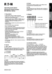
B. SPECIFICATIONS
1024 x 768 @ 75Hz
1024 x 768 @ 60Hz
1. Maximum Resolution
2. Recommend Resolution
3. Synchronization Range
Horizontal
Vertical
4. Active Display Area
5. Dot Pitch
6. Support display colors
7. Contrast Ratio (Typical)
8.Luminance of White
9. Bandwidth
10. User Control
11. OSD Function
31 – 60 KHz
60– 75 Hz
285.7mm (H) x 214.3mm (V)
0.279(H) x 0.279(V) mm
262K color
300:1
150cd/m²
80MHz
4 Key Switch
Brightness, Conrast, H-Position, V-Position, H-Size, Phase,
Color Select, Auto adjustment, Reset, Language, OSD Position,
Exit
12. View Angle
Horizontal
Vertical
13. Power Source
14. Power Consumption
15. Connection Type
16. Input Signal
Video
Sync.
17. Color Temperature
18. Dimension (WxHxD)
19. Monitor Weight
20. Base Operation
Tilt
Power
Saving
21.
ON
STAND BY
OFF
22. Signal Connector Pin Assignment
Pin No.
45 / 45 Degrees
10 / 30 Degrees
100 – 240 Vac 60 / 50 Hz
36W (max.)
15 Pin D Type
Analog R.G.B. , 0.7Vp-p / 75 Ohms
TTL level,positive or negative polarity
Packing
Physical
Gross/Net
Cool / Warm
370 x 340 x 90 mm
317 x 302.8 x 112.7 mm
2.6 Kg / 2.1 Kg
-5 / + 20 degree
< 36W
< 5W
< 5W
1. Red
2. Green
3. Blue
4. Ground
5. Self Test
6. Red Ground
7. Green Ground
8. Blue Ground
9. 5VDC
10. Sync. Ground
11. Ground
12. SDA (For DDC)
13. Horizontal Sync.
14. Vertical Sync.
15. SCL (For DDC)
C.TIMING CHART
Video
Back porch
Active display
Front porch
Sync.
Sync-width
Total
VESA
VESA
800X600
800X600
36.000
40.000
37.500
35.156
37.879
26.413
26.667
28.444
26.400
25.422
20.317
20.317
22.222
20.000
6.355
6.356
6.095
6.349
6.222
6.400
(µs)
0.635
0.636
0.762
0.508
0.667
1.000
H-Sync-width
(µs)
3.813
3.813
1.270
2.032
2.000
3.200
H-Back Porch
(µs)
1.906
1.907
4.063
3.810
3.556
2.200
70.1
59.94
72.81
75.0
56.25
60.3
14.267
16.683
13.735
13.333
17.778
16.579
V-Active Display (ms)
12.710
15.253
12.678
12.800
17.067
15.840
V-Blanking
(ms)
1.557
1.430
1.057
0.533
0.711
0.739
V-Front Porch
(ms)
0.413
0.318
0.238
0.027
0.028
0.026
V-Sync-width
(ms)
0.064
0.064
0.079
0.080
0.057
0.106
V-Back Porch
(ms)
1.080
1.049
0.740
0.427
0.626
0.607
H/V Sync. Polarity
- +
- -
- -
- -
+ +
+ +
Interlace
NONE
NONE
NONE
NONE
NONE
NONE
VGA
VGA
VESA
720X400
640X480
640X480
28.325
25.175
31.500
31.472
31.469
37.861
(µs)
31.774
31.778
H-Active Display (µs)
25.419
H-Blanking
(µs)
Front Porch
Preset
Modes
Pixel clock
(MHz)
H-Frequency
(KHz)
H-Total
V-Frequency
(Hz)
V-Total
(ms)
VESA
640X480
31.500
Preset
Modes
VESA
VESA
VESA
VESA
VESA
800X600
800X600
1024X768
1024X768
1024X768
Pixel clock
(MHz)
50.000
49.500
65.000
75.000
78.750
H-Frequency
(KHz)
48.077
46.875
48.363
56.476
60.023
(µs)
20.800
21.333
20.677
17.707
16.660
H-Active Display (µs)
16.000
16.162
15.754
13.563
13.003
H-Blanking
(µs)
4.800
5.172
4.923
4.053
3.657
Front Porch
(µs)
1.120
0.323
0.369
0.320
0.203
H-Sync-width
(µs)
2.400
1.616
2.092
1.813
1.219
H-Back Porch
(µs)
1.280
3.232
2.462
1.920
2.235
V-Frequency
(Hz)
72.2
75.0
60.0
70.1
75.0
V-Total
(ms)
13.853
13.333
16.666
14.272
13.328
V-Active Display (ms)
12.480
12.800
15.880
13.599
12.795
V-Blanking
(ms)
1.373
0.533
0.786
0.673
0.533
V-Front Porch
(ms)
0.770
0.021
0.062
0.053
0.017
V-Sync-width
(ms)
0.125
0.064
0.124
0.106
0.050
V-Back Porch
(ms)
0.478
0.448
0.600
0.513
0.466
H/V Sync. Polarity
+ +
+ +
- -
- -
+ +
Interlace
NONE
NONE
NONE
NONE
NONE
H-Total
D. CONTROL LOCATION
Font control panel
1.Menu Button ( MENU )
4. Auto Button ( AUTO )
2.Select Button ( DOWN)
5. Power Button
3.Select Button ( UP)
6. Power indicator
Rear panel
1. VGA Signal Cable
2. Power jack
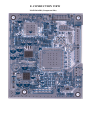
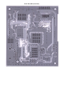
E. CONDUCTION VIEW
MAIN BOARD (Component Side)
MAIN BOARD (Solid Side)
F. ADJUSTMENT PROCEDURE
ITEM
Program Menu.
B+
Check
A
﹟Test Meter
﹡Test Point
﹫Pattern
﹟Digital Voltmeter
﹡CN7
﹫Crosshatch Pattern
(31.5KHz,640x480)
Operation
1. Plug power cable into the adapter, check adapter
power indicator light up green.
2. Make sure the voltage of the power plug (CN1)
on the main PCB to the value shown at right.
Power Saving ﹟Wattmeter
Check
﹟PC or Pattern
B
generator
﹫Crosshatch Pattern
(31.5KHz,640x480)
1. Unplug the signal cable into the monitor.
2. Turn the power switch of the monitor ON.
3. Check monitor power indicator to dark.
4. Make sure the wattmeter value shown at right.
5. OSD will be display “NO SIGNAL” Picture.
Into Factory ﹟PC or Pattern
mode
generator
C
﹫Crosshatch Pattern
(31.5KHz,640x480)
1. Hold DOWN key,then turn the power switch of the
monitor OFF.
2. Hold UP key,then turn the power switch of the
monitor ON.
3. You can into factory adjustment mode.
12.0V
±0.2V
< 5W
Auto mode
Check
﹟PC or Pattern
generator
﹫Crosshatch Pattern
(1024x768/60Hz)
1. Press and relese the AUTO knob auto adjuat display
mode to its utmost performance according to VGA
setting.
2. In the event of the display image needs further
adjustment
White
Balance
Adjust
﹟PC or Pattern
generator
﹫White Pattern
(1024x768/60Hz)
Y = 150
1. Move the OSD to the COLOR CONTROL mode.
±0.1FL
2. set color is 9300°K using the OSD,Check the value
x = 0.283
shown at below.
±0.01
Y = 150 x = 0.283 y = 0.297
3. set color is 6500°K using the OSD,Check the value y = 0.297
±0.01
shown at right.
Y = 150 x = 0.311 y = 0.329
﹟PC or Pattern
generator
1. Move the OSD to the LANGUAGE mode.
2. You can choose one of the five language you need.
D
E
Check
Value
OSD
F Language
Setting
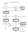
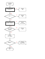
G. TROUBLE SHOOTING HINTS
No Display
( Black )
LED ON ?
NO
NO
Power
adapter ?
YES
Change
adapter
YES
Push the power
ON/OFF switch
LED Color
change ?
YES
Back light
ON?
NO
YES
To Step 2
NO
Check main
board U3/Pin141
Check the CN1/Pin1
of Inverter
Hi / Lo under
push power
sw?
+12V ?
High Voltage !
NO
YES
Make sure the
connection of
Inverter is fine
YES
NO
A
To Step 2
NO
Display ?
Check
F1(Fuse) of inverter
YES
B
OK !
A
B
Check the
connection of
CN1 cable
NO
Change the
main board
Hi / Lo under
push power
sw?
YES
Display ?
YES
NO
Change the
Inverter
OK !
Display ?
Change the
main board
NO
To Step 2
YES
OK !
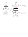
Step 2
Check the main
board 12V ?
NO
Check
F1,D3
YES
NO
Check
U10
+5.0 V ?
YES
Check the main
board U3 VDC2V ?
YES
Check
U13
YES
H/V input
Signal ?
YES
Change
U3
NO
Change
Signal Cable
NO
Check
H/V Signal
Display ?
YES
OK !
No display
(White)
Check the main
board 5V ?
NO
Check
U10
NO
Check
U12
YES
+3.3V ?
YES
Check the main
board U3/Pin30 ?
NO
Check
3.3V Circuit
YES
YES
H/V Input
Signal ?
Change
U3
NO
Check
H/V Signal
Display ?
YES
OK !
NO
Change
Signal Cable
H. REPLACEMENT PARTS LIST
PZ456
NO
Parts No.
Description
Part Location
Q’ty
1 002-U00-PZ456
User Manual
1
2 003-H03-ALL9
ALL ICT OK LBL 8*8MM(white)
1
3 003-H03-LCD
LBL 13.5*8MM
1
4 005-000-45PR
PZ456 PROVIEW CTN
1
5 123-004-PZ456
PZ456 FRAME TOSHIBA-LTM14C500Z-11 PANEL)
T=0.8mm
1
6 123-002-PZ456-B
PZ456 METAL COVER SEPT T=0.3
1
7 153-000-PZ456-A
PZ456 BACK LBL
1
8 170-000-0848C
PE BAG 0.07mm 14*30.5cm
3
9 170-001-GW520
PE BAG(All)
1
10 170-001-PZ456
PZ-456 protect film 1mm
1
11 170-005-VM541
LT-541 PE BAG 300*200mm
1
12 003-002-0848-AM
CARTON LABEL 70*40mm
1
13 160-00L-PZ456
PZ456 POLYFOAM EPS (L)
1
14 160-00R-PZ456
PZ456 POLYFOAM EPS (R)
1
15 846-120-B5AS-G2
ADAPTER 12V 2.5A(2PIN)
1
16 705-541-850B
TOSHIBA 14" LTM14C500Z 460g
1
17 200-100-PZ456-8
PZ456 MAIN BOARD REV:S2
1
18 281-031-12104
RES
19 281-035-0R04
20 281-035-1024
R1,R126
2
RES 0ohm 5% 1/10W 0603 SMD
R83
1
RES 1K 5% 1/10W 0603 SMD
R29,R51,R52,R89, R108
5
21 281-035-1034
RES 10K 5% 1/10W 0603 SMD
R19,R22,R23,R27,R30,R31,R32,R38,R47,R48,R49,
R53,R57,R58,R59,R60,R64,R65,R71,R73,R104,
R132,R135
23
22 281-035-1044
RES 100K 5% 1/10W 0603 SMD
R80,R130
2
23 281-035-1054
RES 100K 5% 1/10W 0603 SMD
R50,R107
2
24 281-035-1514
RES 150ohm +-5% 1/10W 0603 SMD
R2,R4,R5,R7,R8,R10
6
25 281-035-2204
RES 22ohm 5% 1/10W 0603 SMD
R11,R12,R17,R20,R34,R35,R42,R43,R44,R45,
10
26 281-035-3304
RES 33ohm 5% 1/10W 0603 SMD
R14,R15,R24,R25,R36,R37,R56,R63,R66,R68,R69,
R127
12
27 281-035-3314
RES 330 5% 1/10W 0603 SMD
R133,R134
2
28 281-035-4724
RES 4.7K 5% 1/10W 0603 SMD
R61,R62,R77,R86,R87,R88,R90,R103
8
29 281-035-4734
RES 47K 5% 1/10W 0603 SMD
R13,R74,R75,R105
4
30 281-035-5114
RES 510 5% 1/10W 0603 SMD
R78,R79,R106
3
31 281-035-5124
RES 5.1K 5% 1/10W 0603 SMD
R131
1
32 281-035-7504
SMD R 75 ohm 0603
R3,R6,R9
3
33 282-330-2454
RES-NET 33ohm 5% SMD 8P4R
RP13,RP14,RP15,RP16,RP17
5
34 381-151-032554
SMD CC 150PF 25V NPO 0603 +-5%
CP1
1
35 381-220-032554
SMD CC 22pF 25V NPO 0603
C11,C12,C13,C14,C17,C18,C27,C29,C31,C32
10
36 381-330-032554
NPO 33PF/25V +-5% 0603 SMD
C140
1
37 382-102-035064
X7R 1000pF/50V +-10% 0603 SMD
C64,C66,C68,C70,C78,C80,C82,C84,C90,C92
10
38 382-103-032564
SMD CC 0.01uF/25V X7R 0603 +- 10%
C2,C4,C5,C7,C8,C10,C22,C23
8
39 382-393-032564
SMD CC 0.039uF/25V X7R 0603
CZ1
1
121 1% 1/10W 0603 SMD
40 382-472-035064
X7R 4700pF/50V +-10% 0603 SMD
C21,C24,C25
3
41 385-104-032584
Y5V
0.1u/25V +80%-20% 0603
C15,C16,C20,C28,C30,C42,C48,C49,C50,C51,C52,
C53,C54,C55,C56,C57,C58,C59,C60,C61,C62,C63,
C79,C81,C83,C91,C93,C98,C110,C118,C133,C134,
C135,C136,C137,C138,C139,C111,C1,C19,C33,
C142,C143,
43
42 385-105-031684
Y5V
1uF/16V +80-20% 0603
C141,C144
2
43 481-LCC-0440
SOCKET 44PIN PLCC
U5
1
44 506-0AI-C1084
SMD REG.AIC1084CM 3.3V 5A
U12
1
45 506-0TH-63LM83
THC63LVDM83 TQFP56 LVDS IC SMD
U20
1
46 506-524-LC21
MEMORY IC 24LC21 SMD
U2
1
47 506-5NM-24C16
24C16 SO8 MEMORY IC SMD
U6
1
48 506-774-LCX14
74LCX SOIC14 HI SPEED TTL SMD
U1
1
49 506-RAM-2576-5
REGULATOR AMC2576-5.0DD/ADD
U10
1
50 506-RLD-1117-A
LD1117-ADJ-A UTC SOT223
U13
1
51 506-SXX-MV3
SMD IC SCALER CHIP MASCOT MV3
U3
1
52 518-02N-3904
NPN 2N3904S(SMD)
Q2,Q3,Q4,Q7,Q8
5
53 518-02N-3906
SMD TR 2N3906
Q6
1
54 518-1CE-9435
MOSFET CE9435A S08
U9
1
55 528-2BA-T54C
SMD DIODE BAT54C SOT23
D1
1
56 528-R1N-4148
DIODE 1N4148 SOT-34 SMD
D4
1
57 558-352-5000
SMD FUSE 1206 24V 5A
F1
1
58 622-106-0201
JUMPER 2.54MM 0.6D
JP1-->3.3V
1
59 630-020-8001
HEADER 20(SMD BASE 1.25 20P)
CON6
1
60 780-103-3000
SMDBEAD SBK160808300Y0603 30Ω
L1,L2,L3,L29,L30, L31
6
61 780-104-6010
FB 0805/600ohm 100mHZ
L4,L5,L16,L17,L18,L19,L20,L25,L26,L27
10
62 780-107-121K50
BEAD 120ohm 1206 5A FBM-11
L22
1
63 851-0NM-PZ456-A PZ456 M/B DIP ASS'Y LVDS no AUDI
1
64 330-100-16255
5mm EC 10uF 16V 105C M TP MI 4*5
EC1,EC4,EC11,EC24,EC35,EC41
6
65 630-006-1008
JWT A2001 PITCH 2.00mm
CN9
1
66 630-008-C001
JST 1.5mm HEADER ZR S8B-ZR
CN3
1
67 745-330-2062-3
33uH C4426-060128YB-UL
LL1
1
68 630-016-1008
BASE 16p JWT A2001
CN1
1
69 151-A00-Z45S4
PZ456 FRONT BEZEL
1
70 151-001-Z45NV
PZ456 REAR CABINET 424C
1
71 154-001-Z45S4
PZ456 HANDLE 877C
1
72 154-001-PZ456
PZ456 KEY TOP
1
73 154-002-PZ456
PZ456 LED LENS
1
74 154-003-PZ456
PZ456 MYLAR SHEET PVC
1
75 506-1SM-89516
SYNCMOS SM89516C25J 44Pin PLCC
1
76 610-151-15CDC
PZ456 Signal cable DC JACK 424C
1
77 121-001-PZ456
PZ-456 HANDLE PLATE SPCC T=1.6
1
78 121-002-PZ456
PZ-456 CLAMP SPCC T=1.0
1
79 101-003-2033
EZPC SCREW P2*3
8
80 100-006-3032
SCREW R3*6mm ISO
7
81 109-S06-3033
SCREW AU (M3*6.0*HEX1.5)
6
82 103-005-3033
SCREW F3*5mm ISO ZI3C
1
83 100-008-3033
R 3*8 ISO
2
84 126-045-ALP1
Aluminum foil L75*W45mm
1
85 121-003-PZ456
PZ-456 BASE LOCK(T=0.5mm)SUS301
1
86 100-004-2032
SCREW R2.0*L4.0mm ISO
1
87 003-H01-LCD
LCD CPU LBL 15mmx15mm
1
88 154-005-PZ456
PZ456 MYLAR SHEET PVC T=0.2mm58*28
1
89 107-008-3073
B 3*8 TP4
2
90 111-148-0800
FLAT WASHER 1 SPCC T=1.0
1
91 111-014-0800
FLAT WASHER 2 PVC T=0.5mm
2
92 111-148-0801
FLAT WASHER 3 SUS304 T=0.3
2
93 111-046-0020
RUBBER WASHER 20*4*2
1
94 100-006-4033
SCREW P4*6 ISO
1
95 132-001-PZ456
SPRING WASHER SUS301 T=0.5
1
96 123-003-PZ456
PZ456 BASE ARM DIE CASTING AL
1
97 123-00L-PZ456-A
BASE LEG LEFT DIE CASTING AL
1
98 123-00R-PZ456-A BASE LEG RIGHT DIE CASTING AL
1
99 155-001-PS576
RUBBER FOOT(NR)
3
100 105-006-4033-1
SCREW T4*6mm ISO
101 631-006-J456
WIRE 6P 2.0-1.25 100mm PZ456
1
102 631-008-G020-B
PZ4561.5mmPITCH->1.5 dual CORE 135mm
1
103 631-020-7010-B
LVDS CABLE 20P TO 20P L=80mm
1
104 100-003-3032
SCREW R3.0*L3.0mm ISO
8
105 154-004-PZ456
PZ456 MYLAR SHEET PVC T=0.2mm
1
106 401-270-0205
ACT SW 2P 6*3.5 H 5.0 180g
107 200-701-PZ456-A
PZ456 CONTROL PCB
108 330-220-16255
MINI CE 22uF/16V +-20% TP105℃4*5
EC36,EC42
2
109 330-221-16255
EC H:5mm 220uF16V +-20% 105C 8*5
EC9,EC12,EC23,EC38,EC39,EC40
6
110 330-470-16275
EC 47uF 16V 5*5 105C +-20%
EC10,EC13,EC14,EC18,EC20,EC22,
6
111 630-008-C001
JST 1.5mm HEADER ZR S8B-ZR
J1
1
112 531-110-49US
1.0592MHZ HC 49US CRYSTAL
X1
1
113 531-120-49US
12MHZ HC 49US CRYSTAL 30PPM
Y1
1
114 522-030-B340-T
SCHTTKY SB340 TP
D3
1
S1,S2,S3,S4,S5,
5
1
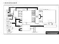
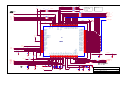
I. BLOCK DIAGRAM
VSYNC
HSYNC
VGA-IN
12PIN
C
O
N
N
E
N
T
SCALER
ADC
8 R0~R7
LVDS
10 EVEN
8 RA0~RA7
LCD PANEL(LVDS)
8 GA0~GA7
3 {R.G.B}
8 G0~G7
8 BA0~BA7
DDC-SDA
DDC-SCL
8 B0~B7
D-DE
8 RB0~RB7
D.D.C
24C21
LVDS
8 GB0~GB7
EEPROM
CRYSTAL
10 ODD
8 BB0~BB7
24C16
HI VOLTAGE
12M HZ
EEPROM
MCU
INVERTER
SDA
SCL
POWER
SWITCH POWER
SUPPLY AND
REGULATOR
8PIN
3V
5V
CRYSTAL
12V
POWER
ADAPTER
BLK-ON/OFF
BRIGHTNESS
12M HZ
12V
12V
C
O
N
N
E
N
T
Title
FUNCTION KEY
Size
B
Date:
BLOCK DIAGRAM
Document Number
Rev
B
ORION
Tuesday, October 23, 2001
Sheet
1
of
1
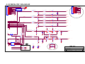
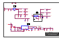
J. SCHEMATIC DIAGRAM
DC_VIN
CN1
1
2
3
4
5
6
7
8
9
10
11
12
13
14
15
16
JP2
DC_VIN
DDC_SCL
DDC_SDA
CABLE
$$$1
VGA_VSYNC
VGA_HSYNC
3
ADD TO R135
BLUE
5
GND
L1
RED
BE0603-RGB
R2
150 1%
C2
10nF
RED+
R3
GREEN
RED
PC5V
75 1%
C3
R4
150 1%
C4
NP
10nF
L2
BE0603-RGB
R5
150 1%
C5
DDC_SCL
DDC_SDA
RED-
2
GREEN+
2
GREEN-
2
BLUE+
2
BLUE-
2
CABLE
VGA_VSYNC
VGA_HSYNC
BLUE
GREEN
RED
PC5V
JST2.0-13PIN-180°
JST2.0-1X16PIN
GREEN
2
1
2
3
4
5
6
7
8
9
10
11
12
13
5/18 追加
10nF
C6
R6
NP
75 1%
R7
150 1%
C7
10nF
RED
PC5V
GREEN
BLUE
L3
BLUE
BE0603-RGB
R8
150 1%
C8
10nF
R9
DDC_SDA
C9
DDC_SDA
VGA_HSYNC
75 1%
VGA_VSYNC
DDC_SCL
R10
150 1%
C10
NP
10nF
VDD
DDC_SCL
VDD
VDD
R104
U1A
22
R11
VGA_HSYNC
14
10K
C11
R13
VDD
R14
D1
1
BAT54
33
2
7
3
SSHCT14
22pF
47K
PC5V
R16
NP
R18
NP
4
7
R17
VGA_VSYNC
R19
22
VDD
5
C13
NP
U2
1
2
3
4
NC
NC
NC
VSS
10K
VCC
VCLK
SCK
SDA
R23
10K
47K
VSYNC
2
R24
VCC
VDD
6
9
7
7
C15
0.1uF
33
DD_SCL
3
R20
22
C14
SSHCT14
22pF
22pF
1
3
8
2
L4
BE0805
33
DD_SDA
R25
U1D
14
1
修改1
24LC21
DDC_SCL
2
22pF
SSHCT14
R105
8
7
6
5
DDC_SDA
HSYNC
C12
VDD
14
10K
R22
22
SSHCT14
U1C
R21
R12
33
3
2
R15
U1B
14
1
C16
0.1uF
MRT, Inc.
2
L5
BE0805
Title
GND
VGA INPUT
Size
Document Number
Date:
Wednesday, May 21, 2003
Rev
MVP3-SCH-001
1.0
Sheet
1
of
8
VDD
CONFIG1
VDD
R29
1K
CONFIG2
R31
10K
CONFIG3
CONFIG0
R26
NP
R27
10K
R28
NP
R30
10K
修改4_B
MV_RESET
SDA
3
HFS
3
IRQ-
33
R37
33
R32
10K
R33
NP
R34
22
R35
22
CFG[1:0]
0 0 -> I2C
0 1 -> SPI
1 0 ->
6-WIRE
CFG[3:2]
BLK-ADJ
4
VDDCTRL
4
VDD
VDC2V
OA[0..23] 4
1
1
VDD2V
VSYNC
HSYNC
VAA2V
SOG
VAA3V
R38
OB7
OB6
OB5
OB4
OB3
OB2
OB1
OB0
CAP_VSYNC
BLU_INB_0
BLU_INB_1
BLU_INB_2
BLU_INB_3
BLU_INB_4
BLU_INB_5
BLU_INB_6
BLU_INB_7
DIVDD3V
DIVSS
GRN_INB_0/HDATA_0
GRN_INB_1/HDATA_1
GRN_INB_2/HDATA_2
GRN_INB_3/HDATA_3
GRN_INB_4/HCLK
GRN_INB_5
GRN_INB_6
GRN_INB_7
DCVDD2V
DCVSS
RED_INB_0
RED_INB_1
RED_INB_2
RED_INB_3
RED_INB_4
RED_INB_5
RED_INB_6
RED_INB_7
VDD3V
DGND
DTEST
VDD2V
VGA_VSYNC
VGA_HSYNC
VAA2A
GNDA
SOGIN
VAA3V
AGND
EC3
10K
22uF/16V
U3
MV3
RED+
RED-
OA15
OA14
OA13
OA12
OA11
OA10
OA9
OA8
OA7
OA6
OA5
OA4
OA3
OA2
OA1
OA0
INV1
CPH1
POL
RLS
R43
22
R45
22
AUDIO-ADJ
1
2
3
C20
V
R
G
D-SHCLK2
C140
33p
C26
33p
GND
100
1
1
OA19
OA18
OA17
OA16
VREF
VAA2V
BLUE+
BLUEGREEN+
GREEN-
OA23
OA22
OA21
OA20
CPH1
GND-ANA
R106
120
119
118
117
116
115
114
113
112
111
110
109
108
107
106
105
104
103
102
101
100
99
98
97
96
95
94
93
92
91
90
89
88
87
86
85
84
83
82
81
41
42
43
44
45
46
47
48
49
50
51
52
53
54
55
56
57
58
59
60
61
62
63
64
65
66
67
68
69
70
71
72
73
74
75
76
77
78
79
80
R39
NP
1
1
1
1
DOBVSS
BLU_OUTB_7
BLU_OUTB_6
BLU_OUTB_5
BLU_OUTB_4
DOBVDD3V
BLU_OUTB_3
BLU_OUTB_2
BLU_OUTB_1
BLU_OUTB_0
DOBVSS
RED_OUTA_7
RED_OUTA_6
RED_OUTA_5
RED_OUTA_4
DCVDD2V
RED_OUTA_3
RED_OUTA_2
RED_OUTA_1
RED_OUTA_0
DCVSS
GRN_OUTA_7
GRN_OUTA_6
GRN_OUTA_5
GRN_OUTA_4
DOBVDD3V
GRN_OUTA_3
GRN_OUTA_2
GRN_OUTA_1
GRN_OUTA_0
DOBVSS
BLU_OUTA_7
BLU_OUTA_6
BLU_OUTA_5
BLU_OUTA_4
DOBVDD3V
BLU_OUTA_3
BLU_OUTA_2
BLU_OUTA_1
BLU_OUTA_0
VREF
CP
CZ
VAA3B
BIN+
BINAGNDB
BCLP
VTOP
VBOT
VAA3G
GIN+
GINAGNDG
GCLP
TOUTP
TOUTM
VAA3R
RIN+
RINAGNDR
RCLP
ADVDD3V
ADVSS
XTAL
XTALI
DCVSS
GPIO1
GPIO0
PWM1
STH1
STH8
LP
DCVDD2V
SHC
RLS/<DISP_DE>
POL/<DISP_VSYNC>
CPH1/<SHCLK>
INV1/<DISP_HSYNC>
DCVSS
VDD3V
160
CAP_HSYNC
159
CAP_HREF
158
TVCLK
157
IRQ#
156
SCS#/HFS#
155
SDA
154
SCL
153
RST
152
STV3
151
STV1
150
CPV
149
OE3/<CONFIG3>
148
OE2/<CONFIG2>
147
OE1/<CONFIG1>
146
CPH2
145
PWM0/<CONFIG0>
144
DCVDD2V
143
INV2/<LCD_VEE>
142
LCD_VDD
141
LCD_VBL
140
DCVSS
139
RED_OUTB_7
138
RED_OUTB_6
137
RED_OUTB_5
136
RED_OUTB_4
135
DOBVDD3V
134
RED_OUTB_3
133
RED_OUTB_2
132
RED_OUTB_1
131
RED_OUTB_0
130
DOBVSS
129
GRN_OUTB_7
128
GRN_OUTB_6
127
GRN_OUTB_5
126
GRN_OUTB_4
125
DOBVDD3V
124
GRN_OUTB_3
123
GRN_OUTB_2
122
GRN_OUTB_1
121
GRN_OUTB_0
GND
VDC2V
6
OB[0..23] 4
VDC2V
1
2
3
4
5
6
7
8
9
10
11
12
13
14
15
16
17
18
19
20
21
22
23
24
25
26
27
28
29
30
31
32
33
34
35
36
37
38
39
40
6
LCD_VEE_A
BL-ON0
OB11
OB10
OB9
OB8
3
R36
OB15
OB14
OB13
OB12
SCL
OB19
OB18
OB17
OB16
3
OB23
OB22
OB21
OB20
3
VDD
0.1uF
CP1
CZ1
150pF
39nF
EC1
MV_XT_1
C21
C22
C23
C24
C25
4.7nF
10nF
10nF
4.7nF
4.7nF
MV_XT
22uF/16V
VAA3RGB
VDD
R42
22
R44
22
1M
C34
C18
M22pF
22pF
Y1
12MHZ
D-HSYNC
D-SHCLK2
D-VSYNC
D-DE2
4
4
4
4
INV1->D-HSYNC
CPH1->D-SHCLK2
POL->D-VSYNC
RLS->D-DE2
8
C35
R107
D-SHCLK2
M22pF
MRT, Inc.
C17
22pF
Title
MVP3
Size
Document Number
Date:
Wednesday, May 21, 2003
Rev
MVP3-SCH-001
1.0
Sheet
2
of
8
C141
1uF
VCC
R129
NP
MV_RESET
ADD
R135
0422
2
Q6
2N3906
RESET
3
2
2
VCC
C 3
+
X1
R50
11.0592MHz 1M
35
CLK
C29
22pF
1
2
3
4
5
6
7
8
R56
33
Power
R63
R66
R68
R69
33
33
33
33
DOWN
UP
MENU
AUTO
2
21
20
RESET
CN3-1
LED_O
LED_G
CN3-4
CN3-5
CN3-6
CN3-7
C28
0.1uF
10
IRQ-
IRQ-
14
15
16
17
AUTO
MENU
UP
DOWN
Power
P1_5
CN3-1
CN3-4
CN3-5
CN3-6
CN3-7
C133
0.1uF
C136
0.1uF
C137
0.1uF
C138
0.1uF
C139
0.1uF
SDA
SCL
U5
EA/VP
X1
X2
SOCKET PLCC44
RESET
P0.0
P0.1
P0.2
P0.3
P0.4
P0.5
P0.6
P0.7
P2.0
P2.1
P2.2
P2.3
P2.4
P2.5
P2.6
P2.7
INT0
INT1
T0
T1
P1.0
P1.1
P1.2
P1.3
P1.4
P1.5
P1.6_SDA
P1.7_SCL
VCC
R64
10K
修改3
2
3
4
5
6
7
8
9
RD
WR
PSEN
ALE/P
TXD
RXD
R65
10K
R57
10K
R58
10K
R59
10K
R60
10K
R61
4.7K
LED_ORANGE
19
18
32
33
13
11
7
C134
0.1uF
$$$1
INB12
INB11
INB10
INB9
INB8
LED_GREEN
LED_ORANGE
1K
1K
R127
PC-DETECT
1K
33
R53
NP
1
AUD_OFF
8
HFS
2
->
->
->
->
->
HCLK
HDATA3
HDATA2
HDATA1
HDATA0
VCC
VCC
R54
NP
R55
NP
MV_RESET
MV_RESET
2
修改4_A
DD_SCL
DD_SDA
DD_SCL
DD_SDA
1
1
JWT-A2001WV2-06
DEBUG
PORT
39
38
37
36
35
34
33
32
31
30
29
CN4
DD_SDA
DD_SCL
SDA
SCL
VCC
1
2
3
4
5
6
1
2
3
4
5
6
18
19
20
21
22
23
24
25
26
27
28
11
24
25
26
27
28
29
30
31
R108
7
8
9
10 ALI&MRT8064PLCC44
11
12
13
14
15
16
17
14
10
R51
PO_0
PO_1
R52
43
42
41
40
39
38
37
36
R62
4.7K
U1E
R70
R49
10K
PP1
VDD
LED_O
R135 R48
10K
10K
1
12
22
34
23
CN3
JST-S8B-ZR
EC4
22uF/16V
R47
10K
2E
6
5
4
3
2
1
44
43
42
41
40
B 1
44
A
VCC
C27
22pF
VCC
R132
10K
C144
1uF
VCC
0.1uF
5.1K
1
0.1uF
C142
R131
INT2
INT3
VSS
P4.0
P4.1
D4
1N4148
1
R130
100K
C143
R71SSHCT14
NP
VDD
10K
U1F
14
R72
LED_G
12
VDD
LED_GREEN
13
R137
R73SSHCT14
VCC
10K
R133
C30
0.1uF
330
LED_O
3
2N3904
1.Power
2.LED O(570LEDON G)
3.LED G(568C2ON) ET502 LED/ON
4.DOWN5.UP
6.MENU
7.AUTO
8.GND
1
SCL-E
VSS
A0
A1
A2
WP
SCL
SDA
LED_ORANGE
SCL
2
SDA
2
33
R136
6
5
SDA-E
33
C32
22pF
C31
22pF
VCC
B
使用藍光LED
R須改為150甌姆須再測試
R134
330
MRT, Inc.
LED_G
PROVIEW KEY PAD --OK
Title
3
2N3904
2 OB[0..23]
Q7
2
4
1
2
3
7
U6
24C16
VCC
NP
8
7
C135
0.1uF
RP1
OB23
OB22
OB21
OB20
OB19
OB18
OB17
OB16
1
2
3
4
1
2
3
4
8
7
6
5
8
7
6
5
RB7
RB6
RB5
RB4
RB3
RB2
RB1
RB0
OB15
OB14
OB13
OB12
OB11
OB10
OB9
OB8
1 RP2 RP3 8
2
7
3
6
4
5
1
8
2
7
3
6
4
5
GB7
GB6
GB5
GB4
GB3
GB2
GB1
GB0
2
OB21
OB20
OB19
OB18
OB17
OB16
OB13
OB12
OB11
OB10
OB9
OB8
OB5
OB4
OB3
OB2
OB1
Q8
1
LED_GREEN
RP13
1
2
3
4
1
2
3
4
RP15
1
2 RP14
3
4
1
2
3
4
1
8
7
6
5
8
7
6
5
8
7
6
5
8
7
6
5
8
RB7
RB6
RB5
RB4
RB3
RB2
GB7
GB6
GB5
GB4
GB3
GB2
BB7
BB6
BB5
BB4
BB3
MCU
Size
Document Number
Date:
Wednesday, May 21, 2003
Rev
MVP3-SCH-001
1.0
Sheet
3
of
8
LCDVDD
PANEL
CN10
LCDVDD
CVDD
CVDD
BB0
BB1
BB2
BB3
1
2
3
4
5
6
7
8
1
45
M/B
JUMP1
O
4
I
3
O
2
G
1
VCC
U12
AIC1084-33CM
47uF/16V
OUT
EC14
C55
47uF/16V
0.1uF
TO263
OUT1
L17
2
L16
VAA3V
VDC2V
4
C56
C54
1
EC22
IN
C
3
0.1uF
0.1uF
LT1117CST-2.5
L19
VAA3RGB
O
G
0.1uF
L20
U13
C60
2
L18
VAA2V
3
I
O
C58
3
VIN
VOUT
TAB
2
4
VDD2V
0.1uF
EC20
C61
C62
1
0.1uF
0.1uF
LT1117CST-2.5&ADJ
ADJ
C59
47uF/16V
1
VCC
VDD3V
EC18
4
SOT-223
C57
R126
120_1%
VDD
C63
EC23
0.1uF
220uF/16V
DC_VIN
GND
LL1
C4426-060128YB
C48
0.1uF
EC9
EC10
220uF/16V 47uF/16V
EC38
220uF/16V
0
+5V
VCC
L26
2
D3
R83
5/18 追加
3
OUTPUT
1
GND1
ON/OFF
5
0.1uF
4
VIN
GND
C49
1
Keep feedback wire away from inductor flux
FEEDBACK
1
R1
120_1%
5
4
3
2
AMC2576-5
+12V
3
4
1 125V/5A 2
0.1uF
1N5820
EC39
220uF/16V
+
EC12
220uF/16V
+
BE0805
C53
0.1uF
L27
BE0805
C51
C52
0.1uF
0.1uF
EC11
+
22uF/16V
+
EC40
220uF/16V
4
F1
U10
SW
FB
GND
OUT
IN
0.1uF
修改2
2
C50
0.1uF
6
DC_VIN
6
DC_VIN
3
1
AMC2576-5
47uF/16V
MRT, Inc.
Title
POWER SUPPLY
Size
Document Number
Date:
Wednesday, May 21, 2003
Rev
MVP3-SCH-001
1.0
Sheet
5
of
8
VDD3V
VDD2V
VAA2V
C70
C64
C66
C72
VAA3V
H1
C73
VAA3RGB
C68
EC2
22uF/16V
1000pF
1000pF
1000pF
1000pF
H2
1000pF
VDD
C78
C79
C80
C81
C82
C83
C84
C90
0.1uF
C91
C92
C93
VDC2V
H3
1000pF
0.1uF 1000pF
0.1uF 1000pF
0.1uF 1000pF
1000pF
0.1uF 1000pF 0.1uF
H4
VCC
EVERY POWER PIN OF MASCOT
NEEDS A PAIR OF
CAPACITORS
R86
R87
INV_BRIGHT_CTL
4.7K
3
Q3
2
1
2 BLK-ADJ
R88
4.7K 2N3904
+12V
1K
S1
L22
EC24
22uF/16V
0.1uF
EC13
C
INV_ON_OFF
INV_BRIGHT_CTL
GND
BL-ON0
1
2
3
4
5
6
INV_ON_OFF
INV_BRIGHT_CTL
HEADER 6
JP3
1
2
3
4
5
6
WH1-210-6PIN-180°
B
1
R89
2
VCC
3
S4
CN5
GND
DEFAULT = 0
S3
BE1206(2A)
47uF/16V
GND
GND
S2
C98
BL-ON0
1K
2
GND
E
Q4
1
2N3904
GND
+5V
3
2
INV_ON_OFF
R90
4.7K
MRT, Inc.
Title
GND
MISC & DECAP
Size
Document Number
Date:
Wednesday, May 21, 2003
Rev
MVP3-SCH-001
1.0
Sheet
6
of
8
1
C124
VCC
2
VCC
MODE VCC OP VOL
R109
2
47uF/16V
VCC_AU
BE0805
R112
NP
C125
0.1uF
R110
R111
20K
33K
5/18 追加
C126
0.1uF
BASE2-180°
1
2
18
19
27
VDD
6
20K
Lift Gain2
5
Lift Gain1
Mute Hi is Mute
Mode
VDD
4
VDD
5
4
3
2
1
16
R113
U21
17
DEL L15
DEL L17
DEL C134
DEL R86
BASE2S
Left_outp
L-OUT
1
2
Left_Outm
Lift out -
L-OUT
JP5
C127
0.0068UF
Mute
DEL R89
CN12
Left_outp
R114
C128 1UF
12
20K
11
C129 1UF
RIGHTIN
10
R117
9
R118
10K
Right Out+
Hi is Gain on
3
AUD4835_DCVOL
7
R119
10K
Shutdown
Right Out-
Gain Select
DC_Vol
NS4838&APA4835A
C131
1UF
MUTE
0
VCC
C145
33p
HI HP OUT
LOW SP OUT
C146
33p
BASE2-180°
28
1
2
Right_Outp
26
R120
20K
33K
1
R-OUT
CN15
20K
1
1
2
Right_outm
R122
GAIN
5/18 追加
BASE2S
Right_Outp
Right_outm
R121
MODE
R-OUT
JP6
20K
Hi is Shoutdown
2
Gain
Right Dock
Left_Outm
21
Right Gain2
Shoutdown
AUD4835_SD
AUD_OFF
HP Sense
Right In
15
25
3
Beep In
Right Gain1
HI SHUTDOWN
VCC
Lift out +
Lift In
24
R116 20K
Left Dock
GND
GND
GND
GND
GND
GND
20K
1
8
14
20
23
29
R115
LEFTIN
Bypass
5/18 修改
13
22
PA3
SCJ-0356M5(B)
1
MODE GND OP MAX
10K
L28
SDWN
0
C130
0.0068UF
C147
33p
C148
33p
HPS
0
R123
R124
AUD4835_DCVOL
4.7K
1
2 AUDIO-ADJ
R125
4.7K 2N3904
3
Q5
2
1K
EC37
22uF/16V
C132
0.1uF
GND
GND
GND
Title
Size
Date:
<Title>
Document Number
Custom <Doc>
Wednesday, May 21, 2003
Rev
A
Sheet
8
of
8
Memu