1
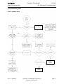
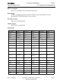
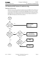
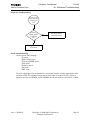
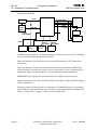
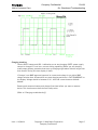
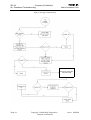
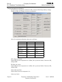
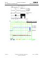
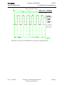
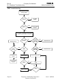
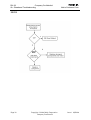
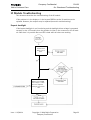
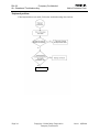
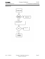
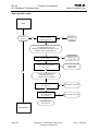
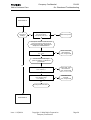
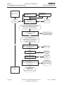
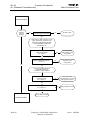
Nokia Customer Care
RH-29 Series Cellular Phones
6a - Baseband Troubleshooting
Issue 1 05/2004
Copyright © 2004 Nokia Corporation
Company Confidential
Page 1
RH-29
Company Confidential
6b - Baseband Troubleshooting
Nokia Customer Care
Table of Contents
Page No
Introduction to RH-29 Troubleshooting ........................................................................................... 3
General guidelines for RH-29 troubleshooting ............................................................................ 3
Tools needed for troubleshooting ................................................................................................. 3
General guidelines............................................................................................................................. 3
Nominal current consumption .......................................................................................................... 4
Troubleshooting Paths............................................................................................................................ 5
Dead or jammed device ...................................................................................................................... 5
Partially damaged device ................................................................................................................... 6
Most common symptoms reported by customer ......................................................................... 6
Most common symptoms for audio problems........................................................................... 6
Symptoms related to energy management ................................................................................ 6
Problems related to UI module:..................................................................................................... 6
Most common RF related symptoms: .......................................................................................... 6
ASIC is changed .................................................................................................................................... 7
UEM changed...................................................................................................................................... 7
UPP_WD2 changed ........................................................................................................................... 7
ZOCUS changed.................................................................................................................................. 7
Test points .............................................................................................................................................. 7
“CONTACT SERVICE” on display ........................................................................................................ 8
1CK Baseband HW Subarea Troubleshooting.................................................................................. 9
Flashing troubleshooting .................................................................................................................... 9
Energy management troubleshooting ..........................................................................................11
Device does not stay on................................................................................................................ 11
General power checking ............................................................................................................... 12
Power key troubleshooting .......................................................................................................... 14
Clocks troubleshooting.................................................................................................................. 14
Charging checking.......................................................................................................................... 16
Energy management calibration ................................................................................................ 19
ADC-reading..................................................................................................................................... 20
Backup battery ............................................................................................................................... 21
SIM card ............................................................................................................................................ 22
Memory troubleshooting ..................................................................................................................26
Serial interface troubleshooting ....................................................................................................27
CBUS................................................................................................................................................... 27
FBUS ................................................................................................................................................... 28
MBUS.................................................................................................................................................. 28
MMC troubleshooting .......................................................................................................................29
Vibra .......................................................................................................................................................30
ZOCUS ....................................................................................................................................................31
UI Module Troubleshooting ............................................................................................................... 32
Keymat backlight ................................................................................................................................32
Keyboard problem ..............................................................................................................................33
Display blank ........................................................................................................................................34
Image on display not correct ..........................................................................................................35
Backlight does not turn on .............................................................................................................36
Handportable audio ...........................................................................................................................37
Accessory Audio ..................................................................................................................................40
Page 2
Copyright © 2004 Nokia Corporation
Company Confidential
Issue 1 05/2004
Company Confidential
RH-29
6b - Baseband Troubleshooting
Nokia Customer Care
Introduction to RH-29 Troubleshooting
This document is intend to be a guide for localizing and repairing electrical faults in the
RH-29 device. First there is a brief guide for fault localizing. Then fault repairing is
divided into troubleshooting paths.
Before any service operation you must be familiar with the RH-29 product and module
level architecture. You have to also be familiar with the RH-29 specified service tools
such as the Phoenix service software, flashing tools and software.
General guidelines for RH-29 troubleshooting
Tools needed for troubleshooting
• Service tools (as listed at service tools chapter in service manual)
•
Laboratory power supply with current indicator
•
Oscilloscope
•
Digital multimeter
General guidelines
If the device cannot be turned on by any means, see “dead device” troubleshooting
Current consumption (missing consumption) gives an idea whether the device is able to
start up.
Dropping supply voltage or very large current consumption indicates a short circuit
Check whether the connection with Phoenix works and what can be discovered with
Phoenix (ADC-readings, baseband self-test, BB-calibrations etc.)
Check baseband self-tests with Phoenix if “CONTACT SERVICE” is shown on the display.
Check visually display and rocker faults.
Force phone to LOCAL mode and make keyboard test by phoenix.
Check that board-to-board connector is OK, and connectors make good contacts.
If liquid damage, stop repairing!
Flash the phone before disassembling it, if the fault is not obvious and the Phoenix connection is OK.
Disassemble phone:
Try to locate failed module.
Issue 1 05/2004
Copyright © 2004 Nokia Corporation
Company Confidential
Page 3
RH-29
Company Confidential
6b - Baseband Troubleshooting
Nokia Customer Care
Check failed module visually:
Mechanical damages?
Solder joints OK?
Continue with specific troubleshooting procedure for the module:
If there is an obvious fault, repair it before reflashing the device.
Flash first if a fault is not obvious.
If flashing is not working go to flashing troubleshooting.
Due to CSP packages short circuits or broken solder joints are not easily seen. If the
examined signal seems to be continuously in low or high level, then measure for possible
short circuit to ground (signal low) or to supply voltage (signal high) Note that if a problem is not found from any visible contact/component it can be under CSPs where the signal is connected.
Care must be taken when assembling and disassembling the transceiver. Failure to do
this may result in unnecessary damage to device.
Nominal current consumption
NOTE: Service tools need some amount of current to work.
The following current consumption values are measured from a complete RH-29.
Vbatt = 3.6V
Measured nominal currents are drawn from the main battery.
Measurements have been made with a current probe connected to an oscilloscope.
Operating mode
Current consumption
Idle
90 mA
2w audio call (backlights off) 250 mA
Page 4
Copyright © 2004 Nokia Corporation
Company Confidential
Issue 1 05/2004
Nokia Customer Care
Company Confidential
RH-29
6b - Baseband Troubleshooting
Troubleshooting Paths
Dead or jammed device
Disassemble
yes
Check UI
connector
Replace
UI module
Issue 1 05/2004
Copyright © 2004 Nokia Corporation
Company Confidential
Page 5
RH-29
Company Confidential
6b - Baseband Troubleshooting
Nokia Customer Care
Partially damaged device
If the device is working, but some functionality is missing try to localize where the problems is and see relevant part of this manual. E.g audio is not working see “Audio Troubleshooting”, if charging is not working see chapter Charging troubleshooting etc.
Most common symptoms reported by customer
In this chapter is described most common symptoms reported by customers when the
device is brought in for service. Some tips where the trouble can be found are given also.
When troubleshooting use these tips and follow the given troubleshooting path.
Most common symptoms for audio problems
“Earpiece sound is missing”
”Handsfree sound is missing”
”Headset is not recognized”
”Microphone is not working”
”Volume cannot be adjusted”
” Ringing tones does not work”
”Audio volume too low”
If symptom is something like above see audio troubleshooting.
Symptoms related to energy management
“Phone does not stay on”
”Charging is not working”
”Time is lost during battery change”
”Charging takes too long”
”Operating time is very short”
These symptoms lead to relevant part of energy management troubleshooting
Problems related to UI module:
“UI-module keypad is not working”
”Backlight is dim”
”Backlight not even”
”Backlight is blinking”
”Keypad or display backlight is not working”
”Display related problems”
See UI- module troubleshooting.
Most common RF related symptoms:
“Call cannot be made”
”Phone does not find signal”
”Call is often dropped”
See RF troubleshooting
Page 6
Copyright © 2004 Nokia Corporation
Company Confidential
Issue 1 05/2004
Company Confidential
RH-29
6b - Baseband Troubleshooting
Nokia Customer Care
ASIC is changed
ASIC’s can be changed only at a defined service level.
UEM changed
If UEM is changed baseband calibrations should be made. New IMEI must be programmed also. ZOCUS calibration is not necessary.
UPP_WD2 changed
IMEI must be reprogrammed.
ZOCUS changed
Zocus must be re-calibrated
Test points
Test Point
Signal
Test Point
Signal
Test Point
Signal
J109
UEMInt
J203
TXQD
J477
SIM IF
J123
SLEEPCLK
J204
AUXD
J482
MMC IF
J124
SLEEPX
J311
FLASH CE
J483
MMC IF
J125
PURX
J312
FLASH CE
J484
MMC IF
J170
RFCLK_I
J314
SDRAMCLK
J485
MMC IF
J190
EARDATA
J315
FLASH CLK
J487
MMC IF
J191
MICDATA
J334
Shutdown
Audio PA
J488
MMC IF
J192
SIMIODAI
J390
Current sense
resistor
J490
MMC IF
J193
SIMCLKI
J391
Current sense
resistor
J492
MMC IF
J194
SIMIOCTRL
J392
Current sense
resistor
J493
MMC IF
J195
MBUSTX
J393
Current sense
resistor
J495
MMC IF
J196
MBUSRX
J470
SIM IF
J496
MMC IF
J197
FBUSTXI
J471
SIM IF
J497
MMC IF
J198
FBUSRXI
J472
SIM IF
J498
MMC IF
J199
RFCONVCLK
J473
SIM IF
J499
MMC IF
J200
RXID
J474
SIM IF
J201
RXQD
J475
SIM IF
J202
TXID
J476
SIM IF
Issue 1 05/2004
Copyright © 2004 Nokia Corporation
Company Confidential
Page 7
RH-29
Company Confidential
6b - Baseband Troubleshooting
Nokia Customer Care
“CONTACT SERVICE” on display
CONTACT SERVICE on display (Self-tests by Phoenix)
Display information: “Contact Service”
This fault means that software is able to run and thus the watchdog of UEM can be
served.
Self-test functions are executed when the phone is powered on and if one or more selftest functions fail, the message “Contact Service” is shown on the display.
MCU self-test cases can be split into two categories: The ones that are executed during
power up and the ones that are executed only with a PC connected. These test and the
items included are as follows:
If some self-test failed, see relevant chapter in this troubleshooting document.
Page 8
Copyright © 2004 Nokia Corporation
Company Confidential
Issue 1 05/2004
Company Confidential
RH-29
6b - Baseband Troubleshooting
Nokia Customer Care
1CK Baseband HW Subarea Troubleshooting
Flashing troubleshooting
RH-29 has three memory components installed on the main PWB. The best indication of
which one is causing problems can be obtained by flashing the device. It has to be kept
in mind that all three flashes are interfaced with UPP WD2 asic that might it self have
some problems. The necessary steps are described below. Phoenix error messages during
flashing greatly help on defining what is wrong. To be able to flash the device, most
device BB area components must function properly.
Flashing
faults
The phone does
not set Flashbus
TXD line high
after startup
Yes
Check connections
Check BB voltages
Check clocks
Change UEM
No
The phone does
not set the
flashbus TXD
line low after the
startup
Yes
Measure BSI
pulse during
flash
programming
Is it ok?
No
Check
line
Check BSI
BSI line
Battery
connector,
Battery connector,flex,
C239,
Z383,
C381,
R192
andR384
C231
Yes
Change
UEM
No
Memory
faults page
2
Issue 1 05/2004
Measure
FBUSTX line
during flash
programming is
it 1.8V?
Yes
No
Change UPP
WD2
Copyright © 2004 Nokia Corporation
Company Confidential
Page 9
RH-29
Company Confidential
6b - Baseband Troubleshooting
Nokia Customer Care
Memory
faults
page2
"Secondary
receive fail" or
"Algorithm send
failed"
message?
Yes
Change UPP_WD2
Change SDRAM
No
Yes
Prommer
message about
sdram failure?
Yes
Activity
ActivityininSDRAM
sdram
Clkclk
path
(R101)?
J108
pad?
(J314)?
Yes
No
No
Voltages
Voltages
VmemA
VmemAand
and
Vio
OK?
VioA
ok?
No
Change UPP_WD2
Wrong
manufacturer ID
and device ID
Change Flash Chip
according to Phoenix
messages
If both chips report wrong
ID's -> change UPP_WD2
No
"Flash informs
about a failure"
during flashing
EM
troubles
Yes
Yes
Check flash0 bypass caps, check
Vpp connection to flasher, Check
resistor(4.7k)
VppVpp
resistor
(R310)
Ok->Change flash0
No
Retest
Page 10
Copyright © 2004 Nokia Corporation
Company Confidential
Issue 1 05/2004
Yes
Issue 1 05/2004
Copyright © 2004 Nokia Corporation
Company Confidential
Yes
VcoreA (1.5V)
?
Yes
VIO C216 (1.8V),
UEMRSTX R431(VBAT)
and PURX J125(1.8)
?
Flashing starts ok
after 5s flashing stop's and
show error code C101
change flash
(128Mb) D311
No
No
No
No
Page 11
Change
UPP WD2 (D100)
Yes
VR3(C212)
(2.78V)
at power up ?
No
Change
UEM (D190)
Check N260
SMPS Regulator
Change
UEM (D190)
Check BSI line
Battery connector
(X382) and C381
Yes
C101 "boot timeout "
or C102 "boot start txd
fail" message
Check connections
try flashing with
powers from FPS-8
Flashing
faults
Pulses to
2.78V
Change
UEM (D190)
No
Change
UPP WD2 (D100)
Sleep clock (J123)
OK ?
Yes
C106 "Secondary
receive fail"
message ?
Change
UPP WD2 (D100)
Yes
RFClk (C602)
Bias 800-1000mV ?
No
Check
Mjoelner (N601)
XTAL (B601)
Doesn't help
Change UPP
WD2 (D100)
Yes
Measure BSI
pulse (X382,pin2
"middle") during flash
programming
is it ok ?
Yes
C103 "Boot serial line"
Fail ?
No
Yes
No
Current
consumption
50mA in local
mode ?
No
Broken flashchips?
Change
UEM (D190)
No
Yes
Yes
Yes
Change
SDRAM (D310)
Yes
Voltage VIO OK ?
Yes
C108 "Prommer
message about
SDRAM
failure" ?
Yes
and SDRAM
allredy
changed
Op.Start
phone
fail
No
Sleep clock (J123)
OK
?
C202 "Algorithm
send" or C281 "phone
message cheksum"
fail ?
Change
UEM (D190)
No
Yes
A204 "Wrong
manufacture
ID and device
ID" ?
Change Flash chip
according to phoenix
messages (typical D312)
if both chips report wrong
ID's -->change UPP WD2
(D100)
Change
UPP WD2 (D100)
and reflash
Change
UEM (D190)
Change and
reflash
No
Yes
Flashing with option
"phone only" succesful ?
Yes
C385 "Data block
handling timeout"
message ?
No
No
Bluetooth module is unable to start flashing
-> check V601, R601,R602,R627 and C602
-> still not OK
->change BT module
No
Check flash bypass
caps, check VPP R310
connection to flasher,
check R310 (4.7k)
OK ->flash (D311)
Yes
C586 "Phone fail
response received"
or C684 "Data block
NAK" ?
Nokia Customer Care
Company Confidential
RH-29
6b - Baseband Troubleshooting
RH-29
Company Confidential
6b - Baseband Troubleshooting
Nokia Customer Care
Energy management troubleshooting
Device does not stay on
If the device is switched off without any visible reason, there may be problems in the following areas:
•
UEM watchdog problem (WD is not updated by SW)
•
BSI line problem (BSI line is floating => contact failure)
•
Battery line problem
•
Soldering problem
The most likely reason is UEM WD (watchdog), which turns the device off after about 32
seconds if SW is jammed.
This may caused by SW problem, UPP_WD2 problem (Not server by SW), UEM or memory
malfunctions.
The following tests are recommended:
•
General power checking
•
Clocks
•
Memory testing
•
Serial Interface
If there is something wrong in BSI line, the device seems to be dead after the power key
is pressed. However the regulators of the device are on a few seconds before the powerdown.
This mode can easily be detected from the current consumption of the device. After a
few seconds the current consumption drops almost to 0 mA.
In this case check component or soldering
•
Battery connector X382
EMI-filter R381
UEM D190 (pin number C2)
If phone boots to TEST or LOCAL mode with normal battery, BSI is short circuited to
ground. Check EMI-filter and filtering capacitors, which are located to BSI.
Page 12
Copyright © 2004 Nokia Corporation
Company Confidential
Issue 1 05/2004
Nokia Customer Care
Company Confidential
RH-29
6b - Baseband Troubleshooting
General power checking
Use service tool SF-20. Battery voltage should be at least 3.6V. After phone disassembly,
use module jig MJ-21.
Supply voltage
drops? (or current
is large >1A)
Short circuit in Vbatt1-3,
Vbattbb or Vbattihf lines. Try to
find short circuit. Check
components which are able to
short circuit these lines,
(filtering components etc.)
Vbatt1-3, Vbatbb,
Vbattihf meas. from
C300,C301
C302
C301,
C302 & C303
J12544
PURX (PIN
?)
BT module)
Check Vcorea
and Vmema
voltages, OK?
See next page
Check sleep
(J123)
clock (PIN
26 BT mod.)
32.768Khz?
Meas. from
C200, OK?
Check B190,
C199, C200
Issue 1 05/2004
Copyright © 2004 Nokia Corporation
Company Confidential
Page 13
RH-29
Company Confidential
6b - Baseband Troubleshooting
Nokia Customer Care
Vcorea dead
Voltages at
C262, C263 and L260
(both sides), OK?
Yes
Retest
No
Change
L260 OK?
Yes
Retest
No
Change N260 and
Retest
Page 14
Copyright © 2004 Nokia Corporation
Company Confidential
Issue 1 05/2004
Company Confidential
RH-29
6b - Baseband Troubleshooting
Nokia Customer Care
Power key troubleshooting
Phone cannot
be powered by
pressing pwr
key
Connect
charger, phone
is powered
up?
No
See dead device
troubleshooting
Yes
Change power key
and retest
Clocks troubleshooting
Clocks include the following:
RF-clock
DBUS, CBUS clocks
Flash and SDRAM clocks
Sleep clock
Bluetooth clock
SIM clock
MMC clock
The main clock signal for the baseband is generated from the voltage controlled crystal
oscillator VCXO. This 26 MHz triangle wave clock signal is supplied to OSC_IN pin of
Mjoelner and out to UPPWD2. Inside UPPWD2 the clock frequency is divided to 13 MHz
Issue 1 05/2004
Copyright © 2004 Nokia Corporation
Company Confidential
Page 15
RH-29
Company Confidential
6b - Baseband Troubleshooting
Nokia Customer Care
and then fed to RFCLK.
RFClk
26 MHz
VCXO
UPP_WD2
SleepClk 32 MHz
CBusClk 1 MHZ
DBusClk
13 MHz
SIMClk
3.25 MHz
RFBusClk
13 MHz
RF-ASIC
Mjoelner
UEM
SIM
LPRFClk
analog 26 MHZ
ZOCUS
13 MHz
MMC
FlashClk
Max 40 MHz
BT
module
Flash
memories
SDRAM
Max 104 MHz
SDRAM
In SLEEP mode the VCXO is off. UEM generates low frequency clock signal (32.768 kHz)
that is fed to UPP_WD2, Bluetooth and ZOCUS.
When the flashing of the device does not succeed, but powering is OK, follow these
instructions.
Note: The absence of clocks may indicate that the device (put phone to LOCAL mode
when the sleep is not allowed or press buttons so that phone is not in sleep mode) is in
sleep mode. Make sure that the device is not in sleep during clocks measuring.
IMPORTANT: Clock signals have to be measured with 1MΩ (or greater) probes!
Measure signal from J170. This should be 26Mhz clock signal. See RF Troubleshooting for
further information.
Check the crystal oscillator (B190) is oscillating at 32.768kHz frequency. If not change
B190. If OK measure sleepclk from J123. Frequency should be the same 32.678kHz (see
Figure 1, “Sleep clock,” on page 17 below.) If not change UEM.
Page 16
Copyright © 2004 Nokia Corporation
Company Confidential
Issue 1 05/2004
Nokia Customer Care
Company Confidential
RH-29
6b - Baseband Troubleshooting
Figure 1: Sleep clock
(J123)
Charging checking
Use the BL6-C battery and JBV-1 calibration set to test charging. (NOTE: power supply
cannot be charged if it not has a current sinking capability.) When you are charging
totally empty battery, remember that start-up charging might take a little bit longer time
than normal. During this time display is blank.
If charger is not NMP approved type and its current and voltage is not within NMP
charger window then software does not start charging and there is “NOT CHARGING” on
the display. Voltage should be between 5.3V - 9.5V and current between 200mA –
900mA
Remove and reconnect battery and charger few times before you start to measure
device. This check ensures that the fault really exists.
(Refer to “Charging troubleshooting”)
Issue 1 05/2004
Copyright © 2004 Nokia Corporation
Company Confidential
Page 17
RH-29
Company Confidential
6b - Baseband Troubleshooting
Nokia Customer Care
Figure 2: Charging troubleshooting
Check BL6-C, Btemp, BSI,
X382, R381, R390
Page 18
Copyright © 2004 Nokia Corporation
Company Confidential
Issue 1 05/2004
Nokia Customer Care
Company Confidential
RH-29
6b - Baseband Troubleshooting
Nothing
happens
ACP-12
when ACP-8
is connected
Measure Vchar
at V380. Is it
>3.0Vdc?
Check F380, L380,
V380, C382, C389
Check R190,
is it OK?
Replace R190
and retest
Issue 1 05/2004
Copyright © 2004 Nokia Corporation
Company Confidential
Page 19
RH-29
Company Confidential
6b - Baseband Troubleshooting
Nokia Customer Care
Energy management calibration
During energy management calibration A/D-converter, BSI, Btemp, Battery voltage,
Charger voltage and Charger current are calibrated.
Limits for calculated calibration values are as follows:
Channel
Low
High
ADC Offset
-50
50
ADC Gain
26000
29500
BSI Gain
860
1180
Vbatt Offset
2400
2600
Vbatt Gain
10000
11000
Vchar
57000
63000
Ichar
3600
5000
ADC-offset over limits:
Inspect BSI line and components in it (R381, Pull-up resistor R192). If these are OK,
change UEM.
BSI Gain over limits:
Inspect BSI line and components in it (R381, Pull-up resistor R192). If these are OK,
change UEM.
Vbatt offset and Gain:
Inspect Vbatt lines and component in it.
Vchar over limits:
Page 20
Copyright © 2004 Nokia Corporation
Company Confidential
Issue 1 05/2004
Nokia Customer Care
Company Confidential
RH-29
6b - Baseband Troubleshooting
Inspect components which are connected Vchar line: F380, L380 and V380.
Ichar over limits:
Inspect components which are connected at Vchar line. If those are OK, First change current sense resistor (R190), if calibration is not still successful change UEM.
Calibration can be checked using ADC-readings. Known voltages, currents and resistances are fed and read by ADC-readings, read values and known values can be compared.
ADC-reading
Divided and scaled battery voltage, Charger voltage, Charger current, BSI and Btemp values can be read by this tool. Read values few times before you can be sure that results
are accurate.
NOTE: IF Vbatt Scaled and Divided unit results are different default calibration values are
used. In this case perform EM-calibration to get full performance of phone.
Issue 1 05/2004
Copyright © 2004 Nokia Corporation
Company Confidential
Page 21
RH-29
Company Confidential
6b - Baseband Troubleshooting
Nokia Customer Care
Maximum tolerances are:
Reading
Check point
Tolerance
Vbatt SCAL
4.2V
± 25mV
Vchar
8.4V
± 40mV
Ichar
500mA
± 20mA
BSI
91k
± 1.3kohm
Btemp
47k
± 5% <+25°C
Backup battery
Symptom of backup battery fault is
Real Time Clock loses the correct time during short main battery removal.
The same symptom can also be seen when the backup battery is empty. About 5 hours is
needed to fully charge the backup battery in the device. NOTE: Backup battery is charged
only the same time with main battery charging. Or when the device is LOCAL or TEST
mode.
Always check the backup battery visually for any leakage or any other visual defect.
Check that the backup battery is correctly mounted in the device before closing the
cover.
Check with Phoenix that backup battery is OK
Measure the voltage of backup battery
•
Normal operation when the voltage is > 2.0V
•
Fully charged when the voltage is about 3.2V (because of large internal
impedance voltage won’t stay above 3.0V a long time after charging is
disabled)
Enable backup battery charging (start to charge main battery or boot device to LOCAL or
TEST mode)
Measure voltage of backup battery during charging, It should arise if it is not 3.2V, yet.
When the voltage is over 2.0V for sure, check backup battery with Phoenix.
-> If not OK then D190 is faulty.
Ensure that the RTC is running.
Page 22
Copyright © 2004 Nokia Corporation
Company Confidential
Issue 1 05/2004
Company Confidential
RH-29
6b - Baseband Troubleshooting
Nokia Customer Care
SIM card
The whole SIM interface locates in two chips UPP_WD2 and UEM. UEM contains the SIM
interface logic level shifting. UPP provides SIMClk through UEM to the SIM. SIM interface supports both 3 V and 1.8 V SIMs.
UPP & UEM SIM connections
GND
GND
SIM
SIMDATA
C5 C6 C7
C1 C2 C3
SIMCLK
SIMIO
SIMIO
SIMClk
SIMClk
Data
Data
SIMRST
VSIM
UEM
UPP
SIMIF
register
UIF Block
BSI
BSI line from battery
UEM
digital
logic
UEMInt
CBusDa
CBusEnX
CBusClk
The SIM power up/down sequence is generated in the UEM. This means that the UEM
generates the RST signal to the SIM. Also the SIMCardDet signal is connected to UEM.
The card detection is taken from the BSI signal, which detects the removal of the battery.
Monitoring of the BSI signal is done by a comparator inside UEM. The threshold voltage
is calculated from the battery size specifications.
The SIM interface is powered up when the SIMCardDet signal indicates ”card in”. This
signal is derived from the BSI signal. SW tries first to power up the SIM with 1.8 V. If this
doesn't succeed power up is repeated with VSIM switched to 3 V.
The data communication between the card and the phone is asynchronous half duplex.
The clock supplied to the card is in GSM system 1.083 MHz or 3.25 MHz. The data
baudrate is SIM card clock frequency divided by 372 (by default), 64, 32 or 16.
Issue 1 05/2004
Copyright © 2004 Nokia Corporation
Company Confidential
Page 23
RH-29
Company Confidential
6b - Baseband Troubleshooting
Nokia Customer Care
Figure 3: SIM Power Up.
Ch1 Vsim
Ch2 Reset
Ch3 Clock
Ch4 I/O
Measured with
3Vsim
Figure 4: SIM answer to reset.
SIM answer to reset
CH1 = SIM_CLK
CH2 = SIM_RST
CH3 = SIM_I/O
CH4 = SIM_PWR
Measure points
SIM connector
Page 24
Copyright © 2004 Nokia Corporation
Company Confidential
Issue 1 05/2004
Nokia Customer Care
Company Confidential
RH-29
6b - Baseband Troubleshooting
Figure 5: SIM Clk 3.25MHz.
SIM_Clk_3.25MHz
CH1 = SIM_CLK
Measure points
SIM connector
Remember to check the two PHOENIX test cases before changing UPP!!!!
Issue 1 05/2004
Copyright © 2004 Nokia Corporation
Company Confidential
Page 25
RH-29
Company Confidential
6b - Baseband Troubleshooting
Nokia Customer Care
"Insert SIM Card" in device display although card is inserted
START
Perform
SIM BB self tests.
Are they OK?
No
Perform
BB SIM self tests.
Are they OK?
Replace UEM
Yes
Perform
Phoenix SIM tests.
Are they OK?
Replace UPP_WD2
Yes
No
Check SIM connector
Is it OK?
Yes
Is the SIM
Detection Reliable?
No
No
Check & clean connector
contacts & pads
Replace connector
Yes
No
Measure VSIM.
Is it 1.8/3.0V when SIM
interface is powered
Check & clean battery
centre contact. Verify BSI
signal has a steady voltage.
No
up?
No
Change UEM
Yes
Yes
Yes
Measure VSIM
resistance to GND.
Is it low?
Check C470. Is it OK?
No
Change VSIM
decoupler, C470
Yes
Change SIM ASIP, R470
Check SIM Power Up
sequencing. Is it OK?
Yes
No
Check Clk, RST &
DATA at SIM connector.
Are the signals
present?
Yes
No
Check Clk,
RST & DATA between
UEM and the SIM ASIP.
Are the signals
present?
No
Change UEM
Yes
Change SIM ASIP, R496
R470
Problem solved?
No
Analyse signals & look for
errors in rise / fall times due
to wrong fitted / faulty
passives
Yes
END
Page 26
Copyright © 2004 Nokia Corporation
Company Confidential
Issue 1 05/2004
Company Confidential
RH-29
6b - Baseband Troubleshooting
Nokia Customer Care
Memory troubleshooting
Most memory related errors are found through flashing the device, flashing the device is
therefore recommended before any of the steps described in this chapter. Check flashing
troubleshooting section first.
There are however a few memory related errors that cannot be found through flashing.
•
- SDRAM(D310) partially damaged. This can mean that the SDRAM
component itself is partially damaged and all the memory locations cannot be successfully read or there is a soldering problem somewhere
either under UPP or SDRAM. There is a BB self test for testing SDRAM
component quite thoroughly, but the problem is that if SDRAM doesn't
function properly one may not be able to run those tests as SDRAM is
used during the device boot and self-test cannot be run if the device
hasn't booted.
•
DEVICE may inform about being "out of memory " more often than it
should
•
- flash1 (D312) is partially/totally damaged. During flashing the manufacturer, device and revision id's are read, but flashing is done based on
id's of the flash0 (D311). This means that one cannot see any error
messages displayed on Phoenix window during flashing if flash1 is failing. Id's are however displayed on the Phoenix window and successful
read of flash1 id's can be checked from there.
Issue 1 05/2004
Copyright © 2004 Nokia Corporation
Company Confidential
Page 27
RH-29
Company Confidential
6b - Baseband Troubleshooting
Nokia Customer Care
Serial interface troubleshooting
CBUS
CBUS is a three wire serial interface between the main baseband components. The bus
consists of data, clock and bus_enable signals. In RH-29 the bus is connected from UPP
WD2 to ZOCUS, UEM and LPRF. UPP_WD2 takes care of controlling the traffic on the bus.
If the interface is faulty from the UPP WD2's end the phone won't boot properly as powering configurations don't work. Traffic on the bus can be monitored from three pins on
the LPRF module. Pins 34, 35 and 36.
In the pictures below CBUS traffic at boot up is shown. CbusEnx is connected to Ch1,
Cbus Da to Ch2 and CbusClk to Ch3.
CBUS_EN
CBUS_DATA
CBUS_CLK
If however you are able to get the phone to boot up and can reach Phoenix BB self tests
it is possible to test the functionality of each component attached to Cbus. Use
Page 28
Copyright © 2004 Nokia Corporation
Company Confidential
Issue 1 05/2004
Nokia Customer Care
Company Confidential
RH-29
6b - Baseband Troubleshooting
ST_ZOCUS_CBUS_IF_TEST to test AEM Cbus interface
ST_UEM_CBUS_IF_TEST to test UEM Cbus interface
ST_LPRF_IF_TEST to test Bluetooth Cbus interface
If an error is found testing any of the above components you should replace the failing
component.
FBUS
FBUS is a two wire RX and TX interface between UPP and flash/test interface. The bus
goes through UEM which adjusts the voltage levels to suit UPP_WD2. The interface voltage level on the phone flash/test pad pattern is 2.78V and on the UPP WD2 end it is 1.8V.
The functionality of this interface should not affect the device boot into NORMAL, LOCAL
nor TEST modes. Phoenix tests can be performed through MBUS interface in the case of a
failure in FBUS interface. Flashing is not possible if there is a problem in FBUS.
MBUS
MBUS is a two wire RX and TX interface between UPP and UEM. From UEM the interface
continues to flash/test interface as a one wire interface. UEM also adjusts the voltage
levels. The interface voltage level on the phone flash/test pad pattern is 2.78V and on the
UPP WD2 end it is 1.8V. MBUS traffic between UPP WD2 and UEM can be tested with
PHOENIX (ST_MBUS_RX_TX_LOOP_TEST). Flashing is not possible if there is a problem in
MBUS.
Issue 1 05/2004
Copyright © 2004 Nokia Corporation
Company Confidential
Page 29
RH-29
Company Confidential
6b - Baseband Troubleshooting
Nokia Customer Care
MMC troubleshooting
Save Photo to known
working MMC
Yes
No MMC
failure
Does save
succeed
No
Pass
Phoenix
MMC test
No Physical MMC
failure, reflash
software
Fail
Use CRO to examine Clk and CMD
signals at points MMC connector.
Are signals
present?
Replace R473
No
Are signals
present @
Yes
Replace R473
J490, J485
J495
J481,
Yes
No
Yes
Is
connector
damaged
No
No MMC fault
found
No Physical MMC
failure, reflash
software
Yes
Replace N470
Replace N470
No
Replace UPP_WD2
Replace R473
MMC
working?
Yes
J490, J485
J495
J481,
No
No
Page 30
Are signals
present @
Are
signals
correct?
Yes
End
Yes
MMC
working?
Copyright © 2004 Nokia Corporation
Company Confidential
No
Issue 1 05/2004
Company Confidential
RH-29
6b - Baseband Troubleshooting
Nokia Customer Care
Vibra
There may be three kinds of problems with the vibra:
- it does not rotate
- It is noisy
- it is continuously on
Noisiness is usually caused by the contact of the rotating mass with surrounding
mechanics.
that C146 is
Check C145, C146,
C147
Issue 1 05/2004
Copyright © 2004 Nokia Corporation
Company Confidential
Page 31
RH-29
Company Confidential
6b - Baseband Troubleshooting
Nokia Customer Care
ZOCUS
Check
N380
Page 32
Copyright © 2004 Nokia Corporation
Company Confidential
Issue 1 05/2004
Nokia Customer Care
Company Confidential
RH-29
6b - Baseband Troubleshooting
UI Module Troubleshooting
This document describes the troubleshooting of the UI module
If the problem is in the display or in the keymat PWB the entire UI module must be
replaced. However, the earpiece may be replaced (see audio troubleshooting).
Keymat backlight
If the keymat backlight is not functioning and the backlight driver voltage is generated
correctly on the 1CK module, then the problem is either in the connector or the UI module. Note that it is possible that one LED is dead while all others are working.
Check and
measure that
R610 is on its
place.
Measure from VKEYB
that voltage is ~Vbat
when the keyboard
backlight is turned on.
OK?
V165
Issue 1 05/2004
Copyright © 2004 Nokia Corporation
Company Confidential
Page 33
RH-29
Company Confidential
6b - Baseband Troubleshooting
Nokia Customer Care
Keyboard problem
If the keyboard does not work, follow the troubleshooting chart below:
Change UPPWD2
Page 34
Copyright © 2004 Nokia Corporation
Company Confidential
Issue 1 05/2004
Nokia Customer Care
Company Confidential
RH-29
6b - Baseband Troubleshooting
Display blank
Check and change
V132 and Z130.
Display OK.
Issue 1 05/2004
Copyright © 2004 Nokia Corporation
Company Confidential
Page 35
RH-29
Company Confidential
6b - Baseband Troubleshooting
Nokia Customer Care
Image on display not correct
MJ-21
display
Page 36
Copyright © 2004 Nokia Corporation
Company Confidential
Issue 1 05/2004
Company Confidential
RH-29
6b - Baseband Troubleshooting
Nokia Customer Care
Display backlight does not turn on
Display
not working
Display
LEDs OK?
C130
Check and replace
display module or
connectors.
C133
R130
Replace D130
and V130
Issue 1 05/2004
Copyright © 2004 Nokia Corporation
Company Confidential
Page 37
RH-29
Company Confidential
6b - Baseband Troubleshooting
Nokia Customer Care
Hand portable audio
Start
Is earpiece
working?
No
Replace earpiece with
new one. Does the
earpiece work now?
Yes
Retest
earpiece and
UI module.
No
Check R341,X130
and lines. If OK,
change UEM.
No
Place phone to MJ21 and set it to local mode.
Use Phoenix audio test to set
MIC2(Amp1=0dB,MicGainCtrl=0dB), HP OUT
(GainCtrl=-6db), LOOPBACKANA on.
Measure DC-offset from earpiece pads.
Is it ~1.3V?
Yes
Measure MICB2 from MIC2P.
Is it ~2.1V?
Yes
No
Check L381,R337,R349
and lines. If OK,
change UEM.
Yes
Change UPP and retest.
Yes
Connect external audio signal
(1kHz sine 200mVp-p)
to MIC2P and gnd to MIC2N.
Measure signal from earpiece pads.
Is it ~180mVp-p?
No
Measure differential signal
over R336. (UEM)
Is it ~190mVp-p?
Yes
Change UEM and retest.
No
Check L381,R335,
C337 and lines.
Audio faults 2
Page 38
Copyright © 2004 Nokia Corporation
Company Confidential
Issue 1 05/2004
Company Confidential
RH-29
6b - Baseband Troubleshooting
Nokia Customer Care
Audio faults 2
Is
microphone
working?
No
Replace microphone with
new one. Does the
microphone work now?
Yes
Retest microphone.
No
Place phone to MJ21 and set it to local
mode. Use Phoenix audio test to set
MIC1(MicGainCtrl=0dB), EAR(GainCtrl=
-26dB) and LOOPBACKANA on.
Measure MICB1 from MICP.
Is it ~2.0V?
No
Check R339,R350,
R340 and lines.
If OK, change UEM.
No
Check R338, C344,
R340 and lines.
If OK, change UEM.
No
Check R341, X130
and lines.
If OK, change UEM.
Yes
Connect external audio signal
(1kHz sine 200mVp-p ) to MICP and
gnd to MICN.
Yes
Measure differential signal over R340.
Is it ~170mVp-p?
Yes
Measure differential signal
from earpiece pads.
Is it ~225mVp-p?
Yes
Change UPP and retest.
Audio faults 3
Issue 1 05/2004
Copyright © 2004 Nokia Corporation
Company Confidential
Page 39
RH-29
Company Confidential
6b - Baseband Troubleshooting
Check IHF-lid pogo pins.
Pins stuck?
Audio faults 3
Yes
Nokia Customer Care
Replace IHF-lid.
Does MALT work?
No
Is MALT
working?
No
No
Replace MALT.
Does the MALT work now?
Yes
Yes
Retest phone.
No
Place phone to MJ21 and set it to local mode. Use
Phoenix audio test to set MIC2(g1&g2),
HF+HFCM(g) and LOOPBACKANA on.
Measure DC-offset from
C331,C332,R386 and R389.
Is it ~800mV?
No
Check lines. If OK,
change UEM and retest.
Yes
Use Phoenix audio test to
activate Boomer IHF. Connect external
audio signal (1kHz sine 200mVp-p)
to MIC2P and gnd to MIC2N.
Yes
Measure differential signal from
AudioP and AudioN pads in MJ21.
Is it ~450mVp-p?
Yes
Retest phone.
No
Measure J334 voltage.
Is it ~1.8V?
No
Change UPP
and retest.
No
Check L330
and lines,
retest.
Yes
Measure VAPA voltage.
Is it near supply voltage?
Yes
Measure signal between C331 and C332.
Is it ~240mVp-p?
Measure signal between R330 and R331.
Is it ~240mVp-p?
No
Check C331,C332,
R330, R331 and lines.
Replace defected.
Yes
END
Page 40
Check R332, R333,
N330 and lines.
Replace defected and retest.
Copyright © 2004 Nokia Corporation
Company Confidential
Issue 1 05/2004
Company Confidential
RH-29
6b - Baseband Troubleshooting
Nokia Customer Care
Accessory Audio
Start
Is
accessory
detection
working?
No
Replace connector X381.
Does detection work now?
Yes
Retest phone.
No
Check contacts of PWB.
Are those OK?
No
Solder a replacement
contact and retest.
No
Check L384 and line.
If OK, change UEM
and retest.
Yes
Place phone to MJ21.
Set phone to normal mode.
Measure HEADINT voltage from
L384 and J402 . Is it ~2.75V?
Yes
User may have used
unsopported accessory.
Yes
Accessory faults 2
Issue 1 05/2004
Copyright © 2004 Nokia Corporation
Company Confidential
Page 41
RH-29
Company Confidential
6b - Baseband Troubleshooting
Nokia Customer Care
Accessory faults 2
Is
accessory
earpiece
working?
No
Replace accessory.
Does the earpiece work now?
Yes
Accessory fault.
No
Place phone to MJ21 and set it to local
mode. Use Phoenix audio test to set
MIC2(Amp1=0dB,MicGainCtrl=0dB),
HF+HFCM(GainCtrl=-6dB) and
LOOPBackAna on.
Measure DC-offset from R386, R389,
L382, HF and HFCM.
Is it ~810mV?
No
Check R386, R389,
L382 and lines. If OK,
change UEM.
Yes
No
Check L381,R337,R349
and lines. If OK,
change UEM.
No
Check L381, R335,
C337 and lines. If OK, verify
audio signal connection.
Measure MICB2 from MIC2P.
Is it ~2.1V?
Yes
Yes
Connect external audio signal
(1kHz sine 200mVp-p)
to MIC2P and gnd to MIC2N.
Measure differential
signal over R336.
Is it ~190mVp-p?
Yes
Measure differential signal from HF and HFCM.
Is it ~180mVp-p ?
No
Change UEM and retest.
Yes
Change UPP and retest.
Accessory faults 3
Page 42
Copyright © 2004 Nokia Corporation
Company Confidential
Issue 1 05/2004
Company Confidential
RH-29
6b - Baseband Troubleshooting
Nokia Customer Care
Accessory faults 3
Is
accessory
microphone
working?
No
Replace accessory. Does the
microphone work now?
Yes
Accessory fault.
No
Check L381,R337,R349
and lines. If OK,
change UEM.
No
Place phone to MJ21 and set it to local
mode. Use Phoenix audio test to
set MIC2(Amp1=0dB,MicGainCtrl=0dB),
HF+HFCM(GainCtrl=-6dB) and
LOOPBackAna on.
Measure MICB2 from MIC2P.
Is it ~2.1V?
Yes
Measure DC-offset from R386, R389,
L382, HF and HFCM.
Is it ~810mV?
Yes
No
Check R386, R389,
L382 and lines. If OK,
change UEM.
Yes
Connect external audio signal
(1kHz sine 200mVp-p )
to MIC2P and gnd to MIC2N.
Measure differential signal
over R336.
Is it ~190mVp-p ?
Check L381, R335,
C337 and lines. If OK, verify
audio signal connection.
No
Yes
Measure differential signal over HF and HFCM.
Is it ~180mVp-p ?
No
Change UEM and retest.
Yes
Change UPP and retest.
Accessory faults 4
Issue 1 05/2004
Copyright © 2004 Nokia Corporation
Company Confidential
Page 43
RH-29
Company Confidential
6b - Baseband Troubleshooting
Nokia Customer Care
Accessory faults 4
Is
accessory
button
working?
No
Replace accessory. Does the
button work now?
Yes
Accessory fault.
Yes
Connector fault. Retest
after replacement.
No
Check R337,R349
and lines. If OK,
change UEM.
No
Check R334
and lines. If OK,
change UEM.
No
Replace connector X381.
Does the button work now?
No
Place phone to MJ21 and set it to local
mode. Use Phoenix audio test to
set MIC2, Ear and LOOPBackAna on.
Measure voltage level from R334.
Is it ~2.1V?
Yes
Yes
Press HOOKINT
button in MJ21.
Measure voltage level from R334.
Is it ~1.0V?
Yes
Retest phone.
End
Page 44
Copyright © 2004 Nokia Corporation
Company Confidential
Issue 1 05/2004
易迪拓培训
专注于微波、射频、天线设计人才的培养
网址:http://www.edatop.com
射 频 和 天 线 设 计 培 训 课 程 推 荐
易迪拓培训(www.edatop.com)由数名来自于研发第一线的资深工程师发起成立,致力并专注于微
波、射频、天线设计研发人才的培养;我们于 2006 年整合合并微波 EDA 网(www.mweda.com),现
已发展成为国内最大的微波射频和天线设计人才培养基地,成功推出多套微波射频以及天线设计经典
培训课程和 ADS、HFSS 等专业软件使用培训课程,广受客户好评;并先后与人民邮电出版社、电子
工业出版社合作出版了多本专业图书,帮助数万名工程师提升了专业技术能力。客户遍布中兴通讯、
研通高频、埃威航电、国人通信等多家国内知名公司,以及台湾工业技术研究院、永业科技、全一电
子等多家台湾地区企业。
易迪拓培训课程列表:http://www.edatop.com/peixun/rfe/129.html
射频工程师养成培训课程套装
该套装精选了射频专业基础培训课程、射频仿真设计培训课程和射频电
路测量培训课程三个类别共 30 门视频培训课程和 3 本图书教材;旨在
引领学员全面学习一个射频工程师需要熟悉、理解和掌握的专业知识和
研发设计能力。通过套装的学习,能够让学员完全达到和胜任一个合格
的射频工程师的要求…
课程网址:http://www.edatop.com/peixun/rfe/110.html
ADS 学习培训课程套装
该套装是迄今国内最全面、最权威的 ADS 培训教程,共包含 10 门 ADS
学习培训课程。课程是由具有多年 ADS 使用经验的微波射频与通信系
统设计领域资深专家讲解,并多结合设计实例,由浅入深、详细而又
全面地讲解了 ADS 在微波射频电路设计、通信系统设计和电磁仿真设
计方面的内容。能让您在最短的时间内学会使用 ADS,迅速提升个人技
术能力,把 ADS 真正应用到实际研发工作中去,成为 ADS 设计专家...
课程网址: http://www.edatop.com/peixun/ads/13.html
HFSS 学习培训课程套装
该套课程套装包含了本站全部 HFSS 培训课程,是迄今国内最全面、最
专业的 HFSS 培训教程套装,可以帮助您从零开始,
全面深入学习 HFSS
的各项功能和在多个方面的工程应用。购买套装,更可超值赠送 3 个月
免费学习答疑,随时解答您学习过程中遇到的棘手问题,让您的 HFSS
学习更加轻松顺畅…
课程网址:http://www.edatop.com/peixun/hfss/11.html
`
易迪拓培训
专注于微波、射频、天线设计人才的培养
网址:http://www.edatop.com
CST 学习培训课程套装
该培训套装由易迪拓培训联合微波 EDA 网共同推出,是最全面、系统、
专业的 CST 微波工作室培训课程套装,所有课程都由经验丰富的专家授
课,视频教学,可以帮助您从零开始,全面系统地学习 CST 微波工作的
各项功能及其在微波射频、天线设计等领域的设计应用。且购买该套装,
还可超值赠送 3 个月免费学习答疑…
课程网址:http://www.edatop.com/peixun/cst/24.html
HFSS 天线设计培训课程套装
套装包含 6 门视频课程和 1 本图书,课程从基础讲起,内容由浅入深,
理论介绍和实际操作讲解相结合,全面系统的讲解了 HFSS 天线设计的
全过程。是国内最全面、最专业的 HFSS 天线设计课程,可以帮助您快
速学习掌握如何使用 HFSS 设计天线,让天线设计不再难…
课程网址:http://www.edatop.com/peixun/hfss/122.html
13.56MHz NFC/RFID 线圈天线设计培训课程套装
套装包含 4 门视频培训课程,培训将 13.56MHz 线圈天线设计原理和仿
真设计实践相结合,全面系统地讲解了 13.56MHz 线圈天线的工作原理、
设计方法、设计考量以及使用 HFSS 和 CST 仿真分析线圈天线的具体
操作,同时还介绍了 13.56MHz 线圈天线匹配电路的设计和调试。通过
该套课程的学习,可以帮助您快速学习掌握 13.56MHz 线圈天线及其匹
配电路的原理、设计和调试…
详情浏览:http://www.edatop.com/peixun/antenna/116.html
我们的课程优势:
※ 成立于 2004 年,10 多年丰富的行业经验,
※ 一直致力并专注于微波射频和天线设计工程师的培养,更了解该行业对人才的要求
※ 经验丰富的一线资深工程师讲授,结合实际工程案例,直观、实用、易学
联系我们:
※ 易迪拓培训官网:http://www.edatop.com
※ 微波 EDA 网:http://www.mweda.com
※ 官方淘宝店:http://shop36920890.taobao.com
专注于微波、射频、天线设计人才的培养
易迪拓培训
官方网址:http://www.edatop.com
淘宝网店:http://shop36920890.taobao.com