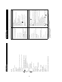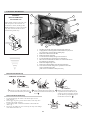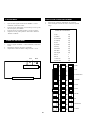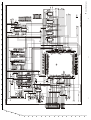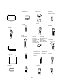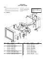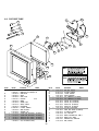
1
SERVICE MANUAL
MODEL
KV-28DX30U
COMMANDER
RM-888
DEST
UK
BE-3E CHASSIS
MODEL
CHASSIS NO.
KV-32DX30U
SCC-Q25H-A
1
COMMANDER
RM-888
DEST
UK
CHASSIS NO.
SCC-Q25J-A
7$%/( 2) &217(176
Section
Title
Specifications
Connectors
Self Diagnostic Software
....................
....................
....................
Page
Section
Title
Page
3
4
5
4. CIRCUIT ADJUSTMENTS
4-1.
Electrical Adjustments
4-2.
TT Test Mode
4-3.
T Test Mode
9
9
9
10
10
11
11
12
12
13
13
14
14
5. DIAGRAMS
5-1.
Block Diagram (1)
Block Diagram (2)
Block Diagram (3)
Block Diagram (4)
5-2.
Circuit Board Location
5-3.
Schematic Diagrams and
Printed Wiring Boards
* C Board
* D Board
* D2 Board
* VM Board
* H Board
* A Board
* A2 Board
* J Board
* D1 Board
* H7 Board
* F4 Board
* H8 Board
* N Board
5-4.
Semiconductors
5-5.
IC Blocks
....................
....................
....................
24
27
28
....................
....................
....................
....................
....................
29
33
37
41
44
....................
....................
....................
....................
....................
....................
....................
....................
....................
....................
....................
....................
....................
....................
....................
....................
44
45
49
52
54
56
59
65
70
71
74
76
76
77
90
93
6. EXPLODED VIEWS
6-1.
Chassis
6-2.
Picture Tube
....................
....................
95
96
7. ELECTRICAL PARTS LIST
....................
97
1. GENERAL
Overview of the Remote Control...................
AutomaticallyTuning the TV ....................
Finding your video channel
....................
Rearranging the TV Channels ....................
Adjusting the Picture
....................
Adjusting the Sound
....................
Setting up Dolby Pro Logic
....................
Changing the Screen Mode
....................
ManuallyTuning the TV
....................
Viewing Standard Teletext
....................
Viewing Digital Teletext
....................
Specifications
....................
Troubleshooting
....................
2. DISASSEMBLY
2-1.
Rear Cover Removal
2-2.
Chassis Removal
2-3.
N Board Removal
2-4.
Service Position
2-5.
A Board Removal
2-6.
A Extension Board
2-7.
Side Control Removal
2-8.
F4 Bracket Removal
2-9.
F4 and H8 Board Removal
2-10. Picture Tube Removal
Bottom Plates
....................
....................
....................
....................
....................
....................
....................
....................
....................
....................
....................
15
15
15
16
16
16
17
17
17
18
19
3. SET-UP ADJUSTMENTS
3-1.
Beam Landing
....................
3-2.
Convergence
....................
3-3.
Focus, Screen [G2] Adjustment ....................
3-4.
White Balance
....................
20
21
23
23
ATTENTION
APRES AVOIR DECONNECTE LE CAP DE’LANODE,
COURT-CIRCUITER L’ANODE DU TUBE CATHODIQUE ET CELUI
DE L’ANODE DU CAP AU COUCHE DE CARBONE PEINTE SUR
LE TUBE CATHODIQUE.
CAUTION
SHORT CIRCUIT THE ANODE OF THE PICTURE TUBE AND THE
ANODE CAP TO THE CARBON PAINTED ON THE CRT, AFTER
REMOVAL OF THE ANODE CAP.
ATTENTION !!
AFIN D’EVITER TOUT RISQUE D’ELECTROCUTION PROVENANT
D’UN CHÁSSIS SOUS TENTION, UN TRANSFORMATEUR
D’ISOLEMENT DOIT ETRE UTILISÈ LORS DE TOUT DÈPANNAGE
LE CHÁSSIS DE CE RÈCEPTEUR EST DIRECTMENT RACCORDÈ
Á L’ALIMENTATION SECTEUR.
WARNING !!
AN ISOLATION TRANSFORMER MUST BE USED DURING ANY
SERVICE WORK TO AVOID POSSIBLE SHOCK HAZARD DUE TO
LIVE CHASSIS, THE CHASSIS OF THIS RECEIVER IS DIRECTLY
CONNECTED TO THE POWER LINE.
ATTENTION AUX COMPOSANTS RELATIFS Á
LA SECURITÈ!!
SAFETY-RELATED COMPONENT WARNING !!
LES COMPOSANTS IDENTIFIÈS PAR UNE TRAME ET PAR UNE
MARQUE £ SUR LES SCHÈMAS DE PRINCIPE, LES VUES
EXPLOSÈES ET LES LISTES DE PIECES SONT D’UNE IMPORTANCE CRITIQUE POUR LA SÈCURITÈ DU FONCTIONNEMENT,
NE LES REMPLACER QUE PAR DES COMPSANTS SONY DONT LE
NUMÈRO DE PIÈCE EST INDIQUÈ DANS LE PRÈSENT MANUEL
OU DANS DES SUPPLÈMENTS PUBLIÈS PAR SONY.
COMPONENTS IDENTIFIED BY SHADING AND MARKED £ ON
THE SCHEMATIC DIAGRAMS, EXPLODED VIEWS AND IN THE
PARTS LIST ARE CRITICAL FOR SAFE OPERATION. REPLACE
THESE COMPONENTS WITH SONY PARTS WHOSE PART
NUMBERS APPEAR AS SHOWN IN THIS MANUAL OR IN
SUPPLEMENTS PUBLISHED BY SONY.
2
ITEM MODEL
UK
Television System
Stereo System
Channel Coverage
I
NICAM Stereo
UHF : B21-B69
Model
Color System
PAL, SECAM
NTSC4.43, NTSC3.58
(VIDEO IN)
KV-28DX30U
KV-32DX30U
136W
134W
FD Trinitron Wide
Approx 71 cm (28 inches)
(Approx 66cm picture measured
diagonally)
Picture Tube
Approx 82 cm (32 inches)
(Approx 76cm picture measured
diagonally)
110 degree deflection
Input/Output Terminals [REAR]
Inputs for Audio and Video signals.
1: 21-pin Euro connector
Inputs for RGB.
(CENELEC standard)
Outputs of TV Video and Audio
signals.
Inputs for Audio and Video signals.
Inputs for S Video.
2: 21-pin Euro connector
Outputs of TV Video and Audio signals.
(selectable)
Inputs for Audio and Video signals.
Inputs for S Video.
3: 21-pin Euro connector
Outputs for Video and Audio signals
(monitor out)
Sound output
Right and Left speaker
2x20W (Music Power)
2x10W (RMS)
Power Requirements
220 - 240V AC
Power Consumption
RCA Connectors
28" Approx 796x518x522mm
Dimensions
32" Approx 883x567x562mm
28" Approx 44.0kg
Weight
32" Approx 62.0kg
Supplied Accessories
RM-888 Remote Commander (1)
IEC designated R6 battery (2)
Other Features
Digital EPG, Dynamic Picture Control,
Vir tual Dolby, 2 Tuners
Variable output for Audio Signals
DIN
External Speakers
PCMCIA
Card Slot
Input/Output Terminals [FRONT]
Remote control system
Headphone jack
stereo mini jack
Power requirements
Audio inputs
Video inputs
S Video input
phono jacks
phono jacks
4 pin DIN
Dimensions
Weight
Infrared control
3V dc
2 batteries IEC designation
R6 (size AA)
Approx 210x45x23mm (w/h/d)
Approx 95g (not including battery)
Design and specifications are subject to change without notice.
Model Name
Item
KV-28DX30U
KV-32DX30U
Pal Comb
OFF
OFF
OFF
PIP
OFF
RGB Priority
ON
ON
Woofer Box
OFF
OFF
Scar t 1
ON
ON
Scar t 2
ON
ON
Scar t 3
ON
ON
Front in (4)
ON
ON
Projector
OFF
OFF
AKB in 16:9 mode
ON
ON
Norm B/G
OFF
OFF
Norm I
ON
OFF
Norm D/K
OFF
OFF
Norm AUS
OFF
OFF
Norm L
OFF
OFF
Norm SAT
OFF
OFF
Norm M
OFF
OFF
Teletext
ON
ON
Nicam Stereo
ON
ON
WARNING (UK Models only)
The flexible mains lead is supplied connected to a B.S. 1363 fused plug
having a fuse of 5 AMP rating. Should the fuse need to be replaced, use
a 5 AMP FUSE approved by ASTA to BS 1362, ie one that carries the
ASA
T mark.
IF THE PLUG SUPPLIED WITH THIS APPLIANCE IS NOT SUITABLE
FOR THE OUTLET SOCKETS IN YOUR HOME, IT SHOULD BE CUT
OFF AND AN APPROPRIATE PLUG FITTED. THE PLUG SEVERED
FROM THE MAINS LEAD MUST BE DESTROYED AS A PLUG WITH
BARED WIRES IS DANGEROUS IF ENGAGED IN A LIVE SOCKET.
When an alternative type of plug is used, it should be fitted with a
5 AMP FUSE, otherwise the circuit should be protected by a 5 AMP
FUSE at the distribution board.
How to replace the fuse.
Open the fuse compartment with
a screwdriver blade and replace
the fuse.
FUSE
3
SLQ FRQQHFWRU
Pin No
1
2
3
1
21
20
19
Signal
Signal level
Audio output B
(right)
Standard level : 0.5V rms
Output impedence : Less than 1kohm*
2
Audio output B
(right)
Standard level : 0.5V rms
Output impedence : More than 10kohm*
3
Audio output A
(left)
Standard level : 0.5V rms
Output impedence : Less than 1kohm*
4
Ground (audio)
5
Ground (blue)
6
Audio input A
(left)
7
Blue input
0.7 +/- 3dB, 75 ohms positive
8
Function select
(AV control)
High state (9.5-12V) : Part mode
Low state (0-2V) : TV mode
Input impedence : More than 10K ohms
Input capacitance : Less than 2nF
Standard level : 0.5V rms
Output impedence : More than 10kohm*
18
17
16
15
14
13
12
11
10
9
9
Ground (green)
10
Open
11
Green
12
Open
13
Ground (red)
14
8
Ground (blanking)
_
7
5
Green signal : 0.7 +/- 3dB, 75 ohms,
positive
_
Red input
0.7 +/- 3dB, 75 ohms, positive
(S signal Chroma
input)
0.3 +/- 3dB, 75 ohms, positive
High state (1-3V) Low state (0-0.4V)
Input impedence : 75 ohms
6
15
4
16
Blanking input
(Ys signal)
2
17
Ground (video
output)
18
Ground (video
input)
19
Video output
1V +/- 3dB, 75ohms, positive sync 0.3V
(-3+10dB)
Video input
1V +/- 3dB, 75ohms, positive sync 0.3V
(-3+10dB)
Video input
Y (S signal)
1V +/- 3dB, 75ohms, positive sync 0.3V
(-3+10dB)
_
3
1
_
20
_
_
21
Common ground
(plug, shield)
Connected
5HDU &RQQHFWLRQ 3DQHO
Not Connected (open)
* at 20Hz - 20kHz
)URQW &RQQHFWLRQ 3DQHO
p
-
S-Video
socket
S Video socket pin configuration
+
s4
4
Pin
No
Signal
Signal Level
-
1
Ground
2
Ground
-
3
Y (S signal) input
1V+/- 3dB 75ohm,
positive Sync. 0.3V
-3 +10dB
4
C (S signal) input
0.3V+/- 3dB
75ohm, positive
Sync.
MONO
4
L/G/S/I
R/D/D/D
4
4
BE-3E SELF DIAGNOSTIC SOFTWARE
The errors indicated below can be read using an Error Reader Display (Part Number S-188-900-10) connected to the service connector. Once an
error has been detected it will then be displayed on the two digit error reader. During the power up procedure and during normal run time, the micro’s
self diagnostic procedures monitor for various errors. Errors displayed refer to the table indicated below.
Error Code
00
01
02
03
04
05
06
07
08
09
10
11
12
13
14
15
16
17
18
19
20
21
22
23
24
25
26
27
28
29
30
31
32
33
34
Error Message
No error (TV Error Reader shows 00 in normal condition)
Not allowed (may be confused with Sircs response flash on LED)
Protection circuit trip[ (OCP, OVP & No V-Sync)
Reserved for OVP (Included in error 2 for BE-3E)
Reserved for No V-Sync (Included in error 2 for BE-3E)
AKB
IIC Scl Low <Power Up Only>
IIC Sda Low <Power Up Only>
IIC Sda & Scl Low <Power Up Only>
Jungle controller no acknowledge <Power Up Only>
Video Switch (CXA2040) no acknowledge <Power Up Only>
Tuner no acknowledge
MSP no acknowledge
NVM no acknowledge
AV Switch (CXA2089) no acknowledge
Not Used
Por t Expander (CXA1875) no acknowledge
Not Used
Dynamic Convergence (CXA8070) no acknowledge
Cannot initialise jungle (after initial power on check OK) - <Chassis Initialisation>
Jungle Controller response failure after power up check (+9v test)
Video Switch (CXA2040) cannot power on reset -<Chassis Initialisation>
Video Switch (CXA2040) response failure after power up check (+9v test)
NVM acknowledge fail after initialisation (STBY +5V - same as micro!)
MSP run-time failure <May Not Be Fatal - Display on Error Reader>
DSP run-time failure <May Not Be Fatal - Display on Error Reader>
M3L bus Clock low time out after data send <Run-Time Failure>
Not Used
M3L bus Clock low time out after data send <At Initialisation>
Not Used
Not Used
Not Used
Not Used
Compact Text does not respond (+5V test)
Compact Text run-time failure <May Not Be Fatal - Display on Error Reader>
5
Protection Error
Once every main loop (approximately 200ms OSD mode, 50ms text or menu mode), the micro checks the protection pin (pin 66). If the protection
pin is high 6 successive times, a protection error is diagnosed. The protection pin is not checked during the first 3 - 4 seconds after AC on.
If this error is diagnosed, the respective NVM register will be updated and the set goes straight into diagnostic standby with 2 flashes - no reset is
attempted.
AKB Error (Error 5)
Once every main loop the micro checks the AKB stability by reading the IKR return from the Jungle IC. IKR=1 means that the AKB is stable,
IKR=0 means that the AKB is unstable. If the AKB status is unstable for 10 seconds, an AKB error is diagnosed. AKB stability is not checked
during the first 20 seconds after AC switch on.
If this error is diagnosed, the respective NVM register will be updated and the response LED will flash 5 times continually, but the set will not go
into standby mode. If the AKB status becomes stable, and remains stable for 10 seconds, the LED will stop flashing.
0
10
20
Time /seconds
40
50
30
60
70
80
90
100
IKR
Return
A
B
C
D
E
F
A.
B.
C.
D.
IKR Return first goes high after 12 seconds
Micro begins checking IKR Return status 20 seconds after power on
Micro detects IKR return=0
Micro detects that IKR has been 0 for 10 seconds; NVM counter is incremented and the LED
starts flashing (flashes 5 times, off for 2 seconds, flashes 5 times, etc.)
E. Micro detects that IKR=1; LED continues to flash
F. Micro detects that IKR has been high for 10 seconds; LED stops flashing.
Startup Diagnostic Errors (Error 6-18, 27, 29-32)
NVM
6
7
8
9
10
11
12
13
14
16
18
27
29
30
31
32
Error Message
SCL pin Low
SDA pin Low
Both SCL and the SDA pins are Low
No acknowledge from the Jungle (CXA2076)
No acknowledge from the Video Switch (CXA2040)
No acknowledge from the tuner
No acknowledge from the MSP
No acknowledge from the NVM
No acknowledge from the CXA2089 Video Switch
No acknowledge from the CXA1875 Video Por t Expander
No acknowledge from the Dynamic Convergence (CXA8070)
M3L_TXD pin low after Compact Text RAM test
M3L_TXD pin low
M3L_RXD pin low
M3LEN pin low
Compact Text RAM test fail
If any of these errors are detected, the respective NVM register will be incremented. The software will then carry on with the power up sequence.
6
General IIC Device Run-time Errors (Errors 19-23)
NVM
19
20
21
22
23
Error Message
No acknowledge from Jungle when attempting to initialise
No acknowledge from Jungle when attempting to read registers
AV Switch cannot complete reset during initialisation
No acknowledge from AV Switch when attempting to read registers
No acknowledge from NVM when attempting to read or write
If any of these errors are detected, the respective NVM register will be incremented and the software will carry on.
Compact Text Run-time Errors (Errors 26, 28, 33 & 34)
NVM
26
28
33
Error Message
M3L_TXD pin low when checking register 81 (implies that no communication was
possible)
M3L_TXD pin low when attempting to initialise (implies that no communication
was possible)
Compact Text RAM test failed during initialisation of devices
In the case of these errors, the ‘device reset’ pin will be held low for 60ms, causing a hardware reset of Compact Text. Following this reset, a longer
timeout will be allowed for the M3L bus to recover. If the error still exists, the NVM register will be incremented and the software will carry on.
NVM
34
Error Message
Register 81 check fail, but M3L_TXD pin high (implies that Compact Text has
either reset or become corrupted)
In the case, the ‘device reset’ pin will be held low for 60ms, causing a hardware reset of Compact Text. Compact Text will then be re-initialised and
the NVM counter updated. This is the same as for errors 26, 28 and 33 except that the M3L bus timeout is not changed.
MSP and DSP Run-time Errors (Errors 24 & 25)
NVM
24
25
Error Message
Error 24 can be caused by any of the following :
- After MSP initialisation, Scar t Prescale Register check fail (implies that the
MSP has either reset or become corrupted).
-MSP fails to acknowledge reset instruction.
-Scar t Prescale Register check fail (implies that the MSP has either reset or
become corrupted).
DSP test byte corrupted implies that the MSP has either reset or become
corrupted).
For both these errors, the software will refresh the MSP and DSP registers. If the errors still exist, the NVM counter will be incremented, and the
software will carry on.
7
Error Display Mode
Error Display Mode is entered by the following sequence of commands :
Standby -> Information -> Digit 5 -> Volume Down -> TV
This mode will display a special menu, which will list all possible errors and the number of occurrances of each error (0 - 255, as stored in the
NVM). There will also be a display of the current error (00 if no error). This display mode will appear as follows :
ERROR DISPLAY MODE
Current Error Code = 00
Error Code
2
3
4
5
6
7
8
9
10
11
12
13
14
15
16
17
18
Occurrences
2
--0
0
0
0
0
0
0
0
0
0
3
0
0
6
Error Code
19
20
21
22
23
24
25
26
27
28
29
30
31
32
33
34
Occurrences
0
0
0
0
0
0
4
5
89
3
0
0
0
0
3
38
Whilst in this mode, the number of occurences of each error can be reset to 0 by following sequence of Sircs commands: Digit 8 -> Digit 0.
‘TT08’ will also reset this NVM data.
This mode can only be exited by switching off the TV.
The Current Error Code can also be read by using a TV Error Reader (IIC slave address 42H). This device simply receives 1 data byte, which is the
error number in binary coded decimal form.
8
9
To adjust TV volume
Press to adjust the volume of the TV.
To display sound menu
Press to change the sound settings. Press the
OK button to remove the display.
To display picture menu
Press to change the picture settings. Press
the OK button to remove the display.
To select Teletext
Press to switch on Teletext.
To select EPG
Press to display the Electronic Programme
Guide. Press again to remove display.
For double digit programme numbers,
e.g.23, press -/-- first, then the buttons 2 and
3. If you enter an incorrect first digit, select
-/-- button again to enter the programme
number of your choice.
To select channels
Press the numbered buttons to select
channels.
To reveal on screen information
Press to reveal all on-screen indications.
Press again to cancel. In teletext mode,
press to reveal concealed information (e.g.
answers to a quiz) then press again to
cancel.
To mute sound
Press to mute TV sound. Press again to
restore the sound.
RM-888
PROGR
MENU
To select channels
Press to select channels.
See Teletext section of manual for details.
To change screen format
Press to change the size of the screen.
9
To select menu items
Use these buttons and the OK button to select the
options available when in the menu system of this TV.
Pressing the OK button in normal TV mode will
display the channel listing table.
To display the menu
Press to use the TV menu system. Press again to
remove the menu from the TV screen.
To return to previous channel
Press to return to the previous channel you were
watching. Note: This can be done only if you watched
the previous channel for at least 5 seconds.
To select input signal or freeze teletext
Press to select inputs from the TV sockets (see Using
Optional Equipment section). In teletext mode, press
to freeze the displayed page. Press once again to
cancel.
To temporarily switch off TV
Press to temporarily switch off TV. Press again to
switch on from standby mode. To save energy, we
recommend switching off completely when the TV is
not in use.
NOTE: After 15-30 minutes without a TV signal and
without any button being pressed, the TV switches
automatically into standby mode.
Overview of the remote control buttons
Overview
8
7
MENU
6. Press the PROGR+/- or the numbered buttons on the
remote control to view the TV channels.
5. Press the MENU button to remove the menu from the TV
screen.
4. When the TV has finished tuning in all available
channels, the ‘PROGRAMME SORTING’ menu appears
on the TV screen enabling you to change the order of the
channels on your TV. If you do not wish to use this
option, proceed to step 5.
If you wish to change the channel order, press the V or v
buttons on your remote control to select the channel you
want to move, then press the OK button. Press the V or v
buttons to select the new programme number position for
your selected channel then press the OK button to
confirm. The selected channel now moves to its new
programme position. Repeat this procedure if you wish to
sort the order of other channels on your TV.
3. Ensure the antenna is connected as instructed, then press
the OK button to confirm. The TV starts to automatically
search and store all available channels for you. Please be
patient and do not press any buttons.
The digital channels will be stored on programme
numbers 1-90 and the analogue channels on programme
numbers 91-99.
Note: If any digital channels are stored on programme
numbers 91-99 during the Automatic Tuning procedure,
then no analogue channels will be allocated. If this
happens, please refer to the section ‘Manually tuning the
TV’ on page 19 of this manual to tune in and store the
analogue channels.
2. The ‘automatic tuning’ menu appears on the TV screen in
your selected language. Press the V or v buttons to select
‘YES’ then press the OK button to confirm.
Confirm: OK
BBC TWO
Please confirm that
antenna is connected
Yes
No
Confirm: OK
Do you want to start
automatic tuning?
Note: If you wish to move your video channel to a different programme position, refer to the ‘Re-arranging the TV channels’ section in this
instruction manual.
1. Press the PROGR +/- buttons on the remote control until the video picture appears on the TV screen.
If you have connected a VCR to your TV, you now need to find the video channel.
7. Finding your video channel after tuning
RM-888
PROGR
OK
0
6
5
4
9
3
2
1
1. When switching on the TV for the first time, the
‘LANGUAGE’ menu appears automatically on the TV
screen enabling you to select in which language you wish
to read the TV menu screens. Press the V or v buttons on
the remote control to select your chosen language then
press the OK button to confirm your selection.
7
When you first switch on the TV, the following sequence of menu screens appear on the TV enabling you to 1) choose a language
for the TV menu screens, 2) tune channels to the TV, 3) arrange the channels.
6. Automatically tuning the TV
Getting Started
The operating instructions mentioned here are partial abstracts from the ‘Operating
Instruction Manual’. The page numbers of the ‘Operating Instruction Manual’ remain
as in the manual.
SECTION 1 GENERAL
10
24
OK
RM-888
PROGR
MENU
7. Press the MENU button to remove the menu from the TV
screen.
6. Repeat steps 4 and 5 if you wish to sort other channels.
5. Press the V or v buttons to select the new programme
position (e.g. PROG 4) for your selected channel, then
press the OK button to confirm. The selected channel
now moves to its new programme position.
4. Press the V or v buttons to select the channel you want
to move then press the OK button to confirm.
3. Press the v button to select ‘Programme Sorting’ then
press the b button to enter the ‘PROGRAMME
SORTING’ menu.
2. Press the V or v buttons to select the
symbol on the
menu screen then press the b button to enter the
‘PRESET’ menu.
1. Press the MENU button on the remote control to display
the menu on the TV screen.
After tuning the TV, you can use this feature to change the channel order.
Re-arranging the TV channels
Additional TV Features
10
OK
RM-888
PROGR
MENU
B
On
1. Press the
symbol on the remote control for picture modes
or the
symbol for sound modes.
2. Press the V or v buttons to select the desired mode.
3. Press the OK button to remove the display from the TV
screen.
You can quickly change the Picture Mode or the Sound Mode
without entering the ‘PICTURE CONTROL’ or the ‘SOUND
CONTROL’ menu screens.
Changing picture and sound modes quickly
*Only if you select ‘Personal’ in ‘Picture Mode’.
** Available for NTSC colour system only.
Off
Set to Composite or RGB. Choose the option
that gives you the picture quality you prefer
Digital Signal
b
Resets picture to factory preset levels
(refer to page 14 for details)
Format
Scroll
Auto 16:9
Personal (for individual settings)
Movie (for films)
Live (for live broadcasts)
Format
Brightness*
Colour*
Sharpness*
Hue**
B
Picture Modeb
Reset
Contrast
Picture Mode
1. Press the MENU button on the remote control to display the
menu on the TV screen.
2. Press the V or v buttons on the remote control to select the
symbol on the menu screen then press the b button to
enter the ‘PICTURE CONTROL’ menu.
3. Press the V or v buttons to select the item on the screen you
wish to adjust then press the b button to confirm. For a
description of the menu items and their effects, see the table
below.
4. If you selected ‘Picture Mode’ or ‘Format’ in step 3, press the
V or v buttons to select the item on the screen you wish to
adjust then press the b button to confirm.
5. Press the b or B buttons to adjust your selected item.
6. As soon as you have adjusted the item, press the OK button to
store the new setting.
7. If you selected ‘Picture Mode’ or ‘Format’ in step 3, press the
B button to return to the ‘PICTURE CONTROL’ menu.
8. Repeat steps 3-7 to adjust the other items.
9. Press the MENU button to remove the menu from the TV
screen.
Although the picture is adjusted at the factory, you can modify it to suit your own taste.
Adjusting the picture
Additional TV Features
Personal
Movie
Live
11
OK
RM-888
PROGR
MENU
Personal
Rock
Jazz
Pop
Choose from the special sound effects:
Off --> Pro Logic --> 3 Stereo --> Virtual Dolby -->
Pseudo Stereo --> Spatial
StereoB
b Mono (for a stereo broadcast)
A for channel 1B b B for channel 2
(for a bilingual broadcast)
B
Surround Mode
Dual Sound
Volume Offset
Auto Surround
Headphones
i Volume
i Dual Sound
Boosts bass by a fixed amount
Bass Extension
Set to ‘On’ to automatically select Pro Logic
Surround sound when transmitted.
Stereo B b Mono (for a stereo broadcast)
A for channel 1 B b B for channel 2
(for a bilingual broadcast)
The channel volume level can be b
adjusted over a range of -12 to +12.
Resets sound to factory preset levels
Only available when ‘Surround Mode’ is set to ‘Off’
In ‘Personal’ mode, Treble and Bass can be adjusted
B
b
Reset
Balance
Sound Mode
1. Press the MENU button on the remote control to display the
menu on the TV screen.
2. Press the V or v buttons to select the
symbol on the
menu screen then press the b button to enter the ‘SOUND
CONTROL’ menu.
3. Press the V or v buttons to select the item on the screen you
wish to adjust then press the b button to confirm. For a
description of the menu items and their effects, see the table
below.
4. If you selected ‘Sound Mode’ or ‘Surround Mode’ in step 3,
press the V or v buttons to select the item on the screen you
wish to adjust then press the b button to confirm.
5. Press the b or B buttons to adjust your selected item.
6. As soon as you have adjusted the item, press the OK button
to store the new setting.
7. If you selected ‘Sound Mode’ or ‘Surround Mode’ in step 3,
press the B button to return to the ‘SOUND CONTROL’
menu.
8. Repeat steps 3-7 to adjust the other items.
9. Press the MENU button to remove the menu from the TV
screen.
Although the sound is adjusted at the factory, you can modify it to suit your own taste.
Adjusting the sound
Additional TV Features
11
OK
RM-888
PROGR
MENU
Note: After setting up Dolby ProLogic, refer to the ‘Adjusting the sound’ section
on page 11 and set the Surround Mode to Pro Logic.
10. Press the MENU button to remove the display.
9. Repeat steps 7 and 8 to select and adjust the ‘Centre’,
‘Right’, and ‘Surround’ speakers, so that the sound output
from all speakers are balanced in relation to your sitting
position.
8. Press the V or v buttons to alter the sound level, then
press the OK button.
7. Press the v button to select the ‘Left Speaker’, then press
the b button to confirm. The tone remains at the left
speaker.
6. Press the v button to select ‘Test Tone’ then push the b
button to enter. Press the b or B buttons to select ‘On’,
then press the OK button.
The test tone will cycle through all the speakers.
5. Press the v button to select ‘Centre Mode’, then push the
b button to enter. Press the b or B buttons to select one
of the following modes then press the OK button to store
the chosen mode:
Normal: all 5 speakers are activated
Wide: wider bandwidth for centre speaker
Phantom: centre speaker is not used (This cannot be
selected if you have chosen “3 stereo” mode in step 4)
4. Press the V or v buttons to select ‘Dolby Mode’, then
press the b button to enter. Press the b or B buttons to
select one of the following modes then press the OK
button to store the chosen mode:
Pro Logic: all 5 speakers are activated
3 stereo: surround speakers are not used
Virtual: no external speakers required. Do not select this
mode if you wish to receive Dolby Pro logic
3. Press the V or v buttons to select ‘Dolby Mode Setup’ on
the menu screen then press the b button to enter the
‘DOLBY MODE SETUP’ menu.
2. Press the V or v buttons to select the
symbol on the
menu screen then press the b button to enter the
‘PRESET’ menu.
1. Press the MENU button on the remote control to display
the menu on the TV screen.
13
Before listening to Dolby Pro Logic encoded programmes, you can adapt the Dolby features to suit your own taste. This is only
required if you have connected your own external speakers (SS-CR190 or equivalent), and/or if you decide to change the speaker
positions.
Note: There will be no output available from the headphones or the audio output sockets on the rear of the TV during Dolby Pro
Logic mode.
Setting up Dolby Pro Logic
Additional TV Features
12
14
OK
RM-888
PROGR
MENU
Smart - imitation of wide screen effect (16:9) for 4:3
broadcasts
Wide - for 16:9 broadcasts
Zoom - imitation of wide screen effect (16:9) for movies
broadcast in cinemascopic format
14:9 - compromise between 4:3 and 16:9 format - for
conventional 14:9 picture
4:3 - conventional 4:3 picture
Note: You can change the picture format quickly without having
to enter the menu system. Simply press the
button repeatedly
until the picture is displayed in the format you desire.
7. Press the MENU button to remove the menu from the TV
screen.
6. Auto 16:9
Press the V or v buttons to select ‘Auto 16:9’ then press the b
button to enter. Press the B or b buttons to select ‘On’ if you
wish the TV to switch automatically to wide format when a
16:9 broadcast is detected, or ‘Off’ to retain the format
selected in step 4. Press the OK button to store.
5. Scroll (Applies to Zoom, 14:9 or Smart format only)
Press the V or v buttons to select ‘Scroll’. You can use
‘Scroll’ to move the screen up or downwards in order to see
the cut-off parts (e.g. to read subtitles). Press the b button to
highlight the present value then press the B or b buttons to
adjust the screen position over a range of -5 to +5. Press the
OK button to store.
•
•
•
•
•
4. Format
Press the V or v buttons to select ‘Format’ then press the b
button to enter. Press the b or B buttons repeatedly to select
one of the following modes then press the OK button to store
the chosen mode:
3. Press the V or v buttons to select ‘Format’ on the menu
screen then press the b button to enter the ‘FORMAT’ menu.
FORMAT
Format
Scroll
Auto 16:9
rmat
Smart
Wide
0
On
4:3
14:9
Zoom
Wide
7
MENU
9
RM-888
PROGR
OK
0
8
6
5
4
NOTE: After manually tuning in the channels you require, you
can sort the channels into the order you prefer by following the
procedure ‘Re-arranging the TV channels’ on page 24.
10. Repeat steps 4-9 if you wish to store more channels then
press the MENU button to remove the menu from the TV
screen.
9. If this is the channel you wish to store, press the OK button.
8. If you do not wish to store this channel on the programme
number you selected, press the V or v buttons on the
remote control to continue searching for the desired
channel.
7. If you wish to change the ‘SERV’ service number (on
digital programmes only), select each digit in turn and press
the numbered buttons on the remote control to change to
your desired service.
6. Select the first number digit of ‘CHAN’ (channel) then the
second number digit of ‘CHAN’ with the numbered buttons
on the remote control
or
Press the V or v buttons to search for the next available
channel.
5. Press the V or v buttons to select the TV broadcast system
(I for analogue or DIG for digital) or a video input source
(AV1, AV2 ...) then press the b button to confirm.
4. Press the V or v buttons to select an unused programme
number for your channel then press the b button to enter.
3. Press the V or v buttons to select ‘Manual Programme
Preset’ on the menu screen then press the b button to enter
the ‘MANUAL PROGRAMME PRESET’ menu.
2. Press the V or v buttons to select the
symbol on the TV
screen then press the b button to enter the PRESET menu.
3
2
2. Press the V or v buttons to select the
symbol on the menu
screen then press the b button to enter the ‘PICTURE
CONTROL’ menu.
1
1. Press the MENU button on the remote control to display
the menu on the TV screen.
03
19
You have already tuned the TV automatically using the instructions at the start of this manual. You can however carry out this
operation manually, adding channels to the TV, one at a time.
Manually tuning the TV
Additional TV Features
1. Press the MENU button on the remote control to display the
menu on the TV screen.
Using this Screen Mode feature you can change the aspect ratio of the screen.
Changing the screen mode
Additional TV Features
13
8
4
7
0
6
5
RM-888
PROGR
MENU
9
3
2
1
button to switch off teletext.
button to display teletext.
3. Press the
button twice to return to normal TV.
2. Press the coloured buttons to search for the page you desire:
Red: to go back to the previous page.
Green: to proceed to the next page.
Yellow: to proceed to the first page of the next group.
Blue: to proceed to the first page of the next block.
1. Press the
Displaying TOP-Text (when available)
With TOP-Text you can access pages easily by selecting blocks or
groups of pages. The block is a category (for example Sports) which
includes the groups (for example Football). When TOP-Text is
broadcast, a colour coded menu appears at the bottom of the screen.
The colours of this menu correspond to the red, green, yellow and
blue buttons on the remote control. Press these coloured buttons to
displayed the desired pages.
Using colour buttons to access pages (Fastext)
When the colour coded menu appears at the bottom of a page, press
the colour buttons (red, green, yellow or blue) on the remote control
to access the corresponding page.
Revealing concealed information (eg:answers to a quiz).
Press the
button to reveal information. Press again to conceal the
information.
To freeze a Teletext page
Press the
button to freeze the page. Press again to cancel the
freeze.
To move to the next or preceding page
Press the
or
buttons to select the previous or next page.
Using Other Standard Teletext Functions
4. Press the
3. Select your required page using the numbered buttons on the
remote control. If you make an error, complete the number, then
re-enter the correct page number.
2. Press the
on the remote control to switch on teletext. Press
the
button again if you wish to superimpose teletext on to
the TV screen.
1. When viewing analogue channels press a numbered button on
the remote control to select the channel which carries the
teletext service you wish to receive.
Selecting Teletext
Teletext is an information service transmitted by most TV stations.
Viewing standard teletext
Teletext
25
153
101
98
25
98
Weather
Weather
101
Sport
Sport
153
News
News
25
Programme
Index
TELETEXT
TELETEXT
Programme
Index
26
7
4
1
OK
0
8
5
2
RM-888
PROGR
MENU
9
6
3
button
On other channels there may be no on-screen symbol, but you can
see if there is a digital service as follows:
1. When watching a digital TV channel, press the
button on
your remote control to display any text service which may be
available.
2. Press the numbered buttons to select the various pages of
information available and/or the coloured buttons for the
functions shown on screen.
3. When you have finished using the text service, press the
button to return to normal TV.
4. When you have finished viewing teletext, press the
and then select an alternative digital channel.
3. Once the text information is displayed on screen, use the V, v,
B or b buttons, the coloured buttons and/or the numbered
buttons to access the chosen information.
2. Alternatively, you may be requested to use the numbered and
coloured buttons on your remote control to display the various
pages of text information. If when viewing the teletext pages,
you are requested to select ‘OK’ or ‘Cancel’, press the OK
button for ‘OK’ or the
button for ‘Cancel’.
1. Press the V, v, B or b buttons to select the symbol then press
the OK button to display the chosen information.
Normal teletext services may also be available on other digital
channels. Sometimes this is indicated by a small symbol or text
display on your TV screen, superimposed on the channel you are
watching.
Selecting teletext from the other
digital channels
5. When you have finished viewing teletext, press the
button
or the PROG +/- buttons, and then select an alternative digital
channel.
4. If when viewing the teletext pages, you are requested to select
‘OK’ or ‘Cancel’, press the OK button for ‘OK’ or the
button for ‘Cancel’.
3. Alternatively, you can use the numbered and coloured buttons
on the remote control to directly enter the page number required
and to display the various pages of text information.
2. Once the teletext channel is displayed, follow the instructions
on-screen to display the teletext information, then press the V,
v, B or b buttons to guide the on-screen cursor to the required
area of the screen, then press the OK button to display the
chosen information.
1. To view the dedicated digital teletext service, press the
numbered buttons on your remote control to select the relevant
channel number. If you do not know the channel number, press
the OK button to look for that channel in the channel table.
Selecting the dedicated digital
teletext channel
Most of the digital TV channels broadcast information via teletext. This digital service includes high quality text and graphics as
well as advanced navigational options. Additionally, this television set has access to a dedicated digital teletext channel.
Viewing Digital Teletext
Teletext
14
2x20W (music power)
Design and specifications are subject to change without notice.
Other features
Teletext
Dolby ProLogic Surround System
Smartlink
Accessories supplied
RM-888 remote control (1)
IEC designated size AA battery (2)
Approx. 44kg
Approx. 62kg
34
•
•
•
•
•
•
•
•
•
•
•
•
•
•
•
•
•
•
•
•
•
Plug in the TV.
Press the
button on the front of the TV.
If the
indicator is on press the / button or a numbered button on the
remote control.
Check the aerial connection.
Select
on the TV menu system then adjust the brightness, picture and colour
balance levels.
Tune in the analogue channels available using the ‘Manually tuning the TV’
instruction in this manual, then contact a local installer to find out when digital
transmissions begin in your area.
Contact a local installer to find out which transmitter you should be pointing
your aerial at.
Change your aerial to cover the channels used by digital programmes. (Contact
a local installer)
Ensure aerial is correctly aligned to transmitter.
Ensure aerial is plugged directly into the TV (not through other equipment).
Upgrade to a higher gain aerial.
Subscribe to pay-per-view broadcaster.
See ‘Skipping programme positions’ section.
See ‘Re-arranging the TV channels’ section.
Do not open the cabinet, refer to qualified personnel.
Contact your nearest Sony Service Centre.
Press the
+ button on the remote control.
If
is displayed on the screen, press the
button on the remote control.
Press the
button repeatedly until the RGB symbol
is displayed on
screen.
Select
on the TV menu system then adjust the colour setting.
If you continue to have these problems, have your TV serviced by qualified personnel or
you can contact the Sony UK Digital HelpLine on 0870 600 1717.
NEVER open the casing yourself.
Colour level setting.
Wrong external mode selected.
Volume control.
Fault.
Scrambled/subscription-only channel.
Programme information without picture or sound.
No digital transmissions from the transmitter you
are currently using.
Unsuitable aerial.
No digital transmissions in your area.
Picture level adjustment.
Aerial disconnected.
Weight
KV-28DX30U:
KV-32DX30U:
33
Cause
Power off.
TV in standby.
Weak signal.
•
Wrong external mode selected on an RGB video source.
Colour level setting.
Batteries low.
Inputs from external equipment not switched off.
•
•
•
•
Solution
The button marked
on the rear of the TV is pressed in.
The TV has been set up to receive Dolby Pro Logic.
•
•
No head phone output and no output from the audio
sockets marked
on the rear of the TV.
Poor picture quality.
No colour on colour programmes.
Remote control does not function.
Distorted picture when changing programmes or
selecting Teletext.
Good Picture, no sound.
Standby indicator flashing.
Some channels are blank.
•
Power off.
TV in standby.
Aerial disconnected.
Picture preset level adjustment.
No digital transmissions in your area.
No digital transmissions from the transmitter you are currently using.
Weak signal.
Unsuitable aerial.
Scrambled/subscription-only channel.
Programme used only for data (no picture or sound).
Programme not being transmitted.
Digital mode Timer Record active (regular flash).
Fault (irregular flash).
Volume control.
No picture, no sound.
Poor or no picture (screen is dark), but good sound.
No picture on any channel after digital tuning.
Cause
•
•
•
•
•
•
•
•
•
•
•
•
•
•
Problem
Here are some simple solutions to problems which may affect the picture and sound.
Troubleshooting
Additional Information
Dimensions (wxhxd)
KV-28DX30U:
Approx. 796x518x522mm
KV-32DX30U:
Approx. 883x567x562mm
Power consumption
KV-28DX30U:
136W
KV-32DX30U:
134W
Sound output
Left/Right:
Front Terminals
Video input -phono jack
2
Audio inputs - phono jacks
2
S
video input - 4 pin DIN
s
Headphones jack - minijack stereo
Rear Terminals
21-pin Euro connector (CENELEC standard) including audio/video
1
input, RGB input, TV audio/video output.
2 / s 2 21-pin Euro connector (CENELEC standard) including audio/video
input, S-video input, selectable audio/video output.
21-pin Euro connector (CENELEC standard) including audio/video
3
input, selectable audio/video output.
Audio outputs - phono jacks
MODEM
Modem connection
Picture tube
KV-28DX30U
FD Trinitron WIDE
Approx. 71cm (28inches) (Approx. 66cm picture measured diagonally), 102° deflection
KV-32DX30U
FD Trinitron WIDE
Approx. 82cm (32 inches) (Approx. 76cm picture measured diagonally), 102° deflection
Channel coverage
UHF:B21-B69
Colour system
PAL
NTSC 3.58, 4.43 (only Video in)
TV system
I/DVB-T
Specifications
Additional Information
SECTION 2 DISASSEMBLY
2-3. N Board Removal
<=
<=
<=
2-1. Rear Cover Removal
=>
<=
Shield
Case
=>
=>
=>
<=
<=
Clip
Remove the rear cover fixing screws indicated. Take care
when removing the rear cover not to damage the speaker
cables [Disconnect the speaker connector] as speakers are
fitted inside the rear cover.
To remove the N Board first pull the shield case shown
vertically. The clip circled can then be released and the board
gently removed.
2-2. Chassis Removal and Refitting
When refitting the chassis ensure that the main
bracket is located in the beznet guide slots before
sliding the chassis forwards. Refit the
interconnecting leads in their respective purse locks.
To remove lift the main bracket rear slightly and slide the
chassis away from the beznet. Ensure that the interconnecting
leads are released from their purse locks to prevent damage
being caused.
15
2-4. Service Position
Position the chassis as indicated to access the solder side. To gain access to the D Board follow the instructions on page 19. [Removal and
Replacement of the main bracket bottom plates ].
2-6. A Extension Board
2-5. A Board Removal
A board
BE-3E Extension Board
To remove the A Board release the clip circled and gently
remove the board in a vertical direction.
To gain test access to the A Board remove the board and plug in
the extension board. The A board can then be plugged into the
extension board to allow testing.
16
2-7. Side Control Module Removal
2-8. F4 Bracket Removal
Remove the two screws fixing the user control module to the
side of the set. The control module can then be removed by
sliding it towards the rear of the set allowing access to the H7
Board.
Release the clip circled and pull the bracket towards the rear of
the set. The bracket can then be removed to allow access to the
boards.
Screws
Clip
2-9. F4 and H8 Board Removal
To remove the F4 and H8 Boards release the clips circled and
ease the boards gently away from the support bracket.
Clips
Clips
17
3LFWXUH 7XEH 5HPRYDO
10
8
WARNING:
BEFORE REMOVING
THE ANODE CAP
High voltage remains in the CRT even
after the power is disconnected. To
avoid electric shock, discharge CRT
before attempting to remove the anode
cap. Short between anode and CRT
coated earth ground strap.
1
9
7
3
2
6
Coated Earth
Ground Strap
5
4
1.
2.
Discharge the anode of the CRT and remove the anode cap.
Unplug all interconnecting leads from the Deflection yoke, neck
assy, degaussing coils and CRT grounding strap.
3. Remove the C Board from the CRT.
4. Remove the chassis assembly.
5. Loosen the Neck assembly fixing screw and remove.
6. Loosen the Deflection yoke fixing screw and remove.
7. Place the set with the CRT face down on a cushion and remove
the Degaussing Coil holders.
8. Remove the Degaussing Coils.
9. Remove the CRT grounding strap and spring tentioners.
10. Unscrew the four CRT fixing screws [ located on each CRT
corner ] and remove the CRT.
[Take care not to handle the CRT by the neck.]
5HPRYDO RI WKH $QRGH&DS
* REMOVING PROCEDURES.
c
a
b
b
Anode button
1 Turn up one side of the rubber cap in
the direction indicated by the arrow a
+RZ WR KDQGOH WKH $QRGH&DS
1.
2.
3.
4.
2 Using a thumb pull up the rubber cap 3 When one side of the rubber cap is
firmly in the direction indicated by the
separated from the anode button, the
arrow b
anode-cap can be removed by turning
up the rubber cap and pulling it up in
the direction of the arrow c
To prevent damaging the surface of the anode-cap do not use
sharp materials.
Do not apply too great a pressure on the rubber, as this may cause
damage to the anode connector.
A metal fitting called a shatter hook terminal is fitted inside the
rubber cap.
Do not turn the rubber foot over excessively, this may cause damage
if the shatter hook sticks out.
18
1
Fig 1
FIG 3
MAIN BRACKET
1
2
2
19
1
Catch
Tab
NUMERICAL MARKINGS
4
2
ATTENTION
In the event of the plates requiring to be removed
at a later stage, this can be achieved by inserting a
screwdriver in the snap-recess indicated as in Fig 4
and lifting out.
Fig 2
REFITTING
other.
Fig 4
REFITTING
Please note that the plates need to be rotated 180 degrees from their cut position to allow the
tabs to be fitted into their catch positions.
3
INSERT FROM
THE BOTTOM
SIDE
Cut points
ATTENTION
Because the plates differ in size it is important that the correct plates are refitted in their original
location.
THIS PLATE MUST BE REMOVED
(TURN 180' NOT FLIP OVER)
AFTER CUTTING AWAY
FOR SAFETY REASONS
Note : There are 4 plates fitted to the main bracket and secured by3 gates.
Only remove the necessary plate to gain access to the printed wiring board.
THIS PLATE MUST BE REMOVED
(TURN 180' NOT FLIP OVER)
AFTER CUTTING AWAY
FOR SAFETY REASONS
(2) REFITTING THE PLATES
THIS PLATE MUST BE REMOVED
AFTER CUTTING AWAY FOR THE SAFETY REASON.
In the event of servicing being required to the solder side of the D Board printed wiring board,
the bottom plates fitted to the main chassis bracket require to be removed.
This is performed by cutting the gates with a sharp wire cutter at the locations indicated by the
arrows.
2
2
For safety reasons, on no account should the plates be
removed and not refitted after servicing.
4
(1) REMOVING THE PLATES
1
£
2
2
2
4
REMOVAL AND REPLACEMENT OF THE MAIN-BRACKET
BOTTOM PLATES.
4
SECTION 3 SET-UP ADJUSTMENTS
•
•
•
Carry out the adjustments in the following order :
3-1.
Beam Landing.
3-2.
Convergence.
3-3.
Focus.
3-4.
White Balance.
When complete readjustment is necessary or a new picture tube is
installed, carry out the following adjustments.
Unless there are specific instructions to the contrary, carry out
these adjustments with the rated power supply.
Unless there are specific instructions to the contrary, set the
controls and switches to the following settings :
Contrast
Note : Test equipment required.
1.
Color bar/pattern generator.
2.
Degausser.
3.
Oscilloscope.
4.
Digital multimeter.
.................................. normal
Brightness .................................. normal
3-1. Beam Landing
Caution :
Preparation :
1.
2.
High voltages are present on the Deflection yoke terminals - take care
when handling the Deflection yoke whilst carrying out adjustments.
In order to reduce the influence of geomagnetism on the set’s
picture tube, face it in an easterly or westerly direction.
Switch on the TV set’s power and degauss with a degausser.
(2) Landing
Note : Before carrying out the following adjustments adjust the
magnets as indicated below [See Fig.3-4].
1. Input a crosshatch signal from the signal generator.
2. Rough-adjust the focus and horizontal convergence.
3. Switch from the crosshatch pattern to an all-red pattern.
4. Move the deflection yoke backwards and adjust with the purity
magnet so that the red is at the centre and it aligns
symmetrically [See Fig.3-5].
5. Move the deflection yoke forward to the point where the entire
screen just becomes red [Mark its position].
6. Move the deflection yoke further forward until the screen just
changes colour at the edges. [Mark its position]
7. Position the deflection yoke between the two marks indicated
above.
8. Input a crosshatch pattern from the pattern generator and rotate the
deflection yoke so that the horizontal lines are parallel with the top
and bottom of the screen.
9. When the position of the deflection yoke has been determined,
fasten it with its fixing screw.
10. Switch the pattern generator to green then blue and confirm the
purity.
11. If the beam does not land correctly in all the corners of the screen,
use disk magnets to correct it. [Confirm the corner landing for
green and blue]
(1) Adjustment of Correction Magnet for Y-Splitting Axis.
1.
2.
3.
4.
5.
6.
7.
Input a crosshatch signal from the pattern generator.
Set the Picture control to minimum and confirm that the
Brightness control is set to normal.
Position the neck assembly as indicated in Fig.3-3.
Loosen the deflection yoke fixing screw.
Move the deflection yoke as far forward as is possible.
Adjust the upper and lower pin symmetrically by opening or
closing the Y-splitting axis correction magnets located on the neck
assembly. [See Fig 3-1 and Fig 3-2]
Return the deflection yoke to its original position and re-tighten its
fixing screw.
Fig.3-1
Y-splitting axis correction magnet
Fig.3-3
Neck assy
G2
G1
+
G3
Fig.3-2
20
Align the edge
of the neck assy with
the edge of the G2 grid
on the G3 side.
Fig.3-4
Purity control magnets
Align both Purity magnets
to the vertical position
Purity magnets
Align pips on
each magnet
3-2. Convergence
(1) Screen centre convergence [Static convergence]
1.
2.
3.
Input a dot pattern signal from the pattern generator.
Normalize the picture setting.
[Moving vertically], adjust the V.STAT magnet so that the
vertical red, green and blue dots coincide at the centre of the
screen.
GREEN
RED
BLUE
Center dot
R
G
B
R G
)LJ
Purity control corrects
this area
a
c
B
V.STAT Vertical Static Magnet
Disk magnets or
rotatable disk
magnets correct
these areas (a-d)
H STAT
convergence
control
C Board
RV701 (H STAT)
H STAT Convergence
(on mount side)
b
d
Deflection yoke positioning
corrects these areas
By opening or closing the V.STAT magnet, the red green and blue
dots move in the direction indicated below.
Disk Magnets
Note:
21
B
B
G
G
R
R
Do not adjust the H.STAT by rotating the V.STAT
magnets as this can affect the focus setting.
4.
Correction for HMC [Horizontal mis-convergence] and VMC
[Vertical mis-convergence] by using the BMC [Hexapole] magnet.
HTIL correction can be performed by adding a THL correction
assembly to the Deflection yoke.
a). HMC correction by BMC [Hexapole] magnet and movement of
the electron beam.
HMC co r r e ct i o n ( A )
A < B R G
H M C c o r r e c t io n ( B)
A > B R
B
G B
YCH Adjustment
A = B R G B
A = B R G B
+
b). VMC correction by BMC [Hexapole] magnet and movement of
the electron beam.
+
+
YCH VR
Deflection Yoke
VMC correction(A)
VMC correction(B)
TLV Adjustment
C < D
R
C
G
D
B
C
D
C = D
R
C > D
R
G
G
B
B
C = D
R
G
TLV VR
B
+
+
HAMP Adjustment
+
Deflection Yoke
H-TRAP Adjustment
+
Adjust the HAMP using HAMPL and HAMPR registers in the
Dynamic Convergence section of the service menu.
HTRAP VR
+
+
Deflection Yoke
HTIL Adjustment
The H-TRAP should not be adjusted unless absolutely necessary as it
affects the TLV settings.
THL Correction assy
22
Layout of each control
3-3. Focus, Screen (G2) Adjustment
1.
2.
3.
Purity magnet
BMC (Hexaploe) magnet
V STAT convergence magnet
Y-splitting axis correction magnet
Focus
Control
Note : If you are unable to adjust the corner convergence properly,
this can be corrected with the use of permalloy magnets.
a
Receive a television broadcast signal.
Normalize the picture setting.
Adjust the focus control located on the flyback transformer to
obtain the best focus at the centre of the screen.
Bring only the centre area of the screen into focus, the magentaring appears on the screen. In this case, adjust the focus to
optimize the screen uniformly.
Screen
(G2)
b
a-d: screen-corner
convergence defect
c
d
G2 adjustment [RV5376]
1.
2.
3.
4.
Input a dot signal from the pattern generator.
Set the Picture, Brightness and Colour to minimum.
Apply 170V DC from an external power supply to the R, G and B
cathodes of the CRT.
Whilst watching the picture, adjust the G2 control RV5376
[SCREEN] located on the C Board to the point just before the
flyback return lines disappear.
3-4. White Balance Adjustment
[Adjustment in the service mode using the remote
commander]
Install the permalloy assembly
for the area that needs correcting.
a
White balance adjustment for TV mode
1.
2.
b
3.
4.
5.
6.
Permalloy Assy
X-4387-214-1
7.
c
d
Convergence adjustment with permalloy
23
Input an all-white signal from the pattern generator.
Enter into the ‘Service Mode’ by pressing ‘TEST’, ‘TEST’ and
‘MENU’ on the Service Commander.
Select ‘Picture Adjustment’ from the on screen menu display and
press the joystick to the right.
The ‘Picture Adjustment’ menu will appear on the screen.
[See Page 24]
Select ‘Sub Contrast’ and adjust to 7.
Adjust the ‘G-Drive’ and the ‘B-Drive’ so that the white
balance becomes optimum.
Press the ‘TV’ button on the remote commander to return to TV
operation.
SECTION 4
CIRCUIT ADJUSTMENTS
4-1. ELECTRICAL ADJUSTMENTS
PICTURE ADJUSTMENT
Service adjustments to this model can be performed
using the supplied Remote Commander RM-888.
HOW TO ENTER INTO SERVICE MODE
1.
2.
Turn on the main power switch and enter into the stand-by
mode.
Press the following sequence of buttons on the Remote
Commander.
+
(ON SCREEN
DISPLAY)
•
3.
5
+
(DIGIT 5)
(VOLUME +)
(TV)
AFC mode
1
REF position
3
SCP BGR
1
SCP BGF
1
Trap fo
9
Sub contrast
Adj
Sub colour
Adj
Sub brightness
Adj
Green drive
Adj
Blue drive
Adj
Green cutoff
Adj
Blue cutoff
Adj
Gamma
0
‘TT--’ will appear in the upper right corner of the
screen.
Other status information will also be displayed.
Pre / overshoot
0
Y delay
3
D Pic
ON/OFF
Press ‘MENU’ on the remote commander to obtain the
following menu on the screen.
D Colour
ON/OFF
DC Transfer
ON/OFF
GEOMETRY ADJUSTMENT - 4:3
TEST MENU
V size
> Picture Adjustment
4.
5.
6.
Adj
V position
Adj
Geometry
S Correction
Adj
Wide
V Linearity
Adj
IC status
H size
Adj
MSP
H position
Adj
Dynamic Convergence
Pin Amp
Adj
Current TV status
Pin Phase
Adj
AFC Bow
Adj
Move to the corresponding adjustment using the button on the
remote commander.
Press the + button to enter the selected adjustment.
Turn off the power to quit the service mode when adjustments
have been completed.
AFC Angle
Adj
EHT V
1
EHT H
0
Lo Corn Pin
Adj
Up Corn Pin
Adj
WIDE ADJUSTMENT - 4:3
24
V Aspect
0
V Scroll
25
Upper V Lin
0
Lower V Lin
0
Left Blanking
1
Right Blanking
11
Dynamic Convergence
IC STATUS (CXA203452 / CXA2040)
Range
Adj Off - 42
CXA2034526
H stat
Adj Off - 63
H lock
1
H amp l
Adj Off - 63
IKR
1
V NG
X-RAY
H amp r
Adj Off - 63
Up Y
Adj Off - 63
0
Low Y
Adj Off - 63
0
Y up l
Adj Off - 63
Colour system
7
CV1 sync
0
CXA2040
Sync sep
Y up r
Adj Off - 63
Y low l
Adj Off - 63
Y low r
Adj Off - 63
Mbow up l
Adj Off - 63
Mbow up r
Adj Off - 63
Mbow low l
Adj Off - 63
0
Mbow low r
Adj Off - 63
S1 mode pin
01
V Stat
Adj Off - 63
S2 mode pin
01
SUB BRIGHTNESS ADJUSTMENT
PORT EXPANDER
Power Good
1.
2.
3.
4.
1
TUNER
Tuner status
Input a Phillips pattern.
Set the picture control to minimum.
Enter into the ‘Picture Adjustment’ service menu.
Adjust the ‘Sub-Brightness’ data so that there is barely a
difference between the 0 IRE and 10 IRE signal levels.
01101011
SUB CONTRAST ADJUSTMENT
TV STATUS BE3E
1.
Text system
C TEXT- 2
Dolby Enabled
YES
DSP Present
NO
Text language set
WEST
Menu language set
WEST
Destination
UK
Ageing
DISABLED
Auto Shut Off
ENABLED
Size
28/32
Colour trap sw
ALL
Velocity mod
ON
2.
3.
4.
5.
Input a video that contains a small 100% area on a black
background.
Set the picture control to maximum.
Connect an oscilloscope to Pin 3 of CN301 [A Board].
Enter into the ‘Picture Adjustment’ service menu.
Adjust the ‘Sub-contrast’ data to obtain a black to white
amplitude of 2.20V.
SUB COLOUR ADJUSTMENT
1.
2.
3.
4.
Receive a PAL colour bar video signal.
Connect an oscilloscope to Pin 3 of CN301 [A Board].
Enter into the ‘Picture Adjustment’ service menu.
Adjust the ‘Sub-colour’ data so that the Cyan, Magenta and
Blue colour bars are of equal height as indicated below.
AFT STATUS
Same Level
Digital RF
YES
Attenuation
OFF
Micro/Jungle
SDA30C263/MSP3452
B-Out Waveform
Note:
25
The data indicated in the ‘TV STATUS’ table is
dependant on destination, screen size and country.
I.F ADJUSTMENT
1.
2.
3.
4.
DEFLECTION SYSTEM ADJUSTMENT
1.
2.
Input an off air signal of between 60-100dBuV / 75 ohm
terminated, via the tuner socket.
Enter into the ‘IF Adjustment’ service mode [i.e ‘TT59’] to fix
the I.F frequency to 39.9MHz.
Enter into the service mode and select ‘Current TV status’.
Adjust the I.F coil [LV01] until the ‘AFT Status’ indicates a
‘Window’ condition.
Enter into the ‘Geometry Adjustment’ service menu.
Select and adjust each item in order to obtain the optimum
image.
GEOMETRY ADJUSTMENT
V size
STUNER AGC ADJUSTMENT
1.
2.
3.
Receive a signal of 63dBuV / 75 ohm terminated, via the tuner
socket.
Measure the voltage at test point 1 [A Board].
Adjust RV01 control to obtain a voltage of 3.0V +/- 0.3V.
LV01
A
RV01
Adj
V position
Adj
S Correction
Adj
V Linearity
Adj
H size
Adj
H position
Adj
Pin Amp
Adj
Pin Phase
Adj
AFC Bow
Adj
AFC Angle
Adj
EHT V
1
EHT H
0
Lo Corn Pin
Adj
Up Corn Pin
Adj
TP1
V SIZE
TUNER / IF
V LIN
S CORRECTION
V CENTRE
H SHIFT
H SIZE
PIN AMP
TILT
CORNER PIN
V ANGLE
26
4-2. ‘TT’ TEST MODE :
‘TT’ Mode is available by pressing the Test key twice. It is exited by pressing 0 twice, or by pressing the Test key, or by pressing the TV key, or by
switching the set into standby.
The functions described below are available by pressing 2 digits:
00
Cancel Test mode
01
Picture Maximum
02
Picture Minimum
03
Volume & Headphone Volume 35%
04
Volume & Headphone Volume 50%
05
Volume & Headphone Volume 65%
06
Volume & Headphone Volume 80%
07
Ageing mode Enable/Disable
08
Shipping Condition
09
Display TV status
11
Sub Picture adjustment
57
58
60
Set Colour and Picture to Minimum and Adjust SubBrightness
No function
61
N-board Reset
62
Toggle the 3.3v regulator on A2-board
63
Toggle Attenuation switch on Port Expander
64
Smart Link Test- Toggle the Smart Link pin 50 times
66
No function
67
No function
68
Pre-set AV Labels
69
No function
70
No function
71
Select Compact Text/Compact Text-2
72
Balance Left/Right (press key for balance left, for balance right, and for centre balance)
12
Sub Colour adjustment
13
Sub Brightness adjustment
14
Text H-Position adjustment
15
Rotation Test
21
Destination A/D (East Menu/West Text)
22
Destination L (West Menu/West Text)
73
Dual Sound Headphones ( key for A,
23
Destination E (West Menu/West Text)
74
Dual Sound Speakers ( key for A,
24
Destination U (West Menu/ West Text)
75
DSP Bypass
25
Destination D (East Menu/Greek Text)
26
Destination B (East Menu/West Text)
27
Destination K (East Menu/East Text)
28
Destination R (Russian Menu/Russian Text)
31
Toggle Auto Shutoff Disable
32
Toggle Bit Error Rate Display
33
Toggle Terminal Debug Mode
38
Default Dynamic Convergence Settings
41
Re-initialize the NVM
76
Dolby Enabled/Disabled toggle
77
Setup trap switch
78
Set Screen Size
79
Wide Setup
key for B)
key for B)
80
No function
81
Velocity Mod ON
82
Velocity Mod OFF
83
Special Picture Mode - Personal mode, reset &
brightness = 0
42
Re-initialise geometry settings
84
Text Interlace odd (Non interlace mode = 3)
43
Default Programme info in NVM with factory settings
85
Text Interlace even (Non interlace mode = 2)
44
Default favourite pages to 100,101,102 and 103
86
Auto Cut Off ENABLE
45
Switch off all Parental locks
87
Auto Cut Off DISABLE
47
Default MSP settings
88
Diagnostics OFF
48
Set NVM as Non-virgin
89
Diagnostics ON
49
Set NVM as virgin
90
No function
50
No function
91
Clear & disable OSD
51
Dolby Pro-Logic On, Volume 90%
92
Enable OSD
52
Noise On Left Speaker
93
D/K Nicam Enable
53
Noise On Right Speaker Only
94
D/K Nicam Disable
54
Noise On Centre Speaker Only
95
Reset language select menu on power up
55
Noise On Surround Speaker Only
96
Set all programme labels to default
56
Set Colour to Minimum and Picture to Maximum
97
Toggle MHEG Mode
27
4-3. ‘T’ TEST MODE :
‘T’ Mode is available by pressing the Test key once. It is exited by
pressing the Test key twice, or by pressing the TV key, or by switching the set into standby.
The functions described below are available by pressing the indicated
key :
Key
T Mode Function
Volume +
Volume Maximum
Volume -
Volume Minimum
Picture +
Picture Maximum
Picture -
Picture Minimum
Colour +
Colour Maximum
Colour -
Colour Minimum
Brightness +
Brightness Maximum
Brightness -
Brightness Minimum
Hue +
Hue Maximum
Hue -
Hue Minimum
Sharpness +
Sharpness Maximum
Sharpness -
Sharpness Minimum
Balance Left
Balance Full Left
Balance Right
Balance Full Right
Treble +
Treble Maximum
Treble -
Treble Minimum
Bass +
Bass Maximum
Bass -
Bass Minimum
Analogue +
Select Analogue Value Maximum
Analogue -
Select Analogue Value Minimum
28
AUDIO R OUT
CN202
AUDIO L OUT
AUDIO R OUT
AUDIO L OUT
AUDIO L IN
AUDIO R IN
AUDIO L IN
AUDIO R IN
BLUE IN
GREEN IN
RED IN
BLANKING
CVBS OUT
MODE
MODE
SVHS-C IN
CVBS/Y IN
CVBS IN
CVBS OUT
CN201
RF IN
B1
B11
B7
A1
A3
B1
B3
A6
A2
B6
R
L
G1
B15
B2
FB-1
R1
B16
A19
A8
B8
A15
A20
B20
B19
AM AF
QSS
CVBS
AGC
MON 1
AFC
SDA
SCL
A
+5v
+33v
VIDEO BUF
Q110-112
CF120
SIF BUFF
Q121,124,130
SIF BUFF
Q120,122
Y3
V3
+5V
C3
6 MODE
4 MODE
3
29
L OUT HP 59
1
RESET 61
R OUT AV-2 48
L OUT AV-2 47
R OUT HP 60
IC205
RESET
51 R OUT AV-1
50 L OUT AV-1
37 L IN AV-3
36 R IN AV-3
31 L IN AV-2
30 R IN AV-2
34 L IN AV-1
33 R IN AV-1
28 MONO IN (AM)
23 ANA-(IN2)
25 Z
8 SDA
9 SCL
IC202
AUDIO PROCESSOR
7 C IN AV-3
5 Y IN AV-3
31 CVBS IN AV-3
CVBS OUT
15
AV-2
V3,Y3,C3
HPR
21 D7
20 D6
19 D5
18 D4
A17 30
A16 2
A15 3
A14 29
A13 28
A12 4
A11 25
A10 23
A9 26
A8 27
A7 5
A6 6
A5 7
A4 8
R3,L3
5
6
SDA
SCL
IC2 NVM
OUT 7
OUT 1
COIL 11
HS SSCP 54
41 D1
38 D6
36 D7
40 D5
44 D3
42 D4
RGB-S 6
VS 79
VS 55
SCL1 57
43 D2
SDA1 56
39 D0
4
COR 49
BLANKING 48
ENABLE 77
RXD 76
TXD 75
MUTE 7
K1 65
LED 61
LS 64
STBY 62
IR 80
4:3 3
14:9 2
DGC 78
TRAP 9
63 RST
16 RST 2
66
67 AGC
MON 1
8 V-BLK
19 A16
18 A17
21 A15
22 A14
24 A13
13 A12
33 A10
30 A11
26 A8
28 A9
27 A6
25 A7
29 A5
32 A3
31 A4
A3 9
59 SCL
58 SDA
15 D2
17 D3
VM 49
ABL IN 28
L2 FIL 39
AFC PIN 38
H OUT 37
V-DRIVE 31
E-W 33
V+ DRIVE 32
Y IN 6
Y OUT 5
VS IN 46
HS IN 47
SYNC OUT 48
IC1 TXT MICRO-CONTROLLER
16 HB-2 IN
15 FB-2 IN
19 B-2 IN
18 G-2 IN
17 R-2 IN
11 FB-1 IN
14 B-1 IN
13 G-1 IN
12 R-1 IN
57 SVHS-C IN
55 SVHS-Y IN
37 A0
FB3
FB2
R-Y IN
35 A1
34 A2
LEVEL SHIFT
Q4,5
B1
B1
B-Y IN
B-Y OUT
7
4
53 CVBS IN
8
R-Y OUT
3
1K IN 27
B OUT 26
G OUT 24
R OUT 22
IC301
Y/C JUNGLE
10 SSCP OUT
A1 11
LEVEL SHIFT
Q305
FB2
R2
G1
R1
G1
FB1
50 SCL
51 SDA
A0 12
+5V
16
IC4 RESET
14
A2 10
3
12
13 D0
STDY 5V
11
5
IC302
BASE BAND DELAY-LINE
14 D1
IC3
SOFTWARE
HPL
SVHS-C
SVHS-C 9
3 C IN AV-2
1 Y IN AV-2
AV-2
29 CUBS IN
27 AV-1
CUBS IN
CV BS
SVHS-Y
VIDEO BUFF
Q202
VIDEO BUFF
Q201
SVHS-Y 11
CVBS OUT 13
AGC MONT
17 CVBS OUT
23 SYNC IN TV
25 TV IN
21 SDA
20 SCL
IC201
AV SWITCHING
SCL,SDL
SSCP
SCL
)
R-Y OUT
SDA
SIGNAL PROCESSING
B-Y OUT
TU101
(
B-Y IN
5-1. BLOCK DIAGRAMS (1)
B-Y IN
COR
AMP
Q80,81
SWITCH
Q306
VM AMP
Q331
BUFFER
Q332
SWITCH
Q300
PROTECT
Q330
30
SWITCH
Q1001
BUFF
Q1,1002
VS
HS
BLANKING
ENABLE
USART
USART
CVBS IN
AFC
V SYNC
H SYNC
BLUE 63
GREEN 62
RED 61
IC1001
COMPACT TEXT
17 RESET
4
5
64
68
67
66
10
B2
G2
R2
G
R
B
EHT
15
38
Y3
C3
V3
L3
R3
HPL
HPR
26
25
24
28
23
22
21
20
31
MUTE
VM
32
K1
35
16
39
LS
9
8
13
42
IR
LED
6
7
TO VM BOARD
CN1502
14:9
4:3
CN4
S-VHS Y IN AV-3
S-VHS C IN AV-3
CVBS IN AV-3
AUDIO L IN AV-3
AUDIO R IN AV-3
AUDIO L OUT HP
AUDIO R OUT HP
VM
AUDIO MUTE
FRONT KEY 1
STANDBY LED
LUMISPONDER
CHASSIS STANDBY
SIRCS
DGC RELAY
AUDIO R OUT SPEAKER
AUDIO OUT SPEAKER
AFC
PROTECTION
ABL
V SYNC
EHT
H FLYBACK
H DRIVE
V-DRIVE
EAST WEST DRIVE
16:9
V+ DRIVE
ROTATION COIL
TO D1 BOARD
CN3801
CN301
ABL
HFBP
CN1
12
43
45
STBY
DGC
SPR
SPL
AFC
PROT
ABL
V SYNC
46
5
HFBP
H OUT
V-
EW
3
4
1
4
48
2
1
6
3
16.9
V+
CUT 0FF
2
3
CN303
3
6
2
1
TO D BOARD
CN902
CN701
B
IK
G
R
C
(RGB DRIVE)
+9V
IK
VOF
VI
VB
VO
8
IK
VOF
VI
VB
VO
8
5
9
3
1
IK
VO
8
9
5
7
3
1
1
CN7102
11
CN7103
TO D BOARD
CN901
TO A BOARD
CN1703
VOF
VI
VB
IC702
VIDEO OUT (BLUE)
5
9
3
1
IC703
VIDEO OUT (GREEN)
5
9
3
1
IC701
VIDEO OUT (RED)
RV701
B
G2
H1
H2
H2
H1
G2
RCV
KEY
AV3 R OUT
AV3 L OUT
AV3 LUMINANCE OUT
AV3 CHROMA OUT
HEADPHONE L IN
HEADPHONE R IN
H STAT
G
R
G4
FV
3
8
7
5
1
10
11
12
1
5
6
2
4
3
R
L
Y/C
VIDEO
S7900
S7901
S7902
1
31
)
J7925
HEADPHONE
TO D BOARD
HV (T803)
SIDE AV,
HEADPHONE AND
CONTROL SWITCH
J7900
TO D BOARD
CN804
HV
V901
PICTURE TUBE
H7 (
CN708
CN703
H2
J701
TO D BOARD
FV (T803)
TO D BOARD
CN901
CN7100
6
4
3
CN5916
CN5903
+5V STBY
SIRCS
RESP
1
2
3
1
8
9
1
3
13
11
1
2
1
6
2
5
1
IC7150
RECEIVER
+12V
FUNCTION
SWITCH
S5900 - S5902
F5601
)
RIGHT AV IN
LEFT AV IN
Y IN
C IN
H.P.R.
H.P.L.
AC IN
AC IN
LED,
IR RECEIVER
H8 (
OPEN
TO D BOARD
CN903
CN5608
CN5602
CN5609
CN5901
TO D BOARD
CN901
TO F4 BOARD
CN7602
TO D BOARD
CN602
TO F4 BOARD
CN7601
3
4
S
L
R
32
TO H BOARD
CN5608
CN5900
VIDEO
1
2
J5900
RECT
D5642
2
1
CN7602
5
4
3
7
5
)
POWER SWITCH
F4 (
POWER
2
1
1
IC5904
2
1
CN7601
2
+5V
STDBY
TO H BOARD
CN5609
INPUT, SIRCS, FRONT AV,
( AV STBY
)
POWER SUPPLY
3
4
D5604
+5V RECT
H
S7601
IC5605
4
STANDBY
T5602
CN1803
CN901
16
DGC
Y IN
CN602
CN601
4
1
3 3
1
26
25
C IN
23
22
21
20
24
28
31
35
15
V IN
L IN
R IN
H/P R
H/P L
MUTE
VM OUT
STBY LED
SMART SW
SPKRR
13
9
38
39
12
STBY
SPKRL
SIRCS
PROT
42
DGC RELAY
7
6
5
3
3
1
5
4
3
AFC
43
45
46
48
ABL
EHT
HFBP
V SYNC
H DRIVE
V- OUT
E/W
V- OUT
ROT COIL
CN902
RESPL
KEY
V+ SAW
V-DRIVE
5
D (
AC IN
AC IN
STBY +5V
THP600
1
2
3
4
+15V
D601
)
RELAY DRIVE
Q607
DEFLECTION AND
POWER SUPPLY
RY601
RY600
D619
PROJECT
D618
PROTECT
33
D606
MAIN RECT
D600
RELAY DRIVE
Q611
8
3
B
9 Vcc
INH
D605
6
+
D607
5
1
C
D603
REF
D604
1
4
18
17
16
19
21
20
13
14
15
2
6
5
+135V
D614
-21V RECT
D613
+21V RECT
-21V
7.5V
D612
15V RECT
3
2
5V REG
IC603
+15V
1
+135V
REG
IC602
ERR-AMP
D609
135V RECT
2
MUTE SWITCH
Q1201
+21V
D611
5V RECT
D608
+5V
+9V
S801
+15V
D803
V BOOST
7
V - I/P
R825
D801
H DUMPER
D808
H CENT
D815
H CENT
L802
MUTE SWITCH
Q1202
3
F B-PLS
D800
H DUMPER
3
H OUT
Q802
L804
HLC
1
4
T601
SRT
IC601
OPTO-COUPLER
2
3
MUTE
Q1204
T804
HDT
T800
PMT
L801
D807
SWITCH
Q502
IC500
V OUT
V + I/P
8
L
R
6
MUTE
Q1203
3
1
H DRIVE
Q803
PIN OUT
Q800, 801
SWITCH
Q503
SWITCH
Q501
IC1201
HEADPHONE AMP
7
IC600
POWER CONTROL
D IN D OUT
4
6
7
SOFT START
Q601
L
R
SWITCH
Q805
F/B OCP
7
+
5
D507
D504
IC800
PIN CORRECTION
-
5
D505
V OUT
ROT COIL
TO H BOARD
CN5601
TO A (2/2)
BOARD
CN1
TO H BOARD
CN5901
TO H8 BOARD
CN7100
Vcc OUT
5-1. BLOCK DIAGRAMS (2)
1
7
8
9
6
5
2
4
1
+B
200V
STDBY 5V
1
5
IC1200
AUDIO AMP
11 R IN R OUT 2
7 L IN L OUT 4
T803 FBT
2
9V REG
IC606
+135V
3
+33V
9V
POWER OFF SWITCH
Q605, 606, D617, 625
MUTE SWITCH
Q1200
D502
-15V RECT
-15V
D503
+15V RECT
+15V
135V
D810
200V RECT
11
12
FV
13
HV
4
H+
5
SPL
MUTE
MUTE SW
8
6
4
3
1
1
3
8
9
11
13
7
5
TO J2 BOARD
CN6202
TO A2 BOARD
CN4407
TO VM BOARD
CN1716
CN1401
34
MPEG/AV3R
MPEG/AV3L
MPEG/AV3
R AV IN
L AV IN
CN904
MPEG/AV3L
MPEG/AV3R
Y IN
C IN
HP L
HP R
CN903
SMART SW
SMART CORR
TO H BOARD
CN5903
TO D2 BOARD
CN8801
TO D1 BOARD
CN2202
CN805
H-
TO D1 BOARD
CN3803
TO C BOARD
CN703
CN1407
CN1403
12
3
4
1
3
VM OUT
SPR
4
4
MUTE
J1200
3
5
MUTE SW
R
L
R OUT
CN800
CN1408
1
2
3
6
VH-
6
2
V+
H2
L OUT
200V
CN804
DF TO D1 BOARD
CN 2806
FV TO C BOARD
J701 (G4)
HV TO
PICTURE TUBE
TO D1 BOARD CN2804
CN801
CN802
3
S
S
C
L
R
-
+
-
+
-
+
-
+
-
+
J3201
TO
D BOARD
CN1401
CN1716
TO
D1 BOARD
CN2807
CN1801
CN1717
4
3
4
5
6
S3201
VM OUT
+
6
7
IC1802
ROTATION AMP
3
2
+
5
HSTAT 8
HDY
6
CONN
6
VS IN
5
J(
DOLBY SPEAKER
TERMINAL
SPS
C
SUB WOOFER MUTE
SPK L IN
SPK R IN
SPK L OUT
SPK R OUT
)
)
CN3201
CN3203
CN3202
12
2
1
3
1
3
1
VM AMP
BUFFER
Q1704, 1705
VELOCITY MODULATION &
DYNAMIC CONVERGENCE
+9V
VM AMP
Q1701, 1702,
Q1708, 1709
VM (
ROTATION
V-DRIVE IN
V+ SAW
2
REFV
OUT
IC1501
CONVERGENCE
CONTROLLER
3 V SAW
6
TO A2 BOARD
CN4001
TO D BOARD
CN1408
35
CY AMP
Q1505,
1506
VM OUT
Q1703, 1706
135V
TO
SPEAKERS
2
3
IC1502
DYNAMIC
CONVERGENCE
TO
A BOARD
CN303
Q.P.
H-
H-
SWITCH
SMART CORR
SMART CORR
CN8801
12
11
7
5
4
NECK ASSY
VM
TO
D1 BOARD
CN2805
CN1719
TO
ROTATION
COIL
CN1802
CN1502
CN1718
1
3
1
3
4
3
1
TO D BOARD
CN805
GND
VM
Q.P +
Q.P -
ROT +
ROT -
ABL
CY-
CY+
SWITCH
Q8802, 8803
+15V
3
4
Q8801
(SMART MODE DEFLECTION)
IC8801
SMART MODE
DEFLECTION
2
1
D2
TO VM BOARD
CN1717
TO D BOARD
CN801
TO D BOARD
CN1403
TO A BOARD
CN4
6
3
4
3
2
1
4
1
CN2807
CN2804
CN2202
CN3801
+9V
7
1
2
7
IC2803
COMPACTOR
STBY
MUTE SW
Q2203
10
9
STBY/
MUTE
OUTPUT 1
INPUT
IC2201
SUBWOOFER AMP
T3802
QP OUT
Q2805,Q2806
+9V
+9V
T3801
36
)
DF
QP-
DYNAMIC FOCUS OF DQP
4:3 AND 14:9 ASPECT MODE
SWITCHING, SUBWOOFER
AUDIO AMP
RELAY
RY3802
RELAY
RY3801
D1(
1
IC2801
DF/DQP/TIMING
5
6
3
2
MUTE SW
Q2201, 2202
15V PULSE
MUTE
MUTE SW
SPL
SPR
RELAY SW
Q3802
RELAY SW
Q3801
-
+
+
-
+
H-DY-
TO D BOARD
CN802
CN2806
TO VM BOARD
CN1719
CN2805
3
1
TO D BOARD
CN800
TO
SUBWOOFER
CN2203
H-DY+
1
1
H-DY+
2
H-DY-
V-DY4
3
V-DY+
5
CN3802
V-DY+
V-DY-
H-DY-
H-DY-
H-DY+
H-DY+
CN3803
6
6
5
4
3
2
1
V-
H DY
V DY
DY ASSY
H-
H+
V+
TO A2 BOARD
CN4002
CN3101
DIG-EN
SCLTV
SDATV
5b
3a
2b
HREFO
UV3
UV2
UV1
UV0
Y7
Y6
Y5
Y4
Y3
Y2
Y1
Y0
DATA (7)
DATA (6)
DATA (5)
DATA (4)
DATA (3)
DATA (2)
DATA (1)
DATA (0)
PTEN
PTCK
R OUT
L OUT
CVBS OUT
19b
13a
13b
14a
14b
15a
15b
16a
16b
17a
17b
18a
18b
8a
8b
9a
9b
10a
10b
11a
11b
6b
7a
25a
24a
24b
PTSTRT
TXD2
1b
7b
RXD2
1a
19a
20a
OUT
7 OUT
1
IC3413
IC3201
OP AMP
TO N BOARD
(2/2)
4
5-1. BLOCK DIAGRAMS (3)
- 8
+ 3
2
DATA (0)
DATA (1)
DATA (2)
DATA (3)
DATA (4)
DATA (5)
DATA (6)
DATA (7)
DATA (0)
DATA (1)
DATA (2)
DATA (3)
DATA (4)
DATA (5)
DATA (6)
DATA (7)
1A1
1A2
1A3
1A4
2A1
2A2
2A3
9
7
5
3
1Y1 18
1Y2 16
1Y3 14
1Y4 12
2Y1
2Y2
2Y3
2Y4
9
9
7
5
3
A OUT L
WS 1
SD 2
SCK 3
WS
SD
SCK
FSCLK
MDI (0)
MDI (1)
MDI (2)
MDI (3)
MDI (4)
MDI (5)
MDI (6)
MDI (7)
MDO (0)
MDO (1)
MDO (2)
MDO (3)
MDO (4)
MDO (5)
MDO (6)
MDO (7)
FSCLK 14
IC3203
AUDIO D/A
1Y1 18
1Y2 16
1Y3 14
1Y4 12
2Y1
2Y2
2Y3
2Y4
6 A OUT R
1A1
1A2
1A3
1A4
2A1
2A2
2A3
2A4
37
2
4
6
8
11
13
15
17
IC3404
3 STATE BUFFERS
2
4
6
8
11
13
15
2A4
IC3402
3 STATE BUFFERS
17
UV0,UV1,UV2,UV3,Y0-Y7
MDI (0)
MDI (1)
MDI (2)
MDI (3)
MDI (4)
MDI (5)
MDI (6)
MDI (7)
MDO (0)
MDO (1)
MDO (2)
MDO (3)
MDO (4)
MDO (5)
MDO (6)
MDO (7)
1Y1
1Y2
1Y3
1Y4
2Y1
2Y2
2Y3
2Y4
1A1
1A2
1A3
1A4
2
4
6
8
2A1 11
2A2 13
2A3 15
2A4 17
18
16
14
12
9
6
5
3
1Y1
1Y2
1Y3
1Y4
2Y1
2Y2
2Y3
2Y4
8
6
4
2
2A1 11
1A4
1A3
1A2
1A1
IC3409
3 STATE BUFFERS
18
16
14
12
9
7
5
3
IC3407
3 STATE BUFFERS
A (22)
A (21)
A (20)
A (19)
A (18)
MO (0)
MO (1)
MO (2)
MO (3)
MO (4)
MO (5)
MO (6)
MO (7)
)
DIGITAL
PROCESSING
N (1/2) (
TO A BOARD
(2/2)
A(0)-A(23)
11 B8
~
18 B1
1 DIR
D(16)-D(23)
TO N BOARD
(2/2)
A1 2
~
A8 9
IC3403
BUS TRANSCEIVER
R/W
PTCK
PTEN
CMISTAT
CMISTAT
PTEN
A(17)
A(16)
A(15)
PTCK
CMISTAT
PTCK
A(1)
A(0)
A(23)
~
53
.
51
~
48
~
74
.
71
~
HD7 68
HDO 77
~
YUVI7 10
YUVIO 3
11
12
14
CE1 64
OE 62
IOWR 61
IORD 60
SI2 47
SI3 46
WE 41
SI0 17
SI1 18
SO1 20
D7
DO 56
IA3
1AI
IA1
IA2
6
1A3
4 1A2
2
2
4
15 2A3
13 2A2
11 2A3
6
IC3408
38
2A2 13
1Y3 14
2A3 15
1Y2 16
2A4 17
1Y1 18
2Y1 9
2Y2 7
2Y3 5
IC3405
3 STATE BUFFERS
57 MISTR
58 TSCK
79 HA1
78 HA0
15 SEL0
38 YUV011
~
34
.
31
~
25 YUVDO
24
59 TSSTR
1
43
44
IC3406
D(24)-D(31)
MDCLK
MICLK
MDVAL
MIVAL
MDSTAT
MISTAT
MICLK
MIVAL
MISTAT
R/W
AVDTACK
AVIRQ
CE1
OE
IOWA
IORD
CD2
VSI
WE
IREQ
CD1
RESET
A(14)
A(13)
A(12)
A(11)
A(10)
A(9)
A(8)
A(7)
A(6)
A(5)
A(4)
A(3)
A(2)
A(1)
A(0)
1A4
1A3
1A2
1A1
2Y4 3
2Y3 5
2Y2
7
2Y1 9
1Y4 12
1Y3 14
1Y2 16
1Y1 18
1A4
1A3
1A2
1A1
15 2A3
13 2A2
11 2A1
8
6
4
2
2Y3 5
2Y2 7
2Y1 9
1Y4 12
1Y3 14
1Y2 16
1Y1 18
IC3410
3 STATE BUFFERS
17 2A4
15 2A3
13 2A2
11 2A1
8
6
4
2
IC3411
3 STATE BUFFERS
TO N
BOARD
(1/2)
AC(14)
AC(13)
AC(12)
AC(11)
AC(10)
AC(9)
AC(8)
AC(7)
AC(6)
AC(5)
AC(4)
AC(3)
AC(2)
AC(1)
AC(0)
A(1)-A(22)
MDO(0)-MDO(7)
D(16)-D(23)
141
~
148
CVDEN 151
CADEN 152
SCAVCLK 153
VDIN0
VDIN7
RESET 117
75
DMXIRQ1 74
DMXIRQ0 73
R/W 100
WE 101
WE1 102
IC3103
DC MULTIPLEXER AND
GRAPHICS
DECHSYNC 140
DECVSYNC 139
CHDATA7
CHDATA0
75 HA22
.
76
.
80
~
99 HA1
121
~
128
SPISO/HSDO 48
53 HD15
~
SPIXCS/HSD1 47
57
.
60
SPICLK/HSDEN 46
~
69
SPISI 43
.
72 HD0
CS2 103
DECSYNC
DECFIELD
DMUXACK
DMXIRQ1
DMXIRQ0
R/W
WE
WE1
CS2
+5V
5
VDD
IY 4
IC3115
6
3
1B 2
2Y 6
2
1
B
A
39
GH 13
IC3206 EXOR GATES
1 1A
IC3204 EXOR GATES
4
1
2
IC3102 AND GATES
YUVENC(0)-YUVENC(7)
TO N BOARD
(2/2)
CVD(0)-CVD(7)
A1-A8
RCV2 8
9 MP7
~
16 MP0
RCV1 7
CVBS 30
40 RESET
IC3202
DIGITAL VIDEO
ENCODER
DECSYNC
DECFIELD
D(16)-D(31)
TO N BOARD
(2/2)
CS3
DATA(15)
DATA(0)
AVDATA(7)
AV_DATA(0)
ADDRESS(8)
ADDRESS(1)
CS
145 WS
143 SO
142 SCK
139 FSCLK
107 VS
108 HS
146 V_STROBE
159 A_STROBE
21
~
24
.
26
~
29
.
31
~
34
.
36
~
39
150
~
153
.
155
~
158
41
~
44
.
46
~
49
8
CPBIMEXT 83
SDRAM_UDQ 78
SDRAM_RAS 77
SDRAM_CAS 75
SDRAM_WE 74
SDRAM_DATA(0) 53
SDRAM_DATA(1) 55
SDRAM_DATA(2) 58
SDRAM_DATA(3) 61
SDRAM_DATA(4) 63
SDRAM_DATA(5) 66
SDRAM_DATA(6) 69
SDRAM_DATA(7) 71
SDRAM_DATA(8) 73
SDRAM_DATA(9) 70
SDRAM_DATA(10) 67
SDRAM_DATA(11) 65
SDRAM_DATA(12) 62
SDRAM DATA(13) 59
SDRAM_DATA(14) 57
SDRAM_DATA(15) 54
SDRAM_ADDR(0) 94
SDRAM_ADDR(1) 98
SDRAM_ADDR(2) 99
SDRAM_ADDR(3) 100
SDRAM_ADDR(4) 98
SDRAM_ADDR(5) 95
SDRAM_ADDR(6) 92
SDRAM_ADDR(7) 90
SDRAM_ADDR(8) 86
SDRAM_ADDR(9) 87
SDRAM_ADDR(10) 91
SDRAM_ADDR(11) 88
IC3205
MPEG VIDEO DECODER
DO(0)
DO(1)
DO(2)
DO(3)
DO(4)
DO(5)
DO(6)
DO(7)
DO(8)
DO(9)
DO(10)
DO(11)
DO(12)
DO(13)
DO(14)
DO(15)
MDA(0)
MDA(1)
MDA(2)
MDA(3)
MDA(4)
MDA(5)
MDA(6)
MDA(7)
MDA(8)
MDA(9)
MDA(10)
MDA(11)
DO(0)
DO(1)
DO(2)
DO(3)
DO(4)
DO(5)
DO(6)
DO(7)
DO(8)
DO(9)
DO(10)
DO(11)
DO(12)
DO(13)
DO(14)
DO(15)
MDA(0)
MDA(1)
MDA(2)
MDA(3)
MDA(4)
MDA(5)
MDA(6)
MDA(7)
MDA(8)
MDA(9)
MDA(10)
MDA(11)
35
14
17
16
15
12
9
6
3
49
46
43
40
39
42
45
48
2
5
8
11
21
22
23
24
27
28
29
30
31
22
20
19
UDOM
LDOM
RASN
CASN
WEN
DO7
DO5
DO3
DO1
DO15
DO13
DO11
DO9
DO8
DO10
DO12
DO14
DO0
DO2
DO4
DO6
A0
A1
A2
A3
A4
A5
A6
A7
A8
A9
A10
A11
IC3207
40
MDI(0)-MDI(7)
MDO(0)-MDO(7)
AC(0)-AC(14)
63
49
48
47
MDI11/A19
MDI10/A18
50
53
54
55
56
64
65
66
37
38
39
40
41
57
20
62
MDI12/A20
MDI13/A21
MDI14/A22
MDI15/A23
MDI16/A24
MDI17/A25
MDO0
MDO1
MDO2
MDO3
MDO4
MDO5
MDO6
MDO7
MOCLK
19
46
MICLK
MOVAL
MIVAL
MISTAT
29
28
27
26
25
24
23
22
21
14
13
12
11
10
8
7
9
45
44
67
43
15
16
36
58
30
31
32
2
3
4
5
6
MOSTAT
A0
A1
A2
A3
A4
A5
A6
A7
A12
A14
A13
A8
A9
A11
A10
CE1
OE
IOWA
IORD
CD2
VSI
WE
IREQ
CDI
RESET
D0
D1
D2
D3
D4
D5
D6
D7
CN3401
CN3102
DUMMY
OPEN
CS2
PP3/DDATA3
PP2/DDATA2
PP1/DDATA1
PP0/DDATA0
PP3/DDATA3
PP2/DDATA2
PP1/DDATA1
PP0/DDATA0
21
9
22
10
RESET
PP4/PST0
PP4/PST0
8
4
PP5/PST1
PP5/PST1
20
A(0)-A(23)
PP6/PST2
PP6/PST2
7
TO N BOARD
(1/2)
PP7/PST3
TXD2
RXD2
PP7/PST3
PP(0) - PP(7)
TO N BOARD
(1/2)
19
17
18
15
14
CN3302
WEI
C53
A(0)
25
.
26
.
28
.
29
.
31
.
32
.
34
.
35 A(23)
1
.
2
.
4
.
5
.
7
.
8
.
10
.
11
.
13
.
14
.
16
.
17
.
19
.
20
.
22
.
23
159 PP0/DDATA0
158 PP1/DDATA3
157 PP2/DDATA3
156 PP3/DDATA3
154 PP4/PST0
153 PP5/PST1
152 PP6/PST2
151 PP7/PST3
126 TD1/DS1
124 TD0/DS0
121 TRST/DSCLK
127 TMS/BKPT
137 TXD2
136 RXD2
45 CS2
40 A26/CS6/WEI
46
5-1. BLOCK DIAGRAMS (4)
IC3308
CPU
120
.
119
.
117
~
113
~
111
.
109
~
107
.
105
~
103
.
101
~
99
.
97
~
95
.
93
~
91
.
89
~
87
.
85
~
83
.
81
~
79
1Y 4
3Y 9
2Y 7
18 8D
17 7D
14 6D
13 5D
8 4D
7 3D
1 2D
4
3 1D
+5V
2Y2 7
1A4 8
2Y1 9
12 1Y4
13 2A2
RXDI 141
TXDI 142
41
1A2 4
17 2A4
1A1 2
8Q 19
7Q 16
6Q 15
5Q 12
4Q 9
3Q 6
18 1Y1
19 2G
IC3317
18 8D
11 C
1
2Q 5
1Q 2
IC3316
GP INPUT BY LATCH
TO N BOARD
(2/2)
TO N BOARD
(2)
3A 9
RTSI 139
ADVS
AVIRQ
2B 4
2C 5
CTSI 138
4Q 9
3Q 6
8Q 19
C 11
IC3315
GP OUT BY LATCH
5 2L0
1 5
13 4L1
TO N BOARD
(1/2)
D (31)
D (30)
D (29)
D (28)
D (27)
D (26)
D (25)
D (24)
1B 2
IC3318
SELECTORS
13 4A
1A 1
6 2Y
10 3B
13 1C
1 1A
12 1Y
2Y4 3
R/W
DMXTRQ1
1Y 3
DMXTRQO
11 2A1
RAS0
CAS0
CAS1
CAS2
CAS3
DRAMW
D(0)-D(31)
TO N
BOARD
(2/2)
6 2Y
5 2B
IC3320
NAND GATES
TO N BOARD
(2)
D (31)
D (30)
D (29)
D (28)
D (27)
D (26)
D (25)
2
5
8
IC3301
RESET
AVDTACK
DEMUXACK
D (24)
1
IC3312
3 INPUTS AND GATES
RASO 71
CAS0 72
CAS1 74
CAS2 75
CAS3 76
DRAMW 78
D31
DO
RSTI 59
WE/A17/LS7 41
R/W 54
A25/CSS 38
IRQ1/IPL0 64
IRQ4/IPL1 63
ATA 61
IRQ1/IPL2 62
4
7
+5V
CN3301
MODEM
OUT
1
3
6
2
25 A1
~
18
.
8
A(1)-A(19) ~
1
.
48
.
17
.
16 A19
11 /WE
12 RESET
1A
ACTAVRST
TO N BOARD
(2)
TU4001
9
8
29
.
31
.
33
.
35
.
38
.
40
.
42
.
44
.
30
.
32
.
34
.
36
.
39
.
41
.
43
.
45
D(16)-D(31)
A(9)-A(15), A(17), A(19), A(21)
R/W 28
D31
D16
18 /RAS
34 /UCAS
35 /LCAS
17 /WE
DQ1
~
46
.
44
~
41
.
10
~
7
.
5
~
2
DQ16 49
D(16)-D(24)
RAS0
CAS0
CAS1
DRAMW
18 /RAS
34 /UCAS
35 /LCAS
17 /WE
21 A0
~
23
.
28
~
32
.
24
.
27 A9
DQ1
~
46
.
44
~
41
.
10
~
7
.
5
~
2
DQ16 49
42
D(0)-D(15)
IC3304
16 MBIT ED DRAM UPPER
RAS0
CAS0
CAS1
DRAMW
21 A0
~
23
.
28
~
32
.
24
.
27 A9
SWB
5
SWC
SCL DTV
Y 00
Y 01
Y 02
Y 03
Y 04
Y 05
Y 06
Y 07
MP7
43
IC4001
DIGITAL VIDEO
ENCODER
16 MP0
15 MP1
14 MP2
13 MP3
12 MP4
11 MP5
10 MP6
9
B1 IN
R2 IN
3
5
2
FB2 IN 14
FB1 IN 15
FB OUT 13
10
1
F BLK 4
IC4005
PORT EXPANDER
RGB
11
R OUT 12
G OUT
IC4200
RGB SWITCH
SEL
R1 IN
3 G1 IN
4
6
B OUT 10
Y 00
Y 01
Y 02
Y 03
Y 04
Y 05
Y 06
Y 07
R1 IN
G1 IN
B1 IN
FB1 IN
FB OUT
R OUT
G OUT
33
18
14
17
35
16
36
15
13
11
9
15
14
12
10
9
SDA
DIGITAL INTERFACE DOLBY CENTRE
AND SURROUND AMPLIFIER
SDA DTV
10 SCL
AGC IN
RESET
RXD2
TXD2
TXD
RXD
OFDM RESET
PTSTART
PTCK
SDA DTV
SCL DTV
PTSTART
PTCK
8
9
3
7
2
2
50
1
5
44
7
45
43
PTEN
PTEN
DATA 00
DATA 02
D05
DATA 01
42
DATA 03
D04
D07
10
DATA 04
D03
D06
41
DATA 05
D02
11
)
6
12 SWD
12
SDA DTV
B2 IN
7 G2 IN
8
8
6
4
40
SCL DTV
OUT A
INC
13 SWA
1
4
11
26
R (Cr) 23
G (Y)
B (CG) 29
B OUT
V2 IN
R2 IN
2
5
1
1
3
DATA 06
IC4008
PLL SWITCH
OUT B
33
V2 IN 15
IC4009
A/D CONVERTOR
V3 IN
MODE 3
11 IND
8
1
6
R2 IN 18
L2 IN 16
L2 IN
L2 IN
R2 IN
4
6
DATA 07
1
R3 IN
2 L3 IN
4
40
L3 OUT
V3 OUT
D01
A2 (
RESET 42
AGC 10
SDA DTV 38
SCL DTV 36
SYNC 34
CLOCK 32
DEN 48
D07 30
D06 28
D05 26
D04 24
D03 22
D02 20
SWITCH
Q4009
32
30
V3 OUT
L3 OUT 39
IC4003
AUDIO/VIDEO SWITCH
D00
V OUT
V IN
MODE
L IN
PLLSW 46
SCL
SDA
19
20
8
6
R IN
L OUT
R OUT
D01 18
IC3307
16 MBIT ED DRAM UPPER
4A 12
2
3
1
D00 16
2 1B
1
3 1Y
9 3A
J4001
R/W 28
D31
IC3309
8 MBIT FLASH
A19
A1
11 /WE
R/W
10 3B
13 4B
IC3313
NAND GATES
N(2/2)
45
.
43
.
41
.
39
.
36
.
34
.
32
.
30
.
44
.
42
.
40
.
38
.
35
.
33
.
31
.
29
D16
D(16)-D(31)
TO N BOARD
(2/2)
IC3310
8 MBIT FLASH
12 RESET
25
~
18
.
8
A(1)-A(19) ~
1
.
48
.
17
.
16
TO N BOARD
(2/2)
CN4901
CN4002
CN4205
CN4206
TO N BOARD
CN3101
TO A BOARD
CN205
A Board
D1 Board
•
•
•
•
•
•
•
•
•
•
•
•
•
•
•
•
•
•
•
: earth - chassis.
: earth - ground.
: RF signal path.
: B - bus.
: B + bus.
44
All variable and adjustable resistors have
characteristic curve B, unless otherwise noted.
All voltages are in Volts.
Readings are taken with a 10Mohm digital mutimeter.
Readings are taken with a color bar input signal.
Voltage variations may be noted due to normal production
tolerences.
: panel designation or adjustment for repair.
: internal component.
: fusible resistor.
: nonflammable resistor.
Chip resistors are 1/10W
All resistors are in ohms.
k = 1000 ohms, M = 1000,000 ohms
Pitch : 5mm
Electrical power rating : 1/4W
All capacitors are in µF unless otherwise noted.
pF : µµF 50WV or less are not indicated except for
electrolytic types.
Indication of resistance, which does not have one for
rating electrical power, is as follows.
Note :
D2 A
D Board
D
A1
A2
A2 Board
JJ
Board
S1 Board
N
N Board
D2 Board A Board
C Board
5-3. SCHEMATIC DIAGRAMS AND
PRINTED WIRING BOARDS
D1
H7 Board
H
H Board
CVM Board
VM
H8 Board VM Board
F4 Board
C
5-2. CIRCUIT BOARD LOCATION
ALR
ALT
ALB
MPP
MPS
PT
PP
PS
TA
LF-8L
RW
RB
RS
FUSE
FPRD
RC
RN
: HIGH RIPPLE
: HIGH TEMPERATURE
: BIPOLAR
: METALIZED POLYPROPYLENE
: METALIZED POLYESTER
: MYLAR
: POLYPROPYLENE
: STYROL
: TANTALUM
: MICRO INDUCTOR
: ADJUSTMENT RESISTOR
: NON FLAMMABLE WIREWOUND
: NON FLAMMABLE CEMENT
: NON FLAMMABLE METAL OXIDE
: NON FLAMMABLE FUSIBLE
: NON FLAMMABLE CARBON
: SOLID
: METAL FILM
par une marque
sont d'une importance
critique pour la sécurité. Ne les remplacer
que par des pièces de numéro spécifié.
specified.
Note : Les composants identifiés par une trame et
and marked
are critical for safety.
Replace only with the part numbers
specified in the parts list.
Note : The components identified by shading
CAPACITOR
COIL
RESISTOR
Reference Information
C
[ R,G,B DRIVE ]
1
45
143 Vp-p (H)
2
139 Vp-p (H)
WAVEFORMS C BOARD
3
128 Vp-p (H)
IC Voltage Table
46
IC5350
IC703
IC701
3.2
156.0
157.5
154.0
7
8
9
3.6
5
3.3
152.2
9
1
8
3
3.2
153.8
155.3
5
7
3.6
3.3
153.4
9
3
156.7
8
1
5.1
155.5
5
7
3.6
3.3
1
3
Ref No Pin No Voltage (V)
Q701
Ref
3
(e)
0.1
(b)
3.2
(c)
Semiconductor Voltage Table
D
10
9
8
7
6
5
4
3
2
1
B
[ PRINTED WIRING BOARD ]
A
C
D
47
E
F
G
H
I
J
K
L
M
-10.7
0
12.3
gnd
gnd
gnd
Q503
Q605
Q606
Q607
Q611
Q803
0
0
0
12.1
0
-5.1
0
0
(b)
0
7.3
-20.9
0
0
6
7
11
20.9
3
5
0
1
2
4
1.6
-20.9
7
0
13.0
6
1.6
-11.5
1
3
5
7.5
7
3.3
2.3
6
5
Q1204
Q1203
Q1202
Q1201
Q1200
Q900
Q805
Ref
gnd
4
1
48
51 Vp-p (H)
51 Vp-p (V)
2
(e)
0
0
3.1
3.6
3
0
0
(b)
0
0
0
4.9
4.4
3.8
3.5
(c)
J-7
H-7
IC1200
L-7
G-7
E-9
E-5
C-5
Q605
Q606
Q607
Q611
C-8
Q1202
L-7
L-7
D510
D570
D1202
D1201
D920
D609
D905
D904
D903
D902
D817
C-9
E-8
B-8
B - 10
C-9
C-9
D-9
C-9
J-9
I-3
K-4
D812
J-7
I-2
K-5
J-6
K-7
J-9
K-8
C-5
D-6
G-8
D-5
D-5
A-3
I-7
G-7
F-7
F-7
E-6
D815
K-4
D810
D808
D807
D803
D801
D800
D638
D637
D625
D622
D620
D619
D618
D617
D614
D613
D612
12 Vp-p (H)
L-9
D507
3
L-9
L-9
L - 10
M-4
M-6
K-9
D506
D505
D504
D503
D502
D500
DIODES
C-7
E-8
Q1201
K-7
I-8
Q1200
Q1204
B-7
Q900
Q1203
K-7
I-7
Q805
Q803
Q804
H-2
I-6
Q802
J-6
E-3
Q601
Q801
M-8
Q503
M-8
L-9
Q502
Q501
H-6
D-7
D609
D611
F-3
E-4
D-4
D-4
F-4
E-4
D-4
D-2
C-7
D608
D607
D606
D605
D604
D603
D601
D600
D571
TRANSISTOR
IC1201
D-6
D-8
IC603
IC800
H-7
IC606
D-5
F-3
IC602
IC600
IC601
L-8
IC
Semiconductor Location Table
IC500
Portions of the circuit marked as shown are high
voltage areas. Use care to prevent electric shock
during inspection or repair.
NOTE:
2.7 Vp-p (H)
0
gnd
gnd
3.1
2.4
gnd
WAVEFORMS D BOARD
IC1200
IC500
IC800
Ref No Pin No Voltage (V)
73.5
0
12.3
0
12.1
-10.6
-5.1
0
(c)
Semiconductor Voltage Table
IC Voltage Table
gnd
gnd
Q501
Q502
(e)
Ref
T
S
R
Q
P
O
N
M
L
K
J
I
H
G
F
E
D
C
B
A
1
2
49
3
4
5
6
7
8
9
10
50
11
12
13
14
15
16
17
18
51
3.3K
6.8K
33K
220K
390K
1.2K
15K
27
330K
390K
560K
22K
1-433-980-12
R803
R804
R805
R806
R809
R824
R828
R835
R843
R846
R847
R848
T805
32DX30U
1-435-107-11
2.2M
2.2M
3.9M
-
22
18K
1.8K
330K
470K
18K
-
6.8K
8.2K
1.8K
39K
18K
27K
12K
JW 5.0MM
JW 5.0MM
-
1M
0.001UF
0.019UF
0.056UF
0.56UF
0.022UF
0.0015UF
21
[ POWER SUPPLY & DEFLECTION ]
4.7K
R802
D
27K
2.2K
R610
8.2K
R519
R521
33K
6.8K
R506
COIL, AIR CORE
L803
R504
1SS133T-77
47PF
C845
D802
470PF
C818
TAB (CONTACT)
0.021UF
C814
CN615
0.82UF
0.068UF
C813
470PF
C801
C812
28DX30U
0.0047UF
C502
20
Ref
D Board ‘*’ Mark
19
D2
21
20
19
28DX30U
0.16UF
1.2UF
Ref
C8802
C8805
D2 Board ‘*’ Mark
[ SMART MODE DEFLECTION ]
52
0.82UF
0.12UF
32DX30U
18
17
16
15
14
13
12
11
53
10
VM
9
8
7
6
5
[ VELOCITY MODULATION & DYNAMIC CONVERGENCE ]
4
3
54
2
1
A
B
C
D
E
S
R
Q
P
O
N
M
L
K
J
I
H
G
F
H [ PRINTED WIRING BOARD ]
55
56
H
[ AV INPUT, SIRCS, FRONT AV, STBY POWER SUPPLY ]
A-9
G-1
B-4
B-4
B-4
E - 10
D - 10
Q110
Q111
Q112
Q120
Q122
H-1
D-4
Q80
Q82
Q30
Q81
B-8
E-4
Q15
Q1002
Q404
Q403
Q402
Q401
Q335
Q334
Q333
Q332
Q331
Q330
B-8
F-9
F-8
E-9
E-9
E- 2
E-2
F-2
E-8
E-4
D-8
D-8
D - 10
C-9
B-2
F-8
B-3
B-3
B-3
A-2
G-7
A-9
H-3
5
2
Q304
Q300
H-4
IC1001
Q4
C-8
G-2
IC302
Q211
Q306
E-3
IC301
Q206
Q305
D-4
IC205
Q205
G-3
D-3
IC202
Q204
Q203
Q202
Q201
TRANSISTORS
B-1
IC201
Q140
Q141
Q1
G-4
B - 10
B-9
IC4
IC2
IC3
G-4
IC1
IC
187 mVp-p (H)
1.1 Vp-p (H)
1.0 Vp-p (H)
A [ PRINTED WIRING BOARD ]
7
4
1
WAVEFORMS A BOARD
D220
D218
D217
D216
D215
D214
D213
D212
D211
D210
D209
D208
D207
D206
D205
D204
D203
D202
D201
D101
D30
D16
D2
57
B-5
B-5
B-5
B-5
F-8
F-8
D-2
D-2
H-7
H-6
H-7
H-6
F-7
F-7
C-2
C-2
H-6
A-4
H-6
G - 10
D-8
C-9
C - 10
TRANSISTORS
1.0 Vp-p (H)
1.3 Vp-p (H)
D1010
D402
D401
D370
D331
D320
D304
D303
D227
D226
D225
D224
D223
D222
D221
1.2 Vp-p (V)
1.1 Vp-p (H)
B-7
E-8
H-9
F-3
D-7
D-7
F-7
F-7
B-2
B-3
B-2
B-3
B-3
H-6
B-5
6
3
10
9
8
7
6
5
4
3
2
1
A
B
C
D
E
58
F
G
H
59
60
14
15
16
17
18
61
IC301
IC202
IC201
T
S
R
Q
5 .4
0
0
0
5 .4
9
10
11
12
2.9
3.3
Q203
Q201
3.5
3.5
Q141
Q202
3.3
vcc
Q122
4.4
Q112
Q120
1.8
vcc
3.0
4 .1
4.1
8.2
3 .9
5 .0
2.7
4 .1
2 .0
4.1
0
(b )
A
gnd
Q81
Q111
IC302
IC301
Ref No
(c)
16
15
14
Ref
Q1002
Q1001
Q405
Q404
Q403
Q402
Q401
Q334
Q333
Q332
Q305
Q300
Q204
(e)
vcc
gnd
4.9
vcc
4.1
4.1
gnd
2.0
2.0
2.7
0
gnd
3.3
5 .1
0
4.9
4.2
2 .9
4.1
0
1 .4
1.4
2.0
0
3.4
3 .1
(b )
1 .4
0
1.4
3.0
3.0
0.7
5
12
11
-5.2
0
5 .1
5.0
4 .5
-0.3
4.1
-4.6
3.6
4.9
3.9
4.1
4 .5
4 .5
6.7
4.4
3.0
3.9
2 .6
1.7
0
2 .3
4.0
4 .5
3.3
3.3
4 .5
4 .1
3.6
2 .9
2 .8
1.5
8 .9
4 .1
2 .9
1.3
4 .0
1.4
4 .0
1 .4
4.4
5.4
5.4
5. 4
0
0
5.4
64
63
62
61
60
58
57
56
55
54
53
52
51
50
49
48
47
46
45
43
42
41
40
39
38
37
35
34
33
32
31
30
29
28
27
26
25
24
23
22
21
19
18
17
16
15
14
(c)
8.8
4.0
0
4.8
vcc
4.2
4.6
gnd
gnd
6.6
vcc
0
vcc
[ SIGNAL PROCESSING (Page 1/2) ]
vcc
8.1
vcc
0 .9
vcc
vcc
vcc
2.7
4.5
4.7
4.0
4.9
8.1
21
Pin No Voltage (V)
Semiconductor Voltage Table
5.4
5 .4
8
4 .9
6
7
3.5
5
0
5.6
5.6
2
3
4
1 .5
1
0
0
0
59
60
57
3 .6
47
0
7 .1
0
7.1
46
56
3 .6
42
44
48
3.6
37
3.6
3.6
31
3 .6
3.6
30
36
2 .5
29
34
3.6
28
3.6
1.5
33
1.5
23
25
0.3
21
24
1.9
2 .2
20
4.5
4.1
8
9
4 .2
4.5
29
3 .2
27
4.5
21
0 .1
4.5
20
24
25
4.1
4.1
15
17
4.1
13
4 .1
4 .1
7
11
0 .1
6
4 .1
4.1
5
9
0 .1
4.1
3
4
4.1
1
Q110
20
IC Voltage Table
Ref No Pin No Voltage (V)
19
0
13
0
12
gnd
11
Q4
10
Q80
9
3 .2
8
3.5
7
Q1
6
(e)
5
Ref
4
P
3
13
2
O
N
M
L
K
J
I
H
G
F
E
D
C
B
A
1
A
20
[ SIGNAL PROCESSING (Page 2/2) ]
21
19
62
18
17
16
15
14
13
12
11
63
10
9
8
7
6
5
4
3
64
2
1
A
B
C
D
E
S
R
Q
P
O
N
M
L
K
J
I
H
G
F
T
S
R
Q
P
O
N
M
L
K
J
I
H
G
F
E
D
C
B
A
1
2
65
3
4
5
6
7
8
9
10
66
11
12
13
14
15
16
17
19
20
21
67
A2 [ DIGITAL INTERFACE, DOLBY CENTRE & SURROUND SOUND ]
18
10
9
8
7
6
5
4
3
2
1
A2
21
20
A
J-4
D-3
G-4
B-5
H-3
IC4003
IC4004
IC4005
IC4007
IC4008
IC
B
[ PRINTED WIRING BOARD ]
K-10
C
Q4007
Q4005
Q4004
Q4001
I-4
B - 10
B - 10
D-5
TRANSISTORS
IC4009
19
68
Q4261
Q4260
Q4014
Q4011
Q4009
Q4008
18
E
16
E-4
E-4
G-4
C-5
I - 10
J-5
D4007
D4006
D4005
D4004
D4002
K-5
I-4
G-4
I-4
D-5
DIODES
D4013
D4012
D4011
D4010
D4009
D4008
Semiconductor Location Table
D
17
H-4
I-4
K-3
K-5
H-3
K-3
F
15
D4020
D4019
D4018
D4016
D4015
D4014
14
F-4
K-4
G-3
K-4
K-3
I-4
G
D4260
D4021
13
H
H-4
E-4
12
I
11
69
J
10
K
9
8
L
7
6
J
J
5
4
[ DOLBY SPEAKER TERMINAL BOARD ]
[ PRINTED WIRING BOARD ]
3
70
2
1
A
B
C
D
E
S
R
Q
P
O
N
M
L
K
J
I
H
G
F
T
S
R
Q
P
O
N
M
L
K
J
I
H
G
F
D1
E
D
2
3
4
5
71
[ DYNAMIC FOCUS & DQP, 4:3 & 14:9 ASPECT MODE SWITCHING, SUB WOOFER AUDIO AMP ]
C
B
A
1
6
7
8
9
10
72
11
12
13
14
15
16
17
18
73
19
20
21
[ PRINTED WIRING BOARD ]
[ SIDE AV, HEADPHONE, CONTROL SWITCHES ]
[ PRINTED WIRING BOARD ]
D1
H7
H7
74
75
H8
H8
[ PRINTED WIRING BOARD ]
F4
[ PRINTED WIRING BOARD ]
[ LED, IR RECEIVER ]
[ POWER SWITCH ]
F4
76
T
S
R
Q
P
O
N
M
L
K
J
I
H
G
F
E
D
C
B
A
1
2
77
3
4
5
6
7
8
9
10
78
11
12
13
14
15
16
17
18
79
19
N
21
[ DIGITAL PROCESSING (Page 1/4) ]
20
N
20
[ DIGITAL PROCESSING (Page 2/4) ]
21
19
80
18
17
16
15
14
13
12
11
81
10
9
8
7
6
5
4
3
82
2
1
A
B
C
D
E
S
R
Q
P
O
N
M
L
K
J
I
H
G
F
T
S
R
Q
P
O
N
M
L
K
J
I
H
G
F
E
D
C
B
A
1
2
83
3
4
5
6
7
8
9
10
84
11
12
13
14
15
16
17
18
85
19
N
21
[ DIGITAL PROCESSING (Page 3/4) ]
20
N
20
[ DIGITAL PROCESSING (Page 4/4) ]
21
19
86
18
17
16
15
14
13
12
11
87
10
9
8
7
6
5
4
3
88
2
1
A
B
C
D
E
S
R
Q
P
O
N
M
L
K
J
I
H
G
F
N
A
B
C
D
E
F
[PRINTED WIRING BOARD ]
H
G
I
J
1
2
3
4
5
6
7
8
9
10
Semiconductor Location Table
IC3116
D-1
IC3201
B-5
IC3209
E-4
IC3315
I-7
IC3404
H-7
IC3412
D-4
Q3201
I-9
D3307
A-5
IC3101
E-3
IC3117
G-5
IC3202
C-5
IC3301
B-5
IC3316
J-7
IC3405
I-7
IC3413
D-5
Q3202
H-9
D3308
A-5
IC3102
F-2
IC3118
E-7
IC3203
B-4
IC3304
J-4
IC3317
B-4
IC3406
E-3
IC3413
D-5
Q3301
A-4
D3309
A-5
IC3103
F-1
IC3119
F-9
IC3204
G-9
IC3307
I-4
IC3318
I-2
IC3407
H-6
IC3414
E-5
Q3302
I-9
D3311
A-5
IC3112
G-9
IC3120
D-5
IC3205
F-3
IC3308
I-2
IC3320
H-2
IC3408
I-8
IC3415
E-3
Q3401
I-7
IC3416
D-3
Q3402
G-9
IC
IC3113
H-2
IC3121
D-4
IC3206
G-8
IC3309
G-5
IC3321
E-5
IC3409
E-2
IC3114
G-3
IC3122
D-4
IC3207
H-3
IC3310
H-5
IC3402
H-7
IC3410
E-2
IC3115
G-5
IC3123
D-4
IC3208
B-4
IC3312
I-2
IC3403
I-6
IC3411
E-3
89
TRANSISTORS
Q3101
G-5
DIODES
D3306
A-4
5-4. SEMICONDUCTORS
BA7046F
BA7046F-T1
LM393PS-E20
MB3793-42NF
MB3793-42NF-ER
NJM2240M
NJM2240M(TE2)
NJM3404AD
MSP3410D-QA-B4
SAA7185WP
SDA5273P-C134-GEG
SDA5275
KA78R05TU
KA78R09TU
KA78R33TU
9
68
1
STV9379
61
10
60
18
52
1
7
8
5
1
1
2
3
4
:
:
:
:
2
3
4
V IN
V OUT
GND
ON/OFF CONTROL
26
44
27
35
43
TC4S69F
( TOP VIEW )
4
5
1
CAD005AD
LM358
LM393N
M5216P
M24C32-BN6
ST24C16FB6
TDA2822M
UPC393C
4
( TOP VIEW )
CXA1855Q-T6
36
25
8
37
7
6
C
M27C800-100K1
6
1 44
40
7
1
5
2
3
39
TC55257DFTL-70V-EL
5
17
24
29
18
28
( TOP VIEW )
48
13
1
12
1
2
3
4
MSM65355GS
SAB-C161R1-LM
( TOP VIEW )
LM78L05ACZ
LM78L12ACZ
L78L05ACZ-AP
L78L12ACZ-AP
TDA6111Q/N4
CXA1875AM-T4
HE4094BT
MC14052BDR2
MC74F157ADR2
SN74LS221D
74HCT4046AD/S470
16
30
1
9
SBX1981-51
9
IN
GND
TDA7309D013TR
OUT
11
20
MB3793-42PNF-ER
1
8
1
10
( TOP VIEW )
( TOP VIEW )
SDA9361
CXD2053S
TDA4780/V3
28
33
23
MB88141PF-ER
15
34
22
44
12
( TOP VIEW )
1
SDA9288X-B121
TDA9143/N2
TDA9144/N2
TDA9170T
MSM534031E3Y-Z
12
32
17
14
1
1
( TOP VIEW )
24
13
11
16
1
( TOP VIEW )
90
U2860B-BFPG3
74LVC08D
TDA9320H-N1-518
51
IMZ1A-T109
2SC2500-B
2SC2551-O
2SC2551O-TPE2
4
33
14
5
8
6
32
52
3
2
1
64
6
5
4
20
7
1
1
( TOP VIEW )
19
(TOP VIEW)
3
BC546B
BC556B
E C B
1
2
IRF614
IRF620
2SC2688-LK
2SC3840K
TEA6422DT
LM393N
S
G
D
B
E
C
BF199
BF199-AMMO
E
DTA144EK
DTA144EK-T146
DTC114EK
DTC114YKA-T146
DTC123EK
DTC123EK-T146
DTC124EKA-T146
IN
GND
OUT
TLC2933
DTC144EK
DTC144EK-T146
2SA1037K-T-146-R
2SA1162-G
2SC2412K-QR
2SC2412K-T-146-R
B
C
2SC3997CA
MARKING SIDE VIEW
C
( TOP VIEW )
1
14
E
B
E B C
B
8
7
E
2SA933AS-RT
2SA933AS-QRT
2SA933S-RT
2SC1740S-RT
2SC2785-HFE
DTA144ESA
DTA144ESA-TP
DTC114ESA-TP
DTC144ESA-TP
2SA1175-HFE
2SA733-K
BF421-AMMO
TLC5733A
49
64
C
2SC4793
48
1
E
C
B
33
16
B
17
32
E
BF87-127
TOP209P
8
C
2SA1837
B
C
2SD2396H
5
1
4
( TOP VIEW )
E
B
C
B
B
91
C
E
C E
E
DAN202K
DAN202K-T-146
D4SB60L
D4SB60L-F
RBA-402L
UF4005PKG23
ESAC39M-06C
ESAC39M-06CF38
ANODE
3
1
2
CATHODE
2
3
1
1
DAP202K
DAP202K-T-146
3
2
1
1
2
2
1
3
DA204K
DA204K-T-146
3
MTZJ-T-77-9.1
MTZJ-T-77-12
MTZJ-T-77-22
MTZJ-T-77-18B
MTZJ-33C
RD5.6ESB2
RD9.1ESB2
PGKE200AG23
1SS119-25
1SS119-25TD
ERA38-06TP1
ERA82-004TP1
GP08DPKG23
MTZJ-T-77-12
MTZJ-T-77-15
MTZJ-T-77-2.2A
MTZJ-T-77-3-3B
MTZJ-T-77-3.6A
MTZJ-T-77-4.7B
MTZJ-T-77-5.6B
MTZJ-T-77-6.8
MTZJ-T-77-7.5B
3
3
2
MA3033-L
MA3033L-TX
MA3056M-TX
MA3062M-TX
MA3030-H-(TX)
3
1
2
CATHODE
1
NC
2
2
3
2
1
RGP02-20EG23
RGP10GPKG23
RGP15GPKG23
S2LA20F
1SS133T-77
1SS83
1SS83TD
1
MA3051L-TX
ANODE
D1NL20-TA
D1NL20U-TR
D1NS4-TR
EGP20G
EL1Z
GP08D
GP08DPKG23
R2K-V1
3
CATHODE
ERC04-06SE
ANODE
CATHODE
MA73-TX
CATHODE
ANODE
ANODE
ERD08M-15
1SS355TE-17
RD12SB2
UDZ-TE-17-3.9B
UDZ-TE-17-4.7B
UDZ-TE-17-6.2B
UDZ-TE-17-6.8B
UDZ-TE-12B
D10SC4M-F
D10SC6M
1
2
CATHODE
3
ANODE
ANODE
CATHODE
1
2
3
92
5-5. IC BLOCK DIAGRAMS (1)
A BOARD IC301 CXA2076Q-TL
56
48
51
50
54
49
52
45
46
47
40
41
38
39
36
H SYNC
SEP
V SYNC
SEP
32fH
VCO
PHASE
DET
GATE
1/32
PHASE
DET
44
42
PHASE
SHIFT
H.DRIVE
37
10
SAND
CASTLE
53
S
SEP
SUB
CONT
VIDEO
SW
55
57
DL
TRAP
SHARP
NESS
DC
TRAN
CLP
D PIC
ACC
DET
35
INTERLACE
KILLER
DET
DEM
APC
PAL/
NTSC
2
PAL
ID
WIDE
Sawtooth
Gen.
Count Down
525/625
GATE
59
20
34
TOT
ACC
Y/C
fsc
ID
YS
SW
MIX
I REF
DEM
AXIS
43
VCO
60
62 61
64
COLOR
&AXIS
1
3
4
5
6
7
8
32
31
WIDE
Parabola
Gen.
YS/YM
SW
OSD
PIC
MIX
DCOL
y
GB
OFF
HV
COMP
CLP
22
BLK
DRV
DIG
CLP
33
CUT
BRT
HUE
9
30
50/60 ID
24
26
AKB
27
ABL
11 12 13 14 15 16 17 18 19
29
28
21 23 25
A BOARD IC201 CXA2040AQ
48
51
50
49
49
I2C BUS DECODER
22
A BOARD IC202 MSP3410D
65
3
68
1
5
4
7
6
23
25
SBUS Interface
25
23
27
DEMODULATOR
D/A
56
D/A
57
IDENT
DFP
D/A
59
D/A
60
A/D
1
CV2
CV3
CV4
CV1
CV2
CV3
CV4
CV5
CV6
CV7
SW1
17
D/A
47
D/A
48
37
50
SCART Switching Facilities
CV1
CV2
CV3
CV4
CV5
CV6
CV7
SW2
15
SW3
13
SW4
11
SW5
9
CV5
+CV6
A/D
33
36
29
31
31
34
CV1
I2C Interface
28
30
SYNC
SEP
3
CV1
CV2
CV3
CV4
CV5
CV6
CV7
CV7
5
+
51
7
32
93
Regulator
5-5. IC BLOCK DIAGRAMS (2)
A BOARD IC4 PST593C
Vcc
3
+
OSC
T DELAY
R
-
Q
V out
1
4
GND
Reset
2
D BOARD IC500 STV9379
2
8
6
FLYBACK
GENERATOR
-
1
POWER
AMP
5
+
7
THERMAL
PROTECTION
4
D BOARD IC600 STR-S6709
9
START UP
OVP
PROPORTIONAL
DRIVE
LATCH
5
PRE REG
4
3
OSC
THERMAL
1
REF
2
6
7
8
94
SECTION 6
EXPLODED VIEWS
NOTE :
•
•
Items with no part number and no description are not
stocked because they are seldom required for routine
service.
The construction parts of an assembled part are indicated with a collation number in the remarks column.
•
Items marked “ * “ are not stocked
since they are seldom required for
routine service. Some delay should
be anticipated when ordering
these items.
The components identified by
shading and marked
are critical
for safety
Replace only with the part number
specified.
6-1. CHASSIS
23
16
17
15
14
20
13 12
18
22
11
10
9
19
8
21
6
5
7
4
3
2
20
REF. NO.
PART.NO
DESCRIPTION
1
2
3
4
5
6
7
8
9
10
*4-205-697-01
*A-1646-223-A
1-571-433-21
*A-1624-091-A
*A-1647-041-A
*4-204-752-02
*A-1640-405-A
*4-202-531-01
1-776-204-12
*A-1642-268-A
*A-1642-269-A
1-453-332-11
*A-1651-254-A
H/F BRACKET
H8 BOARD, COMPLETE
SWITCH, PUSH (AC POWER)
F4 BOARD, COMPLETE
H BOARD, COMPLETE
BRACKET, MAIN
D1 BOARD, COMPLETE
AC CORD LOCK (SC)
POWER CORD, FILTER (UK)
D BOARD, COMPLETE (KV-28DX30U)
D BOARD, COMPLETE (KV-32DX30U)
TRANSFORMER ASSY, FLYBACK (NX-4521//J114)
D2 BOARD, COMPLETE (KV-28DX30U)
11
12
£
£
£
1
REMARK
REF. NO.
13
14
15
16
17
18
19
20
21
22
23
95
PART.NO
DESCRIPTION
REMARK
*A-1642-251-A
1-693-339-11
*A-1632-909-A
4-205-128-01
*A-1651-143-A
*A-1654-051-A
*A-1632-908-A
*4-204-751-11
1-529-408-11
4-205-700-11
4-205-736-01
4-204-656-11
4-039-358-01
D2 BOARD, COMPLETE (KV-32DX30U)
TUNER/VIF (UK)
A BOARD, COMPLETE
BUTTON, SURROUND
J BOARD, COMPLETE
N BOARD, COMPLETE
A2 BOARD, COMPLETE
BRACKET, A2
SPEAKER (4.2x24CM)
REAR COVER (KV-28DX30U)
REAR COVER (KV-32DX30U)
COVER, PCMCIA
SCREW (4x16), (+) BV TAPPING
6-2. PICTURE TUBE
72
71
75
76
77
78
79
71
74
73
70
68
51
67
69
66
65
64
61
63
62
58
55
59
57
60
56
52
54
53
REF. NO.
51
52
53
54
55
56
57
58
59
60
61
62
63
64
65
£
£
£
£
PART.NO
DESCRIPTION
REMARK
X-4200-630-2 BEZNET ASSY (KV-28DX30U)52-54
X-4200-641-1 BEZNET ASSY (KV-32DX30U)52-54
4-205-699-01 POWER BUTTON
4-202-964-11 SPRING
4-205-698-01 GUIDE, LIGHT
A-1610-076-A DOOR ASSY
56-59
3-022-410-01 DAMPER
4-047-464-01 CATCHER, PUSH
4-205-743-01 SPRING, TORSION
4-205-695-01 DOOR BRACKET
*A-1646-222-A H7 BOARD, COMPLETE
4-203-128-41 SHEET, BLOTTING
*4-203-098-01 SUPPORTER, CRT
8-737-786-05 PICTURE TUBE (W66LLX060X) (KV-28DX30U)
8-735-054-05 PICTURE TUBE (W66LLZ060X) (KV-32DX30U)
1-451-481-31 DEFLECTION YOKE (Y28RVC2) (KV-28DX30U)
1-451-480-31 DEFLECTION YOKE (Y32RVC2) (KV-32DX30U)
1-452-896-11 COIL, NA ROTATION (RT200)
REF. NO.
66
£
67
68
69
70
£
£
71
72
73
74
75
76
77
78
79
96
£
PART.NO
DESCRIPTION
REMARK
8-453-011-11 NECK ASSY, NA299-M
*A-1644-107-A VM BOARD, COMPLETE
*A-1638-126-A C BOARD, COMPLETE
4-200-433-01 SPRING, EXTENSION
1-416-466-11 COIL, DEMAGNETIC (KV-28DX30U)
1-416-769-11 COIL, DEMAGNETIC (KV-32DX30U)
*4-203-390-01 CUSHION, DGC (KV-28DX30U)
*4-203-390-41 CUSHION, DGC (KV-32DX30U)
*4-057-303-01 HOLDER, DGC (KV-28DX30U)
*4-059-569-01 HOLDER, DGC (KV-32DX30U)
1-251-317-63 CAP ASSY, HIGH-VOLTAGE
4-036-188-01 SCREW, SELF TAPPING (KV-28DX30U)
4-204-225-01 PT SCREW (KV-32DX30U)
4-308-870-00 CLIP, LEAD WIRE
1-452-094-00 MAGNET, ROTATABLE DISK; 15MM Ø
1-452-032-00 MAGNET, DISK; 10MM Ø
X-4387-214-1 PERMALLOY ASSY, CORRECTION
3-701-007-00 BAND, BINDING
SECTION 7
ELECTRICAL PARTS LIST
PARTS LISTING TABLE OF CONTENTS
Page
H7 BOARD COMPLETE Parts List :
......................................................................................................... 98
F4 BOARD COMPLETE Parts List :
......................................................................................................... 98
A2 BOARD COMPLETE Parts List :
......................................................................................................... 98
A BOARD COMPLETE Parts List :
......................................................................................................... 101
C BOARD COMPLETE Parts List :
......................................................................................................... 108
D1 BOARD COMPLETE Parts List :
......................................................................................................... 109
D2 BOARD COMMON Parts List :
Parts common to all models listed in this manual .......................................... 111
D2 BOARD VARIANT Parts List :
Parts that belong only to the model specified
Model
KV-28DX30U
......................................................................................................... 111
KV-32DX30U
......................................................................................................... 112
D BOARD COMMON Parts List :
Parts common to all models listed in this manual .......................................... 112
D BOARD VARIANT Parts List :
Parts that belong only to the model specified
Model
KV-28DX30U
......................................................................................................... 116
KV-32DX30U
......................................................................................................... 116
H8 BOARD COMMON Parts List :
......................................................................................................... 117
H BOARD COMMON Parts List :
......................................................................................................... 117
J BOARD COMMON Parts List :
......................................................................................................... 118
N BOARD COMMON Parts List :
......................................................................................................... 118
VM BOARD COMPLETE Parts List :
......................................................................................................... 123
MISCELLANEOUS :
......................................................................................................... 125
ACCESSORIES AND PACKAGING MATERIALS : .................................................................................................. 125
Note : Refer to the designated variant parts list when seeking a part indicated by an asterisk (*)
Parts indicated (#) on the Schematic Diagram are not used in this model and
therefore do not appear in the Parts List.
97
The components identified by
shading and marked
are critical
for safety
Replace only with the part number
specified.
H7 F4 A2
REF. NO.
PART.NO
*A-1646-222-A
DESCRIPTION
REMARK
REF. NO.
H7 Board, Complete
*A-1624-091-A
< CAPACITOR >
C7900
C7901
C7903
C7904
C7925
1-102-106-00
1-102-106-00
1-126-964-11
1-126-964-11
1-137-372-11
CERAMIC
CERAMIC
ELECT
ELECT
MYLAR
C7926
1-137-372-11 MYLAR
100PF
100PF
10UF
10UF
0.022UF
10.00%
10.00%
20.00%
20.00%
5.00%
50V
50V
50V
50V
50V
0.022UF
5.00% 50V
< SWITCH >
S7601
< CAPACITOR >
1-694-564-11 TERMINAL BLOCK, S
1-785-448-11 JACK
INDUCTOR
INDUCTOR
INDUCTOR
INDUCTOR
10UH
10UH
10UH
10UH
< RESISTOR >
R7901
R7902
R7903
R7905
R7910
1-535-465-11
1-249-437-11
1-249-437-11
1-535-465-11
1-249-422-11
LEAD, JUMPER
CARBON
CARBON
LEAD, JUMPER
CARBON
(5.0MM)
47K 5%
47K 5%
(5.0MM)
2.7K 5%
R7911
R7912
R7913
R7914
R7915
1-535-465-11
1-249-429-11
1-249-426-11
1-249-437-11
1-249-433-11
LEAD, JUMPER
CARBON
CARBON
CARBON
CARBON
(5.0MM)
10K 5%
5.6K 5%
47K 5%
22K 5%
1/4W
1/4W
1/4W
1/4W
1/4W
1/4W
1/4W
< SWITCH >
S7900
S7901
S7902
A2 Board, Complete
4-202-373-01 SPRING, IC
4-202-710-01 SPACER, INSULATING
4-382-854-11 SCREW (M3X10), P, SW (+)
8-719-923-60 DIODE MTZJ-T-77-9.1
8-719-109-89 DIODE MTZJ-T-77-5.6B
1-408-603-31
1-408-603-31
1-414-183-41
1-414-183-41
£ 1-571-433-21 SWITCH, PUSH (AC POWER)
*A-1632-908-A
*1-564-522-11 PLUG, CONNECTOR 7P
*1-564-528-11 PLUG, CONNECTOR 13P
*1-564-520-11 PLUG, CONNECTOR 5P
< COIL >
L7901
L7902
L7925
L7926
F4 Board, Complete
CN7601 £ *1-691-291-11 PIN, CONNECTOR (PC BOARD) 5P
CN7602 £ *1-580-843-11 PIN, CONNECTOR (POWER)
< SOCKET >
J7900
J7925
REMARK
< CONNECTOR >
< DIODE >
D7902
D7910
DESCRIPTION
*1-679-217-12 PWB, F4
< CONNECTOR >
CN7901
CN7903
CN7905
PART.NO
1-692-979-11 SWITCH, TACTILE
1-692-979-11 SWITCH, TACTILE
1-692-979-11 SWITCH, TACTILE
98
C4001
C4002
C4003
C4004
C4005
1-163-021-91
1-126-933-11
1-126-933-11
1-164-004-11
1-126-933-11
CERAMIC CHIP 0.01UF
ELECT
100UF
ELECT
100UF
CERAMIC CHIP 0.1UF
ELECT
100UF
10.00%
20.00%
20.00%
10.00%
20.00%
50V
16V
16V
25V
16V
C4006
C4007
C4008
C4009
C4010
1-164-004-11
1-126-933-11
1-164-004-11
1-163-021-91
1-164-004-11
CERAMIC
ELECT
CERAMIC
CERAMIC
CERAMIC
CHIP 0.1UF
100UF
CHIP 0.1UF
CHIP 0.01UF
CHIP 0.1UF
10.00%
20.00%
10.00%
10.00%
10.00%
25V
16V
25V
50V
25V
C4011
C4012
C4014
C4015
C4016
1-126-969-11
1-126-935-11
1-164-004-11
1-163-021-91
1-164-004-11
ELECT
220UF
ELECT
470UF
CERAMIC CHIP 0.1UF
CERAMIC CHIP 0.01UF
CERAMIC CHIP 0.1UF
20.00%
20.00%
10.00%
10.00%
10.00%
50V
16V
25V
50V
25V
C4018
C4019
C4020
C4021
C4022
1-126-933-11
1-126-933-11
1-126-933-11
1-126-933-11
1-164-004-11
ELECT
ELECT
ELECT
ELECT
CERAMIC CHIP
100UF
100UF
100UF
100UF
0.1UF
20.00%
20.00%
20.00%
20.00%
10.00%
16V
16V
16V
16V
25V
C4023
C4024
C4025
C4026
C4027
1-164-004-11
1-164-004-11
1-126-964-11
1-164-004-11
1-126-964-11
CERAMIC CHIP 0.1UF
CERAMIC CHIP 0.1UF
ELECT
10UF
CERAMIC CHIP 0.1UF
ELECT
10UF
10.00%
10.00%
20.00%
10.00%
20.00%
25V
25V
50V
25V
50V
C4028
C4029
C4030
C4031
1-164-004-11
1-164-004-11
1-126-933-11
1-163-021-91
CERAMIC CHIP 0.1UF
CERAMIC CHIP 0.1UF
ELECT
100UF
CERAMIC CHIP 0.01UF
10.00%
10.00%
20.00%
10.00%
25V
25V
16V
50V
The components identified by
shading and marked
are critical
for safety
Replace only with the part number
specified.
A2
REF. NO.
PART.NO
DESCRIPTION
REF. NO.
PART.NO
C4032
C4033
C4034
C4035
C4036
1-126-964-11
1-126-933-11
1-164-004-11
1-126-964-11
1-126-964-11
ELECT
10UF
ELECT
100UF
CERAMIC CHIP 0.1UF
ELECT
10UF
ELECT
10UF
20.00%
20.00%
10.00%
20.00%
20.00%
50V
16V
25V
50V
50V
C4084
C4085
C4086
C4088
C4089
1-164-004-11
1-164-004-11
1-164-004-11
1-164-004-11
1-163-021-91
CERAMIC
CERAMIC
CERAMIC
CERAMIC
CERAMIC
0.1UF
0.1UF
0.1UF
0.1UF
0.01UF
10.00%
10.00%
10.00%
10.00%
10.00%
25V
25V
25V
25V
50V
C4039
C4040
C4041
C4042
C4043
1-126-964-11
1-164-004-11
1-164-004-11
1-164-004-11
1-164-004-11
ELECT
CERAMIC
CERAMIC
CERAMIC
CERAMIC
CHIP
CHIP
CHIP
CHIP
10UF
0.1UF
0.1UF
0.1UF
0.1UF
20.00%
10.00%
10.00%
10.00%
10.00%
50V
25V
25V
25V
25V
C4091
C4092
C4093
C4261
C4262
1-163-005-11
1-163-005-11
1-163-021-91
1-137-194-81
1-136-165-00
CERAMIC CHIP 470PF
CERAMIC CHIP 470PF
CERAMIC CHIP 0.01UF
FILM
0.47UF
FILM
0.1UF
10.00%
10.00%
10.00%
5.00%
5.00%
50V
50V
50V
50V
50V
C4044
C4045
C4046
C4047
C4048
1-164-004-11
1-164-004-11
1-164-004-11
1-164-004-11
1-164-004-11
CERAMIC
CERAMIC
CERAMIC
CERAMIC
CERAMIC
CHIP
CHIP
CHIP
CHIP
CHIP
0.1UF
0.1UF
0.1UF
0.1UF
0.1UF
10.00%
10.00%
10.00%
10.00%
10.00%
25V
25V
25V
25V
25V
C4263
C4264
C4265
C4266
C4267
1-137-194-81
1-137-194-81
1-137-366-11
1-137-366-11
1-136-169-00
FILM
FILM
MYLAR
MYLAR
FILM
0.47UF
0.47UF
0.0022UF
0.0022UF
0.22UF
5.00%
5.00%
5.00%
5.00%
5.00%
50V
50V
50V
50V
50V
C4049
C4050
C4051
C4052
C4053
1-163-035-00
1-163-035-00
1-163-035-00
1-163-035-00
1-163-035-00
CERAMIC
CERAMIC
CERAMIC
CERAMIC
CERAMIC
CHIP
CHIP
CHIP
CHIP
CHIP
0.047UF
0.047UF
0.047UF
0.047UF
0.047UF
50V
50V
50V
50V
50V
C4268
C4271
C4272
C4273
1-136-169-00
1-126-952-11
1-126-952-11
1-101-005-00
FILM
ELECT
ELECT
CERAMIC
0.22UF
1000UF
1000UF
0.022UF
5.00% 50V
20.00% 35V
20.00% 35V
50V
C4054
C4055
C4056
C4057
C4058
1-163-035-00
1-164-004-11
1-164-004-11
1-164-004-11
1-164-004-11
CERAMIC
CERAMIC
CERAMIC
CERAMIC
CERAMIC
CHIP
CHIP
CHIP
CHIP
CHIP
0.047UF
0.1UF
0.1UF
0.1UF
0.1UF
10.00%
10.00%
10.00%
10.00%
50V
25V
25V
25V
25V
C4059
C4060
C4061
C4062
C4063
1-164-004-11
1-164-004-11
1-164-004-11
1-164-004-11
1-126-959-11
CERAMIC
CERAMIC
CERAMIC
CERAMIC
ELECT
CHIP
CHIP
CHIP
CHIP
0.1UF
0.1UF
0.1UF
0.1UF
0.47UF
10.00%
10.00%
10.00%
10.00%
20.00%
25V
25V
25V
25V
50V
C4064
C4065
C4066
C4067
C4068
1-126-964-11
1-126-959-11
1-126-959-11
1-126-959-11
1-126-960-11
ELECT
ELECT
ELECT
ELECT
ELECT
10UF
0.47UF
0.47UF
0.47UF
1UF
20.00%
20.00%
20.00%
20.00%
20.00%
50V
50V
50V
50V
50V
C4069
C4070
C4071
C4072
C4073
1-126-960-11
1-126-960-11
1-126-960-11
1-126-960-11
1-126-933-11
ELECT
ELECT
ELECT
ELECT
ELECT
1UF
1UF
1UF
1UF
100UF
20.00%
20.00%
20.00%
20.00%
20.00%
50V
50V
50V
50V
16V
C4074
C4077
C4078
C4079
C4080
1-163-021-91
1-163-021-91
1-126-933-11
1-163-021-91
1-163-021-91
CERAMIC
CERAMIC
ELECT
CERAMIC
CERAMIC
10.00%
10.00%
20.00%
10.00%
10.00%
50V
50V
16V
50V
50V
C4081
C4083
1-126-933-11 ELECT
1-125-943-21 FILM
CHIP 0.01UF
CHIP 0.01UF
100UF
CHIP 0.01UF
CHIP 0.01UF
100UF
0.22UF
REMARK
DESCRIPTION
CHIP
CHIP
CHIP
CHIP
CHIP
REMARK
< CONNECTOR >
CN4001
CN4002
CN4204
CN4205
CN4206
*1-770-747-11
1-695-299-11
*1-564-507-11
1-785-802-11
*1-564-511-11
CONNECTOR, BOARD TO BOARD 12P
CONNECTOR, BOARD TO BOARD 50P
PLUG, CONNECTOR 4P
PIN, CONNECTOR (WITH PWB) 20P
PLUG, CONNECTOR 8P
CN4407
CN4604
CN4901
*1-564-511-11 PLUG, CONNECTOR 8P
*1-564-509-11 PLUG, CONNECTOR 6P
*1-564-508-11 PLUG, CONNECTOR 5P
< COMPOSITION CIRCUIT BLOCK >
CP4001
8-598-515-00 RF SPLITTER RFD-AC401
< DIODE >
20.00% 16V
5.00% 50V
99
D4002
D4004
D4005
D4006
D4007
8-719-812-43
8-719-929-15
8-719-991-33
8-719-929-15
8-719-929-15
DIODE
DIODE
DIODE
DIODE
DIODE
TLG124A
MTZJ-T-77-9.1B
1SS133T-77
MTZJ-T-77-9.1B
MTZJ-T-77-9.1B
D4008
D4009
D4010
D4011
D4012
8-719-929-15
8-719-929-15
8-719-929-15
8-719-110-31
8-719-982-27
DIODE
DIODE
DIODE
DIODE
DIODE
MTZJ-T-77-9.1B
MTZJ-T-77-9.1B
MTZJ-T-77-9.1B
MTZJ-T-77-12B
MTZJ-T-77-33C
D4013
D4014
D4015
8-719-991-33 DIODE 1SS133T-77
8-719-109-69 DIODE MTZJ-T-77-3.6B
8-719-109-85 DIODE MTZJ-T-77-5.1B
The components identified by
shading and marked
are critical
for safety
Replace only with the part number
specified.
A2
REF. NO.
PART.NO
DESCRIPTION
D4016
D4018
D4019
D4020
D4021
8-719-109-85
8-719-109-85
8-719-923-60
8-719-109-85
8-719-109-85
D4260
8-719-109-72 DIODE MTZJ-T-77-3.9B
DIODE
DIODE
DIODE
DIODE
DIODE
REMARK
MTZJ-T-77-5.1B
MTZJ-T-77-5.1B
MTZJ-T-77-9.1
MTZJ-T-77-5.1B
MTZJ-T-77-5.1B
< FERRITE BEAD >
REF. NO.
PART.NO
DESCRIPTION
REMARK
< SOCKET >
J4001
*1-793-200-11 CONNECTOR, SQUARE TYPE 21P
< COIL >
L4001
L4002
L4005
L4006
L4010
1-408-603-31
1-410-645-31
1-410-645-31
1-410-667-31
1-410-645-31
INDUCTOR
INDUCTOR
INDUCTOR
INDUCTOR
INDUCTOR
10UH
100UH
100UH
22UH
100UH
FB4001
FB4002
FB4003
FB4004
FB4005
1-414-232-22
1-414-232-22
1-414-232-22
1-414-232-22
1-414-232-22
INDUCTOR
INDUCTOR
INDUCTOR
INDUCTOR
INDUCTOR
0UH
0UH
0UH
0UH
0UH
FB4006
FB4007
FB4008
FB4009
FB4012
1-414-232-22
1-414-232-22
1-414-232-22
1-414-232-22
1-414-232-22
INDUCTOR
INDUCTOR
INDUCTOR
INDUCTOR
INDUCTOR
0UH
0UH
0UH
0UH
0UH
FB4013
FB4014
FB4015
FB4016
FB4018
1-414-232-22
1-414-232-22
1-414-232-22
1-414-232-22
1-414-232-22
INDUCTOR
INDUCTOR
INDUCTOR
INDUCTOR
INDUCTOR
0UH
0UH
0UH
0UH
0UH
FB4019
FB4020
FB4021
FB4022
FB4025
1-414-232-22
1-414-232-22
1-414-232-22
1-414-232-22
1-414-232-22
INDUCTOR
INDUCTOR
INDUCTOR
INDUCTOR
INDUCTOR
0UH
0UH
0UH
0UH
0UH
JR4002
JR4003
JR4007
JR4008
JR4009
1-216-295-11
1-216-295-11
1-216-295-11
1-216-295-11
1-216-295-11
SHORT
SHORT
SHORT
SHORT
SHORT
0
0
0
0
0
FB4026
FB4027
FB4028
FB4030
FB4031
1-414-232-22
1-414-232-22
1-414-232-22
1-412-911-11
1-412-911-11
INDUCTOR
INDUCTOR
INDUCTOR
FERRITE
FERRITE
0UH
0UH
0UH
0UH
0UH
JR4010
1-216-295-11 SHORT
0
FB4032
FB4033
FB4034
1-412-911-11 FERRITE
1-412-911-11 FERRITE
1-412-911-11 FERRITE
R4002
R4004
R4005
R4006
R4007
1-216-295-11
1-216-049-11
1-216-073-00
1-216-073-00
1-216-025-11
SHORT
RES-CHIP
RES-CHIP
RES-CHIP
RES-CHIP
0
1K
10K
10K
100
5%
5%
5%
5%
1/10W
1/10W
1/10W
1/10W
R4008
R4009
R4011
R4012
R4013
1-216-073-00
1-216-085-00
1-216-049-11
1-216-025-11
1-216-025-11
RES-CHIP
RES-CHIP
RES-CHIP
RES-CHIP
RES-CHIP
10K
33K
1K
100
100
5%
5%
5%
5%
5%
1/10W
1/10W
1/10W
1/10W
1/10W
R4014
R4015
R4016
R4017
R4018
1-216-295-11
1-216-025-11
1-216-025-11
1-216-049-11
1-216-073-00
SHORT
RES-CHIP
RES-CHIP
RES-CHIP
RES-CHIP
0
100
100
1K
10K
5%
5%
5%
5%
1/10W
1/10W
1/10W
1/10W
R4019
R4020
1-216-025-11 RES-CHIP
1-216-025-11 RES-CHIP
100
100
5%
5%
1/10W
1/10W
0UH
0UH
0UH
< IC >
IC4001
IC4002
IC4003
IC4004
IC4005
8-759-587-04
8-759-587-03
8-752-087-76
8-759-585-29
8-752-072-94
IC
IC
IC
IC
IC
SAA7127H
TDA8601T
CXA2089Q-T6
TDA7264A
CXA1875AM-T4
IC4006
IC4007
IC4008
IC4009
8-759-648-19
8-759-574-75
8-759-057-06
8-759-239-25
IC
IC
IC
IC
TYA7809CTV
KA78R33-YDTU
PCF8591T
TC74HC4066AF(EL)
< TRANSISTOR >
Q4001
Q4004
Q4005
Q4007
Q4008
1-801-806-11
1-801-806-11
8-729-026-49
8-729-120-28
8-729-120-28
TRANSISTOR
TRANSISTOR
TRANSISTOR
TRANSISTOR
TRANSISTOR
DTC144EKA-T146
DTC144EKA-T146
2SA1037AK-T146-R
2SC2412K-T-146-R
2SC2412K-T-146-R
Q4009
Q4010
Q4011
Q4260
Q4261
1-801-806-11
8-729-120-28
8-729-026-49
8-729-029-94
8-729-119-78
TRANSISTOR
TRANSISTOR
TRANSISTOR
TRANSISTOR
TRANSISTOR
DTC144EKA-T146
2SC2412K-T-146-R
2SA1037AK-T146-R
DTC143TSA-TP
2SC1740S-RT
< RESISTOR >
100
The components identified by
shading and marked
are critical
for safety
Replace only with the part number
specified.
A2
REF. NO.
PART.NO
DESCRIPTION
REMARK
REF. NO.
PART.NO
R4024
R4025
R4026
R4027
R4029
1-216-049-11
1-216-022-00
1-216-022-00
1-216-022-00
1-216-073-00
RES-CHIP
RES-CHIP
RES-CHIP
RES-CHIP
RES-CHIP
1K
75
75
75
10K
5%
5%
5%
5%
5%
R4033
R4035
R4036
R4044
R4046
1-216-065-91
1-216-113-00
1-216-022-00
1-216-022-00
1-216-113-00
RES-CHIP
RES-CHIP
RES-CHIP
RES-CHIP
RES-CHIP
4.7K
470K
75
75
470K
R4047
R4048
R4052
R4053
R4054
1-216-073-00
1-216-022-00
1-216-295-11
1-216-295-11
1-216-051-00
R4055
R4056
R4057
R4058
R4059
DESCRIPTION
REMARK
1/10W
1/10W
1/10W
1/10W
1/10W
R4118
R4120
R4121
R4122
R4123
1-216-025-11
1-216-025-11
1-216-025-11
1-216-025-11
1-216-025-11
RES-CHIP
RES-CHIP
RES-CHIP
RES-CHIP
RES-CHIP
100
100
100
100
100
5%
5%
5%
5%
5%
1/10W
1/10W
1/10W
1/10W
1/10W
5%
5%
5%
5%
5%
1/10W
1/10W
1/10W
1/10W
1/10W
R4124
R4125
R4126
R4127
R4128
1-216-025-11
1-216-025-11
1-216-025-11
1-216-025-11
1-216-025-11
RES-CHIP
RES-CHIP
RES-CHIP
RES-CHIP
RES-CHIP
100
100
100
100
100
5%
5%
5%
5%
5%
1/10W
1/10W
1/10W
1/10W
1/10W
RES-CHIP
RES-CHIP
SHORT
SHORT
RES-CHIP
10K 5%
75 5%
0
0
1.2K 5%
1/10W
1/10W
1/10W
R4129
R4130
R4131
R4132
R4140
1-216-295-11
1-216-295-11
1-216-073-00
1-216-073-00
1-216-073-00
SHORT
SHORT
RES-CHIP
RES-CHIP
RES-CHIP
0
0
10K
10K
10K
5%
5%
5%
1/10W
1/10W
1/10W
1-216-051-00
1-216-051-00
1-216-051-00
1-216-067-00
1-216-067-00
RES-CHIP
RES-CHIP
RES-CHIP
RES-CHIP
RES-CHIP
1.2K
1.2K
1.2K
5.6K
5.6K
5%
5%
5%
5%
5%
1/10W
1/10W
1/10W
1/10W
1/10W
R4141
R4143
R4144
R4199
R4260
1-216-057-00
1-216-113-00
1-216-033-00
1-216-025-11
1-216-295-11
RES-CHIP
RES-CHIP
RES-CHIP
RES-CHIP
SHORT
2.2K
470K
220
100
0
5%
5%
5%
5%
1/10W
1/10W
1/10W
1/10W
R4072
R4073
R4075
R4077
R4078
1-216-022-00
1-216-113-00
1-216-041-00
1-216-295-11
1-216-113-00
RES-CHIP
RES-CHIP
RES-CHIP
SHORT
RES-CHIP
75
470K
470
0
470K
5%
5%
5%
1/10W
1/10W
1/10W
5%
1/10W
R4261
R4262
R4263
R4264
R4265
1-249-413-11
1-249-421-11
1-249-434-11
1-249-425-11
1-249-429-11
CARBON
CARBON
CARBON
CARBON
CARBON
470
2.2K
27K
4.7K
10K
5%
5%
5%
5%
5%
1/4W
1/4W
1/4W
1/4W
1/4W
R4081
R4082
R4084
R4085
R4086
1-216-073-00
1-216-073-00
1-216-073-00
1-216-022-00
1-216-073-00
RES-CHIP
RES-CHIP
RES-CHIP
RES-CHIP
RES-CHIP
10K
10K
10K
75
10K
5%
5%
5%
5%
5%
1/10W
1/10W
1/10W
1/10W
1/10W
R4266
R4267
R4268
R4269
R4270
1-249-424-11
1-212-849-00
1-212-849-00
1-249-433-11
1-249-429-11
CARBON
FUSIBLE
FUSIBLE
CARBON
CARBON
3.9K
4.7
4.7
22K
10K
5%
5%
5%
5%
5%
1/4W
1/4W
1/4W
1/4W
1/4W
R4087
R4088
R4089
R4090
R4091
1-216-022-00
1-216-061-00
1-216-069-00
1-216-073-00
1-216-295-11
RES-CHIP
RES-CHIP
RES-CHIP
RES-CHIP
SHORT
75
3.3K
6.8K
10K
0
5%
5%
5%
5%
1/10W
1/10W
1/10W
1/10W
R4092
R4093
R4094
R4095
R4096
1-216-073-00
1-216-295-11
1-216-295-11
1-216-073-00
1-216-089-11
RES-CHIP
SHORT
SHORT
RES-CHIP
RES-CHIP
10K
0
0
10K
47K
5%
1/10W
5%
5%
1/10W
1/10W
R4097
R4098
R4111
R4112
R4113
1-216-073-00
1-216-022-00
1-216-073-00
1-216-073-00
1-216-073-00
RES-CHIP
RES-CHIP
RES-CHIP
RES-CHIP
RES-CHIP
10K
75
10K
10K
10K
5%
5%
5%
5%
5%
1/10W
1/10W
1/10W
1/10W
1/10W
R4116
R4117
1-216-073-00 RES-CHIP
1-216-025-11 RES-CHIP
10K
100
5%
5%
1/10W
1/10W
< TUNER >
TU4001
8-598-572-00 FRONT END BTD-DU603
*A-1632-909-A
A Board, Complete
1-750-797-11 SOCKET, PLCC
4-352-844-01 PIN, LEAD, COATING
< CAPACITOR >
C1
C2
C3
C4
C8
1-163-038-11
1-104-664-11
1-163-104-00
1-163-104-00
1-163-038-11
C10
C15
C18
1-216-073-00 RES-CHIP
10K
1-163-021-91 CERAMIC CHIP 0.01UF
1-163-038-11 CERAMIC CHIP 0.1UF
101
CERAMIC
ELECT
CERAMIC
CERAMIC
CERAMIC
CHIP 0.1UF
47UF
CHIP 30PF
CHIP 30PF
CHIP 0.1UF
25V
20.00% 16V
5.00% 50V
5.00% 50V
25V
5%
1/10W
10.00% 50V
25V
A
The components identified by
shading and marked
are critical
for safety
Replace only with the part number
specified.
A
REF. NO.
PART.NO
DESCRIPTION
C19
C20
C21
C22
C24
1-163-017-00
1-163-021-91
1-163-021-91
1-163-251-11
1-163-275-11
CERAMIC
CERAMIC
CERAMIC
CERAMIC
CERAMIC
CHIP
CHIP
CHIP
CHIP
CHIP
REF. NO.
PART.NO
50V
50V
50V
50V
50V
C227
C228
C229
C230
C233
1-163-021-91
1-104-664-11
1-163-021-91
1-126-964-11
1-104-664-11
CERAMIC CHIP 0.01UF
ELECT
47UF
CERAMIC CHIP 0.01UF
ELECT
10UF
ELECT
47UF
10.00%
20.00%
10.00%
20.00%
20.00%
50V
16V
50V
50V
16V
C45
C80
C81
C82
C90
1-163-038-11
1-163-251-11
1-126-959-11
1-163-037-11
1-163-038-11
CERAMIC
CERAMIC
ELECT
CERAMIC
CERAMIC
CHIP 0.1UF
CHIP 100PF
0.47UF
CHIP 0.022UF
CHIP 0.1UF
25V
5.00% 50V
20.00% 50V
10.00% 50V
25V
C238
C239
C251
C252
C253
1-104-664-11
1-163-275-11
1-163-087-00
1-163-087-00
1-163-251-11
ELECT
CERAMIC
CERAMIC
CERAMIC
CERAMIC
20.00%
5.00%
0.25PF
0.25PF
5.00%
16V
50V
50V
50V
50V
C101
C102
C103
C104
C110
1-163-038-11
1-126-934-11
1-126-965-11
1-163-251-11
1-104-664-11
CERAMIC CHIP 0.1UF
ELECT
220UF
ELECT
22UF
CERAMIC CHIP 100PF
ELECT
47UF
20.00%
20.00%
5.00%
20.00%
25V
16V
50V
50V
16V
C254
C255
C256
C257
C258
1-163-109-00
1-163-251-11
1-163-038-11
1-126-965-11
1-126-964-11
CERAMIC CHIP 47PF
CERAMIC CHIP 100PF
CERAMIC CHIP 0.1UF
ELECT
22UF
ELECT
10UF
5.00% 50V
5.00% 50V
25V
20.00% 50V
20.00% 50V
C112
C113
C120
C121
C122
1-163-275-11
1-104-664-11
1-163-251-11
1-163-113-00
1-163-137-00
CERAMIC
ELECT
CERAMIC
CERAMIC
CERAMIC
CHIP 0.001UF
47UF
CHIP 100PF
CHIP 68PF
CHIP 680PF
5.00%
20.00%
5.00%
5.00%
5.00%
50V
16V
50V
50V
50V
C259
C260
C261
C262
C263
1-164-005-11
1-163-038-11
1-163-005-11
1-163-005-11
1-163-038-11
CERAMIC
CERAMIC
CERAMIC
CERAMIC
CERAMIC
0.47UF
0.1UF
470PF
470PF
0.1UF
25V
25V
10.00% 50V
10.00% 50V
25V
C123
C124
C125
C144
C201
1-163-113-00
1-163-038-11
1-163-275-11
1-163-038-11
1-164-004-11
CERAMIC
CERAMIC
CERAMIC
CERAMIC
CERAMIC
CHIP
CHIP
CHIP
CHIP
CHIP
5.00% 50V
25V
5.00% 50V
25V
10.00% 25V
C264
C265
C266
C267
C268
1-126-963-11
1-126-964-11
1-126-964-11
1-126-965-11
1-163-038-11
ELECT
ELECT
ELECT
ELECT
CERAMIC CHIP
4.7UF
10UF
10UF
22UF
0.1UF
20.00%
20.00%
20.00%
20.00%
50V
50V
50V
50V
25V
C202
C203
C204
C205
C207
1-164-004-11
1-104-661-91
1-163-038-11
1-126-965-11
1-126-964-11
CERAMIC CHIP 0.1UF
ELECT
330UF
CERAMIC CHIP 0.1UF
ELECT
22UF
ELECT
10UF
10.00% 25V
20.00% 16V
25V
20.00% 50V
20.00% 50V
C269
C270
C271
C272
C273
1-163-131-00
1-163-131-00
1-163-275-11
1-163-275-11
1-163-275-11
CERAMIC
CERAMIC
CERAMIC
CERAMIC
CERAMIC
CHIP
CHIP
CHIP
CHIP
CHIP
390PF
390PF
0.001UF
0.001UF
0.001UF
5.00%
5.00%
5.00%
5.00%
5.00%
50V
50V
50V
50V
50V
C208
C211
C212
C213
C214
1-126-964-11
1-126-964-11
1-164-346-11
1-163-005-11
1-164-346-11
ELECT
10UF
ELECT
10UF
CERAMIC CHIP 1UF
CERAMIC CHIP 470PF
CERAMIC CHIP 1UF
20.00% 50V
20.00% 50V
16V
10.00% 50V
16V
C274
C275
C276
C277
C278
1-163-275-11
1-164-346-11
1-164-346-11
1-164-346-11
1-164-346-11
CERAMIC
CERAMIC
CERAMIC
CERAMIC
CERAMIC
CHIP
CHIP
CHIP
CHIP
CHIP
0.001UF
1UF
1UF
1UF
1UF
5.00% 50V
16V
16V
16V
16V
C215
C216
C217
C218
C219
1-163-005-11
1-104-664-11
1-163-021-91
1-104-664-11
1-163-021-91
CERAMIC CHIP 470PF
ELECT
47UF
CERAMIC CHIP 0.01UF
ELECT
47UF
CERAMIC CHIP 0.01UF
10.00%
20.00%
10.00%
20.00%
10.00%
50V
16V
50V
16V
50V
C279
C280
C281
C282
C289
1-126-965-11
1-163-038-11
1-126-965-11
1-163-038-11
1-163-005-11
ELECT
22UF
CERAMIC CHIP 0.1UF
ELECT
22UF
CERAMIC CHIP 0.1UF
CERAMIC CHIP 470PF
20.00% 50V
25V
20.00% 50V
25V
10.00% 50V
C220
C221
C222
C223
C224
1-126-964-11
1-164-505-11
1-164-346-11
1-163-005-11
1-164-346-11
ELECT
CERAMIC
CERAMIC
CERAMIC
CERAMIC
10UF
2.2UF
1UF
470PF
1UF
20.00% 50V
16V
16V
10.00% 50V
16V
C290
C291
C292
C293
C294
1-163-021-91
1-163-021-91
1-163-005-11
1-164-346-11
1-163-141-00
CERAMIC
CERAMIC
CERAMIC
CERAMIC
CERAMIC
10.00% 50V
10.00% 50V
10.00% 50V
16V
5.00% 50V
C225
C226
1-163-005-11 CERAMIC CHIP 470PF
1-104-664-11 ELECT
47UF
10.00% 50V
20.00% 16V
C295
C296
1-164-346-11 CERAMIC CHIP 1UF
1-164-346-11 CERAMIC CHIP 1UF
CHIP
CHIP
CHIP
CHIP
0.0047UF
0.01UF
0.01UF
100PF
0.001UF
68PF
0.1UF
0.001UF
0.1UF
0.1UF
REMARK
10.00%
10.00%
10.00%
5.00%
5.00%
102
DESCRIPTION
CHIP
CHIP
CHIP
CHIP
CHIP
CHIP
CHIP
CHIP
CHIP
CHIP
CHIP
CHIP
CHIP
CHIP
47UF
0.001UF
4PF
4PF
100PF
0.01UF
0.01UF
470PF
1UF
0.001UF
REMARK
16V
16V
The components identified by
shading and marked
are critical
for safety
Replace only with the part number
specified.
A
REF. NO.
PART.NO
DESCRIPTION
REF. NO.
PART.NO
C300
C301
C302
C303
C304
1-163-109-00
1-163-038-11
1-163-275-11
1-163-275-11
1-163-038-11
CERAMIC
CERAMIC
CERAMIC
CERAMIC
CERAMIC
CHIP
CHIP
CHIP
CHIP
CHIP
47PF
0.1UF
0.001UF
0.001UF
0.1UF
5.00% 50V
25V
5.00% 50V
5.00% 50V
25V
C353
C354
C355
C356
C357
1-164-505-11
1-164-005-11
1-126-965-11
1-163-021-91
1-163-267-91
CERAMIC
CERAMIC
ELECT
CERAMIC
CERAMIC
CHIP 2.2UF
CHIP 0.47UF
22UF
CHIP 0.01UF
CHIP 470PF
16V
25V
20.00% 50V
10.00% 50V
5.00% 50V
C305
C306
C307
C308
C309
1-163-038-11
1-163-021-91
1-163-021-91
1-163-021-91
1-164-346-11
CERAMIC
CERAMIC
CERAMIC
CERAMIC
CERAMIC
CHIP
CHIP
CHIP
CHIP
CHIP
0.1UF
0.01UF
0.01UF
0.01UF
1UF
25V
10.00% 50V
10.00% 50V
10.00% 50V
16V
C358
C359
C360
C370
C371
1-164-005-11
1-163-231-11
1-163-231-11
1-164-505-11
1-163-275-11
CERAMIC
CERAMIC
CERAMIC
CERAMIC
CERAMIC
CHIP
CHIP
CHIP
CHIP
CHIP
0.47UF
15PF
15PF
2.2UF
0.001UF
25V
5.00% 50V
5.00% 50V
16V
5.00% 50V
C310
C311
C312
C313
C315
1-164-346-11
1-164-346-11
1-164-505-11
1-163-275-11
1-216-295-11
CERAMIC
CERAMIC
CERAMIC
CERAMIC
SHORT
CHIP
CHIP
CHIP
CHIP
1UF
1UF
2.2UF
0.001UF
0
16V
16V
16V
5.00% 50V
C372
C373
C534
C1001
C1002
1-164-004-11
1-164-489-11
1-163-021-91
1-163-235-11
1-163-235-11
CERAMIC
CERAMIC
CERAMIC
CERAMIC
CERAMIC
CHIP
CHIP
CHIP
CHIP
CHIP
0.1UF
0.22UF
0.01UF
22PF
22PF
10.00%
10.00%
10.00%
5.00%
5.00%
C317
C319
C320
C321
C322
1-163-038-11
1-163-017-00
1-126-965-11
1-163-021-91
1-163-037-11
CERAMIC
CERAMIC
ELECT
CERAMIC
CERAMIC
CHIP 0.1UF
CHIP 0.0047UF
22UF
CHIP 0.01UF
CHIP 0.022UF
25V
50V
50V
50V
50V
C1003
C1010
C1013
C1014
C1015
1-216-097-11
1-163-038-11
1-126-965-11
1-163-038-11
1-164-489-11
RES-CHIP
CERAMIC CHIP
ELECT
CERAMIC CHIP
CERAMIC CHIP
100K
0.1UF
22UF
0.1UF
0.22UF
5%
C323
C324
C325
C326
C327
1-163-037-11
1-163-037-11
1-164-346-11
1-163-275-11
1-130-770-00
CERAMIC
CERAMIC
CERAMIC
CERAMIC
MYLAR
CHIP
CHIP
CHIP
CHIP
10.00% 50V
10.00% 50V
16V
5.00% 50V
5.00% 63V
C1020
1-164-489-11 CERAMIC CHIP 0.22UF
C328
C329
C330
C331
C332
1-126-965-11
1-163-021-91
1-137-581-11
1-137-581-11
1-163-021-91
ELECT
22UF
CERAMIC CHIP 0.01UF
FILM
0.1UF
FILM
0.1UF
CERAMIC CHIP 0.01UF
20.00%
10.00%
5.00%
5.00%
10.00%
50V
50V
100V
100V
50V
C333
C334
C335
C336
C337
1-126-933-11
1-163-021-91
1-164-004-11
1-163-009-11
1-163-009-11
ELECT
CERAMIC
CERAMIC
CERAMIC
CERAMIC
CHIP
CHIP
CHIP
CHIP
20.00%
10.00%
10.00%
10.00%
10.00%
16V
50V
25V
50V
50V
C338
C339
C340
C341
C342
1-164-346-11
1-163-021-91
1-126-933-11
1-164-005-11
1-164-346-11
CERAMIC
CERAMIC
ELECT
CERAMIC
CERAMIC
CHIP 1UF
CHIP 0.01UF
100UF
CHIP 0.47UF
CHIP 1UF
16V
10.00% 50V
20.00% 16V
25V
16V
D2
D16
D30
D101
D201
8-719-988-61
8-719-988-61
8-719-988-61
8-719-977-81
8-719-069-60
DIODE
DIODE
DIODE
DIODE
DIODE
1SS355TE-17
1SS355TE-17
1SS355TE-17
MA8330-TX
UDZS-TE17-9.1B
C343
C344
C347
C348
C350
1-163-017-00
1-163-251-11
1-164-004-11
1-163-005-11
1-126-964-11
CERAMIC
CERAMIC
CERAMIC
CERAMIC
ELECT
CHIP
CHIP
CHIP
CHIP
10.00%
5.00%
10.00%
10.00%
20.00%
50V
50V
25V
50V
50V
D202
D203
D204
D205
D206
8-719-069-60
8-719-069-60
8-719-069-60
8-719-069-60
8-719-069-60
DIODE
DIODE
DIODE
DIODE
DIODE
UDZS-TE17-9.1B
UDZS-TE17-9.1B
UDZS-TE17-9.1B
UDZS-TE17-9.1B
UDZS-TE17-9.1B
C351
C352
1-164-505-11 CERAMIC CHIP 2.2UF
1-164-005-11 CERAMIC CHIP 0.47UF
16V
25V
D207
D208
8-719-069-60 DIODE UDZS-TE17-9.1B
8-719-069-60 DIODE UDZS-TE17-9.1B
0.022UF
0.022UF
1UF
0.001UF
0.15UF
100UF
0.01UF
0.1UF
0.001UF
0.001UF
0.0047UF
100PF
0.1UF
470PF
10UF
REMARK
10.00%
20.00%
10.00%
10.00%
DESCRIPTION
REMARK
1/10W
25V
20.00% 50V
25V
10.00% 16V
10.00% 16V
< CONNECTOR >
CN1
CN2
CN4
CN5
CN6
1-695-302-11
*1-564-508-11
*1-568-879-11
1-695-915-11
1-695-915-11
CONNECTOR, BOARD TO BOARD 50P
PLUG, CONNECTOR 5P
PIN, CONNECTOR 4P
TAB (CONTACT)
TAB (CONTACT)
CN201
CN204
CN205
CN301
CN303
1-766-296-21
*1-564-507-11
1-785-802-11
*1-568-882-51
*1-568-880-51
CONNECTOR, DUAL SCART
PLUG, CONNECTOR 4P
PIN, CONNECTOR (WITH PWB) 20P
PIN, CONNECTOR 7P
PIN, CONNECTOR 5P
< DIODE >
103
25V
16V
50V
50V
50V
The components identified by
shading and marked
are critical
for safety
Replace only with the part number
specified.
A
REF. NO.
PART.NO
DESCRIPTION
D209
D210
D211
D212
D213
8-719-069-60
8-719-069-60
8-719-069-60
8-719-069-60
8-719-069-60
DIODE
DIODE
DIODE
DIODE
DIODE
UDZS-TE17-9.1B
UDZS-TE17-9.1B
UDZS-TE17-9.1B
UDZS-TE17-9.1B
UDZS-TE17-9.1B
D214
D215
D216
D217
D218
8-719-069-60
8-719-069-60
8-719-069-55
8-719-069-55
8-719-069-55
DIODE
DIODE
DIODE
DIODE
DIODE
UDZS-TE17-9.1B
UDZS-TE17-9.1B
UDZS-TE17-5.6B
UDZS-TE17-5.6B
UDZS-TE17-5.6B
D220
D221
D222
D223
D224
8-719-988-61
8-719-988-61
8-719-069-60
8-719-069-60
8-719-069-60
DIODE
DIODE
DIODE
DIODE
DIODE
1SS355TE-17
1SS355TE-17
UDZS-TE17-9.1B
UDZS-TE17-9.1B
UDZS-TE17-9.1B
D225
D226
D227
D251
D302
8-719-069-60
8-719-069-60
8-719-977-13
8-719-047-16
8-719-988-61
DIODE
DIODE
DIODE
DIODE
DIODE
UDZS-TE17-9.1B
UDZS-TE17-9.1B
DTZ-TT11-6.8C
BAS216
1SS355TE-17
D303
D304
D320
D331
D370
8-719-069-55
8-719-069-55
8-719-069-60
8-719-069-55
8-719-047-16
DIODE
DIODE
DIODE
DIODE
DIODE
UDZS-TE17-5.6B
UDZS-TE17-5.6B
UDZS-TE17-9.1B
UDZS-TE17-5.6B
BAS216
D401
D402
D1010
8-719-978-33 DIODE UDZS-TE17-6.8B
8-719-988-61 DIODE 1SS355TE-17
8-719-036-58 DIODE MA3030-H(TX)
< FILTER >
FL101
FL201
FL202
FL203
FL1001
1-236-071-11
1-236-071-11
1-236-071-11
1-236-071-11
1-236-071-11
ENCAPSULATED
ENCAPSULATED
ENCAPSULATED
ENCAPSULATED
ENCAPSULATED
COMPONENT
COMPONENT
COMPONENT
COMPONENT
COMPONENT
< IC >
IC1
IC2
IC3
IC4
IC201
8-759-376-77
8-759-684-72
8-759-699-30
8-759-394-57
8-752-081-26
IC
IC
IC
IC
IC
SDA30C263-GEG
M24C64-WMN6T
M27C2001-15C1BD401
PST593C-MMP-4P
CXA2040AQ-T4
IC202
IC205
IC301
IC302
IC1001
8-759-691-48
8-759-394-57
8-752-081-43
8-759-565-20
8-759-584-20
IC
IC
IC
IC
IC
MSP3452G-P5-A1
PST593C-MMP-4P
CXA2076Q-TL
TDA4665T/V5-118
SDA5273-3CP-C55-22-GEG
REMARK
REF. NO.
PART.NO
DESCRIPTION
REMARK
< COIL >
L111
L120
L121
L122
L300
1-410-993-22
1-408-602-31
1-408-591-21
1-408-602-31
1-408-607-21
INDUCTOR
INDUCTOR
INDUCTOR
INDUCTOR
INDUCTOR
1UH
8.2UH
1UH
8.2UH
22UH
< TRANSISTOR >
Q1
Q4
Q15
Q30
Q80
8-729-120-28
8-729-120-28
8-729-026-49
8-729-120-28
8-729-120-28
TRANSISTOR
TRANSISTOR
TRANSISTOR
TRANSISTOR
TRANSISTOR
2SC2412K-T-146-R
2SC2412K-T-146-R
2SA1037AK-T146-R
2SC2412K-T-146-R
2SC2412K-T-146-R
Q81
Q82
Q110
Q111
Q112
8-729-026-49
8-729-120-28
8-729-120-28
8-729-026-49
8-729-120-28
TRANSISTOR
TRANSISTOR
TRANSISTOR
TRANSISTOR
TRANSISTOR
2SA1037AK-T146-R
2SC2412K-T-146-R
2SC2412K-T-146-R
2SA1037AK-T146-R
2SC2412K-T-146-R
Q120
Q122
Q140
Q141
Q201
8-729-120-28
8-729-120-28
8-729-120-28
8-729-026-49
8-729-120-28
TRANSISTOR
TRANSISTOR
TRANSISTOR
TRANSISTOR
TRANSISTOR
2SC2412K-T-146-R
2SC2412K-T-146-R
2SC2412K-T-146-R
2SA1037AK-T146-R
2SC2412K-T-146-R
Q202
Q203
Q204
Q205
Q206
8-729-120-28
8-729-120-28
8-729-120-28
8-729-120-28
8-729-120-28
TRANSISTOR
TRANSISTOR
TRANSISTOR
TRANSISTOR
TRANSISTOR
2SC2412K-T-146-R
2SC2412K-T-146-R
2SC2412K-T-146-R
2SC2412K-T-146-R
2SC2412K-T-146-R
Q207
Q211
Q300
Q304
Q305
8-729-120-28
8-729-120-28
1-801-806-11
8-729-120-28
8-729-120-28
TRANSISTOR
TRANSISTOR
TRANSISTOR
TRANSISTOR
TRANSISTOR
2SC2412K-T-146-R
2SC2412K-T-146-R
DTC144EK-T147
2SC2412K-T-146-R
2SC2412K-T-146-R
Q306
Q330
Q331
Q332
Q333
1-801-806-11
8-729-026-49
8-729-120-28
8-729-120-28
8-729-026-49
TRANSISTOR
TRANSISTOR
TRANSISTOR
TRANSISTOR
TRANSISTOR
DTC144EK-T147
2SA1037AK-T146-R
2SC2412K-T-146-R
2SC2412K-T-146-R
2SA1037AK-T146-R
Q334
Q335
Q401
Q402
Q403
8-729-026-49
8-729-026-49
8-729-120-28
8-729-120-28
8-729-120-28
TRANSISTOR
TRANSISTOR
TRANSISTOR
TRANSISTOR
TRANSISTOR
2SA1037AK-T146-R
2SA1037AK-T146-R
2SC2412K-T-146-R
2SC2412K-T-146-R
2SC2412K-T-146-R
Q404
Q405
Q1001
Q1002
8-729-026-49
8-729-026-49
1-801-806-11
8-729-026-49
TRANSISTOR
TRANSISTOR
TRANSISTOR
TRANSISTOR
2SA1037AK-T146-R
2SA1037AK-T146-R
DTC144EK-T147
2SA1037AK-T146-R
104
The components identified by
shading and marked
are critical
for safety
Replace only with the part number
specified.
REF. NO.
PART.NO
A
DESCRIPTION
REMARK
< RESISTOR >
JR7
JR101
JR201
JR204
JR205
1-216-295-11
1-216-295-11
1-216-295-11
1-216-295-11
1-216-295-11
SHORT
SHORT
SHORT
SHORT
SHORT
0
0
0
0
0
JR207
JR208
JR209
JR213
JR214
1-216-295-11
1-216-295-11
1-216-022-00
1-216-025-11
1-216-025-11
SHORT
SHORT
RES-CHIP
RES-CHIP
RES-CHIP
0
0
75
100
100
JR215
JR216
JR391
JR1010
1-216-025-11
1-216-025-11
1-216-295-11
1-216-295-11
RES-CHIP
RES-CHIP
SHORT
SHORT
R1
R2
R3
R4
R5
1-216-049-11
1-216-025-11
1-216-025-11
1-216-013-00
1-216-065-91
R7
R9
R19
R20
R21
5%
5%
5%
1/10W
1/10W
1/10W
100
100
0
0
5%
5%
1/10W
1/10W
RES-CHIP
RES-CHIP
RES-CHIP
RES-CHIP
RES-CHIP
1K
100
100
33
4.7K
5%
5%
5%
5%
5%
1/10W
1/10W
1/10W
1/10W
1/10W
1-216-041-00
1-216-041-00
1-216-025-11
1-216-025-11
1-216-025-11
RES-CHIP
RES-CHIP
RES-CHIP
RES-CHIP
RES-CHIP
470
470
100
100
100
5%
5%
5%
5%
5%
1/10W
1/10W
1/10W
1/10W
1/10W
R22
R24
R25
R26
R28
1-216-025-11
1-216-065-91
1-216-065-91
1-216-065-91
1-216-065-91
RES-CHIP
RES-CHIP
RES-CHIP
RES-CHIP
RES-CHIP
100
4.7K
4.7K
4.7K
4.7K
5%
5%
5%
5%
5%
1/10W
1/10W
1/10W
1/10W
1/10W
R29
R30
R31
R32
R33
1-216-065-91
1-216-065-91
1-216-065-91
1-216-025-11
1-216-025-11
RES-CHIP
RES-CHIP
RES-CHIP
RES-CHIP
RES-CHIP
4.7K
4.7K
4.7K
100
100
5%
5%
5%
5%
5%
1/10W
1/10W
1/10W
1/10W
1/10W
R34
R35
R39
R46
R48
1-216-025-11
1-216-025-11
1-216-073-00
1-216-095-00
1-216-121-11
RES-CHIP
RES-CHIP
RES-CHIP
RES-CHIP
RES-CHIP
100
100
10K
82K
1M
5%
5%
5%
5%
5%
1/10W
1/10W
1/10W
1/10W
1/10W
R49
R50
R51
R54
R58
1-216-025-11
1-216-065-91
1-216-057-00
1-216-025-11
1-216-057-00
RES-CHIP
RES-CHIP
RES-CHIP
RES-CHIP
RES-CHIP
100
4.7K
2.2K
100
2.2K
5%
5%
5%
5%
5%
1/10W
1/10W
1/10W
1/10W
1/10W
R59
1-216-025-11 RES-CHIP
100
5%
1/10W
REF. NO.
PART.NO
R60
R61
R62
R63
R64
1-216-025-11
1-216-025-11
1-216-025-11
1-216-025-11
1-216-025-11
RES-CHIP
RES-CHIP
RES-CHIP
RES-CHIP
RES-CHIP
100
100
100
100
100
5%
5%
5%
5%
5%
1/10W
1/10W
1/10W
1/10W
1/10W
R65
R66
R67
R68
R69
1-216-025-11
1-216-057-00
1-216-057-00
1-216-049-11
1-216-049-11
RES-CHIP
RES-CHIP
RES-CHIP
RES-CHIP
RES-CHIP
100
2.2K
2.2K
1K
1K
5%
5%
5%
5%
5%
1/10W
1/10W
1/10W
1/10W
1/10W
R70
R71
R72
R73
R74
1-216-025-11
1-216-025-11
1-216-025-11
1-216-025-11
1-216-025-11
RES-CHIP
RES-CHIP
RES-CHIP
RES-CHIP
RES-CHIP
100
100
100
100
100
5%
5%
5%
5%
5%
1/10W
1/10W
1/10W
1/10W
1/10W
R75
R76
R77
R78
R79
1-216-025-11
1-216-025-11
1-216-025-11
1-414-233-22
1-216-033-00
RES-CHIP
RES-CHIP
RES-CHIP
INDUCTOR
RES-CHIP
100
100
100
0UH
220
5%
5%
5%
1/10W
1/10W
1/10W
5%
1/10W
R80
R81
R82
R83
R84
1-216-049-11
1-216-081-00
1-216-065-91
1-216-073-00
1-216-081-00
RES-CHIP
RES-CHIP
RES-CHIP
RES-CHIP
RES-CHIP
1K
22K
4.7K
10K
22K
5%
5%
5%
5%
5%
1/10W
1/10W
1/10W
1/10W
1/10W
R85
R86
R87
R88
R89
1-216-073-00
1-216-081-00
1-216-081-00
1-216-025-11
1-216-025-11
RES-CHIP
RES-CHIP
RES-CHIP
RES-CHIP
RES-CHIP
10K
22K
22K
100
100
5%
5%
5%
5%
5%
1/10W
1/10W
1/10W
1/10W
1/10W
R91
R92
R93
R94
R95
1-216-025-11
1-216-025-11
1-216-033-00
1-216-033-00
1-216-033-00
RES-CHIP
RES-CHIP
RES-CHIP
RES-CHIP
RES-CHIP
100
100
220
220
220
5%
5%
5%
5%
5%
1/10W
1/10W
1/10W
1/10W
1/10W
R99
R101
R102
R103
R104
1-216-065-91
1-216-057-00
1-216-025-11
1-216-025-11
1-216-073-00
RES-CHIP
RES-CHIP
RES-CHIP
RES-CHIP
RES-CHIP
4.7K
2.2K
100
100
10K
5%
5%
5%
5%
5%
1/10W
1/10W
1/10W
1/10W
1/10W
R105
R106
R110
R111
R112
1-216-113-00
1-216-073-00
1-216-073-00
1-216-029-00
1-216-029-00
RES-CHIP
RES-CHIP
RES-CHIP
RES-CHIP
RES-CHIP
470K
10K
10K
150
150
5%
5%
5%
5%
5%
1/10W
1/10W
1/10W
1/10W
1/10W
R113
R114
1-216-001-00 RES-CHIP
1-216-029-00 RES-CHIP
10
150
5%
5%
1/10W
1/10W
105
DESCRIPTION
REMARK
The components identified by
shading and marked
are critical
for safety
Replace only with the part number
specified.
A
REF. NO.
PART.NO
DESCRIPTION
REMARK
REF. NO.
PART.NO
R115
R116
R117
R118
R120
1-216-033-00
1-216-025-11
1-216-065-91
1-216-097-11
1-216-069-00
RES-CHIP
RES-CHIP
RES-CHIP
RES-CHIP
RES-CHIP
220
100
4.7K
100K
6.8K
5%
5%
5%
5%
5%
R121
R122
R123
R124
R125
1-216-073-00
1-216-041-00
1-216-031-00
1-216-049-11
1-216-081-00
RES-CHIP
RES-CHIP
RES-CHIP
RES-CHIP
RES-CHIP
10K
470
180
1K
22K
R126
R127
R128
R129
R130
1-216-025-11
1-216-081-00
1-216-035-00
1-216-033-00
1-216-061-00
RES-CHIP
RES-CHIP
RES-CHIP
RES-CHIP
RES-CHIP
R131
R132
R133
R134
R135
1-216-073-00
1-216-025-11
1-216-041-00
1-216-001-00
1-216-037-00
R136
R137
R138
R144
R145
1/10W
1/10W
1/10W
1/10W
1/10W
R219
R220
R221
R222
R223
1-216-113-00
1-216-295-11
1-216-041-00
1-216-089-11
1-216-295-11
RES-CHIP
SHORT
RES-CHIP
RES-CHIP
SHORT
470K 5%
0
470 5%
47K 5%
0
1/10W
5%
5%
5%
5%
5%
1/10W
1/10W
1/10W
1/10W
1/10W
R224
R225
R226
R227
R228
1-216-041-00
1-216-089-11
1-216-033-00
1-216-022-00
1-216-022-00
RES-CHIP
RES-CHIP
RES-CHIP
RES-CHIP
RES-CHIP
470
47K
220
75
75
5%
5%
5%
5%
5%
1/10W
1/10W
1/10W
1/10W
1/10W
100
22K
270
220
3.3K
5%
5%
5%
5%
5%
1/10W
1/10W
1/10W
1/10W
1/10W
R229
R230
R232
R233
R234
1-216-033-00
1-216-022-00
1-216-025-11
1-216-025-11
1-216-113-00
RES-CHIP
RES-CHIP
RES-CHIP
RES-CHIP
RES-CHIP
220
75
100
100
470K
5%
5%
5%
5%
5%
1/10W
1/10W
1/10W
1/10W
1/10W
RES-CHIP
RES-CHIP
RES-CHIP
RES-CHIP
RES-CHIP
10K
100
470
10
330
5%
5%
5%
5%
5%
1/10W
1/10W
1/10W
1/10W
1/10W
R235
R236
R237
R238
R239
1-216-025-11
1-216-113-00
1-216-295-11
1-216-089-11
1-216-041-00
RES-CHIP
RES-CHIP
SHORT
RES-CHIP
RES-CHIP
100
470K
0
47K
470
5%
5%
1/10W
1/10W
5%
5%
1/10W
1/10W
1-216-033-00
1-216-049-11
1-216-041-00
1-216-081-00
1-216-049-11
RES-CHIP
RES-CHIP
RES-CHIP
RES-CHIP
RES-CHIP
220
1K
470
22K
1K
5%
5%
5%
5%
5%
1/10W
1/10W
1/10W
1/10W
1/10W
R240
R241
R242
R243
R244
1-216-295-11
1-216-089-11
1-216-041-00
1-216-033-00
1-216-295-11
SHORT
RES-CHIP
RES-CHIP
RES-CHIP
SHORT
0
47K
470
220
0
5%
5%
5%
1/10W
1/10W
1/10W
R146
R147
R148
R149
R150
1-216-049-11
1-216-033-00
1-216-051-00
1-216-049-11
1-216-061-00
RES-CHIP
RES-CHIP
RES-CHIP
RES-CHIP
RES-CHIP
1K
220
1.2K
1K
3.3K
5%
5%
5%
5%
5%
1/10W
1/10W
1/10W
1/10W
1/10W
R245
R246
R247
R248
R249
1-216-022-00
1-216-041-00
1-216-049-11
1-216-073-00
1-216-001-00
RES-CHIP
RES-CHIP
RES-CHIP
RES-CHIP
RES-CHIP
75
470
1K
10K
10
5%
5%
5%
5%
5%
1/10W
1/10W
1/10W
1/10W
1/10W
R151
R153
R200
R203
R204
1-216-025-11
1-216-295-11
1-216-049-11
1-216-025-11
1-216-025-11
RES-CHIP
SHORT
RES-CHIP
RES-CHIP
RES-CHIP
100
0
1K
100
100
5%
1/10W
5%
5%
5%
1/10W
1/10W
1/10W
R250
R251
R252
R253
R254
1-216-073-00
1-216-025-11
1-216-025-11
1-216-025-11
1-216-025-11
RES-CHIP
RES-CHIP
RES-CHIP
RES-CHIP
RES-CHIP
10K
100
100
100
100
5%
5%
5%
5%
5%
1/10W
1/10W
1/10W
1/10W
1/10W
R205
R206
R208
R209
R210
1-216-081-00
1-216-033-00
1-216-041-00
1-216-182-00
1-216-011-00
RES-CHIP
RES-CHIP
RES-CHIP
RES-CHIP
RES-CHIP
22K
220
470
220
27
5%
5%
5%
5%
5%
1/10W
1/10W
1/10W
1/8W
1/10W
R255
R256
R257
R258
R262
1-216-025-11
1-216-025-11
1-216-011-00
1-216-049-11
1-216-049-11
RES-CHIP
RES-CHIP
RES-CHIP
RES-CHIP
RES-CHIP
100
100
27
1K
1K
5%
5%
5%
5%
5%
1/10W
1/10W
1/10W
1/10W
1/10W
R211
R212
R213
R214
R216
1-216-033-00
1-216-022-00
1-216-022-00
1-216-025-11
1-216-025-11
RES-CHIP
RES-CHIP
RES-CHIP
RES-CHIP
RES-CHIP
220
75
75
100
100
5%
5%
5%
5%
5%
1/10W
1/10W
1/10W
1/10W
1/10W
R263
R264
R265
R266
R267
1-216-081-00
1-216-089-11
1-216-065-91
1-412-002-31
1-412-002-31
RES-CHIP
RES-CHIP
RES-CHIP
INDUCTOR
INDUCTOR
22K 5%
47K 5%
4.7K 5%
4.7UH
4.7UH
1/10W
1/10W
1/10W
R217
R218
1-216-113-00 RES-CHIP
1-216-025-11 RES-CHIP
470K 5%
100 5%
1/10W
1/10W
R268
R269
1-216-089-11 RES-CHIP
1-216-081-00 RES-CHIP
47K
22K
1/10W
1/10W
106
DESCRIPTION
REMARK
5%
5%
1/10W
1/10W
The components identified by
shading and marked
are critical
for safety
Replace only with the part number
specified.
A
REF. NO.
PART.NO
DESCRIPTION
REMARK
REF. NO.
PART.NO
R270
R271
R272
R273
R278
1-216-022-00
1-216-022-00
1-216-022-00
1-216-022-00
1-216-041-00
RES-CHIP
RES-CHIP
RES-CHIP
RES-CHIP
RES-CHIP
75
75
75
75
470
5%
5%
5%
5%
5%
R279
R280
R281
R282
R283
1-216-022-00
1-216-049-11
1-216-081-00
1-216-089-11
1-216-049-11
RES-CHIP
RES-CHIP
RES-CHIP
RES-CHIP
RES-CHIP
75
1K
22K
47K
1K
R284
R285
R286
R288
R289
1-216-081-00
1-216-089-11
1-216-049-11
1-216-081-00
1-216-089-11
RES-CHIP
RES-CHIP
RES-CHIP
RES-CHIP
RES-CHIP
R291
R292
R293
R294
R295
1-216-049-11
1-216-049-11
1-216-049-11
1-216-049-11
1-216-049-11
R296
R297
R298
R299
R300
1/10W
1/10W
1/10W
1/10W
1/10W
R330
R331
R332
R333
R334
1-216-025-11
1-216-057-00
1-216-025-11
1-216-075-00
1-216-041-00
RES-CHIP
RES-CHIP
RES-CHIP
RES-CHIP
RES-CHIP
100
2.2K
100
12K
470
5%
5%
5%
5%
5%
1/10W
1/10W
1/10W
1/10W
1/10W
5%
5%
5%
5%
5%
1/10W
1/10W
1/10W
1/10W
1/10W
R335
R336
R337
R338
R339
1-216-675-91
1-216-109-00
1-216-025-11
1-216-051-00
1-216-049-11
METAL CHIP
RES-CHIP
RES-CHIP
RES-CHIP
RES-CHIP
10K
330K
100
1.2K
1K
0.5%
5%
5%
5%
5%
1/10W
1/10W
1/10W
1/10W
1/10W
22K
47K
1K
22K
47K
5%
5%
5%
5%
5%
1/10W
1/10W
1/10W
1/10W
1/10W
R340
R341
R342
R343
R344
1-216-025-11
1-216-025-11
1-216-049-11
1-216-061-00
1-216-067-00
RES-CHIP
RES-CHIP
RES-CHIP
RES-CHIP
RES-CHIP
100
100
1K
3.3K
5.6K
5%
5%
5%
5%
5%
1/10W
1/10W
1/10W
1/10W
1/10W
RES-CHIP
RES-CHIP
RES-CHIP
RES-CHIP
RES-CHIP
1K
1K
1K
1K
1K
5%
5%
5%
5%
5%
1/10W
1/10W
1/10W
1/10W
1/10W
R345
R346
R347
R348
R349
1-216-025-11
1-216-065-91
1-216-025-11
1-216-025-11
1-216-025-11
RES-CHIP
RES-CHIP
RES-CHIP
RES-CHIP
RES-CHIP
100
4.7K
100
100
100
5%
5%
5%
5%
5%
1/10W
1/10W
1/10W
1/10W
1/10W
1-216-049-11
1-216-022-00
1-216-025-11
1-216-049-11
1-216-025-11
RES-CHIP
RES-CHIP
RES-CHIP
RES-CHIP
RES-CHIP
1K
75
100
1K
100
5%
5%
5%
5%
5%
1/10W
1/10W
1/10W
1/10W
1/10W
R350
R351
R352
R353
R354
1-216-042-00
1-216-053-00
1-216-077-91
8-719-058-24
1-216-295-11
RES-CHIP
510 5%
RES-CHIP
1.5K 5%
RES-CHIP
15K 5%
DIODE RB501V-40TE-17
SHORT
0
1/10W
1/10W
1/10W
R301
R302
R303
R308
R309
1-216-033-00
1-216-295-11
1-216-295-11
1-216-025-11
1-216-033-00
RES-CHIP
SHORT
SHORT
RES-CHIP
RES-CHIP
220
0
0
100
220
5%
1/10W
RES-CHIP
SHORT
RES-CHIP
RES-CHIP
RES-CHIP
1K
0
100K
1K
1K
1/10W
1/10W
1/10W
1-216-049-11
1-216-295-11
1-216-097-11
1-216-049-11
1-216-049-11
5%
5%
5%
R357
R358
R359
R360
R362
5%
5%
5%
1/10W
1/10W
1/10W
R310
R311
R312
R314
R315
1-216-033-00
1-216-295-11
1-216-295-11
1-216-295-11
1-216-295-11
RES-CHIP
SHORT
SHORT
SHORT
SHORT
220
0
0
0
0
5%
1/10W
R364
R370
R401
R402
R403
1-216-049-11
1-216-295-11
1-216-033-00
1-216-049-11
1-216-065-91
RES-CHIP
SHORT
RES-CHIP
RES-CHIP
RES-CHIP
1K
0
220
1K
4.7K
5%
1/10W
5%
5%
5%
1/10W
1/10W
1/10W
R316
R318
R319
R320
R321
1-216-033-00
1-216-089-11
1-216-081-00
1-216-025-11
1-216-025-11
RES-CHIP
RES-CHIP
RES-CHIP
RES-CHIP
RES-CHIP
220
47K
22K
100
100
5%
5%
5%
5%
5%
1/10W
1/10W
1/10W
1/10W
1/10W
R404
R405
R406
R407
R408
1-216-083-00
1-216-073-00
1-216-073-00
1-216-073-00
1-216-049-11
RES-CHIP
RES-CHIP
RES-CHIP
RES-CHIP
RES-CHIP
27K
10K
10K
10K
1K
5%
5%
5%
5%
5%
1/10W
1/10W
1/10W
1/10W
1/10W
R322
R323
R324
R326
R327
1-216-025-11
1-216-033-00
1-216-065-91
1-216-025-11
1-216-025-11
RES-CHIP
RES-CHIP
RES-CHIP
RES-CHIP
RES-CHIP
100
220
4.7K
100
100
5%
5%
5%
5%
5%
1/10W
1/10W
1/10W
1/10W
1/10W
R409
R410
R411
R1001
R1002
1-216-049-11
1-216-049-11
1-216-065-91
1-216-025-11
1-216-025-11
RES-CHIP
RES-CHIP
RES-CHIP
RES-CHIP
RES-CHIP
1K
1K
4.7K
100
100
5%
5%
5%
5%
5%
1/10W
1/10W
1/10W
1/10W
1/10W
R328
R329
1-216-129-00 RES-CHIP
1-216-083-00 RES-CHIP
2.2M 5%
27K 5%
1/10W
1/10W
R1005
R1010
1-216-041-00 RES-CHIP
1-216-295-11 SHORT
470
0
5%
1/10W
107
DESCRIPTION
REMARK
A
The components identified by
shading and marked
are critical
for safety
Replace only with the part number
specified.
C
REF. NO.
PART.NO
DESCRIPTION
REMARK
R1012
R1014
R1017
R1021
R1022
1-216-041-00
1-216-065-91
1-216-295-11
1-216-025-11
1-216-025-11
RES-CHIP
RES-CHIP
SHORT
RES-CHIP
RES-CHIP
470
4.7K
0
100
100
5%
5%
1/10W
1/10W
5%
5%
1/10W
1/10W
R1023
R1024
R1026
R1027
R1028
1-216-025-11
1-216-041-00
1-216-025-11
1-216-025-11
1-216-025-11
RES-CHIP
RES-CHIP
RES-CHIP
RES-CHIP
RES-CHIP
100
470
100
100
100
5%
5%
5%
5%
5%
1/10W
1/10W
1/10W
1/10W
1/10W
CN701
CN703
CN706
CN708
< CRYSTAL >
1-767-154-21
1-760-628-11
1-567-504-11
1-567-505-11
1-767-127-11
X1001
1-579-965-21 VIBRATOR, CRYSTAL
*A-1638-126-A
DESCRIPTION
REMARK
*1-568-882-51
1-778-037-11
1-695-915-11
1-695-915-11
PIN, CONNECTOR 7P
PIN, CONNECTOR 6P
TAB (CONTACT)
TAB (CONTACT)
< DIODE >
1-693-339-21 TUNER/VIF (UK)
X1
X201
X301
X302
X303
PART.NO
< CONNECTOR >
< TUNER >
TU101
REF. NO.
VIBRATOR, CERAMIC
VIBRATOR, CRYSTAL
OSCILLATOR, CRYSTAL
OSCILLATOR, CRYSTAL
VIBRATOR, CERAMIC
D701
D704
D705
D707
D709
8-719-109-85
8-719-991-33
8-719-991-33
8-719-991-33
8-719-051-85
DIODE
DIODE
DIODE
DIODE
DIODE
MTZJ-T-77-5.1B
1SS133T-77
1SS133T-77
1SS133T-77
HSS83TD
D710
D711
D712
D713
D714
8-719-051-85
8-719-051-85
8-719-908-03
8-719-109-72
8-719-991-33
DIODE
DIODE
DIODE
DIODE
DIODE
HSS83TD
HSS83TD
GP08DPKG23
MTZJ-T-77-3.9B
1SS133T-77
< IC >
IC701
IC702
IC703
C Board, Complete
8-759-346-42 IC TDA6101Q/N3
8-759-346-42 IC TDA6101Q/N3
8-759-346-42 IC TDA6101Q/N3
< SOCKET >
< CAPACITOR >
J701
C702
C703
C704
C705
C706
1-128-551-11
1-104-664-11
1-102-945-00
1-102-945-00
1-102-953-00
ELECT
ELECT
CERAMIC
CERAMIC
CERAMIC
22UF
47UF
8PF
8PF
18PF
20.00%
20.00%
0.50PF
0.50PF
5.00%
25V
10V
50V
50V
50V
C707
C708
C709
C710
C711
1-107-651-11
1-126-960-11
1-101-006-00
1-107-651-11
1-107-651-11
ELECT
ELECT
CERAMIC
ELECT
ELECT
4.7UF
1UF
0.047UF
4.7UF
4.7UF
20.00% 250V
20.00% 50V
50V
20.00% 250V
20.00% 250V
C712
C714
C715
C716
C717
1-101-006-00
1-101-006-00
1-101-006-00
1-102-157-00
1-102-157-00
CERAMIC
CERAMIC
CERAMIC
CERAMIC
CERAMIC
0.047UF
0.047UF
0.047UF
560PF
560PF
50V
50V
50V
10.00% 500V
10.00% 500V
C718
C719
C725
C731
1-102-157-00
1-102-074-00
1-107-651-11
1-117-214-11
CERAMIC
CERAMIC
ELECT
CERAMIC
560PF
0.001UF
4.7UF
0.001UF
10.00%
10.00%
20.00%
10.00%
500V
50V
250V
2KV
£ 1-526-990-21 SOCKET, CRT
< COIL >
L701
1-410-667-31 INDUCTOR
22UH
< TRANSISTOR >
Q701
8-729-119-76 TRANSISTOR 2SA1309A-QRSTA
< RESISTOR >
R701
R702
R703
R704
R705
1-247-807-31
1-249-417-11
1-249-437-11
1-215-413-00
1-249-441-11
CARBON
CARBON
CARBON
METAL
CARBON
5%
5%
5%
1%
5%
1/4W
1/4W
1/4W
1/4W
1/4W
R706
R707
R708
R709
R710
1-535-465-11
1-215-424-00
1-215-424-00
1-215-424-00
1-215-413-00
LEAD, JUMPER (5.0MM)
METAL
1.3K 1%
METAL
1.3K 1%
METAL
1.3K 1%
METAL
470 1%
1/4W
1/4W
1/4W
1/4W
R711
R712
R718
1-249-421-11 CARBON
1-249-431-11 CARBON
1-249-422-11 CARBON
108
100
1K
47K
470
100K
2.2K 5%
15K 5%
2.7K 5%
1/4W
1/4W
1/4W
The components identified by
shading and marked
are critical
for safety
Replace only with the part number
specified.
REF. NO.
PART.NO
R719
R720
R722
R725
R727
1-249-422-11
1-249-422-11
1-249-435-11
1-215-903-11
1-215-903-11
CARBON
CARBON
CARBON
METAL OXIDE
METAL OXIDE
2.7K
2.7K
33K
68K
68K
5%
5%
5%
5%
5%
1/4W
1/4W
1/4W
2W
2W
C2685
C2686
C2687
C2801
C2805
R729
R731
R732
R733
R734
1-215-903-11
1-202-818-00
1-202-818-00
1-202-818-00
1-247-739-11
METAL OXIDE
SOLID
SOLID
SOLID
CARBON
68K
1K
1K
1K
100
5%
20%
20%
20%
5%
2W
1/2W
1/2W
1/2W
1/2W
C2806
C2808
C2809
C2811
C2813
1-136-347-11
1-130-491-00
1-130-483-00
1-129-716-00
1-102-228-00
R738
R740
R742
R743
1-249-489-11
1-216-391-11
1-215-912-11
1-202-847-00
CARBON
METAL OXIDE
METAL OXIDE
SOLID
22K
1.5
150
560K
5%
5%
5%
20%
1/2W
3W
3W
1/2W
C2814
C2815
C2817
C2818
C2819
DESCRIPTION
REMARK
< VARIABLE RESISTOR >
RV701
1-241-656-21 RES, ADJ, METAL FILM 110M
< SPARK GAP >
SG701
SG702
SG703
SG704
1-517-712-31
1-517-712-31
1-517-712-31
1-519-421-11
*A-1640-405-A
GAP,
GAP,
GAP,
GAP,
D1
C
SPARK
SPARK
SPARK
DISCHARGE
D1 Board, Complete
4-382-854-11 SCREW (M3X10), P, SW (+)
< CAPACITOR >
C2643
C2644
C2645
C2646
C2647
1-125-991-11
1-107-824-11
1-136-169-00
1-136-164-00
1-107-824-11
ELECT
CERAMIC
FILM
FILM
CERAMIC
180UF
220PF
0.22UF
0.082UF
220PF
20%
5.00%
5.00%
5.00%
5.00%
450V
1KV
50V
50V
1KV
C2648
C2649
C2650
C2651
C2652
1-136-169-00
1-136-164-00
1-117-631-21
1-136-157-00
1-136-165-00
FILM
FILM
FILM
FILM
FILM
0.22UF
0.082UF
3300PF
0.022UF
0.1UF
5.00%
5.00%
3.00%
5.00%
5.00%
50V
50V
1.2KV
50V
50V
C2653
C2654
C2655
C2656
C2657
1-126-965-11
1-126-967-11
1-126-941-11
1-126-967-11
1-126-967-11
ELECT
ELECT
ELECT
ELECT
ELECT
22UF
47UF
470UF
47UF
47UF
20.00%
20.00%
20.00%
20.00%
20.00%
50V
50V
25V
50V
50V
C2659
C2660
C2661
C2662
1-126-936-11
1-126-936-11
1-126-935-11
1-126-935-11
ELECT
ELECT
ELECT
ELECT
3300UF
3300UF
470UF
470UF
20.00%
20.00%
20.00%
20.00%
16V
16V
16V
16V
REF. NO.
PART.NO
DESCRIPTION
1-107-824-11 CERAMIC
£ 1-161-964-91 CERAMIC
£ 1-161-964-91 CERAMIC
1-102-002-00 CERAMIC
1-102-973-00 CERAMIC
REMARK
220PF
0.0047UF
0.0047UF
680PF
100PF
5.00% 1KV
250V
250V
10.00% 500V
5.00% 50V
FILM
MYLAR
MYLAR
FILM
CERAMIC
0.0047UF
0.047UF
0.01UF
0.015UF
470PF
5.00%
5.00%
5.00%
5.00%
10.00%
630V
50V
50V
630V
500V
1-129-992-00
1-117-455-11
1-126-933-11
1-104-665-11
1-126-933-11
FILM
FILM
ELECT
ELECT
ELECT
0.0024UF
22000PF
100UF
100UF
100UF
5.00%
5.00%
20.00%
20.00%
20.00%
630V
630V
16V
25V
16V
C2820
C2841
C2842
C2845
C2846
1-129-725-00
1-102-244-00
1-109-954-11
1-136-684-51
1-130-491-00
FILM
CERAMIC
ELECT
FILM
MYLAR
0.082UF
220PF
0.47UF
0.0022UF
0.047UF
5.00%
10.00%
20.00%
5.00%
5.00%
400V
500V
160V
50V
50V
C2847
C2848
C2849
C2850
C2851
1-126-964-11
1-136-159-00
1-126-964-11
1-130-483-00
1-136-169-00
ELECT
FILM
ELECT
MYLAR
FILM
10UF
0.033UF
10UF
0.01UF
0.22UF
20.00%
5.00%
20.00%
5.00%
5.00%
50V
50V
50V
50V
50V
C2852
C3802
C3804
1-136-169-00 FILM
1-126-965-11 ELECT
1-126-965-11 ELECT
0.22UF
22UF
22UF
5.00% 50V
20.00% 50V
20.00% 50V
< CONNECTOR >
CN2503 *1-564-506-11 PLUG, CONNECTOR 3P
CN2602 £ *1-691-291-11 PIN, CONNECTOR (PC BOARD) 5P
CN2604 *1-568-881-51 PIN, CONNECTOR 6P
CN2804 *1-568-879-11 PIN, CONNECTOR 4P
CN2805
1-568-878-51 PIN, CONNECTOR 3P
CN2806
CN2807
CN3801
CN3802
CN3803
1-695-915-11
*1-564-509-11
*1-568-879-11
*1-785-270-12
*1-580-798-11
TAB (CONTACT)
PLUG, CONNECTOR 6P
PIN, CONNECTOR 4P
PIN, DY CONNECTOR (PC BOARD)
CONNECTOR PIN (DY) 6P
< DIODE >
D2601
D2607
D2615
D2616
D2617
109
8-719-025-88
8-719-991-33
8-719-063-73
8-719-063-73
8-719-991-33
DIODE
DIODE
DIODE
DIODE
DIODE
GBU4JL-6088
1SS133T-77
D1NL20U-TR
D1NL20U-TR
1SS133T-77
The components identified by
shading and marked
are critical
for safety
Replace only with the part number
specified.
D1
REF. NO.
PART.NO
DESCRIPTION
D2619
D2620
D2621
D2669
D2670
8-719-110-57
8-719-160-65
8-719-991-33
8-719-510-12
8-719-040-01
DIODE
DIODE
DIODE
DIODE
DIODE
RD22ES-T1B2
RD16FB2
1SS133T-77
D10SC4M-F
FMB-22H
D2671
D2801
D2802
D2804
D2805
8-719-040-01
8-719-110-41
8-719-991-33
8-719-302-43
8-719-970-87
DIODE
DIODE
DIODE
DIODE
DIODE
FMB-22H
MTZJ-T-77-15B
1SS133T-77
RGP10GPKG23
ERA38-06TP1
D2806
D2807
D2808
D2810
D2811
8-719-300-33
8-719-302-43
8-719-970-87
8-719-991-33
8-719-991-33
DIODE
DIODE
DIODE
DIODE
DIODE
ERB44-06TP1
RGP10GPKG23
ERA38-06TP1
1SS133T-77
1SS133T-77
D2812
D2813
D3801
D3802
8-719-991-33
8-719-991-33
8-719-991-33
8-719-991-33
DIODE
DIODE
DIODE
DIODE
1SS133T-77
1SS133T-77
1SS133T-77
1SS133T-77
< IC >
IC2605
IC2606
IC2801
IC2802
IC2803
8-729-039-65
8-759-908-15
8-759-103-93
8-759-701-59
8-759-700-42
TRANSISITOR MX0541AB-F
IC TL431CLP-Z20
IC LM393P
IC MC7809CT
IC NJM2904D
< COIL >
L2614
L2615
L2616
L2801
L2802
1-412-525-31
1-412-525-31
1-535-465-11
1-535-465-11
1-406-677-11
INDUCTOR
10UH
INDUCTOR
10UH
LEAD, JUMPER (5.0MM)
LEAD, JUMPER (5.0MM)
INDUCTOR
10MH
L2803
L2805
L2806
L3801
L3802
1-406-989-21
1-406-667-11
1-406-679-11
1-535-465-11
1-535-465-11
INDUCTOR
10MH
INDUCTOR
220UH
INDUCTOR
22MH
LEAD, JUMPER (5.0MM)
LEAD, JUMPER (5.0MM)
L3803
1-535-465-11 LEAD, JUMPER (5.0MM)
< IC LINK >
PS2601
PS2602
PS2604
PS2606
PS2607
£
£
£
£
£
1-801-550-21
1-533-597-31
1-801-550-21
1-801-550-21
1-532-637-00
PROTECTOR, MODULE
LINK, IC
PROTECTOR, MODULE
PROTECTOR, MODULE
LINK, IC 1A (ICP-F25)
PS2608 £ 1-801-549-21 PROTECTOR, MODULE
REMARK
REF. NO.
PART.NO
DESCRIPTION
REMARK
< TRANSISTOR >
Q2614
Q2615
Q2802
Q2805
Q2806
8-729-026-39
8-729-119-78
8-729-119-78
8-729-119-76
8-729-039-68
TRANSISTOR
TRANSISTOR
TRANSISTOR
TRANSISTOR
TRANSISTOR
2SA933AS-RT
2SC1740S-RT
2SC1740S-RT
2SA1309A-QRSTA
IRF620
Q2808
Q2810
Q2811
Q2814
Q3801
8-729-119-78
8-729-119-78
8-729-140-97
8-729-043-95
8-729-119-78
TRANSISTOR
TRANSISTOR
TRANSISTOR
TRANSISTOR
TRANSISTOR
2SC1740S-RT
2SC1740S-RT
2SB734-T-34
2SC3840K
2SC1740S-RT
Q3802
8-729-119-78 TRANSISTOR 2SC1740S-RT
< RESISTOR >
R2602
R2603
R2604
R2605
R2607
1-217-418-00
1-260-127-11
1-260-127-11
1-249-391-11
1-260-127-11
FUSIBLE
CARBON
CARBON
CARBON
CARBON
0.47
220K
220K
6.8
220K
10%
5%
5%
5%
5%
1/2W
1/2W
1/2W
1/4W
1/2W
R2608
R2609
R2647
R2648
R2649
1-260-127-11
£ 1-202-962-11
1-249-391-11
1-249-437-11
1-215-429-00
CARBON
CEMENTED
CARBON
CARBON
METAL
220K
3.3
6.8
47K
2.2K
5%
5%
5%
5%
1%
1/2W
10W
1/4W
1/4W
1/4W
R2680
R2681
R2685
R2686
R2687
1-249-417-11
1-215-428-00
1-249-429-11
1-249-377-11
1-249-417-11
CARBON
METAL
CARBON
CARBON
CARBON
1K
2K
10K
0.47
1K
5%
1%
5%
5%
5%
1/4W
1/4W
1/4W
1/4W
1/4W
R2689
R2690
R2801
R2802
R2804
1-249-429-11
1-247-807-31
1-535-465-11
1-215-919-11
1-249-437-11
CARBON
CARBON
LEAD, JUMPER
METAL OXIDE
CARBON
10K 5%
100 5%
(5.0MM)
2.2K 5%
47K 5%
1/4W
1/4W
R2805
R2811
R2813
R2814
R2815
1-249-429-11
1-215-445-00
1-215-469-00
1-215-445-00
1-215-469-00
CARBON
METAL
METAL
METAL
METAL
10K
10K
100K
10K
100K
5%
1%
1%
1%
1%
1/4W
1/4W
1/4W
1/4W
1/4W
R2816
R2817
R2818
R2819
R2820
1-215-443-00
1-215-465-00
1-215-459-00
1-249-421-11
1-249-421-11
METAL
METAL
METAL
CARBON
CARBON
8.2K
68K
39K
2.2K
2.2K
1%
1%
1%
5%
5%
1/4W
1/4W
1/4W
1/4W
1/4W
R2821
R2823
1-247-807-31 CARBON
100 5%
1-535-465-11 LEAD, JUMPER (5.0MM)
1/4W
110
3W
1/4W
The components identified by
shading and marked
are critical
for safety
Replace only with the part number
specified.
D1 D2
REF. NO.
PART.NO
DESCRIPTION
REMARK
R2824
R2825
R2826
R2827
R2828
1-249-425-11
1-249-417-11
1-249-417-11
1-249-441-11
1-249-441-11
CARBON
CARBON
CARBON
CARBON
CARBON
4.7K
1K
1K
100K
100K
5%
5%
5%
5%
5%
1/4W
1/4W
1/4W
1/4W
1/4W
R2829
R2830
R2832
R2840
R2841
1-249-441-11
1-215-912-11
1-249-379-11
1-215-922-11
1-215-922-11
CARBON
METAL OXIDE
CARBON
METAL OXIDE
METAL OXIDE
100K
150
0.68
6.8K
6.8K
5%
5%
5%
5%
5%
1/4W
3W
1/4W
3W
3W
R2842
R2843
R2844
R2845
R2846
1-215-923-00
1-215-923-00
1-249-409-11
1-215-489-00
1-247-903-00
METAL OXIDE
METAL OXIDE
CARBON
METAL
CARBON
10K
10K
220
680K
1M
5%
5%
5%
1%
5%
3W
3W
1/4W
1/4W
1/4W
R2847
R2848
R2849
R2850
R2851
1-249-429-11
1-215-449-00
1-215-491-00
1-215-445-00
1-215-445-00
CARBON
METAL
METAL
METAL
METAL
10K
15K
820K
10K
10K
5%
1%
1%
1%
1%
1/4W
1/4W
1/4W
1/4W
1/4W
R2852
R2853
R2854
R2855
R2856
1-215-481-00
1-215-477-00
1-215-457-00
1-215-457-00
1-247-807-31
METAL
METAL
METAL
METAL
CARBON
330K
220K
33K
33K
100
1%
1%
1%
1%
5%
1/4W
1/4W
1/4W
1/4W
1/4W
L8801
L8802
R2857
R2858
R2859
R2860
R2861
1-249-413-11
1-249-424-11
1-247-807-31
1-215-888-00
1-215-888-00
CARBON
CARBON
CARBON
METAL OXIDE
METAL OXIDE
470
3.9K
100
220
220
5%
5%
5%
5%
5%
1/4W
1/4W
1/4W
2W
2W
Q8801
Q8802
Q8803
R3801
R3804
1-249-421-11 CARBON
1-249-421-11 CARBON
2.2K 5%
2.2K 5%
1/4W
1/4W
< RELAY >
RY3801
RY3802
1-755-172-11 RELAY
1-755-172-11 RELAY
< TRANSFORMER >
T2602
T2603
T2801
T3801
T3802
1-431-616-11
1-433-490-11
1-433-849-11
1-419-090-11
1-419-090-11
TRANSFORMER, CONVERTER
TRANSFORMER, CONVERTER (PIT)
TRANSFORMER, FERRITE (DFT)
COIL, CHOKE (100UH)
COIL, CHOKE (100UH)
REF. NO.
PART.NO
*A-1642-254-A
*A-1642-251-A
DESCRIPTION
REMARK
D2 Board, Complete (KV-28DX30U)
D2 Board, Complete (KV-32DX30U)
D2 Board Common Parts
< CAPACITOR >
C8801
C8804
1-107-683-11 ELECT
1-136-207-11 MYLAR
2.2UF
0.047UF
250V
10.00% 250V
< CONNECTOR >
CN8801
*1-770-748-11 CONNECTOR, BOARD TO BOARD 12P
< DIODE >
D8801
D8802
8-719-923-60 DIODE MTZJ-T-77-9.1
8-719-302-43 DIODE RGP10GPKG23
< IC >
IC8801
8-749-010-64 PHOTO COUPLER PC123FY2
< COIL >
1-406-674-11 INDUCTOR
1-406-978-11 INDUCTOR
3.3MH
150UH
< TRANSISTOR >
8-729-034-09 TRANSISTOR 2SK2518-01MR
8-729-030-02 TRANSISTOR DTC144ESA-TP
8-729-030-02 TRANSISTOR DTC144ESA-TP
< RESISTOR >
R8801
R8802
R8803
R8804
R8805
1-215-909-11
1-249-441-11
1-249-441-11
1-249-421-11
1-249-429-11
METAL OXIDE
CARBON
CARBON
CARBON
CARBON
R8806
R8807
1-247-807-31 CARBON
1-202-719-00 SOLID
47
100K
100K
2.2K
10K
5%
5%
5%
5%
5%
3W
1/4W
1/4W
1/4W
1/4W
100
1M
5%
20%
1/4W
1/2W
D2 Board Variant Parts KV-28DX30U
< CAPACITOR >
C8802
C8805
111
1-136-104-00 FILM
1-136-569-11 FILM
0.16UF
1.2UF
5.00% 200V
5.00% 200V
The components identified by
shading and marked
are critical
for safety
Replace only with the part number
specified.
D2 D
REF. NO.
PART.NO
DESCRIPTION
REMARK
D2 Board Variant Parts KV-32DX30U
< CAPACITOR >
C8802
C8805
1-136-946-11 FILM
1-136-540-11 FILM
*A-1642-268-A
*A-1642-269-A
0.12UF
0.82UF
5.00% 200V
5.00% 200V
D Board, Complete (KV-28DX30U)
D Board, Complete (KV-32DX30U)
D Board Common Parts
1-900-900-22
4-201-023-01
4-202-373-01
4-202-710-01
4-382-854-11
LEAD ASSY, FOCUS
SPACER
SPRING, IC
SPACER
SCREW (M3X10), P, SW (+)
< CAPACITOR >
C503
C504
C506
C507
C509
1-136-165-00
1-102-119-00
1-126-941-11
1-109-953-11
1-136-165-00
FILM
CERAMIC
ELECT
ELECT
FILM
0.1UF
0.0015UF
470UF
2.2UF
0.1UF
5.00%
10.00%
20.00%
20.00%
5.00%
50V
50V
25V
50V
50V
C510
C511
C513
C514
C515
1-126-969-11
1-136-202-11
1-106-220-00
1-136-165-00
1-126-941-11
ELECT
MYLAR
MYLAR
FILM
ELECT
220UF
0.33UF
0.1UF
0.1UF
470UF
20.00%
5.00%
10.00%
5.00%
20.00%
50V
63V
100V
50V
25V
C517
C518
C519
C520
C521
1-126-941-11
1-102-228-00
1-102-228-00
1-126-941-11
1-107-698-11
ELECT
CERAMIC
CERAMIC
ELECT
ELECT
470UF
470PF
470PF
470UF
10UF
20.00%
10.00%
10.00%
20.00%
20.00%
25V
500V
500V
25V
25V
C522
C523
C600
C601
C602
1-126-964-11
1-136-165-00
£ 1-119-888-51
£ 1-161-964-91
£ 1-161-964-91
ELECT
FILM
CERAMIC
CERAMIC
CERAMIC
10UF
0.1UF
2200PF
0.0047UF
0.0047UF
20.00% 50V
5.00% 50V
20.00% 250V
250V
250V
C603
C604
C605
C606
C607
1-117-752-11
1-126-968-11
1-107-929-11
1-162-318-11
1-104-666-11
ELECT(BLOCK)
ELECT
ELECT
CERAMIC
ELECT
330UF
100UF
10UF
0.001UF
220UF
20.00%
20.00%
20.00%
10.00%
20.00%
450V
50V
100V
500V
25V
C608
C609
C611
C612
C613
1-109-880-11
1-102-228-00
1-102-228-00
1-107-929-11
1-124-347-51
FILM
CERAMIC
CERAMIC
ELECT
ELECT
0.0015UF
470PF
470PF
10UF
100UF
3.00%
10.00%
10.00%
20.00%
20.00%
2KV
500V
500V
100V
160V
REF. NO.
PART.NO
C614
C615
C616
C618
C619
1-126-933-11
1-115-789-11
1-115-789-11
1-136-165-00
1-102-228-00
ELECT
ELECT
ELECT
FILM
CERAMIC
100UF
0.001F
0.001F
0.1UF
470PF
20.00%
20.00%
20.00%
5.00%
10.00%
16V
25V
25V
50V
500V
C620
C622
C624
C625
C626
1-102-228-00
1-107-925-11
1-136-165-00
1-126-967-11
1-104-666-11
CERAMIC
ELECT
FILM
ELECT
ELECT
470PF
1UF
0.1UF
47UF
220UF
10.00%
20.00%
5.00%
20.00%
20.00%
500V
100V
50V
50V
25V
C628
C629
C630
C631
C632
1-126-964-11
1-115-819-11
1-115-819-11
1-126-965-11
1-104-666-11
ELECT
ELECT
ELECT
ELECT
ELECT
10UF
0.0022F
0.0022F
22UF
220UF
20.00%
20.00%
20.00%
20.00%
20.00%
50V
35V
35V
50V
25V
C636
C638
C640
C641
C642
£ 1-119-888-51
1-136-203-11
1-106-220-00
£ 1-113-916-11
£ 1-113-916-11
CERAMIC
MYLAR
MYLAR
CERAMIC
CERAMIC
2200PF
0.01UF
0.1UF
0.01UF
0.01UF
20.00%
10.00%
10.00%
20.00%
20.00%
250V
250V
100V
250V
250V
C647
C651
C800
C803
C804
1-162-116-00
1-102-228-00
1-137-368-11
1-129-898-00
1-136-165-00
CERAMIC
CERAMIC
MYLAR
FILM
FILM
680PF
470PF
0.0047UF
0.0022UF
0.1UF
10.00%
10.00%
5.00%
5.00%
5.00%
2KV
500V
50V
630V
50V
C805
C806
C807
C811
C815
1-136-207-11
1-107-370-11
1-136-540-11
1-162-318-11
1-137-046-11
MYLAR
MYLAR
FILM
CERAMIC
MYLAR
0.047UF
0.1UF
0.82UF
0.001UF
0.0082UF
10.00%
10.00%
5.00%
10.00%
10.00%
250V
200V
200V
500V
400V
C816
C817
C819
C822
C824
1-117-214-11
1-117-214-11
1-136-208-11
1-107-662-11
1-123-024-21
CERAMIC
CERAMIC
MYLAR
ELECT
ELECT
0.001UF
0.001UF
0.068UF
22UF
33UF
10.00%
10.00%
10.00%
20.00%
2KV
2KV
250V
250V
160V
C829
C832
C834
C835
C836
1-126-959-11
1-126-960-11
1-128-551-11
1-162-318-11
1-162-117-00
ELECT
ELECT
ELECT
CERAMIC
CERAMIC
0.47UF
1UF
22UF
0.001UF
100PF
20.00%
20.00%
20.00%
10.00%
10.00%
50V
50V
25V
500V
500V
C838
C839
C841
C910
C916
1-102-228-00
1-136-207-11
1-102-114-00
1-535-465-11
1-162-318-11
CERAMIC
MYLAR
CERAMIC
LEAD,JUMPER
CERAMIC
C1200
C1201
1-136-165-00 FILM
1-137-194-81 FILM
112
DESCRIPTION
REMARK
470PF
0.047UF
470PF
(5.0MM)
0.001UF
10.00% 500V
10.00% 250V
10.00% 50V
0.1UF
0.47UF
5.00% 50V
5.00% 50V
10.00% 500V
The components identified by
shading and marked
are critical
for safety
Replace only with the part number
specified.
D
REF. NO.
PART.NO
DESCRIPTION
REMARK
REF. NO.
PART.NO
C1202
C1203
C1204
C1205
C1206
1-137-194-81
1-136-169-00
1-136-169-00
1-101-005-00
1-101-005-00
FILM
FILM
FILM
CERAMIC
CERAMIC
0.47UF
0.22UF
0.22UF
0.022UF
0.022UF
C1207
C1208
C1209
C1210
C1212
1-126-933-11
1-126-963-11
1-126-963-11
1-126-941-11
1-162-318-11
ELECT
ELECT
ELECT
ELECT
CERAMIC
C1213
C1214
C1215
C1216
C1217
1-162-318-11
1-126-933-11
1-137-194-81
1-137-366-11
1-137-366-11
C1218
C1220
C1221
C1222
C1223
1-126-941-11
1-162-318-11
1-162-318-11
1-126-965-11
1-101-006-00
5.00% 50V
5.00% 50V
5.00% 50V
50V
50V
D503
D504
D505
D506
D507
8-719-979-85
8-719-991-33
8-719-982-03
8-719-991-33
8-719-109-85
DIODE
DIODE
DIODE
DIODE
DIODE
RGP15GPKG23
1SS133T-77
MTZJ-T-77-3.6A
1SS133T-77
MTZJ-T-77-5.1B
100UF
4.7UF
4.7UF
470UF
0.001UF
20.00%
20.00%
20.00%
20.00%
10.00%
16V
50V
50V
25V
500V
D510
D570
D571
D600
D601
8-719-924-13
8-719-924-13
8-719-924-13
8-719-510-53
8-719-046-77
DIODE
DIODE
DIODE
DIODE
DIODE
MTZJ-T-77-22B
MTZJ-T-77-22B
MTZJ-T-77-22B
D4SB60L-F
EM1-V1
CERAMIC
ELECT
FILM
MYLAR
MYLAR
0.001UF
100UF
0.47UF
0.0022UF
0.0022UF
10.00%
20.00%
5.00%
5.00%
5.00%
500V
16V
50V
50V
50V
D603
D604
D605
D606
D607
8-719-109-97
8-719-046-75
8-719-302-43
8-719-302-43
8-719-046-78
DIODE
DIODE
DIODE
DIODE
DIODE
MTZJ-T-77-6.8B
EU-1-V1
RGP10GPKG23
RGP10GPKG23
EG-1Z-V1
ELECT
CERAMIC
CERAMIC
ELECT
CERAMIC
470UF
0.001UF
0.001UF
22UF
0.047UF
20.00%
10.00%
10.00%
20.00%
25V
500V
500V
50V
50V
D608
D609
D611
D612
D613
8-719-302-06
8-719-053-32
8-719-058-38
8-719-058-38
8-719-058-38
DIODE
DIODE
DIODE
DIODE
DIODE
EU2-V1
FMU-G16S
FMN-G12S
FMN-G12S
FMN-G12S
D614
D617
D618
D619
D620
8-719-058-38
8-719-991-33
8-719-991-33
8-719-991-33
8-719-991-33
DIODE
DIODE
DIODE
DIODE
DIODE
FMN-G12S
1SS133T-77
1SS133T-77
1SS133T-77
1SS133T-77
D622
D625
D637
D638
D800
8-719-923-60
8-719-991-33
8-719-110-17
8-719-991-33
8-719-991-33
DIODE
DIODE
DIODE
DIODE
DIODE
MTZJ-T-77-9.1
1SS133T-77
MTZJ-T-77-10B
1SS133T-77
1SS133T-77
D801
D803
D807
D808
D810
8-719-991-33
8-719-908-03
8-719-302-43
8-719-908-03
8-719-302-43
DIODE
DIODE
DIODE
DIODE
DIODE
1SS133T-77
GP08DPKG23
RGP10GPKG23
GP08DPKG23
RGP10GPKG23
D811
D812
D815
D817
D902
8-719-110-41
8-719-038-49
8-719-908-03
8-719-109-85
8-719-923-60
DIODE
DIODE
DIODE
DIODE
DIODE
MTZJ-T-77-15B
FMV-3FU-LF027-103
GP08DPKG23
MTZJ-T-77-5.1B
MTZJ-T-77-9.1
D903
D904
D905
D906
D920
8-719-923-60
8-719-923-60
8-719-923-60
8-719-923-60
8-719-109-89
DIODE
DIODE
DIODE
DIODE
DIODE
MTZJ-T-77-9.1
MTZJ-T-77-9.1
MTZJ-T-77-9.1
MTZJ-T-77-9.1
MTZJ-T-77-5.6B
D1201
D1202
8-719-109-72 DIODE MTZJ-T-77-3.9B
1-249-429-11 CARBON
10K 5%
< CONNECTOR >
CN600
CN601
CN602
CN613
CN616
£ *1-508-786-00 PIN, CONNECTOR (5MM PITCH) 2P
£ 1-508-765-00 PIN, CONNECTOR (5MM PITCH) 3P
£ *1-691-291-11 PIN, CONNECTOR (PC BOARD) 5P
4-352-844-01 PIN, LEAD, COATING
4-352-844-01 PIN, LEAD, COATING
CN800
CN801
CN802
CN803
CN804
*1-580-798-11
*1-568-879-11
1-695-915-11
1-695-915-11
1-778-037-11
CONNECTOR PIN (DY) 6P
PIN, CONNECTOR 4P
TAB (CONTACT)
TAB (CONTACT)
PIN, CONNECTOR 6P
CN805
CN901
CN902
CN903
CN904
*1-770-747-11
*1-564-510-11
1-695-299-11
*1-564-516-11
*1-564-511-11
CONNECTOR, BOARD TO BOARD 12P
PLUG, CONNECTOR 7P
CONNECTOR, BOARD TO BOARD 50P
PLUG, CONNECTOR 13P
PLUG, CONNECTOR 8P
CN906
CN1401
CN1403
CN1407
CN1408
*1-564-511-11
*1-564-506-11
*1-564-511-11
*1-564-511-11
*1-564-507-11
PLUG,
PLUG,
PLUG,
PLUG,
PLUG,
CN1803
*1-564-508-11 PLUG, CONNECTOR 5P
CONNECTOR
CONNECTOR
CONNECTOR
CONNECTOR
CONNECTOR
8P
3P
8P
8P
4P
< DIODE >
D500
D502
8-719-109-85 DIODE MTZJ-T-77-5.1B
8-719-979-85 DIODE RGP15GPKG23
113
DESCRIPTION
REMARK
1/4W
The components identified by
shading and marked
are critical
for safety
Replace only with the part number
specified.
D
REF. NO.
PART.NO
DESCRIPTION
REMARK
< FERRITE BEAD >
FB501
FB600
FB601
FB602
FB603
1-410-397-21
1-410-396-41
1-410-396-41
1-410-397-21
1-410-396-41
FERRITE
FERRITE
FERRITE
FERRITE
FERRITE
1.1UH
0.45UH
0.45UH
1.1UH
0.45UH
FB604
FB605
FB606
FB607
FB608
1-410-396-41
1-410-396-41
1-410-397-21
1-410-397-21
1-410-396-41
FERRITE
FERRITE
FERRITE
FERRITE
FERRITE
0.45UH
0.45UH
1.1UH
1.1UH
0.45UH
FB609
FB800
FB801
FB901
FB902
1-410-397-21
1-410-397-21
1-410-396-41
1-535-465-11
1-535-465-11
FERRITE
1.1UH
FERRITE
1.1UH
FERRITE
0.45UH
LEAD, JUMPER (5.0MM)
LEAD, JUMPER (5.0MM)
< FILTER >
FL501
1-236-163-41 ENCAPSULATED COMPONENT
< IC >
IC500
IC600
IC601
IC602
IC603
IC606
IC800
IC1200
IC1201
REF. NO.
PART.NO
L802
L806
L809
L813
1-459-104-00
1-535-465-11
1-408-611-31
1-412-552-11
REMARK
COIL, WITH CORE
LEAD, JUMPER (5.0MM)
INDUCTOR
47UH
INDUCTOR
2.2MH
< IC LINK >
PS600
PS601
PS602
PS603
£
£
£
£
1-532-686-21
1-532-686-21
1-532-686-21
1-532-686-21
LINK,
LINK,
LINK,
LINK,
IC
IC
IC
IC
2.7A
2.7A
2.7A
2.7A
(ICP-F75)
(ICP-F75)
(ICP-F75)
(ICP-F75)
< TRANSISTOR >
Q501
Q502
Q503
Q601
Q605
8-729-119-78
8-729-026-39
8-729-030-02
8-729-025-04
8-729-119-78
TRANSISTOR
TRANSISTOR
TRANSISTOR
TRANSISTOR
TRANSISTOR
2SC1740S-RT
2SA933AS-RT
DTC144ESA-TP
2SC3852A
2SC1740S-RT
Q606
Q607
Q611
Q801
Q802
8-729-029-56
8-729-119-78
8-729-200-21
8-729-039-68
8-729-042-86
TRANSISTOR
TRANSISTOR
TRANSISTOR
TRANSISTOR
TRANSISTOR
DTA144ESA-TP
2SC1740S-RT
2SC2500-B
IRF620
2SC5251-01
8-759-192-71
8-749-010-92
£ 8-749-013-21
8-749-016-19
8-759-390-57
IC
IC
IC
IC
IC
STV9379
STR-S6709
TLP721(D4-GR.T)
SE135N-LF4
LM2940CT-5.0
Q803
Q804
Q805
Q900
Q1200
8-729-119-80
8-729-029-66
8-729-030-02
8-729-119-78
8-729-119-78
TRANSISTOR
TRANSISTOR
TRANSISTOR
TRANSISTOR
TRANSISTOR
2SC2688-L
DTC114ESA-TP
DTC144ESA-TP
2SC1740S-RT
2SC1740S-RT
8-759-267-25
8-759-103-93
8-759-585-29
8-759-502-21
IC
IC
IC
IC
LM2940CT-9.0
LM393P
TDA7264A
TDA2822M
Q1201
Q1202
Q1203
Q1204
8-729-029-94
8-729-029-66
8-729-029-94
8-729-029-94
TRANSISTOR
TRANSISTOR
TRANSISTOR
TRANSISTOR
DTC143TSA-TP
DTC114ESA-TP
DTC143TSA-TP
DTC143TSA-TP
< SOCKET >
J1200
DESCRIPTION
< RESISTOR >
1-770-218-11 JACK, PIN
< COIL >
L501
L502
L503
L609
L610
1-535-465-11
1-412-519-11
1-412-519-11
1-412-533-21
1-535-465-11
LEAD, JUMPER (5.0MM)
INDUCTOR
3.3UH
INDUCTOR
3.3UH
INDUCTOR
47UH
LEAD, JUMPER (5.0MM)
L611
L612
L613
L615
L616
1-412-527-11
1-412-522-41
1-412-522-41
1-412-529-11
1-412-533-21
INDUCTOR
INDUCTOR
INDUCTOR
INDUCTOR
INDUCTOR
L801
1-459-111-00 INDUCTOR
15UH
5.6UH
5.6UH
22UH
47UH
10MH
R500
R502
R503
R505
R507
1-215-457-00
1-249-421-11
1-249-429-11
1-249-382-11
1-215-888-00
METAL
CARBON
CARBON
CARBON
METAL OXIDE
33K
2.2K
10K
1.2
220
1%
5%
5%
5%
5%
1/4W
1/4W
1/4W
1/4W
2W
R508
R509
R510
R520
R522
1-216-371-00
1-249-443-11
1-249-443-11
1-215-451-00
1-249-433-11
METAL OXIDE
CARBON
CARBON
METAL
CARBON
1.5
0.47
0.47
18K
22K
5%
5%
5%
1%
5%
2W
1/4W
1/4W
1/4W
1/4W
R523
R524
R525
R526
R527
1-249-433-11
1-249-425-11
1-249-425-11
1-249-421-11
1-215-433-00
CARBON
CARBON
CARBON
CARBON
METAL
22K
4.7K
4.7K
2.2K
3.3K
5%
5%
5%
5%
1%
1/4W
1/4W
1/4W
1/4W
1/4W
114
The components identified by
shading and marked
are critical
for safety
Replace only with the part number
specified.
REF. NO.
PART.NO
R540
R600
R601
R602
R603
1-249-441-11
1-216-490-11
1-249-417-11
1-215-473-00
1-215-898-11
CARBON
METAL OXIDE
CARBON
METAL
METAL OXIDE
R604
R605
R606
R607
R608
1-249-420-11
1-216-362-11
1-535-143-21
1-216-421-11
1-216-365-00
R609
R611
R612
R616
R617
D
DESCRIPTION
REMARK
PART.NO
DESCRIPTION
5%
5%
5%
1%
5%
1/4W
3W
1/4W
1/4W
2W
R815
R816
R818
R819
R820
1-249-381-11
1-215-917-11
1-215-884-11
1-535-143-71
1-249-403-11
CARBON
METAL OXIDE
METAL OXIDE
LEAD, JUMPER
CARBON
CARBON
METAL OXIDE
LEAD, JUMPER
METAL OXIDE
METAL OXIDE
1.8K 5%
0.27 5%
(12.5MM)
12 5%
0.47 5%
1/4W
2W
1W
2W
R822
R823
R825
R826
R827
1-215-868-00
1-215-918-00
1-215-884-11
1-260-099-11
1-249-425-11
METAL OXIDE
METAL OXIDE
METAL OXIDE
CARBON
CARBON
1-535-465-11
1-249-439-11
1-249-426-11
1-215-471-00
1-215-901-00
LEAD, JUMPER
CARBON
CARBON
METAL
METAL OXIDE
(5.0MM)
68K 5%
5.6K 5%
120K 1%
33K 5%
1/4W
1/4W
1/4W
2W
R829
R831
R833
R836
R838
1-260-120-11
1-535-465-11
1-247-887-00
1-249-439-11
1-215-455-00
R618
R619
R620
R621
R622
1-249-433-11
1-216-425-11
1-260-131-11
1-216-425-11
1-249-437-11
CARBON
METAL OXIDE
CARBON
METAL OXIDE
CARBON
22K
56
470K
56
47K
5%
5%
5%
5%
5%
1/4W
1W
1/2W
1W
1/4W
R840
R841
R844
R849
R851
R623
R624
R625
R626
R627
1-249-429-11
1-249-393-11
1-249-434-11
1-249-430-11
1-216-347-11
CARBON
CARBON
CARBON
CARBON
METAL OXIDE
10K
10
27K
12K
0.68
5%
5%
5%
5%
5%
1/4W
1/4W
1/4W
1/4W
1W
R628
R631
R632
R633
R634
1-249-415-11
£ 1-202-968-11
1-247-807-31
1-247-807-31
1-249-397-11
CARBON
CEMENTED
CARBON
CARBON
CARBON
680
1.2
100
100
22
5%
5%
5%
5%
5%
R636
R637
R638
R639
R641
1-249-417-11
1-249-409-11
1-249-433-11
1-215-425-00
£ 1-240-030-91
CARBON
CARBON
CARBON
METAL
METAL
1K
220
22K
1.5K
4.7M
R642
R643
R646
R647
R648
£ 1-202-968-11 CEMENTED
£ 1-240-030-91 METAL
1-249-377-11 CARBON
1-202-933-61 FUSIBLE
£ 1-202-968-11 CEMENTED
R649
R800
R808
R810
R812
1-249-426-11
1-249-429-11
1-215-888-00
1-215-888-00
1-249-421-11
CARBON
CARBON
METAL OXIDE
METAL OXIDE
CARBON
R813
R814
1-249-417-11 CARBON
1-249-381-11 CARBON
100K
39K
1K
150K
10K
REF. NO.
REMARK
1
5%
1K 5%
47 5%
(7.5MM)
68 5%
1/4W
5%
5%
5%
5%
5%
1W
3W
2W
1/2W
1/4W
CARBON
LEAD, JUMPER
CARBON
CARBON
METAL
56K 5%
(5.5MM)
220K 5%
68K 5%
27K 1%
1/2W
1-247-807-31
1-249-418-11
1-535-143-11
1-249-429-11
1-215-898-11
CARBON
CARBON
LEAD, JUMPER
CARBON
METAL OXIDE
100 5%
1.2K 5%
(10.5MM)
10K 5%
10K 5%
1/4W
1/4W
R852
R853
R901
R902
R907
1-249-432-11
1-216-361-00
1-260-082-11
1-260-082-11
1-249-417-11
CARBON
METAL OXIDE
CARBON
CARBON
CARBON
18K
0.22
39
39
1K
5%
5%
5%
5%
5%
1/4W
2W
1/2W
1/2W
1/4W
1/4W
10W
1/4W
1/4W
1/4W
R909
R922
R923
R1200
R1201
1-249-429-11
1-247-807-31
1-249-416-11
1-249-425-11
1-249-434-11
CARBON
CARBON
CARBON
CARBON
CARBON
10K
100
820
4.7K
27K
5%
5%
5%
5%
5%
1/4W
1/4W
1/4W
1/4W
1/4W
5%
5%
5%
1%
5%
1/4W
1/4W
1/4W
1/4W
1/2W
R1202
R1203
R1204
R1205
R1206
1-249-389-11
1-249-417-11
1-249-417-11
1-249-428-11
1-249-428-11
CARBON
CARBON
CARBON
CARBON
CARBON
4.7
1K
1K
8.2K
8.2K
5%
5%
5%
5%
5%
1/4W
1/4W
1/4W
1/4W
1/4W
1.2
4.7M
0.47
0.1
1.2
5%
5%
5%
10%
5%
10W
1/2W
1/4W
1/2W
10W
R1207
R1208
R1209
R1210
R1211
1-249-413-11
1-212-849-00
1-212-849-00
1-249-413-11
1-249-424-11
CARBON
FUSIBLE
FUSIBLE
CARBON
CARBON
470
4.7
4.7
470
3.9K
5%
5%
5%
5%
5%
1/4W
1/4W
1/4W
1/4W
1/4W
5.6K
10K
220
220
2.2K
5%
5%
5%
5%
5%
1/4W
1/4W
2W
2W
1/4W
R1212
R1213
R1216
R1217
R1218
1-249-424-11
1-249-421-11
1-249-413-11
1-249-425-11
1-535-465-11
CARBON
CARBON
CARBON
CARBON
LEAD, JUMPER
3.9K 5%
2.2K 5%
470 5%
4.7K 5%
(5.0MM)
1/4W
1/4W
1/4W
1/4W
1K
1
5%
5%
1/4W
1/4W
R1219
R1220
1-249-417-11 CARBON
1-249-433-11 CARBON
115
680
1.5K
47
1K
4.7K
1/4W
3W
2W
1K
22K
5%
5%
1/4W
1/4W
1/4W
1/4W
2W
1/4W
1/4W
The components identified by
shading and marked
are critical
for safety
Replace only with the part number
specified.
D
REF. NO.
PART.NO
DESCRIPTION
R1221
R1223
R1224
1-249-433-11 CARBON
1-249-417-11 CARBON
1-249-417-11 CARBON
REMARK
22K
1K
1K
5%
5%
5%
1/4W
1/4W
1/4W
£ 1-755-198-11 RELAY
£ 1-755-266-11 RELAY, AC POWER
< SWITCH >
S801
1-572-707-11 SWITCH, LEVER
< SPARK GAP >
SG801
SG802
SG803
1-519-422-11 GAP, SPARK
1-519-422-11 GAP, SPARK
1-519-422-11 GAP, SPARK
< TRANSFORMER >
T601
T800
T803
T804
£ 1-429-604-11
1-426-981-61
£ 1-453-332-11
1-437-195-11
TRANSFORMER, CONVERTER
TRANSFORMER, FERRITE (PMT)
TRANSFORMER ASSY, FLYBACK (NX4521//J114)
TRANSFORMER, HORIZONTAL DRIVE
< THERMISTOR >
METAL
METAL
METAL
METAL
METAL
33K
6.8K
8.2K
27K
2.2K
1%
1%
1%
1%
1%
1/4W
1/4W
1/4W
1/4W
1/4W
R802
R803
R804
R805
R806
1-215-437-00
1-247-843-11
1-249-427-11
1-249-435-00
1-247-887-00
METAL
CARBON
CARBON
CARBON
CARBON
4.7K
3.3K
6.8K
33K
220K
1%
5%
5%
5%
5%
1/4W
1/4W
1/4W
1/4W
1/4W
R809
R824
R828
R835
R843
1-247-893-11
1-215-423-00
1-215-449-00
1-216-471-11
1-247-891-00
CARBON
METAL
METAL
METAL OXIDE
CARBON
390K
1.2K
15K
27
330K
5%
1%
1%
5%
5%
1/4W
1/4W
1/4W
3W
1/4W
R846
R847
R848
1-247-893-11 CARBON
1-247-897-11 CARBON
1-249-433-11 CARBON
390K 5%
560K 5%
22K 5%
1/4W
1/4W
1/4W
< TRANSFORMER >
T805
C818
C845
1-162-134-11 CERAMIC
1-101-880-00 CERAMIC
< CAPACITOR >
470PF
0.0047UF
0.82UF
0.068UF
0.021UF
5.00%
5.00%
5.00%
5.00%
3.00%
470UF
47PF
10.00% 2KV
5.00% 50V
< CONNECTOR >
CN615
D802
1-102-119-00
1-137-372-11
1-136-853-11
1-129-723-00
1-136-735-11
CERAMIC
MYLAR
FILM
FILM
FILM
0.015UF
0.022UF
0.56UF
0.056UF
0.019UF
10.00%
5.00%
5.00%
5.00%
3.00%
C818
C845
1-117-214-11 CERAMIC
1-247-903-00 CARBON
0.001UF
1M
10.00% 2KV
5%
1/4W
< DIODE >
D802
1-420-872-00 COIL, AIR CORE
1-535-465-11 LEAD, JUMPER (5.0MM)
< COIL >
L803
8-719-991-33 DIODE 1SS133T-77
< COIL >
L803
50V
50V
200V
630V
1.4KV
C502
C801
C812
C813
C814
1-695-915-11 TAB (CONTACT)
< DIODE >
1-433-980-12 TRANSFORMER, HORIZONTAL LINEAR
D Board Variant Parts KV-32DX30U
< CAPACITOR >
CERAMIC
MYLAR
FILM
FILM
FILM
REMARK
1-215-457-00
1-215-441-00
1-215-443-00
1-215-455-00
1-215-429-00
D Board Variant Parts KV-28DX30U
1-102-824-00
1-137-368-11
1-136-540-11
1-129-724-00
1-136-732-11
DESCRIPTION
R504
R506
R519
R521
R610
THP600 £ 1-809-827-11 THERMISTOR, POSITIVE
C502
C801
C812
C813
C814
PART.NO
< RESISTOR >
< RELAY >
RY600
RY601
REF. NO.
1-535-465-11 LEAD, JUMPER (5.0MM)
< RESISTOR >
R504
R506
R519
R521
R610
116
1-215-447-00
1-215-455-00
1-215-451-00
1-215-459-00
1-215-427-00
METAL
METAL
METAL
METAL
METAL
12K
27K
18K
39K
1.8K
1%
1%
1%
1%
1%
1/4W
1/4W
1/4W
1/4W
1/4W
50V
50V
200V
630V
1.4KV
The components identified by
shading and marked
are critical
for safety
Replace only with the part number
specified.
D H8
REF. NO.
PART.NO
DESCRIPTION
REMARK
R802
R803
R805
R806
R809
1-215-443-00
1-249-427-11
1-215-451-00
1-247-895-91
1-247-891-00
METAL
CARBON
METAL
CARBON
CARBON
8.2K
6.8K
18K
470K
330K
1%
5%
1%
5%
5%
1/4W
1/4W
1/4W
1/4W
1/4W
R824
R828
R835
R846
R847
1-249-420-00
1-249-432-00
1-215-907-11
1-259-883-11
1-259-880-11
CARBON
CARBON
METAL OXIDE
CARBON
CARBON
1.8K
18K
22
3.9M
2.2M
5%
5%
5%
5%
5%
1/4W
1/4W
3W
1/4W
1/4W
C5617
C5621
C5623
C5633
C5635
1-126-971-11
1-136-165-00
1-104-666-11
£ 1-107-563-11
£ 1-107-563-11
R848
1-259-880-11 CARBON
2.2M 5%
1/4W
C5654
C5655
C5657
C5658
1-136-165-00
1-107-974-11
1-126-967-11
1-107-679-91
< TRANSFORMER >
T805
1-435-107-11 TRANSFORMER, HORIZONTAL LINEAR
*A-1646-223-A
H8 Board, Complete
< CAPACITOR >
1-126-969-11 ELECT
220UF
20.00% 50V
< CONNECTOR >
CN7150
8-719-081-56 DIODE L-59SRGC-CC
8-719-109-89 DIODE MTZJ-T-77-5.6B
CN5901
CN5905
CN5906
F5601
R7155
1-249-418-11 CARBON
20.00%
5.00%
20.00%
20.00%
20.00%
50V
50V
25V
300V
300V
FILM
CERAMIC
ELECT
ELECT
0.1UF
47PF
47UF
10UF
5.00%
5.00%
20.00%
20.00%
50V
2KV
50V
450V
£
£
£
£
£
*1-580-844-11
*1-691-291-11
*1-691-291-11
*1-580-843-11
*1-691-291-11
PIN,
PIN,
PIN,
PIN,
PIN,
CONNECTOR
CONNECTOR
CONNECTOR
CONNECTOR
CONNECTOR
(POWER)
(PC BOARD) 5P
(PC BOARD) 5P
(POWER)
(PC BOARD) 5P
*1-568-882-51 PIN, CONNECTOR 7P
*1-564-511-11 PLUG, CONNECTOR 8P
*1-564-510-11 PLUG, CONNECTOR 7P
8-719-160-65
8-719-991-33
8-719-109-93
8-719-063-70
8-719-510-53
DIODE
DIODE
DIODE
DIODE
DIODE
RD16FB2
1SS133T-77
MTZJ-T-77-6.2B
D1NL20U-TA2
D4SB60L-F
£ 1-576-232-21 FUSE (H.B.C.) 5A/250V
£ *1-533-725-11 HOLDER, FUSE (F5601)
< IC >
< RESISTOR >
CARBON
CARBON
LEAD, JUMPER
CARBON
CARBON
470UF
0.1UF
220UF
0.1UF
0.1UF
< FUSE >
8-729-029-56 TRANSISTOR DTA144ESA-TP
1-249-409-11
1-249-411-11
1-535-465-11
1-249-425-11
1-249-410-11
ELECT
FILM
ELECT
FILM
FILM
< CONNECTOR >
8-749-014-59 IC TSOP1740KS1
R7150
R7151
R7152
R7153
R7154
H Board, Complete
< CAPACITOR >
D5601
D5602
D5639
D5640
D5642
< TRANSISTOR >
Q7150
REMARK
< DIODE >
< IC >
IC7150
DESCRIPTION
*4-374-846-01 COVER, CAPACITOR, CAP TYPE
*1-564-508-11 PLUG, CONNECTOR 5P
< DIODE >
D7150
D7152
PART.NO
*A-1647-041-A
CN5601
CN5602
CN5603
CN5608
CN5609
4-205-711-01 HOLDER, LED
C7150
REF. NO.
220 5%
330 5%
(5.00MM)
4.7K 5%
270 5%
1/4W
1/4W
1.2K 5%
1/4W
1/4W
1/4W
IC5604
8-759-510-52 IC L4941BV
IC5605
8-759-584-19 IC TNY253P
IC5606 £ 8-749-013-21 IC TLP721(D4-GR.T)
< COIL >
L5608
1-412-527-11 INDUCTOR
15UH
< TRANSISTOR >
Q5601
117
8-729-119-78 TRANSISTOR 2SC1740S-RT
H
H
REF. NO.
J
The components identified by
shading and marked
are critical
for safety
Replace only with the part number
specified.
N
PART.NO
DESCRIPTION
REMARK
REF. NO.
< RESISTOR >
R5601
R5602
R5603
R5629
R5630
R5641
R5653
R5904
1-247-807-31
1-249-389-11
1-535-465-11
£ 1-260-135-11
£ 1-217-155-00
CARBON
CARBON
LEAD, JUMPER
CARBON
METAL
1-249-417-11 CARBON
1-215-863-11 METAL OXIDE
1-249-389-11 CARBON
100 5%
4.7 5%
(5.00MM)
1M 5%
1
10%
1K
100
4.7
5%
5%
5%
1/4W
1/4W
L3201
L3203
L3205
L3206
L3208
1/2W
2W
1/4W
1W
1/4W
R3201
R3202
R3203
R3204
R3205
< TRANSFORMER >
S3201
INDUCTOR
INDUCTOR
INDUCTOR
INDUCTOR
INDUCTOR
1UH
1UH
1UH
1UH
1UH
CARBON
CARBON
CARBON
CARBON
CARBON
5.6K
5.6K
5.6K
5.6K
100
5%
5%
5%
5%
5%
1/4W
1/4W
1/4W
1/4W
1/4W
1-771-784-11 SWITCH, PUSH BUTTON
N Board, Complete
4-204-791-01 SCREW + B, 2X8
< VARISTOR >
< CAPACITOR >
VDR5601 £ 1-803-830-11 VARISTOR (ERZV14D621)
J Board, Complete
< CAPACITOR >
C3203
C3204
C3205
C3206
C3207
1-101-005-00
1-101-005-00
1-101-005-00
1-101-005-00
1-101-005-00
CERAMIC
CERAMIC
CERAMIC
CERAMIC
CERAMIC
0.022UF
0.022UF
0.022UF
0.022UF
0.022UF
50V
50V
50V
50V
50V
C3208
C3211
C3212
C3215
1-101-005-00
1-101-005-00
1-101-005-00
1-101-005-00
CERAMIC
CERAMIC
CERAMIC
CERAMIC
0.022UF
0.022UF
0.022UF
0.022UF
50V
50V
50V
50V
< CONNECTOR >
CONNECTOR, BOARD TO BOARD 12P
PLUG, CONNECTOR 4P
PIN, CONNECTOR 4P
PLUG, CONNECTOR 7P
PLUG, CONNECTOR 7P
< SOCKET >
J3201
1-249-426-11
1-249-426-11
1-249-426-11
1-249-426-11
1-247-807-31
*A-1654-051-A
£ 1-433-925-12 TRANSFORMER, CONVERTER
*1-770-748-11
*1-564-507-11
*1-568-879-11
*1-564-510-11
*1-564-510-11
1-402-711-11
1-402-711-11
1-402-711-11
1-402-711-11
1-402-711-11
< SWITCH >
LF5600 £ 1-431-402-11 TRANSFORMER, LINE FILTER
LF5601 £ 1-431-402-11 TRANSFORMER, LINE FILTER
CN3201
CN3202
CN3203
CN3205
CN3206
REMARK
< RESISTOR >
RY5602 £ 1-755-245-11 RELAY, AC POWER
*A-1651-143-A
DESCRIPTION
< COIL >
< RELAY >
T5602
PART.NO
1-694-591-11 TERMINAL BOARD, SPEAKER
C3101
C3102
C3103
C3104
C3105
1-163-021-91
1-163-021-91
1-163-251-11
1-163-021-91
1-126-964-11
CERAMIC
CERAMIC
CERAMIC
CERAMIC
ELECT
CHIP
CHIP
CHIP
CHIP
0.01UF
0.01UF
100PF
0.01UF
10UF
10.00%
10.00%
5.00%
10.00%
20.00%
50V
50V
50V
50V
50V
C3106
C3107
C3109
C3110
C3111
1-163-021-91
1-163-021-91
1-163-251-11
1-163-021-91
1-163-251-11
CERAMIC
CERAMIC
CERAMIC
CERAMIC
CERAMIC
CHIP
CHIP
CHIP
CHIP
CHIP
0.01UF
0.01UF
100PF
0.01UF
100PF
10.00%
10.00%
5.00%
10.00%
5.00%
50V
50V
50V
50V
50V
C3112
C3113
C3114
C3115
C3116
1-163-021-91
1-163-021-91
1-163-021-91
1-163-251-11
1-163-021-91
CERAMIC
CERAMIC
CERAMIC
CERAMIC
CERAMIC
CHIP
CHIP
CHIP
CHIP
CHIP
0.01UF
0.01UF
0.01UF
100PF
0.01UF
10.00%
10.00%
10.00%
5.00%
10.00%
50V
50V
50V
50V
50V
C3118
C3121
C3122
C3128
C3129
1-163-021-91
1-163-021-91
1-163-021-91
1-163-038-11
1-163-021-91
CERAMIC
CERAMIC
CERAMIC
CERAMIC
CERAMIC
CHIP
CHIP
CHIP
CHIP
CHIP
0.01UF
0.01UF
0.01UF
0.1UF
0.01UF
10.00% 50V
10.00% 50V
10.00% 50V
25V
10.00% 50V
C3130
C3131
C3132
C3134
C3135
1-163-021-91
1-163-263-11
1-163-021-91
1-163-021-91
1-163-222-11
CERAMIC
CERAMIC
CERAMIC
CERAMIC
CERAMIC
CHIP
CHIP
CHIP
CHIP
CHIP
0.01UF
330PF
0.01UF
0.01UF
5PF
10.00%
5.00%
10.00%
10.00%
0.25PF
118
50V
50V
50V
50V
50V
The components identified by
shading and marked
are critical
for safety
Replace only with the part number
specified.
N
REF. NO.
PART.NO
DESCRIPTION
REF. NO.
PART.NO
C3136
C3137
C3138
C3142
C3143
1-163-222-11
1-163-021-91
1-107-888-11
1-163-021-91
1-163-021-91
CERAMIC
CERAMIC
ELECT
CERAMIC
CERAMIC
CHIP 5PF
CHIP 0.01UF
47UF
CHIP 0.01UF
CHIP 0.01UF
0.25PF
10.00%
20.00%
10.00%
10.00%
50V
50V
25V
50V
50V
C3323
C3324
C3325
C3326
C3327
1-163-021-91
1-163-021-91
1-163-021-91
1-163-251-11
1-163-251-11
CERAMIC
CERAMIC
CERAMIC
CERAMIC
CERAMIC
CHIP
CHIP
CHIP
CHIP
CHIP
0.01UF
0.01UF
0.01UF
100PF
100PF
10.00%
10.00%
10.00%
5.00%
5.00%
50V
50V
50V
50V
50V
C3144
C3145
C3201
C3202
C3203
1-163-159-00
1-126-964-11
1-163-021-91
1-163-021-91
1-126-964-11
CERAMIC CHIP 12PF
ELECT
10UF
CERAMIC CHIP 0.01UF
CERAMIC CHIP 0.01UF
ELECT
10UF
2.00%
20.00%
10.00%
10.00%
20.00%
50V
50V
50V
50V
50V
C3328
C3329
C3330
C3331
C3332
1-163-021-91
1-163-021-91
1-163-021-91
1-163-021-91
1-163-251-11
CERAMIC
CERAMIC
CERAMIC
CERAMIC
CERAMIC
CHIP
CHIP
CHIP
CHIP
CHIP
0.01UF
0.01UF
0.01UF
0.01UF
100PF
10.00%
10.00%
10.00%
10.00%
5.00%
50V
50V
50V
50V
50V
C3204
C3205
C3206
C3207
C3208
1-163-021-91
1-163-021-91
1-126-964-11
1-126-964-11
1-163-009-11
CERAMIC CHIP 0.01UF
CERAMIC CHIP 0.01UF
ELECT
10UF
ELECT
10UF
CERAMIC CHIP 0.001UF
10.00%
10.00%
20.00%
20.00%
10.00%
50V
50V
50V
50V
50V
C3333
C3334
C3336
C3337
C3339
1-163-021-91
1-163-021-91
1-163-021-91
1-163-021-91
1-163-021-91
CERAMIC
CERAMIC
CERAMIC
CERAMIC
CERAMIC
CHIP
CHIP
CHIP
CHIP
CHIP
0.01UF
0.01UF
0.01UF
0.01UF
0.01UF
10.00%
10.00%
10.00%
10.00%
10.00%
50V
50V
50V
50V
50V
C3209
C3210
C3211
C3212
C3213
1-163-009-11
1-163-021-91
1-126-964-11
1-163-021-91
1-163-251-11
CERAMIC
CERAMIC
ELECT
CERAMIC
CERAMIC
CHIP 0.001UF
CHIP 0.01UF
10UF
CHIP 0.01UF
CHIP 100PF
10.00%
10.00%
20.00%
10.00%
5.00%
50V
50V
50V
50V
50V
C3340
C3341
C3342
C3343
C3344
1-163-021-91
1-163-021-91
1-163-021-91
1-163-263-11
1-163-021-91
CERAMIC
CERAMIC
CERAMIC
CERAMIC
CERAMIC
CHIP
CHIP
CHIP
CHIP
CHIP
0.01UF
0.01UF
0.01UF
330PF
0.01UF
10.00%
10.00%
10.00%
5.00%
10.00%
50V
50V
50V
50V
50V
C3214
C3215
C3216
C3217
C3218
1-163-021-91
1-163-021-91
1-163-021-91
1-163-021-91
1-163-021-91
CERAMIC
CERAMIC
CERAMIC
CERAMIC
CERAMIC
CHIP
CHIP
CHIP
CHIP
CHIP
0.01UF
0.01UF
0.01UF
0.01UF
0.01UF
10.00%
10.00%
10.00%
10.00%
10.00%
50V
50V
50V
50V
50V
C3345
C3346
C3347
C3401
C3402
1-163-021-91
1-107-888-11
1-163-021-91
1-163-021-91
1-163-021-91
CERAMIC
ELECT
CERAMIC
CERAMIC
CERAMIC
CHIP 0.01UF
47UF
CHIP 0.01UF
CHIP 0.01UF
CHIP 0.01UF
10.00%
20.00%
10.00%
10.00%
10.00%
50V
25V
50V
50V
50V
C3219
C3220
C3221
C3222
C3223
1-163-021-91
1-163-251-11
1-163-251-11
1-163-021-91
1-163-021-91
CERAMIC
CERAMIC
CERAMIC
CERAMIC
CERAMIC
CHIP
CHIP
CHIP
CHIP
CHIP
0.01UF
100PF
100PF
0.01UF
0.01UF
10.00%
5.00%
5.00%
10.00%
10.00%
50V
50V
50V
50V
50V
C3412
C3413
C3414
C3415
C3416
1-164-505-11
1-163-021-91
1-163-021-91
1-163-021-91
1-163-021-91
CERAMIC
CERAMIC
CERAMIC
CERAMIC
CERAMIC
CHIP
CHIP
CHIP
CHIP
CHIP
2.2UF
0.01UF
0.01UF
0.01UF
0.01UF
10.00%
10.00%
10.00%
10.00%
16V
50V
50V
50V
50V
C3224
C3225
C3226
C3227
C3228
1-163-021-91
1-163-251-11
1-163-021-91
1-163-021-91
1-163-021-91
CERAMIC
CERAMIC
CERAMIC
CERAMIC
CERAMIC
CHIP
CHIP
CHIP
CHIP
CHIP
0.01UF
100PF
0.01UF
0.01UF
0.01UF
10.00%
5.00%
10.00%
10.00%
10.00%
50V
50V
50V
50V
50V
C3417
C3418
C3419
C3420
C3421
1-163-021-91
1-163-021-91
1-163-021-91
1-163-021-91
1-163-021-91
CERAMIC
CERAMIC
CERAMIC
CERAMIC
CERAMIC
CHIP
CHIP
CHIP
CHIP
CHIP
0.01UF
0.01UF
0.01UF
0.01UF
0.01UF
10.00%
10.00%
10.00%
10.00%
10.00%
50V
50V
50V
50V
50V
C3229
C3230
C3231
C3232
C3233
1-163-227-11
1-107-888-11
1-163-021-91
1-107-888-11
1-163-263-11
CERAMIC CHIP 10PF
ELECT
47UF
CERAMIC CHIP 0.01UF
ELECT
47UF
CERAMIC CHIP 330PF
0.50PF
20.00%
10.00%
20.00%
5.00%
50V
25V
50V
25V
50V
C3422
C3425
1-163-038-11 CERAMIC CHIP 0.1UF
1-163-021-91 CERAMIC CHIP 0.01UF
C3305
C3308
C3311
C3315
C3318
1-163-021-91
1-163-021-91
1-107-888-11
1-163-021-91
1-163-021-91
CERAMIC
CERAMIC
ELECT
CERAMIC
CERAMIC
10.00%
10.00%
20.00%
10.00%
10.00%
50V
50V
25V
50V
50V
C3319
C3320
1-163-251-11 CERAMIC CHIP 100PF
1-163-021-91 CERAMIC CHIP 0.01UF
CHIP 0.01UF
CHIP 0.01UF
47UF
CHIP 0.01UF
CHIP 0.01UF
REMARK
5.00% 50V
10.00% 50V
DESCRIPTION
REMARK
< FILTER >
CF3101
CF3102
CF3104
CF3106
CF3108
1-543-948-22
1-543-948-22
1-543-948-22
1-216-295-11
1-543-948-22
FERRITE
FERRITE
FERRITE
SHORT
FERRITE
0UH
0UH
0UH
0
0UH
CF3109
CF3110
CF3111
1-543-948-22 FERRITE
1-543-948-22 FERRITE
1-543-948-22 FERRITE
0UH
0UH
0UH
119
25V
10.00% 50V
The components identified by
shading and marked
are critical
for safety
Replace only with the part number
specified.
N
REF. NO.
PART.NO
DESCRIPTION
CF3112
CF3113
CF3114
CF3115
CF3116
1-543-948-22
1-543-948-22
1-543-948-22
1-543-948-22
1-500-245-11
FERRITE
FERRITE
FERRITE
FERRITE
FERRITE
CF3122
CF3123
CF3124
CF3201
CF3202
1-500-245-11
1-500-245-11
1-500-245-11
1-500-245-11
1-500-245-11
CF3203
CF3301
CF3302
CF3303
CF3304
CF3305
CF3306
CF3307
CF3308
CF3309
REMARK
REF. NO.
PART.NO
0UH
0UH
0UH
0UH
0UH
FL3112
FL3113
FL3114
FL3201
FL3203
1-239-558-11
1-239-558-11
1-239-558-11
1-239-899-21
1-239-899-21
FILTER,
FILTER,
FILTER,
FILTER,
FILTER,
CHIP
CHIP
CHIP
CHIP
CHIP
EMI
EMI
EMI
EMI
EMI
FERRITE
FERRITE
FERRITE
FERRITE
FERRITE
0UH
0UH
0UH
0UH
0UH
FL3206
FL3301
FL3302
FL3307
FL3309
1-239-899-21
1-239-899-21
1-239-899-21
1-239-899-21
1-239-899-21
FILTER,
FILTER,
FILTER,
FILTER,
FILTER,
CHIP
CHIP
CHIP
CHIP
CHIP
EMI
EMI
EMI
EMI
EMI
1-500-245-11
1-414-232-22
1-414-232-22
1-414-232-22
1-414-232-22
FERRITE
INDUCTOR
INDUCTOR
INDUCTOR
INDUCTOR
0UH
0UH
0UH
0UH
0UH
FL3310
FL3311
FL3401
FL3402
FL3403
1-239-899-21
1-239-899-21
1-239-899-21
1-239-899-21
1-239-899-21
FILTER,
FILTER,
FILTER,
FILTER,
FILTER,
CHIP
CHIP
CHIP
CHIP
CHIP
EMI
EMI
EMI
EMI
EMI
1-414-232-22
1-414-232-22
1-414-232-22
1-414-232-22
1-500-245-11
INDUCTOR
INDUCTOR
INDUCTOR
INDUCTOR
FERRITE
0UH
0UH
0UH
0UH
0UH
CN3401
8-759-398-17
8-759-560-76
8-759-590-03
8-759-684-72
8-759-638-52
IC
IC
IC
IC
IC
MC74HC04ADR2
74LV08D-118
AVIA-GTX-PCO
M24C64-WMN6T
AS4LC1M16E5-60TCTR
CONNECTOR, BOARD TO BOARD 50P
PLUG, CONNECTOR 7P
SOCKET, CONNECTOR
PIN, CONNECTOR (PWB) 26P
PLUG, CONNECTOR 7P
IC3114
IC3115
IC3117
IC3118
IC3119
8-759-638-52
8-759-325-67
8-759-394-05
8-759-544-28
8-759-542-07
IC
IC
IC
IC
IC
AS4LC1M16E5-60TCTR
TC7SH04F(TE85R)
TC7SH08F-TE85R
MK2720STR
74LV244D-118
1-785-770-11 CONNECTOR, CARD (PCMCIA CARD)
IC3120
IC3201
IC3202
IC3203
IC3204
8-759-394-05
8-759-701-40
8-759-485-02
8-759-491-20
8-759-492-07
IC
IC
IC
IC
IC
TC7SH08F-TE85R
NJM3404AM-TE1
SAA7120H/V1
PCM1725U
74LV86D-118
IC3205
IC3206
IC3207
IC3208
IC3209
8-759-560-24
8-759-492-08
8-759-678-13
8-759-991-41
8-759-394-05
IC
IC
IC
IC
IC
SAA7201-C2D
74LV164D-118
HYB39516160CT.6
L78L05ACZ-AP
TC7SH08F-TE85R
IC3301
IC3304
IC3307
IC3308
IC3309
8-759-342-60
8-759-638-52
8-759-638-52
8-759-539-09
8-759-713-02
IC
IC
IC
IC
IC
PST575DMT-T1
AS4LC1M16E5-60TCTR
AS4LC1M16E5-60TCTR
MCF5206EFT25
MBM29LV160BE-90TN-BE401
IC3310
IC3312
IC3313
IC3315
IC3316
8-759-561-60
8-759-542-03
8-759-492-09
8-759-577-89
8-759-542-08
IC
IC
IC
IC
IC
MBM29LV160B-90PFTN
74LV11D-118
74LV00D-118
74LV273D-118
74LV373D-118
1-695-302-11
*1-564-510-11
1-563-486-11
*1-785-719-11
*1-564-510-11
< DIODE >
D3305
D3306
D3307
D3308
D3309
8-719-914-43
8-719-421-59
8-719-421-59
8-719-421-59
8-719-421-59
DIODE
DIODE
DIODE
DIODE
DIODE
DAN202K-T-146
MA3130WA-TX
MA3130WA-TX
MA3130WA-TX
MA3130WA-TX
< FUSE >
F3301
< IC >
IC3101
IC3102
IC3103
IC3112
IC3113
< CONNECTOR >
CN3101
CN3102
CN3301
CN3302
CN3303
DESCRIPTION
1-533-900-21 FUSE
< FILTER >
FL3101
FL3102
FL3107
FL3108
FL3109
1-239-899-21
1-239-899-21
1-239-899-21
1-239-899-21
1-239-558-11
FILTER,
FILTER,
FILTER,
FILTER,
FILTER,
CHIP
CHIP
CHIP
CHIP
CHIP
EMI
EMI
EMI
EMI
EMI
FL3110
FL3111
1-239-558-11 FILTER, CHIP EMI
1-239-558-11 FILTER, CHIP EMI
120
REMARK
The components identified by
shading and marked
are critical
for safety
Replace only with the part number
specified.
REF. NO.
PART.NO
IC3317
IC3318
IC3320
IC3321
IC3402
8-759-542-07
8-759-560-75
8-759-492-09
8-759-325-67
8-759-542-07
IC
IC
IC
IC
IC
IC3403
IC3404
IC3405
IC3406
IC3407
8-759-542-06
8-759-542-07
8-759-542-07
8-752-397-41
8-759-542-07
IC3408
IC3409
IC3410
IC3411
IC3412
8-759-542-07
8-759-542-07
8-759-542-07
8-759-542-07
*8-759-346-63
IC3413
IC3416
N
DESCRIPTION
REMARK
REF. NO.
PART.NO
74LV244D-118
74LV157D-118
74LV00D-118
TC7SH04F(TE85R)
74LV244D-118
R3125
R3126
R3128
R3129
R3130
1-216-295-11
1-216-049-11
1-216-057-00
1-216-295-11
1-216-295-11
SHORT
RES-CHIP
RES-CHIP
SHORT
SHORT
0
1K 5%
2.2K 5%
0
0
IC
IC
IC
IC
IC
74LV245D-118
74LV244D-118
74LV244D-118
CXD1957AQ-TL
74LV244D-118
R3132
R3133
R3134
R3135
R3136
1-216-017-91
1-216-017-91
1-216-017-91
1-216-017-91
1-216-295-11
RES-CHIP
RES-CHIP
RES-CHIP
RES-CHIP
SHORT
47
47
47
47
0
IC
IC
IC
IC
IC
74LV244D-118
74LV244D-118
74LV244D-118
74LV244D-118
MIC2560-0BWM-T&R
R3138
R3141
R3142
R3143
R3144
1-216-295-11
1-216-025-11
1-216-025-11
1-216-025-11
1-216-025-11
SHORT
RES-CHIP
RES-CHIP
RES-CHIP
RES-CHIP
R3145
R3146
R3147
R3148
R3149
1-216-025-11
1-216-025-11
1-216-025-11
1-216-025-11
1-216-025-11
R3150
R3151
R3154
R3155
R3156
8-759-325-67 IC TC7SH04F(TE85R)
8-759-234-77 IC TC4S66F-TE85L
< TRANSISTOR >
Q3101
Q3201
Q3202
Q3301
Q3302
1-801-806-11
8-729-120-28
8-729-026-49
8-729-106-60
1-801-806-11
TRANSISTOR
TRANSISTOR
TRANSISTOR
TRANSISTOR
TRANSISTOR
DTC144EKA-T146
2SC2412K-T-146-R
2SA1037AK-T146-R
2SB1132-T101-QR
DTC144EKA-T146
Q3303
Q3401
Q3402
1-801-806-11 TRANSISTOR DTC144EKA-T146
1-801-806-11 TRANSISTOR DTC144EKA-T146
1-801-806-11 TRANSISTOR DTC144EKA-T146
< RESISTOR >
R3102
R3103
R3105
R3107
R3108
1-216-025-11
1-216-025-11
1-216-025-11
1-216-025-11
1-216-073-00
RES-CHIP
RES-CHIP
RES-CHIP
RES-CHIP
RES-CHIP
100
100
100
100
10K
5%
5%
5%
5%
5%
1/10W
1/10W
1/10W
1/10W
1/10W
R3109
R3110
R3111
R3112
R3113
1-216-049-11
1-216-049-11
1-216-049-11
1-216-025-11
1-216-025-11
RES-CHIP
RES-CHIP
RES-CHIP
RES-CHIP
RES-CHIP
1K
1K
1K
100
100
5%
5%
5%
5%
5%
1/10W
1/10W
1/10W
1/10W
1/10W
R3114
R3115
R3116
R3117
R3120
1-216-049-11
1-216-049-11
1-216-295-11
1-216-295-11
1-216-025-11
RES-CHIP
RES-CHIP
SHORT
SHORT
RES-CHIP
1K
1K
0
0
100
5%
5%
1/10W
1/10W
5%
1/10W
R3121
R3122
R3124
1-216-017-91 RES-CHIP
1-216-017-91 RES-CHIP
1-216-017-91 RES-CHIP
47
47
47
5%
5%
5%
1/10W
1/10W
1/10W
DESCRIPTION
REMARK
1/10W
1/10W
5%
5%
5%
5%
1/10W
1/10W
1/10W
1/10W
0
100
100
100
100
5%
5%
5%
5%
1/10W
1/10W
1/10W
1/10W
RES-CHIP
RES-CHIP
RES-CHIP
RES-CHIP
RES-CHIP
100
100
100
100
100
5%
5%
5%
5%
5%
1/10W
1/10W
1/10W
1/10W
1/10W
1-216-025-11
1-216-017-91
1-216-025-11
1-216-025-11
1-216-025-11
RES-CHIP
RES-CHIP
RES-CHIP
RES-CHIP
RES-CHIP
100
47
100
100
100
5%
5%
5%
5%
5%
1/10W
1/10W
1/10W
1/10W
1/10W
R3157
R3158
R3159
R3160
R3161
1-216-025-11
1-216-025-11
1-216-025-11
1-216-025-11
1-216-025-11
RES-CHIP
RES-CHIP
RES-CHIP
RES-CHIP
RES-CHIP
100
100
100
100
100
5%
5%
5%
5%
5%
1/10W
1/10W
1/10W
1/10W
1/10W
R3162
R3163
R3201
R3202
R3203
1-216-025-11
1-216-025-11
1-216-683-11
1-216-065-00
1-216-065-00
RES-CHIP
RES-CHIP
METAL CHIP
RES-CHIP
RES-CHIP
100
100
22K
4.7K
4.7K
5%
5%
0.5%
5%
5%
1/10W
1/10W
1/10W
1/10W
1/10W
R3204
R3205
R3206
R3207
R3208
1-216-683-11
1-216-043-91
1-216-675-91
1-216-073-00
1-216-689-11
METAL CHIP
RES-CHIP
METAL CHIP
RES-CHIP
RES-CHIP
22K
560
10K
10K
39K
0.5%
5%
0.5%
5%
5%
1/10W
1/10W
1/10W
1/10W
1/10W
R3209
R3210
R3211
R3212
R3213
1-216-689-11
1-216-675-91
1-216-073-00
1-216-057-00
1-216-057-00
RES-CHIP
METAL CHIP
RES-CHIP
RES-CHIP
RES-CHIP
39K
10K
10K
2.2K
2.2K
5%
0.5%
5%
5%
5%
1/10W
1/10W
1/10W
1/10W
1/10W
R3214
R3215
1-216-295-11 SHORT
1-216-073-00 RES-CHIP
0
10K
5%
1/10W
121
The components identified by
shading and marked
are critical
for safety
Replace only with the part number
specified.
N
REF. NO.
PART.NO
DESCRIPTION
REMARK
REF. NO.
PART.NO
R3216
R3217
R3218
R3219
R3220
1-216-061-00
1-216-025-11
1-216-025-11
1-216-025-11
1-216-025-11
RES-CHIP
RES-CHIP
RES-CHIP
RES-CHIP
RES-CHIP
3.3K
100
100
100
100
5%
5%
5%
5%
5%
R3222
R3223
R3224
R3226
R3227
1-216-049-11
1-216-049-11
1-216-061-00
1-216-017-91
1-216-295-11
RES-CHIP
RES-CHIP
RES-CHIP
RES-CHIP
SHORT
1K
1K
3.3K
47
0
R3228
R3229
R3230
R3231
R3232
1-216-022-00
1-216-049-11
1-216-025-11
1-216-025-11
1-216-025-11
RES-CHIP
RES-CHIP
RES-CHIP
RES-CHIP
RES-CHIP
R3233
R3234
R3235
R3237
R3238
1-216-049-11
1-216-049-11
1-216-049-11
1-216-049-11
1-216-049-11
R3239
R3240
R3241
R3244
R3245
DESCRIPTION
REMARK
1/10W
1/10W
1/10W
1/10W
1/10W
R3340
R3341
R3342
R3343
R3344
1-216-073-00
1-216-073-00
1-216-295-11
1-216-295-11
1-216-295-11
RES-CHIP
RES-CHIP
SHORT
SHORT
SHORT
10K
10K
0
0
0
5%
5%
5%
5%
1/10W
1/10W
1/10W
1/10W
R3345
R3346
R3347
R3348
R3349
1-216-295-11
1-216-025-11
1-216-049-11
1-216-049-11
1-216-017-91
SHORT
RES-CHIP
RES-CHIP
RES-CHIP
RES-CHIP
0
100
1K
1K
47
75
1K
100
100
100
5%
5%
5%
5%
5%
1/10W
1/10W
1/10W
1/10W
1/10W
R3350
R3351
R3352
R3354
R3355
1-216-295-11
1-216-295-11
1-216-295-11
1-216-295-11
1-216-295-11
SHORT
SHORT
SHORT
SHORT
SHORT
0
0
0
0
0
RES-CHIP
RES-CHIP
RES-CHIP
RES-CHIP
RES-CHIP
1K
1K
1K
1K
1K
5%
5%
5%
5%
5%
1/10W
1/10W
1/10W
1/10W
1/10W
R3357
R3359
R3361
R3362
R3363
1-216-295-11
1-216-295-11
1-216-049-11
1-216-049-11
1-216-049-11
SHORT
SHORT
RES-CHIP
RES-CHIP
RES-CHIP
1-216-025-11
1-216-025-11
1-216-025-11
1-216-017-91
1-216-017-91
RES-CHIP
RES-CHIP
RES-CHIP
RES-CHIP
RES-CHIP
100
100
100
47
47
5%
5%
5%
5%
5%
1/10W
1/10W
1/10W
1/10W
1/10W
R3401
R3402
R3403
R3404
R3405
1-216-049-11
1-216-073-00
1-216-073-00
1-216-073-00
1-216-081-00
R3246
R3301
R3302
R3303
R3304
1-216-017-91
1-216-025-11
1-216-025-11
1-216-049-11
1-216-295-11
RES-CHIP
RES-CHIP
RES-CHIP
RES-CHIP
SHORT
47
100
100
1K
0
5%
5%
5%
5%
1/10W
1/10W
1/10W
1/10W
R3406
R3407
R3410
R3411
R3412
R3305
R3306
R3307
R3309
R3310
1-216-025-11
1-216-025-11
1-216-025-11
1-216-049-11
1-216-073-00
RES-CHIP
RES-CHIP
RES-CHIP
RES-CHIP
RES-CHIP
100
100
100
1K
10K
5%
5%
5%
5%
5%
1/10W
1/10W
1/10W
1/10W
1/10W
R3311
R3313
R3315
R3327
R3328
1-216-043-91
1-216-049-11
1-216-049-11
1-216-049-11
1-216-049-11
RES-CHIP
RES-CHIP
RES-CHIP
RES-CHIP
RES-CHIP
560
1K
1K
1K
1K
5%
5%
5%
5%
5%
R3329
R3330
R3331
R3332
R3333
1-216-049-11
1-216-049-11
1-216-049-11
1-216-049-11
1-216-049-11
RES-CHIP
RES-CHIP
RES-CHIP
RES-CHIP
RES-CHIP
1K
1K
1K
1K
1K
R3338
R3339
1-216-295-11 SHORT
1-216-049-11 RES-CHIP
0
1K
5%
5%
1/10W
1/10W
5%
5%
5%
5%
1/10W
1/10W
1/10W
1/10W
0
0
1K
1K
1K
5%
5%
5%
1/10W
1/10W
1/10W
RES-CHIP
RES-CHIP
RES-CHIP
RES-CHIP
RES-CHIP
1K
10K
10K
10K
22K
5%
5%
5%
5%
5%
1/10W
1/10W
1/10W
1/10W
1/10W
1-216-049-11
1-216-295-11
1-216-049-11
1-216-049-11
1-216-049-11
RES-CHIP
SHORT
RES-CHIP
RES-CHIP
RES-CHIP
1K
0
1K
1K
1K
5%
1/10W
5%
5%
5%
1/10W
1/10W
1/10W
R3416
R3417
R3418
R3419
R3420
1-216-017-91
1-216-049-11
1-216-049-11
1-216-049-11
1-216-049-11
RES-CHIP
RES-CHIP
RES-CHIP
RES-CHIP
RES-CHIP
47
1K
1K
1K
1K
5%
5%
5%
5%
5%
1/10W
1/10W
1/10W
1/10W
1/10W
1/10W
1/10W
1/10W
1/10W
1/10W
R3421
R3422
R3423
R3424
R3425
1-216-049-11
1-216-049-11
1-216-049-11
1-216-049-11
1-216-049-11
RES-CHIP
RES-CHIP
RES-CHIP
RES-CHIP
RES-CHIP
1K
1K
1K
1K
1K
5%
5%
5%
5%
5%
1/10W
1/10W
1/10W
1/10W
1/10W
5%
5%
5%
5%
5%
1/10W
1/10W
1/10W
1/10W
1/10W
R3426
R3427
R3428
R3430
1-216-049-11
1-216-049-11
1-216-017-91
1-216-295-11
RES-CHIP
RES-CHIP
RES-CHIP
SHORT
1K
1K
47
0
5%
5%
5%
1/10W
1/10W
1/10W
5%
1/10W
122
The components identified by
shading and marked
are critical
for safety
Replace only with the part number
specified.
REF. NO.
PART.NO
VM
N
DESCRIPTION
REMARK
REF. NO.
< RESISTOR CHIP NETWORK >
PART.NO
DESCRIPTION
REMARK
< CRYSTAL >
RB3105
RB3106
RB3107
RB3108
RB3110
1-233-575-11
1-233-575-11
1-233-575-11
1-233-575-11
1-233-575-11
RES,
RES,
RES,
RES,
RES,
CHIP
CHIP
CHIP
CHIP
CHIP
NETWORK
NETWORK
NETWORK
NETWORK
NETWORK
22
22
22
22
22
RB3111
RB3112
RB3113
RB3114
RB3115
1-233-575-11
1-233-575-11
1-233-575-11
1-233-575-11
1-233-575-11
RES,
RES,
RES,
RES,
RES,
CHIP
CHIP
CHIP
CHIP
CHIP
NETWORK
NETWORK
NETWORK
NETWORK
NETWORK
22
22
22
22
22
RB3116
RB3117
RB3118
RB3119
RB3120
1-233-575-11
1-233-575-11
1-233-575-11
1-239-409-11
1-239-409-11
RES,
RES,
RES,
RES,
RES,
CHIP
CHIP
CHIP
CHIP
CHIP
NETWORK
NETWORK
NETWORK
NETWORK
NETWORK
22
22
22
47 (3216)
47 (3216)
RB3201
RB3202
RB3203
RB3204
RB3205
1-233-575-11
1-233-575-11
1-233-575-11
1-233-575-11
1-233-575-11
RES,
RES,
RES,
RES,
RES,
CHIP
CHIP
CHIP
CHIP
CHIP
NETWORK
NETWORK
NETWORK
NETWORK
NETWORK
22
22
22
22
22
RB3206
RB3207
RB3208
RB3209
RB3210
1-233-575-11
1-233-575-11
1-233-575-11
1-239-409-11
1-239-409-11
RES,
RES,
RES,
RES,
RES,
CHIP
CHIP
CHIP
CHIP
CHIP
NETWORK
NETWORK
NETWORK
NETWORK
NETWORK
22
22
22
47 (3216)
47 (3216)
RB3301
RB3302
RB3303
RB3304
RB3305
1-239-409-11
1-239-409-11
1-239-409-11
1-239-409-11
1-239-409-11
RES,
RES,
RES,
RES,
RES,
CHIP
CHIP
CHIP
CHIP
CHIP
NETWORK
NETWORK
NETWORK
NETWORK
NETWORK
47
47
47
47
47
(3216)
(3216)
(3216)
(3216)
(3216)
RB3306
RB3307
RB3308
RB3309
RB3310
1-239-409-11
1-239-409-11
1-239-409-11
1-239-409-11
1-239-409-11
RES,
RES,
RES,
RES,
RES,
CHIP
CHIP
CHIP
CHIP
CHIP
NETWORK
NETWORK
NETWORK
NETWORK
NETWORK
47
47
47
47
47
(3216)
(3216)
(3216)
(3216)
(3216)
RB3311
RB3312
RB3313
RB3314
RB3315
1-239-409-11
1-239-409-11
1-239-409-11
1-239-409-11
1-239-409-11
RES,
RES,
RES,
RES,
RES,
CHIP
CHIP
CHIP
CHIP
CHIP
NETWORK
NETWORK
NETWORK
NETWORK
NETWORK
47
47
47
47
47
(3216)
(3216)
(3216)
(3216)
(3216)
RB3316
RB3317
RB3319
RB3320
RB3321
1-239-409-11
1-239-409-11
1-239-409-11
1-239-409-11
1-239-409-11
RES,
RES,
RES,
RES,
RES,
CHIP
CHIP
CHIP
CHIP
CHIP
NETWORK
NETWORK
NETWORK
NETWORK
NETWORK
47
47
47
47
47
(3216)
(3216)
(3216)
(3216)
(3216)
X3102
1-781-212-21 VIBRATOR, CRYSTAL
*A-1644-107-A
VM Board, Complete
4-382-854-11 SCREW (M3X10), P, SW (+)
< CAPACITOR >
C1701
C1702
C1703
C1704
C1705
1-126-933-11
1-126-933-11
1-130-491-00
1-107-648-91
1-107-638-11
ELECT
ELECT
MYLAR
ELECT
ELECT
100UF
100UF
0.047UF
100UF
33UF
20.00%
20.00%
5.00%
20.00%
20.00%
16V
16V
50V
160V
160V
C1706
C1707
C1708
C1709
C1710
1-104-999-11
1-137-397-11
1-130-471-00
1-130-471-00
1-102-959-91
MYLAR
MYLAR
MYLAR
MYLAR
CERAMIC
0.1UF
0.047UF
0.001UF
0.001UF
22PF
5.00%
5.00%
5.00%
5.00%
5.00%
200V
100V
50V
50V
50V
C1711
C1720
C1721
C1722
C1723
1-126-962-11
1-107-667-11
1-137-397-11
1-126-935-11
1-161-830-00
ELECT
ELECT
MYLAR
ELECT
CERAMIC
3.3UF
2.2UF
0.047UF
470UF
0.0047UF
20.00%
20.00%
5.00%
20.00%
50V
160V
100V
16V
500V
C1725
C1726
C1801
C1803
C1804
1-128-551-11
1-136-153-00
1-104-664-11
1-137-368-11
1-126-964-11
ELECT
FILM
ELECT
MYLAR
ELECT
22UF
0.01UF
47UF
0.0047UF
10UF
20.00%
5.00%
20.00%
5.00%
20.00%
25V
50V
25V
50V
50V
C1805
1-107-698-11 ELECT
10UF
20.00% 25V
< CONNECTOR >
CN1716
CN1717
CN1718
CN1719
CN1801
*1-564-506-11
*1-564-509-11
*1-770-723-11
1-568-878-51
*1-564-508-11
PLUG, CONNECTOR 3P
PLUG, CONNECTOR 6P
CONNECTOR, BOARD TO BOARD 8P
PIN, CONNECTOR 3P
PLUG, CONNECTOR 5P
CN1802
*1-568-878-51 PIN, CONNECTOR 3P
< DIODE >
D1505
D1701
D1702
D1703
D1801
123
1-535-465-11
8-719-991-33
8-719-110-88
8-719-110-88
8-719-921-71
LEAD,
DIODE
DIODE
DIODE
DIODE
JUMPER (5.00MM)
1SS133T-77
MTZJ-T-77-39
MTZJ-T-77-39
MTZJ-9-1B
The components identified by
shading and marked
are critical
for safety
Replace only with the part number
specified.
VM
REF. NO.
PART.NO
DESCRIPTION
REMARK
< IC >
IC1801
IC1802
8-759-701-59 IC MC7809CT
8-759-603-37 IC M5216P
< COIL >
L1701
L1703
L1704
1-535-465-11 LEAD, JUMPER (5.00MM)
1-408-603-31 INDUCTOR
10UH
1-408-603-31 INDUCTOR
10UH
< IC LINK >
PS1801 £ 1-532-605-00 LINK, IC 0.4A (ICP-F10)
REF. NO.
PART.NO
R1726
R1727
R1728
R1729
R1730
1-249-429-11
1-249-431-11
1-249-408-11
1-249-408-11
1-249-417-11
CARBON
CARBON
CARBON
CARBON
CARBON
10K
15K
180
180
1K
5%
5%
5%
5%
5%
1/4W
1/4W
1/4W
1/4W
1/4W
R1731
R1806
R1807
R1808
R1809
1-249-414-11
1-247-883-00
1-249-429-11
1-249-429-11
1-249-429-11
CARBON
CARBON
CARBON
CARBON
CARBON
560
150K
10K
10K
10K
5%
5%
5%
5%
5%
1/4W
1/4W
1/4W
1/4W
1/4W
R1810
1-249-429-11 CARBON
10K
5%
1/4W
< TRANSISTOR >
Q1701
Q1702
Q1703
Q1704
Q1705
8-729-119-78
8-729-119-78
8-729-017-05
8-729-119-78
8-729-119-76
TRANSISTOR
TRANSISTOR
TRANSISTOR
TRANSISTOR
TRANSISTOR
2SC1740S-RT
2SC1740S-RT
2SA1837
2SC1740S-RT
2SA1309A-QRSTA
Q1706
Q1708
Q1709
8-729-017-06 TRANSISTOR 2SC4793
8-729-119-78 TRANSISTOR 2SC1740S-RT
8-729-119-78 TRANSISTOR 2SC1740S-RT
< RESISTOR >
R1701
R1702
R1703
R1704
R1706
1-249-397-11
1-247-807-31
1-249-416-11
1-247-807-31
1-249-409-11
CARBON
CARBON
CARBON
CARBON
CARBON
22
100
820
100
220
5%
5%
5%
5%
5%
1/4W
1/4W
1/4W
1/4W
1/4W
R1707
R1708
R1710
R1711
R1712
1-249-411-11
1-249-417-11
1-249-403-11
1-249-403-11
1-212-974-00
CARBON
CARBON
CARBON
CARBON
FUSIBLE
330
1K
68
68
47
5%
5%
5%
5%
5%
1/4W
1/4W
1/4W
1/4W
1/2W
R1713
R1714
R1715
R1716
R1717
1-249-386-11
1-249-414-11
1-249-432-11
1-249-417-11
1-216-476-11
CARBON
CARBON
CARBON
CARBON
METAL OXIDE
2.7
560
18K
1K
180
5%
5%
5%
5%
5%
1/4W
1/4W
1/4W
1/4W
3W
R1718
R1719
R1720
R1721
R1722
1-249-432-11
1-249-385-11
1-249-401-11
1-249-414-11
1-249-401-11
CARBON
CARBON
CARBON
CARBON
CARBON
18K
2.2
47
560
47
5%
5%
5%
5%
5%
1/4W
1/4W
1/4W
1/4W
1/4W
R1723
R1724
R1725
1-535-465-11 LEAD, JUMPER (5.00MM)
1-249-417-11 CARBON
1K 5%
1-249-417-11 CARBON
1K 5%
1/4W
1/4W
124
DESCRIPTION
REMARK
The components identified by
shading and marked
are critical
for safety
Replace only with the part number
specified.
REF. NO.
PART.NO
DESCRIPTION
REMARK
REF. NO.
MISCELLANEOUS
£
£
1-416-466-11
1-416-769-11
1-452-032-00
1-452-094-00
1-453-332-11
COIL DEMAGNETIC (KV-28DX30U)
COIL DEMAGNETIC (KV-32DX30U)
MAGNET, DISK; 10MM
MAGNET, ROTATABLE DISK; 15MM
TRANSFORMER ASSY, FLYBACK (NX-4521//J114)
1-529-408-11
1-452-896-11
1-571-433-21
1-776-204-12
1-693-339-11
SPEAKER (4.2x24CM)
COIL, NA ROTATION (RT200)
SWITCH, PUSH (AC POWER)
POWER CORD, FILTER (UK)
TUNER/VIF (UK)
£
£
£
£
£
8-737-786-05
8-735-054-05
1-451-481-31
1-451-480-31
8-453-011-11
PICTURE TUBE (W66LLX060X)
PICTURE TUBE (W76LLZ060X)
DEFLECTION YOKE (Y28RVC2)
DEFLECTION YOKE (Y32RVC2)
NECK ASSY, NA-299-M
£
1-251-317-63 CAP ASSY, HIGH VOLTAGE
£
£
£
(KV-28DX30U)
(KV-32DX30U)
(KV-28DX30U)
(KV-32DX30U)
ACCESSORIES AND PACKAGING MATERIALS
4-205-754-61
*4-395-957-01
*4-029-168-01
*4-205-503-01
*4-205-530-01
MANUAL, INSTRUCTION (ENGLISH)
BAG, PROTECTION (KV-28DX30U)
BAG, PROTECTION (KV-32DX30U)
INDIVIDUAL CARTON (KV-28DX30U)
INDIVIDUAL CARTON (KV-32DX30U)
*4-205-504-01
*4-205-531-01
*4-205-505-01
*4-205-532-01
CUSHION
CUSHION
CUSHION
CUSHION
(UPPER)
(UPPER)
(LOWER)
(LOWER)
(ASSY)
(ASSY)
(ASSY)
(ASSY)
(KV-28DX30U)
(KV-32DX30U)
(KV-28DX30U)
(KV-32DX30U)
REMOTE COMMANDER
1-418-595-12 REMOTE COMMANDER (RM-888)
125
PART.NO
DESCRIPTION
REMARK
A new TV Repair Assistance Tool that combines ease of use and powerful PC software tools to
allow you to save valuable time during many TV repairs.
The TRACE interface connects to the PC's serial port. It provides
connection to the TV's I2C bus and can be provided with an InfraRed
transmitter (optional).
The interface is powered by a standard 9 V PP3 battery for portable
use, and can also be powered by an external 9V/25mA DC power
supply.
The TRACE software that is supplied with the interface allows you to:
• Read, restore and compare NVM contents via the I2C bus
• Acknowledge check of all I2C devices in the TV set
• Read Error Codes (emulation of the Error Reader tool)
With the optional IR Add-on kit, the following features can be added:
• Remote Commander emulation
• User programmable Functional Check through Infrared
• Fast and documented Test Mode setting of all Sony TV chassis
Additional features such as Adjustments and Troubleshooting are
available in chassis-dependent software modules. Please contact your
local Sony Service organisation for the latest information.
Note: For workshops already using the existing I2C Link parallel port interface (9-948-320-30), this software can be used as well, replacing the
TV Data Handling software (9-948-340-50), but Error Reader and IR functions can only be accessed with the TRACE interface.
Partnumbers: TRACE Starter Kit (TRACE interface + software):
TRACE Software (for users of the I2C Link interface):
TRACE IR Add-on (IR interface + Remote Commander software):
9-948-320-70
9-948-340-80
9-948-320-80
PC requirements: IBM-compatible PC with operating system Windows95, Windows98, or WindowsNT*.
* WindowsNT only supported with TRACE interface
Sony Corporation
9-974-998-01
Sony UK
Service Promotions Dept.
English
00IP7116-1
Printed in U.K.
© 2000.9