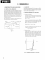
1
KENWOOD
DP-1100 B
DP-1100II
COMPACT DISC PLAYER
NOTE: Please replace this service manual with the old DP-1100's manual (B51-1592-00). This manual
has all descriptions for DP-1100 and DP-110011.
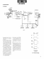
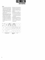
Photo is DP-1100B
•Refer to Parts List on page 177.
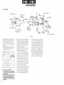
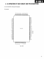
Photo is DP-110011
'Refer to Parts List on page 1 9 1 ,
TRIO-KENWOOD Corp. certifies this
equipment conforms to DHHS Regula
tions No. 21 C F R 1 0 4 0 . 1 0 , Chapter I,
Subchapter J .
DANGER: Laser radiation when open
and interlock defeated.
AVOID DIRECT EXPOSURE TO BEAM.
DP-1100B II
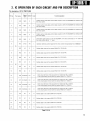
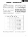
MEANING OF ABBREVIATIONS
AFC:
Disc m o t o r s p e e d c o n t r o l signal o u t p u t f r o m IC8 o n
FOKG:
p r o c e s s PCB
F S R H or F S R C H :
APC:
Disc m o t o r phase c o n t r o l signal o u t p u t f r o m IC8 o n
BCK:
Clock pulse o n w h i c h m u s i c data is sent t o D/A c o n
p r o c e s s PCB
CK88:
KGC:
signal resultant f r o m 1/2 f r e q u e n c y division of X ' t a l
K I C F B or K C I F :
OSC 8 . 4 6 7 2 M H z )
LDC:
A b o u t 8 8 kHz signal w h i c h is identical w i t h signal
LRCK:
Refer to " I C 1 5 pin f u n c t i o n " o n p a g e 7 0 .
Refer t o " I C 1 5 pin f u n c t i o n " o n p a g e 6 9 .
Signal o u t p u t f r o m IC6 o n p r o c e s s PCB. It indicates
w h e t h e r o u t p u t data is f o r L-ch or R-ch.
MODE 4:
PCB or as p s e u d o EFM signal.
CLV:
Inversion signal of signal RFG in I C 1 5 . It is n o r m a l l y
" L " a n d " H " d u r i n g kick of m o t o r .
W D C K ( w o r d c l o c k pulse) o u t p u t f r o m IC6 o n p r o
CLS:
Interrupt c o n t r o l I/O pin b e t w e e n CPU 1 a n d CPU 2
(Interrupt request)
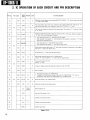
Clock signal of a b o u t 4 M H z f o r m i c r o p r o c e s s o r (the
cess PCB. It is used as c l o c k signal for IC15 o n servo
2 Hz signal t o d e t e c t j u s t f o c u s i n g p o i n t . It
m o v e s the p i c k u p a c t u a t o r u p a n d d o w n .
IRQ:
verter (Bit c l o c k pulse)
CK4M:
Refer t o " I C 1 5 pin f u n c t i o n " o n p a g e 6 9 .
IC15 c o n t r o l signal w h i c h is o u t p u t f r o m
S w i t c h t o i n f o r m o p e n e d or c l o s e d tray state. It is
M5P:
s h o r t e d w i t h tray c l o s e d . ( " L " w i t h tray closed)
MUTE:
M u s i c signal m u t i n g s i g n a l .
Circuit w h i c h m a k e s t h e linear v e l o c i t y of disc m o t o r
OPEN:
S w i t c h w h i c h t u r n s ON ( " L " ) w i t h tray o p e n t o i n
c o n s t a n t t o p r o v i d e c o n s t a n t reading rate of disc
data.
D A T A 1 2 and D A T A 2 1 :
Disc m o t o r O N / O F F c o n t r o l s i g n a l .
f o r m o p e n e d tray state.
OPNS:
Refer t o " I C 1 5 pin f u n c t i o n " o n page 6 8 .
Signals f o r data c o m m u n i c a t i o n
PLAY:
Refer t o " I C 1 5 pin f u n c t i o n " o n p a g e 6 9 .
Refer t o " I C 1 5 pin f u n c t i o n " o n page 7 1 .
( t r a n s m i s s i o n a n d reception) b e t w e e n CPU 1 a n d
PLCK:
CPU 2 .
P U or P . U :
DATA:
Signal line o n w h i c h data is s e n t f r o m process PCB
PUD:
t o D/A c o n v e r t e r .
PUFB:
Inversion signal of signal PUFF in I C 1 5 .
DCON:
Signal w h i c h is o u t p u t f r o m I d 5 o n servo PCB. It is
RES:
CPU initialize signal
DIN:
DOCK:
RFES:
Refer t o " I C 1 5 pin f u n c t i o n " o n p a g e 6 9 .
l o w e r e d in level d u e t o disc f l a w . ( D r o p o u t c o n t r o l )
RFG:
Refer t o " I C 1 5 pin f u n c t i o n " o n page 7 0 .
Signal line o n w h i c h positional data of disc f l a w is
RFOK:
This o u t p u t b e c o m e s
Clock pulse o u t p u t f r o m IC15 o n servo PCB t o disc
position
memory
circuit.
It
is a six
times
o n m e c h a n i s m PCB.
SCK:
SLT:
1
and
EFM
These
0:
are
Eight-to-Fourteen-Modulation
high-frequency
signals or
RF
P r e - e m p h a s i s signal o u t p u t f r o m
Focusing
S V C (A, B, C and INH):
process
and tracking
coils
control
signals.
F E or F . E : Focus error signal
resultant f r o m
I C 1 2 c o n t r o l signal t o enable SVC opera
Servo c o n t r o l
T E or T . E : T r a c k i n g error signal or t r a c k i n g m o n i t o r pin
Refer t o " I C 1 5 pin f u n c t i o n " o n page
68.
T E O P and T E O N :
F . C O I L and T . C O I L :
Refer t o " I C 1 5 pin f u n c t i o n " o n page 6 8 .
TEP:
Refer t o " I C 1 5 pin f u n c t i o n " o n p a g e 6 8 .
TES:
Refer t o " I C 1 5 pin f u n c t i o n " o n page 6 8 .
T R A Y or T R Y : Disc t r a y or t r a y drive signal
1/30
frequency
division
of
signal DOCK. It c o n t r o l s disc m o t o r drive s i g n a l .
FOK:
most track.
T E G 1 and T E G 2 :
IC8 o n
PCB.
FGS:
S w i t c h w h i c h t u r n s ON ( " L " ) w i t h p i c k u p at inner
t i o n by m a i n C P U . ( I C 1 2 O N at " H " )
signals given f r o m optical p i c k u p .
Signal
Clock pulse f o r c o m m u n i c a t i o n b e t w e e n CPU1 a n d
S T A R T or S T A T :
Refer t o " I C 1 5 pin f u n c t i o n " o n p a g e 6 8 .
EFM
O u t p u t signal f r o m r e m o t e c o n t r o l signal amplifier
CPU 2 . (Serial c l o c k pulse)
W i t h disc p r o v i d e d , t h i s pulse o u t p u t is " L " . Q1 o n
signals.
FG4:
from
RMC:
(Disc OK)
EMPH:
RF signal
S1 and S 2 : Pickup o u t p u t signals e m i t t e d f r o m p r e a m p l i f i e r
servo PCB d e t e c t s t h e p r e s e n c e or a b s e n c e of disc.
EFM,
when
Disc m o t o r drive signal
a m p l i f i e d signal of FGS. ( D r o p o u t c l o c k pulse)
DSG:
"L"
p i c k u p is i n p u t t o IC10 ( V 2 ) .
c u i t a n d IC15 o n servo PCB.
flaw
DOK:
Pickup.
Refer t o " I C 1 5 pin f u n c t i o n " o n p a g e 6 8 .
n o r m a l l y " H " a n d b e c o m e s " L " w h e n RF signal is
t r a n s m i t t e d b e t w e e n disc f l a w position m e m o r y cir
DISK:
main
CPU. (Refer t o page 7 0 . )
IC15 i n p u t pin of FG signal f r o m disc m o t o r .
Focus servo c o n t r o l s i g n a l . Servo ON w i t h
TTAC:
WDCK:
Refer t o " I C 1 5 pin f u n c t i o n " o n page 6 8 .
Signal o u t p u t f r o m
IC6 o n
process
PCB. Its fre
q u e n c y is t w i c e t h a t of signal LRCK.
signal
FOK " L " .
5
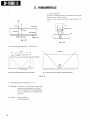
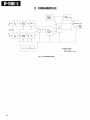
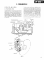
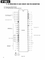
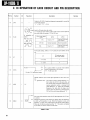
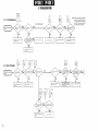
DP-1100B II DP-1100B II
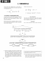
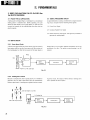
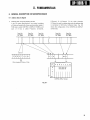
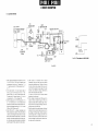
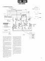
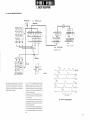
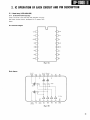
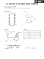
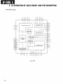
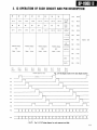
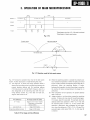
I. BLOCK DIAGRAM
DP-1100B II
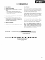
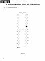
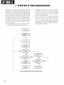
II. FUNDAMENTALS
1-2
1 FUNDAMENTALS
1-1
SAMPLING
A n a n a l o g v o l t a g e is c o n t i n u o u s in respect t o t i m e , a n d has a
value at e a c h t i m e of t
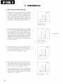
QUANTIZATION
Fig. 1.3 i n d i c a t e s o n e e x a m p l e w h e r e a n a l o g signals r a n g i n g
1 (
t , t , etc. as s h o w n in Fig. 1.1 a n d as
2
f r o m O V t o 1 0 V are c o n v e r t e d t o 1 1 - s t e p v o l t a g e values of
0V, 1V, 2V
9 V a n d 1 0 V via r o u n d - o f f . W i t h t h i s c o n v e r
3
s i o n , p r e p a r a t i o n of o n l y 11 kinds of c o d e s is n e e d e d . T o c o n
w e l l a value at any t i m e b e t w e e n t a n d t .
x
2
vert an a n a l o g signal t o a kind of a digital signal w i t h t h e p r o
cess of r o u n d - o f f or t h e like is called " Q u a n t i z a t i o n " .
Voltage
Digital Voltage Converted by
Rounded-Off
Time
Fig.
1.1
Analog Voltage
If an a n a l o g v o l t a g e is represented c o r r e s p o n d i n g t o a c o d e
s y s t e m , t h e a n a l o g voltage over the definite t i m e range of t t o
t
t
2
is m a d e of the indefinite n u m b e r of c o d e s . In order t o
t r a n s m i t a digital signal c o r r e s p o n d i n g t o t h e voltage at t
1 (
it
needs a definite t i m e l e n g t h , b u t w h e n t r a n s m i t t i n g indefinite
c o d e s , t h e t r a n s m i s s i o n d o e s n o t e n d forever.
Time
Voltage (V)
Fig. 1 . 3
Voltage
Amplitude
t
Fig.
5
Time
1.2
Sampling
T h e r e f o r e , in case w h e r e an a n a l o g v o l t a g e is c o n v e r t e d t o a
c o d e d s y s t e m , a n a l o g v o l t a g e s at t i m i n g s w i t h s o m e interval
are o n l y c o n v e r t e d as s h o w n in Fig. 1.2. W i t h s u c h a p r o
c e s s , t h e definite n u m b e r of c o d e s c o r r e s p o n d i n g t o the
definite t i m i n g s , f o r e x a m p l e , five c o d e s f o r t h e t i m e interval t
t
t o t are p r o d u c e d .
5
W h e n h a v i n g t r a n s m i t t e d c o d e s d e s c r i b e d in Fig. 1.2, o n l y
five c o d e s c a n be received at the receive side b e t w e e n t
t
and
Quantization
t . T h e n u m b e r of v o l t a g e values r e p r o d u c e d t h e r e b y is only
5
f i v e , a n y v o l t a g e at t i m i n g s e x c e p t t
1 (
t , t , etc. c a n n o t be
2
3
determined.
H o w e v e r , if the f r e q u e n c y c o m p o n e n t ( 2 0 kHz) of the original
a n a l o g signal is less t h a n the value ( 4 4 . 1 kHz)
u p o n t h e t i m e interval b e t w e e n t i m i n g s t
1 (
depending
t , t , etc. at w h i c h
2
3
c o d i n g is s t a g e d , e v e n t h e value for n o n - t r a n s m i t t e d p o r t i o n s
c a n be r e p r o d u c e d . T o pick u p a n a l o g values at a fixed t i m e
interval by s u c h a process is called " s a m p l i n g " .
Fig.
1.4
DP-1100B II
II. FUNDAMENTALS
1-3
SAMPLING THEOREM
Signal Waveform
S/H
;
(
a
)
Measurings at a fixed time ( b)
interval (sampling)
Converts the measured
values to figures
(quantization)
A/D
f
Binary coded figures
(Offset Binary)
Recording
Reproduction
D/A
Demodulation
(PAM signal)
Fig. 1.5
T h e f r e q u e n c y of p i c k i n g u p an a n a l o g s i g n a l , for e x a m p l e ,
5 0 , 0 0 0 t i m e s per s e c o n d , is called " a s a m p l i n g f r e q u e n c y . It
is p r o v e n t h a t if s a m p l i n g is c o n d u c t e d at t h e rate larger t h a n a
c e r t a i n v a l u e , t h e original w a v e f o r m c a n be r e p r o d u c e d j u s t
the s a m e t o a n i n c h . T h i s is called " a s a m p l i n g t h e o r e m " .
Sampling T h e o r e m : If s a m p l i n g
ble the m a x i m u m f r e q u e n c y ( 2 0 kHz)
in a s p e c t r u m of a s i g n a l , t h e original
w a v e f o r m c a n be c o m p l e t e l y r e p r o d u c
ed.
8
is c o n d u c t e d at the f r e
q u e n c y ( 4 4 . 1 kHz) w h i c h is over d o u
DP-1100B II
II. FUNDAMENTALS
1-4
QUANTIZING NOISES
Transmitted signal waveform in passing
Signal Waveform
through a demodulation filter
3-digit figure
(decimal code)
9-bit figure
(Binary code)
Sampling point
Fig.
1.6
A r o u n d i n g error is c a u s e d by q u a n t i z a t i o n at s a m p l i n g points
noise is of t h e nature different f r o m noises e m i t t e d f r o m an
as d e s c r i b e d in 1-2, a n d seeing Fig. 1.6 it c a n be t h o u g h t
a n a l o g s y s t e m , being called " a q u a n t i z a t i o n n o i s e " .
t h a t this r o u n d i n g error is c r e a t e d as a distortion or noise. This
Max. Signal Amplitude
Sampling Quantization
Sampling
Frequency
44.1 kHz
Fig.
1.7
T h e ratio of a q u a n t i z i n g noise against t h e m a x i m u m value of
W h e n m a k i n g t h e a m p l i t u d e of 0 t o V c o r r e s p o n d i n g t o t h i s ,
the
the w i d t h E of o n e quantization step is given by:
signal
in a b i n a r y - c o d e d
1 6 - b i t system
is plotted
in
0
r e s p e c t t o a sinusoidal w a v e i n p u t as s h o w n in Fig. 1.7.
E = V/(N
0
-1)
If a 1 6 - b i t c o d e is used in q u a n t i z i n g o n e s a m p l e d v a l u e , the
n u m b e r of steps w h i c h c a n be t a k e n , i.e., the
n u m b e r N is given as f o l l o w s :
N = 2
1 6
quantizing
T h e r e f o r e , t h e a m p l i t u d e of a q u a n t i z i n g noise is E at t h e
0
p e a k - t o - p e a k v a l u e , so t h a t the noise p o w e r N
Q
is:
= 65536
9
DP-1100B II
II. FUNDAMENTALS
On t h e o t h e r
hand, supposing
t h a t an i n p u t signal is a
T h e r e f o r e , the p o w e r ratio is:
sinusoidal w a v e w h o s e a m p l i t u d e at the p e a k - t o - p e a k value is
V , the signal p o w e r S is:
1-5
E F M (EIGHT T O FOURTEEN MODULATION)
T o c o n v e r t a level of an a n a l o g signal at every interval of a fix
Role of Margin Bits
ed p e r i o d ( 1 / 4 4 . 1 kHz = 2 2 . 7 /is), as d e s c r i b e d in 1-4, t o a
T h e p u r p o s e of t h e m a r g i n bits is t o r e d u c e a DC c o m p o n e n t
binary c o d e (1 a n d 0 ) after q u a n t i z a t i o n is called a " P C M "
a n d l o w f r e q u e n c y c o m p o n e n t s by a d d i n g three additional
(Pulse Code M o d u l a t i o n ) .
bits t o t h e signals c o n v e r t e d into EFM.
PCM has v a r i o u s kinds of m o d u l a t i o n s y s t e m s , b u t here a
C h a n n e l Bits
S o n y a n d Philips j o i n t l y d e v e l o p e d n e w s y s t e m , called E F M ,
One of 1 4 bits c o n v e r t e d f r o m 8 bits is called a c h a n n e l bit.
used f o r D A D is d e s c r i b e d .
One word
Sample
A
L S B
MSB
Symbol 1 ( = 8 bits)
Symbol 2 ( = 8 bits)
EFM
Margin bits
added
Symbol 2 { = 17 channel bits)
Symbol 1 ( = 17 channel bits)
Fig.
(1)
1.8
EFM is t h e m o d u l a t i o n t o first divide a 1 6 - b i t d a t u m (data
bit) into t w o 8 - b i t data a n d t h e n c o n v e r t e a c h of these
T w o or m o r e b u t 10 or less Os (zeros) s h o u l d be a l w a y s i n
8 - b i t d a t a t o a 1 4 - b i t d a t u m ( c h a n n e l bit) as s h o w n in
serted b e t w e e n c h a n n e l bits 1 a n d 1 4 .
Fig. 1.8. T h e c o n v e r s i o n is t o select patterns of 2
a m o n g p a t t e r n s of 2
1 4
8
kinds
k i n d s , m e e t i n g the f o l l o w i n g c o n
d i t i o n . C h a n n e l bits of 2
8
m e e t i n g this c o n d i t i o n have
(2)
T h r e e c h a n n e l bits are a l w a y s inserted b e t w e e n
14-bit
b l o c k s . T h e role of these 3 bits is t o m a k e a d j u s t m e n t so
b e e n p r e d e t e r m i n e d by a c o m p u t e r as indicated in Tables
t h a t the a b o v e c o n d i t i o n (enclosed in t h e box) is m e t
1-1 a n d 1-2:
e v e n at t h e c o n n e c t i o n of b l o c k s .
DP-1100B II
II. FUNDAMENTALS
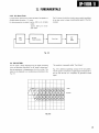
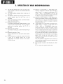
8 bits - 1 4 bits
8 b i t s - 1 4 bits
Order
Order
0
i
2
3
4
5
6
7
8
9
10
11
12
13
14
15
16
17
18
19
20
21
22
23
24
25
26
27
28
29
30
31
32
33
34
35
36
37
38
39
40
41
42
43
44
45
46
47
48
49
50
51
52
53
54
55
56
57
58
59
60
61
62
63
data bits
channel bits
00000000
00000001
00000010
00000011
00000100
00000101
00000110
00000111
00001000
00001001
00001010
00001011
00001100
00001101
00001 110
0 0 0 0 1 111
00010000
00010001
00010010
00010011
00010100
00010101
00010110
0 0 0 1 01 11
00011000
00011001
00011010
00011011
00011 100
00011101
00011110
00011111
00100000
00100001
00100010
00100011
00100100
00100101
00100110
00100111
00101000
00101001
00101010
00101011
00101100
00101101
00101110
00101111
00110000
00110001
00110010
00110011
00110100
00110101
00110110
00110111
00111000
00111001
00111010
00111011
00111100
00111101
00111110
00111111
01001000100000
10000100000000
10010000100000
10001000100000
01000100000000
00000100010000
00010000100000
00100100000000
01001001000000
10000001000000
10010001000000
10001001000000
01000001000000
00000001000000
00010001000000
00100001000000
10000000100000
10000010000000
10010010000000
00100000100000
01000010000000
00000010000000
00010010000000
00100010000000
01001000010000
10000000010000
10010000010000
10001000010000
01000000010000
00001000010000
00010000010000
00100000010000
00000000100000
10000100001000
00001000100000
00100100100000
01000100001000
00000100001000
01000000100000
00100100001000
01001001001000
10000001001000
10010001001000
10001001001000
01000001001000
00000001001000
00010001001000
00100001001000
00000100000000
10000010001000
10010010001000
10000100010000
01000010001000
00000010001000
00010010001000
00100010001000
01001000001000
10000000001000
10010000001000
10001000001000
01000000001000
00001000001000
00010000001000
00100000001000
d1
d8
C1
C14
C1 is first cut.
EFM Conversion table 0 to 127
(NRZ-1 represantation)
data bits
64
65
66
67
68
69
70
71
72
73
74
75
76
77
78
79
80
81
82
83
84
85
86
87
88
89
90
91
92
93
94
95
96
97
98
99
100
101
102
103
104
105
106
107
108
109
110
111
112
113
114
115
116
117
1 18
119
120
121
122
123
124
125
126
127
01000000
01000001
01000010
01000011
01000100
01000101
01000110
01000111
01001000
01001001
01001010
01001011
01001100
01001101
01001110
01001111
01010000
01010001
01010010
01010011
01010100
01010101
01010110
01010111
01011000
01011001
01011010
01011011
0101 1100
01011101
01011110
01011111
01100000
01100001
01100010
01100011
01100100
01100101
01100110
01100111
01101000
01101001
01101010
01101011
01101100
01101101
01101110
01101111
01110000
01110001
O i l 10010
O i l 10011
O i l 10100
01110101
01110110
01110111
0 1 1 1 1 0 00
01111001
01 1 1 1 0 1 0
01111011
01111100
01111101
01111110
01111111
channel bits
01001000100100
10000100100100
10010000100100
10001000100100
01000100100100
00000000100100
00010000100100
00100100100100
01001001000100
10000001000100
10010001000100
10001001000100
01000001000100
00000001000100
00010001000100
00100001000100
10000000100100
10000010000100
10010010000100
00100000100100
01000010000100
00000010000100
00010010000100
00100010000100
01001000000100
10000000000100
10010000000100
10001000000100
01000000000100
00001000000100
00010000000100
00100000000100
01001000100010
10000100100010
10010000100010
10001000100010
01000100100010
00000000100010
01000000100100
00100100100010
01001001000010
10000001000.010
10010001000010
10001001000010
01000001000010
00000001000010
00010001000010
00100001000010
10000000100010
10000010000010
10010010000010
00100000100010
01000010000010
00000010000010
00010010000010
00100010000010
01001000000010
00001001001000
10010000000010
10001000000010
01000000000010
00001000000010
00010000000010
00100000000010
DP-1100B II
II. FUNDAMENTALS
8 bits — 14 bits
8 bits — 14 bits
Order
Order
data bits
128
129
130
131
132
133
134
135
136
137
138
139
140
141
142
143
144
145
146
147
148
149
150
151
152
153
154
155
156
157
158
159
160
161
162
163
164
165
166
167
168
169
170
171
172
173
174
175
176
177
178
179
180
181
182
183
184
185
186
187
188
189
190
191
10000000
10000001
10000010
10000011
10000100
10000101
1 0 0 0 0 1 10
10000111
10001000
10001001
10001010
10001011
10001100
10001101
10001110
10001111
10010000
10010001
10010010
10010011
10010100
10010101
10010110
10010111
10011000
10011001
1001 1010
10011011
1001 1100
10011101
10011110
10011111
10100000
10100001
10100010
10100011
10100100
10100101
10100110
10100111
1010 1000
10101001
10101010
10101011
10101100
10101101
10101110
1010111 1
10110000
10110001
101 10010
10110011
10110100
10110101
10110110
10110111
10111000
10111001
10111010
10111011
10111100
10111101
10111110
10111111
channel bits
01001000100001
10000100100001
10010000100001
10001000100001
01000100100001
00000000100001
00010000100001
00100100100001
01001001000001
10000001000001
10010001000001
10001001000001
01000001000001
00000001000001
00010001000001
00100001000001
10000000100001
10000010000001
10010010000001
00100000100001
01000010000001
00000010000001
00010010000001
00100010000001
01001000000001
10000010010000
10010000000001
10001000000001
01000010010000
00001000000001
00010000000001
00100010010000
00001000100001
10000100001001
01000100010000
00000100100001
01000100001001
00000100001001
0100 0000100001
00100100001001
01001001001001
10000001001001
10010001001001
10001001001001
01000001001001
00000001001001
00010001001001
00100001001001
00000100100000
10000010001001
10010010001001
00100100010000
01000010001001
00000010001001
00010010001001
00100010001001
01001000001001
10000000001001
10010000001001
10001000001001
01000000001001
00001000001001
00010000001001
00100000001001
192
193
194
195
196
197
198
199
200
201
202
203
204
205
206
207
208
209
210
211
212
213
21*4
215
216
217
218
219
220
221
222
223
224
225
226
227
228
229
230
231
232
233
234
235
236
237
238
239
240
241
242
243
244
245
246
247
248
249
250
251
252
253
254
255
data bits
channel bits
11000000
11000001
11000010
11000011
11000100
11000101
11000110
11000111
11001000
11001001
11001010
11001011
11001100
11001101
11001110
11001111
11010000
11010001
11010010
11010011
11010100
11010101
1 1 0 1 0 1 10
11010111
11011000
11011001
11011010
11011011
11011100
11011101
11011110
11011111
11100000
11100001
11100010
11 1 0 0 0 1 1
11100100
11100101
11100110
1 1100111
11101000
11101001
11101010
11101011
11101100
11101101
11101110
1 1 1 0 1 1 11
11110000
11110001
11 1 1 0 0 1 0
11110011
111 1 0 1 0 0
1 1110101
11110110
111 1 0 1 1 1
111 1 1 0 0 0
111 1 1 0 0 1
11111010
11111011
111 1 1 1 0 0
11111101
11111110
11111111
01000100100000
10000100010001
10010010010000
00001000100100
01000100010001
00000100010001
00010010010000
00100100010001
00001001000001
10000100000001
00001001000100
00001001000000
01000100000001
00000100000001
00000010010000
00100100000001
00000100100100
10000010010001
10010010010001
10000100100000
01000010010001
00000010010001
00010010010001
00100010010001
01001000010001
10000000010001
10010000010001
10001000010001
01000000010001
00001000010001
00010000010001
00100000010001
01000100000010
00000100000010
10000100010010
00100100000010
01000100010010
00000100010010
01000000100010
00100100010010
10000100000010
10000100000100
00001001001001
00001001000010
01000100000100
00000100000100
00010000100010
00100100000100
00000100100010
10000010010010
10010010010010
00001000100010
01000010010010
00000010010010
00010010010010
00100010010010
01001000010010
10000000010010
10010000010010
10001000010010
01000000010010
00001000010010
00010000010010
00100000010010
data bits
d1
d8
C1
C14
C1 is first cut.
EFM Conversion table 128 to 2 5 5
(NRZ-1 represantation)
cf: NRZ Non Return to Zero
channel bits
DP-1100B II
II. FUNDAMENTALS
1-6
FRAME SYNCHRONIZATION AND FRAME
STRUCTURE
R e p r o d u c t i o n signals c a n n o t be r e c o v e r e d RF signals d o n o t
Channel bits
Margin bits
Total bits
Frame Synchro
nization
24
3
27
Users buts
14
3
17
c o m e o u t for a l o n g t i m e due t o d r o p o u t or o n e i n f o r m a t i o n bit
has b e e n shifted o w i n g t o jittering in digital r e c o r d i n g
or
p l a y b a c k . Because o n e bit shift of a digital signal m a k e s t h e
signal quite different in its signal level.
Data bits
T h e r e f o r e , by d i v i d i n g a r e c o r d e d signal t o m a n y small blockjs,
14 b i t x 2 4 = 336
408
14 b i t x 8 = 1 1 2
3 bit x 24
136
486
102
588
t h e s y s t e m is o r g a n i z e d so t h a t even w h e n a signal is d i s t u r b
ed d u e t o jittering or t h e like, a bit s y n c h r o n i z a t i o n is a l w a y s
Error correction
bits (Parity bits)
estabilished at the n e w block t o identify t h e j o i n t part b e t w e e n
3
b i t x 8 = 24 = 72
b l o c k s . S u c h a block is called a " F r a m e " . Frame Sync signals
are inserted t o indicate the b o u n d a r y of the f r a m e a n d t o
m a k e a bit s y n c h r o n i z a t i o n . Fig. 1.9 s h o w s the structure of
one frame.
Frame Structure
1-frame (588 Channel Bits)
• Margin Bit
User's Bit
Data Bits
I
2
4
3
5
14 14 14 14
3A
-3
:
6
14
:
:
7
Parity
9
10
14 14 14 14
14
8
.;
:
11
12
14
:i
14
13
14
15
14
14
14
:
2
Data Bits
16
17
14
14
:. 2
18
19
14
14
:
Parity
20
21
22
23
24
25
26
27
28
14
14
14
14
14
14
14
14
14
29
:i
Data Symbol 1 (14 Channel Bits)
Sync Pattern (24 Channel Bits)
Channel Bit Frequency = 4 . 3 MHz
Frame Frequency = 7 . 3 5 kHz
11
2 x Tmax
S T A R T FRAME
Fig.
1.9
14
32
14
:i
Control Display Symbol (14 Channel Bits) PQ Data Absolute Music
11 Channel Bits
31
30
24
14
:
;
:
DP-1100B II
II. FUNDAMENTALS
1-7
1.
2.
C O M P A C T D I S C (CD)
T h e r e are m a n y kinds of D A D s y s t e m s : C D , M D a n d
m o i s t u r e a b s o r p t i o n c a u s i n g b e n d is a big d e f e c t . (Refer
A H D . (Refer t o Fig. 1.10)
t o p r e c a u t i o n s o n h a n d l i n g t h e disc.)
7.
D P - 1 1 0 0 B / I I a d o p t s t h e CD s y s t e m . T h e CD system is
also c a l l e d
"a
light s y s t e m " .
A
light b e a m
from
Playback t i m e is 6 0 m i n u t e s w i t h a 1 2 0 m m disc.
D i m e n s i o n s are given in Fig. 1 . 1 2 .
a
s e m i c o n d u c t o r laser is c o n v e r g e d w i t h an objective lens
8.
t o hit pits inside a disc for using their reflected light.
T h e rotating s p e e d of t h e disc is n o t c o n s t a n t . Because of
a c o n s t a n t linear v e l o c i t y system e m p l o y e d , the rotating
3.
speed
T h e r e are no g r o o v e in t h e CD s y s t e m hit pits.
Size
of
Pit:
Width
0 . 5 fim,
Length: 0.9
to
is varied
between
(counterclockwise)
3.3 /im,
CLV
around
5 0 0 to 2 0 0
(constant
linear
r.p.m.
velocity):
c a p s t a n drive t y p e t a p e r e c o r d e r C A V ( c o n s t a n t a n g u l a r
D e p t h : 0 . 1 /im
v e l o c i t y ) : rim drive t y p e t a p e r e c o r d e r .
4.
Laser b e a m is hit t h r o u g h a t r a n s p a r e n t disc layer t o read
o u t d a t a . (See Fig.
9.
1.11)
PL) (pickup) d o e s n o t c o n t a c t a disc surface b u t t r a c e s a
t r a c k m o v i n g f r o m inner radius t o outer radius.
5.
C o n s t r u c t i o n of disc. (See Fig. 1.11)
6.
Disc baseplates are usually m a d e of PC ( p o l y c a r b o n a t e ) ,
It d e p e n d s u p o n the t r a n s m i s s i o n f a c t o r , reflection f a c t o r
P M M A (acryl) is superior f o r a disc baseplate, b u t its
and double refraction.
1 0 . H o w m u c h effectively d o e s it use a laser beam?
1.5 /tm
0 . 9 - 3 . 3 nm
Protective Surface
Pit
0.4 nm
Reflecting Surface
Reproduction Light Spot
0.11 nm
1.2
mm
Transparent Plastic
Approx. 1 mm0
Objective Lens
CD System
Fig.
1.10
Laser Beam
1 mm0
1.2 mm
Disc Baseplate (Polycarbonate)
1.6 /tm
Reflecting Film (Aluminium)
Protective Film
Fig.
14
1-11
DP-1100B II
II. FUNDAMENTALS
Program
Lead in
Lead out
"(T.O.C)
Fig.
1.12
Lead In: T O C (table of c o n t e n t s ) — A b s o l u t e t i m e of t h e
h e a d i n g of m u s i c is i n c l u d e d .
Lead Out:
Used for retrieving of t h e h e a d i n g indicates of
program end.
Other — C o n t r o l Data P, Q
15
DP-1100B II
II. FUNDAMENTALS
1 2 . D o u b l e Refraction
11.
T h e rating of d o u b l e refraction is represented by a light path
difference ( m m ) . Rating: 1 0 0 m m
T h e m a i n c a u s e of d o u b l e refraction is m o l d d i s t o r t i o n . Fig.
1.14
100%
PU
Disc Surface
. Objective Lens
Absorption
Disc Baseplate
Disc
Reflection attenuation
Fig.
Reflection Film
1.13
Fig.
1.14
1 3 . CD is t o u g h a g a i n s t dusts Fig. 1.15(a) a n d (b)
Laser Beam
1 mm#
Dust
Disc Surface
1 iirr\<t>
Pits
1.5 nm<j>
(a) In a case where dusts are deposited on the disc surface
(b) In a case where dusts are attached to a reflecting film surface
Fig.
14.
Fabricating p r o c e s s of baseplate. Fig. 1.16
15.
Mastering:
Procedures for
Photo-resist c o a t i n g ,
laser
r e c o r d i n g a n d d e v e l o p m e n t are i n c l u d e d .
T h i s is c o r r e s p o n d i n g t o t h e f a b r i c a t i n g p r o
cess of a l a c q u e r disc in an a n a l o g r e c o r d
production.
16.
Molding:
Injection m o l d i n g
P h o t o Polymerization
6
1.15
0P-1100B II
II. FUNDAMENTALS
Glass Disc
Glass Disc
Photoresist
Photoresist Coating
Glass Disc
Laser R e c o r d i n g
Development
Master Disc •
Silver Mirror Ni plating
Metal Master
Ni plating
M o t h e r Disc.
Ni plating
Stamper
Molding
T r a n s p a r e n t Disc
Reflecting Film e v a p o r a t i o n
Protective file c o a t i n g
Label Printing
Finished G o o d ( C o m p a c t Disc)
Packing
Fig. 1 . 1 6 Manufacturing P r o c e s s of C D
17
DP-1100B II
II. FUNDAMENTALS
Control &
Display
Encoding
LP
Filter
Sample
& Hold
Sync.
Generation
Modulator
ADC
Ch 1
Serial
Data
Output
MUX
MUX
Audio input
Error
Correction
System
Ch 2
LP
Filter
Sample
& Hold
ADC
X-tal
Timing
ENCODING S Y S T E M
*
time multiplexer
* * Analog to Digital converter
Fig. 1 . 1 7 Encoding s y s t e m
8
DP-1100B II
II. FUNDAMENTALS
2 CODE ERROR
2-3
INTERLEAVE
Even if r e a d i n g every page of a b o o k slantwise f r o m its u p p e r
2-1
C A U S E S OF CODE ERROR
(1)
Defectives
which
are
already
left side t o l o w e r right side, y o u c a n fully recognize t h e c o n
present
on
a disc
at
text or c o n t e n t s . H o w e v e r , y o u c a n n o t recognize the c o n t e n t s
delivery:
of the b o o k if y o u are reading carefully o n e c h a r a c t e r
— Dusts a t t a c h e d t o pits d u r i n g p r o d u c t i o n of disc.
or
clause w i t h o u t r e a d i n g several t e n s of p a g e s .
— Disc m o l d i n g d i s t o r t i o n (entering of air b u b b l e s w h o s e
r e f r a c t i o n f a c t o r is n o t e q u a l . )
A n error c o l l e c t i o n c o d e is the s a m e as this, a n d c o r r e c t i o n is
easy
(2)
(3)
even w h e n
code
errors of
some
bits are
present.
Faults c r e a t e d o n h a n d l i n g of a disc: d u s t s , s c r a t c h e s ,
H o w e v e r , if m a n y , say 1000,
stains a n d f i n g e r prints.
a t i m e , it is very difficult t o c o r r e c t t h o s e errors.
Level variations of r e p r o d u c t i o n signal (eye pattern)
T h e r e f o r e , t h e t e c h n i q u e w i t h w h i c h an o r d e r of a signal is
Because p r o t e c t i o n of o u t - o f - t r a c k i n g , Focus a n d CLV
o n c e c h a n g e d a n d t h e n r e c o r d e d a n d , after r e p r o d u c t i o n ,
are all d e p e n d i n g o n a servo s y s t e m , p o o r stability of the
bits are c o n s e c u t i v e l y w r o n g at
r e t u r n e d b a c k t o t h e original order is e m p l o y e d . This c h a n g i n g
servo leads t o increased c o d e errors.
of the order of a signal is called an " i n t e r l e a v e " , a n d the
r e t u r n i n g t o t h e original order is called a " d e i n t e r l e a v e " .
2-2
KINDS OF C O D E ERROR
(1)
R a n d o m Error:
an error w h i c h causes an error in one bit
terleave. T h e o r d e r of a signal at f a b r i c a t i o n of the disc is o u t
(2)
Burst Error: an error w h i c h c a u s e s an error in m a n y s u c
c o d e errors are d i s p e r e s e d , so t h a t o p e r a t i o n of error c o r r e c
cessive bits.
tion a n d associated j o b s are m a d e facilitative.
Fig.
2.1
is the
illustration e x p l a i n i n g the
principle
of i n
of order. T h e r e f o r e , by deinterleaving t h e s i g n a l , successive
Signal words arranged
(interleaved on a disc)
10 successive words are wrong
Signal words deinterleaved
Signal words returned to their original locations
(10 successive error words are dispersed.)
Fig.
2.1
1
•P-1100B II
II. FUNDAMENTALS
2-4
SINGLE ERASURE CORRECTING METHOD
Bill (a) as s h o w n in Fig. 2-2 indicates prices of f o u r kinds
Bill (a)
of articles A , B, C a n d D a n d t h e t o t a l . In bill (b), t h e price
of article B disappears. This calls a disappearance or
erasure. W h e n t h e total a m o u n t is k n o w n , t h e price of ar
ticle B c a n be f o u n d even if o n e figure is m i s s e d . In t h e
c o d i n g t h e o r y , w e t h e r t h e total a m o u n t is c o r r e c t in bill
+
A ¥
100
B ¥
200
C ¥
300
D ¥
400
(a) is c h e c k e d . This o p e r a t i o n is called " s y n d r o m e " .
Total P ¥ 1,000
Syndrome (Checking)
S=A+B+C+D-P=0
(2)
In bill ( b ) , t h e price of article B disappears. (It is indicated
Bill (b)
by B * . B * = 0 ) C o n d u c t i n g t h e s y n d r o m e does n o t creat
S = 0 because there is a n erasure.
However,
as t h e
n u m b e r of erasure is o n e , t h e a m o u n t of B* c a n be f o u n d
from
syndrome
S=-200.
According
t o t h e single
diserasure c o r r e c t i n g m e t h o d , o p e r a t i o n of c o r r e c t i o n is
c o n d u c t e d o n t h e a s s u m p t i o n t h a t all other data ( A ' , C
a n d D') are c o r r e c t . If there is an error f o r a n o t h e r article,
+
A'
¥
B*
¥
100
C
¥
300
D' ¥
400
?
Total P' ¥ 1,000
miscorrection happens.
Syndrome (Checking)
S = A' + B' + C' + D ' - P = 0
B = B * - S = 200
(3)
O p e r a t i n g t h e s y n d r o r m e o n bill ( c ) , zero does n o t c o m e
Bill (c)
out. T h e r e f o r e , it m a y be f o u n d t h a t s o m e t h i n g is w r o n g ,
b u t it c a n n o t be f o u n d w h i c h of A ' , B ' , C , D' a n d P' is i n
¥
100
B' ¥
300
A'
c o r r e c t . In s u c h a c a s e , c o r r e c t i o n is infeasible.
¥
300
D' ¥
400
C
+
Total P' ¥ 1,000
S = A' + B' + C' + D ' - P ' = 0
(4)
Bill (d) illustrates t h e e x a m p l e t h a t t h e location t o be cor
Bill (d)
rected is k n o w n , a n d t h e c o r r e c t i o n c a n be d o n e by t h e
s a m e m e a n s as in bill (b). T h e m e a n s t o indicate t h e loca
t i o n of error in s u c h
a w a y is called a " p o i n t e r " .
In t h e e x a m p l e s of (1) t o ( 4 ) , " T o t a l P " is used f o r c h e c k
of error or erasure of data A , B, C a n d D. A w o r d used f o r
c h e c k a n d c o r r e c t i o n besides required data is called a
+
A'
¥
100
B*
¥
300
C
¥
300
D' ¥
400
Total P' ¥ 1,000
" p a r i t y w o r d " or a " p a r i t y b i t " .
S = A' + B' + C' + D ' - P ' = 100
B = B * - S = 200
20
Disppearance
II. FUNDAMENTALS
2-5
SINGLE ERROR CORRECTION, DOUBLE E R A S U R E S
In case of (3) in 2 - 4 , c o r r e c t i o n is infeasible because the
Bill (a)
location of error is u n k n o w n . Even in s u c h a c a s e , the
w a y by w h i c h c o r r e c t i o n is feasible is a single error c o r
recting m e t h o d . In 2 - 4 , t h e r e is only o n e parity w o r d , P.
Besides t h i s , a " W e i g h t e d Total V a l u e " , Q, is u s e d .
Because t w o parity w o r d s P a n d Q are u s e d , there are
A ¥
100
B ¥
200
C ¥
300
D
400
¥
P ¥ 1,000
also t w o s y n d r o m e s S j A n d S .
2
Q ¥ 1,000
N o w s u p p o s e t h a t t h e r e is an i n c o r r e c t bill (b) in respect
P=A+B+C+D
t o a c o r r e c t bill (b) a n d t h a t the location of error (one) in
Q = 4A + 3B + 2C + D
bill (b) is u n k n o w n .
Syndromes
S u p p o s i n g t h a t the differences f r o m original values are
E,
A
E , E, E
B
c
Dl
E and E w i t h respect t o A ' , B', C , D ' , P'
P
e
S
1=
A + B+ C+ D-P = 0
S, = 4A + 3B + 2C + D - Q = 0
and Q ' , respectively, of bill (b) (for no error, E , to E = 0 )
A
k' = k + E
P' = P + E
Dl
B' = B + E ,
Al
C' = C + E ,
B
Q' = Q + E
Obtaining syndrome
Q
D' = D + E ,
C
D
Q
S
Bill (b)
v
5 = A ' + B' + C' + D ' - P '
A'
1
= ( A + E J + (B + E ) + (C + E ) + (D + E ) - ( P + E )
B
C
D
P
= A+B + C + D - P + E + E +Ec+E -E -E ,-(1)
yl
B
0
F
100
300
¥
300
D' ¥
C
400
i
0
¥
B' ¥
?' ¥ 1,000
= E +
E +E +E -E
A
B
C
D
Q' ¥ 2,000
P
Obtaining syndrome S
2
Syndrome
5 = 4A' + 3B' + 2C' + D ' - Q '
S ^ A ' + B' + C' + D ' - P ' ^ O O
2
= 4 A + 3 B + 2C + D - Q + (4E^ + 3 E + 2 E + E - E ) (2)
£
0
= 4E4 + 3 E + 2 E + E - E
B
C
D
C
D
Q
Q
S u p p o s i n g t h a t a c o d e error is one w o r d b e t w e e n A ' t o
P', Q'
(I)
A'wrong
S j = E^, S = 4E
(II)
B'wrong
S = E , S = 3E
B
(III)
C wrong
S = E , S = 2E
C
(IV)
D'wrong
S^E^,
(VI)
P'wrong
S^Ep, S = 0
(VII)
Q'wrong
S = 0,
2
1
1
fl
C
2
2
S =E
2
A
D
2
t
S =-E
2
e
By a m e t h o d w h e r e t w o s y n d r o m e s are i n t r o d u c e d as
m e n t i o n e d a b o v e a n d d e t e r m i n e d , w r o n g w o r d s c a n be
found and corrected.
S, = 4A' + 3B' + 2C' + D ' - Q ' = 300
DP-1100B II
II. FUNDAMENTALS
(2)
EB=100
T h e principle of d o u b l e erasure c o r r e c t i o n is described
b e l o w . In this c a s e , t h e l o c a t i o n of error is indicated w i t h
Bill (c)
a pointer. It is here k n o w n t h a t t w o w o r d s in bill (c) are
w r o n g a n d t h e r e are n o other w r o n g w o r d s .
S = A + B+ C+ D-P + E +
1
yl
E
f l
+E +E -E =200
c
D
¥
100
B' ¥
300
A'
Using e q u a t i o n (1) in p a r a g r a p h ( 1 ) ,
P
0
C
¥
400
D'
¥
400
Pointer
P' ¥ 1,000
Q' ¥ 2,000
S u p p o s i n g E = 0, E = 0 a n d E = 0
A
D
P
(3)
S = E ,+ E = 2 0 0
1
J
C
E =100
c
F r o m Equation (2) of (1
5 = A' + B * + C * + D ' - P ' = 200
1
5 = 4A' + 3B' + 2C* + D' — Q' = 500
2
S = 4 A + 3 B + 2C + D + (4E + 3 E + 2 E + E - E ) = 5 0 0
2
/4
B
c
B
Q
B* = E + E C * + = C + E
0
S = 3E
2
Where
B
J J
C
(4)
+2E =500
C
T h i s t h e o r y is t h e principle of a Reed S o l o m o n C o d e . In
Determining E
B
(3) a n d ( 4 ) ,
22
a n d E f r o m s i m u l t a n e o u s e q u a t i o n s of
c
p r a c t i c e , t h e Reed S o l o m o n Code w i t h f o u r parity w o r d s
is u s e d .
DP-1100B II
II. FUNDAMENTALS
2-6
CROSS-INTERLEAVE
Fig. 2 . 2
s h o w s a principle
of a cross-interleave.
delivered directly, b u t w o r d s f e d into N o . 2 t o N o . 4 lines
An
original series of signals is d i v i d e d into a n u m b e r
are s u b j e c t t o delay w i t h delay m e m o r i e s by o n e t o three
of
w o r d s so t h a t the w o r d o r d e r is c h a n g e d (interleaved) at
w o r d s , a n d parity w o r d s are inserted.
their respective t e r m i n a l s .
P = W
1
+ W
P = W
5
+ W
6
P = W
9
+ W
1
1
5
9
2
+ W
3
+ W
7
+
+
+ W
0
W
N
4
W
+
T h e r e is an a d d e r f o l l o w i n g the delay m e m o r i e s , w h e r e
(5)
8
W
1
a n o t h e r parity w o r d Q is c r e a t e d .
2
Q
Four original series of signals ( W
W , W
6
1 0
1 (
W , W , W ...), (W ,
5
9
1 3
2
= W
1
+ W.
Q
5
= W
5
+ W
2
+ W.
Q
9
= W
9
+ W
6
+ W
1
2
+ W.
1
3
+ W-
5
+ W .
+ W
0
8
4
+
W.
+ P .
1
5
(6)
U
+ P.?
, W , . . . ) , ( W , W , W , W , . . . ) and ( W , W ,
u
3
7
u
1 5
4
8
W , W , . . . ) a m o n g m a n y original series of signals are
1 2
1 6
a r r a n g e d f o r f o u r lines N o . 1 via N o . 4 in Fig. 2 . 2 of
In other w o r d s , t w o s y s t e m of c o d e s are used o n b o t h
these w o r d s , the w o r d s
sides of t h e delay m e m o r i e s .
passing t h r o u g h
8
7
W
1 are
1 Word
Original series of signals
,W W
No.
W
6
5
2 Words
Recorded series of signals
w
5
Q P.
t
15
W_ W .
8
5
W.
2
W
t
3 Words
Disc recording sequence
Adder
p =w +w +w +w
1
1
2
3
4
Q = Wj + W + W_ + W_„ + W .
t
2
5
P = W + W + W + W
S
5
6
7
5
2
Delay memories
15
8
Q = W + W + W.n + W_ + P_
5
4 Words
4
Adder
n
Fig. 2 . 2 Principle of C r o s s - I n t e r l e a v e E n c o d e r
(2)
Fig. 2 . 3 indicates relations b e t w e e n t w o parity c o d e s .
Data Word
Check Word
T h e solid lines m e a n a P's series, a n d the d o t t e d lines
m e a n a Q's series. Each of t h e m has the capability of
single erasure c o r r e c t i o n , so t h a t an error of a single
w o r d c a n be easily c o r r e c t e d of c o u r s e .
T h e s y n d r o m e of e a c h o t h e r ' s series c a n be used as a
p o i n t e r f o r p o i n t i n g o u t a l o c a t i o n of error.
Fig. 2 . 3 C o d e S e r i e s of C r o s s Interleave
(Black circules indicate errors).
P-1100B II
II. FUNDAMENTALS
3 BRIEF EXPLANATIONS ON CD PLAYER (See
the BLOCK DIAGRAM)
3-1
3-2
PICKUP FOR C D APPLICATION
SIGNAL PROCESSING CIRCUIT
A p i c k u p p a r t c o r r e s p o n d i n g t o a c a r t r i d g e for a c o n v e n t i o n a l
A signal d e t e c t e d at a p i c k u p is delivered t o a signal process
analog
ing c i r c u i t , a n d split into t h e f o l l o w i n g three signals.
player is detailed later.
Briefly s p e a k i n g , this
part
a l l o w s the laser d i o d e t o e m i t a light b e a m ( X = 7 8 0 n m ) a n d
c o n v e r t t h e intensity of t h e reflected light f r o m disc pits into
(1)
Focus Error Signal
(2)
t r a c k i n g (Radial) Error Signal
electric signals.
(3)
Radio F r e q u e n c y (RF) S i g n a l : This signal is processed to
generate an a n a l o g signal.
3-3
3-3-1
SERVO CIRCUIT
F o c u s S e r v o Circuit
a l w a y s k e p t o n a pit surface against f l u c t u a t i o n s due t o t h e
A f o c u s error signal is f e d into a f o c u s servo c i r c u i t t o c o n t r o l a
lens s y s t e m w i t h the use of a f o c u s servo coil (like a v o i c e coil
revolutions of a disc. (The s a m e as a u t o - f o c u s i n g in an EE
of a l o u d s p e a k e r ) so t h a t t h e f o c u s s p o t of the laser b e a m is
camera)
Pickup
Disc
Lens
Focus coil
Signal
Focus Servo
Processing
Focus Coil
Driver
• Approx. 2 nm dia. Lader Spot
Fig.
3-3-2
3.1
T r a c k i n g S e r v o Circuit
Because a c o m p a c t disc has no guide g r o o v e , it is n e e d e d t o
ing servo c i r c u i t , t h e o u t p u t of w h i c h drives a t r a c k i n g servo
o p e r a t e a servo so t h a t a laser b e a m s p o t c a n a u t o m a i t c a l l y
coil t o operate t h e servo s y s t e m .
f o l l o w a signal t r a c k . A t r a c k i n g error signal is fed into a t r a c k
Laser spot (approx. 2 /tm dia.
To Tracking Coil
Pits on disc
Signal
Processing
1.6 nm
Tracking Servo
Pick Up
Fig. 3 . 2
24
Tracking
Coil Driver
DP-1100B II
II. FUNDAMENTALS
3-3-3
C L V S e r v o Circuit
C o n s t a n t linear v e l o c i t y (CLV) m e a n s t o keep a line s p e e d at a
The CLV servo c i r c u i t is t h e c i r c u i t t o s e r v o - c o n t r o l r e v o l u t i o n s
c o n s t a n t speed of a p p r o x . 1.2 m / s e c .
of the disc m o t o r t o keep c i r c u m f e r e n t i a l s p e e d of t h e disc
For this p u r p o s e disc is r o t a t e d : a p p r o x . 5 0 0 r . p . m . at inside
constant.
radios
a p p r o x . 2 0 0 r . p . m . at o u t
side radios
EFM
Signal
Bit Sync
CLV
Disc
Motor
Servo Amp.
Signal Generation
Fig. 3 . 3
3-4
EYE PATTERN
T h e RF signal is being delivered f r o m the signal processing
The w a v e f o r m is generally called " E y e P a t t e r n " .
c i r c u i t as d e s c r i b e d u n d e r 3 - 2 . T h e RF signal is vaired acord i n g t o a p p e a r a n c e or d i s a p p e a r a n c e of a pit o n a disc. This
Fig. 3 - 5 is s k e t c h e s e x p l a i n i n g c o n c e p t of t h e eye p a t t e r n .
signal c a n be displayed o n an o s c i l l o s c o p e as illustrated in the
The RF signal is c o n v e r t e d t o a digital signal c o m p o s e d of 1s
Fig. 3 - 5 .
a n d Os w i t h the aid of a c o m p a r a t o r t o g e n e r a t e an EFM
signal.
1 V/div
0.5 /ts/div
Fig. 3 . 5
25
DP-1100B II
II. FUNDAMENTALS
4 SEMICONDUCTOR LASER (LASER DIODE)
4-2 L A S E R DIODE
4-1
t e r m s of r e c o m b i n a t i o n l u m i n e s c e n c e of carriers, b u t different
A laser d i o d e , as m e n t i o n e d 4 - 1 , is t h e s a m e as an LED in
PRINCIPLE O F L E D LUMINESCENCE
A LED is f o r m e d w i t h a P-N j u n c t i o n c o m p o s e d of an n-type
in t h a t t h e light e m i t t e d is a c o h e r e n t laser light, t h e phase of
s e m i c o n d u c t o r w h i c h a l l o w s electric c o n d u c t i o n w i t h elec
w h i c h is u n i f o r m (single w a v e l e n g t h ) .
t r o n s a n d p-type s e m i c o n d u c t o r in w h i c h holes serves electric
c o n d u c t i o n . A p p l y i n g a v o l t a g e in t h e f o r w a r d d i r e c t i o n , elec
4-3 PROPERTIES REQUIRED FOR A L A S E R DIODE
t r o n s in t h e n-type s e m i c o n d u c t o r are i n j e c t e d into t h e p-type
s e m i c o n d u c t o r , a n d holes in t h e p- t y p e s e m i c o n d u c t o r are
(1)
Oscillation W a v e l e n g t h
A c c o r d i n g t o a C D ' s p r o p o s a l , t h e r e s h o u l d be t h e f o l l o w
i n j e c t e d into t h e n-type s e m i c o n d u c t o r . Red l u m i n e s c e n c e is
e m i t t e d w h e n e l e c t r o n s i n j e c t e d into t h e p-type s e m i c o n d u c
ing relaiton b e t w e e n a w a v e l e n g t h of a laser d i o d e a n d
t o r c o m b i n e w i t h holes.
t h e n u m b e r of a p e r t u r e of lens N A :
Green l u m i n e s c e n c e is e m i t t e d w h e n holes injected into t h e
X / N A = 1 . 7 5 jim
n-type s e m i c o n d u c t o r c o m b i n e w i t h e l e c t r o n s .
A s l o n g as t o d a y ' s G a A I A s material is u s e d , it is difficult
t o m a k e a laser d i o d e h a v i n g a w a v e l e n g t h shorter t h a n
Conduction band
Electrons
apporx.
Light
7 6 0 n m , b u t a laser d i o d e w i t h
higher
than
7 8 0 n m c a n be m a d e in mass p r o d u c t i o n .
Valence Band
T h e r e f o r e , N A = X / 1 . 7 5 /*m = 0 . 4 4 6
Holes
N-Type Region
A s t h e result, t h e o b j e c t i v e lens in t h e p i c k u p used in DP-
P-Type Region
1 1 0 0 B / I I has been d e s i g n e d for a p p r o x .
NA = 0 . 4 7 ± 0 . 0 1
PN Junciton
(2)
Fig. 4.1
Operating Current
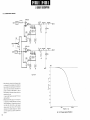
A n laser d i o d e has a t h r e s h o l d c u r r e n t I, w i t h
which
oscillation starts, a n d w i t h a c u r r e n t larger t h a n
this
t h r e s h o l d level, a light p o w e r P increases linearly w i t h i n
crease of a c u r r e n t I. F u r t h e r m o r e , if k e e p i n g drive at a
fixed c u r r e n t , t h e light o u t p o u t is greatly varied d u e t o
t e m p e r a t u r e i n c r e a s e . T h e r e f o r e , c o n t r o l is a l w a y s d o n e
Light Output
so t h a t t h e light o u t p u t is kept c o n s t a n t .
T,<T
2
I, (30mA)
Current
Fig. 4 . 2 Oscillating C h a r a c t e r i s t i c of a L a s e r Diode
26
•P-1100B II
II. FUNDAMENTALS
5 PICK-UP (PU) AND PU SERVO
The light reflected f r o m a disc passes again t h r o u g h t h e o b
jective lens a n d f o l l o w s t h e s a m e path as the f o r w a r d path t o
5-1
the polarizing f i l m . By t h e effect of the q u a r t e r - w a v e plate, the
S T R U C T U R E OF A PICKUP
light i n c o m i n g into the polarizing f i l m is c h a n g e d so t h a t its
Light b e a m s e m i t t e d f r o m a s e m i c o n d u c t o r laser are c h a n g e d
polarizing d i r e c t i o n is p e r p e n d i c u l a r t o the polarizing d i r e c t i o n
t o parallel light ralys by a c o l l i m a t o r lens system a n d enter a
polarization p r i s m . Since the s e m i c o n d u c t o r laser b e a m s are
in t h e f o r w a r d p a t h . T h e r e f o r e , the light t r a n s m i t s t h e polariz
linear-polarized in t h e d i r e c t i o n vertical t o the plane of in
ing f i l m a n d d o e s n o t g o b a c k t o t h e s e m i c o n d u c t o r raSer.
c i d e n c e , t h e b e a m s are reflected by the polarizing f i l m . T h e
Next, t h e light i n c o m i n g into a critical angle prism for d e t e c
light b e a m s reflected f r o m a n o t h e r plane of the polarization
t i o n of a f o u c s p o i n t is reflected t h r e e t i m e s inside the prism
prism pass t h r o u g h a q u a r t e r - w a v e plate, a n d t h e n are c o n
a n d t h e n f e d into 4 - d i v i d e d p h o t o d i o d e s . T h e o u t p u t of these
v e r g e d t o a s p o t of nearly 1.5 /im in d i a m e t e r w i t h the aid of
p h o t o d i o d e s are used f o r c o n t r o l i n g a t r a c k i n g servo coil a n d
an o b j e c t i v e lens.
a f o c u s servo coil t o o b t a i n an o p t i m u m f o c u s i n g of the abjec
tive lens o n pits of the disc.
Disc
4-divided photodiodes
Objective
lens
Laser diode
Monitor photodiode
Critical angle prism
Tracking
servo
coil
Focus
servo
coil
Polarizing prism
Collimator lens
1/4 wavelength plate
Polarization
film
4-divided
photodiodes'
Critical angle prism
Collimator lens
Laser
diodes
Polarized prism
Objective lens
Fig.
5.1
27
DP-1100B II
II. FUNDAMENTALS
(1)
C o l l i m a t o r Lens
5-2
Diffused light b e a m s are c h a n g e d t o parallel light b e a m s .
T o read tiny pits ( w i d t h : 0 . 5 / i m , length 0 . 9 # 3 . 2 / * m )
F O C U S ERROR AND TRACKING ERROR
Light b e a m s d i s t r i b u t e d in oval pattern is c h a n g e d t o a p
disc by m e a n s of a laser s p o t , t h e l o c a t i o n m u s t be precisely
prox. circular distributions.
c o n t r o l l e d t o f o l l o w surface a n d axial d e v i a t i o n s of t h e disc
on a
c a u s e d by r o t a t i n g t h e disc f o r p l a y b a c k . For this p u r p o s e ,
(2)
(3)
Polarized Prism
Light polarized in parallel t o a surface is r e f l e c t e d , a n d
(1)
Focus error
light polarized in vertical is passed t h r o u g h t h e p r i s m .
(2)
T r a c k i n g error
114 W a v e l e n g t h Plate
m u s t be d e t e c t e d . T h e d e t e c t i o n m u t h o d s for b o t h errors w i l l
and
be given b e l o w .
5-2-1
F o c u s Error Detection
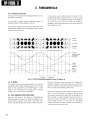
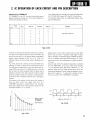
W h e n a light b e a m is passed f r o m a high refraction material t o
a l o w r e f r a c t i o n m a t e r i a l , a r e l a i o n , as s h o w n in Fig. 5 . 2 , is
existed b e t w e e n t h e i n c i d e n t angle a n d refleciton ratio at t h e
b o u n d a r y of t h e materials. A s c a n be seen f r o m t h e g r a p h s ,
t h e reflection ratio will c h a n g e rapidly as t h e i n c i d e n t light
angle c h a n g e s in t h e area w h e r e t h e i n c i d e n t angle is slightly
less t h a n t h e critical a n g l e .
Reflection Surface
(4)
Objective Lens
NA
0.47
S
P
o
l
a
""1L,
g
h
t
NA = Sin0
1.5/xm
WD
Strength
of
Reflection
(Rp-Rs)
Disc
Critical Angle
(41.8°)
Pit surface
Incident light angle 0
(5)
4-divided photodiodes
C o n v e r t s light into an electrical signal
28
Fig. 5 . 2
Refleciton c h a n g e s rapidly at angles d o s e
to critical angle.
QP-1100B II
II. FUNDAMENTALS
In Fig. 5 . 3 , t h e a n g l e of t h e critical p r i s m has been a d j u s t e d
D i s c too c l o s e
so t h a t t h e i n c i d e n t light angle is j u s t e q u a l t o t h e critical angle
for
a center
light b e a m
of i n c i d e n t
light. A c c o r d i n g l y ,
Objective lens
if
parallel light b e a m s are i m p i n g e d , t h e i n c i d e n t light angle is
Divergent
e q u a l t o critical angle f o r all light b e a m s a n d all light b e a m s
(Go through)
Light axi
Light
are r e f l e c t e d , g i v i n g e q u a l light a m o u n t t o e a c h e l e m e n t of
beam
4 - d i v i d e d p h o t o - d i o d e s (PDa, PDb, PDc a n d PDd). If diffused
or d i v e r g e n t light is i m p i n g e d , reflection s t r e n g t h at a left half
Reflected beam
of t h e p r i s m l o w e r s a n d light a m o u n t r e c e i v e d by t h e p h o t o
d i o d e s PDa a n d PDb w i l l be d e c r e a s e d . On t h e c o n t r a r y , if
Prism
Disc
c o n v e r g e n t light is i m p i n g e d , light a m o u n t received by PDc
4-divided
a n d PDd is r e d u c e d . By utilizing this p h e n o m e n o n , t h e p h o t o
photodiodes
d i o d e s c o n v e r t light received into f o u r electrical signals a n d
the signals are p r o c e s s e d w i t h a differential amplifier t o p r o
vide a f o c u s error signal in t e r m s of (A + A ) — ( A + A ) .
t
(A
1 (
A , A , and A
2
3
4
2
3
4
A r e electrical signals d e v e l o p e d by PDa,
P D b , PDc a n d P D d , respectively.)
Disc Focused
Objective lens
^Critical angle prism
Reflection surface
Light axi
4-divided photodiode
(Go through)
Convergent
light
Focus Error Signal
(A! + A ) - ( A + A )
2
A + A
3
3
-Ai + A
2
A + A
2
A + A
4
A + A
4
3
4
t
3
4
Criticl angle
Disc too close (point A) (divergent light beams....)
Focus point (point B) (parallel light....)
Disc too far (point C) (convergent light beams....)
D i s c too far
Parallel
-light beams
3
2
PDc
PDb
PDd
PDa
4
1
Prism
4-Divided Photodiode
Fig. 5 . 4
Fig. 5 . 3
F o c u s error detection by using a critical prism
F o c u s error detection m e t h o d using a critical
angla prism
29
DP-1100B II
II. FUNDAMENTALS
5 - 2 - 2 T r a c k i n g Error Detection
T r a c k i n g error is a d e v i a t i o n of the r e a d i n g light s p o t f r o m the
In this
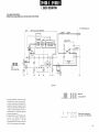
pits (track) t o be t r a c e d .
4 - d i v i d e d p h o t o d i o d e is a s s u m e d as A , A , A
Pickup
a
each
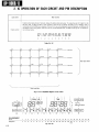
electrical
signal
x
A + A
3
A + A
3
t
In the
system,
method
called
"heterodyne
system"
is
a d o p t e d t o d e t e c t t h e s p o t d e v i a t i o n f r o m a pit.
t
converted
2
3
by
the
A n d A , and
4
a n d A + A A r e e v a l u a t e d . N a m e l y , b o t h phases f o r
2
and
A + A
2
4
are the
same
when
the
tracking
is
established, w h i l e phase difference will be c a u s e d w h e n the
s p o t deviates f r o m a pit.
T h e h e t e r o d y n e s y s t e m is based u p o n the distribution of the
reflected light d i f f r a c t e d f r o m a pit d e p e n d s u p o n a relative
l o c a t i o n of t h e pit a n d s p o t .
Inside of
the track
On a track
Outside of
the track
On a track
Inside or outside
of the track
Sum signal
Inside of
the track
Difference
Signal
Outside or
the track
Pit Section
Fig. 5 . 5
5-3
Time elapsed
P I C K U P Radial Signal Sampling T h e o r y (Pit depth X/4)
RF SIGNAL
W h e n the LDC g o e s t o L level, the o u t p u t of T A 7 5 4 5 8 ( 1 / 2 )
4
c h a n g e s t o n e g a t i v e , a n d this a l l o w s bias c u r r e n t of Q 1 0 9 to
d e v e l o p e d b y the 4 - d i v i d e d p h o t o d i o d e (refer to 3 - 5 ) . T h e RF
f l o w f r o m its e m i t t e r t o the base, t h u s Q 1 0 9 is t u r n e d o n a n d
signal is t h e n p r o c e s s e d t o provide EFM signal. T h e EFM
the Laser d i o d e e m i t s infrared light ( 8 1 0 m m ) .
A RF signal is a s u m of e a c h electrical signal A , A , A a n d A
x
2
signal is t h e n c o n v e r t e d into an a n a l o g signal in
3
passing
t h r o u g h a D-A c o n v e r t o r after d e m o d u l a t e d .
W h e n light e m i t t e d f r o m the laser d i o d e is i m p i n g e d t o the pin
5-4
f r o m a n o d e to c a t h o d e of the d i o d e . W i t h the strength of the
d i o d e , a c u r r e n t p r o p o r t i o n a l t o s t r e n g t h of the light f l o w s
LIGHT EMISSION F R O M L A S E R DIODE
TA75458(Q108)
light i n c r e a s e d , a v o l t a g e d e v e l o p e d across R 1 1 3 also i n
b e c o m e s positive as s h o w n in the s c h e m a t i c d i a g r a m , A n d a
creases a n d m a k e s n o n - i n v e r t e d ( + ) t e r m i n a l of the o p e r a
current
tional
When
the
LDC
flowing
goes
H,
through
the
output
R145,
of
D102,
And
D104
turns
Q 1 0 9 c u t off, t h e r e b y stops the oscillation of the Laser D i o d e .
amplifier
positive.
As
the
c u r r e n t f l o w i n g into the laser d i o d e .
30
result,
the
operational
amplifier o u t p u t also increases in positive, t h u s r e d u c i n g the
DP-1100B II
II. FUNDAMENTALS
6. GENERAL DESCRIPTION ON MICROPROCESSOR
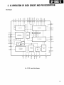
6-1
A d d r e s s D a t a (Q Signal)
1)
A d d r e s s Data (Q Signal) Reading S e c t i o n
R-Channel....&
In t h e CD system s p e c i f i c a t i o n s , o n e s y m b o l c o n s i s t i n g
Q-Channel is used f o r address data a n d o n e a d d r e s s data
W-Channel.
the
is c o m p r i z e d
PCM data is called C O N T R O L & DISPLAY S Y M B O L , a n d
s h o w s this c o n f i g u r a t i o n of the C O N T R O L &
each
symbol data.
8
bits
Frame Synchronization Signal
is
called
P-Channel,
Frame Synchronization Signal
Q-Channel,
Frame Synchronization Signal
Frame Synchronization Signal
Frame Synchronization Signal
User's bit
After conversion of 8 bits to 14 bits
CONTROL DISPLAY Symbol
Fig. 6-1
Q-Channel
eight
of 8 bits a n d l o c a t e d after f r a m e s y n c h r o n i z a t i o n signal of
of
of 9 8 f r a m e
Of
data.
channels,
Fig.
5.6
DISPLAY
DP-1100B II
II. FUNDAMENTALS
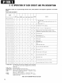
A d d r e s s data f o r m a t (outside lead-in area) are as f o l l o w s :
SO, S 1 :
2 bits address signal sync p a t t e r n .
CONTROL:
4 bits c o n t r o l d a t a , M S B indicates p r e - e m p h a s i s o n or off, a n d LSB indicates 4 C H / 2 C H .
1: Pre-emphasis ON
0: Pre-emphasis O F F
1: 4 CH
0: 2 C H
ADR:
4 bit m o d e data
M O D E 1 (1 in BCD): A d r e s s m o d e
M O D E 2 (2 in BCD): Disc c a t a l o g n u m b e r m o d e
M O D E 3 (3 in BCD): Special i n f o r m a t i o n m o d e ( r e c o r d e d by a l p h a n u m e r i c c o d e 0 # 9 , A # Z )
MNR:
P r o g r a m n u m b e r expressed by BCD in 2 digits (8 bits)
X:
Index f o r e a c h p r o g r a m expressed by BCD in 2 digits (8 bits)
MIN:
Elapsed t i m e ( m i n u t e ) f o r e a c h p r o g r a m expressed by BCD in 2 digits (8 bits)
FRAME:
Elapsed t i m e f o r e a c h p r o g r a m expressed by BCD in 2 digits (8 gits) ( F r a m e , 1 f r a m e = 1/75 sec)
ZERO:
N o t used (8 bits <£data)
A MIN:
Elapsed t i m e (sec) f o r disc expressed by BCD in 2 digits (8 bits)
A SEC:
Elapsed t i m e (sec) f o r a disc expressed by BCD in 2 digits (8 bits)
A FRAME:
Elapsed t i m e f o r a disc expressed by BCD in 2 digits (8 bits) ( f r a m e ) .
CRC:
16 bit CRC c o d e data c a l c u l a t e d f o r data C O N T R O L # A FRAME.
Fig. 6-2
S h o w s the a d d r e s s d a t a configuration.
Each f i g u r e u n d e r a c o d e s h o w s bit n u m b e r required f o r the c o d e .
s
0
>
2
S
i
CONTROL
A D R
4
4
M N
8
R
X
8
M
I
8
N
S E C
FRAME
ZERO
AMIN
ASEC
8
8
8
8
8
Fig. 6 - 2 A d d r e s s D a t a configuration
32
AFRAME
8
C R C
16
SQISI
DP-1100B II
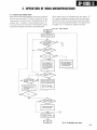
1. CIRCUIT DESCRIPTION
H e a d a m p " , t h e servo PCB a n d t h e
w h e n play m o d e is e n t e r e d f r o m s t o p m o d e . It c h e c k s t h e
p r o c e s s PCB are d e s c r i b e d in o r d e r a l o n g the RF signal f l o w .
n u m b e r of data errors to c o n t r o l c o n t r o l i n p u t s A , B, C a n d
1-1
playback.
Subsequent to " 1 - 2
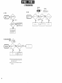
INH of Q 1 0 2 o n t h e m e c h a n i s m PCB t o o b t a i n t h e o p t i m u m
Head amplifier
T h e f o u r signals f r o m t h e p i c k u p are i n p u t t o preamplifier IC
T h e internal block d i a g r a m a n d t r u t h table of Q 1 0 2 is s h o w n
in Fig 2-1 C a n d D of s e c t i o n 2 - 1 - 2 . Inputs A , B, C a n d I N H ,
( Q 1 0 3 ) o n the m e c h a n i s m PCB.
d e t e r m i n e w h i c h o u t p u t 0 t o 7 (bilateral s w i t c h s h o u l d be i n
1- 1-1
ternally c o n n e c t e d w i t h C O M ) .
F o c u s b a l a n c e a n d S V C operation circuit ( Q 1 0 3 )
T h e internal b l o c k d i a g r a m of Q 1 0 3
is s h o w n in section
2 - 1 - 1 . T h r o u g h t h e resistors, c o n n e c t e d b e t w e e n pins 1 a n d
1-1-4
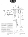
A P C (laser p o w e r control) circuit ( Q 1 0 5 , Q 1 0 6 a n d
Q107)
2 a n d b e t w e e n pins 15 a n d 16 of Q 1 0 3 ( T A 7 7 3 1 P ) , f o c u s
b a l a n c e a n d SVC o p e r a t i o n (described later) are p e r f o r m e d .
Q 1 0 5 , w h i c h is the laser O N / O F F s w i t c h , t u r n s O N w i t h " L "
W e a k signal is a m p l i f i e d a n d o u t p u t t o servo PCB as S1 a n d
signal LDC (J8-3P) f r o m the m i c r o p r o c e s s o r so t h a t t h e laser
d i o d e e m i t s light. T h i s laser d i o d e i n c o r p o r a t e s a light e m i s
S2.
sion m o n i t o r d i o d e . T h e n , APC o p e r a t i o n is p e r f o r m e d by us
1-1-2
F o c u s error signal generation circuit ( Q 1 0 1 and Q 1 0 4 )
ing t h e m o n i t o r o u t p u t as t h e APC c o n t r o l i n p u t .
T h e FE amplifier a n d peak d e t e c t o r , c o n s i s t i n g of Q 1 0 1 a n d
Q 1 0 4 , is a c i r c u i t t o g e n e r a t e t h e f o c u s error signal. Peak
1-1-5
d e t e c t i o n is m a d e w i t h t h e B-E d i o d e characteristic of Q 1 0 4
FG signal is p r o d u c e d by Q 1 0 1 , Q 1 0 8 a n d Q 1 0 9 t o m o n i t o r
F G amplifier circuit ( Q 1 0 1 ( 2 / 2 ) , Q 1 0 8 a n d Q 1 0 9 )
a n d t h e CR t i m e c o n s t a n t of its e m i t t e r . T h e f o c u s error signal
t h e rotation of t h e disc m o t o r . Q 1 0 1 p e r f o r m s a m p l i f i c a t i o n
is o b t a i n e d f r o m (C + D) - (A + B) o p e r a t i o n of the p i c k e d - u p
a n d Q 1 0 8 , Q 1 0 9 a n d D 1 0 4 p e r f o r m w a v e f o r m s h a p i n g . For
f o u r signals f r o m t h e p i c k u p by Q 1 0 1 .
a d j u s t m e n t of e a c h t r i m m i n g p o t e n t i o m e t e r , refer t o " A d j u s t
m e n t " o n page 1 6 5 .
1-1-3
S V C circuit operation ( Q 1 0 2 )
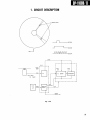
T h e servo c o n t r o l (SVC) is p e r f o r m e d by processor IC12 o n
the p r o c e s s PCB ( X 3 2 - 1 0 1 0 ) , w h e n t h e disc is e x c h a n g e d or
Fig. 1 - 1 - 3
S V C Circuit Operation
33
DP-11D0BII
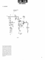
1. CIRCUIT DESCRIPTION
1-2 Servo circuits
1-2-3
1-2-1
Pits are m a d e o n a disc in s u c h a w a y t h a t the s u m of " H "
F o c u s s e r v o circuit
D S V circuit ( I C 8 ( 1 / 2 ) a n d I C 1 5 D L S 1 a n d 2)
T h e f o c u s error (FE) s i g n a l , g e n e r a t e d in t h e m e c h a n i s m PCB,
d u r a t i o n s is equal t o t h a t of " L " d u r a t i o n s i.e. DSV (Digital
is f e d into pin 8 of C N 6 o n t h e servo PCB, T h i s signal is used
S u m Value) is z e r o . T h u s , this c i r c u i t c o n t r o l s the amplifier
in m a k i n g signal DOK w h i c h t h e p r e s e n c e or a b s e n c e of t h e
bias so t h a t t h e data o n the disc is identical t o t h a t read by t h e
disc is j u d g e d w h e n t h e tray is c l o s e d .
player, t h e r e b y d e c r e a s i n g error.
W i t h a disc present, " L " signal DOK is o u t p u t f r o m pin 1 of
C N 2 t o pin 2 7 of IC15 o n t h e p r o c e s s PCB ( X 3 2 ) .
1 -2-4
On t h e o t h e r h a n d , w h e n t h e RF signal f r o m the p i c k u p is i n
T h e signal f r o m pin 4 of IC6 is f u r t h e r a m p l i f i e d a n d applied t o
p u t t o pin 2 0 of I C 1 5 , pin 1 2 (FOK) of IC16 is at - 1 2 V a n d
the base of Q 2 1 . T h e variation in a m p l i t u d e of the DC c o m p o
Q2 turns
OFF. Signal
adjustment
nent, t h a t is e q u i v a l e n t t o t h e a m p l i t u d e of the EFM signal
p o t e n t i o m e t e r V R 1 is a m p l i f i e d in IC1 ( 1 / 2 ) a n d i n p u t t o IC2
w a v e , a p p e a r s in the e m i t t e r of Q 2 1 . This DC c o m p o n e n t is
( 1 / 2 ) via t h e phase c o r r e c t i o n CR c i r c u i t . T h e n , t h e signal
a m p l i f i e d o n l y in l o w f r e q u e n c y by IC8 ( 1 / 2 ) a n d applied t o
p o w e r - a m p l i f i e d in IC2 ( 1 / 2 ) drives t h e p i c k u p a c t u a t o r coil t o
the gate of AGC FET Q 3 3 , t h u s r e d u c i n g the c h a n g e in EFM
f o r m a servo l o o p i n c l u d i n g t h e optical p i c k u p by w h i c h the
signal. In a d d i t i o n , t h e EFM signal is l e v e l - c o m p a r e d in IC10
laser b e a m is a l w a y s f o c u s e d exactly o n t h e disc pit surface ir
( 1 / 2 ) . T h e n " L " at pin 1 of IC10 ( 1 / 2 ) i n f o r m s t o pins 2 0
respective of t h e a m o u n t of disc w a r p , e t c .
(RFOK) of IC15 o n SERVO ( x 2 9 )
D u r i n g light e m i s s i o n of t h e laser d i o d e , the gate of FET Q 4
IC15 o n t h e p r o c e s s ( X 3 2 ) PCB t h r o u g h pin 1 of C N 7 t h a t t h e
c o n n e c t e d t o t h e LDC line is " L " so t h a t IC2 ( 1 / 2 ) p e r f o r m s
EFM signal is p r o v i d e d .
PCB a n d 2 9 (RFOK) of
n o r m a l a m p l i f i c a t i o n . In a d d i t i o n , t h e gate of Q6 c o n n e c t e d t o
In a d d i t i o n , t h e EFM signal is also applied t o IC10 ( 2 / 2 ) via
the
RF signal is p r o v i d e d .
diode D 1 9 f o r l e v e l - c o m p a r i n g . T h e n , it is o u t p u t f r o m pin 8
T h e r e f o r e , Q 6 t u r n s OFF a n d a m p l i f i c a t i o n is possible in the
as signal RFES. T h i s signal is used in d r o p o u t c o n t r o l o n play
l o o p c o n n e c t i n g IC1 a n d I C 2 , w h e r e t h e f o c u s servo w o r k s .
or used in t h e kick p r o c e s s i n g c i r c u i t at kick of m o t o r .
FOK line is at
1 -2-2
—12
V when
1 -2-5
T r a c k i n g s e r v o circuit
Pickup carry motor driver
D ) , p r o d u c e d by t h e pre
A s play a d v a n c e s t r a c i n g the disc pit s e q u e n c e by t h e p i c k u p ,
a m p l i f i e r o n t h e m e c h a n i s m PCB, are f e d into pins 6 a n d 7 of
a positive offset v o l t a g e a p p e a r s at t h e o u t p u t of t r a c k i n g coil
Signals S1 (A +
B) a n d S2 (C +
c o n n e c t o r C N 6 . These signals are partially a m p l i f i e d by a
driver pin 8 of IC2 ( 2 / 2 ) by the t r a c k i n g servo f u n c t i o n . Since
3-stage a m p l i f i e r of inverter IC5 t o g e n e r a t e the t r a c k i n g error
the h i g h - f r e q u e n c y c o m p o n e n t , w h i c h is also c o n t a i n e d in t h e
s i g n a l , t h e n w a v e f o r m - s h a p e d by IC7 a n d i n p u t t o TS1 a n d
tracking
T S 2 of I C 1 5 .
necessary f o r d r i v i n g t h e p i c k u p c a r r y m o t o r , it is e l i m i n a t e d
driver
output
besides the
offset v o l t a g e ,
is u n
T h e t r a c k i n g error signal is g e n e r a t e d in IC15 a n d o u t p u t f r o m
by an LPF a m p l i f i e r of IC3 ( 2 / 2 ) . Further, this o u t p u t is p o w e r -
TEOP a n d T E O N . T h i s signal w o r k s as the t r a c k i n g
a m p l i f i e d in IC4 ( 2 / 2 ) t o drive t h e p i c k u p carry m o t o r .
servo
signal.
In a d d i t i o n , Q 1 4 is ON t o avoid a p p l i c a t i o n of the t r a c k i n g ser
On t h e o t h e r h a n d , signals S1 a n d S2 are c o m b i n e d via R 1 0 0
v o o u t p u t signal d u r i n g m o d e s o t h e r t h a n play. Signal PUFB,
a n d R 1 0 1 t o e x t r a c t m u s i c signal. T h e c o m b i n e d signal is i n
w h i c h is e n t e r e d t o t h e i n p u t of the p o w e r amplifier (pin 3 of
p u t t o IC6 w h i c h acts as an amplifier like IC5. After 1 st stage-
IC4 ( 2 / 2 ) ) , is used in kick o p e r a t i o n or fast m o v e m e n t of the
a m p l i f i c a t i o n , it is f u r t h e r 2-stage a m p l i f i e d t h r o u g h t h e EFM
pickup.
test
34
FE t h r o u g h f o c u s gain
Envelope detection
point
via
the
second-stage
amplifier
which
is
bias-
c o n t r o l l e d by DSV a n d is i n p u t t o pin 17 (EFM I) of I C 1 5 .
1 -2-6
T h e t r a c k i n g error signals o u t p u t f r o m pins 3 a n d 4 of IC15
W h e n pin 15 (MSP) of IC15 o n the servo PCB e m i t s an " H "
D i s c motor driver
(TEOP a n d TEON) are c o m b i n e d in IC12 ( 1 / 2 ) . T h e c o m b i n e d
signal a c c o r d i n g t o t h e CPU c o m m a n d , the gate of
o u t p u t (TE) is p h a s e - i n v e r t e d in I C 1 4 ( 1 / 2 ) a n d i n p u t via
becomes " L "
t r a c k i n g g a i n t r i m m i n g p o t e n t i o m e t e r V R 2 t o pin 6 of IC1
( 1 / 2 ) c a n a m p l i f y signal AFC e m i t t e d f r o m IC8 o n the process
Q17
a n d Q 1 7 t u r n s OFF. Disc m o t o r driver
IC4
( 2 / 2 ) in w h i c h it is p h a s e - c o r r e c t e d a n d a m p l i f i e d .
PCB due t o start t h e disc m o t o r . Due t o shorten t h e start t i m e
Further, o u t p u t of IC1 ( 2 / 2 ) is p o w e r - a m p l i f i e d in IC2 ( 2 / 2 ) ,
or t h e s t o p t i m e , a c i r c u i t c o n s i s t i n g of Q 1 9 , C 3 6 , Q 1 8 a n d
Q 1 0 a n d Q 1 1 . A m p l i f i e d TE signal drives t h e p i c k u p a c t u a t o r
R 9 4 applies positive or negative pulse t o the pin 7 of IC4
coil t o f o r m a t r a c k i n g servo by w h i c h t h e laser b e a m s p o t
(1/2).
f o l l o w s e x a c t l y t h e pit s e q u e n c e o n t h e disc.
motor's stop).
(Positive
pulse
at m o t o r ' s
start
Negative
pulse
at
DP-1100B II
1. CIRCUIT DESCRIPTION
Scratch, Dust
RFES
•DCON
Disc
DOCK
Fig.
1-2A
35
DP-1100B II
1. CIRCUIT DESCRIPTION
1 -2-7
1 - 2 - 1 0 T E noise limiter
T r a y motor driver
3-state o u t p u t situation in pin 9 of IC15 is used for driving t h e
This noise limiter consists of I C 1 4 ( 2 / 2 ) a n d Q 2 7 t o Q 3 0 .
tray m o t o r . T h e signal at " H " is i n v e r s i o n - a m p l i f i e d in IC3
Q 2 9 is t h e limiter ON/OFF s w i t c h . W h e n signal TEP is " L "
( 1 / 2 ) t o drive Q 1 6 t o m a k e pin 3 of C N 4 negative so t h a t t h e
(during k i c k ) , no limiter o p e r a t i o n is possible. N o r m a l l y , Q 2 9
tray m o t o r rotates in t h e d i r e c t i o n in w h i c h the tray is c l o s e d .
is OFF d u r i n g play.
Conversely, t h e signal at " L " is also i n v e r s i o n - a m p l i f i e d in
T h e t r a c k i n g error (TE) voltage is a m p l i f i e d t o a b o u t 6 t i m e s in
IC3 ( 1 / 2 ) t o t u r n ON Q 1 5 so t h a t t h e tray m o t o r rotates in the
IC14 ( 2 / 2 ) a n d is applied t o t h e bases of Q 2 7 a n d
d i r e c t i o n in w h i c h t h e tray is o p e n e d .
t h r o u g h an HPF c o n s i s t i n g of C 7 3 a n d others. W h e n the
Q28
In a d d i t i o n , w h e n pin 9 of IC15 is o p e n e d , pin 2 of IC3 is at
voltage g o e s u p m o r e t h a n a b o u t + 0 . 6 V , Q 2 7 t u r n s O N ,
zero voltage so t h a t t h e tray m o t o r stops since no v o l t a g e is
w h i l e w h e n it g o e s d o w n less t h a n a b o u t — 0 . 6 V , Q 2 8 t u r n s
O N . D u r i n g t h a t ON p e r i o d , t h e peak noise of the voltage is
applied.
suppressed so t h a t the f o l l o w i n g stage gets free f r o m the
1 -2-8
d i s t u r b a n c e c a u s e d by this noise. T h e r e b y , t h e p i c k u p is
T r a c k i n g error detector control
(This c i r c u i t is effective o n l y at kick o p e r a t i o n . )
p r e v e n t e d f r o m j u m p i n g off t h e c o r r e c t t r a c k t o a n o t h e r o n e
Both IC12 ( 2 / 2 ) a n d IC13 ( 1 / 2 ) o u t p u t " H " signals in nor
due t o noise.
m a l o p e r a t i o n . T h e r e u p o n , w h e n the t r a c k i n g error v o l t a g e at
pin TE o u t p u t g o e s u p m o r e t h a n a b o u t + 0 . 6 V , pin 2 of
1-2-11
IC12 ( 2 / 2 ) b e c o m e s " L " a n d this v o l t a g e is applied t o TEG 1
Signal RFES p r o d u c e d in IC10 ( 2 / 2 ) b e c o m e s " H " w h e n the
i n p u t of I C 1 5 . See " 1 " in t h e table b e l o w .
D i s c f l a w position m e m o r y circuit ( S e e F i g . 1 - 2 A . )
RF signal level is discreased by f l a w s or d u s t o n t h e disc. This
signal at " L " is o u t p u t as signal DIN f r o m the d r o p o u t c o n t r o l
State
TE Voltage
TEG1
TEG2
block in IC15 t o t h e disc f l a w position m e m o r y c i r c u i t in
1
>+0.6
L
H
w h i c h positional data of f l a w is s t o r e d . A t the s a m e t i m e , this
2
<-0.6
H
L
Table-1
signal is also o u t p u t as signal DCON w h i c h is t h e t r a c k i n g ser
v o gain r e d u c t i o n gate pulse. D r o p o u t c o n t r o l is t h u s m a d e .
Pin DIN of IC15 o u t p u t s a signal i n d i c a t i n g t h e RFES state at
Conversely, w h e n t h e t r a c k i n g error v o l t a g e at TE o u t p u t g o e s
d o w n less t h a n - 0 . 6 V , pin 2 of IC12 ( 2 / 2 ) b e c o m e s " H "
a n d pin 2 of IC13 ( 1 / 2 ) " L " so t h a t this v o l t a g e is applied t o
TEG 2 i n p u t o f I C 1 5 . See " 2 " in the table a b o v e . T h e search
the rising e d g e of signal DOCK. It also c h e c k s the o u t p u t of
the disc f l a w position m e m o r y c i r c u i t (pin 8 of IC7) at the fall
ing e d g e of signal DOCK a n d t h e n o u t p u t s signal DCON (pin
12 of IC15) t o t r a c k i n g servo a m p c i r c u i t .
t i m e is s h o r t e n e d by this c o n t r o l c i r c u i t . N o r m a l l y , in play
m o d e , this v o l t a g e is offset by signal TEP, therefore i n p u t s
TEG 1 a n d TEG 2 are invalid.
1-2-12
Relationship b e t w e e n s e r v o a n d control line
For play, t h e a c t u a t o r of the p i c k u p is m o v e d u p or d o w n by
the 2 Hz signal f r o m F.SRCH (pin 2 of C N 2 ) . A t this t i m e ,
1-2-9
P e a k hold circuit
w h e n t h e disc is in r o t a t i o n , the RF signal is o u t p u t f r o m the
T h e peak h o l d c i r c u i t consists of Q 2 3 t o Q 2 6 , D 2 8 t o D 3 5 ,
IC14 ( 1 / 2 ) , e t c . W h e n KGC b e c o m e s " H " o n kick state, Q 2 3
p i c k u p o n l y at t h e m o m e n t the laser b e a m is f o c u s e d . W i t h
the RF s i g n a l , IC10 ( 1 / 2 ) o u t p u t s an " L " signal (RFOK) to
:
a n d Q 2 4 t u r n O N , a n d Q 2 5 a n d Q 2 6 t u r n OFF. T h e r e b y , C 7 0
is c h a r g e d w i t h t h e positive peak v o l t a g e at t r a c k i n g error i n
p u t TE a n d C 6 9 is c h a r g e d w i t h the negative peak v o l t a g e .
D u r i n g kick, C 6 9 a n d C 7 0 are c o n t i n u o u s l y c h a r g e d w i t h
these peak v o l t a g e s . W h e n the unit returns t o n o r m a l play
t u r n ON Q 3 1 . Further, this signal is inverted at IC16 a n d FOK
b e c o m e s — 12 V . Q 2 a n d Q6 is t u r n e d off by " L " FOK s i g n a l ,
" H " LDC signal is inverted t o " L " t o t u r n Q 4 off, so t h a t the
f o c u s servo starts o p e r a t i o n . T h u s , a c o n t i n u o u s RF signal a p
pears at pins 6 a n d 7 of C N 6 f r o m the p i c k u p . T h e r e b y , pin
f r o m t h e kick state, Q 2 3 a n d Q 2 4 t u r n OFF a n d Q 2 5 a n d
1 4 (FOKG) of IC15 o u t p u t s an " H " signal. T h i s signal is i n
Q 2 6 t u r n O N . T h e n , t h e average value of t h e voltages at C 7 0
verted at I C 1 6 . T h e voltage at pin 11 of IC15 b e c o m e s
a n d C 6 9 is i n p u t t o I C 1 4 ( 1 / 2 ) . H e r e , it is s u b j e c t t o s u b t r a c
V . T h e r e f o r e , Q 1 2 t u r n s OFF so t h a t IC2 ( 2 / 2 ) c a n p e r f o r m
-12
t i o n w i t h the v a l u e of v o l t a g e T E , so t h a t t h e unit is restored t o
a m p l i f i c a t i o n . In a d d i t i o n , DCON is " L " as long as the level of
n o r m a l play f r o m the kick state.
the RF signal d o e s n o t d r o p s u d d e n l y due t o f l a w s or dirt o n
the disc. A s t h e KGC line is at - 1 2 V in n o r m a l play (except
for t h e kick s t a t e ) , Q 7 , Q 8 , Q9 a n d Q 1 2 are all OFF. T h u s ,
the t r a c k i n g servo w o r k s so t h a t t h e p i c k u p t r a c e s the pit se
q u e n c e o n t h e disc. T h e data o n t h e disc c a n t h e r e b y be read
out continuously.
36
DP-1100B II
1. CIRCUIT DESCRIPTION
1-3 PROCESS CIRCUIT
1-3-1
Only t h e data w h i c h c o u l d n o t be c o r r e c t e d even in t h e C2
c o r r e c t i o n s e c t i o n is s u b j e c t t o m e a n - v a l u e i n t e r p o l a t i o n a n d
E F M signal demodulation
T h e EFM signal (EFMO) o u t p u t f r o m pin 4 1 of IC15 o n t h e
is o u t p u t t o t h e D/A c o n v e r t e r .
servo PCB is i n p u t t o pin 5 2 (EFM 2) of IC8 a n d pin 1 4 (EFMI)
of IC9 o n t h e p r o c e s s PCB.
1-3-2
IC9 w o r k s as a digital PLL t o g e t h e r w i t h V C O Q 3 . Signal EFMI
a) A F C
is p h a s e - c o m p a r e d w i t h signal PLCK ( 4 . 3 2 MHz)
T h e signal resultant f r o m
resultant
C L V s e r v o control in I C 8 ( T C 9 1 7 8 F )
1/4 f r e q u e n c y division of f r a m e
sync signal a n d t h e i n p u t s i g n a l ( 2 . 1 1 6 8 M H z ) f r o m C 2 1 K
f r o m 1/4 f r e q u e n c y division of signal V C O I .
T
are used here. T h e n , w i t h t h e c e n t e r of t h e c o u n t of 1 1 5 2
b e c o m e s " L " a n d acts t o m a k e t h e V C O f r e q u e n c y higher.
c l o c k pulses of C 2 1 K in r e s p e c t t o t h e f o r m e r s i g n a l , pin 2 0
H e r e , w h e n signal PLCK is d e l a y e d f r o m signal EFMI, pin \ J
C o n v e r s e l y , w h e n it is a d v a n c e d , pin D T
OU
O U
becomes " H " and
(AFCO) o u t p u t s a 0 V signal w h e n t h e s p e e d of t h e disc m o t o r
acts t o m a k e t h e V C O f r e q u e n c y l o w e r .
rises a b o u t 1 0 % a n d o u t p u t s a 5 V signal w i t h t h e s a m e
T h e EFM signal o u t p u t f r o m pin D T
in s y n c h r o n i z a t i o n w i t h
v o l t a g e as v o l t a g e V D D w h e n t h e s p e e d l o w e r s a b o u t 1 0 % .
t h e rising e d g e of signal PLCK is f e d t o pin 5 3 (EFMI) of IC8,
T h u s , in the range of ± 1 0 % c h a n g e in m o t o r s p e e d , t h e o u t
in w h i c h d e t e c t i o n is m a d e t o a f r a m e sync signal w h i c h is a
put voltage corresponds to m o t o r revolution ( P W M w a v e ) .
OU
c o n t i n u o u s signal of 11 " H " bits a n d 11 " L " bits.
W h e n t h e f r a m e s y n c signal is o b t a i n e d , t h e EFM signal is
b) A P C
d e m o d u l a t e d into an 8 - b i t signal. M o r e o v e r , the u s e r ' s bits
P h a s e - c o m p a r i s o n is m a d e b e t w e e n t h e signal resultant f r o m
j u s t after t h e f r a m e s y n c signal are d e m o d u l a t e d a n d data Q
118 f r e q u e n c y division of t h e f r a m e sync signal a n d t h e signal
among
f r o m a f r e q u e n c y division of signal C 2 1 K . T h e
them
are displayed
as t i m e
data
bundled
by
98
f r a m e s . T h e s e are also used in FF or B W D o p e r a t i o n , etc.
comparison
o u t p u t is e m i t t e d as P W M signal w i t h 8-bit r e s o l u t i o n . H e r e ,
T h e m u s i c d a t a , c o n v e r t e d f r o m 1 4 - b i t t o 8 - b i t signals, are
V D D / 2 ( 2 . 5 V) is o u t p u t at a phase d i f f e r e n c e of zero in a
w r i t t e n in jitter a b s o r p t i o n m e m o r y IC7 u n d e r c o n t r o l of IC6
c o n t r o l range of ± 7 / 8 ir.
( T C 9 1 7 9 F ) . T h e o n e - f r a m e 3 2 - s y m b o l data is c o r r e c t e d f o r
In a d d i t i o n , t h e speed of t h e disc m o t o r c a n be c o n t r o l l e d by
error in t h e C1 c o r r e c t i o n s e c t i o n . N e x t , after de-interleave
signal D I V +
o p e r a t i o n , t h e data w h i c h c o u l d n o t be c o r r e c t e d in the C1
T C 9 1 7 8 F a n d T C 9 1 7 9 F , refer t o t h e d i a g r a m o n p a g e s 8 1
c o r r e c t i o n s e c t i o n is c o r r e c t e d in t h e C2 c o r r e c t i o n s e c t i o n .
to 9 0 .
or DIV- f r o m T C 9 1 7 9 F . For i n f o r m a t i o n a b o u t
37
DP-11G0B II
1. CIRCUIT DESCRIPTION
1-4
D/A converter
T h e serial m u s i c d a t a , w h i c h is o u t p u t f r o m IC6 o n t h e p r o
this LPF o u t p u t s a m u s i c signal w i t h a peak a m p l i t u d e of 1/2
cess PCB, is i n p u t t o the D/A c o n v e r t e r (IC21) at the falling
t h a t of the P A M w a v e . This m u s i c signal is i n p u t t o buffer
e d g e of signal BCK. T h e data of o n e w o r d is t r a n s f e r r e d t o
amplifier IC27 t o w h i c h a f r e q u e n c y c h a r a c t e r i s t i c c o m p e n -
IC21 by repeat i n p u t at 16 cycles of signal BCK. A f t e r t h a t ,
sotor CR c i r c u i t is c o n n e c t e d .
w h e n signal CC d r o p s d o w n t o " L " , a pulse (DCR or DCL) is
IC26 c o n t r o l s the e m p h a s i z e d signal d e t e c t e d by IC8. Pin
o u t p u t w i t h w h i c h t h e integrator o u t p u t is d i s c h a r g e d . T h e n ,
EMPH of IC8 o u t p u t s an " H " signal w i t h a disc o n w h i c h e m
after c l e a r i n g the p r e v i o u s s a m p l e d v a l u e , signal IOUTR or
phasized signals are r e c o r d e d , a n d t h u s the d e - e m p h a s i s cir
IOUTL is c o n t i n u o u s l y o u t p u t a c c o r d i n g t o the level of signal
c u i t w o r k s . T h e m u t i n g relay c o n n e c t e d t o the o u t p u t pin is
LRCK d u r i n g t h e t i m e in p r o p o r t i o n t o the a m o u n t of t h e digital
c o n t r o l l e d by the m u t i n g signal f r o m the m i c r o - p r o c e s s o r . In
m u s i c data a n d is held as an a n a l o g v o l t a g e at integration
a d d i t i o n , IC21 j u d g e s t h e m u s i c data as an R-ch signal w h i l e
c a p a c i t o r C 2 1 2 or C 2 1 3 . T h e e x a m p l e of w a v e f o r m
signal LRCK is " L " .
Fig. 1-4A
represents a s e q u e n c e of this state. (2) Fig.
©
in
1-4A
s h o w s t h e w a v e f o r m w h e n signal IOUTR or IOUTL is s a m p l e d
L-ch signal a n d signal IOUTL as an R-ch signal.
by signal LRCK. W h e n this P A M w a v e is filtered by an LPF,
Fig. 1 - 4 A
38
D u r i n g this p e r i o d , IC6 o u t p u t s
L-ch
signals. T h e r e f o r e , signal IOUTR of IC21 is h a n d l e d as an
D / A C o n v e r t e r Circuit
DP-1100B II DP-1I00B II
1. CIRCUIT DESCRIPTION
1-5 MAIN CIRCUIT OPERATION
1-5-1
RESET OPERATION
Fig. 1-5-1-1
Power ON
Power OFF
VDD
1 . W h e n p o w e r s w i t c h S1 is t u r n e d o n , + 5 V a n d + 8 V are
5. W h e n t h e reset signal is " H " level, I C 1 5 ( T M P 4 7 4 0 N ) ,
s u p p l i e d t o t h e RESET c i r c u i t f r o m t h e v o l t a g e regulated
I C 1 2 , IC1 a n d IC15 ( T C 1 5 G 0 0 8 A P - 0 0 0 7 ) start f u n c t i o n
power supply circuit.
i n g . IC15 ( T C 1 5 G ) is, h o w e v e r , reset via Q 1 1 in o r d e r t o
2 . T h e rising t i m e a n d t h e falling t i m e of t h e p o w e r s u p p l y
a v o i d t h e o v e r l o a d i n g at pin 11 of I C 1 3 . W h e n Q 1 1 is
v o l t a g e s + 5 V a n d + 8 V are different ( + 8 V rises faster
OFF, m o d e s 0 t h r o u g h 4 are at " L " level by m e a n s of
t h a n + 5 V w h e n t h e p o w e r is t u r n e d o n a n d it falls faster
R97.
w h e n t u r n e d o f f . ) T h i s c r e a t e s a difference in o p e r a t i o n
6 . W h e n p o w e r s w i t c h S1 is t u r n e d OFF, + 8 V d r o p s , m a k
t i m i n g t o t h e m i c r o p r o c e s s o r ciruit ( + 5 V) a n d t h e a n a l o g
ing t h e e m i t t e r v o l t a g e of Q 5 also d r o p . W h e n + 8 V d r o p s
c i r c u i t ( + 8 V ) . D i o d e D 9 c l a m p s + 8 V until + 5 V rises,
by 1 V , t h e e m i t t e r v o l t a g e of Q 5 g o e s d o w n to a b o u t 4 V ,
so t h a t t h e t i m i n g d i f f e r e n c e c a n be e l i m i n a t e d .
C42 R 3 4
Reset
because a b o u t 3 V d i s c h a r g e v o l t a g e is b e i n g p r o v i d e d by
3 . W h e n + 5 V rises, it is s u p p l i e d t o t h e e m i t t e r of Q 5 . Q 5
C 1 0 2 c o n n e c t e d a c r o s s R 1 1 8 . Since t h e base v o l t a g e of
t u r n s o n , p r o d u c i n g a b o u t 5 V at its c o l l e c t o r . It is c o u p l e d
Q5 is c h a r g e d by C 4 2 , it d o e s n o t d r o p v e r y q u i c k l y . Q 5 is
t o pin 1 4 of I C 1 3 a n d p u t s it t o " H " level. W h e n t h e e m i t
p l a c e d u n d e r OFF state. T h e c o l l e c t o r v o l t a g e d r o p s , m a k
ter of Q 5 is p r o v i d e d w i t h a b o u t 5 V , t h e base v o l t a g e
ing pin 13 of IC13 t o " H " level a n d pin 11 t o " L " level.
becomes about 4 . 4 V due to time constants R34 and
IC15 ( T M P 4 7 4 0 N ) ,
C 4 2 . T h i s " H " level signal is a p p l i e d t o pin 1 5 of I C 1 3 .
functioning.
I C 1 2 , IC1 a n d I C 1 5 ( T C 1 5 G )
stop
) Reset
Approx. lOOsec
* " H " level: more t h a n 3 . 5 V
" L " L e v e l : less than 1.5 V
4 . W h e n b o t h o f pin 1 4 a n d 1 5 are at " H " level, t h e level of
pin 1 3 c h a n g e s f r o m " H " t o " L " . T h e inverted o u t p u t is
Fig. 1 - 5 - 1 - 2 Timing C h a r t for I C 1 3 R e s e t Signal
o b t a i n e d at pin 1 1 , after g o i n g t h r o u g h pin 1 2 . pin 11 is
set at " L " level by R 3 6 , b u t it c h a n g e s t h e level f r o m " L "
t o " H " . (This signal is t e r m e d reset signal.)
39
DP-1100B II DP-1100B II
1. CIRCUIT DESCRIPTION
1-5-2
TRAY OPERATION
Fig.
1 . W h e n tray OPEN/CLOSE s w i t c h S 0 0 4 is p r e s s e d , Q1
OPEN/CLOSE
9. W h e n the tray c l o s e s , pin 9 of IC15 ( T C 1 5 G of T 7 0 0 1 )
m o m e n t a r i l y t u r n s o n a n d a key s c a n n i n g signal available
s w i t c h is p r e s s e d , the tray o p e n s . W h e n the s w i t c h is
is at " H " level. It p u s h e s the v o l t a g e at pin 3 of IC3 f r o m
f r o m pin 13 of IC1 is a p p l i e d t o pin 2 9 of I C 1 .
pressed a g a i n , it closes. T h e o p e r a t i o n is repeated alter
2.5 V
nately by every pressure of OPEN/CLOSE s w i t c h ( S 0 0 4 )
v o l t a g e at pin 3 b e c o m e s higher t h a n t h a t of pin
2 . The signal p u t t h r o u g h pin 2 9 is p r o c e s s e d in IC1 a n d its
output
is c o u p l e d
to
pin
39
of
IC15
(TMP4740N)
t h r o u g h pin 4 0 .
3 . T h e data signal fed t h r o u g h pin 3 9 c o n t r o l s pin 1 to 5 in
I C 1 5 . (An i n s t r u c t i o n signal t o IC15 ( T C 1 5 G or T 7 0 0 1 )
is d e v e l o p e d by a c o m b i n a t i o n of pin 1 t o 5.)
4 . W h e n the p o w e r is t u r n e d o n a n d tray
5. T h e OPEN/CLOSE f u n c t i o n of the tray is a c h i e v e d
by
^ \ T R A Y
CLOSES
Remarks
Control^
Mode
Pin^^
1
E
L
F
H
8
L
C
Refer to control MODE of
IC15 (TC15G008AP)
Table 2-2B and notes
below.
L
H
H
L
L
3
H
H
L
H
4
H
H
H
H
5
L
L
L
L
supply
voltage.
When
the
4
( 2 . 5 V ) , the inverted o u t p u t c h a n g i n g ( f r o m 0 V) t o w a r d
m i n u s a p p e a r s at pin 2 . It t u r n s o n Q 1 6 (while Q 1 5 is
6. T h e o u t p u t s f r o m pin 1 t o 5 of IC15 ( T M P 4 7 4 0 N ) are
applied t o pin 2 4 t o 2 7 a n d 3 0 , a n d the o u t p u t is t h e n
which comes from
- 1 2 V line t h r o u g h R72 a n d L 2 .
T h e m o t o r revolves in t h e c o u n t e r c l o c k w i s e d i r e c t i o n .
1 0 . W h e n the OPEN/CLOSE f u n c t i o n of the tray is c o m p l e t e d
by pressing the tray OPEN/CLOSE S w i t c h , a leaf s w i t c h
for the c o n d i t i o n s other t h a n the listed left. T h e i n p u t t o
p r o v i d e d o n the tray t u r n s O N or OFF. T h e state of the
pin 3 of IC3 is + 2 . 5
switch
V , w h i c h is o b t a i n e d by d i v i d i n g
+ 5 V w i t h R 6 8 a n d R 7 1 . T h e + 5 V is also d i v i d e d by
R 6 6 a n d R 6 7 to provide pin 4 of IC3 w i t h + 2 . 5 V . T h e
c o m p a r a t i v e d i f f e r e n c e b e t w e e n v o l t a g e s at pin 3 a n d 4
of IC3 is available at pin 2 as an o u t p u t .
Since
the
t a n t o u t p u t at pin 2 b e c o m e s 0 V. W h e n t h e v o l t a g e at
pin 2 of IC3 is 0 V , Q 1 5 a n d Q 1 6 are OFF a n d t h e tray
m o t o r d o e s n o t run w i t h n o p o w e r s u p p l i e d .
8 . W h e n the tray o p e n s , pin 9 of IC15 ( T C 1 5 G or T 7 0 0 1 )
is at " L " level. It pulls d o w n the potential at pin 3 of IC3
f r o m 2 . 5 V d o w n t o w a r d g r o u n d . The inverted o u t p u t
'Notes on Control Mode in Tray OPEN/CLOSE operation
E: The SLT (start limit) switch Is ON, i.e. the tray is retracted and the
pickup is moved toward the center of the disc till pickup start limit
switch is on. This occurs when the tray is retracted with or without
disc by OPEN/CLOSE switch.
F: The SLT switch is OFF. This occurs in the state other than mentioned
above such as in PLAY mode or PAUSE mode during playback.
8: The laser diode is ON. This occurs when the tray is closed by pressing
PLAY button or any kind of music selection or playback button.
C: The laser diode is OFF. This occurs when the tray is closed by pressing
OPEN/CLOSE switch.
power
OFF), p r o v i d i n g the tray m o t o r w i t h a m i n u s v o l t a g e ,
voltages at pin 3 a n d 4 are the s a m e + 2 . 5 V , the resul
2
toward
IC15 ( T M P 4 7 4 0 N ) as s h o w n b e l o w .
7. Pin 9 of IC15 ( T C 1 5 G of T 7 0 0 1 ) has a high i m p e d a n c e
OPENS
up
c o m b i n a t i o n s of " H " a n d " L " levels at pin 1 t o 5 of
available at pin 9 of IC15 ( T C 1 5 G or T 7 0 0 1 ) .
40
1-5-3
c h a n g i n g ( f r o m 0 V) t o w a r d plus a p p e a r s at pin 2 . It
t u r n s o n Q 1 5 . T h e m o t o r revolves in the c l o c k w i s e direc
t i o n . ( Q 1 5 a n d Q 1 6 p r e v e n t o v e r l o a d i n g of pin 2 of IC3.)
is given t o
IC15
(TMP4740N)
to control
signals at pin 1 t o 5 a n d the m o t o r stops r e v o l v i n g .
the
•ilifillililiflllMflllililiHIl
1. CIRCUIT DESCRIPTION
1-5-3
L A S E R ON OPERATION
Fig. 1 - 5 - 3 - 2 Timing diagram for L A S E R O N T I M E .
Fig. 1-5-3-1
1 . W h e n a signal t o activate the laser is a p p l i e d t o pin 2 4 t o
2 7 of IC15 ( T C 1 5 G or T 7 0 0 1 ) f r o m the system c o n t r o l
5. Q 1 0 6
consists
characteristics,
of
two
transistors
with
the
being used u n d e r t h e s a m e
identical
conditions
m i c r o p r o c e s s o r , t h e level at pin 11 c h a n g e s f r o m " L " t o
(same e m i t t e r v o l t a g e a n d c u r r e n t ) . T h e r e f o r e , it f u n c t i o n s
" H " a n d t h e level at pin 3 of IC16 also s w i t c h e s f r o m " L "
t o p r o d u c e the s a m e base v o l t a g e . W h e n laser c u r r e n t
to " H " .
c o n t r o l R 1 2 8 is a d j u s t e d , t h e base v o l t a g e of t h e other
2 . IC16 o u t p u t b e c o m e s
IC16:
y )
DD
+5V
(power supply voltage
of
at pin 1 3 , w h e n i n p u t pin 3 is at " L " level.
transistor is also a f f e c t e d (the v o l t a g e is d e t e r m i n e d
R123,
W h e n t h e i n p u t is " H " level, t h e o u t p u t b e c o m e s o p e n .
T h e values of
T h e o u t p u t at pin 1 3 , h o w e v e r , b e c o m e s — 1 2 V , since it
d e p e n d i n g o n the p i c k u p u s e d .
is c o n n e c t e d w i t h a - 1 2 V line t h r o u g h R 2 3 0 .
3 . W h e n t h e v o l t a g e at pin 1 3 of
by
R 1 2 4 a n d t h e laser m o n i t o r d i o d e . )
R123
and
R124
are
properly
selected
6. W h e n a v o l t a g e is i n c r e a s e d a c r o s s R 1 3 5 p l a c e d in the
IC16 c h a n g e s f r o m + 5 V
c o l l e c t o r of Q 1 0 6 , it p r o v i d e s the base of Q 1 0 7 w i t h a
t o - 1 2 V , Q 1 0 5 t u r n s O N . ( + 12 V is d i v i d e d by R 1 2 9
v o l t a g e in a c c o r d a n c e w i t h this c o l l e c t o r v o l t a g e . T h e c o l
a n d R 1 3 0 t o p r o v i d e t h e e m i t t e r of Q 1 0 5 w i t h a b o u t 3 V .
lector c u r r e n t of Q 1 0 7 c h a n g e s a c c o r d i n g l y , t h e r e b y c o n
W h e n t h e base v o l t a g e d r o p s b e l o w 3 V + 0 . 6 V , it m a k e s
trolling t h e o u t p u t of the laser d i o d e .
Q 1 0 5 t u r n O N . ) Q 1 0 6 also t u r n s O N .
4. W h e n Q 1 0 6 turns O N ,
a v o l t a g e is d e v e l o p e d
7. W h e n t h e o u t p u t of t h e laser d i o d e i n c r e a s e s , the internal
across
resistance of the laser m o n i t o r d i o d e b e c o m e s s m a l l . The
R 1 3 5 c o n n e c t e d t o the c o l l e c t o r . Q 1 0 7 s w i t c h e s O N a n d
base v o l t a g e of Q 1 0 6 gets h i g h e r , t h e r e b y r e d u c i n g the
it d r a w s a c u r r e n t t h r o u g h the laser d i o d e t o e m i t laser
c u r r e n t t h r o u g h Q 1 0 6 . T h e v o l t a g e a c r o s s R 1 3 5 in the
b e a m . W h e n t h e d i o d e e m i t s laser b e a m , a m o n i t o r d i o d e
c o l l e c t o r c i r c u i t d r o p s a n d it p r o v i d e s the base of Q 1 0 7
p r o v i d e d in t h e p i c k u p a s s e m b l y w a t c h e s t h e laser e m i s
w i t h a l o w e r v o l t a g e . Its c o l l e c t o r c u r r e n t is r e d u c e d t o p r o
s i o n . T h e e m i s s i o n c a n be held c o n s t a n t by c o n t r o l l i n g the
d u c e less o u t p u t f r o m the laser d i o d e .
c u r r e n t t h r o u g h Q 1 0 7 w i t h a help of t h e m o n i t o r d i o d e .
DP-1100B I] DP-1100B II
1. CIRCUIT DESCRIPTION
1-5-4
FOCUS S E A R C H OPERATION
Fig. 1-5-4-1
W h e n a disc is set a n d the tray is c l o s e d , a signal of 2 Hz
3. A proper size of the laser s p o t is p r o v i d e d o n t h e disc sur
is o u t p u t m a x i m u m f o u r t i m e s to pin 3 6 of m i c r o p r o c e s s o r
f a c e by m o v i n g the p i c k u p lens u p a n d d o w n using the
IC15 ( T M P 4 7 4 0 N ) . This signal c o n f i r m s that the disc has
2 Hz signal. This is called f o c u s search o p e r a t i o n . O n c e it
been p r o p e r l y set a n d prepares for f o c u s servo o p e r a t i o n .
is f o c u s e d , the search signal is d i s c o n t i n u e d .
The f o c u s servo m a i n t a i n s a c o n s t a n t position of the pick
4 . T h e o u t p u t signal f r o m pin 3 6 of m i c r o p r o c e s s o r IC15 is
u p lens against the disc so t h a t the size of the f o c u s e d laser
applied t o pin 4 of f o c u s coil drive a m p IC2 ( 1 / 2 ) via R 1 4 ,
s p o t is kept c o n s t a n t as a result. If the distance b e t w e e n
R17 a n d R 1 8 . (The f o c u s coil m o v e s t h e p i c k u p lens up
the p i c k u p a n d the disc is t o o far or t o o c l o s e , a proper size
and down.)
of the laser s p o t c a n n o t be o b t a i n e d o n the disc s u r f a c e , in
across the f o c u s coil t o m o v e t h e lens u p a n d d o w n .
a n o t h e r w o r d s , n o t properly f o c u s e d .
Its o u t p u t a p p e a r s at pin 2 a n d is applied
5. C5 in the a b o v e s c h e m a t i c d i a g r a m c u t s off t h e DC c o m
p o n e n t of the signal a n d R 6 , C 4 , R 1 4 a n d C 6 f o r m a LPF
to eliminate f r e q u e n c y c o m p o n e n t s h i g h e r t h a n 2 Hz.
6. The phase c o m p e n s a t i o n c i r c u i t ( c o m p e n s a t e s the fre
quency
characteristic
and
phase
charateristic
of
the
p i c k u p ) in the a b o v e d i a g r a m is for t h e f o c u s servo pur
pose. Refer to f o c u s servo o p e r a t i o n ( 1 - 5 - 7 ) .
Disc
- L a s e r Beam
Lens
Pickup
Fig. 1-5-4-2
42
Operation Timing of F o c u s S e a r c h
DP-1100B II I DP-1100B II
1. CIRCUIT DESCRIPTION
1-5-5
DISC DETECTION OPERATION & REVERSE-REVOLUTION PREVENTION CIRCUIT FOR DISC MOTOR
Fig.
1 . A n RF signal is p r o d u c e d by a d d i n g o u t p u t signals
Si
3 . The RFOK signal is to j u d g e the presense of RF signal as
( A + A ) a n d S ( A + A ) f r o m the 4 - d e v i s i o n p h o t o d e t e c -
e x p l a i n e d a b o v e , it results in " L " w h e n the RF signal is
tor t h r o u g h R 1 0 1 a n d R 1 0 0 a n d a m p l i f i e d t o an a d e q u a t e
present a n d it results in " H " w h e n n o t present. Both of the
1
3
2
2
4
level. It is t h e n e n v e l o p e d e t e c t e d by Q 2 1 . The d e t e c t e d
MSP a n d RFOK signals are " H " , w h e n the disc m o t o r
signal is a p p l i e d t o pin 3 of IC10 ( 1 / 2 ) . On the other h a n d ,
starts r u n n i n g (initial start f r o m a c o m p l e t e s t o p state.)
a signal of reference level ( a b o u t 0 . 8 V ) , w h i c h is divided
Q 3 1 a n d Q 1 9 g o to OFF, w h i l e Q 1 8 is O N . This increases
by resistors, is f e d to pin 4 of IC10 ( 1 / 2 ) . The d e t e c t e d
a negative voltage at pin 8 of IC4 ( 1 / 2 ) , t h e r e b y p r e v e n
signal a n d r e f e r e n c e level is c o m p a r e d a n d o u t p u t to pin 2 .
t i n g the disc m o t o r f r o m revolving in t h e reverse d i r e c t i o n .
1-5-5
T h a t is, w h e n t h e e n v e l o p e of RF signal is over 0 . 8 V , " L "
( a b o u t 0 V) o u t p u t results a n d w h e n it is less t h a n 0 . 8 V ,
"H"
( a b o u t 5 V) results.
2 . The t i m e c o n s t a n t for transition t o " H " signal or t o " L "
signal is different. T h e t i m e c o n s t a n t for transition to " H "
is d e t e r m i n e d by C 5 4 a n d R 1 4 9 , a n d the t i m e c o n s t a n t
for it t o " L " is d e t e r m i n e d by C 5 4 a n d R 1 4 0 . T h e t i m e
c o n s t a n t for " H " is a b o u t 1 0 0 0 t i m e s larger t h a n that for
" L " . This prevents the o u t p u t f r o m a c c i d e n t a l l y b e c o m i n g
"H"
b e c a u s e of d r o p o u t s of RF signals c a u s e d by scrat
c h e s or d u s t s . It also falls t o " L " q u i c k l y , w h e n RF signal
(RFOK Signal) is d e t e c t e d .
43
DP-1100B II DP-1100B II
1. CIRCUIT DESCRIPTION
1-5-6
F G & DISC MOTOR DRIVE AND S T O P OPERATIONS
Fig.
1-5-6
1. T h e f r e q u e n c y g e n e r a t o r consists of a polarized m a g n e t i c
3 . The revolution c o n t r o l of the disc m o t o r is a c c o m p l i s h e d
5. Q 1 7 is in an OFF state d u r i n g n o r m a l play. It is ON w h e n
ring a t t a c h e d t o the r o t a t i n g spindle of the disc m o t o r a n d
by APCO ( f r o m pin 19) a n d AFCO ( f r o m pin 2 0 ) . Both of
the disc m o t o r is n o t r u n n i n g , p r o v i d i n g 0 V o u t p u t f r o m
a p r i n t e d pattern in t h e f o r m of c o i l , w h i c h is p r o v i d e d at a
the signals are P W M ( p u l s e - w i d t h m o d u l a t i o n ) signals w i t h
IC4 ( 1 / 2 ) . T h i s O N / O F F o p e r a t i o n is a c h i e v e d by MSP a n d
relative position b e l o w t h e m o t o r spindle. W h e n the m o t o r
a carrier f r e q u e n c y of 8 . 2 7 kHz in the CLV m o d e . W h e n a
FGS. MSP is an o u t p u t signal m a d e available at pin 15 of
revolves, a 2 0 Hz pulsive c u r r e n t w i t h is sent o u t per e a c h
disc is revolving at a n o r m a l s p e e d , b o t h of the AFCO a n d
IC15 ( T C 1 5 G of T 7 0 0 1 ) by the m i c r o p r o c e s s o r . W h e n it
r e v o l u t i o n of t h e m o t o r .
APCO are c l o c k w a v e f o r m signals w i t h a f r e q u e n c y of
is at " H " level, Q 1 7 is t u r n e d OFF a n d the disc m o t o r is
2 . It is f e d t o pin 7 of Q 1 0 1 a n d a sine w a v e signal w i t h an
8 . 2 7 kHz at a 5 0 % d u t y . Since the A F C O regulates a
a m p l i t u d e of ± 5 V is available at pin 8 . It is c o n v e r t e d into
range of zero r e v o l u t i o n t o h i g h r e v o l u t i o n of the disc
6 . Since t h e FGS p r o v i d e s 2 0 pulses per o n e revolution of the
a pulse signal by Q 1 0 8 a n d Q 1 0 9 , d i v i d e d t o a T T L level
m o t o r , it m a y be fixed at " H " or " L " level in s o m e in
disc m o t o r as explained previously, it m a k e s pin 7 of IC16
by R 2 3 7 a n d R 2 3 8 a n d t h e n a p p l i e d t o pin 3 9 of IC15
stances.
( T C 1 5 G or T 7 0 0 1 ) as FGS. T h e FGS is 6 t i m e s m u l t i p l i e d
4 . T h e APCO a n d the AFCO are i n t e g r a t e d by R 8 5 a n d C 3 3 ,
driven t o r u n .
" H " level t h r o u g h D 4 0 d u r i n g the r e v o l u t i o n of the m o t o r
a n d Q 1 7 is t u r n e d OFF. If disc stops revolution a n d the
1/30
a n d R 8 6 a n d C 3 2 respectively. T h e y are t h e n a d d e d via
FGS b e c o m e s " L " , Q 1 7 t u r n s ON t o stop the disc m o t o r .
divided t o give FG4 at pin 3 6 . Since the FGS i n c l u d e s 2 0
R 8 7 a n d R 8 8 . T h e a d d e d signal is p u t t o pin 7 of IC4
T h u s an a c c i d e n t a l rotation of the disc by noises or distur
pulses per o n e disc m o t o r r e v o l u t i o n , the DOCK c o n t a i n s
( 1 / 2 ) . T h e o u t p u t signal g o e s t h r o u g h a l o w - p a s s filter to
b a n c e s is p r e v e n t e d .
120
regulate the disc m o t o r r e v o l u t i o n . C 3 5 a n d R 3 5 are for
in IC15 ( T C 1 5 G or T 7 0 0 1 ) t o be DOCK o u t p u t a n d
pulses
per a r e v o l u t i o n
a n d the
FG4 i n c l u d e s
4
phase c o m p e n s a t i o n . L 2 0 4 is a noise filter.
pulses.
T h e DOCK is used t o d e t e c t a d r o p o u t position (Refer to
section 1 - 5 - 1 5 ) .
T h e FG4 is c o u p l e d t o pin 1 4 of IC8
( T C 9 1 7 8 F ) of d e t e c t the revolution of the disc m o t o r .
DP-1100B II i DPHOOB II
1. CIRCUIT DESCRIPTION
1-5-7
FOCUS SERVO OPERATION
Fig.
1 . W h e n laser is O N a n d a f o c u s s e a r c h signal is given by
m i c r o p r o c e s s o r I C 1 5 ( T M P 4 7 4 0 N ) , the reflecting
beam
f r o m t h e s u r f a c e of a disc is d e t e c t e d by a 4 division
p h o t o d e t e c t o r a n d these signals are s e n t t o pin 4 t o 7 of
3 . T h e FE signal is a p p l i e d t o pin 4 of IC1 ( 1 / 2 ) , t h r o u g h
f o c u s gain a d j u s t m e n t t r i m m i n g p o t e n t i o m e t e r V R 1
and
R2 for m o n i t o r i n g gain a d j u s t m e n t .
4 . Q1 t u r n s ON t o i n f o r m m i c r o p r o c e s s o r I C 1 5 ( T M P 4 7 4 0 N )
t h a t a disc has b e e n p r o p e r l y set, w h e n the
a n d A are a d d e d a n d o u t p u t f r o m pin 1 , A a n d A are a d
p h o t o d e t e c t o r d e t e c t s a r e f l e c t i n g b e a m f r o m t h e disc.
d e d a n d o u t p u t f r o m pin 1 6 respectively. T h e o u t p u t level
5. W h e n a reflecting b e a m f r o m t h e disc is r e c e i v e d , pin 2 of
2
3
4
6. T h e o u t p u t f r o m pin 2 of f o c u s a m p IC1 ( 1 / 2 ) is applied t o
pin 4 of f o c u s a m p IC2 ( 1 / 2 ) t h r o u g h a phase c o m p e n s a
t i o n c i r c u i t . T h e o u t p u t is available at pin 2 a n d the lens at
h e a d a m p Q 1 0 3 as a v a r i a t i o n of c u r r e n t . Inside Q 1 0 3 , A
t
1-5-7
4-division
t a c h e d t o the f o c u s coil is m o v e d u p or d o w n in a c c o r
d a n c e w i t h the o u t p u t .
T h e phase c o m p e n s a t i o n c i r c u i t w o r k s t o secure an a p
propriate m o v e m e n t of the lens in a c c o r d a n c e w i t h the FE
f r o m pin 1 of Q 1 0 3 is v a r i e d by Rx, w h i c h is in t u r n c h a n g
comparator
ed by c o n t r o l l i n g SVC s w i t c h IC ( Q 1 0 2 ) f r o m SVC c o n t r o l
" L " . Q 3 1 t u r n s f r o m OFF t o O N , c h a n g i n g t h e c o l l e c t o r of
characteristic a n d phase characteristic of the f o c u s coil
m i c r o p r o c e s s o r I C 1 2 . T h e o u t p u t level at pin 16 of Q 1 0 3
Q 3 1 f r o m — 1 2 V t o + 5 V . T h e c h a n g e is i n p u t t o pin 4
a n d the p i c k u p .
is variable by R 1 1 9 a n d f o c u s error b a l a n c e R 1 2 0 .
of inverter ( I C 1 6 ) . T h e o u t p u t of t h e inverter (pin
I C 1 0 ( 1 / 2 ) s w i t c h e s its level f r o m
" H "
to
12)
2 . The o u t p u t s f r o m pin 1 a n d 16 of Q 1 0 3 are i n p u t to e a c h
c h a n g e s f r o m + 5 t o - 1 2 V a n d t u r n s Q 2 a n d Q 6 OFF.
base of Q 1 0 4 a n d the f o c u s signal offset is a d j u s t e d by
T h u s , a f o c u s l o o p is f o r m e d . Q 4 is O N t o r e d u c e the gain
R 1 1 8 . T h e o u t p u t s f r o m e m i t t e r s of Q 1 0 4 is i n p u t to
of the f o c u s a m p l i f i e r until laser b e a m is e m i t t e d , b u t it
Q 1 0 1 t o o b t a i n t h e d i f f e r e n c e of S i a n d S as f o c u s error
t u r n s OFF after laser has b e e n e m i t t e d .
2
(FE) signal at pin 2 of Q 1 0 1 .
signal
by
compensating
changes
of
sensitivity
DP-1100B II DP-1100B/H
1. CIRCUIT DESCRIPTION
1-5-8
TRACKING SERVO OPERATION
1. The outputs A
of 4-division p h o t o d e t e c t o r
4 . TEOP a n d T E O N are a d d e d via R 1 6 7 a n d R 1 6 6 a n d in
are a p p l i e d t o pin 4 t o 7 of Q 1 0 3 respectively. T h e resul
t e g r a t e d in IC12 ( 1 / 2 ) . T h e o u t p u t is used as a TE (track
t a n t o u t p u t ( A + A ) a p p e a r s at pin 12 a n d o u t p u t ( A + A )
ing error) signal. This o u t p u t is pulled u p by R 1 6 5 t o shift
2
1 (
A , A
2
and A
3
4
4
x
3
at pin 1 3 . T h e ( A + A ) a n d ( A + A ) are an a d d i t i o n of
its q u i e s c e n t p o i n t t o 0 V , so t h a t o n l y an A C c o m p o n e n t
p h o t o d i o d e o u t p u t in c r o s s e d p o s i t i o n , a n d are called S j
appears.
1
3
2
4
a n d S respectively. T h e S a n d S are sent t o RF a m p c o n
5. The TE signal o u t p u t t o pin 8 of IC14 ( 1 / 2 ) is level a d
sisting of C-MOS inverters t r a n s f o r m e d into T T L levels.
j u s t e d a n d applied t o pin 6 of IC1 ( 2 / 2 ) . T h e level adjust
R 2 3 9 , 2 4 7 , D 4 4 , D 4 5 , D 4 6 , a n d C 8 7 are used as level
m e n t here c o r r e s p o n d s t o the t r a c k i n g loop gain adjust
limiter.
m e n t . T h e o u t p u t f r o m pin 8 of IC1 ( 2 / 2 ) is fed t o pin 6 of
2
t
2
1-5-8
S signals) are
IC2 ( 2 / 2 ) via a phase c o m p e n s a t i o n c i r c u i t , w h i c h c o m
c o n v e r t e d t o TEOP (pin 4 ) a n d TEON (pin 3) by the phase
pensates c h a n g e s of sensitivity c h a r a c t e r i s t i c a n d f r e q u e n
7. T h e o u t p u t available at pin 8 of I C 2 ( 2 / 2 ) is applied t o a
c o m p a r i s o n c i r c u i t of IC15 (TC5G or T 7 0 0 1 ) . W h e n the
cy response of the t r a c k i n g coil t o insure the a p p r o p r i a t e
v o l t a g e limiter (limit voltage of a b o u t ± 5 V) c o n s i s t i n g of
phase of T S
m o v e m e n t of the p i c k u p lens in a c c o r d a n c e w i t h a TE
D 9 a n d D 8 a n d sent t o the driver stage in a push-pull
signal.
cuit c o n s i s t i n g of Q 1 0 a n d Q 1 1 . T h e plus v o l t a g e is driven
2 . T S i a n d T S signals ( T T L level c o n v e r t e d S
2
v
X
2
is leading t h a t of T S , TEOP o u t p u t s " H "
2
level a n d T E O N o u t p u t s " L " level w h e n the phase of T S is
X
lagging b e h i n d t h a t of T S .
2
6. Tracking
jump
may
occur
because
of
an
excessive
3 . TEOP p r o d u c e s a f e w fine pulses at the a l m o s t " L " level
a m p l i t u d e of TE signal c a u s e d by s c r a t c h e s or dusts o n a
u n d e r the n o r m a l play c o n d i t i o n . On the c o n t r a r y , TEON is
disc. RF signals are d r o p p e d o u t f o r m o r e t h a n a predeter
a l m o s t at " H " level, p r o d u c i n g similar fine pulses. T h e
m i n e d period for s u c h a c a u s e as this, the DOC signal
distances b e t w e e n these fine pulses s h o r t e n s , w h e n the
b e c o m e s " H " level t o m a k e D 8 , a n d Q 9 t u r n O N . This
t r a c k i n g servo is off s u c h as in search p e r i o d .
reduces the gain of Q 8 a n d c h a n g e s the degree of the
phase c o m p e n s a t i o n in Q 9 .
46
Fig.
cir
by Q 1 0 a n d t h e m i n u s v o l t a g e by Q 1 1 in order t o regulate
the t r a c k i n g coil of the p i c k u p .
•P-1100B II I DP-1100B II
1. CIRCUIT DESCRIPTION
1-5-9. T R A C K I N G ERROR G E N E R A T I O N A N D KICK OPERATION
Fig.
1 . Signals (TS1 a n d T S 2 ) , w h i c h are available f r o m RF a m p
5. Since the i n p u t t o pin 3 of I C 1 2 ( 2 / 2 ) is an inverted i n p u t ,
IC5 a n d inverted by IC7, are applied to pin 19 a n d 18 of
w h e n the i n p u t v o l t a g e of pin 4 is c o m p a r e d , o n l y the dif
IC15 ( T C 1 5 G or T 7 0 0 1 ) respectively. TS1 a n d T S 2 are
f e r e n c e is inverted a n d m a d e available as an o u t p u t at pin
the
2 . T h e o u t p u t f r o m pin 2 of I C 1 3 (112) is a p p l i e d t o pin 2
resultant o u t p u t s are available at pin 4 (TEOP) a n d pin 3
of IC15 ( T C 1 5 G or T 7 0 0 1 ) a n d the o u t p u t f r o m pin 2 of
phase c o m p a r e d
in IC15
( T C 1 5 G or T 7 0 0 1 )
and
(TEON).
2 . T h e TEOP a n d T E O N are a d d e d a n d f e d t o pin 6 of IC12
( 1 / 2 ) . T h e y are d o u b l e d a n d the o u t p u t t o pin 8 . This
Normal operation
"L"
"H"
TEOP H Output
TEON H Fixed
"H"
"L"
TEOP L Fixed
TEON H Output
p r o d u c i n g TEOP a n d
" L " level a n d the T E O N at " H " level d u r i n g a kick o p e r a
f o r the p i c k u p is m o v e d t o offset this signal d u r i n g n o r m a l
level by t h e m o d e 0 t o 4 signal f r o m m i c r o p r o c e s s o r IC15
"H"
1-5-9
T E O N singals f r o m TS1 a n d T S 2 . Since t h e TEOP is held at
t i o n a n d the f o c u s - o f f p e r i o d , the o u t p u t f r o m pin 8 of
3 . D u r i n g n o r m a l PLAY m o d e , pin 1 (TEP) of IC15 is at " H "
TEG2
"H"
I C 1 2 ( 2 / 2 ) is a p p l i e d t o pin 6 of IC15 ( T C 1 5 G or T 7 0 0 1 ) ,
in o r d e r t o c o n t r o l t h e c i r c u i t for
signal is t e r m e d t r a c k i n g error (TE) signal. The t r a c k i n g coil
PLAY m o d e .
TEG1
IC12 ( 1 / 2 ) b e c o m e s 0 V a n d b o t h of t h e TEG1 a n d TEG2
are at " L " level.
6 . A t t h e e n d of t h e kick o p e r a t i o n , t h e o u t p u t f r o m pin 8 of
( T M P 4 7 4 0 N ) . T h e " H " signal is a p p l i e d t o pin 6 (TEG1)
IC12 ( 1 / 2 ) is a p p l i e d t o pin 7 a n d 6 of IC13 ( 2 / 2 ) . J u d g
via D 2 6 a n d t o pin 2 (TEG2) via D 2 7 .
ing t h e polarity of the o u t p u t f r o m I C 1 2 ( 1 / 2 ) (For e x a m
4 . TEG1 a n d TEG2 signals are used t o c o n t r o l TEOP a n d
ple, if pin 8 of IC12 ( 1 / 2 ) is m i n u s , t h e o u t p u t at pin 8 of
T E O N signals inside the IC15 ( T C 1 5 G or T 7 0 0 1 ) , so that
IC13 ( 2 / 2 ) is " L " level), t h e signal is i n p u t t o pin 5 (TES)
the m o d e c a n be s w i t c h e d into n o r m a l play m o d e very
of IC15 ( T C 1 5 G or T 7 0 0 1 ) . T h e c o n t r o l t i m i n g of a kick
q u i c k l y . T h e TE s i g n a l , o u t p u t t o pin 8 of IC12 ( 1 / 2 ) is a p
pulse is d e t e r m i n e d by this signal in t h e IC15 (servo c o n
plied t o pin 4 of IC13 ( 1 / 2 ) a n d pin 3 of IC12 ( 2 / 2 ) via
trol).
R 1 7 8 . W h e n t h e i n p u t v o l t a g e at pin 4 of IC13 ( 1 / 2 ) is
h i g h e r t h a n t h a t of pin 3 , " H " level is o u t p u t t o pin 2 .
W h e n it is l o w e r , " L " level is o u t p u t .
47
DP-1100B II DP-I100B II
1. CIRCUIT DESCRIPTION
1-5-10.
S E A R C H A N D LOCK-IN CIRCUIT OPERATION DURING KICK M O D E
Fig. 1 - 5 - 1 0
Pin 2 3 (RFG) of I C 1 5 ( T C 1 5 G or T 7 0 0 1 ) is at " L " level
3 . For e x a m p l e , if a t r a c k i n g error w a v e f o r m d u r i n g t h e kick
d u r i n g t h e kick m o d e . T h e RFG signal is f e d t o pin 1 of
mode
IC16 a n d t h e inverted o u t p u t of t h e level-shifted RFG
w a v e f o r m at pin 8 of I C 1 2 ( 1 / 2 ) will be as s h o w n . T h e
is shifted
signal ( n a m e d KGC) is o u t p u t to pin 1 5 . It is " H " level dur
voltage
ing t h e kick m o d e . T h e signal is a p p l i e d t o t h e base of Q 7
+ ( — 0 . 6 V) in this e x a m p l e . T h e c l a m p e r d i o d e s D 2 9 a n d
t h r o u g h R 3 3 , t u r n i n g Q 7 O N u n d e r t h e kick m o d e t o c u t
3 1 has no effect to t h e v o l t a g e as s h o w n in t h e f o r m u l a
applied
1 V toward
to
C70
is
t h e ( + ) side, t h e
output
1.5 V = 1.5 V + ( + 0 . 6 V)
the t r a c k i n g servo l o o p .
because of t h e d i r e c t i o n s in w h i c h t h e y are p u t t o this cir
T h e t r a c k i n g error signal (pin 8 of I C 1 2 ( 1 / 2 ) d u r i n g t h e
cuit. T h e v o l t a g e a p p l i e d t o C 6 9 is - 0 . 5 V = ( - 0 . 5 V) +
kick m o d e is a s a w t o o t h w a v e f o r m as s h o w n , b u t t h e
( - 0 . 6 V) + ( + 0 . 6 V ) . W h e n t h e p i c k u p is kicked t o the
center of its a m p l i t u d e is n o t a l w a y s in line w i t h 0 V (some
selected track a n d t h e unit is p l a c e d in t h e PLAY m o d e , the
offset
KGC b e c o m e s - 1 2 V a n d Q 2 3 a n d Q 2 4 t u r n OFF, m a k
results). This
m a y possibly c a u s e
unstableness,
w h e n t h e unit c h a n g e s t o a n o r m a l PLAY m o d e f r o m t h e
kick m o d e ( w h e n t h e t r a c k i n g servo is O N ) . T o solve this
p r o b l e m , t h e KGC signal ( + 5 V d u r i n g kick m o d e a n d
t h r e s h o l d as b e l o w :
4 . T h e v o l t a g e s c h a r g e d across C 7 0 a n d C 6 9 are a d d e d
through
R194
and
R193.
In
this
d u r i n g PLAY m o d e ) is given to t h e base of Q 2 3
1.5 V + ( — 0 . 5 V ) = 1.0 V is a p p l i e d t o pin 6 (positive i n
put) of I C 1 4 ( 1 / 2 ) , w h e n t h e t r a c k i n g servo is a c t i v e . T h e
a n d Q 2 6 are OFF d u r i n g t h e kick m o d e .
o u t p u t f r o m pin 8 of I C 1 4 ( 1 / 2 ) b e c o m e s 0 V . J u s t in the
o p p o s i t e e x a m p l e , if the t r a c k i n g error w a v e f o r m is shifted
negative shift a n d no offset o u t p u t is p r o d u c e d w h e n the
t r a c k i n g servo is O N .
1.5 V + 0 . 6 V ( D 2 9 ) - 0 . 6 V (D31) = 1.5 V
example,
t o w a r d t h e negative side it o p e r a t e s j u s t t o offset the
48
T h e d i o d e s D 2 9 a n d D 3 1 a d d or s u b t r a c t t h e
ing Q 2 5 a n d Q 2 6 t u r n O N .
t h r o u g h R 1 8 5 , so t h a t Q 2 3 a n d Q 2 4 are O N , a n d Q 2 5
-12V
Output waveform during kick mode,
kick mode
The 1.5 V is c h a r g e d across C 7 0 .
Part ®
*
T h e - 0 . 5 V is c h a r g e d a c r o s s C 6 9 .
W h e n t h e unit is s w i t c h e d f r o m KICK t o PLAY, Q 2 6 a n d
Q 2 5 t u r n O N , C 6 9 - 0 . 5 V + C 7 0 + 1 . 5 V = 1 . 0 V is a p
plied t o pin 6 of I C 1 4 ( 1 / 2 ) a n d t h e o u t p u t f r o m pin 8
becomes 0 V.
DP-IIODB/n DP-1100B II
1. CIRCUIT DESCRIPTION
1-5-11.
PU DRIVE OPERATION
Fig. 1-5-11
Since c o n t r o l of t h e p i c k u p f e e d m o t o r s h o u l d g r a d u a l l y be
m a d e j u s t t o c o m p e n s a t e an offset of t h e t r a c k i n g error signal
d u r i n g a n o r m a l PLAY m o d e , it is d o n e by TCO + ( t r a c k i n g
coil + )
signal
only.
During
a
normal
PLAY
mode,
the
TCO + s i g n a l is a p p l i e d t o pin 7 of IC3 ( 2 / 2 ) t h r o u g h R 7 4 .
Since PLAY is - 1 2 V ( p u l l e d - d o w n o u t p u t of IC16) d u r i n g
n o r m a l PLAY m o d e , Q 1 4 is OFF. In this state, IC3 ( 2 / 2 ) a n d
RC c o m p o n e n t s f o r m a l o w - p a s s filter. A s a result, the h i g h
f r e q u e n c y c o m p o n e n t s are e l i m i n a t e d f r o m T C O + signal t o
o b t a i n offset s i g n a l . It is a p p l i e d t o pin 3 of IC4 ( 2 / 2 ) t h r o u g h
R 7 8 . A f t e r g a i n a d j u s t e d , it drives t h e p i c k u p carry
through R80 and L3.
motor
DP-1100B II DP-1100B II
1. CIRCUIT DESCRIPTION
1-5-12.
F O C U S SERVO CONTROL SIGNAL OPERAITON
FCO-
1.
2 . W H E N A D I S C IS L O A D E D A N D IN P L A Y M O D E :
W H E N NO D I S C IS L O A D E D :
1. W h e n no disc is l o a d e d , Q 6 2 S K 3 0 A a n d Q 2 2 S C 2 8 7 8
1 . W h e n a disc is l o a d e d , a signal p i c k e d up by the 4-division
are t u r n e d O N n o t t o w o r k the f o c u s coil drive c i r c u i t , so
p h o t o d e t e c t o r is divided into t w o signals, S i a n d S
that the f o c u s coil c a n n o t be a c t i v a t e d .
Q 1 0 3 ( T A 7 3 3 1 P ) . T h e y are a m p l i f i e d by Q 2 1 a n d fed to
2 . Since
no
signal
is
increased
across
the
4-division
p h o t o d e t e c t o r , n o RF is available a n d pin 2 of IC10 ( 1 / 2 )
TA75393S
becomes
" H "
level. T h e c o l l e c t o r of
Q31
2 S A 1 0 1 5 is in t u r n held at a " L " level. It is fed t o pin 4 of
Inverter IC16 a n d pin 12 b e c o m e s " H " level.
2
by
pin 3 of IC10 ( 1 / 2 ) .
2 . W h e n the RF signal is present at pin 3 of IC10 ( 1 / 2 ) , pin 2
becomes
"L"
level. It is a p p l i e d t o the
base of
Q31
( 2 S A 1 0 1 5 ) t h r o u g h R 1 4 0 a n d R 2 2 0 , p l a c i n g the collec
tor of Q 3 1 at a " H " level.
3 . T h e " H " level signal is applied t o the gate of Q6 2 S K 3 0 A
3 . The " H " level signal is fed t o pin 4 of IC16 t h r o u g h D 3 8
t h r o u g h R 2 9 1 0 0 kO. It t u r n s ON t o c u t the signal t o pin 2
a n d R 2 1 3 . Its inverted signal is available at pin 12 as an
of IC1 ( 1 / 2 )
" L " level signal. T h e " L " level signal is t h e n a p p l i e d t o the
4 . On the o t h e r h a n d , the " H " level signal is applied t o the
gate of Q6 ( 2 S K 3 0 A ) t h r o u g h R 2 9 , a n d Q 6 is t u r n e d OFF.
base of Q 2 2 S C 2 8 7 8 t h r o u g h R3 2 2 kO. Q 2 is t u r n e d on
4 . A n o t h e r signal g o i n g t h r o u g h R3 is a p p l i e d t o the base of
t o g r o u n d t h e FE s i g n a l . T h u s , no signals are into IC1 (112)
AN6555.
5. T h e s w i t c h i n g f u n c t i o n of Q6 a n d Q 2 c o n t r o l s the o p e r a
t i o n of f o c u s c o i l . It is disabled by this c i r c u i t , w h e n no
f o c u s i n g is r e q u i r e d .
Q 2 2 S C 2 8 7 8 t u r n i n g it OFF.
Both of Q6 a n d Q 2 are u n d e r OFF state, t h e f o c u s servo
circuit works.
DP-110GB II DP-1100B II
t
1 . CIRCUIT DESCRIPTION
1-5-13.
CONTROL SIGNAL OPERATION
1 . A " H " level is o u t p u t at pin 1 4 (FOKG) of IC15 by the
its inverted o u t p u t is available at pin 1 4 . T h e signal is f e d
m i c r o p r o c e s s o r , w h e n t h e f o c u s servo is a c t i v e . It is i n p u t
to the base of Q 8 a n d t o the g a t e of Q 9 in o r d e r t o r e d u c e
t o pin 5 of I C 1 6 . After level-shifted t o a c t u a t e the FET
the gain of Q 8 a n d also t o v a r y t h e phase c o m p e n s a t i o n of
( " L " level is — 1 2 V a n d " H " is + 5 V ) , an inverted o u t
Q 9 , so t h a t t h e p i c k u p d o e s n o t j u m p f r o m a t r a c k b e c a u s e
p u t is available at pin 1 1 . T h e signal is applied to the gate
of Q 1 2 t h r o u g h R 5 6 . W h e n the f o c u s servo is not w o r k
of an excessive a m p l i t u d e of the TE s i g n a l .
4 . W h e n the laser d i o d e e m i t s laser, a " H " level is o u t p u t t o
i n g , Q 1 2 is p l a c e d u n d e r ON state. It w o r k s to disable the
pin 11 (LDC) of I C 1 5 . T h e signal is f e d t o pin 3 or I C 1 6 . It
t r a c k i n g o p e r a t i o n by s h o r t i n g a part of the f e e d b a c k loop
is level-shifted a n d the inverted o u t p u t is available at pin
for the tracking amplifier.
1 3 . T h e signal m a k e s t h e laser d i o d e activate by c o n t r o l l
2 . A " H " level o u t p u t is p r o v i d e d at pin 13 (PLAY) of IC15
The
plied t o the gate of Q 4 at t h e s a m e t i m e . Q 4 t u r n s ON t o
signal is f e d t o pin 6 of I C 1 6 . It is level-shifted to activate
bypass f o c u s servo a m p l i f i e r , so t h a t t h e f o c u s i n g o p e r a
by the m i c r o p r o c e s s o r d u r i n g n o r m a l PLAY m o d e .
the FET, a n d t h e inverted o u t p u t is available at pin 1 0 . T h e
t i o n is d i s c o n t i n u e d w h e n t h e laser d i o d e is n o t b e i n g ac
signal is a p p l i e d t o the gate of Q 1 4 t o m a k e it t u r n ON dur
tivated.
ing t h e m o d e s o t h e r t h a n PLAY. This bypasses the p i c k u p
carry motor a m p and
p r e v e n t s the t r a c k i n g error signal
f r o m d r i v i n g the p i c k u p f e e d m o t o r .
Fig. 1 - 5 - 1 3
ing the APC c i r c u i t d e s c r i b e d in a n o t h e r s e c t i o n a n d is a p
5. A " H " level o u t p u t is a p p l i e d t o pin 1 (TEP) of IC15 only
d u r i n g n o r m a l PLAY m o d e . It, h o w e v e r , b e c o m e s
"L"
level, w h e n a kick signal is g i v e n d u r i n g the n o r m a l PLAY
3 . W h e n an RF signal d r o p s o u t f o r a certain period of t i m e
m o d e . T h e signal is i n t e g r a t e d by R 2 1 0 , R 2 0 9 , D 3 6 a n d
b e c a u s e of s c r a t c h e s or dusts o n a disc, a d r o p o u t d e t e c
C 7 4 t o t u r n o n Q 2 9 a n d Q 3 0 . In this i n s t a n c e , Q 2 7 a n d
t i o n signal of " L " level is p r o v i d e d at pin 12 (DCON) of
Q 2 8 are p l a c e d u n d e r OFF c o n d i t i o n by m a k i n g Q 3 0 t u r n
IC15 at the s a m e s p o t per every r e v o l u t i o n of the disc. T h e
O N d u r i n g the kick m o d e . T h e noise limiter c i r c u i t is t h u s
signal is a p p l i e d t o pin 2 of I C 1 6 . It is level-shifted, a n d
disabled d u r i n g s e a r c h m o d e .
51
DP-1100B/ II DP-1100B II
1. CIRCUIT DESCRIPTION
1-5-14.
SERVO CONTROL CIRCUIT OPERAITON
Fig. 1 - 5 - 1 4
1 . T h e f o c u s error signal is f i g u r e d o u t f r o m the o u t p u t s of
4-division
photodetector
under
operational
processing
n e c t i o n s , w h i c h are p l a c e d in parallel w i t h R 1 2 1
con
(A + B ) - ( C + D ) . O u t p u t s (A + B) a n d (C + D) m u s t have a
n e c t e d t o pin 1 a n d 2 of Q 1 0 3 ( T A 7 7 3 1 P ) . (Refer to the
proper b a l a n c e , o t h e r w i s e n o a d e q u a t e sevo o p e r a t i o n is
t r u t h table at right s h o w i n g t h e c o n n e c t i o n status.)
8 . For e x a m p l e , w h e n the m i c r o p r o c e s s o r i n d i c a t e s ( I N H , A ,
7. The p i c k u p has an offset a m o u n t in the f o c u s i n g d i r e c t i o n .
T h e r e f o r e , t h e o p t i m u m f o c u s i n g p o i n t is l o o k e d for by use
B C) = (L, L, L, L), pin 13 of Q 1 0 2 is c o n n e c t e d t o pin 3 of
possible. T h e o p t i m u m b a l a n c e varies d e p e n d i n g o n a disc
4 . T h e 4-division p h o t o d e t e c t o r signal (A + B) is o u t p u t to pin
a n d a m b i e n t e n v i r o n m e n t a n d has no absolute v a l u e . T h e
1 of Q 1 0 3 . Pin 2 is used as a f e e d b a c k t e r m i n a l for the last
of an exclusive m i c r o p r o c e s s o r ( I C 1 2 ) . M o r e o v e r , w h e n
Q102.
balance a d j u s t m e n t is a u t o m a t i c a l l y m a d e e v e r y t i m e w h e n
stage amplifier.
PLAY is m a d e f r o m t h e tray o p e n state or the stop m o d e ,
w i t h the 15 kQ resistance already inserted b e t w e e n pins 1
a disc is c h a n g e d or s w i t c h e d f r o m the STOP m o d e t o the
available at pin 16 a n d 15 is a f e e d b a c k t e r m i n a l . R 1 2 1 is
the m i c r o p r o c e s s o r varies the resistance value
a n d 2 of Q 1 0 3 , so t h a t the resistance value b e t w e e n pins
PLAY
The
a f e e d b a c k resistor t o d e t e r m i n e the o u t p u t level at pin 1 of
pins 1 a n d 2 of Q 1 0 3 by s w i t c h i n g bilateral s w i t c h e s in
o p e r a t i n g principle of the c i r c u i t is t o a d j u s t t o an o p t i m u m
(A + B) signal. W h e n o n e of R 1 0 7 t h r o u g h R 1 1 1 is c o n
the 8 - c h a n n e l m u l t i p l e x e r IC ( Q 1 0 2 ) t o select a resistance
o n e o u t of t h e 9-step p r e d e t e r m i n e d b a l a n c e s using the er
n e c t e d in parallel, the o u p t u t level varies. R 1 1 9 a n d R 1 2 0
value at w h i c h error is s u p p r e s s e d .
ror n u m b e r in t h e EFM signal.
are f e e d b a c k resistors t o d e t e r m i n e the o u p t u t level (pin
mode.
This
is called
SVC
(servo
control).
2 . C a n d C error d e t e c t i o n c o n d i t i o n s ( " H " level w h e n an
x
2
error o c c u r s ) in the EFM signal is o u t p u t t o pin 6 3 ( D A S T )
In the s a m e w a y , t h e (C + D) signal is
between
T h u s , 2 4 kO resistance is c o n n e c t e d in
16) of the (C + D) signal a n d R 1 2 0 is a t r i m m i n g p o t e n
t i o m e t e r t o adjust the initial c o n d i t i o n of S V C .
Q102
pin No.
Q 1 0 2 input
INH
Q 1 0 2 input
A
Q 1 0 2 input
B
Q 1 0 2 input
C
PU alignment
level
Resistance
5. T h e (A + B) signal a n d the (C + D) signal are a p p l i e d t o the
dicates o n e w o r d o u t p u t p e r i o d , is m a d e available at pin
bases of Q 1 0 4 respectively a n d their d i f f e r e n c e s appear at
6
H
L
L
L
INH
00
12
L
H
H
L
3
5 0 ( W D C K ) a n d a f r a m e latch pulse s i g n a l , w h i c h in
the e m i t t e r s . T h e v o l t a g e d i f f e r e n c e b e t w e e n the emitters
dicates one f r a m e , is available at pin 6 0 (DSLP). These
is expressed as (A + B ) - ( C + D ) . It is a p p l i e d t o pin 3 a n d
three signals are c o u p l e d t o a shift register w i t h strobe
4 of Q 1 0 1 . After a m p l i f i e d , it is used as a f o c u s error
f u n c t i o n IC11 ( T C 4 0 9 4 B P ) . D A S T (error present) is i n p u t
signal. R 1 1 8 in this c i r c u i t adjusts the DC offset of the
as d a t a , W D C K as shift c l o c k a n d DSLP as strobe signal.
f o c u s error signal w h e n no signals are being r e c e i v e d .
t
error p r e s e n c e c o n d i t i o n per every one
6. As described
above, 4-bit
microprocessor
IC12
deter
f r a m e is o u t p u t at pin 11 t o 13 of I C 1 1 . T h e y are t h e n a p
m i n e s an o p t i m u m b a l a n c e ( a p p r o x i m a t e l y m i n i m u m of
plied t o pin 1 of IC12 ( M B 8 8 2 0 1 ) t h r o u g h a w i r e d OR cir
the
c u i t ( " H " level indicates the error d e t e c t i o n . )
(A + B ) - ( C + D ) , c h a n g i n g t h e o u t p u t level of (A + B) to
3 . 4 - b i t M i c r o p r o c e s s o r I C 1 2 ( M B 8 8 2 0 1 ) c o u n t s the error
nine
error
steps
number)
by
of
the
automatically
focus
switching
error
the
feedback
resistance for the ( A + B ) signal d e p e n d i n g o n the error
multiplexer
number.
(TC4051BP)
via
four
ports
Resistance value between
pins 1 and 2 of Q 1 0 3
15
k
180 k
13.8
k
1
L
L
L
H
4
82 k
12.7
k
5
L
H
L
H
5
51 k
11.6
k
2
L
L
H
H
6
39 k
10.8
k
4
L
H
H
H
7
30 k
10
k
13
L
L
L
L
0
24 k
9.23 k
14
L
H
L
L
1
20 k
8.57 k
15
L
L
H
L
2
16 k
7.74 k
signal
n u m b e r in the EFM signal at pin 1 a n d c o n t r o l s 8 - c h a n n e l
Q102
parallel
1 a n d 2 is 9 . 2 3 k f i .
of IC6 ( T C 9 1 7 9 F ) . A c l o c k signal of 8 8 . 2 kHz, w h i c h i n
A s a result, C
52
(pin 9 t o 1 2 ) , selecting o n e of R 1 0 4 t h r o u g h R 1 1 1 c o n
Table 1-5-14
S e l e c t a r e s i s t a n c e value of S V C
DP-1100B II
DP-1100B II
1. CIRCUIT DESCRIPTION
1-5-15.
DROPOUT POSITION DETECTION OPERATION AND PUFF, KICF OPERATION
Detection of Dropout Position
FIG. 1-5-15
1 . T h e d r o p o u t c o n t r o l c i r c u i t e m p l o y e d in this unit has b e e n
3. T r a c k i n g error pulse c o n t r o l signal is present at pin 1 (TEP)
d e s i g n e d t o be s t r o n g a g a i n s t s c r a t c h e s or s h o c k s . T h e
of IC15 a n d it is " H " level d u r i n g the n o r m a l PLAY m o d e .
FGS signal ( 2 0 pulses g e n e r a t e d per o n e r e v o l u t i o n of the
It, h o w e v e r , s w i t c h e s t o " L " level d u r i n g KICK m o d e . This
disc m o t o r ) is a p p l i e d t o pin 3 9 (FGS) of IC15 ( T C 1 5 G or
is i n p u t t o pin 3 a n d 12 of IC9 t o disable the c i r c u i t d u r i n g
T 7 0 0 1 ) a n d it is 6 t i m e s f r e q u e n c y m u l t i p l i e d internally.
that mode.
A n o u t p u t w i t h 1 2 0 pulses per o n e r e v o l u t i o n is o u t p u t t o
pin 3 5 (DOCK). If a s c r a t c h is present, the n u m b e r of
pulses are c o u n t e d . T h e level at pin 12 (DCON) of IC15 is
s w i t c h e d f r o m " H " to " L " at the s a m e position w h e r e the
s c r a t c h w a s present b u t o n e track b e h i n d . Q 8 a n d Q9 in
the tracking servo c i r c u i t are t u r n e d ON to increase the
When a scratch is present on disc
gain of the t r a c k i n g servo c o n t r o l . T h u s , the s y s t e m is p r o
t e c t e d a g a i n s t s c r a t c h e s or s h o c k s .
RF waveform
2 . If a s c r a t c h is f o u n d o n the s u r f a c e of a disc, pin 8 (RFES)
of c o m p a r a t o r IC10 ( 2 / 2 ) is s w i t c h e d f r o m " L " level t o
"H"
level a n d pin 2 2 of IC15 t u r n s t o " H " level. W h e n
DCON signal
pin 2 2 b e c o m e s " H " level, a shift register is set inside
IC15 a n d the DOCK signal ( 1 2 0 pulses per one r e v o l u t i o n
of disc) is c o u n t e d . Both of t h e shift register inside IC15
a n d external register IC9 are used for the c o u n t i n g pur
Dropout position detection
p o s e . W h e n the 1 2 0 pulses are c o u n t e d , the o u t p u t is
available at pin 5 (D T)
OU
of IC9 a n d it is f e d t o pin 11 of
IC7. Its o u t p u t is o b t a i n e d f r o m pin 8 a n d it is f e d t o pin 3 4
(DIN) of I C 1 5 . T h i s c h a n g e s t h e level at pin 12 (DCON)
f r o m " H " to " L " .
(used a s 1 1 4 bit shift register)
53
DP-110DB II DP-11D0B II
1. CIRCUIT DESCRIPTION
PUFF, KICF
1 . This is a c i r c u i t t o c o n t r o l t h e c a r r y m o t o r for the p i c k u p .
4 . PUFF (available t pin 3 3 of IC15) is also h i g h i m p e d a n c e
D u r i n g n o r m a l PLAY m o d e , the p i c k u p c a r r y m o t o r c a n be
d u r i n g the n o r m a l PLAY m o d e . T h e i n p u t at pin 7 of IC11
c o n t r o l l e d o n l y by the TCO + s i g n a l , j u s t t o c o m p e n s a t e
( 2 / 2 ) b e c o m e s 2 . 5 V by R 1 6 0 a n d R 1 6 2 . Since t h e input
the offset of t h e t r a c k i n g error signal. D u r i n g SEARCH or
v o l t a g e at pin 6 of IC11 ( 2 / 2 ) is set at 2 . 5 V , the o u t p u t at
FAST F O R W A R D (FF, REV) m o d e , h o w e v e r , it has t o be
m o v e d m o r e q u i c k l y . For this r e a s o n , t h e m o v e m e n t is
c o n t r o l l e d by KICF a n d PUFF.
t i o n , PUFF a n d KICF are " H " level. Inverted i n p u t pin 7
2 . M o r e precisely, d u r i n g a l o n g (far) SEARCH m o d e , PUFF is
a n d 3 of IC11 are " H " level a n d o u t p u t at pin 8 a n d 2 are
used a n d d u r i n g a s h o r t (close) S E A R C H , FAST F O R W A R D
at " L " level. Inverted i n p u t pin 3 of IC4 ( 2 / 2 ) is also at
or PAUSE m o d e , KICF is used for t h e c o n t r o l p u r p o s e .
3 . KICF (available at pin 3 2 of IC15) is h i g h i m p e d a n c e dur
ing the n o r m a l PLAY m o d e . T h e i n p u t v o l t a g e at pin 3 of
" L " level t o p r o v i d e the c a r r y m o t o r w i t h a h i g h revolution
in the c l o c k w i s e d i r e c t i o n .
6. W h e n the p i c k u p is m o v e d in the B A C K W A R D (REV) direc
IC11 ( 1 / 2 ) b e c o m e s 2 . 5 V by R 1 5 3 a n d R 1 5 5 . Since t h e
t i o n , b o t h of t h e PUFF a n d KICF are " L " level. By m a k i n g
i n p u t v o l t a g e at pin 4 of IC11 ( 1 / 2 ) is set at 2 . 5 V by
the i n p u t of Q 2 1 4 " L " level a n d t h e o u t p u t " H " level, the
R 1 5 7 a n d R 1 5 6 , the o u t p u t f r o m pin 2 of IC11
becomes 0 V.
(1/2)
carry
motor
can
be revolved
at a h i g h
counterclockwise direction.
Control Signal during each Mode
54
pin 8 b e c o m e s 0 V .
5. W h e n the p i c k u p is m o v e d in t h e F O R W A R D (FF) direc
Applies reverse voltage
to put a brake.
Unit [V]
speed
in the
DP-1100B II| DP-1100B II
1. CIRCUIT DESCRIPTION
1-5-16.
K E Y D A T A AND TIMING P U L S E OPERATION
Fig. 1 - 5 - 1 6
Since t h e unit has m a n y f u n c t i o n keys, a 6 x 4 matrix h a d
Pin 11 to 16 of IC1 are p e r i o d i c a l l y p r o v i d i n g the pulses
been m a d e in o r d e r t o m a k e the best use of the i n p u t / o u t
s t a g g e r e d by a regular t i m i n g as s h o w n . Each of t h e m
put ports of IC1 ( 4 - b i t m i c r o p r o c e s s o r ) . T h e key i n p u t c a n
enters the vertical line of t h e key m a t r i x t h r o u g h a d i o d e ,
be j u d g e d by key s c a n n i n g pulses f r o m IC1 (6 lines in t i m e
w h i c h prevents m o r e t h a n 2 keys f r o m b e i n g pressed at
division) a n d f o u r key i n p u t lines.
the s a m e t i m e . Pin 2 6 t o 2 9 are i n p u t lines a n d t h e y are all
0 V w h e n no keys are p r e s s e d .
For e x a m p l e , w h e n t h e PLAY key is p r e s s e d . T h e pin 1 4
line a n d pin 2 6 are s h o r t e d , a n d s c a n n i n g pulse f r o m pin
1 4 is i n p u t t o pin 2 6 .
IC1 (4-bit m i c r o p r o c e s s o r ) r e c o g n i z e s t h a t the PLAY key
Fig. 1 - 5 - 1 6 - 2 1C1 Timing Pulse W a v e f o r m
has been p r e s s e d , based o n t h e i n p u t t o pin 2 6 a n d the
t i m i n g of pulse at pin 1 4 a n d gives the PLAY i n s t r u c t i o n to
IC15 ( c o n t r o l m i c r o p r o c e s s o r . )
T h e reason t h a t the t i m i n g pulse has a d o u b l e f r e q u e n c y at
pin 16 is t h a t t w o c l o c k signals are e n t e r e d s i m u l t a n e o u s
ly, w h e n M-READ a n d CLEAR keys are pressed at s a m e
time.
55
DP-1100B II DH100B II
1. CIRCUIT DESCRIPTION
1-5-17.
EFMI S I G N A L C I R C U I T O P E R A T I O N
1 . O u t p u t s A , B, C a n d D f r o m the 4-division p h o t o d e t e c t o r
are sent t o pin 4 t o 7 of h e a d a m p IC ( Q 1 0 3 ) . (B + D) a n d
(A + C) are o u t p u t t o pin 12 a n d 13 respectively. T h e t w o
signals are a d d e d t o be ( A + B + C + D) t h r o u g h R 1 0 1 a n d
R 1 0 0 . T h e totally a d d e d signal (RF signal) p r o v i d e d by the
4-division p h o t o d e t e c t o r is s h a p e d into a proper w a v e f o r m ,
converted to a T T L level and fed to pin 17 (EFMI) of IC15 as
EFM signal.
2 . The EFM signal i n p u t t o pin 17 of IC15 g o e s t h r o u g h a
buffer a n d EFMO signal is o u t p u t to pin 4 1 . It is t h e n a p
Fig. 1 - 5 - 1 7
plied t o pin 1 4 of IC9. Being l o c k e d by bit lock signal
(PLCK), D O U T signal w i t h its jitter c o m p o n e n t e l i m i n a t e d is
p r o d u c e d . (Refer t o section 1 - 5 - 1 8 . PLL CIRCUIT OPERA
TION.)
The
EFMI,
PLCK
and
DOUT
signals
are
fed
to
IC8
(TC9178F) and processed.
3. 1 4 - b i t 1 s y m b o l is c o n v e r t e d t o 8-bit 1 s y m b o l , using the
17
7. LPF1 a n d LPF2 e l i m i n a t e u n w a n t e d f r e q u e n c i e s
beyond
(IOUTR) a n d pin 18 (IOUTL), a n d at the s a m e t i m e are
2 0 kHz outside the a u d i o f r e q u e n c y range a n d required
level-shifted by V R 2 a n d V R 3 c o n n e c t e d t o pin 1 of IC23
a u d i o signals are available at the Lch o u t p u t a n d the Rch
EFM signal f e d t o pin 5 3 of IC8. T h e 8-bit o u t p u t s are p r o
a n d pin 7 of IC22 respectively (DC offset a d j u s t m e n t ) .
o u t p u t respectively. The signals are applied to pin 3 a n d 5
v i d e d at pin 5 7 t o 6 5 . T h e 8 - b i t data is o n c e m e m o r i z e d in
In I C 2 4 a n d 2 5 , t h e L a n d R signals of the integrator o u t
of buffer a m p IC27 (also w o r k s as an e m p h a s i s ON/OFF
IC17 ( R A M ) . A f t e r being d e l a y e d by necessary
puts are selected
pulse
s w i t c h . Refer t o s e c t i o n 1 - 5 - 2 1 . ) t h r o u g h resistors a n d
number
a n d jitter a b s o r b e d inside I C 1 7 , it is read o u t for
by a p p l y i n g an L/R
switching
IC6
(LRCK O U T 11 of I C 2 1 ) . T h e Lch a n d Rch o u t p u t signals
their o u t p u t s are p r o v i d e d at pin 1 a n d 7. A part of the out
( T C 9 1 7 9 F ) . Inside IC6, C1 error pattern is first p r o d u c e d
are o u t p u t t o pin 3 a n d 5 respectively. I C 2 2 , 2 3 are a s i m
puts is directly c o n n e c t e d t o FIXED O U T P U T a n d the other
to c o r r e c t the error s y m b o l d a t a .
ple l o w - p a s s filter t o shape the w a v e f o r m s , w h i c h are put
is f e d t o buffer a m p IC19 t h r o u g h V R 1 (on the f r o n t panel)
into LPF1 a n d LPF2 respectively.
a n d o u t p u t t o pin 1 a n d 7 for h e a d p h o n e s .
4 . N e x t , e a c h data of every s y m b o l is again read o u t by IC6 to
c o r r e c t the C2 error, after being properly delayed for the
p r o c e s s i n g de-interleave. T h e p r o c e s s e d data is finally sent
f r o m IC17 t o IC6, w h e r e the d a t a , w h i c h w a s impossible
to
correct,
is
average
compensated.
The
output
is
available at pin 4 7 as a serial 1 6 - b i t data alternately for the
Lch a n d R c h .
5. L a n d R alternating
1 6 - b i t serial data signal a n d c l o c k
(BCLK, LRCK, W C L K ) signal are originally sent f r o m IC6
(BCK, L/RG, W D C K respectively). BCLK is 1.411
MHz,
LRCK is 4 4 . 1 kHz a n d W C L K is 2 x LRCK ( 8 8 . 2 k H z ) ,
logic signal respectively. T h e BCLK signal is applied to pin
9 of I C 2 1 . T h e W C L K , D I N , BCLK a n d LRCK signals are
applied t o pin 1 0 , 8 , 9 a n d 7 of IC21 respectively. The
data W C L K , DIN a n d LRCK is s y n c h r o n i z e d w i t h the rising
e d g e of t h e BCLK signal being applied t o pin 9 .
56
The integral c u r r e n t o u t p u t of IC21 appear at pin
DP-1100B II
DP-1100B II
1. CIRCUIT DESCRIPTION
1-5-18.
PLL CIRCUIT OPERATION
Fig. 1 - 5 - 1 8 - 1
A n o u t p u t signal EFM1 f r o m the EFM data s a m p l i n g c i r c u i t
is f e d t o pin 17 of IC15 ( T C 1 5 G or T 7 0 0 1 ) . It is p r o c e s s
ed t h r o u g h the
buffer a n d the o u t p u t signal EFMO
is
available at pin 4 1 . It is t h e n sent t o pin 1 4 of IC9. A phase
c o m p a r i s o n p r o c e s s is m a d e in IC9 a n d the resultant o u t
puts are p r o v i d e d at pin 7 (UP o u t p u t ) a n d pin 8 ( D O W N
o u t p u t ) . These t w o o u t p u t s express t h e lead or lag of
3. R21
and
R22
are
resistors t o
v o l t a g e for the filter, a n d I N A +
determine
a
reference
is usually held at a b o u t
phase b e t w e e n the EFM signal a n d bit c l o c k signal (PLCK).
2 . 7 V . D u r i n g the SEARCH m o d e , h o w e v e r , the reference
W h e n a f r e q u e n c y of the PLCK is l o w e r t h a n the EFM
v o l t a g e is raised u p ( a b o u t 3 V) t o s h o r t e n the
c l o c k , pin 7 is held at " L " level for a longer t i m e , d e c r e a s
p e r i o d . For this p u r p o s e , a n RFG signal of " L " level is a p
search
ing t h e p e r i o d of h i g h i m p e d a n c e . On the c o n t r a r y pin 8
plied t o t h e base of Q 1 5 t o t u r n it ON a n d its " H " o u t p u t is
b e c o m e s " H " level for a shorter p e r i o d of t i m e a n d the
a d d e d t o I N A + t h r o u g h R 1 1 0 d u r i n g t h e SEARCH p e r i o d .
Eliminating the DC c o m p o n e n t by C 1 9 , it is applied t o pin
4 . T h e o u t p u t f r o m pin 4 ( O U T A ) of l o w - p a s s filter o u t p u t
9 of IC9. Being a m p l i f i e d in IC9 a n d 1/4 f r e q u e n c y d i v i d
T h e UP a n d D O W N o u t p u t s are a d d e d t h r o u g h R 2 0 a n d
c o n t r o l s v o l t a g e for VCO t h r o u g h R 1 5 . T h e V C O has been
e d , the o u t p u t is available at pin 12 as PLCK. (The PLCK is
R 1 9 , a n d f e d t o a l o w - p a s s filter. C o m p a r i n g it w i t h a
d e s i g n e d t o oscillate at a b o u t 16 M H z t o 19 M H z w i t h a
a b o u t 4 . 3 kHz d u r i n g n o r m a l PLAY m o d e . ) EFMI i n p u t t o
r e f e r e n c e v o l t a g e , the phase d i f f e r e n c e is a p p l i e d t o VCO
c o n t r o l v o l t a g e range of 1 V t o 8 V . U n d e r n o r m a l PLAY
pin 1 4 is s y n c h r o n i z e d by t h e PLCK, a n d the D O U T o u t p u t
as DC o u t p u t . A n o p e r a t i o n a m p f o r the l o w - p a s s filter pur
c o n d i t i o n , it is oscillating at a b o u t 17 M H z w i t h a c o n t r o l
is available at pin 1 3 . Q 1 4 a n d Q 1 3 are c o n n e c t e d in an
pose is built in IC9, pin 1 ( I N A + ) is for n o n inverted i n p u t
v o l t a g e of a b o u t 5 V. D 6 is a zener d i o d e t o limit the c o n
e m i t t e r f o l l o w e r c o n f i g u r a t i o n a n d w o r k as a buffer for the
a n d pin 2 (INA —) is f o r inverted i n p u t respectively, pin 4 is
trol v o l t a g e at a m a x i m u m of 8 V a n d D 5 is a variable
PLCK a n d D O U T signals. If the w a v e f o r m of EFMI, PLCK
an o u t p u t t e r m i n a l . T h e a d d e d UP a n d D O W N o u t p u t is f e d
c a p a c i t a n c e d i o d e . It f o r m s a c o l p i t t s oscillator t o g e t h e r
a n d D O U T signals are o b s e r v e d w i t h the PLL c i r c u i t at the
to I N A -
w i t h L 1 . R 1 2 a n d R 1 3 p r o v i d e a bias t o Q 3 a n d D 3 3 is a
n o r m a l PLAY c o n d i t i o n , the clean w a v e f o r m is locked as
temperature compensation diode.
s h o w n in the d i a g r a m at right.
p e r i o d of h i g h i m p e d a n c e is i n c r e a s e d .
work.
t h r o u g h R 1 8 . R 1 7 a n d C 2 5 f o r m a filter net
5. A n oscillation a m p l i t u d e of VCO is a b o u t 5 0 0 m V p - p .
Fig. 1 - 5 - 1 8 - 2 P L L Timing Relationship
57
DP-11D0B/I 0P-1100B II
1. CIRCUIT DESCRIPTION
1-5-19.
MUTING CIRCUIT OPERATION
Fig. 1-5-19
1. There are f o l l o w i n g t w o cases w h e r e m u t i n g o u t p u t is re
3. W h e n b a d c o n d i t i o n s of a disc (scratches or dust) m a k e
q u i r e d . One is d u r i n g all m o d e s e x c e p t the n o r m a l PLAY
the a d e q u a t e
m o d e , a n d t h e other is w h e n a d e q u a t e c o r r e c t i o n or c o m
because of t o o m a n y errors in t h e EFM signal e v e n d u r i n g
correction
and
compensation
impossible
p e n s a t i o n for n o r m a l p l a y b a c k c a n not be s e c u r e d because
n o r m a l PLAY m o d e , pin 3 5 a n d 3 6 b e c o m e " L " level. Pin
of t o o m a n y errors c o n t a i n e d in the EFM signal d e p e n d i n g
3 4 of IC6 t u r n s to " L " level by a w i r e d OR c o n n e c t i o n .
o n the c o n d i t i o n of a disc even if it is n o r m a l l y
T h e digital m u t i n g is t h u s a c c o m p l i s h e d by t u r n i n g the
being
p l a y e d . T h e m u t i n g c a n be m a d e by the f o l l o w i n g
two
m e t h o d s . One m e t h o d is t o m u t e the last o u t p u t stage of
the a n a l o g signal by using a relay a n d the other is to t u r n
OFF the 1 6 - b i t digital signal in the process c i r c u i t . For this
r e a s o n , the f o r m e r is called a n a l o g m u t i n g a n d the latter is
called digital m u t i n g .
2 . Pin 3 8 of IC15 ( T C 1 5 G or T 7 0 0 1 ) is at " L " level d u r i n g
all m o d e s e x c e p t n o r m a l PLAY m o d e a n d it p r o v i d e s 0 V t o
the base of Q 4 . Q 4 is t u r n e d OFF, m a k i n g relay RL1 OFF.
The o u t p u t is t h u s m u t e d . A t the s a m e t i m e , pin 3 4 of IC6
( T C 9 1 7 9 F ) is also held at " L " level t h r o u g h R 1 0 3 . T h e
o u t p u t of 16-bit digital signal is t u r n e d OFF inside IC6.
16-bit digital signal OFF.
DP-11Q0B II 0P-1100B II
1. CIRCUIT DESCRIPTION
1-5-20.
REMOTE CIRCUIT OPERATION
(TRANSMITTER H A S A SIMILAR OPERATION A S T V OR VIDEO AND WILL NOT BE EXPLAINED)
Fig. 1 - 5 - 2 0
38kHz carrier
Transmitted waveform
1. A data signal ( m o d u l a t e d by a 3 8 kHz carrier) sent f r o m
t h e t r a n s m i t t e r e n t e r s t o infrared ray sensor d i o d e P H 1 .
PH1 varies t h e c u r r e n t t h r o u g h it b y c h a n g i n g its internal
resistance in a c c o r d a n c e w i t h the i n p u t signal. T h e quies
c e n t p o i n t c u r r e n t is d e t e r m i n e d by load resistor R 2 9 a n d
+ B s u p p l y . T h e v a r y i n g c u r r e n t signal is f e d t o pin 7 of
r e m o t o c o n t r o l a m p I C 1 7 . It is a b o u t 4 0 d B a m p l i f i e d here
a n d t h e o u t p u t is available at pin 1 .
2 . T h e signal is f e d a g a i n t o pin 2 of IC16 t h r o u g h the d e t e c
tion
circuit
3 8 kHz.
The
of
D14,
output
amplification
appears
at
centering
pin
7.
The
Output waveform of receiver circuit
(Input at pin 37 of IC1 (TMP47C40N))
around
signal
w a v e f o r m - s h a p e d b y IC16 as s h o w n at right is f e d t o pin
3 7 of IC1 f o r t h e c o n t r o l p u r p o s e of t h e m i c r o p r o c e s s o r .
59
DP-11D0B II DP-11D0B/11
1. CIRCUIT DESCRIPTION
1-5-21.
EMPHASIS CIRCUIT OPERATION
W h e n playing a disc, t h e level in the h i g h f r e q u e n c y range
c a n be l o w e r e d t o the s a m e degree as w h e n the disc has
been r e c o r d e d w i t h its high f r e q u e n c y level e n h a n c e d in
order t o i m p r o v e the h i g h f r e q u e n c y characteristic. The
p r o c e d u r e t o e n h a n c e is called e m p h a s i s . If a disc has
been e m p h a s i z e d , its i n f o r m a t i o n has been i n c l u d e d in the
s u b c o d e data of t h e disc.
(To l o w e r t h e h i g h f r e q u e n c y level d u r i n g PLAY m o d e is
called de-emphasis.)
PROCESS IC8 ( T C 9 1 7 8 F ) o u t p u t s pin " H " level at pin 12
by r e p r o d u c i n g a n d d e c o d i n g EFM s i g n a l , if the playing
disc is an e m p h a s i z e d o n e . T h e signal is sent t o the base of
Q6.
R220 + C228,
R221+C229
are
high
d a m p e r e l e m e n t s . W h e n Q 6 t u r n s OFF, the
frequency
frequency
c h a r a c t e r i s t i c of the amplifier c h a n g e s to be a response
c u r v e w i t h its h i g h - e n d c u t as s h o w n t o provide the d e emphasis.
60
Fig. 1 - 5 - 2 1 - 2 F r e q u e n c y r e s p o n s e of high-end c u t .
DP-IIOOB/H
2. IC OPERATION OF EACH CIRCUIT AND PIN DESCRIPTION
2-1
Head amp (J25-4404-08)
2-1-1
Q 1 0 3 ( T A 7 7 3 1 P ) head amp
Q 1 0 3 ( T A 7 7 3 1 P ) is t h e head a m p a n d o p e r a t i o n IC f o r t h e
laser b e a m receiver d e v i c e , d e v e l o p e d f o r CD system D A D
player.
Pin c o n n e c t i o n diagram
Block diagram
61
•P-110GB II
2. IC OPERATION OF EACH CIRCUIT AND PIN DESCRIPTION
Pin functions
Pin No.
Symbol
Description
Remarks
i
Pin which outputs the sum signal (A + B) of pin IN A and IN B input signals out of 4-division
1
0UT1
H / " T
photodetector outputs.
The final stage buffer amp is provided with an external feedback resistance to neutralize the
effect of the irregularity in characteristics between photodiodes.
FC. I
-L-r\ IT
R
O
F
U
I
T
'
^ Buffer amp
Note 1
With max. input of 100 kHz
...Transfer impedance
= 27 kfi
R = 9 kQ (typical)
n
Final stage buffer amp negative input pin of OUT1 output signal.
2
FC1
3
GND2
GND pin
4
IN A
Input pin of signal A (one of 4-division photodetector outputs)
5
IN B
Input pin of signal B (one of 4-division photodetector outputs)
6
IN C
Input pin of signal C (one of 4-division photodetector outputs)
7
IN D
Input pin of signal D (one of 4-division photodetector outputs)
8
GND1
GND pin
NC
Not connected
A resistance is connected between this pin and pin OUT1 to control the gain.
Note 1
9-10
11
12
Positive supply voltage pin
0UT4
Pin which outputs the sum signal ( B + D) of pin IN B and IN D input signals out of 4-division
photodetector outputs.
13
0UT3
14
Pin which outputs the sum signal (A + C) of pin IN A and IN C input signals out of 4-division!
photodetector outputs.
Negative supply voltage pin
Final stage buffer amp negative input pin of OUT2 output signal.
15
62
FC2
A resistance (for feedback) is connected between this pin and pin OUT2 to control the gain.
Table 2 - 1 A
Note 1
With max. input of 100 kHz
...Transfer impedance
= 27 kQ (typical)
DP-IIDOB/n
2. IC OPERATION OF EACH CIRCUIT AND PIN DESCRIPTION
Pin No.
Symbol
Remarks
Description
Pin which outputs the sum signal (C + D) of pin IN C and IN D input signals out of 4-division
J ^
photodetector outputs.
The final stage buffer amp is provided with an external feedback resistance to neutralize the
J k
J^>-T
RF2
OUT 2
effect of the irregularity in characteristics between photodiodes.
16
fa Buffer amp
OUT2
Note 1
With max. input of 100 kHz
...Transfer impedance
= 27 kfi
R = 9k0
n
Table 2 - 1 A
Note 1 : 4 - d i v i s i o n photodetector configuration
63
•P-1100B 11
2. IC OPERATION OF EACH CIRCUIT AND PIN DESCRIPTION
2-1-2
Q 1 0 2 (TC4051BP) S V C switch
TC4051BP,
of
8-channel
configuration,
is
a
multiplexer
c a p a b l e of s e l e c t i n g a n a l o g or digital s i g n a l , or c o m b i n i n g
t h e m . T h e s w i t c h pin c o r r e s p o n d i n g t o e a c h c h a n n e l t u r n s
ON w i t h the digital signal f r o m t h e c o n t r o l p i n .
Block diagram
T r u t h table
CONTROL INPUTS
" O N " CHANNEL
INHIBIT
C
B A
L
L
L
L
0
L
L
L
H
1
L
L
H
L
2
L
L
H
H
3
L
H
L
L
4
L
H
L
H
5
L
H H
L
6
L
H
H H
7
Table 2 - 1 C
64
TC4051BP
Fig. 2 - 1 D
DP-1100B II
2. IC OPERATION OF EACH CIRCUIT AND PIN DESCRIPTION
2-2 Servo board (X29-1520-00)
2-2-1
I C 9 ( T C 5 0 5 0 P ) dropout m e m o r y , 5 0 - s t a g e / 1 1 4 - s t a g e selection t y p e shift register
Pin c o n n e c t i o n diagram
Block diagram
Logic diagram
Truth table
t„, t „
t +64
tn+50
n
n
IM
OM
Dot/r
OM
Dour
H
*
H
L
H
H
H
L
*
H
L
L
H
L
*
H
L
L
H
H
H
*
L
L
L
L
H
L
65
DP-1100B II
2. IC OPERATION OF EACH CIRCUIT AND PIN DESCRIPTION
2-2-2
IC15 (TC15G008AP)
semi-custom IC
Pin c o n n e c t i o n
Fig. 2 - 2 - 2 A
66
DP-1100B II
2. IC OPERATION OF EACH CIRCUIT AND PIN DESCRIPTION
Block diagram
Fig. 2 - 2 - 2 B Internal block diagram
67
DP-1100B II
2. IC OPERATION OF EACH CIRCUIT AND PIN DESCRIPTION
Pin f u n c t i o n s
Pin No.
Symbol
1
TEP
2
TEG2
Pin name
Tracking error pulse con
trol output
Tracking
error
0
detector
Outputs a " H " signal only during play. However, it becomes " L " when
the kick signal is output during play.
TEG1
TEG2
H
H
I
control (1) input
Remarks
Description
IN/OUT
Function
Tracking error detection and normal oper
ation
Pullup
resistor
incorporated
TEOP outputs a " H " signal at the timing
L
H
of the absolute phase difference between
TS1 and TS2.
TEON is fixed to " H " .
TEON outputs a " L " signal at the timing
H
L
of the absolute phase difference between
TS1 and TS2.
TEOP is fixed to " L " .
6
TEG1
Tracking
error
detector
Stop of tracking error detection. TEOP is
control (2) input
L
L
fixed to " L " .
TEON is fixed to " H " .
3
4
5
TEON
TEOP
TES
7
TTAC
8
PUD
Tracking
error
negative
output
Tracking
0
When TS2 advances in edge phase against T S 1 , outputs a " L " signal
(at normal operation).
error
positive
output
Tracking error polarity in
dication input
0
When TS2 delays in edge phase against T S 1 , outputs a " H " signal (at
normal operation).
I
Track TAC output
0
PU motor control input
I
Control signal input used in kick control for search operation
Pullup
resistor
incorporated
Pin outputs clock pulse which the microprocessor is informed of com
pletion of kick or the count number of tracks.
Input which stops the PU motor only when the PU motor compulsorycarry signal is a specific code ... (PUD = " H " ) .
9
OPNS
10
DSG
Open/close output
0
Data slice control input
I
Output for disc tray drive motor open-close control signal.
" L " = open, " H " = close, HiZ = OFF
3-state output
Input for control signal which stops the sub-control of the data slice
Pullup
circuit.
" H " input = OFF.
Table 2 - 2 A
68
resistor
incorporated
DP-1100B II
2. IC OPERATION OF EACH CIRCUIT AND PIN DESCRIPTION
Pin No.
Symbol
11
LDC
12
DCON
13
PLAY
Pin name
Laser diode control out
IN/OUT
Remarks
Description
0
Laser diode ON = " H " output, OFF = " L " output
Dropout control output
0
Output which indicates the dropout position of the RF signal.
Play control output
0
put
Control signal output which operates the PU motor by the PU tracking
servo signal.
Outputs the OK signal on instruction from the microprocessor when the
14
FOKG
Focus OK output
0
laser spot is focused.
Focus ON = " H " output.
15
MSP
Disc motor control output
0
Output for disc motor ON/OFF control signal.
16
TPCO
TES polarity select input
I
kick process circuit.
Input for signal which selects the polarity of the TES signal used in the
Pullup
resistor
incorporated
Open ( V ) or connected to GND.
DD
Input for binary signal obtained by passing the RF signal regenerated by
17
EFMI
EFM signal input
I
the PU through a comparator.
Its polarity should be positive against the RF signal polarity.
18
19
TS2
TS1
Tracking error generation
signal (1) input
Tracking error generation
signal (2) input
20
RFOK
RF signal OK input
21
GND
GND
22
RFES
RF envelope signal input
Input for binary signal obtained from passing the A
I
2
+ A
4
4-division photodetector through zero-cross comparator.
signal of
(Used in
tracking error generation.)
Input for binary signal obtained from passing the A
I
t
+ A
4-division photodetector through zero-cross comparator.
3
signal of
(Used in
tracking error generation.)
I
Pullup
resistor
incorporated
Pullup
Pullup
resistor
incorporated
Input for signal indicating the regeneration of the RF signal by the Pullup
pickup. It turns OFF the data slice (sub) and output EFMO. (At "H")
resistor
incorporated
resistor
incorporated
Input for RF presence/absence signal, this signal is obtained by passing
I
the RF envelope detection signal through comparator. It is used in the
kick process and dropout process sections.
Table 2 - 2 A
Pullup
resistor
incorporated
•P-11G0B II
2. IC OPERATION OF EACH CIRCUIT AND PIN DESCRIPTION
Pin No.
Symbol
23
RFG
24-27
28
29
M0DE4-
Pin name
IN/OUT
RFES control signal out
put
Mode select signal input
M0DE1
DSL1
DSL2
Data slice control (1) out
put
0
I
Output which controls the detection level of signal RFES. " L " only dur
ing kick operation.
Input for servo system control signal generation and kick operation pro Pullup
cess direction indication. Connected to the microprocessor.
buffer amp.
Has the same polarity as signal EFMI.
Data slice control (2) out
put
Output for data slice control sub circuit.
0
Detects the variation in slice level by check of the jitter of signal EFMI to
control the slice level at an optimum level.
Input for servo system control signal generation and kick operation pro Pullup
Mode select signal input
I
Test
I
Normally, open or connected to V .
0
" H " output -
FWD, " L " output -
BWD, HiZ -
OFF
PU kick pulse output
0
" H " output -
FWD, " L " output -
BWD, HiZ -
Kick OFF
Dropout data I/O
I/O
Data I/O connected to shift register for dropout control
30
MODE-0
31
TEST
32
PUFF
33
KICF
34
DIN
35
DOCK
36
FG4
37
CK88
88 kHz clock pulse input
38
MUT
Muting output
PU motor fast-carry signal
output
Dropout
resistor
incorporated
Output for signal obtained by passing signal EFMI through the internal
0
control
clock
pulse output
FG signal output
0
0
I
0
cess direction indication. Connected to the microprocessor.
resistor
incorporated
Pullup
D D
resistor
incorporated
3-state output
Output for clock signal (with 6 times the FGS frequency) connected to
shift register for dropout control
Output for clock signal obtained from 30 division of signal DOCK
Input for approx. 88 kHz reference clock signal
Output for muting audio signal.
Table 2 - 2 A
70
Remarks
Description
Pullup
resistor
incorporated
Pullup
resistor
incorporated
DP-1100B II
2. IC OPERATION OF EACH CIRCUIT AND PIN DESCRIPTION
Pin No.
Symbol
39
FGS
40
PLCK
41
EFMO
42
Pin name
FG signal input
PLL section clock pulse
input
EFM output
IN/OUT
I
I
0
Description
Remarks
Input for FG signal with 20 pulse/disc rotation.
Pullup
Should have a duty ratio of approx. 50.
incorporated
Input for reference signal (4.32 MHz) to PLL section for EFM signal Pullup
resistor
resistor
incorporated
reading
Inversion output of signal EFMI.
With signal RFOK " H " , is fixed to " L " .
+ 5 V
Table 2 - 2 A
71
DP-1100B II
2. IC OPERATION OF EACH CIRCUIT AND PIN DESCRIPTION
E a c h d a t a for m o d e 0 to 3 is p a s s e d through the latch circuit, thereby different control signals are generated in the decoder
section.
Control m o d e truth table A )
MODE
*5
TEP
0
1
2
3
l
MUTE
PUFF
OPNS
STATE
1 Tray open state
2 Standby mode after judging right/reverse side of the
disc
3 Pause mode (1) * 1
0
0
0
0
0
0
0
0
0
0
HiZ
HiZ
1
0
0
0
0
1
0
0
0
1
0
0
HiZ
HiZ
0
1
0
0
0
2
(1)
1
1
1
1
1
HiZ
HiZ
1
1
0
0
0
3
(1)
1
1
1
0
HiZ
HiZ
BWD kick, REV, F REV, FWD kick, FWD, F FWD,
Judgement of right/reverse side of the disc, TOC read.
0
0
1
0
0
4
0
0
0
1
0
HiZ
HiZ
Focus servo ON
1
0
1
0
0
5
0
0
1
1
0
HiZ
HiZ
Pause mode (2) *3
Focus tracking servo ON
0
1
1
0
0
6
0
0
1
1
0
1
HiZ
FWD search
1
1
1
0
0
7
0
0
1
1
1
0
0
HiZ
BWD search,
Stop-BWD mode
0
0
0
0
8
0
0
0
1
0
0
HiZ
1
1.
0
0
0
9
(1)
1
1
1
1
0
0
HiZ
PU motor kick before BWD search
0
1
0
0
A
(1)
1
1
'
1
1
(D*
HiZ
Play mode (2) * 4
1
1
0
0
B
(1)
1
1
1
1
0
1
HiZ
PU motor kick in FWD search
0
0
1
0
C
0
0
0
0
0
0
HiZ
1
Tray close (laser diode: OFF)
1
0
1
0
D
0
0
0
0
0
0
0
HiZ
0
1
1
0
E
0
0
0
0
0
0
HiZ
0
Tray open (Open from ON of PU, SLT SW)
1
1
1
0
F
0
0
0
0
0
0
0
0
Tray open (Open from OFF of PU, SLT SW)
1
1
1
2
3
A
5
l
MSP
0
f
f
LDC
0
1 Pause mode 1
Y
*7
FOKG
4
f
h
PLAY
Play mode 1
Pause mode 2
Play mode 2
TEP
6 PUFF
l FOKG
1
6
At judgement of disc's loading.
1 REV
2 Cue
Tray
close (laser diode: ON)
Eject-BWD mode
The beginning of the first tune is neglected, and the unit pauses.
Then, 10 sec later, pause mode is engaged with LD and MD (disc
motor) OFF.
Normal play mode
All pause modes other than pause mode 1
Mode in which FWD pulse is output periodically in play mode 1
Mode which is engaged only a Latch-SP = 1 (section 5-1). In this
case, a " 1 " output is emitted.
With code A, OUT (1) emits a " 1 " output only at PUD = 0.
During continuous kick operation in kick mode, a " 0 " output is
emitted in any mode.
Table 2 - 2 B T C 1 5 G 0 0 8 A P Normal mode table
72
3 Play mode (1) x 2
DP-1100B II
2. IC OPERATION OF EACH CIRCUIT AND PIN DESCRIPTION
S e a r c h c o n t r o l used in m u s i c s c a n , etc. is p e r f o r m e d by t h e
kick c o n t r o l c i r c u i t .
Mode 4
0—1
MODE
Stator
0
1
2
3
(X)
0
0
0
0
0
Kick Reset
1
0
0
0
1
Kick Reset
0
1
0
0
2
BWD1
TRACK KICK
1
1
0
0
3
FWD1
TRACK KICK
0
0
1
0
4
BWD3
TRACK KICK
1
0
1
0
5
FWD3
TRACK KICK
0
1
1
0
6
BWD5
TRACK KICK
1
1
1
0
7
FWD5
TRACK KICK
0
0
0
1
8
BWD7
TRACK KICK
1
0
0
1
9
FWD7
TRACK KICK
0
1
0
1
A
BWD15 TRACK KICK
1
1
0
1
B
FWD15 TRACK KICK
0
0
1
1
C
BWD31 TRACK KICK
1
0
1
1
D
FWD31 TRACK KICK
0
1
1
1
E
BWD CONTINUOUS Kick
1
1
0
0
F
FWD CONTINUOUS Kick
T a b l e 2 - 2 C T C 1 5 G 0 0 8 A P Kick mode table
73
DH100B II
2. IC OPERATION OF EACH CIRCUIT AND PIN DESCRIPTION
2-3 Process board (X32-1010-00)
2-3-1
I C 1 5 ( T M P 4 7 4 0 N - 5 9 0 9 , 5 9 1 4 ) Main microprocessor
Fig. 2 - 3 - 1 A
74
DP-IIDOB/n
2. IC OPERATION OF EACH CIRCUIT AND PIN DESCRIPTION
Pin description of I C 1 5 ( T M P 4 7 4 0 N )
Pin No.
Port name
Signal
name
IN/OUT
Level
Function/operation
1
R40
MDO
0
L
Outputs various mode data and kick data outputs to IC15 (TC15G008AP) for interface with
the servo system.
2
R41
MD1
0
L
Outputs various mode data and kick data outputs to IC15 (TC15G008AP) for interface with
the servo system.
3
R42
MD2
0
L
Outputs various mode data and kick data outputs to IC15 (TC15G008AP) for interface with
the servo system.
4
R43
MD3
0
L
Outputs various mode data and kick data outputs to IC15 (TC15G008AP) for interface with
the servo system.
5
R50
MD4
0
L
Data select signal output to ICI 5 (TC15G008AP). (The kick control data at " H " level and
the mode control data at " L " level.)
6
R51
SVCS
l/N
L
Operation start/stop control signal to the servo control microprocessor IC12 (MB88201)
7
R52
A2
0
L
Address data output to the external RAM IC14 (TC-5514P).
8
R53
A1
0
L
Address data output to the external RAM IC14 (TC-5514P).
9
R60
AO
0
H
Address data output to the external RAM IC14 (TC-5514P).
10
R61
A3
0
H
Address data output to the external RAM IC14 (TC-5514P).
11
R62
A4
0
H
Address data output to the external RAM IC14 (TC-5514P).
12
R63
A5
0
H
Address data output to the external RAM IC14 (TC-5514P)
13
R70
DO/QDAd
I/O
H
1 Data input terminal of the subcode Q from IC8 (TC-9178), (T-6391).
2 Data input/output terminal.with the external RAM IC14 (TC5514).
14
R71
D1/QDAC
I/O
H
1 Data input terminal of the subcode Q from IC8 (TC-9178), (T-6391).
2 Data input/output terminal with the external RAM IC14 (TC5514).
15
R72
D2/QDAD
I/O
H
1 Data input terminal of the subcode Q from IC8 (TC-9178), (T-6391).
2 Data input/output terminal with the external RAM ICI 4 (TC5514).
16
R73
D3/QDAa
I/O
H
1 Data input terminal of the subcode Q from IC8 (TC-9178), (T-6391).
2 Data input/output terminal with the external RAM IC14 (TC5514).
17
P10
A6
0
H
Address data to the external RAM IC14 (TC5514).
18
P11
A7
0
H
Address data to the external RAM IC14 (TC5514).
19
P12
A8
0
H
Address data to the external RAM IC14 (TC5514).
20
P13
A9
0
H
Address data to the external RAM IC14 (TC5514).
R4
R5
R6
R7
P1
Table 2 - 3 - 1 A
75
P-1100B II
2. IC OPERATION OF EACH CIRCUIT AND PIN DESCRIPTION
Pin No.
Port name
Signal
name
IN/OUT
Level
Function/operation
22
P20
R/W
0
H
Read/write control signal to the external RAM IC14 (TC5514). ( " H " level in read mode and
" L " level in write mode)
23
P21
QDSE
0
H
Data input select signal to R7 port. (Data from the external RAM IC14 (TC5514) at " H "
level and the data input of the subcode Q from IC8 (TC-9178) at " L " level)
24
P22
QDAS
0
25
P23
QDARD
0
L
26
KOO
CLS/RFG
I
*
27
K01
OPN/DOK
I
28
K02
SLT
I
29
K03
RFOK
I
*
RF signal input ( " L " level when RF signal exists.)
35
R80
IRQ
I/O
H
Data transfer request signal from IC1 (TMP47C41N)
Usually " H " level and goes to " L " level when the request exists.
36
R81
FSRH
0
L
Focus search signal ( = 2 Hz)
Usually " L " level.
37
R82
QDRE
I
H
A signal to enable reading the subcode Q data from IC8 (TC-9178).
38
R83
TTAC
I
H
Kick end signal
39
R90
DAT21
I/O
L
R91
DAT12
I/O
H
Serial data output to IC1 (TMP47C41N).
R92
SCK
I/O
H
Serial data transfer synchronizing signal
21
v„
Power
supply
30
TEST
P2
CRC error check data and subcode Q data select signal. (Error data at " L " level and Q-data
at " H " level)
A signal to read the subcode Q data from IC8 (TC-9178) in 4-bit units. (Data is updated at
" H " level. One cycle ends every 19 times.)
1 Tray close signal input ( " L " level with the tray closed)
2 Kick operation mode signal ( " L " level during the kick operation, and goes to " H " level
after the kick operation ends.)
1 Tray open signal ( " L " level with the tray opened)
2 Disc existence judge signal ( " L " level when a disc exists.)
KO
Pickup position detect signal input ( " H " level when the pickup is positioned in the program
area and " L " level in the read-in area.)
R8
40
R9
41
31
-
Power supply (0 V)
Not used (Connected to V )
I •
I
1 Serial data input from IC1 (TMP47C41N)
2 A signal for controlling data transfer mode with IC1 (TMP47C41N). ( " H " level in
transmission mode from IC15 (TMP4740N) to IC1 (TMP47C41N))
OT
-
Oscillator connection terminal
32
Xoi/r
0
Oscillator connection terminal
33
RESET
I
Initialize signal input
Table 2 - 3 - 1 A
76
DP-IIOOB/n
2. IC OPERATION OF EACH CIRCUIT AND PIN DESCRIPTION
Pin No.
Port name
34
Signal
name
-
Power
supply
-
Power
supply
42
IN/OUT
v
D D
Function/operation
Level
Power supply ( + 5 V)
Power supply ( + 5 V)
Table 2 - 3 - 1 A
77
DP-1100B II
2. IC OPERATION OF EACH CIRCUIT AND PIN DESCRIPTION
2-3-2
IC9 ( T D 6 3 1 5 P ) PLL IC
IC9 ( T D 6 3 1 5 P ) , t h e PLL IC d e v e l o p e d f o r CD system D A D
player, consists of a digital phase c o m p a r a t o r , a c h a r g e p u m p
Pin c o n n e c t i o n diagram
c i r c u i t , an active LPF a n d a data separation c i r c u i t .
T h e digital phase c o m p a r a t o r d e t e c t s the phase e r r o r ' bet
w e e n t h e c l o c k pulse o b t a i n e d f r o m 4-division of t h e VCO
o u t p u t a n d t h e r e f e r e n c e of t h e HF signal (EFMI) e m i t t e d f r o m
t h e data slicer. T h e n , f r o m the c h a r g e p u m p c i r c u i t , up a n d
d o w n signals UO a n d DO are o u t p u t as phase error d a t a .
Fig. 2 - 3 - 2 A
Block diagram
Fig. 2 - 3 - 2 B
78
T D 6 3 1 5 P Block diagram
DP-1100B/D
2. IC OPERATION OF EACH CIRCUIT AND PIN DESCRIPTION
Pin f u n c t i o n s
Pin No.
1
Symbol
INA +
Remarks
Description
Positive input of built-in OP amp.
Forms the guard ring of INA— together with pin 3 (NC) fixed to approx. 1/2
VCCD
voltage.
Negative input of built-in OP amp.
2
INA-
The signal subject to resistance addition by charge pump circuit outputs UO and DO and
TC9178F pin TMO is input.
3
NC
Not used. This pin connected to pin INA + for giving isolation between pins I N A - and
OUTA.
4
OUTA
5
VEE4
6
NC
Output of built-in OP amp. Connected to pin I N A - through capacitor C and resistor R,
forms a lag lead type filter to control VCO.
Negative voltage supply to analog circuit.
Not used. Connected to pin INA + for giving isolation between pin
and each of output
pins UO and DO.
Charge pump up signal output pin.
7
UO
When signal PLCK obtained from 4-division of VCO frequency is phase delayed in rising
High impedance state ex
edge against signal EFMI input, its " L " output duration is prolonged to make VCO fre
cept during " L " direction.
quency higher. In phase lock, " L " level = 1/2 PLCK.
Charge pump down signal output pin. When signal PLCK obtained from 4-division of VCO
8
DO
frequency is phase advanced in rising edge against signal EFMI input, its " H " output dura
tion is prolonged to make VCO frequency lower. In phase save, " H " level = 1/2 PLCK.
9
VCOI
Input pin of VCO output signal. The signal subject to AC coupling by a capacitor is input.
10
GND
GND pin for digital circuit
11
G
Input by which charge pump outputs UO and DO are made into high impedance.
When made " L " , high impedance mode is entered to hold the VCO frequency.
High impedance state ex
cept during " H " period
TTL level
Output of data separation clock pulse generated from EFMI input signal in PLL circuit. This
12
PLCK
output, obtained from 4-division of VCO frequency (17.3 MHz), is input to PLCK of
C-MOS processor TC9178F.
The clock pulse is 4.32 MHz with duty ratio of 50.
Table 2 - 3 - 2 A
C-MOS leve
DP-11G0B II
2. IC OPERATION OF EACH CIRCUIT AND PIN DESCRIPTION
Pin No.
Symbol
13
DOUT
14
EFMI
15
Voce
16
Signal EFMI output. This output, synchronized with the rising edge of signal PLCK, is input
to pin EFMI of C-MOS processor TC9178F.
Input for EFMI signal obtained by passing the RF signal regenerated from disc through data
sheer.
Voltage supply to digital circuit.
Positive voltage supply pin to analog circuit.
Table 2 - 3 - 2 A
80
Remarks
Description
C-MOS level
TTL level
DP-1100B II
2. IC OPERATION OF EACH CIRCUIT AND PIN DESCRIPTION
2-3-3
I C 8 ( T C 9 1 7 8 F ) E . F . M decoder Pin Description
Pin c o n n e c t i o n
Fig. 2 - 3 - 3 A
81
DP-1100B II
2. IC OPERATION OF EACH CIRCUIT AND PIN DESCRIPTION
T C 9 1 7 8 F Block diagram
Fig. 2 - 3 - 3 B
82
DP-1100B II
2. IC OPERATION OF EACH CIRCUIT AND PIN DESCRIPTION
Pin f u n c t i o n s
Pin No.
Symbol
1
NC
2
PCSA
3
PCSB
I/O
Waveform
-
-
I
5
DIV-
I
DIVC
PCSB
N
L
L
6
H
L
8
918.75
L
H
17
612.5
H
H
16
459.375
1225
10.5/xS
(Appears only at
high disc rotation.)
6
fc (Hz)
PCSA
Input for setting reference frequency division coefficient in APC signal Connected to each of
generation circuit for CLV servo control.
TC9179F D I V + (pin
o v
Input as buffer memory status signal from TC9179F (IC6).
65) and D I V - (pin
(Appears only at In addition, the varying amount is selectable by DIVC.
64)
low disc rotation.)
Reference f r e
Disc m o t o r
DIV + D I V DIVC
q u e n c y division
speed
coefficient
(
DIV +
Not connected
These inputs determines the phase comparison frequency.
Phase comparison frequency = 7 . 3 5 kHz (frame sync signal)/N
I
4
Remarks
Description
*
L
L
H
L
L
1/287.5
Higher
H
L
H
1/287
Higher
L
H
L
1/288.5
Lower
L
H
H
1/289
Lower
H
H
#
1/288
1/288
I
* Don't care
7
8-10
C21K
I
2.1168 MHz input. This signal, the clock pulse obtained from Connected to CK2M
4-division of X'tal OSC frequency 8.4672 MHz, is input from (pin 56) of TC9179F
TC9179F (IC6). Its duty ratio is 50.
(IC6)
TES-1 ~
TES-3
I
Test inputs, which operates normally at " H " or open state.
11
NC
-
Not connected.
12
EMPH
0
Output for emphasis presence/absence judgement represented by
control bit of sub-code signal Q.
" H " = de-emphasis ON
Pullup resistor
porated
incor
Table 2-3-3A
83
DP-1100B II
2. IC OPERATION OF EACH CIRCUIT AND PIN DESCRIPTION
Pin No.
13
Symbol
2/4S
I/O
Waveform
Description
0
-
Output for CH 2/CH 4 selection judgement represented by control bit
of sub-code signal Q.
" L " = CH 2, " H " = CH 4
Remarks
Input for FG pulse from disc motor.
1 or 4 pulse per each rotation of disc motor is fed to control speed of
the motor within the range of 170 to 400 rpm.
14
FG IN
I
(4 pulses/disc ro
tation)
Disc motor speed
(rpm)
APCO
AFCO
Fixed to " H "
Fixed to 5 0 % duty
cycle output
175-740
Normal operation
Normal operation
740-
Fixed to " L "
Fixed to 5 0 % duty
cycle output
-175
Near disc center
Near disc edge
—_r
FG IN pulse setting. Either of 1 or 4 pulse per each rotation can be
set.
15
4/1
OVRG
FG pulse per each
disc motor rotation
" H " level
1
" L " level
4
5 V
At start
16
4/1
I
0 V
I
/
r
Pin to select whether or not disc motor rotation
control is performed by FG IN input.
" H " - FG IN input valid
On play, CLV appl cation begins.
17
APCG
I
ON/OFF selection input of APC signal generator for CLV servo con
trol.
" L " (generator OFF): APC output is fixed to phase difference " 0 "
that is duty ratio of 50. At the same time, as
the internal phase comparison reference fre
quency generation section is arranged into
phase difference " 0 " against the controlled
frequency, the start point of phase com
parison when the generator is changed from
OFF to ON is set to phase difference " 0 " .
"H"
I
5 V
0
18
DMLD
0
START f
Lock
v
Disc motor lock detection output of AFC signal generator for CLV ser
vo control.
Detects the frequency of the frame sync signal. When the frequency
is within ± 5 % deviation, it is set. When the frequency is over ± 1 0
deviation, it is reset. This output signal is the flip-flop output signal.
When set, this flip-flop output becomes " H " . This output, connected
to pin APCG, is used for control of APC block.
Table 2 - 3 - 3 A
84
DP-1100B II
2. IC OPERATION OF EACH CIRCUIT AND PIN DESCRIPTION
Pin No.
19
Symbol
APCO
I/O
0
Waveform
(I
Description
50
f)
n -
0
s
1
XJ— ' H / o v
Remarks
APC signal output for CLV servo control.
The output is a PWM (Pulse Width Modulation) wave with resolution
= 8 bits, carrier frequency = 8.27 kHz and linear output range = 8
TT/9.
20
AFCO
0
(||
j~l|lL
I) 50 /»S
—!/ o v
21
P/S
I
"H"
22
SCSE
I
-
23-26
SC
SC
SC
SC
P/T
Q/U
R/V
S/W
27
AFC signal output for CLV servo control.
The output is a PWM wave with resolution = 8 bits, carrier frequen
cy = 8.27 kHz and linear output range = ± 1 0 % .
CLV servo control signal ON/OFF input. At play, this pin is set to " H "
and, at stop, to " L " . This input signal is given the highest priority in
the CLV servo control system. When this pin is " L " , AFC output is
fixed to " L " , and APC output gets duty ratio of 50.
-
Data selection input for 4 outputs of sub-code signal SCT/T - S/W
| " L " level: Data of 4 bits, P, Q, R and S is output. |
" H " level: Data of 4 bits T, U, V and W is output.
0
-
8-bit data output of sub-code signal P, Q, R, S, T, U, V, W. This
signal is the data of each frame. Here, 4-bit data is output by signal
SCSE as required. Data selection of each frame is performed in syn
chronization with the rising edge of signal PFCK.
-
-
Voltage supply pin.
Not connected
28
v„
-
-
GND pin
29
S Sj
0
-
When sub-code signal pattern SO or S1 is detected, this output
Not connected
becomes " H " for that input frame period.
30
SCPD
0
-
Output to indicate the date contents of sub-code signal P. Data ob
tained when the data of each frame is checked in units of 5 frames by
the sub-code signal P detection section is output.
Not connected
31
PFCK
0
-
The frame period output with duty ratio of 50.
The sub-code data is switched in synchronization with the falling
edge of this output.
Not connected
0
Table 2 - 3 - 3 A
85
DP-1100B II
2. IC OPERATION OF EACH CIRCUIT AND PIN DESCRIPTION
Pin No.
32
Symbol
QDSS
I/O
Waveform
I
"H"
Input for sub-code sync pattern
demodulating sub-code signal Q.
QDRD
I
n\
i n
(
5
)
v
5
m
detection
mode
selection,
Input used in reading the sub-code signal Q data inside internal
memory in units of 4 bits via outputs QDA-a to QDA-d. When signal
QDRD becomes " H " , the next 4-bit data is set to pins QDA-a to
QDA-d after an arbitrary period from that pulse edge.
QDRD
33
Remarks
Description
S
VJL-Jy o V
Q D R E I ^ I S mS
ZTJ__.p, 5 V
\Li
J
J
5
M
S
j-EE*M3 mS
36
QDRE
0
( \
V
j \
5 V
5 mV
y o v
1
13 mS
Enable signal output reading sub-code signal Q. When error judge
ment of 80-bit input sub-code signal Q data is completed, those 4-bit
data of MSB side are set to pin QDA-a to QAD-d, and output QDRE
becomes " H " .
When 20 pulses are input to QDRD or when data Q in the next block
is written | before the data written in internal RAM is read out, |output
QDRE becomes " L " so that data reading is disabled.
QDAS
_n_n
With block error
37
QDAS
Data selection input for sub-code signal Q data outputs QAD-a to
QAD-d. For easier interface with the microprocessor, this input deter
mines output data at QDA-a to b, QDRE and QDE ports.
I
^ D A T - ^
34, 35
NC
38
QDA-d
39
QDA-c
-
41
QDAc
QDAd
L
QDRE
QDEa
QDEb
L
H
QDAa
QDAb
QDAc
QDAd
Not connected.
— .
QDEa QDEb
QDA-b
QDA-a
H
H
Result of judgement
Output data processing
No error
Direct output
L
H
1-bit error of CRCC
Direct output
H
L
1-bit error of data Q
1 -bit correction output
L
L
Error of 2 bits or more
Direct output
(Example of wave
form)
Table 2 - 3 - 3 A
86
QDAb
The 80-bit sub-code signal Q data, the block error judgement result of
the sub-code signal Q data output or signal QDRE, is output according
to the " L " or " H " setting of QDAS. For data transfer to the
microprocessor, QDAS is made " L " first, then the error judgement
result of data Q is transferred and signal QDRD is input with QDAS " L " .
Thus, data Q is transferred in units of 4 bits as required.
In addition, QDA-a to QDA-d are 3-state outputs, where selection bet
ween output mode and high-impedance mode is made by " L " or " H "
0
40
QDAa
DP-1100B II
2. IC OPERATION OF EACH CIRCUIT AND PIN DESCRIPTION
Pin No.
Symbol
I/O
Remarks
Description
Waveform
Window selection of gate signal which, when the frame sync pattern
of EFM signal is detected, determines whether or not this pattern is
given as the sync signal for the internal system.
42
WSEG
1
-
WSEG
Gate signal window (number of clocks PLCK)
L
±3
H
±7
Selects the number of Tmax = N (PLCK) in detection of T „ of EFM
signal which is input from pin EFM2.
m
43
44
TMWS
1
N (PLCK)
L
11 ± 1
H
11 ± 0 . 5
When no frame sync pattern is detected within the window of the
frame sync separation protection gate signal in N continuous frames,
system synchronization is made by the next input frame sync pattern
without the window.
These two inputs are used in selection of number N.
FSGM
1
45
TMWS
-
FSGL
FSGM
N (frame)
L
L
12
H
L
8
L
H
4
H
H
2
-
FSGL
To prevent faulty Tmax detection, data is valid only when data Tmax
continues N times. This number N is determined by the input.
46
47
TMGS
NC
1
-
TMGS
N
L
7
H
4
-
-
Not connected.
Table 2 - 3 - 3 A
87
DP-1100B II
2. IC OPERATION OF EACH CIRCUIT AND PIN DESCRIPTION
Pin No.
Symbol
I/O
Waveform
Description
Remarks
The frequency data obtained from Tmax detection of EFM signal
which is input from EFM2 is output in one of 3 states as the result of
comparison between signal PLCK and Tmax. This output can be used
as the frequency status for the PLL circuit.
When P/S signal is " L " (stop mode), output TMO is compulsorily fix
ed to " H " .
48
TMO
0
" D C 2.5 V "
-3.0 V
EFM signal frequency status
f Tmax > f
49
QDSE
I
50
TMOR
I
FSPS
0
52
EFM2
I
L
f Tmax = f PLCK
High impedance
fTmax>fPLCK
H
Input of " H " compulsorily makes outputs QDA-a to QDA-d into high
impedance state. This input enables effective use of microprocessor
input ports.
"H"
This appears when Input of " L " compulsorily makes output TMO into high impedance
no synchronization state. Normally, it is connected to FSPS or FSLO.
is obtained over
some frames.
" N 20 mS
51
PLCK
TMO
^^^^jo.2
M
S
Output to indicate the system sync state on the frame sync pattern.
Becomes " H " when no sync pattern is given within the window of
gate signal in N continuous frames on selection by input FSGL or
FSGM.
Input of EFM signal regenerated from disc. The signal obtained by
slicing the signal from the RF amp by the level comparator is directly
input (asynchronous to signal PLCK).
4.2 V
53
EFM1
I
(P
VI
^
54
PLCK
I
)
0.2
—yo.4v
/
Input for EFM signal regenerated from disc. Differently from input
signal EFM2, this signal is synchronized to falling edge of signal PLCK
phase-locked in the PLL circuit.
0 V
Clock pulse input for frame sync separation. This signal is fed from
external PLL circuit based on HF signal reproduced from disc. This
Clock pulse signal is locked to 4.32 MHz and have duty ratio of 50.
Table 2 - 3 - 3 A
88
•P-1100B II
2. IC OPERATION OF EACH CIRCUIT AND PIN DESCRIPTION
Pin No.
Waveform
0
Remarks
Description
CO
FSLO
I/O
LO CN
55
Symbol
O
When each system is in synchronization by the frame sync pattern,
and when that input pattern is completely synchronized with the
frame sync pattern in internal frame counter (the frame synchroniza Not connected
tion necessarily has 588 pulses PLCK), " L " is output during the
frame period.
* Note
When " H " is output with a frame sync signal, demodulation data U
Connected to
PBFS
to U are transferred to TC9179 (IC6). If " H " which acts as an
(pin 2) of TC9179F
enable flag, symbol data U„ to U transfer will be possible by MWRE.
(IC6)
0
56
PBFS
3 1
0
3 1
140 nS
57-60
DBOO-
62-65
DB07
Note
Outputs for demodulation data U to U in each frame. These are
Connected to I/O 0 - 7
3-state outputs. When pin BOEN is " L " , data is output. DBOO (LSB)
(pins
19-26)
of
to DB07 (MSB)
TC9179F (IC6)
0
0
I 0.2 nS
(
/
n
\/
3 1
* Note
66
BOEN
I
j)
I
67
MWRE
i f
Input for enable signal which turns ON the DBOO to BD07 bus driver.
3.8/tS
Output for the enable signal which makes memory write enable.
Becomes " L " at the timing at which data is set to the DBOO to DB07
data transfer register. When pin BOEN is " H " and it becomes " L "
when pin MWRE becomes " H " .
0
3 /iS
Connected to BOEN
(pin 4) of TC9179F
(IC6)
DBOO
After signal PBFS becomes " H " , it emits 32 outputs every 17 clock
pulses PLCK.
Table 2 - 3 - 3 A
* Note Data are set to register and MWRE is changed to " L " from " H " . This means data are ready to be written into the external RAM. In this con
dition, BOEN ( " L " active) from TC9179F turns bus driver on for 8-bit data DBOO to DB07 transfer.
At the same time of DBOO to DB07 data transfer, PBFS signal is sent to TC9179AF as a frame sync signal. When PBFS is " H " , U„ to U
output.
Fig. 2 - 3 - 3 C
3 1
is
E F M demodulation timing diagram
89
DP-1100B II
2. IC OPERATION OF EACH CIRCUIT AND PIN DESCRIPTION
2-3-4
I C 6 ( T C 9 1 7 9 F ) Error correction
Pin c o n n e c t i o n
Fig. 2 - 3 - 4 A
90
DP-1100B II
2. IC OPERATION OF EACH CIRCUIT AND PIN DESCRIPTION
Block diagram
Fig. 2 - 3 - 4 B
T C 9 1 7 9 F Block diagram
91
DP-1100B II
2. IC OPERATION OF EACH CIRCUIT AND PIN DESCRIPTION
Pin functions
Pin No.
Symbol
27, 61
I/O
Waveform
-
-
Description
Remarks
Voltage supply pin
\
28, 62,
67
-
GND pin
2
PBFS
I
—
Connected to PBFS
Frame sync input. The symbol data period signal of each frame sent
(pin 56) of TC9178F
from TC9178F (IC8) is input.
(IC8)
3
MWRE
I
—
Memory write request input which accepts MWRE signal from
TC9178F (IC8)
4
BOEN
0
-
Output enable. When signal MWRE from TC9178F (IC8) can be ac Connected to BUSE
cepted, the control signal to release symbol data output DBOO to (pin 66) of TC9178F
(IC8)
DB07 from Hi-impedance state is output.
AD0—AD9,
AD10
0
5-14,
18
R/W
0
\
1
0.
15
5V
0.2
/ OV
Connected to MWRE
(pin 67) of TC9178F
(IC8)
External RAM address data output. Connected to address data input
of external RAM.
MS
Read/write signal output to external RAM. Connected to R/W input of
external RAM.
" L " = Read, " H " = Write
ft
3.4 nS
16
CE2
0
Chip enable 2 signal is output when external RAM is read or written.
Connected to CE2 input of external RAM.
17
CE1
0
Chip enable 1 signal is output when external RAM is read or written.
Connected to CE1 input of external RAM.
0.48 nS
19-26
I/0-7l/O-O
I/O
J0.2 /tS
\
/
uV
Data bus line connected to l/O-O to 7 of external RAM and DB04
-DB07.
1 nS
Table 2 - 3 - 4 A
92
Not connected
DP-1100B II
2. IC OPERATION OF EACH CIRCUIT AND PIN DESCRIPTION
Pin No.
Symbol
Remarks
I/O
Waveform
Description
I
-
Process selection input of C2 correction section. Selects the process Connect to system
algorithm for the frame in which detection of error symbol is not GND.
(Normal position)
possible in C2 correction section. It is " L " in normal operation.
29
ALGC
30-33
AT=0~
AT-3
I/O
-
Digital attenuator I/O controlled by signal WDCK
W D C K = " L " , outputs internal digital attenuator level
W D C K = " H " , reads external control data for digital attenuator.
(AT-3 is not connected.)
34
MUT-1
I
-
Muting control input of the automatic control section of the internal
digital attenuator.
At " L " , attenuation amount increases (finally, it becomes digital
" 0 " ) . At " H " , attenuation amount decreases (it shifts to 0 dB side).
35
MUT-01
0
-
Muting 1 output. Outputs an " L " signal when burst error over 64
frames or buffer-over of jitter absorption memory is detected.
36
MUT-02
0
-
Muting 2 output. Outputs an " L " signal when deinterleave error is
detected over 3 continuous frames.
37
P/S SE
I
-
C)utput data parallel/serial selection input.
L" = parallel o u t p u t , | " H " = serial output.]
38
DA-0
0
-
P/S SE = " L "
Not connected
Outputs LSB of 8-bit data.
P/S SE = " L "
39
DA-1
0
-
DA-2
0
-
Outputs serial data from LSB.
P/S SE = " H "
Outputs the second bit from Outputs correction flag of 8
LSB of 8-bit data.
bits of MSB side.
P/S SE = " L "
40
P/S SE = " H "
Not connected
P/S SE = " H "
Outputs the third bit from LSB Outputs correction flag of 8
of 8-bit data.
bits of LSB side.
Not connected
Table 2-3-4A
93
DP-1100B II
2. IC OPERATION OF EACH CIRCUIT AND PIN DESCRIPTION
Pin No.
4 1 , 42
Symbol
NC
I/O
Waveform
-
-
Description
Not connected.
P/S SE = " L "
43
DA-3
0
-
DA-4
0
Outputs the fifth bit from LSB
of 8-bit data.
-
P/S SE = " L "
45
DA-5
0
-
DA-6
0
DA-7
0
BCK
0
(
)0.2pS
\ - _ _ / n \/
P/S SE = " H "
Not connected
aperture
P/S SE = " H "
Outputs music data in serial
from MSB.
Bit clock pulse is output when serial data is output. Thus, serial data is
output in synchronization with the rising edge of this clock pulse (1.4
MHz).
Table 2 - 3 - 4 A
94
Not connected
P/S S E = " H "
V
Outputs MSB of 8-bit data.
48
1 MCK output.
Outputs the clock signal
(1.058 MHz) obtained from
2-division of signal CK2M.
Outputs the seventh bit from APL output.
LSB of 8-bit data.
Outputs L-channel
signal.
P/S SE = " L "
47
P/S SE = " H "
Not connected
-
/TT-TV
Not connected
Outputs the sixth bit from LSB APL output. Outputs R-channel
of 8-bit data.
aperture signal.
P/S SE = " L "
46
P/S S E = " H "
Outputs the fourth bit from LSB Outputs a " H " signal when
of 8-bit data.
correction flag of LSB side is
set side with level of MSB side
at - 3 0 dB.
P/S SE = " L "
44
Remarks
DP-1100B II
2. IC OPERATION OF EACH CIRCUIT AND PIN DESCRIPTION
Pin No.
Symbol
I/O
49
MLCK
0
50
WDCK
0
Waveform
Description
MSB/LSB clock pulse output. Outputs the clock signal (176.4 kHz)
obtained from 8-division of signal BCK, which is used as a set clock
pulse when 8-bit parallel data is output.
Not connected
c
rrnN
5
Word clock pulse output. Outputs the clock signal (88.2 kHz) obtain
ed from 16-division of signal BCK, which indicates the output period
of one word.
v
5/tS
i-LLJ/O V
51
L/RG
0
52
X-0
0
Remarks
Sampling frequency output. Outputs the clock signal (44.1 kHz) ob
tained from 2-division of signal WDCK, which indicates the data out
put channel.
" L " = L channel, " H " = R channel.
4.26 V
/
^—~\
(
\
X-1
I
_
1
)
( X _ f > )
(f \ l\ A I
53
X
5 V
\ALALy o v
X'tal OSC connection pins. X'tal OSC is connected to generate the
clock signal required in the system.
(Feedback resistance and amp incorporated)
X'tal OSC frequency = 8.4672 MHz
0.05 tiS
54
CKSE
I
55
CK4M
0
56
CK2M
0
Selection pin which informs X'tal OSC frequency.
(Pullup resistance incorporated)
| " H " or open = 8.4672 MHz,|
" L " = 4.2336 MHz
-
5
V
TTT\
10.2 pS
-L^/ 0 V
•AI0.2 pS
5 V
-L-y
57
o
v
Connected to C21K
2 MHz clock pulse output. Outputs 2.1162 MHz, which is used as
(pin 7) of TC9178F
the clock signal for TC9178F (IC8).
(IC8)
TES1
Test pins (pullup resistance incorporated)
In normal operation, it is " H " or open.
I
58
4 MHz clock pulse output. Outputs 4.2336 MHz, which is also used
as the clock signal for microprocessor.
TES2
5 v
59
COFS
0
c
rrK)5o ns
-Wo
Frame period signal output. Outputs corrected frame period signal.
v
44 /tS
90 nS
Table 2-3-4A
95
DP-1100B II
2. IC OPERATION OF EACH CIRCUIT AND PIN DESCRIPTION
Pin No.
Symbol
I/O
Waveform
/138^S\
(
50 nS
—-y
0 V
5
60
DSLP
0
63
DAST
0
Description
Remarks
v
Data status signal output. (Error information signal output)
Data status signal output. (Error information signal output)
V I i i 11 11/ o V
138 nS
64
DIV-
0
138
65
DIV +
ixS
0
138 nS
66
BUSE
1
Buffer memory status output.
Outputs an " H " signal when the jitter absorption buffer memory Connected to DIV —
(pin 5) of TC9178F
enters range of + 2 or + 3 frames in its capacity of ± 4 frames.
This output is connected to pin DIV- of TC9178F (IC8) to lower the (IC8)
disc motor revolution.
Buffer memory status output.
Outputs an " H " signal when the jitter absorption buffer memory Connected to DIV +
(pin 4) of TC9178F
enters range of —2 or —3 frames in its capacity of ± 4 frames.
This output is connected to pin D I V + of TC9178F (IC8) to raise the (IC8)
disc motor revolution.
Buffer selection input pin.
Selects the output condition of DIV —/DIV + .
At " H " , D i v ± output are made when the buffer memory enters
range of ± 2 frames. |At " L " , D i v ± output are made when it enters
range of ± 3 framesj
Table 2 - 3 - 4 A
96
DP-1100B II
2. IC OPERATION OF EACH CIRCUIT AND PIN DESCRIPTION
2-3-5
I C 1 2 ( M B 8 8 2 0 1 - 1 1 5 K ) S V C mircoprocessor
Pin c o n n e c t i o n diagram
Fig. 2 - 3 - 5 A
Block diagram
Fig. 2 - 3 - 5 B
97
DP-1100B II
2. IC OPERATION OF EACH CIRCUIT AND PIN DESCRIPTION
Pin f u n c t i o n s
Pin No. Port name
Signal
name
I/O
Initial value
Description
9
RO
SVC (A)
0
Output for focus offset amount control data to Q102 (SVC circuit)
bit 0
10
R1
SVC (B)
0
Output for focus offset amount control data to Q102 (SVC circuit)
bit 1
0
Output for focus offset amount control data to Q102 (SVC circuit)
bit 2
0
Output for focus offset amount control data to Q102 (SVC circuit)
bit 3
0
11
R2
SVC (C)
12
R3
13
R4
TEP
I
1
Input for focus offset amount 1-level shift request signal.
During execution of kick operation, becomes " L " to perform 1-level shift.
14
R5
RFES
I
1
Input for SVC operation (counting the number of errors) halts request signal.
When track jump occurs, becomes " H " . After that, stops operation for 1.2 msec.
1
R6
CIER
I
1
Input for block error signal from IC11.
When block error occurs, becomes " H " .
2
R7
COFS
I
1
Input for corrected frame period signal (7.35 kHz square wave) from IC6.
At the point when it becomes " H " signal CIER is judged.
3
R8
EOF*
0
1
Output for focus offset amount control data to Q102
(TC4051BP) Not used.
4
R9
EOF*
0
1
Not used. Grounded.
bit 1
5
R10
STAT
I/O
1
SVC operation start/stop control, which is connected to IC15 (TMP4740N).
When a " H " signal is input, operation starts, while when a " L " signal is input, operation
stops. In addition, when offset amount adjustment is complete, it output a " L " signal
with a duration of 3.4 msec.
6
R11
EXSEL
I
1
Not used. Grounded.
7
CK2M
I
8
V„
15
RESET
I
16
-
Power
supply
Clock pulse input.
GND pin
Initialize signal input.
Power supply ( + 5 V) pin.
Table 2 - 3 - 5 A
98
0P-1100B II
2. IC OPERATION OF EACH CIRCUIT AND PIN DESCRIPTION
Operation of I C 1 2 ( M B 8 8 2 0 1 )
Focus offset a m o u n t is c o n t r o l l e d by c o n t r o l of bilateral s w i t c h
IC12 ( M B 8 8 2 0 1 ) is t h e CPU t o c o n t r o l f o c u s offset a m o u n t
Q 1 0 2 ( T C 4 0 5 1 B P ) t h r o u g h SVC ( A ) = S V C (C) a n d
against t e m p e r a t u r e c h a n g e , etc. (This c o n t r o l o p e r a t i o n is
T h e f o l l o w i n g t a b l e s h o w s t h e relationship
t e r m e d SVC o p e r a t i o n f o r s h o r t . )
ports a n d offset level.
^ ^ \ P o r t s
OF
SVC
INH
SVC (B)
(A)
SVC
(C)
OF .
INH
between
each
Remarks
Level
2
0
0
1
0
1
0
1
0
0
0
0
0
0
0
7
0
1
1
1
6
0
0
1
1
5
0
1
0
1
4
0
0
0
1
3
0
1
1
0
INH
1
X
X
X
Initial select offset level
X : Don't care
Table 2 - 3 - 5 B
A s s h o w n in t h e t a b l e , t h e offset level c a n be set t o 8 levels.
M e a s u r e m e n t of t h e n u m b e r of b l o c k errors at e a c h offset
T h e offset level is d e t e r m i n e d by t h e a m o u n t of NFB t o t h e
level is d o n e by 2 5 6 x 6 s a m p l e s (rising e d g e s of
f o c u s error a m p Q 1 0 3 , i.e. t h e value of resistor is c h a n g e d by
COFS). N o r m a l l y , this m e a s u r e m e n t is c o m p l e t e d in a p p r o x .
bilateral s w i t c h c o n t r o l l e d
by SVC (A) t o (C), OF .
signal
The
0 . 2 sec. In a d d i t i o n , w h e n signal RFES b e c o m e s " H " ( w h e n
f o l l o w i n g o u t l i n e s t h e f o c u s offset a m o u n t a d j u s t m e n t p r o
track j u m p o c c u r s ) , t h e m e a s u r e m e n t is halted f o r a p p r o x .
INH
cedure.
1.2 m s e c .
Fig.
Start a n d stop of this SVC a d j u s t m e n t o p e r a t i o n is c o n t r o l l e d
2 - 3 - 5 C s h o w s t h a t , starting f r o m t h e initial offset level,
c o u n t i n g of n u m b e r of b l o c k errors e x e c u t e d f r o m level 0 .
by IC15 ( T M P 4 7 4 0 N ) . In this c a s e , w h e n S T A T
T h e offset level is s t e p p e d d o w n o n e by o n e till the c o u n t ex
"H",
becomes
this o p e r a t i o n starts, w h i l e w h e n it b e c o m e s " L " , t h e
c e e d s 2 0 0 0 (in this case N = A > 2 0 0 0 at level 3 ) . From t h e
o p e r a t i o n stops a n d f o c u s offset a m o u n t returns t o t h e set
level of w h i c h t h e c o u n t e x c e e d e d 2 0 0 0 , the offset level is
value before a d j u s t m e n t . Further, w h e n t h e o p e r a t i o n is c o m
s t e p p e d up 3 levels (in this case to level 6: N = B) for e n o u g h
plete, S T A T o u t p u t s an " L " signal w i t h a d u r a t i o n of a b o u t
c l e a r a n c e m a r g i n f o r b l o c k error n u m b e r s . This level is m a i n
3 . 4 m s e c t o i n f o r m IC15 ( T M P 4 7 4 0 N ) of c o m p l e t i o n .
t a i n e d till t h e e n d of p l a y b a c k unless t h e disc is c h a n g e d or
stopped.
For c o u n t i n g of t h e n u m b e r of block errors, the n u m b e r of
times
by
(TC4094BP)
which
block
generated
error
signal
CIER
in s y n c h r o n i z a t i o n
with
from
IC11
correction
f r a m e p e r i o d signal COFS ( 7 . 3 5 kHz square w a v e ) f r o m IC6
( T C 9 1 7 9 F ) b e c o m e s " H " is c o u n t e d .
Reference value N
(in this system,
N = 2000/sec)
Initial offset level
Fig.
Judges error. With error: " H "
Fig.
2-3-5D
2-3-5C
99
DP-1100B II
2. IC OPERATION OF EACH CIRCUIT AND PIN DESCRIPTION
2-3-6
I C 1 4 ( T C 5 5 1 4 P ) T . O . C . Memory
Pin connection diagram
Fig. 2 - 3 - 6 A
100
DP-1100B II
2. IC OPERATION OF EACH CIRCUIT AND PIN DESCRIPTION
Pin f u n c t i o n s of external R A M I C 1 4 ( T C 5 5 1 4 P )
Pin
No.
Port pin
name
Signal
name
I/O
5
AO
AO
I
Address input from IC15 (TC4740N) (X32-1010-11)
bitO
6
A1
A1
I
Address input from IC15 (TC4740N) (X32-1010-11)
bit 1
7
A2
A2
I
Address input from IC15 (TC4740N) (X32-1010-11)
bit 2
4
A3
A3
I
Address input from IC15 (TC4740N) (X32-1010-11)
bit 3
3
A4
A4
I
Address input from IC15 (TC4740N) (X32-1010-11)
bit 4
2
A5
A5
I
Address input from IC15 (TC4740N) (X32-1010-11)
bit 5
1
A6
A6
I
Address input from IC15 (TC4740N) (X32-1010-11)
bit 6
17
A7
A7
I
Address input from IC15 (TC4740N) (X32-1010-11)
bit 7
16
A8
A8
I
Address input from IC15 (TC4740N) (X32-1010-11)
bit 8
15
A9
A9
I
Address input from IC15 (TC4740N) (X32-1010-11)
bit 9
14
1/01
DO
I
Data in/output from IC15 (TC4740N) {X32-1010-11)
bitO
13
I/02
D1
I/O
Data in/output from IC15 (TC4740N) (X32-1010-11)
bit 1
12
I/03
D2
I/O
Data in/output from IC15 (TC4740N) (X32-1010-11)
bit 2
11
I/04
D3
I/O
Data in/output from IC15 (TC4740N) (X32-1010-11)
bit 3
10
R/W
I
Read/write control signal input. " H " = Read, " L " = Write
8
CE
I
Chip enable signal input (active " L " )
9
GND
Ground
18
V
Initial
value
Ground
Power supply
D D
Description
Power supply pin ( + 5 V)
Table 2 - 3 - 6 A
Control of external R A M I C 1 4 ( T C 5 5 1 4 P )
T h e external R A M is p r o v i d e d w i t h the f o l l o w i n g data storage
data (Area (1)). ( r e a d - o u t start t i m e data is saved in c o d e a d
areas.
dress H ' 6 4 . )
Different
data
are
written
or
read
by
control
m i c r o p r o c e s s o r ports R 6 , P1 a n d R5 ( R 5 2 , R53)
of
(address
In c o m b i n a t i o n w i t h the c o l u m n address d e t e r m i n e d in this
(write/read
m a n n e r , t h e 1 0 ' s digit of m i n u t e s data of play start t i m e is
c o n t r o l ) or p o r t P2 (P21) (chip e n a b l e ) . (Refer to " P i n f u n c
saved in address 0 of the r o w address given by ports R 5 2 a n d
t i o n s of I C I 5 " , T a b l e 2 - 3 - 1 A . )
R 5 3 , the 1's digit of m i n u t e s data is saved in address 1 , t h e
d e s i g n a t i o n ) , port R7 (data I/O), port P2 (P20)
(1)
Area of lead-in data (play start t i m e of e a c h t u n e a n d
1 0 ' s digit of s e c o n d s data in address 2 , a n d the 1 ' digit of
r e a d - o u t start t i m e )
s e c o n d s data in location 3 . T h i s o p e r a t i o n t i m i n g is s h o w n in
Area of t u n e N o . data ( T N O , X) of preset c h a n n e l s (CH 1
Fig. 2 - 3 - 6 B . T h e r e m a i n i n g three areas ( 2 ) , (3) a n d (4) relate
- 16)
w i t h preset c h a n n e l s . For c h a n n e l p r e s e t t i n g , a data save area
(3)
Area of play t i m e data of e a c h preset c h a n n e l
for 16 c h a n n e l s is n e e d e d . T o m e e t this n e e d , the area of c o l
(4)
Area of total play t i m e of e a c h c h a n n e l
(2)
First, t h e m e t h o d of access t o the area of read-in data (Area
u m n addresses H ' 8 0 - H ' F F is d i v i d e d into 16 s e c t i o n s . A s
s h o w n in Table 2 - 3 - 6 B , f o u r w o r d s of index LSB d a t a , index
(1)) is d e s c r i b e d .
MSB d a t a , T N O LSB data a n d T N O MSB data (Area (2)) are
A s s h o w n in T a b l e 2 - 3 - 6 A , IC14 is so c o n f i g u r e d t h a t r o w
saved in r o w address 0 in order f r o m the h e a d c o l u m n a d
address is d e s i g n a t e d by m i c r o p r o c e s s o r ports R52 a n d R 5 3 ,
dress of e a c h s e c t i o n , f o u r w o r d s of 1 's digit of s e c o n d s d a t a ,
LSB data of c o l u m n address by 4 ports R 6 , a n d MSB data of
1 0 ' s digit s e c o n d s d a t a , 1's digit of m i n u t e s data a n d 1 0 ' s
c o l u m n address by 4 ports P 1 . H e r e , the m i c r o p r o c e s s o r is
digit of m i n u t e s data (Area (3)) are in r o w address 1 , a n d five
p r o g r a m m e d so t h a t t h e binary c o n v e r s i o n value of the p o i n t
w o r d s of 1 's digit of s e c o n d s d a t a , 1 0 ' s digit of s e c o n d s digit
data (tune No.) w h i c h is r e a d , in reading the lead-in d a t a , is
d a t a , 1's digit of m i n u t e s d a t a , 1 0 ' s digit m i n u t e s data a n d
set as c o l u m n address. A c o m p a c t disc c a n record up t o a
1 0 0 ' s digit of m i n u t e s data (Area (4)) are in r o w address 3 .
m a x i m u m of 9 9 t u n e s . T h u s , area of c o l u m n addresses H ' 0 1
Fig. 2 - 3 - 6 C s h o w s this o p e r a t i o n t i m i n g .
t o H ' 6 3 ( H ' before the n u m b e r or a l p h a b e t m e a n s t h a t t h e y
are e x p r e s s e d in h e x a d e c i m a l ) is used as save area of lead-in
101
•P-11G0B II
2. IC OPERATION OF EACH CIRCUIT AND PIN DESCRIPTION
External R A M I C 1 4 ( T C 5 5 1 4 P ) m a p
Column address
RAM capacity, 1 0 2 3 words
Capacity used, 626 words
|
j
j
j
]^4bit
R53, R52 (Row address)
Data contents
R1
R6
0
0
0
0
I
I
I
I
I
I
0
1
2
3
1
10 MIN
1 MIN
10 SEC
1 SEC
TNO. 1
2
I
10 MIN
1 MIN
I
I
I
I
I
I
I
10 SEC
1 SEC
TNO. 2
I
I
I
I
I
6
1
6
2
10 MIN
1 MIN
10 SEC
1 SEC
TNO. 98
6
3
10 MIN
1 MIN
10 SEC
1 SEC
TNO. 99
6
4
10 MIN
1 MIN
10 SEC
1 SEC
Read-out start time
6
I
7
5
I
8
7
9
TNO. 97
Unused
CH CNTL
Unused
Number of memories
7
A
8
0
INDEX L
1 SEC
1 SEC
8
1
INDEX H
10 SEC
10 SEC
8
2
TNO. L
1 MIN
1 MIN
8
3
TNO. H
10 MIN
10 MIN
8
4
CH CNTH
CH1
Unused
100 MIN
CH DATA
CH TIME
TOTAL TIME
8
5
8
6
8
7
8
8
INDEX L
1 SEC
1 SEC
8
9
INDEX H
10 SEC
10 SEC
8
A
TNO. L
1 MIN
1 MIN
8
B
TNO. H
10 MIN
10 MIN
8
C
8
D
8
E
8
F
9
0
I
I
F
F
Unused
Unused
Unused
Unused
Unused
Unused
CH 3
The same as in 8-8 to 8-F is repeated.
Unused
CH 16
<CH DATA>
<CHTIME>
<TOTAL TIME>
Table 2 - 3 - 6 B
102
CH 2
100 MIN
DP-1100B II
2. IC OPERATION OF EACH CIRCUIT AND PIN DESCRIPTION
T h e operation timing w h e n play start time data of 5 3 min
4 1 s e c is written on the point data of tune 2 0 w h i c h is read
out in reading the read-in d a t a .
Fig. 2 - 3 - 6 B
*
A s m e n t i o n e d a b o v e , t h e binary c o n v e r s i o n data of the
point
data
read
out
is
used
as
column
address.
T h e r e f o r e , in this case (tune 2 0 ) , the c o l u m n address is
H'14.
* *
Data is w r i t t e n or read in order f r o m sec digit.
103
DP-1100B II
2. IC OPERATION OF EACH CIRCUIT AND PIN DESCRIPTION
Operation timing w h e n c h a n n e l - 1 6 total play time data of
9 5 min 3 4 s e c is w r i t t e n
Fig. 2 - 3 - 6 C
• T h e h e a d c o l u m n address for e a c h c h a n n e l is represented
by a h e x a d e c i m a l n u m b e r . For this p u r p o s e , the result of
s u b t r a c t i o n by 1 f r o m c h a n n e l data (CH 1 t o CH 16) is c o n
v e r t e d t o a h e x a d e c i m a l n u m b e r , t o w h i c h H ' 8 0 is t h e n a d d
e d . T h u s , t h e result of this a d d i t i o n is used as this head c o l
u m n a d d r e s s . In this case (CH 1 6 ) , t h e r e f o r e , the head c o l
u m n a d d r e s s is H ' F 8 .
04
DP-1100I
2. IC OPERATION OF EACH CIRCUIT AND PIN DESCRIPTION
2-3-7 IC26 (^PD4053BC)
Pin c o n n e c t i o n
Fig. 2 - 3 - 7 A
Block diagram
Fig. 2 - 3 - 7 B
105
DP-1100I
2. IC OPERATION OF EACH CIRCUIT AND PIN DESCRIPTION
T u r n table
Control inputs
" O N ' ' Channel
An emphasized —
(Q6 is turned off)
Not an emphasized(Q6 is turned on)
INHIBIT
C
B
A
L
L
L
L
Z, Y, X
0
L
L
L
H
Z, Y, X
t
L
L
H
L
Z - Yi, X
0
L
L
H
H
Z , Yi, Xj
L
H
L
L
Zi, Y , X
0
L
H
L
H
Zi. Y , X
x
L
H
H
L
Zi, Y i , X
0
L
H
H
H
z „ Yi, X
x
H
X
X
X
Table 2 - 3 - 7
106
0
0
0
0
0
0
0
0
NONE
"H":
High level
"L":
L o w level
"X":
"H"
or " L '
DP-1100B II
2. IC OPERATION OF EACH CIRCUIT AND PIN DESCRIPTION
2-4 Display PC board (X25-2020-00)
2-4-1
IC1 ( T M P 4 7 C 4 1 N ) display microprocessor
Pin c o n n e c t i o n diagram
Fig. 2 - 4 - 1 A
l
DP-1100B II
2. IC OPERATION OF EACH CIRCUIT AND PIN DESCRIPTION
Pin functions
Pin
No.
Port name
Signal
name
I/O
Initial value
Description
1
R40
LA
0
(Anode)
Anode A
2
R41
LB
0
(Anode)
Anode B
3
R42
LC
0
(Anode)
Anode C
4
R43
LD
0
(Anode)
Anode D
5
R50
FSI
0
FL display tube data (Anode)
Anode I
6
R51
FSJ
0
FL display tube data (Anode)
Anode J
7
R52
FSK
0
FL display tube data (Anode)
Anode K
8
R53
FD1
0
FL display tube data (Grid)
Bit 1
9
R60
FD2
0
FL display tube data (Grid)
Bit 2
10
R61
FD3
0
FL display tube data (Grid)
Bit 3
11
R62
FD4
0
FL display tube data (Grid)
Bit 4
12
R63
FD5
0
FL display tube data (Grid)
Bit 5
13
R70
FD6
0
FL display tube data (Grid)
Bit 6
14
R71
FD7
0
FL display tube data (Grid)
Bit 7
15
R72
FD8
0
FL display tube data (Grid)
Bit 8
17
R73
FD9
0
FL display tube data (Grid)
Bit 9
17
P10
FSA
0
FL display tube data (Anode)
Anode A
18
P11
FSB
0
FL display tube data (Anode)
Anode B
19
P12
FSC
0
FL display tube data (Anode)
Anode C
20
P13
FSD
0
FL display tube data (Anode)
Anode D
22
P20
FSE
0
FL display tube data (Anode)
Anode E
P21
FSF
0
FL display tube data (Anode)
Anode F
*
R4
0
R5
0
R6
0
R7
*
P1
*
P2
23
Table 2 - 4 - 1 A
108
DP-1100B II
2. IC OPERATION OF EACH CIRCUIT AND PIN DESCRIPTION
Pin
No.
Port name
24
P22
Signal
name
I/O
FSG
0
Initial value
Description
FL display tube data (Anode)
Anode G
Anode H
*
P2
25
P23
FSH
0
FL display tube data (Anode)
26
KOO
KSO
I
Key matrix input data
BitO
27
K01
KS1
I
Key matrix input data
Bit 1
*
KO
28
K02
KS2
I
Key matrix input data
Bit 2
29
K03
KS3
I
Key matrix input data
Bit 3
35
R80
"IRQ
I/O
1
I/O for control signal of data transmission/reception with IC15 (X32 board).
Outputs the interrupt pulse signal to IC15 (X32) when data is transmitted.
Receives the interrupt pulse signal generated by IC 15 (X32) after completion
of data reception.
36
R81
FSEL
I
1
Input for A-PAUSE/M-SCAN selection signal.
Selects the A-PAUSE function at " H " , and the M-SCAN function at " L " .
R82
REM
I
1
Input for remote control signal.
This signal is input in the PPM system using NEC remote control IC
/tPD1943G. Reception processing is made in its reading edge.
R8
37
TP in ut
input
38
R83
TP
I/O
'
^
n p U t
t i m e r
p
a y
s e l e c t
o n
'
'
signal.
" H " , timer play function turns OFF.
1
CHIRP output
(Not connected)
Output for chirp sound control signal.
Becomes " H " for approx. 0.072 sec after pressing the key.
39
R90
DAT 12
I/O
1
I/O for control signal of data transmission/reception with IC15 (X32).
Works for transmission of data signal from IC15 (X32) to IC1 (X25-2020).
40
R91
DAT21
I/O
1
I/O for control signal of data transmission/reception with IC15 (X32).
Becomes " H " during transmission of data signal from IC 15 (X32) to IC1
(X25-2020). In reverse communication, works for transmission of data signal
from IC1 (X25-2020) to IC15 (X32).
R9
I/O for control signal of data transmission/reception with IC15 (X32).
-H-32
41
R92
SCK
I/O
pS
1
Shifts the shift lock signal for data reception (two-way) in units of 4 bits at a
time.
Table 2 - 4 - 1 A
109
DP-1100B II
2. IC OPERATION OF EACH CIRCUIT AND PIN DESCRIPTION
Pin
No.
Port name
Signal
name
I/O
v„
Power
supply
TEST
I
Not used (Connected to \Z s)
I
OSC connection pin
21
-
30
31
Description
Initial value
Power supply (0 V)
S
32
Xot/r
0
OSC connection pin
33
RESET
I
Initialize signal input
34
HOLD
I
Not used (Connected to
42
v„,
Power
supply
V )
DD
Power supply ( + 5 V)
Table 2 - 4 - 1 A
Operation of IC1 ( T M P 4 7 C 4 1 N ) display board
X25-2020-00
1)
Different display d i v i s i o n s . . . K e y s c a n a n d k e y s e n s e
section
TMP47C41N
(IC1), a C M O S version of T M P 4 7 4 0 N
(ICI 5
q u e n c y per digit is 1 0 3 . 4 Hz. This scan t o the 10 digits is
N M O S ) , has t h e s a m e f u n c t i o n as T M P 4 7 4 0 N e x c e p t t h a t it
p e r f o r m e d in t h e order of 1st digit (FD1) — 2 n d digit (FD2) —
has 1/2 t h e e x e c u t i o n s p e e d . In a d d i t i o n p r o v i d e d w i t h 2 0
3 r d digit (FD3) -
pins of h i g h dielectric s t r e n g t h o u t p u t p o r t s , it is c a p a b l e of
digit (FD5) -
4 t h digit (FD4) -
6 t h digit (FD6) -
9 t h digit (FD9) -
7 t h digit (FD7) -
5th
8 t h digit
(FD8) — 9th digit ( F D 9 ) , in w h i c h the a m o u n t of c h a n g e in
directly d r i v i n g t h e FL display t u b e w i t h o u t driver.
A total of 8 3 e l e m e n t s ; t h e 9-digit FL display t u b e
(which
the brightness of e a c h digit is s u p p r e s s e d l o w . Fig. 2 - 4 - 1 B
consists of 8 digit n u m b e r display u n i t s , 11 m o d e
display
s h o w s the o p e r a t i o n t i m i n g f o r e a c h s e g m e n t a n d e a c h digit,
l a m p s a n d 16 c h a n n e l display lamps) are d y n a m i c a l l y driven
a n d Table 2 - 4 - 1 C s h o w s the m a i n f u n c t i o n of e a c h display
by
IC1
(TMP47C41N).
Table
2-4-1B
shows
the
display
m a t r i x of the FL display t u b e .
division.
This system has 2 4 n o n - l o c k t y p e m e c h a n i c a l keys. The n o n -
Pins FSA-FSK c o r r e s p o n d t o a n o d e s e g m e n t s a t o k of FL
lock t y p e keys are a r r a n g e d in a key m a t r i x , as s h o w n in Fig.
display t u b e a n d pins FD1 t o FD9 t o t h e grid pins of the
2-4-1C.
respective display digits. For key s c a n , 1 0 3 3 . 6 Hz o b t a i n e d
For key scan t o t h e key m a t r i x s h o w n in Fig. 2 - 4 - 1 C , digit
f r o m 4 0 9 6 - d i v i s i o n of t h e reference c l o c k signal f r e q u e n c y
pulses ( F D 4 - F D 9 ) are used as key matrix s c a n n i n g pulse.
4 . 2 3 3 6 M H z is used as t h e scan f r e q u e n c y . T h e s y s t e m in
In a d d i t i o n , after pressing a key e x c e p t the t i m e r s t a n d b y
w h i c h scan is m a d e t o grid G9 alone t w i c e in o n e c y c l e is
s w i t c h , an " H " signal appears at p o r t pin R 8 3 (CHIRP) d u r i n g
e m p l o y e d b e c a u s e of w i d e display a r e a , etc. A c c o r d i n g l y ,
a p p r o x . 0 . 0 7 2 sec.
s c a n to total 1 0 digits is m a d e , a n d t h e effective scan f r e
0
2. IC OPERATION OF EACH CIRCUIT AND PIN DESCRIPTION
Fig. 2 - 4 - 1 B Display matrix in F L tube display s e c t i o n
o.968msec
Fig. 2 - 4 - 1 B Timing diagram for e a c h s e g m e n t and digit
11
DP-1100B II
2. IC OPERATION OF EACH CIRCUIT AND PIN DESCRIPTION
Lamp name
Main function
Display section
8-digit number display division. Normally, displays the address data during play. The respective pairs of 2 digits from the
left show TNO, X, MIN, and SEC in order. However, when the tray is opened, all digits go off. In addition, when a
numeral key or the M-READ key is operated, TNO and X (X may not be displayed) alone are displayed, and MIN and SEC
are blanked. Then, during search, TNO and X (X may not be displayed) blink, and MIN and SEC go off. The display for
mat is shown below:
O
U
0
N
L J
1
~
i
l
2
3
~/
C J
C " C : Z!77 O C D
/ /__/ _D O /._./ C D _D
4
5
6
Table 2 - 4 - 1 C
Fig. 2 - 4 - 1 C
Simplified diagram of key matrix
Fig. 2 - 4 - 1 D
12
7
8
9
DP-1100B II
2. IC OPERATION OF EACH CIRCUIT AND PIN DESCRIPTION
Digit
FD 4 (R62)
FD 5 (R63)
FD 6 (R70)
11
12
13
Signal
name
Pin No.
KOO
KS 0
26
1
0
0
0
1
0
0
0
1
0
0
0
K01
KS 1
27
0
1
0
0
0
1
0
0
0
1
0
0
K02
KS 2
28
0
0
1
0
0
0
1
0
0
0
1
0
K03
KS 3
29
0
0
0
1
0
0
0
1
0
0
0
1
0
1
2
3
4
5
6
7
8
9
TIME
Port name
K 0
OPEN
Accept key
Digit
FD 7 (R71)
FD 8 (R72)
FD 9 (R73)
14
15
16
CLOSE
Signal
name
Pin No.
KOO
KS 0
26
1
0
0
0
1
0
0
0
1
0
0
1
K01
KS 1
27
0
1
0
0
0
1
0
0
0
1
0
0
K02
KS 2
28
0
0
1
0
0
0
1
0
0
0
0
0
K03
KS 3
29
0
0
0
1
0
0
0
1
0
0
1
1
PLAY
PAUSE
STOP
REPEAT
FF
REV
UP
DOWN
CLEAR
Port name
K 0
ME
Accept key
MORY
ALL
M-READ
CLEAR
Fig. 2 - 4 - 1 E K e y matrix input w h e n key is p r e s s e d
1
DHIOOB/n
2. IC OPERATION OF EACH CIRCUIT AND PIN DESCRIPTION
2)
R e m o t e control reception data processing
T h e r e m o t e c o n t r o l t r a n s m i t t e r in this s y s t e m , in w h i c h t h e
In this s y s t e m , t h e falling e d g e of t h e r e c e p t i o n signal is
key matrix s h o w n in Fig. 2 - 4 - 1 F is c o n n e c t e d to r e m o t e c o n
d e t e c t e d by i n t e r r u p t f u n c t i o n (INT1) of IC1
trol t r a n s m i s s i o n IC / * P D 1 9 4 3 G , p e r f o r m s signal t r a n s m i s s i o n
a n d t h e n the t i m e till the next falling e d g e is m e a s u r e d .
the
codes
and
data
mentioned
(TMP47C41N)
in PPM (Pulse Position M o d u l a t i o n ) by infrared LEDs. Recep
Thereby,
t i o n data p r o c e s s i n g is m a d e by the light receiver c i r c u i t . T h e
recognized.
previously
are
PPM signal r e c e i v e d by p h o t o d i o d e ( P H 3 0 2 B ) is a m p l i f i e d ,
T h e a b o v e t i m e m e a s u r e m e n t is m a d e by c o u n t i n g internal
w a v e f o r m - s h a p e d a n d f e d to pin R 8 2 of IC1 ( X 2 5 ) to be
pulses in the internal t i m e r , in w h i c h internal pulse a p p e a r s
t r a n s d u c e d t o electrical signal. Fig. 2 - 4 - 1 G s h o w s the r e c e p
every 0 . 2 4 2 m s e c periodically. H e r e , the value f r o m dividing
t i o n signal f o r m a t f r o m the r e m o t e c o n t r o l t r a n s m i t t e r .
the t i m e c o r r e s p o n d i n g t o e a c h c o d e or data by 0 . 2 4 2 m s e c ,
W h e n a key is p r e s s e d , t h e leader c o d e w i t h 9 m s e c
"L"
i.e., the n u m b e r of internal pulses, is s h o w n b e l o w :
period a n d 4 . 5 m s e c " H " p e r i o d is i n p u t first. T h i s c o d e is us
Data " 0 " =
ed for the p r e p a r a t i o n pulse i n d i c a t i n g t h a t data w i l l be receiv
Data " 1 " = 2 . 2 5 m s e c - * 9 . 3
1 . 1 2 5 msec -
4.7
ed f r o m this t i m e o n . Next, total 3 2 bits are i n p u t , w h i c h i n
Leader c o d e =
c l u d e c u s t o m c o d e (8 bits), inversion c o d e (8 bits) of the
W h e n key is pressed continuously = 9 6 . 1 9 msec — 3 9 7 . 5
1 3 . 5 msec — 5 5 . 8
c u s t o m c o d e , data c o d e (8 bits) a n d inversion c o d e (8 bits) of
From this p o i n t , this system sets e a c h c o d e or data a c c o r d i n g
t h e data c o d e .
t o the n u m b e r of internal pulses as f o l l o w s :
Code bits " 0 " a n d " 1 " are d i s t i n g u i s h e d by periodical length
N u m b e r of internal pulses
s h o w n in Fig. 2 - 4 - 1 G . In a d d i t i o n , w h e n a key is pressed c o n
1 to 6
data " 0 "
t i n u o u s l y , t h e o u t p u t after 1 0 8 m s e c d o e s not b e c o m e the
7 t o 17
data " 1 "
s a m e c o d e as b e f o r e . T h u s , leader c o d e s a l o n e , e a c h w i t h 9
4 1 6 or m o r e
key released
m s e c " L " p e r i o d a n d 2 . 2 5 m s e c " H " p e r i o d , appear c o n
Others
N e w CODE r e c e p t i o n start
tinuously.
Fig. 2 - 4 - 1 F Simplified diagram of key matrix in remote control transmitter
14
DP-1100B II
2. IC OPERATION OF EACH CIRCUIT AND PIN DESCRIPTION
Fig. 2 - 4 - 1 G
1
3. OPERATION OF MAIN MICROPROCESSOR
3-1 OPERATION OF CPU 1 (IC15)
CPU 1 ( m a i n m i c r o p r o c e s s o r ) has m a n y roles. The f o l l o w i n g
describes t h e m a i n o n e s .
3-1-1
T r a y c l o s e operation
T h e m i c r o p r o c e s s o r sends a m e c h a n i s m c o n t r o l i n s t r u c t i o n t o
servo PCB IC15 ( T C 1 5 G ) a n d p e r f o r m s this o p e r a t i o n w h i l e
m o n i t o r i n g t h e m e c h a n i s m c o n d i t i o n by s w i t c h e s . Fig. 3 - 1 A
s h o w s the o p e r a t i o n f l o w c h a r t .
Fig. 3 - 1 A Operation f l o w chart
DP-1100B II
3. OPERATION OF MAIN MICROPROCESSOR
3 - 1 - 2 D i s c p r e s e n c e / a b s e n c e detection
3 - 1 - 3 D i s c surf a c e / r e a r judgement
W i t h a disc o n t h e tray, w h e n t h e laser b e a m is just f o c u s e d ,
Fig. 3 - 1 B s h o w s the o p e r a t i o n f l o w c h a r t . W o r d s at the left of
pin DOK of C N 2 b e c o m e s " L " so this d e t e c t i o n c a n be m a d e .
s o m e steps d e n o t e pin n a m e s of I C 1 5 .
T h e p i c k u p lens is m o v e d f o r w a r d s a n d b a c k w a r d s by signal
FSRCH ( 2 . 5 Hz) t o s e a r c h f o r t h e f o c u s i n g p o i n t . T h u s , w h e n
pin DOK d o e s n o t b e c o m e " L " even after 2 c y c l e s of this
s i g n a l , t h e m i c r o p r o c e s s o r j u d g e s t h a t no disc is present.
Fig. 3 - 1 B Operation f l o w chart
18
DP-1100B II
3. OPERATION OF MAIN MICROPROCESSOR
3 - 1 - 4 Lead-in data reading s e c t i o n
Before lead-in data reading o p e r a t i o n , t h e p i c k u p is l o c a t e d at
W h e n r e a d i n g c a n n o t be c o m p l e t e d even after a p p r o x .
the p o i n t at w h i c h s w i t c h SLT ( S 0 0 3 ) is t u r n e d OFF by tray
sec, r e a d i n g is s t o p p e d a n d o p e r a t i o n shifts t o search o p e r a
close o p e r a t i o n . This p o i n t refers t o the b e g i n n i n g of the disc
tion of t h e first t u n e . In this c a s e , d y n a m i c search a n d c o m p u
p r o g r a m area. T h e p i c k u p is m o v e d b a c k w a r d s a b o u t
tation of v a r i o u s t i m e s p e r f o r m e d based o n TOC data b e c o m e
2~
3 m m f r o m this p o i n t t o the c e n t e r of the disc lead-in area by
20
i m p o s s i b l e . Fig. 3 - 1 C s h o w s the o p e r a t i o n f l o w c h a r t .
b a c k w a r d kick o p e r a t i o n a n d lead-in data reading starts.
Note: TOC... Table of Contents
Fig. 3 - 1 C Operation f l o w chart
11
DP-1100B II
3. OPERATION OF MAIN MICROPROCESSOR
3-1-5 A d d r e s s d a t a (data Q , time data) reading
In c o n f o r m i t y w i t h t h e s t a n d a r d f o r CD s y s t e m , t i m e data is
r e c o r d e d as c h a n n e l Q data by use of 1 bit o u t of t h e 8 bits
w h i c h c o m e after t h e sync signal of f r a m e data. 9 8 of these
c h a n n e l Q signal in 7 3 5 0 Hz f r a m e signal c a n be used as
m e a n i n g f u l t i m e d a t a . T h u s , this data a p p e a r s repeatedly at
7 3 5 0 H z / 9 8 = 7 5 Hz.
For t h e a d d r e s s data f o r m a t , refer t o t h e address data c o n
figuration s h o w n below.
In D P - 1 1 0 0 B / I I , t h e t i m e data read o u t is r e c o r d e d a n d held
by 2 0 w o r d s
(1
block)
in units of 4
bits in EFM
signal
d e c o d e r ( I C 8 ) T C 9 1 7 8 F . T h e data in a b l o c k is read by 2 0
r e a d i n g o p e r a t i o n s in units of 4 bits o n t h e p r o g r a m .
Fig. 3 - 1 D s h o w s t h e o p e r a t i o n f l o w c h a r t .
T h e a d d r e s s data f o r m a t (in t h e p r o g r a m area) is as s h o w n
below.
SO, S1
2-bit address signal s y n c h r o n i z i n g pattern
CONTROL
4 - b i t c o n t r o l d a t a . Selection of 2 C H / 4 C H
play signals.
Designates p r e - e m p h a s i s O N / O F F a n d digital c o p y e n a b l e / d i s a b l e .
ADR
: 4 - b i t m o d e data
M O D E 1 (BCD 1)
:
M O D E 2 (BCD 2)
:
Address mode
Disc c a t a l o g n u m b e r m o d e
M O D E 3 (BCD 3)
:
Special
information
mode
(Written
by
0
to
9
and
A
to
Z
alphanumeric
characters)
MNR
:
X
: Index in e a c h m u s i c expressed by 2 - d i g i t BCD (8 bits)
M u s i c n u m b e r expressed by 2 - d i g i t BCD (8 bits)
MIN
: Elapsed t i m e ( m i n u t e ) in e a c h m u s i c expressed by 2 - d i g i t BCD (8 bits)
SEC
: Elapsed t i m e ( s e c o n d ) in e a c h m u s i c expressed by 2 - d i g i t BCD (8 bits)
FRAME
: Elapsed t i m e (frame) in e a c h m u s i c expressed by 2 - d i g i t BCD (8 bits) (1 f r a m e =
ZERO
: U n u s e d (8-bit 0 data)
AMIN
: Elapsed t i m e ( m i n u t e ) in disc expressed by 2 - d i g i t BCD (8 bits)
ASEC
:
FRAME
: Elapsed t i m e (frame) in disc expressed by 2 - d i g i t BCD (8 bits)
CRC
:
Elapsed t i m e ( s e c o n d ) in disc expressed by 2 - d i g i t BCD (8 bits)
1 6 - b i t CRC (Cyclic R e d u n d a n c y Check) c o d e data c a l c u l a t e d f o r C O N T R O L - A F R A M E data
So,Si
CONTROL
ADR
MNR
X
MIN
SEC
FRAME
ZERO
AMIN
ASEC
AFRAME
2
4
4
8
8
8
8
8
8
8
8
8
A d d r e s s data configuration
20
1/75 s e c o n d s )
1
CRC
6
So.Si •
bits
DP-1100B II
I. OPERATION OF MAIN MICROPROCESSOR
Fig. 3 - 1 D Q - d a t a reading f l o w chart.
•P-11G0B II
3. OPERATION OF MAIN MICROPROCESSOR
3-1-6 F F / R E V mode
W h e n t h e FF key is p r e s s e d , fast f o r w a r d p i c k u p carry o p e r a
T h a t is, the disc is separated into divisions of 10 m i n u t e s by
tion
fast
the absolute t i m e , a n d the data of the average n u m b e r of
b a c k w a r d p i c k u p c a r r y o p e r a t i o n is m a d e . In the case of c o n
tracks/sec in e a c h division is stored in ROM table. T h e r e u p o n ,
t i n u o u s key p r e s s i n g , the fast f o r w a r d / b a c k w a r d p i c k u p carry
w h e n kick o p e r a t i o n is m a d e , t h e absolute t i m e of the disc is
is m a d e , w h i l e
when
the
REV
key is p r e s s e d ,
speed is v a r i e d a c c o r d i n g t o the m o d e (play or pause) j u s t
read o u t f r o m data Q, a n d the data of the n u m b e r of tracks/
before pressing of the FF/REV key.
sec in t h a t p i c k u p position is read o u t . T h e n , based o n this
< ''
Table 3 - 1 A d e s c r i b e s this v a r i a t i o n . In a d d i t i o n , c o n t i n u o u s
d a t a , t h e required kick a m o u n t (1 or 2 sec) is attained by
f o r w a r d / b a c k w a r d p i c k u p carry o p e r a t i o n is all p e r f o r m e d by
c o m b i n a t i o n of 1 , 3 , 5, 7 a n d 15 kicks. C o n t i n u o u s f o r w a r d
a c t u a t o r kick.
carry o p e r a t i o n
in pause m o d e
c a n n o t be m a d e
by
this
m e t h o d since the a m o u n t of p i c k u p carry at a t i m e is t o o
much.
T o c o m p e n s a t e t h i s , a kick o p e r a t i o n is m a d e t o m o v e the
p i c k u p 6 0 t r a c k s every period of 2 0 0 m s e c w h e r e v e r the
pickup
Mode before
key pressing
Play mode
Key pressing
time
Pause mode
\
on
the
disc.
Therefore,
the
for
t h a t in the disc o u t s i d e .
Kick forward/back
ward carry operation
equivalent to 1 sec
play time
Cotinuous press
ing of more than
0.5 sec
Kick forward/back
ward carry operation
equivalent to 2 sec
play time
every
period of 200 msec
(10 times the normal
speed)
(T7001-0007
TC15G0008AP).
For
this
LSI
purpose,
IC15
the
tion) t o s e m i - c u s t o m LSI I C 1 5 . T h e n , w h e n T T A C signal of
the kick o p e r a t i o n c o m p l e t i o n signal f r o m IC15 or RFG signal
Kick forward/back
ward carry operation
equivalent to 10 to 20
sec play time every
period of 200 msec
(50 to 100 times the
normal speed)
A s seen f r o m this t a b l e , in t h e case of single key pressing of
less t h a n 0 . 5 sec, kick o p e r a t i o n e q u i v a l e n t to 1 sec play t i m e
is m a d e in b o t h play a n d pause m o d e s . But, in the b a c k w a r d
carry o p e r a t i o n in play m o d e , a kick o p e r a t i o n e q u i v a l e n t to
sec play t i m e is m a d e f o r the b a c k w a r d
carry
e q u i v a l e n t t o o b t a i n 1 sec play t i m e f r o m the t i m e w h e n the
key h a d b e e n p r e s s e d .
After t h e kick o p e r a t i o n e q u i v a l e n t t o 2 sec play t i m e in c o n
t i n u o u s key pressing of m o r e t h a n 0 . 5 sec in play m o d e ,
m u t i n g is released until the next kick o p e r a t i o n starts. In this
w a y , operability is i m p r o v e d w i t h w h a t is called c u e / r e v i e w
operation.
In s i m p l e key pressing of less t h a n 0 . 5 sec a n d c o n t i n u o u s
f o r w a r d / b a c k w a r d f e e d o p e r a t i o n in play m o d e , the p i c k u p
f e e d s p e e d is a l m o s t c o n s t a n t even w h e n the FF/REV key is
pressed in a n y p i c k u p position o n the disc by use of the
m e t h o d d e s c r i b e d in t h e f o l l o w i n g .
or
m i c r o p r o c e s s o r o u t p u t s kick data (kick a m o u n t , kick direc
Table 3-1A
122
located
Kick o p e r a t i o n is all p e r f o r m e d by s e m i - c u s t o m
\
Simple pressing
of less than 0.5
sec.
a b o u t 1.5
is
w a r d / b a c k w a r d c a r r y speed in the disc inside is a b o u t t w i c e
is i n p u t t o IC15 of processor p c b , IC15 of servo p c b , stops
o u t p u t of kick data a n d c h a n g e s t o the next kick o p e r a t i o n or
other o p e r a t i o n m o d e .
Table 3-1B s h o w s the kick data o u t p u t to IC15 ( T 7 0 0 1 - 0 0 0 7
or TC15.G008AP).
DP-1100B II
3. OPERATION OF MAIN MICROPROCESSOR
3 - 1 - 7 S e a r c h operation
T h e s e a r c h s y s t e m w h o s e a i m is t o assure a c c u r a t e m u s i c
D P - 1 1 0 0 / B has a c o n v e r s i o n table in w h i c h the n u m b e r of
scan in a s h o r t required t i m e is a c o m b i n a t i o n of t w o s y s t e m s :
tracks against t h e absolute t i m e in units of 10 m i n u t e s a n d
d y n a m i c s e a r c h system in w h i c h the p i c k u p is carried at high
the average n u m b e r of t r a c k s / m i n u t e
in e a c h unit of
s p e e d based o n t h e TOC d a t a , a n d kick search system in
minutes
external
are
written.
In a d d i t i o n ,
in
RAM
10
IC14
w h i c h t h e p i c k u p is carried at high precision by kick o p e r a t i o n
( T C 5 5 1 4 P ) , t h e play start a b s o l u t e t i m e of e a c h t u n e r e c o r d
based o n t h e address data until c o m p l e t i o n of the required a d
ed in t h e disc is s t o r e d . T h u s , in the d y n a m i c s e a r c h s y s t e m ,
dress retrieval. T h e p u r p o s e of search is t o f i n d the b e g i n i n g
the time difference b e t w e e n t h e absolute a d d r e s s of the
of t h e p r o g r a m , also the data d e s i g n a t i o n of T N O a n d X is
searching program read out from the external R A M and the
possible.
present absolute a d d r e s s is c o n v e r t e d to the difference in
First, t h e d y n a m i c search system is d e s c r i b e d . In the R O M
number of t r a c k s by the c o n v e r s i o n table, a n d at the s a m e
area in IC15 ( T M P 4 7 4 0 N ) , a table by w h i c h the elapsed t i m e
time, the ripple of the R F signal generated w h e n the pickup
(absolute t i m e ) of t h e disc is c o n v e r t e d to a positional value in
carried
the radius d i r e c t i o n of the disc is p r e p a r e d .
T h e r e b y , it j u d g e s w h e t h e r or not the pickup is carried by
This c o n v e r s i o n table has t h e positional data c a l c u l a t e d f r o m
the required number of t r a c k s . Fig. 3-1 E s h o w s t h e o p e r a
track pitch ( 1 . 6 /an) a n d linear velocity ( 1 . 2 m / s e c ) , in w h i c h
tion f l o w c h a r t of t h e d y n a m i c search s y s t e m . Further d e s c r i p
the p i c k u p position in the radius d i r e c t i o n is represented by
tion is m a d e f o l l o w i n g this c h a r t .
at
high
speed
goes
across
tracks
is c o u n t e d .
the n u m b e r of t r a c k s f r o m the start p o i n t of t h e p r o g r a m area.
MODE
MODE 4
(R50)
Control
0 (R40)
1 (R41)
2 (R42)
3 (R43)
Code
0
0
0
0
0
KICK RESET
1
0
0
0
1
KICK RESET
0
1
0
0
2
BWD 1 TRACK KICK
1
1
0
0
3
FWD 1 TRACK KICK
0
0
1
0
4
BWD 3 TRACK KICK
1
0
1
0
5
FWD 3 TRACK KICK
0
1
1
0
6
BWD 5 TRACK KICK
1
1
1
0
7
FWD 5 TRACK KICK
0
0
0
1
8
BWD 7 TRACK KICK
1
0
0
1
9
FWD 7 TRACK KICK
0
1
0
1
A
BWD 15 TRACK KICK
1
1
0
1
B
FWD 15 TRACK KICK
0
0
1
1
C
BWD 31 TRACK KICK
1
0
1
1
D
FWD 31 TRACK KICK
0
1
1
1
E
BWD CONTINUOUS
1
1
1
1
F
FWD CONTINUOUS
0-1
Table 3 - 1 B
*
Before o u t p u t of t h e kick d a t a , the t r a c k i n g servo is t u r n e d
kick). After t h a t , kick data is o u t p u t to M o d e 0 t o 3 (port
OFF (at M o d e 4 (port pin R50) = 0 . . . . c o n t r o l c o d e 8 is
pins R 4 0 t o R 4 3 ) t o m a k e M o d e 4 (port pin R 5 0 ) = 1 .
o u t p u t in b a c k w a r d kick a n d c o n t r o l c o d e B in f o r w a r d
1
DP-HOOD II
3. OPERATION OF MAIN MICROPROCESSOR
[1]
T h e play start a b s o l u t e t i m e A 1 ( m i n , sec) of the sear
ching
[2]
[3]
f o r m e d in the d i r e c t i o n of the disc e d g e , F W D - s e a r c h
(TC5514P).
mode
T h e p r e s e n t address (absolute t i m e ) is taken as A 2
(T7001 -
(min, sec).
p i c k u p m o t o r . T h e n , F W D - c o n t i n u o u s kick m o d e (Code
position,
AA=|A1-A2|
(min,
sec)
is
7)
0007
is
output
to
semi-custom
or T C 1 5 G 0 0 0 8 A P )
t o t u r n ON
IC15
the
[ 7 . 2 ] W h e n A T is a m i n u s n u m b e r , i.e., w h e n search is per
calculated.
f o r m e d in the d i r e c t i o n of the disc c e n t e r , B W D - s e a r c h
Each of the f o l l o w i n g processes is p e r f o r m e d d e p e n
m o d e (Code 6) is o u t p u t a n d t h e n
d i n g o n the a m o u n t of A A .
kick m o d e (Code E < K I C K > )
A 1 a n d A 2 are c o n v e r t e d t o n u m b e r s of t r a c k s , T 1 a n d
[8]
J u d g e s w h e t h e r or n o t the p i c k u p is carried by the re
T 2 by use of t h e c o n v e r s i o n t a b l e . T h e n , the n u m b e r of
quired
tracks
(T7001 -
to
the
searching
position,
BWD-continuous
is o u t p u t t o start kick
o p e r a t i o n like step ( 7 . 1 ) .
[ 5 . 1 ] W h e n A A is m o r e t h a n 1 m i n . :
AT = T 1 — T 2 ,
is
calculated.
number
of
0007
tracks.
or
In
semi-custom
TC15G0008AP),
when
IC15
con
t i n u o u s kick o p e r a t i o n is s t a r t e d , t h e n u m b e r of t r a c k s
[ 5 . 2 ] W h e n A A is 1 0 t o 5 9 s e c :
by w h i c h the p i c k u p is carried is c o u n t e d a n d signal
T h e n u m b e r of t r a c k s , A T , is d e t e r m i n e d d e p e n d i n g o n
T T A C is inverted e a c h t i m e t h e p i c k u p is carried 3 2
AA.
t r a c k s . IC15 ( T M P 4 7 4 0 N ) has an e v e n t c o u n t e r f u n c
t i o n to d e t e c t the rising e d g e of the pulse i n p u t f r o m
[ 5 . 3 ] W h e n A A is less t h a n 10 s e c :
[6]
(Code
F < K I C K > ) is o u t p u t to start kick o p e r a t i o n .
T h e d i f f e r e n c e b e t w e e n the s e a r c h i n g position a n d the
present
[4]
[ 7 . 1 ] W h e n A T is a plus n u m b e r , i.e., w h e n search is per
p r o g r a m is read o u t f r o m external R A M I C 1 4
Search is p e r f o r m e d in t h e kick search system e x p l a i n
outside t o p e r f o r m c o u n t - u p o p e r a t i o n . In this s y s t e m ,
ed later.
signal
A T is c o n v e r t e d t o a n u m b e r w i t h a base of 6 4 , w h i c h
( T M P 4 7 4 0 N ) , w i t h w h i c h the c o u n t value in its internal
is
then
set
to
internal
counter
EC1
in
TTACK
is
input
as
count
pulse
to
IC15
c o u n t e r EC1 is raised.
IC15
( T M P 4 7 4 0 N ) . For e x a m p l e , w h e n A T is 5 1 2 t r a c k s ,
T h u s , kick o p e r a t i o n is p e r f o r m e d until EC1 c o u n t s up
5 1 2 / 6 4 = 8 is set.
t o t h e n u m b e r set at step [ 6 ] t o carry the p i c k u p by the
required n u m b e r of t r a c k s .
[9]
Brake o p e r a t i o n is m a d e t o stop t h e p i c k u p in a short
time.
Fig. 3 - 1 F s h o w s this o p e r a t i o n t i m i n g c h a r t .
124
DP-110QB II
OPERATION OF MAIN MICROPROCESSOR
Fig. 3 - 1 E Operation f l o w chart of d y n a m i c s e a r c h s y s t e m
DP-1100B II
3. OPERATION OF MAIN MICROPROCESSOR
W h e n A T is m o r e t h a n 5 1 2 t r a c k s , c o n s i d e r i n g the effect of
Next, the kick s e a r c h s y s t e m is d e s c r i b e d .
disc e c c e n t r i c i t y a n d brake o p e r a t i o n , A T + 2 ( 1 2 8 t r a c k s are
In this s y s t e m , search o p e r a t i o n is p e r f o r m e d based o n only
a d d e d ; refer t o T a b l e 3 - 1 D ) is c a l c u l a t e d a n d a kick o p e r a t i o n
the address data read o u t .
in w h i c h the p i c k u p is c a r r i e d by m o r e t h a n the c a l c u l a t i o n
Here, the amount of pickup m o v e m e n t is c o n v e r t e d to the
value is p e r f o r m e d . On the o t h e r h a n d , w h e n A T is less t h a n
number of t r a c k s w h i c h is represented by s t a g e No. Nor
5 1 2 t r a c k s a n d if the a b o v e s a m e m e t h o d is p e r f o r m e d , the
mally, at first, operation begins w i t h the greatest a m o u n t ,
d i f f e r e n c e b e t w e e n the required n u m b e r of tracks a n d the
then the amount is lowered according to the searching pro
n u m b e r of t r a c k s by w h i c h the p i c k u p is actually carried is
gram and the pickup is m o v e d in the b a c k w a r d direction.
v e r y large. T o c o m p e n s a t e t h i s , the o p e r a t i o n s h o w n in Fig.
T h i s p r o c e s s is performed repeatedly. T h u s , the amount of
3 - 1 G is m a d e , i.e., kick o p e r a t i o n by w h i c h the p i c k u p is car
pickup m o v e m e n t is controlled s o that the kick operation is
ried by 3 1 t r a c k s is e x e c u t e d in intervals of 3 msec r e p e a t e d
necessarily completed before the searching program.
ly. T h e u p p e r limit in the n u m b e r of repetitions d e p e n d s o n the
p e r f o r m a n c e of external c i r c u i t . Since the p e r f o r m a n c e of ex
In D P - 1 1 0 0 B / I I ,
ternal c i r c u i t m a y be greatly c h a n g e d hereafter, the m a x i m u m
are set as s h o w n o n Table 3 - 1 D .
9 stages for a m o u n t of p i c k u p
movement
n u m b e r of repetitions is c o n t r o l l e d by v a r y i n g the inputs t o
p o r t pins K M A X
0
a n d KMAXn (only i m m e d i a t e l y after p o w e r
Stage
O N ) . T h e f o l l o w i n g table s h o w s the relationship b e t w e e n t h e
m a x i m u m n u m b e r of repetitions a n d these i n p u t s .
KMAX
0
1
1
0
KMAXj
Maximum repetitions
1
0
4
8
6
1
Set number of tracks (pickup movement
time conversion value (sec))
1
1 track ( 0 . 3 3 - 0 . 1 2 )
2
3 tracks (1 - 0 . 4 )
3
5 tracks ( 1 . 7 - 0 . 6 )
4
Table 3 - 1 C
T h e d y n a m i c s e a r c h s y s t e m , based o n TOC d a t a , c a n be ex
7 tracks ( 2 . 3 - 1 )
5
15 tracks ( 5 - 2 )
6
31 tracks ( 1 1 - 4 )
7
64 tracks ( 2 1 - 8 )
e c u t e d o n l y w h e n T N O alone is d e s i g n a t e d as the s e a r c h i n g
8
128 tracks ( 4 3 - 1 6 )
p r o g r a m N o . ( X = 0 1 is d e s i g n a t e d ) . T h e r e f o r e , w h e n X is also
9
256 tracks ( 8 5 - 3 2 )
d e s i g n a t e d , d y n a m i c search o p e r a t i o n w h i c h is a little dif
f e r e n t f r o m t h e system based on TOC data is e x e c u t e d . T h e
Table 3 - 1 D Relationship b e t w e e n s t a g e s and s e t numbers
of t r a c k s
d i f f e r e n c e is t h a t after the s e a r c h i n g p r o g r a m N o . a n d the pre
s e n t p r o g r a m N o . c o i n c i d e , kick search o p e r a t i o n takes p l a c e .
In the table, c o n c e r n i n g p l a y t i m e conversion value, the value at
For e x a m p l e , w h e n T N O = 3 a n d X = 8 are d e s i g n a t e d for the
the left in the parenthesis represents the t i m e required to m o v e
s e a r c h i n g p r o g r a m , d y n a m i c search o p e r a t i o n to T N O = 3 is
the n u m b e r of tracks at the o u t e r - m o s t side of disc and the
p e r f o r m e d a n d the p i c k u p is m o v e d at high speed t o w i t h i n
value at the right is for the inner-most side. For the operation,
t h e t h i r d p r o g r a m area, after w h i c h kick search o p e r a t i o n is
the c o d e (2 < K I C K > t o D < K I C K > ) c o r r e s p o n d i n g t o each
executed.
stage
In a d d i t i o n , w h e n TOC data is n o t read o u t , d y n a m i c search
T C 1 5 G 0 0 0 8 A P ) . Stages 7 to 9 are executed by repeatedly
is o u t p u t to s e m i - c u s t o m
IC15
(T70001 — 0007
or
o p e r a t i o n c a n n o t be p e r f o r m e d . In this c a s e , t h e r e f o r e , all
performing a kick operation w h i c h m o v e s the pickup 31 tracks
s e a r c h o p e r a t i o n is p e r f o r m e d in the kick search s y s t e m .
and t w i c e the 1 track kick.
A g a i n s t this c a s e , in D P - 1 1 0 0 B / I I , a self-learning f u n c t i o n of
For e x a m p l e , stage 7 ( 6 4 tracks) is executed by performing
TOC data is p r o d u c e d by w r i t i n g in external R A M the absolute
t w i c e a kick operation w h i c h m o v e s the pickup 31 tracks and
t i m e o n c o m p l e t i o n of search o p e r a t i o n so t h a t the subse
t w i c e the 1 track kick.
q u e n t s e a r c h o p e r a t i o n c a n be p e r f o r m e d p r o m p t l y .
Fig. 3 - 1 F
•P-1100B II
3. OPERATION OF MAIN MICROPROCESSOR
Fig. 3 - 1 G
Fig. 3-11 Operation model of kick s e a r c h s y s t e m
Fig. 3 - 1 H s h o w s t h e o p e r a t i o n f l o w c h a r t of the kick search
[2]
W h e n t h e s e a r c h i n g position is outside t h e p r e s e n t posi
s y s t e m . Further d e s c r i p t i o n is m a d e f o l l o w i n g this c h a r t .
t i o n , f o r w a r d kick o p e r a t i o n in w h i c h the p i c k u p is m o v e d
[1]
The stage N o . in w h i c h kick search o p e r a t i o n starts is
by the n u m b e r of t r a c k s c o r r e s p o n d i n g to the stage N o . is
d e t e r m i n e d a c c o r d i n g t o the t i m e difference b e t w e e n the
performed.
present absolute
address
b a c k w a r d kick o p e r a t i o n in w h i c h the p i c k u p is m o v e d by
(TOC data s t o r e d in external R A M ) . H o w e v e r , w h e n X is
the n u m b e r of t r a c k s c o r r e s p o n d i n g to t h e stage N o . is
address a n d the
searching
also d e s i g n a t e d as t h e s e a r c h i n g value w i t h the sear
c h i n g address u n c l e a r
( e . g . TOC data n o t read o u t ) ,
When
the
searching
position
is
inside,
performed.
[3]
A f t e r c o m p l e t i o n of kick o p e r a t i o n , the present address
[4]
J u d g e s w h e t h e r or n o t the p i c k u p crosses t h e s e a r c h i n g
stage 9 ( 2 5 6 tracks) is set.
data is read o u t .
p o s i t i o n . If it d o e s n o t c r o s s , step [ 2 ] is p e r f o r m e d a g a i n .
Time difference
Set stage (number of tracks)
If it c r o s s e s , step [ 5 ] is e x e c u t e d . For e x a m p l e , w h e n t h e
6 — 10 sec
Stage 5 or 6 (15 or 31 tracks)
....Dependent on the present
pickup position.
address before kick o p e r a t i o n is T N O = 1 2 , X = 0 2 w i t h
the s e a r c h i n g data of T N O = 1 2 , X = 0 3 , f o r w a r d
kick
o p e r a t i o n is p e r f o r m e d . After c o m p l e t i o n of kick o p e r a
Less than 6 sec
Stage 5 ( 1 5 tracks)
t i o n , w h e n the address is of T N O = 1 2 , X = 0 2 step [ 2 ] is
Searching address unclear
Stage 9 (256 tracks)
e x e c u t e d a g a i n , w h i l e w h e n T N O = 1 2 , X = 0 4 , step [ 5 ]
is e n t e r e d .
T a b l e 3 - 1 E S e t s t a g e and time difference
127
DP-1100B II
3. OPERATION OF MAIN MICROPROCESSOR
In a d d i t i o n , c o n c e r n i n g t h e set n u m b e r of t r a c k s , as t h e stage
[6]
T h e stage N o . is l o w e r e d by 1 to reverse the kick d i r e c
N o . l o w e r s by 1 , t h e n u m b e r of t r a c k s b e c o m e s nearly half.
t i o n . H o w e v e r , as s h o w n in Table 3 - 1 D , if t h e last p i c k u p
T h e r e f o r e , n o r m a l l y , t h e p i c k u p crosses t h e s e a r c h i n g p o s i
movement
t i o n by a r o u n d 2 or 3 kick o p e r a t i o n s w i t h t h e s a m e stage.
1-track kick o p e r a t i o n is f u r t h e r m a d e until t h e p i c k u p
H o w e v e r , the p i c k u p is m o v e d b a c k a lot if v i b r a t i o n or disc
f l a w exist. In this c a s e , m o r e t h a n 3 kick o p e r a t i o n s w i t h t h e
was
the
forward
1-track
kick,
backward
crosses t h e s e a r c h i n g p o s i t i o n .
[7]
A s it is b a c k w a r d
1-track kick o p e r a t i o n , the
present
s a m e stage are n e e d e d t o cross t h e s e a r c h i n g p o s i t i o n . In
p o s i t i o n is 1 track ( 0 . 1 2 to 0 . 3 3 sec) a h e a d f r o m t h e
D P - 1 1 0 0 B / I I , w h e n m o r e t h a n 10 kick o p e r a t i o n s w i t h t h e
target
s a m e stage are p e r f o r m e d , a m e a s u r e t o raise the stage N o .
ON
p o s i t i o n . T h u s , it w a i t s in play m o d e
(muting
Code 3) until t h e p i c k u p goes a c r o s s t h e sear
by 1 (the n u m b e r of t r a c k s is nearly d o u b l e d ) is t a k e n t o
c h i n g a d d r e s s . W h e n t h e p i c k u p crosses t h e a d d r e s s , t h e
shorten the search time.
d e s i g n a t e d p l a y / p a u s e m o d e is e n g a g e d , t h e n a series of
[5]
search o p e r a t i o n is c o m p l e t e .
Process a d v a n c e s t o step [ 6 ] or [ 7 ] a c c o r d i n g to w h e t h e r
or n o t b a c k w a r d 1-track kick o p e r a t i o n is m a d e .
Fig. 3 - 1 H Operation f l o w chart of kick s e a r c h s y s t e m
28
DP-1100B II
3. OPERATION OF MAIN MICROPROCESSOR
3-1-8
P a u s e operation
T h e pause o p e r a t i o n is p e r f o r m e d by a p p l i c a t i o n of the search
(3)
tion.
T h e f o l l o w i n g is the o p e r a t i o n p r o c e d u r e .
(1)
T h e a b s o l u t e t i m e ( m i n , sec a n d t e n ' s digit of f r a m e
value) at the p o i n t of t i m e w h e n the PAUSE key is press
ed is s t o r e d in m e m o r y as the s e a r c h i n g address.
(2)
Even w h e n s e a r c h is c o n v e r t e d , kick in t h e d i r e c t i o n of
t h e disc c e n t e r is p e r f o r m e d t o c o n t i n u e search o p e r a
s y s t e m d e s c r i b e d in s e c t i o n 3 - 1 - 7 " S e a r c h o p e r a t i o n " .
(4)
W h e n t h e key o p e r a t i o n t o c a n c e l pause m o d e is per
f o r m e d , t h e pause o p e r a t i o n (search o p e r a t i o n ) is c o m
pleted after c o n v e r g e n c e of s e a r c h .
In D P - 1 1 0 0 / B , t h e t e n ' s digit of f r a m e value is also
In a d d i t i o n , w h e n t h e key o p e r a t i o n t o c a n c e l pause m o d e is
s t o r e d in t h e m e m o r y t o i m p r o v e precision in
n o t p e r f o r m e d even after lapse of a p p r o x . 1 h o u r after start of
pause
operation.
pause o p e r a t i o n , the p r o t e c t i v e f u n c t i o n w o r k s t o enter t h e
T h e stage N o . in w h i c h kick starts is set to stage 2
stop m o d e a u t o m a t i c a l l y t o t u r n OFF laser d i o d e s .
( b a c k w a r d 3-track k i c k ) , u p o n w h i c h search o p e r a t i o n is
then started.
129
DP-1100B II
3. OPERATION OF MAIN MICROPROCESSOR
3-2 DATA TRANSMISSION RECEPTION BETWEEN IC15 (TMP4740N : MAIN CPU) AND IC1
(TMP47C41N : DISPLAY MICROPROCESSOR)
a . Data
transmission
from
IC15
(TMP4740N)
to
IC1
(TMP47C41N)
b. Data
t r a n s m i s s i o n from IC1
(TMP47C41N)
to
IC15
prepared.
(IC1
(TMP4740N)
1 . Pin D A T 2 1 is m a d e " H " . (IC15 ( T M P 4 7 4 0 N ) )
1. The
2 . Pin D A T 2 1 is c h e c k e d in periods of 4 m s e c . If it is " H " ,
data
to
be
transmitted
is
(TMP47C41N))
r e c e p t i o n p r o c e s s i n g starts. 4 bits of transfer c l o c k pulses
2 . Pin IRQ is m a d e " L " . (IC1 ( T M P 4 7 C 4 1 N ) )
are g e n e r a t e d . T h e r e b y , 4 - b i t data is received f r o m IC15
3 . 4 bits of transfer c l o c k pulses (SCK) are o u t p u t .
( T M P 4 7 4 0 N ) . (IC1 ( T M P 4 7 C 4 1 N ) )
3 . IC15
(TMP4740N)
ready.
IC1
makes
(TMP4741N)
the
next
transmission
o u t p u t s transfer c l o c k
data
pulses
(SCK) until the data is c o m p l e t e l y t r a n s m i t t e d .
4 . After t r a n s m i s s i o n of the t r a n s m i s s i o n c o m p l e t i o n
4 . 4 - b i t data is r e c e i v e d . (IC15 ( T M P 4 7 4 0 N ) )
5. For r e c e p t i o n of the next w o r d , step 3 is e x e c u t e d . (IC15
(TMP4740N))
data,
pin D A T 2 1 is r e t u r n e d t o " L " a n d t r a n s m i s s i o n is c o m
pleted.
6. The s e c o n d 4 - b i t data is r e c e i v e d . (IC15 ( T M P 4 7 4 0 N ) )
7. O u t p u t
pin
Thereby,
IRQ to
IC1
(TMP47C41N)
communication
transmission
from
mode
IC 1 5
is
is m a d e
changed
(TMP4740N)
(TMP4741N).
This is n o r m a l m o d e .
Fig. 3 - 2 A Operation timing diagram of data transmission from I C 1 5 ( T M P 4 7 4 0 N ) to IC1
130
(IC15
(TMP4740N))
(TMP47C41N)
to
to
"L".
the
IC1
DP-1100B II
4. TROUBLESHOOTING
4-1
Checking flow chart of the start operation from the moment power is switched on until operation
is enabled. * Actual action taken by DP-1100B/II
Circuits a n d signal line w r i t t e n in parenthesis in the left c o l u m n is the place to be c h e c k e d .
(
POWER
oi\P)
Rising edge of 5 V power
Reset
The microprocessor
is reset.
(reset circuit)
POWER ON-
1r
(limit switch): S L T
The tray position is
detected.
(close or open): C L S , OPEN
* W h e n it is open, the tray is retract
ed and proceed to the next opera
r
The pickup position
is detected.
FL display
TRACK
Flashes-
Laser diode goes on; focus search starts;
forward kick; the disc motor operates in
stantaneously.
1
1
1
Pull out the tray, then switch on the power without
inserting the disc.
The tray is retracted.
The pickup moves slightly backwards, and the
laser diode is
reflected in pale red on the pickup lens.
(LDC, focus search (FSRCH), PUFB, F G S ,
inverter buffer output MSP)
(kick motor circuit)
*When
TIME
•(.DISC)
tion.
(limit switch)
(SLT)
(P.U. motor circuit)
* W h e n the pickup is at the outer
tracks of the disc, it moves to the
innermost tracking position and
proceed to the next operation.
NO.
there
is no
disc,
the
motor
The pickup moves 1 mm or so vertically.
The disc motor momentarily rotates in the forward direction, then
reverses for about 2 sec. before stopping. The fluorescent display
DISC goes out.
rotates in the forward direction momen
tarily (clockwise), then in reverse (ap
prox. 2 s e c ) .
A b s e n c e or pre
sence of the disc is
detected.
(Focus error, DOK)
(Focus servo)
* W h e n there is no disc, the laser diode
goes out, then focus search stops and
fluorescent indication " D I S C " goes
out.
DISC motor start
(IC15, MSP, A F C , CLV)
Pull out the tray, then insert the disc.
The tray is closed.
1
The disc rotates momentarily, then resumes normal revolution.
(If it does not rotate, check DOK, and A F C . )
RFOK is detected.
(S1, S 2 , E F M , RFOK)
(Focus servo, A G C )
(Slice level)
Focus servo on
Focus search stop
(FOK)
With the sound of the rotating disk, the EFM presents jitterless
* T max. is detected.
(Focus servo)
waveform. (FOCUS, tracking servo on)
* If there is no sound and the E F M , RFOK, or EFM waveform is jit
tered, check-the tracking circuit.
Tracking servo on
(FOKG, K G C , T E : Tracking error)
(Tracking servo) (Dropout control)
131
•P-1100B II
4. TROUBLESHOOTING
®
Microprocessor for error setting
operates.
The EFM waveform is distorted, then resumes normally.
(A, B, C , INH)
(IC12)
(CLV bit sync)
• The EFM waveform distorts, then
resumes. Upon completion of the ope
ration, fluorescent indication p D A T A - j
flashes.
(PUFB)
(P.U. feed motor circuit)
(Kick circuit)
Kicked to the T O C
position.
The fluorescent display pDATA-j flashes (SVC setting is complete).
The pickup moves frontwards.
• After backward kick is applied, the for
ward kick is performed, (for brakes)
T O C is read.
Q data, memory R/W, QDRD, QDRE,
Signal processing, main micropro
cessor
The pickup is kicked to the beginn
ing of the first program.
The signal appears at QDRD, Q data, memory R/W.
(Reading to T O C is complete.)
i
The pickup moves backwards. (The RFG waveform will be
as shown.)
(kick circuit)
i _ r u i _ r
Pause at the beginning of the first program
The fluorescent display shows:
T r a c k No.
Time
(The pickup is set to the position of the beginning of the first
program.)
r- D A T A — ]
I
I
01
Is there sound skipping?
(Signal processing, DAC)
(Tracking servo, dropout control)
Is the time indication advanced?
Press the P A U S E button.
Pause at the beginning of the first program
~)
Is sound heard? Is it free from abnormal sound?
(
00 : 00
(Display circuit)
Is indication normal?
Press the PLAY button.
01
(Display circuit, main microprocessor)
3
I
(Signal processing, D A C , IC19)
Is the sound muted?
Is the time indication stopped at a certain reading?
r
(
32
Press the PLAY button.
)
(Kick circuit)
4. TROUBLESHOOTING
Q
Press the 1 to 9 keys and the memory key,
j
Is it possible to memorize? (Display circuit, main microprocessor)
(_ Press F F , BWD, | « , » | .
)
Is the above operation normal? (Kick circuit, display circuit)
(
1
Press the STOP button.
)
Does the disc stop rotating in 10 seconds
during the pause of the first program?
(Display circuit, main microprocessor)
(
Press the tray switch ( E J E C T ) " ~ )
i
Does the disc motor stop, and the tray comes out?
(Main microprocessor, tray circuit)
( Operation ok ^
DP-1100B II
4. TROUBLESHOOTING
4-1-1
F u n c t i o n s of r e s p e c t i v e display divisions
Main functions
Indicator
DATA
When TOC data is all read out normally, lights after completion of search for first program. In addition, it blinks while
TOC data is read out.
DISC
After the OPEN/CLOSE key is pressed, blinks during tray open/close operation. In addition, it lights only when the disc is
loaded correctly with the tray closed.
PAUSE
Lights in pause mode. When the PAUSE key is pressed as a substitute for the OPEN/CLOSE key, it blinks until search for
the first program completes. It also blinks when the pickup is carried to one of both ends of the program area by FF or
REV operation.
PLAY
(PLAY INDICATOR)
Lights in play mode. In addition, when the PLAY key is pressed as a substitute for the OPEN/CLOSE key, it blinks until
search for the first program is completed.
M-PLAY
Lights in memory play mode.
M-SCAN
Lights when the M-SCAN function is ON.
TOTAL-TIME
Lights when the time display mode is the absolute time mode. < +TOTAL)
REMAINING-TIME
Lights when the time display mode is the remaining time mode. ( — REMAINING)
REPEAT
Lights when the repeat function is ON.
MEMORY
CHANNEL
In manual play mode, those lamps corresponding to all memory channels written light. In addition, in memory play
mode, only those lamps corresponding to all playable channels light. However, when all channels are not playable, all
lamps blink.
MEMORY
In memory play mode, those lamps corresponding to those memory channels which are in play at present light. In addi
tion, when a memory channel is read out by operation of the M-READ key, that lamp corresponding to the channel being
read out blinks. Then, when data is written in a memory channel by operation of the MEMORY key, its corresponding
lamp blinks for 3 sec. after the MEMORY key is pressed.
Table 4 - 1 A
34
DP-1100B II DP-1100B II
4. TROUBLESHOOTING
4-2 FOCUS SERVO
DOK
FSRCH
(CN2(D)
(CN2©)
T h e p i c k u p lens is
m o v e d upwards and
d o w n w a r d s
at
1 mm.
YES
The focus servo is
not effective.
J
NO
(Unless this is output, the
motor does not turn.)
<
NO
r
Check the FE signal from the
mechanism PCB (pin 8 of CN6).
Check F search at pin 2 of CN2
(2 Hz).
Is LDC - 1 2 V (at pin 3 of CN6)?
Check the RF a m p .
Check the slice level control.
Check the A G C
Check the focus search signal from
the signal processing PCB (at pin 2
of J 1 7 1 ) .
R24 1200 outputs
YES
YES
<
Is a minus signal applied to
the base of transistor and
the gate of the FET in the
FOK cirucit (Q2 and Q6)?
YES
* The pickup position should be at inner tracks.
NO
1r
Check the AGC a m p .
Is the RF amp ok?
Check the slice level control.
Check the resistor array, and the
conductor pattern foil.
(IC6 pin 4)
Check the comparator.
Check to see if MPS is high at pin 15
of IC15.
Check the control logic circuit ( c o m
ponents associated with Q 3 2 ) .
Check IC1 (1/2) and its peripheral
circuit
DP-1100B II DP-110GB II
4. TROUBLESHOOTING
When the disc has
scratches
Normal waveform
4.3 TRACKING SERVO
T . E r r o r signal
I C 2 (2/2) O U T P U T W A V E F O R M
The output varies depending on the
degree of eccentricity of the motor
spindle and the disc.
Is the RF signal present at
pins 6 and 7 Of CN6?
h e n the servo is not effective (Servo: OFF)
W
When the servo is effec
tive (Servo: ON)
Is the tracking error s i g n a l '
applied to the tracking
potentiometer (pin 5 of
CND?
The tracking servo is
not effective.
NO
Are the KGC, FOKG, and
DCON signals applied nor
mally to the transistor and
FET?
- 1 2 V ( R 2 2 2 , 2 2 7 , 225)
NO
Check the limiter a m p , Q 2 7 , Q 2 8 ,
Q 3 0 and IC14.
Confirm by using a disc relatively
free from scratches.
•FOKG.... Is the RFOK signal fed to
the microprocessor?
• F o r KGC a n d D C O N ,
refer
to respective chapters.
The actuator and
associated w i t h the
defective.
the
parts
pickup are
NO
Check the tracking error amps, I C I ,
IC2, Q 1 1 , Q 1 0 , D 1 0 and D 1 1 .
CK88(88.2kHz)
ICI 5 ©
5/iS
Are TS1 and TS2 output
normally? Is the difference
in output 2 dB or less (pins
18 and 19 of IC15)?
>5<
Are the
PLCK
(4.3
MHz) signal a n d CK88
(88.2 kHz) signal input to the
semi-custom IC (at pins 40
and 37 of IC15)?
YES
NO
Inverter? (IC5)
4-4. Pickup feed motor circuit
136
Check the signal processing PCB.
Check IC12 (1/2) and peripheral cir
cuit.
IC15 (Servo PC board)
Check the TEG1 and TEG2 c o m
parators. Check ICI 2 , IC13, D26
and D 2 7 .
4. TROUBLESHOOTING
The time during w h i c h the DCON is effective
varies depending on the state of scratches on
the disc.
-5. DROPOUT CONTROL (DCON)
Note: When checking, use a disc
with scratches.
YES
DCON is not effec
tive.
DCON is normal
Check the envelope detection
cuit.
cir
Check the 114-bit shift register
(IC9). Check the inverter (IC7).
Check to see if the DOCK is output
(at pin 3 5 of IC15: Servo PCB).
Check the semi-custom DCON (pin
12 of IC15)
Check the transistor for control (Q8).
Check the FET for control (Q9).
(IC15 2 3 ),
IC 15 (Servo PCB)
6. KICK CIRCUIT
TTAC
PUPS
While the B W D is
in operation
While the F F is in
operation
While the B W D is
in operation
While the F F is in
operation
YES
Kick is not effective.
NO
r
Check the semi-custom IC. Check
the TES (IC13-2/2). Check RFES
(IC10-2/.2).
Check the microprocessor m o d e .
Check the associated circuitry of
IC11 ( 2 / 2 ) . Check the PUFB of IC15
(Servo pcb).
Check the KICF (pin 33) of S-IC15.
Check the kick signal inverting circuit
(IC11: Servo PCB).
Check the inverter buffer IC16 (Ser
vo PCB).
Check the microprocessor mode.
Note: Unless the TES and RFES are in operation, search is not possi
ble beacuse TTAC is not output.
Note: If the tracking gain increases too m u c h , the actuator sound
becomes conspicuous, or kick or search takes too much time
or even worse, programs cannot be read. Therefore, in case of
doubt, check the gain.
Check the tracking servo circuit (IC1
and IC2: Servo PCB).
Check the feed motor amp circuit
(IC4 ( 2 / 2 ) : Servo PCB)
•P-1100B II DPHOOB II
4. TROUBLESHOOTING
E F M (When the
disc has scrat
ches)
GATE VOLTAGE
4-8. A G C
4-7. TRAY
The A G C is not ef
fective.
The tray feed is not
effective.
u
NO
OPEN ( + 9 V)
CLOSE ( - 9 V)
Check
Q16).
mode.
Check
close.
the drive transistors IQ15 and
Check the microprocessor
Check the values.
the limit switch for open or
Refer to focus servo.
Check the remote control circuit.
Check the microprocessor m o d e .
(Refer to the description of IC15)
(the state of mode 0 to 4)
4-9. SLICE LEVEL CONTROL
(D.S.V)
YES
The slice level con
trol is not effective.
Check the auto slice level control
a m p (IC8).
(pins 28 and 29 of IC15 Servo
PCB)
•Note: The AGC circuit makes the input level to the RF amp constant
when the input level has changed due to the variation in disc
speed or scratches on the disc.
Note: The slice level control circuit eliminates the DC component in
the EFM wave.
138
Check the peak detection amp (IC8)
for AGC.
Check the Q33
0P-1100B II DP-1100B II
4. TROUBLESHOOTING
PLAY STOP
4-10. CLV
When it has started.
(CN8 pin 2) A F C
(constant linear verocity)
When it has overrun.
AFC
/
\
OV
Check the disc motor drive circuit.
Check PLCK.
(IC4, Q 1 7 and Q18)
The C L V is not effec
tive.
NO
NO
r
Check the microprocessor mode or
play m o d e .
Check the delay circuit in the stop
mode
(Refer to the description of IC15)
(R217, R218 and C76).
1 7 0 Hz or so a t inner t r a c k s .
6 0 Hz or so a t o u t e r t r a c k s .
Note:
NO
When there are
too many scratches, the signal
t e n d s to go
high.
•
\ Q I 4 Emitter
4.3MHz
Is PLCK 4 . 3 MHz?
(CN11 p i n 3)
T h e s e appear w h e n t h e
s a m e f r a m e s are n o t in
s y n c (pin 3 o f C N 1 1 ) .
Check the mechanism PCB. Check
the mechanism FG coil.
Note: When the pickup is outside the disc, the disc rotates at high
speed. The same is true when PLCK is not present at IC15
(Servo PCB) or when - 1 2 V is not present.
I39
DP-1100B II DP-1100B II
4. TROUBLESHOOTING
V C O 17MHz
EFMI
When the microprocessor is malfunction
ing, the symptom does not appear clear
ly. Therefore, disconnect the SVC con
nector (CN10), then operate manually for
easier confirmation of the symptom.
4-11. BIT SYNCHRONIZATION
Stop the disc or shut off E F M .
I
Turn the disc (place it in play
mode) or apply the EFM signal.
Bit sync is not effec- \j
tive.
JJ
NO
r
Check the VCO circuit.
associated w i t h Q3)
(Parts
Set to 5 V while in play m o d e .
Check the IC and the emitter follower
circuit (IC9 and Q 1 4 ) .
Check the IC and the emitter follower
circuit.
Refer to focus/tracking servo.
Check IC9. Check the VCO circuit
(L1 and D5).
EFMI
C21Kor CK2M
IC8@
C-E
R/W
0.2/<s
(Q)T
4-12. SIGNAL PROCESSING
Are CE, R/W signals input
to the Q data RAM ( d u r i n g '
the reading of the TOC
signal) (pins 8 and 10 of
IC14)?
(
YES
Defective
circuit
process
r
Refer to the description of focus,
tracking servo.
NO
NO
NO
Check the reset circuit
Refer to the next page.)
Refer to the description of bit syn
chronization.
Check the crystal oscillator, solder
ing and IC.
140
NO
r
r
Check the IC and soldering.
(Note
6:
Check the microprocessor circuit.
Check the inverter circuit. Check the
soldering of IC6 and IC8. Check the
pull-up resistor (R96).
Are the DATA and A D
DRESS signals present at
the Q data RAM (while
reading the TOC signal)?
DP-11D0B II i DP-1100B II
i
4. TROUBLESHOOTING
State where muting is not
effective.
•
•
•
•
R/W
TEPMUTE
MUTE
MUTE
" - 1 2 V"
1 34 pin 0 35 pin i
0 36 pin J
~"H'
• AT 0 30 pin
• AT1 31 pin
• AT2 32 pin
Note: 1. The level at the signal processing digital line is either 0 V or 5 V.
Therefore, the values in between never appear, if such values should ap
pear, check the PCB pattern for bridge soldering or broken pattern.
2. Since EFM2 contains a lot of jitter, the rising and falling edges are blur
red.
3. Easy way to find the bad soldering of the flat IC leads is to check the
signal at patterns for output ports and check the signal at pins for input
ports.
4. Easy way to find the bad soldering of flat IC leads is to use an awl or
equivalent tool as shown in the figure below.
NO
5. The PLCK and EFM1 signals should be PLL-locked.
6. Checking method of the power ON reset
• Pull out the tray, then set the disc.
• Turn on the power switch.
Check D/A circuit
Check IC6, including soldering
Check IC6, including soldering
Check IC6, including soldering
• The tray is retracted, then the disc starts
rotating.
Check the mute circuit. Check the
TEP circuit on the servo PCB.
( - 1 2 V ) . Check to see if the disc
being used is jumping tracks.
• The fluoresent display: ( D I S K ) bl inks, and
TRACK NO. and TIME light.
• The EFM waveform which is free from jitter,
etc. appears once, then it is distorted.
If the foregoing applies, the power ON reset is
regarded as acceptable.
7. PAM: Pulse Amplitude Modulation
DISCHARGE
4-13.
W D C K (88.2kHz)
L R C K (44.1 k H z )
BCLKO-4MHz)
Integrated waveform
Sumpling hold waveform
Low-pass fitter output
D/ACONVERTOR
No sound,
tion noise
YES
distor
Check the crystal oscillator.
Check error correction (IC6).
Check the crystal oscillator.
Check C X 2 0 0 1 7 (IC21).
Check the discharge FETs (Q9 and
Q10). Check the op amps (IC22 and
IC23). Check the integrating capa
citors (C72 and C 7 3 ) .
Check the switching ICs (IC24 and
IC25). Check the LRCK signal (pin
11 of IC21). Check the peak hold
ICs (IC22 and IC23).
Check the relay. Check the relay
drive circuit (R78, Q 4 , and IC10).
Note: Turn the disc or use the encoder to input EFM.
141
•P-110DB II ! DP-11D0B II
4. TROUBLESHOOTING
f he fluorescent display indicates
power on.
DATA21
4-14. DISPLAY PCB
The display PCB does
not operate.
Refer to the description of signal pro
cessing (CN5).
Check the reset circuit. Check the grid
scan signal. Check the anode scan
signal. Check IC2.
Check the s w i t c h . Check the signal
level at IN port. Check IC3. Check to
see if pin 37 of IC1 is high.
C h e c k the m i c r o p r o c e s s o r
(for
display). Check the signal level. Check
the lead connection.
<
Check P-IC15 (signal p r o - „
cessing PCB). Check to see
if the level at pin 36 of
P-IC8 shifts from high t o ^
low.
* Key scan timing
®
* When read-in has completed,
(0-3)
Remote control " H "
5V
OV
5V
(4-7)
Tray " H "
OV
SV
RESET " H "
(8.9. T i m e Tray)
IRQ " H " (A pulse is output only when the play, pause, etc. button is depressed.!
SCK " H "
• OV
/Play, Pause, S T O P \
V
REPEAT
/
D A T A 12 " H "
Signal is output only during play mode.
( F F , R E V UP, DOWN)
DATA21 " L "
/Clear, Memory\
\
M-Read
/
Timing of the latch for lighting the L E D
0.8ms
J t
n _
o .5
msec, clock pulse
5 m s e c : Play and pause, anode scan signa
142
JtdLdh
1
5
_JULIJIJ_ :
Check the parts associated w i t h IC14
and IC15.
NO
DP-1100B II
5. MECHANISM OPERATION
5-1
BRIEF DESCRIPTION OF MECHANISM
SECTION (Details described later in each
chapter)
5-1-1
(1)
5-1-3 Tray section mechanism
Pickup slide m e c h a n i s m
(1)
Operation
T r a y operation
T w o w o r m gears a n d one w h e e l gear are rotated by the
a) W h e n the c l a m p rack is pulled r e a r w a r d s , the link
p i c k u p carry m o t o r . This rotation is t r a n s m i t t e d t o the
shaft p u t in the c l a m p rack presses t h e link t o rotate
disc tray B (disc s h a p e d s e c t i o n ) .
rack gear by w h i c h t h e p i c k u p in t u r n p e r f o r m s a linear
b) Disc tray A (square m o l d e d section) has c a m g r o o v e s
motion.
(2)
Construction
inside. A s a c a t c h of disc tray B is e n g a g e d w i t h a c a m
T h e w o r m gear in the carry m o t o r is e n g a g e d w i t h the
g r o o v e , disc tray B d e s c e n d s rotating a l o n g the c a m
groove section.
w h e e l gear. T h u s , a n o t h e r w o r m gear a t t a c h e d t o the
drive shaft c o n n e c t e d t o the w h e e l gear are e n g a g e d
(2)
T r a y grounding m e c h a n i s m
This m e c h a n i s m prevents faulty o p e r a t i o n of the unit d u e
w i t h the rack gear.
t o the static electricity (several kV t o tens of kV) c h a r g e d
5 - 1 - 2 Eject and loading m e c h a n i s m
in the h u m a n b o d y w h e n the OPEN/CLOSE b u t t o n is
(1)
pressed w i t h the tray o p e n .
Operation during p o w e r O N
In this unit, the eject a n d loading o p e r a t i o n s are the c o m
plete reverse t o e a c h other.
5-1-4 F G mechanism
a) W h e n the OPEN/CLOSE b u t t o n is pressed w i t h the
The FG m e c h a n i s m is p r o v i d e d t o p r o d u c e a signal t o d e t e c t
tray c l o s e d , the l o a d i n g m o t o r rotates a n d the loading
the disc rotating s p e e d . FG m a g n e t s are m a g n e t i c a l l y a t t a c h
gears do so also. T h u s , as the tray g o e s o u t f o r w a r d s
ed to the disc m o t o r shaft alternately in r e s p e c t t o N a n d S
by m o t i o n of the t w o tray r a c k s , the metal at the rear
poles. W h e n these m a g n e t s rotate, an e l e c t r o m o t i v e f o r c e
of the tray rail strikes the o p e n e d tray d e t e c t i o n leaf
appears in the FG PCB vicinity. T h i s f o r c e is t a k e n as a FG
s w i t c h so t h a t the loading m o t o r stops.
signal.
T h e n , the eject o p e r a t i o n is c o m p l e t e .
b) W h e n the OPEN/CLOSE b u t t o n is pressed w i t h the
tray o p e n , the tray drive rack is d r i v e n by the loading
5 - 1 - 5 Start limit s w i t c h
W h e n t h e OPEN/CLOSE b u t t o n is p r e s s e d , t h e p i c k u p c a r r y
gears. T h u s , w h e n the tray reaches the position at
m o t o r rotates t o m o v e the p i c k u p t o the b e g i n n i n g of t h e first
w h i c h it is h o u s e d , it is released f r o m the drive rack.
p r o g r a m w h e r e v e r the p i c k u p is p o s i t i o n e d . T h e start limit
A t this t i m e , the tray c l a m p rack b e g i n s t o m o v e . T h e
s w i t c h d e t e c t s the b e g i n n i n g of t h e first p r o g r a m .
tray t h e r e b y is l o w e r e d rotating a n d at the s a m e t i m e
the
clamper
lever
also
lowers.
Then,
when
the
5 - 1 - 6 H e a d amplifier P C B s e c t i o n
c l a m p e r c l a m p s the disc to the disc t u r n t a b l e , the
T h e h e a d amplifier PCB s e c t i o n p e r f o r m s the f o l l o w i n g t h r e e
c l a m p e r gear strikes the c l o s e d tray d e t e c t i o n
functions:
leaf
s w i t c h so t h a t the loading m o t o r is s t o p p e d by the
m i c r o p r o c e s s o r . T h e loading o p e r a t i o n is t h e n c o m
plete.
c) T h e
a) It handles t h e light r e c e p t i o n signal f r o m t h e
4-division
p h o t o d i o d e d e t e c t o r in the p i c k u p t o g e n e r a t e t h e f o c u s er
ror (FE) signal a n d signals S1 a n d S2 f r o m w h i c h t h e t r a c k
eject
operation
is
controlled
by
the
micro
ing error (TE) is p r o d u c e d .
processor t o stop the disc rotation c o m p l e t e l y to avoid
b) It c o n t r o l s the laser o u t p u t .
damage
c) It amplifies the FG signal a n d c o n v e r t s it t o a pulse signal.
of the
Therefore,
disc
before
a slight t i m e
the
tray
is sent
out.
lag exists f r o m the
time
OPEN/CLOSE b u t t o n had been p r e s s e d .
(2)
During p o w e r O F F
In
this
case,
the
tray
does
not
move
even
if
the
OPEN/CLOSE b u t t o n is pressed. W h e n the tray is t o be
e j e c t e d w i t h o u t p o w e r ON f o r repair, r e m o v e the t o p
case a n d rotate the c l a m p e r gear m a n u a l l y . W h e n the
tray m o v e s a r o u n d 5 m m by full rotation of the c l a m p e r
gear, it c a n be o p e n e d w h e n pulled o u t w a r d m a n u a l l y .
143
DP-1100B II
5. MECHANISM OPERATION
5-2 MECHANISMS AND THEIR OPERATIONS
5-2-1
(1)
Pickup slide m e c h a n i s m
Operation ( S e e Fig. M 1 . )
Hexagon socket setscrew B 2 . 6 x 8 (62)
Pickup adjustment mount (817)
, Special screw 3 x 1 0
(64)
Hexagon socket setscrew A 2 . 6 x 8 (62)
, Guide rack spring (20)
Laser pickup (38)'
Thrust bearing (17)
Disc motor ass'y (10)-
Worm T
Guide rack
- Motor mount (23)
Pickup carry motor (26)
Rack gear ass'y (19)
Motor shaft thrust spring (25)
Gear WH (21)
Drive shaft thrust spring (24)
Fig. M1 L a s e r pickup slide m e c h a n i s m
Explanation is given o n l y f o r f o r w a r d m o d e (during play
p i c k u p is d r i v e n . The f u n c t i o n of these springs m a k e s
or w h e n t h e p i c k u p is fast f o r w a r d e d ) . T h e d i r e c t i o n of
inconstant thrust adjustment unnecessary,
e a c h a r r o w used is reverse in reverse m o d e .
d) F u n c t i o n of g u i d e rack spring (See Fig. M 2 . )
a) W h e n carry m o t o r (26) rotates, the plastic w o r m gear
T h e g u i d e rack spring enables the p i c k u p t o be driven
by t h e w o r m T a n d the teeth of the guide rack w h e n
of m o t o r t u r n s in t h e d i r e c t i o n of the a r r o w .
the
the unit ( m e c h a n i s m ) n o t p l a c e d level. N o r m a l l y , w i t h
c) Gear W H (21) has t h e drive shaft j o i n t e d by D-shape
w e e n t h e g u i d e rack a n d the guide rack s p r i n g . W h e n
b) Gear W H
( 2 1 ) is driven by e n g a g e m e n t w i t h
the unit ( m e c h a n i s m ) p l a c e d level, a gap exists bet
w o r m gear.
e n g a g e m e n t . W o r m T a t t a c h e d t o the drive shaft also
n o t p l a c e d level, the spring applies e n o u g h f o r c e to
t u r n s in the d i r e c t i o n of the a r r o w t o g e t h e r w i t h gear
the g u i d e rack so t h a t the e n g a g e m e n t of w o r m T a n d
W H (21).
the g u i d e rack is the s a m e as w h e n p l a c e d level.
d) T h e g u i d e rack m o v e s by e n g a g e m e n t w i t h w o r m T.
e) Pickup
adjustment
mount
(817)
and
laser
pickup
Pickup adjustment mount (817)
( 3 8 ) s e c u r e d to t h e guide rack p e r f o r m linear m o v e
Guide rack spring
m e n t in t h e d i r e c t i o n of a r r o w ( A ) .
(2)
Guide rack
Construction
a) T h e drive shaft, w o r m T a n d the g u i d e rack, w h i c h are
u n i f i e d , are service parts as gear a s s ' y ( 1 9 ) . W o r m T
is a t t a c h e d w i t h adhesive t o the p r e d e t e r m i n e d posi
- Drive shaft
tion.
Worm T
b) T h e carry m o t o r a n d the plastic w o r m gear, w h i c h are
unified by f o r c e f i t t i n g , are service parts as m o t o r
ass'y (26).
Normally, a clearance is present.
c) M o t o r shaft t h r u s t s p r i n g (25) a n d drive shaft thrust
s p r i n g ( 2 4 ) exert f o r c e o n the m o t o r shaft a n d the
44
drive shaft in the d i r e c t i o n of t h r u s t to eliminate the
Laser pickup
servo lag t i m e d u e t o i n c o n s t a n t t h r u s t w h e n
Fig. M 2 F u n c t i o n of guide rack spring
the
DP-1100B II
5. MECHANISM OPERATION
5 - 2 - 2 Eject and loading m e c h a n i s m
(1)
Operation at p o w e r O N
Explanation is given o n l y for loading o p e r a t i o n f r o m t h e
a) W h e n OPEN/CLOSE s w i t c h S 0 0 4 is pressed w i t h t h e
tray o p e n p o s i t i o n . T h e eject o p e r a t i o n is the reverse t o
tray o p e n (Fig. M 3 ) , l o a d i n g m o t o r (74) rotates in t h e
the loading o p e r a t i o n . In the eject or loading o p e r a t i o n ,
d i r e c t i o n of a r r o w (A) a n d l o a d i n g gears (65) t o ( 6 9 )
the tray also m o v e s c o r r e s p o n d i n g l y .
also rotate. (Fig. M 4 )
Therefore,
also
refer t o section 5 - 2 - 3 " T r a y section m e c h a n i s m "
Cross-recessed bind screw 2 . 6 x 6 (3)
E m
Gear D ass'y (69)
, Drive rack (80)
Gear C (67)
Cross-recessed bind screw
2 . 6 x 6 (3)
Loading motor ass'y (74)
Eject switch (S004)
Gear A (65)
Gear B (66)
Fig. M 3 Loading m e c h a n i s m
Main chassis (28)
Gear C (67)
Drive rack (80)
Pinion -
Loading motor ass'y (74)
Gear B (66)
I B
Fig. M 4 Loading gear motion and drive rack driving (1)
145
DP-1100B II
5. MECHANISM OPERATION
b) T r a y drive rack (80) is driven by gear C ( 6 7 ) of the
l o a d i n g gear g r o u p so t h a t t h e tray (ass'y) is retracted
into t h e unit. (Fig. M 5 )
Gear C engages drive rack.
Idle rotation
Drive rack (80)
Gear E (68)
Gear D ass'y (69)• Gear B (66)
Loading motor ass'y (74).
Gear A (65)
Fig. M 5 Loading gear motion a n d drive rack driving (2)
c) W h e n the tray nears the position at w h i c h it is h o u s e d ,
c l a m p e r gear ( 5 3 ) starts rotating by m e a n s of the u p
per rack s e c t i o n of c l a m p rack ( 8 2 ) . C l a m p rack (82)
is pressed in t h e inside of its l o n g hole by s t e p p e d
s c r e w ( 7 8 ) to m o v e at the s a m e s p e e d as drive rack
( 8 0 ) . (Fig. M 6 )
Clamper gear (53)
Engagement begins.
Stepped screw (78) is in hole of clamp rack (82).
Clamp rack (82)
_Stepped screw (78)
.Clamp rack (82)
Gear E (68)
Drive rack (80)
Gear D ass'y (69)
Engagement is about to end.
. T r a y reinforcement plate
Lock lever (813)
Gear C (67)
Lock pin
Gear B (66)
Loading motor ass'y (74)Gear A (65)
Fig. M 6 Relative operation b e t w e e n drive rack and c l a m p rack (1)
DP-1100B II
5. MECHANISM OPERATION
pleted by relay of f o r c e f r o m drive rack ( 8 0 ) t o c l a m p
d) T h e tray driven by gear C (67) a n d drive rack ( 8 0 ) is
completed.
After
that, w h e n
loading gear
rack ( 8 2 ) . (Fig. M 7 )
E (68)
e n g a g e s w i t h c l a m p rack ( 8 2 ) , disc tray B ( 9 1 ) (disc
s h a p e d section) is l o w e r e d also w i t h rotation
* For m o t i o n of disc tray B, refer t o 5 - 2 - 3 " T r a y sec
and
t i o n m e c h a n i s m " . (Figs. M 9 , M 1 2 a n d M 1 3 )
c l a m p e r gear ( 5 3 ) rotates. M o t i o n of the tray is c o m
Clamper gear (53)
Released
Clamp rack (82)
Engagement begins.
Link shaft (83)
, Idle rotation
Gear E (68)
Drive rack (80)
Gear D ass'y (69)
Gear C (67)
"Gear B (66)
Lock pin
Loading motor ass'y (74)
Gear A (65)
Fig. M 7 Relative operation b e t w e e n drive rack and clamp rack (2)
*
W h e n o p e r a t i o n is relayed f r o m drive rack (80) t o c l a m p
m o v e at the s a m e c i r c u m f e r e n t i a l a n d linear s p e e d . Gear E
rack ( 8 2 ) or w h e n the f u n c t i o n of gear D ass'y ( 6 9 ) shifts
(68) a n d gear D (small) have half t h a t
f r o m step c t o d , drive rack (80) c o m p l e t e s its o w n j o b .
speed, however.
circumferential
Instead, c l a m p rack ( 8 2 ) takes over the s u b s e q u e n t o p e r a
T o c o m p e n s a t e t h i s , gear D (small) m o v e s earlier t h a n
t i o n . T h i s relay of o p e r a t i o n is m a d e s m o o t h by gear D
gear D (large) so t h a t gear E ( 6 8 ) c a n be e n g a g e d w i t h
a s s ' y ( 6 9 ) . (Fig. M 8 )
c l a m p rack ( 8 2 ) .
In step c, gear C ( 6 7 ) , drive rack (80) a n d c l a m p rack (82)
Clamp rack (82)
Gear E (68)-
Drive rack (80)
- G e a r C (67)
Gear D ass'y (69)-
Fig. M 8 Operation of gear D a s s ' y
147
DP-1100B II
5. MECHANISM OPERATION
e) Lock lever ( 8 1 3 ) is m o v e d by the c a m section of c l a m p e r
f)
The clamper section
(parts ( 3 2 ) , ( 3 5 ) , (36) a n d
(37))
m o u n t e d o n t h e t o p of c l a m p e r lever ( 8 0 6 ) also l o w e r s t o
gear ( 5 3 ) . C l a m p e r lever ( 8 0 6 ) begins t o l o w e r c o r r e s p o n
c l a m p t h e disc. T h e f o r c e t o c l a m p the disc is o b t a i n e d
dingly. (Fig. M 9 )
f r o m the a t t r a c t i o n p o w e r b e t w e e n c l a m p e r m a g n e t ( 3 6 )
a n d the disc t u r n t a b l e m a d e of i r o n .
Clamper gear (53)
Cam section
Clamp rack (82)
Gear section
Lock lever (813)
Clamp lever (806)
Link (823)
Fig. M 9 T r a y operation
g) W i t h the disc is c l a m p e d , the p r o t r u s i o n of c l a m p e r gear
h) T h e m i c r o p r o c e s s o r c h e c k s w h e t h e r or n o t the disc is pre
( 5 3 ) p u s h e s t h e c l o s e d tray d e t e c t i o n leaf s w i t c h a t t a c h e d
sent. If present, it rotates disc m o t o r (10) a n d carries the
by s c r e w s t o c l a m p e r lever m o u n t i n g stand (51) so t h a t
p i c k u p t o the b e g i n n i n g of the first p r o g r a m after r e a d i n g
the l o a d i n g m o t o r stops rotation (Fig. M 1 0 ) . T h e r e u p o n ,
data T O C . T h e n , the disc m o t o r is s t o p p e d . ( W h e n the
the l o a d i n g o p e r a t i o n is c o m p l e t e . S u b s e q u e n t l y , the unit
play b u t t o n is pressed w i t h the tray o p e n , the disc m o t o r
implements the following operation:
does not stop a n d play m o d e is e n t e r e d as it is.)
If n o t , the disc m o t o r d o e s n o t rotate.
T h u s , the o p e r a t i o n w h e n t h e OPEN/CLOSE b u t t o n is pressed
f r o m the tray o p e n position is c o m p l e t e . H e r e u p o n , w h e n the
OPEN/CLOSE b u t t o n is pressed a g a i n , entirely reverse o p e r
ation f r o m step (g) t o (a) is p e r f o r m e d .
(2)
During p o w e r O F F
W h e n t h e tray is t o be pulled o u t fully at p o w e r OFF,
s l o w l y rotate c l a m p e r gear ( 5 3 ) (Fig. M 9 ) m a n u a l l y in the
d i r e c t i o n reverse t o t h a t of the a r r o w until it s t o p s .
W h e n c l a m p e r gear ( 5 3 ) has been fully r o t a t e d , the tray
c o m e s o u t a b o u t 5 m m f r o m the panel s u r f a c e . After
Closed tray detection
leaf switch (S001)
w a r d s , the tray c a n be pulled o u t f r o n t w a r d by h a n d .
A t this t i m e , w h e n t h e tray is pulled by an excessive
p o w e r , drive rack ( 8 0 ) m a y be d i s e n g a g e d f r o m gear C
Fig. M 1 0 C l o s e d tray detection leaf s w i t c h
( 6 7 ) or rather skips the teeth of the g u i d e rack. H o w e v e r ,
this case d o e s n o t m e a n a failure since the g u i d e rack
s w a y s a little a w a y f r o m t h e gear C t o p r o t e c t the rack
a n d gear f r o m being d a m a g e d .
In a d d i t i o n , w h e n the tray is pulled w i t h o u t c l a m p e r gear
( 5 3 ) fully r o t a t e d , the tray m a y c o m e o u t only h a l f w a y . In
this c a s e , return t h e tray t o the position in w h i c h it is
48
h o u s e d in.
DP-1100B II
5. MECHANISM OPERATION
5 - 2 - 3 T r a y section m e c h a n i s m
(1)
(2)
Construction
T r a y operation
Disc tray B (91) has a c o n e - s h a p e d sectional v i e w , as
The tray o p e r a t e s as f o l l o w s w h e n the disc is l o a d e d . T h e
s h o w n in Fig. M 1 1 , by w h i c h the signal pit surface on
tray o p e r a t e s in reverse w h e n the disc is e j e c t e d .
the disc is p r o t e c t e d against d a m a g e . Disc tray B (91)
a) C l a m p rack ( 8 2 ) is d r i v e n by gear E ( 6 8 ) . (Fig. M 7 )
has f o u r c a t c h e s in its outer c i r c u m f e r e n c e . These cat
b) W h e n c l a m p rack ( 8 2 ) m o v e s , link shaft (83) in this
rack also m o v e s . (Fig. M 9 )
c h e s are e n g a g e d w i t h the f o u r c a m g r o o v e s of disc tray
A ( 9 3 ) so t h a t the tray section m o v e s up a n d d o w n c o n
c) Link shaft ( 8 3 ) p u s h e s link ( 8 2 3 ) .
currently with rotation.
d) Disc tray B ( 9 1 ) c o n n e c t e d w i t h link ( 8 2 3 ) b e g i n s t o
rotate.
e) Disc tray B ( 9 1 ) l o w e r s a l o n g the c a m g r o o v e s e c t i o n
of disc tray A ( 9 3 ) . (Fig. M 1 2 )
Point of contact between tray B (91) and disc
f)
W h e n disc tray B ( 9 1 ) c o m e s t o the p o s i t i o n s h o w n in
Fig. M 1 3 , t h e c l o s e d tray d e t e c t i o n leaf s w i t c h (Fig.
M 1 0 ) w o r k s t o stop the loading m o t o r , at w h i c h t i m e
disc tray
Disc tray B (91)
B (91)
also s t o p s . T h e r e u p o n , t h e
tray
o p e r a t i o n is c o m p l e t e . A t this t i m e , t h e p i c k u p
is
parallel w i t h the n o t c h e d section of disc tray B ( 9 1 ) in
Disc tray A (93)
its sliding d i r e c t i o n .
Fig. M11 C o n s t r u c t i o n of tray section
Tray A (93)
Eject switch (S004)
Tray A (93)
Eject switch (S004)
Fig. M 1 2 T r a y operation
Fig. M 1 3 T r a y operation
149
DP-1100B II
5. MECHANISM OPERATION
(3)
T r a y grounding route
T h e electrostatic c h a r g e in the h u m a n b o d y m a y reach a
i) C h a r g e d finger
f e w kV t o t e n s of kV. T h e electrostatic c h a r g e is released
via the f o l l o w i n g route so t h a t the unit is p r o t e c t e d f r o m
ii) G r o u n d pin of OPEN/CLOSE key s w i t c h S 0 0 4
m a l f u n c t i o n i n g w h e n the OPEN/CLOSE b u t t o n is pressed
w i t h t h e tray o p e n (Fig. M 1 4 ) .
•
iii) Tray r e i n f o r c e m e n t plate ( 8 2 1 )
*
In any of those m e c h a n i s m s of m a s s - p r o d u c e d p r o
d u c t s N o . 1 t o N o . 3 0 0 0 , the a l u m i t e o n the entire
bottom
side
of
rail
L (822)
is s c r a p e d
off
as a
T
iv) T a p p i n g s c r e w 3 x 8
substitue m e t h o d . T h e r e b y , t h e g r o u n d plate spring
a n d the side are b r o u g h t into c o n t a c t , t h e r e b y g r o u n
v) Rail L ( 8 2 2 )
d i n g t h e chassis base.
vi) G r o u n d plate ( 8 2 7 )
vii) G r o u n d plate spring
Viii) M a i n chassis
ix) Unit e n c l o s u r e
Charged finger
Tray reinforcement plate (821)
Tapping screw 3 x 8
Unit enclosure
Rail L (822)
Ground plate
Ground plate spring
Fig. M 1 4 D i s c tray ground m e c h a n i s m
Fig. M 1 5 D i s c tray ground m e c h a n i s m
50
DP-1100B II
5. MECHANISM OPERATION
5-2-4 F G mechanism
(1)
(2)
Construction
Operation
a) 2 0 pairs of N a n d S pole m a g n e t s are radially installed
W h e n t h e disc m o t o r rotates, an A C e l e c t r o m o t i v e f o r c e
u n d e r the disc t u r n t a b l e (Fig. M 1 6 ) . These are unified
appears in t h e FG PCB d u e t o the m a g n e t i c field c r e a t e d
by the m a g n e t c o m b i n a t i o n . This f o r c e is t a k e n as the FG
as m o t o r a s s ' y (10) for service parts.
b) On t h e other h a n d , a PC b o a r d w i t h radial a n d zig-zag
signal t o d e t e c t t h e r o t a t i n g s p e e d of the disc m o t o r .
c i r c u i t patterns is p r o v i d e d , at a slight c l e a r a n c e ( 0 . 2
t o 0 . 7 m m ) f r o m t h e a b o v e a s s ' y . (Fig. M 1 7 )
c) T h e relative position b e t w e e n the a b o v e t w o is s h o w n
in Fig. M 1 8 .
Fig. M 1 6 F G magnet
Fig. M 1 7 F G P C B
, Disc turntable
- F G magnet
FG PCB pattern
Disc motor
Fig. M 1 8 D i s c motor a s s ' y
151
DP-1100B II
5. MECHANISM OPERATION
5 - 2 - 5 Grounding of e a c h positional detection leaf s w i t c h
(1) Start limit d e t e c t i o n leaf s w i t c h
T h e respective g r o u n d i n g routes of (1) start limit, (2) c l o s e d
tray (loading) a n d (3) o p e n e d tray (eject) d e t e c t i o n leaf s w i t
(2) Closed tray d e t e c t i o n leaf s w i t c h
c h e s are s h o w n in Fig. M 1 9 .
(3) O p e n e d tray d e t e c t i o n leaf s w i t c h
(1) Start limit detection leaf s w i t c h
(2) C l o s e d tray detection leaf s w i t c h
Leaf switch
Leaf switch
Pan head screw M 2 x 6 (13)
Pan head screw M2 x 6 (B)
Mechanism chassis (803)
Clamper lever mounting plate (814)
Screw D T 2 . 6 x 6 (3)
Screw D T 2 . 6 X 6 (3)
(3) O p e n e d tray detection leaf s w i t c h
Leaf switch
Pan head screw M 2 x 6 (13)
Toothed washer (801)
FG PCB (5)
Ground lead with lug
Cross-recessed bind screw M2.6 x 12 (11)
Spacer (12)
Main c h a s s i s (28)
Closed tray detection switch (S001)
-Pan head screw M 2 x 6 (13)
-Clamper lever mounting plate (814)
Mechanism chassis (803)
- FG PCB (5)
Start limit detection leaf switch (S003)
Screw DT 2 . 6 x 6 (3) Opened tray detection switch (S002)
Toothed washer (801)
• Main chassis (28)
^Spacer (12)
Cross-recessed bind screw M 2 . 6 x 12 (11)
Fig. M 1 9 G r o u n d line of positional detection leaf s w i t c h e s
152
DP-IIOOB ri
5. MECHANISM OPERATION
5-3 REPLACEMENT AND REMOVAL OF MAIN
COMPONENTS
5-3-1
•
R e m o v e t w o s c r e w s ( 5 5 ) ( M 3 x 4 ) m o u n t i n g laser p i c k u p
R e p l a c e m e n t of pickup (Figs. M 2 0 , M21 and M 2 2 )
Remove
screw
(61)
(M2x8)
mounting
roller
(60)
( 3 8 ) , a n d the p i c k u p will be d e t a c h e d .
as
A s s e m b l y s h o u l d be carried o u t carefully in the reverse
shown.
•
•
Be s u r e to insert a s e r v i c e short pin into laser pickup
procedure.
(38).
Notes: •
D i s c o n n e c t the c o n n e c t o r s (5-P s o c k e t ass'y ( 8 0 8 ) a n d
4-P
socket
ass'y
(807)
from
laser
pickup
(38),
•
•
and
desolder the three lead w i r e s .
Note: Make sure to use a grounded soldering iron. Also, ground the
chassis in the mechanism section and the body of the service
engineer.
Laser pickup (38)
•
Short pin should not be taken off from the new pickup till
completion of wire connection.
Avoid touching the pickup lens.
When it is difficult to mount the pickup in pickup mount
ass'y (816), unfasten the pickup spring (51) at one side for
easy mounting. In this case, avoid loosening pickup adjust
ment screws (82) and (84), because this causes the pickup
to go out of adjustment.
When mounting the new pickup, be sure to apply lubricant
to the specified points, as shown in Fig. M46. (Refer to 5.4
"Lubricant application points".)
(2) Roller (60)
(1) Cross-recessed bind screw M 2 x 8 (61)
Laser pickup (38)
Fig. M 2 0 R e p l a c e m e n t of laser pickup (1)
Pickup mounting screw
M 3 x 4 (55)
Laser pickup (38)
(3) Service short pin
(5) Cross-recessed bind screw (55)
Caution
Pickup mounting screw M 3 x 4 (55)
Fig. M 2 1
R e p l a c e m e n t of laser pickup (2)
' (4) 4-P socket ass'y (807)
- (4) 5-P socket ass'y (808)
(6) Cross-recessed bind screw (55)
Fig. M 2 2 R e p l a c e m e n t of laser pickup (3)
153
DP-1100B II
5. MECHANISM OPERATION
5 - 3 - 2 R e p l a c e m e n t of disc motor on F G P C B
R e m o v e t w o s c r e w s (3) ( M 2 . 6 x 6 )
m o u n t i n g the c l a m p e r
lever m o u n t so t h a t t h e overall c l a m p e r lever m o u n t a s s ' y c a n
m o v e freely w i t h t h e lead w i r e s k e p t c o n n e c t e d . (Fig. 1)
R e m o v e p u s h rivet (1) ( 0 3 x 3 . 5 )
a n d take o u t FG c o v e r
( 8 0 0 ) . (See e x p l o d e d v i e w . )
R e m o v e f o u r s c r e w s (3) ( M 2 . 6 x 6 ) m o u n t i n g the disc m o t o r .
Desolder t h e lead w i r e s f r o m FG PCB ( 5 ) , a n d the FG PCB will
Desolder the disc m o t o r lead w i r e s (red a n d black)
be d e t a c h e d .
loading m o t o r PCB ( 2 7 ) , a n d disc m o t o r a s s ' y ( 1 0 ) w i l l be
from
d e t a c h e d . (Fig. M 2 3 )
A s s e m b l y s h o u l d be carried o u t in t h e reverse p r o c e d u r e .
Note: When securing the disc motor by screws, note that one screw has a
toothed washer (4).
BLK
Black
Red
RED
Disc motor ( 1 0 )
Fig. M 2 3 R e p l a c e m e n t of F G P C B a n d d i s c motor
154
•P-1100B II
5. MECHANISM OPERATION
5 - 3 - 3 Replacement of pickup carry motor in pickup slide
mechanism section
Remove s c r e w
(3)
(M2.6x6)
m o u n t i n g the carry m o t o r _
m o u n t a n d s c r e w (3) ( M 2 . 6 x 6 ) m o u n t i n g the t h r u s t bear
i n g , a n d separate it into the carry m o t o r s e c t i o n , guide rack
section a n d t h r u s t bearing ( 1 7 ) . (Fig. M 2 4 )
Remove s c r e w (11) ( M 2 . 6 x 1 2 )
m o u n t i n g the guide rack,
Remove screw (22) ( M 2 . 6 x 5 )
m o u n t i n g the c a r r y
and the guide rack s e c t i o n will be separated into the p i c k u p
a n d the carry m o t o r section will be s e p a r a t e d into
section a n d guide rack a s s ' y ( 1 9 ) .
m o u n t (23) a n d m o t o r a s s ' y ( 2 6 ) .
motor,
motor
Desolder t h e t e r m i n a l section of carry m o t o r a s s ' y ( 2 6 ) .
A s s e m b l y s h o u l d be carried o u t in the reverse p r o c e d u r e .
Note: Be sure to put gear WH (21) in the drive shaft to its full depth.
Note: In assembly, solder the terminal section with motor polarities set as
shown in Fig. M25 (the terminal which has a boss nearby is set to
the capacitor side).
Cross-recessed bind screw 2 . 6 x 6 (3)
Cross-recessed bind screw 2 . 6 x 6 (3)
Motor mount (23)
Motor PCB (27)
Carry motor ass'y (26)
Thrust bearing (17)
.Motor mount (23)
V
(3) Cross-recessed bind screw 2.6 x 12 (11)
r
(1) Cross-recessed bind screw M 2 . 6 x 5 (22)
Guide rack (19)
Gear WH (21)
Fig. M 2 4 R e p l a c e m e n t of pickup slide m e c h a n i s m
Fig. M 2 5 R e p l a c e m e n t of pickup carry motor
1
DP-1100B II
5. MECHANISM OPERATION
5 - 3 - 4 R e p l a c e m e n t of loading motor on loading gear group
R e m o v e s c r e w (3) ( M 2 . 6 x 6 )
m o u n t i n g the c l a m p e r lever
Gear support washer (65)
m o u n t so t h a t overall c l a m p e r lever m o u n t a s s ' y ( 8 1 4 ) c a n
m o v e freely.
Remove screw (11) ( M 2 . 6 x 1 2 )
m o u n t i n g the
mechanism
(1) Gear B (66)
(2) Gear C (67)
chassis so t h a t t h e overall m e c h a n i s m chassis ass'y c a n m o v e
freely.
Note: When removing screw (11), be careful not to damage the lead wire
(brown) of leaf switch (S001) in overall clamper lever mount ass'y
(814).
(4) Gear E (68)
(5) Gear D (69)
(3) Gear A (70)-
R e m o v e gear s u p p o r t w a s h e r ( 6 5 ) ( 0 2 . 1 ) , a n d gear B ( 6 6 ) ,
gear C ( 6 7 ) , gear A ( 7 0 ) , gear E ( 6 8 ) a n d gear E ass'y (69)
will be d e t a c h e d in t h a t order. W h e n r e m o v i n g gear A ( 7 0 ) ,
slightly raise m e c h a n i s m chassis a s s ' y ( 8 0 3 ) .
Note: Take special care in removal of gears, since gear A (70) is extremely
susceptible to damage. When removing gear E (68), be careful not
to break a gear leg in opening it with tweezers as shown.
Remove
screw
(71)
(M2.6x3.5,
black)
mounting
the
loading m o t o r , a n d loading m o t o r a s s ' y ( 7 4 ) will be d e t a c h
ed.
Fig. M 2 6 R e p l a c e m e n t of loading gears
Desolder t h e t e r m i n a l section of l o a d i n g m o t o r ass'y ( 7 4 ) .
A s s e m b l y s h o u l d be carried o u t in the reverse p r o c e d u r e .
Notes: •
•
•
When putting in gears, be careful not to damage them. Especial
ly, as gear A (70) is susceptible to damage, take adequate care
in removal work.
When mounting the loading motor by screw (71), avoid applica
tion of excessive turque to the screw, as this may cause a
broken thread.
When replacing the loading motor or resoldering it, pay attention
to motor polarities. As shown in Fig. M26-B, the hole section in
the panel side is the specified soldering point and motor moun
ting location.
Hole section
Fig. M 2 6 - B
156
5. MECHANISM OPERATION
5 - 3 - 5 R e p l a c e m e n t of tray
R e m o v e the f o u r t a p p i n g s c r e w s of the panel r e i n f o r c e m e n t
plate
and
the
four
red
tapping
screws
securing
the
m e c h a n i s m t o the unit as s h o w n in Fig. M 2 8 , restore the tray
t o the state t h a t it is nearly h o u s e d
i n , t h e n lift u p
the
m e c h a n i s m in its rear side as s h o w n in Fig. M 2 8 - a . T h e metal
fixture (right) of the rail w i l l t h e n be d e t a c h e d s i d e w a y s .
Detach this metal f i x t u r e , t h e n restore the m e c h a n i s m t o t h e
original l o c a t i o n , a n d the tray c a n be pulled o u t f o r w a r d s
manually.
Note: The tray can be detached with a short shaft screwdriver for M2.6
without removing the above eight screws as shown in Fig. M27.
Fig. M 2 7 R e m o v a l of tray
•
D r a w o u t the tray in its o p e n i n g d i r e c t i o n , s l o w l y .
A s s e m b l y s h o u l d be carried o u t in the reverse p r o c e d u r e .
Notes: •
•
When putting in the tray, make sure that gear C is engaged with
the drive rack.
Be careful not to damage the rollers of main chassis ass'y (28)
by the edges of the rails.
Panel reinforcement plate
Fig. M 2 8 - a
Fig. M 2 8 R e m o v a l a n d replacement of tray
DP-1100B II
5. MECHANISM OPERATION
5 - 3 - 6 R e p l a c e m e n t of m e c h a n i s m c h a s s i s rubber c u s h i o n
5 - 3 - 8 R e p l a c e m e n t of clamper lever mount
lever
R e m o v e s c r e w (3) ( M 2 . 6 x 6 ) of head amplifier PCB m o u n t
m o u n t so t h a t overall c l a m p e r lever m o u n t a s s ' y ( 8 1 4 ) c a n
ing metal fixture ( 3 0 ) a n d s c r e w (3) ( M 2 . 6 x 6 ) of c l a m p e r
m o v e freely. (Fig. M 3 )
lever m o u n t ( 8 1 4 ) . (Fig. M 3 )
R e m o v e s c r e w (3) ( M 2 . 6 x 6 )
m o u n t i n g the c l a m p e r
Remove screw (11) ( M 2 . 6 x 1 2 )
m o u n t i n g the
mechanism
chassis so t h a t m e c h a n i s m chassis asd'y ( 8 0 3 ) c a n
move
freely.
R e m o v e pan h e a d s c r e w ( 1 3 ) ( M 2 x 6 ) of leaf s w i t c h S 0 0 1
taking care n o t t o d a m a g e the b r o w n w i r e , a n d t h e c l a m p e r
lever m o u n t will be d e t a c h e d . (Fig. M 1 0 )
Note: Be careful not to damage the lead wire (brown) of leaf switch S001
in the clamper lever mount.
Remove
E-ring (54)
( 0 3 ) , a n d c l a m p e r gear (53) will
detached.
Detach spacer (12)
D e t a c h c u s h i o n ( 1 4 ) by gently p u s h i n g it f r o m a b o v e w i t h
m e c h a n i s m chassis a s s ' y (16) slightly raised.
Note: When raising mechanism chassis ass'y (16), take adequate care not
to damage gear A (70) by carry motor PCB (87).
A s s e m b l y s h o u l d be carried o u t in the reverse p r o c e d u r e .
5 - 3 - 7 R e m o v a l of h e a d amplifier P C B
R e m o v e s c r e w (3) ( M 2 . 6 x 6 ) of head amplifier PCB m o u n
t i n g metal fixture ( 3 0 ) so t h a t head amplifier PCB a s s ' y ( 8 1 2 )
c a n be d e t a c h e d f r o m t h e m e c h a n i s m s e c t i o n .
B e sure t o insert the s e r v i c e short pin to laser pickup ( 3 8 ) .
(Fig.
M22)
Note: Make sure to use a grounded soldering iron. Also, ground the
chassis in the mechanism section and the body of the service
engineer.
t
Desolder t h e w i r e s a n d pull o u t the c o n n e c t o r s f r o m head
amplifier PCB a s s ' y ( 8 1 2 ) .
A s s e m b l y s h o u l d be carried o u t in the reverse p r o c e d u r e .
Note: Short pin should not be taken off from the pickup till completion of
connection.
158
A s s e m b l y s h o u l d be carried o u t in the reverse p r o c e d u r e .
be
0P-1100B II
5. MECHANISM OPERATION
5-4 LUBRICANT APPLICATION POINTS
W h e n r e p l a c i n g a c o m p o n e n t , w h e n the o p e r a t i o n of e a c h
section g o e s o u t of order, c h e c k t h a t l u b r i c a n t ( 3 0 0 , 0 0 0 unit
silicon oil) has been a p p l i e d t o the f o l l o w i n g p o i n t s :
(5) Sliding s e c t i o n b e t w e e n p i c k u p roller a n d
mechanism
chassis ( 3 0 0 , 0 0 0 unit silicon oil)
(6) C a m s e c t i o n of c l a m p e r gear ( 3 0 0 , 0 0 0 u n i t silicon oil)
( D W o r m a n d gear W H in carry m o t o r (Fig. M 4 7 )
(7) Disc m o t o r shaft a n d c e n t e r ring ( 3 0 0 , 0 0 0 unit silicon
(2) Drive shaft ( 3 0 0 , 0 0 0 unit silicon oil) (Fig. M 4 7 )
oil) (Fig. M 4 9 )
(3) W o r m T a n d guide rack ( 3 0 0 , 0 0 0 unit silicon oil) (Fig.
M47)
(8) C a m
section
and
rack
spring
sliding s e c t i o n
in
tray
( 3 0 0 , 0 0 0 unit silicon oil)
(4) W h e n replacing the p i c k u p , be sure t o apply 3 0 0 , 0 0 0
unit silicon oil b e t w e e n the p i c k u p a n d its s u p p o r t s c r e w .
W i t h o u t s u c h a p p l i c a t i o n , note t h a t the p i c k u p c a n n o t be
adjusted.
(9) Lock lever a n d lock pin of tray
(10) Sliding s e c t i o n b e t w e e n c l a m p e r lever a n d lock lever a d
justment screw
Note: 300,000 unit silicon oil (Parts No. W01-9991-00)
Hexagon socket setscrew 2 . 6 x 8 (62)
Pickup adjustment mount (817)
Special screw 3 x 1 0
(64)
, Hexagon socket setscrew 2 . 6 x 8 (62)
- Guide rack spring
Pickup carry motor (26)
-Guide rack
Laser pickup ( 3 8 )
/
Disc motor ass'y (10)-
Drive shaft
Rack gear
Pickup mount ass'y (816)
Worm T
Gear WH (21)
Lubricant application point
Washer
Lubricant
159
5. MECHANISM OPERATION
5-5 CLAMPER LEVER HEIGHT ADJUSTMENT
W h e n the c l e a r a n c e is smaller at right a n d left, c o r r e c t it by
W h e n the disc m o t o r d o e s n o t rotate even if a disc is l o a d e d ,
p u s h i n g the c l a m p e r lever m a n u a l l y . (Fig. M 4 0 )
or w h e n no data TOC is read even if t h e disc m o t o r rotates
(e.g. it rotates infinitely), or w h e n a f r i c t i o n s o u n d o c c u r s in
c) Lock lever a s s ' y ( 8 1 3 ) is also p r o v i d e d w i t h an a d j u s t m e n t
rotation of the disc m o t o r , the c l a m p e r lever m a y be in c o n
s c r e w w h i c h is used as in c l a m p e r lever h e i g h t a d j u s t m e n t
t a c t w i t h the c l a m p e r .
(Fig. M 3 9 - d ) w i t h tray o p e n .
a) In this c a s e , a d j u s t by t u r n i n g the h e i g h t a d j u s t m e n t s c r e w
This s c r e w is used in a d j u s t m e n t only w h e n t h e c l a m p e r
(Fig. M 3 9 - a ) so t h a t the ratio of c l e a r a n c e s A a n d B is A : B
creates f r i c t i o n w i t h tray A in loading of disc or w h e n
= 2 : 3 w i t h the disc c l a m p e d as s h o w n in Fig. M 3 9 - b .
s o u n d o c c u r s by t h e c l a m p e r striking t h e t o p c a s e .
As s h o w n
b) W h e n this p r o b l e m is n o t d e s o l v e d even by the m e t h o d
mentioned
above,
turn
the
clamper
and
see
if
in Fig. M 4 1 , adjust this s c r e w so t h a t the
c l a m p e r is k e p t f r o m striking the t o p case also m e e t i n g the
the
a p p l i c a t i o n of tray A t o c l a m p e r c l e a r a n c e (d) >
c l e a r a n c e (C), w h i c h c a n be c h e c k e d t h r o u g h the n o t c h e d
1 [mm].
section of the c l a m p e r , is a l m o s t the s a m e at several points
when turning.
Lock lever ass'y adjustment screw (101) with tray open
M39-d
M39-c
A : B= 2 : 3
M39-a
M39-b
Fig. M 3 9 C l a m p e r lever height adjsutment
Clamper lever (806)
Case (100)
Clearanace
Clearance (C)
Tray A (93)
Clamper lever (806)
Fig. M 4 1
C l a m p e r lever height adjustment w i t h tray open
Fig. M 4 0 C l a m p e r lever-plate clearance c h e c k
DP-1100B II
5. MECHANISM OPERATION
5-6 WIRE CONNECTION AND BUNDLING
Disc motor (10)
PCB (804)
1 . W i r e c o n n e c t i o n for m o t o r s a n d leaf s w i t c h e s is as s h o w n
in Fig. M 4 2 .
1) C o n n e c t the black, y e l l o w , red a n d orange w i r e s f r o m
t h e 4-P s o c k e t t o BLK, YEL, RED a n d ORG w i r e s ,
respectively.
Tray loading motor (74)
2) C o n n e c t the blue w i r e of the 3-P s o c k e t t o the blue w i r e
of the start limit d e t e c t i o n
leaf s w i t c h t h r o u g h
the
l o a d i n g m o t o r PCB, the b r o w n w i r e to the b r o w n w i r e of
the closed tray d e t e c t i o n leaf s w i t c h t h r o u g h the s a m e
Opened tray detection leaf switch
(S002)
PCB, a n d the gray w i r e t o the gray w i r e of the o p e n e d
tray d e t e c t i o n leaf s w i t c h directly.
3) C o n n e c t the red a n d black w i r e s of the disc m o t o r t o the
D.RED a n d D.BLK w i r e s in the loading m o t o r
Fig. M43
Wiring of motor P C B
PCB,
respectively.
Note: When wire connection is made as instructed in paragraph 1)
and 2 ) , the red wire of the disc motor is connected with the
black wire of the 4-P socket, and the black wire with the red
wire.
Pickup carry motor (26)
PCB (804)
2 . W i r i n g is p e r f o r m e d as s h o w n in Figs. M 4 3 - M 4 6 .
1) Perform w i r i n g of the m o t o r PCB exactly as s h o w n in
Tray loading motor
,,(74)
Disc motor (10)-
Fig. M 4 3 . In this c a s e , note the f o l l o w i n g three p o i n t s :
a) Slacken the w i r e i n d i c a t e d by a r r o w [ A ] .
b) Slightly b e n d the section i n d i c a t e d by a r r o w [B] in
t h e d i r e c t i o n in w h i c h the w i r e is p u t in.
Opened tray detection
leaf switch (S002)
c) Bring the locking part of t h e w i r e b a n d u p w a r d i n
d i c a t e d by a r r o w [ C ] , as s h o w n .
2) Perform w i r e b u n d l i n g in t h e rear of the m a i n chassis
exactly as s h o w n in Fig. M 4 4 . In this c a s e , the n u m b e r
Head amplifier PCB (812)
Chassis caulking ass'y (28)
of w i r e s to be b u n d l e d in the l o c k i n g part is 8 , a n d t h a t
in t h e head amplifier PCB is 9.
3) In w i r i n g the p i c k u p s e c t i o n , solder t h e r e d , black a n d
Fig. M44
Wire bundling in rear of main c h a s s i s
y e l l o w w i r e s exactly as s h o w n in Fig. 4 5 , a n d secure
these three w i r e s by a w i r e c l a m p .
4) In w i r i n g the head amplifier PCB a s s ' y , solder the r e d ,
Yellow Black Red
black a n d y e l l o w w i r e s exactly as s h o w n in Fig. M 4 6 .
In a d d i t i o n , m a k e sure t h a t no c o n t a c t o c c u r s b e t w e e n
any t w o of the transistors, coils a n d c a p a c i t o r s s h o w n
Mount (817)
in Fig. M 4 6 .
Pickup (38)
Pickup adjustment mount (817)
Fig. 4 5 Wiring of pickup s e c t i o n
1
DP-1100B II
5. MECHANISM OPERATION
Head amplifier PCB (812)
Yellow
Black
Red
5P socket
4P socket
| Do not contact. |
F i g . M 4 6 Wiring of h e a d amplifier P C B a s s ' y
Servo PCB (X29-1520-00)
Pickup motor (26)
• Process PCB ( X 3 2 - 1 0 1 0 - 0 0 )
Tray loading motor (74)
Fig. M 4 2 C o n n e c t i o n s for m o t o r s a n d leaf s w i t c h e s
162
DP-1100B II
14. SPECIFICATIONS
DP-1100II
DP-1100B
Compact disc player
Compact disc player
D i s c loading s y s t e m
Linear skate disc loading
D i s c loading s y s t e m
mechanism
Linear skate disc loading
mechanism
Frequency response
2 Hz t o 2 0 kHz, ± 0 . 5 dB
Frequency response
2 Hz to 2 0 kHz, ± 0 . 5 d B
D y n a m i c range
9 5 dB or m o r e
D y n a m i c range
9 5 dB
T o t a l harmonic distortion
0 . 0 0 1 5 % (1 kHz)
C h a n n e l separation
9 0 dB (1 kHz)
Signal-to-noise ratio
9 5 dB or m o r e
T o t a l harmonic distortion
Less t h a n 0 . 0 0 1 5 % (1 kHz)
C h a n n e l separation
9 0 dB or m o r e (1 kHz)
W o w and flutter
B e l o w m e a s u r a b l e limit
W o w a n d flutter
B e l o w m e a s u r a b l e limit
Output level
2 V
4 4 . 1 kHz
Output level
2 V
Output i m p e d a n c e
6000
Sampling f r e q u e n c y
Sampling f r e q u e n c y
4 4 . 1 kHz
Quantization
16 bit linear 1 c h a n n e l
Quantization
16 bit linear q u a n t i z i n g / c h a n
Pickup
S e m i c o n d u c t o r laser
nel
P o w e r supply
AC 1 2 0 V , 6 0 Hz (USA a n d
Spindle s p e e d
2 0 0 to 5 0 0 rpm
Canada)
Pickup
S e m i c o n d u c t o r laser (GaAIAs)
AC 1 2 0 V t o AC 2 2 0 / 2 4 0 V ,
Error correction
T u n e selection
CIRC
T N O ( M u s i c N o . ) , INDEX (In
dex N o . )
Number of tune s e a r c h
Up t o 9 9
A c c e s s time
Average 2 seconds
Number of m e m o r y
16
Repeat play
Endless
P o w e r supply
AC 1 2 0 V , 6 0 Hz (USA a n d
5 0 / 6 0 Hz (Others)
Power consumption
23 W
Dimensions
W
Weight
Canada)
Remote control unit
AC 120 V to AC 2 2 0 / 2 4 0 V,
System
5 0 / 6 0 Hz (Others)
Power consumption
20 W (USA),
2 3 W (Others)
Dimensions
4 4 0 ( W ) X 88(H) X 3 1 0 ( D ) m m
Weight
6 . 8 kg
Remote control unit
System
440 mm (17-5/16")
H
88 m m (3-15/32")
D
310 mm (12-7/32")
6 . 8 kg ( 1 5 lb)
Infrared c o n t r o l
Wave length; 9 3 0 nm
Effective d i s t a n c e
6 m
Effective angle
± 3 0 ° f r o m the c e n t e r axis
Dimensions
1 4 0 ( H ) x 5 4 ( W ) x 12(D) m m
Batteries
A A A or R 0 3 X 2
Weight
5 0 g ( w i t h o u t batteries)
Infrared c o n t r o l
Wave length; 9 3 0 nm
Effective d i s t a n c e
4 m
E f f e c t i v e angle
± 3 0 ° f r o m the center axis
Dimensions
1 4 0 ( H ) X 5 4 ( W ) X 12(D) m m
Batteries
A A A or R 0 3 X 2 (option)
Weight
5 0 g ( w i t h o u t batteries)
K e n w o o d follows a policy of c o n t i n u o u s advancements
in development. F o r this reason specifications m a y be
changed w i t h o u t notice.
K e n w o o d poursuit une politique de progres constants en
ce qui doncerne le developpement. Pour cette r a i s o n , les
specifications sont sujettes a modifications sans preavis.
K e n w o o d strebt standige, Verbesserungen in der E n t w i c k l u n g a n . D a h e r bleiben A n d e r u n g e n der t e c h n i s c h e n
Daten jederzeit vorbehalten.
202