1
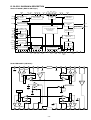
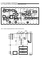
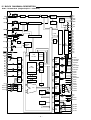
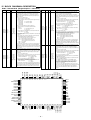
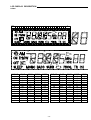
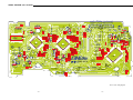
FILE NO.
Service Manual
1
2
Micro Component System
DC-MCR60
(XE)
3
4
5
6
7
8
9
FM MODE
/REPEAT
TUNER
/BAND
0
REMOTE CONTROLLER RB-MCR60
Contents
Laser beam safety precaution ...........................................
Tape adjustments .............................................................
Tuner adjustments ............................................................
CD pick-up maintenance ...................................................
Exploded view ...................................................................
Parts list ............................................................................
Exploded view & parts list (Tape Mechanism) ..................
IC block diagram & description .........................................
LCD display .......................................................................
Wiring connection .............................................................
Schematic diagram
(CD & SYSCON) CD Section .........................................
SYSCON Section ...............................
PRODUCT CODE No.
129 684 01
1
1
2
2
3
4
7
8
16
17
18
20
(FRONT) ........................................................................
(DECK) ...........................................................................
(AMPLIFIER) ..................................................................
(TUNER) ........................................................................
Wiring diagram
(CD & SYSCON) ...........................................................
(FRONT) .......................................................................
(DECK) ..........................................................................
(AMPLIFIER & TUNER) ................................................
(PRIMARY POWER SUPPLY) ......................................
(SECONDARY POWER SUPPLY) ...............................
(SWITCH) ......................................................................
24
26
28
30
22
25
27
32
34
34
34
This service manual consists of "DC-MCR60U/XE" (Main unit : 129 683 01) and
"SX-MCR60/XE" (Speaker system : 165 097 03).
REFERENCE No. SM5810499
LASER BEAM SAFETY PRECAUTION
• Pick-up that emits a laser beam is used in this CD player section.
CAUTION :
THIS PRODUCT CONTAINS A LOW POWER LASER DEVICE,
TO ENSURE CONTINUED SAFETY DO NOT REMOVE ANY
COVERS OR ATTEMPT TO GAIN ACCESS TO THE INSIDE
OF THE PRODUCT.
REFER ALL SERVICING TO QUALIFIED PERSONNEL.
LASER OUTPUT .............. 0.6 mW Max. (CW)
WAVELENGTH .................. 790 nm
CAUTION – INVISIBLE LASER RADIATION WHEN OPEN AND
INTERLOCKS DEFEATED. AVOID EXPOSURE TO BEAM.
ADVARSEL – USYNLIG LASER STRÅLING VED ÅBNING, NÅR
SIKKERHEDSAFBRYDERE ER UDE AF FUNKTION, UNDGÅ UDS ÆTTELSE
FOR STRÅLING.
VARNING – OSYNLIG LASER STRÅLNING NÄR DENNA DEL ÄR ÖPPNAD
OCH SPÄRR ÄR URKOPPLAD. STRÅLEN ÄR FARLIG.
VORSICHT – UNSICHTBARE LASERSTRAHLUNG TRITT AUS, WENN
DECKEL GEÖFFNET UND WENN SICHERHEITSVERRIEGELUNG
ÜBERBRÜCKT IST. NICHT, DEM STRAHL AUSSETZEN.
VARO – AVATTAESSA JA SUOJALUKITUS OHITETTAESSA OLET ALTTIINA
NÄKYMÄTTÖMÄLLE LASERSÄTEILYLLE. ÄLÄ KATSO SÄTEESEEN.
FM
ANT
SPEAKERS
(4 MIN.)
R
AM
LOOP
PHONES
L
EXT. ANT
TAPE ADJUSTMENTS
a. Replacing the head
c.
Adjusting motor speed
1.
After replacement, demagnetize the heads by using
a degausser.
1. Insert the test tape (MTT-111 or etc. 3,000 Hz).
2.
Be sure to clean the heads before attempting to make
3. Use a flat-tip screwdriver to turn the SVR to adjust so
2. Press the PLAY button.
any adjustments.
3.
that the frequency counter becomes 3,000 Hz.
Be sure both channels (1 and 2) are the same level.
4. Press the STOP button.
(Using a dual-channels oscilloscope).
4.
All wiring should be returned to the original position
after work is completed.
d.
Replacing the motor
MOTOR SPEED
ADJUSTMENT
R / P HEAD
RED
WHITE
1
3
YELLOW
EARTH
2
4
b. Adjusting head azimuth
1.
e. Checking the mechanism torques
Load a test tape (VTT-738, etc. :10kHz) for
• Clean the head, capstan and pinch roller before making
azimuth adjustment.
2.
3.
any measurement.
Press the PLAY button.
Use a cross-tip screwdriver to turn the screw for
normal azimuth adjustment so that the left and right
outputs are maximized at the same phase during
Measurement
Take-up torque
Cassette for
PLAY : TW-2111A
measurement F.FWD/REW : TW-2231
normal playback.
4.
4
Press the STOP button.
Back tension
PLAY : TW-2111A
Tape tension
Drive-power cassette
TW-2412
PLAY
30 ~ 70gr.cm
1.0 ~ 6.0gr.cm
80 gr or more
F.FWD/REW
55 gr or more
-
-
- 1 -
TUNER ADJUSTMENTS
• Use a plastic screw driver for adjustments.
• MODE : ST (Stereo)
• Speaker impedance : 4 ohms
• TUNING
FM : 87.5 - 108MHz
AM : 522 - 1611 kHz (9 kHz steps)
520 - 1610 kHz (10 kHz steps)
J4301
J4202
XF210
C2011
C2005 C2024
C2015
IC201
R2005
C2016
C2013
D2005
L2204
R2117
R2119
CN201
J2301
C2131
MW OSC
D2004
CT211
C2141
D2102
R2131
C2142
J2103
J2104
L2205
R2113 C2126
J2303
J2102
D2006
C2022
C2009
J2101
CN203
C2001
C2014
C2020
JW
R2010
C2010
FMOSC
GND
C2003
FMOSC R2011
C2140
D2002
R2002
C2021
Q2002
L2001
D2003
C2017 R2004
R2014
R2001 C2002
J2302
R2003 C2008
Q2001
L2002
E
E
Q4992
J4105
R4106
C4963
R2006
R2008 R2007
C2112
J2203
C4962
J4107
D4962
D4963
J4110
L2003
C2012
Q2201
J2202
R4953
E
CT211
Q2102
IC211
TP25
L2205
L2204
Antenna
: 75Ω unbalanced direct, Modulation : 1 kHz
Dev.
RF Level
: ±22.5kHz(MONO), ±22.5kHz(STEREO),±6.75kHz(PILOT)
: dBuV EMF
E
Output Level : about 30mV at TP13, TP14, TP15
1. FM
Step AdjustingCirc
uit
Connection
Remark
Output
SG
Frequency
Adjustment
Input
TP24,25
98.0MHz
T2002
(IC211 3-22pin)
0.0±0.05V
1
IF(0V)
Adjustment
FM ANT
SG=66dBuV
2
Cover
---
Tracking
FM Ant
TP11 (H)
87.5MHz
---
1.50±0.5V Check Only
TP12 (E)
108.0MHz
L2002
8.0±0.05V
TP13 (L)
90.0MHz
---
Maximum
TP14 (R)
TP15 (E)
Anntena
RF Level
2. AM
106.0MHz
: IRE Loop(SG), Moduration : 1kHz 30%
: dBuV EMF
Output Level : about 30mV at TP13, TP14, TP15
Step AdjustingCirc
uit
Connection
Input
1
IF Adjustment
Loop Ant
2
Cover
(MW)
---
3
C2019
R2009
E
D4951
C4951
Q4994
J2201
C2119
R4962
R4938
C4984
XF211
SH201
C2026
C4726
J2305
TP24
R2201
C2107
C2111
C2106
L2002
Q4106
J2304 E
R2303
R2106
C2117
J2109
J2110
R2206
C2602
C2120
C2114
R2301
C2115
J2311
J2204
C2801
C2702 C2802
C2207
C2218
C2122
C2113
Q2111
T2002
C2118
R2302
IC211
C2108
R2105
C2110
C2701
R2801
E
C2102
C2103
C2101
C2104
C2121
R2107
C2312
J2307
J2308
J2310
D2101
R2701
L2005
J2313
T2002
R2129 R2127
R2104 R2128
J2108
R2101
E
J4307
J2106
J2107
C2209
XF212
J2111
D2104
E Q2110
Q4730
R4770 C4744
R4743 R4753
R4745
VT
XF215
1
R4870
C4733
R4741 C4740 C4741
R4742 C4742 R4747
R4739 C4739 R4746
R4740 C4738
R4737 C4735
C4734
R4738
R4736 C4736
C4732
R4731
C4752
R4732
R4750 C4753 R4735
10
R4749
R4748
J2306
C2311
J2309
T2001
J4116
Q2003
R2210
Q2101
TP12
J4322
J2115
L2007
L2006
R2205
R4734
C4731
C4701
E
Q4104
C4999
J2312
3
R4730
R4733
J4119
J2112
J2113
J2114
15
R4751
J4213
R4107
TP11
C4730
J4118
J4120
+9.0V
GND
M_GND
J4320
J4321
J4325
J4326
CN492
TAPE_PLAY
SYNC_REC
J4123
1AD4B10D2100A
T002 94V-0
BEAT
PLAY_R
REC_R
REC_L
PLAY_L
TP15
E
TP13 T2001
E
TP14
Tracking
(MW)
Loop Ant
Output
TP13 (L)
TP14 (R)
TP15 (E)
TP11 (H)
TP12 (E)
TP13 (L)
TP14 (R)
TP15 (E)
SG
Frequency
Adjustment
Remark
450KHz
at 999kHz
T2001
Maximum
522kHz
L2205
1.00±0.05V
1611kHz
---
7.50±0.50V Check Only
603kHz
L2204
1404kHz
CT211
Maximum
CD PICK-UP MAINTENANCE
About pick-up (Optical lens) Cleaning
Clean a lens with swab of the cotton which moistened it with alcohol, cleaning paper or cleaning disc appointed.
Specified cleaning disc : LC-1 (Part code : 645 026 1961 ..... manufactured by SANYO.)
Show a clean procedure in the following in reference by swab of cotton.
1. Cotton swab is wrapped with Cleaning paper.
2. Add the isopropyl alcohol.
3. Gently move the tip of cotton swab just like a draw a whirlpool from inside to outside on the surface of lens.
- 2 -
- 3 -
2
1
11 12 13
16
16
3
16
15
Y01 5
16 14
6
7
19
Y05
51
21
Y06
8
44
20
22
Y06
Y05
18
Y02
71
Y03
4 Y01
43
Y04
17
8
8
73 Y09
46
9
10
N.S.P=Not available as service parts.
52
Y07
Y09
Y07
72
23
54 55
Y08
Y10
25
30
28
35
36
31
Y12
Y14
Y14
40
Y08
53
Y13
Y11 32
33
34
24
Y10
Y11
27
26
42
74
Y13
38
41
Y15
37
Y14
45
75
N.S.P
Y17
29
Y18
Y16
57
76
77
58
Y18
Y21
Y19
59
This is a basic exploded view.
56
39
Y20
EXPLODED VIEW
PARTS LIST
PRODUCT SAFETY NOTICE
EACH PRECAUTION IN THIS MANUAL SHOULD BE FOLLOWED DURING SERVICING. COMPONENTS IDENTIFIED WITH THE
IEC SYMBOL ! IN THE PARTS LIST AND THE SCHEMATIC DIAGRAM DESIGNATED COMPONENTS IN WHICH SAFETY AND
PERFORMANCE CAN BE OF SPECIAL SIGNIFICANCE. WHEN REPLACING A COMPONENT IDENTIFIED BY ! , USE ONLY THE
REPLACEMENT PARTS DESIGNATED, OR PARTS WITH THE SAME RATINGS OF RESISTANCE, WATTAGE OR VOLTAGE THAT
ARE DESIGNATED IN THE PARTS LIST IN THIS MANUAL. LEAKAGE-CURRENT OR RESISTANCE MEASUREMENTS MUST BE
MADE TO DETERMINE THAT EXPOSED PARTS ARE ACCEPTABLY INSULATED FROM THE SUPPLY CIRCUIT BEFORE
RETURNING THE PRODUCT TO THE CUSTOMER.
CAUTION :
N.S.P :
Regular type resistors and capacitors are not listed. To know those values, refer to the schematic diagram.
Regular type resistors are less than 1/4 W carbon type and 0 ohm chip resistors.
Regular type capacitors are less than 50 V and less than 1000 µF type of Ceramic type and Electrical type.
Not available as service parts.
PACKING & ACCESSORIES
REF.NO.
PART NO.
614 328 9937
614 327 8085
614 327 8092
645 035 1563
614 328 9975
614 329 0001
645 046 8322
614 328 4635
645 063 8725
614 328 9319
DESCRIPTION
CARTON CASE
CUSHION,RIGHT
CUSHION,LEFT
POLY SHEET-0870X0480*NC,SET
INSTRUCTION MANUAL
INSTRUCTION SHEET
ASSY,ANTENA,LOOP
LID,BATTERY REMOCON,SERVICE
REMOCON,RB-MCR60
ASSY,BOX,SPEAKER
REF.NO.
42
43
44
45
46
FIXING PARTS
REF.NO.
Y01
Y02
CABINET & CHASSIS
REF.NO.
1
2
3
4
5
6
7
8
9
10
11
12
13
14
15
16
17
18
19
20
21
22
23
24
25
26
27
28
29
30
31
32
33
34
35
36
37
38
39
40
41
PART NO.
614 327 8672
614 327 8009
614 327 7996
614 322 2125
614 327 7941
614 327 7682
614 307 2072
614 298 8886
614 327 8016
614 327 7958
614 327 7859
614 327 7804
614 327 7798
614 327 7750
614 327 7743
614 327 8382
614 327 7675
614 328 9500
614 328 9517
614 328 9524
614 328 9531
614 327 7699
614 328 4604
614 327 8030
614 329 2432
614 327 7934
614 327 7781
614 327 7712
614 327 8054
614 327 7972
614 322 2132
614 327 7866
614 327 7873
614 327 7880
614 327 7897
614 327 7903
614 327 7910
614 270 8477
614 328 9340
614 327 8023
614 328 9821
Y03
DESCRIPTION
ASSY,PANEL FRONT
SHAFT,RIGHT
SHAFT,LEFT
ASSY,GEAR,LID,CD
LEVER
BUTTON,CD OPEN
COVER,PICK-UP
SPACER,MECHA,MTG CD+DA11
SPRING,CD
MOUNTING,CD
KNOB,VOLUME
DEC,CAP VOLUME
DEC,RING
DEC,WINDOW,CD BTM
DEC,WINDOW,CD TOP
CAP,WINDOW
ASSY,PANEL
DEC,BUTTON
DEC,BUTTON
DEC,BUTTON
DEC,BUTTON
BUTTON,OPERATION,8 KEYS
ASSY,COVER LID
SPRING,DOOR CD
SPRING,DOOR CD
LID,CASSETTE
DEC,WINDOW,DECK
COVER,DECK
SPRING,DOOR DECK
PANEL,TOP
ASSY,GEAR,LID,CASSETTE
KNOB,DECK,MECHA,REC
KNOB,DECK,MECHA,PLAY
KNOB,DECK,MECHA,REW
KNOB,DECK,MECHA,FFWD
KNOB,DECK,MECHA,STOP/EJECT
KNOB,DECK,MECHA,PAUSE
SHAFT
ASSY,CABINET,REAR
SPRING,REC
SHIELD,DECK PWB
PART NO.
DESCRIPTION
614 329 2425 SHIELD,DECK PWB
614 329 2845 SPACER,CUSHION,
F-PANEL+BUTTON,CD OPEN
614 329 3408 SPACER,CUSHION
614 327 5534 STAND,CUSHION
614 327 7668 ASSY,MECHA,DA11B3N
Y04
Y05
Y06
Y07
Y08
Y09
Y10
Y11
Y12
Y13
Y14
Y15
Y16
Y17
Y18
Y19
Y20
Y21
- 4 -
PART NO.
DESCRIPTION
411 021 3503 SCR S-TPG BIN 3X10,
SHAFT+LID,CD
411 021 3503 SCR S-TPG BIN 3X10,
F-PANEL+ASSY,GEAR CD
411 092 0906 WASHER Z 2.6X10X0.5,
F-PANEL+LEVER
411 156 2105 SCR S-TPG BIN 2.3X6,
F-PANEL+LEVER
411 165 3803 SCR S-TPG BIN 2.3X10,
MTG CD+CD11
411 092 0906 WASHER Z 2.6X10X0.5,
MTG CD+CD11
411 021 3503 SCR S-TPG BIN 3X10,
MTC CD+F-PANEL
411 021 3503 SCR S-TPG BIN 3X10,
MTG-CD+CD,PWB
411 098 4700 SCR S-TPG BIN 2.3X8,
FRONT,PWB+LID,CD
411 187 2808 SCR S-TPG BIN 2.3X8,
LID,CD+COVER,LID
411 187 2709 SCR S-TPG BIN 2.3X6,
CAP,WINDOW+COVER,LID
411 020 8905 SCR S-TPG BRZ+FLG 3X10,
PANEL,TOP+ASSY,CEAR DECK
412 032 6408 SPECIAL SCREW,
SHAFT+PANEL,TOP
411 021 6405 SCR S-TPG BIN 3X8,
DECK,MECHA+PANEL,TOP
411 021 3503 SCR S-TPG BIN 3X10,
DECK,PWB+PANEL,TOP
411 020 9100 SCR S-TPG BRZ+FLG 3X12,
P TRANS+REAR
411 021 3503 SCR S-TPG BIN 3X10,AC CORD
411 098 7800 SCR S-TPG FLT 3X12,
PANEL,FRONT+REAR(L,R)
411 021 4906 SCR S-TPG BIN 3X20,
PANEL,FRONT+REAR
411 021 3503 SCR S-TPG BIN 3X10,
REAR+ANT TERMINAL
411 021 3503 SCR S-TPG BIN 3X10,
PANEL,TOP+REAR
PARTS LIST
ELECTRICAL PARTS
REF.NO.
51
52
53
PART NO.
614 328 4307
614 328 4376
614 328 4369
54
614 328 4390
55
614 328 4383
56
57
58
59
614 274 2013
423 016 7908
645 064 8144
645 016 9939
FRONT P.W.BOARD ASSY
DESCRIPTION
ASSY,WIRE,CD TO MOTOR
FLEXIBLE FLAT CABLE,CD PICK UP
FLEXIBLE FLAT CABLE,
SYSCON TO AMP
FLEXIBLE FLAT CABLE,
SYSCON TO FRONT
FLEXIBLE FLAT CABLE,
SYSCON TO FRONT
CORD,ID CONNECTOR
FUSE 250V 2.5A
TRANS,POWER
CORD,POWER-1.74MK,
GB-FB-160-N2B-012-0
SWITCH P.W.BOARD ASSY
REF.NO.
71
CN698
S6951
PART NO.
614 327 7330
614 020 6548
645 023 5795
DESCRIPTION
ASSY,PWB,SW(Only initial)
SOCKET,2P
SWITCH,LEVER
CD & SYSCON P.W.BOARD ASSY
REF.NO.
72
C6200
or
CN111
CN113
or
CN690
or
CN691
CN692
or
CN693
CN694
or
D1401
D1402
D1403
D1404
D1410
D6901
D6902
IC101
IC102
IC103
IC601
JW600
L1451
L6900
L6901
PR140
Q1301
or
or
Q1401
or
or
Q6200
or
or
or
or
Q6201
or
or
or
or
X1451
or
X6001
PART NO.
614 328 8510
403 259 0508
403 373 7001
645 059 0498
645 005 8127
614 310 2472
645 004 2881
614 310 2731
645 063 8695
645 012 5324
645 009 8482
645 059 0498
614 310 2731
645 004 2881
407 012 4406
407 012 4406
407 012 4406
407 099 5204
407 098 3300
407 012 4406
407 012 4406
409 503 5701
409 539 9704
409 486 8706
409 578 1103
614 329 2128
645 001 4550
645 001 4550
645 002 1459
645 014 2499
405 008 6809
405 008 7202
405 008 7301
405 141 3604
405 009 5207
405 009 5306
405 011 8609
405 017 9600
405 017 9709
405 011 8500
405 143 8706
405 143 8706
405 011 8500
405 011 8609
405 017 9600
405 017 9709
614 231 2667
645 057 1145
645 052 6206
REF.NO.
73
BR601
BR602
BR603
BR604
CN601
CN603
D6201
D6313
D6314
D6315
D6330
D6401
D6402
LCD60
Q6300
or
or
or
S6101
or
or
or
S6102
or
or
or
S6103
or
or
or
S6104
or
or
or
S6105
or
or
or
S6106
or
or
or
S6107
or
or
or
S6108
or
or
or
S6500
SE601
DESCRIPTION
ASSY,PWB,CD-SYSCON(Only initial)
NP-ELECT 1U M 50V
NP-ELECT 1U M 50V
SOCKET,FPC 16P
PLUG,6P
PLUG,6P
PLUG,2P,MCON-LID_SW
PLUG,2P,MCON-LID_SW
SOCKET,FPC 22P,MCON-FRONT
SOCKET,FPC 28P,MCON-AMP
SOCKET,FFC 28P,MCON-AMP
SOCKET,FPC 16P,MCON-FRONT
PLUG,2P,MCON-TU
PLUG,2P,MCON-TU
DIODE 1SS133
DIODE 1SS133
DIODE 1SS133
ZENER DIODE MTZJ5.1B
DIODE RL153-BF-S2
DIODE 1SS133
DIODE 1SS133
IC LA9242M-MPB
IC LC78629E
IC MM1469XH
IC LC72338-9C10,MICON
ASSY,WIRE
INDUCTOR,10U K
INDUCTOR,10U K
INDUCTOR,22U K
PROTECTOR,0.4A 125V
TR 2SB808-F-SPA
TR 2SB810-E
TR 2SB810-F
TR KTA1273-Y
TR 2SB927-S
TR 2SB927-T
TR 2SC1740S-S
TR 2SC3330-T
TR 2SC3330-U
TR 2SC1740S-R
TR KTC3199-GR
TR KTC3199-GR
TR 2SC1740S-R
TR 2SC1740S-S
TR 2SC3330-T
TR 2SC3330-U
RESONATOR
OSC,CERAMIC 16.93MHZ
OSC,CRYSTAL 4.5MHZ
- 5 -
PART NO.
614 328 8411
614 327 7828
614 327 7842
614 327 7736
614 327 7989
645 063 8695
645 063 8701
407 235 7406
407 235 7406
407 235 7406
407 235 7406
407 012 4406
407 012 4406
407 099 5303
645 064 7826
405 011 8609
405 015 6205
405 015 6403
405 011 8500
614 240 1002
645 006 5958
645 048 3820
614 220 5471
614 220 5471
614 240 1002
645 006 5958
645 048 3820
614 220 5471
614 240 1002
645 006 5958
645 048 3820
614 220 5471
614 240 1002
645 006 5958
645 048 3820
614 240 1002
645 006 5958
645 048 3820
614 220 5471
614 220 5471
614 240 1002
645 006 5958
645 048 3820
614 220 5471
614 240 1002
645 006 5958
645 048 3820
614 220 5471
614 240 1002
645 006 5958
645 048 3820
645 031 8078
407 232 4002
DESCRIPTION
ASSY,PWB,FRONT(Only initial)
DEC,SHEET LCD
HOLDER,LCD
COVER,LED
REFLECTOR,LCD
SOCKET,FPC 22P,FRONT-MCON
SOCKET,FPC 16P,FRONT-MCON
LED LT7V34-81-URC1
LED LT7V34-81-URC1
LED LT7V34-81-URC1
LED LT7V34-81-URC1
DIODE 1SS133
DIODE 1SS133
ZENER DIODE MTZJ5.6B
LCD
TR 2SC1740S-S
TR 2SC2785-E
TR 2SC2785-F
TR 2SC1740S-R
SWITCH,TACT
SWITCH,PUSH 1P-1T
SWITCH,PUSH
SWITCH,TACT
SWITCH,TACT
SWITCH,TACT
SWITCH,PUSH 1P-1T
SWITCH,PUSH
SWITCH,TACT
SWITCH,TACT
SWITCH,PUSH 1P-1T
SWITCH,PUSH
SWITCH,TACT
SWITCH,TACT
SWITCH,PUSH 1P-1T
SWITCH,PUSH
SWITCH,TACT
SWITCH,PUSH 1P-1T
SWITCH,PUSH
SWITCH,TACT
SWITCH,TACT
SWITCH,TACT
SWITCH,PUSH 1P-1T
SWITCH,PUSH
SWITCH,TACT
SWITCH,TACT
SWITCH,PUSH 1P-1T
SWITCH,PUSH
SWITCH,TACT
SWITCH,TACT
SWITCH,PUSH 1P-1T
SWITCH,PUSH
SWITCH,ROTARY(ENCODER)
PHOTO DIODE SPS-440-1-VG
PARTS LIST
DECK P.W.BOARD ASSY
REF.NO.
74
C5918
or
CN500
CN505
or
CN506
or
IC510
L5902
Q5902
or
or
or
or
Q5904
or
or
or
or
S5950
PART NO.
614 327 7316
403 056 7502
403 377 6307
645 012 2750
614 310 2755
645 004 2904
614 310 2458
645 005 8110
409 384 3506
645 031 5893
405 143 8706
405 011 8500
405 011 8609
405 017 9600
405 017 9709
405 017 9600
405 017 9709
405 011 8609
405 011 8500
405 143 8706
645 038 7586
DESCRIPTION
ASSY,PWB,DECK(Only initial)
POLYESTER 1000P J 50V
POLYESTER 1000P J 50V
SOCKET,DIP 10P
PLUG,4P
PLUG,4P
PLUG,4P
PLUG,4P
IC BA3314F
TRANS,OSC,85KHZ,O.S.C
TR KTC3199-GR
TR 2SC1740S-R
TR 2SC1740S-S
TR 2SC3330-T
TR 2SC3330-U
TR 2SC3330-T
TR 2SC3330-U
TR 2SC1740S-S
TR 2SC1740S-R
TR KTC3199-GR
SWITCH,PUSH,R/PSW
AMPLIFIER & TUNER P.W.BOARD ASSY
REF.NO.
75
C4714
or
C4814
or
C4913
or
CN201
or
CN203
CN401
CN402
CN421
or
CN441
or
CN461
CN491
CN492
or
CT211
D2002
D2003
D2004
D2005
D2006
D2101
D2102
or
D2104
D4102
D4951
D4953
D4961
D4962
D4963
D4980
D4981
D4982
D4983
D4993
FCL41
or
FCL42
or
HS401
PART NO.
614 328 8404
403 058 4608
403 377 6406
403 058 4608
403 377 6406
403 329 5907
403 350 9301
645 025 4703
645 038 7715
614 221 8273
645 006 1875
645 006 1875
645 011 6384
645 055 1017
614 310 2731
645 004 2881
614 221 8273
645 012 5324
614 310 2519
645 005 8158
645 032 5663
407 157 8109
407 157 8109
407 012 4406
407 012 4406
407 012 4406
407 012 4406
407 105 1602
407 105 1305
407 099 5303
407 012 4406
407 099 6003
407 012 4406
407 012 4406
407 012 4406
407 012 4406
407 098 3300
407 098 3300
407 098 3300
407 098 3300
407 012 4406
645 006 4760
645 031 7903
645 006 4760
645 031 7903
614 327 7835
DESCRIPTION
ASSY,PWB,AMP-TU(Only initial)
POLYESTER 0.15U J 50V
POLYESTER 0.15U J 50V
POLYESTER 0.15U J 50V
POLYESTER 0.15U J 50V
ELECT 3300U M 25V
ELECT 3300U M 25V
TERMINAL,ANTENNA
TERMINAL
TERMINAL
PLUG,2P,SPEAKER
PLUG,2P,SPEAKER
JACK,PHONE D3.6,HEADPHONE
JACK,PHONE D3.6,HEADPHONE
PLUG,2P,POWER
PLUG,2P,POWER
TERMINAL
SOCKET,FPC 28P,AMP-MCON
PLUG,10P,AMP-DECK
PLUG,10P,AMP-DECK
TRIMMER,7PF
VARACTOR DI SVC211-B
VARACTOR DI SVC211-B
DIODE 1SS133
DIODE 1SS133
DIODE 1SS133
DIODE 1SS133
VARACTOR DI SVC342M-V
VARACTOR DI SVC342L-V
ZENER DIODE MTZJ5.6B
DIODE 1SS133
ZENER DIODE MTZJ9.1B
DIODE 1SS133
DIODE 1SS133
DIODE 1SS133
DIODE 1SS133
DIODE RL153-BF-S2
DIODE RL153-BF-S2
DIODE RL153-BF-S2
DIODE RL153-BF-S2
DIODE 1SS133
HOLDER,FUSE
HOLDER,FUSE
HOLDER,FUSE
HOLDER,FUSE
HEAT SINK
REF.NO.
IC201
IC211
IC411
IC412
IC446
L2001
L2002
L2003
L2005
L2006
L2007
L2204
or
L2205
L4780
L4781
L4881
PR495
PR496
Q2001
or
Q2002
or
Q2003
or
or
or
or
Q2101
or
Q2102
or
Q2110
or
Q2111
or
Q2201
or
Q4103
or
Q4104
or
Q4106
or
Q4108
or
Q4109
or
Q4730
or
or
or
or
Q4740
or
Q4751
or
or
or
or
Q4830
or
or
or
or
Q4840
or
Q4851
or
or
or
or
- 6 -
PART NO.
409 016 0200
409 474 3201
409 390 1107
409 295 7402
409 039 9204
645 040 2753
645 040 2746
645 002 1534
645 002 1459
645 002 1459
645 002 1459
645 058 8792
645 037 2377
645 065 3568
645 002 1459
645 002 1459
645 002 1459
645 014 2529
645 014 2536
405 151 4301
405 151 4806
405 151 4301
405 151 4806
405 017 9709
405 017 9600
405 011 8609
405 011 8500
405 143 8706
405 000 0904
405 151 5209
405 143 0007
405 000 3806
405 143 0007
405 000 3806
405 151 4301
405 151 4806
405 151 5209
405 000 0904
405 000 0508
405 110 5400
405 000 3103
405 109 9204
405 000 3103
405 109 9204
405 000 3806
405 143 0007
405 000 3806
405 143 0007
405 143 6504
405 004 4601
405 006 1806
405 006 1905
405 004 5103
405 000 3103
405 109 9204
405 151 4400
405 021 0204
405 021 0600
405 033 6706
405 033 6805
405 143 6504
405 004 4601
405 004 5103
405 006 1806
405 006 1905
405 109 9204
405 000 3103
405 151 4400
405 021 0204
405 021 0600
405 033 6706
405 033 6805
DESCRIPTION
IC LA1186N-AUDIO
IC LA1844ML
IC LC75392
IC TA8229K
IC NJM78L05A
INDUCTOR,AIR —
COIL,AIR —
INDUCTOR,8.2U K
INDUCTOR,22U K
INDUCTOR,22U K
INDUCTOR,22U K
TRANS,ANT,796KHZ
TRANS,ANT,796KHZ
TRANS,OSC,796KHZ
INDUCTOR,22U K
INDUCTOR,22U K
INDUCTOR,22U K
PROTECTOR,1.25A 125V
PROTECTOR,1.5A 125V
TR KTC3195-Y
TR KTC3195-O
TR KTC3195-Y
TR KTC3195-O
TR 2SC3330-U
TR 2SC3330-T
TR 2SC1740S-S
TR 2SC1740S-R
TR KTC3199-GR
TR DTA114YS
TR KRA107M
TR KRC107M
TR DTC114YS
TR KRC107M
TR DTC114YS
TR KTC3195-Y
TR KTC3195-O
TR KRA107M
TR DTA114YS
TR DTA114ES
TR KRA102M-A
TR DTC114ES
TR KRC102M-A
TR DTC114ES
TR KRC102M-A
TR DTC114YS
TR KRC107M
TR DTC114YS
TR KRC107M
TR KTA1267-GR
TR 2SA608-F-SPA
TR 2SA933S-R
TR 2SA933S-S
TR 2SA608-G-SPA
TR DTC114ES
TR KRC102M-A
TR KTD1303
TR 2SD1012-F-SPA
TR 2SD1012-G-SPA
TR 2SD1468S-R
TR 2SD1468S-S
TR KTA1267-GR
TR 2SA608-F-SPA
TR 2SA608-G-SPA
TR 2SA933S-R
TR 2SA933S-S
TR KRC102M-A
TR DTC114ES
TR KTD1303
TR 2SD1012-F-SPA
TR 2SD1012-G-SPA
TR 2SD1468S-R
TR 2SD1468S-S
PARTS LIST
REF.NO.
Q4903
or
or
or
or
Q4951
or
or
Q4992
or
or
Q4994
or
Q4995
or
or
R4752
R4852
R4941
SA401
SA402
SH201
T2001
T2002
or
XF210
or
or
PART NO.
405 143 8706
405 011 8500
405 011 8609
405 017 9600
405 017 9709
405 138 6403
405 095 1602
405 095 1701
405 008 2504
405 008 2405
405 141 3703
405 000 3806
405 143 0007
405 141 3703
405 008 2405
405 008 2504
402 071 1304
402 071 1304
402 096 0306
411 021 6405
411 021 6405
614 256 3052
645 043 0213
645 040 9981
645 039 9923
645 059 0047
645 026 2975
614 252 1045
DESCRIPTION
TR KTC3199-GR
TR 2SC1740S-R
TR 2SC1740S-S
TR 2SC3330-T
TR 2SC3330-U
TR KTD2058Y
TR 2SD2061-E
TR 2SD2061-F
TR 2SB698-G
TR 2SB698-F
TR KTA1271-Y
TR DTC114YS
TR KRC107M
TR KTA1271-Y
TR 2SB698-F
TR 2SB698-G
FUSIBLE RES 2.2 JA 1/4W
FUSIBLE RES 2.2 JA 1/4W
FUSIBLE RES 27 JA 1/4W
SCR S-TPG BIN 3X8
SCR S-TPG BIN 3X8
SHIELD
FILTER,450KHZ
TRANS,IF 10.7MHZ
TRANS,IF 10.7MHZ
FILTER,BP
FILTER,BP 108MHZ
FILTER,LC
REF.NO.
XF211
or
or
XF212
or
or
XF215
or
PART NO.
645 054 1223
645 010 7665
614 240 2917
645 054 1223
645 010 7665
614 240 2917
645 041 9324
645 059 0054
DESCRIPTION
CERAMIC FILTER 10.70MHZ
CERAMIC FILTER 10.70MHZ
FILTER,CERAM
CERAMIC FILTER 10.70MHZ
CERAMIC FILTER 10.70MHZ
FILTER,CERAM
CERAMIC FILTER 450KHZ
CERAMIC FILTER 450KHZ
PRIMARY POWER SUPPLY P.W.BOARD ASSY
REF.NO.
76
CN450
CN453
PART NO.
614 327 7323
614 020 1215
614 328 4338
DESCRIPTION
ASSY,PWB,PT(Only initial)
SOCKET,2P
ASSY,WIRE
SECONDARY POWER SUPPLY P.W.BOARD ASSY
REF.NO.
77
CN451
CN452
L4591
or
PART NO.
614 328 4482
614 017 8203
614 017 8203
645 038 6053
645 041 3087
DESCRIPTION
ASSY,PWB,PT2(Only initial)
TERMINAL BOARD
TERMINAL BOARD
INDUCTOR,181U
INDUCTOR,180U
EXPLODED VIEW & PARTS LIST (TAPE MECHANISM)
TAPE MECHANISM
*
TM01
REF.NO.
TM02
*
*
TM03
TM01
TM02
TM03
TM04
TM05
TM06
PART NO.
614 328 4239
645 033 8625
645 041 3025
645 009 1612
645 009 1766
645 033 3415
614 312 0629
DESCRIPTION
ASSY,MECHA,TM DS60TN-SH
E HEAD 6PA
R.P HEAD
PINCH ROLLER ARM ASSY
RF BELT
MAIN BELT
ASSY,MOTOR
* : Not available as service parts.
TM04
TM05
*
*
*
TM06
- 7 -
IC BLOCK DIAGRAM & DESCRIPTION
IC101 LA9242M-MPB (Servo Processing Signal for CD Player)
Vcc1
LDS
LDD
64
63
62
BH1 PH1
61
LF2
60
VR REF1 Vcc2 FSS DRF CE DAT CL CLK
59
58
57
56
55
54 53
52
51
DEF
50
49
REF
APC
RF DET
48 NC
FIN2 1
47 TBC
VCA
FIN1 2
46 FSC
I/V
E 3
45 DGND
BAL
VCA
44 SLI
INTER FACE
F 4
SLC
43 SLC
TB 5
42 RFS-
RF Amp
TE
TE- 6
41 RFSM
TE 7
40 CV+
TESI 8
SCH 9
T.SERVO & T.LOGIC
39 CV38 SLOF
TH 10
37 HFL
36 TES
TA 11
35 TOFF
TD- 12
SPINDLE SERVO
34 TGL
F.SERVO & F.LOGICK
TD 13
33 JP+
JP 14
SLED SERVO
TO 15
FD 16
17
18
FD- FA
19
20
FA-
FE FE- AGND SP
21
22 23
24
SPI
25
26
SPG SP-
27
28
29
SPD SLEQ SLD
IC201 LA1186N-AUDIO (Diode for RM AMP, MIX, OSC & AFC)
Vref
RF
1
RF IN
BUFFER
MIX
2
3
4
REG
5
GND
- 8 -
6
IF OUT
OSC
7
8
9
Vcc
30
31
SL- SL+
32
JP-
IC BLOCK DIAGRAM & DESCRIPTION
_
_
_
_
_
_
_
_
_
_
_
_
_
_
_
_
1
2
3
4
5
6
7
8
9
10
11
12
13
14
15
16
48
47
46
45
44
43
42
41
40
39
38
37
36
35
34
33
_ EFLG
_ SBSY
_ XVSS
_ XIN
_ XOUT
_ XVDD
_ MUTER CONT8
_ RVDD
_ RCHO
_ RVSS
_ LVSS
_ LCHO
_ LVDD
_ MUTEL CONT7
_ PCCL
_ TEST4
TOFF
TGL
JP+
JPPCK
FSEQ
VDD
CONT1
CONT2
CONT3
CONT4
CONT5
EMPH CONT6
C2F
DOUT
TEST3
_ 17
_ 18
_ 19
_ 20
_ 21
_ 22
_ 23
_ 24
_ 25
_ 26
_ 27
_ 28
_ 29
_ 30
_ 31
_ 32
DEFI
TAI
PDO
VVSS
ISET
VVDD
FR
VSS
EFMO
EFMIN
TEST2
CLV+
CLVV *P
HFL
TES
64 _ TEST1
63 _ VDD3V
62 _ TEST5
61 _ 4.2M
60 _ 16M
59 _ TST11
58 _ *RES
57 _ *CQOUT
56 _ COIN
55 _ SQOUT
54 _ RWC
53 _ WRQ
52 _ FSX
51 _ SBCK
50 _ SFSY
49 _ PW
IC102 LC78629E (DSP for CD Player)
No. Symbol I/O
1
DEFI
I
Function description
Defect detection signal(DEF) input pin.
(Must be connected to 0V when unused.)
2
TAI
I
Test input pin. A pull-down resistor is built-in.
Must be connected to 0V.
3
PDO
O
External VCO control phase comparator output pin.
4
VVSS
-
Internal VCO ground pin.Must be connected to 0V.
PLL
5
ISET
6
VVDD
7
FR
8
VSS
-
Digital system ground pin. Must be connected to 0V.
9
EFMO
O
10 EFMIN
I
Slice level
control
11 TEST2
I
AI
O
13 CLV-
O
14 V/*P
-
-
-
-
Incertitude
39 RVSS
-
Right channel ground pin. Must be connected to 0V.
-
-
40 RCHO
O
Right channel output pin.
-
41 RVDD
-
Right channel power supply pin.
-
EFM signal output pin.
EFM signal input pin.
Test input pin. A pull down resistor is built in.
Must be connected to 0V.
-
17 TOFF
O
Tracking off output pin.
O
Tracking gain switching output pin.
Increase the gain when low.
42 MUTER/ O
CONT8
H output
Incertitude
Track jump output.
Three-value output is also possible when specified by
microprocessor command.
L output
O
EMF data playback clock monitor pin.
Output 4.3218MHz when the normal-speed playback phase
command.
L output
O
Synchhronization signal detection output pin. Output a high
level when the synchronization signal detected from the EFM
signal and the internaly generated synchronization signal range.
Peripheral circuitry 5V system power suply pin.
Incertitude
-
General-purpose 2
25 CONT2 I/O input/output pin.
General-purpose 3
26 CONT3 I/O input/output pin.
General-purpose 4
27 CONT4 I/O input/output pin.
O
De-emphasis monitor pin.
A high level indicates playback of a de-emphasis disk,
General-purpose 6 output pin.
Rest to EMPH function.
O
C2 flag output pin.
Incertitude
31 DOUT
O
Digital output pin. (EIJA format)
Incertitude
32 TEST3
I
Test input pin.
A pull-down resistor is built in. Must be connected to 0V.
C2F
L output
-
H output
-
Crystal oscillator power supply pin.
-
O
45 XIN
I
Connections for a 16.934MHz crystal oscillating circuit
ground pin.
-
46 XVSS
-
Crystal oscillator ground pin. Must be connected to 0V.
47 SBSY
O
Subcode block synchronization signal pin.
Incertitude
48 EFLG
O
C1,C2,signal and double error correction monitor pin.
Incertitude
49 PW
O
Subcode P,Q,R,S,T,U,V and W output pin.
Incertitude
50 SFSY
O
Subcode frame synchronization signal output pin.
This signal falls when the subcode are in the standby stase.
Incertitude
51 SBCK
I
Subcode readout clock input pin. This is a Schmitt input.
(Must be connected to 0V when unused.)
52 FSX
O
Output for the 7.35kHz synchronization signal divided from
the crystal oscillator pin.
Incertitude
53 WRQ
O
Subcode Q output standby output pin.
Incertitude
54 RWC
I
Read/ write control input pin. This is a Schmidt input.
Subcode Q output pin.
-
-
Incertitude
I
Command, data input pin from control microprocessor.
-
57 *CQCK
I
Input for both the command input acquisition clock and the
SQOUT subcode readout clock input pin.
This is Schmidt input.
-
58 *RES
I
Reset input pin.
This pin must be set low briefly after power is first applied.
-
59 TST11
O
Test output pin. Leave open. (Notmally output a low level.)
L output
60 16M
O
16.9344MHz clock output pin.
Clock output
61 4.2M
O
4.2336MHz clock output pin.
Clock output
62 TEST5
I
Test input pin. A pull-down resistor is built in.
Must be connected to 0V.
-
63 VDD3V
-
Internal circuit 3.3V system power supply pin.
-
64 TEST1
I
Test input pin.
A pull-down resistor is built in. Must be connected to 0V.
-
Input
General-purpose 5
28 CONT5 I/O input/output pin.
Right channel mute output pin, General-purpose 8
output pin.
Rest to MUTER function.
44 XOUT
56 COIN
Controlled by serial data commands.
From the microprocessor.
Any of these that are unused must
be either set up as input pin and
connected to 0V, or set up as output
pin and left open.
Rch
one-bit
DAC
43 XVDD
55 SQOUT O
General-purpose 1
24 CONT1 I/O input/output pin.
30
H output
Left channel ground pin. Must be connected to 0V.
-
EMPH/
29 CONT6
Lch
one-bit
DAC
-
Tracking error signal input pin. This is a Schmidt input.
-
Left channel mute output pin, General-purpose 7
output pin.
Rest to MUTEL function.
38 LVSS
I
VDD
O
-
16 TES
23
MUTEL/
35 CONT7
Left channel output pin.
-
FSEQ
-
Left channel power supply pin.
Track detection signal input pin. This is a Schmidt input.
22
I
-
I
PCK
34 PCCL
O
15 HFL
21
-
General-purpose I/O command identification pin.
A pull-down resistor is built in.
Used operate similarly to LC78622E connected to open or 0V.
H ; Must be connected to general-purpose port command.
L ; Be able to all command control.
37 LCHO
L output
O
Test input pin.
A pull-down resistor is built in. Must be connected to 0V.
36 LVDD
Rough servo/phase control automatic switching monitor
output pin.
Outputs a high level during rough servo and a low level.
O
I
VCO frequency range adjustment.
O
20 JP-
Output pin
to rest
Internal VCO power supply pin.
L output
19 JP+
Function description
-
Disk motor control output.
Can be set to three-value output by microprpcessor command.
18 TGL
No. Symbol I/O
33 TEST4
PDO output current adjustment resistor
connection pin.
AI
12 CLV+
Output pin
to rest
Note) The same potential must be suplied to all power supply pins, i.e., VDD,VVDD,LVDD,RVDD
and XVDD.
- 9 -
IC BLOCK DIAGRAM & DESCRIPTION
IC102 LC78629E (DSP for CD Player)
EFMO
VVDD VVSS
9
DEFI 1
6
Slice level
Control
EFMIN 10
FSEQ 22
PDO ISET FR
4
3
5
PCK
21
7
TST11 TEST2 TEST4
TAI TEST1 TEST3 TEST5
2 59 64 11 32 33 62
VDD VSS
23 8
RAM Address
Generatorl
2KX8bits
RAM
VCO Clock Oscillator
& Clock Control
VDD3V
63
Syncrnous Detection
EFM Demodulation
Interpolalation
Mute
30 C2F
Digital Output
CLV+ 12
CLV
Digital Servo
CLV- 13
C1 C2 Error Detection&
Correction Flag
Processing
V/*P 14
PW
SBCK
SBSY
SFSY
49
51
47
50
WRQ 53
SQOUT 55
31 DOUT
Digital Attenuator
Subcode
Separation
QCRC
8X Over Sampling
Digital Filter
Micro-computer
Inter Fase
1bit DAC
*CQCK 57
COIN 56
General
PurposePort
Servo Commander
RWC 54
L.P.F
Crystal Oscillator
System Generator
24 25 26 27 28
29
48
15 16 17 20 19 58 18 34
HFL TES TOFF JP- JP+ *RES TGL
CONT1 CONT3 CONT5 EMPH/ EFLG
CONT6
PCLL
CONT2 CONT4
60 61 46 52 45 44 43
39 41
35
40
RVDD
16M 4.2M
FSX XIN
XVDD
RCHO
RVSS MUTEL/
XVSS
XOUT
CONT7
37
42
LCHO MUTER/
CONT8
38
LVSS
36
LVDD
IC103 MM1469XH (CD Driver)
28
27
26
25
24
23
22
21
20
D.BUF D.BUF
19
18
17
16
15
13
14
D.BUF D.BUF
Vcc
Level shift
Level shift
Vcc
DRIVER MUTE
Level shift
Level shift
T.S.D
D.BUF D.BUF
1
2
D.BUF D.BUF
3
4
5
6
7
8
- 10 -
9
10
11
12
IC BLOCK DIAGRAM & DESCRIPTION
IC211 LA1844ML (Electronic Tuning-Supported Home Audio Tuner IC)
24
ALC
23
22
21
20
AM
OSC
AM
MIX
AM
RF.AMP
BUFF
LEVEL
DET
AM/FM
IF
BUFF
S-CURVE
17
16
P-DET
AM
DET
14
STEREO
SW
FF
38k
VCO
304kHz
3
GND
4
5
FF
19k 2
FF
19k
6
7
8
9
10
LTOUT
LT2
LT4
(RTOUT)
(RT2) (RT4)
LVRIN
LVROUT
LTCOM
LT1
LT3
(RVRIN) (RVROUT)
(RTCOM)
(RT1)
(RT3)
1,30
3,28 2,29
8,2 7,2 6,25 5,26 4,27
L1
(R1) 12
L2
(R2) 11
L3
(R3) 10
L4
(R4) 9
Vref 18
LATCH
DECODER
CE 16
CONTROL
PILOT
DET
VCC
IC411 LC75392 (Single-Chip Electronic Volume Control System)
CL 14
DI 15
13
PILOT
CANCEL
TUNING
DRIVE
FM
DET
2
15
DECODER
ANTI-BIRDIE
COMP
REG
1
18
AGC
AM
IF
FM
IF
19
SHIFT REGISTER
13 17
VDD VSS
- 11 -
11
12
IC BLOCK DIAGRAM & DESCRIPTION
IC412 TA8229 (Audio Power IC)
VCC2
VCC1
8
4
6 B.S.1
IN-1 11
-
NF1 10
+
RIPPLE
TERMINAL 9
5 OUT-1
Ch-1
BIAS CIRCUIT
THERMAL CUT-OFF
PROTECTION
IN-2 12
-
NF2 13
+
7 POWER
GND
3 OUT-2
Ch-2
2 B.S.2
14
15
PRE PRE
GND1 GND2
IC510 BA3314F (Dual Pre Amp for Audio)
NF1 1
14 ALC
IN1 2
150k
-
GND (SUB) 3
+
GND 4
ALC
+
Vcc 5
-
13 NC
12 OUT
11 NC
10 OUT
150k
IN2 6
9 NF2
FILTER 7
8 NC
- 12 -
IC BLOCK DIAGRAM & DESCRIPTION
IC601 LC72338-9C10 (Single-Chip PLL + Controller)
DIVIDER
REFERENCE DIVIDER
SELECTER
XIN 1
XOUT 80
PHASE
DETECTOR
COMMON
DRIVER
1 / 16,1 / 17
FMIN 74
UNLOCK
F/F
PROGRAMMABLE DIVIDER
77
78
58
57
56
E01
E02
COM1
COM2
COM3
60 Vdd1
59 Vdd2
AMIN 75
SNS 72
VDD 73
VSS 76
HCTR 70
LCDA/B
4
SNSFF
LATCH
V-DET
4
1/2
UNIVERSAL
COUNTER
(20bits)
SEG
PLA 7
LCPA/B
LCTR 71
HOLD
TEST1
TEST2
PA0
PA1
PA2
PA3
PB0
PB1
PB2
PB3
PC0
PC1
PC2
PC3
69
79
2
18
17
16
15
14
13
12
11
10
9
8
7
RAM
512 x 4bits
ADDRESS
DECODER
LATCH
BUS
DRIV.
BUS
DRIV.
BUS
DRIVER
LATCH
BUS
DRIV.
ROM
8K x 16bits
LATCH
BUS
DRIV.
ADDRESS DECODER
LATCH
BUS
DRIV.
BEEP
LATCH
BUS
DRIV.
SIO
STACK
PG0 6
SO0/PG2 4
SI0/PG3 3
LATCH
BUS
DRIV.
INSTRUCTION
DECODER
PROGRAM COUNTER
CK0/PG1 5
LCD
LATCH 96 PORT
DRIVER
MPX
JUDGE
LATCH
BUS
DRIV.
MPX
LATCH
BUS
DRIV.
ALU
MPX
MPX
MPX
DAC
LATCH
BUS
DRIV.
INTERRUPT
ADC
55
54
53
52
51
50
49
48
47
46
45
44
43
42
41
40
S1
S2
S3
S4
S5
S6
S7
S8
S9
S10
S11
S12
S13
S14
S15
S16
39
38
37
36
35
34
33
32
30
29
28
27
26
25
24
23
61
62
63
64
S17/PE0
S18/PE1/SCK2
S19/PE2/SO2
S20/PE3/SI2
S21/PF0
S22/PF1/SCK1
S23/PF2/SO1
S24/PF3/SI1
S25/PM0
S26/PM1
S27/PM2
S28/PM3
S29/PN0/BEEP
S30/PN1
S31/PN2
S32/PN3
PJ3/DAC3
PJ2/DAC2
PJ1/DAC1
PJ0/DAC0
19
20
21
22
PK3
PK2
PK1/INT1
PK0/INT0
MPX
65 PH3/ADI3
LATCH
BUS
DRIV.
66 PH2/ADI2
67 PH1/ADI1
68 PH0/ADI0
- 13 -
IC BLOCK DIAGRAM & DESCRIPTION
IC601 LC72338-9C10 (Single-Chip PLL + Controller)
PIn name Pin No. I/O I/O Format
PA0
PA1
PA2
PA3
18
17
16
15
PB0
PB1
PB2
PB3
PC0
PC1
PC2
PC3
14
13
12
11
10
9
8
7
PG0
PG1/SCK0
PG2/SO0
PG3/SI0
XIN
XOUT
6
5
4
3
1
80
Pull-down
resistor
input
O
Unbalance
CMOS
Push-pull
Port only for key source signal output.
Since the output transistor circuit is an unbalanced CMOS
structure, diodes to prevent short-circuiting due to multiple key
presses are not required.
In clock stop mode, these pins go to the output high-impedance
state and hold this state until an output instruction is executed.
CMOS
posh-pull
General-purpose output/serial I/O ports. Schmidt type input
the IOS instruction performs switching between general-purpose
I/O ports and serial I/O ports, and between input and output for
general-purpose I/O ports.
• When used as general-purpose I/O ports these pins
can be set for input or output in bit units(bit I/O),
and are set for use as general-purpose I/O ports by
the IOS instruction with Pn=0.
b0=SI/O
0
0 • • • general-purpose port
1 • • • SI/O port
Specification of input or output is made by the IOS instruction
in bit units.
PG • • • Pn=6
0 • • • Input
1 • • • Output
• When used as serial I/O ports these pins are set for
serial I/O port use by the IOS instruction with Pn=0.
The content of serial I/O data buffer is saved or load by the
INR and OUTR instructions.
*Pin setup states when used as serial I/O ports
PG0 • • • general-purpose input or output
PG1 • • • SCK0 output in internal block
SCK0 input in external block
PG2 • • • SO0 output
PG3 • • • SI0 input
In clock stop mode, input is disabled and these pins go to
the high-impedance state.
During the power-on reset, these pins become general-purpose
input ports.
I/O
I
O
-
78
77
O
CMOS
tristate
VSS
VDD
76
31,73
-
-
AMIN
HCTR
SNS
74
75
70
72
PIn name Pin No. I/O I/O Format
I
EO1
EO2
FMIN
Functions
Port only for key return signal input.
The threshold voltage is set to a relatively low value.
When a key matrix is formed by combining PB and PC ports,
maximum three simultaneous key presses can be detected.
All of four pull-down resistor are set by the IOS instruction with
Pn=2, bl and specification of resistor for each pin is impossible.
The input is disabled in clock stop mode.
I
I
I
I
LCTR
71
I
HOLD
69
I
PH0/ADI0
PH1/ADI1
PH2/ADI2
PH3/ADI3
68
67
66
65
I
PLLcontrol and CLOCK STOP mode control pin.
Setting this pin low in the hold enable state disables input to the
FMIN and AMIN pins and sets the E0 pin to the high-impedance
state. To enter clocl stop mode, set the HOLDEN flag, set this pin
low, and execute a CKSTP instruction. To clear clock stop mode
set this pin high.
General-purpose input ports/ADC input pins.
The IOS instruction with Pn=7 switches the pin function between
genetal-purpose input ports and ADC inputs.
• For use as the general-purpose input port
The IOS instruction with Pn=7 specifies the use as generalpurpose input port in bit units.
• For use as ADC input pin
The IOS instruction with Pn=7 specifies the use as ADC in bit
units. The IOS instruction with Pn=1 specifies the pin to
convert. The UCC instruction (b2) starts a conversion.
The ADCE flag will be set when the conversion completes.
Note) Executing an input instruction for a port specified for ADI
use will always return low since input is disabled. These
pins must be set up for general-purpose input port usage
before an input instruction is excuted. (In other words, the
port must be set to the general-porpose input function
before the input instruction is executed.)
Input is disabled in clock stop mode. During the power-on reset
these pins go to the general-purpose input port function.
4.5MHz crystal oscillator pin.
Charge pump output pin.
These pins go to high-impedance state when the HOLD pin is set
low in the hold enable state.
In ckock stop mode, during the power-on reset and in the PLL
stop state, these pins go to the high-impedance state.
O
General-purpose output ports/DAC input pin.
The IOS instruction with Pn=9 switches the pin function between
general-purpose output ports and ADC inputs. Since these pins
are open drain circuit, pull-up resistors are required in exrernal
circuit accepting these outputs.
• For use as general-purpose output port
The IOS instruction with Pn=9F specifies general-purrpose
input port use in bit units.
Nch
• For use as DAC
open drain
The IOS instruction Pn=9 is used to switch the port in bit units.
DAC data is loaded into tne DAC (0 to 3) specified with the
DAC instruction, Although PWM waveform is output as soon
as the port is switched, the data prior to that load is output for
up to 114µs (1/8.791kHz) after data is loaded.
The general-purpose output port function is selected after a power
-on reset, and the output go to the transistor off (H output) state.
I/O
General-purpose I/O / external interrupt ports
There is no instruction that switches the function between generalpurpose ports and external interrupt ports. These pins function for
input only when the external interrupt enable flag is set.
(Output disables)
• For use as general-purpose I/O port
These pins can be set for input or output in bit units (bit I/O).
The IOS instruction is used to specify input or output in bit
units.
• For use as external interrupt pin
This function can be used by setting the external interrupt
enable flags (INT0EN and INT1EN) in status register 2.
The corresponding pin is automatically set to the input port.
To enable interrupt operation, the interrupt enable flag (INTEN)
in status register 1 must also be set. The IOS instruction with
Pn=3, b1=INT1, and b0=INT0 is used to select rising or falling
edge detection.
In clock stop mode, input is disabled and these pins go to the highimpedance state. During the power-on reset, these pins go to the
general-purpose input port function.
Power supply pin.
FMVCO (local oscillator) input pin.
This pin is selected by the PLL instruction CW1 (b1=0,b0=don't
care). Capacitor coupling must be used for signalinput. Input is
disabled when the HOLD pin is set low inthe hold enable state.
Input is disable in clock stop mode,during the power-on reset,
and in the PLL stop state.
AMVCo (lcal oscillator) input pin.
This pin is selected and the band set by the PLL instruction
CW1 (b1,b0).
b1 b0
Band
1
0
2 to 40MHz (SW)
1
1
0.5 to 10MHz (MW,NW)
Capacitor coupling must be used for signal input.
Input is disabled when the HOLD pin is set low in the hold enable
state. Input is disabled in clock stop mode, during the power-on
reset, and in the PLL stop state.
Universal counter / general-purpose input port.
The IOS instruction b3 with Pn=3 switches the pin function
between universal counter input and general-purpose input.
• Frequency measurement
The universal counter function is selected by an IOS
instruction with Pn=3 and b2=0. HCTR frequency measurement mode is set up by a UCS instruction with b3=0 and b2=0,
and counting is started with a UCC instruction after the count
time is selected. The CNTEND flag is set when the count
completes. To operate this circuit as an AC amplifier in this
mode, the input must be capacitor coupled.
• For use as the general-purpose input pin.
The general-porpose input port function is selected by an IOS
instruction with Pn=3 and b2=1. An internal register (address
OEH) input instruction INR(b0) is used to acquire data from
this pin.
Input is disabled in clock stop mede (the input pin will be pulled
down.) During the power-on reset, the universal counter function
is selected.
Voltage sense / general-purpose input pin port.
This circuit is designed for a relatively low input threshold voltage.
• For use as the voltage sense pin
This input pin is is used to determine whether or not a power
failure occurred after recovery from backup (clock stop) mode.
An internal sense F/F is used for this determination. The
sense F/F is tested with a TUL instruction (b2).
• For use as the general-purpose input port
When used as a genaral-purpose input port, the state is
sensed by using a TUL instruction (b3).
Since unlike other input ports, input is not disablle in clock
stop mode and during the power-on reset, special care is
required with respect to through currents.
PJ0/DAC0
PJ1/DAC1
PJ2/DAC2
PJ3/DAC3
64
63
62
61
Functions
Universal counter (freqency and period measurement) / generalpurose input port.
This IOS instruction b3 with Pn=3 swithes the pin function
between universal counter input and general-puropse input.
• Frequency measurement
The universal counter function is selected by an IOS
instruction with Pn=3 and b3=0. LCTR frequency measurement mode is set up by a UCS instruction with b3=0 and b2=1,
and counting is started with a UCC instruction after the count
time is selected. The CNTEND flag is set when the count
completes. To operate this circuit as an AC amplifier in this
mode, the input must be capacitor coupled.
• Period measurement
With the universal counter function selected, a UCS instruction
with b3=1 and b2=0 sets up the period measurement mode
and a UCC instruction starts counting after selecting the
count time. The CNTEND flag is set when the count
completes. In this mode, the signal must be input with DC
coupling to turn off the bias feedback resistor.
• For use as general-purpose input pin use.
The general-purpose input port function is selected by an IOS
instruction with Pn=3 and b3=1. An internal register (address
OEH) input instruction INR(b1) is used to acquire data from
this pin. Input is disabled in clock stop mode. (The input pin
will be pulled down.) During the power-on reset. The universal
counter function(in HCTR frequency measurement mode) is
selected.
PK0/INT0
PK1/INT1
PK2
PK3
22
21
20
19
Vdd1
57
Pin for external application of 2/3 voltage of LCD drive bias.
Vdd2
58
Pin for external application of 1/3 voltage of LCD drive bias.
TEST1
TEST2
79
2
LSI test pin.
These pins must be either left open or connected to ground.
COM1
COM2
COM3
58
57
56
O
CMOS
three
value
output
LCD driver common output pin.
Driver format 1/3 duty, 1/3 bias.
This pin is fixed at the low level in CLOCK STOP mode.
This pin is fixed at the low level after a power-on reset.
S1
|
S16
55
|
40
O
CMOS
three
value
output
LCD driver common output pin.
Driver format 1/3 duty, 1/3 bias.
The frame frequency 100MHz.
This pin is fixed at the low level in CLOCK STOP mode.
This pin is fixed at the low level after a power-on reset.
- 14 -
CMOS
push-pull
IC BLOCK DIAGRAM & DESCRIPTION
IC601 LC72338-9C10 (Single-Chip PLL + Controller)
PIn name Pin No. I/O I/O Format
S17/PE0
S18/PE1/SCK2
S19/PE2/SO2
S20/PE3/SI2
S25/PM0
S26/PM1
S27/PM2
S28/PM3
39
38
37
36
30
29
28
27
I/O
I/O
CMOS
three
value
output
and
push-pull
CMOS
three
value
output
and
push-pull
PIn name Pin No. I/O I/O Format
Functions
LCD driver segment output, general-porpose input/output and
serial I/O ports
The IOS instruction is used to switch between the LCD driver
segment output, general-purpose I/O, and serial I/O functions,
and to switch between input and output of the general-purpose
input port function.
• For use as segment output
These pins can be set in bit units.
The IOS instruction with Pn=ODH specifies segment output
use in bit units.
b0=S17/PE0 0 • • • Segment output
b1=S18/PE1 1 • • • PE0 to 3 output
b2=S19/PE2
b3=S20/PE3
• For use as general-purpose input /output port
These pins can be set for input /output in bit units.
(1 bit I/O)
b2=SI/O2
0 • • • Genetal-purpose port
1 • • • SI/O port
Input /output is specified with the IOS instruction in bit units.
PE • • • Pn=4 0 • • • Input
1 • • • Output
• For serial I/O port
The serial I/O port function is specified with the IOS instruction
(Pn=0).
The contents of the serial I/O data buffer can be saved and
loaded with the INR and OUTR instructions.
*Pin setup states when used as a serial I/O port
PE0 • • • General-purpose input /output
PE1 • • • SCK2 output in internal clock mode
SCK2 output in external clock mode
PE2 • • • SO2 output
PE3 • • • SI2 input
In CLOCK STOP mode, if this port is used as a general-purpose
I/O port or as a serial I/O port, the pins go to the input disabled
high-impedance state. If used for segment output, the pins fixed at
the low level. The segment output port function is selected after a
power-on reset.
LCD driver segment output, general-porpose input /output ports.
The IOS instruction is used to switch between the LCD driver
segment output, general-purpose I/O port, and serial I/O to switch
between input and output of the general-purpose input /output
port function.
• For use as segment output
These pins can be set in 4 bits units. The IOS instruction with
Pn=OEH specifies segment output use in bit units.
b0=S25 to 28/PM0 to 3
0 • • • Segment output
1 • • • PM0 to 3
• For use as general-purpose input /output port
These pins can be set for input /output in bit units.
Input /output is specified with the IOS instruction in bit units.
PM • • • Pn=OCH
0 • • • Input
1 • • • Output
In CLOCK STOP mode, if this port is used as a general-purpose
I/O port, the pins go to the input disabled high-impedance state. If
used for segment output, the pins are fixed at the low level. The
segment output port function is selected after a power-on reset.
26
25
24
23
I/O
O
CMOS
three
value
output
and
push-pull
CMOS
three
value
output
and
push-pull
Segment output/general-porpose input port 1/ BEEP tone output
pins. The IOS instruction is used to switch between the segment
output port and the PN0 to 3 functions. The BEEP instruction
switches between the general-purpose output port and BEEP tone
function.
• For use as segment output
These pins can be set in 3 bits units. The IOS instruction with
Pn=OEH specifies segment output use in bit units.
b2=S29 to 32/ PN0 to 3
0 • • • Segment output
1 • • • PN0 to 3
• For use as general-purpose output.
The general-porpose output port function is selected with the
BEEP instruction (b3=0).
PN1 to 3 are dedicated general-purpose output function pins.
• For use as BEEP output pin
The BEEP instruction with b3=1 sets the BEEP output.
The BEEP instruction bit b0,b1 and b2 sets the frequency.
When this is set as the BEEP port, executing an output
instruction will rewrite the internal latch data but has no
influence on the output.
These pins go to the output high-impedance state in clock stop
mode. If used for segment output, the pins are fixed at the low level.
These pins go to the output high-impedance state during the
power-on reset and hold that state until an output instruction is
executed.
XIN
2
1
4
3
TEST2
SI0/PG3
6
5
SO0/PG2
PG0
8
7
SCK0/PG1
PC2
10
9
PC3
PC0
12
11
PC1
PB2
14
13
PB3
PB0
16
15
PB1
PA2
18
17
PA3
PA0
20
19
PA1
PK2
22
21
PK3
INT0/PK0
INT1/PK1
80 79 78 77 76 75 74 73 72 71 70 69 68 67 66 65
SCK2/PE1/S18
PE0/S17
S16
23
SI2/PE3/S20
SO2/PE2/S19
PN3/S32
SO1/PF2/S23
SCK1/PF1/S22
PF0/S21
S29/PN0/BEEP
S30/PN1
S31/PN2
S32/PN3
35
34
33
32
25 26 27 28 29 30 31 32 33 34 35 36 37 38 39 40
[Vpp]Vdd
SI1/PF3/S24
24
BEEP/PN0/S29
PM3/S28
PM2/S27
PM1/S26
PM0/S25
PN2/S31
PN1/S30
S21/PF0
S22/PF1/SCK1
S23/PF2/SO1
S24/PF3/SI1
Functions
LCD driver segment output, general-porpose input/output and
serial I/O ports.
The PF0 to 3 inputs are in the Schmidt format.
The IOS instruction is used to switch between the LCD driver
segment output, general-purpose I/O, and serial I/O functions, and
to switch between input and output of the general-purpose input
port function.
• For use as segment output
These pins can be set in 4 bits units. The IOS instruction with
Pn=OEH specifies segment output use in bit units.
b0=S21 to 24/ PF0 to 3
0 • • • Segment output
1 • • • PE0 to 3
• For use as general-purpose input /output port
These pins can be set to input /output in bit units. (1 bit I/O)
b1=SI/O 1
0 • • • Genetal-purpose port
1 • • • SI/O port
Input /output is specified with the IOS instruction in bit units.
PF • • • Pn=5 0 • • • Input
1 • • • Output
• For use as serial I/O port
The serial I/O port function is specified with the IOS instruction
(Pn=0). The contents of the serial I/O data buffer can be saved
and loaded with the INR and OUTR instructions.
*Pin setup states when used as a serial I/O port
PF0 • • • General-purpose input /output
PF1 • • • SCK1 output in internal clock mode
SCK1 output in external clock mode
PF2 • • • SO1 output
PF3 • • • SI1 input
In CLOCK STOP mode, if this port is used as a general-purpose
I/O port or as a serial I/O port, the pins go to the input disabled
high-impedance state. If used for segment output, the pins are
fixed at the low level. The segment output port function is selected
after a power-on reset.
63
P11/DAC1
P10/DAC0
P13/DAC3
P12/DAC2
64
61
Vdd2
Vdd1
62
59
COM2
COM1
60
57
S1
COM3
58
55
56
S3
S2
S5
S4
53
51
52
S7
S6
54
49
S9
S8
50
47
S11
S10
48
45
S13
S12
46
43
S15
S14
44
41
42
- 15 -
XOUT
TEST1
E02
E01
VSS
AMIN
FMIN
Vdd
SNS
LCTR
HCTR
HOLD
PH0/ADI0
PH1/ADI1
PH2/ADI2
PH3/ADI3
LCD DISPLAY DESCRIPTION
LCD60
28
1
A
A
F
M
F
B
B
G
G
E
K
C
E
C
D
D
2h
1h
T9
T1
T2
T4 T6
T3 T5
1
2
3
1
2
3
4
5
6
7
8
9
10
11
12
13
14
C1
C2
C3
S1
S2
S3
S4
S5
S6
S7
S8
S9
S10
S11
5
T7
6
3h
PAD NO. IC NO.
4
COM1
COM2
__
COM1
__
__
COM2
__
7A
7B
ON
6A
6B
OFF
T1
5
T5
4A
4B
7F
7G
7C
6F
6G
6C
MHz
PROG.
T6
4F
4G
COM3
__
__
T8
4h
PAD NO. IC NO.
15
16
17
18
19
20
21
22
23
24
25
26
27
28
COM3
7E
7D
CH
6E
6D
TR
kHz
BASS
ST
4E
4D
- 16 -
7
S12
S13
S14
S15
S16
S17
S18
S19
S20
S21
S22
S23
S24
S25
COM1
COM2
COM3
4M
3A
3B
3M
T2
T9
T8
2A
2B
2h
1A
1B
1h
SURR
4C
3F
3G
3C
T4
T3
4h
2F
2G
2C
1F
1G
1C
SLEEP
4K
3E
3D
3K
T7
__
3h
2E
2D
MONO
1E
1D
1K
AM
WIRING CONNECTION
AC IN
230V
50Hz
P.T
T4981
FM ANT.
PRIMARY
POWER SUPPLY
P.W.B
AM LOOP
ANT.
TAPE DECK MECHANISM
PHONES
M
SPEAKERS
L-CH R-CH
CN421
CN450
(2P) CN451 CN452
BL
BW
CN402 CN401
(2P)
(2P)
SECONDARY
POWER SUPPLY
P.W.B
CN203
RED
YELLOW
MOTOR
SWITCH
BROWN
R/P HEAD
AMPLIFIER & TUNER P.W.B
ORANGE
CN492
(10P)
FU401
T2.5A L
250V
CN491
(28P)
CN441
(2P)
DECK P.W.B
CN506
(4P)
CN500
(10P)
CN505
(4P)
CN693
(16P)
CN113
(6P) CN691
(22P)
(6P)
CN111
(16P)
CN694
(2P)
CN692
(28P)
CD & SYSCON P.W.B
(6P)
CD MECHANISM
LCD60
CN601
(22P)
FRONT P.W.B
This is a basic wiring connection.
- 17 -
CN603
(16P)
CN698
(2P)
CN690
(2P)
SWITCH
P.W.B
560
R1463
560
R1475
560
CQCK
COIN
SQOUT
C1321
3300P
R1464
1K
45
44
XVSS
FSEQ
DVDD
CONT1(D-MUTE)
CONT2
CONT3 (SLED +)
CONT4 (SLED -)
CONT5
EMPH
C2F
DOUT
22
23
24
25
26
27
28
29
30
31
R1331 220K
L1451
10;K
46
LVDD
NC
C1495
0.01
C1493
0.01
2.1
2.1
R1773
100K
CD_L
C1783
10;25
R1781
1K
0.0
0.0
2.1
2.1
5.1
5.1
0.0
4.7
0.0
0.0
TEST3
TEST4
0.0
0.0
0.0
0.0
32
TO U_COM PWB
DRF
REST
RWC
CQCK
R1330 220K
WRQ
COIN
SQOUT
VC
CD_R
A.GND
R1503
1.5K
C1772
1000P
A.GND
5.1
5.1
CD_L
+9V
-
PR140
5.0
5.0
C1402
0.01
BASE
MECHANISM
400mA
C1403
470;10
GND
CN113
1
C1401
470;6.3
GND
C1404
0.01
9 10 11 12 13 14
8.0
8.4
+
IN
VDD
8
Q1401
KTA1273
7
LIMIT
LIMIT SW
8.0
8.2
6
-
5
D1401 D1402 D1403
1SS133 1SS133 1SS133
C1407
0.022
4
+
3
MUTE
2
IN
VDD
VC
IN
+
1
MM1469XH
LIM_SW
DRF
RESET
RWC
CQCK
WRQ
COIN
SQOUT
CD_R
CD_GND
CD_L
GND
+B
TO MCON GND
0.01
C1496
100;16
2
21 20 19 18 17 16 15
C1408
LIMIT
IC103
SL-
5V
3
REG
SLSLED MOTOR
28 27 26 25 24 23 22
SL+
IN
4
SP-
-
5
SL+
+
6
D1410
RL153
SP+
-
SP+
SP-
M
R1783
100K
0.0
4.7
SPINDLE MOTOR
M
C1782
1000P
4.8
4.8
C1492
47;10
43
39
38
LCHO
MUTEL
0.0
0.0
4.8
0.0
4.8
4.8
0.0
0.0
0.0
0.0
0.0
4.8
R1771
1K
C1773
10;25
D1404
MTZJ5.1B
PCK
21
0.0
0.0
JP-
20
0.0
0.0
JP+
19
0.0
0.0
TGL
18
TOFF
16
17
4.8
4.8
TES
TGL
42
HFL
41
V/P
40
CLV-
LVSS
37
CLV+
RVSS
36
TEST2
RCHO
35
EFMIN
IC102
LC78629E
34
9
EFMO
RVDD
33
8
DVSS
X1451
16.93M
SFSY
PW
SBCK
SBSY
DRF
48
FSX
2
47
WRQ
CQCK
RWC
REST
COIN
TST11
SQOUT
4.8
4.8
16M
0.0
0.0
4.2M
0.0
0.0
0.0
0.0
TEST5
EFLG
WRQ
C1491
0.01
3
TEST1
CS
0.0
0.0
1
49
MUTER
C1485
0.01
32
50
4
5
6
7
FR
C1457
10;25
31
TOFF
0.0
4.8
C1481
100P
34
33
REF
SLEQ
SLD
30
51
RWC
C1472 0.01
56K
29
52
560
CD_R
R1472 4.7K
100P
R1327
28
JP-
27
C1318
SL-
26
53
XVDD
10
0.0
4.8
JP+
54
XOUT
ISET
VVDD
11
0.0
0.0
0.0
4.8
0.0
0.0
55
XIN
12
0.0
0.0
RF
4.8
4.8
56
VVSS
13
38
37
4.8
4.8
C1325 R1336
2200P
330
CV-
36
1.5
1.5
2.3
2.3
CV+
35
C1346
33P
57
PDO
14
2.4
1.6
1K
58
TAI
15
15K
59
18K
C1456
R1335 10K
R1333 R1334
1P
2.4
2.4
R1343 100K
C1455
0.1
0.01
R1456
10K R1455
C1324
0.033
47
45
43
42
41
40
39
C1452
0.1
R1338
330K
SLC
60
100
R1480
560
FE
25
2.3
2.3
24
2.5
2.5
23
C1340
0.1
R1317R1318
68K 1.5K
22
REF
R1329 6.8K
C1350
0.018
R1315
15K
R1351
820K
1000P
C1313 R1314
22K
0.1
21
R1320
8.2K
TGL
JP+
JP-
2.5
2.5
20
TO
6.8K
19
SLI
61
0.0
0.0
0.0
0.0
0.0
0.0
TOFF
12CM
R1328
18
DGND
TES
REF
22;50
17
44
LATCH
SLOF
REF
8CM
16
46
PH4
S.Q.R
FOFF
15
2.5
2.5
62
OR
REF
REF
FSC
63
R1465
R1454
680
C1329
4.7;50
TES
SLOF SLOF
FE1
REF
C1451
0.1
0.0
0.0
REF
C1312
R1502
3.3K
FSTA
GEN
FSERCH
TOFF
2.3
2.3
REF
REF
SL+
TD
2.5
2.5
HFL
JP+
HFL
14
R1313
22K
R1501
3.9K
FOADJ
R1337
TBC 6.8K
SLOF
SLOF
C1320
FD
2.5
2.5
JP
TOFF2
SPD
TO
2.5
2.5
TD-
JP-
JP
2.9
2.5
JP
2.5
2.5
THLD
REF
13
REF
GEN
WCOMP
REF
CV-
CV+
FSTA
C1319 4.7;50
R1312 6.8K
12
OR
TA
REF STOP
DEF
CV+
CV-
FSTA
TGL
SP-
2.5
2.5
FOCS
AND
THLDI
C1317 R1326 R1325
0.22
1K
56K
2.5
2.5
TGHI
TGLI
REF
SPOF
15K
TGLI
TGHI
TGLI
THLDI
TH
SPG
F-
CN111
1
0.047 R1310
RFSM
REF
THLDI
11
RF
VR+0.3V
TES
SHOCK:WCOMP
2.5
2.5
2.5
2.5
F-
T+
-HIST.COMP
SCH
R1324
33K
2
R1309
330
10
aR
SPI
T+
C1309
D Q
2.2
2.5
3
2.5
2.5
2.5
2.5
27K
TESI
0.0
0.0
DAT
PONRST
FSC
FSS
T-
T-
C1341 3300P
R1308
9
CL
REF
TOSTA
SP
F+
2.5
2.5
REF
VCC
STOP
2.2
2.5
FOCUS
COIL
TRCKING
COIL
4
C1308 0.22
CE
RFSREF
GEN
C1316
3300P
F+
REF
TOADJ
8
TOSTA
2FREQ
LASER
FSTA
8/12CM
SLOF
TE
TE
2.5
2.5
MD
VDRF
CLK
TBC
AGND
5
C1305
330P
REF
EFBAL
FOSTA
BAL
0.0
0.0
MD
VR
TE- REF
BPL
7
DRF
REF
VCA
R1304
6.8K 2.5
2.5
VCA
FE-
6
5
HFL
VHFL
BAL
2.5
2.5
VR
LD
REF
FE
MD
7
TB
6
DEF
REF
VCA
FA-
SVR
SHORT
LAND
LD
C1310
0.15
LD
GND
GAIN
VCA
C1315
0.018
8
2.5
2.5
REF
F
2.5
2.5
2.5
2.5
GND
150K
C1303
0.22
REF
RF
REF
4
FA
9
F
2.5
2.5
2.5
2.5
FSC
FE1
2.5
2.5
F
C
3
FD-
10
REF
2.5
R1348 2.5
E
000 2.5
150K
2.5
R1347
R1346
0.033
C
B
R1311
100K
11
R1305 R1303
C1304 2.2K 150K
B
TBC
BH2
R1345 82K
2
VCC
BH1
FIN1
LASER
VPPC
PH1
R1344 82K
2.5
2.5
12
A
DEFI
0.0
0.0
NC
C1323
12P
49
R1332
18K
50
RFVCC
A
DEF
CL
51
C1322
52
64
IC101
LA9242M
48
53
DEF
54
CLK
CE
DAT
4.8
0.0
55
S.DVCC
DRF
0.0
0.0
56
FSS
4.9
4.9
57
THLD
58
VCC2
C1330
2.5
2.5
REFI10;25
2.5
2.5
59
VR
C1331
LF2 0.01
2.5
1.0
60
CL
61
PH1 0.047
C1333
62
CLK
63
DAT
1
CE
2.5
2.5
LDD
0.2
0.0
64
FIN2
82K
DRF
R1340 82K
R1342
R1453
2.7K
FSS
13
D
1000P
C1302
VCC1
14
D
E
4.9
4.9
E
R1350
000
15
BH1 0.22
2.5
1.0 C1332
3.6
4.2
3.6
1.6
2.2
2.2
COMMON C1335
10;50
COM
R1462
R1499
LDS
16
PICK UP
DT11T3CN
R1498
100
REST
Q1301
2SB810
4.3
4.9
VREF
3.6
4.2
VREF
C1475
68P
68P
C1470
C1478
150P
C1469
100P
C1477
0.022
C1468
68P
C1467
68P
C1480
0.022
C1471
68P
C1336
0.01
C1338
10;25
10;25
C1337
0.01
C1339
C1334
0.01
C1301
47;10
R1349
000
R1301
100
R1302
10
SCHEMATIC DIAGRAM (CD & SYSCON) CD Section
R1473
100K
C1405
0.01
R1476
1K
PLAY
STOP
PRODUCT SAFETY NOTICE
Each precaution in this manual should be followed during servicing. Components identified
with the IEC symbol ! and mark in the parts list and the schematic diagram designated
components in which safety and performance can be of special significance. When
replacing a component identified by ! and
, use only the replacement parts
designated, or parts with the same ratings of resistance, wattage or voltage that are
designated in the parts list in this manual. Leakage-current or resistance measurements
must be made to determine that exposed parts are acceptably insulated from the supply
circuit before returning the product to the customer.
This is a basic schematic diagram.
- 18 -
- 19 -
SCHEMATIC DIAGRAM (CD & SYSCON) SYSCON Section
R6009
EU-1
US
OPEN
0
(TV)
JP
SS
8.2K
10K
8.2K
EU-2
8.2K
10K
15K
JP
8.2K
10K
15K
27K
CD-L
CN698
C6203 100P
CD-R
MODEL
R6115
75
12
+5.6V
9
16
10
17
11
R6103
100K
D6902
1SS133
C6905 R6905
1000/6.3
100
C6903
0.01
47/10
C6906
47/10
51
30
17
15 PA3
S6 50
50
54
18
16
16 TAPE_PLAY
S7 49
49
32
19
17
17 WRQ
S8 48
48
53
20
18
18 DRF
S9 47
47
33
21
19 JOG2
S10 46
46
52
22
20 JOG1
S11 45
45
21 PICK_SW.
S12 44
44
34
1
22 REMIN
S13 43
43
51
2
S14 42
42
35
3
S15 41
41
50
4
39
5
49
6
40
7
48
8
21
C6916
1000P
SD
S18
S19
S20
S21
VDD
S22
S23
S24
S25
MONO
R6907
C6206
36
35
34
33
100P
32
28
9
25 26 27 28 29 30 31 32 33 34 35 36 37 38 39 40
25
24
BAND1
A
MUTE
24
30
+9V
C6010
100P
S5 51
29
26
C6904
16
14 P_CON
14
C6922 0.01
26
10K
55
28
25
25
100P
52
27
24
10K
S4 52
26
38
R6011
15
13 PB1
R6113 10K
23
R6012
29
C6910 0.01
36
C6011
53
LC72338
12 BASS
R6106
10K
37
22
R6013
10K
14
S3 53
R6105
21
KY0
56
10K
16
KY1
54
R6104 10K
20
DIST
AC_SENS
13
S2 54
11 AUX_MUTE
24
14
7
12
IC601
23 BAND2
19
R6115
8.2K
R6111
47K
330P
C6100
FMIF
AMIF
VDD
LID_SW.
VSS
EO2
EO1
XOUT
S1 55
6
28
C6921
100P
18
27
56
5
66
55
8
15
57
COM3 56
10 TU_MUTE
13
14
COM2 57
SURR
4
11
11
11
BEAT
9
2
57
10
71
8
1
27
C6918
2200P
C6920
100P
9
10
58
+9V
10
8
9
COM1 58
21
C6013
100P
64
DSP_RESET
18
C6208
2200P
C6205
100P
8
7
R6112 10K
63
(VDD2) 59
6
+5.6V
S16
7
RWC
40
62
6
S17
6
(VDD1) 60
SYNC_REC.
D_GND
CQCK
47K
5
5
(POWER) 61
39
CD_L
COIN
38
4
4
STEREO
CD_R
A_GND
62
SQOUT
10
L6900
58
CD_RST
3
VF_CE 62
3
D6901
1SS133
8
R6906
470
6
2
63
TEST2
17
65
5
1
D_OUT 63
2
4
3
64
XIN
C6012 100P
C6915
100P
4
8.2K
CLOCK
5
D_CLK 64
1
37
Q6201
2SC1740
4.7K
SELECTION
1
3
C6101 330P
4.5MHz
100P
FMOSC
C6913
100P
AMOSC
2
R6108
O
CLOCK
AUX
R6114
47K
R6107
4.7K
80 79 78 77 76 75 74 73 72 71 70 69 68 67 66 65
TEST1
C6914
Q6200
2SC1740
C6924
1000P
CN692
MGND
CD_R
A_GND
CD_L
D_GND
VF_CE
D_OUT
D_CLK
AC_SNS
AM_IF
AM_OSC
+5.6V
VT
BEAT
SURR
TU_MUTE
AUX_MUTE
BASS
P_CON
TAPE_PLAY
ST
SD
SYNC_REC
A_MUTE
MONO
+9V
BAND
FGND
C6105 56P
1
C6923
1000P
TO AMP SEC.
FMOSC
GND
CN694
C6201
0.01
2
X6001
C6104 56P
LID_SW
GND
CN690
C6102 100P
C6103 330P L6901
22UH
R6200
2.2K
OTHER
3
R6109
47K
R6201 C6200
2.7K 1/50
JP
CD_RST
R6010
10K
65
C6202
1000P
71
C6911 0.01
C6401
0.1
75
66
AGND
R6952
1K
R6009
33K
S6951
D_GND
CD-L
A_GND
CD-R
CD RESET
SQOUT
COIN
CQCK
TO CD SEC.
WRQ
RWC
DRF
(PICK_SW.)LIMIT
DGND
C6953
1000P
41
9
47
10
42
11
46
12
43
13
45
14
44
15
16
TO FRONT SEC.
C6917
1000P
This is a basic schematic diagram.
- 20 -
CN691
+9V
GND
+5.6V
LED
JOG2
KEY1
JOG1
KEY0
REMIN
1
28
2
27
3
26
4
25
5
24
6
23
7
CN693
22
8
21
9
20
10
19
11
18
12
17
13
16
14
15
GND
- 21 -
- 22 -
J1209
CN113
J6604
J6711
1AD4B10D2100C
T002 94V-0
A
CN691
J6705
J6706
J6817
J6818
J6819
CN693
TO FRONT
- 23 -
R6907
R6103
R6111
C6921
C6920
C6923
R6106
R6113
J6704
R6105 C6924
R6104
C6916
J6701
C6103
C6102
CN694
Q6201
E
OSC
J6803
J6805
J6601
R6109
IC601
This is a basic wiring diagram.
CD LIT
J1113
J1112
J1201
D6902
C6906
C1496
J1110
J1111
C6904
AC_SNS
D_CLK
D_OUT
VF_CE
DGND
CD_L
AGND
CD_R
MGND
FGND
BAND
+9V
MONO
A_MUTE
REC
SD
ST
TA_PLAY
P_CON
BASS
AU_MUT
TU_MUT
SURR
BEAT
VT
+5.6V
AMOSC
AM_IF
C1320
J1303
R1328
R1329
J1202
J1114
J1402
J1310
J1305
C6903
R6012
R6011
J6812
R6010
5V
C6203
C6202
R6009
C6012
C6013
CN690
C6201
Q6200
R6200 R6201
C6200
C6918
J1304
J1308
J6602
R1781
J6702
GND
J6815
X6001
C6101
C6100 C6911
R6115
R6114
C6914
C6913
C6915
R6906
C6105 C6104
L6901
J6816
R6108
J6814
R1771
J6804
J6806
J6807
J6808
J6810
D6901
R6107
C1340
CN111
R1501
J6811
J6813
J6703
L6900
J6710
C6011
R6112
C6205
C6910
C6208
C6206 J6603
C6922
C6917
R1312
FT+
TF+
MD
SVR
LD
GND
F
C
B
A
D
E
COMMON
VREF
J6707
J6708
J6709
J1319
J1116
IC101
J1403
C1782
R1783
J6801
J6802
C6010
C1330
C1341
C1308 R1311
C1310
R1310
R1309
R1308
C1309
R1348
R1345
R1344
R1346
R1342
R1340
R1347
R1305
R1304 C1304
R1303 C1305
C1303
J1115
CN692
J6606
C1301
J1118
C1317
R1327 R1326 R1351
C1318 R1325 R1320 C1313
R1324 C1315 C1312
C1316 R1318 R1313
R1317 R1314
C1350 R1315
TO AMP
J6605
R1301
C1337
C1324 R1333
C1322
J1311
R1337 C1346
C1325
R1336 R1332
R1334
R1338
R1335
R1343
R1773
C1772
R6013
R1302 C1302
C1319
JW600
Q1301
R1350
J1119
C1338
C1331
C1333
C1332
C1336
R1498
C1335
J1121
C1334
C1471
R1453
C1480 C1468
C1477
R1349
C1467
J1328
E
J1205
C1329
R1454
C1451
C1321
R1330
R1331
1
28
2
27
3
26
4
25
5
24
6
23
7
22
8
21
9
20
10
19
11
18
12
17
13
16
14
15
CAN
J1307
C1481
R1502
+9V
GND
+5.6V
LED
JOG2
KEY1
JOG1
KEY0
REMIN
D1410
J1315
C1323
J1321
J1326
J1327
J1122
C1478
J1120
C1339
IC102
J1401
J1306
J1210
CAN
J1312
J1313
J1203
IC103
R1456
R1455
C1452
C1455
C1456
C1457
R1475
R1463
R1462
C1485
J1323
C1493
J1320
X1451
C1475
C1470
R1465 C1469
R1499 R1464
J1316
J1208
C1408
C1773
J1206
C1492
R1503
J1302
J1325
C1783
400
C1495 C1491
J1309
J1324
C1404
C1402
C1407
PR140
R1480
IC103
J1207
J1322
J1314
J1317
J1318
J1204
C1401
L1451
D1404 J1117
DIP
C1472 R1472
R1473
C1405
R1476
SP+
SPSL+
SLLMT
GND
C1403
D1401
D1402
D1403
Q1401
E
J1301
E
J1123
WIRING DIAGRAM (CD & SYSCON)
R6905
C6905
J6809
10
9
11
12
13
14
15
16
17
18
19
20
21
22
23
24
25
26
27
28
POWER
S6101
- 24 -
CD PLAY
S6102
CLOCK/TIME
S6106
10/16
0.01
C6301
100P
C6300
1000P
C6307
1
D6401
D6330
J6103
R6503
J6303
J6304
C6304
J6309
J6310
J6311
J6312
R6320
R6304
D6201
- 25 -
CN601
C6300
SE601
C6307
D6402
C6301
J6305
J6306
J6307
J6308
C6313
5
S6108
C6302
10
LCD60
D6313
R6006
S6107
E
Q6300
C6314
R6310
R6309
CN603
22
8
21
9
20
10
19
11
18
12
17
13
16
14
15
GND
CN603
+9V
GND
+5.6V
LED
JOG2
KEY1
JOG1
KEY0
REMIN
1
28
2
27
3
26
4
25
5
24
6
23
7
CN601
R6501
S6500
R6502
C6502
D6315
C6501
C6506
D6314
This is a basic wiring diagram.
J6301
J6302
GND
15 14
16 13
17 12
18
11
19
10
20
9
21
8
22
1AD4B10D2100BA
R6307
R6306
DIP
15
R6005
1
2
3
4
5
6
7
8
9
10
11
12
13
14
15
16
1
2
3
4
5
6
7
8
9
10
11
12
13
14
15
16
17
18
19
20
21
TO FRONT SEC.
This is a basic schematic diagram.
R6315
T002 94V-0
20
1K
R6315
J6102
J6201
R6004
Q6300
000
15
14
16
13
17
12
18
11
19
10
20
9
21
8
22
7
23
6
24
5
25
4
26
3
27
2
28
1
J6101
C6401
0.1
C6303
25
C6302
C6402
J6202
D6313
CD LED
1000PC6313
C6305
C6303
LCD LED
D6201
S6106
STOP CLOCK/TIMER
MEMORY FUNCTION
R6309 1.5K
FWD
D6314
S6105
1000PC6314
REW
0.1
C6305
S6104
R6306 1.5K
R6003
R6307 1.5K
D6315
VOL LED
S6103
R6310 1.5K
R6002
1K R6503
1SS133
D6401
R6311 1.5K
S6102
1K
R6502
R6501
1K
1000P
R6312 1.5K C6315
S6101
3
0.1
C6304
R6001
4700P
C6402
820
R6320
R6304
820
2
1
2
S6500
JOG
3
4
4
100P
C6506
3
D6330
1SS133
1
5
6
-2
5
6
MTZJ5.6B
D6402
POWER CD PLAY
STOP
S6105
2
MEMORY
S6107
1
R6005
680
4700P
C6403
SE601
REWS
S6103
R6004
820
8
-1
7
3
0.01
C6502
5
R6006
560
FUNCTION
S6108
R6002
680
7
8
2
0.01
C6501
4
R6003
560
FWD
S6104
R6001
820
LCD60
28 27 26 25 24 23 22 21 20 19 18 17 16 15 14 13 12 11 10 9
1
22
SCHEMATIC DIAGRAM (FRONT)
WIRING DIAGRAM (FRONT)
R6311
C6315 R6312
7
23
6
24
5
25
4
26
3
27
2
28
REMIN 1
JOG1 KEY0
JOG2KEY1
LED
+5.6V
GND
+9.0V
MAGNETIC
E HEAD
R-CH
MOTOR
CN505
CN506
R5815
000
1000P
C5805
C5918
1000P
(MYLAR)
C5906
CN506
J5903
Q5904
- 27 -
C5807
1AD4B10D2100D
T002 94V-0
C5802
REC
PLAY
Q5902
2SC3330
0
0.6
R5803 C5803
C5707
R5901
R5704
R5704C5703R5703
R5703
R
R5912
330
R5712
1K
R5711
1K
J5704
J5801
18K
R5708
C5708
2200P
R5816
C5808
J5802
R5808 R5712
R5809 R5714
C5809
C5708
R5715 R5708
R5709
C5709
J5705
J5706
J5707
R5911
12
0
0.1
18K
R5808
C5808
2200P
R5715
000
R5901
C5921
10/25
0
4.3
820
C5901
C5702
This is a basic wiring diagram.
C5711
P
C5702
PLAY_L
TA_PLAY
J5902
1
2
3
4
5
6
7
8
9
10
MOTOR_GND
GND
+9.0V
SYCN_REC
TAPE_PLAY
PLAY_L
REC_L
REC_R
PLAY_R
BEAT
CN500
TO AMP
GND
GND
9V
REC
This is a basic schematic diagram.
R5714
REC_L
REC_R
PLAY_R
J5901 BEAT
C5905
C5704
J5708
J5709
IC510
J5803
1
2
R5711
R5710
NF1
IN1
1000P
ALC
NF3
J5703
C5811C5705
R5705
R5910
10K
3
GND
C5919
0.01
S5950
C5706
R5804
4
GND
14
13
R5713
C5804
R
5
VCC
R5911
L5902
P
6
J5710
7
12
OUT1
BA3314
NC
11
1.5K
C5915
J5711
IC510
FILTER IN2
10
OUT2
J5702
C5805
R5805
R5810
9
NF2
R
S5950-4
J5701
J5804
J5805
8
C5918
R5914
L5902
C5916
47/10
C5804
NC
P
CN505
C5806
R5815
R5912
C5920
C5921 Q5902
R5914
2.7K
18K
R5705
1000P
C5705
Q5904
2SC3330
S5950-2
S5950
S5950-1
C5916
180P
R
P
R
P
S5950-7
R
P
R
P S5950-8
18K
R5805
S5950-5
L-CH
R/P
HEAD
S4904
+
-
C5909
270P
C5806
C5802
1000P
3.9K
R5804
0.022
C5803
C5811
R
220/10
56
R5803
C5905 R5816
10/25
000
R5810
3.9K
10/25
3.9K
R5704
0.022
C5703
S5950-6
2200P
C5707
270P
C5706
1000P
C5906
560P
47/10
C5704
56
R5703
C5901
47/10
560P
C5809
510K
R5809
C5709
S5950-3
820
R5709
3.9K
R5710
0.01
1/50
C5915
P
R5713
1.5K
10/25
C5711
R5905
100
C5920
C5807
2200P
E
- 26 -
C5919
R5910
E
SCHEMATIC DIAGRAM (DECK)
WIRING DIAGRAM (DECK)
CN500
R5905
C5909
DIP
(FUSE)
2.2
R4852
C4750
0.01
1.5K
R4759
5.6K
R4758
560
R4718
C4911
330/10
47/10
11.6
8
0
7
9
6.3
C4713
C4712
3300P
R4717
15K
Q4830
KTA1267
47K
6
5
R4941
27
11.3
5.9
4
3
TA8229K
(1/2)
0.6
0
TA8229K
0
0.6
12.0
2
R4881
330
L4881
22U
LEFT
WOOFER
C4998
0.047
CN402
R4857
8.2K
Q4840
KRC102M
(FUSE)
R4954
4.7K
RIGHT
WOOFER
Q4995
KTA1271
D4993
1SS133
C4994
47/10
C4997
0.01
R4109
3.3K
2
1
R4955
47K
3
Q4951
KTD2058
C4952
D4953
1SS133
C4951 47/25
C4953
470/16
C4110
100/10
1K
R4110
R4953
4.7K
D4951
MTZJ9.1B
D4102
1SS133
Q4994
KRC107M
R4104
100K
Q4903
TKTC3199
PRODUCT SAFETY NOTICE
Each precaution in this manual should be followed during servicing. Components identified with the IEC symbol ! and
mark in the parts list and the
schematic diagram designated components in which safety and performance can be of special significance. When replacing a component identified by ! and
, use only the replacement parts designated, or parts with the same ratings of resistance, wattage or voltage that are designated in the parts list in this
manual. Leakage-current or resistance measurements must be made to determine that exposed parts are acceptably insulated from the supply circuit before
returning the product to the customer.
This is a basic schematic diagram.
- 28 -
- 29 -
CN450
CN441
T4981
L4591
000
C4983
0.1
C4982
0.1
D4981
RL153
D4983
RL153
D4982
RL153
C4980
0.1
CN415 CN416
10K
R4105
Q4104
KRC102M
D4980
RL153
C4981
0.1
FU401
2.5A 250V
Q4103
KRA102M
R4107
47K
R4106
10K
0.01
C4984
Q4106
KRC102M
R4952
470
R4951
470
Q4992
KTA1271
9.6
Q4108
KRC107M
1250mA
0.022
R4108
3.3K
PR495
12.0
9.0
CN461
C4993
10/25
1
Q4109
KRC107M
1
GND
2
BAND
3
CD_+B
4
MONO
5
A_MUTE
SYNC_REC 6
7
SD
8
ST
TAPE_PLAY 9
P_CON(ST_BY) 10
11
BASS
AUX_MUTE 12
TU_MUTE 13
QSOUND 14
15
BEAT
16
VT
17
+5.6V
18
AMOSC
19
AMIF
AC_SENS 20
21
D_CLK
22
D_OUT
VOL_STB 23
24
GND
25
CD_L
26
AGND
27
CD_R
28
GND
SP481
C4714
0.15
IC446
TO MCON BLOCK
SP471
CN401
NJM78L05A
CN491
HEAD PHONE
CN421
10K
R4870
C4816
1000/16
R4886 270
C4815
100/16
R4991
C4843 1/50
10P C4823
5.9
R4856
4.7K
11.3
30
(2/2)
10
29
R4786 270
C4913
3300/25
R4752
2.2
R4839 47K
28
L4781
22U
C4716
1000/16
1
R4843
100K
R4845 C4836
15K 6800P
R4837
18K
R4835
3.9K
C4835
150P
C4834 R4838
1K
0.01
C4833
1/50
C4853
0.22
R4836
47K
1/50
1/50
C4832
C4831
R4949
2.2K
R4971
100
R4948
2.2K
C4852
0.15
22K
R4833
3.9K
R4850
R4834
3.9K
47K
R4832
5.6K
C4837
470/6.3
22K
R4849
27
IC412
26
L4780
22U
R4781
330
C4850
0.01
25
0
24
0
23
(FUSE)
C4715
100/16
PR496
1500mA
5.6K
22
1.5K
R4859
21
C4851
1/50
R4818
20
10/16
19
RVR
OUT
10/16
18
RVR
IN
D4962 1SS133
17
C4801
10/25
RT
OUT
C4962
16
RT1
RT2
RT3
RT4
RT
FLAT ROCK POP CLASSIC COM
C4963
R4
IN
C4844
5600P
R4853
180K
R3
IN
C4842 R4842
2200P
10K
R2
IN
C4841
47P
R1
IN
R4816
1K
1/50
C4826
27K
VREF
R4848
LVR
OUT
R4841
VSS
R4831
47K
LVR
IN
LC75392
CE
R4830
12K
LT
OUT
R4716 C4751
1K
1/50
11
LT1
LT2
LT3
LT4
LT
FLAT ROCK POP CLASSIC COM
1/50
12
L4
IN
1
13
L3
IN
2
14
C4726
3
15
L2
IN
4
R4858
L1
IN
5
C4813 47/10
VDD
6
560
CL
7
R4817
15K
DI
8
C4812
3300P
9
Q4851
2SD1012
10
1K
11
C4961
1;50
10K
C4723
R4962
12
C4912
220/25
C4743 1/50
10K
13
C4814
0.15
R4757
8.2K
KRC102M
Q4740
1SS133 D4963
14
R4961
D4961
1SS133
C4744
5600P
R4753 180K
C4741
47P
C4740 R4747
3300P
68K
R4742 C4742
10K 2200P
C4739 R4746
470P
82K
R4741 27K
47K
Q4751
2SD1012
R4756
4.7K
R4847 C4840
68K 3300P
R4851
22K
TU_RCH
TU_LCH
TU_GND
STEREO
SD
BAND1
TU_MUTE
MONO
VT
AMIF
AMOSC
+9.0V
R4770
47K
10P
15
IC411
TO TUNER
R4740 C4738
22K 0.015
C4736 R4745
6800P 15K
C4735
150P
R4734
3.9K
R4735
3.9K
C4753
0.22
22K
R4751
C4838 R4840
0.015
22K
1
KTA1267
Q4730
R4938
C4701
10/25
2
R4846 C4839
470P
82K
3
R4743
100K
22K
4
R4739
R4731 47K
R4738 C4734
1K
0.01
5
R4736
47K
6
47K
R4748
C4733
1/50
C4761
0.1
C4999
470
1/50
7
R4737
18K
C4760
220/16
8
R4733
3.9K
22K
R4749
C4732
9
C4752
0.15
R4750
R4732
5.6K
10
C4731 1/50
MOTOR_GND
GND
+9.0V
SYNC_REC.
TAPY_PLAY
PLAY_L
REC_L
REC_R
PLAY_R
BEAT
CN492
R4730
12K
100/10
TO DECK
C4730
SCHEMATIC DIAGRAM (AMPLIFIER)
CN451
CN452
AC 230V 50Hz
SCHEMATIC DIAGRAM (TUNER)
C2108
100/10
1
2
3
4
5
6
7
8
9
10
11
12
2.11
2.11
4.75
4.9
2.11
2.11
2.09
2.10
0
0
4.84
4.84
4.83
4.84
2.70
3.38
4.75
4.90
0
0
3.57
1.55
3.57
0
LA1844ML
2.07
2.10
2.06
2.09
1.26
1.53
0
2.26
2.75
1.53
2.16
0.18
2.1
2.1
1.16
1.17
1.12
1.13
3.71
3.55
24
23
22
21
20
19
18
17
16
15
14
13
C2140
0.1
D2101
1SS133
Q2102
KRC107M
0
0
Q2201
KRA107M
R2131
56K
L2205
18K
C2701
2.2/50
C2702
0.022
R2107
33K
TO FRONT GND
C2131
560P (CH)
C2111 R2303
10/25
C2801
2.2/50
15K
4.75
4.90
C2114 R2301
4.7/50
C2118 R2302
0.1
22K
0.033
68K
TP203
0.047
L OUT
3.30
3.45
R2801
IC211
R OUT
(MW)
C2110
15K
FM
AM
C2112
R2117
820K
C2113
1/50
C2106
0.47/50
Q2111
KTC3195
R2701
R2129
22K
C2107
1/50 R2106
2.7K
R2128
330K
1P
D2102
SVC342
T2002
10.7MHZ
C2802
0.022
D2003
R2004
10K
0
4.82
R2119
27K
(MW)
R2205
68K
0
2P-9P
C2141
C2014
0.01
1SS133
D2005
SVC211-B--C
L2003
8.2UH
R2003
18
C2017
1000P
Q2002
KTC3195-O
R2101
3.9K
L2204
C2021
1000P
4.70
4.87
0
0
FMOSC
1SS133
D2004
C2026
0.022
R2113
10K
C2010
100P
0
C2207
0.022
0.8
0.7
4.5
Q2001
KTC3195-O
C2009
0.47/50
4.74
4.90
0.7
C2126
0.047
AM LOOP
R2002
10K
R2011
120K
XF215
450KHz
Q2101
KRA107M
C2142 22P
R2005 C2013
18
0.022
C2016
0.01
R2008
220
C2015
0.022
R2010
100
TP202
L2002
(E)
AM ANT TERMANL
CN201
XF211
R2014
100K
C2008(CH)
15P
C2003
3P (CH)
C2022 3P
R2001
330K
L2001
C2001
0.01
C2024
0.1
C2002
0.022
D2002
SVC211-B--C
C2005
0.01
1SS133
D2006
CN203
000
C2012
5P
R2104
10K
9
C2115
4700P
8
R2105
10K
7
C2103
0.01
6
C2102
0.01
5
C2117
680P
4
C2104
10/25
3
C2119
22/25
2
XF212
R2501
000
1
T2001
R2007
560K
C2120
0.022
4.66
C2101
0.01
3.98
C2121
4.7/50
0
C2122
0.022
4.66
R2127
4.7K
0
R2009
330
0
CT211
3
4.66
C2020
0.022
2
1.63
R2006
560
1
LA1186N
IC201
0.95
C2019
0.022
CN
(H)
C2011
15P (CH)
XF210
FM 75 OHM
3.56
0
Q2003
KTC3199-GR
Q2110
KRC107M
00.0
00.0
C2311
0.022
47/25
C2312
R2210
1.0K
00.0
00.0
00.0
00.0
C2218
100/16
MTZ5.6B
D2104
C2209
1000P
R2206
2.2K
C2602
0.022
R2201
100
L2006
22UH
L2005
22UH
L2007
22UH
This is a basic schematic diagram.
- 30 -
- 31 -
AMOSC
IF
VT
MONO
MUTE
BAND1
TU_L
GND
TU_R
SD
STEREO
TU_+B
TO AMP
- 32 -
D2005
D2004
R2005
C2009
J2101
J4123
C4999
1AD4B10D2100A
T002 94V-0
- 33 -
J2203
Q2102
E
C2026
C2117
J2109
J2110
C2107
C2106
E
R2106
C2207
J2311
C2701
J2204
C2702 C2802
C2801
R2701
J2313
R2104 R2128
R2129 R2127
Q2111
R2105
C2103
D2101
R2205
Q2101
T2002
J2310
L2005
J2115
MW OSC
C2140
J2202
C2119
C2120
C2101
C2104
XF215
Q2003
J2112
J2113
J2114
J2312
+9.0V
GND
M_GND
J2308
Q4104
CN492
TAPE_PLAY
SYNC_REC
L2007
J4119
R4107
J4325
J4326
J4116
E
C2312
J2307
R2210
J2309
C2102
E Q2110
C2311
BEAT
PLAY_R
REC_R
REC_L
PLAY_L
C2118
R2101
T2001
C2111
C2108
L2006
R4734
J4320
J4321
J4317
J4319
J4118
J4120
C2110
J2306
J4213
C2114
R2301
C2115
IC211
D2104
R4751
C4731
R2303
R2302
XF212
R4730
R4733
C2112
C2113
R4745
VT
R2107
C2209
J2111
R4731
C4752
C2131
J2102
Q2201
C2003
FMOSC R2011
J2304
E
C2022
Q2002
D2003
C2019
R2009
XF211
J4307
J2201
D2002
C2011
C2015
L2003
C2012
Q4106
1
C4730
J4122
J4227
J4228
J4223
J4124
C2122
C2121
J2108
10
R4749
R4748
Q4109
E
C4994
IC201
C2005 C2024
Q4994
E
R4938
C4984
R4770 C4744
R4743 R4753
E
Q4730
C4743
C4843
20
J4318 C4837
J4121
IC446
D4993
R4104 R4105
C4993
J2107
J4322
C4997
J2103
J2104
SH201
J2305
J2106
C4732
J4217
J4218
J4219
J4220
R4971
R2002
C2021
R4953
R4756 R4717
R4716
Q4851
Q4751
R4961
R4962
D4951
C4951
D4953
C4761
C4952
R4856
30
J4209
L2205
R2201
C2602
C4701
E
Q4103
D4102
Q4903
J4329
J4104
R4952
R4951
L4780
J4113
E
R4732
R4750 C4753 R4735
J4316 16
R4831
R4830
R4833
R4832
J4208
R4948
R4949
Q2001
R2131
C2218
C4733
IC411
R4109
R4834
R4848
L2002
R2206
R2117
R2119
C2142
J2303
C2020
JW
R2010
R2003 C2008
D2102
R2113 C2126
L2204
C2014
FMOSC
R2008 R2007
R4741 C4740 C4741
R4742 C4742 R4747
R4739 C4739 R4746
R4740 C4738
R4737 C4735
C4734
R4738
R4736 C4736
R4851
J4205
C4912
R4850
R4849
C4852
J4110
C2141
C2010
GND
J2302
R2006
15
C4853
R4835
J4224
J4225
J4226
J4332
FR_GND
GND
CD_R
AGND
CD_L
GND
VF_CE
D_OUT
D_CLK
AC_SNS
+5.6V
AMIF
AMOSC
VT
BEAT
SURR
TU_MUTE
AUX_MUTE
BASS
P_CON
TA_PLAY
STEREO
SD
SYNC_REC
A_MUTE
MONO
+9.0V
BAND
FR_GND
TO MICON CN461
J4221
J4222
E
J4330
J4331
R4870
C4833
Q4108
J4117
CN491
CN441
J4203
C4832
J4212
J4327
J4328
J4324
R4816
R4817
Q4830
C4844
R4853
C4714
IC412
C4850
R4886
15
J4204
1
R4941
J4112
R4991
R4955
J4314
J4215
J4214
J4323
C4826
C4723
C4823
E
C4816
J4306
R4954
R4852
C4831
J4207
R4108
D4962
C4726
C4801
C4913
C4963
C2016
C2013
R2001 C2002
C2017 R2004
R2014
J4101
R4781
R4786
J4102
J4303
DC_MCR60U/XE.SH
1AD4B10D21010
MAIN PWB
1250
Q4995
J4109
J4105
C4961 D4963
C2001
E
CN416 FU401
C4814
C4953
D4961
L2001
J2301
CT211
D2006
J4202
E
CN415
PR495
Q4740
E
T2.5A L 250V
1500
R4759 R4110
XF210
R4106
J4107
R4843
C4815
E
J4312
E
J4301
E
J4111
R4859
C4841 C4840 R4841
R4847 C4842 R4842
R4846 C4839 R4839
C4838 R4840
C4835 R4837
C4834 R4838
R4845 C4836 R4836
PR496
D4981
DIP
E
C4715
0
E
R4718 C4750
R4758
R4757
C4911
C4962
Q4840
J4108
C4713
C4751
J4304
J4106
C4110
E
C4760J4302
Q4992
E
D4980
R4857
R4858
R4818
C4813
R4752
J4310
D4983
C4981
Q4951
J4305
C4812
C4712
C4982
J4311
E
L4881
C4851
J4309
D4982
J4201
E
J4206
CN201
CN203
L4781
R4881
J4308
C4983
CN421
C4998
J4103
This is a basic wiring diagram.
C4980
CN402
E
CN401
C4716
WIRING DIAGRAM (AMPLIFER & TUNER)
R2801
WIRING DIAGRAM
PRIMARY POWER SUPPLY P.W.BOARD ASSY
1AD4B10D2100E T002 94V-0
RE
BK
CN450
T002 94V-0
1AD4B10D2100HA
SECONDARY POWER SUPPLY P.W.BOARD ASSY
T4981
S6951
SWITCH P.W.BOARD ASSY
T002 94V-0
C6953
1AD4B10D2100F
L4591
CN452
BWBL
CN451
This is a basic wiring diagram.
- 34 -
CN698
R6952
SANYO Electric Co., Ltd.
Nov. / '03 BB
Printed in Japan
Osaka, Japan