1
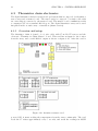
CINTAL - Centro de Investigação Tecnológica do Algarve
Universidade do Algarve
Analog 16-hydrophone vertical line array for
the Acoustic-Oceanographic buoy - AOB
F.Zabel, C.Martins and A.Silva
Rep 03/06 - SiPLAB
18 August 2006
University of Algarve
Campus de Gambelas
8005-139, Faro
Portugal
tel: +351-289864258
fax: +351-289864258
[email protected]
www.ualg.pt/cintal
Work requested by
Laboratory performing
the work
Projects
Title
Authors
Date
Reference
Number of pages
Abstract
Clearance level
Distribution list
Total number of copies
CINTAL
Universidade do Algarve, Campus de Gambelas,
8005-139 Faro, Portugal
tel: +351-289800131, [email protected],
www.ualg.pt/cintal
Signal Processing Laboratory (SiPLAB)
Universidade do Algarve, Campus de Gambelas,
8000-117 Faro, Portugal
tel: +351-289800949
RADAR - FCT contract POCTI/CTA/47719/2002
UAB - FCT contract POCI/MAR/59008/2004
Analog 16-hydrophone vertical line array for AOB2
F.Zabel, C.Martins and A.Silva
August 18, 2006
03/06 - SiPLAB
77 (seventy seven)
This report describes the sensor array system designed
for the Acoustic Oacenographic Buoy (version 2) - AOB2,
and is intended as a user and maintenance manual and
system reference.
SiPLAB/CINTAL eyes only
SiPLAB (2+2CD), CINTAL (1+1CD)
3 (three)
Copyright Cintal@2006
Approved for publication
E. Alte da Veiga
President Administration Board
Contents
List of Figures
IV
1 Introduction
8
2 Overall Description
9
3 User Manual
3.1 Introduction . . . . . . . . . . . . . . . . . . . . . . .
3.2 Hardware overview . . . . . . . . . . . . . . . . . . .
3.3 Pre-deployment procedures . . . . . . . . . . . . . . .
3.3.1 Hardware . . . . . . . . . . . . . . . . . . . .
3.3.2 Software . . . . . . . . . . . . . . . . . . . . .
3.4 Deployment, recover and post-deployment procedures
3.5 Maintenance . . . . . . . . . . . . . . . . . . . . . . .
3.6 Troubleshooting . . . . . . . . . . . . . . . . . . . . .
.
.
.
.
.
.
.
.
.
.
.
.
.
.
.
.
.
.
.
.
.
.
.
.
.
.
.
.
.
.
.
.
.
.
.
.
.
.
.
.
.
.
.
.
.
.
.
.
.
.
.
.
.
.
.
.
.
.
.
.
.
.
.
.
.
.
.
.
.
.
.
.
.
.
.
.
.
.
.
.
.
.
.
.
.
.
.
.
.
.
.
.
.
.
.
.
11
11
11
12
12
12
13
13
14
4 System Reference
4.1 Mechanical . . . . . . . . . . . . . .
4.1.1 Protection Sleeve . . . . . . .
4.1.2 Top Thimble . . . . . . . . .
4.1.3 Bottom Thimble . . . . . . .
4.1.4 Strength Member . . . . . . .
4.1.5 Ballast . . . . . . . . . . . . .
4.1.6 Hydrophone Protection Case .
4.2 Hydrophone electronics . . . . . . . .
4.2.1 Hydrophones . . . . . . . . .
4.2.2 Pre-amplifiers . . . . . . . . .
4.2.3 Cables and Connectors . . . .
4.3 Thermistor chain electronics . . . . .
4.3.1 Overview and setup . . . . . .
4.3.2 Power-up . . . . . . . . . . .
4.3.3 Status LEDs . . . . . . . . . .
4.3.4 Serial Interface Configuration
4.3.5 Serial Interface Messages . . .
4.3.6 Thermistors . . . . . . . . . .
4.3.7 1-Wire bus . . . . . . . . . . .
4.3.8 Data packet . . . . . . . . . .
4.3.9 CRC . . . . . . . . . . . . . .
4.3.10 1-Wire Bus Master . . . . . .
4.3.11 Electronic card . . . . . . . .
4.3.12 Thermistor reading software .
4.4 Array system testing . . . . . . . . .
.
.
.
.
.
.
.
.
.
.
.
.
.
.
.
.
.
.
.
.
.
.
.
.
.
.
.
.
.
.
.
.
.
.
.
.
.
.
.
.
.
.
.
.
.
.
.
.
.
.
.
.
.
.
.
.
.
.
.
.
.
.
.
.
.
.
.
.
.
.
.
.
.
.
.
.
.
.
.
.
.
.
.
.
.
.
.
.
.
.
.
.
.
.
.
.
.
.
.
.
.
.
.
.
.
.
.
.
.
.
.
.
.
.
.
.
.
.
.
.
.
.
.
.
.
.
.
.
.
.
.
.
.
.
.
.
.
.
.
.
.
.
.
.
.
.
.
.
.
.
.
.
.
.
.
.
.
.
.
.
.
.
.
.
.
.
.
.
.
.
.
.
.
.
.
.
.
.
.
.
.
.
.
.
.
.
.
.
.
.
.
.
.
.
.
.
.
.
.
.
.
.
.
.
.
.
.
.
.
.
.
.
.
.
.
.
.
.
.
.
.
.
.
.
.
.
.
.
.
.
.
.
.
.
.
.
.
.
.
.
.
.
.
.
.
.
.
.
.
.
.
.
.
.
.
.
.
.
.
.
.
.
.
.
.
.
.
.
.
.
.
.
.
.
.
.
.
.
.
.
.
.
.
.
.
.
.
.
.
.
.
.
.
.
.
.
.
.
.
.
15
15
15
15
15
15
16
16
17
17
18
21
26
26
27
27
27
28
29
30
31
33
34
37
40
40
III
.
.
.
.
.
.
.
.
.
.
.
.
.
.
.
.
.
.
.
.
.
.
.
.
.
.
.
.
.
.
.
.
.
.
.
.
.
.
.
.
.
.
.
.
.
.
.
.
.
.
.
.
.
.
.
.
.
.
.
.
.
.
.
.
.
.
.
.
.
.
.
.
.
.
.
.
.
.
.
.
.
.
.
.
.
.
.
.
.
.
.
.
.
.
.
.
.
.
.
.
.
.
.
.
.
.
.
.
.
.
.
.
.
.
.
.
.
.
.
.
.
.
.
.
.
.
.
.
.
.
.
.
.
.
.
.
.
.
.
.
.
.
.
.
.
.
.
.
.
.
.
.
.
.
.
.
.
.
.
.
.
.
.
.
.
.
.
.
.
.
.
.
.
.
.
.
.
.
.
.
.
.
.
.
.
.
.
.
.
.
.
.
.
.
.
.
.
.
.
.
.
.
.
.
.
.
.
.
.
.
.
.
.
.
.
.
.
.
.
.
.
.
.
.
.
IV
CONTENTS
A Technical specifications
43
B Equipment checklist
45
C Pre-amplifier electronics calculus
C.1 Output voltage range . . . . . . .
C.2 Pre-amplifier gain . . . . . . . . .
C.3 Bandwidth . . . . . . . . . . . . .
C.4 Noise . . . . . . . . . . . . . . . .
.
.
.
.
.
.
.
.
.
.
.
.
.
.
.
.
.
.
.
.
.
.
.
.
.
.
.
.
.
.
.
.
.
.
.
.
.
.
.
.
.
.
.
.
.
.
.
.
.
.
.
.
.
.
.
.
.
.
.
.
.
.
.
.
.
.
.
.
46
46
47
48
48
D Pre-amplifier electronic schematics and PCB
D.1 Schematic . . . . . . . . . . . . . . . . . . . .
D.2 PCB and components layout . . . . . . . . . .
D.3 PCB layout . . . . . . . . . . . . . . . . . . .
D.4 Component order list for pre-amplifier board .
.
.
.
.
.
.
.
.
.
.
.
.
.
.
.
.
.
.
.
.
.
.
.
.
.
.
.
.
.
.
.
.
.
.
.
.
.
.
.
.
.
.
.
.
.
.
.
.
.
.
.
.
.
.
.
.
.
.
.
.
.
.
.
.
52
52
53
55
57
E Thermistor master card technical details
E.1 DS18B20-PAR addresses . . . . . . . . . . . . .
E.2 PIC18F6620 software flowcharts . . . . . . . . .
E.3 Thermistors master PCB . . . . . . . . . . . . .
E.3.1 Pcb and components layout . . . . . . .
E.3.2 Pcb layout . . . . . . . . . . . . . . . . .
E.4 Component order list for thermistor master card
.
.
.
.
.
.
.
.
.
.
.
.
.
.
.
.
.
.
.
.
.
.
.
.
.
.
.
.
.
.
.
.
.
.
.
.
.
.
.
.
.
.
.
.
.
.
.
.
.
.
.
.
.
.
.
.
.
.
.
.
.
.
.
.
.
.
.
.
.
.
.
.
.
.
.
.
.
.
.
.
.
.
.
.
.
.
.
.
.
.
58
58
59
68
69
71
73
.
.
.
.
.
.
.
.
.
.
.
.
.
.
.
.
.
.
.
.
.
.
.
.
F Manufacturers and Suppliers
74
G Hydrophone-case mechanical specifications
75
List of Figures
2.1 AOB2 analog array with dimensions. . . . . . . . . . . . . . . . . . . . . . 9
2.2 AOB2 system overview: analog array with dimensions (a) and complete
system drawing (b). . . . . . . . . . . . . . . . . . . . . . . . . . . . . . . . 10
4.1
4.2
4.3
4.4
4.5
4.6
4.7
4.8
4.9
4.10
4.11
4.12
4.13
4.14
4.15
4.16
4.17
4.18
4.19
4.20
4.21
4.22
4.23
4.24
4.25
4.26
Mechanical Overview . . . . . . . . . . . . . . . . . . . . . . . . .
Ballast . . . . . . . . . . . . . . . . . . . . . . . . . . . . . . . . .
hydrophone pre-amplifier case mechanical overview. . . . . . . . .
SQ26 foto . . . . . . . . . . . . . . . . . . . . . . . . . . . . . . .
Sq26 - Sensitivity versus frequency . . . . . . . . . . . . . . . . .
pre-amplifier circuit . . . . . . . . . . . . . . . . . . . . . . . . . .
power supply cable . . . . . . . . . . . . . . . . . . . . . . . . . .
cables and connectors overview . . . . . . . . . . . . . . . . . . .
thermistors cable and connector overview . . . . . . . . . . . . . .
thermistors master card. . . . . . . . . . . . . . . . . . . . . . . .
thermistors master card power-up flowchart . . . . . . . . . . . .
Thermistors pinout . . . . . . . . . . . . . . . . . . . . . . . . . .
DS18B20-PAR typical error curve . . . . . . . . . . . . . . . . . .
64-bits lasered rom code . . . . . . . . . . . . . . . . . . . . . . .
1-wire bus linear topology . . . . . . . . . . . . . . . . . . . . . .
DS18B20-PAR’s parasite power circuit and internal block diagram
DS18B20 . . . . . . . . . . . . . . . . . . . . . . . . . . . . . . . .
DS18B20-PAR memory chart . . . . . . . . . . . . . . . . . . . .
DS18B20-PAR temperature registers format. . . . . . . . . . . . .
DOW CRC generator. . . . . . . . . . . . . . . . . . . . . . . . .
DS2480B usage (simplified). . . . . . . . . . . . . . . . . . . . . .
DS2480B circuit example. . . . . . . . . . . . . . . . . . . . . . .
R-C filter helps DS2480B interfaces on short-to-medium networks.
thermistor chain’s electronic circuit. . . . . . . . . . . . . . . . . .
PIC programming schematic. . . . . . . . . . . . . . . . . . . . .
Thermistors acquisition software algorithm . . . . . . . . . . . . .
.
.
.
.
.
.
.
.
.
.
.
.
.
.
.
.
.
.
.
.
.
.
.
.
.
.
.
.
.
.
.
.
.
.
.
.
.
.
.
.
.
.
.
.
.
.
.
.
.
.
.
.
.
.
.
.
.
.
.
.
.
.
.
.
.
.
.
.
.
.
.
.
.
.
.
.
.
.
.
.
.
.
.
.
.
.
.
.
.
.
.
.
.
.
.
.
.
.
.
.
.
.
.
.
.
.
.
.
.
.
.
.
.
.
.
.
.
.
.
.
.
.
.
.
.
.
.
.
.
.
16
16
17
18
19
20
22
23
24
26
27
29
30
30
31
32
32
32
33
34
36
36
37
38
39
41
C.1 Pre-amplifier circuit . . . . . . . . . . . . . . . . . . . . . . . . . . . . . . . 46
D.1
D.2
D.3
D.4
D.5
D.6
Hydrophone pre-amplifier . . . . . . . . . .
pre-amplifier top components placement. . .
pre-amplifier bottom components placement.
pre-amplifier top pcb layout. . . . . . . . . .
pre-amplifier bottom pcb layout. . . . . . . .
pre-amplifier component order list. . . . . .
.
.
.
.
.
.
.
.
.
.
.
.
.
.
.
.
.
.
.
.
.
.
.
.
.
.
.
.
.
.
.
.
.
.
.
.
.
.
.
.
.
.
.
.
.
.
.
.
.
.
.
.
.
.
.
.
.
.
.
.
.
.
.
.
.
.
.
.
.
.
.
.
.
.
.
.
.
.
.
.
.
.
.
.
.
.
.
.
.
.
.
.
.
.
.
.
.
.
.
.
.
.
52
53
54
55
56
57
E.1 DS18B20-PAR addresses . . . . . . . . . . . . . . . . . . . . . . . . . . . . 58
E.2 Power ON . . . . . . . . . . . . . . . . . . . . . . . . . . . . . . . . . . . . 59
E.3 Timer0 interrupt . . . . . . . . . . . . . . . . . . . . . . . . . . . . . . . . 60
V
VI
LIST OF FIGURES
E.4
E.5
E.6
E.7
E.8
E.9
E.10
E.11
E.12
E.13
E.14
E.15
E.16
E.17
E.18
E.19
E.20
E.21
E.22
E.23
Acquisition routine flowchart( 1 of 4) . . . . . . . . . . . . . . .
Acquisition routine flowchart( 2 of 4) . . . . . . . . . . . . . . .
Acquisition routine flowchart( 3 of 4) . . . . . . . . . . . . . . .
Acquisition routine flowchart( 4 of 4) . . . . . . . . . . . . . . .
DS2480B DETECT subroutine . . . . . . . . . . . . . . . . . .
DS2480B POWER ON RESET subroutine . . . . . . . . . . .
DS2480B SET TIMING subroutine . . . . . . . . . . . . . . .
DS2480B DATA MODE subroutine . . . . . . . . . . . . . . .
DS2480B COMMAND MODE subroutine . . . . . . . . . . .
OWRESET subroutine . . . . . . . . . . . . . . . . . . . . . . .
OWWRITEBYTE subroutine . . . . . . . . . . . . . . . . . . .
OWREADBYTE subroutine . . . . . . . . . . . . . . . . . . . .
DS2480 STRONG PULLUP ON subroutine flowchart . . . .
DS2480 STRONG PULLUP OFF subroutine flowchart . . . .
DS2480 TERMINATE subroutine flowchart . . . . . . . . . . .
thermistors master top components placement (not to scale). . .
thermistors master bottom components placement (not to scale).
thermistors master top pcb layout (not to scale). . . . . . . . . .
thermistors master bottom pcb layout (not to scale). . . . . . .
component order list for thermistors master card. . . . . . . . .
.
.
.
.
.
.
.
.
.
.
.
.
.
.
.
.
.
.
.
.
.
.
.
.
.
.
.
.
.
.
.
.
.
.
.
.
.
.
.
.
.
.
.
.
.
.
.
.
.
.
.
.
.
.
.
.
.
.
.
.
.
.
.
.
.
.
.
.
.
.
.
.
.
.
.
.
.
.
.
.
.
.
.
.
.
.
.
.
.
.
.
.
.
.
.
.
.
.
.
.
.
.
.
.
.
.
.
.
.
.
.
.
.
.
.
.
.
.
.
.
61
62
63
63
64
65
65
65
65
66
67
67
68
68
68
69
70
71
72
73
G.1 hydrophone case mechanical design design. . . . . . . . . . . . . . . . . . . 75
G.2 hydrophone case support mechanical design. . . . . . . . . . . . . . . . . . 76
Abstract
This report contains the user guide and the system reference for the analog 16-hydrophone
AOB vertical line array. The array is a 67.5m long cable with 16 4m-spaced hydrophones
and 17 digital thermistor sensors, distributed along its length. Each module has a dedicated preamplifier to increase signal strenght at the hydrophone output and drive a
balanced line to transmit the signal to the surface buoy’s electronics. The thermistor
sensors are digital devices that transmit the temperatures values through a 1-wire digital
serial bus. This report presents the system user guide and the system reference guide.
The user guide has instructions for system deployment, everyday usage and maintenance.
The system reference guide is intended for specialized technicians for system repairing
and/or upgrade.
Chapter 1
Introduction
Following the requirements of CINTAL projects for underwater acoustic research there was
the need for an acoustically dense array with, however nearly the same acoustic aperture
than the previous 8-hydrophone vertical array of the AOB1 system [2]. Therefore the
most important improvement is the increase of the number of hydrophones and also the
array geometry that is should be equispaced at 4 m so as to allow for easy beamforming
for surface noise studies and time-reversal as required by UAB - Underwater Acoustic
Barriers project.
The other requirement is that the new array system should be interconnected with the
AOB2 surface buoy[1], therefore the same bandwidth and connector pinout. The array
mechanical design should be improved so as to offer a better compact and streamed line of
cables for easy handle during deploying and recovering operations. Another requirement is
that each hydrophone module should also contain a temperature sensor for online reading.
The handling of the temperature data stream should be as light as possible in terms of
cabling.
The result is a new array that follows a very similar design to that of the older AOB1
model with, however several improvements: i) a more compact mechanical design including a polyester sleeve covering the cables along the array, ii) a new proprietary preamplifier
design and 3) a new digital temeprature sensor bus system with T-sensors colocated with
the hydrophones.
The following sections will describe the array from a basic user perspective up to a
more detailed description. The next section starts with an overall description. Following
is the user-manual. The third section covers all the array design details.
8
Chapter 2
Overall Description
The analog array is a 67.5m long cable with 16, 4m-spaced hydrophones and 16+1 hydrophone colocated digital thermistor sensors, distributed along its length (figure 2.1).
Each module has a dedicated preamplifier to enhance the signal and drive one balanced
Figure 2.1: AOB2 analog array with dimensions.
line, to transmit the signal to the surface buoy’s electronics. The thermistor sensors are
digital devices that transmit the temperature values through a single wire serial digital
network that requires only two wires. The signals received at the hydrophone modules
are available at two connectors on the top of the array. A third connector is used for the
thermistor bus. The cables are protected by a polyamide sleeve; one internal strength
member cable is used to handle the vertical mechanical forces applied to the array, and
one ballast weight is placed on the bottom to stretch the array and keep nearly vertical.
The result is a thin and compact array with all the sensors at precise positions (figure
9
10
CHAPTER 2. OVERALL DESCRIPTION
2.1).
In the AOB2 system (figure 2.2), the array is attached to the buoy’s bottom cover
support ring, and the signal connectors are attached to the buoy’s top cover. The buoy
is floating at the sea surface and, with the help of the ballast, the array is kept as much
vertical as possible.
Figure 2.2: AOB2 system overview: analog array with dimensions (a) and complete
system drawing (b).
Chapter 3
User Manual
3.1
Introduction
The first thing the user must notice is that the array is not a standalone element, it is
part of the AOB2 system and, therefore, all the information shown in this manual should
not be used alone but always as a complement to the AOB2 report/manual.
This chapter details the high-level operations regarding the correct use and maintenance of the array, plus some troubleshooting hints. The next chapter introduces the
user to the hardware details about the array. The following two sections present the
pre-deployment, the recover and post-deployment procedures. The fourth section enumerates some maintenance recommendations. The last section gives some hints to solve
possible problems that may happen with this device while being used at sea or during
maintenance/preparation for sea trial.
3.2
Hardware overview
This section describes the few hardware parts that compose the array:
• the main cable, composed by the electrical wires, sensors and one strength member
all protected by a polyamid mesh sleeve;
• hydrophone cases, to protect the hydrophone and the pre-amplifier electronics inside
a polyurethane mold;
• thermistor’s, inside a polyurethane mold;
• a Dynema based strength member to maintain the vertical structure of the array
and to attach the sensors so that they are held always at the constant distance;
• top thimble, fasten to the top of the strength member and used to securely attach
the array to the buoy using a shackle. The shackle is made of plastic to avoid
parasitic sounds when in contact with metal;
• bottom thimble, fasten to the bottom of the strength member and used to secure
the ballast weights.
• ballast, made of lead weights, for keeping the array vertical when underwater.
The array technical specifications, including the electronic parts, are described in table A.1 of appendix A. Care must be taken with all the hardware parts specially bending
of electrical cables, water, sand or other contaminant in the connectors, sensor cases or
strength member.
11
12
CHAPTER 3. USER MANUAL
3.3
3.3.1
Pre-deployment procedures
Hardware
The following steps must be followed for safe array deployment:
1. read the pre-deployment procedures for the AOB2 buoy;
2. check if the top and bottom thimbles are correctly tighten to the strength member;
3. check if the top and bottom thimbles have pvc electrical tape around to prevent
acoustic noises;
4. attach the ballast weight to the bottom thimble using a shackle;
5. secure the shackle using plastic cable ties;
6. arrange the array in the deck in an 8-shape, assuring that the top end is the ballast
(first in the water);
7. attach the array to the buoy connecting the top thimble with the array support in
the buoy, using a shackle;
8. secure the shackle using plastic cable ties;
9. check the connectors’ o-rings, if necessary apply silicone-based grease;
10. there are three electrical connectors to be attached to the surface buoy: two large 24pin connectors one for each 8 hydrophone sub-array and one smaller 5-pin connector
for the digital thermistor sensor array. The two large connectors are marked H1 and
H2 for the upper half and lower half arrays, respectively. They should attached to
the respectively marked H1 and H2 receptacles on the buoy’s top cover. The 5pin smaller connector should be attached to the respective receptacle on the buoys’
cover. The user should ensure that the digital thermistor master card is correctly
installed inside surface buoy (see 4.3 for details). Don’t forget to pass the array
cable inside the buoy’s float.
3.3.2
Software
Please refer to the AOB2 manual [1] for data acquisition software initialization and preparing/testing before deployment. This section will concentrates on the instalation of the
thermistor chain software, which is a new piece of hardware not previously described.
The instalation of the thermistor chain software is done by placing the file Thermistor
ChainDigital.py in the /AOB/programs directory from where it will be activated as
an aditional service to be run on system startup (see section 4.3.12.2 for more details on this file format). Configuration of the software can be achieved by editing the
ThermistorChainDigital.py in any text editor, variables to change if any are: the serial
port (/dev/ttyS1 for serial port 2) and additionally the line coef = (0,0,0,0,0,0,0,0,0,
0,0,0,0,0,0,0,0) which is the compensation value to be applied to each individual sensor. Data is written to the file /AOB/data/termchain-data.log at the interval at which
it is received from the thermistor chain. Each data line in the termchain-data.log file
is of the following format:
09,11,2006,05:10:12,23.250000,23.062500,22.875000,22.937500,22.937500,
23.062500,22.937500,22.875000,22.875000,22.812500,22.812500,22.750000,
22.937500,22.750000,23.000000,23.000000,23.312500
3.4. DEPLOYMENT, RECOVER AND POST-DEPLOYMENT PROCEDURES
13
The first fields are date and acquisition time, then followed by the temperature sensor
readings in degrees C, separated by the comma delimeter.
3.4
Deployment, recover and post-deployment procedures
The steps for a safe recovery and storage of the array are as follows:
1. read the deployment procedure for the AOB2 system. The array is the first element
to enter the water, starting with the ballast. Pay attention to the sea current to
avoid entangling the array under the ships’ propeller;
2. read the recovery procedure for the AOB2 Buoy.
3. after the buoy is on the deck, start pulling the array out of water. If possible arrange
the array in an 8 shape immediately.
4. wash the array and the buoy with fresh water.
5. remove the electrical connectors. Pay attention not to loose the connector’s o-rings.
6. place the dummies in the buoy and array connectors.
7. remove the top shackle.
8. leave the ballast weights attached, unless it cause problems to the transport or
storage.
9. let the array dry.
10. store it in the AOB2 box, over the buoy.
3.5
Maintenance
Due to its characteristics, the array requires very few maintenance and a minimum checkup
before any deployment is sufficient. Follow these steps:
• check if the o-rings are very dry or damaged before every experiment or deployment.
If so replace them.
• check for any corrosion on every metallic parts(connectors, shackles), every 4 months
and before every deployment.
• check the protection sleeve, for cuts, before each deployment.
• check the straps that hold the ballast before every deployment.
• check if the electrical cables are dry to cause breaches when bent, every 4 months.
If so, replace them.
Always wash the array with fresh water after recovery to remove the salt water, and
let it dry on air preferably protected from direct sun light.
14
CHAPTER 3. USER MANUAL
3.6
Troubleshooting
This section describes possible problems that may occur with the array and their solutions.
The only problems that can be found directly in the array are mechanical, since all
electrical problems are only detected when the array is connected to the buoy, and for
this ones both array and buoy must be checked.
The buoy is very unstable at the sea:
• Increase the ballast weight.
The protection sleeve is damaged:
• If it is not possible to replace at that moment, use some pvc tape, to cover the area.
The shackle’s bolts are too tight:
• Remove the plastic tie.
• Use some lubricant, like WD40, to remove the bolt.
• If the shackle shows any oxidation, replace it.
One connector has residues of water inside:
• Remove the o-ring from the connector (using a thin plastic tie usually helps) and
check if it is damaged. Replace if necessary.
• If the o-ring is ok, the problem may be lack of silicone-based grease on the o-ring
or the connector wasn’t tight enough.
The signals in one or more channels are not the expected:
• Look at the troubleshooting section in the AOB2 manual.
• Check the connectors to see if they are loose or if there is water inside, and make a
test (stroke each hydrophone and check the result).
• Apply some contact cleaner.
• Check the buoy’s electronics and software.
A value of -28 or 0 degrees appear in the T-sensor reading:
• a value of -28 denotes a reading error on the temperature sensor. It should be very
unusual and may appear once in a while. If this reading becomes persistent in time,
then a T-sensor may have a permanent problem and should be replaced. If this
reading appears in a number of sensors say, a full section, it may mean that the bus
is in open circuit between that section and the main master card. The solution is
to replace the faulty portion of cable.
• any other problem in the cable generates error messages and a T-sensor reading of
0 degrees - inside the buoy the error LED is on. In general these problems can not
be simply solved (see section 4.3).
If the problem does not fit in any of the above, please contact Siplab/CINTAL for
further assistance.
Chapter 4
System Reference
This chapter describes the array hardware in a higher technical detail. This information
should be used by a qualified techician so as to ensure the minimum knowledge for testing
or repairing electrical or mechanical components. This chapter is organized as follows:
the first section addresses the array mechanical parts, the second section describes the
hydrophone electronics and connections and the third and last section gives a tutorial
description of the thermistor sensor electonics and respective master card.
4.1
Mechanical
The array mechanics includes all the elements used to keep the array structure intact and
protect the electrical and electronic parts. All these elements are represented in figure
4.1.
4.1.1
Protection Sleeve
A polyamid sleeve is used to protect and to keep the wires and cables together. The sleeve
is made of resistant and flexible polyamid mesh. The result is a compact, flexible and
robust cable. The sleeve is manufactured by AUTEC (www.autec-vertrieb.de), and the
used references are: GS-12, GS-15, GS-20 and GS-25 (AUFLEX).
4.1.2
Top Thimble
Top ring to connect the array to the buoy, using an inox shackle.
4.1.3
Bottom Thimble
Bottom ring to connect the array to the ballast, using an stainless-steel shackle.
4.1.4
Strength Member
The strength member
breaking load of 1500
protection sleeve, and
low stretch factor, the
and stable position.
is a 6mm Dyneema cable, with a very low stretching factor and
Kg. It goes from the top to the bottom of the array, inside the
connects the top thimble with the bottom one. As it has a very
sensors in the array are fasten to this cable, to be assured a fixed
15
16
CHAPTER 4. SYSTEM REFERENCE
Figure 4.1: Mechanical Overview
4.1.5
Ballast
At the bottom of the array there is a 8kg ballast, made of lead weights, to keep the array
under tension and as vertical as possible. The used weights are the same as scuba-divers,
and are fastened to the bottom thimble using a strap (figure 4.2).
Figure 4.2: Ballast
4.1.6
Hydrophone Protection Case
A protection case was specially designed to keep the hydrophone and preamplifier electronics protected from the environment and to help fasten the hydrophone to the strength
member at a known fixed depth position. Polyurethane resin UR5041 (RS code: 1608481)
4.2. HYDROPHONE ELECTRONICS
17
is used to fill the case and isolate the electronics from the water. A spacer element is used
to help tighten the case to the strength member. Figure 4.3 shows a self-explaining
illustration. 3D drawings can be found in appendix G.
Figure 4.3: hydrophone pre-amplifier case mechanical overview.
4.2
4.2.1
Hydrophone electronics
Hydrophones
The hydrophones in use are the SQ26 (figure 4.4) manufactured by Sensor Technology
Limited (http://www.sensortech.ca/main.html), whose main specifications are shown in
table 4.1. Refer to figure 4.5 for a graph of the hydrophone sensitivity versus frequency.
Hydrophone capacitance variations may be calculated as follows:
CSQ26 = 1.4ηF ± 10% @ 20◦ C
⇒
1.26ηF ≤ CSQ26 ≤ 1.54ηF
d
d
CSQ26 (d) = CSQ26 1 − 0.07 1000
= 1.4ηF 1 − 0.07 1000
where d is hydrophone depth in meter. These variations are shown in table 4.2. The
relation between voltage and water pressure is
∆Q
∆p
= 24 ηC/bar
∆V =
∆Q
C
=
24ηC/bar
1.4ηF
= 17.1429 V /bar
18
CHAPTER 4. SYSTEM REFERENCE
Figure 4.4: SQ26 foto
Voltage Sensitivity
Charge sensitivity
Capacitance
Sensitivity variation with temperature
Capacitance variation with temperature
Capacitance variation with depth
Operating depth
Frequency response
Acceleration sensitivity
Storage and operating temperature
Diameter
Length
Mass
Electrical leads
Electrical insulation
Water blocked leads
-193.5 ± 1.0dBV re 1 Pa 20o C, 20 V/bar
24 ηC/bar;
1.4ηF ± 10% 20o C
< 1dB loss from 0o C to 35o C
0.33% increase per o C
7% loss per 1000m
1000m
flat from 1Hz to 28kHz
< 0,2mbar/g when properly mounted
-30o C to 60o C
25.4mm
25.4mm
16 grams
two red and black stranded, 28AWG
15cm long, Hytrel-insulated leads
> 500 MΩ
yes
Table 4.1: SQ26, Sensor Technology Ltd. hydrophone specifications
4.2.2
Pre-amplifiers
The pre-amplifiers were designed to adapt the small electrical signals obtained from the
variation of the hydrophone’s capacitance to the input voltage range of the acquisition
electronics inputs (ADCs1 inputs), taking into account the attenuation of the transmission
line. As a starting point for the design of the circuit, the main goals are:
• approximate voltage gain of 36dB;
1
ADC - Analog to Digital Converter
4.2. HYDROPHONE ELECTRONICS
19
Figure 4.5: Sq26 - Sensitivity versus frequency
Depth [m]
5.55
9.55
13.55
17.55
21.55
25.55
29.55
33.55
37.55
41.55
45.55
49.55
53.55
57.55
61.55
65.55
Capacitance [ηF ]
1.3994561
1.3990641
1.3986721
1.3982801
1.3978881
1.3974961
1.3971041
1.3967121
1.3963201
1.3959281
1.3955361
1.3951441
1.3947521
1.3943601
1.3939681
1.3935761
Table 4.2: hydrophone capacitance variations with depth
• -3dB bandwidth between 100Hz and above 17kHz;
• lowest noise as possible;
• differential output;
• output voltage range output between −5V and +5V ;
20
CHAPTER 4. SYSTEM REFERENCE
• low input bias currents (very important characteristic with capacitive transducers,
like the hydrophones, to reduce offset voltages);
• smallest size as possible.
4.2.2.1
Circuit overview
The basic circuit is shown in figure 4.6. The design is based on a non-inverting op-ampbased scheme which circuit is proposed for an hydrophone transducer in the datasheets
of two low-noise opamps, LT1113 and AD743 .
Amplifier LT1113 is a low noise JFET opamp designed to amplify low level signals
from high impedance capacitive transducers. Following the amplifier is a differentialoutput buffer amplifier, SSM2142, to convert the single ended signal to a balanced output
signal. Capacitors C1 and C2 are used to eliminate DC signals and to set the amplifier’s
highpass cutoff frequency to 100Hz. Two diodes, D1 and D2, connected in anti-parallel
are used to protect the opamp’s input from high-voltages, that may occur due to very
strong signals received by the hydrophone.
Figure 4.6: pre-amplifier circuit
4.2.2.2
Output Voltage Range
The output voltage range of the amplifier is limited by the power supply of the electronics.
Using ±8V voltage regulators, the output voltage range of the pre-amplifier is −5V ≤
Vout ≤ +5V , reference to ground, while the differential pre-amp output voltage range is
−10V ≤ Vout ≤ +10V . See detailed calculus in appendix C.1.
4.2. HYDROPHONE ELECTRONICS
4.2.2.3
21
Pre-amplifier gain
Detailed gain calculus can be found in appendix C.2 while a short table with a few
important theoretical gain values are shown in table 4.3. Note the maximum gain in the
frequency band of 36 dB and a highpass cutoff frequency of 108 Hz.
f
Apre amp
Apre amp
(Hz)
(dB)
0
0
−∞
0.16
0.992
-69.5
108.27
45.6
33.17
108.3 → 52800 1+R3 /R2 =64.4
36.2
52800
45.6
33.17
∞
0
−∞
Table 4.3: theoretical hydrophone pre-amplifier gain.
4.2.2.4
Pre-amplifier bandwidth
Pre-amplifier bandwidth varies with opamp characteristics and component temperature
dependence. Detailed bandwidth calculus are shown in appendix C.3 and main results
reported below.
Preamp bandwidth:
Temperature range:
Top frequency variation:
(full temperature range)
4.2.2.5
108.27Hz ≤ Bpre−amp ≤ 52796Hz
0 ◦ C ≤ Tamb ≤ 70 ◦ C
12423.4Hz ≤ Bpre−amp ≤ 52796Hz
Noise
Ignoring the noise from the balanced line driver, which is not specified on the datasheet [8],
the preamplifier noise main sources are the operational amplifier voltage and current noise
(Table C.1) and the thermal noise on the resistors. All together give a final output noise
of En−out ≈ 4.5019 mV. Taking into account a pre-amplifier output range of ±5V gives,
for a sine wave at 1 kHz an output RMS voltage Vout−RM S = √52 = 3.5355V and therefore
3.5355
= 785.34
4.5019 × 10⁻³
that in dB gives 20 log(785) = 57.897dB. The complete calculus to obtain these values
is shown in appendix C.4. Attention must be payed to the fact that during the noise
calculus, the noise bandwidth was assumed to be equal to the input signal bandwidth and
not to the total noise bandwidth.
4.2.3
Cables and Connectors
The cabling system is designed to provide power to all the hydrophone pre-amplifiers and
to bring the electrical signals from each hydrophone pre-amp to the surface buoy input
connector.
22
4.2.3.1
CHAPTER 4. SYSTEM REFERENCE
Power supply cable
The power supply cable is a three wire cable, where each pre-amplifier is connected in a
bus topology (figure 4.7). Table 4.4 shows the cable’s properties.
Figure 4.7: power supply cable
Number of cores
Cross-section
Nominal Voltage
Nominal current
RS code
3
1.5 mm2
450/750 V rms
22 A
4099486
Table 4.4: power supply cable properties.
4.2.3.2
Signal cable
The electrical signals from the hydrophones - pre-amplifier modules are connected to the
surface buoy via a twisted-pair cooper cable, see figure 4.8. Table 4.5 show the cable’s
properties:
Number of cores
Inner conductor
Insulation
Twists
External diameter
Capacitance
Resistance
Maximum current
RS code
2
10 × 0.254 mm (20 AWG)
1.92 mm diameter PVC
Left hand lay, 17.24 twists/m
5.12 ± 0.20 mm
77 pF/m
34Ω /km
8A
0360958
Table 4.5: signal cable properties
4.2.3.3
1-wire cable
The 1-wire bus uses a twisted-pair cable, equal to the signal cables. Figure 4.9 shows the
connections between the 1-wire bus cable, the top connector and the temperature sensors.
4.2. HYDROPHONE ELECTRONICS
Figure 4.8: cables and connectors overview
23
24
CHAPTER 4. SYSTEM REFERENCE
Figure 4.9: thermistors cable and connector overview
4.2.3.4
Connectors
MSSJ-CCP-5
1
2
3
4
5
-
DQ (Data I/O)
GND
NC (Not connected)
NC (Not connected)
NC (Not connected)
Table 4.6: thermistors 1-wire bus connector.
All array connectors are made by Impulse(www.impulse-ent.com). A separate connector
is used for the thermistors 1-wire bus. The connector reference is MSSJ-5. Figure 4.9
and table 4.6 show the connectors pinout. Hydrophone connections are made through
two MHDL-CCP # 24. Figure 4.8 shows the array system cabling overview for the
hydrophones and table 4.7 shows the hydrophone connectors’ pinout.
4.2. HYDROPHONE ELECTRONICS
25
MHDL-CCP-24
Connector1
Connector2
1 - GND (Power)
2 - +12V (+Power)
3 - +Channel 1
4 - -Channel 1
5 - +Channel 3
6 - -Channel 3
7 - +Cha nnel 5
8 - -Channel 5
9 - +Channel 6
10 - -Channel 6
11 - +Channel 8
12 - Channel 8
13 - -12V (-Power)
14 - +12V (+Power
15 - +Channel 2
16 - -Channel 2
17 - +Channel 4
18 - -Channel 4
19 - +Channel 7
20 - -Channel 7
21 - -12V (-Power)
22
23
24
1 - GND (Power)
2 - +12V (+Power)
3 - +Channel 9
4 - -Channel 9
5 - +Channel 11
6 - -Channel 11
7 - +Channel 13
8 - -Channel 13
9 - +Channel 14
10 - -Channel 14
11 - +Channel 16
12 - Channel 16
13 - -12V (-Power)
14 - +12V (+Power
15 - +Channel 10
16 - -Channel 10
17 - +Channel 12
18 - -Channel 12
19 - +Channel 15
20 - -Channel 15
21 - -12V (-Power)
22
23
24
Table 4.7: hydrophone connectors.
26
4.3
CHAPTER 4. SYSTEM REFERENCE
Thermistor chain electronics
The digital thermistor chain is a newly developed system that is composed of a thermistor
sensor array and a master board. The sensor array is composed of a single cable with
two wires that is connected to the master board. The master board communicates with
a computer CPU via a standard RS-232 port. The digital thermistor array can be used
integrated in the acoustic array or standalone (future version).
4.3.1
Overview and setup
The thermistor chain is formed of a 2 wire cable with 17 molded T-sensors and the
electronic “Thermistor’s Chain Master” board. This card has an input for the 2 wires
from the array, and a serial RS232 output as shown on figure 4.10. After the card is
Figure 4.10: thermistors master card.
powered ON, it starts reading the temperatures from the array continuously. The card
reads the 17 values approximately every 5 seconds, and sends the readings in ASCII
4.3. THERMISTOR CHAIN ELECTRONICS
27
format to the serial port. The acquisition timing is obtained from the microcontroller’s
cristal oscillator taken as reference clock.
4.3.2
Power-up
Figure 4.11 shows the power-up flowchart.
Figure 4.11: thermistors master card power-up flowchart
4.3.3
Status LEDs
The board’s LED’s show the status of the system, coded as follows:
• ON LED (Left/Red) - The microcontroler set this Led ON when the card is
powered-ON.
• ACQUISITION LED (Middle/Green LED) - This Led is ON when the microcontroler is acquiring one set of 17 temperatures, and returns to OFF when the
acquisition ends.
• ERROR LED (Right/Red) - This LED is turned ON every time one error occur.
At the same time, one error message is sent through the serial port to the host
computer.
4.3.4
Serial Interface Configuration
In order to receive the data from the card an RS-232 interface with the following configuration is necessary:
28
CHAPTER 4. SYSTEM REFERENCE
• Baud Rate: 19200 bauds
• Data: 8 bits
• Parity: None
• Stop Bits: 1
• Flow Control: None
4.3.5
Serial Interface Messages
The communication between the card and the computer host is performed through ASCII
messages, in simplex mode, from the card to the host. The messages semantics allow the
user to read them directly, using a serial port interface software (such as ”Hyperterminal”).
To make the development of the interface software easier for the host computer, the
number of possible messages is finite and each message lenght is constant.
• Each message has a specific and constant number of characters, being either alphanumeric or hexadecimal values.
• The description of each message start and end with ”. This characters are not sent
by the card.
• In the description, spaces are shown as: t .
• Some messages include linebreaks. Linebreaks are sent using 0x0A (New Line) followed by 0x0D (Carriage Return). To distinguish this, from the ASCII characters,
lets assume a linebreak to be like: \\
Message list:
• ”\\1-WIREtTHERMISTORStARRAY\\” (26 characters)
– This message is sent everytime the card’s microntroller is powered ON, or a
software reset is performed in the microcontroller. This is always the first
message sent by the card to the host.
• ”\\TEMP\\” (6 characters)
– This message is the header for a set of 17 temperature values. The 17 temperatures, from the array thermistors, are sent to the host after this message. The
first temperature to be sent is from thermistor 1 and ends with the temperature
from thermistor 17.
– Each temperature value’s size is constant and is composed with a signal character equal to ’+’ or ’-’, plus 7 characters with the value in degrees centigrades,
plus one linebreak: ”SXX,XXXX\\”
– If the temperature returned is equal to ”-28,000\\”, this means an error occured
in the reading. CRC codes are used to validade every temperature values
received from the sensors.
• ”BUStINtSHORT-CIRCUIT\\” (21 characters)
– This message is send if the 1-wire bus is in short-circuit.
• ”NOtDEVICEStINtTHEtBUS\\” (22 characters)
4.3. THERMISTOR CHAIN ELECTRONICS
29
– This message is send if there are no devices in the bus or, and most commonly,
if the array is not connected to the card.
• ”RESET-ACQ ISR\\” (14 characters)
– This message is send after an error in the acquisition routine.
– After the message is sent, the microcontroler performs a reset.
– Contact to the card’s manufacturer or refer to section 4.3.12
• ”RESET-OWRESET\\” (14 characters)
– This message is send after an error in the 1-wire reset routine.
– After the message is sent, the microcontroler performs a reset.
– Contact to the card’s manufacturer or refer to section 4.3.12
4.3.6
Thermistors
The temperature sensors used in the array are the ”DS18B20-PAR”, manufactured by
Maxim (www.maxim-ic.com). Their specifications are
• 1-wire interface, requires only 2 pins connection to work;
• derives power from data line (”parasite power”), does not need a local power supply;
• multi-drop capability simplifies distributed temperature sensing applications;
• requires no external components;
• ±0.5◦ C accuracy from -10◦ C to +85◦ C;
• measures temperatures from -55◦ C to +100◦ C (-67◦ F to +212◦ F);
• thermometer resolution is user-selectable from 9 to 12 bits
• converts temperature to 12-bit digital word in 750 ms (max.);
• ideal for use in remote sensing applications (e.g., temperature probes) that do not
have a local power source.
and the thermistor’s pinout is shown in figure 4.12. Thermistor’s typical error curve is
given in figure 4.13 that mainly shows that these T-sensors have a bias of -0.2◦ C and a -3
standard deviation error less than 0.3◦ C. Refer to sensor datasheet [9] for further details.
Figure 4.12: Thermistors pinout
30
CHAPTER 4. SYSTEM REFERENCE
Figure 4.13: DS18B20-PAR typical error curve
4.3.7
1-Wire bus
The 1-wire bus is a digital serial data communication bus featuring: low-speed data, low
signaling, low power, low cost, 1 wire data and 1 ground lines, and power over data line.
More details info about 1-wire are available in reference [10].
4.3.7.1
Serial network
The 1-wire bus may work as a serial network, with one master device and one or more
slaves. The master is a controller unit directly connected to the bus or through an interface
chip. The slave devices include temperature sensors, memories, mixed signal, and secure
authentication chips. The seventen DS18B20-PAR are the slave devices in the array. Each
1-wire slave device have a unique 64-bits identification codes, stored in ROM and recorded
from factory. The code includes a 8-bits CRC validation code, a 48-bits serial number
and a 8-bits family number (28h = DS18B20-PAR’s family devices), as shown in figure
4.14. This code is used as an address to access each device individually. At appendix
E.1 is a list with address from all the sensors, in the array and the spares. The number
Figure 4.14: 64-bits lasered rom code
of lines needed for the 1-wire bus are only two, a single data line and a ground line.
Three different network topologies are proposed by the manufacturer: Linear, Stubbed
and Star. This array uses the Linear topology(figure 4.15), the 1-wire bus is a single pair,
starting at the master and extending to the farthest slave device. Other slave devices
are attached to the pair along its length without significant (>3m) branches or ”stubs”.
The communication in the bus is always between one master and one or more slaves, and
the slaves can’t communicate between them. There is possible for the master to send
4.3. THERMISTOR CHAIN ELECTRONICS
31
Figure 4.15: 1-wire bus linear topology
commands or data to one specific device or to several devices at the same time (point-topoint or point-multipoint). On the slaves side, they can only send data to the master one
at the time (point-to-point) and after request from the master.
In the 1-wire network, two terms are used to describe measurements: radius and weight.
The radius of a network is the wire run distance from the master end to the furthest slave
device, in meters. The weight of a network is the total amount of connected wire in the
network, in meters. To assure a realiable network, the radius must not be greater than
750m, due to protocol timings, and the weight is limited to 200m or 500m, due to signal
attenutation: 200m when using a single pull-up resistor, and 500m when using active
pullups to provide higher currents under logic control. The weight of a network is not
only specified by the cable lenght but also by the slave devices and pcb boards:
• i-buttons slave devices : 1 meter per device;
• non i-buttons slave devices (DS18B20-PAR): 0.5 meters per device;
• pcb trace with 24pF: 1m.
In this array, the weight and radius of the network is:
weightslaves = 17devices × 0.5 = 8.5meters
weightcable = array length + cable length from the array to the master
≈ 65.55m + 2.5m = 68.05m ≈ 70meters
weightnetwork = weightslaves + weightcable = 8.5m + 70m = 70.5meters
radiusnetwork = weightcable = 70.5meters
Refer to Maxim application note AN148 [11] (guidelines for reliable 1-wire networks).
4.3.7.2
Parasite Power
Some slave devices, like DS18B20-PAR, don’t need a local external power supply because
they have an internal parasite power circuit, to ”steal” power from the 1-wire bus data
line (figure 4.16). When the data line is high, the device is directly powered and one
capacitor is charged; when the data line is low, power is provided by the charged capacitor.
Whenever the power from the bus and the capacitor aren’t enough, the master circuit
must provide a strong pullup on the 1-wire bus (figure 4.17). This situations always
happens when the DS18B20-PAR is performing a temperature reading or is copying data
to the EEPROM. No other activity can take place on the 1-Wire bus while the strong
pullup is enabled. Refer to DS18B20-PAR datasheet for more details [9].
4.3.8
Data packet
The DS18B20-PAR’s memory is organized as shown in figure 4.18. Each time a temperature is measured the value is stored in bytes 0 (LSB) and 1 (MSB), and then the
32
CHAPTER 4. SYSTEM REFERENCE
Figure 4.16: DS18B20-PAR’s parasite power circuit and internal block diagram
Figure 4.17: DS18B20
whole scratchpad packet (9 bytes) is sent to the master. The reason to send the whole
scratchpad to the master is that a CRC code is included to validade the whole packet,
and not only the temperature values. Temperature values have a resolution of 9, 10, 11 or
Figure 4.18: DS18B20-PAR memory chart
12-bits (0.5o C, 0.25o C, 0.125o C, 0.0625o C), user-configurable in the configuration register.
The temperature data is stored as a 16-bit sign-extended two’s complement number in
the temperature register (figure 4.19). The signal bit is bit11 and his values is extend
from bit 12 to 15. For 11-bit resolution, bit 0 is undefined; for 10-bit resolution, bits 1
and 0 are undefined; and for 9-bit resolution bits 2, 1 and 0 are undefined. Table 4.8,
shows some examples between temperature values and binary code. At power-up, the
4.3. THERMISTOR CHAIN ELECTRONICS
33
Figure 4.19: DS18B20-PAR temperature registers format.
TEMPERATURE
+85◦ C2
+25.0625◦ C
+10.125◦ C
+0.5◦ C
0◦ C
-0.5◦ C
-10.125◦ C
-25.0625◦ C
-55◦ C
DIGITAL OUTPUT (Binary)
0000 0101 0101 0000
0000 0001 1001 0001
0000 0000 1010 0010
0000 0000 0000 1000
0000 0000 0000 0000
1111 1111 1111 1000
1111 1111 0101 1110
1111 1110 0110 1111
1111 1100 1001 0000
DIGITAL OUTPUT (Hex)
0550h
0191h
00A2h
0008h
0000h
FFF8h
FF5Eh
FE6Fh
FC90h
Table 4.8: temperature conversion table.
default resolution is 12bits. Resolution also limits the acquisition time, the higher the
resolution, more time is needed to perform an acquisition (table 4.9). Luckly, the 1-wire
protocol allows the master to issue a temperature acquisition to the all the slaves at the
same time. Nevertheless, after the acquisition ends, the master have to read each device
temperature register (full scratchpad) one by one.
Resolution Max Conversion Time
9-bit
93.75 ms
10-bit
187.5 ms
11-bit
375 ms
12-bit
750 ms
Table 4.9: Temperature acquisition time
This system resolution is 12 bits. Refer to DS18B20-PAR datasheet for more details
[9]
4.3.9
CRC
Both DS18B20-PAR 64-bit identification code and scratchpad includes a CRC(Cyclic
Redudancy Check) code for errors detection. The identification ROM code’s CRC is
calculated from the first 56 bits of the code and is contained in the most significant byte.
The scratchpad CRC is calculated from the data stored in the scratchpad, and therefore
it changes when the data in the scratchpad changes. The CRCs provide the bus master
with a method of data validation when data is read from the DS18B20-PAR. The Dallas
Semiconductor 1-Wire CRC (DOW CRC) magnitude is 8 bits, and is capable of detect
the following types of errors:
• Any odd number of errors.
• All double-bit errors.
34
CHAPTER 4. SYSTEM REFERENCE
• Any cluster of errors that can be contained within an 8-bit ”window” (1-8 bits
incorrect).
• Most larger clusters of errors.
The equivalent polynomial function of the DOW CRC is: CRC = X8 + X5 + X4 + 1.
The bus master can re-calculate the CRC and compare it to the CRC values from the
DS18B20-PAR using the polynomial generator shown in figure 4.20. This circuit consists
of a shift register and XOR gates, and the shift register bits are initialized to 0. Starting
with the least significant bit of the ROM code or the least significant bit of byte 0 in the
scratchpad, one bit at a time should shifted into the shift register. After shifting in the
56th bit from the ROM or the most significant bit of byte 7 from the scratchpad, the
polynomial generator will contain the re-calculated CRC. Next, the 8-bit ROM code or
scratchpad CRC from the DS18B20-PAR must be shifted into the circuit. At this point,
if the re-calculated CRC was correct, the shift register will contain all 0s. If memory is
Figure 4.20: DOW CRC generator.
available in the master, one better and faster way to check the DOW CRC is to use a
look-up table that is accessed directly for any 8-bit value currently stored in the CRC
register and any 8-bit pattern of new data. For the simple case where the current value of
the CRC register is 00 Hex, the 256 different bit combinations for the input byte can be
evaluated and stored in a matrix, where the index to the matrix is equal to the value of
the input byte (i.e., the index will be I = 0-255). It can be shown that if the current value
of the CRC register is not 00 Hex, then for any current CRC value and any input byte,
the lookup table values would be the same as for the simplified case, but the computation
of the index into the table would take the form of:
New CRC = Table [I] for I = 0 to 255;
where I = (Current CRC) EXOR (Input byte)
Table 4.10 shows the lookup table values for the DOW CRC and table 4.11 shows an
example about how to use it. The look-up table method is the one used in our system.
Refer to Maxim application note AN27 [12] (Understanding and Using Cyclic Redundancy
Checks).
4.3.10
1-Wire Bus Master
The system master is composed by a microcontroller PIC18F6620 [13] and a serial-to-1wire interface chip DS2480B [14]. The microcontroller is responsible for:
• set the temperature acquisiton rate to aproximately 5seconds.
• communicate with the 1-wire slave devices, DS18B20-PAR, through the DS2480B;
• communicate with the host computer through an rs232 serial port interface.
4.3. THERMISTOR CHAIN ELECTRONICS
35
table[0..255]= (
0, 94, 188, 226, 97, 63, 221, 131, 194, 156, 126, 32, 163, 253, 31, 65,
157, 195, 33, 127, 252, 162, 64, 30, 95, 1, 227, 189, 62, 96, 130, 220,
35, 125, 159, 193, 66, 28, 254, 160, 225, 191, 93, 3, 128, 222, 60, 98,
190, 224, 2, 92, 223, 129, 99, 61, 124, 34, 192, 158, 29, 67, 161, 255,
70, 24, 250, 164, 39, 121, 155, 197, 132, 218, 56, 102, 229, 187, 89, 7,
219, 133, 103, 57, 186, 228, 6, 88, 25, 71, 165, 251, 120, 38, 196, 154,
101, 59, 217, 135, 4, 90, 184, 230, 167, 249, 27, 69, 198, 152, 122, 36,
248, 166, 68, 26, 153, 199, 37, 123, 58, 100, 134, 216, 91, 5, 231, 185,
140, 210, 48, 110, 237, 179, 81, 15, 78, 16, 242, 172, 47, 113, 147, 205,
17, 79, 173, 243, 112, 46, 204, 146, 211, 141, 111, 49, 178, 236, 14, 80,
175, 241, 19, 77, 206, 144, 114, 44, 109, 51, 209, 143, 12, 82, 176, 238,
50, 108, 142, 208, 83, 13, 239, 177, 240, 174, 76, 18, 145, 207, 45, 115,
202, 148, 118, 40, 171, 245, 23, 73, 8, 86, 180, 234, 105, 55, 213, 139,
87, 9, 235, 181, 54, 104, 138, 212, 149, 203, 41, 119, 244, 170, 72, 22,
233, 183, 85, 11, 136, 214, 52, 106, 43, 117, 151, 201, 74, 20, 246, 168,
116, 42, 200, 150, 21, 75, 169, 247, 182, 232, 10, 84, 215, 137, 107, 53);
Table 4.10: DOW CRC lookup table.
Current CRC Value Input Data
(= Current Table
Index)
0000 0000 = 00h
0000 0010 = 02h
1011 1100 = BCh
0001 1100 = 1Ch
1010 1111 = AFh
1011 1000 = B8h
0001 1110 = 1Eh
0000 0001 = 01h
1101 1100 = DCh
0000 0000 = 00h
1111 0100 = F4h
0000 0000 = 00h
0001 0101 = 15h
0000 0000 = 00h
1010 0010 = A2h
1010 0010 = A2h
New Index
(= Current CRC xor Input
Data)
(00h xor 02h) = 02h = 2
Table (New Index)
(=New
CRC
Value)
Table[2]= 188 =
1011 1100 = BCh
(BCh xor 1Ch) = A0h = Table[160]= 175 =
160
1010 1111 = AFh
(AFh xor B8h) = 17h = 23 Table[23]= 30 =
0001 1110 = 1Eh
(1Eh xor 01h) = 1 Fh = 31 Table[31]= 220 =
1101 1100 = DCh
(DCh xor 00h) = DCh = Table[220]= 244 =
220
1111 0100 = F4h
(F4h xor 00h) = F4h = 244 Table[244]= 21 =
0001 0101 = 15h
(15h xor 00h) = 15h = 21
Table[21]= 162 =
1010 0010 = A2h
(A2h xor A2h) = 0h = 0
Table[0]= 0 = 0000
0000 = 00h
Table 4.11: table lookup method for computing DOW CRC.
After power up, the temperatures acquisition is continuous, and every 5 seconds one set of
17 temperatures is read, decoded to ASCII characters and sent to the host computer. It
is important to refer that the sensors don’t have any syncronization clock for continuous
acquisition, and one acquisition is performed everytime the master send the order. In
this way, the syncronising clock used is the microcontroller’s crystal oscillator, which is
not very precise when compared, for example, to a dedicated temperature compensated
oscillator.
36
CHAPTER 4. SYSTEM REFERENCE
The DS2480B is an interface chip designed to connect masters, with UARTs or 5V
RS232 interfaces, to the 1-wire bus (figure 4.21). This bridge allows any host with a
very simple serial communication UART to generate properly timed and slew controlled
1-Wire waveforms. The DS2480B receives escaped commands and data, performs 1-Wire
operations, and returns the result back to the host. To establish communication with the
Figure 4.21: DS2480B usage (simplified).
bridge, the UART must be configured to:
• Baud Rate: 9600 bauds
• Data: 8 bits
• Parity: None
• Stop Bits: 1
• Flow Control: None
This is the startup default configuration to access the bridge, and is the configuration
used by this system. If necessary, after the communication is stablished, it is possible
to negotiate faster rates: 115.2kbps, 57.6kbps and 19.2kbps. An example of the physical
connection of the DS1480B with the microcontroller is displayed in figure 4.22. Differences
between this circuit and one used in the system is only the absence of the two diodes. Pin
Vpp may be connected to 5V, if the master don’t need to program any slave’s EEPROM;
otherwise this pin must be connected to 12V. In our system the DS18B20-PAR EEPROM
is not used. According to the manufacturer [14] [11], an R-C filter must be used on
Figure 4.22: DS2480B circuit example.
networks longer than 1m and under 100m (figure 4.23). In our application this filter is
4.3. THERMISTOR CHAIN ELECTRONICS
37
Figure 4.23: R-C filter helps DS2480B interfaces on short-to-medium networks.
bypassed and the network is still functioning ok. To improve the 1-wire network reliability
and performance [11], the DS2480B 1-wire timings and slew-rates may be tunned to better
match the network physical medium. Manufacturer tests with long and short bus lines
has shown that the optimum timings for all networks areas follows:
• Pulldown Slew Rate: 1.37V/µs
• Write-One Low Time: 11µs
• Data Sample Offset/Recovery: 10µs
These timings apply only to networks where the pullup voltage is between 4.5V and 5.5V.
4.3.11
Electronic card
The electronic circuit for the thermistors chain master card is shown in figure 4.24. Assembled on a pcb board with PC-104 dimensions, the circuit includes the microcontroller
PIC18F6620 unit plus the 1-wire bridge DS2480. One line driver/receiver for RS-232 chip
(MAX203ECWP) connects the microcontroller’s uart with the computer’s RS-232 serial
port. One 4 MHz cristal sets the microcontroller’s working frequency. Input buttons
are implemented on the circuit, but the current microcontroller software doesn’t support
them. All the connectors on the card and the LEDs functions are described in section
4.3.3 and in figure 4.10.
4.3.11.1
Microcontroller’s frequency
The microcontroller frequency is set by the 4MHz crystal [13]:
PIC mode = HS-PLL ⇒ fosc = fcrystal × 4 = 16M Hz ⇒
4.3.11.2
16M Hz
= 4M IP S
4
Microcontroller’s programming
The circuit designed has an error in the programming connector (ICSP connector), and
the programmer can’t be directly connected to this port to program the PIC3 . To make
programming possible, all the PIC’s Vcc pins must be disconnected from the circuit and
routed only to the programmer. Figure 4.25 ilustrates these changes.
3
The actual circuit probably work if Microchip ICD2 programmer is used, but this was not tested.
38
CHAPTER 4. SYSTEM REFERENCE
Figure 4.24: thermistor chain’s electronic circuit.
4.3. THERMISTOR CHAIN ELECTRONICS
4.3.11.3
39
Power supply
To work the circuit needs a voltage of 5V. The 12V voltage is only necessary if the
microcontroller’s software needs to write any values in the 1-wire slave devices EEPROM;
if not, the 12V input may be connected to 5V. In the current system the slave devices
EEPROM is not used and in the 12V input receives 5V. Refer to DS2480B datasheet [14].
Figure 4.25: PIC programming schematic.
40
CHAPTER 4. SYSTEM REFERENCE
4.3.12
Thermistor reading software
The software for reading in the data provided by the digital thermistor chain is separated
in two parts: one is the low level piece of software running in the PIC of the Master board
card and the other is the RS-232 port reading from the AOB2 CPU.
4.3.12.1
PIC software
The acquisition program is explained in figure 4.26’s flowchart. For detailed flowcharts
refer to appendix E.2. For further details about 1-wire, besides DS18B20-PAR datasheet
[9] and DS2480B datasheet [14], refer to Maxim aplication notes: AN148 [11], AN27 [12],
AN155 [15] and app192 [16].
4.3.12.2
AOB2 thermistor reading software
Data is received from the Digital Thermistor Acquisition Board through the serial port.
The software (in python) is a program which reads every line which comes in over
the serial line and saves the respective data in an internal table. The table is filled
when the Thermistor Chain signals at begin of transmission. For each acquired sensor
there exists a compensation value which is added to the read value. Data is stored in
/AOB/data/termchain-data.log where each line represents a complete acquisition cyle
of all the channels. The source code shown in table 4.12 in python reads the data from
the thermistor chain using the serial port.
4.4
Array system testing
The various system components were individually tested using computer simulators (preamplifier and thermistor chain board), lab tested either separately or connected together
and mechanically tested both in pool and at sea and during a sea trial (RADAR’06).
Several changes were introduced to the system, in particular to the pre-amplifiers design,
during these various testing phases. The description made in this report reflects only the
final design and is supposed to fulfill the requirements of the sponsor projects.
4.4. ARRAY SYSTEM TESTING
Figure 4.26: Thermistors acquisition software algorithm
41
42
CHAPTER 4. SYSTEM REFERENCE
#!/usr/bin/python2.4
import string
import serial
import time
import datetime
from string import atof
filename = "/AOB/data/termchain-data.log"
ser = serial.Serial(’/dev/ttyS1’, 19200, timeout=1)
FILE = open(filename,"a+")
data = range(17)
coef = range(17)
coef = (0,0,0,0,0,0,0,0,0,0,0,0,0,0,0,0,0)
begin = -2
#x = ser.read()
#s = ser.read(10)
while 1<=2:
line = ser.readline()
print line.strip()
#read one byte
#read up to ten bytes (timeout)
#read a ’\n’ terminated line
if line.strip()==’TEMP’:
begin = -1
today = datetime.datetime.now()
datestring = today.strftime("%02e,%2m,%4Y,%2H:%2M:%2S")
if begin > -1 and begin < 17:
tmp = line.strip()
data[begin] = atof(tmp)
# adicionar correct. de temperatura aqui
data[begin] = data[begin] + coef[begin]
begin += 1
if begin==-1:
begin += 1
if begin == 17:
begin = -2
dataline = "%s,%f,%f,%f,%f,%f,%f,%f,%f,%f,%f,%f,%f,%f,%f,%f,%f,%f" %
(datestring, data[0], data[1], data[2], data[3], data[4], data[5], data[6],
data[7], data[8], data[9], data[10], data[11], data[12], data[13], data[14],
data[15], data[16])
print dataline
FILE.writelines(dataline)
FILE.writelines("\n")
FILE.flush()
ser.close()
FILE.close()
Table 4.12: source code for reading thermistor chain data.
Appendix A
Technical specifications
Name
Description
Sensors
Sensor locations
Mechanics, Dimensions and
Weight
Hydrophones+pre-amp
Array16
Underwater vertical array designed for the AOB2 buoys, with 16
hydrophones.
Hydrophones: 16
Thermistors: 17
Hydrophones:
Distance from the top thimble to the first hydrophone: 5.55m
Distance between hydrophones: 4m
Distance from the top thimble to the last hydrophone: 65.55m
Thermistors:
Distance from the top thimble to the first thermistor: 5.55m
Distance between thermistor: 4m
Distance from the top thimble to the last two thermistors:
65.55m
Total Length: 67.5m
Estimated weight in air (excl. ballast): 50 kg
Estimated weight in water (excl. ballast): ∼12 kg
Ballast’s weight: 8 kg
Top thimble inside diameter: 14mm
Bottom thimble inside diameter: 14mm
Strength member made of Dyneema
Strength member diameter: 6mm
Strength member breaking load: 1500 kg
Protection sleeve mesh made of Polyamid
Outside Case:
Diameter: 33.4mm
Length: 129mm
Hydrophone:
Reference: SQ26 from Sensortech
Frequency response: flat from 1Hz to 28kHz
Storage and operating temperature: -30o C to 60o C
Pre-Amplifier:
Gain: 36dB
continued on next page...
43
44
APPENDIX A. TECHNICAL SPECIFICATIONS
-3dB Bandwidth: 108.27Hz up to 52.796kHz
Output voltage range, referenced to ground: ±5V
Differential preamp output voltage range: ±10V
Table A.1: analog 16-hydrophone and temperature sensor array technical specifications.
Appendix B
Equipment checklist
Array
3×
3×
1×
1×
1×
1×
1×
AOB2
1×
Top connectors spare o-rings
Dummies for the impulse connectors
Shackle to connect the array to the buoy
Shackle to connect the array to the bottom weights
Lead weights plus holding band (8kg)
Isolation tape
Plastic cable ties + plier
Thermistors master electronic card
Table B.1: equipment checklist.
45
Appendix C
Pre-amplifier electronics calculus
Figure C.1: Pre-amplifier circuit
C.1
Output voltage range
Power supply voltage: ± 9.3V ≤ VSI N ≤ ±35V
Voltage Regulators: VS = ±8V
LT 1113 output voltage range:
VS = ±8V ⇒ VRange−lt1113 = ±6.8V
SSM2142 output voltage range, referenced to ground:
VRange−ssm2142 = ±5V (0.1%distortion)
Output voltage range, referenced to ground:
VOU T = ±5V
Differential output voltage range:
VOU T −dif = ±10V
46
C.2. PRE-AMPLIFIER GAIN
C.2
47
Pre-amplifier gain
Assuming that the lt1113 is an ideal op-amp and ignoring C1 :
R3
R2
Aideal = 1 +
fHP
−3dB
f → 0Hz
=
1+
1
jωC2 R2
1
1
=
= 108.27Hz
2πC2 R2
2 × π × 1.47 × 10−6 × 1000
⇒ AIDEAL = 1
f → 108.27Hz ⇒ AIDEAL = 0.7079 × 64.4
f → +∞
⇒ AIDEAL = 1 +
R3
R2
= 64.4
AIDEAL
dB
= 0dB
AIDEAL
dB
= −3 + 36.17dB
AIDEAL
dB
= 36.17dB
Which is the same as a high-pass filter with 1 pole and -3dB cutoff frequency at 108.27Hz.
Including capacitor C1 gives,
!
R3
1
R2
Aideal = 1 +
×
1
1 + jωC2 R2
1 + jωC11 R1
fHP
1
=
1
2πC1 R1
=
1
2×π×100×10−9 ×10×106
fHP
2
=
1
2πC2 R2
=
1
2×π×1.47×10−6 ×1000
= 0.16Hz
= 108.27Hz
f → 0Hz
⇒ AIDEAL = 0
AIDEAL
dB
= −∞dB
f → 0.16Hz
⇒ AIDEAL = 0.992
AIDEAL
dB
= −69.49dB
AIDEAL
dB
= 33.17dB
AIDEAL
dB
= 36.17dB
f → 108.27Hz ⇒ AIDEAL = 45.592
f → +∞
⇒ AIDEAL = 1 +
R3
R2
= 64.4
Assuming taht the opamp has a finite and frequency dependent gain:
AV OL
tipical
= 3400(V /mV ) = 130.63dB
fp lt1113 = 1Hz
ωp lt1113 = 2πrad/s
AV OL tipical
1 + ωp jω
lt1113
a = aopamp =
a
Apre
amp
1
1+ jωC1 R
1
=
1+a
1
1
R2 + jωC
2
1
R2 +R3 + jωC
2
48
APPENDIX C. PRE-AMPLIFIER ELECTRONICS CALCULUS
When f → +∞Hz:
Apre
amp
=
1+a
a
R2
R2 +R3
=
64.3988
jω
1 + 2×π×52796
f → 0Hz
⇒ Apre
amp
=0
Apre
amp dB
= −∞dB
f → 0.16Hz
⇒ Apre
amp
= 0.992
Apre
amp dB
= −69.49dB
f → 108.27Hz
⇒ Apre
amp
= 45.592
Apre
amp dB
= 33.17dB
108.27Hz < f < 52.796kHz ⇒ Apre
amp
=1+
Apre
amp dB
= 36.17dB
f → 52.796kHz
⇒ Apre
amp
= 45.592
Apre
amp dB
= 33.17dB
f → +∞
⇒ Apre
amp
=0
Apre
amp dB
= −∞dB
C.3
R3
R2
= 64.4
Bandwidth
108.27Hz 6 Bpre
amp
6 52796Hz
The upper cutoff frequency depends on the opamp open-loop gain, wich is dependent
of temperature.
C.4
Temperature range:
0 ◦ C ≤ Tamb ≤ 70 ◦ C
Opamp open-loop gain:
800(V /mV ) ≤ AV OL ≤ 3400(V /mV )
Pre-amp upper cutoff frequency:
12423.4Hz ≤ f3dBL owP ass ≤ 52796Hz
Noise
LT1113
Input Noise Voltage Density @ 1Hz
Input Noise Voltage Density @ 10Hz
Input Noise Voltage @ 0.1Hz → 10Hz
Input Noise Voltage Density(Typical) (Ewhitenoise ) @ 1000Hz
Input Noise Voltage Density(Maximum) @ 1000Hz
Input Noise Current Density (Iwhitenoise ) @ 10Hz and 1000Hz
Corner Frequency(fnc )
√
50 ηV / Hz
√
17 ηV / Hz
2.4 µV
√
4.5 ηV / Hz
√
6 ηV / Hz
√
10 f A/ Hz
120 Hz
Table C.1: lt1113 noise characteristics.
Hydrophone bandwidth:
1Hz ≤ Bhyd ≤ 28kHz
C.4. NOISE
49
Pre-amp bandwidth:
108.27Hz 6 Bpre
amp
6 52796Hz
Noise bandwidth:
BN OISE =
≈
1
|Apre
amp max |
1
|64.3988|2
2
+∞
R
|Apre
2
amp | dω
1+
R3
R2
1+ jωC1 R
2 2
0
2π5000
R 0
2
+∞
R
× 1+ 1 1 dω +
jωC1 R1
2π5000
!
64.3988 2
dω
jω
1+ 2×π×52796
≈ 82779Hz
For the noise calculus, it was considered that the noise bandwidth is equal to the input
signal bandwidth (hydrophone bandwidth).
fmin = 1Hz
fmax = 28kHz
Individual noise values
lt1113
r
fnc × ln ffmax
+ (fmax − fmin )
min
q
= 120 × 10−9 120 × ln 28000
+ (28000 − 1)
1
= 769.326ηV
Enlt1113 = Ewhitenoise
Enlt1113
Ignoring the 1/f noise:
En = Ewhitenoise
p
p
(fmax − fmin ) = 120 × (28000 − 1) = 752.981ηV
The near results are because (fmax − fmin ) >> fnc
The 1/f noise may be ignored.
√
fmax − fmin
Inlt1113 = Iwhitenoise √
= 10 × 10−15 28000 − 1
Inlt1113 = 1.67329ρA
R1
p
EnR1 = p4KT R1 (fmax − fmin )
= 4 × 1.38 × 10−23 × (25 + 273) × 10 × 106 × (28000 − 1)
EnR1 = 67.865µV
50
APPENDIX C. PRE-AMPLIFIER ELECTRONICS CALCULUS
R2
p
EnR2 = p4KT R2 (fmax − fmin )
= 4 × 1.38 × 10−23 × (25 + 273) × 1000 × (28000 − 1)
EnR2 = 678.655ηV
R3
p
EnR3 = p4KT R3 × (fmax − fmin )
= 4 × 1.38 × 10−23 × (25 + 273) × 63400 × (28000 − 1)
EnR3 = 5.404µV
Individual output noise values
En−out LT1113
En−outlt1113 = 1 +
R3
R2
Enlt1113 = 1 +
63400
1000
769.326 × 10−9 = 49.54µV
EIn −out LT1113
3
EIn −outlt1113 ≈ 1 + R
× R1 × Inlt1113 = 1 +
R2
EIn −outlt1113 ≈ 1.0776mV
63400
1000
× 10 × 106 × 1.67329 × 10−12
En−out R1
En−outR1 = 1 +
R3
R2
EnR1 = 1 +
63400
1000
67.865 × 10−6 = 4.3705mV
En−out R2
En−outR2 =
R3
E
R2 nR2
=
63400
678.655
1000
× 10−9 = 43.03µV
En−out R3
En−outR3 = EnR3 = 5.404µV
Output noise value
C.4. NOISE
51
En−out R3
En−out =
=
q
q
2
2
2
2
En−outlt1113
+ EI2n −outlt1113 + En−outR
+ En−outR
+ En−outR
1
2
3
(49.54 × 10⁻⁶ )2 + (1.0776 × 10⁻³ )2 + (4.3705 × 10⁻³ )2 +
+ (43.03 × 10⁻⁶ )2 + (5.404 × 10⁻⁶ )2
= 4.5019mV
Appendix D
Pre-amplifier electronic schematics
and PCB
This appendix presents the schematic, the PCB components layout and the PCB layout for
the hydrophone pre-amplifier circuit. The following pages are organized in the following
order: schematic, PCB components layout, PCB board layout and component order list.
D.1
Schematic
Figure D.1: Hydrophone pre-amplifier
52
D.2. PCB AND COMPONENTS LAYOUT
D.2
PCB and components layout
22-11-2006 18:15:49 C:\development\eagle siplab projects\Array2\Preamp-final-4layer
Figure D.2: pre-amplifier top components placement.
53
54
APPENDIX D. PRE-AMPLIFIER ELECTRONIC SCHEMATICS AND PCB
22-11-2006 18:16:34 mirrored C:\development\eagle siplab projects\Array2\Preamp-
Figure D.3: pre-amplifier bottom components placement.
D.3. PCB LAYOUT
D.3
55
PCB layout
22-11-2006 18:17:11 mirrored C:\development\eagle siplab projects\Array2\Preamp-
Figure D.4: pre-amplifier top pcb layout.
56
APPENDIX D. PRE-AMPLIFIER ELECTRONIC SCHEMATICS AND PCB
22-11-2006 18:18:07 C:\development\eagle siplab projects\Array2\Preamp-final-4layer
Figure D.5: pre-amplifier bottom pcb layout.
D.4. COMPONENT ORDER LIST FOR PRE-AMPLIFIER BOARD
D.4
Component order list for pre-amplifier board
Figure D.6: pre-amplifier component order list.
57
Appendix E
Thermistor master card technical
details
E.1
DS18B20-PAR addresses
Figure E.1: DS18B20-PAR addresses
58
E.2. PIC18F6620 SOFTWARE FLOWCHARTS
E.2
PIC18F6620 software flowcharts
Figure E.2: Power ON
59
60
APPENDIX E. THERMISTOR MASTER CARD TECHNICAL DETAILS
Figure E.3: Timer0 interrupt
E.2. PIC18F6620 SOFTWARE FLOWCHARTS
Figure E.4: Acquisition routine flowchart( 1 of 4)
61
62
APPENDIX E. THERMISTOR MASTER CARD TECHNICAL DETAILS
Figure E.5: Acquisition routine flowchart( 2 of 4)
E.2. PIC18F6620 SOFTWARE FLOWCHARTS
Figure E.6: Acquisition routine flowchart( 3 of 4)
Figure E.7: Acquisition routine flowchart( 4 of 4)
63
64
APPENDIX E. THERMISTOR MASTER CARD TECHNICAL DETAILS
Figure E.8: DS2480B DETECT subroutine
E.2. PIC18F6620 SOFTWARE FLOWCHARTS
Figure E.9: DS2480B POWER ON RESET subroutine
Figure E.10: DS2480B SET TIMING subroutine
Figure E.11: DS2480B DATA MODE subroutine
Figure E.12: DS2480B COMMAND MODE subroutine
65
66
APPENDIX E. THERMISTOR MASTER CARD TECHNICAL DETAILS
Figure E.13: OWRESET subroutine
E.2. PIC18F6620 SOFTWARE FLOWCHARTS
Figure E.14: OWWRITEBYTE subroutine
Figure E.15: OWREADBYTE subroutine
67
68
APPENDIX E. THERMISTOR MASTER CARD TECHNICAL DETAILS
Figure E.16: DS2480 STRONG PULLUP ON subroutine flowchart
Figure E.17: DS2480 STRONG PULLUP OFF subroutine flowchart
Figure E.18: DS2480 TERMINATE subroutine flowchart
E.3
Thermistors master PCB
This appendix presents the PCB components layout and the PCB layout for the thermistors master circuit. The schematic for this card is on 4.24
E.3. THERMISTORS MASTER PCB
E.3.1
Pcb and components layout
23/05/2006 12:26:25 C:\development\eagle siplab projects\AOB2\Thermistor_chain\thermistor_master.brd
Figure E.19: thermistors master top components placement (not to scale).
69
70
APPENDIX E. THERMISTOR MASTER CARD TECHNICAL DETAILS
23/05/2006 12:27:20 mirrored C:\development\eagle siplab projects\AOB2\Thermistor_chain\thermistor_master.brd
Figure E.20: thermistors master bottom components placement (not to scale).
E.3. THERMISTORS MASTER PCB
E.3.2
Pcb layout
23/05/2006 12:24:54 mirrored C:\development\eagle siplab projects\AOB2\Thermistor_chain\thermistor_master.brd
Figure E.21: thermistors master top pcb layout (not to scale).
71
72
APPENDIX E. THERMISTOR MASTER CARD TECHNICAL DETAILS
23/05/2006 12:23:30 C:\development\eagle siplab projects\AOB2\Thermistor_chain\thermistor_master.brd
Figure E.22: thermistors master bottom pcb layout (not to scale).
E.4. COMPONENT ORDER LIST FOR THERMISTOR MASTER CARD
E.4
73
Component order list for thermistor master card
Figure E.23: component order list for thermistors master card.
Appendix F
Manufacturers and Suppliers
Parts
Electronic components
Hydrophones
Suppliers
RS-amidata
Contacts
www.rsportugal.com
Sensortech
Impulse Connectors
Analog devices
components
Impulse
http://www.sensortech.ca/
http://www.impulseent.com/home.html
Avnet / Silica
Maxim components
Maxim
Inox
parts
(Shackles, thimbles)
Polyamid mesh
MGLInox
strenght member cable
Sulcampo
www.rsportugal.com
www.maxim-ic.com
prototype orders (use the
excel sheet to perform
any order, the on-line request on the site doesn’t
work, the credic card validation always give errors).
Conceição de Faro
AUTEC
www.autec-vertrieb.de
Nautical equipment store
in Olhão
Table F.1: list of equipment and parts suppliers.
74
Appendix G
Hydrophone-case mechanical
specifications
Figures G.1 and G.2 respectively show the mechanical design of the hydrophone case and
the case support (for attachment to the strenghtmember rope).
Figure G.1: hydrophone case mechanical design design.
75
76
APPENDIX G. HYDROPHONE-CASE MECHANICAL SPECIFICATIONS
Figure G.2: hydrophone case support mechanical design.
Bibliography
[1] Zabel F., Martins C., Silva A., Acoustic Oceanographic Buoy v2 (AOB version 2),
SiPLAB - University of Algarve, November 2005.
[2] Jesus S.M., Farinha L., Martins C., Silva A.J., Soares C., Acoustic Oceanographic
Buoy System Description and Operation (AOB version 1), SiPLAB - University of
Algarve, December 2004.
[3] SEDRA Adel; SMITH Kenneth. Microelectronics Circuits, fifth edition. Oxford University Press. 2004.
[4] MANCINI, Ron. Op Amps for Everyone, Design Reference. Texas Instruments. 2002.
[5] MOTCHENBACHER C. D., CONNELLY J. A., Low Noise Electronic System Design. Wiley-interscience publications, 1993.
[6] LT1113 datasheet rev B 1993. www.linear.com, 2006.
[7] AD743 datasheet rev E 2003. www.analogdevices.com, 2006.
[8] SSM2142 datasheet rev B. www.analogdevices.com, 2006.
[9] DS18B20-PAR datasheet. www.maxim-ic.com, 2006.
[10] 1-wire overview. www.maxim-ic.com, 2006.
[11] AN148 - Guidelines for Reliable 1-Wire Networks. www.maxim-ic.com, 2006.
[12] AN27 - Understanding and Using Cyclic Redundancy Checks. www.maxim-ic.com,
2006.
[13] PIC18F6620 datasheet. www.microchip.com, 2006.
[14] DS2480B datasheet. www.maxim-ic.com, 2006.
[15] AN155-1-Wire Software Resource Guide. www.maxim-ic.com, 2006.
[16] app192-Using the DS2480B Serial 1-Wire Line Driver www.maxim-ic.com, 2006.
77