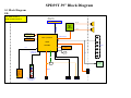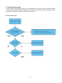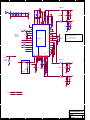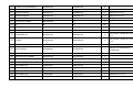
1
FILE NO SERVICE MANUAL TC-L39B6 LED TV TC-L39B6X TC-L39B6P 1 CONTENTS 1. Safety precautions ................................................................................................. 3 2. Alignment instructions and method of software upgrading.....................................5 3. Working principle analysis of the unit ................................................................... 12 4. Specifications.......................................................................................................13 5. Block diagram ......................................................................................................14 6. IC block diagram ..................................................................................................17 7. Wiring diagram ................................................................................................... 24 8. Troubleshooting guide..........................................................................................29 9. Schematic diagram ..............................................................................................33 10. APPENDIX-A: Assembly list APPENDIX-B: Exploded View 11. Disassembly and Assembly Instructions 2 Attention: This service manual is only for service personnel to take reference with. Before servicing please read the following points carefully. Safety precautions 1. Instructions Be sure to switch off the power supply before replacing or welding any components or inserting/plugging in connection wire Anti static measures to be taken (throughout the entire production process!): a) Do not touch here and there by hand at will; b) Be sure to use anti static electric iron; c) It’s a must for the welder to wear anti static gloves. Please refer to the detailed list before replacing components that have special safety requirements. Do not change the specs and type at will. 2. Points for attention in servicing of LED 2.1 Screens are different from one model to another and therefore not interchangeable. Be sure to Use the screen of the original model for replacement. 2.2 The operation voltage of LED screen is high voltage. Be sure to take proper measures in protecting yourself and the machine when testing the system in the course of normal operation or right after the power is switched off. Please do not touch the circuit or the metal part of the module That is in operation mode. Relevant operation is possible only one minute after the power is switched off. 2.3 Do not use any adapter that is not identical with the TV set. Otherwise it will cause fire or damage to the set. 2.4 Never operate the set or do any installation work in bad environment such as wet bathroom, laundry, kitchen, or nearby fire source, heating equipment and devices or exposure to sunlight etc. Otherwise bad effect will result. 2.5 If any foreign substance such as water, liquid, metal slices or other matters happens to fall into the module, be sure to cut the power off immediately and do not move anything on the module lest it should cause fire or electric shock due to contact with the high voltage or short circuit. 2.6 Should there be smoke, abnormal smell or sound from the module, please shut the power off at once. Likewise, if the screen is not working after the power is on or in the course of operation, the power must be cut off immediately and no more operation is allowed under the same condition. 2.7 Do not pull out or plug in the connection wire when the module is in operation or just after the power is off because in this case relatively high voltage still remains in the capacitor of the driving circuit. Please wait at least one minute before the pulling out or plugging in the connection wire. 2.8 When operating or installing LED please don’t subject the LED components to bending, twisting or extrusion, collision lest mishap should result. 2.9 As most of the circuitry in LED TV set is composed of CMOS integrated circuits, it’s necessary to pay attention to anti statics. Before servicing LED TV make sure to take anti static measure and ensure full grounding for all the parts that have to be grounded. 2.10 There are lots of connection wires between parts behind the LED screen. When servicing or moving the set please take care not to touch or scratch them. Once they are damaged the screen would be unable to work and no way to get it repaired. If the connection wires, connections or components fixed by the thermo tropic glue need to disengage when service, please soak the thermo tropic glue into the alcohol and then pull them out in case of damage. 3 2.11 Special care must be taken in transporting or handling it. Exquisite shock vibration may lead to breakage of screen glass or damage to driving circuit. Therefore it must be packed in a strong case before the transportation or handling. 2.12 For the storage make sure to put it in a place where the environment can be controlled so as to prevent the temperature and humidity from exceeding the limits as specified in the manual. For prolonged storage, it is necessary to house it in an anti-moisture bag and put them altogether in one place. The ambient conditions are tabulated as follows: Temperature Humidity Scope for operation 0 ~ + 35 oC Scope for storage -20 ~ + 60oC Scope for operation 20% ~ 80 % Scope for storage 10% ~ 90% 2.13 Display of a fixed picture for a long time may result in appearance of picture residue on the screen, as commonly called “ghost shadow”. The extent of the residual picture varies with the maker of LED screen. This phenomenon doesn’t represent failure. This “ghost shadow” may remain in the picture for a period of time (several minutes). But when operating it please avoid displaying still picture in high brightness for a long time. 3. Points for attention during installation 3.1 The front panel of LED screen is of glass. When installing it please make sure to put it in place. 3.2 For service or installation it’s necessary to use specified screw lest it should damage the screen. 3.3 Be sure to take anti dust measures. Any foreign substance that happens to fall down between the screen and the glass will affect the receiving and viewing effect 3.4 When dismantling or mounting the protective partition plate that is used for anti vibration and insulation please take care to keep it in intactness so as to avoid hidden trouble. 3.5 Be sure to protect the cabinet from damage or scratch during service, dismantling or mounting. 4 2. Alignment instructions (1) Test equipment VG-859 (YPbPr, VGA, HDMI signal generator) FLUKE 54200(TV signal generator) CA310 (white balancer) (2) Power test Connect main board, power board and IR board according the wiring diagram, connect the power and press power key (Remote controller or Keypad) button to turn on the TV. a) Test the pin voltage of P802/power board , the data is shown in table1: Table1 voltage data of P802 For 39” P802 Pin1,2 Pin3,4 Voltage GND 11.4V~12.6V Pin5,6,7 GND Pin8,9 Pin10,11 11.4V~12.6V 4.75V~5.25V For 39” Pin12 On:2.5V~5.25V Off: 0~0.5V Pin13 Normal: 2.0~5V Abnormal :0~0.5V Pin 14 Pin15 On:2.5V~5.25V Off: 0~0.5V Duty 5%~100% 5 Pin16 NC (3) Alignment flow-chart The alignment flow-chart is shown as fig-1 Check if EDID, HDCP KEY, FLASH are written Combined test for general assembly Auto Gamma adjustment Connect to the center signal source and check each Function of TV (station leaking, analog control, etc.) Check the output of speaker. Input AV signal and check the function Input HD signal and check the function of YPbPr Input USB signal and check if the display is normal, check the function (analog control), horizontal/vertical center, etc. Input HDMI signal and check if the display is normal, check the function (analog control), horizontal/vertical center, etc. Checking SPDIF will output the signal on Amplifier. Preset ex-factory Check the accessories and packing Fig-1 adjustment flow-chart 6 (4) Adjustment instruction At any input source then press the “←”, “EXIT” and “OK” (using RC within 1 sec) to enter factory mode During Factory menu, if “EXIT” key is pushed, system will exit factory mode. 4-1. Auto Gamma Adjustment & Check 4-2.1. Set into factory mode then choose Auto Gamma Adjust, 4-2.2. Press "2" "3" "2" "4" in turn within 1sec to enter the item, and push Init will self-generate gray pattern for adjusting. 4-2.3. Following the Cool spec as bellow. Color x y Adjust Tolerance Cool 100IRE 0.2662 50IRE 0.2658 100IRE 0.2667 50IRE 0.2654 ±0.005 (1) Adjust 100IRE First, Decrease G to meet y spec(0.2667). Second, Decrease R to meet x spec(0.2662). (2) Adjust 50IRE First, Decrease G to meet y spec(0.2654). Second, Decrease R to meet x spec(0.2658). Note: Do not adjust the B GAIN on both 100IRE and 50IRE. When match the spec, pressing “Save” then exit the adjustment page. (3) When match the spec, pressing right key in "Save" position then exit the adjustment page. 4-2.4. Exit Factory Mode: After finish Gamma adjust press [EXIT] to exit factory mode. 7 (5) Items of Factory menu When in any source, press the “Left -> Exit -> OK” key of remote control can enter into factory mode. During Factory menu, only “EXIT” key is pushed, system will exit factory mode. Press up and down key can move high light item from Model Change -> Color Temp. Adjust -> Auto Gamma Adjust -> Timer Clear -> Preset Channel -> Full Power -> ADC Calibration -> Shipping reset -> Bypass Gamma -> UART Enable -> I2C -> Boot Loader Upgrade -> V-Com Adjust -> SG Pattern. Push “Enter” key can enter high light item function. (Press left and right can adjust value) Display Model version, Release Date, firmware version and released date on the bottom. 1)Model ID Press up or down key can select high light item function Press enter or right key to enter the item. It's only used for FW engineer. 2)Color Temp. Adjust Press up or down key can select high light item function Press enter or right key to enter the item. It's only used for PQ engineer. 3)Auto Gamma Adjust Press up or down key can select high light item function Press enter or right key to enter the item. It's only used for PQ engineer. 4)Timer Clear Reset the timer which records hours of LED panel burn in This item will have a check dialog “yes or no” to do or not. - Time in factory mode: Time function shall be displayed automatically. Saving the total time of system power on (LED turn on), and count the time automatically. The timer is continuous and saved (per 10 minutes) forever, unless it will be reset by doing “Timer Clear”. 5)Preset channel Load preset channel for production line. 6)Full Power This is for power consumption testing. To measure the maximum power consumption of TV set, we adjust the value of following items to maximum. - Video: Contrast maximum value, Brightness maximum value, Backlight maximum value. - Audio: Volume maximum value, Bass default value, Treble default value. Press enter key to turn on Full Power and OSD stay display until press enter key to recover from Full Power. 8 7)ADC Calibration ADC Calibration function is reserved for calibration by hand (PQ engineer only). 8)Shipping reset Reset all settings of OSD menu to default value. Reset settings: Channel table, Model table (H/V Position, Clock, Phase), Source dependent setting (Contrast, Brightness etc.), Common setting (Volume, Language etc.), Parental Control (Rating, Password etc), Closed Caption. 9)Bypass Gamma For factory test value of gamma. 10)UART Enable Enable to communicate with Auto-Alignment system. 11)I2C Enable to communicate with Eeprom burn-in tool. 12)Boot Loader Upgrade For firmware downgrade used. 13)V-Com Adjust It's reserved for BMS function. 14)SG Pattern Aging is for factory burn in and PTN ID provides each pattern for tester using. (6) Performance check 6-1 TV function Connect RF to the center signal source, enter Channel menu → auto tuning, check if there are channels be skipped, check if the picture and speaker are normal. 6-2 AV terminals Input Video signal, check if the picture and sound are normal. 6-3 YPbPr terminal Input YUV signal (VG859 signal generator), separately input the YUV signals listed in table4 and check if the display and sound are normal at any situation (power on, channel switch and format convert, etc.) Table4 YUV signal format MODE 59.94Hz 720x480i 59.94Hz 720x480P 60Hz 1280x720P 60Hz 1920X1080i 60Hz 1920X1080P FREQ PERIOD SYNC POLARITY PIXEL CLOCK LINE(kHz) FRAME (Hz) LINE (pixel) FIELD (lines) LINE FIELD (MHz) 15.734 1716 Negitive 59.94 525 Negitive 31,469 858 Negitive 59.94 525 Negitive 45 1650 Positive 60 750 Positive 33.75 2200 Positive 60 1125 Positive 67.5 2200 Positive 60 1125 Positive 9 27 27 74.25 74.25 148.5 Display SYNC WIDTH BACK PORCH LINE (pixel) LINE (pixel) LINE (pixel) FRAME FRAME FRAME (lines) (lines) (lines) 1440 124 114 480 3 15 720 62 60 480 6 30 1280 40 220 720 5 20 1920 44 148 1080 5 15 1920 44 148 1080 5 36 6-4 HDMI terminal Input HDMI signal (VG859 signal generator), separately input the signals listed in table6 and check the display and sound (32 KHz, 44.1 KHz, 48 KHz) at any situation (power on, channel switch and format convert, etc.) Table6 HDMI signal format HDMI 1/2/ DVI Timing Table FREQ MODE 640x480 800x600 1024x768 1280x768 (1280cvt) 1280x768 1280x1024 1360x768 1366x768 1920x1080 59.94Hz 1440x480i 59.94Hz 720x480P 60Hz 1280x720P 60Hz 1920X1080i 24Hz 1920x1080P 30Hz 1920x1080P 60Hz 1920X1080P FREQ PERIOD LINE(kHz) LINE (pixel) FRAME(Hz) FIELD(lines) SYNC POLARITY PIXEL CLOCK LINE FIELD (MHz) 25.175 31.47 800 Negitive 59.94 525 Negitive 37.88 1056 Positive 60.32 628 Positive 48.36 1344 Negitive 60 806 Negitive 47.4 1440 Positive 59.99 790 Negitive 47.78 1664 Negitive 59.87 798 Positive 63.98 1688 Positive 60.02 1066 Positive 47.71 1792 Positive 60.02 795 Positive 47.71 1792 Positive 59.79 795 Positive 67.5 2200 Positive 60 1125 Positive 15.73 1716 Negitive 59.94 262.5 Negitive 31.47 858 Negitive 59.94 525 Negitive 45 1650 Positive 60 750 Positive 33.75 2200 Positive 60 562.5 Positive 27 2750 Positive 24 1125 Positive 33.75 2200 Positive 30 1125 Positive 67.5 2200 Positive 60 1125 Positive 10 40 65 68.25 79.5 108 85.5 85.5 148.5 27 27 74.25 74.25 74.25 74.25 148.5 Display SYNC WIDTH BACK PORCH LINE (pixel) LINE (pixel) LINE (pixel) FRAME FRAME FRAME (lines) (lines) (lines) 640 96 48 480 2 33 800 128 88 600 4 23 1024 136 160 768 6 29 1280 32 80 768 7 12 1280 128 192 768 7 20 1280 112 248 1024 3 38 1360 112 256 768 6 18 1366 112 256 768 6 18 1920 44 148 1080 5 36 1440 124 114 480 3 15 720 62 60 480 6 30 1280 40 220 720 5 20 1920 44 148 1080 5 15 1920 44 148 1080 5 36 1920 44 148 1080 5 36 1920 44 148 1080 5 36 6-5 other functions check a) Check the sleep timer, picture/sound mode, OSD, stereo and analog TV Teletext, etc. (7) Firmware update process (1) Plug the USB with the firmware file named upgrade_2013_NA_60.pkg (2) If system detect upgrade_2013_NA_60.pkg, USB upgrade message would appear automatically. (3) Press Up key to select Yes, and then press OK key to start the upgrading. (4) Upgrading is starting, please wait for the progress finish. (5) When the progress completed, please follow the instruction to remove USB and restart Power off then on. 11 3. Working principle analysis of the unit 1. NTSC signals flow: Antenna signal will be send to tuner TDST-H021F, t h e n T u n e r w i l l b e demodulating and output standard video signal TV-CVBS, and sound SIF signal. TV-CVBS will send to the master control IC MT5385 to video decode, de-interlace and scaler, then output LVDS level drive for panel display. The sound IF (SIF) will be fed into MT5385, after demodulating, pre-amplifying, bass adjusting and volume control, the sound signal w i l l b e t r a n s f o r m i n t o d i g i t a l I 2 S s i g n a l and sent to digital amplifier TAS5707. 2. Composite/Component signal flow Composite signal and Component signal will be fed to MT5385 to perform video decode, deinterlace and scaler, then output LVDS drive level for panel display. Audio signal from Composite/Component terminal via matched resistance is fed to MT5385 to bass adjust and volume control, the sound signal will b e t r a n s f o r m i n t o d i g i t a l I 2 S s i g n a l and sent to digital amplifier TAS5707. 3. HDMI signal flow Two HDMI video signals are directly fed to the master control IC MT5385 to digital decode, image scale, then output LVDS drive level for panel display. HDMI audio signal via decoder built-in MT5385 to bass adjust and volume control, the sound signal will b e t r a n s f o r m i n t o d i g i t a l I 2 S s i g n a l and sent to digital amplifier TAS5707. 4. USB signal flow USB signal via USB connector sent to MT5385 and its A/D conversion to YPbPr output for MT5385, then output R/G/B of 24 bit to back end module to Video decode, de-interlace and image scale, then send to LVDS level drive for panel display. Sound signal of USB signal v i a matched resistance a n d sent to MT5385 to bass adjust and volume control, the sound signal will b e t r a n s f o r m i n t o d i g i t a l I 2 S s i g n a l and sent to digital amplifier TAS5707. 5. SPDIF signal flow The master control IC MT5385 will transfer digital sound signal out by format Dobly Digital or PCM. 12 4. Specifications 13 SPD39T 39” Block Diagram 5-1 Block Diagram EE: A70 60Hz Models by MTK MT5835 Platform WXGA :2x10 Full-HD :2x20 Panel out R_out Audio AMP TAS5707 L_out DDR3 1G-1600 H5TQ1G63DFR-PBC Audio I2S output Flash 16MB MX25L12845EMI-10G DTV system IC MTK MT5385 Keypad EEPROM 64KB 24C32 IF +/- Crystal 27MHz CVBS/Y Pb Pr & Audio R/L IR Enable ARC Buffer IR / LED-R Board Y Pb S/PDIF Tuner LG TDSTH021F 5-1 Block Diagram Power board:FSP ANT / CABLE USB Pr L SPE39T 39” Block Diagram R COLOR STREAM HD & COMPOSITE IN & Audio R/L in SPDIF OUT HDMI 1 14 HDMI 2 Power Board: FSP 15 Power Board: DARFON 16 6. IC block diagram 1. MT5385 GENERAL FEATURE LIST Host CPU ARM11 single core 700MHz Floating Point Unit 16K I-Cache and 16K D-Cache for ARM11 core 128K L2 Cache Boot ROM Boot from serial flash, NAND flash Supports security boot JTAG ICE interface Watch Dog timers General Copy Protection Unit Supports CPPM/CPRM Supports AES with 128/192/256 bit key Supports AACS Supports DES/3DES Supports SHA-1/224/256 Supports MD5 Supports CSS Supports RC4 Random number generator MPEG1 Decoder MPEG2 Decoder MPEG MP@ML, MP@HL Supports de-blocking filter Full-HD 30P dual decoder MPEG4 Decoder (option) ASP@L5 Full-HD 30P dual decoder H.264 (MPEG4.10 / AVC) HD Decoder (option) [email protected], [email protected], constrained BP@L3 video standard Full-HD 30P dual decoder VC-1 (SMPTE421M) Decoder (option) MP@HL, AP@L3 WMV9 decoder MP@HL Full-HD 30P dual decoder DivX (XviD) Decoder (option) 17 DIVX3 / DIVX4 / DIVX5 / DIVX6 / DIVX HD Full-HD 30P dual decoder AVS Decoder (option) Jizhun profile @Level 6.2 (supports 4:2:0 format) Full-HD 30P dual decoder RMVB Decoder (option) RealVideo8/9/10 Full-HD 30P dual decoder VP6 Decoder (option) VP8 Decoder (option) Supports 3D side-by-side Full-HD contents Full-HD 30P dual decoder MVC H.264 stereo high profile Full-HD 60fps Still Image decoding JPEG decoder (base-line or progressive), hardware accelerator BMP/PNG/JIF decoder De-mosquito engine For all AV inputs 2D Graphics Supports multiple color modes Point, horizontal/vertical line primitive drawings Rectangle fill and gradient fill functions Bitblt with transparent options Alpha blending and optional pre-multiplied alpha composition Bitblt Stretch Bitblt YCbCr to RGB color space conversion Supports index to direct mode bitblt Image Resizer Supports 16bpp/32bpp direct color format Supports 420/422 video format Supports 420/422/444 JPEG format Arbitrary ratio vertical/horizontal scaling of video, from 1/128X to 128X Simple DMA Supports MMU in OSD mode OSD Plane Three linking list OSDs with multiple color mode and all of them have up-scaler Supports stereo OSD 18 Video Plane Supports video freeze and over scan Flesh tone management Gamma correction Color Transient Improvement (CTI) 2D Peaking Saturation/hue adjustment Brightness and contrast adjustment Black and White level extender Adaptive Luma management Automatic detect video, film and mixed-mode source 3:2/2:2 pull down source detection Supports FHD motion-adaptive de-interlace Supports excellent low angle image processing Brilliant boundary shaping for moving object Advanced non-linear panorama scaling Programmable zoom viewer Progressive scan output Supports alpha blending for OSD on video plane Dithering processing for flat panel display Frame rate conversion Supports FHD panel and VGA dot-to-dot Supports PIP/POP, (dual de-interlace, one HD and one SD) OD (option) Supports 60Hz Full-HD and WXGA panel over drive TCON (option) Flexible timing control with programmable timing Horizontal timing control Vertical timing control Multi-line timing control Multi-frame timing control Supports gate power modulation timing Supports command-based timing Supports POL inversion every 30 seconds Supports 1/2/4/8 frame inversion, 1-line inversion, 2-line inversion, and could up to 255-line dot inversion Local Dimming Block division: up to 800 total blocks, up to 100 horizontal blocks Supports 50K ~ 50M SPI clock rate LVDS 19 Supports 6/8/10-bit one-link, 6/8/10-bit dual-link LVDS transmitter Built-in spread spectrum for EMI performance Programmable panel timing output Mini-LVDS Dual port 8-bit 6 pairs mini-LVDS output CVBS In On-chip 54 MHz 10-bit video ADC Supports PAL (B,G,D,H,M,N,I,Nc), NTSC, NTSC-4.43, SECAM NTSC/PAL supports 3D/2D comb filter Built-in motion-adaptive 3D Noise Reduction VBI data slicer for CC/TT decoding Supports 1 S-Video Supports 2 1-channel CVBS Supports SCART connector VGA In Supports VGA input up to UXGA 162 MHz Supports full VESA standards Component Video In Supports 2 component video inputs Supports 480i / 480p / 576i / 576p / 720p / 1080i / 1080p Audio ADC Supports 3 pair L/R input Audio digital input Supports 1 bit (2 channel) I 2 S audio input HDMI Receiver Two channel HDMI1.4a Maximum data rate can be up to 3.3 GHz Audio return channel EIA/CEA-861B CEC Video bypass ATV bypass CVBS Monitor (any AV or S-video input) TV audio demodulator Supports BTSC / EIA-J / A2 / NICAM / PAL FM / SECAM world-wide formats Standard automatic detection 20 Stereo demodulation, SAP demodulation Mode selection (Main/SAP/Stereo) Audio DAC Supports 2-pair audio DACs DRAM Controller 16-bit DDR2/DDR3 interface Supports DDR2 1066Mhz, DDR3 1333Mhz Supports 512Mb or 1Gb or 2Gb DDR2 and DDR3 DRAM device Supports DDR2-1066/DDR3-1333/DDR3-1600 device Audio DSP Supports AC-3 (Dolby Digital) decoding (ATSC) and E-AC3 (Dolby Digital Plus) decoding (option) MPEG-1 layer I/II decoding Supports WMA / HE-AAC (option) Support Dolby DDCO, and MS10 (option) Dolby Prologic II (option) Audio output: 5.1ch + 2ch (down mix) + 2ch(bypass) Pink noise and white noise generator Equalizer Bass management 3D surround processing with virtual surround Audio and video lip synchronization Supports bass/treble Automatic volume control Supports 5-bit (10-channel) main audio I 2 S output interface, each of these channels is up to 24-bit resolution S/PDIF interface Supports SPDIF in bypass SPDIF out Analog TV IF Demodulator Supports world-wide analog TV standard Accept direct IF and low IF Full digital AGC control and carrier recovery Embedded SAW filter and IF Amplifier. Cost effective TV front-end structure and no more cost on: External analog SAW filters (Video/Audio) External analog IF demodulator External peripheral circuit on CVBS signal data path External SAW filter and IF VGA on tuner 21 Digital TV (ATSC / Open-Cable) Demodulator Compliant with ATSC digital television standard Supports SCTE DVS-031 and ITU J.83 Annex B digital CATV standard Accept direct IF (44 MHz or 43.75 MHz) and low IF (5.38 MHz) NTSC interference rejection capability Meet all ATSC/A74 requirements Excellent adjacent and co-channel rejection capability Dual digital AGC controls for IF and RF, respectively Full-digital frequency offset recovery with wide acquisition range 500KHz for ATSC and 250 kHz for CATV reception EIA/CEA-909 antenna interface, both mode A and mode B are supported Embedded SAW filter and IF Amplifier. Cost effective TV front-end structure and no more cost on: External analog IF demodulator External SAW filter and IF VGA on tuner Peripherals Seven basic serial interfaces: one is for the tuner, three are the masters for general purpose and two of them can be active in standby mode, one is the slave for VGA DDC, the other two extra slave serial interfaces used for HDMI EDID data Five PWMs, two of them can be active in standby mode IR receiver Real-time clock and watchdog controller Built-in 2-link USB2.0/1.1, both of them support external hub with 16 endpoints. Built-in uP for standby mode Supports SDIO interface Supports smart card interface Supports two serial flash or one serial and one NAND flash Supports 2-input low-speed ADC Supports boundary scan (JTAG) IC Outline LQFP Package 216 pins with E-pad 3.3V/1.2V and 1.8V for DDR2 or 1.5V for DDR3 22 2. TI TAS5707 20-W STEREO DIGITAL AUDIO POWER AMPLIFIER WITH EQ AND DRC 23 SPD39T 39-inch Wiring Diagram 7-1 BLOCK 24 7-2 Wiring Connection LG panel Panel side Main board to Panel Main board to Speaker SPD39T SPD39T LVDS cable Main board CN1 Main board CN4 Color Speaker Right 1 NC NC 1 SPK_OUTL+ Red P3 Speaker + 2 NC NC 2 SPK_OUTL- Black P2 Speaker - 3 NC NC 4 NC NC 3 SPK_OUTR- Green P5 Speaker - 5 NC NC 4 SPK_OUTR+ White P4 Speaker + 6 NC NC 7 SELLVDS Yellow Left 28 LVDS_SEL 8 NC NC Main board to IR / Key 9 NC NC SPD39T 10 NC NC IR board CN1 11 GND NC 1 VCC3V3_STB 12 R1AN White 40 TX_AO0N 13 R1AP Black 14 R1BN Color Main board CN3 Red 1 3V3STB 2 IRR White 2 IRR 39 TX_AO0P 3 GND Black 3 GND White 38 TX_AO1N 4 LED_G Orange 4 LEDG 15 R1BP Brown 37 TX_AO1P NC 5 LEDR 16 R1CN White 36 TX_AO2N NC 6 Light_S_C 17 R1CP Red 35 TX_AO2P NC 7 Light_S_D 18 GND Black 15 GND 1 GND Black 8 GND 19 R1CLKN White 34 TX_AOCKN 2 Power Red 9 Power Key 25 20 R1CLKP Orange 33 TX_AOCKP 3 SAR0 Orange 10 SAR0 21 GND Black 16 GND 4 SAR1 Yellow 11 SAR1 22 R1DN White 32 TX_AO3N 23 R1DP Yellow 31 TX_AO3P 24 NC NC 25 NC NC 26 NC NC 27 NC NC 28 R2AN White 12 TX_AE0N 29 R2AP Black 11 TX_AE0P 30 R2BN White 10 TX_AE1N 31 R2BP Brown 9 TX_AE1P 32 R2CN White 8 TX_AE2N 33 R2CP Red 7 TX_AE2P 34 GND Black 17 GND 35 R2CLKN White 6 TX_AECKN 36 R2CLKP Orange 5 TX_AECKP 37 GND Black 18 GND 38 R2DN White 4 TX_AE3N 39 R2DP Yellow 3 TX_AE3P 40 NC NC 41 NC NC 42 NC NC 43 NC NC 26 44 GND Black 25 GND 45 GND Black 26 GND 46 GND Black 27 GND 47 NC NC 48 VCC Red 19 LVDS_PWR 49 VCC Red 20 LVDS_PWR 50 VCC Red 21 LVDS_PWR 51 VCC Red 22 LVDS_PWR 27 Main board to Power board: 28 8. Trouble shooting 1. Fault clearance Before calling your dealer or service center for assistance, check the matters below once again. (1) Make sure you have connected LED TV to your equipment as described in the section “ CONNECTING LED TV”. (2) Check cable connection. Verify that all external equipment and power cord are properly connected. (3) Verify that all power is switched on. (4) If LED TV still does not produce an image, re-start the external equipment. (5) If the image still does not appear, unplug LED TV from the external equipment and check the external equipment. The problem may be with your graphics controller rather than with LED TV. (When you reconnect LED TV, remember to turn the external equipment and TV off before you power up LED TV. Power the equipment back on in order of LED TV and external equipment.) (6) If the problem still exists, check the following chart. Problem NO POWER Try these Solutions Plug this LED TV into the AC outlet. Press POWER button on side control or on Remote Control to turn on LED TV. Check POWER Indicator. If this indicator blank, this TV has getting trouble. Check the batteries. Remote Make sure nothing is between the Remote Receiver and the Remote Control. Control does Make sure you are not too far from LED TV when using Remote Control. not work Maximum operating range is 5m. Is direct sunlight or strong artificial light shining on LED TV‘s Infrared Remote Receiver? Eliminate the light by closing curtains, pointing the light in a different direction, etc. Check the connection between the external equipment and LED TV. No image When turning LED TV on, it takes within 7 seconds (ATV mode) to display the image. Check the system that you select is corresponding with the external equipment or the video equipment. Make sure the temperature is not out of the Operating Temperature (0°C ~ 35°C). Turn off power, then turn on again, re-start LED TV. Check Audio cable connection from Audio input source. No sound Adjust the Sound System. Press VOLUME (+) button. Press MUTE button. There are tiny Dark or bright points of light (red, green, or blue) may appear on the screen. This is a characteristic of the LED panel, not a malfunction of the LED TV. black points LED panel is produced with very high accuracy technology. There is 99.99% or and/or bright more dot pixel, but there is also 0.01 % or less of dot pixel lack or dot pixel that point on the TV is constantly lighted. This is not defect. Regarding LED panel characteristic, it may occur picture remain (look like a mirror) when the screen is changed if it displays same screen for a long time. Changing the picture or turn-off the power supply may recover. Stripe pattern (more, interference stripes) may show up on the screen depends on the reflected picture. Abnormal Adjust the value of color. color of image Select different color system. 29 2. Troubleshooting guide The flow chart shown below will help you to troubleshoot your Televison set with it doesn’t display normally. Each procedure offers a simple way to check for system errors. Before starting, ensure that there is a signal in and that the Televison is turned on. 2-1 Power LED no light 30 2-2 Has audio but no video out 2-3 Has video but no audio out step 1 31 2-4 Has video but no audio out step 2 32 9.SCHEMATIC DIAGRAM --ELECTRON 5 4 3 2 1 PCB1 MT5385 Power Tree (12V) AMP_VCC For AMP D D FB20 +12V U14 DMG4435SSS Q15 SOT-23B LMBT3904LT1G FB22 5V_SW SOP8 LVDS_PWR FB21 (LVDS_PWR_EN) For Panel (NC) (Option) (1.2V) +5VSB FB1 U1 SOP8-T5 AX3518ESA FB2 VCCK POWER_EN VTV-L32616 REV:1 (About 3.2A) FW1 (3.3V) FB3 FIRMWARE U2 AX1007E33A FB4 3V3SB SOT-223 R39 FW L32616 C E1 AVDD33_XTAL_STB R41 AVDD33_REG_STB C SOT-23GDS Q1 DMP2160U SOT-23B Q2 LMBT3904LT1G (5V) FB5 5V_SW FB17 +5V_USB0 +5V_USB0 => About 500mA VCCK For USB (3.295V) EMIcover-50x68m m /NC FB6 U3 AX1117ADA (1.2V) (3.295V) DVDD3V3 R8 AVDD3V3 FB7 TO-252 U5 AX1007E12A FB10 AVDD1V2 SOT-223 R9 R21 (NC) (Option) R30 AVDD12_RGB R31 AVDD12_DEMOD R28 AVDD1V2_HDMI1 AVDD33_MEMPLL R29 AVDD33_DEMOD R24 AVDD3V3_HDMI1 R39 AVDD33_PLLGP R15 ADAC_3V3 B B R20 AVDD33_DAC FB11 AVDD33_AADC (1.5V) FB8 U4 AX1117ADA FB9 DDRV For DDR3 Power TO-252 (3.3V) FB19 U13 AX1117AD33A +3.3V_TUNER FB18 +3.3V_TUNER_1 (About 330mA) TO-252 For Tuner A A Title COMPAL OPTOELECTRONICS CO., LTD SCHEMATIC,M/B VTV-L32616 Size Docum ent Num ber Date: Tues day, Novem ber 27, 2012 Rev 1 XXXXXX 5 4 3 2 1 Sheet 1 of 11 5 4 3 2 1 Buck Converter 4A (1.2V) 11 POWER_EN +5VSB +3.3V_Standby power (3V3SB) VCCK FB1 CLS UPB201212T-121Y-N 5A U1 8 D R2 10/1% C3 + LX 5 C4 VCC EN 0.1uF/10V/0402 CLS UPB201212T-121Y-N 5A REF C6 15pF/50V/0402 100mA U2 AX1007E33A +5VSB C1 0.1uF/10V/0402 R3 332K/1% R4 634K/1% 3 FB3 CLS UPB201212T-121Y-N 5A VIN D C7 CLS UPB201212T-121Y-N 5A GND/ADJ C5 RB 2 4 VOUT VOUT 2 RA 1 22uF/6.3V/0805 100K/1% C8 0.1uF/10V/0402 3V3SB FB4 RA 4 6 3 9 R6 FB FB2 7 C2 1 ELNA SE100uF/16V VIN PGND GND THEM_PAD R1 10/1% L1 SCD0403T-2R2M 2.2uH/3.8A AX3518ESA R5 249/1%/NC + C10 C9 + C11 C12 0.1uF/10V/0402 10uF/16V/0805 0.1uF/10V/0402 4.7uF/6.3V C13 RB 0.1uF/10V/0402 ELNA SE100uF/16V/NC R7 0 10uF/6.3V/NC Vout=0.8Vx (1+RA/RB) +5V_Nomal power (5V_SW) 5V_SW +5VSB U16 1 2 3 4 C C14 FB5 S1 S2 S3 G R10 D4 D3 D2 D1 8 7 6 5 +3.3V_Digital power (DVDD3V3) CLS UPB201212T-121Y-N 5A C16 + C15 DMG4435SSS/NC C17 0.1uF/10V/0402 4.7uF/16V/0805 400mA U3 AX1117ADA 5V_SW 0.1uF/10V/0402/NC 47K/1% Q1 S 3 FB6 CLS UPB201212T-121Y-N 5A D VIN G VOUT C24 RA 1 Q2 E POWER_EN : High => 1.2V_SW POWER ON Low => 1.2V_SW POWER OFF 100K/1% 2 ADJ / GND DMP2160U C B R12 DVDD3V3 C20 + 10uF/16V/0805 LMBT3904LT1G AVDD3V3 ELNA SE100uF/16V VCCK Strapping mode :Must default Pull low. C (3.295V) + C21 0.1uF/10V/0402 C23 RB 1uF/6.3V/0402 0/1%/0805 R9 0/1%/0805/NC R11 110/1% C18 3/1 ,3/2 Modify R8 C19 C22 10uF/10V/0805 0.1uF/10V/0402 ELNA SE100uF/16V/NC R13 180/1% 10uF/6.3V/NC VO=1.25Vx(1+RB/RA)+IadjxR2 B B +1.5V_DDR3 power (DDRV) (1.5V) +3.3V_Analog power (ADAC_3V3) +1.2V_Analog power (AVDD1V2) (1.2V) 100mA DDRV U4 AX1117ADA 5V_SW (3.295V) U5 AX1007E12A AVDD3V3 AVDD1V2 2/20 Modify FB9 3 FB8 CLS UPB201212T-121Y-N 5A VIN VOUT FB10 2 AVDD3V3 R15 ADJ / GND RA 1 ADAC_3V3 CLS UPB201212T-121Y-N 5A 3 FB7 CLS UPB201212T-121Y-N 5A VIN 0/1%/0805 VOUT VOUT 2 4 CLS UPB201212T-121Y-N 5A GND/ADJ R14 110/1% 1 C30 C27 10uF/16V/0805 + C25 C26 0.1uF/10V/0402 C35 RB R16 22/1% C28 10uF/10V/0805 0.1uF/10V/0402 + C29 C31 1/31 Delete 1uF/16V ELNA SE100uF/16V/NC + C32 0.1uF/10V/0402 10uF/16V/0805 C33 4.7uF/6.3V C34 0.1uF/10V/0402 10uF/6.3V/NC VO=1.25Vx(1+RB/RA)+IadjxRB A A Title COMPAL OPTOELECTRONICS CO., LTD SCHEMATIC,M/B VTV-L32616 Size Document Number Date: Tuesday, November 27, 2012 Rev 1 XXXXXX 5 4 3 2 Sheet 1 2 of 11 5 4 3 AOSDATA0_1 2 AVDD3V3 C36 R23 AMP_MCK_1 R99 AVDD3V3 C VCCK VCCK AVDD33_MEMPLL 1_CKE 1_A10 1_BA1 1_A4 1_A1 1_A6 1_A8 1_A11 1_A12 1_RAS# 1_CAS# DDRV 1_WE# 1_A0 1_A13 1_A9 1_RST# 1_A7 1_A2 1_A5 1_A3 1_BA2 1_BA0 1_CS# 1_ODT RDQ4 22pF/50V/0402 10nF/50V/0402 VCCK AVDD3V3 MT5385 AVDD1V2 (Pin216) AVDD1V2_HDMI1 R28 0/0402 EPAD_GND (Pin51) AVDD33_DEMOD R29 0/0402 AVDD1V2 AVDD3V3 FAT_INFAT_IN+ (Pin195) AVDD12_DEMOD R31 0/0402 CVBS0P C57 0.1uF/10V/0402 LVDS out 1uF/6.3V/0402/NC AVDD3V3 AVDD3V3 TX_AE0P TX_AE0N TX_AE1P TX_AE1N TX_AE2P TX_AE2N TX_AECKP TX_AECKN TX_AE3P TX_AE3N TX_AE4P TX_AE4N AVDD3V3 (Pin38) (Pin106) AVDD3V3 AVDD12_RGB PR0P PB0P COM0 Y0P SOY0 C60 C59 0.1uF/10V/0402 DRAM RDQ0 RDQ1 RDQ2 RDQ3 RDQ4 RDQ5 RDQ6 RDQ7 RDQ8 RDQ9 RDQ10 RDQ11 RDQ12 RDQ13 RDQ14 RDQ15 RDQS1 RDQS1# RDQS0 RDQS0# RDQM1 RDQM0 1_A0 1_A1 1_A2 1_A3 1_A4 1_A5 1_A6 1_A7 1_A8 1_A9 1_A10 1_A11 1_A12 1_A13 RCLK0 RCLK0# 1_WE# 1_ODT 1_CAS# 1_RAS# 1_CKE 1_CS# 1_RST# 1_BA0 1_BA1 1_BA2 R33 AVDD33_XTAL_STB (Pin55) 0/0402 + C62 10uF/6.3V/NC R34 AVDD33_REG_STB (Pin23) C65 0.1uF/10V/0402 0/0402 3V3SB Power Key AMP_MUTE OPCTRL0 (Pin8) C66 0.1uF/10V/0402 (OPCTRL1) R35 C64 0.1uF/10V/0402 3V3SB VCCK OPWRSB OIRI U0TX U0RX 0/0402/NC LED_R 3V3SB HDMI_HPD0 HDMI_SDA0 HDMI_SCL0 HDMI_HPD1 HDMI_SDA1 HDMI_SCL1 HDMI_CEC HDMI HDMI_CEC RX0_2 RX0_2B RX0_1 RX0_1B RX0_0 RX0_0B RX0_C RX0_CB RX1_2 RX1_2B RX1_1 RX1_1B RX1_0 RX1_0B RX1_C RX1_CB GPIO BL_ON/OFF LVDS_PWR_EN AC Drop_DET 217 AMP_MUTE LED_G LED_R SYS EE_WP PANEL SLET LIGHT_S_C LIGHT_S_D BL_ON/OFF 11 LVDS_PWR_EN 11 AC Drop_DET 11 AMP_MUTE LED_G LED_R 4,5 11 11 SYS EE_WP PANEL SLET LIGHT_S_C LIGHT_S_D 4 7 11 11 (OPCTRL1) HDMI_CEC RX0_2 RX0_2B RX0_1 RX0_1B RX0_0 RX0_0B RX0_C RX0_CB RX1_2 RX1_2B RX1_1 RX1_1B RX1_0 RX1_0B RX1_C RX1_CB 9 9 9 9 9 9 9 9 9 9 9 9 9 9 9 9 9 System IO OPWRSB ORESET# OXTALI OXTALO OIRI U0TX U0RX SDA_SYSTEM SCL_SYSTEM OPWRSB 11 ORESET# 4 OXTALI 4 OXTALO 4 OIRI 11 U0TX 4,6 U0RX 4,6 SDA_SYSTEM 4,5,7 SCL_SYSTEM 4,5,7 HDMI_SDA0 HDMI_SCL0 HDMI_HPD0 HDMI_SDA1 HDMI_SCL1 HDMI_HPD1 HDMI_SDA0 HDMI_SCL0 HDMI_HPD0 HDMI_SDA1 HDMI_SCL1 HDMI_HPD1 C61 0.1uF/10V/0402 0.1uF/10V/0402/NC Standby Power 3V3SB C63 4.7uF/6.3V 6 (Pin121) C58 AVDD33_PLLGP AVDD33_REG_STB AVDD10_LDO ORESET# ADIN0 SAR0 CVBS0P AVDD3V3 C56 0.1uF/10V/0402 VCCK 10 10 C55 0.1uF/10V/0402 (Pin43) AVDD12_DEMOD CVBS0P 0/0402/NC FAT_INFAT_IN+ Demod IF C53 0.1uF/10V/0402 C54 0.1uF/10V/0402 R32 6 6 6 6 6 AVDD3V3 (Pin36) AVDD12_RGB R30 0/0402 OXTALO OXTALI AVDD33_DEMOD FAT_INFAT_IN+ SOY0 Y0P COM0 PB0P PR0P CVBS AVDD1V2 54 53 52 51 50 49 48 47 46 45 44 43 42 41 40 39 38 37 36 35 34 33 32 31 30 29 28 27 26 25 24 23 22 21 20 19 18 17 16 15 14 13 12 11 10 9 8 7 6 5 4 3 2 1 D SOY0 Y0P COM0 PB0P PR0P 0.1uF/10V/0402 C52 0.1uF/10V/0402 AVDD3V3_HDMI1 RX0_CB RX0_C RX0_0B RX0_0 RX0_1B RX0_1 RX0_2B RX0_2 RX1_CB RX1_C RX1_0B RX1_0 RX1_1B RX1_1 RX1_2B RX1_2 AVDD1V2_HDMI1 USB_DM0 USB_DP0 YPbPr 0 C50 For improve Audio AADC performance VCCK 24K/1%/0402 AVDD3V3 RDQ6 RDQ2 DDRV RDQ0 RDQ11 RDQ9 RDQ13 DDRV RDQ15 RDQM1 VCCK RVREF RDQS0 RDQS0# DDRV RCLK0# RCLK0 RDQM0 RDQS1 RDQS1# DDRV RDQ12 RDQ14 RDQ10 RDQ8 RDQ1 DDRV RDQ3 RDQ7 RDQ5 VCCK REXT R37 C68 0.1uF/10V/0402 C49 4.7uF/6.3V C51 0.1uF/10V/0402 163 164 165 166 167 168 169 170 171 172 173 174 175 176 177 178 179 180 181 182 183 184 185 186 187 188 189 190 191 192 193 194 195 196 197 198 199 200 201 202 203 204 205 206 207 208 209 210 211 212 213 214 215 216 R38 1K/1%/0402 AVDD33_AADC FB11 SBK160808T-800Y 0.4A (Pin199) AVDD3V3_HDMI1 R24 0/0402 0.1uF/10V/0402 1uF/6.3V/0402 AVDD33_XTAL_STB YPbPr_L_In0 YPbPr_R_In0 AVDD33_AADC AVDD33_DAC R26 0/0402/NC R25 0/0402/NC IFAGC AOSDATA0_1 AMP_BCK_1 AMP_LRCLK_1 AMP_MCK_1 SPDIF_OUT C48 XTALO XTALI AVSS33_DEMOD AVDD33_DEMOD ADCINN_DEMOD ADCINP_DEMOD AVSS12_DEMOD AVDD12_DEMOD CVBS0P SY SC AVDD33_CVBS AVSS33_CVBS AVDD33_PLLGP VCCK VDACX_OUT AVDD33_VDAC AVSS12_RGB AVDD12_RGB PRP PBP COM YP SOY RP COM GP SOG BP HSYNC VSYNC AVDD33_VGA_STB AVDD10_LDO ORESET_ ADIN0_SRV ADIN1_SRV VCCK OPWRSB OIRI U0TX U0RX VGA_SDA VGA_SCL OPCTRL2 OPCTRL1 OPCTRL0 VCC3IO_STB HDMI_0_HPD HDMI_0_SDA HDMI_0_SCL HDMI_1_HPD HDMI_1_SDA HDMI_1_SCL HDMI_CEC C67 0.1uF/10V/0402 RVREF C40 10nF/50V/0402 10uF/10V (Pin57) VMID_AADC B R36 1K/1%/0402 C44 0.1uF/10V/0402 ADAC_3V3 DVDD3V3 AE4P AE4N AE3P AE3N AECKP AECKN AE2P AE2N AE1P AE1N AE0P AE0N AVDD33_LVDSA AO4P AO4N AO3P AO3N AOCKP AOCKN AO2P AO2N AO1P AO1N AO0P AO0N VCCK VCCK AVDD33_MEMPLL RCKE RA10 RBA1 RA4 RA1 RA6 RA8 RA11 RA12 RRAS_ RCAS_ VCC2IO RWE_ RA0 RA13 RA9 RRESET_ RA7 RA2 RA5 RA3 RBA2 RBA0 RCS_ RODT RDQ4 DDRV C41 C43 C47 BL_ON/OFF SCL_SYSTEM SDA_SYSTEM PSRC_WR SYS EE_WP PANEL SLET PDD2 PDD1 PDD0 BL_DIMMING VCCK DVDD3V3 SDA_TUNER SCL_TUNER TX_AO4P TX_AO4N TX_AO3P TX_AO3N TX_AOCKP TX_AOCKN TX_AO2P TX_AO2N TX_AO1P TX_AO1N TX_AO0P TX_AO0N 109 110 111 112 113 114 115 116 117 118 119 120 121 122 123 124 125 126 127 128 129 130 131 132 133 134 135 136 137 138 139 140 141 142 143 144 145 146 147 148 149 150 151 152 153 154 155 156 157 158 159 160 161 162 + 22pF/50V/0402 C45 RDQ6 RDQ2 VCC2IO RDQ0 RDQ11 RDQ9 RDQ13 VCC2IO RDQ15 RDQM1 VCCK RVREF RDQS0 RDQS0_ VCC2IO RCLK0_ RCLK0 RDQM0 RDQS1 RDQS1_ VCC2IO RDQ12 RDQ14 RDQ10 RDQ8 RDQ1 VCC2IO RDQ3 RDQ7 RDQ5 VCCK REXT AVDD33_USB USB_DM USB_DP VCCK AVDD33_HDMI_1_RX HDMI_0_RX_CB HDMI_0_RX_C HDMI_0_RX_0B HDMI_0_RX_0 HDMI_0_RX_1B HDMI_0_RX_1 HDMI_0_RX_2B HDMI_0_RX_2 HDMI_1_RX_CB HDMI_1_RX_C HDMI_1_RX_0B HDMI_1_RX_0 HDMI_1_RX_1B HDMI_1_RX_1 HDMI_1_RX_2B HDMI_1_RX_2 AVDD12_HDMI_1_RX TX_AE4P TX_AE4N TX_AE3P TX_AE3N TX_AECKP TX_AECKN TX_AE2P TX_AE2N TX_AE1P TX_AE1N TX_AE0P TX_AE0N AMP_MCK (Pin65) AVDD33_DAC R20 0/0402 (Pin136) AVDD33_MEMPLL R21 0/0402 AVDD12_LVDSA GPIO2 GPIO1 GPIO0 VCC3IO POWE_ PAALE PACLE POCE0_ POOE_ PARB_ PDD7 PDD6 PDD5 PDD4 PDD3 PDD2 PDD1 PDD0 POCE1_ GPIO3 VCCK FSRC_WR DEMOD_TSDATA0 DEMOD_TSSYNC DEMOD_TSVAL DEMOD_TSCLK SCL_SYSTEM SDA_SYSTEM VCC3IO DEMOD_RST RF_AGC IF_AGC AOSDATA0 AOBCK AOLRCK AOMCLK ASPDIFO0 VCCK AR1_ADAC AR0_ADAC AL1_ADAC AL0_ADAC AVDD33_DAC AVSS33_DAC AIN2_L_AADC AIN2_R_AADC AIN1_L_AADC AIN0_L_AADC AIN1_R_AADC AIN0_R_AADC AVDD33_AADC VMID_AADC AVDD33_XTAL_STB U6 ADAC_3V3 AVDD3V3 22pF/50V/0402 100/0402/NC UART_Det ARC_SELECT PACLE POCE0# POOE# CP_C PDD7 PDD6 PDD5 PDD4 PSRC_WR AMP_LRCLK 108 107 106 105 104 103 102 101 100 99 98 97 96 95 94 93 92 91 90 89 88 87 86 85 84 83 82 81 80 79 78 77 76 75 74 73 72 71 70 69 68 67 66 65 64 63 62 61 60 59 58 57 56 55 LVDS_PWR_EN E-Fuse (Pin108) R27 4.7K/1%/0402 R22 33/0402 R104 100/0402 AVDD1V2 100/0402 R19 33/0402 C39 C46 0.1uF/10V/0402 D 22pF/50V/0402 C38 C42 0.1uF/10V/0402 AVDD3V3 Analog Normal Power AMP_BCK R18 33/0402 AMP_LRCLK_1 AC Drop_DET AVDD1V2 AMP_BCK_1 Add R99 reserve for LED flash when AC-ON LED_G C37 0.1uF/10V/0402 1 AOSDATA0 R17 33/0402 9 9 9 9 9 9 RDQ0 RDQ1 RDQ2 RDQ3 RDQ4 RDQ5 RDQ6 RDQ7 RDQ8 RDQ9 RDQ10 RDQ11 RDQ12 RDQ13 RDQ14 RDQ15 RDQS1 RDQS1# RDQS0 RDQS0# RDQM1 RDQM0 1_A0 1_A1 1_A2 1_A3 1_A4 1_A5 1_A6 1_A7 1_A8 1_A9 1_A10 1_A11 1_A12 1_A13 RCLK0 RCLK0# 1_WE# 1_ODT 1_CAS# 1_RAS# 1_CKE 1_CS# 1_RST# 1_BA0 1_BA1 1_BA2 TX_AO0P TX_AO0N TX_AO1P TX_AO1N TX_AO2P TX_AO2N TX_AOCKP TX_AOCKN TX_AO3P TX_AO3N TX_AO4P TX_AO4N 8 8 8 8 8 8 8 8 8 8 8 8 8 8 8 8 8 8 8 8 8 8 8 8 8 8 8 8 8 8 8 8 8 8 8 8 8 8 8 8 8 8 8 8 8 8 8 8 BL_DIMMING TX_AE0P TX_AE0N TX_AE1P TX_AE1N TX_AE2P TX_AE2N TX_AECKP TX_AECKN TX_AE3P TX_AE3N TX_AE4P TX_AE4N 7 7 7 7 7 7 7 7 7 7 7 7 TX_AO0P TX_AO0N TX_AO1P TX_AO1N TX_AO2P TX_AO2N TX_AOCKP TX_AOCKN TX_AO3P TX_AO3N TX_AO4P TX_AO4N 7 7 7 7 7 7 7 7 7 7 7 7 BL_DIMMING C 11 USB USB_DM0 USB_DP0 USB_DM0 USB_DP0 7 7 PACLE 4 POCE0# POOE# PDD7 PDD6 PDD5 4 4 4 4 7 NAND/Nor Flash PACLE POCE0# POOE# PDD7 PDD6 PDD5 UART_Det ARC_SELECT CP_C PDD1 PDD0 B UART_Det 4 ARC_SELECT 9 CP_C 6 TP15 TP16 Tuner and Demod TS I/F IFAGC IFAGC 10 SPDIF Out DDRV SPDIF_OUT AVDD3V3 R39 (Pin41) SPK AVDD33_PLLGP AMP_MCK AMP_LRCLK AMP_BCK AOSDATA0 0/0402 C69 10uF/10V/0805 C70 C71 1uF/6.3V/0402 0.1uF/10V/0402 C72 C73 0.1uF/10V/0402 0.1uF/10V/0402 C74 C75 0.1uF/10V/0402 C76 0.1uF/10V/0402 1uF/6.3V/0402 C77 10nF/50V/0402 Core Power ( Close to Mainchip ) DVDD3V3 VCCK (Pin79) A C78 (Pin104) C79 0.1uF/10V/0402 1uF/6.3V/0402 C80 0.1uF/10V/0402 (Pin18) + C81 PXE100uF/16V/NC C82 4.7uF/6.3V SAR0 Power Key AMP_MCK 5 AMP_LRCLK 5 AMP_BCK 5 AOSDATA0 5 (Pin70) C84 1uF/6.3V/0402 0.1uF/10V/0402 (Pin87) C85 0.1uF/10V/0402 (Pin134) (Pin135) C87 0.1uF/10V/0402 (Pin135) C88 0.1uF/10V/0402 (Pin173) C89 SAR0 Power Key 11 11 SDA_TUNER SCL_TUNER ADIN0 LIGHT_S_C LIGHT_S_D Add R73 & R102 if change ACD pin to OPCTRL0 (Pin40) C83 6,9 (Pin193) C90 0.1uF/10V/0402 0.1uF/10V/0402 (Pin198) C91 AUDIO ADC IN Key Near to IC 3.3V IO Power ( Close to Mainchip) SPDIF_OUT R73 R40 R41 R42 YPbPr_R_In0 YPbPr_L_In0 YPbPr_R_In0 YPbPr_L_In0 6 6 SDA_TUNER 10 SCL_TUNER 10 0/0402 0/0402/NC 10/0402 10/0402 LIGHT_S_C SCL_SYSTEM SDA_SYSTEM SAR1 11 A 3V3SB C92 0.1uF/10V/0402 PDD2 0.1uF/10V/0402 R67 10/1%/0402 BL_ERR R102 47K/1%/0402/NC OPCTRL0 R103 100/0402/NC BL_ERR 11 AC Drop_DET Title COMPAL OPTOELECTRONICS CO., LTD SCHEMATIC,M/B VTV-L32616 Size Docum ent Num ber Date: Tues day, Novem ber 27, 2012 Rev 1 XXXXXX 5 4 3 2 1 Sheet 3 of 11 5 4 3 2 1 DVDD3V3 SPI FLASH DVDD3V3 R43 4.7K/1%/0402 R45 4.7K/1%/0402 U17 U7 1 2 3 4 5 6 7 8 DVDD3V3 D R44 4.7K/1%/0402 3 3 POCE0# PDD7 POCE0# PDD7 NC/SIO3 VCC NC PO2 PO1 PO0 CS# SO/SIO1/PO7 16 15 14 13 12 11 10 9 SCLK SI/SIO0 PO6 PO5 PO4 PO3 GND WP#/SIO2 POOE# PDD6 POOE# PDD6 3 3 1 2 3 4 POCE0# PDD7 WP# CS# DOUT WP#/VPP VSS VCC HOLD# CLK DIN 8 7 6 5 DVDD3V3 R140 10K/0402/NC POOE# PDD6 D MX25L6406EM2I-12G/NC WP# MX25L12845EM1-10G SOP16 C94 0.1uF/10V/0402 C93 0.1uF/10V/0402 RESET Circuit 3V3SB U8 3V3SB VCC /RESET 27MHz CRYSTAL 1 3 OXTALI 2 R81 0/0402 OXTALO ORESET# 3 R47 C95 10nF/50V/0402 100K/1%/0402/NC 1 2 (Low reset) OXTALO ORESET# J1 GND AX6901ERA Y1 27MHz/20pF/30ppm/S/2P OXTALI R46 1K/1%/0402 POR 3 3 HDR_1X2_H2031_P2_SW/NC C C C96 C97 27pF/50V/0402 27pF/50V/0402 STRAPPING (Default : Serial boot) UART0 3V3SB 3V3SB 3V3SB (OPCTRL1) R87 4.7K/1%/0402 R51 4.7K/1%/0402/NC R52 4.7K/1%/0402 3,5 AMP_MUTE UART_Det 100/1%/0402 100/1%/0402 R82 100/1%/0402 For ESD 1 8/31 Reserve UART_Detect R53 R54 2 B 1 U0RX U0TX 2 3 U0RX U0TX AMP_MUTE R48 10K/1% R50 10K/1% PACLE 3 DVDD3V3 1 2 3 4 VD2 SESD0402P1BN-0450-090/NC 3,6 3,6 VD1 SESD0402P1BN-0450-090/NC J2 R49 10K/1%/NC PACLE JWT A2001WV2-4P (Place on TOP_Layer) A2001WV2-4P-6T2-F2 B SYS EE_WP SYSTEM EEPROM DVDD3V3 DVDD3V3 DVDD3V3 1 2 3 R58 4.7K/1%/0402/NC JWT A2001WV2-3P A2001WV2-3P-6T2-F2 U5 depend on customer request. If yes,need one more GPIO to control pin 7 of U5 A 3 I2C ADDRESS "A0" R55 4.7K/1%/0402 3,5,7 SCL_SYSTEM 3,5,7 SDA_SYSTEM SYS EE_WP 64K bit R57 R56 4.7K/1%/0402 4.7K/1%/0402 J3 SCL_SYSTEM SDA_SYSTEM DVDD3V3 U9 SYS EE_WP SCL_SYSTEM SDA_SYSTEM 8 7 6 5 VCC WP SCL SDA E0 E1 E2 GND 1 2 3 4 BR24T64FJ-WGE2 A Title COMPAL OPTOELECTRONICS CO., LTD SCHEMATIC,M/B VTV-L32616 Size Document Number Date: Tuesday, November 27, 2012 Rev 1 XXXXXX 5 4 3 2 Sheet 1 4 of 11 5 4 3 2 1 L2 SMTDR75-150K 15uH/2A SPK_OUTL+ SDA 1K/1% DVDD C131 0.1uF/50V C132 1uF/50V/0805 33nF/50V C114 C115 0.1uF/50V 1uF/50V/0805 C117 C116 2 3 1 OUT_A PVDD_A PVDD_A OUT_D PVDD_D PVDD_D BST_D 11 C119 C120 10nF/50V/NC 0.1uF/50V/NC 48 47 46 AMP_VCC 45 AD mode : (1) Mount :C131 ,C141 ;C159 ,C163 ;C134 (2) Mount :C121 ;C158 ;C134 BD mode : (1) Mount :C131 ,C141 ;C159 ,C163 44 43 C125 33nF/50V 42 C122 33nF/50V C123 C124 0.1uF/50V/NC 1uF/50V/0805/NC AMP_VCC 41 40 C 39 38 37 L4 SMTDR75-150K 15uH/2A AMP_VCC SPK_OUTR+ 11 SPK_OUTR- 11 R76 3.3/1206/NC C133 0.47uF/50V/0805/NC C137 D 36 35 34 33 GVDD_OUT VREG 10uF/10V/0805 C118 1uF/50V/0805 R75 AMP_RST 33nF/50V 100K/1% C130 R74 0.1uF/50V AMP_PDN 32 R79 10K/0402/NC 31 26 AMP_PDN PGND_CD 0.1uF/50V AMP_MUTE Low : Enable High : Disable PGND_CD SCL 1uF/50V/0805 24 OUT_C TH_PD 23 AMP_SCL PVDD_C SDIN AGND AMP_SDA SCLK GND 22 30 21 10/0402 29 10/0402 R70 PVDD_C 51 R69 LRCLK DVSS 20 DVDD 10/0402 28 R68 BST_B BST_C 25 R71 4.7K/1% 3,4 AMP_MUTE 4 TAS5707 /PDN STEST 19 C110 10nF/50V/NC 0.1uF/50V/NC R63 3.3/1206/NC 0.68uF/25V 0.1uF/50V VR_DIG 27 AOSDATA0 BST_A 22.1K/1% R62 PVDD_B /RESET AMP_BCK 3 C113 2.2uF/16V/0805/NC DVSSO C121 18 3 PVDD_B C109 SPK_OUTL- 1uF/50V/0805 10K/1% 1uF/50V/0805 C 7 OUT_B U10 17 AMP_LRCLK 6 PGND_AB OSC_RES R66 AMP_PDN 3 SSTIMER PGND_AB MCLK 18.2K/1% 16 AMP_PDN High : Enable Low : Disable 5 470 /FAULT C104 0.68uF/25V L3 SMTDR75-150K 15uH/2A C127 R65 C103 0.47uF/50V/0805/NC C126 15 10/0402 C129 R64 C128 AMP_MCK AVDD AMP_VCC GVDD_OUT 14 3 PLL_FLTP PLL_FLTM 13 VR_ANA DVDD 4.7nF/50V 11 10 12 4.7nF/50V C112 NC C111 OC_ADJ 0.1uF/50V R61 C106 10uF/10V/0805 8 C105 0.1uF/50V 9 C102 10uF/10V/0805 11 R59 3.3/1206/NC AVSS C101 0.1uF/50V 470 C100 10uF/10V/0805 R60 C99 0.1uF/50V C107 C98 D C108 FB12 PBY160808T-300Y 3A 47nF/16V 47nF/16V DVDD DVDD3V3 C134 0.68uF/25V C135 C136 10nF/50V/NC 0.1uF/50V/NC C139 C138 0.1uF/10V/0402 Delay 100ms B B L5 SMTDR75-150K 15uH/2A R77 3.3/1206/NC C140 0.68uF/25V 3,4,7 SDA_SYSTEM 3,4,7 SCL_SYSTEM SDA_SYSTEM SCL_SYSTEM R78 10/0402 AMP_SDA R80 10/0402 AMP_SCL C141 C142 10nF/50V/NC 0.1uF/50V/NC A A Title COMPAL OPTOELECTRONICS CO., LTD SCHEMATIC,M/B VTV-L32616 Size Document Number Date: Tuesday, December 11, 2012 Rev 1 XXXXXX 5 4 3 2 Sheet 1 5 of 11 5 4 Component input 3 2 A/V input Close to IC OPT SPDIF out Close to CONN. IO1 1x5_CX_COMPO-AUDIO_SW_H8.5 3 CVBS0P C143 CVBS0P 3 3 SOY0 Y0P Y G 100/1%/0402 47nF/16V/0402 SOY0 R84 10/1%/0402 C145 Y-V_IN SPDIF_OUT 3,9 2/1 Modify GND GND IN VCC 1 5V_SW 2 D C170 100pF/25V/0402/NC FB16 PBY160808T-300Y 3A Y-V_IN 1.5nF/50V/0402 C147 Y0P T1 S1 R123 47/1%/0402 IO4 6 7 R83 D 1 R85 Pb G R86 100/1%/0402 T2 S2 Pb_HD GND 18/1%/0402 3 C171 0.1uF/10V/0402 YUQIU/OPTICAL_V 10nF/50V/0402 13 C148 10pF/50V/0402 R88 C149 R90 0/0402 100/1%/0402 C 3 PB0P PB0P L G SW R G R92 C150 Pb_HD 100/1%/0402 10nF/50V/0402 Pr_HD T4 S4 YBRL_IN0 B5 T5 S5 YBRR_IN0 PF 10nF/50V/0402 R91 T3 S3 R100 100/0402 R205 Modify form last version D_TX 0/NC YBRL_IN0 5V_SW R127 R101 100/0402 1 D_RX FB15 R94 10pF/50V/0402 1 R96 C153 PBY160808T-300Y 3A C224 100/1%/0402 10pF/50V/0402 C 3 Q5 U0RX 10pF/50V/NC 3,4 R121 18/1%/0402 C155 CP_C LMBT3904L B 10pF/50V/NC Pr_HD 10nF/50V/0402 2 47K/1%/0402 C371 2 PR0P 1 2 R95 3 R144 D_RX 56/1%/0402 PR0P 2 10K/0402 18/1%/0402 C152 C COM0 Pr G E COM0 PF 1 3 12 56/1%/0402 R89 R98 1 2 56/1%/0402 4.7K/0402 CP_C = "Low" UART communication workable. Close to CONN. B YBRL_IN0 C151 10uF/6.3V Close to IC 30K/1%/0402 R93 YPbPr_L_In0 Q4 LMBT3906L FB14 YPbPr_L_In0 3 E D_TX C U0TX 10pF/50V/NC C315 10pF/50V/NC R214 1 2 10K/0402 3 A Pb_HD VD9 2 2 VD8 YBRL_IN0 YBRR_IN0 VD10 1 Pr_HD 1 Y-V_IN VD11 A VD12 2 YPbPr_R_In0 1 YPbPr_R_In0 2 R97 1 30K/1%/0402 2 10uF/6.3V 1 C154 3,4 B 1 C369 2 2 1 PBY160808T-300Y 3A YBRR_IN0 B CP_C = "High" UART communication disable. Title COMPAL OPTOELECTRONICS CO., LTD SCHEMATIC,M/B VTV-L32616 SESD0402P1BN-0450-090/NC SESD0402P1BN-0450-090/NC SESD0402P1BN-0450-090/NC SESD0402P1BN-0450-090/NC SESD0402P1BN-0450-090/NC 5 4 3 Size Document Number Date: Tuesday, November 27, 2012 Rev 1 XXXXXX 2 Sheet 1 6 of 11 5 4 3 2 1 WXGA A2006WV0-2X10P FHD A2006WV0-2X20P (PIN21~PIN40) (PIN1~PIN40) CN1 A2006WR0-2X20P D 32 CN5 P-TWO 30P 1.00MM/NC 30 29 28 27 26 25 24 23 22 21 20 19 18 17 16 15 14 13 12 11 10 9 8 7 6 5 4 3 2 1 TX_AOCKP TX_AOCKN TX_AO2P TX_AO2N TX_AO1P TX_AO1N TX_AO0P TX_AO0N LVDS_SEL C 3 TX_AO1P 3 TX_AO2P 3 TX_AOCKP 3 TX_AO3P 3 TX_AO4P TX_AO0P 39 TX_AO1P 37 TX_AO2P 35 TX_AOCKP 33 TX_AO3P 31 TX_AO4P 29 27 25 23 LVDS_PWR 21 19 17 15 31 LVDS_PWR LVDS_PWR LVDS_PWR LVDS_PWR TX_AO0P 3 TX_AE0P 3 TX_AE1P 3 TX_AE2P 3 TX_AECKP 3 TX_AE3P 3 3 TX_AE4P PANEL SLET PANEL_SDA_P 13 TX_AE0P 11 TX_AE1P 9 TX_AE2P 7 TX_AECKP 5 TX_AE3P 3 TX_AE4P 1 39 40 37 38 35 36 33 34 31 32 29 30 27 28 25 26 23 24 21 22 19 20 17 18 15 16 13 14 11 12 9 10 7 8 5 6 3 4 1 PANEL SLET R130 100/0402/NC S TX_AO3P TX_AO3N 3 R131 10/0402 2 D 40 TX_AO0N 38 TX_AO1N 36 TX_AO2N 34 TX_AOCKN 32 TX_AO3N 30 TX_AO4N 28 LVDS_SEL TX_AO0N 3 TX_AO1N 3 TX_AO2N 3 TX_AOCKN 3 TX_AO3N 3 TX_AO4N 3 LVDS_PWR R128 4.7K/NC 26 R129 1.8K/NC 24 LVDS_PWR 22 LVDS_PWR 20 C172 C173 0.1uF/50V 18 ELNA SE100uF/16V 16 14 PANEL_SCL_P 12 TX_AE0N 10 TX_AE1N 8 TX_AE2N 6 TX_AECKN 4 TX_AE3N 2 TX_AE4N C TX_AE0N 3 TX_AE1N 3 TX_AE2N 3 TX_AECKN 3 TX_AE3N 3 TX_AE4N 3 LVDS_SEL EQUAL LENGTH and DIFFERENTIAL IMPEDANCE 90ohm +5V_USB0 6 B SDA_SYSTEM B Q6 2N7002/NC L77 CL-2M2012-181JT 1 2 3 4 SDA_SYSTEM SCL_SYSTEM 3 3 3,4,5 SCL_SYSTEM 3,4,5 1 USB_DM0 USB_DP0 SDA_SYSTEM PANEL_I2C_EN VD18 VD19 SCL_SYSTEM S + C174 0.1uF/10V/0402 10uF/16V/0805 R132 10/0402 PANEL_SCL_P R133 10/0402 PDD5 PDD5 3 G 2 PANEL_I2C_EN 2 C175 D 5 1 USB_DM0 USB_DP0 PANEL_SDA_P G IO6 USB_RA_YQ D USB SESD0402P1BN-0450-090/NC SESD0402P1BN-0450-090/NC Q7 2N7002/NC PANEL_I2C_EN R134 10K/0402 USB Power Control FB17 PBY160808T-121Y 2.5A A F1 1206L075THYR +5V_USB0 A 5V_SW USB POWER Title COMPAL OPTOELECTRONICS CO., LTD SCHEMATIC,M/B VTV-L32616 Size Document Number Date: Tuesday, November 27, 2012 Rev 1 XXXXXX 5 4 3 2 Sheet 1 7 of 11 5 4 DDR3#1 3 1Gb DDR3-1600 for H5TQ1G63DFR-PBC U11 H5TQ1G63DFR-PBC_MTK 2 1 RDQ0 RDQ1 RDQ2 RDQ3 RDQ4 RDQ5 RDQ6 RDQ7 RDQ8 RDQ9 RDQ10 RDQ11 RDQ12 RDQ13 RDQ14 RDQ15 Damping and Termination for CLK Close to Mainchip Close to DRAM D C RDQ0 RDQ1 RDQ2 RDQ3 RDQ4 RDQ5 RDQ6 RDQ7 RDQ8 RDQ9 RDQ10 RDQ11 RDQ12 RDQ13 RDQ14 RDQ15 E3 F7 F2 F8 H3 H8 G2 H7 D7 C3 C8 C2 A7 A2 B8 A3 RDQS1 RDQS1# RDQS0 RDQS0# RDQM1 RDQM0 C7 B7 F3 G3 D3 E7 T2 B_RST# L8 ZQ1 R141 240/0402 UDQS UDQS# LDQS LDQS# UDM LDM RESET# ZQ DDRV A1 A8 C1 C9 D2 E9 F1 H2 H9 B2 D9 G7 K2 K8 N1 N9 R9 R1 B DDRV R145 1K/1%/0402 DQ0 DQ1 DQ2 DQ3 DQ4 DQ5 DQ6 DQ7 DQ8 DQ9 DQ10 DQ11 DQ12 DQ13 DQ14 DQ15 C176 0.1uF A0 A1 A2 A3 A4 A5 A6 A7 A8 A9 A10/AP A11 A12/BC# A13 NC_0 NC_1 NC_2 NC_3 NC_4 NC_6 BA0 BA1 BA2 CK CK# CS# CAS# ODT RAS# WE# CKE VDDQ_0 VDDQ_1 VDDQ_2 VDDQ_3 VDDQ_4 VDDQ_5 VDDQ_6 VDDQ_7 VDDQ_8 VSSQ_0 VSSQ_1 VSSQ_2 VSSQ_3 VSSQ_4 VSSQ_5 VSSQ_6 VSSQ_7 VSSQ_8 VDD_0 VDD_1 VDD_2 VDD_3 VDD_4 VDD_5 VDD_6 VDD_8 VDD_7 VSS_0 VSS_1 VSS_2 VSS_3 VSS_4 VSS_5 VSS_6 VSS_7 VSS_8 VSS_9 VSS_10 VSS_11 N3 P7 P3 N2 P8 P2 R8 R2 T8 R3 L7 R7 N7 T3 B_A0 B_A1 B_A2 B_A3 B_A4 B_A5 B_A6 B_A7 B_A8 B_A9 B_A10 B_A11 B_A12 B_A13 RCLK0 R135 100/0402 RCLK0# RP1 1_WE# 1_CAS# 1_RAS# 1_A12 B_BA0 B_BA1 B_BA2 RCLK0 RCLK0# B_CS# B_CAS# B_ODT B_RAS# B_WE# B_CKE 1_ODT 1_CS# 1_BA0 1_BA2 1 3 5 7 1 3 5 7 1_A3 1_A5 1_A2 1_A7 1 3 5 7 1_A4 1_BA1 1_A10 1_CKE 1 3 5 7 1_A11 1_A8 1_A6 1_A1 1 3 5 7 1_A0 1_A1 1_A2 1_A3 1_A4 1_A5 1_A6 1_A7 1_A8 1_A9 1_A10 1_A11 1_A12 1_A13 100R/0804 2 B_WE# 4 B_CAS# 6 B_RAS# 8 B_A12 100/0402B_ODT 100/0402B_CS# 100/0402B_BA0 100/0402B_BA2 R136 R137 R138 R139 RP2 1_RST# 1_A9 1_A13 1_A0 B1 B9 D1 D8 E2 E8 F9 G1 G9 A9 B3 E1 G8 J2 J8 M1 M9 P1 P9 T1 T9 3 3 3 3 3 3 3 3 3 3 3 3 3 3 3 3 RDQS1 RDQS1# RDQS0 RDQS0# RDQM1 RDQM0 3 3 3 3 3 3 D Damping for DDR ADDR/CMD J1 J9 L1 L9 M7 T7 M2 N8 M3 J7 K7 L2 K3 K1 J3 L3 K9 RDQS1 RDQS1# RDQS0 RDQS0# RDQM1 RDQM0 RDQ0 RDQ1 RDQ2 RDQ3 RDQ4 RDQ5 RDQ6 RDQ7 RDQ8 RDQ9 RDQ10 RDQ11 RDQ12 RDQ13 RDQ14 RDQ15 100R/0804 2 B_RST# 4 B_A9 6 B_A13 8 B_A0 RP3 100R/0804 2 B_A3 4 B_A5 6 B_A2 8 B_A7 RP4 100R/0804 2 B_A4 4 B_BA1 6 B_A10 8 B_CKE RP5 RCLK0 RCLK0# 1_WE# 1_ODT 1_CAS# 1_RAS# 1_CKE 1_CS# 1_RST# 1_BA0 1_BA1 1_BA2 1_A0 1_A1 1_A2 1_A3 1_A4 1_A5 1_A6 1_A7 1_A8 1_A9 1_A10 1_A11 1_A12 1_A13 3 3 3 3 3 3 3 3 3 3 3 3 3 3 RCLK0 RCLK0# 1_WE# 1_ODT 1_CAS# 1_RAS# 1_CKE 1_CS# 1_RST# 3 3 3 3 3 3 3 3 3 1_BA0 1_BA1 1_BA2 3 3 3 C 100R/0804 2 B_A11 4 B_A8 6 B_A6 8 B_A1 B DDRV C177 0.1uF/10V/0402 R146 1K/1%/0402 DDRV H1 RVREF1 R147 1K/1%/0402 C178 0.1uF/10V/0402 VREFDQ VREFCA M8 RVREF2 C179 0.1uF/10V/0402 R148 1K/1%/0402 C180 C181 C182 C183 0.1uF/10V/0402 0.1uF/10V/0402 0.1uF/10V/0402 0.1uF/10V/0402 A A C184 C185 C186 0.1uF/10V/0402 0.1uF/10V/0402 10uF/16V/0805 Title COMPAL OPTOELECTRONICS CO., LTD SCHEMATIC,M/B VTV-L32616 Size Document Number Rev 1 XXXXXX Date: 5 4 3 2 Tuesday, November 27, 2012 Sheet 1 8 of 11 5 4 3 CEC R149 HDMI port 1 SESD0402P1BN-0450-090/NC 2 1 VD21 R150 47K/1%/0402 R151 47K/1%/0402 100/1%/0402 100/1%/0402 L82 QTC24CG900U RX1_2 RX1_2B CEC 1 2 3 4 5 6 7 8 9 10 11 12 13 14 15 16 17 18 19 L83 QTC24CG900U RX1_1 RX1_1B L84 QTC24CG900U RX1_0 RX1_0B L85 QTC24CG900U RX1_C RX1_CB TP2 R152 R153 cab_p HDMI_SCL HDMI_SDA B C B Q9 E 47K/1%/0402 C R157 100K/1%/0402 Q8 E R159 LMBT3904LT1G LMBT3904LT1G 20 21 22 SESD0402P1BN-0450-090/NC 1 VD25 2 5V_SW SESD0402P1BN-0450-090/NC 1 VD24 2 C HDMI_HPD1 SESD0402P1BN-0450-090/NC 1 VD23 2 R156 909/1%/0402 SESD0402P1BN-0450-090/NC 1 VD26 2 HDMI1-5V R154 75/1%/0402 R155 47K/1%/0402 3 IO7 HDMI_PLUGPWR1 HDMI_SCL1 HDMI_SDA1 HDMI_CEC 1 100/1%/0402 For ESD Test D HDMI_CEC 2 RX0_2 RX0_2B RX0_1 RX0_1B RX0_0 RX0_0B RX0_C RX0_CB TMDSD2+ DSHLD0 TMDSD2TMDSD1+ DSHLD1 TMDSD1TMDSD0+ DSHLD2 TMDSD0TMDSC+ CSHLD0 TMDSCCEC NC SCL SDA DDC_GND VCC5 HPD RX1_2 RX1_2B RX1_1 RX1_1B RX1_0 RX1_0B RX1_C RX1_CB RX0_2 RX0_2B RX0_1 RX0_1B RX0_0 RX0_0B RX0_C RX0_CB 3 3 3 3 3 3 3 3 RX1_2 RX1_2B RX1_1 RX1_1B RX1_0 RX1_0B RX1_C RX1_CB 3 3 3 3 3 3 3 3 HDMI_SDA0 HDMI_SCL0 HDMI_HPD0 SHLD0 SHLD1 SHLD2 HDMI_SCL1 HDMI_SDA1 HDMI_HPD1 FREEPOT/HDMI_SMD_V D HDMI_SDA0 HDMI_SCL0 HDMI_HPD0 3 3 3 HDMI_SCL1 HDMI_SDA1 HDMI_HPD1 3 3 3 5V_SW C HDMI_PLUGPWR1 D1 BAT54C/NC 1 HDMI_PLUGPWR1 DVDD3V3 3 DVDD3V3 2 R158 HDMI1-5V R209 10K 0/0402 U25 3 ARC_SELECT 3,6 SPDIF_OUT 1 2 3 OE VCC A GND Y 5 C86 4 R206 1 180 2 HDMI_ARC 1uF/6.3V/0402 SN74LVC1G125DCKR C144 0.1uF/10V/0402 HDMI port 0 HDMI_PLUGPWR0 R160 47K/1%/0402 R161 47K/1%/0402 RX0_2 RX0_2B CEC RX0_1 RX0_1B RX0_0 RX0_0B RX0_C RX0_CB HDMI_ARC HDMI_SCL0 HDMI_SDA0 R162 R163 R211 L78 QTC24CG900U 1 2 3 4 5 6 7 8 9 10 11 12 13 14 15 16 17 18 19 L79 QTC24CG900U L80 QTC24CG900U L81 QTC24CG900U 0/0402 100/1%/0402 100/1%/0402 E E Q11 Q10 LMBT3904LT1G LMBT3904LT1G 20 21 22 SESD0402P1BN-0450-090/NC 1 VD41 2 B 47K/1%/0402 R167 100K/1%/0402 C C R169 A B SESD0402P1BN-0450-090/NC 1 VD40 2 HDMI_HPD0 5V_SW SESD0402P1BN-0450-090/NC 1 VD39 2 R166 909/1%/0402 SESD0402P1BN-0450-090/NC 1 VD38 2 HDMI0-5V R164 75/1%/0402 R165 47K/1%/0402 R208 100K IO8 SESD0402P1BN-0450-090/NC 2 1 VD36 B R207 82 TMDSD2+ DSHLD0 TMDSD2TMDSD1+ DSHLD1 TMDSD1TMDSD0+ DSHLD2 TMDSD0TMDSC+ CSHLD0 TMDSCCEC NC SCL SDA DDC_GND VCC5 HPD B SHLD0 SHLD1 SHLD2 FREEPOT/HDMI_SMD_V 5V_SW HDMI_PLUGPWR0 D2 A BAT54C/NC 1 HDMI_PLUGPWR0 3 2 R168 HDMI0-5V Title 0/0402 COMPAL OPTOELECTRONICS CO., LTD SCHEMATIC,M/B VTV-L32616 Size Document Number Rev 1 XXXXXX Date: 5 4 3 2 Tuesday, November 27, 2012 Sheet 1 9 of 11 5 4 3 +3.3V_TUNER_1 2 1 +3.3V_TUNER FB18 +3.3V_TUNER Depend on tuner SPEC. PBY160808T-300Y 3A 0.1uF/10V/0402 330pF/50V/0402 10uF/10V/0805 NC NC SDA SCL +B1 [3.3V] NC NC NC IF AGC DIF+ DIF- C188 C189 R170 R171 TUNER_CLK TUNER_DATA 1 2 3 4 5 6 7 8 9 10 11 TUNER_DATA TUNER_CLK close to tuner TU_AGC DIF1_OUT2 DIF1_OUT1 R175 4.7K/1%/0402 4.7K/1%/0402 R173 R174 C190 47pF/50V/0402 1 GND GND GND GND TDST-H020F D SCL_TUNER 100/1%/0402 100/1%/0402 SCL_TUNER 3 C191 47pF/50V/0402 Near to Tuner IFAGC_1 10K/1%/0402 SDA_TUNER C192 47nF/16V/0402 2 12 13 14 15 C187 TDST-H020F D U12 SDA_TUNER 3 Close to TUNER Tuner I2C C C194 C C193 68pF/50V/0402/NC 47pF/50V/0402 C195 DIF1_OUT2 1uF/6.3V/0402 L6 CLS UPB160808T-121Y-N L7 0 R177 100/1%/0402 R178 0/0402 FAT_IN- FAT_IN- 3 FAT_IN+ 3 R179 200/1%/0402 C196 DIF1_OUT1 L9 1uF/6.3V/0402 0 L8 CLS UPB160808T-121Y-N C198 R180 100/1%/0402 R181 0/0402 FAT_IN+ C197 68pF/50V/0402/NC FOR TUNER (3.3V) 47pF/50V/0402 B Near to Tuner Near to mainchip (330mA) 5V_SW 3 FB19 CLS UPB201212T-121Y-N 5A VIN VOUT 2 ADJ / GND R182 249/1%/NC 1 C199 IFAGC_1 R183 IFAGC IFAGC 3 10uF/16V/0805 + B +3.3V_TUNER U13 AX1117AD33A C200 + C201 0.1uF/10V/0402 10K/0402 C204 C205 10uF/6.3V/NC R184 0 C202 C203 10uF/10V/0805 0.1uF/10V/0402 ELNA SE100uF/16V/NC 47nF/16V/0402 Close to mainchip A A Title COMPAL OPTOELECTRONICS CO., LTD SCHEMATIC,M/B VTV-L32616 Size Document Number Rev 1 XXXXXX Date: 5 4 3 2 Tuesday, November 27, 2012 Sheet 1 10 of 11 5 4 AMP_VCC R217 R186 4.7K/0402 C206 22uF/16V/1206 C 3 BL_ERR BL_ERR +12V Q14 DRC2114E/NC 10K (12V PANEL) 10nF/25V/0402 10uF/10V/0805 (5V PANEL) POWER_EN 0/0402 AC Drop_DET1 BKLT_EN BL_DIMMING_C BL_ERR B R187 100pF/25V/0402 10K POWER_EN E 2 POWER_EN +5VSB 1 2 3 4 5 6 7 8 9 10 11 12 13 14 15 16 C227 C207 +5VSB C208 1 CN2 C226,C227 for EMI solution C226 10nF/25V/0402 100 3 AC Drop_DET 2 R72 0/0402/NC D LVDS_PWR +12V U14 FB20 CLS UPB201209T-300Y-N 6A 5V_SW 1 2 3 4 panel_power FB22 CLS UPB201209T-300Y-N 6A/NC C209 C210 R188 47K/1% 10uF/16V/0805 S1 S2 S3 G 8 7 6 5 D4 D3 D2 D1 FB21 CLS UPB201209T-300Y-N 6A TP19 Placement on TOP_Layer R189 1K/1206 DMG4435SSS JWT A2001WR2-16P C211 C212 1nF/25V/0402 1nF/25V/0402 POWER INTERFACE 1uF/50V/0805/NC C R185 22K/0402/NC D 3 R186 NC if change ACD DTC pin 3 LVDS_PWR_EN For EMI 47K/1%/0402 B R190 High => PANEL POWER ON Low => PANEL POWER OFF R191 C213 C214 3.3K/1%/0402 Q15 LMBT3904LT1G E DVDD3V3 10uF/10V/0805 100pF/25V/0402 R203 10K Q16 2/17 Modify R197 100/1%/0402 3 BL_DIMMING BL_DIMMING_C CN3 JWT A2001WR2-11P 1 2 3 4 5 6 7 8 9 10 11 R195 R196 3V3SB OIRI 47/1%/0402 0/0402 R253 R228 R227 C215 C216 VD54 SESD0402P1BN-0450-090 100pF/25V/0402 VD53 C225 SESD0402P1BN-0450-090 1nF/25V/0402/NC C218 1nF/25V/0402 C217 High => Backlight Enable Low => Backlight Diable VD52 SESD0402P1BN-0450-090 100pF/25V/0402 C221 Option :For SRF32T used, R142 from 100/1% change 1K/1% VD51 SESD0402P1BN-0450-090 Option :For SRF32T used, mount C178,C223 R199 10K/1%/0402 1nF/25V/0402 C220 3 BL_ON/OFF BKLT_EN R200 R201 4.7K/1%/0402 4.7K/1%/0402 For EMI VD50 SESD0402P1BN-0450-090 B 0/0402 3 3 3 100pF/25V/0402 Place closer to U1 R198 Power Key SAR0 SAR1 10/20 ESD protaction For EMI BL_ON/OFF 1K 10K 10K 2/17 Modify: Delete C240 ,C241 1nF/25V/0402 C219 C0402/NC 3 LED_G 3 LED_R 3 LIGHT_S_C 3 LIGHT_S_D 3 B 1nF/25V/0402 LMBT3904LT1G C R210 10K 1nF/25V/0402 R194 47K/1%/0402 R202 10K FRONT PANEL CONNECTOR C222 Low => POWER ON High => POWER OFF 4 3 2 1 C B OPWRSB E 3 SPK_OUTL+ SPK_OUTLSPK_OUTRSPK_OUTR+ POWER_EN R193 4.7K/1%/0402 3V3SB C223 5 5 5 5 R192 4.7K/1%/0402 3V3SB CN4 JWT A2001WR2-4P 2mm C Strapping mode :Must default Pull low. 3V3SB SPK +5VSB For EMI A A Title COMPAL OPTOELECTRONICS CO., LTD SCHEMATIC,M/B VTV-L32616 Size Document Number Date: Tuesday, December 11, 2012 Rev 1 XXXXXX 5 4 3 2 Sheet 1 11 of 11 SCHEMATIC DIAGRAM3 32:(5 5 4 3 2 1 B+ CCM1 NC CC-12DP7.5-R RM10 10F R1206 RM2 604KF R0603 3 CM2 105/50V C0805 RM6 4.7KF R1206 ! 1 11 10 RM15 10KF R1206 QM2 7 3 P1825ATF CM9 221/1KV CC-P5+7.5 RM8 75F R1206 CM13 475/25V C0805 ! 2 12V1 LTV-817 5VS_OVP RA2 3.6MF R0603 2 CX1 474/275V CX-18X16-R 6 RM28 100F R0805 CA1 102/50V C0805 RA6 300KF R0805 CA2 104/50V C0805 VCC NDFPO GND FPO IN1 RA10 4 NC R0805 4 2 3 DM8 NC SOT23 CM12 NC C0805 RM22 2.4KF R0805 2 RA12 NC R0805 1 1 12V1 CM11 474/50V C0805 DM11 BAW56 SOT23 60V RM18 43KF R0805 CM17 NC C0805 CA4 102/50V C0805 3 RM26 NC R0805 CA3 822/50V C0805 4 1 3 2 RM36 100F R1206 RM29 1KF R0805 UM4 LTV-817 DIP4 CM15 102/50V C0805 C 2 RM31 1KF R1206 1 ! CA6 NC C0805 5 2 ! CA5 NC C0805 3 1 1 CD IN1M101 SOT236 1 3 ACD_NL RM21 2.4KF R0805 ZDM4 CDZ55B6V2S D0805 UM3 AS431BZTR-E1 TO92-A RM19 11.3KF R0805 RM27 220K R0805 12V_OVP ZDM3 CDZ55B9V1S D0805 ZDA1 CDZ55B6V2S D0805 1 BY6 BF10 BF10 UA2 LTV-817 DIP4 UA1 3 QA3 NC SOT23 RM32 10KF R1206 1 2 RA11 NC R0805 RA1 5.1MF R0603 RX3 590K R1206 RA13 NC R0805 ACD_NH B 5VS ZDM2 CDZ55B15S D0805 1 RX2 590K R1206 CY5 101/250V CY-12DP10 CM16 NC C0805 VCC RM20 3KF R1206 4 DIP4 5VS VCC RA9 5.1KF R0805 L2 NC L6DP3 ! ! 12VA UM2 VDD ! RX1 590K R1206 CEM10 100uF/25V CE-6.3D-P2.5 12V1 3 4 + CM10 NC C0805 CM-9X23.5-P15+20 473/630V CFM1 3 3 2 CEM6 100uF/25V CE-6.3D-P2.5 LM3 1.1uH L7DP6 RM7 680F R0805 CM6 101/50V C0805 + TM1 EFD-3835 T-EEX3835-2 RM23 470F R1206 CY4 NC CY-12DP10 1 12VCC RM17 NC R1206 2 LF2 JUMP L12X12 RM16 NC R1206 DM5 SR540 D20 2 ! C + CEM3 1500U/16V CE-10X20 TO220RB CM7 224/50V C0805 CM4 474/50V C0805 LM1 1.1uH L7DP6 12V1 9 CCM3 NC CC-5DP5 9 8 RV Reg VGL COM 12 13 NC 14 NC OC 6 16 15 VB 5 4 Css GND VGH FB 3 CM3 333/50V C0805 2 ! CY3 NC CY-12DP10 ! VS 17 18 NC NC Vsen CM1 104/50V C0805 DM4 SR540 D20 8 1 1 RM5 95.3KF R0805 3 CCM4 10P/3KV CC-P5+7.5 CM5 102/50V C0805 D RM33 NC R1206 1 4 ! L1 NC L6DP3 VCC_Main CCM2 10P/3KV CC-P5+7.5 RM34 NC R1206 2 2 DM1 UF1007 D12.5 DM7 SF53G D17.5 5 RM14 91F R1206 + CEM7 82uF/100V CE-10X20 11 DM3 CD4148WSN D0805 12V_OVP CEM1 NC + CE-5D-P2.5 10 QM1 P1825ATF TO220RB 1 RM12 10KF R1206 RM13 10F R1206 Vsen ! CY2 681/250V CY-12DP10 CY1 681/250V CY-12DP10 LF1 10mH L23.5X23.5 RM30 1MF R0603 ZDM1 CDZ55B15S RM9 D0805 10F R1206 ! 2 ! RM4 1MF R0603 1 TVS1 NC D17.5 BR1 ! + CEP1 330UF/220V CE-16X51-RO 1 ! 3 UM1 SSC9522S SO18-360 B Vcc 1 BD1 GSIB480 DB-3SR-1 2 4 RM39 604KF R0603 2 B+ 2 RM38 604KF R0603 2 BY5 Jumper BF10 CM8 224/50V C0805 60V 12 2 RM11 91F R1206 1 RM3 604KF R0603 RC EMI CIRCUIT 7 D DM6 SF53G D17.5 ! DM2 CD4148WSN D0805 2 B+ RM1 604KF R0603 BY4 BF15 BF15 ! CY7 471/250V CY-12DP10 ! TR1 1OHM/5A TR10DP5-R B+ RS6 100F R1206 BR1 ! CCM5 NC CC-12DP7.5-R RS9 820K R0603 RS32 82K/2WS R1W CCS2 222/1KV CY-10.5DP7.5 ! ! L RS10 820K R0603 N 2 RS27 820K R0603 P801 AW 0721-6-PSF-1 AC-CCT2302 ZDS3 NC ZD7.5 1 2 VCC QS8 PMBT2907A SOT23 5VS 2 2 CS19 104/50V C0805 1 RS28 820K R0603 3 RS25 10KF R0805 1 2 3 1 RS24 680F R0805 RS26 10KF R0805 RS38 390F R1206 RS36 5.1KF R0805 RS39 390F R1206 RS40 390F R1206 RS41 NC R1206 4 ZDS4 NC ZD7.5 RS11 715KF R0805 1 3 2 US4 LTV-817 DIP4 QS3 PMBT3904 SOT23 CS13 105/50V C0805 RS37 5.1KF R0805 DRAIN BR DRAIN GND FB NC VCC 8 7 6 VDD RS3 4.7F R1206 + CES2 22uF/50V CE-6.3D-P2.5 CS8 105/50V C0805 B + CES1 22uF/50V CE-6.3D-P2.5 ZDS1 1N5251B ZD7.5 5VS 5V1 GNDA VDD RS23 16KF R0805 12Va 12Va GNDP RS16 6.8KF R0805 ! 2 RS35 1KF R0805 2 CS14 104/50V C0805 1 1 3 PMBS3906 DS6 BAV70 SOT23 RS15 2.4KF R0805 CS12 104/50V C0805 3 2 CS9 102/50V C0805 2 QS1 PMBT3904 SOT23 RS20 2.4KF R0805 RS19 1KF R0805 US2 LTV-817 DIP4 ZDS11 1N5251B ZD7.5 CS15 105/50V C0805 1 1 5VS_OVP 1 1 2 SOT23 3 B 4 DS3 CD4148WSN D0805 QS2 RS14 NC R0805 Vsen FB RS30 3.6MF R0603 RS17 13KF R0805 FB ZDS2 NC D0805 2 P802 CON16 HD-16-P2R GNDA RS21 1KF R0805 1 CS18 104/50V C0805 CS6 NC C0805 9 RS22 24KF R0805 2 RS7 NC R1206 1 PWR_ON 3 + 2 DS4 CD4148WSN D0805 5 5VS CES4 100uF/25V CE-6.3D-P2.5 + 3 DS2 PR1007G D12.5 US1 A6069H DIP8 RS12 4.7M R0805 1 ! 4 OCP LS1 1.1uH L7DP6 CS11 NC C0805 GNDP GNDP 12Vcc 12Vcc 5Vcc CS10 105/50V C0805 5Vcc 3 3 5V1 CES3 1500uF/16V CE-10X20 6 RS1 5.1/1WS R1W VCC 2 QS4 PMBT2907A SOT23 VCC_Main CCS3 101/1KV CC-5DP5 RDS1 0.82/2WS R1W 2 B 5 DS1 PR1007G D12.5 RS13 820K R0603 CS3 102/50V C0805 DS5 SR540 D20 1 3 CS2 102/50V C0805 RS5 100F R1206 TS1 1.3mH T-EE22-1 BS1 BF10 BF10 PWON ACD 1 US3 AS431BZTR-E1 TO92-A BLON RS29 NC R0805 RS18 12.4KF R0805 DIM BL_ERR 1 2 3 12VA 4 5 R505 0 R1206 6 7 8 12VCC ZD503 NC D0805 9 10 PWR_ON 2 t 5VS 1 ! F1 T4AH/250V FUSE5X20-HOLD 4 3 BY3 Jumper BF10 AC DETECT CIRCUIT 2 1 VZ1 NC VZ14DP7.5-R 2 RY1 R2W NC 11 12 ACD 13 14 R504 22F R1206 ACD_NH R503 NC R1206 15 16 ACD_NL R506 0 R1206 BLON 2 3 RS31 3.6MF R0603 BL_ERR RS33 5.6MF R0805 3 1 1 RS34 715KF R0805 QS9 RK7002 SOT23 BY2 Jumper BF15 2 1 ZDS5 CDZ55B27S D0805 2 CS16 101/50V C0805 A ZD504 NC D0805 BY1 Jumper BF10 R507 0 R1206 A DIM 2 CY6 471/250V CY-12DP10 1 ZD505 NC D0805 NC = No Component 2.2mm eyelet 1.6mm eyelet 補補 DARFON PCB: FR1-CTI600 Basic: 3.5mm, Reinforced: 7.5mm 5 2012/12/05 Prepared by 4 3 2 REV. 達達達達達達達達達達 CUSTOMER MODEL: SPD39T CUSTOMER PART NO: PK DARFON Model Name: B178-C01 for PP D Reviewed by Tony Ku Hughes Lai Approved by Peter Wang 1 5 4 3 2 1 D D LL1 DR10 L11.5DP6 DL2 SR3150 D17.5 L2+ 60V BL_ERR 12V1 DL3 NC D0805 RL51 NC R0805 3 QL7 NC SOT23 1 1 CL15 NC C0805 RL19 47F R0805 12V1 RL27 205K R1206 1 RL10 CL2 105/50V C0805 1 QL11 P0920AD 3 TO252 RL20 10KF R0805 RL1 10F R1206 SC VIN RL21 470 R0805 CL9 471/50V C0805 10K R0805 1 RL28 205K R0805 20 RL23 0.5F R1206 RL22 0.5F R1206 2 RL3 10K R0805 RL56 200K R0805 RL55 10K R0805 CL21 471 C0805 CL3 104/50V C0805 RL7 2K R0805 CL4 104/50V C0805 RL8 2K R0805 RL17 15K R0805 QL15 3 RK7002 SOT23 1 2 DIM CL17 104/100V C0805 RT GATE2 4 CL6 472/25V C0805 CMP1 GATE1 CMP2 GND LL2 DR10 L11.5DP6 HCP CS2 DL4 SR3150 D17.5 NC DL5 NC D0805 17 RL37 47F 16 2 RL25 NC R0805 NC RL36 205K R1206 1 RL38 10KF R0805 R0805 BL2 BF10 BF10 QL12 P0920AD 3 TO252 CL20 104/100V C0805 CEL4 + 22U/160V CE-10X20 RL41 205K R0805 1 RL57 10K R0805 2 6 RL4 10K R0805 CL5 471 C0805 R0805 CS1 RL59 100K R0805 7 RL5 10KF B SYNC L2- 15 ENA LSD2 RL13 10 R0805 14 RL26 470 R0805 QL5 P0320AL 2 SOT223-A 1 CL8 471/50V C0805 RL6 200K R0805 CL7 101/50V C0805 OVP1 RL15 1K R0805 RL16 1K R0805 FB2 CL12 101/50V C0805 CL14 471/50V C0805 10 OVP1 LSD1 OVP2 FB1 CL13 471/50V C0805 RL11 100 R0805 RL44 3.9F R1206 12 6 7 8 9 LED3LED3+ L2- 10 11 LED4LED4+ 12 RL34 0.5F R1206 L2+ OVP1 RL47 8.87K R0805 RL45 5.1F R1206 RL50 110F R1206 JL3 JUMP JL4 JUMP RL54 110F R1206 B 11 RL12 10 R0805 UL1 OB3372KP SO20-480 RL48 NC R1206 L1- 5 13 OP1 9 OVP2 DIM RL32 0.5F R1206 RL40 NC R1206 C RL46 205K R0805 FB2 3 8 RL33 0.5F R1206 NC CL19 104/100V C0805 3 SOT23 RK7002 QL16 NC 18 L1+ 3 4 LED2- L1+ 1 2 LED1LED2+ CS2 5 LED1+ 19 60V 3 P803 LED Output HD-12-P2R-2 OVP2 RL30 8.87K R0805 CL10 NC C0805 BLON RL35 NC R1206 RL31 NC R1206 RL29 205K R0805 RL24 0.5F R1206 RL9 30K R0805 C 12V1 CL16 104/100V C0805 CEL2 + 22U/160V CE-10X20 CS2 RL39 NC R0805 3 2 DL6 NC SOT23 3 QL6 NC SOT23 2 RL52 NC R0805 BL1 BF10 BF10 1 2 DL7 NC SOT23 3 2 2 RL18 NC R0805 L1QL1 P0320AL 2 SOT223-A 1 RL14 100 R0805 CL11 101/50V C0805 RL43 4.3F R1206 DL8 BAV70 SOT23 FB1 3 RL42 4.3F R1206 JL1 JUMP RL49 110F R1206 FB1 FB2 RL53 110F R1206 OP1 RL60 1K R0805 2 3 3 1 RL58 10K R0805 JL2 JUMP QL13 RK7002 1 CL18 102/50V C0805 2 SOT23 NC = No Component A A 2.2mm eyelet 1.6mm eyelet 補補 DARFON PCB: FR1-CTI600 Basic: 3.5mm, Reinforced: 7.5mm 5 2012/12/05 REV. Prepared by 4 3 2 達達達達達達達達達達 CUSTOMER MODEL: SPD39T CUSTOMER PART NO: PK DARFON Model Name: B178-C01 for PP D Reviewed by Tony Ku Hughes Lai Approved by Peter Wang 1 ! 12 N.C. LF101:1 R102 1.2M C104 12 P2 LF102:1 ! R108 ! 12 1.2M 10 N.C. VGH VCC VB 36K 2 8 1 5 SSC9522 Reg VS Vsen VGL CSS RV Q102 C106 PGND R127 12Va 7 100uF,25V C303 D302 GND 101 C102 R130 P802 GND T101:7 47K 4 12Vcc + S3 6 3 334C116 3K R131 9.53K 5.1K R202 R234 R203 R205 12Vcc R132 104 5.1K R212 224 C208 R R137 4 3 FB Drain 1 ! 3 LTV817 1 PC103:2 IPK 4 FPO C112 6 IN1 CD C118 R136 220 A PWON C216 330 R227 1 103 R138 N.C. JUMP 1N4937 1.5 JUMP R232 J201 T501:1 21 ACD + C512 5 N.C. R201 EPC-19 FB502 D504 R524 1 473 71.5K PC502:2 ! 22uF,50V LTV817 PC103:1 Q201 C126 104 N.C. T501:2 471 ! CY103 N.C. ZD201 R115 Vss 16K C 6.2B 1.2M 4 INIM102 2 R114 R229 LTV817 4 1.2M 104 C121 Vcc NDFPO 24K R225 102 C217 3 R113 3 C214 4401 Q205 N.C. U502 R112 G 104 1K R223 SCR201 ! 1.2M 1.2M 27K 8.2K R228 1.8K R222 104 U202 BT169D 5Vcc 2 LTV817 16B ! 1.2M R116 GND 224 R220 C515 PC501:1 ZD504 B+ 24B ZD103 S2 C 6 ZD505 4148 R A PC502:1 D505 R224 C213 AS431 7 5.1K 16B C ZD202 330 R226 Drain 2K 4403 Q204 15B 2 VDD R233 4 LTV817 3 R528 PC501:2 + ! C212 LTV817 R206 2 Vcc 5.1K Drain 8.66K R217 102 ! JUMP 8 C201 FSB127H 104 D506 Q502 C514 4148 HV T501:7 T501:8 1.74K 1500uF,10V 5.1K 36B 2 4.7uF,50V 110K C511 110K 0 1N4007 KSP2222A R504 R506 ZD502 R502 D102 + 102 K 5 P2 FB503 C210 330 12 U501 Vsen 100 R207 T501:4 P1 1 VFB Q106 R134 C132 ZD104 R216 R503 R505 5Vcc + R215 C513 102 ZD503 6.2B R522 47.5K 3 R118 P3 D108 D501 110K 110K R501 2.3A C202 330 102 C211 R218 100 100uF,25V L201 1 0 1N4007 D103 8LR00530 D201 R214 T501:5 STO2D-170 R111 R117 SR560 2 EPC-19 T501:6 12 104 A B+ BEAD FB501 R110 T501:9 T501:10 B C936 AS431 ! R133 PWON ACD BLON DIM BL_ERR 2.43K R210 U201 R119 5Vcc C207 PC101:2 2 287 R139 LTV817 249 471 C123 101 C114 474 C122 ! C N.C. 474 C119 102 C120 LTV817 9.1C ZD101 ! PC101:1 B 1 2 3 4 5 6 7 8 9 10 11 12 13 14 15 16 12Va N.C. 1 3 472 C130 82KR128 104 C117 104 C115 1.1A + SR560 C101 680 R129 L302 C302 R301 C301 + 363 680 8LR00530 330uF,25V 910 330uF,25V D301 T101:8 4148 10 100uF,25V C304 SR560 T101:2 RC OC SGND FB 4 N.C. 36K 10P 9 1.6A L301 + FQPF9N25 ! D107 105 C111 S3 T101:4 36 10 8LR00530 EEX3835 R126 R125 11 GND T101:10 T101:12 ! 104 C113 15 HER303G A R124 36 R123 ZD102 14 T101:9 R937 Q101 30K R935 N.C. FQPF9N25 R122 16 16B R109 R140 4148 D106 10 30K 30K R934 U101 R107 BD101 D906 30K 30K S2 CY101 ! N.C. 13 471 C128 KBJ406G N.C. + ! 39V/1.7A VLED 30K D101 R121 1.2M R104 C920 R930 R106 ! C129 CY102 220uF,50V D905 UF4007 10 17 N.C. R103 T101:11 R931 1.2M 471 HER303G C131 8 R933 N.C. C601 C103 R105 7 SECONDARY 104 1.2M + N.C. VS101 43 18 8LM02926 43 220V,330uF B+ LF102:2 8LM02926 PRIMARY N.C. CY106 P801:3 N TH101 LF101:2 SCK015 6 ! N.C. 471 ! 5 N.C. ! VA101 CY105 ! ! 0.33uF CX101 471 TVR10681-D P801:1 A ! ! 4 Vcc F101 4.0A H,250V L ! 3 P1 P801 ! N.C. ! 2 R101 1 BEAD FB201 R 全漢企業股份有限公司 D FSP GROUP D FSP Technology Inc. TITLE: FSP107-3FS01 P/N: 3BS0339511GP APPROVED: Gerry size: A2 CHECKED: rev: 1.3 DESIGNER: Johnny Feimin Sheet 1 of 2 Date: 2012/11/16 PCB File: FSP107-3FS01-R1 File: D:\LAYOUT\LAYOUT-SUMMER\FSP107-3FS01-R1\WITH VALUE\FSP107-3FS01-R1 with va 線路圖 表單編號:7000P-0106 1 2 3 4 5 6 7 8 3 4 VLED 5 6 60uH SR3100 L901 L901:1 L901:4 D903 7 56uF,100V C901 LED N.C. 470C903 100 470 R901 4148 D907 + C904 100 A 8 N.C. C924 2 C923 1 R902 20K GND A 110K R920 R903 100K R925 R938 474 4148 C902 D908 110K LED R904 LED1+ LED2+ LED3+ LED4+ 200K 26 R926 104 C929 130K 25 R929 102 C930 59K R928 C931 60.4KR932 102 R927 2K R939 N.C. 24 23 21 22 G1 VREF S1 RT LED2 FB G2 CP S2 PWM1 LED3 PWM2 G3 C932 D909 224 C933 4148 R946 200K R947 S3 223 101 LED4 C919 G4 S4 9 13 36B 14 12 16 36B 17 15 19 20 36B 18 R924 B GND C905A N.C. 10K R901B C905B 22 N.C. 10K R901C 22 R902B 1K R902C PA110BIS 28 AGND DIM 36B 11 1 2 3 4 5 6 7 8 9 10 11 12 Q901C R903B 10K R901A 22 R902A 1K R903A LED4- 301K LSP BD9289F 5.23K 2.2F 27 10 PA110BIS R923 C928 8 2.2F LED1 LED3LED3+ LED4LED4+ 102 R905B 360K B OVP REG90 0.11 R921 LED3- 3 6 C926 Q901B PGND STB 105 C935 10K 222 C934 4 R906 30K D904 2.2F 102 R922 C927 4148 51R910 7 R904B CS LED2- BLON 200K FAIL 102 5 5.1B 10K N ZD901 BL_ERR VCC ZD901A 2 ZD901B 1 D910 LED1+ LED1LED2+ LED2- C922 R909 ZD901C 4148 C925 N.C. Q901A U901 105 ZD901D 12Vcc P803 Q901 R905 22 R905A R936 R943 MDD1903 20 R904A 10 PA110BIS Q902 2.2F 2N7002 R901D 22 R902D 1K LED1- 10K 2.2F R903C R905C N.C. C905C 2.2F C R904C C PA110BIS 2.2F 1K R905D R903D 2.2F N.C. C905D R904D Q901D R 全漢企業股份有限公司 FSP GROUP TITLE: D P/N: FSP Technology Inc. FSP107-3FS01 3BS0339511GP APPROVED: Gerry D size: A3 CHECKED: Johnny rev: 1.3 DESIGNER: Feimin Sheet 2 of 2 PCB File: FSP107-3FS01-R1 Date: 2012/11/16 File: D:\LAYOUT\LAYOUT-SUMMER\FSP107-3FS01-R1\WITH VALUE\FSP107-3FS01-R1-1 wi 線路圖 表單編號:7000P-0106 1 2 3 4 5 6 7 8 APPENDIX-A: Main assembly SPD39T (TC-L39B6) Version: 01 Part Number REF. Description NO Qty. Chassis no: SPD39T Product no: SPD39TTA010 Product no: SPD39TTA101 SKD 1 PCBA IR/B 454C4070L01 454C4070L01 1 2 PCBA KEY/B 454C4770L01 454C4770L01 1 3 FIRMWARE M/B 461C6270L11 461C6270L11 1 4 LCD MODU AC6VT3900R1 NA 1 5 SPK SET CG101023P0I CG101023P0I 2 6 H-CON SET DC02A00300I DC02A00300I 1 7 H-CON SET DC02L01170I DC02L01170I 1 8 H-CON SET DC02P02360I DC02P02360I 1 9 H-CON SET DC02V05020I DC02V05020I 1 10 MYLAR AL TAPE LCTC324010I LCTC324010I 5 11 PWR MODU(SPD39T) PK101W0180I or PK101W0190I PK101W0180I or PK101W0190I 1 12 CABINET ASSY APPD39T010I APPD39T010I 1 13 BACK COVER ASSY APPD39T020I APPD39T020I 1 14 BOTTOM_COVER ASSY APPD39T030I APPD39T030I 1 15 KEY BUTTON BRACKET A APPD50T060I APPD50T060I 1 16 METAL BRACKET BOTTOM ECPD39T020I ECPD39T020I 1 17 LCD MTG SIDE (50B6) ECPD50T070I ECPD50T070I 2 18 GROUND_SPRING (32XM6 EEPE32T010I EEPE32T010I 2 19 SIDE AV BRACKET(32B6 FAPD32T050I FAPD32T050I 1 20 SPEAKER BRACKET(32B6 FAPD32T070I FAPD32T070I 4 21 CH MOUNT BOSS(32XM6) FAPE32T060I FAPD32T060I 2 22 SPONGE CR4305 FHRE40T085I FHRE40T085I 1 Remarks 23 ACETIC ACID TYPE LCSE55T020I LCSE55T020I 6 24 SCREW+LOCK WASHER(8) MAA8002040I MAA8002040I 6 25 SCREW MAAT40001ZI MAAT40001ZI 4 26 TAPPING SCREW MAB300001ZI MAB300001ZI 12 27 TAPPING SCREW MABA000120I MABA000120I 14 28 RATING NP-TC-L39B6 EJ4PD39000I EJ4PD39000I 1 29 CARTON-TC-L39B6 HB4PD39011I NA 1 30 ENERGY GUIDE HGPD390000I HGPD390000I 1 31 ZIPPERED BAG HK3OL77801I HK3OL77801I 1 32 PE BAG FOR TV HK3PE39001I HK3PE39001I 1 33 SCRW-SEMS-W MAA7000130I MAA7000130I 4 Type B screw 34 SCREW MAAF50001ZI MAAF50001ZI 4 Type A screw 35 MANUAL KITS-39_50B6 PK28PD3901I PK28PD3901I 1 36 PWR CORD(S) GA05009160I GA05009160I 1 Change from GA05009080I to GA05009160I 37 REMO CTRL AA PK11V01870I PK11V01870I 1 38 PEDESTAL ASY (39EM6) APPE39T040I APPE39T040I 1 39 STAND METAL ECPD39T010I ECPD39T010I 1 40 EPS FOAM (T-L) FJPD39T010I NA 1 41 EPS FOAM (T-R) FJPD39T020I NA 1 42 EPS FOAM (B-L) FJPD39T030I NA 1 43 EPS FOAM (B-R) FJPD39T040I NA 1 44 EPS FOAM (T-M) FJPD39T050I NA 1 45 EPS FOAM (B-M) FJPD39T060I NA 1 SPD39T (TC-L39B6X) Version: 01 Part Number REF. Description NO Qty. Chassis no: SPD39T Product no: SPD39TTX010 Product no: SPD39TTX101 SKD 1 PCBA IR/B 454C4070L01 454C4070L01 1 2 PCBA KEY/B 454C4770L01 454C4770L01 1 3 FIRMWARE M/B 461C6270L12 461C6270L12 1 4 LCD MODU AC6VT3900R1 NA 1 5 SPK SET CG101023P0I CG101023P0I 2 6 H-CON SET DC02A00300I DC02A00300I 1 7 H-CON SET DC02L01170I DC02L01170I 1 8 H-CON SET DC02P02360I DC02P02360I 1 9 H-CON SET DC02V05020I DC02V05020I 1 10 MYLAR AL TAPE LCTC324010I LCTC324010I 5 11 PWR MODU(SPD39T) PK101W0180I or PK101W0190I PK101W0180I or PK101W0190I 1 12 CABINET ASSY APPD39T010I APPD39T011I 1 13 BACK COVER ASSY APPD39T020I APPD39T021I 1 14 BOTTOM_COVER ASSY APPD39T030I APPD39T030I 1 15 KEY BUTTON BRACKET A APPD50T060I APPD50T060I 1 16 METAL BRACKET BOTTOM ECPD39T020I ECPD39T020I 1 17 LCD MTG SIDE (50B6) ECPD50T070I ECPD50T070I 2 18 GROUND_SPRING (32XM6 EEPE32T010I EEPE32T010I 2 19 SIDE AV BRACKET(32B6 FAPD32T050I FAPD32T050I 1 20 SPEAKER BRACKET(32B6 FAPD32T070I FAPD32T070I 4 21 CH MOUNT BOSS(32XM6) FAPE32T060I FAPD32T060I 2 22 SPONGE CR4305 FHRE40T085I FHRE40T085I 1 23 ACETIC ACID TYPE LCSE55T020I LCSE55T020I 6 Remarks 24 SCREW+LOCK WASHER(8) MAA8002040I MAA8002040I 6 25 SCREW MAAT40001ZI MAAT40001ZI 4 26 TAPPING SCREW MAB300001ZI MAB300001ZI 12 27 TAPPING SCREW MABA000120I MABA000120I 14 28 RATING NP-TC-L32B6X EJ4PD32050I EJ4PD32050I 1 29 CARTON-TC-L39B6X HB4PD39021I NA 1 30 NA NA NA NA 31 ZIPPERED BAG HK3OL77801I HK3OL77801I 1 32 PE BAG FOR TV HK3PE39001I HK3PE39001I 1 33 SCRW-SEMS-W MAA7000130I MAA7000130I 4 Type B screw 34 SCREW MAAF50001ZI MAAF50001ZI 4 Type A screw 35 MANUAL KITS-39_50B6X PK28PD3911I PK28PD3911I 1 36 PWR CORD(S) GA18000030I GA18000030I 1 37 REMO CTRL AA PK11V01870I PK11V01870I 1 38 PEDESTAL ASY (39EM6) APPE39T040I APPE39T040I 1 39 STAND METAL ECPD39T010I ECPD39T010I 1 40 EPS FOAM (T-L) FJPD39T010I NA 1 41 EPS FOAM (T-R) FJPD39T020I NA 1 42 EPS FOAM (B-L) FJPD39T030I NA 1 43 EPS FOAM (B-R) FJPD39T040I NA 1 44 EPS FOAM (T-M) FJPD39T050I NA 1 45 EPS FOAM (B-M) FJPD39T060I NA 1 Change from GA18000020I to GA18000030I SPD39T (TC-L39B6P) Version: 01 Part Number REF. Description NO Qty. Chassis no: SPD39T Product no: SPD39TTP010 Product no: SPD39TTP101 SKD Remarks 1 PCBA IR/B 454C4070L01 454C4070L01 1 2 PCBA KEY/B 454C4770L01 454C4770L01 1 3 FIRMWARE M/B 461C6270L12 461C6270L12 1 4 LCD MODU AC6VT3900R1 NA 1 5 SPK SET CG101023P0I CG101023P0I 2 6 H-CON SET DC02A00300I DC02A00300I 1 7 H-CON SET DC02L01170I DC02L01170I 1 8 H-CON SET DC02P02360I DC02P02360I 1 9 H-CON SET DC02V05020I DC02V05020I 1 10 MYLAR AL TAPE LCTC324010I LCTC324010I 5 Update from 1 to 5 11 PWR MODU(SPD39T) PK101W0180I or PK101W0190I PK101W0180I or PK101W0190I 1 Change from 2 to 1 12 CABINET ASSY APPD39T010I APPD39T010I 1 13 BACK COVER ASSY APPD39T020I APPD39T020I 1 14 BOTTOM_COVER ASSY APPD39T030I APPD39T030I 1 15 KEY BUTTON BRACKET A APPD50T060I APPD50T060I 1 16 METAL BRACKET BOTTOM ECPD39T020I ECPD39T020I 1 Change from 4 to 1 17 LCD MTG SIDE (50B6) ECPD50T070I ECPD50T070I 2 Change from 1 to 2 18 GROUND_SPRING (32XM6 EEPE32T010I EEPE32T010I 2 19 SIDE AV BRACKET(32B6 FAPD32T050I FAPD32T050I 1 20 SPEAKER BRACKET(32B6 FAPD32T070I FAPD32T070I 4 Change from 1 to 4 21 CH MOUNT BOSS(32XM6) FAPE32T060I FAPD32T060I 2 Change from 4 to 2 22 SPONGE CR4305 FHRE40T085I FHRE40T085I 2 Change from 2 to 1 23 ACETIC ACID TYPE LCSE55T020I LCSE55T020I 6 Change from 4 to 6 24 SCREW+LOCK WASHER(8) MAA8002040I MAA8002040I 6 6 25 SCREW MAAT40001ZI MAAT40001ZI 4 Change from 10 to 4 26 TAPPING SCREW MAB300001ZI MAB300001ZI 12 Change from 4 to 12 27 TAPPING SCREW MABA000120I MABA000120I 14 Change from 9 to 14 28 RATING NP-TC-L39B6P EJ4PD39030I EJ4PD39030I 1 Change from 8 to 1 29 CARTON-TC-L39B6P HB4PD39030I NA 1 30 NA NA NA NA 31 ZIPPERED BAG HK3OL77801I HK3OL77801I 1 32 PE BAG FOR TV HK3PE39001I HK3PE39001I 1 33 SCRW-SEMS-W MAA7000130I MAA7000130I 4 34 SCREW MAAF50001ZI MAAF50001ZI 4 35 MANUAL KITS-39_50B6P PK28PD3921I PK28PD3921I 1 36 PWR CORD(S) GA18000030I GA18000030I 1 37 REMO CTRL AA PK11V01870I PK11V01870I 1 38 PEDESTAL ASY (39EM6) APPE39T040I APPE39T040I 1 39 STAND METAL ECPD39T010I ECPD39T010I 1 40 EPS FOAM (T-L) FJPD39T010I FJPD39T010I 1 41 EPS FOAM (T-R) FJPD39T020I FJPD39T020I 1 42 EPS FOAM (B-L) FJPD39T030I FJPD39T030I 1 43 EPS FOAM (B-R) FJPD39T040I FJPD39T040I 1 44 EPS FOAM (T-M) FJPD39T050I FJPD39T050I 1 Update Q’ty from 4 to 1 45 EPS FOAM (B-M) FJPD39T060I FJPD39T060I 1 Update Q’ty from 4 to 1 Type B screw ; Update Q’ty from 1 to 4 Type A screw ; Update Q’ty from 1 to 4 Change from GA18000020I to GA18000030I APPENDIX-B: SPD39 Exploded View 12 4 7 10 23 20 26 5 21 10 18 3 19 24 10 1 8 7 22 17 13 27 6 26 23 20 26 11 9 18 21 24 5 26 14 25 16 27 2 15 27 26 27 Type A 36 34 31 33 Type B 39 28 40 41 38 44 32 35 37 29 30 42 45 43 11 Disassembly and Assembly Instructions 11.1. PEDESTAL 1. Lay down the unit so that the rear cover faces upward. 2. Remove the 4 screws. 3. Remove the Pedestal_assy 11.2. Back cover 1. Remove the 20 screws. 2. Remove the Back cover. 11.3. P-Board 1. Remove the 4 screws. 2. Disconnect the key board connectors (P1) & P-board connectors (PW P1, PW P2) 3. Remove the P-Board. 4. Remove the key button bracket assy & key board. 11.4. M-Board 1. Remove the 2 screws. 2. Disconnect the connectors (M1,M2, M3,M4). 3. Remove the M-Board. & Side AV Bracket 11.5. Speaker unit 1. Remove the speaker units. 2. Remove the 4 screws. 3. Remove the speaker bracket x 4pcs. 11.6. Metal parts 1. Remove the 4 screws. 3. Remove the metal (METAL_BRACKET_BOTTOM). 3. Remove the 2 metal (LCD_MTG_SIDE). 11.7. Bottom cover 1. Remove the 2 screws. 2. Remove the Bottom cover. 11.8. IR-Board 1. Disconnect the connectors (IR P1). 2. Remove the IR-Board. 11.9. LED Panel 1. Remove the LED panel. PD39T SERVICE MANUAL CHANGE LIST DATE Page VERSION CHANGE ITEM 26 / Feb. 2013 50-55 01 Update the APPENDIX parts list