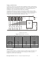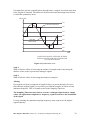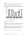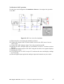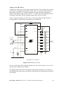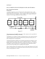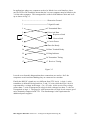
1
DET
Electronics
Analogue and Digital Interfacing
Teacher/Lecturer Notes
Higher
6827
Spring 2000
HIGHER STILL
DET
Electronics
Analogue and Digital
Interfacing
Teacher/Lecturer Notes
Higher
Support Materials
CONTENTS
TEACHER/LECTURER GUIDE
The Learning Outcomes to be covered in the unit
Section 1
Section 2
Teaching and learning advice including how to use the resource
material
Section 3
Details of starting points based on Electronic and Electrical
Fundamentals (Int 2)
Section 4
Assessment procedures showing what is to be assessed, when it is to
be assessed and result recording procedures
Section 5
Resource requirements including course notes, book list,
audio/visual aid list
Section 6
Electronics laboratory requirements including technical information
sources, components, materials, facilities and equipment
Section 7
Safety
Section 8
Acknowledgements
STUDENT GUIDE
The outcomes to be covered in the unit
Section 1
Section 2
The assessment instrument for the outcomes
Section 3
Student’s guide to working on the unit
Section 4
The required achievement standard for the assessment
Section 5
Information sheets/references for safety and laboratory work
Section 6
Analogue to digital and digital to analogue conversion notes and
tutorials
Section 7
Data communication techniques notes and tutorials
Section 8
Optoisolation and DC power switching notes and tutorials
DET Support Materials: Electronics – Analogue and Digital Interfacing (H)
1
DET Support Materials: Electronics – Analogue and Digital Interfacing (H)
2
SECTION 1
THE LEARNING OUTCOMES TO BE COVERED IN THE UNIT
OUTCOME 1
Analyse and use digital-to-analogue conversion circuits.
Performance criteria
a. Standard terms used to characterise digital-to-analogue converters are defined
correctly.
b. The operating principles of an R–2R network are explained correctly.
c. Manufacturers’ data sheets are correctly interpreted.
d. A digital-to-analogue converter is correctly chosen to meet a specified application.
e. A digital-to-analogue converter is correctly used and its operation is accurately
verified.
Note on the range of the outcome
Terms: resolution, accuracy, settling time, uni-polar/bi-polar, conversion time.
Evidence requirements
Written and graphical evidence that the candidate can define the standard terms and
extract the relevant data from manufacturers’ data sheets, explain the operating
principles of an R–2R network, and explain the reasoning for the selection of a
particular device to fulfil a given specification.
Performance evidence that the candidate can use and verify the operation of a digitalto-analogue converter.
OUTCOME 2
Analyse and use analogue-to-digital conversion circuits.
Performance criteria
a. Standard terms used to characterise analogue-to-digital converters are defined
correctly
b. Aliasing is accurately explained.
c. The requirements of a sample/hold circuit are correctly explained.
d. The operation of an analogue-to-digital converter is correctly explained.
e. Data from manufacturers’ data sheets are correctly interpreted.
f. An analogue-to-digital converter is correctly used and its operation is accurately
verified.
Note on the range of the outcome
Terms: resolution, accuracy, settling time, uni-polar/bi-polar, conversion time.
Analogue-to-digital converter: successive approximation, ramp, flash.
DET Support Materials: Electronics – Analogue and Digital Interfacing (H)
3
Evidence requirements
Written and graphical evidence to show that the student can explain the sampling rule,
aliasing, the requirement of a sample and circuit, the operation of ramp, successive
approximation and flash ADCs.
Performance evidence that the student can construct and verify the operation of one of
the ADCs using a dedicated IC.
OUTCOME 3
Evaluate digital communication techniques.
Performance criteria
a. Different types of data transmission standards are accurately compared.
b. Serial communication links are successfully used.
c. Serial-to-parallel and parallel-to-serial conversion techniques are correctly
explained.
d. The principles of time-division multiplexing are correctly explained.
Note on the range of the outcome
Data transmission: serial (RS232C and RS423), parallel (IEEE 488), synchronous,
asynchronous.
Serial: baud rate, parity, start/stop bits, ASCII format.
Conversion techniques: SIPO, PISO, FIFO, UART.
Methods: multiplexing and demultiplexing.
Evidence requirements
Written and oral and graphical evidence to show that the student can compare
different types of data communication, and explain conversion techniques and timedivision multiplexing.
Performance evidence that the student can use a serial communication link, for
example by linking and communicating successfully between two computers.
OUTCOME 4
Demonstrate d.c. load power switching devices.
Performance criteria
a. From a given load an open-collector output stage is correctly designed.
b. A transistor-based power switching device is correctly selected for a given load.
c. Explanation of the needs for optoisolation is correct.
d. The operation of a power switching interface is correctly verified.
Note on the range of the outcome
Transistor: single transistor (n-p-n common emitter), Darlington pair (discrete and
IC).
DET Support Materials: Electronics – Analogue and Digital Interfacing (H)
4
Evidence requirements
Written and graphical evidence to show that the student can design an open-collector
output stage to drive one load, select a transistor-based power switching device to
drive a given load (minimum 20 watts) and explain the need for optoisolation. This
load must be selected from: indicators, electromechanical relays, small d.c. motors.
Performance evidence that the candidate can construct and verify the operation of a
switching interface. This should be limited to not less than three stages, one of which
reached in a technical report.
DET Support Materials: Electronics – Analogue and Digital Interfacing (H)
5
DET Support Materials: Electronics – Analogue and Digital Interfacing (H)
6
SECTION 2
TEACHING AND LEARNING ADVICE INCLUDING HOW TO USE THE
RESOURCE MATERIAL
Teaching Methods
In general the teaching and learning methods used are very dependent on the contents
of the unit and the facilities and expertise available at the delivering centre. By their
very nature, however, the units in the Higher Electronics Course suggest the following
teaching methods:
• Laboratory based learning activities
• Use demonstration circuits where possible
• Use candidate centred circuit testing and analysis
• Relate essential theory to circuit applications
• Place components used in a commercial contexts.
It is important that all the teachers/lecturers working on the Higher Electronics Course
share a commitment to these methods and employ them as much as possible. In
addition other methods may be identified such as Computer Based Training if the
centre has such a facility. The outcome of this should be a teaching ethos which
pervades the course and sets it apart from other courses which will enjoy a different
background.
ANALOGUE AND DIGITAL INTERFACING UNIT DELIVERY
MAIN TOPICS
DELIVERY SUGGESTED
OUTCOME 1
DACs
Introduce through manufacturers’ data sheets to show
the range and variety available.
DAC terminology
Review of manufacturers’ data sheets, explanations
and notes with terms defined.
R - 2R network operating principals
Circuit diagram, explanation of circuit with simple
mathematical model, student notes.
Choosing DAC to meet a given specification
Main DAC characteristics reviewed, sample
specifications considered with the selection of a
suitable DAC, tutorial examples.
Using a DAC and verifying its operation
Laboratory experiment with preconstructed DAC.
DET Support Materials: Electronics – Analogue and Digital Interfacing (H)
7
ANALOGUE AND DIGITAL INTERFACING UNIT DELIVERY
MAIN TOPICS
DELIVERY SUGGESTED
OUTCOME 2
ADCs
Introduce through manufacturers’ data sheets to show
the range and variety available.
ADC terminology
Review of manufacturers’ data sheets, explanations
and notes with terms defined.
Aliasing
Explain the concept, give examples, discuss.
The requirement for sample and hold circuits
Identify the need, explain a typical circuit, student
notes.
The operation of successive approximation,
ramp and flash ADCs
Show circuit with explanation, students study and
discuss in groups, verbal reports of circuit operation,
consider commercial examples, tutorial examples.
Interpretation of manufacturers’ data sheets
Tutorial exercises in groups and individually to
interpret manufacturers’ data sheets.
Using an ADC and verifying its operation
Laboratory experiment with preconstructed ADC.
OUTCOME 3
Data communications
Introduce basis concepts of serial and parallel data
communications. Show examples.
Serial communications
Explain RS232 and RS423, show examples, review
technical terms, notes and tutorials.
Parallel communications
Explain IEEE 488, show examples, review technical
terms, notes and tutorials.
Conversion techniques
Show different techniques using block diagrams,
explain their operation, notes and tutorials.
Data communication terminology
Collect and record technical terms, discuss and
define them as they arise.
Interpretation of manufacturers’ data sheets
Tutorial exercises in groups and individually to
interpret manufacturers’ data sheets.
Time division multiplexing
Explain the advantages of TDM, explain a simplified
multiplexer circuit, analyse a simplified
demultiplexer circuit, explain a simplified TDM
system.
Use a serial communication link
Laboratory experiment to use a serial communication
link.
DET Support Materials: Electronics – Analogue and Digital Interfacing (H)
8
ANALOGUE AND DIGITAL INTERFACING UNIT DELIVERY
MAIN TOPICS
DELIVERY SUGGESTED
OUTCOME 4
DC power switching
Introduce through applications indicating advantages
and disadvantages.
Opto-isolation
Explain its purpose, show device examples using
manufacturers’ data sheets, show applications.
Current switching using n-p-n and Darlington
transistor configurations
Explain single stage circuit, discuss example
calculations, tutorial examples. Repeat for two stage
circuits with a range of transistors.
Power dissipation
Explain the need for adequate device dissipation,
perform power calculations for devices, select
devices to meet power requirements.
Verifying the operation of power switching
circuit
Students design a circuit to meet a given
specification, the circuit is built and tested. The
results are analysed and faults corrected until the
design meets the specified requirements.
DET Support Materials: Electronics – Analogue and Digital Interfacing (H)
9
DET Support Materials: Electronics – Analogue and Digital Interfacing (H)
10
SECTION 3
DETAILS OF STARTING POINTS BASED ON ELECTRONIC AND
ELECTRICAL FUNDAMENTALS (INT 2)
The units in Electronic and Electrical Fundamentals (Int 2) have been reviewed for
starting points for the teaching of topics in Analogue and Digital Interfacing (H).
Relevant outcomes are identified using the Analogue and Digital Interfacing (H)
outcomes as the basis.
Outcome 1
The main topics are digital-to-analogue conversion circuits their operation and the
associated terminology.
Starting points from Electrical
Fundamentals (Int 2)
Voltage and current relationships in networks.
Starting points from
Introduction to Semiconductor
Applications (Int 2)
Operational amplifier circuits.
Starting points from
Combinational Logic (Int 2)
Binary operations and digital codes.
Outcome 2
The main topics are analogue-to-digital conversion circuits their operation and the
associated terminology.
Starting points from Electrical
Fundamentals (Int 2)
Voltage and current relationships in networks.
Starting points from
Introduction to Semiconductor
Applications (Int 2)
Operational amplifier circuits.
Starting points from
Combinational Logic (Int 2)
Binary operations and digital codes.
Combinational logic circuits.
DET Support Materials: Electronics – Analogue and Digital Interfacing (H)
11
Outcome 3
The main topics are serial and parallel data transmission.
Starting points from Electrical
Fundamentals (Int 2)
Serial and parallel circuit concepts.
Starting points from
Introduction to Semiconductor
Applications (Int 2)
None
Starting points from
Combinational Logic (Int 2)
Binary codes. Combinational logic circuits.
Outcome 4
The main topic is DC power switching circuits.
Starting points from Electrical
Fundamentals (Int 2)
Voltage and current relationships in networks.
Power and energy calculations.
Starting points from
Introduction to Semiconductor
Applications (Int 2)
The operation of single-stage resistance-loaded
small-signal amplifiers.
Starting points from
Combinational Logic (Int 2)
None.
DET Support Materials: Electronics – Analogue and Digital Interfacing (H)
12
SECTION 4
ASSESSMENT PROCEDURES SHOWING WHAT IS TO BE ASSESSED,
WHEN IT IS TO BE ASSESSED AND RESULT RECORDING PROCEDURES
Using the instruments of assessment
This unit is assessed using two laboratory assignments, a data research and test
assignment, a design assignment and a short answer test. In Outcome 1 a DAC has to
be used and similarly in Outcome 2 an ADC has to be used. In these outcomes it is
recommended that a preconstructed circuit is provided which offers both facilities.
Suitable experimental converter circuits may be obtained from suppliers of
educational products.
Outcome 1 covers digital-to-analogue conversion and is assessed by a laboratory
assignment. This should be the natural conclusion of the teaching of this topic which
should be reinforced as a consequence. Preconstructed boards should be used in
conjunction with manufacturer’s data sheets. Evidence should be collected on the
assignment sheet as the candidate progresses through the tasks.
Outcome 2 covers analogue-to-digital conversion and is assessed by a laboratory
assignment. This should be the natural conclusion of the teaching of this topic which
should be reinforced as a consequence. Preconstructed boards should be used in
conjunction with manufacturer’s data sheets. Evidence should be collected on the
assignment sheet as the candidate progresses through the tasks.
Outcomes 3 covers data communications techniques. The assessment of this uses
two different assessment instruments. The first assessment instrument is a data search
and test assignment which focuses on serial and parallel communications. The output
of this is a report in a defined format which should be the result of the candidate
seeking out and interpreting relevant data from a range of sources. The second
assessment instrument is a short written test which covers the principles of serial-toparallel and parallel-to-serial conversion as well as time division multiplexing. This
should also be the natural conclusion of the teaching of this topic which should be
reinforced as a consequence.
Outcome 4 covers the application of dc load power switching devices and is assessed
by a design assignment. This should be overtaken at the end of teaching of the topic
which should be reinforced as a consequence. The candidate should design, construct
and test a dc power switching circuit. The circuit should contain three stages one of
which must be opto-isolation. Evidence should be collected in the form of a short
report in a prearranged format.
DET Support Materials: Electronics – Analogue and Digital Interfacing (H)
13
This is an investigative and practical unit which should be taught in a laboratory
environment. The instruments of assessment reflect this as laboratory based
assignments are used for nearly all the outcomes. In the laboratory it is important that
the focus is on the interfacing technology and that the candidate’s attention is not
unduly distracted by other issues such as the use of test equipment, the operation of
software and the recording of results. To this end candidates attempting this unit
should be familiar with any test equipment used, the operation of any software used
and be able to record and interpret the results taken from them.
The timing and duration of assessments
It is recommended that the interfacing technology is taught in three stages. A-D and
D-A conversion, data communications and load power switching. The order in which
the stages are delivered is not important. The timing of these assignments is
dependent on the candidate’s understanding of the relevant stages and should be
selected with that as the main restraint.
In principle, there are no time limits for the completion of each instrument of
assessment, but it is likely that a maximum time will be allocated for the completion
of each assignment. It is expected, however, that the average candidate will complete
the work within the maximum time allowed. The table below indicates the
recommended time allocated for each instrument of assessment.
Outcomes
Activity
Suggested maximum time
1
2
3
Laboratory assignment
Laboratory assignment
Data search and test assignment
Digital Communication Test
Design assignment
120 Minutes
120 Minutes
5 hours
60 minutes
7 hours
4
Reassessment
Time is allowed within units for the assessment and reassessment of outcomes.
Where a candidate has not attained the standard necessary to pass a particular
outcome or outcomes, there should be an opportunity to be reassessed. Reassessment
should focus on the outcome(s) concerned and, as a general rule, should be offered on
a maximum of two occasions following further work on areas of difficulty. Evidence
from the original unit assessment, should assist teachers and lecturers to identify why
an individual candidate has failed to achieve a particular outcome and to plan focused
support for learning.
For all the outcomes the reassessment should be based on the original instrument of
assessment.
DET Support Materials: Electronics – Analogue and Digital Interfacing (H)
14
When candidates have not produced a satisfactory answer to a section of an
assessment they should only be asked to repeat those sections in which they have not
provided suitable responses. Candidates should be asked to complete the
reassessment under the original controlled conditions. The reassessment should take
place as soon as practicable after the initial assessment and after discussion and
analysis of the initial assessment has taken place between the candidate and the
assessor. Candidates should be informed of the sections of the assessments that they
are required to repeat and given additional teaching to help them tackle the
reassessment. When there is a substantial number of candidates requiring
reassessment a revision lesson on the problem area should be presented before
reassessment.
When candidates have produced an answer which is substantially correct but which
contains minor errors such as the mislabelling of a diagram or the incorrectly reading
of an instrument (100 mA instead of 10 mA). They should be reassessed by asking
them to give the correct answer orally. This should take place as soon as possible
after the initial assessment and before any fuller discussion or analysis of it.
In the laboratory it is important that the focus is on interfacing technology and that the
candidate’s attention is not distracted by other issues such as the use of test
equipment, the operation of software and the recording of results. To this end
candidates attempting this unit should be familiar with any test equipment or software
used and be able to record and interpret the information taken from them. The
assessor should distinguish between assessment difficulties resulting from a
candidate’s weakness in the use of test equipment or software and a lack of
understanding of interfacing technology. If the candidate is weak in the use of test
equipment or the operation of software this should be resolved by additional training
followed by the repeating of the requisite tests by the candidate.
The conditions under which assessment takes place
Arrangements documents refer to assessment being carried out under controlled
conditions to ensure reliability and credibility. For the purposes of internal
assessment, this means that assessment evidence should be compiled under
supervision to ensure that it is the candidate’s own work. Supervision may be carried
out by a teacher, invigilator or other responsible person, for example, a workplace
provider.
The assessments should take place in a laboratory adequately equipped with the
necessary test equipment. Ideally candidates should work individually but they may
be allowed to work in pairs provided individual answer sheets are prepared.
Candidates should not have access to teaching notes or texts on interfacing technology
but should complete the assessments from their own knowledge and understanding.
It is recommended that the laboratory assignment assessments are introduced using
the following procedure:
• allow the candidates a few moments to read the laboratory assignment sheet
• review and summarise the tasks required by the assignment
• identify the equipment and facilities provided for the assignment
• explain the operating conditions within the laboratory
• emphasise safety practices and precautions.
DET Support Materials: Electronics – Analogue and Digital Interfacing (H)
15
Candidates should be encouraged to identify themselves to the assessor on completion
of the assignment and before any equipment is dismantled. The assessor should, if
possible, mark the assignment and provide immediate feedback to the candidate
regarding the outcome. If necessary remedial action should be taken by the candidate.
Using internal assessment evidence to contribute to course estimates
The assessments for this unit are designed largely for internal assessment purposes
and have only limited potential to generate evidence for external assessment
performance. Since the assessments are largely laboratory assignments they offer
limited opportunities to provide evidence of a candidate’s likely performance in an
external exam based assessment. Only the parts of the assignments which require the
candidate to interpret the operation of a circuit offer opportunities to provide evidence
for likely performance in the external assessment.
Advice on recording and retention of evidence
Regular meetings and informal discussions between internal verifiers and assessors
facilitate good assessment practice. By using this approach assessors should
understand that internal assessors are matching the internal assessments with external
standards.
Internal verifiers sample records, observe a sample of assessments, countersign
recording documents, support and guide assessors and are involved where disputes
and appeals arise.
All evidence in the form of laboratory results should be retained in case of appeals or
disputes. Below is an example of checklist which could also be used to record results.
DET Support Materials: Electronics – Analogue and Digital Interfacing (H)
16
DET Support Materials: Electronics – Analogue and Digital Interfacing (H)
Unit Number:
Candidate’s Name:
Unit Title: Analogue and Digital Interfacing.
Class:
Date:
Assessor:
LO 1
Analyse and use digital-to-analogue conversion circuits.
PC (a) Standard terms used to characterise digital-to-analogue converters are defined correctly.
PC (b) The operating principles of an R–2R network are explained correctly.
PC (c) Manufacturers’ data sheets are correctly interpreted.
PC (d) A digital-to-analogue converter is correctly chosen to meet a specified application.
PC (e) A digital-to-analogue converter is correctly used and its operation is
accurately verified.
LO 2
Analyse and use analogue-to-digital conversion circuits.
PC (a) Standard terms used to characterise analogue-to-digital converters are defined correctly.
PC (b) Aliasing is accurately explained
PC (c) The requirements of a sample/hold circuit are correctly explained
PC (d) The operation of an analogue-to-digital converter is correctly explained.
PC (e) Manufacturers’ data sheets are correctly interpreted.
PC (f)
An analogue-to-digital converter is correctly used and its operation is accurately verified.
LO 3
Evaluate data communication techniques.
PC (a) Different data transmission standards are accurately compared.
PC (b) Serial communication links are successfully used.
PC (c) Serial-to-parallel and parallel-to-serial conversion techniques are correctly
explained.
PC (d) The principles of time-division multiplexing are correctly explained.
LO 4
Apply d c load power switching devices.
PC (a) For a given load an open-collector output stage is correctly designed.
PC (b) A transistor-based power switching device is correctly selected for a given load.
PC (c) Explanation of the needs for optoisolation is correct.
PC (d) The operation of a power switching interface is correctly verified.
Design assignment
Design assignment
Design assignment
Design assignment
Test evidence collected
Assignment evidence collected
Assignment evidence collected
Test evidence collected
Assignment evidence collected
Assignment evidence collected
Assignment evidence collected
Assignment evidence collected
Assignment evidence collected
Assignment evidence collected
Assignment evidence collected
Assignment evidence collected
Assignment evidence collected
Assignment evidence collected
Assignment evidence collected
17
SECTION 5
RESOURCE REQUIREMENTS INCLUDING COURSE NOTES, BOOK LIST,
AUDIO/VISUAL AID LIST
Course Notes
Students should have access to notes provided for the other units in the Electronics
(H) course. In addition any other similar material collected by the student from earlier
courses or other relevant areas of study should be used.
Comprehensive notes for the unit are provided in the student support material.
Book List
Below are only a few suggestions from the many excellent text books on offer. Some
of these may be more suited to staff than students.
Ralph J Smith, Electronics: Circuits and Devices, John Wiley and Sons, ISBN 0-47108751-3
John B Pratley Electronic Principles and Applications, Arnold, ISBN 0-340-69275-8
John C Morris, Applied Electronics, Arnold, ISBN0-340-65284-5
Jacob Millman, & Arvin Grabel, Microelectronics, McGraw-Hill,
ISBN 0-071-00596-x
G B Clayton, Operational Amplifiers, Butterworths, ISBN 0-408-00370-7
Paul Horowitz and Winfield Hill, The Art of Electronics, Cambridge University Press,
ISBN 0-521-37095-7
ESM Electronics Service Manual, Wimborne Publishing Ltd, Allen House, East
Borough, Wimborne, Dorset BH21 1PF. Tel: 01202 881749, Fax: 01202 641692
DET Support Materials: Electronics – Analogue and Digital Interfacing (H) – Teacher’s Guide
18
Audio/visual aids
The electronics teaching laboratory should have prominently displayed an electrical
safety notice. These are available from a variety of electrical and electronic wholesale
outlets and distributors and are relatively inexpensive.
Component manufacturers and distributors offer wall charts and posters showing
many aspects of electronics. These vary from resistor colour codes to product
processing details and application advertisements. They are generally free and
available on request. They are useful as visual aids on the walls of the electronics
teaching laboratory as they create atmosphere and over a period of time act as a
constant reminder to students.
Data booklets
Technological Studies Data Booklet
Basic Electrical Formulae
Robert Gibson and Sons, 17 Fitzroy Place,
Glasgow G3 7SF
These should be either constructed by the
student or provided by the teaching section.
Their main advantage is that they can be
tailored to fit the courses on offer.
DET Support Materials: Electronics – Analogue and Digital Interfacing (H) – Teacher’s Guide
19
DET Support Materials: Electronics – Analogue and Digital Interfacing (H) – Teacher’s Guide
20
SECTION 6
ELECTRONICS LABORATORY REQUIREMENTS INCLUDING
TECHNICAL INFORMATION SOURCES, COMPONENTS, MATERIALS,
FACILITIES AND EQUIPMENT.
Technical information sources
It should be noted that developments in electronics, communications and computing
continue to offer tremendous opportunities for the dissemination and retrieval of
information. At the time of writing the Internet, CD-ROM and on-line component
distributors’ catalogues as well as web sites for manufacturers, suppliers and
providers of educational material are current examples. All of these and similar
potential future products originate from electronics technology. Accordingly students
should be encouraged to take advantage of such technological products as they
emerge through exploring and using them. A culture of using the technology to its
limits should be encouraged.
There are numerous sources of technical information on electronics other than the
traditional library books. These sources, however, are only helpful if they are both
accessible and relevant. The following has been refined through use and experience
but inevitably will be superseded by better methods as the technology advances and
they become available.
Component Distributors Catalogues
MPS [Maplin]
Web Site
http://www.maplin.co.uk
E-mail
<recipient>@maplin.co.uk
Telephone: Customer services
01702 554002
Telephone: Free technical helpline
01702 556001
Address
Maplin MPS, Freepost SMU 94, P.O. Box 777, Rayleigh, Essex SS6 8LU
RS
Web Site
http://rswww.com
E-mail
http://rswww.com
Telephone
01536 201201
Telephone: Free technical helpline
01536 402888
Address
RS Components Ltd., P O Box 99, Corby, Northants NN17 9RS
DET Support Materials: Electronics – Analogue and Digital Interfacing (H) – Teacher’s Guide
21
Farnell
Web Site
http://www.farnell.co.uk
E-mail
[email protected]
Telephone: Customer services
0113 2636311
Telephone: Free technical helpline
0133 2799123
Address
Farnell Electronic Components, Canal Road, Leeds, LS12 2TU
Access should be provided for students to one or more of the above component
distributors’ catalogues in either paper, CD-ROM or on-line form.
Selected data books, reference books and specialist text books should also be provided
from those offered by the above sources. There are so many good items on offer it is
impossible to recommend a definitive list which is largely a matter of local
preference. Choices should be based on staff expertise, the teaching and learning
approaches used and the available budget. As many of the smaller specialised texts
are low cost it should be possible to provide several reference copies for use in the
electronics laboratory.
Many manufactures of electronic components have web sites. These may be located
by a net search using the manufacturer’s name. Once into the web site it is often
possible to locate technical data, application information and in some situations
design tutorials.
Components
The Electronics Laboratory should offer access to component stocks as a standard
facility. This is for the benefit of both staff and students who will require access to
components for demonstrations, experimentation and for case study and project work.
The stock, however, has to be managed and controlled if the quality of the facility is
to be sustained. The approach taken to this is a matter for the centre’s organisational
structure but experience suggests that one person needs to be clearly identified as
having responsibility for the stock, for issuing it and for reordering.
DET Support Materials: Electronics – Analogue and Digital Interfacing (H) – Teacher’s Guide
22
Below is a typical basic selection of components.
resistors
Low cost metal film 0.25 W - standard preferred values from 1 Ω to
10 M Ω .
High powered resistors 2.5 W silicon coated- standard available
values.
potentiometers
150 mW carbon trimmers- standard preferred values from 100 Ω to
10 M Ω .
capacitors
Metallised ceramic plate capacitors-standard preferred values from
1.8 pF to 120 pF
Resin dipped plate ceramic capacitors -standard preferred values
from 10 pF to 0.47 µF
Radial polystyrene capacitors-standard preferred values from
100 pF to 8200 pF
Radial lead electrolytic capacitors-standard preferred values from
1 µF to 47000 µF
Axial lead electrolytic capacitors-standard preferred values from
1 µF to 47000 µF
diodes
1N4148, 1N4001,1N5401,BZX85- range of voltages from 2.7 V to
15 V
bridge rectifier
W005G
light emitting diodes
3 mm and 5 mm red, orange and green
transistors
BC184L, BC214L, 2N3053, BFY50, TIP31A, TIP32A,TIP33A,
2N3055E, 2N2955, 2N3819, 2N3820
op. amps.
µA 741, LM 324N, CA3140E
logic chips
74 LS series TTL - selected functions as appropriate
4000 series CMOS - selected functions as appropriate
DET Support Materials: Electronics – Analogue and Digital Interfacing (H) – Teacher’s Guide
23
other analogue integrated
circuits
NE555N timer, ICM7555 timer, L7805CP, L7812 CP positive
voltage regulators, L7905CT, L7812 CT negative voltage
regulators
other digital integrated circuits
DACs and ADCs to suit laboratory applications
fuses
As required for instruments
switches
Push button, toggle, slide and DIL miniature as required
Transformers and inductors
As required
lamps and bulbs
Low voltage and power selection to meet requirements
relays
Low voltage as required
connectors
Terminal blocks, 4 mm plugs and sockets in red, black, blue, yellow
and green
prototype boards
Breadboards for solderless circuit construction
Materials
Few materials are required. It may be helpful to have reels of solid and stranded
conductor wire in a variety of colours available. Some are suggested below.
WIRE TYPE
COLOUR
Solid Core Wire (1/0.6)
Black, Blue, Brown, Green, Red, White, Violet,
Yellow
Hook-Up Wire (7/0.2)
Black, Blue, Brown, Green, Red, White, Violet,
Yellow
DET Support Materials: Electronics – Analogue and Digital Interfacing (H) – Teacher’s Guide
24
Facilities
The ideal electronics teaching laboratory has office-style or computer tables (wide)
around the walls with matching narrow tables in the middle. A typical plan is shown
below. This type of layout has found favour in a number of centres and so has clearly
proved its worth for several teams of teaching engineers.
Stora ge
a nd
c om pute r
W hite boa rd
S tora ge
a nd
c om pute r
Trunking with 13 Amp socket outlets should be fitted around the walls at a convenient
height above the wide tables. Each student should have available a 2 metre run of
surface and at least four 13Amp socket outlets. This is necessary to allow adequate
working surface for test equipment, circuits, components and papers. Eye level
shelving around the walls above the power socket trunking can also be useful for test
instruments and general storage.
The socket outlets should be protected by a suitable device such as an earth leakage
circuit breaker and a central safety switch with key lock. The design and installation
of such facilities should be undertaken by a specialist as they constitute important
safety features.
DET Support Materials: Electronics – Analogue and Digital Interfacing (H) – Teacher’s Guide
25
The central tables are used for written work and group teaching. Suitable strong
moveable chairs such as those found in hotel conference rooms should be provided in
adequate numbers to allow seating around the wall tables or in the centre but not both.
Excessive furniture and narrow spaces between tables in the laboratory can be a safety
hazard and should be avoided The room should be brightly lit and well ventilated.
Equipment
In the electronics laboratory each student should have access to the following
equipment. Ideally there should be one set of equipment per student.
1.
2.
3.
4.
5.
6.
Multimeter
Dual rail power supply
Signal generator
Double beam oscilloscope
Logic probe
Computer.
It is also helpful to have a limited range of tools available such as
• Snipe nosed pliers
• Wire cutters
• Wire strippers
• Screw drivers.
The types of tools and equipment on the market are constantly changing through a
process of continuous improvement. It is strongly recommended that before
purchasing any items for an electronics laboratory advice is sought from a current user
experienced in this area. Issues such as the cost of hand tools in relation to their
quality and life expectancy with inexperienced users who may damage or remove
them from the laboratory have to be given due consideration. Equipment may be
found which is both adequate for the teaching laboratory, student proof and
inexpensive requiring little maintenance.
There are many suppliers of test equipment and tools but only those specialising in the
educational market are likely to offer products at an acceptable price. Similarly these
suppliers are more likely to have tools and equipment which can survive the rigours of
the teaching laboratory. It is good practice to both commercially and technically
survey the market to insure that the best suppliers are offered sales opportunities.
Other centres, which have tried and tested equipment are often the best source of
information and should be consulted as part of the purchasing exercise. Suppliers
may provide access to users of their products who are prepared to discuss their
experiences with others. Time spent on this will pay substantial dividends in future
years in terms of equipment downtime and repair costs.
DET Support Materials: Electronics – Analogue and Digital Interfacing (H) – Teacher’s Guide
26
Software
The electronics teaching laboratory is greatly enriched by the presence of PCs with
appropriate software. Since computers are one of the main products of electronics
technology they find extensive use in the application of the technology and form part
of the electronics environment. While the capital outlay for this may be significant
there has to be recognition of the part played by the computer with specialised
software in the electronics environment.
Through access to suitable computing facilities and software students should be
exposed to this environment in the teaching laboratory. Commercial software for
word and data processing is widely available at reasonable cost and is generally
selected by centres to conform with their local policy. These may find application in
the creation of reports and the analysis of results.
In addition, however, circuit simulation and drawing software may also be used. The
software must be easy to use without extensive training and be available at low cost
with multiple copies site licensed. While there are several products on the market
those which have stood the test of time and so are favoured for use in colleges and
schools are listed below.
Invent! crocodile clips: simple simulation of electronics and mechanics
Web address
www.crocodile-clips.com/education/v3.htm
E-mail
[email protected]
Telephone
0131 226 1511
Fax
0131 226 1522
Address
Crocodile Clips
11 Randolph Place
Edinburgh
EH3 7TA
DET Support Materials: Electronics – Analogue and Digital Interfacing (H) – Teacher’s Guide
27
Electronics Workbench: circuit simulation and testing
Web address
http://www.adeptscience.co.uk
E-mail
[email protected]
Telephone
01462 480055
Fax
01462 480213
Address
Adept Science plc
6 Business Centre West
Avenue One
Letchworth
Herts.
SG6 2HB
SmartDraw: drawing of diagrams and plans with associated symbol libraries
Web address
http://www.smartdraw.com
E-mail
[email protected]
Telephone
01889 564601
Fax
01889 563219
Address
The Thompson Partnership
Lion Buildings,
Market Place,
Uttoxeter,
Staffs.
ST14 8HZ
DET Support Materials: Electronics – Analogue and Digital Interfacing (H) – Teacher’s Guide
28
SECTION 7
SAFETY
The safety of teaching staff and students working in the electronics laboratory must be
the primary concern of everyone involved.
This has to take precedence over all other activities and be sustained against all
other pressures.
There are many aspects to safety as follows:
• statutory requirements
• centre procedures
• centre structure
• staff training and behaviour
• laboratory features
• student training and behaviour.
It is beyond the scope of this document to provide details of all of all aspects of a
centre’s safety policy. Staff must, however, be content that all appropriate safety
measures are in place before embarking on work within the electronics laboratory.
Student training is a recurrent activity, which is likely to be the direct responsibility of
the lecturer/teacher. While this has to take place on a continuous basis as work in the
laboratory proceeds it is helpful to perform specific safety training at course
commencement. Such training might form part of the course induction as its
relevance extends across all course units. This is particularly important for electronics
students as they should be encouraged to develop their own safety culture, which
should become a lifelong asset.
Lecturers/teachers performing safety training for students may find a rich diversity of
available material. Of specific relevance, however, is a teaching package prepared by
the University of Southampton’s Department of Electrical Engineering and Teaching
Support and Media Services. The package was prepared in association with and
financially supported by the Health and Safety Executive. It consists of:
• Handbook: ‘Safety Handbook for Undergraduate Electrical Teaching
Laboratories’
• Video Programme: ‘Not to Lay Blame’
• A booklet: ‘Tutor’s Guide’.
The package is targeted at the first year undergraduate level and works well with other
students at similar levels. The handbook is very comprehensive and sufficiently
inexpensive to be bought in quantity and given to students for everyday use. It is well
presented using text and cartoons. The video dramatises issues associated with
electrical/electronics laboratory work using a style and characters likely to appeal to
the majority of students. The Tutor’s Guide booklet rounds the package off by giving
guidance on the use of the video and handbook. In addition it contains ‘Safety Rules
for Electrical Laboratories’ and a comprehensive list of references to enable further
reading should you wish it.
DET Support Materials: Electronics – Analogue and Digital Interfacing (H) – Teacher’s Guide
29
At the time of writing the distribution of the package was being handled by:
Maggie Bond
Department of Electrical Engineering
University of Southampton
SO17 1BJ
Phone: 01703 595164
Email: [email protected]
DET Support Materials: Electronics – Analogue and Digital Interfacing (H) – Teacher’s Guide
30
SECTION 8
ACKNOWLEDGEMENTS
The support and assistance provided by colleagues at Fife College of Further and
Higher Education, Stowe College and James Watt College who have contributed
material and helpful advise for this pack is gratefully acknowledged.
Also acknowledged with thanks is the help of lecturers and teachers in other colleges
and schools who have assisted in the preparation of the pack by contributing material
and by commenting on draft documents.
DET Support Materials: Electronics – Analogue and Digital Interfacing (H) – Teacher’s Guide
31
DET Support Materials: Electronics – Analogue and Digital Interfacing (H) – Teacher’s Guide
32
STUDENT’S INFORMATION AND SUPPORT MATERIAL
CONTENTS
Section 1
The outcomes to be covered in the unit
Section 2
The assessment instruments for the outcomes
Section 3
Student’s guide to working on the unit
Section 4
The required achievement standard for the assessment
Section 5
Information sheets/references for safety and laboratory work.
Section 6
Analogue to digital and digital to analogue conversion notes and
tutorials
Section 7
Data communication techniques notes and tutorials
Section 8
Optoisolation and DC power switching notes and tutorials
The following information and support material will help you to work on the
Analogue and Digital Interfacing unit. Information is provided about the unit’s
contents and the learning outcomes. There is a guide to working on the unit and notes
for you to study. The nature of the assessments is explained and the standard that you
are required to achieve. As you will be working in the laboratory there is a safety
reminder sheet which you should study before you start.
DET Support Materials: Electronics – Analogue and Digital Interfacing (H) – Student’s Guide
1
DET Support Materials: Electronics – Analogue and Digital Interfacing (H) – Student’s Guide
2
SECTION 1
THE OUTCOMES TO BE COVERED IN THE UNIT
OUTCOME 1
Analyse and use digital-to-analogue conversion circuits.
Performance criteria
a. Standard terms used to characterise digital-to-analogue converters are defined
correctly.
b. The operating principles of an R–2R network are explained correctly.
c. Manufacturers’ data sheets are correctly interpreted.
d. A digital-to-analogue converter is correctly chosen to meet a specified application.
e. A digital-to-analogue converter is correctly used and its operation is accurately
verified.
Note on the range of the outcome
Terms: resolution, accuracy, settling time, uni-polar/bi-polar, conversion time.
Evidence requirements
Written and graphical evidence that the candidate can define the standard terms and
extract the relevant data from manufacturers’ data sheets, explain the operating
principles of an
R–2R network, and explain the reasoning for the selection of a particular device to
fulfil a given specification.
Performance evidence that the candidate can use and verify the operation of a digitalto-analogue converter.
OUTCOME 2
Analyse and use analogue-to-digital conversion circuits.
Performance criteria
a. Standard terms used to characterise analogue-to-digital converters are defined
correctly
b. Aliasing is accurately explained.
c. The requirements of a sample/hold circuit are correctly explained.
d. The operation of an analogue-to-digital converter is correctly explained.
e. Data from manufacturers’ data sheets are correctly interpreted.
f. An analogue-to-digital converter is correctly used and its operation is accurately
verified.
Note on the range of the outcome
Terms: resolution, accuracy, settling time, uni-polar/bi-polar, conversion time.
Analogue-to-digital converter: successive approximation, ramp, flash.
DET Support Materials: Electronics – Analogue and Digital Interfacing (H) – Student’s Guide
3
Evidence requirements
Written and graphical evidence to show that the student can explain the sampling rule,
aliasing, the requirement of a sample and circuit, the operation of ramp, successive
approximation and flash ADCs.
Performance evidence that the student can construct and verify the operation of one of
the ADCs using a dedicated IC.
OUTCOME 3
Evaluate digital communication techniques.
Performance criteria
a. Different types of data transmission standards are accurately compared.
b. Serial communication links are successfully used.
c. Serial-to-parallel and parallel-to-serial conversion techniques are correctly
explained.
d. The principles of time-division multiplexing are correctly explained.
Note on the range of the outcome
Data transmission: serial (RS232C and RS423), parallel (IEEE 488), synchronous,
asynchronous.
Serial: baud rate, parity, start/stop bits, ASCII format.
Conversion techniques: SIPO, PISO, FIFO, UART.
Methods: multiplexing and demultiplexing.
Evidence requirements
Written and oral and graphical evidence to show that the student can compare
different types of data communication, and explain conversion techniques and timedivision multiplexing.
Performance evidence that the student can use a serial communication link, for
example by linking and communicating successfully between two computers.
OUTCOME 4
Demonstrate d.c. load power switching devices.
Performance criteria
a. From a given load an open-collector output stage is correctly designed.
b. A transistor-based power switching device is correctly selected for a given load.
c. Explanation of the needs for optoisolation is correct.
d. The operation of a power switching interface is correctly verified.
Note on the range of the outcome
Transistor: single transistor (n-p-n common emitter), Darlington pair (discrete and
IC).
DET Support Materials: Electronics – Analogue and Digital Interfacing (H) – Student’s Guide
4
Evidence requirements
Written and graphical evidence to show that the student can design an open-collector
output stage to drive one load, select a transistor-based power switching device to
drive a given load (minimum 20 watts) and explain the need for optoisolation. This
load must be selected from: indicators, electromechanical relays, small d.c. motors.
Performance evidence that the candidate can construct and verify the operation of a
switching interface. This should be limited to not less than three stages, one of which
should include an optoisolator.
DET Support Materials: Electronics – Analogue and Digital Interfacing (H) – Student’s Guide
5
DET Support Materials: Electronics – Analogue and Digital Interfacing (H) – Student’s Guide
6
SECTION 2
THE ASSESSMENT INSTRUMENTS FOR THE OUTCOMES
SAFETY WARNING
The assessments for the Analogue and Digital Interfacing unit consist of four assignments
and one test. During the Power Switching Interface Design Assignment you may find that
some components heat up and are dangerous to touch. You should only switch on your
circuit for a short time initially and take the required readings. Once you have checked the
component power ratings and you clearly understand which devices will heat up you
should take care when handling them.
Remember Electronic Engineers and Technicians all learn to work safely with potentially
hot components as one of their professional skills. They have to be responsible for both
their own safety and the safety of those around them.
If in doubt ask your supervisor before you connect the circuit or switch it on not after
when there is smoke rising from it or the test equipment and you have burnt your fingers.
The laboratory assignments require you to build and test circuits, search out and
interpret technical data and to interconnect two computers. You will be expected to
perform some or all the following during each assignment:
-
identify the functions of different parts of circuits
explain the operation of circuits
calculate expected component values
select correctly resistors
interconnect two computers
set up matching communication protocols between computers
search out and interpret component data
use multimeters to measure currents and voltages
build and test circuits
relate your experimental results to the operation of the circuit tested
use dc power supplies
There are four separate laboratory assignments, one for each of the unit’s learning
outcomes. You will be provided with assignment sheets which you should complete
and hand in.
Learning Outcome 1 assignment deals with digital-to-analogue converters and should
take you about two hours to complete. You will be expected to explain DAC
terminology. You will be asked to use a DAC and you will be required to correctly
select a DAC to meet a given performance specification.
DET Support Materials: Electronics – Analogue and Digital Interfacing (H) – Student’s Guide
7
Learning Outcome 2 assignment is similar to the assignment for Learning Outcome
1. It deals with analogue -to- digital converters and should take you about two hours
to complete. You will be expected to explain ADC terminology. You will be asked
to use an ADC and you will be required to correctly select an ADC to meet a given
performance specification
Learning Outcome 3 deals with Data Communications. The majority of the
assessment involves an information search and test activity. You will be allocated 5
hours to search for data on serial and parallel interfaces. During this time you will
also be expected to connect up two computers and use their software to establish a
serial communication link between them given a specific protocol. In addition there
is a second part of this assessment which is a short one hour test during which you
will be asked to explain communication techniques.
Learning Outcome 4 is a design assignment. You will be allocated 7 hours for this.
The design assignment requires you to interface a low power digital signal to a higher
powered load. The interface requires the use of an opto-isolator and several stages of
transistor switch. You will be given the basic circuit and from it expected to work out
the best components to use from a limited range of available components. Once you
have decided on the design you will then build and test it correcting any problems as
you go until you have a working solution and a justifiable design.
As the assessments are laboratory based you should enjoy the challenge of working on
electronic circuits and interpreting their operation.
After you have completed the assessments you will have a good basic understanding
of:
• analogue-to-digital conversion
• digital-to-analogue conversion
• serial and parallel communication techniques
• interfacing digital signals dc loads.
DET Support Materials: Electronics – Analogue and Digital Interfacing (H) – Student’s Guide
8
SECTION 3
STUDENT’S GUIDE TO WORKING ON THE UNIT
This unit specialises in the interfacing of electronic systems. Most electronic systems
require signals to input information into them and signals to carry data or control
information out of them. The system in the middle processes the input signals and as
a consequence generates appropriate output signals. Typical examples of this are the
personal computer which takes in signals from the keyboard, mouse, telephone line or
scanner and having processed them sends the resulting information and control signals
to the display, a printer or modem. Similarly the control electronics in an aircraft
receives input signal from the pilot, the navigation systems and the aircraft monitoring
systems. These are processed in the control electronics and the resulting output
signals control the engines and the wing and tail flaps which are used to fly the plane.
The first part of this unit requires you to explore two types of interface circuit which
enable signals to be fed into and out of digital systems from an analogue environment.
This means that signals generated as a model or analogy of some physical quantity are
converted into a digital form for use in a computer or similar system. Once processed
the digital signals are then converted back into an analogue form for use in the
analogue environment.
As an example of this consider an aircraft taking off. The jet engines generate
enormous thrust to accelerate the machine along the runway sensed by the passengers
being pushed back into their seats. A speed sensor will produce a voltage equivalent
to the plane’s speed such as 100 mV as the analogy of 100 mph which will be
converted into a digital code such as 01100100 to be fed into the control computer.
When the correct take off speed is reached the control computer will send a digital
signal to the flap controller to get the plane to lift into the air. This digital signal will
be converted to an analogue one with adequate power to open the hydraulic valve
which controls the flaps. In the first part of this unit you will find out how these
analogue-to-digital and digital-to-analogue converters work, the language used to
describe them and you will have an opportunity to test one of each.
The second part of the unit involves a study of the two main data communication
techniques in use. These are serial and parallel communications which form the basis
for most electronic data communication systems. Because of their importance in
electronic systems various standard methods have been developed and are widely
used throughout the electronics industry. This approach simplifies interfacing circuits
and eases the communication links between systems. You will learn about the
characteristics of both types and how the standard industrial systems work. In
addition you will have an opportunity to use a serial communication system and
experiment with its data transfers.
DET Support Materials: Electronics – Analogue and Digital Interfacing (H) – Student’s Guide
9
The third and last part of the unit will involve you in designing, building and testing
DC switching circuits. This is typical of the output circuit from a digital system to
some form of load device which requires a reasonable amount of DC power to
operate. Examples of this would vary from indicators such as light bulbs to motors
which might drive a mechanism such as a coin dispenser in a change machine or
electromechanical relays which could be used to switch power onto a variety of other
types of load. As you will have to calculate the circuit’s main requirements and then
prove that you are correct by building and testing your design this should be a very
practical activity. You will be introduced to the circuit to be used and provided with a
range of components to help you. At the end of this you will have a good knowledge
of the circuit as well as some experience of circuit design and testing.
DET Support Materials: Electronics – Analogue and Digital Interfacing (H) – Student’s Guide
10
SECTION 4
THE REQUIRED ACHIEVEMENT STANDARD FOR THE ASSESSMENT
All the assessments for this unit are laboratory assignments. These require you to
perform a variety of tasks which test your knowledge of the technology. To meet the
required standard for these assessments you must carefully follow the instructions on
the laboratory assignment sheets and make sure that you:
• complete all the tasks detailed on the assignment sheet
• answer all aspects of every question correctly
• achieve the standard of the performance criteria in the unit specification.
If you complete the laboratory assignments successfully you will achieve the
assessment standard.
DET Support Materials: Electronics – Analogue and Digital Interfacing (H) – Student’s Guide
11
DET Support Materials: Electronics – Analogue and Digital Interfacing (H) – Student’s Guide
12
SECTION 5
INFORMATION SHEETS/REFERENCES FOR SAFETY AND
LABORATORY WORK
Safety Guidelines for Electronics Laboratory Work.
You should read these guidelines and discuss them with your tutor to clarify their
significance in your working environment.
• Enter the Electronics Laboratory only at agreed times.
• Enter the Electronics Laboratory only when you are authorised.
• You should only work on equipment when a supervisor is present.
• Always avoid bulky, loose or trailing clothes, long loose hair, heavy metal
bracelets or watch straps.
• Do not take food or drink into the Electronics Laboratory.
• Avoid wet hands or clothes and clean up any liquid spillages.
• Be as careful for the safety of others as yourself.
• Think before you act, be tidy and systematic.
• Keep passages and work areas free of obstructions.
• Voltages above 120 V dc and 50 V rms are always dangerous, take extra
precautions as voltages increase.
• Never remove earth connections and make sure that all accessible conducting
parts of equipment or experiments are earthed. If in doubt check for earth
continuity.
• Multimeters and hand-held probes should be of good fused design and are not
recommended for dangerous levels of voltage or power.
• Understand the correct handling procedures for batteries, capacitors, inductors and
other energy-storage devices. Always handle them carefully.
• Fluorescent lights can cause rotating equipment to appear stationary. You should
be aware of this and take precautions if necessary.
• Before equipment is made live all casings, covers or shrouds must be in place so
that no live parts can be touched with fingers.
• Before equipment is made live circuit connections and layouts should be checked
by your supervisor.
• If you are working in a group everyone in the group should give their assent
before equipment is made live.
• Never make changes to either circuits or mechanical layouts without isolating the
circuit by switching it off and removing connections to supplies.
• Experimental equipment left unattended should be isolated from the supply unless
it has to be left on for some special reason, in which case a barrier and warning
notice are required.
• Equipment found to be faulty in any way should be reported to your supervisor
immediately and not used until it is inspected and declared safe.
• You should know what to do if there is an emergency in the Electronics
Laboratory.
• Use hand tools carefully and treat them with respect as they can be dangerous
when misused or faulty.
• Do not remove equipment, tools or materials from the Electronics Laboratory
without authorisation from your supervisor.
DET Support Materials: Electronics – Analogue and Digital Interfacing (H) – Student’s Guide
13
DET Support Materials: Electronics – Analogue and Digital Interfacing (H) – Student’s Guide
14
SECTION 6
ANALOGUE TO DIGITAL AND DIGITAL TO ANALOGUE CONVERSION
NOTES AND TUTORIALS
DET Support Materials: Electronics – Analogue and Digital Interfacing (H) – Student’s Guide
15
DIGITAL TO ANALOGUE CONVERTERS.
Introduction
A digital to analogue converter (DAC) shown in figure 1 is a circuit/device that
accepts a multi-bit digital code and produces an equivalent analogue output signal.
LS B
D IG ITAL IN P U TS
D0
D7
+ V cc
8 - B IT D AC
Vo
0V
D AC BLO C K D IA G R A M
Figure 1 DAC block diagram
The output signal is proportional to the sum of the binary weighted input signals. The
amount by which the output changes when the least significant bit (LSB) of the input
code is changed is called the step-size of the DAC.
Consider a 3 bit-DAC with a step-size of 0.5V, for this DAC a table showing input
codes and equivalent output voltages can be constructed as below.
Inputs
D2 D1 D0
0 0 0
0 0 1
0 1 0
0 1 1
1 0 0
1 0 1
1 1 0
1 1 1
Output
Vo (v)
0.0
0.5
1.0
1.5
2.0
2.5
3.0
3.5
Table 1 DAC input and output relationship
This Table shows
• That the output voltage can only have discrete values.
• The number of voltage levels is given by 2n where n is the number of digital inputs.
• The number of output voltage steps is given by 2n – 1.
• Maximum output voltage or full scale output (FSO) is given by the number of steps
times the step-size. In this case (23 –1) x 0.5 = 3.5V
• 2n x step-size is called the full-scale range voltage (FSR), which is never reached.
FSO is always one step-size less than the FSR. In this case FSR = 8 x 0.5 = 4V.
DET Support Materials: Electronics – Analogue and Digital Interfacing (H)
16
The table below shows the DAC input, output and relationship with FSR.
Inputs
D2 D1 D0
0 0 0
0 0 1
0 1 0
0 1 1
1 0 0
1 0 1
1 1 0
1 1 1
Output
In terms of FSR
Vo (V)
Vo (V)
0.0
0.5
1.0
1.5
2.0
2.5
3.0
3.5
(0/8) x FSR
(1/8) x FSR
(2/8) x FSR
(3/8) x FSR
(4/8) x FSR
(5/8) x FSR
(6/8) x FSR
(7/8) x FSR
Table 2 DAC output expressed in terms of FSR.
The transfer characteristic for the DAC may be drawn by plotting Vo against the
digital input code and joining the points of transition as shown below.
(V)
Vo
3.5
D AC
C HA RAC TER IS TIC
3.0
25.
2.0
D AC O UTP UT
1.5
1.0
0.5
D IG ITA L
IN PU TS
0
0
0
0
0
0
1
0
1
0
0
1
1
1
0
0
1
0
1
1
1
0
1
1
1
D2
D1
D0
D AC TR AN SFER C HA RA CTE RISTIC
Figure 2 DAC transfer characteristic
This transfer characteristic may be used to determine the accuracy, linearity and offset
voltage of a DAC. Some of these terms will be defined later.
DET Support Materials: Electronics – Analogue and Digital Interfacing (H)
17
From the DAC gain curve it can be clearly seen that the step-size (in this case for the
3-bit DAC) is 0.5V. The step-size may also be referred to as the resolution of the
DAC.
SAQ 1
An 8-bit DAC has a step-size of 10mV. Calculate the output voltages when the
following input codes are applied.
(a) 0000 0000
(b) 1000 0000
(c) 1111 1111
(d) 0000 0001
SAQ 2
If the resolution of a 4-bit DAC is 0.125V what is
(a) The step-size?
(b) Maximum output voltage (FSO)?
(c) The FSR voltage?
DAC circuits
A DAC circuit consists of
• a voltage or current reference source
• a number of binary weighted resistors
• electronic switches (operated by digital inputs)
• a summing circuit to add the binary weighted currents.
The basic design for a 4-bit DAC is shown below:
Rf
4 - B IT
R EG IS TER
+5V (Vr)
R
M SB
D3
0V
S3
Vo
2R
D2
S2
D IG ITAL
IN PU T S
4R
D 1`
S1
8R
LSB
D0
S0
0V
0V
BASIC D AC CIR CU IT
Figure 3 Basic DAC circuit.
DET Support Materials: Electronics – Analogue and Digital Interfacing (H)
18
The operational amplifier is in the inverting mode as a summing circuit. The four bits
in the register control four electronic (transistor) switches and allow 16 different
combinations of the switches to occur. If a particular switch closes to Vr the output is
given by the product of the reference voltage and the ratio of the value of the feedback
resistor to that of the switched resistor. For example if the LSB switch closes to Vr
when bit 0 is a logic 1 then
Vo = −
Rf
Rf
Vr = − Vr (20 )
8R
8R
Usually the switch legend is incorporated into the above equation. When calculating
the value of the output voltage, the switch label is given the value 1 if the switch
connects to Vr and the value 0 if it connect to 0V. Hence the above equation may be
expressed as follows:
Vo = −
Rf
Rf
Vr ( S 0) = − Vr (S 0 x 20 )
8R
8R
Hence if bit D0 equals logic 1, the switch connects to Vr and
Vo = −
Rf
Rf
Rf
Vr (S 0 x 20 ) = − Vr (1x1) = − Vr
8R
8R
8R
If bit D0 equals logic 0, the switch connects to 0V and
Vo = −
Rf
Rf
Vr ( S 0 x 20 ) = − Vr (0 x1) = 0
8R
8R
For bit D1 the ouput is given by
Vo = −
Rf
Rf
Vr (S1) = − Vr ( S1x 21 )
4R
8R
In fact each switch changes the Vo by a power of 2 compared to adjacent switch. If
more than one switch closes to Vr, then the output voltage is the addition of the
combined effects of the switches For example if bits D3, D2 D0 are at logic 1 and D1
is at logic 0 then
Vo = −
Rf
Rf
Rf
Rf
Vr ( S 3) −
Vr (S 2) −
Vr (S1) −
Vr (S 0)
R
2R
4R
8R
Rf
Vr ( S 3x 23 + S 2 x 22 + S1x 21 + S 0 x 20 )
8R
Rf
= − Vr (1x 23 + 1x 22 + 0 x 21 + 1x 20 )
8R
The above equation clearly shows that the summing circuit produces an output
voltage, which is directly related to the binary weighted inputs and hence is a simple
but effective DAC circuit.
The problem with the weighted DAC is that it requires a range of resistor values
(in accurate ratios) and hence is not suitable for integrated circuit manufacture.
=−
DET Support Materials: Electronics – Analogue and Digital Interfacing (H)
19
The R-2R network DAC
The R-2R ladder network DAC is generally used for single chip designs as it uses
only 2 values of resistors, however almost twice as many resistors are required.
R-2R network
The structure of this network is such that current entering through a branch at any
node is split equally into the two branches leaving the junction. Consider the
following simple parallel resistor network.
I
I/2
I/2
2R
R IN = R
2R
C UR R E NT DIV IS IO N IN PA R ALL EL
R ES IS TO R NE TW O R K
Figure 4 Current division in parallel resister network
Since the two resistors are equal the current I splits into two equal parts I/2 and I/2.
The same effect can be achieved by replacing the second 2R resistor by a slightly
more complex resistor network. This network consists of an R in series with 2-2R
resistors in parallel, giving an equivalent resistance of 2R. This is shown below.
I
I/2
I/2
R IN = R
2R
R
I/4
2R
I/4
2R
R ES IS TA NC E O F S E C TIO N = 2R
TH E S EC O ND 2R O F Fig4 RE P LA CE D
B Y E Q U IVA LE NT CIRC U IT
Figure 5 The second 2R of Figure 4 replaced by equivalent circuit.
DET Support Materials: Electronics – Analogue and Digital Interfacing (H)
20
As the current at the first node divides in half, then the current at the second node
divides in half. By repeatedly replacing the 2R resistor by the slightly more complex
network the resulting networks’ binary weighted currents flow in the vertical 2R
resistors as shown below.
I
R
I/2
I/2
R
I/8
I/4
I/8
2R
2R
R IN = R
R
I/4
I/16
2R
I/16
2R
2R
2R
2R
2R
Figure 6 The R-2R ladder network
This network is used with the operational amplifier summing circuit configuration to
implement a DAC circuit, in a similar manner to the basic DAC circuit, as illustrated
below.
R
I
I/2
R
I/4
2R
R
I/8
2R
I/16
2R
2R
2R
+
Vr
Rf
X
If
Vo
0V
D3
D2
D1
D0
X IS VIRTUAL EA RTH
D IG ITA L IN PU TS
Figure 7 R-2R ladder network DAC
In this circuit when a bit controlling a switch is at logic 1 the switched resistor is
connected to the operational amplifier inverting terminal and a current flows into the
virtual earth. When the bit is at logic 0 the corresponding resistor is connected directly
to 0V and the current flowing through it is diverted away from the inverting terminal
of the operational amplifier.
DET Support Materials: Electronics – Analogue and Digital Interfacing (H)
21
Using operational amplifier theory and incorporating the digital signals into the
equations to reflect the state of the switches the expression for the output voltage can
be derived as follows:
The sum of the currents flowing into the virtual earth flow through Rf since the
operational amplifier itself has infinite resistance (ideal case). The voltage developed
across Rf is equivalent the output voltage Vo.
Vo = − IfRf
I
I
I
I
= − Rf ( D3 + D 2 + D1 + D 0 )
2
4
8
16
D3 D 2 D1 D 0
= − RfI (
+
+
+
)
2
4
8
16
RfI
= −
(8 xD3 + 4 xD 2 + 2 xD1 + 1xD0)
16
RfI 3
= −
(2 xD3 + 2 2 xD 2 + 2 1 xD1 + 2 0 xD0)
16
Vr Rf
= −
x
(2 3 xD3 + 2 2 xD 2 + 2 1 xD1 + 2 0 xD0)
R 16
The reference voltage Vr always sees the same resistance R across its terminals,
therefore the current drawn I =Vr/R.
Since Vr, Rf and R are constants then Vo must be directly related to the binary input
code operating the switches in the summing circuit, hence this circuit is an effective
DAC.
DET Support Materials: Electronics – Analogue and Digital Interfacing (H)
22
DAC characteristics.
Resolution
The resolution of a DAC is the smallest increment in voltage, which can be discerned.
This depends on the number of bits in the digital inputs.
For an n bit DAC the resolution is 1in 2n.
Resolution as percentage is (1/2n) x 100%
The step-size of DAC is also referred as the resolution. The step-size is equal to (FSR
voltage/ 2n) or (FSO voltage/(2n-1)).
Some textbooks state resolution as 1 in 2n-1
Accuracy
The accuracy of the DAC is a measure of how close the output voltage is to the
theoretical output. This depends largely on the accuracy of the resistors used in the
networks.
Settling Time
The settling time for a DAC is the time taken for the output to attain its new value
(within a specified voltage band) after a change in the digital input word. The longest
settling time would be for a word of 0000 to change to 1111 or for 1111 to change to
0000, (assuming a 4-bit DAC).
Conversion Time
Conversion time is not normally stated for a DAC, however it may be described as the
time required for the output to become valid after the application of a digital input.
Conversion time will naturally be greater than the settling time.
Uni-polar/bi-polar
A uni-polar DAC produces the output voltage only in one direction, that is all positive
or all negative.
A bi-polar DAC can produce a positive or negative output voltage.
The direction of the output voltage usually depends on the MSB of the digital input
word. For example if the MSB of the input is logic 0, varying the remaining bits will
produce positive voltages only. Similarly if the MSB of the input is logic 1 varying
the remaining bits will generate only negative voltages.
Bipolar DAC circuits are slightly more complex than uni-polar DAC circuits.
DET Support Materials: Electronics – Analogue and Digital Interfacing (H)
23
SAQ 3
Obtain the data sheet for a DAC (for example the AD 558J DAC) and determine the
following characteristics.
Characteristic
Resolution
Relative accuracy
Settling time
Uni-polar/bi-polar
Power supply
Value /comment/units
Table3 DAC characteristics
DAC Applications
Most DACs operates from +5V or ± 5V and have inputs that are microprocessor and
TTL/CMOS compatible. Some DACs have serial data inputs to reduce the size of the
IC package containing the DAC. Some DAC ICs incorporate matched DACs (that is
more than one DAC) for specialised work in stereo sound/video signal generation.
There are many applications for DACs, some of which are listed below:
• Function generation
• Industrial process control
• Automatic test equipment
• Video signal production in PCs
• Robots and motor control
• Digital signal processing
• Speech and music production.
SAQ 4
The table below lists various DAC characteristics and their corresponding
applications. Using electronics distributors’ catalogues source suitable devices for the
listed applications.
DAC application
Simple control system
Waveform generation
Stereo sound production
in PCs and CD/Digital
Audio Tape (DAT) players
Production of Red, Green,
Blue (RGB) analogue
video signals in PCs
DAC requirements
Suitable device
Resolution
8 bits
Settling time
500ns
Microprocessor
compatible
Resolution
16 bits
Settling time
90ns
Operation
uni-polar/bi-polar
Resolution
16 bits
Settling time
fast
Power supply
+5V
Stereo
matched DACs in IC
Resolution
8 bits
Settling time fast (high performance)
Power supply
+5V
Microprocessor compatible
RGB
3 matched DACs in IC
Table 4 DAC applications
DET Support Materials: Electronics – Analogue and Digital Interfacing (H)
24
Verification of the DAC operation
Use the given circuit diagram with simulation software to investigate the operation
of a DAC.
Figure 8 DAC test circuit
Figure 9 DAC test circuit instruments in action
(a) Enter the given circuit into the simulation software.
(b) Ensure that the inputs of the DAC are connected in the correct sequence to the
word generator.
(c) On the word generator set initial address to 0000, final address to 00FF, frequency
to 1 kHz and select pattern option up counter.
(d) Set the oscilloscope on D.C. coupled, channel one to 2V/div and time base to
0.02s/div.
DET Support Materials: Electronics – Analogue and Digital Interfacing (H)
25
(e) To measure the output voltage of the DAC set the multimeter on D.C. and volts.
(f) Select the step option on the word generator
(g) Simulate the circuit and complete the table below:
Digital input code
Binary
0000 0000
0000 0001
0000 0010
0000 1111
0001 0000
0111 1111
1000 0000
1100 0000
1111 1111
Output voltage (V)
HEX
00
01
02
0F
10
7F
80
C0
FF
Step-size (V)
--
------
Table 5 DAC test data
(a) Stop the simulation and select cycle mode on the word generator.
(b) Simulate the circuit again and note the oscilloscope waveform.
(c) Answer the following questions
• What is the resolution of the DAC in volts?
• Explain the waveform obtained on the oscilloscope with the word generator in
the cycle mode.
• How may a triangular waveform be obtained from a DAC?
• How may a sinusoidal waveform be obtained from a DAC?
DET Support Materials: Electronics – Analogue and Digital Interfacing (H)
26
Testing a real DAC device
To fully test a DAC device all possible input combinations must be applied and the
output measured for each input code. An 8 bit DAC requires 256 input codes for the
complete test. This is only feasible through the use of a computer, however it is
reasonable to carry out partial testing of the device manually.
Assemble the following circuit (if pre-constructed not available) using a readily
available DAC IC such as the AD558 on a breadboard. Test the circuit by applying
various input codes and measuring the output of the DAC using a multi-meter.
Compare the results obtained with the manufacturer’s data.
+5V
1K
R ES IS TO R S
0.1µ F
0V
11
1
2
3
4
5
6
7
8
16
AD558
DAC
15
14
9
D7
D6
D5
D4
D3
D2
D1
10
D VM
12 13
D0
0V
A D558 D AC TE S T C IRC U IT
Figure 10 AD558 DAC test circuit
Binary
0000 0000
0000 0001
0000 0010
0000 1111
0001 0000
0111 1111
1000 0000
1100 0000
1111 1111
Digital Input Code
Hexadecimal
00
01
02
0F
10
7F
80
C0
FF
Decimal
0
1
2
15
16
127
128
192
255
Output Voltage
2.56V Range
0V
0.010V
0.020V
0.150V
0.160V
1.270V
1.280V
1.920V
2.550V
Table 6 Manufacturer’s test data for the AD558 DAC
Additional activity
Connect the DAC inputs to a computer output port and the output of the DAC to an
oscilloscope. Using pre-written software or by creating new software produce a
triangular waveform on the oscilloscope.
DET Support Materials: Electronics – Analogue and Digital Interfacing (H)
27
ANALOGUE TO DIGITAL CONVERSION
Analogue to digital conversion is the process of allocating digital codes to an
analogue signal. The analogue signal is a time continuous waveform that has an
infinite number of values, however the digital codes used to represent the analogue
signal are finite. For example using 3 bits to represent an analogue signal means that
the signal can only be coded into 8 different levels.
Before the analogue signal is digitised, it is sampled. These sample values are
allocated digital codes. The sampling process is illustrated below:
AM PLITUDE (V)
7
6
5
4
3
2
1
TIM E
(a)
AN ALOG UE SIG NAL
TIM E
(b)
SAM PLING CLO CK SIGN AL
AM PLITUDE (V)
7
6
5
4
3
2
1
TIM E
(c)
SAM PLES O F THE ANALO GUE SIG NAL
THE SAM PLING PRO CESS
Figure 11 the sampling process
DET Support Materials: Electronics – Analogue and Digital Interfacing (H)
28
The process of allocating digital codes to the sample values is called quantisation. As
can be seen from the diagrams below the nearest available digital code is assigned…
this results in quantisation error.
A M PL IT UD E (V )
7
D IG ITA L
C O DE S
111
6
110
5
10 1
4
10 0
3
011
2
01 0
1
00 1
00 0
TIM E
(a)
SAM PLES VALUES
(b)
Q UAN TISATIO N
A M PL IT UD E
+
0
TIM E
(c)
Q UAN TISATIO N ERR OR
QUANTISATION AND QUANTISATION ERROR
Figure 12 quantisation and quantisation error
DET Support Materials: Electronics – Analogue and Digital Interfacing (H)
29
If straight lines join the sampled values (through time) a stepped waveform equivalent
to the original is obtained. The difference between the actual and stepped waveforms
is called the quantisation noise.
A M P LITU D E
111
7
S TEP P E D W AV E FO R M
6
110
5
101
4
100
3
011
O RIG IN AL
W AV E FO R M
2
010
1
001
0
000
TIM E
Q UA N TIS ATIO N N O IS E IS D IFFE RE N C E B ETW EE N
O RIG IN AL W AV E FO R M A ND S TE P P ED W AV EFO RM
O F Q UA N TIS E D S AM P LES
Figure 13 quantisation noise
SAQ 5
What will be the effect of increasing the number of samples and/or increasing the
number of bits used to represent the analogue signal?
SAQ 6
What will be the effect of decreasing the number of samples?
Aliasing
If a stepped waveform (composed of sampled values) is passed through a low pass
filter then the original signal is recoverable, provided the samples are taken at some
minimum frequency. This is formally stated in the Sampling Theorem:
The Sampling Theorem states that to recreate a analogue signal from its sample
values, the signal must sampled at a frequency equal to least twice the bandwidth
of the signal.
Loosely speaking the minimum sampling frequency must equal twice the highest
signal frequency.
DET Support Materials: Electronics – Analogue and Digital Interfacing (H)
30
When the sampling frequency is less than twice the bandwidth of the signal being
converted, then the original signal is no longer replicated from the sample values by a
low pass filter circuit. In fact, some other low frequency signal is recovered, the alias
of the original signal. This effect is called aliasing.
In other words if the sampling rate is inadequate the high frequency signal gets
“folded back” in the frequency domain and comes out as a low frequency signal!
The diagrams below show the effects of sampling an analogue signal at various
sampling rates.
V
S AM P LES
t
(a)
S AM P LING RATE G REATE R TH AN SIGNA L FRE Q UENCY
V
t
V
(b)
S AM P LE RATE EQ UA L TO 2x S IG NAL FR EQ UE NCY
t
V
(c)
S AM P LE RATE EQ UA L TO 2x S IG NAL FR EQ UE NCY
A LIAS
t
(d)
S AM P LE RATE LE S S THA N 2x SIGNA L FRE Q UENCY
E FFE CT O F DIFFE REN T S AM P LING RATE S
Figure 14 effect of sampling rates.
DET Support Materials: Electronics – Analogue and Digital Interfacing (H)
31
Figure 14(a) shows a waveform being sampled at a frequency much greater than the
waveform frequency, in fact the sampling rate is 4 times the signal frequency. Using
the sample values the original signal can be readily reconstructed.
Figures 14(b) and (c) show sampling occurring at exactly 2 times the signal
frequency. The Figure 14(b) samples can be used to reconstruct the original signal,
however in figure 14 (c) sampling results in zeros and no waveform can be developed.
In practice to overcome this problem the sampling frequency is always made greater
than 2 times the signal frequency.
In Figure 14(d) the sampling frequency equals the signal frequency and using these
samples an alias signal appears as indicated by the broken line waveform.
DET Support Materials: Electronics – Analogue and Digital Interfacing (H)
32
Sample and Hold Circuit
The circuit used to sample the analogue signal and hold the sampled value steady for
conversion into a digital code by an analogue to digital converter is called a sample
and hold (S/H) circuit or a sample and hold amplifier (figures 15 and 16).
This circuit consists of two unity gain buffers, a capacitor and an electronic switch
(usually a FET).
A1
V IN
A2
C O N TRO L
VO
C
0V
FU NC TIO NA L DIA G R A M FO R S A M P LE A N D H O LD C IR C UIT
Figure 15 Functional diagram for sample and hold circuit.
A2
A1
VO
FE T
V IN
C
S /H
0V
S A M P LE A N D HO LD C IR C UIT D IA G RA M
Figure 16 Sample and hold circuit diagram
DET Support Materials: Electronics – Analogue and Digital Interfacing (H)
33
Operation
When the switch is closed the circuit is in the sample mode and the capacitor voltage
follows the input signal voltage making the output voltage Vo = Vc = Vin.
When the switch is open the capacitor is isolated from the input signal and Vo
remains steady at Vc, during this hold time the output of the sample and hold circuit is
converted into a digital code by an ADC. The S/H circuit input and output waveforms
are shown in figure 17.
A M P LITU D E (V )
V IN
VO
(a)
IN P U T A ND O U TP UT W AV E FO R M S
t
S A M P LE H O LD S A M P LE H O LD S A M P LE H O LD S A M P LE H O LD S A M P LE H O LD
t
(b)
S A M P LE H O LD CO N TR O L S IG N A L
Figure 17 sample and hold circuit wave forms
Requirements of a sample and hold circuit
Sample mode
To enable the capacitor to track the input voltage successfully the output impedance
of the first amplifier and the ‘on’ impedance of the FET must be very low. This allows
the capacitor to charge and discharge rapidly, hence follow the input signal.
Hold mode
In this mode the capacitor voltage is held steady and must not drop, that is the
capacitor should not discharge into the output of the first amplifier, the FET switch
and the input of the second amplifier. Therefore the ‘off’ impedance of the FET and
the input impedance of the second amplifier must both be very high
SAQ 7
Why must the input impedance of the first stage of the S/H circuit be high?
DET Support Materials: Electronics – Analogue and Digital Interfacing (H)
34
Analogue to Digital Converters (ADCs)
The function of an ADC is to convert an analogue signal into an equivalent digital
code. There are several circuit techniques that can be utilised to achieve the desired
effect. The circuits are mainly based around analogue comparators, digital counters,
ramp generators and digital control circuitry.
The Flash ADC
The fastest ADC converter available is the flash or parallel ADC, operating at
frequencies around 20MHz to 60MHz. These ADCs are hardware based, very
expensive, with a limited number of bits and are generally used for video signal
processing.
The flash ADC uses a comparator for each quantum interval (step). If an 8 bit flash
ADC is to be implemented then the number of comparators required would be equal
to the number of quantisation intervals, that is 28 – 1 = 255. This is an extremely large
number of comparators to fit into a single IC package. Hence flash ADCs have low
resolutions.
How many comparators are required for a 3 bit ADC? Yes, 7 comparators will be
necessary.
The figure below shows a 3 bit ADC that uses 8 (23) resistors in series between a
positive reference voltage and earth with 7 (23 – 1) voltage comparators to the
junction between the resistors. The comparators’ inputs are spaced at voltage intervals
equal to the weight of the least significant comparator (in this example the quantum
interval is 1V). The analogue voltage to be converted is applied to the non-inverting
terminals of the comparators.
DET Support Materials: Electronics – Analogue and Digital Interfacing (H)
35
PRECISION VOLTAGE
8V
Va
R
7V
R
6V
R
5V
R
4V
R
6
5
4
3
R
2V
R
1V
O/P
7
R
E
G
I
S
T
E
R
E
N
C
O
D
E
R
DIGITAL
BINARY
OUTPUT
CODE
2
1
C O N V ER T
FA ST PA R A LLE L O R FLA S H A D C
Figure 18 Flash ADC
DET Support Materials: Electronics – Analogue and Digital Interfacing (H)
36
Operation
Comparator 1 switches on at the point set for level 1 and comparator 2 switches at the
level 2 point and so on. When the analogue input voltage is applied each comparator
compares it with the voltage at its inverting terminal. If the input voltage lies between
1V and 2V the output of comparator 1 is set. If the input voltage lies between 2V and
3V the output of comparators 1 and 2 are set and so on. In order to use the outputs of
the comparators a (2n – 1) to n binary encoder is used as shown in the diagram.
Almost immediately after the convert command is issued the result is available in the
output register. The table below shows all operating conditions for the 3 bit ADC and
the encoded outputs.
Input
Voltage
(V)
0 <Va<= 1
1 <Va<= 2
2 <Va<= 3
3 <Va<= 4
4 <Va<= 5
5 <Va<= 6
6 <Va<= 7
7 <Va<= 8
Comparator outputs
C7
0
0
0
0
0
0
0
1
C6
0
0
0
0
0
0
1
1
C5
0
0
0
0
0
1
1
1
C4
0
0
0
0
1
1
1
1
C3
0
0
0
1
1
1
1
1
Encoder Output
C2
0
0
1
1
1
1
1
1
C1
0
1
1
1
1
1
1
1
B2
0
0
0
0
1
1
1
1
B3
0
0
1
1
0
0
1
1
B1
0
1
0
1
0
1
0
1
Table 7 Flash ADC operation
The advantage of this type of ADC is that all comparators check the input, voltage
simultaneously (in parallel) and make an immediate conversion.
The disadvantage is the number of comparators required for a relatively small number
of inputs.
DET Support Materials: Electronics – Analogue and Digital Interfacing (H)
37
The Basic Ramp ADC
The figure below shows the block diagram of the basic “digital” ramp type ADC. The
analogue input is applied to the comparator, whose output enables the clock into the
counter when Va is less than Vr (output of the DAC) and disable the clock when Vr
just exceeds Va. The digital output is from the counter and is also applied to the DAC.
C LO C K
C O M PA RATO R
S TA RT
Va
R ES E T
Vr
DAC
COUNTER
D IG ITAL O UTP UTS
R AM P BAS ED A DC
Figure 19 Ramp based ADC.
Operation
At the start of the conversion the analogue signal (Va) is applied, the counter is reset
so that it has zero count. The output of the comparator enables the clock into the
counter since Va is greater than Vr. As the counter begins to count up the output of
the DAC increments in steps, each step corresponding to the value of the LSB, and is
compared with the analogue input. When the output of the DAC just exceeds the
analogue input the clock is disabled and the counter contents reflect the digital value
of the analogue signal.
This type of converter has the following peculiarities
• To start another conversion the counter must be reset.
• The time to convert the analogue signal into an equivalent digital value is
dependent on the magnitude of the input signal. There is a short conversion time
for a small signal and long conversion time for a large signal.
DET Support Materials: Electronics – Analogue and Digital Interfacing (H)
38
A representation of the operation of the digital ramp ADC is shown below, using
timing diagrams.
R ESE T
STA RT
Va
Va
C O M PAR ATO R
IN PU TS
Vr = Va
0V
Vr
C O M PAR ATO R
O U TPU T
C O UN TER
COUNTS UP
R AM P TYP E A DC W AVE FO RM S
Figure 20 Ramp type ADC waveforms
DET Support Materials: Electronics – Analogue and Digital Interfacing (H)
39
SUCCESSIVE APPROXIMATION ADC
Successive approximation is the most commonly used technique for implementing
analogue to digital conversion in medium to high-speed converters. This technique
involves approximating the input signal with a binary code and then successively
revising that approximation, until the best approximation is found.
The block diagram for the successive approximation ADC shown in figure 21 is very
similar to that for the ramp type ADC. Again the analogue input is compared with the
output from the DAC. However the DAC is not fed from a simple up counter but from
a register whose output bits are set and reset individually. This register is known as
the successive approximation register (SAR), and its outputs also represent the digital
value of the analogue signal after the conversion process is complete.
C O N TRO L
C O M PAR ATO R
Va
LOGIC
DAC
CLOCK
SAR
D IG ITAL O U TPU T
SU C C ESSIVE APPR O XIM ATIO N AD C
Figure 21 Successive approximation ADC
Operation
Assume that the analogue input is 9.5V, the DAC has a full-scale range of 16V and
that the SAR output is 4 bits wide. This gives a quantisation interval of 1V. There are
5 steps in the conversion process for this 4 bit ADC as illustrated below:
1. On receiving the convert command the input of the DAC is set to 0000, its output
goes to 0V and the output of the comparator becomes logic 0.
2. The MSB of the DAC is set to logic 1; its output rises to 8V (FSR/2). Since the
input voltage Va is greater than Vr, the output of the comparator remains at 0V.
DET Support Materials: Electronics – Analogue and Digital Interfacing (H)
40
3. The second MSB is now set to a logic 1 making the DAC input 1100 so its output
rises to 12V (FSR/2 + FSR/4). As Vr is now greater than Va the output of the
comparator becomes logic 1. Consequently the second MSB is reset making the
output of the comparator logic 0 again. This indicates that the analogue input
voltage lies between 8V and 12V
4. The third MSB of the DAC is now set to a logic 1 making the DAC input 1010 so
its output becomes 10V (FSR/2 + 0 + FSR/8). Again Vr is greater than Va so the
output of the comparator becomes logic 1. Consequently the third MSB is reset
making the output of the comparator logic 0. This indicates that the analogue input
voltage lies between 8V and 10V.
5. The LSB of the DAC is now set to logic 1 making the DAC input 1001 so its
output becomes 9V (FSR/2 + 0 +0 +FSR/16). The comparator output remains at
logic 0 and the input is now known to lie between 9V and 10V. The 1V
represented by the LSB is the smallest voltage difference that can be achieved by
this particular converter.
Since there are no more bits left to test the conversion is complete and the final value
for the input is 1001. Although this value does not exactly match the input it is the
closest possible approximation for the converter.
The successive approximation process is illustrated in figure 22 using waveforms and
in figure 23 using logic flow diagram.
The conversion time for the successive approximation ADC does not depend on the
size of the input signal but on the bit size of the ADC, hence for a given successive
approximation ADC the conversion time is constant.
DET Support Materials: Electronics – Analogue and Digital Interfacing (H)
41
V
F SR
16
15
14
13
12
Va A N ALO G U E
IN P U T
11
10
9
8
D AC O U T PU T
7
5
4
3
2
1
0000
1000
1100
1010
1001
SAR O UT PU T
t
0
SA R D AC W AVE FO R M S
Figure 22 Successive approximation ADC waveforms
1 1 1 1
1 1 1 0
1 1 0 1
1100
1 0 1 1
1 0 1 0
1 0 0 1
1000
0 1 1 1
0 1 1 0
0 1 0 1
0100
0 0 1 1
0000
S TA RT
0 0 1 0
0 0 0 1
1 1 1 1
1 1 1 0
1 1 0 1
1 1 0 0
1 0 1 1
1 0 1 0
1 0 0 1
1 0 0 0
0 1 1 1
0 1 1 0
0 1 0 1
0 1 0 0
0 0 1 1
0 0 1 0
0 0 0 1
0 0 0 0
SA R D AC LO G IC FLO W D IAG R AM
Figure 23 Successive approximation ADC logic flow diagram
DET Support Materials: Electronics – Analogue and Digital Interfacing (H)
42
ADC characteristics
Resolution
The resolution of an ADC is defined, as the smallest change required in the analogue
input of an ADC to change its output code by one level.
The resolution of an ADC may also be quoted as the number of bits the ADC uses; or
as fraction 1 part in 2n, where n is the number of bits.
Accuracy
The accuracy of an ADC is the difference between the specified analogue input
required to produce a given digital output and the actual analogue input that produces
that output.
Settling Time
This is not normally quoted for an ADC, however the settling time for the ADC may
be considered as the time taken for the digital output to become valid after the
initiation of the convert command.
Conversion Time
Conversion time is the minimum time required to convert an analogue input sample
into an equivalent binary number.
Uni-polar/bi-polar
A uni-polar ADC produces uni-polar codes such as ordinary binary, in which the
rightmost bit is the LSB and the leftmost bit is the MSB. In other words all bits
represent magnitude of the (uni-polar) analogue input signal.
A bi-polar ADC produces bi-polar codes such as two’s-complement, one’scomplement, sign magnitude or offset binary. Normally the MSB of a bi-polar code
indicates whether the number is positive or negative and the remaining bits reflect the
magnitude of the analogue input signal.
DET Support Materials: Electronics – Analogue and Digital Interfacing (H)
43
SAQ 8
Using manufacturers’ data sheets find the omitted parameters for the devices listed in
the table below:
Device
Manufacturer
ADC
0804
AD
7574
AD
7555
ADC
0808
AD
5010
National
Resolution
(bits)
Conversion
method
Conversion
time
(µs)
Supply
(V)
Comment
Analog
Devices
Analog
Devices
National
Analog
Devices
Table 8 ADC parameters for sample devices.
SAQ 9
Using electronic distributors’ catalogues source suitable ADCs for the applications
listed in the table below:
ADC APPLICATION
Microprocessor based
process control
Telecommunications and
digital signal processing
Digital audio (sampling
left and right channels)
Data acquisition/logging
ADC REQUIREMENTS
SUITABLE DEVICE
Resolution
8 bits
Conversion time 700ns
Supply
+5V or ±5V
Input range
uni-polar/bi-polar
Resolution
8 bits
Conversion time 5µs
Supply
+5V
Resolution
18 bits
Sample rate
50kHz/channel
Supply
+5V
Outputs
serial
Anti-alias filtering
Resolution
8 bits
Channels
8
Supply
+5V
Microprocessor compatible
Table 9 Sample ADC applications
DET Support Materials: Electronics – Analogue and Digital Interfacing (H)
44
Verification of ADC operation
Use the given circuit diagram with simulation software to investigate the operation
of an ADC.
Figure 24 ADC test circuit for simulation
(a) Enter the above circuit into the simulation software.
(b) Connect the output of the 555 timer astable circuit to the ADC start of convert
(SOC) input.
(c) Connect the ADC analogue input (Vin) to the potentiometer [R].
(d) Monitor the ADC analogue input, use a multimeter set on D.C. as shown on above
diagram.
(e) Monitor the digital outputs of the ADC using the decoded seven segment displays.
(f) Simulate the circuit.
(g) Vary [R] from 0% to 100% is steps of 5% and note the meter and display readings
for every step
(h) Plot the digital output against the analogue input and comment on your results.
DET Support Materials: Electronics – Analogue and Digital Interfacing (H)
45
Testing a real ADC device
Testing of an ADC device can be quite complex, however some testing can be readily
carried out to establish the functionality of the ADC. For example, if the maximum
input range of an ADC is 5V then the minimum voltage at the input producing a
change in the digital output will be (5/255) V = 19.6mV. Hence by applying 19.6mV
increments in the input voltage all digital output codes can be exercised
Select a popular and simple IC ADC device (such as the National ADC 0804) for
testing purposes. Construct the circuit below on a breadboard.
10K
150µ F
1 CS
Vcc 20
2 RD
CLK R 19
3 WR
Do 18
10µ F
ANALOG UE
INPUT
4 CLK IN
17
5 INTR
16
6
15
0V
0.1µ F
ANALOG UE
G RO UND
2.560 V
7
14
8
13
9
V ref
2
10 G ND
0.1µ F
+5V
(5.12V)
12
D 7 11
S
T
A
R
T
1K3
(8)
LEDs
(8)
0V
ADC 0804 TEST CIRC UIT
Figure 25 ADC0804 test circuit
For ease of testing 2.560V should be applied to the Vref (pin 9) and Vcc set to 5.12V.
This provides an LSB value of 20mV.
The digital output LEDs can be decoded by dividing the 8 bits into 2 hex characters,
the 4 MSBs being equivalent to the MS hex digit and the 4 LSBs being equivalent the
LS hex digit.
DET Support Materials: Electronics – Analogue and Digital Interfacing (H)
46
After power up, momentarily close the start switch to set the ADC into the free
running mode (continuous conversion). Adjust the input voltage (from the
potentiometer) from 0V upwards until the output digital code increases by 1 LSB.
Note the value of the analogue input on the multimeter and the corresponding digital
output code on the LEDs.
By adjusting the input voltage exercise ‘all’ the output digital code and record some
sample results in the table below.
DIGITAL OUTPUT CODES
Hex
ANALOGUE INPUT
Binary
00
0000
0000
01
0000
0001
02
0000
0010
08
0000
1000
18
0001
1000
80
1000
0000
81
1000
0001
F0
1111
0000
FE
1111
1110
FF
1111
1111
(V)
Table 10 ADC test results
Comment on your test results, for example were some codes missing or being
repeated? In what type of application would you use this device?
DET Support Materials: Electronics – Analogue and Digital Interfacing (H)
47
SAMPLE ANSWERS TO SAQS.
SAQ 1
An 8-bit DAC has a step-size of 10mV. Calculate the output voltages when the
following input codes are applied.
(a) 0000 0000
(b) 1000 0000
(c) 1111 1111
(d) 0000 0001
(a) 0V (b) 127mV (c) 255mV (d) 10mV
SAQ 2
If the resolution of a 4-bit DAC is 0.125V what is
(a) The step-size?
(b) Maximum output voltage (FSO)?
(c) The FSR voltage?
(a) 125mV (b) 1875mV (c) 2000mV
SAQ 3
Obtain the data sheet for a DAC (for example the AD 558J DAC) and determine the
following characteristics.
CHARACTERISTIC
VALUE /COMMENT/UNITS
Resolution
8 bits
Relative accuracy
±0.5 LSB
Settling time
1.5µs max
Uni-polar/bi-polar
Possible
Power supply
+5V or +10V
Table3 DAC characteristics
DET Support Materials: Electronics – Analogue and Digital Interfacing (H)
48
SAQ 4
The table below lists various DAC characteristics and their corresponding
applications. Using electronics distributors catalogues source suitable devices for the
listed applications.
DAC APPLICATION
Simple control system
DAC REQUIREMENTS
Resolution
8 bits
Settling time
500ns
Microprocessor
compatible
Resolution
16 bits
Settling time
90ns
Operation
uni-polar/bi-polar
Stereo sound production
Resolution
16 bits
in PCs and CD/Digital Audio
Tape (DAT) players
Settling time
fast
Power supply
+5V
Waveform generation
Stereo
Production of Red, Green,
Blue (RGB) analogue video
signals in PCs
Resolution
SUITABLE DEVICE
MAX7524JN
AD6696AN
AD1866N
matched DACs in IC
8 bits
Triple 8-bit
Settling time fast (high performance)
VIDEO DAC
Power supply
Bt121KPJ50
+5V
Microprocessor compatible
RGB
3 matched DACs in IC
Table 4 DAC applications
SAQ 5
What will be the effect of increasing the number of samples and/or increasing the
number of bits used to represent the analogue signal?
Quantisation error/noise will be reduced
SAQ 6
What will be the effect of decreasing the number of samples?
Quantisation error/noise will be increased, may lead to aliasing (see below).
SAQ 7
Why must the input impedance of the first stage of the S/¯ H circuit be high?
To prevent the input signal from being over loaded or distorted.
DET Support Materials: Electronics – Analogue and Digital Interfacing (H)
49
SAQ 8
Using manufacturers’ data sheets find the omitted parameters for the devices listed in
the table below:
Device
Manufacturer
Resolution
(bits)
Conversion
method
Conversion
time
(µs)
Supply
(V)
Comment
ADC
0804
National
8
SAR
100
+5
CMOS
AD
Analog
7574
Devices
AD
Analog
7555
Devices
ADC
0808
On chip
clock
8
SAR
15
+5
As above
4.5
Dual-slope
610ms
±5
CMOS
National
8
SAR
100
+5
8 channel
AD
Analog
6
Parallel
10ns
±5
Very fast
5010
Devices
Table 8 ADC parameters for sample devices.
SAQ 9
Using electronic distributors’ catalogues source suitable ADCs for the applications
listed in the table below:
ADC APPLICATION
ADC REQUIREMENTS
Microprocessor based process
control
Telecommunications and digital
signal processing
Digital audio (sampling left and
right channels)
Data acquisition/logging
SUITABLE DEVICE
Resolution
8 bits
Conversion time 700ns
Supply
+5V or ±5V
Input range
uni-polar/bi-polar
Resolution
8 bits
Conversion time 5µs
Supply
+5V
AD7821KN
Resolution
18 bits
Sample rate
50kHz/channel
Supply
+5V
Outputs
serial
Anti-alias filtering
Resolution
8 bits
Channels
8
Supply
+5V
Microprocessor compatible
CS5330-KS
MAX166CCPP
AD7581JN
Table 9 Sample ADC applications
DET Support Materials: Electronics – Analogue and Digital Interfacing (H)
50
Verification of DAC operation
DIGITAL INPUT CODE
OUTPUT VOLTAGE (V)
STEP-SIZE (V)
Binary
HEX
CRO
0000 0000
00
0
--
0000 0001
01
0.01953
0.01953
0000 0010
02
0.039
--0.1947
0000 1111
0F
0.29296
--
0001 0000
10
0.3125
0.01954
0111 1111
7F
2.48
--
1000 0000
80
2.5
0.02
1100 0000
C0
3.75
--
1111 1111
FF
4.98
--
Table 5 DAC test data
a) Answer the following questions
• What is the resolution of the DAC in volts?
• Explain the waveform obtained on the oscilloscope with the word generator in the
cycle mode.
• How may a triangular waveform be obtained from a DAC?
• How may a sinusoidal waveform be obtained from a DAC?
Resolution = 0.0195V
As the counter increments the DAC output increases linearly producing a staircase
ramp waveform; however when the counter is full its contents reset on the next pulse
and the output of the DAC falls to 0V.
A triangular waveform may be produces using an up-down counter.
A sinusoidal waveform may be produced by sending numbers, that are calculated
using the sine function, to a DAC. For example sin 900 could be represented by 255,
sin 450 by 180 and sin 00 by 0.
Verification of ADC operation.
b) Plot the digital output against the analogue input and comment on your results.
The graph should be a straight-line function. As the input voltage rises the digital code
should become larger. There may be some duplicate or missing codes.
DET Support Materials: Electronics – Analogue and Digital Interfacing (H)
51
Testing a real ADC device
Digital output codes
Hex
00
01
02
08
18
80
81
F0
FE
FF
Binary
0000 0000
0000 0001
0000 0010
0000 1000
0001 1000
1000 0000
1000 0001
1111 0000
1111 1110
1111 1111
Analogue input
(V)
0
0.02
0.04
0.16
0.48
2.56
2.58
4.8
5.08
5.1
Table 10 ADC test results
Comment on your test results, for example were some codes missing or being
repeated? In what type of application would you use this device?
Better than expected results, fairly easy to use device and good for basic control
applications.
DET Support Materials: Electronics – Analogue and Digital Interfacing (H)
52
SECTION 7
DATA COMMUNICATION TECHNIQUES NOTES AND TUTORIALS
Data Transmission Standards
Introduction
A computer comprises a series of elements such as the keyboard, mouse, visual
display unit (VDU) and disk drives. These are generally known as the peripherals,
each of which has to be compatible with the computer. The computer block itself
consists of several stages and these are shown in Fig.3.1.
Control Bus
MPU
MPU
ROM
RAM
Interface
1
Interface
2
Address
Bus
Data Bus
Computer
Interface
Figure 3.1
The microprocessor unit (MPU) is the ‘heart’ of the computer and is responsible for
program instructions, decoding and timing.
The Random Access Memory (RAM) is sometimes known as the read/write memory
and the programs which are present in the RAM are generally entered by the user
from a storage device or the keyboard.
The Read Only Memory (ROM) stores programs which allow the computer to carry
out such functions as writing to the screen or reading the keyboard.. Generally the
RAM is used to hold temporary data and its content is lost when power is removed.
The ROM, in contrast, cannot have its contents altered and contains data which is
necessary for the operating system or perhaps VDU programs.
The two interface blocks are sometimes referred to as the input/output ports (I/O) and
these are responsible for the communication between the microprocessor and external
devices such peripherals or sensors.
DET Support Materials: Electronics – Analogue and Digital Interfacing (H)
53
The lines connecting the blocks are known as buses and, as can be seen, there are
three main ones called the address bus, the data bus and the control bus.
As this performance criteria deals with data transmission standards it is essential to
understand why an interface is required.
There are three main reasons:
• the peripheral signals may be different from those of the computer
• the speed at which the computer and the peripheral handle data may be different
• some signal conversion may be needed between the computer and peripheral.
Interface and Signalling Standards
The main task of data communications is to transmit data through a series of
interfaces and communications channels without the data being corrupted. There are
many interfaces and standards available but this unit deals with three of the most
frequently used:
• the RS-232C serial interface
• the RS423 serial interface
• the IEEE 488 parallel or General Interface Bus (GPIB).
The RS-232C Interface
This interface specifies:
• the mechanical characteristics of the interface
• the electrical signals across the interface
• the function of each signal
• subsets of signals for certain applications.
These are recommendations to manufacturers as a design guide to creating equipment
which can communicate serially.
The specification provides for too many options and so no one option complies with
all the recommendations. It was originally designed for serial communications via the
telephone network and so many of the provisions are specially targeted at modem
operation. However it provides a physical medium which can support an
asynchronous or synchronous link.
The standard specifies a 25 pin cable and D-type male/female connectors to carry 21
different signals. The connectors are often used as specified but very few of the
signals recommended by the standard are implemented. This is because the RS232C
port is most often used to connect computers to terminals, printers and other
peripherals and these do not require the extensive range of control circuits and extra
communications channels provided for use with certain modems.
DET Support Materials: Electronics – Analogue and Digital Interfacing (H)
54
The standard female connector is shown in Fig.3.2 below. This is used at the data
terminal equipment end (DTE) which would normally be the computer.
14
1
15
2
16
3
17
4
18
5
19
6
20
7
21
8
22
9
23 10
24 11
25 12
13
1
2
3
4
5
6
7
8
9
10
11
12
13
14
15
16
17
18
19
20
21
22
23
24
25
Protective Ground
Transmitted Data
Received Data
Request to Send
Clear to Send
Data Set Ready
Signal Ground
Data Carrier Detect
Reserved for Data Set Rea
Reserved for Data Test Rea
Unassigned
Secondary Data Carrier D
Secondary Clear to Send
Secondary Transmitted Da
Transmit Clock
Secondary Received Data
Receiver Clock
Unassigned
Secondary Request to Sen
Data Terminal Ready
Signal Quality Detector
Ring Indicator
Data Rate Select
External Clock
Unassigned
Figure 3.2
DET Support Materials: Electronics – Analogue and Digital Interfacing (H)
55
The heart of the RS232C is the electrical and functional sections. The electrical
specification deals with the signal voltage and handshaking levels for each pin while
the functional sections define the sequencing of the signals and what action the data
terminal equipment (DTE) and the data communications equipment (DCE) would
take in response to receiving a particular signal.
Note that the mechanical standard includes connector gender, cable capacity and
length.
Table 3.1 shows the pin connections for the RS232C interface but not all of the pins
are used. The minimum pin connection would occur with no handshaking i.e. without
the use of control signals. This is shown in Fig.3.3 below.
Transmitted Data
DTE
Terminal
Received Data
Signal Ground
DCE
Terminal
Figure 3.3
With handshaking the Clear-to-Send (CTS) and Request-to-Send (RTS) lines are
connected. The function and direction of these control signals can be seen from
Fig.3.3. These signals were originally intended to be used in conjunction with a
modem as the DCE. They have since been applied to perform data flow control
between computers and peripherals.
2
3
4
5
6
7
Transmitted Data
Received Data
Request to Send
Clear to Send
Data Set Ready
Signal Ground
20 Data Terminal Ready
DTE
2
3
4
5
6
7
20
DCE
Figure 3.4
Fig.3.4 shows the Data-Set-Ready (DSR) and Data-Terminal-Ready (DTR) lines
connected up and these lines are used to declare equipment readiness.
DET Support Materials: Electronics – Analogue and Digital Interfacing (H)
56
PIN NUMBER
DESCRIPTION
1
Protective Ground
7
Signal ground common return
FROM DTE
TO DCE
DATA CIRCUITS
2
Transmitted Data
3
Received Data
14
Secondary Transmitted Data
16
Secondary Received Data
X
X
X
X
CONTROL CIRCUITS
4
Request to Send
X
5
Clear to Send
X
6
Data Set Ready
X
20
Data Terminal Ready
8
Data Carrier detect
X
21
Signal Quality Detector
X
23
Data Signal Rate Selector (DTE)
23
Data Signal Rate Selector (DCE)
X
22
Ring Indicator
X
19
Secondary Request to Send
13
Secondary Ready Clear to Send
X
12
Secondary Data Carrier Detect
X
11
Remote Loop-back
X
18
Local Loop-back
25
Test Mode
X
X
X
X
X
TIMING CIRCUITS
24/15
Transmitter Signal Element Timing
X
17
Receiver Signal Element Timing (DCE)
X
X
Table 3.1
Table 3.1 indicates other control pins and timing pins which may be used depending
on the applications involved.
DET Support Materials: Electronics – Analogue and Digital Interfacing (H)
57
In applications where two computers need to be linked via a serial interface, these
may be DTE or DCE and this means that pin 2 on one computer must be linked to pin
3 on the other computer. This arrangement is called a Null Modem Cable and is set
up as shown in Fig.3.5.
1---------------------------------------1 Protective Ground
7
7 Signal Ground
2
2 Transmitted Data
3
4
3 Received Data
4
Request to Send
5
5
Clear to Send
8
8 Carrier Detect
6
6 Data Set Ready
20
20 Data Terminal Ready
22
22 Ring Indicator
24
24 Transmitter Timing
17
17 Receiver Timing
Figure 3.5
It can be seen from this diagram that these connections are used to ‘fool’ the
computers at each end into thinking they are connected to a modem.
Finally the RS232C signals are very different from TTL levels. A logic 1 at the
transmitter is defined as being between –5 and –25 volts, while the logic 0 level is
represented by a voltage in the range +5 to +25 volts. At the receiver any voltage
greater than +3 volts is interpreted as a logic 0 while voltages less than –3 volts are
recongnised as logic 1. The gap of 6 volts between the two logic levels ensures good
noise immunity compared with TTL. The disadvantage is the requirement for
additional power supplies.
DET Support Materials: Electronics – Analogue and Digital Interfacing (H)
58
Limitations on the RS232C
There are three main limitations associated with the RS232C interface:
• distance limitations
• speed limitations
• ground limitations.
There is a 15 m limitation on the length of the cable used with this interface due to the
stray capacitance allowable in the cable. The RS232C specification restricts the
capacitance to 2500 pF but as the cables generally used for the RS232C have a
capacitance of 40 to 50 pF per meter this limits the length of the cable.
The maximum transmission speed is limited to 20 Kbps. This is not a disadvantage in
applications between computers and terminals but the problem is related to cable
capacitance and also to the input resistance of the receiver. Both these effects cause
rounding of the digital data pulses which is unacceptable.
If there is a difference in potential between the two ends of a cable, particularly for
long lengths, the change between a mark and a space is narrowed and a signal will be
misinterpreted.
The RS 422A Interface
To allow transmission at higher data rates the RS 422A recommends the use of two
wires for each transmitted signal. This technique is called balanced transmission and
although it double the number of wires required in the cable, it permits very high data
rates. The reason for this is that signals are not ground referenced; each has its own
return and so cable capacitance between shield and signal wire is not significant.
The signals are incompatible with the RS 232C types. This is because the definitions
of the logic levels, having been narrowed to maximise transmission speeds and they
can fall into the RS 232C imdefined region (between +3 V and –3 V). This type of
signal is readily available in most computer systems unlike those required by the RS
232C interface.
The signal levels are such that a logic 1 occurs for a level between –0.2 V and –6 V
while a logic 0 occurs between +0.2 V and +6 V. The undefined region is –0.2 V to
+0.2 V.
DET Support Materials: Electronics – Analogue and Digital Interfacing (H)
59
The RS 423A Interface
This interface will recognise RS 422 logic levels and can also cope with those
generated by RS 232C systems which the RS 422A cannot do. It is a 37 pin
connector.
It also transmits at lower speeds and uses one wire as a common return path for all
signals. It is an unbalanced transmission interface like the RS 232C but it has two
return wires. This is shown in Fig. 3.6 below.
Driver
Receiver
RS423 Unbalanced
Common Line
Figure 3.6
Because the return path does not connect to ground in the receiver, the problem of
ground currents does not arise due to difference in ground potentials.
A logic 1 requires voltages between –4 V and –6 V while a logic 0 requires a voltage
between +4 V and +6 V which is compatible with the RS 232C interface levels. The
IEEE 488 Interface
The interface standards previously discussed were all serial types. However one
important parallel interface device is the IEEE 488 which is used as an interface bus
to connect various instruments to the computer. This device was developed by
Hewlett-Packard but this company has now stopped manufacture of the IEEE 488 and
other companies are manufacturing what is called the General Purpose Interface Bus
(GPIB) used to control test equipment. Some of these may be programmable such as
digital voltmeters or power supplies.
The three types of device which can be connected to the IEEE 488 are:
(a) A ‘listener’, which is able to receive data from other instruments. Examples are
signal generators, printers and displays.
(b) A ‘talker’,which is able to send data to other instruments. Examples are digital
voltmeters and frequency counters.
(c) A ‘controller’ which determines who talks and who listens on the bus.
DET Support Materials: Electronics – Analogue and Digital Interfacing (H)
60
The use of the IEEE 488 bus is shown in Fig.3.7 below.
Computer
Controller
Talker and
Listener
IEEE 488 Interface Bus
Printer
Listener
Signal
Generator
Talker
Digital
Voltmeter
Talker and
Listener
Figure 3.7
This interface bus uses 24 lines which are specifically grouped as follows:
(a) An 8-bit bi-directional data bus which is multiplexed to handle the eight bits of the
data bus as well as the low and high bytes of the address bus. ( Multiplexing will
be discussed in a later section).
(b) Three handshake lines:
Data available
DAV
Not ready for data NRFD
No data accepted NDAC
(c) Five control lines:
Attention
ATN
Interface clear
IFC
Service request
SRQ
Remote enable
REN
End of identity
EOI
(d) The eight ground lines comprise a braided shield, a logic ground and six
individual ground lines forming twisted conductor pairs with the signals DAV,
NRFD, NDAC, IFC, SRQ and ATN.
As can be seen from Fig.3.7, the computer performs as talker, listener or controller
while the instruments have specific roles although it should be appreciated that certain
instruments such as the digital voltmeter can have a dual role as talker or listener.
The system interconnections are often made between the devices by means plug-in
cards that connect to a back plane by using 24-way connectors.
DET Support Materials: Electronics – Analogue and Digital Interfacing (H)
61
The main electrical features are given as:
• TTL levels used
• logic 0 is defined as a high state and logic 1 as a low state
• driver low voltage 0-0.5 V and capable of sinking +48 mA
• input high is from 2.5 V-5.0 V with a current of –5.2 mA
• receiver low input is between –0.6 V and 0.8 V
• receiver high input is from 2.0 V and 5.5 V.
Transmission Modes
There are two main transmission modes used in data communications:
• asynchronous
• synchronous.
Both these methods are concerned with the time relationships between characters
transmitted in the network. Asynchronous literally means ‘not synchronized’ and
each character can start at any time and when transmission is completed the line
enters an idle state. There is no limit on the idle time but idle times of one, one point
five or twice a normal bit duration are common. The asynchronous mode is ideal for
typing characters at a terminal as each time a key is struck an asynchronous character
is transmitted.
A typical data character format is shown in Fig.3.8 below.
Mark
Start
Stop
1 1 0
1
0 0
1 0
Space
Figure 3.8
This bit stream shows that idle is indicated by the presence of voltage on the line. The
beginning of the character is signalled by a start bit with binary 0. The character then
follows which consists of from five to eight bits. This is followed by a parity bit
which is used for error correction. Finally the stop bit is transmitted to indicate the
end of the character transmission by making the line high. As with the idle bit, the
stop bit can be any value and will be continuously transmitted until the next start bit
appears.
A more efficient means of communication is SYNCHRONOUS TRANSMISSION. In this
mode blocks of characters or bits are transmitted without start and stop bits and the
exact timing of the bits is predictable. Obviously some form or synchronisation is
required to prevent a time drift between the transmitter and receiver. One method is
to provide a separate clockline between the transmitter and receiver or else include the
clocking information in the data.
DET Support Materials: Electronics – Analogue and Digital Interfacing (H)
62
A typical synchronous frame is shown in Fig.3.9.
SYN SYN
Control
Characters
Data Control
Characters
Figure 3.9
The synchronising character (SYN) is a unique bit pattern that informs the receiver
that the block transmission is about to begin. The control characters consist of
character synchronisation, frame synchronisation and other control signals necessary
for transmission and this is followed by the data proper.
The asynchronous method is slower but is effective over long distances. However for
large blocks of data, synchronous transmission is far more efficient in that the control
information is far less, about 5%. Asynchronous, on the other hand requires about
20%.
DET Support Materials: Electronics – Analogue and Digital Interfacing (H)
63
Serial Communication Links
In order to successfully link two computer systems together compatibility must be
maintained and in order to accomplish this certain parameters and PROTOCOLS (rules
of transmission) must be established. In Fig.3.10 an RS232C application is shown.
Telephone Line
DTE
1
DTE
2
Modem
1
Modem
2
RS232C
RS232C
Figure 3.10
Various factors have to be considered in order to establish a satisfactory link. The
main ones are:
• baud rate
• parity
• start/stop bits
• type of coding (ASCII).
In Fig.3.10 the two modems should have the same baud rate for example and the same
error correction method should be used. The start/stop bits should be the same length
and of course the encoding methods should be compatible.
Before looking at an actual practical exercise involving a linkup between two
computers an understanding of baud rate and bit rate is necessary.
In most applications BIT RATE and BAUD RATE are the same but this will depend on
the modulating method used. In the case of frequency modulation (FM) and phase
shift keying (PSK) the bit rate and baud rate are the same but if more complicated
modulating systems such as multilevel modulation is used (in data communications
quadrature phase shift keying is common (QPSK)) then the baud rate is quite different
from the bit rate.
DET Support Materials: Electronics – Analogue and Digital Interfacing (H)
64
Consider Fig.3.11 below.
0
1
0
0
1
1
0
1
2
(a)
1 0 0 0
1 1 0 1 1
0
1
2
3
4
(b)
Figure 3.11
In Fig.3.11 (a) a constant frequency carrier is modulated by a data stream. It can be
seen that each time the information signal changes the modulation envelop changes in
sympathy. In other words the signal level changes. Note that a SIGNAL is a time
interval during which the parameters of the carrier remain constant i.e. the carrier
frequency remains the same and appears as a pure sine wave.
As the baud rate is defined as the maximum number of signals a system can transmit
in one second, then, in this case, the baud rate is the same as the bit rate.
Alternatively we may say that the level of carrier wave changes for each mark and
space of the information signal. This is a two level system.
On the other hand, Fig.3.11(b) shows a four level system in which each pair of bits
represents a level or signal change. In this case the bit rate is twice the baud rate.
DET Support Materials: Electronics – Analogue and Digital Interfacing (H)
65
Parity is a method of error detection but can only detect single bit errors. There are
two main methods of error checking with parity namely odd parity and even parity.
Usually in an 8-bit system the MSB is used for parity and the remaining bits code the
character. Both these methods are given below.
1 110001………………….odd parity
1 110001……………….even parity
Hence for odd parity an extra 1 is placed in the character to make an odd number of
1s while for even parity an extra 1 is added to the character to make an even number
of 1s. If one of the digits is reversed the system will detect an error as odd or even
parity will not be conserved and an error will be detected.
A variety of coding systems could be used to encode the keys of a keyboard but in
practice one code is used called the ASCII code (American Standard Code for
Information Interchange). This is a seven bit binary code and 128 characters are
possible. As can be seen in Table 3.2 all the alphanumeric characters and other
characters are represented by a two digit hexadecimal number.
HEX
0
1
2
3
4
5
6
7
0
NUL
DLE
SPACE
0
@
P
1
SOH
DC1
!
1
A
Q
a
q
2
STX
DC2
“
2
B
R
b
r
3
ETX
DC3
#
3
C
S
c
s
4
EOT
DC4
$
4
D
T
d
t
5
ENQ
NAK
%
5
E
U
e
u
6
ACK
SYN
&
6
F
V
f
v
7
BEL
ETB
‘
7
G
W
g
w
8
BS
CAN
(
8
H
X
h
x
9
HT
EM
)
9
I
Y
i
y
A
LF
SUB
*
:
J
Z
j
z
B
VT
ESC
+
;
K
[
k
{
C
FF
FS
,
<
L
\
l
|
D
CR
GS
-
=
M
]
m
}
E
SO
RS
.
>
N
^
n
~
F
SI
US
/
?
O
_
o
DEL
p
Table 3.2
DET Support Materials: Electronics – Analogue and Digital Interfacing (H)
66
In Table 3.2 a character’s most significant digit is indicated by its column and its least
significant digit by its row. For example the value of the character A is 41 (hex.)
while the character # is represented by 23 (hex.). The option of an odd or even parity
bit may be added to the ASCII characters.
The ASCII table is organised in a particular way in which columns 0 and 1 contain
control characters such as DLE (data link escape) and DC1 (device control 1).
Columns 2 and 3 contain numerics and punctuation marks. Columns 4 and 5 contain
uppercase letters and columns 6 and 7 contain lower case letters.
The advantages of using the ASCII code are listed below:
• all the control characters have values less than 20 hex
• a numeric digital value is equal to the LSB of its ASCII code, for example 0=30
hex and 1=31 hex
• conversion between upper and lower case letters is very simple, for example A+20
hex =a
Practical Exercise 1
This exercise investigates the function of an R S232C interface by connecting two
computers (running terminal emulation software). The protocol table is shown below
and each computer should be set to these parameter values.
Baud Rate
1200
Data Bits
8
Stop Bits
1
Parity
Even
The RS232C should be connected with pins 2 and 3 cross connected and the ground
pins 7 commonly connected. Note the communications ports are used on each
machine (COM ports). Once this has been done data should be typed on the keyboard
of one computer and a display seen on the screen of the other.
DET Support Materials: Electronics – Analogue and Digital Interfacing (H)
67
Practical Exercise 2
Repeat practical exercise 1 using the following protocol table.
Baud Rate
2400
Data Bits
7
Stop Bits
2
Parity
Odd
Practical Exercise 3
Set up practical exercise 2 and use an oscilloscope (50-100 MHz) to record the actual
waveforms transmitted for several ASCII characters. Complete the table below.
CHARACTER
ASCII CODE
A
1000001
B
1000010
C
1000011
D
1000100
E
1000101
F
1000110
ACTUAL BIT PATTERN
DET Support Materials: Electronics – Analogue and Digital Interfacing (H)
68
Conversion Techniques
As was indicated in performance criteria (a) data may be transmitted in serial or
parallel form depending on the transmission standard used. The RS232C is a serial
interface while the IEEE 488 is a parallel interface.
Data is transferred between computers and terminals by changes in the current or
voltage levels on a wire or channel. These transfers are called parallel if a group of
bits moves through several data lines at the same time and serial if the bits are
transmitted one at a time over a single line. Parallel and serial transmission or shown
in Fig.3.12
1
Eight
Parallel
Data Lines
0
1
0
1 0 1 0 1 1 0 1
1
1
Single Data Line
0
1
(a)
(b)
Figure 3.12
In parallel transmission each bit of a character travels on its own wire. A signal called
a strobe signal or clock is transmitted along an additional wire in order to inform the
receiver when all the data bits are present on the appropriate wires. This then allows
the data to be sampled.
Digital systems located near one another normally use parallel transmission because it
is much faster. However, as the distance increases, the number of wires becomes
costly and also, because of pulse delay and noise, there is a difficulty in receiving
data. It is for this reason that serial transmission is generally used over long distances.
DET Support Materials: Electronics – Analogue and Digital Interfacing (H)
69
Fig.3.13 shows a system which requires serial -to -parallel and parallel-to-serial
conversion..
Terminal
RS232C
Serial
Parallel
Printer
Figure 3.13
In order to perform these conversions shift registers are used. The shift register stores
each data bit as it comes in and two of the most frequently used conversion techniques
are the Serial in Parallel Out (SIPO) and the Parallel in Serial Out (PISO). These are
really input/output devices (I/O) which have been mentioned previously.
Serial In
1 2 3 4 5 6 7 8
Parallel Out
Figure 3.14
Fig. 3.14 shows SIPO data in which serial data is fed into the register and parallel
date is fed out. An 8-bit register is shown in Fig.3.14 but 16 and 32 bit registers are
now
commonly used. The output from the register is generally fed to a holding register
which allows the shift register to receive new materials data while the previous
character is temporarily stored. This allows the microprocessor a short time to read
the content of the holding register before its content is overwritten by new data. The
connection between a computer and a modem is a typical example of the use of a
SIPO.
Fig.3.15 shows PISO data in which the input data is fed to the shift register in parallel
and the output is converted to a serial data stream. An example of where PISO may
be used is when several sensors or devices are connected to the input ports of a
computer and the data from them is converted to serial transmission.
Parallel In
Serial
Out
1 2 3 4 5 6 7 8
Figure 3.15
DET Support Materials: Electronics – Analogue and Digital Interfacing (H)
70
Another term commonly used in data transfer is first in first out (FIFO). This refers to
the movement of data into a register and out of it in the same order. It is referred to as
a buffer system and is used to store data while a peripheral or communication link is
busy.
fourth word in
third word in
second word in
first word in
DATA OUTPUT
A commonly used I/O device is the Universal Asynchronous Receiver/Transmitter
(UART). This is a device that performs asynchronous communication functions by
converting a parallel digital output from DTE into serial transmission and vice versa.
It uses large scale integration and can perform all the data conversion processes
already mentioned.
The basic block diagram is shown in Fig.3.16
Address
Bus
Control
Lines
Transmit
Data
UART
Data
Bus
Receive
Data
Figure 3.16
The UART also controls the timing of bit movement in and out of the device and is
capable of altering word lengths, parity and the number of stop bits.
Because of the UART the circuitry has been reduced and smaller computers such as
laptops are possible. It is normally included in the motherboard of the computer and
is connected to the connector that represents the interface to the serial port.
DET Support Materials: Electronics – Analogue and Digital Interfacing (H)
71
Multiplexing and Demultiplexing
Most control and data communications systems involve the transmission of data from
many transducers or the transmission of information from many channels. Hence
provision must be made for handling these multiple inputs in an organised way and as
it is not practical to accept data from many inputs simultaneously some form of time
sharing has to be used.
An easy method of organising the hardware is to provide individual paths for each
input. Software can then be applied which reads the information from each line and
feeds it to the input port of a computer. The problem with this method is that each
line may have different signals which require different conversion times.
Handshaking is required and this adds to the complications.
Apart from these difficulties a lot of hardware will be required and hence another
approach is necessary. The answer is multiplexing in which the inputs are accepted in
sequence with some of the hardware being common to several or all of the input lines.
Fig.3.17 shows an application of this method
Ch1
Ch2
Transmission
Medium
Multiplexer
Ch3
Figure 3.17
Three data communication channels are connected to the input of a multiplexer
(MUX). The multiplexer selects each of the inputs in sequence and passes each signal
to a transmission medium which may be an optical fibre or copper cable. At the
receiver end a demultiplexer (DEMUX) is used which performs the opposite process
of transmitting all the original channels which have been transmitted along the
medium in sequence. The demultiplexer is shown in Fig.3.18.
Ch1
Input
Demultiplexer
Ch2
Receiver
Ch3
Figure 3.18
DET Support Materials: Electronics – Analogue and Digital Interfacing (H)
72
The multiplexer performs like a high speed rotary switch in which each signal is being
scanned for a particular short time interval. This type of process is known as time
division multiplexing in which each signal is allocated a particular time slot. In order
that each channel is kept in the correct time sequence synchronization and control
signals are required. Generally the synchronizing signals are part of the digital data
stream while the control lines select the particular channel for ongoing transmission.
Fig.3.19 shows how six data channels would be transmitted using time division
multiplexing.
Frame 1
6
5
4
3
2 1
Frame 2
6
5
4
3
2 1
Multiplexer
Input
Frame 3
6
5
4
3
Output
2 1
Input
Frame 1
Demuliplexer
Frame 2
Receiver
Frame 3
Figure 3.19
Each channel has a particular time slot at which it is sampled. The multiplexer
samples each signal in turn and the resulting sample is fed into a transmission
medium. The six samples form part of the first frame and this process is repeated to
form the other frames.
At the receiver end the demultiplexer separates each signal and reconstructs it. The
sample for channel 1 (CH1) from the first frame is combined with the CH1 sample
from the second frame and the third frame to reconstruct the CH1 signal. A similar
process is performed on the other channels.
DET Support Materials: Electronics – Analogue and Digital Interfacing (H)
73
Tutorial 1
1.
State two practical uses for the RS232C interface.
2.
Explain the method of handshaking when transferring data between a computer
and peripheral. State why it is required.
3.
State the voltage levels used for the RS232C interface and explain if they are
TTL compatible or not.
4.
Explain the function of the RS232C Transmit Clock pin.
5.
List the baud rates which an RS232C can physically handle.
6.
Compare the physical features of an RS232C interface with the RS423.
7.
Compare the electrical features of an RS232C interface with the RS423.
8.
Draw a block diagram in which a computer controls three devices interfaced to
an IEEE488. State what the controlled devices are and define their functions.
9.
State the advantages and disadvantages of using a bus interface system such as
the IEEE488.
10. Explain what is meant by synchronous and asynchronous transmission.
DET Support Materials: Electronics – Analogue and Digital Interfacing (H)
74
Tutorial 2
1.
Explain the difference between baud rate and bit rate.
2.
Explain the term parity and mention its limitations.
3.
Explain the necessity of having start and stop bits in an asynchronous serial
transmission.
4.
Explain what is meant by the ASCII code and mention two of its advantages over
other coded systems.
5.
Using the ASCII code determine the hexadecimal values of the following
characters.
NUL
SPACE
D
g
<
m
?
SYN
#
ESC &
6. Draw a single frame for a serial data format showing the arrangement for the stop
and start bits and parity bit.
7. A communication protocol is shown below which uses an RS232C interface.
Baud Rate
4800
Data Bits
8
Stop Bits
1
Parity
Flow Control
Even
Xon/Xoff
Set up two computers with the above protocol and transfer a message between the two
machines.
8. A communication protocol I shown below which uses an RS423 interface.
Baud Rate
9600
Data Bits
7
Parity
Odd
Stop bits
1
Set up two computers and transfer messages for this protocol.
DET Support Materials: Electronics – Analogue and Digital Interfacing (H)
75
Tutorial 3
1.
Compare the advantages and disadvantages of serial and parallel data
communications.
2.
Show how a shift register may be used to convert data from serial to parallel
form.
3.
Show how a shift register may be used to convert data from parallel to serial
form.
4.
State four functions performed by a UART.
5.
What is the advantage of using a UART compared with other I/O devices?
6.
What is meant by the term multiplexing and what is its main advantage?
7.
Explain the principle of time division multiplexing.
8.
Explain the term frame synchronization as applied to time division multiplexing.
DET Support Materials: Electronics – Analogue and Digital Interfacing (H)
76
SECTION 8
OPTOISOLATION AND DC POWER SWITCHING NOTES AND
TUTORIALS
Optoisolators
Optoisolators or optocouplers are used in electronic circuits to provide both electrical
isolation and signal coupling. When used for electrical isolation they separate or
insulate two parts of a system which are at different voltages. When used for signal
coupling they insure that unwanted voltages in one part of a system do not interfere
with the signal voltages in another part.
Isolation
Optoisolators used for electrical insulation separate two parts of an electrical system
which are at different voltages while allowing signals to pass between them.
Typically this enables a low voltage device such as a computer to be used to control a
high voltage device such as a large AC motor without there being any risk to the
computer’s operator. As computer circuits operate at 5 volts and large industrial
motors at 11000 volts there is a definite danger for the user of the computer if the
interface circuits do not provide adequate protection from the high voltage. If there is
a failure in the interconnecting cable the computer and its operator might come in
contact with the 11000 volts. Optoisolators offer protection against this problem.
5 VO LTS
O PTO ISO LATO R
PO W ER
ELECT R O N IC S
11000 VO LTS
72
02
$&
5
Optoisolator used to electrically separate a computer and a high voltage motor
Coupling
Optoisolators used for coupling act as a barrier between two parts of an electrical
system. One part may contain low voltage circuits which could be upset by noise or
interference from the second part of the system. Typically the second part would
contain electrical devices which produce or pick up noise and interference. To
prevent the noise and interference in the second part of the system from reaching the
first part of the system through earth connections an optoisolator acts as a barrier
which allows wanted signals through but blocks everything else.
DET Support Materials: Electronics – Analogue and Digital Interfacing (H)
77
An example of this can be found in oil rigs which have very powerful electric motors
to operate heavy pieces of machinery. Typically these are thyristor controlled causing
substantial amount of electrical noise within the electrical systems. Also on the rig
are numerous sensors detecting everything from gas or oil flow rates to air
temperature but using low voltage signals to send the information to the rig’s control
centre computer. The small signals created by these sensors are fed into the main
control computer but are isolated from all the electrical noise using optoisolators.
DET Support Materials: Electronics – Analogue and Digital Interfacing (H)
78
C O N T R O L C E N TR E
CO MPUTER
O P TO ISO LATO R
Optoisolator used to stop interference moving from one part of a system to another
Optoisolator Construction and Characteristics
Optoisolators are semiconductor devices which have a light source coupled to a light
sensitive detector. Electrical signals at the light source cause it to generate light.
This is passed across a relatively short space to the detector which converts the light
energy back into an electrical signal. Since the coupling mechanism between the
source and detector is light there is no direct electrical connection between the input
signal to the source and the output signal from the detector. It is this electrical
separation or isolation of the input and output circuits which makes the optoisolator
useful. There are many different combinations of source and detector available.
Some of these are shown below.
LED / PHO TO TRANSISTO R
LED / PHO TO DARLING TO N
LED / PHO TO RESISTO R
Optoisolator source and detector combinations
DET Support Materials: Electronics – Analogue and Digital Interfacing (H)
79
Typically these are packaged in four or six pin dual in line packs or their surface
mount technology equivalent but there are other packaging variations available. They
appear in the manufacturer’s data sheets as follows.
4
BAS E
2
5
C O LLE CT O R
N O T U SE D 3
6
EM ITT ER
AN O D E 1
C AT HO DE
4N32 Photodarlington Optocoupler
Absolute Maximum Ratings at 25°C
4N32
Minimum isolation voltage input to output
Total power dissipation
Input diode power dissipation
Output transistor power dissipation
Maximum diode continuous forward current
Typical diode forward voltage
Minimum transistor collector-emitter breakdown
voltage
Maximum transistor Vce(sat)
Typical current transfer ratio (CTR)
5300
250
150
150
80
1.2
30
Vrms
mW
mW
mW
mA
V
V
1.0 V
500 %
These are only some of the characteristics published by the manufacturer but are
adequate to understand the main aspects of optocouplers.
DET Support Materials: Electronics – Analogue and Digital Interfacing (H)
80
Minimum isolation voltage input to output: This is the maximum voltage which can
be withstood between the input and output of the device without causing an electrical
breakdown. It is the most important characteristic when the optocoupler is used for
voltage isolation between two circuits.
Power dissipations: These allow the engineer to calculate how much power in the
form of heat can be dissipated in the device. If they are exceeded the semiconductors
will overheat and may be damaged.
Maximum diode continuous forward current: This is the maximum forward current
that the diode can conduct. This is very useful in the design of circuits since it is the
maximum signal current which can be applied to the diode continuously.
Typical diode forward voltage: This is the voltage drop across the diode when it is
conducting.
Minimum transistor collector-emitter breakdown voltage: This is the maximum
voltage that could be applied to the transistor without damage.
Maximum transistor Vce(sat): This is the voltage drop across the transistor’s collector
and emitter when it is fully conducting.
Typical current transfer ratio: This enables the engineer to select devices based on the
signal gain between input and output. For the 4N32 there is a typical gain of 500
which would enable a 0.1 mA signal to be increased to 50 mA as it passed through the
device.
DET Support Materials: Electronics – Analogue and Digital Interfacing (H)
81
Key design aspects
When optoisolators are used the photodiode is connected to the output of the signal
sending circuit. Similarly the transistor is connected to the input of the signal
receiving circuit. As a consequence of this the input diode and output transistor
characteristics of the optoisolator are very important in the overall design of the
system. The important diode parameters are the forward voltage and the maximum
forward current. The important transistor characteristics are the collector - emitter
saturation voltage and the maximum collector current. Other characteristics have also
to be kept in mind, however, such as the device’s power dissipation and the reverse
voltage handling capability. Overall the transfer ratio or signal gain of the
optoisolator is also very important as this determines how much signal amplification
is required once the signal has passed through the device.
The diode circuit’s main design parameters can be calculated from the following.
R
S IG N AL S EN D IN G
C IR C UIT
I
VD
Diode circuit design parameters
The value of R has to be calculated to make sure that (a) the diode forward current
does not exceed the rated value and damage the diode or (b) the diode current does
not exceed the output capabilities of the signal sending circuit and (c) the power
dissipated in the diode is within specification. If the circuit sending the signal has an
output of 5V with a maximum current of 4 mA then the value of R is calculated as
follows.
As the circuit sending the signal can only provide 4 mA R must be calculated to
ensure that this is the maximum current which can flow.
R=
Maximum signal output voltage - diode forward voltage
Maximum signal out put current
∴R =
5 - 1.2
Ω
4 × 10⁻³
∴ R = 950 Ω
A 1 K Ω resistor is selected to make sure that the current does not exceed 4 mA. This
will result in both the signal source and the diode working within their current limits.
DET Support Materials: Electronics – Analogue and Digital Interfacing (H)
82
The power dissipated by the diode is calculated by
PD = Diode voltage × diode current
∴ PD = 1.2 × 4 × 10-3
∴ PD = 4.8 mW
This is well within the device rating of 150 mW
The transistor circuit’s main design parameters can be calculated from the following:
24V
R
I
V CE
Transistor circuit design parameters
The value of R has to be calculated to make sure that (a) the transistor’s collector
emitter current does not damage it and (b) the power dissipated in the transistor is
within specification. As the typical current transfer ratio of the device is 500 % then
the detector current can be calculated by:
Current transfer ratio =
detector current
× 100%
diode current
∴ minimum detector current =
minimum current transfer ratio × diode current
100
×
∴ minimum detector current = 500 4
100
mA
∴ minimum detector currrent = 20 mA
DET Support Materials: Electronics – Analogue and Digital Interfacing (H)
83
As the current transfer ratio is a minimum the detector current could be more than the
calculated value but it will be restricted by R. If we decide to make the maximum
collector current possible 100 mA then R can be calculated by:
R=
Power supply voltage − VCEsat
detector current
∴R =
24 - 1.0
= 230 Ω
100 × 10-3
∴ R = 230 Ω which would suggest that a 220 Ω resistor should be used to give a
maximum current of:
maximum current =
power supply voltage - VCEsat
R
∴ maximum current =
24 - 1.0
= 104.5mA
220
This will result in the following power being dissipated in the transistor:
Transistor power dissipatio n = VCEsat × maximum current
∴ Transistor power dissipatio n = 1.0 × 104.5 × 10-3
∴ Transistor power dissipatio n = 104.5 mW
Again this is within the rating of the transistor which is 150 mW.
DET Support Materials: Electronics – Analogue and Digital Interfacing (H)
84
Tutorial Exercises
1. Find a component catalogue which contains optoisolators. This may be on-line,
on a CD ROM or in paper form. Find the optoisolator section which may be part
of the optoelectronic section. You may also find that optoisolators are called
optocouplers. Now complete the following tables from the range of devices in the
catalogue:
a) Isolation voltage
Device number
Largest input to output voltage
Smallest input to output voltage
b) LED characteristics, forward current and voltage.
Forward
Voltage
Largest forward current
Smallest forward current
Device
number
c) Current transfer ratio. Find any three examples.
Device number
First current transfer ratio
Second current transfer ratio
Third current transfer ratio
d) Output transistor collector/emitter saturation voltage (VCEsat).
Device number
Largest collector/emitter
saturation voltage (VCEsat)
Smallest collector/emitter
saturation voltage (VCEsat)
e) Device power rating. Note two examples.
Diode power
Transistor power
Total device
power
Device number
2. Calculate the value of series resistor required to ensure that the diodes will not
have excessive current passing through them in the following circumstances.
a) Power supply 5 V, LED forward voltage 1.15 V , maximum diode forward current
25 mA.
b) Power supply 12 V, LED forward voltage 1.2 V , maximum diode forward current
100 mA.
c) Power supply 4.5-20 V, LED forward voltage 1.2 V , maximum diode forward
current 5 mA.
DET Support Materials: Electronics – Analogue and Digital Interfacing (H)
85
3. Using the information in Q2 calculate the maximum diode power dissipation for
each diode.
4. Calculate the value of series resistor required to ensure that the transistors will not
have excessive current passing through them in the following circumstances.
a) Power supply 5 V, collector/emitter saturation voltage (VCEsat)0.15 V ,
maximum transistor forward current 10 mA.
b) Power supply 12 V, collector/emitter saturation voltage (VCEsat)0.2 V ,
maximum transistor forward current 50 mA.
c) Power supply 24 V, collector/emitter saturation voltage (VCEsat)0.25 V ,
maximum transistor forward current 100 mA.
5. Using the information in Q4 calculate the maximum power dissipation for each
transistor when saturated.
6. An optocoupler has a current transfer ratio of 300%. If the diode current is 10 mA
what is the expected transistor current?
7. An optisolator has a coupling transfer ratio of 63% to 125% when the diode
current is 1 mA.
(a) What will the range of transistor currents be?
(b) When the diode current is reduced to 0.5 mA the transfer ratio range is from
32% to 75%.
(c) What will the range of transistor currents be for the new diode current?
DET Support Materials: Electronics – Analogue and Digital Interfacing (H)
86
DC current switching using single n-p-n and Darlington pair transistors
Electrical power is transmitted and is readily available in ac form but electronic
systems generally use diodes and transistors to provide useful functions which operate
from dc supplies. As a consequence of this most electronic systems have a power
supply which converts ac to dc. When electronic systems are required to control
power devices such as mechanisms, motors and indicators this is often achieved using
dc switching circuits as they can be driven directly from the electronic systems’ dc
power supplies. The following notes explain some of the main aspects of these
circuits and their design features.
Power transistors
The semiconductor industry manufactures an enormous range of power
semiconductors. These include bipolar power transistors and field effect power
transistors as well as triacs, rectifiers and SCRs. All of these devices have common
features which are of interest to the circuit designer as they form the basis for their use
in different applications such as motor and water valve control in washing machines
or money dispensing mechanism control in banking terminals. These common
features are:
current handling capacity
power handling capacity.
¾
¾
Focusing on bipolar power transistors, however, there are additional features of
interest such as:
current gain
collector/emitter breakdown voltage
encapsulation type.
¾
¾
¾
It is helpful to see the range of devices available including their different
encapsulations and to get an appreciation of their main features. To do this find a
component catalogue which contains power transistors. This may be on-line, on a CD
ROM or in paper form. Find the power transistor section which may be part of the
discrete semiconductor section and locate lists of transistors which are:
• medium or high power
• silicon
• NPN
Now complete the following tables from the range of devices in the catalogue:
f) Collector current IC
Device number
Largest collector current
Smallest collector current
g) Power handling capacity PTOT.
Device number
Largest power handling capacity (PTOT)
Smallest power handling capacity (PTOT)
DET Support Materials: Electronics – Analogue and Digital Interfacing (H)
87
h) Current gain hFE. Find three examples.
Device number
Low current gain
Medium current gain
High current gain
i) Collector/emitter breakdown voltage (VCEO).
Device number
Largest collector/emitter
breakdown voltage (VCEO)
Smallest Collector/emitter
breakdown voltage (VCEO)
j) Have a look at the different encapsulations or case styles available in the
catalogue and note the three most popular ones for the NPN silicon power
transistors. Find some examples of these in the laboratory and compare them with
the diagram in the catalogue.
Case 1
Case 2
Case 3
Repeat these activities for power Darlington transistors.
a) Collector current IC
Device number
Largest collector current
Smallest collector current
b) Power handling capacity PTOT.
Device number
Largest power handling
capacity (PTOT)
Smallest power handling
capacity (PTOT)
c) Current gain hFE. Find three examples.
Device number
Low current gain
Medium current gain
High current gain
DET Support Materials: Electronics – Analogue and Digital Interfacing (H)
88
d) Collector/emitter breakdown voltage (VCEO).
Device number
Largest collector/emitter
breakdown voltage (VCEO)
Smallest Collector/emitter
breakdown voltage (VCEO)
What is the main technical difference between the single bipolar power transistors and
the power Darlington transistors?
Answer here.
Single npn and Darlington pair transistor power switching stage design
The basis of the power switching stage is the common emitter (CE) circuit which is
widely used in a variety of applications. To switch power onto a load, adequate base
current has to be provided and the transistor has to be capable of conducting the load
current. As heat is dissipated in the transistor while it is conducting the transistor has
to be adequately rated to cope with its effects. In many situations this is achieved by
mounting the power transistor on a heat sink which helps to remove some of the heat
and maintain the device’s temperature within its specified limits. In other situations,
however, a device with adequate power handling capacity is chosen. This is the
approach that will be adopted in the following design process.
V CC
V CC
RL
RL
IC
IB
IC
N PN
P O W ER
TR AN S IS TO R
IB
N PN
P O W ER
D AR LING TO N
Common emitter transistor power switching stages
In the above circuit the load RL may be any dc load but typically it is an indicator,
relay or dc motor. When either a relay or a dc motor is the load it has a fly back diode
in parallel to protect the transistor from the high voltages generated when it is
switched off and the coil field tries to collapse.
DET Support Materials: Electronics – Analogue and Digital Interfacing (H)
89
The designer’s main task is to select a power transistor that will work under the
circuit’s main operating parameters which are:
• supply voltage
• control current
• load resistance
• load power.
Using these a power transistor is selected with the appropriate ratings for:
• gain
• collector current
• power.
Normally the power supply voltage, the base current and the load resistance are
known or can be calculated. The design engineer requires to calculate the load
current, transistor gain and its power rating to allow the selection of a suitable device
for the circuit. Here is a table of typical devices which might be available.
Type
DC current gain
BC184L
2N3053
BFY50
TIP31A
TIP33 A
2N3055E
120-800
50-250
30 (min)
10-50
20-100
20-70
Maximum collector
current
100 mA
700 mA
1.0 A
3.0 A
10.0 A
15.0 A
Maximum power
350
5.0
800
40
80
115
mW
W
mW
W
W
W
A typical example of such calculations for a load of 10 watts, a power supply of 12 V
and a base current of 40 mA now follows. The initial circuit would look like this:
12V
RL
IC
40m A
T1
Since the load is 12 watts the load
current can be calculated if the voltage
drop across it is known. This can be
found if the collector/emitter saturation
voltage is taken to be about 0.25 V
Load voltage drop = VCC − 0.25 = 12 − 0.25 = 11.75V
Since the power in the load equals the
load voltage drop multiplied by the
load current the load current can now
be calculated.
10
= 850 A
11.75
This is the same as the transistor’s
collector current.
IL =
Initial power switching stage design
DET Support Materials: Electronics – Analogue and Digital Interfacing (H)
90
The transistor’s requirements start to become clearer.
Type
DC current gain
????????
??????????
Maximum collector
current
850
mA
Maximum power
??????
mW
It is also possible to work out the current gain since:
collector current 850 × 10−3
=
= 21.25
Current gain =
base current
40 × 10− 3
This is just a ratio of two numbers and so has no unit like V for voltage. This can now
be added to the transistor’s requirements.
Type
DC current gain
????????
24.5
Maximum collector
current
850
mA
Maximum power
(m)
??????
mW
The last item to be calculated is the transistor’s power requirements. Since the
collector current is known and the collector/emitter voltage has been taken as 0.25 V
this can be worked out.
Transistor power reqirements = IC × VCEsat = 850 × 10-3 × 0.25 = 212.5 mW
Type
DC current gain
????????
24.5
Maximum collector
current
850
mA
Maximum power
212.5
mW
The transistor may now be chosen by eliminating each parameter in turn starting with
collector current which reduces the choice to:
Type
DC current gain
BC184L
2N3053
BFY50
TIP31A
TIP33 A
2N3055E
120-800
50-250
30 (min)
10-50
20-100
20-70
Maximum collector
current
100 mA
700 mA
1.0 A
3.0 A
10.0 A
15.0 A
Maximum power
350
5.0
800
40
80
115
mW
W
mW
W
W
W
All of the transistors left offer adequate power handling capability and so none are
eliminated on that basis. This leaves the choice to be made from:
DET Support Materials: Electronics – Analogue and Digital Interfacing (H)
91
Type
DC current gain
BFY50
TIP31A
TIP33 A
2N3055E
30 (min)
10-50
20-100
20-70
Maximum collector
current
1.0 A
3.0 A
10.0 A
15.0 A
Maximum power
800
40
80
115
mW
W
W
W
The last parameter to be considered is the transistor’s gain which has to be at least
24.5. Checking the choices this eliminates most of the devices and leaves the BFY 50
as the remaining one.
Type
DC current gain
BFY50
30 (min)
TIP31A
TIP33 A
2N3055E
10-50
20-100
20-70
Maximum collector
current
1.0 A
Maximum power
800 mW
3.0 A
10.0 A
15.0 A
40 W
80 W
115 W
12V
RL
11.75 V
980m A
The resulting circuit design would
then look like this.
40m A
B F Y 50
0.25 V
Final power switching stage design
DET Support Materials: Electronics – Analogue and Digital Interfacing (H)
92
Tutorial examples
In the following examples use 0.25 V as the transistors’ collector /emitter saturation
voltage.
1. A 25 W warning light is to be powered from the 12 volt battery in a car. The light
is to be switched on by the car’s engine management computer which feeds the
control signal into an interface circuit whose output is 250 mA. Work out the
power transistor’s collector current, its current gain and power requirements. Use
them to select a suitable device from a component catalogue.
2. A 12 V automotive power relay whose contacts can switch up to 40 A is to be
energised from a 5 mA signal. The relay coil has a resistance of 80 Ω and a
1N4001 diode connected across it. Work out the coil current and from this the
gain and power rating of a suitable transistor which is to be used to energise the
relay coil. Select a suitable device from a component catalogue.
3. A dc motor is specified as follows:
Type
RE540/1
Nominal voltage
12
Speed (rpm)
13,360
Current (A)
2.85
Output (W)
21.2
It is to be turned on and off by a 20 mA signal from a control circuit. Calculated
the gain of the transistor which is required to switch the motor on and off and the
power dissipated in the transistor when the motor is running. Use this
information to select a suitable device bearing in mind the motor current. Draw
the final circuit which you have designed and include on your diagram all branch
voltages and currents.
4. A super-bright LED is specified as follows:
Forward voltage at IF =20 mA
Forward current (max)
Reverse voltage (max)
Power dissipation (max)
Peak wavelength
1.8V
30 mA
5V
100 mW
660 nm
This is to be used in a lap top computer with a 5 V power supply. The LED is to
be switched on/off by a small 100 µ A signal from the computer. Work out the
value of collector resistor required to make sure that the LED operates at 20 mA.
Calculate the switching transistor’s current gain and from that select a suitable
device. Draw the complete circuit design once you have made your choices.
5. A TIP31A transistor whose current gain is in the range 10-50 is used to switch dc
power to a 25 W indicator lamp from a 24 V dc supply. The transistor’s base
signal, however, is only 50 mA which is too small to provide adequate current
and power for the lamp if its gain is at the bottom end of the range. Work out the
gain at which the TIP31A will enable adequate current to flow through the lamp
and illuminate it fully. How would you modify the circuit to make sure that the
lamp was always fully illuminated?
DET Support Materials: Electronics – Analogue and Digital Interfacing (H)
93
Increasing current gain with additional transistor stages
Signals which are derived from low power sources such as computers or
microcontrollers generally lack the current to drive power switching devices. Even
with one stage of current gain the signal may still be inadequate to switch a substantial
load current. This is because the bipolar power transistors available have limited gain
capabilities and are unable to make the transition from the low current output of the
computer to the high current required by the load. The table below shows typical
examples of NPN bipolar power transistors and their current gains.
Type
DC current gain
BC184L
2N3053
BFY50
TIP31A
TIP33 A
2N3055E
120-800
50-250
30 (min)
10-50
20-100
20-70
Maximum collector
current (mA)
100
mA
700
mA
1.0
A
3.0
A
10.0
A
15.0
A
Maximum power
(mW)
350
mW
5.0
W
800
mW
40
W
80
W
115
W
This shows that for these devices the minimum gains are quite small once load
currents of more than 1 A are to be switched. Darlington connected transistors are
one method of increasing the gain of the single transistor and of course these are
available in single encapsulations to meet this need. An alternative approach,
however, is to place two common emitter connected transistors in series. This is just
as effective and offers an opportunity to increase the gain of the circuit for every extra
stage.
A1 = 25
A2 = 10
Total gain of both stages together = A1 x A2 = 25 x 10 = 250
Try these problems.
a. Two transistors have gains of 25 and 20. If they are connected as common
emitter amplifiers in series with each other what will the total gain of the two
stages be? If the transistors are used in the reverse order what will the total gain
of the two stages be?
b. A transistor of gain 65 is put in series with a second transistor of gain 15. What
will the total gain of the combined transistors be?
DET Support Materials: Electronics – Analogue and Digital Interfacing (H)
94
c. If you have available the four transistors mentioned in questions a. and b. and you
use them in pairs, how many different gain combinations can you get?
d. A transistor has a gain range from 10 to 55 and a second transistor has a similar
range from 15 to 30. If these transistors are connected in series what is the
combined gain range?
VCC
R1
R2
IOUT
I IN
T1
IB
T2
Two stage switching circuit
When there is inadequate current gain from a single transistor a second one is placed
in series using the circuit above.
The collector current of T1 is determined by its base current and its gain. As with any
other load R1 will determine the collector current but in this situation it is selected to
make sure that the current and power handling capacity of T1 are not exceeded. The
collector current of T1 is diverted to the base of T2 when T1is turned off. The second
stage is just a repeat of the first stage with R2 in place of a load.
The overall current gain of the combination is:
Current gain =
I out Iout I B
=
×
= Gain of T2 × Gain of T1
Iin
IB I In
Using this type of circuit combination it is possible to design two stage switching
circuits with a wide range of gains given a selection of single transistors.
DET Support Materials: Electronics – Analogue and Digital Interfacing (H)
95
Tutorial examples
Type
DC current gain
BC184L
2N3053
BFY50
TIP31A
TIP33 A
2N3055E
120-800
50-250
30 (min)
10-50
20-100
20-70
Maximum collector
current (mA)
100 mA
700 mA
1.0 A
3.0 A
10.0 A
15.0 A
Maximum power (mW)
350
5.0
800
40
80
115
mW
W
mW
W
W
W
1. Using the transistor selection above design a two stage dc power switching circuit
with a load of 30 W switched from a signal of 10 mA and using a 12 V power
supply. Resistors should be selected from a range of preferred values and must be
of adequate wattage to meet the needs of the circuit.
2. A two stage transistor power switching circuit is required to switch a 20 W load
from a 5 mA signal. Using the transistor selection above design a suitable circuit
with a 10 V power supply. Resistors should be selected from a range of preferred
values and must be of adequate wattage to meet the needs of the circuit.
3. A TIP31A transistor is used to switch dc power to a 40 W indicator lamp from a
12 V dc supply. The transistor’s base signal, however, is only 50 mA which is too
small to provide adequate current and power for the lamp if its gain is at the
bottom end of the range. Design a two stage power switching circuit using the
transistor selection above which has adequate gain and a large enough transistor to
cope with the load current.
4. The circuit in Q1 requires to be optoisolated. Select a suitable optoisolator to give
1200 V protection and draw the new circuit diagram showing how it is added to
the design.
5. The circuit in Q2 requires to be optoisolated. Select a suitable optoisolator to give
1000 V protection and draw the new circuit diagram showing how it is added to
the design.
DET Support Materials: Electronics – Analogue and Digital Interfacing (H)
96