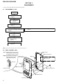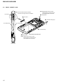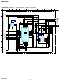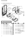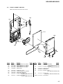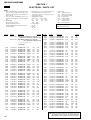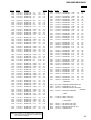
1
NW-A805/A806/A808
SERVICE MANUAL
Canadian Model
AEP Model
UK Model
E Model
Australian Model
Chinese Model
Tourist Model
Ver. 1.0 2007.04
Photo: NW-A808
• SonicStage and the SonicStage logo are trademarks or registered trademarks of Sony
Corporation.
• OpenMG, ATRAC, ATRAC3, ATRAC3plus, ATRAC Advanced Lossless and their logos are
trademarks of Sony Corporation.
• “WALKMAN”and “WALKMAN” logo are registered trademarks of Sony Corporation.
SPECIFICATIONS
Supported le format
Music
Codec
MP3
Bit rate: 32 to 320 kbps, variable bit rate-compliant (VBR)
Sampling frequency*1: 32, 44.1, 48 kHz
WMA*2
Bit rate: 32 to 192 kbps, variable bit rate-compliant (VBR)
Sampling frequency*1: 44.1 kHz
ATRAC
Bit rate: 48 to 352 kbps (66*3, 105*3, 132 kbps for ATRAC3)
Sampling frequency*1: 44.1 kHz
ATRAC
Advanced
Lossless* 4
Bit rate: 64 to 352 kbps (132 kbps for ATRAC3 base layer)
Sampling frequency*1: 44.1 kHz
AAC* 2
Bit rate: 16 to 320 kbps, variable bit rate-compliant (VBR)* 5
Sampling frequency*1: 8, 11.025, 12, 16, 22.05, 24, 32, 44.1, 48 kHz
is a trademark of Sony Corporation.
• Microsoft, Windows, Windows Vista and Windows Media are trademarks or registered
trademarks of Microsoft Corporation in the United States and/or other countries.
• Adobe and Adobe Reader are trademarks or registered trademarks of Adobe Systems
Incorporated in the United States and/or other countries.
• MPEG Layer-3 audio coding technology and patents licensed from Fraunhofer IIS and
Thomson.
• IBM and PC/AT are registered trademarks of International Business Machines Corporation.
• Macintosh is a trademark of Apple Inc.
• QuickTime is a trademark or registered trademark of Apple Inc. in the U.S. and/or other
countries.
• Pentium is a trademark or a registered trademark of Intel Corporation.
• This software is based in part on the work of the Independent JPEG Group.
• THIS PRODUCT IS LICENSED UNDER THE MPEG-4 VISUAL PATENT PORTFOLIO
LICENSE FOR THE PERSONAL AND NON-COMMERCIAL USE OF A CONSUMER FOR
(i) ENCODING VIDEO IN COMPLIANCE WITH THE MPEG-4 VISUAL STANDARD
(“MPEG-4 VIDEO”) AND/OR
(ii) DECODING MPEG-4 VIDEO THAT WAS ENCODED BY A CONSUMER ENGAGED
IN A PERSONAL AND NON-COMMERCIAL ACTIVITY AND/OR WAS OBTAINED
FROM A VIDEO PROVIDER LICENSED BY MPEG LA TO PROVIDE MPEG-4 VIDEO.
NO LICENSE IS GRANTED OR SHALL BE IMPLIED FOR ANY OTHER USE.
ADDITIONAL INFORMATION INCLUDING THAT RELATING TO PROMOTIONAL,
INTERNAL AND COMMERCIAL USES AND LICENSING MAY BE OBTAINED FROM
FROM MPEG LA, LLC. SEE HTTP://WWW.MPEGLA.COM
• THIS PRODUCT IS LICENSED UNDER THE AVC PATENT PORTFOLIO LICENSE FOR
THE PERSONAL AND NON-COMMERCIAL USE OF A CONSUMER TO
(i) ENCODE VIDEO IN COMPLIANCE WITH THE AVC STANDARD (“AVC VIDEO”)
AND/OR
(ii) DECODE AVC VIDEO THAT WAS ENCODED BY A CONSUMER ENGAGED IN A
PERSONAL AND
NON-COMMERCIAL ACTIVITY AND/OR WAS OBTAINED FROM A VIDEO PROVIDER
LICENSED TO PROVIDE AVC VIDEO. NO LICENSE IS GRANTED OR SHALL BE
IMPLIED FOR ANY OTHER USE.
ADDITIONAL INFORMATION MAY BE OBTAINED FROM MPEG LA, L.L.C. SEE
HTTP://MPEGLA.COM
• US and foreign patents licensed from Dolby Laboratories.
• All other trademarks and registered trademarks are trademarks or registered trademarks of their
respective holders. In this manual, TM and ® marks are not specified.
This product is protected by certain intellectual property rights of Microsoft Corporation.
Use or distribution of such technology outside of this product is prohibited without a license from
from Microsoft or an authorized Microsoft subsidiary.
Program ©2007 Sony Corporation
Documentation ©2007 Sony Corporation
The number of songsMax. 65,535
Video
File format
MP4 file format, “Memory Stick” video format
File extension
.mp4, .m4v
Codec
Video
MPEG-4
Profile: Simple Profile
Bit rate: Max. 2,500 kbps
AVC
(H.264/AVC)
Profile: Baseline Profile
Level: 1.2, 1.3
Bit rate: Max. 768 kbps
Frame rate: Max. 30 fps
Resolution: Max. QVGA (320 × 240)
Audio
File size
Max. 2 GB
The number of files
Max. 1,000
AAC-LC
Channel number: Max. 2 channels
Sampling frequency: 24, 32, 44.1, 48 kHz
Bit rate: Max. 288 kbps per 1 channel
Photo*6
File format
Compatible with DCF 2.0/Exif 2.21file format
File extension
.jpg
Codec
JPEG (Baseline)
Number of pixels: Max. 4,000 × 4,000 pixels (16,000,000 pixels)
The number of files
Max. 10,000
*1 Sampling frequency may not correspond to all encoders.
*2 Copyright protected WMA/AAC files cannot be played back.
*3 You cannot record songs on CDs in the ATRAC3 66/105 kbps format using SonicStage.
*4 The bit rate description of ATRAC Advanced Lossless shows the bit rate for the contents
which enables fast transfer to ATRAC compatible devices or media.
*5 Non-standard bit rates or non-guaranteed bit rates are included depending on the
sampling frequency.
*6 Some video files cannot be played back, depending on their file formats.
– Continued on next page –
DIGITAL MEDIA PLAYER
9-887-631-01
2007D05-1
© 2007.04
Sony Corporation
Connect Business Division
Published by Sony Techno Create Corporation
NW-A805/A806/A808
Maximum recordable number of songs and time (Approx.)
Battery life (continuous playback)
The approximate times are based on the case in which you transfer or record only 4
minutes songs (not including videos and photos) in the ATRAC*1 or the MP3 format.
Other playable audio file format song numbers and times may differ from ATRAC or MP3
format.
*1 Except ATRAC Advanced Lossless. Compression rate of ATRAC Advanced Lossless
varies depending on songs.
For example, one CD (containing 15 4-minute songs) is approximately 200 to 500 MB.
The time below is approximated when “New Song Pop Up”, “Clear Stereo”, “DSEE” and
and “Dynamic Normalizer” are set to “Off,” “Display Time” is set to other than “Always
On”, and screensaver, “Equalizer” and “VPT” are set to “None.”
Furthermore, for videos, the time is approximated when the brightness of the screen is set
to “3.”
The time below may differ depending on ambient temperature or the status of use.
NW-A805
NW-A806
NW-A805/A806/A808
Music
Bit rate
Songs
Time
Songs
Time
Playback at ATRAC 132 kbps
Approximately 30 hours
48 kbps
1,300
86 hr. 40 min.
2,700
180 hr. 00 min.
Playback at ATRAC 128 kbps
Approximately 27 hours
64 kbps
980
65 hr. 20 min.
2,000
133 hr. 20 min.
Playback at ATRAC 48 kbps
Approximately 28 hours
128 kbps
495
33 hr. 00 min.
1,000
66 hr. 40 min.
Approximately 27 hours
256 kbps
250
16 hr. 40 min.
515
34 hr. 20 min.
Playback at ATRAC Advanced
Lossless 64 kbps
320 kbps
200
13 hr. 20 min.
410
27 hr. 20 min.
Playback at MP3 128 kbps
Approximately 33 hours
Playback at WMA 128 kbps
Approximately 33 hours
Playback at AAC 128 kbps
Approximately 32 hours
NW-A808
Bit rate
Songs
Time
Video
48 kbps
5,500
366 hr. 40 min.
Playback at MPEG-4 384 kbps
Approximately 8 hours
64 kbps
4,100
273 hr. 20 min.
Playback at MPEG-4 768 kbps
Approximately 7 hours
128 kbps
2,050
136 hr. 40 min.
Playback at AVC 384 kbps
Approximately 6.5 hours
256 kbps
1,050
70 hr. 00 min.
Playback at AVC 768 kbps
Approximately 6.5 hours
320 kbps
840
56 hr. 00 min.
Display
Maximum recordable time of videos (Approx.)
The approximate recordable times is estimated in the case where only videos are
transferred. The time may differ, depending on the conditions under which the player is
used.
NW-A805
NW-A806
NW-A808
Bit rate
Time
Time
Time
384 kbps
7 hr. 40 min.
15 hr. 40 min.
32 hr. 40 min.
768 kbps
4 hr. 20 min.
9 hr. 20 min.
19 hr. 00 min.
Maximum recordable number of photos that can be transferred (Approx.)
Max. 10,000
Recordable number of photos may be less depending on file sizes.
Capacity (User available capacity)*
1
NW-A805: 2 GB (Approx. 1.81 GB = 1,948,622,848 bytes)
NW-A806: 4 GB (Approx. 3.73 GB = 4,008,198,144 bytes)
NW-A808: 8 GB (Approx. 7.56 GB = 8,127,348,736 bytes)
*1 Available storage capacity of the player may vary.
A portion of the memory is used for data management functions.
Output (headphones)
• Output
5 mW + 5 mW (16 )
• Frequency response
20 to 20,000 Hz (when playing data file, single signal measurement)
Interface
Headphone: Stereo mini-jack
WM-PORT (multiple connecting terminal): 22 pins
Hi-Speed USB (USB 2.0 compliant)
Operating temperature
5°C to 35°C (41°F to 95°F)
Power source
• Built-in rechargeable lithium-ion battery
• USB power (from a computer via the supplied USB cable)
Charging time
USB-based charging
Approx.3 hours (full charge), Approx.1.5 hours (approx. 80%)
2
2.0-inch, low-temperature poly-silicon TFT color display with white LED-backlight,
QVGA (240 × 320 dots), 0.1275 mm dot pitch, 262,144 colors
Dimensions (w/h/d, projecting parts not included)
43.8 × 88.0 × 9.1 (Thinnest part 8.3) mm (1 3/4 × 3 1/2 × 3/8 (Thinnest part 11/32) inches)
Dimension (w/h/d)
44.5 × 88.0 × 9.6 mm (1 13/16 × 3 1/2 × 13/32 inches)
Mass
Approx. 53 g (Approx. 1.9 oz)
Supplied Accessories
Headphones (1)
Headphone extension cord (1)
Earbuds (Size S, L) (1)
USB cable*1 (1)
Attachment (1)
Use when connecting the player to the optional cradle, etc.
CD-ROM*2 (1)
− SonicStage software
− Image Converter software*3
− Operation Guide (PDF file)
Quick Start Guide (1)
*1 Do not use any USB cable other than the supplied USB cable or the specified
optional dedicated cables.
*2 Do not attempt to play this CD-ROM in an audio CD player.
*3 Use this player together with the supplied Image Converter software (version
3.0 or later). This software is referred as ìImage Converterî in this manual.
Design and specifications are subject to change without notice.
NW-A805/A806/A808
SECTION 1
SERVICING NOTES
TABLE OF CONTENTS
1.
SERVICING NOTES ............................................... 3
2.
GENERAL ................................................................... 5
3.
DISASSEMBLY
3-1.
3-2.
3-3.
3-4.
3-5.
3-6.
Disassembly Flow ...........................................................
Rear Cabinet Assy ...........................................................
MAIN Board ....................................................................
Holder Connector ............................................................
NAND Board, SVX Switch Flexible (PWB Assy) ..........
Note When Installing The SVX Switch Flexible
(PWB Assy) .....................................................................
3-7. Front Button ....................................................................
3-8. SVX LCD Assy (LCD801), Battery Assy .......................
3-9. Front Cabinet Assy ..........................................................
6
6
7
7
8
8
9
9
10
4.
TEST MODE .............................................................. 11
5.
DIAGRAMS
5-1.
5-2.
5-3.
5-4.
5-5.
5-6.
5-7.
5-8.
5-9.
Block Diagram ................................................................
Printed Wiring Boards – MAIN Section (1/2) – ..............
Printed Wiring Boards – MAIN Section (2/2) – ..............
Schematic Diagram – MAIN Section (1/6) – ..................
Schematic Diagram – MAIN Section (2/6) – ..................
Schematic Diagram – MAIN Section (3/6) – ..................
Schematic Diagram – MAIN Section (4/6) – ..................
Schematic Diagram – MAIN Section (5/6) – ..................
Schematic Diagram – MAIN Section (6/6) – ..................
6.
EXPLODED VIEWS
18
20
21
22
23
24
25
26
27
6-1. Rear Cabinet Section ....................................................... 41
6-2. MAIN Board, NAND Board Section .............................. 42
6-3. Front Cabinet Section ...................................................... 43
7.
ELECTRICAL PARTS LIST ................................ 44
UNLEADED SOLDER
Boards requiring use of unleaded solder are printed with the leadfree mark (LF) indicating the solder contains no lead.
(Caution: Some printed circuit boards may not come printed with
the lead free mark due to their particular size)
: LEAD FREE MARK
Unleaded solder has the following characteristics.
• Unleaded solder melts at a temperature about 40 ˚C higher
than ordinary solder.
Ordinary soldering irons can be used but the iron tip has to be
applied to the solder joint for a slightly longer time.
Soldering irons using a temperature regulator should be set to
about 350 ˚C.
Caution: The printed pattern (copper foil) may peel away if
the heated tip is applied for too long, so be careful!
• Strong viscosity
Unleaded solder is more viscou-s (sticky, less prone to flow)
than ordinary solder so use caution not to let solder bridges
occur such as on IC pins, etc.
• Usable with ordinary solder
It is best to use only unleaded solder but unleaded solder may
also be added to ordinary solder.
NOTE THE IC301, IC302, IC501, IC503, IC505, IC506,
IC509, IC601, IC602, IC701, IC802, IC803, IC901 AND
IC903 ON THE MAIN BOARD REPLACING
When IC301, IC302, IC501, IC503, IC505, IC506, IC509, IC601,
IC602, IC701, IC802, IC803, IC901 and IC903 on the MAIN board
is damaged, exchange the new MAIN board for the MAIN board
which IC damaged.
NOTE THE CN601 ON THE MAIN BOARD
REPLACING
When CN601 on the MAIN board is damaged, exchange the new
MAIN board for the MAIN board which connector damaged.
MinimumSystem Requirements (for the player)
Notes on chip component replacement
• Never reuse a disconnected chip component.
• Notice that the minus side of a tantalum capacitor may be
damaged by heat.
Flexible Circuit Board Repairing
• Keep the temperature of the soldering iron around 270 ˚C
during repairing.
• Do not touch the soldering iron on the same conductor of the
circuit board (within 3 times).
• Be careful not to apply force on the conductor when soldering
or unsoldering.
CAUTION
Danger of explosion if battery is incorrectly replaced.
Replace only with the same or equivalent type.
• Computer
IBM PC/AT or compatible computer preinstalled with the following Windows operating
systems:
Windows 2000 Professional (Service Pack 4 or later)/Windows XP Home Edition (Service
Pack 2 or later)/Windows XP Professional (Service Pack 2 or later)/Windows XP Media
Center Edition (Service Pack 2 or later)/Windows XP Media Center Edition 2004 (Service
Pack 2 or later)/Windows XP Media Center Edition 2005 (Service Pack 2 or later)/Windows
Vista Home Basic/Windows Vista Home Premium/Windows Vista Business/Windows Vista
Ultimate
Not supported by 64 bit version OS.
Not supported by OSs other than above.
• CPU: Pentium III 733 MHz or higher (For Windows Vista, Pentium III 800 MHz or higher)
• RAM: 128 MB or more (For Windows XP, 256 MB or more; for Windows Vista, 512 MB
or more)
• Hard Disk drive: 240 MB or more of available space (1.5 GB or more is recommended)
More space may be required, depending on the version of the operating system.
Additional space is required for storing music, video and photo data.
• Display:
− Screen Resolution: 800 × 600 pixels (or higher) (recommended 1,024 × 768 or higher)
− Colors: High Color (16 bit) (or higher) (SonicStage and Image Converter may not operate
properly at color settings at or below 256 colors.)
• CD-ROM drive (supporting Digital Music CD playback capabilities using WDM)
To create original CDs or to back up audio CDs, a CD-R/RW drive is required.
• Sound board
• USB port (Hi-Speed USB is recommended)
• Internet Explorer 6.0 or later and DirectX version 9.0b or later need to be installed.
• Internet connection is required to use the CD Data Base (CDDB) or Electronic Music
Distribution (EMD) or to restore the backup data with SonicStage.
• When converting Windows Media format videos, it is required to have installed the latest
Windows Media Player.
• When converting QuickTime or M4V format videos, it is required to have installed the latest
QuickTime.
We do not guarantee operation for all computers even if they meet the above System
Requirements.
Not supported by the following environments:
− Personally constructed computers or operating systems
− An environment that is an upgrade of the original manufacturer-installed operating system
− Multi-boot environment
− Multi-monitor environment
− Macintosh
3
NW-A805/A806/A808
NOTE THE MAIN BOARD REPLACING
When the MAIN board is replaced, format it according to the
following.
COLOR VARIATION
Model
Formatting Memory (Format)
You can format the built-in flash memory of the player.
If the memory is formatted, all music, video and photo data, etc., will be
erased.
Be sure to verify the data stored in memory prior to formatting and export
any important data to SonicStage or the hard disk of your computer.
NW-A805
5-way button
Settings
BACK/HOME
button
NW-A806
Note
• This function is only available in the pause mode.
1 Press and hold the BACK/HOME button in the pause mode until the
Home menu appears.
2 Press the f/F/g/G button to select
(Settings), and then press
the 7 button to conrm.
3 Press the f/F/g/G button to select “Common Settings,” and then
press the 7 button to conrm.
The list of Common Settings options appears.
4 Press the f/F/g/G button to select “Format,” and then press the
7 button to conrm.
“All data including songs will be deleted. Proceed?” appears.
5 Press the f/F button to select “Yes,” and then press the 7 button
to conrm.
“All data will be deleted. Proceed?” appears.
6 Press the f/F button to select “Yes,” and then press the 7 button
to conrm.
While the memory is being formatted, an animated display appears.
When initialization finishes, “Memory formatted.” appears.
To cancel the operation
Select “No” in step 5 or 6 and press the 7 button to confirm.
To return to the previous menu
Press the BACK/HOME button.
Note
• Do not format the built-in flash memory using Windows Explorer.
4
NW-A808
Destination
CND
CE7
CEW
CEV
E, AUS, JE
MX
CH
CND
CE7
CEW
CEV
E, AUS, JE
MX
CH
CND
CE7
CEW
CEV
E, AUS, JE
MX
CH
BLACK
z
z
z
z
z
z
z
z
z
z
z
z
z
z
z
z
z
z
• Abbreviation
AUS : Australian model
CE7 : AEP and UK models
CEV : East European model
CEW : French model
CH : Chinese model
JE
: Tourist model
MX : Mexican model
COLOR
VIOLET WHITE
z
z
z
z
z
z
z
z
z
z
z
z
z
z
z
z
z
z
z
z
z
PINK
z
z
z
z
z
z
z
NW-A805/A806/A808
SECTION 2
GENERAL
This section is extracted from
instruction manual.
Parts and Controls
Front
Rear
1 5-way button*1
Starts playback and enables
navigation of the player’s on-screen
menus.
2 BACK/HOME button*2
Press to go up one list screen level,
or to return to the previous menu.
Press and hold the BACK/HOME
button to display the Home menu.
3 WM-PORT jack
Use this jack to connect the supplied
USB cable, or optional peripheral
devices, such as supported
accessories for the WM-PORT.
4 Headphone jack
For connecting the headphones or the
headphone extension cord. Insert the
jack pin until it clicks into place. If
the headphones are connected
improperly, the sound from the
headphones may not sound right.
Whenusing the headphone
extension cord
5 OPTION/PWR OFF button*2
Displays the Option menu.
If you press and hold the OPTION/
PWR OFF button, the screen turns
off and the player enters the standby
mode. If you press any button while
the player is in the standby mode,
the Now Playing screen appears and
the player is ready for operation.
Furthermore, if you leave the player
in the standby mode for about a day,
the player turns completely off
automatically. If you press any button
when the player is turned off, the
start up screen appears first, then the
Now Playing screen appears.
Note
• The player consumes the battery very
slightly even when it is in the standby
mode. Therefore, the player might
turn completely off in a short time,
depending on the power remaining in
the battery.
8 Strap hole
This is used to attach a strap (sold
separately).
9 HOLD switch
You can protect the player against
accidental operation by using the
HOLD switch when carrying it. By
sliding the HOLD switch in the
direction of the arrow, all operation
buttons are disabled. If you slide the
HOLD switch to the opposite
position, the HOLD function is
released.
*1 There are tactile dots. Use them to help
with button operations.
on the
*2 Functions of marked with
player are activated if you press and hold
the corresponding buttons.
6 VOL+*1/-- button
Adjusts the volume.
7 RESET button
Resets the player when you press the
RESET button with a small pin, etc.
Headphones
Headphone
extension cord
5
NW-A805/A806/A808
SECTION 3
DISASSEMBLY
• This set can be disassembled in the order shown below.
3-1. DISASSEMBLY FLOW
SET
3-2. REAR CABINET ASSY
(Page 6)
3-3. MAIN BOARD
(Page 7)
3-4. HOLDER CONNECTOR
(Page 7)
3-5. NAND BOARD,
SVX SWITCH FLEXIBLE (PWB ASSY)
(Page 8)
3-6. NOTE WHEN INSTALLING THE SVX SWITCH FLEXIBLE (PWB ASSY)
(Page 8)
3-7. FRONT BUTTON
(Page 9)
3-8. SVX LCD ASSY (LCD801),
BATTERY ASSY
(Page 9)
3-9. FRONT CABINET ASSY
(Page 10)
Note: Follow the disassembly procedure in the numerical order given.
3-2. REAR CABINET ASSY
4 two claws
Note1: Adhesive (rear) cannot re-used.
Please replace to brand-new part
once adhesive (rear) is removed.
8 rear cabinet assy
Note2: On installation of hold button,
adjust the position of hold
switch (S602) hold button.
3 claw
(BLACK, VIOLET model only)
7 spacer (belt)
3 claw
hold button
5
6 adhesive (rear)
2 claw
hold switch (S602)
1 two ornament pins
hold button
6 adhesive (rear)
hold switch (S602)
6
NW-A805/A806/A808
3-3. MAIN BOARD
9 insulating sheet (main)
1 cushion (connector)
q; spacer (PWB)
2 sheet (harness)
4 battery assy connector
(CN901)
3 LCD flexible board
(CN801)
6 screw (M1.4)
qa spacer (IC)
qg MAIN board
qf spacer (SRAM)
8 connector
(CN601)
qs Remove the
two solders.
qd shield case (main)
qs Remove the
two solders.
5 Unsolder three places of the
HP flexible board,
and turn it up without applying
an excessive force.
– rear view –
7 Turn up the LCD flexible board.
– rear view –
3-4. HOLDER CONNECTOR
5 connector door assy
NOTE WHEN INSTALLING THE SPRING (DOOR)
3
4 shaft
Note: Hook the spring (door) on the part A of connector door assy
and the part B of holder connector as shown in the figure.
6 spring (door)
2
4 shaft
holder connector
spring (door)
A
B
1 Lift up the
holder connector.
7 holder connector
connector door assy
– side view –
– rear view –
7
NW-A805/A806/A808
3-5. NAND BOARD, SVX SWITCH FLEXIBLE (PWB ASSY)
8 sheet (NAND)
(NW-A805/A806 only)
3 two screws (M1.4)
9 spacer (NAND)
q; NAND board
6 Remove the three solders.
5 Lift up the NAND board.
4 Turn up the LCD flexible board.
2 Lift up the
SVX swtch flexible (PWB assy).
7 SVX swtch flexible (PWB assy)
1 two claws
– rear view –
3-6. NOTE WHEN INSTALLING THE SVX SWITCH FLEXIBLE (PWB ASSY)
Note: Follow the assembly procedure in the numerical order given.
2 Holding the bent part,
rotate the SVX swtch flexible (PWB assy)
by 3 or 4 turns in the arrow direction,
and twist to bind the lead wires.
Note: Route the lead wires as shown in the figure,
and solder them at the angle shown in the figure.
SVX swtch flexible (PWB assy)
1 Bend the switch flexible board.
Note: The soldering height
should be less than 0.8 mm.
lead wire (red)
lead wire (gray)
claw
LCD holder
lead wires
About 45°
front cabinet assy
claw
About 45°
lead wire (black)
– rear view –
NAND board
3 Holding the bent part, push in the
SVX swtch flexible (PWB assy)
until it gets stuck by two claws
of the front cabinet assy.
4 Push the lead wires completely into a space
between front cabinet assy and LCD holder.
8
NW-A805/A806/A808
3-7. FRONT BUTTON
2 front button
1 Turn up the LCD flexible board.
– rear view –
3-8. SVX LCD ASSY (LCD801), BATTERY ASSY
1 screw (B1.4)
q; spacer (rear)
4 adhesive (LCD)
Note: Adhesive (LCD) cannot re-used.
Please replace to brand-new part
ones adhesive (LCD) is removed.
1 screw (B1.4)
qa battery assy
9 cushion (BATT)
3 Turn down the LCD flexible board.
7 two claws
6 adhesive (LCD)
Note: Adhesive (LCD) cannot re-used.
Please replace to brand-new part
ones adhesive (LCD) is removed.
5 Open the LCD flexible board.
8 SVX LCD assy
(LCD801)
7 two claws
7 claw
2
– rear view –
9
NW-A805/A806/A808
3-9. FRONT CABINET ASSY
VOL button
Note: The VOL button should be oriented
as shown in the figure when it is installed.
Note: NAND gasket cannot re-used.
Please replace to brand-new part
ones NAND gasket is removed.
3 NAND gasket
1 VOL button
4 conductive sheet (jack)
rear cabinet assy
front cabinet assy
5 front cabinet assy
front cabinet assy back view
2 gasket (rear)
Note: Gasket (rear) cannot re-used.
Please replace to brand-new part
ones gasket (rear) is removed.
– side view –
10
NW-A805/A806/A808
SECTION 4
TEST MODE
Note: Information on the test mode must correspond in enough security. When the leakage has been revealed by any chance, the source
of information is specified.
1. SETTING THE TEST MODE
Note: Perform the test mode in the state of 3.6 V or more in the
battery voltage.
Setting method:
1. Turn the power on.
2. Press the [BACK] key for 1.5 seconds or more, the home menu
is displayed.
3. Slide the [HOLD] key to set the hold on.
4. While pressing the [OPTION] key, press the key as following order.
v→B→V→b→v→u→v→b→V→B→v→u
5. The set reboots when the [HOLD] key is slided to set the hold
off, and the color bar is displayed in the liquid crystal display.
6. Enter the test mode when the [BACK] key is pressed in the
state of step 5.
Note: The destination setting and sound pressure regulation setting cannot be executed by this test mode.
2. RELEASING THE TEST MODE
1. Display the major item selection screen.
2. Press the v / V key to select the “EXITTEST”, and press the
B key to select the “SURE ?”.
3. Press the u key, turn the power off and release the test mode.
3. CONFIGURATION OF THE TEST MODE
Major item
[B] key
Major item switching:
[v]/ [V] key
[b] key
Minor item
Minor item switching:
[v]/ [V] key
[u] key
Start
[BACK] key
Automatic
4-1-1. Power supply voltage check
This mode is used in case power supply voltage in the state where
all power supply lines are starting is checked.
Checking method:
1. Enter the test mode.
2. Press the v / V key to select the “POWER”, and press the
key to enter the minor item.
3. Press the v / V key to select the “VCHK”.
4. Press the u key, all power supply lines are started.
B
liquid crystal display
POWER VCHK
START
In this state, the power supply voltage of each power supply line
can be confirmed by measuring the voltage.
5. Press the [BACK] key, return to minor item selection screen.
4-1-2. Consumption current (audio playback) check
This mode is used in case consumption current (audio playback) is
checked in the state where “1 kHz 0 dBs L-ch/R-ch VOLUME: 15”
audio signal is outputed.
Checking method:
1. Enter the test mode.
2. Press the v / V key to select the “POWER”, and press the B
key to enter the minor item.
3. Press the v / V key to select the “ACHK”.
4. Press the u key, “1 kHz 0 dBs L-ch/R-ch VOLUE: 15” audio
signal is outputed.
liquid crystal display
Finish
or
Result
4. OPERATION OF THE TEST MODE
4-1. Power
POWER ACHK
1kHz 0dBs L/Rch
HPOUT [ VOL: 15 ]
liquid crystal display
MPTAPP MENU
POWER
AUDIO
VIDEO
OTHER
SHUTDOWN
EXITTEST
VCHK
ACHK
DSVCHK
CHGCHK
BATTCHK
START
5. In this state, each time the [OPTION] key is pressed, LCD back
light on/off switch is performed.
6. Press the [BACK] key, return to minor item selection screen.
11
NW-A805/A806/A808
4-1-3. Standby current check
4-1-5. Battery voltage check
This mode is used in case standby current is checked.
This mode is used in case battery voltage is checked.
Checking method:
1. Enter the test mode.
2. Press the v / V key to select the “POWER”, and press the
key to enter the minor item.
3. Press the v / V key to select the “DSVCHK”.
4. Press the u key, enter the state of the deep sleep.
5. Press the [BACK] key, release the state of the deep sleep.
Checking method:
1. Enter the test mode.
2. Press the v / V key to select the “POWER”, and press the B
key to enter the minor item.
3. Press the v / V key to select the “BATTCHK”.
4. Press the u key, the battery voltage is displayed.
When the battery voltage cannot be confirmed, “ERROR” is
displayed.
B
liquid crystal display
liquid crystal display
POWER DSVCHK
POWER BATTCHK
X.XXXV
OK
6. Press the [BACK] key, return to minor item selection screen.
X.XXXV: Battery voltage
4-1-4. Charge current check
6. Press the [BACK] key, return to minor item selection screen.
This mode is used in case charge current is checked.
Checking method:
1. Enter the test mode.
2. Press the v / V key to select the “POWER”, and press the
key to enter the minor item.
3. Press the v / V key to select the “CHGCHK”.
4. Press the u key, the charge setting is displayed.
B
liquid crystal display
POWER CHGCHK
AC
AC
5. In this state, each time the [OPTION] key is pressed, the port
setting for the charge is changed as shown in the table below.
Port control
Display CHG_XCHGEN CHG_PEN CHG_PEN2
AC
L
H
H
USB500
L
H
H
USB100
L
H
L
6. Press the [BACK] key, return to minor item selection screen.
12
4-2. Audio
While playing the audio track, it's in a repeat state. If [BACK] key is
pressed, it’s stopped.
Press the [VOL +] key to switch the HP/LINE.
liquid crystal display
MPTAPP MENU
POWER
AUDIO
VIDEO
OTHER
SHUTDOWN
EXITTEST
OUTPUT
SN
F1
F2
SEPLR
SEPRL
MAXOUT
NMLZR
SPCHK
NW-A805/A806/A808
4-2-1. Output check
4-2-3. Frequency characteristic 1 check
“1 kHz 0 dBs L-ch/R-ch VOLUME: 25” audio signal is outputted.
“20 Hz 0 dBs L-ch/R-ch VOLUME: 25” audio signal is outputted.
Checking method:
1. Enter the test mode.
2. Press the v / V key to select the “AUDIO”, and press the B
key to enter the minor item.
3. Press the v / V key to select the “OUTPUT”.
4. Press the u key, “1 kHz 0 dBs L-ch/R-ch VOLUME: 25”
audio signal is outputted.
Checking method:
1. Enter the test mode.
2. Press the v / V key to select the “AUDIO”, and press the B
key to enter the minor item.
3. Press the v / V key to select the “F1”.
4. Press the u key, “20 Hz 0 dBs L-ch/R-ch VOLUME: 25”
audio signal is outputted.
liquid crystal display
liquid crystal display
AUDIO OUTPUT
1kHz 0dBs L/Rch
HPOUT [ VOL: 25 ]
AUDIO F1
20Hz 0dBs L/Rch
HPOUT [ VOL: 25 ]
START
START
5. Press the [BACK] key, return to minor item selection screen.
5. Press the [BACK] key, return to minor item selection screen.
4-2-2. S/N check
4-2-4. Frequency characteristic 2 check
“Infinity Zero VOLUME: 30” audio signal is outputted.
“20 kHz 0 dBs L-ch/R-ch VOLUME: 25” audio signal is outputted.
Checking method:
1. Enter the test mode.
2. Press the v / V key to select the “AUDIO”, and press the B
key to enter the minor item.
3. Press the v / V key to select the “SN”.
4. Press the u key, “Infinity Zero VOLUME: 30” audio signal
is outputted.
Checking method:
1. Enter the test mode.
2. Press the v / V key to select the “AUDIO”, and press the B
key to enter the minor item.
3. Press the v / V key to select the “F2”.
4. Press the u key, “20 kHz 0 dBs L-ch/R-ch VOLUME: 25”
audio signal is outputted.
liquid crystal display
liquid crystal display
AUDIO SN
Infinity Zero
HPOUT [ VOL: 30 ]
AUDIO F2
20kHz 0dBs L/Rch
HPOUT [ VOL: 25 ]
START
START
5. Press the [BACK] key, return to minor item selection screen.
5. Press the [BACK] key, return to minor item selection screen.
13
NW-A805/A806/A808
4-2-5. CH separation (L-ch) check
4-2-7. Maximum output check
“1 kHz 0 dBs L-ch VOLUME: 25” audio signal is outputted.
“1 kHz 0 dBs L-ch/R-ch VOLUME: 30” (Headphone output when
AVLS operates: “1 kHz 0 dBs L-ch/R-ch VOLUME: 13”) audio signal is outputted.
Checking method:
1. Enter the test mode.
2. Press the v / V key to select the “AUDIO”, and press the B
key to enter the minor item.
3. Press the v / V key to select the “SEPLR”.
4. Press the u key, “1 kHz 0 dBs L-ch VOLUME: 25” audio
signal is outputted.
liquid crystal display
Checking method:
1. Enter the test mode.
2. Press the v / V key to select the “AUDIO”, and press the B
key to enter the minor item.
3. Press the v / V key to select the “MAXOUT”.
4. Press the u key, “1 kHz 0 dBs L-ch/R-ch VOLUME: 30”
(Headphone output when AVLS operates: “1 kHz 0 dBs L-ch/
R-ch VOLUME: 13”) audio signal is outputted.
liquid crystal display
AUDIO SEPLR
1kHz 0dBs Lch
HPOUT [ VOL: 25 ]
AUDIO MAXOUT
1kHz 0dBs L/Rch
HPOUT [ VOL: 30 ]
AVLS OFF
START
5. Press the [BACK] key, return to minor item selection screen.
START
4-2-6. CH separation (R-ch) check
“1 kHz 0 dBs R-ch VOLUME: 25” audio signal is outputted.
Checking method:
1. Enter the test mode.
2. Press the v / V key to select the “AUDIO”, and press the B
key to enter the minor item.
3. Press the v / V key to select the “SEPRL”.
4. Press the u key, “1 kHz 0 dBs R-ch VOLUME: 25” audio
signal is outputted.
liquid crystal display
AUDIO SEPRL
1kHz 0dBs Rch
HPOUT [ VOL: 25 ]
START
5. In this state, each time the [OPTION] key is pressed, AVLS on/
off switch is performed.
6. Press the [BACK] key, return to minor item selection screen.
4-2-8. Normalizer check
“1 kHz –24 dBs L-ch/R-ch VOLUME: 30” audio signal is outputted.
Checking method:
1. Enter the test mode.
2. Press the v / V key to select the “AUDIO”, and press the B
key to enter the minor item.
3. Press the v / V key to select the “NMLZR”.
4. Press the u key, “1 kHz –24 dBs L-ch/R-ch VOLUME: 30”
audio signal is outputted.
liquid crystal display
AUDIO NMLZR
1kHz –24dBs L/Rch
HPOUT [ VOL: 30 ]
5. Press the [BACK] key, return to minor item selection screen.
START
5. Press the [BACK] key, return to minor item selection screen.
14
NW-A805/A806/A808
4-2-9. Sound pressure regulation level check
“1 kHz 0 dBs L-ch/R-ch VOLUME: 30” audio signal is outputted.
Checking method:
1. Enter the test mode.
2. Press the v / V key to select the “AUDIO”, and press the B
key to enter the minor item.
3. Press the v / V key to select the “SPCHK”.
4. Press the u key, “1 kHz 0 dBs L-ch/R-ch VOLUME: 30”
audio signal is outputted.
liquid crystal display
AUDIO SPCHK
1kHz 0dBs L/Rch
HPOUT [ VOL: 30 ]
START
5. Press the [BACK] key, return to minor item selection screen.
4-4. Other
liquid crystal display
MPTAPP MENU
POWER
AUDIO
VIDEO
OTHER
SHUTDOWN
EXITTEST
CLOCK
KEY
FORMAT
DEST
SPSET
FWVER
NCAPCHK
4-4-1. Clock check
The movement of an internal clock is confirmed.
Checking method:
1. Enter the test mode.
2. Press the v / V key to select the “OTHER”, and press the
key to enter the minor item.
3. Press the v / V key to select the “CLOCK”.
4. Press the u key, date and time are displayed.
B
liquid crystal display
4-3. Video
liquid crystal display
MPTAPP MENU
POWER
AUDIO
VIDEO
OTHER
SHUTDOWN
EXITTEST
OTHER CLOCK
XX, XX XX XXXX
##:##:##.######
LCD
START
XX, XX XX XXXX
##:##:##.######
4-3-1. LCD display check
Liquid crystal display is checked.
: Date
: Time
“START” changes into “OK” if the movement of an internal
clock is confirmed.
5. Press the [BACK] key, return to minor item selection screen.
Checking method:
1. Enter the test mode.
2. Press the v / V key to select the “VIDEO”, and press the B
key to select the “LCD”.
3. Press the u key, all black is displayed on the liquid crystal
display.
4. In this state, each time the [OPTION] key is pressed, the screen
display changes in the following order.
All black (default) → All red → All green → All blue → All
white → Color bar → Maximum drawing size confirmation
Maximum drawing size confirmation:
All blue (All sides are red) is displayed. Whether red in all
sides is seen is confirmed.
4. In this state, each time the [VOL ---] key is pressed, LCD back
light brightness min/max/middle switch is performed.
5. Press the [BACK] key, return to minor item selection screen.
15
NW-A805/A806/A808
4-4-2. Key check
4-4-6. Firmware version check
The operation of the key is confirmed.
The firmware version is displayed.
Checking method:
1. Enter the test mode.
2. Press the v / V key to select the “OTHER”, and press the
key to enter the minor item.
3. Press the v / V key to select the “KEY”.
4. Press the u key, all keys are displayed.
Checking method:
1. Enter the test mode.
2. Press the v / V key to select the “OTHER”, and press the
key to enter the minor item.
3. Press the v / V key to select the “FWVER”.
4. Press the u key, the firmware version is displayed.
B
liquid crystal display
B
liquid crystal display
OTHER FWVER
X.XX.XX
OTHER KEY
UP
VOL+
REW
PLAY FF VOL–
DOWN OPTION
HOLD
BACK
START
5. The character corresponding to the key is selected every time
the key is pressed. “START” changes into “OK” if all keys are
pressed.
6. Slide the [HOLD] key from ON to OFF, return to minor item
selection screen.
X.XX.XX
: Firmware version
5. Press the [BACK] key, return to minor item selection screen.
4-4-7. NAND capacity check
(firmware version 1.00.19 former)
4-4-3. Format
The user’s area is formatted, and ICV for the video and ICV for
audio are initialized.
Note: Not used for the servicing.
Format the set from “Settings” → “Common settings” →
“Format” when it home menu in usually operates when the
set should format it.
Capacity of NAND flash memory is displayed.
Checking method:
1. Enter the test mode.
2. Press the v / V key to select the “OTHER”, and press the B
key to enter the minor item.
3. Press the v / V key to select the “NCAPCHK”.
4. Press the u key, capacity of NAND flash memory is displayed.
4-4-4. Destination setting
The destination setting, language information, and sound pressure
regulation information are written in the NAND flash memory.
liquid crystal display
Note: Not used for the servicing.
OTHER NCAPCHK
X GB
4-4-5. Sound pressure regulation setting
ON/OFF of sound pressure regulation is confirmed.
Note: Not used for the servicing.
X GB
: Capacity of NAND flash memory
2 GB/4 GB/8 GB
5. Press the [BACK] key, return to minor item selection screen.
16
NW-A805/A806/A808
4-4-8. NAND capacity check
(since firmware version 1.00.20)
Capacity of NAND flash memory, present bud block, maximum
bud block, and vender ID are displayed.
Checking method:
1. Enter the test mode.
2. Press the v / V key to select the “OTHER”, and press the B
key to enter the minor item.
3. Press the v / V key to select the “NCAPCHK”.
4. Press the u key, capacity of NAND flash memory, present
bud block, maximum bud block, and vender ID are displayed.
liquid crystal display
OTHER NCAPCHK
X @@@@ #### $$$$
X
: Capacity of NAND flash memory
2/4/8 (2 GB/4 GB/ 8 GB)
@@@@ : Number of present bud block
(It makes an error the acquisition of the number
of bud blocks at “–1”)
####
: Number of maximum bud block
(It makes an error the acquisition of the vender ID
at “–1”)
$$$$
: Vender ID of NAND flash memory
0x98/0xec (TOSHIBA/SAMSUNG)
(It makes an error the acquisition of the vender ID
at “–1”)
5. Press the [BACK] key, return to minor item selection screen.
4-5. Shutdown
Function that power supply of set can be turned off without ending
static test mode.
Procedure:
1. Enter the test mode.
2. Press the v / V key to select the “SHUTDOWN”, and press
the B key to select the “SURE ?”.
3. Press the u key, turn the power off while having entered the
test mode.
NW-A805/A806/A808
17
17
NW-A805/A806/A808
SECTION 5
DIAGRAMS
5-1. BLOCK DIAGRAM
CN851 (1/2)
(WM-PORT)
D+
D–
SYSTEM CONTROLLER, POWER CONTROL,
LCD DRIVER, NAND FLASH INTERFACE,
MS INTERFACE, SD-RAM INTERFACE
IC601
USB
CONTROLLER
IC501
3
4
A3 DP
A4 DM
CD0 – CD15
A/D CONVERTER,
D/A CONVERTER
IC302
AB0_D0 – AB0_D15
USB DATA0 – USB DATA15
CA1 – CA8
HEADPHONE/LINE
SELECTOR
IC303
AB0_A1 – AB0_A8
USB ADDRESS1 – USB ADDRESS8
PM0_SO AC22
X501
12MHz
C8 XO
XCS
XRD
XDACK
XDREQ
F22
J19
F23
E24
H2
G3
F4
G4
IC508
LEVEL SHIFT
IC509
XINT E3
XWRH F3
XWRL H3
3 COM1
9 COM2
AOUTA 11
AOUTB 10
32 SDIN
AB0_CSZ2
AB0_RDZ
AB0_XACK
AB0_XDRQ
AC5 USB_INT1
AB14 USB_INT2
CN851 (2/2)
(WM-PORT)
14 AU_L_OUT
17 AU_R_OUT
NC1 4
NC2 8
5 7
MUTING
Q302
MUTING
Q303
CRD_LINEOUT AA1
MUTING
CONTROL
Q301, 304
HP_XMUTE Y3
D FLIP-FLOP
IC505, 506
H16 AB0_WRZ
IC507
E19 FLASHCLK
XRESET D1
NO1 2
NO2 10
IN1
IN2
B8 XI
J301
(HEADPHONE)
P10 RESETZ
AB13 USB_XRST
RESET SWITCH
IC502
T26 CKO
X603
11.2896MHz
U26 CKI
PM0_SI AD22
SPIO_SO
SPIO_SK
PM0_CLK
PM0_SEN
REFCLKO
SPIO_SCZ2
ADA_XRST
29 SDOUT
AC8
AC7
AC21
AB22
U18
AD7
AC20
2
3
31
1
30
4
25
13 AU_L_IN
16 AU_R_IN
AIN1A 23
AIN1B 24
SDA/CDIN
SCL/CCLK
SCLK
LRCK
MCLK
AD0/nCS
nRESET
AC26 OSCOUT
X602
32.768kHz
AB26 OSCIN
256Mbit SD-RAM
IC701
DQ0 – DQ31
SDR_D0O – SDR_D31
SDR_DATA0 –
SDR_DATA31
A0 – A12
SDR_A00 – SDR_A12
SDR_A0 – SDR_A12
BA0
BA1
CLK
CS
CKE
WE
CAS
RAS
DQM0
DQM1
DQM2
DQM3
J7
H8
J1
J8
J2
K8
K7
J9
K9
K1
F8
F2
AB5
T4
AA5
T3
T1
R5
U8
T5
P5
R4
R3
R2
NAND_D0O – NAND_D07
LCD_R0 – LCD_R5
LCD_G0 – LCD_G5
LCD_G0 – LCD_G5
LCD_B0 – LCD_B5
S601
: AUDIO
LCD BACK
LIGHT DRIVER
IC802
LCD_BLTCTL V17
LCD_PWM1 AD23
LCD_PCI W2
LCD_PON W3
VCC_VBUS
VCC_DCIN
VCC_VBUS
VCC_VBAT
20
11
12
DCIN
USB_DET
UNREG_OUT
10
8
TXD/SLEEP
RXD/WAKE
9
CRD_AD
VDD_UNREG
NAND_CLE
NAND_ALE
NAND_CEZ0
NAND_CEZ1
NAND_CEZ2
NAND_CEZ3
NAND_WEZ
NAND_REZ
NAND_RBZ0
NAND_RBZ1
NAND_RBZ2
NAND_RBZ3
VDD_UNREG
20 SYS
21 SYS
DC/DC
CONVERTER
IC903
VDD_DDCOUT20
SYS +3.1V
+3.1V
REGULATOR
IC602
USB +1.8V
+1.8V
REGULATOR
IC504
USB +3.1V
+3.1V
REGULATOR
IC503
USB_PWRCTL AD20
AD5 KEY_WAKE
HP/LINE +1.8V
U13 WAKEUP
AA2 WAKEUP_INT
G4 EXTRST
S602 OFF
(HOLD)
ON
LCD_B0 – LCD_B5
LIQUID
CRYSTAL
DISPLAY
LCD801
RESET
• SIGNAL PATH
LCD_G0 – LCD_G5
LEVEL
SHIFT
IC803
LCD_VSYNC K24
LCD_HSYNC K22
LCD_PXCLK P23
C6 KEY_AD0
B6 KEY_AD1
WAKE UP
SWITCH
Q603
LCD_B0 – LCD_B5
LCD_R0 – LCD_R5
NAND_DA0 – NAND_DA12
E9
D3
M9
C2
B3
C3
A4
E3
D2
H8
J8
K8
NAND
BOARD
SDR_BA0
SDR_BA1
SDR_CLK
SDR_CSZ0
SDR_CKE0
SDR_WEZ
SDR_CASZ
SDR_RASZ
SDR_DQM0
SDR_DQM1
SDR_DQM2
SDR_DQM3
LCD_R0 – LCD_R5
AD4 XHOLD_KEY
NW-A805/A806/A808
18
18
+1.8V
REGULATOR
IC301
CHG_ICTL Y2
VDD_ANA
VDD_ECO
VDD_DDCIO
VDD_GP1
VDD_GP3
VDD_GP4
VDD_HP
VDD_LO
VDD_LOG
VDD_PLL
CHG_XCHGEN
CHG_PEN2
USB_SUSPEND
XUSB_OK
XCHG_DET
CHG_XFLT
V10
W8
AB8
AB2
AC4
AB4
U70_SOUT
U70_SRIN
CRD_DET
CRD_AD
T17
T18
AB3
C8
CHARGE
CONTROL
Q903
DC
DC
USB
USB
2
3
15
16
POWER CONTROL,
CHARGE CONTROL
IC901
11 ISET
22
4
6
13
23
19
24
/DOK
/CEN
PEN2
USUSS
/UOK
/CHG
/FLT
BAT 17
BAT 18
LITHIUM ION
STRAGE
BATTERY
3.7V 610mAh
NW-A805/A806/A808
• Note for Printed Wiring Boards and Schematic Diagrams
Note on Printed Wiring Board:
• Y : parts extracted from the conductor side.
: Pattern from the side which enables seeing.
•
(The other layers' patterns are not indicated.)
Caution:
Pattern face side:
(Side B)
Parts face side:
(Side A)
Parts on the pattern face side seen from
the pattern face are indicated.
Parts on the parts face side seen from
the parts face are indicated.
• MAIN board is multi-layer printed board.
However, the patterns of intermediate-layers have not been
included in diagrams.
Note on Schematic Diagram:
• All capacitors are in µF unless otherwise noted. (p: pF)
50 WV or less are not indicated except for electrolytics
and tantalums.
• All resistors are in Ω and 1/4 W or less unless otherwise
specified.
• C : panel designation.
• A : B+ Line.
• Power voltage is dc 3.7 V and fed with regulated dc power
supply from CN901 pin 1 and pin 2 on the MAIN board.
• Voltages are dc with respect to ground under no-signal
conditions.
no mark : PLAY BACK
• Voltages are taken with a VOM (Input impedance 10 MΩ).
Voltage variations may be noted due to normal production tolerances.
• Signal path.
F : AUDIO
L : VIDEO
• Abbreviation
CEW : French model
NW-A805/A806/A808
19
19
NW-A805/A806/A808
1
3
4
5
6
A
R643
C692
R611
M3 M2 M1
V5 V4 V3 V2 V1
K9 K8 K7
U26 U25 U24 U23 U22
U19 U18 U17 U16 U15 U14 U13 U12 U11 U10 U9 U8
U5 U4 U3 U2 U1
T26 T25 T24 T23 T22
T19 T18 T17
T10 T9 T8
T5 T4 T3 T2 T1
R26 R25 R24 R23 R22
R19 R18 R17
R10 R9 R8
R5 R4 R3 R2 R1
P26 P25 P24 P23 P22
P19 P18 P17
P10 P9 P8
P5 P4 P3 P2 P1
IC601
N26 N25 N24 N23 N22
N19 N18 N17
N10 N9 N8
N5 N4 N3 N2 N1
M26 M25 M24 M23 M22
M19 M18 M17
M10 M9 M8
M5 M4 M3 M2 M1
L26 L25 L24 L23 L22
L19 L18 L17
L11 L10 L9 L8
L5 L4 L3 L2 L1
K26 K25 K24 K23 K22
K19 K18 K17 K16 K15 K14 K13 K12 K11 K10 K9 K8
K5 K4 K3 K2 K1
J26 J25 J24 J23 J22
J19 J18 J17 J16 J15 J14 J13 J12 J11 J10 J9 J8
J5 J4 J3 J2 J1
H26 H25 H24 H23 H22
H19 H18 H17 H16 H15 H14 H13 H12 H11 H10 H9 H8
H5 H4 H3 H2 H1
G26 G25 G24 G23 G22
G5 G4 G3 G2 G1
F26 F25 F24 F23 F22
F5 F4 F3 F2 F1
J9
J8
J7
F9
F8
F7
F3
F2
F1
E9
E8
E7
E3
E2
E1
D9 D8 D7
D3 D2 D1
C9 C8 C7
C3 C2 C1
B9 B8 B7
B3 B2 B1
A1
A3 A2
A26 A25 A24 A23 A22 A21 A20 A19 A18 A17 A16 A15 A14 A13 A12 A11 A10 A9 A8 A7 A6 A5 A4 A3 A2 A1
VDR852
2 4
1 3
R604
C623 R656
R657
C619 R655
R621 R658
C611
R619
R620
C853
R647
R642
C628
C518
IC509
R857
R628
R629
R510
C631
R509
VDR851
X501
1
C645
D
S
G
C689
CL909
LF851
CL637
R618
R646
C516
A1 B1 C1
1
8
4
9
5
R514
C633 C634
R853
C509
5
3
R855
4
IC502 IC506
R648
R649
IC508
5
4
A2 B2 C2
CL633
R520
1
C517
R502
C510
1
R858
C505
R506
3
IC505
R513
IC501
R516
5
C513
R851
CL634
4
IC507
9 1
8
C514
C657
3 1
R517
A1
A2
A3
A4
A5
A6
A7
A8
C690
F1 E1 D1 C1 B1
F2 E2 D2 C2 B2
F3 E3 D3 C3 B3
F4
C4 B4
F5
C5 B5
F6 E6 D6 C6 B6
F7 E7 D7 C7 B7
F8 E8 D8 C8 B8
5
C656
R603
C686
R505
C501
A9 A8 A7
B26 B25 B24 B23 B22 B21 B20 B19 B18 B17 B16 B15 B14 B13 B12 B11 B10 B9 B8 B7 B6 B5 B4 B3 B2 B1
R522
H1 G1
H2 G2
H3 G3
H4 G4
H5 G5
H6 G6
H7 G7
H8 G8
H3 H2 H1
G3 G2 G1
G9 G8 G7
C26 C25 C24 C23 C22 C21 C20 C19 C18 C17 C16 C15 C14 C13 C12 C11 C10 C9 C8 C7 C6 C5 C4 C3 C2 C1
4
C512
R519
3
J1
J2
J3
IC701
D26 D25 D24 D23 D22 D21 D20 D19 D18 D17 D16 D15 D14 D13 D12 D11 D10 D9 D8 D7 D6 D5 D4 D3 D2 D1
1
L801
K3 K2 K1
H9 H8 H7
E26 E25 E24 E23 E22 E21 E20 E19 E18 E17 E16 E15 E14 E13 E12 E11 E10 E9 E8 E7 E6 E5 E4 E3 E2 E1
L1
22
E
C502
23
CN851
(WM-PORT)
24
CL907
11
(11)
1-871-811-
NW-A805/A806/A808
20
20
29
W5 W4 W3 W2 W1
V19 V18 V17 V16 V15 V14 V13 V12 V11 V10 V9 V8
NAND
BOARD
S601
RESET
1
W19 W18 W17 W16 W15 W14 W13 W12 W11 W10 W9 W8
V26 V25 V24 V23 V22
CN601
W26 W25 W24 W23 W22
L2
L3
L7
30
L8
L9
C515
R511
R512
M9 M8 M7
2
Y5 Y4 Y3 Y2 Y1
C711 C712
AA5 AA4 AA3 AA2 AA1
Y26 Y25 Y24 Y23 Y22
5
R702
AA26 AA25 AA24 AA23 AA22
C507
R504
N3 N2 N1
6
11
IC903
C710 C709
R633
C668
IC504
C503
C508
N9 N8 N7
10
L901
1
R650
R521
P3 P2 P1
Q603
B1 A1
B2 A2
C511
P9 P8 P7
R605
R814
R503
C612
4
6
R3 R2 R1
AE26 AE25TAE24 AE23 AE22 AE21 AE20 AE19 AE18 AE17 AE16 AE15 AE14 AE13 AE12 AE11 AE10 AE9 AE8 AE7 AE6 AE5 AE4 AE3 AE2 AE1
C625
C685
C683 C682
C629
R9 R8 R7
R859
C614
X603
C703 C704
CL910
AF26 AF25 AF24 AF23 AF22 AF21 AF20 AF19 AF18 AF17 AF16 AF15 AF14 AF13 AF12 AF11 AF10 AF9 AF8 AF7 AF6 AF5 AF4 AF3 AF2 AF1
R623
R644
C618
C604
C620
R627
C669
R634
C601
C616
C640
AB26AB25 AB24 AB23 AB22 AB21AB20AB19AB18AB17AB16AB15AB14AB13AB12AB11AB10 AB9 AB8 AB7 AB6 AB5 AB4 AB3 AB2 AB1
C688
CL621
C654 C702 C714
C672 C675
AD26 AD25AD24 AD23 AD22 AD21 AD20 AD19 AD18 AD17 AD16 AD15 AD14 AD13 AD12 AD11 AD10 AD9 AD8 AD7 AD6 AD5 AD4 AD3 AD2 AD1
IC503 R507
D
C655 C701 C713
C680 C684 C687
C615 C698 C651 C661
C643
C504
C609
C
C671 C674 C677
AC26 AC25 AC24 AC23 AC22 AC21 AC20 AC19 AC18 AC17 AC16 AC15 AC14 AC13 AC12 AC11 AC10 AC9 AC8 AC7 AC6 AC5 AC4 AC3 AC2 AC1
C666
C603
B
C667
CL620
C626
X602
C602
CL908
C608
C605
R635
C607
D-5
C613 C697 C650 C660
R601
C610
MAIN BOARD (SIDE A)
C695
Q603
: Uses unleaded solder.
2
C617
Ref. No. Location
IC501
D-2
IC502
D-3
IC503
C-1
IC504
C-2
IC505
D-3
IC506
D-3
IC507
D-2
IC508
D-4
IC509
D-4
IC601
C-3
IC701
C-4
IC903
B-6
5-2. PRINTED WIRING BOARDS – MAIN Section (1/2) –
C506
• Semiconductor
Location
NW-A805/A806/A808
5-3. PRINTED WIRING BOARDS – MAIN Section (2/2) –
1
• Semiconductor
Location
: Uses unleaded solder.
2
3
4
5
6
Ref. No. Location
D101
D-3
D201
D-3
A
MAIN BOARD (SIDE B)
1
R801
2
C606
C813
R312
C302
C104
25
24
R202
C203 C103
R102
C102
1
C202
C205
C105
R901
C915
6
C301
1
2
CN901
C920
C632
S602
HOLD
ON
OFF
CL902
R607
CL901
R608
R861
R302
3
7
C204
C206
C904
R651
CL201
32
33
IC302
R204
C917
C909
CN801
FB806
R630
12
CL905
C305
4
33
C910
13
C307
R315
11
1-871-811- (11)
CL101
1
2
LITHIUM ION
STRAGE BATTERY
3.7V 610mAh
NW-A805/A806/A808
21
21
IC301
C308
FB805
R314
32
R912
E
CL623
CL904
25
7
FB807
FB818
C306
16
17
C106
C908
IC901
R903
C902
18
FB809
1
R104
24
1
C110
R110
19
FB810
C314
C313
R922
A
FB101
C907
C906
CL903
D101
G
LCD801
LIQUID
CRYSTAL
DISPLAY
FB817
8
C315
D
FB811
FB813
R310
C312
Q903
R919
R907
R107
A
S
FB802
R305
C318
R923
C662
R306
R911
FB803
FB801
R304
5
9
FB804
C316
C207
C310
1
CL603
C303
C678 C691
R205
A1
A2
A3
A4
A5
A6
A7
A8
A9
A10
FB815 FB808
C804
R806
C638
C694
C311
R105
R921
R908
CL604
R626
FB816 FB814 FB812
L602
C653
IC303
R106
CL622
CL629
C665
R805
R622
R624
R617
C648
C208
Q303
R209
C321
IC803
C681
6
CL102
R811
C806
C647
C646
C676
C670
L601
R210
L
K1 J1 H1 G1 F1 E1 D1 C1 B1
K2
K3
H3 G3 F3 E3 D3 C3
K4
H4
C4
K5
H5
C5
K6
H6
C6
K7
H7
C7
K8
H8 G8 F8 E8 D8 C8
K9
K10 J10 H10G10 F10E10D10 C10B10
C107
2E 2B 1C
R111
C210
A805: CEW/
A806: CEW/
A808: CEW
CL301
HP
FLEXIBLE
BOARD
R816
C664
R660
C802 R636
FB819
R637
6
R909
G
C109
Q302
C108
C649
11
C905
G
R
L
2E
2B
1C
C652
2C 1B 1E
A
CL202
CL625
CL801
R804
C807
2C R206
1B
1E
10
R906
J301
(HEADPHONE)
R109
C
D201
FB201
FB301
A
R
CL627
CL803
R616
R211
C209
R313
Q304
C319
A805: CEW/
A806: CEW/
A808: CEW
D
C679
R653
R652
CL613
R208
CL614
E
C708 C705
B
C
E
R108
C811
C644
B
IC602
R307
C
C707 C706
CL610
TH901
R625
CL631
R207
C808
R602
C622
R638 R640
IC802
CL804
C641
C913
VDR301
C812
B2 B1
A2 A1
R809
R813
R913
R807
R808
R701
CL802
R641
C901
R812
C3 C2 C1
B3
B1
A3 A2 A1
R615
CL626
R914
C810
R645
Q301
R915
CL636
C673
C903
CL805
R905
R803
CL635
CL624
R910
R902
R802
R639
C911
B
C912
C921
CL628
R904
CL906
IC301
IC302
IC303
IC602
IC802
IC803
IC901
D-6
D-5
C-4
C-2
C-2
C-5
E-4
Q301
Q302
Q303
Q304
Q903
C-3
D-3
C-3
C-3
D-4
NW-A805/A806/A808
5-4. SCHEMATIC DIAGRAM – MAIN Section (1/6) –
1
2
3
• See page 28 for IC Block Diagrams. • See page 30 for IC Pin Function Description.
4
6
5
7
8
9
10
11
13
12
14
15
16
MAIN BOARD (1/6)
A
R302
0
VDD_HP
CRD_LINEOUT
HP_XMUTE
R102
R306
0
LINE_IN_L
R104
22k
R204
22k
IC B/D
IC301
C104
150p
0.001
0.001
C204
150p
C105
0.001
C103
0.001
C205
0.001
FB101
FB201
1
IC B/D
)
R111
470
∗
SDA/CDIN
SCL/CCLK
AD0/nCS
VA_HP
FLYP
GND_HP
FLYN
3
4
5
6
7
8
NO1
COM1
NC1
IN1
GND
C316
R105
47
22
C308
1
NO2
COM2
NC2
IN2
GND
∗
R206
470
2
VDD_DDCOUT20
MAIN
BOARD
(6/6)
C307
10
C207
0.068
R205
47
C108
100p
C109
0.0047
C318
0.1
C208
0.0047
∗R107,207
5.6(EXCEPT A805:CEW/A806:CEW/A808:CEW)
47(A805:CEW/A806:CEW/A808:CEW)
R310
0
C306
0.1
AGND
DGND
(Page 27)
NW-A805/A806/A808
22
22
R110
2.2
RSB6.8STE61
VDR301
R207
11
F
R210
2.2
RSB6.8STE61
D201
)
C107
0.068
LRCK
2
R106
470
VCC
A805:CEW/
A806:CEW/
A808:CEW
R211
470
IC303
MAX4764ETB+TG069
R107
SPI0_CLK
(
IC303
HEADPHONE/LINE SELECTOR
10
A805:CEW/
A806:CEW/
A808:CEW
9
(
AGND
1
FB301
C310 0.1
C311
1
SPI0_XCS2
Q303
EMX18
Q302,303
MUTING
C209
100p
CL102
L
CL202
R
CL301
G
MAIN
BOARD
(4/6)
(Page
25)
J301
(HEADPHONE)
L
R
G
HP FLEXIBLE
BOARD
C210
0.22
Q302
EMX18
C321
0.022
C110
0.22
C319
4.7
8
AOUTA
1
C315
7
MCLK
VA
C314
6
AGND
A/D CONVERTER,
D/A CONVERTER
IC302
CS42L51-CNZR
SDOUT
-2
C313 0.1
1
VSS_HP
DGND
R209
470
-1
D101
MICIN1/AIN3A
AIN2A
MICIN2/AIN3B/BIAS
AFILTA
SDIN
IC302
DAC_FILT+
-2
2
SPI0_MOSI
AOUTB
VQ
VD
R109
470
R208
470
-1
3
E
33
PCM0_LRCK
SCLK
ADC_FILT+
VL
R108
470
4
PCM0_DADT
C312
22
5
R315 220
PCM0_BCK
R307
1k
10 11 12 13 14 15 16
CPU_REFCLKO
C303
0.1
nRESET
R313
1k
Q301
UNR31A600LS0
9
C301
0.001
PCM0_ADDT
C302
0.1
ADA_XRST
D
32 31 30 29 28 27 26 25
R312
0
AIN2B/BIAS
AFILTB
AIN1B
AIN1A
C305
10
R314 0
LINE_OUT_R
C203 0.001
24 23 22 21 20 19 18 17
R305
220k
LINE_OUT_L
CL201
Q301,304
MUTING CONTROL
7
(Page
24)
CL101
5
VOUT2
IC301
VOUT1
XC6401FF58DR
EN1
GND
VSS
C106
C206
Q304
UNR31A600LS0
4
1
VIN
3
MAIN
BOARD
(3/6)
EN2
2
1
C102
1
C202
1
R202
22k
6
+1.8V REGULATOR
R304
150k
G
3
LINE_IN_R
B
C
22k
NW-A805/A806/A808
• See page 28 for IC Block Diagrams.
5-5. SCHEMATIC DIAGRAM – MAIN Section (2/6) –
1
2
A
3
4
5
6
7
8
10
9
11
12
13
14
15
16
17
MAIN BOARD (2/6)
VDD_GP1
USB_INT
R510
22
AB0_XDRQ
B
IC B/D
IC508
TC7SG04AFS
C
1
IC B/D
G
AB0_D15
CA7
CA6
CA5
CA4
CA3
CA2
CA1
XBEL
XDACK
XDREQ
XINT
F3
XCS
CA8
H2
XWRH
E3
CD0
8
7
G4
C517
0.1
CD5
VBUS
AB0_D4
AB0_D7
AB0_D8
AB0_D9
CK
D
/Q
VCC
/PR
/CLR
GND
C503
1
R507
10
VCC_VBUS
IC501
IC505
TC7WG74FC
Q
GND
AB0_D10
VBUSFLG
USB CONTROLLER
D FLIP-FLOP
AB0_D5
AB0_D6
VBUSEN
C1
IC505
AB0_D3
IC501
B1
IC B/D
AB0_D2
R513
100k
9
AB0_D9
AB0_D10
CD9
CD10
CD11
CD12
CD13
AB0_D14
CD14
AB0_D15
CD15
AB0_D11
C515
0.1
AB0_D11
AB0_D12
AB0_D13
S1R72V17B00A20B
DM
DP
R1
BURNIN
ATPGEN
TESTEN
XO
XI
USB_DM
AB0_D13
AB0_D14
C510
0.1
AB0_D15
USB_DP
R506
6200
R504
100k
R503
100k
R502
0
C501
18p
X501
12MHz
1
VCC
LVDD
LVDD
LVDD
LVDD
CVDD
VSS
VSS
VSS
VSS
VSS
VSS
NC
C2
A2
A7
C7
G2
D7
B2
B4
B5
B6
B7
G7
A1
IC502
TC7SG08AFS
R516
10
4
1
VCC
5
GND
4
R522
0
VDD_UNREG
B1
IC504
+1.8V REGULATOR
VOUT
IC503
TK63731BCB-G
VOUT
GND
A2
+3.1V REGULATOR
VCONT
4
IC504
TK63718HCL-G
VIN
IC503
J
5
NC
VCONT
6
B2
GND
IC B/D
GND
(Page 27)
C504
0.1
DGND
VIN
5
C505
0.1
R521
0
C512
1
3
1
2
3
IC B/D
A1
K
C511
1
NW-A805/A806/A808
23
C509
0.1
2
C508
0.1
NC
B3
C507
0.1
GND
3
A5
C506
0.1
2
IC502
RESET SWITCH
R519
100k
5
HVDD
USB_PWRCTL
C502
15p
HVDD
INVERTER
IC507
TC7SG04AFS
HVDD
IC507
FLASHCLK
23
6
MAIN
BOARD
(4/6)
(Page 25)
R505
100k
AB0_D12
USB_XRST
MAIN
BOARD
(6/6)
VCCA
AB0_XRD
RESETZ
I
VCCB
A
GND
C518
0.1
A4
AB0_D1
C513
0.1
AB0_XWR
H
IC509
SN74AVC1T45YZPR
DIR
H3
G3
CD8
D8
AB0_D8
XRESET
D1
CD7
CD4
C3
AB0_D7
G5
CD6
H5
AB0_D6
F5
AB0_D5
E6
AB0_D4
XWRL
A3
AB0_D14
F4
A6
AB0_D13
D2
A8
AB0_D12
C4
H8
AB0_D11
E1
H1
AB0_D9
AB0_D10
C5
C8
AB0_D8
E2
B8
AB0_D7
D3
XRD
G8
F
G1
CLKIN
F7
AB0_D6
F1
CD3
E7
AB0_D5
AB0_D3
F8
AB0_D4
F2
CD2
D6
AB0_D3
H4
CD1
E8
AB0_D2
AB0_D2
C6
AB0_D1
C514
0.1
AB0_D0
8
AB0_D0
AB0_D1
AB0_A8
7
AB0_A8
E
4
AB0_A7
6
AB0_A7
NC
B
R514
10
9
5
(Page 24)
Q
GND
AB0_A4
LEVEL SHIFT
GND
INVERTER
H6
AB0_A6
/PR
/CLR
G6
AB0_A6
IC506
TC7WG74FC
F6
AB0_A5
GND
H7
AB0_A5
/Q
6
MAIN
BOARD
(3/6)
AB0_A4
D
VCC
5
AB0_A3
1
AB0_A3
4
2
AB0_A2
3
AB0_A1
4
AB0_A2
CK
1
AB0_A1
IC B/D
2
D
R517
0
IC509
5
IC508
D FLIP-FLOP
AB0_XCS2
AB0_XACK
3
AB0_XCS2
AB0_XACK
3
IC506
AB0_XRD
4
AB0_XRD
2
VCC
A1 B1 C1
C516
0.1
A2 B2 C2
AB0_XCS2
R520
100k
R512
0
AB0_XACK
AB0_XDRQ
R511
220k
AB0_A1
AB0_A2
AB0_A3
AB0_A4
AB0_A5
AB0_A6
AB0_A7
AB0_A8
AB0_D0
R509
0
NW-A805/A806/A808
• See page 28 for IC Block Diagrams.
5-6. SCHEMATIC DIAGRAM – MAIN Section (3/6) –
1
3
2
4
5
7
8
9
11
10
12
13
14
15
16
17
18
19
21
20
VDD_DDCOUT20
VDD_DDCOUT20
VCC_VBAT
C640
1
C643
1
R620 0
R621 0
CL635
CL636
0.1
VDD_UNREG
VDD_UNREG
C665
R627
1k
SDR_XCS0
SDR_CLK
SDR_XWR
SDR_XRAS
SDR_DQM3
SDR_DQM2
SDR_DQM1
SDR_DQM0
SDR_D09
SDR_D08
SDR_D07
SDR_D06
SDR_D05
SDR_D04
SDR_D31
SDR_D30
SDR_D03
SDR_D29
SDR_D28
SDR_D27
SDR_D26
SDR_D25
SDR_D24
SDR_D23
SDR_D22
SDR_D21
SDR_D20
SDR_D02
SDR_D19
SDR_D18
SDR_D17
SDR_D16
SDR_D15
SDR_D14
SDR_D13
SDR_D12
SDR_D11
SDR_D10
SDR_D01
SDR_D00
SPI0_XCS2
CHG_PEN2
CHG_XCHGEN
USB_SUSPEND
R630
100
LCD_PWM1
1M
R633
0
LCD_R4
LCD_R3
LCD_R2
LCD_R1
LCD_R0
LCD_G5
R626
100k
C666
0.1
C667
VDD_GP4
R629
470k
R625
100k
0.001
C649
0.001
SPI0_MOSI
SPI0_CLK
VDD_GP1
C664
0.1
C648
0.1
C
0.001
C657
VDD_DDCIO
LCD_R5
C668
5p
R628
470k
C656
0.1
C647
0.001
R619 0
VCC_VBAT
C655
0.001
R624
0
C646
0.1
0.1
CPU_REFCLKO
UART_RXD
UART_TXD
VDD_L0
CRD_AD
KEY_AD1
KEY_AD0
C653
0.001
R618
0
C644
22
C654
VDD_LOG
R634
C641
22
0.1
CL614
0.001
CL610
CL631
XUSB_OK
XUSB_OK
C652
CL613
C669
5p
CL603
CL604
XCHG_DET
R616
0.22
L601
10µH
XCHG_DET
R623
0
0
X603
11.2896MHz
CHG_XFLT
L602
10µH
CHG_XFLT
R622
R617
0.22
C645
(Page
27)
CHG_ICTL
CHG_ICTL
MAIN
BOARD
(6/6)
VDD_ANA
CHG_PEN2
CHG_XCHGEN
USB_SUSPEND
USB_SUSPEND
11
VDD_DDCIO
VDD_GP1
VDD_GP1
CHG_PEN2
CHG_XCHGEN
LCD_G4
LCD_G3
LCD_G2
SDR_DQM1
SDR_DQM0
SDR_XWR
SDR_CKE0
SDR_XCS0
SDR_XRAS
N
SDR_XCAS
SDR_A12
SDR_A11
SDR_A10
SDR_A09
SDR_A08
SDR_A07
SDR_A06
SDR_A05
o
SDR_A04
SDR_A03
SDR_A02
SDR_A01
SDR_A00
SDR_BA1
SDR_BA0
T3
R1
N3
N1
M5
SDR_CKE0
SDR_XCAS
SDR_BA1
SDR_BA0
SDR_A09
SDR_A08
SDR_A07
SDR_A06
SDR_A05
SDR_A04
SDR_A03
SDR_A02
SDR_A12
SDR_A11
SDR_A10
SDR_A01
SDR_A00
RESETZ
AB5
U5
V4
W4
Y4
U2
Y5
P10
SDR_DQM2
R642
100k
V16
AD20
SDR_DQM1
SDR_DQM0
LCD_HSYNC
LCD_VSYNC
LCD_PCI
LCD_PON
LCD_BLTCTL
AD22
AC21
E3
J8
D2
PCM0_ADDT
ADA_XRST
USB_PWRCTL
SPI0_MOSI
PCM0_DADT
PCM0_ADDT
PCM0_LRCK
PCM0_BCK
NAND_XWR
NAND_XRD
NAND_RXB3
NAND_RXB2
NAND_RXB1
NAND_RXB0
SPI0_XCS2
SPI0_CLK
CPU_REFCLKO
HP_XMUTE
ADA_XRST
CRD_LINEOUT
PCM0_DADT
E7
VDD_DDCIO
VDD_GP4
LCD_PWM1
LCD_R5
LCD_R4
LCD_R3
LCD_R2
LCD_R1
LCD_R0
LCD_G5
LCD_G4
LCD_G3
LCD_G2
LCD_G1
LCD_G0
LCD_B5
LCD_B4
LCD_B3
L9
D4
H12
LCD_B2
LCD_B1
LCD_B0
LCD_PXCLK
LCD_HSYNC
LCD_VSYNC
LCD_PCI
LCD_PON
LCD_BLTCTL
PCM0_LRCK
PCM0_BCK
PCM0_ADDT
SPI0_MOSI
SPI0_CLK
SPI0_XCS2
CPU_REFCLKO
HP_XMUTE
ADA_XRST
CRD_LINEOUT
H9
C3
C2
D3
PCM0_DADT
VDD_ANA
U11
AB15
AC16
AC17
CRD_DET
R639
47k
R638
47k
R637
47k
CL623
CL624
CL625
CL626
CL627
CL628
CL629
R660
47k
R636
47k
VDD_ANA
V11
AC18
R640
47k
CL622
CRD_AD
VDD_GP1
UART_RXD
UART_TXD
VCC_DCIN
LCD_VSYNC
LCD_R5
LCD_R4
LCD_R3
LCD_R2
LCD_R1
LCD_R0
LCD_PXCLK
LCD_HSYNC
LCD_G5
LCD_G4
LCD_G3
LCD_G2
LCD_G1
LCD_G0
T22
P22
N25
P23
N23
M25
M23
L22
C695
0.1
C692
0.001
C687
0.1
C684
0.001
C680
0.1
AC25
C674
0.1
C671
0.001
AD9
C677
0.001
M19
R643
0
VDD_GP1
USB_PWRCTL
USB_XRST
AB0_XACK
FLASHCLK
AB0_XCS2
AB0_XRD
XHOLD_KEY
AB0_XWR
R651
470k
W25
AB0_A1
Q603
3LP01S-K-TL-E
WAKE UP SWITCH
F5
D5
R644
0
B5
AB0_A2
AB0_A3
AB0_A4
S
KEY_WAKE
A5
AB0_A5
AB0_A6
S602
HOLD
OFF t ON
0.1
0.001
0.1
0.001
0.1
0.1
0.001
J3
0.001
V2
P26
AB0_A7
R646
470k
AB0_A8
C694
C691
C688
C681
C685
C675
C672
C19
C678
AB0_D0
J1
AB0_D1
AB0_D2
AE19
R647
470k
AC3
AB0_D3
AB0_D4
AC1
AB0_D5
AD19
AB0_D6
AD24
WAKEUP_INT
U13
AB0_D7
AB0_D8
0.1
AB0_D9
R645
0
AB0_D10
AB0_D11
C698
0.1
C697
0.001
C690
C686
0.001
C683
C682
0.001
0.1
0.1
0.1
VDD_ECO
C676
0.001
UART_RXD
UART_TXD
VCC_VBUS
LCD_B5
LCD_B4
LCD_B3
LCD_B2
LCD_B1
LCD_B0
VDD_GP1
L24
CRD_AD
VCC_DCIN
RESETZ
K23
CRD_DET
VCC_VBUS
AB0_D12
AB0_D13
AB0_D15
VDD_PLL
AB0_XDRQ
SDR_CKE0
USB_INT
VDD_ANA
USB_XRST
RESETZ
AB0_XACK
FLASHCLK
AB0_XCS2
AB0_XRD
AB0_XWR
AB0_A1
AB0_A2
AB0_A3
AB0_A4
AB0_A5
AB0_A6
AB0_A7
AB0_A8
AB0_D0
AB0_D1
AB0_D2
AB0_D3
AB0_D4
AB0_D5
AB0_D6
AB0_D7
AB0_D8
AB0_D9
AB0_D10
AB0_D11
AB0_D12
AB0_D13
AB0_D14
AB0_D15
AB0_XDRQ
USB_INT
SDR_XRAS
AGND
R648
4700
B2
SDR_A10
SDR_A08
SDR_A07
IC602
SDR_A06
+3.1V REGULATOR
VCONT
IC602
TK63731BCB-G
VOUT
CL621
NAND_D00
NAND_D01
SDR_A04
NAND_D02
SDR_A03
NAND_D03
SDR_A02
SDR_A01
A1
SDR_A00
NAND_D04
NAND_D05
NAND_D06
SDR_BA1
SDR_BA0
CN601
30P
KEY_AD1
SDR_A09
SDR_A05
R649
4700
NAND_D07
C622
1
C660
0.001
C651
0.1
NAND_RXB2
NAND_RXB3
p
DGND
1
KEY_AD0
KEY_GND
2
3
KEY_AD1
KEY_WAKE
4
5
DGND
7
VDD_GP3
9
NC
NAND_CLE
10
11
NAND_D00
NAND_ALE
12
13
NAND_D01
NAND_XRD
14
DGND
VDD_GP3
24
24
8
NAND_D02
NAND_XWR
16
17
NAND_D03
NC
18
19
NAND_D04
NAND_XCS0
20
21
NAND_D05
NAND_XCS1
22
23
NAND_D06
NAND_XCS2
24
25
NAND_D07
NAND_XCS3
26
27
NAND_RXB2
NAND_RXB0
28
NAND_RXB1
NAND_RXB3
NAND BOARD
NW-A805/A806/A808
6
15
29
R650
1k
30
NAND_CLE
NAND_ALE
NAND_XRD
NAND_XWR
NAND_XCS0
NAND_XCS1
NAND_XCS2
NAND_XCS3
NAND_RXB0
NAND_RXB1
(Page
25)
USB_PWRCTL
VDD_GP3
KEY_AD0
12
MAIN
BOARD
(4/6)
VDD_GP1
SDR_XCS0
IC B/D
(Page
22)
NAND_D01
NAND_D00
NAND_CLE
NAND_XCS3
NAND_XCS2
NAND_XCS1
NAND_XCS0
NAND_ALE
B4
VCC_VBAT
SDR_A11
1
MAIN
BOARD
(1/6)
R641
1k
J10
SDR_XWR
SDR_A12
(Page
26)
NAND_D07
NAND_D06
NAND_D05
NAND_D04
NAND_D03
NAND_D02
K9
AB0_D14
SDR_XCAS
9
MAIN
BOARD
(5/6)
VDD_HP
PCM0_BCK
C689
0.047
VDD_LOG
VDD_HP
LCD_PWM1
CL634
CL637
AB21
LCD_PXCLK
C662
0.001
CL620
AC23
LCD_B0
PCM0_LRCK
R635
0
U14
W17
W18
W16
W15
W13
W14
W12
LCD_B1
T8
U8
C679
LCD
IIC
V13
V15
W11
V9
V14
V12
U9
NC
C673
PCM
NAND
MS
SDuWIRE
P19
R19
T19
T9
P9
R9
P18
N9
P17
N19
N18
N10
N17
M18
M10
L18
M17
L17
K16
K18
L10
K17
K15
K14
K12
K13
LCD_B2
C670
0.001
L3
M3
M1
L1
P4
J4
H3
J5
H4
P2
P8
P5
N5
T5
R3
AC6
AC7
W10
T26
V10
U17
W19
Y23
AA24
AA23
T18
R18
AA22
B14
C10
C12
C11
D14
Y24
A20
D11
AE7
K2
R25
AE8
C9
D7
B6
B7
B8
B9
J25
K26
F26
G26
D26
AF19
AF13
AF16
AF14
AE17
AF5
AE5
AD7
K10
K11
SDR_DQM3
J16
SDR_CLK
J14
SDR_D00
J17
L11
SDR_D01
J15
C26
SDR_D02
J13
C1
J12
SDR_D03
D8
B26
V19
B25
V18
B2
J11
AF3
B1
SDR_D04
V17
AF26
SDR_D05
W22
AF25
SDR_D06
JTAG
AE16
AF24
DTV
U19
AF2
SDR_D07
AsyncBus
V23
AF1
T24
AE26
V22
AE25
SDR_D08
W23
AE2
SDR_D09
AC10
AE1
U22
SDR_D10
U24
AD26
AE10
AD1
AC11
A3
SDR_D11
AB11
A26
AD11
A25
SDR_D12
AE11
1
1
1
C607
C609
C605
0.1
1
0.1
C620
C610
C608
0.1
1
C606
0.1
C617
C618
0.1
0.1
0.1
C615
C613
C612
1
1
1
C601
A24
LCD_BLTCTL
SDR_DQM2
A2
AB10
M
A1
SDR_D13
AD10
SDR_DQM3
B11
SDR_D14
AB13
SDR_CLK
A8
AD12
SDR_D00
A7
AC12
SDR_D01
SDR_D15
B16
A16
C626
8p
AB12
SDR_D02
C625
8p
C611
0.001
AB14
(Page
25)
SDR_D03
SDR_D16
USB_INT
USB_XRST
SDR_D04
A13
AE14
MAIN
BOARD
(4/6)
A12
AC14
SDR_D05
SDR_D17
A11
AE15
SDR_D06
R611
0
AD14
7
A9
A6
B12
SDR_D18
0.001
SDR_D07
SDR_D19
A10
C650
SDR_D08
X602
32.768kHz
AD15
SDR_D09
A15
0.1
SDR_D10
A14
SDR_D20
C661
SDR_D11
A18
SDR_D21
E19
SDR_D12
B18
AC15
K
C18
H23
SDR_D13
E17
E16
H14
SDR_D14
B10
R603
10k
SDR_D22
R26
D9
H24
SDR_D15
SDR_D23
E2
T23
J19
SDR_D16
R658
100k
S601
RESET
SDR_D24
AB0_XWR
FLASHCLK
SDR_D17
SDR_D25
AB0_D0
AB0_D1
AB0_D10
AB0_D11
AB0_D12
AB0_D13
AB0_D14
AB0_D15
AB0_D2
AB0_D3
AB0_D4
AB0_D5
AB0_D6
AB0_D7
AB0_D8
AB0_D9
AB0_XRD
SDR_D18
H1
SDR_D26
LCD_B3
CL633
SDR_D19
F3
G2
AB0_XCS2
SDR_D20
G3
AB0_XACK
AB0_XDRQ
AB0_A3
AB0_A4
AB0_A5
AB0_A6
AB0_A7
AB0_A8
J
R657
100k
SDR_D27
AB0_A2
SDR_D21
D1
E21
SDR_D22
P24
F4
C21
SDR_D23
F2
E1
R656
100k
SDR_D28
D21
SDR_D24
AD16
AD13
H18
SDR_D25
AC13
AB0_A1
SDR_D26
C604
1
R655
100k
B1
SDR_D27
SDR_D29
AC26
GND
SDR_D28
SDR_D30
AD17
AB26
IC601
MC-10051F1-FAE-A
VIN
SDR_D29
A2
SDR_D30
I
SDR_D31
C603
SDR_D31
C602
VDD_ECO
VDD_ECO
G5
RTC
G4
0
H16
U25
V24
R602
IC601
SYSTEM CONTROLLER,POWER CONTROL,
LCD DRIVER NAND FLASH INTERFACE,
MS INTERFACE,SD-RAM INTERFACE
H22
T25
M26
H25
W26
N26
F25
AC24
VDD_PLL
F24
VDD_LOG
U23
H
G23
AE23
Y26
G25
AE24
VDD_HP
VDD_L0
E25
AE22
G24
AE21
AF23
D25
AF22
VDD_GP3
VDD_GP4
J23
V25
AE20
LCD_B4
T1
SDR_CKE0
SDR_CASZ
T4
SDR_BA1
SDR_BA0
U4
SDR_A9
SDR_A8
V8
SDR_A7
SDR_A6
V5
SDR_A5
SDR_A4
W5
SDR_A3
SDR_A2
U1
SDR_A12
SDR_A11
U3
SDR_A10
SDR_A1
AA4
SDR_A0
RESETZ
U15
L1_DET
NC
U16
ERR_RST_REQZ
DSP_DET
LCD_PWM1
AD23
PWM0
ADA_XRST
AC20
USB_PWRCTL
PM1_SEN
AB20
PM1_CLK
PM0_SO
AC22
PM0_SI
PM0_SEN
AB22
PM0_CLK
A4
NAND_WEZ
NAND_REZ
K8
NAND_RBZ3
NAND_RBZ2
H8
NAND_RBZ1
NAND_RBZ0
J9
NC
NC
E8
NAND_DA7
NAND_DA6
E6
NAND_DA5
NAND_DA4
E4
NAND_DA3
NAND_DA2
NC H13
NC
NC H11
NC
NC H10
NC
C4
NAND_DA1
NAND_DA0
E9
NAND_CLE
NAND_CEZ3
B3
NAND_CEZ2
NAND_CEZ1
M9
NAND_CEZ0
NAND_ALE
T10
NC
NC
R10
NC
NC
U10
NC
MS_SCKO
AB18
MS_INSZ
MS_DATA3
AB16
MS_DATA2
MS_DATA1
AB17
MS_DATA0
MS_BS
K24
LCD_VSYNC
LCD_R5
R23
LCD_R4
LCD_R3
R22
LCD_R2
LCD_R1
N24
LCD_R0
LCD_PXCLK
K22
LCD_HSYNC
LCD_G5
N22
LCD_G4
LCD_G3
M24
LCD_G2
LCD_G1
M22
LCD_G0
NC
L25
LCD_B5
LCD_B4
L23
LCD_B3
LCD_B2
L19
LCD_B1
LCD_B0
AE9
IO_C
IO_C
AC9
IO_C
IO_C
AB9
IO_C
IO_B
W24
IO_B
IO_B
E5
IO_B
IO_B
C5
IO_B
IO_B
AE13
IO_B
IO_B
V3
IO_A
IO_A
V1
IO_A
IO_A
P25
IO_A
IO_A
J2
IO_A
IO_A
D19
IO_A
IO_A
B19
IO_A
IO_A
AD18
IO_A
IO_A
AC2
IO_A
IO_A
A19
IO_A
NC
AC19
NC
NC
U12
NC
WAKEUP
W9
GND
SDRAM
SPI
REG
AF20
C25
V26
VDD_DDCOUT20
VDD_GP1
J22
AA25
G
J24
R24
G22
AA26
D24
AD21
AD25
F22
AF21
AB25
C638
1
E22
C632
1
R607
470k
C616
0.1
C614
1
VDD_ANA
H15
D17
A17
K19
C17
R608 10
VCC_VBUS
J18
E15
B17
B21
E11
B13
H17
B15
D15
VCC_DCIN
VCC_VBAT
A21
C16
C15
C631
0.01
VDD_ECO
E13
D20
VDD_UNREG
470p
470p E12
470p
D16
ULPI
PowerSW
F
C619
C623
C628
E20
Y1
E10
C20
W1
0.1
R605
0
C24
G1
E24
AA3
F1
E18
C633
0.1
AB2
F23
R601 100k
E23
AB3
ADC
CHG
D18
C634
AC4
AB4
B23
E
AD2
AC5
B24
USB_INT
XCHG_DET
CHG_XFLT
CRD_DET
XUSB_OK
R604
0
H19
AD3
C23
W3
D23
Y2
W2
D22
Y3
DDC
C22
AA1
DD2LX3
DD2VFBK
DD2VFBK2
DD2VFBSW
KEY_WAKE
XHOLD_KEY
WAKEUP_INT
CRD_LINEOUT
HP_XMUTE
CHG_ICTL
LCD_PCI
LCD_PON
BDID0
BDID1
USB_INT1
XCHG_DET
CHG_XFLT
CRD_DET
XUSB_OK
GPIO9
DGND
DVDD
IOGND
IOVDD
BATSEL
CAPADDL
CAPBTDL
CAPVBDL
CAPVBSW
SWADP
SWADP2
SWBAT
SWGND
SWVBUS
SWVBUS2
VCCADP
VCCVBAT
VCCVBAT
VCCVBUS
COM
GND1
GND2
GND3
GNDSINK
VANA
VANAIN
VDSP
VDSPIN
VGP1
VGP12IN
NC
VGP3IN
VGP3
VGP4
VGP45IN
VGP5
VHP
VL0
VL0IN
VLOG
VLOGIN
NC
VMICIN
VPLL
VPLLIN
EXTRST
NC
BKBAT
OSCIN
OSCOUT
NC
NC
NC
CHGVBUS
DISCHGVBUS
NC
NC
IDPULLUP
NC
NC
NC
USBSUSPD
NC
NC
NC
CPEN
NC
NC
NC
NC
NC
NC
NC
NC
NC
NC
NC
GND
GND
GND
GND
GND
NC
NC
NC
GND
NC
NC
NC
NC
NC
NC
NC
NC
NC
NC
NC
NC
NC
NC
NC
NC
NC
NC
NC
NC
NC
NC
NC
NC
NC
A23
AD4
AA2
R615 1k
DD2LX2
AF9
DD2LX1
DD2INB2
AF6
DD2INB1
DD2INA
AE6
DD2GNDB2
AF10
DD2GNDB1
DD2GNDA
AF18
DD1VFBK2
DD1VFBK
AF15
DD1LX2
DD1LX1
AF17
DD1INB2
DD1INB1
AE12
DD1INA
DD1GNDB2
AF12
DD1GNDB1
DD1GNDA
NC H2
NC
NC
E26
NC
NC
J26
NC
CHGGND2
K25
CHGGND1
NC
H26
NC
NC
L26
ADVCC
AD6
NC
ADIN8
C8
CRD_AD
ADIN6
C7
ADIN5
KEY_AD1
C6
KEY_AD0
ADGND
K3
VDD_L1
VDD_L1
K1
VDD_L1
VDD_L1
D6
VDD_L1
VDD_L1
AD8
VDD_L1
VDD_L0
B20
VDD_L0
VDD_L0
AB1
VDD_L0
VDD_L0
Y25
VDD_DSP
VDD_DSP
AE18
VDD_DSP
NC
D10
GND
GND
NC
E14
NC
NC
C14
NC
NC
D13
NC
NC
D12
NC
GND C13
U70_SRIN
T17
U70_SOUT
U70_RTSZ
R17
U70_CTSZ
GND
AB23
GND
GND
AB24
GND
TM2
Y22
TM1
TM0
U18
REFCLKO
WR_ERR
AB19
WR_LEDCTL
CKO
U26
CKI
NC
W8
CHG_PEN2
CHG_XCHGEN
AB8
USB_SUSPEND
NC
AC8
SPI0_SO
SPI0_SK
AB7
NC
SPI0_CSZ2
AB6
NC
NC
R5
SDR_WEZ
SDR_RASZ
R2
SDR_DQM3
SDR_DQM2
R4
SDR_DQM1
SDR_DQM0
N4
SDR_DATA9
SDR_DATA8
N8
SDR_DATA7
SDR_DATA6
P1
SDR_DATA5
SDR_DATA4
H5
SDR_DATA31
SDR_DATA30
P3
SDR_DATA3
SDR_DATA29
K4
SDR_DATA28
SDR_DATA27
K5
SDR_DATA26
SDR_DATA25
L5
SDR_DATA24
SDR_DATA23
L2
SDR_DATA22
SDR_DATA21
L4
SDR_DATA20
SDR_DATA2
L8
SDR_DATA19
SDR_DATA18
M2
SDR_DATA17
SDR_DATA16
M4
SDR_DATA15
SDR_DATA14
M8
SDR_DATA13
SDR_DATA12
N2
SDR_DATA11
SDR_DATA10
R8
SDR_DATA1
SDR_DATA0
T2
NC
SDR_CSZ0
AA5
SDR_CLK
AF8
AD5
LCD_B5
GPIO
KEY_WAKE
XHOLD_KEY
WAKEUP_INT
CRD_LINEOUT
HP_XMUTE
CHG_ICTL
LCD_PCI
LCD_PON
AE4
LCD_G0
AB0_A1
NC
NC
NC
NC
NC
NC
NC
NC
NC
NC
AB0_A2
NC
NC
NC
NC
AB0_XACK
AB0_XDRQ
AB0_A3
AB0_A4
AB0_A5
AB0_A6
AB0_A7
AB0_A8
NC
NC
NC
NC
NC
NC
AB0_CSZ2
ETHER_XINT
AB0_D0
AB0_D1
AB0_D10
AB0_D11
AB0_D12
AB0_D13
AB0_D14
AB0_D15
AB0_D2
AB0_D3
AB0_D4
AB0_D5
AB0_D6
AB0_D7
AB0_D8
AB0_D9
AB0_RDZ
NC
AB0_WRZ
FLASHCLK
AVDD_HPLL
AVDD_HPLL
AVDD_HPLL
AVDD_LPLL
AVDD_LPLL
AVDD_LPLL
NC
NC
USB_INT2
USB_XRST
NC
NC
NC
NC
NC
NC
NC
NC
NC
C_RTCK
C_TCK
C_TDI
C_TDO
C_TMS
C_TRSTZ
NC
NC
NC
LCD_BLTCTL
NC
GND
GND
GND
GND
GND
GND
GND
GND
GND
GND
GND
GND
GND
GND
GND
GND
GND
GND
GND
GND
GND
GND
GND
GND
GND
GND
GND
GND
GND
GND
GND
GND
GND
GND
GND
GND
GND
GND
GND
GND
GND
GND
GND
GND
GND
GND
GND
GND
GND
GND
GND
AE3
AF4
B22
AF7
A22
R652
100k
R653 100k
D
AF11
LCD_G1
C629
1
L
22
MAIN BOARD (3/6)
A
B
6
• See page 30 for IC Pin Function Description.
4
MAIN
BOARD
(2/6)
(Page
23)
NW-A805/A806/A808
5-7. SCHEMATIC DIAGRAM – MAIN Section (4/6) –
1
3
2
A
MAIN BOARD
4
5
7
6
8
9
10
11
12
(4/6)
SDR_A00
SDR_CLK
C704 100p
SDR_D24
SDR_D24
SDR_D23
SDR_D23
SDR_D22
SDR_D22
SDR_D21
SDR_D21
SDR_D15
SDR_D15
SDR_D14
SDR_D14
SDR_D13
SDR_D13
SDR_D12
SDR_D12
SDR_DQM1
SDR_DQM2
SDR_DQM3
SDR_XWR
SDR_XCS0
SDR_XCAS
SDR_XRAS
SDR_CLK
SDR_CKE0
SDR_A12
SDR_DQM0
VDR851
0.1
100p
C713
C714
VDR852
0.1
100p
C712
DQM0
DQM1
DQM2
DQM3
CS
WE
CAS
RAS
CKE
NC
CLK
NC
A12
NC
NC
A11
VSS
DQ19
VSSQ
DQ18
VSSQ
DQ17
VSSQ
DQ16
VSSQ
DQ15
VSSQ
DQ14
VSSQ
DQ13
VSSQ
DQ12
VSSQ
DQ11
VSSQ
DQ10
VSSQ
DQ9
SDR_D06
SDR_D05
SDR_D04
SDR_D04
SDR_D03
SDR_D03
GND
6
RESERVE
7
VIN
8
RXD/WAKE
9
CRD_AD
10
TXD/SLEEP
11
USB_DET
12
UNREG_OUT
AU_L_IN
AU_L_OUT
SDR_D30
15
AU_COM
SDR_D29
16
AU_R_IN
SDR_D28
17
AU_R_OUT
SDR_D27
18
VIDEO-GND/GND
SDR_D26
19
VIDEO-IN/OUT/OPEN
SDR_D25
20
DCIN
SDR_D24
21
DIGITAL_OUT/OPEN
SDR_D23
22
GND
SDR_D22
SDR_D21
SDR_D20
DGND
SDR_D19
VCC_DCIN
SDR_D17
VCC_VBAT
SDR_D16
VCC_VBUS
SDR_D13
LINE_IN_R
SDR_D12
LINE_OUT_L
SDR_D11
LINE_IN_L
SDR_D09
VCC_DCIN
DQ8
DQ7
DQ6
DQ5
DQ4
UART_RXD
R859 1k
CRD_DET
VCC_VBUS
USB_DM
USB_DP
SDR_D08
25
3
MAIN
BOARD
(1/6)
(Page 22)
SDR_D10
VDD_ANA
25
(Page 27)
LINE_OUT_R
SDR_D14
R855
47k
NW-A805/A806/A808
MAIN
BOARD
(6/6)
SDR_D15
CRD_AD
SDR_D01
8
AGND
SDR_D18
G8 G9 F7 F3 G1 G2 G3 H1 H2 J3 G7 J7 H8 R8 N7 R9 N8 P9 M8 M7 L8 L2
SDR_D02
SDR_D00
D-
5
VCC_VBUS
SDR_D08
SDR_D05
D+
4
UART_TXD
SDR_D09
SDR_D06
SDR_D00
DQ20
SDR_D07
I
VSS
RESERVE(OTG)
3
14
SDR_D10
SDR_D07
SDR_D01
DQ21
GND
2
13
SDR_D11
SDR_D07
SDR_D02
DQ22
IC701
K4M56323PG-HG75T
SDR_D06
SDR_D08
256Mbit SD-RAM
SDR_D05
H
VSS
DQ23
DQ3
SDR_D09
VSS
IC701
DQ2
SDR_D10
VDDQ
SDR_D04
SDR_D11
DQ24
SDR_D03
G
SDR_D16
VDDQ
DQ1
SDR_D16
SDR_D17
DQ25
DQ0
SDR_D17
SDR_D18
VDDQ
SDR_D02
SDR_D18
SDR_D19
DQ26
SDR_D01
SDR_D19
VDDQ
BA1
SDR_D20
SDR_D20
C710 100p
DQ27
SDR_D00
F
SDR_D25
0.1
VDDQ
BA0
SDR_D25
SDR_D26
C709
DQ28
A10
SDR_D26
SDR_D27
C708 100p
VDDQ
SDR_BA1
(Page 24)
SDR_D27
SDR_D28
C707
0.1
DQ29
SDR_BA0
SDR_D28
SDR_D29
VDDQ
A9
MAIN
BOARD
(3/6)
SDR_D29
SDR_D30
DQ30
A8
7
SDR_D30
C706 100p
VDDQ
SDR_A10
SDR_D31
DQ31
SDR_A09
E
0.1
VDDQ
1
SDR_D31
C703
0.1
C705
SDR_D31
R853 1k
R861 0
M3 M2 P1 N2 R1 N3 R2 E8 D7 D8 B9 C8 A9 C7 A8 A2 C3 A1 C2 B1 D2 D3 E2
SDR_A01
SDR_A08
SDR_CLK
SDR_A02
A7
SDR_A00
SDR_A03
A6
SDR_A01
B2 R7 L7 F9 A7 K3 K2 H9 H7 H3 E7 E3 J1 J2 K7 J9 K8 J8 F2 F8 K1 K9
SDR_A07
SDR_A02
SDR_A04
NC
SDR_A03
R858
10k
SDR_A05
A5
SDR_A04
SDR_A06
A4
SDR_A05
R851
1k
SDR_A06
D
SDR_A07
SDR_A05
SDR_A06
SDR_A08
VDD
SDR_A07
LF851
SDR_A09
VDD
SDR_A08
R702
100k
CN851
22P
(WM-PORT)
SDR_A10
A3
SDR_A09
R857
470k
SDR_A11
SDR_A04
SDR_A10
SDR_A12
A2
SDR_A11
C853
100p
SDR_BA0
SDR_A03
SDR_A12
SDR_BA1
VDD
C
C702
100p
VDD
SDR_BA0
R701
0
SDR_XCAS
A1
SDR_BA1
SDR_XRAS
SDR_A02
SDR_XCAS
0.1
SDR_XRAS
SDR_XCS0
C711
SDR_XCS0
SDR_XWR
SDR_CKE0
C701
SDR_XWR
SDR_CKE0
SDR_DQM3
VDDQ
SDR_DQM3
A0
SDR_DQM2
SDR_DQM1
SDR_DQM2
SDR_A01
B
SDR_DQM0
SDR_A00
SDR_DQM1
P8 P3 N1 M1 L9 E9 D1 C1 B8 B3 R3 L3 F1 A3 P7 P2 N9 M9 L1 E1 D9 C9 B7
SDR_DQM0
SDR_A11
VDD_ECO
12
MAIN
BOARD
(3/6)
(Page 24)
6
MAIN
BOARD
(2/6)
(Page 23)
NW-A805/A806/A808
5-8. SCHEMATIC DIAGRAM – MAIN Section (5/6) –
1
2
• See page 28 for IC Block Diagrams. • See page 30 for IC Pin Function Description.
3
4
7
6
5
8
10
9
11
12
13
MAIN BOARD (5/6)
A
MAIN
BOARD
(3/6)
LCD_G1
(Page 24)
LCD_B5
LCD_G2
LCD_G0
LCD_B4
LCD_B3
LCD_B2
LCD_B1
LCD_B0
LCD_PON
LCD_PCI
VDD_DDCIO
E
VDD_LOG
G3
G1
B2
FB810
FB815
FB808
B1
PXCLK
FB819
B0
FB813
FB814
HSYNC
VSYNC
LCD_R4
LCD_G4
LCD_G3
LCD_R2
LCD_G2
LCD_B0
LCD_G1
LCD_R3
LCD_G0
LCD_R0
LCD_B5
LCD_PXCLK
LCD_B4
LCD_B3
LCD_B2
LCD_B1
LCD_B0
LCD_B4
LCD_B2
LCD_B1
LCD_R1
LCD_G5
LCD_PON
LCD_G4
LCD_PCI
LCD_G3
LCD_G2
LCD_G1
G3_OUT
G1_OUT
B2_OUT
LCD_G5
B5
G0
G1
G2
G4_OUT
R2_IN
B0_IN
DATA_IN
R3_IN
R5_OUT
R0_IN
B3_OUT
IC803
PXCLK_IN
B4_IN
R4_OUT
B4_OUT
LEVEL SHIFT
B2_IN
B5_OUT
IC803
XC2C64A-7CPG56C-01
B1_IN
G0_OUT
R1_IN
G2_OUT
G5_IN
G5_OUT
G4_IN
R0_OUT
G3_IN
R1_OUT
G2_IN
R2_OUT
G1_IN
R3_OUT
FB811
A1 A2 A3 A4 A5 A7 A8 A9 A10 B1 B10 C1 C3 C4
9
LCD_G3
LCD_R0
PXCLK_OUT
LCD_G4
LCD_R1
G4
G3
G4
FB806
R5
G5
B3
R0
R4
R1
B4
R2
B5
R3
G0
R4
G2
R5
G5
LCD_PCI
FB816
FB805
FB817
FB818
FB807
FB809
FB812
FB801
R0
FB802
LCD_PON
FB804
C813
R3
HSYNC
TCK
TMS
TDO
TDI
GND
GND
GND
VAUX
VCCIO2
VCC
B3_IN
G0_IN
B5_IN
VCCIO1
VSYNC
R808
33k
R807
47k
CL805
C807
CL803
0.1
C806
CL804
0.1
0.1
C804
0.1
C802
LCD_B3
LCD_B5
LCD_G0
CL802
CL801
K6 K7 K8 G8 H6 C6 D3 C7 F8 H4 J10 A6 K9 K10
F
L801
22µH
R806
10k
R805
10k
R812
0
IC B/D
R801
0
C3 C2
GNDA
EN
IC802
LCD BACK
LIGHT DRIVER
VOUT
VFB
B3 C1
0
0
SW
R816
R804
A2 A1
G
0
GND
R803
TEST
VIN
IC802
BD6069GUT-E2
H
A3 B1
10
I
MAIN
BOARD
(6/6)
R802
0
VDD_UNREG
C808
0.1
DGND
(Page 27)
NW-A805/A806/A808
26
26
100k
R2
PXCLK
LCD_BLTCTL
R813
R814
100k
R1
FB803
VDD_GP4
LCD_PWM1
0.1
B4
G1 F10 F3 E10 F1 E8 E3 E1 D10 D8 D1 C10 C8 C5
B1_OUT
LCD_G5
LCD_R2
B0_OUT
LCD_R0
B3
ERR_IN
C
LCD_R3
R809
22
C810
1
33
GND
32
GND
31
LED_-
30
LED_-
29
LED_+
28
LED_+
27
B0
26
B1
25
B2
24
B3
23
B4
22
B5
21
G0
20
G1
19
G2
18
G3
17
G4
16
G5
15
R0
14
R1
13
R2
12
R3
11
R4
10
R5
9
PCI
8
RST
7
VDD1
6
VDD1
5
PVDD1
4
MCK
3
VSYNC
2
HSYNC
1
GND
0.1
B0
B2
VSYNC_OUT
LCD_R1
C812
LCD_R4
DATA_OUT
LCD_R2
C811
B1
HSYNC_OUT
LCD_R3
CN801
33P
LCD_R5
R4_IN
LCD_R4
LCD_HSYNC
VSYNC_IN
LCD_R5
LCD_VSYNC
LCD_R5
LCD_HSYNC
LCD_VSYNC
R5_IN
LCD_VSYNC
LCD_PXCLK
HSYNC_IN
LCD_PXCLK
K5 K4 K3 K2 K1 J1 H10 H8 H7 H5 H3 H1 G10 G3
B
D
LCD_HSYNC
R811
470k
0.1
LCD801
LIQUID
CRYSTAL
DISPLAY
NW-A805/A806/A808
5-9. SCHEMATIC DIAGRAM – MAIN Section (6/6) –
1
2
• See page 28 for IC Block Diagrams.
3
4
5
6
7
8
9
10
5
R902
0
MAIN BOARD (6/6)
A
11
VDD_UNREG
DGND
IC B/D
IC903
(Page 23)
C903
0.1
VDD_UNREG
8
10
9
LX
PGND
7
XSHDN
IC903
MAX1557ETB
INP
D2
6
OUT
D1
PGND
1
2
3
C911
0.001
SS
4
B
IN
5
DC/DC CONVERTER
GND
L901
4.7µH
VDD_DDCOUT20
C912
22
C921
22
11
R913
10k
C907
22
C913
22
CHG_ICTL
CHG_ICTL
C917
22
CHG_PEN2
CHG_PEN2
C915
22
R915
33k
(Page 22)
C909
22
C908
0.1
C920
4.7
C910
0.1
R901
0
AGND
USB_SUSPEND
USB_SUSPEND
MAIN
BOARD
(1/6)
DGND
CHG_XCHGEN
CHG_XCHGEN
2
R914
47k
0.1
(Page 24)
CHG_XFLT
CHG_XFLT
R911
470k
C906
C
MAIN
BOARD
(3/6)
XCHG_DET
XCHG_DET
R923
470k
XUSB_OK
11
XUSB_OK
XUSB_OK
CHG_XFLT
R907
470k
XCHG_DET
VDD_DDCOUT20
VDD_GP1
VCC_VBAT
DGND
VDD_UNREG
1
BATT-
2
IC B/D
DC
SYS
SYS
IC901
2.9
0.1
10k
VCC_DCIN
470k
CHG_PEN2
DC
/CEN
PEN1
2.7
VCC_VBAT
R904
3
R908
4
CHG_XCHGEN
BAT
POWER CONTROL,
CHARGE CONTROL
2.9
5
C902
BAT
USB
IC901
MAX8677AETG
2.7
USB
TSET
6
0
USUSS
PEN2
13 14 15 16 17 18
1
/DONE
2
CL903
C901
10
E
/CHG
LITHIUM ION
STRAGE BATTERY
3.7V 610mAh
/DOK
/UOK
/FLT
GND
25 24 23 22 21 20 19
CL902
THM
9
ISET
8
CT
GND
7
0
0
10 11 12
0
0
CL904
VL
8
0
R921
220k
PSET
R903
470k
F
CL905
MAIN
BOARD
(4/6)
CL906
(Page 25)
CL908
CL907
R912
8200
R919
10k
DGND
S
22k
R909
0.068
0
2.9
C905
CHG_ICTL
C904
G
Q903
2SK3541T2L
CHARGE CONTROL
0.1
CL909
CL910
R906
3300
R905
1500
TH901
VCC_VBUS
AGND
NW-A805/A806/A808
27
10
MAIN
BOARD
(5/6)
(Page 26)
2.7
3.7
3.7
CN901 CL901
2P
2.7
2.7
2.7
D
BATT+
MAIN
BOARD
(2/6)
27
R910
33k
3.7
3.7
0
0
R922
220k
USB_SUSPEND
0
NW-A805/A806/A808
• IC Block Diagrams
– MAIN Board –
IC504 TK63718HCL-G
ON / OFF
CONTROL
1
10 NO2
NO1 2
9 COM2
GND 2
REGULATOR 2
VIN
VCC 1
6
2
COM1 3
8
NC2
NC1 4
7
IN2
6
GND
IN1 5
VOLTAGE
REFERENCE
5
VOUT1
4
VSS
ON / OFF
CONTROL
VOUT 3
6
VCONT
5
GND
4
NC
11
GND
7
IC501 S1R72V17B00A20B
NC
VSS
VSS
VSS
VSS
VSS
VSS
CVDD
LVDD
LVDD
LVDD
LVDD
HVDD
HVDD
HVDD
IC509 SN74AVC1T45YZPR
A1 G7 B7 B6 B5 B4 B2 D7 G2 C7 A7 A2 C2 B3 A5
VCCA A1
XI B8
XO C8
A2 VCCB
B2 DIR
OSCILLATOR
USB
FIRST-IN FIRST-OUT
TESTEN H1
ATPGEN H8
BURNIN A8
DEVICE SERIAL
INTERFACE
ENGINE
CPU INTERFACE
CONTROLLER
MULTI
TRANSCELVER
MACRO
R1 A6
DP A3
DM A4
C6
E8
D6
F8
E7
F7
G8
H7
CD15
CD14
CD13
CD12
CD11
CD10
CD9
CD8
F6
G6
H6
E6
F5
H5
G5
CD7
CD6
CD5
CD4
CD3
CD2
CD1
C2 B
A C1
CHANNEL
/ENDPOINT
DMA
CONTROLLER
HOST SERIAL
INTERFACE
ENGINE
VBUSFLG B1
VBUSEN C1
VBUS C3
GND B1
USB
FIRST-IN FIRST-OUT
CONTROLLER
TEST
MUX
XRESET D1
CLKIN D8
XRD G3
XWRL H3
H2 E3 G4 F4
D2
C4 E1 C5 E2 D3 G1 F1 F2
H4
XWRH
XBEL
CA1
CA2
CA3
CA4
CA5
CA6
CA7
CA8
GND
SW
XCS
XINT
XDREQ
XDACK
CD0
IC802 BD6069GUT-E2
F3
C3
C2
C1 VOUT
DRIVER
GNDA A1
OVER VOLTAGE
PROTECT
EN A2
VCONT
IC503, 602 TK63731BCB-G
CONTROL
SHORT
PROTECT
A2
B2 VIN
THERMAL
SHUTDOWN
OSCILLATOR
THERMAL &
OVER CURRENT
PROTECTION
PWM
COMPARATOR
ON / OFF
CONTROL
VOLTAGE
REFERENCE
REGULATOR
CURRENT
SENSE
GND A1
28
28
B1
VIN
VOUT
NW-A805/A806/A808
A3
TEST
+
B1
ERROR AMP
CK
1
S
C
D
XQ
2
3
XQ
GND
4
B3 VFB
8
7
VCC
XPR
6
5
XCLR
Q
Q
D
R
9
GND
ON / OFF
CONTROL
3
REGULATOR
VOUT2
VOLTAGE
REFERENCE
REGULATOR 1
EN1
THERMAL &
OVER CURRENT
PROTECTION
GND
EN2
VIN 1
IC303 MAX4764ETB+TG069
IC301 XC6401FF58DR
IC505, 506 TC7WG74FC
NW-A805/A806/A808
/DONE 1
DC 2
DC 3
GND
/FLT
/UOK
/DOK
SYS
SYS
/CHG
IC901 MAX8677AETG
25
24
23
22
21 20
19
CURRENT-LIMITED
VOLTAGE REGULATOR
INPUT
VOLTAGE
MONITOR
SYSTEM
LOAD SWITCH
LITHIUM BATTERY
CHARGER
18
17
16
15
14
/CEN 4
PEN1 5
PEN2 6
INPUT LIMITER &
CHARGER THERMAL
REGULATION
CURRENT
SETTING
BAT
BAT
USB
USB
TSET
13 USUSS
10 11 12
8 9
CT
ISET
THM
VL
GND
PSET
7
IC903 MAX1557ETB
IN 1
0.675V
OUTPUT
VOLTAGE
SELECTOR
BIAS
GND 2
CURRENT
SENSE
CURRENT-LIMIT
COMPARATOR
REFERENCE
1.25V
SLOPE
COMPARATOR
PWM
COMPARATOR
PWM
AUTO SKIP
CONTROL
10 D1
SHORT-CIRCUIT
PROTECTION
9 INP
DRIVER
SS 3
ERROR
AMPLIFIER
CLOCK
1MHZ
SKIP-OVER
ENTER SKIP/
SR OFF
OUT 4
XSHDN 5
8
LX
7
PGND
6
D2
ZERO-CROSS
DETECT
PGND
11
29
NW-A805/A806/A808
• IC Pin Function Description
MAIN BOARD IC302 CS42L51-CNZR (A/D CONVERTER, D/A CONVERTER)
Pin No.
1
30
Pin Name
I/O
LRCK
I/O
Description
L/R sampling clock signal input/output with the system controller
I2C mode : Serial date input/output with the system controller
SPI mode : Serial date input from the system controller
2
SDA/CDIN
I/O
3
SCL/CCLK
I
Serial data transfer clock signal input from the system controller
4
AD0/nCS
I
I2C mode : Address signal input from the system controller
SPI mode : Chip select signal input from the system controller
5
VA_HP
-
Power supply terminal (+1.8V)
6
FLYP
I
Connected to the external charge pump capacitor (positive node)
7
GND_HP
-
Ground terminal
8
FLYN
I
Connected to the external charge pump capacitor (negative node)
9
VSS_HP
-
Connected to the capacitor for the internal analog headphone section
10
AOUTB
O
R-ch analog audio signal output to the headphone and WM-port
11
AOUTA
O
L-ch analog audio signal output to the headphone and WM-port
12
VA
-
Power supply terminal (+1.8V)
13
AGND
-
Ground terminal
14
DAC_FILT+
-
Not used
15
VQ
-
Not used
16
ADC_FILT+
-
Not used
17
MICIN1/AIN3A
I
Analog audio signal input terminal Not used
18
MICIN2/AIN3B/
BIAS
I
Analog audio signal input terminal Not used
19
AIN2A
I
Analog audio signal input terminal Not used
20
AIN2B/BIAS
I
Analog audio signal input terminal Not used
21
AFILTA
-
Not used
22
AFILTB
-
Not used
23
AIN1A
I
L-ch analog audio signal input from the WM-port
24
AIN1B
I
R-ch analog audio signal input from the WM-port
25
nRESET
I
Reset signal input from the system controller
26
VL
-
Power supply terminal
27
VD
-
Power supply terminal (+1.8V)
28
DGND
-
Ground terminal
29
SDOUT
O
Serial audio date output to the system controller
30
MCLK
I
Master clock signal input from the system controller
31
SCLK
O
Serial clock signal output to the system controller
32
SDIN
I
Serial audio date input from the system controller
33
AGND
-
Ground terminal
NW-A805/A806/A808
MAIN BOARD IC601 MC-10051F1-FAE-A (SYSTEM CONTROLLER, POWER CONTROL, LCD DRIVER,
NAND FLASH INTERFACE, MS INTERFACE, SD-RAM INTERFACE)
Pin No.
Pin Name
I/O
Description
A1 to A3
NC
-
Not used
A4
NAND_WEZ
O
Write enable signal output to the NAND flash memory
A5
IO_B
-
Not used
A6 to A10
NC
-
Not used
A11 to
A13
GND
-
Ground terminal
A14 to
A16
NC
-
Not used
A17
VCCVBUS
-
Power supply terminal (USB power supply)
A18
NC
-
Not used
A19
IO_A
-
Not used
A20
VDD_L0
-
Power supply terminal
A21
AB0_A8
O
Address signal output to the USB controller
A22 to
A26, B1,
B2
NC
-
Not used
B3
NAND_CEZ2
O
Chip enable signal output to the NAND flash memory
B4
NAND_DA0
I/O
Serial date input/output with the NAND flash memory
B5
IO_B
-
Not used
B6
KEY_AD1
I
Key input terminal (A/D input)
B7, B8
ADIN6, ADIN8
-
Not used
B9
ADVCC
-
Power supply terminal
B10
CPEN
-
Not used
B11, B12
GND
-
Ground terminal
B13
SWGND
-
Ground terminal
B14
NC
-
Not used
B15
SWADP2
-
Not used
B16
GND
-
Ground terminal
B17
VCCADP
-
Power supply terminal
B18
NC
-
Not used
B19
IO_A
-
Not used
B20
VDD_L0
-
Power supply terminal
B21 to
B26, C1
NC
-
Not used
C2, C3
NAND_CEZ1,
NAND_CEZ3
O
Chip enable signal output to the NAND flash memory
C4
NAND_DA1
I/O
Serial date input/output with the NAND flash memory
C5
IO_B
-
Not used
C6
KEY_AD0
I
Key input terminal (A/D input)
C7
ADIN5
-
Not used
C8
CRD_AD
I
Terminal for peropherals distinction of WM-port
C9
ADGND
-
Ground terminal
C10
NC
-
Not used
C11
GND
-
Ground terminal
C12
NC
-
Not used
C13
GND
-
Ground terminal
31
NW-A805/A806/A808
Pin No.
Pin Name
I/O
Description
C14
NC
-
Not used
C15
SWADP
-
Not used
C16
CAPVBDL
-
Not used
C17
VCCVBAT
-
Power supply terminal (battery power supply)
C18
NC
-
Not used
C19
IO_A
-
Not used
C20
AB0_A5
O
Address signal output to the USB controller
C21 to C24
NC
-
Not used
C25
AB0_D1
I/O
C26
NC
-
Not used
D1
IDPULLUP
-
Not used
D2
NAND_RBZ0
O
Read/busy signal output to the NAND flash memory
D3
NAND_ALE
O
Address latch enable signal output to the NAND flash memory
D4
NAND_DA2
I/O
Serial date input/output with the NAND flash memory
D5
IO_B
-
Not used
D6, D7
VDD_L1
-
Power supply terminal
D8
GND
-
Ground terminal
D9
NC
-
Not used
D10
GND
-
Ground terminal
D11 to
D14
NC
-
Not used
Serial date input/output with the USB controller
D15
SWVBUS2
-
Not used
D16
CAPVBSW
-
Not used
D17
VCCVBAT
-
Power supply terminal (battery power supply)
D18
Address signal output to the USB controller
AB0_A3
O
D19
IO_A
-
Not used
D20
AB0_A6
O
Address signal output to the USB controller
D21 to
D23
NC
-
Not used
D24, D25 AB0_D0, AB0_D2
I/O
Serial date input/output with the USB controller
D26
NC
-
Not used
E1
DISCHGVBUS
-
Not used
E2
NC
-
Not used
E3
NAND_REZ
O
Read enable signal output to the NAND flash memory
E4
NAND_DA3
I/O
Serial date input/output with the NAND flash memory
E5
IO_B
-
E6
NAND_DA5
I/O
Not used
Serial date input/output with the NAND flash memory
E7
NC
-
E8
NAND_DA7
I/O
Serial date input/output with the NAND flash memory
E9
NAND_CLE
O
Command latch enable signal output to the NAND flash memory
E10
Not used
Not used
BATSEL
-
E11
SWBAT
-
Not used
E12
CAPBTDL
-
Not used
E13
CAPADDL
-
Not used
E14
NC
-
Not used
E15
SWVBUS
-
Not used
E16, E17
NC
-
Not used
E18
AB0_A4
O
Address signal output to the USB controller
32
NW-A805/A806/A808
Pin No.
Pin Name
I/O
Description
E19
FLASHCLK
O
Flash clock output to the D flip-flop
E20
Address signal output to the USB controller
AB0_A7
O
E21 to E23
NC
-
Not used
E24
AB0_XDRQ
I
DMA request signal input from the USB controller
E25
AB0_D4
I/O
Serial date input/output with the USB controller
E26
NC
-
Not used
F1
DGND
-
Ground terminal
F2
CHGVBUS
-
Not used
F3, F4
NC
-
Not used
F5
IO_B
-
Not used
F22
AB0_CSZ2
O
Chip select signal output to the USB controller
F23
AB0_XACK
O
DMA acknowledge signal output to the USB controller
I/O
Serial date input/output with the USB controller
F24, F25 AB0_D3, AB0_D5
F26
NC
-
Not used
G1
DVDD
-
Power supply terminal
G2, G3
NC
-
Not used
G4
EXTRST
I
Reset signal input from the reset switch
G5
NC
-
Not used
G22
ETHER_XINT
-
Not used
G23 to
G25
AB0_D15 to
AB0_D13
I/O
Serial date input/output with the USB controller
G26
NC
-
Not used
H1
USBSUSPD
-
Not used
H2
NC
-
Not used
H3 to H5
SDR_DATA25,
SDR_DATA27,
SDR_DATA31
I/O
Serial data input/output with the 256Mbit SD-RAM
H8
NAND_RBZ1
O
Read/busy signal outoput to the NAND flash memory
H9 to H15
NC
-
Not used
H16
AB0_WRZ
O
Write strobe signal output to the USB controller
H17
NC
-
Not used
O
Address signal output to the USB controller
Serial date input/output with the USB controller
H18, H19 AB0_A1, AB0_A2
H22 to
H25
AB0_D8, AB0_D9,
AB0_D7, AB0_D6
I/O
H26
NC
-
Not used
J1 to J3
IO_A
-
Not used
J4, J5
SDR_DATA29,
SDR_DATA30
I/O
Serial data input/output with the 256Mbit SD-RAM
J8
NAND_RBZ2
O
Read/busy signal outoput to the NAND flash memory
J9, J10
NC
-
Not used
J11 to J17
GND
-
Ground terminal
J18
NC
-
Not used
J19
AB0_RDZ
O
Read strobe signal output to the USB controller
J22 to
J24
AB0_D10 to
AB0_D12
I/O
Serial date input/output with the USB controller
J25
CHGGND1
-
Ground terminal
J26
NC
-
Not used
K1 to K3
VDD_L1
-
Power supply terminal
33
NW-A805/A806/A808
Pin No.
Pin Name
I/O
Description
K4, K5
SDR_DATA28,
SDR_DATA26
I/O
Serial data input/output with the 256Mbit SD-RAM
K8
NAND_RBZ3
O
Read/busy signal outoput to the NAND flash memory
K9
NAND_DA6
I/O
Serial date input/output with the NAND flash memory
K10 to
K18
GND
-
Ground terminal
K19
NC
-
Not used
K22
LCD_HSYNC
O
Horizontal sync signal output to the level shift
K23
NC
-
Not used
K24
LCD_VSYNC
O
Vertical sync signal output to the level shift
K25
CHGGND2
-
Ground terminal
K26
NC
-
Not used
L1 to L5,
L8
SDR_DATA23 to
SDR_DATA20,
SDR_DATA24,
SDR_DATA19
I/O
Serial data input/output with the 256Mbit SD-RAM
L9
NAND_DA4
I/O
Serial date input/output with the NAND flash memory
L10
GND
-
Ground terminal
L11
NC
-
Not used
L17, L18
GND
-
Ground terminal
L19, L22
to L25
LCD_B1 to
LCD_B5
O
Video signal (B) output to the level shift
L26
NC
-
Not used
M1 to M5, SDR_DATA18 to
M8
SDR_DATA13
I/O
Serial data input/output with the 256Mbit SD-RAM
M9
NAND_CEZ0
O
Chip enable signal output to the NAND flash memory
M10,
M17, M18
GND
-
Ground terminal
M19
LCD_B0
O
Video signal (B) output to the level shift
M22 to
M25
LCD_G0 to
LCD_G3
O
Video signal (G) output to the level shift
M26
NC
-
Not used
N1 to
N5, N8
SDR_DATA12 to
SDR_DATA7
I/O
N9, N10,
N17 to
N19
GND
-
Ground terminal
N22, N23 LCD_G4, LCD_G5
O
Video signal (G) output to the level shift
N24, N25 LCD_R0, LCD_R1
O
Video signal (R) output to the level shift
Power supply voltage input terminal
Serial data input/output with the 256Mbit SD-RAM
N26
VMICIN
I
P1 to P4
SDR_DATA5 to
SDR_DATA2
I/O
P5
SDR_DQM0
O
Write mask signal output to the 256Mbit SD-RAM
P8
SDR_DATA6
I/O
Serial data input/output with the 256Mbit SD-RAM
P9
GND
-
Ground terminal
P10
RESETZ
O
Reset signal output to the USB controller
P17 to P19
GND
-
Ground terminal
P22
LCD_R3
O
Video signal (R) output to the level shift
34
Serial data input/output with the 256Mbit SD-RAM
NW-A805/A806/A808
Pin No.
Pin Name
I/O
Description
P23
LCD_PXCLK
O
Clock signal output to the level shift
P24
NC
-
Not used
P25, P26
IO_A
-
Not used
R1
SDR_DATA0
I/O
Serial data input/output with the 256Mbit SD-RAM
R2 to R4
SDR_DQM3 to
SDR_DQM1
O
Write mask signal output to the 256Mbit SD-RAM
R5
SDR_WEZ
O
Write enable signal output to the 256Mbit SD-RAM
R8
SDR_DATA1
I/O
Serial data input/output with the 256Mbit SD-RAM
R9
GND
-
Ground terminal
R10
NC
-
Not used
R17
U70_CTSZ
-
Not used
R18
U70_RTSZ
-
Not used
R19
GND
-
Ground terminal
O
Video signal (R) output to the level shift
Ground terminal
R22, R23 LCD_R2, LCD_R4
R24
GNDSINK
-
R25
VDD_L0
-
Power supply terminal
R26
NC
-
Not used
T1
SDR_CKE0
O
Clock enable signal output to the 256Mbit SD-RAM
T2
NC
-
Not used
T3
SDR_CSZ0
O
Chip select signal output to the 256Mbit SD-RAM
T4
SDR_BA1
O
Bank address signal output to the 256Mbit SD-RAM
T5
SDR_RASZ
O
Row address strobe signal output to the 256Mbit SD-RAM
T8
NC
-
Not used
T9
GND
-
Ground terminal
T10
NC
-
Not used
T17
U70_SOUT
O
Serial data output to the WM-port
T18
U70_SRIN
I
Serial data input from the WM-port
T19
GND
-
Ground terminal
T22
LCD_R5
O
Video signal (R) output to the level shift
T23
NC
-
Not used
T24
C_TMS
I
MS signal input terminal for JTAG
T25
Not used
VLOG
O
Power supply output terminal
T26
CKO
O
Main system clock output terminal (11.2896MHz)
U1 to U5
SDR_A12 to
SDR_A8
O
Address signal output to the 256Mbit SD-RAM
U8
SDR_CASZ
O
Column address strobe signal output to the 256Mbit SD-RAM
U9
GND
-
Ground terminal
U10 to
U12
NC
-
Not used
U13
WAKEUP
O
Wake up signal output terminal
U14
NC
-
Not used
U15
L1_DET
-
Not used
U16
ERR_RST_REQZ
-
Not used
U17
NC
-
Not used
U18
REFCLKO
O
Master clock signal output to the D/A converter
U19
NC
-
Not used
U22
C_TDO
O
Data output terminal for JTAG
U23
VLOGIN
I
Power supply voltage input terminal
Not used
35
NW-A805/A806/A808
Pin No.
Pin Name
U24
I/O
Description
C_TCK
I
Clock signal input terminal for JTAG
U25
VPLL
O
Power supply voltage output terminal
U26
CKI
I
Main system clock input terminal (11.2896MHz)
V1 to V3
IO_A
-
Not used
V4, V5,
V8
SDR_A6, SDR_A5,
SDR_A7
O
Address signal output to the 256Mbit SD-RAM
V9
GND
-
Ground terminal
V10
CHG_XCHGEN
O
Charge enable signal output to the charge control
V11
NC
-
Not used
V12 to
V15
GND
-
Ground terminal
V16
DSP_DET
-
Not used
V17
LCD_BLTCTL
O
Control signal output to the LCD back light driver
V18, V19
NC
-
Not used
V22
C_RTCK
I
Clock signal input terminal for JTAG
Not used
V23
C_TRSTZ
I
Reset signal input terminal for JTAG
Not used
V24
VPLLIN
I
Power supply voltage input terminal
V25
VDSPIN
I
Power supply voltage input terminal
V26
VDSP
-
Not used
W1
IOGND
-
Ground terminal
W2
Not used
LCD_PCI
O
PCI signal output to the liquid crystal display
W3
LCD_PON
O
PON signal output to the liquid crystal display
W4, W5
SDR_A4, SDR_A3
O
Address signal output to the 256Mbit SD-RAM
W8
CHG_PEN2
O
Charge enable signal output to the charge control
W9
GND
-
Ground terminal
W10
NC
-
Not used
W11 to
W18
GND
-
Ground terminal
W19
WR_ERR
-
Not used
W22
NC
-
Not used
W23
C_TDI
I
Data input terminal for JTAG
W24, W25
IO_B
-
Not used
W26
VLO
O
Power supply voltage output terminal
Not used
Y1
IOVDD
-
Power supply terminal
Y2
CHG_ICTL
O
Charge on/off control signal output to the charge control
Y3
HP_XMUTE
O
Analog muting on/off control signal output terminal
Y4, Y5
SDR_A2, SDR_A1
O
Address signal output to the 256Mbit SD-RAM
Y22, Y23
TM1, TM0
-
Not used
Y24, Y25
VDD_DSP
-
Power supply terminal
Y26
VHP
O
Power supply voltage output terminal
AA1
CRD_LINEOUT
O
Selection signal output to the headphone/line selecter
AA2
WAKEUP_INT
I
Wake up signal input terminal
AA3
GPIO9
-
Not used
AA4
SDR_A0
O
Address signal output to the 256Mbit SD-RAM
AA5
SDR_CLK
O
Clock signal output to the 256Mbit SD-RAM
AA22,
AA23
GND
-
Ground terminal
AA24
TM2
-
Not used
36
NW-A805/A806/A808
Pin No.
Pin Name
I/O
AA25
VANAIN
I
Description
Power supply voltage input terminal
AA26
VANA
O
Power supply voltage output terminal
AB1
VDD_L0
-
Power supply terminal
AB2
XUSB_OK
I
USB OK signal input from the charge control
AB3
CRD_DET
I
Wake up signal input from the WM-port
AB4
CHG_XFLT
I
Charge signal showing that the drive is in fault status is input
AB5
Bank address signal output to the 256Mbit SD-RAM
SDR_BA0
O
AB6, AB7
NC
-
Not used
AB8
USB_SUSPEND
O
USB suspend signal output to the charge control
AB9
IO_C
-
Not used
AB10 to
AB12
NC
-
Not used
AB13
USB_XRST
O
Reset signal output to the USB controller
AB14
USB_INT2
I
Interrupt request signal input from the USB controller
AB15 to
AB17
MS_DATA3,
MS_DATA2,
MS_DATA0
-
Not used
AB18
MS_INSZ
-
Not used
AB19
WR_LEDCTL
-
Not used
AB20
PM1_SEN
I/O
AB21
PM1_CLK
I
AB22
PM0_SEN
I/O
AB23,
AB24
GND
-
L/R sampling clock signal input/output terminal
Serial clock signal input terminal
Not used
Not used
L/R sampling clock signal input/output with the D/A converter
Ground terminal
AB25
GND1
-
Ground terminal
AB26
OSCIN
I
Sub system clock input terminal (32.768kHz)
AC1 to
AC3
IO_A
-
Not used
AC4
XCHG_DET
I
Charge detection signal input from the charge control
AC5
USB_INT1
I
Interrupt request signal input from the USB controller
AC6
NC
-
Not used
AC7
SPI0_SK
O
Serial data transfer clock signal output to the D/A converter
AC8
SPI0_SO
I/O
I2C mode : Serial date input/output with the D/A converter
SPI mode : Serial date output to the D/A converter
AC9
IO_C
-
Not used
AC10 to
AC13
NC
-
Not used
AC14
AVDD_LPLL
-
Power supply terminal
AC15
AVDD_HPLL
-
Power supply terminal
AC16
MS_DATA1
-
Not used
AC17
MS_BS
-
Not used
AC18
MS_SCK0
-
Not used
AC19
NC
-
Not used
AC20
ADA_XRST
O
Reset signal output to the D/A converter
AC21
PM0_CLK
I
Serial clock signal input from the D/A converter
AC22
PM0_SO
O
Serial audio date output to the D/A converter
AC23
PWM0
-
Not used
AC24
VLOIN
I
Power supply voltage input terminal
37
NW-A805/A806/A808
Pin No.
Pin Name
I/O
AC25
IO_C
-
Not used
AC26
OSCOUT
O
Sub system clock output terminal (32.768kHz)
AD1
NC
-
Not used
AD2, AD3 BDID1, BDID0
Description
-
Not used
AD4
XHOLD_KEY
I
Key hold on/off signal input from the hold switch
AD5
KEY_WAKE
I
Wake up control signal input terminal
AD6
NC
-
Not used
AD7
SPI0_CSZ2
O
I2C mode : Address signal output to the D/A converter
SPI mode : Chip select signal output to the D/A converter
AD8
VDD_L1
-
Power supply terminal
AD9
IO_C
-
Not used
AD10 to
AD13
NC
-
Not used
AD14
AVDD_LPLL
-
Power supply terminal
AD15
AVDD_HPLL
-
Power supply terminal
AD16
NC
-
Not used
AD17
BKBAT
I
Battery voltage detection input terminal
AD18
IO_A
-
Not used
AD19
NC
-
Not used
AD20
USB_PWRCTL
O
USB power control signal output terminal
AD21
GND2
-
Ground terminal
AD22
PM0_SI
I
Serial audio date input from the D/A converter
AD23
LCD_PWM1
O
PWM signal output to the LCD back light driver
AD24
NC
-
Not used
AD25
GND3
-
Ground terminal
AD26,
AE1, AE2
NC
-
Not used
AE3
DD2VFBK
I
Power supply voltage feedback terminal
AE4
DD2VFBSW
O
Power supply voltage output terminal
AE5
DD2GNDA
-
Ground terminal
AE6
DD2INA
I
Power supply voltage input terminal
AE7
VDD_L0
-
Power supply terminal
AE8
VDD_L1
-
Power supply terminal
AE9
IO_C
-
Not used
AE10,
AE11
NC
-
Not used
AE12
DD1INA
I
Power supply voltage input terminal
AE13
IO_B
-
Not used
AE14
AVDD_LPLL
-
Power supply terminal
AE15
AVDD_HPLL
-
Power supply terminal
AE16
GND
-
Ground terminal
AE17
Power supply voltage feedback terminal
DD1VFBK
I
AE18
VDD_DSP
-
Power supply terminal
AE19
IO_A
-
Not used
AE20
VGP12IN
I
Power supply voltage input terminal
AE21
VGP3IN
I
Power supply voltage input terminal
AE22
VGP4
O
Power supply voltage output terminal
AE23
VGP5
O
Power supply voltage output terminal
38
NW-A805/A806/A808
Pin No.
Pin Name
I/O
AE24
VGP45IN
I
Description
Power supply voltage input terminal
AE25,
AE26, AF1
to AF3
NC
-
Not used
AF4
DD2VFB2
I
Power supply voltage feedback terminal
AF5, AF6
DD2INB1,
DD2INB2
I
Power supply voltage input terminal
AF7 to
AF9
DD2LX3,
DD2LX1,
DD2LX2
O
Power supply voltage output terminal
AF10,
AF11
DD2GNDB1,
DD2GNDB2
-
Ground terminal
AF12,
AF13
DD1GNDB1,
DD1GNDB2
-
Ground terminal
AF14,
AF15
DD1LX1,
DD1LX2
O
Power supply voltage output terminal
AF16,
AF17
DD1INB1,
DD1INB2
I
Power supply voltage input terminal
AF18
DD1VFBK2
I
Power supply voltage feedback terminal
AF19
DD1GNDA
-
Ground terminal
AF20
VGP1
O
Power supply voltage output terminal
AF21
COM
-
Not used
AF22
NC
-
Not used
AF23
VGP3
O
Power supply voltage output terminal
AF24 to
AF26
NC
-
Not used
39
NW-A805/A806/A808
MAIN BOARD IC803 XC2C64A-7CPG56C-01 (LEVEL SHIFT)
Pin No.
Pin Name
I/O
Description
A1 to A4
R3_OUT to
R0_OUT
O
Video signal (R) output to the liquid crystal display
A5
G5_OUT
O
Video signal (G) output to the liquid crystal display
A6
TDO
O
Data output terminal for JTAG Not used
A7, A8
G2_OUT,
G0_OUT
O
Video signal (G) output to the liquid crystal display
A9, A10
B5_OUT,
B4_OUT
O
Video signal (B) output to the liquid crystal display
B1
R4_OUT
O
Video signal (R) output to the liquid crystal display
B10
B3_OUT
O
Video signal (B) output to the liquid crystal display
C1
R5_OUT
O
Video signal (R) output to the liquid crystal display
C3
DATA_IN
-
Not used
C4, C5
G4_OUT,
G3_OUT
O
Video signal (G) output to the liquid crystal display
C6
VCCIO2
-
Power supply terminal
C7
GND
-
Ground terminal
C8
G1_OUT
O
Video signal (G) output to the liquid crystal display
C10
B2_OUT
O
Video signal (B) output to the liquid crystal display
D1
PXCLK_OUT
O
Clock signal output to the liquid crystal display
D3
VAUX
-
Power supply terminal
D8, D10
B1_OUT,
B0_OUT
O
Video signal (B) output to the liquid crystal display
E1
VSYNC_OUT
O
Vertical sync signal output to the liquid crystal display
E3
ERR_IN
I
Not used
E8
DATA_OUT
-
Not used
E10
VSYNC_IN
I
Vertical sync signal input from the system controller
F1
HSYNC_OUT
O
Horizontal sync signal output to the liquid crystal display
F3
R4_IN
I
Video signal (R) input from the system controller
F8
GND
-
Ground terminal
F10
HSYNC_IN
I
Horizontal sync signal input from the system controller
G1, G3
R5_IN, R2_IN
I
Video signal (R) input from the system controller
G8
Power supply terminal
VCC
-
G10
B0_IN
I
Video signal (B) input from the system controller
H1, H3
R3_IN, R0_IN
I
Video signal (R) input from the system controller
H4
GND
-
Ground terminal
H5
PXCLK_IN
I
Clock signal input from the system controller
H6
VCCIO1
-
Power supply terminal
H7, H8,
H10
B4_IN, B2_IN,
B1_IN
I
Video signal (B) input from the system controller
J1
R1_IN
I
Video signal (R) input from the system controller
J10
TDI
I
Data input terminal for JTAG Not used
I
Video signal (G) input from the system controller
I
Video signal (B) input from the system controller
K1 to K6 G5_IN to G0_IN
K7, K8
B5_IN, B3_IN
K9
TMS
I
MS signal input terminal for JTAG Not used
TCK
I
Clock signal input terminal for JTAG Not used
K10
40
NW-A805/A806/A808
SECTION 6
EXPLODED VIEWS
NOTE:
• -XX and -X mean standardized parts, so they
may have some difference from the original
one.
• Color Indication of Appearance Parts
Example:
KNOB, BALANCE (WHITE) . . . (RED)
↑
↑
Parts Color Cabinet's Color
6-1.
• Items marked “*” are not stocked since they
are seldom required for routine service. Some
delay should be anticipated when ordering
these items.
• The mechanical parts with no reference
number in the exploded views are not supplied.
• Accessories are given in the last of the
electrical parts list.
• Refer to Servicing Notes “COLOR VARIATION”
(page 4) about color variation.
• Abbreviation
AUS : Australian model
CE7 : AEP and UK models
CEV : East European model
CEW : French model
CH : Chinese model
JE : Tourist model
MX : Mexican model
REAR CABINET SECTION
(BLACK, VIOLET model only)
1
not supplied
3
2
3
MAIN board, NAND board section
Ref. No.
1
1
1
1
1
Part No.
Description
Remark
X-2177-668-1
X-2177-669-1
X-2177-670-1
X-2177-674-1
REAR CABINET ASSY (B) (BLACK) (A805: CND)
REAR CABINET ASSY (B) (BLACK) (A806: CND)
REAR CABINET ASSY (B) (BLACK) (A808: CND)
REAR CABINET ASSY (W) (WHITE)
(A805: CND)
X-2177-720-1 REAR CABINET ASSY (B) (BLACK)
(A808: E, AUS, JE)
Ref. No.
1
1
1
1
1
1
1
1
1
1
1
1
X-2177-721-1 REAR CABINET ASSY (V) (VIOLET)
(A805: E, AUS, JE)
X-2177-722-1 REAR CABINET ASSY (V) (VIOLET)
(A806: E, AUS, JE)
X-2177-724-1 REAR CABINET ASSY (W) (WHITE)
(A805: E, AUS, JE)
X-2177-725-1 REAR CABINET ASSY (W) (WHITE)
(A806: E, AUS, JE)
X-2177-731-1 REAR CABINET ASSY (B) (BLACK)
(A805: CE7, CEV)
X-2177-732-1 REAR CABINET ASSY (B) (BLACK)
(A806: CE7, CEV)
X-2177-733-1 REAR CABINET ASSY (B) (BLACK)
(A808: CE7, CEV)
X-2177-734-1 REAR CABINET ASSY (V) (VIOLET)
(A805: CE7, CEV)
X-2177-735-1 REAR CABINET ASSY (V) (VIOLET) (A806: CE7)
X-2177-737-1 REAR CABINET ASSY (W) (WHITE)
(A805: CE7, CEV)
X-2177-738-1 REAR CABINET ASSY (W) (WHITE)
(A806: CE7, CEV)
X-2177-739-1 REAR CABINET ASSY (W) (WHITE) (A808: CE7)
X-2177-740-1 REAR CABINET ASSY (P) (PINK)
(A805: CE7, CEV)
Description
Remark
X-2177-741-1 REAR CABINET ASSY (P) (PINK) (A806: CE7)
X-2177-750-1 REAR CABINET ASSY (B) (BLACK) (A805: CEW)
1
1
1
X-2177-751-1 REAR CABINET ASSY (B) (BLACK) (A806: CEW)
X-2177-752-1 REAR CABINET ASSY (B) (BLACK) (A808: CEW)
X-2177-753-1 REAR CABINET ASSY (V) (VIOLET)
(A805: CEW)
X-2177-756-1 REAR CABINET ASSY (W) (WHITE)
(A805: CEW)
X-2177-757-1 REAR CABINET ASSY (W) (WHITE)
(A806: CEW)
1
1
Part No.
1
1
1
1
1
1
1
1
X-2177-759-1 REAR CABINET ASSY (P) (PINK) (A805: CEW)
X-2177-918-1 REAR CABINET ASSY (P) (PINK) (A806: CND)
X-2177-919-1 REAR CABINET ASSY (P) (PINK)
(A806: E, AUS, JE)
X-2177-920-1 REAR CABINET ASSY (V) (VIOLET) (A805: MX)
X-2177-921-1 REAR CABINET ASSY (B) (BLACK) (A806: MX)
1
1
1
1
1
X-2177-922-1
X-2177-923-1
X-2178-903-1
X-2178-904-1
X-2178-905-1
REAR CABINET ASSY (V) (VIOLET) (A806: MX)
REAR CABINET ASSY (B) (BLACK) (A808: MX)
REAR CABINET ASSY (B) (BLACK) (A805: CH)
REAR CABINET ASSY (V) (VIOLET) (A805: CH)
REAR CABINET ASSY (W) (WHITE) (A805: CH)
1
1
1
1
2
X-2178-906-1
X-2178-907-1
X-2178-908-1
X-2178-912-1
2-889-243-01
REAR CABINET ASSY (B) (BLACK) (A806: CH)
REAR CABINET ASSY (W) (WHITE) (A806: CH)
REAR CABINET ASSY (B) (BLACK) (A808: CH)
REAR CABINET ASSY (P) (PINK) (A805: CH)
PIN, ORNAMENT
3
3-196-648-01 ADHESIVE (REAR)
41
NW-A805/A806/A808
6-2.
MAIN BOARD, NAND BOARD SECTION
Note: The illustration sees the set from the rear.
not supplied
59
not
supplied
not supplied
58
62
60
57
56
56
61
(A805/A806)
55
63
54
front cabinet section
52
53
Note: When the MAIN board is replaced, format it
according to the “NOTE OF MAIN BOARD
REPLACING” (refer to page 4) of the servicing notes.
Ref. No.
51
Part No.
Description
51
52
53
54
55
X-2149-671-1
2-889-236-01
2-889-239-01
2-889-229-01
2-897-318-01
DOOR ASSY, CONNECTOR
SPRING (DOOR)
CONNECTOR, HOLDER
SHEET (NAND)
SPACER (NAND) (A805/A806)
56
57
3-234-449-11 SCREW (M1.4)
X-2177-781-1 NAND BOARD, COMPLETE (for SERVICE)
(A805: CND)
X-2177-782-1 NAND BOARD, COMPLETE (for SERVICE)
(A806: CND)
X-2177-783-1 NAND BOARD, COMPLETE (for SERVICE)
(A808: CND)
X-2177-784-1 NAND BOARD, COMPLETE (for SERVICE)
(A805: CE7, CEV)
57
57
57
57
57
57
57
57
42
Remark
X-2177-785-1 NAND BOARD, COMPLETE (for SERVICE)
(A806: CE7, CEV)
X-2177-786-1 NAND BOARD, COMPLETE (for SERVICE)
(A808: CE7, CEV)
X-2177-787-1 NAND BOARD, COMPLETE (for SERVICE)
(A805: CEW)
X-2177-788-1 NAND BOARD, COMPLETE (for SERVICE)
(A806: CEW)
X-2177-789-1 NAND BOARD, COMPLETE (for SERVICE)
(A808: CEW)
Ref. No.
57
57
57
57
57
57
58
59
60
60
61
62
63
Part No.
Description
Remark
X-2177-790-1 NAND BOARD, COMPLETE (for SERVICE)
(A805: E, MX, AUS, JE)
X-2177-791-1 NAND BOARD, COMPLETE (for SERVICE)
(A806: E, MX, AUS, JE)
X-2177-792-1 NAND BOARD, COMPLETE (for SERVICE)
(A808: E, MX, AUS, JE)
X-2178-909-1 NAND BOARD, COMPLETE (for SERVICE)
(A805: CH)
X-2178-910-1 NAND BOARD, COMPLETE (for SERVICE)
(A806: CH)
X-2178-911-1 NAND BOARD, COMPLETE (for SERVICE)
(A808: CH)
3-208-193-01 SPACER (REAR)
2-889-227-01 SHIELD CASE (MAIN)
X-2177-776-1 MAIN BOARD, COMPLETE (for SERVICE)
(EXCEPT A805: CEW/A806: CEW/A808: CEW)
X-2177-777-1 MAIN BOARD, COMPLETE (for SERVICE)
(A805: CEW/A806: CEW/A808: CEW)
2-894-337-01 SHEET (MAIN), INSULATING
2-894-339-01 SHEET (HARNESS)
2-889-228-01 CUSHION (CONNECTOR)
NW-A805/A806/A808
6-3.
FRONT CABINET SECTION
Note: The illustration sees the set from the rear.
104
101
103
102
LCD801
109
not supplied
not supplied
105
106
108
107
108
Ref. No.
Part No.
Description
101
101
101
101
102
X-2177-802-1
X-2177-803-1
X-2177-804-1
X-2177-805-1
3-196-649-01
FRONT CABINET ASSY (B) (BLACK)
FRONT CABINET ASSY (V) (VIOLET)
FRONT CABINET ASSY (W) (WHITE)
FRONT CABINET ASSY (P) (PINK)
GASKET (REAR)
103
104
105
106
2-889-232-01
X-2177-801-1
3-208-376-01
2-889-233-01
106
Remark
BUTTON, VOL (− VOL +)
FLEXIBLE (PWB ASSY), SVX SWITCH
SHEET (JACK), CONDUCTIVE
BUTTON, FRONT (BLACK)
(v B V b, u, OPTION, BACK)
2-889-233-11 BUTTON, FRONT (WHITE)
(v B V b, u, OPTION, BACK)
Ref. No.
106
106
107
108
109
Part No.
Description
107
Remark
2-889-233-21 BUTTON, FRONT (VIOLET)
(v B V b, u, OPTION, BACK)
2-889-233-31 BUTTON, FRONT (PINK)
(v B V b, u, OPTION, BACK)
2-894-335-01 ADHESIVE (LCD)
3-252-823-01 SCREW (B1.4)
X-2177-657-1 BATTERY (A) ASSY
(A805: CND/A806: CND/A808: CND)
109
X-2178-011-1 BATTERY ASSY
(EXCEPT A805: CND/A806: CND/A808: CND)
LCD801 X-2178-012-1 SVX LCD ASSY
43
NW-A805/A806/A808
SECTION 7
ELECTRICAL PARTS LIST
MAIN
NOTE:
• Due to standardization, replacements in the
parts list may be different from the parts
specified in the diagrams or the components
used on the set.
• -XX and -X mean standardized parts, so they
may have some difference from the original
one.
• RESISTORS
All resistors are in ohms.
METAL: Metal-film resistor.
METAL OXIDE: Metal oxide-film resistor.
F: nonflammable
Ref. No.
Part No.
• Items marked “*” are not stocked since they
are seldom required for routine service.
Some delay should be anticipated when
ordering these items.
• SEMICONDUCTORS
In each case, u: µ, for example:
uA... : µA...
uPA... : µPA...
uPB... : µPB...
uPC... : µPC...
uPD... : µPD...
• CAPACITORS
uF: µF
• COILS
uH: µH
Description
Remark
X-2177-776-1 MAIN BOARD, COMPLETE (for SERVICE)
(EXCEPT A805: CEW/A806: CEW/A808: CEW)
X-2177-777-1 MAIN BOARD, COMPLETE (for SERVICE)
(A805: CEW/A806: CEW/A808: CEW)
*********************
< CAPACITOR >
C102
C103
C104
C105
C106
1-112-717-91
1-128-627-11
1-112-322-91
1-128-627-11
1-128-627-11
CERAMIC CHIP
CERAMIC CHIP
CERAMIC CHIP
CERAMIC CHIP
CERAMIC CHIP
1uF
0.001uF
150PF
0.001uF
0.001uF
10%
10%
10%
10%
10%
6.3V
16V
6.3V
16V
16V
C107
C108
C109
C110
C202
1-137-987-11
1-128-622-91
1-100-581-81
1-165-887-11
1-112-717-91
CERAMIC CHIP
CERAMIC CHIP
CERAMIC CHIP
CERAMIC CHIP
CERAMIC CHIP
0.068uF
100PF
0.0047uF
0.22uF
1uF
10%
10%
10%
10%
10%
10V
16V
50V
6.3V
6.3V
C203
C204
C205
C206
C207
1-128-627-11
1-112-322-91
1-128-627-11
1-128-627-11
1-137-987-11
CERAMIC CHIP
CERAMIC CHIP
CERAMIC CHIP
CERAMIC CHIP
CERAMIC CHIP
0.001uF
150PF
0.001uF
0.001uF
0.068uF
10%
10%
10%
10%
10%
16V
6.3V
16V
16V
10V
C208
C209
C210
C301
C302
1-100-581-81
1-128-622-91
1-165-887-11
1-164-937-11
1-112-716-11
CERAMIC CHIP
CERAMIC CHIP
CERAMIC CHIP
CERAMIC CHIP
CERAMIC CHIP
0.0047uF
100PF
0.22uF
0.001uF
0.1uF
10%
10%
10%
10%
10%
50V
16V
6.3V
50V
6.3V
C303
C305
C306
C307
C308
1-112-716-11
1-100-735-91
1-112-716-11
1-100-735-91
1-112-717-91
CERAMIC CHIP
CERAMIC CHIP
CERAMIC CHIP
CERAMIC CHIP
CERAMIC CHIP
0.1uF
10uF
0.1uF
10uF
1uF
10%
20%
10%
20%
10%
6.3V
4V
6.3V
4V
6.3V
C310
C311
C312
C313
C314
1-112-716-11
1-112-717-91
1-100-611-91
1-112-716-11
1-112-717-91
CERAMIC CHIP
CERAMIC CHIP
CERAMIC CHIP
CERAMIC CHIP
CERAMIC CHIP
0.1uF
1uF
22uF
0.1uF
1uF
10%
10%
20%
10%
10%
6.3V
6.3V
6.3V
6.3V
6.3V
C315
C316
C318
C319
C321
1-112-717-91
1-100-611-91
1-112-716-11
1-100-507-91
1-107-819-11
CERAMIC CHIP
CERAMIC CHIP
CERAMIC CHIP
CERAMIC CHIP
CERAMIC CHIP
1uF
22uF
0.1uF
4.7uF
0.022uF
10%
20%
10%
20%
10%
6.3V
6.3V
6.3V
6.3V
16V
C501
C502
1-164-856-11 CERAMIC CHIP
1-164-854-11 CERAMIC CHIP
18PF
15PF
5%
5%
50V
50V
44
Ref. No.
Part No.
• Abbreviation
AUS : Australian model
CE7 : AEP and UK models
CEV : East European model
CEW : French model
CH : Chinese model
CND : Canadian model
JE
: Tourist model
MX : Mexican model
When indicating parts by reference number,
please include the board.
Description
Remark
C503
C504
C505
1-100-352-11 CERAMIC CHIP
1-112-716-11 CERAMIC CHIP
1-112-716-11 CERAMIC CHIP
1uF
0.1uF
0.1uF
20%
10%
10%
16V
6.3V
6.3V
C506
C507
C508
C509
C510
1-112-716-11
1-112-716-11
1-112-716-11
1-112-716-11
1-112-716-11
CERAMIC CHIP
CERAMIC CHIP
CERAMIC CHIP
CERAMIC CHIP
CERAMIC CHIP
0.1uF
0.1uF
0.1uF
0.1uF
0.1uF
10%
10%
10%
10%
10%
6.3V
6.3V
6.3V
6.3V
6.3V
C511
C512
C513
C514
C515
1-112-717-91
1-112-717-91
1-112-716-11
1-112-716-11
1-112-716-11
CERAMIC CHIP
CERAMIC CHIP
CERAMIC CHIP
CERAMIC CHIP
CERAMIC CHIP
1uF
1uF
0.1uF
0.1uF
0.1uF
10%
10%
10%
10%
10%
6.3V
6.3V
6.3V
6.3V
6.3V
C516
C517
C518
C601
C602
1-112-716-11
1-112-716-11
1-112-716-11
1-112-717-91
1-112-717-91
CERAMIC CHIP
CERAMIC CHIP
CERAMIC CHIP
CERAMIC CHIP
CERAMIC CHIP
0.1uF
0.1uF
0.1uF
1uF
1uF
10%
10%
10%
10%
10%
6.3V
6.3V
6.3V
6.3V
6.3V
C603
C604
C605
C606
C607
1-112-717-91
1-112-717-91
1-112-717-91
1-112-717-91
1-112-717-91
CERAMIC CHIP
CERAMIC CHIP
CERAMIC CHIP
CERAMIC CHIP
CERAMIC CHIP
1uF
1uF
1uF
1uF
1uF
10%
10%
10%
10%
10%
6.3V
6.3V
6.3V
6.3V
6.3V
C608
C609
C610
C611
C612
1-112-717-91
1-112-717-91
1-112-716-11
1-128-627-11
1-112-716-11
CERAMIC CHIP
CERAMIC CHIP
CERAMIC CHIP
CERAMIC CHIP
CERAMIC CHIP
1uF
1uF
0.1uF
0.001uF
0.1uF
10%
10%
10%
10%
10%
6.3V
6.3V
6.3V
16V
6.3V
C613
C614
C615
C616
C617
1-112-716-11
1-112-717-91
1-112-716-11
1-112-716-11
1-112-716-11
CERAMIC CHIP
CERAMIC CHIP
CERAMIC CHIP
CERAMIC CHIP
CERAMIC CHIP
0.1uF
1uF
0.1uF
0.1uF
0.1uF
10%
10%
10%
10%
10%
6.3V
6.3V
6.3V
6.3V
6.3V
C618
C619
C620
C622
C623
1-112-716-11
1-164-935-11
1-112-716-11
1-112-717-91
1-164-935-11
CERAMIC CHIP
CERAMIC CHIP
CERAMIC CHIP
CERAMIC CHIP
CERAMIC CHIP
0.1uF
470PF
0.1uF
1uF
470PF
10%
10%
10%
10%
10%
6.3V
50V
6.3V
6.3V
50V
C625
C626
C628
C629
C631
1-117-746-81
1-117-746-81
1-164-935-11
1-112-717-91
1-164-943-11
CERAMIC CHIP
CERAMIC CHIP
CERAMIC CHIP
CERAMIC CHIP
CERAMIC CHIP
8PF
8PF
470PF
1uF
0.01uF
0.1PF
0.1PF
10%
10%
10%
16V
16V
50V
6.3V
16V
Note: When the MAIN board is replaced, format it
according to the “NOTE OF MAIN BOARD
REPLACING” (refer to page 3) of the servicing notes.
NW-A805/A806/A808
MAIN
Ref. No.
Part No.
Description
C632
C633
C634
C638
C640
1-100-352-11
1-112-716-11
1-112-716-11
1-112-717-91
1-112-717-91
CERAMIC CHIP
CERAMIC CHIP
CERAMIC CHIP
CERAMIC CHIP
CERAMIC CHIP
1uF
0.1uF
0.1uF
1uF
1uF
20%
10%
10%
10%
10%
16V
6.3V
6.3V
6.3V
6.3V
Remark
C641
C643
C644
C645
C646
1-100-611-91
1-112-717-91
1-100-611-91
1-112-716-11
1-112-716-11
CERAMIC CHIP
CERAMIC CHIP
CERAMIC CHIP
CERAMIC CHIP
CERAMIC CHIP
22uF
1uF
22uF
0.1uF
0.1uF
20%
10%
20%
10%
10%
6.3V
6.3V
6.3V
6.3V
6.3V
C647
C648
C649
C650
C651
1-128-627-11
1-112-716-11
1-128-627-11
1-128-627-11
1-112-716-11
CERAMIC CHIP
CERAMIC CHIP
CERAMIC CHIP
CERAMIC CHIP
CERAMIC CHIP
0.001uF
0.1uF
0.001uF
0.001uF
0.1uF
10%
10%
10%
10%
10%
16V
6.3V
16V
16V
6.3V
C652
C653
C654
C655
C656
1-112-716-11
1-128-627-11
1-112-716-11
1-128-627-11
1-112-716-11
CERAMIC CHIP
CERAMIC CHIP
CERAMIC CHIP
CERAMIC CHIP
CERAMIC CHIP
0.1uF
0.001uF
0.1uF
0.001uF
0.1uF
10%
10%
10%
10%
10%
6.3V
16V
6.3V
16V
6.3V
C657
C660
C661
C662
C664
1-128-627-11
1-128-627-11
1-112-716-11
1-164-937-11
1-112-716-11
CERAMIC CHIP
CERAMIC CHIP
CERAMIC CHIP
CERAMIC CHIP
CERAMIC CHIP
0.001uF
0.001uF
0.1uF
0.001uF
0.1uF
10%
10%
10%
10%
10%
16V
16V
6.3V
50V
6.3V
C665
C666
C667
C668
C669
1-128-627-11
1-112-716-11
1-128-627-11
1-117-743-81
1-117-743-81
CERAMIC CHIP
CERAMIC CHIP
CERAMIC CHIP
CERAMIC CHIP
CERAMIC CHIP
0.001uF
0.1uF
0.001uF
5PF
5PF
10%
10%
10%
0.1PF
0.1PF
16V
6.3V
16V
16V
16V
C670
C671
C672
C673
C674
1-128-627-11
1-128-627-11
1-128-627-11
1-112-716-11
1-112-716-11
CERAMIC CHIP
CERAMIC CHIP
CERAMIC CHIP
CERAMIC CHIP
CERAMIC CHIP
0.001uF
0.001uF
0.001uF
0.1uF
0.1uF
10%
10%
10%
10%
10%
16V
16V
16V
6.3V
6.3V
C675
C676
C677
C678
C679
1-112-716-11
1-128-627-11
1-128-627-11
1-128-627-11
1-112-716-11
CERAMIC CHIP
CERAMIC CHIP
CERAMIC CHIP
CERAMIC CHIP
CERAMIC CHIP
0.1uF
0.001uF
0.001uF
0.001uF
0.1uF
10%
10%
10%
10%
10%
6.3V
16V
16V
16V
6.3V
C680
C681
C682
C683
C684
1-112-716-11
1-112-716-11
1-128-627-11
1-112-716-11
1-128-627-11
CERAMIC CHIP
CERAMIC CHIP
CERAMIC CHIP
CERAMIC CHIP
CERAMIC CHIP
0.1uF
0.1uF
0.001uF
0.1uF
0.001uF
10%
10%
10%
10%
10%
6.3V
6.3V
16V
6.3V
16V
C685
C686
C687
C688
C689
1-128-627-11
1-128-627-11
1-112-716-11
1-112-716-11
1-119-923-11
CERAMIC CHIP
CERAMIC CHIP
CERAMIC CHIP
CERAMIC CHIP
CERAMIC CHIP
0.001uF
0.001uF
0.1uF
0.1uF
0.047uF
10%
10%
10%
10%
10%
16V
16V
6.3V
6.3V
10V
C690
C691
C692
C694
C695
1-112-716-11
1-128-627-11
1-128-627-11
1-112-716-11
1-112-716-11
CERAMIC CHIP
CERAMIC CHIP
CERAMIC CHIP
CERAMIC CHIP
CERAMIC CHIP
0.1uF
0.001uF
0.001uF
0.1uF
0.1uF
10%
10%
10%
10%
10%
6.3V
16V
16V
6.3V
6.3V
C697
C698
C701
1-128-627-11 CERAMIC CHIP
1-112-716-11 CERAMIC CHIP
1-112-716-11 CERAMIC CHIP
0.001uF
0.1uF
0.1uF
10%
10%
10%
16V
6.3V
6.3V
Note: When CN601 on the MAIN board is damaged,
exchange the new MAIN board for the MAIN board
which connector damaged.
Ref. No.
Part No.
Description
Remark
C702
C703
1-128-622-91 CERAMIC CHIP
1-112-716-11 CERAMIC CHIP
100PF
0.1uF
10%
10%
16V
6.3V
C704
C705
C706
C707
C708
1-128-622-91
1-112-716-11
1-128-622-91
1-112-716-11
1-128-622-91
CERAMIC CHIP
CERAMIC CHIP
CERAMIC CHIP
CERAMIC CHIP
CERAMIC CHIP
100PF
0.1uF
100PF
0.1uF
100PF
10%
10%
10%
10%
10%
16V
6.3V
16V
6.3V
16V
C709
C710
C711
C712
C713
1-112-716-11
1-128-622-91
1-112-716-11
1-128-622-91
1-112-716-11
CERAMIC CHIP
CERAMIC CHIP
CERAMIC CHIP
CERAMIC CHIP
CERAMIC CHIP
0.1uF
100PF
0.1uF
100PF
0.1uF
10%
10%
10%
10%
10%
6.3V
16V
6.3V
16V
6.3V
C714
C802
C804
C806
C807
1-128-622-91
1-112-716-11
1-112-716-11
1-112-716-11
1-112-716-11
CERAMIC CHIP
CERAMIC CHIP
CERAMIC CHIP
CERAMIC CHIP
CERAMIC CHIP
100PF
0.1uF
0.1uF
0.1uF
0.1uF
10%
10%
10%
10%
10%
16V
6.3V
6.3V
6.3V
6.3V
C808
C810
C811
C812
C813
1-112-716-11
1-100-591-91
1-100-566-91
1-100-566-91
1-112-716-11
CERAMIC CHIP
CERAMIC CHIP
CERAMIC CHIP
CERAMIC CHIP
CERAMIC CHIP
0.1uF
1uF
0.1uF
0.1uF
0.1uF
10%
10%
10%
10%
10%
6.3V
25V
25V
25V
6.3V
C853
C901
C902
C903
C904
1-164-931-11
1-100-966-91
1-125-777-11
1-112-716-11
1-112-716-11
CERAMIC CHIP
CERAMIC CHIP
CERAMIC CHIP
CERAMIC CHIP
CERAMIC CHIP
100PF
10uF
0.1uF
0.1uF
0.1uF
10%
20%
10%
10%
10%
50V
10V
10V
6.3V
6.3V
C905
C906
C907
C908
C909
1-137-987-11
1-112-716-11
1-100-611-91
1-112-716-11
1-100-611-91
CERAMIC CHIP
CERAMIC CHIP
CERAMIC CHIP
CERAMIC CHIP
CERAMIC CHIP
0.068uF
0.1uF
22uF
0.1uF
22uF
10%
10%
20%
10%
20%
10V
6.3V
6.3V
6.3V
6.3V
C910
C911
C912
C913
C915
1-100-505-91
1-164-937-11
1-100-611-91
1-100-611-91
1-100-611-91
CERAMIC CHIP
CERAMIC CHIP
CERAMIC CHIP
CERAMIC CHIP
CERAMIC CHIP
0.1uF
0.001uF
22uF
22uF
22uF
20%
10%
20%
20%
20%
16V
50V
6.3V
6.3V
6.3V
C917
C920
C921
1-100-611-91 CERAMIC CHIP
1-100-670-11 CERAMIC CHIP
1-100-611-91 CERAMIC CHIP
22uF
4.7uF
22uF
20%
20%
20%
6.3V
16V
6.3V
< CONNECTOR >
CN601
CN801
CN851
CN901
(Not supplied) CONNECTOR, BOARD TO BOARD 30P
1-819-974-11 CONNECTOR, FPC (ZIF) 33P
1-820-771-21 CONNECTOR, MULTIPLE (RECEPTACL)
(WM-PORT)
1-820-726-21 RECEPTACLE, CONNECTOR
< DIODE >
D101
D201
8-719-083-04 DIODE RSB6.8STE61
8-719-083-04 DIODE RSB6.8STE61
< FERRITE BEAD >
FB101
FB201
FB301
FB801
FB802
1-400-851-11
1-400-851-11
1-400-915-21
1-481-258-21
1-481-258-21
EMI, FERRITE (SMD) (1005)
EMI, FERRITE (SMD) (1005)
INDUCTOR (EMI FERRITE) (2012)
SMD EMI FERRITE
SMD EMI FERRITE
45
NW-A805/A806/A808
MAIN
Ref. No.
Part No.
Description
Remark
Ref. No.
Part No.
Description
Remark
R105
R106
R107
1-218-937-11 RES-CHIP
47
5%
1/16W
1-218-949-11 RES-CHIP
470
5%
1/16W
1-208-455-11 RES-CHIP
5.6
5%
1/16W
(EXCEPT A805: CEW/A806: CEW/A808: CEW)
R107
1-218-937-11 RES-CHIP
FB803
FB804
FB805
FB806
FB807
1-481-258-21
1-481-258-21
1-481-258-21
1-481-258-21
1-481-258-21
SMD EMI FERRITE
SMD EMI FERRITE
SMD EMI FERRITE
SMD EMI FERRITE
SMD EMI FERRITE
FB808
FB809
FB810
FB811
FB812
1-481-258-21
1-481-258-21
1-481-258-21
1-481-258-21
1-481-258-21
SMD EMI FERRITE
SMD EMI FERRITE
SMD EMI FERRITE
SMD EMI FERRITE
SMD EMI FERRITE
R108
R109
R110
R111
1-218-949-11
1-218-949-11
1-244-161-11
1-218-949-11
RES-CHIP
RES-CHIP
RES-CHIP
RES-CHIP
FB813
FB814
FB815
FB816
FB817
1-481-258-21
1-481-258-21
1-481-258-21
1-481-258-21
1-481-258-21
SMD EMI FERRITE
SMD EMI FERRITE
SMD EMI FERRITE
SMD EMI FERRITE
SMD EMI FERRITE
R202
R204
R205
R206
R207
1-208-715-11
1-208-715-11
1-218-937-11
1-218-949-11
1-208-455-11
METAL CHIP
22K
0.5% 1/16W
METAL CHIP
22K
0.5% 1/16W
RES-CHIP
47
5%
1/16W
RES-CHIP
470
5%
1/16W
RES-CHIP
5.6
5%
1/16W
(EXCEPT A805: CEW/A806: CEW/A808: CEW)
FB818
FB819
1-481-258-21 SMD EMI FERRITE
1-400-462-21 FERRITE, EMI (SMD) (1005)
R207
1-218-937-11 RES-CHIP
R208
R209
R210
R211
1-218-949-11
1-218-949-11
1-244-161-11
1-218-949-11
RES-CHIP
RES-CHIP
RES-CHIP
RES-CHIP
R302
R304
R305
R306
R307
1-218-990-11
1-218-979-11
1-218-981-11
1-218-990-11
1-208-683-11
SHORT CHIP
RES-CHIP
RES-CHIP
SHORT CHIP
METAL CHIP
0
150K
220K
0
1K
R310
R312
R313
R314
R315
1-218-990-11
1-218-990-11
1-208-683-11
1-218-990-11
1-218-945-11
SHORT CHIP
SHORT CHIP
METAL CHIP
SHORT CHIP
RES-CHIP
0
0
1K
0
220
R502
R503
R504
R505
R506
1-218-990-11
1-218-977-11
1-218-977-11
1-218-977-11
1-208-906-81
SHORT CHIP
RES-CHIP
RES-CHIP
RES-CHIP
METAL CHIP
0
100K
100K
100K
6.2K
R507
R509
R510
R511
R512
1-218-929-11
1-218-990-11
1-218-933-11
1-218-981-11
1-218-990-11
RES-CHIP
SHORT CHIP
RES-CHIP
RES-CHIP
SHORT CHIP
10
0
22
220K
0
R513
R514
R516
R517
R519
1-240-718-91
1-218-929-11
1-218-929-11
1-218-990-11
1-218-977-11
METAL CHIP
RES-CHIP
RES-CHIP
SHORT CHIP
RES-CHIP
R520
R521
R522
R601
R602
1-218-977-11
1-218-990-11
1-218-990-11
1-240-718-91
1-218-990-11
R603
R604
R605
R607
R608
1-218-965-11
1-218-990-11
1-218-990-11
1-218-985-11
1-218-929-11
< IC >
IC301
IC302
IC303
IC501
IC502
(Not supplied)
(Not supplied)
6-708-971-01
(Not supplied)
6-708-511-01
IC
IC
IC
IC
IC
XC6401FF58DR
CS42L51-CNZR
MAX4764ETB+TG069
S1R72V17B00A20B
TC7SG08AFS
IC503
IC504
IC505
IC506
IC507
(Not supplied)
6-711-031-01
(Not supplied)
(Not supplied)
6-710-712-01
IC
IC
IC
IC
IC
TK63731BCB-G
TK63718HCL-G
TC7WG74FC
TC7WG74FC
TC7SG04AFS
IC508
IC509
IC601
IC602
IC701
6-710-712-01
(Not supplied)
(Not supplied)
(Not supplied)
(Not supplied)
IC
IC
IC
IC
IC
TC7SG04AFS
SN74AVC1T45YZPR
MC-10051F1-FAE-A
TK63731BCB-G
K4M56323PG-HG75T
IC802
IC803
IC901
IC903
(Not supplied)
(Not supplied)
(Not supplied)
(Not supplied)
IC
IC
IC
IC
BD6069GUT-E2
XC2C64A-7CPG56C-01
MAX8677AETG
MAX1557ETB
< COIL >
L601
L602
L801
L901
LF851
1-457-412-11
1-457-412-11
1-481-213-11
1-481-097-11
1-456-984-11
INDUCTOR
10uH
INDUCTOR
10uH
INDUCTOR
22uH
INDUCTOR
4.7uH
COIL, COMMONMODECHOKE (SMD1210)
< TRANSISTOR >
Q301
Q302
Q303
Q304
Q603
6-550-282-01
6-551-186-01
6-551-186-01
6-550-282-01
6-550-747-01
TRANSISTOR
TRANSISTOR
TRANSISTOR
TRANSISTOR
FET
Q903
6-551-346-01 FET
UNR31A600LS0
EMX18
EMX18
UNR31A600LS0
3LP01S-K-TL-E
46
1-208-715-11 METAL CHIP
1-208-715-11 METAL CHIP
47
5%
1/16W
(A805: CEW/A806: CEW/A808: CEW)
470
5%
1/16W
470
5%
1/16W
2.2
5%
1/16W
470
5%
1/16W
(A805: CEW/A806: CEW/A808: CEW)
5%
5%
1/16W
1/16W
0.5%
1/16W
0.5%
1/16W
5%
1/16W
5%
5%
5%
0.5%
1/16W
1/16W
1/16W
1/16W
5%
1/16W
5%
5%
1/16W
1/16W
100K
10
10
0
100K
5%
5%
5%
1/20W
1/16W
1/16W
5%
1/16W
RES-CHIP
SHORT CHIP
SHORT CHIP
METAL CHIP
SHORT CHIP
100K
0
0
100K
0
5%
1/16W
5%
1/20W
RES-CHIP
SHORT CHIP
SHORT CHIP
RES-CHIP
RES-CHIP
10K
0
0
470K
10
5%
1/16W
5%
5%
1/16W
1/16W
2SK3541T2L
< RESISTOR >
R102
R104
47
5%
1/16W
(A805: CEW/A806: CEW/A808: CEW)
470
5%
1/16W
470
5%
1/16W
2.2
5%
1/16W
470
5%
1/16W
(A805: CEW/A806: CEW/A808: CEW)
22K
22K
0.5%
0.5%
1/16W
1/16W
Note: When IC301, IC302, IC501, IC503, IC505, IC506, IC509, IC601, IC602,
IC701, IC802, IC803, IC901 and IC903 on the MAIN board are damaged,
exchange the new MAIN board for the MAIN board which IC damaged.
NW-A805/A806/A808
MAIN
Ref. No.
Part No.
Description
Remark
R611
R615
R616
R617
R618
1-218-990-11
1-218-953-11
1-245-684-21
1-245-684-21
1-218-990-11
SHORT CHIP
RES-CHIP
RES-CHIP
RES-CHIP
SHORT CHIP
0
1K
0.22
0.22
0
R619
R620
R621
R622
R623
1-218-990-11
1-218-990-11
1-218-990-11
1-218-990-11
1-218-990-11
SHORT CHIP
SHORT CHIP
SHORT CHIP
SHORT CHIP
SHORT CHIP
0
0
0
0
0
R624
R625
R626
R627
R628
1-218-990-11
1-240-718-91
1-240-718-91
1-240-695-11
1-218-985-11
SHORT CHIP
METAL CHIP
METAL CHIP
METAL CHIP
RES-CHIP
0
100K
100K
1K
470K
R629
R630
R633
R634
R635
1-218-985-11
1-218-941-11
1-218-990-11
1-218-989-11
1-218-990-11
RES-CHIP
RES-CHIP
SHORT CHIP
RES-CHIP
SHORT CHIP
470K
100
0
1M
0
R636
R637
R638
R639
R640
1-240-714-91
1-240-714-91
1-240-714-91
1-240-714-91
1-240-714-91
METAL CHIP
METAL CHIP
METAL CHIP
METAL CHIP
METAL CHIP
R641
R642
R643
R644
R645
1-218-953-11
1-208-935-11
1-218-990-11
1-218-990-11
1-218-990-11
R646
R647
R648
R649
R650
5%
5%
5%
1/16W
1/8W
1/8W
5%
5%
5%
5%
1/20W
1/20W
1/20W
1/16W
5%
5%
1/16W
1/16W
5%
1/16W
47K
47K
47K
47K
47K
5%
5%
5%
5%
5%
1/20W
1/20W
1/20W
1/20W
1/20W
RES-CHIP
METAL CHIP
SHORT CHIP
SHORT CHIP
SHORT CHIP
1K
100K
0
0
0
5%
0.5%
1/16W
1/16W
1-218-985-11
1-218-985-11
1-208-699-11
1-208-699-11
1-218-953-11
RES-CHIP
RES-CHIP
METAL CHIP
METAL CHIP
RES-CHIP
470K
470K
4.7K
4.7K
1K
5%
5%
0.5%
0.5%
5%
1/16W
1/16W
1/16W
1/16W
1/16W
R651
R652
R653
R655
R656
1-218-985-11
1-218-977-11
1-218-977-11
1-240-718-91
1-240-718-91
RES-CHIP
RES-CHIP
RES-CHIP
METAL CHIP
METAL CHIP
470K
100K
100K
100K
100K
5%
5%
5%
5%
5%
1/16W
1/16W
1/16W
1/20W
1/20W
R657
R658
R660
R701
R702
1-240-718-91
1-240-718-91
1-240-714-91
1-218-990-11
1-218-977-11
METAL CHIP
METAL CHIP
METAL CHIP
SHORT CHIP
RES-CHIP
100K
100K
47K
0
100K
5%
5%
5%
1/20W
1/20W
1/20W
5%
1/16W
R801
R802
R803
R804
R805
1-218-990-11
1-218-990-11
1-218-990-11
1-218-990-11
1-218-965-11
SHORT CHIP
SHORT CHIP
SHORT CHIP
SHORT CHIP
RES-CHIP
0
0
0
0
10K
5%
1/16W
R806
R807
R808
R809
R811
1-218-965-11
1-208-927-11
1-208-923-11
1-208-643-11
1-218-985-11
RES-CHIP
METAL CHIP
METAL CHIP
METAL CHIP
RES-CHIP
10K
47K
33K
22
470K
5%
0.5%
0.5%
0.5%
5%
1/16W
1/16W
1/16W
1/16W
1/16W
R812
R813
1-218-990-11 SHORT CHIP
1-218-977-11 RES-CHIP
0
100K
5%
1/16W
Ref. No.
Part No.
Description
Remark
R814
R816
R851
1-218-977-11 RES-CHIP
1-218-990-11 SHORT CHIP
1-218-953-11 RES-CHIP
100K
0
1K
5%
1/16W
5%
1/16W
R853
R855
R857
R858
R859
1-218-953-11
1-208-927-11
1-218-985-11
1-218-965-11
1-218-953-11
RES-CHIP
METAL CHIP
RES-CHIP
RES-CHIP
RES-CHIP
1K
47K
470K
10K
1K
5%
0.5%
5%
5%
5%
1/16W
1/16W
1/16W
1/16W
1/16W
R861
R901
R902
R903
R904
1-216-295-00
1-216-864-11
1-216-864-11
1-218-985-11
1-218-985-11
SHORT CHIP
SHORT CHIP
SHORT CHIP
RES-CHIP
RES-CHIP
0
0
0
470K
470K
5%
5%
1/16W
1/16W
R905
R906
R907
R908
R909
1-208-687-11
1-218-959-11
1-218-985-11
1-218-965-11
1-208-715-11
METAL CHIP
RES-CHIP
RES-CHIP
RES-CHIP
METAL CHIP
1.5K
3.3K
470K
10K
22K
0.5%
5%
5%
5%
0.5%
1/16W
1/16W
1/16W
1/16W
1/16W
R910
R911
R912
R913
R914
1-208-923-11
1-218-985-11
1-208-909-11
1-208-911-11
1-208-927-11
METAL CHIP
RES-CHIP
METAL CHIP
METAL CHIP
METAL CHIP
33K
470K
8.2K
10K
47K
0.5%
5%
0.5%
0.5%
0.5%
1/16W
1/16W
1/16W
1/16W
1/16W
R915
R919
R921
R922
R923
1-208-923-11
1-208-911-11
1-218-981-11
1-218-981-11
1-218-985-11
METAL CHIP
METAL CHIP
RES-CHIP
RES-CHIP
RES-CHIP
33K
10K
220K
220K
470K
0.5%
0.5%
5%
5%
5%
1/16W
1/16W
1/16W
1/16W
1/16W
< SWITCH >
S601
S602
1-786-227-21 SWITCH, TACTILE (RESET)
1-798-038-11 SWITCH, SLIDE (SMD) (HOLD)
< THERMISTOR >
TH901
1-804-949-11 THERMISTOR, NTC (SMD)
< VARISTOR >
VDR301 1-805-774-21 VARISTOR, CHIP
VDR851 1-805-774-21 VARISTOR, CHIP
VDR852 1-805-774-21 VARISTOR, CHIP
< VIBRATOR >
X501
1-813-877-11 VIBRATOR, CRYSTAL 12MHZ (12MHz)
X602
1-813-206-11 VIBRATOR, CRYSTAL (32.768kHz)
X603
1-795-758-21 VIBRATOR, CRYSTAL (11.2896MHz)
************************************************************
47
NW-A805/A806/A808
NAND
Ref. No.
Part No.
Description
Remark
X-2177-781-1 NAND BOARD, COMPLETE (for SERVICE)
(A805: CND)
X-2177-782-1 NAND BOARD, COMPLETE (for SERVICE)
(A806: CND)
X-2177-783-1 NAND BOARD, COMPLETE (for SERVICE)
(A808: CND)
X-2177-784-1 NAND BOARD, COMPLETE (for SERVICE)
(A805: CE7, CEV)
X-2177-785-1 NAND BOARD, COMPLETE (for SERVICE)
(A806: CE7, CEV)
X-2177-786-1 NAND BOARD, COMPLETE (for SERVICE)
(A808: CE7, CEV)
X-2177-787-1 NAND BOARD, COMPLETE (for SERVICE)
(A805: CEW)
X-2177-788-1 NAND BOARD, COMPLETE (for SERVICE)
(A806: CEW)
X-2177-789-1 NAND BOARD, COMPLETE (for SERVICE)
(A808: CEW)
X-2177-790-1 NAND BOARD, COMPLETE (for SERVICE)
(A805: E, MX, AUS, JE)
X-2177-791-1 NAND BOARD, COMPLETE (for SERVICE)
(A805: E, MX, AUS, JE)
X-2177-792-1 NAND BOARD, COMPLETE (for SERVICE)
(A805: E, MX, AUS, JE)
X-2178-909-1 NAND BOARD, COMPLETE (for SERVICE)
(A805: CH)
X-2178-910-1 NAND BOARD, COMPLETE (for SERVICE)
(A806: CH)
X-2178-911-1 NAND BOARD, COMPLETE (for SERVICE)
(A808: CH)
*********************
When NAND board is defective, exchange the entire mounted board.
************************************************************
MISCELLANEOUS
**************
104
109
X-2177-801-1 FLEXIBLE (PWB ASSY), SVX SWITCH
X-2177-657-1 BATTERY (A) ASSY
(A805: CND/A806: CND/A808: CND)
109
X-2178-011-1 BATTERY ASSY
(EXCEPT A805: CND/A806: CND/A808: CND)
LCD801 X-2178-012-1 SVX LCD ASSY
************************************************************
ACCESSORIES
************
1-831-429-11 CORD, CONNECTION (Headphone extension
cord) (WHITE) (for WHITE, PINK models)
1-831-429-21 CORD, CONNECTION (Headphone extension
cord) (BLACK) (for BLACK, VIOLET models)
1-833-490-12 CORD, PC CONNECTION (USB cable)
2-895-532-02 ATTACHMENT (D) (Use when connecting the
player to the optional cradle, etc.)
2-896-040-11 MANUAL (QSG), INSTRUCTION
(Quick Start Guide) (ENGLISH)
2-896-040-21 MANUAL (QSG), INSTRUCTION (Quick Start
Guide) (FRENCH) (A805: CND, CE7, CEW/
A806: CND, CE7, CEW/A808: CND, CE7, CEW)
2-896-040-31 MANUAL (QSG), INSTRUCTION
(Quick Start Guide) (GERMAN)
(A805: CE7/A806: CE7/A808: CE7)
48
Ref. No.
Part No.
Description
Remark
2-896-040-41 MANUAL (QSG), INSTRUCTION
(Quick Start Guide) (SPANISH)
(A805: CE7, MX/A806: CE7, MX/A808: CE7, MX)
2-896-040-51 MANUAL (QSG), INSTRUCTION
(Quick Start Guide) (ITALIAN)
(A805: CE7/A806: CE7/A808: CE7)
2-896-040-61 MANUAL (QSG), INSTRUCTION
(Quick Start Guide) (RUSSIAN)
(A805: CEV/A806: CEV/A808: CEV)
2-896-040-71 MANUAL (QSG), INSTRUCTION
(Quick Start Guide) (SIMPLIFIED CHINESE)
(A805: CH/A806: CH/A808: CH)
2-896-040-81 MANUAL (QSG), INSTRUCTION
(Quick Start Guide) (TRADITIONAL CHINESE)
(A805: E, AUS, JE/A806: E, AUS, JE/
A808: E, AUS, JE)
2-896-040-91 MANUAL (QSG), INSTRUCTION
(Quick Start Guide) (KOREAN)
(A805: E, AUS, JE/A806: E, AUS, JE/
A808: E, AUS, JE)
3-046-415-11 PIECE (L), EAR (Size L) (GRAY)
(for WHITE, PINK models)
3-046-415-21 PIECE (L), EAR (Size L) (CLEAR BLACK)
(for BLACK, VIOLET models)
4-220-438-11 PIECE (M), EAR (Size M) (GRAY)
(for WHITE, PINK models)
4-220-438-21 PIECE (M), EAR (Size M) (CLEAR BLACK)
(for BLACK, VIOLET models)
4-220-439-11 PIECE (S), EAR (Size S) (GRAY)
(for WHITE, PINK models)
4-220-439-21 PIECE (S), EAR (Size S) (CLEAR BLACK)
(for BLACK, VIOLET models)
8-912-759-90 RECEIVER (MDR-EX082/BC9 SET) (Headphone)
(for BLACK, VIOLET models)
(Including EARBUD: Size S/M/L)
8-912-759-92 RECEIVER (MDREX082SPW9 SET)
(Headphone) (for WHITE, PINK models)
(Including EARBUD: Size S/M/L)
X-2178-385-2 CD-ROM ASSY (RUSSIA HELP) (for SonicStage,
Image Converter of Russsian Help)
(A805: CEV/A806: CEV/A808: CEV)
X-2178-869-2 SOFT ASSY, APPLICATION
(CD-ROM: SonicStage software, Image
Converter software, Oparation Guide (PDF file))
NW-A805/A806/A808
MEMO
49
NW-A805/A806/A808
REVISION HISTORY
Clicking the version allows you to jump to the revised page.
Also, clicking the version at the upper right on the revised page allows you to jump to the next revised
page.
2
Ver.
Date
1.0
2007.04
Description of Revision
New