1
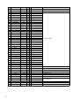
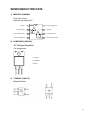
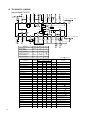
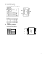
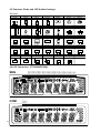
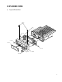
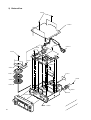
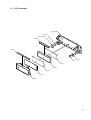
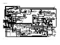
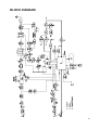
TOMAHAWK 245
Service Manual DR-245A
CONTENTS
SPECIFICATIONS
PARTS LIST
1) GENERAL ................................................................ 2
2) TRANSMITTER ........................................................ 2
3) RECEIVER ............................................................... 2
CPU .................................................................. 22, 23
Main Unit .......................................................... 23~26
VCO Unit ................................................................ 26
Mechanical Parts .................................................... 26
CIRCUIT DESCRIPTION DR-135
1) Receiver System .................................................. 3, 4
2) Transmitter System ................................................... 4
3) PLL Synthesizer Circuit ........................................ 5, 6
4) CPU and Peripheral Circuits ................................. 6, 7
5) Power Supply Circuit ................................................. 7
6) M3826M8L270GP (XA0819) .............................. 8~10
SEMICONDUCTOR DATA
1) M5218FP (XA0068) ................................................ 11
2) NJM7808FA (XA0102) ............................................ 11
3) TC4S66F (XA0115) ................................................ 11
4)
5)
6)
7)
TK10930VTL (XA0223) .......................................... 12
BU4052BF (XA0236) .............................................. 13
TC4W53FU (XA0348) ............................................ 13
M64076GP (XA0352) ............................................. 14
8)
9)
10)
11)
LA4425A (XA0410) ................................................. 15
M68729 (XA0591) .................................................. 15
AN8010M(XA0119) ................................................ 16
NJM2902 (XA0596) ................................................ 16
12)
13)
14)
15)
24LC32A (XA0604) ................................................ 17
S-80845ALMP-EA9-T2 (XA0620) ........................... 17
L88MS05TLL (XA0675) .......................................... 17
Transistor, Diode, and LED Ontline Drawings ......... 18
Speaker .................................................................. 27
Packing Parts ......................................................... 27
ADJUSTMENT
1)
2)
3)
4)
Adjustment Spot .................................................... 28
VCO and RX Adjustment Specification ................... 29
Tx Adjustment Specification ................................... 29
Rx Test Specification ............................................... 30
5) Tx Test Specification ............................................... 30
PC BOARD VIEW
1) CPU Unit Side A (UP 0414) .................................... 31
2) CPU Unit Side B (UP 0414) .................................... 31
3) Main Unit Side A (UP 0414) .................................... 32
4) Main Unit Side B (UP 0414) .................................... 32
SCHEMATIC DIAGRAM
1) CPU Unit ................................................................ 33
2) Main Unit ................................................................ 34
BLOCK DIAGRAM ..................................................... 35
16) LCD Connection (TTR3626UPFDHN) ................... 18
EXPLODED VIEW
1) Top and Front View ................................................. 19
2) Bottom View ........................................................... 20
3) LCD Assembly ........................................................ 21
ALINCO,INC.
SPECIFICATIONS
1) GENERAL
Frequency range
Operating mode
CH1(245.000MHz) ~ CH80(245.9875MHz )
8K50F3E
Frequency resolution
12.5 kHz
Memory channel
100 channels + 1 call channel
Antenna impedance
50Ω unbalanced
Microphone impedance
2 kΩ
Rated voltage
Ground
13.8V DC ±15% (11.7 to 15.8V)
Negative ground
Current
Receive
0.6A(Max.)
Transmit
5.0A or less
0.4A(Squelched) or less
Operating temperature
- 10°C ~ 60°C(+14°F ~ +140°F)
Frequency stability
±5 ppm
Dimensions
142(W) × 40(H) × 174(D) mm
5.58”(W) × 1.57”(H) × 6.83”(D)
Weight
Approx. 1.0kg (35.3oz)
2) TRANSMITTER
Output power
High:10W
Mid: 5W Low: 2.5W
Modulation system
Variable reactance frequency modulation
Maximum frequency deviation
±2.5KHz
Spurious emission
-60dB or less
3) RECEIVER
Sensitivity
0.2 uV for 12dB SINAD 0.4 uV for 20dBNQL
Receiver circuitry
Double conversion superheterodyne
Intermediate frequency
Squelch sensitivity
1st 30.85MHz
-16dBu
Adjacent channel selectivity
-60dB
Spurious and image rejection ratio
70dB
Audio output power
2.0W (8Ω,10%THD)
2nd 455kHz
! Note: All spesifications are subject to change without notice or obligation.
2
CIRCUIT DESCRIPTION TOMAHAWK 245
1) Receiver System
The receiver system is a double superheterodyne system with a 30.85 MHz first IF and a 455 kHz
second IF.
1. Front End
The received signal at any frequency in the 245.00MHz to 245.9875MHz
range is passed through the low-pass filter (L116, L115, L114, L113, C204,
C203, C202, C216 and C215) and tuning circuit (L105, L104 and D105,
D104), and amplified by the RF amplifier (Q107). The signal from Q107 is
then passed through the tuning circuit (L103, L107, L102, and varicaps
D103, D107 and D102) and converted into 30.85 MHz by the mixer (Q106).
The tuning circuit, which consists of L105, L104, varicaps D105 and D104,
L103, L107, L102, varicaps D103, D107 and D102, is controlled by the
tracking voltage form the VCO. The local signal from the VCO is passed
through the buffer (Q112), and supplied to the source of the mixer (Q106).
The radio uses the lower side of the superheterodyne system.
2. IF Circuit
The mixer mixes the received signal with the local signal to obtain the sum
of and difference between them. The crystal filter (XF102, XF101) selects
30.85 MHz frequency from the results and eliminates the signals of the
unwanted frequencies. The first IF amplifier (Q105) then amplifies
the signal of the selected frequency.
3. Demodulator Circuit
After the signal is amplified by the first IF amplifier (Q105), it is input to pin
24 of the demodulator IC (IC108). The second local signal of 30.395 MHz,
which is oscillated by the internal oscillation circuit in IC108 and crystal
(X104), is input through pin 1 of IC108. Then, these two signals are mixed
by the internal mixer in IC108 and the result is converted into the second
IF signal with a frequency of 455 kHz. The second IF signal is output from
pin 3 of IC108 to the ceramic filter ( FL102), where the unwanted frequency
band of that signal is eliminated, and the resulting signal is sent back to
the IC108 through pins 5.
The second IF signal input via pin 5 is demodulated by the internal limiter
amplifier and quadrature detection circuit in IC108, and output as an audio
signal through pin 12.
4. Audio Circuit
The audio signal from pin 12 of IC108 is amplified by the audio amplifier
(IC104:A),and switched by the signal switch IC (IC111) and then input it to
the de-emphasis circuit.
and is compensated to the audio frequency characteristics in the
de-emphasis circuit (R203, R207, R213, R209, C191, C218, C217) and
amplified by the AF amplifier (IC104:D). The signal is then input to volume
(VR1) . The adjusted signal is sent to the audio power amplifier (IC117)
through pin 1 to drive the speaker.
3
5. Squelch Circuit
The detected output which is outputted from the pin 12 of IC108 is inputted to
pin 19 of IC108 after it was been amplified by IC104:A and it is outputted
from pin 20 after the noise component was been eliminated from the
composed band pass filter in the built in amplifier of the IC, then the signal is
rectified by D106 to convert into DC component. The adjusted voltage
level at VR101 is delivered to the comparator of the CPU.
The voltage is led to pin 2 of CPU and compared with the setting voltage.
The squelch will open if the input voltage is lower than the setting voltage.
During open squelch, pin 30 (SQC) of the CPU becomes “L” level, AF
control signal is being controlled and sounds is outputted from the speaker.)
2) Transmitter System
1. Modulator Circuit
The audio signal is converted to an electrical signal by the microphone,
and input it to the microphone amplifier (Q6). Amplified signal which passes
through mic-mute control IC109 is adjusted to an appropriate mic-volume
by means of mic-gain adjust VR106.
IC114:AandB consists of two operational amplifiers; one amplifier (pins 1,
2, and 3) is composed of pre-emphasis and IDC circuits and the other
(pins 5, 6, and 7) is composed of a splatter filter. The maximum frequency
deviation is obtained by VR107. and input to the cathode of the varicap of
the VCO, to change the electric capacity in the oscillation circuit. This produces
the frequency modulation.
2. Power Amplifier Circuit
The transmitted signal is oscillated by the VCO, amplified by the drive
amplifier (IC112) and younger amplifier (Q115), and input to the final power
module (IC110). The signal is then amplified by the final power module
(IC110) and led to the antenna switch (D110) and low-pass filter (L113,
L114, L115, L116, C215, C216, C202, C203 and C204), where unwanted
high harmonic waves are reduced as needed, and the resulting signal is
supplied to the antenna.
3. APC Circuit
Part of the transmission power from the low-pass filter is detected by D111
and D112, converted to DC. The detection voltage is passed through the
APC circuit (Q118, Q117, Q116), then it controls the APC voltage supplied to
the younger amplifier Q115 and the final power module IC110 to fix the
transmission power.
4
3) PLL Synthesizer Circuit
1. PLL
The dividing ratio is obtained by sending data from the CPU (IC1) to pin 2
and sending clock pulses to pin 3 of the PLL IC (IC501). The oscillated
signal from the VCO is amplified by the buffer (Q504 and Q501) and input
to pin 15 of IC501. Each programmable divider in IC501 divides the
frequency of the input signal by N according to the frequency data, to
generate a comparison frequency of 5 or 6.25 kHz.
2. Reference Frequency Circuit
The reference frequency appropriate for the channel steps is obtained by
dividing the 12.8 MHz reference oscillation (X103) by 2048, according
to the data from the CPU (IC1). When the resulting frequency is 6.25 kHz,
channel steps of 12.5 kHz are used.
3. Phase Comparator Circuit
The PLL (IC501) uses the reference frequency, 6.25kHz. The phase
comparator in the IC501 compares the phase of the frequency from the
VCO with that of the comparison frequency, 6.25 kHz, which is obtained
by the internal divider in IC501.
4. PLL Loop Filter Circuit
If a phase difference is found in the phase comparison between the
reference frequency and VCO output frequency, the charge pump output
(pin 13) of IC501 generates a pulse signal, which is converted to DC
voltage by the PLL loop filter and input to the varicap of the VCO unit for
oscillation frequency control.
5. VCO Circuit
A Colpitts oscillation circuit driven by Q503 directly oscillates the desired frequency. The frequency control voltage determined in the CPU (IC1) and
PLL circuit is input to the varicaps (D503 and D504). This change the
oscillation frequency, which is amplified by the VCO buffer (Q504) and
output from the VCO area.
4) CPU and Peripheral Circuits
1. LCD Display Circuit
The CPU turns ON the LCD via segment and common terminals with 1/4
the duty and 1/3 the bias, at the frame frequency is 64Hz.
5
2. Dimmer Circuit
The dimmer circuit makes the output of pin 13 of CPU (IC1) into “H” level
at set mode, so that Q9 and Q3 will turn ON to make the lamp control
resistor R84 short and make its illumination bright. But on the other hand,
if the dimmer circuit makes pin 13 into “L” level, Q9 and Q3 will turn OFF,
R84’s illumination will become dimmer as its hang on voltage falls down in
the working LED (D11, D2, D5, D3 and D6).
3. Reset and Backup
When the power form the DC cable increases from Circuits 0 V to 2.5 or
more, “H” level reset signal is output form the reset IC (IC4) to pin 33 of the
CPU (IC1), causing the CPU to reset. The reset signal, however, waits at
100, and does not enter the CPU until the CPU clock (X1) has stabilized.
4. S(Signal) Meter Circuit
The DC potential of pin 16 of IC106 is input to pin 1 of the CPU (IC1),
converted from an analog to a digital signal, and displayed as the S-meter
signal on the LCD.
5. DTMF Encoder
The CPU (IC1) is equipped with an internal DTMF encoder. The DTMF
signal is output from pin 10, through R35, R34 and R261 (for level
adjustment), and then through the microphone amplifier (IC114:A), and is
sent to the varicap of the VCO for modulation. At the same time, the monitoring
tone passes through the AF circuit and is output form the speaker.
6. Tone Encoder
The CPU (IC1) is equipped with an internal tone encoder. The tone signal
(67.0 to 250.3 Hz) is output from pin 9 of the CPU to the varicap (D503
and D504) of the VCO for modulation.
7. DCS Encoder
The CPU (IC1) is equipped with an internal DCS code encoder. The code
(023 to 754) is output from pin 9 of the CPU to the varicap (D124) of the
PLL reference oscillator. When DCS is ON, DCS MUTE circuit (Q126-ON,
Q133-ON, Q132-OFF)works. The modulation activates in X103 side only.
8. CTCSS, DCS Decoder
The voice band of the AF output signal from pin 1 of IC104:A is cut by
sharp active filter IC104:B and C (VCVS) and amplified, then led to pin 4
of CPU. The input signal is compared with the programmed tone frequency
code in the CPU. The squelch will open when they match. During DCS,
Q108 is ON, C156 is working and cut off frequency is lowered.
6
5) Power Supply Circuit
When power supply is ON, there is a “L” signal being inputted to pin 39 (PSW) of CPU which enables
the CPU to work.
Then, “H” signal is outputted from the pin 41 (C5C) of CPU and drives ON the power supply switch
control Q8 and Q7 which turns the 5VS ON.
5VS turns ON the PLL IC501, main power supply switch Q127 and Q122, AF POWER IC117 and the
8 V of AVR (IC115).
During reception, pin 29 (R5) of CPU outputs “H” level, Q124 is ON, and the reception circuits supplied by
8 V.
While during transmission, pin 28 (T5) of CPU outputs “L” level which is reverse by Q11 so that the
output in Q128 will be “H” level, Q123 is ON, and the transmission circuit is supplied by 8 V.
Or, in the case when the condition of PLL is UNLOCK, “H” level is outputted from pin 14 of IC501,
UNLOCK switch Q129 is ON, transmission switch Q128 is OFF which makes the transmission to
stop.
1. ACC External Power Supply Terminal
When optional power supply cord DEC-37 etc. is connected to the external
power supply terminal JK101, with ACC power supply ON, switch Q101
will turn ON, 5 V of AVR IC101 pin 2 (STB) becomes “L” which makes C5V
to turn ON. With this, it can turn the power supply of the radio ON.
7
6) M3826M8L270GP (XA0819)
CPU
Terminal Connection
(TOP VIEW)
8
No.
Pin Name
1
P67/AN7
Function I/O PU
SMT
I
-
Logic
A/D
S-meter input
Description
2
P66/AN6
SQL
I
-
A/D
Noise level input for squelch
3
P65/AN5
BAT
I
-
A/D
Battery voltage input
4
P64/AN4
TIN
I
-
A/D
CTCSS tone input/DCS code input
5
P63/SCLK22/AN3
BP1
I
-
A/D
-
6
P62/SCLK21/AN2
BP2
I
-
A/D
-
7
P61/SOUT2/AN1
DCSW
O
-
Activ high
DCS signal mute (DCS:H)
8
P60/SIN2/AN0
RE2
I
-
Activ low
Rotary encoder input
9
P57/ADT/DA2
TOUT
O
-
D/A
CTCSS tone output/DCS tone output
10
P56/DA1
DOUT
O
-
D/A
DTMF output
11
P55/CNTR1
SCL
O
-
Pulse
Serial clock for EEPROM
12
P54/CNTR0
TBST
O
-
Pulse
-
13
P53/RTP1
BP4
I/O
-
Activ low
Lamp dimmer HI/LOW switch
14
P52/RTP0
MUTE
I/O
-
Activ low
Microphone mute (TX:H) / Security alarm SW (SCR:H)
15
P51/PWM3
CLK
O
-
Pulse
Serial clock output for PLL-IC
16
P50/PWM0
DATA
I/O
-
Pulse
Serial data output for PLL-IC/PLL unlock signal input (H:UL)
17
P47/SROY1
TSTB
I/O
-
Activ low/Pulse
18
P46/SCLK1
STB
O
-
Pulse
Strobe for PLL-IC
19
P45/TXD
UTX
O
-
Pulse
UART data transmission output
UART data reception output
20
21
P44/RXD
P43/
/TOUT
RTX
I
-
Pulse
BEEP
I/O
-
Pulse / Activ low
Activ high
-
Beep tone output
Sscurity voltage input (H:SCR on)
22
P42I/NT2
SEC
I
-
23
P41/INT1
RE1
I
*
24
P40
DSQ
I
-
Activ low
Activ high
Rotary encoder input
Digital squelch input (H:AF out)
25
P77
PTT
I
-
Activ low
PTT input
26
P76
SSTB
O
-
Pulse
27
P75
W/N
O
-
Activ low
-
28
P74
T5
O
-
Activ low
TX power ON/OFF output
29
P73
R5
O
-
Activ high
RX power ON/OFF output
30
P72
SQC
O
-
Activ low
SQL ON/OFF (AF out:L)
31
P71
C/S
O
-
Activ low
-
32
P70/INTO
BU
I
-
Activ low
Backup signal detection input
33
RESET
RESET
I
-
Activ low
34
Xcin
Xcin
-
-
-
-
35
Xcout
Xcout
-
-
-
-
36
Xin
Xin
-
-
-
Main clock input
37
Xout
Xout
-
-
-
Main clock output
CPU GND
38
Vss
GND
-
-
-
39
P27
PSW
I
-
Activ low
40
P26
SDA
O
-
Pulse
41
P25
C5C
O
-
Activ high
SCR alarm control out (SCR: )
Reset input
Power switch input
Serial data for EEPROM
C5V power ON/OFF output (C5V:H)
42
P24
AIR
O
-
Activ high
Tx middle power (MID:H)
43
P23
LOW
O
-
Activ high
Tx low power (LOW:H)
44
P22
EXP
O
-
Activ low
45
P21
SW6
I
*
Activ low
Key sw6 (SQL)
46
P20
SW5
I
*
Activ low
Key sw5 (CALL)
47
P17
SW4
I
*
48
P16
SW3
I
*
Activ low
Activ low
Key sw4 (TS/DCS)
Key sw3 (MONI)
49
P15/SEG39
SW2
I
*
Activ low
Key sw2 (V/M)
50
P14/SEG38
SW1
I
*
51
P13/SEG37
DOWN
I
*
Activ low
Activ low
Key sw1 (FUNC)
Mic down input
52
P12/SEG36
DUD
I
*
Activ low
-
-
9
10
No.
Pin Name
Function I/O PU
Logic
Description
53
P11/SEG35
SCR
I
*
-
54
P10/SEG34
UP
I
*
Activ low
55
P07/SEG33
S33
O
-
-
56
P06/SEG32
S32
O
-
-
57
P05/SEG31
S31
O
-
-
58
P04/SEG30
S30
O
-
-
59
P03/SEG29
S29
O
-
-
60
P02/SEG28
S28
O
-
-
61
P01/SEG27
S27
O
-
-
62
P00/SEG26
S26
O
-
-
63
P37/SEG25
S25
O
-
-
64
P36/SEG24
S24
O
-
-
65
P35/SEG23
S23
O
-
-
66
P34/SEG22
S22
O
-
-
67
P33/SEG21
S21
O
-
-
68
P32/SEG20
S20
O
-
-
69
P31/SEG19
S19
O
-
-
70
P30/SEG18
S18
O
-
-
71
SEG17
S17
O
-
-
72
SEG16
S16
O
-
-
73
SEG15
S15
O
-
-
74
SEG14
S14
O
-
-
75
SEG13
S13
O
-
-
76
SEG12
S12
O
-
-
77
SEG11
S11
O
-
-
78
SEG10
S10
O
-
-
79
SEG9
S9
O
-
-
80
SEG8
S8
O
-
-
81
SEG7
S7
O
-
-
82
SEG6
S6
O
-
-
83
SEG5
S5
O
-
-
84
SEG4
S4
O
-
-
85
SEG3
S3
O
-
-
86
SEG2
S2
O
-
-
87
SEG1
S1
O
-
-
88
SEG0
S0
O
-
-
89
Vcc
VDD
-
-
-
CPU power terminal
90
Vref
Vref
-
-
-
AD converter power supply
91
Avss
Avss
-
-
-
AD converter GND
92
COM3
COM3
O
-
-
LCD COM3 output
93
COM2
COM2
O
-
-
LCD COM2 output
94
COM1
COM1
O
-
-
LCD COM1 output
95
COM0
COM0
O
-
-
LCD COM0 output
96
VL3
VL3
-
-
-
97
VL2
VL2
-
-
-
98
C2
I
-
-
-
99
C1
C1
-
-
-
100
VL1
VL1
I
-
A/D
Mic up input
LCD segment signal
LCD power supply
LCD power supply
SEMICONDUCTOR DATA
1) M5218FP (XA0068)
Dual Low Noise
Operational Amplifiers
Output 1 1
8
Power Supply Plus
Inverting Input 1 2
7
Output 2
Non Inverting Input 1 3
6
Inverting Input 2
Power supply Minus 4
5
Non Inverting Input 2
2) NJM7808FA (XA0102)
8V Voltage Regulator
Pin Assignment
1. OUTPUT
2. COMMON
3. INPUT
3
2
1
3) TC4S66F (XA0115)
Bilateral Switch
11
21
19
AMP
18
17
15
AM AF OUT
AM SW
68K
16
IF GND
0.1
RSSI OUT
0.033
AM LOW CUT
AM AGC
+
NOISE AMP INPUT
1K +
20
14
4.7K
AF OUTPUT (AM)
0.022
22
270K
13
+ -
23
SQ
24
30K
COMP IN
COMP OUT
Vcc
GND
0.01
RF INPUT
51
IF IN
10.7MHz
1 F
NOISE AMP OUTPUT
+
Narrow Band FM IF IC
1 F
4) TK10930VTL (XA0223)
S DET
AM DET
FM DET
AGC
IF AMP
QUAD IN
OSC
Parameter
Ratings
Vcc max
10.0
V
Power dissipation
Pd
400
mV
Storage temperature
Tstg
-55~+150
Operating temperature
Top
-30~+75
Operating voltage
Vop
2.5~8.5
V
Operating frequency
fop
~60
MHz
Parameter
Min
FM AF OUT AF OUTPUT (FM)
8.2K
0.1 F
Vcc 3V
Ta=25
Unit
Typical
Max
Vcc=3V
Condition
Supply Current 1
lcc1
6.8
8.9
mA
No signal, AM ON
Supply Current 2
lcc2
3.9
5.3
mA
No signal, AM OFF
Mixer Coversion Gain
Mg
20
dB
Mixer Input Impedance
Mz
3.6
K
DC Test
FM
Limiting Sensitivity
Limit
Output Voltage
Vo1
Distortion
THD1
85
Output Impedance
Zo
Filter Gain
Gf
30
Scan Control Hi Voltage
SH
2.3
Scan Control Low Voltage
SL
Squelch Hysteresis
Hys
2.0
8.0
V
150
230
mVrms
-3.0dB
10mVin +/-3kHz DEV
1.0
2.0
%
10mVin +/-3kHz DEV
10mVin
800
38
dB
0.3
30
Fin=30kHz, Vo=100mV
V
Squelch input=2.5V
V
Squelch input=0V
mV
S meter Output Voltage
S0
0.05
0.5
V
Vin=0mV, RS=68k
S meter Output Voltage
S1
0.05
0.5
0.9
V
Vin=0.01mV, RS=68k
S meter Output Voltage
S2
0.7
1.2
1.7
V
Vin=0.1mV, RS=68k
S meter Output Voltage
S3
1.2
1.8
2.5
V
Vin=1mV, RS=68k
S meter Output Voltage
S4
1.6
2.3
2.9
V
Vin=10mV, RS=68k
S meter Output Voltage
S5
1.8
2.4
2.9
V
Vin=100mV, RS=68k
US
20
15
Output Voltage
Vo2
60
120
160
Distortion-1
THD2
1.0
2.0
%
1kHz, 30%, Vin=1mV
Distortion-2
THD3
2.0
4.0
%
1kHz, 30%, Vin=1mV
S/N
S/N
40
dB
1kHz, 30%, Vin=1mV
AM OFF
Vo
-0.3
AM
Sensitivity
12
V
48
0.3
mVrms
%
required input level to get
20mV rms output
1kHz, 30%, Vin=1mV
0.01
7BRE-7437Z
12
Unit
Ratings
Symbol
10 F
2.2K
+
Symbol
Supply voltage
11
LIM OUT
30K
10
0.1 F
DECOUPLING
9
0.1 F
0.1 F
8
DECOUPLING
CFU455D
7
0.1 F
6
FM IF INPUT
5
DECOUPLING
4
AM IF INPUT
3
Vcc
2
33p
MIX OUT
10.245MHz OSC(B)
1
120p OSC(E)
MIX
5) BU4052BF (XA0236)
Analog Multiplexer/Demultiplexer
6) TC4W53FU (XA0348)
Multiplexer/Demultiplexer
Function Table
COMMON
VDD
INH
ch0
VEE
ch1
VSS
A
Control input
ON channel
INH
A
L
L
ch0
L
H
ch1
H
*
NONE
* Don't Care
13
7) M64076GP (XA0352)
Dual PLL Synthesizer
Parameter
Symbol
Power supply voltage
Vcc
LPF supply voltage
VF
Local oscillator input level
Vin
Local oscillator input frequency
Fin
Condition
Fin=80~520MHz
Vin=-10dBm
Fin=80~520MHz
Vin=-20~-4dBm
Vcc=2.7~5.5V
Min.
Typ.
Max.
Unit
2.7
-
5.5
V
-
9
12
V
-20
-
-4
dBm
80
-
520
MHz
0.4
-
1.4
Vp-p
10
-
25
MHz
Vcc=2.7~5.5V
Equivalent Circuit
14
Xin input level
Vxin
Xin input frequency
Fxin
Fxin=10~25MHz
Sine wave
Vcc=2.7~5.5V
Vxin=0.4~1.4Vp-p
8) LA4425A (XA0410)
5W Audio Power Amplifiers
Input 2.2 F
+
1000 F
Test Circuit
1
Vcc
13.2V
+
5
LA4425
SP
+
2
Vcc=13.2V RL=4
3
4
4 1000 F
Po =5W Gain= 45dB
1
2
3
4
5
9) M68729 (XA0591)
ABSOLUTE MAXIMUM RATING(TC = 25˚C)
M68729
Block Diagram
2
3
Rating
4
5
1 Pin
Unit
17
V
Total current
Icc
10
A
Input power
Pin(max)
600
mW
Output Power
Po(max)
40
W
Operation case temperature
Tc(op)
-30 to + 110
Strage temperature
Tstg
-40 to + 110
Zg=Zl=50W
ELECTRICAL CHARACTERISTICS
Symbol
Parameter
f
Frequency range
Test conditions
Total efficiency
2fo
2nd. harmonic
3fo
3rd. harmonic
rin
Input VSWR
Load VSWR tolerance
Limits
Unit
Min Max
220
246 MHz
30
Output power
hT
PIN :
Ratings
Vcc
Po
1
Symbol
Supply voltage
GND (FIN)
Output
terminal (60W)
Final DC supply
terminal (12.5V)
1st stage DC
supply
terminal(12.5V)
Input terminal
(300mW)
5
Fin(Ground)
Fin(Ground)
220 ~ 246MHz 30W
RF Power Module
VCC1,2 = 12.5V
Pin = 300mV
ZG = ZL = 50W
W
40
%
-30
dBc
-30
dBc
3
VCC1,2 = 15.2V
Po = 30W(Pin = Controlled)
No degradation
Load VSWR = 20:1 (All phase), or destroy
ZG = 50W
-
: RF INPUT
2 VCC1 : 1st. DC SUPPLY
3 VCC2 : 2nd. DC SUPPLY
4 PO
: RF OUTPUT
5 GND : FIN
15
10) AN8010M(XA0119)
Voltage Regulator
Test Circuit
Vin
Vout
1
3
10µF
0.33µF
2
CA
AN8010M
Output
Common
Input
AN8010M
11) NJM2902 (XA0596)
Quad Operational Amplifiers
Pin Assignment
1. A OUTPUT
2. A-INPUT
3. A+INPUT
4. V+
5. B+INPUT
6. B-INPUT
7. B OUTPUT
16
8. C OUTPUT
9. C-INPUT
10. C+INPUT
11. GND
12. D+INPUT
13. D-INPUT
14. D OUTPUT
12) 24LC32A (XA0604)
CMOS Serial EEPROM
PDIP
A0
Vcc
Name
A1
WP
A0..A2
A2
SCL
Vss
Ground
Vss
SDA
SDA
Serial Address/Data I/O
SCL
Serial Clock
WP
Write Protect Input
Vcc
Function
User Configurable Chip Selects
2.5V~6.0V Power Supply
13) S-80845ALMP-EA9-T2 (XA0620)
Voltage Detector
14) L88MS05TLL (XA0675)
5V Voltage Regulator With On/Off Function
Reference voltage
1. VIN
2. STB
3. GND
4. Cn
5. VOUT
Start-up circuit
Pin Assignment
Error
amp
ON/OFF
Control
Short circuit
protector
Thermal protector
1 2 3 4 5
17
15) Transistor, Diode, and LED Outline Drawings
Top View
1SS355
XD0254
DTZ5. 1B
XD 0165
DSA3AI
XD0131
1SV214
XD0131
1SV262
XD0300
1SV268
XD0301
DA204U
XD0130
DAN235U
XD0246
VD
RLS-73
XD0363
TD
T1
A
MA729
XD0300
MA742
XD0250
MI407
XD0013
HQ
E
B
B
2SB1132
XT0061
2SB1292F
XT0112
E
B1292
B C E
2SC4081
XT0095
C
C
C
C
BR
JP
QY
HB
DTC144EUA
XU0148
B
B
E
C
C
64
E
B
DTC114YU
XU0029
26
B
D
E
FA1111C
XL0069
2SC4245
XT0125
B
G1
E
FA1111C
XL0077
E
3SK184S
XE0013
C
C
R24
DTA114YU
XU0112
3RS
S
C
24
B
E
E2 B2 E1
B2 E B1
V12
9M
C2
C1
18
SEG32
SEG31
SEG30
SEG29
SEG28
SEG27
SEG26
SEG25
SEG24
SEG23
COM3
COM2
COM1
COM0
COM
SEG22
SEG21
SEG20
SEG19
SEG18
SEG17
SEG16
SEG15
SEG14
SEG13
SEG12
SEG11
SEG10
SEG9
SEG8
SEG27
SEG7
SEG6
SEG5
SEG4
SEG3
SEG2
SEG1
SEG0
16) LCD Connection (TTR3626UPFDHN)
SEG
E
DTC114EU
XU0131
C
XP215
XU0178
C1/B2
B
54
UMC3TR
XU0047
C2
D
2SC3356
XT0030
G2
D
S
2SC2954
XT0084
B C E
BCE
B C E
2SC4215
XT0124
E
XG
C
2SC4099
XT0096
B
G
K52
KQ
C
FR
2SA1736
XT0099
BA
PQ
C
G
MI7
2B
A2
2SA1576
XT0094
M
2SK880GR
XE0021
S
M1U
2SA1036K
XT0110
K
2SK508
XE0010
B
E
EXPLODED VIEW
1) Top and Front View
AA0050
AV0006
FG0273
DP0137A
AV0006
NK0072
• KZ0130
NK0073
19
2) Bottom View
AA0050
• KS0075
AV0006
UA0037Y
AV0006
AV0006
UX1047
AW0001
ST0065
ES0017
FP0151
AV0006
ST0066
TG0034
UE0258
SP0008
FF0015
• SS0096
20
3) LCD Assembly
CPU BOARD
FM0034
NUT (UE0035)
FG0305
FF0017
ST0068
NUT
TL0023
DG0037
TL0024
EL0049
ST0064
21
PARTS LIST
CPU
Ref.
Parts No.
No.
22
Description
Parts Name
Unit
Loc
Qty
(side)
Ref.
Parts No.
No.
Description
Parts Name
Unit
Loc
Qty
(side)
C1
CU3111
Chip C.
C1608JB1C104KT-N
CPU
B
1
R14 RK3048
Chip R.
MCR03EZHJ682
CPU
B
1
C2
CU3111
Chip C.
C1608JB1C104KT-N
CPU
B
1
R16 RK3001
Chip R.
MCR03EZHJ000
CPU
B
1
C3
CU3049
Chip C.
C1608JB1E153KT-NS
CPU
B
1
R17 RK3001
Chip R.
MCR03EZHJ000
CPU
B
1
C4
CU3049
Chip C.
C1608JB1E153KT-NS
CPU
B
1
R19 RK3062
Chip R.
MCR03EZHJ104
CPU
B
1
C5
CU3111
Chip C.
C1608JB1C104KT-N
CPU
B
1
R20 RK3046
Chip R.
MCR03EZHJ472
CPU
B
1
C6
CU3023
Chip C.
C1608CH1H101JT-AS
CPU
B
1
R21 RK3030
Chip R.
MCR03EZHJ221
CPU
B
1
C7
CU3023
Chip C.
C1608CH1H101JT-AS
CPU
B
1
R22 RK3038
Chip R.
MCR03EZHJ102
CPU
B
1
C8
CU3043
Chip C.
C1608JB1H472KT-NS
CPU
B
1
R23 RK3064
Chip R.
MCR03EZHJ154
CPU
A
1
C9
CU3111
Chip C.
C1608JB1C104KT-N
CPU
B
1
R24 RK3050
Chip R.
MCR03EZHJ103
CPU
B
1
C10 CU3043
Chip C.
C1608JB1H472KT-NS
CPU
B
1
R25 RK3050
Chip R.
MCR03EZHJ103
CPU
B
1
C11 CU3043
Chip C.
C1608JB1H472KT-NS
CPU
B
1
R26 RK3050
Chip R.
MCR03EZHJ103
CPU
B
1
C12 CU3101
Chip C.
C1608JB1C473KT-NS
CPU
B
1
R27 RK3050
Chip R.
MCR03EZHJ103
CPU
B
1
C13 CS0049
Chip tantalum
TMCSA1C105MTR
CPU
B
1
R28 RK3038
Chip R.
MCR03EZHJ102
CPU
B
1
C14 CU3014
Chip C.
C1608CH1H180JT-AS
CPU
B
1
R29 RK3038
Chip R.
MCR03EZHJ102
CPU
B
1
C15 CU3014
Chip C.
C1608CH1H180JT-AS
CPU
B
1
R30 RK3038
Chip R.
MCR03EZHJ102
CPU
B
1
C16 CU3035
Chip C.
C1608JB1H102KT-AS
CPU
B
1
R31 RK3038
Chip R.
MCR03EZHJ102
CPU
B
1
C17 CS0372
Chip tantalum
TMCMB1C106MTR
CPU
B
1
R32 RK3044
Chip R.
MCR03EZHJ332
CPU
B
1
C18 CU3035
Chip C.
C1608JB1H102KT-AS
CPU
B
1
R33 RK3034
Chip R.
MCR03EZHJ471
CPU
B
1
C19 CU3111
Chip C.
C1608JB1C104KT-N
CPU
B
1
R34 RK3047
Chip R.
MCR03EZHJ562
CPU
B
1
C20 CU3101
Chip C.
C1608JB1C473KT-NS
CPU
B
1
R35 RK3052
Chip R.
MCR03EZHJ153
CPU
B
1
C21 CU3047
Chip C.
C1608JB1H103KT-N
CPU
B
1
R36 RK3062
Chip R.
MCR03EZHJ104
CPU
B
1
C22 CU3035
Chip C.
C1608JB1H102KT-AS
CPU
B
1
R37 RK3049
Chip R.
MCR03EZHJ822
CPU
B
1
C23 CU3047
Chip C.
C1608JB1H103KT-N
CPU
A
1
R38 RK3050
Chip R.
MCR03EZHJ103
CPU
B
1
C24 CU3035
Chip C.
C1608JB1H102KT-AS
CPU
B
1
R39 RK3058
Chip R.
MCR03EZHJ473
CPU
B
1
C25 CU3035
Chip C.
C1608JB1H102KT-AS
CPU
B
1
R40 RK3062
Chip R.
MCR03EZHJ104
CPU
B
1
C26 CU3035
Chip C.
C1608JB1H102KT-AS
CPU
B
1
R41 RK3026
Chip R.
MCR03EZHJ101
CPU
B
1
C27 CU3035
Chip C.
C1608JB1H102KT-AS
CPU
B
1
R42 RK3050
Chip R.
MCR03EZHJ103
CPU
B
1
CN1 UE0398
Connector
20-5082-3010-17-100
CPU
H
1
R43 RK3050
Chip R.
MCR03EZHJ103
CPU
B
1
CN2 UE0398
Connector
20-5082-3010-17-100
CPU
H
1
R44 RK3026
Chip R.
MCR03EZHJ101
CPU
B
1
CN3 UE0035
Connector
FM214-8SMPY
CPU
H
1
R45 RK3050
Chip R.
MCR03EZHJ103
CPU
B
1
D1
XL0069
Chip LED
FA1111C-TR
CPU
A
1
R47 RK3038
Chip R.
MCR03EZHJ102
CPU
B
1
D2
XL0077
Chip LED
FA1111C-TR CDE RANK
CPU
A
1
R48 RK3038
Chip R.
MCR03EZHJ102
CPU
B
1
D3
XL0077
Chip LED
FA1111C-TR CDE RANK
CPU
A
1
R49 RK3038
Chip R.
MCR03EZHJ102
CPU
B
1
D4
XL0069
Chip LED
FA1111C-TR
CPU
A
1
R50 RK3070
Chip R.
MCR03EZHJ474
CPU
B
1
D5
XL0077
Chip LED
FA1111C-TR CDE RANK
CPU
A
1
R51 RK3038
Chip R.
MCR03EZHJ102
CPU
A
1
D6
XL0077
Chip LED
FA1111C-TR CDE RANK
CPU
A
1
R52 RK3038
Chip R.
MCR03EZHJ102
CPU
A
1
D8
XD0254
Chip Diode
1SS355 TE17
CPU
B
1
R53 RK3062
Chip R.
MCR03EZHJ104
CPU
B
1
D11 XL0077
Chip LED
FA1111C-TR CDE RANK
CPU
A
1
R54 RK3050
Chip R.
MCR03EZHJ103
CPU
A
1
D12 XD0165
Chip Diode
UDZSTE-17 5.1B
CPU
B
1
R55 RK3074
Chip R.
MCR03EZHJ105
CPU
B
1
D14 XD0291
Chip Diode
MA729-TX
CPU
B
1
R56 RK3050
Chip R.
MCR03EZHJ103
CPU
A
1
IC1
XA0819
CPU
M38267M8L270GP
CPU
B
1
R57 RK3066
Chip R.
MCR03EZHJ224
CPU
B
1
IC2
XA0604
IC
24LC32AT-I/SN
CPU
A
1
R58 RK3034
Chip R.
MCR03EZHJ471
CPU
B
1
IC4
XA0620
IC
S-80845ALMP-EA9-T2
CPU
B
1
JK1
UJ0047
Jack
HSJ2013-01-120
CPU
H
1
R59 RK3026
R60 RK3034
Chip R.
Chip R.
MCR03EZHJ101
MCR03EZHJ471
CPU
CPU
B
B
1
1
LCD1 EL0049
LCD
TTR3626 UPTDHN
CPU
H
1
R61 RK3074
Chip R.
MCR03EZHJ105
CPU
B
1
Q1
XU0029
Chip Transistor DTC114YUA T106
CPU
B
1
R62 RK3050
Chip R.
MCR03EZHJ103
CPU
B
1
Q2
XU0131
Chip Transistor DTC114EUA T106
CPU
B
1
R63 RK3026
Chip R.
MCR03EZHJ101
CPU
B
1
Q3
XT0110
Chip Transistor 2SA1036K T146Q
CPU
B
1
R64 RK3046
Chip R.
MCR03EZHJ472
CPU
B
1
Q4
XU0131
Chip Transistor DTC114EUA T106
CPU
B
1
R65 RK3026
Chip R.
MCR03EZHJ101
CPU
B
1
Q5
XU0131
Chip Transistor DTC114EUA T106
CPU
B
1
R66 RK3050
Chip R.
MCR03EZHJ103
CPU
B
1
Q6
XT0095
Chip Transistor 2SC4081 T106R
CPU
B
1
R67 RK3026
Chip R.
MCR03EZHJ101
CPU
B
1
Q7
XT0061
Chip Transistor 2SB1132T 100Q
CPU
A
1
R68 RK3050
Chip R.
MCR03EZHJ103
CPU
B
1
Q8
XU0029
Chip Transistor DTC114YUA T106
CPU
A
1
R69 RK3046
Chip R.
MCR03EZHJ472
CPU
B
1
Q9
XU0148
Chip Transistor DTC144EUA T106
CPU
A
1
R70 RK3062
Chip R.
MCR03EZHJ104
CPU
B
1
Q10 XU0131
Chip Transistor DTC114EUA T106
CPU
B
1
R71 RK3072
Chip R.
MCR03EZHJ684
CPU
B
1
Q11 XU0112
Chip Transistor DTA114YUA T106
CPU
B
1
R72 RK3050
Chip R.
MCR03EZHJ103
CPU
A
1
R73 RK3032
Chip R.
MCR03EZHJ331
CPU
A
1
R74 RK3026
Chip R.
MCR03EZHJ101
CPU
B
1
R75 RK3046
Chip R.
MCR03EZHJ472
CPU
B
1
R76 RK3034
Chip R.
MCR03EZHJ471
CPU
B
1
R77 RK3028
Chip R.
MCR03EZHJ151
CPU
A
1
R78 RK3001
R79 RK3038
Chip R.
Chip R.
MCR03EZHJ000
MCR03EZHJ102
CPU
CPU
B
B
1
1
R80 RK3038
Chip R.
MCR03EZHJ102
CPU
B
1
R82 RK3050
Chip R.
MCR03EZHJ103
CPU
A
1
Q12 XU0112
Chip Transistor DTA114YUA T106
CPU
B
1
R1
RK3054
Chip R.
MCR03EZHJ223
CPU
B
1
R2
RK3001
Chip R.
MCR03EZHJ000
CPU
B
1
R4
RK3054
Chip R.
MCR03EZHJ223
CPU
B
1
R5
RK3050
Chip R.
MCR03EZHJ103
CPU
B
1
R6
RK3050
Chip R.
MCR03EZHJ103
CPU
B
1
R7
RK3023
Chip R.
MCR03EZHJ560
CPU
A
1
R8
RK3023
Chip R.
MCR03EZHJ560
CPU
A
1
R9
RK3038
Chip R.
MCR03EZHJ102
CPU
B
1
R83 RK3038
Chip R.
MCR03EZHJ102
CPU
A
1
R10 RK3032
Chip R.
MCR03EZHJ331
CPU
B
1
R84 RK0008
Chip R.
ERJ6GEYJ330V
CPU
B
1
R11 RK3046
Chip R.
MCR03EZHJ472
CPU
B
1
R85 RK3046
Chip R.
MCR03EZHJ472
CPU
B
1
Ref.
Parts No.
No.
Description
Parts Name
Unit
Loc
Qty
(side)
R86 RK3050
Chip R.
MCR03EZHJ103
CPU
B
1
R87 RK3054
Chip R.
MCR03EZHJ223
CPU
B
1
R88 RK3050
Chip R.
MCR03EZHJ103
CPU
B
1
R89 RK3058
Chip R.
MCR03EZHJ473
CPU
B
1
R90 RK3058
Chip R.
MCR03EZHJ473
CPU
B
1
R91 RK3050
Chip R.
MCR03EZHJ103
CPU
B
1
R92 RK3032
Chip R.
MCR03EZHJ331
CPU
A
1
R94 RK3001
Chip R.
MCR03EZHJ000
CPU
B
1
RE1 UR0015
Dial
RH90N74E20-A90770
CPU
H
1
SW1 UU0015Z Switch
EVQPPXA25
CPU
A
1
SW2 UU0015Z Switch
EVQPPXA25
CPU
A
1
SW3 UU0015Z Switch
EVQPPXA25
CPU
A
1
SW4 UU0015Z Switch
EVQPPXA25
CPU
A
1
SW5 UU0015Z Switch
EVQPPXA25
CPU
A
1
SW6 UU0015Z Switch
EVQPPXA25
CPU
A
1
SW7 UU0015Z Switch
EVQPPXA25
CPU
A
1
VR1 RV0035
Variable R.
EVUF2JFK4B14
CPU
H
1
X1
Xtal
CSA310/3.6864MHz
CPU
H
1
DG0037
LCD LIGHT DR135
CPU
H
1
FG0305
LCD RUB.CONNECT. 135 CPU
H
1
FM0034
MIC GND PLATE
CPU
H
1
FP0034
MIC SPACER DR110
CPU
H
1
ST0064
LCD HOLDER DR135
CPU
H
1
ST0068
DIAL FITTING DR135
CPU
H
1
TL0023
REFLECTION DR135
CPU
H
1
TL0024
DIFFUSION SHEET 135
CPU
H
1
XQ0131
Main Unit
Ref.
No.
C101
C102
C103
C104
C105
C106
C107
C108
C109
C110
C113
C114
C115
C117
C118
C119
C120
C121
C122
C123
C124
C125
C126
C127
C129
C130
C132
C133
C134
C135
C137
C138
C139
C140
C141
C142
C143
C144
C145
C146
Parts No.
Description
Parts Name
Unit
CU3047
Chip C.
C1608JB1H103KT-N
MAIN
CU3047
Chip C.
C1608JB1H103KT-N
MAIN
CS0049
Chip tantalum
TMCSA1C105MTR
MAIN
CU3047
Chip C.
C1608JB1H103KT-N
MAIN
CS0394
Chip tantalum
TMCMB0J476MTR
MAIN
CU3051
Chip C.
C1608JB1E223KT-NS
MAIN
CU3111
Chip C.
C1608JB1C104KT-N
MAIN
CU3047
Chip C.
C1608JB1H103KT-N
MAIN
CS0216
Chip tantalum
TMCMB1A106MTR
MAIN
CU3047
Chip C.
C1608JB1H103KT-N
MAIN
CU3047
Chip C.
C1608JB1H103KT-N
MAIN
CU3047
Chip C.
C1608JB1H103KT-N
MAIN
CU3047
Chip C.
C1608JB1H103KT-N
MAIN
CU3047
Chip C.
C1608JB1H103KT-N
MAIN
CU3049
Chip C.
C1608JB1E153KT-NS
MAIN
CU3051
Chip C.
C1608JB1E223KT-NS
MAIN
CU3021
Chip C.
C1608CH1H680JT-AS
MAIN
CU3003
Chip C.
C1608CH1H020CT-AS
MAIN
CU3002
Chip C.
C1608CH1H010CT-AS
MAIN
CU3013
Chip C.
C1608CH1H150JT-AS
MAIN
CU3040
Chip C.
C1608JB1H272KT-NS
MAIN
CU3044
Chip C.
C1608JB1H562KT-NS
MAIN
CU3038
Chip C.
C1608JB1H182KT-AS
MAIN
CU3041
Chip C.
C1608JB1H332KT-NS
MAIN
CU3111
Chip C.
C1608JB1C104KT-N
MAIN
CS0220
Chip tantalum
TMCMA1C225MTR
MAIN
CU3027
Chip C.
C1608CH1H221JT-AS
MAIN
CU3003
Chip C.
C1608CH1H020CT-AS
MAIN
CU3042
Chip C.
C1608JB1H392KT-NS
MAIN
CU3044
Chip C.
C1608JB1H562KT-NS
MAIN
CU3015
Chip C.
C1608CH1H220JT-AS
MAIN
CS0049
Chip tantalum
TMCSA1C105MTR
MAIN
CU3014
Chip C.
C1608CH1H180JT-AS
MAIN
CU3014
Chip C.
C1608CH1H180JT-AS
MAIN
CU3111
Chip C.
C1608JB1C104KT-N
MAIN
CU3111
Chip C.
C1608JB1C104KT-N
MAIN
CU3111
Chip C.
C1608JB1C104KT-N
MAIN
CU3009
Chip C.
C1608CH1H080CT-A
MAIN
CU3003
Chip C.
C1608CH1H020CT-AS
MAIN
CE0339
Electrolytic C.
16MV 10SWB+TS
MAIN
Loc
Qty
(side)
A
1
A
1
A
1
A
1
A
1
A
1
A
1
A
1
A
1
A
1
A
1
A
1
A
1
A
1
A
1
A
1
A
1
A
1
A
1
A
1
A
1
A
1
A
1
A
1
A
1
A
1
A
1
A
1
A
1
A
1
A
1
A
1
A
1
A
1
A
1
A
1
A
1
A
1
A
1
H
1
Ref.
Parts No. Description
No.
C148 CU3015 Chip C.
C149 CU3019 Chip C.
C150 CU3002 Chip C.
C151 CU3035 Chip C.
C152 CE0339 Electrolytic C.
C153 CU3035 Chip C.
C154 CU3035 Chip C.
C155 CU3012 Chip C.
C156 CU3047 Chip C.
C157 CU3035 Chip C.
C158 CU3013 Chip C.
C159 CU3018 Chip C.
C160 CE0339 Electrolytic C.
C161 CU3111 Chip C.
C162 CU3035 Chip C.
C165 CU3111 Chip C.
C168 CU3111 Chip C.
C169 CU3027 Chip C.
C170 CU3002 Chip C.
C171 CU3111 Chip C.
C173 CU3035 Chip C.
C174 CU3029 Chip C.
C175 CU3111 Chip C.
C176 CU3002 Chip C.
C177 CU3014 Chip C.
C179 CU3111 Chip C.
C180 CU3035 Chip C.
C183 CU3035 Chip C.
C184 CU3035 Chip C.
C185 CS0061 Chip tantalum
C186 CU3013 Chip C.
C187 CU3035 Chip C.
C188 CU3035 Chip C.
C189 CU3011 Chip C.
C191 CU3102 Chip C.
C193 CU4033 Chip C.
C194 CU3011 Chip C.
C195 CU3009 Chip C.
C196 CU3013 Chip C.
C198 CE0339 Electrolytic C.
C199 CE0339 Electrolytic C.
C200 CU3035 Chip C.
C201 CU4011 Chip C.
C202 CU4013 Chip C.
C203 CU4013 Chip C.
C204 CU4008 Chip C.
C205 CU3035 Chip C.
C206 CE0339 Electrolytic C.
C207 CU3002 Chip C.
C208 CU3002 Chip C.
C209 CU3035 Chip C.
C210 CU3003 Chip C.
C211 CU3003 Chip C.
C212 CE0364 Electrolytic C.
C213 CU3035 Chip C.
C215 CU4013 Chip C.
C216 CU4013 Chip C.
C217 CU3051 Chip C.
C218 CU3051 Chip C.
C219 CU3035 Chip C.
C220 CU3035 Chip C.
C221 CU3047 Chip C.
C222 CU3035 Chip C.
C223 CE0100 Electrolytic C.
C224 CU3023 Chip C.
C225 CU3035 Chip C.
C226 CU3035 Chip C.
C227 CS0049 Chip tantalum
C228 CU3035 Chip C.
C229 CU3101 Chip C.
C230 CU3035 Chip C.
C231 CU3035 Chip C.
Parts Name
Unit
C1608CH1H220JT-AS
MAIN
C1608CH1H470JT-AS
MAIN
C1608CH1H010CT-AS
MAIN
C1608JB1H102KT-AS
MAIN
16MV 10SWB+TS
MAIN
C1608JB1H102KT-AS
MAIN
C1608JB1H102KT-AS
MAIN
C1608CH1H120JT-AS
MAIN
C1608JB1H103KT-N
MAIN
C1608JB1H102KT-AS
MAIN
C1608CH1H150JT-AS
MAIN
C1608CH1H390JT-AS
MAIN
16MV 10SWB+TS
MAIN
C1608JB1C104KT-N
MAIN
C1608JB1H102KT-AS
MAIN
C1608JB1C104KT-N
MAIN
C1608JB1C104KT-N
MAIN
C1608CH1H221JT-AS
MAIN
C1608CH1H010CT-AS
MAIN
C1608JB1C104KT-N
MAIN
C1608JB1H102KT-AS
MAIN
C1608JB1H331KT-AS
MAIN
C1608JB1C104KT-N
MAIN
C1608CH1H010CT-AS
MAIN
C1608CH1H180JT-AS
MAIN
C1608JB1C104KT-N
MAIN
C1608JB1H102KT-AS
MAIN
C1608JB1H102KT-AS
MAIN
C1608JB1H102KT-AS
MAIN
TMCSA1V224MTR
MAIN
C1608CH1H150JT-AS
MAIN
C1608JB1H102KT-AS
MAIN
C1608JB1H102KT-AS
MAIN
C1608CH1H100DT-AS
C1608JB1C333KT-NS
MAIN
MAIN
GRM42-6X7R102K500PT
MAIN
C1608CH1H100DT-AS
MAIN
C1608CH1H080CT-A
MAIN
C1608CH1H150JT-AS
MAIN
16MV 10SWB+TS
MAIN
16MV 10SWB+TS
MAIN
C1608JB1H102KT-AS
MAIN
GRM42-6CH100D500PT
MAIN
GRM42-6CH150J500PT
MAIN
GRM42-6CH150J500PT
MAIN
GRM42-6CH070D500PT
MAIN
C1608JB1H102KT-AS
MAIN
16MV 10SWB+TS
MAIN
C1608CH1H010CT-AS
MAIN
C1608CH1H010CT-AS
MAIN
C1608JB1H102KT-AS
MAIN
C1608CH1H020CT-AS
MAIN
C1608CH1H020CT-AS
MAIN
16MV 47SWB+TS
MAIN
C1608JB1H102KT-AS
MAIN
GRM42-6CH150J500PT
MAIN
GRM42-6CH150J500PT
MAIN
C1608JB1E223KT-NS
MAIN
C1608JB1E223KT-NS
MAIN
C1608JB1H102KT-AS
MAIN
C1608JB1H102KT-AS
MAIN
C1608JB1H103KT-N
MAIN
C1608JB1H102KT-AS
MAIN
16MV 22UW
MAIN
C1608CH1H101JT-AS
MAIN
C1608JB1H102KT-AS
MAIN
C1608JB1H102KT-AS
MAIN
TMCSA1C105MTR
MAIN
C1608JB1H102KT-AS
MAIN
C1608JB1C473KT-NS
MAIN
C1608JB1H102KT-AS
MAIN
C1608JB1H102KT-AS
MAIN
Loc
Qty
(side)
A
1
A
1
A
1
A
1
H
1
A
1
A
1
A
1
A
1
A
1
A
1
A
1
H
1
A
1
A
1
A
1
A
1
A
1
A
1
A
1
A
1
A
1
A
1
A
1
A
1
A
1
A
1
A
1
A
1
A
1
A
1
A
1
A
1
A
1
A
1
A
1
A
1
A
1
A
1
H
1
H
1
A
1
A
1
A
1
A
1
A
1
A
1
H
1
A
1
A
1
A
1
A
1
A
1
H
1
A
1
A
1
A
1
A
1
A
1
A
1
A
1
A
1
A
1
H
1
A
1
A
1
A
1
A
1
A
1
A
1
A
1
A
1
23
Ref.
Parts No.
No.
24
Description
Parts Name
Unit
Loc
Qty
(side)
Ref.
Parts No.
No.
Parts Name
Description
Unit
Loc
Qty
(side)
C232 CU3035
Chip C.
C1608JB1H102KT-AS
MAIN
A
1
D106
XD0250
Chip Diode
MA742 TX
MAIN
A
1
C233 CU3011
Chip C.
C1608CH1H100DT-AS
MAIN
A
1
D107
XD0131
Chip Diode
1SV214 TPH4
MAIN
A
1
C234 CU3035
Chip C.
C1608JB1H102KT-AS
MAIN
A
1
D108
XD0130
Chip Diode
DA204U T106
MAIN
A
1
C235 CU3003
Chip C.
C1608CH1H020CT-AS
MAIN
A
1
D109
XD0301
Chip Diode
1SV268-TD
MAIN
A
1
C237 CU3035
Chip C.
C1608JB1H102KT-AS
MAIN
A
1
D110
XD0013
Diode
MI407
MAIN
H
1
C238 CS0049
Chip tantalum
TMCSA1C105MTR
MAIN
A
1
D111
XD0250
Chip Diode
MA742 TX
MAIN
A
1
1
C239 CS0049
Chip tantalum
TMCSA1C105MTR
MAIN
A
1
D112
XD0250
Chip Diode
MA742 TX
MAIN
A
C241 CU3022
Chip C.
C1608CH1H820JT-AS
MAIN
A
1
D113
XD0254
Chip Diode
1SS355 TE17
MAIN
A
1
C242 CU3051
Chip C.
C1608JB1E223KT-NS
MAIN
A
1
D114
XD0246
Chip Diode
DAN235UT 106
MAIN
A
1
C243 CE0339
Electrolytic C.
16MV 10SWB+TS
MAIN
H
1
D115
XD0254
Chip Diode
1SS355 TE17
MAIN
A
1
C244 CE0339
Electrolytic C.
16MV 10SWB+TS
MAIN
H
1
D117
XD0254
Chip Diode
1SS355 TE17
MAIN
A
1
C245 CS0049
Chip tantalum
TMCSA1C105MTR
MAIN
A
1
D118
XD0130
Chip Diode
DA204U T106
MAIN
A
1
C246 CU3043
Chip C.
C1608JB1H472KT-NS
MAIN
A
1
D119
XD0254
Chip Diode
1SS355 TE17
MAIN
A
1
C247 CU3111
Chip C.
C1608JB1C104KT-N
MAIN
A
1
D120
XD0254
Chip Diode
1SS355 TE17
MAIN
A
1
C248 CU3047
Chip C.
C1608JB1H103KT-N
MAIN
A
1
D121
XD0274
Diode
DSA3A1
MAIN
H
1
D124
IC101
IC104
IC108
IC109
XD0131
XC0036
Chip Diode
Ceramic Filter
1SV214 TPH4
ALFYM455G
MAIN
MAIN
A
H
1
1
1
C249 CU3038
Chip C.
C1608JB1H182KT-AS
MAIN
A
1
C250 CU3026
Chip C.
C1608CH1H181JT-AS
MAIN
A
1
C251 CE0339
Electrolytic C.
16MV 10SWB+TS
MAIN
H
1
C252 CU3008
Chip C.
C1608CH1H070CT-A
MAIN
A
1
C253 CU3111
Chip C.
C1608JB1C104KT-N
MAIN
A
1
C254 CU3111
Chip C.
C1608JB1C104KT-N
MAIN
A
1
C255 CE0364
Electrolytic C.
16MV 47SWB+TS
MAIN
H
1
C256 CU3111
Chip C.
C1608JB1C104KT-N
MAIN
A
1
C257 CE0339
Electrolytic C.
16MV 10SWB+TS
MAIN
H
1
C258 CS0049
Chip tantalum
TMCSA1C105MTR
MAIN
A
1
C259 CU3035
Chip C.
C1608JB1H102KT-AS
MAIN
A
1
XA0675
IC
L88MS05TLL-TL
MAIN
A
XA0596
IC
NJM2902V-TE1
MAIN
A
1
XA0223
IC
TK10930VTL
MAIN
A
1
IC110
IC111
IC112
IC113
IC114
XA0115
IC
TC4S66F TE85R
MAIN
A
1
XA0591
IC
M68729
MAIN
H
1
XA0236
IC
BU4052BCF-E2
MAIN
A
1
XA0119
IC
AN8010M E1
MAIN
A
1
XA0348
IC
TC4W53FU(TE12)
MAIN
A
1
IC115
IC116
IC117
JK101
JK102
XA0068
IC
M5218AFP/600E
MAIN
A
1
XA0102
IC
NJM7808FA
MAIN
H
1
XA0410
IC
LA4425A
MAIN
H
1
UJ0046
Jack
C260 CE0339
Electrolytic C.
16MV 10SWB+TS
MAIN
H
1
C261 CU3035
Chip C.
C1608JB1H102KT-AS
MAIN
A
1
C262 CU3111
Chip C.
C1608JB1C104KT-N
MAIN
A
1
C263 CS0220
Chip tantalum
TMCMA1C225MTR
MAIN
A
1
C264 CU3035
Chip C.
C1608JB1H102KT-AS
MAIN
A
1
L101
QC0043
Chip inductor
NL322522T-2R2J-3
MAIN
A
1
C265 CU3035
Chip C.
C1608JB1H102KT-AS
MAIN
A
1
L102
QA0155
Coil
E544ENAS-110251
MAIN
H
1
UJ0024Z Jack
MJ82-1
MAIN
H
1
LGY6501-0600
MAIN
H
1
C266 CU3007
Chip C.
C1608CH1H060CT-A
MAIN
A
1
L103
QA0155
Coil
E544ENAS-110251
MAIN
H
1
C267 CU3035
Chip C.
C1608JB1H102KT-AS
MAIN
A
1
L104
QA0155
Coil
E544ENAS-110251
MAIN
H
1
C268 CU3035
Chip C.
C1608JB1H102KT-AS
MAIN
A
1
L105
QA0155
Coil
E544ENAS-110251
MAIN
H
1
C270 CU3047
C271 CU3035
Chip C.
Chip C.
C1608JB1H103KT-N
C1608JB1H102KT-AS
MAIN
MAIN
A
A
1
1
L106
QC0061
Chip inductor
NL322522T-033JA
MAIN
A
1
L107
QA0155
Coil
E544ENAS-110251
MAIN
H
1
C272 CE0339
Electrolytic C.
16MV 10SWB+TS
MAIN
H
1
C274 CU3018
Chip C.
C1608CH1H390JT-AS
MAIN
A
1
L111
L112
QKA35E
QKA25D
Coil
Coil
MR3.0 3.5T 0.8
MR3.0 2.5T 0.6
MAIN
MAIN
H
H
1
1
C276 CU3047
Chip C.
C1608JB1H103KT-N
MAIN
A
1
L113
QKA35E
Coil
MR3.0 3.5T 0.8
MAIN
H
1
C277 CE0343
Electrolytic C.
16MV 1000HC+T
MAIN
H
1
L114
QKA35E
Coil
MR3.0 3.5T 0.8
MAIN
H
1
C278 CU3035
Chip C.
C1608JB1H102KT-AS
MAIN
A
1
L115
QKA35E
Coil
MR3.0 3.5T 0.8
MAIN
H
1
C280 CU3019
Chip C.
C1608CH1H470JT-AS
MAIN
A
1
L116
QKA35E
Coil
MR3.0 3.5T 0.8
MAIN
H
1
C286 CU3027
Chip C.
C1608CH1H221JT-AS
MAIN
A
1
L117
QC0061
Chip inductor
NL322522T-033JA
MAIN
A
1
C291 CU3011
Chip C.
C1608CH1H100DT-AS
MAIN
A
1
L118
QKA95D
Coil
MR3.0 9.5T 0.6
MAIN
H
1
C294 CU3035
Chip C.
C1608JB1H102KT-AS
MAIN
A
1
L119
QC0061
Chip inductor
NL322522T-033JA
MAIN
A
1
1
C297 CU3035
Chip C.
C1608JB1H102KT-AS
MAIN
A
1
Q101 XU0131
Chip Transistor DTC114EUA T106
MAIN
A
C298 CU3015
Chip C.
C1608CH1H220JT-AS
MAIN
A
1
Q102 XU0131
Chip Transistor DTC114EUA T106
MAIN
A
1
C300 CU4011
Chip C.
GRM42-6CH100D500PT
MAIN
A
1
Q105 XT0096
Chip Transistor 2SC4099 T106N
MAIN
A
1
C301 CU3023
Chip C.
C1608CH1H101JT-AS
MAIN
A
1
Q106 XE0013
FET
3SK184 TX S
MAIN
A
1
C302 CU3023
Chip C.
C1608CH1H101JT-AS
MAIN
A
1
Q107 XE0013
FET
3SK184 TX S
MAIN
A
1
C303 CU3023
Chip C.
C1608CH1H101JT-AS
MAIN
A
1
Q108 XU0131
Chip Transistor DTC114EUA T106
MAIN
A
1
C305 CU3047
Chip C.
C1608JB1H103KT-N
MAIN
A
1
Q112 XT0125
Chip Transistor 2SC4245-Y(TE85L)
MAIN
A
1
C306 CU3111
Chip C.
C1608JB1C104KT-N
MAIN
A
1
Q115 XT0084
Chip Transistor 2SC2954 T1
MAIN
A
1
C307 CU3047
Chip C.
C1608JB1H103KT-N
MAIN
A
1
Q116 XT0112
Transistor
MAIN
H
1
2SB1292F
C308 CE0342
Electrolytic C.
16MV 470HC+TS
MAIN
H
1
Q117 XT0095
Chip Transistor 2SC4081 T106R
MAIN
A
1
C309 CU3051
Chip C.
C1608JB1E223KT-NS
MAIN
A
1
Q118 XT0094
Chip Transistor 2SA1576A T106R
MAIN
A
1
C310 CU3023
Chip C.
C1608CH1H101JT-AS
MAIN
A
1
Q121 XU0178
Chip Transistor XP1215-TX
MAIN
A
1
C318 CU3035
Chip C.
C1608JB1H102KT-AS
MAIN
A
1
Q122 XT0099
Chip Transistor 2SA1736 TE12R
MAIN
A
1
C319 CS0237
Chip tantalum
TMCMA1A475MTR
MAIN
A
1
Q123 XT0061
Chip Transistor 2SB1132T 100Q
MAIN
A
1
C320 CS0237
Chip tantalum
TMCMA1A475MTR
MAIN
A
1
Q124 XU0047
Chip Transistor UMC3NTR
MAIN
A
1
C321 CS0220
Chip tantalum
TMCMA1C225MTR
MAIN
A
1
Q125 XE0021
FET
MAIN
A
1
C322 CU3035
CN102 UE0397
Chip C.
Connector
C1608JB1H102KT-AS
10-5082-3110-17-100
MAIN
MAIN
A
H
1
1
Q126 XU0131
Chip Transistor DTC114EUA T106
MAIN
A
1
Q127 XT0095
Chip Transistor 2SC4081 T106R
MAIN
A
1
CN103 UE0397
Connector
1
2SK880GR TE85L
10-5082-3110-17-100
MAIN
H
1
Q128 XU0131
Chip Transistor DTC114EUA T106
MAIN
A
CN104 UA0037Y Cable
DC CABLE UA0037
MAIN
H
1
Q129 XU0148
Chip Transistor DTC144EUA T106
MAIN
A
1
CN106 UE0043
Connector
PI22A02M
MAIN
H
1
Q131 XT0030
Chip Transistor 2SC3356T1BR24/25
MAIN
A
1
D101 XD0112
Chip Diode
1SV128 TE85L
MAIN
A
1
Q132 XU0131
Chip Transistor DTC114EUA T106
MAIN
A
1
D102 XD0131
Chip Diode
1SV214 TPH4
MAIN
A
1
Q133 XU0131
Chip Transistor DTC114EUA T106
MAIN
A
1
D103 XD0131
Chip Diode
1SV214 TPH4
MAIN
A
1
Q139 XT0095
Chip Transistor 2SC4081 T106R
MAIN
A
1
D104 XD0131
Chip Diode
1SV214 TPH4
MAIN
A
1
Q140 XT0095
Chip Transistor 2SC4081 T106R
MAIN
A
1
D105 XD0131
Chip Diode
1SV214 TPH4
MAIN
A
1
R101 RK3050
Chip R.
MAIN
A
1
MCR03EZHJ103
Ref.
Parts No.
No.
Description
Parts Name
Unit
Loc
Qty
(side)
Ref.
Parts No.
No.
Description
Parts Name
Unit
Loc
Qty
(side)
R102 RK3091
Chip R.
MCR03EZPFX3902
MAIN
A
1
R198 RK3050
Chip R.
MCR03EZHJ103
MAIN
A
1
R103 RK3091
Chip R.
MCR03EZPFX3902
MAIN
A
1
R199 RK3058
Chip R.
MCR03EZHJ473
MAIN
A
1
R104 RK3050
Chip R.
MCR03EZHJ103
MAIN
A
1
R201 RK3001
Chip R.
MCR03EZHJ000
MAIN
A
1
R105 RK3028
Chip R.
MCR03EZHJ151
MAIN
A
1
R203 RK3056
Chip R.
MCR03EZHJ333
MAIN
A
1
R108 RK3023
Chip R.
MCR03EZHJ560
MAIN
A
1
R204 RK3062
Chip R.
MCR03EZHJ104
MAIN
A
1
R109 RK3026
Chip R.
MCR03EZHJ101
MAIN
A
1
R205 RK0069
Chip R.
ERJ6GEYJ104V
MAIN
A
1
R110 RK3050
Chip R.
MCR03EZHJ103
MAIN
A
1
R206 RK0001
Chip R.
ERJ6GEYJ100V
MAIN
A
1
R111 RK3001
Chip R.
MCR03EZHJ000
MAIN
A
1
R207 RK3052
Chip R.
MCR03EZHJ153
MAIN
A
1
R112 RK3026
Chip R.
MCR03EZHJ101
MAIN
A
1
R208 RK3028
Chip R.
MCR03EZHJ151
MAIN
A
1
R114 RK3041
Chip R.
MCR03EZHJ182
MAIN
A
1
R209 RK3061
Chip R.
MCR03EZHJ823
MAIN
A
1
R115 RK3043
Chip R.
MCR03EZHJ272
MAIN
A
1
R210 RK3038
Chip R.
MCR03EZHJ102
MAIN
A
1
R116 RK3038
Chip R.
MCR03EZHJ102
MAIN
A
1
R211 RK4018
Chip R.
ERJ12YJ220U
MAIN
A
1
R117 RK3071
Chip R.
MCR03EZHJ564
MAIN
A
1
R212 RK4026
Chip R.
ERJ12YJ101U
MAIN
A
1
R118 RK3026
Chip R.
MCR03EZHJ101
MAIN
A
1
R213 RK3049
Chip R.
MCR03EZHJ822
MAIN
A
1
R119 RK3052
Chip R.
MCR03EZHJ153
MAIN
A
1
R214 RK3050
Chip R.
MCR03EZHJ103
MAIN
A
1
R120 RK3045
Chip R.
MCR03EZHJ392
MAIN
A
1
R215 RK3041
Chip R.
MCR03EZHJ182
MAIN
A
1
R121 RK3063
Chip R.
MCR03EZHJ124
MAIN
A
1
R216 RK3042
Chip R.
MCR03EZHJ222
MAIN
A
1
R122 RK3059
Chip R.
MCR03EZHJ563
MAIN
A
1
R217 RK3042
Chip R.
MCR03EZHJ222
MAIN
A
1
R123 RK3061
Chip R.
MCR03EZHJ823
MAIN
A
1
R218 RK3056
Chip R.
MCR03EZHJ333
MAIN
A
1
R124 RK3057
Chip R.
MCR03EZHJ393
MAIN
A
1
R220 RK4034
Chip R.
ERJ12YJ471U
MAIN
A
1
R125 RK3036
Chip R.
MCR03EZHJ681
MAIN
A
1
R221 RK3052
Chip R.
MCR03EZHJ153
MAIN
A
1
R128 RK3060
Chip R.
MCR03EZHJ683
MAIN
A
1
R222 RK3050
Chip R.
MCR03EZHJ103
MAIN
A
1
R129 RK3050
Chip R.
MCR03EZHJ103
MAIN
A
1
R223 RK3026
Chip R.
MCR03EZHJ101
MAIN
A
1
R130 RK3060
Chip R.
MCR03EZHJ683
MAIN
A
1
R224 RK4026
Chip R.
ERJ12YJ101U
MAIN
A
1
R131 RK3061
Chip R.
MCR03EZHJ823
MAIN
A
1
R225 RK3001
Chip R.
MCR03EZHJ000
MAIN
A
1
R132 RK3046
Chip R.
MCR03EZHJ472
MAIN
A
1
R226 RK3026
Chip R.
MCR03EZHJ101
MAIN
A
1
R133 RK3037
Chip R.
MCR03EZHJ821
MAIN
A
1
R227 RK3030
Chip R.
MCR03EZHJ221
MAIN
A
1
R134 RK3055
Chip R.
MCR03EZHJ273
MAIN
A
1
R228 RK3062
Chip R.
MCR03EZHJ104
MAIN
A
1
R135 RK3052
Chip R.
MCR03EZHJ153
MAIN
A
1
R229 RK3048
Chip R.
MCR03EZHJ682
MAIN
A
1
R136 RK3050
Chip R.
MCR03EZHJ103
MAIN
A
1
R230 RK3054
Chip R.
MCR03EZHJ223
MAIN
A
1
R137 RK3067
Chip R.
MCR03EZHJ274
MAIN
A
1
R231 RK3050
Chip R.
MCR03EZHJ103
MAIN
A
1
R138 RK3059
Chip R.
MCR03EZHJ563
MAIN
A
1
R234 RK3054
Chip R.
MCR03EZHJ223
MAIN
A
1
R139 RK3050
Chip R.
MCR03EZHJ103
MAIN
A
1
R235 RK3049
Chip R.
MCR03EZHJ822
MAIN
A
1
R140 RK3072
Chip R.
MCR03EZHJ684
MAIN
A
1
R236 RK3050
Chip R.
MCR03EZHJ103
MAIN
A
1
R141 RK3064
Chip R.
MCR03EZHJ154
MAIN
A
1
R237 RK3026
Chip R.
MCR03EZHJ101
MAIN
A
1
R143 RK3050
Chip R.
MCR03EZHJ103
MAIN
A
1
R238 RK3062
Chip R.
MCR03EZHJ104
MAIN
A
1
R144 RK3042
Chip R.
MCR03EZHJ222
MAIN
A
1
R239 RK3050
Chip R.
MCR03EZHJ103
MAIN
A
1
R147 RK3050
Chip R.
MCR03EZHJ103
MAIN
A
1
R241 RK3051
Chip R.
MCR03EZHJ123
MAIN
A
1
R148 RK3062
Chip R.
MCR03EZHJ104
MAIN
A
1
R242 RK3044
Chip R.
MCR03EZHJ332
MAIN
A
1
R151 RK3050
R152 RK3001
Chip R.
Chip R.
MCR03EZHJ103
MCR03EZHJ000
MAIN
MAIN
A
A
1
1
R243 RK3054
Chip R.
MCR03EZHJ223
MAIN
A
1
R244 RK3068
Chip R.
MCR03EZHJ334
MAIN
A
1
R153 RK3050
Chip R.
MCR03EZHJ103
MAIN
A
1
R245 RK3038
Chip R.
MCR03EZHJ102
MAIN
A
1
R155 RK3052
Chip R.
MCR03EZHJ153
MAIN
A
1
R246 RK3046
Chip R.
MCR03EZHJ472
MAIN
A
1
R156 RK3034
Chip R.
MCR03EZHJ471
MAIN
A
1
R247 RK3038
Chip R.
MCR03EZHJ102
MAIN
A
1
R157 RK3062
Chip R.
MCR03EZHJ104
MAIN
A
1
R248 RK3070
Chip R.
MCR03EZHJ474
MAIN
A
1
R158 RK3026
Chip R.
MCR03EZHJ101
MAIN
A
1
R249 RK3042
Chip R.
MCR03EZHJ222
MAIN
A
1
R160 RK3062
Chip R.
MCR03EZHJ104
MAIN
A
1
R250 RK3070
Chip R.
MCR03EZHJ474
MAIN
A
1
R161 RK3062
Chip R.
MCR03EZHJ104
MAIN
A
1
R251 RK3050
Chip R.
MCR03EZHJ103
MAIN
A
1
R162 RK3023
Chip R.
MCR03EZHJ560
MAIN
A
1
R252 RK3070
Chip R.
MCR03EZHJ474
MAIN
A
1
R163 RK3014
Chip R.
MCR03EZHJ100
MAIN
A
1
R253 RK3057
Chip R.
MCR03EZHJ393
MAIN
A
1
R164 RK3014
Chip R.
MCR03EZHJ100
MAIN
A
1
R254 RK3057
Chip R.
MCR03EZHJ393
MAIN
A
1
R165 RK3074
Chip R.
MCR03EZHJ105
MAIN
A
1
R255 RK3046
Chip R.
MCR03EZHJ472
MAIN
A
1
R167 RK3052
Chip R.
MCR03EZHJ153
MAIN
A
1
R256 RK3026
Chip R.
MCR03EZHJ101
MAIN
A
1
R168 RK3054
Chip R.
MCR03EZHJ223
MAIN
A
1
R257 RK3046
Chip R.
MCR03EZHJ472
MAIN
A
1
R171 RK3062
Chip R.
MCR03EZHJ104
MAIN
A
1
R258 RK3057
Chip R.
MCR03EZHJ393
MAIN
A
1
R172 RK3062
Chip R.
MCR03EZHJ104
MAIN
A
1
R259 RK3050
Chip R.
MCR03EZHJ103
MAIN
A
1
R173 RK3026
Chip R.
MCR03EZHJ101
MAIN
A
1
R260 RK3043
Chip R.
MCR03EZHJ272
MAIN
A
1
R174 RK3034
Chip R.
MCR03EZHJ471
MAIN
A
1
R261 RK3054
Chip R.
MCR03EZHJ223
MAIN
A
1
R176 RK3050
Chip R.
MCR03EZHJ103
MAIN
A
1
R262 RK3069
Chip R.
MCR03EZHJ394
MAIN
A
1
R180 RK3001
Chip R.
MCR03EZHJ000
MAIN
A
1
R263 RK3050
Chip R.
MCR03EZHJ103
MAIN
A
1
R181 RK3042
Chip R.
MCR03EZHJ222
MAIN
A
1
R264 RK3038
Chip R.
MCR03EZHJ102
MAIN
A
1
R182 RK3062
Chip R.
MCR03EZHJ104
MAIN
A
1
R265 RK3047
Chip R.
MCR03EZHJ562
MAIN
A
1
R183 RK3074
Chip R.
MCR03EZHJ105
MAIN
A
1
R266 RK3050
Chip R.
MCR03EZHJ103
MAIN
A
1
R184 RK3059
Chip R.
MCR03EZHJ563
MAIN
A
1
R267 RK3030
Chip R.
MCR03EZHJ221
MAIN
A
1
R185 RK3070
Chip R.
MCR03EZHJ474
MAIN
A
1
R269 RK3062
Chip R.
MCR03EZHJ104
MAIN
A
1
R186 RK3026
Chip R.
MCR03EZHJ101
MAIN
A
1
R271 RK4034
Chip R.
ERJ12YJ471U
MAIN
A
1
R189 RK3038
Chip R.
MCR03EZHJ102
MAIN
A
1
R272 RK3050
Chip R.
MCR03EZHJ103
MAIN
A
1
R191 RK3038
Chip R.
MCR03EZHJ102
MAIN
A
1
R273 RK3062
Chip R.
MCR03EZHJ104
MAIN
A
1
R192 RK3054
Chip R.
MCR03EZHJ223
MAIN
A
1
R274 RK3050
Chip R.
MCR03EZHJ103
MAIN
A
1
R193 RK3043
Chip R.
MCR03EZHJ272
MAIN
A
1
R275 RK3022
Chip R.
MCR03EZHJ470
MAIN
A
1
R195 RK3070
Chip R.
MCR03EZHJ474
MAIN
A
1
R279 RK3046
Chip R.
MCR03EZHJ472
MAIN
A
1
R196 RK3038
Chip R.
MCR03EZHJ102
MAIN
A
1
R280 RK3058
Chip R.
MCR03EZHJ473
MAIN
A
1
25
Ref.
Parts No. Description
No.
R281 RK3041 Chip R.
R282 RK3050 Chip R.
R283 RK3038 Chip R.
R284 RK3030 Chip R.
R285 RK3050 Chip R.
R286 RK3045 Chip R.
R287 RK3046 Chip R.
R288 RK3014 Chip R.
R290 RK3038 Chip R.
R291 RK3001 Chip R.
R297 RK3050 Chip R.
R304 RK3052 Chip R.
R306 RK3076 Chip R.
R308 RK3076 Chip R.
R309 RK3050 Chip R.
R311 RK3038 Chip R.
R312 RK3038 Chip R.
R313 RK3038 Chip R.
R315 RK3042 Chip R.
R316 RK3051 Chip R.
R318 RK3050 Chip R.
R319 RK3062 Chip R.
R320 RK3062 Chip R.
R322 RD0108 Jumper
R323 RK3001 Chip R.
R327 RK3092 Chip R.
R328 RD3013 Resistor
R334 RK3042 Chip R.
TC101 CT0012 Trimmer
TH101 XS0031 Thermistor
Parts Name
Unit
MCR03EZHJ182
MAIN
MCR03EZHJ103
MAIN
MCR03EZHJ102
MAIN
MCR03EZHJ221
MAIN
MCR03EZHJ103
MAIN
MCR03EZHJ392
MAIN
MCR03EZHJ472
MAIN
MCR03EZHJ100
MAIN
MCR03EZHJ102
MAIN
MCR03EZHJ000
MAIN
MCR03EZHJ103
MAIN
MCR03EZHJ153
MAIN
MCR03EZHJ155
MAIN
MCR03EZHJ155
MAIN
MCR03EZHJ103
MAIN
MCR03EZHJ102
MAIN
MCR03EZHJ102
MAIN
MCR03EZHJ102
MAIN
MCR03EZHJ222
MAIN
MCR03EZHJ123
MAIN
MCR03EZHJ103
MAIN
MCR03EZHJ104
MAIN
MCR03EZHJ104
MAIN
J1/6Z
MAIN
MCR03EZHJ000
MAIN
MCR03EZPFX7502
MAIN
ERX1SJ100
MAIN
MCR03EZHJ222
MAIN
CTZ3S-10A-W1-P
MAIN
NTCCM16084BH682KCT
MAIN
Loc
Qty
(side)
A
1
A
1
A
1
A
1
A
1
A
1
A
1
A
1
A
1
A
1
A
1
A
1
A
1
A
1
A
1
A
1
A
1
A
1
A
1
A
1
A
1
A
1
A
1
H
1
A
1
A
1
H
1
A
1
A
1
A
1
Parts Name
Description
Unit
Loc
Qty
(side)
C525
CU3007
Chip C.
C1608CH1H060CT-A
VCO
A
1
C526
C527
CU3001
CU3009
Chip C.
Chip C.
C1608CH1H0R5CT-AS
C1608CH1H080CT-A
VCO
VCO
A
A
1
1
C528
CU3003
Chip C.
C1608CH1H020CT-AS
VCO
A
1
C529
CU3035
Chip C.
C1608JB1H102KT-AS
VCO
A
1
C530
CU3035
Chip C.
C1608JB1H102KT-AS
VCO
A
1
C531 CU3011
CN501 UE0420
Chip C.
Connector
C1608CH1H100DT-AS
B8P-BC-2
VCO
VCO
A
H
1
1
CN502 UE0185
Connector
B6P-BC-2
VCO
H
1
D501
XD0131
Chip Diode
1SV214 TPH4
VCO
A
1
D503
XD0300
Chip Diode
1SV262TPH2
VCO
A
1
D504
XD0300
Chip Diode
1SV262TPH2
VCO
A
1
IC501 XA0352
IC
M64076GP
VCO
B
1
L501
QC0104
Chip inductor
LER015T1R5M
VCO
A
1
L503
QA0147
Coil
4VP-5.25T
VCO
A
1
L504
QC0104
Chip inductor
LER015T1R5M
VCO
A
1
L505
QC0104
Chip inductor
LER015T1R5M
VCO
A
1
L506
QC0544
Chip inductor
LER015TR47M
VCO
A
1
L507
QC0430
Chip inductor
MLF1608DR10K-T
VCO
A
1
Q501
XT0124
Chip Transistor 2SC4215-Y(TE85L)
VCO
A
1
Q503
XE0010
FET
VCO
A
1
2SK508K52 T2B
Q504
XT0124
Chip Transistor 2SC4215-Y(TE85L)
VCO
A
1
R502
RK3022
Chip R.
MCR03EZHJ470
VCO
A
1
R503
RK3030
Chip R.
MCR03EZHJ221
VCO
A
1
R504
RK3001
Chip R.
MCR03EZHJ000
VCO
A
1
R505
RK3048
Chip R.
MCR03EZHJ682
VCO
A
1
R506
RK3053
Chip R.
MCR03EZHJ183
VCO
A
1
R507
RK3042
Chip R.
MCR03EZHJ222
VCO
A
1
R508
RK3026
Chip R.
MCR03EZHJ101
VCO
A
1
R509
RK3034
Chip R.
MCR03EZHJ471
VCO
A
1
R510
RK3054
Chip R.
MCR03EZHJ223
VCO
A
1
R511
RK3044
Chip R.
MCR03EZHJ332
VCO
A
1
R512
RK3022
Chip R.
MCR03EZHJ470
VCO
A
1
VR101 RH0146
Trimmer Pot.
MVR22HXBRN473
MAIN
A
1
VR102 RH0148
Trimmer Pot.
MVR22HXBRN104
MAIN
A
1
VR103 RH0142
Trimmer Pot.
MVR22HXBRN103
MAIN
A
1
R513
RK3050
Chip R.
MCR03EZHJ103
VCO
A
1
VR104 RH0144
Trimmer Pot.
MVR22HXBRN223
MAIN
A
1
R514
RK3060
Chip R.
MCR03EZHJ683
VCO
A
1
VR106 RH0146
Trimmer Pot.
MVR22HXBRN473
MAIN
A
1
R518
RK3030
Chip R.
MCR03EZHJ221
VCO
A
1
VR107 RH0140
Trimmer Pot.
MVR22HXBRN472
MAIN
A
1
R519
RK3022
Chip R.
MCR03EZHJ470
VCO
A
1
VR108 RH0148
Trimmer Pot.
MVR22HXBRN104
MAIN
A
1
R520
RK3045
Chip R.
MCR03EZHJ392
VCO
A
1
W101 MBAG02GG Wire
#22BH1-020-H1
MAIN
H
1
R521
RK3026
Chip R.
MCR03EZHJ101
VCO
A
1
X101 XK0002
Discriminator
CDBM455C7
MAIN
H
1
R522
RK3034
Chip R.
MCR03EZHJ471
VCO
A
1
X103 XQ0096
Xtal
12.8MHZ 5PPM UM5
MAIN
H
1
R523
RK3050
Chip R.
MCR03EZHJ103
VCO
A
1
X104 XQ0058A Xtal
UM-530.395MHZ
MAIN
H
1
XF10 XF0031Z Xtal Filter
SD0034
TS0164A
UM1 30.85MHZ 30M7
GND SPRING DR130
VCO CASE DR235
MAIN
MAIN
MAIN
H
H
H
1
1
1
SILICON DUMPER
SHEET
MAIN
MAIN
H
H
1
1
PCB DR245
MAIN
A
1
TZ0049
TZ0072
UP0414
PCBoard
VCO Unit
Ref.
Parts No.
No.
26
Ref.
Parts No.
No.
Description
Parts Name
Unit
Loc
Qty
(side)
Mechanical Patrs
Ref.
Parts No.
No.
AA0050
AV0006
Description
Screw
Screw
Parts Name
XSC26+6FZ
B2.6+8 Fe/Ni
Unit
Mechanical
Mechanical
Loc
Qty
(side)
-
6
16
AW0001
Screw
XYN3+J8FN
Mechanical
-
2
AZ0042
Washer
Washer
Mechanical
-
2
DP0137
LCD panel DR235A
Mechanical
-
1
FF0015
BLIND CLOTH DR110
Mechanical
-
2
FF0017
BLIND CLOTH DR570
Mechanical
-
1
1
C503
CU3039
Chip C.
C1608JB1H222KT-AS
VCO
A
1
FG0273
ON AIR KEY RUBBER
Mechanical
-
C504
CU3051
Chip C.
C1608JB1E223KT-NS
VCO
A
1
FG0320
SP cushion
Mechanical
-
1
C505
CS0220
Chip tantalum
TMCMA1C225MTR
VCO
A
1
FP0151
REAR PANEL DR135
Mechanical
-
1
C506
CS0220
Chip tantalum
TMCMA1C225MTR
VCO
A
1
KS0075
BOTTOM CASE DR235A
Mechanical
-
1
C507
CU3035
Chip C.
C1608JB1H102KT-AS
VCO
A
1
KZ0130
FRONT ASSY. DR235A
Mechanical
-
1
C508
CS0063
Chip tantalum
TMCSA1V104MTR
VCO
A
1
NK0072
VOL KNOB DR135
Mechanical
-
1
C511
CU3047
Chip C.
C1608JB1H103KT-N
VCO
A
1
NK0073
DIAL KNOB DR135
Mechanical
-
1
C512
CU3047
Chip C.
C1608JB1H103KT-N
VCO
A
1
SP0008
GND TERM XM601
Mechanical
-
1
C513
CU3008
Chip C.
C1608CH1H070CT-A
VCO
A
1
SS0096
CHASSIS(R)
Mechanical
-
1
C514
CU3035
Chip C.
C1608JB1H102KT-AS
VCO
A
1
ST0065
SP HOLDER DR135
Mechanical
-
1
C515
CU3006
Chip C.
C1608CH1H050CT-AS
VCO
A
1
ST0066
SP FITTING DR135
Mechanical
-
1
C516
CU3035
Chip C.
C1608JB1H102KT-AS
VCO
A
1
TG0034
SP HIMERON DR135
Mechanical
-
1
C517
CU3035
Chip C.
C1608JB1H102KT-AS
VCO
A
1
UE0258
Connector
FM-M.D.R-(4)
Mechanical
-
1
C518
CU3003
Chip C.
C1608CH1H020CT-AS
VCO
A
1
YZ0131
Tape
Tape #9110 12X1mm
Mechanical
-
15
C519
CU3035
Chip C.
C1608JB1H102KT-AS
VCO
A
1
C520
CS0382
Chip tantalum
TMCMB1A226MTR
VCO
A
1
C523
CU3004
Chip C.
C1608CH1H030CT-AS
VCO
A
1
C524
CU3027
Chip C.
C1608CH1H221JT-AS
VCO
A
1
Speaker
Ref.
Parts No.
No.
Parts Name
Description
Unit
Loc
Qty
(side)
ES0017
Speaker
057M9017
Spesker
-
1
UX1047
Wire
WIRE DR130
Spesker
-
1
Packing Parts
Ref.
Parts No.
No.
AE0012
Parts Name
Description
Unit
Loc
Qty
(side)
HEXH/D M4+8 FE/B.ZN
Packing
-
4
T5x20mm
Packing
-
4
HEX5mm
Packing
-
4
5x9.2mm
Packing
-
4
Packing
-
4
AZ0009
Screw
Screw
Nut
Washer
AZ0010
Washer
5x12mm
Model Name Plate
Packing
-
1
Fuse
FGBO 125V 15A
Packing
-
2
EMS53
Microphone
Packing
-
1
ADFM78
BRACKET DR130
Packing
-
1
AJ0003T
AN0002
DS0388A
EF0005
FM0079
SPANNER DR130
Packing
-
1
HK0514
Item Carton DR245
Packing
-
1
HM0203
5PCS
Packing
-
0.2
HP0006
Protection Bag 5x90x170
HP0009
Protection Bag 5x125x250
HP0035
Protection Bag 5x200x250
Packing
Packing
Packing
-
1
1
1
HU0099
FRONT DR605
Packing
-
1
HU0159
Fixture
Packing
-
1
HU0161
Fixture
Packing
-
0.4
PH0009A
Registration Card
Packing
-
1
PK0084
Schematic Diagram
Packing
-
1
PR0454
Security Seal T
Packing
-
2
PS0371
INSTRUCTION DR135TA
Packing
-
1
PT0004A
SERIAL NO.FOR CARTON Packing
-
2
ADUA38
Power Cable
R-B2.0X3M RECEPT.15A
Packing
-
1
UX1259
WIRE SCR1
Packing
-
1
UX1260
WIRE SCR2
Packing
-
1
YZ0121
Tape 10mm
Packing
-
2
27
ADJUSTMENT
1) Adjustment Spot
Power Supply Voltage 13.8 V
Output of SSG is all EMF indication
SSG output is MOD 1KHz 1.5KHz/DEV
Standard Modulation is also based above.
Speaker load is 8Ω and Output is 50~100 mV.
PD
Attention: Don’t set the variable resistor into its open position.
28
2) VCO and RX Adjustment Specification
ITEM
CONDITION
UNIT
ADJ. SPOT
ADJUSTING METHOD
Adjustment
Frequency
CH1 245.00MHz
TX
MAIN
TC101
Adjust so that Tx Frequency
becomes within 245.00MHz±100Hz
VCO
Adjustment
CH1 245.00MHz
RX
MAIN
L503
Adjust so that PD voltage becomes 3.1V
VCO
Confirmation
CH1 245.00MHz
RX
MAIN
Rx Signal
Sensitivity
Adjustment
CH41 245.50MHz
MAIN
L105, L104
L103, L107
L102
Repeatedly adjust so that the Rx
Sensitivity becomes in maximum.
Confirm:
At -8dBu SINAD more than 12dB
At -8dBu SINAD more than 12dB
At -8dBu SINAD more than 12dB
Confirm if PD voltage becomes less
than 7.2V
CH5 245.05MHz
CH41 245.50MHz
CH77 245.95MHz
Squelch
Adjustment
CH41 245.50MHz
SSG OFF
Indication 01
MAIN
VR 101
Adjust so that the squelch stops at
perfectly close location
S Meter
Adjustment
CH41 245.50MHz
SSG20dBu 1KHz
1.5KHz/DEV
MAIN
VR102
Adjust so that all the indicator appears
3) Tx Adjustment Specification
ITEM
CONDITION
UNIT
ADJ. SPOT
ADJUSTING METHOD
HI POWER
Adjustment
CH41 245.50MHz
HI POWER
MAIN
VR103
Adjust to 10.0±1.0W
MID POWER
Adjustment
CH41 245.50MHz
MID POWER
MAIN
VR104
Adjust to 5.0±1.0W
LOW POWER
Confirmation
CH41 245.50MHz
LOW POWER
MAIN
Maximum
Deviation
Adjustment
CH41 245.50MHz
MAIN
MOD 1KHz40mVemf
VR107
2.3±0.1KHz/DEV
Mic Gain
Adjustment
CH41 245.50MHz
MOD 1KHz4mVemf
WIDE
MAIN
VR 106
1.5±0.1KHz/DEV
CTCSS
Modulation Level
Confirmation
CH41 245.50MHz
88.5Hz
MAIN
DCS
Modulation Level
Confirmation
CH41 245.50MHz
255 Code
MAIN
DTMF
Modulation Level
Confirmation
CH41 245.50MHz
DTMF 1
Press the V/M key
during TX
MAIN
Confirm if it becomes
2.5±1.0W
500±200Hz/DEV 3KHz LPF ON
VR108
500±100Hz/DEV 3KHz LPF ON
1.5±0.5KHz/DEV
29
4) Rx Test Specification
TEST ITEM
RX Sensitivity
CONDITION
RX Distortion
RX S/N
ADJ STANDARD SPECIFICATION
NOTE
Less than -7dBu
12dBSINAD
Less than 4%
Less than 5%
SSG Output 30dBu
More than 34dB
Less than 32dBu
SSG Output 30dBu
0.3~3KHzBPF OFF
CH5 245.05MHz Less than -8dBu
CH41 245.50MHz
CH77 245.95MHz
CH41 245.50MHz
Squelch
Sensitivity
CH5 245.50MHz Squelch Open
Squelch Close
Indication 02
Squelch Open
Squelch Close
SSG Output -10dBu
SSG Output OFF
S Meter
CH41 245.50MHz All appears at
20dBu
All appears at
25dBu
Decrease SSG level and
decrease S Meter level
AF Output
CH41 245.50MHz More than 2W
More than 2W
SSG Output 30 dBu
CTCSS
Sensitivity
CH41 245.50MHz Open at
250Hz/DEV
tone 88.5Hz
Open at
250Hz/DEV
SSG Output 0dBu
88.5Hz
DCS
Sensitivity
CH41 245.50MHz Opens when test
tone 255
Equipment is in
Tx
Opens when test
Equipment is in
Tx
255 code
Drain Current
CH41 245.50MHz Less than 0.65A
Less than 0.65A
MAX VR
Power Off Current
Howling
CH41 245.50MHz Less than 10mA
CH41 245.50MHz Don't occur
Less than 10mA
Don't occur
Power Off
SSG Output 60dBu
MOD OFF MAX VR
5) Tx Test Specification
TEST ITEM
ADJ STANDARD SPECIFICATION
NOTE
CH1 245.00MHz 10±1W
CH41 245.50MHz 10±1W
CH80
10±1W
245.9875MHz
10±2W
10±2W
TX Output
MID POWER
CH41 245.50MHz 5±1W
5±2W
TX Output
Low Power
Drain Current
CH41 245.50MHz 2.5±1W
2 ~ 4W
CH41 245.50MHz Less than 5A
Less than 6A
Frequency
Deviation
CH41 245.00MHz Within±0.3KHz
Within±0.5KHz
Spurious
CH1 245.00MHz More than 65dB
CH41 245.50MHz More than 65dB
CH80
More than 65dB
459.9875MHz
More than 60dB
More than 60dB
More than 65dB
Modulation
Level
CH41 245.50MHz 1.5±0.1KHz/DEV
2.3±0.1KHz/DEV
1.5±0.2KHz/DEV
2.3±0.2KHz/DEV
MIC IN 4mVemf
MIC IN 40mVemf
CTCSS
Modulation level
CH41 245.50MHz 500±200Hz/DEV
500±300Hz/DEV
88.5Hz
3KHz LPF ON
DCS Modulation
Level
CH41 245.50MHz 500±100Hz/DEV
500±200Hz/DEV
Code 255
3KHz LPF ON
DTMF Modulation
Level
CH41 245.50MHz 1.5±0.5
KHz/DEV
1.5±0.5
KHz/DEV
Presss the V/M key
during TX
TX Output
HI POWER
30
CONDITION
10±2W
Modulation
Distortion
Less than 3%
Less than 4%
TX S/N
More than 35dB
More than 33dB
0.3~3KHz BPF ON
PC BOARD VIEW
1) CPU Unit Side A (UP 0414)
2) CPU Unit Side B (UP 0414)
31
3) MAIN Unit Side A (UP 0414)
4) MAIN Unit Side B (UP 0414)
VCO Unit Side A
VCO Unit Side B
VCO Unit
SP0008
32
SCHMATIC DIAGRAM
1) CPU Unit
33
2) MAIN Unit
34
M38267M8L270GP
BLOCK DIAGRAM
35
DJ-195
Service Manual
ALINCO, INC.
Head Office : “TWIN 21” MID Tower Building 25F
1-61, 2-Chome, Shiromi, Chuo-ku, Osaka 540-8580, Japan
Phone: 06-6946-8150 Fax: 06-6946-8175
E-mail:[email protected]
U.S.A. : 438 Amapola Ave., Suite 130, Torrance, CA 90501-6201, U.S.A.
Phone: 310-618-8616 Fax: 310-618-8758
http://www.alinco.com/
Germany : Eschborner Landstrasse 55, 60489 Frankfurt am Main, Germany
Phone: 069-786018 Fax: 069-789-60766
http://www.alinco.de/
Dealer/Distributor
Copyright 2000 Alinco, lnc. Osaka Japan
Printed in Japan
PM0063