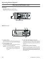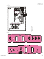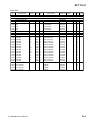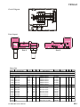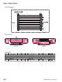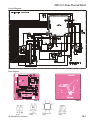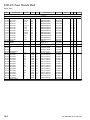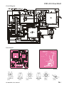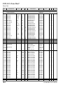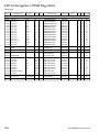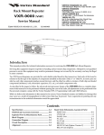
1
VERTEX STANDARD CO., LTD. 4-8-8 Nakameguro, Meguro-Ku, Tokyo 153-8644, Japan VERTEX STANDARD US Headquarters 10900 Walker Street, Cypress, CA 90630, U.S.A. International Division 8350 N.W. 52nd Terrace, Suite 201, Miami, FL 33166, U.S.A. VHF FM Transceiver VX-4000V YAESU EUROPE B.V. P.O. Box 75525, 1118 ZN Schiphol, The Netherlands Service Manual YAESU UK LTD. Unit 12, Sun Valley Business Park, Winnall Close Winchester, Hampshire, SO23 0LB, U.K. VERTEX STANDARD HK LTD. Unit 5, 20/F., Seaview Centre, 139-141 Hoi Bun Road, Kwun Tong, Kowloon, Hong Kong ©2002 VERTEX STANDARD CO., LTD. Printed in Japan. POWER Introduction This manual provides technical information necessary for servicing the VX-4000V FM Transceiver. Servicing this equipment requires expertise in handling surface-mount chip components. Attempts by non-qualified persons to service this equipment may result in permanent damage not covered by the warranty, and may be illegal in some countries. Two PCB layout diagrams are provided for each double-sided circuit board in the Transceiver. Each side of is referred to by the type of the majority of components installed on that side (“leaded” or “chip-only”). In most cases one side has only chip components, and the other has either a mixture of both chip and leaded components (trimmers, coils, electrolytic capacitors, ICs, etc.), or leaded components only. While we believe the technical information in this manual to be correct, VERTEX STANDARD assumes no liability for damage that may occur as a result of typographical or other errors that may be present. Your cooperation in pointing out any inconsistencies in the technical information would be appreciated. Contents Operating Manual Reprint ........................ 1-1 Cloning .................................................................... 2-1 Specifications .............................................. 2-2 Exploded View & Miscellaneous Parts ... 3-1 Block Diagram ............................................ 3-2 Interconnection Diagram .......................... 3-4 Circuit Description .................................... 4-1 Alignment ................................................... 5-1 Board Unit (Schematics, Layouts & Parts) MAIN Unit ........................................................ 6A-1 DISPLAY Unit ................................................... 6B-1 KEY Unit ........................................................... 6C-1 VR Unit .............................................................. 6D-1 MIC CONN Unit .............................................. 6D-2 Optional Board Unit (Schematics, Layouts & Parts) F2D-8 2-Tone Decode Unit ............................... 7A-1 F5D-14 5-Tone Unit .......................................... 7B-1 FVP-25 Encryption / DTMF Pager Unit ........... 7C-1 VTP-50 VX-Trunk Unit ..................................... 7D-1 1 2 Operating Manual Reprint CONTROLS & CONNECTORS Front Panel ‚ƒ • † „ … POWER A ˆ ‰ Š ‡ • POWER Button Press the button to turn the transceiver ON and OFF. ‚ TX Indicator This lamp glows red when the radio is transmitting. ƒ BUSY Indicator This lamp glows green when the channel is busy. „ Liquid Crystal Display The display include an 8-character alpha-numeric section showing channel and group names, status and identity information, and error messages. Additional indicators on the display show priority channel assignments and scan include / exclude selection. This channel on “HORN ALERT” List † SQC Indicator This lamp glows orange when incorrect position at the setting of CE35. ‡ Programmable Function Button (PF button) This button can be set up for special applications, such as high/low power selection, monitor, dimmer, talk-around, and call alert function, as determined by your network requirements and programmed by your VERTEX STANDARD dealer. ˆ VOLUME Knob ‰ EMERGENCY Microphone This channel on “INTERCOM” List Receiver Monitor This channel on “SCAN” List This channel on “OPTION” List Pressing these buttons changes the current group (and displayed group number or name). Holding this button for more than 1/2 second causes the function to repeat. This knob sets the volume of the receiver. This channel on “SELECTABLE TONE” List This channel on “PUBLIC A DDRESS ” or “S PEAKER ” List … p/q Button Channel Group Number The emergency microphone is located behind this small slit. When the emergency feature is activated, this Microphone is enabled. Š CHANNEL Selector Knob This knob select the operating channel. Programmable Function Button (PF button) This button can be set up for special applications, such as high/low power selection, monitor, dimmer, talk-around, and call alert function, as determined by your network requirements and programmed by your VERTEX STANDARD dealer. 8 Character Alpha-numeric Display This channel on “AUX A/B/C” List VX-4000 VHF Service Manual 1-1 Operating Manual Reprint CONTROLS & CONNECTORS Side Panel Microphone Jack (It is on both sides.) Connect the microphone plug to this jack. Microphone Jack REAR (Heatsink) • ‚ ƒ „ À Antenna Socket The 50-ohm coaxial feedline to the antenna must be connected here, using a type-M (PL-259) plug. Á External Speaker Jack An external loudspeaker may be connected to this 2-contact, 3.5-mm mini-phone jack. Caution: Do not connect this line to ground, and be certain that the speaker has adequate capability to handle the audio output from the VX-4000. 1-2  13.8-V DC Cable Pigtail w/Connector The supplied DC power cable must be connected to this 2-pin connector. Use only the supplied fused cable, extended if necessary, for power connection. à DSUB 25-Pin Accessory Connector External TX audio line input, PTT (Push To Talk), Squelch, and external RX audio line output signal may be obtained from this connector for use with accessories such as data transmission/reception modems, ets. VX-4000 VHF Service Manual Operating Manual Reprint BASIC OPERATION OF THE TRANSCEIVER Important! - Before turning on the radio the first time, confirm that the power connections have been made correctly and that a proper antenna is connected to the antenna jack. Switching Power ON/OFF Push the POWER switch turn on the radio. The display will become illuminated. The radio will start up on the last channel used prior to shutdown during the previous operating session. Turn the CHANNEL selector knob to choose the desired operating channel. A channel name will appear on the display. If you want to select the operating channel from a different Memory Channel Group, press the UP (p) or DOWN (q) button to select the Memory Channel Group you want before selecting the operating channel. Setting the Volume Turn the VOLUME knob clockwise to increase the volume, and counterclockwise to decrease it. If no signal is present, press and hold in the MON button more than 1/2 seconds; background noise will now be heard, and you may use this to set the VOLUME knob for the desired audio level. Press and hold the MON button more than 1/2 seconds to quiet the noise and resume normal (quiet) monitoring. VX-4000 VHF Service Manual Transmitting To transmit, wait until the “BUSY” indicator is off (the channel is not in use), and press the PTT (Push-To-Talk) switch on the side of the microphone (the “TX” indicator will appear or the “TX” indicator will glow red). While holding in the PTT switch, speak across the face of the microphone in a clear, normal voice level, and then release the PTT switch to receive. Selecting Groups and Channels m Press the UP (p) or DOWN (q) button (repeatedly, if necessary) to select a different group of channels. m Turn the CHANNEL selector knob to select a different channel within the current group. Automatic Time-Out Timer If the selected channel has been programmed for automatic time-out, you must limit the length of each transmission. While transmitting, a beep will sound five seconds before time-out. Another beep will sound just before the deadline; the “TX” indicator will disappear and transmission will cease soon thereafter. To resume transmitting, you must release the PTT and wait for the “penalty timer” to expire (if you press the PTT before this timer expires, the timer restarts, and you will have to wait another “penalty” period.) 1-3 Operating Manual Reprint ADVANCED OPERATION Programmable Function Button (PF button) The VX-4000 includes the seven Programmable Function Buttons (PF button). The PF button functions can be customized, via programming by your VERTEX STANDARD dealer, to meet your communications/network requirements. Some features may require the purchase and installation of opetional internal accessories. The possible PF button programming features are il- lustrated at the below, and their functions are explained on next page. For further details, contact your VERTEX STANDARD dealer. For future reference, check the box next to each function that has been assigned to the PF button on your particular radio, and keep it handy. POWER Programmable Function Button (PF button) Functions <1.5 sec >1.5 sec <1.5 sec >1.5 sec <1.5 sec >1.5 sec <1.5 sec >1.5 sec <1.5 sec >1.5 sec <1.5 sec >1.5 sec <1.5 sec >1.5 sec None SCAN (SCN) Dual Watch Call/Reset Talk-Around (TA) Noise Blanker* (NB) Alpha Numeric (A/N) DIMMER (DIM) Emergency (EMG) Horn Alert (HA) Home Channel (HOM) Intercom (IC) Low Power (LOW) GRP UP GRP DWN CH UP CH DWN AUX A AUX B AUX C Public Address (PA) Monitor (MON) RCL Selectable Tone (ST) SP** Squlch Level (SQL) Encryption*** (OPT) * for VX-4000L 1-4 ** requires RMK-4000 ** requires Encryption Unit VX-4000 VHF Service Manual Operating Manual Reprint ADVANCED OPERATION Channel Scan The Scanning feature is used to monitor multiple signals programmed into the transceiver. While scanning, the transceiver will check each channel for the presence of a signal, and will stop on a channel if a signal is present. To activate scanning: m Press the assigned PF button of the “Scan” momentarily to activate scanning. m The scanner will search the channels, looking for active ones; it will pause each time it finds a channel on which someone is speaking. To stop scanning m Press the assigned PF button of the “Scan”. m Operation will revert to the channel to which the CHANNEL selector knob is set. Note:Your dealer may have programmed your radio to stay on one of the following channels if you press the PTT switch during scanning pause: r Current channel (“Talk Back”) r “Last Busy” channel r “Priority” channel r “Home” channel r Scan Start” channel Dual Watch The Dual Watch feature is similar to the Scan feature, except that only two channels are monitored: r The current operating channel; and r The “Priority” channel. To activate Dual Watch: m Press the assigned PF button of the “Dual Watch”. m The scanner will search the two channels; it will pause each time it finds a channel on which someone is speaking. To stop Dual Watch: m Press the assigned PF button of the “Dual Watch”. m Operation will revert to the channel to which the CHANNEL selector knob is set. VX-4000 VHF Service Manual ARTS (Auto Range Transpond System) This system is designed to inform you when you and another ARTS-equipped station are within communication range. During ARTS operation, your radio automatically transmits for about 1 second every 25 (or 55) seconds (the interval is programmed by Dealer) in an attempt to Shake hands with the other station. If you move out of range for more than one minutes, your radio senses that no signal has been received, a ringing beeper will sound. If you subsequently move back into range, as soon as the other station transmits, your beeper will sound. The PF Button Function The PF (Programmable Function) button can be programmed by the dealer to provide two of the other functions described below. To activate the primary Accessory function, press the PF button momentarily. To access the secondary Accessory function (which may include the Alarm), press and hold the PF button for 1.5 seconds or longer. Call/Reset When this feature is programmed and a selective call has been received, momentarily press the assigned PF button of the “Call/Reset” to reset the flashing indicator and mute the receiver, otherwise press the assigned PF button of the “Call/ Reset” to sent your radio’s identification code (ANI) to the dispatcher. Talk-Around The feature causes the assigned PF button of the “Talk-Around” to select simplex operation on semi-duplex channels: the transmit frequency becomes the same as the receive frequency (regardless of any programmed offset for the channel). Note:This feature has no effect on simplex channels. After pressing the button, “TA” is displayed on the LCD. Noise Blanker (for VX-4000L) Because local noise can be particularly troublesome in the VHF Low-Band frequency spectrum, the Low-Band version of the VX-4000 includes a Noise Blanker feature, which may be toggled on and off by pressing the assigned PF button of the “Noise Blanker” for the appropriate length of time. 1-5 Operating Manual Reprint ADVANCED OPERATION Alpha Numeric Press the assigned PF button of the “Alpha Numeric” to switch the display between the Group/ Channel number, and the Group/Channel name (alphanumeric). A tone will sound each time you switch between numerical and alphanumerical display. DIM Press the assigned PF button of the “DIM” to adjust the brightness of the display and key backright. EMG (Emergency) Press the assigned PF button of the “EMG” to initiate an emergency call (requires ANI board). When an emergency call is made, not tone is emitted and the display does not change. To end the emergency call, turn the transceiver power OFF. HA (Horn Alert) Press the assigned PF button of the “HA” to turn the Horn Alert function ON or OFF. If you receive a call from the base station with 2Tone or DTMF signaling, horn alert will activate. When you turn Horn Alert ON, a tone will sound ” appears on the display.. and “ Home (Home Channel) Press the assigned PF button of the “Home” to select the pre-programmed Home Channel. Press it again to return to the previous channel. If used while scanning, pressing this key a second time will change to the revert channel. IC (Intercom) This feature requires dual head configuration. Press the assigned PF button of the “IC” to turn the intercom feature ON or OFF. While ON, you can press the PTT switch to communicate to another control head operator without transmitting over the air. When you press this key, a tone sounds and “ ” appears on the display. The intercom can be used even while scanning and receiving a call. GRP UP/DWN Press the assigned PF button of the “GRP UP” or “GRP DWN” to select a different group of channels. CH UP/DWN Press the assigned PF button of the “CH UP” or “CH DWN” to select a different channel within the current group. AUX A/B/C Press the assigned PF button of the “AUX A”, “AUX B”, or “AUX C” to turn the output port (respectively). PA (Public Address) Press the assigned PF button of the “PA” to use the transceiver as a PA amplifier. When you en” apable this function, a tone sounds and “ pears on the display. The public address can be used even while scanning and receiving a call. MONI (Monitor) Press the assigned PF button of the “MONI” momentarily to cancel CTCSS and DCS signaling squelch; the “MON” icon appears on the display. Press and hold this key for 1/2 seconds to hear background noise (unmute the audio); the MON icon blinks on the display. RCL (Channel Recall) During scan, you can press the assigned PF button of the “RCL” to select the last called channel. ST (Selectable Tone) Press the assigned PF button of the “Selectable Tone”, then rotate the CHANNEL selector knob to select a 2-Tone. SP Press the assigned PF button of the “SP” to switch “Front panel”, “Front panel & Body” and “Body” speaker. When “Body” is selected, a tone sounds and the “ ” icon appears on the display. You can use this function while scanning and receiving a call. However, all audio will be emitted from the PA speaker. Low Power Press the assigned PF button of the “Low Power” to set the radio's transmitter to the “Low Power” mode. Press this key again to return to “High Power” operation when in difficult terrain. 1-6 VX-4000 VHF Service Manual Operating Manual Reprint ADVANCED OPERATION SQL (Squelch Level) You can manually adjust the squelch level using this function: 1. Press the assigned PF button of the “SQL”. A tone sounds and SQL appears on the display with the current squelch level. 2. Rotate the CHANNEL selector knob to select the desired level. 3. Press the this key. A tone sounds and the display returns to the normal channel. Encryption (Option) When the Voice Scrambler feature is enabled, pressing the assigned PF button of the “Encryption” toggles the Scrambler on and off. VX-4000 VHF Service Manual 1-7 Operating Manual Reprint OPTIONAL ACCESSORIES MH-25B7A MH-53C7A MH-53A7A MH-53B7A CE35 CT-70 CT-71 CT-72 CT-81 CT-82 CT-83 CNT-4000 RF DECK RMK-4000SH RMK-4000DH RMK-4000DB RMK-4000DBH F2D-8 F5D-14 VTP-50 FVP-25 FP-1023 MLS-100 MMB-75 MMB-76 LF-1 FIF-7 CN-6 FIF-8 1-8 Microphone Heavy Duty Microphone Heavy Duty Microphone w/Noise Canceler Heavy Duty DTMF Microphone w/Noise Canceler Programming Software Radio Programming Cable (Requires VPL-1) Radio to PC Programming Cable Radio to Radio Programming Cable Cable for RMK-4000 (6 m) Cable for RMK-4000 (2.5 m) Cable for RMK-4000 (0.6 m) Control Head RF Deck w/MMB-75 (for Dual Band Installations) Remote Kit (for Single Transceiver) Remote Kit (for Dual-Head Installations) Remote Kit (for Dual Band Installations) Remote Kit (for Dual Band plus Dual Head Installations) 2-Tone Decode Unit (Requires FIF-7) 5-Tone ENC-DEC Unit (Requires FIF-7) VX-Trunk Unit (Requires FIF-7) Encryption/DTMF pager Unit (Requires FIF-7) External 23A Power Supply Mobile Loud speaker (12 W Peak Power) Mobile Mounting Bracket Locking Mobile Mounting Bracket Line Filter Inter face Board (for F2D-8, F5D-14, VTP-50, FVP-25) Inter face Board (for Accessories) Flash ROM Adapter VX-4000 VHF Service Manual DSUB 25-PIN ACCESSORY CONNECTOR DSUB 25-Pin Numbering DSUB25 output level (V) Pin 1: RSSI [Analog Output] A DC voltage proportional to the strength of the signal currently being received (Receiver Signal Strength Indicator) is provided on this pin. This low impedance output is generated by the receiver IF sub-system and buffered by an internal op-amp. Typical voltages are graphed as follows: 5.0 4.5 4.0 3.5 3.0 2.5 2.0 1.5 1.0 0.5 0 1259 398 125 398 12.5 None MON DIM Hook SCAN G-SCAN RPT INH ENG Home CH SW0 CH SW1 CH SW2 4 1.25 0.4 0.125 0.04 SSG Input Level (uV) Pin 2, 3, 4, 5 & 6: AI1, AI2, AI3, AI4 & AI5 [Universal Input Port] These input port features can be programmed via the CE35 programmer. The same item can not be chosen twice. To select the “Input port” page, (View à Common View à DSUB-25pin connector à Input port). Pin 2 Pin 3 Pin 4 Pin 5 CH SW3 This feature is the same as pressing and holding in the Monitor key. LCD illumination dimmer “on.” Activates the Hook1 feature. Activates the scanner. Activates the Group scanner. Disables the repeater feature during Multi Deck operation. Activates the Emergency feature. Switches to the Home Channel. Memory channel recall (Channel Switch Table bit 0) Memory channel recall (Channel Switch Table bit 1) Memory channel recall (Channel Switch Table bit 2) Memory channel recall (Channel Switch Table bit 3) Example If you assign “CH SW0” and “CH SW1” to the Universal Input Port, you can recall Channels 1~3 as shown below. Channel 1 2 3 CH SW0 1 0 1 CH SW1 0 1 1 Pin 6 LOGIC level (+5V / 0V) input (Low active). High Impedance input. VX-4000 VHF Service Manual 1-9 Similarly, if you assign “CH SW0,” “CH SW1,” and “CH SW2” to the Universal Input Port, you can recall Channels 1~7 as shown below: Channel 1 2 3 4 5 6 7 CH SW0 1 0 1 0 1 0 1 CH SW1 0 1 1 0 0 1 1 CH SW2 0 0 0 1 1 1 1 Pin 8: AO2 [Universal Output Port] Open collector output. Output voltage 0 ~ 5 V, Max. sink current 30 mA. The possible programming features (use CE35) are illustrated below. A KEY/B KEY/C KEY/D KEY/E KEY/HA/Invert If you need to recall all memory channels (15 CH) from the External Controller via the Uni-versal Input Port, you should assign the “All Channel Recall” Command (CH SW 0 ~ CH SW 3) to the Universal Input Port. In this case: Channel 1 2 3 4 5 6 7 8 9 10 11 12 13 14 15 CH SW0 1 0 1 0 1 0 1 0 1 0 1 0 1 0 1 CH SW1 0 1 1 0 0 1 1 0 0 1 1 0 0 1 1 CH SW2 0 0 0 1 1 1 1 0 0 0 0 1 1 1 1 CH SW3 0 0 0 0 0 0 0 1 1 1 1 1 1 1 1 The Memory Channel is determined via the CE35 Programmer. (View à Common View à DSUB25pin connector à Channel switch Table). 5V DSUB 25-Pin PINS 2, 3, 4, 6 47kW Pin 7: E [GND] Ground for all logic levels and power supply return. DSUB 25-Pin Refer to the “Pins 20, 21, & 22” section for details. Pin 9: TXD2 [Digital Output for Alignment software] Connect to the RS232C cable (requires FIF-8 and CT-88) Pin 10: RXD2 [Digital Input for Alignment software] Connect to the RS232C cable (requires FIF-8 and CT-88) Pin 11: TXS [EXT PTT] Shorting this port to ground causes the transceiver to be placed in the Transmit mode, while opening the connection to this port returns the transceiver to the Receive mode. Pin 12: MCM [MIC Mute] MIC mute on: Level High (5V) MIC mute off: Open LOGIC level (+5V / 0V) output. When the PTT/EXT PTT switch is pressed, this pin switches to “open.” Pin 13: MD/DI [Digital Input for DATA Communications] m TX Hi-speed Data Input Type (jumper JP2006). Input level 800 mV/600 Ohms, Max.input 1.2V m Tx Low-speed Data input Type (Jumper JP2007). Input level 40 mV/600-Ohms If the Jumper setting is “Low-speed Data” (JP2007 jumpered), this port is usable in the AUDIO (300~3000 Hz) range. If the jumper setting is “HI-speed Data” (JP2006 jumpered), this port is usable for 9600 bps DATA communications, because the filter and limiter are not engaged in the Audio line. Pin 14: SB [13.8 V/5 V DC Output] m Switched 13.8V output for supplying power to an accessory (jumper JP2009). m Switched and regulated DC 5.0V output for supplying power to an accessory (jumper JP2008). Maximum output current is 200 mA PIN 5 (Pull Up) Sample Circuit 1-10 VX-4000 VHF Service Manual Pin 15: IGN [Ignition Sense feature] The VX-4000 may automatically be switched to the STAND-BY mode when the vehicle's igni-tion key is turned on. Maximum current is 20 mA. This feature is only enabled on transceivers configured for Dual Deck operation. DSUB 25-Pin Ignition 13.8V Pin 19: NC [No Connection] Pins 20, 21, & 22: AO1, AO3 & AO4 [Universal Output Port] LOGIC level (+5V / 0V) output. The logic output appears at these pins when the front panel's PF key is turned on. The possible programming features (use CE35) are illustrated below. If the HA feature is assigned to these ports, a current amplifier must be connected between the Horn circuit and the port. A KEY/B KEY/C KEY/D KEY/E KEY/HA/Invert Pin 16: NC [NO connection] Pin 17: AFO [Digital Output for DATA Communications] m RX Hi-speed Data Output Type (jumper JP2004). output level 600 mV/10k Ohms m RX Low-speed Data Output Type (jumper JP2005). output level 200 mV/600 Ohms If the Jumper setting is “Low-speed Data” (JP2007 jumpered), this port is usable in the AUDIO (300~3000 Hz) range. If the jumper setting is “HI-speed Data” (JP2006 jumpered), this port is usable for 9600 bps DATA communications, because the filter and limiter are not engaged in the Audio line. Pin 23: SQ [Squelch Signal Output] Open collector output. Max. sink current 10 mA. A Signal is present (Squelch is open): Level High No Signal is present (Squelch is closed): Open When you connect the solder jumper on J2002, this port changes to PULL UP (5 V) output. This status can be changed by CE35 programmer. Pin 24: SPM [Speaker Mute Output] Open collector output. External Speaker mute on: Level High External Speaker mute off: Open Pin 25: ME [GND] Chassis ground. Pin 18: E [GND] Ground for all logic levels and power supply return. VX-4000 VHF Service Manual 1-11 Note: 1-12 VX-4000 VHF Service Manual Cloning The VX-4000 includes a convenient “Clone” feature, which allows the programming data from one transceiver to be transferred to another VX-4000. Here is the procedure for Cloning one radio’s data to another. Note: When a cloning isn't made, you correct the following part using "CE35." When a "Radio to Radio Clone" which is in the "Miscellaneous" menu is "Disabled," change this menu to "Enabled." 1. 2. 3. 4. Turn both transceivers off. Remove the plastic cap and its two mounting screws from the Microphone jack on the transceiver. Do this for both transceivers. Connect the optional CT-72 cloning cable between the Microphone jacks of the two transceivers. On the Destination transceiver, press and hold the PF Button (just below the POWER Button) while turning the transceiver on. 5. 6. 7. 8. 9. Now, on the source transceiver, press and hold the q Button while turning the transceiver on.Data will now be transferred to the Destination transceiver from the source transceiver. If there is a problem during the cloning process, sound an error beep from source the transceiver. Check your cable connections and battery voltage, and try again. If cloning is a successful, turn the Destination transceiver off. Now turn the source transceiver off. Disconnect the CT-72. Replace the plastic cap and its two mounting screws. You can then turn the transceivers back on, and begin normal operation. Optional Cloning Cable CT-72 POWER POWER Destination source DealerProgramming of VTP-50 and F5D-14 These procedures are designed to be used by the installing technician after the VTP-50 and F5D-14 has been installed in the transceiver. To program a VX-4000's VTP-50 and F5D-14 board, you will need the CT-71 programming interface cable, the CE-26 Programming diskette, and an IBM PC/AT or PS/2compatible tyoe computer. To enter the Programming mode, use the following procedure: 1. Turn the transceiver off. 2. Turn on the transceiver while holding in the PF Button (just below the q Button). VX-4000 VHF Service Manual POWER 2-1 Specifications GENERAL Number of Channels: Frequency Range: Channel Spacing: Power Supply Voltage: Current Consumption: Ambient Temperature Range: Frequency Stability: RF Input-Output Impedance: Audio Output Impedance: Dimensions: Weight: RECEIVER 250 channels 134 - 160 MHz (A), 148 - 174 MHz (C) 12.5 / 25 / 30 kHz 13.8 VDC Standby: 400 mA Receive: 2.1 A Transmit: 12 A –30°C to +60°C (–22°F to +140°F) ±2.5 ppm 50 Ohms 4 Ohms 7" (w) x 2.4" (H)x 7.7" (D) (178 x 60 x 195 mm) 4.9 lbs. (2.2 kg) (Measurements made per EIA standard TIA/EIA-603) Circuit Type: Sensitivity(EIA 12 dB SINAD): Adjacent Channel Selectivity: Intermodulation: Spurious and Image Rejection: Audio Response: Audio Output: TRANSMITTER Double-conversion Super-heterodyne 0.25 µV 85 dB / 75 dB 76 dB 90 dB +3 / –8 dB from the 6 dB / oct. re-emphasis curve 5 W @ 4 Ohms, 10 % THD 10 W @ 4 Ohms w/<10 % THD (Option) (Measurements made per EIA standard TIA/EIA-603) Power Output: Modulation: Max Deviation: Conducted Spurious Emissions: FM Hum & Noise: Audio Response: Audio Distortion (@ 1 kHz): 50 / 25 W 16K0F3E, 11K0F3E 5.0 / 2.5 kHz 70 dB Below Carrier 45 dB (25 kHz) / 40 dB (12.5 kHz) +1 / –3 dB from the 6 dB / oct-8 <3% Measurements per EIA standards unless noted above. Specifications subject to change without notice or obligation. 2-2 VX-4000 VHF Service Manual Exploded View & Miscellaneous Parts À Screw List REF. VXSTD P/N Description Qty. 1 U20306007 BINDING HEAD SCREW M3x6B 4 2 U20306002 BINDING HEAD SCREW M3x6NI 6 3 U24308002 TAPTITE SCREW M3x8NI 9 4 U23206001 TAPTITE SCREW M2.6x6 14 5 U20308002 BINDING HEAD SCREW M3x8NI 2 6 U24208001 TAPTITE SCREW M2.6x8 1 7 U20305007 BINDING HEAD SCREW M3x5B 2 8 U32450007 FLAT HEAD SCREW M2.6x5B 2 9 U31306007 OVAL HEAD SCREW M3x6B 2 10 S5000182 SCREW JFS-4S-B1MW 2 RA0254900 CASE À À RA0262700 PACKING SHEET À Q6000114 TERMINAL STRIP RA0134490 HOLDER Ä Â Ä S6000395 COVER P-25P(23)  Accessories Description VXSTD P/N Qty. BLADE FUSE ATC 15A Q0000075 2 DC CABLE 02P 15AX2 T9021015 1 KNOB CAP RA0254100 5 NAME PLATE RA0254700 1   MAIN Unit T9206926 WIRE ASSY Å RA0262400 PACKING SHEET Á É Â Â É Â RA0262300 HOLDER PLATE *A MIC CONN Unit RA0262500 PACKING SHEET RA0252700 REFLECTOR SHEET DISPLAY Unit  RA0252800 DIFFUSER SHEET P1090654 CONNECTOR (W/ *A) MIC CONN Unit à G6090140 LCD à RA0253000 LCD HOLDER RA0254200 RUBBER PACKING RA0251500 CHASSIS RA020830A DOUBLE FACE (Both Side) à RA0215400 SHEET à à à à Á RA0251900 PANEL ASSY Á Ç RA0254800 CONTACT ASSY (Both Side) à à RA0252300 LIGHT GUIDE RA0252900 RUBBER CONNECTOR à à à S6000396 RUBBER GROMMET TM-96-17 P1090984 CONNECTOR à VR3601* RA0254000 RUBBER KNOB (PWR) Á Á  à VR Unit Á Æ Æ RA0215000 EXT CAP R0145680 FITTING (x4 pcs) M4090133 SPEAKER Supplide is VR3601* KEY Unit RA0253900 RUBBER KNOB (CH) RA02543A0 KNOB RA0254300 KNOB VX-4000 VHF Service Manual RA0275500 RUBBER KNOB ASSY È R6054387B SPECIAL NUT Non-designated parts are available only as part of a designated assembly. È 3-1 Block Diagram 3-2 VX-4000 VHF Service Manual Block Diagram VX-4000 VHF Service Manual 3-3 Interconnection Diagram 3-4 VX-4000 VHF Service Manual Circuit Description Reception and transmission are switched by "RX" and "TX" lines from the microprocessor unit (MPU). Main Receiver Signal Path The receiver uses double-conversion superheterodyne circuitry, with a 43.95MHz 1st IF and 450 kHz 2nd IF. The 1st LO, produced by a PLL synthesizer, yields the 43.95MHz 1st IF. The 2nd LO uses a 43.5 MHz (43.95 MHz-450 kHz) signal generated by a crystal oscillator. The 2nd mixer and other circuits use a custom IC to convert and amplify the 2nd IF, and detect FM to obtain demodulated signals. During transmit, the PLL synthesizer oscillates at the desired frequency directly, for amplification to obtain RF power output. During transmit, voice modulation and CTCSS (or DCS) modulation are applied to this synthesizer. Transceiver functions, such as TX/RX control, PLL synthesizer settings, and channel programming, are controlled using the MPU. Receiver Incoming RF signals from the antenna connector are delivered to the MAIN Unit, and pass through a low-pass filter (LPF) antenna switching network consisting of coils L1001, L1002, L1003 and L1006, capacitors C1001,C1006, C1009, C1013, and C1023, and antenna switching diodes D1006,D1007 and D1008 for delivery to the receiver front end. Signals within the frequency range of the transceiver are then passed through a varactor-tuned bandpass filter consisting of L1008, L1009 / L1024, L1025 before RF amplification by Q1012 (3SK228). The amplified RF is then band-pass filtered again by varactor-tuned resonators L1018, L1019 / L1038, L1039 to ensure pure in-band input to 1st mixer Q1025 (2SK228). Buffered output from the VCO Unit is amplified by Q1021 (2SC5107) and low-pass filtered by L1042 / L1046 and C1132 / C1139 / C1142, to provide a pure 1st local signal between 112.3 and 152.3 MHz to the 1st mixer. The 43.95MHz 1st mixer product then passes through dual monolithic crystal filters XF1001 and XF1002 (7.5 kHz BW), and is amplified by Q1029 (2SC4215Y) and delivered to the input of the FM IF subsystem IC Q1026 (TA31136FN). This IC contains the 2nd mixer, 2nd local oscillator, limiter amplifier, FM detector, noise amplifier, and squelch gates. The 2nd LO in the IF-IC is produced from crystal X1001 (14.500MHz), and the 1st IF is converted to 450kHz by the 2nd mixer and stripped of unwanted components by ceramic filter CF1001 or CF1002. After passing through a limiter amplifier, the signal is demodulated by the FM detector. Demodulated receive audio from the IF-IC is amplified by Q1031 (2SA1602A) / Q2014 (CXA1846N). After volume adjustment by the AF power amplifier Q2029 (TDA7240AV), the audio signal is passed to the optional headphone jack or 4-ohm loudspeaker. PLL synthesizer The 1st LO maintains stability from the PLL synthesizer by using a 14.500 MHz reference signal from crystal X1001. PLL synthesizer IC Q1024 (SA7025DK) consists of a prescaler, reference counter, swallow counter, programmable counter, a serial data input port to set these counters based on the external data, a phase comparator, and charge pump. The PLL-IC divides the 14.500 MHz reference signal by 725 using the reference counter (20.0 kHz comparison frequency). The phase detector comparison frequency to be eight times the channel spacing (2.5kHz). The VCO output is divided by the prescaler, swallow counter and programmable counter. These two signals are compared by the phase comparator and input to the charge pump. A voltage proportional to their phase difference is delivered to the low-pass filter circuit, then fed back to the VCO as a voltage with phase error, controlling and stabilizing the oscillating frequency. This synthesizer also operates as a modulator during transmit. The RX-VCO is comprised of Q1015 (2SK520) and D1017, D1018, D1035, D1036 (HVU356x4), and oscillates between 177.950MHz and 217.950MHz according to the programmed receiving frequency. And the TX-VCO is comprised of Q1014 (2SC5107) and D1015, D1016, D1019 (1SV276x3), and oscillates between 134.000MHz and 174.000MHz according to the programmed transmit frequency. The VCO output passes through buffer amplifier Q1018 (2SC5107), and a portion is fed to the buffer amplifier Q1019 (2SC5107) of the PLL IC, and at the same time amplified by Q1021 (2SC5107) to obtain stable output. The VCO DC supply is regulated by Q1008 (2SC4154E). Synthesizer output is fed to the 1st mixer by diode switch D1024 (1SS321) during receive, and to drive amplifier Q1020/Q1022 (2SC5415Ex2) for transmit. The reference oscillator feeds the PLL synthesizer, and is com- 4-1 Circuit Description posed of crystal X1001 (14.500 MHz), the temperature compensation circuit which includes D1033 (MC2850) and thermostats TH1003 and TH1002, and transmit (DCS) modulation circuit D1029 (1SV2309). DCS Demodulator Transmitter CTCSS encoder/decoder Voice audio from the microphone is delivered via the Mic (Jack) Unit to the MAIN Unit, after passing through amplifier Q3039/Q2108 (NJM2902V), pre-emphasis, limiter (IDC instantaneous deviation control) ,and LPF Q2001 (NJM2902V), is adjusted for optimum deviation level and delivered to the next stage. Voice input from the microphone and CTCSS are FMmodulated to the VCO of the synthesizer, while DCS audio is modulated by the reference frequency oscillator of the synthesizer. Synthesizer output, after passing through diode switch D1024 (1SS321), is amplified by driver Q1020 / Q1022 (2SC5415Ex2) and power module Q1013 (M67746) to obtain full RF output. The RF energy then passes through antenna switch D1007 / D1008 and a low-pass filter circuit and finally to the antenna connector. RF output power from the final amplifier is sampled by CM coupler and is rectified by D1011, D1014 (HSM88ASx2). The resulting DC is fed through Automatic Power Controller Q1007 (NJM2904V), Q1001 (2SC4154E), Q1002 (2SB1143S) to transmitter RF amplifier and thus the power output. Generation of spurious products by the transmitter is minimized by the fundamental carrier frequency being equal to the final transmitting frequency, modulated directly in the transmit VCO. Additional harmonic suppression is provided by a low-pass filter consisting of L1002, L1003, L1007, L1012 and C1006, C1009, C1013, C1023, C1033, C1037 and C1046, resulting in more than 60dB of harmonic suppression prior to delivery to the RF energy to the antenna. 4-2 DCS signals are demodulated on the MAIN-UNIT, and are applied to low-pass filter Q2110 (NJM2902V), as well as the limiter comparator Q2110. The CTCSS code is generation and encoding by MPU IC Q2019 (MB90F583B). Demodulation and detection of the CTCSS tones are carried out by IC Q2013 (MX165C). MPU Operation is controlled by 16-bit MPU IC Q2019 (MB90F583B). The system clock uses a 16.000 MHz crystal for a time base. IC Q2027 (S-80735SN) resets the MPU when the power is on, and monitors the voltage of the regulated 5V power supply line. EEPROM The EEPROM retains TX and RX data for all memory channels and CTCSS data, DCS data, prescaler dividing, and REF oscillator data (internal/external). Alignment The VX-4000 has been carefully aligned at the factory for the specified performance across the frequency range specified for each version. Realignment should therefore not be necessary except in the event of a component failure, or alteration of version. All component replacement and service should be performed only by an authorized VERTEX STANDARD representative, or the warranty policy may be voided. The following procedures cover the sometimes critical and tedious adjustments that are not normally required once the transceiver has left the factory. However, if damage occurs and some parts are replaced, realignment may be required. If a sudden problem occurs during normal operation, it is likely due to component failure; realignment should not be done until after the faulty component has been replaced. We recommend that servicing be performed only by authorized VERTEX STANDARD service technicians who are experienced with the circuitry and fully equipped for repair and alignment. Therefore, if a fault is suspected, contact the dealer from whom the transceiver was purchased for instructions regarding repair. Authorized VERTEX STANDARD service technicians realign all circuits and make complete performance checks to ensure compliance with factory specifications after replacing any faulty components. Those who do undertake any of the following alignments are cautioned to proceed at their own risk. Problems caused by unauthorized attempts at realignment are not covered by the warranty policy. Also, VERTEX STANDARD must reserve the right to change circuits and alignment procedures in the interest of improved performance, without notifying owners. Under no circumstances should any alignment be attempted unless the normal function and operation of the transceiver are clearly understood, the cause of the malfunction has been clearly pinpointed and any faulty components replaced, and the need for realignment determined to be absolutely necessary. The following test equipment (and thorough familiarity with its correct use) is necessary for complete realignment. Correction of problems caused by misalignment resulting from use of improper test equipment is not covered under the warranty policy. While most steps do not require all of the equipment listed, the interactions of some adjustments may require that more complex adjustments be performed afterwards. VX-4000 VHF Service Manual Do not attempt to perform only a single step unless it is clearly isolated electrically from all other steps. Have all test equipment ready before beginning, and follow all of the steps in a section in the order presented. Required Test Equipment r RF signal generator: calibrated output level at 1000 MHz r Deviation Meter (linear detector) r AF Millivoltmeter r SINAD Meter r Inline Wattmeter with 5% accuracy at 1000 MHz r Regulated DC Power Supply: adjustable from 10 to 17 VDC, 15A r 50-ohm Non-reactive Dummy Load: 100 W at 1000 MHz r Frequency Counter: >0.1 ppm accuracy at 1000 MHz r AF Signal Generator r DC Voltmeter: high impedance r RF Sampling Coupler(attenuation pad) r AF Dummy Load: 4 ohm, 20W r Oscilloscope r Spectrum Analyzer r IBM PC/compatible computer w/ VERTEX STANDARD CT-71 programming cable and CE35 channel programming editor. Alignment Preparation & Precautions A dummy load and inline wattmeter must be connected to the main antenna jack in all procedures that call for transmission, except where specified otherwise. Correct alignment is not possible with an antenna. After completing one step, read the following step to determine whether the same test equipment will be required. If not, remove the test equipment (except dummy load and wattmeter, if connected) before proceeding. Correct alignment requires that the ambient temperature be the same as that of the transceiver and test equipment, and that this temperature be held constant between 68 ~ 86°F (20 ~ 30°C). When the transceiver is brought into the shop from hot or cold air it should be allowed some time for thermal equalization with the environment before alignment. If possible, alignments should be made with oscillator shields and circuit boards firmly affixed in place. Also, the test equipment must be thoroughly warmed up before beginning. 5-1 Alignment Before beginning, connect the transceiver and PC using the CT-71 programming cable as described in the EEPROM Programming chapter, and download the EEPROM data from the transceiver to the computer. Store this data in a disk file so that it can be saved and retrieved later. Using the table below, program the channel, CTCSS, and DCS alignment settings for your transceiver version. Upload this file to the transceiver. Note:Signal levels in dB referred to in this procedure are based on 0 dBµ = 0.5 µV (closed circuit). Caution:Do not connect this line to ground, and be certain that the speaker has adequate capability to handle the audio output from the radio. Because of the bridge audio amplifier circuit used in the radio, it is necessary to construct and use a simple audio load test adapter as shown in the schematic diagram above, when conducting receiver alignment steps. Alignment Channel Frequencies VHF TYPE A Channel CH1 CH2 CH3 CH4 CH5 CH6 CH7 CH8 CH9 CH10 Frequency (simplex) 134.01 MHz 147.01 MHz 159.99 MHz 134.01 MHz 147.01 MHz 159.99 MHz 147.01 MHz 147.01 MHz 147.01 MHz 147.01 MHz CTCSS Encode None None None None None None 151.4 Hz None 151.4 Hz None DCS Encode None None None None None None None 023 None 023 Narrow/wide Wide Wide Wide Narrow Narrow Narrow Wide Wide Narrow Narrow VHF TYPE C Channel CH1 CH2 CH3 CH4 CH5 CH6 CH7 CH8 CH9 CH10 Frequency (simplex) 148.01 MHz 161.01 MHz 173.99 MHz 148.01 MHz 161.01 MHz 173.99 MHz 161.01 MHz 161.01 MHz 161.01 MHz 161.01 MHz CTCSS Encode None None None None None None 151.4 Hz None 151.4Hz None DCS Encode None None None None None None None 023 None 023 Narrow/wide Wide Wide Wide Narrow Narrow Narrow Wide Wide Narrow Narrow PLL & Transmitter Set up the test equipment as shown for transmitter alignment. Maintain the supply voltage at 13.8 V DC for all steps. 50-Ohm Dummy Load RF Signal Generator Inline Wattmeter Deviation Meter Frequency Counter Transceiver CT-71 connection Cable Power Supply 13.8V DC PC COM port PLL VCV r Connect the positive lead of the DC voltmeter to the test point TP1007 (VCV) on the Main Unit, as indicated in the figure, and the negative lead to chassis ground. r Set the transceiver to the high band edge frequency channel, then adjust L1021 on the Unit for 4.2 V (VHF-A), 4.3 V (VHF-C) on the voltmeter. r Key the transmitter, and adjust L1022 on the Unit for 4.2 V (VHF-A), 4.3 V (VHF-C) on the voltmeter. r Next select to the low edge frequency channel and confirm 0.8 V on the voltmeter. r Key the transmitter, and confirm 1.0 V on the voltmeter. PLL Reference Frequency With the wattmeter, dummy load and frequency counter connected to the antenna jack, and select band center frequency channel, key the transmitter (Low power level) and adjust TC1001 on the Main Unit, if necessary, so the counter frequency is within 100 Hz of the channel center frequency for the transceiver version. Transmitter Output Power The following transmitter parameters can be adjusted from the computer by utilizing the Alignment Software. Refer to the onboard help of the Alignment Software Manual for details. HIGH Power LOW Power 5-2 RF Sampling Coupler 50 ± 1 W 25 ± 0.5 W VX-4000 VHF Service Manual Alignment Transmitter Deviation The following modulation parameters can be adjusted from the computer by utilizing the Alignment Software. Refer to the onboard help of the Alignment Software Manual for details. Microphone Audio Modulation Level 4.3 kHz ± 0.1 kHz CTCSS Modulation Level 0.75 kHz ± 0.1 kHz DCS Modulation Level 0.75 kHz ± 0.1 kHz L1022 L1021 TP1007 VX-4000 VHF Service Manual TC1001 5-3 Alignment Squelch Threshold Receiver The sensitivity parameters can be adjusted from the computer by utilizing the Alignment Software. Refer to the onboard help of the Alignment Software Manual for details. r Set up the test equipment as shown for receiver alignment, and install the audio test adapter. 50-Ohm Dummy Load RF Signal Generator Inline Wattmeter Power Supply 13.8V DC Deviation Meter Frequency Counter RF Sampling Coupler CT-71 Connection Cable Transceiver AF Test Adapter The squelch parameters can also be adjusted from the computer by utilizing the Alignment Software. Refer to the onboard help of the Alignment Software Manual for details. r Select the band center frequency channel, and with the RF signal generator turned to the same frequency, set the generator for ±3.0 kHz deviation with 1 kHz tone modulation, and set the output level for –6 dBµ (for wide) or -4 dBµ (for narrow) at the antenna jack. r Adjust the squelch threshold level (by control commands from the computer) such that the squelch just closes at this signal input level (the BUSY LED will turn off). AF Generator SINAD Meter AC Volt Meter r With the transceiver set to the band center frequency channel, and with the RF signal generator tuned to the same frequency, set the generator for ±3.0 kHz deviation (for 25 kHz steps) with 1 kHz tone modulation, and set the output level for 1µV at the antenna jack. r Adjust (by control commands from the computer) the receiver front-end tuning for optimum SINAD, reducing signal generator output level as necessary for proper meter deflection. r After the previous step, the final signal generator level should be less than –8 dBµ (for wide) or -6 dBµ (for narrow) for 12dB SINAD. 5-4 VX-4000 VHF Service Manual MAIN Unit (Lot. 1~) Circuit Diagram (2.09V) (5.68V) 13.75V (13.8V) (5.67V) 1.48V (0V) (0.97V) 0.39V 12.99V 6.36V 0.86V (5.64V) 13.8V (13.8V) 8.9V (13.51V) 3.44V (6.93V) 13.0V (13.51V) 3.44V (8.38V) 3.37V (2.5V) (1.18V) (1.08V) Wide:(0.01V) Narrow:(1.84V) 5.27V (5.58V) 0.76V (0.0V) 7.89V (7.84V) (4.82V) 7.77V (7.72V) 8.07V (7.84V) 8.31V (8.28V) (5.16V) (5.3V) (4.48V) 5.69V 8.4V (0.0V) (3.68V) 8.94V (8.91V) 2.97V (3.1V) 0.75V (0.4V) (6.05V) Wide:(4.92V) Narrow:(0V) 3.46V (2.48V) 2.7V (0.02V) 3.45V (0.07V) 2.05V (0.02V) (2.24V) (4.94V) 2.34V (1.74V) 2.74V (0.02V) 3.43V (2.54V) (0.9V) (5.0V) 5.3V (5.3V) (2.6V) 4.73V (4.81V) 13.11V (13.14V) 8.97V (8.95V) (2.4V) (2.94V) (0.01V) (1.92V) 5.0V (4.98V) 9.04V (9.04V) 8.32V (8.94V) 4.96V (0.0V) 0.06V (4.81V) 0.0V (8.97V) 9.02V (0.02V) (4.82V) (4.0V) (4.89V) (3.99V) 7.56V (0.05V) 13.75V (4.94V) (4.97V) 2.68V (2.71V) (2.47V) 0.66V (0.14V) 4.47V (4.45V) 0.0V (4.53V) 0.07V (8.94V) 0.0V (4.95V) 0.0V (4.97V) 2.69V (2.71V) (8.73V) 1.98V (1.98V) 1.67V (1.67V) (1.8V) 3.44V (2.55V) (7.82V) 6.85V (5.08V) Wide:0.0V Narrow:(4.92V) NB/RF_G Hi: (0.03V) NB/RF_G Lo: (0.26V) (0.0V) (8.87V) 6.86V(5.08V) (0.08V) (0.31V) 3.42V (2.54V) (5.55V) (0.68V) (0.01V) 0.01V (0.01V) XX: TX 161.01 MHz, MIC Input Level 1 kHz 3.0mV (STD Dev), High Power (XX):RX 161.01 MHz, RF Input Level 40dbµ emf (MOD=1.0 kHz, Dev=3.0 kHz), EXT SP OUT 10% Distn 14.0W VX-4000 VHF Service Manual 6A-1 MAIN Unit (Lot. 1~) 0.01V (0.78V) 0.14V (2.09V) 0.0V (3.6V) 1.28V (1.1V) 8.64V (8.65V) 1.1V (1.1V) 1.86V (1.19V) (12.47V) 0.01V (0.81V) (0.31V) 1.1V (1.1V) 0.0V (2.09V) (12.99V) 4.87V (4.87V) 4.86V (4.86V) 0.0V (0.77V) 1.31V (1.1V) 0.0V (4.19V) 1.76V (1.18V) 3.65V (3.65V) 8.96V (8.97V) 3.85V (3.85V) 4.88V (4.88V) 3.84V (3.84V) 6.83V (6.83V) 0.0V (0.0V) 1.1V (1.1V) 8.97V (8.97V) 3.84V (3.84V) 3.84V (3.85V) 2.14V (2.14V) 4.86V 4.87V (4.87V) (4.87V) 4.87V (4.87V) 3.85V (3.85V) 4.03V (4.03V) 4.04V (4.04V) 4.03V (4.03V) 0.0V (0.0V) Pow Off: (13.74V) Pow On:(0.02) 4.5V (4.5V) 0.63V (4.88V) (4.54V) 2.4V (2.4V) 2.4V (2.41V) (4.5V) 8.97V (8.97V) 2.38V (2.38V) 0.0V (0.0V) 2.21V (2.21V) 4.03V (4.04V) 0.0V (0.0V) (4.5V) 4.76V (4.76V) 4.76V (4.76V) 8.96V (8.97V) 2.39V (2.39V) 4.03V (4.03V) 2.57V (2.57V) 4.86V (4.86V) 0.0V (4.86V) 4.86V (4.86V) 0.0V (0.0V) 4.76V (0.0V) (4.59V) 4.50V (4.50V) 1.95V (1.95V) 1.97V (1.97V) 4.04V (4.04V) 4.58V (4.59V) 1.96V (1.96V) 1.96V (1.96V) 4.04V (4.04V) (13.47V) 4.41V (4.41V) 1.9V (1.9V) (13.13V) 4.87V (4.88V) 4.92V (4.92V) 0.0V (0.0V) (6.1V) 1.92V (1.92V) 1.97V (1.97V) 4.03V (4.04V) 4.03V (4.04V) (6.21V) (6.2V) 5.92V (5.92V) (6.16V) (6.19V) 6A-2 XX: TX 161.01 MHz, MIC Input Level 1 kHz 3.0mV (STD Dev), High Power (XX): 161.01 MHz, RF Input Level 40dbµ emf (MOD=1.0 kHz, Dev=3.0 kHz) , EXT SP OUT 10% Distn 14.0W VX-4000 VHF Service Manual MAIN Unit (Lot. 1~) Parts Layout A B C D E F G TA31136FN (Q1026) SA7025DK (Q1024) 1 BU4066BF (Q2007) MB90F583B (Q2019) TC4W53FU (Q2117) 2 CXA1846N (Q2014) HN58X2432TI (Q2028) 3 4 5 2SC4154E (LE) (Q1001, 2018) 2SC5107-O (MFO) (Q1014, 1018) 2SC4215Y (QY) (Q1029) RT1N241M (N2) (Q1004, 1016, 1032 2006, 2011, 2116 2119, 2124) HZM5.6NB2 (562) (D1027) Side A VX-4000 VHF Service Manual M67746-01 (Q1013) 2SA1602A (MF) (Q1031) 3SK228 (XR-) (Q1012, 1025) IMD3 (D3) (Q2112) TDA7240AV (Q2029) IMH6 (H6) (Q1017) 2SK520 (K41) (Q1015) DTC323TK (H02) (Q2012) MC2850 (A7) (D2003, 2004) HSM88AS (C1) (D1011, 1014) 6A-3 MAIN Unit (Lot. 1~) a IMD3 (D3) (Q2115) IMH6 (H6) (Q1009) IMX1 (X1) (Q2009) IMZ1 (Z1) (Q2002) DTB123EK (F12) (Q1005, 2015, 2111) MX165CDW (Q2013) 2SB1201STP (Q1003) c d BU4053BCF (Q2016) e f g 2SB1143S (Q1002) 1 NJM2902V (Q1007, 2001, 2003 2108, 2110) 2SJ327Z (Q2020) RT1N241M (N2) (Q1011, 1028, 1033 2004, 2008, 2026 2114, 2118, 2120 2121, 2122, 2125) 2SC4154E (LE) (Q1008, 1027) 2SC5107-O (MFO) (Q1019, 1021) 2SB1132R (BA) (Q1006) b 2 2SC2954 (QK) (Q1020) 2SC5415E (EA) (Q1022) MM1216ENRE (1A) (Q1030) 3 NJM78L05UA (8C) (Q1023, 2024) 4 2SA1602A (MF) (Q2025) S-80735SN (DZ) (Q2027) 5 MC2850 (A7) (D1033, 2002, 2006 2010) 6A-4 1SS321 (F9) (D1024) MC2848 (A6) (D1026, 1028) MC2846 (D2001, 2007) Side B VX-4000 VHF Service Manual MAIN Unit (Lot. 4~) Circuit Diagram (2.09V) (5.68V) 13.75V (13.8V) (5.67V) 1.48V (0V) (0.97V) 0.39V 12.99V 6.36V 0.86V (5.64V) 13.8V (13.8V) 8.9V (13.51V) 3.44V (6.93V) 13.0V (13.51V) 3.44V (8.38V) 3.37V (2.5V) (1.18V) (1.08V) Wide:(0.01V) Narrow:(1.84V) 5.27V (5.58V) 0.76V (0.0V) 7.89V (7.84V) (4.82V) 7.77V (7.72V) 8.07V (7.84V) 8.31V (8.28V) (5.16V) (5.3V) (4.48V) 5.69V 8.4V (0.0V) (3.68V) 8.94V (8.91V) 2.97V (3.1V) 0.75V (0.4V) (6.05V) Wide:(4.92V) Narrow:(0V) 3.46V (2.48V) 2.7V (0.02V) 3.45V (0.07V) 2.05V (0.02V) (2.24V) (4.94V) 2.34V (1.74V) 2.74V (0.02V) 3.43V (2.54V) (0.9V) (5.0V) 5.3V (5.3V) (2.6V) 4.73V (4.81V) 13.11V (13.14V) 8.97V (8.95V) (2.4V) (2.94V) (0.01V) (1.92V) 5.0V (4.98V) 9.04V (9.04V) 8.32V (8.94V) 4.96V (0.0V) 0.06V (4.81V) 0.0V (8.97V) 9.02V (0.02V) (4.82V) (4.0V) (4.89V) (3.99V) 7.56V (0.05V) 13.75V (4.94V) (4.97V) 2.68V (2.71V) (2.47V) 0.66V (0.14V) 4.47V (4.45V) 0.0V (4.53V) 0.07V (8.94V) 0.0V (4.95V) 0.0V (4.97V) 2.69V (2.71V) (8.73V) 1.98V (1.98V) 1.67V (1.67V) (1.8V) 3.44V (2.55V) (7.82V) 6.85V (5.08V) Wide:0.0V Narrow:(4.92V) NB/RF_G Hi: (0.03V) NB/RF_G Lo: (0.26V) (0.0V) (8.87V) 6.86V(5.08V) (0.08V) (0.31V) 3.42V (2.54V) (5.55V) (0.68V) (0.01V) 0.01V (0.01V) XX: TX 161.01 MHz, MIC Input Level 1 kHz 3.0mV (STD Dev), High Power (XX):RX 161.01 MHz, RF Input Level 40dbµ emf (MOD=1.0 kHz, Dev=3.0 kHz), EXT SP OUT 10% Distn 14.0W VX-4000 VHF Service Manual 6A-5 MAIN Unit (Lot. 4~) 0.01V (0.78V) 0.14V (2.09V) 0.0V (3.6V) 1.28V (1.1V) 8.64V (8.65V) 1.1V (1.1V) 1.86V (1.19V) (12.47V) 0.01V (0.81V) (0.31V) 1.1V (1.1V) 0.0V (2.09V) (12.99V) 4.87V (4.87V) 4.86V (4.86V) 0.0V (0.77V) 1.31V (1.1V) 0.0V (4.19V) 1.76V (1.18V) 3.65V (3.65V) 8.96V (8.97V) 3.85V (3.85V) 4.88V (4.88V) 3.84V (3.84V) 6.83V (6.83V) 0.0V (0.0V) 1.1V (1.1V) 8.97V (8.97V) 3.84V (3.84V) 3.84V (3.85V) 2.14V (2.14V) 4.86V 4.87V (4.87V) (4.87V) 4.87V (4.87V) 3.85V (3.85V) 4.03V (4.03V) 4.04V (4.04V) 4.03V (4.03V) 0.0V (0.0V) Pow Off: (13.74V) Pow On:(0.02) 4.5V (4.5V) 0.63V (4.88V) (4.54V) 2.4V (2.4V) 2.4V (2.41V) (4.5V) 8.97V (8.97V) 2.38V (2.38V) 0.0V (0.0V) 2.21V (2.21V) 4.03V (4.04V) 0.0V (0.0V) (4.5V) 4.76V (4.76V) 4.76V (4.76V) 8.96V (8.97V) 2.39V (2.39V) 4.03V (4.03V) 2.57V (2.57V) 4.86V (4.86V) 0.0V (4.86V) 4.86V (4.86V) 0.0V (0.0V) 4.76V (0.0V) (4.59V) 4.50V (4.50V) 1.95V (1.95V) 1.97V (1.97V) 4.04V (4.04V) 4.58V (4.59V) 1.96V (1.96V) 1.96V (1.96V) 4.04V (4.04V) (13.47V) 4.41V (4.41V) 1.9V (1.9V) (13.13V) 4.87V (4.88V) 4.92V (4.92V) 0.0V (0.0V) (6.1V) 1.92V (1.92V) 1.97V (1.97V) 4.03V (4.04V) 4.03V (4.04V) (6.21V) (6.2V) 5.92V (5.92V) (6.16V) (6.19V) 6A-6 XX: TX 161.01 MHz, MIC Input Level 1 kHz 3.0mV (STD Dev), High Power (XX): 161.01 MHz, RF Input Level 40dbµ emf (MOD=1.0 kHz, Dev=3.0 kHz) , EXT SP OUT 10% Distn 14.0W VX-4000 VHF Service Manual MAIN Unit (Lot. 4~) Parts Layout A B C D E F G TA31136FN (Q1026) SA7025DK (Q1024) 1 BU4066BF (Q2007) MB90F583B (Q2019) TC4W53FU (Q2117) 2 CXA1846N (Q2014) HN58X2432TI (Q2028) 3 4 5 2SC4154E (LE) (Q1001, 2018) 2SC5107-O (MFO) (Q1014, 1018) 2SC4215Y (QY) (Q1029) RT1N241M (N2) (Q1004, 1016, 1032 2006, 2011, 2116 2119, 2124) HZM5.6NB2 (562) (D1027) Side A VX-4000 VHF Service Manual M67746-01 (Q1013) 2SA1602A (MF) (Q1031) 3SK228 (XR-) (Q1012, 1025) IMD3 (D3) (Q2112) TDA7240AV (Q2029) IMH6 (H6) (Q1017) 2SK520 (K41) (Q1015) DTC323TK (H02) (Q2012) MC2850 (A7) (D2003, 2004) HSM88AS (C1) (D1011, 1014) 6A-7 MAIN Unit (Lot. 4~) a IMD3 (D3) (Q2115) IMH6 (H6) (Q1009) IMX1 (X1) (Q2009) IMZ1 (Z1) (Q2002) DTB123EK (F12) (Q1005, 2015, 2111) MX165CDW (Q2013) 2SB1201STP (Q1003) c d BU4053BCF (Q2016) e f g 2SB1143S (Q1002) 1 NJM2902V (Q1007, 2001, 2003 2108, 2110) 2SJ327Z (Q2020) RT1N241M (N2) (Q1011, 1028, 1033 2004, 2008, 2026 2114, 2118, 2120 2121, 2122, 2125) 2SC4154E (LE) (Q1008, 1027) 2SC5107-O (MFO) (Q1019, 1021) 2SB1132R (BA) (Q1006) b 2 2SC2954 (QK) (Q1020) 2SC5415E (EA) (Q1022) MM1216ENRE (1A) (Q1030) 3 NJM78L05UA (8C) (Q1023, 2024) 4 2SA1602A (MF) (Q2025) S-80735SN (DZ) (Q2027) 5 MC2850 (A7) (D1033, 2002, 2006 2010) 6A-8 1SS321 (F9) (D1024) MC2848 (A6) (D1026, 1028) MC2846 (D2001, 2007) Side B VX-4000 VHF Service Manual MAIN Unit Parts List REF. DESCRIPTION VALUE WV TOL. MFR’S DESIG VXSTD P/N VERS. CS1728001 CS1728002 FR004680D FR004680E K22174221 K22174243 K22281801 K22174823 K22124805 K33279019 K22174821 K33279047 K22174821 K22174227 K22174821 K33279024 K22174235 K78120016 K78140019 K22174225 K78140021 K22174219 K22174821 K33279024 K22174821 K22174821 K22124805 K22174225 K40129065 K22174227 K78100048 K78120057 K22174821 K33279023 K22124805 K22174821 K33279024 K22174821 K22174821 K22124805 K78100028 K78100028 K22174821 K22271221 K22271208 K33279021 K33279019 K22174821 K22174821 K22174821 K22174204 K22174205 K22174204 K22174249 K22174821 K22174821 K22174821 K22174249 K22174243 VERSION C VERSION A LOT. SIDE. LAY ADR. *** MAIN UNIT *** C 1001 C 1002 C 1003 C 1004 C 1005 C 1006 C 1007 C 1009 C 1010 C 1011 C 1012 C 1013 C 1014 C 1015 C 1015 C 1016 C 1017 C 1020 C 1022 C 1023 C 1024 C 1025 C 1026 C 1027 C 1028 C 1030 C 1031 C 1031 C 1032 C 1033 C 1035 C 1036 C 1037 C 1038 C 1039 C 1040 C 1041 C 1042 C 1045 C 1046 C 1046 C 1046 C 1046 C 1047 C 1048 C 1049 C 1050 C 1050 C 1050 C 1051 C 1052 C 1053 C 1055 C 1056 C 1057 PCB with Components PCB with Components Printed Circuit Board Printed Circuit Board CHIP CAP. CHIP CAP. CHIP CAP. CHIP CAP. CHIP CAP. FILM CAP. CHIP CAP. FILM CAP. CHIP CAP. CHIP CAP. CHIP CAP. FILM CAP. CHIP CAP. CHIP TA.CAP. CHIP TA.CAP. CHIP CAP. CHIP TA.CAP. CHIP CAP. CHIP CAP. FILM CAP. CHIP CAP. CHIP CAP. CHIP CAP. CHIP CAP. AL.ELECTRO.CAP. CHIP CAP. CHIP TA.CAP. CHIP TA.CAP. CHIP CAP. FILM CAP. CHIP CAP. CHIP CAP. FILM CAP. CHIP CAP. CHIP CAP. CHIP CAP. CHIP TA.CAP. CHIP TA.CAP. CHIP CAP. CHIP CAP. CHIP CAP. FILM CAP. FILM CAP. CHIP CAP. CHIP CAP. CHIP CAP. CHIP CAP. CHIP CAP. CHIP CAP. CHIP CAP. CHIP CAP. CHIP CAP. CHIP CAP. CHIP CAP. CHIP CAP. VX-4000 VHF Service Manual 27pF 220pF 0.001uF 0.01uF 0.1uF 10pF 0.001uF 9pF 0.001uF 47pF 0.001uF 33pF 100pF 4.7uF 4.7uF 39pF 10uF 22pF 0.001uF 33pF 0.001uF 0.001uF 0.1uF 39pF 3300uF 47pF 68uF 47uF 0.001uF 27pF 0.1uF 0.001uF 33pF 0.001uF 0.001uF 0.1uF 10uF 10uF 0.001uF 22pF 5pF 22pF 10pF 0.001uF 0.001uF 0.001uF 3pF 4pF 3pF 470pF 0.001uF 0.001uF 0.001uF 470pF 220pF 50V 50V 630V 50V 16V 500V 50V 500V 50V 50V 50V 500V 50V 16V 25V 50V 25V 50V 50V 500V 50V 50V 16V 50V 16V 50V 10V 16V 50V 500V 16V 50V 500V 50V 50V 16V 10V 10V 50V 500V 500V 500V 500V 50V 50V 50V 50V 50V 50V 50V 50V 50V 50V 50V 50V CH CH R B B B B CH B CH CH CH B B B B CH CH B B B B B B B CH CH B B B CJ CH CJ CH B B B CH CH GRM39CH270J50PT GRM39CH221J50PT GHM1030R102K630PT GRM39B103M50PT GRM39B104K16PT UC232H0100D-T GRM39B102K50PT UC232H0090D-T GRM39B102K50PT GRM39CH470J50PT GRM39B102K50PT UC232H0330J-T GRM39CH101J50PT TEMSVB21C475M-8R TEMSVB21E475M-8R GRM39CH390J50PT TEMSVC1E106M12R GRM39CH220J50PT GRM39B102K50PT UC232H0330J-T GRM39B102K50PT GRM39B102K50PT GRM39B104K16PT GRM39CH390J50PT RE3-16V332M 3300UF GRM39CH470J50PT TEMSVC1A686M12R TEMSVC1C476M12R GRM39B102K50PT UC232H0270J-T GRM39B104K16PT GRM39B102K50PT UC232H0330J-T GRM39B102K50PT GRM39B102K50PT GRM39B104K16PT TEMSVA1A106M-8R TEMSVA1A106M-8R GRM39B102K50PT GRM42-6CH220J500PT GRM42-6CH050C500PT UC232H0220J-T UC232H0100D-T GRM39B102K50PT GRM39B102K50PT GRM39B102K50PT GRM39CJ030C50PT GRM39CH040C50PT GRM39CJ030C50PT GRM39CH471J50PT GRM39B102K50PT GRM39B102K50PT GRM39B102K50PT GRM39CH471J50PT GRM39CH221J50PT VERSION A VERSION C VERSION A VERSION C 141111111111111131111111111114111111111111 2-3 441111-3 44111111- B A A A A A A A B A B A A A A A A A B A A B B A A A A A A A A A A B B B B B B A A A A B A A A A A A A B A A A a3 B2 G1 D3 B2 G1 B2 G1 d3 G3 e3 G1 B2 C3 C3 G3 E2 G3 d2 G2 B2 e3 d2 G3 C2 G3 C3 C3 D3 G2 E2 D3 G2 d3 b2 d3 d3 d3 c3 F3 F3 F3 F3 d3 F2 F2 F3 F3 F3 F2 E3 d5 E5 F2 E5 6A-9 MAIN Unit REF. C 1058 C 1059 C 1060 C 1061 C 1062 C 1063 C 1064 C 1065 C 1066 C 1067 C 1069 C 1070 C 1071 C 1072 C 1073 C 1074 C 1075 C 1076 C 1077 C 1078 C 1079 C 1080 C 1081 C 1082 C 1083 C 1084 C 1085 C 1086 C 1088 C 1089 C 1090 C 1091 C 1092 C 1094 C 1095 C 1096 C 1097 C 1098 C 1099 C 1100 C 1101 C 1102 C 1103 C 1105 C 1106 C 1107 C 1107 C 1107 C 1108 C 1109 C 1110 C 1111 C 1112 C 1113 C 1114 C 1115 C 1116 C 1117 C 1118 C 1119 6A-10 DESCRIPTION CHIP CAP. CHIP CAP. CHIP CAP. CHIP CAP. CHIP CAP. CHIP CAP. CHIP CAP. CHIP CAP. CHIP CAP. CHIP CAP. CHIP CAP. CHIP CAP. FILM CAP. CHIP CAP. CHIP CAP. CHIP CAP. CHIP CAP. CHIP CAP. CHIP CAP. FILM CAP. CHIP CAP. CHIP CAP. CHIP CAP. CHIP CAP. CHIP CAP. CHIP CAP. CHIP CAP. CHIP CAP. CHIP CAP. CHIP CAP. CHIP CAP. CHIP CAP. CHIP CAP. CHIP CAP. CHIP CAP. CHIP TA.CAP. CHIP CAP. CHIP CAP. CHIP TA.CAP. CHIP CAP. CHIP CAP. CHIP CAP. CHIP CAP. CHIP CAP. CHIP CAP. CHIP CAP. CHIP CAP. CHIP CAP. CHIP CAP. CHIP CAP. CHIP CAP. CHIP CAP. CHIP CAP. CHIP CAP. CHIP CAP. CHIP TA.CAP. CHIP CAP. CHIP CAP. CHIP CAP. CHIP CAP. VALUE 470pF 0.001uF 0.001uF 470pF 220pF 0.001uF 1pF 220pF 0.001uF 0.001uF 0.001uF 15pF 0.022uF 0.001uF 0.001uF 0.001uF 0.001uF 0.001uF 0.001uF 0.022uF 0.001uF 12pF 12pF 68pF 47pF 0.001uF 0.001uF 0.001uF 100pF 0.001uF 0.001uF 100pF 1pF 1pF 100pF 10uF 0.001uF 0.01uF 0.68uF 0.001uF 10pF 0.01uF 0.01uF 10pF 0.001uF 15pF 22pF 15pF 6pF 3pF 0.001uF 0.001uF 0.001uF 0.001uF 18pF 1uF 0.001uF 0.001uF 10pF 0.001uF WV 50V 50V 50V 50V 50V 50V 50V 50V 50V 50V 50V 50V 16V 50V 50V 50V 50V 50V 50V 16V 50V 50V 50V 50V 50V 50V 50V 50V 50V 50V 50V 50V 50V 50V 50V 10V 50V 25V 20V 50V 50V 25V 25V 50V 50V 50V 50V 50V 50V 50V 50V 50V 50V 50V 50V 16V 50V 50V 50V 50V TOL. CH B B CH CH B CK CH B B B CH B B B B B B B CH CH CH CH B B B CH B B CH CK CK CH B B B CH B B CH B CH CH CH CH CJ B B B B CH B B CH B MFR’S DESIG GRM39CH471J50PT GRM39B102K50PT GRM39B102K50PT GRM39CH471J50PT GRM39CH221J50PT GRM39B102K50PT GRM39CK010C50PT GRM39CH221J50PT GRM39B102K50PT GRM39B102K50PT GRM39B102K50PT GRM39CH150J50PT ECHU1C223JB5 GRM39B102K50PT GRM39B102K50PT GRM39B102K50PT GRM39B102K50PT GRM39B102K50PT GRM39B102K50PT ECHU1C223JB5 GRM39B102K50PT GRM39CH120J50PT GRM39CH120J50PT GRM39CH680J50PT GRM39CH470J50PT GRM39B102K50PT GRM39B102K50PT GRM39B102K50PT GRM39CH101J50PT GRM39B102K50PT GRM39B102K50PT GRM39CH101J50PT GRM39CK010C50PT GRM39CK010C50PT GRM39CH101J50PT TEMSVA1A106M-8R GRM39B102K50PT GRM39B103K25PT TESVA1D684M1-8R GRM39B102K50PT GRM39CH100D50PT GRM39B103K25PT GRM39B103K25PT GRM39CH100D50PT GRM39B102K50PT GRM39CH150J50PT GRM39CH220J50PT GRM39CH150J50PT GRM39CH060D50PT GRM39CJ030C50PT GRM39B102K50PT GRM39B102K50PT GRM39B102K50PT GRM39B102K50PT GRM39CH180J50PT TESVA1C105M1-8R GRM39B102K50PT GRM39B102K50PT GRM39CH100D50PT GRM39B102K50PT VXSTD P/N VERS. LOT. SIDE. LAY ADR. K22174249 1K22174821 1K22174821 1K22174249 1K22174243 1K22174821 1K22174202 1K22174243 1K22174821 1K22174821 1K22174821 1K22174215 1K57120011 1K22174821 1K22174821 1K22174821 1K22174821 1K22174821 1K22174821 1K57120011 1K22174821 1K22174213 1K22174213 1K22174231 1K22174227 1K22174821 1K22174821 1K22174821 1K22174235 1K22174821 1K22174821 1K22174235 1K22174202 1K22174202 1K22174235 1K78100028 1K22174821 1K22144803 1K78130009 1K22174821 1K22174211 1K22144803 1K22144803 1K22174211 1K22174821 1K22174215 1-3 K22174219 VERSION A 4K22174215 VERSION C 4K22174207 1K22174204 1K22174821 1K22174821 1K22174821 1K22174821 1K22174217 1K78120009 1K22174821 1K22174821 1K22174211 1K22174821 1- A B B A B A A A B A B A A A A B A A B A B A A A A A B A A A A A A A B B A B A A B A A B A B B B B A A A B A A A B B B B E2 c4 c5 F2 c5 F3 E5 E5 c2 E2 c4 D4 F5 F3 C2 b3 E5 D3 d2 F5 b3 E5 E5 E4 E5 F3 d2 F3 C3 E4 E4 D3 E4 E4 e2 c4 E4 e2 E5 C2 e2 D3 F5 d2 E4 d2 d2 d2 c4 E3 E4 F3 e2 C3 E4 C3 e2 b4 b4 e2 VX-4000 VHF Service Manual MAIN Unit REF. C 1120 C 1121 C 1122 C 1122 C 1122 C 1123 C 1124 C 1125 C 1127 C 1128 C 1129 C 1129 C 1130 C 1131 C 1131 C 1131 C 1132 C 1133 C 1133 C 1134 C 1135 C 1136 C 1137 C 1138 C 1139 C 1140 C 1141 C 1141 C 1141 C 1142 C 1144 C 1145 C 1146 C 1147 C 1148 C 1149 C 1150 C 1151 C 1152 C 1153 C 1154 C 1155 C 1156 C 1157 C 1158 C 1159 C 1160 C 1161 C 1162 C 1163 C 1164 C 1165 C 1166 C 1167 C 1168 C 1169 C 1170 C 1171 C 1172 C 1173 DESCRIPTION CHIP CAP. CHIP CAP. CHIP CAP. CHIP CAP. CHIP CAP. CHIP CAP. CHIP CAP. CHIP CAP. CHIP CAP. CHIP CAP. CHIP TA.CAP. CHIP TA.CAP. CHIP CAP. CHIP CAP. CHIP CAP. CHIP CAP. CHIP CAP. CHIP TA.CAP. CHIP TA.CAP. CHIP CAP. CHIP CAP. CHIP CAP. CHIP CAP. CHIP CAP. CHIP CAP. CHIP CAP. CHIP CAP. CHIP CAP. CHIP CAP. CHIP CAP. CHIP CAP. CHIP TA.CAP. CHIP CAP. CHIP CAP. CHIP CAP. CHIP CAP. CHIP CAP. CHIP CAP. CHIP CAP. CHIP CAP. CHIP CAP. CHIP CAP. CHIP CAP. CHIP CAP. CHIP CAP. CHIP CAP. CHIP CAP. CHIP CAP. CHIP CAP. CHIP CAP. CHIP CAP. CHIP CAP. CHIP CAP. CHIP CAP. CHIP CAP. CHIP CAP. CHIP CAP. CHIP CAP. CHIP CAP. CHIP CAP. VX-4000 VHF Service Manual VALUE 12pF 47pF 12pF 18pF 12pF 0.001uF 33pF 0.001uF 12pF 0.001uF 4.7uF 4.7uF 0.001uF 2pF 4pF 2pF 4pF 4.7uF 4.7uF 0.001uF 0.001uF 0.001uF 220pF 18pF 27pF 100pF 1pF 2pF 1pF 6pF 100pF 10uF 33pF 0.001uF 0.001uF 0.001uF 0.001uF 0.01uF 0.1uF 0.001uF 0.1uF 220pF 15pF 0.01uF 0.01uF 0.01uF 0.001uF 0.001uF 0.001uF 22pF 0.01uF 0.01uF 0.01uF 0.001uF 120pF 15pF 0.1uF 47pF 12pF 0.01uF WV 50V 50V 50V 50V 50V 50V 50V 50V 50V 50V 10V 16V 50V 50V 50V 50V 50V 10V 16V 50V 50V 50V 50V 50V 50V 50V 50V 50V 50V 50V 50V 10V 50V 50V 50V 50V 50V 25V 16V 50V 16V 50V 50V 25V 25V 25V 50V 50V 50V 50V 25V 25V 25V 50V 50V 50V 16V 50V 50V 25V TOL. CH CH CH CH CH B CH B CH B B CK CH CK CH B B B CH CH CH CH CK CK CK CH CH CH B B B B B B B B CH CH B B B B B B CH B B B B CH CH B CH CH B MFR’S DESIG VXSTD P/N GRM39CH120J50PT GRM39CH470J50PT GRM39CH120J50PT GRM39CH180J50PT GRM39CH120J50PT GRM39B102K50PT GRM39CH330J50PT GRM39B102K50PT GRM39CH120J50PT GRM39B102K50PT TEMSVA1A475M-8R TEMSVA1C475M-8R GRM39B102K50PT GRM39CK020C50PT GRM39CH040C50PT GRM39CK020C50PT GRM39CH040C50PT TEMSVA1A475M-8R TEMSVA1C475M-8R GRM39B102K50PT GRM39B102K50PT GRM39B102K50PT GRM39CH221J50PT GRM39CH180J50PT GRM39CH270J50PT GRM39CH101J50PT GRM39CK010C50PT GRM39CK020C50PT GRM39CK010C50PT GRM39CH060D50PT GRM39CH101J50PT TEMSVA1A106M-8R GRM39CH330J50PT GRM39B102K50PT GRM39B102K50PT GRM39B102K50PT GRM39B102K50PT GRM39B103K25PT GRM39B104K16PT GRM39B102K50PT GRM39B104K16PT GRM39CH221J50PT GRM39CH150J50PT GRM39B103K25PT GRM39B103K25PT GRM39B103K25PT GRM39B102K50PT GRM39B102K50PT GRM39B102K50PT GRM39CH220J50PT GRM39B103K25PT GRM39B103K25PT GRM39B103K25PT GRM39B102K50PT GRM39CH121J50PT GRM39CH150J50PT GRM39B104K16PT GRM39CH470J50PT GRM39CH120J50PT GRM39B103K25PT K22174213 K22174227 K22174213 K22174217 K22174213 K22174821 K22174223 K22174821 K22174213 K22174821 K78100022 K78120031 K22174821 K22174203 K22174205 K22174203 K22174205 K78100022 K78120031 K22174821 K22174821 K22174821 K22174243 K22174217 K22174221 K22174235 K22174202 K22174203 K22174202 K22174207 K22174235 K78100028 K22174223 K22174821 K22174821 K22174821 K22174821 K22144803 K22124805 K22174821 K22124805 K22174243 K22174215 K22144803 K22144803 K22144803 K22174821 K22174821 K22174821 K22174219 K22144803 K22144803 K22144803 K22174821 K22174237 K22174215 K22124805 K22174227 K22174213 K22144803 VERS. VERSION A VERSION C VERSION A VERSION C VERSION A VERSION C LOT. SIDE. LAY ADR. 111-3 44111111411-11 121211411111111-3 441111111111111111111111111111111- B B B B B B B B B A B B B B B B B B B B B B B B B B B B B B B B B B B B A B B B B B B B B B B A A B B B B A A B A B B B c4 c4 d2 d2 d2 e2 c5 d3 b4 E4 c3 c3 e3 d3 d3 d3 c3 b5 b5 d4 b5 d3 b5 d3 c4 b5 c4 c4 c4 c4 b5 b5 b5 b5 b4 b4 F4 b4 b5 b4 b5 a4 b4 a4 b4 b4 b4 F5 G4 a4 a5 a4 a4 G4 G4 b4 G4 b4 b4 a4 6A-11 MAIN Unit REF. C 1174 C 1175 C 1177 C 1179 C 1182 C 1184 C 1185 C 1186 C 1189 C 1191 C 1192 C 1195 C 1198 C 1199 C 1200 C 1201 C 1202 C 1203 C 1204 C 1205 C 1206 C 1207 C 1210 C 1210 C 1211 C 1212 C 1212 C 1212 C 1213 C 1213 C 1213 C 1214 C 2001 C 2002 C 2003 C 2004 C 2005 C 2006 C 2007 C 2008 C 2009 C 2010 C 2011 C 2012 C 2012 C 2013 C 2014 C 2015 C 2016 C 2016 C 2018 C 2019 C 2019 C 2020 C 2021 C 2022 C 2023 C 2024 C 2024 C 2027 6A-12 DESCRIPTION CHIP CAP. CHIP CAP. CHIP CAP. CHIP CAP. CHIP TA.CAP. CHIP CAP. CHIP CAP. CHIP CAP. CHIP CAP. CHIP CAP. CHIP CAP. CHIP CAP. CHIP CAP. CHIP CAP. CHIP CAP. CHIP CAP. CHIP TA.CAP. CHIP CAP. CHIP CAP. CHIP CAP. CHIP CAP. CHIP CAP. FILM CAP. FILM CAP. CHIP CAP. CHIP CAP. CHIP CAP. CHIP CAP. CHIP CAP. CHIP CAP. CHIP CAP. CHIP CAP. CHIP TA.CAP. CHIP TA.CAP. CHIP CAP. CHIP CAP. CHIP CAP. CHIP CAP. CHIP CAP. CHIP CAP. CHIP CAP. CHIP CAP. CHIP CAP. CHIP TA.CAP. CHIP TA.CAP. CHIP CAP. CHIP CAP. CHIP CAP. CHIP TA.CAP. CHIP TA.CAP. CHIP CAP. CHIP TA.CAP. CHIP TA.CAP. AL.ELECTRO.CAP. CHIP CAP. CHIP CAP. CHIP CAP. CHIP CAP. CHIP CAP. CHIP CAP. VALUE 82pF 0.1uF 0.0056uF 0.01uF 33uF 27pF 5pF 0.01uF 220pF 0.001uF 27pF 0.01uF 0.01uF 0.001uF 0.001uF 0.001uF 10uF 0.001uF 0.001uF 0.001uF 3pF 10pF 5pF 2pF 10pF 150pF 82pF 150pF 7pF 7pF 5pF 82pF 10uF 10uF 100pF 100pF 100pF 100pF 100pF 100pF 100pF 100pF 100pF 4.7uF 4.7uF 220pF 100pF 100pF 4.7uF 4.7uF 100pF 4.7uF 4.7uF 100uF 0.1uF 0.001uF 0.001uF 0.1uF 0.22uF 220pF WV 50V 16V 50V 25V 10V 50V 50V 25V 50V 50V 50V 25V 25V 50V 50V 50V 20V 50V 50V 50V 50V 50V 500V 500V 500V 300V 500V 300V 500V 500V 500V 500V 10V 10V 50V 50V 50V 50V 50V 50V 50V 50V 50V 10V 16V 50V 50V 50V 10V 16V 50V 10V 16V 16V 16V 50V 50V 16V 10V 50V TOL. CH B B B CH CH B CH B CH B B B B B B B B CJ CH CH CH CH CH CH CH CH CH CH CH CH CH CH CH CH CH CH CH CH CH CH B B B B B CH MFR’S DESIG GRM39CH820J50PT GRM39B104K16PT GRM39B562M50PT GRM39B103K25PT TEMSVB21A336M-8R GRM39CH270J50PT GRM39CH050C50PT GRM39B103K25PT GRM39CH221J50PT GRM39B102K50PT GRM39CH270J50PT GRM39B103K25PT GRM39B103K25PT GRM39B102K50PT GRM39B102K50PT GRM39B102K50PT TEMSVB21D106M-8R GRM39B102K50PT GRM39B102K50PT GRM39B102K50PT GRM39CJ030C50PT GRM39CH100D50PT UC232H0050D-T UC232H0020D-T GRM42-6CH100D500PT GRH111CH151J300 GRM42-6CH820J500PT GRH111CH151J300 GRM42-6CH070D500PT GRM42-6CH070D500PT GRM42-6CH050C500PT GRM42-6CH820J500PT TEMSVA1A106M-8R TEMSVA1A106M-8R GRM39CH101J50PT GRM39CH101J50PT GRM39CH101J50PT GRM39CH101J50PT GRM39CH101J50PT GRM39CH101J50PT GRM39CH101J50PT GRM39CH101J50PT GRM39CH101J50PT TEMSVA1A475M-8R TEMSVA1C475M-8R GRM39CH221J50PT GRM39CH101J50PT GRM39CH101J50PT TEMSVA1A475M-8R TEMSVA1C475M-8R GRM39CH101J50PT TEMSVA1A475M-8R TEMSVA1C475M-8R ECEV1CA101WP GRM39B104K16PT GRM39B102K50PT GRM39B102K50PT GRM39B104K16PT GRM39B224K10PT GRM39CH221J50PT VXSTD P/N K22174233 K22124805 K22174818 K22144803 K78100047 K22174221 K22174206 K22144803 K22174243 K22174821 K22174221 K22144803 K22144803 K22174821 K22174821 K22174821 K78130028 K22174821 K22174821 K22174821 K22174204 K22174211 K33279010 K33279043 K22271213 K22253201 K22271235 K22253201 K22271210 K22271210 K22271208 K22271235 K78100028 K78100028 K22174235 K22174235 K22174235 K22174235 K22174235 K22174235 K22174235 K22174235 K22174235 K78100022 K78120031 K22174243 K22174235 K22174235 K78100022 K78120031 K22174235 K78100022 K78120031 K48120012 K22124805 K22174821 K22174821 K22124805 K22104801 K22174243 VERS. VERSION C VERSION C VERSION C VERSION C VERSION C LOT. SIDE. LAY ADR. 11111111111111111111114102-3 2 3 42-3 4103 1111111111114111141141111141- A A B B B B B A B A A B B A A A A B B B A A A A G4 G4 b5 a4 a4 b5 b5 F4 b5 G4 G4 a5 a4 G4 D3 G4 D2 d3 b3 c3 E5 E4 F2 F2 A A B A A A A A B B B B B B B B B B B B B A A A B B B B A1 A1 g4 B1 A1 A1 A1 B1 g1 f5 f5 f5 f5 f5 f5 f5 f5 f5 e5 e5 e5 A2 A2 B5 f5 g3 g3 e5 VX-4000 VHF Service Manual MAIN Unit REF. C 2028 C 2029 C 2030 C 2031 C 2032 C 2034 C 2036 C 2037 C 2038 C 2039 C 2040 C 2041 C 2041 C 2042 C 2043 C 2043 C 2044 C 2045 C 2046 C 2047 C 2048 C 2049 C 2050 C 2051 C 2052 C 2053 C 2055 C 2056 C 2057 C 2057 C 2058 C 2059 C 2060 C 2061 C 2062 C 2062 C 2063 C 2064 C 2065 C 2065 C 2066 C 2067 C 2068 C 2069 C 2070 C 2071 C 2072 C 2073 C 2074 C 2075 C 2076 C 2078 C 2079 C 2080 C 2081 C 2082 C 2082 C 2083 C 2084 C 2085 DESCRIPTION CHIP CAP. CHIP CAP. CHIP CAP. CHIP TA.CAP. CHIP TA.CAP. CHIP CAP. CHIP CAP. CHIP CAP. CHIP CAP. CHIP CAP. CHIP TA.CAP. CHIP TA.CAP. CHIP TA.CAP. CHIP TA.CAP. CHIP CAP. CHIP CAP. CHIP CAP. CHIP CAP. CHIP CAP. CHIP CAP. CHIP CAP. CHIP CAP. CHIP CAP. CHIP CAP. CHIP CAP. CHIP TA.CAP. CHIP CAP. CHIP CAP. CHIP TA.CAP. CHIP TA.CAP. CHIP CAP. CHIP CAP. CHIP CAP. CHIP CAP. CHIP TA.CAP. CHIP TA.CAP. CHIP CAP. CHIP CAP. CHIP TA.CAP. CHIP TA.CAP. CHIP CAP. CHIP CAP. CHIP CAP. CHIP TA.CAP. CHIP CAP. CHIP CAP. CHIP CAP. CHIP CAP. CHIP CAP. CHIP TA.CAP. CHIP CAP. CHIP CAP. CHIP CAP. CHIP CAP. CHIP CAP. CHIP TA.CAP. CHIP TA.CAP. CHIP CAP. CHIP CAP. CHIP CAP. VX-4000 VHF Service Manual VALUE 0.1uF 0.1uF 47pF 10uF 10uF 1uF 0.1uF 0.1uF 0.1uF 0.047uF 1uF 4.7uF 4.7uF 1uF 0.0022uF 0.0022uF 270pF 0.01uF 0.01uF 0.01uF 0.022uF 0.1uF 0.1uF 0.1uF 0.1uF 1uF 0.1uF 0.01uF 4.7uF 4.7uF 220pF 220pF 0.01uF 0.01uF 4.7uF 4.7uF 0.1uF 0.0022uF 4.7uF 4.7uF 0.022uF 0.001uF 270pF 10uF 470pF 330pF 0.1uF 0.01uF 470pF 1uF 470pF 0.1uF 22pF 0.1uF 0.001uF 4.7uF 4.7uF 22pF 0.01uF 0.01uF WV 16V 16V 50V 10V 10V 10V 16V 16V 16V 16V 16V 10V 16V 16V 50V 50V 50V 25V 25V 25V 25V 16V 16V 16V 16V 16V 16V 25V 10V 16V 50V 50V 25V 25V 10V 16V 16V 50V 10V 16V 25V 50V 50V 10V 50V 50V 16V 25V 50V 16V 50V 16V 50V 16V 50V 10V 16V 50V 25V 25V TOL. B B CH F B B B B B B B B B B B B B B B B B CH CH B B B B B B B CH B B B CH CH B CH B B CH B B MFR’S DESIG VXSTD P/N GRM39B104K16PT GRM39B104K16PT GRM39CH470J50PT TEMSVA1A106M-8R TEMSVA1A106M-8R GRM39F105Z10PT GRM39B104K16PT GRM39B104K16PT GRM39B104K16PT GRM39B473K16PT TESVA1C105M1-8R TEMSVA1A475M-8R TEMSVA1C475M-8R TESVA1C105M1-8R GRM39B222M50PT GRM39B222K50PT GRM39B271M50PT GRM39B103K25PT GRM39B103K25PT GRM39B103K25PT GRM39B223K25PT GRM39B104K16PT GRM39B104K16PT GRM39B104K16PT GRM39B104K16PT TESVA1C105M1-8R GRM39B104K16PT GRM39B103K25PT TEMSVA1A475M-8R TEMSVA1C475M-8R GRM39CH221J50PT GRM39CH221J50PT GRM39B103K25PT GRM39B103K25PT TEMSVA1A475M-8R TEMSVA1C475M-8R GRM39B104K16PT GRM39B222K50PT TEMSVA1A475M-8R TEMSVA1C475M-8R GRM39B223K25PT GRM39B102K50PT GRM39B271M50PT TEMSVA1A106M-8R GRM39CH471J50PT GRM39B331K50PT GRM39B104K16PT GRM39B103K25PT GRM39CH471J50PT TESVA1C105M1-8R GRM39CH471J50PT GRM39B104K16PT GRM39CH220J50PT GRM39B104K16PT GRM39B102K50PT TEMSVA1A475M-8R TEMSVA1C475M-8R GRM39CH220J50PT GRM39B103K25PT GRM39B103K25PT K22124805 K22124805 K22174227 K78100028 K78100028 K22105001 K22124805 K22124805 K22124805 K22124804 K78120009 K78100022 K78120031 K78120009 K22174813 K22174822 K22174802 K22144803 K22144803 K22144803 K22144807 K22124805 K22124805 K22124805 K22124805 K78120009 K22124805 K22144803 K78100022 K78120031 K22174243 K22174243 K22144803 K22144803 K78100022 K78120031 K22124805 K22174822 K78100022 K78120031 K22144807 K22174821 K22174802 K78100028 K22174249 K22174820 K22124805 K22144803 K22174249 K78120009 K22174249 K22124805 K22174219 K22124805 K22174821 K78100022 K78120031 K22174219 K22144803 K22144803 VERS. LOT. SIDE. LAY ADR. 111111111111411411111111111114111114111411111111111111114111- A B B B A A B A B B B A A A A A B B B A A A B B B A B A A A A A A A A A A A A A B B B A B B B B B A B A B A A A A B B B C5 f5 f5 g3 A3 A3 e5 C5 f3 f3 d4 D4 D4 D4 C5 C5 d5 d4 d4 C5 C4 D5 e4 e4 e4 C4 e4 C3 C3 C3 C3 C3 B4 B4 C5 C5 C5 C5 C5 C5 e4 e5 d5 D5 d4 d4 d4 d5 d4 D4 d4 C4 d4 C5 C5 D5 D5 e5 d5 d5 6A-13 MAIN Unit REF. C 2086 C 2087 C 2088 C 2089 C 2090 C 2090 C 2091 C 2092 C 2093 C 2094 C 2095 C 2096 C 2097 C 2098 C 2098 C 2099 C 2099 C 2100 C 2101 C 2102 C 2103 C 2104 C 2105 C 2106 C 2107 C 2108 C 2109 C 2110 C 2111 C 2112 C 2113 C 2114 C 2115 C 2116 C 2117 C 2119 C 2120 C 2122 C 2123 C 2124 C 2126 C 2128 C 2129 C 2130 C 2131 C 2132 C 2133 C 2133 C 2134 C 2135 C 2137 C 2137 C 2138 C 2138 C 2139 C 2140 C 2141 C 2141 C 2142 C 2143 6A-14 DESCRIPTION CHIP CAP. CHIP CAP. CHIP CAP. CHIP CAP. CHIP CAP. CHIP CAP. CHIP CAP. CHIP CAP. CHIP CAP. CHIP CAP. CHIP CAP. CHIP TA.CAP. CHIP CAP. CHIP TA.CAP. CHIP TA.CAP. CHIP TA.CAP. CHIP TA.CAP. CHIP CAP. CHIP CAP. CHIP CAP. CHIP TA.CAP. CHIP TA.CAP. CHIP CAP. CHIP CAP. CHIP CAP. CHIP CAP. CHIP CAP. CHIP CAP. CHIP CAP. CHIP CAP. CHIP CAP. CHIP CAP. CHIP CAP. CHIP CAP. CHIP CAP. AL.ELECTRO.CAP. CHIP CAP. CHIP CAP. CHIP CAP. CHIP CAP. CHIP CAP. CHIP CAP. CHIP CAP. CHIP CAP. CHIP CAP. CHIP CAP. CHIP TA.CAP. CHIP TA.CAP. CHIP TA.CAP. CHIP CAP. CHIP TA.CAP. CHIP TA.CAP. CHIP TA.CAP. CHIP TA.CAP. CHIP CAP. CHIP CAP. CHIP TA.CAP. CHIP TA.CAP. CHIP CAP. CHIP CAP. VALUE 330pF 0.01uF 0.01uF 470pF 0.0047uF 0.0047uF 9pF 4pF 18pF 820pF 0.0056uF 1uF 0.1uF 4.7uF 4.7uF 4.7uF 4.7uF 7pF 0.1uF 0.1uF 1uF 1uF 820pF 0.0012uF 220pF 0.01uF 0.001uF 0.0022uF 100pF 220pF 0.01uF 0.01uF 0.01uF 0.001uF 0.1uF 470uF 0.001uF 0.1uF 0.01uF 0.01uF 0.1uF 0.1uF 47pF 0.001uF 0.01uF 0.22uF 4.7uF 4.7uF 10uF 0.01uF 4.7uF 4.7uF 4.7uF 4.7uF 0.1uF 0.1uF 4.7uF 4.7uF 100pF 100pF WV 50V 25V 25V 50V 50V 50V 50V 50V 50V 50V 50V 16V 16V 10V 16V 10V 16V 50V 16V 16V 16V 16V 50V 50V 50V 25V 50V 50V 50V 50V 25V 25V 25V 50V 16V 16V 50V 16V 25V 25V 16V 16V 50V 50V 25V 10V 10V 16V 10V 25V 10V 16V 10V 16V 16V 16V 10V 16V 50V 50V TOL. B B B CH B B CH CH CH B B B CH B B B B CH B B B CH CH B B B B B B B B B B B CH B B B B B B CH CH MFR’S DESIG VXSTD P/N GRM39B331K50PT GRM39B103K25PT GRM39B103K25PT GRM39CH471J50PT GRM39B472M50PT GRM39B472K50PT GRM39CH090D50PT GRM39CH040C50PT GRM39CH180J50PT GRM39B821M50PT GRM39B562M50PT TESVA1C105M1-8R GRM39B104K16PT TEMSVA1A475M-8R TEMSVA1C475M-8R TEMSVA1A475M-8R TEMSVA1C475M-8R GRM39CH070D50PT GRM39B104K16PT GRM39B104K16PT TESVA1C105M1-8R TESVA1C105M1-8R GRM39B821M50PT GRM39B122K50PT GRM39CH221J50PT GRM39B103K25PT GRM39B102K50PT GRM39B222K50PT GRM39CH101J50PT GRM39CH221J50PT GRM39B103K25PT GRM39B103K25PT GRM39B103K25PT GRM39B102K50PT GRM39B104K16PT RE3-16V471M 470UF GRM39B102K50PT GRM39B104K16PT GRM39B103K25PT GRM39B103K25PT GRM39B104K16PT GRM39B104K16PT GRM39CH470J50PT GRM39B102K50PT GRM39B103K25PT GRM39B224K10PT TEMSVA1A475M-8R TEMSVA1C475M-8R TEMSVA1A106M-8R GRM39B103K25PT TEMSVA1A475M-8R TEMSVA1C475M-8R TEMSVA1A475M-8R TEMSVA1C475M-8R GRM39B104K16PT GRM39B104K16PT TEMSVA1A475M-8R TEMSVA1C475M-8R GRM39CH101J50PT GRM39CH101J50PT K22174820 K22144803 K22144803 K22174249 K22174817 K22174833 K22174210 K22174205 K22174217 K22174808 K22174818 K78120009 K22124805 K78100022 K78120031 K78100022 K78120031 K22174208 K22124805 K22124805 K78120009 K78120009 K22174808 K22174826 K22174243 K22144803 K22174821 K22174822 K22174235 K22174243 K22144803 K22144803 K22144803 K22174821 K22124805 K40129066 K22174821 K22124805 K22144803 K22144803 K22124805 K22124805 K22174227 K22174821 K22144803 K22104801 K78100022 K78120031 K78100028 K22144803 K78100022 K78120031 K78100022 K78120031 K22124805 K22124805 K78100022 K78120031 K22174235 K22174235 VERS. LOT. SIDE. LAY ADR. 111114111111114141111111111111111111111111111114111414111411- B B B B B B B A A B B B A A A A A A A B B B B B B B B B B B B A B B B A B B B B A B B B B B B B B B B B B B B B B B A A d5 d5 d5 d4 d4 d4 g4 A4 A4 d4 d4 e4 D4 D4 D4 D4 D4 D4 D4 d4 e4 e4 e5 e5 e5 d5 d4 d5 d5 f1 f2 A5 d5 g4 d5 B2 f2 f4 g4 g4 D5 g4 d5 f2 f3 f2 g5 g5 f2 f2 f5 f5 f3 f3 f4 g4 e4 e4 B1 B1 VX-4000 VHF Service Manual MAIN Unit REF. DESCRIPTION C 2144 CHIP TA.CAP. C 2144 CHIP TA.CAP. C 2145 CHIP TA.CAP. C 2145 CHIP TA.CAP. C 2146 CHIP CAP. C 2146 CHIP CAP. C 2147 CHIP CAP. C 2147 CHIP CAP. C 2148 CHIP CAP. C 2148 CHIP CAP. C 2149 CHIP CAP. C 2149 CHIP CAP. C 2150 CHIP CAP. C 2154 CHIP CAP. C 2156 CHIP CAP. C 2157 CHIP CAP. C 2158 CHIP CAP. C 2159 CHIP CAP. C 2160 CHIP CAP. C 2161 CHIP CAP. C 2162 CHIP CAP. C 2163 CHIP CAP. C 2164 CHIP CAP. C 2165 CHIP CAP. C 2166 CHIP CAP. C 2167 CHIP CAP. C 2168 CHIP CAP. C 2169 CHIP CAP. C 2170 CHIP CAP. C 2171 CHIP CAP. C 2172 CHIP CAP. C 2173 CHIP CAP. C 2174 CHIP CAP. C 2175 CHIP CAP. C 2197 CHIP CAP. C 2199 CHIP CAP. C 2200 CHIP CAP. C 2201 CHIP CAP. C 2203 CHIP CAP. C 2203 CHIP CAP. C 2204 CHIP CAP. C 2205 CHIP CAP. C 2206 CHIP CAP. C 2207 CHIP CAP. C 2208 AL.ELECTRO.CAP. C 2209 CHIP CAP. CD1001 CERAMIC DISC CF1001 CERAMIC FILTER CF1002 CERAMIC FILTER CO2001 CERAMIC OSC D 1001 DIODE D 1002 DIODE D 1003 SURGE ABSORBER D 1005 DIODE D 1006 DIODE D 1007 DIODE D 1008 DIODE D 1009 DIODE D 1010 DIODE D 1011 DIODE VX-4000 VHF Service Manual VALUE 4.7uF 4.7uF 4.7uF 4.7uF 470pF 470pF 470pF 470pF 470pF 470pF 470pF 470pF 0.1uF 33pF 100pF 100pF 100pF 100pF 100pF 100pF 100pF 100pF 100pF 100pF 100pF 100pF 100pF 100pF 100pF 0.01uF 0.01uF 0.01uF 0.01uF 0.01uF 470pF 0.1uF 0.01uF 0.047uF 0.1uF 0.22uF 0.1uF 0.1uF 100pF 0.001uF 10uF 0.1uF 1MHz WV 10V 16V 10V 16V 50V 50V 50V 50V 50V 50V 50V 50V 16V 50V 50V 50V 50V 50V 50V 50V 50V 50V 50V 50V 50V 50V 50V 50V 50V 25V 25V 25V 25V 25V 50V 16V 25V 16V 16V 10V 16V 16V 50V 50V 16V 16V TOL. B CH B CH B CH B CH B CH CH CH CH CH CH CH CH CH CH CH CH CH CH CH CH B B B B B CH B B B B B B B CH B B MFR’S DESIG TEMSVA1A475M-8R TEMSVA1C475M-8R TEMSVA1A475M-8R TEMSVA1C475M-8R GRM39B471M50PT GRM39CH471J50PT GRM39B471M50PT GRM39CH471J50PT GRM39B471M50PT GRM39CH471J50PT GRM39B471M50PT GRM39CH471J50PT GRM39B104K16PT GRM39CH330J50PT GRM39CH101J50PT GRM39CH101J50PT GRM39CH101J50PT GRM39CH101J50PT GRM39CH101J50PT GRM39CH101J50PT GRM39CH101J50PT GRM39CH101J50PT GRM39CH101J50PT GRM39CH101J50PT GRM39CH101J50PT GRM39CH101J50PT GRM39CH101J50PT GRM39CH101J50PT GRM39CH101J50PT GRM39B103K25PT GRM39B103K25PT GRM39B103K25PT GRM39B103K25PT GRM39B103K25PT GRM39CH471J50PT GRM39B104K16PT GRM39B103K25PT GRM39B473K16PT GRM39B104K16PT GRM39B224K10PT GRM39B104K16PT GRM39B104K16PT GRM39CH101J50PT GRM39B102K50PT RV2-16V100MB55-R GRM39B104K16PT CDBC450CX24-TC CFWM450G CFWM450E CSBF1000J221T-TC01 RLS135 TE-11 BAS316 P6KA18 BAS316 UM9957F/TR UM9957F/TR UM9957F/TR 1SV229 TPH3 1SV229 TPH3 HSM88AS TR VXSTD P/N K78100022 K78120031 K78100022 K78120031 K22174805 K22174249 K22174805 K22174249 K22174805 K22174249 K22174805 K22174249 K22124805 K22174223 K22174235 K22174235 K22174235 K22174235 K22174235 K22174235 K22174235 K22174235 K22174235 K22174235 K22174235 K22174235 K22174235 K22174235 K22174235 K22144803 K22144803 K22144803 K22144803 K22144803 K22174249 K22124805 K22144803 K22124804 K22124805 K22104801 K22124805 K22124805 K22174235 K22174821 K48120014 K22124805 H7901340 H3900435 H3900466 H7900950 G2070128 G2070716 Q9000721 G2070716 G2070562 G2070562 G2070562 G2070256 G2070256 G2070170 VERS. LOT. SIDE. LAY ADR. 14141414141411111111111111111111114111141-3 1-3 444111111111111111- A A A A B B B B B B B B A B A A A A A A A A A A A A A A A B B B B B B B A B B B A B A B A C5 C5 C5 C5 f5 f5 f5 f5 f5 f5 g5 g5 C5 d3 B1 A1 A1 A1 A1 A1 A1 A1 A1 B1 B1 B1 B1 B1 B1 g4 f3 f3 f3 f3 a2 g3 B3 f2 g3 g3 B2 f3 A5 g5 B2 B A A A B B A A B B B A A A a4 G5 G4 B3 a3 a3 B1 D3 a2 a2 a2 F3 F3 F2 6A-15 MAIN Unit REF. D 1012 D 1013 D 1014 D 1015 D 1016 D 1017 D 1018 D 1019 D 1020 D 1021 D 1022 D 1023 D 1024 D 1026 D 1027 D 1028 D 1029 D 1030 D 1031 D 1033 D 1034 D 1035 D 1036 D 2001 D 2002 D 2003 D 2004 D 2005 D 2006 D 2007 D 2010 D 2011 D 2012 D 2013 D 2014 D 2015 F 2001 J 2001 J 2004 J 2005 L 1001 L 1002 L 1003 L 1004 L 1005 L 1006 L 1007 L 1008 L 1009 L 1012 L 1013 L 1014 L 1015 L 1018 L 1019 L 1019 L 1019 L 1021 L 1021 L 1021 6A-16 DESCRIPTION DIODE DIODE DIODE DIODE DIODE DIODE DIODE DIODE DIODE DIODE DIODE DIODE DIODE DIODE DIODE DIODE DIODE DIODE SURGE ABSORBER DIODE DIODE DIODE DIODE DIODE DIODE DIODE DIODE DIODE DIODE DIODE DIODE DIODE DIODE DIODE DIODE DIODE CHIP FUSE CONNECTOR CONNECTOR CONNECTOR COIL COIL COIL COIL COIL COIL COIL COIL COIL COIL COIL M.RFC M.RFC COIL COIL COIL COIL COIL COIL COIL VALUE 0.25A 0.033uH 0.033uH 0.033uH 0.033uH 0.033uH 0.11uH 10uH 33uH WV TOL. MFR’S DESIG 1SV229 TPH3 1SV229 TPH3 HSM88AS TR HVU306A5TRF HVU306A5TRF HVU356TRF HVU356TRF 1SV276(TPH3) 1SV229 TPH3 1SV229 TPH3 1SV229 TPH3 1SV229 TPH3 1SS321 TE85R MC2848-T11-1 HZM5.6NB2 TR MC2848-T11-1 HVU359TRF 1SV230 TPH3 P6KA18 MC2850-T11-1 BAS316 HVU356TRF HVU356TRF MC2846-T11-1 MC2850-T11-1 MC2850-T11-1 MC2850-T11-1 BAS316 MC2850-T11-1 MC2846-T11-1 MC2850-T11-1 BAS316 BAS316 BAS316 BAS316 BAS316 KAB-2402-251NA31 JBY-25S-1A3F BM03B-SRSS-TBT AXN426C530P E2 0.28-1.0-6T-R AS1005-33NK AS1005-33NK E2 0.25-1.85-8.5T-L E2 0.25-1.85-8.5T-L AS1005-33NK AS1005-33NK E2 0.25-1.9-12T-L E2 0.35-1.6-4.5T-L AS1005-33NK AS0810-B0NK LK1608 100K-T LK1608 330M-T E2 0.35-1.6-4.5T-L E2 0.25-1.85-8.5T-L E2 0.25-1.9-8.5T-L E2 0.25-1.85-8.5T-L E2 0.3-1.7-7T-R E2 0.3-1.7-8T-L E2 0.3-1.7-7T-R VXSTD P/N G2070256 G2070256 G2070170 G2070132 G2070132 G2070306 G2070306 G2070420 G2070256 G2070256 G2070256 G2070256 G2070076 G2070694 G2070722 G2070694 G2070452 G2070126 Q9000721 G2070704 G2070716 G2070306 G2070306 G2070702 G2070704 G2070704 G2070704 G2070716 G2070704 G2070702 G2070704 G2070716 G2070716 G2070716 G2070716 G2070716 Q0000085 P1090815 P0091301 P0091296 L0022366 L0022546 L0022546 L0022576 L0022576 L0022546 L0022546 L0022592 L0022577 L0022546 L0022542 L1690689 L1690690 L0022577 L0022576 L0022611 L0022576 L0022372 L0022376 L0022372 VERS. VERSION A VERSION C VERSION A VERSION C LOT. SIDE. LAY ADR. 1111111111111111111111111111111111111111111111111111111-3 441-3 44- A A A A A A A A A A A A B B A B B B F3 F3 E2 E5 E5 E5 E5 E5 E3 E3 E3 E3 d3 a5 G5 a5 b5 b5 B A A A B B A A A B B B A B B A A A B A A B A A A A A A A A A A A A A A A A A A A a5 D3 E5 E5 g4 d4 C4 D4 C4 f5 f2 g3 A2 g1 g1 A4 A5 A1 f1 A2 B4 a3 G1 G2 G3 G3 G2 G2 G3 G3 G2 F2 E5 E5 F3 F3 F3 F3 E5 E5 E5 VX-4000 VHF Service Manual MAIN Unit REF. L 1022 L 1022 L 1022 L 1023 L 1024 L 1025 L 1028 L 1030 L 1031 L 1032 L 1033 L 1034 L 1037 L 1038 L 1039 L 1040 L 1041 L 1042 L 1043 L 1044 L 1045 L 1046 L 1047 L 1048 L 1049 L 1050 L 1051 L 1052 L 2001 Q 1001 Q 1002 Q 1003 Q 1004 Q 1005 Q 1006 Q 1007 Q 1008 Q 1009 Q 1011 Q 1012 Q 1013 Q 1014 Q 1015 Q 1016 Q 1017 Q 1018 Q 1019 Q 1020 Q 1021 Q 1022 Q 1023 Q 1024 Q 1025 Q 1026 Q 1027 Q 1028 Q 1029 Q 1030 Q 1031 Q 1032 DESCRIPTION COIL COIL COIL M.RFC COIL COIL CHIP COIL M.RFC CHIP COIL M.RFC M.RFC M.RFC M.RFC COIL COIL M.RFC M.RFC M.RFC M.RFC M.RFC M.RFC M.RFC CHIP COIL M.RFC M.RFC M.RFC M.RFC M.RFC M.RFC TRANSISTOR TRANSISTOR TRANSISTOR TRANSISTOR TRANSISTOR TRANSISTOR IC TRANSISTOR TRANSISTOR TRANSISTOR FET IC TRANSISTOR FET TRANSISTOR TRANSISTOR TRANSISTOR TRANSISTOR TRANSISTOR TRANSISTOR TRANSISTOR IC IC FET IC TRANSISTOR TRANSISTOR TRANSISTOR IC TRANSISTOR TRANSISTOR VX-4000 VHF Service Manual VALUE 1uH 0.064uH 0.047uH 0.084uH 0.082uH 0.082uH 0.22uH 0.082uH 0.082uH 0.33uH 0.082uH 0.12uH 0.22uH 0.068uH 0.082uH 0.82uH 0.1uH 0.33uH 33uH 33uH 33uH 2.2uH WV TOL. MFR’S DESIG E2 0.35-1.6-7T-L E2 0.3-1.7-7T-R E2 0.35-1.6-7T-L LK1608 1R0K-T E2 0.25-1.9-12T-L E2 0.35-1.6-4.5T-L LQN1A64NJ04 HK1608 47NJ-T LQN1A84NJ04 HK1608 82NJ-T HK1608 82NJ-T LK1608 R22K-T HK1608 82NJ-T E2 0.25-1.9-12T-L E2 0.35-1.6-4.5T-L HK1608 82NJ-T LK1608 R33K-T HK1608 82NJ-T LK1608 R12K-T LK1608 R22K-T HK1608 68NJ-T HK1608 82NJ-T C2520C-R82J HK1608 R10J-T LK1608 R33K-T LK1608 330M-T LK1608 330M-T LK1608 330M-T LK1608 2R2K-T 2SC4154-T11-1E 2SB1143S 2SB1201S-TL RT1N241M-T11-1 DTB123EK T146 2SB1132 T100 R NJM2902V-TE1 2SC4154-T11-1E IMH6A T108 RT1N241M-T11-1 3SK228XR-TR M67746-01 2SC5107-O(TE85R) 2SK520-T2B K41 RT1N241M-T11-1 IMH6A T108 2SC5107-O(TE85R) 2SC5107-O(TE85R) 2SC2954-T2 2SC5107-O(TE85R) 2SC5415E-TD NJM78L05UA TE1 SA7025DK 3SK228XR-TR TA31136FN(EL) 2SC4154-T11-1E RT1N241M-T11-1 2SC4215Y TE85R MM1216ENRE 2SA1602A-T11-1F RT1N241M-T11-1 VXSTD P/N VERS. LOT. SIDE. LAY ADR. L0022390 1-3 L0022372 VERSION A 4L0022390 VERSION C 4L1690687 1L0022592 1L0022577 1L1690258 1L1690524 1L1690259 1L1690527 1L1690527 1L1690410 1L1690527 1L0022592 1L0022577 1L1690527 1L1690412 1L1690527 1L1690408 1L1690410 1L1690526 1L1690527 1L1690555 1L1690528 1L1690412 1L1690690 1L1690690 1L1690690 1L1690634 1G3341548E 1G3211430S 1G3070195 1G3070249 1G3070022 1G3211327R 1G1091679 1G3341548E 1G3070066 1G3070249 1G4802287 1G1092992 1G3351077O 1G3805207A 1G3070249 1G3070066 1G3351077O 1G3351077O 1G3329547 1G3351077O 1G3354158E 1G1091325 1G1093014 1G4802287 1G1091605 1G3341548E 1G3070249 1G3342157Y 1G1092432 1G3116028F 1G3070249 1- A A A A A A B A B B B B B A A B B B B B B B B A A A A A A A B B A B B B B B B A A A A A A A B B B B B A B A B B A B A A E5 E5 E5 F3 F3 F3 d2 E4 d2 b4 c5 e2 b5 E3 E3 e2 c4 c3 d3 c4 d3 c4 b4 G4 G4 E4 E4 E5 A4 D2 d2 e3 D3 e3 e3 d3 d3 e3 d5 F3 C1 E4 E5 D4 E4 E4 c4 d2 d4 e3 a5 F5 b4 G4 b4 a5 F4 e3 G4 G4 6A-17 MAIN Unit REF. Q 1033 Q 2001 Q 2002 Q 2003 Q 2004 Q 2006 Q 2006 Q 2007 Q 2008 Q 2009 Q 2011 Q 2012 Q 2013 Q 2014 Q 2015 Q 2016 Q 2018 Q 2019 Q 2019 Q 2019 Q 2020 Q 2024 Q 2025 Q 2026 Q 2027 Q 2027 Q 2028 Q 2029 Q 2108 Q 2110 Q 2111 Q 2112 Q 2114 Q 2115 Q 2116 Q 2117 Q 2118 Q 2119 Q 2120 Q 2121 Q 2122 Q 2124 Q 2125 Q 2127 R 1001 R 1002 R 1003 R 1004 R 1005 R 1006 R 1007 R 1008 R 1009 R 1010 R 1011 R 1012 R 1013 R 1014 R 1015 R 1016 DESCRIPTION TRANSISTOR IC TRANSISTOR IC TRANSISTOR TRANSISTOR TRANSISTOR IC TRANSISTOR TRANSISTOR TRANSISTOR TRANSISTOR IC IC TRANSISTOR IC TRANSISTOR IC IC IC FET IC TRANSISTOR TRANSISTOR IC IC IC IC IC IC TRANSISTOR TRANSISTOR TRANSISTOR TRANSISTOR TRANSISTOR IC TRANSISTOR TRANSISTOR TRANSISTOR TRANSISTOR TRANSISTOR TRANSISTOR TRANSISTOR TRANSISTOR CHIP RES. CHIP RES. CHIP RES. CHIP RES. CHIP RES. CHIP RES. CHIP RES. CHIP RES. CHIP RES. CHIP RES. CHIP RES. CHIP RES. CHIP RES. CHIP RES. CHIP RES. CHIP RES. VALUE 47k 10k 10k 220k 1k 470 220k 100k 100k 1k 2.2k 10k 1k 1k 220k 47 WV 1/16W 1/16W 1/16W 1/16W 1/16W 1/16W 1/16W 1/16W 1/16W 1/16W 1/16W 1/16W 1/16W 1/16W 1/16W 1/16W TOL. 5% 5% 5% 5% 5% 5% 5% 5% 5% 5% 5% 5% 5% 5% 5% 5% MFR’S DESIG RT1N241M-T11-1 NJM2902V-TE1 IMZ1 T108 NJM2902V-TE1 RT1N241M-T11-1 RT1N241M-T11-1 DTC323TK T146 BU4066BF-E2 RT1N241M-T11-1 IMX1 T110 RT1N241M-T11-1 DTC323TK T146 MX165CDW-TR CXA1846N-T4 DTB123EK T146 BU4053BCF-E2 2SC4154-T11-1E MB90F583B R0509 MB90F583B R0526 MB90F583B(FLASH) 2SJ327-Z-E1 NJM78L05UA TE1 2SA1602A-T11-1F RT1N241M-T11-1 S-80735SN-DZ-T1 S-80835CNMC-B8U-T2 HN58X2432TI TDA7240AV NJM2902V-TE1 NJM2902V-TE1 DTB123EK T146 IMD3 T108 RT1N241M-T11-1 IMD3 T108 RT1N241M-T11-1 TC4W53FU TE12L RT1N241M-T11-1 RT1N241M-T11-1 RT1N241M-T11-1 RT1N241M-T11-1 RT1N241M-T11-1 RT1N241M-T11-1 RT1N241M-T11-1 RT1N241M-T11-1 RMC1/16 473JATP RMC1/16 103JATP RMC1/16 103JATP RMC1/16 224JATP RMC1/16 102JATP RMC1/16 471JATP RMC1/16 224JATP RMC1/16 104JATP RMC1/16 104JATP RMC1/16 102JATP RMC1/16 222JATP RMC1/16 103JATP RMC1/16 102JATP RMC1/16 102JATP RMC1/16 224JATP RMC1/16 470JATP VXSTD P/N G3070249 G1091679 G3070025 G1091679 G3070249 G3070249 G3070042 G1092593 G3070249 G3070024 G3070249 G3070042 G1092775 G1092690 G3070022 G1092723 G3341548E G1093508 G1093538 G1093208 G4070010 G1091325 G3116028F G3070249 G1091876 G1093606 G1093315 G1091020 G1091679 G1091679 G3070022 G3070053 G3070249 G3070053 G3070249 G1091675 G3070249 G3070249 G3070249 G3070249 G3070249 G3070249 G3070249 G3070249 J24185473 J24185103 J24185103 J24185224 J24185102 J24185471 J24185224 J24185104 J24185104 J24185102 J24185222 J24185103 J24185102 J24185102 J24185224 J24185470 VERS. LOT. SIDE. LAY ADR. 11111141111111111131011111131111111111111111141111111111111111- B B B B B A A A B B A A B A B B A A A A B B B B B B A A B B B A B B A A B A B B B A B B A A A A A A A B B A B B A A A A b3 d5 f5 d4 g1 C5 C5 C4 f5 g5 B5 A3 e4 D4 f3 e5 A4 B4 B4 B4 f2 f2 f2 f2 f2 f2 C4 A3 e5 d5 g5 A4 g1 g4 B5 A5 e4 B5 e4 e4 e4 D5 g4 f3 G1 D3 D3 D2 D2 D3 D2 d3 d3 D2 d3 d3 D3 D2 D3 D3 ø Requires Firmware, CE35 and FIF-8. 6A-18 VX-4000 VHF Service Manual MAIN Unit REF. R 1017 R 1018 R 1019 R 1020 R 1021 R 1022 R 1023 R 1024 R 1025 R 1026 R 1027 R 1029 R 1030 R 1031 R 1032 R 1033 R 1034 R 1035 R 1036 R 1037 R 1038 R 1039 R 1040 R 1041 R 1042 R 1043 R 1044 R 1046 R 1048 R 1049 R 1050 R 1051 R 1054 R 1055 R 1055 R 1055 R 1056 R 1057 R 1058 R 1059 R 1060 R 1060 R 1060 R 1061 R 1061 R 1061 R 1062 R 1063 R 1064 R 1065 R 1065 R 1065 R 1067 R 1068 R 1069 R 1070 R 1072 R 1072 R 1073 R 1074 DESCRIPTION CHIP RES. CHIP RES. CHIP RES. CHIP RES. CHIP RES. CHIP RES. CHIP RES. CHIP RES. CHIP RES. CHIP RES. CHIP RES. CHIP RES. CHIP RES. CHIP RES. CHIP RES. CHIP RES. CHIP RES. CHIP RES. CHIP RES. CHIP RES. CHIP RES. CHIP RES. CHIP RES. CHIP RES. CHIP RES. CHIP RES. CHIP RES. CHIP RES. CHIP RES. CHIP RES. CHIP RES. CHIP RES. CHIP RES. CHIP RES. CHIP RES. CHIP RES. CHIP RES. CHIP RES. CHIP RES. CHIP RES. CHIP RES. CHIP RES. CHIP RES. CHIP RES. CHIP RES. CHIP RES. CHIP RES. CHIP RES. CHIP RES. CHIP RES. CHIP RES. CHIP RES. CHIP RES. CHIP RES. CHIP RES. CHIP RES. CHIP RES. CHIP RES. CHIP RES. CHIP RES. VX-4000 VHF Service Manual VALUE 100k 1k 2.2k 82 220k 2.2k 4.7k 2.2M 4.7k 2.2M 1k 56k 100 47k 330 4.7k 100 33k 4.7k 22k 4.7k 220k 330k 22k 680 2.2k 4.7k 82 4.7k 10k 0 10 4.7k 470 470 180 1k 47 270 0 22 22 56 22 22 56 3.3k 270 4.7k 470 470 180 100 0 10k 10k 10 10 2.2M 560 WV 1/16W 1/16W 1/16W 1W 1/16W 1/16W 1/16W 1/16W 1/16W 1/16W 1/16W 1/16W 1/2W 1/16W 1/16W 1/16W 1/2W 1/16W 1/16W 1/16W 1/16W 1/16W 1/16W 1/16W 1/16W 1/16W 1/16W 1/16W 1/16W 1/16W 1/8W 1/16W 1/16W 1/10W 1/10W 1/10W 1/16W 1/16W 1/16W 1/16W 1/10W 1/10W 1/10W 1/10W 1/10W 1/10W 1/16W 1/16W 1/16W 1/10W 1/10W 1/10W 1/16W 1/16W 1/16W 1/16W 1/4W 1/4W 1/16W 1/16W TOL. 5% 5% 5% 5% 5% 5% 5% 5% 5% 5% 5% 5% 5% 5% 5% 5% 5% 5% 5% 5% 5% 5% 5% 5% 5% 5% 5% 5% 5% 5% 5% 5% 5% 5% 5% 5% 5% 5% 5% 5% 5% 5% 5% 5% 5% 5% 5% 5% 5% 5% 5% 5% 5% 5% 5% 5% 5% 5% 5% 5% MFR’S DESIG RMC1/16 104JATP RMC1/16 102JATP RMC1/16 222JATP RMC1 820JTE RMC1/16 224JATP RMC1/16 222JATP RMC1/16 472JATP RMC1/16 225JATP RMC1/16 472JATP RMC1/16 225JATP RMC1/16 102JATP RMC1/16 563JATP RMC1/2 101JCTP RMC1/16 473JATP RMC1/16 331JATP RMC1/16 472JATP RMC1/2 101JCTP RMC1/16 333JATP RMC1/16 472JATP RMC1/16 223JATP RMC1/16 472JATP RMC1/16 224JATP RMC1/16 334JATP RMC1/16 223JATP RMC1/16 681JATP RMC1/16 222JATP RMC1/16 472JATP RMC1/16 820JATP RMC1/16 472JATP RMC1/16 103JATP RMC1/8T 000J RMC1/16 100JATP RMC1/16 472JATP RMC1/10T 471J RMC1/10T 471J RMC1/10T 181J RMC1/16 102JATP RMC1/16 470JATP RMC1/16 271JATP RMC1/16 000JATP RMC1/10T 220J RMC1/10T 220J RMC1/10T 560J RMC1/10T 220J RMC1/10T 220J RMC1/10T 560J RMC1/16 332JATP RMC1/16 271JATP RMC1/16 472JATP RMC1/10T 471J RMC1/10T 471J RMC1/10T 181J RMC1/16 101JATP RMC1/16 000JATP RMC1/16 103JATP RMC1/16 103JATP RMC1/4 100JATP RMC1/4 100JATP RMC1/16 225JATP RMC1/16 561JATP VXSTD P/N J24185104 J24185102 J24185222 J24305820 J24185224 J24185222 J24185472 J24185225 J24185472 J24185225 J24185102 J24185563 J24275101 J24185473 J24185331 J24185472 J24275101 J24185333 J24185472 J24185223 J24185472 J24185224 J24185334 J24185223 J24185681 J24185222 J24185472 J24185820 J24185472 J24185103 J24215000 J24185100 J24185472 J24205471 J24205471 J24205181 J24185102 J24185470 J24185271 J24185000 J24205220 J24205220 J24205560 J24205220 J24205220 J24205560 J24185332 J24185271 J24185472 J24205471 J24205471 J24205181 J24185101 J24185000 J24185103 J24185103 J24245100 J24245100 J24185225 J24185561 VERS. VERSION A VERSION C VERSION A VERSION C VERSION A VERSION C VERSION A VERSION C VERSION A LOT. SIDE. LAY ADR. 1111111111111111111111111111111111-3 4411111-3 441-3 441111-3 4411111-3 411- B B B B B A A A A A A A B B A B B A B A B A A A A B A A A A B A A B B B A A A A B B B B B B A A A B B B A A A A A A A A e3 d3 e3 b2 c3 D5 F2 F3 F2 F3 E5 D5 c2 d5 E5 d5 b2 E5 c2 D5 c2 D5 D5 F3 F3 b3 E5 F3 E4 E4 d2 F3 E5 d2 d2 d2 E4 E4 E4 E5 d2 d2 d2 d2 d2 d2 E5 E5 E4 d2 d2 d2 E4 F5 E4 E4 C2 C2 E3 E4 6A-19 MAIN Unit REF. R 1075 R 1076 R 1077 R 1078 R 1079 R 1080 R 1081 R 1082 R 1083 R 1084 R 1085 R 1086 R 1087 R 1088 R 1089 R 1090 R 1091 R 1092 R 1093 R 1094 R 1095 R 1096 R 1097 R 1098 R 1099 R 1100 R 1101 R 1102 R 1103 R 1104 R 1105 R 1106 R 1107 R 1108 R 1109 R 1110 R 1111 R 1112 R 1113 R 1114 R 1115 R 1116 R 1117 R 1118 R 1119 R 1120 R 1120 R 1121 R 1121 R 1122 R 1123 R 1125 R 1126 R 1131 R 1136 R 1138 R 1144 R 1145 R 1151 R 1152 6A-20 DESCRIPTION CHIP RES. CHIP RES. CHIP RES. CHIP RES. CHIP RES. CHIP RES. CHIP RES. CHIP RES. CHIP RES. CHIP RES. CHIP RES. CHIP RES. CHIP RES. CHIP RES. CHIP RES. CHIP RES. CHIP RES. CHIP RES. CHIP RES. CHIP RES. CHIP RES. CHIP RES. CHIP RES. CHIP RES. CHIP RES. CHIP RES. CHIP RES. CHIP RES. CHIP RES. CHIP RES. CHIP RES. CHIP RES. CHIP RES. CHIP RES. CHIP RES. CHIP RES. CHIP RES. CHIP RES. CHIP RES. CHIP RES. CHIP RES. CHIP RES. CHIP RES. CHIP RES. CHIP RES. CHIP RES. CHIP RES. CHIP RES. CHIP RES. CHIP RES. CHIP RES. CHIP RES. CHIP RES. CHIP RES. CHIP RES. CHIP RES. CHIP RES. CHIP RES. CHIP RES. CHIP RES. VALUE 2.2M 10 180k 15 47 15 100 220 330 47k 47 330 10k 22 330 1k 330 22k 3.3k 1k 1k 1M 1k 22 470 22 15 12k 10k 270 2.2k 12k 12k 10k 220 12k 12k 3.3k 2.2k 1k 220k 12k 1k 47k 220k 1k 1k 5.6k 5.6k 47k 47k 47k 390 220k 220 120k 270k 220k 22k 27k WV 1/16W 1/4W 1/16W 1/16W 1/16W 1/16W 1/16W 1/16W 1/16W 1/16W 1/10W 1/16W 1/16W 1/16W 1/16W 1/16W 1/16W 1/16W 1/16W 1/16W 1/16W 1/16W 1/16W 1/16W 1/16W 1/16W 1/16W 1/16W 1/16W 1/16W 1/16W 1/16W 1/16W 1/16W 1/16W 1/16W 1/16W 1/16W 1/16W 1/16W 1/16W 1/16W 1/16W 1/16W 1/16W 1/10W 1/10W 1/10W 1/16W 1/16W 1/16W 1/16W 1/16W 1/16W 1/16W 1/16W 1/16W 1/16W 1/16W 1/16W TOL. 5% 5% 5% 5% 5% 5% 5% 5% 5% 5% 5% 5% 5% 5% 5% 5% 5% 5% 5% 5% 5% 5% 5% 5% 5% 5% 5% 5% 5% 5% 5% 5% 5% 5% 5% 5% 5% 5% 5% 5% 5% 5% 5% 5% 5% 5% 5% 5% 5% 5% 5% 5% 5% 5% 5% 5% 5% 5% 5% 5% MFR’S DESIG RMC1/16 225JATP RMC1/4 100JATP RMC1/16 184JATP RMC1/16 150JATP RMC1/16 470JATP RMC1/16 150JATP RMC1/16 101JATP RMC1/16 221JATP RMC1/16 331JATP RMC1/16 473JATP RMC1/10T 470J RMC1/16 331JATP RMC1/16 103JATP RMC1/16 220JATP RMC1/16 331JATP RMC1/16 102JATP RMC1/16 331JATP RMC1/16 223JATP RMC1/16 332JATP RMC1/16 102JATP RMC1/16 102JATP RMC1/16 105JATP RMC1/16 102JATP RMC1/16 220JATP RMC1/16 471JATP RMC1/16 220JATP RMC1/16 150JATP RMC1/16 123JATP RMC1/16 103JATP RMC1/16 271JATP RMC1/16 222JATP RMC1/16 123JATP RMC1/16 123JATP RMC1/16 103JATP RMC1/16 221JATP RMC1/16 123JATP RMC1/16 123JATP RMC1/16 332JATP RMC1/16 222JATP RMC1/16 102JATP RMC1/16 224JATP RMC1/16 123JATP RMC1/16 102JATP RMC1/16 473JATP RMC1/16 224JATP RMC1/10T 102J RMC1/10T 102J RMC1/10T 562J RMC1/16 562JATP RMC1/16 473JATP RMC1/16 473JATP RMC1/16 473JATP RMC1/16 391JATP RMC1/16 224JATP RMC1/16 221JATP RMC1/16 124JATP RMC1/16 274JATP RMC1/16 224JATP RMC1/16 223JATP RMC1/16 273JATP VXSTD P/N VERS. LOT. SIDE. LAY ADR. J24185225 1J24245100 1J24185184 1J24185150 1J24185470 1J24185150 1J24185101 1J24185221 1J24185331 1J24185473 1J24205470 1J24185331 1J24185103 1J24185220 1J24185331 1J24185102 1J24185331 1J24185223 1J24185332 1J24185102 1J24185102 1J24185105 1J24185102 1J24185220 1J24185471 1J24185220 1J24185150 1J24185123 1J24185103 1J24185271 1J24185222 1J24185123 1J24185123 1J24185103 1J24185221 1J24185123 1J24185123 1J24185332 1J24185222 1J24185102 1J24185224 1J24185123 1J24185102 1J24185473 1J24185224 1J24205102 2-3 J24205102 VERSION C 4J24205562 2-3 J24185562 VERSION C 4J24185473 1J24185473 1J24185473 1J24185391 1J24185224 1J24185221 1J24185124 1J24185274 1J24185224 1J24185223 1J24185273 1- A B B B B B B B B B A B B B B B B B B B B B B B B B B B A A B B B B A B B B B B B B B B B E3 e2 c4 c4 c4 c4 e2 b4 b5 d4 C2 d4 e3 b5 c4 b4 c3 b5 b5 b4 b4 c4 b4 b4 b4 b4 b4 a4 F5 G4 a5 a5 a4 a4 F4 a5 a4 a4 a5 b4 b5 a4 a4 b5 b5 B B B A A A B B B A A b4 b4 b5 F4 F4 G4 b5 a5 a5 F5 F5 VX-4000 VHF Service Manual MAIN Unit REF. R 1153 R 1154 R 1155 R 1156 R 1157 R 1158 R 1159 R 1160 R 1161 R 1162 R 1163 R 1167 R 1168 R 1168 R 2003 R 2005 R 2006 R 2007 R 2008 R 2009 R 2010 R 2011 R 2012 R 2013 R 2014 R 2015 R 2018 R 2019 R 2020 R 2022 R 2022 R 2026 R 2028 R 2029 R 2030 R 2031 R 2032 R 2033 R 2034 R 2035 R 2036 R 2037 R 2038 R 2039 R 2040 R 2041 R 2042 R 2043 R 2044 R 2047 R 2048 R 2050 R 2051 R 2051 R 2052 R 2053 R 2054 R 2055 R 2056 R 2057 DESCRIPTION CHIP RES. CHIP RES. CHIP RES. CHIP RES. CHIP RES. CHIP RES. CHIP RES. CHIP RES. CHIP RES. CHIP RES. CHIP RES. CHIP RES. CARBON FILM RES. CHIP RES. CHIP RES. CHIP RES. CHIP RES. CHIP RES. CHIP RES. CHIP RES. CHIP RES. CHIP RES. CHIP RES. CHIP RES. CHIP RES. CHIP RES. CHIP RES. CHIP RES. CHIP RES. CARBON FILM RES. CHIP RES. CHIP RES. CHIP RES. CHIP RES. CHIP RES. CHIP RES. CHIP RES. CHIP RES. CHIP RES. CHIP RES. CHIP RES. CHIP RES. CHIP RES. CHIP RES. CHIP RES. CHIP RES. CHIP RES. CHIP RES. CHIP RES. CHIP RES. CHIP RES. CHIP RES. CHIP RES. CHIP RES. CHIP RES. CHIP RES. CHIP RES. CHIP RES. CHIP RES. CHIP RES. VX-4000 VHF Service Manual VALUE 10k 1k 2.2k 2.2k 1M 3.3k 220k 470k 10k 82 10k 0 150 10 100k 100k 330 330 10k 330 330 560 120k 2.2k 680 47k 680 0.33 150k 2.2 2.2 100k 100k 100k 10k 10k 680 4.7k 4.7k 100k 22k 120k 4.7k 100k 2.2k 39k 220k 10k 270k 470k 22k 2.7k 47k 2.2M 680 470 47k 4.7k 4.7k 5.6k WV 1/16W 1/16W 1/16W 1/16W 1/16W 1/16W 1/16W 1/16W 1/16W 1/16W 1/16W 1/16W 1/4W 1/4W 1/16W 1/16W 1/16W 1/16W 1/16W 1/16W 1/16W 1/16W 1/16W 1/16W 1/16W 1/16W 1/16W 1W 1/16W 1/6W 1/16W 1/16W 1/16W 1/16W 1/16W 1/16W 1/16W 1/16W 1/16W 1/16W 1/16W 1/16W 1/16W 1/16W 1/16W 1/16W 1/16W 1/16W 1/16W 1/16W 1/16W 1/16W 1/16W 1/16W 1/16W 1/16W 1/16W 1/16W 1/16W 1/16W TOL. 5% 5% 5% 5% 5% 5% 5% 5% 5% 5% 5% 5% 5% 5% 5% 5% 5% 5% 5% 5% 5% 5% 5% 5% 5% 5% 5% 10% 5% 5% 5% 5% 5% 5% 5% 5% 5% 5% 5% 5% 5% 5% 5% 5% 5% 5% 5% 5% 5% 5% 5% 5% 5% 5% 5% 5% 5% 5% 5% 5% MFR’S DESIG RMC1/16 103JATP RMC1/16 102JATP RMC1/16 222JATP RMC1/16 222JATP RMC1/16 105JATP RMC1/16 332JATP RMC1/16 224JATP RMC1/16 474JATP RMC1/16 103JATP RMC1/16 820JATP RMC1/16 103JATP RMC1/16 000JATP RD14SJ151 150 RMC1/4 100JATP RMC1/16 104JATP RMC1/16 104JATP RMC1/16 331JATP RMC1/16 331JATP RMC1/16 103JATP RMC1/16 331JATP RMC1/16 331JATP RMC1/16 561JATP RMC1/16 124JATP RMC1/16 222JATP RMC1/16 681JATP RMC1/16 473JATP RMC1/16 681JATP RMC1 R33KATE RMC1/16 154JATP RD16UJ2R2 2.2 RMC1/16 2R2JATP RMC1/16 104JATP RMC1/16 104JATP RMC1/16 104JATP RMC1/16 103JATP RMC1/16 103JATP RMC1/16 681JATP RMC1/16 472JATP RMC1/16 472JATP RMC1/16 104JATP RMC1/16 223JATP RMC1/16 124JATP RMC1/16 472JATP RMC1/16 104JATP RMC1/16 222JATP RMC1/16 393JATP RMC1/16 224JATP RMC1/16 103JATP RMC1/16 274JATP RMC1/16 474JATP RMC1/16 223JATP RMC1/16 272JATP RMC1/16 473JATP RMC1/16 225JATP RMC1/16 681JATP RMC1/16 471JATP RMC1/16 473JATP RMC1/16 472JATP RMC1/16 472JATP RMC1/16 562JATP VXSTD P/N VERS. J24185103 J24185102 J24185222 J24185222 J24185105 J24185332 J24185224 J24185474 J24185103 J24185820 J24185103 J24185000 J02245151 J24245100 VERSION C J24185104 J24185104 J24185331 J24185331 J24185103 J24185331 J24185331 J24185561 J24185124 J24185222 J24185681 J24185473 J24185681 J24309001 J24185154 J02225229 J24185229 J24185104 J24185104 J24185104 J24185103 J24185103 J24185681 J24185472 J24185472 J24185104 J24185223 J24185124 J24185472 J24185104 J24185222 J24185393 J24185224 J24185103 J24185274 J24185474 J24185223 J24185272 J24185473 J24185225 J24185681 J24185471 J24185473 J24185472 J24185472 J24185562 LOT. SIDE. LAY ADR. 1111111111111-3 4111111111111111141111111111111111111-3 1114111111- A A A A A A A A B B B B A A B B B B B B B B B B A A B A B B B B B A B B A B B B B B B A B B B B B B A B B B A A B B B A G4 G4 G4 G4 F3 F4 D3 D3 b3 b3 c3 d3 C2 C2 f4 f4 g3 g1 g1 f5 f5 f5 f5 f5 B5 B5 f5 B2 f5 g2 g2 f4 f4 C4 g4 g1 A1 g5 g5 e5 e5 e5 f5 C5 e5 e5 g2 f5 f5 g3 A3 f2 g3 g3 A2 C4 f3 f5 f5 B5 6A-21 MAIN Unit REF. R 2058 R 2059 R 2060 R 2061 R 2062 R 2063 R 2064 R 2065 R 2066 R 2067 R 2068 R 2069 R 2070 R 2071 R 2072 R 2073 R 2074 R 2075 R 2076 R 2077 R 2078 R 2079 R 2080 R 2081 R 2082 R 2083 R 2084 R 2085 R 2086 R 2087 R 2088 R 2089 R 2090 R 2091 R 2092 R 2093 R 2094 R 2095 R 2096 R 2097 R 2098 R 2099 R 2100 R 2101 R 2102 R 2103 R 2104 R 2105 R 2106 R 2107 R 2108 R 2109 R 2110 R 2111 R 2112 R 2113 R 2114 R 2115 R 2116 R 2117 6A-22 DESCRIPTION CHIP RES. CHIP RES. CHIP RES. CHIP RES. CHIP RES. CHIP RES. CHIP RES. CHIP RES. CHIP RES. CHIP RES. CHIP RES. CHIP RES. CHIP RES. CHIP RES. CHIP RES. CHIP RES. CHIP RES. CHIP RES. CHIP RES. CHIP RES. CHIP RES. CHIP RES. CHIP RES. CHIP RES. CHIP RES. CHIP RES. CHIP RES. CHIP RES. CHIP RES. CHIP RES. CHIP RES. CHIP RES. CHIP RES. CHIP RES. CHIP RES. CHIP RES. CHIP RES. CHIP RES. CHIP RES. CHIP RES. CHIP RES. CHIP RES. CHIP RES. CHIP RES. CHIP RES. CHIP RES. CHIP RES. CHIP RES. CHIP RES. CHIP RES. CHIP RES. CHIP RES. CHIP RES. CHIP RES. CHIP RES. CHIP RES. CHIP RES. CHIP RES. CHIP RES. CHIP RES. VALUE 10k 22k 10k 100k 0 10k 15k 1k 10k 10k 47 47k 10k 10k 220k 100k 150k 1M 150k 1M 1M 47k 2.2k 3.3k 10k 47 10k 22k 18k 39k 10k 15k 12k 39k 680k 10k 39k 330k 2.2M 5.6k 470k 150k 180k 180k 15k 12k 150k 0 180 2.2k 0 150k 10k 2.2M 330k 10k 82k 10k 18k 12k WV 1/16W 1/16W 1/16W 1/16W 1/16W 1/16W 1/16W 1/16W 1/16W 1/16W 1/16W 1/16W 1/16W 1/16W 1/16W 1/16W 1/16W 1/16W 1/16W 1/16W 1/16W 1/16W 1/16W 1/16W 1/16W 1/16W 1/16W 1/16W 1/16W 1/16W 1/16W 1/16W 1/16W 1/16W 1/16W 1/16W 1/16W 1/16W 1/16W 1/16W 1/16W 1/16W 1/16W 1/16W 1/16W 1/16W 1/16W 1/16W 1/16W 1/16W 1/16W 1/16W 1/16W 1/16W 1/16W 1/16W 1/16W 1/16W 1/16W 1/16W TOL. 5% 5% 5% 5% 5% 5% 5% 5% 5% 5% 5% 5% 5% 5% 5% 5% 5% 5% 5% 5% 5% 5% 5% 5% 5% 5% 5% 5% 5% 5% 5% 5% 5% 5% 5% 5% 5% 5% 5% 5% 5% 5% 5% 5% 5% 5% 5% 5% 5% 5% 5% 5% 5% 5% 5% 5% 5% 5% 5% 5% MFR’S DESIG RMC1/16 103JATP RMC1/16 223JATP RMC1/16 103JATP RMC1/16 104JATP RMC1/16 000JATP RMC1/16 103JATP RMC1/16 153JATP RMC1/16 102JATP RMC1/16 103JATP RMC1/16 103JATP RMC1/16 470JATP RMC1/16 473JATP RMC1/16 103JATP RMC1/16 103JATP RMC1/16 224JATP RMC1/16 104JATP RMC1/16 154JATP RMC1/16 105JATP RMC1/16 154JATP RMC1/16 105JATP RMC1/16 105JATP RMC1/16 473JATP RMC1/16 222JATP RMC1/16 332JATP RMC1/16 103JATP RMC1/16 470JATP RMC1/16 103JATP RMC1/16 223JATP RMC1/16 183JATP RMC1/16 393JATP RMC1/16 103JATP RMC1/16 153JATP RMC1/16 123JATP RMC1/16 393JATP RMC1/16 684JATP RMC1/16 103JATP RMC1/16 393JATP RMC1/16 334JATP RMC1/16 225JATP RMC1/16 562JATP RMC1/16 474JATP RMC1/16 154JATP RMC1/16 184JATP RMC1/16 184JATP RMC1/16 153JATP RMC1/16 123JATP RMC1/16 154JATP RMC1/16 000JATP RMC1/16 181JATP RMC1/16 222JATP RMC1/16 000JATP RMC1/16 154JATP RMC1/16 103JATP RMC1/16 225JATP RMC1/16 334JATP RMC1/16 103JATP RMC1/16 823JATP RMC1/16 103JATP RMC1/16 183JATP RMC1/16 123JATP VXSTD P/N J24185103 J24185223 J24185103 J24185104 J24185000 J24185103 J24185153 J24185102 J24185103 J24185103 J24185470 J24185473 J24185103 J24185103 J24185224 J24185104 J24185154 J24185105 J24185154 J24185105 J24185105 J24185473 J24185222 J24185332 J24185103 J24185470 J24185103 J24185223 J24185183 J24185393 J24185103 J24185153 J24185123 J24185393 J24185684 J24185103 J24185393 J24185334 J24185225 J24185562 J24185474 J24185154 J24185184 J24185184 J24185153 J24185123 J24185154 J24185000 J24185181 J24185222 J24185000 J24185154 J24185103 J24185225 J24185334 J24185103 J24185823 J24185103 J24185183 J24185123 VERS. LOT. SIDE. LAY ADR. 111111111111111111111111111111111111111111111111111111111111- B B A B B B B A B B A B A A A A B B B A A A A B B B A A A A A A A B B A A B B A B B B B A A B B A B A B B A A A A A A A e4 e5 C5 e5 f3 e4 e4 A3 g3 g3 D4 d4 D4 D4 C5 C5 d5 d4 d4 C5 C4 D5 D4 d4 d4 e3 B4 B4 B4 B4 B4 C5 C5 e5 e5 C5 D4 d5 d5 D5 d4 d4 d5 d4 D4 D4 d4 d4 D4 d4 D4 d4 d4 C4 C4 D4 C5 C5 C5 D5 VX-4000 VHF Service Manual MAIN Unit REF. R 2118 R 2119 R 2120 R 2121 R 2122 R 2123 R 2124 R 2125 R 2126 R 2127 R 2128 R 2129 R 2130 R 2131 R 2133 R 2134 R 2135 R 2136 R 2137 R 2138 R 2139 R 2140 R 2141 R 2142 R 2143 R 2144 R 2145 R 2146 R 2147 R 2149 R 2150 R 2151 R 2152 R 2153 R 2154 R 2155 R 2156 R 2157 R 2158 R 2159 R 2160 R 2162 R 2166 R 2168 R 2169 R 2170 R 2171 R 2172 R 2175 R 2176 R 2177 R 2178 R 2179 R 2180 R 2182 R 2183 R 2184 R 2185 R 2187 R 2188 DESCRIPTION CHIP RES. CHIP RES. CHIP RES. CHIP RES. CHIP RES. CHIP RES. CHIP RES. CHIP RES. CHIP RES. CHIP RES. CHIP RES. CHIP RES. CHIP RES. CHIP RES. CHIP RES. CHIP RES. CHIP RES. CHIP RES. CHIP RES. CHIP RES. CHIP RES. CHIP RES. CHIP RES. CHIP RES. CHIP RES. CHIP RES. CHIP RES. CHIP RES. CHIP RES. CHIP RES. CHIP RES. CHIP RES. CHIP RES. CHIP RES. CHIP RES. CHIP RES. CHIP RES. CHIP RES. CHIP RES. CHIP RES. CHIP RES. CHIP RES. CHIP RES. CHIP RES. CHIP RES. CHIP RES. CHIP RES. CHIP RES. CHIP RES. CHIP RES. CHIP RES. CHIP RES. CHIP RES. CHIP RES. CHIP RES. CHIP RES. CHIP RES. CHIP RES. CHIP RES. CHIP RES. VX-4000 VHF Service Manual VALUE 820k 680k 1.2k 15k 470k 470k 330k 330k 1M 330k 1M 180k 1k 180 47k 10k 680k 180k 100k 6.8k 1.5M 10k 180k 100k 120k 120k 10k 330k 10k 15k 47k 47k 47k 47k 10k 100k 120k 10k 10k 10k 47k 1k 0 10k 10k 39k 10k 22k 15k 220k 15k 47k 10k 47k 47k 220k 10k 100k 120k 56k WV 1/16W 1/16W 1/16W 1/16W 1/16W 1/16W 1/16W 1/16W 1/16W 1/16W 1/16W 1/16W 1/16W 1/16W 1/16W 1/16W 1/16W 1/16W 1/16W 1/16W 1/16W 1/16W 1/16W 1/16W 1/16W 1/16W 1/16W 1/16W 1/16W 1/16W 1/16W 1/16W 1/16W 1/16W 1/16W 1/16W 1/16W 1/16W 1/16W 1/16W 1/16W 1/16W 1/16W 1/16W 1/16W 1/16W 1/16W 1/16W 1/16W 1/16W 1/16W 1/16W 1/16W 1/16W 1/16W 1/16W 1/16W 1/16W 1/16W 1/16W TOL. 5% 5% 5% 5% 5% 5% 5% 5% 5% 5% 5% 5% 5% 5% 5% 5% 5% 5% 5% 5% 5% 5% 5% 5% 5% 5% 5% 5% 5% 5% 5% 5% 5% 5% 5% 5% 5% 5% 5% 5% 5% 5% 5% 5% 5% 5% 5% 5% 5% 5% 5% 5% 5% 5% 5% 5% 5% 5% 5% 5% MFR’S DESIG RMC1/16 824JATP RMC1/16 684JATP RMC1/16 122JATP RMC1/16 153JATP RMC1/16 474JATP RMC1/16 474JATP RMC1/16 334JATP RMC1/16 334JATP RMC1/16 105JATP RMC1/16 334JATP RMC1/16 105JATP RMC1/16 184JATP RMC1/16 102JATP RMC1/16 181JATP RMC1/16 473JATP RMC1/16 103JATP RMC1/16 684JATP RMC1/16 184JATP RMC1/16 104JATP RMC1/16 682JATP RMC1/16 155JATP RMC1/16 103JATP RMC1/16 184JATP RMC1/16 104JATP RMC1/16 124JATP RMC1/16 124JATP RMC1/16 103JATP RMC1/16 334JATP RMC1/16 103JATP RMC1/16 153JATP RMC1/16 473JATP RMC1/16 473JATP RMC1/16 473JATP RMC1/16 473JATP RMC1/16 103JATP RMC1/16 104JATP RMC1/16 124JATP RMC1/16 103JATP RMC1/16 103JATP RMC1/16 103JATP RMC1/16 473JATP RMC1/16 102JATP RMC1/16 000JATP RMC1/16 103JATP RMC1/16 103JATP RMC1/16 393JATP RMC1/16 103JATP RMC1/16 223JATP RMC1/16 153JATP RMC1/16 224JATP RMC1/16 153JATP RMC1/16 473JATP RMC1/16 103JATP RMC1/16 473JATP RMC1/16 473JATP RMC1/16 224JATP RMC1/16 103JATP RMC1/16 104JATP RMC1/16 124JATP RMC1/16 563JATP VXSTD P/N J24185824 J24185684 J24185122 J24185153 J24185474 J24185474 J24185334 J24185334 J24185105 J24185334 J24185105 J24185184 J24185102 J24185181 J24185473 J24185103 J24185684 J24185184 J24185104 J24185682 J24185155 J24185103 J24185184 J24185104 J24185124 J24185124 J24185103 J24185334 J24185103 J24185153 J24185473 J24185473 J24185473 J24185473 J24185103 J24185104 J24185124 J24185103 J24185103 J24185103 J24185473 J24185102 J24185000 J24185103 J24185103 J24185393 J24185103 J24185223 J24185153 J24185224 J24185153 J24185473 J24185103 J24185473 J24185473 J24185224 J24185103 J24185104 J24185124 J24185563 VERS. LOT. SIDE. LAY ADR. 111111111111111111111111111111111111111111111111111111111111- A B B B B B B B B B B B B B B A B B B B A A A B B B B B B A A B B B B B B B B B B B A B A B B B B B B B A B B B B B A B C5 e5 e5 e4 e5 d5 d5 d5 d5 d5 g4 d5 d4 d4 f4 D4 d4 d4 d4 d4 D4 C4 C3 e5 e5 e5 d4 d5 d4 A4 A3 g4 f4 f4 d5 d5 d5 e4 e4 e4 f2 f2 D5 g4 D5 d5 d5 d5 f2 f2 f2 f2 A3 f3 f3 g4 g4 g4 D5 d5 6A-23 MAIN Unit REF. R 2189 R 2190 R 2191 R 2192 R 2193 R 2195 R 2196 R 2197 R 2198 R 2200 R 2201 R 2202 R 2203 R 2204 R 2205 R 2206 R 2208 R 2209 R 2210 R 2211 R 2212 R 2213 R 2214 R 2215 R 2216 R 2217 R 2218 R 2219 R 2221 R 2222 R 2223 R 2224 R 2227 R 2229 R 2230 R 2231 R 2232 R 2234 R 2235 R 2236 R 2237 R 2238 R 2240 R 2241 R 2242 R 2243 R 2244 R 2245 R 2246 R 2247 R 2248 R 2249 R 2250 R 2251 R 2254 R 2255 R 2256 R 2257 R 2258 R 2259 6A-24 DESCRIPTION CHIP RES. CHIP RES. CHIP RES. CHIP RES. CHIP RES. CHIP RES. CHIP RES. CHIP RES. CHIP RES. CHIP RES. CHIP RES. CHIP RES. CHIP RES. CHIP RES. CHIP RES. CHIP RES. CHIP RES. CHIP RES. CHIP RES. CHIP RES. CHIP RES. CHIP RES. CHIP RES. CHIP RES. CHIP RES. CHIP RES. CHIP RES. CHIP RES. CHIP RES. CHIP RES. CHIP RES. CHIP RES. CHIP RES. CHIP RES. CHIP RES. CHIP RES. CHIP RES. CHIP RES. CHIP RES. CHIP RES. CHIP RES. CHIP RES. CHIP RES. CHIP RES. CHIP RES. CHIP RES. CHIP RES. CHIP RES. CHIP RES. CHIP RES. CHIP RES. CHIP RES. CHIP RES. CHIP RES. CHIP RES. CHIP RES. CHIP RES. CHIP RES. CHIP RES. CHIP RES. VALUE 150k 150k 47k 47k 47k 10k 1k 33k 10k 10k 10k 4.7k 22k 1k 470 4.7k 330 470 10k 10k 10k 2.2k 4.7k 4.7k 4.7k 4.7k 4.7k 1M 10k 47k 10k 4.7k 0.33 1k 1k 1k 1k 1k 1k 1k 1k 1k 1k 1k 1k 1k 1k 180k 47k 10 15k 4.7k 2.2k 2.2k 0 0 470 0 0 0 WV 1/16W 1/16W 1/16W 1/16W 1/16W 1/16W 1/16W 1/16W 1/16W 1/16W 1/16W 1/16W 1/16W 1/16W 1/16W 1/16W 1/16W 1/16W 1/16W 1/16W 1/16W 1/16W 1/16W 1/16W 1/16W 1/16W 1/16W 1/16W 1/16W 1/16W 1/16W 1/16W 1W 1/16W 1/16W 1/16W 1/16W 1/16W 1/16W 1/16W 1/16W 1/16W 1/16W 1/16W 1/16W 1/16W 1/16W 1/16W 1/16W 1/4W 1/16W 1/16W 1/16W 1/16W 1/16W 1/16W 1/16W 1/16W 1/16W 1/16W TOL. 5% 5% 5% 5% 5% 5% 5% 5% 5% 5% 5% 5% 5% 5% 5% 5% 5% 5% 5% 5% 5% 5% 5% 5% 5% 5% 5% 5% 5% 5% 5% 5% 10% 5% 5% 5% 5% 5% 5% 5% 5% 5% 5% 5% 5% 5% 5% 5% 5% 5% 5% 5% 5% 5% 5% 5% 5% 5% 5% 5% MFR’S DESIG RMC1/16 154JATP RMC1/16 154JATP RMC1/16 473JATP RMC1/16 473JATP RMC1/16 473JATP RMC1/16 103JATP RMC1/16 102JATP RMC1/16 333JATP RMC1/16 103JATP RMC1/16 103JATP RMC1/16 103JATP RMC1/16 472JATP RMC1/16 223JATP RMC1/16 102JATP RMC1/16 471JATP RMC1/16 472JATP RMC1/16 331JATP RMC1/16 471JATP RMC1/16 103JATP RMC1/16 103JATP RMC1/16 103JATP RMC1/16 222JATP RMC1/16 472JATP RMC1/16 472JATP RMC1/16 472JATP RMC1/16 472JATP RMC1/16 472JATP RMC1/16 105JATP RMC1/16 103JATP RMC1/16 473JATP RMC1/16 103JATP RMC1/16 472JATP RMC1 R33KATE RMC1/16 102JATP RMC1/16 102JATP RMC1/16 102JATP RMC1/16 102JATP RMC1/16 102JATP RMC1/16 102JATP RMC1/16 102JATP RMC1/16 102JATP RMC1/16 102JATP RMC1/16 102JATP RMC1/16 102JATP RMC1/16 102JATP RMC1/16 102JATP RMC1/16 102JATP RMC1/16 184JATP RMC1/16 473JATP RMC1/4 100JATP RMC1/16 153JATP RMC1/16 472JATP RMC1/16 222JATP RMC1/16 222JATP RMC1/16 000JATP RMC1/16 000JATP RMC1/16 471JATP RMC1/16 000JATP RMC1/16 000JATP RMC1/16 000JATP VXSTD P/N J24185154 J24185154 J24185473 J24185473 J24185473 J24185103 J24185102 J24185333 J24185103 J24185103 J24185103 J24185472 J24185223 J24185102 J24185471 J24185472 J24185331 J24185471 J24185103 J24185103 J24185103 J24185222 J24185472 J24185472 J24185472 J24185472 J24185472 J24185105 J24185103 J24185473 J24185103 J24185472 J24309001 J24185102 J24185102 J24185102 J24185102 J24185102 J24185102 J24185102 J24185102 J24185102 J24185102 J24185102 J24185102 J24185102 J24185102 J24185184 J24185473 J24245100 J24185153 J24185472 J24185222 J24185222 J24185000 J24185000 J24185471 J24185000 J24185000 J24185000 VERS. LOT. SIDE. LAY ADR. 1111111111111111111111111111111111111111111111-9 11111111111111- A B B B B B A B A B B B A A B B B B B B B B B B B B B A A A A B A B B B B B B B B B B B B B B B A B A A A A B B B B B B D5 d5 f2 f2 f3 f5 B3 g3 A4 d5 f2 f3 B3 B4 f5 f5 f1 d4 d4 f5 g4 f5 f5 f5 g5 g5 f5 C5 B5 B5 C4 d4 B2 f1 f1 f1 f1 f1 g1 g1 g1 g1 g1 g1 g1 f1 f1 f2 B4 f2 C5 C5 D5 D5 g1 g1 f1 f1 g1 f1 VX-4000 VHF Service Manual MAIN Unit REF. R 2260 R 2261 R 2262 R 2262 R 2263 R 2263 R 2264 R 2264 R 2265 R 2266 R 2267 R 2268 R 2269 TC1001 TH1002 TH1003 TH2002 X 1001 X 2001 XF1001 XF1002 DESCRIPTION CHIP RES. CHIP RES. CHIP RES. CHIP RES. CARBON FILM RES. CHIP RES. CARBON FILM RES. CHIP RES. CHIP RES. CHIP RES. CHIP RES. CARBON FILM RES. CHIP RES. TRIMMER CAP. THERMISTOR THERMISTOR THERMISTOR XTAL TOP-B XTAL 92SMX(A) XTAL FILTER XTAL FILTER SHIELD CASE SHIELD CASE LEAF SPRING VX-4000 VHF Service Manual VALUE 47k 47k 10k 470k 47k 47k 2.2 2.2 4.7k 10k 4.7k 10k 1M 10pF 14.5MHz 16MHz WV 1/16W 1/16W 1/16W 1/16W 1/6W 1/16W 1/6W 1/16W 1/16W 1/16W 1/16W 1/6W 1/10W TOL. 5% 5% 5% 5% 5% 5% 5% 5% 5% 5% 5% 5% 5% MFR’S DESIG RMC1/16 473JATP RMC1/16 473JATP RMC1/16 103JATP RMC1/16 474JATP RD16PJ473 47K RMC1/16 473JATP RD16UJ2R2 2.2 RMC1/16 2R2JATP RMC1/16 472JATP RMC1/16 103JATP RMC1/16 472JATP RD16PJ103 10K RMC1/10T 105J ECR-JA010A11X TBPS1R473K475H5Q TBPS1R103K440H5Q TBPS1R104K475H5Q 14.5MHZ 16.000MHZ 43Y12B5F 43Y12B5F (A) VXSTD P/N J24185473 J24185473 J24185103 J24185474 J01225473 J24185473 J02225229 J24185229 J24185472 J24185103 J24185472 J01225103 J24205105 K91000227 G9090068 G9090067 G9090069 H0103196 H0103252 H1102307 H1102307 RA0073900 RA0014200 R0140031 VERS. LOT. SIDE. LAY ADR. 111414144441211111111555- B B B B B B B B A B A g4 f4 g3 g3 f4 f4 g3 g3 A5 e4 B5 A A A B A A A A F4 F5 F5 a2 F5 A4 F4 F4 6A-25 MAIN Unit Note: 6A-26 VX-4000 VHF Service Manual DISPLAY Unit (Lot. 1~) Circuit Diagram (13.77V) (12.89V) (13.16V) (4.48V) (3.94V) (4.63V) (7.71V) (5.7V) (3.73V) (5.81V) (3.91V) (4.94V) (2.29V) 2.26V (3.27V) (1.65V) (2.39V) MON On:(2.92V) (3.84V) (4.95V) (4.92V) (2.16V) (0V) (2.18V) (2.18V) (4.82V) (4.97V) (4.96V) (2.18V) (12.32V) (4.97V) (3.92V) (0.02~4.83V) (4.95V) (4.62V) (0.77V) (13.07V) (4.26V) (0.07V) (0.17V) (4.86V) (4.61V) (2.18V) (4.93V) (2.18V) (0.0V) (2.18V) (0.0V) (4.92V) (4.96V) (4.76V) (3.1V) (13.77V) (0.0V) (4.96V) (4.76V) (3.2V) (3.86V) (4.19V) (4.34V) (4.46V) (4.53V) (4.61V) (4.96V) VX-4000 VHF Service Manual 6B-1 DISPLAY Unit (Lot. 1~) Note: 6B-2 VX-4000 VHF Service Manual DISPLAY Unit (Lot. 1~) Parts Layout A B C D E F 1 2 3 Side A S-93C46AMFN-TB (Q3012) VX-4000 VHF Service Manual 2SB1132Q (BA) (Q3031) RT1N241M (N2) (Q3003) NJM78L05UA (8C) (Q3021) MC2848 (A6) (D3008) DAP202U (P) (D3006) MC2850 (A7) (D3018, 3019) 6B-3 DISPLAY Unit (Lot. 1~) Parts Layout a b c d e g f 1 2 3 Side B NJM2902V (Q3039) HD64F3642AH (Q3014) S-80735SN (DZ) (Q3016) IMD3 (D3) (Q3013) TC4S66F (C9) (Q3043) IMH6 (H6) (Q3015, 3033) IMZ1 (Z1) (Q3004, 3011, 3040) IMX1 (X1) (Q3010, 3038) 2SC4154E (LE) (Q3019) RT1N241M (N2) (Q3005, 3008, 3009 3020, 3022, 3024 3025, 3026, 3027) 1SS226 (C3) (D3005) 2SB1132Q (BA) (Q3028, 3029) LC75823W (Q3001) 6B-4 2SA1602A (MF) (Q3017) UMW1 (W1) (Q3030) VX-4000 VHF Service Manual DISPLAY Unit (Lot. 3~) Circuit Diagram (13.77V) (12.89V) (13.16V) (4.48V) (3.94V) (4.63V) (7.71V) (5.7V) (3.73V) (5.81V) (3.91V) (4.94V) (2.29V) 2.26V (3.27V) (1.65V) (2.39V) MON On:(2.92V) (3.84V) (4.95V) (4.92V) (2.16V) (0V) (2.18V) (2.18V) (4.82V) (4.97V) (4.96V) (2.18V) (12.32V) (4.97V) (3.92V) (0.02~4.83V) (4.95V) (4.62V) (0.77V) (13.07V) (4.26V) (0.07V) (0.17V) (4.86V) (4.61V) (2.18V) (4.93V) (2.18V) (0.0V) (2.18V) (0.0V) (4.92V) (4.96V) (4.76V) (3.1V) (13.77V) (0.0V) (4.96V) (4.76V) (3.2V) (3.86V) (4.19V) (4.34V) (4.46V) (4.53V) (4.61V) (4.96V) VX-4000 VHF Service Manual 6B-5 DISPLAY Unit (Lot. 3~) Note: 6B-6 VX-4000 VHF Service Manual DISPLAY Unit (Lot. 3~) Parts Layout A B C D E F 1 2 3 Side A S-93C46AMFN-TB (Q3012) VX-4000 VHF Service Manual 2SB1132Q (BA) (Q3031) RT1N241M (N2) (Q3003) NJM78L05UA (8C) (Q3021) MC2848 (A6) (D3008) DAP202U (P) (D3006) MC2850 (A7) (D3018, 3019) 6B-7 DISPLAY Unit (Lot. 3~) Parts Layout a b c d g f e 1 2 3 Side B NJM2902V (Q3039) HD64F3642AH (Q3014) S-80735SN (DZ) (Q3016) IMD3 (D3) (Q3013) TC4S66F (C9) (Q3043) IMH6 (H6) (Q3015, 3033) IMZ1 (Z1) (Q3004, 3011, 3040) IMX1 (X1) (Q3010, 3038) 2SC4154E (LE) (Q3019) RT1N241M (N2) (Q3005, 3008, 3009 3020, 3022, 3024 3025, 3026, 3027) 1SS226 (C3) (D3005) 2SB1132Q (BA) (Q3028, 3029) LC75823W (Q3001) 6B-8 2SA1602A (MF) (Q3017) UMW1 (W1) (Q3030) VX-4000 VHF Service Manual DISPLAY Unit Parts List REF. DESCRIPTION VALUE WV TOL. MFR’S DESIG VXSTD P/N VERS. LOT. SIDE. LAY ADR. *** DISPLAY UNIT *** C 3001 C 3002 C 3003 C 3004 C 3005 C 3006 C 3006 C 3009 C 3010 C 3011 C 3012 C 3013 C 3014 C 3015 C 3016 C 3017 C 3018 C 3019 C 3020 C 3021 C 3022 C 3023 C 3024 C 3024 C 3025 C 3026 C 3027 C 3027 C 3028 C 3029 C 3030 C 3030 C 3031 C 3032 C 3034 C 3036 C 3037 C 3038 C 3038 C 3039 C 3040 C 3042 C 3043 C 3044 C 3045 C 3047 C 3049 C 3050 C 3051 C 3053 C 3055 C 3056 C 3058 C 3059 C 3059 C 3060 PCB with Components Printed Circuit Board Printed Circuit Board CHIP CAP. CHIP CAP. CHIP CAP. CHIP CAP. CHIP CAP. CHIP TA.CAP. CHIP TA.CAP. CHIP CAP. CHIP CAP. CHIP CAP. CHIP CAP. CHIP CAP. CHIP CAP. CHIP TA.CAP. CHIP TA.CAP. CHIP CAP. CHIP CAP. CHIP CAP. CHIP CAP. CHIP TA.CAP. CHIP CAP. CHIP CAP. CHIP TA.CAP. CHIP TA.CAP. CHIP CAP. CHIP CAP. CHIP TA.CAP. CHIP TA.CAP. CHIP CAP. CHIP CAP. TANTALUM CAP. CHIP TA.CAP. CHIP CAP. CHIP TA.CAP. CHIP CAP. CHIP CAP. CHIP CAP. CHIP TA.CAP. CHIP TA.CAP. CHIP CAP. CHIP CAP. CHIP CAP. CHIP TA.CAP. CHIP CAP. AL.ELECTRO.CAP. CHIP CAP. CHIP CAP. CHIP CAP. CHIP CAP. AL.ELECTRO.CAP. CHIP CAP. CHIP CAP. CHIP CAP. CHIP TA.CAP. CHIP TA.CAP. CHIP CAP. VX-4000 VHF Service Manual 0.1uF 0.1uF 680pF 470pF 470pF 4.7uF 10uF 470pF 470pF 0.1uF 0.1uF 0.1uF 22pF 2.2uF 33uF 0.1uF 470pF 470pF 10pF 1uF 0.1uF 4pF 4.7uF 10uF 18pF 0.1uF 4.7uF 4.7uF 4pF 0.01uF 10uF 10uF 0.1uF 10uF 0.1uF 0.1uF 0.01uF 4.7uF 10uF 0.001uF 0.001uF 0.1uF 10uF 0.1uF 100uF 33pF 33pF 0.01uF 0.1uF 100uF 0.01uF 0.1uF 0.01uF 4.7uF 10uF 0.01uF 16V 16V 50V 50V 50V 16V 10V 50V 50V 16V 16V 16V 50V 6.3V 4V 16V 50V 50V 50V 16V 16V 50V 16V 10V 50V 16V 16V 16V 50V 25V 10V 10V 16V 10V 16V 16V 25V 16V 10V 50V 50V 16V 10V 16V 16V 50V 50V 25V 16V 16V 25V 16V 25V 16V 10V 25V B B B B B B B B B B CH B B B CH B CH CH B CH B B B B B B B B B CH CH B B B B B B GRM39B104K16PT GRM39B104K16PT GRM39B681M50PT GRM39B471M50PT GRM39B471M50PT TEMSVB21C475M-8R TEMSVA1A106M-8R GRM39B471M50PT GRM39B471M50PT GRM39B104K16PT GRM39B104K16PT GRM39B104K16PT GRM39CH220J50PT TESVA0J225M1-8R TEMSVA0G336M-8R GRM39B104K16PT GRM39B471M50PT GRM39B471M50PT GRM39CH100D50PT TMCSA1C105MTR GRM39B104K16PT GRM39CH040C50PT TEMSVB21C475M-8R TEMSVA1A106M-8R GRM39CH180J50PT GRM39B104K16PT TEMSVB21C475M-8R TEMSVA1C475M-8R GRM39CH040C50PT GRM39B103K25PT DN1A100M1S TEMSVA1A106M-8R GRM39B104K16PT TEMSVA1A106M-8R GRM39B104K16PT GRM39B104K16PT GRM39B103K25PT TEMSVB21C475M-8R TEMSVA1A106M-8R GRM39B102K50PT GRM39B102K50PT GRM39B104K16PT TEMSVA1A106M-8R GRM39B104K16PT ECEV1CA101WP GRM39CH330J50PT GRM39CH330J50PT GRM39B103K25PT GRM39B104K16PT ECEV1CA101WP GRM39B103K25PT GRM39B104K16PT GRM39B103K25PT TEMSVB21C475M-8R TEMSVA1A106M-8R GRM39B103K25PT CB1088001 FR004690C FR004690D K22124805 K22124805 K22174807 K22174805 K22174805 K78120016 K78100028 K22174805 K22174805 K22124805 K22124805 K22124805 K22174219 K78080009 K78060036 K22124805 K22174805 K22174805 K22174211 K78120023 K22124805 K22174205 K78120016 K78100028 K22174217 K22124805 K78120016 K78120031 K22174205 K22144803 K70107106 K78100028 K22124805 K78100028 K22124805 K22124805 K22144803 K78120016 K78100028 K22174821 K22174821 K22124805 K78100028 K22124805 K48120012 K22174223 K22174223 K22144803 K22124805 K48120012 K22144803 K22124805 K22144803 K78120016 K78100028 K22144803 1311111131111111111111111311131113111111311111-8 111111111131- B B B B B A A B B B B B B B B B B B B B A B A A B A B B B B B B B B B A A A A B A A A B B B B A B B B A B A A B d1 d1 c1 b1 a1 A3 A3 a1 b1 d3 d3 d3 d3 d3 d3 d3 b1 a1 d3 c3 F2 b2 F2 F2 b2 F2 e2 e2 b3 e3 d2 d2 e3 e3 f1 F2 E1 D3 D3 e3 B3 F1 D3 f2 e2 a2 a3 A2 f2 f2 f2 D3 f2 C3 C3 a1 6B-9 DISPLAY Unit REF. C 3062 C 3063 C 3064 C 3065 C 3069 C 3070 C 3071 C 3071 C 3074 C 3075 C 3075 C 3076 C 3079 D 3005 D 3006 D 3008 D 3010 D 3011 D 3012 D 3013 D 3015 D 3016 D 3017 D 3018 D 3019 D 3020 D 3021 D 3022 D 3023 DS3002 J 3001 J 3005 J 3007 J 3008 J 3009 JP3001 JP3002 L 3001 Q 3001 Q 3003 Q 3004 Q 3005 Q 3008 Q 3009 Q 3010 Q 3011 Q 3012 Q 3013 Q 3014 Q 3014 Q 3014 Q 3015 Q 3016 Q 3016 Q 3017 Q 3019 Q 3020 Q 3021 Q 3022 Q 3024 DESCRIPTION VALUE CHIP CAP. CHIP CAP. CHIP CAP. CHIP CAP. AL.ELECTRO.CAP. AL.ELECTRO.CAP. CERAMIC CAP. CHIP CAP. CHIP CAP. TANTALUM CAP. CHIP TA.CAP. CHIP CAP. CHIP TA.CAP. DIODE DIODE DIODE LED LED LED LED LED LED LED DIODE DIODE DIODE DIODE DIODE DIODE LCD CONNECTOR CONNECTOR CONNECTOR CONNECTOR CONNECTOR WIRE ASSY WIRE ASSY M.RFC IC TRANSISTOR TRANSISTOR TRANSISTOR TRANSISTOR TRANSISTOR TRANSISTOR TRANSISTOR IC TRANSISTOR IC IC IC TRANSISTOR IC IC TRANSISTOR TRANSISTOR TRANSISTOR IC TRANSISTOR TRANSISTOR 0.1uF 470pF 470pF 0.1uF 100uF 100uF 0.022uF 0.022uF 0.1uF 10uF 10uF 0.1uF 1uF 2.2uH WV 16V 50V 50V 16V 16V 16V 50V 25V 16V 10V 10V 16V 25V TOL. B B B B F B B B MFR’S DESIG GRM39B104K16PT GRM39B471M50PT GRM39B471M50PT GRM39B104K16PT ECEV1CA101WP ECEV1CA101WP DD108F223Z50 GRM39B223K25PT GRM39B104K16PT DN1A100M1S TEMSVA1A106M-8R GRM39B104K16PT TEMSVA1E105M-8R 1SS226 TE85R DAP202U T106 MC2848-T11-1 TLOU1008(T4) TLOU262 TLOU1008(T4) TLOU262 GL3HS44 GL3PR8 GL3KG8 MC2850-T11-1 MC2850-T11-1 BAS316 BAS316 BAS316 BAS316 MS-6403 9210B-1-08Z696-T 9210B-1-08Z707-T SB20-15WS BM14B-SRSS-TBT BM14B-SRSS-TBT GRN 20 2/2 GRN 50 2/2 LK1608 2R2K-T LC75823W RT1N241M-T11-1 IMZ1 T108 RT1N241M-T11-1 RT1N241M-T11-1 RT1N241M-T11-1 IMX1 T110 IMZ1 T108 S-93C46AMFN-TB IMD3 T108 HD64F3642AH R0508 HD64F3642AH R0527 HD64F3642AH(FLASH) IMH6A T108 S-80735SN-DZ-T1 S-80835CNMC-B8U-T2 2SA1602A-T11-1F 2SC4154-T11-1E RT1N241M-T11-1 NJM78L05UA TE1 RT1N241M-T11-1 RT1N241M-T11-1 VXSTD P/N K22124805 K22174805 K22174805 K22124805 K48120012 K48120012 K13179010 K22144807 K22124805 K70107106 K78100028 K22124805 K78140013 G2070003 G2070160 G2070694 G2070796 G2090763 G2070796 G2090763 G2090675 G2090433 G2090432 G2070704 G2070704 G2070716 G2070716 G2070716 G2070716 G6090140 P0091300 P0091304 P0091093 P0091302 P0091302 T50502000 T50505000 L1690634 G1092941 G3070249 G3070025 G3070249 G3070249 G3070249 G3070024 G3070025 G1093147 G3070053 G1093509 G1093539 G1093228 G3070066 G1091876 G1093606 G3116028F G3341548E G3070249 G1091325 G3070249 G3070249 VERS. LOT. SIDE. LAY ADR. 1111111331331311111111111111111111111-2 1-2 111111111111391113111111-8 B B B B B B A A B B B B d3 c1 b1 e3 e1 e1 G1 G1 d1 d2 d2 f3 B A A A A A A A A A A A B B B B A A A B B B d3 F2 B2 F1 A1 F1 A2 A2 A1 A1 A2 F1 a1 b1 a1 b1 D1 F3 C2 f2 a1 f2 B B A B B B B B B A B B B B B B B B B B A B B b3 d1 D3 b1 a1 d3 c3 b1 b1 F2 b1 b2 b2 b2 d2 e3 e3 f2 b3 e2 B3 b2 e2 ø Requires Firmware, CE35 and FIF-8. 6B-10 VX-4000 VHF Service Manual DISPLAY Unit REF. Q 3025 Q 3026 Q 3027 Q 3028 Q 3029 Q 3030 Q 3031 Q 3033 Q 3038 Q 3039 Q 3040 Q 3043 R 3002 R 3004 R 3006 R 3007 R 3008 R 3017 R 3018 R 3019 R 3020 R 3021 R 3022 R 3023 R 3024 R 3025 R 3026 R 3027 R 3030 R 3031 R 3033 R 3034 R 3035 R 3036 R 3037 R 3038 R 3039 R 3040 R 3041 R 3042 R 3043 R 3044 R 3045 R 3046 R 3047 R 3048 R 3049 R 3050 R 3051 R 3052 R 3053 R 3054 R 3055 R 3056 R 3057 R 3058 R 3059 R 3060 R 3061 R 3062 DESCRIPTION TRANSISTOR TRANSISTOR TRANSISTOR TRANSISTOR TRANSISTOR TRANSISTOR TRANSISTOR TRANSISTOR TRANSISTOR IC TRANSISTOR IC CHIP RES. CHIP RES. CHIP RES. CHIP RES. CHIP RES. CHIP RES. CHIP RES. CHIP RES. CHIP RES. CHIP RES. CHIP RES. CHIP RES. CHIP RES. CHIP RES. CHIP RES. CHIP RES. CHIP RES. CHIP RES. CHIP RES. CHIP RES. CHIP RES. CHIP RES. CHIP RES. CHIP RES. CHIP RES. CHIP RES. CHIP RES. CHIP RES. CHIP RES. CHIP RES. CHIP RES. CHIP RES. CHIP RES. CHIP RES. CHIP RES. CHIP RES. CHIP RES. CHIP RES. CHIP RES. CHIP RES. CHIP RES. CHIP RES. CHIP RES. CHIP RES. CHIP RES. CHIP RES. CHIP RES. CHIP RES. VX-4000 VHF Service Manual VALUE 47k 2.2k 56k 15k 27k 100k 4.7k 4.7k 4.7k 4.7k 2.2k 4.7k 330 4.7k 10k 10k 680 22k 1.5M 220 4.7k 4.7k 4.7k 2.2k 4.7k 4.7k 4.7k 4.7k 15k 15k 330k 220k 2.2k 10k 2.2M 10k 1k 220 1.2M 4.7k 4.7k 4.7k 4.7k 10k 10k 330k 10k 1.2M WV 1/16W 1/16W 1/16W 1/16W 1/16W 1/16W 1/16W 1/16W 1/16W 1/16W 1/16W 1/16W 1/16W 1/16W 1/16W 1/16W 1/16W 1/16W 1/16W 1/16W 1/16W 1/16W 1/16W 1/16W 1/16W 1/16W 1/16W 1/16W 1/16W 1/16W 1/16W 1/16W 1/16W 1/16W 1/16W 1/16W 1/16W 1/16W 1/16W 1/16W 1/16W 1/16W 1/16W 1/16W 1/16W 1/16W 1/16W 1/16W TOL. 5% 5% 5% 5% 5% 5% 5% 5% 5% 5% 5% 5% 5% 5% 5% 5% 5% 5% 5% 5% 5% 5% 5% 5% 5% 5% 5% 5% 5% 5% 5% 5% 5% 5% 5% 5% 5% 5% 5% 5% 5% 5% 5% 5% 5% 5% 5% 5% MFR’S DESIG RT1N241M-T11-1 RT1N241M-T11-1 RT1N241M-T11-1 2SB1132 T100 Q 2SB1132 T100 Q UMW1 TR 2SB1132 T100 Q IMH6A T108 IMX1 T110 NJM2902V-TE1 IMZ1 T108 TC4S66F TE85R RMC1/16 473JATP RMC1/16 222JATP RMC1/16 563JATP RMC1/16 153JATP RMC1/16 273JATP RMC1/16 104JATP RMC1/16 472JATP RMC1/16 472JATP RMC1/16 472JATP RMC1/16 472JATP RMC1/16 222JATP RMC1/16 472JATP RMC1/16 331JATP RMC1/16 472JATP RMC1/16 103JATP RMC1/16 103JATP RMC1/16 681JATP RMC1/16 223JATP RMC1/16 155JATP RMC1/16 221JATP RMC1/16 472JATP RMC1/16 472JATP RMC1/16 472JATP RMC1/16 222JATP RMC1/16 472JATP RMC1/16 472JATP RMC1/16 472JATP RMC1/16 472JATP RMC1/16 153JATP RMC1/16 153JATP RMC1/16 334JATP RMC1/16 224JATP RMC1/16 222JATP RMC1/16 103JATP RMC1/16 225JATP RMC1/16 103JATP RMC1/16 102JATP RMC1/16 221JATP RMC1/16 125JATP RMC1/16 472JATP RMC1/16 472JATP RMC1/16 472JATP RMC1/16 472JATP RMC1/16 103JATP RMC1/16 103JATP RMC1/16 334JATP RMC1/16 103JATP RMC1/16 125JATP VXSTD P/N G3070249 G3070249 G3070249 G3211327Q G3211327Q G3070078 G3211327Q G3070066 G3070024 G1091679 G3070025 G1090893 J24185473 J24185222 J24185563 J24185153 J24185273 J24185104 J24185472 J24185472 J24185472 J24185472 J24185222 J24185472 J24185331 J24185472 J24185103 J24185103 J24185681 J24185223 J24185155 J24185221 J24185472 J24185472 J24185472 J24185222 J24185472 J24185472 J24185472 J24185472 J24185153 J24185153 J24185334 J24185224 J24185222 J24185103 J24185225 J24185103 J24185102 J24185221 J24185125 J24185472 J24185472 J24185472 J24185472 J24185103 J24185103 J24185334 J24185103 J24185125 VERS. LOT. SIDE. LAY ADR. 111111111111111111111111111111111111111111111111111111111111- B B B B B B A B B B B B B B A A B B B B B B B B B B B B A B B B B B B B B B B B B B B B B B B B B B B B B B B B B B B B b1 e2 f3 f2 a3 a2 B2 f2 d3 d3 b1 b1 c1 d3 A2 D3 d3 d3 b1 b1 b1 a1 a1 a1 e1 a1 c2 c3 A3 d3 d3 d3 a1 a1 a1 b2 b1 b1 b1 a1 d3 d3 d3 c3 d3 c2 c3 c3 d3 d3 d3 b1 b1 a1 a1 b1 b1 c3 d3 d3 6B-11 DISPLAY Unit REF. R 3063 R 3064 R 3065 R 3066 R 3067 R 3068 R 3069 R 3070 R 3071 R 3072 R 3073 R 3074 R 3075 R 3076 R 3077 R 3078 R 3079 R 3080 R 3081 R 3082 R 3083 R 3084 R 3085 R 3086 R 3087 R 3088 R 3089 R 3090 R 3091 R 3092 R 3093 R 3095 R 3096 R 3097 R 3099 R 3103 R 3104 R 3105 R 3106 R 3107 R 3108 R 3109 R 3110 R 3111 R 3112 R 3113 R 3114 R 3115 R 3116 R 3117 R 3118 R 3119 R 3120 R 3121 R 3122 R 3123 R 3124 R 3125 R 3126 R 3127 6B-12 DESCRIPTION CHIP RES. CHIP RES. CHIP RES. CHIP RES. CHIP RES. CHIP RES. CHIP RES. CHIP RES. CHIP RES. CHIP RES. CHIP RES. CHIP RES. CHIP RES. CHIP RES. CHIP RES. CHIP RES. CHIP RES. CHIP RES. CHIP RES. CHIP RES. CHIP RES. CHIP RES. CHIP RES. CHIP RES. CHIP RES. CHIP RES. CHIP RES. CHIP RES. CHIP RES. CHIP RES. CHIP RES. CHIP RES. CHIP RES. CHIP RES. CHIP RES. CHIP RES. CHIP RES. CHIP RES. CHIP RES. CHIP RES. CHIP RES. CHIP RES. CHIP RES. CHIP RES. CHIP RES. CHIP RES. CHIP RES. CHIP RES. CHIP RES. CHIP RES. CHIP RES. CHIP RES. CHIP RES. CHIP RES. CHIP RES. CHIP RES. CHIP RES. CHIP RES. CHIP RES. CHIP RES. VALUE 10k 1.2k 2.7k 5.6k 12k 10k 10k 1M 10k 10k 2.2k 47k 10k 47k 47k 47k 15k 220k 12k 330k 68k 33k 27k 56k 120k 220k 15k 47k 47k 10k 10k 2.2k 12k 10k 1k 10k 15k 12k 6.8k 8.2k 10k 15 560 47k 0 33k 4.7k 47k 2.2k 1k 6.8k 180 1k 6.8k 2.2k 4.7k 470 330 100 10k WV 1/16W 1/16W 1/16W 1/16W 1/16W 1/16W 1/16W 1/16W 1/16W 1/16W 1/16W 1/16W 1/16W 1/16W 1/16W 1/16W 1/16W 1/16W 1/16W 1/16W 1/16W 1/16W 1/16W 1/16W 1/16W 1/16W 1/16W 1/16W 1/16W 1/16W 1/16W 1/16W 1/16W 1/16W 1/16W 1/16W 1/16W 1/16W 1/16W 1/16W 1/16W 1/2W 1/16W 1/16W 1/16W 1/16W 1/16W 1/16W 1/16W 1/16W 1/16W 1/4W 1/16W 1/16W 1/16W 1/16W 1/16W 1/16W 1/16W 1/16W TOL. 5% 5% 5% 5% 5% 5% 5% 5% 5% 5% 5% 5% 5% 5% 5% 5% 5% 5% 5% 5% 5% 5% 5% 5% 5% 5% 5% 5% 5% 5% 5% 5% 5% 5% 5% 5% 5% 5% 5% 5% 5% 5% 5% 5% 5% 5% 5% 5% 5% 5% 5% 5% 5% 5% 5% 5% 5% 5% 5% 5% MFR’S DESIG RMC1/16 103JATP RMC1/16 122JATP RMC1/16 272JATP RMC1/16 562JATP RMC1/16 123JATP RMC1/16 103JATP RMC1/16 103JATP RMC1/16 105JATP RMC1/16 103JATP RMC1/16 103JATP RMC1/16 222JATP RMC1/16 473JATP RMC1/16 103JATP RMC1/16 473JATP RMC1/16 473JATP RMC1/16 473JATP RMC1/16 153JATP RMC1/16 224JATP RMC1/16 123JATP RMC1/16 334JATP RMC1/16 683JATP RMC1/16 333JATP RMC1/16 273JATP RMC1/16 563JATP RMC1/16 124JATP RMC1/16 224JATP RMC1/16 153JATP RMC1/16 473JATP RMC1/16 473JATP RMC1/16 103JATP RMC1/16 103JATP RMC1/16 222JATP RMC1/16 123JATP RMC1/16 103JATP RMC1/16 102JATP RMC1/16 103JATP RMC1/16 153JATP RMC1/16 123JATP RMC1/16 682JATP RMC1/16 822JATP RMC1/16 103JATP RMC1/2 150JCTP RMC1/16 561JATP RMC1/16 473JATP RMC1/16 000JATP RMC1/16 333JATP RMC1/16 472JATP RMC1/16 473JATP RMC1/16 222JATP RMC1/16 102JATP RMC1/16 682JATP RMC1/4 181JATP RMC1/16 102JATP RMC1/16 682JATP RMC1/16 222JATP RMC1/16 472JATP RMC1/16 471JATP RMC1/16 331JATP RMC1/16 101JATP RMC1/16 103JATP VXSTD P/N J24185103 J24185122 J24185272 J24185562 J24185123 J24185103 J24185103 J24185105 J24185103 J24185103 J24185222 J24185473 J24185103 J24185473 J24185473 J24185473 J24185153 J24185224 J24185123 J24185334 J24185683 J24185333 J24185273 J24185563 J24185124 J24185224 J24185153 J24185473 J24185473 J24185103 J24185103 J24185222 J24185123 J24185103 J24185102 J24185103 J24185153 J24185123 J24185682 J24185822 J24185103 J24275150 J24185561 J24185473 J24185000 J24185333 J24185472 J24185473 J24185222 J24185102 J24185682 J24245181 J24185102 J24185682 J24185222 J24185472 J24185471 J24185331 J24185101 J24185103 VERS. LOT. SIDE. LAY ADR. 11111111111111111111111111111-8 1111111111111111111111111111111- B B B B B B B A B B B A B B B B A B A A A A B B B B B A A A A B A A B B A A A A B A B B A B B B B B B B B B B B B B B B c3 a1 a1 a1 b1 a2 a2 F3 d2 d2 d2 F2 e2 d2 e2 f1 A2 f2 A2 F2 F1 F1 b1 b1 b1 b1 b2 A3 B2 F2 E1 e2 C3 D3 f2 b2 F1 F1 F1 F2 f2 B2 d2 f2 F2 a2 a2 a2 a2 a2 a2 f1 a2 a2 a2 a3 f2 f1 f1 e1 VX-4000 VHF Service Manual DISPLAY Unit REF. DESCRIPTION R 3128 R 3129 R 3135 R 3136 R 3137 R 3142 R 3143 R 3144 R 3145 R 3146 R 3147 R 3150 R 3152 R 3153 R 3154 R 3155 R 3156 R 3157 R 3158 R 3159 R 3160 R 3161 R 3162 R 3164 R 3166 R 3167 R 3168 S 3007 S 3008 S 3009 X 3001 CHIP RES. CHIP RES. CHIP RES. CHIP RES. CHIP RES. CHIP RES. CHIP RES. CHIP RES. CHIP RES. CHIP RES. CHIP RES. CHIP RES. CHIP RES. CHIP RES. CHIP RES. CHIP RES. CHIP RES. CHIP RES. CHIP RES. CHIP RES. CHIP RES. CHIP RES. CHIP RES. CHIP RES. CHIP RES. CARBON FILM RES. CHIP RES. TACT SWITCH TACT SWITCH TACT SWITCH XTAL 92SMX(A) LIGHT GUIDE REFLECTOR SHEET DIFFUSER SHEET RUBBER CONNECTOR LCD HOLDER LED SPACER LIGHT SHEET VX-4000 VHF Service Manual VALUE 1k 47k 8.2 330 330 56k 680 22k 47k 220 0 470 4.7k 4.7k 4.7k 4.7k 4.7k 2.2k 180k 10k 4.7 4.7 2.7k 0 1 10k 8.2k 16MHz WV 1/16W 1/16W 1W 1/16W 1/16W 1/16W 1/16W 1/16W 1/16W 1/4W 1/16W 1/4W 1/16W 1/16W 1/16W 1/16W 1/16W 1/16W 1/16W 1/16W 1W 1W 1/16W 1/16W 1/10W 1/6W 1/16W TOL. 5% 5% 5% 5% 5% 5% 5% 5% 5% 5% 5% 5% 5% 5% 5% 5% 5% 5% 5% 5% 5% 5% 5% 5% 5% 5% 5% MFR’S DESIG RMC1/16 102JATP RMC1/16 473JATP RMC1 8R2JTE RMC1/16 331JATP RMC1/16 331JATP RMC1/16 563JATP RMC1/16 681JATP RMC1/16 223JATP RMC1/16 473JATP RMC1/4 221JATP RMC1/16 000JATP RMC1/4 471JATP RMC1/16 472JATP RMC1/16 472JATP RMC1/16 472JATP RMC1/16 472JATP RMC1/16 472JATP RMC1/16 222JATP RMC1/16 184JATP RMC1/16 103JATP RMC1 4R7JTE RMC1 4R7JTE RMC1/16 272JATP RMC1/16 000JATP RMC1/10T 1R0J RD16PJ103 10K RMC1/16 822JATP SKQDAB SKQDAB SKQDAB 16.000MHZ LH-5-6 VXSTD P/N J24185102 J24185473 J24305829 J24185331 J24185331 J24185563 J24185681 J24185223 J24185473 J24245221 J24185000 J24245471 J24185472 J24185472 J24185472 J24185472 J24185472 J24185222 J24185184 J24185103 J24305479 J24305479 J24185272 J24185000 J24205010 J01225103 J24185822 N5090058 N5090058 N5090058 H0103252 RA0252300 RA0252700 RA0252800 RA0252900 RA0253000 S6000239 RA0276500 VERS. LOT. SIDE. LAY ADR. 11111111111111111111111131911111111115- A B B A A B A A B A A B B B B B B B B B B B B B A A2 e2 e1 A2 F3 a2 C3 C3 e2 B3 A1 f1 b1 b1 b1 c1 c1 b2 e3 d2 g2 g2 d3 d2 G1 A A A B A1 F1 F1 a3 6B-13 DISPLAY Unit Note: 6B-14 VX-4000 VHF Service Manual KEY Unit (Lot. 1~) Circuit Diagram 1.96V 5.8V 3.9V 1.92V 3.82V 4.62V 7.71V 4.95V 3.18V 3.87V 4.19V 4.34V 4.46V 4.53V 4.61V 2SA1602A (MF) (Q3401) Parts Layout Side A Side B VX-4000 VHF Service Manual 6C-1 KEY Unit (Lot. 1~) Note: 6C-2 VX-4000 VHF Service Manual KEY Unit (Lot. 3~) Circuit Diagram 1.96V 5.8V 3.9V 1.92V 3.82V 4.62V 7.71V 4.95V 3.18V 3.87V 4.19V 4.34V 4.46V 4.53V 4.61V Parts Layout Side A Side B VX-4000 VHF Service Manual 6C-3 KEY Unit (Lot. 3~) Note: 6C-4 VX-4000 VHF Service Manual KEY Unit Parts List REF. DESCRIPTION VALUE WV TOL. MFR’S DESIG VXSTD P/N VERS. LOT. SIDE. LAY ADR. *** KEY UNIT *** PCB with Components Printed Circuit Board Printed Circuit Board C 3402 CHIP CAP. D 3401 LED D 3402 LED D 3403 LED D 3404 LED D 3405 LED J 3401 CONNECTOR MC3401 MIC. ELEMENT Q 3401 TRANSISTOR R 3401 CHIP RES. R 3402 CHIP RES. R 3403 CHIP RES. R 3404 CHIP RES. R 3405 CHIP RES. R 3406 CHIP RES. R 3407 CHIP RES. R 3408 CHIP RES. R 3409 CHIP RES. R 3410 CHIP RES. R 3411 CHIP RES. R 3412 CHIP RES. R 3413 CHIP RES. R 3414 CHIP RES. R 3420 CHIP RES. R 3421 CHIP RES. S 3401 TACT SWITCH S 3402 TACT SWITCH S 3403 TACT SWITCH S 3404 TACT SWITCH S 3405 TACT SWITCH VX-4000 VHF Service Manual 0.001uF 50V B 330k 68k 180 470 33k 15k 12k 6.8k 6.8k 8.2k 8.2k 0 33k 2.2k 220 0 1/16W 1/16W 1/4W 1/4W 1/16W 1/16W 1/16W 1/16W 1/16W 1/16W 1/16W 1/16W 1/16W 1/16W 1/4W 1/16W 5% 5% 5% 5% 5% 5% 5% 5% 5% 5% 5% 5% 5% 5% 5% 5% GRM39B102K50PT TLOU1008(T4) TLOU1008(T4) TLOU1008(T4) TLOU1008(T4) TLOU1008(T4) 9110S-08 EM-140 2SA1602A-T11-1F RMC1/16 334JATP RMC1/16 683JATP RMC1/4 181JATP RMC1/4 471JATP RMC1/16 333JATP RMC1/16 153JATP RMC1/16 123JATP RMC1/16 682JATP RMC1/16 682JATP RMC1/16 822JATP RMC1/16 822JATP RMC1/16 000JATP RMC1/16 333JATP RMC1/16 222JATP RMC1/4 221JATP RMC1/16 000JATP SKQDAB SKQDAB SKQDAB SKQDAB SKQDAB CB1349001 FR006070C FR006070D K22174821 G2070796 G2070796 G2070796 G2070796 G2070796 P1091014 M3290032 G3116028F J24185334 J24185683 J24245181 J24245471 J24185333 J24185153 J24185123 J24185682 J24185682 J24185822 J24185822 J24185000 J24185333 J24185222 J24245221 J24185000 N5090058 N5090058 N5090058 N5090058 N5090058 13111111111111111111111111311111- B A A A A A B A B B B B B B B B B B B B B B B B B A A A A A 6C-5 KEY Unit Note: 6C-6 VX-4000 VHF Service Manual VR Unit Circuit Diagram Parts Layout Side A Side B Parts List REF. DESCRIPTION VALUE WV TOL. MFR’S DESIG VXSTD P/N VERS. LOT. SIDE. LAY ADR. *** VR UNIT *** C 3601 C 3602 C 3603 C 3604 C 3605 C 3606 J 3601 R 3601 R 3602 R 3603 R 3604 R 3605 R 3606 R 3607 S 3601 VR3601 VR3601 PCB with Components Printed Circuit Board CHIP CAP. CHIP CAP. CHIP CAP. CHIP CAP. CHIP CAP. CHIP CAP. CONNECTOR CHIP RES. CHIP RES. CHIP RES. CHIP RES. CHIP RES. CHIP RES. CHIP RES. ROTARY SWITCH POT. POT. VX-4000 VHF Service Manual 0.01uF 0.01uF 0.01uF 0.01uF 0.01uF 0.01uF 25V 25V 25V 25V 25V 25V B B B B B B 47k 47k 47k 47k 47k 0 0 1/16W 1/16W 1/16W 1/16W 1/16W 1/16W 1/16W 5% 5% 5% 5% 5% 5% 5% GRM39B103K25PT GRM39B103K25PT GRM39B103K25PT GRM39B103K25PT GRM39B103K25PT GRM39B103K25PT 9110S-08L RMC1/16 473JATP RMC1/16 473JATP RMC1/16 473JATP RMC1/16 473JATP RMC1/16 473JATP RMC1/16 000JATP RMC1/16 000JATP SRZW0L RK09L1120 L=15 10KC RK09L1120 L=15 10KC CB1350001 FR006080C K22144803 K22144803 K22144803 K22144803 K22144803 K22144803 P1091104 J24185473 J24185473 J24185473 J24185473 J24185473 J24185000 J24185000 N0190177 J60800253 J60800258 111111111111111115- B B B B B B A B B B B B B B A A A 6D-1 MIC CONN Unit Circuit Diagram Parts Layout Side A Side B Parts List REF. DESCRIPTION VALUE WV TOL. MFR’S DESIG VXSTD P/N VERS. LOT. SIDE. LAY ADR. *** MIC CONN UNIT *** PCB with Components Printed Circuit Board J 3901 CONNECTOR J 3902 CONNECTOR 6D-2 14FE-ST-VK-N BM14B-SRSS-TBT CB1384001 FR006090C P1091103 P0091302 111- A B VX-4000 VHF Service Manual F2D-8 2-Tone Decode Unit Circuit Diagram Parts Layout Side A TC7S04FU (E5) (Q1003) VX-4000 VHF Service Manual TA75S01F (SA) (Q1004) Side B HD64F3334YTF16 (Q1001) DTC124TU (05) (Q1005) 7A-1 F2D-8 2-Tone Decode Unit Parts List REF. DESCRIPTION VALUE V/W TOL. MFR’S DESIG VXSTD P/N VERS. LOT. SIDE LAY ADR *** F2D-8 *** C 1001 C 1002 C 1003 C 1007 C 1007 C 1007 C 1008 C 1009 C 1010 C 1011 C 1012 C 1013 C 1014 D 1001 D 1002 J 1001 Q 1001 Q 1003 Q 1004 Q 1005 R 1001 R 1002 R 1003 R 1004 R 1005 R 1006 R 1007 R 1008 R 1009 R 1009 R 1010 R 1015 R 1016 R 1016 R 1017 7A-2 Printed Circuit Board CHIP TA.CAP. CHIP CAP. CHIP CAP. CHIP CAP. CHIP CAP. CHIP CAP. CHIP CAP. CHIP CAP. CHIP CAP. CHIP CAP. CHIP CAP. CHIP CAP. CHIP CAP. DIODE DIODE CONNECTOR IC IC IC TRANSISTOR CHIP RES. CHIP RES. CHIP RES. CHIP RES. CHIP RES. CHIP RES. CHIP RES. CHIP RES. CHIP RES. CHIP RES. CHIP RES. CHIP RES. CHIP RES. CHIP RES. CHIP RES. BLIND SHEET 4.7uF 0.001uF 0.01uF 0.1uF 0.0015uF 0.01uF 0.1uF 0.0018uF 0.001uF 0.001uF 47pF 0.1uF 0.1uF 6.3V 50V 25V 16V 50V 50V 16V 50V 50V 50V 50V 16V 16V B B B B B B B B B CH B B 2.2k 2.2k 47k 47k 47k 47k 47k 1M 4.7k 0 100k 18k 0 27k 0 1/16W 1/16W 1/16W 1/16W 1/16W 1/16W 1/16W 1/16W 1/16W 1/16W 1/16W 1/16W 1/16W 1/16W 1/16W 5% 5% 5% 5% 5% 5% 5% 5% 5% 5% 5% 5% 5% 5% 5% TEMSVA0J475M-8R GRM39B102K50PT GRM39B103K25PT GRM39B104K16PT GRM39B152M50PT GRM39B103M50PT GRM39B104K16PT GRM39B182M50PT GRM39B102K50PT GRM39B102K50PT GRM39CH470J50PT GRM39B104K16PT GRM39B104K16PT DA221 TL 1SS355 TE-17 AXK5S40035P HD64F3334YTF16 R0226 TC7S04FU TE85R TA75S01F TE85R DTC124TU T106 RMC1/16 222JATP RMC1/16 222JATP RMC1/16 473JATP RMC1/16 473JATP RMC1/16 473JATP RMC1/16 473JATP RMC1/16 473JATP RMC1/16 105JATP RMC1/16 472JATP RMC1/16 000JATP RMC1/16 104JATP RMC1/16 183JATP RMC1/16 000JATP RMC1/16 273JATP RMC1/16 000JATP FR002530C K78080017 K22174821 K22144803 K22124805 K22174811 K22174823 K22124805 K22174812 K22174821 K22174821 K22174227 K22124805 K22124805 G2070178 G2070470 P1091012 G1092873 G1091530 G1091593 G3070065 J24185222 J24185222 J24185473 J24185473 J24185473 J24185473 J24185473 J24185105 J24185472 J24185000 J24185104 J24185183 J24185000 J24185273 J24185000 RA0109300 11111618111111111111111111111116111611- A A A A A A A A A A A A A A A A A A A A A A A A A A A A A A A A A A A VX-4000 VHF Service Manual F5D-14 5-Tone Unit Circuit Diagram Parts Layout Side A TK71650SC (L50) (Q1001) DTC114TE (04) (Q1002) VX-4000 VHF Service Manual PIC17LC44-08/PQ (Q1003) Side B 2SC4617 (BR) (Q1004) MD09 (Q1005) BR93LC66FV (Q1006) 7B-1 F5D-14 5-Tone Unit Parts List REF. DESCRIPTION VALUE V/W TOL. MFR’S DESIG VXSTD P/N VERS. LOT. SIDE LAY ADR *** F5D-14 *** C 1001 C 1002 C 1003 C 1005 C 1006 C 1007 C 1008 C 1008 C 1009 C 1010 C 1011 C 1012 C 1013 C 1014 C 1015 C 1016 C 1017 C 1018 C 1019 C 1020 C 1021 D 1001 J 1001 L 1001 Q 1001 Q 1002 Q 1003 Q 1004 Q 1005 Q 1006 R 1001 R 1002 R 1003 R 1004 R 1005 R 1006 R 1007 R 1008 R 1009 R 1010 R 1011 R 1012 R 1013 R 1014 R 1015 R 1016 R 1017 R 1018 R 1019 R 1020 R 1021 R 1022 R 1023 X 1001 7B-2 Printed Circuit Board Printed Circuit Board CHIP CAP. CHIP CAP. CHIP CAP. CHIP CAP. CHIP CAP. CHIP CAP. CHIP TA.CAP. CHIP TA.CAP. CHIP CAP. CHIP CAP. CHIP CAP. CHIP CAP. CHIP CAP. CHIP CAP. CHIP CAP. CHIP CAP. CHIP CAP. CHIP CAP. CHIP TA.CAP. CHIP CAP. CHIP CAP. DIODE CONNECTOR M.RFC IC TRANSISTOR IC TRANSISTOR IC IC CHIP RES. CHIP RES. CHIP RES. CHIP RES. CHIP RES. CHIP RES. CHIP RES. CHIP RES. CHIP RES. CHIP RES. CHIP RES. CHIP RES. CHIP RES. CHIP RES. CHIP RES. CHIP RES. CHIP RES. CHIP RES. CHIP RES. CHIP RES. CHIP RES. CHIP RES. CHIP RES. XTAL 94SMX BLIND SHEET 0.1uF 0.0018uF 0.001uF 0.01uF 0.01uF 0.1uF 10uF 10uF 0.01uF 0.0027uF 0.1uF 18pF 0.01uF 0.1uF 18pF 0.1uF 0.01uF 0.001uF 1uF 100pF 100pF 10V 50V 50V 16V 16V 10V 6.3V 6.3V 16V 50V 10V 50V 16V 10V 50V 10V 16V 50V 6.3V 50V 50V B B B B B B 1/16W 1/16W 1/16W 1/16W 1/16W 1/16W 1/16W 1/16W 1/16W 1/16W 1/16W 1/16W 1/16W 1/16W 1/16W 1/16W 1/16W 1/16W 1/16W 1/16W 1/16W 1/16W 1/16W 5% 5% 5% 5% 5% 5% 5% 5% 5% 5% 5% 5% 5% 5% 5% 5% 5% 5% 5% 5% 5% 5% 5% B B B CH B B CH B B B CH CH 22uH 18k 0 82k 0 470k 1M 22k 1k 100k 5.6k 10k 22k 47k 33k 10k 47k 47k 47k 330k 82k 15k 10k 100k 8MHz GRM36B104K10PT GRM36B182K50PT GRM36B102K50PT GRM36B103K16PT GRM36B103K16PT GRM36B104K10PT EEJK0JS106R ECST0JZ106R GRM36B103K16PT GRM36B272K50PT GRM36B104K10PT GRM36CH180J50PT GRM36B103K16PT GRM36B104K10PT GRM36CH180J50PT GRM36B104K10PT GRM36B103K16PT GRM36B102K50PT TMCP0J105MTR GRM36CH101J50PT GRM36CH101J50PT MA2S111-(TX) AXK5S40035P ELJ-FC220K TK71650SCL DTC114TE TL PIC17LC44-08/PQ 2SC4617 TL R MD09 BR93LC66FV-E2 RMC1/16S 183JTH RMC1/16S JPTH RMC1/16S 823JTH RMC1/16S JPTH RMC1/16S 474JTH RMC1/16S 105JTH RMC1/16S 223JTH RMC1/16S 102JTH RMC1/16S 104JTH RMC1/16S 562JTH RMC1/16S 103JTH RMC1/16S 223JTH RMC1/16S 473JTH RMC1/16S 333JTH RMC1/16S 103JTH RMC1/16S 473JTH RMC1/16S 473JTH RMC1/16S 473JTH RMC1/16S 334JTH RMC1/16S 823JTH RMC1/16S 153JTH RMC1/16S 103JTH RMC1/16S 104JTH 8.000MHZ FR006510B FR006510D K22108802 K22178812 K22178809 K22128804 K22128804 K22108802 K78080079 K78080078 K22128804 K22178814 K22108802 K22178218 K22128804 K22108802 K22178218 K22108802 K22128804 K22178809 K78080071 K22178236 K22178236 G2070614 P1091012 L1690201 G1093136 G3070225 S8100917 G3346178R G1093276 G1092853 J24189040 J24189070 J24189048 J24189070 J24189057 J24189061 J24189041 J24189025 J24189049 J24189034 J24189037 J24189041 J24189045 J24189043 J24189037 J24189045 J24189045 J24189045 J24189055 J24189048 J24189039 J24189037 J24189049 H0103248 RA0109300 131111111811111111111111111111111111111111111111111111111- A A A A A A A A A A A A A A A A A A A A A A A A A A A A A A A A A A A A A A A A A A A A A A A A A A A A A A VX-4000 VHF Service Manual FVP-25 Encryption / DTMF Pager Unit Circuit Diagram Parts Layout Side A M64026FP (Q1001) VX-4000 VHF Service Manual Side B LC73881 (Q1002) DTC144EU (26) (Q1003) 7C-1 FVP-25 Encryption / DTMF Pager Unit Parts List REF. DESCRIPTION VALUE V/W TOL. MFR’S DESIG VXSTD P/N VERS. LOT. SIDE LAY ADR *** FVP-25 *** Printed Circuit Board C 1001 CHIP CAP. C 1002 CHIP CAP. C 1003 CHIP CAP. C 1004 CHIP CAP. C 1005 CHIP CAP. C 1007 CHIP CAP. C 1007 CHIP CAP. C 1008 CHIP CAP. C 1009 CHIP CAP. C 1010 CHIP CAP. C 1011 CHIP CAP. C 1012 CHIP TA.CAP. C 1013 CHIP CAP. C 1014 CHIP CAP. D 1001 DIODE D 1002 DIODE J 1001 CONNECTOR Q 1001 IC Q 1002 IC Q 1003 TRANSISTOR R 1001 CHIP RES. R 1002 CHIP RES. R 1003 CHIP RES. R 1004 CHIP RES. R 1006 CHIP RES. R 1007 CHIP RES. R 1008 CHIP RES. R 1008 CARBON FILM RES. R 1008 CHIP RES. X 1001 XTAL SX-1315 X 1002 XTAL SX-1315 BLIND SHEET 7C-2 0.1uF 0.01uF 10pF 10pF 0.1uF 0.1uF 0.01uF 0.1uF 68pF 390pF 0.001uF 4.7uF 0.022uF 0.1uF 16V 25V 50V 50V 16V 16V 25V 16V 50V 50V 50V 6.3V 25V 16V B B CH CH B B B B CH CH B 47k 1M 22k 680k 150k 47k 10k 22k 22k 3.6263MHz 4.194304MHz 1/16W 1/16W 1/16W 1/16W 1/16W 1/16W 1/16W 1/8W 1/16W 5% 5% 5% 5% 5% 5% 5% 5% 5% B B GRM39B104K16PT GRM39B103M25PT GRM39CH100D50PT GRM39CH100D50PT GRM39B104K16PT GRM39B104K16PT GRM39B103M25PT GRM39B104K16PT GRM39CH680J50PT GRM39CH391J50PT GRM39B102K50PT TEMSVA0J475M-8R GRM39B223K25PT GRM39B104K16PT 1SS355 TE-17 1SS355 TE-17 AXK5S40035P M64026FP-650C LC73881M-TLM DTC144EU T106 RMC1/16 473JATP RMC1/16 105JATP RMC1/16 223JATP RMC1/16 684JATP RMC1/16 154JATP RMC1/16 473JATP RMC1/16 103JATP RD18TJ223 22K RMC1/16 223JATP 3.6263MHZ 4.194304MHZ FR005010F K22124805 K22144802 K22174211 K22174211 K22124805 K22124805 K22144802 K22124805 K22174231 K22174255 K22174821 K78080017 K22144807 K22124805 G2070470 G2070470 P1091012 G1092754 G1092755 G3070041 J24185473 J24185105 J24185223 J24185684 J24185154 J24185473 J24185103 J01215223 J24185223 H0103183 H0103184 RA0109300 111111132111111111111111111111417111- A A A A A A A A A A A A A A A A A A A A A A A A A A A A A A A B1 B1 A1 A1 A1 A1 A1 A2 A1 A1 A2 A2 A1 A1 B1 B1 A2 A1 B1 B1 A1 A1 A1 A1 A1 B1 A1 A1 A1 A1 B1 VX-4000 VHF Service Manual VTP-50 VX-Trunk Unit Circuit Diagram Parts Layout Side B Side A NJM2904V (Q1001) VX-4000 VHF Service Manual MC68HSC705C8A502 (Q1002) TA75S01F (SA) (Q1003) BR93LC56FV (Q1004) 7D-1 VTP-50 VX-Trunk Unit Parts List REF. DESCRIPTION VALUE V/W TOL. MFR’S DESIG VXSTD P/N VERS. LOT. SIDE LAY ADR *** VTP-50 *** C 1002 C 1003 C 1003 C 1004 C 1004 C 1005 C 1005 C 1006 C 1007 C 1008 C 1009 C 1010 C 1011 C 1012 C 1013 C 1014 D 1001 J 1001 Q 1001 Q 1002 Q 1002 Q 1003 Q 1004 R 1001 R 1002 R 1003 R 1004 R 1005 R 1006 R 1007 R 1008 R 1009 R 1010 R 1011 R 1012 R 1013 R 1014 R 1015 R 1016 R 1017 R 1018 R 1019 R 1020 R 1021 R 1022 R 1023 R 1024 R 1025 R 1026 R 1027 R 1028 X 1001 7D-2 Printed Circuit Board CHIP CAP. CHIP CAP. CHIP CAP. CHIP CAP. CHIP CAP. CHIP CAP. CHIP CAP. CHIP CAP. CHIP CAP. CHIP CAP. CHIP TA.CAP. CHIP CAP. CHIP CAP. CHIP CAP. CHIP CAP. CHIP CAP. DIODE CONNECTOR IC IC IC IC IC CHIP RES. CHIP RES. CHIP RES. CHIP RES. CHIP RES. CHIP RES. CHIP RES. CHIP RES. CHIP RES. CHIP RES. CHIP RES. CHIP RES. CHIP RES. CHIP RES. CHIP RES. CHIP RES. CHIP RES. CHIP RES. CHIP RES. CHIP RES. CHIP RES. CHIP RES. CHIP RES. CHIP RES. CHIP RES. CHIP RES. CHIP RES. CHIP RES. XTAL SX-1315 BLIND SHEET 0.001uF 0.01uF 0.01uF 0.1uF 0.01uF 0.01uF 0.01uF 10pF 10pF 0.001uF 4.7uF 0.0018uF 0.1uF 0.1uF 0.001uF 0.1uF 50V 25V 25V 16V 25V 25V 25V 50V 50V 50V 6.3V 50V 16V 16V 50V 16V B B B B B B B CH CH B 0 680k 100k 470k 120k 680k 330k 150k 82k 39k 20k 10k 10k 1M 10k 10k 10k 10k 10k 2.2k 2.2k 100k 560k 18k 68k 470k 68k 33k 3.579545MHz 1/16W 1/16W 1/16W 1/16W 1/16W 1/16W 1/16W 1/16W 1/16W 1/16W 1/16W 1/16W 1/16W 1/16W 1/16W 1/16W 1/16W 1/16W 1/16W 1/16W 1/16W 1/16W 1/16W 1/16W 1/16W 1/16W 1/16W 1/16W 5% 5% 5% 5% 5% 5% 5% 5% 5% 5% 1% 5% 5% 5% 5% 5% 5% 5% 5% 5% 5% 5% 5% 5% 5% 5% 5% 5% B B B B B GRM39B102K50PT GRM39B103M25PT GRM39B103K25PT GRM39B104K16PT GRM39B103K25PT GRM39B103M25PT GRM39B103K25PT GRM39CH100C50PT GRM39CH100C50PT GRM39B102K50PT TEMSVA0J475M-8R GRM39B182M50PT GRM39B104K16PT GRM39B104K16PT GRM39B102K50PT GRM39B104K16PT 1SS355 TE-17 AXK5S40035P NJM2904V-TE1 MC68HSC705C8A502-6030 130 MC68HSC705C8A502-6030 131 TA75S01F TE85R BR93LC56FV-E2 RMC1/16 000JATP RMC1/16 684JATP RMC1/16 104JATP RMC1/16 474JATP RMC1/16 124JATP RMC1/16 684JATP RMC1/16 334JATP RMC1/16 154JATP RMC1/16 823JATP RMC1/16 393JATP RMC1/16 203FTP RMC1/16 103JATP RMC1/16 103JATP RMC1/16 105JATP RMC1/16 103JATP RMC1/16 103JATP RMC1/16 103JATP RMC1/16 103JATP RMC1/16 103JATP RMC1/16 222JATP RMC1/16 222JATP RMC1/16 104JATP RMC1/16 564JATP RMC1/16 183JATP RMC1/16 683JATP RMC1/16 474JATP RMC1/16 683JATP RMC1/16 333JATP 3.579545MHZ FR002540C K22174821 K22144802 K22144803 K22124805 K22144803 K22144802 K22144803 K22174248 K22174248 K22174821 K78080017 K22174812 K22124805 K22124805 K22174821 K22124805 G2070470 P1091012 G1091677 G1092917 G1093326 G1091593 G1092787 J24185000 J24185684 J24185104 J24185474 J24185124 J24185684 J24185334 J24185154 J24185823 J24185393 J24183203 J24185103 J24185103 J24185105 J24185103 J24185103 J24185103 J24185103 J24185103 J24185222 J24185222 J24185104 J24185564 J24185183 J24185683 J24185474 J24185683 J24185333 H0103185 RA0109300 111919191111111111111611111111111111111111111111111111- A A A A A A A A A A A A A A A A A A A A A A A A A A A A A A A A A A A A A A A A A A A A A A A A A A A A VX-4000 VHF Service Manual 2 No portion of this manual may be reproduced without the permission of VERTEX STANDARD CO., LTD. Copyright © 2002 VERTEX STANDARD CO., LTD. All rights reserved E 7D-4 C 0 0 5 N 9 0 1 Printed in Japan. VX-4000 VHF Service Manual