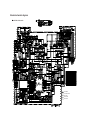
1
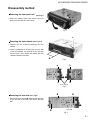
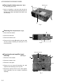
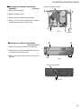
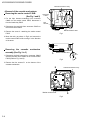
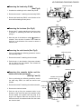
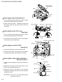
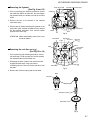
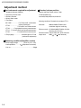
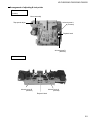
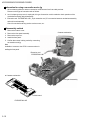
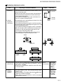
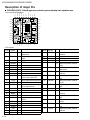
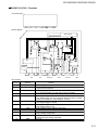
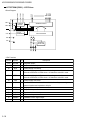
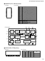
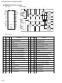
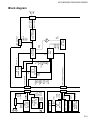
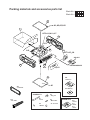
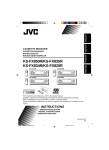
KS-FX850R/KS-FX820R/KS-FX835R
KS-FX850R/KS-FX820R/KS-FX835R
SERVICE MANUAL
CASSETTE RECEIVER
KS-FX850R
KS-FX820R
KS-FX835R
Area Suffix
E ---- Continental Europe
KS-FX850R
40Wx4
/I / ATT
DISP
5
°
RDS
TP
MO
RND
SSM
RPT
PTY
7
8
9
10
11
12
DOLBY B NR
CD-CH
SCM
DAB
TAPE
FM/AM
KS-FX835R
40Wx4
/I / ATT
DISP
5
°
RDS
TP
MO
RND
SSM
RPT
PTY
7
8
9
10
11
12
DOLBY B NR
CD-CH
SCM
DAB
TAPE
FM/AM
KS-FX820R
40Wx4
/I / ATT
DISP
5
°
RDS
TP
MO
RND
SSM
RPT
PTY
7
8
9
10
11
DOLBY B NR
CD-CH
SCM
KS-FX850R
KS-FX835R
KS-FX820R
12
Illumination
Color
Blue & Red
White
DAB
FM/AM
TAPE
Remote controller
Contents
Safety precaution
Instructions
Disassembly method
Adjustment method
Description of major ICs
1-2
1-3~18
2-1
2-8
2-12
Block diagram
Standard schematic diagrams
Printed circuit board
Parts list
2-21
2-22
2-25
3-1~17
VICTOR COMPANY OF JAPAN, LIMITED
MOBILE ELECTRONICS DIVISION,10-1,1Chome,Ohwatari-machi,Maebashi-city,Japan
(No.49549)
Printed in Japan
200002(V)
This service manual is made from 100% recycled paper.
COPYRIGHT 2000 VICTOR COMPANY OF JAPAN, LTD.
No.49549
Feb. 2000
Safety precaution
! CAUTION Burrs formed during molding may be left over on some parts of the chassis. Therefore,
pay attention to such burrs in the case of preforming repair of this system.
KS-FX850R/KS-FX835R/KS-FX820R
Disassembly method
Removing the front panel unit
(See Fig.1)
1. Press the release switch and remove the front
panel unit in the direction of the arrow.
Fig.1
c
Removing the front chassis (See Fig.2~3)
1. Remove the two screws A attaching the front
chassis.
2. Insert a screwdriver to the two joints a on the side
of the front chassis, two joints b on the right side
and one joint c from upside, then detach the front
chassis toward the front side.
A
Fig.2
a
b
a
Front chassis
b
Fig. 3
B
Removing the heat sink (See Fig.4)
B
1. Remove the three screws B attaching the heat sink
on the left side of the body, and remove the heat
sink.
B
Heat sink
Fig. 4
2-1
KS-FX850R/KS-FX835R/KS-FX820R
Removing the bottom cover (See Fig.5)
Bottom cover
d
1. Turn the body upside down.
2. Insert a screwdriver to the two joints d and two
joints e on both sides of the body and the joint f on
the back of the body, then detach the bottom cover
from the body.
e
f
Fig. 5
Removing the rear panel (See Fig.6 )
C
1. Remoe the front chassis.
2. Remove the heat sink.
3. Remove the bottom cover.
B
B
B
4. Remove the five screws B attaching the rear panel
and one screw C attaching the pine jack on the
back of the body.
Fig. 6
Main board assembly
Removing the main amplifier board
assembly
(See Fig.7)
1. Remove the front chassis.
D
D
2. Remove the bottom cover.
3. Remove the rear panel.
CP701
4. Remove the two screws D attaching the main
amplifier board assembly on the top cover.
5. Disconnect connector CP701 on the main amplifier
board assembly from the cassette mechanism
assembly.
Fig. 7
2-2
KS-FX850R/KS-FX835R/KS-FX820R
Removing the Cassette mechanism
assembly
(See Fig.8)
1. Remove the front chassis.
Cassette mechanism assembly
F
F
2. Remove the bottom cover.
3. Remove the main amplifier board assembly.
4. Remove the fore screws F attaching the cassette
mechanism assembly from the top cover.
F
Removing the control switch board
Fig. 8
F Top cover
G
G
(See Fig.9 and 10 )
1. Remove the front panel unit from the main body.
2. Remove the five screws G attaching the rear cover
on the back of the front panel unit.
3. Remove the control switch board from the front
panel unit.
G
Fig. 9
G
LCD & Key control board
Fig. 10
2-3
KS-FX850R/KS-FX835R/KS-FX820R
Cassette mechanism ass’y
<Removal of the cassette mechanism>
Removing the mecha control P.W.B.
(See Fig.1 and 2)
1. For the 6pin harness extending from connector
CN402 on the mecha control P.W.B, disconnect it
from the head relay P.W.B.
Head relay
P.W.B.
6pin
harness
2. Disconnect the card wire from connector CN403 on
the mecha control P.W.B.
CN403
CN402
3. Remove the screw A attaching the mecha control
P.W.B.
Mecha control P.W.B.
Fig.1
4. Move the tab a as shown in Fig.2 and remove the
mecha control P.W.B. while moving it in the direction
of the arrow.
CN402
CN403
Removing the cassette
assembly (See Fig.1 to 3)
mechanism
1. Disconnect the 6pin harness from connector CN402
and the card wire from CN403 on the mecha control
P.W.B. (Refer to Fig.1 and 2).
2. Remove the four screws B
cassette mechanism.
A
Mecha control P.W.B.
Tab a
Fig.2
on the bottom of the
B
Cassette mechanism ass’y
Mecha control P.W.B.
B
Fig.3
2-4
KS-FX850R/KS-FX835R/KS-FX820R
Head relay P.W.B.
Removing the head relay P.W.B.
(See Fig.4)
1. Unsolder the soldering b on the head relay P.W.B.
2. Remove the screw C attaching the head relay P.W.B.
3. Remove the head relay P.W.B. in the direction of the
arrow while releasing the two joints c.
Fig.4
Soldering b
C
Joint c
Cach
Removing the load arm (See Fig.5)
Spring d
1. Remove the E washer attaching the load arm using
a pincette or something like that and remove the
spring d.
2. Move the part of the load arm marked upwards to
release it from the axis of rotation. Then rotate the
load arm in the direction of the arrow to remove it
from the cach.
Load arm
E washer
Fig.5
Removing the sub chassis (See Fig.6)
Head relay P.W.B.
* Prior to performing the following procedure, remove
the head relay P.W.B.
1. Remove the screw D attaching the sub chassis.
2. Push the tab e in the direction of the arrow to detach
the one side of the sub chassis. Then release the
sub chassis from the tab f.
Tab e
Tab f
D
Fig.6
Reinforce bracket
Removing the cassette holder and the
holder arm in the eject mode
(See Fig.7 and 8)
* Prior to performing the following procedure, remove
the head relay P.W.B., the load arm and the sub
chassis.
1. Remove the screw E attaching the reinforce bracket.
2. Remove the reinforce bracket.
3. Push the tab g fixing the cassette holder in the
direction of the arrow and open the cassette holder
and the holder arm upward until they stop at an
angle of 45 degrees. Move the two joints h to the
side and remove the cassette holder and the holder
arm from the shaft.
Cassette mecha chassis
E
Cassette holder
Sub chassis
Reinforce
bracket
tab g
Head relay
P.W.B.
Joint h
Load arm
Holder arm
Joint h
Fig.7
2-5
KS-FX850R/KS-FX835R/KS-FX820R
Cassette holder
and holder arm
Joint h
Shaft
Joint h
Shaft
Removing the play head (See Fig.9)
* Prior to performing the following procedure, remove
the head relay P.W.B.and the sub chassis.
1. Remove the two screws F attaching the play head
(The spring under the play head comes off at the
same time).
Fig.8
Pinch roller ass’y
Play head
Pinch roller ass’y
Tab i
Tab i
Removing the pinch roller ass’y
(See Fig.9)
Spring
F
Tab i
Tab i
* Prior to performing the following procedure, remove
the head relay P.W.B.and the sub chassis.
Pinch roller ass’y
Fig.9
1. Push each tab i in the direction of the arrow and pull
out the pinch rollers on both sides.
Reel disc P.W.B.
Cassette mechanism ass’y
Soldering j
Removing the reel disc P.W.B.
(See Fig.10)
Tabs k
1. Unsolder the soldering j on the reel disc P.W.B.
Tabs k
2. Push the seven tabs k on the bottom of the cassette
mechanism assembly in the direction of the arrow.
G
Flyhwheel
Motor
Removing the motor and the sub motor
(See Fig.10 and 11)
1. Unsolder the two soldering l of the motor and the sub
motor.
G
Belt
Fig.10
Soldering j
Sub motor
Tab m
2. Release the sub motor from the three tabs m. Push
the sub motor upward and pull out it.
Soldering l
Tab m
3. Remove the belt on the bottom of the cassette
mechanism assembly and remove the two screws G
attaching the motor.
ATTENTION: The motors can be detached before
removing the load arm.
2-6
Tab m
Soldering l
Load arm
Motor
Fig.11
KS-FX850R/KS-FX835R/KS-FX820R
Removing the flywheel
(See Fig.10 and 12)
1. Prior to performing the following procedure, remove
the head relay P.W.B, the load arm, the sub chassis,
the cassette holder, the holder arm and the reel disc
P.W.B.
Soldering j
Tab k
2. Remove the belt on the bottom of the cassette
mechanism ass’y.
3. Remove the slit washer attaching the flywheel on the
upper side of the cassette mechanism ass’y and pull
out the flywheel downward. Then remove another
flywheel in the same way.
Cassette mechanism ass’y
Reel disc P.W.B.
Tab k
G
Flyhwheel
Motor
Belt
G
ATTENTION: When reassembling, make sure to use
a new slit washer.
Fig.10
Slit washer
Tab o
Reel driver
The part n
Reel disc
ass’y( )
Tabs o
Plate
Push aside
the gear
Removing the reel disc ass’y( )
(See Fig.12 to 14)
* Prior to performing the following procedure, remove
the head relay P.W.B, the load arm, the sub chassis,
the cassette holder and the holder arm.
1. Disengage the part n inside of the reel driver which
engages with the shaft, using a pincette or
something like that. Then remove the reel driver from
the shaft.
Slit washer
The part n
Reel disc ass’y( )
Reel driver
Fig.12
2. Remove the reel driver spring and the reel table.
Shaft
The part n
Reel driver
Fig.13
Reel driver spring
Reel table
Fig.14
2-7
KS-FX850R/KS-FX835R/KS-FX820R
Adjustment method
Test instruments required for adjustment
Standard volume position
1. Digital oscilloscope(100MHz)
2. Frequency Counter meter
3. Electric voltmeter
4. Wow & flutter meter
5. Test Tapes
Balance and Bass,Treble volume .Fader
:Center(Indication"0")
Loudness,Dolby NR,Sound,Cruise:Off
MC-109C ................... For TAPA CURL confirmation
(without Padd type)
VT724 .......................For DOLBY level measurement
VT739 ............ For playback frequency measurement
VT712 .... For wow flutter & tape speed measurement
VT703 ..................... For head azimuth measurement
6. Torque gauge .................... Cassette type for CTG-N
(mechanism adjustment)
Measuring conditions(Amplifier section)
Power supply voltage .............. DC14.4V (10.5 - 16V)
Load impedance ........... 4 (2Speakers connection)
Line out ............................................................ 20k
2-8
following conditions. Playback the test tape VT721.
AM mode
999kHz/62dB,INT/400Hz,30%
modulation signal on receiving.
FM mono mode 97.5MHz/66dB,INT/400Hz,22.5kHz
deviation pilot off mono
FM stereo mode 1kHz,67.5kHz dev. pilot7.5kHz dev.
Output level
0dB(1 V,50 /open terminal)
KS-FX850R/KS-FX835R/KS-FX820R
Arrangement of adjusting & test points
Cassette mechanism
(Surface)
Motor assembly
Tape speed adjust
Azimuth screw A
(Forward)
Playback head
Azimuth screw B
(Reverse)
Head section view
Azimuth screw B
(Reverse)
Azimuth screw A
(Forward)
Playback Head
2-9
KS-FX850R/KS-FX835R/KS-FX820R
Information for using a car audio service jig
1. We're advancing efforts to make our extension cords common for all car audio products.
Please use this type of extension cord as follows.
2. As a U-shape type top cover is employed, this type of extension cord is needed to check operation of the
mechanism assembly after disassembly.
3. Extension cord : EXTKSRT002-18P ( 18 pin extension cord ) For connection between mechanism assembly
and main board assembly.
Check for mechanism driving section such as motor ,etc..
Disassembly method
1.
2.
3.
4.
5.
Remove the bottom cover.
Remove the front panel assembly.
Remove the top cover .
Install the front panel.
Confirm that current is being carried by connecting
an extension cord jig.
Note
Available to connect to the CP701 connector when installing the front panel.
Cassette mechanism
Extension cord
EXTKSRT002-18P
Main board
to Cassette mechanism
Front panel assembly
to Main board
EXTKSRT002-18P
2-10
KS-FX850R/KS-FX835R/KS-FX820R
Mechanism adjustment section
Item
1. Tape running
adjustment
2. Azimuth
adjustment
confirmation
Adjusting & Confirmation Methods
Adjust
Std. Value
a) At Forward playmode, using mirror tape, make adjustment
with Azimuth screw A and Azimuth screw B, without curl of 4
parts of head tape guide.
b) At Reverse play mode, using mirror tape, make adjustment
with Azimuth screw A and Azimuth screw B, without tape
curl of 4 parts of head guide.
c) At Forward / Reverse play mode, make confirmation of no
tape curl of 4 parts of head tape guide.
Azimuth
screw A
Azimuth
screw B
a) At forward play mode, make adjustment of peak of Lch / Rch
output with Azimuth screw A.
* For Oscilloscope litharge corrugation, set 45 as standard.
b) At Reverse play mode, make adjustment of peak of Lch / Rch
output with Azimuth screw B.
* For Oscilloscope litharge corrugation, set 45 as standard.
c) With AC volt meter confirm the difference of output for 4ch
between Lch / Rch at forward play mode and Lch / Rch
Reverse play mode being within 3.0dB.
d) After operation, make confirmation of Lch / Rch azimuth
output being within 1.0dB from adjustment value.
HEAD
0
Phase
45
Tape guide
Tape curl NG
OK
HEAD
TAPE
Tape Speed
2.Tape Speed and 1.Check to see if the reading of the frequency counter & W ow Built-in
flutter meter is within 2940-3090 Hz( FWD/REV ), and less volume resistor 2940-3090Hz
Wow & Flutter
than 0.35% ( JIS RMS ).
Wow&Flutter
2.In case of out of specification, adjust the motor with a builtLess than
in volume resistor .
0.35%
(JIS RMS)
3.Playback
Frequency
response
1.Play the test tape ( VT724 : 1kHz ) back and set the volume
position at 2V .
2.Play the test tape ( VT739 )back and confirm 0 3dB at1kHz/
10kHz and -4+2dB at 1kHz/63Hz.
3.When 10kHz is out of specification, it will be necessary to
read adjust the azimuth.
Speaker out
1kHz/10kHz
: 0dB 3dB,
63Hz/1kHz
: -4dB+2dB,
2-11
KS-FX850R/KS-FX835R/KS-FX820R
Descrption of major ICs
CXA2560Q (IC401) : Dolby B type noise reduction system with play back equalizer amp.
TAPEIN2
GND
DIREF
LINEOUT2
TCH2
29
28
27
26
25
24
23
7k/12k
70 /120
100k
+
300k
21
20 MSMODE
OFF/B
19 DRSW
T2
MS MODE
x1
+
F2
PBGND 33
22
NR
PBFB2 31
PBRIN2 32
NC
OUTREF2
30
MSSW
PBTC2
PBOUT2
1.Pin layout & block diagram
BIAS
18 TAPESW
MUTE
PBFIN2 34
30k
17 MUTESW
TAPE EQ
VCT 35
NR MODE
45k
16 NRSW
FWD/RVS
PBREF 36
15 NC
Vcc
30k
LPF
PBFIN1 37
MS ON/
OFF
+
-
+
-
F3
x1
300k
+
-
70 /120
11 G2FB
8
9
10
NC
NC
7
MSLPF
6
TCH1
5
LINEOUT1
4
Vcc
PBTC1
12 G1FB
OFF/B
NR
3
TAPEIN1
2
100k
OUTREF1
1
PBOUT1
PBFB1 40
13 MSTC
T1
PBRIN1 39
7k/12k
14 MSOUT
DET
F1
PBGND 38
2. Pin function
Pin No.
Symbol
1
PBTC1
2
PBOUT1
3
4
5
6
7
8
9
10
OUTREF1
TAPEIN1
Vcc
NC
LINEOUT1
TCH1
NC
MSLPF
11
12
13
G2FB
G1FB
MSTC
14
15
16
17
18
MSOUT
NC
NRSW
MUTESW
TAPESW
19
20
21
22
23
24
2-12
DRSW
MSMODE
MSSW
NC
TCH2
LINEOUT2
I/O
Function
Playback equalizer amplifier
capacitance
O Playback equalizer amplifier
output
O Output reference
I TAPE input
- Power supply
O Line output
- Time constant for the HLS
-
-
Cut-off frequency adjustment
of the music sensor LPF
- Music signal interval detection
- Music signal interval detection
- Time constant for detecting
music signal interval
O Music sensor out
- No use
I Dolby NR control
I Mute function control
I Playback equalizer amplifier
control
I Head select control
I Music sensor mode control
I Music sensor control
- Time constant for the HLS
O Line output
Pin No.
25
Symbol
DIREF
I/O
26
27
28
29
GND
TAPEIN2
OUTREF2
PBOUT2
I
O
O
30
PBTC2
-
31
PBFB2
I
32
PBRIN2
I
33
PBGND
-
34
PBFIN2
I
35
36
VCT
PBREF
O
O
37
PBFIN1
I
38
PBGND
-
39
PBRIN1
I
40
PBFB1
I
-
Function
Resistance for setting the
reference
Ground
TAPE input
Output reference
Playback equalizer amplifier
output
Playback equalizer amplifier
capacitance
Playback equalizer amplifier
feedback
Playback equalizer amplifier
input
Playback equalizer amplifier
ground
Playback equalizer amplifier
input
Center
Playback equalizer amplifier
reference
Playback equalizer amplifier
input
Playback equalizer amplifier
ground
Playback equalizer amplifier
input
Playback equalizer amplifier
feedback
KS-FX850R/KS-FX835R/KS-FX820R
BA4905-V3 (IC901) : Regulator
1.Terminal layout
1
2
3
4
5
6
7
8
9
10
11
12
2.Block daigram
REGULATOR
Overvoltage
protection circuit
EXT
RESET
1
2
RESET
3
4
COMP
EXT
5
6
VDD 5.7V
ACC
7
8
CD 8V
AUDIO 9V
9
37K
5K
10
VCC
CTRL
11
12
AJ
ILM 10V
GND
3.Pin function
Pin no.
Symbol
1
2
RESET
EXT output
3
COMP output
4
5
ACC
VDD output
6
AUDIO output
7
CD output
8
9
10
CTRL
VCC
ILM output
11
AJ
12
GND
Function
If VDD voltage becomes 4V or less.RESET output becomes low level.
This output voltage is approximately 0.5V lower than VCC. and max
output current is 300mA.
A voltage supply for ACC block. This output voltage is approximately
0.7V lower than VDD'S. The max output current is 100mA.
Control of the COMP output by inputting voltage.
This output voltage is 5.7V, and max output current is 100mA.
This voltage supply is for microcomputer. Whenever back up voltage
supply is connected, the output keeps on running.
This output voltage is 9.0v, and max output current is 500mA.
This voltage supply for AUDIO.
This output voltage is 8.0V, and max output current is 1A.
This voltage supply for CD.
Output selector of CD. AUDIO, ILM and EXT.
To be connected with the BACK UP of car.
This output voltage is 10V, and max output current is 500mA.
Output voltage is adjustable.
Putting a resistance between ILM and AJ or between AJ and GND
makes ILM output voltage adjustable.
Ground.
2-13
KS-FX850R/KS-FX835R/KS-FX820R
UPD178018AGC-551 (IC701) : Main system control CPU
1. Pin layout
80
~
61
~
60
~
1
20
41
21
~
40
2. Pin function
Pin No.
1
2
3
4
5
6
7
8
9
10
11
12
13
14
15
16
17
18
19
20
21
22
23
24
25
26
27
28
29
30
31
32
33
34
35
36
37
38
39
40
2-14
Port Name
I/O
KEY 0
KEY 1
KEY 2
LEVEL
SM
SQ
LCDCE
LCDDA
LCDSCK
BUSI/O
OPEN
BUSSI
BUSSO
BUSSCK
NC
NC
NC
NC
INLOCK
NC
GNDPORT
VDDPORT
NC
AFCK
MONO
FM/AM
SEEK/STP
NC
IFC
VDDPLL
FMOSC
NC
GNDPLL
AMEO
FMEO
IC
SD/ST
STAGE0
NC
MOTOR
I
I
I
I
I
I
O
O
O
I
I
I
O
I/O
O
O
O
O
O
I
I
I
O
O
I
I
O
Descriptions
Key input 0
Key input 1
Key input 2
Level meter input
S.meter level input
S.Quality level input
CE output to LCD driver
Data output to LCD driver
Clock output to LCD driver
I/O selector output for J-BUS, H : OUT, L: INPUT
Door open detect input
J-BUS Data input
J-BUS Data output
J-BUS Clock in/output
Non connect
Non connect
Non connect
Non connect
Non connect
Non connect
Port GND
Port Vdd
Non connect
AF check output, L: AF check
Monaural on /off selecting output, H:mono on
FM/AM switching output L : FM H : AM
Auto seek /stop selecting output, H: Seek, L:Stop
Pulse signal input port for Cruise control
FM/AM midle frequency counter input
PLL Vdd
FM/AM limited generator frequency input
None connect
PLL GND
AM error out output
FM error out output
GND
Station detector, Stereo signal input, H:Find Station, L:Stereo
Pull up
Non connect
Main motor output
KS-FX850R/KS-FX835R/KS-FX820R
UPD178018AGC-551 (IC701) : Main system control CPU
Pin No.
Port Name
I/O
Descriptions
41
FF/REW
I
Output for input signal level switching for MS L : FF,REW H : PLAY
42
F/R
O
FWD,REV running direction switch signal input
43
DOLBY
O
Dolby on "H" output
44
MSIN
I
MS input
45
I2CCLK
O
I2C information clock output
46
I2CDAO
O
I2C information data output
47
I2CDAI
I
I2C information clock input
48
REEL
O
Switch for detecting tape end position
49
SUBMO1
I
Sub motor clock direction input
50
SUBMO2
O
Sub motor clock opposite detection drive output
51
MODE
O
Mechanism mode position detection input
TAPEIN
O
Cassette in detection input H : cassette in L : cassette out
STANDBY
I
Standby position detection input H : eject side L : operation side
NC
-
Non connect
NC
-
Non connect
56
NC
-
Non connect
57
NC
-
Non connect
58
NC
-
Non connect
59
BEEP
O
Touch tone output
60
MUTE
O
Mute output , L : mute on
61
PCNT
O
Power ON /OFF switching output , H : power on
62
TELMUTE
I
Telephone mute signal detection input
63
DIMIN
I
Dimmer signal detection input
64
DIMOUT
O
Dimmer control output , Dimmer off L output
65
ENC1
I
Rotary volume signal 1 input Power save : L
66
ENC2
I
Rotary volume signal 2 input
67
ACCDET
I
Power save 1 Working togethe ACC
68
POWER
O
Power save 2, Working together Back up by H input, stop mode
69
RDSSCK
I
Clock input for RDS
70
RDSDA
I
RDS data input
71
REMOCON
I
Remocom input
DETACH
I
Detach signal input H : Power save
J-BUSINT
I
Cut-in input for J-BUS signal
REGCPU
-
Regulator for CPU power supply, Connect the GND with0.1 F.
GND
-
Ground
76
X2
-
Connecting the crystal oscillator for system clock
77
X1
I
Connecting the crystal oscillator for system clock
78
REGOSC
-
Regulator for oscillator circuit.Connect the GND with 0.1 F.
79
VDD
-
Vdd
80
RESET
-
Pull up
52
53
54
55
72
73
74
75
L : dimmer
Power save : L
2-15
KS-FX850R/KS-FX835R/KS-FX820R
HA13158A (IC301) : Power amp
1. Pin layout
1
~
23
2. Block diagram
14
INVCC
2
18
6
PVCC2
PVCC1
STBY
IN1
1
3
+
INPUTBUFFER1
AMP1
4
5
7
+
IN2
11
INPUTBUFFER2
AMP2
-
8
9
15
+
IN3
13
INPUTBUFFER3
AMP3
-
16
17
19
+
IN4
23
INPUTBUFFER4
AMP4
10
MUTE
PROTECTOR (ASO
SURGE, TSD)
12
2-16
22
TAB
20
21
KS-FX850R/KS-FX835R/KS-FX820R
HD74HC126FP-X (IC801) : Buffer
1. Pin layout
2. Function
1
2
3
4
5
6
7
Inputs
C
A
L
X
H
L
H
H
14
13
12
11
10
9
8
3. Block diagram
Vcc
Outputs
Y
Z
H
L
Vcc
See Function Table
1k
Input
1A
2A
3A
4A
1C
2C
3C
4C
Output
S1
1Y
2Y
2Y
CL
1k
Output
Sample as Load Circuit 1
Output
3Y
Sample as Load Circuit 1
Output
4Y
Sample as Load Circuit 1
RPM6938-SV4 (IC602) : Remote control receiver
Vcc
AGC
AMP
I/V
conversion
Comp
BPF
PD
magnetic shield
Vcc
22k
ohm
Rout
Detector
for
trimming
circuit
GND
2-17
KS-FX850R/KS-FX835R/KS-FX820R
LC75873NW (IC601) : LCD Driver
VDD1
S5
S4/P4
S3/P3
S2/P2
S1/P1
S68
S67
COM1
COM2
COM3
1.Block Diagram
COMMOM
DRIVER
SEGMENT DRIVER
CLOCK
GENERATOR
SHIFT REGISTER
VDD2
INH
OSC
VDD
VSS
ADDRESS
DETECTOR
2.Pin Functions
Pin No.
Symbol
I/O
Description
1~66
S3~S68
O
Segment Output.
67~69
COM1~3
O
Common Driver Output.
70
VDD
-
Power Supply Connection.
71
VDD1
I
Used for applying the LCD drive 2/3 bias voltage externally.
Must be connected to VDD2 when a 1/2 bias drive scheme in used.
72
VDD2
I
Used for applying the LCD drive 1/3 bias voltage externally.
Must be connected to VDD1 when a 1/2 bias drive scheme in used.
73
VSS
-
74
OSC
I/O
Power supply connection.
Oscillator connection. An oscillator circuit is formed by connecting an
external resistor and capacitor to this pin.
2-18
75
INH
I
Display off control input.
76
CE
I
Chip enable input.
77
CLOCK
I
Synchronization clock input.
78
DI
I
Serial data input.
79
DIMMER
O
DIMMER Control signal output.
80
NC
-
Non connect.
KS-FX850R/KS-FX835R/KS-FX820R
SAA6579T-X (IC71) : RDS demodulator
1. Pin layout
2. Pin function
Pin
No.
1
2
3
4
5
6
7
8
1
2
3
4
5
6
7
8
9
10
11
12
13
14
15
16
16
15
14
13
12
11
10
9
Symbol
QUAL
RDDA
Vref
MUX
VDDA
VSSA
CIN
SCOUT
MODE
TEST
VSSD
VDDD
OSCI
OSCO
T57
RDCL
Function
Quality indication output
RDS data output
Reference voltage output (0.5VDDA)
Multiplex signal input
+5V supply voltage for anarog part
Ground for analog part (0V)
Subcarrier input to comparator
Subcarrier output of reconstruction filter
Oscillator mode / test sontrol input
Test enable input
Ground for digital part (0V)
+5V supply voltage for digital part
Oscillator input
Oscillator output
57kHz clock signal output
RDS clock output
3. Block diagram
MUX
SCOUT
CIN
VDDA
Vref
4
57kHz
BANDPASS
(8th ORDER)
ANTIALIASING
FILTER
OSCI
OSCO
13
14
OSCCILLATOR
AND
DIVIDER
RECONSTRUCTION
FILTER
VDDD
12
QUALITY BIT
GENERATOR
1 QUAL
8
7
5
3
COSTAS LOOP
VARIABLE AND
FIXED DIVIDER
CLOCKED
COMPARATOR
BIPHASE
SYMBOL
DECODER
DIFFERRENTIAL 2
DECODER
16
Vp1
CLOCK
REGENERATION
AND SYNC
REFERENCE
VOLTAGE
15
TEST LOGIC AND OUTPUT
SELECTOR SWITCH
6
9
VSSA
10
MODE
RDDA
RDCL
T57
11
TEST
VSDD
LB1641 (IC402) : DC Motor Driver
2. Pin Functions
1. Pin Layout
Input
3
4
5
GND OUT1 P1
1
2
VZ
IN1
6
7
8
9
IN2 VCC1 VCC2 P2
10
OUT2
Output
Mode
IN1
IN2
OUT1
OUT2
0
0
0
0
1
0
1
0
0
1
0
1
COUNTER-CLOCKWISE
1
1
0
0
Brake
Brake
CLOCKWISE
2-19
KS-FX850R/KS-FX835R/KS-FX820R
TEA6320T-X (IC161) : E.volume
1.Pin Layout
2.Block Diagram
10
SDA
GND
OUTLR
OUTLF
TL
B2L
B1L
IVL
ILL
QSL
IDL
MUTE
ICL
IMD
IBL
IAL
1
2
3
4
5
6
7
8
9
10
11
12
13 CD-CH
14
15 TAPE
16 TUNER
32
31
30
29
28
27
26
25
24
23
22
21
20
19
18
17
SCL
VCC
OUTRR
OUTRF
TR
B2R
B1R
IVR
ILR
QSR
IDR
Vref
ICR
CAP
IBR
IAR
21
31
2
19
16
15
13
11
14
8
9
5
7 6
12
MUTE
FUNCTION
ZERO CROSS
DETECTOR
POWER
VOLUME 2
0 to 55 dB
BALANCE
FENDER REAR
3
VOLUME 2
0 to 55 dB
BALANCE
FENDER FRONT
4
SUPPLY
VOLUME 1
+20 to -31 dB
LOUDNESS
LEFT
BASS
LEFT
+15 dB
TREBLE
LEFT
+12 dB
HC BUS
REC
LOGIC
1
SOURCE
SELECTOR
VOLUME 1
+20 to -31 dB
LOUDNESS
RIGHT
22
20
18
17
23
25
24
BASS
RIGHT
+15 dB
26 27
TREBLE
RIGHT
+12 dB
VOLUME 2
0 to -55dB
BALANCE
FENDER FRONT
29
VOLUME 2
0 to -55dB
BALANCE
FENDER REAR
30
28
3.Pin Functions
Pin
No. Symbol I/O
Functions
I/O Serial data input/output.
Pin
No. Symbol I/O
Functions
17
IAR
I
Input A right source.
Ground.
18
IBR
I
Input B right source.
O
output left rear.
19
CAP
-
Electronic filtering for supply.
OUTLF
O
output left front.
20
ICR
I
Input C right source.
5
TL
I
21
Vref
-
Reference voltage (0.5Vcc)
6
B2L
-
Treble control capacitor left channel or
input from an external equalizer.
Bass control capacitor left channel or
output to an external equalizer.
22
IDR
-
Not used
7
B1L
-
Bass control capacitor left channel.
23
QSR
O
Output source selector right channel.
8
IVL
I
Input volume 1. left control part.
24
ILR
I
Input loudness right channel.
9
ILL
I
Input loudness. left control part.
25
IVR
I
Input volume 1. right control part.
10
QSL
O
Output source selector. left channel.
26
B1R
-
Bass control capacitor right channel
11
IDL
-
Not used
27
B2R
O
12
MUTE
-
Not used
28
TR
I
13
ICL
I
Input C left source.
29 OUTRF O
Output right front.
14
IMO
-
Not used
30 OUTRR O
Output right rear.
15
IBL
I
Input B left source.
31
Vcc
-
Supply voltage.
16
IAL
I
Input A left source.
32
SCL
I
Serial clock input.
1
SDA
2
GND
-
3
OUTLR
4
2-20
32
Bass control capacitor right channel or
output to an external equalizer.
Treble control capacitor right channel or
input from an external equalizer.
SUBMO+
SUBMO-
REEL
MODE
TAPEIN
STANDBY
IC602
REMOCON
RECEIVER
ENCODER
KEY SWITCH
IC601
LCD
DRIVER
REMOCON
ENC1
ENC2
KEY0
~KEY2
LCDCE
LCDCL
LCDDA
S1~S68
COM1~COM3
LCD
CJ402
Lch
Rch
FF/REW
FWD-L F/R
FWD-R DOLBY
REW-L MSOUT
REW-R
IC401
DOLBY NR /
P.B. EQ
IC402
MOTOR
DRIVER
SUBMO+
SUBMO-
CJ402
CJ401
CN601
M
CP401
CJ601
M
SK/ST
SM
MONO
SD/ST
SEEK/STOP
FMOSC
AFCK
FMEO
AMEO
FM/AM
RDSCK
RDSDA
IC71
RDS
DETECTOR
MUX
ENC1,ENC2,KEY0,KEY1,KEY2
LCDCE,LCDDA,LCDCK,REMOCON
STANDBY
TAPEIN
MODE
SUBMO+
SUBMOREEL
MSOUT
DOLBY
F/R
FFREW
MOTOR
TAPE-L,TAPE-R
TU_L,TU_R
TU1
TUNER PACK
IC701
CPU
SCL
SDA
CH_L
CH_R
FL,FR
RL,RR
IC301
POWER AMP.
SCK
SI/SO
J801
IC801
JVC BUS
JBUSSI
JBUSSO
JBUSIO
JBUSSCK
IC161
E.VOLUME
FRONTL
FRONTR
REARL
REAR
CP901
LINE OUTPUT
FLOUT+,FLOUTFROUT+,FROUTRLOUT+,RLOUTRROUT+,RROUT-
KS-FX850R/KS-FX835R/KS-FX820R
Block diagram
2-21
CP901
Standard schematic diagrams
Tuner & Main circuit section
TUNER SIGNAL
CD CHANGER SIGNAL
TAPE SIGNAL
FRONT SIGNAL
REAR SIGNAL
Mechanism control circuit section
TAPE SIGNAL
LCD & Key control circuit section
Printed circuit boards
Main board
LCD & Key control board (Forward side)
LCD & Key control board (Reverse side)
CA-IN
Main
Main+
Sub
Sub+
St.BY
MODE
D.Gnd
Pho- Tr
Anode
CrO2
Reel board
Mecah control board
CA-IN
3
Main:Main:+
Sub:Sub:+
J
MODE
S T- B Y
CrO2
M
PARTS LIST
[ KS-FX850R ]
[ KS-FX835R ]
[ KS-FX820R ]
* All printed circuit boards and its assemblies are not available as service parts.
Areas suffix
E ----------- Continental Europe
- Contents Exploded view of general assembly and parts list
Cassette mechanism assembly and parts list
Electrical parts list
P acking materials and accessories parts list
3-3
3-5
3-10
3-16
Parts list (General assembly)
A
Item
1
Parts number
Block No. M1MM
Parts name
Description
Q'ty
ZCKSFX850R-FB
FRONT CHASSIS
1 KS-FX850R
ZCKSFX820R-FB
FRONT CHASSIS
1 KS-FX820R/835R
1-1
FSJC1060-001
FRONT CHASSIS
1
1-2
FSJC3014-001
CASSETTE LID
1 KS-FX850R
FSJC4003-031
CASSETTE LID
1 KS-FX820R/835R
VKW4947-002
DOOR SPRING
1
ZCKSFX820R-NPA
NOSE PIECE
1 KS-FX820R
ZCKSFX850R-NPA
NOSE PIECE
1 KS-FX850R
1-3
2
ZCKSFX835R-NPA
NOSE PIECE
1 KS-FX835R
2-1
FSJC1058-001
FRONT PANEL
1
2-2
FSJD3024-00B
FINDER LENS
1 KS-FX850R
FSJD3024-00C
FINDER LENS
1 KS-FX820R
FSJD3024-00D
FINDER LENS
1 KS-FX835R
3
FSMH3001-002
HEAT SINK
1
4
FSKM3011-002
BOTTOM COVER
1
5
FSMA3005-001
INSULATOR
1
6
QYSDST2604Z
SCREW
4 CHASSIS+MECHA.B
7
FSKZ4005-001
SCREW
3
8
QYSDST2606Z
SCREW
2 CHASSIS+REAR BK
9
QYSDST2606Z
SCREW
2 CHASSIS+MAIN PW
11
QYSDSF2006M
SCREW
2
13
FSJC1056-002
CHASSIS BASE
1
14
QYSDST2606Z
SCREW
4 MECHA+M.BKT
15
QYSDST2606Z
SCREW
1 PCB+MECHA
17
---------------
CDS-801 JV
1 CASSETTE MECHA
18
FSXK3003-005
VOL.KNOB
1 JOG DIAL
21
FSXP2045-002
PRESET BUTTON
1 1-6 LASER CUT
22
FSXP3053-002
POWER BUTTON
1
23
FSXP3058-001
EJECT BUTTON
1
24
FSXP3062-001
PUSH BUTTON(R)
1 MO/RND RPT
26
FSXP2041-003
PUSH BUTTON(L)
1 DISP TP PTY
27
FSXP3061-001
SEL BUTTON
1
28
FSJK3027-001
RIM LENS
1 FOR KNOB
30
FSJK4009-001
REMOTE LENS
1 FOR REMOTE CON.
31
VKW3001-330
COMP.SPRING
1 FOR EJECT BUTTO
32
VKW3001-330
COMP.SPRING
1 FOR DETACH BUTT
33
FSJC1059-001
REAR COVER
1
34
VKZ4777-001
MINI SCREW
5 FRONT+SW.PWB
35
FSYN3113-005
NAME PLATE
1 KS-FX850R
FSYN3110-D005
NAME PLATE
1 KS-FX835R
FSYN3111-D005
NAME PLATE
1 KS-FX820R
40
FSYH4061-002
LIGHTNG SHEET
1 KS-FX820R
41
FSYH4080-001
LIGHTNG SHEET
1 KS-FX835R
42
FSJK3028-001
LCD LENS
1
43
FSKS3013-001
LENS CASE
1
45
FSYH3024-001
LCD CASE
1
46
QNZ0450-001
RUBB.CONNECTOR
1
47
QNZ0449-001
RUBB.CONNECTOR
1
Area
Parts list (General assembly)
A
A
Item
Parts number
Block No. M1MM
Parts name
Description
Q'ty
48
FSYH4061-001
LIGHTNG SHEET
1
51
FSXP2038-001
OPERAT.BUTTON
1 LENS+D.FUNC CAP
52
FSXP3060-001
RELEASE LEVER
1
53
FSKW3002-016
COMP.SPRING
1 FOR RELEASE KNO
54
VJK3707-001
LIGHT LENS
1
55
QYSPSGU1745N
MINI SCREW
2 FOR LIGHT LENS
57
VKS3793-001
LOCK LEVER(TOP)
1
58
FSKS3015-001
LOCK LEVER(O.L)
1
59
VKS3798-002
RELEASE LEVER
1
60
FSXP2043-001
UP DOWN BUTTON
1
61
VKS3794-003
LOCK LEVER(L)
1
62
VKS3795-002
LOCK LEVER(R)
1
64
VKS5563-001
GEAR
1
65
VKZ4786-002
OIL DAMPER
1
67
FSKW4012-002
T.SPRING
1 FOR L.LEVER(TOP
68
FSKW4013-002
T.SPRING
1 FOR OPEN LEVER
69
VKW5262-001
T.SPRING
1 FOR L.LEVER(R)
70
VKW5263-002
T.SPRING
1 FOR L.LEVER(L)
71
VKW5264-005
T.SPRING
1 FOR RELEASE LEV
72
QYSDSF2006M
SCREW
1 DAMPER+L.LEVER(
74
VKZ4777-001
MINI SCREW
1 LOCK LEVER(O.L.
82
FSKL4018-00B
IC BRACKET
1
83
FSKL4023-001
P.W.B.BRACKET
1
84
FSKL4014-001
HEAT SINK
1
85
VMA4652-001SS
EARTH PLATE
1
86
QMFZ021-100-J1
FUSE
1
87
FSKS3017-002
LED HOLDER
1
88
FSXP4006-001
SCM BUTTON
1
89
FSKS3014-001
OPEN LEVER
1
90
FSYH4036-035
SHEET
1 SLIDING SHEET
93
FSYH4036-049
KNOB SHEET
1
94
FSYH4036-050
MECHA SHEET
1
96
FSYH4036-032
SHEET
1
99
FSKL2001-001
MECHA BRACKET
1
LCD1 QLD0113-001
LCD MODULE
1 KS-FX850R
QLD0124-001
LCD MODULE
1 KS-FX820R
QLD0123-001
LCD MODULE
1 KS-FX835R
100
FSKL2002-001
MECHA BRACKET
1
101
FSYH4036-031
SHEET
1
102
FSXP3059-001
DETACH BUTTON
1
104
FSKM3012-011
REAR BRACKET
1
105
QYSDST2606Z
SCREW
1 REAR BKT+ANT JA
106
QYSDST2606Z
SCREW
1 REAR BKT+REG B
107
QYSDSF3006Z
SCREW
1 REAR BKT+PIN JA
108
QYSDST2606Z
SCREW
1 REAR BKT+CD IN
Area
Cassette mechanism assembly and parts list
Block No. M 2 M M
CDS-801
107
76
105
103
104
68
CFD-409
24
5
73
97
50
99 100 101 102
91
17
FG-84M
28
94
FG-84M
65
26
41
SW-902
FG-84M
SW-902
93
CFD-409
95
10
47
59
CFD-409
42
16
4
40
SW-522B
63
40
CFD-409
96
75 FG-84M
39
LEN-315Y2
64
67
109
75
117
FG-84M
39
66
49
25
23
66
FG-84M
SW-522B
2
FG-84M
LEN-315Y2
CFD-409
27
11
106
LEN-315Y2
107
106
1
LEN-315Y2
FG-84M
48
30
51
FG-84M
32
3
12
108
35
60
61
43
46
FG-84M
110
113
36
37
72
FG-84M
34
33
85
111
FG-84M
45
71
FG-84M
84
74
13
FG-84M
87
82
113
38
114
111
44
55
86
21
SW-522B
22
FG-84M
98
9
Grease point 1/2
SW-902
SW-522B
FG-84M
CFD-409
LEN-315Y2
FG-84M
SW-902
SW-902
SW-902
FG-84M
FG-84M
SW-902
FG-84M
SW-902
FG-84M
FG-84M
Grease point 2/2
Parts list (Cassette mechanism)
A
Item
Parts number
Block No. M2MM
Parts name
Description
Q'ty
1
X-0801-1003S
MAIN CHASSIS AS
1
2
X-0801-1002S
SLIDE CHASSIS A
1
3
X-0801-1008S
SIDE BKT ASS'Y
1
4
X-0801-1010S
EJECT CAM LIMIT
1
5
X-0801-1013S
CASSETTE HANGER
1
9
1-0801-6002S
FLYWHEEL ASSY F
1
10
X-0801-2003S
GEAR BASE ASS'Y
1
11
X-0801-2021S
PINCH ARM F ASS
1
12
X-0801-2022S
PINCH ARM R ASS
1
13
1-0801-6003S
FLYWHEEL ASSY R
1
16
X-0801-7006S
SUB MOTOR ASS'Y
1
17
X-0801-7057S
MAIN MOTOR ASSY
1
21
1-0801-1003S
DIRECTION PLATE
1
22
1-0801-1004S
DIRECTION LINK
1
23
1-0801-1005S
PINCH SPG ARM
1
24
1-0801-1006S
CASSETTE GUIDE
1
25
1-0801-1007S
LOAD ARM
1
26
1-0801-1009S
HEAD SUPT SPG
1
27
1-0801-1011S
EJECT CAM PLATE
1
28
1-0801-1012S
CASSETTE HOLDER
1
30
1-0801-1020S
REINFORCE BRKT
1
32
1-0101-2056S
IDLE PULLEY(A1)
1
33
1-0801-2004S
REDUCTION GEARA
1
34
1-0801-2005S
REDUCTION GEARB
1
35
1-0801-2006S
SPG HOLDER F
1
36
1-0801-2007S
FRICTION GEARPL
1
37
1-0801-2008S
FRICTION GEARFF
1
38
1-0801-2009S
MODE GEAR
1
39
1-0801-2010S
REEL SPINDLE
2
40
1-0801-2011S
REEL DRIVER
2
41
1-0801-2014S
GEAR BASE ARM
1
42
1-0801-2015S
GEAR BASE LINK
1
43
1-0801-2016S
TAKE UP GEAR
1
44
1-0801-2017S
REFLECTOR GEAR
1
45
1-0801-2018S
MODE RACK
1
46
1-0801-2019S
MODE SW ACTUATR
1
47
1-0801-2020S
TAPE GUIDE
1
48
1-0801-2023S
LOAD RACK
1
49
1-0801-2024S
RACK LINK
1
50
1-0801-2025S
CASSETTE CATCH
1
51
1-0801-2030S
SPG HOLDER R
1
55
1-0801-3005S
RACK COLLAR
1
59
1-0801-4001S
PINCH ARM SPG
1
60
1-0801-4002S
TU SPG
1
61
1-0801-4003S
FF SPG
1
63
1-0801-4005S
EJECTCAM PLT SP
1
64
1-0801-4006S
HOLDER CUSH SPG
1
65
1-0801-4007S
GEAR BASE SPG
1
Area
Parts list (Cassette mechanism)
A
Item
Parts number
Block No. M2MM
Parts name
Description
Q'ty
66
1-0801-4008S
REEL DRIVER SPG
2
67
1-0801-4009S
LOAD ARM SPG
1
68
1-0801-4011S
HOLDER STAB SPG
1
71
1-0801-5001S
BELT
1
72
1-0801-5002S
FELT
1 7.5*18.5*1.0
73
1-0801-5003S
AZIMUTH SCR
2
74
1-0801-5004S
FELT
1 11*18.5*1.0
75
1-0801-5005S
REEL WASHER
2
76
21732-6280-36S
LUG PLATE
1
82
1-0801-7001S
REEL PCB DL
1
84
1-0801-7003S
SW(MATSUSHITA)
2 (ESE22MH2L)
85
1-0801-7005S
SW
1 (ALPS SPPB64)
86
1-0801-7024S
PHOTO SENSOR
1 (ON2170-QR FS)
87
1-0801-7026S
FLAT CABLE 10P
1
91
1-0801-7014S
HEAD
1 (MITSUMIP-5544)
93
10801-7009-0S
M.MOTOR WIRE
1 BLACK
94
10801-7009-1S
M.MOTOR WIRE
1 RED
95
10801-7010-0S
S.MOTOR WIRE
1 ORANGE
96
10801-7010-1S
S.MOTOR WIRE
1 BROWN
97
10801-7015-0S
HEAD WIRE BLACK
1
98
10801-7015-1S
HEAD WIRE BROWN
1
99
10801-7015-2S
HEAD WIRE RED
1
100
10801-7015-3S
HEAD WIRE ORANG
1
101
10801-7015-4S
HEAD WIRE YELLO
1
102
10801-7015-5S
HEAD WIRE WHITE
1
103
1-0801-7016S
HEAD PCB
1
104
1-0801-7025S
CONN S6B-PH-K-S
1
105
21382-3060-C2S
+PLAIN B-TYPE
1 M2.3*6.0
106
2-1032-0025-C2S
+SCREW PLAIN
2 M2*2.5
107
21332-0035-P1S
S-TYPE PRECISIO
2 M2*3.5
108
21112-6035-C2S
+SCREW PLAIN
1 M2.6*3.5
109
2-1816-0032-E8S
LMW-S
2 1.6*3.2*0.35
110
21812-0032-D2S
PSW-S
1 1.2*3.2*0.25
111
1-0036-5024S
PSW-S(REEL B)
2 1.5*3.2*0.25
113
2-1821-0040-D1S
PSW
2 2.1*4.0*0.25
114
21821-0040-D2S
PSW-S
1 2.1*4.0*0.25
117
2-1711-5040-16S
E-RING
1 1.5
Area
Packing materials and accessories parts list
Block No. M 3 M M
Block No. M 4 M M
P4
A1,A2,A3,A18
KIT2:A10,A11,A17
P2
A13
P3
A16
P5
KIT1:A5 A9
A20,A21
P6
A14
P2
KS-FX850R/835R
A12
P4
A1
A16
: Trim Plate
A21 : Battery
SCREW KIT 1
A14
: Car Cable
A20
: Remocon
A9
: Hook
A8
:Washer
A5
: Plug nut
A6
: Mount bolt
A7: Lock nut
SCREW KIT 2
A10
: Screw
A17
: Sheet
A11
: Sheet
Packing parts list
A
Item
P 1
Block No. M3MM
Parts number
Parts name
Description
Q'ty
FSPE3001-174
PACKING CASE
1 KS-FX850R
FSPE3004-061
PACKING CASE
1 KS-FX820R
FSPE3004-060
PACKING CASE
1 KS-FX835R
P 2
FSPH1018-002
PAPER CUSHION
2
P 3
VPE3005-064
POLY BAG
1
P 4
QPA01703505P
POLY BAG
2 FOR INST. BOOK
P 5
QPA00801205
POLY BAG
1
P 6
QPA01003003
POLY BAG
1
Accessories parts list
A
Item
A 1
Block No. M4MM
Parts number
Parts name
Description
Q'ty
FSUN3113-321
INST.BOOK
1 SPA ITA SWE FIN
FSUN3113-311
INST.BOOK
1 ENG GER FRE DUT
FSUN3113-T481
INSTRUCT.SHEET
1 SWE FIN
FSUN3113-T451
INSTRUCT.SHEET
1 DUT SPA ITA
FSUN3113-T211
INSTRUCT.SHEET
1 ENG GER FRE
A 3
BT-54013-1
WARRANTY CARD
1
A 5
VKZ4027-202
PLUG NUT
1
A 6
VKH4871-001SS
MOUNT BOLT
1
A 7
VKZ4328-001
LOCK NUT
1
A 8
WNS5000Z
WASHER
1
A 2
Area
A 9
FSKL4010-002
HOOK
2
A 10
VKZ4777-001
MINI SCREW
2 THEFT PREVENTIO
A 11
FSYA4002-001
SHEET
1 THEFT PREVENTIO
A 12
FSJB3001-00A
HARD CASE
1
A 13
FSKM2004-002SSF
MOUNTING SLEEVE
1
A 14
QAM0160-001
CAR CABLE
1 KS-FX850R
QAM0158-001
CAR PLUG CORD
1 KS-FX820R/835R
A 16
FSJD2034-001
TRIM PLATE
1
A 17
FSYH4036-043
SHEET
2
A 18
VND3046-001
SERIAL TICKET
1
A 20
RM-RK31
REMOCON
1 KS-FX850R/835R
A 21
---------------
BATTERY
1 KS-FX850R/835R
KIT 1
KDGS717K-SCREW1
SCREW PARTS KIT
1 A5 - A9
KIT 2
KDSX959-SCREW2
SCREW PARTS KIT
1 A10 A11 A17
Area