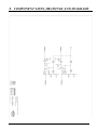
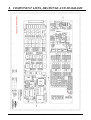
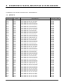
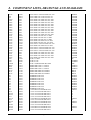
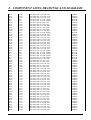
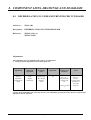
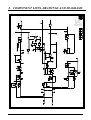
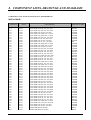
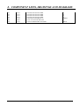
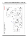
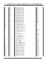
1
FRED MULTIPULSE BIOWAVE
(First Responder External Defibrillator Biphasic)
Notice technique
Version Juillet 2001
Part No. 0-48-0001
FRED MULTIPULSE BIOWAVE
Service Manual
Revision History
Version 1:
Art. N° 0-48-0001
Page I
July 2001
Vo. Juillet 2001
FRED MULTIPULSE BIOWAVE
WARNING
This manual shall be considered to form an integral part of the described device.
This service manual is intended for qualified personnel. It describes the operating,
maintenance and troubleshooting of MULTIPULSE BIOWAVE FRED devices.
Compliance with its contents is a prerequisite for correct device performance and the
safety of the patient and the operator.
The manufacturer shall only be liable for the safety, reliability and performance of the
device if:
-
all assembly, extensions, adjustments, modifications and repairs have been
performed by the manufacturer or by persons authorised by the manufacturer.
-
the electrical system of the premises of use is in accordance with applicable
requirements.
-
the device is used in accordance with the instructions for use.
-
only original Schiller spare parts are used.
This manual describes the device at the time of printing.
The provision of this manual shall not in any event constitute permission or approval
to modify or repair the device.
The manufacturer agrees to supply all the spare parts for a ten-year period.
All rights reserved for the devices, circuits, processes and names mentioned in this
document.
The use of the MULTIPULSE BIOWAVE FRED device shall comply with the
description provided in the Operating Manual. The device shall not be put to uses
other than as described in the manual, which may be hazardous.
Art. N° 0-48-0001
Page II
Vo. Juillet 2001
FRED MULTIPULSE BIOWAVE
SAFETY INFORMATION
•
The device bears the following marking:
CE-0459
in accordance with the requirements of Council directive 93/42/EEC relating to medical devices, based
on the essential requirements of Annex I of the directive.
•
The device fully meets the electromagnetic compatibility requirements of standard IEC 60601-1-2/EN 60601-2,
“Electromagnetic compatibility of Medical Electrical Equipment”.
•
The device has undergone interference elimination in accordance with the requirements of standard EN 50011,
class B.
•
In order to ensure optimum patient safety, electromagnetic compatibility, measurement precision and device
operation, users are advised to use only original Schiller spare parts. Users shall be solely liable for the use of
accessories other than original accessories. The manufacturer shall not be liable for any damage due to the use of
incompatible accessories or consumable supplies.
•
The manufacturer shall only be liable for safety, reliability and device performance if:
- assembly, configuration, modifications, extensions or repairs have been made by Schiller personnel or
personnel that have been duly authorised by Schiller.
- the device is used in accordance with the instructions for use.
•
Users shall be entirely liable for any use of the device that does not comply with the procedures described in the
Operating Manual.
•
This manual describes the device and the technical safety standards applicable at the time of printing. All rights
reserved for the circuits, processes, names, software and devices referred to in this service manual.
•
The quality assurance system applicable in the manufacturer’s facility meets the requirements of international
standards EN ISO 9001 and EN 46001.
•
No part of this document may be reproduced without the written permission of Schiller.
Art. N° 0-48-0001
Page III
Vo. Juillet 2001
FRED MULTIPULSE BIOWAVE
Safety symbols used on the device
Danger – High Voltage.
Conventions used in the manual
G
Danger:
Warns the user of an imminent hazard. If the warning is not heeded, the
user (and/or people and property around the user) could be exposed to
death or serious injury.
I
Caution:
Warning describing conditions or actions that could lead to device or
software malfunctioning.
Note:
Remark or note providing useful information to enable the user to get the
most from the equipment.
F
Additional information or explanation about the previous paragraphs.
Manufacturer:
SCHILLER
MEDICAL SA
19, Avenue de la Gare
F- 67 162 Wissembourg
Tel.
Fax
: **33 / (0) 3.88.63.36.00
: **33 / (0) 3.88.94.12.82
Art. N° 0-48-0001
Page IV
Vo. Juillet 2001
FRED MULTIPULSE BIOWAVE
PRECAUTIONS REQUIRED WHILE TESTING THE DEVICE
While testing the MULTIPULSE BIOWAVE FRED device, only fixed resistors with high voltage and power ratings
that are well insulated from the frame and the earth may be used to simulate the patient. Never use incorrectly
insulated systems, systems with loose contacts or systems with components such as sparkers or flash tubes, as they
could destroy the device beyond repair.
Art. N° 0-48-0001
Page V
Vo. Juillet 2001
FRED MULTIPULSE BIOWAVE
CONTENTS
SERVICE MANUAL REVISION HISTORY.................................................................................................... I
WARNING ............................................................................................................................................................ II
SAFETY INFORMATION.................................................................................................................................. III-IV
PRECAUTIONS REQUIRED WHILE TESTING THE DEVICE.................................................................. V
CONTENTS .......................................................................................................................................................... VI-X
1.
DESCRIPTION OF THE MULTIPULSE BIOWAVE FRED DEVICE ............................................. 1-1
1.1.
Overview ....................................................................................................................................... 1-1
1.2.
Specifications ................................................................................................................................ 1-3
1.3.
Optional features ........................................................................................................................... 1-9
1.4.
1.3.1.
BUFRDI.................................................................................................................. 1-9
1.3.2.
BUFRS.................................................................................................................... 1-9
1.3.3.
BUFREC 3.............................................................................................................. 1-9
1.3.4.
BUFREC 12............................................................................................................ 1-9
1.3.5.
BUFRMAN............................................................................................................. 1-9
1.3.6.
FREDVO ................................................................................................................ 1-9
Optional communication features.................................................................................................. 1-9
1.4.1
FREDWARE .......................................................................................................... 1-9
1.4.2
MODEM 1 .............................................................................................................. 1-9
1.4.3
BUFRTC................................................................................................................. 1-10
Art. N° 0-48-0001
Page VI
Vo. Juillet 2001
FRED MULTIPULSE BIOWAVE
1.5.
1.6.
2.
1.4.4
SEMA 200 .............................................................................................................. 1-10
1.4.5
READER 0 ............................................................................................................. 1-10
1.4.6
READER 1 ............................................................................................................. 1-10
1.4.7
READER 2 ............................................................................................................. 1-10
Cells, batteries and charger for FRED........................................................................................... 1-10
1.5.1.
Mains charger for FRED......................................................................................... 1-10
1.5.2.
Vehicle charger for FRED ...................................................................................... 1-10
1.5.3.
DG 2002 C2 charger ............................................................................................... 1-11
1.5.4.
BT 01 charger - discharger...................................................................................... 1-11
Accessories.................................................................................................................................... 1-11
1.6.1
General accessories................................................................................................. 1-11
1.6.2
Defibrillation accessories........................................................................................ 1-12
1.6.3
ECG accessories...................................................................................................... 1-12
1.6.4
SpO2 accessories .................................................................................................... 1-12
STARTING UP.......................................................................................................................................... 2-1
2.1.
Safety instructions ......................................................................................................................... 2-1
2.2.
Power supply ................................................................................................................................. 2-2
2.3.
Recharging the cadmium-nickel battery........................................................................................ 2-3
2.3.1
Mains charger for FRED®...................................................................................... 2-3
2.3.2
Vehicle charger for FRED ...................................................................................... 2-4
2.3.3
DG 2002 C2 charger ............................................................................................... 2-5
3.
OPERATION............................................................................................................................................. 3-1
4.
TESTING AND MAINTENANCE .......................................................................................................... 4-1
4.1.
Functional inspections ................................................................................................................... 4-1
4.1.1.
Art. N° 0-48-0001
Automatic testing upon power up ........................................................................... 4-1
Page VII
Vo. Juillet 2001
FRED MULTIPULSE BIOWAVE
4.1.2.
Manual testing......................................................................................................... 4-2
4.2.
Automatic daily test....................................................................................................................... 4-3
4.3.
Systematic check before use.......................................................................................................... 4-3
4.4.
Weekly check ................................................................................................................................ 4-4
4.5.
Annual check................................................................................................................................. 4-4
4.6.
Cleaning and disinfecting .............................................................................................................. 4-4
5.
TROUBLESHOOTING............................................................................................................................ 5-1
6.
REPLACEMENT OF PARTS ................................................................................................................. 6-1
6.1.
Device disassembly procedure ...................................................................................................... 6-1
6.2.
Operations on the upper part ......................................................................................................... 6-2
6.3.
6.2.1.
Removing the CPU circuit ...................................................................................... 6-2
6.2.2.
Removing the LCD display..................................................................................... 6-3
6.2.3.
Removing the BACKLIGHT CONVERTER support circuit ................................. 6-3
6.2.4.
Removing the DEFIBRILLATION ECG PREAMP circuit ................................... 6-4
6.2.5.
Removing the TWELVE-LEAD ECG AMP circuit ............................................... 6-4
Operations on the lower part ......................................................................................................... 6-5
6.3.1.
Verification of the full discharging of the HV capacitor......................................... 6-6
6.3.2.
Removing the DEFIBRILLATOR CONTROL circuit ........................................... 6-6
6.3.3.
Removing the POWER SUPPLY circuit ................................................................ 6-7
6.3.4.
Removing the ECG PREAMP PROTECTION circuit ........................................... 6-7
6.3.5.
Removing the HT switching circuit ........................................................................ 6-8
6.3.6.
Removing the HIGH-VOLTAGE CIRCUIT .......................................................... 6-9
6.3.7.
Replacing the HV capacitor .................................................................................... 6-10
6.3.8.
Replacement of parts............................................................................................... 6-12
Art. N° 0-48-0001
Page VIII
Vo. Juillet 2001
FRED MULTIPULSE BIOWAVE
7.
OPERATING EXPLANATIONS ............................................................................................................ 7-1
7.1.
General operation .......................................................................................................................... 7-1
7.2.
Upper part...................................................................................................................................... 7-2
7.3.
8.
7.2.1.
TWELVE-LEAD ECG AMP printed circuit board ................................................ 7-2
7.2.2.
DEFIBRILLATION ECG PREAMP printed circuit board .................................... 7-4
7.2.3.
CPU printed circuit board ....................................................................................... 7-6
7.2.4.
BACKLIGHT CONVERTER support PCB .......................................................... 7-11
Lower part ..................................................................................................................................... 7-12
7.3.1.
Battery interface printed circuit board .................................................................... 7-12
7.3.2.
POWER SUPPLY printed circuit board ................................................................. 7-12
7.3.3.
HIGH-VOLTAGE CIRCUIT printed circuit board ................................................ 7-13
7.3.4.
DEFIBRILLATOR CONTROL printed circuit board ............................................ 7-16
7.3.5.
HIGH-VOLTAGE SWITCHING circuit board...................................................... 7-21
7.3.6.
ECG PREAMP PROTECTION printed circuit board ............................................ 7-22
7.3.7.
INSULATION AND SHIELDING printed circuit board ....................................... 7-23
7.3.8.
Timing charts of the defibrillator part..................................................................... 7-23
LIST OF COMPONENTS, DRAWINGS AND DIAGRAMS ............................................................... 8-1
8.1.
List of abbreviations and components ........................................................................................... 8-1
8.2.
List of signals used in the diagrams............................................................................................... 8-2
8.3.
List of different printed circuit boards........................................................................................... 8-7
8.4.
ECG preamp interconnection drawing .......................................................................................... 8-8
8.5.
Monitor part interconnection drawing........................................................................................... 8-9
8.6.
Defibrillator part interconnection drawing .................................................................................... 8-10
8.7.
Defibrillator part diagram.............................................................................................................. 8-11
8.8.
TWELVE-LEAD ECG AMP printed circuit board....................................................................... 8-13
8.9.
DEFIBRILLATION ECG PREAMP printed circuit board........................................................... 8-33
8.10.
Central processing unit printed circuit board ................................................................................ 8-41
Art. N° 0-48-0001
Page IX
Vo. Juillet 2001
FRED MULTIPULSE BIOWAVE
9.
8.11.
Backlighting converter support printed circuit board .................................................................... 8-62
8.12.
Battery interface printed circuit board........................................................................................... 8-66
8.13.
POWER SUPPLY printed circuit board........................................................................................ 8-70
8.14.
HIGH-VOLTAGE CIRCUIT printed circuit board ...................................................................... 8-75
8.15.
DEFIBRILLATOR CONTROL printed circuit board .................................................................. 8-82
8.16.
HIGH-VOLTAGE SWITCHING circuit board ............................................................................ 8-89
8.17.
ECG PREAMP PROTECTION printed circuit board................................................................... 8-94
INDEX ........................................................................................................................................................ 9-1
Art. N° 0-48-0001
Page X
Vo. Juillet 2001
1. DESCRIPTION OF THE MULTIPULSE BIOWAVE
FRED DEVICE
This section provides a general description of the device, along with the specifications of the various functions
and an overview of the optional features and accessories.
1.1. OVERVIEW
The MULTIPULSE BIOWAVE FRED® device is either a biphasic automated external defibrillator (AED)
intended for use by first-aid personnel or a biphasic defibrillator that may be used in the manual mode
(optional) by medical personnel.
The basic version of MULTIPULSE BIOWAVE FRED® includes the following:
-
a monitor showing the various messages in the semiautomatic mode,
an ECG input through adhesive defibrillation electrodes,
an automatic VF/VT recognition function,
a voice prompt function,
a biphasic waveform defibrillation function,
a battery slot designed for either a cadmium-nickel battery or a lithium cell,
a charging connector for a cadmium-nickel battery,
a connector for the PCMCIA memory card.
As an option, MULTIPULSE BIOWAVE FRED® may be fitted with the following:
-
a function to display the ECG signal on the monitor,
a three-lead ECG acquisition function through the patient cable,
a twelve-lead ECG acquisition function through the patient cable,
an SpO2 function,
manual operating mode,
a memory for saving the voices of carers,
a function for the telephone transmission of the data saved on the PCMCIA card.
The following data are always displayed on the LCD screen:
- the time elapsed since the device was switched on,
- the number of shocks delivered since the device was switched on,
- the messages of the AHA/ERC protocol for AED mode operation.
The following data may be displayed on the LCD screen:
- the ECG signal, either from the adhesive defibrillation electrodes or from the patient cable,
- the heart rate with the heart rate unit,
- a systolic indicator,
- a battery symbol when the battery charge is low,
- a symbol indicating the recording of data on the memory card,
- the synchronising mode (only in the optional manual defibrillator mode, in the presence of a QRS signal),
- system alarm messages,
- defibrillator data: selected energy value, capacitor charging, defibrillator ready, safety discharge (with
optional manual defibrillator mode),
- the pulse curve and the blood oxygen saturation rate (optional SpO2 feature).
Art. no. 0-48-0001
Page 1-1
Version July 2001
1. DESCRIPTION OF THE MULTIPULSE BIOWAVE
FRED DEVICE
With MULTIPULSE BIOWAVE FRED®, defibrillation is performed easily and safely (all the stages of
defibrillation are displayed on the screen) in the semiautomatic mode or in the manual mode (optional).
AED mode: the AED or semiautomatic mode can be set up in the factory on the basis of the protocol of
the American Heart Association (AHA) or that of the European Resuscitation Council (ERC).
The MULTIPULSE BIOWAVE FRED® device offers two energy sequences in the AED mode:
• standard sequence: when ventricular fibrillation or ventricular tachycardia above 180 b/min is detected, an
automatic charge of 130 J is started up for shocks 1 and 2, followed by 180 J for any subsequent shocks
that may be needed,
• upon a request from the customer, the device may be factory-set with the following sequence: when
ventricular fibrillation or ventricular tachycardia above 180 b/min is detected, an automatic charge of 90 J
is started up for shock 1, followed by 130 J for shock 2 and 180 J for any subsequent shocks that may be
needed.
Manual mode: the energy value is selected through the manual defibrillator keyboard. The energy values
available in the manual mode are as follows: 1 J, 2 J, 4 J, 6 J, 8 J, 15 J, 30 J, 50 J, 70 J, 90 J, 110 J, 130 J, 150 J
and 180 J. In the manual mode, the selected energy value and the stored energy during the Defibrillator Ready
phase are selected on the screen in order to detect any malfunctioning or operator error.
Also, a safety system automatically discharges the capacitor within the device if the energy stored is not used.
The triggering of the defibrillation pulse by the Shock key may be unsynchronised (semiautomatic mode with
ventricular tachycardia or ventricular fibrillation) or synchronised (atrial fibrillation and flutters,
supraventricular tachycardia in the manual mode).
Art. no. 0-48-0001
Page 1-2
Version July 2001
1. DESCRIPTION OF THE MULTIPULSE BIOWAVE
FRED DEVICE
1.2. SPECIFICATIONS
POWER SUPPLY
Battery power supply
Battery
:
Cadmium-nickel: 12 V – 2.4 Ah
Cell life
:
2.5 hours in the ECG monitoring mode or 110 defibrillation
shocks at 180 J
Recharge
:
· DEFIGARD 2002 C2
· with a FRED vehicle charger connected to the battery
charge connector
· by FRED mains adapter
Charging time
:
· 1 hour with DEFIGARD 2002 C2
· 80% of the capacity after 20 hours through the battery
charge connector
· 100% of the capacity after 27 hours
Recycling frequency
:
· recommended after every 15 discharge cycles
· at least once a month with the recycling schedule
label affixed on the battery
Lithium cell power supply
Cell
:
Lithium: 18 V – 4.75 Ah
Cell life
:
5 hours in the ECG monitoring mode or 450 defibrillation
shocks at 180 J (at 20°C)
:
Life after one year of
installation in FRED with a
daily operating test, without
using the device
2 hours in the ECG monitoring mode or 150
defibrillation shocks at 180 J (at 20°C)
Life after five years of
storage (at +10 to + 20°C)
in the original packaging
:
4.5 hours in the ECG monitoring mode or 400
defibrillation shocks at 180 J (at 20°C)
Recharge
:
the lithium cell is not rechargeable
Art. no. 0-48-0001
Page 1-3
Version July 2001
1. DESCRIPTION OF THE MULTIPULSE BIOWAVE
FRED DEVICE
MONITOR PART
ECG signal
Inputs
:
· insulated – type CF
· acquisition through a three-lead patient cable, four-lead
·
·
·
·
·
·
·
patient cable, ten-lead patient cable or through adhesive
defibrillation electrodes
leads I, II, III or ECG through the adhesive defibrillation
electrodes
protection from defibrillation and pacing
impedance: > 2.5 MΩ at 10 Hz
common mode reject rate > 100 dB
noise at the input < 35 µV
patient lead current < 0.1µA
electrode impedance monitoring
Input voltage
:
· dynamics: ± 5 mV
· common mode: ± 1 V
· differential mode: ± 1 V
Bandwidth
:
0.5 Hz - 40 Hz at -3 dB
Heart rate range
:
10 to 300 b/min
Accuracy
:
± 5 b/min
Minimum QRS width
:
5 ms
Baseline correction after
saturation
:
after 200 ms
QRS indicator
:
audio and visual
VF/VT Recognition
Shock recommendation
:
in the presence of VF/VT at a rate of over 180 b/min
Sensitivity
:
98.8 % (AHA and MIT)
Specificity
:
99.97 % (AHA and MIT)
Minimum amplitude
required for ECG
interpretation
:
ECG amplitude > 0.20 mV
Signals with an amplitude < 0.2 mV are interpreted as asystole.
Art. no. 0-48-0001
Page 1-4
Version July 2001
1. DESCRIPTION OF THE MULTIPULSE BIOWAVE
FRED DEVICE
LCD Monitor
Specifications
:
·
·
·
·
Display
:
· display of measurement values / alphanumeric settings
· ECG curve (optional)
· plethysmogram (optional)
Scrolling speed
:
25 mm/s (for ECG and plethysmogram)
Scrolling direction
:
left to right
Technical alarms
:
· visual and audio
Physiological alarms
:
· visual and audio
Recording capacity
:
5 hours of ECG records and 500 events maximum
for a 2 MB PCMCIA memory card or (optionally) one hour of
ECG, one hour of the sound environment and 500 events for a
10 MB PCMCIA memory card.
PCMCIA card reading
:
either with the FREDWARE multimedia system or with the
SAED Reader Pro software
liquid crystal display (passive matrix), type FSTN
black and white
dimensions: 130 x 70 mm
2 tracks
Alarms
Memory
SPO2 AND PULSE RATE
Inputs
:
Type CF, protected from defibrillation shocks
Sensor
:
finger sensor or Y sensor
Measuring range
:
0 to 100%
Accuracy
:
· ± 2 % from 70 to 99 %
· ± 3 % from 50 to 69 %
Integration period
:
8 sec or 16 sec depending on the configuration
Signal intensity indicator
:
bar graph on the monitor
Amplitude adjustment
:
automatic gain
Art. no. 0-48-0001
Page 1-5
Version July 2001
1. DESCRIPTION OF THE MULTIPULSE BIOWAVE
FRED DEVICE
DEFIBRILLATOR PART
Electrodes
Type of electrode
:
single-use adhesive defibrillation electrodes
Inputs
:
insulated – type BF
Operating modes
:
· semiautomatic defibrillation (AED mode)
· manual defibrillation in synchronised mode
· manual defibrillation in non-synchronised mode
Energy value selection
:
· AED mode: semiautomatic function (AED mode)
· Manual mode: selection by manual keyboard (optional)
Energy values in AED
mode
:
· 130 J – 130 J – 180 J (energy delivered into 50 Ω ) or on
Functions
request
· 90 J – 130 J – 180 J (energy delivered into 50 Ω)
· 1 - 2 - 4 - 6 - 8 - 15 - 30 - 50 - 70 - 90 -110 - 130 - 150 –
Energy values available in
Manual mode
:
Energy accuracy
:
· ± 15 % (> 50 J) in 50 Ω
· ± 4 J (≤ 50 J) in 50 Ω
Energy display
:
· selected energy value
Charge completed
indication
:
· audio message
· visual indication
Safety
:
180 J (energy delivered into 50 Ω)
· internal safety discharge displayed on monitor
Performance
Nominal service
Capacitor charging time
· with full battery
· after 15 discharges at
maximum energy
:
90 charges at maximum energy with no time gap between two
charges (Cd/Ni battery fully charged)
· 5 sec with Cd/Ni or lithium cell
:
· 6 sec with Cd/Ni or lithium cell
:
Discharge curve:
:
Biphasic waveform
MULTIPULSE BIOWAVE
Discharge time into a
resistance of 100 Ω
:
Phase 1 = 4 ms and Phase 2 = 4 ms
Idle time = 400 µs between two phases
Art. no. 0-48-0001
Page 1-6
Version July 2001
1. DESCRIPTION OF THE MULTIPULSE BIOWAVE
FRED DEVICE
Discharge time into a
resistance of 50 Ω
:
Phase 1 = 4 ms and Phase 2 = 4 ms
Idle time = 400 µs between two phases
Synchronised shocks
:
25 ms after the R wave
Safety discharge
:
·
·
·
·
·
20 sec after charging
160 ms after delivering the shock
if insufficient cell/battery charge capacity
if technical fault
when the device is switched off
Discharge curves at 180 Joules
Oscillogram of discharge into
40, 60, 80, 100 and 120 Ω resistance at maximum energy
100
1
1.
Oh
2.
Oh
3.
Oh
4.
Oh
5.
Oh
2
80
3
4
60
Courant (A)
5
R
R
R
R
R
=
=
=
=
=
40
60
80
100
120
40
20
0
-20
-40
0
1
2
3
4
5
6
7
8
9
10
11
Tem ps (m s)
DIMENSIONS AND WEIGHT
Dimensions
:
· Width: 260 mm
· Height: 90 mm
· Depth: 255 mm
Weight
:
· 2.9 kg (without battery or accessories)
· 3.4 kg (with lithium cell)
· 3.7 kg (with Cd/Ni battery)
Art. no. 0-48-0001
Page 1-7
Version July 2001
1. DESCRIPTION OF THE MULTIPULSE BIOWAVE
FRED DEVICE
PHYSICAL ENVIRONMENT REQUIREMENTS
Transport temperature
range
:
-30 °C to +50 °C
:
-10 to +50°C
Operating temperature
range
:
0 to +50°C
Relative humidity
:
30…95%, non condensing
Atmospheric pressure
:
700…1060 hPa
Protection class
:
· IP 20 without bag, with charger
· IP 21 without bag, without charger
· IP 23 with bag
Storage temperature range
Art. no. 0-48-0001
Page 1-8
Version July 2001
1. DESCRIPTION OF THE MULTIPULSE BIOWAVE
FRED DEVICE
1.3. FRED ACCESSORIES
1.3.1.
BUFRDI
Optional ECG display. This option is used to view the ECG taken from the adhesive
defibrillation electrodes or ECG electrodes on the monitor.
1.3.2.
BUFRS
SpO2 module. Optional module including the ECG display (BUFRDI) and that
plethysmogram. Supplied with SpO2 sensor and cable.
1.3.3.
of the
BUFREC3
Optional three-lead ECG module. This option is used to analyse the ECG from a three-lead
cable. The BUFRDI module is required for viewing the ECG. Supplied with a three-lead ECG
cable and electrodes.
1.3.4.
BUFREC12
Optional twelve-lead ECG module. This optional module is used to acquire a twelve-lead ECG
for transmission via GSM using special software. Modem (GSM) and software (SEMA 200) for
an extra charge. The BUFRDI module is required to display a lead on the screen. Supplied with a
ten-conductor ECG cable.
1.3.5.
BUFRMAN
Optional manual defibrillation function. This optional function is used to operate the defibrillator
in the manual mode: the user can select the energy value, set off capacitor charging and deliver
the shocks. In the manual mode, shock synchronisation is integrated. The ECG display is also
included and configurable.
1.3.6.
FREDVO
Optional sound environment recording module. This module is used to record the voices of
carers (30 min) in addition to the ECG and events. Supplied with 10 MB memory card. The
FREDWARE system is required for reading.
1.4. OPTIONAL COMMUNICATION FEATURES
1.4.1.
FREDWARE
Multimedia system for FRED®. The system includes a multimedia computer for reading (2 or
10 MB) PCMCIA cards directly or through a telephone link. Configured and tested. Supplied
with a multimedia PC, 17” monitor, modem, PCMCIA drive and SAED Reader Pro software.
1.4.2.
MODEM1
Modem for FRED®. The modem is configured for FRED® and is used to transmit the content
of a memory card. The reception system is made up of READER 1 as a minimum.
Art. no. 0-48-0001
Page 1-9
Version July 2001
1. DESCRIPTION OF THE MULTIPULSE BIOWAVE
FRED DEVICE
1.4.3.
MODEMGSM
Optional feature for transmitting the ECG by GSM. The GSM kit enables the FRED® device
with the optional BUFREC12 module to transmit a complete ECG. The SEMA 200 reception
software is available for an extra charge.
1.4.4.
SEMA 200
Twelve-lead reception software. The SEMA 200 software makes it possible to view and archive
the ECG transmitted by FRED® with the optional MODEMGSM and BUFREC12 modules.
1.4.5.
READER 0
Memory card data transfer software. This SAED Reader Light freeware is used to transfer the
content of the memory card to a PC via a serial link and a PCMCIA card. The software only
offers the ECG display function. Compatible with Windows 95, 98 and NT.
1.4.6.
READER 1
Memory card data transfer kit. The kit includes a PCMCIA reader, a security key and the SAED
Reader Pro software. Installation is available for an extra charge. This complete version is used
to transfer the content of the memory card to a PC (series link, PCMCIA, modem). Compatible
with Windows 95, 98 and NT.
1.4.7.
READER 2
Memory card data transfer kit for laptop PCs with PCMCIA drives. The kit includes a security
key and the SAED Reader Pro software. This complete version is used to transfer the content of
the memory card to a PC (series link, PCMCIA, modem). Compatible with Windows 95, 98 and
NT.
1.5. CELLS, BATTERIES AND CHARGER FOR FRED
1.5.1.
Mains charger for FRED®
*
*
77 592
230-V mains charger, Europe version, for FRED®
79 091
110-V mains charger, US version, for FRED®
The FRED mains charger offers slow charging (22 hours) of the cadmium-nickel battery by
means of the mains. The FRED mains charger is also used to enable MULTIPULSE
BIOWAVE FRED® to run in the monitoring mode on the mains power supply.
1.5.2.
Vehicle charger for FRED
*
Art. no. 0-48-0001
W141 2013
Vehicle charger for FRED®
Page 1-10
Version July 2001
1. DESCRIPTION OF THE MULTIPULSE BIOWAVE
FRED DEVICE
The vehicle charger for FRED offers slow recharging (22 hours) of the cadmium-nickel battery
installed in FRED® by means of DC power taken from a vehicle. The vehicle charger is also
used to enable MULTIPULSE BIOWAVE FRED® to run in the monitoring mode.
1.5.3.
DG 2002 C2 charger
The DG 2002 C2 charger is used to rapidly recharge one or two cadmium-nickel batteries by
means of the mains. The charger makes it possible to have fully charged cadmium-nickel
batteries for MULTIPULSE BIOWAVE FRED® at all times.
1.5.4.
BT 01 charger/discharger
The BT01 charger/discharger is used for the rapid charging and recycling of cadmium-nickel
batteries by means of the mains.
1.6. ACCESSORIES
1.6.1.
Art. no. 0-48-0001
General accessories
*
U 16006
Ni/Cd – 12 V – 2.4 Ah battery
*
W141 5323
18 V – 4.75 Ah lithium cell (non rechargeable)
*
W140 5013
accessory bag
*
W140 5309
transport bag
*
W140 5045
Training CD-ROM for FRED®
*
W741 1927
ECG simulator for training, with electrodes
*
W140 5046
Training book for FRED®
*
W141 1876
PCMCIA memory card, capacity 2 MB
*
W141 1877
PCMCIA memory card, capacity 10 MB
*
W140 5307
vehicle wall mounting support for FRED® with the transport
bag
*
W140 5367
vehicle wall mounting support for FRED® with no transport bag
Page 1-11
Version July 2001
1. DESCRIPTION OF THE MULTIPULSE BIOWAVE
FRED DEVICE
*
1.6.2.
1.6.3.
1.6.4.
Art. no. 0-48-0001
W141 2108
connecting cable between FRED® and a PC (null modem series)
Defibrillation accessories
*
W141 0241
large single-use defibrillation electrodes for adults
*
W140 4262
large single-use defibrillation electrodes for children
*
W140 5424
defibrillation training electrodes, for use on a standard dummy
only. These electrodes cannot be used for defibrillation.
*
W140 4811
Defibrillation cable for demonstration on dummy
ECG accessories
*
W140 9608
three-conductor ECG patient cable with clip (red, green, yellow)
and 45° bent connector
*
U 50063
four-conductor ECG patient cable with clip (red, green, yellow)
and 45° bent connector
*
W140 2037
ten-conductor ECG patient with 45° bent connector
*
W140 3846
three-conductor ECG patient cable for infants, with no clip (red,
green, yellow), with 45° bent connector
*
72 365
adhesive ECG electrodes for adults, diameter 34 mm, bag of 50
SpO2 accessories
*
U 50153
SpO2 finger sensor for adults
*
U 50106
Oxilink SpO2 sensor (Y type) for U 50105 finger cot
*
U 50105
finger cot for Oxilink sensor (Y type) U 50106
*
U 50072
two-metre SpO2 extension cord
Page 1-12
Version July 2001
1. DESCRIPTION OF THE MULTIPULSE BIOWAVE
FRED DEVICE
Art. no. 0-48-0001
*
W140 1977
soft SpO2 sensor for infants, reusable
*
W140 2254
soft SpO2 sensor for children, reusable
*
W140 2255
ear SpO2 sensor
*
W140 2377
single-use SpO2 finger sensor for adults (bag of 10)
*
W140 2378
adhesive single-use SpO2 sensor for children weighing 15 – 45
kg (bag of 10)
*
W140 2379
adhesive single-use SpO2 sensor for children weighing 3 – 15 kg
(bag of 10)
*
W140 2380
adhesive single-use SpO2 sensor for infants weighing less than 3
kg (bag of 10)
*
W140 2852
reusable adhesive tape for SpO2 sensors (bag of 12)
*
W140 1994
single-use adhesive tape for soft SpO2 sensors (bag of 40)
Page 1-13
Version July 2001
2. STARTING UP
This section describes the various possibilities of supplying power to the MULTIPULSE BIOWAVE
FRED® device and charging the cadmium-nickel batteries and outlines some safety instructions to ensure
correct device operation.
2.1. SAFETY INSTRUCTIONS
Danger! Risk of explosion
FRED® has not been designed for use in medical rooms with an explosive atmosphere.
Also, the defibrillator may not be used in oxygen-rich environments or in the presence of inflammable
substances (petrol) or anaesthetics.
Avoid supplying oxygen to the area around the location of the defibrillation electrodes. Shut off any
oxygen supply temporarily.
Warning! Risk of electrocution
The instructions below shall be followed strictly by all users. Any failure to follow the instructions
could expose the patient, the user and rescue workers to the risk of death.
• MULTIPULSE BIOWAVE FRED® is a treatment device that uses high voltages. It may only be used
by duly trained and qualified personnel. Any failure to use the device correctly could expose all the people
concerned to the risk of death. Follow all the instructions provided in the operating manual.
•
Before each use, the user shall make sure that the device is safe and in perfect working order (functional
check), particularly by inspecting the cables, connections, electrodes and sensors for any sign of damage.
Any defective part shall be replaced immediately.
•
Take care to insulate the patient electrically (no direct contact with the other people present).
•
Only connect devices to each other or the surrounding equipment if such connection does not jeopardise
the safety of the patient, the user and the environment. If the technical specifications of different devices
do not offer the certainty that they can be connected to each other safely, the user shall be responsible for
contacting the manufacturers or a competent specialist in order to guarantee the safety of the patient, the
user and the environment. In any event, the requirements of standard IEC 60601-1-1 / EN 60601-1-1 shall
be met.
•
In view of the requirements relating to devices protected from splashing water of standard IEC 60601 / EN
60601, the device may be used in a humid environment. However, avoid administering defibrillation
shocks in very moist or wet environments.
•
MULTIPULSE BIOWAVE FRED® devices may not be used outdoors along with the mains charger or
the vehicle charger for FRED.
Art. no. 0-48-0001
Page 2-1
Version July 2001
2. STARTING UP
Warning! Risk of disrupting device operation
Device operation may be disrupted by the presence of magnetic or electrical fields. While using the device,
check if all the other devices operating nearby meet all the relevant electromagnetic compatibility
requirements. X-ray equipment, CAT scanners, radio transmitters and mobile telephones etc. may disrupt the
operating of other devices as they are authorised to create more powerful electromagnetic fields.
Always keep such devices at an appropriate distance and always run a functional check before using the
defibrillator.
Warning! Risk of disrupting other devices
Likewise, energy charging and the delivery of the defibrillation shock could disrupt the operating of other
devices. Before proceeding, submit such other devices to a functional check.
Warning! Availability
MULTIPULSE BIOWAVE FRED® is designed for emergency use. As a result, it must be kept ready to
operate at all times, regardless of the conditions of use. Always check the charge level of the battery or cell.
Warning! Risk of asphyxia
Take care to dispose of packaging materials in accordance with the applicable regulations and keep them out of
the reach of children.
Warning! Risk of device damage
•
Special care must be taken when HF surgery devices are used at the same time. As a principle, a minimum
distance of 15 cm is to be kept between the ECG lead electrodes and the HF surgery or defibrillation
electrodes. In the event of doubt, disconnect the patient cables (ECG acquisition) and the defibrillation
electrodes while the HF surgery device is in use.
•
Avoid setting off repeated shocks (in the Manual mode) when the electrodes are not connected to the
patient. The internal safety discharge system that dissipates unneeded energy may lead to excess
overheating
2.2. POWER SUPPLY
MULTIPULSE BIOWAVE FRED® may be powered by a rechargeable cadmium-nickel battery with a
capacity of 2.4 Ah or by a non-rechargeable lithium cell with a capacity of 4.75 Ah.
Art. no. 0-48-0001
Page 2-2
Version July 2001
2. STARTING UP
•
•
The cadmium-nickel battery offers independent operation for two and a half hours in the monitoring mode
or the possibility to deliver 110 defibrillation shocks at 180 Joules.
The lithium cell has an operating life of 5 hours in the monitoring mode or the possibility to deliver 450
defibrillation shocks at 180 Joules.
Notes
MULTIPULSE BIOWAVE FRED® cannot be started up without first inserting a correctly charged battery,
even when the device is connected to the FRED® mains charger or vehicle charger.
MULTIPULSE BIOWAVE FRED® automatically monitors the charge capacity of the battery or cell. When
the remaining charge level drops to the minimum required (30 minutes of operation or seven shocks at180 J),
the BATTERY LOW symbol is displayed on the screen.
2.3. RECHARGING THE CADMIUM-NICKEL BATTERY
The cadmium-nickel battery can be recharged in the device itself by the mains charger or the vehicle charger
for FRED®. The batteries may also be charged independently from the device with the help of an external DG
2002 C2 charger dedicated to cadmium-nickel batteries.
2.3.1.
Mains charger for FRED®
Always recharge the cadmium-nickel battery after each use, and leave the FRED® mains charger connected
all the time. There is no risk of overcharging the battery.
The mains charger offers two functions:
• slow recharging (in 27 hours) of the cadmium-nickel battery installed in MULTIPULSE BIOWAVE
FRED when the device is off.
• ECG monitoring by MULTIPULSE BIOWAVE FRED®.
Recharging the cadmium-nickel battery with the mains charger
The recharging of the cadmium-nickel battery installed in MULTIPULSE BIOWAVE FRED only operates
when the device is off.
To charge the cadmium-nickel battery by mean of the FRED® mains charger, start off by switching the device
off, connect the charger connection cable to the corresponding connector on MULTIPULSE BIOWAVE
FRED® and connect the mains charger to the mains.
•
Art. no. 0-48-0001
A cadmium-nickel battery (2.4 Ah) is recharged to 80% of its capacity in 20 hours, and to 100% in 27
hours via the FRED® mains charger.
Page 2-3
Version July 2001
2. STARTING UP
ECG monitoring with the mains charger
The mains charger for FRED® also enables ECG monitoring with MULTIPULSE BIOWAVE FRED®. For
such monitoring, just connect MULTIPULSE BIOWAVE FRED® to the mains charger for FRED® and
start up the device (which will be powered by the mains).
Important notes:
When Multipulse Biowave FRED® is powered through the mains charger for FRED®, the defibrillation
function is not available and the recharging of the cadmium-nickel battery in place is not guaranteed.
Besides, in some conditions of use, the device may generate a low battery alarm message - the message is
to be ignored.
•
•
While using MULTIPULSE BIOWAVE FRED® in the monitoring mode through the mains charger for
FRED®, users are recommended not to charge the high-voltage capacitor: in either of the two modes,
manual or AED.
However, if you do start charging the high-voltage capacitor, charging will not be effective and the
device will either be switched off or display error messages. To cancel the error messages, the device
must be switched off with the On/Off key.
2.3.2.
Vehicle charger for FRED®
The vehicle charger for FRED® also performs two functions:
• slow recharging (in 27 hours) of the cadmium-nickel battery installed in MULTIPULSE BIOWAVE
FRED®.
• ECG monitoring by MULTIPULSE BIOWAVE FRED®.
Recharging the cadmium-nickel battery with the vehicle charger
The recharging of the cadmium-nickel battery installed in MULTIPULSE BIOWAVE FRED® does not
depend on the device status. The device is recharged, whether it is on or off.
To charge the cadmium-nickel battery by mean of the FRED® vehicle charger, connect the vehicle charger
connection cable to the corresponding connector on MULTIPULSE BIOWAVE FRED® and connect the
vehicle charger to the DC supply of the vehicle (mind the polarity).
•
A cadmium-nickel battery (2.4 Ah) is recharged to 80% of its capacity in 20 hours, and to 100% in 27
hours via the FRED® vehicle charger.
ECG monitoring with the vehicle charger
The vehicle charger for FRED® also enables ECG monitoring with MULTIPULSE BIOWAVE FRED®.
For such monitoring, just connect MULTIPULSE BIOWAVE FRED® to the vehicle charger for FRED®
and start up the device (which will be powered by the vehicle).
Art. no. 0-48-0001
Page 2-4
Version July 2001
2. STARTING UP
Important notes:
When MULTIPULSE BIOWAVE FRED® is powered by the FRED® vehicle charger, the defibrillation
function is not available.
•
•
While using MULTIPULSE BIOWAVE FRED® in the monitoring mode through the vehicle
charger for FRED®, users are recommended not to charge the high-voltage capacitor: in either
mode – manual or AED – or when there is no battery.
However, if you do start charging the high-voltage capacitor, charging will not be effective and the
device will either be switched off or display error messages. To cancel the error messages, the
device must be switched off with the On/Off key.
2.3.3.
DG 2002 C2 charger
The DG 2002 C2 charger is used for rapidly recharging one or two cadmium-nickel batteries. It has been
designed specially for such batteries and offers the following advantages:
•
•
optimised charging performance and
a longer life for cadmium-nickel batteries.
To charge one or two cadmium-nickel batteries with the DG 2002 C2 charger, connect the charger to the
mains. Switch on the DG 2002 C2 charger (switch located below the mains cord connector) and insert a battery
in one of the two slots. Rapid charging starts as soon as the battery is inserted (the indicator goes on).
Recharging a fully discharged battery takes one hour. When the cadmium-nickel battery is fully charged, the
console switches to the continuous charge mode (the indicator flashes).
A cadmium-nickel battery can be charged to 100% of its capacity in one hour with the DG 2002 C2 charger,
which offers a controlled charging facility.
Notes:
While the battery is being recharged, never expose it to direct sunlight or place it on a radiator. Also, avoid
exposing it to temperatures below +5°C. The surrounding temperature may not exceed +40°C as exposure to
excessively high temperatures could have an adverse effect on the total life of the battery.
Art. no. 0-48-0001
Page 2-5
Version July 2001
3. OPERATION
This section describes the field of use of the device and the basic principles of the chain of survival. For more
information about the use of the device and its context of use, it is imperative to refer to the Operating Manual
of the FRED® device.
In its basic version, MULTIPULSE BIOWAVE FRED® is a battery-operated compact biphasic
semiautomatic defibrillator. Defibrillation is achieved by means of large single-use adhesive defibrillation
electrodes, which also acquire the ECG signal in order to analyse and measure the heart rate.
When the device is in use, the user is guided by visual and audio instructions (LCD screen and speaker).
For documentation and analysis, the device can save up to 5 hours of the ECG signal and the intervention
procedure on its PCMCIA memory card.
The use of this device in the semiautomatic defibrillation mode (or AED mode) is only permitted if the
legislation of the country of use expressly provides for early defibrillation by non-medical personnel. The
personnel shall be trained specially and placed under the control of a physician.
A special variant of the device offers the possibility to use the MULTIPULSE BIOWAVE FRED® device
for manual defibrillation.
In principle, the use of this device is part of the “chain of survival” developed by the American Heart
Association (AHA) and the European Resuscitation Council (ERC). The chain of survival is represented by a
succession of steps taken by different protagonists, all of whom play an essential role in offering continuous
care to victims of sudden cardiac arrests. Such care is indispensable in order to improve the chances of survival
of such patients. Time is of the essence in the chain of survival. It is generally accepted that the chain of
survival includes several complementary integrated steps, which are as follows:
1. Recognition of cardiac arrest
2. Early access
3. Early CPR (cardiac-pulmonary resuscitation)
4. Early defibrillation where required
5. Early advanced life support
6. Hospitalisation in intensive care
The people involved in the chain are as follows:
•
witnesses
•
first-aid workers
•
medical teams: paramedics or out-of-hospital medical personnel
•
hospital teams
Art. no. 0-48-0001
Page 3-1
Version July 2001
3. OPERATION
The effectiveness of the entire chain of survival can be jeopardised if any of its links were to fail.
Note relating to biocompatibility
The product components and accessories described in this manual that come in contact with the patient during
the proper use of the product are designed to fulfil all the requirements of biocompatibility standards. For any
questions on this matter, do not hesitate to contact Schiller.
F
Art. no. 0-48-0001
The correct procedure for using MULTIPULSE BIOWAVE FRED® has been provided
in the FRED® operating manual.
Page 3-2
Version July 2001
4. TESTING AND MAINTENANCE
This section describes the testing and maintenance procedures recommended for MULTIPULSE BIOWAVE
FRED®.
4.1. FUNCTIONAL INSPECTIONS
As regards functional checking, the device offers two different testing possibilities:
•
Automatic
testing upon power up
•
Manual test
4.1.1.
Automatic testing upon power up
When the device is switched on, the self test screen appears and the automatic test takes place.
The automatic self test upon power up includes the following:
• main processor working memory check (read, write)
• main processor check (internal memory, arithmetic operations)
• program medium check (8-bit CRC)
• analogue/digital converter check (verification of power supply voltages)
• ECG amplifier module check (internal self test)
• VF/VT recognition module test (internal self test)
• recording module check (internal self test)
• defibrillator check (with no high-voltage capacitor charge)
• cadmium-nickel battery or lithium cell charge test
If the device does not find any error, it switches to the AED mode and prompts the user to connect the large
defibrillation electrodes.
On the other hand, if the device detects an error, an audio alarm sounds and an error message is displayed. In
that case, switch off the device or the power supply to the device (remove the battery or cell). The device may
only be used again after it has been repaired.
Note
•
An error in the data recording module (PCMCIA memory card) does not have any effect on correct device
operation. Once the test has been completed, the device switches to the AED mode. To signal the error
detected, the recording symbol flashes.
•
A complete functional check of the high-voltage capacitor discharge circuit (energy discharge test) can
only be performed with an appropriate test simulator (see p 4.2). The simulator must generate a fibrillation
ECG signal and have a circuit to measure the energy delivered during a biphasic defibrillation shock.
Warning! Risk of electrocution
•
Art. no. 0-48-0001
In addition to a successful self test, remember to visually check all the cables, connections, electrodes and
sensors before each use. If the inspection brings out any defects that could reduce the safety of the patient
or user, the device may not be used before it is repaired.
Page 4-1
Version July 2001
4. TESTING AND MAINTENANCE
Precautions required while testing the device
While testing the MULTIPULSE BIOWAVE FRED device, only fixed resistors with high voltage and
power ratings that are well insulated from the frame and the earth may be used to simulate the patient.
Never use incorrectly insulated systems, systems with loose contacts or systems with components such as
sparkers or flash tubes, as they could destroy the device beyond repair.
4.1.2.
Manual testing
Manual tests can be set off at any time while switching on the device, by pressing the On/Off and Contrast keys at the same time.
To set off the manual test, switch off the device if it is on. Press the Contrast – key and press the On/Off key
with the Contrast – key pressed in. MULTIPULSE BIOWAVE FRED® will switch to the manual test mode
and the manual test screen will be displayed. First of all, the device runs an internal test of the various
functions and then tests the various keypads. Follow the instructions provided on the screen and press the
required keys as told.
Manual testing includes the following:
• main processor working memory check (read, write)
• main processor check (internal memory, arithmetic operations)
• program medium check (8-bit CRC)
• analogue/digital converter check (verification of power supply voltages)
• ECG amplifier module check (internal self test)
• VF/VT recognition module test (internal self test)
• recording module check (internal self test)
• defibrillator check (with high-voltage capacitor charge)
• cadmium-nickel battery or lithium cell charge test
• check of the various keypads (interactive check with the operator)
• LCD monitor check
If the manual test is successful, the device goes off automatically at the end of the test.
If MULTIPULSE BIOWAVE FRED® detects an error during the manual test, it transmits an audio alarm till
the device is switched off by the operator (pressing the On/Off key or removing the battery).
Note
•
You can interrupt the manual test at all times by pressing the Off key of the device.
•
Users are advised to run the manual test every time the cell or battery is changed, in order to check the
charge level.
Art. no. 0-48-0001
Page 4-2
Version July 2001
4. TESTING AND MAINTENANCE
4.2. AUTOMATIC DAILY TEST
In order to ensure that the device is available for use, it runs an automatic functional test every day. Every day
at 12.00, MULTIPULSE BIOWAVE FRED® runs an automatic daily test even when it is off (monitor off).
The automatic daily test procedure is identical to the self test upon power up, with the exception of the
defibrillator part test, which includes a charge of the high-voltage capacitor in this case.
The automatic daily test includes the following:
• main processor working memory check (read, write)
• main processor check (internal memory, arithmetic operations)
• program medium check (8-bit CRC)
• analogue/digital converter check (verification of power supply voltages)
• ECG amplifier module check (internal self test)
• VF/VT recognition module test (internal self test)
• recording module check (internal self test)
• defibrillator check with high-voltage capacitor charge
• cadmium-nickel battery or lithium cell charge test
If the automatic daily test is successful, the device goes off automatically at the end of the test.
If MULTIPULSE BIOWAVE FRED® detects an error during the automatic daily test, it generates a sound
alarm after every two minutes and briefly displays an error message.
To stop the alarm, the operator has to start the manual test (see 4.1.2).
Note
•
With a fully charged cadmium-nickel battery, the device can perform this daily check for at least 4 weeks.
4.3. SYSTEMATIC INSPECTION BEFORE USE
Before each use, users are advised to visually inspect the device, the cables, the connectors and the electrodes.
If any defect or malfunctioning is found that could jeopardise the safety of the patient or user, do not use the
device before it is repaired.
− Systematic check before each use
· device housing condition check
· no mechanical damage
· no penetration of liquid in the device
· soft keypad and connector condition check
Art. no. 0-48-0001
Page 4-3
Version July 2001
4. TESTING AND MAINTENANCE
4.4. WEEKLY CHECK
MULTIPULSE BIOWAVE FRED® is an emergency device that must be available for use at all times. The
checks below are to be performed at regular intervals:
− Weekly inspection
· device housing condition check
· connector and cable insulator condition check
· accessory completeness check
4.5. YEARLY CHECK
The after-sales service of Schiller can take charge of checking MULTIPULSE BIOWAVE FRED® devices
once a year as part of a maintenance agreement. Otherwise, make sure that the checks are performed by
personnel who are trained and have the experience and qualifications required for such operations.
− Yearly check:
· visual inspection of the device to locate any mechanical damage Immediately replace any damaged
·
·
·
·
·
·
parts.
check of the legibility of safety instructions Replacement of any missing or illegible marking
check of the presence and legibility of a brief operating manual.
functional device check by means of a manual test
leakage current measurement to IEC 60601-2-4
measurement of the energy delivered by the defibrillator (see precautions while testing the device, p.
4.2)
careful check of the electrode cables for any mechanical faults, short circuits or cuts
Other than the checks and inspections outlined above, MULTIPULSE BIOWAVE FRED® does not require
any special maintenance.
4.6. CLEANING AND DISINFECTING
I
Caution:
Switch the device off before cleaning it. Remove the battery or cell
before starting to clean the device in order to rule out the risk of
starting it up accidentally. Disconnect the defibrillation electrode
cables from the device before cleaning.
No liquid may be allowed to penetrate inside the device. However, if
that does happen, the device may not be used before it is verified by
the Customer service department.
Never clean the device or the electrodes with substances such as ether, acetone, esters or aromatic
chemicals.
Never use phenol-based agents or agents containing peroxide derivatives to disinfect the surfaces of the
housing of the device.
Art. no. 0-48-0001
Page 4-4
Version July 2001
4. TESTING AND MAINTENANCE
•
Dispose of all single-use electrodes immediately after use in order to eliminate any risk of accidental reuse
(hospital waste disposal system).
•
Before cleaning the sensor and electrode cables, disconnect the cables from the device. For cleaning and
disinfecting the cables, wipe them down with a piece of gauze moistened with cleaner or disinfectant.
Never immerse the connectors in a liquid. You may use any cleaning or disinfecting solution that is
commonly used in hospitals.
•
Proceed likewise with the housing, with a cloth moistened with cleaner or disinfectant. No liquid may be
allowed to penetrate inside the device during this operation.
Art. no. 0-48-0001
Page 4-5
Version July 2001
5. TROUBLESHOOTING
This section describes the troubleshooting procedure to be used if MULTIPULSE BIOWAVE FRED® fails to
operate correctly. If you have trouble locating or correcting the fault, contact the Customer service department of
Schiller.
Precautions required during troubleshooting
While testing the MULTIPULSE BIOWAVE FRED device, only fixed resistors with high voltage and power
ratings that are well insulated from the frame and the earth may be used to simulate the patient. Never use
incorrectly insulated systems, systems with loose contacts or systems with components such as sparkers or
flash tubes, as they could destroy the device beyond repair.
PROBLEM
CAUSES
CORRECTIVE ACTION
Battery
Battery worn down
Test the battery: run 15 charging/discharging cycles at
180 J on an external charge (e.g. a joulemeter) in
series of 5 with a five-minute gap. If a charge takes
more than 15 seconds, the battery must be changed.
The device starts incorrectly
and/or does not reach its
normal operating mode
1. Exceptional error
2. Operating error
3. Battery too low
4. CPU board
5. TWELVE-LEAD ECG AMP
board
1. Switch off the device, then on again.
2. Check the instructions and try again.
3. Make sure that the battery is sufficiently charged.
4. Change the CPU board
5. Change the TWELVE-LEAD ECG AMP board.
The device cannot be
switched on
1. Battery flat or absent
2. Battery incorrectly inserted
3. Defective On/Off button
4. F1 fuse
5. POWER SUPPLY board
6. High-voltage PCB
7. CPU board
2. Recharge or replace the battery
2. Check the battery connection with the battery
interface board
3. Check the On/Off button
4. Change fuse F1 on the high-voltage PCB
5. Change the POWER SUPPLY board
6. Change the high-voltage PCB
7. Change the CPU board
The high-voltage capacitor
takes more than 15 seconds
to charge to 180 J
1. Battery flat
2. Battery worn down
3. High-voltage PCB
4. High-voltage capacitor
5. HIGH-VOLTAGE SWITCHING
board
1. Recharge or replace the battery
2. See Battery problem.
3. Change the high-voltage PCB
4. Change the high-voltage capacitor
5. Change the HIGH-VOLTAGE SWITCHING board
Art. no. 0-48-0001
Page 5-1
Version July 2001
5. TROUBLESHOOTING
PROBLEM
CAUSES
CORRECTIVE ACTION
The high-voltage capacitor
does not charge correctly
1. Battery flat
2.High-voltage and
DEFIBRILLATOR CONTROL
PCBs
3. CPU board
4. HIGH-VOLTAGE SWITCHING
board
1. Recharge or replace the battery
2. Change the high-voltage and DEFIBRILLATOR
CONTROL PCBs
3. Change the CPU board
4. Change the HIGH-VOLTAGE SWITCHING board
The defibrillator does not
charge
1. Operating error
2. Battery flat
3. The high-voltage capacitor is
incorrectly connected
4. Fuse F3
5. High-voltage and
DEFIBRILLATOR CONTROL
PCBs
6. HIGH-VOLTAGE SWITCHING
board
1. Repeat the operation
2. Recharge or replace the battery
3. Check the connection of the high-voltage capacitor
4. Change fuse F3 on the high-voltage PCB
5. Change the high-voltage and DEFIBRILLATOR
CONTROL PCBs
6. Change the HIGH-VOLTAGE SWITCHING board
The energy delivered
is incorrect
1. Operating error
2. The joulemeter is providing an
incorrect value
1. Check the instructions and try again.
2. Make sure that the Joulemeter is compatible with
pulsed discharge or use an insulated current sensor
and measure the defibrillation current.
The pulse biphasic waveform
is changed
1. High-voltage and
1. Change the high-voltage and DEFIBRILLATOR
CONTROL PCBs
2. Change the HIGH-VOLTAGE SWITCHING board
Loss of date and time
1. Clock upset
2. Backup cell flat:
REPLACE AFTER TEN YEARS
3. CPU board
Message: 001 : ‘ECG
RECEPTION TIMEOUT’
Major error – return the device for repairs
Message: 101 : FV
RECEPTION TIMEOUT’
Major error – return the device for repairs
Message: 102 : ‘SAED
AUTOMATON ERROR’
Major error – return the device for repairs
Message: 202 : DEFI
AUTOMATON ERROR’
Major error – return the device for repairs
Art. no. 0-48-0001
DEFIBRILLATOR CONTROL
PCBs
2. HIGH-VOLTAGE SWITCHING
board
Page 5-2
1. Set the clock as instructed in the operating manual
and switch on the device.
2. Change the lithium cell on the CPU board
3. Change the CPU board
Version July 2001
5. TROUBLESHOOTING
PROBLEM
CAUSES
CORRECTIVE ACTION
Message: 301 : DISPLAY
AUTOMATON ERROR’
Major error – return the device for repairs
Message: 401 : ALARM ID
OUT OF RANGE’
Major error – return the device for repairs
Message: 501 :
’CMD FIFO SCRATCH
ERROR’
Major error – return the device for repairs
Message: 502 :
MEMORY RECEPTION
TIMEOUT’
Major error – return the device for repairs
Message: ’605: SPO2
TRANSMISSION ERROR’
Major error – return the device for repairs
Message: ’701:
’EEPROM WRITE
ERROR’
Major error – return the device for repairs
Message: ’801: EXT
MODEM TRANS
ERROR’
Major error – return the device for repairs
Message: ’802: EXT
AUTOMATON ERROR’
Major error – return the device for repairs
Message:
‘BATTERY LOW’
1. Battery flat
2. CPU board
1. Recharge or replace the battery
2. Change the CPU board
Message:
Inappropriate asystole
1. Electrode connection
2. Exceptional error
3. Electrodes
4. ECG PREAMP PROTECTION
board
5. Twelve-lead defibrillation ECG
amp board
6. CPU board
1. Check the connection between the electrodes and
the device.
2. Switch off the device, then on again.
3. Change the electrodes
4. Change the ECG PREAMP PROTECTION board
5. Change the twelve-lead defibrillation ECG amp
board.
6. Change the CPU board
Art. no. 0-48-0001
Page 5-3
Version July 2001
5. TROUBLESHOOTING
PROBLEM
CAUSES
CORRECTIVE ACTION
Message:
‘SENSOR’
1. SpO2 sensor connection
2. Exceptional error
3. SpO2 sensor
4. SpO2 board
5. CPU board
1. Check the connection between the sensor and the
device
2. Switch off the device, then on again.
3. Change the SpO2 sensor
4. Change the SpO2 board
5. Change the CPU board
Message:
‘ELECTRODE FAULT’
1. Electrode connection
2. Exceptional error
3. Electrodes
4. ECG PREAMP PROTECTION
board
5. CPU board
1. Check the connection between the electrodes and
the device.
2. Switch off the device, then on again.
3. Change the electrodes
4. Change the ECG PREAMP PROTECTION board
5. Change the CPU board
Message:
‘BATTERY ERROR’
1. Battery connection
2. Battery flat
1. Check the battery connection
2. Recharge or replace the battery
Message:
‘ADC ERROR’
1. Exceptional error
2. CPU board
1. Switch off the device, then on again.
2. Change the CPU board
Message:
‘CPU ERROR’
1. Exceptional error
2. CPU board
1. Switch off the device, then on again.
2. Change the CPU board
Message:
‘DEFI ERROR’
1. Exceptional error
2. HIGH-VOLTAGE PCB
3. DEFIBRILLATOR CONTROL
board
4. HIGH-VOLTAGE SWITCHING
board
5. CPU board
1. Switch off the device, then on again
2. Change the high-voltage PCB
3. Change the DEFIBRILLATOR CONTROL PCB
4. Change the HIGH-VOLTAGE SWITCHING board
5. Change the CPU board
Message:
‘ECG ERROR’
1. Exceptional error
2. TWELVE-LEAD ECG AMP
board
3. CPU board
1. Switch off the device, then on again
2. Change the TWELVE-LEAD ECG AMP board.
3. Change the CPU board
Message:
‘EEPROM ERROR’
1. Exceptional error
2. EEPROM problem
3. CPU board
1. Switch off the device, then on again
2. Change the CPU board
3. Change the CPU board
Message:
‘EPROM ERROR’
1. Exceptional error
2. EPROM problem
3. CPU board
1. Switch off the device, then on again
2. Change the EPROM modules
3. Change the CPU board
Art. no. 0-48-0001
Page 5-4
Version July 2001
5. TROUBLESHOOTING
PROBLEM
CAUSES
CORRECTIVE ACTION
Message:
‘MEMORY ERROR’
1. Exceptional error
2. CPU board
1. Switch off the device, then on again
2. Change the CPU board
Message:
‘RAM ERROR’
1. Exceptional error
2. RAM problem
3. CPU board
1. Switch off the device, then on again
2. Change the CPU board
3. Change the CPU board
Message:
‘FV ERROR’
1. Exceptional error
2. VF microcontroller
3. CPU board
1. Switch off the device, then on again
2. Change the VF EPROM
2. Change the CPU board
Message:
‘PULSE’
1. SpO2 sensor connection
2. SpO2 sensor
3. Exceptional problem
4. SpO2 board
5. CPU board
1. Check the connection between the sensor and
the device
2. Change the SpO2 sensor
3. Switch off the device, then on again
4. Change the SpO2 board
5. Change the CPU board
Inappropriate or
incomprehensible message
1. Exceptional error
2. CPU board
1. Switch off the device, then on again
2. Change the CPU board
Inappropriate or
incomprehensible
audio message
1. Exceptional error
2. CPU board
1. Switch off the device, then on again
2. Change the CPU board
No audio messages
1. Exceptional error
2. Device set-up
3. Speaker connection
4.Voice microcontroller
5. CPU board
1. Switch off the device, then on again
2. Check if the sound is on
3. Check the speaker connection
4. Change the Voice EPROM
5. Change the CPU board
Incorrect ECG signal
1. Exceptional error
2. Loose contact
3. Electrodes
4. TWELVE-LEAD ECG AMP
board
5. DEFIBRILLATION ECG
PREAMP board
6. ECG PREAMP PROTECTION
board
7. CPU board
1. Switch off the device, then on again
2. Check the contact between the electrodes and the
device
3. Change the electrodes
4. Change the TWELVE-LEAD ECG AMP board.
5. Change de DEFIBRILLATION ECG PREAMP
board
6. Change the ECG PREAMP PROTECTION board
7. Change the CPU board
Art. no. 0-48-0001
Page 5-5
Version July 2001
5. TROUBLESHOOTING
PROBLEM
CAUSES
CORRECTIVE ACTION
No data stored on memory
card
1. The memory card is full
2. The memory card is writeprotected
1. The corresponding icon is flashing: transfer the
content of the memory card with the Reader
software
2. A crossed-out icon is flashing on the monitor:
change the position of the micro switch at the rear of
the memory card to set it to the W/P off position
When the device is
connected to the mains
charger, the battery does not
charge
1. The device is on
2. Connection with the charger
3. Fuse F2
4. High voltage board wiring
5. High voltage board
1. Switch off the device
2. Check the connection with the charger
3. Change fuse F2 on the high-voltage board
4. Check the wiring of external DC connector
5. Change the high-voltage PCB
When the device is
connected to the mains
charger, the defibrillator
does not operate
The defibrillator cannot operate with
the mains charger when there is no
battery.
1. Put in a charged battery
When the device is
connected to the mains
charger, there are alarm
messages or the device is
switched off when you try to
charge the capacitor
The defibrillator cannot operate with
the mains charger when there is no
battery.
1. Switch off the device if it is still on.
2. Put in a charged battery
When the device is
connected to the vehicle
charger, the battery does not
charge
1. Connection with the charger
2. Vehicle charger
3. Fuse F2
4. High voltage board wiring
5. High voltage board
1. Check the connection with the charger
2. Check the vehicle charger
3. Change fuse F2 on the high-voltage board
4. Check the wiring of external DC connector
5. Change the high-voltage PCB
When the device is
connected to the vehicle
charger, the defibrillator
does not operate
The defibrillator cannot operate with
the vehicle charger when there is no
battery.
1. Put in a charged battery
When the device is
connected to the vehicle
charger, there are alarm
messages or the device is
switched off when you try to
charge the capacitor
The defibrillator cannot operate with
the vehicle charger when there is no
battery.
1. Switch off the device if it is still on.
2. Put in a charged battery
Art. no. 0-48-0001
Page 5-6
Version July 2001
6. REPLACEMENT OF PARTS
This section describes how to dismantle the device in order to replace faulty parts. The warnings below apply
to all operations on internal device components.
G
Warning:
MULTIPULSE BIOWAVE FRED® is a defibrillator with a highvoltage capacitor that can be charged to a fatal voltage. The device
may only be disassembled by specially trained and authorised
personnel.
I
Caution:
Before disassembling the device, remove the battery or cell from its
slot.
I
Caution:
The device contains circuits sensitive to electrostatic discharge. All
operations on MULTIPULSE BIOWAVE FRED® shall be
performed in accordance with applicable ESD rules. The operations
shall be carried out on an antistatic mat connected to the earth, and
the operator shall wear an antistatic strap connected to the mat.
Remove the antistatic strap while working on the high-voltage part
of the defibrillator.
I
Caution:
The device shall undergo a general test every time it is opened.
6.1. DEVICE DISASSEMBLY PROCEDURE
Follow the instructions below while disassembling the device:
1.
Remove the cadmium-nickel battery or lithium cell from its slot
2.
Also remove the mains or vehicle charger cable if the charger is connected to MULTIPULSE
BIOWAVE FRED®.
3.
Disconnect all the electrode or SpO2 cables.
4.
Turn the device over (LCD monitor down) and unscrew the six assembly screws of the bottom and top
halves of the housing.
5.
After removing the six screws, turn the device over (LCD monitor towards you).
6.
The upper and lower halves of the housing can now be separated. Lift off the upper half and place it to the
rear of the lower half by clearing the loop of the ribbon cable located inside the CPU shield (18) of the
upper half.
7. The two parts can be separated by disconnecting the three cables that connect them:
• Disconnect the flat 34-conductor cable with the help of the connector locking clips accessible in the lower
half
• Carefully disconnect the flat 10-conductor cable from the connector in the top half
• Carefully disconnect the shielded 5-conductor cable of the connector that is partly hidden under the
insulation piece (25) of the upper half.
Art. no. 0-48-0001
Page 6-1
Version July 2001
6. REPLACEMENT OF PARTS
At this point, the two halves are completely separated. Now you can work on the upper part (monitor
function) or the lower part (defibrillator function).
6.2. OPERATIONS ON THE UPPER PART
While working on the upper part, use the references to the drawing titled “Upper housing assembly”. In order
to access the various components in the upper part, you must first remove the shielding cover (18) of the CPU
board, which is fixed by six screws.
6.2.1.
Removing the CPU circuit
After removing the shielding cover (18), the CPU PCB is entirely accessible. Place the upper part flat (LCD
screen down) with its rear wall turned towards you (the handle towards the back of the workstation). To
remove the CPU board (5) from the upper part, follow the indications below:
1.
Carefully remove the flat cable (10 conductors) from its base J3 located close to the rear left corner of the
upper part.
2.
Also remove the AMP connector connected to the BACKLIGHTING PCB.
3.
Lift the CPU board from the side of the notch on the right-hand side of the board and disconnect the
connection between cards (with the LCD screen) at that location.
4.
Pull the CPU board to the right in order to remove the ejectors of the memory card support from the
memory card notch protected by the soft cap (3).
5.
Turn the CPU board over so that the side marked Top Side rests on the upper part towards the handle.
6.
Remove the various flat jumpers from their respective bases (i.e. J12, J8 and J6 from left to right).
MULTIPULSE BIOWAVE FRED® devices with an optional manual defibrillation function also have
an interconnected jumper at J7.
7.
After the above steps have been completed, the CPU board can be removed from the upper part.
I
Caution:
This circuit contains components sensitive to electrostatic discharge.
The operation described above shall be performed in accordance
with applicable ESD rules.
The CPU board has a lithium cell for saving the various settings. The cell continues to power some circuits
even when the CPU board is completely disconnected from the device.
The backup lithium cell must be replaced after ten years of service.
Art. no. 0-48-0001
Page 6-2
Version July 2001
6. REPLACEMENT OF PARTS
6.2.2.
Removing the LCD display
Once the CPU board is removed (see relevant section), the LCD display is entirely accessible. Place the upper
part flat (LCD screen down) with its rear wall turned towards you (the handle towards the back of the
workstation). To remove the LCD display (28) from the upper part, follow the instructions below:
1. Carefully remove the connector connected to the base (CP2) of the BACKLIGHT CONVERTER support
board.
2.
Unscrew the two monitor fixing pieces (handle side of the upper part).
3.
Unscrew the two screen fixing screws (on the side of the patient preamp insulation piece, 25)
4.
Once these steps have been taken, the LCD monitor can be removed from the upper part.
I
Caution:
This circuit contains components sensitive to electrostatic discharge.
The operation described above shall be performed in accordance
with applicable ESD rules.
If the LCD monitor is being changed, ensure that the new screen and the protective piece (31) are clean. Never
wipe the surface of an LCD monitor with cloth or paper that could be slightly abrasive, as that would scratch
the screen. Any dust may be removed by blowing with compressed air.
6.2.3.
Removing the BACKLIGHT CONVERTER support circuit
In order to gain access to the backlight converter support circuit, you must also remove the CPU board. After
removing the CPU board (see relevant section), you have access to the backlight converter support PCB. Place
the upper part flat (LCD screen down) with its rear wall turned towards you (the handle towards the back of the
workstation). To remove the BACKLIGHT CONVERTER support circuit (9) from the upper part, follow the
instructions below:
1.
Carefully remove the connector connected to the base (CP2) of the BACKLIGHT CONVERTER support
board.
2.
Unscrew the three fixing screws of the backlighting converter board.
3.
When the steps above have been completed, the BACKLIGHT CONVERTER support circuit can be
removed from the upper part.
Art. no. 0-48-0001
Page 6-3
Version July 2001
6. REPLACEMENT OF PARTS
6.2.4.
Removing the DEFIBRILLATION ECG PREAMP circuit
After the CPU board has been removed (see relevant section), the insulation and shielding enclosure (25) of the
ECG preamp circuits is accessible. Place the upper part flat (LCD screen down) with its rear wall turned
towards you (the handle towards the back of the workstation). To remove the DEFIBRILLATION ECG
PREAMP circuit (6) from the upper part, follow the instructions below:
1.
Remove the two adhesive tapes that close the insulation and shielding enclosure (25) of the ECG preamp
circuits.
2.
After opening the enclosure, remove the insulating piece (24) from the DEFIBRILLATION ECG
PREAMP PCB.
3.
Unscrew the four screw that hold the DEFIBRILLATION ECG PREAMP PCB.
4.
Turn the DEFIBRILLATION ECG PREAMP PCB over and carefully pull flat cable (10 conductors) out
of base J1.
5.
After the above steps have been completed, the DEFIBRILLATION ECG PREAMP board can be
removed from the upper part.
I
Caution:
This circuit contains components sensitive to electrostatic discharge.
The operation described above shall be performed in accordance
with applicable ESD rules.
To replace the DEFIBRILLATION ECG PREAMP PCB, proceed as described above for removal. While
reassembling the board, take care to put in the insulation piece (24) before you close the insulation and
shielding enclosure (25). Put in place the two adhesive tapes in order to keep the enclosure closed.
I
Caution:
6.2.5.
The impedance setting must be made imperatively with
potentiometer P1 of the DEFIBRILLATION ECG PREAMP board.
Removing the TWELVE-LEAD ECG AMP circuit
After the CPU and DEFIBRILLATION ECG PREAMP PCBs have been removed (see relevant sections), the
TWELVE-LEAD ECG AMP circuit becomes accessible at the bottom of the insulation and shielding
enclosure. Place the upper part flat (LCD screen down) with its rear wall turned towards you (the handle
towards the back of the workstation). To remove the TWELVE-LEAD ECG AMP PCB (7) from the upper
part, follow the instructions below:
1.
Remove the defibrillator ECG preamp PCB and remove the two tapes remaining on the insulation and
shielding enclosure (25) on the left-hand side.
2.
Also remove the copper-coated conducting adhesive tape applied along the closing edge of the insulation
and shielding enclosure.
Art. no. 0-48-0001
Page 6-4
Version July 2001
6. REPLACEMENT OF PARTS
3.
After opening the enclosure, remove the insulation piece (26) from the TWELVE-LEAD ECG AMP PCB.
4.
Unscrew the two screws used to fix the TWELVE-LEAD ECG AMP PCB (left-hand side of the board).
5.
Also unscrew the two fixing pieces of the TWELVE-LEAD ECG AMP PCB (right-hand side of the
board).
6.
Remove the cable interconnected with CP1 on the TWELVE-LEAD ECG AMP PCB.
7.
Now you can remove the TWELVE-LEAD ECG AMP PCB from the upper part.
I
Caution:
This circuit contains components sensitive to electrostatic discharge.
The operation described above shall be performed in accordance
with applicable ESD rules.
If the TWELVE-LEAD ECG AMP PCB is to be replaced, proceed as described above for disassembly. While
reassembling the board, make sure that the insulating piece (26) has been installed correctly. Also make sure
that the flat cable (interconnection with the DEFIBRILLATION ECG PREAMP circuit) has been fed through
the slot provided before closing the insulation and shielding (25) enclosure. Put it place a copper-coated
conducting tape along the edge (left-hand side of the board) and the two adhesive tapes to keep the enclosure
closed.
6.3. OPERATIONS ON THE LOWER PART
I
Caution:
Before starting to work on the lower part, make sure that the
lithium cell or the cadmium-nickel battery is not in the slot.
While working on the lower part, use the references in the drawing titled “Exploded view of biphasic pulse”. In
order to have access to the components of the lower part, you must first remove the insulation and shielding
circuit (24) that is fixed by seven screws, which covers the entire defibrillator part. While removing the
INSULATION AND SHIELDING circuit which is connected to the insulating piece (45), take care to clear the
shielded cable.
Art. no. 0-48-0001
Page 6-5
Version July 2001
6. REPLACEMENT OF PARTS
G
Warning:
MULTIPULSE BIOWAVE FRED® is a defibrillator with a highvoltage capacitor that can be charged to a fatal voltage. The lower
part of the device contains all the components of the defibrillator
part. The device may only be disassembled by specially trained and
authorised personnel.
G
Warning:
Before disassembling the lower part, it is imperative to make sure
that the high-voltage capacitor is fully discharged. Refer to the point
below for the discharge.
I
Caution:
While working on a complete defibrillator section assembled in the
lower housing (e.g. to remove a board), do not wear an antistatic
strap connected to the earth. While working on PCBs of the
defibrillator section that are outside the device and disconnected
from it, comply with applicable ESD rules.
G
Warning:
After working on the lower part, the energy values are to be tested
systematically, followed by a general device test. The energy values
shall be located with a tolerance of ± 15% or ± 4 Joules.
6.3.1.
Verification of the full discharging of the HV capacitor
Caution: The high-voltage capacitor (5) of MULTIPULSE BIOWAVE FRED® devices has two
capacities – C1 (30 µF/3.6 kV) between terminals C and C1 and C2 (30 µF/1.2 kV) between terminals C
and C2.
When the INSULATION AND SHIELDING circuit (24) is removed, the components of the defibrillator
section become accessible. Place the lower part flat with the handle turned towards you. Connect a voltmeter
with a high-voltage probe (or a high-voltage divider) at the terminals of the high-voltage capacitor. Connect the
COM pole of the multimeter to the terminal marked (C) of the high-voltage capacitor and the high-voltage
probe (or high-voltage divider) to the terminal (C1) of the high-voltage capacitor. Make sure that there is no
load voltage at capacity C1. Repeat the operation for capacity C2 between (C) and (C2).
6.3.2.
Removing the DEFIBRILLATOR CONTROL circuit
After removing the shielding cover (24), the DEFIBRILLATOR CONTROL PCB is entirely accessible. Place
the lower part flat with the handle turned towards you. To remove the DEFIBRILLATOR CONTROL PCB
(42) from the lower part, follow the instructions below:
1.
Art. no. 0-48-0001
The DEFIBRILLATOR CONTROL PCB is connected to the HIGH-VOLTAGE CIRCUIT through a
board-to-board connector (J1).
Page 6-6
Version July 2001
6. REPLACEMENT OF PARTS
2.
I
Just pull up the DEFIBRILLATOR CONTROL circuit till it is completely separated from the board.
Caution:
6.3.3.
This circuit contains components sensitive to electrostatic discharge.
After disconnecting the PCB from the device, follow applicable ESD
rules.
Removing the POWER SUPPLY circuit
After removing the shielding cover (24), the POWER SUPPLY PCB is entirely accessible. Place the lower part
flat with the handle turned towards you. To remove the POWER SUPPLY PCB (16) from the lower part,
follow the instructions below:
1.
The POWER SUPPLY PCB is connected to the HIGH-VOLTAGE CIRCUIT through a board-to-board
connector (CP14).
2.
Just pull up the POWER SUPPLY circuit till it is completely separated from the board.
3.
While removing the POWER SUPPLY circuit, take care not to damage the connector (J17) on the HIGHVOLTAGE CIRCUIT located close by.
I
Caution:
6.3.4.
This circuit contains components sensitive to electrostatic discharge.
After disconnecting the PCB from the device, follow applicable ESD
rules.
Removing the ECG PREAMP PROTECTION circuit
After removing the shielding cover (24), the ECG PREAMP PROTECTION circuit becomes fully accessible.
Place the lower part flat with the handle turned towards you. To remove the ECG PREAMP PROTECTION
circuit (25) from the lower part, follow the instructions below:
1.
The ECG PREAMP PROTECTION PCB is connected two high-voltage wires (white and orange) to the
connector for the large defibrillation electrodes.
2.
To disconnect the two high-voltage wires, pull back the insulating sleeves and lugs with flat pliers, taking
care not to crush the connector.
Art. no. 0-48-0001
Page 6-7
Version July 2001
6. REPLACEMENT OF PARTS
3.
I
After the above steps have been completed, the ECG PREAMP PROTECTION board can be removed
from the lower part.
Caution:
This circuit contains components sensitive to electrostatic discharge.
After disconnecting the PCB from the device, follow applicable ESD
rules.
While putting back the ECG PREAMP PROTECTION circuit, make sure that the Faston lugs connected to the
two high-voltage wires (orange and white) are installed correctly. Incorrect installation of these lugs can lead to
immediate malfunctioning of the defibrillator section or malfunctioning after some time (if the contacts are
loose). Make sure that nothing has been forgotten before starting up the device.
Every time the board is replaced, remember to set the impedance (see defibrillation preamp board adjustment
procedure).
6.3.5.
Removing the HIGH-VOLTcircuit
Note: It is preferable to use additional marking for high-voltage cables.
After the shielding cover (24) and the two high-voltage wires (orange and white) are removed from the ECG
PREAMP PROTECTION PCB (25) (see relevant procedures), the HIGH-VOLTAGE SWITCHING circuit
can be removed. Place the lower part flat with the handle turned towards you. To remove the HIGHVOLTAGE SWITCHING circuit (9) from the lower part, follow the instructions below:
1.
Carefully remove the three high-voltage cables (lugs J6, J9 and J2) connected to the high-voltage
capacitor. To remove these and the following cables, pull up the insulating sleeves and the lugs with flat
pliers.
2.
Carefully remove the two high-voltage wires (lugs J10 and J11) connected to the connector for the large
defibrillation electrodes.
3.
Carefully remove the high-voltage cable connected to lug J12 of the HIGH-VOLTAGE CIRCUIT.
4.
Carefully remove the high-voltage cable connected to lug J4 of the HIGH-VOLTAGE CIRCUIT.
5.
Also remove the two cables (red and black) connected to lugs J19 and J20 on the HIGH-VOLTAGE
SWITCHING circuit.
6.
Remove the cable from connector J18 of the HIGH-VOLTAGE SWITCHING circuit.
7.
Remove the four high-voltage wires from the high-voltage converter that are connected to lugs J3 (red), J4
(black), J5 (white) and J7 (blue) of the HIGH-VOLTAGE SWITCHING circuit.
8.
Unscrew the four screws used to fix the HIGH-VOLTAGE SWITCHING circuit and take them out.
9.
After the above steps have been completed, the HIGH-VOLTAGE SWITCHING board can be removed
from the lower part.
10. While replacing the HIGH-VOLTAGE SWITCHING circuit, also unsolder the (grey) wire soldered to tab
J2 of the HIGH-VOLTAGE CIRCUIT.
Art. no. 0-48-0001
Page 6-8
Version July 2001
6. REPLACEMENT OF PARTS
While putting back the HIGH-VOLTAGE SWITCHING circuit, fix it with the two fixing screws and make
sure that the high-voltage cables with Faston lugs are installed correctly. Incorrect installation of these lugs can
lead to immediate malfunctioning of the defibrillator section or malfunctioning after some time (if the contacts
are loose), or even the destruction of several circuits. Also make sure that the wires (black and red, J19 and J20
respectively) are connected and that the cable with AMP connector is connected to J18 of the HIGHVOLTAGE SWITCHING circuit. Put back any cable clamps that may have been removed while disassembling
the HIGH-VOLTAGE SWITCHING circuit. Make sure that nothing has been forgotten before starting up the
device.
I
Caution:
This operation concerns a critical subassembly of the defibrillator
section, which carries high voltages. It may only be performed by
personnel who have special authorisation and training to work on
MULTIPULSE BIOWAVE FRED devices.
I
Caution:
While working on high-voltage wires, take care not to damage the
cables.
6.3.6.
Removing the HIGH-VOLTAGE CIRCUIT
After removing the shielding cover (24), the DEFIBRILLATOR CONTROL PCB (43) and the POWER
SUPPLY circuit (1) (see relevant sections), the HIGH-VOLTAGE CIRCUIT is accessible. Place the lower part
flat with the handle turned towards you. Follow the instructions below to remove the HIGH-VOLTAGE
CIRCUIT (43) from the lower part for repairs:
1.
Carefully remove the cable with an Amp connector from base J17 of the HIGH-VOLTAGE CIRCUIT.
2.
Carefully remove the high-voltage cable connected to lug J16 of the HIGH-VOLTAGE CIRCUIT. To
remove the cable, pull up the insulating sleeve and the lug with flat pliers.
3.
Carefully remove the red and black cables from lugs J7 and J8. Proceed as described.
4.
Carefully remove the cable with an Amp connector from base J6 of the HIGH-VOLTAGE CIRCUIT.
5.
Carefully remove the two high-voltage cables connected to lugs J4 and J12. Proceed as described.
6.
Carefully remove the four high-voltage cables from the high-voltage converter connected by Faston lugs
to lugs J2, J4, J5 and J7 of the HIGH-VOLTAGE SWITCHING circuit. Undo the corresponding cable
clamps to remove the cables.
7.
Unscrew the two fixing screws of the HIGH-VOLTAGE CIRCUIT located close to the insulating wall
close to the high-voltage capacitor.
8.
Also unscrew the three metal fixing pieces of the HIGH-VOLTAGE CIRCUIT, close to the rear wall.
9.
Now lift the HIGH-VOLTAGE CIRCUIT vertically till the board-to-board connector formed by base J15
and male connector J1 of the battery interface PCB are fully disconnected.
Art. no. 0-48-0001
Page 6-9
Version July 2001
6. REPLACEMENT OF PARTS
10. Unsolder the grey wire from the HIGH-VOLTAGE SWITCHING circuit soldered to pin J2 on the rear of
the PCB.
11. The HIGH-VOLTAGE CIRCUIT can now be removed from the lower part.
I
Caution:
This circuit contains components sensitive to electrostatic discharge.
After disconnecting the PCB from the device, follow applicable ESD
rules.
Working on the HIGH-VOLTAGE CIRCUIT is a delicate operation, which concerns a key component for the
correct operating of the entire device. All work on this circuit shall be performed with utmost care in order not
to damage any component.
While putting in place the HIGH-VOLTAGE CIRCUIT, take care to ensure that the high-voltage cables with
Faston lugs are put in place correctly. Incorrect installation of these lugs can lead to immediate malfunctioning
of the defibrillator section or the entire device or malfunctioning after some time (if the contacts are loose).
Make sure that no cable is stuck anywhere and that the cables are connected to the right location. Also make
sure that the various board-to-board connections are made correctly; Put back the various cable clamps so as to
restore the original wiring. Do not forget to solder the grey wire to pin J2 of the HIGH-VOLTAGE CIRCUIT.
While putting in place the fixing piece located nearby, make sure that it is not in contact with pin J2. Make sure
that nothing has been forgotten before starting up the device.
I
Caution:
6.3.7.
G
Art. no. 0-48-0001
This operation concerns a key component of the device. Failure to
put the HIGH-VOLTAGE CIRCUIT in place correctly could
damage the device beyond repair. This operation may only be
performed by personnel who have special authorisation and training
to work on MULTIPULSE BIOWAVE FRED devices.
Replacing the HV Capacitor
Warning:
This operation concerns the high-voltage capacitor, which can be
charged to a fatal voltage. Before starting to work, make sure that
the high-voltage capacitor is fully discharged (see relevant section).
Never touch the terminals of the HIGH-VOLTAGE CIRCUIT
directly. The high-voltage capacitor may only be replaced by
specially authorised and trained personnel.
Page 6-10
Version July 2001
6. REPLACEMENT OF PARTS
I
Caution:
The high-voltage capacitor (5) of MULTIPULSE BIOWAVE
FRED® devices has two capacities – C1 (30 µF/3.6 kV) between
terminals C and C1 and C2 (30 µF/1.2 kV) between terminals C and
C2.
The replacement of the high-voltage capacitor is required extremely rarely, as the capacitor has a very long
life. However, if needed, the high-voltage capacitor can be replaced after removing the shielding cover (24).
Place the lower part flat with the handle turned towards you. To remove the high-voltage capacitor (5) from the
lower part, follow the instructions below:
1.
First clear the insulating piece of the high-voltage capacitor (22) by making an incision along the silicone
fixing seal between the insulating piece of the high-voltage capacitor (5) and the outer wall of the lower
frame. Make the incision with a Stanley knife, taking care to prevent accidental injury.
2.
When the silicone seal has been cut fully, remove the insulating piece from the high-voltage capacitor.
3.
Repeat the operation with the other silicone seal located between the insulating wall of the lower housing
and the high-voltage capacitor itself.
4.
When the silicone seal has been cut fully, the high-voltage capacitor must be free in the housing.
5.
Remove lug J16 of the HIGH-VOLTAGE CIRCUIT, with the black wire connected to the high-voltage
capacitor housing.
6.
Remove the three high-voltage cables connected to the high-voltage capacitor. To do so, cut the various
cable clamps and carefully remove the three high-voltage cables connected to lugs J2, J6 and J9 of the
HIGH-VOLTAGE SWITCHING circuit. To remove the cables, pull up the insulating sleeve and the lug
with flat pliers.
7.
After the above steps have been completed, the high-voltage capacitor can be removed from the lower
part.
F
After removing the (fully discharged) high-voltage capacitor from the lower part, short
its three terminals with a conducting wire.
While replacing the high-voltage capacitor, wire it before fixing it into its housing. Connect the pole marked
(C) of the high-voltage capacitor to lug J6 of the HIGH-VOLTAGE SWITCHING circuit, pole (C1) to lug J2
of the HIGH-VOLTAGE SWITCHING circuit and pole (C2) to lug J9 of the HIGH-VOLTAGE SWITCHING
circuit. Take care to follow the above polarity instructions and check if the Faston lugs are placed correctly.
Incorrect installation of these lugs can lead to immediate malfunctioning of the defibrillator section or
malfunctioning after some time (if the contacts are loose). Position the high-voltage capacitor in its slot and
glue the high-voltage capacitor housing against the insulating wall of the lower frame with silicone. Put in
place a new high-voltage capacitor insulating piece (22) and glue it with silicone. Put back the cable clamps as
they were before the operation. Make sure that nothing has been forgotten before starting up the device.
Art. no. 0-48-0001
Page 6-11
Version July 2001
6. REPLACEMENT OF PARTS
I
Caution:
This operation concerns a key component of the high-voltage section.
It may only be performed by personnel who have special
authorisation and training to work on MULTIPULSE BIOWAVE
FRED devices.
All operations shall be followed by a test of the delivered energy
values.
6.3.8.
G
Replacement of parts
Warning:
Parts may only be replaced by personnel who have been specially
trained and authorised by Schiller Medical.
Also, only original Schiller Medical replacement parts may be used.
F
Art. no. 0-48-0001
Note:
While ordering parts from Schiller Medical, provide the article number of the
device and the serial number stated on the bottom of the device. Specify also
the article number of the part, the reference, the description in the list of parts
and the ECL of the replaced part.
Page 6-12
Version July 2001
6. REPLACEMENT OF PARTS
Art. no. 0-48-0001
Page 6-13
Version July 2001
6. REPLACEMENT OF PARTS
Art. no. 0-48-0001
Page 6-14
Version July 2001
6. REPLACEMENT OF PARTS
Art. no. 0-48-0001
Page 6-15
Version July 2001
7. OPERATING EXPLANATIONS
7.1. GENERAL OPERATION
From the technical standpoint, MULTIPULSE BIOWAVE FRED® is divided into two subassemblies:
• The upper part of the device encloses the following:
. ECG signal acquisition from adhesive defibrillation electrodes or from the patient cable,
. ECG signal analysis,
. ECG signal display,
. Display of messages in the AED mode
. Voice prompt system
. Saving of the ECG and events on the PCMCIA memory card,
. Optional sound environment recording module
. Optional SpO2 module
• The lower part of the device encloses the following:
. PCB power supply
. Pulse biphasic waveform defibrillator section
. ECG preamp protection
. Cadmium-nickel battery charging
The upper part includes the following components:
• twelve-lead ECG amplifier for acquiring signals from the patient cable and the interface with the CPU
• ECG preamplifier for acquiring signals from the adhesive electrodes
• CPU for managing the communication between the various functional parts
• VF detection circuit
• LCD monitor for viewing traces and messages
• Backlight converter for the LCD monitor
• Circuit for saving the ECG and events on the PCMCIA card
• Control keypads
It may also include the following optional features:
• SpO2 circuit
• Circuit for saving the sound environment in the AED mode on the PCMCIA card (10 MB)
The lower part includes the following components:
• Control circuit for charging and discharging the high-voltage capacitor
• High-voltage capacitor charging circuit
• High-voltage capacitor
• High-voltage switching circuit to deliver the pulsed waveform
• ECG preamp protection circuit
• Power supply circuit that generates the power supply voltages from the battery.
Art. no. 0-48-0001
Page 7-1
Version July 2001
7. OPERATING EXPLANATIONS
7.2. UPPER PART
The section below describes the functioning of the various PCBs located in the upper part of the
MULTIPULSE BIOWAVE FRED® device.
The PCBs are as follows:
• TWELVE-LEAD ECG AMP printed circuit board
• DEFIBRILLATION ECG PREAMP printed circuit board
• CPU printed circuit board
• BACKLIGHT CONVERTER support board
7.2.1.
TWELVE-LEAD ECG AMPprinted circuit board
The TWELVE-LEAD ECG AMP printed circuit board (U3P287) is responsible for acquiring the ECG signal
through the patient cable. The PCB also takes charge of transmitting ECG data to the CPU.
The PCB is made up of the following:
• ECG input circuits
• ECG signal amplification,
• Pacing and artefact recognition
• Microcontroller
• Non-floating part
• Power supply
• Data transmission.
OVERVIEW
The TWELVE-LEAD ECG AMP PCB is made up of an eight-channel hardware amplification chain, a
microcontroller for acquiring and processing ECG data, a section for transmission between the floating and the
non-floating parts and a power supply.
The hardware amplification chains are those of leads I, II and V1 to V6. Leads III and AVR, AVL and AVF
are calculated by the microcontroller. The data from all twelve leads are transmitted by a serial bi-directional
link to the non-floating part for processing by the HOST CPU.
ECG INPUT STAGES
The input stages of the TWELVE-LEAD ECG AMP board include components that offer protection from
defibrillation shocks and high-frequency surgical instruments.
Protection from defibrillation shocks is provided by resistors R1 to R19 and sparkers E1 to E9. Along with the
resistors above, capacitors C1 to C9 form a low-pass filter in order to attenuate the high-frequency components
of signals if electrosurgery is used. Poor electrode contact is recognised by polarising the ECG inputs with a
voltage source via high resistances. If the electrode contact is loose, the DC component of the ECG signal
increases, as does the output voltage of following stages IC10 to IC12. The signals are converted by the ADC
via multiplexers IC4 and IC5. A 10-Hz signal may also be injected at each input through input multiplexers in
order to check the proper functioning of the amplification chain.
Art. no. 0-48-0001
Page 7-2
Version July 2001
7. OPERATING EXPLANATIONS
ECG AMPLIFICATION CHAIN
The paragraph below describes the ECG channel corresponding to lead I (the structure of other channels is
identical). Along with IC100, following stages IC10A and IC10B form an instrumentation amplifier with a
gain value of 5. The following amplification stage (IC102A) eliminates the DC component of the signal
through C110. The lower cut-off frequency of that stage can be modified by analogue multiplexer IC110A.
The upper cut-off frequency is determined by capacitors C111 and C112. Stages IC110A, IC110B and C111
form a sample-and-hold device in order to reduce the baseline offset in the case of high-amplitude pulses, e.g.
with a pacemaker. The function is active when the two analogue multiplexers have a high impedance. The last
amplification stage (IC102B) is identical to the previous stage, but does not include a sample-and-hold
function. The total amplification of the chain is 200. The lower cut-off frequency (second order) can be
switched from 0.05 Hz to 0.5 Hz, whilst the upper cut-off frequency (fifth order) is fixed and is equal to 150
Hz.
PACING AND ARTEFACT DETECTION
Pacing pulses and artefacts are recognised by the fact that they have a greater component of higher frequencies.
For that purpose, each ECG channel may be selected by the microcontroller via multiplexer IC301. The first
amplification stage is made up of IC302A. The higher frequency components of the signal are eliminated by
C310 and R310. Components R311, C311 and R313, C311 limit the upper bandwidth. The following stage is
built identically (IC302). The two stages make up a band-pass filter that detects and amplifies signal
disturbances. Circuits IC302C and IC302D include a window comparator. When the signal disturbance
amplitude exceeds a given limit, the comparators set off two monostable components IC303A and IC303B.
They control the sample-and-hold stages and supply a signal to the microcontroller. The microcontroller
determines if the pulse is an artefact or a pacemaker pulse and can also affect the sample-and-hold stage.
MICROCONTROLLER
The digital part of the TWELVE-LEAD ECG AMP board includes a microcontroller (IC900), an address flipflop (IC903), memory modules (IC901, IC902), address decoding circuits (IC908, IC909), port extension
circuits (IC905 to IC907), a reset circuit with power supply voltage monitoring (IC930) and a twelve-bit
analogue-digital converter (IC920).
The microcontroller is responsible for the following functions:
• Mains frequency rejection
• Pacing detection source selection
• Pacing recognition and suppression
• QRS complex detection
• Miscellaneous filtering functions
• Communication with the HOST CPU
• Self test of the analogue part
Because these functions are performed by the software, their characteristics are guaranteed over time. The
microcontroller can change the lower cut-off frequency of each channel from 0.05 Hz to 0.5 Hz through the
“back_x” signal. The function enables the trace to return rapidly in the case of an overrun due to channel
saturation. The block signal acts as a sample-and-hold device if pacing or an artefact is recognised.
By injecting a 10-Hz signal via multiplexers IC1 to IC3, the microcontroller also runs a self test of the
hardware channels. The resulting signal is processed by the microcontroller and the test result is sent to the
HOST CPU. Any electrode fault is determined by means of multiplexers IC4 and IC5.
Art. no. 0-48-0001
Page 7-3
Version July 2001
7. OPERATING EXPLANATIONS
NON-FLOATING PART
POWER SUPPLY
The TWELVE-LEAD ECG AMP circuit is powered by a push-pull circuit associated with controller IC700
and switching transistors T700 and T701. The converter secondary supplies two floating power supply
voltages: +5V and –5V. Voltage control is applied on the +5V output of the secondary by means of circuit
IC701 and optocoupler OPT700. Regulation relies on the principle of pulse width modulation.
DATA TRANSMISSION
Communication with the HOST CPU takes place through a 115.2 KB bi-directional serial channel. All data
transmissions on this PCB operate according to the same principle, so the description is provided for only one
channel. The data are applied at optocoupler OPT600 through MOSFET T600. The current limitation of the
optocoupler emitting diode is performed by R600. When the current passes through the diode, there is a drop in
the voltage at the terminals of R603 on the reception side. As a result, the voltage at the terminals of R603
reflects the flow of information. The signal is differentiated through R604 and C600 before being applied to a
Schmidt trigger (IC911A). The output of the Schmidt trigger is connected to the serial port of the
microcontroller. The signal amplitude (p2 of IC911A) ought to be greater than twice the hysteresis at p3. The
transmission chain for the QRS signal is very similar to the circuit described above. This information is
transmitted at a slightly slower speed, with greater hysteresis (1.5 times).
7.2.2.
DEFIBRILLATION ECG PREAMPprinted circuit board
The defibrillation ECG printed circuit board (W4P14 1691) is responsible for acquiring the ECG signal taken
through the adhesive defibrillation electrodes. This circuit transmits the ECG signal to the floating part of the
patient cable ECG preamplifier.
The PCB is made up of the following:
• Floating power supply
• Communication
• PWM modulation
• PWM demodulation
• Amplification and processing
• Pacing inhibition
• Amplification chain verification
OVERVIEW
The defibrillator ECG preamplifier is responsible for amplifying and filtering the ECG signals and the contact
impedance measurement signal. It is made up of two floating areas. The floating area that is in contact with the
patient contains preamplifier U5 and U4, filter R27, R28, C16, R26 and C18, PWM modulator U3 and U8B of
the ECG signal and amplifier U2 and U15, filtering C6, R7, C7, R8, C9, R13, C53 and R41 and PWM
modulator U3 and U8A of the signal from the contact impedance measurement. The other floating area that is
connected to the 12-channel preamplifier contains PWM demodulator U16 and power supplies U9 and U10.
Transformer TR1 and optocouplers U11, U12, U13 and U14 are responsible for insulating, supplying power to
and ensuring communication between the two floating areas.
Art. no. 0-48-0001
Page 7-4
Version July 2001
7. OPERATING EXPLANATIONS
POWER SUPPLY
The power supply of the defibrillator floating part is built around transformer TR1. Oscillator U9 generates a
square signal with a cyclical ratio of 1. It is applied through driver U10 to the primary of transformer TR1. The
defi_on/off signal is used to switch the power on and off. The voltage at the secondary of TR1 is rectified by
D4, D5, D6 and D7 and stabilised by regulators RG1 and RG2. The voltages obtained in this way +VFD and –
VFD supply power to the defibrillator floating part.
COMMUNICATION
Communication between the defibrillator floating part and the patient cable floating part is provided through
optocouplers U11, U12, U13 and U14. Communication takes place in the form of digital signals. The pulse
width of analogue signals ECG_DEFI and IMP_ELEC_DEFI is modulated before they are applied at
optocouplers U11 and U14. Control signals 10HZ_P and INH_PACE are applied directly to the optocouplers.
PWM MODULATION
PWM modulation is provided by a triangular signal generator built around U3. This reference signal is applied
at the same time as the analogue signals to be modulated on the comparators, which supply pulse width
modulated signals. These control the optocouplers.
PWM DEMODULATION
The signals delivered by optocouplers U11 and U14 are applied to the comparators with hysteresis through
capacitive links. The modulated signals from the comparators are applied to low-pass filters U16, which return
analogue signals.
AMPLIFICATION AND PROCESSING OF ANALOGUE SIGNALS
The composite signal from the patient contains two types of information. It includes the ECG signal and the
(20 KHz) signal of the contact impedance measurement.
AMPLIFICATION AND FILTERING OF THE ECG SIGNAL
The ECG signal is taken from the composite signal with the filter made up of R102, R103 and C69. After that,
it is amplified by the differential amplifier built around U5. A second amplification is provided with U4A. The
amplified ECG signal from U4A is applied to modulator comparator U8B. At the same time, at the output of
U4A, the ECG signal amplified through the electronic switch is filtered by the low-pass filter made up of R26
and C18 to retain only the DC component of the amplified ECG signal. This DC component of the polarisation
voltage given to the ECG signal is brought to detection comparators U17 via U4B and R107. The output of the
comparators is applied to transistor T4 which controls electronic switch U7C, which brings a voltage of ~3.5V
to modulation comparator U8A.
AMPLIFICATION AND FILTERING OF THE IMPEDANCE MEASUREMENT SIGNAL
The signal taken from the patient is applied to follower U2 and filtered by high-pass filters C6, R7 and C7, R8
and C9, R13 and C53, R41 in order to eliminate the DC component and the 50 Hz noise. It is then amplified by
U2C and U2D. The amplified filtered 20 KHz impedance measurement signal is rectified by U15A and D1 and
brought to U15B, which has a P1 adjustment input to adjust the detection limit of the contact impedance. The
signal from U15B is applied to the modulator.
Art. no. 0-48-0001
Page 7-5
Version July 2001
7. OPERATING EXPLANATIONS
PACING INHIBITION
When a pacing pulse is detected, signal INH_PACE opens a link that monitors the DC component of the ECG
signal in order to avoid any drift in the signal as a result of the pacing pulses.
AMPLIFICATION CHAIN VERIFICATION
The 10Hz_P signal is analysed to verify the validity of the chain of amplification. The 10Hz_P signal, with an
amplitude located between +VFD and –VFD, is brought to a voltage compatible with the input of differential
amplifier U5 through U6. At the same time, the pulses of 10Hz_P charge capacitor C20 which makes
electronic switches U7 conduct and makes it possible to inject the 10Hz_P signal in the differential stage of the
amplification chain.
7.2.3.
CPU printed circuit board
The CPU PCB (W4P141694) makes up the central processing unit of the device and is built around several
microcontrollers 80C251. Each microcontroller performs specific tasks.
The PCB is made up of the following:
• HOST CPU
• Video CPU
• Recording CPU
• VF CPU
• Optional SpO2 module
OVERVIEW
The CPU PCB is built around a structure of four microcontrollers 80C251, which operate in the master-slave
mode. The master microcontroller function is performed by the HOST microcontroller (U1). The slave
microcontroller function is performed by microcontrollers Display (U100), Recording (U50) and VF (U70).
Communication between the HOST microcontroller and the Recording and VF microcontrollers takes place
through a serial link via UART (U25).
Communication between the HOST microcontroller and the Display microcontroller takes place through a
parallel link (D[0-7]) via flip-flop D (U103).
Communication with the SpO2 module, external module and PCMCIA modem takes place through a serial
link, via UARTs (U25, U26).
Communication between the CPU and defibrillation takes place through input and output flip-flops.
HOST CPU
The HOST CPU is built around a HOST microcontroller (U1), an EPROM (U3), a working RAM (U4), a
decoder (U6), input flip-flops (U20, U39, U40, U41) output flip-flops (U103, U18, U33, U34, U35, U36),
serial communication UARTs (U25, U26), the device on/off system (D1, D3, D4, T3 etc.),the time stamper
(U5), the battery voltage monitoring system (R35, R36, U38, U37), the configuration EEPROM (U7), the
analogue-digital converter (U8), the ECG signal amplification-filtering system (U10), the LCD contrast
adjustment (U9A), the reset and watchdog circuit (U17), the multiplexer and analogue-digital converter (U38,
U37), the audio alarm generator with audio amplifiers (U43, U29, U30).
Art. no. 0-48-0001
Page 7-6
Version July 2001
7. OPERATING EXPLANATIONS
OUTPUT FLIP-FLOPS
Reset
Control signals (RAZVID, RAZVF, RAZENREG, RAZSPO2, RAZUART1, RAZUART2) are associations
through the OR gate, the signal (Reset) and resetting pulses generated by the HOST microcontroller through
output flip-flop U18.
Audio alarms
The control signals (U33[14-19]) generated by output flip-flop U33 are used to control the form and tone of
audio alarms.
Spoken messages or audio alarms
Control signals (AUDIO [0-2]) generated by output flip-flop U34 control the type of audio emission.
Communication with the defibrillator
The defibrillator is managed by defibrillator control signals (-SYNCDEF, STARTCONV, SACHARGE,
SAWSEL[0-3] and WDUMP) generated by output flip-flops U36 and U35. The signals have been described in
detail in the defibrillator part.
Signal (-RSTSHOCK) generated by output flip-flop U33 is used to refresh the interrupt flip-flop used to
control A/D power conversion of the current delivered during defibrillation shocks.
LCD backlight
Signal (BACKLIGHT) generated by output flip-flop U35 is used to control the on/off function of the
backlighting.
Luminous indicator of the defibrillator input
Signal (-PATCHLED) generated by output flip-flop U35 is used to control the luminous indicator located
above the defibrillator input.
Luminous indicators of the analyse key
The luminous indicators of the analyse key are controlled by line control signals (LED[1-3]RED, LED[13]GREEN) generated by output flip-flop U35.
ECG preamplifier power supply
The ECG preamplifier power supply is controlled by signal (-ECG_ON) generated by output flip-flop U35.
Communication with the CPU
Communication between the HOST CPU and the Display CPU is managed by an interrupt flip-flop that is
refreshed by signal (-RSTRDYV) generated by output flip-flop U33.
Multiplexing and analogue-digital conversion
The channel of the signals to be converted is selected by signals (ADMUX[0-2]) generated by output flip-flop
U34.
INPUT FLIP-FLOPS
Keypad keys
The activation of keypad keys via the low-pass filters and the polarisation resistors built around RN1, C80-C87
and RN2 is applied by input flip-flop U40 and read by the HOST microcontroller.
Setting jumpers
Setting jumpers CH2-CH9 and CH10-CH11 used for setting up the device are taken into account by input flipflops U20 and U41.
Communication with the defibrillator
The defibrillator status signals (DEFCHARGE, DEFREADY, SECDISCH, -DEFSEC and –CDNI/LI) are
applied by input flip-flop U39. The signals have been described in detail in the defibrillator part.
Cold start
Signal CLDSTRT generated by the voltage supervisor/watchdog circuit is applied by input flip-flop U41. It
informs the HOST microcontroller of the reason for the generation of a reset pulse.
Art. no. 0-48-0001
Page 7-7
Version July 2001
7. OPERATING EXPLANATIONS
Communication with the display CPU
Display CPU status signals (READY_VID and ERRORVID) are applied by input flip-flop U41. READY_VID
is used to synchronise the transfer of data between the HOST CPU and the display CPU and ERRORVID is a
signal that monitors the functioning of the display CPU. Besides, signal (READY_VID), which is taken into
account by input flip-flop U39 in association with signal (-INTVIDEO), is used to ensure real-time
communication between the two CPUs.
Voice prompt control
Status signal (V_IN_PROGR) from the VF CPU is applied by input flip-flop U39. It is used to prevent
conflicts between the transmission of spoken messages and audio alarms.
SERIAL COMMUNICATION
Communication between the HOST CPU and the VF CPU, the recording CPU, the SpO2 module, the ECG
preamplifier, the PCMCIA modem and the external modem takes place through a serial link via U25 and U26.
Communication with the external modem alone supports a full RS 232 link.
The two quadruple UARTs are controlled by the HOST microcontroller via buses D[0-7] and A[0-2], control
signals –PSEN, -WR, reset signals RAZUART[1-2], the selection signals of the various UARTs –CS and
interrupt signal –INTUART. The signal occupies an interrupt input on the HOST microcontroller.
ON/OFF SYSTEM
The device can be switched on in three different ways:
1. Manually with the On/Off key
2. Automatically for the daily test (see the time stamper section below)
3. Switching on by inserting the battery (see the time stamper section below)
Pressing the On/Off keypad key forces line ONBYKEY to the low status. The signal becomes –ON/OFF
through D1 and U18. It is applied to the power supply switching transistor located on the power supply PCB.
At the same time, the ONBYKEY signal is applied through D4 and R12 to input 2 of the HOST
microcontroller. In response, the microcontroller puts line KEEPWR of the output flip-flip in the high status.
The signal is applied through R9, D3 at the base of T3, which is saturated and keeps the –ON/OFF signal in the
low status. Pressing the On/Off keypad key once again forces line ONBYKEY to the low status. That low
status is applied to input 2 of the HOST microcontroller, which in turn positions line KEEPWR on the low
status. The amplitude of the –ON/OFF signal switches back to +Ubatt voltage and the power supplies are cut
off.
Switching on with the On/Off button is disabled when the battery voltage is too low (9.5V). When the battery
voltage is too low, output 7 of U117 switches to high. The signal is applied to comparator U118, which
prevents signal-ON/OFF from switching to zero if the On/Off key is pressed, if the battery is inserted and if the
device is trying to run a daily test.
Note:
When you press the On/Off button with a very low battery, the device switches on normally, but the
backlighting does not go on. The device will operate as long as the On/Off key is kept pressed in.
TIME STAMPER
Time stamper U5 is under the control of the HOST microcontroller through bus D[0-7] and control signals
ALE, -CSRTC, -PSEN, -WR.
In addition to its conventional function, the time stamper is required to fulfil two specific functions – automatic
switching on for the daily test and switching on when the battery is inserted.
Art. no. 0-48-0001
Page 7-8
Version July 2001
7. OPERATING EXPLANATIONS
Automatic switching on for the daily test:
When output U5(1) switches to zero, that affects conductor T2, which saturates transistor T3 via D2 and R7,
thereby taking the –ON/OFF signal to the ground. The –ON/FF signal controls the power supply switching
transistor on the power supply PCB. At the same time, collector signal T3 is transmitted via D1, D4, R12 to
HOST microcontroller U1 (12). In its turn, the HOST microcontroller sets signal (KEEPWR) to high. Through
R9 and D3, the signal keeps T3 saturated.
Switching on when the battery is inserted:
When the battery is inserted in its slot, a pulse is generated at the terminals of the differentiator made up by R2
and C27. The pulse is transmitted by the time stamper through T1. In response, output 1 of the time stamper
switches to low, which sets off the device switch-on sequence described above.
A lithium cell BAT1 is used to save the content of registries and provide buffer power supply for automatically
switching on the device for the daily test, through jumper CH1.
BATTERY VOLTAGE MONITORING
Battery voltage monitoring is performed by dividing bridge R35 and R36. The signal collected (CHECKBAT)
is sent to analogue-digital converter U37 via multiplexer U38.
SETTINGS EEPROM
EEPROM U7 saves some settings and adjustments. It is under the direct control of microcontroller U1 through
a serial link made up of control signals CSEEPROM, CLKEEPROM and data signals SERIEL_IN,
SERIEL_OUT.
DIGITAL-ANALOGUE CONVERSION AND AMPLIFICATION-FILTERING OF ECG SIGNAL
Digital-analogue converter U8 shares the serial link and control signals with the settings EEPROM.
The analogue signal delivered by the converter first goes through offset-compensated follower U10A
followed by 25 Hz filter R23 and C17 and final amplifier U10B with a gain of 1000.
LCD CONTRAST SETTING
Contrast setting uses the same digital-analogue converter as the settings EEPROM. The signal at the converter
output is amplified by U9A and applied to the LCD.
RESET AND WATCHDOG
The + 5 V voltage supervision and watchdog functions are performed by U17. When the device is operating,
the pulses from –CSWDOG constantly refresh the watchdog. When refresh pulses are interrupted, a reset pulse
is generated and signal CLDSTRT switches to low. When a reset pulse is set off by the voltage supervisor, the
CLDSTRT signal stays high.
Signal CLDSTRT is in relation with the HOST microcontroller through input flip-flop U41.
MULTIPLEXING AND ANALOGUE-DIGITAL CONVERSION
Analogue signals HVMONIT and IPAT from the defibrillator and signal CHECKBAT from the battery voltage
monitoring system are applied to analogue-digital converter U37 through multiplexer U38. Signals
ADMUX[0-2] of output flip-flop U34 control the selection of multiplexer channels. The analogue-digital
converter is controlled by the HOST microcontroller via bus D[0-7] and control signals –CSADC, -PSEN, WR.
Art. no. 0-48-0001
Page 7-9
Version July 2001
7. OPERATING EXPLANATIONS
AUDIO ALARM AND SOUND AMPLIFICATION
Audio alarms are generated by microcontroller U43 (PIC16IC54), which is under the control of the HOST
microcontroller through output flip-flop U33. The audio alarm signal and the voice prompt signal (VOICE) are
applied via multiplexer U31 to audio amplifiers U29 and U30.
VIDEO CPU
The video CPU is built around the video microcontroller (U100), its EEPROM (U102), output flip-flop (U105)
and input flip-flop (U103). The data sent by the HOST microcontroller are received by the video
microcontroller through input flip-flop U103. That communication is under the control of signals BUSY_VID
and READY_VID. Signal ERRORVID of output flip-flop U105 informs the HOST microcontroller of the
status of the video microcontroller. The associated optical link (U104) and status signal TM910OK are not
effective.
RECORDING CPU
The recording CPU is built around the recording microcontroller (U50), its EEPROM (U52), its working RAM
(U58), address decoder (U59), output flip-flops (U53, U54, U55 and U56) and the audio message control logic
(U62, U61, U60) and the PCMCIA connector support.
OUTPUT FLIP-FLOPS
Outputs of flip-flops U53, U54, U55 and U56 are used to form the addresses of the flash memory. For making
up the flash memory addresses, these flip-flops are addressed one after the other through bus DM[0-7] and
CS… signals generated by decoder U59.
RECORDING CONTROL LOGIC
The audio signals picked up through a microphone (PHONE_IN and PHONEGND) are amplified, filtered and
codified by U62. The counter built around U61 and gates U63 and U64 generate the conversion and sampling
frequency of ADPCM encoder (U62) and regulates the transfer of data from the encoder to offset register U60.
The data output from the offset register are read by the recording microcontroller and saved in the flash
memory. The PCMCIA connector support that is screwed onto the CPU PCB receives the flash memory.
VF CPU
The VF CPU is built around the VF microcontroller (U70), its EEPROM (U72), its working RAM (U80),
decoder (U79), voice prompt controller (U73 and U75) and analogue processing system (U90, U91, U92, U93,
U94, U95 etc.), which includes A/D and D/A conversion (U78 and U77).
VOICE PROMPT CONTROLLER
Spoken messages are emitted by the voice prompt controller (U73). It is under the control of the VF
microcontroller through DVF[0-7] and signals –RD_VF, -WR_VF and –CSSYNTH. Flash memory U75
contains the various messages. The analogue output of the messages takes place with amplifiers U76B and
U66B.
Art. no. 0-48-0001
Page 7-10
Version July 2001
7. OPERATING EXPLANATIONS
ANALOGUE PROCESSING
The DC component of signal ECGX1000 is cancelled by capacitor C170. After that, the residual signal is
filtered (U91) and rectified (U92). Resulting signal ECGMAX/2 is sent to the ADC. The signal associated with
U96 provides automatic gain for the ECGFV signal. The amplitude of the ECGMAX/2 signal, associated with
U66A, U93C and U93D, fixes the minimum authorised limit (LIMIT) for an analysis. Signal –DEPASS fixes
the maximum authorised limit for an analysis. Signal ECGFV digitised by ADC (U78) is supplied in the
analogue form ECGQRS by DAC (U77, U76A). This fixed-gain signal is used to recognise –QRSFV.
SPO2 MODULE
The SpO2 module is mechanically fixed to the CPU board. The floating power supply of the SpO2 module is
provided by PWM controller U112, switching transistors T25 and T26 and transformer TR1.
The counter-reaction for voltage stability VSpO2 is provided through U115 and DZ10. Communication
between the SpO2 module and the CPU takes place via optocouplers U113, U114 and U116.
7.2.4
BACKLIGHT CONVERTER support printed circuit PCB
The BACKLIGHT CONVERTER support printed circuit board (U3 P297) mechanically maintains the LCD
monitor backlight circuit.
The function includes the following parts:
• BACKLIGHT CONVERTER support PCB
• backlight converter
The backlight converter is powered by the + 12 V voltage generated by the power supply PCB and supplies an
output voltage of about 1 kV in order to light the LCD screen by means of a CFL tube included in the display.
Art. no. 0-48-0001
Page 7-11
Version July 2001
7. OPERATING EXPLANATIONS
7.3. LOWER PART
The section below describes the functioning of the various PCBs located in the lower part of the
MULTIPULSE BIOWAVE FRED® device.
The PCBs are as follows:
• BATTERY INTERFACE printed circuit board
• POWER SUPPLY printed circuit board
• HIGH-VOLTAGE CIRCUIT printed circuit board
• DEFIBRILLATOR CONTROL printed circuit board
• HIGH-VOLTAGE SWITCHING circuit board
• ECG PREAMP PROTECTION printed circuit board
• INSULATION AND SHIELDING printed circuit board
7.3.1.
BATTERY INTERFACE printed circuit board
The BATTERY INTERFACE PCB (W4P14 1682) is responsible for the mechanical and electrical connection
between the contacts of the battery inserted in its slot and the electrical circuits of MULTIPULSE
BIOWAVE FRED®.
The battery interface circuit includes three links via connector J1:
• power supply link: + UBATT
• earth link: GND
• cadmium-nickel battery or lithium cell recognition signal: NTC
7.3.2.
POWER SUPPLY printed circuit board
The POWER SUPPLY PCB (U3 P296) generates all the power supply voltages required for the monitor
section of FRED® to operate. The circuit also includes the On/Off transistor controlled by the CPU.
The input voltage of the power supply circuit must be located between 10 and 28 V.
The power supply printed circuit generates the following power supply voltages:
• + 5 V voltage that powers the logical circuits of the CPU board
• + 12 V voltage that powers the analogue circuits of the CPU board, the backlight converter and the radio
amplifier.
• - 12 V voltage that powers the analogue circuits of the CPU board
• - 24 V voltage for adjusting the LCD monitor contrast
Transistor T100 takes care of the On/Off function through the ON/OFF control signal. The various power
supply voltages are generated by two switching regulators (U800 and IC360), the input voltage of which is
switched by transistor T100.
+ 5V VOLTAGE
The + 5 V power supply voltage is provided by switching regulator U800, switching transistors T800, T801,
induction coil L800 and freewheel diode D801. The whole system makes up a step-down regulator with peak
current limitation (R802 and R805).
Art. no. 0-48-0001
Page 7-12
Version July 2001
7. OPERATING EXPLANATIONS
+ 12 V VOLTAGE
The + 12 V power supply voltage is provided by switching regulator IC360, switching transistors T362 and
T363, control transistors T360 and T361, transformer TR360 and rectifying diode D361. The system makes up
a flyback mode regulator. The current is limited by the network made up of R360, R362 and R363. The voltage
is controlled by dividing bridge R368, R369 and R370.
- 12 V VOLTAGE
The – 12 V power supply voltage is provided through another secondary coil of TR1. After it is rectified and
filtered by D500 and C500, the secondary voltage is approximately – 15 V. Linear regulator IC500 regulates
the voltage of the – 12 V output.
- 24 V VOLTAGE
The – 24 V power supply voltage is provided through a third secondary coil of TR1. After it is rectified and
filtered by D600 and C600, the secondary voltage is approximately –- 28 V. Linear regulator IC600 and diode
DZ601 regulate the voltage of the – 24 V output.
7.3.3.
HIGH-VOLTAGE CIRCUIT printed circuit board
The HIGH-VOLTAGE CIRCUIT PCB (W4P14 1721) takes care of the electrical link between the various
parts that make up the defibrillator. The POWER SUPPLY and DEFIBRILLATOR CONTROL PCBs are
directly connected to the HIGH-VOLTAGE CIRCUIT. The HIGH-VOLTAGE SWITCHING PCB is
connected to the HIGH-VOLTAGE PCB by means of three cables. The HIGH-VOLTAGE CIRCUIT is
responsible for the transfer of energy between the battery and the high-voltage capacitor, and for battery
charging, high-voltage capacitor charging voltage measurement, HIGH-VOLTAGE SWITCHING PCB control
and patient relay activation.
The high-voltage circuit PCB (W14P14 1721) includes the various parts:
• Battery charge circuit via the external DC input
• Cadmium-nickel battery or lithium cell recognition circuit
• High-voltage generator
• High-voltage capacitor safety discharge
• Control signal forming circuit of the high-voltage switching PCB
• Patient relay activation circuit
• High-voltage capacitor charge voltage measurement circuit
The defibrillator function is a sequential circuit with four distinct phases:
1) Standby phase:
this is when the device is on (monitoring function) and the defibrillator part is
standing by (no charging request).
2) Charging phase:
phase during which the high-voltage generator charges the high-voltage
capacitor (30 µF / 3.6 kV and 30 µF / 1.2 kV).
3) Hold phase:
this phase lasts no more than 20 seconds, during which the charged highvoltage capacitor is ready to be discharged.
4) Discharging phase:
this is when the high-voltage capacitor is discharging.
Art. no. 0-48-0001
Page 7-13
Version July 2001
7. OPERATING EXPLANATIONS
OVERVIEW
The high-voltage circuit associated with the high-voltage capacitor and the high-voltage switching circuit is the
power unit of the defibrillator part. The high-voltage PCB has all the components required for charging the
high-voltage capacitor and providing the control signals for the capacitor.
The high-voltage circuit control signals are generated on the defibrillator control PCB.
The power supply of the defibrillator part + UDEF (TP1) is supplied by the power supply board. The power
supply is the battery voltage switched by the On/Off transistor of the power supply circuit. Using this power
supply voltage, the defibrillator part generates its own source of +5V voltage through regulator RG2 (TP3).
STANDBY PHASE
During the standby phase, the whole high-voltage circuit (high-voltage generator included) is inactive. Only
the high-voltage measuring circuits (U5B), some associated circuits (U3A) and the defibrillator control circuit
are powered by the + 5 V voltage generated by RG2 (TP3). The drivers (U1, U2) of the control signals of the
insulated gate bipolar transistors of the high-voltage switching circuit are powered by the + 12 V power supply
voltage (TP2) generated on the power supply PCB.
CHARGING PHASE
The high-voltage converter (TR1), which is driven by the high-voltage generator (U4 and associated
components) is responsible for the charging phase of the high-voltage capacitor. During the charging phase,
safety discharge relay (RL1) is excited by transistor T3 controlled by signal STARTDEF (TP5) in order to
enable the high-voltage capacitor to charge. Two conditions must be met to activate the high-voltage generator:
• Conditioning of the charging transistor (T10) by the presence of a low level at signal -CHARGEDR
• High level at signal GEST (TP6).
HOLD PHASE
When the high-voltage capacitor is charged to the selected energy value, the defibrillator switches to the hold
phase, which lasts no more than 20 seconds. During the hold phase, transistor T11 is made to conduct by a low
level at signal –DISCHENDR (TP9). The condition is required in order to validate possible defibrillation,
during which the patient relay is activated by the two discharge transistors (T12 and T13).
DISCHARGING PHASE
The discharging phase is the phase during which the charged high-voltage capacitor is switched to the patient
in order to defibrillate. The discharging phase consists in activating the patient relay and controlling the
insulated gate bipolar transistors of the high-voltage switching circuit via drivers (U1, U2) in order to generate
the pulse biphasic waveform. The discharging phase is always followed by a return to the normally closed
position by the safety discharge relay (RL1), after a delay of 160 ms.
As a result, high-voltage capacitor discharging can be performed by two different circuits:
• Either by the external discharge circuit, i.e. via the high-voltage switching circuit and the patient relay
(RL1 and RL2 on the circuit), for defibrillation.
• Or by the safety discharge circuit when relay RL1 of the high-voltage circuit is not excited and signal
STARTDEF is on low. The safety discharge circuit is made up of the following components: RL1 and
power resistor R1 of the high-voltage circuit.
Art. no. 0-48-0001
Page 7-14
Version July 2001
7. OPERATING EXPLANATIONS
Safety discharging of the high-voltage capacitor occurs when signal STARTDEF returns to the low level, in
the following cases:
• If the energy level is changed to a value below the initial value
• When adhesive electrode disconnection is recognised
• If no defibrillation occurs after twenty seconds
• If a technical fault is found in the defibrillator part
• When the device is switched off
BATTERY CHARGE CIRCUIT
The battery charge circuit is made up of a source of DC current (RG1) associated with R13 and R14. Diode
D11 protects the circuit if the external DC connection is reversed. In order to charge a cadmium-nickel battery
inserted in the device, the input voltage must be at least 18V. In that case, the battery charging current is
125 mA.
If a lithium cell is used, the absence of NTC in the battery housing blocks transistor T5, which disables the
battery charge current.
CADMIUM-NICKEL BATTERY OR LITHIUM CELL RECOGNITION CIRCUIT
The cadmium-nickel battery or lithium cell recognition circuit is made up of U3A, which recognises the
presence of NTC in the battery slot. The detection is done by the NTC signal. Comparator U3A outputs the
corresponding information for the CPU, signal –CDNI/LI.
HIGH-VOLTAGE GENERATOR
The high-voltage generator is used to charge the high-voltage capacitor to a preset energy level. The stored
energy is measured by measuring the sum of the two charging voltages of the high-voltage capacitor (30 µF /
3.6 kV and 30 µF / 1.2 kV).
The high-voltage capacitor is charged by high-voltage converter (TR1), driven by PWM (U4) and associated
components T1, T2, T6, T8 and T9. Two conditions must be met to activate the high-voltage generator:
• Activation of the charging transistor (T10) by a low level at signal -CHARGEDR
• High level at signal GEST (TP6).
When transistor T10 conducts, switching regulator U4 is powered, as is the primary of TR1. The presence of a
high level at signal GEST unlocks the high-voltage generator, the oscillation of which generates the voltage
required to charge the high-voltage capacitor (30 µF / 3.6 kV and 30 µF / 1.2 kV) through the two secondary
coils of rectified TR1.
The high-voltage generator has a system for controlling the primary peak current formed by R2, R44 and C16
and a triggering circuit after the core formed by T6 and the associated components is demagnetised. The
measurement circuit of the charging voltage at the primary of the high-voltage converter used to stop charging
is made up of T4 (signal HVMES1). The high-voltage generator has two different charging speeds, depending
on the type of power supply used (cadmium-nickel or lithium). Transistor T7 controls the two charging speeds
defined by resistors R35, R38 and R30.
HIGH-VOLTAGE CAPACITOR SAFETY DISCHARGE CIRCUIT
The high-voltage circuit also includes the function for the safety discharge of the high-voltage capacitor. This
function includes the safety discharge relay (RL1), which is used to discharge the high-voltage capacitor (30
µF / 3.6 kV and 30 µF / 1.2 kV) into resistor R1. The safety discharge relay is activated by transistor T3, which
is driven by signal STARTDEF.
Art. no. 0-48-0001
Page 7-15
Version July 2001
7. OPERATING EXPLANATIONS
INSULATED GATE BIPOLAR TRANSISTOR CONTROL SIGNAL FORMING CIRCUIT
The high-voltage circuit includes two drivers (U2 and U3), which buffer the driving signals of the insulated
gate bipolar transistor stages of the high-voltage switching circuit. The driver input signals are generated on the
defibrillator control PCB. The driver output signals are connected to the high-voltage switching PCB through
connector J6.
PATIENT RELAY ACTIVATION CIRCUIT
The patient relay activation circuit (RL1 and RL2 on the high-voltage switching circuit) is made up of
transistors T11, T12 and T13. The transistors perform the following functions:
• T11 : discharge validation transistor driven by signal -DISCHENDR
• T12 : patient relay activation transistor driven by signal DISCH
• T13 : patient relay activation transistor driven by transistors T14 and T15, which are controlled by signals
–SYNCDR and DISCHKEY2 respectively.
The patient relay is activated when the entire driving chain is active (simultaneous conduction by all the
transistors). Transistors T14 and T15 also drive two pulsed discharge validation transistors through T12 and
T15 on the high-voltage switching circuit.
HIGH-VOLTAGE CAPACITOR CHARGE VOLTAGE MEASUREMENT CIRCUIT
The circuit for measuring the sum of the charging voltages of the high-voltage capacitor (30 µF / 3.6 kV and 30
µF / 1.2 kV) is made up of two dividing bridges R47 / R9 and R48 / R41 referenced to the earth, and
differential amplifier U5B. The network of diodes DN3 and DN4 forms a clipping network for protection from
any transients during the high-voltage capacitor discharge. The output division factor (signal HVMES2) is
1100.
Any insulation fault in the IGBT discharge circuits (high-voltage switching circuit) is also monitored by U5B
and the associated components. IGBT insulation faults are detected by resistors R69 and R70 wired on the
high-voltage switching circuit. The detection function is performed by the CPU (upper part), which analyses
signals HVEMS2.
7.3.4.
DEFIBRILLATOR CONTROL printed circuit board
The DEFIBRILLATOR CONTROL PCB (W4P14 1722) generates all the control signals required for the
defibrillator to operate. The PCB makes up the control stage of the power circuit made up of the HIGHVOLTAGE CIRCUIT (W4P14 1721) and the HIGH-VOLTAGE SWITCHING circuit (W4P14 1724).
The PCB is made up of the following:
• Tension reference and energy selection multiplexer
• End-of-charging detection circuit
• Input interface circuits
• Reset circuit and microcontroller
• Output interface circuits
• Pulse biphasic waveform control circuit
• Safety switching and monitoring circuit
Art. no. 0-48-0001
Page 7-16
Version July 2001
7. OPERATING EXPLANATIONS
OVERVIEW
The DEFIBRILLATOR CONTROL PCB (W4P14 1722) performs the following functions:
• monitoring the high-voltage capacitor charging process and the safety discharge function, through
microcontroller (U12)
• generating the control signals required to drive the IGBTs that make up the pulse biphasic waveform
• hardware monitoring of some functions and disabling the defibrillator circuit if a technical fault is found.
STANDBY PHASE
During the standby phase, the entire defibrillator control circuit is supplied with + 5 V. Microcontroller (U12)
timed by Q1 supplies a 16-ms WDCLK signal. Besides, two reference voltages are generated in the circuit: A
+ 4.00 V reference (DZ1) for selecting the energy values and a + 2.5 V reference (DZ2) for the safety chain
comparators.
CHARGING PHASE
The high-voltage capacitor charging phase is initialised by signal SACHARGE from the CPU PCB (upper
part) and interfaced by U10D. Following the control pulse, microcontroller (U12) supplies the following three
signals: SECRST, STARTDEF and LOADC. These three signals reset the safety switch, excite the safety
discharge relay and activate the high-voltage generator respectively. When the end-of-charging comparator
(U3A) generates the –STOP signal, microcontroller (U12) interrupts the charging phase and switches to the
hold phase.
HOLD PHASE
During the hold phase, the microcontroller (U12) supplies signal CFULL in order to make transistor T11 (highvoltage circuit) conduct, by a low level at signal –DISCHENDR. This condition is required to validate
defibrillation through the patient relay and the IGBTs of the high-voltage switching circuit. The
microcontroller limits the duration of the phase to 20 seconds maximum.
During the charging and hold phases, signal STARTDEF activates signals PREPULSE 1 and PREPULSE 2
through U6A, U6B and U6C in order to actively block the IGBTs of the high-voltage switching circuit. These
pulses are generated after every
16 ms through U3B and associated components.
DISCHARGING PHASE
The discharging phase is triggered when the user presses the Shock key on the device. The Shock key supplies
two signals, DISCHKEY1 and DISCHKEY2, which generate two control signals for microcontroller U12
through U9A and U9B. When the two signals DISCH and –DISCH2 change status, the microcontroller
generates the DISCH and –DISCH signals. The DISCH signal drives transistor T12 (high-voltage circuit),
which makes up the first patient relay activation channel (RL1, RL2 of the high-voltage switching circuit). In
order to excite the patient relay, the second fully hard channel must also activate transistor T13 of the highvoltage circuit. When the two conditions are met, the patient relay is excited. During that time, signal –DISCH
unlocks the 10 KHz oscillator (U7), counter (U5) and the EPROM (U4). After 25 ms, the signals at the
EPROM output supply the control pulses of the IGBTs of the high-voltage switching circuit. The resulting 5
KHz switching by the IGBTs of the two phases of 4 ms each generates the pulse biphasic wave. Patient relay
activation lasts 160 ms, after which time signal STARTDEF comes back to zero, which makes the contacts of
the safety discharge relay return to the normally closed position.
Art. no. 0-48-0001
Page 7-17
Version July 2001
7. OPERATING EXPLANATIONS
The IGBT stages of the high-voltage switching circuit are controlled by four signals, PREPULSE 1,
PREPULSE 2, PHASE 1 and PHASE 2 generated by the defibrillator control circuit. Signals PREPULSE 1
and PREPULSE 2 block the IGBTs, while signals PHASE 1 and PHASE 2 make the IGBTs conduct.
VOLTAGE REFERENCE AND ENERGY SELECTION MULTIPLEXER
The reference voltage for the energy selection stage is made up of DZ1 (TL 1431C) and dividing bridge R68,
R69. The fixed reference voltage is + 4.00 V. The energy selection circuit is made up of analogue multiplexer
U1. This circuit is addressed by signals SAWSEL0 to SAWSEL3, which are generated by the CPU PCB
(upper part). The voltage reference for a given energy value is formed by resistor R70 in association with a
base resistance selected by the multiplexer. Stage U2A makes up a follower, the output of which supplies the
reference voltage to the end-of-charging comparator (U3A).
END-OF-CHARGING DETECTION CIRCUIT
The end-of-charging detection circuit is made up of comparator U3A. The reference voltage corresponding to
the selected energy is supplied by follower U2A. The measuring voltage (equal to the sum of the two charging
voltages) is supplied by signal HVMES1 which is generated on the high-voltage circuit. When the amplitude of
signal HVMES1 corresponding to the charging voltage of the high-voltage capacitor (30 µF / 3.6 kV and 30 µF
/ 1.2 kV) is equal to the reference voltage, the output from comparator U3A (signal –STOP) switches to zero.
That stops the high-voltage generator controlled through microcontroller U12, which switches the GEST signal
to low.
INPUT INTERFACE CIRCUIT
The input interface circuits are made up of drivers U10C, U10D, U10E and AOP U9A, U9B. Circuit U10D
makes up the interface circuit of signal SACHARGE which triggers the high-voltage capacitor charge. Safety
discharging while charging or during the hold phase is triggered by signal WDUMP generated by the CPU
PCB and interfaced by driver U10C. Signal SYNCDEF generated by the CPU PCB synchronises the shock in
the event of cardioversion through driver U10E. The signal also drives the second discharging channel
(hardware) through driver U10F. The shock (first channel) is triggered with the help of two comparators U9A
and U9B. The output of U9A is active when high (signal DISCH1). The output of U9B is active when low
(signal -DISCH2). Charging is disabled during safety discharging by comparator U11B which checks that there
is no voltage at the terminals of the high-voltage capacitor (signal HVMES2) before starting up charging.
Signal –HVPRES is active when low. Comparator U2B is used to detect any malfunctioning in the charging
transistor (T10) on the high-voltage circuit through the CHARGEN signal. Any short circuit at the charging
transistor (T10) is detected during the standby phase and can, if required, block the charging of the highvoltage transistor as T10 is part of the secondary circuit.
RESET CIRCUIT AND MICROCONTROLLER
All the charge/discharge cycle sequences are driven by microcontroller U12, namely:
• Charge triggering
• Charge disabling during the safety discharge
• Stopping the charge when the selected energy value is reached
• Limiting the maximum duration of the charging phase to 20 seconds
• Controlling the hold phase, also limited to 20 seconds maximum
• Generating a 16-ms clock signal
Art. no. 0-48-0001
Page 7-18
Version July 2001
7. OPERATING EXPLANATIONS
•
•
•
•
•
Activating and delaying the discharge phase, duration limited to 160 ms
Resetting and setting off the safety discharge
Triggering the shock in the direct mode
Triggering the shock in the synchronised mode
Setting off a battery test cycle.
Microcontroller U12 is powered by a + 5 V voltage supplied by the high-voltage circuit. Circuit U18 monitors
the power supply voltage and resets the microcontroller (- MCLR) when the device is switched on. If there is
any technical fault, U18 also resets the microcontroller through comparator U15A, associated components and
the safety switch (U13A). U12 is controlled by quartz (Q1) with an oscillation frequency of 4.0 MHz. Besides,
the microcontroller supplies an output signal (WDCLK) that makes it possible to check functioning. Signal
WDCLK has an invariable 16-ms period.
OUTPUT INTERFACE CIRCUITS
The output interface circuits are made up of drivers U10A, U10B, U8A, U8B, U8C, U8D, U8E and U8F.
Circuit U14A supplies a high-level output, either through signal STARTDEF or through signal TBAT (in
battery test mode).
The output of U14A is used to control the charging transistor (T10) on the high-voltage circuit by means of the
-CHARGEDR signal via U10B. If a technical fault is detected by the safety circuit (U13A), transistor T1 is
saturated, which imposes a low level at the input of U10B, which blocks the charging transistor (T10) of the
high-voltage circuit and therefore stops the high-voltage generator (if it is charging the high-voltage capacitor)
and leads to a safety discharge of the high-voltage capacitor. Signal STARTDEF (supplied by the
microcontroller), which activates the safety discharge relay, is buffered with U8B. The high-voltage generator
control signal (GEST) is buffered with U8A. The signal comes from U14B and originates from the LOADC
signal output by the microcontroller (U12) during high-voltage capacitor charging or the TBAT signal during
the battery test. The discharge validation transistor (T11) on the high-voltage board is activated by U10A,
which is controlled by the CFULL signal (hold phase). Transistor (T12) (triggering the shock on the first
channel) on the high-voltage PCB (W4P14 1721) is made to conduct by signal DISCH. The defibrillator status
signals transmitted to the CPU PCB are as follows: DEFCHARGE, DEFREADY, DEFDISCH and
SECDISCH buffered by U8E, U8D, U8F and U8C respectively. The status signal of the safety switch (U13A)
is –DEFSEC.
PULSE BIPHASIC WAVEFORM CONTROL CIRCUIT
The control circuit of the pulse biphasic waveform is made up of circuits U4, U5 and U7, associated with gates
U6A, U6B and U6C. During the charging and hold phases, the IGBTs of the high-voltage switching circuit are
blocked actively by signals PREPULSE 1 and PREPULSE 2. These blocking signals are generated from signal
WDCLK (16 ms) supplied by U12 and differentiated by R71 and C28. The pulses shaped by U3B have a 100µs duration and are switched by U6B, U6A and U6C. During the shock, when signal –DISCH switches to low,
oscillator U7, counter U5 and EPROM U4 are activated. The IGBT driving signals (conduction and blocking)
are generated by four EEPROM data bits (U4).
• Datum D1 of U4 (PHASE1) gives rise to phase-1 IGBT conduction periods through driver (U2) on the
high-voltage PCB during the shock
• Datum D3 of U4 (PHASE2) gives rise to phase-2 IGBT conduction periods through driver (U2) on the
high-voltage PCB during the shock
• Datum D4 of U4 gives rise to phase-1 IGBT active blocking periods through U10G, U6C and driver (U1)
on the high-voltage PCB
• Datum D5 of U4 gives rise to phase-2 IGBT active blocking periods through U10H, U6A and driver (U1)
on the high-voltage PCB
Art. no. 0-48-0001
Page 7-19
Version July 2001
7. OPERATING EXPLANATIONS
SAFETY SWITCH AND MONITORING CIRCUIT
The safety circuit deactivates the defibrillator (resets microcontroller U10) and runs a safety discharge of the
energy stored in the high-voltage capacitor. The safety functions are as follows:
•
Monitoring the functioning of the charging transistor (T10)
•
Monitoring transistor T12
•
Monitoring transistor T13
•
Monitoring signal WDCLK
•
Monitoring the insulation faults of the IGBTs of the high-voltage switching circuit
•
Detecting voltage surges if there is an end-of-charge fault
The safety circuit is made up of number of comparators (U11, U16 and U17), which set off the safety switch
(U13A) through U15B if a technical fault is detected. When the device is started up, the safety switch (U13A)
is triggered by the charging of capacitor C9 and comparator U15B in order to check operation through signal –
DEFSEC (active when low). All charging cycles or battery tests are preceded by a reset of the safety switch by
the SECRST signal generated by microcontroller U12. The setting off of the safety switch (in the event of a
technical fault) stops the high-voltage generator and leads to a safety discharge of the high-voltage capacitor by
making T1 conduct. Besides, circuits U15A and U18 reset U12 in the event of a technical fault.
MONITORING OF CHARGING TRANSISTOR T10
Charging transistor (T10 on the high-voltage circuit) is monitored by divider R10, R11 (high-voltage circuit)
and comparator U2B.
MONITORING OF TRANSISTORS T12 AND T13
Patient relay activation transistors (T12 and T13 on the high-voltage circuit) are monitored by window
comparators U16A and U16B and circuits U17A, U17D and associated components.
MONITORING OF SIGNAL WDCLK
Signal WDCLK is monitored by comparator U17B and associated components.
MONITORING THE INSULATION FAULTS OF THE IGBTS OF THE HIGH-VOLTAGE SWITCHING
CIRCUIT
The insulation faults of the IGBTs of the high-voltage switching circuit are monitored by resistors R69 and
R70 installed on the high-voltage switching circuit, connected by the grey wire to pin J2 of the high-voltage
circuit. If there is any insulation fault in a high-voltage switching IGBT, the amplitude of signal HVMES2 is
distorted. In that case, the fault is detected by the CPU PCB (upper part), which switches signal WDUMP to
high to activate the safety discharge of the high-voltage capacitor. Besides, the CPU PCB generates an error
message on the LCD screen if that happens.
DETECTING VOLTAGE SURGES IF THERE IS AN END-OF-CHARGING FAULT
Voltage surges if there is a fault in the end-of-charging circuit are detected by comparator U11A, which
monitors the amplitude of signal HVEMS2. The triggering limit in the event of a surge is approximately 5.1
kV for the sum of the two charging voltages.
The outputs of all the open-collector comparators of the safety circuit are interconnected. If a technical fault is
detected, they set off the safety switch through comparator U15B. The reference limit for the comparators of
the safety circuit is provided by the voltage reference DZ2, which is itself monitored through U17C.
Art. no. 0-48-0001
Page 7-20
Version July 2001
7. OPERATING EXPLANATIONS
7.3.5.
HIGH-VOLTAGE SWITCHING circuit board
The HIGH-VOLTAGE SWITCHING PCB (W4P14 1724) makes up the high-voltage and high-current
chopping unit which generates defibrillation by means of a pulse biphasic waveform.
The circuit is connected to the HIGH-VOLTAGE CIRCUIT (W4P14 1721) and the high-voltage capacitor (30
µF / 3.6 kV and 30 µF / 1.2 kV). The HIGH-VOLTAGE SWITCHING circuit includes control signal interface
components, high-voltage switching components (IGBTs) and the patient insulation relay.
The HIGH-VOLTAGE SWITCHING PCB is made up of the following:
• phase 1 IGBT control circuit
• phase 2 IGBT control circuit
• IGBT type high-voltage switching circuits
• patient insulation circuit with relays
OVERVIEW
The HIGH-VOLTAGE SWITCHING PCB (W4P14 1724) performs the following functions:
• synchronised generation of IGBT control pulses for defibrillation with a pulse biphasic waveform
• patient insulation from the high-voltage circuit of the defibrillator section
In general, the terms PHASE 1 and PHASE 2 refer to the two phases of the pulse biphasic discharge curve
delivered by MULTIPULSE BIOWAVE FRED® (see waveform on pages 1 to 7).
PHASE 1 IGBT CONTROL CIRCUIT
Phase 1 of the pulse biphasic defibrillation waveform is made up by driving IGBTs T1, T2, T3, T4 and T5, T6,
which are connected to the 30 µF / 3.6 kV high-voltage capacitor. The synchronised control of T1 to T6 is
performed by the simultaneous induction of the driving cores of grids L1, L2 and L3. Zener diodes (DZ1 to
DZ12) make up the IGBT grid clipping components. The grids are driven via the cores by current pulses in the
control wire connected to J14 and J16. The current pulses in the control wire are generated by transistors T13
and T14, for the active blocking and conduction of the IGBTs respectively. The control signals of transistors
T13 and T14 are PREPHI 1 and PHI 1 respectively, generated on the defibrillator control circuit (W4P14
1722), buffered by the high-voltage circuit (W4P14 1721). T15 is the validation transistor of the pulse biphasic
waveform and is controlled by transistors T11, T14 and T15 of the high-voltage circuit. The current in the
control wire is limited by R7, R8 and R9.
PHASE 2 IGBT CONTROL CIRCUIT
Phase 2 of the pulse biphasic defibrillation waveform is made up by driving IGBTs T7, T8, and T9, which are
connected to the 30 µF / 1.2 kV high-voltage capacitor. The synchronised control of T7 to T9 is performed by
the simultaneous induction of the driving cores of grids L4, L5 and L6. Zener diodes (DZ13 to DZ24) make up
the IGBT grid clipping components. The grids are driven via the cores by current pulses in the control wire
connected to J15 and J17. The current pulses in the control wire are generated by transistors T10 and T11, for
the active blocking and conduction of the IGBTs respectively. The control signals of transistors T10 and T11
are PREPHI 2 and PHI 2 respectively, generated on the defibrillator control circuit (W4P14 1722), buffered by
the high-voltage circuit (W4P14 1721).
Art. no. 0-48-0001
Page 7-21
Version July 2001
7. OPERATING EXPLANATIONS
T12 is the validation transistor of the pulse biphasic waveform and is controlled by transistors T11, T14 and
T15 of the high-voltage circuit. The current in the control wire is limited by R7, R8 and R9.
IGBT TYPE HIGH-VOLTAGE SWITCHING CIRCUITS
The high-voltage and high-current switching circuits are made up by associating IGBTs.
The phase 1 switching channel is made up of IGBTs T1, T2, T3, T4, T5 and T6. These IGBTs make up a series
assembly of 3 x 2 IGBTs mounted in parallel. The synchronous control of the various IGBTs outputs the first
phase of the pulse biphasic waveform by means of the chopping discharge of the 30 µF / 3.6 kV capacitor.
Resistors R1, R2 and R3 associated with each pair of IGBTs make up an IGBT potential balancing chain.
The phase 2 switching channel is made up of IGBTs T7, T8 and T9. These IGBTs make up a series assembly
of 3 IGBTs. The synchronous control of the various IGBTs outputs the second phase of the pulse biphasic
waveform by means of the chopping discharge of the 30 µF / 1.2 kV capacitor. Resistors R4, R5 and R6
associated with the IGBTs make up an IGBT potential balancing chain.
PATIENT INSULATION CIRCUIT WITH RELAYS
The high-voltage switching circuit also performs the function of insulating the patient by means of relays RL1
and RL2. The coils of the two relays are connected in series. The activation of relays RL1 and RL2 is
controlled by transistors T11, T12 and T13 of the high-voltage circuit (W4P14 1721). The patient insulation
relay (RL1 and RL2) activation duration is 160 ms, which is equal to the duration of the DISCH signal that
controls transistor T12.
7.3.6.
ECG PREAMP PROTECTION printed circuit board
The ECG PREAMP PROTECTION PCB (W4P14 1723) electrically connects the ECG signals from the
adhesive defibrillation electrode connector to the defibrillation ECG preamplifier circuit located in the upper
part.
The PCB is made up of the following:
• Stage for protecting the ECG preamplifier from defibrillation shocks
• Stage for protecting the patient impedance measurement circuit from defibrillation shocks
• Circuit designed to measure the contact impedance of the adhesive electrodes.
OVERVIEW
The ECG PREAMPLIFIER PROTECTION PCB (W4P14 1723) is made up of two parts:
The first part contains the components that protect and clip the defibrillation shock, associated with an
oscillator for measuring the patient impedance. The second part contains the components that protect and clip
the defibrillation shock, associated with two unit-gain followers for transmitting the ECG signal to the
defibrillation ECG preamplifier of the upper part.
Art. no. 0-48-0001
Page 7-22
Version July 2001
7. OPERATING EXPLANATIONS
CONTACT IMPEDANCE MEASUREMENT
The frequency generator dedicated to measuring the contact impedance is built around U2. It delivers a 20-kHz
sinus signal. The signal is injected in the patient through R4, R6, R3, C1, C2, R5, C3, C4 and R1, R2. The
signal between J1 and J2, which is made up of the ECG signal and the 20-kHz signal that is the patient contact
impedance image, is transmitted to the defibrillation preamplifier through R7, R8, R10, R9, L1, L2 and U1A,
U1B. The signals at the output of U1 (J3 and J4) are connected to the defibrillator ECG preamplifier in the
upper part of MULTIPULSE BIOWAVE FRED®.
PROTECTION FROM DEFIBRILLATION SHOCKS
The 20-kHz generator is protected by the capacitive coupling of C1, C2, C3 and C4 associated with resistors
R7, R8 and sparker E1, then supplemented by a final clipping system built around DZ1, DZ2, R3, R4, and R5,
R6.
The amplifier chain is protected by power resistors R7, R10 associated with sparker E2. An additional clipping
system is built around R8, R9, DN1 and DN2 and is used to bring the residual voltage following a
defibrillation shock within the range of power supply voltages +VFD and –VFD.
Power supply voltages +VFD and –VFD are generated on the defibrillation ECG preamplifier PCB in the
upper part. The two reference voltages DZ5 and DZ6 supply polarising voltages for clipping diodes DN1 and
DN2.
7.3.7.
INSULATION AND SHIELDING printed circuit board
The INSULATION AND SHIELDING PCB (W4P14 1725) provides mechanical protection for the circuits of
the defibrillator part, and additional electrical insulation between the high-voltage part of the defibrillator and
the upper part. Besides, the insulation and shielding circuit includes conductive coating (connected to the
ground by the fixing piece screws) in order to make the upper part more immune to disturbance during
defibrillation shocks.
7.3.8.
Timing charts of the defibrillator part
The pages below provide timing charts relating to the various phases of the defibrillator part.
The timing charts are as follows:
• Charging phase timing chart
• Hold phase timing chart
• IGBT control signal timing chart
• Discharging phase timing chart
Art. no. 0-48-0001
Page 7-23
Version July 2001
7. OPERATING EXPLANATIONS
Charging phase timing chart
-SACHARGE
(p15. U10)
+5V
0
SECRST
(p25. U12)
Tmin = 100 ms
t
+5V
0
5 ms
t
STARDEF
(TP5)
+5V
0
t
+ UCHARGE
drain T10
(p2. J9)
+ UBATT
0
t
RL1 Activation
on
W4P14 1721
Activation or safety
discharge relay
0
t
GEST
(TP6 )
+5V
0
65 ms
t
Vds
T1, T2
70V
+ UBATT
HVMES 1
(TP8)
0
Selected energy
reference 180 J
VREF = 3,00 V
0
t
End of charge
- STOP
(p1. U3)
+5V
0
t
HVMES 2
(TP15)
+ 4,24 V
U HT = 4,24 x 1100
U HT = 4664 V
0
Art. no. 0-48-0001
t
t
Page 7-24
Version July 2001
7. OPERATING EXPLANATIONS
Hold phase timing chart
STARTDEF
(TP5)
+5V
0
t
GEST
(TP6)
+5V
0
55 ms
0
55 ms
t
CFULL
p20. U12
Tmax = 20 s
Activation of discharge
transistor validation
T11 (W4P14 1721)
Anode of D6
t
+ UBATT
0
0
t
Indication DEF READY
t
HVMES 2
(TP15)
0
Art. no. 0-48-0001
t
Page 7-25
Version July 2001
7. OPERATING EXPLANATIONS
IGBT control signal timing chart
STARTDEF
0
t
0
t
0
t
16 ms
(p7. U3)
- DISCH
CLK
(p10. U7)
f = 10 kHz
0
t
PHASE 1
(p5. J1)
0
25 ms
4 ms
t
PHASE 2
(p7. J1)
0
4 ms
t
PREPULSE 1
(p6. J1)
0
2 ms
t
PREPULSE 2
(p8. J1)
0
Art. no. 0-48-0001
t
Page 7-26
Version July 2001
7. OPERATING EXPLANATIONS
Discharging phase timing chart
CFULL
(p20. U12)
0
t
0
t
0
t
0
t
Activation of
the shock
button
DISCH 1
(p1. U9)
- DISCH 2
(p7. U9)
DISCH
(p19. U12)
0
150 ms
160 ms
t
Pulsed
biowave
0
Art. no. 0-48-0001
25 ms
Page 7-27
t
Version July 2001
8. COMPONENT LISTS, DRAWINGS AND DIAGRAMS
8.1. COMPONENT ABBREVIATION LIST
Reference
BAT
BZ
Battery – cell
Buzzer
C
CTR
Capacitor
Cathode ray tube
D
DN
DP
DZ
Diode
Diode network
LED display
Zener diode – voltage reference
E
Sparker
F
FB
Fuse
Ferrite bead
J
JP
Connector – connection bar – Fast-on lug
Jumper
L
LA
LD
HP
Induction coil - core
Lamp - indicator
LED (light emitting diode)
Speaker
P
PB
PF
Potentiometer
Pushbutton
Fuse-holder
Q
Quartz
R
RA
RB
RG
RL
RN
Resistor – VD resistor
Adjustable resistor
Rectifying bridge
Regulator
Relay
Resistor network
S
SP
SW
Support
Solder pin
Switch – sectioning switch
T
TN
TP
TR
Transistor - IGBT
Transistor network
Test point
Transformer
U
Art no. 0-48-0001
Description
Integrated circuit – optocoupler
Page 8-1
Version July 2001
8. COMPONENT LISTS, DRAWINGS AND DIAGRAMS
8.2. LIST OF SIGNALS USED IN THE DIAGRAMS
A[0-17]
HOST microcontroller address bus
AMEM[0 25]
Flash memory address bus
ANALYSE
Analyse/Shock key
AVDO
LCD monitor controller registry address signal
BVDMEM1
Detection of the saving voltage for SRAM memory cards
BVDMEM2
Detection of the saving voltage for SRAM memory cards
CHARGEN
High-voltage capacitor charging enabling signal (active on 1)
CHECKBAT
Battery voltage monitoring signal
CLDSTRT
Signal indicating the origin of the RESET signal
CONTR_DOWN
Decrease contrast key
CONTR_UP
Increase contrast key
CTS_SUBD9
Control signal of the serial link between the HOST microcontroller and the
external modem
-CDMEM1
Signal of the presence of the flash memory card
-CDMEM2
Signal of the presence of the flash memory card
-CDNI/LI
Cadmium-nickel battery or lithium cell encoding signal
-CHARGEDR
Control signal of the charge validation transistor (T2) of the high-voltage
capacitor (active on 0)
-CSADC
ADC selection signal (U37)
CSAUDIO
U33 output flip-flop selection signal
-CSDEFI0
U36 output flip-flop and U39 input flip-flop selection signal
-CSDEFI1
U35 output flip-flop and U41 input flip-flop selection signal
-CSECG_NF
UART selection signal, serial link between the HOST microcontroller and
the 12-lead ECG preamplifier
-CSENREG
UART selection signal, serial link between the HOST microcontroller and
the recording microcontroller
-CSFLASH
Flash memory card selection signal
-CSKEY
U40 input flip-flop selection signal
-CSLCD
LCD monitor controller selection signal
-CSMUX
U34 output flip-flop selection signal
-CSSpO2
UART selection signal, serial link between the HOST microcontroller and
the SpO2 module
Art no. 0-48-0001
Page 8-2
Version July 2001
8. COMPONENT LISTS, DRAWINGS AND DIAGRAMS
-CSSUBD9
UART selection signal, serial link between the HOST microcontroller and
the external modem
-CSVF
UART selection signal, serial link between the HOST microcontroller and
the fibrillation detection microcontroller
-CSVIDEO
Selection signal for communication from the HOST microcontroller to the
video microcontroller
DCD_SUBD9
Control signal of the serial link between the HOST microcontroller and the
external modem
DCIN
DC input voltage for battery charging
DEFCHARGE
Signal indicating the high-voltage capacitor charging phase (active on 1)
DEFDISCH
Signal indicating the defibrillation phase (active on 1)
DEFREADY
Signal indicating the defibrillator ready phase (active on 1)
DISCH
Discharge triggering signal from the microcontroller (active on 1)
DISCHKEY 1
Signal from the Analyse/Shock key
DISCHKEY 2
Signal from the Analyse/Shock key
DSR_SUBD9
Control signal of the serial link between the HOST microcontroller and the
external modem
DTR_SUBD9
Control signal of the serial link between the HOST microcontroller and the
external modem
D[0-7]
HOST microcontroller data bus
DMEM[0 7]
Flash memory card data bus.
DV[0 7]
LCD monitor data bus
-DEFSEC
Signal indicating a technical fault in the defibrillator (active on 0)
-DISCHENDR
Control signal of the discharge validation transistor (T11) (active on 0)
ECG X1000
ECG signal with gain value of 1000
-ECG_ON
12-lead ECG preamplifier power supply control signal
-ERRORVID
Video microcontroller status signal
GEST
High-voltage generator control signal (active on 1)
HVMES 1
High-voltage capacitor charging voltage measured with the high-voltage
converter (TR1).
HVMES 2
High-voltage capacitor charging voltage measured with the high-voltage
balancing resistors
HVMONIT
High-voltage capacitor charging voltage amplitude sent to the CPU
-INTUART
Association of interrupt signals from UARTs
-INT1
Association of interrupt signals from video microcontroller and defibrillator
Art no. 0-48-0001
Page 8-3
Version July 2001
8. COMPONENT LISTS, DRAWINGS AND DIAGRAMS
LED1GREEN
Analysis indication LED
LED2GREEN
Analysis indication LED
LED3GREEN
Analysis indication LED
LED1RED
Defibrillator Ready indication LED
LED2RED
Defibrillator Ready indication LED
LED3RED
Defibrillator Ready indication LED
MODE_MEDICAL
Manual mode selection key
NTC
Cadmium-nickel battery or lithium cell recognition signal
ONBYKEY
Signal from the On/Off key
-OEMEM
Flash memory card reading signal
-ON/OFF
Signal from the On/Off circuit (active on 0)
PATCHLED
Adhesive defibrillation electrode connection indication LED
PATRL
Patient relay validation by T11
-PATRL
Patient relay activation by T12 and T13
PHASE1
Phase 1 control signal
PHASE2
Phase 2 control signal
PHI1
Buffered control signal for phase 1 IGBTs
PH2
Buffered control signal for phase 2 IGBTs
PHONE_TRANSM
Telephone transmission key
PREPHI1
Buffered control signal of the active blocking of phase 1 IGBTs
PREPHI2
Buffered control signal of the active blocking of phase 2 IGBTs
PREPULSE1
Active blocking control signal for phase 1
PREPULSE2
Active blocking control signal for phase 2
-PSEN
Reading validation signal
QRS_TRIG
QRS complex detection pulse
RAZENREG
Recording microcontroller reset signal
RAZSpO2
SpO2 module reset signal
RAZUART1
UART 1 reset signal (U25)
RAZUART2
UART 2 reset signal (U26)
RAZVID
Video microcontroller reset signal
RAZVF
Fibrillation detection microcontroller reset signal
RDYMEM
Status signal regulating communication
microcontroller and the flash memory card
READY_VID
Status signal regulating communication between the HOST microcontroller
and the video microcontroller
Art no. 0-48-0001
Page 8-4
between
the
recording
Version July 2001
8. COMPONENT LISTS, DRAWINGS AND DIAGRAMS
RESET
Reset signal (active on 1)
REVERSE
LCD monitor reverse video signal
RI_SUBD9
Control signal of the serial link between the HOST microcontroller and the
external modem
RST_MEM
Flash memory card reset signal
RST_VID
LCD monitor controller reset signal
RTS_SUBD9
Control signal of the serial link between the HOST microcontroller and the
external modem
RXD_ECG_NF
12-lead ECG preamplifier serial link reception signal
RXD_ENREG
Recording microcontroller serial link reception signal
RXD_SpO2
SpO2 module serial link reception signal
RXD_SUBD9
External modem reception signal
RXD_VF
Fibrillation detection microcontroller serial link reception signal
-REGMEM
Flash memory card registry selection signal
-RESET
Reset signal (active on 0)
-RD_VID
LCD monitor controller read signal
SACHARGE
High-voltage capacitor charge triggering signal (active on 1)
SAWSEL0
Energy selection in the AED mode
SAWSEL1
Energy selection in the AED mode
SAWSEL2
Energy selection in the AED mode
SAWSEL3
Energy selection in the AED mode
SECDISCH
Signal indicating the high-voltage capacitor safety discharge (active on 1)
STARTCONV
High-voltage generator activation signal in the battery test mode (active on
1)
START_CHARGE
Defibrillator charging key in the manual mode
STARTDEF
Charging/discharging cycle control signal (active on 1)
SYNCDEF
Defibrillation control signal in the direct / synchronised mode
+SPEAKER
Audio amplifier output signal to speaker
-SPEAKER
Audio amplifier output signal to speaker
-SYNCDR
Defibrillation control signal in the buffered synchronised / direct mode
TXD_ECG_NF
12-lead ECG preamplifier serial link transmission signal
TXD_ENREG
Recording microcontroller serial link transmission signal
TXD_SpO2
SpO2 module serial link transmission signal
TXD_SUBD9
External modem transmission signal
Art no. 0-48-0001
Page 8-5
Version July 2001
8. COMPONENT LISTS, DRAWINGS AND DIAGRAMS
TXD_VF
Fibrillation detection microcontroller serial link transmission signal
-TESTVF
Reserved
U_BCKLIGH
BACKLIGHT CONVERTER power supply voltage
VOICE
Analogue signal for voice prompts
V_IN_PROGR
Status signal transmitted by the fibrillation detection microcontroller
informing the HOST microcontroller that a voice prompt is in progress
VSMEM1
Flash memory card type recognition.
VSMEM2
Flash memory card type recognition.
WAITMEM
Flash memory card access delay signal
WDUMP
High-voltage capacitor safety discharge control signal
WPMEM
Flash memory write protection signal
WSEL_DOWN
Energy selection key in the manual mode
WSEL_UP
Energy selection key in the manual mode
-WEMEM
Flash memory write signal
-WR
Writing validation signal
-WR_VID
LCD monitor controller write signal
+UBATT
Battery power voltage
+UBATTF
Battery power voltage protected by an 8AT fuse
+UDEF
Power supply voltage of the defibrillator part
-VO
LCD screen contrast / polarisation voltage
+2,5VREF
+2.5V reference voltage
+5V
Power supply voltage of the circuits of the defibrillator part
+5VCPU
CPU part circuit power supply
+12V
Monitor part analogue circuit power supply
-12V
Monitor part analogue circuit power supply
-24V
LCD screen contrast / polarisation voltage
Art no. 0-48-0001
Page 8-6
Version July 2001
8. COMPONENT LISTS, DRAWINGS AND DIAGRAMS
8.3. LIST OF PRINTED CIRCUIT BOARDS
Description
PCB number
Article number of
and versions
fitted PCB
12-lead
U3P287-1
U53287
ECG amp PCB
U3P287-2
Defibrillation
W4P14 1691A
ECG PCB
W4P14 1691B
CPU PCB
W4P14 1694A
W141 1901
W141 1904
W4P14 1694C
W4P14 1694D
U3P297-1
W141 1909
W4P14 1682
W141 1787
U3P296-1
U53296
W4P14 1721
W141 2006
Defibrillator
W4P14 1722
W141 2007
control PCB
W4P14 1722A
High-voltage
W4P14 1724
switching PCB
W4P14 1724A
ECG preamplifier
W4P14 1723
W141 2008
W4P14 1725
W141 2010
BACKLIGHT
CONVERTER
support PCB
Battery
Interface PCB
POWER SUPPLY
PCB
High-voltage
PCB
W141 2009
protection PCB
Insulation and
shielding PCB
Art no. 0-48-0001
Page 8-7
Version July 2001
Art no. 0-48-0001
Page 8-8
A
B
C
D
Version July 2001
8
7
W1411788
J4
J3
7
J5,J6,J7,J8,J9
Protection préampl ( W4P141683. )
Preamp protection (W4P141691)
Schema_bloc_preampl_fred.opj
Sternum
Apex
Patient
cable
Câble
patient
8
J2
W1411901
5
J1
Préampl défi ( W4P141691.. )
4 wire shielded cable
6
5
4
4
3
CP2
CP1
U53287
3
CP3
Préampl 12 canaux ( U3P287 )
12 canal preamp (U3P287)
10 wire flat cable
W1411841
Câble plat 10 fils
W1411841
Defi preamp (W4P141691)
Câble blindé 4 fils
W1411834
12 wire link
w1411842
Liaison 12 fils
W1411842
6
2
10 wire flat cable
(U3P287)
Câble plat 10 fils
W1411870
2
1
J.MEYER
04.07.2000
CPU ( J3 )
1
A
B
C
D
8. COMPONENT LISTS, DRAWINGS AND DIAGRAMS
8.4. ECG PREAMP INTERCONNECTION DRAWING
Art no. 0-48-0001
Page 8-9
A
B
C
D
Version July 2001
8
7
7
4 wire shielded
cable W1411834
Câble blindé
4 brins
W1411834
JP3
Defi pream
(W4P141691)
W1411901
J2
6
J1
Liaison
carte à carte
Board to board
link
5
5
10 wire flat cable
W1411841
Câble plat 10 fils
W1411841
Câble plat
10 brins
W1411870
10 wire
flat
cable
W1411870
2 separate wire link
Liaison filaire 2 fils
34 wire flat cable
Câble plat 34 fils
W1411840
72960
JP1
Module SpO2
6
Preampli. défi ( W4P141691.. )
Câble filaire
8 fils
W1411864
8 separate wire
cable W1411864
Scema_bloc_moniteur_fred.opj
VERS LE DEFI
To the defi
VERS LE DEFI
To the defi
Capteur_SpO2
SpO2 sensor
8
4
CP1
4
12 canal preamp (U3P287)
U53287
CP2
CP3
J12
J8
J7
J6
J10
TP5,TP6,TP7
J11
SP1,SP2
Preampli 12 canaux ( U3P287 )
W1411904
J3
J5
J13
J4
J2
J1
2 separate wire
Wcable W1411217
CPU ( W4P141694.. )
3
2
CN1
Ecran LCD
W1411909
CP1
3
12 wire cable
W1411842
Câble 12 fils
W1411842
Clavier W1404924
Clavier W1404923
Clavier W1404926
Clavier W1404925
keyboard
2
Câble plat 9 fils ( CPU version C ):
9 wire flat cable
W1411863
Câble plat 9 fils ( CPU version D ):
W1412016
Câble blindé 2 fils ( W1411866 )
1
CCFL
1
J.MEYER
30.06.2000
Patient cable
Câble patient
On/off keyboard
Clavier_M/A
Contrast keyboard
Clavier_contraste
Manual keyboard
Clavier_manuel
Analyse keyboard
Clavier_analyse
External keyboard
Modem_externe
Microphone
backlighting
Modem_PCMCIA
Mémoire_PCMCIA
PCMCIA memory
CP2
LCD display
Rétro-éclairage ( U3P297 )
2 wire shielded
72939
cable (W1411866)
Connecteur
carte à
carte
Board to
board
connector
Câble filaire
2 fils
W1411217
Connecteur carte à carte
Connecteur carte à carte
Board to board connector
A
B
C
D
8. COMPONENT LISTS, DRAWINGS AND DIAGRAMS
8.5. MONITOR PART INTERCONNECTION DRAWING
A
B
C
D
PLI-00.SCH
8
18V 4,75Ah
LITHIUM
12V 1,9Ah
Ni/Cd
W4P14 1682
INTERFACE
BATTERY
332
W4P14 1722A
W4P14 1722
7
CONTROL BOARD
DEFIBRILLATOR
U3P296-1
POWER SUPPLY
DEFI PATCH
INDICATOR
DC INPUT
LOUDSPEAKER
(Red)
(Black)
(Grey)
(Grey)
(Black)
(White)
Version July 2001
6
13
14
15
16
17
18
19
20
21
22
23
24
25
26
27
28
29
HVMES1
+5V
DISCHKEY1
DISCHKEY2
SAWSEL0
SAWSEL1
SAWSEL2
SAWSEL3
SACHARGE
STARTCONV
WDUMP
SYNCDEF
GND
GND
GND
DISCH
DEFCHARGE
DEFREADY
DEFDISCH
SECDISCH
-DEFSEC
-CHARGEDR
STARTDEF
GEST
-DISCHENDR
-SYNCDR
30
31
32
33
34
35
36
37
38
1
2
3
4
5
6
7
8
9
10
11
12
34
1
2
3
4
5
6
7
8
9
10
11
12
13
14
15
16
17
18
19
20
21
22
23
24
25
26
27
28
29
30
31
32
33
1
2
3
4
5
6
7
8
1
2
3
4
5
6
N.C
N.C
N.C
N.C
PHASE1
PREPULSE1
PHASE2
PREPULSE2
HVMES2
CHARGEN
PATRLSEC
+UPWR
+UPWR
+UPWR
+UPWR
GND
GND
GND
GND
+UDEF
+UDEF
ON/OFF
N.C
+12V
+12V
+12V
+12V
GND
GND
+5VCPU
+5VCPU
+5VCPU
+5VCPU
GND
GND
GND
GND
-12V
-12V
-24V
-24V
GND
GND
N.C
N.C
GND
GND
GND
GND
+UBATT
+UBATT
+UBATT
NTC
DCIN
GND
-SPEAKER
+SPEAKER
GND
PATCHLED
J1
J18
J15
J17
5
W140 5319
TR1
TRANSFORMER
HIGH VOLTAGE
W4P14 1721
BOARD
HIGH VOLTAGE
J8
J7
J6
J12
J4
J2
-HV2
+HV2
-HV1
+HV1
J16
J10
1
1
1
2
3
4
5
6
7
8
1
1
1
1
25
26
27
28
29
30
31
32
33
34
1
2
3
4
5
6
7
8
9
10
11
12
13
14
15
16
17
18
19
20
21
22
23
24
4
GND
+UBATTF
PATRL
-PATRL
N.C
PHI1
PREPHI1
PREPHI2
PHI2
2X22M/VR37
(Blue)
(Black)
(White)
(Red)
4
1
1
8
7
6
5
4
3
2
1
1
1
ESJC37-10
ESJC37-10
1K/3W
J19
J20
J18
J8
J1
J7
1
J4
W4P14 1723
PROTECTION
ECG PREAMP
3
J3
J9
3
ECL00
26/03
01
RH
DRAWN
APPROV
HAUTE TENSION
J6
J11
J10
J12
J13
J2
2
MODIFICATION
30uF
3640V
J2
J1
(White)
(Yellow)
(Black)
(Green)
(Brown)
HV CAPACITOR
30uF
1250V
COMMUTATION
W4P14 1724
W4P14 1724A
2
J3 J4 J5 J6 J7
CIRCUIT de
J5
1
5
1
6
1
7
1
Page 8-10
1
Art no. 0-48-0001
1
8
1
1
1
1
(Sternum)
(Apex)
CONNECTOR
DEFI-PATCH
FLOATING
ECG
CPU
TO HOST
SHT NO : 1/1
DSK NO : ........
DWG NO :
PRT NO :
ART NO :
1
.DG 501 BIPHASIC
.PLAN D'INTERCONNEXION
.WIRING DIAGRAM
(Orange)
(White)
-VFD
FGNF
+VFD
STERNECG
APEXECG
+UBATTF
ON/OFF
GND
+12V
+12V
+12V
+5VCPU
+5VCPU
-12V
-24V
PATCHLED
WDUMP
SYNCDEF
DISCHKEY1
DISCHKEY2
-CDNI/LI
DEFCHARGE
DEFREADY
DEFDISCH
SECDISCH
-DEFSEC
HVMONIT
N.C
+SPEAKER
-SPEAKER
GND
GND
GND
STARTCONV
SAWSEL0
SAWSEL1
SAWSEL2
SASWEL3
SACHARGE
1
A
B
C
D
8. COMPONENT LISTS, DRAWINGS AND DIAGRAMS
8.6. DEFIBRILLATOR PART INTERCONNECTION DRAWING
SYN-00.SCH
POWER
D
Art no. 0-48-0001
C
B
Page 8-11
MAIN CPU
A
Version July 2001
01
ECL00
22/03
APPROV
MODIFICATION
PREAMP.
ECG
DEFI.
PROTECTION
SHT NO : 1/1
DSK NO : ........
DWG NO :
PRT NO :
ART NO :
.DEFIBRILLATOR BLOCK DIAGRAM
.SYNOPTIQUE DEFIBRILLATEUR
.DG 501
DEFI.ECG OUTPUT
B
RH
DRAWN
ECG
PREAMP.
DEFI-PATCH
CONNECTOR
C
MONITOR PART
HIGH VOLTAGE
CIRCUIT
1
CONTROL UNIT
TRANSF.
HV
FLOATING PART
D
DEFIBRILLATOR
GENERATOR
HIGH VOLTAGE
6
SUPPLY
2
DEFIBRILLATOR
8. COMPONENT LISTS, DRAWINGS AND DIAGRAMS
8.7. DEFIBRILLATOR PART DIAGRAM
A
1
2
3
3
4
4
5
5
6
7
7
8
8
Art no. 0-48-0001
Page 8-12
A
B
SYN-01.SCH
8
7
DIGITAL
Version July 2001
6
MAIN CPU
MONITOR PART
INTERFACE SIGNALS
DEFIBRILLATOR
PUSH-BUTTON
1
2
1
5
GATING
BIPHASIC
PULSED
DRIVERS
RELAY
(analog)
MONITORING
CAPACITOR VOLTAGE
2
DISCHARGE
BUTTON
INTERFACE
ANALYSE KEY
ANALYSE/DISCHARGE
ENERGY
SELECTION
INTERF.
OUTPUT
DEFIBRILLATOR
DIGITAL
VOLTAGE
DIVIDER and
MULTIPLEXER
VOLTAGE
REFERENCE
STATE
MACHINE
DETECTION
FAILURE
DEFIB.
HV
MONITORING
for ENERGY
DISPLAY and
IGBT
DEFAULT
DETECTION
ESJC
37-10
40M
30uF
1,2KV
4
40M
C2
SAFETY
DISCH.
RELAY
22 1 2 A 2
21 11 A1
SAFETY
DISCHARGE
POWER
RESISTOR
3
INTERFACE
IGBT
module2
IGBT
module1
IGBT
HIGH
2
SHT NO : 1/1
DSK NO : ........
PRT NO :
ART NO :
1
.DG 501 BIPHASIC
.SYNOPTIQUE DEFIBRILLATEUR
.DEFIBRILLATOR BLOCK DIAGRAM
DWG NO :
MODIFICATION
PREAMP.
PROTECTION
ECG
CONNECTOR
DEFI-PATCH
1
DEFI.ECG OUTPUT
TUBE
DISCHARGE
GAS
ECL00
26/03
01
APPROV
PREAMP.
ECG
DEFI.
RESISTORS
LIMITING
CURRENT
VOLTAGE
2
RH
DRAWN
20M
PATIENT RELAY
42
DEFIBRILLATOR
CHARGE
DRIVER
11
C1
ENERGY
CAPACITORS
30uF
3,6KV
CIRCUIT
HIGH VOLTAGE
3
32
2 A 41
CONTROL UNIT
PWM
Checking
capacitor
voltage
for End of
Charge and
desaturat.
3
ESJC
37-10
4
1 A 31
14 A2
END OF
CHARGE
COMPARATOR
TRANS.
HV
TRANSFORMER
5
13 A1
24
DEFIBRILLATOR
18V
LITH.PRIM.BATTERY
CHARGE
GENERATOR
SUPPLY
12V Ni/Cd
ACCUMULATOR
HIGH VOLTAGE
6
POWER
7
23
C
D
8
A
B
C
D
8. COMPONENT LISTS, DRAWINGS AND DIAGRAMS
8. COMPONENT LISTS, DRAWINGS AND DIAGRAMS
8.8. TWELVE-LEAD ECG AMP PRINTED CIRCUIT BOARD
Article no.:
U53 287
Description:
12-LEAD ECG AMP PCB
Reference:
U3P287-1 or
U3P287-2
Art no. 0-48-0001
Page 8-13
Version July 2001
8. COMPONENT LISTS, DRAWINGS AND DIAGRAMS
Art no. 0-48-0001
Page 8-14
Version July 2001
8. COMPONENT LISTS, DRAWINGS AND DIAGRAMS
Art no. 0-48-0001
Page 8-15
Version July 2001
8. COMPONENT LISTS, DRAWINGS AND DIAGRAMS
Art no. 0-48-0001
Page 8-16
Version July 2001
8. COMPONENT LISTS, DRAWINGS AND DIAGRAMS
Art no. 0-48-0001
Page 8-17
Version July 2001
8. COMPONENT LISTS, DRAWINGS AND DIAGRAMS
Art no. 0-48-0001
Page 8-18
Version July 2001
8. COMPONENT LISTS, DRAWINGS AND DIAGRAMS
Art no. 0-48-0001
Page 8-19
Version July 2001
8. COMPONENT LISTS, DRAWINGS AND DIAGRAMS
Art no. 0-48-0001
Page 8-20
Version July 2001
8. COMPONENT LISTS, DRAWINGS AND DIAGRAMS
Art no. 0-48-0001
Page 8-21
Version July 2001
8. COMPONENT LISTS, DRAWINGS AND DIAGRAMS
Art no. 0-48-0001
Page 8-22
Version July 2001
8. COMPONENT LISTS, DRAWINGS AND DIAGRAMS
Art no. 0-48-0001
Page 8-23
Version July 2001
8. COMPONENT LISTS, DRAWINGS AND DIAGRAMS
COMPONENT LIST OF TWELVE-LEAD ECG AMPLIFIER PCB
1.1
U3P287-2
POSITION
C1
C100
C110
C111
C112
C115
C116
C117
C130
C140
C141
C142
C145
C146
C147
C2
C200
C210
C211
C212
C215
C216
C217
C230
C240
C241
C242
C245
C246
C247
C260
C270
C271
C272
C275
C276
C277
C3
C30
C310
C311
C312
C320
C321
C322
C330
C331
C335
C336
C35
ITEM
45051
21018
22172
21006
21006
22172
21006
21006
21018
22172
21006
21006
22172
21006
21006
45051
21018
22172
21006
21006
22172
21006
21006
21018
22172
21006
21006
22172
21006
21006
21018
22172
21006
21006
22172
21006
21006
45051
8493
21014
21006
21006
21014
21006
21006
21014
20990
21014
21014
21014
Art no. 0-48-0001
DESCRIPTION
CAPA CHIP 1206 2.2N 50V NPO 1%
CAPA SMD 1206 22N 50V 10% X7R
CAPA SMD 2220 1U 63V 20% Z5U
CAPA SMD 1206 2.2N 50V 20% X7R
CAPA SMD 1206 2.2N 50V 20% X7R
CAPA SMD 2220 1U 63V 20% Z5U
CAPA SMD 1206 2.2N 50V 20% X7R
CAPA SMD 1206 2.2N 50V 20% X7R
CAPA SMD 1206 22N 50V 10% X7R
CAPA SMD 2220 1U 63V 20% Z5U
CAPA SMD 1206 2.2N 50V 20% X7R
CAPA SMD 1206 2.2N 50V 20% X7R
CAPA SMD 2220 1U 63V 20% Z5U
CAPA SMD 1206 2.2N 50V 20% X7R
CAPA SMD 1206 2.2N 50V 20% X7R
CAPA SMD 1206 22N 50V 10% X7R
CAPA SMD 2220 1U 63V 20% Z5U
CAPA SMD 1206 2.2N 50V 20% X7R
CAPA SMD 1206 2.2N 50V 20% X7R
CAPA SMD 2220 1U 63V 20% Z5U
CAPA SMD 1206 2.2N 50V 20% X7R
CAPA SMD 1206 2.2N 50V 20% X7R
CAPA CHIP 1206 2.2N 50V NPO 1%
CAPA SMD 1206 100N 50V 20% X7R
CAPA SMD 1206 10N 50V 20% X7R
CAPA SMD 1206 2.2N 50V 20% X7R
CAPA SMD 1206 2.2N 50V 20% X7R
CAPA SMD 1206 10N 50V 20% X7R
CAPA SMD 1206 2.2N 50V 20% X7R
CAPA SMD 1206 2.2N 50V 20% X7R
CAPA SMD 1206 10N 50V 20% X7R
CAPA SMD 1206 100P 50V 5% NPO
CAPA SMD 1206 10N 50V 20% X7R
CAPA SMD 1206 10N 50V 20% X7R
CAPA SMD 1206 10N 50V 20% X7R
Page 8-24
MANUFACTURER
VITRAM
VITRAM
VITRAM
VITRAM
VITRAM
VITRAM
VITRAM
VITRAM
VITRAM
VITRAM
VITRAM
VITRAM
VITRAM
VITRAM
VITRAM
VITRAM
VITRAM
VITRAM
VITRAM
VITRAM
VITRAM
VITRAM
VITRAM
VITRAM
VITRAM
VITRAM
VITRAM
VITRAM
VITRAM
VITRAM
VITRAM
VITRAM
VITRAM
VITRAM
VITRAM
VITRAM
VITRAM
VITRAM
VITRAM
VITRAM
VITRAM
VITRAM
VITRAM
VITRAM
VITRAM
VITRAM
VITRAM
VITRAM
VITRAM
VITRAM
Version July 2001
8. COMPONENT LISTS, DRAWINGS AND DIAGRAMS
C4
C40
C400
C410
C411
C412
C415
C416
C417
C430
C440
C441
C442
C445
C446
C447
C460
C470
C471
C472
C475
C476
C477
C48
C49
C5
C50
C500
C501
C51
C510
C511
C52
C53
C6
C600
C601
C602
C603
C610
C611
C660
C661
C7
C700
C701
C702
C703
C704
C705
C706
C707
C708
C709
C710
C711
C712
C713
C715
45051
21014
21018
22172
21006
21006
22172
21006
21006
21018
22172
21006
21006
22172
21006
21006
21018
22172
21006
21006
22172
21006
21006
21014
8493
45051
21014
21014
21002
8493
21014
21002
8493
8493
45051
20996
65496
65496
20983
20996
20983
20998
20983
45051
65496
65496
8493
21014
21006
8493
65496
8493
8493
65496
65496
65496
21006
8493
65496
Art no. 0-48-0001
CAPA CHIP 1206 2.2N 50V NPO 1%
CAPA SMD 1206 10N 50V 20% X7R
CAPA SMD 1206 22N 50V 10% X7R
CAPA SMD 2220 1U 63V 20% Z5U
CAPA SMD 1206 2.2N 50V 20% X7R
CAPA SMD 1206 2.2N 50V 20% X7R
CAPA SMD 2220 1U 63V 20% Z5U
CAPA SMD 1206 2.2N 50V 20% X7R
CAPA SMD 1206 2.2N 50V 20% X7R
CAPA SMD 1206 22N 50V 10% X7R
CAPA SMD 2220 1U 63V 20% Z5U
CAPA SMD 1206 2.2N 50V 20% X7R
CAPA SMD 1206 2.2N 50V 20% X7R
CAPA SMD 2220 1U 63V 20% Z5U
CAPA SMD 1206 2.2N 50V 20% X7R
CAPA SMD 1206 2.2N 50V 20% X7R
CAPA SMD 1206 22N 50V 10% X7R
CAPA SMD 2220 1U 63V 20% Z5U
CAPA SMD 1206 2.2N 50V 20% X7R
CAPA SMD 1206 2.2N 50V 20% X7R
CAPA SMD 2220 1U 63V 20% Z5U
CAPA SMD 1206 2.2N 50V 20% X7R
CAPA SMD 1206 2.2N 50V 20% X7R
CAPA SMD 1206 10N 50V 20% X7R
CAPA SMD 1206 100N 50V 20% X7R
CAPA CHIP 1206 2.2N 50V NPO 1%
CAPA SMD 1206 10N 50V 20% X7R
CAPA SMD 1206 10N 50V 20% X7R
CAPA SMD 1206 1N 50V 5% NPO
CAPA SMD 1206 100N 50V 20% X7R
CAPA SMD 1206 10N 50V 20% X7R
CAPA SMD 1206 1N 50V 5% NPO
CAPA SMD 1206 100N 50V 20% X7R
CAPA SMD 1206 100N 50V 20% X7R
CAPA CHIP 1206 2.2N 50V NPO 1%
CAPA SMD 1206 330P 50V 5% NPO
CAPA ELECT TANTAL SMD 10U 25V
CAPA ELECT TANTAL SMD 10U 25V
CAPA SMD 1206 27P 50V 5% NPO
CAPA SMD 1206 330P 50V 5% NPO
CAPA SMD 1206 27P 50V 5% NPO
CAPA SMD 1206 470P 50V 5% NPO
CAPA SMD 1206 27P 50V 5% NPO
CAPA CHIP 1206 2.2N 50V NPO 1%
CAPA ELECT TANTAL SMD 10U 25V
CAPA ELECT TANTAL SMD 10U 25V
CAPA SMD 1206 100N 50V 20% X7R
CAPA SMD 1206 10N 50V 20% X7R
CAPA SMD 1206 2.2N 50V 20% X7R
CAPA SMD 1206 100N 50V 20% X7R
CAPA ELECT TANTAL SMD 10U 25V
CAPA SMD 1206 100N 50V 20% X7R
CAPA SMD 1206 100N 50V 20% X7R
CAPA ELECT TANTAL SMD 10U 25V
CAPA ELECT TANTAL SMD 10U 25V
CAPA ELECT TANTAL SMD 10U 25V
CAPA SMD 1206 2.2N 50V 20% X7R
CAPA SMD 1206 100N 50V 20% X7R
CAPA ELECT TANTAL SMD 10U 25V
Page 8-25
VITRAM
VITRAM
VITRAM
VITRAM
VITRAM
VITRAM
VITRAM
VITRAM
VITRAM
VITRAM
VITRAM
VITRAM
VITRAM
VITRAM
VITRAM
VITRAM
VITRAM
VITRAM
VITRAM
VITRAM
VITRAM
VITRAM
VITRAM
VITRAM
VITRAM
VITRAM
VITRAM
VITRAM
VITRAM
VITRAM
VITRAM
VITRAM
VITRAM
VITRAM
VITRAM
VITRAM
SIEMEN
SIEMEN
VITRAM
VITRAM
VITRAM
VITRAM
VITRAM
VITRAM
SIEMEN
SIEMEN
VITRAM
VITRAM
VITRAM
VITRAM
SIEMEN
VITRAM
VITRAM
SIEMEN
SIEMEN
SIEMEN
VITRAM
VITRAM
SIEMEN
Version July 2001
8. COMPONENT LISTS, DRAWINGS AND DIAGRAMS
C716
C8
C9
C900
C901
C902
C903
C905
C906
C907
C908
C909
C910
C911
C912
C913
C915
C916
C917
C918
C920
C921
C928
C930
C931
C932
C933
CP1
CP2
CP3
CP700
D300
D301
D302
D710
D711
D712
E1
E2
E3
E4
E5
E6
E7
E8
E9
IC1
IC10
IC100
IC102
IC11
IC110
IC12
IC140
IC2
IC202
IC210
IC240
IC260
65496
45051
45051
8493
8493
8493
8493
8493
8493
8493
8493
8493
8493
20983
20983
20983
20994
21018
65496
20990
65496
65496
65496
8493
8493
8493
8493
72998
84306
84306
4384
69251
69251
69251
51589
51589
51589
65947
65947
65947
65947
65947
65947
65947
65947
65947
51685
69964
69964
69964
69964
51685
69964
51685
51685
69964
51685
51685
69964
Art no. 0-48-0001
CAPA ELECT TANTAL SMD 10U 25V
CAPA CHIP 1206 2.2N 50V NPO 1%
CAPA CHIP 1206 2.2N 50V NPO 1%
CAPA SMD 1206 100N 50V 20% X7R
CAPA SMD 1206 100N 50V 20% X7R
CAPA SMD 1206 100N 50V 20% X7R
CAPA SMD 1206 100N 50V 20% X7R
CAPA SMD 1206 100N 50V 20% X7R
CAPA SMD 1206 100N 50V 20% X7R
CAPA SMD 1206 100N 50V 20% X7R
CAPA SMD 1206 100N 50V 20% X7R
CAPA SMD 1206 100N 50V 20% X7R
CAPA SMD 1206 100N 50V 20% X7R
CAPA SMD 1206 27P 50V 5% NPO
CAPA SMD 1206 27P 50V 5% NPO
CAPA SMD 1206 27P 50V 5% NPO
CAPA SMD 1206 220P 50V 5% NPO
CAPA SMD 1206 22N 50V 10% X7R
CAPA ELECT TANTAL SMD 10U 25V
CAPA SMD 1206 100P 50V 5% NPO
CAPA ELECT TANTAL SMD 10U 25V
CAPA ELECT TANTAL SMD 10U 25V
CAPA ELECT TANTAL SMD 10U 25V
CAPA SMD 1206 100N 50V 20% X7R
CAPA SMD 1206 100N 50V 20% X7R
CAPA SMD 1206 100N 50V 20% X7R
CAPA SMD 1206 100N 50V 20% X7R
CN M 13 D PRT
CN M 10 S PC
CN M 10 S PC
CN M 3 D PRT BARSIL H6.7MM
DIODE SMD 1206 1% 1N4148
DIODE SMD 1206 1% 1N4148
DIODE SMD 1206 1% 1N4148
DIODE SMD PRLL5819 SOD87
DIODE SMD PRLL5819 SOD87
DIODE SMD PRLL5819 SOD87
SPARKER FUSE 230V
SPARKER FUSE 230V
SPARKER FUSE 230V
SPARKER FUSE 230V
SPARKER FUSE 230V
SPARKER FUSE 230V
SPARKER FUSE 230V
SPARKER FUSE 230V
SPARKER FUSE 230V
IC 4053/MUX CD4053BCM SO16
IC 2274 /TLC2274CD SMD SO D
IC 2274 /TLC2274CD SMD SO D
IC 2274 /TLC2274CD SMD SO D
IC 2274 /TLC2274CD SMD SO D
IC 4053/MUX CD4053BCM SO16
IC 2274 /TLC2274CD SMD SO D
IC 4053/MUX CD4053BCM SO16
IC 4053/MUX CD4053BCM SO16
IC 2274 /TLC2274CD SMD SO D
IC 4053/MUX CD4053BCM SO16
IC 4053/MUX CD4053BCM SO16
IC 2274 /TLC2274CD SMD SO D
Page 8-26
SIEMEN
VITRAM
VITRAM
VITRAM
VITRAM
VITRAM
VITRAM
VITRAM
VITRAM
VITRAM
VITRAM
VITRAM
VITRAM
VITRAM
VITRAM
VITRAM
VITRAM
VITRAM
SIEMEN
VITRAM
SIEMEN
SIEMEN
SIEMEN
VITRAM
VITRAM
VITRAM
VITRAM
JST
LUMBER
LUMBER
AMP
BOURNS
BOURNS
BOURNS
PHILIP
PHILIP
PHILIP
SIEMEN
SIEMEN
SIEMEN
SIEMEN
SIEMEN
SIEMEN
SIEMEN
SIEMEN
SIEMEN
FAIRCH
TI
TI
TI
TI
FAIRCH
TI
FAIRCH
FAIRCH
TI
FAIRCH
FAIRCH
TI
Version July 2001
8. COMPONENT LISTS, DRAWINGS AND DIAGRAMS
IC262
IC270
IC3
IC30
IC300
IC301
IC302
IC303
IC4
IC410
IC432
IC440
IC470
IC5
IC500
IC6
IC600
IC700
IC701
IC900
IC901
IC902
IC903
IC905
IC906
IC907
IC908
IC909
IC910
IC911
IC920
IC930
L1
L2
L600
L701
L900
OPT600
OPT610
OPT660
OPT700
PRT
Q900
R1
R10
R100
R101
R102
R103
R104
R105
R11
R110
R111
R112
R113
R114
R115
R116
69964
51685
51685
69964
51685
51953
69964
51676
51953
51685
69964
51685
51685
51953
69958
51953
69964
84126
51832
69968
U06064
51531
69963
51921
51921
51921
69973
69965
69967
69958
69962
69961
14468
21352
14468
21352
14468
84349
84349
84349
84349
U07287
84000
67014
1035
20750
20750
21335
20750
20750
21335
1035
51563
21344
21338
21329
21338
51563
21344
Art no. 0-48-0001
IC 2274 /TLC2274CD SMD SO D
IC 4053/MUX CD4053BCM SO16
IC 4053/MUX CD4053BCM SO16
IC 2274 /TLC2274CD SMD SO D
IC 4053/MUX CD4053BCM SO16
IC 4051/MUX HEF4051BT SO16
IC 2274 /TLC2274CD SMD SO D
IC 4538/CD HEF4538BT SO16 SMD
IC 4051/MUX HEF4051BT SO16
IC 4053/MUX CD4053BCM SO16
IC 2274 /TLC2274CD SMD SO D
IC 4053/MUX CD4053BCM SO16
IC 4053/MUX CD4053BCM SO16
IC 4051/MUX HEF4051BT SO16
IC 2272 /TLC2272CD SMD SO8
IC 4051/MUX HEF4051BT SO16
IC 2274 /TLC2274CD SMD SO D
IC 3525 /SG3525AP SO16
IC 431/VREF TL431CD SO8 SMD
IC 80320 /DS80C320 PLCC44
PG ODAM EPROM ECG PROGR.
IC 43256/SRAM SOP 28 SMD
IC 74573 /SN74AHC573 SMD TSSOP
IC 74259/74HC259 SO16 SMD
IC 74259/74HC259 SO16 SMD
IC 74259/74HC259 SO16 SMD
IC 74138 /SN74AHC138 SMD TSSOP
IC 7432 /SN74AHC32 SMD TSSOP14
IC 9356 /M93C56 SO8
IC 2272 /TLC2272CD SMD SO8
IC 199 /MAX199 SMD SSOP28
IC 7705 /TLC7705 SMD SO D
SELF 18UH
RES SMD 0 1% 0.25W 1206
SELF 18UH
RES SMD 0 1% 0.25W 1206
SELF 18UH
OPTO KOP CNY65
OPTO KOP CNY65
OPTO KOP CNY65
OPTO KOP CNY65
ECG AMP. 12 CHANEL PCB
QUARTZ 30MHZ HC49/4H16PF 50PPM
99 RES MET 0414 1% 1W 120K
RES MET 121K 1% 0.6W 50PPM
RES SMD 10K 1% 0.25W 1206
RES SMD 10K 1% 0.25W 1206
RES SMD 100K 1% 0.25W 1206
RES SMD 10K 1% 0.25W 1206
RES SMD 10K 1% 0.25W 1206
RES SMD 100K 1% 0.25W 1206
RES MET 121K 1% 0.6W 50PPM
RES SMD 4.7M 1% 0.25W 1206
RES SMD 562K 1% 0.25W 1206
RES SMD 182K 1% 0.25W 1206
RES SMD 33.2K 1% 0.25W 1206
RES SMD 182K 1% 0.25W 1206
RES SMD 4.7M 1% 0.25W 1206
RES SMD 562K 1% 0.25W 1206
Page 8-27
TI
FAIRCH
FAIRCH
TI
FAIRCH
PHILIP
TI
PHILIP
PHILIP
FAIRCH
TI
FAIRCH
FAIRCH
PHILIP
TI
PHILIP
TI
MOTORO
TI
DALLAS
EMED
NEC
TI
TI
TI
TI
TI
TI
STM
TI
MAXIM
TI
STETTN
BOURNS
STETTN
BOURNS
STETTN
TEMIC
TEMIC
TEMIC
TEMIC
POLYTR
IQD
BEYSCH
DRALOR
BOURNS
BOURNS
BOURNS
BOURNS
BOURNS
BOURNS
DRALOR
BOURNS
BOURNS
BOURNS
BOURNS
BOURNS
BOURNS
BOURNS
Version July 2001
8. COMPONENT LISTS, DRAWINGS AND DIAGRAMS
R117
R118
R119
R12
R13
R130
R131
R132
R133
R134
R135
R14
R140
R141
R142
R143
R144
R145
R146
R147
R148
R149
R15
R16
R17
R18
R19
R2
R200
R201
R202
R203
R204
R205
R21
R210
R211
R212
R213
R214
R215
R216
R217
R218
R219
R22
R23
R230
R231
R232
R233
R234
R235
R24
R240
R241
R242
R243
R244
21338
84137
21338
1035
1035
20750
20750
21335
20750
20750
21335
1035
51563
21344
21338
21329
21338
51563
21344
21338
84137
21338
1035
1035
1035
1035
1035
67014
20750
20750
21335
20750
20750
21335
21637
51563
21344
21338
21329
21338
51563
21344
21338
84137
21338
21637
21637
20750
20750
21335
20750
20750
21335
21637
51563
21344
21338
21329
21338
Art no. 0-48-0001
RES SMD 182K 1% 0.25W 1206
RES CHIP 1206 1% 0.25W 34.8K
RES SMD 182K 1% 0.25W 1206
RES MET 121K 1% 0.6W 50PPM
RES MET 121K 1% 0.6W 50PPM
RES SMD 10K 1% 0.25W 1206
RES SMD 10K 1% 0.25W 1206
RES SMD 100K 1% 0.25W 1206
RES SMD 10K 1% 0.25W 1206
RES SMD 10K 1% 0.25W 1206
RES SMD 100K 1% 0.25W 1206
RES MET 121K 1% 0.6W 50PPM
RES SMD 4.7M 1% 0.25W 1206
RES SMD 562K 1% 0.25W 1206
RES SMD 182K 1% 0.25W 1206
RES SMD 33.2K 1% 0.25W 1206
RES SMD 182K 1% 0.25W 1206
RES SMD 4.7M 1% 0.25W 1206
RES SMD 562K 1% 0.25W 1206
RES SMD 182K 1% 0.25W 1206
RES CHIP 1206 1% 0.25W 34.8K
RES SMD 182K 1% 0.25W 1206
RES MET 121K 1% 0.6W 50PPM
RES MET 121K 1% 0.6W 50PPM
RES MET 121K 1% 0.6W 50PPM
RES MET 121K 1% 0.6W 50PPM
RES MET 121K 1% 0.6W 50PPM
99 RES MET 0414 1% 1W 120K
RES SMD 10K 1% 0.25W 1206
RES SMD 10K 1% 0.25W 1206
RES SMD 100K 1% 0.25W 1206
RES SMD 10K 1% 0.25W 1206
RES SMD 10K 1% 0.25W 1206
RES SMD 100K 1% 0.25W 1206
RES SMD 10M 1% 0.25W 1206
RES SMD 4.7M 1% 0.25W 1206
RES SMD 562K 1% 0.25W 1206
RES SMD 182K 1% 0.25W 1206
RES SMD 33.2K 1% 0.25W 1206
RES SMD 182K 1% 0.25W 1206
RES SMD 4.7M 1% 0.25W 1206
RES SMD 562K 1% 0.25W 1206
RES SMD 182K 1% 0.25W 1206
RES CHIP 1206 1% 0.25W 34.8K
RES SMD 182K 1% 0.25W 1206
RES SMD 10M 1% 0.25W 1206
RES SMD 10M 1% 0.25W 1206
RES SMD 10K 1% 0.25W 1206
RES SMD 10K 1% 0.25W 1206
RES SMD 100K 1% 0.25W 1206
RES SMD 10K 1% 0.25W 1206
RES SMD 10K 1% 0.25W 1206
RES SMD 100K 1% 0.25W 1206
RES SMD 10M 1% 0.25W 1206
RES SMD 4.7M 1% 0.25W 1206
RES SMD 562K 1% 0.25W 1206
RES SMD 182K 1% 0.25W 1206
RES SMD 33.2K 1% 0.25W 1206
RES SMD 182K 1% 0.25W 1206
Page 8-28
BOURNS
BOURNS
BOURNS
DRALOR
DRALOR
BOURNS
BOURNS
BOURNS
BOURNS
BOURNS
BOURNS
DRALOR
BOURNS
BOURNS
BOURNS
BOURNS
BOURNS
BOURNS
BOURNS
BOURNS
BOURNS
BOURNS
DRALOR
DRALOR
DRALOR
DRALOR
DRALOR
BEYSCH
BOURNS
BOURNS
BOURNS
BOURNS
BOURNS
BOURNS
BOURNS
BOURNS
BOURNS
BOURNS
BOURNS
BOURNS
BOURNS
BOURNS
BOURNS
BOURNS
BOURNS
BOURNS
BOURNS
BOURNS
BOURNS
BOURNS
BOURNS
BOURNS
BOURNS
BOURNS
BOURNS
BOURNS
BOURNS
BOURNS
BOURNS
Version July 2001
8. COMPONENT LISTS, DRAWINGS AND DIAGRAMS
R245
R246
R247
R248
R249
R25
R26
R260
R261
R262
R263
R264
R265
R27
R270
R271
R272
R273
R274
R275
R276
R277
R278
R279
R28
R29
R3
R30
R300
R301
R31
R310
R311
R312
R313
R32
R320
R321
R322
R323
R33
R330
R331
R332
R333
R334
R335
R336
R337
R338
R339
R34
R340
R36
R37
R38
R4
R40
R400
51563
21344
21338
84137
21338
21637
21637
20750
20750
21335
20750
20750
21335
21637
51563
21344
21338
21329
21338
51563
21344
21338
84137
21338
21637
21637
67014
21338
20750
20741
21334
21333
21326
20734
21326
21338
21333
21326
20737
21326
21338
21333
21326
21351
21351
21351
21344
21344
20741
20741
53699
21326
21338
21637
21637
21637
67014
21335
20750
Art no. 0-48-0001
RES SMD 4.7M 1% 0.25W 1206
RES SMD 562K 1% 0.25W 1206
RES SMD 182K 1% 0.25W 1206
RES CHIP 1206 1% 0.25W 34.8K
RES SMD 182K 1% 0.25W 1206
RES SMD 10M 1% 0.25W 1206
RES SMD 10M 1% 0.25W 1206
RES SMD 10K 1% 0.25W 1206
RES SMD 10K 1% 0.25W 1206
RES SMD 100K 1% 0.25W 1206
RES SMD 10K 1% 0.25W 1206
RES SMD 10K 1% 0.25W 1206
RES SMD 100K 1% 0.25W 1206
RES SMD 10M 1% 0.25W 1206
RES SMD 4.7M 1% 0.25W 1206
RES SMD 562K 1% 0.25W 1206
RES SMD 182K 1% 0.25W 1206
RES SMD 33.2K 1% 0.25W 1206
RES SMD 182K 1% 0.25W 1206
RES SMD 4.7M 1% 0.25W 1206
RES SMD 562K 1% 0.25W 1206
RES SMD 182K 1% 0.25W 1206
RES CHIP 1206 1% 0.25W 34.8K
RES SMD 182K 1% 0.25W 1206
RES SMD 10M 1% 0.25W 1206
RES SMD 10M 1% 0.25W 1206
99 RES MET 0414 1% 1W 120K
RES SMD 182K 1% 0.25W 1206
RES SMD 10K 1% 0.25W 1206
RES SMD 2.21K 1% 0.25W 1206
RES SMD 82.5K 1% 0.25W 1206
RES SMD 68.1K 1% 0.25W 1206
RES SMD 18.2K 1% 0.25W 1206
RES SMD 681 1% 0.25W 1206
RES SMD 18.2K 1% 0.25W 1206
RES SMD 182K 1% 0.25W 1206
RES SMD 68.1K 1% 0.25W 1206
RES SMD 18.2K 1% 0.25W 1206
RES SMD 1K 1% 0.25W 1206
RES SMD 18.2K 1% 0.25W 1206
RES SMD 182K 1% 0.25W 1206
RES SMD 68.1K 1% 0.25W 1206
RES SMD 18.2K 1% 0.25W 1206
RES SMD 2.21M 1% 0.25W 1206
RES SMD 2.21M 1% 0.25W 1206
RES SMD 2.21M 1% 0.25W 1206
RES SMD 562K 1% 0.25W 1206
RES SMD 562K 1% 0.25W 1206
RES SMD 2.21K 1% 0.25W 1206
RES SMD 2.21K 1% 0.25W 1206
RES SMD 47.5K 1% 0.25W 1206
RES SMD 18.2K 1% 0.25W 1206
RES SMD 182K 1% 0.25W 1206
RES SMD 10M 1% 0.25W 1206
RES SMD 10M 1% 0.25W 1206
RES SMD 10M 1% 0.25W 1206
99 RES MET 0414 1% 1W 120K
RES SMD 100K 1% 0.25W 1206
RES SMD 10K 1% 0.25W 1206
Page 8-29
BOURNS
BOURNS
BOURNS
BOURNS
BOURNS
BOURNS
BOURNS
BOURNS
BOURNS
BOURNS
BOURNS
BOURNS
BOURNS
BOURNS
BOURNS
BOURNS
BOURNS
BOURNS
BOURNS
BOURNS
BOURNS
BOURNS
BOURNS
BOURNS
BOURNS
BOURNS
BEYSCH
BOURNS
BOURNS
BOURNS
BOURNS
BOURNS
BOURNS
BOURNS
BOURNS
BOURNS
BOURNS
BOURNS
BOURNS
BOURNS
BOURNS
BOURNS
BOURNS
BOURNS
BOURNS
BOURNS
BOURNS
BOURNS
BOURNS
BOURNS
BOURNS
BOURNS
BOURNS
BOURNS
BOURNS
BOURNS
BEYSCH
BOURNS
BOURNS
Version July 2001
8. COMPONENT LISTS, DRAWINGS AND DIAGRAMS
R401
R402
R403
R404
R405
R41
R410
R411
R412
R413
R414
R415
R416
R417
R418
R419
R42
R43
R430
R431
R432
R433
R434
R435
R44
R440
R441
R442
R443
R444
R445
R446
R447
R448
R449
R45
R46
R460
R461
R462
R463
R464
R465
R470
R471
R472
R473
R474
R475
R476
R477
R478
R479
R48
R49
R5
R50
R500
R501
20750
21335
20750
20750
21335
21333
51563
21344
21338
21329
21338
51563
21344
21338
84137
21338
21329
20730
20750
20750
21335
20750
20750
21335
21338
51563
21344
21338
21329
21338
51563
21344
21338
84137
21338
21338
21326
20750
20750
21335
20750
20750
21335
51563
21344
21338
21329
21338
51563
21344
21338
84137
21338
51563
51563
67014
21338
51563
51563
Art no. 0-48-0001
RES SMD 10K 1% 0.25W 1206
RES SMD 100K 1% 0.25W 1206
RES SMD 10K 1% 0.25W 1206
RES SMD 10K 1% 0.25W 1206
RES SMD 100K 1% 0.25W 1206
RES SMD 68.1K 1% 0.25W 1206
RES SMD 4.7M 1% 0.25W 1206
RES SMD 562K 1% 0.25W 1206
RES SMD 182K 1% 0.25W 1206
RES SMD 33.2K 1% 0.25W 1206
RES SMD 182K 1% 0.25W 1206
RES SMD 4.7M 1% 0.25W 1206
RES SMD 562K 1% 0.25W 1206
RES SMD 182K 1% 0.25W 1206
RES CHIP 1206 1% 0.25W 34.8K
RES SMD 182K 1% 0.25W 1206
RES SMD 33.2K 1% 0.25W 1206
RES SMD 332 1% 0.25W 1206
RES SMD 10K 1% 0.25W 1206
RES SMD 10K 1% 0.25W 1206
RES SMD 100K 1% 0.25W 1206
RES SMD 10K 1% 0.25W 1206
RES SMD 10K 1% 0.25W 1206
RES SMD 100K 1% 0.25W 1206
RES SMD 182K 1% 0.25W 1206
RES SMD 4.7M 1% 0.25W 1206
RES SMD 562K 1% 0.25W 1206
RES SMD 182K 1% 0.25W 1206
RES SMD 33.2K 1% 0.25W 1206
RES SMD 182K 1% 0.25W 1206
RES SMD 4.7M 1% 0.25W 1206
RES SMD 562K 1% 0.25W 1206
RES SMD 182K 1% 0.25W 1206
RES CHIP 1206 1% 0.25W 34.8K
RES SMD 182K 1% 0.25W 1206
RES SMD 182K 1% 0.25W 1206
RES SMD 18.2K 1% 0.25W 1206
RES SMD 10K 1% 0.25W 1206
RES SMD 10K 1% 0.25W 1206
RES SMD 100K 1% 0.25W 1206
RES SMD 10K 1% 0.25W 1206
RES SMD 10K 1% 0.25W 1206
RES SMD 100K 1% 0.25W 1206
RES SMD 4.7M 1% 0.25W 1206
RES SMD 562K 1% 0.25W 1206
RES SMD 182K 1% 0.25W 1206
RES SMD 33.2K 1% 0.25W 1206
RES SMD 182K 1% 0.25W 1206
RES SMD 4.7M 1% 0.25W 1206
RES SMD 562K 1% 0.25W 1206
RES SMD 182K 1% 0.25W 1206
RES CHIP 1206 1% 0.25W 34.8K
RES SMD 182K 1% 0.25W 1206
RES SMD 4.7M 1% 0.25W 1206
RES SMD 4.7M 1% 0.25W 1206
99 RES MET 0414 1% 1W 120K
RES SMD 182K 1% 0.25W 1206
RES SMD 4.7M 1% 0.25W 1206
RES SMD 4.7M 1% 0.25W 1206
Page 8-30
BOURNS
BOURNS
BOURNS
BOURNS
BOURNS
BOURNS
BOURNS
BOURNS
BOURNS
BOURNS
BOURNS
BOURNS
BOURNS
BOURNS
BOURNS
BOURNS
BOURNS
BOURNS
BOURNS
BOURNS
BOURNS
BOURNS
BOURNS
BOURNS
BOURNS
BOURNS
BOURNS
BOURNS
BOURNS
BOURNS
BOURNS
BOURNS
BOURNS
BOURNS
BOURNS
BOURNS
BOURNS
BOURNS
BOURNS
BOURNS
BOURNS
BOURNS
BOURNS
BOURNS
BOURNS
BOURNS
BOURNS
BOURNS
BOURNS
BOURNS
BOURNS
BOURNS
BOURNS
BOURNS
BOURNS
BEYSCH
BOURNS
BOURNS
BOURNS
Version July 2001
8. COMPONENT LISTS, DRAWINGS AND DIAGRAMS
R502
R504
R505
R51
R510
R511
R512
R514
R515
R52
R53
R56
R57
R58
R6
R60
R600
R601
R602
R603
R604
R605
R606
R61
R610
R611
R612
R613
R614
R615
R616
R62
R63
R64
R65
R66
R660
R661
R662
R663
R664
R665
R666
R67
R68
R69
R7
R70
R700
R701
R702
R703
R705
R706
R708
R709
R71
R710
R711
21637
21637
21637
21338
51563
51563
21637
21637
21637
51563
69298
21326
21326
21326
67014
21637
20734
20744
21330
53689
20746
20741
21338
21637
20734
20744
21330
53689
20746
20741
21338
21637
21637
21637
21637
21637
20744
20744
21338
21324
21327
20744
21338
21637
21637
21637
67014
21326
20741
20720
20741
53699
20728
20750
21326
21326
21326
21326
21326
Art no. 0-48-0001
RES SMD 10M 1% 0.25W 1206
RES SMD 10M 1% 0.25W 1206
RES SMD 10M 1% 0.25W 1206
RES SMD 182K 1% 0.25W 1206
RES SMD 4.7M 1% 0.25W 1206
RES SMD 4.7M 1% 0.25W 1206
RES SMD 10M 1% 0.25W 1206
RES SMD 10M 1% 0.25W 1206
RES SMD 10M 1% 0.25W 1206
RES SMD 4.7M 1% 0.25W 1206
RES CHIP 1206 1% 3.9M
RES SMD 18.2K 1% 0.25W 1206
RES SMD 18.2K 1% 0.25W 1206
RES SMD 18.2K 1% 0.25W 1206
99 RES MET 0414 1% 1W 120K
RES SMD 10M 1% 0.25W 1206
RES SMD 681 1% 0.25W 1206
RES SMD 3.92K 1% 0.25W 1206
RES SMD 39.2K 1% 0.25W 1206
RES SMD 274 1% 0.25W 1206
RES SMD 5.62K 1% 0.25W 1206
RES SMD 2.21K 1% 0.25W 1206
RES SMD 182K 1% 0.25W 1206
RES SMD 10M 1% 0.25W 1206
RES SMD 681 1% 0.25W 1206
RES SMD 3.92K 1% 0.25W 1206
RES SMD 39.2K 1% 0.25W 1206
RES SMD 274 1% 0.25W 1206
RES SMD 5.62K 1% 0.25W 1206
RES SMD 2.21K 1% 0.25W 1206
RES SMD 182K 1% 0.25W 1206
RES SMD 10M 1% 0.25W 1206
RES SMD 10M 1% 0.25W 1206
RES SMD 10M 1% 0.25W 1206
RES SMD 10M 1% 0.25W 1206
RES SMD 10M 1% 0.25W 1206
RES SMD 3.92K 1% 0.25W 1206
RES SMD 3.92K 1% 0.25W 1206
RES SMD 182K 1% 0.25W 1206
RES SMD 12.1K 1% 0.25W 1206
RES SMD 22.1K 1% 0.25W 1206
RES SMD 3.92K 1% 0.25W 1206
RES SMD 182K 1% 0.25W 1206
RES SMD 10M 1% 0.25W 1206
RES SMD 10M 1% 0.25W 1206
RES SMD 10M 1% 0.25W 1206
99 RES MET 0414 1% 1W 120K
RES SMD 18.2K 1% 0.25W 1206
RES SMD 2.21K 1% 0.25W 1206
RES SMD 56.2 1% 0.25W 1206
RES SMD 2.21K 1% 0.25W 1206
RES SMD 47.5K 1% 0.25W 1206
RES SMD 221 1% 0.25W 1206
RES SMD 10K 1% 0.25W 1206
RES SMD 18.2K 1% 0.25W 1206
RES SMD 18.2K 1% 0.25W 1206
RES SMD 18.2K 1% 0.25W 1206
RES SMD 18.2K 1% 0.25W 1206
RES SMD 18.2K 1% 0.25W 1206
Page 8-31
BOURNS
BOURNS
BOURNS
BOURNS
BOURNS
BOURNS
BOURNS
BOURNS
BOURNS
BOURNS
BOURNS
BOURNS
BOURNS
BOURNS
BEYSCH
BOURNS
BOURNS
BOURNS
BOURNS
BOURNS
BOURNS
BOURNS
BOURNS
BOURNS
BOURNS
BOURNS
BOURNS
BOURNS
BOURNS
BOURNS
BOURNS
BOURNS
BOURNS
BOURNS
BOURNS
BOURNS
BOURNS
BOURNS
BOURNS
BOURNS
BOURNS
BOURNS
BOURNS
BOURNS
BOURNS
BOURNS
BEYSCH
BOURNS
BOURNS
BOURNS
BOURNS
BOURNS
BOURNS
BOURNS
BOURNS
BOURNS
BOURNS
BOURNS
BOURNS
Version July 2001
8. COMPONENT LISTS, DRAWINGS AND DIAGRAMS
R712
R713
R715
R716
R717
R74
R75
R76
R77
R78
R8
R800
R801
R9
R901
R910
R911
R912
R913
R930
R931
R932
R935
R937
R943
R948
R982
RN900
RN905
RN906
RN907
SO901
T600
T610
T660
T70
T700
T701
T71
TR700
20737
21338
21326
20741
21338
21637
21637
21637
21637
21637
67014
72651
986
67014
21352
21637
21338
21326
21338
21338
20747
21338
21338
21338
20737
21326
20720
84061
84061
84061
84061
69969
51471
51471
51470
51470
68375
68375
51470
U21156
Art no. 0-48-0001
RES SMD 1K 1% 0.25W 1206
RES SMD 182K 1% 0.25W 1206
RES SMD 18.2K 1% 0.25W 1206
RES SMD 2.21K 1% 0.25W 1206
RES SMD 182K 1% 0.25W 1206
RES SMD 10M 1% 0.25W 1206
RES SMD 10M 1% 0.25W 1206
RES SMD 10M 1% 0.25W 1206
RES SMD 10M 1% 0.25W 1206
RES SMD 10M 1% 0.25W 1206
99 RES MET 0414 1% 1W 120K
CAPA CERDI 220PF 6KV R12.5
RES MET 10 1% 0.6W 50PPM
99 RES MET 0414 1% 1W 120K
RES SMD 0 1% 0.25W 1206
RES SMD 10M 1% 0.25W 1206
RES SMD 182K 1% 0.25W 1206
RES SMD 18.2K 1% 0.25W 1206
RES SMD 182K 1% 0.25W 1206
RES SMD 182K 1% 0.25W 1206
RES SMD 6.81K 1% 0.25W 1206
RES SMD 182K 1% 0.25W 1206
RES SMD 182K 1% 0.25W 1206
RES SMD 182K 1% 0.25W 1206
RES SMD 1K 1% 0.25W 1206
RES SMD 18.2K 1% 0.25W 1206
RES SMD 56.2 1% 0.25W 1206
RES NET SOP16 8X56 2%
RES NET SOP16 8X56 2%
RES NET SOP16 8X56 2%
RES NET SOP16 8X56 2%
IC SOCKEL PLCC32 SMD
TRANS SMD BSS84 SOT23
TRANS SMD BSS84 SOT23
TRANS SMD BSS138 SOT23
TRANS SMD BSS138 SOT23
TRANS RFD16N05 TO-251AA
TRANS RFD16N05 TO-251AA
TRANS SMD BSS138 SOT23
CORE FERRITE MOUNT.U4B156
Page 8-32
BOURNS
BOURNS
BOURNS
BOURNS
BOURNS
BOURNS
BOURNS
BOURNS
BOURNS
BOURNS
BEYSCH
ROEDER
DRALOR
BEYSCH
BOURNS
BOURNS
BOURNS
BOURNS
BOURNS
BOURNS
BOURNS
BOURNS
BOURNS
BOURNS
BOURNS
BOURNS
BOURNS
BOURNS
BOURNS
BOURNS
BOURNS
NUGENT
SIEMEN
SIEMEN
SIEMEN
SIEMEN
HARRIS
HARRIS
SIEMEN
EMED
Version July 2001
8. COMPONENT LISTS, DRAWINGS AND DIAGRAMS
8.9. DEFIBRILLATION ECG PREAMP PRINTED CIRCUIT BOARD
Article no.:
W141 1901
Description:
DEFIBRILLATION ECG PREAMP BOARD
Reference:
W4P14 1691A or
W4P14 1691B
Adjustments:
The Defibrillator ECG preamplifier PCB requires one adjustment:
1. setting the patient impedance measurement signal (P1)
Adjustment
Measuring
apparatus
Measuring
point
Adjustable
Settings and
tolerances
Notes
Patient
impedance
measurement
signal
VDC
digital
multimeter
between pin
TP1 (GND)
and lug 6
of J10
P1
If Z = 25 Ω
the measured
voltage must
be:
The 25-Ω
resistor
is connected to
the adhesive
electrode
connector.
1.660 V ± 0.050
V
Caution: If the defibrillator ECG preamp board or the defibrillator preamp protection board is replaced, this
adjustment must be repeated.
Art no. 0-48-0001
Page 8-33
Version July 2001
6
5
Page 8-34
4
3
*
A
GND
VO
*
7
6
1
D9
BAS32
VI
RG1
79L05 SMD
D8
BAS32
5
1
L1
47u
L2
47u
RG2
78L05 SMD
3
2
8
2
3
6
7
PARTIE FLOTTANTE
C41
100n
C39
100n
*
P1691B_1
C37
10u
C36
10u
D11
BAS32
D10
BAS32
INH_PACE
10HZ_P
IMP_ELEC_DEFI
T2
D7
BAS85
R47
4.75k
D6
BAS85
D4
BAS85
+VFD
-VFD
BSS138 SMD
D5
BAS85
-VFD
R72
1k
-VFD
R46
4.75k
+VFD
R45
2.21k
+VFD
R44
2.21k
+VFD
15
17
14
18
13
3
4
3
4
2
1
2
1
TR1
MB03422
OPI1264C
U13
OPI1264C
U12
OPI1264C
U14
OPI1264C
U11
6
7
8
2
+VD
+VD
R70
1k
R69
1k
TP1
PICOT
2
1
2
1
3
4
3
4
C35
470n
C34
10u
+VD
+VD
-VD
+VREF
100p
C49
R56
562
+VREF
100p
C44
4
5
+
+
R53
221k
+
+
C32
22n
&
RX/CX
R
CX
RX
M2
S
+VD
M1 1
T3
BC860 SMD
U9
4047 SMD
[2 ,1
2 ,1
14
12
5
4
8
6
3
9
1
2
R95
10k
R93
1k
C31
22n
R58
33.2k
C50
10n
R83
33.2k
C47
10n
-VD
R94
47.5k
C30
1n
2
Version July 2001
1
CK
ECL02
10 / 99
JM
APPROV
13
12
+
14
2
3
+
+
1
U16D
TLC2274 SMD
+
U16A
C51
TLC2274 SMD
10n
C45
22n
C48
10n
MODIFICATION
defi_on/off
-VD
+VREF
R66
2.74k
ECL02
10 / 99
DRAWN
+VREF
R65
221k
R64
221k
+VD
R62
33.2k
R55
33.2k
PARTIE NON FLOTTANTE
10
11
13
-VD
R57
221k
7
8
U16C
TLC2274 SMD
U16B
TLC2274 SMD
6
5
9
10
R92
100k
+VD
R63
22.1k
C33
10u
U10
TSC1428 SMD
2
7
+VD
R68
4.75k
+VREF
R67
4.75k
R52
22.1k
*
-VD
C46
22n
TP12
PICOT
SHT NO : 1/2
DSK NO :
DWG NO : W4S141691B
PRT NO : W4P141691B
ART NO : W1411901
DEFI PREAMPLIFIER
5
8
7
3
+VD
PREAMPLIFICATEUR DEFI
DG501
DZ7
4.7V
C63
10u
*
R104
82.5R
R106
22.1k
+VREF
ecg_defi
10hz_p
imp_elec_defi
inh_pace
C64
47u
66.5k
R105
*
4
VO
VI
1
LBO
LBI
2
SET
OFF
6
GND
U/U
RG3
MAX884
+VD
1
2
3
4
5
6
7
8
9
10
C62
10u
CON10
J1
*
+VD
C65
22n
2
NE PAS MONTER
C38
10u
TP11
PICOT
TP10
PICOT
C40
10u
+VFD
-VFD
APEX
STERNUM
R71 BSS138 SMD
1k
T1
3
TP2
PICOT
+VFD
-VFD
CON5
1
2
3
4
5
ECG_DEFI
-VFD
+VREF
4
VO
Art no. 0-48-0001
7
5
GND
8
6
VI
J2
flottant defi
B
3
7
6
8
7
C
11
D
4
R51
562
8. COMPONENT LISTS, DRAWINGS AND DIAGRAMS
1
D
C
B
A
3
*
ne pas monter
APEX
STERNUM
R100
1k
R101
1k
R103
20k
R102
20k
C67
4.7n
C66
4.7n
*
*
C69
4.7n
C24
4.7n
C23
4.7n
*
*
R54
1k
R59
1k
+
+
+
7
1
6
5
+
7
R34
33.2k
R33
33.2k
+
TL062 SMD
U5B
U2B
TL064 SMD
R32
100k
6
5
+
11
U2A
TL064 SMD
4
2
3
C7
1n
C6
1n
2
U5A
+
#
+VFD
U7B
4066 SMD
#
U7A
4066 SMD
-VFD
R35
100k
TL062 SMD
2
3
+
+
*
11
12
1
13
+
1
C21
100n
U2C
TL064 SMD
-VFD
+VFD
9
10
68p
C8
R12
100k
6.98k
R31
8
1
+
2
Version July 2001
1u
C20
-VFD
+
+
+VFD
-VFD
R39
681k
-VFD
+
+VFD
1
+
+
R29
6.98k
9
TL064 SMD
U2D
R38
681k
C52
13
12
22n
D2
BAS85
R40
1M
2
3
U4A
TL062 SMD
2
3
-VFD
22n
C54
R30
332k
C19
1n
R13
10k
U6A
TL062 SMD
C9
1n
R14
10k
90.9k
R16
C10
33p
7
#
U6B
TL062 SMD
+
+
R37
100R
R28
10k
6
5
8
6
C53
1n
U7D
4066 SMD
14
C18
1u
R36
681k
R26
10M
R41
10k
+
1
*
330n
R25
1.21k
*
C17
*
U15A
TL062 SMD
+
TP7
PICOT
2
3
-VFD
+VFD
6
5
+
10HZ_P
+
7
-VFD
3
R18
1k
-VFD
R23
10k
2
3
*
*
R22
22.1k
+
1
100k
R107
R86
100k
5
4
C14
100n
R85
221k
R84
100k
C56
22n
-VFD
+VFD
+
C11
22u
33.2k
R99
U7C
4066 SMD
TP8
PICOT
+VFD
R27
10k
C15
100n
R17
1M
+VFD
U3A
TL062 SMD
C61
330n
*
R24
100k
U4B
TL062 SMD
BAS85
D1
*
TP9
PICOT
C58
22n
1
P1
20k
22n
C55
5
6
3
2
R88
100k
2
3
1
COMP
7
100n
C68
C16
22n
U17B
TLC393 SMD
+
-
C57
22n
+VFD
U17A
TLC393 SMD
+
-
-VFD
COMP
+VFD
R97
100k
R98
47.5k
+
7
+
R87
10k
APPROV
CK
ECL02
10 / 99
DRAWN
JM
ECL02
10 / 99
R20
15k
+
7
DZ2
3.3V
*
C12
10n
TP5
PICOT
*
R19
49.9k
DZ3
3.3V
DZ4
3.3V
TP3
PICOT
MODIFICATION
*
DZ1 *
3.3V
+VFD
-VFD
C13
1n
R90
100k
T4
BC850 SMD
+VFD
U3B
TL062 SMD
6
5
R89
100k
R91
10k
U15B
TL062 SMD
+
R21
22.1k
1k
R109
1k
R108
6
5
R42
100k
C60
22n
+
+
1
+
+
*
TP4
PICOT
TLC2272 SMD
U8B
1
SHT NO : 2/2
DSK NO :
2
DWG NO : W4S141691B
PRT NO : W4P141691B
ART NO : W1411901
DEFI PREAMPLIFIER
ECG_DEFI
INH_PACE
IMP_ELEC_DEFI
PREAMPLIFICATEUR DEFI
DG501
PICOT
6
5
7
C59
22n
U8A
TLC2272 SMD
TP6
2
3
-VFD
+VFD
3
10
C22
100n
R11
100k
R10
10k
R8
1M
R9
10k
8
8
R7
1M
4
4
-VFD
14
Page 8-35
4
7
5
8
6
4
4
A
4
Art no. 0-48-0001
7
5
8
8
6
8
7
4
B
8
8
C
4
D
4
8
#
+VFD
8. COMPONENT LISTS, DRAWINGS AND DIAGRAMS
1
D
C
B
A
8. COMPONENT LISTS, DRAWINGS AND DIAGRAMS
8
6
7
5
4
3
1
2
D
D
R46
C55
U12
C62
U11
C63
R106
R105
R93
R94
C64
DZ7
R16
C10
R14
R13
C9
R12
C8
R97
R42
R88
R10
R11
R8
R102
C23
*
R34
C66
*
W4P141691B
TOP SIDE
R31
R35
U5
TP11
C19
R30
*
C16
R28
TP5
U4
R29
U7
C7
R9
R7
C6
R32
R33
R25
*
U8
*
TP2 TP3
RG1
C39
C40
C37 C38
RG2
D4
D6
D5
D7
U10
C34
C36
C41
TP10
C35
B
TP9
*
*
C17
TP8
R24
*
R98
R99
D1
R17
R18
C56
R39
R38
T4
*
R72
C33
T3
R71
R91
R27
U9
R89
C68
C58
C12
R22
R20
R45
TP1
C31
E
t
i
q
u
e
t
t
e
U2
U15
U17
U6
T2 T1
C50
C46
R62
R65
C51
R68
R57
R58 C48
R63
R56
C49
*
*
C14
* U3
TP4
TP12
C
P1
C15
R70
*
R104
TP6
C44
R66
C30
R92 U14
L2
*
RG3
C65
*
P
C32
C52
S
D10 D11
R52
R51
R64
C47
R55
R67
R53
U16
DZ2
C61
* *
TR1
TP7
B
C60
C54
R69
R83
R44
R21
R37
R36
*
*
R40
C20
D2
R26
R23
L1
C22
D8 C21
W4P141691B
BOTTOM SIDE
D9
C69
C
R87
C18
R59
*
R84
*
C59
*
R47
D12
C13
R101
1
*
C67
J2
R 109
D13
DZ1
C24
R54
R100
R103
C57
C45
R 108
C11
J1
U13
R107
R85
R95
R90 DZ3 DZ4 R86
R19
C53 R41
A
A
DEFIG ARD 501.
PREAMPLIFICATEU R D EFI
DEFI PREAM PLIFIER
* = pas monté
8
Art no. 0-48-0001
7
6
DRAW N
APPRO V MO DIFICATION
ECL2
ECL2
10/99
10/99
5
Page 8-36
4
ART N O : W 1411901
PRT N O : W 4P141691B
DW G NO : W 4L141691B
DSK N O :
SH T N O : 1/1
3
BRUKER M EDICAL
2
Version July 2001
1
8. COMPONENT LISTS, DRAWINGS AND DIAGRAMS
COMPONENT LIST OF TWELVE-LEAD ECG AMPLIFIER PCB
W4P14 1691B
POSITION
C10
C11
C12
C13
C14
C15
C16
C18
C19
C20
C21
C22
C30
C31
C32
C33
C34
C35
C36
C37
C38
C39
C40
C41
C44
C45
C46
C47
C48
C49
C50
C51
C52
C53
C54
C55
C56
C57
C58
C59
C6
C60
C62
C63
C64
C68
C69
C7
C9
D1
D10
ITEM
20984
51557
21014
21002
72502
72502
21018
51518
21002
72660
72502
72502
21002
21018
21018
51559
51559
22597
51559
51559
51559
72502
51559
72502
20990
21018
21018
21014
21014
20990
21014
21014
21018
21002
21018
21018
21018
21018
21018
21018
21002
21018
51556
51556
51556
72502
21010
21002
21002
51329
22029
Art no. 0-48-0001
DESCRIPTION
CAPA SMD 1206 33P 50V 5% NPO
CAPA SMD TANTAL 22U 20V 20%
CAPA SMD 1206 10N 50V 20% X7R
CAPA SMD 1206 1N 50V 5% NPO
CAPA SMD 1206 100N 50V 5% X7R
CAPA SMD 1206 100N 50V 5% X7R
CAPA SMD 1206 22N 50V 10% X7R
CAPA SMD 1812 1U 50V 20% Y4T
CAPA SMD 1206 1N 50V 5% NPO
CAPA SMD 1206 1U 16V +80/-20%
CAPA SMD 1206 100N 50V 5% X7R
CAPA SMD 1206 100N 50V 5% X7R
CAPA SMD 1206 1N 50V 5% NPO
CAPA SMD 1206 22N 50V 10% X7R
CAPA SMD 1206 22N 50V 10% X7R
CAPA SMD TANTAL 10U 16V 20%
CAPA SMD TANTAL 10U 16V 20%
CAPA SMD 1812 470N 50V 20% X7R
CAPA SMD TANTAL 10U 16V 20%
CAPA SMD TANTAL 10U 16V 20%
CAPA SMD TANTAL 10U 16V 20%
CAPA SMD 1206 100N 50V 5% X7R
CAPA SMD TANTAL 10U 16V 20%
CAPA SMD 1206 100N 50V 5% X7R
CAPA SMD 1206 100P 50V 5% NPO
CAPA SMD 1206 22N 50V 10% X7R
CAPA SMD 1206 22N 50V 10% X7R
CAPA SMD 1206 10N 50V 20% X7R
CAPA SMD 1206 10N 50V 20% X7R
CAPA SMD 1206 100P 50V 5% NPO
CAPA SMD 1206 10N 50V 20% X7R
CAPA SMD 1206 10N 50V 20% X7R
CAPA SMD 1206 22N 50V 10% X7R
CAPA SMD 1206 1N 50V 5% NPO
CAPA SMD 1206 22N 50V 10% X7R
CAPA SMD 1206 22N 50V 10% X7R
CAPA SMD 1206 22N 50V 10% X7R
CAPA SMD 1206 22N 50V 10% X7R
CAPA SMD 1206 22N 50V 10% X7R
CAPA SMD 1206 22N 50V 10% X7R
CAPA SMD 1206 1N 50V 5% NPO
CAPA SMD 1206 22N 50V 10% X7R
CAPA SMD TANTAL 47U 16V 20%
CAPA SMD TANTAL 47U 16V 20%
CAPA SMD TANTAL 47U 16V 20%
CAPA SMD 1206 100N 50V 5% X7R
CAPA SMD 1206 4.7N 50V 10% X7R
CAPA SMD 1206 1N 50V 5% NPO
CAPA SMD 1206 1N 50V 5% NPO
DIODE SMD BAS85 SOD80
DIODE SMD BAS32L SOD80
Page 8-37
MANUFACTURER
VITRAM
SPRAGU
VITRAM
VITRAM
VITRAM
VITRAM
VITRAM
VITRAM
VITRAM
TDK
VITRAM
VITRAM
VITRAM
VITRAM
VITRAM
SPRAGU
SPRAGU
VITRAM
SPRAGU
SPRAGU
SPRAGU
VITRAM
SPRAGU
VITRAM
VITRAM
VITRAM
VITRAM
VITRAM
VITRAM
VITRAM
VITRAM
VITRAM
VITRAM
VITRAM
VITRAM
VITRAM
VITRAM
VITRAM
VITRAM
VITRAM
VITRAM
VITRAM
SPRAGU
SPRAGU
SPRAGU
VITRAM
VITRAM
VITRAM
VITRAM
PHILIP
PHILIP
Version July 2001
8. COMPONENT LISTS, DRAWINGS AND DIAGRAMS
D11
D2
D4
D5
D6
D7
D8
D9
DZ3
DZ4
DZ7
J1
J2
P1
P1691B
R10
R100
R101
R102
R103
R104
R107
R108
R109
R11
R12
R13
R14
R16
R17
R18
R19
R20
R21
R22
R24
R26
R27
R28
R29
R30
R31
R32
R33
R34
R35
R36
R37
R38
R39
R40
R41
R42
R44
R45
R46
R47
R51
R52
22029
51329
51329
51329
51329
51329
22029
22029
51945
51945
51772
84306
72977
51460
W1404663
20750
20737
20737
33927
33927
20722
21335
20737
20737
21335
21335
20750
20750
53697
21347
20737
51750
21325
21327
21327
21335
21637
20750
20750
51763
53690
51763
21335
21329
21329
21335
21345
20724
21345
21345
21347
20750
21335
20741
20741
20745
20745
20733
21327
Art no. 0-48-0001
DIODE SMD BAS32L SOD80
DIODE SMD BAS85 SOD80
DIODE SMD BAS85 SOD80
DIODE SMD BAS85 SOD80
DIODE SMD BAS85 SOD80
DIODE SMD BAS85 SOD80
DIODE SMD BAS32L SOD80
DIODE SMD BAS32L SOD80
DIODE Z SMD SOD80 3.3V
DIODE Z SMD SOD80 3.3V
DIODE Z SMD SOD80 4.7V
CN M 10 S PC
CN M 5 C PRT
RES ADJUST 20K 0.25W 1T SMD
IC DEF PREAMPLIFIER DG501
RES SMD 10K 1% 0.25W 1206
RES SMD 1K 1% 0.25W 1206
RES SMD 1K 1% 0.25W 1206
RES SMD 20K 1% 0.25W 1206
RES SMD 20K 1% 0.25W 1206
RES SMD 82.5 1% 0.25W 1206
RES SMD 100K 1% 0.25W 1206
RES SMD 1K 1% 0.25W 1206
RES SMD 1K 1% 0.25W 1206
RES SMD 100K 1% 0.25W 1206
RES SMD 100K 1% 0.25W 1206
RES SMD 10K 1% 0.25W 1206
RES SMD 10K 1% 0.25W 1206
RES SMD 90.9K 1% 0.25W 1206
RES SMD 1M 1% 0.25W 1206
RES SMD 1K 1% 0.25W 1206
RES SMD 49.9K 1% 0.25W 1206
RES SMD 15K 1% 0.25W 1206
RES SMD 22.1K 1% 0.25W 1206
RES SMD 22.1K 1% 0.25W 1206
RES SMD 100K 1% 0.25W 1206
RES SMD 10M 1% 0.25W 1206
RES SMD 10K 1% 0.25W 1206
RES SMD 10K 1% 0.25W 1206
RES SMD 6.98K 1% 0.25W 1206
RES SMD 332K 1% 0.25W 1206
RES SMD 6.98K 1% 0.25W 1206
RES SMD 100K 1% 0.25W 1206
RES SMD 33.2K 1% 0.25W 1206
RES SMD 33.2K 1% 0.25W 1206
RES SMD 100K 1% 0.25W 1206
RES SMD 681K 1% 0.25W 1206
RES SMD 100 1% 0.25W 1206
RES SMD 681K 1% 0.25W 1206
RES SMD 681K 1% 0.25W 1206
RES SMD 1M 1% 0.25W 1206
RES SMD 10K 1% 0.25W 1206
RES SMD 100K 1% 0.25W 1206
RES SMD 2.21K 1% 0.25W 1206
RES SMD 2.21K 1% 0.25W 1206
RES SMD 4.7K 1% 0.25W 1206
RES SMD 4.7K 1% 0.25W 1206
RES SMD 562 1% 0.25W 1206
RES SMD 22.1K 1% 0.25W 1206
Page 8-38
PHILIP
PHILIP
PHILIP
PHILIP
PHILIP
PHILIP
PHILIP
PHILIP
PHILIP
PHILIP
PHILIP
LUMBER
JST
BOURNS
WUERTH
BOURNS
BOURNS
BOURNS
BOURNS
BOURNS
BOURNS
BOURNS
BOURNS
BOURNS
BOURNS
BOURNS
BOURNS
BOURNS
BOURNS
BOURNS
BOURNS
BOURNS
BOURNS
BOURNS
BOURNS
BOURNS
BOURNS
BOURNS
BOURNS
BOURNS
BOURNS
BOURNS
BOURNS
BOURNS
BOURNS
BOURNS
BOURNS
BOURNS
BOURNS
BOURNS
BOURNS
BOURNS
BOURNS
BOURNS
BOURNS
BOURNS
BOURNS
BOURNS
BOURNS
Version July 2001
8. COMPONENT LISTS, DRAWINGS AND DIAGRAMS
R53
R54
R55
R56
R57
R58
R59
R62
R63
R64
R65
R66
R67
R68
R69
R7
R70
R71
R72
R8
R83
R84
R85
R86
R87
R88
R89
R9
R90
R91
R92
R93
R94
R95
R97
R98
R99
RG1
RG2
T1
T2
T3
T4
TP1
TP10
TP11
TP12
TP2
TP6
TR1
U10
U11
U12
U13
U14
U15
U16
U17
U2
21339
20737
21329
20733
21339
21329
20737
21329
21327
21339
21339
20742
20745
20745
20737
21347
20737
20737
20737
21347
21329
21335
21339
21335
20750
21335
21335
20750
21335
20750
21335
20737
53699
20750
21335
53699
21329
22993
22504
51470
51470
51777
51779
42990
42990
42990
42990
42990
42990
W1402079
51582
72268
72268
72268
72268
51675
72941
72272
51545
Art no. 0-48-0001
RES SMD 221K 1% 0.25W 1206
RES SMD 1K 1% 0.25W 1206
RES SMD 33.2K 1% 0.25W 1206
RES SMD 562 1% 0.25W 1206
RES SMD 221K 1% 0.25W 1206
RES SMD 33.2K 1% 0.25W 1206
RES SMD 1K 1% 0.25W 1206
RES SMD 33.2K 1% 0.25W 1206
RES SMD 22.1K 1% 0.25W 1206
RES SMD 221K 1% 0.25W 1206
RES SMD 221K 1% 0.25W 1206
RES SMD 2.7K 1% 0.25W 1206
RES SMD 4.7K 1% 0.25W 1206
RES SMD 4.7K 1% 0.25W 1206
RES SMD 1K 1% 0.25W 1206
RES SMD 1M 1% 0.25W 1206
RES SMD 1K 1% 0.25W 1206
RES SMD 1K 1% 0.25W 1206
RES SMD 1K 1% 0.25W 1206
RES SMD 1M 1% 0.25W 1206
RES SMD 33.2K 1% 0.25W 1206
RES SMD 100K 1% 0.25W 1206
RES SMD 221K 1% 0.25W 1206
RES SMD 100K 1% 0.25W 1206
RES SMD 10K 1% 0.25W 1206
RES SMD 100K 1% 0.25W 1206
RES SMD 100K 1% 0.25W 1206
RES SMD 10K 1% 0.25W 1206
RES SMD 100K 1% 0.25W 1206
RES SMD 10K 1% 0.25W 1206
RES SMD 100K 1% 0.25W 1206
RES SMD 1K 1% 0.25W 1206
RES SMD 47.5K 1% 0.25W 1206
RES SMD 10K 1% 0.25W 1206
RES SMD 100K 1% 0.25W 1206
RES SMD 47.5K 1% 0.25W 1206
RES SMD 33.2K 1% 0.25W 1206
IC 7905/VREG MC79L05ACD SO8
IC 7805/VREG MC78L05ACD SO8
TRANS SMD BSS138 SOT23
TRANS SMD BSS138 SOT23
TRANS SMD BC860C PNP SOT23
TRANS SMD BC850C NPN SOT23
ACCBL PIN TEST SMD D=1.0MM
ACCBL PIN TEST SMD D=1.0MM
ACCBL PIN TEST SMD D=1.0MM
ACCBL PIN TEST SMD D=1.0MM
ACCBL PIN TEST SMD D=1.0MM
ACCBL PIN TEST SMD D=1.0MM
TRANS CONVERTER DG2005D
IC 1428/DRV TC1428COA SO8 SMD
OPTO COUP OPI1264C
OPTO COUP OPI1264C
OPTO COUP OPI1264C
OPTO COUP OPI1264C
IC 062/OP TL062CD SO8 SMD
IC 2274 /TLC2274ACD SO14
IC 393/OP TLC393CD SO8
IC 064/OP TL064CD SO14 SMD
Page 8-39
BOURNS
BOURNS
BOURNS
BOURNS
BOURNS
BOURNS
BOURNS
BOURNS
BOURNS
BOURNS
BOURNS
BOURNS
BOURNS
BOURNS
BOURNS
BOURNS
BOURNS
BOURNS
BOURNS
BOURNS
BOURNS
BOURNS
BOURNS
BOURNS
BOURNS
BOURNS
BOURNS
BOURNS
BOURNS
BOURNS
BOURNS
BOURNS
BOURNS
BOURNS
BOURNS
BOURNS
BOURNS
MOTORO
MOTORO
SIEMEN
SIEMEN
SIEMEN
MOTORO
OXLEY
OXLEY
OXLEY
OXLEY
OXLEY
OXLEY
MICROS
TELCOM
OPTEK
OPTEK
OPTEK
OPTEK
TI
TI
TI
ST
Version July 2001
8. COMPONENT LISTS, DRAWINGS AND DIAGRAMS
U3
U4
U5
U6
U7
U8
U9
51675
51675
51675
51675
51794
69958
51796
Art no. 0-48-0001
IC 062/OP TL062CD SO8 SMD
IC 062/OP TL062CD SO8 SMD
IC 062/OP TL062CD SO8 SMD
IC 062/OP TL062CD SO8 SMD
IC 4066/SWI CD4066BM SO14
IC 2272 /TLC2272CD SMD SO8
IC 4047/CD HEF4047BT SO14 SMD
Page 8-40
TI
TI
TI
TI
HARRIS
TI
PHILIP
Version July 2001
8. COMPONENT LISTS, DRAWINGS AND DIAGRAMS
8.10. CENTRAL PROCESSING UNIT PRINTED CIRCUIT BOARD
Article no.:
W141 1904
Description:
CPU PCB
Reference:
W4P14 1694A or
W4P14 1694C or
W4P14 1694D
Art no. 0-48-0001
Page 8-41
Version July 2001
A
B
C
CON4
1
2
3
4
5
6
7
8
9
10
1
2
3
4
5
6
7
8
9
10
11
12
CN12
10n
CON12
J6
J7
PICOT FOURCHE
SP2
SP1
PICOT FOURCHE
5
4
3
2
1
C275
10n
4X100pF
* CN17
CON10
J10
4X100pF
* CN16
P1694C_5
CPU_FV
4
2
8
+5V
10n
C277
R241
100R
CN13
10n
5
4
3
2
1
CON5
J8
u_back-light
R243
100R
R240
100R
R217
100R
P1694C_6
AVD0
-CSLCD
-RD_VID
-WR_VID
DVD7
DVD6
DVD5
DVD4
DVD3
DVD2
DVD1
DVD0
RST_VID
ECGX1000
RAZVF
R245
100R
6
2
REVERSE
VIDEO
onbykey
8
4
TXD_VF
RXD_VF
VOICE
V_IN_PROGR
-TESTVF
C276
10n
+5V
8
*
1
2
3
4
+5V
6
5
7
J14
1
2
3
5
6
CN M DIL20D
7
8
R244
100R
R242
100R
100R
R216
RAZVID
*
CN11
10n
1u
C261
D[0..7]
TM910OK
ERRORVID
-CSVIDEO
-WR
BUSY_VID
READY_VID
CN15
10n
8
2
21
18
12
9
19
20
13
24
23
16
14
1
22
17
11
10
5
6
7
CN10
10n
EN1
1
INPUT
C1+
C1-
7
U111
MAX239
V-
4
VOLTAGE
INVERTER
+5V
C264
10u
10u
C262
C263
1u
+12V
3
D
3
4
6
-CDNI/LI
DEFCHARGE
DEFREADY
DEFDISCH
SECDISCH
-DEFSEC
HVMONIT
IPAT
SPEAKER+
SPEAKER-
STARTCONV
SAWSEL0
SAWSEL1
SAWSEL2
SAWSEL3
SACHARGE
PATCHLED
WDUMP
-SYNCDEF
-ECG_ON
TXD_ECG_NF
RXD_ECG_NF
QRS_TRIG
TXD_MODEM
RXD_MODEM
RST_MODEM
RXD_SpO2
TXD_SpO2
RAZUART1
RAZUART2
CHECKBAT
A[0..2]
CLDSTRT
TXD_ENREG
RXD_ENREG
-RESET
-CSSUBD9
-CSVF
-INTUART
-INT1
-INT1
-INTUART
-CSVF
-CSSUBD9
-RESET
CLDSTRT
A[0..2]
CHECKBAT
RAZSpO2
RAZUART2
RAZUART1
-ON/OFF
RAZENREG
CN1
10n
PICOT FOURCHE
TP5
CN2
10n
CN4
10n
CN3
10n
C266
10u
+12V
TP19
PICOT
TXD_MODEM
RXD_MODEM
RST_MODEM
RXD_SpO2
TXD_SpO2
RAZSpO2
Phone shield
PICOT FOURCHE
TP7
TP6
PICOT FOURCHE
5
4
C235
10u
-12V
CN6
10n
C234
10u
2
10u
C233
CN7
10n
CN8
10n
1
2
3
4
5
6
7
8
9
10
11
12
13
14
15
16
17
18
19
20
21
22
23
24
25
26
27
28
29
30
31
32
33
34
CON34
J5
4
RSTMEM
WAITMEM
-REGMEM
BVDMEM2
BVDMEM1
-CDMEM2
VSMEM1
VSMEM2
-CSFLASH
-OEMEM
-WEMEM
RDYMEM
WPMEM
-CDMEM1
AMEM[0..25]
DMEM[0..7]
4
6
2
5
1
CN9
10n
*
7
3
AMEM[0..25]
DMEM[0..7]
2
P1694C_7
RAZSpO2
TXD_SpO2
RXD_SpO2
INTERFACE SpO2
*
3
:NE PAS MONTER
RDX_SpO2
RSTSpO2
TDX_SpO2
TXD_MODEM
RXD_MODEM
RST_MODEM
RDYMOD
-WEMOD
-OEMOD
-CEMOD2
-CEMOD1
-CDMOD1
-CDMOD2
WPMOD
BVDMOD1
BVDMOD2
-REGMOD
WAITMOD
RSTMOD
DMOD[0..7]
ECL02
11 / 99
JM
DRAWN
+VSpO2
APPROV
-CDMOD2
WPMOD
BVDMOD1
BVDMOD2
-REGMOD
WAITMOD
RSTMOD
+12V
1
2
3
1
2
3
4
5
6
+5V
JM
JM
2
ECL03 ECL04 ECL06
11 / 99 01 / 00 06 / 00
JM
MODIFICATION
CON3
J13
CON6
J4
DMOD2
8
4
RAZSpO2
TXD_SpO2
RXD_SpO2
TP4
PICOT
1
140
139
VSMOD1
-CEMOD1
-OEMOD
-WEMOD
RDYMOD
WPMOD
-CDMOD1
-CEMOD2
RSTMOD
WAITMOD
-REGMOD
BVDMOD2
BVDMOD1
-CDMOD2
VSMOD2
RSTMEM
WAITMEM
-REGMEM
BVDMEM2
BVDMEM1
-CDMEM2
vsmem1
vsmem2
-csflash
-OEMEM
-WEMEM
RDYMEM
WPMEM
-CDMEM1
3
DMOD0
5
C232
10u
-VEE
+UBATT
+5V
+12V
CN5
10n
J3
CON10
1
2
3
4
5
6
7
8
9
10
P1694C_4
TXD_ENREG
RXD_ENREG
RAZENREG
PHONEGND
PHONE_IN
CPU_ENREG
DMOD1
CN14
10n
P1694C_2
START_CHARGE
WSEL_DOWN
WSEL_UP
MODE_MEDICAL
LED1RED
LED1GREEN
LED2RED
ANALYSE
LED2GREEN
LED3RED
LED3GREEN
CONTR_UP
CONTR_DOWN
PHONE_TRANSM
U_BCKLIGH
TXD_SUBD9
DSR_SUBD9
DCD_SUBD9
CTS_SUBD9
RI_SUBD9
RXD_SUBD9
DTR_SUBD9
RTS_SUBD9
+2.5VREF
D[0..7]
VOICE
V_IN_PROGR
-TESTVF
READY_VID
-CSSpO2
-CSECG_NF
-CSMODEM
-CSENREG
-CSADC
-CSDEFI0
-CSDEFI1
-CSMUX
-CSKEYS
-CSAUDIO
-WR
-PSEN
TM910OK
ERRORVID
TXD_VF
RXD_VF
IN/OUT
P1694C_1
-CSAUDIO
-CSKEYS
-CSMUX
-CSDEFI1
-CSDEFI0
-CSADC
-CSENREG
-CSMODEM
-CSECG_NF
-CSSpO2
+2.5VREF
RAZVF
-PSEN
ECGX1000
D[0..7]
-CSVIDEO
-WR
BUSY_VID
RAZVID
-VO
ONBYKEY
CPU_HOST
6
6
5
5
20
19
18
17
16
15
14
13
12
11
10
9
8
7
6
5
4
3
2
1
1
2
7
1
3
4
5
6
7
3
4
4
3
CON5
7
8
8
1
2
2
1
J11
5
6
2
1
1
2
4
7
5
6
4
3
3
4
4
3
1
2
6
5
6
5
1
2
3
4
5
7
8
5
6
8
7
5
6
J12
3
4
6
5
7
7
8
Version July 2001
4
DMOD3
8
2
1
2
4
1
3
1
3
5
2
4
6
7
8
DMOD4
1
2
4
3
8
7
1
2
DMOD5
6
C221
10u
1
VSMOD1
VSMOD2
J2
CON80
AMOD[0..25]
C231
10u
C226
10u
C222
10u
DSK NO :
........
SHT NO : 0/7
1
DWG NO : W4S141694C
PRT NO : W4P141694C
ART NO : W1411904
PROCESS UNIT
C230
10u
J1
69
70
71
CON140
RN
4X33R
10u
C220
CENTRALE
.CENTRAL
.UNITE
.DG501
AMOD3
1
2
3
7
2
1
3
8
7
5
6
4
AMOD4
8
8
3
4
DMOD6
AMOD5
4
8
5
6
DMOD7
5
2
4
6
AMOD10
3
8
7
8
AMOD11
5
AMOD9
AMOD12
AMOD24
AMOD7
AMOD25
AMOD6
6
2
2
4
1
3
DMOD3
7
DMOD4
1
2
4
6
8
1
3
5
7
2
4
6
8
1
3
7
2
4
8
1
3
5
7
1
3
5
7
2
4
6
8
AMOD19
AMOD14
AMOD18
AMOD13
AMOD17
AMOD8
2
2
4
6
8
1
3
2
4
AMOD20
7
DMOD5
4
DMOD6
6
AMOD21
1
2
4
6
8
1
3
5
7
6
8
5
7
6
8
1
3
5
7
DMOD7
3
1
3
5
2
4
6
AMOD10
6
Page 8-42
AMOD11
8
AMOD5
5
2
4
6
8
7
8
AMOD6
AMOD25
AMOD7
AMOD24
AMOD12
AMOD23
AMOD15
AMOD22
AMOD16
7
AMOD9
8
2
4
6
8
2
4
6
8
1
3
5
7
2
4
6
8
AMOD4
3
2
4
AMOD2
AMOD3
AMOD19
AMOD14
AMOD18
AMOD13
AMOD17
AMOD8
1
8
AMOD0
7
6
AMOD1
6
2
2
4
6
8
1
3
5
2
4
6
1
3
5
7
7
8
AMOD20
8
6
8
8
2
3
4
5
6
7
8
9
10
11
12
13
14
15
16
17
18
19
20
21
22
23
24
25
26
27
28
29
30
31
32
33
34
35
36
37
38
39
40
41
42
43
44
45
46
47
48
49
50
51
52
53
54
55
56
57
58
59
60
61
62
63
64
65
66
67
68
1
2
138
137
136
135
134
133
132
131
130
129
128
127
126
125
124
123
122
121
120
119
118
117
116
115
114
113
112
111
110
109
108
107
106
105
104
103
102
101
100
99
98
97
96
95
94
93
92
91
90
89
88
87
86
85
84
83
82
81
80
79
78
77
76
75
74
73
72
3
5
4
6
AMOD21
1
2
3
4
5
6
7
8
9
10
11
12
13
14
15
16
17
18
19
20
21
22
23
24
25
26
27
28
29
30
31
32
33
34
35
36
37
38
39
40
Art no. 0-48-0001
DMOD0
5
DMEM1
DMOD1
3
AMEM0
AMOD23
AMOD15
AMOD22
AMOD16
5
DMEM0
DMOD2
1
AMEM1
1
3
5
AMEM21
1
3
5
7
AMEM20
7
AMEM5
2
4
6
8
1
3
5
7
DMEM2
5
7
AMEM2
1
3
5
7
AMEM3
2
AMEM4
1
AMEM16
AMEM22
AMEM15
AMEM23
AMEM12
AMEM24
AMEM7
AMEM25
AMEM6
3
5
7
AMEM9
4
6
8
1
3
AMEM8
AMEM17
AMEM13
AMEM18
AMEM14
AMEM19
5
AMEM11
7
AMEM10
1
3
5
7
DMEM7
5
7
7
DMEM6
1
DMEM5
3
DMEM4
7
DMEM3
80
79
78
77
76
75
74
73
72
71
70
69
68
67
66
65
64
63
62
61
60
59
58
57
56
55
54
53
52
51
50
49
48
47
46
45
44
43
42
41
8
+12VMOD
+5VMOD
C229
100n
10u
C227
C224
100n
C223
10u
+12V
+5V
C228
100n
C225
100n
A
B
C
D
8. COMPONENT LISTS, DRAWINGS AND DIAGRAMS
AMOD2
AMOD1
AMOD0
A
B
C
R37
4.75k
5.6V
* : NE PAS MONTER
+2.5VREF
CHECKBAT
-ON/OFF
C31
100n
DZ12
ONBYKEY
+UBATT
8
C27
100n
+UBATT
R3
10k
DZ1
5.1V
COMP
R15
100k
ECGX1000
-VO
+5V
R36
392k
R14
100k
U118
LM311
+
+
S/B
B
DN G
R35
1M
7
6
5
4
TP15
PICOT
7
+
+
R257
10M
U117B
TL062
+
Version July 2001
*
2
CLDSTRT
1
-WR
C16
22n
R30
1k
R29
10k
7
+5V
3
1
2
3
5
4
3
2
7
6
8
13
R254
249k
EEPROM
128X16
256X8
#/
1
13
7
8
9
11
R32
100R
R31
100k
C15
22n
U8
TLC5620
#,5
REF
V BA T
CE I
O S CI
OS CS
PFI
WDI
B A T ON
VO
CE O
RE S
RE S
PF O
WDO
L OW L I
+5V
5
2
12
16
15
10
14
6
10k
U117A
TL062
CLDSTRT
R28
10k
C19
22n
22n
C240
R16
2k
2
3
+
+UBATT
R252
100k
RESET
-RESET
6
T3
R7
10k
+
+
+5V
2
3
1
+
C14
1u
1
TP14
PICOT
C241
22n
U9A
LM358AM
+
+5V
10k
-VEE
R20
R9
10k
D3
BAS32
T4
*
BSS138
R27
475k
8
-12V
U10A
TL062CD
+
10k
R19
C238
22n
+12V
1
C280
22n
+5V
2
3
R8
1k
KEEPPWR
D2
BAS32
BC850C
D1
BAS32
+UBATT
R17
+5V
U17
MAX691 SMD
10k
R18
U7
ST93C56
DZ11
LM385M-2.5
R253
383k
C32
100n
R38
100k
T2
BC860C
SERIEL_OUT
R6
100k
UBAUX
BAT1
LITHIUM 3.6V
R5
10k
V/DETECT
+5V
9
10
11
12
[DU]
7
6
M
4
D
C279
100n
C1 & D3
#
&D4
C2
4,D5
+5V
EN
C
A.D.C
+5V
U16A
74HC32 SMD
1
C21
22n
C22
22n
R255
1.2M
D0
D1
D2
D3
D4
D5
D6
D7
CH1
CHEVRON
23
19
1
4
5
6
7
8
9
10
11
U5
DS1685S
R256
3.32M
+UBATT
UBAUX
VBAUX
7
0
SQW
IRQ
PWR
D
0
A
255
CS
ALE
WR
RD
KS
RCLR
X1
X2
12
CLOCK
16
VBAT
TP17
PICOT
6
5
22
13
14
15
17
18
21
-CSWDOG
7
SERIEL_IN
LOAD
LDAC
CSEEPROM
CLKEEPROM
SERIEL_IN
TP16
PICOT
U9B
LM358AM
+
CLDSTRT
-RESET
C20
100n
6
5
-INTUART
-INT1
BUSY_VID
-WR
-PSEN
2
3
1
C281
22n
T1
BSS138
R4
100k
-CSRTC
ALE
-WR
-PSEN
2
3
20
8
D
R2
100k
8
*
C239
22n
*
D5
BAS32
R10
1k
R11
100k
9
8
182k
1
5
R13
100k
C17
33n
6
5
+
11
7
C3
22n
C4
22n
10
Q1
16M
PD
+5V
XTAL1
XTAL2
43
42
41
40
39
38
37
36
35
33
32
24
25
26
27
28
29
30
31
T5
R25
10k
R26
10k
T6
4
BC860C
BC850C
R24
2k
A16
A17
A8
A9
A10
A11
A12
A13
A14
A15
D0
D1
D2
D3
D4
D5
D6
D7
C6
22n
C5
22n
4
U1
80C251SB
TP12
PICOT
uP
PB
2
0 T2
0
3
T2EX
4
ECI
5
PA/
6
A
7
CEX-3
8
9
7 A17
7
10 RST
EA
20 X T AL 2 A L E
21
X T AL 1 P S E N
11
RxD
0
0
13
TxD
14
INT0
15
INT1
16
T0
PC/
17
T1
A+8
18
WR
19
7
7 RD
U11E
74HC14 SMD
DZ2
5.1V
U10B
TL062CD
+
C2
18p
C1
18p
R39
100k
BUSY_VID
-WR
-INTUART
-INT1
RESET
XTAL2
XTAL1
TP13
PICOT
10
+5V
SERIEL_OUT
LDAC
LOAD
SERIEL_IN
CLKEEPROM
CSEEPROM
R12
1k
U32C
74HC02 SMD
R23
R40
66.5k
R21
100R
BAS85
D4
C23
100n
5
44
12
34
1
23
22
32.78KHz
8
C25
12p
5
8
Q2
14
+5V
+5V
D0
D1
D2
D3
D4
D5
D6
D7
C13
22n
1
2
4
5
EN
C1
+5V
1
2
1
5
1
C11
22n
10
3
4
5
+5V
U14B
74HC32 SMD
1
9
U13A
74HCT20 SMD
6
6
A15
A14
A13
A12
A0
A1
A2
A3
A4
A5
A6
A7
A16
9
10
A8
A9
A10
A11
A12
A13
A14
A15
A16
A17
U15A
74HC4075 SMD
1
C10
19
18
17
16
15
14
13
12
22n
U15B
74HC4075 SMD
&
U2
1
8
A17
D[0..7]
3
3
A10
A9
A8
A11
A17
A0
A1
A2
A3
A4
A5
A6
A7
A8
A9
A10
A11
A12
A13
A14
A15
A16
D0
D1
D2
D3
D4
D5
D6
D7
U14C
74HC32 SMD
74HC573 SMD
U14A
74HC32 SMD
4
1
+5V
U15C
74HC4075 SMD
6
3
10
TP11
PICOT
2
3 1D
4
5
6
7
8
9
1
11
+5V
1
2
8
11
12
13
ALE
-PSEN
ALE
C7
22n
14
C26
12p
1
4
20
7
+5V
3
4
4
3
+5V
9
10
12
13
1
2
8
30
22
12
11
10
9
8
7
6
5
27
26
23
25
4
28
3
31
2
C28
22n
A4
A5
A6
A7
C9
22n
U11B
74HC14 SMD
4
A0
A1
A2
A3
A4
A5
A6
A7
A8
A9
A10
A11
A12
A13
A14
A15
A16
U18
ECL02
11 / 99
-WR
19
18
17
16
15
14
13
12
APPROV
1
2
3
4
5
6
7
8
9
10
11
13
14
15
16
17
1
JM
JM
2
-CSRTC
-CSAUDIO
-CSWDOG
-CSVF
-CSSUBD9
-CSVIDEO
-CSSpO2
-CSECG_NF
-CSMODEM
-CSENREG
-CSADC
-CSDEFI0
-CSDEFI1
-CSMUX
-CSKEYS
ECL03 ECL04 ECL06
11 / 99 01 / 00 06 / 00
JM
10
D0
D1
D2
D3
D4
D5
D6
D7
-CSWDOG
-PSEN
RESET
U21C
74HC4075 SMD
MODIFICATION
11
12
13
U6
74HC154 SMD
KEEPPWR
74HC574 SMD
U13B
74HCT20 SMD
8
JM
-PSEN
-CSKEYS
-WR
24
D5
D6
D7
D0
D1
D2
D3
D4
D5
D6
D7
D0
D1
D2
D3
D4
29
19
20
21
13
14
15
17
18
0
1
2
3
4
5
1
6
2
7
4
8
8
9
10
11
12
13
&
14
EN
15
BIN/
HEX
+5V
10
31
1
19
20
21
13
14
15
17
18
U3
27C010
2
U4
IS62C1024L-70Q
EN
[PGM]
[VPP]
[5]A
[6]A
[7]A
U21B
74HC4075 SMD
9
18
19
23
22
21
20
DRAWN
&
EN
C1
+5V
0
131071
[0]A
[1]A
[2]A
[3]A
[4]A
A
&
[W]
[OE]
EN
[5]A
[6]A
[7]A
0
A
131071
[0]A
[1]A
[2]A
[3]A
[4]A
2
3 1D
4
5
6
7
8
9
1
11
1
16
0
16
EPROM
128k x 8
SRAM
128k x 8
22
24
12
11
10
9
8
7
6
5
27
26
23
25
4
28
29
3
2
+5V
U106C
74HC32 SMD
9
1
&
C12
22n
8
16
0
+5V
C8
22n
A[0..17]
32
24
14
8
C24
22n
7
4
4
14
C30
22n
2
3
4
5
6
7
8
9
1
11
2
1
1
+5V
+5V
10
3
4
5
+5V
6
11
6
11
8
3
-CSVF
-CSSUBD9
-CSAUDIO
1
DWG NO : W4S141694C
PRT NO : W4P141694C
ART NO : W1411904
RN3
8X100k
RAZSpO2
RAZENREG
RAZVF
RAZVID
RAZUART1
RAZUART2
CH2
CH6
CH3
CH7
CH4
CH8
CH5
CH9
-CSVIDEO
-CSSpO2
-CSECG_NF
-CSMODEM
-CSENREG
-CSADC
-CSDEFI0
-CSDEFI1
-CSMUX
-CSKEYS
PROCESS UNIT
DSK NO :
........ NO : 1/7
SHT
+5V
A[0..2]
D[0..7]
U21A
74HC4075 SMD
1
U106D
74HC32 SMD
13
U106B
74HC32 SMD
12
1
5
U19D
74HC32 SMD
4
1
13
U19C
74HC32 SMD
12
1
CENTRALE
.CENTRAL
.UNITE
6
1
U19A
74HC32 SMD
9
1
C29
22n
U20
74HC573 SMD
1D
EN
C1
+5V
1
U19B
74HC32 SMD
.DG501
19
18
17
16
15
14
13
12
5
4
20
6
14
20
10
32
24
7
16
10
7
7
7
12
14
14
Page 8-43
7
16
15
14
13
12
11
10
9
Art no. 0-48-0001
1
2
3
4
5
6
7
8
8
A
B
C
D
8. COMPONENT LISTS, DRAWINGS AND DIAGRAMS
A
B
C
D
*
C75
100n
ECL06
*
+5V
Version July 2001
: NE PAS MONTER
8
HVMONIT
IPAT
CHECKBAT
DZ6
TL431CD
R74
2.21k
READY_VID
CLDSTRT
ERRORVID
TM910OK
DEFCHARGE
DEFREADY
SECDISCH
-DEFSEC
-CDNI/LI
V_IN_PROGR
+2.5VREF
-CSDEFI0
-PSEN
R246
0R
-CSDEFI1
-PSEN
CONTR_UP
CONTR_DOWN
WSEL_UP
WSEL_DOWN
START_CHARGE
MODE_MEDICAL
PHONE_TRANSM
ANALYSE
-CSKEYS
-PSEN
TXD_ENREG
TXD_VF
-CSENREG
TXD_ECG_NF
-CSVF
TXD_SpO2
-CSECG_NF
-CSSpO2
R51
10k
RN2
8X10k
*
1
11
+2.5vref
ADMUX0
ADMUX1
ADMUX2
R260
0R
13
12
*
U16D
74HC32 SMD
D17
BYD37M
+5V
R247
100k
D7
D6
D5
D4
D3
D2
D1
D0
R250
100k
9
C74
22n
13
14
15
12
1
5
2
4
6
11
10
9
BAS32
D13
BAS32
D12
BAS32
D11
BAS32
D10
5
4
+5V
0
1
2
3
4
5
6
7
EN
0 0
1 G
7
2
#
#
MUXDX
16
15
14
13
12
11
10
9
CH11
7
3
U38
4051 SMD
-INTVIDEO
-INTSHOCK
+5V
RN1
8X10k
1
2
3
4
5
6
7
8
U16B
74HC32 SMD
1
6
R251
100k
U16C
74HC32 SMD
1
8
+5V
10
-CSADC
-PSEN
-WR
+5V
+5V
A2
A1
A0
U25
TL16C554 SMD
22n
13
5 TRANS 32
4 MIT.
33
A
3
34
D
0
2 0-7 0-2
35
1
36
XTAL
68
37
RESET
67
18
IOW
66
52
0 IOR
65
38
INTN R
XRDY T 39
16
12
11 EN DTR 15
9 CTS I NT 8
DCD
RI
10
14
DSR RTS
7 RX TX 17
20
24
25
21
27
28
26
22
29
19
50
46
45
49
43
42
44
48
41
51
54
58
59
55
61
62
60
56
63
53
6
+2.5vref
+5V
EN
C1
R249
0R
R77
0R
19
18
17
16
15
14
13
12
EN
C1
19
18
17
16
15
14
13
12
+5V
1
2
3
9
D0
D1
D2
D3
D4
D5
D6
D7
[INT]
6
0
1
2
3
4
5
6
7
5
18
17
16
15
14
13
12
11
D0
D1
D2
D3
D4
D5
D6
D7
D0
D1
D2
D3
D4
D5
D6
D7
U39
74HC573 SMD
19
18
17
16
15
14
13
12
#
1,2
/
U37
ADC0802LCM
EN1[CS]
1C2[RD]
1C3[WR]
[VREF/2]
7
[VIN-]
6
[VIN+]
19
[CLKR]
4
[CLKC]
D0
D1
D2
D3
D4
D5
D6
D7
RXD_ENREG
RXD_VF
RXD_ECG_NF
RXD_SpO2
C71
22n
R75
10R
EN
C1
2
3 1D
4
5
6
7
8
9
1
11
+5V
U40
74HC573 SMD
C77
22n
C72
22u
+5V
R73
10k
+5V
2
3 1D
4
5
6
7
8
9
1
11
C80-C87
8X100nF
C78
22n
U41
74HC573 SMD
2
3 1D
4
5
6
7
8
9
+5V
CH10
C73
100p
+5V
C79
22n
1
11
18p
C89
Q3
11.059M
11MHZ
C88
18p
10
C51
16
20
30
47
64
23
40
57
16
15
14
13
12
11
10
9
1
2
3
4
5
6
7
8
7
20
+5V
8
20
D0
D1
D2
D3
D4
D5
D6
D7
D0
D1
D2
D3
D4
D5
D6
D7
D0
D1
D2
D3
D4
D5
D6
D7
-WR
-CSAUDIO
-WR
-CSMUX
-CSDEFI1
-WR
D0
D1
D2
D3
D4
D5
D6
D7
-WR
-CSDEFI0
QRS_TRIG
C68
100n
+5V
TXD_MODEM
-CSSUBD9
CTS_SUBD9
DCD_SUBD9
DSR_SUBD9
TXD_SUBD9
-CSMODEM
R52
10k
1
11
C64
22n
2
1
5
1
1
9
3
C54
22n
C66
22n
C67
22n
+5V
8
EN
C1
EN
C1
C63
22n
C65
22n
EN
C1
6
EN
C1
19
18
17
16
15
14
13
12
C69
22n
C70
22n
4
2
1
3
2
4
-RSTRDYV
-RSTSHOCK
12
11
13
TP18
PICOT
3
C62
22n
+5V
-TESTVF
backlight
-patchled
11MHz
-RESET
PCI
6
0
7
8
9
PB
10
17
0
11
18
PA
12
1
13 7
2
3
3
RTCC
4
MCLR
16
OSC1
15
OSC2
1
U43
PIC16C54
STARTCONV
-RESET
-SYNCDEF
U11A
74HC14 SMD
SACHARGE
SAWSEL0
SAWSEL1
SAWSEL2
SAWSEL3
U42A
74HC08 SMD
1
WDUMP
RST_MODEM
-ECG_ON
&
+5V
1
1
U32D
74HC02 SMD
U32A
74HC02 SMD
+5V
R55
100k
U34
74HC574 SMD
19
18
17
AUDIO0
16
AUDIO1
15
AUDIO2
14
ADMUX0
13
ADMUX1
12
ADMUX2
U33
74HC574 SMD
2
3 1D
4
5
6
7
8
9
1
11
+5V
U35
74HC574 SMD
19
18
17
16
15
14
13
12
19
18
17
16
15
14
13
12
+5V
2
3 1D
4
5
6
7
8
9
1
11
2
3 1D
4
5
6
7
8
9
1
11
5
BAS32
D15
BAS32
D14
U11C
74HC14 SMD
74HC574 SMD
U36
+5V
2
3 1D
4
5
6
7
8
9
1
11
R79
475k
A2
A1
A0
U26
TL16C554 SMD
13
5 TRANS 32
4 MIT.
33
A
3
34
D
0
2 0-7 0-2
35
1
36
XTAL
68
37
RESET
67
18
IOW
66
52
0 IOR
65
38
INTN R
XRDY T 39
16
12
11 EN DTR 15
9 CTS I NT 8
DCD
RI
10
14
DSR RTS
7 RX TX 17
20
24
25
21
27
28
26
22
29
19
50
46
45
49
43
42
44
48
41
51
54
58
59
55
61
62
60
56
63
53
6
U27A
74HC32 SMD
6
U27B
74HC32 SMD
+5V
5
4
U27C
74HC32 SMD
9
1
8
10
13
12
U11D
D16
BAS32
74HC14 SMD
R80
1k
U27D
74HC32 SMD
R54
10k
D7
D6
D5
D4
D3
D2
D1
D0
+5V
20
A[0..2]
10
D[0..7]
10
30
47
64
23
40
57
20
14
14
7
7
7
2
C55
22n
3
3
R83
221k
R82
392k
R81
475k
R85
10k
R63
10k
+12V
RI_SUBD9
RTS_SUBD9
RXD_SUBD9
R70
10k
T18
BSS138
T17
IRFR9024
RXD_MODEM
DTR_SUBD9
+5V
14
-PSEN
-WR
RAZUART2
RAZUART1
7
R62
10k
+5V
-INTUART
ECL02
11 / 99
JM
DRAWN
T16
BSS84
R61
1.5k
T14
C60
1n
JM
+5V
JM
6
2
4
5
6
7
12
11
10
9
1
16
15
2
C59
100n
R72
2R
T12
R68
10k
0
1
2
3
4
5
6
7
#
#
+
1
8
3
2
+12V
DSK NO :
........
SHT NO : 2/7
1
DWG NO : W4S141694C
PRT NO : W4P141694C
ART NO : W1411904
PROCESS UNIT
C53
220n
BYPASS
CENTRALE
U31
DG508 SMD
.CENTRAL
.UNITE
R71
1M
R56
1.5k
BSS138
T10
C58
22u
R69
10k
U30
LM380
+
C237
22n
8
.DG501
0
G7
2
EN
0
MUX
-12V
6
R57
1.5k
BSS138
T11
+12V
R67
10k
6
U42B
74HC08 SMD
&
R58
1.5k
5
4
BSS138
U28A
74HC74 SMD
C236
22n
ECL03 ECL04 ECL06
11 / 99 01 / 00 06 / 00
JM
MODIFICATION
U29
LM380
+
R59
1.5k
R66
10k
10
11
12
13
6
5
U28B
74HC74 SMD
9
S
C1
1D
8
R
4
S
3
C1
2 1D
1
R
C56
22n
BSS138
T13
C57
22u
R65
10k
+5V
14
R60
1.5k
2
7
BSS138
+5V
BYPASS
+
C52
220n
8
3
2
+12V
T15
BSS138
APPROV
R64
10k
R84
475R
7
5
10
10
20
20
4
6
10
5
A[0..2]
1
10
8
14
D[0..7]
8
2
3
6
7
5
13
5
7
14
10
20
14
3
Page 8-44
4
Art no. 0-48-0001
7
8
-INT1
VOICE
R78
100k
C61
1n
SPEAKER+
SPEAKER-
PATCHLED
LED1RED
LED2RED
LED3RED
LED1GREEN
LED2GREEN
LED3GREEN
U_BCKLIGH
DEFDISCH
-RSTSHOCK
-INTSHOCK
-INTVIDEO
READY_VID
-RSTRDYV
A
B
C
D
8. COMPONENT LISTS, DRAWINGS AND DIAGRAMS
A
B
C
D
Version July 2001
8
U95B
4538 SMD
10
9
R141
1M
C170
1u
-12V
+12V
15 CX
14 RX/CX
12
1
11
13
R
ECGQRS
ECGMAX/2
ECGX1000
R196
22.1R
R195
22.1R
6
5
+
C196
10u
C195
10u
7
R143
17.8k
+12VF
-12VF
U90B
TL062CD
+
R142
100k
C171
100n
R144
17.8k
7
C173
100n
R145
17.8k
R168
499k
2
3
C247
22n
4
11
+
U91A
TL064CFP
+
R146
17.8k
R170
619k
R169
150k
C188
100n
1
C248
22n
14
7
6
5
2
3
+12VF
22n
R171
1M
R172
130k
+
6
U90A
TL062CD
+
1
-12VF
C258
22n
+
U92B
TL064CFP
+
C180
47p
R173
100k
22n
C259
2
3
5
+
+
1
-12VF
C190
47p
100k
R175
22n
DN1
BAV199
100k
+2.5V
-2.5V
C254
22n
R188
10k
C249
22n
6
5
2
3
+
+
+
6
5
100k
R177
7
1
+
4
7
22n
C253
R189
1k
DN3
BAV199
C250
22n
U97B
TL064CFP
+
C191
33n
U94B
LM358AM
+
U94A
LM358AM
+
-12VF
1
-12VF
U92A
TL064CFP
+
+12VF
2
3
+12VF
ECG1500
100k
8
8
R176
C260
C183
470n
U92C
TL064CFP
+
C181
47n
100k
R187
+
U91C
TL064CFP
9
10
+
R174
U97A
TL064CFP
+
9
10
R151
115k
R157
100k
+12VF
DN2
BAV199
100k
R152
562k
R186
C178
4.7n
R153
115k
C177
4.7n
C179
4.7n
R150
56.2k
R149
182k
R148
100k
R185
100k
7
R154
562k
C176
4.7n
R184
100k
OVERSHOOTING
C257
C189
100n
+
U91D
TL064CFP
R183
200k
+
U91B
TL064CFP
+
13
12
+
6
5
DEPASSEMENT
R155
100k
R156
10k
C175
100n
R147
17.8k
C174
100n
4
R190
2.4M
+
200k
8
R161
U97C
TL064CFP
9
10
+
R159
221k
R158
221k
+2.5V
+
BAS32
+
+
4
R180
825k
R179
18.2k
R178
36.5k
7
R160
4.7M
14
U96B
LM358AM
+
C186
47n
R162
100k
U93B
4093 SMD
&
U92D
TL064CFP
6
5
D20
6
5
13
12
C182
1u
+
3
C185
22n
U95A
4538 SMD
1
CX
RX/CX
R
+
U66A
TL062CD
+
+5V
2
3
14
22n
C255
1
2
4
5
3
R192
5.11k
-12VF
+12VF
U97D
TL064CFP
C192
1u
13
12
+
R181
2.21M
-2.5V
R164
100k
R163
100k
+5V
+5V
C184
100n
R191
10k
R193
243k
+2.5V
3
8
5
4
8
6
11
4
4
-12VF
8
16
+12VF
4
1
+
U96A
LM358AM
+
100k
R182
100k
&
3
10
R167
1k
2
JM
13
12
2
11
JM
U93D
4093 SMD
&
ECL03 ECL04 ECL06
11 / 99 01 / 00 06 / 00
JM
MODIFICATION
U93A
4093 SMD
APPROV
2
&
U93C
4093 SMD
+5V
9
8
C256
22n
C194
22n
1
C193
68p
1
ECL02
11 / 99
JM
DRAWN
R165
2
3
-12VF
R166
100k
C187
47n
6
7
R194
221k
C252
22n
C251
22n
+12VF
8
C172
100n
11
8
R140
200k
7
4
4
Page 8-45
14
Art no. 0-48-0001
7
8
DSK NO :
........
SHT NO : 3/7
DWG NO : W4S141694C
PRT NO : W4P141694C
ART NO : W1411904
.
CENTRAL
PROCESS UNIT
.
UNITE
CENTRALE
.
DG501
1
-QRSFV
ECGFV
-DEPAS
-LIMIT
ECGMAX/2
ECGMAX/2
1
A
B
C
D
8. COMPONENT LISTS, DRAWINGS AND DIAGRAMS
A
B
C
Version July 2001
8
:NE PAS MONTER
DZ7
R105
1k
C122
1u
+5V
R106
2k
9.1V
: MONTER A LA PLACE DE C119
18p
C116
Q5
R104
10M
+
ECL5
C124
1u
11
10
9
12
2k
R110
3
4
5
6
7
8
9
11
12
13
7
5
4
6
14
13
15
1
2
3
C117
22n
R112
200k
R111
200k
C123
1u
*
3
*
4
10
*
C118
18p
R108
332R
C121
1u
U62
MC145540 SMD
ECL5
PDI_RESET
SCPEN
7
1
5
4
&
6
C101
18p
9
1
2
3
4
5
6
7
8
9
10
11
12
13
14
+5V
1
2
ADPCM
CODEC
15
27
26
25
24
23
21
20
19
18
17
16
C120
22n
U64A
74HC04 SMD
1
+5V
8
U63C
74HC08 SMD
R101
10k
TG
FSR
TIBCLKR
TI+
DR
VAG
C1+
RO
C1AXOSPC
AXO+
DT
VDSP BCLKT
VEXT
FST
PI
SCP RX
POSCP
PO+
TX
PDI/RESET
SCP
SCP
EN
CLK
22n
C113
&
U63B
74HC08 SMD
10
Q4
16M
U64E
74HC04 SMD
ECL5
11
C100
18p
U64B
74HC04 SMD
1
10M
R107
Q6
20.48M
4060 SMD
CT
C119
18p
U61
-3+
N1/Z2
1
2
- 1
3
R
CTR14
U32B
SMD
5 74HC02
1
4
6
+5V
R109
2k
C115
18p
R261
10k
C125
1u
+12V
4.096M
BVDMEM1
BVDMEM2
-WEMEM
-OEMEM
R102
10k
+5V
13
12
SCPRX
2
1
C114
22n
6
SCPCLK
INT0
SCPCLK
6
11
&
+5V
3
22n
CKSER
43
42
41
40
39
38
37
36
35
33
32
24
25
26
27
28
29
30
31
9
U64D
74HC04 SMD
5
13
-rdmem
1
12
8
&
11
U42C
74HC08 SMD
&
-WRMEM
-RDMEM
2
3
4
5
6
7
8
9
LATCHIT
U42D
74HC08 SMD
10
9
DM0
DM1
DM2
DM3
DM4
DM5
DM6
DM7
-wrmem
8
ALEMEM
-PSENMEM
AM8
AM9
AM10
AM11
AM12
AM13
AM14
AM15
DM0
DM1
DM2
DM3
DM4
DM5
DM6
DM7
1
11
+5V
10
19
18
17
16
15
14
13
12
C103
22n
1
6
AM0
AM1
AM2
AM3
AM4
AM5
AM6
AM7
-PSENMEM
U64C
74HC04 SMD
AM15
CKSER
5
U51
74HC573 SMD
1D
EN
C1
20
4
+5V
AM15
AM12
AM13
AM14
AM0
AM1
AM2
AM3
AM4
AM5
AM6
AM7
AM8
AM9
AM10
AM11
AM12
AM13
AM14
AM0
AM1
AM2
AM3
AM4
AM5
AM6
AM7
AM8
AM9
AM10
AM11
AM12
AM13
AM14
AM15
DM[0..7]
4
14
10
11
13
12
6
4
5
1
2
3
10
9
8
7
6
5
4
3
25
24
21
23
2
26
1
22
24
12
11
10
9
8
7
6
5
27
26
23
25
4
28
29
3
2
+5V
+5V
EN[CS]
C1[OE]
C2[WE]
0
32767
A, 1, 2D
/A , 2,
A
&
EN
BIN/OCT
+5V
1D
EN3
C2
SRG8
R
C1/
2D 3
2D 3
31
1
19
20
21
C112
22n
15
14
13
12
11
10
9
7
11
12
13
15
16
17
18
19
20
22
27
15
1
2
3
4
5
6
7
9
+5V
*
-CSVOICE
-CSLOW
-CSMID
-CSHIGH
-CSHUGE
-CSFLASH
DM0
DM1
DM2
DM3
DM4
DM5
DM6
DM7
DM5
DM6
DM7
DM0
DM1
DM2
DM3
DM4
DM0
DM1
DM2
DM3
DM4
DM5
DM6
DM7
U60
74HC595 SMD
ECL5
C110
22n
0
1
2
3
4
5
6
7
C111
22n
7
0
U59
74HC138 SMD
1
2
4
EN
[PGM]
[VPP]
RAM
32k x 8
U58
43256
14
0
0
13
14
15
17
18
C104
22n
131071
[5]A
[6]A
[7]A
A
[0]A
[1]A
[2]A
[3]A
[4]A
EPROM
128k x 8
U52
27C010
16
0
&
+5V
32
C102
U63A
74HC08 SMD
U63D
74HC08 SMD
&
+5V
44
12
34
1
23
22
uP
PB
2
0 T2
0
3
T2EX
4
ECI
5
PA/
6
A
7
CEX-3
8
9
7 A17
7
10 RST
EA
20 XT A L 2 A L E
21
XT A L 1 P S E N
11
RxD
0
0
13
TxD
14
INT0
15
INT1
16
T0 PC/
17
T1 A+8
18
WR
19
7
7 RD
PD
U50
80C251SB
C126
22n
5
3
3
ECL02
11 / 99
JM
DRAWN
-CSHUGE
-CSHIGH
-CSMID
-CSLOW
+5V
EN
C1
EN
C1
+5V
2
1D
3
4
5
6
7
8
9
1
11
+5V
EN
C1
JM
+5V
3
C109
22n
JM
U57
74HC245 SMD
2
G1
1EN2
1EN3
2
U55
74HC574 SMD
AMEM16
19
AMEM17
18
AMEM18
17
AMEM19
16
AMEM20
15
AMEM21
14
AMEM22
13
AMEM23
12
C107
22n
U54
74HC574 SMD
19
AMEM8
18
AMEM9
AMEM10
17
AMEM11
16
AMEM12
15
AMEM13
14
AMEM14
13
AMEM15
12
17
16
15
14
13
12
11
18
1
DSK NO :
........
SHT NO : 4/7
1
DWG NO : W4S141694C
PRT NO : W4P141694C
ART NO : W1411904
.
CENTRAL
PROCESS UNIT
.
UNITE
CENTRALE
.
DG501
DMEM1
DMEM2
DMEM3
DMEM4
DMEM5
DMEM6
DMEM7
DMEM0
U56
74HC574 SMD
AMEM24
19
AMEM25
18
SCPEN
17
SCPRX
16
15
14
13
12
PDI_RESET
C108
22n
U53
74HC574 SMD
19
AMEM0
18
AMEM1
17
AMEM2
16
AMEM3
15
AMEM4
14
AMEM5
13
AMEM6
12
AMEM7
C106
22n
C105
22n
ECL03 ECL04 ECL06
11 / 99 01 / 00 06 / 00
JM
EN
C1
2
1D
3
4
5
6
7
8
9
1
11
MODIFICATION
3
4
5
6
7
8
9
APPROV
2
DM0
+5V
2
1D
3
4
5
6
7
8
9
1
11
2
1D
3
4
5
6
7
8
9
1
11
19
1
DM1
DM2
DM3
DM4
DM5
DM6
DM7
-RDMEM
DM0
DM1
DM2
DM3
DM4
DM5
DM6
DM7
DM0
DM1
DM2
DM3
DM4
DM5
DM6
DM7
DM0
DM1
DM2
DM3
DM4
DM5
DM6
DM7
DM0
DM1
DM2
DM3
DM4
DM5
DM6
DM7
2
D MEM[0..7]
*
+
PHONEGND
PHONE_IN
RXD_ENREG
TXD_ENREG
RAZENREG
WPMEM
-CDMEM2
R103
10k
16
-CDMEM1
8
16
14
8
20
20
20
10
10
10
D
R100
10k
14
+5V
28
7
22
7
20
7
14
10
28
16
16
AMEM[0..25]
8
Page 8-46
20
Art no. 0-48-0001
10
VSMEM1
VSMEM2
RDYMEM
WAITMEM
8
DMEM[0..7]
-CSFLASH
RSTMEM
-REGMEM
AMEM[0..25]
A
B
C
D
8. COMPONENT LISTS, DRAWINGS AND DIAGRAMS
AM[0..15]
A
B
C
D
Version July 2001
R121
2.21k
8
1
8
+2.5V
* : NE PAS MONTER
+5V
CT
11
0 10
9
8
3
U81B
74HC393 SMD
+
CTR4
CT=0
ECGX1000
13
12
RXD_VF
TXD_VF
-TESTVF
RAZVF
V_IN_PROGR
Q7
7
6
3
2
16M
DZ8
TL431CD
C140
18p
-12V
C142
22n
R122
1
2
TP9
TP10
+5V
-rstsynth
8.25k
C141
18p
CT
3
0 4
5
6
3
synchro
fv
2
3
6
7
-2.5V
7
ECGX1000
P1694C_3
DZ9
TL431CD
8
1
2
3
4
5
6
7
8
9
10
20
21
11
13
14
15
16
17
18
19
+5V
0
43
42
41
40
39
38
37
36
35
33
32
24
25
26
27
28
29
30
31
ECGQRS
ECGMAX/2
ECGFV
-DEPAS
-LIMIT
-QRSFV
7
EA
X T AL 2 A L E
X T AL 1 P SEN
0
0 RxD
TxD
INT0
INT1
T0 PC/
T1 A+8
WR
7
7 RD
PD
U70
80C251SB
7 A17
RST
uP
PB
0 T2
T2EX
ECI
PA/
A
CEX-3
22n
AVF8
AVF9
AVF10
AVF11
AVF12
AVF13
AVF14
AVF15
DVF0
DVF1
DVF2
DVF3
DVF4
DVF5
DVF6
DVF7
6
DVF0
DVF1
DVF2
DVF3
DVF4
DVF5
DVF6
DVF7
C157
1u
C144
22n
EN
C1
10
19
18
17
16
15
14
13
12
C156
470n
ale_vf
-psen_vf
U71
74HC573 SMD
2
3 1D
4
5
6
7
8
9
1
11
+5V
20
C143
C155
150P
AVF0
AVF1
AVF2
AVF3
AVF4
AVF5
AVF6
AVF7
R120
10k
5
AVF15
AVF12
AVF13
AVF14
AVF0
AVF1
AVF2
AVF3
AVF4
AVF5
AVF6
AVF7
AVF8
AVF9
AVF10
AVF11
AVF12
AVF13
AVF14
AVF0
AVF1
AVF2
AVF3
AVF4
AVF5
AVF6
AVF7
AVF8
AVF9
AVF10
AVF11
AVF12
AVF13
AVF14
AVF15
5
+5V
6
4
5
1
2
3
10
9
8
7
6
5
4
3
25
24
21
23
2
26
1
22
24
12
11
10
9
8
7
6
5
27
26
23
25
4
28
29
3
2
1
2
3
9
A
+5V
EN
A, 1, 2D
/A , 2,
&
EN
BIN/OCT
7
0
0
1
2
3
4
5
6
7
RAM
32k x 8
EN[CS]
C1[OE]
C2[WE]
0
A
32767
0
1
2
3
4
5
6
7
-wr_vf
-rd_vf
-csadc
[INT]
1,2
U78
ADC0802LCM
EN1[CS]
1C2[RD]
1C3[WR]
[VREF/2]
/
#
U79
74HC138 SMD
1
2
4
0
[PGM]
[VPP]
[5]A
[6]A
[7]A
131071
[0]A
[1]A
[2]A
[3]A
[4]A
U80
43256
14
0
C154
47u
19
[CLKR]
4
[CLKC]
7
[VIN-]
6
[VIN+]
+5V
16
EPROM
128k x 8
-rd_vf
-wr_vf
16
0
&
+5V
5
18
17
16
15
14
13
12
11
15
14
13
12
11
10
9
7
C153
22n
11
12
13
15
16
17
18
19
20
22
27
C152
22n
DVF0
DVF1
DVF2
DVF3
DVF4
DVF5
DVF6
DVF7
-cssynth
-csdac
-csadc
DVF0
DVF1
DVF2
DVF3
DVF4
DVF5
DVF6
DVF7
DVF5
DVF6
DVF7
DVF0
DVF1
DVF2
DVF3
DVF4
U72
27C010
AVF15
31
1
19
20
21
13
14
15
17
18
C145
22n
4
4
11
10
9
8
7
6
5
4
12
13
-csdac
-wr_vf
U77
G20
[O1]
[O2]
1
2
16
15
DAC7524JS
&
# 20
[VREF]
#/ [RF]
C151
22n
1mhz
C146
22n
18
19
20
21
22
23
24
25
26
A
27
28
29
30
31
32
33
34
35
17
36
AO 5
XT1 6
XT2
0
U73
MSM6295 SMD
[CS]
[WR]
0
1
2
3
4
5
6
7
#/
#
I
7
RD
WR
CS
R
SS
7
0
0
+5V
37
38
39
40
41
42
43
44
9
10
11
12
13
14
15
16
2
3
4
8
7
DVF0
DVF1
DVF2
DVF3
DVF4
DVF5
DVF6
DVF7
+5V
DVF0
DVF1
DVF2
DVF3
DVF4
DVF5
DVF6
DVF7
DY0
DY1
DY2
DY3
DY4
DY5
DY6
DY7
+5V
17
C158
22n
44
12
34
1
23
22
PARTIE ANALOGIQUE (sheet 2/2)
no_analyse
U81A
74HC393 SMD
+
CTR4
CT=0
14
32
TP8
7
6
20
28
16
14
8
10
1
3
out 2,3and6:soft test point
7
8
14
Page 8-47
+5V
R123
1k
AY0
AY1
AY2
AY3
AY4
AY5
AY6
AY7
AY8
AY9
AY10
AY11
AY12
AY13
AY14
AY15
AY16
AY17
3
3
+
+
+12VF
U76B
TL062CD
C245
22n
6
5
-enflash
ay18
7
+
1
-12VF
U76A
TL062CD
2
3
+
8
Art no. 0-48-0001
4
C149
ECL02
11 / 99
JM
DRAWN
C246
22n
100n
+
R127
332k
C159
10n
R124
1k
7
JM
JM
31
19
20
21
13
14
15
17
18
C160
22n
2
ECL03 ECL04 ECL06
11 / 99 01 / 00 06 / 00
JM
ECGQRS
U75
29F040
MODIFICATION
C150
1u
+5V
16
12
EPROM
0
11
512k x 8
10
[0]A
9
[1]A
8
[2]A
7
[3]A
6
[4]A
5
27
0
26
A
524287
23
25
4
[5]A
28
[6]A
29
[7]A
3
2
[WE]
30
1
18
22
& EN
24
U66B
TL062CD
6
5
+
APPROV
R125
100k
R126
100k
AY0
AY1
AY2
AY3
AY4
AY5
AY6
AY7
AY8
AY9
AY10
AY11
AY12
AY13
AY14
AY15
AY16
AY17
ay18
C147
10u
2
32
8
+5V
DY5
DY6
DY7
DY0
DY1
DY2
DY3
DY4
DSK NO :
........
SHT NO : 5/7
1
DWG NO : W4S141694C
PRT NO : W4P141694C
ART NO : W1411904
.
CENTRAL
PROCESS UNIT
.
UNITE
CENTRALE
.
DG501
VOICE
1
A
B
C
D
8. COMPONENT LISTS, DRAWINGS AND DIAGRAMS
A
B
1
1
D
C
8. COMPONENT LISTS, DRAWINGS AND DIAGRAMS
+5V
+5V
2
AVD15
1
11
U106A
74HC32 SMD
DVD0
DVD1
DVD2
DVD3
DVD4
DVD5
DVD6
DVD7
2
DVD[0..7]
+5V
2
3
4
5
6
7
8
9
U105
74HC574 SMD
EN
C1
19
18
17
16
15
14
13
12
1D
TM910OK
ERRORVID
2
C214
22n
3
10
DVD7
DVD6
DVD5
DVD4
DVD3
DVD2
DVD1
DVD0
1
20
1
-WR_VID
DVD7
DVD6
DVD5
DVD4
DVD3
DVD2
DVD1
DVD0
7
14
C213
22n
+5V
C204
22n
C202
22n
+5V
C206
C200
18p
C203
22n
XTAL2
C205
22n
C207
22n
BUSY_VID
RST_VID
READY_VID
-WR_VID
-RD_VID
-WR_VID
-RD_VID
DVD0
DVD1
DVD2
DVD3
DVD4
DVD5
DVD6
DVD7
AVD[0..15]
4
C208
22n
13
REVERSE
1
AVD0
AVD1
AVD2
AVD3
AVD4
AVD5
AVD6
AVD7
AVD8
AVD9
AVD10
AVD11
AVD12
AVD13
AVD14
AVD15
12
R208
0R
U64F
74HC04 SMD
U11F
74HC14 SMD
12
13
AVD15
5
-CSLCD
AVD0
AVD0
12
11
10
9
8
7
6
5
27
26
23
25
4
28
29
3
2
0
AVD0
AVD1
AVD2
AVD3
AVD4
AVD5
AVD6
AVD7
EPROM
x 8
128k
[0]A
[1]A
[2]A
[3]A
[4]A
A
13
14
15
17
18
DVD0
DVD1
DVD2
DVD3
DVD4
19
20
21
DVD5
DVD6
DVD7
0
131071
[5]A
[6]A
[7]A
[PGM]
[VPP]
16
22
24
-PSENVID
19
18
17
16
15
14
13
12
+5V
32
*
1D
U101
74HC573 SMD
-PSENVID
AVD8
AVD9
AVD10
AVD11
AVD12
AVD13
AVD14
AVD15
U100
80C251SB
R207
0R
2
3
4
5
6
7
8
9
DVD0
DVD1
DVD2
DVD3
DVD4
DVD5
DVD6
DVD7
4
XTAL2
XTAL1
43
42
41
40
39
38
37
36
7 A17
7
RST
EA 35
XT AL 2
A L E 33
32
XT AL1 PSEN
24
0
0 RxD
25
TxD
26
INT0
27
INT1
28
T0
PC/
29
T1
A+8
30
WR
31
7
7 RD
PD
0
&
5
3
RAZVID
uP
PB
0 T2
T2EX
ECI
PA/
A
CEX-3
16
2
3
4
5
6
7
8
9
10
20
21
11
13
14
15
16
17
18
19
D_DVD0
D_DVD1
D_DVD2
D_DVD3
D_DVD4
D_DVD5
D_DVD6
D_DVD7
EN
C1
3
44
12
34
1
23
22
XTAL1
1
11
10
20
22n
Q8
16M
C1201
18p
31
1
+5V
EN
U102
27010
READY_VID
BUSY_VID
D[0..7]
C209
22n
D[0..7]
6
10
6
20
+5V
1
11
2
3
4
5
6
7
8
9
D0
D1
D2
D3
D4
D5
D6
D7
EN
C1
1D
19
18
17
16
15
14
13
12
D_DVD0
D_DVD1
D_DVD2
D_DVD3
D_DVD4
D_DVD5
D_DVD6
D_DVD7
11
12
1
-WR
13
-CSVIDEO
U14D
74HC32 SMD
U103
74HC574 SMD
D_DVD[0..7]
C212
22n
7
7
+5V
+5V
C211
10u
*
R206
33.2R
TRANSCEIVE
Rxd
IRED
IRED
Txd
SC
4
.DG501
*
U104
TFDT4500 SMD
.UNITE
CENTRALE
.CENTRAL
8
+5V
1
2
3
7
*
6
R205
33.2R
PROCESS UNIT
JM
ECL02
11 / 99
Art no. 0-48-0001
MODIFICATION
JM
JM
Page 8-48
PRT NO : W4P141694C
JM
ECL03 ECL04 ECL06
11 / 99 01 / 00 06 / 00
B
C
: NE PAS MONTER
D
*
APPROV
DWG NO : W4S141694C
DSK NO :
........ NO : 6/7
SHT
A
DRAWN
8
8
ART NO : W1411904
Version July 2001
A
B
1
1
D
C
8. COMPONENT LISTS, DRAWINGS AND DIAGRAMS
+VSpO2
R221
3.32k
R220
1k
T28
+5V
U113
1
4
2
3
R218 BSS84
100k
RDX_SpO2
SFH617G
+5V
2
RXD_SpO2
2
T27
BSS84
R223
1k
+VSpO2
R222
3.32k
R219
100k
U114
4
TXD_SpO2
1
3
TDX_SpO2
2
SFH617G
3
VSpO2
U116
1
4
2
3
3
R237
3.32k
+5V
RSTSpO2
SFH617G
R239
10k
R238
3.32k
T29
BSS138
4
4
RAZSpO2
+VSpO2
+12V
TP3
PICOT
TP2
PICOT
D24
BAS32
3
8
1
2
3
4
5
6
7
T26
IRFR024
R230
2.21k
T25
C269
2.2n
C278
47u
R229
56.2R
C271
10n
R233
18.2k
R234
2.21k
C270
100n
R235
44.2k
U112
SG3525
U115
R224
18.2k
4
6
6
1
2
3
R227
221R
R228
1k
1
SFH617G
8
16
14
11
10
9
8
C272
10u
ECL3
R225
332R
R231
10k
INV
IN. REF
NOINV
OUTB
SYNC
OUTA
OSC.
SHUTD.
CT
COMP.
RT
START
DISCHA.
12
C268
47u
R232
18.2k
C273
10u
+12V
15
2
+12V
IRFR024
4
D23
BAS32
5
C274
10u
5
D22
BAS32
C267
22u
TR1
IMPEDJFS
7
6
5
13
D21
BAS32
DZ10
TL431CD
7
7
7
6
3
2
R226
18.2k
.
DG501
.
UNITE
CENTRALE
DRAWN
JM
Art no. 0-48-0001
MODIFICATION
JM
JM
Page 8-49
JM
ECL03 ECL04 ECL06
11 / 99 01 / 00 06 / 00
B
C
D
ECL02
11 / 99
APPROV
8
ART NO
: W1411904
PRT NO
: W4P141694C
DWG NO : W4S141694C
DSK NO :
........
SHT NO : 7/7
A
8
.
CENTRAL
PROCESS UNIT
Version July 2001
8. COMPONENT LISTS, DRAWINGS AND DIAGRAMS
Art no. 0-48-0001
Page 8-50
Version July 2001
8. COMPONENT LISTS, DRAWINGS AND DIAGRAMS
Art no. 0-48-0001
Page 8-51
Version July 2001
8. COMPONENT LISTS, DRAWINGS AND DIAGRAMS
COMPONENT LIST OF CPU PCB
W4P14 1694D
POSITION
BAT1
C1
C10
C100
C101
C102
C103
C104
C105
C106
C107
C108
C109
C11
C110
C111
C112
C113
C114
C115
C116
C117
C118
C119
C12
C120
C1201
C121
C122
C123
C124
C125
C126
C13
C14
C140
C141
C142
C143
C144
C145
C146
C147
C149
C15
C150
C151
C152
C153
ITEM
72253
20981
21018
20981
20981
21018
21018
21018
21018
21018
21018
21018
21018
21018
21018
21018
21018
21018
21018
20981
20981
21018
20981
20981
21018
21018
20981
51518
51518
51518
51518
51518
21018
21018
51518
20981
20981
21018
21018
21018
21018
21018
51559
8493
21018
51518
21018
21018
21018
Art no. 0-48-0001
DESCRIPTION
LITHIUM CELL 3.6V AA
CAPA SMD 1206 18P 50V 5% NPO
CAPA SMD 1206 22N 50V 10% X7R
CAPA SMD 1206 18P 50V 5% NPO
CAPA SMD 1206 18P 50V 5% NPO
CAPA SMD 1206 22N 50V 10% X7R
CAPA SMD 1206 22N 50V 10% X7R
CAPA SMD 1206 22N 50V 10% X7R
CAPA SMD 1206 22N 50V 10% X7R
CAPA SMD 1206 22N 50V 10% X7R
CAPA SMD 1206 22N 50V 10% X7R
CAPA SMD 1206 22N 50V 10% X7R
CAPA SMD 1206 22N 50V 10% X7R
CAPA SMD 1206 22N 50V 10% X7R
CAPA SMD 1206 22N 50V 10% X7R
CAPA SMD 1206 22N 50V 10% X7R
CAPA SMD 1206 22N 50V 10% X7R
CAPA SMD 1206 22N 50V 10% X7R
CAPA SMD 1206 22N 50V 10% X7R
CAPA SMD 1206 18P 50V 5% NPO
CAPA SMD 1206 18P 50V 5% NPO
CAPA SMD 1206 22N 50V 10% X7R
CAPA SMD 1206 18P 50V 5% NPO
CAPA SMD 1206 18P 50V 5% NPO
CAPA SMD 1206 22N 50V 10% X7R
CAPA SMD 1206 22N 50V 10% X7R
CAPA SMD 1206 18P 50V 5% NPO
CAPA SMD 1812 1U 50V 20% Y4T
CAPA SMD 1812 1U 50V 20% Y4T
CAPA SMD 1812 1U 50V 20% Y4T
CAPA SMD 1812 1U 50V 20% Y4T
CAPA SMD 1812 1U 50V 20% Y4T
CAPA SMD 1206 22N 50V 10% X7R
CAPA SMD 1206 22N 50V 10% X7R
CAPA SMD 1812 1U 50V 20% Y4T
CAPA SMD 1206 18P 50V 5% NPO
CAPA SMD 1206 18P 50V 5% NPO
CAPA SMD 1206 22N 50V 10% X7R
CAPA SMD 1206 22N 50V 10% X7R
CAPA SMD 1206 22N 50V 10% X7R
CAPA SMD 1206 22N 50V 10% X7R
CAPA SMD 1206 22N 50V 10% X7R
CAPA SMD TANTAL 10U 16V 10%
CAPA SMD 1206 100N 50V 20% X7R
CAPA SMD 1206 22N 50V 10% X7R
CAPA SMD 1812 1U 50V 20% Y4T
CAPA SMD 1206 22N 50V 10% X7R
CAPA SMD 1206 22N 50V 10% X7R
CAPA SMD 1206 22N 50V 10% X7R
Page 8-52
MANUFACTURER
SONNEN
VITRAM
VITRAM
VITRAM
VITRAM
VITRAM
VITRAM
VITRAM
VITRAM
VITRAM
VITRAM
VITRAM
VITRAM
VITRAM
VITRAM
VITRAM
VITRAM
VITRAM
VITRAM
VITRAM
VITRAM
VITRAM
VITRAM
VITRAM
VITRAM
VITRAM
VITRAM
VITRAM
VITRAM
VITRAM
VITRAM
VITRAM
VITRAM
VITRAM
VITRAM
VITRAM
VITRAM
VITRAM
VITRAM
VITRAM
VITRAM
VITRAM
SPRAGU
VITRAM
VITRAM
VITRAM
VITRAM
VITRAM
VITRAM
Version July 2001
8. COMPONENT LISTS, DRAWINGS AND DIAGRAMS
C154
C155
C156
C157
C158
C159
C16
C160
C17
C170
C171
C172
C173
C174
C175
C176
C177
C178
C179
C180
C181
C182
C183
C184
C185
C186
C187
C188
C189
C19
C190
C191
C192
C193
C194
C195
C196
C2
C20
C200
C202
C203
C204
C205
C206
C207
C208
C209
C21
C211
C212
C213
C214
C22
C220
C221
C222
C223
C224
51556
20992
22597
51518
21018
21014
21018
21018
21020
51518
8493
8493
8493
8493
8493
21010
21010
21010
21010
20986
72548
51518
22597
8493
21018
72548
72548
8493
8493
21018
20986
21020
51518
20988
21018
51559
51559
20981
8493
20981
21018
21018
21018
21018
21018
21018
21018
21018
21018
51559
21018
21018
21018
21018
51559
51559
51559
51559
8493
Art no. 0-48-0001
CAPA SMD TANTAL 47U 16V 20%
CAPA SMD 1206 150P 50V 5% NPO
CAPA SMD 1812 470N 50V 20% X7R
CAPA SMD 1812 1U 50V 20% Y4T
CAPA SMD 1206 22N 50V 10% X7R
CAPA SMD 1206 10N 50V 20% X7R
CAPA SMD 1206 22N 50V 10% X7R
CAPA SMD 1206 22N 50V 10% X7R
CAPA SMD 1206 33N 50V 10% X7R
CAPA SMD 1812 1U 50V 20% Y4T
CAPA SMD 1206 100N 50V 20% X7R
CAPA SMD 1206 100N 50V 20% X7R
CAPA SMD 1206 100N 50V 20% X7R
CAPA SMD 1206 100N 50V 20% X7R
CAPA SMD 1206 100N 50V 20% X7R
CAPA SMD 1206 4.7N 50V 10% X7R
CAPA SMD 1206 4.7N 50V 10% X7R
CAPA SMD 1206 4.7N 50V 10% X7R
CAPA SMD 1206 4.7N 50V 10% X7R
CAPA SMD 1206 47P 50V 5% NPO
CAPA SMD 1206 47N 50V 5% X7R
CAPA SMD 1812 1U 50V 20% Y4T
CAPA SMD 1812 470N 50V 20% X7R
CAPA SMD 1206 100N 50V 20% X7R
CAPA SMD 1206 22N 50V 10% X7R
CAPA SMD 1206 47N 50V 5% X7R
CAPA SMD 1206 47N 50V 5% X7R
CAPA SMD 1206 100N 50V 20% X7R
CAPA SMD 1206 100N 50V 20% X7R
CAPA SMD 1206 22N 50V 10% X7R
CAPA SMD 1206 47P 50V 5% NPO
CAPA SMD 1206 33N 50V 10% X7R
CAPA SMD 1812 1U 50V 20% Y4T
CAPA SMD 1206 68P 50V 5% NPO
CAPA SMD 1206 22N 50V 10% X7R
CAPA SMD TANTAL 10U 16V 10%
CAPA SMD TANTAL 10U 16V 10%
CAPA SMD 1206 18P 50V 5% NPO
CAPA SMD 1206 100N 50V 20% X7R
CAPA SMD 1206 18P 50V 5% NPO
CAPA SMD 1206 22N 50V 10% X7R
CAPA SMD 1206 22N 50V 10% X7R
CAPA SMD 1206 22N 50V 10% X7R
CAPA SMD 1206 22N 50V 10% X7R
CAPA SMD 1206 22N 50V 10% X7R
CAPA SMD 1206 22N 50V 10% X7R
CAPA SMD 1206 22N 50V 10% X7R
CAPA SMD 1206 22N 50V 10% X7R
CAPA SMD 1206 22N 50V 10% X7R
CAPA SMD TANTAL 10U 16V 10%
CAPA SMD 1206 22N 50V 10% X7R
CAPA SMD 1206 22N 50V 10% X7R
CAPA SMD 1206 22N 50V 10% X7R
CAPA SMD 1206 22N 50V 10% X7R
CAPA SMD TANTAL 10U 16V 10%
CAPA SMD TANTAL 10U 16V 10%
CAPA SMD TANTAL 10U 16V 10%
CAPA SMD TANTAL 10U 16V 10%
CAPA SMD 1206 100N 50V 20% X7R
Page 8-53
SPRAGU
VITRAM
VITRAM
VITRAM
VITRAM
VITRAM
VITRAM
VITRAM
VITRAM
VITRAM
VITRAM
VITRAM
VITRAM
VITRAM
VITRAM
VITRAM
VITRAM
VITRAM
VITRAM
VITRAM
VITRAM
VITRAM
VITRAM
VITRAM
VITRAM
VITRAM
VITRAM
VITRAM
VITRAM
VITRAM
VITRAM
VITRAM
VITRAM
VITRAM
VITRAM
SPRAGU
SPRAGU
VITRAM
VITRAM
VITRAM
VITRAM
VITRAM
VITRAM
VITRAM
VITRAM
VITRAM
VITRAM
VITRAM
VITRAM
SPRAGU
VITRAM
VITRAM
VITRAM
VITRAM
SPRAGU
SPRAGU
SPRAGU
SPRAGU
VITRAM
Version July 2001
8. COMPONENT LISTS, DRAWINGS AND DIAGRAMS
C225
C226
C227
C228
C229
C23
C230
C231
C232
C233
C234
C235
C236
C237
C238
C239
C24
C240
C241
C245
C246
C247
C248
C249
C25
C250
C251
C252
C253
C254
C255
C256
C257
C258
C259
C26
C260
C261
C262
C263
C264
C266
C267
C268
C269
C270
C271
C272
C273
C274
C275
C276
C277
C278
C28
C29
C3
C30
C31
8493
51559
51559
8493
8493
8493
51559
51559
56394
56394
56394
56394
21018
21018
21018
21018
21018
21018
21018
21018
21018
21018
21018
21018
20979
21018
21018
21018
21018
21018
21018
21018
21018
21018
21018
20979
21018
51518
51559
51518
51559
56394
51557
51556
21006
21002
21014
51559
51559
51559
21014
21014
21014
51556
21018
21018
21018
21018
8493
Art no. 0-48-0001
CAPA SMD 1206 100N 50V 20% X7R
CAPA SMD TANTAL 10U 16V 10%
CAPA SMD TANTAL 10U 16V 10%
CAPA SMD 1206 100N 50V 20% X7R
CAPA SMD 1206 100N 50V 20% X7R
CAPA SMD 1206 100N 50V 20% X7R
CAPA SMD TANTAL 10U 16V 10%
CAPA SMD TANTAL 10U 16V 10%
CAPA SMD TANTAL 10U 35V 10%
CAPA SMD TANTAL 10U 35V 10%
CAPA SMD TANTAL 10U 35V 10%
CAPA SMD TANTAL 10U 35V 10%
CAPA SMD 1206 22N 50V 10% X7R
CAPA SMD 1206 22N 50V 10% X7R
CAPA SMD 1206 22N 50V 10% X7R
CAPA SMD 1206 22N 50V 10% X7R
CAPA SMD 1206 22N 50V 10% X7R
CAPA SMD 1206 22N 50V 10% X7R
CAPA SMD 1206 22N 50V 10% X7R
CAPA SMD 1206 22N 50V 10% X7R
CAPA SMD 1206 22N 50V 10% X7R
CAPA SMD 1206 22N 50V 10% X7R
CAPA SMD 1206 22N 50V 10% X7R
CAPA SMD 1206 22N 50V 10% X7R
CAPA SMD 1206 12P 50V 5% NPO
CAPA SMD 1206 22N 50V 10% X7R
CAPA SMD 1206 22N 50V 10% X7R
CAPA SMD 1206 22N 50V 10% X7R
CAPA SMD 1206 22N 50V 10% X7R
CAPA SMD 1206 22N 50V 10% X7R
CAPA SMD 1206 22N 50V 10% X7R
CAPA SMD 1206 22N 50V 10% X7R
CAPA SMD 1206 22N 50V 10% X7R
CAPA SMD 1206 22N 50V 10% X7R
CAPA SMD 1206 22N 50V 10% X7R
CAPA SMD 1206 12P 50V 5% NPO
CAPA SMD 1206 22N 50V 10% X7R
CAPA SMD 1812 1U 50V 20% Y4T
CAPA SMD TANTAL 10U 16V 10%
CAPA SMD 1812 1U 50V 20% Y4T
CAPA SMD TANTAL 10U 16V 10%
CAPA SMD TANTAL 10U 35V 10%
CAPA SMD TANTAL 22U 20V 10%
CAPA SMD TANTAL 47U 16V 20%
CAPA SMD 1206 2.2N 50V 20% X7R
CAPA SMD 1206 1N 50V 5% NPO
CAPA SMD 1206 10N 50V 20% X7R
CAPA SMD TANTAL 10U 16V 10%
CAPA SMD TANTAL 10U 16V 10%
CAPA SMD TANTAL 10U 16V 10%
CAPA SMD 1206 10N 50V 20% X7R
CAPA SMD 1206 10N 50V 20% X7R
CAPA SMD 1206 10N 50V 20% X7R
CAPA SMD TANTAL 47U 16V 20%
CAPA SMD 1206 22N 50V 10% X7R
CAPA SMD 1206 22N 50V 10% X7R
CAPA SMD 1206 22N 50V 10% X7R
CAPA SMD 1206 22N 50V 10% X7R
CAPA SMD 1206 100N 50V 20% X7R
Page 8-54
VITRAM
SPRAGU
SPRAGU
VITRAM
VITRAM
VITRAM
SPRAGU
SPRAGU
SPRAGU
SPRAGU
SPRAGU
SPRAGU
VITRAM
VITRAM
VITRAM
VITRAM
VITRAM
VITRAM
VITRAM
VITRAM
VITRAM
VITRAM
VITRAM
VITRAM
VITRAM
VITRAM
VITRAM
VITRAM
VITRAM
VITRAM
VITRAM
VITRAM
VITRAM
VITRAM
VITRAM
VITRAM
VITRAM
VITRAM
SPRAGU
VITRAM
SPRAGU
SPRAGU
SPRAGU
SPRAGU
VITRAM
VITRAM
VITRAM
SPRAGU
SPRAGU
SPRAGU
VITRAM
VITRAM
VITRAM
SPRAGU
VITRAM
VITRAM
VITRAM
VITRAM
VITRAM
Version July 2001
8. COMPONENT LISTS, DRAWINGS AND DIAGRAMS
C32
C4
C5
C51
C52
C53
C54
C55
C56
C57
C58
C59
C6
C60
C61
C62
C63
C64
C65
C66
C67
C68
C69
C7
C70
C71
C72
C73
C74
C77
C78
C79
C8
C80
C81
C82
C83
C84
C85
C86
C87
C88
C89
C9
CN1
CN10
CN11
CN12
CN13
CN14
CN2
CN3
CN4
CN5
CN6
CN7
CN8
D1
D10
8493
21018
21018
21018
51954
51954
21018
21018
21018
51557
51557
8493
21018
21002
21002
21018
21018
21018
21018
21018
21018
8493
21018
21018
21018
21018
51557
20990
21018
21018
21018
21018
21018
8493
8493
8493
8493
8493
8493
8493
8493
20981
20981
21018
79011
79011
79011
79011
79011
79011
79011
79011
79011
79011
79011
79011
79011
22029
22029
Art no. 0-48-0001
CAPA SMD 1206 100N 50V 20% X7R
CAPA SMD 1206 22N 50V 10% X7R
CAPA SMD 1206 22N 50V 10% X7R
CAPA SMD 1206 22N 50V 10% X7R
CAPA SMD 1210 220N 50V 10% X7R
CAPA SMD 1210 220N 50V 10% X7R
CAPA SMD 1206 22N 50V 10% X7R
CAPA SMD 1206 22N 50V 10% X7R
CAPA SMD 1206 22N 50V 10% X7R
CAPA SMD TANTAL 22U 20V 10%
CAPA SMD TANTAL 22U 20V 10%
CAPA SMD 1206 100N 50V 20% X7R
CAPA SMD 1206 22N 50V 10% X7R
CAPA SMD 1206 1N 50V 5% NPO
CAPA SMD 1206 1N 50V 5% NPO
CAPA SMD 1206 22N 50V 10% X7R
CAPA SMD 1206 22N 50V 10% X7R
CAPA SMD 1206 22N 50V 10% X7R
CAPA SMD 1206 22N 50V 10% X7R
CAPA SMD 1206 22N 50V 10% X7R
CAPA SMD 1206 22N 50V 10% X7R
CAPA SMD 1206 100N 50V 20% X7R
CAPA SMD 1206 22N 50V 10% X7R
CAPA SMD 1206 22N 50V 10% X7R
CAPA SMD 1206 22N 50V 10% X7R
CAPA SMD 1206 22N 50V 10% X7R
CAPA SMD TANTAL 22U 20V 10%
CAPA SMD 1206 100P 50V 5% NPO
CAPA SMD 1206 22N 50V 10% X7R
CAPA SMD 1206 22N 50V 10% X7R
CAPA SMD 1206 22N 50V 10% X7R
CAPA SMD 1206 22N 50V 10% X7R
CAPA SMD 1206 22N 50V 10% X7R
CAPA SMD 1206 100N 50V 20% X7R
CAPA SMD 1206 100N 50V 20% X7R
CAPA SMD 1206 100N 50V 20% X7R
CAPA SMD 1206 100N 50V 20% X7R
CAPA SMD 1206 100N 50V 20% X7R
CAPA SMD 1206 100N 50V 20% X7R
CAPA SMD 1206 100N 50V 20% X7R
CAPA SMD 1206 100N 50V 20% X7R
CAPA SMD 1206 18P 50V 5% NPO
CAPA SMD 1206 18P 50V 5% NPO
CAPA SMD 1206 22N 50V 10% X7R
CAPA RES CER 4X10NF 50V X7R
CAPA RES CER 4X10NF 50V X7R
CAPA RES CER 4X10NF 50V X7R
CAPA RES CER 4X10NF 50V X7R
CAPA RES CER 4X10NF 50V X7R
CAPA RES CER 4X10NF 50V X7R
CAPA RES CER 4X10NF 50V X7R
CAPA RES CER 4X10NF 50V X7R
CAPA RES CER 4X10NF 50V X7R
CAPA RES CER 4X10NF 50V X7R
CAPA RES CER 4X10NF 50V X7R
CAPA RES CER 4X10NF 50V X7R
CAPA RES CER 4X10NF 50V X7R
DIODE SMD BAS32L SOD80
DIODE SMD BAS32L SOD80
Page 8-55
VITRAM
VITRAM
VITRAM
VITRAM
AVX
AVX
VITRAM
VITRAM
VITRAM
SPRAGU
SPRAGU
VITRAM
VITRAM
VITRAM
VITRAM
VITRAM
VITRAM
VITRAM
VITRAM
VITRAM
VITRAM
VITRAM
VITRAM
VITRAM
VITRAM
VITRAM
SPRAGU
VITRAM
VITRAM
VITRAM
VITRAM
VITRAM
VITRAM
VITRAM
VITRAM
VITRAM
VITRAM
VITRAM
VITRAM
VITRAM
VITRAM
VITRAM
VITRAM
VITRAM
AVX
AVX
AVX
AVX
AVX
AVX
AVX
AVX
AVX
AVX
AVX
AVX
AVX
PHILIP
PHILIP
Version July 2001
8. COMPONENT LISTS, DRAWINGS AND DIAGRAMS
D11
D12
D13
D14
D15
D16
D17
D2
D20
D21
D22
D23
D24
D25
D3
D4
D5
DN1
DN2
DN3
DZ10
DZ2
DZ6
DZ7
DZ8
DZ9
J1
J10
J11
J12
J13
J2
J3
J4
J5
J6
J7
J8
P1694D
Q1
Q2
Q3
Q4
Q5
Q7
Q8
R100
R101
R102
R103
R104
R105
R106
R107
R108
R109
R110
R111
R112
22029
22029
22029
22029
22029
22029
51586
22029
22029
22029
22029
22029
22029
51329
22029
51329
22029
72501
72501
72501
51832
51393
51832
51775
51832
51832
72979
84306
72978
72992
72776
72981
84306
53997
W1411840
72993
77596
77596
W1404667
72529
4372
51925
72529
72702
72529
72529
20750
20750
20750
20750
21637
20737
51734
21637
20730
51734
51734
51736
51736
Art no. 0-48-0001
DIODE SMD BAS32L SOD80
DIODE SMD BAS32L SOD80
DIODE SMD BAS32L SOD80
DIODE SMD BAS32L SOD80
DIODE SMD BAS32L SOD80
DIODE SMD BAS32L SOD80
DIODE SMD BYD37M SOD87
DIODE SMD BAS32L SOD80
DIODE SMD BAS32L SOD80
DIODE SMD BAS32L SOD80
DIODE SMD BAS32L SOD80
DIODE SMD BAS32L SOD80
DIODE SMD BAS32L SOD80
DIODE SMD BAS85 SOD80
DIODE SMD BAS32L SOD80
DIODE SMD BAS85 SOD80
DIODE SMD BAS32L SOD80
DIODE SMD BAV199 SOT23
DIODE SMD BAV199 SOT23
DIODE SMD BAV199 SOT23
IC 431/VREF TL431CD SO8 SMD
DIODE Z SMD SOD80 5.1V
IC 431/VREF TL431CD SO8 SMD
DIODE Z SMD SOD80 9.1V
IC 431/VREF TL431CD SO8 SMD
IC 431/VREF TL431CD SO8 SMD
CN M 140 D PRT 53481 SMD
CN M 10 S PC
CN M 72 D PRT 2X36 BERGSTICK
CN F 5 C PRT SERIES 5597
CN M 3 C PRT
CN M 80 D PRT 53481 SMD
CN M 10 S PC
CN M 64 D PRT BARSIL
CBL PL LIAISON CI CPU - CI HT
CN F 12 C PRT SERIES 5597
CN F 5 D PRT SERIES 5597
CN F 5 D PRT SERIES 5597
CI CPU DG501
QUARTZ 16.000MHZ HC-49/U-S
QUARTZ 32.768KHZ
QUARTZ 11.0592MHZ
QUARTZ 16.000MHZ HC-49/U-S
QUARTZ 4.096MHZ HC49/U3H
QUARTZ 16.000MHZ HC-49/U-S
QUARTZ 16.000MHZ HC-49/U-S
RES SMD 10K 1% 0.25W 1206
RES SMD 10K 1% 0.25W 1206
RES SMD 10K 1% 0.25W 1206
RES SMD 10K 1% 0.25W 1206
RES SMD 10M 1% 0.25W 1206
RES SMD 1K 1% 0.25W 1206
RES SMD 2K 1% 0.25W 1206
RES SMD 10M 1% 0.25W 1206
RES SMD 332 1% 0.25W 1206
RES SMD 2K 1% 0.25W 1206
RES SMD 2K 1% 0.25W 1206
RES SMD 200K 1% 0.25W 1206
RES SMD 200K 1% 0.25W 1206
Page 8-56
PHILIP
PHILIP
PHILIP
PHILIP
PHILIP
PHILIP
PHILIP
PHILIP
PHILIP
PHILIP
PHILIP
PHILIP
PHILIP
PHILIP
PHILIP
PHILIP
PHILIP
SIEMEN
SIEMEN
SIEMEN
TI
PHILIP
TI
PHILIP
TI
TI
MOLEX
LUMBER
BERG
MOLEX
JST
MOLEX
LUMBER
PRECID
W2652
MOLEX
MOLEX
MOLEX
OD2100
TELEQU
SARONI
M-TRON
TELEQU
JAUCH
TELEQU
TELEQU
BOURNS
BOURNS
BOURNS
BOURNS
BOURNS
BOURNS
BOURNS
BOURNS
BOURNS
BOURNS
BOURNS
BOURNS
BOURNS
Version July 2001
8. COMPONENT LISTS, DRAWINGS AND DIAGRAMS
R12
R120
R121
R122
R123
R124
R125
R126
R127
R13
R14
R140
R141
R142
R143
R144
R145
R146
R147
R148
R149
R15
R150
R151
R152
R153
R154
R155
R156
R157
R158
R159
R16
R160
R161
R162
R163
R164
R165
R166
R167
R168
R169
R17
R170
R171
R172
R173
R174
R175
R176
R177
R178
R179
R18
R180
R181
R182
R183
20737
20750
20741
20748
20737
20737
21335
21335
53690
21335
21335
51736
21347
21335
53710
53710
53710
53710
53710
21335
21338
21335
51755
53696
21344
53696
21344
21335
20750
21335
21339
21339
51734
51563
51736
21335
21335
21335
21335
21335
20737
51751
21337
20750
51758
21347
33875
21335
21335
21335
21335
21335
53701
21326
20750
21346
21351
21335
51736
Art no. 0-48-0001
RES SMD 1K 1% 0.25W 1206
RES SMD 10K 1% 0.25W 1206
RES SMD 2.21K 1% 0.25W 1206
RES SMD 8.25K 1% 0.25W 1206
RES SMD 1K 1% 0.25W 1206
RES SMD 1K 1% 0.25W 1206
RES SMD 100K 1% 0.25W 1206
RES SMD 100K 1% 0.25W 1206
RES SMD 332K 1% 0.25W 1206
RES SMD 100K 1% 0.25W 1206
RES SMD 100K 1% 0.25W 1206
RES SMD 200K 1% 0.25W 1206
RES SMD 1M 1% 0.25W 1206
RES SMD 100K 1% 0.25W 1206
RES SMD 17.8K 1% 0.25W 1206
RES SMD 17.8K 1% 0.25W 1206
RES SMD 17.8K 1% 0.25W 1206
RES SMD 17.8K 1% 0.25W 1206
RES SMD 17.8K 1% 0.25W 1206
RES SMD 100K 1% 0.25W 1206
RES SMD 182K 1% 0.25W 1206
RES SMD 100K 1% 0.25W 1206
RES SMD 56.2K 1% 0.25W 1206
RES SMD 115K 1% 0.25W 1206
RES SMD 562K 1% 0.25W 1206
RES SMD 115K 1% 0.25W 1206
RES SMD 562K 1% 0.25W 1206
RES SMD 100K 1% 0.25W 1206
RES SMD 10K 1% 0.25W 1206
RES SMD 100K 1% 0.25W 1206
RES SMD 221K 1% 0.25W 1206
RES SMD 221K 1% 0.25W 1206
RES SMD 2K 1% 0.25W 1206
RES SMD 4.7M 1% 0.25W 1206
RES SMD 200K 1% 0.25W 1206
RES SMD 100K 1% 0.25W 1206
RES SMD 100K 1% 0.25W 1206
RES SMD 100K 1% 0.25W 1206
RES SMD 100K 1% 0.25W 1206
RES SMD 100K 1% 0.25W 1206
RES SMD 1K 1% 0.25W 1206
RES SMD 499K 1% 0.25W 1206
RES SMD 150K 1% 0.25W 1206
RES SMD 10K 1% 0.25W 1206
RES SMD 619K 1% 0.25W 1206
RES SMD 1M 1% 0.25W 1206
RES SMD 130K 1% 0.25W 1206
RES SMD 100K 1% 0.25W 1206
RES SMD 100K 1% 0.25W 1206
RES SMD 100K 1% 0.25W 1206
RES SMD 100K 1% 0.25W 1206
RES SMD 100K 1% 0.25W 1206
RES SMD 36.5K 1% 0.25W 1206
RES SMD 18.2K 1% 0.25W 1206
RES SMD 10K 1% 0.25W 1206
RES SMD 825K 1% 0.25W 1206
RES SMD 2.21M 1% 0.25W 1206
RES SMD 100K 1% 0.25W 1206
RES SMD 200K 1% 0.25W 1206
Page 8-57
BOURNS
BOURNS
BOURNS
BOURNS
BOURNS
BOURNS
BOURNS
BOURNS
BOURNS
BOURNS
BOURNS
BOURNS
BOURNS
BOURNS
BOURNS
BOURNS
BOURNS
BOURNS
BOURNS
BOURNS
BOURNS
BOURNS
BOURNS
BOURNS
BOURNS
BOURNS
BOURNS
BOURNS
BOURNS
BOURNS
BOURNS
BOURNS
BOURNS
BOURNS
BOURNS
BOURNS
BOURNS
BOURNS
BOURNS
BOURNS
BOURNS
BOURNS
BOURNS
BOURNS
BOURNS
BOURNS
BOURNS
BOURNS
BOURNS
BOURNS
BOURNS
BOURNS
BOURNS
BOURNS
BOURNS
BOURNS
BOURNS
BOURNS
BOURNS
Version July 2001
8. COMPONENT LISTS, DRAWINGS AND DIAGRAMS
R184
R185
R186
R187
R188
R189
R19
R190
R191
R192
R193
R194
R195
R196
R20
R208
R21
R216
R217
R218
R219
R22
R220
R221
R222
R223
R224
R225
R226
R227
R228
R229
R23
R230
R231
R232
R233
R234
R235
R237
R238
R239
R24
R240
R241
R242
R243
R244
R245
R246
R249
R25
R250
R251
R252
R26
R261
R262
R263
21335
21335
21335
21335
20750
20737
20750
72213
20750
59887
73140
21339
20715
20715
20750
21352
20724
20724
20724
21335
21335
21352
20737
20743
20743
20737
21326
20730
53710
20728
20737
20720
21338
20741
20750
21326
21326
20741
51746
20743
20743
20750
51734
20724
20724
20724
20724
20724
20724
21352
21352
20750
21335
21335
21335
20750
20750
21335
21335
Art no. 0-48-0001
RES SMD 100K 1% 0.25W 1206
RES SMD 100K 1% 0.25W 1206
RES SMD 100K 1% 0.25W 1206
RES SMD 100K 1% 0.25W 1206
RES SMD 10K 1% 0.25W 1206
RES SMD 1K 1% 0.25W 1206
RES SMD 10K 1% 0.25W 1206
RES SMD 2.4M 1% 0.25W 1206
RES SMD 10K 1% 0.25W 1206
RES SMD 5.11K 1% 0.25W 1206
RES SMD 243K 1% 0.25W 1206
RES SMD 221K 1% 0.25W 1206
RES SMD 22.1 1% 0.25W 1206
RES SMD 22.1 1% 0.25W 1206
RES SMD 10K 1% 0.25W 1206
RES SMD 0 5% 0.25W 1206
RES SMD 100 1% 0.25W 1206
RES SMD 100 1% 0.25W 1206
RES SMD 100 1% 0.25W 1206
RES SMD 100K 1% 0.25W 1206
RES SMD 100K 1% 0.25W 1206
RES SMD 0 5% 0.25W 1206
RES SMD 1K 1% 0.25W 1206
RES SMD 3.32K 1% 0.25W 1206
RES SMD 3.32K 1% 0.25W 1206
RES SMD 1K 1% 0.25W 1206
RES SMD 18.2K 1% 0.25W 1206
RES SMD 332 1% 0.25W 1206
RES SMD 17.8K 1% 0.25W 1206
RES SMD 221 1% 0.25W 1206
RES SMD 1K 1% 0.25W 1206
RES SMD 56.2 1% 0.25W 1206
RES SMD 182K 1% 0.25W 1206
RES SMD 2.21K 1% 0.25W 1206
RES SMD 10K 1% 0.25W 1206
RES SMD 18.2K 1% 0.25W 1206
RES SMD 18.2K 1% 0.25W 1206
RES SMD 2.21K 1% 0.25W 1206
RES SMD 44.2K 1% 0.25W 1206
RES SMD 3.32K 1% 0.25W 1206
RES SMD 3.32K 1% 0.25W 1206
RES SMD 10K 1% 0.25W 1206
RES SMD 2K 1% 0.25W 1206
RES SMD 100 1% 0.25W 1206
RES SMD 100 1% 0.25W 1206
RES SMD 100 1% 0.25W 1206
RES SMD 100 1% 0.25W 1206
RES SMD 100 1% 0.25W 1206
RES SMD 100 1% 0.25W 1206
RES SMD 0 5% 0.25W 1206
RES SMD 0 5% 0.25W 1206
RES SMD 10K 1% 0.25W 1206
RES SMD 100K 1% 0.25W 1206
RES SMD 100K 1% 0.25W 1206
RES SMD 100K 1% 0.25W 1206
RES SMD 10K 1% 0.25W 1206
RES SMD 10K 1% 0.25W 1206
RES SMD 100K 1% 0.25W 1206
RES SMD 100K 1% 0.25W 1206
Page 8-58
BOURNS
BOURNS
BOURNS
BOURNS
BOURNS
BOURNS
BOURNS
BOURNS
BOURNS
BOURNS
BOURNS
BOURNS
BOURNS
BOURNS
BOURNS
BOURNS
BOURNS
BOURNS
BOURNS
BOURNS
BOURNS
BOURNS
BOURNS
BOURNS
BOURNS
BOURNS
BOURNS
BOURNS
BOURNS
BOURNS
BOURNS
BOURNS
BOURNS
BOURNS
BOURNS
BOURNS
BOURNS
BOURNS
BOURNS
BOURNS
BOURNS
BOURNS
BOURNS
BOURNS
BOURNS
BOURNS
BOURNS
BOURNS
BOURNS
BOURNS
BOURNS
BOURNS
BOURNS
BOURNS
BOURNS
BOURNS
BOURNS
BOURNS
BOURNS
Version July 2001
8. COMPONENT LISTS, DRAWINGS AND DIAGRAMS
R264
R266
R267
R268
R269
R27
R270
R271
R28
R30
R31
R32
R35
R36
R37
R38
R39
R4
R40
R5
R51
R52
R54
R55
R56
R57
R58
R59
R6
R60
R61
R62
R63
R64
R65
R66
R67
R68
R69
R7
R70
R71
R72
R73
R74
R75
R77
R78
R79
R8
R80
R81
R82
R83
R84
R85
R9
RN1
RN10
21352
21335
21352
21352
21335
51748
21335
21335
20750
20737
21335
20724
21347
21342
20745
21335
21335
21335
51766
20750
20750
20750
20750
21335
20739
20739
20739
20739
21335
20739
20739
20750
20750
20750
20750
20750
20750
20750
20750
20750
20750
21347
51732
20750
20741
20711
21352
21335
51748
20737
20737
51748
21342
21339
51288
20750
20750
22487
83560
Art no. 0-48-0001
RES SMD 0 5% 0.25W 1206
RES SMD 100K 1% 0.25W 1206
RES SMD 0 5% 0.25W 1206
RES SMD 0 5% 0.25W 1206
RES SMD 100K 1% 0.25W 1206
RES SMD 475K 1% 0.25W 1206
RES SMD 100K 1% 0.25W 1206
RES SMD 100K 1% 0.25W 1206
RES SMD 10K 1% 0.25W 1206
RES SMD 1K 1% 0.25W 1206
RES SMD 100K 1% 0.25W 1206
RES SMD 100 1% 0.25W 1206
RES SMD 1M 1% 0.25W 1206
RES SMD 392K 1% 0.25W 1206
RES SMD 4.7K 1% 0.25W 1206
RES SMD 100K 1% 0.25W 1206
RES SMD 100K 1% 0.25W 1206
RES SMD 100K 1% 0.25W 1206
RES SMD 75K 1% 0.25W 1206
RES SMD 10K 1% 0.25W 1206
RES SMD 10K 1% 0.25W 1206
RES SMD 10K 1% 0.25W 1206
RES SMD 10K 1% 0.25W 1206
RES SMD 100K 1% 0.25W 1206
RES SMD 1.5K 1% 0.25W 1206
RES SMD 1.5K 1% 0.25W 1206
RES SMD 1.5K 1% 0.25W 1206
RES SMD 1.5K 1% 0.25W 1206
RES SMD 100K 1% 0.25W 1206
RES SMD 1.5K 1% 0.25W 1206
RES SMD 1.5K 1% 0.25W 1206
RES SMD 10K 1% 0.25W 1206
RES SMD 10K 1% 0.25W 1206
RES SMD 10K 1% 0.25W 1206
RES SMD 10K 1% 0.25W 1206
RES SMD 10K 1% 0.25W 1206
RES SMD 10K 1% 0.25W 1206
RES SMD 10K 1% 0.25W 1206
RES SMD 10K 1% 0.25W 1206
RES SMD 10K 1% 0.25W 1206
RES SMD 10K 1% 0.25W 1206
RES SMD 1M 1% 0.25W 1206
RES SMD 2 5% 0.25W 1206
RES SMD 10K 1% 0.25W 1206
RES SMD 2.21K 1% 0.25W 1206
RES SMD 10 1% 0.25W 1206
RES SMD 0 5% 0.25W 1206
RES SMD 100K 1% 0.25W 1206
RES SMD 475K 1% 0.25W 1206
RES SMD 1K 1% 0.25W 1206
RES SMD 1K 1% 0.25W 1206
RES SMD 475K 1% 0.25W 1206
RES SMD 392K 1% 0.25W 1206
RES SMD 221K 1% 0.25W 1206
RES SMD 475 1% 0.25W 1206
RES SMD 10K 1% 0.25W 1206
RES SMD 10K 1% 0.25W 1206
RES RES 10KX8 2% SOM16
RES NET CAT 4X33 SMD 1206
Page 8-59
BOURNS
BOURNS
BOURNS
BOURNS
BOURNS
BOURNS
BOURNS
BOURNS
BOURNS
BOURNS
BOURNS
BOURNS
BOURNS
BOURNS
BOURNS
BOURNS
BOURNS
BOURNS
BOURNS
BOURNS
BOURNS
BOURNS
BOURNS
BOURNS
BOURNS
BOURNS
BOURNS
BOURNS
BOURNS
BOURNS
BOURNS
BOURNS
BOURNS
BOURNS
BOURNS
BOURNS
BOURNS
BOURNS
BOURNS
BOURNS
BOURNS
BOURNS
BOURNS
BOURNS
BOURNS
BOURNS
BOURNS
BOURNS
BOURNS
BOURNS
BOURNS
BOURNS
BOURNS
BOURNS
BOURNS
BOURNS
BOURNS
BOURNS
BOURNS
Version July 2001
8. COMPONENT LISTS, DRAWINGS AND DIAGRAMS
RN11
RN12
RN13
RN14
RN15
RN16
RN17
RN18
RN19
RN2
RN20
RN21
RN22
RN23
RN24
RN25
RN26
RN27
RN28
RN3
RN4
RN5
RN6
RN7
RN8
RN9
S102
S3
S52
S72
S75
SP1
SP2
SQ1
SQ3
SQ4
SQ5
SQ7
SQ8
T10
T11
T12
T13
T14
T15
T16
T17
T18
T2
T25
T26
T27
T28
T29
T3
T5
T6
TP10
TP11
83560
83560
83560
83560
83560
83560
83560
83560
83560
22487
83560
83560
83560
83560
83560
83560
83560
83560
83560
51840
83560
83560
83560
83560
83560
83560
72935
72935
72935
72935
72935
21456
21456
72175
72175
72175
72175
72175
72175
51470
51470
51470
51470
51470
51470
51471
51365
51470
51777
51364
51364
51471
51471
51470
51779
51779
51777
42990
42990
Art no. 0-48-0001
RES NET CAT 4X33 SMD 1206
RES NET CAT 4X33 SMD 1206
RES NET CAT 4X33 SMD 1206
RES NET CAT 4X33 SMD 1206
RES NET CAT 4X33 SMD 1206
RES NET CAT 4X33 SMD 1206
RES NET CAT 4X33 SMD 1206
RES NET CAT 4X33 SMD 1206
RES NET CAT 4X33 SMD 1206
RES RES 10KX8 2% SOM16
RES NET CAT 4X33 SMD 1206
RES NET CAT 4X33 SMD 1206
RES NET CAT 4X33 SMD 1206
RES NET CAT 4X33 SMD 1206
RES NET CAT 4X33 SMD 1206
RES NET CAT 4X33 SMD 1206
RES NET CAT 4X33 SMD 1206
RES NET CAT 4X33 SMD 1206
RES NET CAT 4X33 SMD 1206
RES RES 100KX8 2% SOM16
RES NET CAT 4X33 SMD 1206
RES NET CAT 4X33 SMD 1206
RES NET CAT 4X33 SMD 1206
RES NET CAT 4X33 SMD 1206
RES NET CAT 4X33 SMD 1206
RES NET CAT 4X33 SMD 1206
IC SUPPORT PLCC32 SMD
IC SUPPORT PLCC32 SMD
IC SUPPORT PLCC32 SMD
IC SUPPORT PLCC32 SMD
IC SUPPORT PLCC32 SMD
ACCBL PIN FORK PRT 1.0MM
ACCBL PIN FORK PRT 1.0MM
INSULATING QUARTZ
INSULATING QUARTZ
INSULATING QUARTZ
INSULATING QUARTZ
INSULATING QUARTZ
INSULATING QUARTZ
TRANS SMD BSS138 SOT23
TRANS SMD BSS138 SOT23
TRANS SMD BSS138 SOT23
TRANS SMD BSS138 SOT23
TRANS SMD BSS138 SOT23
TRANS SMD BSS138 SOT23
TRANS SMD BSS84 SOT23
TRANS SMD IRFR9024 ROLL
TRANS SMD BSS138 SOT23
TRANS SMD BC860C PNP SOT23
TRANS SMD IRFR024N TR
TRANS SMD IRFR024N TR
TRANS SMD BSS84 SOT23
TRANS SMD BSS84 SOT23
TRANS SMD BSS138 SOT23
TRANS SMD BC850C NPN SOT23
TRANS SMD BC850C NPN SOT23
TRANS SMD BC860C PNP SOT23
ACCBL PIN TEST SMD D=1.0MM
ACCBL PIN TEST SMD D=1.0MM
Page 8-60
BOURNS
BOURNS
BOURNS
BOURNS
BOURNS
BOURNS
BOURNS
BOURNS
BOURNS
BOURNS
BOURNS
BOURNS
BOURNS
BOURNS
BOURNS
BOURNS
BOURNS
BOURNS
BOURNS
BOURNS
BOURNS
BOURNS
BOURNS
BOURNS
BOURNS
BOURNS
AMP
AMP
AMP
AMP
AMP
VOGT
VOGT
JAUCH
JAUCH
JAUCH
JAUCH
JAUCH
JAUCH
SIEMEN
SIEMEN
SIEMEN
SIEMEN
SIEMEN
SIEMEN
SIEMEN
IR
SIEMEN
SIEMEN
IR
IR
SIEMEN
SIEMEN
SIEMEN
MOTORO
MOTORO
SIEMEN
OXLEY
OXLEY
Version July 2001
8. COMPONENT LISTS, DRAWINGS AND DIAGRAMS
TP12
TP13
TP14
TP15
TP16
TP17
TP18
TP19
TP2
TP3
TP4
TP5
TP6
TP7
TP8
TP9
U1
U10
U100
U101
U102
U103
U105
U106
U11
U111
U112
U113
U114
U115
U116
U13
U14
U15
U16
U17
U18
U19
U2
U20
U21
U25
U26
U27
U28
U29
U3
U30
U31
U32
U33
U34
U35
U36
U37
U38
U39
U4
U40
42990
42990
42990
42990
42990
42990
42990
42990
21456
21456
42990
21456
21456
21456
42990
42990
72598
51675
72598
51498
59878
51902
51902
51782
22320
79039
84126
72546
72546
72546
72546
72524
51782
72238
51782
72633
51902
51782
51498
51498
72238
67969
67969
51782
51467
69275
59878
69275
17938
51799
51902
51902
51902
51902
51919
51953
51498
84135
51498
Art no. 0-48-0001
ACCBL PIN TEST SMD D=1.0MM
ACCBL PIN TEST SMD D=1.0MM
ACCBL PIN TEST SMD D=1.0MM
ACCBL PIN TEST SMD D=1.0MM
ACCBL PIN TEST SMD D=1.0MM
ACCBL PIN TEST SMD D=1.0MM
ACCBL PIN TEST SMD D=1.0MM
ACCBL PIN TEST SMD D=1.0MM
ACCBL PIN FORK PRT 1.0MM
ACCBL PIN FORK PRT 1.0MM
ACCBL PIN TEST SMD D=1.0MM
ACCBL PIN FORK PRT 1.0MM
ACCBL PIN FORK PRT 1.0MM
ACCBL PIN FORK PRT 1.0MM
ACCBL PIN TEST SMD D=1.0MM
ACCBL PIN TEST SMD D=1.0MM
IC 80251/MCU N80C251SB16PLCC44
IC 062/OP TL062CD SO8 SMD
IC 80251/MCU N80C251SB16PLCC44
IC 74573/74HC573D SOL20 SMD
IC 27010/EPRO 128KX8 PLCC32
IC 74574/SN74HC574DW SOL20CMS
IC 74574/SN74HC574DW SOL20CMS
IC 7432/SN74HC32D SO14 SMD
IC 7414/SN74HC14D SO14 SMD
IC 239/DRV MAX239-RS232 SOL24
IC 3525 /SG3525AP SO16
OPTO COUP SFH617G-3
OPTO COUP SFH617G-3
OPTO COUP SFH617G-3
OPTO COUP SFH617G-3
IC 7420/SN74HCT20D SO14 SMD
IC 7432/SN74HC32D SO14 SMD
IC 4075/SN74HC4075D00 SO14 SMD
IC 7432/SN74HC32D SO14 SMD
IC 691/MAX691CWE SOL16
IC 74574/SN74HC574DW SOL20CMS
IC 7432/SN74HC32D SO14 SMD
IC 74573/74HC573D SOL20 SMD
IC 74573/74HC573D SOL20 SMD
IC 4075/SN74HC4075D00 SO14 SMD
IC 16554 /TL16C554 PLCC68
IC 16554 /TL16C554 PLCC68
IC 7432/SN74HC32D SO14 SMD
IC 7474/74HC74D SO14 SMD
IC 380 /LM380N-8 DIL8
IC 27010/EPRO 128KX8 PLCC32
IC 380 /LM380N-8 DIL8
IC 508/MUX DG508A SO16 8CH-MUX
IC 7402/SN74HC02D SO14 SMD
IC 74574/SN74HC574DW SOL20CMS
IC 74574/SN74HC574DW SOL20CMS
IC 74574/SN74HC574DW SOL20CMS
IC 74574/SN74HC574DW SOL20CMS
IC 0802/ADC0802LCWM SO20 SMD
IC 4051/MUX HEF4051BT SO16
IC 74573/74HC573D SOL20 SMD
IC 621024 /IS62C1024L-70Q SOP
IC 74573/74HC573D SOL20 SMD
Page 8-61
OXLEY
OXLEY
OXLEY
OXLEY
OXLEY
OXLEY
OXLEY
OXLEY
VOGT
VOGT
OXLEY
VOGT
VOGT
VOGT
OXLEY
OXLEY
INTEL
TI
INTEL
PHILIP
AMD
TI
TI
TI
TI
MAXIM
ST
SIEMEN
SIEMEN
SIEMEN
SIEMEN
TI
TI
TI
TI
MAXIM
TI
TI
PHILIP
PHILIP
TI
TI
TI
TI
PHILIP
NS
AMD
NS
TEMIC
TI
TI
TI
TI
TI
NS
PHILIP
PHILIP
ISSI
PHILIP
Version July 2001
8. COMPONENT LISTS, DRAWINGS AND DIAGRAMS
U41
U42
U43
U5
U50
U51
U52
U53
U54
U55
U56
U57
U58
U59
U6
U61
U63
U64
U66
U7
U70
U71
U72
U73
U75
U76
U77
U78
U79
U8
U80
U81
U9
U90
U91
U92
U93
U94
U95
U96
U97
51498
51466
U06051
72983
72598
51498
59878
51902
51902
51902
51902
22323
51531
51270
51537
51795
51466
51915
51675
69967
72598
51498
59878
51534
79000
51675
51536
51919
51270
84146
51531
51546
33924
51675
51545
51545
51791
33924
51676
33924
51545
W1411839
W1405016
W1404965
34926
21456
42990
Art no. 0-48-0001
IC 74573/74HC573D SOL20 SMD
IC 7408/74HC08D SO14 SMD
EPROM TM910S PIC16C54 RS3.3 P.
IC 1685 TIMER DS168 SOL24 SMD
IC 80251/MCU N80C251SB16PLCC44
IC 74573/74HC573D SOL20 SMD
IC 27010/EPRO 128KX8 PLCC32
IC 74574/SN74HC574DW SOL20CMS
IC 74574/SN74HC574DW SOL20CMS
IC 74574/SN74HC574DW SOL20CMS
IC 74574/SN74HC574DW SOL20CMS
IC 74245/SN74HC245DW SOL20 SMD
IC 43256/SRAM SOP 28 SMD
IC 74138/SN74HC138D SO16 SMD
IC 74154/MC74HC154DW SOL24CMS
IC 4060/CD HEF4060BT SO16 SMD
IC 7408/74HC08D SO14 SMD
IC 7404/MC74HC04AD SO14 SMD
IC 062/OP TL062CD SO8 SMD
IC 9356 /M93C56 SO8
IC 80251/MCU N80C251SB16PLCC44
IC 74573/74HC573D SOL20 SMD
IC 27010/EPRO 128KX8 PLCC32
IC 6295/DSP MSM6295 SMD
IC FLASH MEMORY 4MB PLCC32
IC 062/OP TL062CD SO8 SMD
IC 7524/AD7524JR SO16 SMD
IC 0802/ADC0802LCWM SO20 SMD
IC 74138/SN74HC138D SO16 SMD
IC 5620 /TLC5620CD SO14
IC 43256/SRAM SOP 28 SMD
IC 74393/74HC393M SO14 SMD
IC 358A/OP LM358AM SO8 SMD
IC 062/OP TL062CD SO8 SMD
IC 064/OP TL064CD SO14 SMD
IC 064/OP TL064CD SO14 SMD
IC 4093/CD HEF4093BT SO14 SMD
IC 358A/OP LM358AM SO8 SMD
IC 4538/CD HEF4538BT SO16 SMD
IC 358A/OP LM358AM SO8 SMD
IC 064/OP TL064CD SO14 SMD
BACKLIGHT CONVERTER CBL
FRONT FIXING PIECE CPU DG501
FIXING PIECE CPU DG501
ACCBL SLVE THERMO B-EX 160/10
ACCBL PIN FORK PRT 1.0MM
ACCBL PIN TEST SMD D=1.0MM
Page 8-62
PHILIP
PHILIP
OD3200
DALLAS
INTEL
PHILIP
AMD
TI
TI
TI
TI
TI
NEC
TI
TI
PHILIP
PHILIP
MOTORO
TI
STM
INTEL
PHILIP
AMD
OKI
STM
TI
ANALOG
NS
TI
TI
NEC
PHILIP
NS
TI
ST
ST
PHILIP
NS
PHILIP
NS
ST
W2652
LIP
LIP
SES
VOGT
OXLEY
Version July 2001
8. COMPONENT LISTS, DRAWINGS AND DIAGRAMS
8.11. BACKLIGHTING CONVERTER SUPPORT PRINTED
CIRCUIT BOARD
Article no.:
W141 1909
Description:
BACKLIGHT CONVERTER SUPPORT PCB
Reference:
U3P297-1
Art no. 0-48-0001
Page 8-63
Version July 2001
8. COMPONENT LISTS, DRAWINGS AND DIAGRAMS
Art no. 0-48-0001
Page 8-64
Version July 2001
8. COMPONENT LISTS, DRAWINGS AND DIAGRAMS
8
7
6
5
4
3
1
2
D
D
C
C
BC
B
B
A
A
D EFIG ARD 501.
RET RO ECLAIRAG E
8
Art no. 0-48-0001
7
6
D RAW N
APPRO V M OD IFICAT IO N
ECL0
ECL0
04/99
04/99
5
Page 8-65
4
ART NO : W 1411909
PRT N O : U 3P297-1
D W G N O : W 4L14U 297-1
D SK N O :
SH T N O : 1/1
3
B RUK ER M EDIC AL
2
Version July 2001
1
8. COMPONENT LISTS, DRAWINGS AND DIAGRAMS
BACKLIGHT CONVERTER SUPPORT PCB COMPONENT LIST
U3P297-2
POSITION
BC
C1
C2
CP1
CP2
P297-1
ITEM
72934
31185
8125
5615
84391
U07297
Art no. 0-48-0001
DESCRIPTION
CONVERTER FOR LCD SCREEN
CAPA MKS 10N 100V 10% R5
CAPA CHIMI AX 100U 25V 6X10
CN M 3 C PRT MODU2
REPLACE BY 72976
DG501 BACKLIGHT SUPPLY
Page 8-66
MANUFACTURER
TDK
WIMA
PHILIP
AMP
JAE
POLYTR
Version July 2001
8. COMPONENT LISTS, DRAWINGS AND DIAGRAMS
8.12. BATTERY INTERFACE PRINTED CIRCUIT BOARD
Article no.:
W141 1787
Description:
BATTERY INTERFACE PCB
Reference:
W4P14 1682
Art no. 0-48-0001
Page 8-67
Version July 2001
8. COMPONENT LISTS, DRAWINGS AND DIAGRAMS
8
6
7
5
4
3
2
1
D
D
J1
1
2
3
4
5
6
7
8
H1
1
+UBATT
C1
100nF
C
C
MOL42376
H2
1
NTC
C2
100nF
H3
1
B
B
A
DG 501
A
INTERFACE BATTERIE
BATTERY INTERFACE
ART NO : W1411787
DRAWN
H
8
Art no. 0-48-0001
7
6
APPROV
RH
CK
ECL00
03 / 99
ECL00
03 / 99
5
Page 8-68
MODIFICATION
PRT NO : W4P141682
DWG NO : W4S141682
4
3
DSK NO
:
SHT NO
: 1/1
2
Version July 2001
1
8. COMPONENT LISTS, DRAWINGS AND DIAGRAMS
8
7
6
5
4
3
1
2
D
D
C
C
W4P141682
H2
C2
C1
H1
H3
J1
B
B
A
A
DEFIGARD 501.
INTERFACE BATTERIE
BATTERY INTERFACE
8
Art no. 0-48-0001
7
6
DRAW N
APPROV M ODIFICATION
ECL0
ECL0
04/99
04/99
5
Page 8-69
4
ART NO : W1411787
PRT NO : W 4P141682
DWG NO : W 4L141682
DSK NO :
SHT NO : 1/1
3
BRUKER M EDICAL
2
Version July 2001
1
8. COMPONENT LISTS, DRAWINGS AND DIAGRAMS
COMPONENT LIST OF BATTERY INTERFACE PCB
W4P14 1682
POSITION
C1
C2
J1
P1682
ITEM
8493
8493
72930
W1404650
Art no. 0-48-0001
DESCRIPTION
CAPA SMD 1206 100N 50V 20% X7R
CAPA SMD 1206 100N 50V 20% X7R
CN M 36 C PRT 0.64X0.64MM
BATTERY INTERFACE IC DG501
Page 8-70
MANUFACTURER
VITRAM
VITRAM
MOLEX
CIRE
Version July 2001
8. COMPONENT LISTS, DRAWINGS AND DIAGRAMS
8.13. POWER SUPPLY PRINTED CIRCUIT BOARD
Article no.:
U53 296
Description:
POWER SUPPLY PCB
Reference:
U3P296-1
Art no. 0-48-0001
Page 8-71
Version July 2001
8. COMPONENT LISTS, DRAWINGS AND DIAGRAMS
Art no. 0-48-0001
Page 8-72
Version July 2001
8. COMPONENT LISTS, DRAWINGS AND DIAGRAMS
8
7
6
5
4
3
1
2
D
D
C
C
B
B
A
A
D EFIGARD 501.
ALIM EN TAT ION
POWE R SU PPLY
8
Art no. 0-48-0001
7
6
DRAWN
APPRO V M ODIFICATION
ECL0
E CL0
04/99
04/99
5
Page 8-73
4
ART NO : U 53296
PRT N O : U 3P296-1
DW G NO : W 4L14U296-1
DSK NO :
SHT NO : 1/1
3
B RUK ER M EDICAL
2
Version July 2001
1
8. COMPONENT LISTS, DRAWINGS AND DIAGRAMS
COMPONENT LIST OF POWER SUPPLY PCB
U3P296-1
POSITION
CP14
C100
C360
C362
C363
C364
C365
C366
C370
C402
C500
C501
C502
C600
C601
C602
C800
C801
C802
C803
C804
C806
C807
C808
C809
C810
C811
C812
C813
DZ601
DZ800
D360
D361
D500
D600
D800
D801
IC360
IC500
IC600
L100
L400
L500
L600
L800
L801
PRT
R100
R101
R359
ITEM
72948
8493
21002
20990
22597
21014
8493
67238
21014
67392
5223
8493
56394
5223
8493
56394
67236
67236
8493
20990
3669
8493
3669
21014
67236
20990
21014
3669
67392
9812
51942
51868
84407
51868
51868
2967
65760
72763
13052
13052
65341
12715
67600
67600
U21147
65341
U07296
21335
21325
20715
Art no. 0-48-0001
DESCRIPTION
CN F 34 C MILLI-GRID SMD
CAPA SMD 1206 100N 50V 20% X7R
CAPA SMD 1206 1N 50V 5% NPO
CAPA SMD 1206 100P 50V 5% NPO
CAPA SMD 1812 470N 50V 20% X7R
CAPA SMD 1206 10N 50V 20% X7R
CAPA SMD 1206 100N 50V 20% X7R
CAPA CHIMI RAD 100U/25V R5
CAPA SMD 1206 10N 50V 20% X7R
KOND ELKO AX 100U 25V 6.3X10.5
CAPA ELECT RAD 10U 50V R5
CAPA SMD 1206 100N 50V 20% X7R
CAPA SMD TANTAL 10U 35V 10%
CAPA ELECT RAD 10U 50V R5
CAPA SMD 1206 100N 50V 20% X7R
CAPA SMD TANTAL 10U 35V 10%
CAPA ELECT RAD 470U/25V R5
CAPA ELECT RAD 470U/25V R5
CAPA SMD 1206 100N 50V 20% X7R
CAPA SMD 1206 100P 50V 5% NPO
CAPA CHIMI RAD ALU 10U 25V R5
CAPA SMD 1206 100N 50V 20% X7R
CAPA CHIMI RAD ALU 10U 25V R5
CAPA SMD 1206 10N 50V 20% X7R
CAPA ELECT RAD 470U/25V R5
CAPA SMD 1206 100P 50V 5% NPO
CAPA SMD 1206 10N 50V 20% X7R
CAPA CHIMI RAD ALU 10U 25V R5
KOND ELKO AX 100U 25V 6.3X10.5
DIODE Z ZY 12 2W
DIODE Z ZY 6.2V 2W
DIODE 1N4937
DIODE S SR506 DO201AD 60V 5A
DIODE 1N4937
DIODE 1N4937
DIODE 1N4148
DIODE 1N5819
IC 34063/VREG MC34063AD SO8
IC 7912/VREG MC79L12ACP TO92
IC 7912/VREG MC79L12ACP TO92
SELF 1UH 4A SMSC
SELF 56UH 1.5A
CHOKE IM-2 100UH 10%
CHOKE IM-2 100UH 10%
CORE FERRITE MOUNT.
SELF 1UH 4A SMSC
DG501 POWER SUPPLY PCB
RES SMD 100K 1% 0.25W 1206
RES SMD 15K 1% 0.25W 1206
RES SMD 22.1 1% 0.25W 1206
Page 8-74
MANUFACTURER
MOLEX
VITRAM
VITRAM
VITRAM
VITRAM
VITRAM
VITRAM
PHILIP
VITRAM
PHILIP
NICHIC
VITRAM
SPRAGU
NICHIC
VITRAM
SPRAGU
PHILIP
PHILIP
VITRAM
VITRAM
PHILIP
VITRAM
PHILIP
VITRAM
PHILIP
VITRAM
VITRAM
PHILIP
PHILIP
ITT
ITT
MOTORO
INDEG
MOTORO
MOTORO
ITT
G.INST
MOTORO
MOTORO
MOTORO
FASTRO
SIEMEN
DALE
DALE
EMED
FASTRO
POLYTR
BOURNS
BOURNS
BOURNS
Version July 2001
8. COMPONENT LISTS, DRAWINGS AND DIAGRAMS
R360
R362
R363
R364
R365
R366
R367
R368
R369
R370
R500
R600
R800
R801
R802
R805
TR360
T100
T360
T361
T362
T363
T800
T801
U800
69276
20737
20737
69277
20733
20733
20715
20733
20750
20738
21324
21327
21335
20715
69276
69276
U21157
68376
51471
51470
69914
69914
69914
69914
67968
Art no. 0-48-0001
RES WIRE 1% 3W 0.1
RES SMD 1K 1% 0.25W 1206
RES SMD 1K 1% 0.25W 1206
RES WIRE 1% 3W 1.8K
RES SMD 562 1% 0.25W 1206
RES SMD 562 1% 0.25W 1206
RES SMD 22.1 1% 0.25W 1206
RES SMD 562 1% 0.25W 1206
RES SMD 10K 1% 0.25W 1206
RES SMD 1.21K 1% 0.25W 1206
RES SMD 12.1K 1% 0.25W 1206
RES SMD 22.1K 1% 0.25W 1206
RES SMD 100K 1% 0.25W 1206
RES SMD 22.1 1% 0.25W 1206
RES WIRE 1% 3W 0.1
RES WIRE 1% 3W 0.1
CORE FERRITE MOUNT.
TRANS RFD15P05 TO-251AA
TRANS SMD BSS84 SOT23
TRANS SMD BSS138 SOT23
TRANS RFD16N05L TO-251AA
TRANS RFD16N05L TO-251AA
TRANS RFD16N05L TO-251AA
TRANS RFD16N05L TO-251AA
IC 796 /MAX796CSE SO16 SMD
Page 8-75
DALE
BOURNS
BOURNS
DALE
BOURNS
BOURNS
BOURNS
BOURNS
BOURNS
BOURNS
BOURNS
BOURNS
BOURNS
BOURNS
DALE
DALE
EMED
HARRIS
SIEMEN
SIEMEN
HARRIS
HARRIS
HARRIS
HARRIS
TI
Version July 2001
8. COMPONENT LISTS, DRAWINGS AND DIAGRAMS
8.14. HIGH-VOLTAGE CIRCUIT PRINTED CIRCUIT BOARD
Article no.:
W141 2006
Description:
HIGH VOLTAGE PCB
Reference:
W4P14 1721
Adjustments:
The high-voltage PCB offers two adjustments:
1. Adjustment of the energy supplied by the defibrillator (P1)
2. Adjustment of the HV capacitor voltage measurement signal, HVMONIT (P2)
Adjustment
Measuring
apparatus
Measuring
point
Adjustable
Settings and
tolerances
Notes
Energy
delivered
Joulemeter
designed for
pulsed
biphasic
waveforms
Energy
display
on the
Joulemeter
after the shock
P1
The value displayed
on the Joulemeter
must be
For a discharge
at a selected
energy
of
180 J
VDC
digital
Signal
HVMONIT
P2
High-voltage
capacitor
voltage
measurement
signal
Art no. 0-48-0001
180 J ± 2 J
Signal HVMONIT
must have an
amplitude of
Ref.: GND
multimeter
4.18 V ± 50 mV
Page 8-76
For charge
voltage of
4600 V of
the high-voltage
capacitor (C1 +
C2)
Version July 2001
Version July 2001
A
B
C
D
J7
1
1
8
7
6
5
4
3
2
1
J3
FV2.8
J16
TB 501
1
2
3
4
5
6
7
8
9
10
11
12
13
14
15
16
17
18
19
20
21
22
23
24
25
26
27
28
29
30
31
32
33
34
1
2
3
4
5
6
7
8
9
10
11
12
13
14
15
16
17
18
19
20
21
22
23
24
25
26
27
28
29
30
31
32
33
34
MOL87089
J18
J15
MOL4455
1721-H02.SCH
FV2.8
J8
FV2.8
1
2
3
4
5
6
8
H1
3.2mm
ON/OFF
-12V
-24V
H2
3.2mm
+5VCPU
+12V
+SPEAKER
-SPEAKER
STARTCONV
SAWSEL0
SAWSEL1
SAWSEL2
SAWSEL3
SACHARGE
PATCHLED
WDUMP
SYNCDEF
DISCHKEY1
DISCHKEY2
-CDNI/LI
DEFCHARGE
DEFREADY
DEFDISCH
SECDISCH
-DEFSEC
HVMONIT
-24V
-12V
TP08
+5VCPU
TP2
+12V
ON/OFF
+UDEF
+UPWR
D13
MBRS360T3
ECL02
+UBATT
NTC
DCIN
GND
+UBATTF
+UDEF
MBRS360T3
D15
R69
100K
ECL02
F1
8AT
TP1
RU1
S10K35
BYD37M
U
BYD37M
D3
ECL01
R18
1M
R10
332
R11
681
C10
47nF
7
D5
BYD37M
F2
TP6
R45
1K
R12
10K
R13
20
DZ1
15V
T5
IRFL9014
160mAT
VO
ADJ
VI
TP8
T10
-CHARGEDR
STARTDEF
GEST
-DISCHENDR
-SYNCDR
DISCH
+5V
HVMES2
CHARGEN
PATRLSEC
HVMES1
IRF4905S
R46
10K
RN SBE02
J9
R16
20
1
2
RG1
LM317T
1
2
3
4
5
6
7
8
9
10
11
12
13
14
15
16
17
18
19
20
21
22
23
24
25
26
27
28
29
30
31
32
33
34
35
36
37
38
/40V
C2
3300uF
J1
+5V
6
7
R4
22.1K
R5
22.1K
R24
10K
R21
100K
C7
47pF
C8
1nF
+
U3B
LM358AM
+
MOL87089
6
5
6
PHASE2
R63
15K
F3
500mAT
4
R6
22.1K
2
4
2
1
PREPULSE2
10uF/35V
C4
U3A
LM358AM
+
1
+12V
R27
10K
R39
10K
U2
TC4427
+12V
U1
TC4427
5
7
5
D7
BAS32
RG2
TP13
TP11
TP10
5
R17
1K
R19
3.01K
VO
ADJ
VI
PATRL
-PATRL
TP9
LM317LZ
R38
3.32K
ECL00
R35
12.1K
ECL00
R26
12.1K
R29
47.5
C12
22nF
R23
22.1K
R20
47.5K
PHI1
PREPHI1
PREPHI2
PHI2
TP4
TP5
C13
100nF
D4
BAS32
T7
BC850C
T9
BC860C
ECL00
7
T6
BC860C
5
C11
2.2nF
R36
10K
R30
33.2K
R28
4.75K
R14
22.1k
C18
10uF/35V
PREPULSE1
R7
22.1K
+5V
P1
50K
2
3
+
PHASE1
R25
10K
R22
10K
+UDEF
+5V
R15
3.32K
T4
BC860C
3
D2
BAS32
2
8
7
4
C19
100nF
6
6
C1
100uF/25V
D10
BYD37M
J6
1
2
3
4
5
6
7
8
DZ3
TVS305
R56
22.1K
U4
UC2843AD
C U R CO N T
10
VREF
OU T
5
R/C S E N S E
1
F EE D C O M P
AMP MODU2
R34
XX
14
7
3
C9
47pF
12
11
D11
3
3
8
9
8
TP7
4
C5
10uF/16V
TP3
D12
BYD37M
R65
22.1K
R68
10K
T8
BC860C
R40
3.01K
100
R32
100
R37
DZ4
ZY91
D9
BYD37M
4
+5V
C20
10uF/16V
R66
22.1K
R67
10K
DZ5
15V
R8
10K
C16
47nF
100
R44
T1
IRF540
DZ6
9.1V
R64
100
TP12
D14
BAS32
T14
BC860C
T15
BC860C
R3
100k
T3
IRLL014
R2
0.01
bl
bk
wh
rd
R61
22.1K
R59
22.1K
R51
100K
D17
D16
J4
FV2.8
R62
10K
R60
10K
3
R33
1K
D8
BYD37M
R31
22.1K
D6
BYD37M
D1
BYD37M
D16,D17:ESJC37-10
TR1
ETD29
T2
IRF540
11
3
W140 5319
3
1
+5V
T13
IRLL014
T12
IRLL014
-PATRL
PATRL
IRFL9014
T11
RL1
RY16020L5
2 A 21 22
1 A 1 1 12
RS10
R1
27K
30uF
1,2KV
30uF
3,6KV
J1
J11
SP
+5V
R55
10K
R49
10K
2
RH
ECL01
26/02
01
RH
ECL02
26/06
01
DN3
C17
47nF
DN4
BAV99
BAV99
C15
47nF
J13
SP
+5V
MODIFICATION
RH
C14
47nF
J10
SP
1x3 BUP309
2x3 BUP309
+5V
R57
10K
R52
10K
+5V
MODULE de COMMUTATION
R42
511K
2
C3
47nF
R43
511K
J14
SP
R48
40.2M
APPROV
R41
100K
1
1
1
1
1
1
1
1
1
1
ECL00
08/02
01
DRAWN
R9
100K
SP
J2
R47
40.2M
J5
SP
J12
FV2.8
FV2.8
J9
FV2.8
J8
FV2.8
J7
FV2.8
J6
FV2.8
J5
FV2.8
J4
FV2.8
J3
FV2.8
J2
FV2.8
1
1
U5B
7
SHT NO : 1/1
DSK NO : ........
DWG NO : W4S141721-H02
PRT NO : W4P141721
ART NO : W1412006
.HIGH VOLTAGE CIRCUIT
.CIRCUIT HAUTE TENSION
P2
50K
R58
402K
1
1
C6
100nF
HVMONIT
HVMES2
PATRLSEC
TP14
U5A
TLC2272CD
TP15
+5V
+
RL2
JC 2a-6V
R54
402K
2
3
+
TLC2272CD
+
.DG 501 BIPH
R53
40.2K
6
5
+
R50
40.2K
DN2
BAV99
DN1
BAV99
R70
10M
VR37
R69
10M
VR37
RL1
1
JC 2a-6V
8
PATCHLED
+SPEAKER
-SPEAKER
1
1
1
1
13 A1
4
3
Page 8-77
2
Art no. 0-48-0001
14 A2
1 4 A2
23
1 3 A1
24
24
23
1
J17
AMP MODU2
1
1
A
B
C
D
8. COMPONENT LISTS, DRAWINGS AND DIAGRAMS
1
8. COMPONENT LISTS, DRAWINGS AND DIAGRAMS
8
6
7
5
R3
R4
4
R5
U1
R6
T3
3
1
2
U2
R7
R8
C3
C4
R9
R1 1
R 10
D1
C5
R 12
C6
T4
R1 4
R 15
D2
D
C7
R 13
D
R 16
R 17
R 18
D3
R 19
R 21
R2 2
T5
C8
D4
E CL01
R2 0
T6
D5
C9
R 24
R25
C 12
R 26
C1 0
R2 3
C11
D6
R 28
D7
R29
U3
T7
R2 7
C 13
T8
R3 1
R 32
R3 3
R 37
D8
R3 0
R3 4
R3 5
R3 8
U4
T9
R3 6
R3 9
D9
R40
C 14
R4 1
C 15
C16
R 43
D1 0
R44
R4 2
C1 7
R 45
T1 0
DZ 1
R 46
C 18
R 51
R52
D Z5
R54
R 56
R57
C
R 50
DN3
T1 1
DN1
R4 9
R 53
U5
R 55
C 19
C
D N4
T 13
T12
D 11
D N2
E CL02
R 58
R 60
C2 0
R6 1
R 62
R63
DZ 6
R 64
D1 2
D1 4
R66
W 4P14 172 1
R6 7
T15 T14
R 59
D 13
R6 5
R6 8
D 15
R69
TO P SID E
J1
TP2
T P8
TP4
TP5
J2
TP9
J3
R4 7
TP6TP10
T P1 4
DZ 3
T P3
R G1
R G2
F3
TP1 5
C1
P1
B
J6
P2
J5
B
F2
J4
RL 1
C2
F1
T1
T2
R1
J7
J10
DZ 4
R2
J1 1
J12
J13
J8
J9
J14
T P7
R 48
TR 1
J1 5
J16
A
A
TP1 3
J17
T P12
TP1
J1 8
* = pas monter / not mounted
8
Art no. 0-48-0001
7
DG501 BIPHASIQU E
Circuit haute tension
Hight voltage circuit
R U1
6
T P11
DRAW N
A PPRO V
CK
RH
ECL00
06 / 00
E CL00
06 / 00
M O DIFIC AT IO N
CK
ART : W 1412006
PRT : W 4P141721
DGW : W 4L141721
SHT : 1/1
CK
ECL01 E CL02
02 / 01 07 / 01
5
Page 8-78
4
3
2
Version July 2001
1
8. COMPONENT LISTS, DRAWINGS AND DIAGRAMS
COMPONENT LIST OF HIGH-VOLTAGE PCB
W4P14 1721
POSITION
C1
C10
C11
C12
C13
C14
C15
C16
C17
C18
C19
C2
C20
C3
C4
C5
C6
C7
C8
C9
DN1
DN2
DN3
DN4
DZ1
DZ3
DZ4
DZ5
DZ6
D1
D10
D11
D12
D13
D14
D15
D16
D17
D2
D3
D4
D5
D6
D7
D8
D9
F1
F2
F3
J1
J10
ITEM
1994
72548
21006
21018
8493
72548
72548
72548
72548
56394
8493
58245
51559
72548
56394
51559
8493
20986
21002
20986
51778
51778
51778
51778
72933
39832
51296
72933
51775
51586
51586
51586
51586
79073
22029
79073
11721
11721
22029
51586
22029
51586
51586
22029
51586
51586
2259
35466
35008
79075
59995
Art no. 0-48-0001
DESCRIPTION
CAPA CHIMI RAD 100U 63V 10X13
CAPA SMD 1206 47N 50V 5% X7R
CAPA SMD 1206 2.2N 50V 20% X7R
CAPA SMD 1206 22N 50V 10% X7R
CAPA SMD 1206 100N 50V 20% X7R
CAPA SMD 1206 47N 50V 5% X7R
CAPA SMD 1206 47N 50V 5% X7R
CAPA SMD 1206 47N 50V 5% X7R
CAPA SMD 1206 47N 50V 5% X7R
CAPA SMD TANTAL 10U 35V 10%
CAPA SMD 1206 100N 50V 20% X7R
CAPA CHIMI RAD 3300U 40V 22X25
CAPA SMD TANTAL 10U 16V 10%
CAPA SMD 1206 47N 50V 5% X7R
CAPA SMD TANTAL 10U 35V 10%
CAPA SMD TANTAL 10U 16V 10%
CAPA SMD 1206 100N 50V 20% X7R
CAPA SMD 1206 47P 50V 5% NPO
CAPA SMD 1206 1N 50V 5% NPO
CAPA SMD 1206 47P 50V 5% NPO
DIODE SMD BAV99 SOT23
DIODE SMD BAV99 SOT23
DIODE SMD BAV99 SOT23
DIODE SMD BAV99 SOT23
DIODE Z SMD SOD80C 15V
DIODE TVS305 5V 300W
DIODE Z 91V 2W
DIODE Z SMD SOD80C 15V
DIODE Z SMD SOD80 9.1V
DIODE SMD BYD37M SOD87
DIODE SMD BYD37M SOD87
DIODE SMD BYD37M SOD87
DIODE SMD BYD37M SOD87
DIODE SMD MBRS360T3 403-03
DIODE SMD BAS32L SOD80
DIODE SMD MBRS360T3 403-03
DIODE RA 8.5KV 1A
DIODE RA 8.5KV 1A
DIODE SMD BAS32L SOD80
DIODE SMD BYD37M SOD87
DIODE SMD BAS32L SOD80
DIODE SMD BYD37M SOD87
DIODE SMD BYD37M SOD87
DIODE SMD BAS32L SOD80
DIODE SMD BYD37M SOD87
DIODE SMD BYD37M SOD87
FUSE GLASS 5X20MM 8A T 250V
FUSE TR5 8X7MM 0.16A T 250V
FUSE TR5 8X7MM 0.5A T 250V
CN M 38 D PRT MILLI-GRID 2.0MM
ACCBL PIN FORK D1.1MM
Page 8-79
MANUFACTURER
NICHIC
VITRAM
VITRAM
VITRAM
VITRAM
VITRAM
VITRAM
VITRAM
VITRAM
SPRAGU
VITRAM
ROEDER
SPRAGU
VITRAM
SPRAGU
SPRAGU
VITRAM
VITRAM
VITRAM
VITRAM
SIEMEN
SIEMEN
SIEMEN
SIEMEN
PHILIP
MICROS
GENSEM
PHILIP
PHILIP
PHILIP
PHILIP
PHILIP
PHILIP
MOTORO
PHILIP
MOTORO
AEG
AEG
PHILIP
PHILIP
PHILIP
PHILIP
PHILIP
PHILIP
PHILIP
PHILIP
WICKMA
WICKMA
WICKMA
MOLEX
VOGT
Version July 2001
8. COMPONENT LISTS, DRAWINGS AND DIAGRAMS
J11
J12
J13
J14
J15
J16
J17
J18
J2
J3
J4
J5
J6
J7
J8
J9
PF'1
PF1
PF2
PF3
P1
P1721
P2
RG1
RG2
RL1
RU1
R1
R10
R11
R12
R13
R14
R15
R16
R17
R18
R19
R2
R20
R21
R22
R23
R24
R25
R26
R27
R28
R29
R3
R30
R31
R32
R33
R35
R36
R37
R38
R39
59995
35779
59995
59995
72931
35779
72156
72972
59995
72143
35779
59995
72157
35779
35779
35893
4915
4915
35012
35012
34811
W1404691
34811
452
18812
51387
72932
72508
20730
20734
20750
51735
21327
20743
51735
20737
21347
8855
72507
53699
21335
20750
21327
20750
20750
21324
20750
20745
73283
21335
21329
21327
20724
20737
21324
20750
20724
20743
20750
Art no. 0-48-0001
ACCBL PIN FORK D1.1MM
ACCBL TAB PL 2.8 PRT
ACCBL PIN FORK D1.1MM
ACCBL PIN FORK D1.1MM
CN F 8 D PRT 4455 PITCH 2.54MM
ACCBL TAB PL 2.8 PRT
CN M 6 D PRT MODU2
CN M 34 D PRT MILLI-GRID 2.0MM
ACCBL PIN FORK D1.1MM
CN M 34 D PRT GLSS .LONG F/R
ACCBL TAB PL 2.8 PRT
ACCBL PIN FORK D1.1MM
CN M 8 D PRT MODU2
ACCBL TAB PL 2.8 PRT
ACCBL TAB PL 2.8 PRT
CN F 64 D PRT BARSIL R2.54
FUSE SUP PRT 5X20 CLIPS
FUSE SUP PRT 5X20 CLIPS
FUSE SUP PRT TR5
FUSE SUP PRT TR5
RES ADJUST 50K 0.5W 25T V
HV CIRCUIT IC DG501 BIPH
RES ADJUST 50K 0.5W 25T V
IC 317/VREG LM317T TO220
IC 317/VREG LM317LZ TO 92
RELAY 12V 2XR PRT
RES VDR 35V 10% 0.05W R7.5
RES BOB 27K 5% 10W 20PPM
RES SMD 332 1% 0.25W 1206
RES SMD 681 1% 0.25W 1206
RES SMD 10K 1% 0.25W 1206
RES SMD 20 1% 0.25W 1206
RES SMD 22.1K 1% 0.25W 1206
RES SMD 3.32K 1% 0.25W 1206
RES SMD 20 1% 0.25W 1206
RES SMD 1K 1% 0.25W 1206
RES SMD 1M 1% 0.25W 1206
RES SMD 3.01K 1% 0.25W 1206
RES BOB 0.01 3% 3W
RES SMD 47.5K 1% 0.25W 1206
RES SMD 100K 1% 0.25W 1206
RES SMD 10K 1% 0.25W 1206
RES SMD 22.1K 1% 0.25W 1206
RES SMD 10K 1% 0.25W 1206
RES SMD 10K 1% 0.25W 1206
RES SMD 12.1K 1% 0.25W 1206
RES SMD 10K 1% 0.25W 1206
RES SMD 4.7K 1% 0.25W 1206
RES SMD 47.5 1% 0.25W 1206
RES SMD 100K 1% 0.25W 1206
RES SMD 33.2K 1% 0.25W 1206
RES SMD 22.1K 1% 0.25W 1206
RES SMD 100 1% 0.25W 1206
RES SMD 1K 1% 0.25W 1206
RES SMD 12.1K 1% 0.25W 1206
RES SMD 10K 1% 0.25W 1206
RES SMD 100 1% 0.25W 1206
RES SMD 3.32K 1% 0.25W 1206
RES SMD 10K 1% 0.25W 1206
Page 8-80
VOGT
VOGT
VOGT
VOGT
MOLEX
VOGT
AMP
MOLEX
VOGT
AMP
VOGT
VOGT
AMP
VOGT
VOGT
RN
WICKMA
WICKMA
WICKMA
WICKMA
BOURNS
CIRE
BOURNS
STM
STM
KACO
SIEMEN
DALE
BOURNS
BOURNS
BOURNS
BOURNS
BOURNS
BOURNS
BOURNS
BOURNS
BOURNS
BOURNS
DALE
BOURNS
BOURNS
BOURNS
BOURNS
BOURNS
BOURNS
BOURNS
BOURNS
BOURNS
BOURNS
BOURNS
BOURNS
BOURNS
BOURNS
BOURNS
BOURNS
BOURNS
BOURNS
BOURNS
BOURNS
Version July 2001
8. COMPONENT LISTS, DRAWINGS AND DIAGRAMS
R4
R40
R41
R42
R43
R44
R45
R46
R47
R48
R49
R5
R50
R51
R52
R53
R54
R55
R56
R57
R58
R59
R6
R60
R61
R62
R63
R64
R65
R66
R67
R68
R69
R7
R8
R9
TR1
T1
T10
T11
T12
T13
T14
T15
T2
T3
T4
T5
T6
T7
T8
T9
U1
U2
U3
U4
U5
21327
8855
21335
56375
56375
20724
20737
20750
72179
72179
20750
21327
53700
21335
20750
53700
51745
20750
21327
20750
51745
21327
21327
20750
21327
20750
21325
20724
21327
21327
20750
20750
1034
21327
20750
21335
W1412041
51298
72912
72925
72923
72923
51777
51777
51298
72923
51777
72925
51777
51779
51777
51777
79077
79077
33924
72611
69958
2567
35776
Art no. 0-48-0001
RES SMD 22.1K 1% 0.25W 1206
RES SMD 3.01K 1% 0.25W 1206
RES SMD 100K 1% 0.25W 1206
RES SMD 511K 1% 0.25W 1206
RES SMD 511K 1% 0.25W 1206
RES SMD 100 1% 0.25W 1206
RES SMD 1K 1% 0.25W 1206
RES SMD 10K 1% 0.25W 1206
RES MET 40.2M 1% 1W 10000V
RES MET 40.2M 1% 1W 10000V
RES SMD 10K 1% 0.25W 1206
RES SMD 22.1K 1% 0.25W 1206
RES SMD 40.2K 1% 0.25W 1206
RES SMD 100K 1% 0.25W 1206
RES SMD 10K 1% 0.25W 1206
RES SMD 40.2K 1% 0.25W 1206
RES SMD 402K 1% 0.25W 1206
RES SMD 10K 1% 0.25W 1206
RES SMD 22.1K 1% 0.25W 1206
RES SMD 10K 1% 0.25W 1206
RES SMD 402K 1% 0.25W 1206
RES SMD 22.1K 1% 0.25W 1206
RES SMD 22.1K 1% 0.25W 1206
RES SMD 10K 1% 0.25W 1206
RES SMD 22.1K 1% 0.25W 1206
RES SMD 10K 1% 0.25W 1206
RES SMD 15K 1% 0.25W 1206
RES SMD 100 1% 0.25W 1206
RES SMD 22.1K 1% 0.25W 1206
RES SMD 22.1K 1% 0.25W 1206
RES SMD 10K 1% 0.25W 1206
RES SMD 10K 1% 0.25W 1206
RES MET 100K 1% 0.6W 50PPM
RES SMD 22.1K 1% 0.25W 1206
RES SMD 10K 1% 0.25W 1206
RES SMD 100K 1% 0.25W 1206
TRANS CONVERTER HT 81869A
TRANS IRF540A NMOS TO220
TRANS IRF4905 S PMOS D2 PAK
TRANS SMD PMOS IRFL9014 SOT223
TRANS SMD NMOS IRLL014 SOT223
TRANS SMD NMOS IRLL014 SOT223
TRANS SMD BC860C PNP SOT23
TRANS SMD BC860C PNP SOT23
TRANS IRF540A NMOS TO220
TRANS SMD NMOS IRLL014 SOT223
TRANS SMD BC860C PNP SOT23
TRANS SMD PMOS IRFL9014 SOT223
TRANS SMD BC860C PNP SOT23
TRANS SMD BC850C NPN SOT23
TRANS SMD BC860C PNP SOT23
TRANS SMD BC860C PNP SOT23
IC 4427/DRV TC4427 COA SO8 SMD
IC 4427/DRV TC4427 COA SO8 SMD
IC 358A/OP LM358AM SO8 SMD
IC 2843/PWM UC2843AD SO14
IC 2272 /TLC2272CD SMD SO8
EFX NUT HU M3 ACNI
ACCBL SLVE CLIP FASTON 2.8
Page 8-81
BOURNS
BOURNS
BOURNS
BOURNS
BOURNS
BOURNS
BOURNS
BOURNS
PHILIP
PHILIP
BOURNS
BOURNS
BOURNS
BOURNS
BOURNS
BOURNS
BOURNS
BOURNS
BOURNS
BOURNS
BOURNS
BOURNS
BOURNS
BOURNS
BOURNS
BOURNS
BOURNS
BOURNS
BOURNS
BOURNS
BOURNS
BOURNS
DRALOR
BOURNS
BOURNS
BOURNS
OD3100
SAMSUN
IR
IR
IR
IR
SIEMEN
SIEMEN
SAMSUN
IR
SIEMEN
IR
SIEMEN
MOTORO
SIEMEN
SIEMEN
TELCOM
TELCOM
NS
MOTORO
TI
BOSSAR
VOGT
Version July 2001
8. COMPONENT LISTS, DRAWINGS AND DIAGRAMS
11588
58061
1708
35965
76015
35772
Art no. 0-48-0001
EFX WASHR VENT M3 INX A2
RADIAT TO218
EFX SCRW TCB CROSS-HEAD M3X8 ACNI
ACCBL DUCT THERMO B-EX 480
RADIAT TO220 PRT V
ACCBL CLIP FASTON 2.8 0.3-0.6
Page 8-82
BOSSAR
THERMA
BOSSAR
SES
THERMA
VOGT
Version July 2001
8. COMPONENT LISTS, DRAWINGS AND DIAGRAMS
8.15. DEFIBRILLATOR CONTROL PRINTED CIRCUIT BOARD
Article no.:
W141 2007
Description:
DEFIBRILLATOR CONTROL PCB
Reference:
W4P14 1722
W4P14 1722A
Art no. 0-48-0001
Page 8-83
Version July 2001
A
B
C
D
243
56.2
182
182
511
332
750
8.25K
221
681
4.75K
10K
12.1K
R97
R96
R95
R94
R93
R92
R91
R72
R73
R74
R75
R76
R77
J1
R43
22.1K
R90
100K
R49
22.1K
R50
22.1K
R80
1M
DISCH
DEFCHARGE
DEFREADY
DEFDISCH
SECDISCH
-DEFSEC
-CHARGEDR
STARTDEF
GEST
-DISCHENDR
-SYNCDR
8
R44
10K
CH7
R47
100K
R79
10K
47.5K
R86
HVMES1
+5V
DISCHKEY1
DISCHKEY2
SAWSEL0
SAWSEL1
SAWSEL2
SAWSEL3
SACHARGE
STARTCONV
WDUMP
SYNCDEF
SMD20MOL38H
1722A-01.SCH
1
2
3
4
5
6
7
8
9
10
11
12
13
14
15
16
17
18
19
20
21
22
23
24
25
26
27
28
29
30
31
32
33
34
35
36
37
38
PATRLSEC
HVMES2
CHARGEN
STARTCONV
SACHARGE
SYNCDEF
DISCHKEY2
HVMES1
33.2K
30.1K
27.4K
22.1K
9.09K
12.1K
8.25K
4.75K
3.32K
2.74K
2.21K
1.21K
750
+5V
+5V
D5
BAS32
R31
22.1K
R89
22.1K
DZ2
TL1431CD
R88
22.1K
R85
R84
R83
R82
R81
R100
R101
R102
R103
R104
R105
R106
R107
R108
22.1K
PHASE1
PREPULSE1
PHASE2
PREPULSE2
HVMES2
CHARGEN
PATRLSEC
332
R98
DISCHKEY1
MOL87368
180J
150J
130J
110J
90J
70J
50J
30J
15J
8J
6J
4J
2J
1J
R99
22.1K
R60
2.21K
C29
10uF/16V
+5V
TP2
R40
121K
7
R1
10K
R8
10K
+2.5V
TP7
C18
100nF
U1
4067
0
1
2
3
4
5
6
7
8
9
10
11
12
13
14
15
#
EN
0
0
1
G
2 15
3
C25
10uF/16V
R87
0
9
8
7
6
5
4
3
2
23
22
21
20
19
18
17
16
15
10
11
14
13
24
MUXDX
1
+5V
R53
10K
R56
10K
R2
100K
+2.5V
D7
BYD37M
D8
BYD37M
12
#
R3
15K
R10
20K
R9
15K
R39
511
R46
10K
+5V
+5V
+5V
C20
100nF
R51
10K
+2.5V
R52
100K
R54
15K
+5V
DZ1
TL1431CD
C27
10uF/16V
R55
100K
C30
10nF
R70
20K
TP1
+5V
R67
681
8
R48
22.1K
1
+
+
U9B
LM358
+
U9A
LM358
+
+
+
+
+
5
6
3
2
5
4
9
8
7
6
COMP
7
14
1
15
14
7
1
COMP
U16B
LM393
+
-
COMP
U16A
LM393
+
-
COMP
+5V
U11A
LM339
+
-
6
7
1
2
U11C
LM339
+5V
C26
2.2uF/35V
+
-
U11B
LM339
+
-
COMP
U2B
TLC2272CD
6
5
U10D
ULN2804LW
4
1
C21
2.2uF/35V
U10E
ULN2804LW
5
6
5
2
3
+5V
U2A
TLC2272CD
2
3
+5V
8
C35
100nF
R6
10K
C33
22pF
R78
10K
TP6
R45
10K
R32
10K
R35
1K
C34
47nF
R38
200K
+5V
R37
100
R69
3.32K
R68
2K
COMP
+2.5V
U3A
LM393
+
-
+2.5V
9
8
5
4
16
U17C
LM339
COMP
+
-
U17A
LM339
+
-
U11D
LM339
COMP
14
2
C17
22nF
R36
100K
R42
10K
R4
100
R5
475K
13
-HVPRES
-CHARGE
5
5
-RST
-STOP
11
10
-DISCH
U17D
LM339
+
-
COMP
C13
22pF
Q1
4MHz
CH1
C2
470nF
+5V
+2.5V
R30
22.1K
C1
10uF/16V
+5V
-NCHARGE
SYNCDEF
-DISCH2
R33
1K
+
-
+5V
+5V
DISCH1
CH2
R34
1K
C31
2.2uF/35V
COMP
+5V
11
10
1
C32
2.2uF/35V
C19
2.2uF/35V
+2.5V
+5V
+5V
+5V
+5V
3
2
+5V
U10C
ULN2804LW
3
8
2
3
6
7
4
4
4
13
C4
100nF
V/DETECT
PB
PCI
RTCC
MCLR
OSC1
OSC2
7
0
PA
PC
C15
100nF
C14
10uF/16V
+5V
U18
TL7705AC
SENSE
RESIN
CT
REF
R29
22.1K
+5V
3
0
7
0
6
7
8
9
18
19
20
21
22
23
24
25
6
5
-DISCH
C23
1nF
U12
PIC16C57-XT
C16
22pF
1
28
27
26
10
11
12
13
14
15
16
17
L1
1uH
7
2
3
1
+5V
8
2
4
4
+5V
6
4
+5V
R57
22.1K
12
5
4
8
6
3
9
1
2
U7
4047
RX/CX
R
CX
RX
M2
C6
100nF
R28
22.1K
+5V
10
1,2[ 11
1,2
13
STARTDEF
D9
BAS32
C28
1nF
C22
100nF
1 M1
&
S
D1
BAS32
R15
22.1K
+5V
C12
10uF/16V
TP3
+5V
C3
100nF
R7
10K
WDCLK
DISCH
CFULL
LOADC
TBATT
STARTDEF
WDUMP
SECRST
4
14
8
3
8
7
R71
150K
R12
10K
TP5
D2
BAS32
U13B
4013
S
1D
C1
R
U15A
LM358
+
4
11
+
R
5
6
7
6
4040
U5
CT
CTR12
+5V
+2.5V
+2.5V
U14C
4075
0
1
2
3
4
5
6
7
8
9
10
11
3
9
7
6
5
3
2
4
13
12
14
15
1
U3B
LM393
COMP
LM339
COMP
+
-
+
-
1
7
1
22
24
12
11
10
9
8
7
6
5
27
26
23
25
4
28
29
3
2
16
0
+5V
A
3
4
5
ECL01
30/01
01
RH
DRAWN
EN
[PGM]
[VPP]
[5]A
[6]A
[7]A
1 31 07 1
0
[0]A
[1]A
[2]A
[3]A
[4]A
U15B
+
2
1
+
6
+5V
R18
10K
6
5
APPROV
1
2
8
+5V
2
3
4
5
MODIFICATION
2
11
12
C9
1uF/35V
R63
22.1K
1
R59
22.1K
R58
22.1K
R17
10K
R13
100K
6
R41
1K
R64
22.1K
+5V
+5V
+5V
U14B
4075
9
C7
100nF
T1
BC850C
U10H
ULN2804LW
8
1
7
U14A
4075
14
U10G
ULN2804LW
7
R14
10K
R20
10K
R62
22.1K
+5V
R19
22.1K
U4
29F010-55JC
31
1
19
20
21
13
14
15
17
18
U6B
4023
&
LM358
7
U13A
4013
S
1D
C1
R
C5
100nF
R24
22.1K
EPROM
128k x 8
&
+5V
16ms
R66
10K
C10
100nF
R21
47.5K
R25
22.1K
6
5
3
4
C8
10nF
R23
100K
+5V
R22
22.1K
C11
100nF
10
D4
BAS32
D3
BAS32
3
U17B
11
12
13
R26
22.1K
12
13
2
3
+2.5V
R11
33.2K
TP4
10
+
R16
22.1K
R27
22.1K
8
9
11
10
1
+5V
8
16
7
12
4
8
14
R65
22.1K
SDYSTE1
BURST1
SDYSTE2
BURST2
D6
BAS32
R61
10K
U8F
4050
U8C
4050
U8E
4050
U8D
4050
CH4
1
2
8
11
12
13
U6C
4023
&
CH3
9
10
13
15
6
12
10
18
2
PRT NO : W4P141722A
ART NO : W1412007
SHT NO : 1/1
DSK NO : ........
DWG NO : W4S141722A-01
1
PHASE2
PHASE1
CH6
PREPULSE2
PREPULSE1
-SYNCDR
-DEFSEC
DEFDISCH
SECDISCH
DEFCHARGE
DEFREADY
-DISCHENDR
GEST
STARTDEF
-CHARGEDR
CH5
1
.DEFIBRILLATOR CONTROL BOARD
.COMMANDE DEFIBRILLATEUR
U6A
4023
&
+5V
.DG 501 BIPH
+5V
+5V
U8A
4050
U10F
ULN2804LW
6
14
7
11
9
4
17
U8B
4050
+5V C24
100nF
U10A
ULN2804LW
1
3
5
U10B
ULN2804LW
2
1
10
WDUMP
1
12
32
7
8
9
SAWSEL0
SAWSEL1
SAWSEL2
SAWSEL3
8
Version July 2001
2
3
6
7
3
16
Page 8-84
14
Art no. 0-48-0001
7
8
A
B
C
D
8. COMPONENT LISTS, DRAWINGS AND DIAGRAMS
8. COMPONENT LISTS, DRAWINGS AND DIAGRAMS
8
6
7
5
4
3
1
2
D
D
R1
R2
R3
C1
R4
R5
R6
R7
C
U1
VREF
TP1
C5
R19
C22
C21
C26
C16 C19
C6
R20 C13
R57
R37
R45
D2 C10
R54 C23
C14
R21
R46
R15
L1 R38
CH7
D8
C7
R22 R24 C15
R39
C20
R51
R16
D3 R25
R40
R47
R11
R53 R55
R31
C18
R58
C11 R26
D1 C8
R52 R56
R32
R41
D6
R59
R12
R27
R33
D7 C24
C12
R48
R42
C3
R28
R34
R43
R49
R35
C9
C4
D4 R29
R44
R50
R36
C25
R60
R13 R17 R23 R30
D5
C17
R14 R18
CH1
CH2
W4P141722A
DZ1
U4
U5
U7
R62
CH3
CH4
R72
R73
R74
CH5 R63
R75
R64
R76
R65
R77
CH6
C32
C33
R66 R71 R78
C28
D9 C34
R79
R67
R68
R69
R70
C30
C27
C29
R61
R81
R82
R83
R84
R85
R86
R87
R88
R89
R90
R80
Q1
*
R91
R92
R93
R94
R95
R96
R97
R98
R99
C35
R100
R101
R102
R103
R104
R105
R106
R107
R108
C
BOTTOM SIDE
U13
T1
U11
U16
C31
U2
TP6
TP7
C2
R8
R9
R10
U14
U8
U3
B
U9
U17
U10
B
U6
*
TP3
J1
DZ2
* TP2
W4P141722A
TP4
TP5
WDCLK
* *
U12
+2.5V
U18
U15
* = pas monté / not monted
A
A
DEFIGAR D 501
Commande défibrillateur
Defibrillator control
8
Art no. 0-48-0001
7
6
DRA WN
APPROV
RC
RH
ECL01
10/ 00
ECL01
10/ 00
MODIFIC ATION
5
Page 8-85
4
ART : W 1412007
PRT : W 4P141722A
DGW : W 4L141722A
SHT : 1/1
3
BRUKER M EDICAL
2
Version July 2001
1
8. COMPONENT LISTS, DRAWINGS AND DIAGRAMS
COMPONENT LIST OF DEFIBRILLATOR CONTROL PCB
W4P14 1722A
POSITION
C1
C10
C11
C12
C13
C14
C15
C16
C17
C18
C19
C2
C20
C21
C22
C23
C24
C25
C26
C27
C28
C29
C3
C30
C31
C32
C33
C34
C35
C4
C5
C6
C7
C8
C9
D1
D2
D3
D4
D5
D6
D7
D8
D9
DZ1
DZ2
J1
L1
P1722
Q1
R1
ITEM
51559
8493
8493
51559
20982
51559
8493
20982
21018
8493
72541
22597
8493
72541
8493
21002
8493
51559
72541
51559
21002
51559
8493
21014
72541
72541
20982
72548
8493
8493
8493
8493
8493
21014
72543
22029
22029
22029
22029
22029
22029
51586
51586
22029
72503
72503
79074
79076
W1404692
79082
20750
Art no. 0-48-0001
DESCRIPTION
CAPA SMD TANTAL 10U 16V 10%
CAPA SMD 1206 100N 50V 20% X7R
CAPA SMD 1206 100N 50V 20% X7R
CAPA SMD TANTAL 10U 16V 10%
CAPA SMD 1206 22P 50V 5% NPO
CAPA SMD TANTAL 10U 16V 10%
CAPA SMD 1206 100N 50V 20% X7R
CAPA SMD 1206 22P 50V 5% NPO
CAPA SMD 1206 22N 50V 10% X7R
CAPA SMD 1206 100N 50V 20% X7R
CAPA SMD TANTAL 2.2U 35V 20%
CAPA SMD 1812 470N 50V 20% X7R
CAPA SMD 1206 100N 50V 20% X7R
CAPA SMD TANTAL 2.2U 35V 20%
CAPA SMD 1206 100N 50V 20% X7R
CAPA SMD 1206 1N 50V 5% NPO
CAPA SMD 1206 100N 50V 20% X7R
CAPA SMD TANTAL 10U 16V 10%
CAPA SMD TANTAL 2.2U 35V 20%
CAPA SMD TANTAL 10U 16V 10%
CAPA SMD 1206 1N 50V 5% NPO
CAPA SMD TANTAL 10U 16V 10%
CAPA SMD 1206 100N 50V 20% X7R
CAPA SMD 1206 10N 50V 20% X7R
CAPA SMD TANTAL 2.2U 35V 20%
CAPA SMD TANTAL 2.2U 35V 20%
CAPA SMD 1206 22P 50V 5% NPO
CAPA SMD 1206 47N 50V 5% X7R
CAPA SMD 1206 100N 50V 20% X7R
CAPA SMD 1206 100N 50V 20% X7R
CAPA SMD 1206 100N 50V 20% X7R
CAPA SMD 1206 100N 50V 20% X7R
CAPA SMD 1206 100N 50V 20% X7R
CAPA SMD 1206 10N 50V 20% X7R
CAPA SMD TANTAL 1U 35V 20%
DIODE SMD BAS32L SOD80
DIODE SMD BAS32L SOD80
DIODE SMD BAS32L SOD80
DIODE SMD BAS32L SOD80
DIODE SMD BAS32L SOD80
DIODE SMD BAS32L SOD80
DIODE SMD BYD37M SOD87
DIODE SMD BYD37M SOD87
DIODE SMD BAS32L SOD80
IC 1431/VREF TL1431CD SO8
IC 1431/VREF TL1431CD SO8
CN F 38 C MILLI-GRID SMD
SELF SMD BDS3/3/4.6-3S1
DEF CONTROL IC DG501 BIPH
QUARTZ 4MHZ SMLB
RES SMD 10K 1% 0.25W 1206
Page 8-86
MANUFACTURER
SPRAGU
VITRAM
VITRAM
SPRAGU
VITRAM
SPRAGU
VITRAM
VITRAM
VITRAM
VITRAM
SPRAGU
VITRAM
VITRAM
SPRAGU
VITRAM
VITRAM
VITRAM
SPRAGU
SPRAGU
SPRAGU
VITRAM
SPRAGU
VITRAM
VITRAM
SPRAGU
SPRAGU
VITRAM
VITRAM
VITRAM
VITRAM
VITRAM
VITRAM
VITRAM
VITRAM
SPRAGU
PHILIP
PHILIP
PHILIP
PHILIP
PHILIP
PHILIP
PHILIP
PHILIP
PHILIP
TI
TI
MOLEX
PHILIP
SACEL
SARONI
BOURNS
Version July 2001
8. COMPONENT LISTS, DRAWINGS AND DIAGRAMS
R10
R100
R101
R102
R103
R104
R105
R106
R107
R108
R11
R12
R13
R14
R15
R16
R17
R18
R19
R2
R20
R21
R22
R23
R24
R25
R26
R27
R28
R29
R3
R30
R31
R32
R33
R34
R35
R36
R37
R38
R39
R4
R40
R41
R42
R43
R44
R45
R46
R47
R48
R49
R5
R50
R51
R52
R53
R54
R55
33927
21324
20748
20745
20743
20742
20741
20738
51516
21327
21329
20750
21335
20750
21327
21327
20750
20750
21327
21335
20750
53699
21327
21335
21327
21327
21327
21327
21327
21327
21325
21327
21327
20750
20737
20737
20737
21335
20724
51736
59889
20724
21336
20737
20750
21327
20750
20750
20750
21335
21327
21327
51748
21327
20750
21335
20750
21325
21335
Art no. 0-48-0001
RES SMD 20K 1% 0.25W 1206
RES SMD 12.1K 1% 0.25W 1206
RES SMD 8.25K 1% 0.25W 1206
RES SMD 4.7K 1% 0.25W 1206
RES SMD 3.32K 1% 0.25W 1206
RES SMD 2.7K 1% 0.25W 1206
RES SMD 2.21K 1% 0.25W 1206
RES SMD 1.21K 1% 0.25W 1206
RES SMD 750 1% 0.25W 1206
RES SMD 22.1K 1% 0.25W 1206
RES SMD 33.2K 1% 0.25W 1206
RES SMD 10K 1% 0.25W 1206
RES SMD 100K 1% 0.25W 1206
RES SMD 10K 1% 0.25W 1206
RES SMD 22.1K 1% 0.25W 1206
RES SMD 22.1K 1% 0.25W 1206
RES SMD 10K 1% 0.25W 1206
RES SMD 10K 1% 0.25W 1206
RES SMD 22.1K 1% 0.25W 1206
RES SMD 100K 1% 0.25W 1206
RES SMD 10K 1% 0.25W 1206
RES SMD 47.5K 1% 0.25W 1206
RES SMD 22.1K 1% 0.25W 1206
RES SMD 100K 1% 0.25W 1206
RES SMD 22.1K 1% 0.25W 1206
RES SMD 22.1K 1% 0.25W 1206
RES SMD 22.1K 1% 0.25W 1206
RES SMD 22.1K 1% 0.25W 1206
RES SMD 22.1K 1% 0.25W 1206
RES SMD 22.1K 1% 0.25W 1206
RES SMD 15K 1% 0.25W 1206
RES SMD 22.1K 1% 0.25W 1206
RES SMD 22.1K 1% 0.25W 1206
RES SMD 10K 1% 0.25W 1206
RES SMD 1K 1% 0.25W 1206
RES SMD 1K 1% 0.25W 1206
RES SMD 1K 1% 0.25W 1206
RES SMD 100K 1% 0.25W 1206
RES SMD 100 1% 0.25W 1206
RES SMD 200K 1% 0.25W 1206
RES SMD 511 1% 0.25W 1206
RES SMD 100 1% 0.25W 1206
RES SMD 121K 1% 0.25W 1206
RES SMD 1K 1% 0.25W 1206
RES SMD 10K 1% 0.25W 1206
RES SMD 22.1K 1% 0.25W 1206
RES SMD 10K 1% 0.25W 1206
RES SMD 10K 1% 0.25W 1206
RES SMD 10K 1% 0.25W 1206
RES SMD 100K 1% 0.25W 1206
RES SMD 22.1K 1% 0.25W 1206
RES SMD 22.1K 1% 0.25W 1206
RES SMD 475K 1% 0.25W 1206
RES SMD 22.1K 1% 0.25W 1206
RES SMD 10K 1% 0.25W 1206
RES SMD 100K 1% 0.25W 1206
RES SMD 10K 1% 0.25W 1206
RES SMD 15K 1% 0.25W 1206
RES SMD 100K 1% 0.25W 1206
Page 8-87
BOURNS
BOURNS
BOURNS
BOURNS
BOURNS
BOURNS
BOURNS
BOURNS
BOURNS
BOURNS
BOURNS
BOURNS
BOURNS
BOURNS
BOURNS
BOURNS
BOURNS
BOURNS
BOURNS
BOURNS
BOURNS
BOURNS
BOURNS
BOURNS
BOURNS
BOURNS
BOURNS
BOURNS
BOURNS
BOURNS
BOURNS
BOURNS
BOURNS
BOURNS
BOURNS
BOURNS
BOURNS
BOURNS
BOURNS
BOURNS
BOURNS
BOURNS
BOURNS
BOURNS
BOURNS
BOURNS
BOURNS
BOURNS
BOURNS
BOURNS
BOURNS
BOURNS
BOURNS
BOURNS
BOURNS
BOURNS
BOURNS
BOURNS
BOURNS
Version July 2001
8. COMPONENT LISTS, DRAWINGS AND DIAGRAMS
R56
R57
R58
R59
R6
R60
R61
R62
R63
R64
R65
R66
R67
R68
R69
R7
R70
R71
R72
R73
R74
R75
R76
R77
R78
R79
R8
R80
R81
R82
R83
R84
R85
R86
R87
R88
R89
R9
R90
R91
R92
R93
R94
R95
R96
R97
R98
R99
S4
T1
U1
U10
U11
U12
U13
U14
U15
U16
U17
20750
21327
21327
21327
20750
20741
20750
21327
21327
21327
21327
20750
20734
51734
20743
20750
33927
21337
20748
20728
20734
20745
20750
21324
20750
20750
20750
21347
20749
21327
53691
53702
21329
53699
21352
21327
21327
21325
21335
51516
20730
59889
20727
20727
20720
51286
20730
21327
72935
51779
51579
22492
51943
W1405021
51802
51801
33924
51804
51943
Art no. 0-48-0001
RES SMD 10K 1% 0.25W 1206
RES SMD 22.1K 1% 0.25W 1206
RES SMD 22.1K 1% 0.25W 1206
RES SMD 22.1K 1% 0.25W 1206
RES SMD 10K 1% 0.25W 1206
RES SMD 2.21K 1% 0.25W 1206
RES SMD 10K 1% 0.25W 1206
RES SMD 22.1K 1% 0.25W 1206
RES SMD 22.1K 1% 0.25W 1206
RES SMD 22.1K 1% 0.25W 1206
RES SMD 22.1K 1% 0.25W 1206
RES SMD 10K 1% 0.25W 1206
RES SMD 681 1% 0.25W 1206
RES SMD 2K 1% 0.25W 1206
RES SMD 3.32K 1% 0.25W 1206
RES SMD 10K 1% 0.25W 1206
RES SMD 20K 1% 0.25W 1206
RES SMD 150K 1% 0.25W 1206
RES SMD 8.25K 1% 0.25W 1206
RES SMD 221 1% 0.25W 1206
RES SMD 681 1% 0.25W 1206
RES SMD 4.7K 1% 0.25W 1206
RES SMD 10K 1% 0.25W 1206
RES SMD 12.1K 1% 0.25W 1206
RES SMD 10K 1% 0.25W 1206
RES SMD 10K 1% 0.25W 1206
RES SMD 10K 1% 0.25W 1206
RES SMD 1M 1% 0.25W 1206
RES SMD 9.09K 1% 0.25W 1206
RES SMD 22.1K 1% 0.25W 1206
RES SMD 27.4K 1% 0.25W 1206
RES SMD 30.1K 1% 0.25W 1206
RES SMD 33.2K 1% 0.25W 1206
RES SMD 47.5K 1% 0.25W 1206
RES SMD 0 5% 0.25W 1206
RES SMD 22.1K 1% 0.25W 1206
RES SMD 22.1K 1% 0.25W 1206
RES SMD 15K 1% 0.25W 1206
RES SMD 100K 1% 0.25W 1206
RES SMD 750 1% 0.25W 1206
RES SMD 332 1% 0.25W 1206
RES SMD 511 1% 0.25W 1206
RES SMD 182 1% 0.25W 1206
RES SMD 182 1% 0.25W 1206
RES SMD 56.2 1% 0.25W 1206
RES SMD 243 1% 0.25W 1206
RES SMD 332 1% 0.25W 1206
RES SMD 22.1K 1% 0.25W 1206
IC SUPPORT PLCC32 SMD
TRANS SMD BC850C NPN SOT23
IC 4067/MUX HEF4067BT SO24L
IC 62084/TD62084AF SOL18
IC 339/OP LM339M SO14 SMD
PG ODAM 501 DEF CTRL
IC 4013/CD HEF4013BT SO14 SMD
IC 4075/CD HEF4075BT SO14 SMD
IC 358A/OP LM358AM SO8 SMD
IC 393/OP LM393M SO8 SMD
IC 339/OP LM339M SO14 SMD
Page 8-88
BOURNS
BOURNS
BOURNS
BOURNS
BOURNS
BOURNS
BOURNS
BOURNS
BOURNS
BOURNS
BOURNS
BOURNS
BOURNS
BOURNS
BOURNS
BOURNS
BOURNS
BOURNS
BOURNS
BOURNS
BOURNS
BOURNS
BOURNS
BOURNS
BOURNS
BOURNS
BOURNS
BOURNS
BOURNS
BOURNS
BOURNS
BOURNS
BOURNS
BOURNS
BOURNS
BOURNS
BOURNS
BOURNS
BOURNS
BOURNS
BOURNS
BOURNS
BOURNS
BOURNS
BOURNS
BOURNS
BOURNS
BOURNS
AMP
MOTORO
PHILIP
TOSHIB
NS
PIGE
PHILIP
PHILIP
NS
NS
NS
Version July 2001
8. COMPONENT LISTS, DRAWINGS AND DIAGRAMS
U18
U2
U3
U4
U5
U6
U7
U8
U9
51535
69958
51804
W1405391
51494
51800
51796
51798
33924
Art no. 0-48-0001
IC 7705/TL7705ACD SO8 SMD
IC 2272 /TLC2272CD SMD SO8
IC 393/OP LM393M SO8 SMD
PG ODAM 501 PULSE BIPH
IC 4040/CD HEF4040BT SO16 SMD
IC 4023/CD HEF4023BT SO14 SMD
IC 4047/CD HEF4047BT SO14 SMD
IC 4050/CD HEF4050BT SO16 SMD
IC 358A/OP LM358AM SO8 SMD
Page 8-89
TI
TI
NS
OD3200
PHILIP
PHILIP
PHILIP
PHILIP
NS
Version July 2001
8. COMPONENT LISTS, DRAWINGS AND DIAGRAMS
8.16. HIGH-VOLTAGE SWITCHING CIRCUIT BOARD
Article no.:
W141 2009
Description:
HIGH-VOLTAGE SWITCHING PCB
Reference:
W4P14 1724
W4P14 1724A
Art no. 0-48-0001
Page 8-90
Version July 2001
A
B
C
J19
FV2.8
1724A-01.SCH
R7
12.1
FV2.8
J20
1
1
Page 8-91
8
C3
XX
R8
12.1
R9
12.1
1
7
PHI1
PREPHI1
PREPHI2
PHI2
L6
3.3mH
2
4
6
DZ4
15V
4
2
1
3
L5
3.3mH
2
4
BUP309
T4
BUP309
T3
22M VR37
R2
3
1
3.3mH
L2
DZ5
15V
DZ6
15V
DZ7
15V
DZ8
15V
4
2
1
3
5
L4
3.3mH
2
4
BUP309
T6
BUP309
T5
3
1
3.3mH
L3
DZ9
15V
DZ10
15V
DZ11
15V
22M VR37
R3
DZ12
15V
4
2
4
4
FV2.8
1
J12
D1
BAS32
C1
1nF
J22
SP
J21
SP
3
J16
FV2.8
J13
AMP MODU2
J18
FV2.8
J9
FV2.8
J8
FV2.8
J7
FV2.8
1
1
2
3
4
5
6
7
8
1
1
PATRL
-PATRL
DZ24
15V
DZ20
15V
22M VR37
T9
BUP309
R6
22M VR37
RN1
22Kx8
T8
BUP309
R5
DZ19
15V
DZ18
15V
DZ22
15V
DZ23
15V
DZ17
15V
DZ21
15V
5
DZ16
15V
22M VR37
T7
BUP309
R4
DZ15
15V
DZ14
15V
DZ13
15V
Version July 2001
ECL01
21/11
00
RH
DRAWN
R13
100
R12
100
R10
100K
APPROV
1
1
1
1
1
3
MODIFICATION
T12
IRFR024N
T11
IRFR024N
T10
IRFR024N
FV2.8
J17
3
1
3.3mH
L1
DZ1
15V
DZ2
15V
DZ3
15V
6
J15
1
3
BUP309
T2
BUP309
T1
22M VR37
R1
FV2.8
J14
1
1
1
1
1
1
7
FV2.8
1
FV2.8
J6
FV2.8
J5
FV2.8
J4
FV2.8
J3
FV2.8
J2
FV2.8
J1
9
8
7
6
5
4
3
2
Art no. 0-48-0001
1
D
8
-PATRL
PATRL
RL2
JC2a
T15
2
2
4
C2
1nF
R11
100K
D2
BAS32
J10
SHT NO : 1/1
DSK NO : ........
DWG NO : W4S141724A-01
PRT NO : W4P141724A
ART NO : W1412009
.HIGH VOLTAGE SWITCHING BOARD
FV2.8
1
J11
FV2.8
1
.CIRCUIT de COMMUTATION HT
.DG501
IRFR024N
T14
IRFR024N
T13
IRFR024N
3
5
1
6
1
D3
BYD37M
5
3
6
RL1
JC2a
4
2
2
1
1
A
B
C
D
8. COMPONENT LISTS, DRAWINGS AND DIAGRAMS
8. COMPONENT LISTS, DRAWINGS AND DIAGRAMS
Art no. 0-48-0001
Page 8-92
Version July 2001
8. COMPONENT LISTS, DRAWINGS AND DIAGRAMS
COMPONENT LIST OF HIGH-VOLTAGE SWITCHING PCB
W4P14 1724A
POSITION
C1
C2
CBL1
CBL2
D1
D2
D3
DZ1
DZ10
DZ11
DZ12
DZ13
DZ14
DZ15
DZ16
DZ17
DZ18
DZ19
DZ2
DZ20
DZ21
DZ22
DZ23
DZ24
DZ3
DZ4
DZ5
DZ6
DZ7
DZ8
DZ9
J1
J10
J11
J12
J13
J14
J15
J16
J17
J18
J19
J2
J20
J21
J22
J3
J4
J5
J6
J7
ITEM
21002
21002
W1412032
W1412032
22029
22029
51586
72933
72933
72933
72933
72933
72933
72933
72933
72933
72933
72933
72933
72933
72933
72933
72933
72933
72933
72933
72933
72933
72933
72933
72933
35779
35779
35779
35779
35779
35779
35779
35779
35779
72157
35779
35779
35779
59995
59995
35779
35779
35779
35779
35779
Art no. 0-48-0001
DESCRIPTION
CAPA SMD 1206 1N 50V 5% NPO
CAPA SMD 1206 1N 50V 5% NPO
IGBT CTRL CABLE
IGBT CTRL CABLE
DIODE SMD BAS32L SOD80
DIODE SMD BAS32L SOD80
DIODE SMD BYD37M SOD87
DIODE Z SMD SOD80C 15V
DIODE Z SMD SOD80C 15V
DIODE Z SMD SOD80C 15V
DIODE Z SMD SOD80C 15V
DIODE Z SMD SOD80C 15V
DIODE Z SMD SOD80C 15V
DIODE Z SMD SOD80C 15V
DIODE Z SMD SOD80C 15V
DIODE Z SMD SOD80C 15V
DIODE Z SMD SOD80C 15V
DIODE Z SMD SOD80C 15V
DIODE Z SMD SOD80C 15V
DIODE Z SMD SOD80C 15V
DIODE Z SMD SOD80C 15V
DIODE Z SMD SOD80C 15V
DIODE Z SMD SOD80C 15V
DIODE Z SMD SOD80C 15V
DIODE Z SMD SOD80C 15V
DIODE Z SMD SOD80C 15V
DIODE Z SMD SOD80C 15V
DIODE Z SMD SOD80C 15V
DIODE Z SMD SOD80C 15V
DIODE Z SMD SOD80C 15V
DIODE Z SMD SOD80C 15V
ACCBL TAB PL 2.8 PRT
ACCBL TAB PL 2.8 PRT
ACCBL TAB PL 2.8 PRT
ACCBL TAB PL 2.8 PRT
ACCBL TAB PL 2.8 PRT
ACCBL TAB PL 2.8 PRT
ACCBL TAB PL 2.8 PRT
ACCBL TAB PL 2.8 PRT
ACCBL TAB PL 2.8 PRT
CN M 8 D PRT MODU2
ACCBL TAB PL 2.8 PRT
ACCBL TAB PL 2.8 PRT
ACCBL TAB PL 2.8 PRT
ACCBL PIN FORK D1.1MM
ACCBL PIN FORK D1.1MM
ACCBL TAB PL 2.8 PRT
ACCBL TAB PL 2.8 PRT
ACCBL TAB PL 2.8 PRT
ACCBL TAB PL 2.8 PRT
ACCBL TAB PL 2.8 PRT
Page 8-93
MANUFACTURER
VITRAM
VITRAM
OD2100
OD2100
PHILIP
PHILIP
PHILIP
PHILIP
PHILIP
PHILIP
PHILIP
PHILIP
PHILIP
PHILIP
PHILIP
PHILIP
PHILIP
PHILIP
PHILIP
PHILIP
PHILIP
PHILIP
PHILIP
PHILIP
PHILIP
PHILIP
PHILIP
PHILIP
PHILIP
PHILIP
PHILIP
VOGT
VOGT
VOGT
VOGT
VOGT
VOGT
VOGT
VOGT
VOGT
AMP
VOGT
VOGT
VOGT
VOGT
VOGT
VOGT
VOGT
VOGT
VOGT
VOGT
Version July 2001
8. COMPONENT LISTS, DRAWINGS AND DIAGRAMS
J8
J9
L1
L2
L3
L4
L5
L6
P1724A
R1
R10
R11
R12
R13
R2
R3
R4
R5
R6
R7
R8
R9
RL1
RL2
RN1
T1
T10
T11
T12
T13
T14
T15
T2
T3
T4
T5
T6
T7
T8
T9
35779
35779
W1405334
W1405334
W1405334
W1405334
W1405334
W1405334
W1404694
51164
21335
21335
20724
20724
51164
51164
51164
51164
51164
987
987
987
79072
79072
577
79070
51364
51364
51364
51364
51364
51364
79070
79070
79070
79070
79070
79070
79070
79070
Art no. 0-48-0001
ACCBL TAB PL 2.8 PRT
ACCBL TAB PL 2.8 PRT
TRANS CORE DIAM 16.5
TRANS CORE DIAM 16.5
TRANS CORE DIAM 16.5
TRANS CORE DIAM 16.5
TRANS CORE DIAM 16.5
TRANS CORE DIAM 16.5
HV SWITCHING IC DG501 BIPH
RES MET 22M 5% 0.5W 2500V
RES SMD 100K 1% 0.25W 1206
RES SMD 100K 1% 0.25W 1206
RES SMD 100 1% 0.25W 1206
RES SMD 100 1% 0.25W 1206
RES MET 22M 5% 0.5W 2500V
RES MET 22M 5% 0.5W 2500V
RES MET 22M 5% 0.5W 2500V
RES MET 22M 5% 0.5W 2500V
RES MET 22M 5% 0.5W 2500V
RES MET 12.1 1% 0.6W 50PMM
RES MET 12.1 1% 0.6W 50PMM
RES MET 12.1 1% 0.6W 50PMM
RELAY 6V 1XT PRT
RELAY 6V 1XT PRT
RES RES 22KX8 2% SIL9
TRANS BUP309 IGBT TO218AB
TRANS SMD IRFR024N TR
TRANS SMD IRFR024N TR
TRANS SMD IRFR024N TR
TRANS SMD IRFR024N TR
TRANS SMD IRFR024N TR
TRANS SMD IRFR024N TR
TRANS BUP309 IGBT TO218AB
TRANS BUP309 IGBT TO218AB
TRANS BUP309 IGBT TO218AB
TRANS BUP309 IGBT TO218AB
TRANS BUP309 IGBT TO218AB
TRANS BUP309 IGBT TO218AB
TRANS BUP309 IGBT TO218AB
TRANS BUP309 IGBT TO218AB
Page 8-94
VOGT
VOGT
CECLA
CECLA
CECLA
CECLA
CECLA
CECLA
WUERTH
PHILIP
BOURNS
BOURNS
BOURNS
BOURNS
PHILIP
PHILIP
PHILIP
PHILIP
PHILIP
DRALOR
DRALOR
DRALOR
NAIS
NAIS
BOURNS
SIEMEN
IR
IR
IR
IR
IR
IR
SIEMEN
SIEMEN
SIEMEN
SIEMEN
SIEMEN
SIEMEN
SIEMEN
SIEMEN
Version July 2001
8. COMPONENT LISTS, DRAWINGS AND DIAGRAMS
8.17. ECG PREAMP PROTECTION PRINTED CIRCUIT BOARD
Article no.:
W141 2008
Description:
ECG PREAMP PROTECT PCB
Reference:
W4P14 1723
Art no. 0-48-0001
Page 8-95
Version July 2001
A
B
1
1
D
C
8. COMPONENT LISTS, DRAWINGS AND DIAGRAMS
+VFD
-VFD
+2.5VD
R16
100
+VFD1
SP
R11
1.21M
R7
100K/VR68
R1
2K/RS5
-2.5VD
-VFD1
C15
10uF/16V
C14
10uF/16V
R8
20K
R4
R3
1K
3
R5
1K
XX
J3
2
3
+
+
1
1
E2
90V
R19
DZ2
8.2V
L2
1.5uH
R10
100K/VR68
+
+
7
1
SP
U1B
TL062
R13
1M
R2
2K/RS5
XX
J4
6
5
R6
R9
20K
R20
0
C6
XX
C4
220pF/6KV
SP
U1A
TL062
C5
XX
1K
C3
220pF/6KV
L1
1.5uH
1K
DZ1
8.2V
E1
90V
R18
0
4
R12
1M
C2
220pF/6KV
8
R17
C1
220pF/6KV
3
2
1
2
R15
100
DN1
BAV199
J1
+2.5VD
R14
1.21M
J2
4
4
1
DN2
BAV199
SP
-2.5VD
+VFD
+VFD1
5
5
-VFD
DZ4
3.9V
DZ3
3.9V
R22
100
R29
5.1K
R23
100
J6
1
+
7
U2B
TL062
2
3
8
2
3
6
7
1
4
+
DZ6
TL431CD
+
1
J7
1
-2.5VD
-VFD
SP
R30
5.1K
U2A
TL062
C13
1.5nF
8
1
R28
100K
-VFD1
7
7
R26
4.22K
R27
100K
SP
6
C12
1.5nF
+
J5
2
3
6
7
6
5
8
R24
9.09K
6
C11
100nF
C10
100nF
+VFD
SP
DZ5
TL431CD
22.1K
C9
220pF
R25
4.22K
1
+2.5VD
C8
10uF/16V
C7
10uF/16V
R21
. DG501
. PROTECTION PREAMPLI ECG
. ECG PREAMPLIFIER PROTECTION
MODIFICATION
RH
DSK NO : ........
SHT NO : 1/1
B
C
D
Art no. 0-48-0001
DWG NO : W4S141723-00
ECL00
18/10
00
1723-00.SCH
Page 8-96
PRT NO : W4P141723
A
APPROV
8
8
ART NO : W1412008
DRAWN
Version July 2001
8. COMPONENT LISTS, DRAWINGS AND DIAGRAMS
8
6
7
5
4
3
1
2
D
D
U1
R3
C2
W4P141723
E1
E2
R5
J5
J4
J6
* DN2
R19
R20
J7
J3
R13
R14
L2
C6
R9
C12
R25
R26
C13
C3
J2
R10
R2
*
DZ2 DZ1
R27 R4
C14
J1
R7
R6
C15
C
C1
R1
R11 C5
R12 L1 * R8
* DN1
R17
R18
R30
R16
DZ5
R15
DZ6
R29
C
C4
C8
R28
U2
R24
C9
DZ3
DZ4
R21
C11
R23
C10
R22
C7
B
B
* pas monté / not monted
A
A
DG501 BIPHASIQUE
Protection préampli ECG
ECG preamplifier protection
D RA W N
APPROV
RC
RH
07/ 00
8
Art no. 0-48-0001
7
6
M O DIFICA TIO N
ART : W 1412008
PRT : W 4P141723
DGW : W 4L141723
SHT : 1/1
07/ 00
5
Page 8-97
4
3
2
Version July 2001
1
8. COMPONENT LISTS, DRAWINGS AND DIAGRAMS
COMPONENT LIST OF ECG PREAMP PROTECTION PCB
W4P14 1723
POSITION
C1
C10
C11
C12
C13
C14
C15
C2
C3
C4
C7
C8
C9
CBL1
CBL2
CBL3
DN1
DN2
DZ1
DZ2
DZ3
DZ4
DZ5
DZ6
E1
E2
J1
J2
J3
J4
J5
J6
J7
L1
L2
P1723
R1
R10
R11
R12
R13
R14
R15
R16
R17
R19
R2
R21
R22
R23
ITEM
72651
8493
8493
21004
21004
51559
51559
72651
72651
72651
51559
51559
20994
W1411834
W1412042
W1412043
72501
72501
51774
51774
72245
72245
51832
51832
34883
34883
21456
21456
21456
21456
21456
21456
21456
22874
22874
W1404693
72637
72917
21348
21347
21347
21348
20724
20724
21352
21352
72637
21327
20724
20724
Art no. 0-48-0001
DESCRIPTION
CAPA CERDI 220PF 6KV R12.5
CAPA SMD 1206 100N 50V 20% X7R
CAPA SMD 1206 100N 50V 20% X7R
CAPA SMD 1206 1.5N 50V 5% NPO
CAPA SMD 1206 1.5N 50V 5% NPO
CAPA SMD TANTAL 10U 16V 10%
CAPA SMD TANTAL 10U 16V 10%
CAPA CERDI 220PF 6KV R12.5
CAPA CERDI 220PF 6KV R12.5
CAPA CERDI 220PF 6KV R12.5
CAPA SMD TANTAL 10U 16V 10%
CAPA SMD TANTAL 10U 16V 10%
CAPA SMD 1206 220P 50V 5% NPO
CONNECTING CABLE PREAMP/PREAMP PROTEC
CBL WIRE ORG 1 FASTON 2.8-195MM
CBL WIRE BC 1 FASTON 2.8-195MM
DIODE SMD BAV199 SOT23
DIODE SMD BAV199 SOT23
DIODE Z SMD SOD80 8.2V
DIODE Z SMD SOD80 8.2V
DIODE Z SMD SOD80 3.9V
DIODE Z SMD SOD80 3.9V
IC 431/VREF TL431CD SO8 SMD
IC 431/VREF TL431CD SO8 SMD
SPARKER FUSE
SPARKER FUSE
ACCBL PIN FORK PRT 1.0MM
ACCBL PIN FORK PRT 1.0MM
ACCBL PIN FORK PRT 1.0MM
ACCBL PIN FORK PRT 1.0MM
ACCBL PIN FORK PRT 1.0MM
ACCBL PIN FORK PRT 1.0MM
ACCBL PIN FORK PRT 1.0MM
SELF SMD 1008 1.5UH 10%
SELF SMD 1008 1.5UH 10%
CI PROT PREAMP ECG DG501 BIPH
RES BOB 2K 1% 5W 20PPM
RES HT 100K 1%
RES SMD 1.21M 1% 0.25W 1206
RES SMD 1M 1% 0.25W 1206
RES SMD 1M 1% 0.25W 1206
RES SMD 1.21M 1% 0.25W 1206
RES SMD 100 1% 0.25W 1206
RES SMD 100 1% 0.25W 1206
RES SMD 0 5% 0.25W 1206
RES SMD 0 5% 0.25W 1206
RES BOB 2K 1% 5W 20PPM
RES SMD 22.1K 1% 0.25W 1206
RES SMD 100 1% 0.25W 1206
RES SMD 100 1% 0.25W 1206
Page 8-98
MANUFACTURER
ROEDER
VITRAM
VITRAM
VITRAM
VITRAM
SPRAGU
SPRAGU
ROEDER
ROEDER
ROEDER
SPRAGU
SPRAGU
VITRAM
W2652
OD3100
OD3100
SIEMEN
SIEMEN
PHILIP
PHILIP
PHILIP
PHILIP
TI
TI
SIEMEN
SIEMEN
VOGT
VOGT
VOGT
VOGT
VOGT
VOGT
VOGT
COILCR
COILCR
WUERTH
DALE
PHILIP
BOURNS
BOURNS
BOURNS
BOURNS
BOURNS
BOURNS
BOURNS
BOURNS
DALE
BOURNS
BOURNS
BOURNS
Version July 2001
8. COMPONENT LISTS, DRAWINGS AND DIAGRAMS
R24
R25
R26
R27
R28
R29
R3
R30
R4
R5
R6
R7
R8
R9
U1
U2
20749
51291
51291
21335
21335
59887
20737
59887
20737
20737
20737
72917
33927
33927
51675
51675
3632
Art no. 0-48-0001
RES SMD 9.09K 1% 0.25W 1206
RES SMD 4.22K 1% 0.25W 1206
RES SMD 4.22K 1% 0.25W 1206
RES SMD 100K 1% 0.25W 1206
RES SMD 100K 1% 0.25W 1206
RES SMD 5.11K 1% 0.25W 1206
RES SMD 1K 1% 0.25W 1206
RES SMD 5.11K 1% 0.25W 1206
RES SMD 1K 1% 0.25W 1206
RES SMD 1K 1% 0.25W 1206
RES SMD 1K 1% 0.25W 1206
RES HT 100K 1%
RES SMD 20K 1% 0.25W 1206
RES SMD 20K 1% 0.25W 1206
IC 062/OP TL062CD SO8 SMD
IC 062/OP TL062CD SO8 SMD
ACCBL CABLE CLAMP 2.5X89MM
Page 8-99
BOURNS
BOURNS
BOURNS
BOURNS
BOURNS
BOURNS
BOURNS
BOURNS
BOURNS
BOURNS
BOURNS
PHILIP
BOURNS
BOURNS
TI
TI
PANDUI
Version July 2001
9. INDEX
A
O
Abbreviations,
components, 8-1
signals on diagrams, 8-2
Accessories, 1-11
Automated external defibrillator, 3-1
Automatic daily test, 4-2
Automatic test
Upon switching on, 4-1
Optional features, 1-9
Ordering parts, 6-12
Overview, 1-1
P
Power supply, 2-2
R
B
Replacement
boards, 6-2
parts, 6-12
Battery charge, 2-3
Battery disposal, 1-3
Battery
type, 1-3
Biocompatibility, 3-2
S
Safety
information, III
instructions, 2-1
conventions, IV
C
Chart, 8-11, 8-12
Cleaning, 4-4
CPR, 3-1
T
D
Technical specifications, 1-3
Temperature, 1-8
Defibrillation waveform, 1-7
Diagrams, 8-13
Dimensions, 1-7
Disassembly, 6-1
V
Verification
Before use, 4-3
Weekly, 4-4
Yearly, 4-4
E
Electromagnetic compatibility, III, 2-2
Electrostatic discharge, 6-1
ESD, 6-1
Exploded views, 6-13, 6-14
Explosive environment, 2-1
W
Warning, II
F
Failures, 5-1
I
Interconnections, 8-8
L
LCD monitor, 1-5
Liquid
penetration, 4-4
Lithium cell, 1-3
M
Manual test, 4-2
Manual version, I
Memory card, 1-5
Art. no. 0-48-0001
Page 9-1
Version July 2001