1
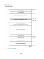
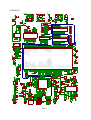
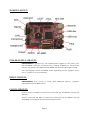
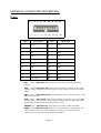
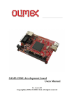
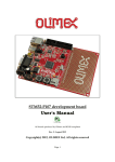
LPC2478-STK and LPC2478-STK-MICTOR development boards User's Manual Document revision C, October 2012 Copyright(c) 2009, OLIMEX Ltd, All rights reserved Page 1 INTRODUCTION: LPC-2478STK is a starter kit which uses MCU LPC2478 from NXP. This powerful MCU supports various serial interfaces such as USB host, USB device, UART, CAN, etc. Additionally, you will find also audio input and output as well as MP3 decoder, digital accelerometer, JTAG, Ethernet, touchscreen TFT display and SD/MMC card connector on this board. All this along with the ARM7TDMI-S™ architecture and uC Linux allow you to build a diversity of powerful applications to be used in a wide range of situations. BOARD FEATURES: − − − − − − − − − − − − − − − − − − − − − − − − MCU: LPC2478 LCD 3.5'' 320x 240 24bit color TFT with backlight and touchscreen MP3 decoder DSP + codec VS1002D 3-axis digital accelerometer with 11-bit accuracy 64 MB SDRAM USB host connector USB device connector IrDA transceiver (optional) MICTOR Trace connector (optional) PS2 keyboard connector 100Mbit Ethernet CAN driver and connector RS232 with ICSP control SD/MMC card connector JTAG connector Reset button and circuit 2 buttons 1 trim pot UEXT connector Audio IN Audio OUT RTC battery FR-4, 1.5 mm, red soldermask, component print Dimensions: 134.6x101.5mm (5.3x4.0'') ELECTROSTATIC WARNING: The LPC-2478STK board is shipped in protective anti-static packaging. The board must not be subject to high electrostatic potentials. General practice for working with static sensitive devices should be applied when working with this board. BOARD USE REQUIREMENTS: Cables: You will need different cables depending on the used programming/debugging tool. If you use Olimex's ARM-JTAG, you will need a LPT cable. If you use ARM-USB-OCD or ARMUSB-TINY, you will need USB A-B cable. If you use a software Page 2 programmer such as FlashMagic, you may need RS232 or other cables. Hardware: Programmer/Debugger – ARM-JTAG, ARM-USB-TINY or ARMUSB-OCD or other compatible programming/debugging tool. Software: The board comes pre-loaded with Uboot and the CD contains ucLinux image you can copy to USB flash disk and boot. You can use GCC or other commercial ARM compiler if you want to develop without ucLinux RTOS. PROCESSOR FEATURES: LPC-2478STK board use MCU LPC2478 from NXP with these features: ARM7TDMI-S processor, running at up to 72 MHz. 512 kB on-chip flash program memory with In-System Programming (ISP) and In-Application Programming (IAP) capabilities. Flash program memory is on the ARM local bus for high performance CPU access. 98 kB on-chip SRAM includes: - 64 kB of SRAM on the ARM local bus for high performance CPU access. - 16 kB SRAM for Ethernet interface. Can also be used as general purpose SRAM. - 16 kB SRAM for general purpose DMA use also accessible by the USB. - 2 kB SRAM data storage powered from the RTC power domain. LCD controller, supporting both Super-Twisted Nematic (STN) and Thin-Film Transistors (TFT) displays. - Dedicated DMA controller. - Selectable display resolution (up to 1024 × 768 pixels). - Supports up to 24-bit true-color mode. Dual Advanced High-performance Bus (AHB) system allows simultaneous Ethernet DMA, USB DMA, and program execution from on-chip flash with no contention. EMC provides support for asynchronous static memory devices such as RAM, ROM and flash, as well as dynamic memories such as Single Data Rate SDRAM. Advanced Vectored Interrupt Controller (VIC), supporting up to 32 vectored interrupts. General Purpose AHB DMA controller (GPDMA) that can be used with and SD/MMC interface as well as for memory-to-memory transfers. Serial Interfaces: - Ethernet MAC with MII/RMII interface and associated DMA controller. These functions reside on an independent AHB. Page 3 - USB 2.0 full-speed dual-port device/host/OTG controller with on-chip PHY and associated DMA controller. - Four UARTs with fractional baud rate generation, one with modem control I/O, one with IrDA support, all with FIFO. - CAN controller with two channels. - SPI controller. - Two SSP controllers, with FIFO and multi-protocol capabilities. One is an alternate for the SPI port, sharing its interrupt. SSPs can be used with the GPDMA controller. - Three I2C-bus interfaces (one with open-drain and two with standard port pins). - I2S (Inter-IC Sound) interface for digital audio input or output. It can be used with the GPDMA. Other peripherals: - SD/MMC memory card interface. - 160 General purpose I/O pins with configurable pull-up/down resistors. - 10-bit ADC with input multiplexing among 8 pins. - 10-bit DAC. - Four general purpose timers/counters with 8 capture inputs and 10 compare outputs. Each timer block has an external count input. - Two PWM/timer blocks with support for three-phase motor control. Each PWM has an external count inputs. - Real-Time Clock (RTC) with separate power domain. Clock source can be the RTC oscillator or the APB clock. - 2 kB SRAM powered from the RTC power pin, allowing data to be stored when the rest of the chip is powered off. - WatchDog Timer (WDT). The WDT can be clocked from the internal RC oscillator, the RTC oscillator, or the APB clock. Single 3.3 V power supply (3.0 V to 3.6 V). 4 MHz internal RC oscillator trimmed to 1 % accuracy that can optionally be used as the system clock. Three reduced power modes: idle, sleep, and power-down. Four external interrupt inputs configurable as edge/level sensitive. All pins on port 0 and port 2 can be used as edge sensitive interrupt sources. Processor wake-up from Power-down mode via any interrupt able to operate during Power-down mode (includes external interrupts, RTC interrupt, USB activity, Ethernet wake-up interrupt, CAN bus activity, port 0/2 pin interrupt). Two independent power needed features. Each peripheral has its own clock divider for further power saving. These dividers help reduce active power by 20 % to 30 %. Brownout detect with separate thresholds for interrupt and forced reset. Page 4 On-chip power-on reset. On-chip crystal oscillator with an operating range of 1 MHz to 24 MHz. On-chip PLL allows CPU operation up to the maximum CPU rate without the need for a high frequency crystal. May be run from the main oscillator, the internal RC oscillator, or the RTC oscillator. Boundary scan for simplified board testing. Versatile pin function selections allow more possibilities for using onchip peripheral functions. Standard ARM test/debug interface for compatibility with existing tools. Emulation trace module supports real-time trace. Page 5 BLOCK DIAGRAM: Page 6 MEMORY MAP: Page 7 S H IE L D USB RJ45 SIDE GND1 GND2 Page 8 + C103 33p + C104 10u/6.3V C105 C106 100n 100n 3.3V GPIO0/SPIBOOT GPIO1 GPIO2/DCLK GPIO3/SDATA TEST VS1002 33 34 9 10 32 XTALI XTALO DREQ X\O\S\C\/BSYNC MCP MCN RCAP GBUF RIGHT LEFT 1 2 44 42 39 46 100n C101 C76 R72 100k C48 GBUF RIGHT LEFT 10n AGND3 AGND4 AGND2 AGND1 AVDD3 AVDD2 AVDD1 1K R69 100p C100 C111 10u/6.3V 1u 1u R74 22 R75 22 R68 1K 10n C110 +3.3V_A C10 L8 470nH 3.3VA_E HEADPHONES 1-L 2 3-R MIC 1-L 2 3-R 3.3V 3.3V R114 33K R15 4.7K R57 4.7K 3.3V_A 100n C8 100n C9 100n C7 R5 R_0R(NA) 3.3V 2 R67 10u/6.3V 100n 1K JACK-3PINPHONE_JACK-TH 1K R54 10n C107 C108 C109 + +3.3V_A 100K 100K 100K 100K 18 17 DREQ 8 SSEL0 13 27 26 R73 22 BAT_HOLDER 3V_BAT JACK-3PINPHONE_JACK-TH EXT/BAT + 470nH + R1 R2 R3 R21 GND_ GND Q3 12.288MHz TX RX RIGHT GBUF LEFT PWR R55 1K 1 L1 R70 1M DVDD3 DVDD2 DVDD1 SO SI SCLK X\C\S\ X\R\E\S\E\T\ R81 100k 3.3V 100n C99 2 C102 33p 100k 100k C26 100n 1 32768/6pF 100n C6 3.3V_E 100n C5 100n C4 100n C3 100n C2 100n C1 100n C37 100n C29 100n C27 100n C54 GND Q2 0R 3.3V + R82 R71 DGND5 DGND4 DGND3 DGND2 DGND1 3.3V 3.3V 19 14 6 100n MISO0 30 MOSI0 29 SCK0 28 CS_AU 23 #RSTOUT 3 U11 22 21 20 16 4 100n 1 1000uF/6.3V/8x12mm + C44 + - 10u/6.3V C43 C79 47uF/6.3V 1000uF/6.3V/low_ESR C11 3.3V L7 470nH 10p C15 10p C14 22p C13 Q1 12.000MHz 22p C12 + R61 330/1% 3.3V C35 150K R98 R62 100/1% 1 2 3 R63 330/1% 2 C74 EXT/JLNK 3.3V +5V_JLINK 2 10u/6.3V C42 VO GND/ADJ VI D6 C75 47uF/6.3V 1N5822(SMC) +5V VREF_E 2.2uF C45 3 3 4.99K/1% R97 VR1 AME1085ACDT-3Z BD9778HFP EN/SYNC GND FB 4.7n +5V R99 4.7K 68K L5 33uH/CW8A + 141 20 22 32 84 172 26 86 174 33 63 77 93 114 133 148 169 189 200 15 60 71 89 112 125 146 165 181 198 37 24 38 34 36 46 TXD2 RXD2 SCL2 SDA2 MISO MOSI SCK SSEL UEXT-1 3.3V_A UEXT-2 UEXT-3 UEXT-4 R76 ADC0[7] BUT1 UEXT-5 10K UEXT-6 330/1% UEXT-7 AN_TRIM C24 UEXT-8 100n UEXT-9 UEXT-10 LPC2478 NC3 VDDA VSSA VSSCORE1 VSSCORE2 VSSCORE3 VDD(DCDC)(3V3)_1 VDD(DCDC)(3V3)_2 VDD(DCDC)(3V3)_3 VSSIO1 VSSIO2 VSSIO3 VSSIO4 VSSIO5 VSSIO6 VSSIO7 VSSIO8 VSSIO9 VSSIO10 VDD(3V3)_1 VDD(3V3)_2 VDD(3V3)_3 VDD(3V3)_4 VDD(3V3)_5 VDD(3V3)_6 VDD(3V3)_7 VDD(3V3)_8 VDD(3V3)_9 VDD(3V3)_10 ALARM VREF VBAT RTCX1 RTCX2 XTAL1 XTAL2 3.3V C21 100n 1K 20K/1% R52 BUT1 R11 BUT2 A0 A1 A2 A3 75 79 83 97 103 107 113 121 127 131 135 145 149 155 159 173 101 104 105 111 109 115 123 129 183 179 119 139 170 176 187 193 3.3V 30 117 1K C49 100n R6 C89 3.3V BDS_E #RSTOUT 10K R123 2 1 NC1 CLK CKE CS WE CAS RAS DQML DQMH VSS1 VSS2 VSS3 VSSQ1 VSSQ2 VSSQ3 VSSQ4 VDD1 VDD2 VDD3 VDDQ1 VDDQ2 VDDQ3 VDDQ4 DQ0 DQ1 DQ2 DQ3 DQ4 DQ5 DQ6 DQ7 DQ8 DQ9 DQ10 DQ11 DQ12 DQ13 DQ14 DQ15 28 41 54 6 12 46 52 1 14 27 3 9 43 49 2 4 5 7 8 10 11 13 42 44 45 47 48 50 51 53 C90 C87 3.3V C88 K4S561632C-TC/L75 40 38 37 19 16 17 18 BA0 BA1 A0 A1 A2 A3 A4 A5 A6 A7 A8 A9 A10/AP A11 A12 C85 C86 3.3V D0 D1 D2 D3 D4 D5 D6 D7 D8 D9 D10 D11 D12 D13 D14 D15 http://www.olimex.com/dev COPYRIGHT(C), 2009 Rev. B NC1 CLK CKE CS WE CAS RAS DQML DQMH BA0 BA1 A0 A1 A2 A3 A4 A5 A6 A7 A8 A9 A10/AP A11 A12 VSS1 VSS2 VSS3 VSSQ1 VSSQ2 VSSQ3 VSSQ4 VDD1 VDD2 VDD3 VDDQ1 VDDQ2 VDDQ3 VDDQ4 DQ0 DQ1 DQ2 DQ3 DQ4 DQ5 DQ6 DQ7 DQ8 DQ9 DQ10 DQ11 DQ12 DQ13 DQ14 DQ15 R50 10K R48 10K 28 41 54 6 12 46 52 1 14 27 3 9 43 49 2 4 5 7 8 10 11 13 42 44 45 47 48 50 51 53 C96 C97 C95 C93 100n 100n 100n 100n C94 3.3V POL JTAG R109 10K 3.3V D19 D20 D21 D22 D23 D24 D25 D26 D27 D28 D29 D30 D31 D16 D17 D18 R110 10K 1 3 5 7 9 11 13 15 17 +5V_JLINK 19 C92 R49 10K K4S561632C-TC/L75 40 38 37 19 16 17 18 15 39 20 21 23 24 25 26 29 30 31 32 33 34 22 35 36 U12 R51 4.7K ETM-E 2 1 R53 100K 100n 100n 100n C98 SDCLK SDCLKEN SDCS SDWEN CASN RASN DQMN2 DQMN3 A13 A14 A0 A1 A2 A3 A4 A5 A6 A7 A8 A9 A10 A11 A12 R47 10K LPC-2478STK 100n 100n 100n 100n 100n 100n 100n C91 SDCLK SDCLKEN SDCS SDWEN CASN RASN 15 39 20 21 A13 A14 DQMN0 DQMN1 23 24 25 26 29 30 31 32 33 34 22 35 36 A0 A1 A2 A3 A4 A5 A6 A7 A8 A9 A10 A11 A12 DBGEN 3.3V 10K EXT-13 EXT-12 LCD[2] LCD[3] EXT-15 EXT-14 SDWEN EXT-16 SDA2 SCL2 TXD2 RXD2 PHY_PD WP EXT-17 A4 A5 A6 A7 A8 A9 A10 A11 A12 A13 A14 CS_AU DREQ 9 DBGEN 2 TDO TDI 4 T MS 6 T RSTN 8 TCK 10 206 RTCK RST 35 29 #RSTOUT 20K/1% R78 BUT2 R77 NC1 NC2 DBGEN TDO TDI TMS #TRST TCK RTCK #RESET #RSTOUT P4[0]/A0 P4[1]/A1 P4[2]/A2 P4[3]/A3 P4[4]/A4 P4[5]/A5 P4[6]/A6 P4[7]/A7 P4[8]/A8 P4[9]/A9 P4[10]/A10 P4[11]/A11 P4[12]/A12 P4[13]/A13 P4[14]/A14 P4[15]/A15 P4[16]/A16 P4[17]/A17 P4[18]/A18 P4[19]/A19 P4[20]/A20/SDA2/SCK1 P4[21]/A21/SCL2/SSEL1 P4[22]/A22/TXD2/MISO1 P4[23]/A23/RXD2/MOSI1 P4[24]/#OE P4[25]/#WE P4[26]/BLS0 P4[27]/BLS1 P4[28]/BLS2/MAT2[0]/LCD[6]/LCD[10]/LCD[2]/TXD3 P4[29]/BLS3/MAT2[1]/LCD[7]/LCD[11]/LCD[3]/RXD3 P4[30]/#CS0 P4[31]/#CS1 U4 TRSTN TDI TMS TCK RTCK TDO RST R46 10K 3.3V 0R +20V 100n C51 3.3V 5 1 2 5 1 2 150 R35 L4 220uH FB SC SE +5V 3.3V 3 9 2 1 10 1 4 ACC_INT 5 6 SCL0 7 8 SDA0 C38 100n -10V C30 100n EXT-3 EXT-2 EXT-1 SMB380,(QFN10) NC1 SCK NC2 SDO SDI/SDA VDDIO VDD INT GND CSB U5 24K R148 2 U9A +15V 3 3 3.3V R85 100/1% C28 TL062CD,(SO8) R147 7 U9B 2 15V_E 1 1n 22K TC R146 3.3K R108 2.2K VCOM +15V C23 470p + +5V C66 10uF/16VDC TL062CD,(SO8) 6 5 C65 100n OUT GND R149 NA IN U6 2.2 R22 -10V MC34063AD(R2)G,(SO8) 1.2k/1% R14 18K/1% R23 D5 1N5819S L9 100uH VR3 78L15ACZ,(TO92) 100n C50 R151 NA R150 R_0R(NA) 2 4 6 8 10 12 14 16 18 20 FB SC SE 4 C41 C81 INV SW 10n R20 20K/1% + 8 3.3V C80 2.2uF 100nF VIN RT C52 1 2 3 7 4 5 2 1 GND C36 470uF/16VDC 100n C72 R115 VR2(5V) 1 6 2.5V RST TDO RTCK TCK TMS TDI TRSTN 0R R79 R_0R(NA) + 6VAC 9VDC VIN RMII CRS G1 REFCK TXEN TX0 TX1 ferrite bead GND1 GND2 GND3 GND4 GND5 DB104(SMD) PHY_IRQ 13 14 15 16 17 18 19 20 21 22 23 24 C63 10u/6.3V L6 P2 PWR_JACK 3.3K PD/CTRL R16 VDDC TXER TXC/REFCLK TXEN TXD0 TXD1 TXD2 TXD3 COL/RMII CRS/RMII_BTB GND3 VDDIO2 + 3.3V KS8721BL C62 100n LCD[6] LCD[5] LCD[4] LCDLP TRACESYNC LCDFP LCDCP PIPESTAT0 1 3 5 7 9 11 13 15 17 19 21 23 25 27 29 31 33 35 37 +20V TC U3 1 R64 SW-TAKT1 MC34063AD(R2)G,(SO8) 3 + C64 100n 3.3V C61 100n RXER CRS_DV 3.3V LCD[7] TRACECLK 2 4 6 8 10 12 14 16 18 20 22 24 26 28 30 32 34 36 38 TRACE MIGTOR(NA) + +5V 100uF/25V/SMD 3.3V 0R PHY_IRQ R134 NA R131 R132 330/1% 330/1% RST# VDDPLL XI XO GND8 GND7 VDDTX TX+ TXGND6 VDDRCV REXT RX3 RX2 RX1 RX0 CRS_DV RXER RMII CRS R133 10K P3[0]/D0 P3[1]/D1 P3[2]/D2 P3[3]/D3 P3[4]/D4 P3[5]/D5 P3[6]/D6 P3[7]/D7 P3[8]/D8 P3[9]/D9 P3[10]/D10 P3[11]/D11 P3[12]/D12 P3[13]/D13 P3[14]/D14 P3[15]/D15 P3[16]/D16/PWM0[1]/TXD1 P3[17]/D17/PWM0[2]/RXD1 P3[18]/D18/PWM0[3]/CTS1 P3[19]/D19/PWM0[4]/DCD1 P3[20]/D20/PWM0[5]/DSR1 P3[21]/D21/PWM0[6]/DTR1 P3[22]/D22/PCAP0[0]/RI1 P3[23]/D23/CAP0[0]/PCAP1[0] P3[24]/D24/CAP0[1]/PWM1[1] P3[25]/D25/MAT0[0]/PWM1[2] P3[26]/D26/MAT0[1]/PWM1[3] P3[27]/D27/CAP1[0]/PWM1[4] P3[28]/D28/CAP1[1]/PWM1[5] P3[29]/D29/MAT1[0]/PWM1[6] P3[30]/D30/MAT1[1]/RTS1 P3[31]/D31/MAT1[2] 10u/6.3V C46 3.3K 3.3K 3.3K 3.3K 1K 1K 4.7K 1K PHY_PD P1[0]/ENET_TXD0 P1[1]/ENET_TXD1 P1[2]/ENET_TXD2/MCICLK/PWM0[1] P1[3]/ENET_TXD3/MCICMD/PWM0[2] P1[4]/ENET_TX_EN P1[5]/ENET_TX_ER/MCIPWR/PWM0[3] P1[6]/ENET_TX_CLK/MCIDAT0/PWM0[4] P1[7]/ENET_COL/MCIDAT1/PWM0[5] P1[8]/ENET_CRS_DV/ENET_CRS P1[9]/ENET_RXD0 P1[10]/ENET_RXD1 P1[11]/ENET_RXD2/MCIDAT2/PWM0[6] P1[12]/ENET_RXD3/MCIDAT3/PCAP0[0] P1[13]/ENET_RX_DV P1[14]/ENET_RX_ER P1[15]/ENET_REF_CLK/ENET_RX_CLK P1[16]/ENET_MDC P1[17]/ENET_MDIO P1[18]/USB_UP_LED1/PWM1[1]/CAP1[0] P1[19]/#USB_TX_E1/#USB_PPWR1/CAP1[1] P1[20]/USB_TX_DP1/LCD[6]/LCD[10]/PWM1[2]/SCK0 P1[21]/USB_TX_DM1/LCD[7]/LCD[11]/PWM1[3]/SSEL0 P1[22]/USB_RCV1/LCD[8]/LCD[12]/USB_PWRD1/MAT1[0] P1[23]/USB_RX_DP1/LCD[9]/LCD[13]/PWM1[4]/MISO0 P1[24]/USB_RX_DM1/LCD[10]/LCD[14]/PWM1[5]/MOSI0 P1[25]/#USB_LS1/LCD[11]/LCD[15]/#USB_HSTEN1/MAT1[1] P1[26]/#USB_SSPND1/LCD[12]/LCD[20]/PWM1[6]/CAP0[0] P1[27]/#USB_INT1/LCD[13]/LCD[21]/#USB_OVRCR1/CAP0[1] P1[28]/USB_SCL1/LCD[14]/LCD[22]/PCAP1[0]/MAT0[0] P1[29]/USB_SDA1/LCD[15]/LCD[23]/PCAP1[1]/MAT0[1] P1[30]/USB_PWRD2/VBUS/AD0[4] P1[31]/#USB_OVRCR2/SCK1/AD0[5] T2 BC817 RST RESET 4 R136 R137 R138 R139 R140 R141 R142 R143 3 2 1 196 TX0 194 TX1 MCICLK 185 177 MCICMD 192 TXEN MCIPWR 156 MCIDAT0 171 MCIDAT1 153 CRS_DV 190 188 RX0 186 RX1 MCIDAT2 163 MCIDAT3 157 USB_UP_LED2 147 184 RXER 182 REFCK 180 MDC 178 MDIO USB_UP_LED1 66 USB1_CONNECT 68 LCD[10] 70 LCD[11] 72 LCD[12] 74 LCD[13] 76 LCD[14] 78 LCD[15] 80 LCD[20] 82 LCD[21] 88 LCD[22] 90 LCD[23] 92 USB_PWRD242 #USB_OVRCR2 40 R80 NA 44 P1 VSS R92 R_0R(NA) R126 2.2K MDIO MDC RX3 RX2 RX1 RX0 + +5V D4 1N4148 100n C20 10u/6.3V C60 NA MDIO GND5 MDC GND4 RXD3/PHYAD1 FXSD/FXEN RXD2/PHYAD2 RX+ RXD1/PHYAD3 RXRXD0/PHYAD4 VDDRX VDDIO1 PD# GND1 LED3/NWAYEN RXDV/CRSDV/PCS_LPBK LED2/DUPLEX RXC LED1/SPD100/NFEF RXER/ISO LED0/TEST GND2 INT/PHYAD0 1 2 3 4 5 6 7 8 9 10 11 12 + +20V NA NA R37 R39 #RSTOUT POL NA R41 VCOM TRACESYNC +15V -10V 3.3V Y1 X1 Y2 X2 LCDLP LCDFP LCDCP R10 20K/1% ISP_E 3.3V C22 2.5V 3.3V C73 36 35 34 33 32 31 30 29 28 27 26 25 8 9 10 11 36 37 38 39 40 41 42 43 44 45 46 47 48 49 50 51 52 53 54 1 2 3 4 5 6 7 R9 33K ISP_E R12 1K D2 BAT54C IS DC C69 100n R125 1.5K/1% Y1 X1 Y2 X2 HSYNC VSYNC DCLK VDD1 VDD2 VCC1 VCC2 SPENA NC2 V_GL NC3 V_GH NC4 SPCLK SPDAT VCOM ENB GND VSS VBL-1 VBL-2 VBL+1 VBL+2 NC1 #RESET POL TFT 6 7 8 9 G2 G1 RS232_0/ICSP db9_male 1 2 3 4 5 R7 220 3.3V VCC RJLBC-060TC1 LEDACT LED100/DUP GFT035A320240Y 13 8 C16 100n C17 100n R8 33K 7 8 1nF/2kV 1:1 D0 D1 D2 D3 D4 D5 D6 D7 D8 D9 D10 D11 D12 D13 D14 D15 D16 D17 D18 D19 D20 D21 D22 D23 D24 D25 D26 D27 D28 D29 D30 D31 197 201 207 3 13 17 23 27 191 199 205 208 1 7 21 28 137 143 151 161 167 175 195 65 58 56 55 203 5 11 19 25 B0 B1 B2 B3 B4 B5 B6 B7 R1IN R2IN 14 7 6 2 RST_E 6 GND GREEN 48 47 46 45 44 43 42 41 40 39 38 37 YELLOW 3.3V 4.7K 4.7K 75 U10 #RSTOUT C67 100n 12 13 14 15 16 17 18 19 LCD[16] LCD[17] LCD[18] LCD[19] LCD[20] LCD[21] LCD[22] LCD[23] G0 G1 G2 G3 G4 G5 G6 G7 R1OUT R2OUT T1OUT T2OUT V- V+ ST3232CD(R),(SO16) M2 75 R124 4.99K/1% + C68 10u/6.3V 20 21 22 23 24 25 26 27 LCD[8] LCD[9] LCD[10] LCD[11] LCD[12] LCD[13] LCD[14] LCD[15] R0 R1 R2 R3 R4 R5 R6 R7 12 9 T1IN T2IN C2- C2+ C1- C1+ U2 15 GND M1 3 7 8 6 75 L3 R36 R24 2.5V CASN RASN SDCLK BUT1 SDCS BUT2 SCK0 SSEL0 SDCLKEN PHY_IRQ MISO0 MOSI0 DQMN0 DQMN1 DQMN2 DQMN3 CP LCD[18] LCD[19] KBD_IO KBD_CK 28 29 30 31 32 33 34 35 R4 220 LCD[0] LCD[1] LCD[2] LCD[3] LCD[4] LCD[5] LCD[6] LCD[7] RXD0 11 10 5 4 3 1 VCC C34 100n U2PWR 16 1.5n C40 75 3.3V CP1 CP2 TRACECLK PIPESTAT0 LCDCP LCDFP TRACESYNC LCDLP LCD[4] LCD[5] LCD[6] LCD[7] ISP_E CP 154 152 150 144 142 140 138 136 134 132 110 108 106 102 91 99 87 95 59 67 73 81 85 64 53 54 57 47 49 43 31 39 13 15 TXD0 C19 100n C18 100n 3.3V C39 1 3 2 AG KG AY KY 7 6 8 3.3V REFCK 33K 2.2K MCIDAT0 MCIDAT1 MCIDAT2 3.3VR44 R45 CD/DAT3/CS CMD/DI VSS1 VDD CLK/SCLK VSS2 DAT0/DO DAT1/RES DAT2/RES SD-CARD 4 TD+ COM TDAG KG AY KY RD+ NC RD- R84 10K ferrite bead 33 R100 47uF/6.3V C59 33K 33K 33K 1 2 3 4 5 6 7 8 9 WP1 WP2 SD/MMC WP + 1:1 C70 100n 3 1 R56 R111 R112 C33 100n P2[0]/PWM1[1]/TXD1/TRACECLK/LCDPWR P2[1]/PWM1[2]/RXD1/PIPESTAT0/LCDLE P2[2]/PWM1[3]/CTS1/PIPESTAT1/LCDCP P2[3]/PWM1[4]/DCD1/PIPESTAT2/LCDFP P2[4]/PWM1[5]/DSR1/TRACESYNC/LCDAC P2[5]/PWM1[6]/DTR1/TRACEPKT0/LCDLP P2[6]/PCAP1[0]/RI1/TRACEPKT1/LCD[0]/LCD[4] P2[7]/RD2/RTS1/TRACEPKT2/LCD[1]/LCD[5] P2[8]/TD2/TXD2/TRACEPKT3/LCD[2]/LCD[6] P2[9]/USB_CONNECT1/RXD2/EXTIN0/LCD[3]/LCD[7] P2[10]/#EINT0 P2[11]/#EINT1/LCDCLKIN/MCIDAT1/I2STX_CLK P2[12]/#EINT2/LCD[4]/LCD[3]/LCD[8]/LCD[18]/MCIDAT2/I2STX_WS P2[13]/#EINT3/LCD[5]/LCD[9]/LCD[19]/MCIDAT3/I2STX_SDA P2[14]/#CS2/CAP2[0]/SDA1 P2[15]/#CS3/CAP2[1]/SCL1 P2[16]/#CAS P2[17]/#RAS P2[18]/CLKOUT0 P2[19]/CLKOUT1 P2[20]/#DYCS0 P2[21]/#DYCS1 P2[22]/#DYCS2/CAP3[0]/SCK0 P2[23]/#DYCS3/CAP3[1]/SSEL0 P2[24]/CKEOUT0 P2[25]/CKEOUT1 P2[26]/CKEOUT2/MAT3[0]/MISO0 P2[27]/CKEOUT3/MAT3[1]/MOSI0 P2[28]/DQMOUT0 P2[29]/DQMOUT1 P2[30]/DQMOUT2/MAT3[2]/SDA2 P2[31]/DQMOUT3/MAT3[3]/SCL2 red SD R32 1K MCICLK MCIDAT3 MCICMD 33K 10 2.2K 14 10u/6.3V C47 2.5V C71 10u/6.3V + OUT E/D 6NC2-50MHz VSS VDD P0[0]/RD1/TXD3/SDA1 P0[1]/TD1/RXD3/SCL1 P0[2]/TXD0 P0[3]/RXD0 P0[4]/I2SRX_CLK/LCD[0]/RD2/CAP2[0] P0[5]/I2SRX_WS/LCD[1]/TD2/CAP2[1] P0[6]/I2SRX_SDA/LCD[8]/SSEL1/MAT2[0] P0[7]/I2STX_CLK/LCD[9]/SCK1/MAT2[1] P0[8]/I2STX_WS/LCD[16]/MISO1/MAT2[2] P0[9]/I2STX_SDA/LCD[17]/MOSI1/MAT2[3] P0[10]/TXD2/SDA2/MAT3[0] P0[11]/RXD2/SCL2/MAT3[1] P0[12]/#USB_PPWR2/MISO1/AD0[6] P0[13]/USB_UP_LED2/MOSI1/AD0[7] P0[14]/#USB_HSTEN2/USB_CONNECT2/SSEL1 P0[15]/TXD1/SCK0/SCK P0[16]/RXD1/SSEL0/SSEL P0[17]/CTS1/MISO0/MISO P0[18]/DCD1/MOSI0/MOSI P0[19]/DSR1/MCICLK/SDA1 P0[20]/DTR1/MCICMD/SCL1 P0[21]/RI1/MCIPWR/RD1 P0[22]/RTS1/MCIDAT0/TD1 P0[23]/AD0[0]/I2SRX_CLK/CAP3[0] P0[24]/AD0[1]/I2SRX_WS/CAP3[1] P0[25]/AD0[2]/I2SRX_SDA/TXD3 P0[26]/AD0[3]/AOUT/RXD3 P0[27]/SDA0 P0[28]/SCL0 P0[29]/USB_D+1 P0[30]/USB_D-1 P0[31]/USB_D+2 USB_D-2 R116 2.2K 470nH 33K 33K R43 R42 1.1K/1% C25 220uF/10V/tnant8.2k/1% R66 R65 LAN + R130 R129 R128 R127 R135 4.7uF/6.3V(NA) 49.9/1% 49.9/1% 49.9/1% 49.9/1% NA R88 2 4 94 96 202 204 168 166 164 162 160 158 98 100 41 45 69 128 130 126 124 122 120 118 116 18 16 14 12 50 48 61 62 51 52 U1 220 R13 RD1 100nF TD1 C55 L2 R113 R144 3.3V VSS C57 100n(NA) 47(NA) EXT-11 EXT-10 RD1 TD1 TXD0 RXD0 EXT-4 EXT-5 EXT-6 EXT-7 EXT-8 EXT-9 EXT-18 EXT-19 #USB_PPWR2 ADC0[7] VBUS SCK SSEL MISO 3.3V MOSI EXT-20 ACC_INT Y2 X2 Y1 X1 TXD3 RXD3 SDA0 SCL0 U1D+ U1DU2D+ U2D- 0 0 0 0 0 0 1 2 3 4 C56 100n 3.3V T4 IRLM6402 D1 TFDU4100(NA) C58 2AOUT 1 RXD3 100K 1 1 1 1 1 1 U7 TXD VSS VDD RXD R118 NA MCIPWR R34 20K/1% 10u/6.3V R87 R89 R94 IR_RX CD1 R83 C53 10n LCD[0] RC 2 LCD[1] RW 2 LCD[8] RS 2 LCD[9] TC 2 LCD[16] TW 2 LCD[17] TS 2 RS CANH CANL VREF CAN1_D 2 1 MCP2551(T)-I/SN,(SO8) 8 7 6 5 +5V 1K T5 BC817 R33 VCC 14(NA) 10K(NA) 220(NA) SHIELD 3.3V MD6R MINI-DIN +5V USB_H_LINK 3 2 1 CON33.5MM CAN1 R40 10K R119 R117 33K DC IS 1 2 6 5 8 3 4 R86 C31 3.3V I2SRX_SDA 2 1 TXD3 18p(NA) KBD_CK KBD_IO R60 4.7K +5V R90 560 R38 120 NA 6 SC 18p(NA) IRDA_LS_E 1 U1DU1D+ 1 2 3 4 5 6 yellow USB_UP_LED2 R152 3.3V #USB_PPWR2 #USB_OVRCR2 8 7 TXD RXD 10K(NA) 2 R30 20K/1% R26 R25 C32 PS2 IO 1 NA 2 GN 3 5V 4 CK 5 NA 6 NC1 NC2 10K R59 4.7K +5V 3.3V LM3526M-L,(SO8) 10K R154 3.3V 1 2 3 4 1N5819S IRED_ANODE IRED_CATHODE VCC1 NC GND 7 C82 10n 33 33 USB_D_LINK USB1_CONNECT 3 2 R29 1 2.2K U13 OUT_A #ENA FLAG_A IN GND FLAG_B OUT_B #ENB -10V_E 2 1 1 4 5 2 USB IRDA R31 560 yellow R28 10K 100n C114 + C112 USB_UP_LED1 3.3V 3.3V R27 1.5K/1% C77 47p(NA) U2DU2D+ C/SC S H IE LD VBUS 3.3V R18 R17 C78 R95 15K 47p(NA) 33 33 8 7 6 5 1 10K R19 15K 10u/6.3V T3 BC807 R96 100K HOST_PWR +5V CAN1_T 1 R58 2 D3 D+ 4 L10 FERRITE_BEAD USB_PWRD2 2 + 1 2 USB_B 0R R91 R_0R(NA) HOST_PWR 1 2 USB_DEV USB_A 1 2 3 4 USB_HOST SCHEMATIC: 41 47 40 37 45 43 38 BOARD LAYOUT: POWER SUPPLY CIRCUIT: LPC-2478STK is powered by +(9-12)VDC/6VAC applied at the power jack. LPC-2478STK could also be powered by a battery (CR2032, Li, 3V) but this battery only powers the 2KB internal SRAM and the RTC (Real Time Clock). The consumption of LPC-2478STK varies depending on the supplied power but at +10VDC it is about 250mA. RESET CIRCUIT: LPC-2478STK reset circuit is made with R68(47k) pull-up, capacitor C20(100nF) and the RST button. CLOCK CIRCUIT: Quartz crystal 12 MHz is connected to LPC2478 pin 44 (XTAL1) and pin 46 (XTAL2). Quartz crystal 32.768 kHz is connected to LPC2478 pin 34 (RTX1) and pin 36 (RTX2) and supplies the internal Real Time Clock. Page 9 JUMPER DESCRIPTION: CAN_D CAN Disable. If this jumper is closed, the CAN is disabled. Default state is open. CAN_T This jumper assures correct work of the CAN. At each end of the bus it should be closed. This means that if you have only two devices with CAN, the jumpers of both devices should be closed. If you have more than two devices, only the two end-devices should be closed. Default state is closed. -10V_E This jumper, when closed, supplies -10 V voltage to the on board LCD panel. Default state is closed. 15V_E This jumper, when closed, supplies 15 V voltage to to the on board LCD panel. Default state is closed. 3.3V_E This jumper, when closed, supplies 3.3 V voltage to the VDD1-10 pins of the MCU. Default state is closed. 3.3VA_E This jumper, when closed, supplies 3.3 V voltage to the VDDA pin of the MCU. Default state is closed. VREF_E This jumper, when closed, supplies 3.3 V reference voltage to the VREF pin of the MCU. Default state is closed. IRDA_LS_E IRDA_LowSpeed_Enable jumper – opened if there is no IrDA module or it is disabled. Default state is opened if your board doesn't have an IrDA connector. I2SRX_SDA IrDA TX input pin jumper – opened if there is no IrDA module or it is disabled. Default state is opened if your board doesn't have an IrDA connector. Page 10 AOUT IrDA RX output pin jumper – opened if there is no IrDA module or it is disabled. Default state is opened if your board doesn't have an IrDA connector. RC This jumper, when closed, outputs the LCD[0] signal from the LPC2478 to the TFT display. If it is open, pin 168 of the LCP2478 is connected to EXT-4. Default state is closed. RW This jumper, when closed, outputs the LCD[1] signal from the LPC2478 to the TFT display. If it is open, pin 166 of the LCP2478 is connected to EXT-5. Default state is closed. RS This jumper, when closed, outputs the LCD[8] signal from the LPC2478 to the TFT display. If it is open, pin 164 of the LCP2478 is connected to EXT-6. Default state is closed. TC This jumper, when closed, outputs the LCD[9] signal from the LPC2478 to the TFT display. If it is open, pin 162 of the LCP2478 is connected to EXT-7. Default state is closed. TW This jumper, when closed, outputs the LCD[16] signal from the LPC2478 to the TFT display. If it is open, pin 160 of the LCP2478 is connected to EXT-8. Default state is closed. TS This jumper, when closed, outputs the LCD[17] signal from the LPC2478 to the TFT display. If it is open, pin 158 of the LCP2478 is connected to EXT-9. Default state is closed. ISP_E If you put this jumper, you enable the ISP (In-System Programming). This is used when you want external software to program the LCP2478. This jumper is used in combination with the RST_E jumper. Default state is open. RST_E If you put this jumper, you enable external software to control the Reset signal to the processor. This is used when you want external software to program the LCP2478. This jumper is used in combination with the ISP_E jumper. Default state is open. Page 11 ETM_E If you put this jumper, you enable the MICTOR Trace connector. Default state is open. BDS_E Boundary scan enable. Default state is open. C/SC This jumper controls the USB device interface. If 1-2 are shorted, the USB is always enabled. If 2-3 are shorted, the USB Enable is controlled by the MCU LPC2478 signal USB1_CONNECT. Default state is 2-3 shorted. PD/CTRL This jumper controls the PHY signal of the Ethernet controller. If there is no jumper, the PHY is always enabled. If 1-2 are shorted, the PHY is disabled If 2-3 are shorted, the PHY is controlled by the LPC2478 signal PHY_PD. Default state is no jumper (opened). EXT/JLINK This jumper controls the JLINK +5V power line (pin19) of the JTAG and the +5VDC power supply of the board. If 1-2 are shorted, the JLINK +5V power line (pin19) from the JTAG interface supplies the board with +5VDC. If 2-3 are shorted, the board is supplied with +5VDC from the +5VDC voltage regulator. Default state is 2-3 shorted. EXT/BAT This jumper controls the VBAT signal of the LPC2478. If 1-2 are shorted, the VBAT pin is supplied by an external battery. If 2-3 are shorted, the VBAT pin is supplied by the common +3.3VDC power supply for the board. Default state is 2-3 shorted. Page 12 INPUT/OUTPUT: SD/MMC LED (red) with name SD connected to SD/MMC pin 4. Power-on LED (red) with name PWR – this LED shows that +3.3V is applied to the board. USB host LED (yellow) with name USB_H_LINK – connected to LPC2478 pin 147 (P1[13]/ENET_RX_DV). USB device LED (yellow) with name USB_D_LINK – connected to LPC2478 pin 66 (P1[18]/USB_UP_LED1/PWM1[1]/CAP1[0]). User button with name BUT1 connected to LPC2478 pin 67 (P2[19]/CLKOUT1). User button with name BUT2 connected to LPC2478 pin 81 (P2[21]/#DYCS1). Reset button with name RESET connected to LPC2478 pin 35 (#RESET). Trimpot with name AN_TRIM connected to LPC2478 pin 45 (P0[13]/USB_UP_LED2/MOSI1/AD0[7]). TFT touchscreen display – 3.5'', 320x200, 24-bit color. Page 13 EXTERNAL CONNECTORS DESCRIPTION: JTAG: Pin # Signal Name Pin # Signal Name 1 +3.3V 2 +3.3V 3 TRSTN 4 GND 5 TDI 6 GND 7 TMS 8 GND 9 TCK 10 GND 11 RTCK 12 GND 13 TDO 14 GND 15 RST 16 GND 17 GND 18 GND 19 +5V_JLINK 20 GND TDI Input Test Data In. This is the serial data input for the shift register. TDO OutputTest Data Out. This is the serial data output for the shift register. Data is shifted out of the device on the negative edge of the TCK signal. TMS Input Test Mode Select. The TMS pin selects the next state in the TAP state machine. TCK Input Test Clock. This allows shifting of the data in, on the TMS and TDI pins. It is a positive edge triggered clock with the TMS and TCK signals that define the internal state of the device. TRSTNInput Test Reset N. This signal resets the JTAG controller. RTCK OutputReturn Clock. This is a synchronization signal which the JTAG connector uses to acknowledge it is ready to receive/transmit. JTAG is used to to program and debug the MCU. Page 14 RS232: Pin # Signal Name 1 NC 2 RXD0 3 TXD0 4 NC 5 GND 6 RST 7 NC 8 ISP_E 9 NC The RS232 in LPC2478-STK and LPC2478-STK is configured as DTE. Note that in order to establish connection to another DTE device (e.g. personal computer) you will need a null modem cable TXD0 OutputTransmit Data. This is the asynchronous serial data output (RS232) for the shift register on the UART controller. (This pin is input for the RS232 and input for the LPC2478) RXD0 Input Receive Data. This is the asynchronous serial data input (RS232) for the shift register on the UART controller. (This pin is output for the RS232 and input for the LPC2478) RST Input Reset. When you use external software to program LPC2478, this software uses the RS232 to connect to the device and if jumper RST_E is put, than through this RST pin the software controls #RESET pin of the MCU. (This pin is output for the RS232 and input for LPC2478) the the the the ISP_E Input In-System Programming. If you use external software to program the device, this pin enables the programming. A pre-condition to enable ISP is the ISP_E jumper to be put. (This pin is output for the RS232 and input for the LCP2478) Page 15 CAN: Pin # Signal Name 1 GND 2 CANL 3 CANH CANL and CANH are either deferential input, or differential output depending on the function of the MCP2551 CAN controller (receiving or transmitting data). Page 16 PWR: Pin # Signal Name 1 Power Input 2 GND The power input should be +(9-12VDC)/6VAC. Audio In: Pin # Signal Name 1 NC 2 GND 3 MCP MCP Input Microphone Input. This pin is input to the DSP codec VS1002D. Audio Out: Pin # Signal Name 1 LEFT 2 GBUF 3 RIGHT LEFT OutputLeft channel output. This pin is output for the DSP codec VS1002D. GBUF OutputVirtual ground for audio output, 1.23 V nominal. This pin is output for the DSP codec VS1002D. RIGHT OutputRight channel output. This pin is output for the DSP codec VS1002D. Page 17 EXT: Pin # Signal Name Pin # Signal Name 1 GND 2 +3.3V 3 +5V 4 P0[4]/I2SRX_CLK/LCD [0]/RD2/CAP2[0] 5 P0[5]/I2SRX_WS/LC D[1]/TD2/CAP2[1] 6 P0[6]/I2SRX_SDA/LCD [8]/SSEL1/MAT2[0] 7 P0[7]/I2STX_CLK/L CD[9]/SCK1/MAT2[1 ] 8 P0[8]/I2STX_WS/LCD[ 16]/MISO1/MAT2[2] 9 P0[9]/I2STX_SDA/L CD[17]/MOSI1/MAT2 [3] 10 TXD3 11 RXD3 12 P4[31]/#CS1 13 P4[30]/#CS0 14 P4[27]/BLS1 15 P4[26]/BLS0 16 P4[24]/#OE 17 P4[17]/A17 18 P0[10]/TXD2/SDA2/MA T3[0] 19 P0[11]/RXD2/SCL2/ MAT3[1] 20 Page 18 UEXT: Pin # Signal Name 1 +3.3V 2 GND 3 TXD2 4 RXD2 5 SCL2 6 SDA2 7 MISO 8 MOSI 9 SCK 10 SSEL USB host: Pin # Signal Name 1 USB_PWRD2 2 U2D- 3 U2D+ 4 GND USB_PWRD2 Output USB Power. This signal is output from the processor and input for the USB host. U2D-, U2D+ I/O This signals form the differential input/output depending on the direction of the data transfer. USB device: Pin # Signal Name 1 VBUS 2 U1D- 3 U1D+ 4 GND Page 19 VBUS OutputUSB device power. U1D-, U1D+ I/O This signals form the differential input/output depending on the direction of the data transfer. LAN: Pin # Signal Name Chip Side Pin # Signal Name Chip Side 1 TD+ 5 LED100/DUP 2 TD- 6 NC 3 2.5V 7 RD+ 4 LEDACT 8 RD- LED Color Usage Right Yellow Activity Left Green 100MBits/s (Half/Full duplex) TD- OutputDifferential signal output. This signal is output from the MCU. TD+ OutputDifferential signal output. This signal is output from the MCU. RD- Input Differential signal input. This signal is input for the MCU. RD+ Input Differential signal input. This signal is input for the MCU. Page 20 SD/MMC card slot: Pin # Signal Name Pin # Signal Name 1 MCIDAT3 2 MCICMD 3 GND (VSS1) 4 VDD 5 MCICLK 6 GND (VSS2) 7 MCIDAT0 8 MCIDAT1 9 MCIDAT2 10 WP 11 - 12 - 13 CP 14 GND 15 GND MCIDAT0-3 I/O Memory Card Interface Data 0-4. These are the data lines for the SD/MMC connector. They could be both input and output for the MCU depending on the data flow direction. MCICMD Output Memory Card Interface Command. This is a command sent form the processor to the memory card and as such it is output from the processor. MCICLK OutputMemory Card Interface Clock. This signal is output from the MCU and synchronizes the data transfer between the memory card and the MCU. WP Input Write Protect. This signal is input for the MCU. CP Input Card Present. This signal is input for the MCU. Page 21 PS2: Pin # Signal Name 1 KBO_IO 2 NC 3 GND 4 +5V 5 KBO_CLK 6 NC KBO_IO I/O Keyboard Input/Output. This is the data line between the keyboard and the MCU. KBO_CLK OutputKeyboard Clock. This is the synchronization clock between the keyboard and the MCU. IrDA (optional chip): Pin # Signal Name 1 +3.3V 2 NC 3 GND/TXD3 – look at jumper I2SRX_SDA 4 NC/RXD3 – look at jumper AOUT 5 NC 6 +3.3V 7 NC 3.3V/GND – look at jumper IRDA_LS_E 8 GND Page 22 MICTOR TRACE (optional): The MICTOR TRACE connector allows you to trace the execution of the programs. Page 23 MECHANICAL DIMENSIONS: All measures are in inches. AVAILABLE DEMO SOFTWARE: LPC-2478STK is delivered pre-loaded with C Linux and the sources and binaries are on the accompanying CD. Page 24 ORDER CODE: LPC-2478STK – assembled and tested (no kit, no soldering required) How to purchase? You can order directly from our e-shop or from any of our distributors. Check our web https://www.olimex.com/ for more info. All boards produced by Olimex are RoHS compliant Revision history: REV.B REV.C - created November 2009 - released October 2012 Page 25 Disclaimer: © 2012 Olimex Ltd. Olimex®, logo and combinations thereof, are registered trademarks of Olimex Ltd. Other product names may be trademarks of others and the rights belong to their respective owners. The information in this document is provided in connection with Olimex products. No license, express or implied or otherwise, to any intellectual property right is granted by this document or in connection with the sale of Olimex products. It is possible that the pictures in this manual differ from the latest revision of the board. The product described in this document is subject to continuous development and improvements. All particulars of the product and its use contained in this document are given by OLIMEX in good faith. However all warranties implied or expressed including but not limited to implied warranties of merchantability or fitness for purpose are excluded. This document is intended only to assist the reader in the use of the product. OLIMEX Ltd. shall not be liable for any loss or damage arising from the use of any information in this document or any error or omission in such information or any incorrect use of the product. This evaluation board/kit is intended for use for engineering development, demonstration, or evaluation purposes only and is not considered by OLIMEX to be a finished end-product fit for general consumer use. Persons handling the product must have electronics training and observe good engineering practice standards. As such, the goods being provided are not intended to be complete in terms of required design-, marketing-, and/or manufacturing-related protective considerations, including product safety and environmental measures typically found in end products that incorporate such semiconductor components or circuit boards. Olimex currently deals with a variety of customers for products, and therefore our arrangement with the user is not exclusive. Olimex assumes no liability for applications assistance, customer product design, software performance, or infringement of patents or services described herein. THERE IS NO WARRANTY FOR THE DESIGN MATERIALS AND THE COMPONENTS USED TO CREATE THE PRODUCT THIS MANUAL IS WRITTEN FOR. THEY ARE CONSIDERED SUITABLE ONLY FOR THIS PRODUCT. Page 26