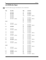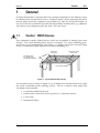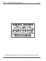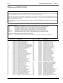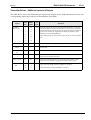
1
1
M800-00
T800 Series II
Ancillary Equipment
Service Manual
Issue 101
May 1998
M800-00-101
Copyright TEL
30/04/98
2
M800-00
France
Thailand
Tait France Sarl
2 Avenue de la Cristallerie
92 316 Sèvres, Cedex
France
Phone: 33 1 41 14-05-50
Fax: 33 1 41 14-05-55
Tait Mobile Radio Ltd
14/1 Suwan Tower
Ground Floor
Soi Saladaeng 1
North Sathorn Road
Bangrak
Bangkok 10500
Thailand
Phone: 662 267-6290-2
Fax: 662 267-6293
Germany
T800
Head Office
New Zealand
Tait Electronics Ltd
558 Wairakei Road
P.O. Box 1645
Christchurch
New Zealand
Phone: 64 3 358-3399
Fax: 64 3 358-3636
Tait Mobilfunk GmbH
Willstätterstraße 50
D-90449 Nürnberg 60
Germany
Phone: 49 911 96 746-0
Fax: 49 911 96 746-79
Hong Kong
Tait Mobile Radio (HK) Ltd
Room 703A
New East Ocean Centre
9, Science Museum Road
Tsim Sha Tsui East
Hong Kong
Phone: 852 2369-3040
Fax: 852 2369-3009
Radio Systems Division
535 Wairakei Road
P.O. Box 1645
Christchurch
New Zealand
Phone: 64 3 358-3399
Fax: 64 3 358-2825
New Zealand
Tait Communications Ltd
Unit 4, 75 Blenheim Road
P.O. Box 1185
Christchurch
Phone: 64 3 348-3301
Fax: 64 3 343-0558
United Kingdom
Tait Mobile Radio Ltd
Ermine Business Park
Ermine Road
Huntingdon
Cambridgeshire PE18 6YA
United Kingdom
Phone: 44 1480-52255
Fax: 44 1480-411996
USA
Tait Electronics (USA) Inc.
9434 Old Katy Road
Suite 110
Houston
Texas 77055
USA
Phone: 1 713 984-8684
Toll Free: 1 800 222-1255
Fax: 1 713 468-6944
Australia
Tait Electronics (Aust) Pty Ltd
186 Granite Street
Geebung Qld 4034
P.O. Box 679
Virginia
Queensland 4014
Australia
Phone: 61 7 3865-7799
Toll Free: 1800 077-112
Fax: 61 7 3865-7990
Canada
Tait Mobile Radio Inc.
Unit 5, 158 Anderson Avenue
Markham
Ontario L6E1A9
Canada
Phone: 1 905 472-1100
Toll Free: 1 800 890-8248
Fax: 1 905 472-5300
30/04/98
Singapore
Tait Electronics (Far East) Pte Ltd
4 Leng Kee Road
SIS Building #05-11A
Singapore 159088
Phone: 65 471-2688
Fax: 65 479-7778
Taiwan
Tait Electronics (Taiwan) Ltd
1104, No. 142 Chung Hsiao E. Rd
Sec. 4
Taipei
Taiwan
Phone: 886 2 731-1290
Fax: 886 2 711-6351
Copyright TEL
3
M800-00
About This Manual
Scope
This manual contains general, technical and servicing information on T800 Series II ancillary equipment.
Format
We have published this manual in a ring binder so that "revision
packages" containing additional information pertaining to new
issues of PCBs, or to additional ancillary equipment, can be
added as required.
Revision Packages
Revision packages will normally be published when an ancillary
equipment manual requires overhaul, or to coincide with the
release of information on a new PCB, and may also contain additions or corrections pertaining to other parts of the manual.
If you return the address card at the front of this manual, you
will be notified when revision packages containing new PCB
information and/or text are available. You may then order as
many packages as you require from your local Tait Company.
Revision packages are supplied ready-punched for inclusion in
your manual.
Revision Control
2
Each page in this manual has a date of issue. This is to comply
with various Quality Standards, but will also serve to identify
which pages have been updated and when. Each page and its
publication date is listed in the "List of Effective Pages", and a
new list containing any new/revised pages and their publication dates will be sent with each revision package.
Any portion of text that has been changed is marked by a vertical line (as shown at left) in the outer margin of the page. Where
the removal of an entire paragraph means there is no text left to
mark, an arrow (as shown at left) will appear in the outer margin. The number beside the arrow will indicate how many paragraphs have been deleted.
The manual issue and revision status are indicated by the last
three digits of the manual IPN. These digits start at 100 and will
increment through 101, 102, 103, etc., as revision packages are
published, e.g:
1 0 3
issue status
revision status
Thus, Issue 103 indicates the third revision to issue 1 and means
that three packages should have been added to the manual. The
issue digit will only change if there is a major product revision,
or if the number of revision packages to be included means that
the manual becomes difficult to use, at which point a new issue
manual will be published in a new ring binder.
PCB Information
Copyright TEL
PCB information is provided for all current issue PCBs, as well
as all previous issue PCBs manufactured in production quantities, and is grouped according to PCB. Thus, you will find the
30/04/98
4
M800-00
parts list, grid reference index (if necessary), PCB layouts and
circuit diagram(s) for each individual PCB grouped together.
Errors
If you find an error in this manual, or have a suggestion on how
it might be improved, please do not hesitate to contact the Technical Writer, Tait Radio Systems Division, Tait Electronics Ltd,
P.O. Box 1645, Christchurch, New Zealand.
Technical Information
Any enquiries regarding this manual or the equipment it describes should be addressed
in the first instance to your nearest approved Tait Dealer or Service Centre. Further
technical assistance may be obtained from the Customer Support Group, Radio Systems
Division, Tait Electronics Ltd, Christchurch, New Zealand.
Updating Equipment And Manuals
In the interests of improving performance, reliability or servicing, Tait Electronics Ltd
reserve the right to update their equipment and/or manuals without prior notice.
Copyright
All information contained in this manual is the property of Tait Electronics Ltd. All
rights are reserved. This manual may not, in whole or part, be copied, photocopied,
reproduced, translated stored or reduced to any electronic medium or machine readable
form without prior written permission from Tait Electronics Ltd.
Ordering Tait Service Manuals
Service Manuals should be ordered from your nearest Tait Branch or approved Dealer.
When ordering, quote the Tait Internal Part Number (IPN) and, where applicable, the
version.
Date Of Issue
IPN M800-00-101
T800 Series II Ancillary Equipment Service Manual
Issue 101 published April 1998
30/04/98
Copyright TEL
5
M800-00
Table Of Contents
This manual is divided into three parts as listed below, with each part being further subdivided into sections. There is a detailed table of contents at the start of each part
and/or section.
Part
Title
A
General Servicing Procedures
B
T807/808 Switching Power Supply
C
T800-22-0000 Base Station/Repeater Rack Frame
Copyright TEL
30/04/98
6
M800-00
List Of Effective Pages
The total number of pages in this Manual is 195, as listed below.
Page
Issue Date
Page
Issue Date
1
2
3
4
5
6
7
8
30/04/98
30/04/98
30/04/98
30/04/98
30/04/98
30/04/98
30/04/98
30/04/98 (blank)
1.6
1.7
1.8
1.9
1.10
31/08/96
31/08/96
31/08/96
31/08/96
31/08/96 (blank)
2.1
2.2
2.3
2.4
2.5
2.6
31/08/96
31/08/96 (blank)
31/08/96
31/08/96
31/08/96
31/08/96
3.1
3.2
3.3
3.4
3.5
3.6
3.7
3.8
3.9
3.10
31/08/96
31/08/96 (blank)
31/08/96
31/08/96
31/08/96
31/08/96
31/08/96
31/08/96
31/08/96
31/08/96 (blank)
4.1
4.2
4.3
4.4
4.5
4.6
31/08/96
31/08/96 (blank)
31/08/96
31/08/96
31/08/96
31/08/96 (blank)
5.1
5.2
5.3
5.4
31/08/96
31/08/96 (blank)
31/08/96
31/08/96
6.1
6.2
6.3
6.4
6.5
6.6
6.7
6.8
6.9
6.10
31/08/96
31/08/96 (blank)
31/08/96
31/08/96
31/08/96
31/08/96
31/08/96
31/08/96
31/08/96
31/08/96 (blank)
Part A
I
II
31/08/96
31/08/96 (blank)
1.1
1.2
31/08/96
31/08/96
2.1
2.2
31/08/96
31/08/96 (blank)
3.1
3.2
31/08/96
31/08/96
4.1
4.2
31/08/96
31/08/96 (blank)
5.1
5.2
5.3
5.4
31/03/98
31/03/98
31/03/98
31/03/98 (blank)
6.1
6.2
31/08/96
31/08/96 (blank)
Part B
I
II
31/08/96
31/08/96 (blank)
1.1
1.2
1.3
1.4
1.5
31/08/96
31/08/96 (blank)
31/08/96
31/08/96
31/08/96
30/04/98
Copyright TEL
7
M800-00
Page
Issue Date
Page
Issue Date
7.1
7.2
7.3
7.4
7.5
7.6
7.7
7.8
31/08/96
31/08/96 (blank)
31/08/96
31/08/96
31/08/96
31/08/96
31/08/96
31/08/96
8.1.1
8.1.2
8.1.3
8.1.4
31/08/96
31/08/96 (blank)
31/08/96
31/08/96
8.2.1
8.2.2
8.2.3
8.2.4
8.2.5
8.2.6
8.2.7
8.2.8
8.2.9
8.2.10
8.2.11
8.2.12
8.2.13
8.2.14
8.2.15
8.2.16
8.2.17
8.2.18
8.2.19
8.2.20
8.2.21
8.2.22
8.2.23
8.2.24
8.2.25
8.2.26
8.2.27
8.2.28
8.2.29
8.2.30
8.2.31
8.2.32
8.2.33
8.2.34
8.2.35
8.2.36
8.2.37
8.2.38
31/08/96
31/08/96
31/08/96
31/08/96
31/08/96
31/08/96
31/08/96
31/08/96
31/08/96
31/08/96
31/08/96
31/08/96
31/08/96
31/08/96
31/08/96
31/08/96
31/08/96
31/08/96
31/08/96
31/08/96
31/08/96
31/08/96
31/08/96
31/08/96
31/08/96
31/08/96
31/08/96
31/08/96
31/08/96
31/08/96
31/08/96
31/08/96
31/08/96
31/08/96
31/08/96
31/08/96
31/08/96
31/08/96
(fold-out)
(fold-out/blank)
8.2.39
8.2.40
8.2.41
8.2.42
8.2.43
8.2.44
8.2.45
8.2.46
8.2.47
8.2.48
8.2.49
8.2.50
8.2.51
8.2.52
8.2.53
8.2.54
8.2.55
8.2.56
8.2.57
8.2.58
8.2.59
8.2.60
31/08/96
31/08/96
31/08/96
31/08/96
30/11/97
31/08/96
31/08/96
30/11/97
31/08/96
31/08/96
30/11/97
31/08/96
31/08/96
31/08/96
31/08/96
31/08/96
31/08/96
31/08/96
31/08/96
31/08/96
31/08/96
31/08/96
(blank)
Part C
(fold-out)
(fold-out/blank)
I
II
30/04/98
30/04/98 (blank)
1.1
1.2
1.3
1.4
1.5
1.6
1.7
1.8
1.9
1.10
30/04/98
30/04/98 (blank)
30/04/98
30/04/98
30/04/98
30/04/98
30/04/98
30/04/98
30/04/98
30/04/98
2.1
2.2
2.3
2.4
2.5
2.6
2.7
2.8
2.9
2.10
30/04/98
30/04/98 (blank)
30/04/98
30/04/98
30/04/98
30/04/98
30/04/98
30/04/98
30/04/98
30/04/98 (blank)
Copyright TEL
(blank)
(blank)
(fold-out)
(fold-out)
(fold-out)
(fold-out/blank)
(blank)
(blank)
(fold-out)
(fold-out/blank)
(blank)
(fold-out)
(fold-out/blank)
(fold-out)
(fold-out)
(fold-out)
(fold-out/blank)
(blank)
(fold-out)
(fold-blank)
(blank)
(fold-out)
(fold-out/blank)
(fold-out)
(fold-out)
(fold-out)
(fold-out/blank)
30/04/98
8
M800-00
3.1.1
3.1.2
3.1.3
3.1.4
30/04/98
30/04/98 (blank)
30/04/98
30/04/98 (blank)
3.2.1
3.2.2
3.2.3
3.2.4
3.2.5
3.2.6
3.2.7
3.2.8
3.2.9
3.2.10
3.2.11
3.2.12
3.2.13
30/04/98
30/04/98
30/04/98
30/04/98
30/04/98
30/04/98
30/04/98
30/04/98
30/04/98
30/04/98
30/04/98
30/04/98
30/04/98
3.3.1
3.3.2
3.3.3
3.3.4
3.3.5
3.3.6
3.3.7
3.3.8
3.3.9
3.3.10
3.3.11
3.3.12
30/04/98
30/04/98
30/04/98
30/04/98
30/04/98
30/04/98
30/04/98
30/04/98
30/04/98
30/04/98
30/04/98
30/04/98
30/04/98
(blank)
(fold-out)
(fold-out)
(fold-out)
(blank)
(blank)
(fold-out)
(fold-out)
(fold-out)
(blank)
Copyright TEL
AI
M800-00
Part A
General Servicing Procedures
This part of the manual is divided into the sections listed below. These sections provide
some general and advisory information on servicing procedures, a brief history of T800
programming software, and a list of Technical Instructions pertaining to T830 Series
equipment.
Section
1
Title
Page
General
1.1
1.1
Caution: CMOS Devices
1.1
1.2
Caution: Beryllium Oxide & Power Transistors
1.2
Mechanical
2.1
2.1
Pozidriv Recess Head Screws
2.1
2.2
Disassembly/Reassembly
2.1
Component Replacement
3.1
3.1
3.1.1
3.1.2
Leaded Components
Desoldering Iron Method
Component Cutting Method
3.1
3.1
3.1
3.2
Surface Mount Devices
3.2
4
To Remove Cased Mica Capacitors
4.1
5
Software History
5.1
5.1
BASEPROG V1/PGM800 V2
5.1
5.2
PGM800 V2.01
5.1
5.3
PGM800 V2.21
5.2
5.4
PGM800Win V1.00
5.2
Technical Instructions
6.1
2
3
6
Figure
1.1
Copyright TEL
Title
Typical Anti-static Bench Set-up
Page
1.1
31/08/96
AII
31/08/96
M800-00
Copyright TEL
General
M800-00
1
A1.1
General
If further information is required about any ancillary equipment or this Manual, it may
be obtained from Tait Electronics Ltd or accredited agents. When requesting this information, please quote the equipment type number (e.g. T807-10) and serial number. In
the case of the Service Manual quote the Tait Internal Part Number (IPN), e.g. M800-00100, and for circuit diagrams quote the 'Title', 'IPN' and 'Issue'.
1.1
Caution: CMOS Devices
This equipment contains CMOS Devices which are susceptible to damage from static
charges. Care when handling these devices is essential. For correct handling procedures refer to the manufacturers' data books, e.g. Philips data books covering CMOS
devices, or Motorola CMOS data books, Section 5 'Handling', etc.
conductive
wrist strap
conductive rubber
bench mat
to building earth
(not mains earth)
via 1M series resistor
metal frame
Figure 1.1 Typical Antistatic Bench Set Up
An antistatic bench kit (refer to Figure 1.1) is available from Tait Electronics Ltd under
the usual consumable goods ordering system. The kit is held in stock under IPN
937-00000-34 and contains:
• 1 conductive rubber bench mat
• 1 earth lead to connect the mat to ground (c/w 1M series resistor)
• 1 wrist strap
• information leaflet.
Copyright TEL
31/08/96
A1.2
General
1.2
Caution: Beryllium Oxide & Power Transistors
M800-00
The power transistors in current use all contain some beryllium oxide. This substance,
while perfectly harmless in its normal solid form, can become a severe health hazard
when it has been reduced to dust. For this reason the power transistors should not be
broken open, mutilated, filed, machined, or physically damaged in any way that can
produce dust particles.
31/08/96
Copyright TEL
Mechanical
M800-00
2
Mechanical
2.1
Pozidriv Recess Head Screws
A2.1
Pozidriv recess head screws are the preferred standard on all Tait manufactured equipment. The very real advantages of this type of screw will not be realised unless the correct screwdrivers are used by servicing personnel.
2.2
Disassembly/Reassembly
Instructions on disassembly/reassembly for individual equipment are given in the relevant part of this manual.
Copyright TEL
31/08/96
A2.2
31/08/96
Mechanical
M800-00
Copyright TEL
Component Replacement
M800-00
3
Component Replacement
3.1
Leaded Components
A3.1
Whenever components are removed from or fitted to a PCB, care must be taken to avoid
damage to the track. The two satisfactory methods of removing components from PTH
PCBs are detailed below.
Note:
The first method requires the use of a desoldering station, e.g. Philips SBC
314 or Pace MBT-100E.
3.1.1
Desoldering Iron Method
Place the tip over the lead and, as the solder starts to melt, move the tip in a circular motion.
Start the suction and continue the movement until 3 or 4 circles have been completed.
Remove the tip while continuing suction to ensure that all solder is removed from
the joint, then stop the suction.
Before pulling the lead out, ensure it is not stuck to the plating.
If the lead is still not free, resolder the joint and try again.
Note:
The desoldering iron does not usually have enough heat to desolder leads
from the ground plane. Additional heat may be applied by holding a soldering iron on the tip of the desoldering iron (this may require some additional help).
3.1.2
Component Cutting Method
Cut the leads on the component side of the PCB.
Heat the solder joint sufficiently to allow easy removal of the lead by drawing it
out from the component side: do not use undue force.
Fill the hole with solder and then clear with solderwick.
Copyright TEL
31/08/96
A3.2
Component Replacement
3.2
Surface Mount Devices
Caution:
31/08/96
M800-00
Surface mount devices (SMDs) require special storage, handling,
removal and replacement techniques. This equipment should be serviced only by an approved Tait Dealer or Service Centre equipped with
the necessary facilities. Repairs attempted with incorrect equipment or
by untrained personnel may result in permanent damage. If in doubt,
contact Tait Electronics Ltd or your nearest Tait Branch or Subsidiary.
Copyright TEL
M800-00
4
To Remove Cased Mica Capacitors
A4.1
To Remove Cased Mica Capacitors
Cased mica capacitors can be removed by heating the top with a heavy-duty soldering
iron and gently lifting the capacitor off the PCB with a solder-resistant spike or equivalent.
Copyright TEL
31/08/96
A4.2
31/08/96
To Remove Cased Mica Capacitors
M800-00
Copyright TEL
Software History
M800-00
5
A5.1
Software History
23/11/89
23/08/90
11/06/91
03/10/95
28/06/96
18/08/97
5.1
BASEPROG Version 1
PGM800 Version 2
PGM800 Version 2.01
PGM800 Version 2.21
PGM800Win Version 1.00
PGM800Win Version 2.00
BASEPROG V1/PGM800 V2
T800 programming software was originally developed as BASEPROG V1 and released
as PGM800 V2.
5.2
PGM800 V2.01
The major changes introduced with V2.01 are as follows:
•
Full support for different display adaptors.
•
Programming of CTCSS frequency data (optional) for individual channels.
•
Full cursor control in edit mode.
•
User selectable output file format (hex or binary).
•
Support for wider range of T800 equipment.
•
DOS shell facility implemented.
•
CTCSS defeat possible when CTCSS tone is not selected.
•
Channel numbering changed from 0-127 to 1-128.
•
An "X" included on the printout to indicate that there are 8 switches on the DIP
switch and the state of the MSB is dependent on the size of the EPROM used.
Note:
Copyright TEL
The data files produced by BASEPROG V1.0 are still compatible with
PGM800 V2.01.
30/04/98
A5.2
Software History
5.3
PGM800 V2.21
M800-00
PGM800 V2.21 is an updated and expanded version of the earlier PGM800 V2.01 software.
PGM800 V2.21 includes many new and improved features over PGM800 V2.01. There
are a number of changes to the user interface to make data entry and editing significantly easier.
Major changes are outlined below:
•
Includes several new radio models which are not programmable with PGM800
V2.01.
•
Default file names with ‘dash’ are saved with ‘dash’ instead of ‘underscore’.
•
Default file extension in Save File page is BIN instead of HEX.
•
Out of range frequencies will result in warning messages, but will still be accepted
as valid entries.
•
Channel numbers are selectable between 0-127 and 1-128.
•
Automatic insertion feature to input frequencies.
Note:
The datafiles produced by BASEPROG V1.0 and PGM800 V2.01 are still
compatible with PGM800 V2.21.
5.4
PGM800Win V1.00
PGM800Win V1.00 is different in concept from DOS versions of PGM800 in that it is
WindowsTM driven. It includes many new and improved features over DOS versions of
PGM800.
Major changes are outlined below:
•
The Windows environment makes data entry and editing significantly easier.
•
Includes several new radio models which are not programmable with DOS versions of PGM800.
•
Out of range frequencies will result in warning messages and will not be accepted
for entry into the standard library module. User defined modules can be created
allowing variation from the standard library module.
•
Channel numbers default to 0-127 to match the EPROM memory locations, however the user can change the setting so that the channel numbers run from 1-128 to
suit his/her particular needs.
31/08/96
Copyright TEL
Software History
M800-00
A5.3
Note:
The datafiles produced by BASEPROG V1.0 and all DOS versions PGM800
are still compatible with PGM800Win V1.00.
5.5
PGM800Win v2.00
PGM800Win V2.00 is an upgraded and expanded version of PGM800Win V1.0. It has
been developed specifically for T800 Series II base stations but also has the capability of
programming Series I equipment.
Major changes are outlined below:
•
The Windows environment makes data entry and editing significantly easier.
•
Includes several new radio models which are not programmable with DOS versions of PGM800.
•
Out of range frequencies will result in warning messages and will not be accepted
for entry into the standard library module. User defined modules can be created,
allowing variation from the standard library module.
•
Channel numbers default to 0-127 to match the EPROM memory locations, however the user can change this setting so that the channel numbers run from 1-128
to suit his/her particular needs.
•
The ability to program T800 Series II base station modules via serial communications.
•
Deviation and reference modulation settings are written automatically to the
radio.
•
Extra information that is not stored in the radio (but is information relevant to the
radio) can be saved to a file on disk (e.g. note field, auxilliary pin names etc).
Note:
Copyright TEL
The datafiles produced by BASEPROG V1.0. all DOS versions of PGM800
and PGM800Win V1.0 are still compatible with PGM800Win V2.00.
30/04/98
A5.4
31/08/96
Software History
M800-00
Copyright TEL
Technical Instructions
M800-00
6
A6.1
Technical Instructions
From time to time Technical Instructions (TIs) are issued by the Radio Infrastructure
Engineering Division of Tait Electronics. These TIs may be used to update equipment or
information, or to meet specific operational requirements.
TIs applicable to specific T800 Series ancillary equipment are listed in the relevant part
of this manual.
Copyright TEL
31/08/96
A6.2
31/08/96
Technical Instructions
M800-00
Copyright TEL
BI
M800-00
Part B
T807/808 Switching Power Supply
This part of the manual is divided into eight sections, as listed below. There is a detailed
table of contents at the start of each section
The T807/808 has been manufactured with three different issues of PCB as
indicated by the last two digits of the IPN which will be -03, -05 or -07. The
information in this manual applies to all three issues of PCB unless otherwise stated in the text.
Note:
Section
Title
1
General Information
2
Circuit Operation
3
Introduction To Servicing
4
Initial Set-up & Adjustment
5
Functional Testing
6
Fault Finding
7
Installation
8
PCB Information
Copyright TEL
31/08/96
BII
31/08/96
M800-00
Copyright TEL
T807/808 General Information
M800-00
1
B1.1
T807/808 General Information
This section provides a brief description of the T807/808 Switch Mode Power Supply
along with detailed specifications
The following topics are covered in this section.
Section
Title
Page
1.1
Introduction
1.3
1.2
Specifications
1.4
1.2.1
Introduction
1.4
1.2.2
General
1.4
1.2.3
EMC Conformity
1.5
1.2.4
Safety Approvals
1.5
1.2.5
AC Mains Input
1.5
1.2.6
Output
1.6
1.2.7
Battery Charging Operation
1.8
Versions
1.9
1.3
Copyright TEL
31/08/96
B1.2
31/08/96
T807/808 General Information
M800-00
Copyright TEL
T807/808 General Information
M800-00
1.1
B1.3
Introduction
The T807/808 is a heavy duty, lightweight switching power supply capable of supplying up to 15A (T807) or 25A (T808) at 11 to 14V DC. The units require a mains supply of
230V/50Hz or 115V/60Hz (nominal values) which can be internally selected with a
switch (if fitted) or wire links. Remote sensing of the output voltage is available as a
standard feature: if connected, it will ensure that the output voltage remains within
±1% of the preset level from no-load to the full specified load, over the specified mains
voltage and temperature ranges (refer to Section 7.6).
The T807/808 power supply is designed to power T800 series base stations. Specifically,
the T807 will power 50W base stations, while the T808 will provide the current requirements for 100W base stations.
Electromagnetic compatibility (EMC) and operator safety are both important and critical parameters for the trouble free functioning of a switching power supply. Refer to
Section 1.2.3 (EMC) and Section 1.2.4 (safety) for current specifications.
The T807/808 is protected against damage caused by faults in the line or load, or by
temperature variations (refer to Section 1.2 for specifications). The protection features
include:
mains transient suppression
mains inrush current limiting
mains undervoltage lockout
soft start
output current limiting
output voltage limiting
output reverse polarity protection
overtemperature shutdown.
The output voltage and current limit and overvoltage points are all adjustable and are
preset during manufacture.
Note:
On earlier model power supplies with an issue 03 PCB, the overvoltage
point is not adjustable.
The T807/808 can be used to float charge a 12V battery under constant voltage conditions. The current limit circuit prevents the charging current from being excessive if the
battery is completely discharged, and the internal rectifier diode will blow the external
fuse in the event of the battery being accidentally connected in reverse. (refer to Section
7.5). An alarm output provides a logic 0 (0V) in the case of a mains and/or power supply failure, even if a battery is connected to the 13.8V output.
Note:
On issue 03, a transient suppression diode across the power supply output
prevents any damage if the battery is accidentally connected in reverse.
A T807/808 may be housed together with other Tait fixed equipment modules in a
standard 484mm (19") rack frame, where it occupies the space of one standard 60mm
module, to give an attractive and convenient installation.
Copyright TEL
31/08/96
B1.4
T807/808 General Information
1.2
Specifications
1.2.1
Introduction
M800-00
The performance figures given are minimum figures, unless otherwise indicated, for
equipment operating at standard room temperature (+22°C to +28°C).
Where applicable, the test methods used to obtain the following performance figures are
those described in the EIA specification. However, there are several parameters for
which performance according to the CEPT specification is given.
Details of test methods and the conditions which apply for Type Approval testing in all
countries can be obtained from Tait Electronics Ltd.
Three different issues of PCB are covered in this manual, as classified by the last two
digits of the IPN. Throughout this manual, differences in the specification or operation
of the various issues of power supply are identified using these digits.
1.2.2
General
Basic Power Supply Concept
.. switched mode technology pulse
width modulation
Switching Frequency
.. 166kHz typical
Overtemperature Protection
.. shuts down when main transformer
temperature rises above 105°C
Cooling:
T807
T808
.. convection
.. convection and forced air (fan)
Power On/Off Switch & LEDs:
On: Switching Enabled
Off: Switching Disabled
.. green "On" LED glows
.. red "Standby" LED glows
Other LEDs on Issues 05 and 07 only:
Overcurrent
Overvoltage
.. red “Overload” LED glows
.. green “On” and red “Overload” LEDs
flash on and off
To remove the mains voltage from the PCB, disconnect the IEC mains connector.
Note:
Efficiency:
T807
T808
31/08/96
.. 80%, 10-15A load typical
.. 80%, 15-25A load typical
Copyright TEL
T807/808 General Information
M800-00
B1.5
Temperature Range:
Operation Within Specification
Operational
.. -10°C to +60°C
.. down to -30°C
Isolation:
Input To Output
Input to Chassis/Earth
Output To Chassis/Earth
.. 3000V AC, 50Hz, 1 minute
.. 1500V AC, 50Hz, 1 minute
.. 500V AC, 50Hz, 1 minute
Dimensions:
Height
Width
Length
Weight
1.2.3
.. 191mm
.. 60mm
.. 330mm
.. 2.5kg
EMC Conformity
EMC
.. all equipment bearing the above logo
conforms with EEC EMC Directive
89/336 and is in accordance with the
requirements of ETS 300 279.
Note:
Refer to Section 3.1.6 for customer requirements in order to meet the above
emissions specification.
1.2.4
Safety Approvals
Safety
.. complies with IEC950, EN60950 &
AS3260
Note:
Refer to Section 3.1.7 for customer requirements in order to meet the above
safety specification.
1.2.5
AC Mains Input
Voltage
.. 200-264V or 100-135V, 50/60Hz
(selection by internal switch or wire
links)
Overvoltage
.. infrequent surges of up to 276V AC
and less than a few hours' duration
will not damage the T807/808
Copyright TEL
31/08/96
B1.6
T807/808 General Information
M800-00
Transient Suppression Threshold:
230V
115V
.. 276V AC
.. 140V AC
Undervoltage Lockout:
(no load to full load)
230V
115V
.. <185V AC, 175V AC typical
.. <95V AC, 90V AC typical
Input True RMS Current:
T807- 230V ±10%
115V ±10%
T808- 230V ±10%
115V ±10%
..
..
..
..
2.5A max.
4A max.
4A max.
6A max.
Input Fuse (Internal):
T807
T808
.. 5A slow blow
.. 8A slow blow
Connection
.. via IEC plug on rear panel
Power Factor @ Full Load
(exact factor depends on
impedance of mains supply)
.. >0.55
1.2.6
Output
Voltage
.. 13.8V DC (adjustable 11-14V)
Voltage Regulation
(remote sensing connected;
over specified load, temperature
and mains voltage range)
.. ±1%
Current
Continuous Operation Up To +40°C:
T807
T808
.. 0-15A DC
.. 0-25A DC
Continuous Operation Up To +60°C:
T807
T808
31/08/96
.. 0-12A DC
.. 0-22A DC
Copyright TEL
T807/808 General Information
M800-00
B1.7
Duty Cycle Operation Up To +60°C:
75% Tx (<30 minute period)
T807
T808
25% Rx (<30 minute period)
.. 15A DC
.. 25A DC
.. 1A DC
These current ratings apply to a typical remote sensing operation, i.e.13.8V
at the load terminals with <0.5V drop across the wiring from the power supply to the load.
Note:
Output Overvoltage Protection (Issue 03):
(zener transient suppression diode)
Voltage Threshold
Peak Power (1ms, 22.5V)
T807
T808
.. 16V ±5%
.. 600W
.. 1500W
This device is likely to short circuit if the peak power rating is exceeded and
will need to be replaced.
Note:
Output Overvoltage Protection (Issues 05 & 07):
(main rectifier diode)
Voltage Threshold
.. 15V ±2%
(15A (T807) or 25A (T808) at 240V
input)
17.8V
(Zero load at 200V input)
Output Hum & Noise:
(mains voltage 230V ±10%, TA = 25C
100/120Hz (@ max. rated load)
.. <20mV pp
<10mV RMS
Wide Band Noise (200Hz to 30MHz):
Load 0 To 1A
Load 1A To Full Load
.. <20mV pp
.. <10mV pp
Current Limit:
T807
T808
.. 16A
.. 27A
Mains And/Or Power Supply Failure
Alarm Output:
OK
Fail
Copyright TEL
.. +Vout (13.8V typ.) via 1k resistor
.. -Vout (0V) via 11k resistors
31/08/96
B1.8
T807/808 General Information
M800-00
Output Connectors:
Type
Flexible Wire Size
Current Rating
Insulation Stripping Length
..
..
..
..
screw clamp
0.5 to 4.0mm
36A
13mm
..
..
..
..
screw clamp
0.5 to 1.5mm
16A
10mm
Remote Sense & Fail Alarm Connectors:
Type
Flexible Wire Size
Current Rating
Insulation Stripping Length
1.2.7
Battery Charging Operation
Reverse Polarity Protection (Issue 03)
.. via internal zener transient suppression diode and external fuse
Reverse Polarity Protection (Issues 05 & 07) .. via internal main rectifier diode and
external fuse
Note 1:
For safe operation an external fuse must be fitted in the battery line.
Note 2:
The T807/808 does not compensate for the temperature dependence of the
battery.
Reverse Bleed Current
(mains and/or power supply off)
.. <5mA
Battery Type
.. constant voltage charging (e.g. conventional automotive lead acid)
31/08/96
Copyright TEL
T807/808 General Information
M800-00
B1.9
1.3
Versions
T807-10:
Switching power supply, 13.8V DC output 230/115V (50/60Hz) internally
selected mains inputs (factory set to 230V/50Hz) 15A continuously rated
power supply for 50W base stations
T808-10:
Switching power supply, 13.8V DC output 230/115V (50/60Hz) internally
selected mains inputs (factory set to 230V/50Hz) 25A continuously rated
power supply for 100W base stations
Copyright TEL
31/08/96
B1.10
31/08/96
T807/808 General Information
M800-00
Copyright TEL
T807/808 Circuit Operation
M800-00
2
B2.1
T807/808 Circuit Operation
This section provides a basic description of the circuit operation of the T807/808 Switch
Mode Power Supply.
The following topics are covered in this section.
Section
Title
Page
2.1
Introduction
2.3
2.2
Mains Input Circuitry
2.3
2.3
Undervoltage Lockout & Fan Control
2.3
2.4
Main Isolation Transformer T1, Snubbing Network & Output Rectifier
2.4
2.5
Output Filter & Minimum Load
2.4
2.6
Output Voltage Regulation & Switching Transistor Drive
2.4
2.7
Current Limit Circuitry
2.5
2.8
Output Overvoltage & Reverse Polarity Protection
2.5
2.8.1
Issue 05 & 07
2.5
2.8.2
Issue 03
2.5
2.9
Overtemperature Protection
2.6
2.10
Mains And/Or Power Supply Fail Alarm
2.6
2.11
Noise Modulator
2.6
2.11.1
Issue 05 & 07
2.6
2.11.2
Issue 03
2.6
Copyright TEL
31/08/96
B2.2
31/08/96
T807/808 Circuit Operation
M800-00
Copyright TEL
T807/808 Circuit Operation
M800-00
2.1
B2.3
Introduction
The Tait T807/808 switched mode power supply uses the well proven conventional
half-bridge, push-pull topology.
Regulation of the output voltage with varying mains input voltage and load conditions
is provided by pulse width modulation of power MOSFET transistors at the primary of
the main isolating transformer.
2.2
Mains Input Circuitry
When the mains supply is first connected to the unit, R3 will limit the maximum inrush
current to an acceptable level. The large filter capacitors (C9 to C12) at first show a very
low impedance, which would result in excessive inrush current without R3. Once the
supply has begun to function, RLY1 will switch, shorting out R3 and avoiding excessive
power dissipation in R3.
The incoming mains is filtered to remove noise and spikes, R2 and R49 providing protection against high voltage spikes that may be on the mains supply. In 230V mode, D1
to D4 act as a conventional bridge rectifier and C9 to C12 are the smoothing capacitors.
In 115V mode, D1 and D2 together with C9 to C12 form a conventional voltage doubler
circuit to provide the same overall DC voltage as in 230V mode. R4 and R7 serve to
equalise the voltage appearing across the series connected capacitors. C9 to C12 are
high temperature, high ripple current capacitors. C14 and C13 are low loss, high frequency capacitors and together with T1, Q1 and Q2 form a conventional half-bridge,
push-pull circuit, operating at 166kHz. D14, D15, D18 and D19 provide reverse voltage
protection for Q1 and Q2.
2.3
Undervoltage Lockout & Fan Control
R50 and D31 provide a 5.6V reference to the 2 comparators formed by IC3. IC3 (pins 1,
2 & 3) is a comparator that is configured with R5, R6, R8, R53 and R54 to detect low AC
input conditions. The values are such that for an AC input of 185V [95V] or less, the
comparator shuts down the main control circuitry via IC4 pin 10. R52 provides approximately 5V hysteresis to prevent on/off oscillations due to mains fluctuations caused by
loading when the supply turns on.
The purpose of the comparator formed by IC3 (pins 5, 6, & 7) and R55 is to prevent the
fan from being activated when the ambient temperature drops below -10C, as the bearings inside the fan become prone to excessive wear. R59 provides a few degrees of hysteresis.
Copyright TEL
31/08/96
B2.4
T807/808 Circuit Operation
2.4
Main Isolation Transformer T1, Snubbing Network &
Output Rectifier
M800-00
T1 provides the required isolation between input and output and its small size is due to
the high operating frequency and low loss ferrite core. This transformer is hi-pot tested
to 3750V to ensure compliance with the most stringent VDE safety regulations.
The main secondary winding is centre tapped, thus requiring only 2 diodes (D43) to
provide full-wave rectification, resulting in reduced power loss. R11, C15, R79, C66 and
C67 provide some high frequency snubbing. The effect of this snubbing is twofold:
firstly, it reduces high frequency spikes due to leakage inductance, and, secondly, it
shapes the load line, resulting in reduced switching losses within Q1 and Q2.
2.5
Output Filter & Minimum Load
T5, C68 to C73, C76 and C78 reduce the 166kHz ripple to an acceptable level, while C74,
C75, L6, C79, C80 and C81 reduce the level of higher frequency noise components.
Q9 switches in R81, R82 and RLY1 which serve as a minimum load to enhance stability.
Q9 is activated via D41 only when the supply is active. This ensures that R81, R82 and
RLY1 will not drain any back-up batteries that might be present on the supply output,
while the supply is switched off or the mains supply is interrupted.
2.6
Output Voltage Regulation & Switching Transistor
Drive
The output voltage is sampled via R84 and R83 (or SKT 7 if remote sense is used), fed to
IC8 (a programmable high stability zener diode), and the error voltage transmitted by
IC7 to the pulse width modulator IC (IC4). R91 to R96 and C86 to C89 form the stabilisation network which ensures good transient response and loop stability. IC4 contains
an oscillator whose frequency is determined by R71 and C59. R72 sets the dead time
between pulses to approximately 1s. IC4 modulates the width of the output pulses and
is buffered by the high current CMOS drivers, IC5 and IC6. The output from the buffers
feeds into T3 which provides the isolated and correctly phased drive to Q1 and Q2. R18
and R20 provide low resistance to the FET gates which, in their normal high impedance
states, are prone to spurious turn-on. R17 and R19 lower the Q of the gate drive circuitry in order to prevent excessive ringing which can otherwise cause the FETs to turn
on at the wrong time.
31/08/96
Copyright TEL
T807/808 Circuit Operation
M800-00
2.7
B2.5
Current Limit Circuitry
T2 is a current transformer and the current sampled is converted to voltage by R12. D5
to D8 rectify the sampled waveform which is then sent to a current limit comparator IC1
(pins 1, 2 & 3). This current limit is set at 10% above the normal load capability of the
supply. Comparator IC1 (pins 5, 6 & 7) is responsible for protecting the supply against
short circuit conditions and limits the short circuit current to a level that is safe for
extended periods (approximately 90% of output capability).
Note:
Issue 05 & 07. An indication of overcurrent and approaching overcurrent
is had by LED D23. This LED starts to glow approximately ½ Amp lower
than the current limit set point.
2.8
Output Overvoltage & Reverse Polarity Protection
2.8.1
Issue 05 & 07
Protection against reverse polarity situations is provided by D43, the main rectifier
diode. The supply has an overvoltage protection circuit based on sampling the AC voltage from T1. D38 detects this voltage and R40, 43, 45, C18 and 19 filter the waveform to
extract a voltage which is very nearly proportional to the output voltage of the power
supply. The voltage is compared to a presettable reference by IC1 (pins 1, 2 & 3). If the
sampled voltage is higher than the reference, IC1 outputs a high to trigger the shutdown
circuitry. Overvoltage is indicated by both “On” and “Overload” LEDs flashing on and
off. Overvoltage can be caused by a failure in the remote sense circuitry outside of the
power supply.
2.8.2
Issue 03
Protection against reverse polarity situations is provided by D46, a special high energy
diode that reacts instantly to overvoltage DC or spikes. If an overvoltage condition persists which may cause excessive power dissipation, D46 will become short circuit and
will need to be replaced before proper operation of the power supply can resume. D46
also provides some level of protection against reverse polarity connection, as it also acts
as a normal diode. The level of protection afforded by D46 is only a "first level"
approach, in that it protects mainly the supply itself. As protection is very dependent
on system configurations, further protection should be determined and implemented by
the system engineer (refer also to Section 7).
Copyright TEL
31/08/96
B2.6
T807/808 Circuit Operation
2.9
Overtemperature Protection
M800-00
Protection against overheating is provided by thermal cut-out TC1. Should the temperature of the main transformer (T1) rise to an unsafe level, TC1 will interrupt the supply
voltage to the control circuitry and the supply will shut down. There is some hysteresis
in TC1 and only after the temperature has dropped by approximately 5°C will it restore
power to the control circuitry, thus restoring normal operation.
2.10
Mains And/or Power Supply Fail Alarm
In the case of a mains and/or power supply failure, a "logic 0" (0V) is available at the
"Mains/PS Fail Alarm" output, even with a battery connected across the main DC output.
If there is no fault with the mains or power supply, the main DC output voltage (typ.
+13.8V) is supplied to this alarm output via Q8 and R99.
2.11
Noise Modulator
2.11.1
Issue 05 & 07
Q11 and Q12 form the white noise circuit and are further amplified/buffered by Q13.
The noise modulates the frequency of oscillation of IC4, the switched mode control IC.
The purpose of the noise modulator is to spread the discrete harmonic frequencies
energy of the switching circuits over a wide bandwidth so that possible interference is
minimised. This results in an overall reduction in noise of approximately 10dB.
2.11.2
Issue 03
A noise modulator PCB is available as an add-on for Issue 03 PCBs, under IPN 22001268-00. This solders on to TP4 and works as described above.
31/08/96
Copyright TEL
T807/808 Introduction To Servicing
M800-00
3
B3.1
T807/808 Introduction To Servicing
This section provides specific information on servicing procedures for the T807/808 and
should be read in conjunction with Part A (General Servicing Procedures) of this manual.
The following topics are covered in this section.
Section
3.1
Title
Page
General
3.3
3.1.1
Warning: Lethal Voltages
3.3
3.1.2
Caution: Ventilation
3.3
3.1.3
Caution: Replacing Components Connected To The Mains
3.3
3.1.4
Caution: Handle With Care
3.4
3.1.5
Caution: Heatsink/Case Temperature
3.4
3.1.6
Caution: Earthing Of Rack Frame
3.4
3.1.7
Caution: Cabinet Requirements To Meet Safety Specifications
3.4
Mechanical
3.5
3.2.1
Construction
3.5
3.2.2
Disassembly Instructions
3.5
3.2.2.1
To Gain Access To The Component Side Of The PCB
3.5
3.2.2.2
To Gain Access To The Solder Side Of The PCB
3.5
3.2.3
Reassembly Instructions
3.6
3.2.4
Screw Torques
3.6
Component Replacement
3.7
3.3.1
Critical Components
3.7
3.3.2
To Replace The Power MOSFET Transistors (Q1 & Q2)
3.7
3.3.3
To Replace The Output Rectifier (D43)
3.8
Technical Instructions
3.9
3.2
3.3
3.4
Copyright TEL
31/08/96
B3.2
31/08/96
T807/808 Introduction To Servicing
M800-00
Copyright TEL
T807/808 Introduction To Servicing
M800-00
3.1
B3.3
General
If you require further information about the T807/808 or this manual, contact your
nearest authorised Tait Dealer or Service Centre. Further assistance may be obtained
from the Customer Support Group, Radio Infrastructure Division, Tait Electronics Ltd,
Christchurch, New Zealand.
When requesting this information, please quote the equipment type number (e.g.
T807-10) and serial number. In the case of the service manual quote the Tait Internal
Part Number (IPN), e.g. M800-00-100, and for circuit diagrams quote the “Title”, “IPN”
and “Issue”.
3.1.1
Warning: Lethal Voltages
The T807/808 power supply contains voltages that may be lethal.
Disconnect the mains IEC connector and wait for 5 minutes for the internal voltages to
drain away before dismantling.
The power on/off switch does not isolate the power supply from the mains. It disables
(or enables) only the switching control circuitry, i.e. output power on/off.
Servicing should be carried out only by qualified technicians and should be attempted
only when powered through a mains isolating transformer of sufficient rating. It is
strongly recommended that the mains supply to the whole of the repair and test area is
supplied via an earth leakage circuit breaker.
3.1.2
Caution: Ventilation
Always ensure there is adequate ventilation around this unit and do not operate it in a
sealed cabinet. The MTBF will decrease if the airflow is blocked. As a rule of thumb the
life expectancy of this unit will approximately halve with every 10°C rise in temperature.
It is therefore recommended to:
keep the ambient temperature low
ensure that airflow is not restricted.
3.1.3
Caution: Replacing Components Connected To The Mains
To maintain operator safety and protection against fire, it is imperative that components
connected to the mains supply (e.g. fuse, X & Y capacitors, filter chokes, etc.) and those
that are critical to maintain isolation (optocouplers, transformers, etc.) are replaced only
with their new, original equivalent.
To maintain performance levels it is strongly recommended that this policy is applied to
every component that is replaced.
Copyright TEL
31/08/96
B3.4
T807/808 Introduction To Servicing
3.1.4
Caution: Handle With Care
M800-00
Although this is a lightweight unit, it contains a number of quite heavy and fragile individual components which are mounted directly on the PCB. Severe mechanical shock
may damage the PCB (i.e. solder joints, copper tracks) and/or components (i.e. fragile
ferrite magnetic materials).
3.1.5
Caution: Heatsink/Case Temperature
The 2 covers of this power supply act as heatsinks for the internal power semi- conductors. Under some conditions the top and bottom sections of these covers and internal
heatsinks may reach temperatures of over 100C. Handle with extreme care after prolonged operation.
3.1.6
Caution: Earthing Of Rack Frame
The power supply case is internally connected to mains earth. Because the unit's case
and the rack frame in which it is usually installed are painted, a secure electrical earthing connection between the unit and the rack is not guaranteed (i.e. it is reliant on
breaking through the paint coating).
It is therefore strongly advised that an additional and secure electrical connection is provided by means of the supplied earth lead (refer to Section 7.2). Failure to do so may
result in harmful voltage potentials between the power supply and rack frame, and/or
miscellaneous power supply switching noise problems in both receivers and transmitters.
Note:
Failure to comply with the above instruction may result in the power supply
falling short of the emissions requirements of ETS 300-279.
3.1.7
Caution: Cabinet Requirements To Meet Safety Specifications
In order to meet stringent safety obligations, it is imperative that the power supply is
mounted in a cabinet which meets the requirements of IEC950. Specifically the top and
sides of the cabinet must comply with one of the following:
holes must not exceed 5mm in any dimension, or
holes must not exceed 1mm in width regardless of length, or
side panels must be provided with louvres that are shaped to deflect outwards an
external vertically falling object, or
tops must be so constructed that direct, vertical entry of a falling object is
prevented from reaching bare parts by means of a trap or restriction.
Additionally, for units mounted in a slimline configuration, the bottom of the cabinet
must be constructed so as to contain any material emitted from the unit under fault conditions which could ignite the supporting surface. If in doubt, refer to IEC950 or
your nearest approved Tait Dealer or Service Centre.
31/08/96
Copyright TEL
T807/808 Introduction To Servicing
M800-00
3.2
Mechanical
3.2.1
Construction
B3.5
All electrical components (except the fan in the T808) are mounted on and soldered to a
single large PCB. This PCB is mounted onto 2 identical extruded aluminium bars which
provide heatsinking for the power semiconductors, as well as mechanical support for
the whole power supply. Both front and rear panels are attached to these extrusions.
Two identical vented covers on either side of the PCB assembly complete the simple but
effective power supply packaging.
The mechanical construction of the T807/808 provides heatsinking, EMI shielding and
user protection, and is also designed for ease of servicing and mounting.
3.2.2
Disassembly Instructions
Warning:
3.2.2.1
Observe the precautions regarding lethal voltages outlined in Section
3.1 of this Manual before disassembling this unit.
To Gain Access To The Component Side Of The PCB
This will give access to the fuse, 115V/230V switch or links and the output adjust trim
pots.
Remove the 2 guide rail screws at the rear of the right hand cover (top and bottom).
Remove the 8 countersunk screws holding the right hand cover onto the extruded
rails (as viewed from the front of the unit).
Remove the right cover.
3.2.2.2
To Gain Access To The Solder Side Of The PCB
Remove the 2 guide rail screws at the rear of the left hand cover (top and bottom).
Remove the 8 countersunk screws holding the left hand cover onto the extruded
rails (as viewed from the front of the unit).
Remove the left cover.
Copyright TEL
31/08/96
B3.6
T807/808 Introduction To Servicing
3.2.3
Reassembly Instructions
M800-00
Refit the left and right covers in the reverse order to which they were removed.
Ensure that the heat transfer surfaces are clean and add new heatsink compound
if necessary.
Power devices Q1, Q2 and D43 must be mounted correctly and electrically isolated from their respective heatsinks (see Section 3.3).
Replace the covers and tighten the screws to the correct torque.
3.2.4
Screw Torques
It is important to tighten the cover securing screws to the correct torque to ensure that
the T807/808 maintains its specified performance.
We recommend the following torque settings:
Cover Screws
PCB To Rails
Power MOSFET Transistors (Q1 & Q2)
Output Rectifier (D43)
Front/Rear Panels and Guide Screws
31/08/96
..
..
..
..
..
8 - 10lb-in./0.88 - 1.1Nm
8 - 10lb-in./0.88 - 1.1Nm
8 - 10lb-in./0.88 - 1.1Nm
4 - 6lb-in/0.44 - 0.66Nm
4 - 5lb-in/0.44 - 0.55Nm
Copyright TEL
T807/808 Introduction To Servicing
M800-00
3.3
Component Replacement
3.3.1
Critical Components
B3.7
The components in the control loop stabilisation part of the circuit are critical in both
value and type. Ensure that only exact equivalents are used for repair.
The components connected to the mains input and/or labelled "X" or "Y" are special
components complying with safety regulations and should be replaced only with similarly specified parts to ensure continued safety protection (refer to Section 3.1.5).
3.3.2
To Replace The Power Mosfet Transistors (Q1 & Q2)
Remove the transistor clamping bar and devices, taking care not to damage the
film insulator.
Reassemble the new MOSFET transistors with an undamaged or new thermal
film insulator and new thermal compound, using the clamping bar, M3x25 countersunk pozidrive screw and nut.
Ensure that transistors Q1 and Q2 are assembled correctly with adequate thermal
compound and are both seated straight and square. Check for unevenness and
burrs on the mounting surfaces - the thermal insulator is only 0.05mm (2 mil/
0.002") thick so it is very important that the mounting surfaces are clean.
Tighten the screw and nut to the correct torque.
Trim the legs of the transistors and solder.
Note 1:
Always replace both Q1 and Q2, as well as D14, D15, D18 and D19. Even
when only one of the transistors seems to be faulty, it is very likely that both
transistors and all 4 diodes are also faulty or damaged.
Note 2:
After any significant repair work it is recommended that the further fault
finding and run-up procedure outlined in Section 6.4 is carried out before
the unit is reconnected to the mains supply.
Copyright TEL
31/08/96
B3.8
T807/808 Introduction To Servicing
3.3.3
To Replace The Output Rectifier (D43)
M800-00
Remove the rectifier, taking care not to damage the insulating gasket.
Attach a new rectifier complete with undamaged or new top hat (T807 only) and
thermal film insulator, using the M3x16 countersunk pozidrive screw, spring
washer and nut.
D43 is a thermally highly stressed component and incorrect assembly will result
in a significant reduction in component life.
Tighten the screw and nut to the correct torque (refer to Section 3.2.2).
Trim the legs of the rectifier and solder.
Note:
31/08/96
After any significant repair work it is recommended that the further fault
finding and run-up procedure outlined in Section 6.4 is carried out before
the unit is reconnected to the mains supply.
Copyright TEL
M800-00
3.4
T807/808 Introduction To Servicing
B3.9
Technical Instructions
From time to time Technical Instructions (TIs) are issued by the Radio Infrastructure
Engineering Division of Tait Electronics. These TIs may be used to update equipment or
information, or to meet specific operational requirements.
Printed below is a list of TIs applicable to the T807/808. You may wish to file a copy of
each TI in this Section for your own reference.
TI No.
Title
Date
358
T807/808 remote sensing of output voltage
10/06/91
365
T807/808 improved earthing for noise interference suppression
29/07/91
Copyright TEL
31/08/96
B3.10
31/08/96
T807/808 Introduction To Servicing
M800-00
Copyright TEL
T807/808 Initial Set-up & Adjustment
M800-00
4
B4.1
T807/808 Initial Set-up & Adjustment
The following section describes the initial set-up and adjustment procedures.
The following topics are covered in this section.
Section
Title
Page
4.1
Introduction
4.3
4.2
Test Equipment Required
4.3
4.3
Adjustments
4.4
4.3.1
Mains Input Voltage
4.4
4.3.2
Output Voltage Adjustment
4.5
4.3.3
Current Limit Adjustment
4.5
4.3.4
Overvoltage Cut-out Adjustment (Issues 05 & 07 Only)
4.5
Figure
4.1
Copyright TEL
Title
Test Equipment Set Up
Page
4.4
31/08/96
B4.2
31/08/96
T807/808 Initial Set-up & Adjustment
M800-00
Copyright TEL
T807/808 Initial Set-up & Adjustment
M800-00
4.1
B4.3
Introduction
Warning:
The T807/808 contains voltages that may be lethal and extreme care
must be taken when working on a "powered up" supply.
Caution:
During set-up and adjustment it is essential that the T807/808 is connected to the mains supply via an isolating transformer. For additional
protection the test set-up should be powered via an earth leakage circuit breaker.
Caution:
Connecting test equipment earths to a T807/808 which is not supplied
via an isolating transformer will connect the mains supply directly
across R3 & D1 and result in the destruction of R3.
Caution:
While the oscilloscope earth is connected to the DC primary negative
rail (TP4), the T807/808 is no longer isolated from the mains earth and
neutral. Extreme care is necessary when working on the power supply.
Disconnect the oscilloscope immediately after use.
4.2
Test Equipment Required
Item
Capability
Earth leakage circuit breaker
10A min., 115 or 230V, trip current <30mA.
Mains isolating transformer
1kVA min.
Variac
1kVA min., 0-260V AC (0-130V AC).
AC current meter
true RMS readings, range to 10A FSD.
AC voltmeter
ranges to 300V FSD.
DC current meter
0-30A FSD.
Variable DC load
0-100 ohm, 20A, 250W for T807
0-100 ohm, 30A, 400W for T808
*DC power supply
0-18V, 1A
*DC power supply
0-15V, 1A
Oscilloscope
20MHz, general purpose, good quality
*Oscilloscope probes
capable of handling 500V signals
*Required for Fault Finding only (Section 6).
Copyright TEL
31/08/96
B4.4
T807/808 Initial Set-up & Adjustment
4.3
Adjustments
M800-00
The T807/808 mains input voltage is factory set to 230V (±10%)/50Hz and the output
voltage to 13.8V DC. The current limit is adjusted to 16A (T807) or 27A (T808).
When adjusting the output voltage and current limit, set up the test equipment as
shown in Figure 4.1.
Oscilloscope
PS1
0-18V DC
1 Amp
V
_
Output Isolated From Earth
Isolating
Transformer
1kVA
Variac
0-260V AC
1kVA
Earth
Leakage
Circuit
Breaker
Mains
Supply
V
_
A
_
+
DC Load
0-30 Amp DC
D30
TP4
AC
Input
A
_*
!
Output
+
-
V
_
A
_
Remote +
Sense -
* True RMS Reading
T807/808 PSU
PS2
-
V
_
A
_
0-15V DC
1 Amp
+
Output Isolated
From Earth
Figure 4.1 Test Equipment Set Up
4.3.1
Mains Input Voltage
The mains input voltage can be set to either 230V (200-264V) or 115V (100-135V) by
either SW1 or by wire links on the PCB.
Disconnect the mains supply.
Set SW1 (where fitted) to the required input voltage - SW1 can be accessed
through the cooling slots on top of the right side cover.
If SW1 is not fitted, remove the left and right side covers (refer to Section 3.2.3).
Change over the PCB links as indicated on the PCB encoding and refit the covers.
Remove or fit the supplied label on the rear panel to indicate clearly the mains
input voltage to which the unit has been set.
31/08/96
Copyright TEL
T807/808 Initial Set-up & Adjustment
M800-00
4.3.2
B4.5
Output Voltage Adjustment
Remove the right cover.
Switch the T807/808 on.
Adjust the "V/OUT SET" trim control (RV92) to produce the required output voltage, observing the limits given in Section 1.2.4.
Note:
Connection of the remote sense terminals after the output voltage has
been set will result in a slight change in the nominal output voltage (by
approx. 0.3V). The remote sense option should be fitted before setting the
output voltage (refer to Section 7.6).
4.3.3
Current Limit Adjustment
Turn the "CURRENT LIMIT SET" control (RV25) fully clockwise.
Switch the T807/808 on and set the variable DC load for a current just above the
maximum desired current (observing the limits in Section 1.2.4).
Adjust RV25 until the voltage across the DC load just starts to drop.
4.3.4
Overvoltage Cut-out Adjustment (Issues 05 & 07 Only)
Set the mains input voltage to 240V (nominal) with a 15A (T807) or 25A (T808)
load connected.
Adjust RV92 to give 15V output from the PSU.
Adjust RV81 slowly for power supply cut-out (“On” LED and “Overload” LED
will flash on and off).
Reset RV92 to give 13.8V output from the PSU.
Copyright TEL
31/08/96
B4.6
31/08/96
T807/808 Initial Set-up & Adjustment
M800-00
Copyright TEL
T807/808 Functional Testing
M800-00
5
B5.1
T807/808 Functional Testing
The following test procedures will confirm that the T807/808 has been set up and
adjusted correctly and is fully operational.
Refer to Figure 4.1 for test equipment details.
The following topics are covered in this section.
Section
Title
Page
5.1
Basic Operation
5.3
5.2
Undervoltage Lockout & Mains Input Current
5.3
5.3
Output Noise
5.4
5.4
Overall Power Supply Stability
5.4
Copyright TEL
31/08/96
B5.2
31/08/96
T807/808 Functional Testing
M800-00
Copyright TEL
T807/808 Functional Testing
M800-00
5.1
B5.3
Basic Operation
To confirm the basic operation of the power supply, proceed as follows.
Set up the test equipment as shown in Figure 4.1.
Ensure the front panel "Power" switch in the off position. Connect the T807/808
to the mains supply. The red "Standby" LED should illuminate.
Set the output DC load to maximum resistance/minimum current.
Depress the "Power" switch to turn the T807/808 on. The green "On" LED should
now illuminate and the red "Standby" LED should extinguish.
Vary the DC load and check that the output voltage and current are within the
specifications (refer to Section 1.2.4).
5.2
Undervoltage Lockout & Mains Input Current
The figures in brackets [ ] are for 115V/60Hz versions of the T807/808.
Ensure the T807/808 "Power" switch is in the off position.
Set up the test equipment (except PS1 & PS2) as shown in Figure 4.1.
Switch on the mains supply and adjust the Variac for 230V or 115V output.
Switch the T807/808 on and set the DC load for maximum current (T807/15A;
T808/25A).
Slowly reduce the Variac voltage from 230V [115V] until "drop-out" occurs (output
current and voltage drop to zero and LED's turn off).
Check that the AC input current and voltage at "drop-out" are as follows:
input current
voltage
T807: <2.5A [<4A]
T808: <4A [<6A]
<185V [<95V]
Slowly increase the Variac voltage and check that the supply turns on again at
approximately 10V [5V] above "drop-out" voltage.
Note:
Copyright TEL
Some on/off oscillation may occur around this voltage point, particularly
with a relatively high mains impedance (Variac, mains transformer, etc.)
and the power supply load being set to maximum current. Increasing the
mains supply by a few volts should turn the supply fully on.
31/08/96
B5.4
T807/808 Functional Testing
5.3
Output Noise
M800-00
Set up the test equipment (except PS1 & PS2) as shown in Figure 4.1.
Connect a digital voltmeter (e.g. Fluke 77) across the load terminals and set the
meter to its lowest AC volts range.
Check that the reading is <10mV AC for both the T807 and T808 under all load
and line conditions.
Note:
A real reading of the level of noise present on the output of a switching
power supply is very difficult to obtain, as low noise levels, common mode
noise paths and ground loops all lead to inaccurate measurement results.
The procedure outlined above will, however, give a good indication of the
output noise.
5.4
Overall Power Supply Stability
Connect the oscilloscope across the output.
Vary the mains voltage and DC load over the full specified range (refer to Section
1.2).
Check on the oscilloscope that no oscillations occur.
Check that no audible noise can be detected, except with open and/or short circuit loading on the output.
31/08/96
Copyright TEL
T807/808 Fault Finding
M800-00
6
B6.1
T807/808 Fault Finding
The following test procedures and fault finding flow charts may be used to help locate a
hardware problem, however they are by no means a complete fault finding procedure.
If the fault still exists after having progressed through them in a logical manner, contact
your nearest authorised Tait Dealer or Service Centre. Further assistance may be
obtained from the Customer Support Group, Radio Infrastructure Division, Tait Electronics Ltd, Christchurch, New Zealand.
The following topics are covered in this section.
Section
Title
Page
6.1
Visual Checks
6.3
6.2
Component Checks
6.3
6.2.1
General
6.3
6.2.2
Initial Checks
6.4
6.3
Common Faults
6.4
6.4
Further Fault Finding & Run-Up Procedure
6.5
6.4.1
Voltage Control Loop Checks
6.5
6.4.2
Start Up Voltage Checks
6.7
6.4.3
Current Limit Checks
6.8
Figure
Title
Page
6.1
TP6 &TP7 Voltage Waveforms
6.6
6.2
Voltage Waveform Noise Jitter
6.6
Copyright TEL
31/08/96
B6.2
31/08/96
T807/808 Fault Finding
M800-00
Copyright TEL
T807/808 Fault Finding
M800-00
6.1
B6.3
Visual Checks
Disconnect the power supply from the mains and wait 5 minutes before removing both
covers.
Inspect the PCB for damaged or broken components, paying particular attention to the
surface mounted devices (SMD's).
Check for defective solder joints. If repair or replacement is considered necessary, refer
to Section 3 of Part A.
Check the fuse. If it is blown, check that the correct rating and type was fitted and fit a
new fuse of the correct rating.
Note:
If the fuse was of a lower rating and there are no signs of component damage, it may be worthwhile fitting a new fuse, replacing the covers and
switching the supply on. If the new fuse blows, proceed with fault finding
as described in the following sections.
6.2
Component Checks
6.2.1
General
If a transistor is suspected of faulty operation, an indication of its performance can be
assessed by measuring the forward and reverse resistance of the junctions. First make
sure that the transistor is not shunted by some circuit resistance (unless the device is
completely desoldered). A 20k ohm/V or better multimeter should be used for taking
the measurements, using only the medium or low resistance ranges.
The collector current drawn by multijunction transistors is a further guide to their performance.
If an IC is suspect, the most reliable check is to measure the DC operating voltages. Due
to the catastrophic nature of most IC failures, the pin voltages will usually be markedly
different from the recommended values in the presence of a fault. The recommended
values can be obtained from either the circuit diagram or the component data catalogue.
Copyright TEL
31/08/96
B6.4
T807/808 Fault Finding
6.2.2
Initial Checks
M800-00
Some components are more likely to be at fault than others and it is recommended that
the following are checked first:
D46 (Issue 03)
If short circuited, replace and confirm with a DVM that the impedance
on the output terminals is >1k ohm.
Q1 & Q2
Check for shorts between any 2 terminals. If either device is faulty,
replace both along with D14, D15, D18 and D19.
Also check R17 and R19 - these will often go faulty along with Q1 or
Q2, sometimes with no external indication.
Q1, Q2 & D43
Check and confirm that they are isolated from their respective heatsinks.
R2 & R49
Check their resistance is >1M ohm.
R3
Check and replace if the resistance is >15 ohms.
IC2
Check by applying 20V DC across C37 and measuring for 15V at TP5.
If no voltage is present at TP5, measure at IC2 pin 3. If there is still no
voltage, replace IC2. If 15V is present, check TC1 connections.
Replace if in doubt.
VREF
Check VREF is 5.1V +_1%.
6.3
Common Faults
Switch the T807/808 off, and then on, and check for the following faults:
Symptoms
Possible Causes
No LED's light up
No output
no mains supply
low mains supply voltage*
thermal cut-out has operated
(equipment has overheated)*
fuse blown
defective switching circuitry
On standby red "Standby"
LED lights up, but no output
and no LED's light up when
power switch set to on
defective switching circuitry
Red "Standby" LED lights up
Green "on" LED lights up
but no output when power
switch set to on
short circuit across output
overvoltage protection diode has gone short circuit#
defective power supply output section
*The fan in the T808 will continue to run.
#Issue 03 only.
31/08/96
Copyright TEL
T807/808 Fault Finding
M800-00
6.4
B6.5
Further Fault Finding & Run-up Procedure
Warning:
The T807/808 is not a conventional power supply and the potential for
lethal accidents is very real.
It is imperative that the following procedures are followed precisely
and under no circumstances must any short cuts be taken.
These procedures have been carefully designed to minimise the danger
to service personnel and deviation from them will only compromise
the safety of all concerned.
Wear safety goggles while running up or working in close proximity to
the T807/808.
Because of the dangers involving off-line power supplies, it is suggested that the following procedures are followed, both after repairs have been carried out and for further
fault finding. These procedures should be carried out only by suitably qualified personnel.
Refer to Figure 4.1 for test equipment details, paying particular attention to the cau-
tions listed in Chapter 4.1.
Note:
The figures in brackets [ ] refer to 115V/60Hz versions of the T807/808.
6.4.1
Voltage Control Loop Checks
Ensure that the mains input supply is disconnected from the T807/808 (hereafter
referred to as the "PSU") and the "Power" switch is set to off.
Apply 15V from an external power supply (PS1) to the anode of D30 (+) and TP4
(-).
Check that the red "Standby" LED is on.
Check on the T808 that the fan is running.
Switch the PSU on and check that it does not draw excessive current (<400mA)
from PS1.
The red "Standby" LED should turn off.
Check that the voltage on pin 1 of IC3 is <0.5V.
If the voltage is high (approximately 15V), momentarily increase the PS1 voltage
to 18V and then reduce it to 15V. If the voltage at pin 1 is still high, check for circuit faults.
Copyright TEL
31/08/96
B6.6
T807/808 Fault Finding
M800-00
Using an oscilloscope with the probe ground connected to TP4, check the voltage
waveform at TP6 and TP7 is as shown in Figure 6.1.
5.5-6.5µs
TP6
15V
TP7
15V
Figure 6.1 TP6 & TP7 Voltage Waveforms
Voltage spikes on the above waveforms are shown for a T807. These spikes
appear with larger magnitude on a T808.
Note:
Switch the PSU off and on, confirming that the waveform's duty cycle starts at 0
and slowly increases to 50%.
Check that after a short delay (approx. 0.25 seconds), the waveform shows signs
of noise jitter (refer to Figure 6.2). This jitter indicates that the noise modulator is
operating satisfactorily.
Figure 6.2 Voltage Waveform Noise Jitter
Connect a second variable power supply (PS2) to the remote sense terminals of
the PSU.
Issues 05 & 07 Only. Turn RV81 fully clockwise.
Note:
Turn RV92 fully clockwise and, whilst observing the waveform at TP6 or TP7,
slowly increase the voltage.
Check that at approximately 10-11V the waveform suddenly reduces in duty cycle
and disappears altogether.
Turn RV92 anticlockwise and check that the waveform reappears.
Turn RV92 fully anticlockwise and increase the voltage until the waveform disappears. At this point the voltage should not exceed 16.5V. Reducing the voltage
should always make the waveform reappear.
31/08/96
Copyright TEL
T807/808 Fault Finding
M800-00
B6.7
Turn RV92 fully clockwise.
This confirms the basic operation of the voltage control loop. Remove the second variable power supply from the PSU remote sense terminals and disconnect the oscilloscope
(refer to Note 1 on page 6.5).
6.4.2
Start Up Voltage Checks
Ensure the switch (or link) is set to the correct mains voltage.
Turn RV25 fully clockwise.
Connect the Variac output (set to minimum output voltage) to the PSU AC input
socket.
Increase the Variac output slowly whilst monitoring the AC current which should
remain low at this point.
Continue increasing the voltage to approximately 60V AC [30V AC].
Check that approximately 3V is now present at the PSU output and that the "On"
LED is glowing.
Check with a multimeter that the DC voltage between TP1 and TP4 is approximately 80V and between TP2 and TP4 is half of that figure ±5V.
If the voltage difference is outside tolerance, disconnect the Variac from the
PSU, wait for the voltages to drain away, and inspect the circuitry for
the cause.
Note:
Warning:
Do not proceed until the cause is found, rectified and satisfactory
results obtained.
High voltages and therefore high energies exist on C9-C12 that can
result in spectacular if not harmful explosions of the capacitors and/or
transistors (Q1 & Q2).
Increase the AC input and check that RLY1 activates at approximately 8V output.
If the relay has not activated at 9V, investigate and rectify before proceeding.
To prevent R3 overheating, it is essential to check that RLY1 has activated
Note:
before proceeding any further.
Connect a variable DC load to the PSU output and monitor the output current.
Increase the load and check that the current limits to approximately 10A (T807) or
17A (T808).
Adjust RV25 to observe the operation of the current limit circuitry.
Return RV25 to the fully clockwise position and remove the load.
Copyright TEL
31/08/96
B6.8
T807/808 Fault Finding
M800-00
Increase the AC voltage and check that at approximately 120V AC [60V AC] the
PSU output voltage stabilises at approximately 10V DC.
Check with a multimeter that the DC voltage between TP1 and TP4 is approximately 160V and between TP2 and TP4 is half of that figure ±5V.
If the voltage difference is outside tolerance, disconnect the Variac from the
PSU, wait for the voltages to drain away, and inspect the circuitry for
the cause.
Note:
Continue increasing the AC voltage.
Check that at approximately 180V AC [90V AC] the current supplied by the external 15V supply (PS1) begins to reduce as the internal supply starts taking over.
Continue increasing the voltage to 200V AC [100V AC] and disconnect the external power supply.
Check that the PSU continues to function normally. If not, check the components
associated with T4.
Fit the top cover loosely in place.
6.4.3
Current Limit Checks
Apply a load of approximately 1A to the output terminals.
Check that the AC input current is within acceptable limits.
Increase the current through the load and check that the current limit is still functioning.
Adjust the current limit for 16A (+0, -0.5A) in the T807, or 27A (+0, -1A) in the
T808.
Issues 05 & 07 Only.
Note:
Check "Overload" LED illuminates when the load is increased to current
limit set point -0.5A ±0.5A.
Adjust load current to 15A (T807) or 25A (T808).
Adjust RV92 for 15V DC output.
Slowly adjust RV81 so that the power supply just trips out. The "On" LED
and "Overload" LED will flash on and off.
Reduce the current through the load to 1A and adjust RV92 for 13.8V output.
Check the current limit again and adjust slightly if necessary.
Check also that the short circuit current limit is functioning.
31/08/96
Copyright TEL
M800-00
T807/808 Fault Finding
B6.9
Check that the AC current is within limits at full output and run the PSU for a few
minutes at 200-260V AC (230V typical) [100-130V AC (115V typical)].
Switch off, disconnect from the mains and inspect for any signs of overheating.
Reassemble as described in Section 3.2.4.
This completes the run-up and fault finding of the T807/808.
Copyright TEL
31/08/96
B6.10
31/08/96
T807/808 Fault Finding
M800-00
Copyright TEL
T807/808 Installation
M800-00
7
B7.1
T807/808 Installation
The following section gives a brief description of the basic rack mounting and wiring
procedures.
The following topics are covered in this section.
Section
Title
Page
7.1
General
7.3
7.2
Rack Mounting
7.3
7.3
Rack Frame Earthing
7.3
7.4
Noise Interference Suppression Earthing
7.4
7.4.1
Introduction
7.4
7.4.2
Mounting
7.4
7.4.3
Earthing
7.4
7.4.4
Filtering
7.5
7.5
Float Charging a Battery
7.5
7.6
Output Voltage Remote Sensing
7.6
7.7
Parallel Operation
7.8
7.8
Mains And/Or Power Supply Failure Alarm
7.8
Figure
Title
Page
7.1
Output Voltage Remote Sensing
7.6
7.2
±1% Constant Output Voltage By "Local Sensing"
7.6
7.3
Output Voltage Remote Sensing With Fuse And/Or Switch
7.7
Copyright TEL
31/08/96
B7.2
31/08/96
T807/808 Installation
M800-00
Copyright TEL
T807/808 Installation
M800-00
7.1
.
B7.3
General
The DC output wiring must be of sufficient gauge to carry the current required without
excessive voltage drops, i.e. <0.5V in total, even with remote sensing connected. The
minimum recommended wire sizes are as follows:
T807 (15A rated output current):
T808 (25A rated output current):
2.0mm (e.g. 152/153 auto cable)
3.0mm (e.g. 154/155 auto cable),
or 2 runs of 2.0mm cable
Use only an IEC type connector for normal mains input wiring and ensure that this wiring has a current rating of at least 5A for the T807 and 10A for the T808.
The output is factory set to 13.8V (no remote sense connected; refer to Section 4.3.2) and
the current limit set to 16A for the T807 and 25A for the T808. Refer to Section 4.3.3 if it
is necessary to change these values.
7.2
Rack Mounting
The T807/808 is designed for use in a standard 483mm rack frame using the supporting
guide rails supplied with the units. Do not install this unit with any other type of guide
rail, as this may prevent adequate ventilation through and past the unit.
The lower guide rail is located in the rack frame with three screws, two at the rear and
one at the front. The short upper guide rail is located with just one screw. The unit is
secured into the guide with two front panel mounting screws.
Although the T807/808 is a high efficiency switching power supply, a considerable
amount of heat is generated during normal operation. An adequate flow of cooling air
is therefore essential for reliable operation. Do not operate this unit in a completely
enclosed cabinet.
If continuous operation at high ambient temperatures is necessary, forced air cooling is
recommended for additional reliability. It is estimated that the average life expectancy
of this unit will double with every 10°C drop in ambient temperature.
7.3
Rack Frame Earthing
The power supply case is internally connected to mains earth. Because the unit's case
and the rack frame in which it is usually installed are painted, a secure electrical earthing connection between the unit and the rack is not guaranteed (i.e. it is reliant on
breaking through the paint coating).
It is therefore strongly advised that an additional and secure electrical connection is provided by means of the supplied earth lead (see below). Failure to do so may result in
harmful voltage potentials between the power supply and rack frame, and/or miscellaneous power supply switching noise problems in both receivers and transmitters.
Copyright TEL
31/08/96
B7.4
T807/808 Installation
M800-00
Fit the "push-on" connector on one end of the earthing cable onto the earthing tab
at the rear of the power supply.
Fit the slotted spade connector on the other end of the cable under a conveniently
located screw on the rack frame. Ensure by testing continuity that a secure electrical and mechanical connection is achieved.
Alternatively, the slotted spade connector can be cut off and the earth wire fitted
to a -DC rail terminal, either on the rear of the power supply or on a -DC rail (0V)
terminal nearby. This should be done only if a mechanically and electrically
secure connection between -DC rail and the rack frame is installed as part of the
system.
7.4
Noise Interference Suppression Earthing
7.4.1
Introduction
The problem of noise interference may occur in installations which include T300 series
receivers and T807/808 power supplies. The procedures outlined in the following Sections will minimise the possibility of noise interference from three main sources:
noise directly picked up via the aerial system if the receive aerial is within approximately 3 metres of the power supply;
noise directly radiated into the receiver;
noise carried via the 13.8V line to the receiver.
These procedures should also be followed to ensure that both the individual units and
the rack frame are earthed to mains earth for reasons of mains safety.
7.4.2
Mounting
The T807/808 should be mounted as far as possible from the receiver, i.e. in a typical
repeater system there should be a transmitter, duplexer and speaker panel between the
power supply and the receiver. Mount the aerial at least 3m from the T807/808.
7.4.3
Earthing
Ensure that all the individual units (receiver, transmitter, power supply) are earthed to
the front of the rack via the front panel and the rear of the rack frame via a separate
earthing strap.
T807/808 power supplies already have the front panel earthed to the chassis. On other
units, a small amount of paint may need to be removed from the back of the front panel
31/08/96
Copyright TEL
T807/808 Installation
M800-00
B7.5
around the button head screws to ensure a good earthing contact. The upper and lower
M3 x 8mm front panel mounting screws require M3 internal shakeproof washers (IPN
353-00010-13) to break through the paint and earth the front panel to the rack.
T807/808's manufactured after June 1991 have an earth terminal at the rear of the unit
which should be connected securely to earth. Other units will require a strap from the
chassis earth to the rack in the immediate vicinity of the unit. This can be done via the
negative rail for each unit.
7.4.4
Filtering
The 13.8V supply to the receiver can be filtered to prevent noise entering and desensitising the receiver.
Fit one Tait No. 8 inductor (IPN 056-00010-08) in the positive lead and one in the negative lead.
Note:
Fit the inductors to the receiver supply leads only. The maximum current
handling capability of the No. 8 inductor is less than the T807/808 maximum output current.
7.5
Float Charging A Battery
The T807/808 power supply can be used to float charge a 12V battery under constant
voltage conditions (e.g. a conventional lead acid battery). The current limit circuit will
prevent the charging current from becoming excessive if the battery connected is completely discharged.
For short circuit and reverse polarity protection, it is essential that a fuse of suitable rating (15A in T807 and 25A in T808) is inserted in the battery line.
Issue 05 & 07. The T807/808 contains an internal rectifier diode (D43) which will protect the power supply by blowing the fuse if a battery is accidentally connected in
reverse.
Issue 03. The T807/808 contains a 16V transient suppression diode (D46) across the
output which will protect the power supply by blowing the fuse if a battery is accidentally connected in reverse.
A series charging diode is not required to isolate the battery from the power supply in
the case of mains failure, as the reverse discharge current back into the supply is <5mA.
Note:
Copyright TEL
The T807/808 does not compensate for the temperature dependence of lead
acid batteries. The output voltage will need to be adjusted to suit the battery and ambient temperature.
31/08/96
B7.6
T807/808 Installation
7.6
Output Voltage Remote Sensing
M800-00
Light Gauge Wire
Load
(e.g. Transmitter)
T807/808
+
Remote
Sense
_
P
N
Mains
E
V Out
+
+
_
_
V DC
Heavy Gauge Wire
Figure 7.1 Output Voltage Remote Sensing
T807/808
+
Remote
Sense
_
P
N
Mains
+
E
V Out
_
To Load
Figure 7.2 ±1% Constant Output Voltage By "Local Sensing"
To maintain the supply voltage within a tolerance of ±1% at the load terminals (e.g.
transmitter), remote sensing is provided on 2 extra screw terminals at the rear of the
T807/808.
To keep power dissipation in the supply output wiring and the power supply to a minimum, it is recommended that the output wiring is of sufficient gauge to limit the voltage difference between Vout and VDC to a maximum of 0.5V (refer to Figure 7.1).
Note:
Issue 05 & 07 Only. The overvoltage protection pot RV81 may need to be
readjusted if maximum current is drawn and long leads are used to the voltage sense points.
To maintain the voltage within a tolerance of ±1% at the power supply output terminals,
it is recommended that the remote sense terminals are connected directly to the output
31/08/96
Copyright TEL
T807/808 Installation
M800-00
B7.7
terminals (refer to Figure 7.2).
Note 1:
Ensure that the remote sense connections are made with the correct
polarity (i.e. "+" to "+" and "-" to "-") before the mains supply is connected.
Shorting of the remote sense connections on a running supply before they
are connected to the output wiring will result in the destruction of the
T807/808 overvoltage diode, D46 (refer to Note 4 below).
Note 2:
As the output voltage is factory set to 13.8V with unconnected remote
sense terminals, connection of these terminals will result in a slight
change in the nominal output voltage (i.e. from 13.8V to approximately
13.5V). If required, the nominal output voltage can be readjusted (refer to
Section 4.3.2).
Note 3:
When remote sensing and float charging are set up as part of a system, it is
recommended that the actual battery charging voltage is close to 13.8V (or
its temperature compensated equivalent). Voltages above or below the
nominal float charge value will mean either the battery is overcharged (high
voltage) or never fully charged (low voltage).
Note 4:
When a fuse and/or switch is fitted in the output wiring between the
power supply and the load, it is essential that the remote sensing is connected to the power supply side of the switch or fuse, as shown in Figure
7.3.
Light Gauge Wire
Load
(e.g. Transmitter)
T807/808
+
Remote
Sense
_
P
N
Mains
Switch
E
V Out
+
+
_
_
Fuse
V DC
Heavy Gauge Wire
Figure 7.3 Output Voltage Remote Sensing With Fuse And/Or Switch
Failure to do this will result in the destruction of the main rectifier diode D43 (Issues 05
& 07) or the overvoltage diode D46 (Issue 03), in the T807/808 when the fuse or switch
is open. This happens when the power supply "sees" 0 volts across the remote sense terminals and the output voltage is then increased to compensate for the apparent reduction of output voltage.
Copyright TEL
31/08/96
B7.8
T807/808 Installation
7.7
Parallel Operation
M800-00
T807/808 power supplies may be operated in parallel as follows:
Set the output voltages to within 0.1V of each other.
Connect the supplies together with equal lengths of output wire.
Note:
With very light or no load, only one power supply may have its "On" LED
illuminated. This is normal and the LED's on the other supplies will illuminate as soon as the load is increased.
7.8
Mains And/or Power Supply Failure Alarm
A mains and/or power supply failure alarm output signal (to -DC rail/0V) is available
on the T807/808 rear panel for system monitoring purposes.
Mains & power supply OK:
approx. +Vout (via 1k resistor - typ. 13.8V)
Mains &/or power supply failure:
(with or without a battery across
main DC output)
approx. -Vout (via 11k resistors - typ. 0V)
This alarm output can be directly connected to an optocoupler input of a T802 remote
monitor unit.
31/08/96
Copyright TEL
T807/808 PCB Information
M800-00
8
B8.1.1
T807/808 PCB Information
This section provides parts lists, exploded views of the mechanical assemblies, grid reference indices, PCB layouts and circuit diagrams for three distinct issues (-03, -05 and -07) of the T807/808
Switching Power Supplies. There is also a parts list, PCB layout and circuit diagram for the Noise
Modulator PCB which solders onto TP4 of the issue -03 Power Supply PCB. The noise modulation
circuit was incorporated into all Power Supply PCBs from issue -05 onwards.
The T807 and T808 are built on a common main PCB, though certain components have different values. While we have provided individual parts lists for each product, all other information provided
in this section pertains to both products, with the different value components clearly indicated with
an asterisk.
This section contains the following information.
Section
Title
IPN
Page
8.1
Introduction
8.2
T807/808 Switching Power Supply PCB
220-01183-03
8.2.1
T807/808 Noise Modulator PCB
220-01268-00
8.2.21
T807/808 Switching Power Supply PCB
220-01183-05
8.2.25
T807/808 Switching Power Supply PCB
220-01183-07
8.2.43
Copyright TEL
8.1.3
31/08/96
B8.1.2
31/08/96
T807/808 PCB Information
M800-00
Copyright TEL
T807/808 PCB Information
M800-00
8.1
B8.1.3
Introduction
PCB Identification
All PCBs are identified by a unique 10 digit number, the last 2 digits of which define the issue status.
The issue status starts at 00 and increments through 01, 02, 03, etc. as the PCB is updated. Some
issue PCBs never reach full production status and are therefore not included in this manual. A letter following the 10 digit IPN has no relevance in identifying the PCB for service purposes.
Parts Lists
The 10 digit numbers (000-00000-00) in this Parts List are “internal part numbers” (IPNs). Your
spare parts orders can be handled more efficiently if you quote the IPN and provide a brief description of the part.
The components listed in this parts list are divided into two main types: those with a circuit reference (e.g. C2, D1, R121, etc.) and those without (miscellaneous and mechanical).
Those with a circuit reference are grouped in alphabetical order and then in numerical order within
each group. Each component entry comprises three or four columns, as shown below:
circuit reference lists components
in numerical order
variant column indicates that
this component
is fitted only to
this variant
description gives a brief description
of the component
Internal Part Number order the component
by this number
The miscellaneous and mechanical section lists the variant and common parts in IPN order.
Copyright TEL
31/08/96
B8.1.4
T807/808 PCB Information
M800-00
Grid Reference Index
To assist in locating components and labelled pads on the PCB layouts and circuit diagrams, a component grid reference index has been provided. This index lists the components and pads in alphabetical order, along with the appropriate alphanumeric grid references, as shown below:
components listed
in alphanumeric order
PCB layout
reference
circuit diagram
reference
component location
on the sheet
sheet number
component location
on the layer
layer number 1 = top side layer
2 = bottom side layer
Using CAD Circuit Diagrams
Reading a CAD circuit diagram is similar to reading a road map, in that both have an alphanumeric
border. The circuit diagrams in this manual use letters to represent the horizontal axis, and numbers for the vertical axis. These circuit diagram “grid references” are useful in following a circuit
that is spread over two or more sheets.
When a line representing part of the circuitry is discontinued, a reference will be given at the end of
the line to indicate where the rest of the circuitry is located. The first digit refers to the sheet number
(printed on the bottom right hand corner of the CAD diagram) and the last two characters refer to
the location on that sheet of the continuation of the circuit (e.g. 1-D4).
If more than one line is represented (indicated by a double thickness line), a dot with a reference
label will follow the route each individual line represents.
31/08/96
Copyright TEL
T807/808 PCB Information
M800-00
8.2
B8.2.1
T807/808 Power Supply PCB
This section contains the following information.
IPN
220-01183-03
220-01268-00
220-01183-05
220-01183-07
Copyright TEL
Section
Page
T807 Parts List
8.2.3
T807 Mechanical & Miscellaneous Parts
8.2.6
T807 Mechanical Assembly Exploded View
8.2.7
T808 Parts List
8.2.9
T808 Mechanical & Miscellaneous Parts
8.2.12
T808 Mechanical Assembly Exploded View
8.2.13
T807/808 Grid Reference Index
8.2.15
T807/808 PCB Layout - Bottom Side
8.2.17
T807/808 PCB Layout - Top Side
8.2.18
T807/808 Circuit Diagram
8.2.19
T807/808 Noise Modulator Parts List
8.2.21
T807/808 Noise Modulator PCB Layout
8.2.22
T807/808 Noise Modulator Circuit Diagram
8.2.23
T807 Parts List
8.2.25
T807 Mechanical & Miscellaneous Parts
8.2.28
T807 Mechanical Assembly Exploded View
8.2.29
T808 Parts List
8.2.31
T808 Mechanical & Miscellaneous Parts
8.2.34
T808 Mechanical Assembly Exploded View
8.2.35
T807/808 Grid Reference Index
8.2.37
T807/808 PCB Layout - Bottom Side
8.2.39
T807/808 PCB Layout - Top Side
8.2.40
T807/808 Circuit Diagram
8.2.41
T807 Parts List
8.2.43
T807 Mechanical & Miscellaneous Parts
8.2.46
T807 Mechanical Assembly Exploded View
8.2.47
T808 Parts List
8.2.49
T808 Mechanical & Miscellaneous Parts
8.2.52
T808 Mechanical Assembly Exploded View
8.2.53
T807/808 Grid Reference Index
8.2.55
T807/808 PCB Layout - Bottom Side
8.2.57
T807/808 PCB Layout - Top Side
8.2.58
T807/808 Circuit Diagram
8.2.59
31/08/96
B8.2.2
31/08/96
T807/808 PCB Information
M800-00
Copyright TEL
T807/808 PCB Information
M800-00
B8.2.3
T807 Parts List (IPN 220-01183-03)
How To Use This Parts List
The components listed in this parts list are divided into two main types: those with a circuit reference (e.g. C2, D1, R121, etc) and
those without (miscellaneous and mechanical). Static sensitive devices are prefixed with (S).
Those with a circuit reference are grouped by component type in numerical order. Each component entry comprises three or four columns: the circuit reference, variant number (if applicable), IPN and description. A number in the variant column indicates that this
component is fitted only to that variant.
The miscellaneous and mechanical section lists the parts in IPN order and where possible the legend indicates their position on the
exploded view.
Parts List Amendments
R13A
R93
R1 & R85
R1 & R85
D43
FC1 & FC2
C23
Changed from 10E to 68E (94/06-301).
Changed from 1K to 910E (94/06-301).
Changed from 030-08100-30 to 030-08100-31 due to incorrect voltage rating of the original (93/07-348).
10M added to underside of PCB to meet BABT high voltage requirements (93/04-202).
Changed from MBR20100 (001-00011-44) to 30CPQ90 to meet BABT high voltage requirements (93/04-202).
(Fuseholders) changed from 6.3mm (340-00010-06) to 5mm, due to being the wrong size (93/04-181).
Changed from 020-08470-07 to -09 due to high profile of the original (92/10-742).
Important mechanical assembly changes to this issue are as follows:
Sidecover
Changed from 303-23128-00 to -01. Width increased by 0.5mm to pass BABT high voltage test (94/05-243).
Spacer
Changed from 319-30030-00 to -01. Length increased by 0.5mm to pass BABT high voltage test (94/05-243).
Screw 4-40 ¼” Changed from 349-00020-06 to -07 (5/16”) due to obsolete component (93/08-410).
Gasket
362-00010-07 replaced by insulator 54*30 (362-01024-00) to meet BABT high voltage requirements (93/04-202).
Ref
C1
C2
C3
C4
C5
C6
*C9
*C10
*C11
*C12
*C13
*C14
*C15
C16
C17
C20
C21
C22
C23
C24
C25
C26
C27
C31
C32
C33
C34
C37
C38
C39
C42
C43
C44
C45
C46
C49
C50
C51
C54
C55
C56
C57
C59
Var
IPN
Description
Ref
IPN
Description
010-04220-09
010-04220-09
022-06470-04
022-06470-04
012-04220-06
012-04220-06
021-09390-00
021-09390-00
021-09390-00
021-09390-00
024-06680-08
024-06680-08
010-03220-03
025-07100-01
011-53470-02
010-04100-04
022-55470-10
022-55470-10
020-08470-09
020-07100-04
025-08100-03
011-54100-01
011-54100-01
011-54100-01
011-54100-01
019-05470-00
025-08100-03
020-19220-04
019-05470-00
019-05470-00
011-54100-01
011-54100-01
025-07100-01
011-54100-01
011-54100-01
019-05470-00
025-08100-03
010-04100-04
011-54100-01
019-05470-00
025-08100-03
025-08100-03
011-54100-01
CAP CER 2N2 10% 250VAC APPROVED
CAP CER 2N2 10% 250VAC APPROVED
CAP MYLAR 470N 10% 250VAC
CAP MYLAR 470N 10% 250VAC
CAP CER 2N2 3-PIN SUPPR FLTR
CAP CER 2N2 3-PIN SUPPR FLTR
CAP 390UF ELECT 200V 105D 25DIAX40 10MMLS
CAP 390UF ELECT 200V 105D 25DIAX40 10MMLS
CAP 390UF ELECT 200V 105D 25DIAX40 10MMLS
CAP 390UF ELECT 200V 105D 25DIAX40 10MMLS
CAP POLYPR AXIAL 680N 20% 250VDC
CAP POLYPR AXIAL 680N 20% 250VDC
CAP CER 220P 10% T/C B 6KV
CAP TANT BEAD 1M 35V
CAP CER AI 470P 10% T/C B 63V
CAP CER 1N 10% T/C B 400V
CAP MYLAR AI 47N 5% 63V POTTED
CAP MYLAR AI 47N 5% 63V POTTED
CAP ELECT RADL 47M 16V 10X18MM HI TEMP
CAP ELECT RADL 1M 63V 8X12MM HI TEMP
CAP 10M 35V 20% TANT 5MM L/S
CAP CER AI 1N 10% T/C B 63V
CAP CER AI 1N 10% T/C B 63V
CAP CER AI 1N 10% T/C B 63V
CAP CER AI 1N 10% T/C B 63V
CAP MONOLITHIC CER 47N 10% 50V X7R
CAP 10M 35V 20% TANT 5MM L/S
CAP 2200M ELEC 35V 16X35 L ESR
CAP MONOLITHIC CER 47N 10% 50V X7R
CAP MONOLITHIC CER 47N 10% 50V X7R
CAP CER AI 1N 10% T/C B 63V
CAP CER AI 1N 10% T/C B 63V
CAP TANT BEAD 1M 35V
CAP CER AI 1N 10% T/C B 63V
CAP CER AI 1N 10% T/C B 63V
CAP MONOLITHIC CER 47N 10% 50V X7R
CAP 10M 35V 20% TANT 5MM L/S
CAP CER 1N 10% T/C B 400V
CAP CER AI 1N 10% T/C B 63V
CAP MONOLITHIC CER 47N 10% 50V X7R
CAP 10M 35V 20% TANT 5MM L/S
CAP 10M 35V 20% TANT 5MM L/S
CAP CER AI 1N 10% T/C B 63V
C60
C61
C62
C63
C65
017-15470-01
025-08100-03
019-05470-00
022-57100-02
020-09470-07
C66
C67
*C68
*C69
*C70
*C71
*C72
*C73
C74
C75
C78
C79
C80
C81
C82
C84
C85
C86
C87
C88
C89
C90
C91
C95
024-14470-01
024-14470-01
020-19220-02
020-19220-02
020-19220-02
020-19220-02
020-19220-02
020-19220-02
010-04220-09
010-04220-09
020-09820-01
019-05470-00
010-04100-04
010-04100-04
010-04100-04
019-05470-00
011-52330-01
022-54100-10
022-54220-10
022-55470-10
011-52220-01
010-04100-04
010-04100-04
011-54100-01
CAP CER SURFACE BARRIER 47N 20% 50V
CAP 10M 35V 20% TANT 5MM L/S
CAP MONOLITHIC CER 47N 10% 50V X7R
CAP MYLAR AI 1M 20% 50V POTTED
CAP 470M 16V 20% ELEC VERT 8*20 3.5MM L/S
LO-ESR
CAP METAL POLYPR RADL 4N7 10% 400VAC
CAP METAL POLYPR RADL 4N7 10% 400VAC
CAP ELECT RAD 2200M 16V 12.5X30MM LO ESR
CAP ELECT RAD 2200M 16V 12.5X30MM LO ESR
CAP ELECT RAD 2200M 16V 12.5X30MM LO ESR
CAP ELECT RAD 2200M 16V 12.5X30MM LO ESR
CAP ELECT RAD 2200M 16V 12.5X30MM LO ESR
CAP ELECT RAD 2200M 16V 12.5X30MM LO ESR
CAP CER 2N2 10% 250VAC APPROVED
CAP CER 2N2 10% 250VAC APPROVED
CAP 820M 16V ELECT 10X25MM
CAP MONOLITHIC CER 47N 10% 50V X7R
CAP CER 1N 10% T/C B 400V
CAP CER 1N 10% T/C B 400V
CAP CER 1N 10% T/C B 400V
CAP MONOLITHIC CER 47N 10% 50V X7R
CAP CER AI 33P 5% N150 50/63V
CAP MYLAR AI 1N 5% 63V POTTED
CAP MYLAR AI 2N2 5% 63V POTTED
CAP MYLAR AI 47N 5% 63V POTTED
CAP CER AI 22P 5% N150 50/63V
CAP CER 1N 10% T/C B 400V
CAP CER 1N 10% T/C B 400V
CAP CER AI 1N 10% T/C B 63V
D1
D2
D3
D4
D5
D6
D7
D8
D11
D12
D13
D14
001-00012-30
001-00012-30
001-00012-30
001-00012-30
001-50012-05
001-50012-05
001-50012-05
001-50012-05
001-50012-05
001-50012-05
008-00014-73
001-00012-23
(S) DIODE 6A6 MR 756 BY214-600 6A/600V
(S) DIODE 6A6 MR 756 BY214-600 6A/600V
(S) DIODE 6A6 MR 756 BY214-600 6A/600V
(S) DIODE 6A6 MR 756 BY214-600 6A/600V
(S) DIODE AI 1N4531 SI SMALL SIG
(S) DIODE AI 1N4531 SI SMALL SIG
(S) DIODE AI 1N4531 SI SMALL SIG
(S) DIODE AI 1N4531 SI SMALL SIG
(S) DIODE AI 1N4531 SI SMALL SIG
(S) DIODE AI 1N4531 SI SMALL SIG
(S) LED HLMP5050 GREEN RT ANGLE PCB MTG
(S) DIODE BYV26C 1A/400V FAST SWITCH
Copyright TEL
Var
31/08/96
B8.2.4
Ref
T807/808 PCB Information
Var
M800-00
IPN
Description
Ref
IPN
Description
*D15
*D18
D19
D20
D21
D22
D24
D25
D26
D27
D30
D31
D32
D36
D37
D41
D43
*D46
001-00012-27
001-00012-27
001-00012-23
001-50012-05
001-50012-05
001-00013-40
001-00011-70
001-00011-70
001-00011-70
001-00011-70
001-00011-70
001-00015-19
008-00014-74
001-50012-05
001-50012-05
001-50012-00
001-00011-45
001-00012-91
(S) DIODE BYV28-200 3.5A/200V FAST SWITCH
(S) DIODE BYV28-200 3.5A/200V FAST SWITCH
(S) DIODE BYV26C 1A/400V FAST SWITCH
(S) DIODE AI 1N4531 SI SMALL SIG
(S) DIODE AI 1N4531 SI SMALL SIG
(S) DIODE SCHOTTKY BAT85 0.2A/30V
(S) DIODE 1N4001 1A/50V
(S) DIODE 1N4001 1A/50V
(S) DIODE 1N4001 1A/50V
(S) DIODE 1N4001 1A/50V
(S) DIODE 1N4001 1A/50V
(S) DIODE ZENER 5V6 0.4W 2% BZX79/B5V6
(S) LED HLMP5030 RED RT ANGLE PCB MTG
(S) DIODE AI 1N4531 SI SMALL SIG
(S) DIODE AI 1N4531 SI SMALL SIG
(S) DIODE AI 1N4148 SI GEN PURPOSE
(S) DIODE DUAL 30A/90V 30CPQ90
(S) DIODE 16V TRANSIENT SUPPRESSOR
*F1
FC1
FC2
265-00010-51
340-00010-07
340-00010-07
FUSE 5.0A 250V SLOW BLOW 5X20
FUSE CLIP PCB MTG 5MM FUSE
FUSE CLIP PCB MTG 5MM FUSE
IC1
IC2
IC3
IC4
IC5
IC6
IC7
IC8
002-00012-40
002-00010-81
002-00012-40
002-00016-61
002-00010-75
002-00010-75
002-00020-58
002-00014-15
(S) IC 358 DUAL OP AMP
(S) IC 7815 +15V 1AMP TO -220 3PIN
(S) IC 358 DUAL OP AMP
(S) IC 3525A SMPS CTRL
(S) IC TSC426 DRIVER INVERTING MOSFET 8PIN
(S) IC TSC426 DRIVER INVERTING MOSFET 8PIN
(S) IC CNX62A OPTOCOUPLER 250VAC
(S) IC TL431 SHUNT REG TO-92
L1
L2
L3
L4
L5
L6
L7
L8
065-00010-20
056-00010-36
056-00021-20
065-00010-11
065-00010-11
065-00010-20
065-00010-11
065-00010-11
BEAD FERRITE BALUN 4B1 PHILIPS
CHOKE FLTR 0.5MH COMMON MODE
IND FXD 2MH 5AMP TOROIDAL
BEAD FERRITE 4S3 3*1*4MM RED
BEAD FERRITE 4S3 3*1*4MM RED
BEAD FERRITE BALUN 4B1 PHILIPS
BEAD FERRITE 4S3 3*1*4MM RED
BEAD FERRITE 4S3 3*1*4MM RED
R53
R54B
R55
R56
R57
R58
R59
R62
R63
R64
R65
R66
R67
R70
R71
R72
R73
R74
R75
R79A
R79B
R80
R80A
R80B
*R81
*R82
R83
R84
R85
R86
R87
R88
R89
R90
R91
RV92
R93
R94
R95
R96
R98
R99
030-55330-20
030-55330-20
045-05100-01
030-55100-20
030-55270-20
030-55100-20
030-57100-20
030-54680-20
030-52330-20
030-52220-20
030-54150-20
030-54150-20
030-55100-20
030-53270-20
030-54330-20
030-52100-20
030-55100-20
030-54470-20
030-54470-20
032-32100-01
032-32100-01
030-54100-20
030-52100-20
030-54180-20
032-33150-01
032-33150-01
030-52220-20
030-52220-20
030-08100-31
030-55470-20
030-53100-20
030-54100-20
030-54470-20
030-55470-20
030-54100-20
042-03470-06
030-53910-20
030-54120-20
030-55680-20
030-54680-20
030-55100-20
030-54100-20
RES FILM AI 33K 5% 0.4W 4X1.6MM
RES FILM AI 33K 5% 0.4W 4X1.6MM
RES NTC 10K 5% 5MM DISC
RES FILM AI 10K 5% 0.4W 4X1.6MM
RES FILM AI 27K 5% 0.4W 4X1.6MM
RES FILM AI 10K 5% 0.4W 4X1.6MM
RES FILM AI 1M 5% 0.4W 4X1.6MM
RES FILM AI 6K8 5% 0.4W 4X1.6MM
RES FILM AI 33E 5% 0.4W 4X1.6MM
RES FILM AI 22E 5% 0.4W 4X1.6MM
RES FILM AI 1K5 5% 0.4W 4X1.6MM
RES FILM AI 1K5 5% 0.4W 4X1.6MM
RES FILM AI 10K 5% 0.4W 4X1.6MM
RES FILM AI 270E 5% 0.4W 4X1.6MM
RES FILM AI 3K3 5% 0.4W 4X1.6MM
RES FILM AI 10E 5% 0.4W 4X1.6MM
RES FILM AI 10K 5% 0.4W 4X1.6MM
RES FILM AI 4K7 5% 0.4W 4X1.6MM
RES FILM AI 4K7 5% 0.4W 4X1.6MM
RES M/F PWR 10E 2.5W 17X5MM
RES M/F PWR 10E 2.5W 17X5MM
RES FILM AI 1K 5% 0.4W 4X1.6MM
RES FILM AI 10E 5% 0.4W 4X1.6MM
RES FILM AI 1K8 5% 0.4W 4X1.6MM
RES M/F PWR 150E 5% 2.5W 17X5MM
RES M/F PWR 150E 5% 2.5W 17X5MM
RES FILM AI 22E 5% 0.4W 4X1.6MM
RES FILM AI 22E 5% 0.4W 4X1.6MM
RES M/F 10M 3.5KV VR37 10*4MM
RES FILM AI 47K 5% 0.4W 4X1.6MM
RES FILM AI 100E 5% 0.4W 4X1.6MM
RES FILM AI 1K 5% 0.4W 4X1.6MM
RES FILM AI 4K7 5% 0.4W 4X1.6MM
RES FILM AI 47K 5% 0.4W 4X1.6MM
RES FILM AI 1K 5% 0.4W 4X1.6MM
RES PRESET 470E CARBON 6MM FLAT
RES FILM AI 910E 5% 0.4W 4X1.6MM
RES FILM AI 1K2 5% 0.4W 4X1.6MM
RES FILM AI 68K 5% 0.4W 4X1.6MM
RES FILM AI 6K8 5% 0.4W 4X1.6MM
RES FILM AI 10K 5% 0.4W 4X1.6MM
RES FILM AI 1K 5% 0.4W 4X1.6MM
RLY1
237-00010-30
RELAY 12V COIL 240V 10A SPDT
SW1
SW2
SK-3
SK-4
SK-5
SK-6
SK-7
SK-8
233-00010-07
232-00020-28
240-00010-23
240-04030-06
240-04030-06
240-04030-07
240-04030-07
240-04030-07
SWITCH DPDT 115/230V 6PIN
PUSH SWITCH PCB MTG
PLUG 3 PIN 10AMP 250V PCB MTG
TRMNL BLOCK 1WAY PC MT PHOENIX
TRMNL BLOCK 1WAY PC MT PHOENIX
TERML BLK PCB MTG 1WAY FRT 2.5H/SA10
TERML BLK PCB MTG 1WAY FRT 2.5H/SA10
TERML BLK PCB MTG 1WAY FRT 2.5H/SA10
T1
T2
T3
T4
*T5
T6
053-00010-58
053-00010-59
053-01060-02
053-00010-63
056-00010-39
056-00010-38
XFMR T4073 T807/808 SWITCHING
XFMR T4074 T807/808 CURRENT SENSE
XFMR T4075 T807/808 MOSFET DRIVE
XFMR T4079 MAINS 5VA 18V
CHOKE T4072 T807 DIFFNL MODE ETD39
CHOKE T4071 T807-808 DIFFNL MODE
TC1
239-00010-06
SWITCH THERMAL PEPI 100C BARE TERML.C/W
SLEEVE
Note:
Fit L4 & L5 On Leads Of C20
Fit L7 & L8 On Leads Of C51
PL-2
240-00020-72
HEADER 2 WAY PCB MTG ULTREX
*Q1
*Q2
Q3
Q4
Q6
Q7
Q8
Q9
000-00012-63
000-00012-63
000-50011-30
000-50011-10
000-00010-66
000-50011-30
000-50011-30
000-00010-66
(S) XSTR MTP4N50 PWR MOSFET 500V TO220
(S) XSTR MTP4N50 PWR MOSFET 500V TO220
(S) XSTR AI BC557B PNP TO-92 AF S/SIG
(S) XSTR AI BC547B NPN TO-92 AF S/SIG
(S) XSTR BC337 NPN AF PWR TO92
(S) XSTR AI BC557B PNP TO-92 AF S/SIG
(S) XSTR AI BC557B PNP TO-92 AF S/SIG
(S) XSTR BC337 NPN AF PWR TO92
R1
R2
R3
R4
R5
R6
R7
R8
R9
R11
*R12
R13A
R13B
R14
*R17
R18
*R19
R20
R24
RV25
R26
R27
R28
R29
R30
R32
R33
R34
R35
R36
R37
R38
R41
R42
R43
R44
R46
R47
R49
R50
R51
R52
030-08100-31
049-00275-40
035-02100-93
032-35470-00
030-56270-20
030-56390-20
032-35470-00
030-55680-20
030-55470-20
032-33100-02
030-53180-20
030-52680-20
030-54150-20
030-54150-20
030-52220-20
030-54120-20
030-52220-20
030-54120-20
030-54120-20
042-03470-06
030-53680-20
030-54180-20
030-53820-20
030-54270-20
030-55100-20
030-56100-20
030-54100-20
030-55100-20
030-55100-20
030-55150-20
030-57100-20
030-55100-20
030-54680-20
030-54220-20
030-55100-20
030-55100-20
030-56100-20
030-52220-20
049-00140-10
030-54220-20
030-55100-20
030-56180-20
RES M/F 10M 3.5KV VR37 10*4MM
VARISTOR 275V AC 140JOULES 20MM DIA.
RES WIRE WOUND 10E 5W 19X8MM
RES M/F PWR 47K 5% 1W 12X4.5MM
RES FILM AI 270K 5% 0.4W 4X1.6MM
RES FILM AI 390K 5% 0.4W 4X1.6MM
RES M/F PWR 47K 5% 1W 12X4.5MM
RES FILM AI 68K 5% 0.4W 4X1.6MM
RES FILM AI 47K 5% 0.4W 4X1.6MM
RES M/F PWR 100E 5% 6W 33X9MM
RES FILM AI 180E 5% 0.4W 4X1.6MM
RES FILM AI 68E 5% 0.4W 4X1.6MM
RES FILM AI 1K5 5% 0.4W 4X1.6MM
RES FILM AI 1K5 5% 0.4W 4X1.6MM
RES FILM AI 22E 5% 0.4W 4X1.6MM
RES FILM AI 1K2 5% 0.4W 4X1.6MM
RES FILM AI 22E 5% 0.4W 4X1.6MM
RES FILM AI 1K2 5% 0.4W 4X1.6MM
RES FILM AI 1K2 5% 0.4W 4X1.6MM
RES PRESET 470E CARBON 6MM FLAT
RES FILM AI 680E 5% 0.4W 4X1.6MM
RES FILM AI 1K8 5% 0.4W 4X1.6MM
RES FILM AI 820E 5% 0.4W 4X1.6MM
RES FILM AI 2K7 5% 0.4W 4X1.6MM
RES FILM AI 10K 5% 0.4W 4X1.6MM
RES FILM AI 100K 5% 0.4W 4X1.6MM
RES FILM AI 1K 5% 0.4W 4X1.6MM
RES FILM AI 10K 5% 0.4W 4X1.6MM
RES FILM AI 10K 5% 0.4W 4X1.6MM
RES FILM AI 15K 5% 0.4W 4X1.6MM
RES FILM AI 1M 5% 0.4W 4X1.6MM
RES FILM AI 10K 5% 0.4W 4X1.6MM
RES FILM AI 6K8 5% 0.4W 4X1.6MM
RES FILM AI 2K2 5% 0.4W 4X1.6MM
RES FILM AI 10K 5% 0.4W 4X1.6MM
RES FILM AI 10K 5% 0.4W 4X1.6MM
RES FILM AI 100K 5% 0.4W 4X1.6MM
RES FILM AI 22E 5% 0.4W 4X1.6MM
VARISTOR 140VRMS 180VDC 42 JOULES
RES FILM AI 2K2 5% 0.4W 4X1.6MM
RES FILM AI 10K 5% 0.4W 4X1.6MM
RES FILM AI 180K 5% 0.4W 4X1.6MM
31/08/96
Var
Copyright TEL
M800-00
Copyright TEL
T807/808 PCB Information
B8.2.5
31/08/96
B8.2.6
T807/808 PCB Information
M800-00
T807 Mechanical & Miscellaneous Parts (220-01183-03)
IPN
Legend Description
IPN
Legend Description
200-00010-35
WIRE T/C 1.5MM/1.4MM
For L1 & L6. 35mm each
356-00020-06
RECEPTL 6.3MM QUICK CONN FLARED INS
For Earth Lead
201-00051-15
WIRE APPLC 1MM2 GREEN HI TEMP PVC85
For Earth Lead
356-00020-07
RECEPTL M3.5QUICK CONN M3.5 OPEN END
For Earth Lead
201-00060-09
WIRE REMIT 0.8MM2 PVC WHITE
For Cut Out Switch on T1
356-00020-21
TAB 6.3MM RT ANGLE SPADE CAR QCK CONN
PCB Mounted Earth Connector
209-00010-26
TAPE COPPER 19MM * 0.08MM SCOTCH 1181
For taping switch to T1
362-00010-13
18
BUSH INSULATING 1.1MM TOP HAT
D43 Mounting x1
PCB T807/T808 SMPS 2 OUNCE COPPER
362-01024-00
19
INSULATOR 54*30 AS PER DRWG A4M2431
Q1/Q2 x1, D43 x1
362-01052-00
20
XSTR CLAMPING BRKT T807/808 A4M2407
Bracing bracket for Q1 & Q2 x1
220-01183-03
1
240-02010-22
SKT MAINS 3PIN FLEX 2M/10A
240-06010-27
BLANKING PLATE 2.5MM GREEN
Fitted to SK-8
365-00011-54
LABEL WHITE RW 1556/2 90X24MM SPEC AD
For outside of box
365-00013-59
LABEL T807/808 HI VOLT WARNING A4A651
365-00100-05
LABEL BLANK 50X9MM S/A METLSD POLYES
Mounting Kit x1 (in bag)
NB/ Label is to be placed over top of screened
version on panel if power supply is to be 115 Volts
HANDLE A4M949 FXD EQUIP
Front Panel
365-01391-01
LABEL BLNK 30X10.8MM TAMPERMARK VOID
Ser No x1, Job No x1, Rev No x1 & Elec Insp x1
HSINK CLIP ON 14 OR 16 DIP INT CCTS
ICs 4, 5 & 6
399-00010-10
RUBBER BAND NO 33
303-23128-01
2
COVR SIDE A2M2403/2 T807/808 COMP SCRN
306-01010-00
3
FERRULE A4M948 HANDLE FXD EQUIP
Place on handle x2
307-02029-00
308-01007-00
GUIDE REAR T807/808 A3M2409
Packed in box x2
4
308-13088-00
308-13091-00
HSINK PCB MTG TO-220
Heatsink for IC2 mounting to PCB
399-00010-51
BAG PLASTIC 75*100MM
For Mounting Kit
311-00010-39
KNOB RED PLASTIC ROUND
Pushes on to SW2
400-00020-01
SLEEVING 0.7MM SIL RUBBER
For Legs of R13A, R47 & R64
400-00020-03
SLEEVING 1MM SIL RUBBER
For Legs of R3, R11, 79A, R79B, R81 & R82
316-06398-00
5
PNL FRT COMPL T807 A3M2405/2
316-21177-02
6
PNL REAR A3M2427/2 T807 COMPL SCRN
400-00020-05
SLEEVING 1.5MM SIL RUBBER
318-01018-00
7
RAIL CHASSIS T807/808 A3M2404
Attached to PCB x2
400-00020-07
SLEEVING 2MM SIL RUBBER
Goes over wire for L1 & L6.
SPACER A4M1115 T807/808
Between P.C.B. & Rails x6
410-01081-00
CRTN T800 KIWI REF22860 402X192X66MM
410-01082-00
CRTN 10 T800 KIWI REF24417 423X410X360
319-30030-01
345-00040-06
8
9
345-00040-12
SCREW M3*8MM PAN POZI ST BZ
SK-3 x2, Mounting Kit x2 (in bag)
SCREW M3X10MM CSK POZI ST BZ
Mounting Kit x6 (in bag)
345-00040-17
10
SCREW M3*16MM CSK POZI ST BZ
D43 x1
345-00040-24
11
SCREW M3X20MM CSK POZI ST BZ
Q1/Q2 Bracing Bracket x2
349-00020-07
12
SCREW 4-40 X 5/16 PAN POZI TAPTITE BLACK
Front x4, Rear x4, Cover x4
349-00020-08
13
SCREW TAPTITE 4-40X3/8IN CSK POZI BZ
Covers to rails x16
349-00020-34
14
SCREW M3*12 PAN POZI TAPTITE BZ
P.C.B. to rails x6
352-00010-08
15
NUT M3 COLD FORM HEX ST BZ
D43 x1, Mains Socket x2, IC2 x1, Mounting Kit x2
(in bag)
352-00010-29
16
NUT M4 NYLOC HEX
Handle x2
353-00010-10
353-00010-12
31/08/96
WASHER M3 FLAT 7MM*0.6MM ST BZ
Mounting Kit x2 (in bag)
17
WASHER M3 SPRING BZ OR Z/C
D43 x1, Mains Socket x2, IC2 x1
Copyright TEL
T807/808 PCB Information
M800-00
B8.2.9
T808 Parts List (IPN 220-01183-03)
How To Use This Parts List
The components listed in this parts list are divided into two main types: those with a circuit reference (e.g. C2, D1, R121, etc) and
those without (miscellaneous and mechanical). Static sensitive devices are prefixed with (S).
Those with a circuit reference are grouped by component type in numerical order. Each component entry comprises three or four columns: the circuit reference, variant number (if applicable), IPN and description. A number in the variant column indicates that this
component is fitted only to that variant.
The miscellaneous and mechanical section lists the parts in IPN order and where possible the legend indicates their position on the
exploded view.
Parts List Amendments
R13A
R93
R1 & R85
R1 & R85
FC1 & FC2
C23
Changed from 10E to 68E (94/06-301).
Changed from 1K to 910E (94/06-301).
Changed from 030-08100-30 to -31 due to incorrect voltage rating of the original (93/07-348).
10M added to underside of PCB to meet BABT high voltage requirements (93/04-202).
(Fuseholders) changed from 6.3mm (340-00010-06) to 5mm, due to being the wrong size (93/04-181).
Changed from 020-08470-07 to -09 due to high profile of the original (92/10-742).
Important mechanical assembly changes to this issue are as follows:
Sidecover
Changed from 303-23128-00 to -01. Width increased by 0.5mm to pass BABT high voltage test (94/05-243).
Spacer
Changed from 319-30030-00 to -01. Length increased by 0.5mm to pass BABT high voltage test (94/05-243).
Screw 4-40 ¼” Changed from 349-00020-06 to -07 (5/16”) due to obsolete component (93/08-410).
Gasket
362-00010-07 replaced by insulator 54*30 (362-01024-00) to meet BABT high voltage requirements (93/04-202).
Ref
C1
C2
C3
C4
C5
C6
*C9
*C10
*C11
*C12
*C13
*C14
*C15
C16
C17
C20
C21
C22
C23
C24
C25
C26
C27
C31
C32
C33
C34
C37
C38
C39
C42
C43
C44
C45
C46
C49
C50
C51
C54
C55
C56
C57
C59
Var
IPN
Description
Ref
IPN
Description
010-04220-09
010-04220-09
022-06470-04
022-06470-04
012-04220-06
012-04220-06
021-09560-00
021-09560-00
021-09560-00
021-09560-00
024-07100-00
024-07100-00
010-03470-03
025-07100-01
011-53470-02
010-04100-04
022-55470-10
022-55470-10
020-08470-09
020-07100-04
025-08100-03
011-54100-01
011-54100-01
011-54100-01
011-54100-01
019-05470-00
025-08100-03
020-19220-04
019-05470-00
019-05470-00
011-54100-01
011-54100-01
025-07100-01
011-54100-01
011-54100-01
019-05470-00
025-08100-03
010-04100-04
011-54100-01
019-05470-00
025-08100-03
025-08100-03
011-54100-01
CAP CER 2N2 10% 250VAC APPROVED
CAP CER 2N2 10% 250VAC APPROVED
CAP MYLAR 470N 10% 250VAC
CAP MYLAR 470N 10% 250VAC
CAP CER 2N2 3-PIN SUPPR FLTR
CAP CER 2N2 3-PIN SUPPR FLTR
CAP 560UF ELECT 200V 105D 25DIAX40 10MMLS
CAP 560UF ELECT 200V 105D 25DIAX40 10MMLS
CAP 560UF ELECT 200V 105D 25DIAX40 10MMLS
CAP 560UF ELECT 200V 105D 25DIAX40 10MMLS
CAP 1M 250VDC 5% POLYPROP.22.5 L/S
CAP 1M 250VDC 5% POLYPROP.22.5 L/S
CAP 470P T/C B 10% 6KV CERAMIC
CAP TANT BEAD 1M 35V
CAP CER AI 470P 10% T/C B 63V
CAP CER 1N 10% T/C B 400V
CAP MYLAR AI 47N 5% 63V POTTED
CAP MYLAR AI 47N 5% 63V POTTED
CAP ELECT RADL 47M 16V 10X18MM HI TEMP
CAP ELECT RADL 1M 63V 8X12MM HI TEMP
CAP 10M 35V 20% TANT 5MM L/S
CAP CER AI 1N 10% T/C B 63V
CAP CER AI 1N 10% T/C B 63V
CAP CER AI 1N 10% T/C B 63V
CAP CER AI 1N 10% T/C B 63V
CAP MONOLITHIC CER 47N 10% 50V X7R
CAP 10M 35V 20% TANT 5MM L/S
CAP 2200M ELEC 35V 16X35 L ESR
CAP MONOLITHIC CER 47N 10% 50V X7R
CAP MONOLITHIC CER 47N 10% 50V X7R
CAP CER AI 1N 10% T/C B 63V
CAP CER AI 1N 10% T/C B 63V
CAP TANT BEAD 1M 35V
CAP CER AI 1N 10% T/C B 63V
CAP CER AI 1N 10% T/C B 63V
CAP MONOLITHIC CER 47N 10% 50V X7R
CAP 10M 35V 20% TANT 5MM L/S
CAP CER 1N 10% T/C B 400V
CAP CER AI 1N 10% T/C B 63V
CAP MONOLITHIC CER 47N 10% 50V X7R
CAP 10M 35V 20% TANT 5MM L/S
CAP 10M 35V 20% TANT 5MM L/S
CAP CER AI 1N 10% T/C B 63V
C60
C61
C62
C63
C65
017-15470-01
025-08100-03
019-05470-00
022-57100-02
020-09470-07
C66
C67
*C68
*C69
*C70
*C71
*C72
*C73
C74
C75
C78
C79
C80
C81
C82
C84
C85
C86
C87
C88
C89
C90
C91
C95
024-14470-01
024-14470-01
020-19330-02
020-19330-02
020-19330-02
020-19330-02
020-19330-02
020-19330-02
010-04220-09
010-04220-09
020-09820-01
019-05470-00
010-04100-04
010-04100-04
010-04100-04
019-05470-00
011-52330-01
022-54100-10
022-54220-10
022-55470-10
011-52220-01
010-04100-04
010-04100-04
011-54100-01
CAP CER SURFACE BARRIER 47N 20% 50V
CAP 10M 35V 20% TANT 5MM L/S
CAP MONOLITHIC CER 47N 10% 50V X7R
CAP MYLAR AI 1M 20% 50V POTTED
CAP 470M 16V 20% ELEC VERT 8*20 3.5MM L/S
LO-ESR
CAP METAL POLYPR RADL 4N7 10% 400VAC
CAP METAL POLYPR RADL 4N7 10% 400VAC
CAP 3300M 16V ELEC 13*40 VERT
CAP 3300M 16V ELEC 13*40 VERT
CAP 3300M 16V ELEC 13*40 VERT
CAP 3300M 16V ELEC 13*40 VERT
CAP 3300M 16V ELEC 13*40 VERT
CAP 3300M 16V ELEC 13*40 VERT
CAP CER 2N2 10% 250VAC APPROVED
CAP CER 2N2 10% 250VAC APPROVED
CAP 820M 16V ELECT 10X25MM
CAP MONOLITHIC CER 47N 10% 50V X7R
CAP CER 1N 10% T/C B 400V
CAP CER 1N 10% T/C B 400V
CAP CER 1N 10% T/C B 400V
CAP MONOLITHIC CER 47N 10% 50V X7R
CAP CER AI 33P 5% N150 50/63V
CAP MYLAR AI 1N 5% 63V POTTED
CAP MYLAR AI 2N2 5% 63V POTTED
CAP MYLAR AI 47N 5% 63V POTTED
CAP CER AI 22P 5% N150 50/63V
CAP CER 1N 10% T/C B 400V
CAP CER 1N 10% T/C B 400V
CAP CER AI 1N 10% T/C B 63V
D1
D2
D3
D4
D5
D6
D7
D8
D11
D12
D13
D14
001-00012-30
001-00012-30
001-00012-30
001-00012-30
001-50012-05
001-50012-05
001-50012-05
001-50012-05
001-50012-05
001-50012-05
008-00014-73
001-00012-23
(S) DIODE 6A6 MR 756 BY214-600 6A/600V
(S) DIODE 6A6 MR 756 BY214-600 6A/600V
(S) DIODE 6A6 MR 756 BY214-600 6A/600V
(S) DIODE 6A6 MR 756 BY214-600 6A/600V
(S) DIODE AI 1N4531 SI SMALL SIG
(S) DIODE AI 1N4531 SI SMALL SIG
(S) DIODE AI 1N4531 SI SMALL SIG
(S) DIODE AI 1N4531 SI SMALL SIG
(S) DIODE AI 1N4531 SI SMALL SIG
(S) DIODE AI 1N4531 SI SMALL SIG
(S) LED HLMP5050 GREEN RT ANGLE PCB MTG
(S) DIODE BYV26C 1A/400V FAST SWITCH
Copyright TEL
Var
31/08/96
B8.2.10
Ref
T807/808 PCB Information
Var
M800-00
IPN
Description
Ref
IPN
Description
*D15
*D18
D19
D20
D21
D22
D24
D25
D26
D27
D30
D31
D32
D36
D37
D41
D43
*D46
001-00011-06
001-00011-06
001-00012-23
001-50012-05
001-50012-05
001-00013-40
001-00011-70
001-00011-70
001-00011-70
001-00011-70
001-00011-70
001-00015-19
008-00014-74
001-50012-05
001-50012-05
001-50012-00
001-00011-45
001-00012-92
(S) DIODE MUR440 ULTRAFAST 400V 4A
(S) DIODE MUR440 ULTRAFAST 400V 4A
(S) DIODE BYV26C 1A/400V FAST SWITCH
(S) DIODE AI 1N4531 SI SMALL SIG
(S) DIODE AI 1N4531 SI SMALL SIG
(S) DIODE SCHOTTKY BAT85 0.2A/30V
(S) DIODE 1N4001 1A/50V
(S) DIODE 1N4001 1A/50V
(S) DIODE 1N4001 1A/50V
(S) DIODE 1N4001 1A/50V
(S) DIODE 1N4001 1A/50V
(S) DIODE ZENER 5V6 0.4W 2% BZX79/B5V6
(S) LED HLMP5030 RED RT ANGLE PCB MTG
(S) DIODE AI 1N4531 SI SMALL SIG
(S) DIODE AI 1N4531 SI SMALL SIG
(S) DIODE AI 1N4148 SI GEN PURPOSE
(S) DIODE DUAL 30A/90V 30CPQ90
(S) DIODE 1N6276A 16V O/VOLT SUPPRESSOR
*F1
FC1
FC2
265-00010-24
340-00010-07
340-00010-07
FUSE 8.0A 250V SLOW BLOW 5X20
FUSE CLIP PCB MTG 5MM FUSE
FUSE CLIP PCB MTG 5MM FUSE
IC1
IC2
IC3
IC4
IC5
IC6
IC7
IC8
002-00012-40
002-00010-81
002-00012-40
002-00016-61
002-00010-75
002-00010-75
002-00020-58
002-00014-15
(S) IC 358 DUAL OP AMP
(S) IC 7815 +15V 1AMP TO -220 3PIN
(S) IC 358 DUAL OP AMP
(S) IC 3525A SMPS CTRL
(S) IC TSC426 DRIVER INVERTING MOSFET 8PIN
(S) IC TSC426 DRIVER INVERTING MOSFET 8PIN
(S) IC CNX62A OPTOCOUPLER 250VAC
(S) IC TL431 SHUNT REG TO-92
L1
L2
L3
L4
L5
L6
L7
L8
065-00010-20
056-00010-36
056-00021-20
065-00010-11
065-00010-11
065-00010-20
065-00010-11
065-00010-11
BEAD FERRITE BALUN 4B1 PHILIPS
CHOKE FLTR 0.5MH COMMON MODE
IND FXD 2MH 5AMP TOROIDAL
BEAD FERRITE 4S3 3*1*4MM RED
BEAD FERRITE 4S3 3*1*4MM RED
BEAD FERRITE BALUN 4B1 PHILIPS
BEAD FERRITE 4S3 3*1*4MM RED
BEAD FERRITE 4S3 3*1*4MM RED
R53
R54B
R55
R56
R57
R58
R59
R62
R63
R64
R65
R66
R67
R70
R71
R72
R73
R74
R75
R79A
R79B
R80
R80A
R80B
*R81
*R82
R83
R84
R85
R86
R87
R88
R89
R90
R91
RV92
R93
R94
R95
R96
R98
R99
030-55330-20
030-55330-20
045-05100-01
030-55100-20
030-55270-20
030-55100-20
030-57100-20
030-54680-20
030-52330-20
030-52220-20
030-54150-20
030-54150-20
030-55100-20
030-53270-20
030-54330-20
030-52100-20
030-55100-20
030-54470-20
030-54470-20
032-32100-01
032-32100-01
030-54100-20
030-52100-20
030-54180-20
032-33120-01
032-33120-01
030-52220-20
030-52220-20
030-08100-31
030-55470-20
030-53100-20
030-54100-20
030-54470-20
030-55470-20
030-54100-20
042-03470-06
030-53910-20
030-54120-20
030-55680-20
030-54680-20
030-55100-20
030-54100-20
RES FILM AI 33K 5% 0.4W 4X1.6MM
RES FILM AI 33K 5% 0.4W 4X1.6MM
RES NTC 10K 5% 5MM DISC
RES FILM AI 10K 5% 0.4W 4X1.6MM
RES FILM AI 27K 5% 0.4W 4X1.6MM
RES FILM AI 10K 5% 0.4W 4X1.6MM
RES FILM AI 1M 5% 0.4W 4X1.6MM
RES FILM AI 6K8 5% 0.4W 4X1.6MM
RES FILM AI 33E 5% 0.4W 4X1.6MM
RES FILM AI 22E 5% 0.4W 4X1.6MM
RES FILM AI 1K5 5% 0.4W 4X1.6MM
RES FILM AI 1K5 5% 0.4W 4X1.6MM
RES FILM AI 10K 5% 0.4W 4X1.6MM
RES FILM AI 270E 5% 0.4W 4X1.6MM
RES FILM AI 3K3 5% 0.4W 4X1.6MM
RES FILM AI 10E 5% 0.4W 4X1.6MM
RES FILM AI 10K 5% 0.4W 4X1.6MM
RES FILM AI 4K7 5% 0.4W 4X1.6MM
RES FILM AI 4K7 5% 0.4W 4X1.6MM
RES M/F PWR 10E 2.5W 17X5MM
RES M/F PWR 10E 2.5W 17X5MM
RES FILM AI 1K 5% 0.4W 4X1.6MM
RES FILM AI 10E 5% 0.4W 4X1.6MM
RES FILM AI 1K8 5% 0.4W 4X1.6MM
RES M/F PWR 120E 5% 2.5W 17X5MM
RES M/F PWR 120E 5% 2.5W 17X5MM
RES FILM AI 22E 5% 0.4W 4X1.6MM
RES FILM AI 22E 5% 0.4W 4X1.6MM
RES M/F 10M 3.5KV VR37 10*4MM
RES FILM AI 47K 5% 0.4W 4X1.6MM
RES FILM AI 100E 5% 0.4W 4X1.6MM
RES FILM AI 1K 5% 0.4W 4X1.6MM
RES FILM AI 4K7 5% 0.4W 4X1.6MM
RES FILM AI 47K 5% 0.4W 4X1.6MM
RES FILM AI 1K 5% 0.4W 4X1.6MM
RES PRESET 470E CARBON 6MM FLAT
RES FILM AI 910E 5% 0.4W 4X1.6MM
RES FILM AI 1K2 5% 0.4W 4X1.6MM
RES FILM AI 68K 5% 0.4W 4X1.6MM
RES FILM AI 6K8 5% 0.4W 4X1.6MM
RES FILM AI 10K 5% 0.4W 4X1.6MM
RES FILM AI 1K 5% 0.4W 4X1.6MM
RLY1
237-00010-30
RELAY 12V COIL 240V 10A SPDT
SW1
SW2
SK-3
SK-4
SK-5
SK-6
SK-7
SK-8
233-00010-07
232-00020-28
240-00010-23
240-04030-06
240-04030-06
240-04030-07
240-04030-07
240-04030-07
SWITCH DPDT 115/230V 6PIN
PUSH SWITCH PCB MTG
PLUG 3 PIN 10AMP 250V PCB MTG
TRMNL BLOCK 1WAY PC MT PHOENIX
TRMNL BLOCK 1WAY PC MT PHOENIX
TERML BLK PCB MTG 1WAY FRT 2.5H/SA10
TERML BLK PCB MTG 1WAY FRT 2.5H/SA10
TERML BLK PCB MTG 1WAY FRT 2.5H/SA10
T1
T2
T3
T4
*T5
T6
053-00010-58
053-00010-59
053-01060-02
053-00010-63
056-00010-49
056-00010-38
XFMR T4073 T807/808 SWITCHING
XFMR T4074 T807/808 CURRENT SENSE
XFMR T4075 T807/808 MOSFET DRIVE
XFMR T4079 MAINS 5VA 18V
CHOKE T4080 T808 DIFFNL MODE ETD39
CHOKE T4071 T807-808 DIFFNL MODE
TC1
239-00010-06
SWITCH THERMAL PEPI 100C BARE TERML.C/W
SLEEVE
Note:
Fit L4 & L5 On Leads Of C20
Fit L7 & L8 On Leads Of C51
PL-2
240-00020-72
HEADER 2 WAY PCB MTG ULTREX
*Q1
*Q2
Q3
Q4
Q6
Q7
Q8
Q9
000-00012-61
000-00012-61
000-50011-30
000-50011-10
000-00010-66
000-50011-30
000-50011-30
000-00010-66
(S) XSTR MTH7N50 N CHAN PWR MOS 7A 500V
(S) XSTR MTH7N50 N CHAN PWR MOS 7A 500V
(S) XSTR AI BC557B PNP TO-92 AF S/SIG
(S) XSTR AI BC547B NPN TO-92 AF S/SIG
(S) XSTR BC337 NPN AF PWR TO92
(S) XSTR AI BC557B PNP TO-92 AF S/SIG
(S) XSTR AI BC557B PNP TO-92 AF S/SIG
(S) XSTR BC337 NPN AF PWR TO92
R1
R2
R3
R4
R5
R6
R7
R8
R9
R11
*R12
R13A
R13B
R14
*R17
R18
*R19
R20
R24
RV25
R26
R27
R28
R29
R30
R32
R33
R34
R35
R36
R37
R38
R41
R42
R43
R44
R46
R47
R49
R50
R51
R52
030-08100-31
049-00275-40
035-02100-93
032-35470-00
030-56270-20
030-56390-20
032-35470-00
030-55680-20
030-55470-20
032-33100-02
030-53100-20
030-52680-20
030-54150-20
030-54150-20
030-52100-20
030-54120-20
030-52100-20
030-54120-20
030-54120-20
042-03470-06
030-53680-20
030-54180-20
030-53820-20
030-54270-20
030-55100-20
030-56100-20
030-54100-20
030-55100-20
030-55100-20
030-55150-20
030-57100-20
030-55100-20
030-54680-20
030-54220-20
030-55100-20
030-55100-20
030-56100-20
030-52220-20
049-00140-10
030-54220-20
030-55100-20
030-56180-20
RES M/F 10M 3.5KV VR37 10*4MM
VARISTOR 275V AC 140JOULES 20MM DIA.
RES WIRE WOUND 10E 5W 19X8MM
RES M/F PWR 47K 5% 1W 12X4.5MM
RES FILM AI 270K 5% 0.4W 4X1.6MM
RES FILM AI 390K 5% 0.4W 4X1.6MM
RES M/F PWR 47K 5% 1W 12X4.5MM
RES FILM AI 68K 5% 0.4W 4X1.6MM
RES FILM AI 47K 5% 0.4W 4X1.6MM
RES M/F PWR 100E 5% 6W 33X9MM
RES FILM AI 100E 5% 0.4W 4X1.6MM
RES FILM AI 68E 5% 0.4W 4X1.6MM
RES FILM AI 1K5 5% 0.4W 4X1.6MM
RES FILM AI 1K5 5% 0.4W 4X1.6MM
RES FILM AI 10E 5% 0.4W 4X1.6MM
RES FILM AI 1K2 5% 0.4W 4X1.6MM
RES FILM AI 10E 5% 0.4W 4X1.6MM
RES FILM AI 1K2 5% 0.4W 4X1.6MM
RES FILM AI 1K2 5% 0.4W 4X1.6MM
RES PRESET 470E CARBON 6MM FLAT
RES FILM AI 680E 5% 0.4W 4X1.6MM
RES FILM AI 1K8 5% 0.4W 4X1.6MM
RES FILM AI 820E 5% 0.4W 4X1.6MM
RES FILM AI 2K7 5% 0.4W 4X1.6MM
RES FILM AI 10K 5% 0.4W 4X1.6MM
RES FILM AI 100K 5% 0.4W 4X1.6MM
RES FILM AI 1K 5% 0.4W 4X1.6MM
RES FILM AI 10K 5% 0.4W 4X1.6MM
RES FILM AI 10K 5% 0.4W 4X1.6MM
RES FILM AI 15K 5% 0.4W 4X1.6MM
RES FILM AI 1M 5% 0.4W 4X1.6MM
RES FILM AI 10K 5% 0.4W 4X1.6MM
RES FILM AI 6K8 5% 0.4W 4X1.6MM
RES FILM AI 2K2 5% 0.4W 4X1.6MM
RES FILM AI 10K 5% 0.4W 4X1.6MM
RES FILM AI 10K 5% 0.4W 4X1.6MM
RES FILM AI 100K 5% 0.4W 4X1.6MM
RES FILM AI 22E 5% 0.4W 4X1.6MM
VARISTOR 140VRMS 180VDC 42 JOULES
RES FILM AI 2K2 5% 0.4W 4X1.6MM
RES FILM AI 10K 5% 0.4W 4X1.6MM
RES FILM AI 180K 5% 0.4W 4X1.6MM
31/08/96
Var
Copyright TEL
M800-00
Copyright TEL
T807/808 PCB Information
B8.2.11
31/08/96
B8.2.12
T807/808 PCB Information
M800-00
T808 Mechanical & Miscellaneous Parts (220-01183-03)
IPN
Legend Description
IPN
200-00010-35
WIRE T/C 1.5MM/1.4MM
For L1 & L6. 35mm each
201-00051-15
WIRE APPLC 1MM2 GREEN HI TEMP PVC85
For Earth Lead
15
NUT M3 COLD FORM HEX ST BZ
D43 x1, Mains Socket x2, IC2 x1, Fan X4, Mount
ing Kit x2 (in bag)
352-00010-29
16
NUT M4 NYLOC HEX
Handle x2
2
201-00060-09
209-00010-26
220-01183-03
Legend Description
352-00010-08
1
WIRE REMIT 0.8MM PVC WHITE
For Cut Out Switch on T1
353-00010-10
TAPE COPPER 19MM * 0.08MM SCOTCH 1181
For taping switch to T1
353-00010-12
WASHER M3 FLAT 7MM*0.6MM ST BZ
Mounting Kit x2 (in bag)
17
WASHER M3 SPRING BZ OR Z/C
D43 x1, Mains Socket x2, IC2 x1, Fan x4
PCB T807/T808 SMPS 2 OUNCE COPPER
356-00020-06
RECEPTL 6.3MM QUICK CONN FLARED INS
For Earth Lead
SOCKET HOUSING 2 WAY MTG ULTREX
To connect fan to PL-2
356-00020-07
RECEPTL M3.5QUICK CONN M3.5 OPEN END
For Earth Lead
*240-04020-76
SKT RECEPTACLES WIRE CRIMP ULTREX
To connect fan to PL-2
356-00020-21
TAB 6.3MM RT ANGLE SPADE CAR QCK CONN
PCB Mounted Earth Connector
240-06010-27
BLANKING PLATE 2.5MM GREEN
Fitted to SK-8
362-00010-13
18
BUSH INSULATING 1.1MM TOP HAT
D43 Mounting x1
240-02010-22
SKT MAINS 3PIN FLEX 2M/10A
*240-04020-72
*258-00010-04
22
FAN 12V TUBEAXIAL 40x40x20 MM
Mount on rear panel
362-01024-00
19
INSULATOR 54*30 AS PER DRWG A4M2431
Q1/Q2 x1, D43 x1
303-23128-01
2
COVR SIDE A2M2403/2 T807/808 COMP SCRN
362-01052-00
20
XSTR CLAMPING BRKT T807/808 A4M2407
Bracing bracket for Q1 & Q2 x1
306-01010-00
3
FERRULE A4M948 HANDLE FXD EQUIP
Place on handle x2
365-00011-54
LABEL WHITE RW 1556/2 90X24MM SPEC AD
For outside of box
GUIDE REAR T807/808 A3M2409
Packed in box x2
365-00013-59
LABEL T807/808 HI VOLT WARNING A4A651
365-00100-05
LABEL BLANK 50X9MM S/A METLSD POLYES
Mounting Kit x1 (in bag)
NB/ Label is to be placed over top of screened
version on panel if power supply is to be 115 Volts
365-01391-01
LABEL BLNK 30X10.8MM TAMPERMARK VOID
Ser No x1, Job No x1, Rev No x1 & Elec Insp x1
399-00010-10
RUBBER BAND NO 33
399-00010-51
BAG PLASTIC 75*100MM
For Mounting Kit
400-00020-01
SLEEVING 0.7MM SIL RUBBER
For Legs of R13A, R47 & R64
307-02029-00
308-01007-00
4
HANDLE A4M949 FXD EQUIP
Front Panel
308-13088-00
HSINK CLIP ON 14 OR 16 DIP INT CCTS
ICs 4, 5 & 6
308-13091-00
HSINK PCB MTG TO-220
Heatsink for IC2 mounting to PCB
311-00010-39
KNOB RED PLASTIC ROUND
Pushes on to SW2
316-06399-00
5
PNL FRT COMPL T807 A3M2405/2
316-21176-02
6
PNL REAR A3M2427/2 T807 COMPL SCRN
318-01018-00
7
RAIL CHASSIS T807/808 A3M2404
Attached to PCB x2
400-00020-03
SLEEVING 1MM SIL RUBBER
For Legs of R3, R11, 79A, R79B, R81 & R82
319-30030-01
8
SPACER A4M1115 T807/808
Between P.C.B. & Rails x6
400-00020-05
SLEEVING 1.5MM SIL RUBBER
400-00020-07
345-00040-06
9
SCREW M3*8MM PAN POZI ST BZ
SK-3 x2, Mounting Kit x2 (in bag)
SLEEVING 2MM SIL RUBBER
Goes over wire for L1 & L6.
410-01081-00
CRTN T800 KIWI REF22860 402X192X66MM
410-01082-00
CRTN 10 T800 KIWI REF24417 423X410X360
345-00040-12
SCREW M3X10MM CSK POZI ST BZ
Mounting Kit x6 (in bag)
345-00040-17
10
SCREW M3*16MM CSK POZI ST BZ
D43 x1
*345-00040-19
21
SCREW M3*25MM PAN POZI ST BZ
Fan x4
345-00040-24
11
SCREW M3X20MM CSK POZI ST BZ
Q1/Q2 Bracing Bracket x2
349-00020-07
12
SCREW 4-40 X 5/16 PAN POZI TAPTITE BLACK
Front x4, Rear x4, Cover x4
349-00020-08
13
SCREW TAPTITE 4-40X3/8IN CSK POZI BZ
Covers to rails x16
349-00020-34
14
SCREW M3*12 PAN POZI TAPTITE BZ
P.C.B. to rails x6
31/08/96
Copyright TEL
M800-00
T807/808 PCB Information
B8.2.13
T808 Mechanical Assembly Exploded View
replace A4 pages B8.2.13/B8.2.14 with A3
pages B8.2.13/B8.2.14, file name 800b82b.100
Copyright TEL
31/08/96
B8.2.14
T807/808 PCB Information
M800-00
T808 Mechanical Assembly Exploded View
replace A4 pages B8.2.13/B8.2.14 with A3
pages B8.2.13/B8.2.14, file name 800b82b.100
31/08/96
Copyright TEL
T807/808 PCB Information
M800-00
B8.2.15
T807/808 Grid Reference Index (IPN 220-01183-03)
How To Use This Grid Reference Index
The first digit in the PCB layout reference is a "1" or "2", indicating the top or bottom side layout respectively, and the last two characters give the location of the component on that diagram.
The first digit in the circuit diagram reference is the sheet number, and the last two characters give the location of the component on
that sheet.
Note:
There is a silk screen printing error on the Issue 03 PCB. D36 and D37 are shown the wrong way around. This Grid Reference Index and the PCB Layout show these components in the correct positions.
Device
PCB
Circuit
Device
PCB
Circuit
C1
C2
C3
C4
C5
C6
*C9
*C10
*C11
*C12
*C13
*C14
*C15
C16
C17
C20
C21
C22
C23
C24
C25
C26
C27
C31
C32
C33
C34
C37
C38
C39
C42
C43
C44
C45
C46
C49
C50
C51
C54
C55
C56
C57
C59
C60
C61
C62
C63
C65
C66
C67
*C68
*C69
*C70
*C71
*C72
*C73
1:U11
1:U12
1:T11
1:R11
1:P10
1:P12
1:K9
1:H11
1:H9
1:K11
1:J8
1:L8
1:D3
1:B11
1:C8
1:C12
1:D8
1:G6
1:F6
1:F7
1:N6
1:N6
1:L6
1:E8
1:G8
1:H8
1:H8
1:P9
1:N7
1:P7
1:W7
1:V5
1:U5
1:W6
1:W6
1:U6
1:V6
1:W5
1:P5
1:Q5
1:P4
1:Q5
1:P6
1:Q5
1:Q6
1:Q6
1:H7
1:G5
1:H3
1:F3
1:N2
1:P2
1:Q2
1:N3
1:P3
1:Q3
1-C6
1-C5
1-C6
1-D6
1-D6
1-D5
1-F6
1-G6
1-F5
1-G5
1-H5
1-H6
1-H5
1-K5
1-J4
1-K4
1-J3
1-L4
1-M4
1-M3
1-M2
1-M2
1-N2
1-P3
1-P3
1-Q2
1-Q2
1-C2
1-D2
1-E2
1-E2
1-F2
1-F2
1-F1
1-F0
1-D1
1-E1
1-D0
1-K0
1-K2
1-K2
1-K2
1-K1
1-M2
1-K0
1-K0
1-N1
1-K8
1-H8
1-J8
1-L8
1-L8
1-M8
1-M8
1-M8
1-N8
C74
C75
C78
C79
C80
C81
C82
C84
C85
C86
C87
C88
C89
C90
C91
C95
D1
D2
D3
D4
D5
D6
D7
D8
D11
D12
D13
D14
*D15
*D18
D19
D20
D21
D22
D24
D25
D26
D27
D30
D31
D32
D36
D37
D41
D43
1:R3
1:R2
1:V3
1:W3
1:X2
1:X3
1:X4
1:R7
1:S4
1:N4
1:N5
1:N5
1:N5
1:X3
1:X4
1:T5
1:N10
1:N9
1:N8
1:M9
1:D7
1:D8
1:C8
1:C7
1:C12
1:B11
1:A11
1:G11
1:G12
1:E12
1:E11
1:H7
1:H7
1:N6
1:Q8
1:P8
1:N8
1:P8
1:U7
1:V7
1:A11
1:P6
1:Q6
1:G4
1:G2
*D46
*FAN
*F1
HS
IC1
1V3:
1:Z8
1:W10
1:P7
1:G8
1-N9
1-N8
1-P8
1-Q8
1-R9
1-R8
1-R7
1-N6
1-P6
1-P5
1-P5
1-Q5
1-R5
1-R6
1-R5
1-P7
1-F6
1-F6
1-F6
1-F6
1-J4
1-J4
1-J3
1-J3
1-H2
1-J5
1-K5
1-L6
1-L6
1-L5
1-L4
1-N4
1-P4
1-M3
1-C2
1-C2
1-C2
1-C2
1-F3
1-F2
1-J2
1-L1
1-M1
1-J8
1-H9
1-H9
1-P8
1-J1
1-B6
IC2
IC3
1:P7
1:U5
Copyright TEL
1-M4
1-Q3
1-Q2
1-D3
1-G2
1-G0
Device
PCB
IC4
IC5
1:Q6
1:R5
IC6
1:R6
IC7
IC8
L1
L2
L3
L4
L5
L6
L7
L8
PL-1
1:S6
1:S5
1:X10
1:V11
1:S11
1:C12
1:C12
1:W3
1:W5
1:W5
1:D9
PL-2
*Q1
*Q2
Q3
Q4
Q6
Q7
Q8
Q9
R1
R2
R3
R4
R5
R6
R7
R8
R9
R11
*R12
R13A
R13B
R14
*R17
R18
*R19
R20
R24
RV25
R26
R27
R28
R29
R30
R32
R33
1:T6
1:G12
1:E12
1:H6
1:M6
1:U6
1:B11
1:T5
1:H5
2:X10
1:N11
1:U10
1:M8
1:L10
1:L10
1:M10
1:L11
1:G10
1:D2
1:C7
1:B10
1:B11
1:C11
1:F12
1:F12
1:D12
1:D12
1:D8
1:F8
1:E8
1:G6
1:G6
1:H6
1:G7
1:G6
1:G7
Circuit
Device
PCB
Circuit
1-D1
1-L0
1-M1
1-N1
1-M0
1-M1
1-N1
1-N0
1-N6
1-P5
1-A6
1-B6
1-C6
1-K4
1-K3
1-Q9
1-D0
1-D0
1-E0
1-E3
1-H0
1-L6
1-L4
1-L3
1-N2
1-H1
1-J2
1-P7
1-K8
R34
R35
R36
R37
R38
R41
R42
R43
R44
R47
R49
R50
R51
R52
R53
R54B
R55
R56
R57
R58
R59
R61
R62
R63
R64
R65
R66
R67
R70
R71
R72
R73
R74
R75
R79A
R79B
R80
R80A
R80B
*R81
*R82
R83
R84
R85
R86
R87
R88
R89
R90
R91
RV92
R93
R94
R95
R96
R98
1:G7
1:G8
1:M6
1:M6
1:M6
1:H7
1:E7
1:E7
1:G8
1:G6
1:N10
1:V6
1:W7
1:V5
1:U7
1:U5
1:W6
1:W6
1:W6
1:W6
1:V5
1:G8
1:U6
1:U6
1:V6
1:B11
1:B11
1:C11
1:P5
1:P6
1:P6
1:P4
1:P6
1:Q6
1:G2
1:G2
1:W8
1:F4
1:G5
1:K5
1:K5
1:U5
1:T5
2:X2
1:T4
1:T4
1:S5
1:T4
1:S4
1:N4
1:S5
1:T5
1:P5
1:N5
1:N5
1:W4
1-M3
1-M3
1-M3
1-M2
1-P2
1-N3
1-P3
1-P3
1-Q3
1-N0
1-B2
1-E2
1-F2
1-G3
1-F2
1-F2
1-E1
1-F0
1-F1
1-F0
1-G1
1-Q3
1-G1
1-H0
1-D1
1-J2
1-J2
1-J2
1-L2
1-K1
1-K1
1-K0
1-M2
1-M2
1-H9
1-J9
1-J9
1-J8
1-K8
1-K9
1-K9
1-Q8
1-Q8
1-E6
1-E6
1-G6
1-G6
1-G5
1-G5
1-G5
1-H5
1-J6
1-J4
1-J5
1-K5
1-K5
1-M5
1-L5
1-M5
1-M4
1-K4
1-K4
1-K3
1-L4
1-L4
1-L3
1-M4
1-M4
1-M3
1-N7
1-P6
1-P6
1-Q6
1-P6
1-N5
1-Q5
1-Q5
1-Q5
1-Q4
1-R5
1-P7
31/08/96
B8.2.16
T807/808 PCB Information
Device
PCB
Circuit
R99
RLY1
1:W4
1:V8
SW1
1:N12
SW2
SK-1
1:C9
1-P7
1-J9
1-F6
1-E5
1-A3
1-J3
1-E0
1-E3
1-H0
1-A4
1-R9
1-R8
1-R6
1-R6
1-R7
1-J6
1-J5
1-M4
1-B2
1-K8
1-P8
1-A7
1-E3
1-G6
1-G5
1-J4
1-B0
1-C1
1-E3
1-P1
1-P1
SK-2
SK-3
SK-4
SK-5
SK-6
SK-7
SK-8
T1
T2
T3
T4
*T5
T6
TAB-1
TC1
TP1
TP2
TP3
TP4
TP5
TP6
TP7
31/08/96
1:X10
1:X2
1:X3
1:Y3
1:Y3
1:Y4
1:C5
1:B8
1:F10
1:S8
1:K3
1:T3
1:Y8
1:N7
1:G10
1:D8
1:L7
1:C9
1:K7
1:J7
Device
PCB
M800-00
Circuit
Device
PCB
Circuit
Device
PCB
Circuit
Copyright TEL
T807/808 Noise Modulator PCB Information
M800-00
B8.2.21
T807/808 Noise Modulator Parts List (IPN 220-01268-00)
How To Use This Parts List
The components listed in this parts list are divided into two main types: those with a circuit reference (e.g. C2, D1, R121, etc) and
those without (miscellaneous and mechanical).
Those with a circuit reference are grouped by component type in numerical order. Each component entry comprises three or four columns: the circuit reference, variant number (if applicable), IPN and description. A number in the variant column indicates that this
component is fitted only to that variant.
The miscellaneous and mechanical section lists the variant and common parts in IPN order.
Parts List Amendments
There were no amendments to the parts list at the time of publication.
Ref
IPN
Description
C1
C2
C3
C4
C5
Var
025-08100-02
025-08100-02
022-06100-01
011-52220-01
022-06100-01
CAP TANT BEAD 10M 10% 16V
CAP TANT BEAD 10M 10% 16V
CAP MYLAR 100N10% 50V
CAP CER AI 22P5% N15050/63V
CAP MYLAR 100N10% 50V
Q1
Q2
Q3
000-50011-10
000-50011-10
000-00033-10
(S) XSTR AI BC547B NPNTO-92 AF S/SIG
(S) XSTR AI BC547B NPNTO-92 AF S/SIG
(S) XSTR J310 JFET TO-92 UHF 2.5MM L/S
R1
R2
R3
R4
R5
030-55560-20
030-55560-20
030-55100-20
030-54330-20
030-57100-20
RES FILM AI 56K 5% 0.4W 4X1.6MM
RES FILM AI 56K 5% 0.4W 4X1.6MM
RES FILM AI 10K 5% 0.4W 4X1.6MM
RES FILM AI 3K3 5% 0.4W 4X1.6MM
RES FILM AI 1M5% 0.4W4X1.6MM
200-00010-04
201-00060-04
201-00060-09
220-01268-00
369-00020-36
WIRE T/C 0.7MM (2 x 30mm lengths)
WIRE REMIT 0.8MM2 PVC YELLOW
WIRE REMIT 0.8MM2 PVC WHITE
PCB T807/808 NOISE MODULATOR
TAPE VINYL FOAM 2 SIDES/A 25.4*3MM 3M4408
Copyright TEL
Ref
Var
IPN
Description
31/08/96
B8.2.22
T807/808 Noise Modulator PCB Information
M800-00
NOISE MOD. 220-01268-00
C4
R1
c
e
Q2 b
R2
C3
++
c
e
Q1 b
C1
C2
C5
R5
R4
d
g
Q3 s
R3
T807/808 Noise Modulator PCB (IPN 220-01268-00) - Top Side Encoding Overlaid On Bottom Side Copper
31/08/96
Copyright TEL
0B
0A
REV/ISS
Copyright TEL
D.O.
R5
1M0
R3
10K
R4
3K3
I/OPAD
K
0
APVD
29/07/96
30/09/92
DATE
4
5
T807
PROJECT:
RBM
DESIGNER:
NAME:
807NM_0B
FILE
B
ISSUE:
ID:.
DATE:
29/07/96
FILE
2.SC. 1
1
NO.SHEETS:
0
T807/808 Noise Modulator PCB Information
220-01268-00
IPN:
T807 NOISE MODULATOR
CIRCUIT DIAGRAM
1
TAIT
TP4
I/OPAD
OUTPUT
6
7
1
CHKD
100N
D Q3
J310
GS
ELECTRONICS
J
2
RBM
MAJ
DRAWN
Q2
BC547
22P
C5
100N
+15V
H
2
Q1
BC547
56K
C4
G
3
AMENDMENTS
C2
10U
C3
F
3
4
5
6
7
RE-DRAWN IN UNICAD
ORIGINAL
C1
10U
R2
R1
56K
E
8
D
8
C
9
B
9
A
M800-00
B8.2.23
T807/808 Noise Modulator PCB (IPN 220-01268-00) - Circuit Diagram
31/08/96
B8.2.24
31/08/96
T807/808 Noise Modulator PCB Information
M800-00
Copyright TEL
T807/808 PCB Information
M800-00
B8.2.25
T807 Parts List (IPN 220-01183-05)
How To Use This Parts List
The components listed in this parts list are divided into two main types: those with a circuit reference (e.g. C2, D1, R121, etc) and
those without (miscellaneous and mechanical).
Those with a circuit reference are grouped by component type in numerical order. Each component entry comprises three or four columns: the circuit reference, variant number (if applicable), IPN and description. A number in the variant column indicates that this
component is fitted only to that variant.
The miscellaneous and mechanical section lists the parts in IPN order and where possible the legend indicates their position on the
exploded view.
Parts List Amendments
C1 & C2
C3 & C4
C5 & C6
C5A & C6A
L1 & L1A
C19
C100
C101
PL-2
Changed from 2.2n (010-04220-09) to 4.7n to meet European Type Approval (95/09-7077).
Changed from 470n (022-06470-04) to 680n to meet European Type Approval (95/09-7077).
Changed from 2.2n (012-04220-06) to 4.7n to meet European Type Approval (95/09-7077).
4.7n added in parallel with C5 & C6 respectively to meet European Type Approval (95/09-7077).
Added in place of L1 (065-00010-20) to meet European Type Approval (95/09-7077).
10n (022-55100-10) deleted from circuit to increase stability of short circuit test (95/08-7024).
10n added to underside of PCB to increase stability of short circuit test (95/08-7024).
100p added to underside of PCB to increase stability of short circuit test (95/08-7024).
Deleted from Parts List. Only fitted to T808-10 (95/11-7106).
Important mechanical assembly changes to this issue are as follows:
Rear Panel
Changed from 316-21177-02 to -03. Change temperature rating from Ta=60°c to Ta=40°c (96/05-7070).
Ref
*C1
*C2
*C3
*C4
*C5
*C5A
*C6
*C6A
*C9
*C10
*C11
*C12
*C13
*C14
*C15
C16
C17
C18
C20
C21
C22
C23
C24
C25
C26
C27
C31
C32
C33
C34
C35
C37
C38
C39
C42
C43
C44
C45
C46
C49
C50
C51
C54
C55
C56
Var
IPN
Description
Ref
IPN
Description
010-04470-09
010-04470-09
022-06680-04
022-06680-04
010-04470-09
010-04470-09
010-04470-09
010-04470-09
021-09390-00
021-09390-00
021-09390-00
021-09390-00
024-06680-08
024-06680-08
010-03220-03
025-07100-01
011-53470-02
011-03680-01
010-04100-04
022-55470-10
022-55470-10
020-08470-07
020-07100-04
025-08100-04
011-54100-01
011-54100-01
011-54100-01
011-54100-01
019-05470-00
025-08100-04
011-54100-01
020-19220-04
019-05470-00
019-05470-00
011-54100-01
011-54100-01
025-07100-01
011-54100-01
011-54100-01
019-05470-00
025-08100-04
010-04100-04
011-54100-01
019-05470-00
025-08100-04
CAP CERAMIC 4N7 +-20% 250VAC APPROVED
CAP CERAMIC 4N7 +-20% 250VAC APPROVED
CAP MYLAR 680N +- 20% 250VAC APPROVED
CAP MYLAR 680N +- 20% 250VAC APPROVED
CAP CERAMIC 4N7 +-20% 250VAC APPROVED
CAP CERAMIC 4N7 +-20% 250VAC APPROVED
CAP CERAMIC 4N7 +-20% 250VAC APPROVED
CAP CERAMIC 4N7 +-20% 250VAC APPROVED
CAP 390UF ELECT 200V 105D 25DIAX40 10MMLS
CAP 390UF ELECT 200V 105D 25DIAX40 10MMLS
CAP 390UF ELECT 200V 105D 25DIAX40 10MMLS
CAP 390UF ELECT 200V 105D 25DIAX40 10MMLS
CAP POLYPR AXIAL 680N 20% 250VDC
CAP POLYPR AXIAL 680N 20% 250VDC
CAP CER 220P 10% T/C B 6KV
CAP TANT BEAD 1M 35V
CAP CER AI 470P 10% T/C B 63V
CAP CER 680P 10% N1K5 50/63V
CAP CER 1N 10% T/C B 400V
CAP MYLAR AI 47N 5% 63V POTTED
CAP MYLAR AI 47N 5% 63V POTTED
CAP ELECT RADL 47M 16V 8X11.5MM HI TEMP
CAP ELECT RADL 1M 63V 8X12MM HI TEMP
(L) CAP 10M 35V 10% TANT 2.5MM L/S
CAP CER AI 1N 10% T/C B 63V
CAP CER AI 1N 10% T/C B 63V
CAP CER AI 1N 10% T/C B 63V
CAP CER AI 1N 10% T/C B 63V
CAP MONOLITHIC CER 47N 10% 50V X7R
(L) CAP 10M 35V 10% TANT 2.5MM L/S
CAP CER AI 1N 10% T/C B 63V
CAP 2200M ELEC 35V 16X35 L ESR
CAP MONOLITHIC CER 47N 10% 50V X7R
CAP MONOLITHIC CER 47N 10% 50V X7R
CAP CER AI 1N 10% T/C B 63V
CAP CER AI 1N 10% T/C B 63V
CAP TANT BEAD 1M 35V
CAP CER AI 1N 10% T/C B 63V
CAP CER AI 1N 10% T/C B 63V
CAP MONOLITHIC CER 47N 10% 50V X7R
(L) CAP 10M 35V 10% TANT 2.5MM L/S
CAP CER 1N 10% T/C B 400V
CAP CER AI 1N 10% T/C B 63V
CAP MONOLITHIC CER 47N 10% 50V X7R
(L) CAP 10M 35V 10% TANT 2.5MM L/S
C57
C59
C60
C61
C62
C63
C65
025-08100-04
011-54100-01
017-15470-01
025-08100-04
019-05470-00
022-57100-02
020-09470-07
C66
C67
*C68
*C69
*C70
*C71
*C72
*C73
C74
C75
C78
C79
C80
C81
C82
C84
C85
C86
C87
C88
C89
C90
C91
C95
C96
C98
C99
C100
C101
024-14470-01
024-14470-01
020-19220-02
020-19220-02
020-19220-02
020-19220-02
020-19220-02
020-19220-02
010-04220-09
010-04220-09
020-09820-01
019-05470-00
010-04100-04
010-04100-04
010-04100-04
019-05470-00
011-52330-01
022-54100-10
022-54220-10
022-55470-10
011-52220-01
010-04100-04
010-04100-04
011-54100-01
022-56100-10
025-08100-04
011-52220-01
019-55100-01
011-03100-06
(L) CAP 10M 35V 10% TANT 2.5MM L/S
CAP CER AI 1N 10% T/C B 63V
CAP CER SURFACE BARRIER 47N 20% 50V
(L) CAP 10M 35V 10% TANT 2.5MM L/S
CAP MONOLITHIC CER 47N 10% 50V X7R
CAP MYLAR AI 1M 20% 50V POTTED
CAP 470M 16V 20% ELEC VERT 8*20 3.5MM L/S
LO-ESR
CAP METAL POLYPR RADL 4N7 10% 400VAC
CAP METAL POLYPR RADL 4N7 10% 400VAC
CAP ELECT RAD 2200M 16V 12.5X30MM LO ESR
CAP ELECT RAD 2200M 16V 12.5X30MM LO ESR
CAP ELECT RAD 2200M 16V 12.5X30MM LO ESR
CAP ELECT RAD 2200M 16V 12.5X30MM LO ESR
CAP ELECT RAD 2200M 16V 12.5X30MM LO ESR
CAP ELECT RAD 2200M 16V 12.5X30MM LO ESR
CAP CER 2N2 10% 250VAC APPROVED
CAP CER 2N2 10% 250VAC APPROVED
CAP 820M 16V ELECT 10X25MM
CAP MONOLITHIC CER 47N 10% 50V X7R
CAP CER 1N 10% T/C B 400V
CAP CER 1N 10% T/C B 400V
CAP CER 1N 10% T/C B 400V
CAP MONOLITHIC CER 47N 10% 50V X7R
CAP CER AI 33P 5% N150 50/63V
CAP MYLAR AI 1N 5% 63V POTTED
CAP MYLAR AI 2N2 5% 63V POTTED
CAP MYLAR AI 47N 5% 63V POTTED
CAP CER AI 22P 5% N150 50/63V
CAP CER 1N 10% T/C B 400V
CAP CER 1N 10% T/C B 400V
CAP CER AI 1N 10% T/C B 63V
CAP MYLAR AI 100N 5% 63V POTTED
(L) CAP 10M 35V 10% TANT 2.5MM L/S
CAP CER AI 22P 5% N150 50/63V
CAP MONOLITHIC AI 10N 5% COG 50V
CAP CER 100P 5% N750 50/63V
D1
D2
D3
D4
D5
D6
D7
001-00012-30
001-00012-30
001-00012-30
001-00012-30
001-50012-05
001-50012-05
001-50012-05
(S) DIODE 6A6 MR 756 BY214-600 6A/600V
(S) DIODE 6A6 MR 756 BY214-600 6A/600V
(S) DIODE 6A6 MR 756 BY214-600 6A/600V
(S) DIODE 6A6 MR 756 BY214-600 6A/600V
(S) DIODE AI 1N4531 SI SMALL SIG
(S) DIODE AI 1N4531 SI SMALL SIG
(S) DIODE AI 1N4531 SI SMALL SIG
Copyright TEL
Var
31/08/96
B8.2.26
Ref
T807/808 PCB Information
Var
M800-00
IPN
Description
Ref
IPN
Description
D8
D11
D12
D13
D14
*D15
*D18
D19
D20
D21
D22
D23
D24
D25
D26
D27
D30
D31
D32
D36
D37
D38
D41
D43
001-50012-05
001-50012-05
001-50012-05
008-00014-73
001-00012-23
001-00012-27
001-00012-27
001-00012-23
001-50012-05
001-50012-05
001-00013-40
008-00014-74
001-00011-70
001-00011-70
001-00011-70
001-00011-70
001-00011-70
001-00015-19
008-00014-74
001-50012-05
001-50012-05
001-50012-05
001-50012-05
001-00011-45
(S) DIODE AI 1N4531 SI SMALL SIG
(S) DIODE AI 1N4531 SI SMALL SIG
(S) DIODE AI 1N4531 SI SMALL SIG
(S) LED HLMP5050 GREEN RT ANGLE PCB MTG
(S) DIODE BYV26C 1A/400V FAST SWITCH
(S) DIODE BYV28-200 3.5A/200V FAST SWITCH
(S) DIODE BYV28-200 3.5A/200V FAST SWITCH
(S) DIODE BYV26C 1A/400V FAST SWITCH
(S) DIODE AI 1N4531 SI SMALL SIG
(S) DIODE AI 1N4531 SI SMALL SIG
(S) DIODE SCHOTTKY BAT85 0.2A/30V
(S) LED HLMP5030 RED RT ANGLE PCB MTG
(S) DIODE 1N4001 1A/50V
(S) DIODE 1N4001 1A/50V
(S) DIODE 1N4001 1A/50V
(S) DIODE 1N4001 1A/50V
(S) DIODE 1N4001 1A/50V
(S) DIODE ZENER 5V6 0.4W 2% BZX79/B5V6
(S) LED HLMP5030 RED RT ANGLE PCB MTG
(S) DIODE AI 1N4531 SI SMALL SIG
(S) DIODE AI 1N4531 SI SMALL SIG
(S) DIODE AI 1N4531 SI SMALL SIG
(S) DIODE AI 1N4531 SI SMALL SIG
(S) DIODE DUAL 30A/90V 30CPQ90
*F1
FC1
FC2
265-00010-51
340-00010-07
340-00010-07
FUSE 5.0A 250V SLOW BLOW 5X20
FUSE CLIP PCB MTG 5MM FUSE
FUSE CLIP PCB MTG 5MM FUSE
IC1
IC2
IC3
IC4
IC5
IC6
IC7
IC8
002-00012-40
002-00010-81
002-00012-40
002-00016-61
002-00010-75
002-00010-75
002-00020-58
002-00014-15
(S) IC 358 DUAL OP AMP
(S) IC 7815 +15V 1AMP TO -220 3PIN
(S) IC 358 DUAL OP AMP
(S) IC 3525A SMPS CTRL
(S) IC TSC426 DRIVER INVERTING MOSFET 8PIN
(S) IC TSC426 DRIVER INVERTING MOSFET 8PIN
(S) IC CNX62A OPTOCOUPLER 250VAC APPRVD
(S) IC TL431 SHUNT REG TO-92
*L1
*L1A
L2
L3
L4
L5
L6
L7
L8
056-00010-50
056-00010-50
056-00010-36
056-00021-20
065-00010-11
065-00010-11
065-00010-20
065-00010-11
065-00010-11
CHOKE 16UH +-20% DIFF MODE
CHOKE 16UH +-20% DIFF MODE
CHOKE FLTR 0.5MH COMM MODE
IND FXD 2MH 5AMP TOROIDAL
BEAD FERRITE 4S3 3*1*4MM RED
BEAD FERRITE 4S3 3*1*4MM RED
BEAD FERRITE BALUN 4B1 PHILIPS
BEAD FERRITE 4S3 3*1*4MM RED
BEAD FERRITE 4S3 3*1*4MM RED
R39
R40
R41
R43
R44
R45
R46
R47
R48
R49
R50
R51
R52
R53
R54B
R55
R56
R57
R58
R59
R60
R61
R62
R63
R64
R65
R66
R67
R68
R69
R70
R71
R72
R73
R74
R75
R76
R79A
R79B
R80
R80A
R80B
*R81
RV81
*R82
R83
R84
R85
R85
R86
R87
R88
R89
R90
R91
RV92
R93
R94
R95
R96
R98
R99
R100
R101
R102
R103
R104
R105
030-54390-20
030-54820-20
030-54680-20
030-55470-20
030-55100-20
030-56100-20
030-55100-20
030-52220-20
030-55150-20
049-00140-10
030-54220-20
030-55100-20
030-56180-20
030-55330-20
030-55330-20
045-05100-01
030-55100-20
030-55270-20
030-55100-20
030-57100-20
030-55100-20
030-57100-20
030-54680-20
030-52330-20
030-52220-20
030-54150-20
030-54150-20
030-55100-20
030-56100-20
030-53680-20
030-53270-20
030-54330-20
030-52100-20
030-55100-20
030-54470-20
030-54470-20
030-54680-20
032-32100-01
032-32100-01
030-54100-20
030-52100-20
030-54180-20
032-33150-01
042-05100-06
032-33150-01
030-52220-20
030-52220-20
030-08100-31
030-08100-31
030-55470-20
030-53100-20
030-54100-20
030-54470-20
030-55470-20
030-54100-20
042-03470-06
030-53820-20
030-54120-20
030-55680-20
030-54680-20
030-55100-20
030-54100-20
030-55560-20
030-55560-20
030-56470-20
030-55560-20
030-55100-20
030-54100-20
RES FILM AI 3K9 5% 0.4W 4X1.6MM
RES FILM AI 8K2 5% 0.4W 4X1.6MM
RES FILM AI 6K8 5% 0.4W 4X1.6MM
RES FILM AI 47K 5% 0.4W 4X1.6MM
RES FILM AI 10K 5% 0.4W 4X1.6MM
RES FILM AI 100K 5% 0.4W 4X1.6MM
RES FILM AI 10K 5% 0.4W 4X1.6MM
RES FILM AI 22E 5% 0.4W 4X1.6MM
RES FILM AI 15K 5% 0.4W 4X1.6MM
VARISTOR 140VRMS 180VDC 42 JOULES
RES FILM AI 2K2 5% 0.4W 4X1.6MM
RES FILM AI 10K 5% 0.4W 4X1.6MM
RES FILM AI 180K 5% 0.4W 4X1.6MM
RES FILM AI 33K 5% 0.4W 4X1.6MM
RES FILM AI 33K 5% 0.4W 4X1.6MM
RES NTC 10K 5% 5MM DISC
RES FILM AI 10K 5% 0.4W 4X1.6MM
RES FILM AI 27K 5% 0.4W 4X1.6MM
RES FILM AI 10K 5% 0.4W 4X1.6MM
RES FILM AI 1M 5% 0.4W 4X1.6MM
RES FILM AI 10K 5% 0.4W 4X1.6MM
RES FILM AI 1M 5% 0.4W 4X1.6MM
RES FILM AI 6K8 5% 0.4W 4X1.6MM
RES FILM AI 33E 5% 0.4W 4X1.6MM
RES FILM AI 22E 5% 0.4W 4X1.6MM
RES FILM AI 1K5 5% 0.4W 4X1.6MM
RES FILM AI 1K5 5% 0.4W 4X1.6MM
RES FILM AI 10K 5% 0.4W 4X1.6MM
RES FILM AI 100K 5% 0.4W 4X1.6MM
RES FILM AI 680E 5% 0.4W 4X1.6MM
RES FILM AI 270E 5% 0.4W 4X1.6MM
RES FILM AI 3K3 5% 0.4W 4X1.6MM
RES FILM AI 10E 5% 0.4W 4X1.6MM
RES FILM AI 10K 5% 0.4W 4X1.6MM
RES FILM AI 4K7 5% 0.4W 4X1.6MM
RES FILM AI 4K7 5% 0.4W 4X1.6MM
RES FILM AI 6K8 5% 0.4W 4X1.6MM
RES M/F PWR 10E 2.5W 17X5MM
RES M/F PWR 10E 2.5W 17X5MM
RES FILM AI 1K 5% 0.4W 4X1.6MM
RES FILM AI 10E 5% 0.4W 4X1.6MM
RES FILM AI 1K8 5% 0.4W 4X1.6MM
RES M/F PWR 150E 5% 2.5W 17X5MM
RES PRESET 10K CARBON 6MM FLAT
RES M/F PWR 150E 5% 2.5W 17X5MM
RES FILM AI 22E 5% 0.4W 4X1.6MM
RES FILM AI 22E 5% 0.4W 4X1.6MM
RES M/F 10M 3.5KV VR37 10*4MM
RES M/F 10M 3.5KV VR37 10*4MM
RES FILM AI 47K 5% 0.4W 4X1.6MM
RES FILM AI 100E 5% 0.4W 4X1.6MM
RES FILM AI 1K 5% 0.4W 4X1.6MM
RES FILM AI 4K7 5% 0.4W 4X1.6MM
RES FILM AI 47K 5% 0.4W 4X1.6MM
RES FILM AI 1K 5% 0.4W 4X1.6MM
RES PRESET 470E CARBON 6MM FLAT
RES FILM AI 820E 5% 0.4W 4X1.6MM
RES FILM AI 1K2 5% 0.4W 4X1.6MM
RES FILM AI 68K 5% 0.4W 4X1.6MM
RES FILM AI 6K8 5% 0.4W 4X1.6MM
RES FILM AI 10K 5% 0.4W 4X1.6MM
RES FILM AI 1K 5% 0.4W 4X1.6MM
RES FILM AI 56K 5% 0.4W 4X1.6MM
RES FILM AI 56K 5% 0.4W 4X1.6MM
RES FILM AI 470K 5% 0.4W 4X1.6MM
RES FILM AI 56K 5% 0.4W 4X1.6MM
RES FILM AI 10K 5% 0.4W 4X1.6MM
RES FILM AI 1K 5% 0.4W 4X1.6MM
RLY1
237-00010-30
RELAY 12V COIL 240V 10A SPDT
SW1
SW2
SK-3
SK-4
SK-5
SK-6
SK-7
SK-8
233-00010-07
232-00020-28
240-00010-23
240-04030-06
240-04030-06
240-04030-07
240-04030-07
240-04030-07
SWITCH DPDT 115/230V 6PIN
PUSH SWITCH PCB MTG
PLUG 3 PIN 10AMP 250V PCB MTG
TRMNL BLOCK 1WAY PC MT PHOENIX
TRMNL BLOCK 1WAY PC MT PHOENIX
TERML BLK PCB MTG 1WAY FRT 2.5H/SA10
TERML BLK PCB MTG 1WAY FRT 2.5H/SA10
TERML BLK PCB MTG 1WAY FRT 2.5H/SA10
T1
T2
T3
T4
*T5
T6
053-00010-58
053-00010-59
053-01060-02
053-00010-63
056-00010-39
056-00010-38
XFMR T4073 T807/808 SWITCHING
XFMR T4074 T807/808 CURRENT SENSE
XFMR T4075 T807/808 MOSFET DRIVE
XFMR T4079 MAINS 5VA 18V
CHOKE T4072 T807 DIFFNL MODE ETD39
CHOKE T4071 T807-808 DIFFNL MODE
TC1
239-00010-06
SW THERM PEPI 100C BARE TERML.C/W SLEEVE
Note:
Fit L4 & L5 On Leads Of C20
Fit L7 & L8 On Leads Of C51
*Q1
*Q2
Q3
Q4
Q6
Q7
Q8
Q9
Q10
Q11
Q12
Q13
000-00012-63
000-00012-63
000-50011-30
000-50011-10
000-00010-66
000-50011-30
000-50011-30
000-00010-66
000-50011-10
000-50011-10
000-50011-10
000-50011-10
(S) XSTR MTP4N50 PWR MOSFET 500V TO220
(S) XSTR MTP4N50 PWR MOSFET 500V TO220
(S) XSTR AI BC557B PNP TO-92 AF S/SIG
(S) XSTR AI BC547B NPN TO-92 AF S/SIG
(S) XSTR BC337 NPN AF PWR TO92
(S) XSTR AI BC557B PNP TO-92 AF S/SIG
(S) XSTR AI BC557B PNP TO-92 AF S/SIG
(S) XSTR BC337 NPN AF PWR TO92
(S) XSTR AI BC547B NPN TO-92 AF S/SIG
(S) XSTR AI BC547B NPN TO-92 AF S/SIG
(S) XSTR AI BC547B NPN TO-92 AF S/SIG
(S) XSTR AI BC547B NPN TO-92 AF S/SIG
R1
R1
R2
R3
R4
R5
R6
R7
R8
R9
R11
*R12
R13A
R13B
R14
*R17
R18
*R19
R20
R24
RV25
R26
R27
R28
R29
R30
R32
R33
R34
R35
R36
R37
R38
030-08100-31
030-08100-31
049-00275-40
035-02100-93
032-35470-00
030-56270-20
030-56390-20
032-35470-00
030-55680-20
030-55470-20
032-33100-02
030-53180-20
030-52680-20
030-54150-20
030-54150-20
030-52220-20
030-54120-20
030-52220-20
030-54120-20
030-54120-20
042-03470-06
030-53680-20
030-54180-20
030-53820-20
030-54270-20
030-55100-20
030-56100-20
030-54100-20
030-55100-20
030-55100-20
030-55150-20
030-57100-20
030-55100-20
RES M/F 10M 3.5KV VR37 10*4MM
RES M/F 10M 3.5KV VR37 10*4MM
VARISTOR 275V AC 140JOULES 20MM DIA.
RES WIRE WOUND 10E 5W 19X8MM
RES M/F PWR 47K 5% 1W 12X4.5MM
RES FILM AI 270K 5% 0.4W 4X1.6MM
RES FILM AI 390K 5% 0.4W 4X1.6MM
RES M/F PWR 47K 5% 1W 12X4.5MM
RES FILM AI 68K 5% 0.4W 4X1.6MM
RES FILM AI 47K 5% 0.4W 4X1.6MM
RES M/F PWR 100E 5% 6W 33X9MM
RES FILM AI 180E 5% 0.4W 4X1.6MM
RES FILM AI 68E 5% 0.4W 4X1.6MM
RES FILM AI 1K5 5% 0.4W 4X1.6MM
RES FILM AI 1K5 5% 0.4W 4X1.6MM
RES FILM AI 22E 5% 0.4W 4X1.6MM
RES FILM AI 1K2 5% 0.4W 4X1.6MM
RES FILM AI 22E 5% 0.4W 4X1.6MM
RES FILM AI 1K2 5% 0.4W 4X1.6MM
RES FILM AI 1K2 5% 0.4W 4X1.6MM
RES PRESET 470E CARBON 6MM FLAT
RES FILM AI 680E 5% 0.4W 4X1.6MM
RES FILM AI 1K8 5% 0.4W 4X1.6MM
RES FILM AI 820E 5% 0.4W 4X1.6MM
RES FILM AI 2K7 5% 0.4W 4X1.6MM
RES FILM AI 10K 5% 0.4W 4X1.6MM
RES FILM AI 100K 5% 0.4W 4X1.6MM
RES FILM AI 1K 5% 0.4W 4X1.6MM
RES FILM AI 10K 5% 0.4W 4X1.6MM
RES FILM AI 10K 5% 0.4W 4X1.6MM
RES FILM AI 15K 5% 0.4W 4X1.6MM
RES FILM AI 1M 5% 0.4W 4X1.6MM
RES FILM AI 10K 5% 0.4W 4X1.6MM
31/08/96
Var
Copyright TEL
M800-00
Copyright TEL
T807/808 PCB Information
B8.2.27
31/08/96
B8.2.28
T807/808 PCB Information
M800-00
T807 Mechanical & Miscellaneous Parts (220-01183-05)
IPN
Legend Description
IPN
Legend Description
200-00010-35
WIRE T/C 1.5MM/1.4MM
For L6. 35mm
353-00010-12
201-00051-15
WIRE APPLC 1MM2 GREEN HI TEMP PVC85
For Earth Lead
356-00020-06
RECEPTL 6.3MM QUICK CONN FLARED INS
For Earth Lead
201-00060-09
WIRE REMIT 0.8MM2 PVC WHITE
For Cut Out Switch on T1
356-00020-07
RECEPTL M3.5QUICK CONN M3.5 OPEN END
For Earth Lead
209-00010-26
TAPE COPPER 19MM * 0.08MM SCOTCH 1181
For taping switch to T1
356-00020-21
TAB 6.3MM RT ANGLE SPADE CAR QCK CONN
PCB Mounted Earth Connector
PCB T807/T808 SMPS 2 OUNCE COPPER
362-00010-13
18
BUSH INSULATING 1.1MM TOP HAT
D43 Mounting x1
362-01024-00
19
INSULATOR 54*30 AS PER DRWG A4M2431
Q1/Q2 x1, D43 x1
362-01052-00
20
XSTR CLAMPING BRKT T807/808 A4M2407
Bracing bracket for Q1 & Q2 x1
220-01183-05
1
240-02010-22
SKT MAINS 3PIN FLEX 2M/10A
240-06010-27
BLANKING PLATE 2.5MM GREEN
Fitted to SK-8
17
WASHER M3 SPRING BZ OR Z/C
D43 x1, Mains Socket x2, IC2 x1
303-23128-01
2
COVR SIDE A2M2403/2 T807/808 COMP SCRN
306-01010-00
3
FERRULE A4M948 HANDLE FXD EQUIP
Place on handle x2
365-00011-54
LABEL WHITE RW 1556/2 90X24MM SPEC AD
For outside of box
GUIDE REAR T807/808 A3M2409
Packed in box x2
365-00013-59
LABEL T807/808 HI VOLT WARNING A4A651
365-00100-05
LABEL BLANK 50X9MM S/A METLSD POLYES
Mounting Kit x1 (in bag)
NB/ Label is to be placed over top of screened
version on panel if power supply is to be 115 Volts
HSINK CLIP ON 14 OR 16 DIP INT CCTS
ICs 4, 5 & 6
365-01391-01
LABEL BLNK 30X10.8MM TAMPERMARK VOID
Ser No x1, Job No x1, Rev No x1 & Elec Insp x1
HSINK PCB MTG TO-220
Heatsink for IC2 mounting to PCB
*365-01500-00
LABEL CE CONFORMITY 12*24MM
Placed on outside of box
KNOB RED PLASTIC ROUND
Pushes on to SW2
399-00010-10
RUBBER BAND NO 33
399-00010-51
BAG PLASTIC 75*100MM
For Mounting Kit
400-00020-01
SLEEVING 0.7MM SIL RUBBER
For Legs of R13A, R47 & R64
400-00020-03
SLEEVING 1MM SIL RUBBER
For Legs of R3, R11, 79A, R79B, R81 & R82
307-02029-00
308-01007-00
4
308-13088-00
308-13091-00
311-00010-39
HANDLE A4M949 FXD EQUIP
Front Panel
316-06398-01
5
PNL FRT COMPL T807 A3M2405/2
316-21177-03
6
PNL REAR A3M2427/2 T807 COMPL SCRN
318-01018-00
7
RAIL CHASSIS T807/808 A3M2404
Attached to PCB x2
*319-01189-00
319-30030-01
345-00040-06
SHIELD, T807 MAINS FILTER
Fitted to underside of PCB across input
8
9
345-00040-12
400-00020-05
SLEEVING 1.5MM SIL RUBBER
SPACER A4M1115 T807/808
Between P.C.B. & Rails x6
400-00020-07
SLEEVING 2MM SIL RUBBER
Goes over wire on L6.
SCREW M3*8MM PAN POZI ST BZ
SK-3 x2, Mounting Kit x2 (in bag)
410-01081-00
CRTN T800 KIWI REF22860 402X192X66MM
410-01082-00
CRTN 10 T800 KIWI REF24417 423X410X360
SCREW M3X10MM CSK POZI ST BZ
Mounting Kit x6 (in bag)
345-00040-17
10
SCREW M3*16MM CSK POZI ST BZ
D43 x1
345-00040-24
11
SCREW M3X20MM CSK POZI ST BZ
Q1/Q2 Bracing Bracket x2
349-00020-07
12
SCREW 4-40 X 5/16 PAN POZI TAPTITE BLACK
Front x4, Rear x4, Cover x4
349-00020-08
13
SCREW TAPTITE 4-40X3/8IN CSK POZI BZ
Covers to rails x16
349-00020-34
14
SCREW M3*12 PAN POZI TAPTITE BZ
P.C.B. to rails x6
352-00010-08
15
NUT M3 COLD FORM HEX ST BZ
D43 x1, Mains Socket x2, IC2 x1, Mounting Kit x2
(in bag)
352-00010-29
16
NUT M4 NYLOC HEX
Handle x2
353-00010-10
31/08/96
WASHER M3 FLAT 7MM*0.6MM ST BZ
Mounting Kit x2 (in bag)
Copyright TEL
T807/808 PCB Information
M800-00
B8.2.31
T808 Parts List (IPN 220-01183-05)
How To Use This Parts List
The components listed in this parts list are divided into two main types: those with a circuit reference (e.g. C2, D1, R121, etc) and
those without (miscellaneous and mechanical). Static sensitive devices are prefixed with (S).
Those with a circuit reference are grouped by component type in numerical order. Each component entry comprises three or four columns: the circuit reference, variant number (if applicable), IPN and description. A number in the variant column indicates that this
component is fitted only to that variant.
The miscellaneous and mechanical section lists the parts in IPN order and where possible the legend indicates their position on the
exploded view.
Parts List Amendments
C19
10n (022-55100-10) deleted from circuit to increase stability of short circuit test (95/08-7024).
C100
10nF added to underside of PCB to increase stability of short circuit test (95/08-7024).
C101
100pF added to underside of PCB to increase stability of short circuit test (95/08-7024).
C104
1nF added to underside of PCB to increase stability of short circuit test (96/01-7003).
R106 & R107
100E added in series with D20 & D21 to increase stability of short circuit test (96/01-7003).
L9 & L10
F8 Ferrite Bead fitted over R17 & R19 to increase stability of short circuit test (96/01-7003).
Important mechanical assembly changes to this issue are as follows:
Rear Panel
Changed from 316-21176-02 to -03. Change temperature rating from Ta=60°c to Ta=40°c (96/05-7070).
Ref
*C1
*C2
*C3
*C4
*C5
*C6
*C9
*C10
*C11
*C12
*C13
*C14
*C15
C16
C17
C18
C20
C21
C22
C23
C24
C25
C26
C27
C31
C32
C33
C34
C35
C37
C38
C39
C42
C43
C44
C45
C46
C49
C50
C51
C54
C55
C56
C57
C59
C60
C61
C62
C63
C65
Var
IPN
Description
Ref
010-04220-09
010-04220-09
022-06470-04
022-06470-04
012-04220-06
012-04220-06
021-09560-00
021-09560-00
021-09560-00
021-09560-00
024-07100-00
024-07100-00
010-03470-03
025-07100-01
011-53470-02
011-03680-01
010-04100-04
022-55470-10
022-55470-10
020-08470-07
020-07100-04
025-08100-04
011-54100-01
011-54100-01
011-54100-01
011-54100-01
019-05470-00
025-08100-04
011-54100-01
020-19220-04
019-05470-00
019-05470-00
011-54100-01
011-54100-01
025-07100-01
011-54100-01
011-54100-01
019-05470-00
025-08100-04
010-04100-04
011-54100-01
019-05470-00
025-08100-04
025-08100-04
011-54100-01
017-15470-01
025-08100-04
019-05470-00
022-57100-02
020-09470-07
CAP CER 2N2 10% 250VAC APPROVED
CAP CER 2N2 10% 250VAC APPROVED
CAP MYLAR 470N 10% 250VAC
CAP MYLAR 470N 10% 250VAC
CAP CER 2N2 3-PIN SUPPR FLTR
CAP CER 2N2 3-PIN SUPPR FLTR
CAP 560UF ELECT 200V 105D 25DIAX40 10MML/S
CAP 560UF ELECT 200V 105D 25DIAX40 10MML/S
CAP 560UF ELECT 200V 105D 25DIAX40 10MML/S
CAP 560UF ELECT 200V 105D 25DIAX40 10MML/S
CAP 1M 250VDC 5% POLYPROP.22.5 L/S
CAP 1M 250VDC 5% POLYPROP.22.5 L/S
CAP 470P T/C B 10% 6KV CER
CAP TANT BEAD 1M 35V
CAP CER AI 470P 10% T/C B 63V
CAP CER 680P 10% N1K5 50/63V
CAP CER 1N 10% T/C B 400V
CAP MYLAR AI 47N 5% 63V POTTED
CAP MYLAR AI 47N 5% 63V POTTED
CAP ELECT RADL 47M 16V 8X11.5MM HI TEMP
CAP ELECT RADL 1M 63V 8X12MM HI TEMP
(L) CAP 10M 35V 10% TANT 2.5MM L/S
CAP CER AI 1N 10% T/C B 63V
CAP CER AI 1N 10% T/C B 63V
CAP CER AI 1N 10% T/C B 63V
CAP CER AI 1N 10% T/C B 63V
CAP MONOLITHIC CER 47N 10% 50V X7R
(L) CAP 10M 35V 10% TANT 2.5MM L/S
CAP CER AI 1N 10% T/C B 63V
CAP 2200M ELEC 35V 16X35 L ESR
CAP MONOLITHIC CER 47N 10% 50V X7R
CAP MONOLITHIC CER 47N 10% 50V X7R
CAP CER AI 1N 10% T/C B 63V
CAP CER AI 1N 10% T/C B 63V
CAP TANT BEAD 1M 35V
CAP CER AI 1N 10% T/C B 63V
CAP CER AI 1N 10% T/C B 63V
CAP MONOLITHIC CER 47N 10% 50V X7R
(L) CAP 10M 35V 10% TANT 2.5MM L/S
CAP CER 1N 10% T/C B 400V
CAP CER AI 1N 10% T/C B 63V
CAP MONOLITHIC CER 47N 10% 50V X7R
(L) CAP 10M 35V 10% TANT 2.5MM L/S
(L) CAP 10M 35V 10% TANT 2.5MM L/S
CAP CER AI 1N 10% T/C B 63V
CAP CER SURFACE BARRIER 47N 20% 50V
(L) CAP 10M 35V 10% TANT 2.5MM L/S
CAP MONOLITHIC CER 47N 10% 50V X7R
CAP MYLAR AI 1M 20% 50V POTTED
CAP 470M 16V 20% ELEC VERT 8*20 3.5MM L/S
LO-ESR
Copyright TEL
Var
IPN
Description
C66
C67
*C68
*C69
*C70
*C71
*C72
*C73
C74
C75
C78
C79
C80
C81
C82
C84
C85
C86
C87
C88
C89
C90
C91
C95
C96
C98
C99
C100
C101
*C104
024-14470-01
024-14470-01
021-19330-02
021-19330-02
021-19330-02
021-19330-02
021-19330-02
021-19330-02
010-04220-09
010-04220-09
020-09820-01
019-05470-00
010-04100-04
010-04100-04
010-04100-04
019-05470-00
011-52330-01
022-54100-10
022-54220-10
022-55470-10
011-52220-01
010-04100-04
010-04100-04
011-54100-01
022-56100-10
025-08100-04
011-52220-01
019-55100-01
011-03100-06
011-04100-02
CAP METAL POLYPR RADL 4N7 10% 400VAC
CAP METAL POLYPR RADL 4N7 10% 400VAC
CAP 3300M 16V ELEC 13*40 VERT
CAP 3300M 16V ELEC 13*40 VERT
CAP 3300M 16V ELEC 13*40 VERT
CAP 3300M 16V ELEC 13*40 VERT
CAP 3300M 16V ELEC 13*40 VERT
CAP 3300M 16V ELEC 13*40 VERT
CAP CER 2N2 10% 250VAC APPROVED
CAP CER 2N2 10% 250VAC APPROVED
CAP 820M 16V ELECT 10X25MM
CAP MONOLITHIC CER 47N 10% 50V X7R
CAP CER 1N 10% T/C B 400V
CAP CER 1N 10% T/C B 400V
CAP CER 1N 10% T/C B 400V
CAP MONOLITHIC CER 47N 10% 50V X7R
CAP CER AI 33P 5% N150 50/63V
CAP MYLAR AI 1N 5% 63V POTTED
CAP MYLAR AI 2N2 5% 63V POTTED
CAP MYLAR AI 47N 5% 63V POTTED
CAP CER AI 22P 5% N150 50/63V
CAP CER 1N 10% T/C B 400V
CAP CER 1N 10% T/C B 400V
CAP CER AI 1N 10% T/C B 63V
CAP MYLAR AI 100N 5% 63V POTTED
(L) CAP 10M 35V 10% TANT 2.5MM L/S
CAP CER AI 22P 5% N150 50/63V
CAP MONOLITHIC AI 10N 5% COG 50V
CAP CER 100P 5% N750 50/63V
CAP CER 1N0 2.5MM 10% T/C B 50V
D1
D2
D3
D4
D5
D6
D7
D8
D11
D12
D13
D14
*D15
*D18
D19
D20
D21
D22
D23
D24
001-00012-30
001-00012-30
001-00012-30
001-00012-30
001-50012-05
001-50012-05
001-50012-05
001-50012-05
001-50012-05
001-50012-05
008-00014-73
001-00012-23
001-00011-06
001-00011-06
001-00012-23
001-50012-05
001-50012-05
001-00013-40
008-00014-74
001-00011-70
(S) DIODE 6A6 MR 756 BY214-600 6A/600V
(S) DIODE 6A6 MR 756 BY214-600 6A/600V
(S) DIODE 6A6 MR 756 BY214-600 6A/600V
(S) DIODE 6A6 MR 756 BY214-600 6A/600V
(S) DIODE AI 1N4531 SI SMALL SIG
(S) DIODE AI 1N4531 SI SMALL SIG
(S) DIODE AI 1N4531 SI SMALL SIG
(S) DIODE AI 1N4531 SI SMALL SIG
(S) DIODE AI 1N4531 SI SMALL SIG
(S) DIODE AI 1N4531 SI SMALL SIG
(S) LED HLMP5050 GREEN RT ANGLE PCB MTG
(S) DIODE BYV26C 1A/400V FAST SWITCH
(S) DIODE MUR440 ULTRAFAST 400V 4A
(S) DIODE MUR440 ULTRAFAST 400V 4A
(S) DIODE BYV26C 1A/400V FAST SWITCH
(S) DIODE AI 1N4531 SI SMALL SIG
(S) DIODE AI 1N4531 SI SMALL SIG
(S) DIODE SCHOTTKY BAT85 0.2A/30V
(S) LED HLMP5030 RED RT ANGLE PCB MTG
(S) DIODE 1N4001 1A/50V
31/08/96
B8.2.32
Ref
T807/808 PCB Information
Var
M800-00
IPN
Description
Ref
IPN
Description
D25
D26
D27
D30
D31
D32
D36
D37
D38
D41
D43
001-00011-70
001-00011-70
001-00011-70
001-00011-70
001-00015-19
008-00014-74
001-50012-05
001-50012-05
001-50012-05
001-50012-05
001-00011-45
(S) DIODE 1N4001 1A/50V
(S) DIODE 1N4001 1A/50V
(S) DIODE 1N4001 1A/50V
(S) DIODE 1N4001 1A/50V
(S) DIODE ZENER 5V6 0.4W 2% BZX79/B5V6
(S) LED HLMP5030 RED RT ANGLE PCB MTG
(S) DIODE AI 1N4531 SI SMALL SIG
(S) DIODE AI 1N4531 SI SMALL SIG
(S) DIODE AI 1N4531 SI SMALL SIG
(S) DIODE AI 1N4531 SI SMALL SIG
(S) DIODE DUAL 30A/90V 30CPQ90
*F1
FC1
FC2
265-00010-51
340-00010-07
340-00010-07
FUSE 5.0A 250V SLOW BLOW 5X20
FUSE CLIP PCB MTG 5MM FUSE
FUSE CLIP PCB MTG 5MM FUSE
IC1
IC2
IC3
IC4
IC5
IC6
IC7
IC8
002-00012-40
002-00010-81
002-00012-40
002-00016-61
002-00010-75
002-00010-75
002-00020-58
002-00014-15
(S) IC 358 DUAL OP AMP
(S) IC 7815 +15V 1AMP TO -220 3PIN
(S) IC 358 DUAL OP AMP
(S) IC 3525A SMPS CTRL
(S) IC TSC426 DRIVER INVERTING MOSFET 8PIN
(S) IC TSC426 DRIVER INVERTING MOSFET 8PIN
(S) IC CNX62A OPTOCOUPLER 250VAC APPRVD
(S) IC TL431 SHUNT REG TO-92
*L1
L2
L3
L4
L5
L6
L7
L8
*L9
*L10
065-00010-20
056-00010-36
056-00021-20
065-00010-11
065-00010-11
065-00010-20
065-00010-11
065-00010-11
065-00010-04
065-00010-04
BEAD FERRITE BALUN 4B1 PHILIPS
CHOKE FLTR 0.5MH COMM MODE
IND FXD 2MH 5AMP TOROIDAL
BEAD FERRITE 4S3 3*1*4MM RED
BEAD FERRITE 4S3 3*1*4MM RED
BEAD FERRITE BALUN 4B1 PHILIPS
BEAD FERRITE 4S3 3*1*4MM RED
BEAD FERRITE 4S3 3*1*4MM RED
BEAD FERRITE F8 4X2X5MM
BEAD FERRITE F8 4X2X5MM
R48
R49
R50
R51
R52
R53
R54B
R55
R56
R57
R58
R59
R60
R61
R62
R63
R64
R65
R66
R67
R68
R69
R70
R71
R72
R73
R74
R75
R76
R79A
R79B
R80
R80A
R80B
*R81
RV81
*R82
R83
R84
R85
R86
R87
R88
R89
R90
R91
RV92
R93
R94
R95
R96
R98
R99
R100
R101
R102
R103
R104
R105
*R106
*R107
030-55150-20
049-00140-10
030-54220-20
030-55100-20
030-56180-20
030-55330-20
030-55330-20
045-05100-01
030-55100-20
030-55270-20
030-55100-20
030-57100-20
030-55100-20
030-57100-20
030-54680-20
030-52330-20
030-52220-20
030-54150-20
030-54150-20
030-55100-20
030-56100-20
030-53680-20
030-53270-20
030-54330-20
030-52100-20
030-55100-20
030-54470-20
030-54470-20
030-54680-20
032-32100-01
032-32100-01
030-54100-20
030-52100-20
030-54180-20
032-33120-01
042-05100-06
032-33120-01
030-52220-20
030-52220-20
030-08100-31
030-55470-20
030-53100-20
030-54100-20
030-54470-20
030-55470-20
030-54100-20
042-03470-06
030-53820-20
030-54120-20
030-55680-20
030-54680-20
030-55100-20
030-54100-20
030-55560-20
030-55560-20
030-56470-20
030-55560-20
030-55100-20
030-54100-20
030-53100-20
030-53100-20
RES FILM AI 15K 5% 0.4W 4X1.6MM
VARISTOR 140VRMS 180VDC 42 JOULES
RES FILM AI 2K2 5% 0.4W 4X1.6MM
RES FILM AI 10K 5% 0.4W 4X1.6MM
RES FILM AI 180K 5% 0.4W 4X1.6MM
RES FILM AI 33K 5% 0.4W 4X1.6MM
RES FILM AI 33K 5% 0.4W 4X1.6MM
RES NTC 10K 5% 5MM DISC
RES FILM AI 10K 5% 0.4W 4X1.6MM
RES FILM AI 27K 5% 0.4W 4X1.6MM
RES FILM AI 10K 5% 0.4W 4X1.6MM
RES FILM AI 1M 5% 0.4W 4X1.6MM
RES FILM AI 10K 5% 0.4W 4X1.6MM
RES FILM AI 1M 5% 0.4W 4X1.6MM
RES FILM AI 6K8 5% 0.4W 4X1.6MM
RES FILM AI 33E 5% 0.4W 4X1.6MM
RES FILM AI 22E 5% 0.4W 4X1.6MM
RES FILM AI 1K5 5% 0.4W 4X1.6MM
RES FILM AI 1K5 5% 0.4W 4X1.6MM
RES FILM AI 10K 5% 0.4W 4X1.6MM
RES FILM AI 100K 5% 0.4W 4X1.6MM
RES FILM AI 680E 5% 0.4W 4X1.6MM
RES FILM AI 270E 5% 0.4W 4X1.6MM
RES FILM AI 3K3 5% 0.4W 4X1.6MM
RES FILM AI 10E 5% 0.4W 4X1.6MM
RES FILM AI 10K 5% 0.4W 4X1.6MM
RES FILM AI 4K7 5% 0.4W 4X1.6MM
RES FILM AI 4K7 5% 0.4W 4X1.6MM
RES FILM AI 6K8 5% 0.4W 4X1.6MM
RES M/F PWR 10E 2.5W 17X5MM
RES M/F PWR 10E 2.5W 17X5MM
RES FILM AI 1K 5% 0.4W 4X1.6MM
RES FILM AI 10E 5% 0.4W 4X1.6MM
RES FILM AI 1K8 5% 0.4W 4X1.6MM
RES M/F PWR 120E 5% 17*5 2.5 W
RES PRESET 10K CARBON 6MM FLAT
RES M/F PWR 120E 5% 17*5 2.5 W
RES FILM AI 22E 5% 0.4W 4X1.6MM
RES FILM AI 22E 5% 0.4W 4X1.6MM
RES M/F 10M 3.5KV VR37 10*4MM
RES FILM AI 47K 5% 0.4W 4X1.6MM
RES FILM AI 100E 5% 0.4W 4X1.6MM
RES FILM AI 1K 5% 0.4W 4X1.6MM
RES FILM AI 4K7 5% 0.4W 4X1.6MM
RES FILM AI 47K 5% 0.4W 4X1.6MM
RES FILM AI 1K 5% 0.4W 4X1.6MM
RES PRESET 470E CARBON 6MM FLAT
RES FILM AI 820E 5% 0.4W 4X1.6MM
RES FILM AI 1K2 5% 0.4W 4X1.6MM
RES FILM AI 68K 5% 0.4W 4X1.6MM
RES FILM AI 6K8 5% 0.4W 4X1.6MM
RES FILM AI 10K 5% 0.4W 4X1.6MM
RES FILM AI 1K 5% 0.4W 4X1.6MM
RES FILM AI 56K 5% 0.4W 4X1.6MM
RES FILM AI 56K 5% 0.4W 4X1.6MM
RES FILM AI 470K 5% 0.4W 4X1.6MM
RES FILM AI 56K 5% 0.4W 4X1.6MM
RES FILM AI 10K 5% 0.4W 4X1.6MM
RES FILM AI 1K 5% 0.4W 4X1.6MM
RES FILM AI 100E 5% 0.4W 4X1.6MM
RES FILM AI 100E 5% 0.4W 4X1.6MM
RLY1
237-00010-30
RELAY 12V COIL 240V 10A SPDT
SW1
SW2
SK-3
SK-4
SK-5
SK-6
SK-7
SK-8
233-00010-07
232-00020-28
240-00010-23
240-04030-06
240-04030-06
240-04030-07
240-04030-07
240-04030-07
SWITCH DPDT 115/230V 6PIN
PUSH SWITCH PCB MTG
PLUG 3 PIN 10AMP 250V PCB MTG
TRMNL BLOCK 1WAY PC MT PHOENIX
TRMNL BLOCK 1WAY PC MT PHOENIX
TERML BLK PCB MTG 1WAY FRT 2.5H/SA10
TERML BLK PCB MTG 1WAY FRT 2.5H/SA10
TERML BLK PCB MTG 1WAY FRT 2.5H/SA10
T1
T2
T3
T4
*T5
T6
053-00010-58
053-00010-59
053-01060-02
053-00010-63
056-00010-49
056-00010-38
XFMR T4073 T807/808 SWITCHING
XFMR T4074 T807/808 CURRENT SENSE
XFMR T4075 T807/808 MOSFET DRIVE
XFMR T4079 MAINS 5VA 18V
CHOKE T4080 T808 DIFFNL MODE ETD39
CHOKE T4071 T807-808 DIFFNL MODE
TC1
239-00010-06
SW THERM PEPI 100C BARE TERML.C/W SLEEVE
Note:
Fit L4 & L5 On Leads Of C20
Fit L7 & L8 On Leads Of C51
Fit L9 Over Body Of R17
Fit L10 Over Body Of R19
PL2
240-00020-72
HEADER 2 WAY PCB MTG ULTREX
*Q1
*Q2
Q3
Q4
Q6
Q7
Q8
Q9
Q10
Q11
Q12
Q13
000-00012-61
000-00012-61
000-50011-30
000-50011-10
000-00010-66
000-50011-30
000-50011-30
000-00010-66
000-50011-10
000-50011-10
000-50011-10
000-50011-10
(S) XSTR MTH7N50 NCHAN PWR MOS 7A 500V
(S) XSTR MTH7N50 NCHAN PWR MOS 7A 500V
(S) XSTR AI BC557B PNP TO-92 AF S/SIG
(S) XSTR AI BC547B NPN TO-92 AF S/SIG
(S) XSTR BC337 NPN AF PWR TO92
(S) XSTR AI BC557B PNP TO-92 AF S/SIG
(S) XSTR AI BC557B PNP TO-92 AF S/SIG
(S) XSTR BC337 NPN AF PWR TO92
(S) XSTR AI BC547B NPN TO-92 AF S/SIG
(S) XSTR AI BC547B NPN TO-92 AF S/SIG
(S) XSTR AI BC547B NPN TO-92 AF S/SIG
(S) XSTR AI BC547B NPN TO-92 AF S/SIG
R1
R2
R3
R4
R5
R6
R7
R8
R9
R11
*R12
R13A
R13B
R14
*R17
R18
*R19
R20
R24
RV25
R26
R27
R28
R29
R30
R32
R33
R34
R35
R36
R37
R38
R39
R40
R41
R43
R44
R45
R46
R47
030-08100-31
049-00275-40
035-02100-93
032-35470-00
030-56270-20
030-56390-20
032-35470-00
030-55680-20
030-55470-20
032-33100-02
030-53100-20
030-52680-20
030-54150-20
030-54150-20
030-52100-20
030-54120-20
030-52100-20
030-54120-20
030-54120-20
042-03470-06
030-53680-20
030-54180-20
030-53820-20
030-54270-20
030-55100-20
030-56100-20
030-54100-20
030-55100-20
030-55100-20
030-55150-20
030-57100-20
030-55100-20
030-54390-20
030-54820-20
030-54680-20
030-55470-20
030-55100-20
030-56100-20
030-55100-20
030-52220-20
RES M/F 10M 3.5KV VR37 10*4MM
VARISTOR 275V AC 140JOULES 20MM DIA.
RES WIRE WOUND 10E 5W 19X8MM
RES M/F PWR 47K 5% 1W 12X4.5MM
RES FILM AI 270K 5% 0.4W 4X1.6MM
RES FILM AI 390K 5% 0.4W 4X1.6MM
RES M/F PWR 47K 5% 1W 12X4.5MM
RES FILM AI 68K 5% 0.4W 4X1.6MM
RES FILM AI 47K 5% 0.4W 4X1.6MM
RES M/F PWR 100E 5% 6W 33X9MM
RES FILM AI 100E 5% 0.4W 4X1.6MM
RES FILM AI 68E 5% 0.4W 4X1.6MM
RES FILM AI 1K5 5% 0.4W 4X1.6MM
RES FILM AI 1K5 5% 0.4W 4X1.6MM
RES FILM AI 10E 5% 0.4W 4X1.6MM
RES FILM AI 1K2 5% 0.4W 4X1.6MM
RES FILM AI 10E 5% 0.4W 4X1.6MM
RES FILM AI 1K2 5% 0.4W 4X1.6MM
RES FILM AI 1K2 5% 0.4W 4X1.6MM
RES PRESET 470E CARBON 6MM FLAT
RES FILM AI 680E 5% 0.4W 4X1.6MM
RES FILM AI 1K8 5% 0.4W 4X1.6MM
RES FILM AI 820E 5% 0.4W 4X1.6MM
RES FILM AI 2K7 5% 0.4W 4X1.6MM
RES FILM AI 10K 5% 0.4W 4X1.6MM
RES FILM AI 100K 5% 0.4W 4X1.6MM
RES FILM AI 1K 5% 0.4W 4X1.6MM
RES FILM AI 10K 5% 0.4W 4X1.6MM
RES FILM AI 10K 5% 0.4W 4X1.6MM
RES FILM AI 15K 5% 0.4W 4X1.6MM
RES FILM AI 1M 5% 0.4W 4X1.6MM
RES FILM AI 10K 5% 0.4W 4X1.6MM
RES FILM AI 3K9 5% 0.4W 4X1.6MM
RES FILM AI 8K2 5% 0.4W 4X1.6MM
RES FILM AI 6K8 5% 0.4W 4X1.6MM
RES FILM AI 47K 5% 0.4W 4X1.6MM
RES FILM AI 10K 5% 0.4W 4X1.6MM
RES FILM AI 100K 5% 0.4W 4X1.6MM
RES FILM AI 10K 5% 0.4W 4X1.6MM
RES FILM AI 22E 5% 0.4W 4X1.6MM
31/08/96
Var
Copyright TEL
M800-00
Copyright TEL
T807/808 PCB Information
B8.2.33
31/08/96
B8.2.34
T807/808 PCB Information
M800-00
T808 Mechanical & Miscellaneous Parts (220-01183-05)
IPN
Legend Description
IPN
200-00010-35
WIRE T/C 1.5MM/1.4MM
For L1 & L6. 35mm each
201-00051-15
WIRE APPLC 1MM2 GREEN HI TEMP PVC85
For Earth Lead
2
Legend Description
352-00010-08
15
NUT M3 COLD FORM HEX ST BZ
D43 x1, Mains Socket x2, IC2 x1, Fan x4, Mount
ing Kit x2 (in bag)
352-00010-29
16
NUT M4 NYLOC HEX
Handle x2
WASHER M3 FLAT 7MM*0.6MM ST BZ
Mounting Kit x2 (in bag)
17
WASHER M3 SPRING BZ OR Z/C
D43 x1, Mains Socket x2, IC2 x1, Fan x4
201-00060-09
WIRE REMIT 0.8MM PVC WHITE
For Cut Out Switch on T1
353-00010-10
209-00010-26
TAPE COPPER 19MM * 0.08MM SCOTCH 1181
For taping switch to T1
353-00010-12
PCB T807/T808 SMPS 2 OUNCE COPPER
356-00020-06
RECEPTL 6.3MM QUICK CONN FLARED INS
For Earth Lead
356-00020-07
RECEPTL M3.5QUICK CONN M3.5 OPEN END
For Earth Lead
356-00020-21
TAB 6.3MM RT ANGLE SPADE CAR QCK CONN
PCB Mounted Earth Connector
220-01183-05
1
240-02010-22
SKT MAINS 3PIN FLEX 2M/10A
*240-04020-72
SOCKET HOUSING 2 WAY MTG ULTREX
To connect fan to PL-2
*240-04020-76
SKT RECEPTACLES WIRE CRIMP ULTREX
To connect fan to PL-2
240-06010-27
BLANKING PLATE 2.5MM GREEN
Fitted to SK-8
362-00010-13
18
BUSH INSULATING 1.1MM TOP HAT
D43 Mounting x1
362-01024-00
19
INSULATOR 54*30 AS PER DRWG A4M2431
Q1/Q2 x1, D43 x1
362-01052-00
20
XSTR CLAMPING BRKT T807/808 A4M2407
Bracing bracket for Q1 & Q2 x1
*258-00010-04
22
FAN 12V 40 x 40 x 20 TUBE AXIAL
Mount to rear panel
303-23128-01
2
COVR SIDE A2M2403/2 T807/808 COMP SCRN
306-01010-00
3
FERRULE A4M948 HANDLE FXD EQUIP
Place on handle x2
365-00011-54
LABEL WHITE RW 1556/2 90X24MM SPEC AD
For outside of box
GUIDE REAR T807/808 A3M2409
Packed in box x2
365-00013-59
LABEL T807/808 HI VOLT WARNING A4A651
365-00100-05
LABEL BLANK 50X9MM S/A METLSD POLYES
Mounting Kit x1 (in bag)
NB/ Label is to be placed over top of screened
version on panel if power supply is to be 115 Volts
HSINK CLIP ON 14 OR 16 DIP INT CCTS
ICs 4, 5 & 6
365-01391-01
LABEL BLNK 30X10.8MM TAMPERMARK VOID
Ser No x1, Job No x1, Rev No x1 & Elec Insp x1
HSINK PCB MTG TO-220
Heatsink for IC2 mounting to PCB
399-00010-10
RUBBER BAND NO 33
KNOB RED PLASTIC ROUND
Pushes on to SW2
399-00010-51
BAG PLASTIC 75*100MM
For Mounting Kit
400-00020-01
SLEEVING 0.7MM SIL RUBBER
For Legs of R13A, R47 & R64
400-00020-03
SLEEVING 1MM SIL RUBBER
For Legs of R3, R11, 79A, R79B, R81 & R82
307-02029-00
308-01007-00
4
308-13088-00
308-13091-00
311-00010-39
HANDLE A4M949 FXD EQUIP
Front Panel
316-06399-01
5
PNL FRT COMPL T807 A3M2405/2
316-21176-03
6
PNL REAR A3M2427/2 T807 COMPL SCRN
318-01018-00
7
RAIL CHASSIS T807/808 A3M2404
Attached to PCB x2
400-00020-05
SLEEVING 1.5MM SIL RUBBER
319-30030-01
8
SPACER A4M1115 T807/808
Between P.C.B. & Rails x6
400-00020-07
SLEEVING 2MM SIL RUBBER
Goes over wire for L1 & L6.
SCREW M3*8MM PAN POZI ST BZ
SK-3 x2, Mounting Kit x2 (in bag)
410-01081-00
CRTN T800 KIWI REF22860 402X192X66MM
410-01082-00
CRTN 10 T800 KIWI REF24417 423X410X360
345-00040-06
9
345-00040-12
SCREW M3X10MM CSK POZI ST BZ
Mounting Kit x6 (in bag)
345-00040-17
10
SCREW M3*16MM CSK POZI ST BZ
D43 x1
*345-00040-19
21
SCREW M3*25MM PAN POZI ST BZ
Fan x4
345-00040-24
11
SCREW M3X20MM CSK POZI ST BZ
Q1/Q2 Bracing Bracket x1
349-00020-07
12
SCREW 4-40 X 5/16 PAN POZI TAPTITE BLACK
Front x4, Rear x4, Cover x4
349-00020-08
13
SCREW TAPTITE 4-40X3/8IN CSK POZI BZ
Covers to rails x16
349-00020-34
14
SCREW M3*12 PAN POZI TAPTITE BZ
P.C.B. to rails x6
31/08/96
Copyright TEL
M800-00
T807/808 PCB Information
B8.2.35
T808 Mechanical Assembly Exploded View
replace A4 pages B8.2.35/B8.2.36 with A3
pages B8.2.35/B8.2.36, file name 800b83b.100
Copyright TEL
31/08/96
B8.2.36
T807/808 PCB Information
M800-00
T808 Mechanical Assembly Exploded View
replace A4 pages B8.2.35/B8.2.36 with A3
pages B8.2.35/B8.2.36, file name 800b83b.100
31/08/96
Copyright TEL
T807/808 PCB Information
M800-00
B8.2.37
T807/808 Grid Reference Index (IPN 220-01183-05)
How To Use This Grid Reference Index
The first digit in the PCB layout reference is a "1" or "2", indicating the top or bottom side layout respectively, and the last two characters give the location of the component on that diagram.
The first digit in the circuit diagram reference is the sheet number, and the last two characters give the location of the component on
that sheet.
Device
PCB
Circuit
Device
PCB
Circuit
Device
PCB
Circuit
Device
PCB
Circuit
*C1
*C2
*C3
*C4
*C5
*C5A
*C6
*C6A
*C9
*C10
*C11
*C12
*C13
*C14
*C15
C16
C17
C18
C19
C20
C21
C22
C23
C24
C25
C26
C27
C31
C32
C33
C34
C35
C37
C38
C39
C42
C43
C44
C45
C46
C49
C50
C51
C54
C55
C56
C57
C59
C60
C61
C62
C63
C65
C66
C67
*C68
*C69
*C70
*C71
1:U11
1:U12
1:T11
1:R11
1:P10
1:P10
1:P12
1:P12
1:K9
1:H11
1:H9
1:K11
1:J8
1:L8
1:D3
1:B11
1:C8
1:C10
1:D10
1:C12
1:D8
1:G6
1:F6
1:F7
1:N6
1:M6
1:L6
1:E8
1:G8
1:H8
1:H8
1:C12
1:P9
1:N7
1:P7
1:W7
1:V5
1:U5
1:W6
1:W6
1:U6
1:V6
1:W5
1:P5
1:Q5
1:P4
1:Q5
1:P6
1:Q5
1:Q7
1:Q6
1:H7
1:G5
1:H3
1:F3
1:N2
1:P2
1:Q2
1:N3
1-C6
1-C5
1-C6
1-D6
1-D6
*C72
*C73
C74
C75
C78
C79
C80
C81
C82
C84
C85
C86
C87
C88
C89
C90
C91
C95
C96
C98
C99
C100
C101
*C104
D1
D2
D3
D4
D5
D6
D7
D8
D11
D12
D13
D14
*D15
*D18
D19
D20
D21
D22
D23
D24
D25
D26
D27
D30
D31
D32
D36
D37
D38
D41
D43
1:P3
1:Q3
1:R3
1:R2
1:V3
1:W3
1:X2
1:X3
1:X4
1:R7
1:S4
1:N4
1:N5
1:N5
1:N5
1:X3
1:X4
1:T5
1:N6
1:N7
1:P7
2:F9
2:G8
2:H7
1:N10
1:N9
1:N8
1:M9
1:D7
1:D8
1:C8
1:C7
1:C12
1:B11
1:A11
1:G11
1:G12
1:E12
1:E11
1:H7
1:H7
1:N6
1:A12
1:Q8
1:P8
1:N8
1:P8
1:U7
1:V6
1:A11
1:Q6
1:Q6
1:C11
1:G4
1:G2
1-M8
1-N8
1-N9
1-N8
1-P8
1-Q8
1-R9
1-R8
1-R7
1-N6
1-P6
1-P5
1-P5
1-Q5
1-R5
1-R6
1-R5
1-P7
1-J1
1-G1
1-K1
IC1
1:G8
IC2
IC3
1:P7
1:U5
IC4
IC5
1:Q6
1:R5
IC6
1:R6
IC7
IC8
*L1
*L1A
L2
L3
L4
L5
L6
L7
L8
*L9
*L10
PL-1
1:S6
1:S5
1:X10
1:X11
1:V11
1:S11
1:C12
1:C12
1:W3
1:W5
1:W5
1:F12
1:D12
1:D9
1-M4
1-Q3
1-M0
1-D3
1-G2
1-G0
1-D1
1-L0
1-M1
1-N1
1-L0
1-M1
1-N1
1-L0
1-N6
1-P5
1-A6
*FAN
*F1
HS
1:Z8
1:W10
1:P7
*PL-2
*Q1
*Q2
Q3
Q4
Q6
Q7
Q8
Q9
Q10
Q11
Q12
Q13
R1
R2
R3
R4
R5
R6
R7
R8
R9
R11
*R12
R13A
R13B
R14
*R17
R18
*R19
1:T6
1:G12
1:E12
1:H6
1:M6
1:U6
1:B11
1:T5
1:H5
1:B12
1:P6
1:P6
1:M7
1:X9
1:N11
1:U10
1:M8
1:L10
1:L10
1:M10
1:L11
1:G10
1:D2
1:C7
1:B10
1:B11
1:C11
1:F12
1:F12
1:D12
R20
R24
RV25
R26
R27
R28
R29
R30
R32
R33
R34
R35
R36
R37
R38
R39
R40
R41
R43
R44
R45
R46
R47
R48
R49
R50
R51
R52
R53
R54B
R55
R56
R57
R58
R59
R60
R61
R62
R63
R64
R65
R66
R67
R68
R69
R70
R71
R72
R73
R74
R75
R76
R79A
R79B
R80
R80A
R80B
*R81
RV81
1:D12
1:D8
1:F8
1:E8
1:G6
1:G6
1:H6
1:G7
1:G6
1:G7
1:G7
1:G8
1:M6
1:M6
1:M6
1:C10
1:C10
1:H7
1:C7
1:G8
1:D11
1:G7
1:G6
1:F7
1:N10
1:V6
1:W7
1:V5
1:U7
1:U5
1:W6
1:W6
1:W6
1:W6
1:V5
1:F7
1:G8
1:U6
1:U6
1:V6
1:B11
1:B11
1:C11
1:C12
1:B12
1:P5
1:P6
1:P6
1:P4
1:Q6
1:Q6
1:G8
1:G2
1:G2
1:W8
1:F4
1:G5
1:K5
1:F7
1-M4
1-K4
1-K4
1-K3
1-L4
1-L4
1-L3
1-M4
1-M4
1-M3
1-M3
1-N3
1-M3
1-N2
1-N2
1-J6
1-K6
1-N3
1-K6
1-Q3
1-K6
1-K0
1-N0
1-P3
1-B2
1-E2
1-F2
1-G3
1-F2
1-F2
1-E1
1-F0
1-F1
1-F0
1-G1
1-P3
1-Q3
1-G0
1-H0
1-D1
1-J3
1-J3
1-J2
1-Q1
1-R2
1-L2
1-K1
1-K1
1-K0
1-M2
1-M2
1-Q2
1-H9
1-J9
1-J9
1-J8
1-K8
1-K9
1-P3
Copyright TEL
1-D5
1-F6
1-G6
1-F5
1-G5
1-H5
1-H6
1-H5
1-K5
1-J4
1-K6
1-L6
1-K4
1-J3
1-L4
1-M4
1-M3
1-M2
1-M2
1-N2
1-Q3
1-Q3
1-M0
1-N0
1-Q1
1-C2
1-D2
1-E2
1-E2
1-F2
1-F2
1-F1
1-F0
1-D1
1-E1
1-D0
1-K0
1-K2
1-K2
1-K2
1-K1
1-M2
1-K0
1-K0
1-N1
1-K8
1-H8
1-J8
1-L8
1-L8
1-M8
1-M8
1-F6
1-F6
1-F6
1-F6
1-J4
1-J4
1-J3
1-J3
1-H2
1-K5
1-K5
1-L6
1-L6
1-L5
1-L4
1-N4
1-P4
1-M3
1-R2
1-C2
1-C2
1-C2
1-C2
1-F3
1-F2
1-J2
1-L1
1-M1
1-J6
1-J8
1-H9
1-H9
1-J0
1-B6
1-B6
1-C6
1-K4
1-K3
1-Q9
1-D0
1-D0
1-B0
1-E3
1-H0
1-L5
1-L4
1-L3
1-N2
1-H0
1-J2
1-P7
1-K8
1-R2
1-H1
1-H1
1-J1
1-B5
1-E6
1-E6
1-G6
1-G6
1-G5
1-G5
1-G5
1-H5
1-H6
1-J4
1-K5
1-K5
1-K5
1-M5
1-L5
1-M5
31/08/96
B8.2.38
T807/808 PCB Information
Device
PCB
Circuit
*R82
R83
R84
R85
R86
R87
R88
R89
R90
R91
RV92
R93
R94
R95
R96
R98
R99
R100
R101
R102
R103
R104
R105
*R106
*R107
RLY1
1:K5
1:U5
1:T5
1:W2
1:T4
1:T4
1:S5
1:T4
1:S4
1:N4
1:S5
1:T5
1:P5
1:N5
1:N5
1:W4
1:W4
1:N6
1:Q6
1:N6
1:N5
1:N5
1:M7
1:H7
1:H7
1:V8
1-K9
1-Q8
1-Q8
1-R9
1-N7
1-P6
1-P6
1-Q6
1-P6
1-N5
1-Q5
1-Q5
1-Q5
1-Q4
1-R5
1-P7
1-P7
1-H1
1-H1
1-J1
1-J1
1-J1
1-J1
SW1
1:N12
SW2
SK-1
1:C9
SK-2
SK-3
SK-4
SK-5
SK-6
SK-7
SK-8
T1
T2
T3
T4
*T5
T6
TAB-1
TC1
TP1
TP2
TP3
TP4
TP5
TP6
TP7
31/08/96
1:X10
1:X2
1:X3
1:Y3
1:Y3
1:Y4
1:C5
1:B8
1:F10
1:S8
1:K3
1:T3
1:Y8
1:N7
1:G10
1:D8
1:L7
1:C9
1:K7
1:J7
Device
PCB
M800-00
Circuit
Device
PCB
Circuit
Device
PCB
Circuit
1-J9
1-F6
1-E5
1-A3
1-J3
1-B0
1-E3
1-H0
1-A4
1-R9
1-R8
1-R6
1-R6
1-R7
1-J5
1-J5
1-M4
1-B2
1-K8
1-P8
1-A7
1-E3
1-G6
1-G5
1-J4
1-B0
1-E3
1-P1
1-P1
Copyright TEL
T807/808 PCB Information
M800-00
B8.2.43
T807 Parts List (IPN 220-01183-07)
How To Use This Parts List
The components listed in this parts list are divided into two main types: those with a circuit reference (e.g. C2, D1, R121, etc) and
those without (miscellaneous and mechanical). Static sensitive devices are prefixed with (S).
Those with a circuit reference are grouped by component type in numerical order. Each component entry comprises three or four columns: the circuit reference, variant number (if applicable), IPN and description. A number in the variant column indicates that this
component is fitted only to that variant.
The miscellaneous and mechanical section lists the parts in IPN order and where possible the legend indicates their position on the
exploded view.
Parts List Amendments
C104
R17 & R19
R83 & R84
R99
Changed from 011-54100-01 (63V) to 011-04100-02 (50V) due to new board design (97/04-7072).
Two ferrite beads to be placed (065-00010-04) - not previously included (96/10-7175).
Ferrite beads to be placed (065-00010-04) - not previously included (96/10-7175).
Part 030-54100-20 not used (97/04-7091).
Important mechanical assembly changes to this issue are as follows:
307-02044-00
308-01007-01
316-06623-00
316-21176-02
319-01189-01
349-00020-07
Copyright TEL
Add Series II guide rail.
Add Series II handle.
Add Series II front panel.
Rear panel changed from 316-21176-02 to -03 - incorrect IPN in previous issue (96/10-7178).
Filter shield changed from 319-01189-01 to -02 - new filter shield (750018).
Delete screw 4-40 x 5/16 Pan Pozi Taptite black - not required in Series II.
31/03/98
B8.2.44
Ref
Var
T807/808 PCB Information
M800-00
IPN
Description
Ref
IPN
Description
C1
C2
C3
C4
C5
C5A
C6
C6A
*C9
*C10
*C11
*C12
*C13
*C14
*C15
C16
C17
C18
C19
C20
C21
C22
C23
C24
C25
C26
C27
C31
C32
C33
C34
C35
C37
C38
C39
C42
C43
C44
C45
C46
C49
C50
C51
C54
C55
C56
C57
C59
C60
C61
C62
C63
C65
010-04470-09
010-04470-09
022-06680-04
022-06680-04
010-04470-09
010-04470-09
010-04470-09
010-04470-09
021-09390-00
021-09390-00
021-09390-00
021-09390-00
024-06680-08
024-06680-08
010-03220-03
025-07100-01
011-53470-02
011-03680-01
019-55100-01
010-04100-04
022-55470-10
022-55470-10
020-08470-07
020-07100-04
025-08100-03
011-54100-01
011-54100-01
011-54100-01
011-54100-01
019-05470-00
025-08100-03
011-54100-01
020-19220-04
019-05470-00
019-05470-00
011-54100-01
011-54100-01
025-07100-01
011-54100-01
011-54100-01
019-05470-00
025-08100-03
010-04100-04
011-54100-01
019-05470-00
025-08100-03
025-08100-03
011-54100-01
017-15470-01
025-08100-03
019-05470-00
022-57100-02
020-09470-07
D13
D14
*D15
*D18
D19
D20
D21
D22
D23
D24
D25
D26
D27
D30
D31
D32
D36
D37
D38
D41
D43
008-00014-73
001-00012-23
001-00012-27
001-00012-27
001-00012-23
001-50012-05
001-50012-05
001-00013-40
008-00014-74
001-00011-70
001-00011-70
001-00011-70
001-00011-70
001-00011-70
001-00015-19
008-00014-74
001-50012-05
001-50012-05
001-50012-05
001-50012-05
001-00011-45
(S) LED HLMP5050 GREEN RT ANGLE PCB MTG
(S) DIODE BYV26C 1A/400V FAST SWITCH
(S) DIODE BYV28-200 3.5A/200V FAST SWITCH
(S) DIODE BYV28-200 3.5A/200V FAST SWITCH
(S) DIODE BYV26C 1A/400V FAST SWITCH
(S) DIODE AI 1N4531 SI SMALL SIG
(S) DIODE AI 1N4531 SI SMALL SIG
(S) DIODE SCHOTTKY BAT85 0.2A/30V
(S) LED HLMP5030 RED RT ANGLE PCB MTG
(S) DIODE 1N4001 1A/50V
(S) DIODE 1N4001 1A/50V
(S) DIODE 1N4001 1A/50V
(S) DIODE 1N4001 1A/50V
(S) DIODE 1N4001 1A/50V
(S) DIODE ZENER 5V6 0.4W 2% BZX79/B5V6
(S) LED HLMP5030 RED RT ANGLE PCB MTG
(S) DIODE AI 1N4531 SI SMALL SIG
(S) DIODE AI 1N4531 SI SMALL SIG
(S) DIODE AI 1N4531 SI SMALL SIG
(S) DIODE AI 1N4531 SI SMALL SIG
(S) DIODE DUAL 30A/90V 30CPQ90
*F1
FC1
FC2
265-00010-51
340-00010-07
340-00010-07
FUSE 5.0A 250V SLOW BLOW 5X20
FUSE CLIP PCB MTG 5MM FUSE
FUSE CLIP PCB MTG 5MM FUSE
IC1
IC2
IC3
IC4
IC5
IC6
IC7
IC8
002-00012-40
002-00010-81
002-00012-40
002-00016-61
002-00010-75
002-00010-75
002-00020-58
002-00014-15
(S) IC 358 DUAL OP AMP
(S) IC 7815 +15V 1AMP TO -220 3PIN
(S) IC 358 DUAL OP AMP
(S) IC 3525A SMPS CTRL
(S) IC TSC426 DRIVER INVERTING MOSFET 8PIN
(S) IC TSC426 DRIVER INVERTING MOSFET 8PIN
(S) IC CNX62A OPTOCOUPLER 250VAC APPROVD
(S) IC TL431 SHUNT REG TO-92
L1
L1A
L2
L3
L4
L5
L6
L7
L8
L9
L10
L12
L13
L14
L15
056-00010-50
056-00010-50
056-00010-36
056-00021-20
065-00010-11
065-00010-11
069-00010-29
065-00010-11
065-00010-11
065-00010-04
065-00010-04
065-00010-08
065-00010-08
065-00010-08
065-00010-08
CHOKE 16UH +-20% DIFF MODE
CHOKE 16UH +-20% DIFF MODE
CHOKE FLTR 0.5MH COMM MODE
IND FXD 2MH 5AMP TOROIDAL
BEAD FERRITE 4S3 3*1*4MM RED
BEAD FERRITE 4S3 3*1*4MM RED
TOROID CORE FERRITE TN14/9/5 4A11 x5
BEAD FERRITE 4S3 3*1*4MM RED
BEAD FERRITE 4S3 3*1*4MM RED
BEAD FERRITE F8 4X2X5MM
BEAD FERRITE F8 4X2X5MM
BEAD FERRITE 4S3 3*0.7*10MM RED
BEAD FERRITE 4S3 3*0.7*10MM RED
BEAD FERRITE 4S3 3*0.7*10MM RED
BEAD FERRITE 4S3 3*0.7*10MM RED
C66
C67
*C68
*C69
*C70
*C71
*C72
*C73
C74
C75
C78
C79
C80
C81
C82
C83
C84
C85
C86
C87
C88
C89
C90
C91
C92
C93
C95
C96
C98
C99
C100
C102
C104
024-14470-01
024-14470-01
020-19220-02
020-19220-02
020-19220-02
020-19220-02
020-19220-02
020-19220-02
022-05470-04
022-05470-04
020-09820-01
015-25100-08
010-05100-09
010-05100-09
010-04100-04
015-06100-08
019-05470-00
011-52330-01
022-54100-10
022-54220-10
022-55470-10
011-52220-01
010-04100-04
010-04100-04
010-04220-09
010-04220-09
011-54100-01
022-56100-10
025-08100-03
011-52220-01
011-03100-06
010-03220-09
011-54100-01
CAP CERAMIC 4N7 +-20% 250VAC APPROVED
CAP CERAMIC 4N7 +-20% 250VAC APPROVED
CAP MYLAR 680N +- 20% 250VAC APPROVED
CAP MYLAR 680N +- 20% 250VAC APPROVED
CAP CERAMIC 4N7 +-20% 250VAC APPROVED
CAP CERAMIC 4N7 +-20% 250VAC APPROVED
CAP CERAMIC 4N7 +-20% 250VAC APPROVED
CAP CERAMIC 4N7 +-20% 250VAC APPROVED
CAP 390UF ELECT 200V 105D 25DIAX40 10MMLS
CAP 390UF ELECT 200V 105D 25DIAX40 10MMLS
CAP 390UF ELECT 200V 105D 25DIAX40 10MMLS
CAP 390UF ELECT 200V 105D 25DIAX40 10MMLS
CAP POLYPR AXIAL 680N 20% 250VDC
CAP POLYPR AXIAL 680N 20% 250VDC
CAP CER 220P 10% T/C B 6KV
CAP TANT BEAD 1M 35V
CAP CER AI 470P 10% T/C B 63V
CAP CER 680P 10% N1K5 50/63V
CAP MONOLITHIC AI 10N 5% COG 50V
CAP CER 1N 10% T/C B 400V
CAP MYLAR AI 47N 5% 63V POTTED
CAP MYLAR AI 47N 5% 63V POTTED
CAP ELECT RADL 47M 16V 8X11.5MM HI TEMP
CAP ELECT RADL 1M 63V 8X12MM HI TEMP
CAP 10M 35V 20% TANT 5MM L/S
CAP CER AI 1N 10% T/C B 63V
CAP CER AI 1N 10% T/C B 63V
CAP CER AI 1N 10% T/C B 63V
CAP CER AI 1N 10% T/C B 63V
CAP MONOLITHIC CER 47N 10% 50V X7R
CAP 10M 35V 20% TANT 5MM L/S
CAP CER AI 1N 10% T/C B 63V
CAP 2200M ELEC 35V 16X35 L ESR
CAP MONOLITHIC CER 47N 10% 50V X7R
CAP MONOLITHIC CER 47N 10% 50V X7R
CAP CER AI 1N 10% T/C B 63V
CAP CER AI 1N 10% T/C B 63V
CAP TANT BEAD 1M 35V
CAP CER AI 1N 10% T/C B 63V
CAP CER AI 1N 10% T/C B 63V
CAP MONOLITHIC CER 47N 10% 50V X7R
CAP 10M 35V 20% TANT 5MM L/S
CAP CER 1N 10% T/C B 400V
CAP CER AI 1N 10% T/C B 63V
CAP MONOLITHIC CER 47N 10% 50V X7R
CAP 10M 35V 20% TANT 5MM L/S
CAP 10M 35V 20% TANT 5MM L/S
CAP CER AI 1N 10% T/C B 63V
CAP CER SURFACE BARRIER 47N 20% 50V
CAP 10M 35V 20% TANT 5MM L/S
CAP MONOLITHIC CER 47N 10% 50V X7R
CAP MYLAR AI 1M 20% 50V POTTED
CAP 470M 16V 20% ELEC VERT 8*20 3.5MM L/S
LO-ESR
CAP METAL POLYPR RADL 4N7 10% 400VAC
CAP METAL POLYPR RADL 4N7 10% 400VAC
CAP ELECT RAD 2200M 16V 12.5X30MM LO ESR
CAP ELECT RAD 2200M 16V 12.5X30MM LO ESR
CAP ELECT RAD 2200M 16V 12.5X30MM LO ESR
CAP ELECT RAD 2200M 16V 12.5X30MM LO ESR
CAP ELECT RAD 2200M 16V 12.5X30MM LO ESR
CAP ELECT RAD 2200M 16V 12.5X30MM LO ESR
CAP MYLAR 47N +-20% 250VAC APPROVED
CAP MYLAR 47N +-20% 250VAC APPROVED
CAP 820M 16V ELECT 10X25MM
CAP CER 0805 CHIP 10N 10% X7R 50V
CAP CER 10N +-20% 250VAC RATED
CAP CER 10N +-20% 250VAC RATED
CAP CER 1N 10% T/C B 400V
CAP CER 1206 CHIP 100N 10% X7R 50V
CAP MONOLITHIC CER 47N 10% 50V X7R
CAP CER AI 33P 5% N150 50/63V
CAP MYLAR AI 1N 5% 63V POTTED
CAP MYLAR AI 2N2 5% 63V POTTED
CAP MYLAR AI 47N 5% 63V POTTED
CAP CER AI 22P 5% N150 50/63V
CAP CER 1N 10% T/C B 400V
CAP CER 1N 10% T/C B 400V
CAP CER 2N2 10% 250VAC APPROVED
CAP CER 2N2 10% 250VAC APPROVED
CAP CER AI 1N 10% T/C B 63V
CAP MYLAR AI 100N 5% 63V POTTED
CAP 10M 35V 20% TANT 5MM L/S
CAP CER AI 22P 5% N150 50/63V
CAP CER 100P 5% N750 50/63V
CAP CER 220P +-10% 250 VAC APPROVED
CAP CER AI 1N 10% T/C B 63V
D1
D2
D3
D4
D5
D6
D7
D8
D11
D12
001-00012-30
001-00012-30
001-00012-30
001-00012-30
001-50012-05
001-50012-05
001-50012-05
001-50012-05
001-50012-05
001-50012-05
(S) DIODE 6A6 MR 756 BY214-600 6A/600V
(S) DIODE 6A6 MR 756 BY214-600 6A/600V
(S) DIODE 6A6 MR 756 BY214-600 6A/600V
(S) DIODE 6A6 MR 756 BY214-600 6A/600V
(S) DIODE AI 1N4531 SI SMALL SIG
(S) DIODE AI 1N4531 SI SMALL SIG
(S) DIODE AI 1N4531 SI SMALL SIG
(S) DIODE AI 1N4531 SI SMALL SIG
(S) DIODE AI 1N4531 SI SMALL SIG
(S) DIODE AI 1N4531 SI SMALL SIG
31/03/98
Note:
Var
Fit L4 & L5 On Leads Of C20
Fit L7 & L8 On Leads Of C51
Fit L9 Over Body Of R17
Fit L10 Over Body Of R19
Fit L12 & L13 On Leads Of R83
Fit L14 & L15 On Leads Of R84
*Q1
*Q2
Q3
Q4
Q6
Q7
Q8
Q9
Q10
Q11
Q12
Q13
000-00012-63
000-00012-63
000-50011-30
000-50011-10
000-00010-66
000-50011-30
000-50011-30
000-00010-66
000-50011-10
000-50011-10
000-50011-10
000-50011-10
(S) XSTR MTP4N50 PWR MOSFET 500V TO220
(S) XSTR MTP4N50 PWR MOSFET 500V TO220
(S) XSTR AI BC557B PNP TO-92 AF S/SIG
(S) XSTR AI BC547B NPN TO-92 AF S/SIG
(S) XSTR BC337 NPN AF PWR TO92
(S) XSTR AI BC557B PNP TO-92 AF S/SIG
(S) XSTR AI BC557B PNP TO-92 AF S/SIG
(S) XSTR BC337 NPN AF PWR TO92
(S) XSTR AI BC547B NPN TO-92 AF S/SIG
(S) XSTR AI BC547B NPN TO-92 AF S/SIG
(S) XSTR AI BC547B NPN TO-92 AF S/SIG
(S) XSTR AI BC547B NPN TO-92 AF S/SIG
R1
R2
R3
R4
R5
R6
R7
R8
R9
R11
*R12
R13A
R13B
R14
R17
R18
R19
R20
R24
RV25
R26
R27
R28
R29
030-08100-31
049-00275-40
035-02100-93
032-35470-00
030-56270-20
030-56390-20
032-35470-00
030-55680-20
030-55470-20
032-33100-02
030-53180-20
030-52680-20
030-54150-20
030-54150-20
030-52220-20
030-54120-20
030-52220-20
030-54120-20
030-54120-20
042-03470-06
030-53680-20
030-54180-20
030-53820-20
030-54270-20
RES M/F 10M 3.5KV VR37 10*4MM
VARISTOR 275V AC 140JOULES 20MM DIA.
RES WIRE WOUND 10E 5W 19X8MM
RES M/F PWR 47K 5% 1W 12X4.5MM
RES FILM AI 270K 5% 0.4W 4X1.6MM
RES FILM AI 390K 5% 0.4W 4X1.6MM
RES M/F PWR 47K 5% 1W 12X4.5MM
RES FILM AI 68K 5% 0.4W 4X1.6MM
RES FILM AI 47K 5% 0.4W 4X1.6MM
RES M/F PWR 100E 5% 6W 33X9MM
RES FILM AI 180E 5% 0.4W 4X1.6MM
RES FILM AI 68E 5% 0.4W 4X1.6MM
RES FILM AI 1K5 5% 0.4W 4X1.6MM
RES FILM AI 1K5 5% 0.4W 4X1.6MM
RES FILM AI 22E 5% 0.4W 4X1.6MM
RES FILM AI 1K2 5% 0.4W 4X1.6MM
RES FILM AI 22E 5% 0.4W 4X1.6MM
RES FILM AI 1K2 5% 0.4W 4X1.6MM
RES FILM AI 1K2 5% 0.4W 4X1.6MM
RES PRESET 470E CARBON 6MM FLAT
RES FILM AI 680E 5% 0.4W 4X1.6MM
RES FILM AI 1K8 5% 0.4W 4X1.6MM
RES FILM AI 820E 5% 0.4W 4X1.6MM
RES FILM AI 2K7 5% 0.4W 4X1.6MM
Copyright TEL
T807/808 PCB Information
M800-00
Ref
IPN
Description
R30
R32
R33
R34
R35
R36
R37
R38
R39
R40
R41
R43
R44
R45
R46
R47
R48
R49
R50
R51
R52
R53
R54B
R55
R56
R57
R58
R59
R60
R61
R62
R63
R64
R65
R66
R67
R68
R69
R70
R71
R72
R73
R74
R75
R76
R79A
R79B
R80
R80A
R80B
*R81
RV81
*R82
R83
R84
R85
R86
R87
R88
R89
R90
R91
RV92
R93
R94
R95
R96
R98
R99
R100
R101
R102
R103
R104
R105
R106
R107
Var
030-55100-20
030-56100-20
030-54100-20
030-55100-20
030-55100-20
030-55150-20
030-57100-20
030-55100-20
030-54390-20
030-54820-20
030-54680-20
030-55470-20
030-55100-20
030-56100-20
030-55100-20
030-52220-20
030-55150-20
049-00140-10
030-54220-20
030-55100-20
030-56180-20
030-55330-20
030-55330-20
045-05100-01
030-55100-20
030-55270-20
030-55100-20
030-57100-20
030-55100-20
030-57100-20
030-54680-20
030-52330-20
030-52220-20
030-54150-20
030-54150-20
030-55100-20
030-56100-20
030-53680-20
030-53270-20
030-54330-20
030-52100-20
030-55100-20
030-54470-20
030-54470-20
030-54680-20
032-32100-01
032-32100-01
030-54100-20
030-52100-20
030-54180-20
032-33150-01
042-05100-06
032-33150-01
030-52220-20
030-52220-20
030-08100-31
030-55470-20
030-53100-20
030-54100-20
030-54470-20
030-55470-20
030-54100-20
042-03470-06
030-53820-20
030-54120-20
030-55680-20
030-54680-20
030-55100-20
030-54100-20
030-55560-20
030-55560-20
030-56470-20
030-55560-20
030-55100-20
030-54100-20
030-53100-20
030-53100-20
RES FILM AI 10K 5% 0.4W 4X1.6MM
RES FILM AI 100K 5% 0.4W 4X1.6MM
RES FILM AI 1K 5% 0.4W 4X1.6MM
RES FILM AI 10K 5% 0.4W 4X1.6MM
RES FILM AI 10K 5% 0.4W 4X1.6MM
RES FILM AI 15K 5% 0.4W 4X1.6MM
RES FILM AI 1M 5% 0.4W 4X1.6MM
RES FILM AI 10K 5% 0.4W 4X1.6MM
RES FILM AI 3K9 5% 0.4W 4X1.6MM
RES FILM AI 8K2 5% 0.4W 4X1.6MM
RES FILM AI 6K8 5% 0.4W 4X1.6MM
RES FILM AI 47K 5% 0.4W 4X1.6MM
RES FILM AI 10K 5% 0.4W 4X1.6MM
RES FILM AI 100K 5% 0.4W 4X1.6MM
RES FILM AI 10K 5% 0.4W 4X1.6MM
RES FILM AI 22E 5% 0.4W 4X1.6MM
RES FILM AI 15K 5% 0.4W 4X1.6MM
VARISTOR 140VRMS 180VDC 42 JOULES
RES FILM AI 2K2 5% 0.4W 4X1.6MM
RES FILM AI 10K 5% 0.4W 4X1.6MM
RES FILM AI 180K 5% 0.4W 4X1.6MM
RES FILM AI 33K 5% 0.4W 4X1.6MM
RES FILM AI 33K 5% 0.4W 4X1.6MM
RES NTC 10K 5% 5MM DISC
RES FILM AI 10K 5% 0.4W 4X1.6MM
RES FILM AI 27K 5% 0.4W 4X1.6MM
RES FILM AI 10K 5% 0.4W 4X1.6MM
RES FILM AI 1M 5% 0.4W 4X1.6MM
RES FILM AI 10K 5% 0.4W 4X1.6MM
RES FILM AI 1M 5% 0.4W 4X1.6MM
RES FILM AI 6K8 5% 0.4W 4X1.6MM
RES FILM AI 33E 5% 0.4W 4X1.6MM
RES FILM AI 22E 5% 0.4W 4X1.6MM
RES FILM AI 1K5 5% 0.4W 4X1.6MM
RES FILM AI 1K5 5% 0.4W 4X1.6MM
RES FILM AI 10K 5% 0.4W 4X1.6MM
RES FILM AI 100K 5% 0.4W 4X1.6MM
RES FILM AI 680E 5% 0.4W 4X1.6MM
RES FILM AI 270E 5% 0.4W 4X1.6MM
RES FILM AI 3K3 5% 0.4W 4X1.6MM
RES FILM AI 10E 5% 0.4W 4X1.6MM
RES FILM AI 10K 5% 0.4W 4X1.6MM
RES FILM AI 4K7 5% 0.4W 4X1.6MM
RES FILM AI 4K7 5% 0.4W 4X1.6MM
RES FILM AI 6K8 5% 0.4W 4X1.6MM
RES M/F PWR 10E 2.5W 17X5MM
RES M/F PWR 10E 2.5W 17X5MM
RES FILM AI 1K 5% 0.4W 4X1.6MM
RES FILM AI 10E 5% 0.4W 4X1.6MM
RES FILM AI 1K8 5% 0.4W 4X1.6MM
RES M/F PWR 150E 5% 2.5W 17X5MM
RES PRESET 10K CARBON 6MM FLAT
RES M/F PWR 150E 5% 2.5W 17X5MM
RES FILM AI 22E 5% 0.4W 4X1.6MM
RES FILM AI 22E 5% 0.4W 4X1.6MM
RES M/F 10M 3.5KV VR37 10*4MM
RES FILM AI 47K 5% 0.4W 4X1.6MM
RES FILM AI 100E 5% 0.4W 4X1.6MM
RES FILM AI 1K 5% 0.4W 4X1.6MM
RES FILM AI 4K7 5% 0.4W 4X1.6MM
RES FILM AI 47K 5% 0.4W 4X1.6MM
RES FILM AI 1K 5% 0.4W 4X1.6MM
RES PRESET 470E CARBON 6MM FLAT
RES FILM AI 820E 5% 0.4W 4X1.6MM
RES FILM AI 1K2 5% 0.4W 4X1.6MM
RES FILM AI 68K 5% 0.4W 4X1.6MM
RES FILM AI 6K8 5% 0.4W 4X1.6MM
RES FILM AI 10K 5% 0.4W 4X1.6MM
RES FILM AI 1K 5% 0.4W 4X1.6MM
RES FILM AI 56K 5% 0.4W 4X1.6MM
RES FILM AI 56K 5% 0.4W 4X1.6MM
RES FILM AI 470K 5% 0.4W 4X1.6MM
RES FILM AI 56K 5% 0.4W 4X1.6MM
RES FILM AI 10K 5% 0.4W 4X1.6MM
RES FILM AI 1K 5% 0.4W 4X1.6MM
RES FILM AI 100E 5% 0.4W 4X1.6MM
RES FILM AI 100E 5% 0.4W 4X1.6MM
RLY1
237-00010-30
RELAY 12V COIL 240V 10A SPDT
SW1
SW2
SK-3
SK-4
SK-5
SK-6
SK-7
SK-8
233-00010-07
232-00020-28
240-00010-23
240-04030-06
240-04030-06
240-04030-07
240-04030-07
240-04030-07
SWITCH DPDT 115/230V 6PIN
PUSH SWITCH PCB MTG
PLUG 3 PIN 10AMP 250V PCB MTG
TRMNL BLOCK 1WAY PC MT PHOENIX
TRMNL BLOCK 1WAY PC MT PHOENIX
TERML BLK PCB MTG 1WAY FRT 2.5H/SA10
TERML BLK PCB MTG 1WAY FRT 2.5H/SA10
TERML BLK PCB MTG 1WAY FRT 2.5H/SA10
T1
T2
T3
T4
*T5
T6
053-00010-58
053-00010-59
053-01060-02
053-00010-63
056-00010-39
056-00010-38
XFMR T4073 T807/808 SWITCHING
XFMR T4074 T807/808 CURRENT SENSE
XFMR T4075 T807/808 MOSFET DRIVE
XFMR T4079 MAINS 5VA 18V
CHOKE T4072 T807 DIFFNL MODE ETD39
CHOKE T4071 T807-808 DIFFNL MODE
TC1
239-00010-06
SW THERM PEPI 100C BARE TERML.C/W SLEEVE
Copyright TEL
Ref
Var
IPN
B8.2.45
Description
31/03/98
B8.2.46
T807/808 PCB Information
M800-00
T807 Mechanical & Miscellaneous Parts (220-01183-07)
IPN
Legend Description
IPN
Legend Description
200-00010-35
WIRE T/C 1.5MM/1.4MM
For L6. 35mm
352-00010-29
201-00051-15
WIRE APPLC 1MM2 GREEN HI TEMP PVC85
For Earth Lead
353-00010-10
201-00060-09
WIRE REMIT 0.8MM2 PVC WHITE
For Cut Out Switch on T1
353-00010-12
209-00010-26
TAPE COPPER 19MM * 0.08MM SCOTCH 1181
For taping switch to T1
356-00020-06
RECEPTL 6.3MM QUICK CONN FLARED INS
For Earth Lead
PCB T807/T808 SMPS 2 OUNCE COPPER
356-00020-07
RECEPTL M3.5QUICK CONN M3.5 OPEN END
For Earth Lead
356-00020-21
TAB 6.3MM RT ANGLE SPADE CAR QCK CONN
PCB Mounted Earth Connector
220-01183-07
1
240-02010-22
SKT MAINS 3PIN FLEX 2M/10A
240-06010-27
BLANKING PLATE 2.5MM GREEN
Fitted to SK-8
302-05228-01
BRACKET TRANSFORMER MTG T807/808
T4 x1
16
NUT M4 NYLOC HEX
Handle x2
WASHER M3 FLAT 7MM*0.6MM ST BZ
Mounting Kit x2 (in bag)
17
WASHER M3 SPRING BZ OR Z/C
D43 x1, Mains Socket x2, IC2 x1
362-00010-13
18
BUSH INSULATING 1.1MM TOP HAT
D43 Mounting x1
362-01024-00
19
INSULATOR 54*30 AS PER DRWG A4M2431
Q1/Q2 x1, D43 x1
20
XSTR CLAMPING BRKT T807/808 A4M2407
Bracing bracket for Q1 & Q2 x1
303-23128-02
2
COVR SIDE A2M2403/2 T807/808 COMP SCRN
306-01010-00
3
FERRULE A4M948 HANDLE FXD EQUIP
Place on Handle x2
362-01052-00
GUIDE REAR T807/808 A3M2409
Packed in box x2
365-00011-54
LABEL WHITE RW 1556/2 90X24MM SPEC AD
For outside of box
HANDLE A4M949 FXD EQUIP
Front Panel
365-00013-59
LABEL T807/808 HI VOLT WARNING A4A651
365-00100-05
LABEL BLANK 50X9MM S/A METLSD POLYES
Mounting Kit x1 (in bag)
NB/ Label is to be placed over top of screened
version on panel if power supply is to be 115 Volts
307-02029-00
308-01007-00
4
308-13088-00
HSINK CLIP ON 14 OR 16 DIP INT CCTS
ICs 4, 5 & 6
308-13091-00
HSINK PCB MTG TO-220
IC2 mounting to PCB
365-01391-01
LABEL BLNK 30X10.8MM TAMPERMARK VOID
Ser No x1, Job No x1, Rev No x1 & Elec Insp x1
KNOB RED PLASTIC ROUND
Pushes on to SW2
365-01500-00
LABEL CE CONFORMITY 12*24MM
369-00020-52
TAPE ELECT INSULATION UL APPRVD 130°C
For T4
311-00010-39
316-06398-01
5
PNL FRT COMPL T807 A3M2405/2
316-21177-02
6
PNL REAR A3M2427/2 T807 COMPL SCRN
399-00010-10
RUBBER BAND NO 33
318-01018-00
7
RAIL CHASSIS T807/808 A3M2404
Attached to PCB x2
399-00010-51
BAG PLASTIC 75*100MM
For Mounting Kit
SHIELD T807/808 MAINS FILTER
Fitted to underside of board across output
400-00020-01
SLEEVING 0.7MM SIL RUBBER
For Legs of R13A, R47 & R64
SPACER A4M1115 T807/808
Between P.C.B. & Rails x6
400-00020-03
SLEEVING 1MM SIL RUBBER
For Legs of R3, R11, 79A, R79B, R81 & R82
EARTH STRAP DC T807/808
Fitted to underside of board across input
400-00020-05
SLEEVING 1.5MM SIL RUBBER
SCREW M3*8MM PAN POZI ST BZ
SK-3 x2, Mounting Kit x2 (in bag)
400-00020-07
SLEEVING 2MM SIL RUBBER
Goes over wire on L6.
SCREW M3X10MM CSK POZI ST BZ
Mounting Kit x6 (in bag)
410-01081-00
CRTN T800 KIWI REF22860 402X192X66MM
410-01082-00
CRTN 10 T800 KIWI REF24417 423X410X360
319-01189-01
319-30030-01
8
319-40012-00
345-00040-06
9
345-00040-12
345-00040-17
10
SCREW M3*16MM CSK POZI ST BZ
D43 x1
345-00040-24
11
SCREW M3X20MM CSK POZI ST BZ
Q1/Q2 Bracing Bracket x1
349-00020-07
12
SCREW 4-40 X 5/16 PAN POZI TAPTITE BLACK
Front x4, Rear x4, Cover x4
349-00020-08
13
SCREW TAPTITE 4-40X3/8IN CSK POZI BZ
Covers to rails x16
349-00020-34
14
SCREW M3*12 PAN POZI TAPTITE BZ
P.C.B. to rails x6
352-00010-08
15
NUT M3 COLD FORM HEX ST BZ
D43 x1, Mains Socket x2, IC2 x1, Mounting Kit x2
(in bag)
31/03/98
Copyright TEL
M800-00
T807/808 PCB Information
B8.2.47
Replace pages b8.2.47/.48 with A3 foldout T807 Mechanical Assembly in file 800b84a.100
Copyright TEL
31/03/98
B8.2.48
31/03/98
T807/808 PCB Information
M800-00
Copyright TEL
T807/808 PCB Information
M800-00
B8.2.49
T808 Parts List (IPN 220-01183-07)
How To Use This Parts List
The components listed in this parts list are divided into two main types: those with a circuit reference (e.g. C2, D1, R121, etc) and
those without (miscellaneous and mechanical). Static sensitive devices are prefixed with (S).
Those with a circuit reference are grouped by component type in numerical order. Each component entry comprises three or four columns: the circuit reference, variant number (if applicable), IPN and description. A number in the variant column indicates that this
component is fitted only to that variant.
The miscellaneous and mechanical section lists the parts in IPN order and where possible the legend indicates their position on the
exploded view.
Parts List Amendments
C104
*R17 & *R19
R17 & R19
R83 & R84
R105
Changed from 011-54100-02 (63V) to 011-04100-02 (50V) (97/04-7072).
Changed from 10E to 22E (030-52100-20) (06/97-720005).
Two ferrite beads to be placed (065-00010-04) - not previously included (96/10-7175).
Ferrite beads to be placed (030-52220-20) - not previously included (96/10-7175).
Changed from 1k (030-54100-20) to 1k5 (030-54150-20) to reduce amplitude of noise from noise modulator
(710042).
Important mechanical assembly changes to this issue are as follows:
307-02044-00
308-01007-01
316-06623-00
316-21176-02
319-01189-01
345-00040-08
345-00040-19
349-00020-07
353-00010-12
Copyright TEL
Add Series II guide rail.
Add Series II handle.
Add Series II front panel.
Rear panel changed from 316-21176-02 to -03 - incorrect IPN in previous issue (96/10-7178).
Filter shield changed from 319-01189-01 to -02 - new filter shield (750018).
Add screw M3 x 12 due to thinner fan being fitted (97/10-720025).
Delete screw M3 x 25mm Pan Pozi ST BZ - not required due to thinner fan being fitted (97/10-720025).
Delete screw 4-40 x 5/16 Pan Pozi Taptite black - not required in Series II.
Delete washer M3 Spring BZ or Z/C - not required due to thinner fan being fitted (97/10-720025).
31/03/98
B8.2.50
Ref
Var
T807/808 PCB Information
M800-00
IPN
Description
Ref
IPN
Description
C1
C2
C3
C4
C5
C5A
C6
C6A
*C9
*C10
*C11
*C12
*C13
*C14
*C15
C16
C17
C18
C19
C20
C21
C22
C23
C24
C25
C26
C27
C31
C32
C33
C34
C35
C37
C38
C39
C42
C43
C44
C45
C46
C49
C50
C51
C54
C55
C56
C57
C59
C60
C61
C62
C63
C65
010-04470-09
010-04470-09
022-06680-04
022-06680-04
010-04470-09
010-04470-09
010-04470-09
010-04470-09
021-09560-00
021-09560-00
021-09560-00
021-09560-00
024-07100-00
024-07100-00
010-03470-03
025-07100-01
011-53470-02
011-03680-01
019-55100-01
010-04100-04
022-55470-10
022-55470-10
020-08470-07
020-07100-04
025-08100-03
011-54100-01
011-54100-01
011-54100-01
011-54100-01
019-05470-00
025-08100-03
011-54100-01
020-19220-04
019-05470-00
019-05470-00
011-54100-01
011-54100-01
025-07100-01
011-54100-01
011-54100-01
019-05470-00
025-08100-03
010-04100-04
011-54100-01
019-05470-00
025-08100-03
025-08100-03
011-54100-01
017-15470-01
025-08100-03
019-05470-00
022-57100-02
020-09470-07
D7
D8
D11
D12
D13
D14
*D15
*D18
D19
D20
D21
D22
D23
D24
D25
D26
D27
D30
D31
D32
D36
D37
D38
D41
D43
001-50012-05
001-50012-05
001-50012-05
001-50012-05
008-00014-73
001-00012-23
001-00011-06
001-00011-06
001-00012-23
001-50012-05
001-50012-05
001-00013-40
008-00014-74
001-00011-70
001-00011-70
001-00011-70
001-00011-70
001-00011-70
001-00015-19
008-00014-74
001-50012-05
001-50012-05
001-50012-05
001-50012-05
001-00011-45
(S) DIODE AI 1N4531 SI SMALL SIG
(S) DIODE AI 1N4531 SI SMALL SIG
(S) DIODE AI 1N4531 SI SMALL SIG
(S) DIODE AI 1N4531 SI SMALL SIG
(S) LED HLMP5050 GREEN RT ANGLE PCB MTG
(S) DIODE BYV26C 1A/400V FAST SWITCH
(S) DIODE MUR440 ULTRAFAST 400V 4A
(S) DIODE MUR440 ULTRAFAST 400V 4A
(S) DIODE BYV26C 1A/400V FAST SWITCH
(S) DIODE AI 1N4531 SI SMALL SIG
(S) DIODE AI 1N4531 SI SMALL SIG
(S) DIODE SCHOTTKY BAT85 0.2A/30V
(S) LED HLMP5030 RED RT ANGLE PCB MTG
(S) DIODE 1N4001 1A/50V
(S) DIODE 1N4001 1A/50V
(S) DIODE 1N4001 1A/50V
(S) DIODE 1N4001 1A/50V
(S) DIODE 1N4001 1A/50V
(S) DIODE ZENER 5V6 0.4W 2% BZX79/B5V6
(S) LED HLMP5030 RED RT ANGLE PCB MTG
(S) DIODE AI 1N4531 SI SMALL SIG
(S) DIODE AI 1N4531 SI SMALL SIG
(S) DIODE AI 1N4531 SI SMALL SIG
(S) DIODE AI 1N4531 SI SMALL SIG
(S) DIODE DUAL 30A/90V 30CPQ90
*F1
FC1
FC2
265-00010-24
340-00010-07
340-00010-07
FUSE 8AMP 5*20MM SLOW BLOW
FUSE CLIP PCB MTG 5MM FUSE
FUSE CLIP PCB MTG 5MM FUSE
IC1
IC2
IC3
IC4
IC5
IC6
IC7
IC8
002-00012-40
002-00010-81
002-00012-40
002-00016-61
002-00010-75
002-00010-75
002-00020-58
002-00014-15
(S) IC 358 DUAL OP AMP
(S) IC 7815 +15V 1AMP TO -220 3PIN
(S) IC 358 DUAL OP AMP
(S) IC 3525A SMPS CTRL
(S) IC TSC426 DRIVER INVERTING MOSFET 8PIN
(S) IC TSC426 DRIVER INVERTING MOSFET 8PIN
(S) IC CNX62A OPTOCOUPLER 250VAC APPRVED
(S) IC TL431 SHUNT REG TO-92
L1
L1A
L2
L3
L4
L5
L6
L7
L8
L9
L10
L12
L13
L14
L15
056-00010-50
056-00010-50
056-00010-36
056-00021-20
065-00010-11
065-00010-11
069-00010-29
065-00010-11
065-00010-11
065-00010-04
065-00010-04
065-00010-08
065-00010-08
065-00010-08
065-00010-08
CHOKE 16UH +-20% DIFF MODE
CHOKE 16UH +-20% DIFF MODE
CHOKE FLTR 0.5MH COMM MODE
IND FXD 2MH 5AMP TOROIDAL
BEAD FERRITE 4S3 3*1*4MM RED
BEAD FERRITE 4S3 3*1*4MM RED
TOROID CORE FERRITE TN14/9/5 4A11 x5
BEAD FERRITE 4S3 3*1*4MM RED
BEAD FERRITE 4S3 3*1*4MM RED
BEAD FERRITE F8 4X2X5MM
BEAD FERRITE F8 4X2X5MM
BEAD FERRITE 4S3 3*0.7*10MM RED
BEAD FERRITE 4S3 3*0.7*10MM RED
BEAD FERRITE 4S3 3*0.7*10MM RED
BEAD FERRITE 4S3 3*0.7*10MM RED
C66
C67
*C68
*C69
*C70
*C71
*C72
*C73
C74
C75
C78
C79
C80
C81
C82
C83
C84
C85
C86
C87
C88
C89
C90
C91
C92
C93
C95
C96
C98
C99
C100
C102
C104
*C112
*C113
*C120
*C121
024-14470-01
024-14470-01
021-19330-02
021-19330-02
021-19330-02
021-19330-02
021-19330-02
021-19330-02
022-05470-04
022-05470-04
020-09820-01
015-25100-08
010-05100-09
010-05100-09
010-04100-04
015-06100-08
019-05470-00
011-52330-01
022-54100-10
022-54220-10
022-55470-10
011-52220-01
010-04100-04
010-04100-04
010-04220-09
010-04220-09
011-54100-01
022-56100-10
025-08100-03
011-52220-01
011-03100-06
010-03220-09
011-54100-01
010-04470-09
010-04470-09
010-04100-04
010-04100-04
CAP CERAMIC 4N7 +-20% 250VAC APPROVED
CAP CERAMIC 4N7 +-20% 250VAC APPROVED
CAP MYLAR 680N +- 20% 250VAC APPROVED
CAP MYLAR 680N +- 20% 250VAC APPROVED
CAP CERAMIC 4N7 +-20% 250VAC APPROVED
CAP CERAMIC 4N7 +-20% 250VAC APPROVED
CAP CERAMIC 4N7 +-20% 250VAC APPROVED
CAP CERAMIC 4N7 +-20% 250VAC APPROVED
CAP 560UF ELECT 200V 105D 25DIAX40 10MML/S
CAP 560UF ELECT 200V 105D 25DIAX40 10MML/S
CAP 560UF ELECT 200V 105D 25DIAX40 10MML/S
CAP 560UF ELECT 200V 105D 25DIAX40 10MML/S
CAP 1M 250VDC 5% POLYPROP.22.5 L/S
CAP 1M 250VDC 5% POLYPROP.22.5 L/S
CAP 470P T/C B 10% 6KV CER 11MM DIA 10MM
CAP TANT BEAD 1M 35V
CAP CER AI 470P 10% T/C B 63V
CAP CER 680P 10% N1K5 50/63V
CAP MONOLITHIC AI 10N 5% COG 50V
CAP CER 1N 10% T/C B 400V
CAP MYLAR AI 47N 5% 63V POTTED
CAP MYLAR AI 47N 5% 63V POTTED
CAP ELECT RADL 47M 16V 8X11.5MM HI TEMP
CAP ELECT RADL 1M 63V 8X12MM HI TEMP
CAP 10M 35V 20% TANT 5MM L/S
CAP CER AI 1N 10% T/C B 63V
CAP CER AI 1N 10% T/C B 63V
CAP CER AI 1N 10% T/C B 63V
CAP CER AI 1N 10% T/C B 63V
CAP MONOLITHIC CER 47N 10% 50V X7R
CAP 10M 35V 20% TANT 5MM L/S
CAP CER AI 1N 10% T/C B 63V
CAP 2200M ELEC 35V 16X35 L ESR
CAP MONOLITHIC CER 47N 10% 50V X7R
CAP MONOLITHIC CER 47N 10% 50V X7R
CAP CER AI 1N 10% T/C B 63V
CAP CER AI 1N 10% T/C B 63V
CAP TANT BEAD 1M 35V
CAP CER AI 1N 10% T/C B 63V
CAP CER AI 1N 10% T/C B 63V
CAP MONOLITHIC CER 47N 10% 50V X7R
CAP 10M 35V 20% TANT 5MM L/S
CAP CER 1N 10% T/C B 400V
CAP CER AI 1N 10% T/C B 63V
CAP MONOLITHIC CER 47N 10% 50V X7R
CAP 10M 35V 20% TANT 5MM L/S
CAP 10M 35V 20% TANT 5MM L/S
CAP CER AI 1N 10% T/C B 63V
CAP CER SURFACE BARRIER 47N 20% 50V
CAP 10M 35V 20% TANT 5MM L/S
CAP MONOLITHIC CER 47N 10% 50V X7R
CAP MYLAR AI 1M 20% 50V POTTED
CAP 470M 16V 20% ELEC VERT 8*20 3.5MM L/S
LO-ESR
CAP METAL POLYPR RADL 4N7 10% 400VAC
CAP METAL POLYPR RADL 4N7 10% 400VAC
CAP 3300M 16V ELEC 13*40 VERT
CAP 3300M 16V ELEC 13*40 VERT
CAP 3300M 16V ELEC 13*40 VERT
CAP 3300M 16V ELEC 13*40 VERT
CAP 3300M 16V ELEC 13*40 VERT
CAP 3300M 16V ELEC 13*40 VERT
CAP MYLAR 47N +-20% 250VAC APPROVED
CAP MYLAR 47N +-20% 250VAC APPROVED
CAP 820M 16V ELECT 10X25MM
CAP CER 0805 CHIP 10N 10% X7R 50V
CAP CER 10N +-20% 250VAC RATED
CAP CER 10N +-20% 250VAC RATED
CAP CER 1N 10% T/C B 400V
CAP CER 1206 CHIP 100N 10% X7R 50V
CAP MONOLITHIC CER 47N 10% 50V X7R
CAP CER AI 33P 5% N150 50/63V
CAP MYLAR AI 1N 5% 63V POTTED
CAP MYLAR AI 2N2 5% 63V POTTED
CAP MYLAR AI 47N 5% 63V POTTED
CAP CER AI 22P 5% N150 50/63V
CAP CER 1N 10% T/C B 400V
CAP CER 1N 10% T/C B 400V
CAP CER 2N2 10% 250VAC APPROVED
CAP CER 2N2 10% 250VAC APPROVED
CAP CER AI 1N 10% T/C B 63V
CAP MYLAR AI 100N 5% 63V POTTED
CAP 10M 35V 20% TANT 5MM L/S
CAP CER AI 22P 5% N150 50/63V
CAP CER 100P 5% N750 50/63V
CAP CER 220P +-10% 250 VAC APPROVED
CAP CER AI 1N 10% T/C B 63V
CAP CERAMIC 4N7 +-20% 250VAC APPROVED
CAP CERAMIC 4N7 +-20% 250VAC APPROVED
CAP CER 1N 10% T/C B 400V
CAP CER 1N 10% T/C B 400V
D1
D2
D3
D4
D5
D6
001-00012-30
001-00012-30
001-00012-30
001-00012-30
001-50012-05
001-50012-05
(S) DIODE 6A6 MR 756 BY214-600 6A/600V
(S) DIODE 6A6 MR 756 BY214-600 6A/600V
(S) DIODE 6A6 MR 756 BY214-600 6A/600V
(S) DIODE 6A6 MR 756 BY214-600 6A/600V
(S) DIODE AI 1N4531 SI SMALL SIG
(S) DIODE AI 1N4531 SI SMALL SIG
31/03/98
Note:
Var
Fit L4 & L5 On Leads Of C20
Fit L7 & L8 On Leads Of C51
Fit L9 Over Body Of R17
Fit L10 Over Body Of R19
Fit L12 & L13 On Leads Of R83
Fit L14 & L15 On Leads Of R84
*PL2
240-00020-72
HEADER 2 WAY PCB MTG ULTREX
*Q1
*Q2
Q3
Q4
Q6
Q7
Q8
Q9
Q10
Q11
Q12
Q13
000-00012-61
000-00012-61
000-50011-30
000-50011-10
000-00010-66
000-50011-30
000-50011-30
000-00010-66
000-50011-10
000-50011-10
000-50011-10
000-50011-10
(S) XSTR MTH7N50 NCHAN PWR MOS 7A 500V
(S) XSTR MTH7N50 NCHAN PWR MOS 7A 500V
(S) XSTR AI BC557B PNP TO-92 AF S/SIG
(S) XSTR AI BC547B NPN TO-92 AF S/SIG
(S) XSTR BC337 NPN AF PWR TO92
(S) XSTR AI BC557B PNP TO-92 AF S/SIG
(S) XSTR AI BC557B PNP TO-92 AF S/SIG
(S) XSTR BC337 NPN AF PWR TO92
(S) XSTR AI BC547B NPN TO-92 AF S/SIG
(S) XSTR AI BC547B NPN TO-92 AF S/SIG
(S) XSTR AI BC547B NPN TO-92 AF S/SIG
(S) XSTR AI BC547B NPN TO-92 AF S/SIG
R1
R2
R3
R4
R5
R6
R7
R8
R9
R11
*R12
R13A
R13B
R14
R17
R18
R19
R20
030-08100-31
049-00275-40
035-02100-93
032-35470-00
030-56270-20
030-56390-20
032-35470-00
030-55680-20
030-55470-20
032-33100-02
030-53100-20
030-52680-20
030-54150-20
030-54150-20
030-52220-20
030-54120-20
030-52220-20
030-54120-20
RES M/F 10M 3.5KV VR37 10*4MM
VARISTOR 275V AC 140JOULES 20MM DIA.
RES WIRE WOUND 10E 5W 19X8MM
RES M/F PWR 47K 5% 1W 12X4.5MM
RES FILM AI 270K 5% 0.4W 4X1.6MM
RES FILM AI 390K 5% 0.4W 4X1.6MM
RES M/F PWR 47K 5% 1W 12X4.5MM
RES FILM AI 68K 5% 0.4W 4X1.6MM
RES FILM AI 47K 5% 0.4W 4X1.6MM
RES M/F PWR 100E 5% 6W 33X9MM
RES FILM AI 100E 5% 0.4W 4X1.6MM
RES FILM AI 68E 5% 0.4W 4X1.6MM
RES FILM AI 1K5 5% 0.4W 4X1.6MM
RES FILM AI 1K5 5% 0.4W 4X1.6MM
RES FILM AI 22E 5% 0.4W 4X1.6MM
RES FILM AI 1K2 5% 0.4W 4X1.6MM
RES FILM AI 22E 5% 0.4W 4X1.6MM
RES FILM AI 1K2 5% 0.4W 4X1.6MM
Copyright TEL
T807/808 PCB Information
M800-00
Ref
Var
IPN
Description
Ref
IPN
Description
R24
RV25
R26
R27
R28
R29
R30
R32
R33
R34
R35
R36
R37
R38
R39
R40
R41
R43
R44
R45
R46
R47
R48
R49
R50
R51
R52
R53
R54B
R55
R56
R57
R58
R59
R60
R61
R62
R63
R64
R65
R66
R67
R68
R69
R70
R71
R72
R73
R74
R75
R76
R79A
R79B
R80
R80A
R80B
*R81
RV81
*R82
R83
R84
R85
R86
R87
R88
R89
R90
R91
RV92
R93
R94
R95
R96
R98
R99
R100
R101
R102
R103
R104
R105
R106
R107
030-54120-20
042-03470-06
030-53680-20
030-54180-20
030-53820-20
030-54270-20
030-55100-20
030-56100-20
030-54100-20
030-55100-20
030-55100-20
030-55150-20
030-57100-20
030-55100-20
030-54390-20
030-54820-20
030-54680-20
030-55470-20
030-55100-20
030-56100-20
030-55100-20
030-52220-20
030-55150-20
049-00140-10
030-54220-20
030-55100-20
030-56180-20
030-55330-20
030-55330-20
045-05100-01
030-55100-20
030-55270-20
030-55100-20
030-57100-20
030-55100-20
030-57100-20
030-54680-20
030-52330-20
030-52220-20
030-54150-20
030-54150-20
030-55100-20
030-56100-20
030-53680-20
030-53270-20
030-54330-20
030-52100-20
030-55100-20
030-54470-20
030-54470-20
030-54680-20
032-32100-01
032-32100-01
030-54100-20
030-52100-20
030-54180-20
032-33120-01
042-05100-06
032-33120-01
030-52220-20
030-52220-20
030-08100-31
030-55470-20
030-53100-20
030-54100-20
030-54470-20
030-55470-20
030-54100-20
042-03470-06
030-53820-20
030-54120-20
030-55680-20
030-54680-20
030-55100-20
030-54100-20
030-55560-20
030-55560-20
030-56470-20
030-55560-20
030-55100-20
030-54100-20
030-53100-20
030-53100-20
RES FILM AI 1K2 5% 0.4W 4X1.6MM
RES PRESET 470E CARBON 6MM FLAT
RES FILM AI 680E 5% 0.4W 4X1.6MM
RES FILM AI 1K8 5% 0.4W 4X1.6MM
RES FILM AI 820E 5% 0.4W 4X1.6MM
RES FILM AI 2K7 5% 0.4W 4X1.6MM
RES FILM AI 10K 5% 0.4W 4X1.6MM
RES FILM AI 100K 5% 0.4W 4X1.6MM
RES FILM AI 1K 5% 0.4W 4X1.6MM
RES FILM AI 10K 5% 0.4W 4X1.6MM
RES FILM AI 10K 5% 0.4W 4X1.6MM
RES FILM AI 15K 5% 0.4W 4X1.6MM
RES FILM AI 1M 5% 0.4W 4X1.6MM
RES FILM AI 10K 5% 0.4W 4X1.6MM
RES FILM AI 3K9 5% 0.4W 4X1.6MM
RES FILM AI 8K2 5% 0.4W 4X1.6MM
RES FILM AI 6K8 5% 0.4W 4X1.6MM
RES FILM AI 47K 5% 0.4W 4X1.6MM
RES FILM AI 10K 5% 0.4W 4X1.6MM
RES FILM AI 100K 5% 0.4W 4X1.6MM
RES FILM AI 10K 5% 0.4W 4X1.6MM
RES FILM AI 22E 5% 0.4W 4X1.6MM
RES FILM AI 15K 5% 0.4W 4X1.6MM
VARISTOR 140VRMS 180VDC 42 JOULES
RES FILM AI 2K2 5% 0.4W 4X1.6MM
RES FILM AI 10K 5% 0.4W 4X1.6MM
RES FILM AI 180K 5% 0.4W 4X1.6MM
RES FILM AI 33K 5% 0.4W 4X1.6MM
RES FILM AI 33K 5% 0.4W 4X1.6MM
RES NTC 10K 5% 5MM DISC
RES FILM AI 10K 5% 0.4W 4X1.6MM
RES FILM AI 27K 5% 0.4W 4X1.6MM
RES FILM AI 10K 5% 0.4W 4X1.6MM
RES FILM AI 1M 5% 0.4W 4X1.6MM
RES FILM AI 10K 5% 0.4W 4X1.6MM
RES FILM AI 1M 5% 0.4W 4X1.6MM
RES FILM AI 6K8 5% 0.4W 4X1.6MM
RES FILM AI 33E 5% 0.4W 4X1.6MM
RES FILM AI 22E 5% 0.4W 4X1.6MM
RES FILM AI 1K5 5% 0.4W 4X1.6MM
RES FILM AI 1K5 5% 0.4W 4X1.6MM
RES FILM AI 10K 5% 0.4W 4X1.6MM
RES FILM AI 100K 5% 0.4W 4X1.6MM
RES FILM AI 680E 5% 0.4W 4X1.6MM
RES FILM AI 270E 5% 0.4W 4X1.6MM
RES FILM AI 3K3 5% 0.4W 4X1.6MM
RES FILM AI 10E 5% 0.4W 4X1.6MM
RES FILM AI 10K 5% 0.4W 4X1.6MM
RES FILM AI 4K7 5% 0.4W 4X1.6MM
RES FILM AI 4K7 5% 0.4W 4X1.6MM
RES FILM AI 6K8 5% 0.4W 4X1.6MM
RES M/F PWR 10E 2.5W 17X5MM
RES M/F PWR 10E 2.5W 17X5MM
RES FILM AI 1K 5% 0.4W 4X1.6MM
RES FILM AI 10E 5% 0.4W 4X1.6MM
RES FILM AI 1K8 5% 0.4W 4X1.6MM
RES M/F PWR 120E 5% 17*5 2.5 W
RES PRESET 10K CARBON 6MM FLAT
RES M/F PWR 120E 5% 17*5 2.5 W
RES FILM AI 22E 5% 0.4W 4X1.6MM
RES FILM AI 22E 5% 0.4W 4X1.6MM
RES M/F 10M 3.5KV VR37 10*4MM
RES FILM AI 47K 5% 0.4W 4X1.6MM
RES FILM AI 100E 5% 0.4W 4X1.6MM
RES FILM AI 1K 5% 0.4W 4X1.6MM
RES FILM AI 4K7 5% 0.4W 4X1.6MM
RES FILM AI 47K 5% 0.4W 4X1.6MM
RES FILM AI 1K 5% 0.4W 4X1.6MM
RES PRESET 470E CARBON 6MM FLAT
RES FILM AI 820E 5% 0.4W 4X1.6MM
RES FILM AI 1K2 5% 0.4W 4X1.6MM
RES FILM AI 68K 5% 0.4W 4X1.6MM
RES FILM AI 6K8 5% 0.4W 4X1.6MM
RES FILM AI 10K 5% 0.4W 4X1.6MM
RES FILM AI 1K 5% 0.4W 4X1.6MM
RES FILM AI 56K 5% 0.4W 4X1.6MM
RES FILM AI 56K 5% 0.4W 4X1.6MM
RES FILM AI 470K 5% 0.4W 4X1.6MM
RES FILM AI 56K 5% 0.4W 4X1.6MM
RES FILM AI 10K 5% 0.4W 4X1.6MM
RES FILM AI 1K 5% 0.4W 4X1.6MM
RES FILM AI 100E 5% 0.4W 4X1.6MM
RES FILM AI 100E 5% 0.4W 4X1.6MM
T4
*T5
T6
053-00010-63
056-00010-49
056-00010-38
XFMR T4079 MAINS 5VA 18V
CHOKE T4080 T808 DIFFNL MODE ETD39
CHOKE T4071 T807-808 DIFFNL MODE
TC1
239-00010-06
SW THERM PEPI 100C BARE TERML.C/W SLEEVE
RLY1
237-00010-30
RELAY 12V COIL 240V 10A SPDT
SW1
SW2
SK-3
SK-4
SK-5
SK-6
SK-7
SK-8
233-00010-07
232-00020-28
240-00010-23
240-04030-06
240-04030-06
240-04030-07
240-04030-07
240-04030-07
SWITCH DPDT 115/230V 6PIN
PUSH SWITCH PCB MTG
PLUG 3 PIN 10AMP 250V PCB MTG
TRMNL BLOCK 1WAY PC MT PHOENIX
TRMNL BLOCK 1WAY PC MT PHOENIX
TERML BLK PCB MTG 1WAY FRT 2.5H/SA10
TERML BLK PCB MTG 1WAY FRT 2.5H/SA10
TERML BLK PCB MTG 1WAY FRT 2.5H/SA10
T1
T2
T3
053-00010-58
053-00010-59
053-01060-02
XFMR T4073 T807/808 SWITCHING
XFMR T4074 T807/808 CURRENT SENSE
XFMR T4075 T807/808 MOSFET DRIVE
Copyright TEL
Var
B8.2.51
31/03/98
B8.2.52
T807/808 PCB Information
M800-00
T808 Mechanical & Miscellaneous Parts (220-01183-07)
IPN
Legend Description
IPN
Legend Description
200-00010-35
WIRE T/C 1.5MM/1.4MM
For L6. 35mm
349-00020-08
13
SCREW TAPTITE 4-40X3/8IN CSK POZI BZ
Covers to rails x16
201-00051-15
WIRE APPLC 1MM2 GREEN HI TEMP PVC85
For Earth Lead
349-00020-34
14
SCREW M3*12 PAN POZI TAPTITE BZ
P.C.B. to rails x6
201-00060-09
WIRE REMIT 0.8MM2 PVC WHITE
For Cut Out Switch on T1
352-00010-08
15
NUT M3 COLD FORM HEX ST BZ
D43 x1, Mains Socket x2, IC2 x1, Fan x4, Mount
ing Kit x2 (in bag)
209-00010-26
TAPE COPPER 19MM * 0.08MM SCOTCH 1181
For taping switch to T1
352-00010-29
16
PCB T807/T808 SMPS 2 OUNCE COPPER
353-00010-10
NUT M4 NYLOC HEX
Handle x2
WASHER M3 FLAT 7MM*0.6MM ST BZ
Mounting Kit x2 (in bag)
17
WASHER M3 SPRING BZ OR Z/C
D43 x1, Mains Socket x2, IC2 x1, Fan x4
220-01183-07
1
240-02010-22
SKT MAINS 3PIN FLEX 2M/10A
*240-04020-72
SOCKET HOUSING 2 WAY MTG ULTREX
To connect fan to PL-2
*240-04020-76
SKT RECEPTACLES WIRE CRIMP ULTREX
To connect fan to PL-2
240-06010-27
BLANKING PLATE 2.5MM GREEN
Fitted to SK-8
353-00010-12
*258-00010-04
22
FAN 12V 40 x 40 x 20 TUBE AXIAL
Mount to rear panel
303-23128-02
2
COVR SIDE A2M2403/2 T807/808 COMP SCRN
306-01010-00
3
356-00020-06
RECEPTL 6.3MM QUICK CONN FLARED INS
For Earth Lead
356-00020-07
RECEPTL M3.5QUICK CONN M3.5 OPEN END
For Earth Lead
356-00020-21
TAB 6.3MM RT ANGLE SPADE CAR QCK CONN
PCB Mounted Earth Connector
362-00010-13
18
BUSH INSULATING 1.1MM TOP HAT
D43 Mounting x1
FERRULE A4M948 HANDLE FXD EQUIP
Place on handle x2
362-01024-00
19
INSULATOR 54*30 AS PER DRWG A4M2431
Q1/Q2 x1, D43 x1
GUIDE REAR T807/808 A3M2409
Packed in box x2
362-01052-00
20
XSTR CLAMPING BRKT T807/808 A4M2407
Bracing bracket for Q1 & Q2 x1
HANDLE A4M949 FXD EQUIP
Front Panel
365-00011-54
LABEL WHITE RW 1556/2 90X24MM SPEC AD
For outside of box
308-13088-00
HSINK CLIP ON 14 OR 16 DIP INT CCTS
ICs 4, 5 & 6
365-00013-59
LABEL T807/808 HI VOLT WARNING A4A651
365-00100-05
308-13091-00
HSINK PCB MTG TO-220
Heatsink for IC2 mounting to PCB
LABEL BLANK 50X9MM S/A METLSD POLYES
Mounting Kit x1 (in bag)
NB/ Label is to be placed over top of screened
version on panel if power supply is to be 115 Volts
311-00010-39
KNOB RED PLASTIC ROUND
Pushes on to SW2
365-01391-01
LABEL BLNK 30X10.8MM TAMPERMARK VOID
Ser No x1, Job No x1, Rev No x1 & Elec Insp x1
365-01500-00
LABEL CE CONFORMITY 12*24MM
369-00020-52
TAPE ELECT INSULATION UL APPRVD 130°C
For T4
307-02029-00
308-01007-00
4
316-06399-01
5
PNL FRT COMPL T807 A3M2405/2
316-21176-02
6
PNL REAR A3M2427/2 T807 COMPL SCRN
318-01018-00
7
RAIL CHASSIS T807/808 A3M2404
Attached to PCB x2
319-01189-01
319-30030-01
8
319-40012-00
345-00040-06
9
345-00040-12
399-00010-10
RUBBER BAND NO 33
SHIELD T807/808 MAINS FILTER
Fitted to underside of board across output
399-00010-51
BAG PLASTIC 75*100MM
For Mounting Kit
SPACER A4M1115 T807/808
Between P.C.B. & Rails x6
400-00020-01
SLEEVING 0.7MM SIL RUBBER
For Legs of R13A, R47 & R64
EARTH STRAP DC T807/808
Fitted to underside of board across input
400-00020-03
SLEEVING 1MM SIL RUBBER
For Legs of R3, R11, 79A, R79B, R81 & R82
SCREW M3*8MM PAN POZI ST BZ
SK-3 x2, Mounting Kit x2 (in bag)
400-00020-05
SLEEVING 1.5MM SIL RUBBER
SCREW M3X10MM CSK POZI ST BZ
Mounting Kit x6 (in bag)
400-00020-07
SLEEVING 2MM SIL RUBBER
Goes over wire on L6.
410-01081-00
CRTN T800 KIWI REF22860 402X192X66MM
410-01082-00
CRTN 10 T800 KIWI REF24417 423X410X360
345-00040-17
10
SCREW M3*16MM CSK POZI ST BZ
D43 x1
*345-00040-19
21
SCREW M3*25MM PAN POZI ST BZ
Fan x4
345-00040-24
11
SCREW M3X20MM CSK POZI ST BZ
Q1/Q2 Bracing Bracket x1
349-00020-07
12
SCREW 4-40 X 5/16 PAN POZI TAPTITE BLACK
Front x4, Rear x4, Cover x4
31/03/98
Copyright TEL
M800-00
T807/808 PCB Information
B8.2.53
T808 Mechanical Assembly Exploded View
replace A4 pages B8.2.53/B8.2.54 with A3
pages B8.2.53/B8.2.54, file name 800b84b.100
Copyright TEL
31/03/98
B8.2.54
T807/808 PCB Information
M800-00
T808 Mechanical Assembly Exploded View
replace A4 pages B8.2.53/B8.2.54 with A3
pages B8.2.53/B8.2.54, file name 800b84b.100
31/03/98
Copyright TEL
T807/808 PCB Information
M800-00
B8.2.55
T807/808 Grid Reference Index (IPN 220-01183-07)
How To Use This Grid Reference Index
The first digit in the PCB layout reference is a "1" or "2", indicating the top or bottom side layout respectively, and the last two characters give the location of the component on that diagram.
The first digit in the circuit diagram reference is the sheet number, and the last two characters give the location of the component on
that sheet.
Device
PCB
Circuit
Device
PCB
Circuit
Device
PCB
Circuit
Device
PCB
Circuit
C1
C2
C3
C4
C5
C5A
C6
C6A
*C9
*C10
*C11
*C12
*C13
*C14
*C15
C16
C17
C18
C19
C20
C21
C22
C23
C24
C25
C26
C27
C31
C32
C33
C34
C35
C37
C38
C39
C42
C43
C44
C45
C46
C49
C50
C51
C54
C55
C56
C57
C59
C60
C61
C62
C63
C65
C66
C67
*C68
*C69
*C70
*C71
1:U10
1:U12
1:T11
1:P11
1:Q10
1:Q10
1:Q12
1:Q12
1:K9
1:H11
1:H9
1:K11
1:J8
1:L8
1:D3
1:B11
1:C8
1:C11
1:G8
1:C12
1:D8
1:G6
1:F6
1:F7
1:N6
1:M6
1:L6
1:E7
1:G8
1:H8
1:H8
1:C12
1:P9
1:N7
1:P7
1:W7
1:V5
1:U5
1:W6
1:W6
1:U6
1:V6
1:W5
1:P5
1:Q5
1:P4
1:Q5
1:P6
1:Q5
1:Q7
1:Q6
1:H7
1:G5
1:G3
1:F3
1:P2
1:Q2
1:R2
1:P3
1-C6
1-C5
1-C6
1-D6
1-D6
1-D6
1-D5
1-D5
1-F6
1-G6
1-F5
1-G5
1-H5
1-H6
1-H5
1-K5
1-J4
1-K6
1-L6
1-K4
1-J3
1-L4
1-M4
1-M3
1-M2
1-M2
1-N2
1-Q3
1-Q3
1-M0
1-N0
1-Q1
1-C2
1-D2
1-E2
1-E2
1-F2
1-F2
1-F1
1-F0
1-D1
1-E1
1-D0
1-K0
1-K2
1-K2
1-K2
1-K1
1-M2
1-K0
1-K0
1-N1
1-K8
1-H8
1-J8
1-L8
1-L8
1-M8
1-M8
*C72
*C73
C74
C75
C78
C79
C80
C81
C82
C83
C84
C85
C86
C87
C88
C89
C90
C91
C92
C93
C95
C96
C98
C99
C100
C102
C104
*C112
*C113
*C120
*C121
D1
D2
D3
D4
D5
D6
D7
D8
D11
D12
D13
D14
*D15
*D18
D19
D20
D21
D22
D23
D24
D25
D26
D27
D30
D31
D32
D36
D37
1:Q3
1:R3
1:M2
1:N2
1:W3
2:Y2
1:V2
1:V4
1:Y4
2:W3
1:R7
1:S4
1:N4
1:N5
1:N5
1:N5
1:X4
1:X4
1:W1
1:W1
1:T5
1:N6
1:N7
1:P7
1:G7
1:X11
1:H8
1:U10
1:U12
1:X10
1:W12
1:N10
1:N9
1:N8
1:M9
1:D7
1:D8
1:C8
1:C7
1:C12
1:B11
1:A11
1:G11
1:G12
1:E12
1:E11
1:H7
1:H7
1:N6
1:A12
1:Q8
1:P8
1:N8
1:P8
1:U7
1:V6
1:A11
1:Q6
1:Q6
1-M8
1-N8
1-L9
1-L8
1-Q9
1-R9
1-P9
1-P8
1-R7
1-P8
1-N6
1-P6
1-P5
1-P5
1-Q5
1-R5
1-R6
1-R5
1-R8
1-R8
1-P8
1-J1
1-G1
1-K1
1-M4
1-B6
1-P1
1-C6
1-C5
1-A6
1-A5
1-F6
1-F6
1-F6
1-F6
1-J4
1-J4
1-J3
1-J3
1-H2
1-K5
1-K5
1-L6
1-L6
1-L5
1-L4
1-N4
1-P4
1-M3
1-R2
1-C2
1-C2
1-C2
1-C2
1-F3
1-F2
1-J2
1-L1
1-M1
D38
D41
*D43
1:C10
1:G4
1:G2
*FAN
*F1
HS
IC1
1:Z8
1:V10
1:P7
1:G8
IC2
IC3
1:P7
1:U5
IC4
IC5
1:Q6
1:R5
IC6
1:R6
IC7
IC8
I/OPAD1
I/OPAD2
L1
L1A
L2
L3
L4
L5
L6
L7
L8
L9
L10
L12
L13
L14
L15
PL-1
*PL-2
*Q1
*Q2
Q3
Q4
Q6
Q7
Q8
Q9
Q10
Q11
Q12
Q13
R1
R2
R3
R4
R5
1:S6
1:S4
1:V5
1:V5
1:X12
1:X10
1:V11
1:S11
1:C12
1:C12
1:W3
1:W5
1:W5
1:F11
1:D11
1:T4
1:T4
1:T4
1:T4
1:D9
1:T6
1:G12
1:E12
1:H6
1:M6
1:U6
1:B11
1:T5
1:H5
1:B12
1:P6
1:P6
1:M7
1:X9
1:N11
1:U8
1:M8
1:L10
1-J6
1-J8
1-H9
1-H9
1-J0
1-B6
2-C0
1-M4
1-Q3
1-M0
1-D3
1-G2
1-G0
1-D1
1-L0
1-M1
1-N1
1-L0
1-M1
1-N1
1-L0
1-N6
1-P5
1-F2
1-F2
1-A5
1-A6
1-B6
1-C6
1-K3
1-K4
1-Q9
1-D0
1-D0
1-M5
1-M5
1-Q8
1-Q7
1-Q7
1-Q7
1-E0
1-H0
1-L5
1-L4
1-L3
1-N2
1-H0
1-J2
1-N7
1-K8
1-R2
1-H1
1-H1
1-J1
1-A6
1-E6
1-E6
1-G6
1-G6
R6
R7
R8
R9
R11
*R12
R13A
R13B
R14
*R17
R18
*R19
R20
R24
RV25
R26
R27
R28
R29
R30
R32
R33
R34
R35
R36
R37
R38
R39
R40
R41
R43
R44
R45
R46
R47
R48
R49
R50
R51
R52
R53
R54B
R55
R56
R57
R58
R59
R60
R61
R62
R63
R64
R65
R66
R67
R68
R69
R70
R71
1:L10
1:M10
1:L10
1:G10
1:D2
1:C7
1:B10
1:B11
1:C11
1:F12
1:F12
1:D12
1:D12
1:E8
1:F8
1:E8
1:G6
1:G6
1:H6
1:G7
1:G6
1:G7
1:G7
1:G8
1:M6
1:M6
1:M6
1:C11
1:C10
1:H7
1:C7
1:G8
1:C10
1:G7
1:G6
1:F7
1:N10
1:V6
1:W7
1:V5
1:U7
1:U5
1:W6
1:W6
1:W6
1:W6
1:V5
1:F7
1:G8
1:U6
1:U6
1:V6
1:B11
1:B11
1:C11
1:C12
1:B12
1:P5
1:P6
1-G5
1-G5
1-G5
1-H5
1-H6
1-J4
1-K5
1-K5
1-K5
1-M5
1-L5
1-M5
1-L4
1-K4
1-K4
1-K3
1-L4
1-L4
1-L3
1-M4
1-M4
1-M3
1-M3
1-N3
1-M3
1-N2
1-N2
1-J6
1-K6
1-N3
1-K6
1-Q3
1-K6
1-K0
1-N0
1-P3
1-B2
1-E2
1-F2
1-G3
1-F2
1-F2
1-E1
1-F0
1-F1
1-F0
1-G1
1-P3
1-Q3
1-G0
1-H0
1-D1
1-J3
1-J3
1-J2
1-Q1
1-R2
1-L2
1-K1
Copyright TEL
31/03/98
B8.2.56
T807/808 PCB Information
Device
PCB
Circuit
R72
R73
R74
R75
R76
R79A
R79B
R80
R80A
R80B
*R81
RV81
*R82
R83
R84
R85
R86
R87
R88
R89
R90
R91
RV92
R93
R94
R95
R96
R98
R99
R100
R101
R102
R103
R104
R105
R106
R107
RLY1
1:P6
1:P4
1:Q6
1:Q6
1:H8
1:G2
1:G2
1:T4
1:F4
1:G5
1:J5
1:F7
1:J5
1:T5
1:T5
1:T2
1:T4
1:T4
1:S5
1:T4
1:S4
1:N4
1:S5
1:T5
1:P5
1:N5
1:N5
1:U4
1:W4
1:N6
1:Q6
1:N6
1:N5
1:N5
1:M7
1:H7
1:H7
1:V8
SW1
1:N12
SW2
SK-1
SK-2
SK-3
SK-4
SK-5
SK-6
SK-7
SK-8
T1
T2
T3
T4
*T5
T6
TAB-1
TC1
TP1
TP2
TP3
TP4
TP5
TP6
TP7
1:C9
1-K1
1-K0
1-M2
1-M2
1-Q2
1-H9
1-J9
1-J9
1-J8
1-K8
1-K9
1-P3
1-K9
1-Q7
1-Q7
1-P9
1-N7
1-P6
1-P6
1-Q6
1-P6
1-N5
1-Q5
1-Q5
1-Q5
1-Q4
1-R5
1-P7
1-P7
1-H1
1-H1
1-J1
1-J1
1-J1
1-J1
1-N4
1-P4
1-J9
1-F6
1-E5
1-A3
1-J3
1-E0
1-H0
1-A4
1-R9
1-R8
1-R6
1-R6
1-R7
1-J5
1-J5
1-M4
1-B2
1-K8
1-P8
1-A7
1-E3
1-G6
1-G5
1-J4
1-B0
1-E3
1-P1
1-P1
31/03/98
1:X7
1:X10
1:X2
1:X3
1:Y3
1:Y3
1:Y4
1:C5
1:B8
1:F10
1:S8
1:K3
1:T3
1:Y8
1:N7
1:G10
1:D8
1:L7
1:C9
1:K7
1:J7
Device
PCB
M800-00
Circuit
Device
PCB
Circuit
Device
PCB
Circuit
Copyright TEL
CI
M800-00
Part C
T800-22-0000
Base Station/Repeater Rack Frame
This part of the manual is divided into three sections, as listed below. There is a detailed
table of contents at the start of each section.
Section
Title
1
General Information
2
Circuit Operation
3
T800-22-0000 PCB Information
Copyright TEL
30/04/98
CII
30/04/98
M800-00
Copyright TEL
T800-22-0000 General Information
M800-00
1
C1.1
T800-22-0000 General Information
This section provides a description and specification of the T800-22-0000 base station/
repeater rack frame.
The following topics are covered in this section.
Section
1.1
Title
Page
The T800-22-0000 Rack Frame
1.3
1.1.1
Panels
1.3
1.1.2
Guides
1.4
1.1.3
Backplane PCB
1.5
1.1.4
Series II Optional Kits
1.6
Specifications
1.8
1.2
Copyright TEL
30/04/98
C1.2
30/04/98
T800-22-0000 General Information
M800-00
Copyright TEL
T800-22-0000 General Information
M800-00
1.1
C1.3
The T800-22-0000 Rack Frame
The T800-22-0000 is a standard 5U high,
19” wide base station/repeater rack
frame. The rack frame houses the range
of T800 Series II modules within the frequency range 66-960MHz, with power
outputs ranging from 1-100W. It can be
configured as a base station or repeater
by changing links on the backplane
PCB.
Figure 1.1 shows the mechanical layout
of the T800-22-0000 rack frame. This is
shown in more detail, along with specific components and parts lists, in Section 3.3.
Figure 1.1
A brief description of each component is given below.
1.1.1
Panels
The T800-22-0000 rack frame comes complete with two blank panels and a speaker
panel. The placement of these panels is shown above in Figure 1.1, with a front view
shown in Figure 1.2.
Figure 1.2
Blank Panels
Blank panels are optional, and are used to cover up empty spaces in a rack frame.
Copyright TEL
30/04/98
C1.4
T800-22-0000 General Information
M800-00
Speaker Panel
The speaker panel, shown right, is fitted with an RJ11
connector for programming T800 Series II modules via a
programming lead. If the speaker panel needs to be
removed, a mirror RJ11 programming port connector is
provided on the backplane PCB.
The speaker panel is described further in Section 2.4.
Figure 1.3
1.1.2
Guides
The guide kits listed below are available for the T800-22-0000 rack frame. They are illustrated in Figure 1.1 in this section, and more information can be found in Section 1.1.4
and in Section 3.3.
•
Double guide kit
This kit fits into a T800 Series II rack frame and accepts two T800 Series II
modules (except for power supplies and power amplifiers which must use
their own guides). Refer to Sections 1.1.4 & 3.3 for more information and
illustrations.
•
Power Supply (T807/8) guide kit
This kit fits into a T800 Series II rack frame and accepts one T800 Series II
power supply (refer to Sections 1.1.4 & 3.3 for more information and illustrations).
•
PA (50W) guide kit
This kit fits into a T800 Series II rack frame and accepts one T800 Series II
50W power amplifier (refer to Sections 1.1.4 & 3.3 for more information and
illustrations).
•
PA (100W) guide kit
This kit fits into a T800 Series II rack frame and accepts one T800 Series II
100W power amplifier (refer to Sections 1.1.4 & 3.3 for more information and
illustrations).
30/04/98
Copyright TEL
T800-22-0000 General Information
M800-00
1.1.3
C1.5
Backplane PCB
The backplane PCB has been laid out with OEM (Original Equipment Manufacturer)
products in mind. The T800-22-0000 rack frame can be configured as either a base station or repeater by means of five link jumpers.
The main components of the backplane PCB are listed below.
•
RJ11 connector - used for module programming whenever the speaker panel has
been removed
•
Two 25-way D-ranges - supplying all Rx and Tx/Ex/PA module pinouts.
•
Two channel select DIP switches (SW1 and SW2) - can be operated separately for
Rx or Tx/Ex, or combined for a single channel selection across both Rx and Tx/Ex
modules. The DIP switches will only work when DR2 is connected to the module.
•
A coaxial relay driver (CN1) - used in base station mode.
•
A cooling fan driver (CN2) - activated off the Tx key line.
These components are all described further in Section 2.
•
A programming connector (CN3) - used for looping the serial programming port
from backplane to backplane.
Figure 1.4 Layout Of Backplane PCB 220-01409-01
Figure 1.5 Layout Of Backplane PCB 220-01409-03
Copyright TEL
30/04/98
C1.6
T800-22-0000 General Information
1.1.4
Series II Optional Kits
M800-00
There are several Series II optional kits available for the T800-22-0000 rack frame. These
are listed below with their appropriate Product Codes which should be used for ordering purposes from your nearest Tait Dealer or Subsidiary.
General Ancillary Kits
•
T004-72
RF Coaxial relay kit
An assembly fitted with three female N-type connectors,
complete with a mounting bracket and two coaxial cables
terminated in male N-type connectors (refer to Section 2 for
more information).
•
T800-03-0000
Auxiliary D-range kit
An additional D-range kit, normally fitted as D-range 2,
comprising one D-range plug assembly complete with
connecting loom and mounting screws. The ribbon cable
loom connects the D-range PCB to the Micromatch socket
(SK805) in the microcontroller compartment. This kit is typically
used in paging applications and where external channel
control is needed.
Front Panel Kits
•
T800-15-0000
Speaker/Programming port kit
A 60mm speaker panel fitted with a 4Ω speaker and complete
with mounting hardware (refer to page 1.4 in this section,
and Sections 2 & 3 for illustrations and more information).
•
T800-40-0001
Blank panel with fitting kit
The blank panel is used to cover up empty spaces in a rack
frame. The kit comprises the blanking guide, blank panel and
mounting screws (refer to Section 3 for illustration).
Rack Ancillaries
•
T800-19-0000
Rack fan kit - rail mounted
This kit features a rack mounting fan which is designed to
fit into the base of any standard 483mm rack frame without
affecting its ability to house seven modules. The kit contains all
mounting hardware.
•
T800-19-0010
Rack fan kit - Series II guide mounted
This kit features a guide mounting fan, and includes all
mounting hardware.
30/04/98
Copyright TEL
M800-00
T800-22-0000 General Information
C1.7
Guide Kits
•
T800-41-0002
Double guide kit
This kit fits into a T800 Series II rack frame and accepts two T800
Series II modules (except for power supplies and power
amplifiers which must use their own guides). It is supplied
disassembled and comprises a top and bottom rail, a double
width rear panel, four D-range sockets and mounting screws
(refer to Section 3.3 for an illustration and more information).
•
T800-44-0000
Power Supply (T807/8) guide kit
This kit fits into a T800 Series II rack frame and accepts one T800
Series II power supply. It comprises a top and bottom rail
and mounting screws (refer to Section 3.3 for an illustration
and more information).
•
T800-45-0000
PA (50W) guide kit
This kit fits into a T800 Series II rack frame and accepts one T800
Series II 50W power amplifier. It comprises a top guide stop, a
bottom guide rail and mounting screws (refer to Section 3.3
for an illustration and more information).
•
T800-45-0001
PA (100W) guide kit
This kit fits into a T800 Series II rack frame and accepts one T800
Series II 100W power amplifier. It comprises a top guide stop, a
bottom guide rail, extra mounting brackets for the double
width front panel and mounting screws (refer to Section 3.3
for an illustration and more information).
Rack PCBs
•
T800-50-0000
Standard rack backplane PCB
This PCB is described in detail in Section 1.1.3. Refer to
Section 3.2 for illustrations and more information.
•
T800-60-0000
Personality PCB for monitor and channel select
Copyright TEL
30/04/98
C1.8
T800-22-0000 General Information
1.2
Specifications
M800-00
The performance figures given are minimum figures, unless otherwise indicated.
Details of test methods and the conditions that apply for safety and EMC testing can be
obtained from Tait Electronics Ltd.
General:
Frequency Range
.. base station
.. repeater
Coaxial Relay Driver
.. negative volts switched
Cooling Fan Driver
.. negative volts switched
Channel Selection
.. single DIP switches for both
Rx and Tx/Ex modules plus
parallelled external select line
via SK6
Speaker Output
.. 4 Ohm nominal 2W
Programming Port
.. 5V logic levels
Fuse:
T8x6/T8x8 or 25/50W
T8x9 100W
OEM Output Connectors
.. 15A slow blow
.. 30A slow blow
.. via two 25-way D-range sockets
Wire:
Power supply wire consists of red and black 154 auto cable (41/0.3 PVC). All other wire
consists of tinned Copper 7/0.2 PVC coated wire.
Tri-rated cable
.. 56/0.3mm (4.0mm) - 12 AWG
Max. operating temperature
.. 105°C
Voltage rating
.. 600V
Nominal outside dia
.. 4.3mm
Current rating at 30°C
.. 41 amps
Note: Optional Tri-rated cable for power supply feeds is available on request.
30/04/98
Copyright TEL
M800-00
T800-22-0000 General Information
C1.9
Dimensions:
Height
Width
Length
Weight:
Copyright TEL
.. 222mm (5U high)
.. 482mm (19” rack mount)
.. 322mm plus clearance space of 50mm
.. 4.5kg
30/04/98
C1.10
30/04/98
T800-22-0000 General Information
M800-00
Copyright TEL
T800-22-0000 Circuit Operation
M800-00
2
C2.1
T800-22-0000 Circuit Operation
This section provides a basic description of the circuit operation of the T800-22-0000
base station/repeater rack frame.
The following topics are covered in this section.
Section
Title
Page
2.1
Channel Select Lines And DIP Switch Operation
2.3
2.2
PGM800Win DIP Switch Assignment
2.4
2.3
Link Configuration
2.5
2.4
Speaker And Programming Port
2.6
2.5
Cooling Fan Driver
2.7
2.6
Coaxial Relay Driver
2.8
2.7
Power Supply Configuration For Backplane PCB
2.9
Copyright TEL
30/04/98
C2.2
30/04/98
T800-22-0000 Circuit Operation
M800-00
Copyright TEL
T800-22-0000 Circuit Operation
M800-00
2.1
C2.3
Channel Select Lines And DIP Switch Operation
Rx
Channel DIP switch
(SW1)
OEM 25-way D-range
(SK6)
Plug-in T800
Modules
Channel change links
Tx/Ex
Channel DIP switch
(SW2)
T800-22-0000 Backplane PCB
Figure 2.1 Channel Select Lines And DIP Switch Operation
Refer to the above Figure.
External channel selection is only available if an optional D-range (T800-03-0000) has
been fitted to one or both T800 Series II modules.
The channel selection lines need to be set to ground to change their states, as they pull
up to 5V normally.
Both Rx and Tx/Ex T800 Series II modules have a separate 8-way DIP switch available
on the backplane PCB. You can use this switch to select one channel from any of the
channels already programmed into the module by PGM800Win.
Note: Channels 1-128 must be programmed using PGM800Win.
PGM800Win can provide the user with a DIP switch
code for each channel address, for example channel
125 will be assigned a switch code of 10000010 (1-128
numbering). In this case the DIP switches should be
set as shown at right. (See Section 2.2 for switch
assignment).
Note: The DIP switch settings override the default
channel programmed by PGM800Win. To set a
default channel via the software, all DIP
switches must be set to “off” (i.e. 00000000).
The channel select DIP switches may also be parallelled for single channel operation
across both Rx and Tx/Ex modules. To do this, solder bridge the channel change links,
shorting them out. Then set all 8 switches on SW2 to off, and use SW1 for the master
channel selection across both modules.
When the two modules have been linked via the channel change links, the channel
select lines may also be accessed via the OEM 25-way D-range (SK6 - refer to Figure 2.6).
Copyright TEL
30/04/98
C2.4
T800-22-0000 Circuit Operation
2.2
PGM800Win DIP Switch Assignment
M800-00
The DIP switches are a form of binary counting to select channel numbers. The binary
value of each DIP switch is shown below.
Binary Value
O
F
F
1
2
3
4
5
6
7
8
1
2
4
8
16
O
N
32
64
Always selected “On” except when
default channel is reqired
When a switch is “Off” its binary count is active, when a switch is “On” its binary count
is inactive.
The various combinations of switching a DIP switch on or off provide a total, which is
then the channel number.
To select a channel, set the appropriate DIP switch or switches to “Off” to make the
binary count total the channel number you want. Set all other switches to “On”.
Example: To select channel 125, the DIP switch settings are as shown below.
Binary Value
O
F
F
O
N
1
1 (Off/Active)
2
3
4
5
6
7
(On/Inactive)
4 (Off/Active)
8 (Off/Active)
16 (Off/Active)
32 (Off/Active)
64 (Off/Active)
8
Total 125
30/04/98
Copyright TEL
T800-22-0000 Circuit Operation
M800-00
2.3
C2.5
Link Configuration
The backplane PCB has link jumpers which are used for configuring rack frame functions as described in the table below.
Link
Description
Function
1
Audio 1
Fitted for repeater function.
2
Audio 2
3
Audio 3
Normally fitted LN2-1 to LN3-1
LN2-2 to LN3-2 (centre taps).
Only changes for special applications. Contact your
nearest Tait Dealer or Subsidiary for more information.
4
Audio 4
Fitted for repeater function.
5
Rx Gate/Tx Key
Fitted for repeater function.
6
Serial Comms
7
Optional
Link normally fitted.
8
(Backplane PCB
220-01409-03
Only)
Fan Drive
If the link is not fitted there is no fan operation.
Fitted 1-2 - fan runs when Tx is keyed.
Fitted 2-3 - fan runs continuously.
Fitted 1-2 - program through D-range 2.
Fitted 2-3 - program through D-range 1.
Note 1:
Link LN2-1 to LN3-1
LN2-2 to LN3-2 to set the configuration for a base station.
Note 2:
Link LN1 to LN5 to set the configuration for a repeater.
Copyright TEL
30/04/98
C2.6
T800-22-0000 Circuit Operation
2.4
Speaker and Programming Port
M800-00
OEM 25-way D-range
(SK7)
Speaker
Speaker
Rx
Programming
and speaker
socket
Static
protection
circuit
DR1
DR1
Tx/Ex
DR2
Programming port
Comms link for
DR1 or DR2
(LN6)
DR2
Speaker/Programming Port
Front Panel
Plug-in T800 Modules
OEM 25-way D-range
(SK6)
DR1 - standard
DR2 - optional
T800-22-0000 Backplane PCB
Figure 2.2 Speaker and Programming Port Configuration
The T800-22-0000 has a standard Series II speaker/programming port front panel fitted
(T800-15-0000). This panel has an RJ11 connector for programming via the programming lead (T800-01-0002). If the speaker/programming port front panel needs to be
removed, a mirror RJ11 programming port connector is provided on the backplane PCB.
There is a static protection circuit for EMC requirements which will dissipate spikes of
greater than ±5.6V to ground via both the speaker/programming port front panel
socket and the backplane PCB programming socket.
LN6 is used to select the communications link to the module via either DR1 or DR2.
SK/Pin Connections
LN6 Link
Programming
Via
D-range Fitted
SK7, Pin 7
Rx1/Tx1, Pins 7/7
DR1, Pin 7
DR1
SK6, Pin 24
Rx2/Tx2, Pins 12/24
DR2 Pin 12 or
DR1 Pin 7
DR1 & DR2
30/04/98
Copyright TEL
T800-22-0000 Circuit Operation
M800-00
2.5
C2.7
Cooling Fan Driver
PA
Tx/Ex
Cooling Fan
Driver
Plug-in T800 Modules
T800-22-0000
Backplane PCB
Figure 2.3 Cooling Fan Driver
The fan driver is supplied via a BC327 PNP transistor (Q1), which is switched by the Tx
key line (DR1 pin 5 of Tx/Ex) to supply negative volts on CN2 pin 2. (Refer to Section
3.2 for the backplane PCB layout and the location of CN2.) CN2 pin 1 is supplied continuously by +13.8V. The fan and mounting hardware is supplied as optional kits (T800-190000 Series II fan mounted underneath the rack frame, T800-19-0010 Series II guide
mounted fan.).
The side panels of the rack also provide mounting holes for the old Series I fan assembly. The fan may be fitted in a front, middle or rear mounted position on the guide rails.
This hardware is supplied as an optional kit (T800-19).
Copyright TEL
30/04/98
C2.8
T800-22-0000 Circuit Operation
2.6
Coaxial Relay Driver
M800-00
PA
Coaxial
Relay
Driver
Tx/Ex
Plug-in T800 Modules
T800-22-0000
Backplane PCB
Figure 2.4 Coaxial Relay Driver
The coaxial relay driver connector (CN1) has +13.8V continuously supplied on pin 1.
(Refer to Section 3.2 for the backplane PCB layout and the location of CN1.) Negative
volts are supplied via CN1 pin 2 from DR2 pin 9 when the optional D-Range (T800-030000) is fitted. Modifications to Rx disable should be carried out on the Rx module. The
module is linked in via LN7 on the backplane PCB.
The coaxial relay kit (T004-72) is available from your nearest Tait Dealer or Subsidiary.
30/04/98
Copyright TEL
T800-22-0000 Circuit Operation
M800-00
2.7
C2.9
Power Supply Configuration For Backplane PCB
Rx
Tx/Ex
Plug-in T800
Modules
15-way
D-range
PA and
Power Supply
Input (SK5)
PA
Fuse
Power
Supply
OEM 25-way
D-range (SK6)
T800 Backplane PCB
Figure 2.5 Power supply configuration for backplane PCB
The power supply feed is arranged so that maximum voltage and current is supplied to
50/100W PAs (when fitted) and 25W PAs (when higher power modules are not fitted).
The supply is fused between the power supply and high powered PA modules by a
Bussmann fuse holder on the rear bottom rail. The following fuses should be used:
•
15A slow blow for T8X6, T8X8
•
30A slow blow for T8X9.
Supply to the backplane PCB is via a 15-way D-range (SK5) which supplies both Rx and
Tx/Ex modules. It also provides an OEM power supply on SK6 of +13.8V, 6A.
Copyright TEL
30/04/98
C2.10
30/04/98
T800-22-0000 Circuit Operation
M800-00
Copyright TEL
T800-22-0000 PCB Information
M800-00
3
C3.1.1
T800-22-0000 PCB Information
This section provides parts lists, mechanical assembly drawings, PCB layouts and circuit diagrams
for the base station/repeater rack frame, backplane PCB and personality PCB.
Note: The backplane PCB is available separately under the product code T800-50-0000.
This section contains the following information.
Section
Copyright TEL
Title
Page
3.1
Introduction
3.1.3
3.2
T800-22-0000 PCB Information
3.2.1
3.3
T800-22-0000 Rack Frame Parts Lists
3.3.1
30/04/98
C3.1.2
30/04/98
T800-22-0000 PCB Information
M800-00
Copyright TEL
T800-22-0000 PCB Information
M800-00
3.1
C3.1.3
Introduction
PCB Identification
All PCBs are identified by a unique 10 digit “internal part number” (IPN), e.g. 220-12345-00, which
is screen printed onto the PCB (usually on the top side), as shown in the example below:
The last 2 digits of this number define the issue status, which starts at 00 and increments through 01,
02, 03, etc. as the PCB is updated. Some issue PCBs never reach full production status and are therefore not included in this manual. A letter following the 10 digit IPN has no relevance in identifying
the PCB for service purposes.
Note:
It is important that you identify which issue PCB you are working on so that you can
refer to the appropriate set of PCB information.
Parts Lists
The 10 digit numbers (000-00000-00) in this Parts List are “internal part numbers” (IPNs). Your
spare parts orders can be handled more efficiently if you quote the IPN and provide a brief description of the part.
The components listed in this parts list are divided into two main types: those with a circuit reference (e.g. C2, D1, R121, etc.) and those without (miscellaneous and mechanical).
Those with a circuit reference are grouped in alphabetical order and then in numerical order within
each group. Each component entry comprises three or four columns, as shown below:
circuit reference lists components
in alphanumeric
order
variant column indicates that this is
a variant component
which is fitted only to
the product type listed
description gives a brief description
of the component
Internal Part Number order the component
by this number
The miscellaneous and mechanical section lists the variant and common parts in IPN order.
Copyright TEL
30/04/98
C3.1.4
30/04/98
T800-22-0000 PCB Information
M800-00
Copyright TEL
T800-22-0000 PCB Information
M800-00
3.2
C3.2.1
T800-22-0000 PCB Information
This section contains the following information on the T800-22-0000 backplane PCB.
Note: The backplane PCB is available separately under the product code T800-50-0000.
IPN
220-01409-00
Copyright TEL
Section
Page
Parts List For 220-01409-01 And 220-01409-03
3.2.3
PCB Layout - Bottom Side
3.2.4
PCB Layout - Top Side
3.2.5
T800 Receiver Standard Inputs And Outputs
3.2.6
Receiver Additional Inputs And Outputs
3.2.7
Transmitter/Exciter Standard Inputs And Outputs
3.2.8
Transmitter/Exciter Additional Inputs And Outputs
3.2.9
Power Amplifier Standard Inputs and Outputs
3.2.10
Circuit Diagram
3.2.11
Input/Output Pins
3.2.12
PCB Mechanical Layout
3.2.13
Personality PCB Mechanical Layout
3.2.14
30/04/98
C3.2.2
30/04/98
T800-22-0000 PCB Information
M800-00
Copyright TEL
T800-22-0000 PCB Information
M800-00
C3.2.3
T800-22-0000 Parts List (IPN 220-01409-01 And IPN 220-01409-03)
How To Use This Parts List
The components listed in this parts list are divided into two main types: those with a circuit reference (e.g. C2, D1, R121, etc.) and
those without (miscellaneous and mechanical).
Those with a circuit reference are grouped in alphabetical order and then in numerical order within each group. Each component
entry comprises three or four columns: the circuit reference, variant (if applicable), IPN and description. A number in the variant column indicates that this is a variant component which is fitted only to the product type listed.
The miscellaneous and mechanical section lists the variant and common parts in IPN order.
Parts List Amendments
Ref
CN1
CN2
CN3
D1
D2
D3
D4
LN1
LN2
LN3
LN4
LN5
LN6
LN7
LN8
Q1
R1
R2
RJ1
SW1
SW2
Var
IPN
Description
IPN
240-04030-09
240-04030-09
240-04030-09
001-00011-70
001-50012-00
001-50012-05
001-00015-19
240-00020-68
240-00020-68
240-00020-68
240-00020-68
240-00020-68
240-00020-59
240-00020-68
240-00020-59
000-00010-60
030-56120-20
030-02100-00
240-04021-60
230-00010-19
230-00010-19
TERMINAL BLK PCB MTG 2W 5MM LS
TERMINAL BLK PCB MTG 2W 5MM LS
TERMINAL BLK PCB MTG 2W 5MM LS
S) DIODE 1N4001 1A/50V
S) DIODE AI 1N4148 SI
S) DIODE AI 1N4531 SI S-SIG
S) DIODE ZEN 5V6 0.4W 2% BZX79
HEADER 2W PCB MTG STD
HEADER 2W PCB MTG STD
HEADER 2W PCB MTG STD
HEADER 2W PCB MTG STD
HEADER 2W PCB MTG STD
HEADER 3W 1R PCB MTG STD
HEADER 2W PCB MTG STD
HEADER 3W 1R PCB MTG STD
S) XSTR BC327 PNP AF PWR TO92
RES FILM AI 120K 5% 0.4W 4X1.6
RES FILM 10E 5% 0.25W 7X2.5
SKT P/JACK 6-WAY VER 69254-001
SWITCH*8 SPST DIP PKG
SWITCH*8 SPST DIP PKG
220-01409-01
PCB BACKPLANE T800-22-000
220-01409-03
PCB BACKPLANE T800-22-0000
240-02020-15
SKT 15 DRANGE PCB PLUS PCB HW
SK5
240-02020-20
SKT 25 DRANGE PCB PLUS FULL HW
SK6/7
240-04020-62
SKT 2 W RECEP SHORTING LINK
Links LN1-8
Copyright TEL
Legend
Description
30/04/98
C3.2.4
T800-22-0000 PCB Information
M800-00
T800-22-0000 PCB (IPN 220-01409-01) - Bottom And Top Sides
30/04/98
Copyright TEL
M800-00
T800-22-0000 PCB Information
C3.2.5
T800-22-0000 PCB (IPN 220-01409-03) - Bottom And Top Sides
Copyright TEL
30/04/98
C3.2.6
T800-22-0000 PCB Information
M800-00
T800 Series II Module Inputs And Outputs
Receiver : Standard Inputs And Outputs
The table below shows standard inputs and outputs for the T800 receiver and corresponding inputs
and outputs on the backplane PCB (SK7).
Signal
DR1
Pin
BKPL
(SK7)
I/P
O/P
Line O/P
1-4
1-4
O/P
Audio output from a 600Ω balanced line transformer. Output level
adjustable from -50 to +10dBm via a potentiometer on the front
panel. Pins 2 & 3 are usually linked for normal operation.
RSSI
5
5
O/P
Receiver Strength Signal Indicator. Provides a DC voltage proportional to the signal strength of the received signal.
Function
Values are: VHF 4.5V @ -100dBm; 1V/15dB (-115 to -70dBm)
UHF 2V @ -110dBm; 1V/10dB (-115 to -70dBm).
For UHF, optional board must be fitted.
Audio 1
6
6
O/P
Audio 1 allows access to audio before it passes through the squelch
circuitry. The output will provide frequencies down to 5Hz when the
audio processor is linked for flat response. From Audio 1, audio can
be passed to external CTCSS and signalling decoders.
Serial
Com/
Audio 2
7
7
I/O
Serial programming input for programming the module. Can be
configured as Audio 2 by internal link resistors if required. Audio 2
is an input and when used in conjunction with Audio 1 allows the
audio path to be broken so that external audio processing can be
used.
Speaker
8
19
O/P
Provides up to 1W into a 4Ω speaker.
Supply
Voltage
9-10
-
I/P
DC Supply Voltage input. Nominal 13.8V, can operate from 10.8 to
16V DC.
Gate O/P
11
14
O/P
Pulls low when a signal is received. In a repeater, configuration can
be used to key the transmitter by directly connecting it to the Tx Key
pin.
Receiver
Gate
Relay
12
13
15
16
O/P
Relay Common
Relay Normally Open
Ground
14-15
30/04/98
A normally open relay contact that closes when a signal is received.
The relay will only operate when PL270 is linked.
-
I/P
Power supply earth, negative ground.
Copyright TEL
T800-22-0000 PCB Information
M800-00
C3.2.7
Receiver : Additional Inputs And Outputs
The table below shows additional inputs and outputs for the T800 receiver and corresponding
inputs and outputs on the backplane PCB (SK6).
DR2
Pin
BKPL
(SK6)
I/P
O/P
1
22
I/P
2
9
3
21
4
8
5
20
6
7
7
19
Ground
8
6
I/P
Power supply earth, negative ground.
Rx
Disable
9
18
I/P
When pulled low disables receiver audio output. Usually used in a
base station application to ensure there is no interference when the
transmitter is operating.
CTCSS
Disable
10
5
I/P
Disables CTCSS (Continuous Tone Controlled Squelch System).
Channel
Select 7
11
23
I/P
Function as for other channel select lines. Must be pulled low when
using external channel selection.
Serial Comm
12
24
I/O
Serial programming input for programming the module. Can be
used if it is not possible to program the radio from D-range 1.
Aux-Out
0-2
13
15
O/P
14
10
Open drain type; capable of sinking 2.25mA via 2k2Ω; Vds max.=5V.
Logic state can change when the channel is changed.
15
11
Signal
Channel
Select 0-6
Copyright TEL
Function
External channel select pins (including Channel Select 7 on pin 11).
Normally high, these pins are pulled low to select logic 0. To select a
channel the binary equivalent must be applied to the pins. when all
pins are left floating (i.e. high) then the selected channel is determined by software (PGM800Win).
Note: When using external channel selection, pin 11 must be pulled
low.
User definable by using PGM800Win software.
30/04/98
C3.2.8
T800-22-0000 PCB Information
M800-00
Transmitter/Exciter : Standard Inputs And Outputs
The table below shows standard inputs and outputs for the T800 transmitter/exciter and corresponding inputs and outputs on the backplane PCB (SK7).
DR1
Pin
BKPL
(SK7)
I/P
O/P
Line
I/P
1-4
22-25
I/P
Audio input to a 600Ω balanced line transformer. For an unbalanced
line connect the line I/P 4 to ground. Accepts audio levels as low as
-30 dBm. Pins 2 & 3 are usually linked for normal operation.
Tx
Enable
5
21
O/P
Pulls low when the transmitter is keyed. Usually connected directly
to Tx Key on the PA to activate the PA alarm circuitry.
Audio 2
6
20
I/P
Audio 2 allows audio to be input to the audio processor bypassing
the 600Ω line transformer. Ideal place to re-inject audio such as a
voice scrambler after external processing.
Serial
Com/
Audio 1
7
7
I/O
O/P
Serial programming input for programming the module. Can be
configured as Audio 1 by internal link resistors if required. Audio 1
allows access to the audio directly after the 600Ω line transformer.
When used in conjunction with Audio 2 it allows the audio path to
be broken so that external audio processing can be used.
CTCSS
8
18
I/P
An external input for CTCSS or DCS (Digital Coded Squelch).
Supply
Voltage
9-10
-
I/P
DC Supply Voltage input. Nominal 13.8V, can operate from 10.8 to
16V DC.
Opto
Keys
11 (+)
9
I/P
12 (-)
8
A high isolation keying option. A DC voltage between 6V and 50V
applied to these inputs will key the transmitter. The inputs may be
used to key the transmitter via a DC remote.
Tx Key
13
17
I/P
A high impedance input which is pulled low to key the transmitter.
Must be <0.7V or connected directly to Ground.
Ground
14-15
-
I/P
Power supply earth, negative ground
Signal
30/04/98
Function
Copyright TEL
T800-22-0000 PCB Information
M800-00
C3.2.9
Transmitter/Exciter : Additional Inputs And Outputs
The table below shows the additional pin inputs and outputs for the T800 transmitter/exciter and
corresponding inputs and outputs on the backplane PCB (SK6).
DR2
Pin
BKPL
(SK6)
I/P
O/P
1
22
I/P
2
9
3
21
4
8
5
20
6
7
7
19
Ground
8
6
I/P
Power supply earth, negative ground.
Tx Relay
Drive
9
18
I/P
Used for coaxial relay switching. Pulls to ground when the transmitter is keyed.
CTCSS Disable
10
17
I/P
Disables CTCSS (Continuous Tone Controlled Squelch System).
Channel Select
7
11
23
I/P
Function as for other channel select lines. Must be pulled low when
using external channel selection.
Serial Comm
12
24
I/O
Serial programming input for programming the module. Can be
used if it is not possible to program the radio from D-range 1.
13
16
O/P
14
4
Open drain type; capable of sinking 2.25mA via 2k2Ω; Vds max.=5V.
Logic state can change when the channel is changed.
15
3
Signal
Channel
Select 0-6
Aux-Out
0-2
Copyright TEL
Function
External channel select pins (including Channel Select 7 on pin 11).
Normally high, these pins are pulled low to select logic 0. To select a
channel the binary equivalent must be applied to the pins. When all
pins are left floating (i.e. high) then the selected channel is determined by software (PGM800Win).
Note: When using external channel selection, pin 11 must be pulled
low.
User definable by using PGM800Win software.
30/04/98
C3.2.10
T800-22-0000 PCB Information
M800-00
Power Amplifier : Standard Inputs And Outputs
The table below shows the additional pin inputs and outputs for the T800 power amplifier.
DR1
Pin
BKPL
(SK7)
I/P
O/P
Supply
Voltage
1-2
-
I/P
Forward
Power
Alarm
3
10
O/P
Reverse
Power
Alarm
4
11
O/P
Forward
Power
Metering
5
12
O/P
Reverse
Power
Metering
6
13
O/P
Ground
7-8
-
I/P
Power supply earth, negative ground. Connected to pins 13,
14 and 15.
Supply
Voltage
9-11
-
I/P
Function as for Pins 1 and 2.
12
21
I/P
Keys the PA when ground is applied. This line is usually taken to the
Tx Enable line on the Exciter.
13-15
-
O/P
Power supply earth, negative earth.
Signal
Tx Key
Ground
30/04/98
Function
DC Supply Voltage input. Nominal 13.8V, can operate from 10.8V to
16V DC. Connected to pins 9, 10 and 11.
These are normally low and float if forward power drops below, or
reverse power rises above, pre-set limits. They have a 500mA sink
capability. A signal is only provided when the Tx Key line on the PA
is being pulled low.
Voltage outputs proportional to the levels of forward and reverse
power are available at these pins for metering purposes. There is
enough output to drive a coil meter.
Copyright TEL
T800-22-0000 Rack Frame Parts Lists
M800-00
3.3
C3.3.1
T800-22-0000 Rack Frame Parts Lists
This section contains the following information.
Section
Page
Mechanical And Miscellaneous Parts
3.3.3
T800-22-0000 Base Station/Repeater Rack Frame
3.3.5
Standard T800-22-0000 Rack Frame With Backplane PCB Mechanical Assembly
3.3.6
Standard T800-22-0002 Rack Frame Without Backplane PCB Mechanical Assembly
3.3.7
Blank Guide Kit Mechanical Assembly (T800-40-0001)
3.3.8
Double Guide Kit Mechanical Assembly (T800-41-0002)
3.3.9
PA Guide Kit Mechanical Assembly (T800-45-0000 & T800-45-0001)
3.3.10
Power Supply Guide Kit Mechanical Assembly (T800-44-0000)
3.3.11
Speaker/Programming Port Mechanical Assembly (T800-15-0000)
3.3.12
Copyright TEL
30/04/98
C3.3.2
30/04/98
T800-22-0000 Rack Frame Parts Lists
M800-00
Copyright TEL
T800-22-0000 Rack Frame Parts Lists
M800-00
C3.3.3
T800-22-0000 Mechanical & Miscellaneous Parts
IPN
Legend Description
IPN
Legend Description
001-00011-60
S)DIODE SR2607
Soldered to plug 15way D-Range 240-00020-55
353-00010-13
WSHR M3 S/PROOF INT BZ
Speaker front panel
201-00030-03
WIRE T/C 7/0.2 PVC ORANGE
295mm PA to Backplane
353-00010-16
WSHR M3 FIBRE 8MM OD X 1.5MM
Speaker front panel
201-00030-04
WIRE T/C 7/0.2 PVC YEL
297mm PA to Backplane
365-00011-54
LABEL R1556/2 90*24MM
365-01371-00
LABEL RACKFRAME 110X145MM
201-00030-05
WIRE T/C 7/0.2 PVC GRN
295mm PA to Backplane
369-00010-14
TIE CABLE NYLON 100*2.6MM
369-00010-14
TIE CABLE NYLON 100*2.6MM
369-00010-20
TIE CABLE NYLON SPIRAL 6MM ST6
369-00010-24
BASE CABLE TIE MTG S/AD
399-00010-51
BAG PLASTIC 75*100MM
399-00010-53
PLASTIC BAG 150X250MM
410-00002-10
PKG T291/2 OUTER CARTON
410-00002-21
PKG POLYST T800 RACK-FRAMES
201-00030-06
WIRE T/C 7/0.2 PVC BLUE
293mm PA to Backplane
201-00030-07
WIRE T/C 7/0.2 PVC VIOLET
297mm PA to Backplane
201-00030-08
WIRE T/C 7/0.2 PVC GREY
Speaker to programming port connector
201-00030-10
WIRE T/C 7/0.2 PVC BLACK
Speaker to programming port connector
201-00050-25
AUTO 154 RED 41/0.3 PVC
350mm PS to Fuse
350mm Fuse to PA socket
300mm PA to Backplane
201-00050-26
AUTO 154 BLACK 41/0.3 PVC
550mm PS to PA socket
300mm PA to Backplane
205-00010-42
CABLE 6W OVAL TELE INT COLOURS
Progamming port to backplane PCB connector
220-01410-00
PCB RJ11 B/HD RACK SER II
Connects cable from programming port to
backplane PCB
240-00020-08
PLUG MODUL PHONE 6W OVAL CABLE
Connects cable to backplane PCB
240-00020-53
PLUG 6 W 2*3 FLAT CABLE TERMN
Programming port/speaker to backplane PCB
connector
240-00020-55
PLUG 15 W D RANGE PNL MTG105 C
Connects to SK5
240-02010-54
SKT 15W DRANGE PNL MTG 125 C
PA/SK5 cable
240-04020-53
SKT 6 W 2 R (3X2) PCB MTG
Speaker panel/programming
socket/ PCB connector
240-04023-00
SOCKET RJ11 BULK HEAD
Connects programming cable
240-06010-14
CLAMP LATCHING 15 W D RANGE
D-range cover
250-00010-19
SPKR A3M2520
265-00010-67
FUSE 30A 6X32MM SLOW BLOW
307-01015-01
GRILLE SPKR 307-01015-00 BLK
316-06616-00
PNL FRT SPKR SINGLE SER II
316-80002-00
PACKING A4M1752 PROTECT FOAM
345-00040-11
SCRW M3X10MM P/POZ ST BZ
Holds backplane PCB onto rack frame
345-00040-20
SCRW M3*8MM BUTTON SKT HD
Holds speaker grill onto front panel
352-00010-08
NUT M3 COLD FORM HEX ST BZ
Speaker front panel
Copyright TEL
Note 1: This parts list contains all those parts not
listed on the drawings which follow.
Note 2:
Replace 345-00040-11 Screw M3x10 mm p/poz
With
349-00020-36 Screw TT M3x8 mm
Pan Torx
Reason Smaller screw now required.
Add
360-00010-05 Grommet 5/8 inch plastic
Reason Not previously included
30/04/98
C3.3.4
30/04/98
T800-22-0000 Rack Frame Parts Lists
M800-00
Copyright TEL
M800-00
T800-22-0000 Rack Frame Parts Lists
C3.3.5
Insert A3 T800-22-0000 Base Station/Repeater Rack Frame A3
Copyright TEL
30/04/98
C3.3.6
T800-22-0000 Rack Frame Parts Lists
M800-00
Insert A3 T800-22-0000 With PCB drawing
30/04/98
Copyright TEL
M800-00
T800-22-0000 Rack Frame Parts Lists
C3.3.7
Insert A3 T800-22-0000 Without PCB drawing
Copyright TEL
30/04/98
C3.3.8
T800-22-0000 Rack Frame Parts Lists
M800-00
IPN/
Product Code
Legend
Description
307-02046-00
1
Guide, Blanking
316-06615-00
2
Blank Panel
349-00020-33
3
M3x6 CSK Pozi Taptite
349-00020-36
4
M3x8 Pan Torx Taptite
T800-40-0001 Blank Guide Kit
Mechanical Assembly
30/04/98
Copyright TEL
M800-00
T800-22-0000 Rack Frame Parts Lists
C3.3.9
IPN/
Product Code
Legend
Description
307-02045-00
1
Guide, T800 Module
316-21189-00
2
Rear Panel, Double
349-00020-06
3
4-40x1/4 Pan Pozi Taptite
349-00020-33
4
M3x6 CSK Pozi Taptite
349-00020-36
5
M3x8 Pan Torx Taptite
T800-41-0002 Double Guide Kit
Mechanical Assembly
Copyright TEL
30/04/98
C3.3.10
T800-22-0000 Rack Frame Parts Lists
M800-00
IPN/
Product Code
Legend
Description
307-02042-00
1
Guide, PA Stop
307-02043-00
2
PA Guide Rail
307-02046-00
3
Guide, Blanking
349-00020-33
4
M3x6 CSK Pozi Taptite
100W PA Only (T800-45-0001)
T800-45-0000 PA Guide Kit
Mechanical Assembly
30/04/98
Copyright TEL
M800-00
T800-22-0000 Rack Frame Parts Lists
IPN/
Product Code
Legend
Description
307-02044-00
1
Guide, Power Supply
345-00040-09
2
M3x6 CSK Pozi
C3.3.11
T800-44-0000 Power Supply Guide Kit
Mechanical Assembly
Copyright TEL
30/04/98
C3.3.12
T800-22-0000 Rack Frame Parts Lists
IPN/
Product Code
M800-00
Legend
Description
220-01410-00
1
PCB RJ11 Bulkhead
240-04023-00
2
Socket RJ11 Bulkhead
250-00010-19
3
Speaker, 4 Ohm 5 Watt
307-01015-01
4
Speaker Grille, Metal
316-06616-00
5
Speaker Panel
349-00020-36
6
M3x8 Pan Torx Taptite
352-00010-08
7
M3 Cold Form
353-00010-13
8
M3 Shakeproof Int
353-00010-16
9
M3 Fibre Washer 1.5T
T800-15-0000 Speaker/Programming Port
Mechanical Assembly
30/04/98
Copyright TEL