1
Model403B
Section IV
SECTION IV
THEORY OF OPERATION
4-1. INTRODUCTION.
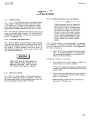
4-6. INPUT CIRCUIT.
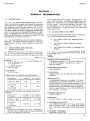
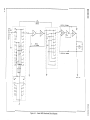
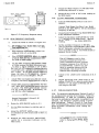
4-2. The Model403B includes a preliminary input
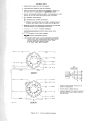
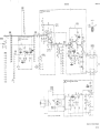
attenuator, a high impedance emitter follower circuit, a range attenuator and a wide range fixed gain
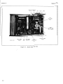
amplifier. Refer to Figure 4-1.
4-7. Rll, CR1, and CR2 make up a limiting circuit
which is used for overload protection to prevent high
instantaneous voltages from being impressed on the
base of Q1. F1 is a 1/16 amp fuse used to protect
the 403B against a continuous or repeated overload.
4-3.
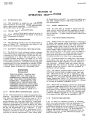
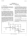
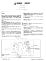
4-8. Since transistors are inherently low impedance
devices, a need for a high input impedance is required.
Referring to Figure 4-2, it would seem that the input
resistance of the first stage would be approximately
Ri of a grounded collector configuration in parallel
with R9, plus the R7-RB combination. Q1 and Q2 ~e
emitter followers, exhibiting unity gain and no phase
reversal. (Ri = approx. input Z of a common collector stage.)
PRELIMINARY ATTENUATOR.
4-4. The RANGE switch is divided up into two sections: the preliminary attenuator, located between
the input terminals and Q1, and the intermediate attenuator, located between Q2 and Q3. The preliminary
input attenuator has two ranges, 100:1 and 10,000:1,
which are switched in at the appropriate time to keep
the input voltage to Q1 less than O. 030 volt. This not
only prevents overloading the input system, but also
provides the necessary accurate attenuation to work
with the intermediate attenuator to produce the conventional 1, 3, 10 sequence for correct meter operation.
4-5. The attenuators are of the compensated resistorcapacitor (rc) type, with the capacitive division ratio
made equal to the resistive ratio to maintain a constant
division ratio at all frequencies. By making one of
the capacitors adjustable, the small variations in stray
circuit capacity can be compensated for, so the voltmeter will have a flat response. The exact division
ratio is set at low audio frequencies by the trimmer
potentiometers, which bring the resistor division ratio
to the exact value.
4-9. The output of Q2 is fed back to the junction of
R9 and R7 -R8. There is an ac voltage existing at this
point that is very nearly the same amplitude as, and
in phase with, the input voltage. Since a very small
ac voltage exists across R9 (due to the feedback from
Q2), the input current lin will be very small. Thereby:
Zin
=
E in
~
10
It can be seen that when lin is very small, the appar-
ent Zin becomes very large.
4-10. The Ri of Q1 is increased in a similar manner
by feeding the Q2 emitter voltage to both the collector
and emitter of Q1.
-13V
R7
C9
+
-13V
CIO
02
RI5
+
~
-S-POSITIVE
FEEDBACK
~
+
~EOUT
RIG
CI2
Figure 4-2. Input Amplifier
4-1