1
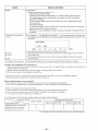
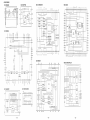
DPS-V77
SERVICE MANUAL
US
Canadian
AEP
Australian
Model
Model
Model
Model
SPECIFICATIONS
AID Converter
1 Bit / 64 times oversampling (24 bit resolution)
DIA Converter
Advanced PULSE 0/ A converter (20 bit resolution)
Sampling
Frequency
Analog input
Digital input
DigitallnputlOutput Terminal type: 8 pin mini DIN
Use optional cables RK-V77 A (for AES/EBU) or
RK-V77S (for SPDIF)
Pedal Input
Terminal type: Standard PHONE type
(assignable control terminals x 2)
MlDllnput/Output
Jack: 5 pin DIN (IN x 1, OUT /THRU x 1)
OUT /THRU can be set to either OUT or THRU
48 kHz
44.1/48 kHz (auto-switching)
Analog Input
Frequency Response 10 - 22 kHz +0, -1 :0 dB
Jack type
reference
input level
maximum
input level
input
impedance
circuit type
XLR-3-31
+4 dBs
+21 dBs
20 kilohms
balanced
PHONE
-20 dBs
or +4 dEs
-2dBs
or +21.dEs
50 kilohms
unbalanced
o dBs:::: 0.775 Vrms
XLR-3-31 connectors (1 : GND 2: HOT 3: COLD)
Analog Output
Jack type·
maximum
load
reference
output level output level impedance
circuit type
XLR-3-32
+4 dBs
600 ohms
or more
balanced
10 kilohms
or more
unbalanced
PHONE
~20
dEs
or +4 dEs
+21 dEs
-2 dBs
or +21 dEs
Signal-to-Noise
Ratio
Greater than 97 dB
Dynamic Range
Greater than 97 dB
Distortion
Less then 0.003%
Memory
Preset 198 locations (99 location preset bank x 2)
User 198 locations (99 location user bank x 2)
Power Source
AC 120 V, 60 Hz
AC 230 V, 50/60 Hz
(1
kHz)
Power Consumption 23 W (120 V)
25 W (230 V)
Dimensions
482 x 44 x 32001111 (WxHxD not including
projections)
Mass
approx. 4.7 kg
o dBs :::: 0.775 Vrms
XLR-3-32 connectors (1 : GND 2: HOT 3: COLD)
Design and specifications subject to change without notice.
MULTI·EFFECT PROCESSOR
SONY.
TABLE OF CONTENTS
Section
Title
SAFETY CHECK-OUT (US Model)
Page
2. TEST MODE························································ 17
A fter correcting the original service problem,
perform the following safety check before releasing
the set to the customer:
Check the antenna terminals, metal trim, "metallized"
knobs, screws, and all other exposed metal parts for
AC leakage. Check leakage as described below.
3. CLOCK CONSTRUCTION .... · ...... · ........ · .. · ...... ·· ...... 19
LEAKAGE TEST
1. GENERAL·····························································3
4. EXPLANATION OF IC TERMINALS ...................... · 20
5. DIAGRAMS
5-1. Block Diagram················································· 24
5-2. Printed Wiring Boards··········· .. · .. · .. ·············· .. · .. · 28
5-3. Schematic Diagram (l/2) ................................ · .. ·33
5-4. Schematic Diagram (2/2) .................................... 38
6. EXPLODED VIEWS
The AC leakage from ;my exposed metal part to
earth ground and from all exposed metal parts to any
exposed metal part having a return to chassis, must
not exceed 0.5 rnA (500 microampers).
Leakage
current can be measured by anyone of three
methods.
I.
A commercial leakage tester, such as the
Simpson 229 or RCA WT-540A. Follow the
manufacturers' instructions to use these instruments.
2.
A battery-operated AC milliammeter. The Data
Precision 245 digital multimeter is suitable for
this job.
3.
Measuring the voltage drop across a resistor by
means of a YOM or battery-operated AC voltmeter.
The "limit" indication is 0.75 Y, so
analog meters must have an accurate lowvoltage scale. The Simpson 250 and Sanwa
SH-63Trd are examples of a passive YOM that
is suitable. Nearly all battery operated digital
multimeters that have a 2 Y AC range arc
suitable. (See Fig. A)
6-1. Front Panel Section··········································· 48
6-2. Chassis Section················································ 49
7. ELECTRICAL PARTS LIST ................................... 50
CAUTION
Danger of explosion if battery is in.correctly replaced. Replace only with the same or equivalent
type recommended by the equipment manufacturer.
Discard u,sed batteries according to manufacturer's
instructions.
To Exposed Metal
Parts on Set
ADVARSEL!
Lithiumbatteri-Eksplosionsfare ved fejlagtig handtering.
Udskiftning rna kun ske med batteri
af samme fabrikat og type.
Lever det brugte batteri tilbage til leverand¢ren.
AC
voltmeter
0.15pF
(0.75 V)
-=Fig. A.
ADVARSEL
Eksplosjonsfare ved feilaktig skifte av batted.
Earth Ground
Using an AC voltmeter to check AC leakage.
SAFETY-RELATED COMPONENT WARNING!!
Benytt samme batteritype eller en tilsvarende
ill.
COMPONENTS IDENTIFIED BY MARK
OR DOTTED
LINE WITH MARK
ON THE SCHEMATIC DIAGRAMS
AND IN THE PARTS LIST ARE CRITICAL TO SAFE
OPERATION.
REPLACE THESE COMPONENTS WITH
SONY PARTS WHOSE PART NUMBERS APPEAR AS
SHOWN IN THIS MANUAL OR IN SUPPLEMENTS PUBLISHED BY SONY.
ill.
type anbcfalt av apparatfabrikanten.
Brukle batterier kasseres i hen hold til fabrikantens
instruksjoner.
VARNING
Explosionsfara vid felaktigt batteribyte. Anva.nd samma
batterityp eller en Iikva.rdig typ som rekommenderas av
apparattillverkaren. Kassera anva.nt batteri enIigt ga.llande
f6reskrifter.
ATTENTION AU COMPOSANT AYANT RAPPORT
A LA SECURITE!
ill.
LES COMPOSANTS IDENTIFIES PAR UNE MARQUE
SUR LES DIAGRAMMES SCHEMATIQUES ET LA L1STE
DES PIECES SONT CRITIQUE:S POUR LA SECURITE
DE FONCTIONNEMENT. NE REMPLACER CES COMPOSANTS QUE PAR DES PIECES SONY DONT LES
NUMEROS SONT DONNES DANS CE MANUEL OU
DANS LES SUPPLEMENTS PUBLIES PAR SONY.
VAROITUS
Paristo voi r:ijahUUi, jos se on virheellisesti asennettu. Vaihda
paristo ainoastaan laitevalmistajan suosittelemaan tyyppiin.
H:ivit:i k:iytetty paristo valmistajan ohjeiden mukaisesti.
-2-
Getting Started
Narnes andiFuractiol'ls of Parts
Names and Functions of Parts
Rear panel
Front panel
2
3
17
16 15
14
POWER ON/OFF switch
Press this switch to turn the power on and off. Turning on
the power on recalls the last used memorized effect and
activates play mode automatically.
2
INPUT level adjustment knob
Turn the knob to the left or right to adjust the input level.
Adjustments can be made independently for each
channel. The outer knob to adjusts channell (CH 1) and
the inner knob adjusts channel 2 (CH 2) (page 14).
~
3
OUTPUT level adjustment knob
Turn to the left or right to adjust the output level from the
output jacks.
4
Input level meter
Indicates the strength of the input signal from -36 dB to
CLIP (overload) with green, orange, and rcd indiCators
(page 14).
5
Memory number display window
Displays the memory number of current effect. 99
different effects are stored in each of the PRESET memory
banks and up to 99 effects can be stored in each of the
USER memory banks.
6
Multi display
Displays various information, such as the name of the
currently selected effect, parameter values, and messages.
7
Number buttons
Use these buttons'to recall effects from the currently
chosen memory bank directly and input exact parameter
values (page 14).
Use ... or T while holding down ENTER/SHIFf to make
incremental adjustments to parameter values
(poge 14).
8
SAVE button
Use this button after chonging parameter values to save a
custom effect in one of the USER memory banks
(page 22).
9
SYSTEM button
Use this button to access the system mentIS and customize
the effecttlr's t'perating environment (pages 24 and 25).
6EN
7
6
5
4
13
12
8 9 10
11
10
11
10 Operation dial/Shuttle ring
Use to select memory numbers from the currently
selected memory bank and make adjustments to
parameter settings. The operation dial lets you advance in
one-step increments. The jog dial lets you advance rapidly
in larger increments, The rate of advance (or value
change) changes according to the angle of the shuttle ring.
11 ENTER/SHIFT button
Use this button to enter a memory number or parameter
value input with the numeric buttons (page 14).
Hold down while pressing the ... or T button to make a
one-step adjustment to a memory number or a parameter
value (page 14).
AC power cord socket
2
13 FUNCTION A-F buttons
Use to select the items displayed above the respective
buttons.
MIDI THRUIOUT terminal
For sending and/ or relaying MIDI command signals
frQm the effector to other components
(see page 26 to select THRU or OUT).
3
4
PEDAL 1 and 2 jacks
Inputs for pedal switches and/or volume control
(pages 21 and 25).
5
7
DIGITAL I/O terminal
Use digital interface cable RK-V77 A (for AES/EBU) or
I{K- V77S (for SPDIF) to make digital connections between
the effector and other components
(pages 8, 12, 13 and 29).
STANDARD OUTPUT jacks
Standard output jacks for channd 1 and channel 2
(pages 9 and 10).
8
MIDI IN terminal
Input for MIDI cOll,1mand Signals. Use a commercially
iWililable MIDI cable to connect this terminal to another
component's MIDI OUT (or THRU) terminal.
BALANCED OUTPUT jacks
Balanced output jacks for channel 1 and channel 2
(pages 9 and 10).
For connecting the effector to an AC power outlet using
the supplied AC power cord.
12 EXIT button
Press after or during a setting procedure to return to the
previous screen or mode, or to de-select an active
parameter on the play screen,
6
10
STANDARD INPUT jacks
G)~
Standard input jacks for channel 1 and channel 2
(pages 9 and 10).
9
mO
BALANCED INPUT jacks
Z-f
m0
Balanced input jacks for channel 1 and channel 2
(pages 9 and 10).
:0
~Z
1Q INPUT level selector switch
r .....
Use to set the input level of the STANDARD INPUT jacks
(8) to match the output level of the connected equipment.
You can select a -20 dB or +-1 dB input level.
11 OUTPUT level selector switch
Use to set the output level of the STANDARD OUTPUT
jacks (7) to match the input level of the connected
equipment. You can select a -20 dB or +-1 dB output level.
14 EDIT/PAGE button
Press during play mode to access the edit screen and
make changes to the current effect (page 17).
Press to display different pages of multi-page menus
(page 17).
15 BANK/COMPARE button
S· -l
Press to select the memory bank containing the effect you
desire (page 14). In edit mode, press to compare
fllterations in effect parameters to the unaltered effect
(page 18).
C/l :J
r+ - -, C/l
C
o
~.
o
:::l
16 BYPASS/MUTE button
Press to route the signal around the effect processing
circuitry so that the signal being input is output
unchanged (bypass), or to completely cut output from the
effector (mute), (see page 15).
C/l
CD
0
g-
3
.:::l
:::l
C
(J)
ro -.
ro CD
;-X
r+
~
17 Memory bank indicators
~
Indicate the currently selected memory bank: PRESET 1,
PRESET 2, USER 1, or USER 2 (see page 14).
CD
0...
7EN
-+.
a
3
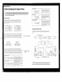
Understanding the Signal Flow
This unit takes in audio signals from two types of input jacks (digital and analog), processes them using various internal
blocks, and outputs them through the analog and digital output jacks. To make the most of this unit, it is essential that you
have a firm understanding of the audio signal flow. This section provides an explanation of the internal blocks and how
they process the input and output audio signals.
PARALLEL '(PARA)
C~NI~'1 Bl~CK l-fl ~IX
,.
Bl~CK
ch 2
]=1
BLOCK
F:::
ch 2
DUAL (DUAL)
IN
This strw. -turl.' lets you isol.ltt..'l·h 1 Mld (h 2,
OUT
Bl~~ ]~ '~~XFCh
r-J BlD.· I. __.. .
ch 1 - 9
Ch2--~i
The audit) signal processor in this unit is divided into two parts, BLOCK 1\ and
BLOCK B. Each of tlwse blocks is composed of an EQ BLOCK and (\n FX (dfect)
BLOCK. Thl' EQ BLOCK works as anl'qualizer. The FX BLOCK contains a large
number of multi·dfe'cls.
BLOCK A
~
~
~
FX BLOCK
(reverb. pitch
shifter. chorus.
etc. .. )
BLOCK
I
BLOCK
Block and structure
I
This strll<:tun..' Ids y~)U .lpply t..'ffl'l..'tS, like
fI.\I'lhl·r .1Ild rl'vl'rh, sl'p.lr.\tdy .lnt.! thl'n mi\
tlwm bdort..' output. In this ("SC, tlll..·rt.... ~ no
undulatioll from till..' t).lIlgl'r in thc rcverb,
~
CK
ch 2
MORPHING (MORPH)
C:~I-1B.lOCK·.I-1 ~I~ ~~~
..
Ch2-1. A
..
[BLO.CKJ_Ch2
l-.
For t.':\.lmplc, you Cilll connect il ~lIit,u il) dl 1
imd ,l drum m.Khint.' to ch 2, tht..·n ,ldd ,l
tl.lIlgt..·r dfl'el to the guit.u .lnd .t rt.'vt..'rb I..'Ht.'Ct
to tht..' drum m.Khinc.
This strw.:ture Ids you make sl'.lI"nless Ch.lngl'S
bl'twt..'t...'1l dfl,C'ts stOfl'J in thl.' mt..'Il\Of\' b.mks
In otllt..'r won.b, it kt.'t.·ps tht..' (Urrl'nt ~t't't.....:t
from :,uJdt..'nly cutting l)ut ",ht..'n you dl.1IlgL'
tl) .uwthl'r dfl'd, ror lil,tails 01\ morphinh' SL'1.'
"rvh)rphing" on p.lgl' 16.
",OC",
EQ
'LOCK
I ~;ft"
FX BLOCK
(reverb. pitch
Setting the INPUT/OUTPUT levels
<ho,.,.
etc ... )
This ch.ut shows the OVl.'r.liJ SiglM} flow rl'i.1tionship bet\\'l'l.'n this unit's inputs ,1nd outputs, Tht.'
following infurnl.ltion is .1n oVl'r\,iew of ,)11 you Ill'ed to know fl'gtlrt.iing this unit's inputs and
ot\tputs.
The positioning of the EQ block and the rX.block is determined when editing the EQ
BLOCK by c1wosing either "Pre" or "Post" in the I Model parameter. In other words.
you can c1wt)se. independently within BLOCK A and BLOCK B. wether to add the
effect to the sound coming from the equalizer, or equalize the sound produced by the
effect.
When you select
"Pre"
"~~~ D
::: "'' ' ' ' ' ' ' '
BYPASS:SW
DIGITAL
OUT
EQ BLOCK
When you select
"Post"
... IEQlfFxl
...
...
~
DIGITAlINPUT ATIENUATION lEVEl
... See page 17 to EDIT an effect.
EffECT BLOCK
... fFxI ... IEQl ...
~
~
~
ANALOG OUTPUT
It's abt) l1l'cessary to dett'rmine the positions of the larger blocks. BLOCK 1\ and
BLOCK B. Thdr pt)sitioning, the way they arc connected, is called the "structure." Set
the structure according to the kind of sound you want to make. The structlire screen
not onl\' lets vou choose the structure type (see the following chartl. but also lets you
adjust the output I"\'el for each block (represented in the chart by the MIX BLOCK).
~CHl
BALANCED
~CH2
... See page 19 to change the
structure.
SERIAL A'" B (SERll)
IN
OUT
~~.~~~ H'~,~' U~~;~:l-1'-~~~'~Ch I
A
1_ BLOCK W. B
IBLOCK ch 2
: ....
............. 1....... __ 1 ... _.... _
ch I - ;
ch 2---'
1-; B~~~~ l-r·~;x-l-4·;~;;:J~···~~~··
!-o!
U
ch
ch 2 ---'
B
:•........ _1
BLOCK
l<ugl'st i1vailaole rcvl'rb (sec page 17 for
on hol',,· to edit effects) (For information
dC'lail.
I :~~~;~,i~;p~f:~'~:~.~;~~;~dll~~~·;~:'~:'"c';:~:~:~r:nd
I SERIAL B ... A (SERI 2)
IN
For exampl". if you set the BLOCK A as an
intense f1anger, ilnd :->t't the BLOCK Has tht'
A
L.._..• .J L_.___
BLOCK
_
OUT
ch I
ch 2
"Preset Memory Catalog.")
You C(lll add n,'vl'rb to the sound produced by
the f1anger effect, or you can flange the sound
produced by the reverb effect.
'Q._----------------"\
You can use the effector as an AID or DIA converter by turning off all the effects.
Analog IN/OUT and digitaliN/OUT
This unit is provided with both analog and digital inputs and outputs, and you can use both of
tilt'm at the same time. The input block in the SYSTEM: Setup menu lets you determine whether to
usc the anall'g, the digital, or both the analog and the digital INPUT /OUTPUT jacks.
Analog INPUT priority
This unit is pro\'ided with both PHONE and XLR type analog INPUT and OUTPUT jacks.
Although the sign,,1 is always output from both the PI lONE and XLR jacks, the PHONE jacks are
gin:-n priority for the input signa I. When the PHONE and XLR INPUT jacks are used at the same
time, th,' XLR signal is autl>matically cut.
Emphasis
Somc older CDs have "emph"sized" high frequency sounds. When outputting an analog signal
from an "('mpha~izl'ti" digital source, it is necessary to "de-emphasize" th~ high frequenc), sounds
and bring them back to their original levels. The (lnputl block in the SYSTEM: Setup menu lets
yotl ddermine \\'hetheT dc-emph;tsis will be carried out automatictllly, Of manually.
Adjusting the INPUT/OUTPUT levels (to prevent clipping)
n,e l1l1111b,'rs on th,' level nwter show, in decibels, how much room is Idt before the INPUT signal
re,Kh,'s the clip point. If the input signal exceeds the clip point ((l dll), dip noise breaks out. This
unit's t.~ffl'ct prrx.'-l'SS(lr incorpoTclh.'s a 12 dB let.'way. Then'fore, (,VE'n if you TC'lise tht.' signalll'vel to
+ 12 dB, with the EQ bllxk for example, the intl'rnal pmces"" will not clip the signal. It is
n('(t.'s ....uy, howl'\'cr, to reduct." 1('\'(.'ls oVt.'r n Jll
choo~,'
bt.l(or~
.... See "Setting the DIGITAL IN/
OUT" on page 13.
.... See "Names and Functions of
Parts" on page 7.
Bypass and Mute
The bypass function outputs the sound of the signal originally input into the effector without
adding any dfl'cts. Pressing the bypass button turns the bypass function on and off.
"Mute" is also ,wajJable as a form of bypass. When the BYPASS button is set to mute, the sound
of the originally signal is cut in "ddition to th" sound of th<l eff<lcts. Th"rcfor", no sound comes
from thl' unit. You can set BYPASS button to operate ,1S either "Mute" or "llypass" in the
SYSTEM: Setup menu.
'Q'--------------"\
.... See "Setting the DIGITAL IN/
OUT" on page 13.
Muting the sound is more than just turning the volume to "0." It is designed to
prevent sound from returning to the mixer when the unit is connected in a sendreturn loop with a mixer. Ideally. when this unit is connected to a mixer. the
sound of the input signal is should not be output from this unit, only the sound of
the effects should be output (see "Cutting the Direct Sound (Dry On/Off)" on
page 25). In this situation, however, using bypass only cuts the sound of the
effects. and the sound input into the effector goes back to the mixer, producing a
double signal. Using mute prevents the sound input into the effector from
returning to the mixer and insures that only the sound generated from the
original source (guitar, keyboard, etc.) reaches the mixer. In other words, it is the
same as bypass.
When using effects
thl'Y ,1rc output. To ndjust thl' eHect )evl'i,
IMi"'rj in the EDIT modt'. See "Changing the effect parameters" on page 17 to "dit an
effect.
U1
~~~J
'Q'---------------.
eflect
'~~l- origina' sound.
.'ement
Even though you can decrease levels in the mixer block. the most important factor
in preserving sound quality is the input level. The following is a general guide line
for adjusting the input level, but your eyes and ears are ultimately the most useful
tools in determining and maintaining the appropriate input level.
return
. _J .
L_~,~~.~~
ellect element
I
onginal sound
When NOT using effects
INPUT jacks
Signal
level meter
reading
Digital
(with the digital attenuator sct to 0 dB)
odll digital (full swing)
OdB
Analog (+ 4 dll)
llALANCED or UNBALANCED
(with the front panellNI'UT kr,ob set to 0 dB)
+ 21 dB signal
Odll
+ 4 dll signal
-17dB
Analog (- 20 dll)
UNllAl.ANCED
(with tlw fn>nt panellNI'UT knob set to [) dll)
- 2 dB signal
OdB
- 20 dll sign,,1
-18dB
Using BYPASS
Using MUTE
rDPs'~~j7'J~
[~~~~~~
origina'L
(!~u~~~
_____
to mixer
[
return
s~
_lsend
~
_.:~: _~_.J
I
anginal sound
original sound +
anginal sound
C:~:~f origina' sound
1
original sound
.... See "Names and Functions
of Parts· on page 6.
.... See 'Outputting Without
Effects (BYPASS/MUTE)"
on page 15 to set the
bypass mode.
Hooking Up
By taking advantage of the DPS-V77's DIGITAL 110 connectors, you can make digital recordings on OAT recorders, input digital
signals from CD, and make digital connections to mixers (see page 29).
• Before connecting this unit to another device, be sure to unplug the AC power cord from the power outlet.
• Turn off the power switch on this unit and all components to be connected, such as keyboards and active speakers (speakers
with built in amplifiers).
DIGITALIN
IHllllllllmlHllmJlI===~,=--;
• After all the connections, double check that the connections are correct before plugging the AC power cord back into the power
outlet.
• If the connected components output large signals that cause distortion, adjust the INPUT knob on this unit to lower the input
level, or lower the output level of the connected component.
OIGiTALIN
___ . __ . _._.
DIGITAl OUT
-
~tI:I:Il..-.
.-~r:l
1R'1"1l- -:mDTO"'--[;";';;WU!.J
OAT R«c'"" i""o,'
tt~
I
!
[;;;;":-:1
Example 1: Hooking up to an instrument
.-]
[::::J
__1___
•.. !o :;.
•
~
. . C'.
MID! Foor COO'lUOII(,<,
tHR.n C5.e1c)
~.=~ -:'"
-1' ~-- ~~tl @_~
~
0'"
'"
-
0
OUT
.
~-~... ~~~~.-.
~o
[I
@@.OPSV'7
'0 0
(c; o'
0' 0' ~-~'t'-.'_'.I~-oo)
'c;:;\~--~'t-.t_t.I~-- (0 (;
'-,,'
.
P('>O,t.A.,,\p"'-("
5: ~.,.~.
en
I~HU
OUT
PO"'IJ'AfT"(Il,I,,,,
Ttl obtain the best p""iblt, sOllnd qllality ",Iwnllsing the DIGITAL
I/O j,l.:k, we n-'('nn'n"l.l.~nd SL'tting the input Illude h) digittll, insh!tlt.i uf
both (digit,,1 .lIld 'lIh'logL
TIll' follllwjllg stl'p~ shu\\' you how to sl'l thl' input mndl', ,ldjllst the
di~it,ll input h'\'l'i, Imd Sl'il'ct till' "dt..."-t..'mph.l~is" modL',
Rd·l.'r to "Undl'r~t.Hldillh till' Sign.ll flow Oil p.\~L' H for dd.lils
regarding the digit.ll ~ign'l1 flow. Alsu, Sl'l' "Input Settings ,lnd the
Inpllt Signal" and "Di~it.'II/O Terminal ChMt" on p.'ge 29 for
,lddition.ll inh)rnl.ltiun
5
Press FUNCTION B [ChSel] and use the
operation dial to select the input
channel(s}.
To use both CII! imd C112, choose s!l'reo (sTREO),
To use only CHI, choose monaur,)ll (fI.\ONO 1>To use only CH2, choose monaural 2 (I\IONO 2) .
'
~I'>'! ... ~e'
Spcllker
St>f',,~e'
You Ciln sek'ct analog (ANALC)' digit.)1 (DICTL), or
both .m.)log and digit.)1 (Both) j,Kks ior input ,md
output.
Setting the DigitaliN/OUT
Example 2: Hooking ur;-to a mixer (cutting the direct sound)
These selling can also be made when using the analog
inputs,
1
Press SYSTEM.
2
Press FUNCTION A to choose "Set Up."
6
System:
B
.1
.;I-
......am-:
G::,.:..;: ..
i., ...
M', , :![:~;=---~==:rr:''''''''''
_~
i
Set
3
1\''\'"''
__
~PS~'7_
El1oct~nd =-====--:;-=mIl~~
TEUe<:'Rl'tV,"~-ou'
I
~ :>C
MID I
4
[Att II lets you adjust the digital input !evel for 01 I,
IAtt 21 lets you adjust the digital input 1l'\'eI ior ClI 2 .
Prl'ss FUNCTION CorD twice to link the pMameters
and adjust both digital input !evl'Is at the same time,
Morph
See pages 9 and 10 for details regarding the input level.
Press FUNCTION A to choose "Input."
Input
,
• Wl' rl'Conlln,'nd "'tting the dirl'ct output 1"\'l'l to ~ (minus infinity). (St'e "Cutting the Din'ct St>llnd (Dry On/Om" on page 2~.)
• IV" abo r,'COll1ll1l'nJ setting the BYPASS function to MUTE (as shown on page IS).
~
Pedal
.. ~ ~ Jiiil. l)!J
OP$V77
When using the effector in a send-return loop
(].?
Memry
System: Setup
':;T
,.",.,.,./.,.,.,.,.,.,+,.,.,.\1)1)1\
UP
Gate
Bypass
OISP
Cge
Clock
7
OryoH
Press FUNCTION E [EMPHA] and use the
operation dial to select the de-emphasis
mode.
"Auto" activates de-emph"sis automatically according
to the type of digital sign,)1 being input.
"On" de-emphasizes all signals input through the
DICITAL I/O jack.
"Off" turns de-emphasis ofi and does not .liter signals
input through the DICITAL I/O jack,
Press FUNCTION A [Mode] and use the
operation dial to select "DIGTL" (digital).
~stem
Press FUNCTION C [Att 1] or D [Att 2] and
use the operation dial to adjust the digital
input levels.
: Input
See page 10 for dl'tails on the emphasis iunction,
DIGTL STREO
~
[ChSel)
12,0
12.0
Auto
[Att 1)
[Att2)
[EMPHA)
Note
This lInit's digit,'1 inpllt only .KCl'pts sign,,1s with eith~r 44.1 kIll or
48 kHz Sdlllpling fn~qU('IKi('s. It l'tlnnnt be llSl't.i with ;\2 kllz si~n.l1s,
12EN
13 EN
Choosing an Effect
Recalling Effects from the Memory
Outputting Without Effects (BYPASS/MUTE)
You can use the following procedure to select effects from
The effector comes with 198 different effects stored in the
either the preset memory or the user memory banks.
preset memory as well as a 198 effect memory capacity for
storing the effects you create.
Memory
number
Number
POWER
Level meter display
Multi-display
buttons
Shuttle ring
-
~
ij
.
The effector comes with two different bypass modes, Bypass and
Mute. Therefore, you can use the BYPASS button to cut output of the
original sound or to output the original sound without effects
depending on, which bypass mode you sell'Ct.
Once you set the BYPASS modc, just pre'Ss BYPASS to activate
Byp"ss or Mute. Prt'Ss again to cancel the bypass or mute.
~.
INPUT
Bank
indicators
BANK
FUNCTION A·F
Press POWER to turn on the power.
The I'LA Y screen is qisplayed.
Category icon
........
Structure message
(see page 19)
_ _l
Memory name
4
Select the effect you desire (1-99).
To select effects using the operation dial/shuttle ring,
rotate the dial or ring to display the number of the
effect you desire.
2
Turn INPUT to adjust the analog input
levels (for digital levels, see page 13).
If the CLIP indicators light, the input level is set too
high. Be sme to set the input level correctly since it has
a direct relationship to the quality of the effects
(see page 10 for details).
(H'
_ CLIP.
-6_
_
CH1
~CH2
~
_-12_
_
-18_
Ir.)!: -24 I't"'t
'"'" -30 1eI':!
r~
-36
l-:::>J
,~_ . .:. _~f.~
PRESET
1mmJ_
select
when
BY PAS
you w,mt to output the original signal
without adding any cfte'CtS. Only the
original signal is output (Sl'\! "Bypass and
Mute" on page 11).
Mute
you want to completely cut the sound
output from the effl'Ct"r (including the
input signal). We l'Specially rl'Commend
using mute whe'll Ctlllnl'Cting the dft'Ctor
ill a send-return loop with a mixer (as
showil on p,'ge 12).
Press SYSTEM.
Press FUNCTION A to choose "Set Up."
......--
System:
G
Set
UP
a.~
~
~
:x
Memry
Pedal
MID I
Morph
~
3
Press FUNCTION C to choose "Bypass."
Setup
CDo::JCD
CD CD CD
+
CDCDCIJCD
.. @ fI/\I ENTER)
Gate
Jjji1.
liD
Bypass
DISP
Ge
Clock
Dry off
To select effects using the arrow buttons, hold down
SHiFf and press either ... or" until the number you
desire appears in the display.
...
c=:J
Both the top and bottom
indicators light for
PRESET or USER bank 2.
I;:__.~_~
+
G8
IT)
T
Before you turn on the connected components
Be sure to turn the volume level down to avoid an uncxpl'ded output
of massive volume.
PRESET
PRESET banks 1 and 2 hold preset effects.
USER banks I and 2 are for user memory.
14fN
1
2
To select effects using the number buttons, input the
number of the effect you want, then press ENTER. (If
you press the wrong number, input the number again
before pressing ENTER.)
SHIFT
2
Choosing the bypass mode
Operation dial
Press BANK to select the memory bank
containing the effect you want (PRESETI
USER 1 or 2).
Only the bottom
indicator lights for
PRESET or USER bank 1.
!;
j
rot
~{d81--'
3
ystem:SypassMoae----------
BY PAS
Press EXIT a few times to return to the PLAY screen.
~
Active parameters (see page 20)
Use the operation dial to select BYPAS or
Mute.
ENTER/SHIFT Operation dial
BYPASS
1
4
To change effect parameters from the PLAY screen
St'l' "Editing in I'LA Y Mod .. (dire,,,t l'dit)" on page' 20.
1SEN
Choosing an Effect
Processing Effects (EDIT)
Morphing
.
3
When the structure is set to (MORPH) (see page 8 for details on the
system structure, see page 19 to change the structure), the effector
creates a seamless change between effects when you switch to other
memory numbers whose structures are also set to (MORPH).
1
Press SYSTEM.
Changing Effect Parameters
The morphing time is the length of time from the
beginning to the end of the morphing process.
The effector will not respond to any commands
(including MIDI) during this period.
The effector comes with 198 different effects stored in the
preset memory as well as a 198 effect memory capacity for
storing the effects you create by altering parameter values.
System: Morphlng Condition
Note
The (,(kctor dOl'S not respond to any commands (including MIDI)
during the morphing proet'ss. It will not respond until the pres,'t
morphing time has e1apsc,<l (Sl'" below).
Setting the morphing time and curve
Press FUNCTION A [Time] and use the
operation dial to set the morphing time.
2.0
IiiIlD
4
><
-
Press FUNCTION B [Curve] to select the
morphing curve.
System: Morphing Condition
2 Press FUNCTION E to select "Morph."
-
-====:J
[Curve I
2.0
[Time]
System:
~
r!l!m
-
1
o
55
~.;;
[.
Use the following procedure to create original effects by
editing the effects stored in the preset memory banks.
Multi-display
PAGE/EDIT
FUNCTION A·F
--------0-
ex>
UP
Memry
Pedal
MID I
Morph
><
~
the block you want to change.
PLAY: CEO - Hall/.::.CE=.:O=--....:H"'8::.:1I--,---_ _ _ _ __
-~
The screen for the chosen block appears in the display.
For example, pressing FUNCTION A selects "EQ A"
and the EDIT: EQ A screen ap~ears (the example below
shows a shelving equalizer).
Fat Reverb
1. 0
O. 64
[ Size] [RotHI]
Provides a gradual transition to the next sound.
Brings the next sound in quickly while the first
sound fades out.
Note
You cannot set the morphing time and curve independ,'ntly for
effect.
ENTER/SHIFT Operation dial
EXIT
3 Use the FUNCTION buttons (A-F) to choose
Choose an effect.
O. 8
[Size]
O. 70
[RotHI]
-6. 0
[FxA-l]
-6. 0
[FxB-l]
E3 a·~ ~ ~ x:
Set
Number buttons
2 Press EDIT/PAGE.
~
EDIT SELECT:
~ach
f~att FX
«CO»)
.. ....-
EDIT SELECT:
lm:I
The EDIT SELECT screen appears in the display.
rEm
FX
.......... ««(j))
FX
«(0»)
PAGE :Q2
rEm FX
««(j))
Mixr
HH
--~
PAGE :02 3
Current page
The numbers in the upper right corner of the display
indicate the number of pages (basic screens) in the
current block. The number in the black square indicates
the current page.
Press EDIT / PACE again to switch to the next page.
Press EDIT/PAGE while holding down ENTER/SHIFT
to page backwards.
0.125
[LowF2]
4
0.0
0.0
[LowGl] [LowG2]
Use the FUNCTION buttons (A-F) to select
the parameter you want to change.
(Continued)
16 EN
17EN
Processing Effects (EDIT)
5
Turn the operation dial to choose the
setting you desire.
i
Certain paramett'rs, like Delay Time, can be set by tapping on the
ENTER button. After choosing the parameter you want to Sl't, press
the ENTER button repeatedly to tap in the tempo you desir(>. The
To change numerical values
processor measures the timing or the last two t~ps and sets the
Use the number buttons and ENTER to input the value you
want dire(,tly. If you press the wrong number, input the
number again before pressing ENTER.
parameter accordin)lly.
This function can only be used with parameters whose parameter
name display is followl'd by an asterisk (*).
[ENTER I
To changl" numerical values using the arrow buttons, hold
down SHiFf and press either A or T until the value you desire
app('ar~ in the display.
A
C:=J
SHIFT
+
Comparing Effect Parameters
T
To change another parameter on the same page of the
same block
Repeat steps 4 and 5 above.
To change a parameter on a different page of the same
block
Press PAGE/EDIT and follow steps 4 and 5 above.
To make changes to another block in the same effect
Press EXIT to return to the EOIT SELECT: "reen, then follow
steps 2 through 4 above.
To return to the PLAY screen after changing parameters
Press EXIT a few times.
Chang.,> m,llk to the parameter settings arc replaced by the
origin,,1 settings when you select another effect from the
memory. Tt) ~a\"l' the new par,lmetcr settings, use the SAVE
function (p,'ge 22).
To return to the original parameter settings after making
changes which have not yet been saved
1',,'" EXIT a f.,\\, tinll'~ to gl't to the I'LA Y screen, tlll'n sell'ct
an()ther dfl'ct from the n"'mory. The settings f,)r the pre"ious
dfl'ct return to tlw origin,,} \ ..llues automatk,llly.
Use FUNGION B [FX A], C [FX B). or D
[Dry], if you want to change the output
levels.
Choose the effect you want to edit.
PLAY: CEO - Hall/CEO - Hall
~Fat Reverb
1. 0
O. 64
O. 8
O. 70
( Size) (RotHI) [Size) [RotHI)
-6. 0
[FxA-1)
Press FUNCTION E or F after choosing FX A, FX B, or
Dry to adjust the levels for each channel independently.
-6. 0
[FxB-1)
2
Press EDIT/PAGE.
3
Press FUNGION E to choose "Mixr."
Press BANK/COMPARE while editing an effect to compare the
sound of the current parameter settin)ls with the ",und of th(>
original, uneditt'<.i effect.
7
Turn the operation dial to choose the
setting you desire.
See page 10 for additional information regarding the
output levels.
Press SAVE to store the new structur~. settings (see page 22).
Press EXIT a few times to return to the play screen.
Press BANK/COMPARE or EXIT to rdurn to thl' curr,'nt paramt'lt'r
settings.
Checking the Structure in PLAY Mode
C±J
~
6
The dfL'<.-tor contains two main effect blocks which perform signal
processing to add cffL"ts to the incoming signals. You can produce
different sounds by changin~ the structure (configuration) of these
two blocks (sec page I:! for details).
1
Tapping in a parameter setting (Tap Tempo)
CDCDo:::J
c::::D CIJ o::J
+
CQ o::J CIJ CIJ
18fN
To change the same parameter for CHl and CH 2 at the same
time (LINK)
Press the FUNCTION button for the parameter you want to chan)ll'
twice. The characters for the other channel's Paraml'ter also reverse
and you can adjust both parameters at the sanil' timl'.
Operation dial
(.C
Changing the Structure
Convenient Ways to Edit
4
Copying Effect Parameters
The symbol in the center of the title bar changes according to the
structure of the effect.
In EDIT mode, you can copy the paraml'l<'r settin~s from an effect
block in a )liven USER or PRESET memory to the sanl(' kind of effect
block in the current USER ml'mory. For example, you can copy the
EQA parameter settings from another USER (or PRESET) memory
number into the EQA (or EQB) block of the USER memory numb<.'r
you are currently editing.
1 Follow steps 1 throu)lh :I on the previous pagt' to sdect the block
(e.g. EQA) you want to copy to.
2 Press FUNCTION A ITypel twice.
Connrm~tion ror entering
the "parameter copy"
Press FUNCTION A [STRG].
S(fc('n
appears in
the display. (Pressing IType! twice durin)l anoth('f edit operation
will also activate this function.)
Press FUNCTION F IYes! to proceed.
Press FUNCTION A INo! to cancel and return to the EDIT: mode.
3 Use FUNCTION button A IMEM#! 10 select the memory number
you want to copy from.
4 Use FUNCTION button B or C to "'it"t the dfl"t b"":k you want
Structure symbol
-6.0
[FxA-t)
5
Turn the operation dial to choose the
structure you desire.
SERI 1 (serial processing from FX A to FX B)
SERI 2 (serial processing from FX B to FX A)
PARA (p,H<llleI processing of FX A and FX B)
DUAL (processes Cil 1 into FX A and CH 2 into FX B)
MORPH (morphing, see page 16)
Effect names dimmed in the PLA Y: bar are .. ffects that are currently
set tu[OFF!.
symbol
To copy an entire effect. see page 23.
structure
SERI I (serial 1) FX A ~ FX B
SERI 2 (serial 2) FX B ~ FX A
PARA (par"lIe!) FX A + FX B
See pages 8 and 9 for descriptions of each structure.
to copy the parameters rrom.
S Press FUNCTION F IEXEC! to copy the paraml'lt'r settin~s from
the effect block you selectt'd in step 4.
-6.0
[FxB-1)
DUAL (dual) FX A (ch
No Block B
1) +
MORPH (m(1rphing) FX A
FX B (ch 2)
~
next memory
See pages 8 and Y for descriptions of each structure.
19 fN
Processing Effects (EDIT)
.Editing in PLAY Mode (direct edit)
With direct edit you can edit up to6 different parameters directly
from th .. PLA Y scre<>n. TI,<'S€ parameters are called Active
3 Press FUNCTION B to 'choose "Active P."
Parameters.
eDIT SELECT:
The following steps show you how to edit from the play screen once
you've designated the Active Parameters. To d<'Signate Active
Parameters, see "SeIL"ting the Active Parameters" l>clow.
1
Setting the Real Time Control (RTC)
2 Press PAGE/EDIT twice.
RTC Active P
-II--
CU
..0 ...._-
Choose an effect from the memory banks.
The parameters available fOr'direct editing (Active
Parameters) appear directly above their corresponding
FUNCTION button.
PAGE: 1111
4
EHect
lly using MIDI controls, such as dampers and modulation wheels,
you can control various characteristics of an effect in real tinle. Since
control conditions vary for each type of effect, control assignments
are m.1de sep.uately for each effect block parameter in the RTC block.
The effector is providc>J with 6 MIDI RTC channels, each carrying
independent control suurCe and destination (paranletcr) infornlation.
1
Choose an effect from the memory banks.
PLAY: CEO - Hall/CEO - Hall
Press a FUNCTION button (A-F) to choose a
location (1-6).
Active PI-Active 1'6 correspond to FUNCTION buttons
A-F respectively. (e.g., FUNCTION B is used to select
Active 1'2 from the PLAY screen.)
6
~
1.0
Fat Reverb
O. 64
0.8
O. 70
~.
0
~.
0
(Size] (RotHI] [Size) [RotHI) (FxA-1] (FxB-1)
2 Press PAGE/EDIT twice.
Active Parameter Select:
"U 1 "U 2 "U3 "U 4 "US "U 6
Active P Active P Active P Active P Active P Active P
-a-......._-
Active parameters
2 Press the FUNCTION button (A-F) of the
parameter you want to adjust.
o
Hall
_.__._-==-_____=
~
1. 0
Fat Reverb
O. 64
O. 8
O. 70
( Size] rn.:mlI (Size] (RotHI]
~.
0
~.
-...-o~-=-----
ABC
adjust the parameter.
When changing numerical values, you can use the
number buttons to input the value directly, or hold
SHIFf and press'" or T to change the value one unit at
C1 tin1C
0
4
Use the FUNCTION buttons (A-F) to choose
an RTC channel (1-6).
--
5· Press FUNCTION A [Block] and use the
6
Press.FUNCTION B [PARAM] and use the
operation dial to select the parameter that
will appear on the PLAY screen.
-{I-
5
-{I-
Use page 1 to specify the parameter you
want to control.
Choose an effect from the memory banks.
PLAY: CEO - Hall I CEO - Hall
1. 0
Fat Reverb
O. 64
O. 8
O. 70
20
fN
~.
0
~.
0
PAGE:1
0
[ Min] (Max]
ISourcJ: selects the control source .
CO-C3! : To use a MIDI control change number.
C64-C120 : To use a MIDI control change number.
Note N : To use a note number
Note V : To use note velocity (Note Off is
obtained by setting note velocity to 0.)
BENDR: To use a pitch bender
CH-PR: To use channel pressure
M.CLK : To use the MIDI clock (tempo display)
as a control source. Settings can be made
within the range of 30 to 250.
PEDL 1 : To use pedal 1 (Be sure to select "Pedal"
on the System: Pedal screen, page 25).
PEDL 2 : To use pedal 2 (Be sure to select "Pedal"
on the System: Vedal screen, page 25).
[MinI: specify the minimal value of the control source's
adjustable range.
[MaxI: specify the maximal value of the control source's
adjustable range.
EXAMPLE
Suppose you w.1nt to set RTC I to use the MIDI control change
numl>cr S (balance control) to change the Hall Re\'erb die"t bal,1nce
from 75:25 to 25:75 :
EDIT: RTC 1 (Parameter) screen (step 5) :
Set [Block] to "HALL" and set [PARAM] to "E. BAL" (effect balance).
Then set [Min] to "75:25" and [Max] to "25:75."
EDIT: RTC 1 (Source) screen (step 6):
Sct [Source! to "01" (controlS), IMinl to "0" and IM.IX) to "127."
Sour(e
range
[B1ockl: selects the block to be controlled, select OFF if
you d.on·t want to use tha't RTC channel.
IPARAM I: specifies the parameter to be controlled
from the selected block.
IMinl: specifies the minimal value of the parameter's
adjustable range.
iMaxl: specifies the maximal value of the parameter's
adjustable range.
Parameter
Effect Balance
2]. ·.·~~;;~~~125.75
-EFFI
1
o '
The h)lIowing ~tt.'p~ ~hll\\" you how to St'lfft the p.uameters that will
•'PPl'(u ill thl' PL!\ Y ~(n.."l·n (or din.'X't editing.
~
0
Adjustable
Selecting the Active Parameters
( Size] (RotHI] (Size] (RotHI]
co
(Sourc]
Control Change '8
Press EXIT a few times to return to the PLAY screen.
1
EDIT: RTC 1 (Source)
Press EXIT a few times to return to the PtAY screen.
Real Time Controller Select:
operation dial to select the effect block
containing the parameter you want to
appear on the PLAY screen.
To adjust parameters not displayed in the PLAY screen,
see "Changing Effect Parameters" on page 17.
3 Use the operation dial or shuttle ring to
Size
(Block] (PAAAM]
0
(FxA-1] (FxB-1]
Press FUNCTION A to choose "RTC."
PA~
edit Active Parameter 1
PLAY: ceo -[IrnJ1 CEO - Hall
3
Press PAGE/EDIT and use page 2 to specify
kind of controller you will use.
Adjustable
....... -.75:25
·DRY...
range
Now you can adjust the effect balance from 75:25 to 25:75 when you
adjust control change number 8 (balance control) from 0 to 127.
(FxA-1] (FxB-1]
2pN
Saving Processed Effects (SAVE)
Protecting USER Memory
Saving an Effect
Effects created by changing the parameter values with the
edit function can be stored in one of the two USER memory
banks for later use. Each USER bank has room for 99 effects.
so you can store up to 198 different effects
Memory number display
-
1
The following procedure shows you how to store an effect in
one of the USER memory banks.
SAVE Shuttle ring
Multl-dlsplay
iii
0".55
Deleting USER memory (DEL)
Bank
BANK/COMPARE
indicators
FUNCTION A·F
4
Press SAVE.
Organizing USER Memory
Number buttons Operation dial
Press FUNCTION C [Name].
The Save: name screen appears in the display.
SAVE: Fat Reverb
Fat Reverb
U1
[BANK.]
This function locks the contents of the specified USER memory
number so that new effects cannot be saved to that number and the
conknts of that memory number cannot be deleted or written over
by a copy command.
1 Press SYSTEM.
2 Press FUNCTION B to choose "MEMRY."
3 Press FUNCTION E to choose "PROTECT."
The operation dial or shuttle ring selects the memory number.
FUNCTION F turns protection on or olf.
Exchanging USER memory (XCHG)
This function lets you exchange the contents of two USER memory
numbers.
1 Press SYSTEM.
2 Press FUNCTION B to choose "MEMRY."
3 Press FUNCTION C to choose "XCHC."
FUNCTION A IMEM1#1 sek'Cts the first memory number to be
exchanged.
FUNCTION B IMEM2#] sek'Cts the second memory number to be
exchanged.
FUNCTION F IEXEC) Execute'S the exchange operation.
SAVE: Fat Reverb
8
[MEM']
[Name]
~
[EXEC]
Fat Reverb
[CLR ] [DEL ] [INS] [
2 Press FUNCTION A [BANK#] and use the
operation dial to select the user memory
bank (USER 1 or USER 2) where you want
to save the effect.
>
]
[AB/ab]
[EXEC 1
Use the
to
Operation dial
(shuttle ring)
select icons and characters.
Number buttons
select chJr()cters. Tlw di .. plilY ("h<1n~l'S
ilS shown lx'iow ea",·h time you prl'ss
c(lch button:
2_1>_('_1'_2
I.~J
3_C_II_I_3
[~.J
[tl
liil
lii.J
3 Press FUNCTION B [MEM#] and use the
1-"-11-('-1
It I
I;!I
m
[§J
operation dial or number buttons to select
the memory number (1-99) where you
want to save the effect.
Since each of the USER memory banks can hold up to 99 elfects, you
may find it dilfkult to keep track of where certain elfects are locattod.
The following procedures show you how to copy, move, SW.lp, and
erase effl>cts in the user memory so that you can organize the effects
into a cOlllfortable cc..mfigur(ltion.
This function lets you delete the contents of a USER memory number.
1 Press SYSTEM.
2 Press FUNCTION B to choose "MEMRY."
3 Press FUNCTION D to choose "DEL."
The operation dial or shuttle ring sdccts the m~mory number.
FUNCTION F IEXECI eXt'Cutes the delete operation.
o_M_N_"_,
4-I-K-I.-4
'_1'_ <.,>- R_(.
7-5_1'_ U_7
~_V_W_X_R
q_Y_Z_I_'
FUNCTION A
I</CLRI
move the nm'or backward. When the
cursor is all the way to till' Idt,lCI..RI
(clear) appears instead of 1<) and lets
you emse the entire name.
FUNCTION B IDELI
ddt'll' the character at the cursor
position.
FUNCTION C IlNS]
insert a space at the cursor position.
FUNCTION D I>]
move the CUfSl)f fOf\\'.ud.
Copying a memory file (Copy)
This function lets you copy the contents of a seiL'Ctlod USER or
PRESET memory number to a specified USER memory number.
1 Press SYSTEM.
2 Press FuNCTION B to choose "MEMRY."
3 Press FUNCTION A to ,"hoose "Copy."
FUNCTION A ISOURCI selects the source memory number to be
copied.
FUNCTION B IDEST] specifil'S the destination.
FUNCTION F IEXEClexecutes the copy operation.
Moving USER memory (Move)
This function lets move the contents of a specified USER memory
number to al\other USER memory number.
1 Prl'SS SYSTEM.
2 Press FUNCTION B to choose "MEMRY."
3 Pre'Ss FUNCTION Il to ,"hoo"" "Move."
FUNCTION A ISOURCI selects the source memory number to be
moved.
FUNCTION B IDESTI selects the destination.
FUNCTION F IEXECI executes the move operation.
FUNCTION E IAB/abl switch betw"en capital or small lettl'rs.
FUNCTION F IEXEC)
"Xl""Utl' the sa",' opl'r.,ti'lIl.
Use EXIT to go back to the previous screen if necessary.
5
Press FUNCTION F [EXEC] to execute the
save operation.
The PLA Y screen appears in the display.
22£N
23£N
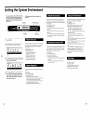
Setting the System Environment
In the system mode lets you set up the effector's operating
The following steps describe how to make changes in the
environments. To go back to the previous screen during
system setup.
setup, press EXIT once. To return to the play mode after
making adjustments, press EXIT a few times until you reach
the PLAY screen.
Multi-display
SYSTEM Shuttle .ring
-
D ••
==
l.J
!!
FUNCTION A-F
Press SYSTEM.
2
Press FUNCTION A to select "Set Up."
......--
System:
EJ G·?
~
~ JC
Set UP
Pedal
MID I
Morph
~
I'.;)
3
Use FUNCTION buttons (A-F) to choose the
items you want tq adjust.
System: Setup
4
24EN
-. ~ rJ\.
Jji1.
[J
Input
Bypass
DISP
Gate
dial
Use the noist! ~.ltt! function wh •.'n the source of the input signal
gt..'llt!r,ltes ,l lot of noisl'. Ihmning the input sign.ll through the noise
giltc lx'fure pn.Kl'ssin~ rCdlll"l'S noise when no sound is being output.
1 Press SYSTEM.
2 I'rL'Ss FUNCTION A "Set Up."
3 Press FUNCTION B "Colte."
FUNCTION A IATKL sets the att,lCk time (the rate at which the
gat"of....'ns).
FUNCTION III RE!.L ,<'ts till' rele,lSe time (the rate at which the
gdtt..' dusl.'sl
FUNCTION C ITHRL sets the threshold lewl (the level "t which
the g,lte will dose). Th,' l.Hger the v,llue, the IMger the signal that
will entC'r thc' g.lte.
Setting the Clock (Clock)
1
Memry
Operation
Setting the Noise Gate (Gate)
Cge
Clock
Dry off
Use FUNCTION buttons (A-F), operation
dial, shuttle ring, number buttons, or the
SHIFT and ... and 'Y buttons to make the
adjustments you desire.
The clock function lets you s"t till' tim" ~nd dat" of the dfedo,s built
in clock. OncE" the dock is set, till' date and liml' c"lft) ilutomiltkillly
stored in the U~t.'r memory when you save" proCl'ssl'd dfl'ct.
1 Prl'ss SYSTEM.
2 Press FUNCTION A "Set Up."
3 Press FUNCTION E "Clock."
FUNCTION A IMonthl sets the Month.
FUNCTION B IDayl sets the Day.
FUNCTION C IY('~rJ scts the Year.
FUNCTION 0 IHourl sets the Hour.
FUNCTION E IMINI sets the Minllte.
FUNCTION F IStartl stMts the clock.
Setting the Display Mode
Cutting the Direct Sound (Dry On/Off)
This setting lets you cut the direct sound and output only the sound
of the dfL",t, regardless of till' MIXER block's DRY l.EVEL setting.
\Vhell u~ing this unit is CtJlultxtL'li to a rnixt:r in ,l sl'nd/wturn loop,
as shown un p,lgt..' 12, be sun.' cut the dirL'Ct sound.
1 Press SYSTEM.
2 Press FUNCTION A "Set Up."
3 l'rc'ss FUNCTION F "Dry On/Off."
The operation didl selects the dry mode.
OFF: forcibly wts the direct level (to -~) regardless of the direct
level setting.
PGM : the direct level determined by the value stored in the
mixer block of Citch effect.
Setting up the Pedal Parameters
Pl...ials CllIllllOC",d to the PEDAL 1 and/or PEDAL 2 jal'ks on the reM
panel ,',lll hl' USl'<1 to control the fllnctions listed hl'1"w.
1 Press SYSTEM.
2 Prl'Ss FUNCTION C "Ped,,!."
3 Pfl'SS FUNCTION A or B to choose "Pedal I" or "l'c'<1,,12."
FUNCTION A ITYP<'I sets the type of pt'<1,,1 function.
MEM +/MEM -: ch,mges memory nllmhl'rs up/down.
Bank +/B,lIlk -: changes bank nllmhl'rs up/down.
TBL + /TBL - : ch,mges the t,lble numhl'r. sf....ocifil...i in the pedal
program t,lble lip/down.
Bypass: sets the ped,'1 to work as the bypass switch
RTC : sets the p,·d.ll to control the parameters set in RTC (s,'\?
p.lge21).
FUNCTION B IMINllets you input the setting for when the pL...lal
is in the "up" position (minimum).
FUNCTION C (MAXI lets ),ou input the setting for when the ped,'1
is in the "down" position (maximum).
FUNCTION [) (Curvellets you scle.-t tht' MIN to 1>IAX transition
FUNCTION E (TBL#I lets Y"ll se\coct the f....'lial prngram t.,bl"
numbers (1-10) when YOll set HJNCl:.ION A to TBl.+/-.
FUNCTION F (MEM#II"ts you se\coct thl' memory bank and
memory number that will n ..'Spond to the table number ~et ,ll
FUNCTION E.
Other Settings
To set "Bypass," Sl...• page 15.
To set "Inpu!," Sl'\? p,'ge 13.
To set the MIDI functions sec p,'g6 21 and 26.
To organize tht:' user 1ll1'11UlTY, Set' page 23.
To set the morphing function, see page 16.
The displ~y function lets you adjllst the display mode and displ~y
contrast.
1 Press SYSTEM.
2 Press FUNCTION A "Set Up."
3 Press FUNCTION 0 "0151'."
FUNCTION A IModel selects the display mode.
Name : displ~ys thl' name of the nwmory fil,' in large charact""
and the Active Parameter settings in smillI charncters.
V(lluf?: displays the memory n(lme in sm(l11 ch(lradcrs (lnJ the
Active P(lrttmeter settings in large ch(lf(lcters.
FUNCTION B (LCDI adjusts the contrast of the display.
2S EN
Using MIDI
You can use the MIDI interface to control various aspects of
this unit For example, you can switch between memorized
effects by using the program table, or save USER memory
data onto an external storage device.
In addition, MIDI controls, like wheels and velocity effect
. controllers, can be used to control things like effect depth in
real time. (See 'Setting the Real Time Control (RTC)H on
page 21.)
SYSTEM Shuttle ring
Multi-display
-
o
~
55
.;;
, [III]
FUNCTION A-F
Operation dial
Preparing a Basic MIDI Setup (Basic)
1
Press SYSTEM.
2
Press FUNCTION D to select "MID!:"
Usc "13i\Sic" to set bi\sic MIDI functions.
1 Press SYSTEM.
2 Press FUNCTION D to choose "MID!."
System:
EJ G·?
Set
Memry
UP
~
Pedal
~
-::x::
MIDI
Morph
3 Press FUNCTION A to choose "Basic."
FUNCTION A I CII I srecifies the MIDI channel (1-16).
FUNCTION B I OMNII turns till'OMNI function ON/OFF.
FUNCTION C lOUT 1sets till' MIDI function OUT/TIIRU.
MIDI Transmit Switch Setup (Tx-Sw)
Tx-Sw lets Y"U wntrol hllw MIDI exclusive dat" is output from this
unit (except when using Ilulk-Tx).
1 Pre'Ss SYSTEM.
2 Press FUNCTION D toch,xlse "MID!."
3 Press FUNCrJON D to chouse "Tx-Sw."
FUNCTION A IPANELI selects the whether or not exclusive
lnessclgl's lh"t "ppcar when buttons on the front panel are presst>d
will be ""nt vi,) MIDI OUT.
Transmitting MIDI Data in Bulk (Bulk-Tx)
Bulk-Tx lets you transmit MIDI data in bulk.
1 Press SYSTEM.
2 Press FUNCrJON D tu l-hoose "MID!."
3 Prl'ss FUNCTION E to chlXlse "BlIlk-Tx."
FUNCTIDN A ITypel selects the type uf data th.)t will be
tr~nslllitted (UI, U2, UI+U2,SYSTEM,ur ALL>.
FUNCTION I:lINUMI sdects whether tu transmit all the cunt"nts
of ,1 memory b'lnk, or only individu,ll memory numbers (when
you select U I or U2 for the ITypeD.
FUNCTION I' IEXECI to sends the data.
CA)
Note
3
Use the FUNCTION buttons (A-F) to choose
the MIDI block you want to adjust.
MIDI Program Table Setup (Table)
Ill' sure th"t both the sending and receiving MIDI channels are sct to
tht· same v,)iul's. H till' sL>nding ,lnd
rl'cl~iving chc'lnnl'1~
nrc different,
th,' dolt" will nut be m:<:ived ewn if OMNI is set tu ON.
TABLE lets you decide how the MIDI commands will eff,'Ct a given
System: Midi
memory number, n'l'lllory bank.
~~~~~
Basic
4
26 EN
Table
Rx-Sw
Tx-Sw
Bulk-Tx
Select
to
Basic
set basic MIDI functions.
Table
determine the MIDI command tilble.
Rx-SW
determine how MIDI datil will be received.
Tx-SW
determine how MIDI diltil will be transmitted.
Bulk-Tx
send MIDI data in bulk.
Use FUNCTION buttons (A-F), operation
dial, shuttle ring, number buttons, or the
SHIFT and A. and T buttons to make the
adjustments you desire_
1 Press SYSTEM.
2 Press FUNCTION D to choose "MID!."
3 Press FUNCTION B to choose "Table."
FUNCTION A IMIDI#I sek'Cts the MIDI rrogram change number.
FUNCTION I3II3ANK#1 sd"cts the oll'mory bank or bYrass.
FUNCTION C IMEM#I sek'Cts the memory number.
MIDI Receive Switch Setup (Rx-Sw)
Rx-Sw lets you d,'Cide how this unit will receive MIDI data.
1 Press SYSTEM.
2 Press FUNCTION D to choose "MID!."
3 Press FUNCTION C to ch,xlSe "Rx-Sw."
FUNCTION A IEXCLVI turns ,'xciusiVl' reCl'ption ON/OFF.
FUNCTION 1311'. Chg.1 turns rrogram ch"ig" rt'Certion ON/OFF.
FUNCTION C IC.Chg.1 turns control d,ange Yl'c"ption ON /OFI'.
FUNCTION J) ICff-I'RI turns channel prl'ssurt' rt'Cl'l'tion ON/OFF.
FUNCTION E IBENDRI turns pitch bender rt'Cl'ption ON/OFF.
27EN
Additional Information
The sound is not modified by the selected effect.
Troubleshooting
. . Press BYPASS to cancel byp~ss.
. . Is the effect set to "OFF"?
If this unit docs not operate as expected, the probl.em may
simply be an oversight, a disconnected cable or a setting
error. Before calling a service technician, Gom~)are the
symptoms of the problem with those listed below to sec if
you can correct the problem yourself.
The morphing effect does not work.
. . Milke sure to SA VE the effect after changing the
stmcture to IMORPI-!!.
. . Make sure the stmctures of all the dfects you want to
morph between arc set to IMORPH I_
No sound is heard, or the sound is small .
. . Press BYPASS to cancel mute.
. . When inputting anal(lg signals, check to see if the
INPUT knob is set to the appropriilte level.
. . When inputting digital signals, check the Input levels
in the System: Setup.
. . Check that all the cables ilrc connected correctly.
. . Make sure the appropriate input mode is selected on
the System: Setup Input screen. You cannot input
ilnalog signals if the input mode is set to "DICTL."
. . Milke sure the effect levels in the mixer block are not
set excessively k)\\',
. . Check the \'olume of the connected an1plifier or
mixer.
The input level CUP indicator lights .
. . Turn INPUT to the left to reducl' lhl' input Iewl.
. . Reduce the output level of the source component.
. . Set the INPUT level selector switch to +4 dB and usc
the INPUT adjustment knob to re-adjust the input
level.
MIDI operations cannot be carried out.
. . Make sure the MIDI receive channel matches the
transmit channel of the MIDI device.
. . Make sure the MIDI control number is set correctly .
. . Make sure the MIDI cable is connected securely_
Block Diagram
~
ANALOG INPUT_
ANALOG OUTPUT
BYPASS LINE (ANALOG)
~CH1
BALANCED
~CH2
DIGITAL
INPUT SW (AUTO)
IN/OUT
~
~I
'I
, ,
~lIlIlIIlIllIIlIlIlIIlIglIIlIlIIlIIlIlIlIlIlI'M
M)----------l
MIDI OUT fTHRU
M'-------I
PEDAL IN 1
PEDAL IN 2
28F.N
cpu
Regarding the options
Two types of digital I/O cables are separately sold.
(Dedicated cables)
CD RK-V77A
• Connection cable for AES/EBU
• No. 1-769-782-11
Digital 1/0 Terminal Chart
(i) RK-V77S
-
• Connection cable for SPDIF
• No. 1-769-783-11
AES/EBU type
* Outline of optional cables
Special cables used when connecting DPS-V77 and a
digital audio format. Depending on the type of the digital
audio format. there are two types of dedicated cables.
the RK-V77 A for professional use and the RK-V77S for
consumers using SPDIF (general CD players. DAT.
etc.).
XLR type
IN
Mini DIN (rear panel)
HOT:
2
5
COLD:
3
8
GND:
OUT
1,2,4,7
HOT:
2
3
COLD:
3
6
GND:
1,2,4,7
SPDIF type
RCA type
Miri°i DIN (rear panel)
HOT
5
COLD
8
HOT
3
COLD
6
IN
OUT"
1,2, and 7 are shorted
4 is open
.. Note
Mini DIN
RCA OUT
:----<f~11-0-n~7~G=)===== ::~D
1.2.7------~~
Mini DIN terminal
-- 15--
1
1
Functional Hierarchy
PLAY
SYSTEM
AP (active paramet.er) 1
AP (active parameter) 2
Setup
Input
AP (active parameter) 3
Att 1 (CH1 digital input attenuator)
AP (active parameter) 4
Att 2 (CH 2 digital input attenuator)
t=
AP (active parameter) 5
AP (active parameter) 6
EDIT
Gate
EaA~~«,
Dlsp
1
Parameter n
::
1
t=
L
EQ B - - - same as above
Hour
MIN (minute)
STRCT (structure)
FX A (Effect A level)
Start
Dry on/off - - Mode (PGMloff)
FX B (Effect B level)
MEMORY
Dry (Dry level)
Copy
SOURC (source select)
t=
CH 1 (CH 1 level)
CH 2 (CH 2 level)
RTC 1
Move
Block (block to be controlled)
PARAM (parameter to be controlled)
Min (minimum parameter value)
Exchange
Max (maximum parameter value)
E
1
Max (maximum control source value)
RTC 3 (same as above)
RTC 4 (same as above)
PEDAL
RTC 5 (same as above)
RTC 6 (same as above)
--c
select)
SOURC (source select)
DEST (destination select)
EXEC (execute)
MEM 11#
MEM21#
L - EXEC (execute)
Protect ~ MEM II (memory number select)
RTC 2 (same as above)
AP 1
(~estination
EXEC (execute)
Delete ~ MEM 1# (memory number select)
Min (minimum control source value)
1
DEST
EXEC (execute)
Sourc (control source)
AP
MODE (namelvalue)
LCD (contrast adjustment)
Clock
FX B - - - same as above
RTC
REL (release time)
Bypass - - - MODE (bypass/mute)
E
Mixer
EMPHA (emphasis mode: aut%n/off)
ATK (attack time)
THR (threshold level)
FX A - - - same as above
L- EXEC (execute)
POL 1 1 Type
MIN (set minimum pedal position)
MAX (set maximum peda. I position)
Curve (curve type)
Block (block to be controlled)
PARAM (parameter to be controlled)
TBL 1# (table number)
AP 2 (same as above)
t=
t=
MEM II (memory number select)
POL 2 - - - same as above
AP 3 (same as above)
MIDI
AP 4 (same as above)
Basic
AP 5 (same as above)
AP 6 (same as above)
Table
SAVE
Mode (analog/digitaVboth)
ChSel (channel select)
BANK #
Ch (select channel 1-16)
Omni (On/Off)
Out (select OUTITHRU)
1
MIDI 1#
BANK 1#
MEM#
MEMII
Rx-Sw
N a m e l CLR (delete all characters) I < ~move cursor backwards)
EXCLV (On/Off)
P.Chg (program change OivOff)
C.Chg (control change On/Off)
DEL (delete character above cursor)
INS (insert space at cursor)
CH-PR (channel pressure On/Off)
> (move cursor forward)
BEN DR (pitch bend On/Off)
AB/ab (capital /lowercase)
Tx-Sw - - - PANEL (On/Off)
EXEC (save and return to PLAY mode)
BUlk-TX~ Type (data type)
MEM 1# (memory number select)
EXEC (save and return to PLAY mode)
EXEC (execute)
Morphing - , - - Time (set change time)
L
-
16-
Curve (set change curve)
SECTION 2
TEST MODE
• This product uses a microcomputer and is equipped with a· MIDI interface for musical instruments and computers, and it has
specifications that make possible rewriting of the internal memory with external MIDI equipment.
Due to this, when required, the internal data can be rewritten by the use of external equipment, etc., and in case the internal data.should
break down at the time of repair (Example: when the power is cut oft), it may happen that the operation becomes unstable. Therefore,
when carrying out service, make sure to pay attention to the following matters.
<Inspection when carrying out repair>
A self-test mode function has been provided to carry out inspection of each function without having to use a special jig when the repair has
been completed. Make absolutely sure to carry out these inspections before returning the unit to your customer.
<Regarding the test mode>
All of the inspections should be carried out, but in case some of them have already been completed they may be skipped upon proper
judgment.
Operation and Display
Subject
1. Entering the test mode.
Turn the POWER switch ON while depressing the 3 keys of [BANK], [EDIT] and [C].
The following display will appear and the test mode menu will be activated.
r-----------------------------l
I
I
I
TEST MODE MENU
I
I
I
> Initialize User Memory?
YES
I
I
[EDIT]
NO
[ B]
[ A ]
[C]
[D]
I
I
[ E]
[F]
[EXIT]
• Initialization of the memory
1) When initializing the user memory, select YES.
2) When you do not want to initialize the user memory, select NO.
Note: Concerning initialization, please refer to <Examples when initialization has to be carried out>
on page 16.
2. Inspection of each function
(No.1)
The following display will appear and test mode No. 1 will be activated.
r-----------------------------l
TEST MODE 1
*1
I
---------I
I
I
I
Battery [3.0]
: PDL 1
[
I
] PDL 2
:SW[
[EDIT]
• Battery
• Pedal
[ B]
[A ]
:
[C]
[D]
:
[ E]
[F]
[EXIT]
1) The voltage of the internal lithium battery (BA601) is displayed.
As the data of the internal SRAM cannot be maintained if the voltage is lower than 2V, replace the
BA601.
2) PEDALl/pEDAL2 terminal (check on the rear panel).
• The pedal terminal AID conversion value is displayed in the range of 000 - 127 within brackets
[ ] by adding the circuit shown below.
• Turn the semi fixture and confirm that the figures change.
• If not especially required, this procedure may be skipped.
• If there is no connection at all, 127 will be displayed.
tOOk Q RES, ADJ
1
--P-HO-N-E-P-/Uglll-----.......,I~
i
To peda/termina/
3) Checking the Jog & Shuttle dial (front panel)
• When rotating the dial, "
will be displayed within the brackets [ ].
When turning the Jog dial once to the left and once to the right, the brackets [ ] will be fully
filled by"
when turning the Shuttle dial fully to the left and right.
4) Checking the switch (front panel)
When pressing the switch, " * " will be displayed within the brackets [ ].
When fully turning the switch, the brackets [ ] will be fully filled by " * " .
*"
*"
• Switch
]
]
~
• Jog&Shuttle
J &S [
[]
-
17-
Operation and Display
Subject
• Others
5) Other checks
• Other error messages are displayed in
1.
[DRAM1 ERR] or [DRAM2 ERR]
Automatic inspection of the soldered bridge, etc., of IC601, IC602, IC603 is carried out.
If this display appears, apply a soldering iron to the terminal of each IC and check the
application of the solder.
In case of [DRAM1 ERR], check IC601 and IC602, and in case of [DRAM2 ERR], check
IC603 and IC604.
[MIDI PORT ERROR]
By using a DIN cable to connect the MIDI IN/OUT terminals on the rear panel, the automatic
inspection of the MIDI terminals is carried out.
When there is no special requirement to make a connection, this display will appear but it may
be ignored .
3. Inspection of each function
(No.2)
• If the brackets [ ] were fully filled with asterisks"
in the preceding checks of the switch and
Jog & Shuttle, press the [ENTER] key. The following display will appear and test mode No.2 will
be activated.
*
*"
r----------------------------.
TEST MODE 2
I
I
I
I
I
I
:
[LCD]
[EDIT]
• LCD #1
• LCD #2
• LED
4. Completion of the inspection
[A ]
[LED]
[ B]
:
[C]
[D]
[ E]
[F]
[EXIT]
1) When pressing the [A] key, check that all LCD dots become black.
2) When all the LCD dots have become black, check that the contrast changes when you rotate the
Jog & Shuttle dials.
3) When pressing the [B] key, check that each dot and segment light up between the 8 segments,
meters and LEDs.
When pressing the [EXIT] key, reactivating is carried out and the test mode is completed.
<Examples when initialization has to be carried out>
1. When reconnecting the power supply and the keys do not have any effect, and when the there are distortions in the display due to
unstable operation of the software.
2. When the version of the ROM (IC607) has been changed. (Including change of circuit board.)
3. When the power supply has been changed or removed once.
* Even except for the above, when there are no special instructions from the customer, carry out the initialization operation.
The following notes are included in the "Instruction Manual". (See step 3.)
[Notes on being requested to carry out repair]
When requesting a repair, data in the USER memory may be reverted to the original factory data settings.
Be sure to save any important data in an external MIDI data filer, or make written notes of the parameter settings.
* Method of initializing without entering the test mode
• Tum the POWER switch ON while simultaneously keeping the [SAVE] and [ENTER] keys depressed .
• After the title screen has been shown and "Initialized!" is displayed, the initialization is completed.
In this case, the data of the internal clock is not initialized.
*
* The following shows the initialization method and the content that is actually initialized.
~d
[SAVE] + [ENTER]
Content being initialized
Initialization of the internal system
Initialization of the user memory
Initialization of the clock data *
Initialization with the test mode
Memory initialization (YES)
Memory initialization (NO)
0
0
0
0
0
0
x
x
0
* As to setting of the clock, please refer to page 24 in the Instruction Manual.
- 18-
SECTION 3
CLOCK CONSTRUCTION
[Regarding the clock source of this unit]
1. The clock source for IC614.(CPU : HD6413002) is X601 (10 MHz).
2. The clock source for IC613 (Clock IC : NJU6355) is X603 (32.768 kHz).
3. The clock sources for the digital audio system (AID, D/A, DPS, etc.) are X301 (48.6 MHz) and X901 (12.288 MHz).
[Regarding the clock of the digital audio system]
The condition of the digital audio system clock differs depending on whether the digital audio interface input is used (external) or not
(internal).
The difference between internal (System Setup Input = Analog) and external (System Setup Input = Digital or both, and input is made into
Digital IN) is the use of 12,288 MHz or the output of IC90l (Digital Audio Interface Receiver: pin @) MCK (256 fs) of CS8412. This is
selected by the EXT/INT of pin @ of IC906 (HC153). (When internal it is L.)
Pin @) MCK of IC901 differs according to the sampling frequency of the signal that is input to the digital audio interface. In case of 48
kHz it is 12.288 MHz and in case of 44.1 kHz it is 11.2896 MHz.
When the clock source is external, the oscillation of the internal crystal X901 (12.288 MHz) is stopped in order to prevent interference
between the clocks.
*
*
IC305 (Digital Filter: CXD8482), which is based on this master clock, outputs LRCK (=lfs), which is the sampling frequency for the
whole system, from pin @ or 64 fs BCK from pin ® .
IC304 (AID converter: CXD8493) receives a clock of 128 fs from pin @ of IC305 (Digital Filter: CXD8482) and operates.
The master clock (1024 fs) of IC307 (D/A converter: CXD8505) is generated by the YCO block (Q904, Q905 and IC909, etc.). It uses
IC910 (PLL : TC8051AP) from LRCK, which is created by IC305 (Digital Filter: CXD8482), to lock. The 1024 fs clock that is oscillated
by YCO becomes the 256 fs output from pin @ (256 fso) of IC307 (D/A converter: CXD8505), and it is further divided by IC907 and
IC908 (Prescaler : HC163) to become lfs, after which it is fed back to IC910 (PLL : TC8051AP) to form a loop.
The master clock of IC602 and 604 (DSP : CXD2707) is fixed at X301 (48.6 MHz). The master clock of DSP is asynchronous with the
sampling frequency, but the processing of the DPS signal is carried out at a LRCK (lfs) cycle.
* At the time of digital input (clock source = external) the master clock that is input to IC305 (Digital Filter: CXD8482) is changed to 256
fs which is output from pin @) of IC901 (Digital Audio Interface Receiver: CS8412), but all sequences besides that are the same as for
the internal operation.
-
19-
SECTION 4
EXPLANATION OF IC TERMINALS
IC602, 604 CDX2707Q (DSP)
Description
Pin No.
Pin name
I/O
1
EA9
0
External install RAM address. Not used (OPEN)
2
ECO
0
External install RAM address. Not used (OPEN)
3
VDD
-
Power supply. (+5V)
4
Vss
-
Power supply. (GND)
5,6
ECl- 2
0
External install RAM address. Not used (OPEN)
7-9
EA13 - 15
0
External install RAM address. Not used (OPEN)
10
TST
I
Test data input.
"L": Normal
11
TDR
I
Test data input.
"L": Normal
12
BFOT
0
Master cIock buffer output. Not used (OPEN)
13
CLKO
0
Master cIock output. Not used (OPEN)
14
CLKI
I
Master cIock input.
15
Vss
-
Power supply. (GND)
16
TSO
I
Test data input.
"L": Normal
17
TS1
I
Test data input.
"L": Normal
18
TSA
I
Test data input.
"L": Normal
19
LRKO
I
LRCK input.
20
LRK1
I
LRCK input.
21
BCKO
I
BCK input.
22
BCK1
I
BCK input.
23
BCT
0
Frequency divider BCK output.
Counter input/frequency divider LRCK output for SYNC DET.
24
LCT
I/O
25
SIA
I
Serial data input.
26
SIB
I
Serial data input.
27
SIC
I
Serial data input.
28
VDD
-
Power supply. (+5V)
29
Vss
-
Power supply. (GND)
30
SOA
0
Serial data output.
31
SOB
0
Serial data output.
32
SOC
0
Serial data output.
33
EClO
I/O
Terminal input/test data output for conditional jump.
34
ECll
I/O
Terminal input/test data output for conditional jump.
35
ECl2
I/O
Terminal input/test data output for conditional jump. Not used (GND connection)
36
ECJ3
I/O
Terminal input/test data output for conditional jump. Not used (GND connection)
37
REDY
0
HCIF Readay signal output. (Open drain)
38
TRDT
0
HCIF data output.
39
XLAT
I
HCIF data • mode identification signal input.
40
Vss
-
Power supply. (GND)
41
SCK
0
HCIF shift cIock output.
42
RVDT
I
HCIF data input.
43
SCLO
0
Test data output. Not used (OPEN)
44
SCL1
0
Test data output. Not used (OPEN)
- 20-
Pin No.
Pin name
I/O
Description
45
LROF
0
Test data output. Not used (OPEN)
46
LR1F
0
Test data output. Not used (OPEN)
47
XRST
I
System reset input. (Active "L")
48
EDO
I/O
External RAM data input/output. Not used (L level)
49
ED16
I/O
External RAM data input/output.
50
ED1
I/O
External RAM data input/output. Not used (L level)
51
ED17
I/O
External RAM data input/output.
52
ED2
I/O
External RAM data input/output. Not used (L level)
53
Voo
-
54
Vss
-
55
ED18
I/O
External RAM data input/output.
56
ED3
I/O
External RAM data input/output. Not used (L level)
Power supply. (+5V)
Power supply. (GND)
57
ED19
I/O
External RAM data input/output.
58
ED4
I/O
External RAM data input/output. Not used (L level)
59
ED20
I/O
External RAM data input/output.
60
ED5
I/O
External RAM data input/output. Not used (L level)
61
ED21
I/O
External RAM data input/output.
62
Vss
-
63
ED6
I/O
External RAM data input/output. Not used (L level)
64
ED22
I/O
External RAM data input/output.
65
ED7
I/O
External RAM data input/output. Not used (L level)
66
ED23
I/O
External RAM data input/output.
Power supply. (GND)
67
ED8
I/O
External RAM data input/output. Not used (L level)
68
ED24
I/O
External RAM data input/output.
69
ED9
I/O
External RAM data input/output. Not used (L level)
70
Vss
-
71
ED25
I/O
External RAM data input/output.
72
ED 10
I/O
External RAM data input/output. Not used (L level)
73
ED26
I/O
External RAM data input/output.
74
ED 11
I/O
External RAM data input/output. Not used (L level)
75
ED27
I/O
External RAM data input/output.
76
ED12
I/O
External RAM data input/output. Not used (L level)
77
ED28
I/O
External RAM data input/output.
Power supply. (GND)
78
Voo
-
79
Vss
-
80
ED 13
I/O
External RAM data input/output. Not used (L level)
Power supply. (+5V)
Power supply. (GND)
81
ED29
I/O
External RAM data input/output.
82
ED14
I/O
External RAM data input/output. Not used (L level)
83
ED30
I/O
External RAM data input/output.
84
ED15
I/O
External RAM data input/output. Not used (L level)
85
ED31
I/O
External RAM data input/output.
86
XOE
0
External RAM OE output.
87
Vss
-
Power supply. (GND)
88
CAS
0
External DRAM CAS output.
89
XWE
0
External RAM WE output.
90
RAS
0
External DRAM CAS/external (P) SRAM CEo
91 - 94
EAO-3
0
External RAM address output.
95
Vss
-
Power supply. (GND)
96 - 99
EA4-7
0
External RAM address output.
100
EA8
0
External RAM address output. Not used (OPEN)
-21-
IC614 HD6413002F10 (MASTER CONTROLER)
Description
Pin No.
Pin name
I/O
1
Vee
-
Power supply. (+5V)
2-8
PBO - PB7
0
Key decorder matrix output.
9
PB7
0
Data enable output to parallel I/O (IC903).
10
RESO
0
Reset signal output. (Not used)
11
Vss
-
GND
12
TXDO
0
Serial data output for communications.
13
TXDI
0
Serial data output for communications.
14
RXDO
I
Serial data input for communications.
15
RXDI
I
Serial data input for communications.
16
P94
I
REDY signal input.
17
SCKI
0
Serial data timing clock output.
18
P40 (0)
0
Data I/O select signal output to clock IC (IC613).
19
P41 (I/O)
I/O
Data I/O terminal to clock IC (IC613).
20
P42 (0)
0
Serial data timing clock output.
21
P43 (0)
0
Chip enable output to clock IC (IC6l3).
22
Vss
-
GND
23
P44 (BYPS)
0
Bypass relay switch output.
24
P45 (MUTE)
0
Bypass mute switch output.
25
P46 (XRST)
0
Reset output terminal.
26
P47 (AD_PD)
0
Power down mode signal output to AID converter IC (IC304).
27 - 34
DO-D7
I/O
Data signal input/output terminal to data bus line.
35
Vee
-
Power supply. (+5V)
36 - 43
AO-A7
0
Address data output to address bus line.
44
Vss
-
GND
45 - 55
A9 - Al8
0
Address data output to address bus line.
56
A19
0
Not used.
57
Vss
-
GND
58
P60 (RELAY MUTE)
0
Initial mute output.
59
P6l (EClO_O)
0
Conditional jump output to DSP (IC602).
60
P62 (EClO))
0
Conditional jump output to DSP (IC604).
61
PHAI
0
System clock output.
62
STBY
I
Standby input. (Fixed "H" level)
63
RES
I
Reset signal input.
64
NMI
I
Non maskable intrude signal input. (Fixed "L" level)
65
Vss
-
GND
- 22-
Pin No.
Pin name
I/O
Description
66
EXTAL
0
System clock. (lOMHz)
67
XTAL
I
System clock. (lOMHz)
68
Vee
-
Power supply.
69
AS
0
Not used.
70
RD
0
Lead signal output to digital meter (lC605), gate alley (lC606), master program ROM (lC607)
and master RAM (lC608, 609)
71
HWR
0
Upper rank byte light output to the digital meter (IC605), gate array (IC606), master RAM
(lC608,609).
72
LWR
0
Not used.
73
MDO
I
Operation mode select input. (Fixed "H" level)
74
MDI
I
Operation mode select input. (Fixed "H" level)
75
MD2
I
Operation mode select input. (Fixed "L" level)
76
AVee
-
AID converter power supply. (+5V)
77
VREF
I
Reference voltage input to AID converter.
78
ANO
I
Battery input terminal.
79
ANI
I
Error condition input from digital input IC (IC90l).
80
AN2
I
FREQ REPORT 0 input from digital input IC (IC90l).
81
AN3
I
FREQ REPORT 1 input from digital input IC (lC90l).
82
AN4
I
FREQ REPORT 2 input from digital input IC (lC90l).
83
AN5
I
ERROR FLAG input from digital input IC (lC90l).
84
AN6
I
Padal switch 2 input terminal.
85
AN7
I
Padal switch 1 input terminal.
86
AVss
-
GND (AID converter)
87
IRQO
I
Interrupt request signal input from LCD controller (lC6l0).
88
P8I
0
Conditional jump output to DSP (lC602).
89
P82
0
Conditional jump output to DSP (lC604).
90
CSI
0
Address data output to gate alley (lC606).
91
CSO
0
Chip enable output to EEPROM (lC607).
92
Vss
-
GND
93
PAO
0
LCD data output.
94
PAl
0
LCD data output.
95
PA2
0
LCD data output.
96
PA3
0
Clock change signal output.
97
PA4
0
LCD data output.
98
PAS
0
Latch output to 0/A converter.
99
PA6
0
MIDI THRU/OUT change signal output.
100
A20
0
Not used.
- 23-
DPS-V77
SECTION 5
DIAGRAMS
5-1. BLOCK DIAGRAM
IelOI
• CIRCUIT BOARD LOCATION
leI 06 (212)
1[106 (1/2)
BALANCE AMP
~ BLiFFER
BYPASS AMP
..J'..
'---.JI ~
[[4£13 (\/Z)
,k ~
BALANCE AMP
TT
I '" "W, I
I '" """ I
I C306 11/2)
IC30b (1/2)
(;1303,304
RVI £I I
INf>OT
~
UNBALANCE£)
J.
r
UNB:~:~C2Ef) AMP
Q3Q3. 3£14
I
](3£17 f)/A CONVERTER
lINPUTl
JI1I3
IC103
I
1[3£14 A/B CONVERTER
reI £1411/21
ATT BUFFER
~
ABC AMP
~ ~
""""'"
~
IC305 f11GITAL FILTER
.........J
I
L
'---{J
+>-C?--1l:C"e::IcI'ij,,:.:.;[C=
r--f~")~rQ'!)-+-®20 ALI
4--->-------(i.)-~
~1ABC£1412/21
AMP
~
OLD S'p--
VEf)
XIN
'Ii'
)-----J
~"i)------------------------------+--------------------,
~:; ~
,-ei)-(!§>" '"''
""'
"'"
~
!,'~;"'~"
I I I
r~l>r~;.;:igw~' ~,'"~~"
~~~~~ ~::t:+:;:::===l=t==3:~~ ~~~:~~~~~J ~~+~, ~ ~
--vv-
Melt:::
--1
_____________
Vtl9
126 FSO (47
256 FSD
1[4D312/2)
BALANCE AMP
'"
fib
I
BUFFER
I [gOg
'_'~"~ILC'~"-'C-'-·'~!Di ~IGITAL ~~====~_i=====~~=================f=~:~l~~~~==~======~t=~~==============~~~~-----~
4- -20
lEXTERNAL!
r
______
Met:::
IN
19
SilATA
20
le901
%ts;:
9
RXP
-----~
"I1OS'_-__(0i!lO
h
I
RXN
eBl
~,""----
T9D I
f
'IZl'
~
5
!±l:5
IZl
I/o!
SWI TCH
BO
""
IC904 CLK fl1VlflE
MASTER
CCK
legQ2 flllHTAL OUT
CLOCK
BI
GEN
I
::p-
IC9Q6
-4,
-----q:
IC90S
MASTER CLOCK &EN
rl ~ -4 ~ I
~ 1>
4,
IC;
IC2
ZC;
ZCI
:,~
!;]904, 905
1
t
IQ-II
~~~ :p-
UNBALANCE AMP
PRES CALER
1~2~i~~~Z
4B,6MH,
AB CONVERT
lllGITAL OUT
MCK SELECTOR
MCK SELECTOR
!LEVEL I~B, I
'"
I
a901.903
lC908
IC910
IL____ y,,~-j_-__(,i)
RIN
PLL
PBOUT
JI04
OUTPUT
UNBALANCE£!
5102
,mIl
CLK
Lf--~c~--~'~~ Tf-"";':':;';"=--'--I1=t=rj=r,======~=:~~~~~~~~~i'x"~~!O!"'~~".~~~~~~J:~~~~~-::::::~Il~~~::~::::::~~i"L4x,~I,~,.,======~~~I.~!::~:''';'':;:;:;;".".':'~')-----:==!==;I::::;')l'l",.:.~:, :c;,c;'_":'"SidR- l": ~
'--~,,,,,~c"'--..('L,_'_X_"_-{"i"")-'_'_"_'--1!
jif t"~;,~,;<~''': ~ ~
1[404 (1/2)
IC907
CLOCK SELECTOR
!INTERNAL!
I
"eo
Q/,I S, 619
'",
I C914
"-------+-t--1----®~I "
'
CN90 I
WIGlTAL
rfi
[e911
CS/FCK
BYPASS
5WlTCH
1[903 PARALLEL 10
DISPLAY PANEL,
LIQUID CRYSTAL
PRIMARY board
(.<)----'
TXP
I·
IC602 flSP
ICbOI URAM
,t
.
I/O 0
'.
"
.;,
".;,
":1
"
.
"is
GI
==+=H=++:H
r------------------+----------------~--------------------------+_----------------------------------------~1
RV-BT
SCK G'B'
ClK[
EBIi.
~Q"9--+-l
"
I/O 15 3'.8
4,0
4
I
RAMI
I
S\o/[TCH
Qb 17
I
I
J
[Cb06 GATE ARRAY
{7
A4 47
:: ::~=:::;lll
H);!
? ~:====~
,,6:6
68
I,D
RAMO
S~!~~H
AI8
{7
12-5.27. 'lb. 23. 25. 4. 28. 29
AD -
AD -
4
~
I Cb07
7,1
'.'
7',
XCE
10 3,25.24. 21, 23. 2. 26,1
AO - At4
Al 4
~
IC608
SRAM
EP-ROM
5,8
10-3. 25,24,21,23.2,26,1
AI4
CO - 117
13-15,17-21
I C609
XCE
SRAM
CO ~ 117
I I-!l'i, 15-1
CO - £17
ll-1i!i. 15-19
'.'
'f
~I
'f
"
f17
61v:=;~=+================~=============1
,
,,~
1 E~O
~o
I,S
94 Ef3
A3 21
9;6
9,9 EA7
2 ECO
A4
AS
2'4V~======J
1'
'8
,H7
E~4
"
IC604 BSP
lebO! f1RAM
~
5
I/O 0
I/O 15
~
J;
SIA(I~
""
SIC (IV----
57
SIB~l~
E!l16
H
MUTE
5'11 ITCH
'-("
~
H
SCKI
P4SIMUrE)
lC614
~.=O"'---.J
I
,ec
CLK [ 14
PM ::5
5.9
1:.,1
"V:====::1'.'
;;51'
3,8
1:.6
(8
4,0
71
7,3
4
'---
E!l31
SQA
SOB
OC,
~~'===E~~J
PA497
3~
C=====:;l
I
01
~
I
EXT AL
",b
XTAl ~
'.'
~ ~ ~ ~
33-30.35,37.38,40
XBD-Xti3
XbOl
tOMH,'
I
iC61!
'1
"'.3
"
CN601
IiITIDJ
Rver
SCK
==+====:'J
NeUSOI
G'$'
GI
f1902.
e90 t
USER!!CHI PRESET!
iCH2
IC605 !l11)ITAl METER
' - - - - - - - - - + - - - 0 ) 1 tiATA
J601
!PEBAU
: ~~~~~~~~:~: ::: i
~
::: ~~
L----~~j)':l'",....';;;Q~~D_°--<:';;::,,')_"-~,,";;;i£':,..'-~-'1
T
32.',',O,3'H'
L--
o!
~
I LC~C~~~~lE I
,
rl ::::::::
+15V
-15V
[C612 RESET
1
L-----------------------------------------------------------------_1-+--+_--->----~----------------------------------------------~--------------------_1--t_+_~--,{~D~'XRES
,
~
m
1
v
""EL-J~~~~~~~?:E~E~~~~Z~~~~~r~~·s~~~t~i~tt~O~EL
~,r -t'':"~''-''~--__.:=~===~'III'I'I~
n tl
JIl80L 8041
I~
REG
-
L
PO '(ERo 'FI~'I iTCH
1C902
INq>Q')---t-----,
,
.~EG
RECT
~
Ica03
+5V~
----.J
INITIAL MUTE
~
~________________________________________________________________________________________________________________-=
I=O='=']'.~'~"'-J~
- 24-
- 25-
~f------~
- 26-
- 27-
DPS-V77
5-2. PRINTED WIRING BOARDS
",,~,------,-~,,------,~,-~,----,--~,-----;,--~-,-----,c~--,-----c;.------,------.,------,~,,-------,-- -~~-~
2
• SEMICONDUCTOR LOCATION
Location
Ref. No.
H-3
H-4
0301
D302
0601
0602
0603
0604
,
0605
0606
Oea7
IG106
0101
E-2
E-2
E-2
E-2
IC:301
G - 11
IC302
IC303
G -10
I-tO
Q202
Q301
, -4
C- B
C-B
IC304
H-2
, -2
H-4
G-5
F-5
Q302
Q303
Q304
Q601
a602
, -4
H-4
H-4
H-B
H-B
E-5
0-6
B-7
F-B
E-B
Q603
Q604
H-l0
C -12
F-15
F - 15
IC305
IC308
IC307
lC4al
F-15
1-16
DA06
1- 16
IG502
0807
0608
0809
0810
0811
1-16
lC503
]-16
H-13
IC504
IC601
IC602
IC603
0812
H -13
0813
0901
G-13
H-l0
Q607
J-7
J-7
0-'
B-7
J-4
J-5
J-B
0608
J·-7
Q609
J-,
J-,
J-B
J -,
IC604
IC005
lC606
IC607
IC606
,- 6
J- 21
H-l1
0613
0614
G-2
0616
0-13
F -11
0617
D
F-7
IC609
~E060!JlDI
IC610
IC611
E -11
H
H
IC612
IC613
C-13
0-10
0818
0819
0620
0621
0622
0-5
0-5
C-9
C 9
IC614
IC615
IC801
IC802
IC803
0-11
C-13
0623
0624
0625
0626
0627
C-9
C- 9
C- 9
0628
0629
0630
Q901
Q902
B -14
B - 14
G -10
0903
Q904
0905
G-B
F 7
G-,
H -13
F -9
11EDBOAJlD)
H - 16
Q612-
Q615
5
6
7
8
9
10
11
12
uJ
13
14
15
16
17
18
19
W901
A
®_'HL I,oj
20
21
22
23
J
1~4
rl UNg~~~TCED ~!
Ii]
m
24
".
rl UNj~(~,:c:c h
OJ
m
25
26
27
28
29
30
[ENCODER BOA.RD
J-B
34
36
35
37
BOARDJ(COMPONENT~'='O:'~'_ _Jr-------~----::-----~---r-~--------r
9
o0
B
or
TRANSFORMER
c
o
o
ooeo
o
H-13
H -13
~
33
32
31
J
H-9
0806
1-13
4
c--------{~r--------,
(MAIN
0605
0610
Q611
3
Location
D-5
C-B
0805
,
E-2
E-3
Ref. No.
8-12
IC107
IC402IC403
IC404
lC5a!
0802
0803
0804
LocatIon
Ql02
0201
C-l1
F-IS
0801
Ref. No.
-'
000
000
0000
[ VOL BOARD 1
14
I)!IAlNBOMtDJ
D902
H - 15
1)!I.IIIN80AJlO)
0903
J - 37
090~
0905
0906
0907
J.- 36
K - 36
J ~ 36
J - 36
0906
0909
0910
0911
0912
K - 36
J - 35
J - 35
K - 35
J - 35
0913
0914
0915
0918
D917
J - 35
K - 35
J - 34
J - 34
K - 34
C -1
9-3
E
1Cl01
IC102
IC103
10104
10105
,
F -,
F- 3
D-9
0-9
H-16
IC804
IC901
IC902
IC903
1C904
J - 16
0-9
O-B
E-'
J-,
IC905
IC908
IC907
IC908
IC909
F-9
F -,
E -,
F- B
G-7
IC910
IC911
IC913
IC914
H-5
0-9
G-9
E
C--g
B - 13
B - 13
F-'
F-'
rHl
F
RVj01
~-u
R\'10'
jOL"PVf]
[ill
'-____________---'''''''''''CJ!ili!l
~
G
(CONDUCTOR SIDE)
H
J- 3
II
II
Note:
o
: Through hole.
: Pattern from the side which enables seeing.
(The other layers' patterns are not indicated)
a
J
Pattern face side: Parts on the pattern face side seen from
(Conductor Side) the pattern face are indicated.
Parts on the parts face side seen from the
Parts face side.
(Component side) purls fuoo are Indicated.
o
a
Caution:
C
000
0000
(10KEY
ILED BOARD] (COMPONENT SIDE)
00
o
o
[ill
1-,,,"-691-
K
lITill
• Abbreviation
CND : Canadian
AUS : Australian
28 --
- 29 --
- 30 -
-- 31 --
32 --
BOARD 1 (COMPONENT
SIDE)
DPS-V77
• WAVEFORMS
Note:
• All capacitors are in ~ F unless otherwise noted. pF: I.J. 1.1 F
50WV or less are not indicated except for electrolytics and
CD
tantalums.
• All resistors are in Q and Y4W or less unless otherwise
specified.
• 1::. : internal component.
· rn±J ; B+ Line
• IB - I : B IP.288MHz
2.0Vp-p
IOMHz
IC905<!j)
5-3. SCHEMATIC DIAGRAM (1/2)
1
2
Ie Block Diagrams.
345
6
5.24Vp-p
32.768kHz
IC614@
0.48Vp-p
48.6MHz
• Voltages are taken with a YOM (Input impedance 10M Q).
Voltage variations may be noted due to normal production
tolerances.
• Waveforms are taken with a oscillo$l;:ope.
Voltage variations may be noted due to normal production
tolerances.
• Circled numbers refer to waveforms.
line
• Voltage and waveforms are de with respect to ground under
no-signal (detuned ) conditions,
4,/2Vp_p
IC914@
IC613 <Z)
• Refer to page 43 for
7
8
9
10
11
12
13
14
15
16
17
18
19
20
21
22
23
25
26
27
28
29
30
31
32
33
34
35
36
37
38
39
40
41
42
A
B
c
o
OUTPUT
BALANCEil
E
F
G
H
I
j
I 04
OUTPUT
UNBIoLl<NCEil
__1..!.2.L......
INPUT
UNBALANCEil .
J
I(
I
I
I
I
L
---f'19l~ii'4\
I
J~O
1leB011
··ir=·I=--·-=-··=~=·._=_.-:::---:::---:::-. +-.
~r;s~1
1!i15lTAL 170'
M
l.~.j ~.Ol
""
nRul
lOUT
N
o
p
'"
- 33-
I
IillIiJ
,
- 34-
- 35-
- 36-
- 37-
DPS-V77
Note:
• All capacitors are in 1.1 F unless otherwise noted. pF: !J !J F
50WV or less are not indicated except for electrolytics and
tantalulTls.
• All resistors are in Q and WW or less unless otherwise
speCified.
Note:
Note:
The components identified by mark
arda!ted line with mark
are critical for safety.
Replace only with part
number specified,
Les composa~ts identifies par
une marque ffi sont critiques
pour la securite.
Ne les rempJacer que par une
piece portant Ie numero sped-
Lh
,&
fie,
· rn±J : B+ LIne
• Abbreviation
eND: Canadian
AUS . Australian
· EJ:8 - Line
• Voltage and waveforms are de with respect to ground under
no-signal (delUned ) conditions.
• Voltages are taken with a YOM (Input impedance 10M Q).
Voltage variations may be noted due to normal production
tolerances.
• Waveforms are taken with a oscilloscope.
Voltage variations may be noted due to normal production
tolerances.
• Circled numbers reler to waveforms.
5·4. SCHEMATIC DIAGRAM (2/2)
123
43
c~
A
MAlN
~UAR~
~
(1/2)
MA [N EUAHB
~
fl/21
~
MAIN BUARIJ 11/21
MAIN 30ARO <1/21
B
""
Wr
c
""
0.1
~-----+hr--------+--i~---------+---~+-+-~'
IE]
D
- --~,~J
,
,
"Iii
.~ ~
E
(~:~,
"
r
;.l ~9
~:
!ll
AO
-'0
BI
__
!
G
,
AS
A5
F
,
".
A6
-fj7
~ lJ4
g
'ISS
Ilcsosl
5-RAMO
II I
-~--
I
I
I
I
I
H
*'1.'1
. em ,.
, ,
""
§!
1 E.. 29
Efl~
""
'"
..;'
.,
"
WOO
•• 31
,.,
"'"
LROF
..
~
J
*~
"~
em
,", ,
,,
, , ",
'i;
.
' < -""
1'1.'1
II
,
,
,
IICS10I
,aihWFOOl
vee
"
"
""
I
FBOI -
[T.I'}[~iYJ ~Er. ~us
',M
..~
K
~
,.
""
"'
Xfl3
,
,
I
L
I
I
u
I
~J
I
1111
N
1
!
a
(10~EY
p
B;ARD
1 -------~
ii
-
i
I
-------
-
I
I
I
I
Q
I
I
'I'lf :'~1~1 'rr~·'·
I
I
I
i
i LC{l
MC-ElULE
,---_.
I
I
I
LCESOl
LeE MOflULE
I
R
- 38-
- 39-
- 40-
F"ao~
la..:.~-....!.-g-:!.J us. CN~
UQ-I;DNTROL~"R
- 41
- 42-
• ICBLOCK DIAGRAMS
IC601,603 M5M44260ATP-7L
IC612 M62021 FP-60.0C
IC304 CXD8493M-E1
IC606 CXD8481 Q
t~---------------------------------------------------- ------------..,
A!lND
:
..'"
o
:
SW
VOUT
~AP-B
U
A.INl-
RI
ACAl
60.4'
COM
VBAT
VlT
PA7
!5
PAb
!!
PAS
!7
!3
12
.....
40
II
."
59
58
51
54
55
51
53
..
.
"
o
<>
'"x
52
50
51
19
18
"
<I
15
"
I!
11
41
"
"
I
P£lML
Ne
Ne
GNB
VIN
,... _- -- ----.
--- ------- - ----- --------- -- - - -- - - --- - ----- - -- -- - ---- -- -_.'
PM II
BELAY
eUReUIT
RES
CT
IC307 CXD8505AQ
a
>
z
0
>
z
t..L.
..:(
>
z
z
1
"
PA2
7'
PAt
71
VSS
71
1t19-AO
§
U'J
p:l
((} tIl
~
~
(f)
>
va~
§
en
u..
>
'" >
PAO
r-----~·,01------f50
flFvnOl
ilVtl£lR
TESTZ
u
c
>
a
u
8FV8BZ
..,
o
"
"
VSUB ((:1 R
OVBBL
o
"
u
u
a
"
"a
If)
o
>
"
..J
..J
Z
Z
u
u
z
z
I~
I~
"
u
~7
XRD
~
eo
"""
PH... 1
SERIAL
INTERFACE
PHAI
II
SOUT
11
SIN
11
~
PDO
71
PDI
7<J
PD2
I.
I
PHAI
REAflER
XRa
PHAI
XRD
XRD
alY
I
3
.. .. '"...
4
5
I
..:E
7
I
o
~
r
w
9
.,
•
II
Il
1/
II
~
II
11
U
0.
x
x
15
on
N
N
"
"
U
U
0.
0.
IC605 MSM6338RS
vce
AI
AO
BB3
eBZ
"
15
"
f
f
LI H
LI
(T)
~
-V
rv
~
'"'">
N
'">
Q
..J
3
PO
'"'">
x
>--
z
o
x
::>
x
({)
If)
>
x
({)
If)
>
x
N
'"3 '"'"
>
A
CaMP
'"'">
B
({)
If)
>
>
I
vee
04
03
02
e
01
00
w
~
11 b 81 T I
S.R
GNO
CURRENT
I
U-J
I;
VOL rAGE:
£IETfeTlNG
CIRCUIT
OA TA
- 43-
MAX REG
(L-CH)
15 BIT
LATCH
OdB
~ OVER
-v DETECT
CIRCUIT
s
8CK
r-
IC608,609 CXK58257AM-10LL-T6
J
--
rr--
:--'---AI4
I
All I
,
A7
CONTROL
Ab
,3
A5
5
,J
lRCK
~>
h
t
Oa8 OVER
COUNTER
A4
l- i -
f- -
AI
AO
XREST
IIR
- 44-
t
,
"
1/0\
1/02 1/
1/03 13
"
-
"
-
t
Ra~
DECODER
-
MEMORY
HATRIX
SI2XSI2
II Ala
I
{>--
I/O GATE
COLUMN
DECODER
BUFFER
~
I
-
{>-r-
T
BUFFER
I
I/O BUFFER
...,
JJJ lllll
"
REAO IIR I TE lOGIC
J
r---
,
7
A2 I
J
OoB
OVER
LATCH
L, R
BUFFER
t
{-
,-}
RO
CS
['----jl' AI3
['----jlS AB
~II A9
'--------( 13 All
II
A3
L....-.
.~
{>--
-
OVER
REG
il
OdB OVER
COUNTER
17
~
&
CIRCUIT
,
-
'---
A
rY--
4
vec
~
CONTROL
t~
ABSOLUTE
VALUE
CIRCUIT
05
y
LATCH
OUT
REG
16BIT
LA TCH
~
OBO
~
~
IS BIT
HPX
uL
r-----v
NC
DATA BUS BUFFER
'---
r-V
IC615 SN74HC151ANS·E20
IC613 NJU6355EM· T1
nB~
~'r
PO
::>
::>
MAX REe>
(R-CH)
15 BIT f~
LATCH
OBI
-<D-V55
- 45-
10
,..---i" 1/08
~'8 1/07
~"
31
A15
35
A17
3<
AI.
31
At9
1/
vaD
31
VSS
3.
PHAl
/,
RST
21
PBO
/7
PBI
II
PB2
2S
PB3
~O
"-
M
Q
At4
l!
pea
~
./~
RST
£NCQ{lER
PC7
-
I
>
RST
XENe
D7-flO
J
!I
PB7-PHO
PARALLEL
lNTERFACE
C
7<
Sc<
PA1-PAO
XPIO
I
~
Al. AO
73
u
u
z
~
·!)7-BO .
I
MHlRESS
eECOOER
a:
..J
N
PA3
At2
1/0b
~II 1/05
~IS 1/04
"
II
21
l!
H
IC901 CS8412-CS
IC610 SED1335FOB
-0
-<
U
z
>
"«
>
co
«
>
:;:
m
«
>
>
N
:;:
'"-<
;;
>
>
""
In
;;
«
>
N
0
~
Ci>
>
'"
~
Ci>
>
U.
0:
IJ.J
>
VAS
1~__________~--J---~~--~--~~~~--~--1
VA4
1)00--------1
YA3
3 )00---------1
VA2
4)00--------1
IC905 SN74HCU04ANS-E20
N
..:
IJ.J
0
If>
.....
"-
u
..:
.....
0:
IJ.J
...
<
0
l:
>
l:
Q
z
I...)
<
.....
C>
:.t
U
N
I'()
l:
l:
l:
...)
...)
IJ.J
al
en
vee
A6
Y6
A5
Y5
A4
u
[NPUT /OUTPUT
REGISTER
V RAM
[NTERF' ACE
VAl
ffi
...J
...J
o
g:
z
8
u
u.
"-
B
...J
Q
u
IC903 M66009FP
COl
X
I~
0
N
"U
!Xl
.....
u
W
"u
0
W
"<
u
W
"-
0
u
...
Q
>
Q
Z
C>
0
Cl..
X
Z
0:
0:
X
U
Z
>-
en
.....
:.t
u
en
:.t
u
u.
:::>
"en
u
IC906 SN74HC153ANS
o
o
«
Ci>
INPUTS
IC611 LC3564SM-10-TRM
WE
VCC
CE2
A8
AS
erII
I
2SbX2Sb
0
-"-
zO:
l:W
z
::>0
::>
OU
I--
...)0 l -
x:
u~
...)
0
u
I
I
I
ROW
I
I
I
NC
AI2
A7
Ab
AS
8S
84
83
N
'I ~
J
INPUT DATA BUFFER
I
....... P.q.-:.E ......
LUJj
A3
A2
AI
IC910 TC5081 AP
INPUT 8ATA CONTROL
I BUFFER
I
AD8RESS BUFFER
A4
I
I
I OUTPUT
I
8A TA
I
I
I
I
~
86
I
l
8EC08ER
ADDRESS BUFFER
87
~
I
~
MEMORY CELL ARRAY
ITT
AIO
All
r-
AO
- 46-
11
11
13
14
flO
fll
82
VSS
- 47-
G
A 8
H
X X
L
L
L
H
L
L
L
H
L
L
H
H
OUTPUT
Y
L
CO
C1
C2
C3
SECTION 6
EXPLODED VIEWS
NOTE:
• -XX, -X mean standardized parts, so
they may have some difference from the
original one.
• The construction parts of an assembled
part are indicated with a collation
number in the remark column.
*
• Items marked" "are not stocked since
they are seldom required for routine
service. Some delay should be anticipated when ordering these items .
• The mechanical parts with no reference
number in the exploded views are not
supplied.
• Hardware ( :;I: mark) list and accessories
and packing materials are given in the
last of this parts list.
The components identified by
mark ~ or dotted line with mark
~ are critical for safety.
Replace only with part number
specified.
Les composants identifies par une
marque it sont critiques pour Ia
securite.
Ne les remplacer que par une
piece portant Ie numero specifie.
6-1. FRONT PANEL SECTION
Ref. No.
1
2
3
4
5
6
7
8
9
10
* 11
Part No.
Description
4-973-987-01
4-973-995-02
4-973-986-01
4-961-104-01
4-973-988-01
KNOB (B)
STOPPER (B)
KNOB (A)
BOLT, HEXAGON SOCKET
PLATE (A), INDICATION
4-973-991-01
4-969-961-01
4-973-985-01
4-973-989-01
X-4946-025-1
PLATE, ORNAMENTAL
EMBLEM (NO.4), SONY
PANEL, FRONT
PLATE (B), INDICATION
BASE ASSY, PANEL
Remark
Ref. No.
12
* 141"3
* 1516
* 17
* 18
* 19
* 20
Part No.
Description
4-973-990-01
1-656-691-11
4-951-620-01
4-916-305-01
4-916-342-32
FILTER
LED BOARD
SCREW (2.6x8), +BVTP
REINFORCEMENT
CASE
1-656-692-11
1-656-693-11
4-916-320-11
4-907-980-01
LCD501 1-810-771-11
4-916-327-01 SHEET, INSULATING
- 48-
10 KEY BOARD
ENCODER BOARD
PLATE, BOTTOM
FOOT
DISPLAY PANEL, LIQUID CRYSTAL
Remark
AEP. Australian model
6-2. CHASSIS SECTION
,------,
BB2
I ~-) ~
BB1
I
1~'~581
~------1
IC607
I~-'
~ I
I~--'~I
~ #5
..-1'-
#5
~ #6
. '.
1,,'
L'.~ _ _ _ _5~
US. Canadian model
. .-
#7
#1
~~~
./ '-- ~
#5
#1
:~~~~~#1
',--/ ~??' l7
.
t:::\
:
/~~~~ #3
>'
><S~
~
••
.J7..u.~_ CNJ1
62
The components identified by Les composants identifies par une
mark it or dotted line with mark marque it sont critiques pour la
securite.
it are critical for safety.
Replace only with part number Ne les rem placer que par une
piece portant Ie numero specifie.
specified.
Part No.
Description
51
52
53
54
4-941-142-01
4-941-136-01
4-922-921-21
1-656-694-11
1-762-363-11
56
Ref. No.
*A\55
* 57
A\58
A\58
59
* 60
61
* 62
* 63
* 64
* 65
* 66
* 67
68
* BB1
* BB2
Remark
Ref. No.
Part No.
KNOB (A)
KNOB (B)
BUTTON (POWER)
VOL BOARD
SWITCH, POWER (POWER)
* BB3
1-537-770-21
4-875-327-01
1-551-812-11
1-590-910-11
1-533-293-11
TERMINAL BOARD, GROUND
HEAT SINK
CORD, POWER (US,Canadian)
CORD SET, POWER (AEP,Australian)
FUSE HOLDER
A\F802
1-580-302-11 BAR, BUS 4P
1-580-375-21 INLET 3P (AC IN~)
1-532-215-00 FUSE, TIME-LAG (TO.8A 250V)
(AEP,Australian)
1-532-739-11 FUSE, GLASS TUBE (0.8A 125V)
(US,Canadian)
1-532-215-00 FUSE, TIME-LAG (TO.8A 250V)
(AEP,Australian)
A-4377-982-A
4-886-821-01
4-973-996-01
1-690-057-11
4-870-539-00
MAIN BOARD, COMPLETE
SCREW, S TIGHT, +PTTWH 3 X 6
PANEL, BACK
LEAD (WITH CONNECTOR) (2 CORE)
PLATE, GROUND
A\CNJ1
A\F801
A\F801
A\F802
A\F803
A\F803
A\F804
A\F804
1-656-690-11
4-916-303-01
3-531-576-51
1-500-278-11
PRIMARY BOARD
SHEET, INSULATING
RIVET
FILTER, CLAMP (FERRITE CORE)
(US,Canadian)
1-580-302-11 BAR, BUS 4P
1-566-940-11 BUS BAR 6P
Description
Remark
1-532-739-11 FUSE, GLASS TUBE (0.8A 125V)
(US,Canadian)
1-532-215-00 FUSE, TIME-LAG (TO. 8A 250V)
(AEP,Australian)
1-532-739-11 FUSE, GLASS TUBE (0.8A 125V)
(US,Canadian)
1-532-215-00 FUSE, TIME-LAG (TO. 8A 250V)
(AEP,Australian)
1-532-739-11 FUSE, GLASS TUBE (0. 8A 125V)
(US,Canadian)
IC607 8-759-350-85 IC TMS27C040-V77-E1
ICS607 1-540-107-11 SOCKET, IC 32P
A\S2
1-570-173-11 SELECTOR, POWER VOLTAGE
(VOLTAGE SELECTOR)
A\T1
1-429-097-11 TRANSFORMER, POWER (US,Canadian)
A\T1
1-429-098-11 TRANSFORMER, POWER (AEP,Australian)
- 49-
SECTION 7
ELECTRICAL PARTS LIST
110 KEVIIENCOOERIILEOIIMAINI
NOTE:
• Due to standardization, replacements in
the parts list may be different from the
parts specified in the diagrams or the
components used on the set.
• -XX, -X mean standardized parts, so
they may have some difference from
the original one.
• RESISTORS
All resistors are in ohms
METAL: Metal-film resistor
METAL OXIDE: Metal oxide-film resistor
F : nonflammable
*
• Items marked" "are not stocked since
they are seldom required for routine
service. Some delay should be anticipated when ordering these items.
• SEMICONDUCTORS
In each case, u: /.l , for example:
uA .... : /.l A .... , uP A .... : /.l PA .. ..
uPB .... : /.l PB .... , uPC .... : /.l PC ... .
uPD .... : /.l PO ... .
Part No.
*
1-656-692-11 10 KEY BOARD
uF: /.l F
• COILS
Description
/.l
When indicating parts by reference· number, please include the
board.
H
Remark
Ref. No.
Part No.
Description
Remark
< SWITCH >
************
S901
S902
< DIODE>
D903-917
8-719-016-74 DIODE
Les composants identifies par une
marque ~. sont critiques pour la
securite.
Ne les remplacer que par une
piece portant Ie numero specifie.
• CAPACITORS
uH:
Ref. No.
The components identified by
mark ~ or dotted line with mark
.6 are critical for safety.
Replace only with part number
specified.
1-762-400-11 SWITCH (BANK)
1-762-400-11 SWITCH (BYPASS)
************************************************************
1SS352
A-4377-982-A MAIN BOARD, COMPLETE
*
********************
< SWITCH >
S904
S905
S906
S907
S908
1-762-400-11
1-762-400-11
1-762-400-11
1-762-400-11
1-762-400-11
SWITCH
SWITCH
SWITCH
SWITCH
SWITCH
(1)
S909
S910
S911
S912
S913
1-762-400-11
1-762-400-11
1-762-400-11
1-762-400-11
1-762-400-11
SWITCH
SWITCH
SWITCH
SWITCH
SWITCH
(8)
(3)
(6)
(9)
S914
S915
S916
S917
S918
1-762-400-11
1-762-400-11
1-762-400-11
1-762-400-11
1-762-400-11
SWITCH
SWITCH
SWITCH
SWITCH
SWITCH
1-537-770-21 TERMINAL BOARD, GROUND
1-533-293-11 FUSE HOLDER
(4)
< BATTERY HOLDER >
(7)
(2)
(5)
BA601 1-550-414-21 HOLDER, BATTERY
< BUS BAR >
* BB1
* BB2
* BB3
.
( )
1-580-302-11 BAR, BUS 4P
1-566-940-11 BUS BAR 6P
1-580-302-11 BAR, BUS 4P
< CAPACITOR >
(+/-)
(0)
(SAVE)
(SYSTEM)
(ENTER)
************************************************************
C101 1-126-851-11
C102 1-126-851-11
C103 1-163-251-11
C104 1-163-251-11
C107-111
1-126-049-11
ELECT
ELECT
CERAMIC CHIP
CERAMIC CHIP
22uF
22uF
100PF
100PF
20%
20%
5%
5%
35V
35V
50V
50V
ELECT
22uF
20%
25V
Cl13
Cl14
C115
C117
Cl18
1-163-038-91
1-163-038-91
1-136-153-00
1-126-049-11
1-126-049-11
CERAMIC CHIP
CERAMIC CHIP
FILM
ELECT
ELECT
O. luF
O. luF
O. 01uF
22uF
22uF
5%
20%
20%
25V
25V
50V
25V
25V
C201 1-126-851-11
C202 1-126-851-11
C203 1-163-251-11
C204 1-163-251-11
C207-211
ELECT
ELECT
CERAMIC CHIP
CERAMIC CHIP
22uF
22uF
100PF
100PF
20%
20%
5%
5%
35V
35V
50V
50V
ELECT
22uF
20%
25V
1-656-693-11 ENCODER BOARD
*************
< SWITCH>
S903
1-473-124-11 ENCODER, ROTARY
(-~~+)
************************************************************
*
1-656-691-11 LED BOARD
*********
< DIODE>
1-126~049-11
0901 8-719-053-62 LED
0902 8-719-053-62 LED
NDU901 8-719-018-45 DIODE
SLA-5651-17 (CHI, PRESET)
SLA-5651-17 (CH2, USER)
SL1283
C213
C214
- 50-
1-163-038-91 CERAMIC CHIP
1-163-038-91 CERAMIC CHIP
O. luF
O. 1uF
25V
25V
jMAINI
Ref. No.
Part No.
Description
1-136-1S3-00
1-126-049-11
1-126-049-11
1-136-16S-00
1-136-169-00
FILM
ELECT
ELECT
FILM
FILM
O. 01uF
22uF
22uF
O. 1uF
O. 22uF
S%
20%
20%
S%
S%
SOV
2SV
2SV
SOV
SOV
C303 1-136-169-00
C304 1-136-16S-00
C30S 1-124-443-00
C306 1-124-443-00
C310-313
1-163-038-91
FILM
FILM
ELECT
ELECT
O. 22uF
O. 1uF
100uF
100uF
S%
S%
20%
20%
SOV
SOV
10V
10V
CERAMIC CHIP
O. 1uF
C314
C31S
C316
C317
C318
1-126-012-11
1-126-012-11
1-163-038-91
1-163-038-91
1-124-472-11
ELECT
ELECT
CERAMIC CHIP
CERAMIC CHIP
ELECT
470uF
470uF
O. 1uF
O. 1uF
470uF
20%
20%
20%
16V
16V
2SV
2SV
10V
C319
C320
C321
C322
C323
1-124-472-11
1-136-16S-00
1-136-16S-00
1-124-472-11
1-126-049-11
ELECT
FILM
FILM
ELECT
ELECT
470uF
O. 1uF
O. 1uF
470uF
22uF
20%
S%
S%
20%
20%
10V
SOV
SOV
10V
2SV
CERAMIC CHIP
ELECT
O. 1uF
22uF
20%
2SV
2SV
CERAMIC CHIP
ELECT
ELECT
O. 1uF
470uF
100uF
20%
20%
2SV
10V
10V
C21S
C217
C218
C301
C302
C324 1-163-038-91
C32S 1-126-049-11
C326-328
1-163-038-91
C329 1-124-472-11
C330 1-124-443-00
C331-333
1-163-038-91
C334 1-124-472-11
C335 1-163-038-91
C336 1-163-038-91
C337 1-124-443-00
CERAMIC CHIP
ELECT
CERAMIC CHIP
CERAMIC CHIP
ELECT
Remark
O.luF
470uF
O. 1uF
O. 1uF
lOOuF
Part No.
Description
C402
C403
C408
C409
C412
1-163-2S1-11
1-163-2S1-11
1-110-339-11
1-110-339-11
1-130-47S-00
CERAMIC CHIP
CERAMIC CHIP
MYLAR
MYLAR
MYLAR
100PF
100PF
220PF
220PF
O. 0022uF
5%
S%
S%
S%
S%
SOV
SOV
SOV
SOV
SOV
C413
C416
C417
C422
C423
1-130-471-00
1-126-049-11
1-126-049-11
1-126-024-11
1-126-024-11
MYLAR
ELECT
ELECT
ELECT
ELECT
O.OOluF
22uF
22uF
220uF
220uF
S%
20%
20%
20%
20%
SOV
2SV
2SV
16V
16V
C42S
C426
CS01
CS02
CS03
1-126-049-11
1-126-024-11
1-130-467-00
1-163-251-11
1-163-2S1-11
ELECT
ELECT
MYLAR
CERAMIC CHIP
CERAMIC CHIP
22uF
220uF
470PF
100PF
100PF
20%
20%
S%
5%
S%
2SV
16V
SOV
SOV
SOV
CS08
CS09
CS12
CS13
CS16
1-110-339-11
1-110-339-11
1-130-47S-00
1-130-471-00
1-126-049-11
MYLAR
MYLAR
MYLAR
MYLAR
ELECT
220PF
220PF
O. 0022uF
O. 001uF
22uF
S%
S%
S%
S%
20%
SOV
SOV
SOV
SOV
2SV
CS17
CS22
CS23
CS2S
CS26
1-126-049-11
1-126-024-11
1-126-024-11
1-126-049-11
1-126-024-11
ELECT
ELECT
ELECT
ELECT
ELECT
22uF
220uF
220uF
22uF
220uF
20%
20%
20%
20%
20%
2SV
16V
16V
25V
16V
CS49
C5S0
C5S1
CS52
C601
1-163-038-91
1-126-968-11
1-163-038-91
1-163-038-91
1-126-961-11
CERAMIC CHIP
ELECT
CERAMIC CHIP
CERAMIC CHIP
ELECT
O. 1uF
100uF
O. 1uF
O. 1uF
2. 2uF
C602-607
1-163-038-91
C608 1-126-961-11
C609 , 1-126-961-11
C610 1-163-038-91
C611 1-163-038-91
CERAMIC CHIP
ELECT
ELECT
CERAMIC CHIP
CERAMIC CHIP
O.
2.
2.
O.
O.
1uF
2uF
2uF
1uF
1uF
20%
20%
ELECT
2. 2uF
20%
CERAMIC CHIP
O. 1uF
CERAMIC CHIP
ELECT
CERAMIC CHIP
O. 1uF
10uF
O. 1uF
Ref. No.
Remark
2SV
20%
20%
C338
C339
C340
C341
C342
1-163-038-91
1-163-038-91
1-124-472-11
1-124-478-11
1-163-038-91
CERAMIC CHIP
CERAMIC CHIP
ELECT
ELECT
CERAMIC CHIP
O.luF
O. 1uF
470uF
100uF
O. 1uF
C343
C344
C34S
C346
C347
1-124-443-00
1-124-478-11
1-163-038-91
1-124-443-00
1-163-239-11
ELECT
ELECT
CERAMIC CHIP
ELECT
CERAMIC CHIP
100uF
100uF
O. 1uF
100uF
33PF
20%
20%
C348
C349
C350
C3S1
C3S2
1-163-141-00
1-163-239-11
1-163-038-91
1-136-16S-00
1-124-443-00
CERAMIC CHIP
CERAMIC CHIP
CERAMIC CHIP
FILM
ELECT
O. 001uF
33PF
O. 1uF
O. 1uF
100uF
S%
5%
C401
1-130-467-00 MYLAR
470PF
20%
20%
2SV
10V
2SV
2SV
10V
2SV
25V
10V
25V
2SV
10V
2SV
2SV
10V
SOV
C612 1-126-961-11
C613-621
1-163-038-91
C623-627
1-163-038-91
C628 1-124-907-11
C629 1-163-038-91
S%
20%
SOV
SOV
25V
SOV
10V
C630
C631
C632
C633
C634
1-124-907-11
1-163-038-91
1-124-907-11
1-126-968-11
1-126-961-11
ELECT
CERAMIC CHIP
ELECT
ELECT
ELECT
10uF
O. 1uF
10uF
100uF
2. 2uF
S%
SOV
C63S
1-163-038-91 CERAMIC CHIP
O. 1uF
20%
S%
-51-
20%
20%
2SV
6. 3V
2SV
2SV
SOV
2SV
SOV
SOV
2SV
2SV
SOV
2SV
20%
20%
20%
20%
20%
2SV
SOV
25V
SOV
2SV
SOV
6. 3V
SOV
2SV
IMAINI
Ref. No.
Part No.
C636 1-163-239-11
C638 1-163-235-11
C639 1-163-235-11
C640 1-163-038-91
C641-643
1-164-232-11
C645-649
1-163-038-91
C650 1-124-907-11
C651 1-163-038-91
C652 1-163-038-91
C6!;>3 1-163-227-11
C654 1-163-227-11
C655-657
1-124-907-11
C658 1-126-968-11
C801 1-128-549-11
C802 1-128-549-11
Description
CERAMIC
CERAMIC
CERAMIC
CERAMIC
CHIP
CHIP
CHIP
CHIP
CERAMIC CHIP
CERAMIC
ELECT
CERAMIC
CERAMIC
CERAMIC
CHIP
CHIP
CHIP
CHIP
Remark
33PF
22PF
22PF
O. 1uF
5%
5%
5%
O. 01uF
O. luF
10uF
O. 1uF
O. 1uF
10PF
Ref. No.
50V
50V
50V
25V
25V
50V
25V
25V
O. 5PF 50V
20%
10PF
O. 5PF 50V
ELECT
ELECT
ELECT
ELECT
10uF
100uF
3300uF
3300uF
20%
20%
20%
20%
50V
6. 3V
35V
35V
C803-806
1-163-038-91
C807 1-126-027-11
C808 1-126-027-11
C809 1-126-946-11
C810 1-163-038-91
CERAMIC CHIP
ELECT
ELECT
ELECT
CERAMIC CHIP
O. 1uF
1000uF
1000uF
6800uF
O. 1uF
20%
20%
20%
25V
25V
25V
16V
25V
C811
C812
C813
C814
C815
1-163-038-91
1-124-999-11
1-126-946-11
1-163-038-91
1-163-038-91
CERAMIC CHIP
ELECT
ELECT
CERAMIC CHIP
CERAMIC CHIP
O. 1uF
2200uF
6800uF
O. 1uF
O. 1uF
20%
20%
25V
10V
16V
25V
25V
C816
C817
C818
C819
C820
1-124-999-11
1-126-967-11
1-124-477-11
1-163-037-11
1-126-105-11
ELECT
ELECT
ELECT
CERAMIC CHIP
ELECT
2200uF
47uF
47uF
O. 022uF
1000uF
20%
20%
20%
10%
20%
10V
35V
25V
25V
35V
C821
C901
C902
C903
C904
1-126-105-11
1-163-038-91
1-163-038-91
1-163-251-11
1-163-251-11
ELECT
CERAMIC
CERAMIC
CERAMIC
CERAMIC
1000uF
O. 1uF
O. 1uF
100PF
100PF
20%
35V
25V
25V
50V
50V
C905
C906
C907
C908
C909
1-163-038-91
1-163-038-91
1-126-049-11
1-136-161-00
1-163-038-91
CERAMIC CHIP
CERAMIC CHIP
ELECT
FILM
CERAMIC CHIP
O. 1uF
O. 1uF
22uF
O. 047uF
O. 1uF
C910
C911
C912
C913
C914
1-126-049-11
1-163-038-91
1-163-038-91
1-163-235-11
1-163-235-11
ELECT
CERAMIC
CERAMIC
CERAMIC
CERAMIC
22uF
O. 1uF
O. 1uF
22PF
22PF
CHIP
CHIP
CHIP
CHIP
Description
C915
C916
C918
C919
C920
1-163-038-91
1-163-038-91
1-136-153-00
1-163-249-11
1-163-227-11
CERAMIC
CERAMIC
FILM
CERAMIC
CERAMIC
C921
C922
C923
C924
C925
1-124-478-11
1-163-227-11
1-163-239-11
1-163-038-91
1-136-157-00
C926
C927
C929
C930
C931
C932
C933
C935
C1002
CHIP
CHIP
Remark
O. luF
O. luF
O. 01uF
82PF
10PF
25V
25V
5%
50V
5%
50V
O. 5PF 50V
ELECT
CERAMIC CHIP
CERAMIC CHIP
CERAMIC CHIP
FILM
100uF
10PF
33PF
O. 1uF
O. 022uF
20%
25V
O. 5PF 50V
5%
50V
25V
5%
50V
1-163-038-91
1-136-173-00
1-163-038-91
1-163-038-91
1-124-478-11
CERAMIC CHIP
FILM
CERAMIC CHIP
CERAMIC CHIP
ELECT
O. 1uF
O. 47uF
O. 1uF
O. 1uF
100uF
1-163-038-91
1-1'24-472-11
1-163-038-91
1-163-038-91
CERAMIC CHIP
ELECT
CERAMIC CHIP
CERAMIC CHIP
O.luF
470uF
O. 1uF
O. 1uF
CHIP
CHIP
50V
CERAMIC CHIP
CHIP
CHIP
CHIP
CHIP
Part No.
5%
5%
20%
5%
20%
5%
5%
25V
25V
25V
50V
25V
25V
25V
25V
50V
50V
5%
20%
20%
< CONNECTOR >
CNI01
CN103
CN601
CN602
CN603
*
*
* CN604
* CN605
* CN606
* CN801
* CN901
1-691-768-11
1-691-768-31
1-750-971-11
1-506-503-11
1-564-341-11
PLUG (MICRO CONNECTOR) 6P
PLUG (MICRO CONNECTOR) 6P
CONNECTOR, DIN 5P (MIDI)
PIN, CONNECTOR 9P
PIN, CONNECTOR 7P
1-564-342-11
1-564-342-61
1-568-839-11
1-560-064-00
1-569-003-11
PIN, CONNECTOR 8P
PIN, CONNECTOR 8P
SOCKET, CONNECTOR 23P
PIN, CONNECTOR 6P
SOCKET, CONNECTOR 8P (DIGITAL I/O)
< DIODE>
D301 8-719-420-90
D302 8-719-420-90
D601-605
8-719-016-74
D606 8-719-800-76
D607 8-719-800-76
D801-808
8-719-200-02
D809 8-719-210-33
D810 8-719-210-33
D811-813
8-719-016-74
D901 8-719-016-74
D902
- 52-
DIODE
DIODE
MA8051-M
MA8051-M
DIODE
DIODE
DIODE
lSS352
lSS226
lSS226
DIODE
DIODE
DIODE
10E2
EClODS2
EC10DS2
DIODE
DIODE
lSS352
lSS352
8-719-928-03 DIODE
KV1260M
25V
50V
25V
25V
25V
25V
10V
25V
25V
Ref. No.
Part No.
Description
Remark
< FUSE >
&F801
&F801
&F802
&F802
&F803
&F803
&F804
&F804
Part No.
Description
IC804
IC901
IC902
IC903
IC904
8-759-701-56
8-759-355-06
8-759-330-78
8-759-191-15
8-759-232-74
IC
IC
IC
IC
IC
NJM78M05FA
CS8412-CS
CS8402A-CS-E1
M66009FP
TC74HC163AF
IC905
IC906
IC907
IC908
IC909
8-759-269-92
8-759-926-17
8-759-232-74
8-759-232-74
8-759-269-92
IC
IC
IC
IC
IC
SN74HCU04ANS-E20
SN74HC153ANS
TC74HC163AF
TC74HC163AF
SN74HCU04ANS-E20
IC9I0
IC911
IC913
IC914
8-759-250-81
8-759:"062-66
8-759-031-84
8-759-269-92
IC
IC
IC
IC
TC5081AP
TC7S66F
SC7S04F
SN74HCU04ANS-E20
Ref. No.
1-532-215-00 FUSE, TIME-LAG (TO. 8A 250V)
(AEP,Australian)
1-532-739-11 FUSE, GLASS TUBE (0. 8A 125V)
(US,Canadian)
1-532-215-00 FUSE, TIME-LAG (TO. 8A 250V)
(AEP,Australian)
1-532-739-11 FUSE, GLASS TUBE (0.8A 125V)
(US,Canadian)
1-532-215-00 FUSE, TIME-LAG (TO. 8A 250V)
(AEP,Australian)
1-532-739-11 FUSE, GLASS TUBE (0.8A 125V)
(US, Canadian)
1-532-215-00 FUSE, TIME-LAG (TO. 8A 250V)
(AEP,Australian)
1-532-739-11 FUSE, GLASS TUBE (0.8A 125V)
(US, Canadian)
Remark
< SOCKET >
ICS607 1-540-107-11 SOCKET, IC 32P
< IC >
IClOI-I07
8-759-711-82
IC301 8-759-701-56
IC302 8-759-701-65
IC303 8-759-701-56
IC304 8-759-330-53
< JACK >
JI0l
IC
IC
IC
IC
IC
NJM4580E
NJM78M05FA
NJM79M05FA
NJM78M05FA
CXD8493M-El
IC305 8-759-196-21
IC306 8-759-711-82
IC307 8-759-334-75
IC401-404
8-759-711-82
IC501-504
8-759-711-82
IC
IC
IC
CXD8482Q
NJM4580E
CXD8505Q
J201
IC
NJM4580E
J202
IC
NJM4580E
J601
1C601
1C602
IC603
IC604
IC605
8-759-283-51
8-752-362-00
8-759-283-51
8-752-362-00
8-759-995-09
IC
IC
IC
IC
IC
M5M44260ATP-7L
CXD2707Q
M5M44260ATP-7L
CXD2707Q
MSM6338RS
IC606
IC607
IC608
IC609
IC610
8-759-188-95
8-759-350-85
8-752-337-79
8-752-337-79
8-759-188-96
IC
IC
IC
IC
IC
CXD8481Q
CXK58257AM-10LL-T6
CXK58257AM-I0LL-T6
SED1335FOB
IC611
IC612
IC613
IC6l4
IC615
8-759-336-84
8-759-637-07
8-759-188-93
8-759-283-49
8-759-269-44
IC
IC
IC
IC
IC
LC3564SM-I0-TRM
M62021FP-600C
NJU6355EM-Tl
HD6413002F10
SN74HC151ANS-E20
IC801 8-759-982-36 IC
IC802 8-759-701-70 IC
IC803 8-759-701-56 IC
TMS27C040~V77-E1
RC78M15FA
NJM79M15FA
NJM78M05FA
JI02
JI03
JI04
1-568-006-11 CONNECTOR, XLR TYPE 3P
(INPUT, BALANCED (CHI»
1-568-005-11 CONNECTOR, XLR TYPE 3P
(OUTPUT, BALANCED (CHI»
1-580-041-11 JACK, LARGE (2 GANG) (INPUT, UNBALANCED)
1-750-973-11 JACK (LARGE TYPE) (2 GANG)
(OUTPUT, UNBALANCED)
1-568-006-11 CONNECTOR, XLR TYPE 3P
(INPUT, BALANCED (CH2»
1-568-005-11 CONNECTOR, XLR TYPE 3P
(OUTPUT, BALANCED (CH2»
1-750-973-11 JACK (LARGE TYPE) (2 GANG) (PEDAL)
< COIL >
L301 1-410-369-11
L302 1-410-377-31
L601-615
1-410-377-31
L617-620
1-414-235-11
L621 1-410-377-31
L901-908
1-410-377-31
L909 1-410-397-21
L910 1-410-377-31
L911 1-426-850-11
L912-915
1-236-129-11
INDUCTOR CHIP
INDUCTOR CHIP
luH
4.7uH
INDUCTOR CHIP
4.7uH
INDUCTOR, FERRITE BEAD
INDUCTOR CHIP 4.7uH
INDUCTOR CHIP 4.7uH
FERRITE BEAD INDUCTOR
INDUCTOR CHIP 4.7uH
COIL (RF)
ENCAPSULATED COMPONENT
< PHOTO COUPLER >
PC601 8-749-924-62 PHOTO COUPLER PC410
The components identified by
mark Lh or dotted line with mark
Lh are critical for safety.
Replace only with part number
specified.
- 53-
Les composants identifies par une
marque Lt sont critiques pour la
securite.
Ne les remplacer que par une
piece portant Ie numero specifie.
IMAINI
Ref. No.
Part No.
Description
Remark
< TRANSISTOR >
QI0l
QI02
Q201
Q202
Q301
8-729-422-29
8-729-422-29
8-729-422-29
8-729-422-29
8-729-205-38
TRANSISTOR
TRANSISTOR
TRANSISTOR
TRANSISTOR
TRANSISTOR
2SD601A-S
2SD601A-S
2SD601A-S
2SD601A-S
2SK208-Y
Q302 8-729-808-01
Q303 8-729-205-38
Q304 8-729-808-01
Q601-605
8-729-805-65
Q606-614
8-729-805-41
TRANSISTOR
TRANSISTOR
TRANSISTOR
2SD1622-S
2SK208-Y
2SD1622-S
TRANSISTOR
2SA1344
TRANSISTOR
2SC3398
Q615
Q616
Q617
Q618
Q619
8-729-120-28
8-729-422-29
8-729-422-29
8-729-805-41
8-729-805-65
TRANSISTOR
TRANSISTOR
TRANSISTOR
TRANSISTOR
TRANSISTOR
2SCl623-L5L6
2SD601A-S
2SD601A-S
2SC3398
2SA1344
Q620
Q621
Q622
Q623
Q624
8-729-805-41
8-729-805-65
8-729-805-41
8-729-805-65
8-729-805-41
TRANSISTOR
TRANSISTOR
TRANSISTOR
TRANSISTOR
TRANSISTOR
2SC3398
2SA1344
2SC3398
2SA1344
2SC3398
Q625
Q626
Q627
Q628
Q629
8-729-805-65
8-729-422-29
8-729-805-65
8-729-120-28
8-729-120-28
TRANSISTOR
TRANSISTOR
TRANSISTOR
TRANSISTOR
TRANSISTOR
2SA1344
2SD601A-S
2SA1344
2SCl623-L5L6
2SCl623-L5L6
Q630 8-729-805-65
Q901-903
8-729-120-28
Q904 8-729-232-07
Q905 8-729-232-07
TRANSISTOR
2SA1344
TRANSISTOR
TRANSISTOR
TRANSISTOR
2SC1623-L5L6
2SK302-Y
2SK302-Y
< RESISTOR >
R101 1-260-016-11
R102 1-260-016-11
R103-106
1-260-012-11
R107 1-259-999-11
RI08 1-260-016-11
CARBON MELF
CARBON MELF
47K
47K
2%
2%
1/8W
1/8W
CARBON MELF
CARBON MELF
CARBON MELF
22K 2%
2. 2K 2%
47K 2%
1/8W
1/8W
1/8W
RI09
RllO
Rlll
Rll2
Rll3
1-260-016-11
1-260-002-11
1-260-020-11
1-260-020-11
1-260-008-11
CARBON
CARBON
CARBON
CARBON
CARBON
47K
3. 3K
lOOK
lOOK
10K
2%
2%
2%
2%
2%
1/8W
1/8W
1/8W
1/8W
1/8W
Rll4
R1l5
Rll6
1-260-008-11 CARBON MELF
1-260-004-11 CARBON MELF
1-260-008-11 CARBON MELF
10K 2%
4. 7K 2%
10K 2%
1/8W
1/8W
1/8W
MELF
MELF
MELF
MELF
MELF
Ref. No.
Part No.
Description
R1l7 1-260-008-11
Rll8 1-260-004-11
R1l9 1-259-979-11
R120 1-259-979-11
R121-123
1-259-991-11
CARBON
CARBON
CARBON
CARBON
R124
R125
R126
R127
R128
MELF
MELF
MELF
MELF
Remark
10K
4. 7K
47
47
2%
2%
2%
2%
1/8W
1/8W
1/8W
1/8W
CARBON MELF
470
2%
1/8W
1-216-057-00
1-216-057-00
1-260-004-11
1-260-004-11
1-260-016-11
METAL CHIP
METAL CHIP
CARBON MELF
CARBON MELF
CARBON MELF
2. 2K
2. 2K
4. 7K
4. 7K
47K
5%
5%
2%
2%
2%
1/l0W
1/10W
1/8W
1/8W
1/8W
R129 1-260-020-11
R201 1-260-016-11
R202 1-260-016-11
R203-206
1-260-012-11
R207 1-259-999-11
CARBON MELF
CARBON MELF
CARBON MELF
lOOK 2%
47K 2%
47K 2%
1/8W
1/8W
1/8W
CARBON MELF
CARBON MELF
22K 2%
2. 2K 2%
1/8W
1/8W
R208
R209
R210
R2ll
R212
1-260-016-11
1-260-016-11
1-260-002-11
1-260-020-11
1-260-020-11
CARBON
CARBON
CARBON
CARBON
CARBON
MELF
MELF
MELF
MELF
MELF
47K
47K
3. 3K
lOOK
lOOK
2%
2%
2%
2%
2%
1/8W
1/8W
1/8W
1/8W
1/8W
R213
R214
R215
R216
R217
1-260-008-11
1-260-008-11
1-260-004-11
1-260-008-11
1-260-008-11
CARBON
CARBON
CARBON
CARBON
CARBON
MELF
MELF
MELF
MELF
MELF
10K
10K
4. 7K
10K
10K
2%
2%
2%
2%
2%
1/8W
1/8W
1/8W
1/8W
1/8W
R218 1-260-004-11
R219 1-259-979-11
R220 1-259-979-11
R221-223
1-259-991-11
R224 1-216-057-00
CARBON MELF
CARBON MELF
CARBON MELF
4. 7K 2%
47
2%
47
2%
1/8W
1/8W
1/8W
CARBON MELF
METAL CHIP
470 2%
2. 2K 5%
1/8W
1/10W
R225
R226
R227
R228
R229
1-216-057-00
1-260-004-11
1-260-004-11
1-260-016-11
1-260-020-11
METAL CHIP
CARBON MELF
CARBON MELF
CARBON MELF
CARBON MELF
2. 2K
4. 7K
4. 7K
47K
lOOK
5%
2%
2%
2%
2%
1/10W
1/8W
1/8W
1/8W
1/8W
R301 1-216-049-91
R302 1-216-025-91
R303 1-216-013-00
R305-3ll
1-216-041-00
R314 1-216-033-00,
METAL GLAZE
METAL GLAZE
METAL CHIP
lK
100
33
5%
5%
5%
1/10W
1/10W
1/10W
METAL CHIP
METAL CHIP
470
220
5%
5%
1/10W
1/10W
R315
R316
R317
R318
R319
METAL
METAL
METAL
METAL
METAL
100
100
220
100
100
5%
5%
5%
5%
5%
1/10W
1/10W
1/10W
1/10W
1/10W
- 54-
1-216-025-91
1-216-025-91
1-216-033-00
1-216-025-91
1-216-025-91
GLAZE
GLAZE
CHIP
GLAZE
GLAZE
IMAINI
Ref. No.
Part No.
Description
Remark
R320 1-216-017-91
R322-324
1-216-041-00
R325 1-216-017-91
R326 1-216-017-91
R327 1-216-041-00
METAL GLAZE
47
5%
l/10W
METAL
METAL
METAL
METAL
470
47
47
470
5%
5%
5%
5%
1/10W
1/10W
l/10W
l/10W
R328 1-216-017-91
R329 1-216-017-91
R330 1-216-121-91
R401-404
1-249-427-11
R405 1-260-004-11
METAL GLAZE
METAL GLAZE
METAL GLAZE
47
47
1M
5%
5%
5%
l/10W
1/10W
l/10W
CARBON
CARBON MELF
6. 8K 5%
4. 7K 2%
1/4W
1/8W
R406 1-260-004-11
R407 1-260-012-11
R408 1-260-012-11
R409-412
1-259-999-11
R414 1-259-999-11
CARBON MELF
CARBON MELF
CARBON MELF
4. 7K 2%
22K 2%
22K 2%
1/8W
1/8W
1/8W
CARBON MELF
CARBON MELF
2. 2K 2%
2. 2K 2%
1/8W
1/8W
R415
R416
R417
R418
R419
1-259-999-11
1-216-254-00
1-260-008-11
1-260-008-11
1-260-004-11
CARBON
CARBON
CARBON
CARBON
CARBON
MELF
MELF
MELF
MELF
MELF
2. 2K
220K
10K
10K
4. 7K
2%
2%
2%
2%
2%
1/8W
1/8W
R420
R421
R422
R423
R424
1-260-008-11
1-260-008-11
1-260-004-11
1-260-028-11
1-260-028-11
CARBON
CARBON
CARBON
CARBON
CARBON
MELF
MELF
MELF
MELF
MELF
10K
10K
4. 7K
470K
470K
2%
2%
2%
2%
2%
l/8W
1/8W
1/8W
1/8W
l/8W
R425
R426
R427
R428
R429
1-259-991-11
1-259-991-11
1-259-983-11
1-259-983-11
1-260-008-11
CARBON
CARBON
CARBON
CARBON
CARBON
MELF
MELF
MELF
MELF
MELF
470
470
100
100
10K
2%
2%
2%
2%
2%
1/8W
1/8W
l/8W
l/8W
1/8W
R430
R431
R432
R433
R434
1-260-008-11
1-260-016-11
1-260-002-11
1-260-028-11
1-259-991-11
CARBON
CARBON
CARBON
CARBON
CARBON
MELF
MELF
MELF
MELF
MELF
10K
47K
3. 3K
470K
470
2%
2%
2%
2%
2%
1/8W
1/8W
1/8W
1/8W
1/8W
CARBON MELF
CARBON MELF
100 2%
lOOK 2%
1/8W
1/8W
CARBON
CARBON MELF
CARBON MELF
6. 8K 5%
4. 7K 2%
4. 7K 2%
1/4W
1/8W
1/8W
CARBON MELF
CARBON MELF
22K
22K
2%
2%
1/8W
1/8W
CARBON MELF
CARBON MELF
CARBON MELF
2. 2K 2%
2. 2K 2%
2. 2K 2%
1/8W
1/8W
1/8W
R435 1-259-983-11
R436 1-260-020-11
R501-504
1-249-427-11
R505 1-260-004-11
R506 1-260-004-11
R507 1-260-012-11
R508 1-260-012-11
R509-512
1-259-999-11
R514 1-259-999-11
R515 1-259-999-11
CHIP
GLAZE
GLAZE
CHIP
l/8W
1/8W
1/8W
Part No.
Description
R516
R517
R518
R519
R520
1-216-254-00
1-260-008-11
1-260-008-11
1-260-004-11
1-260-008-11
CARBON
CARBON
CARBON
CARBON
CARBON
MELF
MELF
MELF
MELF
MELF
220K
10K
10K
4. 7K
10K
2%
2%
2%
2%
2%
l/8W
l/8W
1/8W
1/8W
1/8W
R521
R522
R523
R524
R525
1-260-008-11
1-260-004-11
1-260-028-11
1-260-028-11
1-259-991-11
CARBON
CARBON
CARBON
CARBON
CARBON
MELF
MELF
MELF
MELF
MELF
10K
4. 7K
470K
470K
470
2%
2%
2%
2%
2%
l/8W
l/8W
1/8W
1/8W
l/8W
R526
R527
R528
R529
R530
1-259-991-11
1-259-983-11
1-259-983-11
1-260-008-11
1-260-008-11
CARBON
CARBON
CARBON
CARBON
CARBON
MELF
MELF
MELF
MELF
MELF
470
100
100
10K
10K
2%
2%
2%
2%
2%
1/8W
l/8W
1/8W
1/8W
1/8W
R531
R532
R533
R534
R535
-1-260-016-11
1-260-002-11
1-260-028-11
1-259-991-11
1-259-983-11
CARBON
CARBON
CARBON
CARBON
CARBON
MELF
MELF
MELF
MELF
MELF
47K
3. 3K
470K
470
100
2%
2%
2%
2%
2%
1/8W
l/8W
1/8W
CARBON MELF
METAL CHIP
METAL CHIP
METAL CHIP
lOOK
10
220
220
2%
5%
5%
5%
1/8W
1/10W
METAL CHIP
470
5%
l/10W
METAL
METAL
METAL
METAL
METAL
470
4. 7K
10
220
220
5%
5%
5%
5%
5%
l/10W
1/10W
1/10W
l/10W
1/l0W
METAL CHIP
METAL CHIP
470 5%
4. 7K 5%
1/10W
1/10W
METAL GLAZE
METAL CHIP
METAL CHIP
1K
5%
3. 3K 5%
3. 3K 5%
1/10W
1/10W
METAL CHIP
330
5%
1/10W
METAL
METAL
METAL
METAL
220
330
10K
10K
5%
5%
5%
5%
1/10W
1/10W
1/10W
1/10W
470
1K
1K
5%
5%
5%
1/10W
1/10W
1/10W
Ref. No.
R536 1-260-020-11
R601 1-216-001-00
R602 1-216-033-00
R603 1-216-033-00
R604-610
1-216-041-00
R612-616
1-216-041-00
R617 1-216-065-00
R618 1-216-001-00
R619 1-216-033-00
R620 1-216-033-00
R621-633
1-216-041-00
R634 1-216-065-00
R635-637
1-216-049-91
R638 1-216-061-00
R639 1-216-061-00
R640-643
1-216-037-00
R644-646
1-216-033-00
R647 1-216-037-00
R648 1-216-073-00
R649 1-216-073-00
CHIP
CHIP
CHIP
CHIP
CHIP
CHIP
CHIP
CHIP
CHIP
R650-653
1-216-041-00 METAL CHIP
R654 1-216-049-91 METAL GLAZE
R655 1-216-049-91 METAL GLAZE
- 55-
Remark
1/8W
l/8W
1/10W
1/10W
1/10W
IMAINI
Ref. No.
Part No.
R656-682
1-216-041-00
&R683 1-219-212-11
&R684 1-219-212-11
R685-688
1-216-041-00
R689 1-216-073-00
Description
Remark
METAL CHIP
FUSIBLE
FUSIBLE
470
15
15
5%
5%
5%
1/10W
1/8W F
1/8W F
METAL CHIP
METAL CHIP
470
10K
5%
5%
1/10W
1/10W
R690
R691
R692
R693
R694
1-216-017-91
1-216-073-00
1-216-073-00
1-216-089-91
1-216-073-00
METAL
METAL
METAL
METAL
METAL
GLAZE
CHIP
CHIP
GLAZE
CHIP
47
10K
10K
47K
10K
5%
5%
5%
5%
5%
1/10W
1/10W
1/10W
1/10W
1/10W
R695
R696
R697
R698
R699
1-216-089-91
1-216-073-00
1-216-097-91
1-216-097-91
1-216-121-91
METAL
METAL
METAL
METAL
METAL
GLAZE
CHIP
GLAZE
GLAZE
GLAZE
47K
10K
lOOK
lOOK
1M
5%
5%
5%
5%
5%
1/10W
1/10W
1/l0W
1/10W
1/10W
R700
R701
R702
R703
R704
1-216-061-00
1-216-073-00
1-216-065-00
1-216-073-00
1-216-073-00
METAL
METAL
METAL
METAL
METAL
CHIP
CHIP
CHIP
CHIP
CHIP
3. 3K
10K
4. 7K
10K
10K
5%
5%
5%
5%
5%
1/10W
1/10W
1/10W
1/10W
1/10W
R705 1-216-065-00
R706 1-216-073-00
R707-709
1-216-033-00
R710 1-216-049-91
R711 1-216-089-91
METAL CHIP
METAL CHIP
4. 7K 5%
10K 5%
1/10W
1/10W
METAL CHIP
METAL GLAZE
METAL GLAZE
220
lK
47K
5%
5%
5%
1/l0W
1/10W
1/10W
R712 1-216-073-00
R713 1-216-089-91
R714 1-216-073-00
R720-723
1-216-041-00
R725 1-216-073-00
METAL CHIP
METAL GLAZE
METAL CHIP
10K
47K
10K
5%
5%
5%
1/10W
1/10W
1/10W
METAL CHIP
METAL CHIP
470
10K
5%
5%
1/10W
1/10W
R726
R727
R728
R729
R730
1-216-089-91
1-216-097-91
1-216-121-91
1-216-073-00
1-216-073-00
METAL
METAL
METAL
METAL
METAL
GLAZE
GLAZE
GLAZE
CHIP
CHIP
47K
lOOK
1M
10K
10K
5%
5%
5%
5%
5%
1/10W
1/10W
1/10W
1/10W
1/10W
R801
R802
R803
R804
R805
1-216-037-00
1-216-029-00
1-216-105-91
1-216-089-91
1-216-089-91
METAL
METAL
METAL
METAL
METAL
CHIP
CHIP
GLAZE
GLAZE
GLAZE
330
150
220K
47K
47K
5%
5%
5%
5%
5%
1/10W
1/10W
1/10W
1/10W
1/10W
METAL CHIP
METAL CHIP
METAL GLAZE
10K 5%
2. 2K 5%
100 5%
1/10W
1/10W
1/10W
METAL CHIP
METAL GLAZE
220
47
1/10W
1/10W
R806 1-216-073-00
R807 1-216-057-00
R808 1-216-025-91
R901-904
1-216-033-00
R905 1-216-017-91
5%
5%
Ref. No.
Part No.
Description
R906
R907
R908
R909
R915
1-216-017-91
1-216-033-00
1-216-033-00
1-216-049-91
1-216~033-00
METAL
METAL
METAL
METAL
METAL
GLAZE
CHIP
CHIP
GLAZE
CHIP
47
220
220
1K
220
5%
5%
5%
5%
5%
1/10W
1/10W
1/10W
1/l0W
1/10W
R916
R917
R918
R919
R920
1-216-041-00
1-216-049-91
1-216-017-91
1-216-017-91
1-216-041-00
METAL
METAL
METAL
METAL
METAL
CHIP
GLAZE
GLAZE
GLAZE
CHIP
470
1K
47
47
470
5%
5%
5%
5%
5%
1/l0W
1/10W
1/10W
1/10W
1/10W
Remark
R921 1-216-049-91
R922 1-216-017-91
R923-925
1-216-041-00
R926 1-216-033-00
R927 1-216-049-91
METAL GLAZE
METAL GLAZE
1K
4.7
5%
5%
1/10W
1/10W
METAL CHIP
METAL CHIP
METAL GLAZE
470
220
1K
5%
5%
5%
1/10W
1/10W
1/10W
R928
R929
R931
R932
R933
1-216-121-91
1-216-057-00
1-216-017-91
1-216-017-91
1-216-049-91
METAL
METAL
METAL
METAL
METAL
GLAZE
CHIP
GLAZE
GLAZE
GLAZE
1M
2. 2K
47
47
1K
5%
5%
5%
5%
5%
1/10W
1/10W
1/10W
1/10W
1/10W
R934
R935
R936
R937
R938
1-216-097-91
1-216-097-91
1-216-073-00
1-216-073-00
1-216-097-91
METAL
METAL
METAL
METAL
METAL
GLAZE
GLAZE
CHIP
CHIP
GLAZE
lOOK
lOOK
10K
10K
lOOK
5%
5%
5%
5%
5%
1/10W
1/10W
1/l0W
1/10W
1/10W
R939-941
1-216-049-91
R942 1-216-121-91
R943 1-216-057-00
R944 1-216-049-91
R945 1-216-017-91
METAL
METAL
METAL
METAL
METAL
GLAZE
GLAZE
CHIP
GLAZE
GLAZE
1K
1M
2. 2K
1K
47
5%
5%
5%
5%
5%
1/10W
1/10W
1/10W
1/10W
1/10W
R946
R947
R948
R950
R1004
METAL
METAL
METAL
METAL
METAL
CHIP
CHIP
CHIP
GLAZE
CHIP
4. 7K
3. 3K
220
47
470
5%
5%
5%
5%
5%
1/10W
1/10W
1/10W
1/10W
1/10W
1-216-065-00
1-216-061-00
1-216-033-00
1-216-017-91
1-216-041-00
< RELAY >
RY601-604
1-755-061-11 RELAY
< SWITCH >
S101
S102
1-762-175-11 SWITCH, SLIDE (LEVEL dB)
1-762-175-11 SWITCH, SLIDE (LEVEL dB)
< TRANSFORMER >
T901
T902
1-423-800-11 TRANSFORMER, PULSE
1-423-800-11 TRANSFORMER, PULSE
The components identified by
mark £ or dotted line with mark
£ are critical for safety.
Replace only with part number
specified.
- 56-
Les composants identifies par une
marque £ sont critiques pour la
securite.
Ne les remplacer que par une
piece portant Ie numero specifie.
IMAINllpRIMARVllvOLI
Ref. No.
Part No.
Remark
Description
Ref. No.
Part No.
< VIBRATOR >
X301
X601
X603
X901
1-760-032-11
1-579-358-11
1-567-098-41
1-567-908-11
VIBRATOR,
VIBLATOR,
VIBRATOR,
VIBRATOR,
CRYSTAL
CRYSTAL
CRYSTAL
CRYSTAL
*************
(48.6MHZ)
(10MHZ)
(32. 768KHZ)
(12. 288MHZ)
it55
56
it58
it58
59
1-656-690-11 PRIMARY BOARD
* 6368
*************
< CAPACITOR >
itC1
itC2
itC3
itC4
1-161-744-51
1-161-742-00
1-161-742-00
1-161-742-00
CERAMIC
CERAMIC
CERAMIC
CERAMIC
itC5
1-161-742-00 CERAMIC
itC6
1-161-742-00 CERAMIC
O.
O.
O.
O.
01uF
0022uF
0022uF
0022uF
400V
20%
400V
20%
400V
20%
400V
(US,Canadian)
0.0022uF
20%
400V
(AEP, Austra1ian)
itCNJ1
itF801
itF801
itF802
itF802
O. 0022uF
20%
400V
(AEP, Australian)
< CONNECTOR >
CN1
* CN2
1-580-629-11 PIN, CONNECTOR 2P
1-564-687-11 PIN, CONNECTOR 3P
itF804
1-421-915-11 COIL, LINE FILTER
1-690-057-11 LEAD (WITH CONNECTOR) (2 CORE)
1-500-278-11 FILTER, CLAMP (FERRITE CORE)
(US,Canadian)
1-580-375-21 INLET 3P (AC IN"")
1-532-215-00 FUSE, TIME-LAG (TO. 8A 250V)
(AEP,Australian)
1-532-739-11 FUSE, GLASS TUBE (0.8A 125V)
(US,Canadian)
1-532-215-00 FUSE, TIME-LAG (TO.8A 250V)
(AEP,Australian)
1-532-739-11 FUSE, GLASS TUBE (0.8A 125V)
(US,Canadian)
1-532-215-00 FUSE, TIME-LAG (TO.8A 250V)
(AEP,Australian)
1-532-739-11 FUSE, GLASS TUBE (0.8A 125V)
(US,Canadian)
1-532-215-00 FUSE, TIME-LAG (TO.8A 250V)
(AEP,Australian)
************************************************************
1-762-363-11 SWITCH, POWER (POWER)
1-570-173-11 SELECTOR, POWER VOLTAGE
(VOLTAGE SELECTOR)
ACCESSORIES &PACKING MATERIALS
*******************************
1-551-812-11 CORD, POWER (US,Canadian)
1-590-910-11 CORD SET, POWER (AEP,Australian)
3-703-450-01 INSTRUCTION
(ENGLISH/FRENCH) (US,Canadian)
3-798-760-11 MANUAL, INSTRUCTION
(ENGLISH,FRENCH,DANISH)
3-798-784-11 GUIDE (ENGLISH,FRENCH,DANISH)
1-656-694-11 VOL BOARD
*********
< CONNECTOR >
* CN102
* CN104
SWITCH, POWER (POWER)
TERMINAL BOARD, GROUND
CORD, POWER (US,Canadian)
CORD SET, POWER (AEP,Australian)
FUSE HOLDER
1-532-739-11 FUSE, GLASS TUBE' (0. 8A 125V)
(US, Canadian)
LCD501 1-810-771-11 DISPLAY PANEL, LIQUID CRYSTAL
itTl
1-429-097-11 TRANSFORMER, POWER (US,Canadian)
itT!
1-429-098-11 TRANSFORMER, POWER (AEP, Australian)
************************************************************
*
1-762-363-11
1-537-770-21
1-551-812-11
1-590-910-11
1-533-293-11
itF804
< SWITCH >
itS1
itS2
itF803
itF803
< LINE FILTER >
itLF1
Remark
MISCELLANEOUS
************************************************************
*
Description
1-564-522-11 PLUG, CONNECTOR 7P
1-564-521-11 PLUG, CONNECTOR 6P
*
*
*
< VARIABLE RESISTOR >
RV101 1-241-170-11 RES, VAR, CARBON 20K/20K (INPUT)
RVI02 1-237-306-11 RES, VAR, CARBON 10K/10K (OUTPUT)
3-798-785-11
4-941-101-01
4-941-102-01
4-950-766-01
LIST, PRESET MEMORY
CUSHION (L)
CUSHION (R)
LABEL, FCC DIGITAL DEVICE (US,Canadian)
************************************************************
************************************************************
The components identified by
mark
or dotted line with mark
are critical for safety.
Replace only with part number
specified.
.6
.6
- 57-
Les composants identifies par une
sont critiques pour la
marque
securite.
Ne les rem placer que par une
piece portant Ie numero specifie.
£
DPS-V77
Ref. No.
Part No.
Description
Remark
********************
HARDWARE LIST
********************
#1
#2
#3
#4
#5
7-682-547-09
7-682-247-09
7-682-548-09
7-621-255-35
7-621-284-10
SCREW
SCREW
SCREW
SCREW
SCREW
+BV 3 x 6, S TIGHT
+K 3x6
+BVTT 3 x 8 (S)
+P 2x5
+P 2.6x5
#6
#7
#8
#9
7-621-771-06
7-621-849-00
7-682-661-01
7-685-646-79
SCREW,
SCREW,
SCREW
SCREW
LOCK
TAPPING
+PS 4x8
+BVTP 3 x 8 TYPE2 N-S
Sony Corporation
9-960-369-11
Consumer A&V Products Company
Home A&V Products Div.
- 58-
English
9510210-1
Printed in Japan
©1995.9
Published by Home A&V Products Div.
Quality Engineering Dept.
DPS-V77
SONY.
US Model
Canadian Model
AEPModel
Australian Model
SERVICE MANUAL
CORRECTION-1
Correct your service manual as shown below.
Subject: CORRECTION OF PARTS LIST
(RPC-97001)
~
: indicates corrected portion.
Page
57
CORRECT
INCORRECT
Ref. No.
Part No.
Description
X901
1-567-908-11 VIBRATOR, CRYSTAL (12.288MHz)
Part No.
Description
1-567-907 -11
VIBRATOR, CRYSTAL (12.288MHz)
~
Sony Corporation
9-960-369-91
Home A&V Products Company
98A1610-1D
Printed in Japan © 1998.1
Published by General Engineering Dept.
(Shibaura)