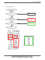
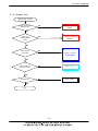
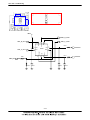
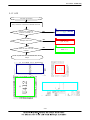
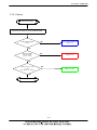
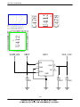
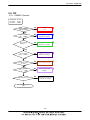
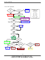
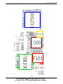
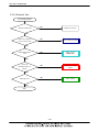
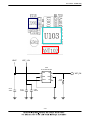
1
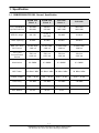
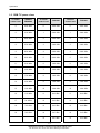
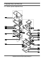
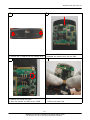
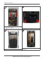
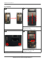
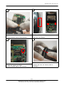
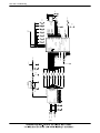
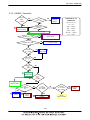
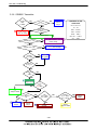
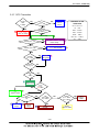
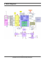
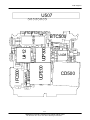
GSM TELEPHONE
SGH-U600
GSM TELEPHONE
CONTENTS
1.
Specification
2.
Exploded View and Parts list
3.
Chart of Troubleshooting
4.
Array course control
5.
Block Diagrams
6.
PCB Diagrams
7.
MAIN Electrical Parts List
8.
Reference data
9.
Safety Precautions
10. Product Function
Contents
1. Specification
1-1. GSM/CDMA General Specification ...........................................................................1-1
1-2. GSM TX power class ...............................................................................................1-2
2. Exploded View and Parts list
2-1. Cellular phone Exploded View ..................................................................................2-1
2-2. Cellular phone Parts list ............................................................................................2-2
2-3. Disassembly ...............................................................................................................2-4
2-4. Assembly ....................................................................................................................2-8
3. Chart of Troubleshooting
3-1. Baseband ............................................................................................................3-1
3-1-1. Power ON .....................................................................................................3-1
3-1-2. System Initial ................................................................................................3-6
3-1-3. SIM Part .......................................................................................................3-8
3-1-4. Charging Part .............................................................................................3-10
3-1-5. Microphone Part .........................................................................................3-13
3-1-6. Speaker Part ..............................................................................................3-16
3-1-7. Receiver Part .............................................................................................3-20
3-1-8. Camera Part ..............................................................................................3-22
1) 2Mega Camera .....................................................................................3-22
2) VGA Camera .........................................................................................3-23
3-1-9. LCD .............................................................................................................3-26
3-2. RF ......................................................................................................................3-13
3-2-1. EGSM Receiver .........................................................................................3-30
3-2-2. EGSM Transmitter .....................................................................................3-31
3-2-3. DCS Receiver ............................................................................................3-32
3-2-4. DCS Transmitter ........................................................................................3-33
3-2-5. PCS Receiver .............................................................................................3-34
3-2-6. PCS Transmitter .........................................................................................3-35
3-2-7. UMTS Receiver ..........................................................................................3-40
3-2-8. UMTS Transmitter ......................................................................................3-41
3-2-9. BLUETOOTH ..............................................................................................3-45
Contents
4. Array course control
4-1. Downloading Binary Files ......................................................................................4-2
4-2. Pre-requsite for Downloading ................................................................................4-2
4-3. S/W Downloader Program .....................................................................................4-3
5. Block Diagrams
6. PCB Diagrams
7. MAIN Electrical Parts List
8. Reference data
8-1. Reference Abbreviate ..............................................................................................8-1
9. Safety Precautions
9-1. Repair Precaution ......................................................................................................9-1
9-2. ESD(Electrostaically Sensitive Devices) Precaution ................................................9-2
10. Product Function
1. Specification
1-1. GSM/DCS1800/PCS1900 General Specification
EG SM 850
Phase 2
EGSM 900
Ph ase 2
DCS1800
Ph ase 1
PCS1 900
Fr eq. Band[ MHz]
Uplink/Downlink
824~849
869~894
880~915
925~960
1710~1785
1805~1880
1850~1910
1930~1990
ARFCN r ange
128 ~251
0~124 &
975~1023
512~885
512~810
Tx/ Rx sp acing
45 MHz
45 MHz
95 MHz
80 MHz
Mod. Bit rat e/
Bit Per iod
270.833 kbps
3.692 us
270.833 kbps
3.692 us
270.833 kbps
3.692 us
270.833 kbps
3.692 us
T im e S lot
Per iod/ Fra me
Period
576.9 us
4.615 ms
576.9 us
4.615 ms
576.9 us
4.615 ms
576.9 us
4.615 ms
Modu lation
0.3 GMSK
0.3 GMSK
0.3 GMSK
0.3 GMSK
MS Power
33 dBm~5 dBm
33 dBm~5 dBm
30 dBm~0 dBm
30 dBm~0 dBm
Power Cl ass
5 pcl ~ 19 pcl
5 pcl ~ 19 pcl
0 pcl ~ 15 pcl
0 pcl ~ 15 pcl
Sensitivity
-102 dBm
-102 dBm
-100 dBm
-100 dBm
T DM A M u x
8
8
8
8
Cell Radius
35 Km
35 Km
2 Km
-
1-1
SAMSUNG Proprietary-Contents may change without notice
This Document can not be used without Samsung's authorization
Specification
1-2. GSM TX power class
TX Power
TX Power
TX Power
control level
GSM850/
EGSM900
control level
5
33±2 dBm
0
30±3 dBm
0
30±3 dBm
6
31±2 dBm
1
28±3 dBm
1
28±3 dBm
7
29±2 dBm
2
26±3 dBm
2
26±3 dBm
8
27±2 dBm
3
24±3 dBm
3
24±3 dBm
9
25±2 dBm
4
22±3 dBm
4
22±3 dBm
10
23±2 dBm
5
20±3 dBm
5
20±3 dBm
11
21±2 dBm
6
18±3 dBm
6
18±3 dBm
12
19±2 dBm
7
16±3 dBm
7
16±3 dBm
13
17±2 dBm
8
14±3 dBm
8
14±3 dBm
14
15±2 dBm
9
12±4 dBm
9
12±4 dBm
15
13±2 dBm
10
10±4 dBm
10
10±4 dBm
16
11±3 dBm
11
8±4 dBm
11
8±4 dBm
17
9± 3dBm
12
6±4 dBm
12
6±4 dBm
18
7±3 dBm
13
4±4 dBm
13
4±4 dBm
19
5±3 dBm
14
2±5 dBm
14
2±5 dBm
15
0±5 dBm
15
0±5 dBm
DCS1800
control level
1-2
SAMSUNG Proprietary-Contents may change without notice
This Document can not be used without Samsung's authorization
PCS1900
2. Exploded View and Parts List
2-1. Cellular phone Exploded View
QFU01
QSP01
QCA01
QMI03
QLC01
QFR01
QVO02
QPC01
QCR68
QMP01
QFL01
QAN02
QAN06
QHI01
QCR04
QCR58
QAN07
QCK01
QSD01
QCR12
QRE01
QVO01
QRF03
QRF01
QBA01
QBA00
2-1
SAMSUNG Proprietary-Contents may change without notice
This Document can not be used without Samsung's authorization
Exploded View and Parts List
2-2. Cellular phone Parts list
Design LOC
Discirption
SEC CODE
QAN02
INTENNA-SGHU600
GH42-01133A
QAN06
ASSY COVER-INTENNA
GH98-04083A
QAN07
PMO-INTENNA DUMMY
GH72-36571A
QBA00
ASSY COVER-BATTERY
GH98-04770A
QBA01
INNER BATTERY PACK-690MAH,BLK,
GH43-02834A
QCA01
UNIT-SGHU600 CAMERA
GH59-04163A
QCR04
SCREW-MACHINE
6001-001479
QCR12
SCREW-MACHINE
6001-001530
QCR58
SCREW-MACHINE
6001-001870
QCR68
SCREW-MACHINE
6001-002067
QFU01
ASSY COVER-SLIDE UPPER
GH98-03317A
QLC01
LCD-MODULE SGHU600
GH07-01087A
QMP01
PBA MAIN-SGHU600
GH92-03347A
QPC01
MEA-SLIDE FPCB KIT
GH97-07452A
QRF01
PMO-COVER RF
GH72-36573A
QSP01
UNIT-SGHU600 SPEAKER MODULE
GH59-04046A
QFR01
ASSY CASE-FRONT PLATE
GH98-04811A
RMO-RUBBER MIC HOLDER
GH73-08776A
ASSY COVER-SLIDE LOWER
GH98-04051A
QHI01
ASSY HINGE-SLIDE
GH98-03319A
QVO02
PMO-POWER KEY
GH72-38555A
ASSY CASE-REAR
GH98-04052A
QCK01
PMO-KEY CAMERA
GH72-37516A
QRF03
PMO-COVER EAR/IF
GH72-36576A
QSD01
PMO-COVER MICRO SD
GH72-36575A
QVO01
PMO-VOLUME KEY
GH72-37517A
QMI03
QFL01
QRE01
2-2
SAMSUNG Proprietary-Contents may change without notice
This Document can not be used without Samsung's authorization
Exploded View and Parts List
Discirption
SEC CODE
BAG PE
6902-000297
CBF INTERFACE-DLC,X830,BLK,PCB
GH39-00720A
ADAPTOR-SGHE690,BLK,EU,A_TYPE
GH44-01361A
S/W CD-SGHU600 PC STUDIO 3.1
GH46-00384A
UNIT-SGHU600,HEADSET,BLK,A TYP
GH59-04446A
LABEL(R)-WATER SOAK
GH68-09361A
LABEL(P)-OPEN MP3
GH68-11246A
LABEL(R)-MAIN(FRANCE)
GH68-14054F
MANUAL USERS-EU FRENCH
GH68-14139A
BOX(P)-UNIT MAIN(EU)
GH69-05115A
CUSHION-CASE TA2 MA2
GH69-05116A
RMO-RUBBER TACT SWITCH
GH73-09461A
MPR-TAPE PBA A
GH74-16066A
MPR-VINYL BOHO MAIN WINDOW
GH74-30725A
MPR-INSU TAPE LCD PCB
GH74-30734A
MPR-TAPE 3X4 KEY IN
GH74-30763A
MPR-TAPE C2C IN
GH74-30764A
MPR-INSU TAPE
GH74-30765A
MPR-GASK TAPE
GH74-30766A
MPR-VINYL BOHO KEY SUB
GH74-30847A
MPR-VINYL BOHO MAIN WINDOW 2
GH74-31274A
MPR-INSU TAPE SPK MODULE
GH74-31527A
MPR-ELEC TAPE
GH74-31528A
MPR-TAPE BATTERY ROOM
GH74-31712A
MPR-ELEC TAPE
GH74-31714A
MPR-INSU TAPE
GH74-31884A
MPR-ELEC TAPE CON TO CON B
GH74-32141A
AS-LCD WINDOW TAPE
GH81-06188A
2-3
SAMSUNG Proprietary-Contents may change without notice
This Document can not be used without Samsung's authorization
Exploded View and Parts List
2-3. Disassembly
1
2
1) Open the RF COVER from the REAR case
1) Open the intenna cover dummy
3
1) Take off IMEI lable
4
1) UNSCREW the 5 POINTS
2-4
SAMSUNG Proprietary-Contents may change without notice
This Document can not be used without Samsung's authorization
Exploded View and Parts List
6
5
1) Unscrew the 2 POINTS from the intenna cover
1) Take off the REAR case
2) Separate the Intenna cover from the PBA
7
8
1) Remove the number key tape
2) Open the actuator and take out the FPCB
1) Separate the PBA with taking off the slide
FPCB on the other side
2-5
SAMSUNG Proprietary-Contents may change without notice
This Document can not be used without Samsung's authorization
Exploded View and Parts List
10
9
1) Unscrew the 6 POINTS
2) Saparate Front cover from the slide upper ass'y
1) UNSCREW the 2 POINTS
11
12
1) Remove the Black shield tape on the
1) Open the Slide lower cover with lifting the case
components
2-6
SAMSUNG Proprietary-Contents may change without notice
This Document can not be used without Samsung's authorization
Exploded View and Parts List
2-4. Assembly
2
1
1) Put the slide lower cover with checking the
lockers and LCD FPCB
1) Put the black insulated tape on the components 2) Push the cover following an arrow
3
4
1) SCREW the 2 POINTS
1) Put the front cover on the slide ass'y
2) Check the slide FPCB is right
3) SCREW the 6 POINTS
2-7
SAMSUNG Proprietary-Contents may change without notice
This Document can not be used without Samsung's authorization
Exploded View and Parts List
6
5
1) Let the slide FPCB in the main board socket
- The connector must be firmly pressed
1) PUT the PBA on the cover
- check the Front Damper
7
8
1) Put the intenna cover
- Handle with case, the intenna could be
damaged
1) Insert the numeric key FPCB
2) Put the insulate tape on the connector.
2-8
SAMSUNG Proprietary-Contents may change without notice
This Document can not be used without Samsung's authorization
Exploded View and Parts List
10
9
1) Combine the REAR cover with checking the
locker
2) Press the connector to lock the cover
1) SCREW the 5 POINTS
11
12
1) SCREW the 2 POINTS
1) Set the IMEI lable
2-9
SAMSUNG Proprietary-Contents may change without notice
This Document can not be used without Samsung's authorization
Exploded View and Parts List
13
14
1) Combine the REAR cover with checking the
locker
2) Press the connector to lock the cover
1) SCREW the 5 POINTS
2-10
SAMSUNG Proprietary-Contents may change without notice
This Document can not be used without Samsung's authorization
3. Flow Chart of Troubleshooting
3-1 BASEBAND
3-1-1. Power ON
'Power On' does not work
Yes
Check the current
consumption more
than 100mA
No
Download again
Yes
No
Check the VBAT
more than 3.3V
Charge the Battery
Yes
①
Check the
VLDO7_1.8V
of UCP300 is more
than 1.8V
No
Check UCP300 and C314
Yes
②
Check U201
pin 1 = 1.8V
pin 4 = 1.6V
pin 7,9 = 1.5V
No
Check U201
Yes
③
Check UCP300
No
Check VRF of
UCP300=2.9V
and C315
Yes
④
Check C131
Freq = 13MHz
Vp-p > 0.8V
No
Yes
Check the initial operation
Yes
END
3-1
Check the clock C131
Flow Chart of Troubleshooting
3-2
Flow Chart of Troubleshooting
VBAT
R214
HP_CORE_1.6V
VCCD_1.8V
D200
U201
GND2
1
ADJ2
2 MODE|DATA
3
VIN
4 FB1
5
DEF_1
SW2
EN2
GND
EN1
SW1
10
9
8
7
6
L200
VLDO1_1.5V
L201
11
C210
C211
3-3
C212
C213
SERLE
SERDAT
SERCLK
BAND_SEL
MOD_SEL
TX_EN
XOENA
SX_EN
PAC_EN
RX_EN
DSP_IO
DSP_RWN
FLASH_RESET
DSP_AB(0:8)
DSP_DB(15)
DSP_DB(14)
DSP_DB(13)
DSP_DB(12)
DSP_DB(11)
DSP_DB(10)
DSP_DB(9)
DSP_DB(8)
DSP_DB(7)
DSP_DB(6)
DSP_DB(5)
DSP_DB(4)
DSP_DB(3)
DSP_DB(2)
DSP_DB(1)
DSP_DB(0)
DSP_AB(8)
DSP_AB(7)
DSP_AB(6)
DSP_AB(5)
DSP_AB(4)
DSP_AB(3)
DSP_AB(2)
DSP_AB(1)
DSP_AB(0)
EAR_CHECK
DB15
DB14
DB13
DB12
DB11
DB10
DB9
DB8
DB7
DB6
DB5
DB4
DB3
DB2
DB1
DB0
AB8
AB7
AB6
AB5
AB4
AB3
AB2
AB1
AB0
I|O
RWN
RESETN_CSP
OCTL0
OCTL1
OCTL2
OCTL3
OCTL4
OCTL5
OCTL6
OCTL7
SERLE1
SERLE2
SERDA
SERCK
D2
D3
E3
E2
F3
F2
F1
F4
G4
G3
H5
J6
J5
K3
K2
K1
K5
K7
M1
M2
N2
N1
L5
P1
K6
L3
L2
R3
E6
C5
F5
E5
A4
G6
B3
A3
B1
A2
C1
C2
A FC
TX P
D9
E7
C322
A FC
VA PC
B5
B6
D7
D6
C7
C6
RTXIP
R TX I N
RTXQP
RTXQN
DSP_DB(0:15)
C301
C304
VCCA_2.9V
C323
A OUTA P
A OUTA N
A OUTB P
A OUTB N
MICINP
MICINN
MICOUTP
MICOUTN
A UXINP
A UXINN
A UXOUTP
A UXOUTN
RA REF2
RA REF1
RXTXIP
RXTXIN
RXTXQP
RXTXQN
C302
VCCD_1.8V
C303
VCCD_2.9V
UCP300
ADC_AUX2
ADC_AUX1
VREF
CREF
RTC_ALMN
VEXT
VBAT
CH_BDRV
CH_ISEN
CH_RES
CSN_PSC
SCLK_PSC
SDO_PSC
SDI_PSC
VSIM
VRTC
LED2_DRV
LED1_DRV
RING_DRV
VIB_DRV
VLDO_7
VLDO_6
VL5S_B
VL5S_A
VLDO_5
VL4S_B
VL4S_A
VLDO_4
VLDO_3
VLDO_2
VLDO_1
VACC
D15
E10
A10
E9
H10
E14
E13
E11
F12
D14
K8
L8
N7
M7
K12
H11
G12
G13
F13
F15
C12
A14
C9
D10
B10
B11
A12
B12
A13
J12
G11
F14
N9
R10
P10
J11
K11
K14
VDD34 C11
VDD12 J13
UP_CLK
UP_RST
UP_IO
SIM_IO
SIM_RST
SIM_CLK
2
1
K 10
J 10
J9
J8
J7
H9
H8
H7
H6
G1 0
G9
G8
G7
F1 0
F9
F8
F7
D 13
NC6
NC5
GNDS17
GNDS16
GNDS15
GNDS14
GNDS13
GNDS12
GNDS11
GNDS10
GNDS9
GNDS8
GNDS7
GNDS6
GNDS5
GNDS4
GNDS3
GNDS2
GNDS1
A UX_A DC3
A O U TA P
A O U TA N
A O U TB P
A O U TB N
MICINP
MICINN
MICOUTP
MICOUTN
A UXINP
A UXINN
A UXOUTP
A UXOUTN
VXVCM
VREGP
VREGN
DA ICK
DA IRN
DA IDI
DA IDO
P11
N12
R12
P12
N14
M14
N15
P15
M15
L 14
K 13
L 13
R13
M13
R14
R4
P4
L6
M6
RTC_CL K
XOENA Q
MC
A DC_A UX4
DINTR
DSP_INT
N4
D1
R6
P5
P3
C L K 32K
XOENA Q
CL K 13M_MC
VBAT
C320
VBAT
C310
ICHRG
RTCALARM
CF
VSIM
C312
VCCB_2.9V
VBAT
INTRQ
PWR_KEEP
RST
R308
UP_CS
UP_SCLK
UP_SDO
UP_SDI
DCS_TX_EN
GSM_TX_EN
KEY_BL_MAIN
SIMCLK
SIMRST
SIMDATA
SIM_IO
SIM_RST
SIM_CLK
C307
C314
VCCD_1.8V_PSC
C313
VCCA_2.9V
C315
VRF_2.9V
C321
C316
R307
C317
VCCD_2.9V VLDO1_1.5V
R306
VR301
C318
C311
BAT300
C319
VCCB_2.9V
R305
VRTC_1.5V
P OS
B4
C4
P13
L 11
F6
A6
M10
N 11
P6
R2
K4
G5
J4
N5
N6
M3
J3
F1 1
K 15
B 15
E8
B 13
C 10
J IG_ON
PWR_ON
PSW1_B UF
1
2
GND_OCTL
VDD_OCTL
GNDV
VDDV
GNDB
VDDB
GNDD
VDDD
VSS4
VSS3
VSS2
VSS1
VDD_IO2
VDD_IO1
VDD3
VDD2
VDD1
GND_HCUR
GND_PSC2
GND_PSC1
GNDQ
VDD67
VDD5
PWR_SW2
PWR_SW1N
PSW1_B UF
RESET_O
MODE
PWR_K EEP
INTRQ
VIB _RNG_EN
C14
C15
L7
K9
N10
M9
L 10
L9
3-4
NEG
VRF_2.9V
Flow Chart of Troubleshooting
Flow Chart of Troubleshooting
9-2-2. Initial
Initial Failure
Yes
①
Check VCCD,
VCCD_1.8V of UCP300
"High" when the phone
is boot on`
No
Check UCP300
Yes
②
Check
the HP_CORE_1.6V of
U201 is "High"
No
Check U201
Yes
LCD display is O.K?
③
No
Check HDC500 and LCD part
Yes
Sound is O.K?
No
Check audio part
Yes
END
3-5
Flow Chart of Troubleshooting
VMOT_3.3V
VCAM_2.8V
VCCD_2.9V
3.1V_TOUCH
VBAT
VCCD_2.9V
VCAM_1.8V
HDC500
1
3
5
7
9
TOUCH_RST
SCL_TOUCH_M
LCD_ADS_O
LCD_WEN_O
LCD_DO(0)
LCD_DO(2)
LCD_DO(4)
LCD_DO(6)
LCD_DO(8)
LCD_DO(10)
LCD_DO(12)
LCD_DO(14)
MLCD_BL_EN
11
13
15
17
19
21
23
25
27
29
31
33
35
37
39
41
43
45
47
49
51
53
55
57
59
VCA_3.3V
CAM_D(0)
CAM_D(2)
CAM_D(4)
CAM_D(6)
CAM_VSYNC
CAM_HSYNC
C_SCL
CAM_RST
2
4
6
8
10
12
14
16
18
20
22
24
26
28
30
32
34
36
38
40
42
44
46
48
50
52
54
56
58
60
2
4
6
8
10
12
14
16
18
20
22
24
26
28
30
32
34
36
38
40
42
44
46
48
50
52
54
56
58
60
TOUCH_IRQ
SDA_TOUCH_M
PWR_ON
MLCD_CS_O
LCD_DO(1)
LCD_DO(3)
LCD_DO(5)
LCD_DO(7)
LCD_DO(9)
LCD_DO(11)
LCD_DO(13)
LCD_DO(15)
LCD_FLM
FLASH_EN
CAM_D(1)
CAM_D(3)
CAM_D(5)
CAM_D(7)
M_CLK
P_CLK
C_SDA
VCAM_EN
R533
R534
R535
V502
V501
V500
61
62
63
64
NC
NC
NC
NC
SPK_P_CON
1
3
5
7
9
11
13
15
17
19
21
23
25
27
29
31
33
35
37
39
41
43
45
47
49
51
53
55
57
59
3-6
LCD_READ
SPK_N_CON
Flow Chart of Troubleshooting
3-1-3. Sim Part
Phone can't access
SIM card
①
Check the pin 1 of
SIM300
Voltage = 3V
NO
Check the circuit related to
UCP300
YES
Check the SIM
connector's
(SIM300)
connector's to SIM
card
②
NO
resolder or change
SIM300
YES
Check the circuit around SIM30 0
input circuitry
③
NO
Check the related circuit of
SIM300
YES
Check the circuit around
UCP300 output
and voltage supply circuitry
④
NO
Check the related circuit of
UCP300
YES
END
3-7
Flow Chart of Troubleshooting
SIM300
VSIM
SIM_RST
SIM_CLK
C330
C331
C332
C333
3-8
1
2
3
1
2
3
7
8
9
7
8
9
6 6
5 5
4 4
12 12
11 11
10 10
G G G G
16 15 14 13
SIM_IO
C334
Flow Chart of Troubleshooting
3-1-4. Charging Part
Abnormal charging part
Yes
①
Battery Contact at
BTC500?
No
Yes
Charger input of
IFC500 ?
Battery Check BTC500
②
No
Check the IFC500
Yes
END
3-9
Flow Chart of Troubleshooting
VCCD_1.8V
R524
R525
1
7
6
2
5
8
3
VBAT
JIG_ON_IF_B
SDS_RXD_B
4
IFC500
ZD500
1
2
3
4
5
6
7
8
9
10
11
12
13
14
15
16
17
18
19
20
21
22
23
24
R_ANT
EAR_MICP
EAR_MICN
EAR_R
EAR_L
EAR_SWITCH
JACK_IN
EAR_CHECK
T_OPT
SDS_RXD
R527
R528
R529
R530
R531
JIG_ON_IF
USB_D+
L501
6
1
7
2
8
3
5
ZD502
4
ZD504
ZD503
TA501 C520
C517
C518
C519
TA502
L500
ZD501
USB_DUSB_5.0V
TA_VEXT
VBAT
1
2
3
4
5
6
7
CF
C508
C509
TA500
1
2
3
NC
NC
NC
NC
BTC500
3-10
1
2
3
4
5
6
7
8
9
10
11
12
13
14
15
16
17
18
19
20
NC
NC
NC
NC
25
NC
26
NC
27
NC
28
NC
Flow Chart of Troubleshooting
3-1-5. Microphone Part
Microphone does not work
Check the
assembled status of
microphone.
NO
Reassemblage microphone
YES
Check the reference
voltage on mic path
R409=2.9V
NO
resolder or change
(R409,
TA403,C431,R411)
YES
Is microphone ok?
NO
Check UCP300
YES
END
3-11
Flow Chart of Troubleshooting
VAUDIO_3.1V
TI_1.8V
C423
C424
SPK_P
SPK_N
CSP_MICP
CSP_MICN
TA403
B2
A2
A1
B3
C431
R411
YMU_EAR_R
YMU_EAR_L
RADIO_R
RADIO_L
C442
C443
MIC+
C448
C444
C449
AOUTBP
AOUTBN
MSPK+
MSPK-
B4
A3
A4
B5
B7
B6
A6
A5
IOVDD
VDDA 1
VDDA 1
VDDA 1
DVDD
A VDDA 2
MICDET
MICBIAS
MIC3R
MIC3L
HPROUT
HPRCOM
HPLOUT
HPLCOM
GPIO2
GPIO1
U408
DOUT
DIN
SELECT
SDA
SCL
/RESET
MCLK
WCLK
BCLK
MFP3
MFP2
MFP1
MFP0
LINE2RP
LINE2RM
LINE2LP
LINE2LM
LINE1RP
LINE1RM
LINE1LP
LINE1LM
NC
NC
NC
TA401
G1
F1
D1 TA402
E1
R455
R456
MICINP
MICOUTP
F8
E9
C335
R318
MICINN
MICOUTN
R319
E8
D8
C8
H8
G8
F9
G9
SDA
SCL
TI_RESET
TI_MSCK
TI_LRCK
TI_BCK
1
2
A7
C337
R320
3-12
C329
CSP_MICN
C336
EAR_L
TI_SDIN
TI_SDOUT
CSP_MICP
R317
EAR_R
J8
J9
D9
E2
F2
G2
H2
C2
D2
R414
A9
A8
B9
B8
RIGHT_LOP
RIGHT_LOM
LEFT_LOP
LEFT_LOM
MONO_LOP
MONO_LOM
C426
DVSS
DRVSS
DRVSS
A VSS_DA C
A VSS_DA C
A VSS_A DC
A VSS_A DC
J6
J7
J4
J5
J2
J3
R409
MIC-
C425
C9
B1
C1
H1
H9
J1
VCCA_2.9V
Flow Chart of Troubleshooting
3-1-6. Speaker Part
Speaker does not work
Is the terminal of
Speaker OK?
NO
check the specker connector
HDC500
YES
①
Check the
pin 58,59of HDC500
"HIGH"
Change or resolder
HDC500
NO
YES
②
Check the circuit
around U409
NO
Change or resolder
around U409
YES
③
Check the voltage of
R420, R431 is high
NO
Check UCP300
NO
Change speaker
YES
Is speaker OK?
YES
END
3-13
Flow Chart of Troubleshooting
VBAT
SPK_N_CON
NO1
3
R432
NC
U409
IN1
COM1
SPK_P_OUT
VCC
4
SPK_P_CON
8
R420
7
R431
5
AOUTAP
AMP_EN
C470
AOUTAN
GND 6
NC1
2
NO2
1
9
IN2
10
COM2
SPK_N_OUT
C471
C472
3-14
C473
Flow Chart of Troubleshooting
3-1-7. LCD
LCD does not Display
First, Check the connection of HDC500 and LCD
①
Have a some problem of
connector (HDC500, J1)
YES
Replace a connector (HDC500,
J1)
NO
NO
②
Check of U1
(pin 19, 20)
Backlight does work
YES
check the data line from
HDC500
③
NO
Check U412
YES
try with the new LCD module and
change
3-15
Flow Chart of Troubleshooting
VCCD_1.8V
CORE_1.2V_O
CORE_1.2V
CORE_1.2V_PLL
VCAM_2.8V
VCCD_2.9V
C432 C427
C430
C439
USB_1.2V
C433
C428
C434
USB_3.3TV
C435
USB_3.3CV
C436
C437
C438
C441
HERA_CS
A(18)
CP_OEN
CP_WEN
A(8)
HERA_INT
M_HOLD
HERA_RST
OSC400
2
R418
1
3
4
H14
G14
CAM_D(0:7)
C459
C461
C460
VCAM_2.8V
R457
M_CLK
C479
R427
R428
CAM_D(0)
CAM_D(1)
CAM_D(2)
CAM_D(3)
CAM_D(4)
CAM_D(5)
CAM_D(6)
CAM_D(7)
CAM_HSYNC
CAM_VSYNC
C480
CAM_RST
P_CLK
C_SDA
C_SCL
N11
P11
M11
M10
N10
P12
L10
TI_MSCK
TI_BCK
TI_LRCK
SCL
SDA
TI_SDOUT
TI_SDIN
LCD_D(0:15)
VCCD_1.8V
R434
R435
MLCD_CS
LCD_WEN
LCD_READ
LCD_ADS
D1
D2
D3
D4
D5
E1
E2
E3
B4
C1
B3
C5
C2
C3
C4
F1
LCD_D(0)
LCD_D(1)
LCD_D(2)
LCD_D(3)
LCD_D(4)
LCD_D(5)
LCD_D(6)
LCD_D(7)
LCD_D(8)
LCD_D(9)
LCD_D(10)
LCD_D(11)
LCD_D(12)
LCD_D(13)
LCD_D(14)
LCD_D(15)
M2
M1
L4
L3
L2
L1
K4
K3
K2
K1
J4
J3
J2
J1
H4
H3
H2
H1
G4
L5
M3
N2
G3
N1
M4
TDI
TRST
TMS
TCK
RTCK
TDO
SD_D0
SD_D1
SD_D2
SD_D3
SD_CLK
SD_CMD
SD_WP
XIN
XOUT
C_D0
C_D1
C_D2
C_D3
C_D4
C_D5
C_D6
C_D7
C_HS
C_VS
C_RST
C_PCLK
C_MCLK
C_SDA
C_SCK
GPIOS_D15
T_VRO
T_VREF
T_OUT
U412
USB_DP
USB_DM
USB_ID
USB_VBUS
USB_REXT
USB_VBUS_DRV
STROBE
TESTMODE
C_PWDN
PWR_STRB
G_INT
MASTER0
D_MSCK
D_BCK
D_LRCK
D_SCK
D_SDA
D_SDATAOUT
D_SDATAIN
L_DA0
L_DA1
L_DA2
L_DA3
L_DA4
L_DA5
L_DA6
L_DA7
L_DA8
L_DA9
L_DA10
L_DA11
L_DA12
L_DA13
L_DA14
L_DA15
L_DA16
L_DA17
L_CS_N
LS_CS_N
L_WR_N
L_RD_N
L_ADS
L_PCLK
GPIOL_D13
SOUT0
XRTS0
SIN0
XCTS0
N_D0
N_D1
N_D2
N_D3
N_D4
N_D5
N_D6
N_D7
N_RE_N
N_WE_N
N_ALE
N_CLE
N_CS_N
N_RDY
GPIO1_D0
GPIO1_D1
GPIO1_D2
GPIO1_D3
GPIO1_D4
GPIO1_D5
GPIO1_D6
GPIO1_D7
VSSA 33T
VSSA 33T
VSSA 33C
VSSp l l
VSSQ
VSSQ
A VSSt v
VSS
VSS
VSS
VSS
VSS
D(0)
D(1)
D(2)
D(3)
D(4)
D(5)
D(6)
D(7)
D(8)
D(9)
D(10)
D(11)
D(12)
D(13)
D(14)
D(15)
M_SA0
M_SA1
M_SA2
M_SD0
M_SD1
M_SD2
M_SD3
M_SD4
M_SD5
M_SD6
M_SD7
M_SD8
M_SD9
M_SD10
M_SD11
M_SD12
M_SD13
M_SD14
M_SD15
M_CS_N
MS_CS_N
M_RD_N
M_WR_N
M_ADS
M_INTR
M_HOLD
M_RESET_N
J 13
J 12
J 14
G9
F6
J9
F4
G6
H6
J6
F9
H9
A14
B13
C11
G11
E14
F13
F12
F11
E13
D14
E12
E11
C14
D13
D12
D11
C13
B14
C12
B10
B11
C10
D9
A13
B12
A12
D10
A(1)
A(2)
D[0:15]
VDDi
VDDi
VDDc
VDDc
VDDc
VDDC0
VDDp l l
VDDs
VDDl c d
VDDR
VDDR
VDDs d
VDDac
A VDDt v
VDDg 1
VDD12u s b
VDDA 33T
VDDA 33T
VDDA 33C
F8
J7
G7
H7
H8
E10
G8
E5
K5
F7
J8
L 11
K 10
F3
M9
L 12
H1 1
H1 2
H1 3
C440
VDD_TV_2.8V
3-16
NC
NC
NC
NC
NC
NC
NC
NC
NC
NC
NC
NC
NC
NC
NC
NC
NC
NC
NC
NC
C9
D8
B9
A10
A6
B7
C7
A7
A8
B8
A9
C8
M6
M8
N8
P8
P6
N6
VCCD_1.8V
A1
A2
A3
A4
B5
D6
C458
USB_3.3CV
N13
N12
M14
M13
P13
N14
M12
G2
G1
F2
L14
K14
K11
K12
K13
L13
VDD_TV_2.8V
R419
C462
GOLD_TV_OUT
USB_HERA+
USB_HERA-
USB_5.0V
R429
B2
J11
B1
A11
G12
F14
PWR_STRB
M5
L8
P9
N9
L9
P10
N5
P14
A5
B6
C6
D7
E4
G13
L6
L7
M7
N3
N4
N7
P1
P2
P3
P4
P5
P7
1
2
R430
TV_EN
VCAM_EN
USB_CHG_ON
USB_EN
TOUCH_RST
LCD_FLM
CHG_OFF
R436
Flow Chart of Troubleshooting
3-1-8. Camera
Camera does not work
Check the connection of J2 and CAMERA Module
Check camera FPCB
and J2
Change camera module and
check of J2
NO
YES
Check the voltage
pin 4 of U413
(Pin 4 : 3.3V)
NO
Change U413
YES
Check pin C5, C2 of
U412
NO
Check of U412
(C5 :48MHz, C2 :24MHz)
YES
END
3-17
Flow Chart of Troubleshooting
VCAM_EN
VBAT
VCA_3.3V
U413
3 VIN
VOUT 4
2 GND
1 STBY
NC
5
GND
6
C476
C477
3-18
C478
Flow Chart of Troubleshooting
3-2. RF
3-2-1. GSM850 Receiver
CONTINUOS RX ON
RF INPUT : 190CH
Cell power : -50dBm
NORMAL CONDITION
catch the channel?
NO
CHECK
1
C100
YES
F101 CHECK
pin6 ≥ -65dBm?
NO
RFS100
resolder or change
NO
F101
resolder or change
NO
L103, L104, C111
resolder or change
2
YES
F101 CHECK
pin18,19 ≥ -
3
YES
U100 CHECK
pin2,3 ≥ -65dBm?
4
YES
the power source
of U100
NO
5
check battery contact
YES
U100 CHECK
Pin15,17 :13MHz
NO
check OSC100 and
change
YES
GSM Receiver is ok?
NO
GSM RX path component
resolder or change
END
3-19
6
Flow Chart of Troubleshooting
3-2-2. GSM900 Receiver
CONTINUOS RX ON
RF INPUT : 62CH
Cell power : -50dBm
NORMAL CONDITION
catch the channel?
NO
CHECK
1
C100
YES
F101 CHECK
pin6 ≥ -65dBm?
NO
RFS100
resolder or change
NO
F101
resolder or change
NO
L105, L106, C115
resolder or change
2
YES
F101 CHECK
pin17,18 ≥ 65dBm?
3
YES
U100 CHECK
pin4,5 ≥ -65dBm?
4
YES
the power source
of U100
NO
5
check battery contact
YES
U100 CHECK
Pin15,17:13MHz
NO
check OSC100 and
change
YES
GSM Receiver is ok?
NO
GSM RX path component
resolder or change
END
3-20
6
Flow Chart of Troubleshooting
3-2-3. DCS Receiver
CONTINUOS RX ON
RF INPUT : 698CH
Cell power : -50dBm
NORMAL CONDITION
catch the channel?
NO
CHECK
1
C100
YES
F101 CHECK
pin6 ≥ -65dBm?
NO
RFS100
resolder or change
NO
F101
resolder or change
NO
L107, L108
resolder or change
2
YES
F101 CHECK
pin14,15 ≥ 65dBm?
3
YES
U100 CHECK
pin6,7 ≥ -65dBm?
4
YES
the power source
of U100
NO
5
check battery contact
YES
U100 CHECK
Pin15,17:13MHz
NO
check OSC100 and
change
YES
GSM Receiver is ok?
NO
GSM RX path component
resolder or change
END
3-21
6
Flow Chart of Troubleshooting
3-2-4. PCS Receiver
CONTINUOS RX ON
RF INPUT : 698CH
Cell power : -50dBm
NORMAL CONDITION
catch the channel?
NO
CHECK
1
C100
YES
F101 CHECK
pin6 ≥ -65dBm?
NO
RFS100
resolder or change
NO
F101
resolder or change
NO
L109, L110
resolder or change
2
YES
F101 CHECK
pin12,13 ≥ 65dBm?
3
YES
U100 CHECK
pin8,9 ≥ -65dBm?
4
YES
the power source
of U100
NO
5
check battery contact
YES
U100 CHECK
Pin15,17:13MHz
NO
check OSC100 and
change
YES
GSM Receiver is ok?
NO
GSM RX path component
resolder or change
END
3-22
6
Flow Chart of Troubleshooting
3-23
3-24
GSM_OUT
DPCS_OUT
DCS_TX_EN
GSM_TX_EN
C127
0.01NF
C126
0.01NF
ANT
8
18
19
EGSM_RX 16
EGSM_RX 17
DCS_RX 14
DCS_RX 15
PCS_RX 12
PCS_RX 13
850_RX
850_RX
FEMGEDPBD5440EGG
L100
39nH
1 2 3 4 7 9 10 11 20 23 24 25 26 27 28
G G G G G G G G G G G G G G G
5 EGSM_TX
22 DCS|PCS_TX
21 VC2
6 VC1
F101
C100
22pF
C128
NC
C123
NC
0.75PF
C115
0.75PF
C111
R119
0
L101
18nH
L110
4.7nH
L109
4.7nH
L108
6.2nH
L107
6.2nH
L106
10nH
L105
10nH
L104
10nH
L103
10nH
C101
NC
L102
3PF
ANT
R111
MOD_SEL
39K,1%
SAT_DET
TX_FB
VPC
DCS74138_OUT
GSM74138_OUT
ANT101
ANT100
41
39
14
36
35
12
33
32
31
2
3
4
5
6
7
NC
MODE_LON
LPFADJ
TX_IM
TX_IP
TX_QM
TX_QP
C106
10nF
U100
SKY74138
VAPC
CHIPENA
VDIGENA_LOP
NC|UHFTUNE+_RX_IP_NC7_IPUHFVTUNE
NC|TICVTUNE?_RX_IM_NC6_IMTICVTUNE
NC|RX_QP_IFTESTP_IFPORRX_QP
NC|RX_IM_IFTESTM_IFMORRX_QM
SXENA
TXENA
RXENA
XBUF
XTUNE
XTAL
CLK
DATAIN
LATCHENABLE
R100
1
COMPN_CALOUT_TEST_ERRM
PA_SAT_DET_TEST_ERRP
TXRFIN
VPC
TXHB
TXLB
850LNA_M
850LNA_P
900LNA_M
900LNA_P
1800LNA_M
1800LNA_P
1
18
26
11
VCC1
V CC2
V CC3
V CC4
G
4
C
3
A
2
G
1
RFS100
KMS-512
13
38
40
22
23
24
25
37
34
10
15
16
17
20
19
21
28
27
29
30
C107
2.2UF
C102
100nF
XOENA
SX_EN
TX_EN
RX_EN
SERCLK
SERDAT
SERLE
RTXIN
RTXIP
RTXQN
RTXQP
C108
22pF
VBAT
C103
10UF
10V
C129
0.12nF
R112
10K
C124
10nF
1
4
GND2
HOT
VAPC
13M_BUF
AFC
3
HOT
GND1
2
C104
100nF
R108
10K
OSC100
TN4-26374
C109
100PF
R109
0
Flow Chart of Troubleshooting
Flow Chart of Troubleshooting
3-2-5. GSM850 Transmitter
F101 pin 8
about
NO
2~5dBm?
2
UCP300
check &
NO
F101
pin 6 : 2.8V
CONTINUS TX ON
CONDITION
change
MS TX level 19
YES
YES
1
F101, C100
check & change
CH : 190
RBW : 100KHz
PAM100 pin7
3~6dBm?
NO
VBW : 100KHz
YES
NO
PAM100 pin 4 : 3.7V
SPAN : 10MHz
3
PAM100/R105 check & change
REF LEV. : 10dBm
BATTERY, BATTERY CONNECTOR
check & change
ATT. : 20dB
4
YES
NO
PAM100 pin3: 'LOW'
UCP300 check & change
5
YES
NO
PAM100
pin 1: 'HIGH'
6
UCP300
check & change
YES
PAM100
pin 6 : 1.2V
?
NO
YES
PAM101 pin
12
: -5dBm?
NO
YES
7
PAM100
change&resolder
U100
pin31 :
7~11dBm?
NO
C112
change or resolder
8
YES
U100
pin27,28,29,30
1.7V
NO
U100
pin17 13MHz
Vp-p :950mV
NO
9
YES
UCP300
change
10
U100
check &
change
YES
11
U100 change or
resolder
3-25
NO
OSC100
pin 3 : 13MHz
Vp-p : 950mV
NO
OSC100
change or resolder
YES
U100
change or
resolder
Flow Chart of Troubleshooting
3-2-6. GSM900 Transmitter
F101 pin 8
about
NO
2~5dBm?
2
UCP300
check &
NO
F101
pin 6 : 2.8V
CONTINUS TX ON
CONDITION
change
MS TX level 19
YES
YES
1
F101, C100
check & change
CH : 62
RBW : 100KHz
PAM100 pin7
3~6dBm?
NO
VBW : 100KHz
YES
NO
PAM100 pin 4 : 3.7V
SPAN : 10MHz
3
PAM100/R105 check & change
REF LEV. : 10dBm
BATTERY, BATTERY CONNECTOR
check & change
ATT. : 20dB
4
YES
NO
PAM100 pin3: 'LOW'
UCP300 check & change
5
YES
NO
PAM100
pin 1: 'HIGH'
6
UCP300
check & change
YES
PAM100
pin 6 : 1.2V
?
NO
YES
PAM101 pin
12
: -5dBm?
NO
YES
7
PAM100
change&resolder
U100
pin31 :
7~11dBm?
NO
C112
change or resolder
8
YES
U100
pin27,28,29,30
1.7V
NO
U100
pin17 13MHz
Vp-p :950mV
NO
9
YES
UCP300
change
10
U100
check &
change
YES
11
U100 change or
resolder
3-26
NO
OSC100
pin 3 : 13MHz
Vp-p : 950mV
NO
OSC100
change or resolder
YES
U100
change or
resolder
Flow Chart of Troubleshooting
3-2-7. DCS Transmitter
F101 pin 8
about
NO
2~5dBm?
2
UCP300
check &
NO
F101
pin 21 : 2.8V
CONTINUS TX ON
CONDITION
change
MS TX level 12
YES
YES
1
F101, C100
check & change
CH : 698
RBW : 100KHz
PAM100 pin2
3~6dBm?
NO
VBW : 100KHz
YES
NO
PAM100 pin 4 : 3.7V
SPAN : 10MHz
3
PAM100 check & change
REF LEV. : 10dBm
BATTERY, BATTERY CONNECTOR
check & change
ATT. : 20dB
4
YES
NO
PAM100 pin3: 'LOW'
UCP300 check & change
5
YES
NO
PAM100
pin 1: 'HIGH'
6
UCP300
check & change
YES
PAM100
pin 6 : 1.2V
?
NO
YES
PAM101 pin
14
: -5dBm?
NO
YES
7
PAM100
change&resolder
U100
pin32 :
7~11dBm?
NO
C105
change or resolder
8
YES
U100
pin27,28,29,30
1.7V
NO
U100
pin17 13MHz
Vp-p :950mV
NO
9
YES
UCP300
change
10
U100
check &
change
YES
11
U100 change or
resolder
3-27
NO
OSC100
pin 3 : 13MHz
Vp-p : 950mV
NO
OSC100
change or resolder
YES
U100
change or
resolder
Flow Chart of Troubleshooting
3-2-8. PCS Transmitter
F101 pin 8
about
NO
2~5dBm?
2
UCP300
check &
NO
F101
pin 21 : 2.8V
CONTINUS TX ON
CONDITION
change
MS TX level 12
YES
YES
1
F101, C100
check & change
CH : 660
RBW : 100KHz
PAM100 pin2
3~6dBm?
NO
VBW : 100KHz
YES
NO
PAM100 pin 4 : 3.7V
SPAN : 10MHz
3
PAM100 check & change
REF LEV. : 10dBm
BATTERY, BATTERY CONNECTOR
check & change
ATT. : 20dB
4
YES
NO
PAM100 pin3: 'LOW'
UCP300 check & change
5
YES
NO
PAM100
pin 1: 'HIGH'
6
UCP300
check & change
YES
PAM100
pin 6 : 1.2V
?
NO
YES
PAM101 pin
14
: -5dBm?
NO
YES
7
PAM100
change&resolder
U100
pin32 :
7~11dBm?
NO
C105
change or resolder
8
YES
U100
pin27,28,29,30
1.7V
NO
U100
pin17 13MHz
Vp-p :950mV
NO
9
YES
UCP300
change
10
U100
check &
change
YES
11
U100 change or
resolder
3-28
NO
OSC100
pin 3 : 13MHz
Vp-p : 950mV
NO
OSC100
change or resolder
YES
U100
change or
resolder
Flow Chart of Troubleshooting
3-29
Flow Chart of Troubleshooting
3-2-9. Bluetooth Part
BT connection disable
Check BT function ON
NO
Enable BT function
YES
Check the voltage of
C137 is around 1.8V
NO
Check U102 and change
YES
Check 32KHz Clock on
U103
NO
Check U103 or
Initial part
NO
Resolder or change
AN102
YES
Check the
assembled status of
AN102
YES
Exchange U103
NO
check UCP200
YES
END
3-30
Flow Chart of Troubleshooting
VBAT
VBT_1.8V
U102
R1114D181D-TR-F
1
2
3
C136
330nF
C137
1000nF
VDD
GND
VOUT
C139
2200nF
3-31
CE
GND
NC
6
VBT_EN
5
4
47K
R118
Flow Chart of Troubleshooting
ANT102
ACS2450EBAEC
2
1
U103
BTTM46C2SA
A NT
16
3
7
1
8
4
26
2
5
PCM_CLK
PCM_IN
PCM_OUT
PCM_SYNC
UART_CTS
UART_RTS
UART_RX
UART_TX
PIO0
PIO1
PIO2
PIO3
PIO4
PIO5
PIO6
PIO7
PIO8
PIO9
RESETB
USB_DN VDD_1.8V
USB_DP VDD_PIO
VDD_REG
13
21
14
18
25
24
27
22
11
12
VBT_1.8V
6
23
9
GND
GND
GND
BT_TXD
BT_RXD
3
28
19
20
10
15
17
PCM_CLK
PCM_IN
PCM_OUT
PCM_SYNC
3-32
C138
2200nF
4. Array course control
Test Jig (GH80-03307A)
Test Cable (GH39-00478A)
RF Test Cable (GH39-00182A)
4-1
SAMSUNG Proprietary-Contents may change without notice
This Document can not be used without Samsung's authorization
Array course control
Software Downloading
4-1. Downloading Binary Files
• Three binary files for downloading U600.
– U600XXYY.s3 : Main source code binary.
4-2. Pre-requsite for Downloading
• Downloader Program(OptiFlash.exe)
• U600 Mobile Phone
• Data Cable
• Binary files
4-2
SAMSUNG Proprietary-Contents may change without notice
This Document can not be used without Samsung's authorization
1.
Array course control
4-3. S/W Downloader Program
1. Load the binary download program by executing the “OptiFlash.exe”
2. Select the “Options” -> “Settings” -> “Generic” -> “Specify hardware platform”.
Choose hardware platform for the downloader file setting.
Set the everything else as the default values which are shown below
4-3
SAMSUNG Proprietary-Contents may change without notice
This Document can not be used without Samsung's authorization
Array course control
3. Select the COM port when the download cable is connected
Up to twelve ports are supported. Additionally you can select the
maximum
transfer speed OptiFlash will use to communicate with
the phone. However, OptiFlash will use a slower speed if either the
PC’s or the phone’s serial hardware is incapable of handling the
selected speed
4-4
SAMSUNG Proprietary-Contents may change without notice
This Document can not be used without Samsung's authorization
Array course control
4. Select the“Flash&Verify” -> “Browse”
Set the directory path and choose the latest s/w binary, for example
U600XXYY.s3”, for the downloader binary setting.
The reserved memory regions are included in optiflash program, platform.def.
4-5
SAMSUNG Proprietary-Contents may change without notice
This Document can not be used without Samsung's authorization
“
Array course control
5. Click “OK” button then press “Flash”.
(Before pressing ‘Flash’ button, push the button ‘*’and ‘END’ at the same time. Then
press ‘Flash’.)
Downloader will upload the binary file as below for the downloading.
6. When downloading is finished successfully, there is a “All is well” message.
7. After finishing downloading, Certain memory resets should be done to guarantee the
normal performance.
8. Confirm the downloaded version name and etc. :
*#1234#
Full Reset :
*2767*3855#
4-6
SAMSUNG Proprietary-Contents may change without notice
This Document can not be used without Samsung's authorization
5. Block Diagrams
5-1
SAMSUNG Proprietary-Contents may change without notice
This Document can not be used without Samsung's authorization
6. PCB Diagrams
G500
G501
JTAG100
U402
HDC300
U503
VR309
VR307
VR308
VR310
SIM300
U504
VR306
VR305
VR304
VR303
VR302
U403
VR301
U400
U101
OSC100
U200
U407
U404
D200 TA400
U204
U201
U406
U411
U502
U100
TP500
TA402
TA401
U506
ZD502
RFS100
ZD500
U500
G502
ANT101
U103
ANT102
ANT100
6-1
SAMSUNG Proprietary-Contents may change without notice
This Document can not be used without Samsung's authorization
U501
BAT300
ZD300
U301
PAM100
F101
U505
TA502
PCB Diagrams
U507
OSC200
TA501
ZD504
TACSW_C
U405
BTC500
TA500
U409
U408
U410 U203
CD500
ZD501
U102
I FC500
OSC400
VR200
UCP200
TACSW_DW
U412
U401
UCP300
V501
V500
U300
U413
V502
HDC500
TACSW_UP
U202
VR311
TP510TP516
TA404
F502F501
F500
TP513
TA403
TP509 TP512
TA300
TP507
ZD503
TP514 TP505
6-2
SAMSUNG Proprietary-Contents may change without notice
This Document can not be used without Samsung's authorization
7. MAIN Electrical Parts List
SEC CODE
Design LOC
Discription
0403-001547
ZD300
DIODE-ZENER
SA
0403-001547
ZD503
DIODE-ZENER
SA
0404-001172
D200
DIODE-SCHOTTKY
SA
0406-001190
ZD500
DIODE-TVS
SA
0406-001190
ZD502
DIODE-TVS
SA
0406-001200
U503
DIODE-TVS
SA
0406-001210
ZD504
DIODE-TVS
SA
0406-001239
ZD501
DIODE-TVS
SA
0505-002207
U406
FET-SILICON
SA
0801-002958
U101
IC-CMOS LOGIC
SA
0801-002958
U504
IC-CMOS LOGIC
SA
0801-002995
U500
IC-CMOS LOGIC
SA
1001-001231
U506
IC-ANALOG SWITCH
SA
1001-001401
U300
IC-ANALOG SWITCH
SA
1001-001410
U409
IC-ANALOG SWITCH
SA
1006-001322
U202
IC-LINE TRANSCEIVER
SA
1009-001020
U203
IC-HALL EFFECT S/W
SA
1108-000063
UCP200
IC-MCP
SA
1201-002147
U411
IC-VIDEO AMP
SA
1201-002233
U410
IC-AUDIO AMP
SA
1201-002368
PAM100
IC-POWER AMP
SA
1203-003340
U200
IC-POSI.FIXED REG.
SA
1203-003340
U403
IC-POSI.FIXED REG.
SA
1203-003432
U404
IC-POSI.FIXED REG.
SA
1203-003688
U102
IC-POSI.FIXED REG.
SA
1203-003737
U204
IC-POSI.FIXED REG.
SA
1203-003754
U400
IC-POSI.FIXED REG.
SA
1203-003754
U413
IC-POSI.FIXED REG.
SA
1203-003787
U401
IC-POSI.FIXED REG.
SA
1203-003789
U502
IC-POWER SUPERVISOR
SA
1203-004119
UCP300
IC-POWER SUPERVISOR
SA
1203-004394
U402
IC-MULTI REG.
SA
1203-004482
U201
IC-DC/DC CONVERTER
SA
1203-004518
U501
IC-BATTERY
SA
1203-004554
U405
IC-DC/DC CONVERTER
SA
1204-002138
U407
IC-MELODY
SA
7-1
SAMSUNG Proprietary-Contents may change without notice
This Document can not be used without Samsung's authorization
STATUS
Main Electrical Parts List
SEC CODE
Design LOC
Discription
1204-002746
U505
IC-TUNER
SA
1205-002272
U301
IC-TRANSCEIVER
SA
1205-002946
U408
IC-CODEC
SA
1205-003203
U100
IC-TRANSCEIVER
SA
1205-003210
U412
IC-CODEC
SA
1404-001165
VR301
THERMISTOR-NTC
SA
1405-001082
V500
VARISTOR
SA
1405-001082
V501
VARISTOR
SA
1405-001082
V502
VARISTOR
SA
1405-001082
VR200
VARISTOR
SA
1405-001133
VR300
VARISTOR
SA
1405-001133
VR302
VARISTOR
SA
1405-001133
VR303
VARISTOR
SA
1405-001133
VR304
VARISTOR
SA
1405-001133
VR305
VARISTOR
SA
1405-001133
VR306
VARISTOR
SA
1405-001133
VR307
VARISTOR
SA
1405-001133
VR308
VARISTOR
SA
1405-001133
VR309
VARISTOR
SA
1405-001133
VR310
VARISTOR
SA
1405-001133
VR311
VARISTOR
SA
2007-000141
R310
R-CHIP
SA
2007-000141
R316
R-CHIP
SA
2007-000171
R119
R-CHIP
SA
2007-000171
R322
R-CHIP
SA
2007-000171
R323
R-CHIP
SA
2007-000171
R432
R-CHIP
SA
2007-000171
R533
R-CHIP
SA
2007-000171
R534
R-CHIP
SA
2007-000172
R536
R-CHIP
SA
2007-000172
R537
R-CHIP
SA
2007-001119
R309
R-CHIP
SA
2007-001244
R312
R-CHIP
SA
2007-001244
R314
R-CHIP
SA
2007-001306
R439
R-CHIP
SA
2007-007009
R438
R-CHIP
SA
7-2
SAMSUNG Proprietary-Contents may change without notice
This Document can not be used without Samsung's authorization
STATUS
Main Electrical Parts List
SEC CODE
Design LOC
Discription
2007-007132
R513
R-CHIP
SA
2007-007134
R111
R-CHIP
SA
2007-007134
R422
R-CHIP
SA
2007-007134
R425
R-CHIP
SA
2007-007156
R100
R-CHIP
SA
2007-007317
R106
R-CHIP
SA
2007-007590
R318
R-CHIP
SA
2007-007590
R320
R-CHIP
SA
2007-007741
R112
R-CHIP
SA
2007-007741
R311
R-CHIP
SA
2007-007741
R313
R-CHIP
SA
2007-007741
R317
R-CHIP
SA
2007-007741
R319
R-CHIP
SA
2007-007741
R440
R-CHIP
SA
2007-007741
R441
R-CHIP
SA
2007-007741
R504
R-CHIP
SA
2007-007741
R506
R-CHIP
SA
2007-008040
R455
R-CHIP
SA
2007-008040
R456
R-CHIP
SA
2007-008044
R110
R-CHIP
SA
2007-008045
R114
R-CHIP
SA
2007-008045
R117
R-CHIP
SA
2007-008045
R300
R-CHIP
SA
2007-008045
R532
R-CHIP
SA
2007-008051
R417
R-CHIP
SA
2007-008051
R429
R-CHIP
SA
2007-008052
R208
R-CHIP
SA
2007-008052
R308
R-CHIP
SA
2007-008052
R430
R-CHIP
SA
2007-008053
R512
R-CHIP
SA
2007-008055
R207
R-CHIP
SA
2007-008055
R212
R-CHIP
SA
2007-008055
R213
R-CHIP
SA
2007-008055
R216
R-CHIP
SA
2007-008055
R508
R-CHIP
SA
2007-008055
R509
R-CHIP
SA
7-3
SAMSUNG Proprietary-Contents may change without notice
This Document can not be used without Samsung's authorization
STATUS
Main Electrical Parts List
SEC CODE
Design LOC
Discription
2007-008055
R510
R-CHIP
SA
2007-008055
R515
R-CHIP
SA
2007-008055
R517
R-CHIP
SA
2007-008055
R525
R-CHIP
SA
2007-008419
R523
R-CHIP
SA
2007-008419
R527
R-CHIP
SA
2007-008419
R528
R-CHIP
SA
2007-008419
R529
R-CHIP
SA
2007-008419
R530
R-CHIP
SA
2007-008419
R531
R-CHIP
SA
2007-008420
R303
R-CHIP
SA
2007-008420
R304
R-CHIP
SA
2007-008478
R302
R-CHIP
SA
2007-008478
R414
R-CHIP
SA
2007-008483
R118
R-CHIP
SA
2007-008483
R206
R-CHIP
SA
2007-008483
R210
R-CHIP
SA
2007-008483
R301
R-CHIP
SA
2007-008483
R401
R-CHIP
SA
2007-008483
R403
R-CHIP
SA
2007-008483
R404
R-CHIP
SA
2007-008483
R433
R-CHIP
SA
2007-008483
R436
R-CHIP
SA
2007-008483
R437
R-CHIP
SA
2007-008483
R500
R-CHIP
SA
2007-008483
R501
R-CHIP
SA
2007-008483
R502
R-CHIP
SA
2007-008483
R507
R-CHIP
SA
2007-008483
R535
R-CHIP
SA
2007-008486
R514
R-CHIP
SA
2007-008516
R108
R-CHIP
SA
2007-008516
R211
R-CHIP
SA
2007-008516
R450
R-CHIP
SA
2007-008531
R204
R-CHIP
SA
2007-008542
R107
R-CHIP
SA
2007-008542
R109
R-CHIP
SA
7-4
SAMSUNG Proprietary-Contents may change without notice
This Document can not be used without Samsung's authorization
STATUS
Main Electrical Parts List
SEC CODE
Design LOC
Discription
2007-008542
R324
R-CHIP
SA
2007-008542
R457
R-CHIP
SA
2007-008542
R458
R-CHIP
SA
2007-008544
R409
R-CHIP
SA
2007-008579
R101
R-CHIP
SA
2007-008579
R103
R-CHIP
SA
2007-008587
R113
R-CHIP
SA
2007-008588
R305
R-CHIP
SA
2007-008588
R427
R-CHIP
SA
2007-008588
R428
R-CHIP
SA
2007-008588
R434
R-CHIP
SA
2007-008588
R435
R-CHIP
SA
2007-008774
R214
R-CHIP
SA
2007-008808
R410
R-CHIP
SA
2007-009084
R418
R-CHIP
SA
2007-009108
R413
R-CHIP
SA
2007-009111
R420
R-CHIP
SA
2007-009111
R421
R-CHIP
SA
2007-009111
R424
R-CHIP
SA
2007-009111
R431
R-CHIP
SA
2007-009115
R102
R-CHIP
SA
2007-009157
R419
R-CHIP
SA
2007-009166
R306
R-CHIP
SA
2007-009167
R307
R-CHIP
SA
2007-009168
R215
R-CHIP
SA
2007-009168
R503
R-CHIP
SA
2007-009169
R511
R-CHIP
SA
2007-009170
R524
R-CHIP
SA
2007-009171
R412
R-CHIP
SA
2007-009233
R505
R-CHIP
SA
2007-009314
R116
R-CHIP
SA
2007-009402
R411
R-CHIP
SA
2203-000233
C217
C-CER,CHIP
SA
2203-000438
C466
C-CER,CHIP
SA
2203-000438
C467
C-CER,CHIP
SA
2203-000438
C500
C-CER,CHIP
SA
7-5
SAMSUNG Proprietary-Contents may change without notice
This Document can not be used without Samsung's authorization
STATUS
Main Electrical Parts List
SEC CODE
Design LOC
Discription
2203-000812
C325
C-CER,CHIP
SA
2203-000812
C326
C-CER,CHIP
SA
2203-000812
C328
C-CER,CHIP
SA
2203-000812
C335
C-CER,CHIP
SA
2203-000812
C337
C-CER,CHIP
SA
2203-000870
L102
C-CER,CHIP
SA
2203-001405
C319
C-CER,CHIP
SA
2203-002677
C111
C-CER,CHIP
SA
2203-002677
C115
C-CER,CHIP
SA
2203-002709
C512
C-CER,CHIP
SA
2203-002709
C513
C-CER,CHIP
SA
2203-002982
C445
C-CER,CHIP
SA
2203-005481
C329
C-CER,CHIP
SA
2203-005481
C336
C-CER,CHIP
SA
2203-005482
C412
C-CER,CHIP
SA
2203-005682
C122
C-CER,CHIP
SA
2203-005682
C132
C-CER,CHIP
SA
2203-005682
C134
C-CER,CHIP
SA
2203-005682
C332
C-CER,CHIP
SA
2203-005682
C333
C-CER,CHIP
SA
2203-005682
C334
C-CER,CHIP
SA
2203-005682
C509
C-CER,CHIP
SA
2203-005682
C518
C-CER,CHIP
SA
2203-005682
C519
C-CER,CHIP
SA
2203-005683
C508
C-CER,CHIP
SA
2203-005719
C472
C-CER,CHIP
SA
2203-005719
C473
C-CER,CHIP
SA
2203-005725
C100
C-CER,CHIP
SA
2203-005725
C108
C-CER,CHIP
SA
2203-005727
C226
C-CER,CHIP
SA
2203-005727
C227
C-CER,CHIP
SA
2203-005729
C112
C-CER,CHIP
SA
2203-005729
C448
C-CER,CHIP
SA
2203-005736
C109
C-CER,CHIP
SA
2203-005736
C118
C-CER,CHIP
SA
2203-005736
C311
C-CER,CHIP
SA
7-6
SAMSUNG Proprietary-Contents may change without notice
This Document can not be used without Samsung's authorization
STATUS
Main Electrical Parts List
SEC CODE
Design LOC
Discription
2203-005736
C318
C-CER,CHIP
SA
2203-005736
C423
C-CER,CHIP
SA
2203-005736
C426
C-CER,CHIP
SA
2203-005736
C510
C-CER,CHIP
SA
2203-005789
C114
C-CER,CHIP
SA
2203-005806
C219
C-CER,CHIP
SNA
2203-005806
C455
C-CER,CHIP
SNA
2203-006048
C300
C-CER,CHIP
SA
2203-006048
C306
C-CER,CHIP
SA
2203-006048
C502
C-CER,CHIP
SA
2203-006120
C140
C-CER,CHIP
SA
2203-006121
C117
C-CER,CHIP
SA
2203-006194
C106
C-CER,CHIP
SA
2203-006194
C121
C-CER,CHIP
SA
2203-006194
C124
C-CER,CHIP
SA
2203-006194
C200
C-CER,CHIP
SA
2203-006194
C202
C-CER,CHIP
SA
2203-006194
C205
C-CER,CHIP
SA
2203-006194
C207
C-CER,CHIP
SA
2203-006194
C208
C-CER,CHIP
SA
2203-006194
C218
C-CER,CHIP
SA
2203-006194
C301
C-CER,CHIP
SA
2203-006194
C304
C-CER,CHIP
SA
2203-006194
C321
C-CER,CHIP
SA
2203-006194
C463
C-CER,CHIP
SA
2203-006194
C464
C-CER,CHIP
SA
2203-006257
C312
C-CER,CHIP
SA
2203-006257
C431
C-CER,CHIP
SA
2203-006260
C324
C-CER,CHIP
SA
2203-006260
C327
C-CER,CHIP
SA
2203-006305
C126
C-CER,CHIP
SA
2203-006305
C127
C-CER,CHIP
SA
2203-006305
C130
C-CER,CHIP
SA
2203-006305
C131
C-CER,CHIP
SA
2203-006305
C459
C-CER,CHIP
SA
2203-006305
C461
C-CER,CHIP
SA
7-7
SAMSUNG Proprietary-Contents may change without notice
This Document can not be used without Samsung's authorization
STATUS
Main Electrical Parts List
SEC CODE
Design LOC
Discription
2203-006324
C107
C-CER,CHIP
SA
2203-006361
C116
C-CER,CHIP
SA
2203-006361
C210
C-CER,CHIP
SA
2203-006377
C501
C-CER,CHIP
SA
2203-006377
C505
C-CER,CHIP
SA
2203-006423
C102
C-CER,CHIP
SA
2203-006423
C104
C-CER,CHIP
SA
2203-006423
C135
C-CER,CHIP
SA
2203-006423
C201
C-CER,CHIP
SA
2203-006423
C203
C-CER,CHIP
SA
2203-006423
C204
C-CER,CHIP
SA
2203-006423
C206
C-CER,CHIP
SA
2203-006423
C209
C-CER,CHIP
SA
2203-006423
C215
C-CER,CHIP
SA
2203-006423
C222
C-CER,CHIP
SA
2203-006423
C225
C-CER,CHIP
SA
2203-006423
C302
C-CER,CHIP
SA
2203-006423
C303
C-CER,CHIP
SA
2203-006423
C308
C-CER,CHIP
SA
2203-006423
C309
C-CER,CHIP
SA
2203-006423
C322
C-CER,CHIP
SA
2203-006423
C331
C-CER,CHIP
SA
2203-006423
C403
C-CER,CHIP
SA
2203-006423
C404
C-CER,CHIP
SA
2203-006423
C416
C-CER,CHIP
SA
2203-006423
C424
C-CER,CHIP
SA
2203-006423
C427
C-CER,CHIP
SA
2203-006423
C428
C-CER,CHIP
SA
2203-006423
C429
C-CER,CHIP
SA
2203-006423
C430
C-CER,CHIP
SA
2203-006423
C434
C-CER,CHIP
SA
2203-006423
C435
C-CER,CHIP
SA
2203-006423
C437
C-CER,CHIP
SA
2203-006423
C439
C-CER,CHIP
SA
2203-006423
C440
C-CER,CHIP
SA
2203-006423
C441
C-CER,CHIP
SA
7-8
SAMSUNG Proprietary-Contents may change without notice
This Document can not be used without Samsung's authorization
STATUS
Main Electrical Parts List
SEC CODE
Design LOC
Discription
2203-006423
C444
C-CER,CHIP
SA
2203-006423
C449
C-CER,CHIP
SA
2203-006423
C451
C-CER,CHIP
SA
2203-006423
C454
C-CER,CHIP
SA
2203-006423
C460
C-CER,CHIP
SA
2203-006423
C462
C-CER,CHIP
SA
2203-006423
C465
C-CER,CHIP
SA
2203-006423
C471
C-CER,CHIP
SA
2203-006423
C475
C-CER,CHIP
SA
2203-006423
C477
C-CER,CHIP
SA
2203-006423
C504
C-CER,CHIP
SA
2203-006466
C517
C-CER,CHIP
SA
2203-006556
C223
C-CER,CHIP
SA
2203-006562
C137
C-CER,CHIP
SA
2203-006562
C216
C-CER,CHIP
SA
2203-006562
C220
C-CER,CHIP
SA
2203-006562
C224
C-CER,CHIP
SA
2203-006562
C305
C-CER,CHIP
SA
2203-006562
C310
C-CER,CHIP
SA
2203-006562
C313
C-CER,CHIP
SA
2203-006562
C314
C-CER,CHIP
SA
2203-006562
C315
C-CER,CHIP
SA
2203-006562
C316
C-CER,CHIP
SA
2203-006562
C317
C-CER,CHIP
SA
2203-006562
C323
C-CER,CHIP
SA
2203-006562
C330
C-CER,CHIP
SA
2203-006562
C400
C-CER,CHIP
SA
2203-006562
C405
C-CER,CHIP
SA
2203-006562
C417
C-CER,CHIP
SA
2203-006562
C418
C-CER,CHIP
SA
2203-006562
C419
C-CER,CHIP
SA
2203-006562
C420
C-CER,CHIP
SA
2203-006562
C421
C-CER,CHIP
SA
2203-006562
C422
C-CER,CHIP
SA
2203-006562
C433
C-CER,CHIP
SA
2203-006562
C436
C-CER,CHIP
SA
7-9
SAMSUNG Proprietary-Contents may change without notice
This Document can not be used without Samsung's authorization
STATUS
Main Electrical Parts List
SEC CODE
Design LOC
Discription
2203-006562
C438
C-CER,CHIP
SA
2203-006562
C442
C-CER,CHIP
SA
2203-006562
C443
C-CER,CHIP
SA
2203-006562
C447
C-CER,CHIP
SA
2203-006562
C450
C-CER,CHIP
SA
2203-006562
C458
C-CER,CHIP
SA
2203-006562
C474
C-CER,CHIP
SA
2203-006562
C503
C-CER,CHIP
SA
2203-006562
C506
C-CER,CHIP
SA
2203-006562
C507
C-CER,CHIP
SA
2203-006562
C514
C-CER,CHIP
SA
2203-006562
C521
C-CER,CHIP
SA
2203-006620
C446
C-CER,CHIP
SNA
2203-006626
C136
C-CER,CHIP
SA
2203-006626
C411
C-CER,CHIP
SA
2203-006626
C414
C-CER,CHIP
SA
2203-006626
C468
C-CER,CHIP
SA
2203-006626
C469
C-CER,CHIP
SA
2203-006626
C476
C-CER,CHIP
SA
2203-006648
C320
C-CER,CHIP
SA
2203-006648
C520
C-CER,CHIP
SA
2203-006824
C307
C-CER,CHIP
SA
2203-006824
C432
C-CER,CHIP
SA
2203-006825
C211
C-CER,CHIP
SA
2203-006825
C212
C-CER,CHIP
SA
2203-006825
C213
C-CER,CHIP
SA
2203-006838
C214
C-CER,CHIP
SA
2203-006838
C221
C-CER,CHIP
SA
2203-006838
C401
C-CER,CHIP
SA
2203-006838
C402
C-CER,CHIP
SA
2203-006872
C138
C-CER,CHIP
SA
2203-006872
C139
C-CER,CHIP
SA
2203-006872
C406
C-CER,CHIP
SA
2203-006872
C407
C-CER,CHIP
SA
2203-006872
C408
C-CER,CHIP
SA
2203-006872
C413
C-CER,CHIP
SA
7-10
SAMSUNG Proprietary-Contents may change without notice
This Document can not be used without Samsung's authorization
STATUS
Main Electrical Parts List
SEC CODE
Design LOC
Discription
2203-006872
C415
C-CER,CHIP
SA
2203-006872
C425
C-CER,CHIP
SA
2203-006872
C478
C-CER,CHIP
SA
2203-006896
C129
C-CER,CHIP
SA
2203-006979
C409
C-CER,CHIP
SA
2404-001268
C103
C-TA,CHIP
SA
2404-001339
TA400
C-TA,CHIP
SA
2404-001352
TA403
C-TA,CHIP
SA
2404-001353
TA401
C-TA,CHIP
SA
2404-001353
TA402
C-TA,CHIP
SA
2404-001381
C511
C-TA,CHIP
SA
2404-001381
TA300
C-TA,CHIP
SA
2404-001381
TA404
C-TA,CHIP
SA
2404-001396
TA501
C-TA,CHIP
SA
2404-001406
TA500
C-TA,CHIP
SA
2404-001406
TA502
C-TA,CHIP
SA
2703-002200
L101
INDUCTOR-SMD
SA
2703-002586
L107
INDUCTOR-SMD
SA
2703-002586
L108
INDUCTOR-SMD
SA
2703-002597
L103
INDUCTOR-SMD
SA
2703-002597
L104
INDUCTOR-SMD
SA
2703-002597
L105
INDUCTOR-SMD
SA
2703-002597
L106
INDUCTOR-SMD
SA
2703-002700
L109
INDUCTOR-SMD
SA
2703-002700
L110
INDUCTOR-SMD
SA
2703-002819
L200
INDUCTOR-SMD
SA
2703-002819
L201
INDUCTOR-SMD
SA
2703-002858
C105
INDUCTOR-SMD
SA
2703-002906
R105
INDUCTOR-SMD
SA
2703-002910
L100
INDUCTOR-SMD
SA
2703-003002
L403
INDUCTOR-SMD
SA
2703-003196
L500
INDUCTOR-SMD
SA
2801-004458
OSC400
CRYSTAL-SMD
SA
2801-004466
OSC200
CRYSTAL-SMD
SA
2801-004552
OSC100
CRYSTAL-SMD
SA
2901-001348
F501
FILTER-EMI/ESD
SA
7-11
SAMSUNG Proprietary-Contents may change without notice
This Document can not be used without Samsung's authorization
STATUS
Main Electrical Parts List
SEC CODE
Design LOC
Discription
2901-001348
F502
FILTER-EMI/ESD
SA
2901-001349
F500
FILTER-EMI/ESD
SA
2911-000049
F101
DUPLEXER-FEM
SA
3301-001158
L405
BEAD-SMD
SA
3301-001158
L406
BEAD-SMD
SA
3301-001341
L202
BEAD-SMD
SA
3301-001341
L400
BEAD-SMD
SA
3301-001341
L401
BEAD-SMD
SA
3301-001341
L402
BEAD-SMD
SA
3301-001341
L404
BEAD-SMD
SA
3301-001879
L501
BEAD-SMD
SA
3404-001303
TACSW_DW
SWITCH-TACT
SA
3404-001303
TACSW_UP
SWITCH-TACT
SA
3404-001320
TACSW_C
SWITCH-TACT
SA
3705-001358
RFS100
CONNECTOR-COAXIAL
SA
3708-002283
HDC300
CONNECTOR-FPC/FFC/PIC
SA
3709-001447
SIM300
CONNECTOR-CARD EDGE
SA
3709-001464
CD500
CONNECTOR-CARD EDGE
SA
3710-002306
IFC500
SOCKET-INTERFACE
SA
3711-006323
HDC500
HEADER-BOARD TO BOARD
SA
3711-006329
BTC500
HEADER-BATTERY
SA
4202-001283
ANT102
ANTENNA-CHIP
SA
4302-001158
BAT300
BATTERY-LI(2ND)
SA
4709-001413
U103
BLUETOOTH MODULE
SA
GH09-00045A
UCP200
IC MICOM
SA
7-12
SAMSUNG Proprietary-Contents may change without notice
This Document can not be used without Samsung's authorization
STATUS
8. Reference data
8-1. Reference Abbreviate
AAC: Advanced Audio Coding.
AVC : Advanced Video Coding.
BER : Bit Error Rate
BPSK: Binary Phase Shift Keying
CA : Conditional Access
CDM : Code Division Multiplexing
C/I : Carrier to Interference
DMB : Digital Multimedia Broadcasting
EN : European Standard
ES : Elementary Stream
ETSI: European Telecommunications Standards Institute
MPEG: Moving Picture Experts Group
PN : Pseudo-random Noise
PS : Pilot Symbol
QPSK: Quadrature Phase Shift Keying
RS : Reed-Solomon
SI : Service Information
TDM : Time Division Multiplexing
TS : Transport Stream
8-1
SAMSUNG Proprietary-Contents may change without notice
This Document can not be used without Samsung's authorization
9. Safety Precautions
9-1. Repair Precaution
● Repair in Shield Box, during detailed tuning.
Take specially care of tuning or test,
because specipicty of cellular phone is sensitive for surrounding interference(RF noise).
● Be careful to use a kind of magnetic object or tool,
because performance of parts is damaged by the influence of manetic force.
● Surely use a standard screwdriver when you disassemble this product,
otherwise screw will be worn away.
● Use a thicken twisted wire when you measure level.
A thicken twisted wire has low resistance, therefore error of measurement is few.
● Repair after separate Test Pack and Set because for short danger (for example an
overcurrent and furious flames of parts etc) when you repair board in condition of
connecting Test Pack and tuning on.
● Take specially care of soldering, because Land of PCB is small and weak in heat.
● Surely tune on/off while using AC power plug, because a repair of battery charger is
dangerous when tuning ON/OFF PBA and Connector after disassembing charger.
● Don't use as you pleases after change other material than replacement registered on SEC
System.
Otherwise engineer in charge isn't charged with problem that you don't keep this rules.
9-1
SAMSUNG Proprietary-Contents may change without notice
This Document can not be used without Samsung's authorization
Safety Precautions
9-2. ESD(Electrostatically Sensitive Devices) Precaution
Several semiconductor may be damaged easilly by static electricity. Such parts are called by
ESD(Electrostatically Sensitive Devices), for example IC,BGA chip etc. Read Precaution below.
You can prevent from ESD damage by static electricity.
● Remove static electricity remained your body before you touch semiconductor or parts with
semiconductor. There are ways that you touch an earthed place or wear static electricity
prevention string on wrist.
● Use earthed soldering steel when you connect or disconnect ESD.
● Use soldering removing tool to break static electricity. , otherwise ESD will be damaged by
static electricity.
● Don't unpack until you set up ESD on product. Because most of ESD are packed by box
and aluminum plate to have conductive power,they are prevented from static electricity.
● You must maintain electric contact between ESD and place due to be set up until ESD is
connected completely to the proper place or a circuit board.
9-2
SAMSUNG Proprietary-Contents may change without notice
This Document can not be used without Samsung's authorization
10. Product Function
Main Function
-
Camera and camcorder
Synchronisation with Windows Media Player
Music player
Image editor
Photo printing
Phone to TV
Offline mode
FM radio
Bluetooth
File viewer
SOS message
10-1
SAMSUNG Proprietary-Contents may change without notice
This Document can not be used without Samsung's authorization
GSPN (Global Service Partner Network)
Country
North America
Latin America
CIS
Europe
China
Asia
Mideast & Africa
This Service Manual is a property of Samsung Electronics Co.,Ltd.
Any unauthorized use of Manual can be punished under applicable
International and/or domestic law.
Web Site
service.samsungportal.com
latin.samsungportal.com
cis.samsungportal.com
europe.samsungportal.com
china.samsungportal.com
asia.samsungportal.com
mea.samsungportal.com
ⓒ
Samsung Electronics Co.,Ltd.
2007. 03. Rev.1.0