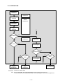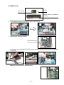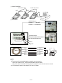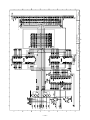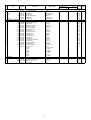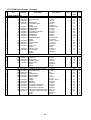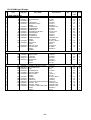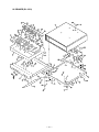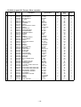
1
SERVICE MANUAL
(without price)
ELECTRONIC CASH REGISTER
QT-2100
(EX-590)
FEB. 2002
INDEX
Ver. 2
OCT. / 2002
Ver. 1
MAY / 2002
CONTENTS
QT-2100
PAGE
1. SPECIFICATIONS........................................................................................ 1
2. CONNECTOR LOCATIONS ........................................................................ 3
3. INITIALIZE (MAC) OPERATION.................................................................. 4
4. DISASSEMBLY ............................................................................................ 9
5. CIRCUIT EXPLANATIONS ........................................................................ 14
6. OPTION INSTALLATION........................................................................... 27
7. IN LINE ....................................................................................................... 33
8. ON LINE ..................................................................................................... 36
9. DIAGNOSTIC OPERATION ....................................................................... 39
10. ERROR CODE LIST................................................................................... 55
11. IC DATA ..................................................................................................... 62
12. PCB LAYOUT ............................................................................................ 68
13. CIRCUIT DIAGRAMS ................................................................................. 70
14. PARTS LIST ............................................................................................... 90
1. SPECIFICATIONS
1-1. Electrical specifications
120V
Max. 0.6 A
Max. 0.15 A
220V
0.4A
0.09A
230V
0.4A
0.09A
240V
0.4A
0.08A
•Power consumption
In operation
stand-by
•Memory protection
Back-up battery
Back-up period
Battery life
VL3032/SGA
30 days (25 °C)
Replace the battery every 5 years.
Recharge time
Accuracy
Auto calendar
48 hours
Within ± 30 sec. per month (25 °C)
Effective until 2099 A.D.
•Clock & Calendar
1-2. Environmental specifications
• Operating temperature
0 °C ~ 40 °C
• Operating humidity
10 % ~ 90 %
• Storage temperature
-20 °C ~ 60 °C
• Storage humidity
10 % ~ 90 %
• Vibration strength
1.5 G (The machine must be in the carton box)
1-3. Main components
• CPU
Name
Number of control bit
Internal RAM
HD6417709AF133B
32 bits
16 KBytes
• RAM1, 2, 3 and 4
Name
Capacity
MSM51V18165DSL-6TKFB
2 Mbits x 2pcs(Standard RAM1,2)
• Video RAM
Name
Capacity
LC35256FT-70U
256 Kbytes
• Flash ROM
Name
Capacity
MBM24DL324BE90PFTN
4 Mbits
Specification
D-18BC-B84M-13*
D-18BC-B87M-13*
D-18BC-B84SM-13*
D-18BC-B87SM-13*
D-17BT-B65SM-9*
D-17BT-B65M-9*
NOTE
Europe, other countries
Europe
Europe, UK, Germany
Europe, UK, Germany
USA, Canada
Europe
1-4. Drawer List
DRAWER NAME
•DL-2780
•DL-2916
•DL-2781
•DL-2917
•DL-3618
•DL-3619
Type
M
M
M
M
L
L
—1—
1-5. Option List
DEVICE NAME
•Dallas key (Clerk key)
•MCR (Magnetic card reader)
•Rear display
•Sheet holder
•Sheet holder
•RAM CHIP
•Multi drawer kit
•Remote display
•Option pole
•Remote display cable
•PC cable
•Sheet cover
•Slip printer
•Slip printer cable
•Remote printer
•Remote printer
•Remote printer
•Printer cable
•Printer cable
•Printer power supply
•Printer AC
•Handy scnner
•CF Memory Card
•Modem
•Modem
•ISDN TA
MODEL
CLK-K22
QT-2046MC
QT-2160D
SH-KIT8
SH-KIT9
QT-2130RAM
MDL-11
QT-2163D
QT-2061S
QT-2162S
PRL-CB-2
WT-81
SP-1300
PRT-CB-8C
UP-250
UP-350
SA-3015
PRT-CB-8B
PRT-CB-8A
PS-170
AC-170
HHS-15
SDCFB-xx-505
56k External Faxmodem
“US Robotics”
56k External Voice
Faxmodem
“US Robotics”
ELSA MICROLINK
TL-Pro (ISDN)
NOTE
for 6 clerk
1 holders (1st - 4th)
2 holders (1st - 4th, 5th - 8th)
Capacity 4 Mbytes, Backup battery
additional 1 drawer
For Remote display
Length 1.5m
Length 5m
Length 3m
Power supply unit
AC cord
Only in Germany
CAUTION
Danger of explosion if battery is incorrectly replaced.
Replace only with the same or equivalent type
recommended by the manufacturer.
Dispose of used batteries according
to the manufacture’s instructions.
VORSICHT !
Explosionsgefahr bei unsachgemäßem Austausch der
Batterie.
Ersatz nur durch denselben oder einen vom
Hersteller empfohlenen gleichwertigen Typ.
Entsorgung gebrauchter Batterien nach
Angaben des Herstellers.
ADVARSEL !
Lithiumbatteri - Eksplosionsfare ved fejlagtig hándtering.
Udskiftning má kun ske med batteri
af samme fabrikat og type.
Levér det brugte batteri tilbage til leverandØren.
—2—
2. CONNECTOR LOCATIONS
COM6 Port
COM5 Port
COM4 Port
IN LINE SELECTOR
COM1 Port (PC/MODEM)
SLIP POWER
IN LINE2 TERMINATOR
IN LINE2 IN
IN LINE2 OUT
COM3 Port (REMOTE DISP)
COM2 Port (SCANNER)
IN LINE1
POWER SWITCH
—3—
3. INITIALIZE (MAC) OPERATION
3-1.How to initialize QT-2100 terminal
Preparation:
1. All peripheral devices and QT-2100 terminals of this cluster
should be turned off.
2. Connect all of the peripheral devices (such as printer, display
etc.) to QT-2100 terminal.
3. Connect all QT-2100 terminals by in-line.
Operation:
Date
Time
ID Character
Check System
Check Cluster ID
R/J/Order Printer(1)
R/J/Order Printer(2)
R/J/Order Printer(3)
Slip Printer
01-10-10
12:34 00
MC #01
Master
0
No
No
No
No
OK?
YES
Date
Time
ID Character
Check System
Check Cluster ID
R/J/Order Printer(1)
R/J/Order Printer(2)
R/J/Order Printer(3)
Slip Printer
01-10-10
12:34 00
MC #01
Master
0
No
No
No
No
OK?
YES
Date
Time
ID Character
Check System
Check Cluster ID
R/J/Order Printer(1)
R/J/Order Printer(2)
R/J/Order Printer(3)
Slip Printer
01-10-10
12:34 00
MC #01
Master
0
No
No
No
No
OK?
YES
Date
Time
ID Character
Check System
Check Cluster ID
R/J/Order Printer(1)
R/J/Order Printer(2)
R/J/Order Printer(3)
Slip Printer
01-10-10
12:34 00
MC #01
Master
0
No
No
No
No
OK?
YES
4. Turn on all peripheral devices of a QT-2100 terminal.
5. Turn on this QT-2100 terminal with pressing the left-most key of
the top row and release the key after buzzer sounds.
6. After releasing the key, enter “other = 1000, USA = 2000” and
press the right part of the <ST> key.
7. Data:
Enter the current date (YY/MM/DD order) and press the <YES>
key.
8. Time:
Enter the current date (HH/MM/SS order) and press the <YES>
key.
9. ID Character:
In ID character field, the auto-defined ID No. is shown.
We recommend that you should not change the value.
—4—
Date
Time
ID Character
Check System
Check Cluster ID
R/J/Order Printer(1)
R/J/Order Printer(2)
R/J/Order Printer(3)
Slip Printer
01-10-10
12:34 00
MC #01
Master
0
No
No
No
No
OK?
YES
10.Check System:
Align the cursor as shown to the left.
The following is displayed by pressing <YES> key.
Check System
1. Master
2. Backup Master
3. Satellite
4. Selfmaster
Select one from the items in the above figure and press <YES>
key.
Date
Time
ID Character
Check System
Check Cluster ID
R/J/Order Printer(1)
R/J/Order Printer(2)
R/J/Order Printer(3)
Slip Printer
01-10-10
12:34 00
MC #01
Master
0
No
No
No
No
OK?
YES
11.Check System:
Align the cursor as shown to the left.
The following is displayed by pressing <YES> key.
R/J/Order Printer2
1. No
2. UP-350
3. SA-3015
4. UP-250
Select one from the items in the above figure and press <YES>
key.
Date
Time
ID Character
Check System
Check Cluster ID
R/J/Order Printer(1)
R/J/Order Printer(2)
R/J/Order Printer(3)
Slip Printer
01-10-10
12:34 00
MC #01
Master
0
No
No
No
No
OK?
YES
12.Check System:
Align the cursor as shown to the left.
The following is displayed by pressing <YES> key.
Slip Printer
1. No
2. SA-3015
3. SP-1300
Select one from the items in the above figure and press <YES>
key.
Date
Time
ID Character
Check System
Check Cluster ID
R/J/Order Printer(1)
R/J/Order Printer(2)
R/J/Order Printer(3)
Slip Printer
01-10-10
12:34 00
MC #01
Master
0
No
No
No
No
OK?
YES
13.Please confirm all of the field and if they are all right, press the
<YES> key to proceed the next step.
—5—
14.If you want to download program data from other terminal,
Please select one of “2” or “3” and Press <YES> key.
If you don’t need to download any program data, select “1. No
Restore / Receive” and Press <YES> key. The initialization of
this terminal is completed.
AUTO PGM
1. No Restore / Receive
2. PGM Restore (CF Card)
3. PGM Restore (Inline)
■ When “2. PGM Restore (CF card)” is selected
1 The file name list of the AUTO PGM data inside the CF CARD
is displayed.
Note: The files are displayed in the order they are found.
They may not be listed in chronological order.
CF Card
Data Restor
* 1. PLUPGM1 .004****
2. PLUPGM2 .004
3. PLUPGM3 .004
4. STORE-AA .090
5. STORE-BB .090
6. STORE-CC .090
7. STORE-DD .090
8. SETMENU .028
0. 00
* * *
2 Selecting a file name displays the confirmation as shown in the
left figure.
Press <ESC> to return to the previous screen.
CF Card
STORE-AA.090
Are you sure to restore?
0. 00
* * *
CF Card
CF Card
Data Restore
20
090
3 When <YES> is pressed: the file is restored from the CF card,
followed by “End” display.
Press <NO> or <ESC> to end and return to the previous display.
Normal End
0. 00
4 Press <ESC> to end CF Card and change to waiting mode.
—6—
■ When “3. PGM Restore (IN LINE)” is selected
31-12-96 11:59PM
Receive Data
PGM Receive from
*All*Data****
*MC*#1*******
1
2
OK?
*Yes*
3
Normal End
1 Select one of the following for the Receive PGM.
1. All Data: Eincluding totalizer, CHK, Index&Detail
2. All PGM
2 Select receive terminal.
3 Align the cursor and press <YES> key.
When INLINE AUTO PGM normally ended.
When INLINE AUTO PGM abnormally ended.
31-12-96 11:59PM
Receive Data
PGM Receive from
31-12-96 11:59PM
All Data
MC #01
Normal End
Receive Data
PGM Receive from
All Data
MC #01
OK?
YES
Normal End
Notes: There is no retry even when abnormally ended.
In either (normal or abnormal) ending, press <ESC> to
end INLINE AUTO PGM and change to waiting mode.
—7—
3-2. How to initialize QT-2100 terminal (add/replace one QT-2100)
1. All peripheral devices and QT-2100 terminals of this cluster should be turned off.
2. Connect all of the peripheral devices (such as printer, display etc.) to this QT-2100 terminal.
3. Connect this QT-2100 terminal to in-line.
4. Turn on all peripheral devices of this QT-2100 terminal.
And turn on all QT-2100 except this terminal of the cluster.
5. Turn on this QT-2100 terminal with pressing the left-most key of the top row and release the key after
buzzer sounds.
6. After releasing the key, enter “other = 1000, USA = 2000” and press the right part of the <ST> key.
7. Refer to “2-1 How to initialize QT-2100 terminal” on page 3.
2-3. How to flag clear QT-2100 terminal (or INIT2)
Preparation:
1. This QT-2100 terminal should be turned off.
2. Check the connection of all peripheral devices (such as printer,
display etc.) of this QT-2100 terminal.
3. Check the connection of this QT-2100 terminal to in-line.
Operation:
4. Turn on this QT-2100 terminal with pressing the right-most key
of the top row and release the key after buzzer sounds.
5. After releasing the key, press the <ST> key.
10-10-01 12:34
INIT
1.Flag Clear
2.Init2
0.00
6. Select “1.Flag Clear” and press the <YES> kye.
The flag clear operation is finished.
Note:
Performing “Init 2” requires password “8888888888”.
—8—
4. DISASSEMBLY
■ UPPER COVER
1. Remove the key sheet and two screws.
Screws
2. Remove the front cover by sliding it forward.
3. Remove the connector (CN5) and the keyboard block.
CN5
—9—
■ MAIN PCB
1. Remove the upper cover as shown in steps 1 to 3 of page 9.
2. Remove the seven connectors (CN13, CN14, CN15, CN11, CN9, CN8, CN7, CN18), two FPCs (CN16,
CN17) and five screws, and then the MAIN PCB.
CN19
CN14 CN15 CN16
CN13
CN12
CN18
CN17
CN11 CN10
CN9
CN8 CN7
CN5
Screws
CN3
CN2
— 10 —
CN6
■ POWER UNIT
1. Remove the upper cover as shown in steps 1 to 3 of page 9.
2. Remove the rear cover.
3. Remove the three screws for the power unit.
Screws
4. Remove the two connectors (CN14, CN15) and the power unit.
CN14
CN15
— 11 —
■ LCD MODULE/INVERTER
1. Remove the two blinders (screw covers) and two screws.
Screws
2 Remove the LCD cover.
Note: Be careful not to lose the blind sheets at the volume.
blind sheet x 2
3. Remove the two screws (plastic).
Note: Be careful not to break the screws.
Screws
4. Remove the two screws on the hinges.
Note: Put a towel etc. under the LCD unit to prevent from defects.
Screws
— 12 —
5. Move the LCD unit to the left and remove the LCD cover.
Note: Lift 1 up slightly and move it in the direction of 2.
2
1
Hook
6 Remove the two connectors (CN1, CN2) as well as the earth cable, and then the LCD unit.
Earth cable
CN1
CN2
7. Remove the two stoppers and the inverter.
Note: When fixing the Hinge case, put the blind sheets in the direction in the figure below first and fix it by
positioning the slide switch in the center.
slide switch
blind sheet x 2
— 13 —
— 14 —
DL-2780
DL-2781
DL-2916
DL-2917
DL-3618
DL-3619
Optional Drawer
MBM29DL324BE90TN-A
FROM
Optional RAM BOARD : QT-2130RAM
E590-RAM
DRAM
M51V18165DSL-6TKFB
DRAM
Others : OPTION
Optional
Battery
SW
DS9092
POWER CORD
M2511 : Europe, etc
MP5004 : Great Britin
M3203 : Austlaria
PS204-A : U.S.A., Canada, etc
MPW6616 :
AC220 240V
ë
MPW6716 :
AC120V
POWER SUPPLY UNIT
E590-ARC
iButton
DS1982-F5
Dallas key
Menu Sheet SW
iButton Probe
E590-E42
E590-1
MAIN BOARD
VL3032/SGA
Battery
Standard
CPU
E590-E4
KEY_SHEET : FPC
Germany : STANDARD
HD6417709AF133B
E590-E41
Note : Do not connect REAR DISPLAY and REMOTE DISPLAY at the same time.
U.S.A : STANDARD
Others : OPTION
CU20029SCPB-W31A
QT-2160D
Rear Display
LCD contrast/brightness
volume
E590-VOL
PS100175-002
M51V18165DSL-6TKFB
Optional Drawer
LRUBL616XA-1
Power supply for CFL
CFL
QT-2100
LCD UNIT
RS232C
COM3
RS232C
COM2
E590-CNB2
Modular Plug
Modular Plug
RS232C
COM1
RS232C
COM4
E590-CNB1
RS232C
COM5
RS232C
COM6
(+24V)
Power Supply
for SP-1300
QT-2046MC
QT-2100
QT-2100
QT-2100
QT-2100
HHS-15
Optional MCR UNIT
CU20029SCPB-W31A
E590-RMT
OPTIONAL REMOTE CUSTOMER DISPLAY SYSTEM
QT-2163D
CASIO STP cable
CASIO STP cable
CAT.5 UTP cable
PC DIRECT
UP-250
SA-3015
Optional Hand Held Scanner
Optional UNIT
CAT.5 UTP cable
MODEM
UP-350
SP-1300
Optional Printer UNIT
5. CIRCUIT EXPLANATION
5-1. BLOCK DIAGRAM
5-2. LSI BLOCK DIAGRAM
RS232C
FROM
IC 9
SERIAL
CPUBUS
3.3 V Backup
EDORAM
IC 8, 12
3.3 V
CPU (SH3)
IC7
SERIAL
5 V Backup
5V
V-RAM
IC 1
EDORAM
(OPTION)
1.9 V + 3.3 V
back up Vrtc only
buf
CF-CARD
MCR
LCDC
IC4
I/O
CONTROLLER
IC11
BUZZER
3.3 V or 5 V
KEY
buf
PCMCIA
MENU
EP-ROM
IC 10
5V
DALLAS
RDISP
GA
DRAWER
5V
ARC-NET
IC 15
3.3V unless otherwise specified
232C
232C
232C
232C
232C
— 15 —
5-3. SYSTEM FLOW
POWER OFF
씮POWER ON
FROM
OPERATION
CPU PORT
INITIALIZ
DRAM
OPERATION
StartUp C language
for BOOTER
KEY
INITIALIZ
1
NO
Press INIT button
YES
I/O CONTROLLER
OPERATION
NO
Press 'FINIT' button
Display INIT
YES
Process register
IPL boot code
NO
YES
NO
NO
CHECK
SUM?
CHECK
SUM?
Process register
OK
OK
1
RESUME
OPERATION
1
FINIT
OPERATION
1
INIT OPERATION
: Operations in BOOT ROM
Note: When CHECK SUM is NG, BOOT ROM waits for power off again because of error.
It sends information about FINIT/INIT/RESUME and the input register at time of INIT to applications.
— 16 —
5-4. CPU (IC7)
5-4-1. MEMORY MAP
Area 0
FLASH-ROM
H’00000000
Area 1
I/O
H’04000000
Area 2
H’08000000
Area 3
EDORAM
H’00000000
H’0E000000
EDORAM(OPTION)
H’10000000
Area 4
Area 5
CF
ARC-NET
UART
H’14000000
Area 6
PCMCIA
H’18000000
H’14000000
H’14800000
H’15000000
H’15800000
H’16000000
H’16800000
H’17000000
H’17800000
CF
H’18000000
MEMORY
H’19000000
COMMON MEMORY
H’1A000000
I/O
CF
ARC,UART
H’1B000000
— 17 —
H’16800000
H’16900000
H’16A00000
H’16B00000
H’16C00000
H’16D00000
H’16E00000
H’16F00000
PCMCIA
ARCENT
UARTINT
UART1
UART2
UART3
UART4
UART5
5-4-2. Pin description
PIN NO
1
2
3
4
5
6
7
8
9
10
11
12
13
14
15
16
17
18
19
20
21
22
23
24
25
26
27
28
29
30
31
32
33
34
35
36
37
38
39
40
41
42
43
44
45
46
47
48
49
50
51
52
53
54
55
56
57
58
59
60
61
62
63
64
65
66
67
PIN NAME
MD1
MD2
Vcc-RTC
XTAL2
EXTAL2
Vss-RTC
NMI
IRQ0/IRL0/PTH[0]
IRQ1/IRL1/PTH[1]
IRQ2/IRL2/PTH[2]
IRQ3/IRL3/PTH[3]
IRQ4/PTH[4]
D31/PTB[7]
D30/PTB[6]
D29/PTB[5]
D28/PTB[4]
D27/PTB[3]
D26/PTB[2]
VssQ
D25/PTA[1]
VccQ
D24/PTA[0]
D23/PTA[7]
D22/PTA[6]
D21/PTA[5]
D20/PTA[4]
Vss
D19/PTA[3]
Vcc
D18/PTA[2]
D17/PTA[1]
D16/PTA[0]
VssQ
D15
VccQ
D14
D13
D12
D11
D10
D9
D8
D7
D6
VssQ
D5
VccQ
D4
D3
D2
D1
D0
A0
A1
A2
A3
VssQ
A4
VccQ
A5
A6
A7
A8
A9
A10
A11
A12
I/O
IN
IN
OUT
IN
IN
IN/IN/I/O
IN/IN/I/O
IN/IN/I/O
IN/IN/I/O
IN/I/O
I/O
I/O
I/O
I/O
I/O
I/O
I/O
I/O
I/O
I/O
I/O
I/O
I/O
I/O
I/O
I/O
I/O
I/O
I/O
I/O
I/O
I/O
I/O
I/O
I/O
I/O
I/O
I/O
I/O
I/O
I/O
I/O
I/O
I/O
I/O
OUT
OUT
OUT
OUT
OUT
OUT
OUT
OUT
OUT
OUT
OUT
OUT
OUT
— 18 —
DESCRIPTION
VCC (3.3V)
GND
Vrtc (1.90V)
CLOCK (32.768KHz)
CLOCK (32.768KHz)
RTC (GND)
Not used
Power cut
UART INT
PCMCIA INT
IOC CPU CTS
ARCENT/Ether Net INT
Data bus (D31)
Data bus (D30)
Data bus (D29)
Data bus (D28)
Data bus (D27)
Data bus (D26)
I/O Power supply (0V)
Data bus (D25)
I/O Power supply (3.3V)
Data bus (D24)
Data bus (D23)
Data bus (D22)
Data bus (D21)
Data bus (D20)
GND
Data bus (D19)
VCC
Data bus (D16)
Data bus (D17)
Data bus (D18)
GND
Data bus (D15)
I/O Power supply (3.3V)
Data bus (D14)
Data bus (D13)
Data bus (D12)
Data bus (D11)
Data bus (D10)
Data bus (D9)
Data bus (D8)
Data bus (D7)
Data bus (D6)
I/O Power supply (0V)
Data bus (D5)
I/O Power supply (3.3V)
Data bus (D4)
Data bus (D3)
Data bus (D2)
Data bus (D1)
Data bus (D0)
Address bus (A0)
Address bus (A1)
Address bus (A2)
Address bus (A3)
I/O Power supply (0V)
Address bus (A4)
I/O Power supply (3.3V)
Address bus (A5)
Address bus (A6)
Address bus (A7)
Address bus (A8)
Address bus (A9)
Address bus (A10)
Address bus (A11)
Address bus (A12)
PIN NO
68
69
70
71
72
73
74
75
76
77
78
79
80
81
82
83
84
85
86
87
88
89
90
91
92
93
94
95
96
97
98
99
100
101
102
103
104
105
106
107
108
109
110
111
112
113
114
115
116
117
118
119
120
121
122
123
124
125
126
127
128
129
130
131
132
133
134
135
136
137
138
139
PIN NAME
I/O
DESCRIPTION
A13
OUT
Address bus (A13)
VssQ
I/O Power supply (0V)
A14
OUT
Address bus (A14)
VccQ
I/O Power supply (3.3V)
A15
OUT
Address bus (A15)
A16
OUT
Address bus (A16)
A17
OUT
Address bus (A17)
A18
OUT
Address bus (A18)
A19
OUT
Address bus (A19)
A20
OUT
Address bus (A20)
A21
OUT
Address bus (A21)
Vss
VSS
A22
OUT
Address bus (A22)
Vcc
VCC
A23
OUT
Address bus (A23)
VssQ
VSS
A24
OUT
Address bus (A24)
VccQ
I/O Power supply (3.3V)
A25
OUT
Address bus (A25)
BS/PTK[4] (_1:)
OUT/I/O
Not used
RD
OUT
Read strobe
WE0/DQMLL
OUT
D7-D0 select signal / DQM (EDO)
WE1/DQMLU/WE
OUT
DQM (EDO) / Write strobe (PCMCIA)
WE2/DQMUL/ICORD / PTK [6] OUT/OUT/OUT/I/O DQM (SDRAM) / PCMCIA I/O Read signal
WE3/DQMUU/ICOWR / PTK [7] OUT/OUT/OUT/I/O DQM (EDO) / PCMCIA I/O Write signal
RD/WD (_1:)
OUT
Read / Wrie signal
AUDSYNC/PTE[7]
OUT/I/O
COM1 DTR
VssQ
I/O Power supply (0V)
CS0/MCS/PTE[7]
OUT
Chip select for FROM
VccQ
I/O Power supply (3.3V)
CS2/PTK[0]
OUT/I/O
Not used
CS3/PTK[1]
OUT/I/O
Not used
CS4/PTK[2]
OUT/I/O
Not used
CS5/CE1A/PTA[3]
OUT/OUT/I/O
CE1 (Area5 PCMCA)
CS6/CE1B
OUT/OUT/I/O
CE1 (Area6 PCMCA)
CE2A/PET[4]
OUT/I/O
CE2 (Area5 PCMCA)
CE2B/PET[5]
OUT/I/O
CE2 (Area6 PCMCA)
CKE/PTK[5]
OUT/I/O
Not used
RAS3L/PTJ[0]
OUT/I/O
RAS for RAM (RAM1,2)
RAS2L/PTJ[1]
OUT/I/O
Not used
CASLL/CASL/PTJ[2]
OUT/I/O
CAS for RAM (RAM1,3)
VssQ
I/O Power supply (0V)
CASLH/CASU/PTJ[3]
OUT/I/O
CAS for RAM (RAM1,3)
VccQ
I/O Power supply (3.3V)
CASHL/PTJ[4]
OUT/I/O
CAS for RAM (RAM2)
CASHH/PTJ[5]
OUT/I/O
CAS for RAM (RAM2)
DACK0/PTD[5]
OUT/I/O
Not used
DACK/PTD[7]
OUT/I/O
Not used
CAS2L/PTE[6]
OUT/I/O
Not used
CAS2H/PTE[3]
OUT/I/O
Not used
RAS3U/PTE[2]
OUT/I/O
RAS for RAM (RAM3)
RAS3U/PTE[1]
OUT/I/O
Not used
TDO/PTE[0]
OUT/I/O
DATA OUTPUT (H-UDI)
BACK
OUT
Not used
BREQ
IN
Not used
WAIT
IN
WAIT signal (PCMCIA)
RESETM
IN
RESET signal
ADTRG/PTH[5]
IN
Not used
I/OIS16/PTG[7]
IN/I/O
IOIS16 (PCMCIA)
ASEMDO/PTG[6]
IN
ASE mode (H-UDI)
ASEBRKAK/PTG[5]
OUT/I/O
ASE break (H-UDI)
PTG[4]
IN/OUT
Not used
AUDATA[3]/PTG[3]
I/O
Not used
AUDATA[2]/PTG[2]
I/O
Not used
Vss
VSS
AUDATA[1]/PTG[1]
I/O
Not used
Vcc
VCC (1.9V)
AUDATA[0]/PTG[0]
I/O
Not used
TRST/PTF[7]/PINT[5]
IN
RESET (H-UDI)
TMS/PTF[6]/PINT[14]
IN
MODE SELECT (H-UDI)
TDI/PTF[5]/PINT[13]
IN
DATA INPUT (H-UDI)
TCK/PTF[4]/PINT[12]
IN
CLOCK (H-UDI)
— 19 —
PIN NO
140
141
142
143
144
145
146
147
148
149
150
151
152
153
154
155
156
157
158
159
160
161
162
163
164
165
166
167
168
169
170
171
172
173
174
175
176
177
178
179
180
181
182
183
184
185
186
187
188
189
190
191
192
193
194
195
196
197
198
199
200
201
202
203
204
205
206
207
208
PIN NAME
IRSL[3]/PTF[3]/PINT[11]
IRSL[2]/PTF[2]/PINT[10]
IRSL[1]/PTF[1]/PINT[9]
IRSL[0]/PTF[0]/PINT[8]
MD0
Vcc-PLL1
CAP1
Vss-PLL1
Vss-PLL2
CAP2
Vcc-PLL2
AUDCK/PTH[6]
Vss
Vss
Vcc
XTAL
EXTAL
STAUTS0/PTJ[6](_1:)
STAUTS1/PTJ[7](_1:)
TCK/PTH[7]
IRQOUTJ(_1:)
VssQ
CKI/O
VccQ
TxD0/SCPT[0]
SCK0/SCPT[1]
TxD1/SCPT[2]
SCK1/SCPT[3]
TxD2/SCPT[4]
SCK2/SCPT[5]
RTS2/SCPT[6]
RxD0/SCPT[0]
RxD1/SCPT[2]
Vss
RxD2/SCPT[4]
Vcc
CTS2/IRO/SCPT[7]
MCS[7]/PTC[7]/PINT[7]
MCS[6]/PTC[6]/PINT[7]
MCS[5]/PTC[5]/PINT[5]
MCS[4]/PTC[4]/PINT[4]
VssQ
WAKEUP/PTD[3]
VccQ
RESETOUTR/PTD[2]
MCS[3]/PTC[3]/PINT[3]
MCS[2]/PTC[2]/PINT[2]
MCS[1]/PTC[1]/PINT[1]
MCS[0]/PTC[0]/PINT[0]
DRAK0/PTD[1]
DRAK1/PTD[0]
DREQ0/PTD[4]
DREQ1/PTD[6]
RESETP
CA
MD3
MD4
MD5
AVss
AN[0]/PTL[0]
AN[1]/PTL[1]
AN[2]/PTL[2]
AN[3]/PTL[3]
AN[4]/PTL[4]
AN[5]/PTL[5]
Avcc
AN[6]/DA[1]/PTL[6]
AN[7]/DA[1]/PTL[7]
AVss
I/O
IN
IN
IN
IN
IN
IN
OUT
IN
OUT/I/O
OUT/I/O
I/O
OUT(_1:)
I/O
OUT
I/O
OUT
I/O
OUT
I/O
OUT/I/O
IN
IN
IN
IN
OUT/I/O/IN
OUT/I/O/IN
OUT/I/O/IN
OUT/I/O/IN
OUT/I/O
OUT/I/O
OUT/I/O/IN
OUT/I/O/IN
OUT/I/O/IN
OUT/I/O/IN
OUT/IN
OUT/IN
IN/I/O
IN/I/O
IN
IN
IN
IN
IN
IN
IN
IN/OUT/IN
IN/OUT/IN
IN/OUT/IN
IN/OUT/IN
IN/OUT/IN
IN/OUT/IN
-
— 20 —
DESCRIPTION
Not used
Not used
Not used
CF CARD IN/OUT signal
CLOCK MODE
PLL Power supply (1.9V)
Not used
PLL Power supply (0V)
PLL Power supply (0V)
Not used
PLL Power supply (1.9V)
VCC (3.3V)
VSS
VSS
VCC (1.9V)
CLOCK 8.25MHz
CLOCL 8.25MHz
VCC (3.3V)
VCC (3.3V)
RESET LATCH signal
Not used
I/O Power supply (0V)
VCC (3.3V)
I/O Power supply (3.3V)
IOC CPU TxD
VCC (3.3V)
Not used
IOC PWD
COM1 TxD
RESET LATCH
COM1 RTS
IOC CPU RxD
VCC (3.3V)
VSS
COM1 RxD
VCC (1.9V)
COM1 CTS
PCMCIA I/O signal
IOC CPU RESET (OUT)
IOC CPU RTS (OUT)
COM1 CI (IN)
I/O Power supply (0V)
VSS
I/O Power supply (3.3V)
VCC (3.3V)
COM1 DSR (IN)
COM1 CD (IN)
VCC (3.3V)
VCC (3.3V)
VCC (3.3V)
VCC (3.3V)
VCC (3.3V)
VCC (3.3V)
RESET
VCC (3.3V)
VSS
VCC (3.3V)
VCC (3.3V)
VSS
IOC CPU DSR (IN)
VCC (3.3V)
VCC (3.3V)
VCC (3.3V)
VCC (3.3V)
VCC (3.3V)
Anaog power supply (3.3V)
Not used
Not used
Anaog power supply (0V)
5-5. I/O CONTROLLER (IC11)
5-5-1. MEMORY MAP
00000
SYSTEM RAM
(0FFD0 ~ 0FFDF : External I/O)
20000
LCDC VRAM
256 Kbit
28000
LCDC I/O
28010
Not used (LCDC I/O)
30000
Not used
80000
Character Generator
EPROM
4 Mbit
FFFFF
ADDRESS
D0
~
28000H
D7
D0
D1
D2
D3
28001H
D4
D5
D6
D7
D0
~
28002H
D7
D0
~
28003H
D7
D0
~
28004H
D7
D0
~
28005H
D7
D0
~
28006H
D7
D0
~
28007H
D7
D0
~
28008H
D7
D0
~
28009H
D7
D0
~
2800AH
D7
D0
~
2800BH
D7
D0
~
2800CH
D7
D0
~
2800DH
D7
D0
~
2800EH
D7
D0
~
2800FH
D7
— 21 —
R/W
FUNCTION
REMARK
–
W
RAMS
LCDE
4/8
CRAY
OR
PANEL
REV
DISP
Set up basic performance mode for
SED1353.
W
C/R
Number of horizontally displayed
characters per 1 line
W
LPW
Pulse width of LP per 1 line
W
SLTL
Number of vertical lines in the LCD
(lower 8 bit)
W
SLTH
Number of vertical lines in the LCD
(upper 2 bit)
R/W
SAD1L
Start address in the first screen (lower 8 bit)
R/W
SAD1H
Start address in the first screen (upper 8 bit)
R/W
SAD2L
Start address in the second screen
(lower 8 bit)
R/W
SAD2H
Start address in the second screen
(upper 8 bit)
W
SL1L
Number of vertical lines in the fist screen
(lower 8 bit)
W
SL1H
Number of vertical lines in the fist screen
(lower 8 bit)
W
APADJ
Address pitch adjust in the virtual screen
W
GS1
Gradation conversion code
W
GS2
Gradation conversion code
–
5-5-2. BLOCK DIAGRAM
I/O
CONTROLLER
LOAD × 2
CLOCK × 2
DATA × 2
BUZZ
PWD
from HardReset
MCR
RESET
12.5 MHz
BUZZER
KC × 12
KI × 14
KEY
12 × 14
from CPU PORT
Menu Sheet x 4
RTS
CTS
DTR
TXD/RXD
3.3 V 5 V
MENU
SHEET
Drawer drive x 2
Drawer x 2
DRAWER
×2
TXD (RS-232C)
REAR
DISP
INPUT
OUTPUT
DALLAS
KEY
OPTION
iButton: 1Wired Line
BackLight ON/OFF
BUS outside WAIT
LCDC
6 MHz
LCD
VRAM
256 Kbit
Back up power for 1/4 VGA VRAM only
BUS
EPROM
4 Mbit
For Character Generator
— 22 —
5-5-3. Pin description
PIN NO PIN NAME
1
2
3
4
5
6
7
8
9
10
11
12
13
14
15
16
17
18
19
20
21
22
23
24
25
26
27
28
29
30
31
32
33
34
35
36
37
38
39
40
41
42
43
44
45
46
47
48
49
50
P120
P121
P122
P123
P124
P125
P126
P127
VDD
X2
X1
VSS
XT2
XT1
RESET
P00
P01
P02
P03
P04
P05
P06
AVDD
AVREF0
P10
P11
P12
P13
P14
P15
P16
P17
AVSS
P130
P131
AVREF1
P70
P71
P72
P20
P21
P22
P23
P24
P25
P26
P27
P80
P81
P82
I/O
I
I
I
I
I
I
I
I
VCC
I/O
I/O
GND
GND
GND
O
I
I
I
I
I
I
I
VCC
VCC
I
I
I
I
I
I
I
I
GND
O
O
VCC
VCC
I
O
I
O
O
O
O
VCC
O
O
O
O
O
DESCRIPTION
PIN NO
KEY INPUT
KEY INPUT
KEY INPUT
KEY INPUT
KEY INPUT
KEY INPUT
KEY INPUT
KEY INPUT
VCC
CLOCK 12.5MHz
CLOCK 12.5MHz
GND
GND
GND
RESET
MCR CLOCK1
MCR CLOCK2
MCR CARD LOAD1
MCR CARD LOAD2
CTS
KEY INPUT (DALLAS KEY)
PWD
VCC
VCC
KEY INPUT
KEY INPUT
KEY INPUT
KEY INPUT
KEY INPUT
KEY INPUT
KEY INPUT
KEY INPUT
GND
DRAWER DRIVE1
DRAWER2 DRIVE2
VCC
VCC
TxD
BACKLIGHT ON/OFF
RxD
TxD
KEY OUTPUT (DALLAS KEY)
LCD
BUZZER
VCC
RTS
DTR
ADDRESS (A0)
ADDRESS (A1)
ADDRESS (A2)
— 23 —
51
52
53
54
55
56
57
58
59
60
61
62
63
64
65
66
67
68
69
70
71
72
73
74
75
76
77
78
79
80
81
82
83
84
85
86
87
88
89
90
91
92
93
94
95
96
97
98
99
100
PIN NAME
P83
P84
P85
P86
P87
P40
P41
P42
P43
P44
P45
P46
P47
P50
P51
P52
P53
P54
P55
P56
P57
VSS
P60
P61
P62
P63
P64
P65
P66
P67
VDD
P100
P101
P102
P103
P30
P31
P32
P33
P34
P35
P36
P37
TEST
P90
P91
P92
P93
P94
P95
I/O
O
O
O
O
O
I/O
I/O
I/O
I/O
I/O
I/O
I/O
I/O
O
O
O
O
O
O
O
O
GND
O
O
O
O
O
O
I
Not used
O
O
O
O
O
O
O
O
O
O
O
O
O
GND
I
I
I
I
O
O
DESCRIPTION
ADDRESS (A3)
ADDRESS (A4)
ADDRESS (A5)
ADDRESS (A6)
ADDRESS (A7)
DATA (D0)
DATA (D1)
DATA (D2)
DATA (D3)
DATA (D4)
DATA (D5)
DATA (D6)
DATA (D7)
ADDRESS (A8)
ADDRESS (A9)
ADDRESS (A10)
ADDRESS (A11)
ADDRESS (A12)
ADDRESS (A13)
ADDRESS (A14)
ADDRESS (A15)
GND
ADDRESS (A16)
ADDRESS (A17)
ADDRESS (A18)
ADDRESS (A19)
READ signal
WRITE signal
WAIT signal
Not used
VDD
KEY OUTPUT (Common)
KEY OUTPUT (Common)
KEY OUTPUT (Common)
KEY OUTPUT (Common)
KEY OUTPUT (Common)
KEY OUTPUT (Common)
KEY OUTPUT (Common)
KEY OUTPUT (Common)
KEY OUTPUT (Common)
KEY OUTPUT (Common)
KEY OUTPUT (Common)
KEY OUTPUT (Common)
GND
DRAWER STATUS1
DRAWER STATUS2
MENU SHEET STATUS
MENU SHEET 0
MENU SHEET 1
MENU SHEET 2
5-6. G/A (IC15)
5-6-1. BLOCK DIAGRAM
#CS4~#CS8 (138)
#INTC2
#INTC1
#G
B
#G
A
B
A
D0-D7
GD0-GD15
D0-D15
245
*1
245
*5
EN
EN (DIR)
RD/#WE
#CS
GA0-GA3
A0-A3
D6
#INT6
D5
#INT7
D4
D3
D2
D1
D0
#CS1
A23
G
#G2A
#G2B
#GCS1
#CS2
138
#CS3
#CS4
UART1
#CS5
A20
A21
A22
1(A)
#CS6
2(B)
#CS7
3(C)
#CS8
#GCS2
#int1
UART2
UART3
UART4
UART5
#int2
#int3
#int4
#int5
30PIN
U1_CTS
U1_DSR
U1_SIN
U1_DTR
U1_RTS
U1_SOUT
#RD
#GRD
#WE
#GWE
×6
#RESET
CLK
(1.8432MHz)
PCMIN
PCIN
PCMG
CE1B
CE2B
CFCE1A
CFIN
CIN
CE1A
CFCE
CFG
CE2A
CFCE2A
— 24 —
BFI1
BFO1
BFI2
BFO2
BFI3
BFO3
BFI4
BFO4
ANDI1
ANDI2
ANDO1
ANDI3
ANDI4
ANDO2
5-6-2. Pin description
PIN NO PIN NAME I / O
1
2
3
4
5
6
7
8
9
10
11
12
13
14
15
16
17
18
19
20
21
22
23
24
25
26
27
28
29
30
31
32
33
34
35
36
37
38
39
40
41
42
43
44
45
46
47
48
49
50
51
52
53
54
55
56
57
58
59
60
61
62
63
64
65
66
67
68
69
70
71
72
VDD
GD0
GD1
GD2
GD3
GD4
TVDD
TGND
GD5
GD6
GD7
GD8
GD9
TGND
GD10
GD11
GD12
GD13
GD14
TVDD
TGND
GD15
GA0
GA1
GA2
GA3
TGND
D0
D1
D2
TVDD
TGND
D3
D4
D5
VDD
GND
GND
D6
D7
D8
TGND
D9
D10
D11
TVDD
TGND
D12
D13
D14
TGND
D15
INTC2
INTC1
GCS1
GCS2
GRD
GWE
PCIN
PCMG
CFCE1A
CIN
CFG
CFCE2A
ANDO1
ANDO2
BFO1
BFO2
BFO3
BFO4
GND
GND
VDD
I/O
I/O
I/O
I/O
I/O
VDD
GND
I/O
I/O
I/O
I/O
I/O
GND
I/O
I/O
I/O
I/O
I/O
VDD
GND
I/O
O
O
O
O
GND
I/O
I/O
I/O
VDD
GND
I/O
I/O
I/O
VDD
GND
GND
I/O
I/O
I/O
GND
I/O
I/O
I/O
VDD
GND
I/O
I/O
I/O
GND
I/O
O
O
O
O
O
O
O
O
O
O
O
O
O
O
O
O
O
O
GND
GND
DESCRIPTIN
PIN NO PIN NAME I / O
VDD
ARC DATA (D0)
ARC DATA (D1)
ARC DATA (D2)
ARC DATA (D3)
ARC DATA (D4)
VDD
GND
ARC DATA (D5)
ARC DATA (D6)
ARC DATA (D7)
VDD
VDD
GND
VDD
VDD
VDD
VDD
VDD
VDD
GND
VDD
ARC ADDRESS (A0)
ARC ADDRESS (A1)
ARC ADDRESS (A2)
Not used
GND
DATA (D0)
DATA (D1)
DATA (D2)
VDD
GND
DATA (D3)
DATA (D4)
DATA (D5)
VDD
GND
GND
DATA (D6)
DATA (D7)
VDD
GND
VDD
VDD
VDD
VDD
GND
VDD
VDD
VDD
GND
VDD
INT for ARC
INT for COM
Chip Select for ARC
Not used
Read signal for ARC
Write signal for ARC
PCMCIA IN/OUT signal
Enable for PCMCIA
Chip Enable1 for CF CARD
CF CARD IN/OUT signal
Enable for CF CARD
Chip Enable2 for CF CARD
WAIT signal
CD
RXD
CTS
CI
DSR
GND
GND
— 25 —
73
74
75
76
77
78
79
80
81
82
83
84
85
86
87
88
89
90
91
92
93
94
95
96
97
98
99
100
101
102
103
104
105
106
107
108
109
110
111
112
113
114
115
116
117
118
119
120
121
122
123
124
125
126
127
128
129
130
131
132
133
134
135
136
137
138
139
140
141
142
143
144
VDD
CLKOUT
CLKIN
GND
CS
A0
A1
A2
A3
A23
A20
A21
A22
RD
WE
INT6
INT7
TVDD
RESET
RD_WE
TESTB
U1_CTSB
U1_DSRB
U1_SIN
U1_DTRB
U1_RTSB
U1_SOUT
U2_CTSB
U2_DSRB
U2_SIN
U2_DTRB
U2_RTSB
U2_SOUT
U3_CTSB
U3_DSRB
VDD
GND
GND
U3_SIN
U3_DTRB
U3_RTSB
U3_SOUT
U4_CTSB
U4_DSRB
U4_SIN
U4_DTRB
U4_RTSB
U4_SOUT
U5_CTSB
U5_DSRB
U5_SIN
U5_DTRB
U5_RTSB
U5_SOUT
TVDD
PCMIN
CE1B
CE2B
CFIN
CE1A
CFCE
CE2A
BFI1
BFI2
BFI3
BFI4
ANDI1
ANDI2
ANDI3
ANDI4
GND
GND
VDD
O
I
I
I
I
I
I
I
I
I
I
I
I
I
I
VDD
VDD
I
I
I
I
I
I
O
O
O
I
I
I
O
O
O
I
I
VDD
GND
GND
I
O
O
O
I
I
I
O
O
O
I
I
I
O
O
O
VDD
I
I
I
I
I
I
I
I
I
I
I
I
I
I
I
GND
GND
DESCRIPTIN
VDD
CLOCK 8MHz
CLOCK 8MHz
GND
Chip Enable 1
ADDRESS (A1)
ADDRESS (A2)
ADDRESS (A3)
GND
ADDRESS (A23)
ADDRESS (A20)
ADDRESS (A21)
ADDRESS (A22)
IO READ
IO WRITE
INT for ARC
VDD
VDD
RESET
READ/WRITE signal
VDD
CST2
DSR2
RXD2
DTR2
RTS2
TXD2
CTS3
DSR3
RXD3
DTR3
RTS3
TXD3
CTS4
DSR4
VDD
GND
GND
RXD4
DTR4
RTS4
TXD4
CTS5
DSR5
RXD5
DTR5
RTS5
TXD5
CTS6
DSR6
RXD6
DTR6
RTS6
TXD6
VDD
PCMCD1
CE1
CE2
CFCD1
CE1
ADDRESS (A23)
CE2
RXD1
CTS1
CI1
DSR1
WAIT for CF CARD
WAIT for PCMCIA
CD1
CD1
GND
GND
5-7. LCD CONTROLLER (IC4)
5-7-1. BLOCK DIAGRAM
MCLK (LCD BUS CLOCK)
A0-A15
D0-D3
IOCS
DECODER MEMCS
I/O
CONTROLLER
(IC11)
D0-D7
RD
WR
WAIT
78 K IV
12.5 MHz
LCD
LCD
CONTROLLER
(IC4)
MPUCLK (12.5 MHz)
MCLK
VRAM
BUS
6.00 Mhz
Display memory
(IC1)
256 Kbit
5-7-2. Pin description
PIN NO NAME
1
DB7
2
Vss
3
Vdd
4
DB8
5
DB9
6
DB10
7
DB11
8
DB12
9
DB13
10
DB14
11
DB15
12
AB0
13
AB1
14
AB2
15
AB3
16
AB4
17
AB5
18
AB6
19
AB7
20
AB8
21
AB9
22
AB10
23
AB11
24
AB12
25
AB13
26
AB14
27
AB15
28
AB16
29
AB17
30
AB18
31
AB19
32
RESET
33
VA0
34
VA1
35
VA2
36
VA3
37
VA4
38
VA5
39
VA6
40
VA7
41
VA8
42
VA9
43
VA10
44
VD0
45
VD1
46
VD2
47
VD3
48
VD4
49
VD5
50
VD6
I/O
DESCRIPTION
I/O System data bus
GND
Vcc
I/O Connected to Vdd
I/O Connected to Vdd
I/O Connected to Vdd
I/O Connected to Vdd
I/O Connected to Vdd
I/O Connected to Vdd
I/O Connected to Vdd
I/O Connected to Vdd
I System address bus
I System address bus
I System address bus
I System address bus
I System address bus
I System address bus
I System address bus
I System address bus
I System address bus
I System address bus
I System address bus
I System address bus
I System address bus
I System address bus
I System address bus
I Connected to GND
I Connected to GND
I Connected to GND
I Connected to GND
I Connected to GND
I Reset signal
O Display memory address bus
O Display memory address bus
O Display memory address bus
O Display memory address bus
O Display memory address bus
O Display memory address bus
O Display memory address bus
O Display memory address bus
O Display memory address bus
O Display memory address bus
O Display memory address bus
I/O Display memory data bus
I/O Display memory data bus
I/O Display memory data bus
I/O Display memory data bus
I/O Display memory data bus
I/O Display memory data bus
I/O Display memory data bus
PIN NO
51
52
53
54
55
56
57
58
59
60
61
62
63
64
65
66
67
68
69
70
71
72
73
74
75
76
77
78
79
80
81
82
83
84
85
86
87
88
89
90
91
92
93
94
95
96
97
98
99
100
— 26 —
NAME
VD7
Vss
Vdd
VD8
VD9
VD10
VD11
VD12
VD13
VD14
VD15
VA11
VA12
VA13
I/O
DESCRIPTION
I/O Display memory data bus
GND
Vcc
I/O Not used
I/O Not used
I/O Not used
I/O Not used
I/O Not used
I/O Not used
I/O Not used
I/O Not used
O Display memory address bus
O Display memory address bus
O Display memory address bus
O Display memory address bus
VA15
O Display memory address bus
VWE
O Write signal for display memory
VCS0
O Select display memory
VCS1
O Not used
UD3
O Panel display data bus
UD2
O Panel display data bus
UD1
O Panel display data bus
UD0
O Panel display data bus
LD3
O Not used
LD2
O Not used
LD1
O Not used
LD0
O Not used
YD
O Vertical scanning start pulse
LP
O Display data latch clock
WF
O Not used
XSCL
O Display data shift clock
LCDENB O LCD enable signal output
VOE
O Read signal for display memory
IOCS
I Select internal registers
IOW
I Write signal for internal register
IOR
I Read signal for internal register
MEMCS
I Indicate a memory cycle
MEMW
I Indicate a memory write cycle
MEMR
I Indicate a memory read cycle
READY
O Ready signal
BHE
I Vcc
OSC1
I Clock signal
OSC2
O Clock signal
DB0
I/O System data bus
DB1
I/O System data bus
DB2
I/O System data bus
DB3
I/O System data bus
DB4
I/O System data bus
DB5
I/O System data bus
DB6
I/O System data bus
6. OPTION INSTALLATION
6-1. REAR DISPLAY
Note: The REMOTE DISPLAY and the REAR DISPLAY cannot be fixed at the same time.
1. Assemble the REAR DISPLAY.
Note: Be careful with the direction (left/right) of the frame.
Right frame
Left frame
2. Remove the upper cover as shown in steps 1 to 2 of page 9.
3. Fix two screws temporarily to the POWER UNIT.
4. Attach the REAR DISPLAY and fix it with two screws.
Screws
5. Let the connector through the tube and connect it to the MAIN PCB (CN15).
CN15
6. Fix the UPPER COVER and REAR COVER.
— 27 —
6-2. Dallas Key (Except for Germany)
1. Remove the upper cover as shown in steps 1 to 3 of page 9.
2. Let the Dallas key through the unit and connect it to the MAIN PCB (CN2).
Note: Wind the cable through the Ferrite core two and a half times.
Ferrite core should be in side of lower case.
Vinyl tube
Wind the cable two and
a half times.
Ferrite core
Washer
Bush Nut
3. After mounting dallas key, fix the UPPER COVER.
Vinyl tube: Do not put tube in the ferrite core.
6-3. MAGNETIC CARD READER (MCR)
1. Remove two screws and the lower case.
Screws
2. Remove the MAIN PCB (Remove the upper cover as shown in steps 1 to 3 of page 9).
3. Solder the connector (CN6) on the MAIN PCB.
Connector (CN6)
PCB
NOTE: When fixing the connecotor, be careful with its
direction.
— 28 —
4. Fix the MAIN PCB.
5. Put the cable of the MCR into the ECR and connect it to the MAIN PCB (CN6).
A
Fix the terminal to position A
6. Fix the base of the MCR.
7. Cut the edge of the lower case with a nipper.
8. Fix the lower case with two screws.
Cut the edge with a nipper.
Fix the MCR base.
9. Fix the MCR.
10. Fix the UPPER COVER.
— 29 —
Screws
6-4. MEMORY PCB
Screw
Main memory
Backup battery for additional
memory
1. Remove the upper cover as shown in steps 1 to 3 of page 9.
2. Fix the additional memory to the MAIN PCB (CN3) with a screw.
3. Remove the UL tube from the ECR.
UL tube (Clear type)
4. Let the power cord of the BACKUP BATTERY through the hole on the side of the ECR and fix it to the MAIN
PCB (CN19).
Note: Insert two BACKUP BATTERIES together.
— 30 —
6-5. REMOTE DISPLAY
6-6. HANDY SCNNER
6-7. REMOTE PRINTER / SLIP PRINTER
Note: The REMOTE DISPLAY and the REAR DISPLAY cannot be fixed at the same time.
1. Remove two screws and the lower case.
Screws
2. Connect the following peripherals to the COM ports respectively.
REMOTE DISPLAY : COM3
HANDY SCANNER : COM2
REMOTE PRINTER/ : COM4, 5, 6
SLIP PRINTER
3. Remove the parts from which the peripherals should be connected with a nipper.
4. Fix the lower case with two screws.
Remove the parts from which the peripherals
should be connected with a nipper.
Screws
— 31 —
6-8. DRAWER
1. Remove the upper cover as shown in steps 1 to 3 of page 9.
2. Remove two screws and the lower case.
Screws
3. Let the cable through the part as shown below and put into the ECR.
4. Put the cable into the tube and connect it to the MAIN PCB (CN11).
NOTE: CN10 for Multi Drawer
5. Fix the UPPER COVER.
6. Connect the earth line with the drawer connector.
Connect the drawer earth line.
— 32 —
Connect the drawer
connector.
7. IN LINE
■ There are two types for IN LINE; CATEGORY5A and ARCNET.
7-1. ARCNET
1 ARCNET connection diagram
The maximum ARCNET cable length and the maximum connection unit will be varied by the in-line
communication speed as shown below list.
In-line
[ARCNET cable wiring]
QT2100-1
R/J
Total Length : A
QT2100-2
QT2100-3
QT2100-4
R/J
R/J
R/J
QT2100-32
R/J
Note: When the cluster has more than 8 QT-2100 terminals, all printer should be local printer. When
the cluster has less than or equal to 8 QT-2100 terminals, remote printer is allowable.
ARCNET communication speed
(Baud rate)
Maximum
connection unit
Maximum
cable length A (m)
312.5 K bps
156.25 K bps
20
32
430
890
2 In line cable, Connector, and Terminater
ARCNET cable
Code No.
1904 4023
Parts name
In-line cable
Specification
IPEV-SLA0.5x1P
ARCNET connector(ECR side)
Code No.
3540 3924
Parts name
In-line connector kit
Specification
XLP-KIT-2
Parts name
Carbon film resistor
Specification
R-25-100-J
Terminater
Code No.
2600 2516
— 33 —
3 ARCNET Cable connection diagram
Signal
SD
Pin
1
RD
2
Terminater
100 ohms
FG
FG plate
(In-line connector)
Signal
SD
Pin
1
Signal
SD
Pin
1
RD
2
RD
2
Terminater
100 ohms
FG
FG plate
(In-line connector)
FG
FG plate
(In-line connector)
[Connection end of ECR]
Red
Red
In-line cable
Wrap bent shield wire
Black
with Copper tape
Shield wire
In-line connector
Black
Terminator (100 ohms)
[Connection between ECR and ECR]
Red
Red
In-line cable
In-line connector
Wrap bent shield wire
with Copper tape Shield wire Black
Black
7-2. LAN (CATEGORY5)
1 Restrictions
• Maximum number of units that can be connected is 32.
• HUB and rooter cannot be connected.
• With ARCNET simultaneous use impossible.
• Minimum cable length between units is 5 meters.
2 APPLICATION
• Auto PGM
• Sales Data Collection
• Shared Check Tracking
• Shared Printer
• IPL
— 34 —
Maximun total length of the cable
4 units : 450m
8 units : 420m
32 units : 230m
3 BLOCK DIAGRAM
CAT5 UTP Cable
OUT
(Min 5m) IN
CAT5 UTP Cable
OUT
(Min 5m) IN
RS232C
PCPC
4 Connection
IN LINE selector
Position 1:
ARC NET
Position 2: CATEGORY5
Terminator Switch
Turn on the switch of the units of
both first and the last ends.
2
1
ON
OFF
IN
OUT
White/Orange
Orange
White/Green
Blue
White/Blue
Green
White/Brown
Brown
1
2
3
4
5
6
7
8
1
2
3
4
5
6
7
8
White/Orange
Orange
White/Green
Blue
White/Blue
Green
White/Brown
Brown
8, 7, 6, .....2, 1
LAN CABLE
NOTE:
1) The power of all units which share the network must be turned on.
If even one of them is OFF, normal communication cannot be done.
If any of the units has a failure and its power is turned off, remove the unit from the network.
2) Communication speed of the categoly 5 is fixed 312.5kbps.
— 35 —
8. ON LINE
Only the RS-232C Com1 port can be connected with a modem or perssonal computer.
8-1. Direct connection to PC
1 Connection layout
PC
RS-232C
QT2100
KP/M
QT2100
CHK/BM
Slip
Slip
QT2100
CHK/M
QT2100
KP/BM
R/J
Slip
Using Com1 port
2 PC Cable wiring
QT-2100 (Com1)
Pin No.
3
2
7
8
1
4
6
9
5
PC
Signal name
Pin No.
(DSUB9)
3
2
7
8
1
4
6
5
SD/TXD
RD/RXD
RS/RTS
CS/CTS
CD/DCD
ER/DTR
DR/DSR
CI/RI
GND
— 36 —
Pin No.
(DSUB25)
2
3
4
5
8
20
6
22
7
Signal name
SD
RD
RS
CS
CD
ER
DR
CI
GND
8-2. MODEM system
1 Connection layout
Note: When the cluster has more than 8 QT-2100 terminals,
all printer should be local printer. When the cluster has
less than or equal to 8 QT-2100 terminals, remote
printer is allowable.
PC
on-line
MAX : 15 m
QT2100-1
QT2100-2
R/J
R/J
QT2100-3
QT2100-32
R/J
R/J
Use Com1 port
2 PC Cable wiring
QT-2100 (Com1)
Pin No.
3
2
7
8
1
4
6
9
5
MODEM (DSUB25)
Signal name
SD/TXD
RD/RXD
RS/RTS
CS/CTS
CD/DCD
ER/DTR
DR/DSR
CI/RI
GND
Pin No.
2
3
4
5
8
20
6
22
7
— 37 —
Signal name
SD
RD
RS
CS
CD
ER
DR
CI
GND
8-3. PRINTER Connection
■ Three printers can be connected to QT-2100.
Com4 ~ Com6 are used for ports.
1 Connection layout
Maimum connection number : Max. 3 printer
Note:The slip printer can be connected one unit only.
QT2100
R/J
R/J
— 38 —
Slip
9. DIAGNOSTIC OPERATION
9-1 .To start the diagnostic operation
1.
2.
3.
4.
5.
Power off.
While holding down the button on the upper left corner, turn the power on.
Release the button when the main display on.
Input "99990000" and press [SUB TOTAL].
Diagnostic program is executed.
[LCD]
DALLAS 1123456789abcdefg
DRW1 CLOSE
MENU SHEET 1
DRW2 CLOSE
0000
1234
9-2. Check item
The following test can be checked in the diagnostic test.
No
1
2
3
4
5
6
7
8
9
10
11
12
13
14
15
16
17
18
19
20
21
22
23
24
Device to be checked
Operation
Note
Test Device : RAM, Flash, LCD,
Series test
1
Printer, Date, Time, Drawer
RAM write/read test
xn011
RAM read only test
xn111
Flash ROM check sum
n512
Flash clear & write/read test
n612
CF-CARD write/read test
n013
CF-CARD read only test
n113
CF-CARD clear test
n213
CF-CARD clear & write/read test
n313
LCD test
n021
LCD Back Light OFF test
121
Rear Display test
na22
Remote Display test
na23
Use COM3 Port
Printer test
xxxn03d
Use RS232C Port and Printer
RS232C port test
xn04d
Use Ioop back connector
In-line (ARCNET) test
rllmmx0a51
In-line (ARCNET) batch test
150 (Send) 250 (Receive)
Date time set test
xxxxxx0a70
Drawer open test
xn091
Buzzer test
n092
Running test
93
Key display test
94
OBR (Scanner) test
95
MCR test
96
To exit the diagnostic mode
— 39 —
Page
40
41
42
42
43
43
44
44
45
45
46
46
47
48
49
50
51
51
52
52
53
53
54
54
9-3. Operation of each test
[ 1 ] Series test
This test will perform the following tests in series.
Printer connects to COM1.
1) RAM Write/Read
2) LCD test
3) LCD back light test
4) Printer test
5) Time and Date
6) Drawer open test
Note : Make sure to set the baud rate of the printer which is used to 9600bps.
Details refer to the page of each test.
Operation :
1
SUB TOTAL
[ LCD ]
1) RAM Write/Read
2) LCD test
If the result is OK, press 1 KEY.
If the result is NG, press 9 KEY.
BATC H
STD RAM WR
OPT RAM WR
Please Hit key
1
OK
OK
OK-> 1
NG-> 9
[ LCD ]
3) LCD back light test
This is a test for the backlight. Since the backlight is
turned off, the display is difficult to see.
If the result is OK, press 1 KEY.
If the result is NG, press 9 KEY.
BATC H
STD RAM WR
OPT RAM WR
Please Hit key
LCD
Please Hit key
1
OK
OK
OK-> 1
OK
OK-> 1
BATC H
1
NG-> 9
NG-> 9
[ PRINT ]
4) Printer test
If a printer is connected, the result is printed as shown
in the right figure.
STD RAM WR
OK
OPT RAM WR
OK
LCD
OK
BACK LIGHT
OK
BBBBBBBBBBBBBBBBBBBBBBBB
DATE
01/12/31
TIME
23:59-30
DRW ALL
OK
END
1
*8,888.88
Print Test
5) Time and Date
6) Drawer open test
If the result is OK, press 1 KEY.
If the result is NG, press 9 KEY.
[ LCD ]
BATC H
STD RAM WR
OPT RAM WR
Please Hit key
LCD
Please Hit key
BACK LIGHT
PINTER
DATE
TIME
Please Hit key
DRW ALL
END
Note : In case of error, the following error message will be printed.
"STD RAM WT NG............." = RAM write error
"FLASH WT NG............." = FLASH write error
— 40 —
1
OK
OK
OK-> 1
NG-> 9
OK-> 1 NG-> 9
OK
OK
01/12/31
23:59:30
OK-> 1 NG-> 9
OK
1
[ 2 ] RAM write/read test and read only test
These tests will check the write/read test and the read only test for RAM.
Operation :
x
n
w
1
1
SUBTOTAL
x : Type of RAM
1 = STD RAM
2 = Option RAM
0 or Space = STD and Option RAM
n : 0 = One time check
Not 0 = Continuous check ( To stop the test, press "Esc" key)
w : 0 = Write/Read
1 = Read only
Note : Perform the write test, before start of read only test.
[ LCD write/read ]
RAM
xn011
RAM
xn011
STD RAM WR
OK
STD RAM WR
OK
OPT RAM WR
OK
OPT RAM WR
NG 0
END
xn011
END
xn011
[ LCD read only ]
RAM
xn011
RAM
xn011
STD RAM RD
OK
STD RAM RD
OK
OPT RAM RD
OK
OPT RAM RD
NG 0
END
xn011
END
When the both RAM are selected.
xn011
When the both RAM are selected, and
option RAM nothing.
Note : In case of error, the error address will be displayed.
[ PRINT ]
[ PRINT ]
1234567890123456789012345678901234567890
1234567890123456789012345678901234567890
RAM
RAM
xn011
STD RAM WR
OK
STD RAM RD
OPT RAM WR
OK
OPT RAM RD
END
xn011
END
Note : In case of error, the error address will be printed.
— 41 —
xn011
OK
OK
xn011
[ 3 ] Flash ROM check sum
The check sum test for FLASH ROM is performed.
The area which can be checked is only the code area (from address of 0x8000 to little over than 2.5M).
The area range depends on the code capacity.
Operation :
n
5
1
2
SUBTOTAL
n : 0 = One time check
Not 0 = Continuous check (To stop the test, press "Esc" key)
[ LCD ]
FLASH
[ PRINT ]
512
FLASH
512
FLASH CHK SUN OK
FLASH CHK SUN OK
END
END
512
512
Note : Displays only OK or NG, displays no address
Do not perform the Flash clear test before this test.
[ 4 ] Flash clear & write/ read test
The CLEAR & WRITE/READ test for FLASH MEMORY is performed.
After deleting the memory by CLEAR, WRITE/READ test is performed.
NOTE: IPL becomes necessary again after the test since this test cannot make a backup copy of the
program.
The program is also deleted if the memory inside the FLASH is deleted by the CLEAR test.
Operation :
n
6
1
2
SUBTOTAL
n : 0 = One time check
Not 0 = Continuous check (To stop the test, press "Esc" key)
The counter is displayed which indicates that the FLASH test is in progress.
[ LCD ]
[ PRINT ]
FLASH
612
FLASH
FLASH CLR&WR
OK
FLASH CLR&WR
OK
END
612
END
612
612
NOTE: NG and the address are displayed if WRITE cannot be done normally.
NG and the address are printed if WRITE cannot be done normally.
— 42 —
[ 5 ] CF-CARD write/read test
This test will check the write/read test for CF-CARD.
Perform the CF-CARD clear test, before start of this test.
Operation :
p
n
0
1
3
SUBTOTAL
p : Select PCMCIA SLOT
0 = CF
1 = PCMCIA
n : 0 = One time check
Not 0 = Continuous check (To stop the test, press "Esc" key)
[ LCD ]
[ PRINT ]
CF-CARD
pn013
CF-CARD
pn013
CF WR
OK
CF WR
OK
END
pn013
END
pn013
Note : In case of error, the error address will be displayed/printed.
[ 6 ] CF-CARD read only test
This test will check the read test for CF-CARD.
Perform the CF-CARD write test, before start of this test.
Operation :
p
n
1
1
3
SUBTOTAL
p : Select PCMCIA SLOT
0 = CF
1 = PCMCIA
n : 0 = One time check
Not 0 = Continuous check (To stop the test, press "Esc" key)
[ LCD ]
[ PRINT ]
CF-CARD
pn113
CF-CARD
pn113
CF RD
OK
CF RD
OK
END
pn113
END
pn113
Note : In case of error, the error address will be displayed/printed.
— 43 —
[ 7 ] CF-CARD clear test
This test wiil clear the memory for CF-CARD.
In the case that data of CF-CARD is necessary, data should save by PC.
Operation :
p
n
2
1
3
SUBTOTAL
p : Select PCMCIA SLOT
0 = CF
1 = PCMCIA
n : 0 = One time check
Not 0 = Continuous check (To stop the test, press "Esc" key)
[ LCD ]
[ PRINT ]
CF-CARD
pn213
CF-CARD
pn213
CF CLR
OK
CF CLR
OK
END
pn013
END
pn013
Note : In case of error, the error address will be displayed/printed.
[ 8 ] CF-CARD clear & write/read test
This test will perform the write/read test after clear memory of CF-CARD.
In the case that data of CF-CARD is necessary, data should save the by the PC.
Operation :
p
n
3
1
3
SUBTOTAL
p : Select PCMCIA SLOT
0 = CF
1 = PCMCIA
n : 0 = One time check
Not 0 = Continuous check (To stop the test, press "Esc" key)
[ LCD ]
[ PRINT ]
CF-CARD
pn313
CF-CARD
pn313
CF CLR&WR
OK
CF CLR&WR
OK
END
pn313
END
pn313
Note : In case of error, the error address will be displayed/printed.
— 44 —
[ 9 ] LCD test
This test will check the LCD.
Operation :
n
0
2
1
SUBTOTAL
n : 0 = One time check
Not 0 = Continuous check ( To stop the test, press "Esc" key )
Note : When the one time check is selected, the following message will appear.
"Please Hit key OK -> 1 NG -> 9"
Press "1" key or "9" key.
[ LCD ]
Continuous
Check
LCD
n021
Please Hit Key OK->1 NG->9
LCD
OK
END
n021
One time
Check
[ PRINT ]
LCD
n021
LCD
OK
END
n021
[ 10 ] LCD back light OFF test
This test will turn off the back light for LCD.
Operation :
1
2
1
SUBTOTAL
Note : After this operation has been entered, the following message will appear.
"Please Hit Key OK -> 1 NG -> 9"
Press "1" key or "9" key.
Since the backlight is turned off in the backlight test, characters on the display are difficult to see.
[ LCD ]
[ PRINT ]
1234567890123456789012345678901234567890
BACK LIGHT
121
BACK LIGHT
121
BACK LIGHT
OK
BACK LIGHT
OK
END
121
END
121
— 45 —
[ 11 ] Rear Display test
This test will check the rear display.
Operation :
n
a
2
2
SUBTOTAL
n : 0 = One time check
Not 0 = Continuous check (To stop the test, press "Esc" key)
a : 0 = displays test characters
1 = displays all dots
Note : When the one time check is selected, the following message will appear.
"Please Hit key OK -> 1 NG -> 9"
Press "1" key or "9" key.
[ LCD ]
[ PRINT ]
READ DISP
na22
Please Hit Key OK->1 NG->9
READ DISP
OK
READ DISP
OK
END
na22
END
na22
READ DISP
na22
(One time check)
(One time check)
[ REAR DISPLAY ]
1234567890ABCDEFGHIJ
Note : One time check = Display remains like the figure.
Continuous check = Display scrolls.
KLMNOPQRSTUVWXYZabcd
[ 12 ] Remote Display test
This test will Check the remote display. Remote display cable connects to COM3.
Operation :
n
a
2
3
SUBTOTAL
n : 0 = One time check
Not 0 = Continuous check (To stop the test, press "Esc" key)
a : 0 = displays test characters
1 = displays all dots
Note : When the one time check is selected, the following message will appear.
"Please Hit key OK -> 1 NG -> 9"
Press "1" key or "9" key.
[ LCD ]
[ PRINT ]
REMOTE DISP
na23
Please Hit Key OK->1 NG->9
REMOTE DISP
OK
REMOTE DISP
OK
END
na23
END
na23
REMOTE DISP
na23
(One time check)
(One time check)
[ REMOTE DISPLAY ]
1234567890ABCDEFGHIJ
KLMNOPQRSTUVWXYZabcd
Note :One time check = Remote Display remains like the figure, Continuous check = Remote Display scrolls.
— 46 —
[ 13 ] Printer test
This test will check the print test for printer.
Operation :
x1 x2 x3
n
0
3
d
SUBTOTAL
X1 : Display test pattern
0 = A pattern 1 = B pattern
X2 : Port selection
1 = COM1
2 = COM2
5 = COM5
6 = COM6
3 = COM3
4 = COM4
X3 : Baud rate selection
1 = 4800 bps 2 = 9600 bps 3 = 19.2 kbps
n:
0 = One time check
Not 0 = Continuous check (To stop the test, press "Esc" key)
d:
Printer type selection
1 = RJ
2 = SLIP
[ PRINTER SPEC ]
SLIP SP-1300
RJ UP250/350
SA3015
TM-U300
IDP-3541
CBM-231
19.2 kbps
NG
OK
NG
NG
NG
OK
9600 bps
OK
OK
OK
OK
OK
OK
4800 bps
OK
OK
OK
OK
OK
OK
[ LCD ]
(When the RJ printer is selected)
PRT
xxxn03d
END
xxxn03d
Note : The following error the printer without being connected.
NON PRINTER ERR
[ PRINT ]
Note : Printing pattern is the following 2types.
1234567890123456789012345678901234567890
1234567890123456789012345678901234567890
BBBBBBBBBBBBBBBBBBBBBBBBBBBBBBBBBB
BBBBBBBBBBBBBBBBBBBBB
A Pattern
B Pattern
Note : SLIP = 35 character
RJ = 40 character
— 47 —
*8,888.88
[ 14 ] RS232C port test
This test will check the RS232C port. Connect the loop back connector before this test.
Operation :
x
n
0
4
d
SUBTOTAL
x : Baud rate selection
1 = 4800 bps 2 = 9600 bps 3 = 19.2 kbps 7 = 115 kbps (com1 only)
n : 0 = One time check
Not 0 = Continuous check (To stop the test, press "Esc" key )
d : Port selection
1 = COM1
2 = COM2
3 = COM3
4 = COM4
5 = COM5
6 = COM6
[ LCD ]
(COM1 test)
COM1
41
RTS1=1 -->
CTS1=1
OK
DTR1=1 -->
DSR1=1
OK
DTR1=1 -->
CD1=1
OK
DTR1=1 -->
CI1=1
OK
RTS1=1 -->
CTS1=1
OK
DTR1=1 -->
DSR1=1
OK
DTR1=1 -->
CD1=1
OK
DTR1=1 -->
CI1=1
OK
TXD
RXD
OK
-->
END
There are only COM1 display.
41
[ LOOP BACK CONNECTOR]
COM1
TxD
RxD
CTS
RTS
DTR
DSR
CD
CI
3pin
2pin
8pin
7pin
4pin
6pin
1pin
COM2~COM6
TxD
RxD
CTS
RTS
DTR
DSR
3pin
2pin
8pin
7pin
4pin
6pin
9pin
— 48 —
[ 15 ] In-line test (ARCNET and Category 5)
This test will check the In-line (ARCNET) function. This test needs the reception machine as show below:
In-line
Send
ECR
In-line
Receive
ECR
In-line cable
Operation :
r
l
l
m
m
x
0
a
5
1
SUBTOTAL
r:
Retry number and should be within the range of 0 to 9.
If input no number or 0, the test is 5 times.
This command is eftective only mode 1.
ll :
The other machine ID number
mm : The machine ID number
x:
Baud rate selection
0 = 156 kbps 1 = 312 kbps
a:
Mode selection
1 = Send mode 1
2 = Reception mode 1
3 = Send mode 2
3 = Reception mode 2
Note1 : To stop the test, press "Esc" key.
Note2 : The send packet data format is as follows:
SID
DID
LEN
Data 00h~FFh, 00h, 01h~FBh
LRC
Total data 508 byte
Note3 : In case the data is correctly,
[Mode 1]
Reception mode 1 : Check the recveive data, then, snd the reverse receive data (FBh-01
h,00h,FFh-00h) back to the send machine.
Send mode 1:
Then, after checking the reverse data, send the test data again.
[Mode 2]
Reception mode 2 : Check the receive data only.
Send mode 2 :
Send the test data each one second continuously.
Note4 : Retry opeation (Reception mode 1 or Send mode 1 is selected)
Reception side :
Send side :
Until "r" times continuous error, retry the reception. After that, retrun to
waiting condition.
If there no answer from reception machine, the machine will wait after
one second, retry "r" times send opertation. If there no answer again,
the machine send the error data.
[ LCD ]
[ PRINT ]
ARCNET
rllmmx0a51
ARCNET
rllmmx0a51
END
rllmmx0a51
END
rllmmx0a51
— 49 —
Error list
ARCNET RETRY OVER = Selecting retry number was excessed.
ARCNET BLK ERR
= Block No. is not same No. between send and reception.
ARCNET DATA ERR
= Data is not same between send and reception.
ARCNET LENG ERR
= Data length is not same between send and reception.
ARCNET TIMEOUT
= Time out error during communication time or starting time.
ARCNET OPEN ERR
= Failuer of ARCNET initialization.
[ 16 ] In-Iine batch test (ARCNET and Category 5)
This test is same as "[13] In-line (ARCNET) test". But all commands are fixed.
Operation : Send side
1
5
0
SUBTOTAL
Fixed command : The other machine ID number = 01
The machine ID number
= 02
Mode selection
= Send mode 1
Baud rateselection
= 312 kbps
Retry number
= 5 times
Reception side
2
5
0
SUBTOTAL
Fixed command : The other machine ID number = 02
The machine ID number
= 01
Mode selection
= Send mode 1
Baud rateselection
= 312 kbps
Retry number
= 5 times
[ LCD ]
(Send side)
(Reception side)
xx
Retry number
xx
ARCENT
150
ARCENT
250
END
150
END
250
— 50 —
[ 17 ] Date time set test
The machine will set the time and the date.
Operation : Set the date and the time.
x1 x2 x3 x4 x5 x6
0
a
7
0
SUBTOTAL
a : 0 = Time set (x1 x2 : Hour, x3 x4 : Minute, x5 x6 : Second)
1 = Date set (x1 x2 :Year, x3 x4 : Month, x5 x6 : Day)
Note 1 : Run number is only one time.
Display the date and the time.
7
0
SUBTOTAL
Note 2 : To stop the operation, press "Esc" key.
[ LCD ]
[ PRINT ]
(Display the date and the time)
DATE/TIME
70
DATE/TIME
70
DATE/TIME
Y/MM/DD HH:MM-SS
DATE/TIME
Y/MM/DD HH:MM-SS
END
70
END
70
[ 18 ] Drawer open check
This test will check the drawer open function.
Operation :
x
n
0
9
1
SUBTOTAL
x : 0 = Open every drawer
1 = Open drawer 1
2 = Open drawer 2
n : 0 = One time check
Not 0 = Continuous check (To stop the test, press "Esc" key)
Note1 : When the one time check is selected, the following message will appear.
"Please Hit key OK -> 1 NG -> 9"
Press "1" key or "9" key.
Note2 : When the continuous check is selected, the drawer will open with 1 time in 2 seconds.
[ LCD ]
[ PRINT ]
(One time check)
xn091
DRW
xn091
DRW1
OK
DRW1
OK
END
xn091
END
xn091
DRW
— 51 —
[ 19 ] Buzzer test
This test will check the buzzer function.
Operation :
n
0
9
2
SUBTOTAL
n : 0 = One time check
Not 0 = Continuous check (To stop the test, press "Esc" key )
[ LCD ]
[ PRINT ]
BUZZ
n092
BUZZ
n092
END
n092
END
n092
[ 20 ] Running test
This test is rinning test for ECR.
Printer cable connects to COM6 before this test.
The following process is a cycle of one testing. This process repeats it 15 times a minute.
Display → Print 1 Iine → Display → Print 1 Iine → Open drawer 1 time
Operation :
9
3
SUBTOTAL
Note : To stop the test, press "Esc" key.
[ LCD ]
[ PRINT ]
BBBBBBBBBBBBBBBB
*88.88
BBBBBBBBBBBBBBBB
*88.88
BBBBBBBBBBBBBBBB
*88.88
BBBBBBBBBBBBBBBB
*88.88
[ REAR DISPLAY ]
CASIO QT2100
QA TEMP TEST MODE
— 52 —
[ 21 ] Key display test
The display shows pressed button number when the key switch function correctly.
Operation :
9
4
SUBTOTAL
Note : To stop the test, press "Esc" key.
[ LCD ]
KEY
#mmm = =Key code
94
KEY#mmm
END
94
[ LOCATION OF THE KEY CODE ]
14
13
12
11
10
9
8
7
6
5
4
3
2
1
28
27
26
25
24
23
22
21
20
19
18
17
16
15
42
41
40
39
38
37
36
35
34
33
32
31
30
29
56
55
54
53
52
51
50
49
48
47
46
45
44
43
70
69
68
67
66
65
64
63
62
61
60
59
58
57
84
83
82
81
80
79
78
77
76
75
74
73
72
71
98
97
96
95
94
93
92
91
90
89
88
87
86
85
112
111
110
109
108
107
106
105
104
103
102
101
100
99
126
125
124
123
122
121
120
119
118
117
116
115
114
113
140
139
138
137
136
135
134
133
132
131
130
129
128
127
154
153
152
151
150
149
148
147
146
145
144
143
142
141
168
167
166
165
164
163
162
161
160
159 C (ESC)
158
157
156
155
[ 22 ] OBR (Scanner) test
This test will check the OBR function. The test checks the fixed data and read data comparison.
The fixed data is "49400250".
Scanner cable connects to COM2 before this test.
Operation :
9
5
SUBTOTAL
Note : To stop the test, press "Esc" key.
[ LCD ]
OBR
95
OBR
OK
OBR ERR
*******************
[ PRINT ]
(1)
(2)
ESC
END
OBR
95
OBR
OK
OBR ERR
*******************
ESC
95
END
95
( 1 ) When the read data is correct.
( 2 ) When the read data is incorrect, bar code will be displayed.
— 53 —
[ 23 ] MCR test
The test checks the fixed data and read data comparison.
Operation :
9
6
SUBTOTAL
Note1 : To stop the test, press "Esc" key.
[ LCD ]
[ PRINT ]
MCR
96
MCR
96
MCR1
OK
MCR1
OK
MCR2
OK
MCR2
OK
END
96
END
96
Note1 : MCRI = Trock1
MCR2 = Trock2
MCR1 ERR
[ ERROR DISPLAY ]
*************************
MCR1 ERR
******************************
*************************
******************************
Read data
(When the trock1 data is incorrect)
(When the trock2 data is incorrect)
Note2 : In case of error, the read data is displayed.
[ 24 ] To exit the diagnostic mode
To escape the diagnostic mode, execute INITIALIZE (MAC) operation.
— 54 —
10. ERROR CODE LIST
10-1. Error messages
When an error occurs on a QT-2100 terminal, a buzzer sounds and the appropriate error message
appears on the main display, indicating what action to take.
The following table lists the error messages and describes the action to take.
Prompt message
E001
E003
E005
E011
E016
E017
E018
E019
E020
E023
Operation mistake
Wrong Mode.
Wrong operator.
Insufficient memory.
Close the drawer.
Change back to REG mode.
Enter Check/TBL number.
Enter Table No.
Enter Number of covers.
Enter Seat number.
Stock running short.
E024 No stock is available.
E026 Stay down compulsory ERR.
Enter Item(s).
E028 Not found PLU or C/D is
mismatch.
E029 No registration is possible
while you are in the tender
operation.
E031 Press ST key before
Finalization.
E033 Enter tendered amount
E035 Change amount exceeds
the limit.
E036 Remove money from the
drawer.
E037 Digit or Amount Limitation
Over
E038 Perform Money Declaration
E040 Issue Guest Receipt .
E041 Print Validation.
E044 Print Cheque.
E045 Print Check-Endorsement
E046 REG Buffer Full.
Please Finalize or NB.
E047 Print bill.
E048 Insert Slip Paper and retry.
E049 CHECK memory full
E050 Detail memory full.
E051 CHK/TBL No. is occupied.
E052 CHK/TBL No. is busy.
E053 CHK/TBL No. is not opened.
Meaning
Operation error
Check tracking (Open mode error)
Error clerk/Error clerk in CHK tracking
Memory allocation over
Drawer compulsory
Prohibit plural operation in RF mode
Check#compulsory
Table# compulsory
Cover compulsory
Seat number compulsory
Alarm when any item drops below its programmed minimum
stock quantity during registration.
Error when actual stock value for a registration items is a
negative value.
Stay down compulsory
Scanning PLU is not found or OBR code is mismatched.
Attempted registration whilst pallial tender operation is being
done.
ST compulsory
Amount tender compulsory
Change amount exceeds the limit.
Contents of the drawer exceed the programmed limit
–Sentinel function.
H.D L., H.A.L.O error
Money declaration compulsory
Guest receipt compulsory
Validation compulsory
CHK-PRT compulsory
CHK-END compulsory
Registration buffer full
Slip compulsory
Alarm when no paper is inserted in the Slip.
CHK tracking index full/near end
CHK tracking memory full/near end
Attempt is made to use the New Check key to open a
new check using a number that is already used for an
existing check tracking memory.
Attempt to use the same check number whilst the
specified number is being used in the other terminal.
CHK# not found
— 55 —
Prompt message
E054 Out of CHK/TBL No. Range
E056 Store range full.
E057 No item exists in detail.
E058 Enter post entry item.
E059 Press Eat-in or Take-out key.
∗∗∗∗∗∗∗∗∗∗
E060 Printer offline
∗∗∗∗∗∗∗∗∗∗
E061 Printer error
∗∗∗∗∗∗∗∗∗∗
E061 Printer error
YES : Retry to print
NO : Show on the screen
ESC : Discard data
∗∗∗∗∗∗∗∗∗∗
E062 Printer paper end
∗∗∗∗∗∗∗∗∗∗
E062 Printer paper end
YES : Retry to print
NO : Show on the screen
ESC : Discard data
E064 Printer buffer full
YES : Retry to print
NO : Show on the screen
ESC : Discard data
∗∗∗∗∗∗∗∗∗∗
E070 Terminal out of action.
Cannot print.
∗∗∗∗∗∗∗∗∗∗
E071 Target terminal printer
BF full.
YES : Retry to print
NO : Show on the screen
ESC : Discard data
∗∗∗∗∗∗∗∗∗∗
E072 Target printer terminal
is busy.
∗∗∗∗∗∗∗∗∗∗
E073 Your receipt/order may not be
issued.
∗∗∗∗∗∗∗∗∗∗
E073 Your receipt/order may not be
issued.
YES : Retry to print
NO : Show on the screen
ESC : Discard data
E075 Negative Balance.
Cannot be finalized.
E080 Electronic Jourual Full
Please clear E-jourual.
E082 ∗∗∗∗∗ Illegal Data ∗∗∗∗∗
E083 Cannot create E-jourual.
Check flash memory.
Meaning
CHK# range over
All check # are occupied in range.
Round Repeat cannot be found in detail.
Post Entry item exists in detail.
Press Eat-in or Take-out key.
Printer offline. “∗∗∗∗” means ECR Iogical ID and
printer number.
Printer downed. “∗∗∗∗” means ECR Iogical ID and
printer number.
Paper near-end/end “∗∗∗∗” means ECR Iogical ID and
printer number.
Print buffer full at sender side
Down at target ECR which has printer
“∗∗∗∗” means ECR logical ID and printer number.
Printer buffer full at target ECR which has printer
“∗∗∗∗” means ECR logical ID and printer number.
Busy at target ECR which has printer
“∗∗∗∗” means ECR logical ID and printer number.
Time out at ECR which has printer
“∗∗∗∗” means ECR logical ID and printer number.
Time out at ECR which has printer
“∗∗∗∗” means ECR logical ID.
Attempted finalization when balance is less than zero.
Electronic journal full
Illegal Electronic journal data
Electronic journal file cannot be created.
— 56 —
Prompt message
E083 Cannot create Electronic
jourual file.
Check flash memory.
∗∗∗∗∗∗∗∗∗∗
E105 Check/TBL Tracking Master
down. Please call Manager.
YES : Retry for connection.
NO : Remove it from system.
∗∗∗∗∗∗∗∗∗∗
E106 Check/TBL Tracking Backup
master down. Please call
Manager.
YES : Retry for cennection .
NO : Remove it from system.
∗∗∗∗∗∗∗∗∗∗
E107 Both Master&Backup master
down. CHK/TBL tracking or
Clerk interrupt is not available.
∗∗∗∗∗∗∗∗∗∗
E108 CHK/TBL Master is removed
from system.
∗∗∗∗∗∗∗∗∗∗
E109 CHK/TBL Backup master is
removed from system.
E110 CHK data mismatch between
Master and Backup master.
E130 Middle of Pick up or Loan
Press Cancel Key.
E131 Middle of <Bill Copy>
Press Cancel Key.
E133 Middle of <Media Change>
Press Cancel Key.
E134 Middle of Clerk Transfer
Press ESC Key.
E136 Middle of <Separate Check>
Press ESC key.
E139 Not allowed to be negative by
Minus/Coupon key.
E140 Wrong menu.
E141 Press <TRAY TOTAL> twice
before finalization.
E145 Arrangement syntax error.
E150 Incorrect value entry.
E151 Incorrect key Pressed.
E152 PGM File or Memory number
does not Exist.
E164 Employee No. is not Found
in the Employee File.
E165 Employee No. is not
Clocking-in.
E166 Employee No. is Occupied
E167 Incorrect JOB coad
Meaning
Electronic journal file cannot be created.
CHK master down
“∗∗∗∗” means ECR logical ID.
CHK BM down
“∗∗∗∗” means ECR logical ID.
CHK M/BM down
“∗∗∗∗” means ECR logical ID.
Master down then take it off from system
“∗∗∗∗” means ECR logical ID.
Backup master down then take it off from system
“∗∗∗∗” means ECR logical ID.
Data mismatch has occurred.
During picking up
During Bill copy
Dutrng Media CHG
During CLK Trans
During SEP CHK
Credit balance error
This sheet holder is prohibited by PGM.
This sheet holder is prohibited by PGM.
Arrangement syntax error.
Incorrect entry for PGM.
Linking is incorrect.
No such file, no such record.
Employee No. is not set in the Employee File.
Employee has not done CLOCK-IN operation yet.
Employee who has done CLOCK-lN operation attempts
to operate CLOCK-IN again.
Employee attempts to operate CLOCK-IN with
incorrect JOB code.
— 57 —
Prompt message
E168 Your Operation is out of
Schedule.
Please Call Manager.
E169 Work Hours Exceeded.
Please Call Manager.
E170 No Shift Reminds in the
Schedule.
You cannnot Clock-in.
E171 Please Break-out and Retry.
E172 Break Hours Exceeded.
Please call Manager.
E173 This employee is at work now.
E174 This employee is taking a
break now.
∗∗∗∗∗∗∗∗∗∗
E175 Please Clock-in/Break-out
before you sign on.
or Please Call Mamager.
E176 You cannot Clock-in.
Pleaee reset Employee Report.
E177 Time&Attendance Data
Communication Error.
Please Call Manager.
E180 IDC FILE (1) memory full.
Please Clear IDC data.
E181 IDC FILE (2) memory full.
Please Clear IDC data.
E182 IDC FILE (3) memory full.
Please Clear IDC data.
E200 Insert CF card.
E201 Format error.
E203 Insufficient memory.
E205 The file already exists.
Do you want to replace?
YES : Replace the file.
NO : Input new name.
Meaning
Employees operate CLOCK-OUT in not allowance time.
Overtime work.
There is no empty shift left.
Employee attempts to operate CLOCK-OUT whilst
he/she is in a break time.
Break hours are exceeded.
Employee is at work without break,
Employee who has not done BREAK-OUT operation
attempts to operate BREAK-IN.
Sign on after you clock-in or berak-out.
Employee Report.
Time&Attendance Data communication error.
IDC FILE (1) memory is full of items.
IDC FILE (2) memory is full of items.
IDC FILE (3) memory is full of items.
CF card is not inserted to the slot.
CF card data or formatis illegal.
Insufficient memory is remained in CF card.
File name duplication error.
— 58 —
10-2. Operation prompt
All prompt messages, together with descriptors and symbol characters for printing on receipts, slips or
reports are contained in the list below. These messages cannot be added, modified or deleted.
Prompt message
Data cannot be printed out.
Do you want to display?
Do you want to clear data?
Cancel OK?
Please wait.
Item Consolidation Mode.
Non Consolidation Mode.
REG MODE
REFUND MODE
REG– MODE
REG2 MODE
Training
Please Sign on.
Enter Check/Table Number.
Enter Table Number
Enter Number of covers.
Enter Seat Number
Perform Slip Printing
Issue Guest Receipt.
Perform Validation Printing.
Perform Check Printing.
Perform Check Endorsement.
Operation Code?
Copy of not printed data.
Re_configuration…
Re_configuration and
Clock-in OK?
Clock-out OK?
Break-out OK?
Enter cash tip amount and press
<YES> key.
Communication Error
This procedure stops system
maximum 60 sec. OK?
Meaning
Request to check the data which cannot be printed out.
Confirmation to reset displayed report.
Confirmation of all void operation.
Please wait. ECR now processing.
In the item consolidation mode.
Not in the item consolidation mode.
Mode change : REG mode
Mode change : RF mode
Mode change : REG– mode
Mode change : REG 2 mode
Training operator
Sign off
CHK# compulsory
TBL# compulsory
Covers compulsory
Seat# compulsory
Slip compulsory
GUEST RCT compulsory
VLD compulsory
CHK-PRT compulsory
CHK-END compulsory
Secret No entry for REG 2 mode
Display header of mon printed data.
Durring system reconfiguration.
System reconfiguration ends.
Time and attendance clock-in operation.
Time and attendance clock-out operation.
Time and attendance break-out operation.
Time and attendance tip declaration compulsory.
Communication error during clock-in.
Alert before flash memory clear.
— 59 —
10-3. System error code
All error codes are contained in the list below. These error codes are displayed or printed on error log
report.
Error code
0010
0011
0012
0013
0014
0015
0016
0017
0018
0019
0020
0021
0022
0023
0024
0025
0026
0027
0028
0040
0041
0042
0044
0045
0046
0047
0048
0049
0050
0051
0052
0053
0054
0055
0056
0057
0058
0059
0060
0061
0064
0065
0066
0067
0068
0069
0070
0071
0072
0073
Meaning
Handler access error (software)
Cannot execute handler (system configuration)
Break by PC
Break by ECR
DSR off before receiving command packet
Receive illegal command number of command packet
Receive illegal character
Send error (hardware)
Receive error (hardware)
Receive illegal data packet
No response error
Receive illegal command phase
Received illegal packet
CNET receive error
Illegal termination by sender
Received illegal packet during receiving data packets
Not enough data packets received
Flash erase error
Flash write error
No “H” information
No “I” information
No “F” information
Illegal packet format
No file exists
Illegal block
Illegal command packet
Illegal command No. (Not CMD)
Illegal command No. (Not DATA)
Sequence error
Turn off DSR signal
Received cancellation
Retry over while waiting command
Retry over while waiting EOT
Retry over while waiting data
Received EOT
Retry over while waiting ACK
Retry over while sending data
Retry over while waiting “C”
Retry over while sending response
Retry over while excluding
Break end
Error during printing report header
Error during printing report data
Error during printing report data in work file
Error during printing report data in consolidation file
Work file clear error
Consoloidation file clear error
Z Iock error
Z clear error
Z Iock release error
— 60 —
Error code
0074
0075
0076
0077
0078
0079
0128
0130
0134
0138
0140
0141
0144
0145
0146
0147
0152
0153
0155
0156
0158
0160
0161
0162
0163
0164
0165
0166
0167
0168
0170
0171
0172
0173
0174
0175
0176
0177
0178
0179
0180
0190
0192
0194
0197
0198
0202
0204
0205
0209
0210
0232
0235
0247
Meaning
Error during accumulating to consolidation file
Error during copying report data from terminal memory to work
Error during copying stock data to terminal memory
Z Iock error on satellite terminal
Z clear error on satellite terminal
Z lock release error on satellite terminal
Parameter error/Maximum length of send error
Error drive
Network parameter error
Detect error in core system
Parameter error (record length exceeds work buffer)
EOF over
Calculation overflow
Undefined value of n_open () mode
Mismatch of type when closing network
Parameter error
Defined ncb is not network resource
Retry over by the target busy
Sequence error
No port exists
Target port in use
Error while getting priority
Fail to change temporary priority
Error semaphore operation to keep resource
Fail to get new sled
Error while getting semaphore
Error to operate semaphore
Error during delay
Error during termination
Error when resource return
Error during getting task ID
No code is found while search/pick up
Cannot get work buffer
File opened/fail to activate task
No file exists
ITRON service error
Cannot create file
Record number error
Detect error while memory area opening
Detect error while returning mail box double create error
Detect error while handling memory
rcb is not e-mail box resource
Error send message id
Send message length over
ending response
Time out while waiting for ending response/no receive message
No free PCB
Memory capacity shortage
Fail to create mail box
Cannot find the coincide PCB resource
Cannot find the coincide PCB resource
ID collision when network starts
Protocol error
Stop token
— 61 —
11. IC DATA
nRESET
VSS
nTXEN
RXIN
24
23
22
21
20
nPULSE2
nINTR
nCS
1. COM20019ILJP (IC14)
XTAL2
VDD
28
16
XTAL1
A0/nMUX
1
15
VDD
A1
2
14
VSS
A2/ALE
3
13
N/C
AD0
4
12
D7
7
8
9
10
nPULSE1
11
D6
6
19
18
D5
5
D4
17
D3
27
VSS
nRD/nDS
AD2
25
26
AD1
nWR/DIR
A0/nMUX
A1
A2/ALE
ADDRESS
DECORDING
CIRCUITRY
2K✕8
RAM
ADDITIONAL
REGISTERS
AD0-AD2,
D3-D7
nINTR
nRESET
STATUS/
COMMAND
REGISTER
nPULSE1
MICROSEQUENCER
AND
WORKING
REGISTERS
TX/RX
LOGIC
nPULSE2
nTXEN
RXIN
RESET
LOGIC
XTAL1
OSCILLATOR
XTAL2
nRD/nWR
nWR/DIR
nCS
BUS
ARBITRATION
CIRCUITRY
RECONFIGURATION
TIMER
— 62 —
NODE ID
LOGIC
2. HD74HCT1G08CME (IC45,46)
3. HD74LV00 (IC20,29)
14 VCC
1A 1
1
IN B
5
VCC
2
IN A
GND
1B
2
1Y
3
13 4B
12 4A
A
2A 4
4
3
OUT Y
Y
B
11 4Y
2B
5
10 3B
2Y
6
9 3A
GND 7
8 3Y
5. HD74LV10 (IC28)
4. HD74LV07 (IC19,22)
1A 1
14 VCC
1A 1
14 VCC
1Y
2
13 6A
1B
2
2A
3
12 6Y
2A
3
13 1C
12 1Y
A
B
C
11 5A
2B 4
3A
5
10 5Y
2C 5
10 3B
3Y
6
9 4A
6
9 3A
GND 7
8 4Y
GND 7
8 3Y
2Y 4
A
Y
2Y
Y
11 3C
7. HD74LV74 (IC24)
6. HD74L1G00 (IC18)
5 VCC
IN B 1
14 VCC
1CLR 1
1D 2
CK
D
13 2CLR
PR CLR
3
1CK
IN A
2
Q
Q
11 2CK
1PR 4
1Q 5
GND 3
4 OUT Y
1Q 6
D
CK
CLR PR
Q
Q
GND 7
14 VCC
1A 1
1B
2
13 4B
1Y
3
12 4A
A
B
10 2PR
9 2Q
8 2Q
9. HD74LVC08 (IC23,25)
8. HD74LV86 (IC27)
2A 4
12 2D
Y
1A 1
14 VCC
1B
2
13 4B
1Y
3
12 4A
2A 4
11 4Y
2B
5
10 3B
2Y
6
9 3A
GND 7
8 3Y
11 4Y
2B
5
10 3B
2Y
6
9 3A
GND 7
8 3Y
— 63 —
10. HD74LVC138 (IC21)
Inputs
16 VCC
A 1
B 2
B
C 3
A
Y0
15 Y0
C
Y1
14 Y1
G2A 4
G2A
Y2
G2B 5
G2B
Y3
G1 6
G1
Y4
Y7 7
Y7
Y6
Y5
GND 8
Enable
Outputs
Select
G1
G2A
G2B
C
B
A
Y0
Y1
Y2
Y3
Y4
Y5
Y6
Y7
X
X
H
X
X
X
H
H
H
H
H
H
H
H
X
H
X
X
X
X
H
H
H
H
H
H
H
H
L
X
X
X
X
X
H
H
H
H
H
H
H
H
12 Y3
H
L
L
L
L
L
L
H
H
H
H
H
H
H
11 Y4
H
L
L
L
L
H
H
L
H
H
H
H
H
H
H
L
L
L
H
L
H
H
L
H
H
H
H
H
10 Y5
H
L
L
L
H
H
H
H
H
L
H
H
H
H
9 Y6
H
L
L
H
L
L
H
H
H
H
L
H
H
H
H
L
L
H
L
H
H
H
H
H
H
L
H
H
H
L
L
H
H
L
H
H
H
H
H
H
L
H
H
L
L
H
H
H
H
H
H
H
H
H
H
L
13 Y2
H: High
L: Low
X: Don t care
12. HD74LVC245 (IC2,6)
11. HD74LVC244 (IC3,5)
Inputs
1G 1
20 VCC
T/R
1
20
Vcc
1A1 2
19 2G
A0
2
19
2Y4 3
A1
18 1Y1
1A2 4
17 2A4
2Y3 5
16 1Y2
1A3 6
15 2A3
2Y2 7
12 1Y4
GND 10
11 2A1
28
27
26
25
24
23
22
21
Vcc
20
19
18
17
16
15
CE
I/O8
I/O7
I/O6
I/O5
I/O4
A0 ~ A14
ADDRESS
BUFFER
16
B2
A4
6
15
B3
A5
7
14
B4
A6
8
13
B5
A7
9
12
B6
10
11
B7
DECODER
MEMORY
ARRAY
LOGIC
OUTPUT
BUFFER
DATA
CONTOROL
CIRCUIT
OE
INPUT
BUFFER
CE
WE
OE
Z
5
A10
I/O1 ~ I/O8
X
A3
WE
A13
A8
A9
A11
Bus A Data to Bus B
H
B1
13. LC35256FT (IC1)
1
2
3
4
5
6
7
8
9
10
11
12
13
14
B0
H
17
GND
A14
A12
A7
A6
A5
A4
A3
A2
A1
A0
I/O1
I/O2
I/O3
GND
Bus B Data to Bus A
L
4
13 2A2
2Y1 9
18
OE
T/R
L
A2
14 1Y3
1A4 8
3
CONTOROL
CIRCUIT
— 64 —
Vcc
GND
Output Y
OE
L
H : High
L : Low
X : Don t care
Z : High impedance
14. M51V18165DSL (IC8,12)
Function
PIN NAME
VCC 1
50 VSS
DQ1 2
49 DQ16
DQ2 3
48 DQ15
RAS
DQ3 4
47 DQ14
LCAS
ROW ADDRESS STROBE
COLUMN ADDRESS STROBE
DQ4 5
46 DQ13
UCAS
COLUMN ADDRESS STROBE
VCC 6
45 VSS
DQ5 7
44 DQ12
OE
OUTPUT ENABLE
DQ6 8
43 DQ11
WE
WRITE ENABLE
DQ7 9
42 DQ10
VCC
POWER SUPPLY (3.3V)
DQ8 10
41 DQ9
VSS
GND (0V)
NC 11
40 NC
NC
NOT USED
NC 15
36 NC
NC 16
35 LCAS
WE 17
34 UCAS
RAS 18
33 OE
NC 19
32 A9
NC 20
31 A8
A0 21
30 A7
A1 22
29 A6
A2 23
28 A5
A3 24
27 A4
VCC 25
26 VSS
ADDRESS INPUT
A0 ~ A9
DATA
DQ1 ~ DQ16
15. MBM29DL324BE90TN (IC9)
15
14
13
A12
A11
A10
A9
A8
A19
A20
WE
RESET
N.C.
WP/ACC
RY/BY
A18
A17
A7
A6
A5
A4
A3
A2
A1
1
2
3
4
5
6
7
8
9
10
11
12
13
14
15
16
17
18
19
20
21
22
23
24
48
47
46
45
44
43
42
41
40
39
38
37
36
35
34
33
32
31
30
29
28
27
26
25
Function
PIN NAME
A16
BYTE
VSS
DQ15/A
DQ7
DQ14
DQ6
DQ13
DQ5
DQ12
DQ4
VCC
DQ11
DQ3
DQ10
DQ2
DQ9
DQ1
DQ8
DQ0
OE
VSS
CE
A0
Function
PIN NAME
A1, A0 ~ A20
ADDRESS INPUT
RY/BY
RADY/BUSY
DQ0 ~ DQ15
DATA
BYTE
8 bit/16 bit
WRITE PROTECT/
ACCELERATOR
CE
CHIP ENABLE
OE
OUTPUT ENABLE
VSS
GND
WE
WRITE ENABLE
VCC
POWER SUPPLY
RESET
N.C.
NOT USED
RESET
WP/ACC
— 65 —
16. S-80130CNMC (IC30)
VDD
Delay Circuit
Oscillator
Circuit
Counter
Timer
OUT
VREF
VSS
DS
17. SN751178NSR (IC39)
1B
1A
1R
1DE
2R
2A
2B
GND
1
16
2
15
3
14
4
13
5
12
6
11
7
10
8
9
VCC
1D
1Y
1Z
2DE
2Z
2Y
2D
18. SN75188PWR (IC34,35,38,41,42)
OUTPUTS
INPUT
D
ENABLE
DE
Y
Z
H
H
H
L
L
H
L
H
X
L
Z
Z
14 VCC+
VCC- 1
H = high level,
L = low level,
X = irrelevant,
Z = high impedance (off)
1A
2
1Y
3
2A 4
1Y
1A
2A
2Y
2B
DIFFERENTIAL INPUTS
A–B
OUTPUT
R
VID . 0.2 V
–0.2 V < VID < 0.2 V
H
VID 3 –0.2 V
L
5
2Y
6
4A
7
4B
GND
3Y
3B
14 VCC+
1A 1
1CONT
2
13 4A
1Y
3
12 4CONT
2A 4
2CONT
2Y
GND
A
5 Response
Control
6
7
Y
11 4Y
9 3A
8 3Y
?
20. TC74HC4050AFT (IC26)
Vcc 1
16 NC
1Y
2
15 6Y
1A
3
14 6A
2Y
4
13 NC
2A
5
12 5Y
3Y
6
11 5A
3A
7
10 4Y
10 3A
9 3CONT
8 3Y
GND 8
— 66 —
10 3B
4Y
H = high level,
L = low level,
? = indeterminate
19. SN75189APWR (IC31-33,36,37)
12 4A
11 4Y
3A
2B
13 4B
9
4A
21. XC6201P192MR (IC17)
NC
4
VOUT
5
VIN
VOUT
Current
Limit
2
1
3
VSS VIN
Voltage
Reference
NCOUT
VSS
22. XC62EP1902MR (IC44)
CE/CE
5
EXT
4
VDD
VOUT
EXT
2
1
Current
Limit
3
VSS VIN
NCOUT
CE
Voltage
Reference
VSS
23. XC6365A363MR (IC43)
VOUT
(FB)
CE
4
5
Phase
Compensation
VOUT
Error Amp
1
2
EXT/ VDD
VDD
PWM
Controler
3
Buffer,
Drive
GND
CE
Vref whth
Soft Start,
CE
PWM/PFM
Controler
Ramp Wave
Generatpr,
OSC
— 67 —
EXT/
GND
12. PCB LAYOUT
(Front side)
IC7
IC8
IC12
IC15
IC14
IC11
IC1
IC4
— 68 —
(Back side)
R130
IC44
Q9
D22
C109
R131
D23
C138
L1
Q8
R200
R197
R196
R193
D21
R201
R202
R203
R199
R198
R195
R194
R192
R191
R190
R129
RA47
RA48
R121
R120
C86
IC19
R122
C43
IC41
IC32
RA55
RA56
R171
R169
R170
C97
IC25
R174
R175
IC23
R127
R138
R137
R136
R135
R134
R133
R132
C115
C116 R206
C117 R207 C105
C118 C114
R208
C135
C98
IC28 D15
IC31
C134
R172
IC42
R173
C133
C96
R187
C106
R186
IC24
R128
R168
R167
IC29
C110
C111
C112
C113 D17
C136
D16
C188
C107
C95
IC30
C108
C137
R189
R205
R204
C139
D14
R126
R139
R140
R141
R143
R143
R144
R145
Q3
R184
R211
R210
C119
R209
RA46
R123
Q2
R161
D8
R178
R179
R212
C88
RA44
RA42
RA58 RA57
C100
D18
RA43
D5
R218
R217
R216
R215
R123
D19
R214
IC39
RA45
D6
Q5
D10
F3
IC21
R111
R221
IC20
F2
RA62
R219
R220
C125
SW1
Q6
D20
D9
C126
C102
RA59
IC26
RA60
C90
C101
RA61
— 69 —
C89
R110 C85
C124
R180
C91
RA41
R160
R166
C123
C87
R162
C94
D7
IC37
C122
R163
R164
RA52 RA51
C121
C128
IC22
R119
RA53 RA54
R112
R113
R114
R115
R116
R117
R118
R107
IC36
IC38
C127
IC27
C103
IC35
Q7
RA63
C93
C129
R222
C92
RA64
IC33
R177
R176
C99
IC34
C120
C130
RA50
R124
R153
R154
R155
R156
R157
R158
R159
R224
R223
R125
R152
R151
R150
R149
R148
R147
R146
IC40
RA49
Q4
R109
R108
C132
R225
C131
D11
R185
IC18
13. CIRCUIT DIAGRAM
MODEL : QT-2100 (EX-590)
CONTENTS
1. OPTION BLOCK DIAGRAM .................................................................................................... 71
2. MAIN PCB CIRCUIT ................................................................................................................
2-1. MAIN PCB CIRCUIT (1/9) ................................................................................................
2-2. MAIN PCB CIRCUIT (2/9) ................................................................................................
2-3. MAIN PCB CIRCUIT (3/9) ................................................................................................
2-4. MAIN PCB CIRCUIT (4/9) ................................................................................................
2-5. MAIN PCB CIRCUIT (5/9) ................................................................................................
2-6. MAIN PCB CIRCUIT (6/9) ................................................................................................
2-7. MAIN PCB CIRCUIT (7/9) ................................................................................................
2-8. MAIN PCB CIRCUIT (8/9) ................................................................................................
2-9. MAIN PCB CIRCUIT (9/9) ................................................................................................
72
72
73
74
75
76
77
78
79
80
3. KEYBOARD ............................................................................................................................. 81
3-1. KEYBOARD 1 ................................................................................................................... 81
3-2. KEYBOARD 2 ................................................................................................................... 82
4. CONNECTOR BOARD ............................................................................................................ 83
4-1. CONNECTOR BOARD 1 .................................................................................................. 83
4-2. CONNECTOR BOARD 2 .................................................................................................. 83
5. KEY SHEET SWITCH .............................................................................................................. 85
6. ARCNET BOARD .................................................................................................................... 86
7. LCD VOLUME ......................................................................................................................... 87
8. EXPANDED RAM BOARD (OPTION) ..................................................................................... 88
9. REMORT DISPLAY (OPTION) ................................................................................................ 89
Items
Power supply voltage
Battery discharge current
LCD drive voltage
RS232C drive voltage
Consumed voltage
Circuit Names
Vp
Vcc
Vdd
V3.3
Vedo
V1.9
Vrts
Vdeo
VLCD
Vcon
+12V
-12V
AC current
Management Criteria
22.8V ~ 25.2V (typ 24.0V)
4.75V ~ 5.25V (typ 5.00V)
4.75V ~ 5.25V (typ 5.00V)
3.00V ~ 3.60V (typ 3.30V)
3.20V ~ 3.60V (typ 3.30V)
1.75V ~ 2.05V (typ 1.90V)
1.75V ~ 2.05V (typ 1.90V)
650uA (typ 300uA)
26.6V ~ 39.4V (typ 28.0V)
23.5V ~ 26.0V (typ 24.5 ~25.0V)
11.4V ~12.6V (typ 12.0V)
-12.6V ~ -11.4V (typ -12.0V)
100V system (rated AC120V)
200V system (rated AC230V)
— 70 —
Remarks
Waiting (no option)
Battery voltage 3.1 ± 0.1V
The LCD contrast is positioned in center.
Option and loop back connector are not mounted in COM port.
Waiting (no option)
Input value of AC voltage : rated voltage
— 71 —
DL-2780
DL-2781
DL-2916
DL-2917
DL-3618
DL-3619
Optional Drawer
MBM29DL324BE90TN-A
FROM
Optional RAM BOARD : QT-2130RAM
E590-RAM
DRAM
M51V18165DSL-6TKFB
DRAM
M51V18165DSL-6TKFB
/RESET
PWD
V3.3
Vcc
Vp
AC
+18V
min130mS
RESET SEQUENCE
Others : OPTION
Battery
Optional
max100mS
min130mS
SW
DS9092
M2511 : Europe, etc
MP5004 : Great Britin
M3203 : Austlaria
PS204-A : U.S.A., Canada, etc
POWER CORD
MPW6616 :
AC220 240V
ë
MPW6716 :
AC120V
POWER SUPPLY UNIT
E590-ARC
iButton
DS1982-F5
Menu Sheet SW
iButton Probe
E590-E42
E590-1
MAIN BOARD
VL3032/SGA
Battery
Standard
CPU
E590-E4
KEY_SHEET : FPC
Germany : STANDARD
HD6417709AF133B
E590-E41
Note : Do not connect REAR DISPLAY and REMOTE DISPLAY at the same time.
U.S.A : STANDARD
Others : OPTION
CU20029SCPB-W31A
QT-2160D
Rear Display
LCD contrast/brightness
volume
E590-VOL
PS100175-002
Optional Drawer
LRUBL616XA-1
Power supply for CFL
CFL
LCD UNIT
QT-2100 & OPTION BLOCK DIAGRAM
QT-2100
max100mS
min100mS
RS232C
COM3
RS232C
COM2
E590-CNB2
Modular Plug
Modular Plug
RS232C
COM1
RS232C
COM4
E590-CNB1
RS232C
COM5
RS232C
COM6
(+24V)
Power Supply
for SP-1300
HHS-15
Optional MCR UNIT
QT-2046MC
QT-2100
QT-2100
QT-2100
E590-RMT
Optional Hand Held Scanner
OPTIONAL REMOTE CUSTOMER DISPLAY SYSTEM
QT-2163D
CASIO STP cable
CASIO STP cable
CAT.5 UTP cable
QT-2100
PC DIRECT
UP-250
SA-3015
CU20029SCPB-W31A
Optional UNIT
CAT.5 UTP cable
MODEM
UP-350
SP-1300
Optional Printer UNIT
10
19
CLK1
YES
NO
HOUSE
BON
MENU
SHIFT
28
29
30
31
32
33
34
35
36
HOME
SEAT
No
TABLE
TRANS
37
38
39
40
41
42
43
44
45
PAGE
DOWN
PAGE
UP
COVERS
NEW/OLD
CHK
46
47
48
49
50
51
52
53
54
SYSTEM BLOCK
Name
0
1
4
7
C
64
.
3
6
9
VOID
73
74
75
76
77
78
79
80
81
GUEST
RECEIPT
CHK
CR
CH
CANCEL
82
83
84
85
86
87
88
89
90
PD
ESC/
SKIP
100
101
102
103
104
105
106
107
108
NB
CASH/AMT
TEND
SUB TOTAL
RC
VAT
91
92
93
94
95
96
97
98
99
E240854
CASIO COMPUTER CO.,LTD.
00
2
5
8
X
65
66
67
68
69
70
71
72
Drawing No.
55
56
57
58
59
60
61
62
63
LOCATION OF THE KEY
QT-2100 (EX-590)
Model
-
%-
SUBST.
DISP
ON/OFF
CLK3
ADD
CHK
#/NS
CLK2
X/Z
MODE
REG.
MODE
20
21
22
23
24
25
26
27
SEP
CHK
1
11
12
13
14
15
16
17
18
PGM.
MODE
CLK4
CLK5
2
3
4
5
6
7
8
9
— 72 —
The following capacitors are mounted on the circuit board.
CASIO COMPUTER CO.,LTD.
Model
QT-2100 (EX-590)
Board No.
E590-1
BLOCK DIAGRAM [ 1 / 9 ]
Name
Drawing No.
E240856
— 73 —
CASIO COMPUTER CO.,LTD
QT-2100 (EX-590)
Model
E590-1
BLOCK DIAGRAM [ 2 / 9 ]
Board No. Name
E240856
Drawing No.
Note : The following 'TPxx's are the test pad.
— 74 —
CASIO COMPUTER CO.,LTD.
QT-2100 (EX-590)
Model
Board No. Name
BLOCK DIAGRAM [ 3 / 9 ]
E590-1
E240856
Drawing No.
— 75 —
Pitch Pin Header
CASIO COMPUTER CO.,LTD.
Model
QT-2100 (EX-590)
E590-1
Board No.
Name
BLOCK DIAGRAM [ 4 / 9 ]
Drawing No.
E240856
— 76 —
CASIO COMPUTER CO.,LTD.
Model
QT-2100 (EX-590)
Board No.
E590-1
Name
BLOCK DIAGRAM [ 5 / 9 ]
Drawing No.
E240856
SW1: IN LINE Selection SW
A: Category5
B: ARCNET
— 77 —
CASIO COMPUTER CO.,LTD.
Model
QT-2100 (EX-590)
Board No.
E590-1
BLOCK DIAGRAM [ 6 / 9 ]
Name
E240856
Drawing No.
— 78 —
CASIO COMPUTER CO.,LTD.
Model
QT-2100 (EX-590)
E590-1
Board No.
Name
BLOCK DIAGRAM [ 7 / 9 ]
Drawing No.
E240856
— 79 —
CASIO COMPUTER CO.,LTD.
Model
QT-2100 (EX-590)
Board No.
E590-1
Name
BLOCK DIAGRAM [ 8 / 9 ]
Drawing No.
E240856
— 80 —
CASIO COMPUTER CO.,LTD.
Model
QT-2100 (EX-590)
Board No.
E590-1
Name
BLOCK DIAGRAM [ 9 / 9 ]
E240856
Drawing No.
— 81 —
CASIO COMPUTER CO.,LTD.
Model
QT-2100 (EX-590)
LOCATION OF KEY CODE
Name
KEY BOARD1
Drawing No.
E240448
Model
CASIO COMPUTER CO.,LTD.
Name
QT-2100 (EX-590)
— 82 —
KEY BOARD2
Drawing No.
E441379
— 83 —
CASIO COMPUTER CO.,LTD.
QT-2100 (EX-590)
Model
CONNECTOR BOARD1
Name
E341303
Drawing No.
Name
Model
CASIO COMPUTER CO.,LTD QT-2100 (EX-590) CONNECTOR BOARD2
— 84 —
Drawing No.
E441378
Model
CASIO COMPUTER CO.,LTD.
Name
QT-2100 (EX-590)
— 85 —
KEYSHEET SW
Drawing No.
E441380
CASIO COMPUTER CO .,LTD
Model
Name
QT-2100 (EX590)
ARCNET BOARD
— 86 —
Drawing No.
E441381
TO E590-1
TO INVERTOR
CONTRAST
BRIGHTNESS
Name
Model
CASIO COMPUTER CO.,LTD
QT-2100(EX-590)
— 87 —
VOLUME
Drawing No.
E441382
— 88 —
CASIO COMPUTER CO.,LTD
Model
QT-2100 (EX-590)
Board No.
EX-RAM
Name
RAM BOARD
Drawing No.
E341304
CASIO COMPUTER CO.,LTD.
Model
Name
QT-2100(EX-590)
REMOTE DISP
— 89 —
Drawing No.
E441383
14. PARTS LIST
PARTS LIST
MODEL : QT-2100 (EX-590)
CONTENTS
Explode view .................................................................................................................................. 91
1.
2.
3.
4.
5.
6.
7.
8.
9.
10.
11.
MAIN BLOCK ...........................................................................................................................
LCD BLOCK ............................................................................................................................
REAR DISPLAY BLOCK .........................................................................................................
BUTTON BLOCK .....................................................................................................................
POWER SUPPLY BLOCK .......................................................................................................
DALLAS KEY ...........................................................................................................................
ARCNET IN-LINE BOARD ......................................................................................................
CONNECTOR BOARD ............................................................................................................
UPPER CASE BLOCK ............................................................................................................
LOWER CASE BLOCK ............................................................................................................
OTHERS ..................................................................................................................................
93
96
96
97
97
97
98
98
99
99
99
12.
13.
14.
15.
16.
17.
18.
REAR DISPLAY .......................................................................................................................
DRAWER (DL-2780) ................................................................................................................
DRAWER (DL-2781) ................................................................................................................
DRAWER (DL-2916) ................................................................................................................
DRAWER (DL-2917) ................................................................................................................
DRAWER (DL-3618) ................................................................................................................
DRAWER (DL-3619) ................................................................................................................
100
101
103
104
105
107
109
NOTES :
1. Price and specifications are subject to change withput prior notice.
2. As for spare parts order and supply, refer to the “GUIDEBOOK for Spare Parts Supply”, published
separately.
3. The numbers in item column corespond to the same numbers in drawing.
4. CASIO does not supply the spare parts without parts code.
5. Remarks
Q'ty : Quantity used per unit
RANK: A = Essential
B = Stock recommended
C = Less recommended
X = No stock recommended
— 90 —
16
11
33
6
3
12
15
2
28
5
30
17
27
32
18
14
63
31
4
65
66
62
29
9
64
13
60
23
61
20
25
77
70
BUTTON BLOCK
92
24
22
90
8
26
73
79
7
10
94
69
5
72
19
84
78
21
70
80
82
85
8
71
95
4
75
93
74
87
67
1
68
83
or
89
71
81
76
88
91
— 91 —
86
50
46
45
56 57
39
41
53
42
35
54 55
36
52
37
34
38
58 59
49
40
47
44
43
48
51
— 92 —
Q'ty
N
N
N
N
N
N
N
N
N
N
N
N
N
N
N
N
N
N
N
N
N
N
N
N
N
N
N
N
N
N
N
N
N
N
N
N
N
N
N
N
N
N
N
N
N
N
N
Item
Code No.
1
1
IC7
IC11
IC15
IC9
IC8,12
IC1
IC4
IC14
IC26
IC20,29
IC19,22
IC28
IC18
IC24
IC27
IC23,25
IC21
IC3,5
IC2,6
IC45,46
IC17
IC44
IC43
IC40
IC30
IC39
IC34,35,38,41,42
IC31-33,36,37
F2,3
F1
D11,14
D9,10,19,20
D12,13,17,26
D4
D5-8
D18
D21-23
D3,15,16,24,25
D1,2
Q6
Q9
Q3,4
Q7
Q8
Q5
Q1,2,10
R180
L1
T1
X1
X2
X5
X3
X4
X6
RA13,15-17,39,
63-66
RA7-12,24,35,
40-48,51-54,61,62
Parts Name
1. MAIN PCB BLOCK
10073421 PCB ASSY/E590-1
10073422 PCB ASSY/E590-1
10074040 LSI
10075914 LSI
10073986 LSI
10083006 LSI
10074499 LSI
10074500 LSI
10074501 LSI
10006024 LSI
10073989 IC/MOS
10073990 IC/MOS
10073991 IC/MOS
10073992 IC/MOS
10073993 IC/MOS
10073994 IC/MOS
10073995 IC/MOS
10073996 IC/MOS
10073998 IC/MOS
10005674 IC/MOS
10005676 IC/MOS
10074000 IC/MOS
10074001 IC/MOS
10074002 IC/MOS
10074003 IC/MOS
10007012 IC
10074004 IC/RESET
10074005 IC
10074006 IC
10074007 IC
30008079 FUSE
30007777 FUSE
23902058 DIODE
30007959 DIODE
10009218 DIODE
23900987 DIODE
23900777 DIODE/CHIP ARRAY
23153115 DIODE/ZENER
28953130 DIODE/SCHOTTKY BARRIER
23903042 DIODE/SCHOTTKY BARRIER
23903082 DIODE/SCHOTTKY BARRIER
10076309 TRANSISTOR
10076310 TRANSISTOR
10076311 TRANSISTOR
10077387 TRANSISTOR
10074017 TRANSISTOR
25902697 TRANSISTOR/DIGITAL
22592674 TRANSISTOR/DIGITAL
10059695 THERMISTOR/CHIP
10074018 INDUCTOR/POWER
10076313 TRANSFORMER/DC
10074020 X' TAL/CHIP
10079022 X' TAL/CHIP
10074503 CERALOCK/CHIP
10074504 CERALOCK/CHIP
10074505 CERALOCK/CHIP
10074506 CERALOCK/CHIP
27958158 RESISTOR/CHIP NETWORK
27975626
RESISTOR/CHIP NETWORK
Specification
E240831*1
E240831*2
HD6417709AF133B
UPD784215AGC1698EU
UPD65945GJ-P16-JEU
MBM29DL324BE90TN-C
M51V18165DSL-6TKFB
LC35256FT-70U-TLM
S1D13503F00A100
COM20019ILJP
TC74HC4050AFT
HD74LV00ATELL
HD74LV07ATELL
HD74LV10ATELL
HD74LV1G00ACME
HD74LV74ATELL
HD74LV86ATELL
HD74LVC08TELL
HD74LVC138TELL
HD74LVC244ATELL
HD74LVC245ATELL
HD74HCT1G08CME
XC6201P192MR
XC62EP1902MR
XC6365A363MR
MB3800PF
S-80130CNMC-JKP-T2
SN751178NSR
SN75188PWR
SN75189APWR
430.500
230.600
1SR154-400TE25
1SS376TE-17
1SS400TE61
DAN202K-T146
IMN10T-108
PTZTE-255.1B
RB051L-40TE25
RB521S-30TE61
SB05-05CP-TB
2SA1729S-TD
2SA2012-TD
2SD1626-TD
2SK1920-TL.
XP162A12A6PR
DTC114EETL
DTC114YETL
NTH5G16P33B103J07T
CDRH104R220NC-T
CEI128-001
MA406-8.25M-10P
MC306-12.5/10
CSTCE8M00G55-R0
CSTCR6M00G55-R0
CSTCV12M6T54J-R0
CSTCW20M0X53-R0
RAC1005-1014DJT
RAC1005-1034DJT
- 93 -
USA,Canada
and Germany
Other
Countries
Price
Code
Rank
1
1
1
1
2
1
1
1
1
2
2
1
1
1
1
2
1
2
2
2
1
1
1
1
1
1
5
5
2
1
2
4
4
1
4
1
3
5
2
1
1
2
1
1
1
3
1
1
1
1
1
1
1
1
1
9
1
1
1
1
1
2
1
1
1
1
2
2
1
1
1
1
2
1
2
2
2
1
1
1
1
1
1
5
5
2
1
2
4
4
1
4
1
3
5
2
1
1
2
1
1
1
3
1
1
1
1
1
1
1
1
1
9
EJ
EJ
CT
BN
BU
CG
BT
BA
CD
CF
AF
AB
AD
AB
AA
AB
AB
AC
AE
AF
AF
AA
AC
AC
AG
AO
AC
BG
AF
AF
AD
AE
AB
AA
AA
AA
AB
AB
AC
AA
AB
AC
AC
AC
AM
AF
AA
AA
AA
AG
AT
AM
AL
AB
AB
AC
AC
AA
A
A
A
A
A
A
A
A
A
A
A
A
A
A
A
A
A
A
A
A
A
A
A
A
A
A
A
A
A
A
A
A
B
B
B
B
B
B
B
B
B
B
B
B
B
B
B
B
B
B
B
B
B
B
B
B
B
C
23
23
AA
C
1
Q'ty
N
N
N
N
N
N
N
N
N
N
N
N
N
N
N
N
N
N
N
N
N
N
N
N
N
N
N
Item
RA36,37,57,58
RA18-21
RA59,60
RA26-32
RA38
RA1-6,14,22,23,25,
33,34,49,50,55,56
C109
C39,40,137,139
C138
C2
C81
C63,77
C76
C74
C62
C5,35,38,42,44,79
C82
C60
C61
CN16
CN17
CN12
CN7
CN2
CN10,11
CN15
CN18
CN8
CN9
CN1
CN3
R102
C78,80
CN13,19
CN5
CN14
IC10
JP1
BZ1
SW1
N
N
N JP1
N CN1
N
N
R22-27
R215-218
R107,112-118,176,
187,226-230,235
R206,213,220,236
R13,14,30-32,35,36,
39,40,43,44,47,48,
51,52,55,56,59,60,
63,64,67,68,71,84,
87,88,91-101,103,
108,109,111,123,
124,127,130-138,
153-159,163,166,
171,177,179,189,
193,196,197,200203,205,208
Code No.
Parts Name
Specification
27975627
27975630
10074008
27753401
27251355
10074009
RESISTOR/CHIP NETWORK
RESISTOR/CHIP NETWORK
RESISTOR/CHIP NETWORK
RESISTOR/CHIP NETWORK
RESISTOR/CHIP NETWORK
RESISTOR/CHIP NETWORK
RAC1005-1044DJT
RAC1005-3304DJT
RAC1005-3314DJT
RAC1005-4704DJT
RAC1005-4724DJT
RAC1005-5634DJT
77201631
28953056
28952541
28077823
10074012
10074013
28077818
28073641
28077120
28073647
28077078
28077106
28077099
10074025
10074026
10074027
77401603
35019394
35021809
35018645
35017546
35020374
10074422
10074507
10074034
10074493
10073679
35005846
35802399
35802371
36106859
10073680
32402089
10073681
10073058
30011719
10074494
59000007
10083106
CAPACITOR/CHIP TANTALUM
CAPACITOR/CHIP TANTALUM
CAPACITOR/CHIP TANTALUM
CAPACITOR/ELECTROLYTIC
CAPACITOR/ELECTROLYTIC
CAPACITOR/ELECTROLYTIC
CAPACITOR/ELECTROLYTIC
CAPACITOR/ELECTROLYTIC
CAPACITOR/ELECTROLYTIC
CAPACITOR/ELECTROLYTIC
CAPACITOR/ELECTROLYTIC
CAPACITOR/ELECTROLYTIC
CAPACITOR/ELECTROLYTIC
CONNECTOR
CONNECTOR
CONNECTOR
CONNECTOR
CONNECTOR
CONNECTOR
CONNECTOR
CONNECTOR
CONNECTOR
CONNECTOR
CONNECTOR
CONNECTOR
METAL OXIDE RESISTOR
AL CAPACITOR
CONNECTOR
CONNECTOR
CONNECTOR
SOCKET/IC
CONNECTOR
BUZZER
SWITCH/SLIDE
SPACER/PCB
SOCKET
GUIDE
SCREW
CABLE SUB ASSY/JUMPER
RESISTOR/CHIP
RESISTOR/CHIP
RESISTOR/CHIP
SK4-0J106M-RA
SK4-1A107M-RD0
SK5-1A106M-RA
RV-10V221MG68-R
RV-16V471MH10-R
RV-25V221MG10-R
RV-35V101MG10-R
RV-50V101MH10-R
RV2-16V100M-R
RV2-16V101MS-R
RV2-16V470M-R
RV2-35V100M-R
RV2-50V100M-R
16FMN-BMT-A-TF
34FMN-BMT-A-TF
AXN380130P
B2B-PH-SM3-TB
B2B-ZR-SM3-TF
B3B-PH-SM3-TB
B5B-PH-SM3-TB
B5B-ZR-SM3-TF
B6B-PH-SM3-TB
DF13C-14P1.25V(21)
FCN-568H050-G/A3
IMSA-9830S-70Y930
ERX1ANJP5R6H
RE3-50V102M-T4
53253-0210
B32B-PHDSS
B4P-VH
DILB32P-8JK
IMSA-9202B-1-03P-T
PKM22EPT-2001
SSSU141500
E441289-1
IMSA-9215H-T
FCN-560HAC
3 X 15 ZMC-3
RJE500069*1
MCR01MZSJ000
MCR01MZSJ100
MCR01MZSJ101
RESISTOR/CHIP
RESISTOR/CHIP
MCR01MZSJ102
MCR01MZSJ103
- 94 -
USA,Canada
and Germany
Other
Countries
4
4
2
7
1
16
4
4
2
7
1
16
1
4
1
1
1
2
1
1
1
6
1
1
1
1
1
1
1
1
2
1
1
1
1
1
1
1
2
2
1
1
1
1
1
1
1
1
5
1
6
4
16
1
4
1
1
1
2
1
1
1
6
1
1
1
1
1
1
1
1
2
1
1
1
1
1
1
1
2
2
1
1
1
1
1
1
1
1
1
5
1
6
4
16
4
76
4
76
Price
Code
AA
AA
AA
AA
AA
AA
Rank
AA
AE
AA
AB
AC
AB
AB
AC
AA
AA
AA
AA
AA
AD
AF
BE
AC
AB
AC
AC
AC
AC
AF
AX
AP
AA
AD
AA
AF
AB
AD
AA
AE
AJ
AD
AA
AP
AA
AA
C
C
C
C
C
C
C
C
C
C
C
C
C
C
C
C
C
C
C
C
C
C
C
C
C
C
C
C
C
C
C
C
C
C
C
C
C
C
C
X
X
X
C
C
C
C
C
C
X
X
Q'ty
N
Item
Code No.
R207
R12
R181,182,233,234
R225,231
R185,204,210,223
R104,214,219
R2,105,222
R178
R29
R1,110,119-122,128,
162,173,184,186,
188,211,221,232
R224
R167-170,174,175
R3-6,8-11,129,160,
161,183,209,
R212
R83,106
C33,34,45-55,
64-73,93,98-100,107,
110-113,115-118,
123,124,141
C56-59,104,106,119
C1,3,4,6,9-12,14,
16-32,36,37,41,43,
85-92,94-97,102,
103,105,108,
120-122,125-130,
132-136,140,143
C83,84
C7,8,13,15
C131
C114
2. LCD BLOCK
N
N
N
N
N
N
N VR1,2
N CN2
N CN1
N
2
3
4
5
6
7
N
8
9
10
11
12
13
14
15
16
N
N
17
18
N
N
19
20
N
N
N
10071233
10073675
10076314
10072963
10072962
10074466
10073687
35022019
35017322
10073062
62477281
10072952
10076262
10065575
62480878
62480879
10042373
10073043
10042372
10042350
10069256
10075127
55600368
10064968
10072958
Parts Name
Specification
USA,Canada
and Germany
Other
Countries
Price
Code
Rank
RESISTOR/CHIP
RESISTOR/CHIP
RESISTOR/CHIP
RESISTOR/CHIP
RESISTOR/CHIP
RESISTOR/CHIP
RESISTOR/CHIP
RESISTOR/CHIP
RESISTOR/CHIP
RESISTOR/CHIP
MCR01MZSJ104
MCR01MZSJ105
MCR01MZSJ123
MCR01MZSJ152
MCR01MZSJ202
MCR01MZSJ203
MCR01MZSJ331
MCR01MZSJ332
MCR01MZSJ471
MCR01MZSJ472
1
1
4
2
4
3
3
1
1
15
1
1
4
2
4
3
3
1
1
15
X
X
X
X
X
X
X
X
X
X
RESISTOR/CHIP
RESISTOR/CHIP
RESISTOR/CHIP
MCR01MZSJ473
MCR01MZSJ560
MCR01MZSJ563
1
6
13
1
6
13
X
X
X
RESISTOR/CHIP
RESISTOR/CHIP
CAPACITOR/CHIP CERAMIC
MCR03EZHJ103
MCR10EZHF15R0
GRM36CH101J50PT
1
2
38
1
2
38
X
X
X
CAPACITOR/CHIP CERAMIC
CAPACITOR/CHIP CERAMIC
GRM36B102K50PT
GRM36F104Z16PT
7
62
7
62
X
X
CAPACITOR/CHIP CERAMIC
CAPACITOR/CHIP CERAMIC
CAPACITOR/CHIP CERAMIC
CAPACITOR/CHIP CERAMIC
SCREW
SCREW
SCREW
GRM39B105K6.3PT
GRM36CH150J50PT
GRM36B152K50PT
GRM36F473Z16PT
3 X 5 ZMC-3
2 X 5 ZMC-3
2 NI
2
4
1
1
1
2
2
2
4
1
1
1
2
2
X
X
X
X
X
X
X
LCD/MODULE
INVERTER/CFL
CABLE SUB ASSY LCD-14
CABLE SUB ASSY/DR-05
WIRE SUB ASSY/FG
PCB ASSY/E590-VOL
SLIDE VOLUME
CONNECTOR
CONNECTOR
CABLE SUB ASSY/VOL-06
PANEL/LCD
CASE/LCD F
CASE/LCD R
CHASSIS/LCD
CUSHION/LCD VE580
CUSHION/LCD HE580
SHAFT
RUBBER/LCD
BAND/WATERPROOF
BAND/WATERPROOF L
SPACER/PCB
SPACER/PCB
TIE/INSULOCK
PLATE/FIX LCD
CASE/HINGE UPPER
LRUBL6168A
PS-10175-002
E441314A-1
E340541-2
E310997C-30
E441347*1
RS15T11AA00
S05B-DR
S6B-PH-K-S
E441313-1
E340436-1
E140455-2
E140415A-2
E240796-1
E440561-1
E440562-1
KH62B075L
E441186A-2
E441189-1
E441193-1
MSPLS-3U
RSPS-6U
T-18S
E341122B-1
E240798-1
1
1
1
1
1
1
2
1
1
1
1
1
1
1
2
2
1
2
1
2
2
2
1
1
1
1
1
1
1
1
1
2
1
1
1
1
1
1
1
2
2
1
2
1
2
2
2
1
1
1
- 95 -
DR
CI
AT
AH
AD
BT
AH
AA
AA
AG
BG
AT
AU
AT
AA
AB
BT
AF
AA
AA
AA
AA
AA
AU
AF
A
A
C
C
C
C
C
C
C
C
C
C
C
C
C
C
C
C
C
C
C
C
C
C
C
Q'ty
N
N
N
N
N
N
N
N
N
N
N
N
N
N
N
N
N
N
N
N
N
N
N
N
N
N
N
N
N
N
N
N
N
N
N
Item
Code No.
21
22
23
24
25
26
27
10072959
10072974
10072977
10073049
59000007
10073667
10077957
Parts Name
CASE/HINGE LOWER
KEYNOB/SLIDE
COVER/SCREW
SHEET
SCREW
SCREW
SCREW
SCREW
SCREW
SCREW
3. BUTTON BLOCK and UPPER BLOCK
33 10042392 COVER/REAR
34 10076271 SHEET PGM/E590
35 62477309 RUBBER/CONTACT E580
36 62477204 SHEET/COMMON E580
37 62480898 SPACER/E580
38 62477218 FPC/E580
39 62480770 BUTTON/DETECTION
40 10074460 PCB ASSY/E590-E41
CN3
10073692 CONNECTOR
CN2
10073693 CONNECTOR
CN1
35005848 CONNECTOR
41 10074464 PCB ASSY/E590-E42
CN1
10073692 CONNECTOR
SW1-4
30007931 SWITCH / PUSH
42 10073060 PLATE/INSULATION E4-2
43 10073046 CABLE/FFC JOINER
44 10073067 CABLE SUB ASSY/KEY
45 10072893 FRAME/KEYBOARD
46 10076264 HOLDER/KEYBOARD
47 10072968 KB CHASSIS SUB ASSY
48 10072979 COVER/SWITCH
49 55001683 SPACER/TAPPING CARD
50 55001690 MAGNET
51 31206121 COACHING CLIP
55600368 TIE/INSULOCK
52 10042323 SHEET MENU
53 10042349 COVER/SHEET
54 10073033 PLATE/E590-1
55 10073034 PLATE/E590-2
56 10073035 PLATE/E590-3
57 10073036 PLATE/E590-4
58 10072964 SHEET FRAME SUB ASSY/1-3
59 10072965 SHEET FRAME SUB ASSY/2-4
SCREW
SCREW
SCREW
SCREW
SCREW
4. ARCNET IN-LINE BOARD
69 10074459 PCB ASSY/E590-ARC
IC1
10073682 IC
SW1
10073694 SLIDE SWITCH
C4
10073688 AL CAPACITOR
CN2,3
10073685 CONNECTOR
CN1
35016944 CONNECTOR
70 10073064 CABLE SUB ASSY/ARC-05
71 10005683 INLINE CONNECTOR SUB ASSY
R1
REGISTOR/CHIP
R2,3
REGISTOR/CHIP
C1,C2
CAPACITOR/CHIP CERAMIC
C3
CAPACITOR/CHIP CERAMIC
10073666 SCREW
Specification
E240799-1
E341219-1
E341121-2
E441273-1
3 X 15 ZMC-3
4 X 14 ZMC-3
3 X 4 PLASTIC
3 X 5 ZMC-3
3 X 8 NI
2.6 X 8 ZMC-3
USA,Canada
and Germany
Other
Countries
Price
Code
AD
AC
AC
AA
AA
AA
AA
Rank
1
2
2
2
1
2
2
7
4
4
1
2
2
2
1
2
2
7
4
4
E140127B-2
E240301B-7
E340446-1
E240296-1
E240297A-1
E240298-1
E440387A-1
E441345*1
05FM-1.0ST
S32B-PHDSS
HLEM26R-1
E441346*1
05FM-1.0ST
ABU8112S
E441300-1
E441270-3
E441318-1
E140104A-2
E240342A-2
E341228*1
E341223-1
KGTS-4K
B-MMC12
CS-2-U
T-18S
E240301A-5
E240724-1
E440401A-9
E440401A-10
E440401A-11
E440401A-12
E341123A*5
E341123A*6
3 X 5 ZMC-3
3 X 6 ZMC-3
3 X 8 PAI 8 ZMC-3
3 X 6 ZMC-3
3 X 8 NI
1
1
4
1
1
1
4
1
1
1
1
1
1
4
1
1
1
1
1
1
1
3
2
1
1
1
2
1
1
1
1
1
1
7
29
6
2
2
1
1
4
1
1
1
4
1
1
1
1
1
1
4
1
1
1
1
1
1
1
3
2
1
1
1
2
1
1
1
1
1
1
7
29
6
2
2
BH
AD
AT
AT
AM
AY
AA
BN
AB
AF
AC
BU
AB
AF
AA
AC
BB
BF
AK
AY
AH
AC
AN
AA
AA
AD
AY
AG
AG
AG
AG
BA
BA
C
A
A
A
C
C
B
C
C
C
C
C
C
B
C
C
C
C
C
C
C
C
C
C
C
C
C
C
C
C
C
C
C
X
X
X
X
X
E441344*1
HYC2488S
SSSU011700
RE3-16V470M
TM3RA-88
B5B-PH-K-S
E441315-1
E440720*2
RD25SM10-6101J
R25-154-K-S
DEA1X3A180JC1B
ECQ-V1H-104-JZW
3 X 20 NI
1
1
1
1
2
1
1
1
1
2
2
1
2
1
1
1
1
2
1
1
1
1
2
2
1
2
DN
DG
AF
AA
AZ
AA
AE
AF
A
A
B
C
C
C
C
C
X
X
X
X
C
- 96 -
AA
C
C
C
C
C
C
C
X
X
X
Q'ty
N
N
N
N
N
N
N
N
N
N
N
N
N
N
N
N
N
N
N
N
N
N
Item
Code No.
5. CONNECTOR BOARD
72
CN6
CN5
CN1-4
73
CN1
CN2,3
6. LOWER CASE BLOCK
74
75
76
77
78
79
80
81
82
83
84
85
86
87
88
89
90
91
Parts Name
Specification
USA,Canada
and Germany
Other
Countries
Price
Code
Rank
10073423
10073690
30006937
30007917
10074458
10073691
30007917
PCB ASSY/E590-CNB
CONNECTOR
CONNECTOR
CONNECTOR
PCB ASSY/E590-CNB2
CONNECTOR
CONNECTOR
E341263*1
34FMN-STK-A
TCP7361-11-0201
ID9P33E4GX28
E441343*1
16FMN-BTK-A
ID9P33E4GX28
1
1
1
4
1
1
2
1
1
1
4
1
1
2
BW
AC
AH
AK
AX
AC
AK
C
C
C
C
C
C
C
10074896
10074895
62466529
62479710
10073044
10073045
10072954
10072953
10074898
10072960
10072961
55001887
10073057
10072980
10072982
10073056
10073059
10072976
10078374
55002010
LITHIUM BATTERY
SPACER/MAIN PCB E590
RUBBER/FOOT
WIRE SUB ASSY(B)/FG
CABLE/FFC JOINER
CABLE/FFC JOINER
LOWER CASE/E590
CHASSIS/E590
CHASSIS F SUB ASSY
CHASSIS/L E590
CHASSIS/R E590
ONE TOUCH BUSH
PLATE/DALLAS
COVER/CARD
COVER SUB ASSY/CABLE
COVER/SWITCH
PLATE/FIXED CABLE
CHASSIS/B E590
RUBBER ASSY/FOOT
COACHING CLIP
SCREW
SCREW
SCREW
SCREW
SCREW
SCREW
SCREW
VL3032 / SGA
E441356-1
E412136-1
E310997B-28
E441270-1
E441270-2
E140459-1
E140458-1
E341231A*1
E240800-1
E240801-1
TB-0813
E441283-1
E341224-1
E341268*1
E441278-1
E441290-1
E341221-1
RJE500009-001
CS-4U
4 X 8 PAI 8 ZMC-3
4 X 5 ZMC-3
3 X 8 ZMC-3
3 X 6 ZMC-3
3 X 5 ZMC-3
3 X 8 NI
3 X 6 ZMC-3
1
2
2
1
1
1
1
1
1
1
1
1
1
1
1
1
1
1
1
1
1
1
9
9
5
2
2
1
2
2
1
1
1
1
1
1
1
1
1
1
1
1
1
1
1
1
1
1
1
9
9
5
2
2
CN
AA
AD
AE
AD
AC
BU
BW
AV
AO
AO
AA
AA
AE
BD
AB
AE
AK
AD
AA
A
C
C
C
C
C
C
C
C
C
C
C
C
C
C
C
C
C
C
C
X
X
X
X
X
X
X
36375230
62481489
10073061
55600511
CORE/FERRITE
DRAWER CABLE SUB ASSY
NAME PLATE/QT-2100
TIE/INSULOCK
TR-25-15-12
E440737*1
E441305-1
BK-1
1
1
1
1
1
1
1
1
AF
AC
AH
AA
C
C
C
C
7. OTHER
N
92
93
94
- 97 -
N
Item
Code No.
PARTS NAME
Q'ty
Plug Type
Europe Australia
Specification
UK
N
N
N
N
N
N
N
N
N
N
N
N
N
N
N
N
N
N
N
8. POWER SUPPLY BLOCK
60 10073424
60 10073425
60 10079264
60 10079265
10073695
10073697
10075130
61 10073066
10073705
10075128
10075129
35800989
62 62214802
62 37010242
62 37004283
62 10023027
63 55300526
64 30008017
10073700
65 31206121
10073698
10073699
10072981
66 62477323
POWER SUPPLY ASSY
POWER SUPPLY ASSY
POWER SUPPLY ASSY
POWER SUPPLY ASSY
SWITCHING POWER SUPPLY UNIT
SWITCHING POWER SUPPLY UNIT
SWITCH/POWER
POW-04 SUB ASSY
CABLE SUB ASSY/SW-BL
CABLE SUB ASSY /SW-GL
CABLE SUB ASSY/SW-BLU
FLAT TERMINAL
CORD/POWER
CORD/POWER
CORD/POWER
CORD/POWER
CABLE JOINT
CORE/FERRITE
BUSH/CABLE
COACHING CLIP
CHASSIS/POWER SUPPLY UNIT
COVER/POWER SUPPLY UNIT
PLATE/EARTH
CABLE CLAMP
SCREW
SCREW
SCREW
E240839*1
E240839*2
E240839*3
E240839*4
MPW6616(200V)
MPW6716(100V)
SDDJE30300
E441317-1
E441323*2
E441323*4
E441323*5
235830-23
M2511
MP5004
M3203
PS204-A
CE2
RI-12-15-8.5
2865 OCB-375
CS-2-U
P42-10055-006
P42-10055-007
E341254-1
E440375-1
3 X 5 ZMC-3
4 X 5 ZMC-3
3 X 6 ZMC-3
- 98 -
USA
1
1
1
1
1
1
1
1
1
1
1
1
1
1
1
1
1
1
1
2
2
1
2
1
1
1
1
1
2
1
1
2
1
2
1
1
1
1
1
2
1
8
2
1
2
1
1
1
1
1
2
1
8
2
1
2
1
1
1
1
1
2
1
8
1
2
1
2
1
1
1
1
1
2
1
8
Price
Code
Rank
DP
DO
DP
DO
DE
DD
AP
AH
AB
AB
AB
AA
BC
BO
AZ
AR
AA
AB
AB
AA
AZ
BA
AE
AC
C
C
C
C
A
A
B
C
C
C
C
C
C
C
C
C
C
C
C
C
C
C
C
C
X
X
X
N
N
N
N
N
N
N
N
N
N
N
N
Item
Code No.
PARTS NAME
9. RAM BOARD (Option)
95 10073429 RAM ASSY/E590
C3
10074508 AL CAPACITOR
IC1,IC2
10074499 LSI
RA1-12
27753401 RESISTOR/CHIP NETWORK
CN1
10073702 CONNECTOR
R1
RESISTOR/CHIP
C1,C2
CAPACITOR/CHIP CERAMIC
10. REAR DISPLAY BLOCK (USA : Standard , Other Countries : Option)
28 10073663 REAR DISPLAY MODULE
29 10075915 CABLE SUB ASSY/REAR-05
30 10073047 FRAME/REAR L
31 10073048 FRAME/REAR R
32 10073664 SPACER/PCB
11. DALLAS KEY (Germany : Standard , Other Countries : Option)
67 10073671 CORE/FERRITE
68 10073426 DALLAS CABLE ASSY
10079263 DALLAS KEY ASSY/6PCS
Specification
Price
Code
Rank
1
1
2
12
1
1
2
CY
AA
BT
AA
AP
C
C
A
C
C
X
X
CU20029SCPB-W31A
E441316A-1
E441271-1
E441272-1
RSPLS-4MU
1
1
1
1
1
DN
AE
AI
AI
AA
A
C
C
C
C
TR-20-10-10
E441328*1
RJE500025*1
1
1
6
AD
CD
DA
C
C
C
E441306*1
RE3-16V101M-G10
M51V18165DSL-6TKFB
RAC1005-4704DJT
IMSA-9841B-70Y930
MCR01MZSJ470
GRM36F104Z16PT
- 99 -
Q'ty
12. REMOTE DISPLAY
2
3
5
6
4
1
N
N
N
N
N
N
N
N
Item
1
2
3
4
5
6
7
8
Code No.
Parts Name
Specification
62480606
62480613
10083195
10072973
10073664
10073069
10073070
10073431
10074509
28203233
21130217
Display Case
Display Window
Display Module
Chassis/RMT
Spacer/PCB
Cable Sub Assy/RMT1
Cable Sub Assy/RMT2
PCB Assy/RMT
Capacitor/Ceramic
Capacitor/TF
IC
E110169-2
E110170-7
CU20029SCPB-W32A
E341217-1
RSPLS-4MU
E441320-1
E441321-1
E441310*1
DD104-63B101K50
ECQ-V1H104JZW
SN75189AN
— 100 —
Q'ty
1
1
1
1
6
1
1
1
1
1
1
Price
code
AT
AT
DN
AR
AA
AT
AV
ER
AA
AA
AE
Rank
C
C
A
C
X
C
C
C
C
C
A
13. DRAWER (DL-2780)
21
20
19
16
17
18
15
31
31
30
10
35
33
12
34
13
32
3
13
11
2
14
13
29
5
9
23
4
24
28
6
7
1
8
23
— 101 —
28 25
22
27
26
DL-2780(M type) Europe, Other countries
N
Item
Code No.
1. MAIN CASE BLOCK
1 10078897
2 55000619
N
3 10079066
N
4 10078764
N
5 10078754
N
N
N
N
N
N
N
6
7
8
9
10
11
12
13
10080393
62465010
62466529
10080421
10078901
10078759
10078760
10080450
N
N
14
15
10079068
10078882
16
10080445
62457930
N
N
N
N
N
N
2. UPPER DRAWER
17 10078898
18 10078899
19 10078740
20 10078741
21 10078755
3. LOWER DRAWER
22 10078903
23 55000619
24 52000106
N
25 62465030
N
26 10079060
N
27 10078900
N
N
28 10079068
N
29 10078757
30 62473935
N
31 10051420
32 62214911
N
33 10079062
N
34 10079063
N
35 10079064
N
Parts Name
Specification
Qt'y
Price
code
Rank
X
B
X
C
C
X
C
C
C
B
X
C
C
X
X
X
X
X
X
C
X
X
CASE/MAIN
ROLLER/DELRIN
NUT
LEVER/HOOK
AXIS/HOOK LEVER
SCREW
SPRING/LOCK
SPRING/PRESS
RUBBER/PAD
SOLENOIDO SUB ASSY
COVER/UPPER
RAIL/MLED18
RAIL/MRED18
RUBBER/DUMPER
SCREW
WASHER
COVER/TOP
SCREW
LABEL/DL-2780
FG LEAD ASSY
SCREW
WASHER
E140494-1
DR-19B1
6 ZMC-3
E341286-1
E341241-1
3X8 ZMC-3
RJE500007-001
E412069-1
E412136-1
E341301*005
E140498-1
E240841-1
E240842-1
RJE500005-001
4X10 ZMC-3
6X13X1.0 ZMC-3
E240850-2
3X8 NI
E341256-16
E411996*1
3X8 ZMC-3
4
1
2
2
1
1
4
1
1
4
1
1
1
1
4
6
2
1
3
1
1
1
1
BS
AG
AA
AA
AA
DRAWER/UPPER
PANEL/FRONT
PLATE/STP
LEVER/STP
HOLDER/STP
SCREW
SCREW
E140495-1
E140496-1
E441288-1
E341242-1
E341243-1
3X8 ZMC-3
3X10 NI
1
1
1
1
1
2
2
AT
AP
AA
AA
AA
X
X
C
C
C
X
X
DRAWER SUB ASSY/LOWER
ROLLER/DERULIN
RIVET
SPRING/EARTH
LOCK/CYLINDER
PANEL/FRONT
SCREW
WASHER
CASE/BILL
CASE/COIN
PLATE/COIN CASE PARTITION
PLATE/BILL CASE PARTITION
BILL HOLDER SUB ASSY
SPRING/BILL HOLDER
BRACKET/BILL HOLDER
SCREW
SCREW
E341274*1
DR-19B1
5X30
E412092-1
CL-16
E140497-1
3X10 NI
6X13X1.0 ZMC-3
E140505-1
E140058-1
E340173A-1
ZD43652
E341290*1
E441357-1
E240845-1
3X8 ZMC-3
3X5 NI
1
2
1
1
1
1
2
2
1
1
6
3
4
4
1
3
4
BJ
AG
AA
AA
BA
AV
X
B
X
C
C
X
X
X
C
C
C
C
B
C
C
X
X
- 102 -
AA
AA
AD
BC
AN
AQ
AQ
AB
AA
BZ
AA
AF
AA
AT
AX
AC
AC
AE
AA
AD
14. DRAWER (DL-2781)
21
20
19
18
22
23
17
36
36
32
10
35
33
12
34
13
37
3
13
11
2
15
14
16
13
31
5
9
25
26
4
30
6
7
1
8
25 30
— 103 —
27
24
29
28
DL-2781(M type) Europe, Germany
N
Item
Code No.
1. MAIN CASE BLOCK
1 10078897
2 55000619
N
3 10079066
N
4 10078764
N
5 10078754
N
N
N
N
N
N
N
N
N
N
6
7
8
9
10
11
12
13
10080393
62465010
62466529
10078895
10078901
10078759
10078760
10080450
14
15
16
17
10079068
30007231
54400225
10078882
18
10080446
62457930
N
N
N
N
N
N
2. UPPER DRAWER
19 10078740
20 10078741
21 10078755
22 10078898
23 10078899
3. LOWER DRAWER
24 10078903
25 55000619
26 52000106
N
27 62465030
N
28 10079060
N
29 10078900
N
N
N
N
N
N
N
30
31
32
33
34
35
36
37
10079068
10078757
62473935
10079062
10079063
10079064
10051420
62214911
Parts Name
Specification
Qt'y
Price
code
Rank
X
B
X
C
C
X
X
X
X
B
X
C
C
X
X
X
B
X
X
X
X
C
X
X
CASE/MAIN
ROLLER/DELRIN
NUT
LEVER/HOOK
AXIS/HOOK LEVER
SCREW
SPRING/LOCK
SPRING/PRESS
RUBBER/PAD
SOLENOIDO SUB ASSY
COVER/UPPER
RAIL/MLED18
RAIL/MRED18
RUBBER/DUMPER
SCREW
WASHER
SWITCH/MICRO
SCREW
COVER/TOP
SCREW
LABEL/DL-2781
FG LEAD ASSY
SCREW
WASHER
E140494-1
DR-19B1
6 ZMC-3
E341286-1
E341241-1
3X8 ZMC-3
RJE500007-001
E412069-1
E412136-1
E341301*3
E140498-1
E240841-1
E240842-1
RJE500005-001
4X10 ZMC-3
6X13X1.0 ZMC-3
V-103-1A5
3X16 ZMC-3
E240850-2
3X8 NI
E341256-17
E411996*1
3X8 ZMC-3
4
1
2
2
1
1
4
1
1
4
1
1
1
1
4
6
2
1
1
1
3
1
1
1
1
BS
AG
AA
AA
AA
PLATE/STP
LEVER/STP
HOLDER/STP
DRAWER/UPPER
PANEL/FRONT
SCREW
SCREW
E441288-1
E341242-1
E341243-1
E140495-1
E140496-1
3X8 ZMC-3
3X10 NI
1
1
1
1
1
2
2
AA
AA
AA
AT
AP
C
C
C
X
X
X
X
DRAWER SUB ASSY/LOWER
ROLLER/DERULIN
RIVET
SPRING/EARTH
LOCK/CYLINDER
PANEL/FRONT
SCREW
WASHER
CASE/BILL
CASE/COIN
BILL HOLDER SUB ASSY
SPRING/BILL HOLDER
BRACKET/BILL HOLDER
PLATE/COIN CASE PARTITION
PLATE/BILL CASE PARTITION
SCREW
SCREW
E341274*1
DR-19B1
5X30
E412092-1
CL-16
E140497-1
3X10 NI
6X13X1.0 ZMC-3
E140505-1
E140058-1
E341290*1
E441357-1
E240845-1
E340173A-1
ZD43652
3X8 ZMC-3
3X5 NI
1
2
1
1
1
1
2
2
1
1
4
4
1
6
3
3
4
BJ
AG
AA
AA
BA
AV
X
B
X
X
C
X
X
X
C
C
B
C
C
C
C
X
X
- 104 -
AA
AA
AD
BD
AN
AQ
AQ
AB
AA
BE
AA
BZ
AA
AF
AA
AT
AX
AE
AA
AD
AC
AC
15. DRAWER (DL-2916)
21
20
19
16
17
18
15
31
31
30
10
34
12
33
13
3
32
13
11
2
14
13
29
5
9
23
4
28
24
6
7
1
8
23 28
— 105 —
25
22
27
26
DL-2916(M type) Europe
N
Item
Code No.
1. MAIN CASE BLOCK
1 10078897
2 55000619
N
3 10079066
N
4 10078764
N
5 10078754
N
N
N
N
N
N
N
6
7
8
9
10
11
12
13
10080393
62465010
62466529
10080421
10078901
10078759
10078760
10080450
N
N
14
15
10079068
10078882
16
10080448
62457930
N
N
N
N
N
N
2. UPPER DRAWER
17 10078898
18 10078899
19 10078740
20 10078741
21 10078755
3. LOWER DRAWER
22 10078903
23 55000619
24 52000106
N
25 62465030
N
26 10079060
N
27 10078900
N
N
N
N
N
N
N
28
29
30
31
32
33
34
54400399
10078757
62473935
10051420
10080660
10080662
10080663
Parts Name
Specification
Qt'y
Price
code
Rank
X
B
X
C
C
X
X
X
X
B
X
C
C
X
X
X
X
X
X
C
X
X
CASE/MAIN
ROLLER/DELRIN
NUT
LEVER/HOOK
AXIS/HOOK LEVER
SCREW
SPRING/LOCK
SPRING/PRESS
RUBBER/PAD
SOLENOIDO SUB ASSY
COVER/UPPER
RAIL/MLED18
RAIL/MRED18
RUBBER/DUMPER
SCREW
WASHER
COVER/TOP
SCREW
LABEL/DL-2916
FG LEAD ASSY
SCREW
WASHER
E140494-1
DR-19B1
6 ZMC-3
E341286-1
E341241-1
3X8 ZMC-3
RJE500007-001
E412069-1
E412136-1
E341301*005
E140498-1
E240841-1
E240842-1
RJE500005-001
4X10 ZMC-3
6X13X1.0 ZMC-3
E240850-2
3X8 NI
E341256-19
E411996*1
3X8 ZMC-3
4
1
2
2
1
1
4
1
1
4
1
1
1
1
4
6
2
1
3
1
1
1
1
BS
AG
AA
AA
AA
DRAWER/UPPER
PANEL/FRONT
PLATE/STP
LEVER/STP
HOLDER/STP
SCREW
SCREW
E140495-1
E140496-1
E441288-1
E341242-1
E341243-1
3X8 ZMC-3
3X10 NI
1
1
1
1
1
2
2
AT
AP
AA
AA
AA
X
X
C
C
C
X
X
DRAWER SUB ASSY/LOWER
ROLLER/DERULIN
RIVET
SPRING/EARTH
LOCK/CYLINDER
PANEL/FRONT
SCREW
WASHER
CASE/BILL
CASE/COIN
PLATE/COIN CASE PARTITION
TRAY/BILL LIFT
TRAY/BILL RIGHT
PLATE/BILL CASE PARTITION
SCREW
SCREW
E341274*1
DR-19B1
5X30
E412092-1
CL-16
E140497-1
3X10 NI
6X13X1.0 ZMC-3
E140505-1
E140058-1
E340173A-1
RJE500012-001
RJE500012-002
RJE500013-001
3X8 ZMC-3
3X5 NI
1
2
1
1
1
1
2
2
1
1
6
1
1
5
3
4
BJ
AG
AA
AA
BA
AV
X
B
X
X
C
X
X
X
C
C
C
C
C
C
X
X
- 106 -
AA
AA
AD
BC
AN
AQ
AQ
AB
AA
BZ
AA
AF
AA
AT
AX
AC
AJ
AJ
AB
16. DRAWER (DL-2917)
21
20
18
19
22
23
17
36
36
35
10
34
12
33
13
3
32
13
11
2
15
14
16
13
31
5
25
9
30
26
4
6
7
1
8
25 30
— 107 —
27
24
29
28
DL-2917(M type) Europe, Germany
N
Item
Code No.
1. MAIN CASE BLOCK
1 10078897
2 55000619
N
3 10079066
N
4 10078764
N
5 10078754
N
N
N
N
N
N
N
N
N
N
6
7
8
9
10
11
12
13
10080393
62465010
62466529
10078895
10078901
10078759
10078760
10080450
14
15
16
17
10079068
30007231
54400225
10078882
18
10080449
62457930
N
N
N
N
N
N
2. UPPER DRAWER
19 10078740
20 10078741
21 10078755
22 10078898
23 10078899
3. LOWER DRAWER
24 10078903
25 55000619
26 52000106
N
27 62465030
N
28 10079060
N
29 10078900
N
N
N
N
N
N
N
30
31
32
33
34
35
36
54400399
10078757
10080660
10080662
10080663
62473935
10051420
Parts Name
Specification
Qt'y
Price
code
Rank
X
B
X
C
C
X
X
X
X
B
X
C
C
C
X
X
B
X
X
X
X
C
X
X
CASE/MAIN
ROLLER/DELRIN
NUT
LEVER/HOOK
AXIS/HOOK LEVER
SCREW
SPRING/LOCK
SPRING/PRESS
RUBBER/PAD
SOLENOIDO SUB ASSY
COVER/UPPER
RAIL/MLED18
RAIL/MRED18
RUBBER/DUMPER
SCREW
WASHER
SWITCH/MICRO
SCREW
COVER/TOP
SCREW
LABEL/DL-2917
FG LEAD ASSY
SCREW
WASHER
E140494-1
DR-19B1
6 ZMC-3
E341286-1
E341241-1
3X8 ZMC-3
RJE500007-001
E412069-1
E412136-1
E341301*3
E140498-1
E240841-1
E240842-1
RJE500005-001
4X10 ZMC-3
6X13X1.0 ZMC-3
V-103-1A5
3X16 ZMC-3
E240850-2
3X8 NI
E341256-20
E411996*1
3X8 ZMC-3
4
1
2
2
1
1
4
1
1
4
1
1
1
1
4
6
2
1
1
1
3
1
1
1
1
BS
AG
AA
AA
AA
PLATE/STP
LEVER/STP
HOLDER/STP
DRAWER/UPPER
PANEL/FRONT
SCREW
SCREW
E441288-1
E341242-1
E341243-1
E140495-1
E140496-1
3X8 ZMC-3
3X10 NI
1
1
1
1
1
2
2
AA
AA
AA
AT
AP
C
C
C
X
X
X
X
DRAWER SUB ASSY/LOWER
ROLLER/DERULIN
RIVET
SPRING/EARTH
LOCK/CYLINDER
PANEL/FRONT
SCREW
WASHER
CASE/BILL
TRAY/BILL LIFT
TRAY/BILL RIGHT
PLATE/BILL CASE PARTITION
CASE/COIN
PLATE/COIN CASE PARTITION
SCREW
SCREW
E341274*1
DR-19B1
5X30
E412092-1
CL-16
E140497-1
3X10 NI
6X13X1.0 ZMC-3
E140505-1
RJE500012-001
RJE500012-002
RJE500013-001
E140058-1
E340173A-1
3X8 ZMC-3
3X5 NI
1
2
1
1
1
1
2
2
1
1
1
5
1
6
3
4
BJ
AG
AA
AA
BA
AV
X
B
X
X
C
X
X
X
C
C
C
C
C
C
X
X
- 108 -
AA
AA
AD
BD
AN
AQ
AQ
AB
AA
BE
AA
BZ
AA
AF
AA
AT
AJ
AJ
AB
AX
AC
17. DRAWER (DL-3618)
— 109 —
DL-3618 (L type) USA, Canada
N
Item
Code No.
N
2
3
4
5
6
7
8
9
10
11
12
13
14
15
16
17
18
19
20
21
22
23
24
25
26
27
28
29
30
31
32
33
34
35
36
37
38
39
40
41
42
43
44
45
46
47
48
49
50
51
52
53
94870651
55000619
55000878
19079682
19077150
19081339
94870387
94870395
94870397
94870413
94870398
94870573
19083432
19064014
19081343
94870405
19077157
19027095
94870399
19064017
19074259
94870396
19064018
19064008
94870574
94870652
19077153
19074264
94870653
94870654
94870655
94870656
94870657
94870658
94870659
94870660
94870661
94870662
94870663
94870664
19079659
94870665
94870404
19064021
94870666
19074278
19074279
94870667
94870576
19074282
19064007
94870668
N
N
N
N
N
N
N
N
N
N
N
N
N
N
N
N
N
Parts Name
Specification
CHASSIS/BOTTOM
ROLLER/DERLIN
ROLLER/DERLIN
WASHER
NUT
BRACKET/LOCK
SOLENOID(Include micro switch)
BRACKET/SHAFT GUIDE
SCREW
SPRING/MICRO SWITCH
SCREW
SCREW
SPRING/LOCK
SPRING/DRAWER
HOLDER/SPRING
RUBBER/STOPPER
WASHER
SCREW
SCREW
RUBBER/STOPPER
FOOT/RUBBER
SCREW
EARTH/LEAF SPRING
SCREW
SCREW
DRAWER
SHAFT/HOLDER
RING/M4E
PANEL/FRONT
LEVER/ARM
PIN/LEVER
SPRING/RESET
LOCK/CYLINDER
CAM/LOCK
RING/M5E
KEY/CYLINDER LOCK
CLIP
WASHER/LOCK KEY
COVER/LOCK KEY
CASE/MONEY
PLATE/BILL CASE PARTITION
CASE/COIN
PLATE/COIN CASE PARTITION
PLATE/COIN CASE PARTITION
BRACKET/BILL HOLDER
STOPPER/BILL HOLDER
HOLDER/BILL
SPRING/BILL HOLDER
SCREW
SCREW
WIRE/FG
LABEL/DRAWER
183A-1101
DR-19-B1
DR-19-B2
SW-M6
HN-M6
37A-B150
262A-S154C
808R-1910
CP-M2.3X10
S808-1557
CPS-M3X5
CPDT-M2.6X6
S37-1551
S40-1351
44A-1302
R37-1561
PW-M4
M4X12
CPS-M4X6
262A-1651
NR13-1461
CCST-M4X12
33V-1103
CCST-M3X6
CPDT-M3X5
183A-2100
12H-5339
RE-4JIS
185A-2401CY
183A-2501
262A-2531
S262-2553
SL-010L
262A-2502
RE-5JIS
SL-010K
010-2552
PW-2509
185A-2504
P18A-4151
70-9602
P18A-4153
P16-4164
P16-4184
181J-4201
13C-4202
16B-4203
S18-4254
CPDT-M3X5Z
CPTS-M3X6
FG-3451
PO-3618
- 110 -
Qt'y
1
2
2
2
2
1
1
1
2
1
2
2
1
1
1
1
1
1
5
2
4
4
1
2
8
1
1
2
1
1
1
1
1
1
1
2
1
1
1
1
4
1
3
3
1
5
5
5
5
2
1
1
Price
code
CN
AG
AP
AA
AA
BL
CD
BH
AA
AC
AA
AA
AV
AW
AW
AD
AA
AA
AA
AN
AD
AA
AN
AA
AA
DF
AD
AA
BK
AX
AE
AB
BK
AH
AA
BK
AH
AF
AL
BR
AE
BC
AF
AF
BC
AF
AF
AA
AA
AA
AJ
AC
Rank
X
B
B
X
X
X
B
X
X
C
X
X
C
C
B
X
X
X
X
X
X
X
X
X
X
X
X
X
X
C
C
C
C
X
X
C
X
X
X
C
C
C
C
C
X
B
B
X
X
X
X
X
18. DRAWER (DL-3619)
— 111 —
DL-3619 (L type) UK, Europe, Other countries
N
Item
Code No.
N
2
3
4
5
6
7
8
9
10
11
12
13
14
15
16
17
18
19
20
21
22
23
24
25
26
27
28
29
30
31
32
33
34
35
36
37
38
39
40
41
42
43
44
45
46
47
48
49
50
51
94870651
55000619
55000878
19079682
19077150
19081339
19061304
94870398
19064012
94870573
19083432
19064014
19081343
94870405
19077157
19027095
94870399
19064017
19074259
94870396
19064018
19064008
94870574
94870652
19077153
19074264
94870653
94870654
94870655
94870656
94870657
94870658
94870659
94870660
94870661
94870662
94870663
94870664
19079659
94870665
94870404
19064021
94870666
19074278
19074279
94870667
94870576
19074282
19064007
94870669
N
N
N
N
N
N
N
N
N
N
N
N
N
N
N
N
N
Parts Name
Specification
CHASSIS/BOTTOM
ROLLER/DERLIN
ROLLER/DERLIN
WASHER
NUT
BRACKET/LOCK
SOLENOID
SCREW
BRACKET/SHAFT GUIDE
SCREW
SPRING/LOCK
SPRING/DRAWER
HOLDER/SPRING
RUBBER/STOPPER
WASHER
SCREW
SCREW
RUBBER/STOPPER
FOOT/RUBBER
SCREW
EARTH/LEAF SPRING
SCREW
SCREW
DRAWER
SHAFT/HOLDER
RING/M4E
PANEL/FRONT
LEVER/ARM
PIN/LEVER
SPRING/RESET
LOCK/CYLINDER
CAM/LOCK
RING/M5E
KEY/CYLINDER LOCK
CLIP
WASHER/LOCK KEY
COVER/LOCK KEY
CASE/MONEY
PLATE/BILL CASE PARTITION
CASE/COIN
PLATE/COIN CASE PARTITION
PLATE/COIN CASE PARTITION
BRACKET/BILL HOLDER
STOPPER/BILL HOLDER
HOLDER/BILL
SPRING/BILL HOLDER
SCREW
SCREW
WIRE/FG
LABEL/DRAWER
183A-1101
DR-19-B1
DR-19-B2
SW-M6
HN-M6
37A-B150
262A-S153
CPS-M3X5
37A-1503
CPDT-M2.6X6
S37-1551
S40-1351
44A-1302
R37-1561
PW-M4
M4X12
CPS-M4X6
262A-1651
NR13-1461
CCST-M4X12
33V-1103
CCST-M3X6
CPDT-M3X5
183A-2100
12H-5339
RE-4JIS
185A-2401CY
183A-2501
262A-2531
S262-2553
SL-010L
262A-2502
RE-5JIS
SL-010K
010-2552
PW-2509
185A-2504
P18A-4151
70-9602
P18A-4153
P16-4164
P16-4184
181J-4201
13C-4202
16B-4203
S18-4254
CPDT-M3X5Z
CPTS-M3X6
FG-3451
PO-3619
- 112 -
Qt'y
1
2
2
2
2
1
1
2
1
2
1
1
1
1
1
1
5
2
4
4
1
2
8
1
1
2
1
1
1
1
1
1
1
2
1
1
1
1
4
1
3
3
1
5
5
5
5
2
1
1
Price
code
CN
AG
AP
AA
AA
BL
BK
AA
AH
AA
AV
AW
AW
AD
AA
AA
AA
AN
AD
AA
AN
AA
AA
DF
AD
AA
BK
AX
AE
AB
BK
AH
AA
BK
AH
AF
AL
BR
AE
BC
AF
AF
BC
AF
AF
AA
AA
AA
AJ
AC
Rank
X
B
B
X
X
X
B
X
X
X
C
C
B
X
X
X
X
X
X
X
X
X
X
X
X
X
X
C
C
C
C
X
X
C
X
X
X
C
C
C
C
C
X
B
B
X
X
X
X
X
Ver. 1 :
Correcttion of page 93 and page 100.
Ver. 2 :
Correction of page 1 and 3.
CASIO TECHNO CO.,LTD.
Overseas Service Division
Nishi-Shinjuku Kimuraya Bldg. 1F
5-25, Nishi-Shinjuku 7-Chome
Shinjuku-ku, Tokyo 160-0023, Japan