1
ORDER NO. KMS0304726C3
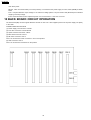
Hybrid IP-PBX
KX-TDA100BX
(for Asia, Middle Near East, South America and Africa)
IMPORTANT INFORMATION ABOUT LEAD FREE, (PbF), SOLDERING
If lead free solder was used in the manufacture of this product the printed circuit boards will be marked PbF.
Standard leaded, (Pb), solder can be used as usual on boards without the PbF mark.
When this mark does appear please read and follow the special instructions described in this manual on the use of PbF and how
it might be permissible to use Pb solder during service and repair work.
© 2003 Panasonic Communications Co., Ltd. All
rights reserved. Unauthorized copying and
distribution is a violation of law.
KX-TDA100BX
CONTENTS
Page
1 ABOUT LEAD FREE SOLDER (PbF: Pb free)
1.1. SUGGESTED PbF SOLDER
Page
3
11.1. INTRUDUCTION
31
3
11.2. TYPICAL EXAMPLE
32
11.3. MPR CARD
33
11.4. ERROR LOG
50
1.2. HOW TO RECOGNIZE THAT Pb FREE SOLDER IS
USED
4
2 FOR SERVICE TECHNICIANS
4
3 CAUTION
12 DIAGNOSIS
55
5
12.1. DIAGNOSIS FEATURES
55
3.1. NOTE
5
12.2. DIAGNOSIS TEST
59
3.2. SAFETY PRECAUTIONS
5
3.3. INSULATION RESISTANCE TEST
5
3.4. BATTERY CAUTION
5
14 TERMINAL GUIDE OF ICS, TRANSISTORS AND DIODES
68
3.5. CAUTION
5
15 HOW TO REPLACE A FLAT PACKAGE IC
69
13 IC DATA
13.1. IC101
64
64
6
15.1. PREPARATION
69
4.1. GENERAL DESCRIPTION
6
15.2. PROCEDURE
69
4.2. CHARACTERISTICS
6
15.3. REMOVING SOLDER FROM BETWEEN PINS
69
4.3. SYSTEM CAPACITY
7
4 SPECIFICATIONS
5 SYSTEM OVERVIEW
5.1. SYSTEM CONFIGURATIONS
5.2. SYSTEM COMPONENTS
5.3. SYSTEM CONNECTION DIAGRAM
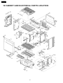
16 CABINET AND ELECTRICAL PARTS LOCATION
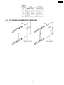
16.1. EXTENSION BOARDS FOR SERVICING
8
70
71
8
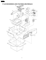
17 ACCESSORIES AND PACKING MATERIALS
72
9
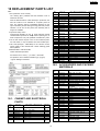
18 REPLACEMENT PARTS LIST
73
10
18.1. CABINET AND ELECTRICAL PARTS
73
6 NAME AND LOCATIONS
12
18.2. ACCESSORIES AND PACKING MATERIALS
73
7 DISASSEMBLY INSTRUCTIONS
13
18.3. MPR CARD PARTS
74
7.1. DISASSEMBLY INSTRUCTION (MPR CARD)
13
18.4. BACK/LED BOARD PARTS
79
7.2. DISASSEMBLY INSTRUCTION (BACK BOARD)
14
18.5. FIXTURES AND TOOLS
80
8 OUTLINE
16
19 FOR THE SCHEMATIC DIAGRAM
81
8.1. GENERAL DESCRIPTION
16
20 SCHEMATIC DIAGRAM
82
8.2. SYSTEM CONTROL
17
20.1. MPR CARD
82
8.3. BACK BOARD SIGNAL CONNECTION DIAGRAM
20
20.2. BACK/LED BOARD
87
20.3. WAVEFORM
90
9 MPR CARD CIRCUIT OPERATION
9.1. MPR CARD
23
23
21 PRINTED CIRCUIT BOARD
92
10 BACK BOARD CIRCUIT OPERATION
30
21.1. MPR CARD
92
11 TROUBLESHOOTING GUIDE
31
21.2. BACK/LED BOARD
94
2
KX-TDA100BX
1 ABOUT LEAD FREE SOLDER (PbF: Pb free)
Note:
In the information below, Pb, the symbol for lead in the periodic table of elements, will refer to standard solder or solder that
contains lead.
We will use PbF when discussing the lead free solder used in our manufacturing process which is made from Tin, (Sn), Silver,
(Ag), and Copper, (Cu).
This model, and others like it, manufactured using lead free solder will have PbF stamped on the PCB. For service and repair
work we suggest using the same type of solder although, with some precautions, standard Pb solder can also be used.
Caution
· PbF solder has a melting point that is 50° ~ 70° F, (30° ~ 40°C) higher than Pb solder. Please use a soldering iron with
temperature control and adjust it to 700° ± 20° F, (370° ± 10°C). In case of using high temperature soldering iron, please
be careful not to heat too long.
· PbF solder will tend to splash if it is heated much higher than its melting point, approximately 1100°F, (600°C).
· If you must use Pb solder on a PCB manufactured using PbF solder, remove as much of the original PbF solder as possible
and be sure that any remaining is melted prior to applying the Pb solder.
· When applying PbF solder to double layered boards, please check the component side for excess which may flow onto the
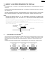
opposite side (See figure, below).
1.1.
SUGGESTED PbF SOLDER
There are several types of PbF solder available commercially. While this product is manufactured using Tin, Silver, and Copper,
(Sn+Ag+Cu), you can also use Tin and Copper, (Sn+Cu), or Tin, Zinc, and Bismuth, (Sn+Zn+Bi). Please check the manufac
turer’s specific instructions for the melting points of their products and any precautions for using their product with other
materials.
The following lead free (PbF) solder wire sizes are recommended for service of this product: 0.3mm, 0.6mm and 1.0mm.
3
KX-TDA100BX
1.2.
HOW TO RECOGNIZE THAT Pb FREE SOLDER IS USED
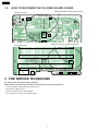
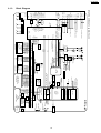
Marked PbF (PbF is marked around here)
(Component View)
X202
RA308
25
48
25
29
12
D407
2
C408
30
48
L401
14 IC311 8
1
R307
7
8
1
R306
IC
R12
R12
R12
R10
R10
R
16
14
16 IC310 9 IC1
1
1
44
C402
J314
23
22
R230
RA309
R232
1
1
16
10
11
1
RES
R550
PbF
8 12
SG
R211
R216
L204 R229
L205
FIL204
14
L206 R231
IC1
L207
FIL205
L208 R233
R218 L210
C212
CN211
R209
IC302
9 1
SG
R220
44
1
24
1
1
24
R241
C208
1
CN206
IC304
IC303
1
IC205
R239
13
R243
PSUP1317ZB
C218
R247
R248
C217
48
RA202 24
37
25 C213 36
R244
R242
QA103
QA101
R148
BATALM
LED103
R176
R164
LED101
SDIN
R251R240
J113
Marked PbF (PbF is marked around here)
(Component View)
B1
B45
A45
A1
CN107
B1
B45
R313 R306
R311
R303
R307
C203
R302
R308
R317 R314
R305
R318 R342 R316
R315
R310
R304 C201
R312 R340
C202 R309 R301
C204
A45
C209 R347
C210 R344
R348 R343
R345 R346
C207 C208
PbF
A1
CN112
B1
B45
1
L105
L104 L106 L110 L111
R338
R333
R332
C206 R337
R335
R334 R326
R330
R329 R323 C205
R331
R325 R324
R336 R328 R327
PSUP1367Z-A
2 FOR SERVICE TECHNICIANS
ICs and LSIs are vulnerable to static electricity.
When repairing, the following precautions will help prevent recurring malfunctions.
1. Cover the plastic parts boxes with aluminum foil.
2. Ground the soldering irons.
3. Use a conductive mat on the worktable.
4. Do not touch IC or LSI pins with bare fingers.
4
LED202
ALM
PSUP1367Z-B
LED201
RUN
B
B
CN113
L112 L108 L101
L103
9 L107
L109 L102
1
CN114 3
1
3
CN201
KX-TDA100BX
3 CAUTION
3.1.
NOTE
When you note the serial number, write down all of the 11 digits.
The serial number may be found on the label affixed to the bottom of the unit.
3.2.
SAFETY PRECAUTIONS
1. Before servicing, unplug the power cord to prevent an electric shock.
2. When replacing parts, use only the manufacturer´s recommended components for safety.
3. Check the condition of the power cord. Replace if wear or damage is evident.
4. After servicing, be sure to restore the lead dress, insulation barriers, insulation papers, shields, etc.
5. Before returning the serviced equipment to the customer, be sure to perform the following insulation resistance test to prevent
the customer from being exposed to shock hazards.
3.3.
INSULATION RESISTANCE TEST
1. Unplug the power cord and short the two prongs of the plug with a jumper wire.
2. Turn on the power switch.
3. Measure the resistance value with ohmmeter between the jumpered AC plug and each exposed metal cabinet part, such as
screw threads, control shafts, handle brackets, etc.
Note:
Some exposed parts may be isolated from the chassis by design. These will read infinity.
4. If the measurement is outside the specified limits, there is a possibility of shock hazard. The equipment should be repaired and
rechecked before it is returned to the customer.
3.4.
BATTERY CAUTION
1. Danger of explosion if battery is incorrectly replaced. Replace only with the same or equivalent type recommended by the
manufacturer. Dispose of used batteries according to the manufacturer’s Instructions.
2. The lithium battery is a critical component (type No.CR23541). Please observe for the proper polarity and the exact location
when replacing it and soldering the replacement lithium battery in.
3.5.
CAUTION
The power socket wall outlet should be located near this equipment and be easily accessible.
5
KX-TDA100BX
4 SPECIFICATIONS
4.1.
GENERAL DESCRIPTION
Control Bus
Communication Bus
Switching
Power Input
PSU-S
(KX-TDA0108)
PSU-M
(KX-TDA0104)
External Battery
Maximum Power Failure Tolerance
Memory Backup Duration
Dialling
Trunk
Extension
Mode Conversion
Ring Frequency
Trunk Loop Limit
Operating
Environment
Temperature
Humidity
Conference Call Trunk
Music on Hold (MOH)
Paging
Serial Interface Port
Internal
External
RS-232C
USB
Extension Connection Cable
Dimension
KX-TDA100
Weight (when fully mounted) KX-TDA100
4.2.
Original bus (16 bit, 8 MHz,10 megabytes per second)
H.100 bus conformity (1024 time slot)
Non Blocking Distributed Time Switch
100 V AC to 130 V AC/200 V AC to 240 V AC, 1.4 A/0.8 A, 50 Hz/60 Hz
100 V AC to 130 V AC/200 V AC to 240 V AC, 2.5 A/1.4 A, 50 Hz/60 Hz
+36 V DC (+12 V DC x 3, battery capacity of 28 Ah or below recommended for 1 external
battery)
300 ms (without using backup battery)
7 years
Dial Pulse (DP) 10 pps, 20 pps
Tone (DTMF) Dialling
Dial Pulse (DP) 10 pps, 20 pps
Tone (DTMF) Dialling
DP-DTMF, DTMF-DP
20 Hz/25 Hz (selectable)
1600 Ω maximum
0 °C to 40 °C
10%to 90% (non condensing)
From 10 x 3-party conference call to 4 x 8-party conference call
2 ports (Level Control: -11 dB to +11 dB in 1 dB steps)
MOH1: External Music Source port
MOH2: Selectable Internal/External Music Source port
Level Control: -6 dB to +3 dB in 3 dB steps
2 ports (Volume Control: -15 dB to +15 dB in 1 dB steps)
1 (max 115.2 kbps)
1
SLT
1 pair wire (T, R)
DPT
1-pair wire (D1, D2) or
2-pair wire (T, R, D1, D2)
APT
2-pair wire (T, R, D1, D2)
DSS Consoles and Add-on Key Module
1-pair wire (D1, D2)
334 mm (W) x 390 mm (H) x 270 mm (D)
(13 5/32 in x 15 11/32 in x 10 5/8 in)
Under 12 kg (26.5 lb)
CHARACTERISTICS
Terminal Equipment Loop Limit
· PT: KX-T76xx series and KX-T7560/KX-T7565: 90 Ω; all other DPTs/APTs: 40 Ω
· SLT: 600 Ω including set
· Doorphone: 20 Ω
Minimum Leakage Resistance
Maximum Number of Extension
Instruments per Line
Ring Voltage
Trunk Loop Limit
Hookswitch Flash/Recall Timing Range
BRI Cards Internal ISDN Mode
Door Opener Current Limit
Paging Terminal Impedance
MOH (Music on Hold) Terminal Impedance
· CS: 130 Ω
15000 Ω maximum
1 for PT or SLT
2 by Parallel or eXtra Device Port connection of a PT and an SLT
75 Vrms at 20 Hz/25 Hz depending on the Ringing Load
1600 Ω maximum
24 ms to 2032 ms
Supply Voltage: 40 V
Power Supply: 4.5 W per 1 line,10 W per 4 lines (BRI4)
4.5 W per 1 line, 20 W per 8 lines (BRI8)
Power Supply Method: Phantom Power Supply
24 V DC/30 V AC, 1 A maximum
600 Ω
10000 Ω
6
KX-TDA100BX
4.3.
SYSTEM CAPACITY
4.3.1.
Maximum Trunk and Extension Cards
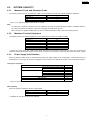
The following number of trunk and extension cards can be installed in the main unit (Hybrid IP-PBX) for expansion.
Card Type
Trunk Card *1
Extension Card
Total
KX-TDA100
4
4
5
*1 One T1, E1, PRI30 and PRI23 card counts as 2 cards.
Note:
· For each card, a maximum number that can be installed in the main unit (Hybrid IP-PBX) is listed in "Installation Manual".
· Any card that exceeds the capacity of the main unit (Hybrid IP-PBX) will be ignored.
· When the main unit (Hybrid IP-PBX) starts up with an invalid configuration mode, some cards will be ignored.
4.3.2.
Maximum Terminal Equipment
The following number of terminal equipment can be supported by the main unit (Hybrid IP-PBX).
Terminal Equipment Type
Telephone *1
CS
PS
Voice Mail
Doorphone
Door Opener
KX-TDA100
64
16
128
2
8
8
*1 When only T76xx series and T7560, T7565 DPTs and SLTs are connected. If other DPTs or APTs are connected, the
maximum number will decrease as each of these units is counted as 4 sets of SLTs or DPTs (T76xx series and T7560, T7565).
4.3.3.
Power Supply Unit Selection
Main unit (Hybrid IP-PBX) needs an optional power supply unit (PSU) suitable for its configuration. Calculate the amount of
"load figures" from the type and number of equipment to be connected, and determine the type of PSU that will be required.
Load Figure Calculation
PT
Extension Card *1
Equipment Type
DPT (T76xx series and T7560, T7565)
Other DPT/APT/DSS Console
DHLC8
SLC8
SLC16
MSLC16
CS
ISDN Extension
Voice Mail
*1 Only the extension cards that can support SLTs count for the load figures.
PSU Capability
Each PSU supports a different amount of load figures.
PSU Type
Maximum Load Figures
64
128
PSU-S
PSU-M *2
*2 Available for the KX-TDA100 and KX-TDA200.
7
Load Figure
1
4
8
8
16
16
4
2
1
KX-TDA100BX
5 SYSTEM OVERVIEW
5.1.
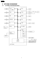
SYSTEM CONFIGURATIONS
8
KX-TDA100BX
5.2.
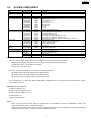
SYSTEM COMPONENTS
Model
Shelf
KX-TDA100BX
Main Central Processing
Card
MPR Option Card
KX-TDA0196XJ
CO Line Cards
KX-TDA0180X
KX-TDA0181X
KX-TDA0184XJ
KX-TDA0188XJ
KX-TDA0193XJ
KX-TDA0284XJ
KX-TDA0288XJ
KX-TDA0290CJ
KX-TDA0290X
KX-TDA0480X
Extension Cards
KX-TDA0144XJ
KX-TDA0170XJ
KX-TDA0171XJ
KX-TDA0172XJ
KX-TDA0173XJ
KX-TDA0174XJ
KX-TDA0175XJ
Other Cards
KX-TDA0161XJ
KX-TDA0166XJ
KX-TDA0190XJ
KX-TDA0191XJ
KX-TDA0410XJ
Power Supply Units
KX-TDA0104XJ
(PSUs)
KX-TDA0108XJ
Cell Stations (CS’s)
KX-TDA0142CE
Proprietary Equipment KX-A228XJ
KX-A229XJ
KX-A258XJ
KX-T30865X
Card Name
MPR
RMT
LCOT8
LCOT16
E&M8
E1
CID8
BRI4
BRI8
PRI30
PRI23
IP-GW4
CSIF8
DHLC8
DLC8
DLC16
SLC8
SLC16
MSLC16
DHP4
ECHO16
OPB3
MSG4
CTI-LINK
PSU-M
PSU-S
Description
Basic Shelf
Main Processing Card
Remote Card
8-Port Analogue Trunk Card
16-Port Analogue Trunk Card
8-Port E &M Trunk Card
E-1 Trunk Card
8-Port Caller ID Card
4-Port BRI Card
8-Port BRI Card
PRI Card
PRI Card
4-Channel VoIP Gateway Card
8 Cell Station Interface Card
8-Port Digital Hybrid Extension Card
8-Port Digital Extension Card
16-Port Digital Extension Card
8-Port Single Line Telephone Extension Card
16-Port Single Line Telephone Extension Card
16-Port Single Line Telephone Extension with Message Lamp Card
4-Port Doorphone Card
16-Channel Echo Canceller Card
Optional 3-Slot Base Card
4-Channel Message Card
CTI Link Card
M-Type Power Supply Unit
S-Type Power Supply Unit
4-Channel Cell Station Unit for DECT Portable Station
S/M-type Back-up Battery Cable
L-type Back-up Battery Cable
Blank Slot Cover
Doorphone
Available Telephones
This main unit (Hybrid IP-PBX) supports all of the Panasonic KX-T7xxx and KX-TD7xxx series:
· Digital/Analog proprietary telephones (e.g., KX-T7625, KX-T7630, KX-T7633, KX-T7636)
· Portable stations (e.g., KX-TD7690, KX-TD7680)
· DSS consoles (e.g., KX-T7640)
This main unit (Hybrid IP-PBX) does not support the following telephones:
· KX-T308xx series Proprietary Telephones and DSS consoles
· KX-T616xx series Proprietary Telephones and DSS consoles
· KX-T1232xx series Proprietary Telephones and DSS consoles
For the equipment (e.g., Add-on Key Module, USB Module, Headset) that can be connected to a particular telephone, refer to
the telephone’s manual.
Abbreviations in this manual
Proprietary telephone: PT
Digital proprietary telephone: DPT
Analog proprietary telephone: APT
Portable station: PS
Single line telephone: SLT
Note:
· There are some optional service cards and features that are not available for certain countries/areas. Consult your
authorized Panasonic dealer for detailed instructions.
· The power supply capacity of this main unit (Hybrid IP-PBX) may differ from the values described in this manual depending
on the model number. Please consult your dealer for detailed information.
9
KX-TDA100BX
5.3.
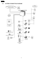
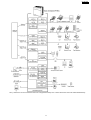
SYSTEM CONNECTION DIAGRAM
10
KX-TDA100BX
*Only 1 Server PC can be connected to the main unit (Hybrid IP-PBX). Two or more Server PCs cannot be used simultaneously.
11
KX-TDA100BX
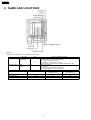
6 NAME AND LOCATIONS
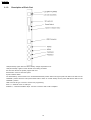
· Null slot:
Null slot is not available for any optional service card.
RUN Indicator
ALARM Indicator
LED Type
LED1
(Power/RUN)
LED2
(Alarm)
Slot Type
Free Slots 1 to 5
Option Card Slot
MPR Card Slot
Color
Green
Red
Usage and Status Definition
Display of Power Supply & RUN Status
OFF: Power OFF (inc. in normal resetting)
ON: Power ON & RUN (On-Line)
Flash (60/min.): Power ON & In starting
Flash (120/min.): Power ON & In resetting before system clear
Display of ALARM
OFF: Normal
ON: Alarm (CPU stop, Alarm for each card)
Flash: Alarm (MPR file error in restarting)
MPR Card
CO Line Cards
Extension Cards
Yes
No
No
No
No
Yes
12
OPB3 Card
CTL-LINK Card
Yes
Yes
No
KX-TDA100BX
7 DISASSEMBLY INSTRUCTIONS
7.1.
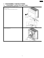
DISASSEMBLY INSTRUCTION (MPR CARD)
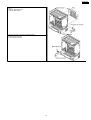
1. Remove the Lib by sliding it in the direction of arrow 1.
2. This will be removed if the user attached a Pad Lock as shown in a
Fig.1.
3. Loosen the Screw.
4. Front Cover is removed in the direction of arrow 2.
5. Loosen the two Screws.
6. Remove the MPR Card.
13
KX-TDA100BX
7.2.
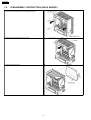
DISASSEMBLY INSTRUCTION (BACK BOARD)
1. Remove four Screws (A).
2. Remove the Left Side Cover and the Right Side Cover.
3. Remove the Hook. Remove the Top Cover.
4. Remove nine Screws (B).
5. Remove the Back Cover.
14
KX-TDA100BX
6. Remove the RS-232C Connector and LED Connector from Back
Board 1.
7. Remove eight Screws (C).
8. Remove Back Board 1.
9. Remove the LED Connector from Back Board 2.
10. Remove the Screw (C).
11. Remove Back Board 2.
15
KX-TDA100BX
8 OUTLINE
8.1.
GENERAL DESCRIPTION
The control system of the main unit is composed of the main central processing card (MPR card) controlling the entire system
and exchanging voice data, the circuit control section (LPR/LC) controlling various telephone lines and the power supply section
(POWER).
MPR card, LPR/LC and POWER are connected each other through the System BUS (ADDRESS BUS, DATA BUS and
CONTROL BUS). MPR card and LPR/LC are under I/O control (I/O Read/Write) by MPR card.
MPR card controls LPR which have a microprocessor by the lnter-Microprocessor Communication System supported by ASIC.
Those are, MPR card and LPR exchange controlling messages through bi-directional buffer and CPU controls LPR so that it
can manage multiple telephone lines. Since LC does not have a microprocessor, it is completely controlled through ASIC from
MPR card.
I/O address for LPR access is fixed for each free slot. CPU discriminates the sort of LPR through the inter-processor
communication system.
POWER detects the voltage drop of the AC input and the DC output and transfers it to MPR card.
8.1.1.
MPR Card
This card is the main control section of main unit. It controls all the cards mounted on the free slots, and communication of RS232C ports.
There are two LED (BATT ALARM, SD ACCESS), one SD card slot, one push switch, one slide switch, one USB port, two MOH
jacks, and two EPG jacks in the front of MPR card. BATT ALARM LED light red if the output of the lithium battery in MPR card
is set to about 2.8V or less. During access to SD card, it green-blinks or SD ACCESS LED light and blink. Enclosed SD card
is used for SD card slot on a main part, putting in. The main program is stored in SD card. It connects with PC and a USB port
is used for a maintenance or a system setup. The external sound source for BGM or suspension sound is connected to a MOH
jack. A speaker with amplifier is connected to external paging at an EPG jack. Light Emitting Diode (RUN indicator,
ALARMindicator) arranged at the main part upper part is directly controlled from MPR card, and shows the state of a system
of operation.
This control circuit executes the control signals for the exchange process, and this card is composed of the following
(A) 32bit CPU (32bit data bus)
(B) SDRAMs, SRAMs
(C) Flash memorys
(D) Lithium Battery for back-up of clock IC and Static RAMs
8.1.2.
Back Board
BB (back board) is the mother board of the basic shelf. This board connects each card/unit (POWER, MPR card, and optional
service cards) together. This board has one RS-232C connector.
8.1.3.
Power Supply Unit
This unit is switching regulator power supply and supplies DC voltages to MPR card, and optional card (free slot). PSU (power
supply unit) has four outputs (40V, 30V, 15VPT, 15V). 15V output is supplied only in MPR card and option card. Other outputs
are mainly used as an object for the electric supply to a terminal. Refer to each S/M for the details of PSU.
16
KX-TDA100BX
8.2.
8.2.1.
SYSTEM CONTROL
System Control Block Diagram
17
KX-TDA100BX
8.2.2.
Voice (TDM Highway) Bus Block Diagram
18
KX-TDA100BX
8.2.3.
Voice Bus Logical Assignment
In the line card, the CT_D line number, which is output in accordance with the inserted slot, and the time slot are assigned by
software.
For the detail of output slot for each card (optional service card), refer to the service manual of the card (optional service card).
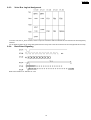
8.2.4.
Back Board Signaling
Back board waveform of TDM bus for voice
19
KX-TDA100BX
8.3.
8.3.1.
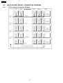
BACK BOARD SIGNAL CONNECTION DIAGRAM
CT Bus System Connection Diagram
20
KX-TDA100BX
8.3.2.
EC Bus System Connection Diagram
21
KX-TDA100BX
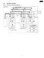
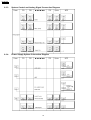
8.3.3.
System Control and Analog Signal Connection Diagram
8.3.4.
Power Supply System Connection Diagram
22
KX-TDA100BX
9 MPR CARD CIRCUIT OPERATION
9.1.
MPR CARD
9.1.1.
Outline
1) Function
· System Control
· Circuit Switching (includes gain adjustment function)
· Conference Call (3 people x 8 ~ 8 people x 3)
· MOH
· PAGING
· Clock
2) Configuration
· Power Supply: DC/DC Converter
· CPU: HITACHI SH7709S (133MHz)
· ASIC: Our own products
· ROM: 4Mbit x 1 (for boot programs)
· SDRAM: 64Mbit x 2 (for work area)
· SRAM: 4Mbit x 2 (for user data backup)
· SD card I/F (for operating programs) x 1
· USB I/F (for PC programming) x 1
· MOH: External sound input x 2
· PAGING: External output x 2
· Expanded memory connector x 1
· Modem card connector x 1
3) Operation Rating
· Power Input : +15V
· Power Output : +15V (for MOH)
+3.3V (for I/O)
+3.3VBB (back board signal line pull-up)
+3.3VB (for SRAM backup)
+1.8V (for CPU core)
+1.9VB (for clocking backup)
±9.4V (for RS-232C driver/receiver)
+5VRMT unused (for remote card)
+5V (for RS-232C driver/receiver)
23
KX-TDA100BX
9.1.2.
Description of Each Part
LED (BATALM): Lights when the lithium battery voltage drops below 2.8V.
LED (SD ACCES): Lights on when the SD card is being accessed.
SD card slot: Mounts the system program SD card.
Reset Switch: Press to reset the system.
System Initialize Switch:
On default startup, set the switch to the "SYSTEM INITIALIZE" position before turning the power ON. Return the switch to the
"NORMAL" position when the main power switch starts to flash. On normal startup, turn the power ON with this switch in the
"NORMAL" position.
USB connector: B-type connector. Used for PC programming.
MOH 1, 2: External music on hold input.
PAGING 1, 2: External PAGING output. Connect to a device with a built-in amplifier.
24
ADD BUS
CNT BUS
DATA BUS
Dbus
Buffer
LD[15:0]
OSC
12MHz X201
X202
to CPU
nDREQ0,1
nDACK0,1
+3.3V
+1.8V
nRD
DQMLU,DQMLL
ADD0-7
nCS_SDB
P-I/O Ports
PCMCIA Interface
JTAG Interface
SIO(SCI0)
SIO with FIFO(SCI2)
SIO with FIFO(SCI1)
+3.3VB
DSRs,DTRs, RTS, CTS,
nINIT, DIPSWs
AC_ALM,DC_ALM,nBATALM
POWTYPE[1:0],nBATT
(16bit bus)
4Mbit*2
SRAM
Total:1MB
(16bit bus)
4Mbit
+3.3V
CH_SEL2
nIRQ
IC406
AGC
AGC
IC408
DQMLU,DQMLL
nCS_5
nWR
nRD
nBS
CODEC
(+3.3V)
IC405
Mu/nA
-9V
IC121
IC120
90pin DIN
RXD1, CS1, DR1
LEDRUN
LEDALM
RING_SYNC
RING_SIN
RINGER
nHALT
TXD2
RXD2
DCALM
ACALM
POWTYPE[1:0]
nBATT
nLOS
TXD1, RS1, ER1
RCV
+5V
CT_NETREF
CT_D[7:0]
CT_FRAME
CT_C8
EC_CLK
EC_nRST
EC_AD[15:0]
EC_CBE[1:0]
EC_nPAR
EC_nFRAME
EC_nTRDY
EC_nSTOP
EC_nPERR
EC_nCDET
EC_nINT
(EC_IDSEL)
+3.3V_BB
(for B.B.)
+15V
GND
DRV
+9V,-9V
H100_bus
+3.3V
Termination
EC_bus
Limitter
+3.3V Current
IC403
+1.8V
Series Reg.
SW Reg.
IC402
+3.3V
KX-TDA100 MPR CARD BLOCK DIAGRAM
from CPU(Output Port)
from ASIC(Output Port)
from ASIC
to CPU(Input Port)
+5V
Series Reg.
+9V
EC_CLK
EC_nRST
EC_AD[15:0]
EC_CBE[1:0]
EC_nPAR
EC_nFRAME
EC_nTRDY
EC_nSTOP
EC_nPERR
EC_nCDET
EC_nINT
IC102
ASIC
SW Reg.
IC413
+15V
SDI,SDO,CTS,RTS
CT_NETREF
LDHW0,LUHW0
CT_D[7:0]
nF0,HW_CLK
CT_FRAME
CT_C8
CH_SEL[2:0]
PIO[7:4]
nIRQ
nBREQ
nBACK
nCS
nWR
nRD
nBS
D0-D15 DATA
A1-A23 ADD
HALT, Mu/nA,MOH_SEL,
MELODY_SEL
X103
TCXO
16.384MHz
TxD,RxD,CTS,RTS(UART i/f)
CODEC
(+3.3V)
IC409
+15V/GND
64Mbit*2
(32bit bus)
SDRAM
Total:16 MB
IC305, IC306
nBREQ
nBACK
UHW,DHW,CLK(4.096MHz)
DTR,DSR
+3.3V
nPRS_RMT
GAIN0,GAIN1
Battery
(+3.0V)
IC404
Regulator
(+1.8V)
IC303
FLASH
Total:512KB
+3.3V
MELODY_SEL
(Software)
Melody
IC410 IC
MOH-SEL
(Software)
RMT card
(Option)
VRTC
+3.3VB
7pin Conn.
(Debug Interface)
DTR,RTS,LEDs,REG,BELTIME
(Checker Pad only)
(for RS232C port)
IC107
Local
Reset
OSC
16.384MHz
X101
CoreCLK=131.072MHz
CLK
Modulation
32.768kHz
X102
VRTC
CPU
IC101
DQMUU,DQMUL
DC_ALM,nIRQ_USB, nIRQ_SDB
SH7709S
RTC
Interrupu
Controller
CS Generation
for
Flash,SRAM,
SDB, USB
D[31:0]
LD[15:0]
ADD[25:0]
nCS_2 etc.
RD/nWR
nRAS
nCAS
CKIO
CKE
IC103
DMAC
Bus Arbiter
nWR, nRD
nCS0,3,4
nRASs, nCASs,etc
IC123, IC124
MPR Card
SW103
Initialize
SW
SW101
(Manual Reset SW)
Reset
to Reset IC
LED103
BATT ALARM
SD-ACCESS
LED101
CN209
OSC
20MHz
D[31:0]
USB Interface
(ML60852A)
IC204
LD[15:0]
A[25:0]
USB
Conn.
DQMLU,DQMLL
IC301, IC302
LD[15:0]
ADD1-19
nCS_4
RD/nWR
nRD
+3.3VB
MEC Card
(Expansion Memory)
(Future option)
LD[15:0]
SD Card Interface
(MN5773)
IC205
CH_SEL1
MOH2
CH_SEL0
ADD1-23
RD/nWR
nRD
nCS_0
Paging2
30pin Connection
D[31:0]
ADD2-15
nCS_3
RD/nWR
nRAS
nCAS
CLK
CKE
Paging1
25
MOH1
DQMUU,DQMUL
9.1.3.
SD Card
KX-TDA100BX
Block Diagram
KX-TDA100BX
9.1.4.
Circuit Description
9.1.4.1.
Outline of Block Description
· CPU block
Operates the main unit control. Also operates various controls, generation of select signal, DMA control and serial port control.
This contains the built-in clock function.
· ASIC block
Provides the communication between each optional service card, call control (TSW function), conference call, tone generation
and gain control function.
· Memory block
This is a work area used for the main unit control program storage, the system boot program storage, or the user configuration
data storage.
· USB block
Provides the USB I/F function. Connects to the PC to be used for PC programming or system data load/store.
· SD card block
Provides the SD card I/F function and loads the main unit program and the system data from the SD card containing the main
unit control program.
· MOH/PAGING block
Provides the external music on hold input x 2, and the external paging output x 2 port. Also this provides the external music on
hold input 1 system and exclusively the internal music on hold output.
· Power block
Consists of DC/DC converter circuit and various regulators.
9.1.4.2.
Detail of Block Description
· CPU block
Configuration: IC101 (CPU), IC107 (reset IC), IC103 (spread clock IC), X101 (CPU source clock), X102 (clocking clock) etc.
Function: (IC101)
Generates the select signal in accordance with the memory map and operates read/write of data between each peripheral.
Controls the DMA transfer between USB I/F or built-in serial controller and memory.
Operates input/output control of each I/O signal in accordance with the program.
Contains the built-in clock function (battery backup) with the source clock X102 (32.768 kHz).
(IC107)
Monitoring the power voltage, it generates a reset signal when the voltage drops under the constant value (2.9Vtyp) or when
the reset switch is pressed down.
(IC103)
To reduce unnecessary radiation, it generates the clock with the constant blurring mainly X101 clock output (16.384 MHz).
Description of the Signal on MPR
Signal Name
+15VIN
+15V
+9.4V
+5V
+5VRMT
3.3V_BB
+3.3VB
+3.3V
1.9VB
1.8V
A[0]-A[25]
nAC_ALM
nBACK
nBATT
Functions
+15V DC
For Circuit +15V DC MOH
For Driver IC +9.4V DC RS-232C
For Driver IC +5V DC RS-232C
Reserve
+3.3V DC
For pull-up of back board signal line
+3.3V DC
Battery backup
For SRAM (IC301, IC302) backup
+3.3V DC
+1.9V DC
Battery backup
For clock function of CPU (IC100)
For Core +1.8V DC CPU (IC100)
Address bus
AC alarm signal: Indicates AC voltage cutoff. (L: Alarm condition)
Bus Acknowledge: Indicates Bus Acknowledge.
Indicates whether external battery is connected or not. L: Connected
26
KX-TDA100BX
Signal Name
nBAT_ALM
nBREQ
nBS
nCASL
nCASU
CH_SEL[0]
CH_SEL[1]
CH_SEL[2]
CKE
CKIO
nCS0
nCS2
nCS3
nCS4
nCS5
nCS6
nCS_FLASH0
nCS_FLASH1
nCS_SDB0
nCS_SDB1
nCS_SRAM0
nCS_SRAM1
nCS_USB
nCTS2
CTS_RMT
CT_C8
CT_D[0] -[7]
CT_FRAME
CT_NETREF
C_CS[0]
D[0] -D[31]
nDACK0-1
DCD2
DCLK_RMT
nDC_ALM
DIN_RMT
DOUT_RMT
DQMLL (nWE0)
DQMLU (nWE1)
DQMUL (nWE2)
DQMUU (nWE3)
nDREQ0-1
DSR2
DSR_RMT
DTR2
EC_AD[0] -[15]
EC_nCBE[1]-[0]
EC_nCDET
EC_CLK
EC_nFRAME
EC_nINT
EC_PAR
EC_nPERR
EC_nRST
EC_nSTOP
EC_nTRDY
nFAN_ALM
FSEL0
GAIN0-1
HALT
nINIT
nIRQ_ASIC
nIRQ_SDB
nIRQ_USB
Functions
Battery Alarm Signal: Indicates the declined voltage of lithium battery. (L: Alarm condition)
Bus Request: Bus request signal
Bus Cycle Start: Bus cycle start signal
Lower Byte Address Column Address Strobe: CAS signal for SDRAM
Upper Byte Address Column Address Strobe: CAS signal for SDRAM
Synchronous Signal for CODEC (For MOH#1/Page#1)
Synchronous Signal for CODEC (For MOH#2/Page#2)
Synchronous Signal for CODEC (For RMT)
Clock Enable: CKE signal for SDRAM
Clock I/O Terminal: For bus clock of SDRAM (IC305, IC306) and ASIC (IC101) CPU (IC100) outputs the clock of four
times frequency as Source clock (16.384MHz).
Chip Select 0: Chip select signal for flash memory
Chip Select 2: Chip select signal for the expanded SDRAM (Future Option, Reserve at present.)
Chip Select 3: Chip select signal for SDRAM
Chip Select 4: Chip select signal for SRAM
Chip Select 5: Chip select signal for ASIC
Chip Select 6: Chip select signal for USB I/F and SD card I/F
Chip Select for Flash memory 0: CS signal for IC303
Chip Select for Flash memory 1: CS signal for IC304 (reserve)
Chip Select for Sd card I/F
Reserve
Chip Select for SRAM 0: CS signal for IC301
Chip Select for SRAM 1: CS signal for IC302
Chip Select for USB I/F
Clear To Send from RS-232C connector
Clear to Send: Flow signal for modem
Clock 8.192MHz clock outputted from PLL master
CT Data Bus: Two-way serial data bus to which the drive from any card is possible in the system.
Frame Signal: 8KHz frame signal outputted from the master
Backup Synchronous Signal (MAX 2MHz) 8KHz signal output from slave etc.
Chip Select For RMT
Data Bus
DMA Acknowledge: For USB I/F
Data Carrier Detect
Codec Clock (8MHz): For RMT
DC ALARM:DC alarm signal; Indicates the declined DC voltage. (L: Alarm condition)
Codec Data Input: For RMT
Codec Data Output: For RMT
Data Input/Output Mask (Write Enable): DQM signal for SDRAM and WE signal for each memory IC and ASIC
DMA Request: For USB I/F
Data Set Ready from RS-232C connector
Data Set Ready from RS-232C connector
Data Terminal Ready to RS-232C connector
Address of EC Synchronous Bus, Data Bus (4MHz)
EC Bus Command/Byte Enable: The initiator drives as bus command in the address phase and as byte enable in the
data phase.
EC Line Card Detection Signal Asynchronous interrupting signal
Clock of EC Synchronous Bus (8MHz) All EC bus signals except nRESET/EC_INT operates in sync with this signal.
EC Cycle Frame Signal: Indicates the drive by initiator and the execution of ECI bus cycle.
EC Interrupting Signal: Be asserted when slave interrupt occurs.
Parity Bit of EC Synchronous Bus: Drive by applying even parity to AD[15:0] and CBE[1:0]. (4MHz)
EC Parity Error: Flag indicating error status by parity flag
EC Reset Input: System reset input signal
EC Bus Stop Signal: Be asserted when target requests transaction halt to initiator.
EC Target Ready Signal: Indicates the drive by target and the possible data transfer.
Fan Alarm: It goes Low at the error of the L Power Supply’s FAN. It goes High when the FAN is normal and, Power
Supply S and M, which does not carry the FAN, are used.
Signal which switches the Flash Memory address of the MEX card. FSEL0 is set by hard jumper. L: The number of
Flash Memory chips on the MPR is 1pc. H: The number is 2pcs.
Gain: Gain adjustment signal for the RMT card (Reserve)
Alerts the occurrence of the declined DC voltage to line card. H: Active L: Normal
System Initialization Switch Input: L: At system initialization, H: At normal start-up
Interrupt Request from ASIC: Indicates ASIC requests interrupt.
Interrupt Request from SD card I/F: Indicates SD card I/F requests interrupt.
Interrupt Request from USB I/F: Indicates USB I/F requests interrupt.
27
KX-TDA100BX
Signal Name
LA[1] -[16]
nLB
LD[0] -[15]
LDHW[1] -[0]
nLEDALM
nLEDRUN
nLOS
LHWCLK[0]
LUHW[1] -[0]
MASTER/nS
MD0-2
MELODYSEL
MEX_MODE[0] -[3]
MOHSEL
Mu/nA
M/nS
Functions
Address bus
Lower Byte Select: Indicates Lower byte select signal of SRAM
Data Bus
Down Highway: Data output terminal connected to codec etc. as down data signal of local highway
Alarm display L: On
RUN display L: On
Loss of synchronous signal: Reserve at present
Highway Clock Signal (8MHz): Bit clock of local highway and selectable among 2.048 / 4.096 / 8.192MHz.
Up Highway: Data input terminal connected to codec etc. as up data signal of local highway.
Master/slave identification signal when SIC card (Future Option) as intersystem connection card is mounted. MPR
inputs this signal and detects which the MPR will be. H: Master L: Slave
Mode Control Terminal: Clock operation mode of CPU is set.MD2: L, MD1: L, MD0: H Fixed
Melody IC Tune Name Select L: Ju te veux H: Minuet
Information Bit to know the memory mounting capacity etc. of MEX card. Reserve at present.
Switching Signal between internal hold sound source and external hold sound H: Internal L: External
Switching Signal of Sound Compression Law H: Mu-Law, L: A-Law
TDA100, TDA200 Identification Signal set on the back board. The MPR inputs this signal and detects which the MPR
will be. H: TDA200, L: TDA100
POWTYPE[0] -[1]
nPRS_MEX
nPRS_RMT
nPRS_SDB
nRAS3L
nRAS3U
nRD
RD/nWR
nRESOUT
nRESET
nRESETM
RINGER
RING_SYNC
nRTS2
RTS_RMT
RXD2
RXD_RMT
SDCD
SDCLK
SDCMD
SDDAT0-3
SDWP
SHW_CLK
SHW_FH
TXD2
TXD_RMT
nUB
USB_D+
USB_DVBUS
VREF
nWAIT
WDTCLR
nWE
Press MEX: Information of MEX Card Attachment L: Attached, H: Not attached
Press RMT: Information of RMT Card Attachment L: Attached, H: Not attached
Press SD card: Information of SD Card Attachment L: Attached, H: Not attached
Lower Byte Address Row Address Strobe: RAS signal for SDRAM
Upper Byte Address Row Address Strobe: RAS signal for SDRAM
Read: USB I/F, SD card I/F, ASIC, SRAM, Read signal for flash memory
Read/nWrite: Read/Write signal for SDRAM
Reset Out: Reset from CPU (IC101) to each card
Reset: Power-on reset signal
Manual Reset: Manual reset request signal for CPU
Ringer Signal: Outputs square-wave of 16Hz/20Hz/25Hz as source signal of ringer
Trigger Signal of Ringer Signal generation timing to each internal line card
Request To Send to RS-232C connector
Request to Send: Flow signal for modem
Receive Data from RS-232C connector
Serial Data Output Terminal: ASIC
SD Card Detect Input
SD Card Clock Out
SD Command
SD Card Data
SD Card Write Protect Input
Intersystem Highway Clock Signal (4MHz) Bit clock of intersystem highway and selectable between
256KHz/512KHz/1.024MHz/2.048MHz/4.096MHz.
Intersystem Highway Synchronous Signal (8KHz) 8KHz frame synchronous signal of intersystem highway
Transmit Data to RS-232C connector
Serial Data Input Terminal: Data receiving terminal from RMT to UART in the ASIC
Upper Byte Select: SRAM
USB Data +
USB Data Bit indicating power source is supplied to USB bus [Host (PC etc.) is connected.] H: Host connected L: Host not
connected
Reference Voltage for MOH Circuit Intermediate potential of +15V
Wait: Hardware wait request signal for bus timing between CPU and ASIC
Reserve
Write Enable: WE signal of SRAM
· ASIC block
Configuration: IC102 (ASIC), IC111, X103 and so on.
Function: (IC102)
28
KX-TDA100BX
Functions as the bus master of EC bus (synchronous bus with 16 bit width, transmission rate max.10Mbps). Communicates
with ASIC mounted to each option card via EC bus and controls the option card.
Controls CT bus (HW clock 8.192MHz, 8 highway, 128 timeslot) for TSW function.
(A detailed description of TSW will be added later.)
Controls the conference call for 3 people x ~8 parties ~ 8 people x ~3 parties.
Generates single and DTMF tone in any highway and timeslot.
Provides the digital gain control function by data conversion.
Provides some I/O ports for CODEC channel pulse generation, modem encoding rule setting and music on hold switching
and is controlled by CPU.
· Memory block
Configuration: IC301, IC302 (SRAM), IC303 (FlashROM), IC305, IC306 (SDRAM), IC309, IC310, IC311 (logic IC) and so
on.
Function: (IC301, IC302)
Saves the user configuration data (such as key assign data per PT).
This memory is battery backup.
(IC303)
Saves (some of) the system boot program and the system data.
(IC305, IC306)
The main program is loaded from the SD card on the system start-up.
Used as the program area and the CPU work area after start-up.
Makes a direct bus connection to CPU due to high-speed action (bus clock 66MHz).
(IC309, IC310, IC311)
Generates each memory select signal from the memory area select signal and upper address. Generates the write signal
and upper/lower byte select signal.
· USB block
Configuration: IC204 (USB I/F), X201 (source clock: 12.000MHz), CN209 (USB connector) etc.
Function: Connects to the USB host system (mainly PC) via CN209 (B type connector) as a USB device and makes data
transfer by max.11Mbps. DMA function of CPU is utilized to transfer the data.
· SD card block
Configuration: IC205 (SD card I/F), IC209, X202(20MHz), CN211 (SD card connector) and so on.
Function: Loads the main program and the system data from the SD card connected to CN211 by 10Mbps. Restores the
system data periodically.
· MOH/PAGING block
Configuration: IC405, IC406 (CODEC), IC408, IC409 (OP Amp), IC410 (Melody IC), Q407~Q410 (transistor), JK401~JK404
(pin jack) etc.
Function: The external music on hold 1 is input from JK404 and is A/D converted in IC405 via AGC (Auto Gain Control)
circuit, which consists of IC408, Q407, Q409 and other CR, and then is connected to the call line HW. Likewise the external
music on hold 2 is input from JK403 and is made A/D conversion in IC406 via AGC (Auto Gain Control) circuit, which
consists of IC409, Q408, Q410 and other CR, and then is connected to the call line HW. The external music on hold 2 and
IC410 is exclusively connected to IC406 input (by software control).
The various tones & DTMF tone and the voice data generated in IC102 (ASIC) are made D/A conversion in IC405 and
IC406. They are output via JK402, JK401 respectively.
· Power Supply block
Configuration: IC402 (DC/DC converter), IC403 (1.8V regulator), IC404 (1.9V regulator), IC411 (OP Amp), IC413 (negative
power regulator), Q403, Q404, Q405, Q411, Q412 (transistor), L401, C408, C453, C454, D406~D409, BAT401, IP401,
IP402 (circuit protection device) and so on.
Function:
+15V input is made step-down to +3.3V by DC/DC converter circuit that consists of IC402, L401, Q412 and C408, and is
supplied to each IC power. Also, it monitors +3.3V output voltage and turns ON Q411 to block +15V input when over voltage
is supplied.
+15V input is dropped to +9.4V by Q403 and is supplied to RS232C driver with the inverted voltage (about 9.1V) generated
in IC413, C453 and C454.
+3.3V generated in DC/DC converter is converted to 1.8V in the back board or IC403 and Q405 via Q404 and supplied to
IC101 core power, and also is converted to 1.9V in IC404 via the back-flow prevention diode D407 and supplied to IC101
29
KX-TDA100BX
clock block power.
BAT401, which is a lithium battery for memory backup, is connected to the power supply of IC301, IC302 (SRAM) via D408,
D409.
IC411 compares BAT401 output voltage to the reference voltage (about 2.8V) and drives LED (BATALM) that indicates
dropping of backup voltage.
IP401 and IP402 block the line respectively when over current flows to +15V and +3.3V line.
10 BACK BOARD CIRCUIT OPERATION
The back board (BB) connects signals between all cards in main unit. It also supplies power from the power supply unit (PSU)
to the cards.
CONNECTORS EXPLANATION
(1) Power Supply Unit Connector: CN100
(2) Free Slot Connectors: CN103-CN106
(3) Option Card Slot Connector: CN107
(4) MPR Card Connector: CN112
(5) RS-232C Connector: CN113
CN113 is connected to D-Sub connector in front of the product.
(6) LED Connector: CN114
CN114 is connected to LED Board on the product.
30
KX-TDA100BX
11 TROUBLESHOOTING GUIDE
11.1. INTRUDUCTION
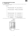
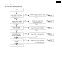
First, check which part of the system is causing the trouble. Follow the flowchart provided below, and replace each unit in turn
with a working unit to identify the damaged unit.
Even when damaged unit is found out, it may mean that not the cause in the unit but the damaged cause in another unit.
31
KX-TDA100BX
11.2. TYPICAL EXAMPLE
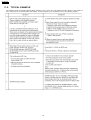
The following items are typical examples when defective occur in main unit. The analysis work first shown in this chapter is
done. When you do not correspond to this chapter, or when analysis is not completed, move to the following chapter.
32
KX-TDA100BX
11.3. MPR CARD
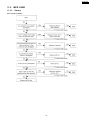
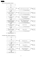
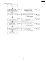
11.3.1. Startup
Run indicator (LED201)
33
KX-TDA100BX
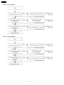
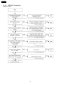
SD card access light does not flash
The battery alarm indication light turns on
34
KX-TDA100BX
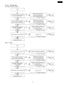
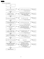
ALARM indicator flashes
· 1 blink and 1 interval
· 2 blinks and 1 interval
(1 blink is 0.5 sec. ON and 0.5 sec. OFF. 1 interval is 2 sec.)
ALARM indicator flashes
· 3 blinks and 1 interval
· 4 blinks and 1 interval
· 5 blinks and 1 interval
(1 blink is 0.5 sec. ON and 0.5 sec. OFF. 1 interval is 2 sec.)
35
KX-TDA100BX
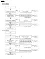
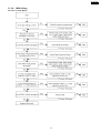
Optional service cards cannot start up
36
KX-TDA100BX
11.3.2. Phone Call
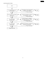
The call path cannot connect
Noise is created
37
KX-TDA100BX
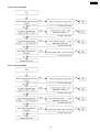
11.3.3. Paging
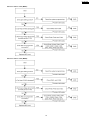
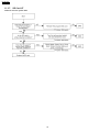
No sound (PAGING1)
No sound (PAGING2)
38
KX-TDA100BX
Noise is Heard (PAGING1)
Noise is Heard (PAGING2)
39
KX-TDA100BX
Sound is small (PAGING1)
Sound is small (PAGING2)
40
KX-TDA100BX
11.3.4. MOH Using
No sound is heard (MOH1)
41
KX-TDA100BX
No sound is heard (MOH2)
42
KX-TDA100BX
Sound is small or loud (MOH1)
Sound is small or loud (MOH2)
43
KX-TDA100BX
11.3.5. USB Connection
Unable to connect
44
KX-TDA100BX
Connection error occurs
45
KX-TDA100BX
11.3.6. RS-232C Connection
Unable to connect
46
KX-TDA100BX
Connecting speed is slowly
47
KX-TDA100BX
11.3.7. SD Card I/F
Unable to save the system data
48
KX-TDA100BX
11.3.8. Other
The clock data is deleted (unset table)
49
KX-TDA100BX
11.4. ERROR LOG
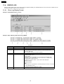
When a major system error occurs in the main unit (Hybrid IP-PBX), the ALARM indicator on the front of the cabinet turns on
red, and the system logs the error information.
11.4.1. Error Log Display Format
Example: KX-TDA Maintenance Console
Example: Station Message Detail Recording (SMDR)
Description
Item
1
2
3
Date
Time
Level
4
5
Error Code
Sub Code
Description
Date of the error detection
Time of the error detection
Major Alarm (MJ ALM):
Errors that affect the whole system operation, or result in system failure
Minor Alarm (MN ALM):
Errors that affect certain part of system operation
Three-digit error code
Five-digit sub code (XYYZZ)
X: Cabinet number (1 to 4)
YY: Slot number
KX-TDA100: 00 to 06 (00: MPR slot; 01 to 05: Free slot; 06: Option slot)
KX-TDA200: 00 to 11 (00: MPR slot; 01 to 10: Free slot; 11: Option slot)
ZZ: Physical port number (01 to 16)
For OPB3 card, sub slot number + port number will be displayed.
Sub slot 1: 11 to 14
Sub slot 2: 21 to 24
Sub slot 3: 31 to 34
Note:
When there is no parameter for slot and physical port number, YY and ZZ
will be displayed as "00".
6
Error Message
Example: Sub code for MPR card = 10000
Error description (maximum 36 characters)
50
KX-TDA100BX
11.4.2. List of Errors and Solutions
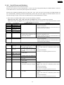
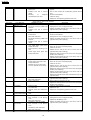
The tables below list the errors and their solutions.
When an error whose error code is indicated with "*" occurs in the main unit (Hybrid IP-PBX), the ALARM indicator on the front
of the cabinet turns on red, and the system logs the error information.
When the error conditions indicated by the error codes "021", "091", "230", and "510" are recovered, the ALARM indicator will
turn off automatically, indicating successful troubleshooting. When other errors are logged, the ALARM indicator will turn off
only when the log for major or minor errors is cleared from the KX-TDA Maintenance Console.
In other words, the ALARM indicator will turn off under the following conditions:
· When the errors "021", "091", "230", and "510" are logged: when the error conditions are recovered
· When other errors are logged: when the log for major or minor errors is cleared from the KX-TDA Maintenance Console
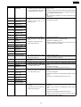
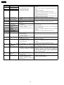
Error Code
100
101
102
103
104
105
106
108
109
110
Error Message
SRAM readwrite error
Flash write error
Flash boot check error
SDRAM eadwrite error
ASIC local bus register
access error
ASIC CT bus HW NG
ASIC Local HW0 NG
SD card not mounted
ASIC HDLC error
ASIC DMAC error
MPR Card Initial Self Diagnosis
PROBABLE CAUSE
SOLUTION
· MPR card malfunction
· See if the MPR card is installed properly
· Press the Reset Button
· Replace the MPR card (be sure to turn off the main unit
(Hybrid IP-PBX) when replacing)
· SD Memory Card not installed
· See if the SD Memory Card is installed properly
· Defective data in SD Memory Card
· Replace the SD Memory Card
· MPR card malfunction
· Replace the MPR card (be sure to turn off the main unit
(Hybrid IP-PBX) when replacing)
· See if the MPR card is installed properly
· MPR card malfunction
· Press the Reset Button
· Replace the MPR card (be sure to turn off the main unit
(Hybrid IP-PBX) when replacing)
Error Code
210
211
212
213
214
215
216
217
LPR (Optional Service Card with Local Processor) Initial Self Diagnosis
Error Message
PROBABLE CAUSE
SOLUTION
· Optional service card malfunction:
· See if the corresponding optional service card is installed
ASIC local bus register
DHLC, DLC, CSIF, T1, PRI, OPB3,
properly
access error
CTI-LINK, E&M, IP-GW
· Pull out and re-insert the corresponding optional service
· Optional service card malfunction:
Speech path loop-back
card
DHLC, DLC, SLC, CSIF, LCOT,
check error
·
Press the Reset Button
T1, PRI, OPB3, CTI-LINK, E&M,
IP-GW
· Replace the corresponding optional service card
· Optional service card malfunction:
Echo cancellor access
CSIF, ECHO
error
CSINF frame sync.
error
· Optional service card malfunction:
DSP Boot check error
T1
· Optional service card malfunction:
Framer IC access error
T1, PRI
· Optional service card malfunction:
MSG card DSP error
MSG, OPB3
· Optional service card malfunction:
· See if the corresponding optional service card is installed
MSG card data error
MSG, OPB3
properly
· Erroneous recording of messages
· Pull out and re-insert the corresponding optional service
card
· Press the Reset Button
· Re-record the messages
218
LANC register access
error
· Optional service card malfunction:
CTI-LINK
· Replace the corresponding optional service card
· See if the corresponding optional service card is installed
properly
· Pull out and re-insert the corresponding optional service
card
· Press the Reset Button
· Replace the corresponding optional service card
51
KX-TDA100BX
Error Code
219
Error Message
PT I/F error
PROBABLE CAUSE
· Optional service card malfunction:
DHLC, DLC
SOLUTION
· See if the corresponding optional service card is installed
properly
· Software error due to external
factors
· Pull out and re-insert the corresponding optional service
card
· Breaking
of
telephone
cord/interference of noise
· Press the Reset Button
· Check the wiring
· Replace the corresponding optional service card
Error Code
000*
001
002
010*
Error Message
MPR WDT overflow
SDRAM bit error
System Start-up and On-line Operation
PROBABLE CAUSE
SOLUTION
· MPR card malfunction
· Press the Reset Button
· Erroneous processing of MPR card
software
· Software error due to external
factors
· Reset Button is pressed
System Reset
AC power down
· Ignore if not frequent
· Press the Reset Button
· MPR card malfunction
· Reprogram the main unit (Hybrid IP-PBX)
· Erroneous processing of MPR card
software
· Replace the MPR card (be sure to turn off the main unit
(Hybrid IP-PBX) when replacing)
· Software error due to external
factors
· Power supply system malfunction
(e.g., power failure, power noise,
trouble with UPS)
· Check the power supply system
· Power supply circuit (PSU, back
board) malfunction
· See if the AC cord is connected properly
· Check the AC cord
· Replace the AC cord (be sure to turn off the main unit
(Hybrid IP-PBX) when replacing)
· Replace the PSU (be sure to turn off the main unit (Hybrid
IP-PBX) when replacing)
· Replace the back board (be sure to turn off the main unit
(Hybrid IP-PBX) when replacing)
· Check the power supply system
· AC power down
DC power down
· Replace the MPR card (be sure to turn off the main unit
(Hybrid IP-PBX) when replacing)
· Power failure
· Bad connection or breaking of AC
cord
011*
· Reprogram the main unit (Hybrid IP-PBX)
· Power supply circuit (PSU, back
board) malfunction
· Detection of over current (short
circuit on optional service cards)
· See if the AC cord is connected properly
· Check the AC cord
· Replace the AC cord (be sure to turn off the main unit
(Hybrid IP-PBX) when replacing)
· Replace the PSU (be sure to turn off the main unit (Hybrid
IP-PBX) when replacing)
· Replace the back board (be sure to turn off the main unit
(Hybrid IP-PBX) when replacing)
012*
MPR RAM battery low
· Battery out
014*
FAN Alarm
· MPR card malfunction
· PSU-L malfunction
016
018
020*
021*
CS overload
CS
superframe
synchronization failure
SD file access error
SD
Memory
disconnected
Card
· Remove the optional service cards and restart the main unit
(Hybrid IP-PBX)
· Replace the MPR card (be sure to turn off the main unit
(Hybrid IP-PBX) when replacing)
· See if anything is jammed in the fan
· Defective cable
· Replace the PSU (be sure to turn off the main unit (Hybrid
IP-PBX) when replacing)
· Check the cable diameter and length
· CS malfunction
· Replace the CS
· Optional service card malfunction:
CSIF
· Optional service card malfunction:
CSIF
· SD Memory Card malfunction
· Replace the corresponding optional service card
· Bad connection of SD Memory
Card
· Reprogram the main unit (Hybrid IP-PBX)
· MPR card malfunction
· SD Memory Card not installed
· Bad connection of SD Memory
Card
· SD Memory Card malfunction
· MPR card malfunction
52
· Replace the corresponding optional service card
· Press the Reset Button
· Replace the SD Memory Card
· Replace the MPR card (be sure to turn off the main unit
(Hybrid IP-PBX) when replacing)
KX-TDA100BX
Error Code
022*
Error Message
Not enough free space
on SD card
PROBABLE CAUSE
· Not enough memory space
available to save the system data,
or to upload system files from the
KX-TDA Maintenance Console
SOLUTION
· Delete the files whose file names start with "$" from SD
Memory Card
· Delete the "Pxxx" files (old program files of optional service
cards) from SD Memory Card. "xxx" indicates the card type
(e.g., "PDHLC" for DHLC card)
Note:
023*
024*
025*
026*
027*
028*
029*
030*
031*
032*
033*
034*
035*
036*
037*
038*
040
System
data
file
version error
System initialization file
version error
Card initialization file
version error
LCD file version error
System
data
file
checksum error
System initialization file
checksum error
Card initialization file
checksum error
LCD file checksum
error
System data file not
found
System initialization file
not found
Card initialization file
not found
LCD file not found
System
data
file
access error
System initialization file
access error
Card initialization file
access error
LCD file access error
Calendar IC failure
090
Card limitation over
091
200
PT connection over
LPR start up error
(ROM NG)
LPR start up error
(RAM NG)
201*
202*
203*
204*
205*
206
207
230*
LPR start up error (No
Program)
LPR start up error
(Version NG)
LPR start up error
(Version NG)
LPR start up error (No
response)
LPR start up error
(Card type NG)
LPR start up error
(Check SUM NG)
Card disconnected
· Old system files on SD Memory
Card
· Defective system
Memory Card
files
on
Do not delete the "PMPR" file; it is the program file of the
MPR card.
· Restore the backup files
· Re-install the software
SD
· SD Memory Card not installed
· Press the Reset Button
· Bad connection of SD Memory
Card
· Reprogram the main unit (Hybrid IP-PBX)
· SD Memory Card malfunction
· MPR card malfunction
· Erroneous processing of calendar
IC of MPR card
· MPR card malfunction
· Too many optional service cards
installed
· Too many PTs connected
· Optional service card malfunction:
DHLC, DLC, CSIF, T1, PRI, OPB3,
CTI-LINK, E&M, IP-GW
· Optional service card malfunction:
DHLC, DLC, CSIF, T1, PRI, OPB3,
CTI-LINK, E&M, IP-GW
· Replace the SD Memory Card
· Replace the MPR card (be sure to turn off the main unit
(Hybrid IP-PBX) when replacing)
· Reset the system clock
· Replace the MPR card (be sure to turn off the main unit
(Hybrid IP-PBX) when replacing)
· Reduce the number of optional service cards
· Reduce the number of PTs
· Pull out and re-insert the corresponding optional service
card
· Press the Rest Button
· Replace the corresponding optional service card
· Pull out and re-insert the corresponding optional service
card
· Press the Rest Button
· Update the software of the corresponding optional service
card
· Replace the corresponding optional service card
· Optional service card not installed
properly
· See if the corresponding optional service card is installed
properly
· Optional service card malfunction
· Pull out and re-insert the corresponding optional service
card
· Back board malfunction
· Press the Rest Button
· Replace the corresponding optional service card
· Replace the back board (be sure to turn off the main unit
(Hybrid IP-PBX) when replacing)
53
KX-TDA100BX
Error Code
231
232
233
234
Error Message
LPR alive check error
MPR-LPR
communication error
LPR data check error
DPLL clock failure
PROBABLE CAUSE
· Optional service card malfunction:
DHLC, DLC, CSIF, T1, PRI, OPB3,
CTI-LINK, E&M, IP-GW
SOLUTION
· See if the corresponding optional service card is installed
properly
· Back board malfunction
· Pull out and re-insert the corresponding optional service
card
· MPR card malfunction
· Press the Rest Button
· Replace the corresponding optional service card
· Replace the back board (be sure to turn off the main unit
(Hybrid IP-PBX) when replacing)
235*
CS clock failure
250
T1/E1 DSP failure
251
MSG DSP failure
300*
Digital trunk out of
synchronization
Digital
trunk
RAI
reception
Digital
trunk
AIS
reception
Multiframe
out
of
synchronization
Frame error
Data Link failure
301*
302*
303*
304*
305*
307
LAN No Carrier
310*
Port Link Failure
· Optional service card
CSIF
· Optional service card
T1
· Optional service card
MSG
· Network
(digital
malfunction
malfunction:
malfunction:
· See if the corresponding optional service card is installed
properly
malfunction:
· Replace the corresponding optional service card
CO
· Check the signals from the networkd is installed properly
line)
· Check the cable
· Optional service card malfunction:
PRI, T1, CTI-LINK
· Wrong A/B switch setting: PRI, T1
· Data link between the CS and
CSIF card failed
· Check the connection between the network and PRI card
· Data link between the network
and PRI card failed
· IP-GW card not connected to the
LAN
· Voice Mail malfunction
· Check the connection between the LAN and IP-GW card
· Ports defective on optional service
card: DHLC, DLC
· See if the corresponding optional service card is installed
properly
392
Clock master
selected
510*
SMDR disconnect
· Clock master card has been
changed to the one indicated by
the sub code
· RS-232C cable not connected
card
· See if the corresponding optional service card is installed
properly
· Check the connection between the CS and CSIF card
· Synchronization of digital
established or restored
391
· See if the A/B switch is set to A on the corresponding
optional service card
· Replace the corresponding optional service card
Digital
signal
synchronization
established
Data Link established
390
· Replace the MPR card (be sure to turn off the main unit
(Hybrid IP-PBX) when replacing)
· Replace the corresponding optional service card
line
· Connection with PC Phone/PC
Console or Voice Mail (DTMF
Integration) established or restored
· Breaking of RS-232C cable
· Printer
(terminal
malfunction
equipment)
54
· Check the Voice Mail
· Replace the corresponding optional service card
· This information is logged when synchronization of digital
line is established, and does not indicate an error condition
that needs to be solved
· This information is logged when connection with PC
Phone/PC Console or Voice Mail (DTMF Integration) is
established, and does not indicate an error condition that
needs to be solved. However, if this is logged frequently
(with "305 Data Link failure"), check the connection as it
may not be done properly.
· Check if the proper card is selected as the new clock
master card
· Check the RS-232C cable
· Check the terminal equipment
KX-TDA100BX
12 DIAGNOSIS
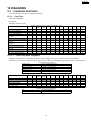
12.1. DIAGNOSIS FEATURES
Card Test and Pair Port Test is in Diagnosis Features.
12.1.1. Card Test
Card Test -SUMMARY
Description
Diagnose all kind of Cards.
Local loop back diagnosis
Card CT bus diagnosis
DTMF receive test
PT loop back diagnosis
DSP DTMF generator/receiver
diagnosis
DSP DTMF receiver diagnosis
Framer IC alarm signal detection
diagnosis
Framer IC error detection
diagnosis
CS-INF loop back diagnosis
Super frame synchronization
diagnosis
Caller ID card loop back diagnosis
Extension mode setting test
CTI-LINK loop back diagnosis
Parallel of Diagnose item of Card Tests and every Cards
DHLC DLC SLC8/L MSLC/ CS-INF LCOT
T1
E1
SLC8 SLC16
X
X
X
X
X
X
X
X
X
X
X
X
X
X
X
X
X
X
X
X
X
X
X
BRI
PRI
OPB3
E&M
X
X
X
X
X
X
X
X
X
X
X
X
X
X
X
X
X
CTILINK
X
X
X
X
X
12.1.1.1. Local Loop Back Diagnosis
Diagnose by transmission of the data from MPR to Card, and doing the Loop back test to return the data to MPR.
The point to do Loop back is different from the every cards, be able to do full diagnosis by Loop back test on the every points.
Primary circuit
Framer IC ST path (Analog)
Framer IC (Digital)
ASIC CODEC (PITS)
Local HW I/F point
Local TSW point
DHLC
Primary circuit
Framer IC ST path (Analog)
Framer IC (Digital)
ASIC CODEC (PITS)
Local HW I/F point
Local TSW point
OK
NG
X
Local loop back diagnosis test
Primary circuit loop back test
IC Analog I/F loop back test
IC Digital I/F loop back test
PITS I/F test loop back
Local HW I/F loop back test
Local TSW loop back test
Local loop back diagnosis test of every Cards
DLC SLC8/L MSLC/ CS-INF LCOT
T1
SLC8 SLC16
X
X
X
X
X
X
X
X
X
X
X
Diagnosis result of every test points
loop back diagnosis OK
loop back diagnosis NG
55
X
X
E1
BRI
PRI
X
X
X
X
X
X
X
X
X
X
X
OPB3
E&M
X
X
X
X
X
CTILINK
KX-TDA100BX
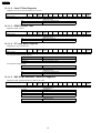
12.1.1.2. Card CT Bus Diagnosis
Diagnose CT bus by Loop back test to use CT bus
DHLC
DLC
X
X
Object of Card
SLC8/L MSLC/ CS-INF LCOT
SLC8 SLC16
X
X
X
X
T1
E1
BRI
PRI
OPB3
E&M
X
X
X
X
X
X
T1
E1
BRI
PRI
OPB3
E&M
CTILINK
X
Diagnosis result
Card CT bus diagnosis OK
Card CT bus diagnosis NG
OK
NG
12.1.1.3. DTMF Receive Test
Diagnosis DTMF receiver
DHLC
Object of Card
DLC
X
SLC8/L MSLC/ CS-INF LCOT
SLC8 SLC16
X
X
CTILINK
X
Diagnosis result
DTMF receive test OK
DTMF receive test NG
OK
NG
12.1.1.4. PT Loop Back Diagnosis
Diagnosis PT by Loop back test
DHLC
DLC
X
X
Object of Card
SLC8/L MSLC/ CS-INF LCOT
SLC8 SLC16
T1
E1
BRI
PRI
OPB3
E&M
CTILINK
T1
E1
BRI
PRI
OPB3
E&M
CTILINK
X
X
PT loop back diagnosis test channel
Cch port xx
Dch port xx
Bch port xx
C channel Port No.xx test
D channel Port No. xx test
B channel Port No. xx test
PT loop back diagnosis test
Primary circuit
ASIC (PT I/F)
Primary circuit loopback test
PT I/F loopback test
OK
NG
Diagnosis result
PT loop back diagnosis OK
PT loop back diagnosis NG
12.1.1.5. DSP DTMF Generator / Receiver Diagnosis
Diagnosis DTMF generator/receiver of DSP in the Card
DHLC
DLC
SLC8/L MSLC/ CS-INF LCOT
SLC8 SLC16
Object of Card
Time slot
Primary circuit
DSP ST loop back
DSP digital loop back
diagnosis point
Time slot test
Primary circuit loop back test
DSP ST point loop back test
DSP digital point loop back test
OK
NG
Diagnosis result
DSP DTMF generator/receiver diagnosis OK
DSP DTMF generator/receiver diagnosis NG
56
KX-TDA100BX
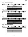
12.1.1.6. DSP DTMF Receiver Diagnosis
Diagnose DTMF receiver of DSP in the Card to use DTMF generator of DSP
DHLC
DLC
SLC8/L MSLC/ CS-INF LCOT
SLC8 SLC16
T1
E1
X
X
Object of Card
BRI
Time slot
Primary circuit
DSP ST loop back
DSP digital loop back
Diagnosis point
Time slot test
Primary circuit loop back test
DSP ST point loop back test
DSP digital point loop back test
OK
NG
Diagnosis result
DSP DTMF generator/receiver diagnosis OK
DSP DTMF generator/receiver diagnosis NG
PRI
OPB3
E&M
CTILINK
PRI
OPB3
E&M
CTILINK
OPB3
E&M
CTILINK
OPB3
E&M
CTILINK
12.1.1.7. Framer IC Alarm Signal Detection Diagnosis
Diagnose the feature to detect the alarm signal of Framer IC is normal action.
DHLC
DLC
SLC8/L MSLC/ CS-INF LCOT
SLC8 SLC16
T1
E1
X
X
Object of Card
BRI
X
RAI
AIS
Primary circuit
Diagnosis point
Yellow alarm signal detection test
Blue alarm signal detection test
Primary circuit alarm signal detection test
OK
NG
Diagnosis result
Framer IC alarm signal detection diagnosis OK
Framer IC alarm signal detection diagnosis NG
12.1.1.8. Framer IC Error Detection Diagnosis
Diagnose the feature to detect the alarm signal of Framer IC is normal action.
DHLC
DLC
SLC8/L MSLC/ CS-INF LCOT
SLC8 SLC16
T1
E1
X
X
Object of Card
BRI
PRI
X
Bipolar violation error
CRC error
Framing error
Primary circuit
Diagnosis point
Bipolar violation error detection test
CRC error detection test
Framing error detection test
Primary circuit error detection test
OK
NG
Diagnosis result
DSP DTMF generator/receiver diagnosis OK
DSP DTMF generator/receiver diagnosis NG
12.1.1.9. CS-INF Loop Back Diagnosis
Diagnose by Loop back test to CS-INF
DHLC
Object of Card
Dch port xx
Bch port xx
DLC
SLC8/L MSLC/ CS-INF LCOT
SLC8 SLC16
X
T1
CS-INF loop back diagnosis test channel
D channel Port No. xx test
B channel Port No. xx test
DNIC analog
DNIC digital
Diagnosis point
DNIC analog loop back test
DNIC digital loop back test
OK
NG
Diagnosis result
CS-INF loop back diagnosis OK
CS-INF loop back diagnosis NG
57
E1
BRI
PRI
KX-TDA100BX
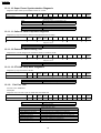
12.1.1.10. Super Frame Synchronization Diagnosis
Diagnose Super frame synchronization feature of CS-INF
DHLC
DLC
Object of Card
SLC8/L MSLC/ CS-INF LCOT
SLC8 SLC16
X
T1
E1
BRI
PRI
OPB3
E&M
CTILINK
BRI
PRI
OPB3
E&M
CTILINK
BRI
PRI
OPB3
E&M
CTILINK
DECT
SS
Diagnosis point
DECT super frame synchronization test
SS super frame synchronization test
OK
NG
Diagnosis result
Super frame synchronization diagnosis OK
Super frame synchronization diagnosis NG
12.1.1.11. Caller ID Card Loop Back Diagnosis
Diagnose by Loop back test to Caller ID card (Optional Card of LCOT)
DHLC
DLC
Object of Card
SLC8/L MSLC/ CS-INF LCOT
SLC8 SLC16
X
T1
E1
Diagnosis result
Caller ID card loop back diagnosis OK
Caller ID card loop back diagnosis NG
OK
NG
12.1.1.12. Extension Mode Setting Test
Diagnose the normal change from outside line mode to inside line mode
DHLC
DLC
SLC8/L MSLC/ CS-INF LCOT
SLC8 SLC16
T1
E1
Object of Card
X
Diagnosis result
Extension mode setting test OK
Extension mode setting test NG
OK
NG
12.1.1.13. CTI-LINK Loop Back Diagnosis
Diagnose by Loop back test to CS-INF
DHLC
DLC
SLC8/L MSLC/ CS-INF LCOT
SLC8 SLC16
T1
E1
BRI
PRI
OPB3
E&M
CTILINK
X
E1
BRI
PRI
OPB3
E&M
CTILINK
Object of Card
Diagnosis result
CTI-LINK loop back diagnosis OK
CTI-LINK loop back diagnosis NG
OK
NG
12.1.2. Pair Port Test
Pair Port Test -SUMMARY
Description
Diagnosis Pair Port Test to pair up inside line and outside line
DHLC
Object of Card
DLC
X
OK
NG
Line current OFF (Ext->CO)
Line current ON (Ext->CO)
Off hook detection (CO->Ext)
DTMF detection (CO->Ext)
DP detection (CO->Ext)
BELL detection (Ext->CO)
Speech path (Ext->CO)
Speech path (CO->Ext)
SLC8/L MSLC/ CS-INF LCOT
SLC8 SLC16
X
X
X
T1
Diagnosis result
Pair Port Test OK
Pair Port Test NG
Detail Diagnosis result
There is no local current from inside line to outside line
There is local current from inside line to outside line
Off-hook detection from outside line to inside line
DTMF transmission/detection from outside line to inside line
SP transmission/detection from outside line to inside line
Bell transmission/detection from inside line to outside line
Call lime from inside line to outside line
Call lime from outside line to inside line
58
KX-TDA100BX
12.2. DIAGNOSIS TEST
1. Click [Diagnosis] of [Utility].
59
KX-TDA100BX
2. Pair Port Test operation Select card for Test.
3. Click [Pair Port Test].
60
KX-TDA100BX
4. Click [OK].
5. Click [Cancel].
61
KX-TDA100BX
6. Card Test operation Select card for Test.
7. Click [Card Test].
62
KX-TDA100BX
8. Click [OK].
9. Click [Cancel].
63
KX-TDA100BX
13 IC DATA
13.1. IC101
Pin No.
1
2
3
4
5
6
7
8
9
10
11
12
13
14
15
16
17
18
19
20
21
22
23
24
25
26
27
28
Pin Name
MD1
MD2
Vcc-TRC*1
XTAL2
EXTAL2
Vcc-TRC*1
NMI
IRQ0/IRL0/PTH[0]
IRQ1/IRL1/PTH[1]
IRQ2/IRL2/PTH[2]
IRQ3/IRL3/PTH[3]
IRQ4/PTH[4]
D31/PTB[7]
D30/PTB[6]
D29/PTB[5]
D28/PTB[4]
D27/PTB[3]
D26/PTB[2]
VssQ
D25/PTB[1]
VssQ
D24/PTB[0]
D23/PTA[7]
D22/PTA[6]
D21/PTA[5]
D20/PTA[4]
Vss
Vss
D19/PTA[3]
I/O
I
I
O
I
I
I
I
I
I
I
I/O
I/O
I/O
I/O
I/O
I/O
I/O
I/O
I/O
I/O
I/O
I/O
I/O
Description
Clock mode setting
Clock mode setting
Power for RTC
Crystal oscillator terminal for built-in RTC
Crystal oscillator terminal for built-in RTC (*6)
Power for RTC
Nonmaskable interrupt request
External interrupt request/input port H
External interrupt request/input port H
External interrupt request/input port H
External interrupt request/input port H
External interrupt request/input port H
Data bus/I/O port B
Data bus/I/O port B
Data bus/I/O port B
Data bus/I/O port B
Data bus/I/O port B
Data bus/I/O port B
Power for I/O (0V)
Data bus/I/O port B
Power for I/O (3.3V)
Data bus/I/O port B
Data bus/I/O port A
Data bus/I/O port A
Data bus/I/O port A
Data bus/I/O port A
Power supply (0V)
Power supply (0V)
Data bus/I/O port A
64
KX-TDA100BX
Pin No.
29
30
31
32
33
34
35
36
37
38
39
40
41
42
43
44
45
46
47
48
49
50
51
52
53
54
55
56
57
58
59
60
61
62
63
64
65
66
67
68
69
70
71
72
73
74
75
76
77
78
79
80
81
82
83
84
85
86
87
88
89
90
91
Pin Name
Vcc
Vcc
D18/PTA[2]
D17/PTA[1]
D16/PTA[0]
VssQ
D15
VccQ
D14
D13
D12
D11
D10
D9
D8
D7
D6
VssQ
D5
VccQ
D4
D3
D2
D1
D0
A0
A1
A2
A3
VssQ
A4
VssQ
A5
A6
A7
A8
A9
A10
A11
A12
A13
VssQ
A14
VccQ
A15
A16
A17
A18
A19
A20
A21
Vss
Vss
A22
Vss
Vss
A23
VssQ
A24
VssQ
A25
BS/PTK[4]
RD
WE0/DQMLL
WE1/DQMLU/WE
WE2/DQMUL/ICIORD/
PTK[6]
I/O
I/O
I/O
I/O
I/O
I/O
I/O
I/O
I/O
I/O
I/O
I/O
I/O
I/O
I/O
I/O
I/O
I/O
I/O
I/O
O
O
O
O
O
O
O
O
O
O
O
O
O
O
O
O
O
O
O
O
O
O
O
O
O
O
O
O/I/O
O
O
O
O/I/O
Description
Power supply (*3)
Power supply (*3)
Data bus/I/O port A
Data bus/I/O port A
Data bus/I/O port A
Power for I/O (0V)
Data bus
Power for I/O (3.3V)
Data bus
Data bus
Data bus
Data bus
Data bus
Data bus
Data bus
Data bus
Data bus
Power for I/O (0V)
Data bus
Power for I/O (3.3V)
Data bus
Data bus
Data bus
Data bus
Data bus
Address bus
Address bus
Address bus
Address bus
Power for I/O (0V)
Address bus
Power for I/O (3.3V)
Address bus
Address bus
Address bus
Address bus
Address bus
Address bus
Address bus
Address bus
Address bus
Power for I/O (0V)
Address bus
Power for I/O (3.3V)
Address bus
Address bus
Address bus
Address bus
Address bus
Address bus
Address bus
Power supply (0V)
Power supply (0V)
Address bus
Power supply (*3)
Power supply (*3)
Address bus
Power for I/O (0V)
Address bus
Power for I/O (3.3V)
Address bus
Bus cycle start signal/I/O port K
Read stroke
D7-D0 select signal/DOM (SDRAM)
D15-D8 select signal/DOM (SDRAM)
D23-D16 select signal/DOM (SDRAM) /PCMCIA I/O read/I/O port K
65
KX-TDA100BX
Pin No.
Pin Name
92
WE3/DQMUU/ICIOW
R/PTK[7]
93
RD/WR
94
AUDSYNC/PTE[7]
95
VssQ
96
CS0/MCS[0]
97
VccQ
98
CS2/PTK[0]
99
CS3/PTK[1]
100
CS4/PTK[2]
101
CS5/PTK[3]
102
CS6/CE1B
103
CE2A/PTE[4]
104
CE2B/PTE[5]
105
CKE/PTK[5]
106
RAS3L/PTJ[0]
107
PTJ[1]
108
CASL/PTJ[2]
109
VssQ
110
CASU/PTJ[3]
111
VssQ
112
PTJ[4]
113
PTJ[5]
114
DACK0/PTD[5]
115
DACK1/PTD[7]
116
PTE[6}
117
PTE[3}
118
RAS3U/PTE[2]
119
PTE[1]
120
TDO/PTE[0]
121
BACK
122
BREQ
123
WAIT
124
RESETM
125
ADTRG/PTH[2]
126
IOIS16/PTG[7]
127
ASEMD0/PTG[6]
128
ASEBRKAK/PTG[5]
129
PTG[4]/CKIO2
130
AUDATA[3]/PTG[3]
131
AUDATA[2]/PTG[2]
132
Vss
Vss
133
AUDATA[1]/PTG[1]
134
Vcc
Vcc
135
AUDATA[0]/PTG[0]
136
TRST/PTF[7]/PINT[15]
137
TMS/PTF[6]/PINT[14]
138
TDI/PTF[5]/PINT[13]
139
TCK/PTF[4]/PINT[12]
140
IRS3/PTF[3]/PINT[11]
141
IRS2/PTF[2]/PINT[10]
142
IRS1/PTF[1]/PINT[9]
143
IRS0/PTF[0]/PINT[8]
144
MD0
145
Vcc-PLL1*2
146
CAP1
147
Vss-PLL1*2
148
Vss-PLL2*2
149
CAP2
150
Vcc-PLL2*2
151
AUDCK/PTH[6]
152
Vss
153
Vss
Vss
154
Vcc
I/O
O/I/O
Description
D31-D24 select signal/DOM (SDRAM) /PCMCIA I/O write/I/O port K
O
O/I/O
O
O/I/O
O/I/O
O/I/O
O/I/O
O
O/I/O
O/I/O
O/I/O
O/I/O
I/O
O/I/O
O/I/O
I/O
I/O
O/I/O
O/I/O
I/O
I/O
O/I/O
I/O
O/I/O
O
I
I
I
I
I
I
I/O
I/O
I/O/I
I/O/I
I/O/I
I/O/I
I
I
I
I
I
I
I
I
I
I
-
Read/Write
AUD synchronization/I/O port E
Power for I/O (0V)
Chip select 0/mask ROM chip select 0
Power for I/O (3.3V)
Chip select 2/I/O port K
Chip select 3/I/O port K
Chip select 4/I/O port K
Chip select 5/CE1 (Area 5PCMCIA)/I/O port K
Chip select 6/CE1 (Area 6PCMCIA)
CE2(Area 5PCMCIA)/ I/O port K
CE2(Area 6PCMCIA)/ I/O port K
CK Enable (SDRAM) / I/O port K
RAS for low 32M/64M bytes address (SDRAM) /I/O port J
I/O port J
RAS for low 32M/64M bytes address (SDRAM) /I/O port J
Power for I/O (0V)
RAS for low 32M bytes address (SDRAM) /I/O port J
Power for I/O (3.3V)
I/O port J
I/O port J
DMA acknowledge0/I/O port D
DMA acknowledge1/I/O port D
I/O port E
I/O port E
RAS for low 32M bytes address (SDRAM) / I/O port E
I/O port E
Test data output/I/O port E
Bus acknowledge
Bus request
Hardware wait request
Manual reset request
Analog trigger/input port H
IOIS168 (PCMCI) / I/O port G
ASE mode:4/I/O port G
ASE break acknowledge/I/O port G
Input port G/clock output
AUD data/input port G
AUD data/input port G
Power supply (0V)
Power supply (0V)
AUD data/input port G
Power supply (*3)
Power supply (*3)
AUD data/input port G
Test reset/input port F/port interruption
Test mode switch/input port F/port interruption
Test mode switch/input port F/port interruption
Test clock/input port F/port interruption
External interrupt request/input port F/port interruption
External interrupt request/input port F/port interruption
External interrupt request/input port F/port interruption
External interrupt request/input port F/port interruption
Clock mode setting
Power for PLL1 (*3)
External capacity terminal for PLL1
Power for PLL1 (0V)
Power for PLL1 (1V)
External capacity terminal for PLL2
Power for PLL2 (*3)
AUD clock/input port H
Power supply (0V)
Power supply (0V)
Power supply (0V)
Power supply (*3)
66
KX-TDA100BX
Pin No.
155
156
157
158
159
160
161
162
163
164
165
166
167
168
169
170
171
172
173
174
175
176
177
178
179
180
181
182
183
184
185
186
187
188
189
190
191
192
193
194
195
196
197
198
199
200
201
202
203
204
205
206
207
208
Pin Name
Vcc
XTAL
EXTAL
STATUS0/PTJ[6]
STATUS0/PTJ[7]
TCLK/PTH[7]
IRQOUT
VssQ
CKIO
VccQ
TxD0/SCPT[0]
SCK0/SCPT[1]
TxD1/SCPT[2]
SCK1/SCPT[3]
TxD2/SCPT[4]
SCK2/SCPT[5]
RTS0/SCPT[6]
RxD0/SCPT[0]
RxD1/SCPT[2]
Vss
Vss
RxD2/SCPT[4]
Vcc
Vcc
CTS2/IRQ5/SCPT[7]
MCS[7]/PTC[7]/PINT[7
]
MCS[6]/PTC[6]/PINT[6
]
MCS[5]/PTC[5]/PINT[5
]
MCS[4]/PTC[4]/PINT[4
]
VssQ
WAKEUP/PTD[3]
VccQ
RESETOUT/PTD[2]
MCS[3]/PTC[3]/PINT[3
]
MCS[2]/PTC[2]/PINT[2
]
MCS[1]/PTC[1]/PINT[1
]
MCS[0]/PTC[0]/PINT[0
]
DRAK0/PTD[1]
DRAK1/PTD[0]
DREQ0/PTD[4]
DREQ1/PTD[0]
RESETP
CA
MD3
MD4
MD5
Avss
AN[0]/PTL[0]
AN[1]/PTL[1]
AN[2]/PTL[2]
AN[3]/PTL[3]
AN[4]/PTL[4]
AN[5]/PTL[5]
Avcc
AN[6]/DA[1]/PTL[6]
AN[7]/DA[0]/PTL[7]
AVss
I/O
O
I
O/I/O
O/I/O
I/O
O
I/O
O
I/O
O
I/O
O
I/O
O/I/O
I
I
I
I
O/I/O
Description
Power supply (*3)
Clock oscillator terminal
External clock/crystal oscillator terminal
Processor status
Processor status
Clock I/O for TMU or RTC/I/O port J
Interrupt request notification
Power for I/O (0V)
System clock I/O
Power for I/O (3.3V)
Transmission data 0/output port for SCI
Serial clock 0/output port for SCI
Transmission data 1/output port for SCI
Serial clock 1/output port for SCI
Transmission data 2/output port for SCI
Serial clock 2/output port for SCI
O/I/O
Mask ROM chip select/I/O port C/port interruption
O/I/O
Mask ROM chip select/I/O port C/port interruption
O/I/O
Mask ROM chip select/I/O port C/port interruption
O/I/O
O/I/O
O/I/O/I
Power for I/O (0V)
Interrupt request notification on standby mode/I/O port D
Power for I/O (3.3V)
Reset output/I/O port D
Mask ROM chip select/I/O port C/port interruption
O/I/O/I
Mask ROM chip select/I/O port C/port interruption
O/I/O/I
Mask ROM chip select/I/O port C/port interruption
O/I/O/I
Mask ROM chip select/I/O port C/port interruption
O/I/O
O/I/O
I
I
I
I
I
I
I
I
I
I
I
I
I
I
I
-
DMA request accepting/I/O port D
DMA request accepting/I/O port D
DMA request/input port D
DMA request/input port D
Power on reset request
Chip active (hardware standby request signal)
Bus width setting for area 0
Bus width setting for area 1
Endian setting
Power for analog (0V)
AD converter input/input port L
AD converter input/input port L
AD converter input/input port L
AD converter input/input port L
AD converter input/input port L
AD converter input/input port L
Power for analog (3.3V)
AD converter input/DA converter output/input port L
AD converter input/DA converter output/input port L
Power for analog (0V)
Transmission data 0/input port for SCI
Transmission data 1/input port for SCI
Power supply (0V)
Power supply (0V)
Transmission data 2/input port for SCI
Power supply (*3)
Power supply (*3)
Transmission clear 2/external interrupt request /I/O port for SCI
Mask ROM chip select/I/O port C/port interruption
67
KX-TDA100BX
14 TERMINAL GUIDE OF ICS, TRANSISTORS AND DIODES
68
KX-TDA100BX
15 HOW TO REPLACE A FLAT PACKAGE IC
15.1. PREPARATION
15.3. REMOVING SOLDER FROM
BETWEEN PINS
· PbF (: Pb free) Solder
· Soldering Iron
1. Add a small amount of solder to the bridged pins.
Tip Temperature of 700°F ± 20°F (370°C ± 10°C)
2. With a hot iron, use a sweeping motion along the flat part of
the pin to draw the solder from between the adjacent pads.
Note: We recommend a 30 to 40 Watt soldering iron. An
expert may be able to use a 60 to 80 Watt iron where
someone with less experience could overheat and damage
the PCB foil.
· Flux
Recommended Flux: Specific Gravity → 0.82.
Type → RMA (lower residue, non-cleaning type)
Note: See ABOUT LEAD FREE SOLDER (PbF: Pb free)
(P.3).
15.2. PROCEDURE
1. Tack the flat pack IC to the PCB by temporarily soldering
two diagonally opposite pins in the correct positions on the
PCB.
Be certain each pin is located over the
correct pad on the PCB.
2. Apply flux to all of the pins on the IC.
3. Being careful to not unsolder the tack points, slide the
soldering iron along the tips of the pins while feeding
enough solder to the tip so that it flows under the pins as
they are heated.
69
KX-TDA100BX
16 CABINET AND ELECTRICAL PARTS LOCATION
70
KX-TDA100BX
16.1. EXTENSION BOARDS FOR SERVICING
71
KX-TDA100BX
17 ACCESSORIES AND PACKING MATERIALS
72
KX-TDA100BX
18 REPLACEMENT PARTS LIST
Note:
Ref.
No.
1. RTL (Retention Time Limited)
The marking (RTL) indicates that the Retention Time is
limited for this item.
After the discontinuation of this assembly in production, the
item will continue to be available for a specific period of
time. The retention period of availability depends on the
type of assembly and the laws governing parts and product
retention. At the end of this period, the assembly will no
longer be available.
2. Important safety notice
Components identified by the
mark indicates special
characteristics important for safety. When replacing any of
these components, only use specified manufacture´s parts.
3. The S mark means the part is one of some identical parts.
For that reason, it may be different from the installed part.
4. ISO code (Example : ABS-94HB) of the remarks column
shows quality of the material and a flame resisting grade
about plastics.
5. RESISTORS & CAPACITORS
Unless otherwise specified;
All resistors are in ohms (Ω), k=1000Ω, M=1000kΩ
All capacitors are in MICRO FARADS (µF), p=µ(µF)
*Type & Wattage of Resistor
Part No.
Part Name & Description
9
PSMH1205Z
CHASSIS, LED
10
11
12
PSHD1091Z
PSKV1016Z1
PSYCTDA100AL
BOLT WITH NUT
COVER, RIGHT SIDE
COVER, FRONT
13
14
15
16
17
18
PSMD1040Y
PSMH1230Z
PSMH1222Z
PSMH1206Y
PSMH1207Z
PSKK1035Z1
FRAME, LOWER
FRAME
ANGLE, RS-232C
ANGLE
ANGLE
LID
19
PSKR1001Y1
GUIDE, CABLE
20
21
22
23
24
25
26
27
28
29
PSKL1016Z1
PSMH1234Z
PQHR10379Z
PSGB1001Z
PSQT1431Z
PSYETDA100BX
PSQT1990Z
PSJS03P16Z
PSJS09P12Z
PQHD10011V
STAND
ANGLE, FRONT
CLAMPER
BADGE
LABEL, WARNING
NAME PLATE
LABEL, CAUTION
CONNECTOR, LED
CONNECTOR, RS-232C
SCREW
30
31
32
33
34
PSUS1022Z
XUC3VW
PSMH1244Z
PSUS1021Y
PSHD1088Z
SPRING
RETAINING RING
CHASSIS, FRONT
SPRING
SCREW
Remarks
ABS-HB
PC+ABS5V
PC+ABS5V
PC+ABS5V
ABS-HB
PS-HB
18.2. ACCESSORIES AND PACKING
MATERIALS
18.1. CABINET AND ELECTRICAL
PARTS
Ref.
No.
Part No.
Part Name & Description
1
PSKV1023Z1
COVER, TOP
2
3
4
5
6
7
8
PSKV1017Z1
PSMD1035Z
PSMD1040Y
PSMH1232Z
PSMD1041Z
PSMH1264Z
PSHR1235Z
COVER, LEFT SIDE
FRAME, SIDE
FRAME, BASE
FRAME,BACK BOARD
COVER, BACK
COVER, HOLD
GUIDE RAIL
Remarks
PC+ABS5V
ABS-HB
PC+ABS5V
73
Ref.
No.
A1
A2
A3
A4
A5
A6
A7
A8
A9
Part No.
Part Name & Description
PSJA1007Z
PQJP1E1Z
XYN4+J18FZ
PQHE17Z
XTB5+20AFY
PSZETDA100BX
PSLB5D1
PSMD1042Z
PSQX2227YCD
A10
A11
A12
PSQW2011Y
PSQX2849ZCD
PSJA1081Z
POWER CORD (AC CORD)
PLUG
SCREW
MOUNTING BRACKET
SCREW
ACCESSORY PARTS,SD CARD
INSULATOR
MOUNTING BRACKET
CD-ROM, INSTALLATION MANUAL
(FOR USER)
LEAFLET, SAFETY INFORMATI
CD-ROM (FOR USER DEALER)
POWER CORD (AC CORD)
P1
P2
P3
P4
P5
P6
P7
P8
P9
PSZKTDA100BX
PSPD1172Z
PSPD1173Z
PSPN1137Y
PSPD1182Z
PSPD1171Y
PSPD1170Y
PSPD1183Z
XZB05X08A03
PACKING CASE
CUSHION
CUSHION
ACCESSORY BOX
CUSHION
CUSHION
CUSHION
CUSHION
PROTECTION COVER (FOR SCREW)
P10
P11
P12
XZB10X15A04
XZB18X27A04
PSPP1070Z
P13
P14
P15
PQPP143Z
PSPP1069Z
XZB50X30A06
PROTECTION COVER
PROTECTION COVER (FOR CD-ROM)
PROTECTION COVER (FOR SD
CARD)
PROTECTION COVER (FOR SET)
PROTECTION COVER
PROTECTION COVER (FOR
MOUNTING BRACKET)
Remarks
KX-TDA100BX
18.3. MPR CARD PARTS
Ref.
No.
PCB1
Part No.
Part Name & Description
PSWP1DA100BX
MPR CARD ASS´Y (RTL)
IC101
IC102
IC103
IC107
IC110
IC111
IC120
IC121
IC123
IC124
IC125
IC126
IC127
IC131
IC132
C2DBYJ000009
C1CB00001395
C1CB00001497
C0EBE0000176
C0JBAB000407
C0JBAB000407
PQVIMC1488MR
PQVIMC1489MR
C0JBAZ001765
C0JBAZ001765
C0JBAC000264
C0JBAA000174
C0JBAZ001704
C0JBAB000407
C0JBAB000381
(ICS)
IC
IC
IC
IC
IC
IC
IC
IC
IC
IC
IC
IC
IC
IC
IC
IC201
IC204
IC205
IC207
IC208
IC209
C0JBAN000187
C1CB00001415
MN5773
C0JBAZ001765
C0JBAZ001765
C0JBAB000504
IC
IC
IC
IC
IC
IC
S
IC301
IC302
IC303
IC305
IC306
IC309
IC310
IC311
C3BBKG000060
C3BBKG000060
PSWITDA100BX
C3ABPJ000054
C3ABPJ000054
C0JBAN000187
C0JBAN000187
C0JBAA000174
IC
IC
IC(ROM)
IC
IC
IC
IC
IC
S
S
IC402
IC403
IC404
IC405
IC406
IC408
IC409
IC410
IC411
IC412
IC413
PQVIS8520F33
C0CBAAG00006
C0CBAAB00022
C0ZBZ0000553
C0ZBZ0000553
PQVINJM4558M
PQVINJM4558M
PSVISV7560
PQVINJM2903M
C0CBADC00009
C0DBEDA00002
IC
IC
IC
IC
IC
IC
IC
IC
IC
IC
IC
Q101
Q403
Q404
Q405
Q406
Q407
Q408
Q409
Q410
Q411
Q412
B1GBCFEH0003
2SD1664Q
2SB1132R
2SB1132R
UN5213
2SC4081R
2SC4081R
B1ABEC000005
B1ABEC000005
B1DFDC000002
B1DHCD000018
(TRANSISTORS)
TRANSISTOR(SI)
TRANSISTOR(SI)
TRANSISTOR(SI)
TRANSISTOR(SI)
TRANSISTOR(SI)
TRANSISTOR(SI)
TRANSISTOR(SI)
TRANSISTOR(SI)
TRANSISTOR(SI)
TRANSISTOR(SI)
TRANSISTOR(SI)
QA101
QA103
B1GHCFJJ0007
B1GHCFJJ0007
TRANSISTOR(SI)
TRANSISTOR(SI)
D102
D402
D403
D405
D406
D407
D408
MA110
PFVDDGD1FP3T
MA8100M
MA8051
MA8043M
MA1070400L
MA728
(DIODES)
DIODE(SI)
DIODE(SI)
DIODE(SI)
DIODE(SI)
DIODE(SI)
DIODE(SI)
DIODE(SI)
Ref.
No.
D409
Part No.
Part Name & Description
MA728
DIODE(SI)
DA401
DA402
MA143
MA143
DIODE(SI)
DIODE(SI)
LED101
LED103
PSVD1VGCT
PSVD1SRCT
LED
LED
CN103
CN205
CN206
CN207
CN209
CN211
K1KA90B00008
K1KAC0A00037
K1KB30A00117
PSJP07A44Z
K1KB04B00036
K1NA09E00022
(CONNECTORS)
CONNECTOR, 90P
CONNECTOR, 120P
CONNECTOR, 30P
CONNECTOR, 7P
CONNECTOR, 4P
CONNECTOR, 9P
JK401
JK402
JK403
JK404
PSJJ1D001Z
PSJJ1D001Z
PSJJ1D001Z
PSJJ1D001Z
(JACKS)
JACK
JACK
JACK
JACK
RA101
RA102
RA103
RA104
RA105
RA106
RA107
RA108
RA109
D1HA1038A005
D1H8R0040009
D1H8R0040009
D1H8R0040009
D1H8R0040009
D1H8R0040009
D1H8R0040009
D1H8R0040009
D1H8R0040009
(COMPONENTS PARTS)
RESISTOR ARRAY
RESISTOR ARRAY
RESISTOR ARRAY
RESISTOR ARRAY
RESISTOR ARRAY
RESISTOR ARRAY
RESISTOR ARRAY
RESISTOR ARRAY
RESISTOR ARRAY
RA111
RA112
RA113
RA114
RA115
RA116
RA117
RA118
RA119
EXB38VR000
EXB38VR000
EXB38VR000
EXB38VR000
EXB38VR000
EXB38VR000
D1HA1038A005
D1HA1038A005
D1HA1038A005
RESISTOR
RESISTOR
RESISTOR
RESISTOR
RESISTOR
RESISTOR
RESISTOR
RESISTOR
RESISTOR
ARRAY
ARRAY
ARRAY
ARRAY
ARRAY
ARRAY
ARRAY
ARRAY
ARRAY
RA120
RA121
RA122
RA123
RA124
RA125
RA126
RA127
RA128
RA129
D1HA1038A005
D1HA1038A005
D1HA1038A005
EXB38V680JV
EXB38V680JV
EXB38V680JV
EXB38V680JV
EXB38V680JV
EXRV8V470JV
EXRV8V470JV
RESISTOR
RESISTOR
RESISTOR
RESISTOR
RESISTOR
RESISTOR
RESISTOR
RESISTOR
RESISTOR
RESISTOR
ARRAY
ARRAY
ARRAY
ARRAY
ARRAY
ARRAY
ARRAY
ARRAY
ARRAY
ARRAY
RA133
RA134
RA135
RA136
RA137
D1HA1038A005
D1HA1038A005
D1HA1038A005
EXB38V222JV
EXB38V103JV
RESISTOR
RESISTOR
RESISTOR
RESISTOR
RESISTOR
ARRAY
ARRAY
ARRAY
ARRAY
ARRAY
RA201
RA202
RA203
RA204
RA205
RA206
RA207
D1HA1048A005
EXB38V220JV
EXB38V220JV
D1H82204A024
D1H82204A024
D1H82204A024
D1H82204A024
RESISTOR
RESISTOR
RESISTOR
RESISTOR
RESISTOR
RESISTOR
RESISTOR
ARRAY
ARRAY
ARRAY
ARRAY
ARRAY
ARRAY
ARRAY
RA301
RA302
RA303
RA304
RA305
D1HA1038A005
D1HA1038A005
D1HA1038A005
D1HA1038A005
D1HA1038A005
RESISTOR
RESISTOR
RESISTOR
RESISTOR
RESISTOR
ARRAY
ARRAY
ARRAY
ARRAY
ARRAY
Remarks
Remarks
S
S
S
S
S
S
S
S
74
S
S
S
S
S
S
KX-TDA100BX
Ref.
No.
RA306
RA307
RA308
RA309
Part No.
Part Name & Description
D1HA1038A005
D1HA1038A005
D1HA1038A005
D1HA1038A005
RESISTOR
RESISTOR
RESISTOR
RESISTOR
C101
C102
C103
C104
C105
C106
C107
C108
C109
PQCUV1A225ZF
ECUV1A105ZFV
ECUV1C104ZFV
ECUV1C104ZFV
ECUV1C104ZFV
ECUV1C104ZFV
ECUV1C104ZFV
ECUV1C104ZFV
ECUV1H120JCV
(CAPACITORS)
2.2
1
0.1
0.1
0.1
0.1
0.1
0.1
12p
C110
C111
C112
C114
C116
C117
C118
C119
ECUV1C104ZFV
ECUV1C104ZFV
ECUV1C104ZFV
ECUV1H120JCV
ECUV1C104ZFV
ECUV1C104ZFV
ECUV1C104ZFV
ECUV1C104ZFV
0.1
0.1
0.1
12p
0.1
0.1
0.1
0.1
C120
C121
C122
C123
C124
C125
C126
C127
C128
C129
ECUV1C104ZFV
ECUV1A105ZFV
ECUV1A105ZFV
ECUV1A105ZFV
ECUV1C104ZFV
ECUV1C104ZFV
PQCUV1A225ZF
PQCUV1A225ZF
PQCUV1A225ZF
ECUV1A105ZFV
0.1
1
1
1
0.1
0.1
2.2
2.2
2.2
1
C130
C131
C132
C133
C134
C135
C136
C137
C138
C139
ECUV1A105ZFV
PQCUV1A225ZF
PQCUV1A225ZF
PQCUV1A225ZF
PQCUV1A225ZF
ECUV1H220JCV
ECUV1H220JCV
ECUV1H471JCV
ECUV1H471JCV
ECUV1C104ZFV
1
2.2
2.2
2.2
2.2
22p
22p
470p
470p
0.1
C140
C141
C142
C143
C144
C145
C146
C147
C148
C149
ECUV1A105ZFV
ECUV1C104ZFV
ECUV1C104ZFV
PQCUV1A225ZF
ECUV1C104ZFV
ECUV1C104ZFV
ECUV1C104ZFV
ECUV1C104ZFV
ECUV1C104ZFV
ECUV1C104ZFV
1
0.1
0.1
2.2
0.1
0.1
0.1
0.1
0.1
0.1
C150
C151
C156
C157
C159
ECUV1A105ZFV
PQCUV1A225ZF
ECUV1H102KBV
ECUV1H102KBV
ECUV1C104ZFV
1
2.2
0.001
0.001
0.1
C160
C161
C162
C163
C166
C167
C168
ECUV1A105ZFV
ECUV1C104ZFV
ECUV1C104ZFV
ECUV1C104ZFV
ECUV1C104ZFV
ECUV1C104ZFV
ECUV1H102KBV
1
0.1
0.1
0.1
0.1
0.1
0.001
C170
ECUV1C104ZFV
0.1
Remarks
ARRAY
ARRAY
ARRAY
ARRAY
75
Ref.
No.
C174
Part No.
Part Name & Description
ECUV1C104ZFV
0.1
C201
C202
C203
C204
C205
C206
C207
C208
C209
ECUV1H220JCV
PQCUV1A225ZF
ECUV1H220JCV
ECUV1A105ZFV
ECUV1C104ZFV
ECUV1C104ZFV
ECUV1C104ZFV
ECUV1C104ZFV
PQCUV1A225ZF
22p
2.2
22p
1
0.1
0.1
0.1
0.1
2.2
C210
C211
C212
C214
C215
C216
C217
C218
C219
ECUV1A105ZFV
ECUV1C104ZFV
ECUV1C105ZFV
ECUV1C104ZFV
ECUV1C104ZFV
ECUV1C104ZFV
ECUV1H150JCV
ECUV1H150JCV
ECUV1C104ZFV
1
0.1
1
0.1
0.1
0.1
15p
15p
0.1
C220
ECUV1A105ZFV
1
C301
C302
C303
C304
C305
C306
C307
C308
PQCUV1A225ZF
PQCUV1A225ZF
ECUV1A105ZFV
ECUV1A105ZFV
ECUV1C104ZFV
ECUV1C104ZFV
ECUV1H102KBV
ECUV1C104ZFV
2.2
2.2
1
1
0.1
0.1
0.001
0.1
C310
C312
C314
C315
C316
C317
C318
C319
ECUV1A105ZFV
PQCUV1A225ZF
ECUV1C104ZFV
ECUV1A105ZFV
PQCUV1A225ZF
ECUV1C104ZFV
ECUV1A105ZFV
PQCUV1A225ZF
1
2.2
0.1
1
2.2
0.1
1
2.2
C320
C321
C322
ECUV1C104ZFV
ECUV1C104ZFV
ECUV1C104ZFV
0.1
0.1
0.1
C402
C403
C404
C406
C408
F2G1E3310005
ECUV1C104ZFV
ECUV1C104ZFV
ECUV1C104ZFV
F2G0J4710006
330
0.1
0.1
0.1
470
C410
C411
C412
C413
C414
C415
C416
C417
C418
C419
ECUV1C104ZFV
ECUV1C104ZFV
ECUV1C104ZFV
ECUV1H103KBV
ECUV1C104ZFV
ECUV1H103KBV
PQCUV1A225ZF
PSCSZ1AX106M
ECUV1A105ZFV
ECUV1H121JCV
0.1
0.1
0.1
0.01
0.1
0.01
2.2
10
1
120p
C420
C421
C422
C423
C424
C425
C426
C427
C428
C429
ECUV1A105ZFV
ECUV1H121JCV
ECUV1C104ZFV
ECUV1C104ZFV
ECUV1C104ZFV
ECUV1C104ZFV
ECUV1C104ZFV
ECUV1C104ZFV
ECUV1C104ZFV
ECUV1C104ZFV
1
120p
0.1
0.1
0.1
0.1
0.1
0.1
0.1
0.1
Remarks
KX-TDA100BX
Ref.
No.
Part No.
Part Name & Description
C430
C431
C433
C435
C436
C437
C438
C439
ECUV1H153KBV
ECUV1H153KBV
ECUV1C104ZFV
ECUV1A105ZFV
ECUV1A105ZFV
ECUV1H333KBV
ECUV1H333KBV
ECUV1H102KBV
0.015
0.015
0.1
1
1
0.033
0.033
0.001
C440
C441
C442
C443
C444
C445
C446
C447
C448
C449
ECUV1H102KBV
ECUV1H332KBV
ECUV1H105ZF
ECUV1H105ZF
ECUV1H332KBV
ECUV1H105ZF
ECUV1H105ZF
ECUV1H105ZF
ECUV1H105ZF
ECUV1H105ZF
0.001
0.0033
1
1
0.0033
1
1
1
1
1
C450
C451
C452
C453
C454
C455
ECUV1H105ZF
PQCUV1C105ZF
PQCUV1C105ZF
F2G1H1000010
F2G1H1000010
ERJ3GEY0R00
1
1
1
10
10
0(RESISTOR)
C465
C466
C467
C468
C469
ECUV1C104ZFV
ECUV1C104ZFV
ECUV1H102KBV
ECUV1H102KBV
ECUV1H102KBV
0.1
0.1
0.001
0.001
0.001
C470
ECUV1H102KBV
0.001
R103
R104
R105
R106
R107
R108
R109
ERJ3GEYJ332
ERJ3GEY0R00
ERJ3GEYJ471
ERJ3GEY0R00
ERJ3GEY0R00
ERJ3GEY0R00
ERJ3GEY0R00
(RESISTORS)
3.3k
0
470
0
0
0
0
R110
R111
R112
R113
R114
R117
R118
R119
ERJ3GEY0R00
ERJ3GEY0R00
ERJ3GEY0R00
ERJ3GEY0R00
ERJ3GEY0R00
ERJ3GEY0R00
ERJ3GEY0R00
ERJ3GEYJ220
0
0
0
0
0
0
0
22
R120
R121
R122
R123
R124
R125
R126
R127
R128
R129
ERJ3GEY0R00
ERJ3GEY0R00
ERJ3GEY0R00
ERJ3GEY0R00
ERJ3GEY0R00
ERJ3GEY0R00
ERJ3GEYJ103
ERJ3GEYJ103
ERJ3GEYJ102
ERJ3GEY0R00
0
0
0
0
0
0
10k
10k
1k
0
R130
R131
R132
R133
R134
R135
R136
ERJ3GEYJ102
ERJ3GEY0R00
ERJ3GEYJ102
ERJ3GEYJ182
ERJ3GEYJ103
ERJ3GEY0R00
ERJ3GEY0R00
1k
0
1k
1.8k
10k
0
0
Remarks
76
Ref.
No.
R137
R138
R139
Part No.
Part Name & Description
ERJ3GEYJ103
ERJ3GEYJ103
ERJ3GEYJ103
10k
10k
10k
R140
R142
R143
R144
R145
R146
R148
ERJ3GEYJ330
ERJ3GEYJ330
ERJ3GEYJ330
ERJ3GEYJ470
ERJ3GEYJ470
ERJ3GEYJ680
ERJ3GEYJ103
33
33
33
47
47
68
10k
R150
R151
R152
R153
R155
R156
R157
R159
R164
R165
R166
R167
R168
ERJ3GEYJ332
ERJ3GEYJ332
ERJ3GEYJ332
ERJ3GEYJ332
ERJ3GEYJ182
ERJ3GEYJ182
ERJ3GEYJ182
ERJ3GEYJ680
ERJ3GEYJ470
ERJ3GEYJ470
ERJ3GEYJ332
ERJ3GEYJ332
ERJ3GEYJ332
3.3k
3.3k
3.3k
3.3k
1.8k
1.8k
1.8k
68
47
47
3.3k
3.3k
3.3k
R170
R171
R172
R173
R174
R175
R176
R178
R179
ERJ3GEYJ332
ERJ3GEYJ102
ERJ3GEYJ103
ERJ3GEYJ102
ERJ3GEYJ102
ERJ3GEYJ182
ERJ3GEYJ681
ERJ3GEYJ102
ERJ3GEYJ222
3.3k
1k
10k
1k
1k
1.8k
680
1k
2.2k
R180
R181
R182
R183
R184
R185
R186
R187
R188
R189
ERJ3GEYJ222
ERJ3GEYJ102
ERJ3GEYJ223
ERJ3GEYJ821
ERJ3GEYJ821
ERJ3GEYJ821
ERJ3GEYJ821
ERJ3GEYJ821
ERJ3GEYJ821
ERJ3GEYJ101
2.2k
1k
22k
820
820
820
820
820
820
100
R190
R191
R192
R193
R194
R195
R196
R197
R198
R199
ERJ3GEYJ101
ERJ3GEYJ220
ERJ3GEYJ220
ERJ3GEYJ220
ERJ3GEYJ220
ERJ3GEYJ101
ERJ3GEYJ101
ERJ3GEYJ101
ERJ3GEYJ472
ERJ3GEYJ102
100
22
22
22
22
100
100
100
4.7k
1k
R203
R204
R205
R206
R207
R208
ERJ3GEYJ330
ERJ3GEYJ330
ERJ3GEYJ330
ERJ3GEYJ330
ERJ3GEYJ105
ERJ3GEYJ681
33
33
33
33
1M
680
R214
R226
R227
R236
R238
R239
ERJ3GEYJ152
ERJ3GEYJ220
ERJ3GEYJ220
ERJ3GEYJ562
ERJ3GEYJ103
ERJ3GEYJ473
1.5k
22
22
5.6k
10k
47k
R240
ERJ3GEYJ473
47k
Remarks
KX-TDA100BX
Ref.
No.
R241
R242
R243
R244
R245
R246
R247
R248
Part No.
Part Name & Description
ERJ3GEYJ473
ERJ3GEYJ473
ERJ3GEYJ104
ERJ3GEYJ472
ERJ3GEYJ473
ERJ3GEYJ473
ERJ3GEYJ102
ERJ3GEYJ105
47k
47k
100k
4.7k
47k
47k
1k
1M
R250
R251
ERJ3GEYJ330
ERJ3GEYJ104
33
100k
R302
R303
R304
R305
R306
R307
ERJ3GEYJ103
ERJ3GEYJ103
ERJ3GEYJ103
ERJ3GEYJ103
ERJ3GEYJ103
ERJ3GEYJ103
10k
10k
10k
10k
10k
10k
R401
R403
R406
R409
ERJ3GEYJ103
ERJ3GEYJ560
ERJ3GEYJ102
ERJ3GEY0R00
R410
R411
R412
R413
R414
R415
R416
R417
R418
R419
Remarks
Ref.
No.
R455
R456
R457
R458
R459
ERJ3GEYJ223
ERJ3GEYJ223
ERJ3GEYJ223
ERJ3GEYJ472
ERJ3GEYJ472
22k
22k
22k
4.7k
4.7k
R460
R461
R462
R463
R464
R465
R468
ERJ3GEYJ222
ERJ3GEYJ222
ERJ3GEYJ473
ERJ3GEYJ473
ERJ3GEY0R00
ERJ3GEY0R00
ERJ3GEYJ106
2.2k
2.2k
47k
47k
0
0
10M
10k
56
1k
0
R501
R502
R503
R504
R505
R506
R507
R508
R509
ERJ3GEYJ103
ERJ3GEYJ103
ERJ3GEYJ681
ERJ3GEYJ681
ERJ3GEYJ103
ERJ3GEYJ103
ERJ3GEYJ103
ERJ3GEYJ103
ERJ3GEYJ103
10k
10k
680
680
10k
10k
10k
10k
10k
ERJ3GEYJ681
ERJ3GEYJ681
ERJ3GEYJ682
ERJ3GEYJ102
ERJ3GEYJ222
ERJ3GEYJ103
ERJ3GEYJ222
ERJ3GEYJ681
ERJ3GEYJ222
ERJ3GEYJ103
680
680
6.8k
1k
2.2k
10k
2.2k
680
2.2k
10k
R510
R511
R512
R513
R514
R515
R516
R517
R518
R519
ERJ3GEYJ103
ERJ3GEYJ103
ERJ3GEYJ103
ERJ3GEYJ103
ERJ3GEYJ103
ERJ3GEYJ103
ERJ3GEYJ103
ERJ3GEYJ103
ERJ3GEYJ103
ERJ3GEYJ821
10k
10k
10k
10k
10k
10k
10k
10k
10k
820
R420
R421
R422
R423
R424
R425
R426
R427
R428
R429
ERJ3GEYJ103
ERJ3GEYJ106
ERJ3GEYJ472
ERJ3GEYJ563
ERJ3GEYJ563
ERJ3GEYJ563
ERJ3GEYJ563
ERJ3GEYJ104
ERJ3GEYJ104
ERJ3GEYJ561
10k
10M
4.7k
56k
56k
56k
56k
100k
100k
560
R520
R521
R522
R523
R525
R526
R527
R528
R529
ERJ3GEYJ102
ERJ3GEYJ222
ERJ3GEYJ102
ERJ3GEY0R00
ERJ3GEYJ103
ERJ3GEYJ103
ERJ3GEYJ220
ERJ3GEYJ220
ERJ3GEYJ103
1k
2.2k
1k
0
10k
10k
22
22
10k
R430
R431
R432
R433
R434
R435
R436
R437
R438
R439
ERJ3GEYJ561
ERJ3GEYJ561
ERJ3GEYJ561
ERJ3GEYJ104
ERJ3GEYJ473
ERJ3GEYJ333
ERJ3GEYJ333
ERJ3GEYJ223
ERJ3GEYJ223
ERJ3GEYJ223
560
560
560
100k
47k
33k
33k
22k
22k
22k
R530
R531
R532
ERJ3GEYJ103
ERJ3GEYJ103
ERJ3GEYJ103
10k
10k
10k
R549
ERJ3GEYJ103
10k
R440
R441
R442
R443
R444
R445
R446
R447
R448
R449
ERJ3GEYJ223
ERJ3GEYJ223
ERJ3GEYJ103
ERJ3GEYJ103
ERJ3GEYJ823
ERJ3GEYJ823
ERJ3GEYJ103
ERJ3GEYJ103
ERJ3GEYJ105
ERJ3GEYJ105
22k
22k
10k
10k
82k
82k
10k
10k
1M
1M
R553
R554
R555
R556
R557
R558
R559
ERJ3GEYJ680
ERJ3GEYJ103
ERJ3GEYJ103
ERJ3GEYJ103
ERJ3GEYJ103
ERJ3GEYJ103
ERJ3GEYJ103
68
10k
10k
10k
10k
10k
10k
R562
R563
R564
R565
R566
R567
R568
R569
ERJ3GEYJ103
ERJ3GEYJ103
ERJ3GEYJ101
ERJ3GEYJ101
ERJ3GEYJ220
ERJ3GEY0R00
ERJ3GEY0R00
ERJ3GEYJ103
10k
10k
100
100
22
0
0
10k
R450
R451
R452
R453
R454
ERJ3GEYJ823
ERJ3GEYJ823
ERJ3GEYJ222
ERJ3GEYJ223
ERJ3GEYJ222
82k
82k
2.2k
22k
2.2k
J105
J109
J110
J113
J114
ERJ3GEYJ223
ERJ3GEY0R00
ERJ3GEY0R00
PQ4R18XJ000
PQ4R18XJ000
22k
0
0
0
0
77
Part No.
Part Name & Description
Remarks
KX-TDA100BX
Ref.
No.
J115
J116
J121
J123
J126
J129
J130
J131
J133
J155
J157
J162
Part No.
Part Name & Description
PQ4R18XJ000
PQ4R18XJ000
ERJ3GEY0R00
ERJ3GEY0R00
ERJ3GEY0R00
ERJ3GEY0R00
ERJ3GEY0R00
ERJ3GEY0R00
ERJ3GEY0R00
ERJ3GEY0R00
ERJ3GEY0R00
ERJ3GEY0R00
0
0
0
0
0
0
0
0
0
0
0
0
J210
J211
J212
J213
J216
ERJ3GEY0R00
ERJ3GEY0R00
ERJ3GEY0R00
ERJ3GEY0R00
ERJ3GEY0R00
0
0
0
0
0
J301
J303
J305
J307
J309
J311
J315
J330
J331
J411
ERJ3GEY0R00
ERJ3GEY0R00
ERJ3GEY0R00
ERJ3GEY0R00
ERJ3GEY0R00
ERJ3GEY0R00
ERJ3GEY0R00
ERJ3GEY0R00
ERJ3GEY0R00
ERJ3GEY0R00
0
0
0
0
0
0
0
0
0
0
DIP02
ERJ3GEY0R00
0
FIL101
FIL102
FIL103
FIL104
FIL106
FIL107
FIL108
FIL109
J0HAAH000003
J0HAAB000020
J0HAAH000003
J0HAAH000003
J0HAAB000020
J0HAAH000003
J0HAAB000020
J0HAAH000003
(FILTERS
,COILS
RESISTORS)
CERAMIC FILTER
IC FILTER
CERAMIC FILTER
CERAMIC FILTER
IC FILTER
CERAMIC FILTER
IC FILTER
CERAMIC FILTER
FIL110
FIL111
J0HAAB000020
J0HAAH000003
IC FILTER
CERAMIC FILTER
FIL201
FIL207
FIL208
FIL209
FIL301
FIL302
FIL303
FIL305
FIL306
J0HAAH000003
J0HAAH000003
J0HAAB000020
J0HAAH000003
J0HAAH000003
J0HAAH000003
J0HAAH000003
J0HAAH000003
J0HAAH000003
CERAMIC FILTER
CERAMIC FILTER
IC FILTER
CERAMIC FILTER
CERAMIC FILTER
CERAMIC FILTER
CERAMIC FILTER
CERAMIC FILTER
CERAMIC FILTER
FIL401
FIL402
FIL403
FIL404
G1BYYYC00007
G1BYYYC00007
G1BYYYC00007
G1BYYYC00007
L101
L102
L103
L105
L106
L107
L108
L109
L110
L113
L114
Remarks
Ref.
No.
L115
L116
L117
L118
L119
ERJ3GEY0R00
ERJ3GEY0R00
ERJ3GEY0R00
ERJ3GEY0R00
ERJ3GEY0R00
0
0
0
0
0
L120
L121
L122
L123
L124
L125
L126
L127
L128
L129
ERJ3GEY0R00
ERJ3GEY0R00
ERJ3GEY0R00
ERJ3GEY0R00
ERJ3GEY0R00
ERJ3GEY0R00
ERJ3GEY0R00
ERJ3GEY0R00
ERJ3GEY0R00
ERJ3GEY0R00
0
0
0
0
0
0
0
0
0
0
L130
L131
L132
L133
L134
L135
L136
L137
L138
L139
ERJ3GEY0R00
ERJ3GEY0R00
ERJ3GEY0R00
ERJ3GEY0R00
ERJ3GEY0R00
ERJ3GEY0R00
ERJ3GEY0R00
ERJ3GEY0R00
ERJ3GEY0R00
ERJ3GEY0R00
0
0
0
0
0
0
0
0
0
0
L140
L141
L142
L143
L144
L145
L146
L147
L148
L149
ERJ3GEY0R00
ERJ3GEY0R00
ERJ3GEY0R00
ERJ3GEY0R00
ERJ3GEY0R00
ERJ3GEY0R00
ERJ3GEY0R00
ERJ3GEY0R00
PFVF1B221SB
PFVF1B221SB
0
0
0
0
0
0
0
0
CERAMIC FILTER
CERAMIC FILTER
L150
L151
L152
L153
L154
L155
L156
L157
L158
L159
PFVF1B221SB
PFVF1B221SB
PFVF1B221SB
PFVF1B221SB
PFVF1B221SB
PFVF1B221SB
PFVF1B221SB
PFVF1B221SB
PFVF1B221SB
PFVF1B221SB
CERAMIC
CERAMIC
CERAMIC
CERAMIC
CERAMIC
CERAMIC
CERAMIC
CERAMIC
CERAMIC
CERAMIC
FILTER
FILTER
FILTER
FILTER
FILTER
FILTER
FILTER
FILTER
FILTER
FILTER
COIL
COIL
COIL
COIL
L160
L161
L162
L163
L164
L165
L166
L167
L168
L169
PFVF1B221SB
PFVF1B221SB
PFVF1B221SB
PFVF1B221SB
PFVF1B221SB
PFVF1B221SB
PFVF1B221SB
PFVF1B221SB
PFVF1B221SB
PFVF1B221SB
CERAMIC
CERAMIC
CERAMIC
CERAMIC
CERAMIC
CERAMIC
CERAMIC
CERAMIC
CERAMIC
CERAMIC
FILTER
FILTER
FILTER
FILTER
FILTER
FILTER
FILTER
FILTER
FILTER
FILTER
J0JCC0000042
J0JCC0000042
J0JCC0000042
ERJ3GEY0R00
ERJ3GEY0R00
ERJ3GEY0R00
ERJ3GEY0R00
ERJ3GEY0R00
COIL
COIL
COIL
0
0
0
0
0
L170
L171
L172
L173
L174
L175
L176
L177
PFVF1B221SB
PFVF1B221SB
PFVF1B221SB
PFVF1B221SB
PFVF1B221SB
PFVF1B221SB
PFVF1B221SB
PFVF1B221SB
CERAMIC
CERAMIC
CERAMIC
CERAMIC
CERAMIC
CERAMIC
CERAMIC
CERAMIC
FILTER
FILTER
FILTER
FILTER
FILTER
FILTER
FILTER
FILTER
ERJ3GEY0R00
ERJ3GEY0R00
ERJ3GEY0R00
0
0
0
L183
L184
L185
PFVF1A471SG
PFVF1A471SG
PFVF1A471SG
CERAMIC FILTER
CERAMIC FILTER
CERAMIC FILTER
AND
78
Part No.
Part Name & Description
Remarks
KX-TDA100BX
Ref.
No.
L186
L187
L189
Part No.
Part Name & Description
PFVF1A471SG
PFVF1A471SG
PFVF1B470SB
CERAMIC FILTER
CERAMIC FILTER
CERAMIC FILTER
L190
L191
L192
L193
L194
L195
L196
PFVF1B470SB
PQ4R10XJ000
PQ4R10XJ000
PQ4R10XJ000
PQ4R10XJ000
PQ4R10XJ000
PQ4R10XJ000
CERAMIC FILTER
0
0
0
0
0
0
L211
L212
L213
L214
L215
L216
L217
L218
L219
ERJ3GEY0R00
ERJ3GEY0R00
ERJ3GEY0R00
ERJ3GEY0R00
ERJ3GEY0R00
ERJ3GEY0R00
ERJ3GEY0R00
ERJ3GEY0R00
ERJ3GEY0R00
0
0
0
0
0
0
0
0
0
L220
L221
L222
L223
L224
L225
L226
L227
L228
L229
ERJ3GEY0R00
ERJ3GEY0R00
ERJ3GEY0R00
ERJ3GEY0R00
ERJ3GEY0R00
ERJ3GEY0R00
ERJ3GEY0R00
PQ4R10XJ000
PQ4R10XJ000
PQ4R10XJ000
0
0
0
0
0
0
0
0
0
0
L301
L302
L303
L305
L306
PQ4R10XJ000
PQ4R10XJ000
PQ4R10XJ000
PQ4R10XJ000
PQ4R10XJ000
0
0
0
0
0
L401
L403
L405
L406
L407
L408
L409
G1A330G00004
J0JHC0000035
PFVF1A471SG
PFVF1A471SG
PFVF1A471SG
PFVF1A471SG
PFVF1A471SG
COIL
CERAMIC
CERAMIC
CERAMIC
CERAMIC
CERAMIC
CERAMIC
L410
L411
L412
L413
L414
L415
L416
L417
L418
L419
PFVF1A471SG
PFVF1A471SG
PFVF1A471SG
PFVF2P600SG
ERJ3GEY0R00
ERJ3GEY0R00
ERJ3GEY0R00
ERJ3GEY0R00
ERJ3GEY0R00
ERJ3GEY0R00
CERAMIC
CERAMIC
CERAMIC
CERAMIC
0
0
0
0
0
0
L420
L421
ERJ3GEY0R00
ERJ3GEY0R00
0
0
IP401
IP402
K5H502Z00003
K5H252Z00003
(FUSES)
FUSE
FUSE
BAT401
CR23541GUF
(BATTERY)
LITHIUM BATTERY
SW101
SW103
EVQPF106K
PQSS2A26Y
Remarks
Ref.
No.
X101
X102
X103
X201
X202
Part No.
Part Name & Description
PSVCC0025GT
PSVCC0019CT
H1B1635B0016
H0J120500019
H0J200500030
CRYSTAL
CRYSTAL
CRYSTAL
CRYSTAL
CRYSTAL
E1
E2
E3
E4
E5
E6
E7
E8
E9
E10
E11
E12
PQDF996Z
PQHR10005Z
PQUB14Z2
PSGE1005Z
PSGE1006Z
PSHD1088Z
PSHE1122Z
PSMH1208Z
PSUS1020Z
PSUS1021Y
XUC25VWV
XYN3+F6
(OTHERS)
SHAFT
SPACER
LEVER
COVER
COVER
SCREW
SPACER
CHASSIS
SPRING
SPRING
RETAINING RING
SCREW
Remarks
OSCILLATOR
OSCILLATOR
OSCILLATOR
OSCILLATOR
OSCILLATOR
PA-V0
ABS-HB
ABS-HB
ABS-HB
18.4. BACK/LED BOARD PARTS
Ref.
No.
PCB2
PSWP2DA100AL
BACK/LED BOARD ASS´Y (RTL)
LED201
LED202
LN316GP
LN216RP
(DIODES)
LED
LED
CN100
CN102
CN103
CN104
CN105
CN106
CN107
CN112
CN113
CN114
CN201
PSJS44A07Y
K1KB90A00014
K1KB90A00014
K1KB90A00014
K1KB90A00014
K1KB90A00014
K1KB90A00014
K1KB90A00014
K1KA09B00077
PQJP3G38Z
PQJP3D68Z
(CONNECTORS)
CONNECTOR, 44P
CONNECTOR, 90P
CONNECTOR, 90P
CONNECTOR, 90P
CONNECTOR, 90P
CONNECTOR, 90P
CONNECTOR, 90P
CONNECTOR, 90P
CONNECTOR, 9P
CONNECTOR, 3P
CONNECTOR, 3P
C101
C106
C107
C108
C109
C110
C111
PQCUV1A225ZF
ECUV1C104ZFV
ECUV1C104ZFV
ECUV1C104ZFV
ECUV1C104ZFV
ECUV1C104ZFV
ECUV1C104ZFV
(CAPACITORS)
2.2
0.1
0.1
0.1
0.1
0.1
0.1
C201
C202
C203
C204
C205
C206
C207
PQCUV1A225ZF
ECUV1C104ZFV
ECUV1C104ZFV
ECUV1C104ZFV
ECUV1C104ZFV
ECUV1C104ZFV
ECUV1C104ZFV
2.2
0.1
0.1
0.1
0.1
0.1
0.1
R101
R102
R105
R106
R107
R108
R109
ERJ3GEYJ103
ERJ3GEYJ103
ERJ3GEYJ103
ERJ3GEYJ103
ERJ3GEYJ103
ERJ3GEYJ103
ERJ3GEYJ103
(RESISTORS)
10k
10k
10k
10k
10k
10k
10k
(SWITCHES)
SWITCH
SWITCH
R110
ERJ3GEYJ103
10k
(CRYSTAL OSCILLATORS)
R147
R148
ERJ3GEYJ103
ERJ3GEYJ103
10k
10k
FILTER
FILTER
FILTER
FILTER
FILTER
FILTER
FILTER
FILTER
FILTER
FILTER
79
Part No.
Part Name & Description
Remarks
KX-TDA100BX
Ref.
No.
Part No.
Part Name & Description
R151
R152
R153
R154
R155
R156
R157
ERJ3GEYJ103
ERJ3GEYJ103
ERJ3GEYJ103
ERJ3GEYJ103
ERJ3GEYJ103
ERJ3GEYJ103
ERJ3GEYJ103
10k
10k
10k
10k
10k
10k
10k
R165
R166
R167
R168
R169
ERJ3GEYJ103
ERJ3GEYJ103
ERJ3GEYJ103
ERJ3GEYJ103
ERJ3GEYJ103
10k
10k
10k
10k
10k
R170
R177
R178
R179
ERJ3GEYJ103
ERJ3GEYJ103
ERJ3GEYJ103
ERJ3GEYJ103
10k
10k
10k
10k
R180
R181
R182
R189
ERJ3GEYJ103
ERJ3GEYJ103
ERJ3GEYJ103
ERJ3GEYJ103
10k
10k
10k
10k
R190
R191
R192
R193
R199
R200
R201
R202
ERJ3GEYJ103
ERJ3GEYJ103
ERJ3GEYJ103
ERJ3GEYJ103
ERJ3GEYJ103
ERJ3GEYJ103
ERJ3GEYJ103
ERJ3GEYJ103
10k
10k
10k
10k
10k
10k
10k
10k
R343
R344
R345
ERJ3GEYJ103
ERJ3GEYJ103
ERJ3GEYJ103
10k
10k
10k
L101
L102
L103
L104
L105
L106
L107
L108
L109
PFVF1A471SG
PFVF1A471SG
PFVF1A471SG
PFVF1A471SG
PFVF1A471SG
PFVF1A471SG
PFVF1A471SG
PFVF1A471SG
PFVF1A471SG
(FILTERS)
CERAMIC FILTER
CERAMIC FILTER
CERAMIC FILTER
CERAMIC FILTER
CERAMIC FILTER
CERAMIC FILTER
CERAMIC FILTER
CERAMIC FILTER
CERAMIC FILTER
L110
L111
L112
PFVF1A471SG
PFVF1A471SG
PFVF1A471SG
CERAMIC FILTER
CERAMIC FILTER
CERAMIC FILTER
E21
PSHR1276Z
(OTHER)
SPACER
Remarks
18.5. FIXTURES AND TOOLS
Ref.
No.
EC1
Part No.
PSZZ1TDA100M
EC2
PSZZ2TDA100M
Part Name & Description
Remarks
EXTENSION BOARD (FOR CPU
CARD)
EXTENSION BOARD (FOR LINE
CARD)
Note:
EC1 and EC2 are necessity for servicing.
80
KX-TDA100BX
19 FOR THE SCHEMATIC DIAGRAM
Note:
1. DC voltage measurements are taken with an oscilloscope or a tester with a ground.
2. The schematic diagrams and circuit board may be modified at any time with the development of new technology.
81
A[0-25]
A[0-25]
D[0-31]
LD[0-15]
+3.3V
A[25]
3
A[23]
6
IC127
2
1
DG
11
TP1015
GND
10
LD[9]
TP139
D[23]
LD[8]
TP141
D[21]
+3.3V
TP143
D[19]
DG
7
D[6]
3
D[5]
4
D[4]
5
D[3]
6
B1
18 TP1000 LD[7]
A1
B2
17 TP1001 LD[6]
A2
B3
16 TP1002 LD[5]
A3
B4
15 TP1003 LD[4]
A4
B5
14 TP1004 LD[3]
A5
B6
13 TP1005 LD[2]
D[2]
7
A6
B7
12 TP1006 LD[1]
D[1]
8
A7
B8
11 TP1007 LD[0]
A8
GND
D[0]
9
29
VCC-1.8
81
VCC-1.8 134
183 VCC-IO
VCC-1.8 154
VSS-IO
33
VSS-IO
VSS-1.8
27
45
VSS-IO
VSS-1.8
79
57
VSS-IO
VSS-1.8 132
69
VSS-IO
VSS-1.8 152
83
VSS-IO
VSS-1.8 153
95
VSS-IO
VSS-1.8 173
R512 10K
R513 10K
R514 10K
1
2.2u
R518 10K
+3.3V
TP361
D18/PTA(2)
A12
67 TP279 L135
TP199 31
D17/PTA(1)
A11
66 TP280 L136
TP363
TP200 32
D16/PTA(0)
A10
65 TP281 L137
TP364
TP201 34
D15
A9
64 TP282 L138
TP365
TP202 36
D14
A8
63 TP283 L139
TP203 37
D13
A7
62 TP284 L140
TP367
TP204 38
D12
A6
61 TP285 L141
TP368
TP205 39
D11
A5
60 TP286 L142
TP369
D10
A4
TP207 41
D9
A3
56 TP288 L144
TP371
TP372
TP123
R11922 TP173 L115
TP124
R120 0 TP174 L116
TP125
R121 0 TP175 L117
TP126
DQMUU(nWE3)
TP127
RD/nWR
TP128
nRD
TP129
CKE
R122 0 TP176 L118
DQMLU(nWE1)
DQMUL(nWE2)
R123 0 TP177 L119
R124 0 TP178 L120
R125 0 TP179 L121
NC
R570
NC
SW106
1
2
R523 0
FIL105
C455
1
3
2
NC TP130 0
DG
CKIO
TP109
NC
8 Q CK 11
CLR
13
DG
4
IC107
nBACK
TP180
MD0
MD1
MD2
+3.3V
X102
2
1
C136
+3.3V
J113
0
IC125
7
C170
14
J115
0.1u
J114
0
J116
0
DG
SW102 NC
1
9
2
10
3
11
4
12
5
13
6
14
7
15
8
16
TP389 A[11]
TP390 A[10]
5
6
7
8
5
6
7
8
4
3
2
1
TP391
A[9]
TP392
A[8]
TP393
A[7]
TP394
A[6]
TP395
A[5]
TP396
A[4]
TP397
A[3]
TP398
A[2]
A[1]
53 TP291 L147
TP374
R136 0
TP400
A[0]
TP211 46
D5
TP212 48
D4
IRQ0/#IRL0/PTH(0)
TP213 49
D3
TP214 50
D2
TP215 51
D1
IRQ3/#IRL3/PTH(3)
TP216 52
D0
IRQ4/PTH(4)
8 TP292
nIRQ_ASIC
IRQ1/#IRL1/PTH(1)
9 TP293
nIRQ_USB
IRQ2/#IRL2/PTH(2)
10 TP294
nIRQ_SDB
11 TP295 nLOS
12 TP296
nDC_ALM
NMI
7 TP297
NMI
#IRQ0UT
160 TP298
nIRQOUT
#CS2/PTK(0)
#WAKEUP/PTD(3)
182 TP299
nLOS
#CS3/PTK(1)
TP220 100
#CS4/PTK(2)
TCLK/PTH(7)
159 TP300
#DREQ0/PTD(4)
191 TP301
+3.3V
R138
+3.3V
nDREQ0
#DACK1/PTD(7)
115 TP302
nDACK1
#DREQ1/PTD(6)
192 TP303
nDREQ1
#DACK0/PTD(5)
114 TP304
DRAK0/PTD(1)
189 TP305
nLEDALM
DRAK1/PTD(0)
190 TP306
nLEDRUN
RxD0/SCPT(0)
171 TP307
nDACK0
RXD0
TxD0/SCPT(0)
164 TP308
TXD0
SOK0/SCPT(1)
165 TP309
MASTER/nS
RxD1/SCPT(2)
172 TP310
RXD1
TxD1/SCPT(2)
166 TP311
SCK1/SCPT(3)
167 TP312
M/nS
RxD2/SCPT(4)
174 TP313
RXD2
TxD2/SCPT(4)
168 TP314
TXD2
nWDTST
TXD1
SCK2/SCPT(5)
169 TP315
#RTS2/SCPT(6)
170 TP316
nRTS2
#CTS2/IRQ5/SCP(7)
176 TP317
nCTS2
#CE2B/PTE(5)
104 TP318
nPRS_SDB
#IOIS16/PTG(7)
126 TP319
FSEL0
#CE2A/PTE(4)
103 TP320
nPRS_MEX
#MCS(0)/PTC(0)/PINT(0)
188 TP321
nRTS1
187 TP322
#MCS(2)/PTC(2)/PINT(2)
186 TP323
5
EXTAL2
#MCS(3)/PTC(3)/PINT(3)
185 TP324
4
XTAL2
#MCS(4)/PTC(4)/PINT(4)
180 TP325
nCTS1
DTR1
DSR1
DTR2
DSR2
DCD2
DSR_RMT
#MCS(5)/PTC(5)/PINT(5)
179 TP326
#MCS(6)/PTC(6)/PINT(6)
178 TP327
#MCS(7)/PTC(7)/PINT(7)
177 TP328
#RESETOUT/PTD(2)
184 TP329
TDO/PTE(0)
120 TP330
nRESOUT
+3.3V
TDOA
#AUDSYNC/PTE(7)
94 TP331
nAUDSYNC
#IRLS(0)/PTF(0)/PINT(8)
143 TP332
nBATT
nBAT_ALM
nAC_ALM
nDC_ALM
#IRLS(1)/PTF(1)/PINT(9)
142 TP333
195 MD3
#IRLS(2)PTF(2)/PINT(10)
141 TP334
196 MD4
#IRLS(3)/PTF(3)PINT(11)
140
197 MD5
TCK/PTF(4)/PNT(12)
139 TP336
+3.3V
+3.3V +3.3V
TDI/PTF(5)/PINT(13)
138 TP337
TMS/PTF(6)/PINT(14)
137 TP338
#TRST/PTF(7)/PINT(15)
136 TP339
AUDATA(0)/PTG(0)
135 TP340
AUDATA(1)/PTG(1)
133 TP341
AUDATA(2)/PTG(2)
131 TP342
AUDATA(3)/PTG(3)
130 TP343
PTG(04)
129 TP344
nINIT
#ASEBRKAK/PTG(5)
128 TP345
nASEBRKAK
#ASEMD0/PTG(6)
127 TP346
nASEMDO
#ADTRG/PTH(5)
125 TP347
AUDCK/PTH(6)
151 TP348
TCK
TDI
TMS
nTRST
DG
DG
MEX_MODE[0]
MEX_MODE[1]
MEX_MODE[2]
MEX_MODE[3]
VBUS
+3.3V
DG
DG
RING_SYNC
#MCS(1)/PTC(1)/PINT(1)
TP261 203
AN(4)/PTL(4)
TP262 204
AN(5)/PTL(5)
TP263 206
AN(6)/DA(1)/PTL(6)
TP264 207
AN(7)/DA(0)/PTL(7)
NC
NC
0
NC
NC
NC
NC
NC
10K
162 CKIO
TP257 199
AN(0)/PTL(0)
TP258 200
AN(1)/PTL(1)
TP259 201
AN(2)/PTL(2)
TP260 202
AN(3)/PTL(3)
82
TP388 A[12]
A0
TP256 158
STATUS1/PTJ(7)
DG
TP387 A[13]
D6
R128 1K
DIP00
DIP01
DIP02
DIP03
DIP04
DIP05
DIP06
DIP07
4
3
2
1
TP385 A[15]
TP386 A[14]
5
6
7
8
TP210 44
R130 1K
DIPSW0
DIPSW1
DIPSW2
DIPSW3
DIPSW4
DIPSW5
DIPSW6
DIPSW7
4
3
2
1
TP384 A[16]
TP399
TP246
12
TP383 A[17]
R135 0
TP182
+3.3V
4
3
2
1
TP373
TP181
10
9
8
7
6
5
6
7
8
54 TP290 L146
DG TP254 194 CA
TP255 157
STATUS0/PTJ(6)
10K
RA101
1
2
3
4
5
13
A1
XTAL
R131 0
9
10
nBACK
D7
22P TP183 TP247 TP265
193 #RESETP
DG
TP248 124
#RESETM
TP249 122
#BREQ
TP250 121
#BACK
R1290
TP251 144
SW105
MD0
1
2
TP252 1
NC
MD1
TP253 2
MD2
DG
GAIN1
11
TP382 A[18]
TP209 43
R127
10K
GNDVOUT
DG
nRESET
nRESETM
nBREQ
+3.3V
3
4
5
R105
SUB
10K
3
22P
M/R VCC
R126
2
470
TP108
1
8
A[21]
TP381 A[19]
A2
TP184
NC
J108
NC
J109
0
J110
0
C173
SW101
+3.3V
NMI
DG
nRESET
IC206
NC 10
1
9 Q
PR D 12
+3.3V
2 TP599
TP600
0
A[22]
TP380 A[20]
D8
C137
470P TP242 149
CAP2
C138 TP243 146
CAP1
470P TP244
156 EXTAL
DG
TP245 155
XTAL
C135
MA110TX
L196
D102
2
3 DG
4
R104
TP379 A[21]
55 TP289 L145
TP118 R114 0 TP168 L110
DQMLL(nWE0)
TP370
TP377 A[23]
TP208 42
nRAS3L
R118 0 TP172 L114
TP366
TP206 40
TP117 R113 0 TP167 L109
R117 0 TP171 L113
TP362
58 TP287 L143
TP116 R112 0 TP166 L108
TP122
TP357
TP358
TP198 30
nRAS3U
TP121
TP354
RA111
0
68 TP278 L134
nBS
NC
J107
C172
A13
TP221 101
#CS5/#CE1A/PTK(3)
TP222 102
#CS6/#CE1B
TP223 87
#BS/PTK(4)
TP224 118
#RAS3U/PTE(2)
TP225 106
#RAS3L/PTJ(0)
TP226 119
#RAS2U/PTE(1)
TP227 107
#RAS2L/PTJ(1)
TP228 108
#CASSLL/CASL/PTJ(2)
TP229 110
#CASLH/CASU/PTJ(3)
TP230 112
#CASHL/PTJ(4)
TP231 113
#CASHH/PTJ(5)
TP232 116
#CAS2L/PTE(6)
TP233 117
#CAS2H/PTE(3)
TP234 89
#WE0/DQMLL
TP235 90
#WE1/DQMLU/#WE
TP236 91
#WE2/DQMUL/#ICIORD/PTK(6)
TP237 92
#WE3/DQMUU/#ICIOWR/PTK(7)
TP238 93
RD/#WR
TP239 88
#RD
TP240 105
CKE/PTK(5)
TP241 123
#WAIT
nWAIT
R103
nWDTST
WDTCLR
DG
D19/PTA(3)
TP115 R111 0
GAIN0
FG
TP197 28
nCS6
SCLK
DG
0
TP360
nCS5
22K
J106
NC
QA102
TP598
DG
70 TP277 L133
TP219 99
J105
NC
R552
5
A14
TP114 R110 0
NC
IC130 TP597
4
3
R551
TP596 NC
NC
C171
J123
0
J121
0
NC
DG
2
IC130
2
1
D20/PTA(4)
TP113 R109 0 TP165 L107
+3.3V
5
+3.3V
R550
NC
C132
VSS
6
C129
2.2u
S1
0.1u
SSCLK
C124
1.0u
S0
NC
16.384MHz
X101
FRSEL
J124
NC
NC
J122
Xout
7
TP2029
TP2028
20.1. MPR CARD
20 SCHEMATIC DIAGRAM
3
12P
+3.3V
R517 10K
J158
NC
J154
NC
FIL103
1
3
TP106
VDD
TP196 26
TP112 R108 0 TP164 L106
FIL102
1
3
2
NC
4
R516 10K
DG
IC103
TP359
nCS4
3.3K +3.3V
TP105
72 TP276 L132
nCS3
NC
NC
Xin
R515 10K
0V
AT
RESET
J102
73 TP275 L131
A15
TP218 98
nPRS_RMT
+3.3V_CPU
TP575 L102
C118
C123 0.1u
C128 1.0u
J101
74 TP274 L130
A16
D21/PTA(5)
TP111 R107 0 TP163 L105
POWTYPE[0]
16.384M
DG
R102
TP103
A17
D22/PTA(6)
TP195 25
nCS2
nCASU
IC101
D23/PTA(7)
TP194 24
#CS0/#MCS(0)
nCASL
VSS-PLL2 148
TP102
TP193 23
TP217 96
nFAN_ALM
C105
DG
TP356
TP110 R106 0
PTE[1]
TP574 L101
VCC-PLL2 150
208 VSS-A3.3
DG
R511 10K
VSS-PLL1 147
198 VSS-A3.3
C114
R510 10K
2
DG
8
R509 10K
RESET SW
205 VCC-A3.3
12P
10K
R555
R508 10K
C117
C122 0.1u
C127 1.0u
VCC-PLL1 145
TP355
75 TP273 L129
nCS0
DG
181 VSS-IO
1
TP162
POWTYPE[1]
DG
C109
R507 10K
J153
NC
FIL104
1
3
TP573
VCC-1.8 175
19
161 VSS-IO
0.1u
2.2u
L195
VCC-1.8
163 VCC-IO
109 VSS-IO
+3.3V
1.0u
0.1u
VCC-IO
111 VCC-IO
4
3
2
1
76 TP272 L128
A18
DG
R506 10K
C119 0.1u
C120
0.1u
C125 0.1u
C130 1.0u
C131 2.2u
C133 2.2u
C134 2.2u
2.2u
1.0u
0.1u
0.1u
0.1u
0.1u
0.1u
0.1u
0.1u
0.1u
C101
C102
C103
C104
C106
C107
C108
C110
C111
C112
2
TP571
TP161
D[1]
+3.3V
DG
VCC-IO
97
J152
NC
FIL101
3
1
6
VSS-RTC
5
6
7
8
TP160
D[0]
10K
VCC-IO
85
TP159
D[2]
1.8V
4
3
2
1
TP158
D[3]
SW107
1
2
R502
VCC-IO
71
TP157
D[5]
D[4]
C126
59
C121
VCC-IO
C116
VCC-IO
47
5
6
7
8
TP156
D[6]
2.2u
L194
35
TP155
D[7]
3 TP572 L103
4
3
2
1
TP154
D[8]
DG
+3.3V
TP153
D[9]
1.9VB
5
6
7
8
TP152
D[10]
DG
VCC-RTC
TP151
D[11]
+3.3V
4
3
2
1
TP150
D[12]
+3.3V_CPU
VCC-IO
TP149
D[13]
10
5
6
7
8
TP148
D[14]
IC124
21
TP147
D[15]
77 TP271 L127
A19
D24/PTB(0)
R132
1K
C161
0.1u
14
2
/2G
TP146
D[16]
A20
D25/PTB(1)
TP192 22
R133
1.8K
D[7]
+3.3V
IC126
19
VCC
4
3
2
1
D26/PTB(2)
TP191 20
2
TP591
20
DIR
C167
1
0.1u
3 TP589
IC126
10
8
9
IC126
4
6
5
TP590
nCS5
nCS6
TP145
D[17]
IC126
5
6
7
8
TP144
D[18]
1
2
nCS0
nCS4
4
3
2
1
TP142
D[20]
IC123
5
6
7
8
TP140
D[22]
TP190 18
4
3
2
1
TP378 A[22]
5
6
7
8
(3)
12
B8
A8
TP138
D[24]
TP353
TP351
(2)
B7
A7
9
TP137
D[25]
LD[10]
TP352
78 TP270 L126
4
AUDCK
+3.3V
(1)
A6
8
TP136
D[26]
LD[11]
80 TP269 L125
A21
5
TP376 A[24]
10K
7
D[9]
D[8]
LD[12]
A22
D27/PTB(3)
TP375 A[25]
10K
D[10]
TP1014
D28/PTB(4)
TP189 17
RA112
0
TP1013
D29/PTB(5)
TP188 16
RA113
0
TP1012
13
TP187 15
RA114
0
14
B6
5
6
7
8
RA115
0
B5
A5
TP135
D[27]
RA116
0
15
A4
6
4
3
2
1
TP134
D[28]
82 TP268 L124
4
3
2
1
R137
10K
B4
5
D[11]
LD[13]
A24
IC101
A23
5
6
7
8
R525
A3
D[12]
D[29]
LD[14]
TP349
TP350
10K
4
TP1011
84 TP267 L123
R558
TP1010
86 TP266 L122
10K
R559
TP1009
16
A25
10K
17
B3
D30/PTB(6)
R557
B2
A2
D31/PTB(7)
TP186 14
R134
A1
3
D[13]
TP185 13
10K
R556
2
D[14]
TP133
RA102
0
B1
D[15]
LD[15]
RA104
0
/2G
18
4
3
2
1
RA105
0
TP1008
19
5
6
7
8
TP132
D[30]
RA106
0
20
RA107
0
VCC
RA108
0
DIR
RA109
0
1
TP2026
3.3V
TP131
D[31]
TP2027
0.1u
IC125
8
C166
9
10
RA103
0
+3.3V
IC125
11
nRD 12
nBACK 13
KX-TDA100 MPR CARD 1/5
(4)(5) (6)
KX-TDA100BX
CN103
L178 NC
4
3
2
1
EC_AD[12]
EC_AD[13]
EC_AD[14]
EC_AD[15]
A7
EC_nFRAME
EC_PAR
B7
EC_PAR
EC_nCBE[0]
A8
EC_nCBE[0]
EC_nCBE[1]
EC_nRST
B8
EC_nCBE[1]
A9
(EC_IDSEL)
EC_AD[0]
EC_AD[1]
EC_AD[2]
EC_AD[3]
EC_AD[4]
EC_AD[5]
EC_AD[6]
EC_AD[7]
CT_D[0]
CT_D[1]
CT_D[2]
CT_D[3]
4
3
2
1
CT_D[4]
CT_D[5]
CT_D[6]
CT_D[7]
10K
RA135
1
2
3
4
5
EC_AD[8]
EC_AD[9]
EC_AD[10]
EC_AD[11]
EC_AD[12]
EC_AD[13]
EC_AD[14]
EC_AD[15]
10K
3 2
TP538 TP592
1
R501
TP594
R199
C168
DG
7
TP595
NC
EC_AD[6]
EC_AD[7]
A16
EC_AD[8]
EC_AD[9]
B16
EC_AD[9]
EC_AD[10]
A17
EC_AD[10]
EC_AD[11]
B17
EC_AD[11]
A18
GND
DG
DG
C159
1.0u
C160
0.1u
FIL111
1
3
EC_AD[12]
2
7
DG
4
5
IC121
1
IC120
6
EC_AD[13]
EC_AD[14]
A20
EC_AD[14]
EC_AD[15]
B20
EC_AD[15]
EC_nINT
A21
EC_nINT
EC_nCDET
B21
EC_nCDET
A22
GND
IC131
R564 DG B22
6 TP2078 100
CT_D[0]
CT_D[1]
B23
CT_D[1]
CT_D[2]
A24
CT_D[2]
CT_D[3]
B24
CT_D[3]
CT_D[4]
A25
CT_D[4]
CT_D[5]
B25
CT_D[5]
CT_D[6]
A26
CT_D[6]
CT_D[7]
B26
CT_D[7]
A27
GND
B27
Reserved_B27
A28
CT_NETREF
CT_C8
B28
CT_C8
CT_FRAME
A29
CT_FRAME
+3.3V
B29
nLOS
A30
10
9
GND
B30
GND
IC120
8
R179
2.2K
+5V
3.3K
R150
3.3K
3.3K
IC121
11
13
TP550 12
1.8K
DG
QA101
5
nLEDRUN 1
TP542
+3.3V
2
4
10K
TP541
QA103
+3.3V
DG
1
5
R159
TP578
68
TP579
3
R522
+3.3V
2 1
Red
TXD1
TP561 R184
820
B31
RXD1
TP562 R185
820
A32
RS1
TP563 R186
820
B32
CS1
TP564 R187
820
A33
ER1
TP565 R188
820
B33
DR1
IC131
TP566
R189100 A34
nLDHW[1]
TP2077
R190100 B34
nLUHW[1]
L183
LEDRUN A35
LEDRUN
L184
LEDALM B35
LEDALM
3
R180
R519
2.2K
TP586 M/nS
680
nFAN_ALM
R521
820
1.0K
R520
2.2K
L185
C
B
RINGER
IC110
Q101
HALT
E
DG
DG
83
TP557
DG
DG
3.3V_BB
IC111
5
IC131
DG
RING_SYNC 13
IC110
1
2
+3.3V
6
13
TP584
IC110
L186
12
11
10
TP583 L187
TP556
IC111
12
13
IC111
IC110
TP559
nDC_ALM
4
3
nAC_ALM
6
5 TP570
9
IC110
POWTYPE[0]
POWTYPE[1]
DG DG
RA136
1
8
2
7
3
6
4
5
A36
nBATT
B36
DCD1
A37
nFAN_ALM
B37
M/nS
A38
(+30V)
B38
(+30V)
A39
RINGER
B39
RING_SYNC
A40
nHALT
B40
RING_SIN
A41
GND
B41
+3.3V
A42
DC_ALM
B42
AC_ALM
A43
POWTYPE[0]
B43
POWTYPE[1]
A44
(DIAG_R)
B44
(DIAG_T)
A45
GND
B45
(RINGER_AC)
5
6
7
8
TP539
12
A31
2
nBATT
DG
+3.3V
LED103 TP580R176
nBAT_ALM
820
+3.3V
47 TP544 1 2
Green
4
TP560 R183
IC131
LED101
R164
2
nPRS_SDB
LDHW[1]
1
LUHW[1]
4
10K
R148
nLEDALM 3
R165
47
22
DG
IC121
8
10
+5V TP549 9
R157
DCD2
IC120
1.8K
R168
3.3K
R153
DG
11
R170
R175
DSR2
nLOS
R191
22K
DTR2
0
CT_NETREF
DG
DG
1.0K
IC121
4
TP548 5
DG
R568
R182
3.3K
1.8K
6
nSHW_FH
A23
+3.3V
R156
nCTS2
EC_AD[12]
B19
MASTER/nS
3.3K
R167
2
nSHW_CLK
EC_AD[13]
+5V
+3.3V
IC132 5
1
R565 DG B18
8 TP2079 100
A19
9
SHW_FH
5
CT_D[0]
TP547 2
nRTS2
R152
2.2u
3.3K
R166
1.8K
3
IC131
SHW_CLK
DG
C151
0.1u
1.0u
0.1u
3.3K
R151
L193
R155
RXD2
FIL109
1
3
C149
C150
C146
C147
C148
0.1u
0.1u
0.1u
0.1u
0.1u
14
X103
1
VCC N.C
TP567
IC120
2
3
3
7
DG
+3.3V
+5V
NC
14
IC110
GND
EC_AD[8]
X104
4
1
VCC NC
5
10 NC
NC 6
9 NC
NC
8
NC 7
NC
2
3
OUT GND
NC
J136
+3.3V
GND
B14
B15
+3.3V
13
12
EC_AD[5]
A14
EC_AD[7]
TXD2
TP577
B13
1K
0
DG
EC_AD[4]
EC_AD[5]
N.C.
2
OUTGND
16.384MHz
L192
2
A13
A15
3
1K
1000p
TP593
0
TP576
EC_AD[3]
EC_AD[4]
EC_AD[6]
IC111
10K
+3.3V
B12
1K
R174
16.384M
C169
J135
NC
FIL107
1
3
EC_AD[2]
EC_AD[3]
RA137
10K
FIL110
A12
DG
RS232C
DRIVER
/RECEIVER
IC111
4
EC_AD[1]
EC_AD[2]
L191
J161
NC
8 J160
NC
4
IC111
1
2
B11
4
3
2
1
R505
10K
R563
4
J163
NC
IC110
EC_AD[0]
EC_AD[1]
R173
J134
J162
0
GND
A11
N.C.
R163
DG
EC_nINT
EC_nCDET
GND
EC_AD[0]
+3.3V
R162
IC130
5
6
14
+3.3V
10
9
8
7
6
EC_nRST
B10
DG
+3.3V
9
R197 B9
100
A10
11
IC126
CT_NETREF
47
CT_C8
68CT_FRAME
NC
3
13
12
nRESOUT
R181
RA128
47
4
3
2
1
R145
R146
N.C. 47
J131
N.C. 112
0
TP449
GND 1
GND 10
GND 20
GND 29
GND 48
GND 54
DG
GND 59
GND 61
GND 66
GND 77
GND 82
GND 88
GND 93
GND 99
GND 104
GND 110
GND 113
GND 124
GND 133
GND 143
GND 152
GND 162
GND 171
GND 180
GND 181
GND 190
GND 202
GND 211
GND 221
GND 230
GND 240
+3.3V
10K RA121
TP450
1
10
P4[7] 12
2
9
TP451
3
8
P4[6] 13
TP452
4
7
P4[5] 14
5
6
TP453
15
P4[4]
TP454
P4[3] 16
TP455
P4[2] 17
TP456
P4[1] 18
TP457
P4[0] 19
+3.3V
10K RA122
TP458
1
10
P5[7] 21
2
9
TP459
3
8
P5[6] 22
TP460
4
7
P5[5] 23
TP2033
5
6
TP461
24
P5[4]
TP462
P5[3] 25
TP463
P5[2] 26
TP464
P5[1] 27
TP465
P5[0] 28
IC131
+3.3V
10
9
8
7
6
1
2
3
4
5
8
IC130
9
8
NC
IC130
11
10
IC130
13
12
10K
RA134
1K
DG
7
680
EC_nPERR
EC_nFRAME
R171 +3.3V
R158
DG N.C.
C156 1000P
RA123
68
680
R504
10K
EC_nTRDY
B6
+3.3V
14
GND
EC_nPERR
IC111
10
11
IC130
NC
GND
B5
100 EC_nINT
100 EC_nCDET
RA129
47
5
6
7
8
R554
RA124
68
RA127
68
RA125
68
RA126
68
EC_AD[8]
EC_AD[9]
EC_AD[10]
EC_AD[11]
DG
+3.3V
EC_nSTOP
A5
C157 1000P
P3[7]/TXB[7]
P3[6]/TXB[6]
P3[5]/TXB[5]
P3[4]/TXB[4]
P3[3]/TXB[3]
P3[2]/TXB[2]
P3[1]/TXB[1]
P3[0]/TXB[0]
B4
EC_nRST
R178
2
3
4
5
6
7
8
9
TP537
J129
0
P2[7]
P2[6]
P2[5]
P2[4]
P2[3]
P2[2]
P2[1]
P2[0]
4
3
2
1
DG
TP448
EC_CLK
EC_nSTOP
A6
R524 DG
TP2032
AVDD 31
J128
AVDD 42
NC
11
VDD
VDD 30
VDD 49
DG
VDD 60
VDD 67
VDD 83
VDD 94
VDD 105
VDD 114
VDD 134
+3.3V_ASIC
VDD 153
VDD 172
VDD 191
VDD 212
VDD 231
A4
EC_nTRDY
NC
0
J125 TP536 J159
NC
NC
+3.3V
PLLGND 43
POWERGND
EC_CLK
6
TP440
TP441
TP442
TP443
TP444
TP445
TP446
TP447
PLLVDD 44
POWERGND
B3
EC_nFRAME
1.0K
232
233
234
235
236
237
238
239
EC_AD[4]
EC_AD[5]
EC_AD[6]
EC_AD[7]
5
TP432
TP433
TP434
TP435
TP436
TP437
TP438
TP439
P1[7]/TXA[7]
P1[6]/TXA[6]
P1[5]/TXA[5]
P1[4]/TXA[4]
P1[3]/TXA[3]
P1[2]/TXA[2]
P1[1]/TXA[1]
P1[0]/TXA[0]
4
3
2
1
SD ACCESS LED
222
223
224
225
226
227
228
229
DG
TP2031
+15V
A3
DG
J155
TESTMODE0 73
TESTMODE1 74
(+40V)
B2
+15VIN
+15VIN
P.G
BATTERT
ALARM
LED
+3.3V
RA120
SW103 2
10K 10
1
1
2
9
3 TP404
3
8
4
7
5
6
DG
System-Initialize_SW
R139
10K
(1)
+3.3V
P0[7]
P0[6]
P0[5]
P0[4]
P0[3]
P0[2]
P0[1]
P0[0]
EC_AD[0]
EC_AD[1]
EC_AD[2]
EC_AD[3]
0
+3.3V
RA119
10K 10
1
2
9
3
8
4
7
5
6
TP424
TP425
TP426
TP427
TP428
TP429
TP430
TP431
DG
TMS
nTRST
TP2030
(+15VPT)
A2
DG
TP585
TP466
(+15VPT)
B1
+3.3V
10
9
8
7
6
EC_PAR
EC_nCBE[0]
EC_nCBE[1]
C466
+3.3V
RA118
10K 10
1
2
9
3
8
4
7
5
6
TP416
TP417
TP418
TP419
TP420
TP421
TP422
TP423
DG
213
214
215
216
217
218
219
220
5
6
7
8
J133
NC
+3.3V
RA117
10K 10
1
2
9
3
8
4
7
5
6
RX[7]
RX[6]
RX[5]
RX[4]
RX[3]
RX[2]
RX[1]
RX[0]
5
6
7
8
TCK
TDOA
VREF_PLUS 40
VREF_MINUS 41
PIO[7]/CHP[7]
PIO[6]/CHP[6]
PIO[5]/CHP[5]
PIO[4]/CHP[4]
PIO[3]/CHP[3]
PIO[2]/CHP[2]
PIO[1]/CHP[1]
PIO[0]/CHP[0]
5
6
7
8
0.1u
3
DG
10K
RA133
1
2
3
4
5
NC
RINGER
68
69
70
71
72
PLLATI 46
PLLCLK 45
5
6
7
8
4
3
2
1
+3.3V
0.1u
C139
1.0u
C140
2.2u
C143
10K
NC
R560
R561
CKIO
TP533
TP534
TP535
RINGER 50
C_CS[3]
C_CS[2]
C_CS[1]
C_CS[0]
DCLK
DOUT
DIN
CP[0]
32
33
34
35
36
37
38
39
+3.3V
L176
L177
TCK
TDI
TDO
TMS
TRST
5
6
7
8
J132
NC
DG
TP502
TP503
0.1u
J120
NC
CT_NETREF 53
CT_C8 52
CT_FRAME 51
C145
(2)
R549
10K
TP525
TP526
TP527
TP528
TP529
TP530
TP531
TP532
C142
C144
R529
R530
R531
R532
L168
L169
L170
L171
L172
L173
L174
L175
CT_D[0]
CT_D[1]
CT_D[2]
CT_D[3]
CT_D[4]
CT_D[5]
CT_D[6]
CT_D[7]
SDI
SDO
RTS
CTS
TP408
203
TP409
204
TP410
205
TP2037
TP411
206
L189
R527 22
TP412
207
L190
R528 22
TP413
208
TP2038
TP402
209
J156
210
NC
TP414
HALT
194
HALT
195
Mu/nA
196
MOHSEL
197
MELODYSEL
TP415 198
WDTCLR
J157 TP2074
199
CH_SEL[2]
0
200
CH_SEL[1]
201
CH_SEL[0]
TP494
TP495
TP496
TP497
TP498
TP499
TP500
TP501
C141
10K
10K
10K
10K
C_CS[0]
DCLK_RMT TP2039
DOUT_RMT
TP2040
DIN_RMT
+3.3V
115
116
117
118
65
64
63
62
58
57
56
55
C163
DG
DG
EC_PAR
EC_nCBE[0]
EC_nCBE[1]
EC_nRST
R195
R196
TP492
TP493
0.1u
R198
4.7K
TP335
1
2
3
(3)
+3.3V
TXD_RMT
RXD_RMT
RTS_RMT
CTS_RMT
C175
10K
DG N.C.
EC_nSTOP
EC_nTRDY
EC_nPERR
J130
0
NC
SW104
C174
Master/Slave_SW
0
IC132
LUHW[1]
LUHW[0]
LDHW[1]
LDHW[0]
R140 TP401FIL106
1
3
33
2TP403
0.1u
LHWCLK[0]
R567
4
TP509
TP510
TP511
TP512
TP513
TP514
TP515
TP516
TP517
TP518
TP519
TP520
TP521
TP522
TP523
TP524
L152
L153
L154
L155
L156
L157
L158
L159
L160
L161
L162
L163
L164
L165
L166
L167
EC_INT 76
EC_CDET 75
C465
CKIO
2
EC_CLK
R161
R172
47 EC_CLK
22 EC_nSTOP
22 EC_nTRDY
22 EC_nPERR
68EC_nFRAME
R192
R193
R194
R553
4
3
2
1
+3.3V
0.1u
10K
R569
R526
2
1
11
IC131
10
IC125
4
5
22
R566 6
nIRQ_ASIC
nBREQ
nBACK
nCS4
nCS5
nRD
DQMLU(nWE1)
DQMLL(nWE0)
nWAIT
nRESET
5
6
7
8
33
LUHW[1]
LUHW[0]
LDHW[1]
LDHW[0]
HW_CLK[1]
HW_CLK[0]
HW_FH
L_NETREF
SHW_CLK
SHW_FH
+3.3V
+3.3V
TP476
TP477
TP478
TP479
TP480
TP481
TP482
TP483
TP484
TP485
TP486
TP487
TP488
TP489
TP490
TP491
R143
187
185
188
186
TP405
183
182
TP406
184
DG
189
TP407
SHW_CLKR142
192
33
SHW_FH
193
+3.3V
nCS5
3
IC125
nBS
98
97
96
95
92
91
90
89
87
86
85
84
81
80
79
78
TP505
TP506
TP507
TP508
L148
L149
L150
L151
10K
nEXTINT[2]
nEXTINT[1]
nEXTINT[0]
nIRQ
nBREQ
nBACK
nCS_SRAM
nCS_MES
nRD
nWR[1]
nWR[0]
nBUSY
nRESET
nBS
CLKIO
DG
EC_AD[0]
EC_AD[1]
EC_AD[2]
EC_AD[3]
EC_AD[4]
EC_AD[5]
EC_AD[6]
EC_AD[7]
EC_AD[8]
EC_AD[9]
EC_AD[10]
EC_AD[11]
EC_AD[12]
EC_AD[13]
EC_AD[14]
EC_AD[15]
TP504 R144
DG
NC
163
164
165
166
167
168
169
170
173
174
175
176
177
178
179
7
TP467
TP468
TP469
TP470
TP471
TP472
TP473
TP474
TP475
J126
0
DATA[15]
DATA[14]
DATA[13]
DATA[12]
DATA[11]
DATA[10]
DATA[9]
DATA[8]
DATA[7]
DATA[6]
DATA[5]
DATA[4]
DATA[3]
DATA[2]
DATA[1]
DATA[0]
LD[15]
LD[14]
LD[13]
LD[12]
LD[11]
LD[10]
LD[9]
LD[8]
LD[7]
LD[6]
LD[5]
LD[4]
LD[3]
LD[2]
LD[1]
LD[0]
C162
IC127
0.1u
14
111
109
108
107
106
103
102
101
100
PLLCLK
R562
144
145
146
147
148
149
150
151
154
155
156
157
158
159
160
161
+3.3V
EC_CLK
EC_STOP
EC_TRDY
EC_PERR
EC_FRAME
EC_PAR
EC_BE[0]
EC_BE[1]
EC_nRST
J127
132
135
136
137
138
139
140
141
142
ADD[20]
ADD[19]
ADD[18]
ADD[17]
ADD[16]
ADD[15]
ADD[14]
ADD[13]
ADD[12]
ADD[11]
ADD[10]
ADD[9]
ADD[8]
ADD[7]
ADD[6]
ADD[5]
ADD[4]
ADD[3]
ADD[2]
ADD[1]
ADD[0]
R503
FIL108
1
3
2
IC102
119
120
121
122
123
125
126
127
128
129
130
131
A[20]
A[19]
A[18]
A[17]
A[16]
A[15]
A[14]
A[13]
A[12]
A[11]
A[10]
A[9]
A[8]
A[7]
A[6]
A[5]
A[4]
A[3]
A[2]
A[1]
A[0]
A1
+3.3V_ASIC +3.3V +3.3V
2.2K
DG
KX-TDA100 MPR CARD 2/5
(4)(5) (6)
KX-TDA100BX
5
6
7
8
5
6
7
8
5
6
7
8
5
6
7
8
4
3
2
1
4
3
2
1
4
3
2
1
4
3
2
1
19
DG
2
3
4
5
6
7
8
9
TP2047 L217 TP2007
TP2046 L216 TP2006
TP2045 L215 TP2005
TP2044 L214 TP2004
TP2043 L213 TP2003
TP2042 L212 TP2002
TP2041 L211 TP2001
1
9
8
7
6
5
4
3
TP2008
TP2048 L218
TP2049 L219 TP2009
TP2050 L220 TP2010
TP2051 L221 TP2011
TP2052 L222 TP2012
TP2053 L223 TP2013
TP2054 L224 TP2014
TP2055 L225 TP2015
TP2016
TP2056 L226
C_CS[0],DCLK_RMT,DIN_RMT,DOUT_RMT
LA[1] TP2057
LA[2] TP2058
LA[3] TP2059
LA[4] TP2060
LA[5] TP2061
LA[6] TP2062
LA[7] TP2063
LA[8] TP2064
LA[9] TP2065
LA[10]TP2066
LA[11]TP2067
LA[12]TP2068
LA[13]TP2069
LA[14]TP2070
LA[15]TP2071
LA[16]TP2072
19
DG
2
B2
B2
A8
A7
A6
A5
A4
A3
IC207
GND
B8
B7
B6
B5
B4
B3
A1
A2
B1
VCC
IC208
GND
B8
B7
B6
B5
B4
/2G
DIR
A8
A7
A6
A5
A4
A3
B3
A1
A2
B1
VCC
/2G
DIR
20
DG
+3.3V
A[9]
A[10]
A[11]
A[12]
A[13]
A[14]
A[15]
A[16]
10
11
12
13
14
15
DG
A[1]
A[2]
A[3]
A[4]
A[5]
A[6]
A[7]
17
16
A[8]
18
20
10
11
12
13
14
15
16
17
18
0.1u
0.1u
1
C216
C215
8
10
15 16
17 18
19 20
21 22
D[21]
D[19]
D[17]
53 54
55 56
57 58
LD[5]
LD[3]
LD[1]
65 66
67 68
69 70
71 72
73 74
75 76
77 78
79 80
81 82
83 84
85 86
A[19]
A[17]
A[15]
A[13]
A[11]
A[9]
A[7]
A[5]
A[3]
A[1]
A[0]
A[2]
A[4]
A[6]
A[8]
A[10]
A[12]
A[14]
A[16]
A[18]
A[20]
A[22]
A[24]
LD[0]
LD[2]
LD[4]
LD[6]
LD[8]
LD[10]
LD[12]
LD[14]
RD/nWR
nCS0
91 92
93 94
95 96
nRD
nPRS_MEX
FSEL0
101 102
103 104
105 106
107 108
109 110
nCS6
nRAS3U
nCASU
nRESET
DG
CN205
DG
TP696
CKIO
119 120
117 118
115 116
+3.3V
MEX_MODE[3]
113 114
MEX_MODE[2]
TP695
MEX_MODE[1]
111 112
MEX_MODE[0]
CKE
nCASL
nRAS3L
99 100
nCS4
nCS5
97 98
nCS2
DQMUU(nWE3)
89 90
DQMUL(nWE2)
DG
DQMLU(nWE1)
DG
DG
D[0]
D[2]
D[4]
D[6]
D[8]
D[10]
D[12]
DG
D[14]
D[16]
D[18]
D[20]
D[22]
D[24]
D[26]
D[28]
D[30]
DG
DG
DQMLL(nWE0)
87 88
63 64
A[21]
61 62
A[23]
A[25]
51 52
LD[7]
59 60
49 50
LD[9]
DG
47 48
45 46
43 44
41 42
39 40
37 38
35 36
33 34
31 32
LD[11]
LD[13]
DG
LD[15]
D[1]
D[3]
D[5]
D[7]
D[9]
29 30
27 28
D[13]
D[11]
25 26
DG
D[15]
23 24
13 14
D[23]
11 12
9
7
+3.3VB
6 TP694
4
2
D[25]
D[27]
D[29]
D[31]
1
+3.3VB
3
DG
+3.3V
5
nCS2
nCS3
TP1020
nCS6
C217
R203
R205
J214
J213
TP2073
DG
LHWCLK[0]
+3.3V
Mu/nA
GAIN1
CH_SEL[2]
RTS_RMT
RXD_RMT
LDHW[0]
33
nRTS1 R206
33
nCTS1
33
RXD1 R204
33
TXD1
X202
1M
R248
20.000MHz
DG
5
4
6
3
G2B
G2A
7
9
10
11
12
TP610
TP609
TP608
TP607
TP606
13 nCS_SDB1
4
+3.3V +3.3V
TP1021
IC209
TP657
DG
+3.3V
DG
+3.3V
DG
TP693
DG
TP690
TP689
TP604
TP603
TP602
TP601
DG
DG
5
6
7
8
20
32
37
22
30
36
21
2
25
24
SDCD
SDCMD
SDCLK
SDWP
40
DG
+3.3V
27 SDCD
33 SDCMD
31 SDCLK
26 SDWP
6 VSS
3 VSS
6
5
LUHW[0]
CN206
29 30
27 28
25 26
23 24
21 22
19 20
DG
nPRS_RMT
nRESET
GAIN0
DSR_RMT
17 18
DG
13 14
15 16
TP692 CTS_RMT
TP691 TXD_RMT
DG
+3.3V
11 12
10
8
4
3
7 RTS
6 CTS
5 N.C
4 GND
3 VDD
6
IC209
IC209
IC209
9
DG
11
13
5
7
14
IC209
TP1024
REMOTE CARD
CONNECTOR
+5VRMT
8
10
12
IC209
J224
DG
2
FIL209
1
3
+3.3V
SG3 SG
SG2 SG
DG
C212
4 VDD
+3.3V
33
R209
TP680
TP679
E
C
DG
2
NC
FIL201
3
1
DG
J226
X201
TP614
TP613
DG
R208
680
DG
12
13
11
+3.3V
DG
Q201
DG
4
5
3
12
TP616
TP612
12.000MHz
1M
9
4
7
1
15
TP615
+3.3V
USBCLK
TP681
B
+3.3V
R207
8
LUHW[1]
SHW_FH
SHW_CLK
LDHW[1]
MASTER/nS
SHW_FH
TP611
LA[1]
LA[2]
LA[3]
LA[4]
LA[5]
LA[6]
LA[7]
CN211
TP697
7 DAT0
TP698
8 DAT1
TP699
9 DAT2
TP700
1 DAT3
TP1016
2 CMD
4
TP1017
5 CLK
3
2
TP1018
11 WR_PROTECT
1
TP2017
12 SDCD
+3.3V
10 Common
4
3
2
1
LD[0]
LD[1]
LD[2]
LD[3]
LD[4]
LD[5]
LD[6]
LD[7]
LD[8]
LD[9]
LD[10]
LD[11]
LD[12]
LD[13]
LD[14]
LD[15]
29 SDDAT0
28 SDDAT1
35 SDDAT2
34 SDDAT3
VSSXSTANDBY
38
VSSTESTMODE
39
VSS MINTESTY
VDD
VDD
VDD
MCLK SDDAT0
XRST SDDAT1
SDDAT2
SDDAT3
XMNIRQ2
18
17
16
15
14
13
12
11
10
9
8
7
6
5
4
3
2 RX
2
9
DG
TP2025
TP2024
TP2023
TP2022
TP2021
TP2020
TP2019
TP2018
5
6
7
8
TP1019
13
12
IC311
SDCLK
11
MND0
MND1
MND2
MND3
MND4
MND5
MND6
MND7
MND8
XMNCS MND9
XMNRE MND10
XMNWEMND11
XMNDK MND12
MND13
MND14
XMNIRQMND15
IC205
MNA1
MNA2
MNA3
MNA4
MNA5
MNA6
MNA7
SD CARD CONNECTOR
SDCD
2
47
46
45
44
43
42
41
nCS_SDB0 19
48
1
23
TP2080
LA[1]
LA[2]
LA[3]
LA[4]
LA[5]
LA[6]
LA[7]
SG1 SG
1
7
SDCLK
SDCMD
SDDAT3
SDDAT2
SDDAT1
SDWP
J222
FIL207
3
1
DG
+3.3V
TP2036
+3.3V+3.3V+3.3V +3.3V+3.3V
SDDAT0
7
TP2000
TP20350
J216
nRESET
nIRQ_SDB
nRD
nWE
CKIO J217 3 CK Q 6
CLR
NC
+3.3V 1
J215
1 TX
CN207
NC
R250
3
TP1023 33
FIL208
DG
1
2
TP605
14 nCS_SDB0 TP658
15 nCS_USB
TP1022 R249
Y7
Y6
Y5
Y4
Y3
Y2
Y1
Y0
IC201
G1
C
B
IC209 TP2034
1
2
3
+3.3V
A[25]
R247
RA207
22
RA206
22
RA205
22
RA204
22
15p
1k
15p
R245
DG
A
R239
C213
2
47K
R241
1
47K
R240
NC
A[24]
4.7K
R246
C_CS[0]
L227
NC
NC
+3.3V
0.1u
4.7K
DIN_RMT
47K
R244
R243
100K
C210
0.1u
J227
DG 2.2u
C209
1.0u
47K
R242
R251
47K
100K
C211
RA203
22
RA202
22
C219
1.0u
C218
J209
J210
C220
A[23]
DOUT_RMT
1u
IC2064 NC
2 D PR Q 5
L228
R237
+3.3V
DCLK_RMT
C201
DG
22P
22k
22P
3.3V
2.2u
LA[1-16]
L229
TP678
IC201
DO4+
DO3-
DO3+
DO2EN1/2
DO2+
RI2+
RI1-
+3.3V
TP618
TP617
TP684
6
TP683
1
R215
DG
R216
220
TP682 220
2
13
14
11
10
5
6
3
2
RI4+
RI3-
TP687
44
43
42
41
38
37
36
35
TP620
8
16
+3.3V
DG
LD[0]
LD[1]
LD[2]
LD[3]
LD[4]
LD[5]
LD[6]
LD[7]
NC
L203
L209 TP649
0
NC
1
2
3
4
5
DG
8
16
DG
FIL204
10
9
8
7
6
FG
TP670
TP669
14
13
12
11
10
9
8
7
CN210
TP663
1
TP664
2
TP665
3
TP666
4
TP667
5
TP668
6
IC206
7
14
DG
5.6K
R236
+3.3V
DG
4 GND
CN209
TP660
1 VBUS
TP661
2 USB_DTP662
3 USB_D+
USB CONNECTOR
100K
RA201
J208
4 3
1 2 FIL206
J207
J206
TP648R233 TP656 4 3
USB_D- DG
0
1 2 FIL202
NC
TP634 4 3
USB_D+
J212
0
J205
J204
0 TP655 1 2 FIL205
NC
TP647R232
0
NC
TP642 L210 TP650
J211
J203
0 TP653 1 2
TP646R231 TP654 4 3
TP641
NC
L208
TP640
TP639
NC
L207
TP638
NC
L206
NC
NC
L205 TP645R230
TP637
+3.3V
J201
0 TP651 1 2 FIL203
NC
TP643R228
NC
L204 TP644R229 TP652 4 3
J202
0
NC
TP636
TP635
TP633
IC203
NC
22
22
R227
R226
180
KX-TDA100 MPR CARD 3/5
DG
8
16
+3.3V
1.5K
R214
2 TP629
1
TP630
IC202
NC
-D
+D
VBUS
nRESET
-RST 11
8 nCS_USB
9
nRD
10 DQMLL(nWE0)
nDREQ0
nDACK0
nDREQ1
nDACK1
nIRQ_USB
TP688
5 GND
39 GND
3 VCC
40 VCC
DG
R224
220
R223
220
R225
34
33
25
18
12
-CS
-RD
6 XIN
-WR
7 XOUT
-DREQ0
DACK0
4 TEST1
-DREQ1
17
DACK1
TEST2
-INTR
+3.3V
TP621
TP622
TP623
TP624
TP625
TP626
TP627
TP628
R218
22
22
R217
DG
TP619
AD0
AD1
AD2
AD3
AD4
AD5
AD6
AD7
IC204
15
14
9
TP686
10
24 ADSEL D8 22
23 ALE
D9 21
D10 20
D11 19
D12 16
D13 15
D14 14
D15 13
32 A0
31 A1
30 A2
29 A3
28 A4
27 A5
26 A6
NC
RI4EN3/4
RO4
RO3
RI3+
7
RI2TP685+3.3V
EN1/2
RO2
RO1
RI1+
IC202
NC
DO4EN3/4
DI4
DI3
DI2
DO1-
DO1+
IC203
DI1
C205
SHW_CLK
0.1u
C203
C202
1.0u
RE2
R210
A[0-25]
C204
0.1u
4.7K
4.7K
LD[0-15]
A[0-25]
C206
R219
RE2
R221
R222
R211
R212
R213
180
2.2K
180
4.7K
4.7K
A[0-25]
0.1u
D[0-31]
C208
R220
0.1u
R238
2.2K
C207
10K
0.1u
84
C214
A[0-25]
KX-TDA100BX
LA[1-16]
DG
2
J319
NC
FIL302
3
1
+3.3VB
2
J317
NC
FIL301
3
1
CKIO
DG
0
+3.3VB
L301
DG
26
27
42
43
44
1
2
3
4
LA[10]
LA[9]
LA[8]
LA[7]
LA[6]
LA[5]
LA[4]
LA[3]
LA[2]
LA[1]
LA[2]
LA[3]
LA[4]
LA[5]
LA[6]
LA[7]
LA[8]
LA[9]
LA[10]
LA[11]
LA[12]
LA[13]
LA[14]
LA[15]
LA[16]
TP701
10K
TP702
Y7
Y6
Y5
Y4
10
9
4
5
1
2
8
6
#LB
VDD
GND
GND
33
12
34
GND
GND
34
#OE
#CS1
#LB
12
#UB
VDD
VDD
33
#WE
41
6
39
40
17
7
11
IC302
CS2/(A18)
8
A1
4
I/O0
A2
3
I/O1
A3
2
9
A4
1
I/O2
A5
44
10
A6
43
13
A7
42
I/O3
A8
27
I/O4
A9
26
14
A10
25
I/O5
I/O9
A11
24
29
30
I/O10
A12
23
15
31
I/O11
A13
22
16
32
I/O12
A14
21
I/O8
35
I/O13
I/O6
36
I/O14
A15
I/O7
37
I/O15
A17
A16
20
38
41
18
A0
nLB
nUB
nWE
LD[0]
LD[1]
LD[2]
LD[3]
LD[4]
LD[5]
LD[6]
LD[7]
LD[8]
LD[9]
LD[10]
LD[11]
LD[12]
LD[13]
LD[14]
LD[15]
nLB
nUB
nWE
CKIO
nRD
nCS_SRAM1
LD[0]
LD[1]
LD[2]
LD[3]
LD[4]
LD[5]
LD[6]
LD[7]
LD[8]
LD[9]
LD[10]
LD[11]
LD[12]
LD[13]
LD[14]
LD[15]
nRD
6 nCS_SRAM0
39
40
17
7
8
9
10
13
14
15
16
29
30
31
32
35
36
37
38
TP782 nWE
TP776 nLB
19
#OE
#CS1
#UB
#WE
I/O0
I/O1
I/O2
I/O3
I/O4
I/O5
I/O6
I/O7
I/O8
I/O9
I/O10
I/O11
I/O12
I/O13
I/O14
VDD
IC301
nCS_SRAM1
nCS_SRAM0
TP774
J3280
NC
TP775 nUB
3
I/O15
IC311
IC311
IC311
9TP2075 J330
0
7TP2076 J331
10TP711
11TP710
12TP709
13TP708
15TP706 J329
NC
14TP707
CS2/(A18)
A0
A1
A2
A3
A4
A5
A6
A7
A8
A9
A10
A11
A12
A13
A14
A15
A16
A17
G2B
G2A
G1
Y3
Y2
Y1
C
Y0
B
IC309
A
11
5
A[19] J314 TP772 28
+3.3VB NC
R307
A[17]
A[18]
25
LA[11]
10K
24
LA[12]
J313
NC
+3.3VB
R306
23
LA[13]
A[19]
22
LA[14]
5
TP771
28
21
LA[1]
20
19
LA[15]
A[17]
LA[16]
18
5
4
6
TP705 3
2
TP704 1
A[18]
DQMLL(nWE0)
nRD
DQMLU(nWE1)
nCS4
A[25]
nRESET
A[22]
A[21]
TP773
20
21
22
23
24
25
LA[5]
LA[4]
LA[3]
LA[2]
LA[1]
TP778
TP777
3
4
5
6
7
8
18
19
20
21
22
23
24
25
LA[14]
LA[13]
LA[12]
LA[11]
LA[10]
LA[9]
LA[8]
LA[7]
LA[6]
LA[5]
LA[4]
LA[3]
LA[2]
LA[1]
#BYTE
#RESET
47
12
#WE
+3.3V
nRESET
#OE
#CE
A0
A1
A2
A3
A4
A5
A6
A7
A8
A9
A10
A11
A12
A13
A14
A15
A16
A17
A18
A19
A20
N.C./(A21)
DQMLL(nWE0) 11
28
26
2
LA[15]
nRD
1
48
17
16
9
10
13
47
LA[16]
nCS_FLASH1
A[17]
A[18]
A[19]
A[20]
A[21]
A[22]
#BYTE
#RESET
nRESET
+3.3V
#WE
DQMLL(nWE0) 11
12
#OE
#CE
A0
A1
A2
A3
A4
A5
A6
A7
A8
A9
A10
A11
A12
A13
A14
A15
A16
A17
A18
A19
A20
N.C./(A21)
DG
J316
J315
J312
J311
J310
J309
28
nRD
nCS_FLASH0 26
19
7
LA[10]
LA[6]
6
LA[11]
LA[7]
5
LA[12]
8
4
LA[13]
18
3
LA[14]
LA[8]
2
LA[9]
1
48
17
16
9
10
13
LA[15]
A[17]
A[18]
A[19]
A[20]
A[21]
A[22]
nCS_FLASH1
nCS_FLASH0
LA[16]
nCS0
A[25]
A[24]
J308
IC304
IC303
+3.3V
TP714
TP713
TP712
G2B
G2A
Y7
Y6
Y5
Y4
Y3
Y2
Y1
Y0
IC310
G1
C
B
A
NC
VSS
VSS
VCC
#WP/ACC
RY/#BY
DQ0
DQ1
DQ2
DQ3
DQ4
DQ5
DQ6
DQ7
DQ8
DQ9
DQ10
DQ11
DQ12
DQ13
DQ14
DQ15/A-1
VSS
VSS
VCC
#WP/ACC
RY/#BY
DQ0
DQ1
DQ2
DQ3
DQ4
DQ5
DQ6
DQ7
DQ8
DQ9
DQ10
DQ11
DQ12
DQ13
DQ14
DQ15/A-1
5
4
6
3
2
1
46
27
37
14
15
29
31
33
35
38
40
42
44
30
32
34
36
39
41
43
45
46
27
37
14
15
29
31
33
35
38
40
42
44
30
32
34
36
39
41
43
45
TP721
7 TP720
9 TP719
10 TP718
11 TP717
TP722
LD[0]
LD[1]
LD[2]
LD[3]
LD[4]
LD[5]
LD[6]
LD[7]
LD[8]
LD[9]
LD[10]
LD[11]
LD[12]
LD[13]
LD[14]
LD[15]
26 A1
25 A0
A[3]
A[2]
D[18]
DQ18 34
D[10]
DQ10 77
D[2]
DQ6 11
DQ5 10
8
7
5
2
3
1
DQ4
DQ3
DQ2
DQ1
DQ0
VCCQ
VCC
17 #WE
59 DQM3(bit31-24)
28 DQM2(bit23-16)
71 DQM1(bit15-8)
16 DQM0(bit7-0)
68 CLK
67 CKE
RD/nWR
DQMUU(nWE3)
DQMUL(nWE2)
DQMLU(nWE1)
DQMLL(nWE0)
+3.3V
CKE
D[3]
DQ7 13
18 #CAS
nCASL
9
DG
VSSQ 52
VSSQ 84
VSSQ 46
VSSQ 38
VSSQ 32
VSSQ 12
VSSQ
6
VSS 86
VSS 72
VSS 58
VSS 44
VCCQ
VCCQ 81
VCCQ 75
VCCQ 55
VCCQ 49
VCCQ 41
VCCQ 35
VCC 43
VCC 29
VCC 15
4
D[4]
DQ8 74
19 #RAS
nRAS3L
D[0]
D[1]
D[5]
D[6]
D[7]
D[8]
DQ9 76
20 #CS
D[9]
D[11]
D[12]
DQ11 79
DQ12 80
nCS3
TP729 73 NC
TP728 70 NC
D[13]
D[14]
D[15]
D[16]
D[17]
D[19]
D[20]
D[21]
D[22]
D[23]
D[24]
D[25]
D[26]
D[27]
D[28]
D[29]
D[30]
D[31]
DQ19 36
DQ20 37
DQ21 39
DQ13 82
27 A2
A[4]
DQ22 40
DQ23 42
DQ24 45
TP727 69 NC
60 A3
A[5]
DQ14 83
61 A4
A[6]
TP726 57 NC
62 A5
A[7]
DQ25 47
DQ26 48
DQ27 50
DQ15 85
63 A6
A[8]
TP725 30 NC
64 A7
A[9]
VSSQ 78
TP781
+3.3V
+3.3V +3.3V
65 A8
A[10]
DQ28 51
DQ29 53
DQ30 54
DQ16 31
66 A9
A[11]
TP724 21 NC
24 A10/AP
A[12]
DQ17 33
23 BA1
A[13]
DQ31 56
A[15] TP723 14 NC(A11)
22 BA0
A[14]
IC305
NC
FIL304
1
3
NC
2
J323
LD[0]
LD[1]
LD[2]
LD[3]
LD[4]
LD[5]
LD[6]
LD[7]
LD[8]
LD[9]
LD[10]
LD[11]
LD[12]
LD[13]
LD[14]
LD[15]
DG
2
J321
NC
FIL303
1
3
TP780
TP779
nCS_FLASH1
12 TP716
13 TP715
14
15 nCS_FLASH0
C308
0.1u
J307
1.0u
10K
A[23]
C312
10K
R303
R302
A[22]
L303
TP703
J325
2
+3.3V
3.3V
NC
TP762 FIL305
1
3
0.1u
C314
J301
0
J302
NC
J303
0
J304
NC
J305
0
J306
NC
1.0u
C315
A[20]
2.2u
C316
A[19]
DG
L305
LA[1-16]
DG
1000P
2.2u
2.2u
0
C305
C306
64 A7
63 A6
62 A5
61 A4
60 A3
27 A2
26 A1
25 A0
A[9]
A[8]
A[7]
A[6]
A[5]
A[4]
A[3]
A[2]
69 NC
TP767
D[18]
D[10]
D[2]
DQ6 11
DQ5 10
8
7
5
2
3
1
DQ4
DQ3
DQ2
DQ1
DQ0
VCCQ
VCC
17 #WE
59 DQM3(bit31-24)
28 DQM2(bit23-16)
71 DQM1(bit15-8)
16 DQM0(bit7-0)
68 CLK
67 CKE
RD/nWR
DQMUU(nWE3)
DQMUL(nWE2)
DQMLU(nWE1)
DQMLL(nWE0)
9
6
D[0]
D[1]
D[5]
D[6]
D[7]
1
2
3
4
5
TP770
D[3]
D[2]
D[1]
D[0]
NC
J327
2
FIL306
1
3
7
DG
DG
IC309
+3.3V
+3.3V
10
9
8
7
6
10
9
8
7
6
10
9
8
7
6
10
9
8
7
6
+3.3V
14
10K
RA304
10K
RA303
10K
RA302
10K
RA301
IC311
D[7] 1
D[6] 2
D[5] 3
D[4] 4
5
D[11]
D[10]
D[9]
D[8]
D[15] 1
D[14] 2
D[13] 3
D[12] 4
5
D[19]
D[18]
D[17]
D[16]
D[23]
D[22]
D[21]
D[20]
D[27]
D[26]
D[25]
D[24]
D[31] 1
D[30] 2
D[29] 3
D[28] 4
5
1
2
3
4
5
8
16
+3.3VB
DG
IC310
10K
10K
10K
RA307
10K
RA306
8
16
10
9
8
7
6
10
9
8
7
6
+3.3V
10K +3.3V_CPU
RA305
10
9
8
7
6
A[1] R304
A[0] R305
A[5]
A[4]
A[3]
A[2]
A[9] 1
A[8] 2
A[7] 3
A[6] 4
5
A[13]
A[12]
A[11]
A[10]
A[17]
A[16]
A[15]
A[14]
A[21]
A[20]
A[19]
A[18]
A[25] 1
A[24] 2
A[23] 3
A[22] 4
5
DG
KX-TDA100 MPR CARD 4/5
VSSQ 84
VSSQ 78
VSSQ 52
VSSQ 46
VSSQ 38
VSSQ 32
VSSQ 12
VSSQ
VSS 86
VSS 72
VSS 58
VSS 44
VCCQ
VCCQ 81
VCCQ 75
VCCQ 55
VCCQ 49
VCCQ 41
VCCQ 35
VCC 43
VCC 29
VCC 15
4
D[3]
DQ7 13
18 #CAS
nCASU
CKE
D[4]
DQ8 74
19 #RAS
nRAS3U
D[8]
DQ9 76
D[9]
D[11]
DQ10 77
D[12]
D[13]
D[14]
D[15]
D[16]
DQ11 79
DQ12 80
DQ13 82
DQ14 83
DQ15 85
DQ16 31
D[17]
D[19]
DQ17 33
DQ18 34
D[20]
D[21]
D[22]
D[23]
D[24]
D[25]
D[26]
D[27]
D[28]
D[29]
D[30]
D[31]
DQ19 36
DQ20 37
DQ21 39
DQ22 40
DQ23 42
DQ24 45
DQ25 47
DQ26 48
DQ27 50
DQ28 51
DQ29 53
DQ30 54
DQ31 56
+3.3V
20 #CS
73 NC
10
9
8
7
6
10
9
8
7
6
nCS3
TP769
70 NC
57 NC
TP766
TP768
30 NC
TP765
21 NC
65 A8
A[10]
TP764
66 A9
A[11]
14 NC(A11)
24 A10/AP
A[12]
IC306
10K
RA309
10K
RA308
TP763
23 BA1
A[13]
A[15]
22 BA0
A[14]
LD[3]
LD[2]
LD[1]
LD[0]
LD[7] 1
LD[6] 2
LD[5] 3
LD[4] 4
5
LD[11]
LD[10]
LD[9]
LD[8]
LD[15] 1
LD[14] 2
LD[13] 3
LD[12] 4
5
0.1u
C317
C320
C307
C301
1.0u
C302
1.0u
L302
C303
0.1u
C304
0.1u
C310
2.2u
C309
NC
C311
NC
C313
1.0u
C318
0.1u
LD[0-15]
NC
2.2u
C319
0.1u
0
C321
D[0-31]
L304
NC
L306
0.1u
85
C322
A[0-25]
KX-TDA100BX
+15VIN
R414
G
Q411
DG
P.G
DG
S
D
MOHSEL
Mu/nA
DG
+3.3V
CH_SEL[1]
LHWCLK[0]
LUHW[0]
LDHW[0]
Mu/nA
2.2K
R416
TP801
DG
+3.3V
TP819
0.1u
2.2K
DG
P.G P.G
DG
TP821
+3.3V
TP820
0.01u
C412
C413
C414
C415
CH_SEL[0]
P.G
IP401
+15VIN
R401
/PDI
BCLKR
FSR
VDD
RO-
BCLKR
FSR
BCLKT
VDD
20
TP804
EXT
VIN
DG
P.G
4 C-
Vout 5
Vr 6
V+ 8
OSC 7
IC413
R431
L401 TP807
DG
P.G
DG
DG
IC120
P.G
-9.3V
+9.4V
P.G
3
2
1
TP883
C424
TP839 0.1u
MELODYSEL
47K
R432 R434
560
1.9A/33u
VOUT
IC402
0.1u
DG
TP837 560
VSS
2 C+
3 GND
TP834
0.1u
TP838 C425
100K
R430 R433
560
R429
TP836 560
ON/#OFF
TP805
C404
DG
C423
0.1u
1 NC
P.G
DG
TP806
10u/50V
C454
DG
P.G
R406
Q403
4
5
16
1K
TP823
TP829
TP835
17 TP830
18
TITG
19
5
TI+
4
3
PO+
Mu/A
56K
TP831
TP828
TP827
TP833
TP892 R424
2
PO-
TP825
IC406
VAG
15 VSS
6
14 FST
7
12
9
11 MCKL
PI
VagRef
1
Mu/A 16
TG 17
TI- 18
DR
10 /PDI
5
4
3
TP832
C422
0.1u
TP891 56K
2
R423
TP826
1
TI+ 19
13 DT
8
PO-
PI
PO+
TP824
IC405
20 VAG
15 VSS
6
14 FST
7
12 BCLKT
9
11 MCKL
10
RO-
S
Q412
TP818
C402
VagRef
56
0.1u
0.01u
0.1u
C403
DR
D
C
R427
C419
120P
100K
120P
R425
56K
R426
56K
L413
C421
13 DT
0
LHWCLK[0]
10K
G
R403
0.1u
C406
8
C408
330u/25V
+3.3V
1
14
470u/6.3V
DG
7
+5V
IP402
TP845
1 GND
DG
0.1u
TP844
DG
IC412
4 NC
Vin 2
3 Vout
5 NC
7
14
D406A
IC121
4.3V
D406
P.G
TP809
DG
TP808
22K
R437
BATTERY
TST 4
VSS 3
IC410
Q404
5 MT
6 SEL
7 VDD OSC2 2
8 OUT OSC1 1
D407
BAT401+
D409A
+5VRMT
L403
0.1u
C428
1
R446
10K
TP849
TP879
R445
DG
4
+15V
3
2 8 IC408
82K R444
2
DA401
MA143TW
DG
MA143TW
TP853 3
0.015u
TP851
C430
DG
TP812
TP811
10K
Q405
DG
DG
TP813
EXT
#CE
4
5
DG
TP889
10K
R420
GND
4 CE
5
7
1
3
DG
IC411
10M
TP890
6
R421
IC404
VOUT
VIN
GND
VOUT
IC403
VDD
2
2
TP814
+3.3V
DG
TP815
R415
DG
TP888
+3.3V
3
82K
C431
DA402
2 8 IC409
TP850 TP852 TP854 3
1
1
TP848
3
R447
0.015u
4
VREF
10K
2
DG
TP810
22K
R440
R441
0.1u
C427
VREF
TP847
DG
R442
10K
DG
R443
10K
C426 TP846 22K
DG
E
Q406
C
TP843
B
NC
L404
J411
0
R435
33K
R436
TP840 33K TP842
TP841
+15V
DG
DG
+3.3V
1
1
TP855
TP856
R448
1M
TP817
R409
R449
DG
C416
DG
BATALM
DG
1.0u
6
5
VREF
R452
2.2K
B
Q408
VREF
DG
DG
nBAT_ALM
1.9VB
1.8V
+3.3VB
+3.3V
3.3V_BB
+15V
C
Q409
E
B
TP862
4.7K
E
C
Q410
R459
3
2
3300P
4.7K
R458
4
DG
1
TP863
TP864
8 IC411
+15V
AGC CIRCUIT
22K
1000p
C468
C438
0.033u
DG
TP896
R454
2.2K
1000p
C467
TP858 R455 TP860
GND GND
1.9VB
1.8V
+3.3VB
+3.3V
3.3V_BB
E
C
B
C437
0.033uTP861
DG
1000p
C470
AGC CIRCUIT
82K +15V TP895
R451
IC409
7
6
5
R450
82K +15V TP893
TP894
C
Q407
R453 TP859
B
E
TP857 22K
7
IC408
C469
1000p
22K
TP816
D402
E
B
D403
10V
680
C410
R428
10u/50V
R410
R411
680
D405
5.1V
0.1u
C451
C440
LUHW[0]
1.0u
100K
C453
0.1u
1.0u
B
E
R412
6.8K
D408 R413
D409
J412
0.1u
E
R457
C435
1.0u
R456
22K
C444
+15V
+15V
L407
C450
TP872 1.0u TP898 L409 TP904
C449
C447
R465
DG
C448
J409
4 3
1 2
J408
J407
4 3
FIL402
1 2 FIL404
FIL401
FIL403
DG
L417
L416
L419
L418
L415
L414
L421
L420
DG
J413
4
2
JK403
4
2
JK401
4
2
JK404
4
2
JK402
KX-TDA100 MPR CARD 5/5
0 TP870 1.0u TP878 L410 TP906
R463
J405
4 3
1 2
J404
J403
4 3
1 2
J402
J406
TP902
TP871 1.0u TP897 L408 TP903
VREF
C446 TP876
1.0u
TP901
TP900
TP899
47K TP869 1.0u TP877 L412 TP905
DG
L411
C445 TP875
TP868
TP880
R464
0
L406
C443 TP874
TP866 1.0u
C442
TP865 1.0u TP873L405
47K TP867 1.0u
R462
2.2K
R438
22K
C441
3300P
R460
0.1u
R469
R470
R471
R439
22K
C459
R472
1000P
C433
R461
NC
NC
NC
NC
LDHW[0]
R468
C429
C
B
680
C
1K
BAT401
NC
NC
R417
10M
C411
C452
2.2K
10K
R418
R419
C417
4.7K
1M
NC C432
C420
NC C434
1.0u
22u/16V
22u/16V
C436
1.0u
2.2u
10u
C464 R473
C418
R422
NC
C439
1000P
C463
86
NC
C462
2.2K
NC
C461
NC
NC
C460
C458
NC
NC
C456
NC
NC
J414
+3.3V +3.3V
KX-TDA100BX
+3.3V
87
NC
R140
NC
R144
NC
NC
R141
R139
R134
NC
NC
R133
R138
R137
NC
R131
NC
NC
R132
R136
NC
R130
NC
R135
NC
NC
NC
R129
R128
R122
R121
NC
R127
NC
NC
R126
NC
R120
R125
NC
NC
NC
NC
R124
R118
R119
R123
NC
NC
NC
NC
R116
R110
R117
R115
NC
NC
10K
10K
R114
R109
NC
R107
10K
R113
10K
R108
R112
NC
R106
NC
R111
10K
NC
10K
R105
R104
R103
NC
10K
R101
R102
NC
10K
R164
R171
EC_nPERR
R204 NC
R200
R206 NC
C105
NC
10K
R202
R205 NC
C104
NC
10K
R201
C103
R203 NC
NC
10K
C102
EC_PAR
EC_CLK
CT_FRAME
CT_C8
CT_NETREF
EC_nCDET
EC_nINT
EC_AD[15]
EC_AD[14]
EC_AD[13]
EC_AD[12]
EC_AD[11]
EC_AD[10]
EC_AD[9]
EC_AD[8]
EC_AD[7]
EC_AD[6]
EC_AD[5]
EC_AD[4]
EC_AD[3]
EC_AD[2]
EC_AD[1]
EC_AD[0]
EC_nRST
EC_nCBE[1]
EC_nCBE[0]
GND
R193
NC
R198
10K
10K
R197
NC
R192
R196
NC
10K
10K
R191
R195
NC
R190
R194
NC
10K
NC
R188
NC
R187
NC
R186
NC
R185
NC
R184
NC
R183
NC
R176
NC
R175
NC
R174
NC
R173
NC
R172
NC
R189
10K
R182
10K
R181
10K
R180
10K
R179
10K
R178
10K
R177
10K
R170
10K
R169
10K
R168
10K
R167
10K
R166
10K
R165
NC
NC
R163
NC
R162
NC
R161
NC
R160
NC
10K
10K
EC_nSTOP
EC_nTRDY
R159 EC_nFRAME
NC
R158
NC
R150
NC
R149
NC
R157
R156
10K
R155
10K
R154
10K
R153
10K
R152
10K
R151
10K
R148
10K
R147
10K
R199
+3.3V
Reserve-B37
nFAN_ALM
Reserve-B36
Reserve-B35
Reserve-A35
RXD2
TXD2
Reserve-B33
Reserve-A33
Reserve-B32
Reserve-A32
Reserve-B31
Reserve-A31
CT_D[7]
CT_D[6]
CT_D[5]
CT_D[4]
CT_D[3]
CT_D[2]
CT_D[1]
CT_D[0]
+3.3V
20.2. BACK/LED BOARD
+3.3V
0.1
C111
0.1
C110
0.1
C109
0.1
C108
0.1
C107
0.1
C106
2.2u
C101
POWERGND
+30V
nFAN_ALM
POWTYPE[1]
AC_ALM
POWTYPE[0]
DC_ALM
nBATT
+30V
POWERGND
+40V
+15V
+15VPT
A10
A11
A12
A13
A14
A15
A16
A17
A18
A19
A20
A21
A22
A6
A7
A8
A9
A5
A4
A3
B4
B5
B6
B7
B8
B9
B10
B11
B12
B13
B14
B15
B16
B17
B18
B19
B20
B21
B22
B2
B3
B1
CN100
A1
A2
+40V
+15V
+15VPT
DC_ALM
POWTYPE[0]
DIAG_R
Reserve-A31
Reserve-A32
Reserve-A33
TXD2
Reserve-A35
nBATT
nFAN_ALM
+30V
RINGER
nHALT
CT_NETREF
CT_FRAME
CT_D[0]
CT_D[2]
CT_D[4]
CT_D[6]
EC_AD[12]
EC_AD[14]
EC_nINT
EC_AD[6]
EC_AD[8]
EC_AD[10]
EC_AD[0]
EC_AD[2]
EC_AD[4]
EC_nTRDY
EC_nFRAME
EC_nCBE[0]
EC_AD[6]
POWERGND
EC_CLK
+15VPT
+40V
B4
B5
B6
B7
B8
B9
B10
B11
B12
B13
B14
B15
B16
B17
B18
B19
B20
B21
B22
B23
B24
B25
B26
B27
B28
B29
B30
B31
B2
B3
B1
A44 B44
A45 B45
A10
A11
A12
A13
A14
A15
A16
A17
A18
A19
A20
A21
A22
A23
A24
A25
A26
A27
A28
A29
A30
A31
A32 B32
A33 B33
A34 B34
A35 B35
A36 B36
A37 B37
A38 B38
A39 B39
A40 B40
A41 B41
A42 B42
A43 B43
A6
A7
A8
A9
A5
A4
A3
A1
A2
NC
CN101
+15V
AC_ALM
POWTYPE[1]
DIAG_T
RINGER_AC
Reserve-B31
Reserve-B32
Reserve-B33
RXD2
Reserve-B35
Reserve-B36
Reserve-B37
+30V
RING_SYNC
RING_SIN
EC_AD[7]
EC_AD[9]
EC_AD[11]
Reserve-B18
EC_AD[13]
EC_AD[15]
EC_nCDET
Reserve-B22
CT_D[1]
CT_D[3]
CT_D[5]
CT_D[7]
Reserve-B27
CT_C8
nLOS
EC_AD[1]
EC_AD[3]
EC_AD[5]
EC_nPERR
EC_PAR
EC_nCBE[1]
EC_nRST
POWERGND
EC_nSTOP
+15VPT
+3.3V
DC_ALM
POWTYPE[0]
DIAG_R
Reserve-A31
Reserve-A32
Reserve-A33
TXD2
Reserve-A35
nBATT
nFAN_ALM
+30V
RINGER
nHALT
CT_NETREF
CT_FRAME
CT_D[0]
CT_D[2]
CT_D[4]
CT_D[6]
EC_AD[12]
EC_AD[14]
EC_nINT
EC_AD[6]
EC_AD[8]
EC_AD[10]
EC_AD[0]
EC_AD[2]
EC_AD[4]
EC_nTRDY
EC_nFRAME
EC_nCBE[0]
EC_AD[0]
POWERGND
EC_CLK
+15VPT
+40V
B41
B42
B43
B38
B39
B40
B30
B31
B32
B33
B34
B35
B36
B37
B4
B5
B6
B7
B8
B9
B10
B11
B12
B13
B14
B15
B16
B17
B18
B19
B20
B21
B22
B23
B24
B25
B26
B27
B28
B29
B2
B3
A44 B44
A45 B45
A10
A11
A12
A13
A14
A15
A16
A17
A18
A19
A20
A21
A22
A23
A24
A25
A26
A27
A28
A29
A30
A31
A32
A33
A34
A35
A36
A37
A38
A39
A40
A41
A42
A43
A6
A7
A8
A9
A5
A4
A3
B1
CN102
A1
A2
+15V
AC_ALM
POWTYPE[1]
DIAG_T
RINGER_AC
Reserve-B31
Reserve-B32
Reserve-B33
RXD2
Reserve-B35
Reserve-B36
Reserve-B37
+30V
RING_SYNC
RING_SIN
EC_AD[7]
EC_AD[9]
EC_AD[11]
Reserve-B18
EC_AD[13]
EC_AD[15]
EC_nCDET
Reserve-B22
CT_D[1]
CT_D[3]
CT_D[5]
CT_D[7]
Reserve-B27
CT_C8
nLOS
EC_AD[1]
EC_AD[3]
EC_AD[5]
EC_nPERR
EC_PAR
EC_nCBE[1]
EC_nRST
POWERGND
EC_nSTOP
+15VPT
+3.3V
DC_ALM
POWTYPE[0]
DIAG_R
Reserve-A31
Reserve-A32
Reserve-A33
TXD2
Reserve-A35
nBATT
nFAN_ALM
+30V
RINGER
nHALT
CT_NETREF
CT_FRAME
CT_D[0]
CT_D[2]
CT_D[4]
CT_D[6]
EC_AD[12]
EC_AD[14]
EC_nINT
EC_AD[6]
EC_AD[8]
EC_AD[10]
EC_AD[0]
EC_AD[2]
EC_AD[4]
EC_nTRDY
EC_nFRAME
EC_nCBE[0]
EC_AD[1]
POWERGND
EC_CLK
+15VPT
+40V
B4
B5
B6
B7
B8
B9
B10
B11
B12
B13
B14
B15
B16
B17
B18
B19
B20
B21
B22
B23
B24
B25
B26
B27
B28
B29
B30
B31
B32
B33
B34
B35
B36
B37
B38
B39
B40
B41
B42
B43
B2
B3
A44 B44
A45 B45
A10
A11
A12
A13
A14
A15
A16
A17
A18
A19
A20
A21
A22
A23
A24
A25
A26
A27
A28
A29
A30
A31
A32
A33
A34
A35
A36
A37
A38
A39
A40
A41
A42
A43
A6
A7
A8
A9
A5
A4
A3
B1
CN103
A1
A2
+15V
+3.3V
DC_ALM
POWTYPE[0]
DIAG_R
Reserve-A31
Reserve-A32
Reserve-A33
TXD2
Reserve-A35
nBATT
nFAN_ALM
+30V
RINGER
nHALT
CT_NETREF
CT_FRAME
CT_D[0]
CT_D[2]
CT_D[4]
CT_D[6]
EC_AD[12]
EC_AD[14]
EC_nINT
EC_AD[6]
EC_AD[8]
EC_AD[10]
EC_AD[0]
EC_AD[2]
EC_AD[4]
EC_nTRDY
EC_nFRAME
EC_nCBE[0]
EC_AD[2]
POWERGND
EC_CLK
+15VPT
+40V
B4
B5
B6
B7
B8
B9
B10
B11
B12
B13
B14
B15
B16
B17
B18
B19
B20
B21
B22
B23
B24
B25
B26
B27
B28
B29
B30
B31
B32
B33
B34
B35
B36
B37
B38
B39
B40
B41
B42
B43
B2
B3
A44 B44
A45 B45
A10
A11
A12
A13
A14
A15
A16
A17
A18
A19
A20
A21
A22
A23
A24
A25
A26
A27
A28
A29
A30
A31
A32
A33
A34
A35
A36
A37
A38
A39
A40
A41
A42
A43
A6
A7
A8
A9
A5
A4
A3
B1
CN104
A1
A2
+15V
AC_ALM
POWTYPE[1]
DIAG_T
RINGER_AC
Reserve-B31
Reserve-B32
Reserve-B33
RXD2
Reserve-B35
Reserve-B36
Reserve-B37
+30V
RING_SYNC
RING_SIN
EC_AD[7]
EC_AD[9]
EC_AD[11]
Reserve-B18
EC_AD[13]
EC_AD[15]
EC_nCDET
Reserve-B22
CT_D[1]
CT_D[3]
CT_D[5]
CT_D[7]
Reserve-B27
CT_C8
nLOS
EC_AD[1]
EC_AD[3]
EC_AD[5]
EC_nPERR
EC_PAR
EC_nCBE[1]
EC_nRST
POWERGND
EC_nSTOP
+15VPT
+3.3V
KX-TDA100 BACK/LED BOARD 1/3
AC_ALM
POWTYPE[1]
DIAG_T
RINGER_AC
Reserve-B31
Reserve-B32
Reserve-B33
RXD2
Reserve-B35
Reserve-B36
Reserve-B37
+30V
RING_SYNC
RING_SIN
EC_AD[7]
EC_AD[9]
EC_AD[11]
Reserve-B18
EC_AD[13]
EC_AD[15]
EC_nCDET
Reserve-B22
CT_D[1]
CT_D[3]
CT_D[5]
CT_D[7]
Reserve-B27
CT_C8
nLOS
EC_AD[1]
EC_AD[3]
EC_AD[5]
EC_nPERR
EC_PAR
EC_nCBE[1]
EC_nRST
POWERGND
EC_nSTOP
+15VPT
KX-TDA100BX
88
POWTYPE[0]
DIAG_R
DC_ALM
nHALT
nBATT
nFAN_ALM
+30V
RINGER
Reserve-A33
TXD2
Reserve-A35
Reserve-A32
Reserve-A31
CT_NETREF
CT_FRAME
CT_D[6]
CT_D[4]
CT_D[0]
CT_D[2]
EC_AD[14]
EC_nINT
EC_AD[12]
EC_AD[10]
EC_AD[6]
EC_AD[8]
EC_AD[4]
EC_AD[0]
EC_AD[2]
EC_nCBE[0]
EC_AD[3]
EC_nFRAME
EC_nTRDY
POWERGND
EC_CLK
+15VPT
+40V
B5
B6
B7
B8
B9
A5
A6
A9
B18
B19
B20
B21
B22
B23
B24
B25
B26
B27
B28
B29
B30
B31
B32
B33
B34
B35
B36
B37
B38
B39
B40
B41
B42
B43
A44 B44
A45 B45
A22
A23
A24
A25
A26
A27
A28
A29
A30
A31
A32
A33
A34
A35
A36
A37
A38
A39
A40
A41
A42
A43
A18
A19
A20
A21
A15 B15
A16 B16
A17 B17
A10 B10
A11 B11
A12 B12
A13 B13
A14 B14
A7
A8
B4
B2
B3
B1
A4
A3
A1
A2
CN105
+15V
RINGER_AC
POWTYPE[1]
DIAG_T
AC_ALM
RING_SIN
Reserve-B36
Reserve-B37
+30V
RING_SYNC
Reserve-B33
RXD2
Reserve-B35
Reserve-B32
Reserve-B31
CT_C8
nLOS
CT_D[7]
Reserve-B27
CT_D[5]
Reserve-B22
CT_D[1]
CT_D[3]
EC_AD[15]
EC_nCDET
EC_AD[11]
Reserve-B18
EC_AD[13]
EC_AD[7]
EC_AD[9]
EC_AD[5]
EC_AD[1]
EC_AD[3]
EC_nCBE[1]
EC_nRST
EC_PAR
EC_nPERR
POWERGND
EC_nSTOP
+15VPT
+3.3V
POWTYPE[0]
DIAG_R
DC_ALM
nHALT
nBATT
nFAN_ALM
+30V
RINGER
Reserve-A33
TXD2
Reserve-A35
Reserve-A32
Reserve-A31
CT_NETREF
CT_FRAME
CT_D[6]
CT_D[4]
CT_D[0]
CT_D[2]
EC_AD[14]
EC_nINT
EC_AD[12]
EC_AD[10]
EC_AD[6]
EC_AD[8]
EC_AD[4]
EC_AD[0]
EC_AD[2]
EC_nCBE[0]
EC_AD[4]
EC_nFRAME
EC_nTRDY
POWERGND
EC_CLK
+15VPT
+40V
B9
B6
B7
B8
B5
B4
B2
B3
B1
B18
B19
B20
B21
B22
B23
B24
B25
B26
B27
B28
B29
B30
B31
B32
B33
B34
B35
B36
B37
B38
B39
B40
B41
B42
B43
A44 B44
A45 B45
A22
A23
A24
A25
A26
A27
A28
A29
A30
A31
A32
A33
A34
A35
A36
A37
A38
A39
A40
A41
A42
A43
A18
A19
A20
A21
A15 B15
A16 B16
A17 B17
A10 B10
A11 B11
A12 B12
A13 B13
A14 B14
A9
A7
A8
A6
A5
A4
A3
A1
A2
CN106
+15V
RINGER_AC
POWTYPE[1]
DIAG_T
AC_ALM
RING_SIN
Reserve-B36
Reserve-B37
+30V
RING_SYNC
Reserve-B33
RXD2
Reserve-B35
Reserve-B32
Reserve-B31
CT_C8
nLOS
CT_D[7]
Reserve-B27
CT_D[5]
Reserve-B22
CT_D[1]
CT_D[3]
EC_AD[15]
EC_nCDET
EC_AD[11]
Reserve-B18
EC_AD[13]
EC_AD[7]
EC_AD[9]
EC_AD[5]
EC_AD[1]
EC_AD[3]
EC_nCBE[1]
EC_nRST
EC_PAR
EC_nPERR
POWERGND
EC_nSTOP
+15VPT
+3.3V
POWTYPE[0]
DIAG_R
DC_ALM
nHALT
nBATT
nFAN_ALM
+30V
RINGER
Reserve-A33
nLDHW[1]
Reserve-A35
Reserve-A32
Reserve-A31
CT_NETREF
CT_FRAME
CT_D[6]
CT_D[4]
CT_D[0]
CT_D[2]
EC_AD[14]
EC_nINT
EC_AD[12]
EC_AD[10]
EC_AD[6]
EC_AD[8]
EC_AD[4]
EC_AD[0]
EC_AD[2]
EC_nCBE[0]
EC_AD[5]
EC_nFRAME
EC_nTRDY
POWERGND
EC_CLK
+15VPT
+40V
B9
B6
B7
B8
B5
B4
B2
B3
B18
B19
B20
B21
B22
B23
B24
B25
B26
B27
B28
B29
B30
B31
B32
B33
B34
B35
B36
B37
B38
B39
B40
B41
B42
B43
A44 B44
A45 B45
A22
A23
A24
A25
A26
A27
A28
A29
A30
A31
A32
A33
A34
A35
A36
A37
A38
A39
A40
A41
A42
A43
A18
A19
A20
A21
A15 B15
A16 B16
A17 B17
A10 B10
A11 B11
A12 B12
A13 B13
A14 B14
A9
A7
A8
A6
A5
A4
A3
B1
CN107
A1
A2
+15V
RINGER_AC
POWTYPE[1]
DIAG_T
AC_ALM
RING_SIN
Reserve-B36
Reserve-B37
+30V
RING_SYNC
Reserve-B33
nLUHW[1]
Reserve-B35
Reserve-B32
Reserve-B31
CT_C8
nLOS
CT_D[7]
MASTER/nS
CT_D[5]
nSHW_FH
CT_D[1]
CT_D[3]
EC_AD[15]
EC_nCDET
EC_AD[11]
nSHW_CLK
EC_AD[13]
EC_AD[7]
EC_AD[9]
EC_AD[5]
EC_AD[1]
EC_AD[3]
EC_nCBE[1]
EC_nRST
EC_PAR
EC_nPERR
POWERGND
EC_nSTOP
+15VPT
+3.3V
KX-TDA100 BACK/LED BOARD 2/3
KX-TDA100BX
+15VPT
89
POWTYPE[0]
DIAG_R
DC_ALM
TXD1
CS1
DR1
nLDHW[1]
LEDRUN
nBATT
nFAN_ALM
+30V
RINGER
nHALT
CT_NETREF
CT_FRAME
CT_D[0]
CT_D[2]
CT_D[4]
CT_D[6]
EC_AD[12]
EC_AD[14]
EC_nINT
EC_AD[8]
EC_AD[10]
EC_AD[6]
EC_AD[2]
EC_AD[4]
EC_AD[0]
EC_nTRDY
EC_nFRAME
EC_nCBE[0]
EC_AD[11]
POWERGND
EC_CLK
+40V
B4
B5
B6
B7
A3
A4
A5
A6
B14
B15
B16
B17
B18
B19
B20
B21
B22
B23
B24
B25
B26
B27
B28
B29
B30
B31
B32
B33
B34
B35
B36
B37
A44 B44
A45 B45
B38
B39
B40
A41 B41
A42 B42
A43 B43
A14
A15
A16
A17
A18
A19
A20
A21
A22
A23
A24
A25
A26
A27
A28
A29
A30
A31
A32
A33
A34
A35
A36
A37
A38
A39
A40
A9
B8
B9
A10 B10
A11 B11
A12 B12
A13 B13
A7
A8
B2
B3
B1
CN112
A1
A2
+15V
DIAG_T
RINGER_AC
POWTYPE[1]
AC_ALM
+30V
RING_SYNC
RING_SIN
RXD1
RS1
ER1
nLUHW[1]
LEDALM
DCD1
EC_AD[13]
EC_AD[15]
EC_nCDET
nSHW_FH
CT_D[1]
CT_D[3]
CT_D[5]
CT_D[7]
MASTER/nS
CT_C8
nLOS
EC_AD[9]
EC_AD[11]
nSHW_CLK
EC_AD[7]
EC_AD[3]
EC_AD[5]
EC_AD[1]
EC_nPERR
EC_PAR
EC_nCBE[1]
EC_nRST
POWERGND
EC_nSTOP
+15VPT
+3.3V
Open:Mtype Short:Stype
LEDRUN
LEDALM
DCD1
FG
1
2 1
Green
LED201
2
LED202
Red
L102
L103
L101
L112
L111
L110
L109
GND
L108
TXD1
L107
L106
L105
L104
RXD1
CS1
RS1
DR1
ER1
3
2
1
CN201
3
2
1
CN114
9
8
7
6
5
4
3
2
1
CN113
+3.3V
NC
R318
10K
R338
NC
R337
NC
R336
NC
R335
NC
R334
NC
NC
NC
CT_FRAME
CT_C8
CT_NETREF
Reserve-B36
CT_D[7]
CT_D[6]
CT_D[5]
CT_D[4]
CT_D[3]
CT_D[2]
CT_D[1]
CT_D[0]
KX-TDA100 BACK/LED BOARD 3/3
0.1
C207
0.1
C206
0.1
C205
R348
C210
NC
C209
NC
C208
R346
NC
NC
NC
0.1
NC
R328
R342
10K
0.1
NC
R327
NC
R345
C204
NC
R326
R340
R333
NC
R332
NC
R331
NC
R330
NC
R329
NC
R325
NC
R324
NC
0.1
10K
R343
NC
R323
C203
+3.3V
+3.3V
R347
nFAN_ALM
Reserve-B35
Reserve-A35
Reserve-B33
Reserve-A33
Reserve-B32
Reserve-A32
Reserve-B31
Reserve-A31
R344
C202
2.2u
C201
R312
NC
NC
R317
NC
R316
NC
R315
NC
R314
NC
R313
NC
R306
NC
R305
NC
R311
R310
NC
R309
NC
R308
NC
R307
NC
R303
NC
R302
NC
NC
R304
NC
R301
KX-TDA100BX
Waveform 4
Waveform 1
16.384MHz
16.384MHz
20.3. WAVEFORM
90
32.768kHz
Switching the frequency of 20Hz/25Hz is
possible by the soft setting.
The abobe-mentioned waveform is the
example of 20Hz.
Waveform 5
Waveform 2
65.536MHz
Switching the pulse spacing of 2976msec/3840msec
/4992msec/5120msec is possible by the soft setting.
The abobe-mentioned waveform is the example of
5120msec.
Waveform 6
Waveform 3
KX-TDA100BX
Waveform 7
20MHz
Waveform 8
12MHz
KX-TDA100BX
91
48
25
48
25
R251R240
RA202 24
2
IC205
1
IC303
37
48
25 C213 36
R244
R242
12
D407
13
CN206
IC304
QA103
QA101
R148
1
24
1
24
SG
9 1
C454
1
1
J313
IC301
R306
7
22 J317
FIL301
23
8
C466
R567 R569
IC132
J132
L192
SG
L146
L144
1
L142
L140
181
240
L138
R142
L136
L134
RA309
L132
L130
L128
L126
L124
L305
L122
43
R124 L120
J325
L204 R229
1
R120 L116
L205
RA307
FIL204 R122 L118
R107 L105
IC305
L206 R231
R109 L107
RA114
R111
RA306
L207
FIL205
L208 R233
44
85
L217 L218
L216
L215
L214
L213
R218 L210
L212
RA112
R518
14 IC130 8 L211
R513
R514
C161
RA204 RA205
R515
R516
1
7
1
14
R517
R507
R551
IC126
QA102
1
14
R508
16
9
7
8
IC206
C212
44
34
8
IC202
7
33
8 12
1
8
L203 R228 FIL203 J201
1
J202
R223
IC204
J204
R214
J211
J205
R224
23
16
11
J206
9
10
R217
R236
22
J207
CN211
R212
R227
R238
J208
IC203
J212
FIL206
11
2
8
1
3
22
44
8
1
C453
RESET
SW101
C215
1
IC302
J314
23
1
C167
INIT
NORM
SW103
C173
R307
7
119
1
J303
J302
CN103
FIL110
1
7
R504 J301
R192
A1
IP401
B1 R194 5
J329 16
L161 10 L165 L16715
20
IC309 9 J330
R193
J331
RA134
L164
R196
J304
L166 R563
J305 1
8
120
L163 R195
L173 R559
J134 14
J306
J308
J307
L172
FIL111
L191
L174
R191
C160
L176 C159
L177
14
8 1
L301
C166
5
CN205
1
Q411
J328
4
RA305
RA308
R401
1
8
C203 X201
R208
C201
R207
IC413
RA201
14 8 16
16 IC310 9 IC127 IC201 9
R230
R232
R209
PSUP1317ZB
C218
R247
X202
RA116
44
R241
IC102
1
R226
L175
FIL107
C402
C214
J159
R143
14 IC311 8
R220
R557
R558
L168
L169
L170
L171
IC111
R524
R568
IC120
25
CN209
105
52
RA108
C418
IC101
1
4
JK403
MOH#2
1
157
208
X102
IC403
Q405
SW104
JK401
PAGE#2
1
JK402
PAGE#1
7
8
7
C465
8
R189
1
14
R203
R130
R128
J158
R570
C129
C132
R153
14
D408
RA136
5
4
IC411
5
11
IC408
1
1
10
10 1
R445 4 R444 4 1
R423
R447 R446 R424
C434
C432
Q407
DA402
Q408
C413
11 20
R204
R206
R205
R246
J412
D409
RA137
A45
B45
R468
Q406 IC410
1
4 C415
R436 R435
C428 5 8 C4275
8
R440
8
1
8
R413
40
CN207
L406 L405L409
J407
R454
R449 R452
R448
C438 R457
R456 C437
Q410
R453
R455
R458 Q409
C445 C448
C450 C449
J114
R469
R471
C459
C460
FIL403
L411 L410 L412
FIL402
R472
C456 C458
J414
J413
FIL401
R470
KX-TDA100 MPR CARD COMPONENT VIEW
JK404
MOH#1
1
35
8 R519 J160
8 J161
14
J163
IC121
J162
1
7
7
X101
156
J102
RA102
RA304 RA303 RA302 RA301
7
8 14
30
IC110
L401
R222
RA135
RA106
29
R248
C217
R243
R550
121 R503
2
R560
R561 180
120
J203
X103
X104
RA104
L121
L110
L113
L114
R555 L109
R127
R103 R126
R422
R525
J105
J139
R417 R415
L148 R553
L150 L149
R197 L151
L153 L152
L155 L154
L156
L158 L157
L160 L159
L162
R219
R213
R506
R511
R510
R512
R125
R114
R117
R118
R113
FIL202
C417
IC404
R145
R179
R181
R505
R146
R183
R184
R186
R185
R188
R187
R190
L184
L183
R182
R180
R521
R520
L186
L185
L187
R151
R155
R166
R167
R156
R152
C464 R473
R565
IC131
R564
R178
SW102
J309
J310
J311
J312
C216
R211
R216
R210
R215
R209
R237
R221
C208
C442
30
R239
J113
BATALM
LED103
R176
R164
LED101
SDIN
J403
C114
C426
C408
J402
J121
J122
J124
J123
IC406
IC125
R566
C443 R459
IC409
R245
R428
R419
R418
R420
FIL404
L408
J406
J405
21.1. MPR CARD
J404
J409
J101
20
BAT401(CR2354)
7
1
R427
R416
IC405
DA401
C446
R464
R462
R465
C447 R463
J408
92
L407
21 PRINTED CIRCUIT BOARD
KX-TDA100BX
R441
L194
R138
R523
R502
R437
C425
C461
C462
C463
C414
C412
R414
93
C112
R104
C124
C138
C455
C137
L102
L101
C128
1
C127
C109
C122
C118
C117
C123
R198
R443
R451
R442
R450
C424
C440
R461
C470
C419
R425
C439
R460
C421
R426
R429
R431
4
5
R129
L416
L154
L196
FIL102
8
IC103
C119
RA101 FIL103
C103 C110
C120
L195
SW107
OFF ON
ON
R112
RA111
C468 C469
C441
C444
C104
R102
RA115
R134 C111
R509
L229
FIL201
C202
J226
C204
C205
J210
USBCLK
C317
R432
R430
C121
C116
C126
J209
J217
J214
1
20
J215
IC207
Q201
RA207
R552
C172
IC107
D402
J108
R133
R132
C467
BATALM
C211
RA203
L228
#WP/ACC
J323
FIL209
J224
8
C210
FIL208
J227
SDCLK
R249
J216
R250
C209 FIL207
L227
J222
1 IC209 7
14
J321
J116
R105
L415
KX-TDA100 MPR CARD BOTTOM VIEW
D102
C207
10 C174
C171
11
L226
L224
10 L222
11 L220
IC208
R302
R303
+3.3VB
L302
C308
C310
C219
C312 C220
R556
OFF
RA113
C125
J213
1
20
L225
L223
L221
L219
RA206
DIP00
C431 DIP02 DIP01
C430
C436
DIP03
C435
DIP04
DIP05
DIP06
DIP07
43
C315
R119
R121
R123
R108
1
IC306
11
11
20
20
J319
C302
FIL303
C423
C135
C318
C314
10
10
1
1
C304
C306
+3.3V
3.3V BB
C416
C420
L303
C422
C429
44
C307
C303
C305
R434
R135
R136
C316 86
FIL306
C319
L306 J327
FIL305
RA119
R305
FIL106
C301
C320
Q404
L403
C311
C309
C313
FIL304
R433
C102
L103 XTAL
RA105
C136
R131
RA103 RA107
J107
J106
C107 C106
C108
J110
J152
J109 C105
C101 C130
FIL101
C134
OFF ON
C133
SW106
C131
FIL105
J120
FIL104
J153
R549 SCLK
R304
RA109
C144
R140
J156
C146
R526
J157
C147
IC123
R438
C433
R157
R150
1.8V
1.9VB
R157
R156
C170
C145
R530 R529
R527
L190
R528
R531R532
RA118 RA117
FIL108
L304
R439
R159
R165
R522
L189
J315 J316
C322
FIL302
J133
J131
R421
R170
R168
L178
C175
R172
R161
C162
GND
IC402
C404
L413
R412
D409A
TCK
TD0A
TDI
TD0
TMS
nTRST
R562
J127
J130
J129
J128
R158
R171
R554
C149
BAT401+
C141 PLLCLK
C151
C142
FIL109
J125 J126
C139
C140
L193
C143
J135
J155
C150
R173
R162
R163
R174
C169
C168
L147 R199
L145
R501
L143
RA122
L141
L139
L137
RA121
L135
L133
L131
RA120
L129
L127
L125
L123
L108
L115
L117
L119
R106
L106
R110
C410
C148
R144
D406A
D406
J136
IC412
C206
C403
Q101
C321
D403
R403
Q412
J411
L404
IP402
C406
R410
D405 R411
R409
R175
C163
C411
+15VIN
Q403
R406
C451
C452
RA129 RA128 RA127 RA126 RA125 RA124 RA123 RA133
KX-TDA100BX
IC124
R137
L421
L420
L418
L419
L417
L414
J115
A22
CN100
C108
B1
C109
C104
A1
B22
R133 C110
R140
R134 R139
R141
R144
C106
R206
C107
C111
A45
R138
R132
R131
R137
R136
R130
R129
R135
R128
R122
R123
R117
R118
R124
R125
R119
R120
R126
R127
R121
R205
R201
R200
R204
C103
R199
R203
R102
R110
R116
R111
R105
R106
R112
R113
R107
R108
R114
R109
R115
R195
R190
R191
R196
R197
R192
R193
R198
R103
R101
R102
R104
R194
R189
R182
R188
R185
R179
R178
R184
R186
R180
R181
R187
R176
R170
R177
R183
R175
R169
R168
R174
R172
R166
R167
R173
R171 C101
R165
R157 R156
R164 R163
R162
R155
R154
R161
R158
R151
R148
R150
C105
R202
R147
R149
R159
R152
R153
R160
21.2. BACK/LED BOARD
A1
CN102
B1
B45
A45
A1
CN103
B1
B45
A45
A1
CN104
B1
B45
A45
A1
CN105
B1
B45
CN106
B1
B45
A45
A1
CN107
B1
B45
A45
R313 R306
R311
R303
R307
C204 C203
R302
R317 R308
R305
R314
R318 R342 R316
R310 R315 R304 C201
R312 R340
C202 R309 R301
C209 R347
C210 R344
R348 R343
R345 R346
C207 C208
A1
CN112
B1
B45
L105
L104 L106 L110 L111
R338
R333
R332
C206 R337
L112 L108 L101
L103
9 L107
L109 L102
R335
R330
R331
R336
R334 R326
R329 R323
R325 R324 C205
R328 R327
PSUP1367Z-A
B
RUN
3
CN114
LED201
B
1
CN113
PSUP1367Z-B
1
LED202
ALM
KX-TDA100 BACK/LED BOARD COMPONENT VIEW
A45
A1
1
94
3
CN201
KX-TDA100BX
95
45
40
GND
RXD1
RS1
ER1
RXD2
LEDALM
DCD1
M/nS
25
EC_AD[11]
nSHW_CLK
EC_AD[13]
EC_AD[15]
EC_nCDET
nSHW_FH
CT_D[1]
CT_D[3]
CT_D[5]
CT_D[7]
MASTER/nS
CT_C8
nLOS
GND
GND Reserved
TXD1 Reserved
Reserved
CS1
DR1 nLUHW[1]
TXD2 Reserved
LEDRUNReserved
M/nS
+30V
RING_SYNC
RING_SIN
+3.3V
AC_ALM
POWTYPE[1]
DIAG_T
RINGER_AC
+15VPT
+15V
Power GND
EC_nSTOP
GND
EC_nPERR
5
EC_PAR
EC_nCBE[1]
EC_nRST
EC_AD[11] GND
EC_AD[1]
EC_AD[3]
EC_AD[5]
GND
EC_AD[7]
EC_AD[9]
B
A
+15VPT
+40V
Power GND
EC_CLK
GND
EC_nTRDY
EC_nFRAME
EC_nCBE[0]
EC_AD[5]
GND
EC_AD[0]
EC_AD[2]
EC_AD[4]
GND
EC_AD[6]
EC_AD[8]
EC_AD[10]
GND
EC_AD[12]
EC_AD[14]
EC_nINT
GND
CT_D[0]
CT_D[2]
CT_D[4]
CT_D[6]
GND
CT_NETREF
CT_FRAME
GND
Reserved
Reserved
Reserved
nLDHW[1]
Reserved
nBATT
nFAN_ALN
+30V
RINGER
nHALT
GND
DC_ALM
POWTYPE[0]
DIAG_R
GND
45
40
40
45
35
30
25
20
35
30
25
20
15
EC_AD[3]
EC_AD[4]
A
5
B
5
1
15
A
10
B
10
5
1
45
40
35
30
25
20
15
10
1
B
A
EC_AD[2]
5
45
40
35
30
25
20
15
10
1
B
A
45
40
35
30
25
20
15
10
5
B
A
EC_AD[0]
+40V
+30V
Power GND
nFAN_ALM
POWTYPE[1]
AC_ALM
10
5
+15V
22
20
15
+30V
Power GND
nBATT
POWTYPE[0]
DC_ALM
Power GND
EC_AD[6]
A
1
+15V
+15VPT
B
KX-TDA100 BACK/LED BOARD BOTTOM VIEW
EC_AD[1]
5
1
Power GND
20
A
+40V
15
10
1
B
+15VPT
LED201
LED202
KX-TDA100BX
KX-TDA100BX
96
A,
KXTDA100BX