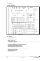
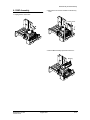
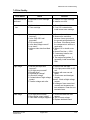
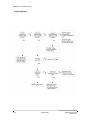
1
WorkCentre Pro 412
Launch Issue
SERVICE
MANUAL
Contents
1. Introduction
2. Service Call Procedures
3. Precautions
4. Specifications
5. Circuit Description
6. Disassembly
7. Maintenance & Troubleshooting
8. Exploded Views and Parts List
9. Electrical Parts List
10. Block Diagram
11. Connection Diagram
12. Schematic Diagrams
Part Number 708P86391
WorkCentre Pro 412.
Service Documentation.
WorkCentre Pro 412 Service Manual.
August 2001.
Prepared by:
Xerox Europe
Global Knowledge & Language Services
Enterprise Centre
P. O. Box 17
Bessemer Road
Welwyn Garden City
Hertfordshire AL7 1HE
England.
© Copyright 2001 by Xerox Europe
***Xerox Private Data***
All service documentation is supplied to Xerox external customers for informational purposes only. Xerox
service documentation is intended for use by certified, product trained service personnel only. Xerox does
not warrant or represent that it will notify or provide to such customer any future change to this documentation. Customer performed service of equipment, or modules, components or parts of such equipment
may affect whether Xerox is responsible to fix machine defects under the warranty offered by Xerox with
respect to such equipment. You should consult the applicable warranty for its terms regarding customer or
third-party provided service.
While every care has been taken in the preparation of this manual, no liability will be accepted by Xerox
Europe arising out of any inaccuracies or omissions.
Xerox Europe, Xerox ® and all identifying numbers used in connection with the Xerox products mentioned
in this publication are trademarks of Xerox Europe.
Printed in the United Kingdom.
Adobe and PostScript are trademarks of Adobe Systems Incorporated.
PCL, PCL5e, and PCLXL2.0 are trademarks of Hewlett-Packard Company. IBM is a trademark of International Business Machines Corporation. Microsoft, Microsoft Windows, Windows3.1, Windows3.11,
Windows95/98, WindowsNT, Windows2000, Microsoft Word, MS, and MS-DOS are trademarks of
Microsoft Corporation. All other product names are trademarks/trade names of their respective owners.
Table of Contents
Table of Contents
1. Introduction. . . . . . . . . . . . . . . . . . . . . . . . . . . . . . . . . . . . . . . . . . . . . . . . . .
1-1 Organisation . . . . . . . . . . . . . . . . . . . . . . . . . . . . . . . . . . . . . . . . . . . . .
1-2 Warnings, Cautions and Notes . . . . . . . . . . . . . . . . . . . . . . . . . . . . . . .
1-3 Safety Procedures and Information. . . . . . . . . . . . . . . . . . . . . . . . . . . .
1-4 Heath and Safety Incident Reporting . . . . . . . . . . . . . . . . . . . . . . . . . .
1-5 Translation of Warnings and Precautions . . . . . . . . . . . . . . . . . . . . . . .
1-1
1-1
1-1
1-2
1-4
1-6
2. Service Call Procedures . . . . . . . . . . . . . . . . . . . . . . . . . . . . . . . . . . . . . . . .
SCP 1 Initial Actions . . . . . . . . . . . . . . . . . . . . . . . . . . . . . . . . . . . . . . . . . .
SCP 2 First Call Actions . . . . . . . . . . . . . . . . . . . . . . . . . . . . . . . . . . . . . . .
SCP 3 Normal Call Actions . . . . . . . . . . . . . . . . . . . . . . . . . . . . . . . . . . . . .
SCP 4 Fault Analysis . . . . . . . . . . . . . . . . . . . . . . . . . . . . . . . . . . . . . . . . . .
SCP 5 Final Actions. . . . . . . . . . . . . . . . . . . . . . . . . . . . . . . . . . . . . . . . . . .
2-1
2-1
2-1
2-2
2-2
2-2
3. Precautions. . . . . . . . . . . . . . . . . . . . . . . . . . . . . . . . . . . . . . . . . . . . . . . . . . 3-1
4. Specifications . . . . . . . . . . . . . . . . . . . . . . . . . . . . . . . . . . . . . . . . . . . . . . . .
4-1 Printer . . . . . . . . . . . . . . . . . . . . . . . . . . . . . . . . . . . . . . . . . . . . . . . . . .
4-2 Facsimile . . . . . . . . . . . . . . . . . . . . . . . . . . . . . . . . . . . . . . . . . . . . . . . .
4-3 Scanner . . . . . . . . . . . . . . . . . . . . . . . . . . . . . . . . . . . . . . . . . . . . . . . . .
4-4 Copier . . . . . . . . . . . . . . . . . . . . . . . . . . . . . . . . . . . . . . . . . . . . . . . . . .
4-5 Power Supply . . . . . . . . . . . . . . . . . . . . . . . . . . . . . . . . . . . . . . . . . . . .
4-6 Dimension . . . . . . . . . . . . . . . . . . . . . . . . . . . . . . . . . . . . . . . . . . . . . . .
4-7 Packaging . . . . . . . . . . . . . . . . . . . . . . . . . . . . . . . . . . . . . . . . . . . . . . .
4-8 Environmental Condition . . . . . . . . . . . . . . . . . . . . . . . . . . . . . . . . . . . .
4-9 Machine Life . . . . . . . . . . . . . . . . . . . . . . . . . . . . . . . . . . . . . . . . . . . . .
4-1
4-1
4-2
4-2
4-3
4-3
4-4
4-4
4-4
4-4
5. Circuit Description. . . . . . . . . . . . . . . . . . . . . . . . . . . . . . . . . . . . . . . . . . . . .
5-1 Main PBA . . . . . . . . . . . . . . . . . . . . . . . . . . . . . . . . . . . . . . . . . . . . . . .
5-2 Circuit Operation . . . . . . . . . . . . . . . . . . . . . . . . . . . . . . . . . . . . . . . . . .
5-3 Scanner . . . . . . . . . . . . . . . . . . . . . . . . . . . . . . . . . . . . . . . . . . . . . . . . .
5-4 Host Interface . . . . . . . . . . . . . . . . . . . . . . . . . . . . . . . . . . . . . . . . . . . .
5-5 Engine Controller. . . . . . . . . . . . . . . . . . . . . . . . . . . . . . . . . . . . . . . . . .
5-6 OPE PBA. . . . . . . . . . . . . . . . . . . . . . . . . . . . . . . . . . . . . . . . . . . . . . . .
5-7 LIU PBA. . . . . . . . . . . . . . . . . . . . . . . . . . . . . . . . . . . . . . . . . . . . . . . . .
5-8 SMPS (Switching Mode Power Supply) Unit. . . . . . . . . . . . . . . . . . . . .
5-1
5-1
5-2
5-18
5-22
5-26
5-34
5-35
5-36
6. Disassembly and Reassembly . . . . . . . . . . . . . . . . . . . . . . . . . . . . . . . . . . .
6-1 General Precautions on Disassembly . . . . . . . . . . . . . . . . . . . . . . . . . .
6-2 Rear Cover . . . . . . . . . . . . . . . . . . . . . . . . . . . . . . . . . . . . . . . . . . . . . .
6-3 Scanner Assembly . . . . . . . . . . . . . . . . . . . . . . . . . . . . . . . . . . . . . . . .
6-4 ADF Assembly. . . . . . . . . . . . . . . . . . . . . . . . . . . . . . . . . . . . . . . . . . . .
6-5 OPE Assembly . . . . . . . . . . . . . . . . . . . . . . . . . . . . . . . . . . . . . . . . . . .
6-6 Side Cover Assembly . . . . . . . . . . . . . . . . . . . . . . . . . . . . . . . . . . . . . .
6-7 Fuser Assembly. . . . . . . . . . . . . . . . . . . . . . . . . . . . . . . . . . . . . . . . . . .
6-8 Exit Assembly . . . . . . . . . . . . . . . . . . . . . . . . . . . . . . . . . . . . . . . . . . . .
6-9 Cover Paper Exit Assembly. . . . . . . . . . . . . . . . . . . . . . . . . . . . . . . . . .
6-10 Drive Assembly . . . . . . . . . . . . . . . . . . . . . . . . . . . . . . . . . . . . . . . . . .
6-11 SMPS . . . . . . . . . . . . . . . . . . . . . . . . . . . . . . . . . . . . . . . . . . . . . . . . .
6-12 LSU . . . . . . . . . . . . . . . . . . . . . . . . . . . . . . . . . . . . . . . . . . . . . . . . . . .
6-13 Main Frame Assembly. . . . . . . . . . . . . . . . . . . . . . . . . . . . . . . . . . . . .
6-14 Cover Exit Rear . . . . . . . . . . . . . . . . . . . . . . . . . . . . . . . . . . . . . . . . . .
6-15 MP Assembly . . . . . . . . . . . . . . . . . . . . . . . . . . . . . . . . . . . . . . . . . . .
6-16 Feed Assembly . . . . . . . . . . . . . . . . . . . . . . . . . . . . . . . . . . . . . . . . . .
6-17 Pick Up Assembly . . . . . . . . . . . . . . . . . . . . . . . . . . . . . . . . . . . . . . . .
6-18 Main PBA . . . . . . . . . . . . . . . . . . . . . . . . . . . . . . . . . . . . . . . . . . . . . .
6-1
6-1
6-1
6-2
6-5
6-6
6-7
6-9
6-10
6-11
6-12
6-13
6-13
6-14
6-14
6-15
6-16
6-16
6-17
WorkCentre Pro 412
Launch Issue
August 2001
TOC-1
Table of Contents
7. Maintenance & Troubleshooting . . . . . . . . . . . . . . . . . . . . . . . . . . . . . . . . . .
7-1 Preventative Maintenance. . . . . . . . . . . . . . . . . . . . . . . . . . . . . . . . . . .
7-2 Diagnostics . . . . . . . . . . . . . . . . . . . . . . . . . . . . . . . . . . . . . . . . . . . . . .
7-3 Scanner . . . . . . . . . . . . . . . . . . . . . . . . . . . . . . . . . . . . . . . . . . . . . . . . .
7-4 FAX . . . . . . . . . . . . . . . . . . . . . . . . . . . . . . . . . . . . . . . . . . . . . . . . . . . .
7-5 Print Quality. . . . . . . . . . . . . . . . . . . . . . . . . . . . . . . . . . . . . . . . . . . . . .
7-6 Malfunction . . . . . . . . . . . . . . . . . . . . . . . . . . . . . . . . . . . . . . . . . . . . . .
7-1
7-1
7-1
7-9
7-12
7-13
7-30
8. Exploded View & Parts List. . . . . . . . . . . . . . . . . . . . . . . . . . . . . . . . . . . . . .
8-1. Main Exploded View & Parts List . . . . . . . . . . . . . . . . . . . . . . . . . . . . .
8-2. Platen Ass’y Exploded View & Parts List . . . . . . . . . . . . . . . . . . . . . . .
8-3. ADF ASS’Y Exploded View & Parts List. . . . . . . . . . . . . . . . . . . . . . . .
8-4. Side Cover Ass’y Exploded View & Parts List . . . . . . . . . . . . . . . . . . .
8-5. Cassette Ass’y Exploded View & Parts List . . . . . . . . . . . . . . . . . . . . .
8-6. Exit Ass’y Exploded View & Parts List . . . . . . . . . . . . . . . . . . . . . . . . .
8-7. Feeder Ass’y Exploded View & Parts List . . . . . . . . . . . . . . . . . . . . . .
8-8. MP Ass’y Exploded View & Parts List . . . . . . . . . . . . . . . . . . . . . . . . .
8-9. Base Frame Exploded View & Parts List . . . . . . . . . . . . . . . . . . . . . . .
8-10. Pick-up Ass’y Exploded View & Parts List . . . . . . . . . . . . . . . . . . . . .
8-11. Drive Ass’y Exploded View & Parts List . . . . . . . . . . . . . . . . . . . . . . .
8-12. Main Frame Ass’y Exploded View & Parts List . . . . . . . . . . . . . . . . .
8-13. FuserAss’y Exploded View & Parts List . . . . . . . . . . . . . . . . . . . . . .
8-1
8-1
8-4
8-6
8-10
8-14
8-16
8-18
8-20
8-22
8-24
8-26
8-28
8-30
9. Electrical Parts Lists . . . . . . . . . . . . . . . . . . . . . . . . . . . . . . . . . . . . . . . . . . . 9-1
9-1 Main PBA . . . . . . . . . . . . . . . . . . . . . . . . . . . . . . . . . . . . . . . . . . . . . . . 9-1
10. Block Diagram . . . . . . . . . . . . . . . . . . . . . . . . . . . . . . . . . . . . . . . . . . . . . . 10-1
11. Connection Diagram . . . . . . . . . . . . . . . . . . . . . . . . . . . . . . . . . . . . . . . . . . 11-1
12. Schematic Diagrams. . . . . . . . . . . . . . . . . . . . . . . . . . . . . . . . . . . . . . . . . .
12-1 Main Circuit Diagram (1 of 14) . . . . . . . . . . . . . . . . . . . . . . . . . . . . . .
12-2 Main Circuit Diagram (2 of 14) . . . . . . . . . . . . . . . . . . . . . . . . . . . . . .
12-3 Main Circuit Diagram (3 of 14) . . . . . . . . . . . . . . . . . . . . . . . . . . . . . .
12-4 Main Circuit Diagram (4 of 14) . . . . . . . . . . . . . . . . . . . . . . . . . . . . . .
12-5 Main Circuit Diagram (5 of 14) . . . . . . . . . . . . . . . . . . . . . . . . . . . . . .
12-6 Main Circuit Diagram (6 of 14) . . . . . . . . . . . . . . . . . . . . . . . . . . . . . .
12-7 Main Circuit Diagram (7 of 14) . . . . . . . . . . . . . . . . . . . . . . . . . . . . . .
12-8 Main Circuit Diagram (8 of 14) . . . . . . . . . . . . . . . . . . . . . . . . . . . . . .
12-9 Main Circuit diagram (9 of 14) . . . . . . . . . . . . . . . . . . . . . . . . . . . . . . .
12-10 Main Circuit Diagram (10 of 14) . . . . . . . . . . . . . . . . . . . . . . . . . . . .
12-11 Main Circuit Diagram (11 of 14) . . . . . . . . . . . . . . . . . . . . . . . . . . . .
12-12 Main Circuit Diagram (12 of 14) . . . . . . . . . . . . . . . . . . . . . . . . . . . .
12-13 Main Circuit Diagram (13 of 14) . . . . . . . . . . . . . . . . . . . . . . . . . . . .
12-14 Main Circuit Diagram (14 of 14) . . . . . . . . . . . . . . . . . . . . . . . . . . . .
12-15 LIU Circuit Diagram . . . . . . . . . . . . . . . . . . . . . . . . . . . . . . . . . . . . . .
12-16 OPE Circuit Diagram . . . . . . . . . . . . . . . . . . . . . . . . . . . . . . . . . . . . .
12-17 HVPS Circuit Diagram (1 of 2) . . . . . . . . . . . . . . . . . . . . . . . . . . . . .
12-18 HVPS Circuit Diagram (2 of 2) . . . . . . . . . . . . . . . . . . . . . . . . . . . . .
12-19 SMPS (110) Circuit Diagram . . . . . . . . . . . . . . . . . . . . . . . . . . . . . . .
12-20 SMPS (220) Circuit Diagram . . . . . . . . . . . . . . . . . . . . . . . . . . . . . . .
12-21 ADF Circuit Diagram . . . . . . . . . . . . . . . . . . . . . . . . . . . . . . . . . . . . .
12-22 Flat Circuit Diagram. . . . . . . . . . . . . . . . . . . . . . . . . . . . . . . . . . . . . .
12-23 PTL Circuit Diagram . . . . . . . . . . . . . . . . . . . . . . . . . . . . . . . . . . . . .
12-24 Sensor Circuit Diagram . . . . . . . . . . . . . . . . . . . . . . . . . . . . . . . . . . .
12-25 Toner RX Circuit Diagram . . . . . . . . . . . . . . . . . . . . . . . . . . . . . . . . .
12-26 Toner TX Circuit Diagram . . . . . . . . . . . . . . . . . . . . . . . . . . . . . . . . .
WorkCentre Pro 412
Launch Issue
August 2001
12-1
12-1
12-2
12-3
12-4
12-5
12-6
12-7
12-8
12-9
12-10
12-11
12-12
12-13
12-14
12-15
12-16
12-17
12-18
12-19
12-20
12-21
12-22
12-23
12-24
12-25
12-26
TOC-2
Introduction
1. Introduction
This service manual is part of a multinational service documentation system, but is not structured in the standard Xerox service manual format.
1-1 Organisation
Section 1 Introduction
This section describes the contents of the service manual, describes the Heath & Safety Incident Reporting
and gives translations of all warnings within the service manual in French, Italian, German and Spanish languages.
Section 2 Service Call Procedures
This section is used to start and complete a service call. This section will either direct you to the Maintenance
and Troubleshooting section, or identify a faulty component or sub-assembly.
Section 3 Precautions
This section contains ESD precautions.
Section 4 Specifications
This section contains the specifications for the various modules of the machine.
Section 5 Circuit Description
This section describes the control system of the machine.
Section 6 Disassembly and Reassembly
This section gives instructions for dismantling and assembling the machine.
Section 7 Maintenance & Troubleshooting
This section contains instructions for preventative maintenance and diagnosis of machine fault
Section 8 Exploded Views and Parts Lists
This section shows all parts of the machine in exploded views with lists of spared parts.
Section 9 Electrical Parts Lists.
This section lists all of the spared electrical components.
Section 10 Block Diagram
This section contains a block diagram of the machine functions.
Section 11 Connection Diagram
This section contains an electrical connection diagram for the whole machine.
Section 12 Schematic Diagrams
This section contains the schematic diagrams for the machine.
1-2 Warnings, Cautions and Notes
Translated versions of all warnings are in Translation of Warnings at the end of this section.
WorkCentre Pro 412
Launch Issue
August 2001
1-1
Introduction
WARNING
A warning is used whenever an operating or maintenance procedure, practice, condition or statement,
if not strictly observed, could result in personal injury.
CAUTION
A caution is used whenever an operation or maintenance procedure, practice, condition or statement, if not
strictly observed, could result in damage to the equipment
NOTE: A note is used where it is essential to highlight a procedure, practice, condition or statement
1-3 Safety Procedures and Information
The Xerox WorkCentre Pro 412 product and supplies are manufactured, tested and certified to strict safety
regulations, electromagnetic regulations and established environmental standards.
WARNING
Any unauthorised alteration, which may include the addition of new functions, the connection of external devices or the use of components not specified by Xerox may impact the products certification,
safety performance or compliance with legislation.
Warning markings
All warning instructions marked on or supplied with the product should be followed.
WARNING
A warning is used whenever an operating, service or maintenance procedure, practice, condition or
statement, if not strictly observed could result in personal injury.
WARNING
Alerts to areas of the product where there are heated surfaces which must be avoided during service
or maintenance operations.
WARNING
The following are general warning statements which apply in various service or maintenance situations.
WorkCentre Pro 412
Launch Issue
August 2001
1-2
Introduction
General Safety Warning
Switch off the power to the machine and disconnect the power cord from the outlet while performing tasks that
do not need the electricity on. Contact with electricity can cause death or injury.
Power Supply
This product must be operated from the type of power supply indicated on the product’s data plate label.
This product must be connected to a protective earth circuit.
Safe Working
Throughout this procedure prior to working on any electrical circuit or any mechanical drive component disconnect all electrical power to the product. The disconnect device is the power cord. Remove the plug from the
power outlet.
Ventilation
This product should not be placed in a built-in installation unless proper ventilation is provided.
Operator Accessible Areas
This product has been designed to restrict operator access to safe areas only. Operator access to hazardous
areas is restricted with covers or guards, which require a tool to remove. Ensure that these covers or guards
are correctly replaced after every service or maintenance task.
Maintenance/Service
Do not to carry out any maintenance or service on the product, which is not described this service documentation.
Cleaning
Before cleaning this product, unplug the product from the power outlet. Always use materials specifically designated for this product, the use of other materials may result in poor performance and may create a hazardous situation. Do not use aerosol cleaners, they may become flammable under certain circumstances.
Precautions
1. Be sure that all built-in protective devices are in place. Restore any missing protective covers.
2. When re-installing chassis and assemblies, be sure to restore all protective devices, including control
knobs and compartment covers.
3. Design Alteration Warning: Never alter or add to the mechanical or electrical design of this equipment,
such as auxiliary connectors, etc. Such alterations and modifications will void the manufacturer’s warranty.
4. Components, parts, and wiring that appear to have overheated or are otherwise damaged should be
replaced with Xerox spare parts. Always determine the cause of damage or overheating, and correct any
potential hazards.
5. Observe the original harness routing, especially near sharp edges, AC, and high voltage power supplies.
Always inspect for pinched, out-of-place, or frayed wiring. Do not change the spacing between components and the printed circuit board.
6. Product Safety Notice: Some electrical and mechanical parts have special safety-related characteristics
which might not be obvious from visual inspection. These safety features and the protection they provide
could be lost if a replacement component differs from the original. This holds true, even though the
replacement may be rated for higher voltage, wattage, etc.
Lithium battery precautions
The Main PWBA is provided with a lithium Cell designated BAT1. Observe the following precautions:
•There could be a danger of explosion if the battery is subject to forced discharge or reverse voltage.
•The battery must only be replaced with the same type.
•The battery should only be replaced at a service centre not at a customer location
•The replacement battery must be the same type and manufacturer as the original.
•Lithium batteries contain substances which are subject to control and should not be opened, crushed or
burned during disposal.
WorkCentre Pro 412
Launch Issue
August 2001
1-3
Introduction
Laser Safety
WARNING
Invisible laser radiation. avoid exposure to beam.
Use of controls or adjustments or performance of procedures other than those specified herein may
result in hazardous radiation exposure.
This product contains laser warning labels. These labels are intended for use by Service and Maintenance Representatives and are placed on the top surface of the Laser Unit. Do not attempt to open the
laser unit. There are no serviceable components or areas inside the unit. Operation of the laser unit
with machine or laser covers removed could cause eye damage if the laser beam is viewed directly.
Electrostatic Damage Caution
The following is an example of the terminology and symbols used in this manual for an electrostatic damage
caution:
Caution
Certain components in this product are susceptible to damage from electrostatic discharge. Observe all ESD
procedures to avoid component damage.
1-4 Heath and Safety Incident Reporting
I. Summary
This standard defines requirements for notification of health and safety incidents involving Xerox products
(equipment and materials) at customer locations.
II. Scope
Xerox Corporation and subsidiaries worldwide.
WorkCentre Pro 412
Launch Issue
August 2001
1-4
Introduction
III. Objective
To enable prompt resolution of health and safety incidents involving Xerox products and to ensure Xerox regulatory compliance.
IV. Definitions
Incident:
An event or condition occurring in a customer account that has resulted in injury, illness or property damage.
Examples of incidents include machine fires, smoke generation, physical injury to an operator or service representative. Alleged events and product conditions are included in this definition.
V. Requirements
Initial Report:
1. Xerox organisations shall establish a process for individuals to report product incidents to EH&S within 24
hours of becoming aware of the event.
2. The information to be provided at the time of reporting is contained in Appendix A (Health and Safety Incident Report involving a Xerox product).
3. The initial notification may be made by any of the following methods:
• For incidents in North America and Developing Markets West (Brazil, Mexico, Latin American North
and Latin American South):
Phone* EH&S at: 1-800-828-6571.
• Electronic mail EH&S at: [email protected].
• Fax EH&S at: 1-716-422-7734 [intelnet 8*222 7734].
• For incidents in Europe and Developing Markets East (Middle East, Africa, India, China and Hong
Kong):
• Phone* EH&S at: +44 (0) 1707 35343.
• Electronic mail EH&S at: [email protected].
• Fax EH&S at: +44 (0) 1707 353914 [intelnet 8*668 3914].
*Initial notification made by phone must be followed within 24 hours by a completed incident report and sent to
the indicated electronic mail address or fax number.
NOTE: If sending a fax, please also send the original via internal mail.
Responsibilities for resolution:
1. Business Groups/Product Design Teams responsible for the product involved in the incident shall:
a. Manage field bulletins, customer correspondence, product recalls, safety retrofits.
b. Fund all field retrofits.
2. Field Service Operations shall:
a. Preserve the Xerox product involved and the scene of the incident inclusive of any associated equipment located in the vicinity of the incident.
b. Return any affected equipment/part(s) to the location designated by EH&S and/or the Business Division.
c. Implement all safety retrofits.
3. EH&S shall:
a. Manage and report all incident investigation activities.
b. Review and approve proposed product corrective actions and retrofits, if necessary.
c. Manage all communications and correspondence with government agencies.
d. Define actions to correct confirmed incidents.
VI. Appendices
The Health and Safety Incident Report involving a Xerox Product (Form # EH&S-700) is available at the end of
this Service Manual.
WorkCentre Pro 412
Launch Issue
August 2001
1-5
Introduction
1-5 Translation of Warnings and Precautions
WARNING
A warning is used whenever an operating or maintenance procedure, practice, condition or statement,
if not strictly observed, could result in personal injury.
AVERTISSEMENT
Un avertissement est utilisé chaque fois qu'une procédure d'utilisation ou de maintenance peut provoquer des blessures si elle n'est pas strictement respectée.
AVVERTENZA
Un’ avvertenza viene utilizzata per segnalare procedure, operazioni, condizioni o istruzioni operative e
di manutenzione, la cui mancata osservanza può causare infortuni.
VORSICHT
Warnhinweise dieser Art gelten für Anweisungen und Situationen, bei deren Nichtbeachtung bzw.
Auftreten Verletzungsgefahr besteht.
AVISO
Los avisos se utilizan cuando un procedimiento, ejercicio, condición o declaración de funcionamiento
o mantenimiento puede producir lesiones personales, si no se sigue estrictamente.
WARNING
Any unauthorised alteration, which may include the addition of new functions, the connection of external devices or the use of components not specified by Xerox may impact the products certification,
safety performance or compliance with legislation.
AVERTISSEMENT
Toute modification non autorisée, qu'il s'agisse de l'ajout de nouvelles fonctions, de la connexion de
dispositifs externes ou de l'utilisation de composants non recommandés par Xerox, peut entraîner
l'annulation de la garantie.
AVVERTENZA
Qualunque modifica che implichi l’ aggiungimento di nuove funzioni, il collegamento ad un dispositivo
esterno o l’ utilizzo di componenti non autorizzati da Xerox può invalidare la certificazione e le dichiarazioni di conformità del prodotto, nonché compromettere la sicurezza operativa di questo.
VORSICHT
Warnhinweise dieser Art gelten für Anweisungen und Situationen, bei deren Nichtbeachtung bzw.
Auftreten Verletzungsgefahr besteht.
AVISO
Cualquier modificación no autorizada, que puede incluir la adición de nuevas funciones, la conexión
de dispositivos externos o el uso de componentes no especificados por Xerox, puede afectar a la certificación del producto, el funcionamiento seguro o el cumplimiento de la legislación.
WARNING
A warning is used whenever an operating, service or maintenance procedure, practice, condition or
statement, if not strictly observed could result in personal injury
AVERTISSEMENT
WorkCentre Pro 412
Launch Issue
August 2001
1-6
Introduction
Un avertissement est utilisé à chaque fois qu'une procédure de maintenance ou qu'une manipulation
présente un risque de blessure si elle n'a pas été strictement observée.
AVVERTENZA
Un’ avvertenza viene utilizzata per segnalare procedure, operazioni, condizioni o istruzioni operative e
di manutenzione, la cui mancata osservanza può causare infortuni.
VORSICHT
Warnhinweise dieser Art gelten für Anweisungen und Situationen, bei deren Nichtbeachtung bzw.
Auftreten Verletzungsgefahr besteht.
AVISO
Los avisos se utilizan cuando un procedimiento, ejercicio, condición o declaración de funcionamiento,
servicio o mantenimiento puede producir lesiones personales, si no se sigue estrictamente.
WARNING
Alerts to areas of the product where there are heated surfaces which must be avoided during service
or maintenance operations.
AVERTISSEMENT
Prévient des risques encourus lors d'une intervention dans des zones chaudes qui peuvent provoquer
des blessures.
AVVERTENZA
Evitare le superfici calde del prodotto, indicate da etichette di avvertenza, durante le operazioni di
manutenzione o di assistenza.
VORSICHT
Weist auf heiße Gerätebereiche hin, die bei der Wartung und Pflege nicht angefasst werden dürfen.
AVISO
Llama la atención sobre áreas del producto donde hay superficies calientes que deben evitarse
durante las tareas de servicio o mantenimiento.
WARNING
The following are general warning statements which apply in various service or maintenance situations.
General safety warning
Switch off the power to the machine and disconnect the power cord from the outlet while performing tasks that
do not need the electricity on. Contact with electricity can cause death or injury.
Power Supply
This product must be operated from the type of power supply indicated on the product’s data plate label.
This product must be connected to a protective earth circuit.
Safe Working
Throughout this procedure prior to working on any electrical circuit or any mechanical drive component disconnect all electrical power to the product. The disconnect device is the power cord. Remove the plug from the
power outlet.
Ventilation
This product should not be placed in a built-in installation unless proper ventilation is provided.
WorkCentre Pro 412
Launch Issue
August 2001
1-7
Introduction
Operator Accessible Areas
This product has been designed to restrict operator access to safe areas only. Operator access to hazardous
areas is restricted with covers or guards, which require a tool to remove. Ensure that these covers or guards
are correctly replaced after every service or maintenance task.
Maintenance/Service
Do not to carry out any maintenance or service on the product, which is not described this service documentation.
Cleaning
Before cleaning this product, unplug the product from the power outlet. Always use materials specifically designated for this product, the use of other materials may result in poor performance and may create a hazardous situation. Do not use aerosol cleaners, they may become flammable under certain circumstances.
AVERTISSEMENT
Cette mention indique des informations relatives à différentes situations de maintenance.
Sécurité générale - Avertissement
Mettre la machine hors tension et débrancher le cordon d'alimentation de la prise murale lors d'interventions
qui ne nécessitent pas que l'alimentation soit maintenue. Un contact avec une zone sous tension peut mettre
en danger la sécurité des personnes.
Alimentation
Ce produit doit être utilisé avec l'alimentation indiqué sur la plaque de la machine.
Ce produit doit être connecté à un circuit avec mise à la terre.
Sécurité
Pendant toute cette procédure d'intervention dans des circuits électriques ou des entraînements mécaniques,
débranchez la machine. Le système de déconnexion est le cordon d'alimentation. Retirer le connecteur de la
prise murale.
Aération
Cet équipement ne doit pas être encastré, sans une ventilation appropriée.
Zones accessibles aux utilisateurs
Ce produit a été conçu de façon à ce que les zones accessibles par les utilisateurs soient sans danger. Les
zones qui peuvent être dangereuses sont protégées par des panneaux ou des sécurités qui nécessitent l'utilisation d'un outil pour être retirer. Veiller à ce que ces panneaux et sécurités sont correctement remis en place
après toute intervention technique ou de maintenance.
Maintenance
N'effectuez aucune procédure de maintenance non décrite dans la documentation.
Nettoyage
Avant toute procédure de nettoyage, débranchez l'équipement de la prise murale. Utilisez toujours les produits
d'entretien conçus spécifiquement pour l'appareil. L'utilisation d'autres produits risque de nuire au bon fonctionnement de l'appareil et peut s'avérer dangereuse. N'utilisez jamais d'aérosols, ils peuvent s'enflammer
sous certaines circonstances.
AVVERTENZA
Le seguenti avvertenze sono applicabili a svariate situationi di manutenzione o di assistenza.
WorkCentre Pro 412
Launch Issue
August 2001
1-8
Introduction
Avvertenza sicurezza generale
Spegnere l’ apparecchio e scollegare il cavo di alimentazione dalla presa durante l’ esecuzione di operazioni
che non richiedono l’ utilizzo di elettricità. Scosse elettriche accidentali possono causare lesioni personali o
morte.
Alimentazione
Utilizzare il prodotto esclusivamente con il tipo di energia indicato e collegarlo a un circuito protettivo con
messa a terra.
Sicurezza elettrica
Accertarsi che il prodotto non riceva elettricità durante le operazioni di intervento sui circuiti elettrici o sulle parti
meccaniche. Il dispositivo di disattivazione del prodotto è costituito dal cavo di alimentazione, il quale deve
essere scollegato dalla presa.
Ventilazione
Non installare l’ apparecchio in un alloggiamento a incasso, a meno che non sia garantita una ventilazione
adeguata.
Aree accessibili per l’ operatore
Questo prodotto è stato progettato in modo da impedire l’ accesso dell’ operatore ad aree non sicure; queste
sono protette da coperture o schermi che richiedono l’ utilizzo di attrezzi per la rimozione. Accertarsi che le
coperture o gli schermi siano reinseriti in seguito a qualunque operazione di manutenzione o di assistenza del
prodotto.
Manutenzione e assistenza
Non effettuare alcuna operazione di manutenzione o di assistenza non descritta nella documentazione del
prodotto.
Pulizia del prodotto
Prima di eseguire operazioni di pulizia, scollegare il cavo di alimentazione dalla presa a muro. Utilizzare sempre prodotti specifici per questo apparecchio: l’ utilizzo di prodotti diversi da quelli consigliati può comportare
un deterioramento delle prestazioni e causare situazioni di pericolo. Non utilizzare detergenti aerosol, che in
alcune circostanze possono risultare infiammabili.
VORSICHT
Die folgenden Warnhinweise gelten für diverse Wartungs- und Pflegearbeiten.
Allgemeine Sicherheitshinweise
Bei Arbeiten, bei denen kein Strom erforderlich ist, das Gerät ausschalten und den Netzstecker abziehen.
Netzanschluss
Das Gerät muss an eine einwandfrei funktionierende Steckdose angeschlossen sein. Das Gerät muss geerdet
sein.
Arbeitssicherheit
Vor jeglichen Arbeiten an einem Stromkreis oder einem mechanischen Antrieb ist immer der Netzanschluss zu
trennen. Das Gerät wird durch Abziehen des Netzsteckers abgeschaltet.
Belüftung
Das Gerät darf nur dann in einer Einbauposition installiert werden, wenn für ausreichende -Lüftung gesorgt ist.
WorkCentre Pro 412
Launch Issue
August 2001
1-9
Introduction
Gefahrenbereiche im Gerät
Der Zugang zum Gerät ist durch Abdeckungen und mechanische Verriegelungen auf sichere Bereiche
eingegrenzt. Gefahrenbereiche sind mit Abdeckungen versehen, die nur mit Werkzeug entfernt werden können. Diese Abdeckungen müssen nach Reparaturarbeiten durch den Kundendienst wieder ordnungsgemäß
eingebaut werden.
Wartung/Kundendienst
Keine Wartungsarbeiten, die nicht in der Dokumentation beschrieben sind, ausführen.
Reinigung
Vor der Reinigung des Geräts den Netzstecker abziehen. Nur die speziell für das Gerät empfohlenen Teile und
Verbrauchsmaterialien benutzen, da im anderen Fall schlechte Laufleistung und Sicherheitsrisiken möglich
sind. Keine Reinigungssprays verwenden, da diese sich ggf. entzünden können.
AVISO
Los siguientes son declaraciones generales de aviso aplicables en varias situaciones de servicio o
mantenimiento.
Aviso de seguridad general
Apague la máquina y desenchufe el cable de alimentación de la toma de corriente para realizar tareas que no
necesiten que se tenga corriente eléctrica en la máquina. El contacto con la corriente eléctrica puede causar
lesiones e incluso la muerte.
Fuente de alimentación eléctrica
Este producto debe utilizarse con el tipo de alimentación eléctrica que se indique en la etiqueta o placa de
datos técnicos del producto. Este producto debe conectarse a un circuito con puesta a tierra de protección.
Seguridad en el trabajo
Durante este procedimiento antes de trabajar en algún circuito eléctrico o componente impulsor mecánico
desconecte el producto de la corriente eléctrica. El dispositivo de desconexión es el cable de alimentación.
Desconecte el enchufe de la toma de corriente.
Ventilación
Este producto no debe colocarse en un lugar empotrado al menos que se tenga la ventilación apropiada.
Áreas accesibles por el operador
Este producto está diseñado para limitar el acceso del operador solamente a áreas seguras. El acceso del
operador a áreas de peligro se limita mediante cubiertas y protectores que para quitarlos es necesario utilizar
alguna herramienta. Asegúrese de volver a colocar las cubiertas y los protectores correctamente después de
cada tarea de servicio o mantenimiento.
Mantenimiento/Servicio
No realice ninguna operación de mantenimiento o servicio en este producto si no está descrita en esta documentación de servicio.
Limpieza
Antes de limpiar este producto, desenchúfelo de la toma de corriente. Utilice siempre materiales designados
específicamente para este producto; el uso de otros materiales puede producir un funcionamiento defectuoso
o crear situaciones de peligro. No utilice limpiadores de aerosol; en ciertas circunstancias pueden llegar a ser
inflamables.
WorkCentre Pro 412
Launch Issue
August 2001
1-10
Introduction
Precautions
1. Be sure that all built-in protective devices are in place. Restore any missing protective covers.
2. When re-installing chassis and assemblies, be sure to restore all protective devices, including control
knobs and compartment covers.
3. Design Alteration Warning: Never alter or add to the mechanical or electrical design of this equipment,
such as auxiliary connectors, etc. Such alterations and modifications will void the manufacturer’s warranty.
4. Components, parts, and wiring that appear to have overheated or are otherwise damaged should be
replaced with Xerox spare parts. Always determine the cause of damage or overheating, and correct any
potential hazards.
5. Observe the original harness routing, especially near sharp edges, AC, and high voltage power supplies.
Always inspect for pinched, out-of-place, or frayed wiring. Do not change the spacing between components and the printed circuit board.
6. Product Safety Notice: Some electrical and mechanical parts have special safety-related characteristics
which might not be obvious from visual inspection. These safety features and the protection they provide
could be lost if a replacement component differs from the original. This holds true, even though the
replacement may be rated for higher voltage, wattage, etc.
7. Components critical for safety are indicated in the parts list with symbols shown below. Use only replacement components that have the same ratings, especially for flame resistance and dielectric specifications.
A replacement part that does not have the same safety characteristics as the original may create shock,
fire, or other safety hazards.
Lithium battery precautions
The Main PWBA is provided with a lithium Cell designated BAT1. Observe the following precautions:
There could be a danger of explosion if the battery is subject to forced discharge or reverse voltage.
The battery must only be replaced with the same type.
The battery should only be replaced at a service centre not at a customer location
The replacement battery must be the same type and manufacturer as the original.
Lithium batteries contain substances which are subject to control and should not be opened, crushed or
burned during disposal.
Précautions
1. Vérifier que tous les dispositifs de protection intégrés sont en place. Replacer les panneaux de protection
manquants.
2. Lors de la réinstallation du châssis et des différentes pièces, veiller à bien replacer tous les dispositifs de
protection, y compris les boutons de contrôle et les couvercles de compartiment.
3. Avertissement relatif aux modifications de conception : Ne jamais modifier la structure mécanique ou électrique de cet équipement (en ajoutant, par exemple, des connecteurs auxiliaires, etc.). De telles transformations et modifications annuleraient la garantie du constructeur.
4. Tout composant, pièce ou câblage ayant été exposé à une surchauffe ou endommagé d’une quelconque
autre façon doit être remplacé par une pièce Xerox. Toujours déterminer la cause du dommage ou de la
surchauffe et éliminer les risque potentiels.
5. Examiner le câblage initial, aux abords notamment des arêtes coupantes, de l’alimentation en courant
alternatif et haute tension et toujours s’assurer qu’aucun fil n’est coincé, déplacé ou endommagé. Ne pas
modifier l’espacement des composants et de la carte de circuit imprimé.
6. Sécurité produit : Certaines pièces mécaniques et électriques présentent des caractéristiques de sécurité
particulières qui peuvent ne pas être évidentes à l’oeil nu. Ces caractéristiques de sécurité et la protection
qu’elles assurent risquent de disparaître si un composant de rechange différent du composant d’origine
est utilisé. Ceci est vrai même dans le cas où la pièce de rechange serait destinée à un voltage, à un
ampérage, etc., supérieur.
7. Les composants essentiels pour la sécurité sont indiqués dans la liste des pièces par les symboles décrits
ci-dessous. Utiliser uniquement des composants de rechange présentant les mêmes caractéristiques
assignées, surtout en matière de tenue à la flamme et de spécifications diélectriques. Une pièce de
rechange ne présentant pas les mêmes caractéristiques de sécurité que la pièce d’origine peut provoquer
des accidents : électrocution, incendie, et autres dangers pour la sécurité.
WorkCentre Pro 412
Launch Issue
August 2001
1-11
Introduction
Précautions relatives aux piles au Lithium
La carte PWBA est équipée d'une pile au lithium identifiée BAT1. Observez les précautions suivantes :
Il existe un risque d'explosion si la pile est l'objet d'une alimentation forcée ou d'un voltage inversé.
Une pile ne doit être remplacée que par une de même type.
La pile ne doit être remplacée que dans un Centre de maintenance et non chez le client.
Les piles de remplacement doivent être de même type et fabrication que celles d'origine.
Les piles au Lithium contiennent des substances qui nécessitent des contrôles et ne doivent pas
être ouvertes, écrasées ou brûlées.
Precauzioni
1. Accertari che non manchino dispositivi di protezione. Rimettere in sede eventuali coperture di protezione
mancanti.
2. Durante l’installazione di coperture e gruppi, accertarsi che siano presenti tutti i dispositivi di protezione,
comprese manopole di controllo e coperture nelle diverse aree.
3. Avvertenza: non modificare la struttura meccanica o elettrica della macchina, quali connettori ausiliari, ecc.
Eventuali modifiche o alterazioni renderanno nullo il certificato di garanzia del produttore.
4. Componenti, parti e cablaggio che appaiono surriscaldati o danneggiati vanno sostituiti da parti di ricambio
Xerox. Stabilire la causa del problema e intervenire in modo adeguato per evitare che si ripresenti.
5. Mantenere il percorso originale del cablaggio, in particolare in prossimità di bordi, per CA e alimentazione
elettrica ad alta tensione. Verificare che il cablaggio non sia strozzato, fuori sede o consumato. Non
alterare lo spazio tra i componenti e la scheda del circuito stampato.
6. Avviso sulla sicurezza del prodotto: alcuni componenti elettrici e meccanici possiedono delle funzioni di
sicurezza non sempre ovvie durante l’ispezione visiva. Queste funzioni possono non essere più attive se
un componente viene sostituito con uno diverso dall’originale. Questo vale anche se le parti di ricambio
hanno specifiche più elevate, ad esempio, di alta tensione, potenza nominale, ecc.
7. I componenti per la sicurezza più importanti sono riportati nell’elenco delle parti di ricambio con i simboli
illustrati qui di seguito. Utilizzare solo componenti con gli stessi valori, in particolare per quanto riguarda i
valori di resistenza al calore e le specifiche dielettriche. Una parte di ricambio con funzioni di sicurezza
diverse dalla parte originale può causare condizioni di pericolo quali scosse elettriche e incendi.
Precauzioni della batteria al litio
La PWBA (scheda a circuito stampato) principale è fornita di una batteria al litio (BAT1).
Osservare le precauzioni riportate di seguito.
La batteria può esplodere se soggetta ad una forzata discarica o tensione inversa.
Sostituire la batteria ESCLUSIVAMENTE con una dello stesso tipo.
Sostituire la batteria presso un centro di assistenza tecnica e accertarsi che la batteria di sostituzione sia dello
stesso tipo e marca dell’ originale.
Le batterie al litio contengono sostanze soggette a controllo e non devono essere aperte, frantumate o bruciate durante l’ eliminazione.
Vorsichtsmaßnahmen
1. Darauf achten, dass alle Sicherheitsvorrichtungen vorhanden sind. Evtl. fehlende Sicherheitsabdeckungen einbauen.
2. Beim Zusammenbau von Komponenten und Gehäuse alle Sicherheitsvorrichtungen sowie Steuerknöpfe
und Abdeckungen installieren.
3. Bauartänderungen: keinerlei Änderung an der mechanischen oder elektrischen Bauart des Geräts, z. B.
durch Installation von Zusatzanschlüssen, durchführen. Bei solchen Änderungen wird die Garantie des
Herstellers ungültig.
4. Komponenten oder Kabel/Drähte, die überhitzt oder anderweitig beschädigt sind, müssen durch Ersatzteile von Xerox ersetzt werden. Die Ursache einer Überhitzung muss immer gesucht und entsprechende
Gefahrenquellen beseitigt werden.
WorkCentre Pro 412
Launch Issue
August 2001
1-12
Introduction
5. Kabelbaum, Netzkabel und Hochspannungskabel besonders in der Nähe scharfer Kanten auf Schäden
und Positionsänderungen überprüfen. Der Abstand zwischen Komponenten und der Leiterplatte darf nicht
geändert werden.
6. Gerätesicherheit: Einige elektrische und mechanische Komponenten verfügen über bestimmte, nicht sichtbare, Sicherheitsmerkmale. Werden Komponenten durch solche anderer Bauart ersetzt, bieten diese ggf.
nicht denselben Gefahrenschutz wie die Originalkomponenten. Das gilt auch dann, wenn die Ersatzteile
für eine höhere Spannung ausgelegt sind, o. Ä.
7. Für die Betriebssicherheit wichtige Komponenten sind in der Teileliste mit dem unten gezeigten Symbol
gekennzeichnet. Es dürfen nur Ersatzteile mit der gleichen Sicherheitsauslegung, insbesondere mit den
gleichen dielektrischen und flammhemmenden Spezifikationen, verwendet werden. Bei Einbau einer
Komponente mit einer anderen Sicherheitsauslegung als der des Originals bestehen Stromschlag-/Brandund weitere Sicherheitsrisiken.
Lithiumbatterie
Das Haupt-PWBA enthält eine Lithiumbatterie (BAT1). Folgende Hinweise beachten:
Bei Rückspannung oder erzwungener Entladung besteht Explosionsgefahr.
Die Batterie darf nur durch eine Batterie gleichen Typs ersetzt werden.
Die Batterie darf nur im Kundendienstzentrum, nicht aber im Haus des Kunden, ersetzt werden.
Die Ersatzbatterie muss vom gleichen Typ und Hersteller sein, wie das Original.
Lithiumbatterien müssen den vorschriftmäßig entsorgt werden.
Precauciones
1. Asegúrese de que todos los dispositivos de protección incorporados están en su sitio. Restaure las cubiertas protectoras que falten.
2. Al reinstalar el chasis y los ensamblajes, asegúrese de restaurar todos los dispositivos de protección,
incluyendo mandos de control y cubiertas de compartimientos.
3. Aviso de alteración del diseño: Nunca altere o agregue nada al diseño mecánico o eléctrico de este
equipo, como conectores auxiliares, etc. Tales alteraciones y modificaciones anularán la garantía del fabricante.
4. Los componentes, piezas y cables que parezcan haber sufrido sobrecalentamiento o daños de otro tipo
deben reemplazarse por piezas de repuesto de Xerox. Siempre determine la causa del daño o sobrecalentamiento y corrija cualquier tipo de riesgo potencial.
5. Observe la ruta original de los mazos de cables, especialmente cerca de bordes afilados, CA y alimentaciones eléctricas de alto voltaje. Siempre inspeccione si los cables están pellizcados, fuera de lugar o pelados. No cambie el espacio entre los componentes y la tarjeta de circuito impreso.
6. Aviso de seguridad del producto: Algunas piezas eléctricas y mecánicas tienen características especiales
relacionadas con la seguridad que pueden pasar desapercibidas a una inspección visual. Estas funciones
de seguridad y la protección que proporcionan podría perderse si un componente de repuesto difiere del
original. Esto es verdadero, aunque la pieza de repuesto admita un voltaje o vatios más altos, etc.
7. Los componentes críticos para la seguridad se indican en la lista de piezas con símbolos mostrados
debajo. Use sólo componentes de repuesto que tengan los mismos valores, sobre todo en cuanto a resistencia al fuego y especificaciones dieléctricas. Una pieza de recambio que no tenga las mismas características de seguridad que la original puede producir una descarga, fuego u otros riesgos de seguridad.
Precauciones con la batería de litio.
El PWBA principal tiene una batería de litio denominada BAT1. Observe las precauciones siguientes:
Podría producirse peligro de explosión si la batería se ve sometida a descarga forzada o tensión inversa.
La batería solamente debe cambiarse por otra del mismo tipo.
La batería debe cambiarse solamente en un centro de servicio y no donde el cliente.
Las baterías de litio contienen substancias sujetas a control y no deben abrirse, aplastarse ni
quemarse para deshacerse de ellas.
WorkCentre Pro 412
Launch Issue
August 2001
1-13
Introduction
This page intentionally blank
WorkCentre Pro 412
Launch Issue
August 2001
1-14
Service Call Procedures
2. Service Call Procedures
SCP 1 Initial Actions
The Service Call Procedures section is used to identify a suspected problem with the machine.
Start a service call with Initial Actions and end with SCP 6 Final Actions.
Initial Actions are used to gather information of the machine performance.
Procedure
Warning
Switch off the power to the machine and disconnect the power cord from the outlet while performing
tasks that do not need the electricity on. Electricity can cause death or injury.
NOTE: Ignore any references in this manual to options not installed on the machine.
NOTE: If the machine is equipped with FAX, do not service or interrupt power until the jobs in the FAX Queue
are completed, or the FAXs in the queue may be lost.
1. Take note of symptoms, error messages or error codes.
2. Ask the operator to describe or demonstrate the problem.
3. If the problem is the result of incorrect operator action, refer the operator to the user documentation.
4. Make sure that:
a. The power cord is connected to the wall outlet and to the machine.
b. Documents are not loaded.
c. Paper is loaded correctly and all paper trays and covers are closed.
d. The telephone line cable is connected correctly between the line socket and the wall jack.
e. The telephone line is good.
f. Connection cable between the machine and any computer or computer network is correctly connected
and in good condition.
5. Check the machine service log book for any previous actions that may be relevant to the call.
6. Either perform SCP 2 First Call Actions or SCP 3 Normal Call Actions.
SCP 2 First Call Actions
First Call Actions are used for the first service call.
Procedure
Perform the following:
1. Check the machine configuration with the customer. Check that all required hardware and software is
installed and / or enabled.
2. Check that all the relevant machine settings are correctly entered.
3. If a fault is present, go to SCP 3 Normal Call Actions. If there is no fault present, go to SCP 6 Final
Actions.
WorkCentre Pro 412
Launch Issue
August 2001
2-1
Service Call Procedures
SCP 3 Normal Call Actions
Normal Call Actions are used to determine the reason for the service call.
Procedure
NOTE: If an error message appears at any time. Refer directly to the error code tables in 1-1 Error Codes
RAP, and perform the procedure.
Perform the Following:
1. Review any defective print or copy samples.
2. If the LCD is completely blank, switch off the machine. Wait 10 seconds. Switch on the machine. If the
LCD is still blank, go to 7-6 Malfunction, No Power (LCD or LED).
3. If connected to a network, verify with the customer, that it is permissible to disconnect the machine from
the network.
4. Check and record the total number of images made by the machine.
5. Make a note of any parts requiring cleaning or replacement, refer to 7-1 Preventative Maintenance.
6. Go to SCP4 Fault Analysis.
SCP 4 Fault Analysis
Fault Analysis is used to identify a fault.
Procedure
Exercise the machine in all modes until the fault is determined.
Perform the following:
• If an error message is displayed, go to 7-2 Diagnostics.
• If an image defect is evident, go to 7-3 Scanner.
• If there are problems in sending or receiving FAXs, go to 7-4 FAX.
• If a print defect is evident, go to 7-5 Print Quality.
• If the machine is malfunctioning, go to 7-6 Malfunction.
• When the fault is corrected, go to SCP 5 Final Actions.
SCP 5 Final Actions
Final Actions are used to evaluate the total operation of the system and to identify the actions required to
complete the service call.
Procedure
Complete the following:
• Perform any remaining cleaning or replacement actions, referred to in SCP 3.
• Exercise the machine in all modes, making copies and / or prints from all trays, utilising the ADF and
the document glass.
• If necessary, make a proof copy of a customer document.
• Remove and destroy any copies of test patterns.
• Provide customer training if required.
• If any of the customers selections were changed, return them to the customers preferred settings.
• Complete all administrative tasks.
Ensure the machine and service area are clean before leaving the customer premises.
2-2
August 2001
WorkCentre Pro 412
Launch Issue
Precautions
3. Precautions
Follow these ESD precautions to prevent equipment damage.
1. Certain semiconductor devices can be easily
damaged by static electricity. Such components
are commonly called “Electrostatically Sensitive
(ES) Devices”, or ESDs. Examples of typical
ESDs are: integrated circuits, some field effect
transistors, and semiconductor “chip” components.
The techniques outlined below should be followed to help reduce the incidence of component
damage caused by static electricity.
CAUTION
•Be sure no power is applied to the chassis or
circuit, and observe all other safety precautions.
2. Before handling a semiconductor component or
semiconductor-equipped assembly, drain off any
electrostatic charge on your body by using the
standard Xerox ESD protection kit, which should
be removed for your personal safety reasons
prior to applying power to the machine.
3. After removing an electrical assembly equipped
with ESDs, place the assembly on the conductive mat of the ESD kit, to prevent electrostatic
charge buildup in the vicinity of the assembly.
4. Use only a grounded tip soldering iron to solder
or de-solder ESDs.
Use only an “anti-static” solder removal device.
Some solder removal devices not classified as
“anti-static” can generate electrical charges sufficient to damage ESDs.
WorkCentre Pro 412
Launch Issue
5.
6.
7.
8.
9.
August 2001
Do not use Freon-propelled chemicals. When
sprayed, these can generate electrical charges
sufficient to damage ESDs.
Do not remove a replacement ESD from its protective packaging until immediately before
installing it. Most replacement ESDs are packaged with all leads shorted together by conductive foam, aluminum foil, or a comparable
conductive material.
Immediately before removing the protective
shorting material from the leads of a replacement
ESD, touch the protective material to the chassis
or circuit assembly into which the device will be
installed.
Maintain continuous electrical contact between
the ESD and the assembly into which it will be
installed, until completely plugged or soldered
into the circuit.
Minimize bodily motions when handling unpacked replacement ESDs. Normal motions,
such as the brushing together of clothing fabric
and lifting one’s foot from a carpeted floor, can
generate static electricity sufficient to damage an
ESD.
3-1
Precautions
This page intentionally blank
3-2
August 2001
WorkCentre Pro 412
Launch Issue
Specifications
4. Specifications
4-1 Printer
Printing method
Laser scanning unit + electro photography
Print speed
12 PPM (Letter size, 5% area coverage)
Resolution
True 600 X 600 DPI
Emulation
PCL6
Operation system
Windows 95/98/2000/NT 4.0/Win-ME
Interface
IEEE1284 (Nibble/ECP)
USB (Windows 98/2000 only, without HUB mode)
Source of Light
Laser diode (LSU)
Feed method
Cassette type and multi-purpose tray
Feed direction
FISO (front-in side-out)
Paper
Size
Normal paper: A4,letter,legal,B5,
Executive, A5
Envelope: normal envelope
Length: 149 to 356mm (5.87 to 14 inches)
Width: 100 to 216mm (3.94 to 8.5 inches)
Weight: For MPF,
60 to 90gsm (16 to 24 bond/xerographic)
For cassette, 60-163 gsm (16 to 40 bond/xerographic)
Paper capacity
MPF: 100 sheets (based on 75gsm, 20 lb.)
Cassette: 550 sheet (based on 75gsm, 20 lb.)
Paper stacker capacity
Face Down: 250 Sheets (75gsm, 20 lb.)
Warming up time
Stand-by: 20 seconds
First printing time
Power save mode: 30 seconds
Minimum PC spec
Pentium II 300 MHz, 64MB RAM
Duplex printing
Yes
WorkCentre Pro 412
Launch Issue
August 2001
4-1
Specifications
4-2 Facsimile
Machine type
Desk top
Applicable line
G3 PSTN
Compatibility
ITU Group 3
Data coding
MH/MR/MMR/JPEG (colour FAX transfer)
FAX Mode
Standard, fine, super fine, halftone
Modem speed
33,600 bps
Transmission speed
Approx. 3 sec.
Effective scanning width
208 mm (8.2 inches)
Memory
4 M Byte
Halftone
256 levels
Automatic document feeder
30 pages (75gsm)
LCD
16 characters x 2 lines
4-3 Scanner
Operation System
Windows 95/98/2000/NT 4.0/Win-ME
Interface
IEEE 1284 (ECP Support), USB (without HUB Mode)
Compatibility
TWAIN standard, WIA
Device
Color CCD (charge coupled device) module
Scan width
Max.: 216 mm (8.5 inches), effective: 208 mm (8.2 inches)
Color depth
Internal 36 bit, external 24 bit
Optical resolution (H x V)
600 x 600 dpi
Interpolation resolution
Max. 4800 dpi
Pre-scan mode:
Yes, 75 dpi
Scan speed
Mono: 1.25 msec/line, Color: 5 msec/line
(Pentium II 300MHz, 64MB Memory)
4-2
August 2001
WorkCentre Pro 412
Launch Issue
Specifications
4-4 Copier
Copy mode
B/W
Scanner type
CCD, Flat-bed with automatic document feeder
Maximum original size
A4/letter
Maximum paper size
A4/letter/legal
Maximum scan width
216 mm (8.5 inches)
Optical resolution
600 x 600 dpi
Copy quality
Text/photo/mixed
Paper type selection
Plain, label, card stock, index, transparency
Mono copy speed (Note 1)
Platen (SDMP): 12 cpm
ADF (SDMP): 12 cpm
ADF (MDPS): text/mixed:6.6 cpm, photo: 3.3cpm
Effective print-edge margin
Top: 4mm, bottom: 4mm, each side: 4mm (0.16 inches)
Multi copy
999 pages (memory multi copy: mono fast mode only)
Zoom Rate
Platen: 25% ~ 400% (1% step)
ADF: 25% ~ 100% (1% step)
Fixed reduction/enlargement settings
100%, autofit, clone
Contrast control
5 steps
FCOT (platen/ADF)
9.8sec(300 dpi), 18sec(600dpi)
Note 1:
Speed claims based on the test chart: Printed spdtst.sam(mono)/letter size.
SDMP = single document multiple printout
MDSP = multiple document single printout
4-5 Power Supply
Power rating
AC 110V to 127V ± 15% 50/60Hz ± 3Hz,
AC 220V to 240V ± 15% 50/60Hz ± 3Hz
Power consumption
Average. 300W
Power saving consumption
Average. 30W
WorkCentre Pro 412
Launch Issue
August 2001
4-3
Specifications
4-6 Dimension
Machine size (W x D x H)
554.5x 433.9 x 459.1 mm (21.8 x 17 x 18 inches)
Machine weight
About 23 Kg (50.6 pounds) with CRU
4-7 Packaging
Power cord
1ea (USA standard, ivory)
IEEE 1284 cable
No
USB cable
1ea
CD-ROM
1ea
Cartridge
Drum CRU 1EA, toner CRU 1EA
Manual
1vol.
4-8 Environmental Condition
Absolute storage
Recommended operating
condition
Temperature-
20 to 40 degrees C (68 to 104 degrees F)
Humidity
10% RH to 95% RH
Temperature
6 to 30 degrees C (43 to 86 degrees F)
Humidity
30% RH to 70% RH
4-9 Machine Life
Product life
5 years
Product life in pages
150,000 printing pages (A4 size, 5% area coverage)
Maximum monthly duty cycle
2,500 printing pages (A4 size, 5% area coverage)
4-4
August 2001
WorkCentre Pro 412
Launch Issue
Circuit Description
5. Circuit Description
5-1 Main PBA
5-1-1 Summary
The main circuit that consists of CPU, MFP controller (built-in 32bit RISC processor core: ARM7TDMI) including various I/O device drivers, system memory, scanner, printer, motor driver, PC I/F, and FAX transceiver
controls the whole system. The entire structure of the main circuit is as follows:
OSC
20 MHz
PROGRAM
ROM
1MB x 4EA
PLL
ARM7TDMI
Cache 8KB
POWER
ON RESET
Reset & WDT
Generation
ROM/SRAM/
FLASH ROM
Control
(4 Bank)
IMCS
SRAM
256K
DATA RAM
(DRAM)
8MB x 2EA
/CS,/RD,/WR
A/D BUS
/MIR0,
MODEM
/RD,/WR
D0~D7
IOCS
I/O
Control
(5 Bank)
CPU BUS
Interface Block
EDO/FPM
DRAM
Control
(4 Bank)
MA
MD
RAS
CAS
A0~A4
GPIO
GEU
RST_OUT
/RST_OUT
/XDACK
RTC
Interrupt
Control
(4 External)
/XDREQ
/SDIP CS
CIP3
/RD,/WR
Timer
(3 CH)
PVC
SYSTEM BUS
Interface Block
[Arbiter]
PARALLEL
INTERFACE
PPI
D0~D15
A0~A5
OSC.(Video)
45.3928 MHz
Tone
Generator
UART
(3 CH)
DMAC
(2 CH)
VIS
OPE PANEL
INTERFACE
Engine
Comm. I/F
ADC
LIU
JBIG
HCT
OSC.
48 MHz
LRAM:1296B
CXRAM:256B
USB
INTERFACE IC
(UNICON)
USB
HPVC
RAM : 512B
RAM
512B+512B
Block Diagram
WorkCentre Pro 412
Launch Issue
August 2001
5-1
Circuit Description
5-2 Circuit Operation
5-2-1 Clock
1) System Clock
Device
Frequency
Oscillator
20MHz
• KS32C61200 RISC PROCESSOR: drives PLL internally and uses 60MHz.
2) Video Clock
Device
Frequency
Oscillator
45.3928 MHz
• Fvd = ((PAPER 1SCAN LINE sending time * SCAN effective late /1SCAN LINE DOT #)*4
=(600dpi*600dpi*58.208mm/s*216mm*4)/(25.4mm*25.4mm*76.1%) = 28.697MHz.
•PAPER 1SCAN LINE sending time = SCAN LINE interval/DOCUMENT SPEED (58.208mm/S)
•1SCAN LINE DOT # = MAZ SCAN distance (216mm) *DOT # per 1mm.
3)USB Clock
Device
Frequency
Oscillator
48MHz
5-2-2 Power on/off Reset
1) Signal Operation
Input Signal
Output Signal
• Power on/off detect
+5V Power Line (VCC)
KS32C61200 nRESET 29F800B nRESET
VCC RISING/FALLING 4.5°¦4.6V
Reset time (Td)
1.48 to1.52ms
• Td = (Ct*V sensing)/I charge (...Ct = 33µF, Is = 100µA)
2) Timing Chart
V CC and SENSE
Threahold Voltage
V CC 3.6V
RESET
V CC
td
td
Output
Undefined
5-2
2V
Output
Undefined
August 2001
WorkCentre Pro 412
Launch Issue
Circuit Description
5-2-3 Risc Microprocessor
1) RISC microprocessor pin & interface
No
Pin Name
I/O
Reset Value
Description
PAD
1
DATA0
I/O
Input
CPU Data Bus 0
PHBTT8, 8 mA
2
DATA1
I/O
"
CPU Data Bus 1
"
3
DATA2
I/O
"
CPU Data Bus 2
"
4
DATA3
I/O
"
CPU Data Bus 3
"
5
Vsso
Vss
-
5 V Gnd
6
DATA4
I/O
Input
CPU Data Bus 4
7
Vddo
Vdd
-
5 V
8
DATA5
I/O
Input
CPU Data Bus 5
PHBTT8, 8 mA
9
DATA6
I/O
"
CPU Data Bus 6
"
10
DATA7
I/O
"
CPU Data Bus 7
"
11
DATA8
I/O
"
CPU Data Bus 8
"
12
Vssi
Vss
-
3.3 V Gnd
13
DATA9
I/O
Input
CPU Data Bus 9
14
Vddi
Vdd
15
DATA10
I/O
Input
CPU Data Bus 10
PHBTT8, 8 mA
16
DATA11
I/O
"
CPU Data Bus 11
"
17
DATA12
I/O
"
CPU Data Bus 12
"
18
DATA13
I/O
"
CPU Data Bus 13
"
19
Vsso
Vss
-
5 V Gnd
20
DATA14
I/O
Input
CPU Data Bus 14
PHBTT8, 8 mA
21
DATA15
I/O
"
CPU Data Bus 15
"
22
DATA16
I/O
"
CPU Data Bus 16
"
23
DATA17
I/O
"
CPU Data Bus 17
"
24
Vsso
Vss
-
5 V Gnd
25
DATA18
I/O
Input
CPU Data Bus 18
PHBTT8, 8 mA
26
DATA19
I/O
"
CPU Data Bus 19
"
27
DATA20
I/O
"
CPU Data Bus 20
"
28
DATA21
I/O
"
CPU Data Bus 21
"
29
Vddi
Vdd
-
3.3 V
30
DATA22
I/O
Input
CPU Data Bus 22
WorkCentre Pro 412
Launch Issue
PHBTT8, 8 mA
PHBTT8, 8 mA
3.3 V
August 2001
PHBTT8, 8 mA
5-3
Circuit Description
5-4
No
Pin Name
I/O
Reset Value
Description
31
Vssi
Vss
-
3.3 V Gnd
32
DATA23
I/O
Input
CPU Data Bus 23
PHBTT8, 8 mA
33
DATA24
I/O
"
CPU Data Bus 23
"
34
Vddp
Vdd
-
5V
35
DATA25
I/O
Input
CPU Data Bus 23
36
Vssp
Vss
-
5 V Gnd
37
DATA26
I/O
Input
CPU Data Bus 23
PHBTT8, 8 mA
38
DATA27
I/O
"
CPU Data Bus 23
"
39
Vddo
Vdd
-
5V
40
DATA28
I/O
Input
CPU Data Bus 23
41
Vsso
Vss
-
5 V Gnd
42
DATA29
I/O
Input
CPU Data Bus 23
PHBTT8, 8 mA
43
DATA30
I/O
"
CPU Data Bus 23
"
44
DATA31
I/O
"
CPU Data Bus 23
"
45
Vssi
Vss
-
3.3 V Gnd
46
LFIA0 / OP4
O
H
Line Feed Motor Phase A
47
Vddi
Vdd
-
3.3 V
48
LFIA1 / OP5
O
H
Line Feed Motor Phase /A
PHOB4, 4mA
49
LFIB0 / OP6
O
"
Line Feed Motor Phase B
"
50
LFIB1 / OP7
O
"
Line Feed Motor Phase /B
"
51
TnRST
I
TAP Controller Reset
PHIT
52
TMS
I
TAP Controller Mode Sel
PHIT
53
TDI
I
TAP Controller Data In
"
54
TCK
I
TAP Controller Clock
"
55
TDO
O
TAP Controller Data Out
PHOB4
56
AVdd
Vcca
-
Analog 3.3 V
57
AVin[0]
I
-
Analog Input 0
PICA
58
AVin[1]
I
-
Analog Input 1
"
59
AVss
Vssa
-
Analog Gnd
60
AVssAVin[2]
I
-
Analog Input 2
August 2001
PAD
PHBTT8, 8 mA
PHBTT8, 8 mA
PHOB4, 4mA
PICA
WorkCentre Pro 412
Launch Issue
Circuit Description
No
Pin Name
I/O
Reset Value
Description
PAD
61
AVref
I
-
Analog Positve Reference
PICA
62
nIOCS0
O
H
IO Chipselect 0
PHOB4, 4 mA
63
nIOCS2/ToneOut
O
"
IO Chipselect 2 / ToneOut
"
64
nIOCS3/BufferSel
O
"
IO Chipselect 2 / BufferSel
"
65
Vssi
Vss
-
3.3 V Gnd
66
nSELECTIN
I
-
Select Input
PHIL, ST
67
nFAULT
O
H
Fault for Error Condition
PHOB8, 8 mA
68
nAUTOFD
I
-
Auto Feed
PHIL, ST
69
nINIT
I
-
Initialization
"
70
SELECT
O
L
Parallel Port Select
PHOB8, 8 mA
71
Vddp
Vdd
-
5 V
72
PERROR
O
L
Paper Error
PHOB8, 8 mA
73
BUSY
O
"
Parallel Port Busy
PHOB8, 8 mA
74
nACK
O
H
Parallel Port Acknowledge
PHOB8, 8 mA
75
Vssp
Vss
-
5 V Gnd
76
PD0
I/O
Input
Parallel Port Data 0
PHBTT8, 8 mA
77
PD1
I/O
"
Parallel Port Data
"
78
Vddi
Vcca
-
3.3 V
for Ring OSC
79
PD2
I/O
Input
Parallel Port Data
PHBTT8, 8 mA
80
PD3
I/O
"
Parallel Port Data
"
81
Vssi
Vssa
-
3.3 V Gnd
for Ring OSC
82
PD4
I/O
Input
Parallel Port Data
PHBTT8, 8 mA
83
PD5
I/O
"
Parallel Port Data
"
84
Vddo
Vdd
-
5 V
85
PD6
I/O
Input
Parallel Port Data
PHBTT8, 8 mA
86
PD7
I/O
"
Parallel Port Data
"
87
nSTROBE
I
-
Data Strobe
PHIL, ST
88
Vsso
Vss
-
5 V Gnd
89
RxD1 / CTin[2]
I
-
Uart 1 Rx Data
PHIL, ST
90
TxD1
O
H
Uart 1 Tx Data
PHOB4, 4 mA
WorkCentre Pro 412
Launch Issue
August 2001
5-5
Circuit Description
No
Pin Name
I/O
Reset Value
Description
PAD
91
nDREQ1/RxD2/CTin[1]
I
-
DMA Request1/Uart 2 RxD
PHIL, ST
92
nDMACK1 / TxD2
O
H
DMA Ack1/Uart 2 TxD
PHOB4, 4 mA
93
nIOCS1 / nIOCS5
O
"
IO CS1 / DMA IO1 CS
"
94
Vddi
Vdd
-
3.3 V
95
nDREQ0 /IP1/CTin[0]
I
-
DMA Request0 / Input Port
PHIL, ST
96
nDMACK0 / OP1
O
H
DMA Ack1 / Out Port
PHOB4, 4 mA
97
nIOCS4 / OP2
O
"
DMA IO0 CS / Out Port
"
98
EIRQ0
I
-
External Interrupt 0
PHILU50, ST
99
EIRQ1
I
-
External Interrupt 1
"
100
EIRQ2
I
-
External Interrupt 2
"
101
nWait / EIRQ3
I
-
Wait Request / Ex. IRQ 3
"
102
Vssi
Vss
-
3.3 V Gnd
103
VCLK
I
-
Video Clock Input
104
Vddi
Vdd
-
3.3 V
105
IP[7] / nFSYNC
I
-
Input Port / Frame Sync
PHIL, ST
106
nLSYNC
I
-
Line Sync
"
107
OP[8] / nPRINT
O
H
Out Port / Print Start
PHOB4, 4 mA
108
Vssi
Vss
-
3.3 V Gnd
109
VDO
O
H
Video Data Output
110
Vsso
Vss
-
5 V Gnd
111
CCLK / PWM[0]
O
H
Com. Clock / PWM [0]
112
nEPRDY / RxD0
I
-
113
nCBSY / TxD0
O
H
114
nEMSG / PWM[1]
I/O
Input
Eng. Message / PWM [1]
PHBLT4,ST,4mA
115
nEBSY / nLsuReady
I
-
Eng. Busy / LSU Ready
PHIL, ST
116
nCMSG / PWM[2]
O
H
Com. Busy / PWM [2]
PHOB4, 4 mA
117
Vddo
Vdd
-
5 V
118
nDRAMCAS0
O
L
DRAM Cas Strobe 0
PHOB8, 8 mA
119
nDRAMCAS1
O
"
DRAM Cas Strobe 1
"
120
nDRAMCAS2
O
"
DRAM Cas Strobe 2
"
5-6
August 2001
Engine Power Ready
/ Uart 0 Rx Data
Command Busy
/ Uart 0 Tx Data
PHIC
PHOB16, 16mA
PHOB4, 4 mA
PHIL, ST
PHOB4, 4 mA
WorkCentre Pro 412
Launch Issue
Circuit Description
No
Pin Name
I/O
Reset Value
Description
PAD
121
nDRAMCAS3
O
L
DRAM Cas Strobe 3
PHOB8, 8 mA
122
Vsso
Vss
-
5 V Gnd
123
nDRAMOE
O
H
DRAM Data Out Enable
"
124
nDRAMWE
O
H
DRAM Data Write Enable
"
125
Vssi
Vss
-
3.3 V Gnd
126
nDRAMRAS0
O
L
DRAM Ras Strobe 0
127
Vddi
Vdd
-
3.3 V
128
nDRAMRAS1
O
L
DRAM Ras Strobe 1
PHOB8, 8 mA
129
nDRAMRAS2
O
"
DRAM Ras Strobe 2
"
130
nDRAMRAS3
O
"
DRAM Ras Strobe 3
"
131
Vsso
Vss
-
5 V Gnd
132
DRAMD0
I/O
Input
DRAM Data Bus 0
133
Vddo
Vdd
-
5 V
134
DRAMD1
I/O
Input
DRAM Data Bus 1
PHBTT12, 12mA
135
DRAMD2
I/O
"
DRAM Data Bus 2
"
136
DRAMD3
I/O
"
DRAM Data Bus 3
"
137
DRAMD4
I/O
"
DRAM Data Bus 4
"
138
Vsso
Vss
-
5 V Gnd
139
DRAMD5
I/O
Input
DRAM Data Bus 5
PHBTT12, 12mA
140
DRAMD6
I/O
"
DRAM Data Bus 6
"
141
DRAMD7
I/O
"
DRAM Data Bus 7
"
142
Vssi
Vss
-
3.3 V Gnd
143
DRAMD8
I/O
Input
DRAM Data Bus 8
144
Vddi
Vdd
-
3.3 V
145
DRAMD9
I/O
Input
DRAM Data Bus 9
PHBTT12, 12mA
146
DRAMD10
I/O
"
DRAM Data Bus 10
"
147
DRAMD11
I/O
"
DRAM Data Bus 11
"
148
Vssp
Vss
-
5 V Gnd
149
DRAMD12
I/O
Input
DRAM Data Bus 12
150
Vddp
Vdd
-
5 V
WorkCentre Pro 412
Launch Issue
August 2001
PHOB8, 8 mA
PHBTT12, 12mA
PHBTT12, 12mA
PHBTT12, 12mA
5-7
Circuit Description
No
Pin Name
I/O
Reset Value
Description
PAD
151
DRAMD13
I/O
Input
DRAM Data Bus 13
PHBTT12, 12mA
152
DRAMD14
I/O
"
DRAM Data Bus 14
"
153
DRAMD15
I/O
"
DRAM Data Bus 15
"
154
DRAMD16
I/O
"
DRAM Data Bus 16
"
155
Vsso
Vss
-
5 V Gnd
156
DRAMD17
I/O
Input
DRAM Data Bus 17
157
Vddo
Vdd
-
5V
158
DRAMD18
I/O
Input
DRAM Data Bus 18
PHBTT12, 12mA
159
DRAMD19
I/O
"
DRAM Data Bus 19
"
160
DRAMD20
I/O
"
DRAM Data Bus 20
"
161
DRAMD21
I/O
"
DRAM Data Bus 21
"
162
Vssi
Vss
-
3.3 V Gnd
163
DRAMD22
I/O
Input
DRAM Data Bus 22
164
Vddi
Vdd
-
3.3 V
165
DRAMD23
I/O
Input
DRAM Data Bus 23
PHBTT12, 12mA
166
DRAMD24
I/O
"
DRAM Data Bus 24
"
167
DRAMD25
I/O
"
DRAM Data Bus 25
"
168
DRAMD26
I/O
"
DRAM Data Bus 26
"
169
Vsso
Vss
-
5 V Gnd
170
DRAMD27
I/O
Input
DRAM Data Bus 27
171
Vddo
Vdd
-
5V
172
DRAMD28
I/O
Input
DRAM Data Bus 28
PHBTT12, 12mA
173
DRAMD29
I/O
"
DRAM Data Bus 29
"
174
DRAMD30
I/O
"
DRAM Data Bus 30
"
175
DRAMD31
I/O
"
DRAM Data Bus 31
"
176
Vsso
Vss
-
5 V Gnd
177
DRAMA0
O
L
DRAM Address Bus 0
PHOB8, 8 mA
178
DRAMA1
O
"
DRAM Address Bus 1
"
179
DRAMA2
O
"
DRAM Address Bus 2
"
180
DRAMA3
O
"
DRAM Address Bus 3
"
5-8
August 2001
PHBTT12, 12mA
PHBTT12, 12mA
PHBTT12, 12mA
WorkCentre Pro 412
Launch Issue
Circuit Description
No
Pin Name
I/O
Reset Value
Description
PAD
181
DRAMA4
O
L
DRAM Address Bus 4
PHOB8, 8 mA
182
Vsso
Vss
-
5 V Gnd
183
DRAMA5
O
"
DRAM Address Bus 5
"
184
DRAMA6
O
"
DRAM Address Bus 6
"
185
DRAMA7
O
"
DRAM Address Bus 7
"
186
Vddo
Vdd
-
5 V
187
DRAMA8
O
L
DRAM Address Bus 8
188
Vsso
Vss
-
5 V Gnd
189
DRAMA9
O
L
DRAM Address Bus 9
PHOB8, 8 mA
190
DRAMA10
O
"
DRAM Address Bus 10
"
191
DRAMA11
O
"
DRAM Address Bus 11
"
192
Vssi
Vss
-
3.3 V Gnd
193
nROMCS0
O
H
ROM Chip Select 0
194
Vddi
Vdd
-
3.3 V
195
nROMCS1
O
H
ROM Chip Select 1
PHOB4, 4 mA
196
nROMCS2
O
"
ROM Chip Select 2
"
197
nROMCS3
O
"
ROM Chip Select 3
"
198
nROMRD
O
"
ROM or IO Read
PHOB8, 8 mA
199
Vssp
Vss
-
5 V Gnd
200
nROMWR
O
H
ROM or IO Write
201
Vddp
Vdd
-
5 V
202
ADDR2
O
L
Address Bus 2 for ROM
PHOB8, 8 mA
203
ADDR3
O
"
Address Bus 3 for ROM
"
204
ADDR4
O
"
Address Bus 4 for ROM
"
205
Vsso
Vss
-
5 V Gnd
206
ADDR5
O
L
Address Bus 5 for ROM
PHOB8, 8 mA
207
ADDR6
O
"
Address Bus 6 for ROM
"
208
ADDR7
O
"
Address Bus 7 for ROM
"
209
Vssi
Vss
-
3.3 V Gnd
210
ADDR8
O
L
Address Bus 8 for ROM
WorkCentre Pro 412
Launch Issue
August 2001
PHOB8, 8 mA
PHOB4, 4 mA
PHOB8, 8 mA
PHOB8, 8 mA
5-9
Circuit Description
No
Pin Name
I/O
Reset Value
Description
PAD
211
ADDR9
O
L
Address Bus 9 for ROM
PHOB8, 8 mA
212
Vddo
Vdd
-
5 V
213
ADDR10
O
L
Address Bus 10 for ROM
214
Vsso
Vss
-
5 V Gnd
215
ADDR11
O
L
Address Bus 11 for ROM
PHOB8, 8 mA
216
ADDR12
O
"
Address Bus 12 for ROM
"
217
ADDR13
O
"
Address Bus 13 for ROM
"
218
ADDR14
O
"
Address Bus 14 for ROM
"
219
Vsso
Vss
-
5 V Gnd
220
ADDR15/CTOut[0]
O
L
Address Bus 15 for ROM
PHOB8, 8 mA
221
ADDR16/CTOut[1]
O
"
Address Bus 16 for ROM
"
222
ADDR17/CTOut[2]
O
"
Address Bus 17 for ROM
"
223
ADDR18/CTOut[3]
O
"
Address Bus 18 for ROM
"
224
Vsso
Vss
-
5 V Gnd
225
ADDR19/CTOut[4]
O
L
Address Bus 19 for ROM
PHOB8, 8 mA
226
ADDR20/CTOut[5]
O
"
Address Bus 20 for ROM
"
227
ADDR21/CTOut[6]
O
"
Address Bus 21 for ROM
"
228
ADDR22/CTOut[7]
O
"
Address Bus 22 for ROM
"
229
Vddo
Vdd
-
5 V
230
ADDR23/PTOut
O
L
Address Bus 23 for ROM
231
Vsso
Vss
-
5 V Gnd
232
TESTSE
I
-
Scan Enable :Tied to Gnd
PHILD50, ST
233
TM
I
-
Test Mode :Tied to Gnd
"
234
Vddi
Vcca
-
3.3 V
for PLL
235
MCLK
I
-
Master Clock
PHIC
236
Vssi
Vssa
-
3.3 V Gnd
for PLL
237
FILTER
O
-
238
CPUTEST
I
-
239
nRESET
I
-
Reset Input
PHIL, ST
240
nRSTOUT
O
L
Reset Output
PHOB8, 8 mA
5-10
August 2001
Charge Pump Out :
Capacitor is connected
CPU Test Mode :
Tied to Gnd
PHOB8, 8 mA
PHOB8, 8 mA
POBA
PHILD50, ST
WorkCentre Pro 412
Launch Issue
Circuit Description
5-2-4 Program ROM (Flash Memory) Control
1) Device
Type No.
Capacity
AM29F800B
4 Mbyte (512K * 16BITS * 4)
2) Programming
Before assembly
After assembly
EPROM programmer or programming at the factory
Download from PC
3) Operating Principle
When the RCSO(ROM CHIP SELECT) signal is activated from the CPU after the POWER is ON, it activates
RD SIGNAL and reads the DATA(HIGH/LOW) stored in the FLASH MEMORY to control the overall system.
The FLASH MEMORY may also write. When turning the power on, press and hold the key (power switch) for
2 - 3 seconds, then the LED will scroll and the PROGRAM DOWNLOAD MODE will be activated. In this
mode, you can download the program through the parallel port.
Tr
Ta
Tw
Tw
Tw
Tw
Tw
Tw
Tw
Td
Tr
Tr
Tr
Tr
MCLK
nWR
A23-2
ROMCS
nTA
SETUP
ACC+1
HOLD
Write Timing Diagram for Two Beat Burst Cycle
WorkCentre Pro 412
Launch Issue
August 2001
5-11
Circuit Description
5-2-5 Dram Control
1) Device
Type No.
K4E6411D EDO type
Capacity
4Mbytes (1M*16BITS*2)
2) Operating Principle
DRAM can either read or write. The data can be stored in the DRAM only when the power is on. It stores data
white the CPU processes data. The address to read and write the data is specified by RAS SIGNAL and CAS
SIGNAL.DRAMWE*SIGNAL is activated when writing data and DRAMOE*SIGNAL, when reading. You can
expand up to 64MBYTE of DRAM in this system.
0xf f f f f f f
bank3 Next
bank3 Bas e
bank2 Next
bank2 Bas e
bank1 Next
bank1 Bas e
bank0 Next
bank0 Bas e
0x0000000
DRAM Bank Configuration
5-12
August 2001
WorkCentre Pro 412
Launch Issue
Circuit Description
5-2-5-1 FPM DRAM Reading Timing
Fast Page Mode DRAM can access the page mode. It can read consecutive cells by accessing the page
mode while accessing the burst. For FPM DRAM, the data are valid only when the nCAS is active.
While configuring the software, you must set the timing register of SFR considering the clock speed and the
DRAM spec.
addr
wait
dat a
dat a
wait
5Mhz
MCLK
nRAS
nCAS
r ow address
DRAMA
column address
column address
nOE
nWE
dat a 0
DRAMD
Trp
Trc
Tcas
dat a 1
Tcas
FPM Read Timing Diagram
WorkCentre Pro 412
Launch Issue
August 2001
5-13
Circuit Description
5-2-5-2 FPM DRAM Write Timing
wait
addr
dat a
dat a
wait
5Mhz
MCLK
nRAS
nCAS
r ow address
DRAMA
column address
column address
dat a 0
dat a 1
nOE
nWE
DRAMD
Trp
Trc
Tcas
Tcas
FPM Write Timing Diagram
Trp
clock
58Mhz
Trc
Tcas
type
cycle #
register
cycle #
register
cycle #
register
40 ns FPM
2
0x1
2
0x1
1
0x0
50 ns FPM
2
0x1
2
0x1
1
0x0
60 ns FPM
3
0x2
2
0x1
2
0x1
70 ns FPM
3
0x2
2
0x1
2
0x1
SFR Values Example for FPM
5-14
August 2001
WorkCentre Pro 412
Launch Issue
Circuit Description
5-2-5-3 EDO DRAM Read Timing
Basically the Extended Data Out DRAM is similar to Fast Page Mode DRAM. For FPM, the data are valid only
when the nCAS is active while reading the internal data, however, it has a latch that the data will be
continuously outputted even after the nCAS is inactivated.
While configuring the software, you must set the timing register of SFR considering the clock speed and the
DRAM spec.
addr
dat a
wait
wait
dat a
5Mhz
MCLK
nRAS
nCAS
r ow address
DRAMA
column
column
nOE
nWE
data 0
DRAMD
Trp
Trc
Tcas
data 1
Tcas
EDO Read Timing Diagram
WorkCentre Pro 412
Launch Issue
August 2001
5-15
Circuit Description
5-2-5-4 edo DRAM Write Timing
addr
dat a
wait
wait
dat a
5Mhz
MCLK
nRAS
nCAS
r ow address
DRAMA
column
column
dat a 0
dat a 1
nOE
nWE
DRAMD
Trc
Trp
Tcas
Tcas
FPM Write Timing Diagram
Trp
clock
Trc
Tcas
type
cycle #
register
cycle #
register
cycle #
register
40 ns EDO
2
0x1
2
0x1
1
0x0
50 ns EDO
2
0x1
2
0x1
1
0x0
60 ns EDO
3
0x2
2
0x1
1
0x0
70 ns EDO
3
0x2
2
0x1
2
0x1
58Mhz
SFR Values Example for FPM
5-16
August 2001
WorkCentre Pro 412
Launch Issue
Circuit Description
5-2-6 FS781 (Frequency Attenuator)
This system used FS741 for the main clock for EMI suppression.
It spreads the source clock in a consistent bandwidth to disperse the energy gathered in order to attenuate the
energy.
The capacitor value of the loop filter (PIN 4) is set depending on the source clock used or the spread bandwidth. Refer to FS781 Spec. for detail.
5-2-7 USB (Universal Serial Bus)
NS’s USBN9602 is used as the interface IC and 48MHz clock is used.
When the data is received through the USB port, EIRQ1 SIGNAL is activated to send interrupt to CPU, then
it directly sends the data to DRAM by IOCS4* & DRAMA(11) SIGNAL through DRAMD (24;31).
5-2-8 SRAM; 32KB SRAM
It stores a variety of option data.
5-2-9 FAX Transceiver
5-2-9-1. General
This circuit processes transmission signals of modem and between LIU and modem.
5-2-9-2. Modem (u44)
FM336 is a single ship fax modem. It has functions of DTMF detection and DTMF signal production as well as
functions of modem. TX A1, 2 is transmission output port and RX IN is received data input port. / POR signal
controlled by MFP controller (U3:KS32C61200) can initialize modem (/M_RST) without turning off the system.
D0-D7 are 8-bit data buses. RS0-RS4 signals to select the register in modem chips. /RS and /WR signals
control READ and WRITE respectively. /IRQ is a signal for modem interrupt.
Transmission speed of FM336 is supported up to 33.6k.
The modem is connected to LINE through transformer directly.
FAX TRANSCEIVER
WorkCentre Pro 412
Launch Issue
August 2001
5-17
Circuit Description
5-3 Scanner
5-3-1 Summary
This flat-bed type device to read manuscripts has 600dpi CCD as an image sensor. There is one optical sensor for detecting CCD home position and Scan-end position. The home position is detected by a optical sensor which is attached to the CCD Module. The Scan-end position is calculated by the number of motor steps.
CCD
Contact Image Sensor improves productivity and allows a compact design.
This machine uses a color CCD.
• Minimum scan line time for one color: 5mS.
• Light source power: +12V.
• Maximum pixel frequency: 6 MHz.
• Effective sensor element: 5340 X 3.
• Clamp level: 0.7 to 0.8V.
• Bright output: min. 0.8V.
AIN
R_L ED,
G _LE D,
B _LE D
PI_TG
AD C_REF T
ADC _REFB
PI1
EXT SRAM
PI2
[ AFE]
Sen so r
Shadi ng
12-bit
Interfac e
Ac qu isitio n
A/ D c onv erter
Vertic al
D ec im ation
Shadi ng
C orrec tio n
SRAM
1 024 x 8
( R/G/ B)
SRAM_A[ 15:0]
SRAM_D[ 15: 0]
SRAM_nRD
SRAM_nWR
Gam ma
C orrec tio n
SRAM
8 192 x 8
( 2l ine)
Imag e
SRAM
Proc es s ing
256 x 8
Enlarge men t
Mo dule
/ Redu c tion
SRAM
4 09 6 x16
(2 line )
IRQ
Vp eak
Contro l
Interrupt
Contro l
Mo to r
Con tro l
TX_A, B
n TX_A, B
TX_EN1, EN2
D MA
n CS
CPU I/F
CIP3
Mod ule
Regis ter
n RD
n WR
A [ 5 : 0]
Interfac e
SRAM
1 024 x 8
D [ 15 : 0]
n XDREQ
n XDACK
DUOIP2 Block Diagram
5-18
August 2001
WorkCentre Pro 412
Launch Issue
Circuit Description
5-3-2 Key Features
Overview
(1) 0.5µm C-MOS process (TLM), 208-PIN QFP, STD85 library.
(2) Frequency: 50 MHz.
(3) On-Chip oscillator.
(4) Method: Raster scanning method.
(5) Image Sauce: 300/400/600dpi CIS & CCD.
(6) Scanning Mode.
• color gray image: each 8 bits / RGB.
• mono gray image: 8 bits / pixel.
• binary image: 1 bit / pixel (for text/photo/mixed mode).
(7) Maximum scanning width: A3, 600dpi (8K effective pixels).
(8) Ideal MSLT (A4, 600/300dpi).
• color gray image: 3x5Kx80nsec = 1.2msec (7/28 CPM).
• mono gray image: 1x5Kx80nsec = 0.4msec (21/84 CPM).
• binary image: 1x5Kx80nsec = 0.4msec (21/84 CPM).
(9) A/D conversion depth: 12bits.
Pixel Processing Structure
• Minimum pixel processing time: 4 system clocks.
• High speed pipe-lined processing method.
(Shading correction, gamma correction, enlargement/reduction, and binarisation).
Shading Correction
(1) White shading correction support for each R/G/B.
(2) White shading data memory: 3x8Kx12bits = 288Kbits → 384Kbits (external).
(3) Black shading data memory: 3x8Kx12bits = 288Kbits → 384Kbits (external).
Gamma Correction
(1) Independent gamma table for each RGB component.
(2) Gamma table data memory: 3x1Kx8bits = 24Kbits (internal).
Binarisation (mono)
(1) 256 Gray’s halftone representation for photo document: 3x5 EDF (Error DifFusion) method proposed by
Stucki.
(2) LAT (Local Adaptive Thresholding) for text document:
• use of 5x5 LOCAL WINDOW (TIP ALGORITHM).
• ABC (Automatic Background Control): Tmin automatic change.
(3) Mixed mode processing for text/photo mixed document.
(4) EDF data memory: 2x4Kx16bits = 128Kbits (internal).
(5) LAT data memory: 4x4Kx16bits = 256Kbits (external).
Scaling of Input Image
(1) Scaling factor:
• Horizontal direction: 25 to 800% by 1% unit.
• Vertical direction: 25 to 100% by 1% unit.
(2) Scaling data memory: 2x8Kx8bits = 128Kbits (internal).
WorkCentre Pro 412
Launch Issue
August 2001
5-19
Circuit Description
Intelligent scan motor controller
(1) Automatic acceleration/deceleration/uniform velocity.
(2) Data memory: 256x16bits = 4Kbits (internal).
Auto-Run
Automatic CLK_LINE (line processing start control) and •’TG (line scan start control) signal generation.
(1)Available re-synchronisation of øTG signal.
(2) programmable øTG’s period & CLK_LINE’s occurrence number.
Processed data output format in DTM (Data Transfer Module)
(1)DMA mode: Burst/On-demand mode.
(2) CDIP I/F: LINE_SYNC, PIXEL_SYSNC, PIXEL_DATA[7:0].
36 General Purpose Input/Output: 8(GPO), 28(GPIO)
Black/White reversion, and Image Mirroring support
ADD R BU S
DATA MEMORY
DMA Controller
DATA BUS
CLK_LINE
Scan/Motor
Driver
T
R
D
M
A
T
R
D
M
A
A
C
K
R
E
Q
_
IW IN
SRAM
_
CLK_PIX
L IN E_PERIO D
CPU
(Jupiter)
1M bit
(Jupiter)
Image
Processor
ADC _CLK
CD S2 _CLK
AFE Co ntro l
AFE
12b it ADC
Sig na l
12 b it (R/ G/ B)
ADD R- BUS
ADDR- BUS
Ana lo g Si gn al
PI_TG
PI1 , PI2
DAT A- BUS
Tx_A, Tx_B,
DAT A- BUS
Scanner
n Tx_A, nTx_B
CIP3
D OCU MENT IMAGE
External interface with CIP3
5-20
August 2001
WorkCentre Pro 412
Launch Issue
Circuit Description
AIN
R_LED,
G _LE D,
B_LED
PI_TG
ADC_REFT
ADC_REFB
PI1
EXT SRAM
PI2
[ AFE]
Sen so r
Shadi ng
12-bit
Interface
Acqu isitio n
A/ D converter
Vertical
Decimation
Shadi ng
Correctio n
SRAM
1 024 x 8
( R/G/ B)
SRAM_A[ 15:0]
SRAM_D[ 15: 0]
SRAM_nRD
SRAM_nWR
Gam ma
Correctio n
SRAM
8 192 x8
( 2l ine)
Imag e
SRAM
Processing
256 x 8
Enlarge men t
Mo dule
/ Redu ction
SRAM
4096 x16
(2 line )
IRQ
Interrupt
Contro l
Vp eak
Contro l
Mo to r
Con tro l
TX_A, B
nTX_A, B
TX_EN1, EN2
DMA
nCS
CPU I/F
CIP3
Mod ule
Register
nRD nWR
A [5:0]
Interface
SRAM
1 024 x 8
D [15:0]
nXDREQ
nXDACK
Block diagram of CIP3
WorkCentre Pro 412
Launch Issue
August 2001
5-21
Circuit Description
5-4 Host Interface
Referred to IEEE 1284 standard.
5-4-1. Host Interface
PARALLEL PORT INTERFACE PART KS32C61200 enables the parallel interface with the PC. This part is
connected to the PC through a Centronics connector. It generates major control signals that are used to actuate parallel communication. It is comprised of/ERROR, PE, BUSY, /ACK, SLCT, /INIT, /SLCTIN, /AUTOFD
and /STB. This part and the PC data transmission method support the method specified in IEEE P1283
Parallel Port Standard (http://www.fapo.com/ieee1284.html). In other words, it supports both compatibility
mode (basic print data transmitting method), the nibble mode (4bit data; supports data uploading to PC) and
ECP (enhanced capabilities port: 8bits data - high speed two-way data transmission with PC). Compatibility
mode is generally referred to as the Centronics mode and this is the protocol used by most PCs to transmit
data to the printer. ECP mode is an improved protocol for the communication between PC and peripherals
such as printer and scanner, and it provides high speed two-way data communication. ECP mode provides
two cycles in the two-way data transmission; data cycle and command cycle. The command cycle has two formats; Run-Length Count and Channel Addressing. RLE (Run-Length Count) has high compression rate (64x)
and it allows real-time data compression that it is useful for the printer and scanner that need to transmit large
raster images . Channel Addressing was designed to address multiple devices with single structure. For
example, like this system, when the fax/printer/scanner have one structure, the parallel port can be used for
other purposes while the printer image is being processed.This system uses RLE for high speed data transmission. PC control signals and data send/receive tasks such as PC data printing, high speed uploading of
scanned data to PC, upload/download of the fax data to send or receive and monitoring the system control
signal and overall system from PC are all processed through this part.
Compatibility Hardware Handshaking Timing
5-22
August 2001
WorkCentre Pro 412
Launch Issue
Circuit Description
ECP Hardware Handshaking Timing (forward)
1. The host places data on the data lines and indicates a data cycle by setting nAUTOFD.
2. Host asserts nSTROBE low to indicate valid data.
3. Peripheral acknowledges host by setting BUSY high.
4. Host sets nSTROBE high. This is the edge that should be used to clock the data into the Peripheral.
5. Peripheral sets BUSY low to indicate that it is ready for the next byte.
6. The cycle repeats, but this time it is a command cycle because nAUTOFD is low.
1 2
3
4
5 6
7
8
nACK
nAUTOFD
PPD( 7: 0)
BUSY
BYTE1
BYTE0
DATA BYTE
COMMAND BYTE
nINI T
PE
ECP Hardware Handshaking Timing (forward)
1. The host request a reverse channel transfer by setting nINIT low.
2. The peripheral signals that it is OK to proceed by setting PE low.
3. The peripheral places data on the data lines and indicates a data cycle by setting BUSY high.
4. Peripheral asserts nACK low to indicate valid data.
5. Host acknowledges by setting nAUTOFD high.
6. Peripheral sets nACK high. This is the edge that should be used to clock the data into the host.
7. Host sets nAUTOFD low to indicate that it is ready for the next byte.
8. The cycle repeats, but this time it is a command cycle because BUSY is low.
WorkCentre Pro 412
Launch Issue
August 2001
5-23
Circuit Description
5-4-2 USB INTERFACE
5-4-2-1 Features
• Full-Speed USB Node Device.
• USB transceiver.
• 3.3V signal voltage regulator.
• 48 MHz oscillator circuit.
• Programmable clock generator.
• Serial Interface Engine consisting of Physical Layer Interface (PHY) and Media Access Controller (MAC),
USB Specification 1.0 compliant.
• Control/Status Register File.
• USB Function Controller with seven FIFO-based End-points.
• One bidirectional Control Endpoint 0 (8bytes).
• Three Transmit Endpoints (2*32 and 1*64 bytes).
• Three Receive Endpoints (2*32 and 1*64 bytes).
• 8-bit parallel interface with two selectable modes - non-multiplexed.
• multiplexed (Intel compatible).
• DMA support for parallel interface.
• MICROWIRE/PLUS Interface.
• 28-pin SO package.
5-24
August 2001
WorkCentre Pro 412
Launch Issue
Circuit Description
CS
DATA_IN
0x00
A0
DATA_IN
VVR
RD
DATA_OUT
DATA_OUT
D[7:0]
ADDRESS
ADDR
0x3F
REGISTERFILE
Non-Multiplexed Mode Interface Block Diagram
cs
A0
RD
VVR
D[7:0]
input
out
vvrte Address
Read Data
out
Burst Read Data
Non-Multiplexed Mode Basic Timing Diagram
WorkCentre Pro 412
Launch Issue
August 2001
5-25
Circuit Description
5-5 Engine Controller
5-5-1. Fuser Control / Thermistor Circuit
This circuit controls the heat lamp temperature to fix the transferred toner on the paper. It is comprised of the
thermistor that has the negative resistance against the temperature and LM393 (voltage comparator) and
transistor for switching.
The thermistor has the resistance value reverse proportional to the heat lamp surface temperature. The voltage value is read by #60 pin(AVIN2) of CPU referring to the parallel combined resistance with the resistor(R43) connected parallel to it and the voltage distribution of R29. The voltage read activates (inactivates)
‘fuser’ signal to high (or low) referring to the set temperature and when the ‘FUSERON’ signal turns down
(high) to low (high) by Q3 switching, the S21ME4 inside SMPS (PC3) turns on (off) and this eventually turns
two-way thyristor(THY501) on (off) to allow (shut) AC voltage to the heat lamp.
LM393 is hardware designed to protect the system when the firmware that controls the heat lamp no longer
functions correctly. When the thermistor temperature goes beyond 210 degrees C, the level of pin #1
(LM393) will turn low, which turns the ‘FUSERON’ signal to high. The LM393 will force the heat lamp off by
forcefully shutting off the power to Q3.
5-5-2. Paper Sensing Circuit
1) Cover Open Sensing
Cover open sensor is located on the right side of the printer. In case the right cover is open, it shuts +5V
(LSU laser unit) and +24V(main motor, polygon motor of fixer LSU and HVPS) that are supplied to
each unit. It detects the cover opening through CPU. In this case, the red LED of the OP panel
LED will turn on.
2) Paper Empty Sensing
The paper empty sensor (photo interruptor), located inside bottom of the bin cassette detects paper with
the actuator connected to it and informs the CPU of whether there is paper. When there is no paper in
the cassette, the red LED of the OP panel LED will turn on to tell the user to fill the cassette with paper.
3) Paper Feeding
When the paper is fed into the set and passes through the actuator of the feed sensor unit, transistor
inside the photo interrupter will turn on, ‘nFEED’ signal will turn low and inform CPU that the paper is
currently fed into the system. CPU detects this signal and sprays video data after certain time (related
to paper adjustment). If the paper does not hit the feed sensor within certain time, CPU detects this and
informs as “Paper Jam0” (red LEDs on the OP panel will turn on).
4) Paper Exit Sensing
The system detects the paper going out of the set with the exit sensor assembled to the actuator
attached to the frame. If CPU does not turn back high a while after the paper hits the exit sensor, CPU
detects this and inform as “Paper Jam2” (red LEDs on the OP panel will turn on).
5-26
August 2001
WorkCentre Pro 412
Launch Issue
Circuit Description
5-5-3. LSU Circuit
1) Polygon Motor Unit (actuated by +24V)
The polygon motor inside LSU rotates by the ‘PMOTOR’ signal. When it reaches the motor constant
velocity section through the initial transient (transient response) section, it sends the ‘nLREADY’ signal
to the CPU.
The ‘clock’ pin is the pin that receives clock of the required frequency when LSU uses external CLK as
the motor rotational frequency. Currently the external clock circuit is located in the HVPS and 1686Hz =
6.9083MHz (crystal frequency)÷212(74HC4060N IC), is used as the rotational frequency of the polygon motor.
2) Laser Unit (actuated by +5V)
After laser is turned on by ‘nLD_ON’ signal, it is reflected by 6 mirrors (polygon mirror) attached to the
polygon motor and performs scan in horizontal way.When the laser beam hits the corner of the polygon
mirror, it generates ‘nHSYNC’ signal (pulse) and the CPU forms the left margin of the image using this
signal (horizontal synchronous signal).
There are no user-serviceable parts inside the Laser unit.
5-5-4. Fan/Solenoid Actuation Circuit
The fan actuation circuit gets its power using NPN TR. When it receives ‘FAN’ signal from the CPU. The TR
will turn on to make the voltage supplied to the fan to 24V in order to actuate the fan.
The solenoid is actuated in the same way. When it receives control signal from the CPU, the solenoid for
paper feeding is actuated by switching circuit.
D29(1N4003) diode is applied to the both ends of the output terminal to protect Q22(KSC1008-Y) from
noise pulse induced while the solenoid is de-energized.
5-5-5. PTL Actuation Circuit
PTL actuation circuit switches its power using NPN TR.
5-5-6. Motor Actuation Circuit
Motor actuation circuit is determined while selecting the initial driver IC (provided by the vendor). This system
uses TEA3718(U57, U58), A2918(U59)’s motor driver IC. However, the sensing resistance (R273, R274,
R292, R293) and reference resistance (R284, R289, R294, R295) can vary depending on the motor actuation
current value.
It receives motor enable signal (2 phase) from CPU and generates bipolar pulse (constant-current) and
sends its output to stepping motor input.
WorkCentre Pro 412
Launch Issue
August 2001
5-27
Circuit Description
5-5-7. High Voltage Power Supply
5-5-7-1. Summary
It is the high voltage power supply that has DC+24V/DC+5V (used for the image forming device in OA digital
picture developing method) as the rated inputs. It supplies electrifying voltage (MHV), supply voltage (SUPPLY), developing voltage (DEV), blade voltage (BLADE) and transferring voltage (THV).
Each high voltage supply shows the voltage required in each digital picture process.
5-5-7-2. Digital Picture Process
Digital picture developing method is widely used by copy machine, laser beam printer and fax paper.
The process is comprised of electrification, exposure, develop, transfer and fixing.
LSU
MHV
BLADE
SUPPLY
DEV
SUPPLY ROLLER
DEVELOPER ROLLER
HEAT ROLLER
DIRECTION OF PAPER
ELECTRIFICATION
ROLLER
THV
PRESSURE ROLLER
TRANSFER ROLLER
First, in the electrification process, retain constant charge at approx. -900V for the electric potential on the
OPC surface by electrifying OPC drum at approx. -1.4KV through the electrification roller.
The electrified surface of OPC is exposed responding to the video data by the LSU that received print command due to rotation. The unexposed non-video section will retain the original electric potential of -900V, but
the electric potential of the image area exposed by LSU will be approx. -180V that it will form the electrostatic
latent image. The surface of the photo-conductive drum where the electrostatic latent image is formed
reaches the developer as the drum rotates. Then the electrostatic latent image formed on the OPC drum is
developed by the toner supplied to the developing roller by supplying roller and it is transformed into visible
image. It is the process to change the afterimage on the OPC drum surface formed by LSU into visible image
by the toner particles.
While the supply roller energized with -450V by HVPS and the developer roller energized with -300V rotate
in the same direction, it keeps the toner particles between two rollers supplied to OPC drum in negative state
by the friction between two rollers.
The toner supplied to the developer roller is biased to bias electric potential by the developer roller and transferred to the developing area. After (-) toner is attached to the developer roller, it will move to the exposed high
electric potential surface (-180V) rather than to the unexposed low electric potential surface (-900V) of the
developer roller and OPC drum. Eventually the toner will not settle in the low electric potential surface to form
the visible image.
Later, the OPC drum continues to rotate and reaches to transfer location in order to accomplish the transfer
process.
This process transfers the (-)toner on the transfer roller to the printing paper by the transfer roller. The (-)toner
attached to the OPC drum will be energized to hundreds to thousands of the (+)transfer voltage by HVPS.
The (+)electrostatic force of the transfer roller generated has higher adhesiveness than the (-)toner OPC drum
and thus it moves to the surface of the paper passing through the transfer roller.
The toner transferred to the paper with weak electrostatic force is fixed to the paper by the pressure and heat
of the fixer composed of pressure roller and heat roller.
The toner attached to the paper is melted by applying the heat (approx. 180°C) from the heat roller and the
pressure (approx. 4kg) from the pressure roller. After the fixing process, the paper is sent out of the set to finish the printing process.
5-28
August 2001
WorkCentre Pro 412
Launch Issue
Circuit Description
5-5-7-3. Organization of the Device
HVPS is comprised of electrification output unit, bias output unit and transfer output unit.
1) Input Unit.
2) Electrification Output (Enable) Unit: MHV (Main High Voltage).
3) Bias Output (Enable) Unit: DEV (Development Voltage)/Supply (Supply Voltage)/BLADE (Blade Voltage).
4) Transfer ‘+’ Output (Enable) Unit: THV (+) (Transfer High Voltage(+)).
5) Transfer ‘-’ Output (Enable) Unit: THV (-) (Transfer High Voltage(-)).
6) Switching Unit.
7) Feedback Unit.
8) Regulation Unit.
9) Output Unit.
SWITCHING
CONTROL UNIT
TRANS
REGULATION
CIRCUIT
OUTPUT
CIRCUIT
MHV
HV-PWM
Electrification Unit Block-Diagram
THVPWM
PWM
CONTROL UNIT
SWITCHING
CONTROL UNIT
REGULATION
CIRCUIT
TRANS
THV
FE E DBACK
THVEA
SWITCHING
CONTROL UNIT
TRANS
REGULATION
CIRCUIT
THVREAD
THV
ENVIRONMENT
RECOGNITION
CIRCUIT
FEED BACK
Transfer Output Unit Block Diagram
WorkCentre Pro 412
Launch Issue
August 2001
5-29
Circuit Description
MHV-PWM
PWM
CONTROL UNIT
TRANS
SWITCHING
CONTROL UNIT
REGULATION
CIRCUIT
MHV
OPC
FEEDBACK
MHV Output unit Block Diagram
BIAS Output Unit Block Diagram
5-30
August 2001
WorkCentre Pro 412
Launch Issue
Circuit Description
5-5-7-4 MHV (Electrification Output Enable)
Electrification Output Enable is the electrification output control signal ’PWM-LOW ACTIVE’.
When MHV-PWM LOW signal is received, Q401 turns on and the steady voltage will be accepted to the noninverting terminal of OP-AMP 324. As the voltage higher than the inverting reference voltage of OP-AMP,
which is set to R405 and R406, OP-AMP output turns high. This output sends IB to the TRANS auxiliary wire
through current-restricting resistance Q402 via R408 and C403 and Q402 turns on. When the current is
accepted to Q402, Ic increases to the current proportional to time through the T401 primary coil, and when it
reaches the Hfe limit of Q402, it will not retain the “on” state, but will turn to “off”. As Q402 turns 'off', TRANS
N1 will have counter-electromotive force, discharge energy to the secondary unit, sends current to the load
and outputs MHV voltage through the high voltage output enable, which is comprised of Regulation circuit.
T401
24VS
MHV OUTPUT
C404
3K/471
18V
C406
3K/471
D402
4KV
U103 7407
MHV-PWM
Q402
D526
R405 220K
Q401 A708
24VS
R416
15M
R412 2.2K
R413
12M
OPC
R403 130K
_
KA324
C403
333
C407
104
R411 2K
R417
15M
R409
390
ZD401
150V
R404
27K
R402
82K
R408
47K
+
R406
2.2K
5-5-7-5 BIAS (supply/dev/blade output unit)
BIAS (Electrification Output Enable) Electrification Output Enable is the electrification output control signal
‘PWM-LOW ACTIVE’.When BIAS-PWM LOW signal is received, Q501 turns on and the steady voltage will be
accepted to the non-inverting terminal of OP-AMP 324. As the voltage higher than the inverting reference voltage of OP-AMP, which is set to R506 and R507, OP-AMP output turns high. This output sends IB to the
TRANS auxiliary wire through current-restricting resistance Q502 via R509 and C504 and Q502 turns on.
When the current is accepted to Q502, Ic increases to the current proportional to time through the T201 primary coil, and when it reaches the Hfe limit of Q502, it will not retain the “on” state, but will turn to “off”. As
Q502 turns ‘off’, TRANS N1 will have counter-electromotive force, discharge energy to the secondary unit,
sends current to the load and outputs DEV voltage through the high voltage output enable, which is comprised of Regulation-circuit.
24VS
T201
KAB-007
D502
4KV
R514
MGR1/2W 50K
7
BLADE
1
5V
R520
26K
BIAS-PWM
CON03-#24
R501
100
R506
86.6KF
Q501
A708-Y
2
C503
104
R508
47K
2
5
_
7
U1
U103-A R519
7407
2.2K
R503
100KF
R502
2K
WorkCentre Pro 412
Launch Issue
6
C501
R504
56.6KF 104
C502
222
5
Q502
D526-Y
R507
12KF
+
U101-B
KA324
6
C505
2KV 680
C506
3KV 471
ZD501
100V
SUPPLY
ZD501
100V
4
R509
47K
R515
MGR1/2W 50K
R510
430
C504
333
R511
1W 3
August 2001
R512
MGR1/2W 12MF
DEV
R516
MGR1/2W 50K
5-31
Circuit Description
5-5-7-6. THV(THV(+)/THV(-) Output Unit)
Transfer(+) output unit is the transfer output control signal ’PWM-LOW ACTIVE’.
When THV-PWM LOW signal is received, Q203 turns on and the steady voltage will be accepted to the noninverting terminal of OP-AMP 324. As the voltage is higher than the inverting reference voltage of OP-AMP,
OP-AMP output turns high.
The 24V power adjusts the electric potential to ZD201 and ZD202, sends IB to TRANS auxiliary wire through
current-restricting resistance R215 via R212 and C204, and eventually Q204 will turn on. When the current is
accepted to Q402, Ic increases to the current proportional to time through the T201 primary coil, and when it
reaches the Hfe limit of Q204, it will not retain the “on” state, but will turn to “off”. As Q402 turns 'off', TRANS
N1 will have counter-electromotive force, discharge energy to the secondary coil, sends current to the load
and outputs THV voltage through the high voltage output enable, which is comprised of Regulation– circuit.
The output voltage is determined by the DUTY width. Q203 switches with PWM DUTY cycle to fluctuate the
output by fluctuating the OP-AMP non-inverting end VREF electric potential, and the
maximum is output at 0% and the minimum, at 100%.Transfer(-) output unit is THV-EA 'L' enable.
When THV-EA is 'L', Q302 turns on and the VCE electric potential of Q302 will be formed and sends IB to
TRANS auxiliary wire through R311, C305 and VR302 via current-restricting resistance R314, and eventually
Q303 will turn on. When the current is accepted to Q303, Q303's Ic increases to the current proportional to
time through the T301 primary coil, and when it reaches the Hfe limit of Q303, it will not retain the “on” state,
but will turn to “off”. As Q303 turns 'off', TRANS N1 will have counter-electromotive force, discharge energy to
the secondary coil, send current to load and output THV(-) voltage through the high voltage output enable,
which is comprised of Regulation circuit.
5V
18V
24VS
R201
10K
#7
TEV-PWM
1
U2
2
3
T201
KAB-007
U2
1
R206
100
R205
1.8K
D201
1N4148
5 +
VR201
50K
7
U1
R209
100KF
R207
2K
24VS
6
C201
103
C202
121
R210
845KF
D202
1N4148
R211
1MF
5
R213
2.2K
_
Q204
D526
11 KA324
C203
472
D203
1N4148
ZD201 ZD202
5.65V 705V
C204
333Z
R214
2.2K
D207
6KV
C207
3KV470pF
4
R215
390
D206
6KV
C209
6KV
D205
6KV
R218
MGR1/2W100KF
R216
SBR306
R212
680K
#19
D204
6KV
6
2
+ C101
35V47UF
#17
C208
6KV
C205
2KV68pF
R208
30K
Q203
A708Y
C206
6KV470pF
7
R217
SBR207
5V
18V
D301
1N4148
5V
R312
1W56
R309
202K
#5
TEV-EA
5
6
7
U2
7407
R307
33K
24VS
KAB-006
T301
Q301
A708Y
1
C306
2KV68pF
18V
D-GND
5
C4
103
#24
TEV-READ
8
R310
2.2K
R308
33K
+ 10
U1
_
KA324
R301
470K
9
R302
33K
R303
100KF
C302
102
R304
389KF
D302
1N4148
C303
103
R306
26.1KF
C307
3KW470pF
Q303
D526
D304
4KV
6
R313
1W56
D303
4KV
C308
3KV470pF
R315
SBR306
7
2
Q302
A708Y
VR302
2K
R311
100KF
C305
333Z
4
R314
1.7K
R305
10KF
VR301
5K
C304
500V103Z
C301
222
5-32
August 2001
WorkCentre Pro 412
Launch Issue
Circuit Description
5-5-7-7. Environment Recognition
THV voltage recognizes changes in transfer roller environment and allows the voltage suitable for the environment in order to realize optimum image output. The analog input is converted to digital output by the comparator that recognizes the environmental changes of the transfer roller. It is to allow the right transfer voltage to
perform appropriate environmental response considering the environment and the type of paper depending
on this digital output by the programs that can be input to the engine controller ROM.
This environment recognition setting is organized as follows: First, set the THV(+) standard voltage. Allow
200M¾ load to transfer output, enable output and set the standard voltage 800V using VR201. Then set 56
(CPU's recognition index value) as the standard using VR302. This standard value with CPU makes sure that
the current feedback is 4µA when output voltage is 800V and load is
200M¾.If the load shows different resistance value when 800V is output, the current feedback will also be different and thus the index value will also be different. according to the index value read by CPU, the transfer
voltage output will differ according to the preset transfer table.
The changes in transfer output required by each load is controlled by PWM-DUTY.
WorkCentre Pro 412
Launch Issue
August 2001
5-33
Circuit Description
5-6 OPE PBA
5-6-1 SUMMARY
OPE Board is separated functionally from the main board and operated by the micom(Z8601) in the board.
OPE and the main use UART (universal asynchronous receiver/transmitter) channel to
exchange information. OPE reset can be controlled by the main. OPE micom controls key-scanning and LCD
and LED display. If there occurs an event in OPE (such as key touch), it sends specific codes to the main to
respond to the situation and the main analyzes these codes and operates the system. For example, it the
main is to display messages in OPE, the main transmits data through UART line to OPE according to the
designated format and OPE displays this on LCD, LED. OPE’s sensing is also transmitted to the main through
UART line and then the main drives necessary operation.
OPE PBA consists of U1(MICOM, Z8601),LCD, key matrix, LED indicators. Refer to OPE Schematic
Diagram and Wiring Diagram sections of this manual.
• Signals from the key matrix are delivered to U1 input pin group (D1 to D6)
• U1 pin 48 (TX DATA) is the UART code sent to MAIN PBA.
• Display from the controller is received at U1 pin 5(RX DATA).
• LCD drive signals are sent from U1 P2-x pin group, P3-4 to P3-6 pins.
• Machine status LED drive signals are sent from U1 LED0 to LED7.
RESONATOR
7.37 MHz
11
UART2
Connector
Reset
MICOM
Z8601
LCD
16u 2line
7
X
Y
8
Key Matrix
LEDs
OPE BLOCK DIAGRAM
5-34
August 2001
WorkCentre Pro 412
Launch Issue
Circuit Description
5-7 LIU PBA
5-7-1. SUMMARY
LIU WIRE CONNECTS Main B’D’s MODEM AND LINE PARTS, AND IMPEDANCE MATCHING (AC, DC),
RING DETECTION PART and LINE SEIZURE (DIALER).
5-7-2. DC MATCHING PART
Normal movement range of LIU is 12mA to 9mA.
Adapting CTR21 standard, the regulation limits to 60mA CURRENT flow through the terminal.
Therefore, select (*:for EU PIT) Option to connect necessary items then the current through LIU will not
exceed 60mA.
• CTR21 Standard (Europe): 12mA~60mA
• OTHER Standard (U.S.): 12mA to 90mA
DC has a character to pass through the LINE. And with Q1 (VN2410) GATE section’s LINE INPUT current and
Q1 Source connection to R20, can be decided as follows:
• -VDCR = VL1 + ILINE X R20.
(VDCR: Tip-Ring CD Voltage, ILINE:
Current flow)VL1:Line Input Voltage, VL1 = VBD1+VCE(Q2)+VDS(Q1).
5-7-3. AC MATCHING PART
Basic LIU’s AC IMPEDANCE is 600 and uses R47. 48. C36 to possibly control combined IMPEDANCE.
• U.S. Usage: A terminal IMPEDANCE Æ 600W(±30%).
• CTR21: A Terminal IMPEDANCE Æ 270+750W//150nF.
5-7-4. DIALER PART
*MF DIAL
DTMF Dialing is controlled by MODEM and should be selected by appropriate LEVEL and On-off Time output
based on each countries’ own National specification.
• Frequency Tolerance: ±1.5%.
High Group: 1209, 1336, 1477, 1633Hz.
Low Group: 697, 770, 852, 941 Hz.
U.S. Usage
CTR21
High Frequency Level
-9.0+2.0/-2.5
-7.0 +1.0/-2.0
Low Frequency Level
-9.0+1.0/-2.0
-11.0+2.5/-2.0
*DP DIAL
Controls from MAIN through / DP-Terminal.
for U.S.Usage, set time to DF signal of 40:60 M/B. DP signal is made of U6 (pcb817). The DC current which
flows through Q2 Base is regulated by On/Off switch and turns to DP dial signal with a COUPLER.
• CTR 21 does not have telephone capability but has the number 3 and 4 Line Connection. No DP condition
but possibility to get approval only on DTMF Dial based terminal.
5-7-5. RING DETECTION PART
RING SIGNALS from the LINE section (TIP, RING) are further passed through C5, R3, ZD1, and ZD2 and
ends up at U9, (PC 814). U9 then detects above RING SIGNAL and passes the output to MAIN B’D. The wire
diagram’s C5 is RINGER CAPACITOR and it normally uses 1UF/250V.
WorkCentre Pro 412
Launch Issue
August 2001
5-35
Circuit Description
A R3 limits AC current and controls upper and lower REN meter.
5-8 SMPS (Switching Mode Power Supply) Unit.
5-8-1 SMPS Specifications
There are no user-serviceable parts inside the SMPS unit.
The SMPS (Switching Mode Power Supply) unit used here is a PWM (Pulse Width Modulation) type power
supply unit that supplies DC+5V to controller and control panel, and DC+5V, DC+24V and DC+12V to the
engine. It also supplies AC power to fixer heat lamp.
No
.
Output Channel
Ch.1
Ch.2
Ch.3
1
Channel name
+5.1V
+24.0V
+12.0V
2
Rated output voltage
+5.1V
+24.0V
+12.0V
3
Rate output current
2A
2.5A
1.0A
Maximum load current
and
load pattern
3A continuous
3.5A continuous
1.0A continuous
4
5
Load change range
0.5~2.0A
0.3~2.5A
0.2~1.0A
6
Rate output voltage
(For rated I/O)
+5.1V±5%
(+4.84 to +5.35V)
+24.0V±10%
(+21.60 to
+26.40V)
+12V±5%
(+11.40 to
+12.60V)
7
1) Total output voltage
deviation
(Input, load, temp.,
aging)
2) Dynamic input
change
3) Dynamic load
change
Including all
+5.1V±5%
(+4.84 to +5.35V)
including set error
Including all
+24.0V±10%
(+21.60 to
+26.40V)
including set
error
Including all
+12V±5%
(+11.40 to
+12.60V)
including set
error
8
Refer to ripple & noise
27)
150mVp-p or less
500mVp-p or
less
150mVp-p or less
5-36
August 2001
WorkCentre Pro 412
Launch Issue
Circuit Description
5-8-2 AC Input Stage
AC input power path is consist of the fuse (F501) for AC current limit, the Varistor (TNR501) for by-passing
high voltage surge, the discharge resistor(R508), the AC impulse noise filtering circuit (C501, LF501, C503),
the common mode grounding circuit (C504, C505), the second noise filter (LF502), and the thermistor
(TH501).
When power is turned on, TH 501 limits inrush current by it’s high resistance, and when it’s temperature rises,
it’s resistance reduces to approximately zero ohms.
5-8-3 SMC (Switched Mode Control)
The AC input voltage is rectified and filtered by BD552 and C507 to create the DC high voltage applied to the
primary winding of T501. TR01 pin #1 is driven by the SMPS device U502. U502. auto-starts and chops the
DC voltage. The U502 is PWM SMPS IC and has internally a SMC (switched mode control) IC and a MOSFET output stage. The SMC IC has a Auto-restart without a Power Supply for the IC and a Thermal Shutdown
function and so on. C509, R512, C510, D505 clamp leading-edge voltage spikes caused by transformer leakage inductance.
The power secondary winding (pin # 11-12) is rectified and filtered by D507, C552, L551, and C554 to create
the 5V output voltage. The bias winding (pin # 4-5) is rectified and filtered by D506 and C511 to create U502
bias voltage. The secondary output 5V is regulated through the path of the voltage divide by R553, R556U503 switching PC252-the bias voltage of U502-U503 PWM duty cycle-T501 secondary voltage. C508 filters
internal pin, determines the auto-restart frequency, and together with R506, compensates the control loop.
U552 of the secondary stage -12V is the Low Power-loss Regulator with built-in over-current protection function.
5-8-4. Fixed Temperature Control
5-8-4-1. Fixed Lamp Control Circuit
AC Power Live
AC Neutral
L501
R503
Zero crossing circuit
C502
4
Logic Unit
Fuser On
2
THY501
R505
1
6
CON502
R502
U501
SMPS Unit
DC Power
Fixed Lamp Control Circuit
WorkCentre Pro 412
Launch Issue
August 2001
5-37
Circuit Description
5-8-4-2. The Concept of Fixed Lamp Control
For fixed lamp control, the logic unit “fuser on” control signal and SMPS unit DC power must be supplied. This
circuit turns on only when “fuser on” sends the signal and the DC power is supplied.
The following explains how the fixed lamp control circuit works.
Logic unit “fuser on” sends trigger current to triac driver U501 LED, then the infrared ray is detected by U501
photo detector. Next, U501 triac is conducted.
The conducted current sends trigger input to triac THY501 gate. At this point, THY501 is conducted and AC
power is supplied to fixed lamp. Lamp is turned on and temperature rises.
As this fixed lamp control circuit uses the AC voltage (“+” and “-” are repeated) as the power supply, it used
two-way triac (THY501), which has advantage over one-way SCR considering the price, size and reliability.
Triac's gate can be triggered by either forward or reverse signal. Once triac is turned on, it will not be controlled by gate signal, but will be continuously on until the current between major terminals decreases below
the holding current. In other words, you cannot turn it off with reverse signal unlike SCR. This property is
called current-voltage threshold rise rate (commutation: dv/dt). In AC power control
application, triac has to turn off conduction in each zero crossing or switch it twice in each cycle. This switching operation is called commutation. It is possible to turn off the triac at the end of half cycle by eliminating the
gate signal when the load current (IL) is gained at the level equal to or lower than holding current. When triac
commutes off-line, the direction of the voltage of the both ends of triac will be reversed and increase up to the
maximum value of line voltage (VAC). At this point, the width of rise rate will be determined by dv/dt and overshoot voltage, by the circuit. When triac commutes off-line, the voltage of both ends of triac will have the same
voltage as the line voltage.
IL
Inductive IL
VT
VAC
G
Inductive Circuit
5-38
August 2001
WorkCentre Pro 412
Launch Issue
Disassembly and Reassembly
6. Disassembly and Reassembly
6-1 General Precautions on Disassembly
WARNING
When you disassemble and reassemble components, you must use extreme care. The close proximity
of cables to moving parts makes proper routing essential. If components are removed, any cables disturbed by the procedure must be restored as close as possible to their original positions. Before
removing any component from the machine, note the cable routing that will be affected.
Whenever servicing the machine, you must perform as follows:
1. Check to verify that documents are not stored in memory.
2. Unplug the power cord.
3. Use a flat and clean surface.
4. Replace only with authorized components.
5. Do not use force to remove or install plastic components.
6. Make sure all components are correctly installed.
6-2 Rear Cover
2. Separate the rear cover from the base frame and
scanner assembly.
1. Remove the six screws securing the rear cover.
WorkCentre Pro 412
Launch Issue
August 2001
6-1
Disassembly and Reassembly
6-3 Scanner Assembly
4. Unplug the two connectors and CCD cable.
1. Before you remove the scanner assembly, you
should remove:
- Rear cover (see page 6-3).
2. Remove the two screws, as shown below.
CAUTION
You should disconnect the CCD cable vertically to
avoid CCD cable pin damage.
5. Pull up the scanner assembly in the direction of
arrow.
3. Open the side cover assembly and front cover,
as shown below.
.
Side Cover Ass’y
Front Cover
6-2
August 2001
WorkCentre Pro 412
Launch Issue
Disassembly and Reassembly
6. Remove the connector from the platen assembly.
7. Pull the ADF assembly upward and remove it.
10. Unplug the one connector and remove the OPE
assembly.
8. Remove the eight screws securing the platen
assembly.
9. Unlatch the scan upper assembly securing the
glass and remove it.
WorkCentre Pro 412
Launch Issue
August 2001
6-3
Disassembly and Reassembly
11. Remove the three screws and take out the
glass from the cover scan upper assembly.
14. Pull up the shaft CCD and take out the scanner
module.
Shaft CCD
Scanner Module
Pully
Belt
12. Remove the five screws and dummy scanner
lower.
15. Remove three screws and take out the motor
bracket.
Dummy Scan Lower
13. Remove the CCD cable.
16. Remove two screws and take out the platen
PBA.
Platen PBA
6-4
August 2001
WorkCentre Pro 412
Launch Issue
Disassembly and Reassembly
6-4 ADF Assembly
3. Pull the ADF assembly upward and remove it.
1. Before you remove the ADF assembly, you
should remove:
- Rear cover (see page 6-3).
- Scanner assembly (see page 6-4).
2. Remove the five screws securing the platen
cover and unlatch the ADF assembly by pushing
the part hooked the platen cover using a sharp
tool.
Platen Cover Ass’y
Platen Cover Ass’y
4. Remove two screws and take out the ADF motor
assembly.
Cover Side L
ADF Motor Ass’y
WorkCentre Pro 412
Launch Issue
August 2001
6-5
Disassembly and Reassembly
6-5 OPE Assembly
4. Remove the contact rubber from the unit.
1. Before you remove the OPE assembly, you
should remove:
- Rear cover (see page 6-3).
- Scanner assembly (see page 6-4).
2. Pull the overlay upward and remove it.
Overlay
5. Remove the key pad from the unit.
3. Remove nine screws securing the OPE PBA to
the OPE cover.
6-6
August 2001
WorkCentre Pro 412
Launch Issue
Disassembly and Reassembly
6-6 Side Cover Assembly
3. Unlatch the cover front securing the base frame
and remove it.
1. Remove the two screws to release the stopper
securing the side cover to the main frame.
4. Unlatch the MP tray securing the side cover
assembly and remove it.
2. Release the right-bottom of the cover, then pull it
the direction of arrow to release the other end.
MP Tray
WorkCentre Pro 412
Launch Issue
August 2001
6-7
Disassembly and Reassembly
5. Unlatch the duplex assembly securing the side
cover assembly and remove it
6. Take out the exit roller, as shown below.
.
6-8
August 2001
WorkCentre Pro 412
Launch Issue
Disassembly and Reassembly
6-7 Fuser Assembly
4. Remove the four screws and take out the thermostat.
1. Before you remove the Fuser assembly, you
should remove:
- Side cover assembly (see page 6-9).
2. Unplug the connector.
5. Remove the two screws and take out the heat
roller.
3. Remove the four screws and take out the fuser
assembly.
6. Remove the halogen lamp from the heat roller.
WorkCentre Pro 412
Launch Issue
August 2001
6-9
Disassembly and Reassembly
6-8 Exit Assembly
3. Pull the exit assembly and remove it.
1. Before you remove exit assembly, you should
remove:
- Rear cover (see page 6-3).
- Scanner assembly (see page 6-4).
- Side cover assembly (see page6-9).
2. Remove three screws and unlatch the exit
assembly, as shown below.
6-10
August 2001
WorkCentre Pro 412
Launch Issue
Disassembly and Reassembly
6-9 Cover Paper Exit Assembly
3. Remove two screws and cover paper exit
assembly, as shown below.
1. Before you remove the cover paper exit assembly, you should remove:
- Rear cover (see page 6-3).
- Scanner assembly (see page 6-4).
- Side cover assembly (see page 6-9).
- Exit assembly (see page 6-12).
Cover Paper Exit Ass’y
2. Remove four screws and take out the dummy
base frame.
Dummy Base Frame
WorkCentre Pro 412
Launch Issue
August 2001
6-11
Disassembly and Reassembly
6-10 Drive Assembly
3. Remove the five screws and take out the drive
assembly.
1. Before you remove the drive assembly, you
should remove:
- Rear cover (see page 6-3).
- Scanner assembly (see page 6-4).
- Side cover assembly (see page 69).
- Exit assembly (see page 6-12).
2. Unplug the all connectors.
4. Remove the one screw and take out the fan and
dust fan.
6-12
August 2001
WorkCentre Pro 412
Launch Issue
Disassembly and Reassembly
6-11 SMPS
3. Remove the SMPS, as shown below.
1. Before you remove the LSU, you should remove:
- Rear cover (see page 6-3).
- Scanner assembly (see page 6-4).
- Side cover assembly (see page 6-9).
- Exit assembly (see page 6-12).
2. Unplug the all connectors.
6-12 LSU
3. Remove the four screws and take out the LSU.
1. Before you remove the LSU, you should remove:
- Rear cover (see page 6-3).
- Scanner assembly (see page 6-4).
- Side cover assembly (see page 6-9).
- Exit assembly (see page 6-12).
2. Unplug the two connectors.
WorkCentre Pro 412
Launch Issue
August 2001
6-13
Disassembly and Reassembly
6-13 Main Frame Assembly
3. Remove the six screws and take out the main
frame assembly.
1. Before you remove the LSU, you should remove:
- Rear cover (see page 6-3).
- Scanner assembly (see page 6-4).
- Side cover assembly (see page 6-9).
- Exit assembly (see page 6-12).
- LSU (see page 6-15).
- SMPS (see page 6-15).
Main Frame Ass’y
2. Unplug the all connectors.
6-14 Cover Exit Rear
1. Remove the one screw and cover exit rear, as
shown below.
6-14
August 2001
Cover Exit Rear
WorkCentre Pro 412
Launch Issue
Disassembly and Reassembly
6-15 MP Assembly
2. Remove the two screws and take out the dummy
cover.
1. Unplug the two connectors.
Dummy Cover
3. Pull the MP assembly upward and remove it.
MP Ass’y
WorkCentre Pro 412
Launch Issue
August 2001
6-15
Disassembly and Reassembly
6-16 Feed Assembly
2. Pull the feed assembly upward and remove it.
1. Remove the three screws.
Feed Ass’y
6-17 Pick Up Assembly
2. Remove the two screws and take out the pick up
assembly, as shown below.
1. Unplug the three connectors.
Pick-up Ass’y
6-16
August 2001
WorkCentre Pro 412
Launch Issue
Disassembly and Reassembly
6-18 Main PBA
2. Remove the two screws and take out the main
PBA from the shield main lower.
1. Remove the two screws and take out the shield
main lower.
Main PBA
3. Unlatch the LIU PBA securing the main PBA and
remove it.
LIU PBA
Main PBA
WorkCentre Pro 412
Launch Issue
August 2001
6-17
Disassembly and Reassembly
This page intentionally blank
6-18
August 2001
WorkCentre Pro 412
Launch Issue
Maintenance & Troubleshooting
7. Maintenance & Troubleshooting
7-1 Preventative Maintenance
The cycle period outlined below is a general guideline for maintenance. The example list is for an average
usage of 50 transmitted and received documents per day. Environmental conditions and actual use will vary
these factors. The cycle period given below is for reference only.
COMPONENT
REPLACEMENT CYCLE
ADF roller
20,00 pages
Feed roller
50,000 pages
Transfer
50,000 pages
Fuser
50,000 pages
Toner CRU
6,000 pages
Drum DRU
15,000 pages
7-2 Diagnostics
This section describes methods and procedures to isolate the cause of a malfunction in the machine. This
machine displays diagnostic information on the LCD. In addition, it can perform a series of tests that allow the
machine to observe individual machine functions.
7-2-1 Error Messages.
Error Message
Description
Solution
RETRY REDIAL?
The machine is waiting for the
programmed interval to automatically re-dial.
You can press START to immediately re-dial, or STOP to cancel the re-dial operation.
COMM. ERROR
A problem with the FAX communications has occurred.
Try again.
DOCUMENT JAM
Loaded document has jammed
in the feeder when document
jam occurred at ADF module
Clear the document Jam.
DOOR OPEN
The side cover is not securely
latched.
Close the cover until it clicks in
place.
WorkCentre Pro 412
Launch Issue
August 2001
7-1
Maintenance & Troubleshooting
Error Message
Description
Solution
GROUP NOT
AVAILABLE
You have tried to select a group
location where only a single
location number can be used,
such as when adding locations
for a multi-dial operation.
Try again, check location for
group.
Error Message
Description
Solution
LINE ERROR
Your unit cannot connect with the
remote machine, or has lost contact because of a problem on the
phone line.
Try again. If failure persists,
wait an hour or so for the line to
clear then try again.
LOAD DOCUMENT
You have attempted to send a
FAX document with no document
loaded.
Load a document and try
again.
MEMORY FULL
The memory has become full.
Either delete unnecessary documents, or re-transmit after
more memory becomes available, or split the transmission
into more than one operation.
NO ANSWER
The remote machine did not
answer after all the re-dial
attempts.
Try again.
Make sure the remote machine
is OK.
NO. NOT
ASSIGNED
The speed dial location you tried
to use has no number assigned
to it.
Dial the number manually with
the keypad, or assign the number to the speed dial and try
again.
NO PAPER
[ADD PAPER]
The paper has run out. The
printer system stops.
Load new paper in the paper
tray.
OVERHEAT
The printer has overheated.
The machine will automatically
return to the standby mode
when it cools down to normal
operating temperature. If failure persists, install a new ELA
HOU-FUSER, PL 1-14.
7-2
August 2001
WorkCentre Pro 412
Launch Issue
Maintenance & Troubleshooting
Error Message
Description
Solution
PAPER JAM 0
OPEN/CLOSE
DOOR
paper has jammed in paper
feeding area.
paper is jammed in pick-up unit
Press STOP and clear the jam.
PAPER JAM 1
OPEN/CLOSE
DOOR
paper has jammed inside the
unit.
paper has jammed in paper exit
unit.
Clear the jam.
TONER EMPTY
The machine has encountered
the toner empty condition.
Install a new ELA -TONER
UNIT SET, PL 1-8
DRUM WARNING
The machine has encountered
the drum life,14000 print pages.
The drum is nearing the end of
it’s life.
7-3
August 2001
WorkCentre Pro 412
Launch Issue
Maintenance & Troubleshooting
Error Message
Description
Solution
REPLACE DRUM
When the machine has encountered the end of life, 15000 print
pages.
The drum has reached the end
of it’s life, install a new ELAOPC UNIT SET, PL 1-7.
NO CARTRIDGE
The machine detected the toner
cartridge has not been installed.
Check that the toner cartridge
is fully seated in the machine.
BYPASS JAM
The machine has detected no
feed from bypass Tray.
Clear the jam.
DUPLEX JAM
The machine detected a duplex
jam in the middle of machine.
Clear the jam.
LINE BUSY
The remote FAX didn’t answer
Try again.
7-4
August 2001
WorkCentre Pro 412
Launch Issue
Maintenance & Troubleshooting
7-2-2 Test Mode
The test mode is used to test certain functions of the machine. The available tests are:
•User mode: Clean drum, Notify toner low
•tech mode: switch test, modem test, SRAM test, DRAM test, ROM test, Pattern test, Clear count, Answer On
CNG, Adjust shading, Flash upgrade.
To enter the Tech Mode:
1. Enter the Tech mode by pressing Menu, #, 1, 9, 3, 4. The letter “T” will appear in the top right of the display.
2. In Tech mode, press Menu, ‘Maintenance [System]’ is displayed on the LCD.
3. Press the Select key
4. Scroll to the options by pressing Up and Down navigation key repeatedly until the correct selection is
found.
5. Press the Select key to initiate the tech mode.
6. Perform step 1 to return to user mode.
• Cleaning DRUM
This procedure removes excess toner on the OPC drum.
1. Make sure that paper is loaded in the automatic feeder or document glass (platen).
2. Press Menu, -> Up or Down key -> Maintenance -> Select -> Up or Down key ->Clean Drum
3. Press ‘Select’.The machine automatically feeds a sheet of paper, and prints out. The excess toner on the
OPC drum surface is fused to the paper.
• Notify Toner Low
With this feature enabled, when the toner becomes low, the toner low information will be sent to the specified
contact point, for example, the service company. After you access this menu, select on, and when the LCD
prompts, enter the name and the number of the contact point, the customer’s FAX number, the model name,
and the serial number.
• Switch Test
This test checks the operation of the LCD display and the LED indicators that interface the switches on the
operation panel.
• Modem Test
This test causes the machine to generate a particular frequency to verify the operation of the modem and it’s
control circuits.
WorkCentre Pro 412
Launch Issue
August 2001
7-5
Maintenance & Troubleshooting
• SRAM Test
This test is used for checking the Random Access Memory (RAM) on the main PBA. If all memory is working
normally, the LCD shows TESTING OK!.
When this testing is carried out, any picture data stored in memory is erased.
• ROM Test
This test mode will display and check the current ROM level in your machine.
FLASH VER.: 1.00 V
ENGINE VER: 1.00 V
• DRAM Test
This test checks the DRAM memory status and shows if it is functioning properly
• Pattern Test
1. Select Pattern Test.
2. There are 4 different pattern tests. Scroll to the options by pressing Up or Down repeatedly until you find
the correct selection.
3. Press Select key.
• ADJUST Shading
This procedure is needed to set (make) a new shading reference value. The reference value is preset at factory. However, when a new CCD or main board is installed, the reference value must be set again.
Follow the next steps as instructed through the LCD window. After the shading value has just been set, the
shading value pattern is automatically printed. The shading value pattern shows the value of the white reference level of the Contact Image Sensor. Check for the waveform in the pattern. For best results the waveform
should be level. If there are many points sharply broken, perform the adjust shading procedure several times
until the waveform is level.
7-6
August 2001
WorkCentre Pro 412
Launch Issue
Maintenance & Troubleshooting
7-2-3 Maintenance List
A number of reports can be printed from the FAX machine within the test mode. The protocol list and memory
dump list all contain detailed information which may be required when contacting technical support.
To printout the protocol and memory dump lists:
1. Enter Tech mode by pressing Menu, #, 1, 9, 3, 4.
2. In Tech mode, press the Reports button, ‘Protocol Report’ will be displayed on the LCD.
3. Press Up or Down key repeatedly until you find ‘Reports Protocol’, press Select key. A sample of a protocol dump list will be printed.
Facsimile Information Field
data described in hexdecmal code
Sending/Receiving
Name of signal
(Facsimile Control Field)
PROTOCOL DUMP LIST
FIF data described
in ASCII code
MAR-20-1999 06:35
S/R
FCF
FIF DATA
S
S
S
S
S
S
R
R
S
R
R
S
R
S
S
NSF
CSI
DIS
NSF
CSI
DIS
TSI
DCS
FTT
TSI
DCS
CFR
MPS
MCF
DCN
61005820003380140200001302090018010000
2020202020202020202020202O20202020202020
00000000 01110111 00010111 00100010
61005020003380140200001302090018010000
202020202020202020202022O202020220202020
00000000 01110111 00010111 00100010
2020202020202020202020202O20202020202020
00000000 01100001 00010101 00000000
ASCII
2020202020202020202020202O20202020202020
00000000 01100001 00010101 00000000
7-2-4 Engine Test
The Engine test mode is used to check the operation of the components related the printer engine. In this
mode, the tests are classified into six sections. The available tests are:
0: MOTOR Test, PTL Test, FAN Test, FUSER Test.
1: LSU MOTOR Test, LD ON Test, LSU OPERATION Test.
2: FEED Sensor Test, EXIT Sensor Test, COVER Sensor Test, 1st Cast Sensor Test, MP Sensor Test.
3: 1st Cast SOLENOID Test, MP SOLENOID Test, DUPLEX SOLENOID Test.
4: MHV Test, DEVBIAS Test, THV Test, THV NEG Test, THV TRIGGER TEST.
5: All components test.
To enter the Engine test mode:
1. Press Menu, #, 1, 9, 3, 1 in sequence.
2. When you see ‘ENGINE TEST?’, press Start ‘ENGINE TEST NO>O-5‘appears in LCD window.
3. Enter the number you want.
4. Scroll to the options by pressing Up or Down key repeatedly until you find the one you want.
5. Press Start to begin the test.
6. After the engine test is finished, press Stop to exit the engine test mode.
WorkCentre Pro 412
Launch Issue
August 2001
7-7
Maintenance & Troubleshooting
7-2-5 Firmware Upgrade
1. Upgrade Local Machine.
• By using ControlCentre Application (Parallel & USB).
- Activate ControlCentre 5.0.
- Select Firmware Upgrade Window.
- Click Browse Icon to search the Upgrade Firmware.
- Click Upgrade Icon.
- The message “Upgrading Firmware” will be displayed.
- Wait until the machine is initialised, this will happen automatically after completion of the upgrade.
- Click the Refresh icon when the machine has been initialized.
- The machine is now updated with New Firmware.
2. Upgrade the Remote Fax.
- Performed on the Local Machine in the Service Center.
- Go to the Tech Mode -Search for the Flash Upgrade in Maintenance Item, select REMOTE.
- Enter Remote Fax Number to be upgraded.
- Multiple remote FAXs can be upgraded sequentially if you enter the multiple FAX numbers.
- Select All Remote Fax Number if required.
- Confirm Input. - Machine will start dialing and send its own image codes to remote fax machine(s).
- It will take 10 to 15 minutes to send the image to each remote FAX machine.
- The Remote Fax machine will automatically program the received image on its flash memory.
- If ECM mode is off, or Received Memory is not empty, or machine is being used, the remote upgrade will
not be performed.
7-8
August 2001
WorkCentre Pro 412
Launch Issue
Maintenance & Troubleshooting
7-3 Scanner
7-3-1 Copy
PROBLEM
White copy
Black copy
Defective image
quality
WorkCentre Pro 412
Launch Issue
ITEMS TO BE CHECKED.
HOW TO SOLVE
• Check the scan-cover is not
open.
• Ambient light can cause image
problems
• Check shading profile.
• Remake shading profile in the
Tech mode.
• Check white/black reference
voltage in Main PBA.
• Replace Main PBA if it is defective.
- U16-97 = 3.3V - U16-98 =
3.3V
- U16-99 = 1.5V
• Check the CCD lamp is on
when scanning.
• If the CCD is defective, replace
it.
- CN3-19 is 5.8V when white
original copying for R, B and
3.5V for G.
• Check for CCD problem in Main
PBA.
• Check the CCD harness contacts.
• Check shading profile.
• Remake shading profile in the
Tech mode.
• Check the CCD problem in Main
PBA.
• If the CCD is defective, install a
new ELEC/MECH-SCANNER
MODULE, PL 2-2-21.
- Cn3-19 is 7.3V when idle for R,
B, and 5V for G.
• Check shading profile.
• Remake shading profile in the
Tech mode.
• Check the gap between original
and scanner glass.
• A gap greater than 0.5mm can
cause a blurred image.
• Check printing quality.
• See “Print” troubleshooting.
August 2001
7-9
Maintenance & Troubleshooting
PROBLEM
Abnormal noise
7-10
ITEMS TO BE CHECKED.
HOW TO SOLVE
• Check the scanner glass and
any mechanical disturbance.
• Check the scanner glass is correctly located and clean, check
that the CCD carriage moves
smoothly.
• Check the motor driver in Driver
PBA.
• If any driver is defective,
replace the main PBA.
- U55 or U55-1, 15 = 0V to 24V
swing signal when operating.
August 2001
WorkCentre Pro 412
Launch Issue
Maintenance & Troubleshooting
7-3-2 PC-Scan
PROBLEM
Scanning error
Defective image
quality
Abnormal noise
WorkCentre Pro 412
Launch Issue
ITEMS TO BE CHECKED.
HOW TO SOLVE
• Check the printer cable.
• Check correct installation, and
use standard IEEE1284 cable.
• Check how TWAIN driver is
installed.
• Remove any other scanner
driver.
• Reboot after reinstallation of
the TWAIN driver.
• Check harness contact.
• Check CN14 contact in Main
PBA
• Check the IEEE1284 signal
level.
• If any signal level is defective,
install a new Main PBA.
- U36-66~74 in Main PBA = 0.8V
to 2.4V TTL signal.
• If necessary, install a new PBA
MAIN MAIN, PL 1-19
• Check shading profile.
• Remake shading profile in the
Tech mode.
• Check the gap between original
and scanner glass.
• A gap greater than 0.5mm can
cause a blurred image.
• Check the scanner glass and
any mechanical disturbance.
• Check the scanner glass is correctly located and clean, check
that the CCD carriage moves
smoothly.
• Check the motor driver in Driver
PBA.
• If any driver is defective,
replace the Main PBA.
- U55 or U56-19 = 0V to 24V
swing signal when operating.
August 2001
7-11
Maintenance & Troubleshooting
7-4 FAX
7-4-1 FAX/Telephone Precautions
PROBLEM
ITEMS TO BE CHECKED.
TEL LINE CANNOT BE
ENGAGED
(NO DIAL TONE)
• When you press the “OHD” key:
a) Check line cord connection.
b) Check MAIN LIU harness, and
CN1(LIU PBA).
c) Check relay operation of LIU
PBA: Is the control signal of
CN20-7(main) low?
HOW TO SOLVE
a) Insert plug into the socket
named “line”.
b) Replace defective parts.
c) Replace main PBA IF the control signal of CN20-7(main) is
high.
Replace LIU PBA if high but
phone line cannot be connected.
Cannot MF dial
• Check CN20 (main PBA), mainLIU harness, and CN1 (LIU
PBA)
• Replace defective parts.
MF dial is possible but not DP
dial.
• Check DP control signal of
CN20-11 of MAIN PBA and the
circuit around R15. U6 and Q2
of LIU PBA.
• Replace LIU PBA.
Defective FAX
transmission
• Check CN20 (main PBA), main
LIU harness, and CN1(LIU
PBA).
• Is the external phone off the
hook?
• Check ‘hook off’: Refer to ‘TEL
LINE CANNOT BE ENGAGED’
above.
• Check the control signals of
CN20-11.
• Check transmission path:
Check output of CN20-3.4 and
T2-4(LIU PBA).
• Check reception path: Check
output CN1-1 (LIU PBA) and
input of CN20-1(main PBA).
• Replace defective parts.
• Replace LIU PBA if low.
• Refer to ‘TEL LINE CANNOT
BE ENGAGED’ above.
• Replace main PBA, if the signals of CN8-11 (MAIN PBA) is
low.
• Replace main PBA, if abnormal.
• Replace LIU PBA if CN1-1(LIU
PBA) is not confirmed.
Replace main PBA if CN201(MAIN PBA) is not confirmed.
Defective automatic FAX reception
• Is the ring checked?
Check ring pattern at CN1-9
(LIU PBA).
• Refer to ‘Defective FAX Transmission.’
• Replace LIU PBA if it cannot be
checked.
• Refer to ‘Defective FAX Transmission’.
7-12
August 2001
WorkCentre Pro 412
Launch Issue
Maintenance & Troubleshooting
7-5 Print Quality
Error Status
Check
Solution
Vertical black line
and band.
1. Bad blade in toner cartridge.
2. LSU.
1. Install a new toner cartridge.
2. Install a new LSU.
Vertical white
line.
1. LSU window contamination.
2. Toner cartridge.
1. Clean LSU window.
2. If not LSU contamination,
install a new toner cartridge.
No image.
1. Has the seal tape been
removed?
2. Is the GND OPC well
grounded?
3. LSU running well?
4. Is the bias voltage normal?
5. Low toner?
6. Is there video data from Main
PBA
1. Remove the seal tape.
2. Measure the resistance
between. frame ground and
the ground spring attached to
the frame. If necessary clean
the components to achieve a
good earth.
3. Adjust LSU or install a new
LSI.
4. Normal Dev bias = -350V.
5. If necessary install a new
toner cartridge.
6. Test engine test pattern, if
necessary, install a new Main
PBA
Light image.
1. Has the seal tape been
removed?
2. LSU light power normal?
3. Enough toner?
4. High charger voltage?
5. Lower bias voltage
6. Contamination of high voltage
contact
7. Transfer voltage and roller.
1. Remove the seal tape
2. LSU light power check is difficult.
Compare with new one and
check.
3. Check toner and developer
counter
4 and 5. Check all high voltage
outputs
6. Leakage of toner cause bad
contacts and increases contact resistance. Clean the contaminated area.
Dark image.
1. LSU light power normal?
2. Bias voltage output is high?
3. Video data is always supplied?
1. Check the rated level and
replace.
2. Set to correct voltage.
3. Replace defected board.
WorkCentre Pro 412
Launch Issue
August 2001
7-13
Maintenance & Troubleshooting
Error Status
Check
Solution
Background.
1. High voltage output is normal?
2. C/R of toner cartridge is contaminated?
1. Set to correct voltage.
2. Install a new toner cartridge.
Ghost.
1. High voltage output.
2. Pre-transfer lamp.
3. Bad high voltage contact.
1. Check all high voltage outputs.
2. Check the operation of the
pre-transfer lamp.
3. Clean the contaminated contact.
7-14
August 2001
WorkCentre Pro 412
Launch Issue
Maintenance & Troubleshooting
Error Status Check
Solution
Stains on
back of
paper
1. Contamination of transfer
roller
2. Stains of paper path
3. Pressure roller’s contamination
1. Clean the transfer roller with vacuum
cleaner
2. Clean the area of paper path with
cloth or air cleaner.
3. Install a new fuser.
Poor Fusing
1. Check the paper quality.
2. Check fusing temperature.
3. The machine has been in a
low temperature for a long
period of time?
1. Try alternative paper.
2. Check engine controller board.
Measure the thermistor voltage to CPU,
2.62V±5% will be measured if the system is working correctly. Check the thermistor contact and thermistor.
3. Re-check the fusing after placing the
machine in a warm place for an hour or
more.
Partial blank
image
(not periodic)
1. Toner is low?
2. The toner cartridge is out of
position?
1. Install a new toner cartridge.
2. Ensure the toner cartridge is correctly
installed.
Partial blank
image
(periodic)
1. Damaged developer unit
2. Defect repeated every 94
mm.
3. Defect repeated every 47
mm.
1 and 2. Install a new toner cartridge.
3. Install a new transfer roller.
Different
image density
(left and
right)
1. Charge roller’s pressure is
uneven along it’s length.
2. Dev. roller and OPC or
Dev. roller and blade’s pressure is uneven along it’s
length.
3. Transfer roller’s pressure is
uneven along it’s length.
1 and 2. Install a new toner cartridge
3. Check left and right spring of transfer
roller and the developer spring inside the
unit.
Horizontal
band
1. Poor high voltage contact.
2. Charge roller contamination.
3. Heat roller contamination.
4. Malfunction of LSU.
1. Clean each contact and check good
contact.
2. Clean charge roller.
3. Install a new fuser.
4. Check Main PBA.
NO
1
Roller
OPC drum
WorkCentre Pro 412
Launch Issue
Abnormal image period
94.29mm
August 2001
Kind of abnormal image
White spot
7-15
Maintenance & Troubleshooting
NO
Roller
Abnormal image period
Kind of abnormal image
2
Charge roller
31.68mm
Black spot
3
Supply roller
42.70mm
Horizontal density band
4
Developer
roller
56.52mm
Horizontal density band
5
Transfer roller
57.78mm
Black side contamination/transfer
fault
6
Heat roller
82.89mm
Black spot, White spot
7
Pressure roller
69.08mm
Black side contamination
WorkCentre Pro 412
Launch Issue
August 2001
7-16
Maintenance & Troubleshooting
No Image
WorkCentre Pro 412
Launch Issue
August 2001
7-17
Maintenance & Troubleshooting
7-18
August 2001
WorkCentre Pro 412
Launch Issue
Maintenance & Troubleshooting
All Black
WorkCentre Pro 412
Launch Issue
August 2001
7-19
Maintenance & Troubleshooting
Vertical White Line (Band)
7-20
August 2001
WorkCentre Pro 412
Launch Issue
Maintenance & Troubleshooting
Dark Image
WorkCentre Pro 412
Launch Issue
August 2001
7-21
Maintenance & Troubleshooting
Background
7-22
August 2001
WorkCentre Pro 412
Launch Issue
Maintenance & Troubleshooting
Ghost
WorkCentre Pro 412
Launch Issue
August 2001
7-23
Maintenance & Troubleshooting
Black Dot
7-24
August 2001
WorkCentre Pro 412
Launch Issue
Maintenance & Troubleshooting
Horizontal Band
WorkCentre Pro 412
Launch Issue
August 2001
7-25
Maintenance & Troubleshooting
Irregular Density
7-26
August 2001
WorkCentre Pro 412
Launch Issue
Maintenance & Troubleshooting
White Spot
WorkCentre Pro 412
Launch Issue
August 2001
7-27
Maintenance & Troubleshooting
Trailing Edge Disturbance When Printing Transparencies
7-28
August 2001
WorkCentre Pro 412
Launch Issue
Maintenance & Troubleshooting
Poor Fusing
WorkCentre Pro 412
Launch Issue
August 2001
7-29
Maintenance & Troubleshooting
7-6 Malfunction
Error Status
Check
Solution
No power
1. Check the power supply to the
machine.
2. Check fuse F1 open.
1. If power supply differs from machine spec.
contact the dealer.
2. Install a new fuse F1.
Fuser Error
1. Thermostat open.
2. AC wire open.
3. Thermistor wire open.
4. Main PBA.
1. Detach AC connector and test for an open
circuit across thermostat, if necessary install a
new thermostat.
2. Install new wiring.
3. Install new wiring.
4. Install a new Main PBA.
Cover open
1. Check the lever is pressed when the
top cover is closed.
2. Micro switch’s contact.
3. CPU and related circuit.
1, 2 and 3. Open top cover and press the
lever. If CPU detects cover close, check for
mechanical problem in top cover and lever
assembly. If not there is an electrical problem.
Jam 0
Check where Jam 0 happens.
1. Paper is not picked up.
2. Paper is located in feed sensor.
3. Jams when inserting specific papers
such as envelope into the MPF.
4. Jams when inserting specific papers
such as envelope into the Manual
Feeder.
5. The stacker extender is unfolded.
6. The adjustable guide can grip the
paper.
1. Check whether solenoid is working or not by
using Engine Test Mode
2. Check the operation of the feed sensor.
Check if it is misplaced with paper width sensor.
3. Re-try using fewer sheets of paper.
•Fan the paper and align.
•Turn the paper stack.
4. Turn the paper stack
•Use paper as recommended for manual feeding.
•When loading, ensure the paper detect sensor senses loading
5. When using long paper, use the stacker
extender
6. Adjust guide to fit the paper width
Jam 1
Paper is jammed just after fuser unit.
1. This is mainly caused by double feeding.
Check paper is well stacked in feeder.
2. Check the mechanical actuation of the feed
sensor. Check the electrical operation of feed
sensor using the Engine Test Mode.
3. Check exit operation. Remove jam and
check actuator moves freely by hand. If actuator is too stiff, paper can wrap around the heat
roller. Install new parts if necessary.
Jam 2
Check where Jam 2 happens
1. Paper is curled and cannot exit.
2. Paper is curled in the exit cover.
1. Remove the paper jam and check for paper
path obstructions
2. Check the ribs of exit cover for obstructions
to the paper path, clean the ribs or install a
new cover.
7-30
August 2001
WorkCentre Pro 412
Launch Issue
Maintenance & Troubleshooting
Error Status
Check
Solution
Jam 2 at
face-up
tray
1. Tried to print and stack thick paper in
the face-up tray.
2. Tried to print and stack thin paper in
the face-up tray.
1. When using thick paper such as envelope,
card stock, label and transparencies, one-sheet
printing is recommended.
2. Face-down tray is recommended for thin
paper.
Jam 2 at
face-down
tray
1. Face down tray is full.
2. Paper curls in the face down tray.
1. Empty the face down tray.
2. Open the cover front and check that the roller
and spring, are correctly located.
Clutch error
1. Check the solenoid spring.
2. Check the armature assembly/cushion
3. Check the harness and connectors to
the clutch.
1. Check whether the spring is expanded or not.
2. Check for the correct assembly of the armature.
3. Install new parts as necessary.
High voltage error
1. Check the terminal output voltage
2. Check HVPS
1. Remove the toner cartridge, open the cover
and press cover open switch lever. Measure the
voltage with high voltage probe during print cycle.
If the voltage is normal, install a new toner cartridge.
2. Disassemble the left side cover, and check HV
of the solder side of HVPS, if necessary, install a
new HVPS.
Feeding
obstacles
1. Check for paper path obstructions.
2. Does the plate-knock-up prevent
paper feeding.
1. Clear obstructions from the paper path.
2. Turn the power off and on. Open and close the
Top cover to return to the original state.
Skew
Is the width guide adjusted to the paper
width?
Correctly adjust the width guide.
Stacking
1. Took out the Stacker extender to support long papers?
2. Too much paper in the stacker
3. Face-up stacker does not neatly
stack the papers and stack not in order.
1. Use extender as per the paper length.
2. The Face-up stacker normally can hold 100
pages when using 75gsm, however, stacking
capacity will be lower with thicker paper.
3. Face-down stacking is recommended for specific papers and one-sheet feed.
Engine
Error
1. Check CBF Harness_CN7.
(Main PBA to LSU)
Refer to troubleshooting “ENGINE ERROR”.
WorkCentre Pro 412
Launch Issue
August 2001
7-31
Maintenance & Troubleshooting
No Power (No LCD or LEDs)
7-32
August 2001
WorkCentre Pro 412
Launch Issue
Maintenance & Troubleshooting
Fuser Error
WorkCentre Pro 412
Launch Issue
August 2001
7-33
Maintenance & Troubleshooting
Paper Jam (Mis-feeding)
7-34
August 2001
WorkCentre Pro 412
Launch Issue
Maintenance & Troubleshooting
Paper Jam (Jam 1)
WorkCentre Pro 412
Launch Issue
August 2001
7-35
Maintenance & Troubleshooting
Engine Error
7-36
August 2001
WorkCentre Pro 412
Launch Issue
Exploded View & Parts List
8. Exploded View & Parts List
10
14-3
26
11
30
14-1
14-2
26-2
20
WorkCentre Pro 412
Launch Issue
August 2001
2-2
2-1
1-5
1-6
2
1-6
1-3
1-4
1
1-1
25
1-2
3
22
23
28
4
6
5
7
12
16
8
15
26-1
24
13
9
14
17
33
21
14-5
18
18-2
29
19
27
18-1
8-1. Main Exploded View & Parts List
8-1
Exploded View & Parts List
8-1-1 Main Parts List
NO
1
1-1
1-2
1-3
1-4
1-5
1-6
2
2-1
2-2
3
4
5
6
7
8
9
10
11
12
13
14
14-1
14-2
14-3
14-4
14-5
15
16
17
18
18-1
18-2
19
20
21
22
-
8-2
SEC CODE
ELA HOU-SCANNER ASS’Y
ELA HOU-ADF ASS’Y
ELA HOU-PLATEN ASS’Y
PMO-COVER OPEN
PMO-COVER SIDE L
PMO-COVER SIDE R
PMO-GUIDE PAPER
MEA RACK-COVER PA EXIT ASS’Y
PMO-TRAY EXTENTION MP NE
PMO-COVER PAPER EXIT
MEC-CASSETTE ASS’Y
MEC-CASSETTE ASS’Y (A4 Size
Europe)
PMO-COVER FRONT
UNIT-LSU
PBA POWER(SMPS US)
PBA POWER(SMPS Europe)
ELA-OPC UNIT SET
ELA-TONER UNIT SET
ELA-TONER UNIT SET
ELA HOU-PICKUP ASS’Y
ELA HOU-SIDE COVER ASS’Y
ELA HOU-MP ASS’Y
ELA HOU-BASE FRAME ASS’Y
MEC-FEED ASS’Y
ELA HOU-FUSER(110V)ASS’Y
ELA HOU-FUSER(220V)ASS’Y
THERMOSTAT
LAMP-HALOGEN (110V)
LAMP-HALOGEN(220V)
GEAR-FUSER
PMO-GUIDE DUPLEX
THERMISTOR-FUSER
ELA HOU-FRAME MAIN ASS’Y
MEC-EXIT ASS’Y
ELA HOU-DRIVE ASS’Y
MEA RACK-COVER REAR ASS’Y
"PMO-COVER SIMM,XRX
PMO-COVER REAR
PBA MAIN-MAIN
PMO-CONNECT PAPER MFP
FAN-DC
PPR-OVERLAY
PPR-OVERLAY (English)
PPR-OVERLAY (English/French)
PPR-OVERLAY (French)
PPR-OVERLAY (German)
PPR-OVERLAY (Italian)
PPR-OVERLAY (Spanish)
PPR-OVERLAY (Portuguese)
PPR-OVERLAY (Finnish)
PPR-OVERLAY (Dutch)
PART NAME
109N00585
022N01482
090N00151
002N02002
002N02003
002N02004
038N00370
002N02013
050N00392
002N02005
050N00393
050N00394
Q’TY
1
1
1
1
1
1
2
1
1
1
1
1
002N02006
122N00207
105N01464
105N01465
113R00506
106R00586
106R00584
022N01485
002N02016
600N01741
1
1
1
1
1
1
1
1
1
1
1
1
1
1
1
1
1
1
1
1
1
1
1
1
1
1
1
1
1
1
1
1
1
1
1
1
1
1
1
August 2001
022N01472
126N00182
126N00183
130N01214
122N00208
122N00209
126N00184
032N00353
126N00185
600N01743
600N01736
007N01117
002N02014
002N02007
002N02008
140N05938
002N02012
127N01375
091N00677
892E62830
892E80010
892E62840
892E62870
892E62860
892E62850
892E62880
892E79920
892E62890
REMARK
XE
NASG/XCL
NOT SPARED
NASG/XCL
XE
NASG/XCL
XE
NOT SPARED
WorkCentre Pro 412
Launch Issue
Exploded View & Parts List
NO
23
24
25
26
26-1
26-2
27
28
29
30
31
32
33
SEC CODE
PPR-OVERLAY (Danish)
PPR-OVERLAY (Norwegian)
PPR-OVERLAY (Swedish)
PPR-OVERLAY (Hungarian)
PPR-OVERLAY (Czech)
PPR-OVERLAY (Polish)
PPR-OVERLAY (Romanian)
PPR-OVERLAY (Bulgarian)
PPR-OVERLAY (Greek/English)
MPR-NAME/PLATE XRX
SOLENOID-PICK UP
PMO-COVER EXIT REAR
A/S MATERAL-CST RAIL
PMO-SHEET GUIDE PAPER
PMO-GUIDE CASSETTE RAIL
PBA LIU (US/Canada)
PBA LIU (Western Europe)
PBA LIU (Eastern Europe)
PMO-DUMMY BASE FRAME
IPR-SHIELD MAIN LOWER
PMO-COVER FEED AY
PMO-COVER BRKT MOTER
PMO-GUIDE PAPER OUT
PMO-DUCT FAN
WorkCentre Pro 412
Launch Issue
PART NAME
892E79910
892E79930
892E79940
892E79990
892E79950
892E79960
892E79980
892E79970
892E79900
015N00436
022N01486
002N02009
001N00384
140N05939
140N05945
140N05946
002N02017
038N00371
August 2001
Q’TY
1
1
1
1
1
1
1
1
1
1
1
1
1
1
1
1
1
1
1
1
1
1
1
1
REMARK
NOT SPARED
NOT SPARED
NOT SPARED
NOT SPARED
NOT SPARED
NOT SPARED
8-3
Exploded View & Parts List
8-2. Platen Ass’y Exploded View & Parts List
8-4
August 2001
WorkCentre Pro 412
Launch Issue
Exploded View & Parts List
8-2-1 Platen Ass’y Parts List
NO
0
1
1-1
1-2
1-3
1-4
1-5
1-6
1-7
1-7-1
1-7-2
1-8
2
2-1
2-2
2-3
2-4
2-5
2-6
2-7
2-7-1
2-8
2-9
2-10
2-11
2-12
2-13
2-14
2-15
2-16
2-17
2-18
2-19
2-20
2-21
3
3-1
3-2
3-3
3-4
3-5
3-6
3-7
3-8
3-9
3-10
3-11
3-12
SEC CODE
ELA HOU-PLATEN ASS’Y
MEA RACK-SCAN UPPER ASS’Y
MCT-GLASS ADF
LABEL(L)-REGISTRATION EDGE (L)
PMO-DUMMY UPPER
LABEL(R)-REGISTRATION EDGE (R)
PMO-COVER SCAN UPPER
IPR-HOLDER GLASS
HEA RACK-GLASS PLATEN ASS’Y
LABEL(P)-SHEET SHADING
MCT-GLASS SCANNER(LEGAL)
A/S MATERAL-DUMMY UPPER
ELA HOU-SCAN LOWER ASS’Y
BELT-TIMING GEAR
SPRING-BELT
GEAR-TIMING
RING-E
GEAR-REDUCTION
PMO-HOLDER BELT
ELA HOU-SCAN MOTOR ASS’Y
MOTOR-SCAN
GEAR-IDLE
PMO-COVER PUMMY LOWER
IPR-CHANNEL BASE FRAME
PMO-HOLDER CCD
PMO-DUMMY SCAN LOWER
ICT-INSERT SHAFT
PMO-PULLEY
PMO-HOLDER BELT
RING-E
ICT-SHAFT CCD
PMO-LEVER SENSOR
IPR-BRK SCAN B’D
SPRING-EXIT
ELEC/MECH-SCANNER MODULE
ELA HOU-OPE COVER ASS’Y
PMO-OPE COVER
RMP-RUBBER FUNCTION
RMO-RUBBER TEL
PMO-KEY TEL
RMO-RUBBER SCROLL
PMO-KEY FUNCTION(A)
PMO-KEY SCROLL
PMO-KEY FUNCTION(B)
PBA SUB-OPE(XEROX)
PMO-KEY REPORT
PMO-KEY STOP
PMO-KEY START
WorkCentre Pro 412
Launch Issue
August 2001
PART NAME
090N00151
600N01737
118N00171
091N00678
019N00615
091N00679
118N00172
019N00622
023N00954
023N00955
005N00781
127N01376
025N00080
005N00781
140N05936
109N00584
002N02015
002N02010
019N00616
019N00617
029N00274
019N00618
029N00275
029N00280
029N00276
140N05937
029N00277
029N00278
029N00279
Q’TY
1
1
1
1
1
1
1
3
1
1
1
1
1
1
1
1
3
1
1
1
1
1
1
1
1
1
1
1
1
1
1
1
1
1
1
1
1
1
1
1
1
1
1
1
1
1
1
1
REMARK
NOT SPARED
NOT SPARED
NOT SPARED
NOT SPARED
NOT SPARED
NOT SPARED
NOT SPARED
NOT SPARED
NOT SPARED
NOT SPARED
NOT SPARED
NOT SPARED
NOT SPARED
NOT SPARED
NOT SPARED
NOT SPARED
NOT SPARED
NOT SPARED
NOT SPARED
8-5
Exploded View & Parts List
8-3. ADF ASS’Y Exploded View & Parts List
0
1-1
1-2
1
1-3
1-5
5
1-4
1-16
1-19
1-21
1-6
2
1-20
2-1
1-17
1-18
1-12
2-2
1-13
2-3
1-4
2-4
1-10
1-15
2-5
7
1-8
1-9
3-8
1-11
4-1
3-1
4-4
4-3
S1
4-6
4-5
4-11
S1
4-8
3-17
3-2
3-7
3-4
4-7
4-9
3-3 3-2
4-2
4
3-19
3-8
3-2
3-5
3-18
3-6
3-4
3-12
3-11
3-10
3
3-9
3-15
3-13
3-13
3-14
8-6
August 2001
WorkCentre Pro 412
Launch Issue
Exploded View & Parts List
8-3-1 ADF Ass’y Parts List
No
0
1
1-1
1-2
1-3
1-4
1-5
1-6
1-7
1-8
1-9
1-10
1-11
1-12
1-13
1-14
1-15
1-16
1-17
1-18
1-19
1-20
1-21
2
2-1
2-2
2-3
2-4
2-5
3
3-1
3-2
3-3
3-4
3-5
3-6
3-7
3-8
3-9
3-10
DESCRIPTION
SEC. CODE
ELA HOU-ADF ASS’Y
MEC RACK-PLATEN COVER ASS’Y
PMO-TX STACKER
IPR-WASHER SPRING CY
PMO-DOC GUIDE L
PMO-DOC GUIDE R
GEAR PINION
SPRING-HINGE PLATE
ROLLER EXIT IDLE
IPR-SHAFT EXIT
NPR-SPRING PINCH DRIVE
PMO-COVER PLATEN
PPR-SPONG SHEET
PPR-SHEET PLATEN
IPR-SPRING PINCH
IPR-SHAFT PINCH
PMO-ROLL PINCH
PMO-HINGE PLATEN
PMO-BUSHING HINGE
PMO-HSG HINGE
ICT-SHAFT HINGE
RING-C
MEA-RACK-HINGE ASS’Y
MEA RACK-ADF UPPER ASS’Y
COVER ADF UPPER
ADF RUBBER
HOLDER ADF
SPONG ADF
SPRING ADF
ELA HOU-ADF LOWER ASS’Y
SPRING TORSION DOC
E-RING
GEAR-ADF 38
PMO-BUSH
MEC-ROLLER DRIVE
COVER ADF LOWER
PMO-ACTUATOR SENSOR DOC
PMO ACTUATOR SENSOR REG
MEC-ROLLER EXIT
BUSHING HOLDER
WorkCentre Pro 412
Launch Issue
August 2001
090N00152
022N01478
038N00372
038N00373
025N00081
600N01738
600N01739
022N01487
019N00610
600N01740
013N00513
007N01113
130N01202
130N01215
022N01473
Q’TY
1
1
1
2
1
1
1
1
2
1
2
1
1
1
3
3
3
1
1
1
1
1
1
1
1
1
1
1
1
1
1
3
1
2
1
1
1
1
1
1
REMARK
NOT SPARED
NOT SPARED
NOT SPARED
NOT SPARED
8-7
Exploded View & Parts List
8-3-1 ADF Ass’y Parts List (Cont.)
No
3-11
3-12
3-13
3-14
3-15
3-16
3-17
3-18
3-19
3-20
4
4-1
4-2
4-3
4-4
4-5
4-6
4-7
4-8
4-9
4-10
4-11
5
S1
8-8
DESCRIPTION
SEC. CODE
SPRING CLUTCH
GEAR-EXITE 23
SPRING WHITE BAR
BRKT WHITE BAR
PPR-WHITE BAR SHEET
PMO-ACTUATOR SENSOR REGI
PBA SUB-ADF
PBA SUB-ADF POS SEN
PBA SUB-ADF DET SEN
PMO-ACTUATOR SENSOR SCAN
ELA HOU-ADF MOTOR ASS’Y
GEAR CLUTCH 29
BRKT ADF MOTOR
PMO-WHITE CLUTCH SUB 29
GEAR-CLUTCH IDLE 39
GEAR DOUBLE 33/20
E-RING
GEAR-DOUBLE 17/35
GEAR IDLE 25
MOTOR ADF
GEAR-JAM NOB
GEAR REDUCTION45/19
MEC RACK-PICK UP ASS’Y
SCREW-TAPTITE
025N00079
025N00080
022N01471
130N01199
130N01200
130N01216
127N01377
002N02001
August 2001
Q’TY
1
1
2
1
1
1
1
1
1
1
1
1
1
1
1
2
6
2
1
1
1
1
1
2
REMARK
NOT SPARED
NOT SPARED
NOT SPARED
WorkCentre Pro 412
Launch Issue
Exploded View & Parts List
This page intentionally blank.
WorkCentre Pro 412
Launch Issue
August 2001
8-9
Exploded View & Parts List
8-4. Side Cover Ass’y Exploded View & Parts List
3-3
3-2 3-1
3
2
1
21
4-2
4-1
5
4-3
15
4
1-4 1-4
11-4
14
13
1-5
11
18
20
0
1-2
17
16
1-8
1-8
1-10
1-11
1-10
9
1-6
19
1-9
1-3
1-9
1-3
1-7
6
8
1-1
10-2
10-3
7
10-4
12
10-6
10-5
10
8-10
August 2001
WorkCentre Pro 412
Launch Issue
Exploded View & Parts List
8-4-1 Side Cover Ass’y Parts List
No
0
1
1-1
1-2
1-3
1-4
1-5
1-6
1-7
1-8
1-9
1-10
1-11
1-12
2
3
3-1
3-2
3-3
3-4
4
4-1
4-2
4-3
5
6
7
8
9
10
10-1
10-2
10-3
10-4
10-5
10-6
DESCRIPTION
ELA HOU-SIDE COVER ASS'Y
MEA RACK-DUPLEX ASS'Y
PMO-GUIDE DP SIDE
RING-CS
SPRING-FUSER EXIT
GEAR-DUP IDLER 17
GEAR-MP/DUP DRV
IPR-BRKT G DUP
PMO-GP LOWER DP
PMO-SHAFT DUP DRIVER
PMO-ROLLER_EXIT
RPR-RUBBER EXIT
PMO-BUSHING TX(B4)
PMO-GUIDE DP SIDE
MEC-ROLLER TRANSFER
MEA UNIT-HOLDER TR:R
SPRING-PLATE TR
SPRING-TR_R
PMO-BUSH
PMO-HOLDER TR R
MEA UNIT-HOLDER TR:L
SPRING-TR_L
PMO-BUSH
PMO-HOLDER TR L
GEAR-FRANSFER
PMO-LOCKER SIDE R
PMO-LOCKER OPEN
SPRING-LOCKER TORSION
SPRING-FEED
MEC RACK-TRAY ASS’Y
PMO-TRAY CASE, MP
PMO-SIDE EXIT, MP
PMO-SIDE GUIDE, MP
PMO-TRAY COVER, MP
IPR-GUIDE LATCH, MP
PMO-TRAY LINK,MP
WorkCentre Pro 412
Launch Issue
SEC. CODE
Q’TY
002N02016
1
1
1
2
2
3
1
1
1
2
2
2
4
1
1
1
1
1
1
1
1
1
1
1
1
1
1
1
2
1
1
1
1
1
1
1
022N01475
007N01114
019N00619
019N00620
009N01366
022N01476
002N02011
August 2001
REMARK
8-11
Exploded View & Parts List
Side Cover Ass’y Parts List(Cont.)
No
11
11-1
12
13
14
15
16
17
18
19
20
21
8-12
DESCRIPTION
SEC. CODE
CBF HARNESS-OPE GND
PMO-GUIDE DP SIDE
PMO-TIE STOPPER
IPR-BRKT GROUND B
IPR-BRKT GROUND TR
IPR-BRKT GROUND A
IPR-BRACKET GUIDE B
PMO-BUSHING FEED
IPR-PLATE SAW
PMO-FEED FRAME
PMO-HOLDER SAW
IPR-BRACKET GUIDE A
120N00394
August 2001
Q’TY
REMARK
1
1
2
1
1
1
1
1
2
1
1
1
WorkCentre Pro 412
Launch Issue
Exploded View & Parts List
This page intentionally blank.
WorkCentre Pro 412
Launch Issue
August 2001
8-13
Exploded View & Parts List
8-5. Cassette Ass’y Exploded View & Parts List
0
11
3
13
13
7
S1
8
2
15
14
1
5
4
12
10
6
9
8-14
August 2001
WorkCentre Pro 412
Launch Issue
Exploded View & Parts List
8-5-1 Cassette Ass’y Parts List
No
0
1
2
3
4
5
6
7
8
9
10
11
12
13
14
15
S1
DESCRIPTION
SEC. CODE
Q’TY
MEC-CASSETTE ASS'Y
IPR-FINGER
IPR-GUIDE PLT PAPER
IPR-PLATE K/UP
IPR-SPR PLT G/SIDE
PMO-COVER CASSETTE
PMO-FRAME CASSETTE
PMO-GUIDE FRONT CST
PMO-GUIDE REAR
PMO-GUIDE/SIDE CST
PMO-LOCKER PLATE
PRP-PAD CAST
SPRING-LOCKER PLATE
SPRING-PLATE K/UP
LABEL(R)-INSTRUCTION CST
LABEL(R)-HEIGHT CST
SCREW-TAPTITE
050N00393
1
1
1
1
1
1
1
1
1
1
1
2
1
2
1
1
5
WorkCentre Pro 412
Launch Issue
015N00437
032N00351
032N00352
015N00438
019N00611
015N00439
015N00435
August 2001
REMARK
8-15
Exploded View & Parts List
8-6. Exit Ass’y Exploded View & Parts List
10
6
7
10
8
6
5
4
10
11
S1
1
10
19
17
15
16
18
3
13
12
14
2
S1
8-16
August 2001
WorkCentre Pro 412
Launch Issue
Exploded View & Parts List
8-6-1. Exit Ass’y Parts List
No
0
1
2
3
4
5
6
7
8
9
10
11
12
13
14
15
16
17
18
19
S1
DESCRIPTION
MEC-EXIT ASS'Y
PMO-GUIDE-EXIT UPPER
PMO-GUIDE-EXIT LOWER
PMO-GUIDE-JAM REMOVE
MEC-ROLLER EXIT DRV
PMO-ROLLER DECURL
PMO-PULLEY DUPLEX
BELT-TIMING GEAR
GEAR-DUPLEX
PMO-BEARING LARGE DP
PMO-BEARING LARGE DP
IPR-GROUND-EXIT
ICT-SHAFT-EXIT LOWER ID
PMO-ROLLER_EXIT
SPRING-EXIT ROLL FD
PMO-HOLDER EXIT ROLL
PMO-ROLLER FD F
PMO-ROLLER FD R
SPRING-EXIT LOWER IDLE
MEC- BRUSH ANTISTATIC
SCREW-TAPTITE
WorkCentre Pro 412
Launch Issue
SEC. CODE
Q’TY
600N01736
1
1
1
1
2
4
2
1
1
1
4
1
1
4
2
4
4
4
4
1
3
007N01115
022N01474
013N00514
013N00514
115N00354
August 2001
REMARK
8-17
Exploded View & Parts List
8-7. Feeder Ass’y Exploded View & Parts List
2
1
6
5
4
7
18
11
12
10
9
3
12
13
5
8
15
17
19
18
12
S1
6
14
8-18
August 2001
WorkCentre Pro 412
Launch Issue
Exploded View & Parts List
8-7-1 Feeder Ass’y Parts List
No
0
1
2
3
4
5
6
7
8
9
10
11
12
13
14
15
16
17
18
19
S1
DESCRIPTION
MEC-FEED ASS'Y
PMO-FRAME FEED
GEAR-FEED
GEAR-MP/DUP DRV
ICT-SHAFT FEED
PMO-BUSHING_P/U,MP
E-RING
C-RING
PMO-BRKT FEED
PMO-ROLLER FEED
PMO-HOLDER PINCH C
PMO-HOLDER PINCH SUB
PMO-ROLLER FEED L
SPRING-FEED CAST
PMO-HOLDER PINCH M
PMO-SUB HOLDER FEED
SPRING-FEED MP
WASHER-PLAIN
PMO-ROLLER FEED S
IPR-SHAFT FEED IDLER
SCREW-TAPTITE
WorkCentre Pro 412
Launch Issue
SEC. CODE
Q’TY
022N01472
1
1
1
1
1
1
1
1
1
1
1
1
3
1
1
1
1
2
1
4
3
013N00515
022N01470
August 2001
REMARK
NOT SPARED
NOT SPARED
8-19
Exploded View & Parts List
8-8. MP Ass’y Exploded View & Parts List
22
16
3
6
20
9
18
5
21
10
14
20
1
8
25
25
3
4
2
12
11
13
17
15
24
8-20
August 2001
7
23
19
WorkCentre Pro 412
Launch Issue
Exploded View & Parts List
8-8-1 MP Ass’y Parts List
No
0
1
2
3
4
5
6
7
8
9
10
11
12
13
14
15
16
17
18
19
20
21
22
23
24
25
26
DESCRIPTION
SEC. CODE
Q’TY
ELA HOU-MP ASS'Y
SCREW-TAPTITE
SCREW-TAPTITE
RING-E
SOLENOID-MP
SPRING--CAM MP
SPRING-PICK UP MP
SPRING-KNOCKUP,MP
IPR-BRACKET SOLENOIDE
PMO-HOLDER CAM MPF
PMO-GEAR P/U MPF
PMO-ROLLER CAM.MP
PMO-ACTUATOR,MP
PMO-ADJUSTER,MP
PMO-CAM PICK UP,MP
PMO-FRAME,MP
PMO-HOLDER PAD,MP
PMO-HOLDER SENSOR,MP
PMO-HOUSING PICK UP,MP
PMO-PLATE KNOCK UP,MP
PMO-IDLE PICK UP MP
RPR-RUBBER PICK UP,MP
RPR-RCT-PAD-PICKUP,MP
RPR-PAD KNOCK UP MP
PBA SUB-MP SEN
PMO-BUSHING PICKUP,MP
A/S MATERAL-PICKUP,MP
600N01741
1
2
1
2
1
1
1
1
1
1
1
1
1
1
1
1
1
1
1
1
2
1
1
1
1
1
1
WorkCentre Pro 412
Launch Issue
005N00781
121N00595
009N01364
009N01365
120N00392
022N01479
022N01480
019N00613
130N01206
013N00516
019N00612
019N00614
130N01203
013N00515
022N01484
August 2001
REMARK
8-21
Exploded View & Parts List
8-9. Base Frame Exploded View & Parts List
1
14
1
8
2
9
15
11
6
1
5
7
1
3
12
13
4
10
1
5
8-22
August 2001
WorkCentre Pro 412
Launch Issue
Exploded View & Parts List
8-9-1 Base Frame Parts List
No
0
1
2
3
4
5
6
7
8
9
10
11
12
13
14
15
DESCRIPTION
SEC. CODE
ELA HOU-BASE FRAME ASS'Y
SCREW-TAPTITE
SCREW-TAPTITE
SCREW-TAPTITE
SPRING-TORSION
FOOT-RUBBER
CAM-CATCH
IPR-CHANNEL BASE FRAME
IPR-GROUND PLATE A(OPC)
IPR-GROUND PLATE B(BASE)
PMO-BASE FRAME
PMO-BRACKET PUSH DEVE
PMO-BRACKET SIDE OPEN
PMO-COVER FRONT DUMMY
ELA M/MEDIO AUD-SPEAKER
SPRING-DEVE
WorkCentre Pro 412
Launch Issue
017N00212
015N00440
015N00441
030N00606
130N01213
August 2001
Q’TY
REMARK
1
5
2
4
1
2
1
1
1
1
1
2
1
1
1
2
8-23
Exploded View & Parts List
8-10. Pick-up Ass’y Exploded View & Parts List
11
17
10
13
15
9
7
18
16
5
9
1
19
6
12
14
8
3
2
8-24
4
August 2001
WorkCentre Pro 412
Launch Issue
Exploded View & Parts List
8-10-1 Pick-up Ass’y Parts List
No
0
1
2
3
4
5
6
7
8
9
10
11
12
13
14
15
16
17
18
19
DESCRIPTION
ELA HOU-PICKUP ASS'Y
IPR-GND FEED
IPR-GND INPUT
IPR-GUIDE INPUT
PMO-ACTUATOR EMPTY
PMO-BEARING SHAFT
PMO-BUSHING PICK UP MP
PMO-FEED SENSOR
PMO-GUIDE PAPER
PMO-HOLDER SENSOR FEED
PMO-LENS TONER SENSOR
PMO-PTL PATH
PMO-SHAFT PICK UP
RPR-RUBBER PICK UP
SPRING-PICKUP
SCREW-TAPTITE
PBA SUB-FEED+P.EMP SEN.
PBA SUB-PTL
PBA SUB-TONER_TX
A/S MATERAL-PICKUP,CST
WorkCentre Pro 412
Launch Issue
SEC. CODE
Q’TY
022N01485
1
1
1
1
1
1
1
1
1
1
1
1
1
2
1
1
1
1
1
1
152N01895
022N01481
120N00393
006N01093
013N00515
022N01477
009N01362
130N01204
140N05940
130N01207
022N01484
August 2001
REMARK
8-25
Exploded View & Parts List
8-11. Drive Ass’y Exploded View & Parts List
5
8
4
6
9
23
2
10
2
S2
23
1
11
S1
3
23
12
13
14
S2
15
23
20
23
17
23
8-26
18
16
August 2001
22
19
17
23
21
WorkCentre Pro 412
Launch Issue
Exploded View & Parts List
8-11-1 Drive Ass’y Parts List
No
0
1
2
3
4
5
6
7
8
9
10
11
12
13
14
15
16
17
18
19
20
21
22
23
S1
S2
DESCRIPTION
ELA HOU-DRIVE ASS'Y
IPR-BRKT MOTOR
MOTOR-STEP
HARNESS-MOTOR
RING-E
SOLENOID-DUPLEX
SPRING SOLENOID DP
IPR-LINK SOLENOID
GEAR-EXIT/U,ID
GEAR-SWING DRV
GEAR-35/19
GEAR-71/23
GEAR-DEVE DRV
PMO-DEV/COUPLING
GEAR-RDCN,OPC
GEAR-86/23
GEAR-RDCN FEED OUTER
GEAR-HUB CLUTCH
GEAR-RDCN FEED INNER
GEAR-FEED DRV
GEAR-OPC DRV
GEAR-GEAR FUSER DRV OUTER
GEAR-FUSER DRV INNER
RING-E
SCREW-TAPTITE
SCREW-TAPTITE
WorkCentre Pro 412
Launch Issue
August 2001
SEC. CODE
Q’TY
007N01117
1
1
2
1
1
1
1
1
1
1
1
1
1
1
1
1
1
2
1
1
1
1
1
8
5
7
127N01378
121N00596
REMARK
8-27
Exploded View & Parts List
8-12. Main Frame Ass’y Exploded View & Parts List
1-19
2
1-22
1-32
1-28
1-13
1-25
1-25 1-24
1-23
4
1-27
1-12
1-33
1-24
1-24
1-29.1-30
1-26
1-31
1
1-16
1-18
1-20
1-17
1-9
1-10
1-8
1-7
3
1-6
1-21
1-1
1-2
1-15
1-4
8-28
1-5
1-3
1-4
1-11
August 2001
WorkCentre Pro 412
Launch Issue
Exploded View & Parts List
8-12-1 Main Frame Ass’y Parts List
No
1
1-1
1-2
1-3
1-4
1-5
1-6
1-7
1-8
1-9
1-10
1-11
1-12
1-13
1-14
1-15
1-16
1-17
1-18
1-19
1-20
1-21
1-22
1-23
1-24
1-25
1-26
1-27
1-28
1-29
1-30
1-31
1-32
1-33
S
S
S
S
2
3
4
DESCRIPTION
ELA HOU-FRAME MAIN ASS’Y
PMO-HOUSING TERMINAL
IPR-TERMINAL BLADE
IPR-TERMINAL SUPPLY
IPR-TERMINAL TR
IPR-TERMINAL GND
IPR-TERMINAL DEVE KEY
CBF-HARNESS;MAIN-DEV_KEY
CBF-HARNESS; HVPS OUTPUT-FRAME
CBF-HARNESS:MAIN-THV
CBF-HARNESS;MAIN-MHV
PMO-FRAME MAIN
PMO-LENS TONER SENSOR
IPR-GND EXIT
IPR-GND OPC
IPR-GND OPC BASE
IPR-GND FUSER
IPR-GUARD C/O S/W
IPR-GND TERMINAL
CBF HARNESS-;FUSER(2PIN,550mm)
CBF-HARNESS;SWITCH-MICRO
CBF-HARNESS MOTOR
PBA SUB-EXIT SENSOR
PBA SUB-TONER_RX
GEAR-EXIT/U,ID
GEAR-EXIT,IDLE(Z17)
CBF-HARNESS THERMISTOR_JOINT
PMO-HOUSING TERMINAL
IPR-TERMINAL FU
PMO-CAP CONNECTOR L
PMO-CAP CONNECTOR U
CBF-HARNESS; RESISTOR ASS’Y(100Mohrn)
SPRING-CLUTCH
RING-CS
NUT-HEXAGON
SCREW-TAPPING,M2*18
SCREW-ASS’Y MACH
SCREW-TAPTITE,M3*8 BLACK,BINDER
PMO-CAM JAM REMOVE
PMO-LOCKER DEVE
PMO-LEVER JAM REMOVE
WorkCentre Pro 412
Launch Issue
August 2001
SEC. CODE
Q’TY
600N01743
1
1
2
2
1
1
2
1
5
1
1
1
2
1
1
1
1
1
1
1
2
1
1
1
3
2
1
1
2
1
1
1
2
5
2
1
2
17
1
1
1
110N01041
130N01205
130N01208
011N00463
116N00227
113N00364
113N00365
011N00465
011N00465
011N00465
REMARK
NOT SPARED
NOT SPARED
NOT SPARED
NOT SPARED
NOT SPARED
NOT SPARED
NOT SPARED
8-29
Exploded View & Parts List
8-13. FuserAss’y Exploded View & Parts List
9
S1
S2
S2
1
13
S2
S2
11
6-1
6-2
10
6
12
7
8
5
4
14
2
25
26
3
23
24
19
22
16
17
18
15
17
20
16
21
27
8-30
August 2001
WorkCentre Pro 412
Launch Issue
Exploded View & Parts List
8-13-1 FuserAss’y Parts List
No
0
1
2
3
4
5
6
6-1
6-2
7
8
9
10
11
12
13
14
15
16
17
18
19
20
21
22
23
24
25
26
27
S1
S2
DESCRIPTION
ELA HOU-FUSER(110V)ASS’Y
ELA HOU-FUSER(220V)ASS’Y
PMO-UPPER FUSER
RMO-ROLLER HEAT
PMO-BEARING H/R-F
BEARING-H/R L
GEAR-FUSER
MEA RACK-CLAW ASS'Y
SPRING-SAPERATION
PMO-GUIDE CLAW
Q’TY
126N00182
126N00183
1
1
1
1
1
1
1
1
4
4
1
2
1
1
1
1
1
1
1
1
1
2
1
1
1
1
1
1
1
1
2
1
8
4
126N00184
IPR-PIN ROLLER EXIT
NPR-ELECTRODE GEAR
NPR-ELECTRODE M
NPR-ELECTRODE F
THERMOSTAT
THERMISTOR-FUSER
LAMP-HALOGEN (110V)
LAMP-HALOGEN(220V)
PMO-LOWER FUSER
THERMISTOR-FUSER
BEARING-PRESSURE/R
RMO-ROLLER PRESSURE
PMO-LEVER JAM R
PMO-LEVER JAM F
PMO-GUIDE INPUT
IPR-GROUND FU
PMO-ACTUATOR EXIT
PMO-GUIDE DUPLEX
PMO-ARM ACTUATOR
SPRING-PR(7300)
LABEL(R)-HV FUSER
SCREW-TAPTITE
SCREW-TAPTITE
WorkCentre Pro 412
Launch Issue
SEC. CODE
130N01214
126N00185
122N00208
122N00209
126N00185
032N00353
August 2001
REMARK
110V
220V
NOT SPARED
110V
220V
8-31
Exploded View & Parts List
This page intentionally blank.
8-32
August 2001
WorkCentre Pro 412
Launch Issue
Electrical Parts List
9. Electrical Parts Lists
9-1 Main PBA
SEC CODE
JC92-01354A
0105-001032
0401-000116
0401-000116
0401-000116
0401-000116
0401-000116
0401-000116
0401-000116
0401-000116
0402-000129
0402-000129
0402-000129
0402-000129
0403-000139
0404-000112
0404-000112
0407-000101
0407-000101
0407-000101
0407-000101
0407-000101
0407-000101
0407-000101
0407-000101
0407-000101
0407-000101
0407-000101
0407-000101
0407-000101
0501-000010
0501-000010
0501-000279
0501-000294
0501-000338
0501-000338
0501-000338
0501-000338
0501-000338
0501-000338
0501-000338
0501-000338
0501-000338
0501-000338
0501-000338
0501-000338
0501-000338
0501-000338
0501-000338
0501-000338
0502-000245
0502-001048
0801-000379
0801-000454
0801-000477
0801-000477
0801-001055
NO.
Q’ty
DESCRIPTION
D13
D17
D18
D21
D34
D48
D6
D8
D19
D29
D5
D9
ZD1
1
2
1
1
1
1
1
1
1
1
1
1
1
1
1
PBA MAIN-MAIN“SCX-5100,XEROX,USA,12PPM,COPIER”
PAPER-ART“75g,W210,-,WHITE,HANSOI,L297”
DIODE-SWITCHING“MMSD914T1,100V,200mA,SOD-123,TP”
DIODE-SWITCHING“MMSD914T1,100V,200mA,SOD-123,TP”
DIODE-SWITCHING“MMSD914T1,100V,200mA,SOD-123,TP”
DIODE-SWITCHING“MMSD914T1,100V,200mA,SOD-123,TP”
DIODE-SWITCHING“MMSD914T1,100V,200mA,SOD-123,TP”
DIODE-SWITCHING“MMSD914T1,100V,200mA,SOD-123,TP”
DIODE-SWITCHING“MMSD914T1,100V,200mA,SOD-123,TP”
DIODE-SWITCHING“MMSD914T1,100V,200mA,SOD-123,TP”
DIODE-RECTIFIER“1N4003,200V,1A,DO-41,TP”
DIODE-RECTIFIER“1N4003,200V,1A,DO-41,TP”
DIODE-RECTIFIER“1N4003,200V,1A,DO-41,TP”
DIODE-RECTIFIER“1N4003,200V,1A,DO-41,TP”
DIODE-ZENER“1N4734A,5.6V,5%,1W,DO-41,TP”
D2
D28
D35
D36
D37
D38
D39
D40
D41
D43
D44
D45
D46
D47
D49
Q19
Q22
Q21
Q4
Q1
Q10
Q11
Q15
Q17
Q18
Q20
Q23
Q24
Q25
Q3
Q5
Q6
Q7
Q8
Q9
Q12
Q14
U48
U22
U26
U27
U40
1
1
1
1
1
1
1
1
1
1
1
1
1
1
1
1
1
1
1
1
1
1
1
1
1
1
1
1
1
1
1
1
1
1
1
1
1
1
1
1
1
1
DIODE-SCHOTTKY“RB420D,25V,100mA,SOT-23,TP”
DIODE-SCHOTTKY“RB420D,25V,100mA,SOT-23,TP”
DIODE-ARRAY“DA204K,20V,100mA,C2-3,SOT-23,T”
DIODE-ARRAY“DA204K,20V,100mA,C2-3,SOT-23,T”
DIODE-ARRAY“DA204K,20V,100mA,C2-3,SOT-23,T”
DIODE-ARRAY“DA204K,20V,100mA,C2-3,SOT-23,T”
DIODE-ARRAY“DA204K,20V,100mA,C2-3,SOT-23,T”
DIODE-ARRAY“DA204K,20V,100mA,C2-3,SOT-23,T”
DIODE-ARRAY“DA204K,20V,100mA,C2-3,SOT-23,T”
DIODE-ARRAY“DA204K,20V,100mA,C2-3,SOT-23,T”
DIODE-ARRAY“DA204K,20V,100mA,C2-3,SOT-23,T”
DIODE-ARRAY“DA204K,20V,100mA,C2-3,SOT-23,T”
DIODE-ARRAY“DA204K,20V,100mA,C2-3,SOT-23,T”
DIODE-ARRAY“DA204K,20V,100mA,C2-3,SOT-23,T”
DIODE-ARRAY“DA204K,20V,100mA,C2-3,SOT-23,T”
TR-SMALL SIGNAL“KSC1008,NPN,800mW,TO-92,TP,120-240”
TR-SMALL SIGNAL“KSC1008,NPN,800mW,TO-92,TP,120-240”
TR-SMALL SIGNAL“KSA1182-Y,PNP,150mW,SOT-23,TP,”
TR-SMALL SIGNAL“KSA708-Y,PNP,800mW,TO-92,TP,12”
TR-SMALL SIGNAL“2SC2812,NPN,200mW,SOT-23,TP,20”
TR-SMALL SIGNAL“2SC2812,NPN,200mW,SOT-23,TP,20”
TR-SMALL SIGNAL“2SC2812,NPN,200mW,SOT-23,TP,20”
TR-SMALL SIGNAL“2SC2812,NPN,200mW,SOT-23,TP,20”
TR-SMALL SIGNAL“2SC2812,NPN,200mW,SOT-23,TP,20”
TR-SMALL SIGNAL“2SC2812,NPN,200mW,SOT-23,TP,20”
TR-SMALL SIGNAL“2SC2812,NPN,200mW,SOT-23,TP,20”
TR-SMALL SIGNAL“2SC2812,NPN,200mW,SOT-23,TP,20”
TR-SMALL SIGNAL“2SC2812,NPN,200mW,SOT-23,TP,20”
TR-SMALL SIGNAL“2SC2812,NPN,200mW,SOT-23,TP,20”
TR-SMALL SIGNAL“2SC2812,NPN,200mW,SOT-23,TP,20”
TR-SMALL SIGNAL“2SC2812,NPN,200mW,SOT-23,TP,20”
TR-SMALL SIGNAL“2SC2812,NPN,200mW,SOT-23,TP,20”
TR-SMALL SIGNAL“2SC2812,NPN,200mW,SOT-23,TP,20”
TR-SMALL SIGNAL“2SC2812,NPN,200mW,SOT-23,TP,20”
TR-SMALL SIGNAL“2SC2812,NPN,200mW,SOT-23,TP,20”
TR-POWER“KSB1151-Y,PNP,1.3W,TO-126,-,16”
TR-POWER“KSD1691,NPN,1.3W,TO-126,BK,160”
IC-CMOS LOGIC“74HC00,NAND GATE,SOP,14P,150MI”
IC-CMOS LOGIC“74HC74,D FLIP-FLOP,SOP,14P,150”
IC-CMOS LOGIC“74HCT273,D FLIP-FLOP,SOP,20P,3”
IC-CMOS LOGIC“74HCT273,D FLIP-FLOP,SOP,20P,3”
IC-CMOS LOGIC“74VHC08,AND GATE,SOP,14P,150MI”
WorkCentre Pro 412
Launch Issue
August 2001
9-1
Electrical Parts List
Main PBA
SEC CODE
0801-001055
0801-001056
0801-001056
0801-001056
0801-001090
0801-001262
0803-001393
0909-000101
1001-000170
1001-000171
1003-001102
1003-001102
1003-001102
1003-001102
1003-001291
1006-000243
1006-000243
1105-001252
1105-001252
1106-001037
1106-001384
1107-001121
1107-001121
1107-001121
1107-001121
1201-000105
1201-000167
1201-000167
1201-001589
1201-001589
1201-001589
1202-000164
1203-000496
1203-001455
1203-001455
1203-001455
1205-001771
1205-001896
2001-000015
2001-000015
2001-000015
2001-000015
2001-000016
2005-000419
2005-000419
2007-000033
2007-000070
2007-000070
2007-000070
2007-000070
2007-000070
2007-000070
2007-000070
2007-000070
2007-000070
2007-000070
2007-000070
2007-000074
2007-000074
2007-000070
9-2
NO.
U45
U1
U2
U21
U61
U10
U3
U18
U42
U46
U55
U56
U57
U58
U59
U33
U34
U53
U54
U11
U13
U14
U15
U19
U20
U52
U50
U51
U7
U8
U9
U6
U49
U31
U47
U60
U23
U44
R271
R272
R273
R274
R243
R292
R293
R321
R128
R172
R23
R24
R25
R26
R27
R313
R63
R64
R65
R11
R110
R66
Q’ty
1
1
1
1
1
1
1
1
1
1
1
1
1
1
1
1
1
1
1
1
1
1
1
1
1
1
1
1
1
1
1
1
1
1
1
1
1
1
1
1
1
1
1
1
1
1
1
1
1
1
1
1
1
1
1
1
1
1
1
1
DESCRIPTION
IC-CMOS LOGIC“74VHC08,AND GATE,SOP,14P,150MI”
IC-CMOS LOGIC“74VHC32,OR GATE,SOP,14P,150MIL”
IC-CMOS LOGIC“74VHC32,OR GATE,SOP,14P,150MIL”
IC-CMOS LOGIC“74VHC32,OR GATE,SOP,14P,150MIL”
IC-CMOS LOGIC“74HC14,SCHIMITT INVERTER,SOP,1”
IC-CMOS LOGIC“74HC4060,BINARY COUNTER,DIP,16”
IC-TTL“7407,BUFFER/DRIVER,SOP,14P,150”
IC-REAL TIME CLOCK“4513,-,SOP,14P,300MIL,0.032MHz”
IC-ANALOG SWITCH“MC14051BD,SPDT CMOS,SOP,16P,15”
IC-ANALOG SWITCH“MC14053BD,SPDT CMOS,SOP,16P,15”
IC-MOTOR DRIVER“TEA3718DP,DIP,16P,300MIL,SINGL”
IC-MOTOR DRIVER“TEA3718DP,DIP,16P,300MIL,SINGL”
IC-MOTOR DRIVER“TEA3718DP,DIP,16P,300MIL,SINGL”
IC-MOTOR DRIVER“TEA3718DP,DIP,16P,300MIL,SINGL”
IC-MOTOR DRIVER“A2918SWH,DIP,18P,1220MIL20W,45V,-”
IC-LINE TRANSCEIVER“74ACT245,SOP,20P,-,OCTAL,ST,PL”
IC-LINE TRANSCEIVER“74ACT245,SOP,20P,-,OCTAL,ST,PL”
IC-DRAM “416C4104,4MX16BIT,TSOP,50P,400MIL,50NS,5V”
IC-DRAM “416C4104,4MX16BIT,TSOP,50P,400MIL,50NS,5V”
IC-SRAM“62256,32Kx8BIT,SOP,28P,450MIL,”
IC-SRAM “6R1016,64KX16BIT,TSOP,44P,400MIL,15NS,5V”
IC-FLASH MEMORY “29F800,1Mx8/512Kx16Bit,TSOP,48P,787MIL,70nS,5V”
IC-FLASH MEMORY“29F800,1Mx8/512Kx16Bit,TSOP,48P,787MIL,70nS,5V”
IC-FLASH MEMORY“29F800,1Mx8/512Kx16Bit,TSOP,48P,787MIL,70nS,5V”
IC-FLASH MEMORY“29F800,1Mx8/512Kx16Bit,TSOP,48P,787MIL,70nS,5V”
IC-AUDIO AMP“34119,SOP,8P,150MIL,SINGLE,-,P”
IC-OP AMP“358,SOP,8P,150MIL,DUAL,100V/mV”
IC-OP AMP“358,SOP,8P,150MIL,DUAL,100V/mV”
IC-OP AMP“15420,SOP,TP,8P,150MIL,DUAL,5.9dB14V,400mW”
IC-OP AMP“15420,SOP,TP,8P,150MIL,DUAL,5.9dB14V,400mW”
IC-OP AMP“15420,SOP,TP,8P,150MIL,DUAL,5.9dB14V,400mW”
IC-VOLTAGE COMP.“393,SOP,8P,150MIL,DUAL,36V,CMO”
IC-VOL. SUPERVISORY“7705,SOP,8P,150MIL,PLASTIC,20V”
IC-POSI.FIXED REG.“1117,DPAK,3P,265MIL,PLASTIC,3.”
IC-POSI.FIXED REG.“1117,DPAK,3P,265MIL,PLASTIC,3.”
IC-POSI.FIXED REG.“1117,DPAK,3P,265MIL,PLASTIC,3.”
IC-CLOCK GENERATOR“FS781BZB,SOP,8P,150MIL,5.5V,37mW”
IC-MODEM“FM336R6719-12,QFP,100P,3.6V,250mW”
R-CARBON(S)“0.5OHM,5%,1/2W,AA,TP,2.4X6.4MM”
R-CARBON(S)“0.5OHM,5%,1/2W,AA,TP,2.4X6.4MM”
R-CARBON(S)“0.5OHM,5%,1/2W,AA,TP,2.4X6.4MM”
R-CARBON(S)“0.5OHM,5%,1/2W,AA,TP,2.4X6.4MM”
R-CARBON(S)“1OHM,5%,1/2W,AA,TP,2.4X6.4MM”
“R-WIRE WOUND,NON”“0.33ohm,1%,1W,AA,TP,4.3x12mm”
“R-WIRE WOUND,NON”“0.33ohm,1%,1W,AA,TP,4.3x12mm”
R-CHIP“0OHM,5%,1/8W,DA,TP,3216”
R-CHIP“0ohm,5%,1/16W,DA,TP,1608”
R-CHIP“0ohm,5%,1/16W,DA,TP,1608”
R-CHIP“0ohm,5%,1/16W,DA,TP,1608”
R-CHIP“0ohm,5%,1/16W,DA,TP,1608”
R-CHIP“0ohm,5%,1/16W,DA,TP,1608”
R-CHIP“0ohm,5%,1/16W,DA,TP,1608”
R-CHIP“0ohm,5%,1/16W,DA,TP,1608”
R-CHIP“0ohm,5%,1/16W,DA,TP,1608”
R-CHIP“0ohm,5%,1/16W,DA,TP,1608”
R-CHIP“0ohm,5%,1/16W,DA,TP,1608”
R-CHIP“0ohm,5%,1/16W,DA,TP,1608”
R-CHIP“100ohm,5%,1/16W,DA,TP,1608”
R-CHIP“100ohm,5%,1/16W,DA,TP,1608”
R-CHIP“0ohm,5%,1/16W,DA,TP,1608”
August 2001
WorkCentre Pro 412
Launch Issue
Electrical Parts List
Main PBA
SEC CODE
2007-000070
2007-000070
2007-000074
2007-000074
2007-000074
2007-000074
2007-000074
2007-000074
2007-000074
2007-000074
2007-000074
2007-000074
2007-000074
2007-000074
2007-000074
2007-000074
2007-000074
2007-000074
2007-000074
2007-000074
2007-000074
2007-000074
2007-000074
2007-000077
2007-000078
2007-000078
2007-000078
2007-000078
2007-000078
2007-000078
2007-000078
2007-000078
2007-000078
2007-000078
2007-000078
2007-000078
2007-000078
2007-000078
2007-000078
2007-000078
2007-000078
2007-000078
2007-000078
2007-000078
2007-000078
2007-000078
2007-000078
2007-000078
2007-000078
2007-000078
2007-000078
2007-000078
2007-000080
2007-000082
2007-000083
2007-000083
2007-000084
2007-000084
2007-000084
2007-000084
NO.
R67
R68
R134
R15
R155
R157
R203
R212
R250
R286
R5
R50
R6
R62
R69
R7
R77
R88
R89
R9
R90
R94
R95
R322
R131
R150
R151
R154
R160
R166
R17
R189
R190
R198
R20
R221
R258
R259
R260
R261
R262
R263
R264
R298
R299
R323
R324
R325
R326
R327
R75
R76
R194
R294
R223
R333
R16
R18
R202
R231
WorkCentre Pro 412
Launch Issue
Q’ty
1
1
1
1
1
1
1
1
1
1
1
1
1
1
1
1
1
1
1
1
1
1
1
1
1
1
1
1
1
1
1
1
1
1
1
1
1
1
1
1
1
1
1
1
1
1
1
1
1
1
1
1
1
1
1
1
1
1
1
1
DESCRIPTION
R-CHIP“0ohm,5%,1/16W,DA,TP,1608”
R-CHIP“0ohm,5%,1/16W,DA,TP,1608”
R-CHIP“100ohm,5%,1/16W,DA,TP,1608”
R-CHIP“100ohm,5%,1/16W,DA,TP,1608”
R-CHIP“100ohm,5%,1/16W,DA,TP,1608”
R-CHIP“100ohm,5%,1/16W,DA,TP,1608”
R-CHIP“100ohm,5%,1/16W,DA,TP,1608”
R-CHIP“100ohm,5%,1/16W,DA,TP,1608”
R-CHIP“100ohm,5%,1/16W,DA,TP,1608”
R-CHIP“100ohm,5%,1/16W,DA,TP,1608”
R-CHIP“100ohm,5%,1/16W,DA,TP,1608”
R-CHIP“100ohm,5%,1/16W,DA,TP,1608”
R-CHIP“100ohm,5%,1/16W,DA,TP,1608”
R-CHIP“100ohm,5%,1/16W,DA,TP,1608”
R-CHIP“100ohm,5%,1/16W,DA,TP,1608”
R-CHIP“100ohm,5%,1/16W,DA,TP,1608”
R-CHIP“100ohm,5%,1/16W,DA,TP,1608”
R-CHIP“100ohm,5%,1/16W,DA,TP,1608”
R-CHIP“100ohm,5%,1/16W,DA,TP,1608”
R-CHIP“100ohm,5%,1/16W,DA,TP,1608”
R-CHIP“100ohm,5%,1/16W,DA,TP,1608”
R-CHIP“100ohm,5%,1/16W,DA,TP,1608”
R-CHIP“100ohm,5%,1/16W,DA,TP,1608”
R-CHIP“470ohm,5%,1/16W,DA,TP,1608”
R-CHIP“1Kohm,5%,1/16W,DA,TP,1608”
R-CHIP“1Kohm,5%,1/16W,DA,TP,1608”
R-CHIP“1Kohm,5%,1/16W,DA,TP,1608”
R-CHIP“1Kohm,5%,1/16W,DA,TP,1608”
R-CHIP“1Kohm,5%,1/16W,DA,TP,1608”
R-CHIP“1Kohm,5%,1/16W,DA,TP,1608”
R-CHIP“1Kohm,5%,1/16W,DA,TP,1608”
R-CHIP“1Kohm,5%,1/16W,DA,TP,1608”
R-CHIP“1Kohm,5%,1/16W,DA,TP,1608”
R-CHIP“1Kohm,5%,1/16W,DA,TP,1608”
R-CHIP“1Kohm,5%,1/16W,DA,TP,1608”
R-CHIP“1Kohm,5%,1/16W,DA,TP,1608”
R-CHIP“1Kohm,5%,1/16W,DA,TP,1608”
R-CHIP“1Kohm,5%,1/16W,DA,TP,1608”
R-CHIP“1Kohm,5%,1/16W,DA,TP,1608”
R-CHIP“1Kohm,5%,1/16W,DA,TP,1608”
R-CHIP“1Kohm,5%,1/16W,DA,TP,1608”
R-CHIP“1Kohm,5%,1/16W,DA,TP,1608”
R-CHIP“1Kohm,5%,1/16W,DA,TP,1608”
R-CHIP“1Kohm,5%,1/16W,DA,TP,1608”
R-CHIP“1Kohm,5%,1/16W,DA,TP,1608”
R-CHIP“1Kohm,5%,1/16W,DA,TP,1608”
R-CHIP“1Kohm,5%,1/16W,DA,TP,1608”
R-CHIP“1Kohm,5%,1/16W,DA,TP,1608”
R-CHIP“1Kohm,5%,1/16W,DA,TP,1608”
R-CHIP“1Kohm,5%,1/16W,DA,TP,1608”
R-CHIP“1Kohm,5%,1/16W,DA,TP,1608”
R-CHIP“1Kohm,5%,1/16W,DA,TP,1608”
R-CHIP“2Kohm,5%,1/16W,DA,TP,1608”
R-CHIP“3.3Kohm,5%,1/16W,DA,TP,1608”
R-CHIP“3Kohm,5%,1/16W,DA,TP,1608”
R-CHIP“3Kohm,5%,1/16W,DA,TP,1608”
R-CHIP“4.7Kohm,5%,1/16W,DA,TP,1608”
R-CHIP“4.7Kohm,5%,1/16W,DA,TP,1608”
R-CHIP“4.7Kohm,5%,1/16W,DA,TP,1608”
R-CHIP“4.7Kohm,5%,1/16W,DA,TP,1608”
August 2001
9-3
Electrical Parts List
Main PBA
SEC CODE
2007-000084
2007-000084
2007-000084
2007-000084
2007-000084
2007-000084
2007-000084
2007-000084
2007-000084
2007-000084
2007-000086
2007-000086
2007-000086
2007-000086
2007-000086
2007-000086
2007-000090
2007-000090
2007-000090
2007-000090
2007-000090
2007-000090
2007-000090
2007-000090
2007-000090
2007-000090
2007-000090
2007-000090
2007-000090
2007-000090
2007-000090
2007-000090
2007-000090
2007-000090
2007-000090
2007-000090
2007-000090
2007-000090
2007-000090
2007-000090
2007-000090
2007-000090
2007-000090
2007-000090
2007-000090
2007-000090
2007-000090
2007-000090
2007-000090
2007-000090
2007-000090
2007-000090
2007-000090
2007-000090
2007-000090
2007-000090
2007-000090
2007-000090
2007-000092
2007-000092
9-4
NO.
R287
R300
R37
R38
R39
R40
R41
R42
R58
R59
R141
R239
R251
R253
R30
R80
R102
R103
R108
R120
R121
R130
R135
R162
R163
R164
R165
R167
R170
R176
R177
R180
R187
R2
R216
R218
R219
R220
R222
R226
R28
R283
R284
R285
R295
R3
R302
R32
R33
R330
R4
R46
R47
R54
R60
R61
R84
R85
R156
R235
Q’ty
1
1
1
1
1
1
1
1
1
1
1
1
1
1
1
1
1
1
1
1
1
1
1
1
1
1
1
1
1
1
1
1
1
1
1
1
1
1
1
1
1
1
1
1
1
1
1
1
1
1
1
1
1
1
1
1
1
1
1
1
DESCRIPTION
R-CHIP“4.7Kohm,5%,1/16W,DA,TP,1608”
R-CHIP“4.7Kohm,5%,1/16W,DA,TP,1608”
R-CHIP“4.7Kohm,5%,1/16W,DA,TP,1608”
R-CHIP“4.7Kohm,5%,1/16W,DA,TP,1608”
R-CHIP“4.7Kohm,5%,1/16W,DA,TP,1608”
R-CHIP“4.7Kohm,5%,1/16W,DA,TP,1608”
R-CHIP“4.7Kohm,5%,1/16W,DA,TP,1608”
R-CHIP“4.7Kohm,5%,1/16W,DA,TP,1608”
R-CHIP“4.7Kohm,5%,1/16W,DA,TP,1608”
R-CHIP“4.7Kohm,5%,1/16W,DA,TP,1608”
R-CHIP“5.6Kohm,5%,1/16W,DA,TP,1608”
R-CHIP“5.6Kohm,5%,1/16W,DA,TP,1608”
R-CHIP“5.6Kohm,5%,1/16W,DA,TP,1608”
R-CHIP“5.6Kohm,5%,1/16W,DA,TP,1608”
R-CHIP“5.6Kohm,5%,1/16W,DA,TP,1608”
R-CHIP“5.6Kohm,5%,1/16W,DA,TP,1608”
R-CHIP“10Kohm,5%,1/16W,DA,TP,1608”
R-CHIP“10Kohm,5%,1/16W,DA,TP,1608”
R-CHIP“10Kohm,5%,1/16W,DA,TP,1608”
R-CHIP“10Kohm,5%,1/16W,DA,TP,1608”
R-CHIP“10Kohm,5%,1/16W,DA,TP,1608”
R-CHIP“10Kohm,5%,1/16W,DA,TP,1608”
R-CHIP“10Kohm,5%,1/16W,DA,TP,1608”
R-CHIP“10Kohm,5%,1/16W,DA,TP,1608”
R-CHIP“10Kohm,5%,1/16W,DA,TP,1608”
R-CHIP“10Kohm,5%,1/16W,DA,TP,1608”
R-CHIP“10Kohm,5%,1/16W,DA,TP,1608”
R-CHIP“10Kohm,5%,1/16W,DA,TP,1608”
R-CHIP“10Kohm,5%,1/16W,DA,TP,1608”
R-CHIP“10Kohm,5%,1/16W,DA,TP,1608”
R-CHIP“10Kohm,5%,1/16W,DA,TP,1608”
R-CHIP“10Kohm,5%,1/16W,DA,TP,1608”
R-CHIP“10Kohm,5%,1/16W,DA,TP,1608”
R-CHIP“10Kohm,5%,1/16W,DA,TP,1608”
R-CHIP“10Kohm,5%,1/16W,DA,TP,1608”
R-CHIP“10Kohm,5%,1/16W,DA,TP,1608”
R-CHIP“10Kohm,5%,1/16W,DA,TP,1608”
R-CHIP“10Kohm,5%,1/16W,DA,TP,1608”
R-CHIP“10Kohm,5%,1/16W,DA,TP,1608”
R-CHIP“10Kohm,5%,1/16W,DA,TP,1608”
R-CHIP“10Kohm,5%,1/16W,DA,TP,1608”
R-CHIP“10Kohm,5%,1/16W,DA,TP,1608”
R-CHIP“10Kohm,5%,1/16W,DA,TP,1608”
R-CHIP“10Kohm,5%,1/16W,DA,TP,1608”
R-CHIP“10Kohm,5%,1/16W,DA,TP,1608”
R-CHIP“10Kohm,5%,1/16W,DA,TP,1608”
R-CHIP“10Kohm,5%,1/16W,DA,TP,1608”
R-CHIP“10Kohm,5%,1/16W,DA,TP,1608”
R-CHIP“10Kohm,5%,1/16W,DA,TP,1608”
R-CHIP“10Kohm,5%,1/16W,DA,TP,1608”
R-CHIP“10Kohm,5%,1/16W,DA,TP,1608”
R-CHIP“10Kohm,5%,1/16W,DA,TP,1608”
R-CHIP“10Kohm,5%,1/16W,DA,TP,1608”
R-CHIP“10Kohm,5%,1/16W,DA,TP,1608”
R-CHIP“10Kohm,5%,1/16W,DA,TP,1608”
R-CHIP“10Kohm,5%,1/16W,DA,TP,1608”
R-CHIP“10Kohm,5%,1/16W,DA,TP,1608”
R-CHIP“10Kohm,5%,1/16W,DA,TP,1608”
R-CHIP“15Kohm,5%,1/16W,DA,TP,1608”
R-CHIP“15Kohm,5%,1/16W,DA,TP,1608”
August 2001
WorkCentre Pro 412
Launch Issue
Electrical Parts List
Main PBA
SEC CODE
2007-000094
2007-000094
2007-000096
2007-000097
2007-000097
2007-000097
2007-000097
2007-000097
2007-000097
2007-000097
2007-000097
2007-000097
2007-000097
2007-000097
2007-000097
2007-000097
2007-000097
2007-000098
2007-000098
2007-000098
2007-000098
2007-000098
2007-000098
2007-000102
2007-000102
2007-000102
2007-000103
2007-000103
2007-000104
2007-000106
2007-000106
2007-000109
2007-000109
2007-000109
2007-000113
2007-000113
2007-000113
2007-000113
2007-000113
2007-000113
2007-000113
2007-000113
2007-000113
2007-000113
2007-000113
2007-000113
2007-000113
2007-000113
2007-000113
2007-000113
2007-000113
2007-000113
2007-000120
2007-000121
2007-000121
2007-000123
2007-000123
2007-000123
2007-000123
2007-000123
NO.
R161
R8
R213
R1
R107
R12
R144
R169
R183
R193
R195
R211
R224
R249
R70
R74
R79
R277
R278
R279
R280
R296
R297
R104
R122
R173
R233
R234
R232
R168
R256
R179
R214
R44
R111
R113
R123
R124
R127
R146
R182
R184
R186
R196
R199
R207
R209
R210
R238
R301
R71
R72
R10
R246
R86
R116
R254
R257
R329
R331
WorkCentre Pro 412
Launch Issue
Q’ty
1
1
1
1
1
1
1
1
1
1
1
1
1
1
1
1
1
1
1
1
1
1
1
1
1
1
1
1
1
1
1
1
1
1
1
1
1
1
1
1
1
1
1
1
1
1
1
1
1
1
1
1
1
1
1
1
1
1
1
1
DESCRIPTION
R-CHIP“22Kohm,5%,1/16W,DA,TP,1608”
R-CHIP“22Kohm,5%,1/16W,DA,TP,1608”
R-CHIP“30Kohm,5%,1/16W,DA,TP,1608”
R-CHIP“47Kohm,5%,1/16W,DA,TP,1608”
R-CHIP“47Kohm,5%,1/16W,DA,TP,1608”
R-CHIP“47Kohm,5%,1/16W,DA,TP,1608”
R-CHIP“47Kohm,5%,1/16W,DA,TP,1608”
R-CHIP“47Kohm,5%,1/16W,DA,TP,1608”
R-CHIP“47Kohm,5%,1/16W,DA,TP,1608”
R-CHIP“47Kohm,5%,1/16W,DA,TP,1608”
R-CHIP“47Kohm,5%,1/16W,DA,TP,1608”
R-CHIP“47Kohm,5%,1/16W,DA,TP,1608”
R-CHIP“47Kohm,5%,1/16W,DA,TP,1608”
R-CHIP“47Kohm,5%,1/16W,DA,TP,1608”
R-CHIP“47Kohm,5%,1/16W,DA,TP,1608”
R-CHIP“47Kohm,5%,1/16W,DA,TP,1608”
R-CHIP“47Kohm,5%,1/16W,DA,TP,1608”
R-CHIP“56Kohm,5%,1/16W,DA,TP,1608”
R-CHIP“56Kohm,5%,1/16W,DA,TP,1608”
R-CHIP“56Kohm,5%,1/16W,DA,TP,1608”
R-CHIP“56Kohm,5%,1/16W,DA,TP,1608”
R-CHIP“56Kohm,5%,1/16W,DA,TP,1608”
R-CHIP“56Kohm,5%,1/16W,DA,TP,1608”
R-CHIP“100Kohm,5%,1/16W,DA,TP,1608”
R-CHIP“100Kohm,5%,1/16W,DA,TP,1608”
R-CHIP“100Kohm,5%,1/16W,DA,TP,1608”
R-CHIP“120Kohm,5%,1/16W,DA,TP,1608”
R-CHIP“120Kohm,5%,1/16W,DA,TP,1608”
R-CHIP“150Kohm,5%,1/16W,DA,TP,1608”
R-CHIP“220Kohm,5%,1/16W,DA,TP,1608”
R-CHIP“220Kohm,5%,1/16W,DA,TP,1608”
R-CHIP“1Mohm,5%,1/16W,DA,TP,1608”
R-CHIP“1Mohm,5%,1/16W,DA,TP,1608”
R-CHIP“1Mohm,5%,1/16W,DA,TP,1608”
R-CHIP“33ohm,5%,1/16W,DA,TP,1608”
R-CHIP“33ohm,5%,1/16W,DA,TP,1608”
R-CHIP“33ohm,5%,1/16W,DA,TP,1608”
R-CHIP“33ohm,5%,1/16W,DA,TP,1608”
R-CHIP“33ohm,5%,1/16W,DA,TP,1608”
R-CHIP“33ohm,5%,1/16W,DA,TP,1608”
R-CHIP“33ohm,5%,1/16W,DA,TP,1608”
R-CHIP“33ohm,5%,1/16W,DA,TP,1608”
R-CHIP“33ohm,5%,1/16W,DA,TP,1608”
R-CHIP“33ohm,5%,1/16W,DA,TP,1608”
R-CHIP“33ohm,5%,1/16W,DA,TP,1608”
R-CHIP“33ohm,5%,1/16W,DA,TP,1608”
R-CHIP“33ohm,5%,1/16W,DA,TP,1608”
R-CHIP“33ohm,5%,1/16W,DA,TP,1608”
R-CHIP“33ohm,5%,1/16W,DA,TP,1608”
R-CHIP“33ohm,5%,1/16W,DA,TP,1608”
R-CHIP“33ohm,5%,1/16W,DA,TP,1608”
R-CHIP“33ohm,5%,1/16W,DA,TP,1608”
R-CHIP“680ohm,5%,1/16W,DA,TP,1608”
R-CHIP“820ohm,5%,1/16W,DA,TP,1608”
R-CHIP“820ohm,5%,1/16W,DA,TP,1608”
R-CHIP“1.5Kohm,5%,1/16W,DA,TP,1608”
R-CHIP“1.5Kohm,5%,1/16W,DA,TP,1608”
R-CHIP“1.5Kohm,5%,1/16W,DA,TP,1608”
R-CHIP“1.5Kohm,5%,1/16W,DA,TP,1608”
R-CHIP“1.5Kohm,5%,1/16W,DA,TP,1608”
August 2001
9-5
Electrical Parts List
Main PBA
SEC CODE
2007-000124
2007-000124
2007-000124
2007-000131
2007-000132
2007-000133
2007-000134
2007-000134
2007-000136
2007-000223
2007-000265
2007-000309
2007-000309
2007-000309
2007-000312
2007-000368
2007-000402
2007-000683
2007-000839
2007-000839
2007-000839
2007-000839
2007-000839
2007-000839
2007-000839
2007-000839
2007-000839
2007-000965
2007-001002
2007-001002
2007-001002
2007-001002
2007-001002
2007-001002
2007-001002
2007-001002
2007-001134
2007-001134
2007-001134
2007-001134
2007-002768
2011-001093
2011-001093
2011-001093
2011-001094
2011-001094
2011-001094
2011-001094
2011-001094
2011-001094
2011-001094
2011-001094
2011-001094
2011-001094
2011-001094
9-6
NO.
R133
R45
R81
R230
R255
R225
R291
R31
R229
R252
R29
R317
R318
R319
R153
R228
R175
R43
R303
R304
R305
R306
R307
R308
R309
R310
R311
R236
R140
R237
R244
R288
R289
R290
R328
R56
R125
R197
R247
R332
R52
RA21
RA22
RA23
RA1
RA10
RA11
RA12
RA13
RA14
RA15
RA16
RA17
RA18
RA19
Q’ty
DESCRIPTION
1
1
1
1
1
1
1
1
1
1
1
1
1
1
1
1
1
1
1
1
1
1
1
1
1
1
1
1
1
1
1
1
1
1
1
1
1
1
1
1
1
1
1
1
1
1
1
1
1
1
1
1
1
1
1
R-CHIP“2.2Kohm,5%,1/16W,DA,TP,1608”
R-CHIP“2.2Kohm,5%,1/16W,DA,TP,1608”
R-CHIP“2.2Kohm,5%,1/16W,DA,TP,1608”
R-CHIP“91Kohm,5%,1/16W,DA,TP,1608”
R-CHIP“180Kohm,5%,1/16W,DA,TP,1608”
R-CHIP“330Kohm,5%,1/16W,DA,TP,1608”
R-CHIP“33Kohm,5%,1/16W,DA,TP,1608”
R-CHIP“33Kohm,5%,1/16W,DA,TP,1608”
R-CHIP“300Kohm,5%,1/16W,DA,TP,1608”
R-CHIP“1.2KOHM,5%,1/8W,DA,TP,3216”
R-CHIP“1.8Kohm,1%,1/16W,DA,TP,1608”
R-CHIP“10ohm,5%,1/16W,DA,TP,1608”
R-CHIP“10ohm,5%,1/16W,DA,TP,1608”
R-CHIP“10ohm,5%,1/16W,DA,TP,1608”
R-CHIP“10OHM,5%,1/8W,DA,TP,3216”
R-CHIP“130Kohm,5%,1/16W,DA,TP,1608”
R-CHIP“150ohm,5%,1/16W,DA,TP,1608”
R-CHIP“3.3Kohm,1%,1/16W,DA,TP,1608”
R-CHIP“39ohm,5%,1/16W,DA,TP,1608”
R-CHIP“39ohm,5%,1/16W,DA,TP,1608”
R-CHIP“39ohm,5%,1/16W,DA,TP,1608”
R-CHIP“39ohm,5%,1/16W,DA,TP,1608”
R-CHIP“39ohm,5%,1/16W,DA,TP,1608”
R-CHIP“39ohm,5%,1/16W,DA,TP,1608”
R-CHIP“39ohm,5%,1/16W,DA,TP,1608”
R-CHIP“39ohm,5%,1/16W,DA,TP,1608”
R-CHIP“39ohm,5%,1/16W,DA,TP,1608”
R-CHIP“5.1Kohm,5%,1/16W,DA,TP,1608”
R-CHIP“510ohm,5%,1/16W,DA,TP,1608”
R-CHIP“510ohm,5%,1/16W,DA,TP,1608”
R-CHIP“510ohm,5%,1/16W,DA,TP,1608”
R-CHIP“510ohm,5%,1/16W,DA,TP,1608”
R-CHIP“510ohm,5%,1/16W,DA,TP,1608”
R-CHIP“510ohm,5%,1/16W,DA,TP,1608”
R-CHIP“510ohm,5%,1/16W,DA,TP,1608”
R-CHIP“510ohm,5%,1/16W,DA,TP,1608”
R-CHIP“68ohm,5%,1/16W,DA,TP,1608”
R-CHIP“68ohm,5%,1/16W,DA,TP,1608”
R-CHIP“68ohm,5%,1/16W,DA,TP,1608”
R-CHIP“68ohm,5%,1/16W,DA,TP,1608”
R-CHIP“6.2Kohm,1%,1/16W,DA,TP,1608”
R-NETWORK“100ohm,5%,1/16W,L,CHIP,8P,TP”
R-NETWORK“100ohm,5%,1/16W,L,CHIP,8P,TP”
R-NETWORK“100ohm,5%,1/16W,L,CHIP,8P,TP”
R-NETWORK“39ohm,5%,63mW,L,CHIP,8P,TP”
R-NETWORK“39ohm,5%,63mW,L,CHIP,8P,TP”
R-NETWORK“39ohm,5%,63mW,L,CHIP,8P,TP”
R-NETWORK“39ohm,5%,63mW,L,CHIP,8P,TP”
R-NETWORK“39ohm,5%,63mW,L,CHIP,8P,TP”
R-NETWORK“39ohm,5%,63mW,L,CHIP,8P,TP”
R-NETWORK“39ohm,5%,63mW,L,CHIP,8P,TP”
R-NETWORK“39ohm,5%,63mW,L,CHIP,8P,TP”
R-NETWORK“39ohm,5%,63mW,L,CHIP,8P,TP”
R-NETWORK“39ohm,5%,63mW,L,CHIP,8P,TP”
R-NETWORK“39ohm,5%,63mW,L,CHIP,8P,TP”
August 2001
WorkCentre Pro 412
Launch Issue
Electrical Parts List
Main PBA
SEC CODE
2011-001094
2011-001094
2011-001094
2011-001094
2011-001094
2011-001094
2011-001094
2011-001094
2011-001094
2011-001334
2203-000189
2203-000189
2203-000189
2203-000189
2203-000189
2203-000189
2203-000189
2203-000189
2203-000189
2203-000189
2203-000189
2203-000189
2203-000189
2203-000189
2203-000189
2203-000189
2203-000189
2203-000189
2203-000189
2203-000189
2203-000189
2203-000189
2203-000189
2203-000189
2203-000189
2203-000189
2203-000189
2203-000189
2203-000189
2203-000189
2203-000189
2203-000189
2203-000189
2203-000189
2203-000189
2203-000189
2203-000189
2203-000189
2203-000189
2203-000189
2203-000189
2203-000189
2203-000189
2203-000189
2203-000189
2203-000189
2203-000189
2203-000189
2203-000189
NO.
RA2
RA20
RA3
RA4
RA5
RA6
RA7
RA8
RA9
U25
C101
C102
C104
C107
C109
C110
C111
C112
C113
C116
C118
C121
C122
C124
C125
C126
C128
C129
C132
C133
C138
C139
C140
C141
C142
C143
C144
C145
C146
C147
C149
C155
C156
C16
C161
C162
C163
C164
C165
C166
C167
C168
C169
C170
C171
C172
C173
C174
C176
WorkCentre Pro 412
Launch Issue
Q’ty
1
1
1
1
1
1
1
1
1
1
1
1
1
1
1
1
1
1
1
1
1
1
1
1
1
1
1
1
1
1
1
1
1
1
1
1
1
1
1
1
1
1
1
1
1
1
1
1
1
1
1
1
1
1
1
1
1
1
1
DESCRIPTION
R-NETWORK“39ohm,5%,63mW,L,CHIP,8P,TP”
R-NETWORK“39ohm,5%,63mW,L,CHIP,8P,TP”
R-NETWORK“39ohm,5%,63mW,L,CHIP,8P,TP”
R-NETWORK“39ohm,5%,63mW,L,CHIP,8P,TP”
R-NETWORK“39ohm,5%,63mW,L,CHIP,8P,TP”
R-NETWORK“39ohm,5%,63mW,L,CHIP,8P,TP”
R-NETWORK“39ohm,5%,63mW,L,CHIP,8P,TP”
R-NETWORK“39ohm,5%,63mW,L,CHIP,8P,TP”
R-NETWORK“39ohm,5%,63mW,L,CHIP,8P,TP”
RC-NETWORK“1K/5.1K/39ohm,10%,150pF,-,6V,28P”
“C-CERAMIC,CHIP”“100nF,+80-20%,25V,Y5V,TP,1608,”
“C-CERAMIC,CHIP”“100nF,+80-20%,25V,Y5V,TP,1608,”
“C-CERAMIC,CHIP”“100nF,+80-20%,25V,Y5V,TP,1608,”
“C-CERAMIC,CHIP”“100nF,+80-20%,25V,Y5V,TP,1608,”
“C-CERAMIC,CHIP”“100nF,+80-20%,25V,Y5V,TP,1608,”
“C-CERAMIC,CHIP”“100nF,+80-20%,25V,Y5V,TP,1608,”
“C-CERAMIC,CHIP”“100nF,+80-20%,25V,Y5V,TP,1608,”
“C-CERAMIC,CHIP”“100nF,+80-20%,25V,Y5V,TP,1608,”
“C-CERAMIC,CHIP”“100nF,+80-20%,25V,Y5V,TP,1608,”
“C-CERAMIC,CHIP”“100nF,+80-20%,25V,Y5V,TP,1608,”
“C-CERAMIC,CHIP”“100nF,+80-20%,25V,Y5V,TP,1608,”
“C-CERAMIC,CHIP”“100nF,+80-20%,25V,Y5V,TP,1608,”
“C-CERAMIC,CHIP”“100nF,+80-20%,25V,Y5V,TP,1608,”
“C-CERAMIC,CHIP”“100nF,+80-20%,25V,Y5V,TP,1608,”
“C-CERAMIC,CHIP”“100nF,+80-20%,25V,Y5V,TP,1608,”
“C-CERAMIC,CHIP”“100nF,+80-20%,25V,Y5V,TP,1608,”
“C-CERAMIC,CHIP”“100nF,+80-20%,25V,Y5V,TP,1608,”
“C-CERAMIC,CHIP”“100nF,+80-20%,25V,Y5V,TP,1608,”
“C-CERAMIC,CHIP”“100nF,+80-20%,25V,Y5V,TP,1608,”
“C-CERAMIC,CHIP”“100nF,+80-20%,25V,Y5V,TP,1608,”
“C-CERAMIC,CHIP”“100nF,+80-20%,25V,Y5V,TP,1608,”
“C-CERAMIC,CHIP”“100nF,+80-20%,25V,Y5V,TP,1608,”
“C-CERAMIC,CHIP”“100nF,+80-20%,25V,Y5V,TP,1608,”
“C-CERAMIC,CHIP”“100nF,+80-20%,25V,Y5V,TP,1608,”
“C-CERAMIC,CHIP”“100nF,+80-20%,25V,Y5V,TP,1608,”
“C-CERAMIC,CHIP”“100nF,+80-20%,25V,Y5V,TP,1608,”
“C-CERAMIC,CHIP”“100nF,+80-20%,25V,Y5V,TP,1608,”
“C-CERAMIC,CHIP”“100nF,+80-20%,25V,Y5V,TP,1608,”
“C-CERAMIC,CHIP”“100nF,+80-20%,25V,Y5V,TP,1608,”
“C-CERAMIC,CHIP”“100nF,+80-20%,25V,Y5V,TP,1608,”
“C-CERAMIC,CHIP”“100nF,+80-20%,25V,Y5V,TP,1608,”
“C-CERAMIC,CHIP”“100nF,+80-20%,25V,Y5V,TP,1608,”
“C-CERAMIC,CHIP”“100nF,+80-20%,25V,Y5V,TP,1608,”
“C-CERAMIC,CHIP”“100nF,+80-20%,25V,Y5V,TP,1608,”
“C-CERAMIC,CHIP”“100nF,+80-20%,25V,Y5V,TP,1608,”
“C-CERAMIC,CHIP”“100nF,+80-20%,25V,Y5V,TP,1608,”
“C-CERAMIC,CHIP”“100nF,+80-20%,25V,Y5V,TP,1608,”
“C-CERAMIC,CHIP”“100nF,+80-20%,25V,Y5V,TP,1608,”
“C-CERAMIC,CHIP”“100nF,+80-20%,25V,Y5V,TP,1608,”
“C-CERAMIC,CHIP”“100nF,+80-20%,25V,Y5V,TP,1608,”
“C-CERAMIC,CHIP”“100nF,+80-20%,25V,Y5V,TP,1608,”
“C-CERAMIC,CHIP”“100nF,+80-20%,25V,Y5V,TP,1608,”
“C-CERAMIC,CHIP”“100nF,+80-20%,25V,Y5V,TP,1608,”
“C-CERAMIC,CHIP”“100nF,+80-20%,25V,Y5V,TP,1608,”
“C-CERAMIC,CHIP”“100nF,+80-20%,25V,Y5V,TP,1608,”
“C-CERAMIC,CHIP”“100nF,+80-20%,25V,Y5V,TP,1608,”
“C-CERAMIC,CHIP”“100nF,+80-20%,25V,Y5V,TP,1608,”
“C-CERAMIC,CHIP”“100nF,+80-20%,25V,Y5V,TP,1608,”
“C-CERAMIC,CHIP”“100nF,+80-20%,25V,Y5V,TP,1608,”
August 2001
9-7
Electrical Parts List
Main PBA
SEC CODE
2203-000189
2203-000189
2203-000189
2203-000189
2203-000189
2203-000189
2203-000189
2203-000189
2203-000189
2203-000189
2203-000189
2203-000189
2203-000189
2203-000189
2203-000189
2203-000189
2203-000189
2203-000189
2203-000189
2203-000189
2203-000189
2203-000189
2203-000189
2203-000189
2203-000189
2203-000189
2203-000189
2203-000189
2203-000189
2203-000189
2203-000189
2203-000189
2203-000189
2203-000189
2203-000189
2203-000189
2203-000189
2203-000189
2203-000189
2203-000189
2203-000189
2203-000189
2203-000189
2203-000189
2203-000189
2203-000189
2203-000189
2203-000189
2203-000189
2203-000189
2203-000189
2203-000189
2203-000189
2203-000189
2203-000189
2203-000189
2203-000189
2203-000189
2203-000189
9-8
NO.
C177
C179
C18
C181
C182
C183
C184
C185
C186
C188
C189
C190
C192
C194
C195
C198
C201
C202
C204
C207
C208
C209
C210
C211
C212
C213
C215
C216
C217
C218
C22
C221
C222
C223
C225
C226
C227
C228
C229
C236
C237
C238
C239
C240
C242
C243
C245
C246
C247
C248
C249
C251
C253
C254
C26
C262
C263
C264
C265
Q’ty
1
1
1
1
1
1
1
1
1
1
1
1
1
1
1
1
1
1
1
1
1
1
1
1
1
1
1
1
1
1
1
1
1
1
1
1
1
1
1
1
1
1
1
1
1
1
1
1
1
1
1
1
1
1
1
1
1
1
1
DESCRIPTION
“C-CERAMIC,CHIP”“100nF,+80-20%,25V,Y5V,TP,1608,”
“C-CERAMIC,CHIP”“100nF,+80-20%,25V,Y5V,TP,1608,”
“C-CERAMIC,CHIP”“100nF,+80-20%,25V,Y5V,TP,1608,”
“C-CERAMIC,CHIP”“100nF,+80-20%,25V,Y5V,TP,1608,”
“C-CERAMIC,CHIP”“100nF,+80-20%,25V,Y5V,TP,1608,”
“C-CERAMIC,CHIP”“100nF,+80-20%,25V,Y5V,TP,1608,”
“C-CERAMIC,CHIP”“100nF,+80-20%,25V,Y5V,TP,1608,”
“C-CERAMIC,CHIP”“100nF,+80-20%,25V,Y5V,TP,1608,”
“C-CERAMIC,CHIP”“100nF,+80-20%,25V,Y5V,TP,1608,”
“C-CERAMIC,CHIP”“100nF,+80-20%,25V,Y5V,TP,1608,”
“C-CERAMIC,CHIP”“100nF,+80-20%,25V,Y5V,TP,1608,”
“C-CERAMIC,CHIP”“100nF,+80-20%,25V,Y5V,TP,1608,”
“C-CERAMIC,CHIP”“100nF,+80-20%,25V,Y5V,TP,1608,”
“C-CERAMIC,CHIP”“100nF,+80-20%,25V,Y5V,TP,1608,”
“C-CERAMIC,CHIP”“100nF,+80-20%,25V,Y5V,TP,1608,”
“C-CERAMIC,CHIP”“100nF,+80-20%,25V,Y5V,TP,1608,”
“C-CERAMIC,CHIP”“100nF,+80-20%,25V,Y5V,TP,1608,”
“C-CERAMIC,CHIP”“100nF,+80-20%,25V,Y5V,TP,1608,”
“C-CERAMIC,CHIP”“100nF,+80-20%,25V,Y5V,TP,1608,”
“C-CERAMIC,CHIP”“100nF,+80-20%,25V,Y5V,TP,1608,”
“C-CERAMIC,CHIP”“100nF,+80-20%,25V,Y5V,TP,1608,”
“C-CERAMIC,CHIP”“100nF,+80-20%,25V,Y5V,TP,1608,”
“C-CERAMIC,CHIP”“100nF,+80-20%,25V,Y5V,TP,1608,”
“C-CERAMIC,CHIP”“100nF,+80-20%,25V,Y5V,TP,1608,”
“C-CERAMIC,CHIP”“100nF,+80-20%,25V,Y5V,TP,1608,”
“C-CERAMIC,CHIP”“100nF,+80-20%,25V,Y5V,TP,1608,”
“C-CERAMIC,CHIP”“100nF,+80-20%,25V,Y5V,TP,1608,”
“C-CERAMIC,CHIP”“100nF,+80-20%,25V,Y5V,TP,1608,”
“C-CERAMIC,CHIP”“100nF,+80-20%,25V,Y5V,TP,1608,”
“C-CERAMIC,CHIP”“100nF,+80-20%,25V,Y5V,TP,1608,”
“C-CERAMIC,CHIP”“100nF,+80-20%,25V,Y5V,TP,1608,”
“C-CERAMIC,CHIP”“100nF,+80-20%,25V,Y5V,TP,1608,”
“C-CERAMIC,CHIP”“100nF,+80-20%,25V,Y5V,TP,1608,”
“C-CERAMIC,CHIP”“100nF,+80-20%,25V,Y5V,TP,1608,”
“C-CERAMIC,CHIP”“100nF,+80-20%,25V,Y5V,TP,1608,”
“C-CERAMIC,CHIP”“100nF,+80-20%,25V,Y5V,TP,1608,”
“C-CERAMIC,CHIP”“100nF,+80-20%,25V,Y5V,TP,1608,”
“C-CERAMIC,CHIP”“100nF,+80-20%,25V,Y5V,TP,1608,”
“C-CERAMIC,CHIP”“100nF,+80-20%,25V,Y5V,TP,1608,”
“C-CERAMIC,CHIP”“100nF,+80-20%,25V,Y5V,TP,1608,”
“C-CERAMIC,CHIP”“100nF,+80-20%,25V,Y5V,TP,1608,”
“C-CERAMIC,CHIP”“100nF,+80-20%,25V,Y5V,TP,1608,”
“C-CERAMIC,CHIP”“100nF,+80-20%,25V,Y5V,TP,1608,”
“C-CERAMIC,CHIP”“100nF,+80-20%,25V,Y5V,TP,1608,”
“C-CERAMIC,CHIP”“100nF,+80-20%,25V,Y5V,TP,1608,”
“C-CERAMIC,CHIP”“100nF,+80-20%,25V,Y5V,TP,1608,”
“C-CERAMIC,CHIP”“100nF,+80-20%,25V,Y5V,TP,1608,”
“C-CERAMIC,CHIP”“100nF,+80-20%,25V,Y5V,TP,1608,”
“C-CERAMIC,CHIP”“100nF,+80-20%,25V,Y5V,TP,1608,”
“C-CERAMIC,CHIP”“100nF,+80-20%,25V,Y5V,TP,1608,”
“C-CERAMIC,CHIP”“100nF,+80-20%,25V,Y5V,TP,1608,”
“C-CERAMIC,CHIP”“100nF,+80-20%,25V,Y5V,TP,1608,”
“C-CERAMIC,CHIP”“100nF,+80-20%,25V,Y5V,TP,1608,”
“C-CERAMIC,CHIP”“100nF,+80-20%,25V,Y5V,TP,1608,”
“C-CERAMIC,CHIP”“100nF,+80-20%,25V,Y5V,TP,1608,”
“C-CERAMIC,CHIP”“100nF,+80-20%,25V,Y5V,TP,1608,”
“C-CERAMIC,CHIP”“100nF,+80-20%,25V,Y5V,TP,1608,”
“C-CERAMIC,CHIP”“100nF,+80-20%,25V,Y5V,TP,1608,”
“C-CERAMIC,CHIP”“100nF,+80-20%,25V,Y5V,TP,1608,”
August 2001
WorkCentre Pro 412
Launch Issue
Electrical Parts List
Main PBA
SEC CODE
2203-000189
2203-000189
2203-000189
2203-000189
2203-000189
2203-000189
2203-000189
2203-000189
2203-000189
2203-000189
2203-000189
2203-000189
2203-000189
2203-000189
2203-000189
2203-000189
2203-000189
2203-000189
2203-000189
2203-000189
2203-000189
2203-000189
2203-000189
2203-000189
2203-000189
2203-000189
2203-000189
2203-000189
2203-000189
2203-000189
2203-000189
2203-000189
2203-000189
2203-000189
2203-000189
2203-000189
2203-000189
2203-000189
2203-000189
2203-000189
2203-000189
2203-000189
2203-000189
2203-000189
2203-000189
2203-000189
2203-000189
2203-000189
2203-000189
2203-000189
2203-000192
2203-000192
2203-000192
2203-000192
2203-000192
2203-000192
2203-000192
2203-000192
2203-000236
2203-000236
NO.
C266
C267
C268
C269
C270
C282
C294
C296
C298
C300
C31
C332
C336
C337
C338
C36
C38
C40
C46
C49
C50
C53
C62
C64
C66
C68
C69
C7
C70
C72
C76
C8
C81
C82
C83
C84
C85
C86
C87
C88
C89
C9
C90
C91
C92
C94
C95
C96
C97
C99
C280
C293
C295
C297
C299
C32
C327
C52
C106
C130
WorkCentre Pro 412
Launch Issue
Q’ty
1
1
1
1
1
1
1
1
1
1
1
1
1
1
1
1
1
1
1
1
1
1
1
1
1
1
1
1
1
1
1
1
1
1
1
1
1
1
1
1
1
1
1
1
1
1
1
1
1
1
1
1
1
1
1
1
1
1
1
1
DESCRIPTION
“C-CERAMIC,CHIP”“100nF,+80-20%,25V,Y5V,TP,1608,”
“C-CERAMIC,CHIP”“100nF,+80-20%,25V,Y5V,TP,1608,”
“C-CERAMIC,CHIP”“100nF,+80-20%,25V,Y5V,TP,1608,”
“C-CERAMIC,CHIP”“100nF,+80-20%,25V,Y5V,TP,1608,”
“C-CERAMIC,CHIP”“100nF,+80-20%,25V,Y5V,TP,1608,”
“C-CERAMIC,CHIP”“100nF,+80-20%,25V,Y5V,TP,1608,”
“C-CERAMIC,CHIP”“100nF,+80-20%,25V,Y5V,TP,1608,”
“C-CERAMIC,CHIP”“100nF,+80-20%,25V,Y5V,TP,1608,”
“C-CERAMIC,CHIP”“100nF,+80-20%,25V,Y5V,TP,1608,”
“C-CERAMIC,CHIP”“100nF,+80-20%,25V,Y5V,TP,1608,”
“C-CERAMIC,CHIP”“100nF,+80-20%,25V,Y5V,TP,1608,”
“C-CERAMIC,CHIP”“100nF,+80-20%,25V,Y5V,TP,1608,”
“C-CERAMIC,CHIP”“100nF,+80-20%,25V,Y5V,TP,1608,”
“C-CERAMIC,CHIP”“100nF,+80-20%,25V,Y5V,TP,1608,”
“C-CERAMIC,CHIP”“100nF,+80-20%,25V,Y5V,TP,1608,”
“C-CERAMIC,CHIP”“100nF,+80-20%,25V,Y5V,TP,1608,”
“C-CERAMIC,CHIP”“100nF,+80-20%,25V,Y5V,TP,1608,”
“C-CERAMIC,CHIP”“100nF,+80-20%,25V,Y5V,TP,1608,”
“C-CERAMIC,CHIP”“100nF,+80-20%,25V,Y5V,TP,1608,”
“C-CERAMIC,CHIP”“100nF,+80-20%,25V,Y5V,TP,1608,”
“C-CERAMIC,CHIP”“100nF,+80-20%,25V,Y5V,TP,1608,”
“C-CERAMIC,CHIP”“100nF,+80-20%,25V,Y5V,TP,1608,”
“C-CERAMIC,CHIP”“100nF,+80-20%,25V,Y5V,TP,1608,”
“C-CERAMIC,CHIP”“100nF,+80-20%,25V,Y5V,TP,1608,”
“C-CERAMIC,CHIP”“100nF,+80-20%,25V,Y5V,TP,1608,”
“C-CERAMIC,CHIP”“100nF,+80-20%,25V,Y5V,TP,1608,”
“C-CERAMIC,CHIP”“100nF,+80-20%,25V,Y5V,TP,1608,”
“C-CERAMIC,CHIP”“100nF,+80-20%,25V,Y5V,TP,1608,”
“C-CERAMIC,CHIP”“100nF,+80-20%,25V,Y5V,TP,1608,”
“C-CERAMIC,CHIP”“100nF,+80-20%,25V,Y5V,TP,1608,”
“C-CERAMIC,CHIP”“100nF,+80-20%,25V,Y5V,TP,1608,”
“C-CERAMIC,CHIP”“100nF,+80-20%,25V,Y5V,TP,1608,”
“C-CERAMIC,CHIP”“100nF,+80-20%,25V,Y5V,TP,1608,”
“C-CERAMIC,CHIP”“100nF,+80-20%,25V,Y5V,TP,1608,”
“C-CERAMIC,CHIP”“100nF,+80-20%,25V,Y5V,TP,1608,”
“C-CERAMIC,CHIP”“100nF,+80-20%,25V,Y5V,TP,1608,”
“C-CERAMIC,CHIP”“100nF,+80-20%,25V,Y5V,TP,1608,”
“C-CERAMIC,CHIP”“100nF,+80-20%,25V,Y5V,TP,1608,”
“C-CERAMIC,CHIP”“100nF,+80-20%,25V,Y5V,TP,1608,”
“C-CERAMIC,CHIP”“100nF,+80-20%,25V,Y5V,TP,1608,”
“C-CERAMIC,CHIP”“100nF,+80-20%,25V,Y5V,TP,1608,”
“C-CERAMIC,CHIP”“100nF,+80-20%,25V,Y5V,TP,1608,”
“C-CERAMIC,CHIP”“100nF,+80-20%,25V,Y5V,TP,1608,”
“C-CERAMIC,CHIP”“100nF,+80-20%,25V,Y5V,TP,1608,”
“C-CERAMIC,CHIP”“100nF,+80-20%,25V,Y5V,TP,1608,”
“C-CERAMIC,CHIP”“100nF,+80-20%,25V,Y5V,TP,1608,”
“C-CERAMIC,CHIP”“100nF,+80-20%,25V,Y5V,TP,1608,”
“C-CERAMIC,CHIP”“100nF,+80-20%,25V,Y5V,TP,1608,”
“C-CERAMIC,CHIP”“100nF,+80-20%,25V,Y5V,TP,1608,”
“C-CERAMIC,CHIP”“100nF,+80-20%,25V,Y5V,TP,1608,”
“C-CERAMIC,CHIP”“100nF,+80-20%,50V,Y5V,TP,2012,”
“C-CERAMIC,CHIP”“100nF,+80-20%,50V,Y5V,TP,2012,”
“C-CERAMIC,CHIP”“100nF,+80-20%,50V,Y5V,TP,2012,”
“C-CERAMIC,CHIP”“100nF,+80-20%,50V,Y5V,TP,2012,”
“C-CERAMIC,CHIP”“100nF,+80-20%,50V,Y5V,TP,2012,”
“C-CERAMIC,CHIP”“100nF,+80-20%,50V,Y5V,TP,2012,”
“C-CERAMIC,CHIP”“100nF,+80-20%,50V,Y5V,TP,2012,”
“C-CERAMIC,CHIP”“100nF,+80-20%,50V,Y5V,TP,2012,”
“C-CERAMIC,CHIP”“0.1nF,5%,50V,NP0,TP,1608”
“C-CERAMIC,CHIP”“0.1nF,5%,50V,NP0,TP,1608”
August 2001
9-9
Electrical Parts List
Main PBA
SEC CODE
2203-000236
2203-000236
2203-000236
2203-000236
2203-000236
2203-000236
2203-000236
2203-000236
2203-000236
2203-000236
2203-000236
2203-000236
2203-000236
2203-000257
2203-000257
2203-000257
2203-000257
2203-000257
2203-000257
2203-000257
2203-000257
2203-000257
2203-000257
2203-000257
2203-000257
2203-000257
2203-000357
2203-000426
2203-000426
2203-000440
2203-000440
2203-000440
2203-000440
2203-000440
2203-000440
2203-000440
2203-000440
2203-000440
2203-000440
2203-000440
2203-000440
2203-000440
2203-000440
2203-000440
2203-000440
2203-000440
2203-000440
2203-000440
2203-000440
2203-000440
2203-000440
2203-000440
2203-000440
2203-000440
2203-000440
2203-000440
2203-000626
2203-000626
2203-000626
2203-000626
9-10
NO.
C131
C134
C135
C150
C196
C214
C230
C24
C5
C58
C6
C60
C73
C119
C191
C20
C219
C231
C317
C318
C319
C328
C329
C330
C331
C42
C80
C105
C123
C10
C17
C19
C199
C203
C205
C206
C224
C23
C232
C235
C25
C250
C252
C258
C259
C281
C283
C29
C30
C322
C323
C324
C325
C335
C340
C41
C115
C120
C157
C160
Q’ty
1
1
1
1
1
1
1
1
1
1
1
1
1
1
1
1
1
1
1
1
1
1
1
1
1
1
1
1
1
1
1
1
1
1
1
1
1
1
1
1
1
1
1
1
1
1
1
1
1
1
1
1
1
1
1
1
1
1
1
1
DESCRIPTION
“C-CERAMIC,CHIP”“0.1nF,5%,50V,NP0,TP,1608”
“C-CERAMIC,CHIP”“0.1nF,5%,50V,NP0,TP,1608”
“C-CERAMIC,CHIP”“0.1nF,5%,50V,NP0,TP,1608”
“C-CERAMIC,CHIP”“0.1nF,5%,50V,NP0,TP,1608”
“C-CERAMIC,CHIP”“0.1nF,5%,50V,NP0,TP,1608”
“C-CERAMIC,CHIP”“0.1nF,5%,50V,NP0,TP,1608”
“C-CERAMIC,CHIP”“0.1nF,5%,50V,NP0,TP,1608”
“C-CERAMIC,CHIP”“0.1nF,5%,50V,NP0,TP,1608”
“C-CERAMIC,CHIP”“0.1nF,5%,50V,NP0,TP,1608”
“C-CERAMIC,CHIP”“0.1nF,5%,50V,NP0,TP,1608”
“C-CERAMIC,CHIP”“0.1nF,5%,50V,NP0,TP,1608”
“C-CERAMIC,CHIP”“0.1nF,5%,50V,NP0,TP,1608”
“C-CERAMIC,CHIP”“0.1nF,5%,50V,NP0,TP,1608”
“C-CERAMIC,CHIP”“10nF,10%,50V,X7R,TP,1608”
“C-CERAMIC,CHIP”“10nF,10%,50V,X7R,TP,1608”
“C-CERAMIC,CHIP”“10nF,10%,50V,X7R,TP,1608”
“C-CERAMIC,CHIP”“10nF,10%,50V,X7R,TP,1608”
“C-CERAMIC,CHIP”“10nF,10%,50V,X7R,TP,1608”
“C-CERAMIC,CHIP”“10nF,10%,50V,X7R,TP,1608”
“C-CERAMIC,CHIP”“10nF,10%,50V,X7R,TP,1608”
“C-CERAMIC,CHIP”“10nF,10%,50V,X7R,TP,1608”
“C-CERAMIC,CHIP”“10nF,10%,50V,X7R,TP,1608”
“C-CERAMIC,CHIP”“10nF,10%,50V,X7R,TP,1608”
“C-CERAMIC,CHIP”“10nF,10%,50V,X7R,TP,1608”
“C-CERAMIC,CHIP”“10nF,10%,50V,X7R,TP,1608”
“C-CERAMIC,CHIP”“10nF,10%,50V,X7R,TP,1608”
“C-CERAMIC,CHIP”“0.15nF,5%,50V,NP0,TP,1608”
“C-CERAMIC,CHIP”“0.018nF,5%,50V,NP0,TP,1608”
“C-CERAMIC,CHIP”“0.018nF,5%,50V,NP0,TP,1608”
“C-CERAMIC,CHIP”“1nF,10%,50V,X7R,TP,1608,-”
“C-CERAMIC,CHIP”“1nF,10%,50V,X7R,TP,1608,-”
“C-CERAMIC,CHIP”“1nF,10%,50V,X7R,TP,1608,-”
“C-CERAMIC,CHIP”“1nF,10%,50V,X7R,TP,1608,-”
“C-CERAMIC,CHIP”“1nF,10%,50V,X7R,TP,1608,-”
“C-CERAMIC,CHIP”“1nF,10%,50V,X7R,TP,1608,-”
“C-CERAMIC,CHIP”“1nF,10%,50V,X7R,TP,1608,-”
“C-CERAMIC,CHIP”“1nF,10%,50V,X7R,TP,1608,-”
“C-CERAMIC,CHIP”“1nF,10%,50V,X7R,TP,1608,-”
“C-CERAMIC,CHIP”“1nF,10%,50V,X7R,TP,1608,-”
“C-CERAMIC,CHIP”“1nF,10%,50V,X7R,TP,1608,-”
“C-CERAMIC,CHIP”“1nF,10%,50V,X7R,TP,1608,-”
“C-CERAMIC,CHIP”“1nF,10%,50V,X7R,TP,1608,-”
“C-CERAMIC,CHIP”“1nF,10%,50V,X7R,TP,1608,-”
“C-CERAMIC,CHIP”“1nF,10%,50V,X7R,TP,1608,-”
“C-CERAMIC,CHIP”“1nF,10%,50V,X7R,TP,1608,-”
“C-CERAMIC,CHIP”“1nF,10%,50V,X7R,TP,1608,-”
“C-CERAMIC,CHIP”“1nF,10%,50V,X7R,TP,1608,-”
“C-CERAMIC,CHIP”“1nF,10%,50V,X7R,TP,1608,-”
“C-CERAMIC,CHIP”“1nF,10%,50V,X7R,TP,1608,-”
“C-CERAMIC,CHIP”“1nF,10%,50V,X7R,TP,1608,-”
“C-CERAMIC,CHIP”“1nF,10%,50V,X7R,TP,1608,-”
“C-CERAMIC,CHIP”“1nF,10%,50V,X7R,TP,1608,-”
“C-CERAMIC,CHIP”“1nF,10%,50V,X7R,TP,1608,-”
“C-CERAMIC,CHIP”“1nF,10%,50V,X7R,TP,1608,-”
“C-CERAMIC,CHIP”“1nF,10%,50V,X7R,TP,1608,-”
“C-CERAMIC,CHIP”“1nF,10%,50V,X7R,TP,1608,-”
“C-CERAMIC,CHIP”“0.022nF,5%,50V,NP0,TP,1608”
“C-CERAMIC,CHIP”“0.022nF,5%,50V,NP0,TP,1608”
“C-CERAMIC,CHIP”“0.022nF,5%,50V,NP0,TP,1608”
“C-CERAMIC,CHIP”“0.022nF,5%,50V,NP0,TP,1608”
August 2001
WorkCentre Pro 412
Launch Issue
Electrical Parts List
Main PBA
SEC CODE
2203-000626
2203-000626
2203-000626
2203-000626
2203-000626
2203-000626
2203-000626
2203-000626
2203-000626
2203-000626
2203-000626
2203-000681
2203-000681
2203-000783
2203-000783
2203-000783
2203-000815
2203-000815
2203-000815
2203-000815
2203-000815
2203-000815
2203-000815
2203-000815
2203-001222
2203-001222
2203-001222
2203-001222
2203-001222
2203-001222
2203-001222
2203-001222
2203-001408
2203-001408
2203-001656
2203-005065
2203-005065
2203-005105
2401-000042
2401-000042
2401-000042
2401-000042
2401-000042
2401-000042
2401-001185
2401-001185
2401-001185
2401-001197
2401-001363
2401-002300
2401-002300
2401-002300
2401-002300
2401-002300
2404-000284
2404-000284
2404-000284
2703-000158
2801-003699
2801-003960
NO.
C197
C200
C287
C288
C289
C290
C43
C51
C61
C74
C75
C178
C187
C333
C334
C339
C11
C12
C13
C14
C15
C154
C220
C286
C305
C306
C307
C308
C309
C310
C311
C312
C158
C261
C159
C255
C260
C79
C1
C257
C28
C284
C59
C77
C193
C233
C78
C256
C175
C27
C285
C326
C47
C48
C180
C234
C244
L8
OSC2
OSC6
WorkCentre Pro 412
Launch Issue
Q’ty
1
1
1
1
1
1
1
1
1
1
1
1
1
1
1
1
1
1
1
1
1
1
1
1
1
1
1
1
1
1
1
1
1
1
1
1
1
1
1
1
1
1
1
1
1
1
1
1
1
1
1
1
1
1
1
1
1
1
1
1
DESCRIPTION
“C-CERAMIC,CHIP”“0.022nF,5%,50V,NP0,TP,1608”
“C-CERAMIC,CHIP”“0.022nF,5%,50V,NP0,TP,1608”
“C-CERAMIC,CHIP”“0.022nF,5%,50V,NP0,TP,1608”
“C-CERAMIC,CHIP”“0.022nF,5%,50V,NP0,TP,1608”
“C-CERAMIC,CHIP”“0.022nF,5%,50V,NP0,TP,1608”
“C-CERAMIC,CHIP”“0.022nF,5%,50V,NP0,TP,1608”
“C-CERAMIC,CHIP”“0.022nF,5%,50V,NP0,TP,1608”
“C-CERAMIC,CHIP”“0.022nF,5%,50V,NP0,TP,1608”
“C-CERAMIC,CHIP”“0.022nF,5%,50V,NP0,TP,1608”
“C-CERAMIC,CHIP”“0.022nF,5%,50V,NP0,TP,1608”
“C-CERAMIC,CHIP”“0.022nF,5%,50V,NP0,TP,1608”
“C-CERAMIC,CHIP”“0.027nF,5%,50V,NP0,TP,1608”
“C-CERAMIC,CHIP”“0.027nF,5%,50V,NP0,TP,1608”
“C-CERAMIC,CHIP”“0.33nF,5%,50V,NP0,TP,1608”
“C-CERAMIC,CHIP”“0.33nF,5%,50V,NP0,TP,1608”
“C-CERAMIC,CHIP”“0.33nF,5%,50V,NP0,TP,1608”
“C-CERAMIC,CHIP”“0.033nF,5%,50V,NP0,TP,1608”
“C-CERAMIC,CHIP”“0.033nF,5%,50V,NP0,TP,1608”
“C-CERAMIC,CHIP”“0.033nF,5%,50V,NP0,TP,1608”
“C-CERAMIC,CHIP”“0.033nF,5%,50V,NP0,TP,1608”
“C-CERAMIC,CHIP”“0.033nF,5%,50V,NP0,TP,1608”
“C-CERAMIC,CHIP”“0.033nF,5%,50V,NP0,TP,1608”
“C-CERAMIC,CHIP”“0.033nF,5%,50V,NP0,TP,1608”
“C-CERAMIC,CHIP”“0.033nF,5%,50V,NP0,TP,1608”
“C-CERAMIC,CHIP”“820pF,10%,50V,X7R,TP,1608,-”
“C-CERAMIC,CHIP”“820pF,10%,50V,X7R,TP,1608,-”
“C-CERAMIC,CHIP”“820pF,10%,50V,X7R,TP,1608,-”
“C-CERAMIC,CHIP”“820pF,10%,50V,X7R,TP,1608,-”
“C-CERAMIC,CHIP”“820pF,10%,50V,X7R,TP,1608,-”
“C-CERAMIC,CHIP”“820pF,10%,50V,X7R,TP,1608,-”
“C-CERAMIC,CHIP”“820pF,10%,50V,X7R,TP,1608,-”
“C-CERAMIC,CHIP”“820pF,10%,50V,X7R,TP,1608,-”
“C-CERAMIC,CHIP”“0.27nF,5%,50V,NP0,TP,1608”
“C-CERAMIC,CHIP”“0.27nF,5%,50V,NP0,TP,1608”
“C-CERAMIC,CHIP”“0.47nF,5%,50V,NP0,TP,1608”
“C-CERAMIC,CHIP”“1000nF,+80-20%,10V,Y5V,TP,1608”
“C-CERAMIC,CHIP”“1000nF,+80-20%,10V,Y5V,TP,1608”
“C-CERAMIC,CHIP”“0.68nF,5%,50V,NP0,TP,1608”
C-AL“100uF,20%,16V,GP,TP,6.3x7,5”
C-AL“100uF,20%,16V,GP,TP,6.3x7,5”
C-AL“100uF,20%,16V,GP,TP,6.3x7,5”
C-AL“100uF,20%,16V,GP,TP,6.3x7,5”
C-AL“100uF,20%,16V,GP,TP,6.3x7,5”
C-AL“100uF,20%,16V,GP,TP,6.3x7,5”
C-AL“33uF,20%,35V,GP,TP,5x11,5”
C-AL“33uF,20%,35V,GP,TP,5x11,5”
C-AL“33uF,20%,35V,GP,TP,5x11,5”
C-AL“33uF,20%,50V,GP,TP,6.3x7,-”
C-AL“470uF,20%,16V,GP,TP,10x12.5,5”
C-AL“47uF,20%,50V,GP,TP,6.3x11,5”
C-AL“47uF,20%,50V,GP,TP,6.3x11,5”
C-AL“47uF,20%,50V,GP,TP,6.3x11,5”
C-AL“47uF,20%,50V,GP,TP,6.3x11,5”
C-AL“47uF,20%,50V,GP,TP,6.3x11,5”
“C-TA,CHIP”“10uF,20%,16V,-,TP,3528,-”
“C-TA,CHIP”“10uF,20%,16V,-,TP,3528,-”
“C-TA,CHIP”“10uF,20%,16V,-,TP,3528,-”
INDUCTOR-SMD“1uH,10%,1.25x2x0.85mm”
CRYSTAL-UNIT“48MHz,50ppm,28-ABM,12pF,80ohm,”
CRYSTAL-UNIT “28.224MHz,50ppm,28-AAA,18pF,35ohm,BK”
August 2001
9-11
Electrical Parts List
Main PBA
SEC CODE
2801-004079
2804-001163
2804-001473
2901-001178
2901-001178
2901-001178
2901-001178
2901-001178
2901-001178
3301-000317
3301-000317
3301-000325
3301-000325
3301-000325
3301-000325
3301-000325
3301-000325
3301-000325
3301-000325
3301-000325
3301-000325
3301-000344
3301-000344
3301-000344
3301-001425
3301-001425
3301-001425
3301-001425
3301-001425
3301-001425
3301-001425
3702-000118
3708-001531
3711-000164
3711-000198
3711-000225
3711-002807
3711-002809
3711-002812
3711-003204
3711-003204
3711-003408
3711-003408
3711-003408
3711-003408
3711-003409
3711-003409
3711-003409
3711-003410
3711-003410
3722-001101
4301-000108
4302-001116
JB13-00002A
JC11-10507A
JC11-10510A
JC13-00006A
JC13-00013A
JC41-00125A
JF68-30527N
9-12
NO.
OSC1
OSC5
OSC7
F1
F2
F3
F4
F5
F6
L10
L9
L1
L11
L12
L13
L14
L15
L4
L5
L6
L7
BD1
BD2
BD3
L16
L17
L18
L19
L20
L21
L22
CN14
CN3
CN23
CN16
CN26
CN19
CN28
CN7
CN2
CN8
CN15
CN21
CN27
CN4
CN18
CN25
CN5
CN17
CN22
CN11
BAT1
BAT2
U12
U29
U28
U36
U16
PCB
Q’ty
1
1
1
1
1
1
1
1
1
1
1
1
1
1
1
1
1
1
1
1
1
1
1
1
1
1
1
1
1
1
1
1
1
1
1
1
1
1
1
1
1
1
1
1
1
1
1
1
1
1
1
1
1
1
1
1
1
1
1
1
DESCRIPTION
CRYSTAL-UNIT “6.9083MHZ,50PPM,28-AAM,16PF,50OHM,BK”
OSCILLATOR-CLOCK“20MHz,50ppm,10TTL & CMOS,ST,5V”
OSCILLATOR-CLOCK“45.3928MHZ,100PPM,10 TTL,ST,5V,40MA”
FILTER-EMISMD“25V,2A,-,100000pF,2x1.25x1mm,TP”
FILTER-EMISMD“25V,2A,-,100000pF,2x1.25x1mm,TP”
FILTER-EMISMD“25V,2A,-,100000pF,2x1.25x1mm,TP”
FILTER-EMISMD“25V,2A,-,100000pF,2x1.25x1mm,TP”
FILTER-EMISMD“25V,2A,-,100000pF,2x1.25x1mm,TP”
FILTER-EMISMD“25V,2A,-,100000pF,2x1.25x1mm,TP”
CORE-FERRITE BEAD“AB,2x1.25x0.9mm,-,-”
CORE-FERRITE BEAD“AB,2x1.25x0.9mm,-,-”
CORE-FERRITE BEAD“AB,3.2x2.5x1.3mm,-,-”
CORE-FERRITE BEAD“AB,3.2x2.5x1.3mm,-,-”
CORE-FERRITE BEAD“AB,3.2x2.5x1.3mm,-,-”
CORE-FERRITE BEAD“AB,3.2x2.5x1.3mm,-,-”
CORE-FERRITE BEAD“AB,3.2x2.5x1.3mm,-,-”
CORE-FERRITE BEAD“AB,3.2x2.5x1.3mm,-,-”
CORE-FERRITE BEAD“AB,3.2x2.5x1.3mm,-,-”
CORE-FERRITE BEAD“AB,3.2x2.5x1.3mm,-,-”
CORE-FERRITE BEAD“AB,3.2x2.5x1.3mm,-,-”
CORE-FERRITE BEAD“AB,3.2x2.5x1.3mm,-,-”
CORE-FERRITE BEAD“AA,-,3.5x0.6x6.5mm,-,-,Mn-Zn,-”
CORE-FERRITE BEAD“AA,-,3.5x0.6x6.5mm,-,-,Mn-Zn,-”
CORE-FERRITE BEAD“AA,-,3.5x0.6x6.5mm,-,-,Mn-Zn,-”
CORE-FERRITE BEAD“AB,120ohm,3.2x1.6x1.1mm,900mA,TP,-,0.15ohm”
CORE-FERRITE BEAD “AB,120ohm,3.2x1.6x1.1mm,900mA,TP,-,0.15ohm”
CORE-FERRITE BEAD “AB,120ohm,3.2x1.6x1.1mm,900mA,TP,-,0.15ohm”
CORE-FERRITE BEAD “AB,120ohm,3.2x1.6x1.1mm,900mA,TP,-,0.15ohm”
CORE-FERRITE BEAD “AB,120ohm,3.2x1.6x1.1mm,900mA,TP,-,0.15ohm”
CORE-FERRITE BEAD “AB,120ohm,3.2x1.6x1.1mm,900mA,TP,-,0.15ohm”
CORE-FERRITE BEAD “AB,120ohm,3.2x1.6x1.1mm,900mA,TP,-,0.15ohm”
CONNECTOR-RIBBON“36P,FEMALE,ANGLE,AU”
CONNECTOR-FPC/FC/PIC“22P,1mm,STRAIGHT,SN”
CONNECTOR-HEADER“1WALL,2P,1R,2.5mm,STRAIGHT,SN”
CONNECTOR-HEADER“1WALL,3P,1R,2.5mm,STRAIGHT,SN”
CONNECTOR-HEADER“1WALL,4P,1R,2.5mm,STRAIGHT,SN”
CONNECTOR-HEADER“BOX,6P,1R,2mm,STRAIGHT,SN”
CONNECTOR-HEADER“BOX,8P,1R,2mm,STRAIGHT,SN”
CONNECTOR-HEADER“BOX,11P,1R,2mm,STRAIGHT,SN”
CONNECTOR-HEADER“BOX,24P,2R,2mm,STRAIGHT,SN”
CONNECTOR-HEADER“BOX,24P,2R,2mm,STRAIGHT,SN”
CONNECTOR-HEADER“BOX,2P,1R,2mm,STRAIGHT,SN”
CONNECTOR-HEADER“BOX,2P,1R,2mm,STRAIGHT,SN”
CONNECTOR-HEADER“BOX,2P,1R,2mm,STRAIGHT,SN”
CONNECTOR-HEADER“BOX,2P,1R,2mm,STRAIGHT,SN”
CONNECTOR-HEADER“BOX,3P,1R,2mm,STRAIGHT,SN”
CONNECTOR-HEADER“BOX,3P,1R,2mm,STRAIGHT,SN”
CONNECTOR-HEADER“BOX,3P,1R,2mm,STRAIGHT,SN”
CONNECTOR-HEADER“BOX,4P,1R,2mm,STRAIGHT,SN”
CONNECTOR-HEADER“BOX,4P,1R,2mm,STRAIGHT,SN”
JACK-USB“4P/2C,8.38mm,AU,IVR,#22-28”
BATTERY-LI“3V,220mAH,BUTTON,20x3.2mm,NO”
BATTERY-NIH(2ND)“4.8V,70mAH,CYLINDRICAL,35mA/3hr,5.8V,”
IC ASIC-UNICON“MJC-1300G,UNICON,QFP,44P,-”
IC MASK ROM-HIGH“ML-165,KM23C8105DG,SOP,44P,600”
“IC MASK ROM-PCL6,LOW” “ml-165,KM23C8105DG,SOP,44P,600”
IC ASIC- SPGPE+ “ML-6060,KS32C61200,QFP,240P,36.4x4”
IC ASIC-IMAGE PROCESSOR “CIP3,SCX-5100,208,5V,-,QFP,TP”
PCB-MAIN
“SCX-5100,FR-4,2L,V1.0,1.6T,235 X 215MM”
LABEL(R)-BAR CODE“SF500,PY,20X10,T0.1,WHT”
August 2001
WorkCentre Pro 412
Launch Issue
Block Diagram
10. Block Diagram
WorkCentre Pro 412
Launch Issue
August 2001
10-1
Block Daigram
This page intentionally blank
10-2
August 2001
WorkCentre Pro 412
Launch Issue
Connection Diagram
11. Connection Diagram
WorkCentre Pro 412
Launch Issue
August 2001
11-1
Connection Diagram
This page intentionally blank
11-2
August 2001
WorkCentre Pro 412
Launch Issue
Schematic Diagrams
12. Schematic Diagrams
12-1 Main Circuit Diagram (1 of 14)
WorkCentre Pro 412
Launch Issue
August 2001
12-1
Schematic Diagrams
12-2 Main Circuit Diagram (2 of 14)
12-2
August 2001
WorkCentre Pro 412
Launch Issue
Schematic Diagrams
12-3 Main Circuit Diagram (3 of 14)
WorkCentre Pro 412
Launch Issue
August 2001
12-3
Schematic Diagrams
12-4 Main Circuit Diagram (4 of 14)
12-4
August 2001
WorkCentre Pro 412
Launch Issue
Schematic Diagrams
12-5 Main Circuit Diagram (5 of 14)
WorkCentre Pro 412
Launch Issue
August 2001
12-5
Schematic Diagrams
12-6 Main Circuit Diagram (6 of 14)
12-6
August 2001
WorkCentre Pro 412
Launch Issue
Schematic Diagrams
12-7 Main Circuit Diagram (7 of 14)
WorkCentre Pro 412
Launch Issue
August 2001
12-7
Schematic Diagrams
12-8 Main Circuit Diagram (8 of 14)
12-8
August 2001
WorkCentre Pro 412
Launch Issue
Schematic Diagrams
12-9 Main Circuit diagram (9 of 14)
WorkCentre Pro 412
Launch Issue
August 2001
12-9
Schematic Diagrams
12-10 Main Circuit Diagram (10 of 14)
12-10
August 2001
WorkCentre Pro 412
Launch Issue
Schematic Diagrams
12-11 Main Circuit Diagram (11 of 14)
WorkCentre Pro 412
Launch Issue
August 2001
12-11
Schematic Diagrams
12-12 Main Circuit Diagram (12 of 14)
12-12
August 2001
WorkCentre Pro 412
Launch Issue
Schematic Diagrams
12-13 Main Circuit Diagram (13 of 14)
WorkCentre Pro 412
Launch Issue
August 2001
12-13
Schematic Diagrams
12-14 Main Circuit Diagram (14 of 14)
12-14
August 2001
WorkCentre Pro 412
Launch Issue
Schematic Diagrams
12-15 LIU Circuit Diagram
WorkCentre Pro 412
Launch Issue
August 2001
12-15
Schematic Diagrams
12-16 OPE Circuit Diagram
12-16
August 2001
WorkCentre Pro 412
Launch Issue
Schematic Diagrams
12-17 HVPS Circuit Diagram (1 of 2)
WorkCentre Pro 412
Launch Issue
August 2001
12-17
Schematic Diagrams
12-18 HVPS Circuit Diagram (2 of 2)
12-18
August 2001
WorkCentre Pro 412
Launch Issue
Schematic Diagrams
12-19 SMPS (110) Circuit Diagram
WorkCentre Pro 412
Launch Issue
August 2001
12-19
Schematic Diagrams
12-20 SMPS (220) Circuit Diagram
12-20
August 2001
WorkCentre Pro 412
Launch Issue
Schematic Diagrams
12-21 ADF Circuit Diagram
WorkCentre Pro 412
Launch Issue
August 2001
12-21
Schematic Diagrams
12-22 Flat Circuit Diagram
12-22
August 2001
WorkCentre Pro 412
Launch Issue
Schematic Diagrams
12-23 PTL Circuit Diagram
WorkCentre Pro 412
Launch Issue
August 2001
12-23
Schematic Diagrams
12-24 Sensor Circuit Diagram
12-24
August 2001
WorkCentre Pro 412
Launch Issue
Schematic Diagrams
12-25 Toner RX Circuit Diagram
WorkCentre Pro 412
Launch Issue
August 2001
12-25
Schematic Diagrams
12-26 Toner TX Circuit Diagram
12-26
August 2001
WorkCentre Pro 412
Launch Issue