1
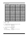
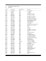
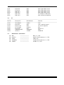
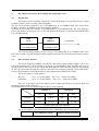
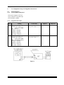
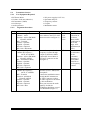
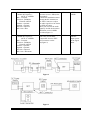
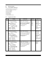
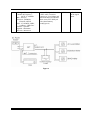
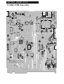
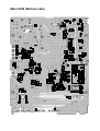
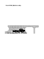
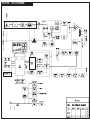
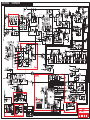
SERVICE
MANUAL
MULTI CHANNEL AM/FM TRANSCEIVER
TCB-770
TTI Tech
TABLE OF CONTENTS
SECTION
1
SPECIFICATIONS
SECTION
2
CIRCUIT DESCRIPTION
1
GENERAL
2
TECHNICAL DESCRIPTION
3
SEMICONDUCTORS AND FUNCTION
4
DESCRIPTION OF FREQUENCY DETERMINING AND STABILIZING CIRCUIT
5
TEST EQUIPMENT SETUP AND ALIGNMENT INSTRUCTIONS
SECTION
3
PART LIST
SECTION
4
MECHANICAL DISASSEMBLY
SECTION
5
BOARD LAYOUT
5-1
MAIN PCB
5-2
FRONT PCB
5-3
LED PCB
5-4
VOLUME PCB
5-5
MIC PCB
SECTION
6
BLOCK DIAGRAM
SECTION
7
SCHEMATIC
SECTION1
SPECIFICATIONS
Channel
Frequency Range
Operating mode
Frequency Control
Frequency Tolerance
Operating Temperature Range
Microphone
Input Voltage
Size
Weight
Antenna Connector
Power Output
Modulation
40 (See the frequency band chart)
26.96 MHz ~ 27.99125 MHz
F3E (FM), A3E (AM)
G
PLL Synthersizer
E
0.002%
N
E
-10 to + 55 C
R
Plug-in Type
A
13.2V DC ± 15%
L
140 (W) x 186 (L) x 37 (H)
990 g
Antenna Connector
T
Duty cycle 10% 4 Watts @13.8V DC
R
AM:from 85% to 95%
A
N
FM:1.8KHz ± 0.2KHz
S
M Frequency Response 300Hz to 3000Hz
I
50ohms, Unbalanced
T Output Impedance
T Harmonic Suppression More than -36dBm
E
AM Full Mod. 1.6A Max.
R Current Drain
Receiving System
Dual conversion superheterodyne
IF Frequencies
Double Conversion 1st 10.695MHz/2nd 455KHz
Sensitivity
0.7 V for 10dB(S+N)/N in AM Mode
R
0.5 V for 20dB SINAD in FM Mode
E
C Audio Output Power 2.0W @ 8 Ohm
Less then 8% @ 1KHz
E Audio Distortion
I Image Rejection
60 dB
V Adjacent Channel Rejection 60 dB
E
R Conducted Spurious More than 60 dB
Frequency Response 300 to 2500Hz
Built-in Speaker
8 Ohms, round
Squelch
Adjustable; Threshold less than 1 microvolt
* Specification is subject to change without prior notice.
SECTION2
CIRCUIT DESCRIPTION
------------ Contents -------------
1
1-1.
1.2.
2.
2-1.
2-2.
2-3.
2-4.
2-5.
2-6.
3.
4.
4-1.
4-2.
4-3.
4-3-1.
4-3-2.
4-3-3.
4-3-4.
4-3-5
4-3-6.
4-3-7.
4-3-8.
4-3-9.
4-4.
4-5.
4-5-1.
4-5-2.
5.
5-1.
5-2.
5-3.
General
Receiver
Transmitter
Technical Description
General
Type of emission
Frequency Table
RF Power Output
DC input Voltage and Current with 13.2V DC Input to Power AMP
Receiver IF and Local Oscillator Frequencies
Semiconductors and Function
Description of Frequency Determining and Stabilizing Circuit
Introduction
Basic Synthesis Scheme
Descriptions of Each Block
Introduction
Reference Frequency
VCO
Programmable Divider and its Control
Phase Detector and VCO Control
Transmitter / Receiver Buffer AMP
Transmitter Doublers
Switching of Turning Capacitor in VCO
Receiver Local Oscillator Outputs
Frequency Stability
Description of other Circuits
Transmitter
Receiver
Test Equipment Setup and Alignment Instructions
General Section
Transmitter Section
Receiver Section
1.
General
1-1.
Receiver
Display : 40 Channels and other functions indication
Frequency Range : 26.965 to 27.405 [MHz]
Frequency Response : 300 to 2,500 [Hz]
Power Source : 13.2 [V] DC
Audio Output Load : 8 [OHM]
Audio Output : 4.0 [W] (or More)
Squelch : Adjustable from 0.3[uV] to 100 [uV]
Sensitivity :
- FM : 20 dB [SINAD] under 1.0 [uV] RF Signal or less
- AM :10 dB [S/N] under 1.0 [uV] RF Signal or less
Intermediate Frequency :
- 1st IF : 10.695 [MHz]
- 2nd IF : 455 [KHz]
①
②
③
④
⑤
⑥
⑦
⑧
⑨
1-2.
Transmitter
① Carrier Power(Conducted) : AM 1 [W] / FM 4 [W]
② Current Drain ( 13.2 [V] Supply Voltage)
- No Modulation : 1,000 [mA]
- Max Modulation : 1,400 [mA]
③ Modulation Capabilities
- AM : ± 90 [%]
- FM : ± 1.8 [KHz/Dev]
④ Spurious Radiation : Less then 72 [dBc]
⑤ Antenna Impedance : 50 [OHM]
⑥ Frequency Tolerance : 0.002 [%]
2.
Technical Description
2-1.
General
Model CB-770 is an mobile type AM/FM radio transceiver for use of the Citizen Radio Service.
2-2.
z
Front Panel Controls
① LCD (Cannel and RX/TX Signal Level Indicator).
② Receiver Audio Control (With Power ON/OFF Control) Volume
③ Squelch Control Volume
④ RF Gain Control Volume
⑤ MIC GAIN Control Volume
⑥ CHANNEL UP/DOWN Rotary Switch
⑦ EMG(Emergency Channel Select) Key
⑧ AM/FM Select Key
⑨ Scan Key
⑩ Q.CHANNEL UP Key
⑪ Q.CHANNEL DOWN Key
z
Accessorily Connectors
① Antenna Socket
② External Speaker Jack
③ External Signal Meter Jack
④ Microphone(Condenser Microphone)
Type of emission : AM(A3E) , FM(F3E)
2-3.
Frequency Table
2-4.
z
z
2-5.
z
z
2-6.
z
z
z
z
Channel
Frequency (MHz)
Channel
Frequency (MHz)
1
26.965
21
27.215
2
26.975
22
27.225
3
26.985
23
27.235
4
27.005
24
27.245
5
27.015
25
27.255
6
27.025
26
27.265
7
27.035
27
27.275
8
27.055
28
27.285
9
27.065
29
27.295
10
27.075
30
27.305
11
27.085
31
27.315
12
27.105
32
27.325
13
27.115
33
27.335
14
27.125
34
27.345
15
27.135
35
27.355
16
27.155
36
27.365
17
27.165
37
27.375
18
27.175
38
27.385
19
27.185
39
27.395
20
27.205
40
27.405
RF Power Output
AM
: 1.0 [W]
FM
: 4.0 [W]
DC Iinput Voltage and Current with 13.2V DC Input to Power AMP
Transmitter Power Amp : Voltage 12.5 V
Current 727 mA
Transmitter Driver Amp : Voltage 12.5 V
Current 120 mA
Receiver IF and Local Oscillator Frequencies
First IF
: 10.695 [MHz]
Second IF
: 455 [KHz]
First Local Oscillator
: 10.695 [MHz] Below Receiving Frequency
Second Local Oscillation : 10.240 [MHz]
3.
3-1.
Semiconductors and Function
Transistor
--------------------------------------------------------------------------------------------------------------------------------------------
Ref No.
Description
Manufacturer
Function
--------------------------------------------------------------------------------------------------------------------------------------------
Q101
Q102
Q103
Q104
Q105
Q121
Q122
Q151
Q152
Q153
Q154
Q161
Q162
Q163
Q164
Q181
Q182
Q183
Q201
Q202
Q233
Q234
Q301
Q302
Q303
Q305
Q311
Q312
Q313
Q502
Q701
Q702
Q703
Q704
Q742
Q801
Q802
Q803
Q911
Q912
Q913
Q914
Q921
Q923
Q924
Q931
Q941
KTC3880S
KTK211
KTK211
KRC101S
KRC101S
KRC110S
KRC112S
KTC3875S
KRC112S
KRC101S
KRC112S
KTC3880S
KTC3880S
KRA102S
KTA1504S
KTC3875S
KTC3875S
KTC3875S
KRC101S
KRC111S
KTA1504S
KTC3875S
KTC3880S
KTC3880S
KTC3880S
KRC101S
KRC101S
KRC101S
KRC101S
KRC111S
KTC3880S
KTC3880S
KTC1006
2SC2078
KTC3875S
KRC104S
KRC101S
KRA101S
KTA1658
KRA1504S
KRC112S
KRC102S
KTC3875S
KTC3875S
KRA1504S
KTC3875S
KRC111S
KEC
KEC
KEC
KEC
KEC
KEC
KEC
KEC
KEC
KEC
KEC
KEC
KEC
KEC
KEC
KEC
KEC
KEC
KEC
KEC
KEC
KEC
KEC
KEC
KEC
KEC
KEC
KEC
KEC
KEC
KEC
KEC
KEC
SANYO
KEC
KEC
KEC
KEC
KEC
KEC
KEC
KEC
KEC
KEC
KEC
KEC
KEC
RX Amplifier
1’st Mixer
1’st Mixer
RX Band1 Switching
RX Band2 Switching
RX RSSI Level Control
RX FM AF Amplifier
FM AF Mute at AM Mode
FM AF Mute at AM Mode
RX AF Mute at TX Mode
AM IF Amplifier
AM IF Amplifier
RX AM B+
Automatic Noise Level Control
RX RF Mute at TX Mode
AGC
AGC
AF Mute
AF Path
Automatic Level Control
Automatic Level Control
VCO
RX/TX VCO Buffer
VCO Buffer
TX VCO Control
VCO Band1 Switching
VCO Band2 Switching
VCO Band3 Switching
FM TX AF Mute at AM TX
TX Doublers
TX Pre-Amplifier
TX Driver Amplifier
TX Power Amplifier
TX RF Mute at RX Mode
CPU Reset
CPU RX/TX Control
MIC Lock Control
Main Regulator
Main Regulator
Main Regulator Control
Power Low Control
8.2V Regulator
RX B+
TX B+
Main Regulator[5.6V]
Mute
Q951
Q952
Q953
Q954
Q961
Q962
3-2.
KTA1241
KTA1241
KRC101S
KRC101S
KRC110S
KRC111S
KEC
KEC
KEC
KEC
KEC
KEC
Back Light LED Control
Back Light LED Control
Back Light LED Control
Back Light LED Control
TX AF Mute at RX Mode
MIC AF Path at AM Mode
IC
--------------------------------------------------------------------------------------------------------------------------------------------
Ref No.
Description
Manufacturer
Function
--------------------------------------------------------------------------------------------------------------------------------------------
IC101
IC102
IC201
IC301
IC401
IC801
IC802
3-3.
TK144889V
KIA358F
KIA7217AP
LC7152NM
KIA4558F
TMP87PP21DF
24WC02
TOKO
KEC
KEC
SANYO
KEC
TOSHIBA
ATMEL
IF IC
AGC, Squelch Control
AF Power Amplifier
PLL
FM TX AF
CPU
EEPROM
Manufacture Information
z
z
z
z
z
KEC
SANYO
TOKO
TOSHIBA
ATMEL
----------------------------------------------------------------------------------------------------------
KEC Co., LTD.
SANYO Semiconductor Co., LTD.
TOKO, Inc.
Toshiba Semiconductor. Co., LTD.
ATMEL Co., LTD
4.
Description of Frequency Determining and Stabilizing Circuit
4-1.
Introduction
The Frequencies for transmitter and receiver first local frequencies are all derived from a signal
4.5MHz crystal by means of a phase locked loop(PLL).
The first local oscillator frequencies are 16.270MHz(CH1) to 16.710MHz(CH40). The second local
frequency is fixed at 10.240MHz to generate second IF 455KHz.
Transmit, the VCO of the PLL operates 13.4825MHz(CH1) to 13.7025MHz(40CH). The VCO frequency
goes to the doublers circuit Q701, L701, L702 with doubles the frequency to generate 26.965MHz(CH1)
to 27.405MHz(40CH).
Q302
VCO
Q701
Doublers
13.4825MHz(CH1)
~
13.7025MHz(CH40)
26.965MHz(CH1)
~
27.405MHz(CH40)
To transmitter
The VCO operating frequency for the receiver is 16.27MHz(CH1) to 16.710MHz(CH40) as the
first local oscillator, injected through the buffer amplifier Q302 into the first FET balanced mixer Q102,
Q103.
4-2.
Basic Synthesis Scheme
The crystal frequency(4.5MHz) is divided by 1800 times to make 2.5KHz which is fed to one
side of the phase detector. The VCO output is divided by a programmable divider, and fed to other side of
the phase detector Pin 9, 10 of IC301. Passing the phase detector output closes the feedback loop through
an active low pass filter and using the output to control the VCO frequency through varicap diode D301.
Under locked conditions, both of phase detector input signal must be identical at 2.5KHz.
The VCO frequency is then given by ;
Receiver
Transmitter
: Fvco / N = 0.005 [MHz] OR Fvco = 0.005 X N [MHz]
: Fvco / N = 0.0025 [MHz] OR Fvco = 0.0025 X N [MHz]
Since “N” is an integer, the VCO frequency can be stepped up with in receiver mode 5KHz and
transmitter mode 2.5KHz increments.
By suitable choice of “N” the desired output frequency can be obtained.
Channel 1
Channel 40
N
Fvco
N
Fvco
Transmit
5393
13.4825
5481
13.7025
Receiver
3254
16.2700
3342
16.7100
See the [Table 1]for other Channels
The VCO frequency goes to the doublers circuit, with doubles the incoming signals.
VCO Output Frequency
Doublers Output Frequency
Transmit
------Transmit
CH 1 , 13.4825 MHz
26.965 MHz
CH 40 , 13.7025 MHz
27.405 MHz
Since all frequencies are obtained from the crystal controlled PLL oscillator, all outputs are
coherent with the crystal oscillator frequency and matching the sample percentage accuracy.
Note that the reference frequency of 5KHz(receiver) and 2.5KHz(transmitter) is obtained by
dividing the 4.5MHz by 900 times and 1800 times
See Table 1 for transmitter/receiver mode VCO frequencies.
Program Data & Frequency[Table 1]
Channel
1
2
3
4
5
6
7
8
9
10
11
12
13
14
15
16
17
18
19
20
21
22
23
24
25
26
27
28
29
30
31
32
33
34
35
36
37
38
39
40
RX
TX
Frequency
[MHz]
N
Fvco
N
Fvco
26.965
26.975
26.985
27.005
27.015
27.025
27.035
27.055
27.065
27.075
27.085
27.105
27.115
27.125
27.135
27.155
27.165
27.175
27.185
27.205
27.215
27.225
27.255
27.235
27.245
27.265
27.275
27.285
27.295
27.305
27.315
27.325
27.335
27.345
27.355
27.365
27.375
27.385
27.395
27.405
3254
3256
3258
3262
3264
3266
3268
3272
3274
3276
3278
3282
3284
3286
3288
3292
3294
3296
3298
3302
3304
3306
3312
3308
3310
3314
3316
3318
3320
3322
3324
3326
3328
3330
3332
3334
3336
3338
3340
3342
16.27
16.28
16.29
16.31
16.32
16.33
16.34
16.36
16.37
16.38
16.39
16.41
16.42
16.43
16.44
16.46
16.47
16.48
16.49
16.51
16.52
16.53
16.56
16.54
16.55
16.57
16.58
16.59
16.60
16.61
16.62
16.63
16.64
16.65
16.66
16.67
16.68
16.69
16.70
16.71
5393
5395
5397
5401
5403
5405
5407
5411
5413
5415
5417
5421
5423
5425
5427
5431
5433
5435
5437
5441
5443
5445
5451
5447
5449
5453
5455
5457
5459
5461
5463
5465
5467
5469
5471
5473
5475
5477
5479
5481
13.4825
13.4875
13.4925
13.5025
13.5075
13.5125
13.5175
13.5275
13.5325
13.5375
13.5425
13.5525
13.5575
13.5625
13.5675
13.5775
13.5825
13.5875
13.5925
13.6025
13.6075
13.6125
13.6275
13.6175
13.6225
13.6325
13.6375
13.6425
13.6475
13.6525
13.6575
13.6625
13.6675
13.6725
13.6775
13.6825
13.6875
13.6925
13.6975
13.7025
4-3.
Descriptions of Each Block
4-3-1.
Introduction
The synthesizer is implemented with the following components;
PLL IC (IC301)
X-TAL (X301)
VCO, VARICAP DIODE (D301)
IC1301 is CMOS LSI that includes most of PLL block.
The Q301, L301, C311, C312, C313, C314, variable capacitance diode D301 are clapping
oscillator circuit to operate as a VCO of the IC301. Q305 is a switching transistor to connect or
disconnect the tuning capacitor in the VCO oscillator tank circuit for transmitter or receiver.
Q302 works as a buffer amplifier for RX local frequencies (≒16MHz) and TX carrier
generating frequencies(≒13MHz)
4-3-2.
Reference Frequency
The crystal X301(4.5MHz) and other components at Pin 1 and 24 of IC301 can make a reference
frequency oscillator with internal amplifier.
4-3-3.
VCO
Q301 and surrounding parts are consisting a clapping oscillator works as a VCO of IC301. With
appropriate control voltage on D301 the VCO can be oscillate over the required range of 13.4825MHz to
16.710MHz.
4-3-4.
Programmable Divider and its Control
The programmable input for each channel are stetted by the PLL Clock(Pin 11), PLL Data(Pin
12), PLL Enable(Pin 13) of IC801. Each input signal to control the PLL IC is done with provide key input
Pin 18, 19, 25, 26, 27, 28, 29, 32, 33, 34, 35, 37. For each key input, an internal code converts EEPROM
appropriate control to the programmable divider for that channel.
Since the change transmit and receive, and additional bit is required at Pin 8 of IC801 to allow
the ROM to recognize the status TX or RX.
During transmit the push to talk switch makes Pin 8 ground with BRT(Q802), PLL IC works
under transmit status.
The programmable divider output fed to the phase detector for compare with the 2,5KHz
reference frequency IC301. See table 1 for actual input and divide ratio on all channels.
4-3-5.
Phase Detector and VCO Control
The phase detector is a digital phase comparator witch compares the phase of the reference
signal with programmable divider output square waves and develops a series of pulses whose dc level
depends on the phase error of each signal.
The phase detector pulse output is fed to an active low pass filter and RC low pass filter output
signal of IC301 is filtered and fed to varicap D301 control the VCO frequency.
4-3-6.
Transmitter / Receiver Buffer AMP
Output signal of Q301 is fed into the buffer amplifier Q302, L302 to generate TX carrier
frequency and 1’st local frequencies.
4-3-7.
Transmitter Doublers
The output signal of Q302, L302 goes to an amplifier with tuning circuit Q701, L701, L702
which doubles incoming 13MHz signals.
4-3-8.
Switching of Turning Capacitor in VCO
The VCO circuit must tune with a wide range of frequencies 13.4825MHz ~ 13.7025MHz for
transmitter and 16.27MHz ~16.71MHz for receiver.
To comply above range of VCO, the tuning capacitance should switch for transmission. The
tuning circuit consists with L301, C311, C312, C313, and C314. When the VCO is working as a receiver
Q305 becomes turn OFF. So, L301 and C311, D301 makes turning function.
When transmitting, Q305 becomes ON. S the o, L301 an parallel capacitance of C316 and C311
make turning function.
4-3-9.
Receiver Local Oscillator Outputs
z
FIRST MIXER :
The secondary output signal of L107 is injected to the sources of 1’st mixer Q102, Q103 in the
1’st IF mixer section.
z
SECOND MIXER :
The output of 10.24MHz oscillator circuit with X101 is injected into the IF IC(IC101) internally.
Incoming IF signal and 10.24MHz signal are mixed inside the IF IC to extract 2’nd IF signal 455KHz.
FM audio Signals are recovered with the way of quadrature detector.
AM signals are recovered with envelope detector.
4-4.
Frequency Stability
Let
: Fo = Crystal oscillator frequency
Fr = Phase detector reference frequency
Fvco = VCO frequency
Ft = Transmit frequency
Then
: Receiver : Fr = Fo/900
Transmitter : Fr = Fo/1800
And under locked conditions : Fr = Fvco / N
Where, “N” is the programmable divider divide ratio.
Then
: Fvco = N X Fr)
From which it can be seen, the percentage error in Ft is the same as the percentage error in Fo.
The stability of the crystal oscillator is determined primarily by the crystal itself and having lesser
deviation by the active and passive components of the oscillator. The choice of crystal and components is
such that the required frequency stability is maintained over the required voltage and temperature range.
4-5.
Description of other Circuits
4-5-1.
Transmitter
A.
RF Amplification
RF carrier frequencies are obtained at the output of doublers amplifier Q701 and turning IFT coil
L701, L702. The input of VCO frequencies 13MHz is selected at the doublers output, which creates the
necessary 27MHz. The output of doublers amplifier Q701 is fed through turning IFT coil L701, L702 to
the base of pre driver amplifier Q702. It’s output; 27MHz is coupled to RF driver amplifier Q703, a lowlevel class C power amplifier. Driver Q703 supplies the necessary power gain to operate RF final Q704 at
the maximum efficient. The output of Q704 is supplied to the antenna through L-C turning circuit.
B.
Circuit for Suppression of Spurious Radiation
The turning circuit between the output of final amplifier Q704 and antenna, 4-stage “π”
network C722, C723, C724, L711, C725, C726, L712, C729, C731, L732, C732, C733, C734, L714,
C735 serves as a spurious radiation suppressor. This network also servers to match the impedance
between TX power amplifier Q704 and the antenna.
C.
Circuits for Limiting Power
After finished all alignment, the constant voltage supply circuit limits the available power 4W or
slightly less. RV911 and corresponding three-transistor control supply voltage of RF power amplifier.
When power low switch function Q914 changed the supply voltage. Tune all the trimming parts for
maximum indication of RF power meter and adjust RV571 to make 4W indication of RF power meter.
After finishing the above adjustments check the RF power meter reading is changed 1W under “LOW”
state.
The turning is adjustment so that the actual power is from 3.8W to 4.0W. There are no other
additional controls for adjusting the TX output power.
D.
Modulation Control
Modulation of the RF is a process that begins with the audio picked up by the microphone.
<FM>
The microphone input is fed to mic audio amplifier IC401 that drives modulation vricap diode
D302 in the VCO circuit RV401 limits the incoming modulation audio levels to inhibit over modulation.
While reading the modulation factor on the modulation analyzing equipment, adjustment RV401 shall not
exceed 2.0KHz deviation.
<AM>
Modulation signals are filtered with RC network and goes to the audio power amplifier IC201 in
to make normal signal level to achieve wanted modulation. IC201 drives T201, which is a combination
AF output/modulation transformer. During transmit, one of the secondary windings of T201 is tied
between the 13.2V DC supply and the collectors of RF driver Q703 and RF power amplifier Q704. As the
audio passes through T201 it causes the collector supplies of Q703 and Q704 to vary with audio,
producing an AM signal at carrier frequency.
To avoid over modulation of the carrier, a protection of the modulating signal is fed back from
the T201 through the AMC circuit, Q233 and Q234, to control the gain of IC201 and sets the maximum
level of modulation. Form the center tab of RV231 and Q233 the feedback signal is rectified by diode
D233, filtered by C233, and supplied the Q234. The collector of Q234 is tied directly TX audio input to
control gain. That is, when the audio output is higher that the preset level of RV231, the information is
reflected through Q233 and Q234, reducing the gain of IC201
4-5-2.
Receiver
Overload protection is provided to receiver’s semiconductors by diode D101. These diodes have
a little effect on the incoming signal from another CB station; they protect the receiver from stray
transmitter energy.
In the receiver mode of operation, Q923 transistor is turned on. Also bias voltage is applied to
Q101, Q102, Q103, Q106.
Q101 is a 27MHz RF input amplifier, and any excessive input signal is limited by diode D101.
CB receiver is dual conversion super-heterodyne type with the first IF 10.695MHz and the
second IF 455KHz.
Receiver is separated to blocks, 1’st IF section and 2’nd IF section. The PLL synthesizer
supplies 1’st local frequency 16.270MHz ~ 16.710MHz. The amplified 27MHz is mixed. With the
provide 1’st local frequencies Q102, Q103 mixes the incoming RF signal to generate 1’st IF signal. The
resulting first IF is 10.695MHz. Q102 and Q103 is the first converter, and 10.695MHz is sharply filtered
by L108 and crystal filter CF101. The first IF is again mixed with a second local oscillator of 10.24MHz.
With the 10.240MHz signal, IC101 FM IF IC converts the incoming signals to generate 2’nd IF
signal and recovered audio signals. 2’nd IF is filtered by a razor sharp ceramic filter CF101 coupled. The
455KHz signal from the 2’nd IF filter was amplified and limits internally. After amplification the signals
fed to the quardrature detector loop L109. Then could see the recovered signals Pin 11 of IC101.
With the amplitude of recovered signals, Q151 serves as an amplifier.
AM signals from the Pin 6 of IC101 were tapped with C161 and amplified two-stage amplifier
Q161, Q162. Q161 is a first 455KHz amplifier, and the Q161 being the last amplifier. D106 is a detector
diode witch produce audio signal as well as negative DC voltage for AGC action. The negative voltage
also provides forward biasing to the emitter of ANL clipping transistor Q164. The biasing voltage has a
time constant determined R174 and C176. Therefore any sharp negative going pulse from D161 will back
bias Q164 and clipped. The way to recover the AM information audio is envelope detector.
5.
Test Equipment Setup and Alignment Instructions
5-1
5-1-1
General Section
Test Equipment Required
• DC power supply(13.2V/3A)
• DC Voltmeter or Oscilloscope
• RF attenuator (30dB)
5-1-2
Step
Alignment Procedure
Setting
Connection
Adjuster
Adjust for
1
RX VCO voltage Adj.
Channel & Frequency :
1CH, 26.956 MHz
Mic : Receive
Volume : Optional
Squelch : Optional
RF Gain : Optional
Mic Gain : Optional
DC voltmeter to VCO
Test point (Figure 1)
L301
1.5~2.0 V DC
2
TX VCO voltage Adj.
Channel & Frequency :
1CH, 26.956 MHz
Mic : Transmit(No Mod)
Volume : Optional
Squelch : Optional
RF Gain : Optional
Mic Gain : Optional
DC voltmeter to VCO
Test point (Figure 1)
L301
1.5~2.0 V DC
Figure 1
5-2
5-2-1
Transmitter Section
Test Equipment Required
• RF Power Meter
• 50 ohms load (non-inductive)
• RF attenuator (30dB)
• Oscilloscope
• Audio generator
5-2-2
Alignment Procedure
Step
Setting
• DC power supply(13.2V/3A)
• Spectrum analyzer
• Frequency counter
• Coupler
• Modulation meter
Connection
Adjuster
Adjust for
1
RF Power Adj.
Channel : 19CH
Function : AM or FM Mode
CB/ANL Off/DX
MIC : Transmit
Volume : Optional
Squelch : Optional
RF Gain : Optional
MIC Gain : Minimum
Connect dummy load and RF
Power Meter to the EXT–ANT
connector on the set(Figure 3)
L302
L701
L702
L703
Maximum
indication on
the Power
Meter(4.0W).
If indication is
not in 4W
range, ACP
Adjustment(R
V911)
2
Frequency Adj.
Channel & Frequency :
19CH, 26.956 MHz
Function : AM or FM Mode
CB/ANL Off/DX
Mic : Transmit(No Mod)
Volume : Optional
Squelch : Optional
RF Gain : Optional
MIC Gain : Optional
AM Modulation Adj.
Channel & Frequency :
19CH, 27.185MHz
MIC: Transmit
Function : AM Mode
CB/ANL Off/DX
Volume : Optional
Squelch : Optional
RF Gain : Optional
MIC Gain : Max
Connect dummy load and
Frequency Counter through
Coupler to RF Power Meter.
Connect RF Power Meter to
EXT-ANT connector on the
set(Figure 2).
CT302
Be sure that
the indication
of the
transmitter
frequency is
27.185MHz
±300 Hz on
the Frequency
Counter
Connection the audio
generator (set to 1 KHz)to the
microphone.
Connect the modulation meter
through the RF attenuator to
the ANT Connector. Adjust
the audio signal level to obtain
by 50% modulation.
When you increase the audio
signal by 20 dB, the
modulation should not exceed
95% Modulation(Figure 3).
RV231
85% ~ 95%
3
4
FM Deviation Adj.
Channel & Frequency :
19CH, 27.185MHz
MIC : Transmit
Function : FM Mode
CB/ANL Off/DX
Volume : Optional
Squelch : Optional
RF Gain : Optional
MIC Gain : Max
Connection the audio
generator (set to 1 KHz)to the
microphone.
Connect the modulation meter
through the RF attenuator to
the ANT Connector. Adjust
the audio signal level to obtain
by 1KHz deviation.
When you increase the audio
signal by 20 dB, the deviation
should not exceed 2.0KHz
deviation(Figure 3).
RV401
1.8KHz ~
2.0KHz
5
TX Signal Meter Adj.
Channel & Frequency :
19CH, 27.185MHz
MIC : Transmit
Function : FM Mode
CB/ANL Off/DX
Volume : Optional
Squelch : Optional
RF Gain : Optional
MIC Gain : Minimum
Connected through Dummy
load to RF Power Meter.
Connect RF Power to EXTANT connector on the
set(Figure 2)
RV571
Adjust for 4
watts RF
output power
on the signal
meter.
Figure 2
Figure 3
5-3
5-3-1
Receiver Section
Test Equipment Required
• Standard Signal Generator(SSG)
• DC power supply(13.8V/3A)
• AC Level Meter
• Distortion Meter
• Oscilloscope
• SINAD Meter
• 8 ohm Dummy Load
5-3-2
Step
Alignment Procedure
Setting
Connection
Adjuster
Adjust for
1
AM Sensitivity Adj.
Channel & Frequency :
19CH, 27.185MHz
MIC : Receive
Function : AM Mode
CB/ANL Off/DX
SSG : 27.185MHz, 1KHz,
-67dBm, 30% Mod.
Volume : Optional
Squelch : Minimum
RF Gain : Maximum
Connect RF Signal Generator
to EXT-ANT Connector.
Connect AC Level Meter and
Distortion Meter and SINAD
Meter across EXT SPK jack
with 8 ohm Dummy
Load(Figure 4)
L101
L103
L104
L105
L107
L108
L112
Audio
Maximum,
Distortion
Minimum.
Reduce output
from SSG
until the audio
output
becomes about
10dB S/N
2
FM Sensitivity Adj.
Channel & Frequency :
19CH, 27.185MHz
MIC : Receive
Function : FM Mode
CB/ANL Off/DX
SSG : 27.185MHz, 1KHz,
-67dBm, 1.5KHz Dev.
Volume : Optional
Squelch : Minimum
RF Gain : Maximum
Squelch Adj.
Channel & Frequency :
19CH, 27.185MHz
MIC : Receive
Function : FM Mode
CB/ANL Off/DX
SSG : 27.185MHz, 1KHz,
-67dBm, 1.5KHz Dev.
Volume : Optional
Squelch : Maximum
RF Gain : Maximum
Connect RF Signal Generator
to EXT-ANT Connector.
Connect AC Level Meter and
Distortion Meter and SINAD
Meter across EXT SPK jack
with 8 ohm Dummy
Load(Figure 4)
L109
Audio
Maximum,
Distortion
Minimum.
Reduce output
from SSG
until the audio
output
becomes about
20dB SINAD
Connect RF Signal Generator
to EXT-ANT Connector.
Connect AC Level Meter and
Distortion Meter and SINAD
Meter across EXT SPK jack
with 8 ohm Dummy
Load(Figure 5)
RV131
Adjust until
the audio
output
appears.
3
4
RX Signal Meter Adj.
Channel & Frequency :
19CH, 27.185MHz
MIC : Receive
Function : FM Mode
CB/ANL Off/DX
SSG : 27.185MHz, 1KHz,
-62dBm, 1.5KHz Dev.
Volume : Optional
Squelch : Maximum
RF Gain : Maximum
Connect RF Signal Generator
to EXT-ANT Connector.
Connect AC Level Meter and
Distortion Meter and SINAD
Meter across EXT SPK jack
with 8 ohm Dummy
Load(Figure 4)
Figure 4
RV572
Adjust for S-9
on the signal
meter.
SECTION3
PART LIST
NAME & DESCRIPTION
ITEM
VENDOE CODE
MAKER
VENDOR
ASS'Y
Q'ty
Location NO
REMARKS
* ELECT Parts
1
COVER ASS'Y
SPEAKER
66mm
66AR000-8P-4K11
ASAHI
ASAHI
MAN
1
SPK201
2
WIRE HARNESS
PH-2PIN TO OPEN
UL1007 #26 L=200mm
FINE
FINE
MAN
1
J204
3
ESCUTCHEON ASS'Y
PCB VOLUME
1LAYER
MAN
1
4
VR
B10K/A10K
SJ093D 15H 10F B10K+SA10K SEJIN
SEJIN
MAN
1
VR101
5
VR
B50K/B50K
SJ093D 15H 10F B50K/B50K
SEJIN
MAN
1
VR102
6
FILM RESISTOR
10K
1/8W 5% ST
MAN
1
R400
7
SW ROTARY
1
SW811
8
COIL AXIAL
6.8UH
LAL03TB6R8K
9
WAFER
16PIN
10
WIRE HARNESS
11
WIRE HARNESS
12
CAPITAL
SJ-PS2101 20SK
SEJIN
SEJIN
SEJIN
MAN
MAN
4
L501, L502, L504, L506
PH-16A 180C
FINE
FINE
MAN
1
J101
PH-16PIN*2
UL1007 #26 L=50MM
FINE
FINE
MAN
1
J101 --- J102
PH-6PIN TO OPEN
UL1007 #26 L=70MM
FINE
FINE
MAN
1
J502
CONNECTOR SOCKET
N-16-6(RPCB)-M
SAMWOO
MAN
1
J501
13
HEAT SINK TUBE
diameter 4 mm x 15mm
MAN
6
14
LCD PCB ASS'Y
PCB LED
1 LAYER
CAPITAL
MAN
1
15
PCB DISPLAY
FR-4 / R-1
CAPITAL
MAN
1
16
CHIP RESISTOR
1K
PHILIPS
SMD
1
R810
17
CHIP RESISTOR
10K
1/16W 5% T 1608
PHILIPS
SMD
5
R805, R806, R807, R811, R814
18
CHIP RESISTOR
100K
1/16W 5% T 1608
PHILIPS
SMD
1
R804
19
20
21
CHIP RESISTOR
CHIP RESISTOR
CHIP RESISTOR
1M
2.2K
220K
1/16W 5% T 1608
1/16W 5% T 1608
1/16W 5% T 1608
PHILIPS
PHILIPS
PHILIPS
SMD
SMD
SMD
1
5
1
R803
R832, R833, R834, R835, R836
R808
22
CHIP RESISTOR
47K
1/16W 5% T 1608
PHILIPS
SMD
11
R812, R816, R831, R851, R852,
R853, R854, R857, R859, R862,
R864
23
24
CHIP CERAMIC
CHIP CERAMIC
0.01UF
1UF
1608
1608
PHILIPS
PHILIPS
SMD
SMD
2
1
C806, C807
C805
25
CHIP CERAMIC
68PF
1608
PHILIPS
SMD
2
C801, C802
26
CHIP TANTAL
10uF/16V
A TYPE
SMD
1
C811
27
28
29
CHIP TRANSISTOR
CHIP TRANSISTOR
CHIP TRANSISTOR
KRA101S
KRC101S
KRC104S
SOT-23
SOT-23
SOT-23
KEC
KEC
KEC
SMD
SMD
SMD
1
1
1
Q803
Q802
Q801
30
LED BACK LIGHT
CHIP LED
IWS-164-BXWF
ITSWELL
SMD
8
31
32
33
IC EEPROM
IC CPU
LCD DISPLAY
AT24C02 (SOP-8)
TMP87PP21DF
SDM8A2299A
FOR TCB-770
ATMEL
TOSHIBA
SANTECH
SMD
SMD
MAN
1
1
1
34
SW TACT
SKTS-1102A
35
RESONATOR
4.0MHz
1/16W 5% T 1608
ZTA4.00MG
ECO050321-01
ECO050809-01
D953, D954, D955, D957, D958,
D959, D965, D966
IC802
IC801
LCD801
SEKWANG
SEKWANG
MAN
5
SW801, SW802, SW806, SW807,
SW808
D.TRON
D.TRON
MAN
1
X801
ECO050325-04
ECO050511-02
NAME & DESCRIPTION
ITEM
VENDOE CODE
MAKER
VENDOR
ASS'Y
Q'ty
Location NO
36
MAIN BODY ASS'Y
CONNECTOR
CH-239(A)-M
SAMWOO
MAN
1
J701
37
TRANSISTOR
KTA1658
KEC
MAN
1
Q911
38
TRANSISTOR
2SC2078
SANYO
39
IC
KIA7217AP
KEC
40
POWER CODE
41
MAIN PCB AUTO ASS'Y
PCB MAIN
FR-4 / R-1
42
CHIP RESISTOR
43
YANG WON
FINE
MAN
1
Q704
MAN
1
IC201
MAN
1
J900
REMARKS
ECO050511-02
2PIN PLUG ASS'Y
FINE
CAPITAL
SMD
1
0
1/16W 5% T 1608
PHILIPS
SMD
3
R108, R137, R201
CHIP RESISTOR
1
1/16W 5% T 1608
PHILIPS
SMD
1
R706
44
CHIP RESISTOR
10
1/16W 5% T 1608
PHILIPS
SMD
2
R133, R301
45
CHIP RESISTOR
100
1/16W 5% T 1608
PHILIPS
SMD
6
R104, R109, R134, R168, R314,
R401
ECO050412-01
ECO050418-03
ECO050715-02
ECO050809-01
46
CHIP RESISTOR
1K
1/16W 5% T 1608
PHILIPS
SMD
19
R126, R164, R182, R183, R187,
R200, R222, R234, R238, R308,
R312, R410, R501, R571, R572,
R955, R956, R957, R958
47
CHIP RESISTOR
10K
1/16W 5% T 1608
PHILIPS
SMD
16
R123, R157, R161, R185, R315,
R321, R322, R323, R324, R412,
R413, R414, R703, R821, R823,
R914
48
CHIP RESISTOR
100K
1/16W 5% T 1608
PHILIPS
SMD
9
R140, R142, R159, R186, R188,
R202, R233, R309, R311
49
CHIP RESISTOR
2M
1/16W 5% T 1608
PHILIPS
SMD
1
R405
50
CHIP RESISTOR
1.5K
1/16W 5% T 1608
PHILIPS
SMD
2
R742, R924
51
CHIP RESISTOR
15K
1/16W 5% T 1608
PHILIPS
SMD
3
R155, R166, R235
52
53
53
54
CHIP RESISTOR
CHIP RESISTOR
CHIP RESISTOR
CHIP RESISTOR
150K
2.2
22
220
1/16W 5% T 1608
1/16W 5% T 1608
1/16W 5% T 1608
1/16W 5% T 1608
PHILIPS
PHILIPS
PHILIPS
PHILIPS
SMD
SMD
SMD
SMD
1
1
1
2
R701
R711
R204
R169, R702
55
CHIP RESISTOR
2.2K
1/16W 5% T 1608
PHILIPS
SMD
12
R131, R203, R237, R307, R402,
R817, R822, R912, R922, R923,
R961, R01
56
CHIP RESISTOR
22K
1/16W 5% T 1608
PHILIPS
SMD
6
R132, R162, R175, R302, R304,
R305
57
CHIP RESISTOR
220K
1/16W 5% T 1608
PHILIPS
SMD
2
R171, R177
58
CHIP RESISTOR
2.2M
1/16W 5% T 1608
SMD
1
R153
59
CHIP RESISTOR
2.7K
1/16W 5% T 1608
PHILIPS
SMD
1
R167
60
CHIP RESISTOR
27K
1/16W 5% T 1608
PHILIPS
SMD
2
R102, R403
61
CHIP RESISTOR
33K
1/16W 5% T 1608
PHILIPS
SMD
3
R172, R404, R407
62
CHIP RESISTOR
3.3M
1/16W 5% T 1608
PHILIPS
SMD
1
R135
63
64
CHIP RESISTOR
CHIP RESISTOR
390
39K
1/16W 5% T 1608
1/16W 5% T 1608
PHILIPS
PHILIPS
SMD
SMD
1
2
R156
R163, R306
ECO050412-01
ECO050422-02
ECO050715-02
ECO050422-02
ECO050412-01
NAME & DESCRIPTION
ITEM
VENDOE CODE
MAKER
VENDOR
ASS'Y
Q'ty
Location NO
REMARKS
65
CHIP RESISTOR
47
1/16W 5% T 1608
PHILIPS
SMD
3
66
CHIP RESISTOR
470
1/16W 5% T 1608
PHILIPS
SMD
7
67
CHIP RESISTOR
4.7K
1/16W 5% T 1608
PHILIPS
SMD
6
R138, R223, R406, R704, R915,
R916, R962
ECO050412-01
ECO050418-03
68
CHIP RESISTOR
47K
1/16W 5% T 1608
PHILIPS
SMD
9
R122, R139, R174, R176, R300,
R303, R409, R411, R415
ECO050715-02
ECO050812-02
69
CHIP RESISTOR
470K
1/16W 5% T 1608
PHILIPS
SMD
2
R154, R573
70
CHIP RESISTOR
5.6K
1/16W 5% T 1608
PHILIPS
SMD
1
R408
71
CHIP RESISTOR
56K
1/16W 5% T 1608
PHILIPS
SMD
2
R103, R313
72
CHIP RESISTOR
6.8K
1/16W 5% T 1608
PHILIPS
SMD
1
R152
73
CHIP RESISTOR
68K
1/16W 5% T 1608
PHILIPS
SMD
1
R189
74
CHIP RESISTOR
82K
1/16W 5% T 1608
PHILIPS
SMD
1
R173
75
76
77
THERMISTOR
THERMISTOR
CHIP CERAMIC
100 OHM
10K OHM
0.001UF
NCP18XF101J03RB
NCP18XH103J03RB
1608
MURATA
MURATA
PHILIPS/SAMSUNG
SMD
SMD
SMD
1
1
4
TH131
TH101
C181, C230, C239, C404
38
C111, C114, C115, C116, C117,
C118, C153, C154, C155, C156,
C157, C161, C162, C183, C184,
C201, C231, C234, C235, C323,
C412, C415, C501, C502, C503,
C504, C506, C703, C704, C708,
C713, C901, C902, C903, C911,
C922, C924, C932
C122, C123, C132, C134, C135,
C137, C138, C168, C169, C180,
C186, C205, C236, C308, C322,
C325, C330, C401, C402, C405,
C413, C571, C573
78
CHIP CERAMIC
0.01UF
1608
PHILIPS/SAMSUNG
SMD
R184, R705, R913
R101, R105, R106, R165, R181,
R236, R931
79
CHIP CERAMIC
0.1UF
1608
PHILIPS/SAMSUNG
SMD
23
80
81
CHIP CERAMIC
CHIP CERAMIC
1UF
0.022UF
1608
1608
PHILIPS/SAMSUNG
PHILIPS/SAMSUNG
SMD
SMD
2
5
82
CHIP CERAMIC
0.047UF
1608
PHILIPS/SAMSUNG
SMD
8
83
84
CHIP CERAMIC
CHIP CERAMIC
0.068UF
10PF
1608
1608
PHILIPS/SAMSUNG
PHILIPS/SAMSUNG
SMD
SMD
1
3
85
CHIP CERAMIC
100PF
1608
PHILIPS/SAMSUNG
SMD
12
C101, C109, C303, C304, C305,
C313, C314, C711, C712, C731,
733 , C736
86
CHIP CERAMIC
150PF
1608
PHILIPS/SAMSUNG
SMD
4
C102, C104, C106, C311
87
CHIP CERAMIC
16PF
1608
PHILIPS/SAMSUNG
SMD
1
C316
88
CHIP CERAMIC
18PF
1608
PHILIPS/SAMSUNG
SMD
4
C98, C99, C112, C119
89
90
91
CHIP CERAMIC
CHIP CERAMIC
CHIP CERAMIC
180PF
2PF
22PF
1608
1608
1608
PHILIPS/SAMSUNG
PHILIPS/SAMSUNG
PHILIPS/SAMSUNG
SMD
SMD
SMD
2
1
2
92
CHIP CERAMIC
220PF
1608
PHILIPS/SAMSUNG
SMD
6
C701, C734
C730
C312, C727
C204, C211, C329, C717, C719,
C724
93
CHIP CERAMIC
3PF
1608
PHILIPS/SAMSUNG
SMD
1
C319
94
95
CHIP CERAMIC
CHIP CERAMIC
30PF
33PF
1608
1608
PHILIPS/SAMSUNG
PHILIPS/SAMSUNG
SMD
SMD
1
3
C315
C108, C302, C318
ECO050525-02
ECO050715-02
C159, C961
C166, C203, C214, C238, C403
C152, C163, C164, C165, C212,
C310, C721, C914
C410
C96, C113, C324
ECO050812-02
NAME & DESCRIPTION
ITEM
VENDOE CODE
MAKER
VENDOR
ASS'Y
Q'ty
Location NO
96
CHIP CERAMIC
330PF
1608
PHILIPS/SAMSUNG
SMD
6
C714, C715, C723, C725, C726,
C729
97
CHIP CERAMIC
39PF
1608
PHILIPS/SAMSUNG
SMD
1
C705
98
CHIP CERAMIC
47PF
1608
PHILIPS/SAMSUNG
SMD
7
C103, C105, C107, C182, C328,
C720, C722
99
CHIP CERAMIC
REMARKS
470PF
1608
PHILIPS/SAMSUNG
SMD
1
C718
100 CHIP CERAMIC
56PF
1608
PHILIPS/SAMSUNG
SMD
1
C130
101 CHIP CERAMIC
6PF
1608
PHILIPS/SAMSUNG
SMD
2
C317, C321
102 CHIP CERAMIC
68PF
1608
PHILIPS/SAMSUNG
SMD
3
C97, C131, C732
103 CHIP CERAMIC
680PF
1608
PHILIPS/SAMSUNG
SMD
1
C414
104 CHIP CERAMIC
82PF
1608
PHILIPS/SAMSUNG
SMD
2
C406, C707
105 CHIP CERAMIC
8PF
1608
PHILIPS/SAMSUNG
SMD
1
C326
106 CHIP CERAMIC
9PF
1608
PHILIPS/SAMSUNG
SMD
1
C110
107 CHIP TANTAL
2.2uF/16V
A TYPE
SMD
1
C301
108 CHIP TRANSISTOR
KTK211
SOT-23
KEC
SMD
2
Q102, Q103
109 CHIP TRANSISTOR
KRA102S
SOT-23
KEC
SMD
1
Q163
110 CHIP TRANSISTOR
KRC101S
SOT-23
KEC
SMD
10
Q104, Q105, Q153, Q222, Q305,
Q311, Q312, Q313, Q953, Q954
111 CHIP TRANSISTOR
KRC102S
SOT-23
KEC
SMD
1
Q914
112 CHIP TRANSISTOR
KRC110S
SOT-23
KEC
SMD
3
Q121, Q960, Q961
ECO050715-02
113 CHIP TRANSISTOR
114 CHIP TRANSISTOR
115 CHIP TRANSISTOR
KRC111S
KRC112S
KTA1504S
SOT-23
SOT-23
SOT-23
KEC
KEC
KEC
SMD
SMD
SMD
3
4
4
Q202, Q502, Q962
Q122, Q152, Q154, Q913
Q164, Q233, Q912, Q924
ECO050412-01
116 CHIP TRANSISTOR
KTC3875S
SOT-23
KEC
SMD
9
Q151, Q181, Q182, Q183, Q234,
Q742, Q921, Q923, Q931
117 CHIP TRANSISTOR
KTC3880S
SOT-23
KEC
SMD
8
Q101, Q161, Q162, Q301, Q302,
Q303, Q701, Q702
118 DIODE ZENER
119 DIODE ZENER
120 DIODE ZENER
Z02W5.1V
Z02W5.6V
Z02W8.2V
SOT-23
SOT-23
SOT-23
KEC
KEC
KEC
SMD
SMD
SMD
1
1
1
DZ181
DZ931
DZ921
121 DIODE SI CHIP
KDS181
SOT-23
KEC
SMD
1
D401
122 DIODE SI CHIP
KDS184
SOT-23
KEC
SMD
13
D102, D103, D105, D171, D180,
D181, D233, D571, D572, D741,
D742, D921, D961
123 DIODE SI CHIP
KDS226
SOT-23
KEC
SMD
1
D101
124 DIODE VARICAP
KDV251S
SOT-23
KEC
SMD
2
D301, D302
125 IC PLL
LC7152NM
SANYO
SMD
1
IC301
126 IC OP AMP
KIA358F
KEC
SMD
1
IC102
127 IC OP AMP
KIA4558F
KEC
SMD
1
IC401
128 IC FM IF
TK14489V
TOKO
SMD
1
IC101
MAIN PCB MANUAL ASS'Y
129 FILM RESISTOR
2.2
1/2W 5% ST MINI
MAN
1
R712
130 FILM RESISTOR
10
1/2W 5% ST MINI
MAN
1
R921
YANG WON
ECO050418-03
ECO050412-01
ECO050412-01
NAME & DESCRIPTION
ITEM
VENDOE CODE
MAKER
VENDOR
ASS'Y
Q'ty
Location NO
131 FILM RESISTOR
470
1/2W 5% ST MINI
MAN
2
R953, R954
132 FILM RESISTOR
4.7K
1/2W 5% ST MINI
MAN
1
R713
133 FILM RESISTOR
1K
1W
134
135
136
137
138
10
100KB
2.2KB
22KB
4.7KB
2W 5% ST BULK
PH0630NOX0X-HA1-B104
PH0630NOX0X-HA1-B222
PH0630NOX0X-HA1-B223
PH0630NOX0X-HA1-B472
139 ELECT CAPACITOR
1UF
140 ELECT CAPACITOR
10UF
141 ELECT CAPACITOR
100UF
KR3-16V101MA 5X11
DONGXIANG
MAN
2
C821, C923
142 ELECT CAPACITOR
1000UF
KR1-16V102MF 10X20
DONGXIANG
MAN
4
C207, C213, C217, C912
143 ELECT CAPACITOR
0.22UF
KR1-16VR22MA 5X11
DONGXIANG
MAN
1
C124
144 ELECT CAPACITOR
2.2UF
KR1-16V2R2MA 5X11
DONGXIANG
MAN
1
C741
145 ELECT CAPACITOR
22UF
KR1-16V220MA 5X11
DONGXIANG
MAN
1
C221
146 ELECT CAPACITOR
220UF
KR1-16V221MB 6.3X20
DONGXIANG
MAN
3
C210, C953, C954
147 ELECT CAPACITOR
33UF
KR1-16V330MA 5X11
DONGXIANG
MAN
148 ELECT CAPACITOR
149 ELECT CAPACITOR
150 DISK
4.7UF
47UF
100P
KR1-16V4R7MA 5X11
KR1-16V470MA 5X11
DONGXIANG
DONGXIANG
MAN
MAN
MAN
1
3
5
1
C209
C208, C411, C960
C143, C185, C206, C233, C933
C735
METAL OXID RESISTOR
RESISTOR SEMI
RESISTOR SEMI
RESISTOR SEMI
RESISTOR SEMI
5% ST MINI
MAN
2
R951, R952
SOUNDWELL
SOUNDWELL
SOUNDWELL
SOUNDWELL
MAN
MAN
MAN
MAN
MAN
1
2
1
1
2
R208
RV571, RV572
RV231
RV401
RV131, RV911
KR1-16V010MA 5X11
DONGXIANG
MAN
3
C167, C407, C408
KR1-16V100MA 5X11
DONGXIANG
MAN
7
C232, C331, C332, C333, C913,
C921, C931
REMARKS
ECO050418-03
ECO050418-03
ECO050412-01
151 DIP TRIMMER
20PF
KCVN620
FOKITS
MAN
1
CT301
ECO050325-04
152 TRANSFORMER
CHOKE
T1
FINE
FINE
MAN
1
T901
ECO050509-02
153 TRANSFORMER
EI-24(MOD.)
T2
FINE
FINE
MAN
1
T201
ECO050509-02
154 IFT COIL RF FREE TX
27MHz
TX1
FINE
FINE
MAN
2
L701, L702
155 IFT COIL
37MHz TX
TX2
FINE
FINE
MAN
1
L703
156 IFT COIL
27MHz-B
RX1
FINE
FINE
MAN
1
L101
157 IFT COIL
27MHz RX (7RC)
RX2
FINE
FINE
MAN
1
L107
158 IFT COIL
10.7MHz RX-B
RX3
FINE
FINE
MAN
1
L108
159 IFT COIL DETECTOR
455KHz
RX4
FINE
FINE
MAN
1
L109
160 IFT COIL
455KHz-B
RX5
FINE
FINE
MAN
1
L112
161 IFT COIL
16.5MHz VCO
VCO1
FINE
FINE
MAN
1
L301
162 IFT COIL
15MHz TX/RX
VCO2
FINE
FINE
MAN
1
L302
163 COIL AXIAL
1.5UH
LAL03TR1R5K
MAN
2
L102, L106
164 COIL AXIAL
6.8UH
LAL03TB6R8K
165 COIL SPRING
2.5X0.8X7T:R
0.11UH
166 COIL SPRING
MAN
1
L706
FINE
FINE
MAN
1
L704
4X0.5X6T:R
FINE
FINE
MAN
1
L712
167 COIL SPRING
4X0.5X7T:R
FINE
FINE
MAN
1
L713
168 COIL SPRING
4X0.5X10T:R
FINE
FINE
MAN
1
L714
169 COIL SPRING
6X0.8X5T:R
0.225UH
FINE
FINE
MAN
1
L711
170 COIL SPRING
5X0.6X13.5T:R
0.5UH
FINE
FINE
MAN
1
L707
171 CORE SPRING
5.5TX0.45XM5E®X2.3 0.17UH
FINE
FINE
MAN
3
L103, L104, L105
172 COIL CHOKE
6UH
FINE
FINE
MAN
1
L201
173 TRANSISTOR
KTC1006
KEC
MAN
1
Q703
174 TRANSISTOR
KTA1241
KEC
MAN
3
Q221, Q951, Q952
175 DIODE
1N4004T/R 400V 1A
MAN
2
D232, D901
176 DIODE
1N60
177 CRYSTAL
10.240MHz
BOBBIN CORE
32PF:30PPM
HC-49/U
D.TRON
D.TRON
MAN
1
D161
MAN
1
X101
ECO050412-01
NAME & DESCRIPTION
ITEM
VENDOE CODE
178 CRYSTAL
4.50MHZ
12PF:30PPM
179 FILTER CRYSTAL
10L08A
10.695MHZ
180 FILTER CERAMIC
MAKER
HC-49U
VENDOR
ASS'Y
Q'ty
Location NO
D.TRON
D.TRON
MAN
1
X301
D.TRON
D.TRON
MAN
1
XF101
LT455HTW
D.TRON
D.TRON
MAN
1
CF101
181 JACK MINI
SKJS-206
SEKWANG
SEKWANG
MAN
1
J203
182 JACK DC
SKJS-3518
SEKWANG
SEKWANG
MAN
1
J202
183 WAFER
2PIN
PH-2A 180C
FINE
FINE
MAN
1
J205
184 WAFER
6PIN
PH-6A 180C
FINE
FINE
MAN
1
J503
185 WAFER
16PIN
PH-16A 180C
FINE
FINE
MAN
1
J102
Hankyung
1
-
Hankyung
1
-
Hankyung
3
For speaker
Hankyung
1
For speaker
49/T-3L
Mechanical PARTS
* COVER ASS'Y
1
BOTTOM COVER
2
UPPER COVER
SPC+BLACK COATING, 0.75t
SPC+BLACK, COATING, 0.75t
3
BRACKET SPK
EGI, 1.0t, COATING
4
FELT(SPK)
5
FELT(COVER)
6
SCREW Mach(+)
M3*8L-TAPTITE, BLACK, BH
same as TCB880
7
SCREW Mach(+)
M3*8L-TAPTITE, BLACK, BH
same as TCB880 / same as item 6.
8
CUSHION
same as TCB880
Φ65*0.3t, BLACK
8*133*0.3t, BLACK
20*24*4.0t, EVA SPONGE, BLACK
Hankyung
4
For bottom cover & upper coveradhesive(location: side)
Bonso
3
Bonso
6
Hankyung
1
Bracket(spk) mounting
Main body + Bottom & upper cover
mounting
For upper cover adhesive(location: center)
Bonso
1
Front case plastic
Bonso
1
-
Hankyung
1
For Bezel
Bonso
2
For Rf & On/off
Bonso
2
For Rf & On/off
same as TCB880 Vol knob
Bonso
1
For Channel
TTI
2
For Rf & On/off
ECO 050328-07
Hankyung
1
-
Hankyung
1
For diffuser
Bonso
1
Diffuser
Bonso
1
For diffuser
Hankyung
1
For diffuser
Bonso
1
-
Bonso
1
For Rf & On/off & Channel
Bonso
4
Esc+Main body mounting
2pc:illuminator mounting, 3pc:Key
PCB mounting
For window
same as TCB880
ECO 050319-02
ECO 050328-07
* ESCUTCHEON ASS'Y
9
ESCUTCHEON
10
BEZEL
ABS. BLACK
11
DOUBLE TAPE(BEZEL)
12
VOL KNOB
13
DUAL KNOB
14
CH KNOB
15
D-SPRING
16
KEY PAD
17
LCD BRACKET
18
DIFFUSER LENS
19
REFLECTOR
20
ZEBRA
21
WINDOW
22
ILLUMINATIOR
23
SCREW MACH(+)
ACRYL, CLEAR
3M, 0.16t
ECO 050402-01
ABS, BLACK
ABS, BLACK
ABS, BLACK
SK5, 0.2t, Zn plating
SILICONE, CLEAR, PU coating
SPTE, 0.3t
ACRYL, CLEAR
ACRYL, CLEAR
SILICONE
ACRYL, CLEAR
ACRYL, CLEAR
M2.6*5L, Black, FH
24
SCREW TAP(+)
25
DOUBLE TAPE(WINDOW)
26
WHITE SHEET
27
RING NUT
28
DOUBLE TAPE(BEZEL)-1
29
DOUBLE SIDE TAPE FOR DIFFUSER
same as TCB880
2.6*8L-2S, Ni plating, BH
3M, 0.16t
POLYESTER, 0.1t
BsBm
same as TCB880
23*1.1*0.16T
29*3.5*0.2T
Bonso
5
Hankyung
1
Hankyung
1
For diffuser
Hankyung
3
For channel,Rf,on/off
NEW
ECO 050731-03
Bonso
1
For Bezel
NEW
ECO 050731-03
Bonso
2
For diffuser
* MAIN BODY ASS'Y
30
MAIN BODY
31
CORD STOPPER
EGI, 1.0t
PP, BLACK
same as TCB880
32
SCREW MACH(+)
M3*10L, Black, BH
same as TCB880
ECO 050412-02
Hankyung
1
-
Hankyung
1
Wire stopper
Bonso
3
TR mounting
REMARKS
ECO050525-02
NAME & DESCRIPTION
ITEM
3*8L-TAPTITE, Black, BH
VENDOE CODE
MAKER
VENDOR
ASS'Y
Q'ty
Location NO
33
SCREW Mach(+)
34
NUT
35
SPRING WASHER
36
HEAT SINK
37
BUSH
38
ANT. TERMINAL
39
MICA
40
TX SHIELD CAN(1)
41
TX SHIELD CAN(2)
42
VCO SHIELD CAN
43
SHIELD COVER
44
Cu Tape-1
Cu 49*9*0.1t
ECO 050328-05
Bonso
1
For TX shield can(1)
45
Cu Tape-2
Cu 77*15*0.1t
ECO 050328-05 / Same as TCB880
Bonso
1
For TX shield can(1)
same as TCB880
Hankyung
Hankyung
Hankyung
Hankyung
Hankyung
Bonso
Bonso
Bonso
Bonso
FINE
1
1
2
1
2
2
3
2
3
1
Bonso
Bonso
Bonso
Bonso
Bonso
Bonso
Bonso
Bonso
Bonso
1
1
1
1
1
2
1
1
-
M3, SS41
M3
AL, 2.0t
NLLON66+GRASS 15%
SPTE, 0.2t
same as TCB880 / same as item 6.
Bonso
4
Main PCB + Main body mounting
same as TCB880
Bonso
3
TR mounting
same as TCB880
Bonso
3
TR mounting
same as TCB880
Hankyung
1
-
same as TCB880
Hankyung
1
For TR
same as TCB880
Hankyung
1
For Antenna
same as TCB880
Hankyung
1
For TR
SPTE, 0.3t
Hankyung
1
For Main PCB(location: lower)
SPTE, 0.3t
Hankyung
1
For Main PCB(location: upper)
same as TCB880
Hankyung
1
For Vco
ECO 050302-01
Hankyung
1
For TX shield can(2)
MICA 0.6t
SPTE, 0.3t
SPTE, 0.3t
* ACCESSORY
1 MIC ASS'Y
2 BRACKET SET
3 STUD BOLT ABS, M6*8L, BLACK
4 BRACKET(MIC) SUS304, 1.0t
5 PACKING RUBBER PACKING RUBBER
6 SCREW Mach(+) M3*8L, Taptite, Black, BH
7 SCREW TAP(+) 5*12L-1S, ZN PLATING, TH
8 STAR WASHER-S M3, NI PLATING, B type
9 STAR WASHER-L M5, NI PLATING, B type
10 POWER CODE
* PACKING ASS'Y
1 OWNER'S MANUAL
2 GIFTBOX SW1E 2.0T
3 INNER BOX A SW1E 2.0T, BROWN
4 INNER BOX B SW1E 2.0T, BROWN
5 WARNING LABEL
6 CODE 39 SERIAL NO. STICKER
7 OUT BOX DW1E 7.0T
8 SILICA-GEL 1g
9 OPP TAPE 50MM
same as TCB880
same as TCB880
same as TCB880
same as TCB880
same as TCB880
same as TCB880
same as TCB880
2PIN RECEPRACLE ASS'Y
REMARKS
SECTION4
MECHANICAL DISASSEMBLY
x2
x2
50
26
51
x2
27
51
47
52
46
56
49
28
45
44
55
x3
53
x3
50
51
x2
54
48
x3
52
51
x3
x2
x4
43
36
41
5
6
51
1
29
30
x2
38
x3
9
10
8
x2
11
x2
12
14
15
7
13
17
16
18
19
20
21
22
23
24
25
42
35
33
34
3
40
37
39
x3
x2
29
29
4
51
x3
31
32
2
NO
1
2
3
4
5
6
7
8
9
10
11
12
13
14
15
16
17
18
19
20
21
22
23
24
25
26
27
28
29
30
31
32
33
34
35
36
37
38
39
40
41
42
43
44
45
46
47
48
49
50
51
52
53
54
55
56
PART NAME
Upper cover
Bottom cover
Main body
Bracket(Set)
Key PCB
Main PCB
Ch knob
Vol knob
Nut for Mic connector
Washer for Mic connector
D-Spring
Dual knob
Ring nut
Bezzel
Double tape(Bezzel)
Escutcheon
Double tape(Window)
Window
illuminator
Key pad
LCD Bracket
LCD
Reflector
Diffuser Lens
Zebra
Stud bolt
Packing rubber
Ant terminal
Felt(Cover)
Cushion
TX shield can(2)
Shield cover
Speaker
Bracket(Spk)
Felt(Spk)
Mic connector
Cu tape-1
Cu tape-2
TX shield can(1)
VCO shield can
White sheet
S/W PCB
Cord stopper
Washer for Ant connector
Nut for Ant connector
Bush
TR
Heat sink
Mic connector
Screw Mach(+)
Screw Mach(+)
Screw Mach(+)
Nut
Spring washer
Screw Tap(+)
Mica
DESCRIPTION
SPC 0.75t, Black
SPC 0.75t, Black
EGI, 1.0t
SPC 1.6t, Blacke
1.6t
1.6t
ABS, Black
ABS, Black
QTY
1
1
1
1
1
1
1
2
1
1
SK5, 0.2t, Zn plating
2
ABS, Black
2
BsBm, Ni plating
3
Acryl
1
0.16t
1
ABS, Black
1
0.16t
1
Acryl
1
Acryl
1
Silicone, PU coating
1
SPTE, 0.3t
1
1
Acryl
1
Acryl
1
Silicone
1
ABS, BsBm
2
NBR
2
SPTC, 0.2t
1
0.3t
4
EVA sponge
1
SPTE, 0.3t
1
SPTE, 0.3t
1
1
EGI, 1.0t
3
Dia 65 x 0.3t
1
1
Cu, 49x9x0.1t
1
Cu, 77x15x0.1t
1
SPTE, 0.3t
1
SPTE, 0.3t
1
PE, 0.1t
1
PVC
1
1
1
1
Nylon66xGrass15%
1
2
AL
1
1
M2.6x5L, FH
4
M3x8L_Taptite, BH
13
M3x10, BH
3
M3
3
M3
3
2.6x8L, BH
3
0.4t
1
REMARK
For TR
For Escutcheon
For Speaker bracket,Main PCB,Cover
For TR
For TR
For TR
For Key PCB
SECTION5
BOARD LAYOUT
5-1 Main PCB (Top side)
Main PCB (Bottom side)
5-2 Front PCB (Top side)
Front PCB (Bottom side)
5-3 LED PCB (Top side)
LED PCB (Bottom side)
5-4 Volume PCB
5-5 MIC PCB
SECTION6
BLOCK DIAGRAM
SECTION7
SCHEMATIC