1
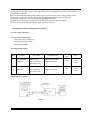
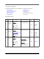
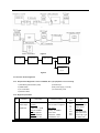
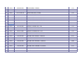
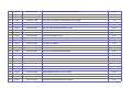
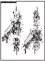
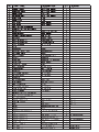
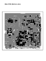
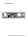
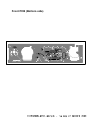
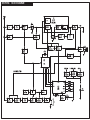
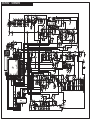
SERVICE
MANUAL
MULTI CHANNEL AM/FM TRANSCEIVER
TCB-550
TTI Tech
TABLE OF CONTENTS
SECTION
1
SPECIFICATIONS
SECTION
2
CIRCUIT DESCRIPTION
1
GENERAL
2
TECHNICAL DESCRIPTION
3
SEMICONDUCTORS AND FUNCTION
4
DESCRIPTION OF FREQUENCY DETERMINING AND STABILIZING CIRCUIT
5
TEST EQUIPMENT SETUP AND ALIGNMENT INSTRUCTIONS
SECTION
3
PART LIST
SECTION
4
MECHANICAL DISASSEMBLY
SECTION
5
BOARD LAYOUT
5-1
MAIN PCB
5-2
FRONT PCB
5-3
LED PCB
5-4
VOLUME PCB
5-5
MIC PCB
SECTION
6
BLOCK DIAGRAM
SECTION
7
SCHEMATIC
SECTION1
G
E
N
E
R
A
L
T
R
A
N
S
M
I
T
T
E
R
R
E
C
E
I
V
E
R
SPECIFICATIONS
Channel
Frequency Range
Operating mode
Frequency Control
Frequency Tolerance
Operating Temperature Range
Microphone
Input Voltage
Size
Weight
Antenna Connector
Power Output
Modulation
Frequency Response
Output Impedance
Harmonic Suppression
Current Drain
Receiving System
IF Frequencies
Sensitivity
Audio Output Power
Audio Distortion
Image Rejection
Adjacent Channel Rejection
Conducted Spurious
Frequency Response
Built-in Speaker
Squelch
40 (See the frequency band chart)
26.56 MHz ~ 28.00 MHz
F3E (FM), A3E (AM)
PLL Synthersizer
0.002%
-10 to + 55 C
Plug-in Type
13.2V DC ± 15%
124 (W) x 135 (L) x 37 (H)
655 g
Antenna Connector
Duty cycle 10% 4 Watts @13.2V DC
AM:from 85% to 95%
FM:1.8KHz ± 0.2KHz
300Hz to 3000Hz
50ohms, Unbalanced
More than -36dBm
AM Full Mod. 1.6A Max.
Dual conversion superheterodyne
Double Conversion 1st 10.695MHz/2nd 455KHz
0.7 V for 10dB(S+N)/N in AM Mode
0.5 V for 20dB SINAD in FM Mode
2.0W @ 8 Ohm
Less then 8% @ 1KHz
60 dB
60 dB
More than 60 dB
300 to 2500Hz
8 Ohms, round
Adjustable; Threshold less than 1 microvolt
* Specification is subject to change without prior notice.
SECTION2
CIRCUIT DESCRIPTION
------------ Contents -------------
1
1-1.
1.2.
2.
2-1.
2-2.
2-3.
2-4.
2-5.
2-6.
3.
4.
4-1.
4-2.
4-3.
4-3-1.
4-3-2.
4-3-3.
4-3-4.
4-3-5
4-3-6.
4-3-7.
4-3-8.
4-3-9.
4-4.
4-5.
4-5-1.
4-5-2.
5.
5-1.
5-2.
5-3.
6.
7.
8.
9.
10.
General
Receiver
Transmitter
Technical Description
General
Type of emission
Frequency Table
RF Power Output
DC input Voltage and Current with 13.2V DC Input to Power AMP
Receiver IF and Local Oscillator Frequencies
Semiconductors and Function
Description of Frequency Determining and Stabilizing Circuit
Introduction
Basic Synthesis Scheme
Descriptions of Each Block
Introduction
Reference Frequency
VCO
Programmable Divider and its Control
Phase Detector and VCO Control
Transmitter / Receiver Buffer AMP
Transmitter Doublers
Switching of Turning Capacitor in VCO
Receiver Local Oscillator Outputs
Frequency Stability
Description of other Circuits
Transmitter
Receiver
Test Equipment Setup and Alignment Instructions
VCO Section
Transmitter Section
Receiver Section
Test Data
Schematic Diagram
Block Diagram
PCB Map
PARTS LIST
1.
General
1-1.
Receiver
Display : 40 Channels and other functions indication
Frequency Range : 26.965 to 27.405 [MHz]
Frequency Response : 300 to 2,500 [Hz]
Power Source : 13.2 [V] DC
Audio Output Load : 8 [OHM] Resistive
Audio Output : 4.0 [W] (or More)
Squelch : Adjustable from 0.2[uV] to 1 [mV]
Sensitivity :
- FM : 20 dB [SINAD] under 1.0 [uV] or less
- AM :10 dB [S/N] under 1.0 [uV] or less
Intermediate Frequency :
- 1st IF : 10.695 [MHz]
- 2nd IF : 455 [KHz]
1-2.
Transmitter
Carrier Power(Conducted) : AM 1 [W] / FM 4.0 [W]
Current Drain ( 13.2 [V] Supply Voltage)
- No Modulation : 1,100 [mA] (No Modulation)
- Max Modulation : 1,400 [mA] (Full Modulation)
Modulation Capabilities
- AM : +/- 90 [%]
- FM : +/- 1.8 [KHz/Dev]
Spurious Radiation : Less then -74 [dBc]
Antenna Impedance : 50 [OHM]
Frequency Tolerance : 0.002 [%]
2.
2-1.
Technical Description
General
Model CB-550 is an mobile type AM/FM radio transceiver for use of the Citizen Radio Service.
Front Panel Controls
LCD Display(Cannel ,RX,TX,AQ,SCAN,AM,FM,EMG Indicator).
Receiver Audio Control (With Power ON/OFF Control) Volume
Squelch Control Volume (S/W ON : TIGHT, S/W OFF : AUTO SQ)
RF Gain Control Volume
CHANNEL UP/DOWN TACT SWITCH.
AM/FM TACT SWITCH
EMG TACT SWITCH
Accessable Connectors
Antenna Jack
External Speaker Jack
External Power Cord
Microphone Jack.
2-2.
Type of emission : AM(A3E) , FM(F3E)
2-3.
Frequency Range : 26.965 MHz (CH.1) - 27.405 MHz (CH.40)
2-4.
RF Power Output : AM/FM 4.0 Watts
2-5.
DC Input Voltage and Current With 13.2V DC Input to Power AMP
Transmitter Power AMP ----------- VOLTAGE 12.5 V
Current 820mA
Transmitter DRIVER AMP --------VOLTAGE 12.5 V
Current 130mA
2-6.
RECEIVER IF AND LOCAL OSCILLATOR FREQUENCIES.
FIRST IF -------------------------------- 10.695 MHz
SECOND IF ---------------------------- 455 KHz
FIRST LOCAL OSCILLATOR------- 10.965 MHz Below RECEIVING FREQUENCY
SECOND LOCAL OSCILLATOR--- 10.240 MHz
2-3. SEMICONDUCTORS AND FUNCTION
REF.NO
DESCRIPTION
RX
TX
REMARK
QR1
KTC4080E
RF AMP
X
KEC
QR2
KTC4080E
1'st MIXER
X
KEC
QR3
KTC4080E
1'st MIXER
X
KEC
QR4
KTC4075E
RF ATTENUATOR
RF ATTENUATOR
KEC
QR5
KTC4080E
IF AMP
X
KEC
QR6
KTC4080E
IF AMP
X
KEC
QR7
KRA2014E
A.N.L.
X
KEC
QQ1
KRC410E
SQ MUTE
X
KEC
QQ2
KTC4075E
RF ARRENUATOR
RF ATTENUATOR
KEC
QQ4
KRC402E
AUTO SQ S/W
X
KEC
QAS1
KRC410E
FM MUTE
X
KEC
QAS2
KRA305E
AM B+
X
KEC
QAS3
KRC402E
AM B+ CONTROL
X
KEC
QAS4
KRC410E
X
AM AUDIO PATH
KEC
QFS1
KRC402E
X
FM AUDIO S/W
KEC
QFS2
KRC410E
POP MUTE
X
KEC
QUS1
KRC404E
SQ CONTROL
X
KEC
QRS1
KTC4075E
RX B+
X
KEC
QTS1
KTA2014E
X
TX B+
KEC
QG1
KTA1658
X
TX POWER REGULATOR
KEC
QG2
KTA2014E
X
TX POWER REGULATOR
KEC
QG3
KRC401E
X
TX POWER REGULATOR
KEC
QG4
KTC3875S
MAIN REGULATOR
MAIN REGULATOR
KEC
QG5
KTC3875S
CPU REGULATOR
CPU REGULATOR
KEC
QHL1
KRC402E
X
POWER HI/LOW S/W
KEC
QV1
KTC4080E
VCO
VCO
KEC
QW1
KTC4080E
X
BUFFER
KEC
QW2
KTC4080E
X
DOUBLER
KEC
QN1
KRC401E
X
TX ENABLE
KEC
QN2
KRA305E
X
TX ENABLE B+
KEC
QT2
KTC4080
X
BUFFER
KEC
QT3
2SC2314
X
DRIVER
SANYO
QT4
2SC2078
X
POWER AMP
SANYO
Q1
KRA226S
LCD BACK LIT
LCD BACK LIT
KEC
Q2
KRC401E
LCD BACK LIT
LCD BACK LIT
KEC
Q3
KRC404E
CPU RESET
CPU RESET
KEC
IC1
DBL5019
FM 1F
X
AUK
IC2
KIA358F
SQ CONTROL
X
KEC
IC3
TDA2003
X
TX AM AUDIO AMP
SGS
IC4
24WCO2J
EEPROM
EEPROM
HOLTEK
IC5
TMP86FM29UG
CPU
CPU
TOSHIBA
IC6
LC7152
PLL
PLL
SANYO
IC7
KIA358F
X
TX FM AUDIO AMP
KEC
*** MANUFACTURER INFORMATION ***
* K.E.C
--------------- KOREA ELECTRONICS SEMICONDUCTOR CO.,LTD.
* TOSHIBA -------------- TOSHIBA SEMICONDUCTOR CO.,LTD.
* SANYO ---------------- JAPAN SANYO SEMICONDUCTOR CO.,LTD.
* SGS --------------------- SGS THOMSON SEMICONDUCTOR CO.,LTD.
4.
Description of Frequency Determining and Stabilizing Circuitry
4-1.
Introduction
The Frequencies for transmitter and receiver first local frequencies are all derived from a signal
10.695MHz cry stal and second local frequencies are derived from 10.240 MHz crystal by means of a
Phase lcoked loop.
The first local oscillator frequencies are 16.270MHz(CH1) to 16.710MHz(CH40). The second local
frequency is fixed at 10.240MHz to generate second IF 455KHz.
Transmit, the VCO of the PLL operates 13.4825MHz(CH1) to 13.7025MHz(40CH). The VCO frequency
goes to the doublers circuit DW2, LT1, LT2 which doubles the frequency to generate 26.965MHz(CH1)
to 27.405MHz(40CH).
QV1
VCO
QW1
Doublers
13.4825MHz(CH1)
~
13.7025MHz(CH40)
26.965MHz(CH1)
~
27.405MHz(CH40)
To transmitter
The VCO operating frequency for the receiver is 16.27MHz(CH1) to 16.710MHz(CH40) as the
first local oscillator, injected through the buffer amplifier Q302 into the first FET balanced mixer QR2,3.
4-2.
Basic Synthesis Scheme
The crystal frequency(10.24MHz) is divided by 4069times to make 2.5KHz which is fed to one
side of the phase detector. The VCO output is divided by a programmable divider, and fed to other side of
the phase detector Pin 22, 23 of IC6.
The feedback loop is closed by passing the phase detector output through an active low pass filter and using
the output to control the VCO frequency through varicap diode DV1,2.
Under locked conditions, both of phase detector input signal must be identical at 2.5KHz.
The VCO frequency is then given by ;
Receiver
: Fvco / N = 0.0025 [MHz]
OR Fvco = 0.0025 X N [MHz]
Since “N” is an integer, the VCO frequency can be stepped up with 2.5 KHz increments.
By suitable choice of “N” the desired output frequency can be obtained.
Channel 1
Channel 40
N
Fvco
N
Fvco
Transmit
5393
13.4825
5481
13.7025
Receiver
3254
16.2700
3342
16.7100
See the [Table 1]for other Channels
The VCO frequency goes to the doublers circuit, with doubles the incoming signals.
VCO Output Frequency
Doublers Output Frequency
Transmit
------Transmit
CH 1 , 13.4825 MHz
26.965 MHz
CH 40 , 13.7025 MHz
27.405 MHz
Since all frequencies are obtained from the crystal controlled PLL oscillator, all outputs are
coherent with the crystal oscillator frequency and matching the same percentage accuracy.
Program Data & Frequency[Table 1]
Channel
1
2
3
4
5
6
7
8
9
10
11
12
13
14
15
16
17
18
19
20
21
22
23
24
25
26
27
28
29
30
31
32
33
34
35
36
37
38
39
40
RX
TX
Frequency
[MHz]
N
Fvco
N
Fvco
26.965
26.975
26.985
27.005
27.015
27.025
27.035
27.055
27.065
27.075
27.085
27.105
27.115
27.125
27.135
27.155
27.165
27.175
27.185
27.205
27.215
27.225
27.255
27.235
27.245
27.265
27.275
27.285
27.295
27.305
27.315
27.325
27.335
27.345
27.355
27.365
27.375
27.385
27.395
27.405
3254
3256
3258
3262
3264
3266
3268
3272
3274
3276
3278
3282
3284
3286
3288
3292
3294
3296
3298
3302
3304
3306
3312
3308
3310
3314
3316
3318
3320
3322
3324
3326
3328
3330
3332
3334
3336
3338
3340
3342
16.27
16.28
16.29
16.31
16.32
16.33
16.34
16.36
16.37
16.38
16.39
16.41
16.42
16.43
16.44
16.46
16.47
16.48
16.49
16.51
16.52
16.53
16.56
16.54
16.55
16.57
16.58
16.59
16.60
16.61
16.62
16.63
16.64
16.65
16.66
16.67
16.68
16.69
16.70
16.71
5393
5395
5397
5401
5403
5405
5407
5411
5413
5415
5417
5421
5423
5425
5427
5431
5433
5435
5437
5441
5443
5445
5451
5447
5449
5453
5455
5457
5459
5461
5463
5465
5467
5469
5471
5473
5475
5477
5479
5481
13.4825
13.4875
13.4925
13.5025
13.5075
13.5125
13.5175
13.5275
13.5325
13.5375
13.5425
13.5525
13.5575
13.5625
13.5675
13.5775
13.5825
13.5875
13.5925
13.6025
13.6075
13.6125
13.6275
13.6175
13.6225
13.6325
13.6375
13.6425
13.6475
13.6525
13.6575
13.6625
13.6675
13.6725
13.6775
13.6825
13.6875
13.6925
13.6975
13.7025
4-3.
4-3-1.
Description Of Each Block
Introduction
The synthesizer is implemented with the following companents :
PLL IC (IC6)
X-TAL(X2)
VARICAP DIODE(DV1,2)
IC6 is a CMOS LSI that includes most of PLL block. The VCO with varicap diode DV1,2 as
a part of the oscillator tank circuit.
QV2 is a switching transistor to connect or disconnect the tunning capacitor in the VCO oscillator
tank circuit for transmitter or receiver.
4-3-2.
Reference frequency
The crystal, X2(10.24MHz) and other components at PIN 1 and 24 of IC6 can make a reference
frequency oscillator with internal amplifier.
The oscillator output is internally fed to a divied by 4096 to produce A 2.5KHz swuare wave witch
is the reference input to the phase detector.
4-3-3. VCO
QV1 is connected as a hartley type oscillator with varicap diode as part of the tank circuit. With
Appropriate control voltage on D601 the VCO can be oscillate over the required range of
13.4825MHz to 16.710 MHz.
4-3-4. Programmable divider and its control
The programmable inputs for each channel are set by the PLL clock(PIN34), DATA(PIN35),
Enable(PIN33) of IC5.
Each input signal to control the PLL IC is done with the provided key input PIN 12~15.
For each key input, an internal code convert EEPROM provides the appropriate control to the
programmable divider for that channel.
Since the change transmit and receive, and additional BIT is required ar PIN 16 of IC5 to allow
the ROM to recognize the status TX or RX.
During transmit the push to talk switch grounds PIN 16 thru diode(DS1) which is the transmit
status.
Thr programmable divider output is fed to the phase detector for comparison with the 2.5KHz
reference. See TABLE 1 for actual input and divide ratio on all channels.
4-3-5. Phase Detector and VCO control
The phase detector is a digital phase comparator which compares the phase of the reference
woth programmable divider output square waves and develops a series of pulses whose DC
level depends on the phase error of each signal.
The phase detector pulse output is fed to an active low pass filter and RC LPF ouput signal
of IC6 is filtered and fed to varicap DV1,2 control the VCO frequency.
4-3-6.
Transmitter / Receiver Buffer AMP
The VCO output is fed into buffer AMP QW1 from the capacitor of CW1.
4-3-7.
Transmitter Doubler
The output signal of QW1 goes to an amplifier tuning circuit(27MHz) QW2, LT1, LT2 which
doubles incoming 13MHz signals.
4-3-8. Switching of tuning capacitor in VCO.
The VCO circuit must turn with a wide range of frequencies 13.4825MHz - 13.7025 MHz for
transmitter and 16.27MHz - 16.710 MHz for receiver. The use of one tuning capacitor in common
has adverse effects as a decrease in C in the tuning circuit and the occurrence of may spurious.
To eliminate these effects, the tuning capacitance is switched for transmission or reception.
The tank circuit consist of the primary of LV1, CV1, CV4, CV6, CV7 when receiving QV2 becomes
off.
So. the primary of LV1 and make tuning function. when transmitting, QW2 becomes on.
So, the primary if LV1 and the parable capacitance of CV11 make turning function.
4-3-9. Receiver Local Oscillator Outputs
-First Mixer :
The output of VCO is injected through buffer AMP QW1 and than
The emitter follower output through the emitter of 1'st mixer or 2,3.
-Second Mixer :
The output of 10.240 MHz oscillator circuit with X2 is injected into the if IC of IC1.
Incoming if signal and 10.240 MHz signal are mixed inside the IF IC to 2'nd IF signal 455MHz.
FM audio signal are recovered with the way of quadrature detector.
AM signlas are recovered with envelope detector.
4-4. Frequency Stability
LET : Fo=Crystal Oscillator Frequency
Fr=Phase detector reference frequency
Fvco=VCO frequency
Ft=Transmit freqency
THEN : Fr=Fo/1800
And under locked confitions : Fr =Fvco / N
Where N is the programmable divider divide ratio.
THEN : Fvco= N X Fr = N(Fo/1800)
From which it can be seen, the percentage error in Ft is the percentage error in Fo.
The stability of the crystal oscillator is determined primarily by the crystal itself and having lesser
deviation by the active and passive components of the oscillator. The choice of crystal and
components is such that the required frequency stability is maintained over the required voltage and
tempertature range.
4-5. Description of other circuits.
4-5-1. Transmitter
1. RF Amplification
The output of doubler AMP QW2 is fed through double tuning(27MHz) LT1 and LT2 to the base
of PRE AMP QT2. The output is then supplied through tuning circuit LT3 to RF driver AMP QT3.
The QT3 output is capacitance divided by tuning circuit CT10, CT12, LT4, CT13 and passed through
the base of final RF stage QT4. The QT4 output is supplied to the antenna through L-C tuning circuit
(CT21, CT22, LT11, CT26, LT12, CT27, CT28, LT14, CT30).
2. Circuit for suppression of spurious radiation
The tuning circuit between frequency synthersizer and final AMP QT4 and 4-stage " PI"
network CT21, CT22, LT11, CT26, LT12, CT27, CT28, LT14, CT30 in the QT4 output circuit serve
to suppress spurious radiation. This network serves to impedance match QT4 to the antenna and to
reduce spurious content to acceptable levels in the frequency synthersizer.
3. Circuit for Limiting Power
After finished all alignment, the constant voltage supply circuit limites the available power 4W or
slightly less. Corresponding three-TR control supply voltage of RF power amplifier. When power
low S/W function QHL1 changed the supply voltage. Tune all the trimming parts for max indication
of RF power meter and adjust VR3 to make 4W indication of RF power meter. After finished the above
adjustment check the RF power meter reading is changed 1W under ' Low" state.
The tuning is adjusted so that the actual power is from 3.6 to 3.9 watts.
There are no other additional controls for adjusting the TX output power.
4. Modulation
- AM
The MIC input is fed to audio power amplifier IC3 which drives modulation transformer TM1.
The audio output at the secondary of TM1 is fed the modulating audui signals series with the B+
voltage to the collectors of driver QT3 and TX power AMP QT4 to modulate both these stages.
A portion of the modulating voltage is rectified with DM1 which controls QM2 and QM1 to attenuate
the MIC input to MIC AMP IC3.
The resulting feedback loop keeps the modulation from exceeding 100 percent inputs approximately
40dB greater than that requires to produce 50% modulation.
- FM
The MIC input is fed to MIC audio amplifier IC7 that drives modulation varicap diode DV1,2 in the
VOC circuit RV3 limits the incoming modulation audio levels to inhibit over modulation. While
reading the modulation factor on the modulation analyzing equipment, adjustment RV3 shall not exceed
2.0 KHz deviation.
4-5-2. Receiver
CB receiver is dual conversion super-heterodyne type with the first IF 10.695MHz and the
second IF 455KHz.
Receiver is separated two blocks, 1’st IF section and 2’nd IF section. The PLL synthesizer
supplies 1’st local frequency 16.270MHz ~ 16.710MHz.
With the provided first local frequencies QR2,3 mixes the incoming signal to generate first IF signal.
Mixed signals were filteres with the CF1(10.695MHz) crystal filter and tuned circuits.
With the 10.24MHz signal,IC1 FM IF IC converts the incoming signals to generate second IF signal.
2'nd IF is filtered by a razor sharp seramic filter CF3 coulpled.
The 455KHz signals from the 2nd IF filter were amplified and limits inernally. After amplification
the signals fed to the quadrature detector loop LR5. Than could see the recovered sifnals PIN 9
of IC1.
AM signals form the PIN 5 of IC1 were tapped with CR34 and amplified two-stage amplifier QR5,6 is a
a first 455KHz amplifier.
DR3 is a detector diode witch produce audio signal as well as negative DC voltage fir AGC action.
The negative voltage laso provides forward biasing to the mitter of ANL clipping TR QR7.
The biasing voltage has a time constant determined RR44 and CR54.
Therefore any sharp negative going pulse from DR3 will back bias QR7 and clipped.
The way to recover the AM information audio is envelope detector.
** Test Equipment Setup and Alignment Instructions
5-1. VCO voltage adjustment
5-1-1. Required Test Equipment
1) DC power supply : 13.8VDC / 3A
2) DC Voltmeter or Oscilloscope
3) RF attenuator (30dB)
5-1-2. Alignment Procedure
Step
1
Test Item
UUT setting
Equipment setting
RX VCO voltage
Channel: CH1
Measure the DC voltage
Adjustment
UUT: RX condition
on the VCO test point
Alignment
point
LV1
TX VCO voltage
Channel: CH1
Measure the DC voltage
Adjustment
UUT: TX condition
on the VCO test point
Others: Don’t care
5-3. Equipment connection
Figure 1
1.8~2.1
(VDC)
Others: Don’t care
2
Spec.
LV1
1.5~2.5
(VDC)
5-2. Transmitter Section Alignment
5-2-1. Required Test Equipment : If uses in HP8920, the 1)~7) equipment is not a necessity.
1) RF Power Meter
6) Frequency counter
2) 50 ohm Load (non-inductive)
7) DC Voltmeter
3) RF attenuator (30dB)
8) Spectrum analyzer
4) Audio Generator
9) DC power supply: 13.8VDC / 3A
5) Modulation meter
10) Oscilloscope
5-2-2. Alignment procedure
Step
Test Item
UUT setting
Equipment setting
TX
Channel: CH19
Connect the equipment and
Frequency
Function:
UUT as shown on Figure.2
Adjustment
1) AM or FM mode
1
2) CB
Alignment
point
CTX1
Unit: TX condition
Spec.
27.185MHz
+/-300Hz
(MIC PTT on)
Others: Don’t care
TX
Channel: CH19
Connect the equipment and
Power
Function:
UUT as shown on Figure.3
Adjustment
1) AM or FM mode
LT1
DC power supply : 15.6V
LT2
2
Max.4W
Unit: TX condition
adjust VR3)
Others: Don’t care
AM Modulation
Channel: CH19
Connect the equipment and
Adjustment
Function:
UUT as shown on Figure.3
1) AM mode
Audio generator
2) CB
1) Set to 1KHz / 50mV
Unit: TX condition
2) Input to MIC
(PTT on)
Others: Don’t care
get a power
up to 4W,
(MIC PTT on)
3
( If cannot
Adjustment:
1) Adjust RVM1 to obtain
85% modulation
RVM1
Max : 90 %
Step
Test Item
UUT setting
Equipment setting
FM
Channel: CH19
Connect the equipment and
Deviation
Function:
UUT as shown on Figure.3
Adjustment
1) FM mode
Audio generator
2) CB
1) Set to 1KHz / 50mV
2) Input to MIC
4
Unit: TX condition
(PTT on)
Others: Don’t care
Alignment
Spec.
point
RV3
1.8KHz
Adjustment:
1) Adjust RV3 to obtain
1.8KHz deviation
5
TX
Band Mode : F Band
Connect the equipment and
Signal
Channel: CH19
UUT as shown on Figure.2
Meter
Function:
AM:1W , FM:4W
of the UUT
1) FM mode
Adjustment:
Adjustment
2) CB
1. AM mode : 1 W
Should
display
.AM mode :
1W
TX - Bar
2. FM mode : 4 W
.FM mode :
Unit: TX condition
4W
(PTT on)
TX - Bar
Others: Don’t care
Channel: CH19
Function:
1) AM mode
2) CB
Half harmonic
6
of the UUT
Adjustment
Unit: TX condition
(PTT on)
Others: Don’t care
Connect the equipment and
UUT as shown on Figure.4
Spectrum
1) Reference Level 35dB
2) Span 50KHz
Adjustment:
1) Carrier Level (by spectrum)
LT1
Center Frequency : 27.185MHz
LT2
Spec : 33 ~ 35dBm
< -100dBm
2) Half Harmonic (by spectrum)
Center Frequency : 39.5925MHz
Spec : < -100 dBm
Channel: CH19
Function:
1) AM mode
2) CB
2
7
nd
Harmonic
of the UUT
Adjustment
Unit: TX condition
(PTT on)
Others: Don’t care
Connect the equipment and
UUT as shown on Figure.4
Spectrum
1) Reference Level 35dB
2) Span 50KHz
Adjustment:
LT11
1) Carrier Level (by spectrum)
LT12
Center Frequency : 27.185MHz
LT13
Spec : 33 ~ 35dBm
2) 2nd Harmonic (by spectrum)
Center Frequency : 54.37 MHz
Spec : < -86 dBm
LT14
< -86dBm
Figure 2
Figure 3
Spectrum
30dB ATT
Notch filter
TCB550
Power
Supply
Figure 4
5-3. Receiv er Section Alignment
5-3-1. Re quired Test Equipment : If uses in HP8920, the 1)~4) equipment is not a necessity.
1) Standard Signal Generator (SSG)
5) Oscilloscope
2) SINAD Meter
6) DC power supply (13.2V/3A)
3) AC Level Meter
7) 8 ohm Dummy Load
4) Distortion Meter
5-3-2. Alignme nt procedure
Step
1
Test Item
UUT setting
Equipment setting
AM
Channel: CH19
Connect the equipment and
Audio output
Function:
UUT as shown on Figure.5
Adjustment
1) AM mode 2) CB
SSG setting:
Unit: RX condition
1) Freq.: 27.185MHz
Volume: Optional
2) AF: 1KHz
Squelch: Minimum
3) RF level: -47dBm
Others: Don’t care
4) Modulation: 30%
Alignment
point
LR1
L1
L2
L3
LR2
LR3
LR4
Spec.
Audio Level:
>5V at maximum
unit’s volume.
Distortion:
<5% at 2V audio
level (need unit’s
volume adj. to get
2V audio level)
Step
Test Item
UUT setting
Equipment setting
Alignment
point
Spec.
RX sensitivity
Same as step ”1”
SSG setting:
1) RF level: -107dBm
2) Others: same as step ”1”
<-107dBM
at 10dB SINAD
(if not,align again)
FM
Audio output
Adjustment
Channel: CH19
Function:
Connect the equipment and
UUT as shown on Figure.5
1) FM mode 2) CB
SSG setting:
Unit: RX condition
Volume: Optional
Squelch: Minimum
Others: Don’t care
1) Freq.: 27.185MHz
2) AF: 1KHz
3) RF level: -47dBm
4) Modulation: 1.5KHz
Audio Level:
>5V at maximum
unit’s volume.
Distortion:
<5% at 2V audio
level (need unit’s
volume adj. to get
2V audio level)
RX sensitivity
Same as step ”3”
SSG setting:
1) RF level: -107dBm
2) Others: same as step ”3”
TIGHT
Squelch
Adjustment
Channel: CH19
Connect the equipment and
UUT as shown on Figure.5
2
3
4
Function:
1) FM mode
2) CB
Unit: RX condition
Volume: Don’t care
Squelch: Maximum
Others: Don’t care
5
LR5
<-107dBm
at 20dB S/N
(if not,align again)
Adjust until
audio signal
is appeared
on the scope.
SSG setting:
1) Freq.: 27.185MHz
2) AF: 1KHz
3) RF level: -47dBm
4) Modulation: 1.5KHz
RVQ1
Adjustment:
1. adjust RVQ1
AUTO
Squelch
Adjustment
6
Channel: CH19
Function:
1) FM mode
2) CB
Unit: RX condition
Volume: Don’t care
Squelch VR: OFF
Others: Don’t care
Adjust until
audio signal
is appeared
on the scope.
Connect the equipment and
as shown on Figure.5
SSG setting:
1) Freq.: 27.185MHz
2) AF: 1KHz
3) RF level: -107dBm
4) Modulation: 1.5KHz
RVQ2
Adjustment:
1. adjust the RVQ2
Figure 5
SECTION3
PART LIST
NO
LEVEL
P/N
DESCRIPTION
QTY
1
ASSY
5A0-5504-000
LCD PCB ASS′Y - TCB550
1.00
2
PART
102-331J-S00
FILM RES. 330OHM 0.5W +-5 ST
1.00
3
PART
102-471J-S00
FILM RES. 470OHM 0.5W +-5 ST
1.00
4
PART
142-100J-000
CHIP RES. 0603 10OHM +-5 PHILIPS
1.00
5
PART
142-102J-000
CHIP RES. 0603 1KOHM +-5 PHILIPS
1.00
6
PART
142-104J-000
CHIP RES. 0603 100KOHM +-5 PHILIPS
1.00
7
PART
142-105J-000
CHIP RES. 0603 1MOHM +-5 PHILIPS
1.00
8
PART
142-222J-000
CHIP RES. 0603 2.2KOHM +-5 PHILIPS
1.00
9
PART
142-223J-000
CHIP RES. 0603 22KOHM +-5 PHILIPS
1.00
10
PART
142-472J-000
CHIP RES. 0603 4.7KOHM +-5 PHILIPS
4.00
11
PART
142-473J-000
CHIP RES. 0603 47KOHM +-5 PHILIPS
29.00
12
PART
212-102B-3K0
CHIP CERAMIC CAP.0603 0.001UF X7R 16V +-10 PHILIPS
2.00
13
PART
212-103B-3K0
CHIP CERAMIC CAP. 0603 0.01UF X7R 16V +-10 PHILIPS
1.00
14
PART
212-105F-3Z0
CHIP CERAMIC CAP. 0603 1UF Y5V 16V -20+80 PHILIPS
2.00
15
PART
212-470C-6J0
CHIP CERAMIC CAP. 0603 47PF NP0 50V +-5 PHILIPS
2.00
16
PART
305-0226-000
CHIP TR. KRA226S KEC
1.00
17
PART
305-0401-000
CHIP TR. KRC401E KEC
1.00
18
PART
305-0404-000
CHIP TR. KRC404E KEC
1.00
19
PART
320-0509-006
IC CPU(FLASH) JT5BL9 TOSHIBA - TCB550
1.00
20
PART
338-2402-A00
IC EEPROM FT24C02A FMD
1.00
21
PART
350-0603-001
CHIP LED BLUE 0603 19-217 BHC-CLEM2RY 3T YADA
4.00
22
PART
352-4686-000
LCD SDM8A4686A SANTECH
1.00
23
PART
363-0800-000
CRYSTAL 8.0MHZ 49S-8.000-20-30 SHOULDER
1.00
24
PART
500-5504-000
LCD PCB MP03 - TCB550
1.00
25
PART
564-1109-100
SWITCH TACT KFC-821 GABOU
4.00
26
PART
701-C7700-60A
DIFFUSER LENS ACRYL CLEAR
1.00
27
PART
701-C7700-70A
REFLECTOR ACRYL CLEAR
1.00
28
PART
702-C7700-50A
LCD BRACKET SPTE 0.3T DESHAN
1.00
29
PART
703-C7700-20A
ZEBRA SILICONE
1.00
30
PART
718-R000D-036
EVA SPONGE-B 20X2.0X0.8T, BLACK
2.00
31
PART
718-R000D-037
EVA SPONGE-A 49X2.0X0.8T, BLACK
2.00
32
PART
719-R000D-004
DOUBLE SIDE TAPE FOR DIFFUSER 29X3.5X0.2T
2.00
33
PART
722-R0000-001
WHITE SHEET POLYESTER 0.1T
1.00
34
ASSY
5A0-5504-100
MAIN PCB ASS′Y - TCB550
1.00
35
PART
102-100J-S00
FILM RES. 10OHM 0.5W +-5 ST
1.00
36
PART
102-229J-S00
FILM RES. 2.2OHM 0.5W +-5 ST
1.00
37
PART
102-331J-S00
FILM RES. 330OHM 0.5W +-5 ST
1.00
38
PART
102-471J-S00
FILM RES. 470OHM 0.5W +-5 ST
1.00
39
PART
112-100J-S00
METAL OXID RESISTOR 10OHM 2W +-5 ST
1.00
40
PART
142-000J-000
CHIP RES. 0603 0OHM +-5 PHILIPS
1.00
41
PART
142-100J-000
CHIP RES. 0603 10OHM +-5 PHILIPS
6.00
42
PART
142-101J-000
CHIP RES. 0603 100OHM +-5 PHILIPS
3.00
43
PART
142-102J-000
CHIP RES. 0603 1KOHM +-5 PHILIPS
7.00
44
PART
142-103J-000
CHIP RES. 0603 10KOHM +-5 PHILIPS
19.00
45
PART
142-104J-000
CHIP RES. 0603 100KOHM +-5 PHILIPS
10.00
46
PART
142-106J-000
CHIP RES. 0603 10MOHM +-5 PHILIPS
1.00
47
PART
142-152J-000
CHIP RES. 0603 1.5KOHM +-5 PHILIPS
3.00
48
PART
142-153J-000
CHIP RES. 0603 15KOHM +-5 PHILIPS
2.00
49
PART
142-154J-000
CHIP RES. 0603 150KOHM +-5 PHILIPS
1.00
50
PART
142-220J-000
CHIP RES. 0603 22OHM +-5 PHILIPS
1.00
51
PART
142-222J-000
CHIP RES. 0603 2.2KOHM +-5 PHILIPS
7.00
52
PART
142-223J-000
CHIP RES. 0603 22KOHM +-5 PHILIPS
5.00
53
PART
142-224J-000
CHIP RES. 0603 220KOHM +-5 PHILIPS
1.00
54
PART
142-225J-000
CHIP RES. 0603 2.2MOHM +-5 PHILIPS
1.00
55
PART
142-229J-000
CHIP RES. 0603 2.2OHM +-5 PHILIPS
3.00
56
PART
142-272J-000
CHIP RES. 0603 2.7KOHM +-5 PHIILIPS
5.00
57
PART
142-273J-000
CHIP RES. 0603 27KOHM +-5 PHILIPS
1.00
58
PART
142-331J-000
CHIP RES. 0603 330OHM +-5 SAMSUNG_PHILIPS
1.00
59
PART
142-335J-000
CHIP RES. 0603 3.3MOHM +-5 PHILIPS
1.00
60
PART
142-393J-000
CHIP RES. 0603 39KOHM +-5 PHILIPS
1.00
61
PART
142-470J-000
CHIP RES. 0603 47OHM +-5 PHILIPS
4.00
62
PART
142-471J-000
CHIP RES. 0603 470OHM +-5 PHILIPS
1.00
63
PART
142-472J-000
CHIP RES. 0603 4.7KOHM +-5 PHILIPS
8.00
64
PART
142-473J-000
CHIP RES. 0603 47KOHM +-5 PHILIPS
14.00
65
PART
142-474J-000
CHIP RES. 0603 470KOHM +-5 PHILIPS
1.00
66
PART
142-562J-000
CHIP RES. 0603 5.6KOHM +-5 PHILIPS
1.00
67
PART
142-563J-000
CHIP RES. 0603 56KOHM +-5 PHILIPS
1.00
68
PART
142-681J-000
CHIP RES. 0603 680OHM +-5 PHILIPS
1.00
69
PART
142-821J-000
CHIP RES. 0603 820OHM +-5 PHILIPS
1.00
70
PART
162-103V-000
TRIM. POTENTIOMETER WS0612-B103-000-G36 CTR
2.00
71
PART
162-222V-001
TRIM. POTENTIOMETER WS0612-B222-000-G36 CTR
1.00
72
PART
162-223V-001
TRIM. POTENTIOMETER WS0612-B223-000-G36 CTR
1.00
73
PART
162-472V-001
TRIM. POTENTIOMETER WS0612-B472-000-G36 CTR
1.00
74
PART
202-1059-M00
ELECT CAP. 1UF KR1-16V010MA 5x11 DONGXIANG
1.00
75
PART
202-1069-M00
ELECT CAP. 10UF KR1-16V100MA 5x11 DONGXIANG
13.00
76
PART
202-108E-M00
ELECT CAP. 1000UF KR1-16V102MF 10x20 DONGXIANG
2.00
77
PART
202-2259-M00
ELECT CAP. 2.2UF KR1-16V2R2MA 5x11 DONGXIANG
1.00
78
PART
202-2279-M00
ELECT CAP. 220UF KR1-16V221MB 5x11 DONGXIANG
1.00
79
PART
202-4749-M00
ELECT CAP. 0.47UF KR1-16V47MA 5x11 DONGXIANG
1.00
80
PART
202-4769-M00
ELECT CAP. 47UF KR1-16V470MA 5x11 DONGXIANG
2.00
81
PART
202-4779-M00
ELECT CAP. 470UF KR1-25V471MA 10x15 DONGXIANG
1.00
82
PART
212-050C-6C0
CHIP CERAMIC CAP. 0603 5PF NP0 50V +-0.25 PHILIPS
1.00
83
PART
212-080C-6C0
CHIP CERAMIC CAP. 0603 8PF NP0 50V +-0.25 PHILIPS
1.00
84
PART
212-100C-6J0
CHIP CERAMIC CAP. 0603 10PF NP0 50V +-5 PHILIPS
4.00
85
PART
212-101C-6J0
CHIP CERAMIC CAP. 0603 100PF NP0 50V +-5 PHILIPS
11.00
86
PART
212-102B-3K0
CHIP CERAMIC CAP.0603 0.001UF X7R 16V +-10 PHILIPS
5.00
87
PART
212-103B-3K0
CHIP CERAMIC CAP. 0603 0.01UF X7R 16V +-10 PHILIPS
26.00
88
PART
212-104B-3K0
CHIP CERAMIC CAP.0603 0.1UF X7R 16V +-10 PHILIPS
15.00
89
PART
212-105F-3Z0
CHIP CERAMIC CAP. 0603 1UF Y5V 16V -20+80 PHILIPS
5.00
90
PART
212-150C-6J0
CHIP CERAMIC CAP. 0603 15PF NP0 50V +-5 PHILIPS
1.00
91
PART
212-151C-6J0
CHIP CERAMIC CAP. 0603 150PF NP0 50V +-5 PHILIPS
4.00
92
PART
212-153B-3K0
CHIP CERAMIC CAP.0603 0.015UF X7R 16V +-10 PHILIPS
1.00
93
PART
212-180C-6J0
CHIP CERAMIC CAP. 0603 18PF NP0 50V +-5 PHILIPS
1.00
94
PART
212-181C-6J0
CHIP CERAMIC CAP. 0603 180PF NP0 50V +-5 PHILIPS
1.00
95
PART
212-221C-6J0
CHIP CERAMIC CAP. 0603 220PF NP0 50V +-5 PHILIPS
1.00
96
PART
212-270C-6J0
CHIP CERAMIC CAP. 0603 27PF NP0 50V +-5 PHILIPS
1.00
97
PART
212-390C-6J0
CHIP CERAMIC CAP. 0603 39PF NP0 50V +-5 PHILIPS
1.00
98
PART
212-470C-6J0
CHIP CERAMIC CAP. 0603 47PF NP0 50V +-5 PHILIPS
5.00
99
PART
212-471C-6J0
CHIP CERAMIC CAP. 0603 470PF NP0 50V +-5 PHILIPS
1.00
100
PART
212-472B-6K0
CHIP CERAMIC CAP.0603 0.0047UF X7R 50V +-10 PHILIP
2.00
101
PART
212-473B-3K0
CHIP CERAMIC CAP. 0603 0.047UF X7R 16V +-10 PHILIP
4.00
102
PART
212-560C-6J0
CHIP CERAMIC CAP. 0603 56PF NP0 50V +-5 PHILIPS
2.00
103
PART
212-561C-6J0
CHIP CERAMIC CAP. 0603 560PF NP0 50V +-5 PHILIPS
1.00
104
PART
22D-151C-J00
DISK CAP.CC1HCH151J (Label 50VCH151J) SAMIL
1.00
105
PART
22D-331C-J00
DISK CAP.CC1HSL331J (Label 50VSL331J) SAMIL
1.00
106
PART
22D-471C-J00
DISK CAP.CC1HSL471J (Label 50VSL471J) SAMIL
1.00
107
PART
22D-561C-J00
DISK CAP.CC1HSL561J (Label 50VSL561J) SAMIL
1.00
108
PART
22D-681C-J00
DISK CAP. CC1HSL681J (Label 50VSL681J) SAMIL
1.00
109
PART
230-2000-000
DIP TRIMMER CAP. 6DIA 20PF KCVN620 FOKITS
1.00
110
PART
300-1504-000
CHIP TR KTA1504S SOT-23 KEC
1.00
111
PART
300-2014-000
CHIP TR. SWITCHING KTA2014E-Y KEC
3.00
112
PART
300-3875-000
CHIP TR. SWITCHING KTC3875S SOT-23 KEC
2.00
113
PART
300-4075-A00
CHIP TR. SWITCHING KTC4075E KEC
4.00
114
PART
300-4080-000
CHIP TR KTC4080E-Y KEC
9.00
115
PART
302-1658-000
TR KTA1658 KEC
1.00
116
PART
302-2078-000
TR 2SC2078E SANYO
1.00
117
PART
302-2314-000
TR 2SC2314F SANYO
1.00
118
PART
305-0305-000
CHIP TR. SWITCHING KRA305E KEC
2.00
119
PART
305-0401-000
CHIP TR. KRC401E KEC
1.00
120
PART
305-0402-000
CHIP TR. SWITCHING KRC402E KEC
4.00
121
PART
305-0404-100
CHIP TR. KRC404 KEC
1.00
122
PART
305-0410-100
CHIP TR. SWITCHING KRC410E KEC
6.00
123
PART
331-0358-A00
IC OP AMP KIA358F KEC
2.00
124
PART
332-2003-000
IC AUDIO AMP TDA2003 ST
1.00
125
PART
335-7152-A00
IC PLL LC7152NM SANYO
1.00
126
PART
336-5019-A00
IC IF SL5019 AUK
1.00
127
PART
340-0243-A00
DIODE ZENER Z02W4.3V SOT-23 KEC
1.00
128
PART
340-0251-A00
DIODE ZENER Z02W5.1V SOT-23 KEC
1.00
129
PART
340-0282-A00
DIODE ZENER Z02W8.2V SOT-23 KEC
1.00
130
PART
341-0251-A00
DIODE VARICAP KDV251S SOT-23 KEC
3.00
131
PART
342-0114-A00
CHIP DIODE SWITCHING KDS114E KEC
2.00
132
PART
342-0120-B00
CHIP DIODE SWITCHING KDS120E KEC
1.00
133
PART
342-0121-B00
CHIP DIODE SWITCHING KDS121E KEC
3.00
134
PART
342-0122-A00
CHIP DIODE SWITCHING KDS122 KEC
1.00
135
PART
342-5822-001
DIP SCHOTTKY DIODE 1N5822 GD
1.00
136
PART
343-1060-000
DIODE 1N60
1.00
137
PART
343-4004-000
DIODE 1N4004TR 400V 1A
1.00
138
PART
343-5402-000
DIODE 1N5402
1.00
139
PART
360-1024-001
CRYSTAL 10.24MHZ 32PF 30PPM HC-49U YOKETAN
1.00
140
PART
367-1060-200
CRYSTAL FILTER 10.695MHZ 49T-3L 10L08A DTRON
1.00
141
PART
373-4551-500
CERAMIC FILTER LT455HTW DTRON
1.00
142
PART
400-0019-000
TRANSFORMER CHOCK T1 FINE
1.00
143
PART
400-0024-000
TRANSFORMER EI-24(MOD) T2 FINE
1.00
144
PART
406-5006-000
COIL SPRING 5X0.6X13.5T:R 0.5UH FINE
1.00
145
PART
406-5008-000
COIL SPRING 5X0.8X8.5T:R FINE
2.00
146
PART
406-5008-400
COIL SPRING 5.0RX0.8X4.5T FINE
2.00
147
PART
406-6008-000
COIL SPRING 6X0.8X5T:R 0.225UH FINE
1.00
148
PART
410-0270-000
IFT COIL RF FREE TX 27MHZ TX1 FINE
2.00
149
PART
410-0271-000
IFT COIL 27MHZ-B RX1 FINE
1.00
150
PART
410-0272-000
IFT COIL 27MHZ RX (7RC) RX2 FINE
1.00
151
PART
410-0450-000
IFT COIL 81C013 450KHZ FINE
1.00
152
PART
410-1070-000
IFT COIL 10.7MHZ RX-B RX3 FINE
1.00
153
PART
410-1650-000
IFT COIL 16.5MHZ VCO VCO1 FINE
1.00
154
PART
410-4551-000
IFT COIL 455KHZ-B RX5 FINE
1.00
155
PART
425-0150-000
COIL AXIAL 1.5UH AL0305 MATSUTA
2.00
156
PART
425-0680-000
COIL AXIAL 6.8UH AL0305 MATSUTA
2.00
157
PART
425-R390-000
COIL AXIAL 0.39UH AL0305 MATSUTA
1.00
158
PART
425-R470-001
COIL AXIAL 0.47UH AL0305 MATSUTA
1.00
159
PART
427-0017-000
CORE SPRING 5.5TX0.45XM5ERX2.3 0.17UH FINE
3.00
160
PART
500-5504-100
MAIN PCB MP01 - TCB550
1.00
161
PART
535-3500-100
JACK DC PJ-625 GABOU
1.00
162
PART
540-0218-000
WAFER 2PIN PH-2A 180C FINE
1.00
163
PART
570-1001-000
VR R16100NS-KA20D11.5-B103-000-G74 CTR
1.00
164
PART
570-5001-000
VR R16100NS-KA20D11.5-A503-000-G74 CTR
1.00
165
PART
702-C5500-50A
TX SHIELD CAN(1) SPTE 0.3T
1.00
166
PART
702-C5500-60A
TX SHIELD CAN(2) SPTE0.3T
1.00
167
PART
702-C7700-80A
VCO SHIELD CAN SPTE 0.3T DESHAN
1.00
168
ASSY
700-C550C-A00
COVER ASSY - TCB550
1.00
169
PART
520-6600-000
SPEAKER 66mm 66AR000-8P-4K11 ASAHI
1.00
170
PART
540-0215-000
WIRE HARNESS PH-2PIN TO OPEN UL 1007 NO26 L150mm
1.00
171
PART
702-C5500-10A
BOTTOM COVER SPC+BLACK COATING 0.8t
1.00
172
PART
702-C5500-20A
UPPER COVER SPC+BLACK COATING 0.8t
1.00
173
PART
702-C7700-30A
BRACKET SPK EGI 1.0T COATING DESHAN
3.00
174
PART
706-3008T-BBH
SCREW MACH(+) 3X8L-TAPTITE BLACK BH
9.00
175
PART
715-C650N-001
FELT (SPK) D65X0.3T BLACK
1.00
176
PART
715-R000D-024
FELT(COVER) 6x117x0.2t BLACK ONE SIDE DOUBLE TAPE
4.00
177
PART
718-R000D-001
CUSHION 20X24X4.0T EVA SPONGE BLACK
1.00
178
ASSY
700-C550E-A00
ESCUTCHEON ASSY - TCB550
1.00
179
PART
541-0400-000
CONNECTOR SOCKET FD-MIC4PIN-F NINGBO
1.00
180
PART
701-C5500-10A
WINDOW ACRYL CLEAR SOLARIUM
1.00
181
PART
701-C5500-20A
ESCUTCHEON ABS BLACK SOLARIUM
1.00
182
PART
701-C7700-50A
VOL KNOB ABS (BLACK COLOR)
2.00
183
PART
703-C5500-10A
KEY PAD SILICONE NATURAL PU coating
1.00
184
PART
706-2604S-BFH
SCREW MACH(+) M2.6x4L BLACK FH
1.00
185
PART
706-2605S-NFH
SCREW MACH(+) M2.6X5L Ni PLATED FH
3.00
186
PART
708-26082-BPH
SCREW TAP(+) 2.6X8L-2S BLACK PH(HEAD DIA 4.2)
2.00
187
PART
712-M70NI-001
RING NUT BsBm
2.00
188
PART
719-S000D-035
DOUBLE TAPE(WINDOW) 3M 0.16t
1.00
189
ASSY
700-C550M-B00
MAIN BODY ASSY - TCB550
1.00
190
PART
541-0239-002
CONNECTOR FD-ANT-1 NINGBO
1.00
191
PART
543-2000-000
POWER CORD ASS′Y UL1015 20AWG 2A FUSE BOX BSQ
1.00
192
PART
701-C5500-70A
CORD STOPPER PP BLACK SOLARIUM
1.00
193
PART
701-C5500-80A
BUSH NYLON66+GRASS 15% SOLARIUM
1.00
194
PART
702-C5500-30A
MAIN BODY EGI 1.0t
1.00
195
PART
702-C5500-70A
SHIELD COVER SPTE, 0.3T
1.00
196
PART
702-C7701-30A
ANT. TERMINAL SPTE 0.2T
1.00
197
PART
706-3008T-BBH
SCREW MACH(+) 3X8L-TAPTITE BLACK BH
5.00
198
PART
706-3010S-BBH
SCREW MACH(+) M3X10L BLACK BH
4.00
199
PART
711-M30NI-000
NUT M3 Ni PLATED
4.00
200
PART
713-M30NI-S01
SPRING WASHER M3
4.00
201
PART
719-R000D-040
CU TAPE-1 COPPER(CU)41.7X9X0.1T 1 SIDE DOUBLE TAPE
1.00
202
PART
719-R000D-041
CU TAPE-2 COPPER(CU)63.5X15X0.1T 1SIDE DOUBLE TAPE
1.00
203
PART
723-C4100-011
INSULATION WASHER PAPER
1.00
204
PART
723-C7700-001
MICA 0.6T
1.00
205
ASSY
8A0-C550-000
PACKING ASS′Y - TCB550
1.00
206
PART
701-C5500-90A
STUD BOLT ABS M6X8L BLACK SOLARIUM
2.00
207
PART
702-C5500-40A
BRACKET SET SPC 1.6T BLACK
1.00
208
PART
702-C7701-10A
BRACKET MIC SUS304 1.0T
1.00
209
PART
703-C7700-50A
PACKING RUBBER
2.00
210
PART
706-3008T-BBH
SCREW MACH(+) 3X8L-TAPTITE BLACK BH
2.00
211
PART
708-50121-ZTH
SCREW TAP(+) 5X12L-1S ZN PLATING TH
3.00
212
PART
714-M30NI-001
STAR WASHER-S M3 NI PLATING B TYPE
2.00
3.0 (Red color)
213
PART
714-M50NI-002
STAR WASHER-L M5 NI PLATING B TYPE
3.00
214
PART
801-C550-001
GIFTBOX(REV.01)
1.00
215
PART
804-C550-A01
INNER BOX A SW1E 2.0T BROWN(REV.01)
1.00
216
PART
804-C550-B02
INNER BOX B SW1E 2.0T BROWN(REV.02)
1.00
217
PART
807-C550-001
INNER PAD FOR INNER BOX A(REV.01)
1.00
218
PART
809-C550-001
OUT BOX DW1E 7.0T(REV.01)
0.10
219
PART
817-0520-000
POLYBAG PE 50X200
1.00
220
PART
817-0810-000
POLYBAG PE 80X100
1.00
221
PART
817-2230-000
POLYBAG PE 220X300
1.00
222
PART
820-C550-001
OWNERS MANUAL(REV.01)
1.00
223
PART
830-C550-001
NAME LABEL(REV.01) (PE 0.2T, 35X20mm)
1.00
224
PART
833-C550-000
CODE 39 SERIAL NO. STICKER (20X25mm)
2.00
225
PART
834-0001-000
WARNING LABEL
1.00
226
PART
834-0002-000
ROHS STICKER - TTI
0.10
227
PART
836-C550-000
LCD PROTECTIVE SHEET
1.00
228
PART
837-0001-000
OPP TAPE 50MM TTI LOGO
0.29
229
PART
838-0001-000
YELLOW STRAP
0.26
230
PART
83A-0001-000
SILICA GEL 1g
1.00
231
PART
905-C550-000
MICROPHONE ASSY - TCB550
1.00
SECTION4
MECHANICAL DISASSEMBLY
SECTION5
BOARD LAYOUT
Main PCB (Top side)
Main PCB (Bottom side)
5-2 Front PCB (Top side)
Front PCB (Bottom side)
5-3 LED PCB (Top side)
LED PCB (Bottom side)
5-4 Volume PCB
5-5 MIC PCB
SECTION6
BLOCK DIAGRAM
SECTION7
SCHEMATIC


![研修テキスト[PDF:11.3MG] - 農業・食品産業技術総合研究機構](http://vs1.manualzilla.com/store/data/006658085_2-92b7eefb7cdf0370c53d9828f00dedb3-150x150.png)