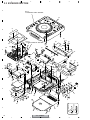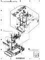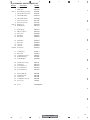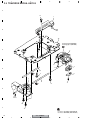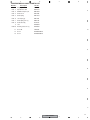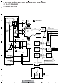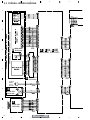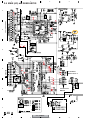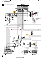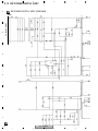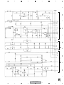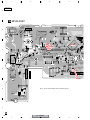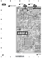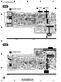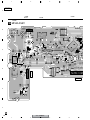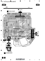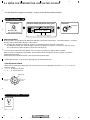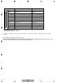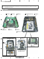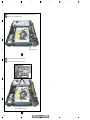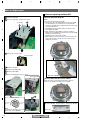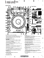
1
ORDER NO.
RRV3353
CDJ-1000MK3
COMPACT DISC PLAYER
CDJ-1000MK3
THIS MANUAL IS APPLICABLE TO THE FOLLOWING MODEL(S) AND TYPE(S).
Model
Type
Power Requirement
CDJ-1000MK3
KUCXJ
AC 120V
CDJ-1000MK3
WYXJ5
AC 220-240V
CDJ-1000MK3
TLFXJ
AC 110-240V
Remarks
For details, refer to "Important Check Points for good servicing".
PIONEER CORPORATION
4-1, Meguro 1-chome, Meguro-ku, Tokyo 153-8654, Japan
PIONEER ELECTRONICS (USA) INC. P.O. Box 1760, Long Beach, CA 90801-1760, U.S.A.
PIONEER EUROPE NV Haven 1087, Keetberglaan 1, 9120 Melsele, Belgium
PIONEER ELECTRONICS ASIACENTRE PTE. LTD. 253 Alexandra Road, #04-01, Singapore 159936
PIONEER CORPORATION 2006
T-IZY APR. 2006 printed in Japan
1
2
3
4
SAFETY INFORMATION
A
This service manual is intended for qualified service technicians ; it is not meant for the casual do-ityourselfer. Qualified technicians have the necessary test equipment and tools, and have been trained
to properly and safely repair complex products such as those covered by this manual.
Improperly performed repairs can adversely affect the safety and reliability of the product and may
void the warranty. If you are not qualified to perform the repair of this product properly and safely, you
should not risk trying to do so and refer the repair to a qualified service technician.
B
WARNING
This product contains lead in solder and certain electrical parts contain chemicals which are known to the state of California to
cause cancer, birth defects or other reproductive harm.
Health & Safety Code Section 25249.6 - Proposition 65
NOTICE
(FOR CANADIAN MODEL ONLY)
Fuse symbols
(fast operating fuse) and/or
be of identical designation.
C
(slow operating fuse) on PCB indicate that replacement parts must
REMARQUE
(POUR MODÈLE CANADIEN SEULEMENT)
Les symboles de fusible
(fusible de type rapide) et/ou
de remplacement doivent avoir la même désignation.
(fusible de type lent) sur CCI indiquent que les pièces
(FOR USA MODEL ONLY)
1. SAFETY PRECAUTIONS
The following check should be performed for the
continued protection of the customer and service
technician.
LEAKAGE CURRENT CHECK
Measure leakage current to a known earth ground
(water pipe, conduit, etc.) by connecting a leakage
current tester such as Simpson Model 229-2 or
equivalent between the earth ground and all exposed
metal parts of the appliance (input/output terminals,
screwheads, metal overlays, control shaft, etc.). Plug
the AC line cord of the appliance directly into a 120V
AC 60 Hz outlet and turn the AC power switch on. Any
current measured must not exceed 0.5 mA.
D
Reading should
Leakage not be above
current 0.5 mA
tester
Device
under
test
E
Test all
exposed metal
surfaces
Also test with
plug reversed
(Using AC adapter
plug as required)
Earth
ground
ANY MEASUREMENTS NOT WITHIN THE LIMITS
OUTLINED ABOVE ARE INDICATIVE OF A POTENTIAL
SHOCK HAZARD AND MUST BE CORRECTED BEFORE
RETURNING THE APPLIANCE TO THE CUSTOMER.
2. PRODUCT SAFETY NOTICE
Many electrical and mechanical parts in the appliance
have special safety related characteristics. These are
often not evident from visual inspection nor the protection
afforded by them necessarily can be obtained by using
replacement components rated for voltage, wattage, etc.
Replacement parts which have these special safety
characteristics are identified in this Service Manual.
Electrical components having such features are
identified by marking with a > on the schematics and on
the parts list in this Service Manual.
The use of a substitute replacement component which
does not have the same safety characteristics as the
PIONEER recommended replacement one, shown in the
parts list in this Service Manual, may create shock, fire,
or other hazards.
Product Safety is continuously under review and new
instructions are issued from time to time. For the latest
information, always consult the current PIONEER Service
Manual. A subscription to, or additional copies of,
PIONEER Service Manual may be obtained at a nominal
charge from PIONEER.
AC Leakage Test
F
2
CDJ-1000MK3
1
2
3
4
5
6
7
8
A
IMPORTANT
LASER DIODE CHARACTERISTICS
MAXIMUM OUTPUT POWER : 5 mW
WAVELENGTH : 780 – 785 nm
THIS PIONEER APPARATUS CONTAINS
LASER OF CLASS 1.
SERVICING OPERATION OF THE APPARATUS
S H O U L D B E D O N E B Y A S P E C I A L LY
INSTRUCTED PERSON.
WARNING !
THE AEL (ACCESSIBLE EMISSION LEVEL) OF THE LASER POWER OUTPUT IS LESS THAN CLASS 1
BUT THE LASER COMPONENT IS CAPABLE OF EMITTING RADIATION EXCEEDING THE LIMIT FOR
CLASS 1.
A SPECIALLY INSTRUCTED PERSON SHOULD DO SERVICING OPERATION OF THE APPARATUS.
B
LABEL CHECK
for WYXJ5 and KUCXJ types
for TLFXJ type
C
(DRW2308)
(DRW2248)
D
Additional Laser Caution
(Printed on the bottom plate)
1. Laser Interlock Mechanism
The position of the switch (S2401) for detecting loading
completion is detected by the system microprocessor, and the
design prevents laser diode oscillation when the switch is not
in LPS1 terminal side (when the mechanism is not clamped
and LPS1 signal is high level.)
Thus, the interlock will no longer function if the switch is
deliberately set to LPS1 terminal side. ( if LPS1 signal is low
level ).
In the test mode∗ the interlock mechanism will not function.
Laser diode oscillation will continue, if pin 5 of AN22022A
(IC601) on the MAIN Assy is connected to GND, or else the
terminals of Q603 are shorted to each other (fault condition).
E
2. When the cover is opened, close viewing of the objective
lens with the naked eye will cause exposure to a Class 1
laser beam.
F
3
CDJ-1000MK3
5
6
7
8
1
A
2
3
4
[Important Check Points for Good Servicing]
In this manual, procedures that must be performed during repairs are marked with the below symbol.
Please be sure to confirm and follow these procedures.
1. Product safety
Please conform to product regulations (such as safety and radiation regulations), and maintain a safe servicing environment by
following the safety instructions described in this manual.
1 Use specified parts for repair.
Use genuine parts. Be sure to use important parts for safety.
2 Do not perform modifications without proper instructions.
B
Please follow the specified safety methods when modification(addition/change of parts) is required due to interferences such as
radio/TV interference and foreign noise.
3 Make sure the soldering of repaired locations is properly performed.
When you solder while repairing, please be sure that there are no cold solder and other debris.
Soldering should be finished with the proper quantity. (Refer to the example)
4 Make sure the screws are tightly fastened.
Please be sure that all screws are fastened, and that there are no loose screws.
5 Make sure each connectors are correctly inserted.
Please be sure that all connectors are inserted, and that there are no imperfect insertion.
C
6 Make sure the wiring cables are set to their original state.
Please replace the wiring and cables to the original state after repairs.
In addition, be sure that there are no pinched wires, etc.
7 Make sure screws and soldering scraps do not remain inside the product.
Please check that neither solder debris nor screws remain inside the product.
8 There should be no semi-broken wires, scratches, melting, etc. on the coating of the power cord.
Damaged power cords may lead to fire accidents, so please be sure that there are no damages.
If you find a damaged power cord, please exchange it with a suitable one.
9 There should be no spark traces or similar marks on the power plug.
D
When spark traces or similar marks are found on the power supply plug, please check the connection and advise on secure
connections and suitable usage. Please exchange the power cord if necessary.
0 Safe environment should be secured during servicing.
When you perform repairs, please pay attention to static electricity, furniture, household articles, etc. in order to prevent injuries.
Please pay attention to your surroundings and repair safely.
2. Adjustments
To keep the original performance of the products, optimum adjustments and confirmation of characteristics within specification.
Adjustments should be performed in accordance with the procedures/instructions described in this manual.
E
3. Lubricants, Glues, and Replacement parts
Use grease and adhesives that are equal to the specified substance.
Make sure the proper amount is applied.
4. Cleaning
For parts that require cleaning, such as optical pickups, tape deck heads, lenses and mirrors used in projection monitors, proper
cleaning should be performed to restore their performances.
5. Shipping mode and Shipping screws
To protect products from damages or failures during transit, the shipping mode should be set or the shipping screws should be
installed before shipment. Please be sure to follow this method especially if it is specified in this manual.
F
4
CDJ-1000MK3
1
2
3
4
5
6
7
8
CONTENTS
1. SPECIFICATIONS .............................................................................................................................................6
2. EXPLODED VIEWS AND PARTS LIST.............................................................................................................8
2.1 PACKING SECTION ...................................................................................................................................8
2.2 EXTERIOR SECTION ..............................................................................................................................10
2.3 CONTROL PANEL SECTION...................................................................................................................12
2.4 SLOT-IN MECHA. SECTION ....................................................................................................................14
2.5 TRAVERSE MECHA. ASSY-S ..................................................................................................................16
3. BLOCK DIAGRAM AND SCHEMATIC DIAGRAM ..........................................................................................18
3.1 BLOCK DIAGRAM....................................................................................................................................18
3.1.1 SIGNAL SECTION .............................................................................................................................18
3.1.2 POWER SUPPLY SECTION ..............................................................................................................20
3.2 OVERALL WIRING DIAGRAM .................................................................................................................22
3.3 MAIN ASSY (1/4)......................................................................................................................................24
3.4 MAIN ASSY (2/4)......................................................................................................................................26
3.5 MAIN ASSY (3/4)......................................................................................................................................28
3.6 MAIN (4/4) and SLMB ASSYS..................................................................................................................30
3.7 SPCN, INSW and SDCB ASSYS .............................................................................................................32
3.8 MJCB ASSY .............................................................................................................................................34
3.9 MFLB ASSY..............................................................................................................................................36
3.10 SLDB and RSWB ASSYS.......................................................................................................................38
3.11 JFLB, KSWB and JOGB ASSYS ............................................................................................................40
3.12 SW POWER SUPPLY ASSY ..................................................................................................................42
3.13 WAVEFORMS.........................................................................................................................................44
3.14 VOLTAGES..............................................................................................................................................53
4. PCB CONNECTION DIAGRAM ......................................................................................................................55
4.1 MAIN ASSY ..............................................................................................................................................56
4.2 SLMB, SPCN, INSW and SDCB ASSYS..................................................................................................60
4.3 MJCB ASSY .............................................................................................................................................62
4.4 MFLB and RSWB ASSYS ........................................................................................................................64
4.5 SLDB ASSY..............................................................................................................................................68
4.6 KSWB ASSY.............................................................................................................................................69
4.7 JFLB and JOGB ASSYS...........................................................................................................................70
4.8 SW POWER SUPPLY ASSY ....................................................................................................................72
5. PCB PARTS LIST ............................................................................................................................................73
6. ADJUSTMENT ................................................................................................................................................77
6.1 TEMPO ZERO POINT ADJUSTMENT .....................................................................................................77
6.2 MODE FOR CHECKING THE LOAD ON THE JOG DIAL........................................................................78
7. GENERAL INFORMATION .............................................................................................................................79
7.1 DIAGNOSIS..............................................................................................................................................79
7.1.1 SERVICE MODE ................................................................................................................................79
7.1.2 HOW TO UPGRADE THE SOFTWARE OF THE MICROCOMPUTER .............................................87
7.1.3 SEQUENCE .......................................................................................................................................88
7.1.4 DISASSEMBLY ..................................................................................................................................90
7.2 PARTS ......................................................................................................................................................99
7.2.1 IC........................................................................................................................................................99
8. PANEL FACILITIES .......................................................................................................................................113
8.1 PANEL SECTION ...................................................................................................................................113
8.2 DISPLAY SECTION ................................................................................................................................115
A
B
C
D
E
F
5
CDJ-1000MK3
5
6
7
8
1
2
3
4
1. SPECIFICATIONS
A
B
1. General
3. Accessories
System .......................... Compact disc digital audio system
Power requirements .......... AC 120 V, 60 Hz (KUCXJ type)
AC 220 V to 240V, 50/60 Hz (WYXJ5 type)
AC 110 V to 240V, 50/60 Hz (TLFXJ type)
Power consumption ............................. 28 W (KUCXJ type)
27 W (WYXJ5 type)
27 W (TLFXJ type)
Operating temperature ................................ +5 ºC to +35 ºC
Operating humidity ........................................... 5 % to 85 %
(There should be no condensation of moisture.)
Weight .......................................................... 4.2 kg (9.26 lb)
Dimensions ...................... 320 (W) x 370 (D) x 105 (H) mm
12 - 5/8 (W) x 14 - 9/16 (D) x 4 - 1/8 (H) in
NOTE:
Specifications and design are subject to possible
modification without notice.
¶ Operating instructions .................................................... 1
¶ Power cord (KUCXJ and WYXJ5 types) ........................ 1
¶ Power cord (TLFXJ type) ............................................... 2
¶ Audio cable .................................................................... 1
¶ Control cord ................................................................... 1
¶ Forced eject pin
(housed in a groove in the bottom panel) ....................... 1
¶ SD memory card ............................................................ 1
¶ Limited warranty (KUCXJ only)....................................... 1
2. Audio section
Frequency response .................................... 4 Hz to 20 kHz
Signal-to-noise ratio ....................... 115 dB or more (JEITA)
Distortion ................................................... 0.006 % (JEITA)
C
Accessories
Audio Cable
(VDE1064) L=1.5m
Control Cord
(XDE3063) L=1 m
D
Power Cord
(KUCXJ type : ADG7021)
(WYXJ5 : ADG1154)
(TLFXJ type : ADG1154, ADG7097)
Forced Eject Pin SD Memory Card
(DEX1013)
(DWX2622)
AC power cord for TLFXJ type
The type of cord which can be used depends on the power voltage in each region or
country. Please make sure you use the correct cord due to the possibility of fire or other
hazard if used incorrectly (see below).
AC power cord and converter plug use
E
Region
Plug type
ADG1154
For European type region
Caution
Do not use this power cord set in Taiwan.
European two-pin plug
ADG7097
For Taiwan exclusively
Caution
For use in Taiwan only.
In other areas, please do not use.
Taiwanese two-pin flat-bladed plug
F
6
CDJ-1000MK3
1
2
3
4
5
6
7
8
A
B
C
D
E
F
7
CDJ-1000MK3
5
6
7
8
1
2
3
4
2. EXPLODED VIEWS AND PARTS LIST
Parts marked by "NSP" are generally unavailable because they are not in our Master Spare Parts List.
The
mark found on some component parts indicates the importance of the safety factor of the part.
Therefore, when replacing, be sure to use parts of identical designation.
Screws adjacent to mark on product are used for disassembly.
For the applying amount of lubricants or glue, follow the instructions in this manual.
(In the case of no amount instructions, apply as you think it appropriate.)
NOTES:
A
2.1 PACKING SECTION
B
13
TLFXJ only
2
10
5
8
15
C
KUCXJ
only
9
16
12
11
7
D
3
6
4
1
E
14
F
17
8
CDJ-1000MK3
1
2
3
4
5
6
7
8
(1) PACKING SECTION PARTS LIST
Mark No.
>
>
1
2
3
4
5
Description
Part No.
Power Cord
Power Cord
Audio Cable (L = 1.5 m)
Control Cord (L = 1 m)
SD Memory Card
See Contrast table (2)
See Contrast table (2)
VDE1064
XDE3063
DWX2622
6
7
NSP 8
NSP 9
10
Forced Eject Pin
Operating Instructions
User Seat
Limited Warranty
Caution Card SB
DEX1013
See Contrast table (2)
DRM1262
See Contrast table (2)
See Contrast table (2)
NSP 11
AHG7117
12
13
14
Polyethylene Bag
(0.06 x 230 x 340)
Packing Sheet
Pad (A)
Pad (B)
15
16
17
Pad (C)
Pad (D)
Packing Case
DHA1535
DHA1536
See Contrast table (2)
A
B
AHG7010
DHA1533
DHA1534
C
(2) CONTRAST TABLE
CDJ-1000MK3/KUCXJ, WYXJ5 and TLFXJ are constructed the same except for the following:
Mark
No.
Symbol and Description
>
>
1
2
7
7
ADG7021
Not used
DRB1397
Not used
ADG1154
Not used
Not used
DRB1396
ADG1154
ADG7097
Not used
Not used
Not used
Not used
DRB1398
9
10
Power Cord
Power Cord
Operating Instructions (English)
Operating Instructions
(English/French/German/Italian/Duch/Spanish)
Operating Instructions
(English/ Spanish/ Chinese)
Limited Warranty
Caution Card SD
ARY7043
Not used
Not used
Not used
Not used
ARM7064
17
Packing Case
DHG2576
DHG2575
DHG2577
7
NSP
CDJ-1000MK3/KUCXJ CDJ-1000MK3/WYXJ5
CDJ-1000MK3/TLFXJ
D
E
F
9
CDJ-1000MK3
5
6
7
8
1
2
3
4
2.2 EXTERIOR SECTION
A
Refer to
"2.3 CONTROL PANEL SECTION".
44
21
B
T
46
45
A
39
38
B
37
35
16
C
2
B
L
D
46
46
38
38
36
E
36
H
48
46
38
F
46
3
K
5
47 42
24
43
46
L
40
30
46
46
T
23
I
I
25
43
42
E
17
44
46
11
46
D
10
O
H
32
46
P
33
G 20
22
N
M
46
28
46
46
18
45
46
M
36
36
C
35
Refer to
"2.4 SLOT-IN MECHA. SECTION".
8
31
J
26
42
G
O
D
B C
E
F
K
45
46
34
A
14
46
46
46
N
F
M S
7
15
45
27
46
12
Q
46
A
E
1
P
13
S
4
R
R
45
44
F
29
44
44
44
10
CDJ-1000MK3
1
2
3
4
CONTACT SIDE
6
J
Q
NON-CONTACT
SIDE
9
19
5
6
7
8
(1) EXTERIOR SECTION PARTS LIST
Mark No.
Description
Mark No.
Part No.
>
1
2
3
4
5
MAIN Assy
SLMB Assy
SDCB Assy
MJCB Assy
SW POWER SUPPLY Assy
DWG1591
DWS1366
DWX2558
DWG1605
DWR1409
>
6
7
8
9
10
15P Flexible Cable
Earth Lead Unit/300V
Connector Assy 3P
Connector Assy 6P
Inlet Assy
DDD1301
DDF1032
DKP3751
DKP3752
See Contrast table (2)
11
12
13
14
15
Earth Lead Unit/300V
Connector Assy
Connector Assy
Connector Assy
Connector Assy
PDF1104
PF04PP-Q12
PF06PP-Q15
PF09PP-B12
PF11EE-R15
Power Button
Door Spring
Card Spring
Silicone Sheet D5 L
Door Cushion
DAC2314
DBH1565
DBK1295
DEB1456
DEB1780
16
17
18
NSP 19
20
21
22
NSP 23
24
25
26
Laser Caution
Dust Guard
Rear Panel
Heatsink
PCB Stay
See Contrast table (2)
DEC2939
See Contrast table (2)
DNG1099
DNH2711
Shield Case
DNH2712
Description
Part No.
27
28
29
30
Earth Plate C
Shield Box
Bottom Plate
Blind Cap
DNH2715
DNH2728
See Contrast table (2)
DNK4218
31
32
33
34
35
Chassis
Card Door
Card Holder
Insulator Assy
Earth Plate
DNK4553
DNK4554
DNK4555
DXA2092
VBK1070
36
37
38
39
40
Damper
Earth Spring
Float Spring G5
Mecha. Plate
Cord Clamper
CNV6011
DBH1398
DBH1494
DNH2339
RNH-184
41
42
43
44
45
Binder (SKB-90BK)
DM Screw
Screw
Screw
Screw
ZCA-SKB90BK
DBA1260
BBT30P100FTB
BBZ30P060FTB
BBZ30P060FTC
Screw
Cord Clamper (069Z)
FFC Guard
BPZ30P080FTB
ZCB-069Z
DEC2586
46
NSP 47
48
A
B
C
D
(2) CONTRAST TABLE
CDJ-1000MK3/KUCXJ, WYXJ5 and TLFXJ are constructed the same except for the following:
Mark
No.
>
10
21
21
23
29
NSP
Symbol and Description
CDJ-1000MK3/KUCXJ CDJ-1000MK3/WYXJ5
Inlet Assy
Laser Caution (7L)
Laser Caution
Rear Panel
Bottom Plate
DKP3754
DRW2308
Not used
DNC1765
DNH2710
DKP3753
DRW2308
Not used
DNC1758
DNH2710
CDJ-1000MK3/TLFXJ
DKP3753
Not used
DRW2248
DNC1766
DNH2732
E
F
11
CDJ-1000MK3
5
6
7
8
1
2
3
4
2.3 CONTROL PANEL SECTION
A
58
26
16
B
53
63
44 62
15
∗2
∗2
65 (2/2)
64
29
57
74
C
74
21
59
A
I
72
49
72
3
9
72
46
D
45
51
56 54
55
13
65 (1/2)
H
72
14
72
72
B
2
47
70
43
72
30
A
G
72
72
72
72
73
72
72
42
40
52
35
C
12
E
72
72
19
D
E
1
72
24
74
71
32
72 72
CONTACT SIDE
∗1
68
23
6
F
33
70
J
8
E
10
72
12
18
3
68
39
38
7 72
4
72
28
MJCB
CN1504
69
CDJ-1000MK3
2
72
25
74
74
34
L
72
∗1; Grease: GYA1001 (ZLB-PN397B)
∗2; Lubricant Agent: (ZLB-HFD1600)
36
37
22
31
1
∗1
20
20
50
20
20
F
C
11 72
17
20
48
66
K 72
21
20
21
5
NON-CONTACT
SIDE
27
17
60
B
F
41
17
61
59
D
∗2
74
4
5
6
7
8
CONTROL PANEL SECTION PARTS LIST
Mark No.
Description
Mark No.
Part No.
Description
Part No.
1
2
3
4
5
MFLB Assy
SLDB Assy
RSWB Assy
JFLB Assy
KSWB Assy
DWG1606
DWS1367
DWS1368
DWG1602
DWS1365
46
47
48
49
50
Set Knob (HS)
Set Knob (MT)
Set Knob (TIME)
Tempo Reset Knob
Set Knob (MEMO)
DAC1986
DAC1987
DAC1991
DAC1993
DAC1994
6
7
8
9
10
JOGB Assy
22P Flexible Cable
25P Flexible Cable
10P Flexible Cable
Connector Assy
DWG1603
DDD1302
DDD1303
DDD1304
PF04PP-B07
51
52
53
54
55
Set Knob (LOOP)
Re-Loop Button
Adjust Knob
Eject Knob
Mode Select Knob
DAC1995
DAC2347
DAC2350
DAC2365
DAC2366
11
12
13
14
15
LED Guard
Protect Cushion
VR Stay
Earth Plate P
JOG Plate
DEC2932
DEC2938
DNF1663
DNH2714
DAH2052
56
57
58
59
60
Set Knob (SC)
Slide Sheet 1C
Display Panel
Ring Lens
Tempo Lens
DAC2368
DAH2404
DAH2435
DNK3880
DNK3882
16
17
18
19
20
JOG Panel
SW Spring 25
Gear Spring 200
Arm Spring
SW Cushion HH48/2
DAH2182
DBH1514
DBH1525
DBH1566
DEC2538
61
62
63
64
65
Card Lens
Eject Guard
Control Panel
Slide Knob
Mode Lens
DNK3885
DNK3958
DNK4568
DNK4656
DNK4701
21
22
23
24
25
Ring Cushion L24/2.0
Encoder Plate
Protect Sheet
FL Sheet
Gear Plate
DEC2958
DEC2889
DEC2945
DEC2946
DNH2713
66
67
68
69
70
Set Knob (PLAY) Assy
•••••
Washer
Screw
Screw
DXB1909
26
27
28
29
30
JOG B
SW Ring
Adjust Plate
JOG A
JOG Holder 1000
DNK4068
DNK4070
DNK4178
DNK4556
DNK4558
71
72
73
74
Screw
Screw
Flange Nut M9
Screw
BPZ20P060FTC
BPZ30P080FTB
DBN1008
DBA1265
31
32
33
34
35
Gear Arm
Gear
Smoother
Gear A
Joint Gear 1
DNK4559
DNK4560
DNK4561
DNK4562
DNK4563
36
37
38
39
40
Joint Gear 2
Joint Gear 3
Compressor Plate
Cam Plate
Sheet SW
DNK4564
DNK4565
DNK4566
DNK4567
DSX1065
41
42
43
44
45
Roller A Assy
JOG Stay Assy
Roller B Asssy
Rotary Knob C
Slide SW Knob
DXB1825
DXB1876
DXB1877
DAA1194
DAC1926
A
B
C
WA52D120D25
BPZ20P100FTC
IPZ30P100FTC
D
E
F
13
CDJ-1000MK3
5
6
7
8
1
2
3
4
2.4 SLOT-IN MECHA. SECTION
A
3
14
∗2
22
24
21
12
13
10
∗2
23
B
16
17
MAIN
CN603
18
∗1
C
19
11
8
20
∗2
15
9
34
Refer to
"2.5 TRAVERSE MECHA. ASSY-S".
4
33
36
32
33
D
MAIN
CN601
32
6
36
1
MAIN
CN604
25
MAIN
CN602
C
D
31
5
E
35
2
31
7
27
NON-CONTACT
SIDE
30
28
F
26
29
30
14
CDJ-1000MK3
1
2
3
4
CONTACT SIDE
∗1; Dyefree : GEM1036 (ZLX-ME413A)
∗2; Grease: GYA1001 (ZLB-PN397B)
5
6
7
8
SLOT-IN MECHA. SECTION PARTS LIST
Mark No.
Description
Part No.
1
2
NSP 3
4
5
SPCN Assy
INSW Assy
Slot-in Mecha. G11 Assy
Traverse Mecha. Assy-S
13P Flexible Cable
DWX2559
DWS1369
DXA2068
DXX2566
DDD1299
6
7
8
NSP 9
10
26P Flexible Cable
Connector Assy 2P
Connector Assy 2P
DC Motor S
Clamp Spring
DDD1300
DKP3769
DKP3750
DXM1230
DBH1374
Guide Spring
SW Lever Spacer
Drive Lever
Main Cam
Disc Guide
DBH1375
DEC2420
DNK3406
DNK3407
DNK3478
Clamp Arm
Eject Lever
Lever AP
Lever BP
Worm Gear
DNK3576
DNK3684
DNK3835
DNK3836
DNK3910
21
22
23
24
25
Loading Gear
Drive Gear
Loading Base Assy-S
Clamper D4 Assy
Inside SW Base
DNK3911
DNK3912
DEA1022
DXA2043
DNK4236
26
27
28
29
30
Float Base G11 Assy
Front Sheet
Vessel Cushion A
Vessel Cushion B
Vessel Cushion C
DXB1793
DED1132
DEC2852
DEC2853
DEC2854
31
32
33
34
35
Spacer POR (T3)
Float Rubber D3
Float Screw
Loading Motor Assy-S
Screw 2 x 5
DEB1566
DEB1404
DBA1286
DEA1008
VBA1062
36
Screw
IPZ20P060FTC
11
12
13
14
15
16
17
18
19
NSP 20
A
B
C
D
E
F
15
CDJ-1000MK3
5
6
7
8
1
2
3
4
2.5 TRAVERSE MECHA. ASSY-S
A
12
1
B
MAIN
CN604
∗1
10
Cleaning liquid (GEM1004)
Cleaning paper (GED-008)
C
3
5
7
9
11
D
8
∗1
4
6
2
8
11
∗2
4
E
SPCN
CN3103
13
F
13
∗1; Grease: GYA1001 (ZLB-PN397B)
∗2; Grease: GEM1007 (ZLB-PN948P)
16
CDJ-1000MK3
1
2
3
4
5
6
7
8
TRAVERSE MECHA. ASSY-S PARTS LIST
Mark No.
NSP
NSP
NSP
NSP
NSP
1
2
3
4
5
NSP 6
NSP 7
NSP 8
9
NSP 10
11
12
13
Description
Part No.
Stepping Motor
Spindle Motor G11
04RM2 Pickup Assy R
Skew Screw
Skew Spring
DXM1227
DXM1231
OWY8071
DBA1263
DBH1437
Joint Spring (J)
Slider Spring G11 (J)
Guide Shaft (S)
Joint
Mounting Plate G11 (J)
DBK1261
DBK1262
DLA1918
DNK3858
DNK4307
Screw 04
Screw
Screw
VBA1092
BPZ20P080FTC
BPZ26P080FTC
A
B
C
D
E
F
17
CDJ-1000MK3
5
6
7
8
1
2
3
4
3. BLOCK DIAGRAM AND SCHEMATIC DIAGRAM
3.1 BLOCK DIAGRAM
3.1.1 SIGNAL SECTION
A
CN601
B
SPINDLE
MOTOR
A MAIN ASSY
IC601
FEP
OEIC
PICKUP
ASSY
B
CN2401
S2401
SLMB
ASSY
FE
29
RFENV
TE
14 18
89 111 109 112
ATAPI
CN605
1
LPS1
IC603
SODC
2
2
3
175
1
LPS2
SERIAL
COMMUNICATION
IC301
FPGA
CONT2
CONT1
176
3
S2402
CONT0
IC604
FLASH ROM
C
DOUT
CN3102
CN602
26
FETRV
CN3103
53
TRDRV
LOAD
67 119 120
52
180 179 177
IC103
FLASH ROM
IC602
6CH DRIVER
CN3101
CN3301
IC101
CPU
S3001
1
1
13
27
D
12
IC102
128MB SDRAM
D
C
INSW ASSY
SPCN ASSY
STEPPING
MOTOR
LRCK
DATA
BCK
CN604
IC403
SD CARD
CONTROLER
M
IC401
DSP
SYSYTEM
BUS
CN603
Pitch bend
Key control at master tempo
Generates CD digital out
M
E
CN401
SD CARD
INTERFACE
SLOT-IN
MECHANISM
CN3002
CN3001
SD CARD
CONNECTOR
F
18
E
SDCB ASSY
CDJ-1000MK3
1
4
14
TRAVERSE
MECHANISM
LOADING
MOTOR
IC402
DSP
2
3
4
5
6
7
8
A
M
JOGB
ASSY
L
SW POWER
SUPPLY ASSY
D2201
ENCODER
SHEET
SW
CN2201
CN1503
CN1507
CN2004
CN501
F
CN1502
8
8
6
6
10
10
14
14
MJCB
ASSY
CN1504
CN2002
2
1
2
1
B
1
CN2003
TCH
CN1501
POWER
JOG2
POWER
JOG1
POWER
JOG
ROTATION
DETECTION
JFLB
ASSY
J
V2001 JOGFL
JOGFL
CONTROL
C
CN2001
17 18 19
17 18 19
CN1001
CN1505
CN503
AUDIO
DATA
1
2
3
IC501
DAC
1
1
16
4
4
MFLB
ASSY
V1001 DATA FL
ANALOG
AUDIO
13
G
D
6 26 25 27
IC1512
OP AMP
3
DATA FL CONTROL
IC1001
FL UCOM
5
J1006
LED KEY
CN1007
1
74
J1004
2
7
2
CN2301
L
CN1201
R
JA1502
JA1503
AUDIO OUT DIGITAL
OUT
KEY
TEMPO
ZERO ADJ.
VR1202
K
H
E
S3001
LED
LED KEY
JA1501
CONTROL
KSWB
ASSY
J1301
SLDB
ASSY
DIRECTION
SW
I
RSWB
ASSY
F
19
CDJ-1000MK3
5
6
7
8
1
2
3
4
3.1.2 POWER SUPPLY SECTION
A
AC CORD
AC INLET
A MAIN ASSY
CN601
B
PICKUP
ASSY
5
V+12S
CN201
11
VA5V
CN1503
V+12S
R609
0
CN3103
SPINDLE
MOTOR
12
13
CN3102
V+5S
1
V+3R3
C
CN602
IC606
5V → 3.3V
VA3V
1
1
2
2
5
5
7
7
9
9
IC1514
VD3V
C
CN1501
CN502
V+1R8
When V+5S is OFF,
IC605 output becomes
OFF.
R604
0
SPCN ASSY
When VD1R5 is OFF,
IC606 output becomes
OFF.
IC1513
Q601, Q602
1.5V → 5V
VD1R5
IC605
3.3V → 1.5V
D
V+2R5FPGA
IC302
3.3V → 2.5V
V+1R6TI
IC405
3.3V → 1.6V
V+3R3
V+1R2FPGA
When V+3R3 is OFF,
IC303 output becomes
OFF.
E
IC303
1.8V → 1.2V
CN503
CN1506
V+5A
13
12
CN401
9
5
V+3R3
F
CN3002
E
SDCB ASSY
20
CDJ-1000MK3
1
2
3
4
V+5A
10
5
6
7
8
A
M
SW POWER SUPPLY ASSY
L
5
4
CN1505
V-12AJ
6
4
3
2
FLAC1
FLAC2
FLAC3
FLAC4
VLOAD
1
3
1
B
3
CN1507
CN2004
IC1504
IC1503
IC1507
V+12A
V-12A
3
CN2201
IC1502
J
IC1501
7
V+5D
CN301
V+1R8
V+5
V+3R3
CN601
JOGB ASSY
IC1506
18
18
16
16
20
20
14
14
12
12
22
22
JFLB ASSY
FLAC1
FLAC2
VLDMFL
FLAC3
FLAC4
V+3R3
Q1507
41V → 27V
V+1R8
C
VLDJOG
V2001 JOG FL
V+5D
VLED
1
1
8
8
CN1504
F
CN2002
MJCB ASSY
D
CN2001
11 25
11 25
7
6
5
4
1
7
6
5
4
1
CN1001
V1001 DATA FL
E
IC501
12V → 5V
V+12AJ
G
J1006
CN1007
9
4
9
9
4
9
CN2301
CN1201
VLED
H
MFLB
ASSY
V+5D
VLED
F
K
KSWB ASSY
SLDB ASSY
21
CDJ-1000MK3
5
6
7
8
1
2
3
4
3.2 OVERALL WIRING DIAGRAM
A
CN301
TRAVERSE MECHANISM ASSY-S (DXX2566)
B
C
INSW ASSY
A A 1/4 - A 4/4
D (DWS1369)
MAIN ASSY (DWG1591)
D
ASSY
C SPCN
(DWX2559)
LOADING
MOTOR
ASSY-S
DEA1008
E
B
SLMB ASSY
(DWS1366)
E
SDCB ASSY
(DWX2558)
F
22
CDJ-1000MK3
1
2
3
4
5
6
7
INLET ASSY:
KUCXJ: DKP3754
WYXJ5, TLFXJ: DKP3753
M
CN601
SW POWER SUPPLY ASSY
(DWR1409)
8
AC POWER CORD:
KUCXJ: ADG7021
WYXJ5: ADG1154
TLFXJ: ADG1154, ADG7097
A
CN101
CN201
K
KSWB ASSY
(DWS1365)
B
SLDB ASSY
H (DWS1367)
F
MJCB ASSY
(DWG1605)
G
MFLB ASSY
(DWG1606)
C
I
RSWB ASSY
(DWS1368)
D
J
JFLB ASSY
(DWG1602)
L
JOGB ASSY
(DWG1603)
E
÷ When ordering service parts, be sure to refer to "EXPLODED VIEWS and PARTS
LIST" or "PCB PARTS LIST".
÷ The > mark found on some component parts indicates the importance of the safety
factor of the part. Therefore, when replacing, be sure to use parts of identical
designation.
÷
: The power supply is shown with the marked box.
23
CDJ-1000MK3
5
6
F
7
8
1
2
3
4
A 3/4
A 2/4
A 1/4 MAIN ASSY (DWG1591)
A
A 4/4
3.3 MAIN ASSY (1/4)
3 4 5 6 7
B
A 2/4
A 2/4
C
D
E
A 2/4
A 2/4
2
A 3/4
9
8
1
10
11
F
A 1/4
12
24
CDJ-1000MK3
1
2
3
4
A 2/4
5
6
7
8
A
A 2/4, 3/4, 4/4
B
C
D
E
F
A 1/4
25
CDJ-1000MK3
5
6
7
8
1
2
3
4
3.4 MAIN ASSY (2/4)
A 2/4 MAIN ASSY (DWG1591)
A
13
A 1/4
A 1/4
B
A 3/4
14
A 1/4
C
A 1/4
A 3/4
A 1/4
D
A 1/4
A 3/4
E
A 1/4
A 4/4
F
A 2/4
26
CDJ-1000MK3
1
2
3
4
5
6
7
8
F
CN1501
A
B
A 1/4
(A)
(A)
A 3/4
CN1506
C
(A)
F
(A)
(DA)
15
16
(DA)
(DA)
(A)
17
(D)
D
(D)
A 1/4
20 21
F
(D)
CN1502
A 3/4
19
A 1/4
E
18
(DA)
(A)
(D)
: Audio Data Signal Route
: Analog Audio Signal Route
: Digital Out Signal Route
F
A 2/4
27
CDJ-1000MK3
5
6
7
8
1
2
3
4
A 2/4
A 3/4 MAIN ASSY (DWG1591)
A 1/4
E
CN3002
A
A 1/4
3.5 MAIN ASSY (3/4)
B
A 1/4
A 2/4
A 1/4
C
A 1/4
D
E
F
A 3/4
28
CDJ-1000MK3
1
2
3
4
5
6
7
8
A
B
22
C
A 1/4
A 2/4
(DA)
(DA)
A 2/4
(D)
(DA)
A 1/4
D
27
26
A 2/4
A 4/4
25
23
24
(DA)
(D)
E
: Audio Data Signal Route
: Digital Out Signal Route
F
A 3/4
29
CDJ-1000MK3
5
6
7
8
1
2
3
4
3.6 MAIN (4/4) and SLMB ASSYS
A
44
TO PICKUP ASSY
43
B
(FS)
(TS)
32
37
36
38
(FS)
(TS)
C
(FS)
(TS)
D
34
CN3102
(SP)
(SP)
33
(L)
(L)
(TS)
(TS)
(FS)
(FS)
31
35
30
TO LOADING
MOTOR ASSY-S
(L)
C
(L)
41
42
(SP)
(ST)
28
(ST)
(ST)
(ST)
29
(ST)
(SP)
E
40
(ST)
(L)
TO STEPPING
MOTOR
39
A 2/4
A 1/4
ASSY
B SLMB
(DWS1366)
F
A 4/4 B
30
CDJ-1000MK3
1
2
3
4
7
8
A 4/4 MAIN ASSY (DWG1591)
A
(TS)
(FS)
(FS)
6
(TS)
5
B
C
(L)
(L)
(ST)
(ST)
D
(SP)
(SP)
A 3/4
E
: RF Signal Route
(FS)
(TS)
(SP)
(ST)
(L)
: Focus Servo Signal Route
: Tracking Servo Signal Route
: Spindle Motor Signal Route
F
: Stepping Motor Signal Route
: Loading Motor Signal Route
A 4/4
31
CDJ-1000MK3
5
6
7
8
1
2
3
4
3.7 SPCN, INSW and SDCB ASSYS
A
C SPCN ASSY (DWX2559)
B
A 4/4
CN602
C
D
D INSW ASSY (DWS1369)
E
F
C D
32
CDJ-1000MK3
1
2
3
4
5
6
7
8
A
E
SDCB ASSY (DWX2558)
A 3/4
CN401
B
C
D
E
F
E
33
CDJ-1000MK3
5
6
7
8
1
2
3
4
3.8 MJCB ASSY
F
A
J
MJCB ASSY (DWG1605)
CN2002
A 2/4
CN503
53
B
(A)
(A)
(A)
(A)
58 57
56
C
(D)
(D)
(D)
59
(D)
D
(D)
E
F
A 2/4
CN501
A 2/4
F
34
CN502
M CN201
CDJ-1000MK3
1
2
3
4
5
6
CAUTION : FOR CONTINUED PROTECTION AGAINST
RISK OF FIRE. REPLACE ONLY WITH
SAME TYPE NO. AEK7008- 491.800
MFD, BY LITTELFUSE INK. FOR IC1501.
7
CAUTION : FOR CONTINUED PROTECTION AGAINST
RISK OF FIRE. REPLACE ONLY WITH
SAME TYPE NO. AEK7023- 491.200
MFD, BY LITTELFUSE INK. FOR IC1504.
CAUTION : FOR CONTINUED PROTECTION AGAINST
RISK OF FIRE. REPLACE ONLY WITH
SAME TYPE NO. AEK7012- 49101.6
MFD, BY LITTELFUSE INK. FOR IC1502
AND IC1503.
8
CAUTION : FOR CONTINUED PROTECTION AGAINST
RISK OF FIRE. REPLACE ONLY WITH
SAME TYPE NO. AEK7013- 4910002.
MFD, BY LITTELFUSE INK. FOR IC1506
AND IC1514.
A
CAUTION : FOR CONTINUED PROTECTION AGAINST
RISK OF FIRE. REPLACE ONLY WITH
SAME TYPE NO. AEK7018- 491004.
MFD, BY LITTELFUSE INK. FOR IC1507.
(A)
(D)
(A)
: Analog Audio Signal Route
: Digital Out Signal Route
(A)
54
(A)
B
(A)
(A)
(A)
C
(D)
55
(D)
(D)
D
E
M CN601
CAUTION : FOR CONTINUED PROTECTION AGAINST
RISK OF FIRE. REPLACE ONLY WITH
SAME TYPE NO. AEK7003- 491.315
MFD, BY LITTELFUSE INK. FOR IC1513.
F
M CN301
F
35
CDJ-1000MK3
5
6
7
8
1
2
3
4
3.9 MFLB ASSY
G MFLB ASSY (DWG1606)
I
J1301
A
K
CN2301
B
C
H
CN1201
D
46
E
CN2001
45
J
47
F
48
G
36
CDJ-1000MK3
1
2
3
4
5
6
7
8
A
49
52
50
51
B
C
D
E
F
G
37
CDJ-1000MK3
5
6
7
8
1
2
3
4
3.10 SLDB and RSWB ASSYS
A
H SLDB ASSY (DWS1367)
J1006
B
G
C
D
(GREEN)
E
(RED)
F
H
38
CDJ-1000MK3
1
2
3
4
5
6
7
8
A
B
C
D
RSWB ASSY (DWS1368)
J1004
I
G
E
F
H I
39
CDJ-1000MK3
5
6
7
8
1
2
3
4
3.11 JFLB, KSWB and JOGB ASSYS
J
JFLB ASSY (DWG1602)
CN1001
F
CN1504
A
G
B
C
D
63
62
60
61
E
F
J
40
CDJ-1000MK3
1
2
3
4
5
6
7
8
A
CN1007
K
KSWB ASSY (DWS1365)
(GREEN)
G
B
(AMBER)
C
(GREEN)
L
(GREEN)
JOGB ASSY (DWG1603)
D
E
F
K L
41
CDJ-1000MK3
5
6
7
8
1
2
3
4
3
4
3.12 SW POWER SUPPLY ASSY
M SW POWER SUPPLY ASSY (DWR1409)
A
CN101
B
TO INLET ASSY
L
N
C
D
E
F
M
42
CDJ-1000MK3
1
2
5
6
7
8
A
CN201
F
CN1503
B
C
F
CN1505
CN601
D
F
CN1507
CN301
E
F
M
43
CDJ-1000MK3
5
6
7
8
1
2
3
4
3.13 WAVEFORMS
WAVEFORMS
A
Note : The encircled numbers denote measuring point in the schematic diagram and pcb diagram.
A 1/4 MAIN ASSY
A 1/4 MAIN ASSY
Mode: Power ON
Mode: Power ON
1
IC104 - 2 pin (V+3R3)
V: 2V/div. H: 100mS/div.
IC104 - 1 pin (RSTCPU)
V: 2V/div. H: 100mS/div.
2
2
6
A 1/4 MAIN ASSY
A 2/4 MAIN ASSY
Mode: PLAY (1kHz, 0dB)
Mode: PLAY
IC104 - 1 pin (RSTCPU)
V: 2V/div. H: 500mS/div.
IC114 - 6 pin (MOT_XRST)
V: 2V/div. H: 500mS/div.
10
IC107 - 6 pin (SH_66M)
V: 0.5V/div. H: 5nS/div.
- 1 pin (MO_LRCK)
15 IC501
V: 2V/div. H: 5µS/div.
16 IC501 - 2 pin (MO_DATA)
V: 2V/div. H: 5µS/div.
17 IC501 - 3 pin (MO_BCK)
V: 2V/div. H: 5µS/div.
1
2
2
6
15
10
B
16
17
A 1/4 MAIN ASSY
A 1/4 MAIN ASSY
A 1/4 MAIN ASSY
2
2
- 8 pin (SDRAM_66M) 18 CN501 - 1 pin (SCLK)
11 IC107
V: 5V/div. H: 20µS/div.
V: 0.5V/div. H: 5nS/div.
19 CN501 - 7 pin (SOUT)
Mode: Power ON
IC104 - 1 pin (RSTCPU)
V: 2V/div. H: 500mS/div.
IC114 - 10 pin (DMA_XRST)
V: 2V/div. H: 500mS/div.
3
Mode: Power ON
7
Mode: PLAY
IC104 - 1 pin (RSTCPU)
V: 2V/div. H: 500mS/div.
IC114 - 12 pin (ATARST)
V: 2V/div. H: 500mS/div.
Mode: PLAY
V: 5V/div. H: 20µS/div.
- 9 pin (SIN)
20 CN501
V: 5V/div. H: 20µS/div.
2
21 CN501 - 11 pin (XCS)
2
C
A 2/4 MAIN ASSY
V: 5V/div. H: 20µS/div.
11
7
3
18
19
20
A 1/4 MAIN ASSY
A 1/4 MAIN ASSY
Mode: Power ON
2
4
IC104 - 1 pin (RSTCPU)
V: 2V/div. H: 500mS/div.
IC114 - 8 pin (CARD_XRST)
V: 2V/div. H: 500mS/div.
A 1/4 MAIN ASSY
Mode: PLAY
8
21
Mode: PLAY
IC107 - 3 pin (66MHz CLOCK)
V: 0.5V/div. H: 5nS/div.
- 10 pin (FPGA_66M)
12 IC107
A 3/4 MAIN ASSY
V: 0.5V/div. H: 5nS/div.
Mode: PLAY
- 27 pin (MO_DOUT)
22 IC402
V: 1V/div. H: 200nS/div.
D
2
8
12
4
22
A 1/4 MAIN ASSY
A 1/4 MAIN ASSY
Mode: Power ON
2
5
E
IC104 - 1 pin (RSTCPU)
V: 2V/div. H: 500mS/div.
IC114 - 4 pin (TI_XRST)
V: 2V/div. H: 500mS/div.
A 2/4 MAIN ASSY
Mode: PLAY
9
Mode: Power ON
IC107 - 4 pin (CARD_66M)
V: 0.5V/div. H: 5nS/div.
- 8 pin (V+3R3)
13 IC302
V: 2V/div. H: 500mS/div.
14 IC301 - 71 pin (FPGA_DONE)
A 3/4 MAIN ASSY
Mode: PLAY
IC407 - 5 pin (16MHz CLOCK)
23 V:
1V/div. H: 20nS/div.
V: 2V/div. H: 500mS/div.
13
2
23
9
5
14
F
44
CDJ-1000MK3
1
2
3
4
5
6
7
8
Note : The encircled numbers denote measuring point in the schematic diagram and pcb diagram.
A
A 3/4 MAIN ASSY
A 4/4 MAIN ASSY
A 4/4 MAIN ASSY
A 4/4 MAIN ASSY
- 1 pin (LPS1)
28 CN605
V: 5V/div. H: 200mS/div.
- 14 pin (TE)
32 IC601
V: 2V/div. H: 500µS/div.
- 28 pin (ST1)
39 IC602
V: 2V/div. H: 500mS/div.
29 CN605 - 3 pin (LPS2)
33 IC602 - 52 pin (TEDRV)
40 IC602 - 29 pin (ST2)
34
- 1 pin (ST1+)
41 CN604
V: 10V/div. H: 500mS/div.
Mode: LOAD IN
Mode: PLAY
24
IC407 - 4 pin (16M_SODC)
V: 1V/div. H: 20nS/div.
30
31
24
V: 5V/div. H: 200mS/div.
CN603 - 1 pin (EMN)
V: 5V/div. H: 200mS/div.
CN603 - 2 pin (EMP)
V: 5V/div. H: 200mS/div.
28
A 3/4 MAIN ASSY
Mode: PLAY
IC407 - 10 pin (Clock for DSP)
26 V:
1V/div. H: 20nS/div.
V: 10V/div. H: 500mS/div.
B
42
A 4/4 MAIN ASSY
A 4/4 MAIN ASSY
A 4/4 MAIN ASSY
- 1 pin (LPS1)
28 CN605
V: 5V/div. H: 200mS/div.
- 14 pin (TE)
32 IC601
V: 2V/div. H: 500µS/div.
29 CN605 - 3 pin (LPS2)
33 IC602 - 52 pin (TEDRV)
30
34
31
A 3/4 MAIN ASSY
42 CN604 - 2 pin (ST1-)
41
35
Mode: UNLOADING
25
V: 2V/div. H: 500mS/div.
40
34
31
Mode: FWD SCAN
39
33
30
Mode: PLAY
35
V: 2V/div. H: 500µS/div.
IC602 - 48 pin (T+)
V: 5V/div. H: 500µS/div.
IC602 - 47 pin (T-)
V: 5V/div. H: 500µS/div.
32
29
- 8 pin (16M_DAC)
25 IC407
V: 1V/div. H: 20nS/div.
Mode: FWD SCAN
V: 5V/div. H: 200mS/div.
CN603 - 1 pin (EMN)
V: 5V/div. H: 200mS/div.
CN603 - 2 pin (EMP)
V: 5V/div. H: 200mS/div.
Mode: REV SCAN
35
V: 2V/div. H: 500µS/div.
IC602 - 48 pin (T+)
V: 5V/div. H: 500µS/div.
IC602 - 47 pin (T-)
V: 5V/div. H: 500µS/div.
Mode: PLAY
43 IC601 - 24 pin (ARF)
44 IC601 - 23 pin (NARF)
C
43
44
28
29
32
30
33
31
G
MFLB ASSY
Mode: Power ON
34
- 2 pin (V+5D)
45 IC1003
V: 2V/div. H: 100mS/div.
35
- 12 pin (XRESET)
46 IC1002
V: 2V/div. H: 100mS/div.
D
26
A 4/4 MAIN ASSY
A 4/4 MAIN ASSY
- 14 pin (TE)
32 IC601
V: 2V/div. H: 200µS/div.
- 10 pin (FEPEN)
36 IC601
V: 2V/div. H: 5µS/div.
33 IC602 - 52 pin (TEDRV)
37 IC601 - 11 pin (FEPCK)
Mode: PLAY
34
38
IC407 - 12 pin (Clock for DSP)
V: 1V/div. H: 20nS/div.
35
Mode: PAUSE
A 3/4 MAIN ASSY
27
V: 2V/div. H: 200µS/div.
IC602 - 48 pin (T+)
V: 5V/div. H: 200µS/div.
IC602 - 47 pin (T-)
V: 5V/div. H: 200µS/div.
Mode: PLAY
V: 2V/div. H: 5µS/div.
IC601 - 12 pin (FEPDT)
V: 2V/div. H: 5µS/div.
46
G
MFLB ASSY
Mode: Rotates a JOG during playback
- 17 pin (JOG1)
47 CN1001
V: 2V/div. H: 2mS/div.
48
36
32
45
E
CN1001 - 18 pin (JOG2)
V: 2V/div. H: 2mS/div.
33
27
37
47
38
48
34
35
F
45
CDJ-1000MK3
5
6
7
8
3
4
32
C677
R658
C675
C516
1
C101
R630
C651
C307
C306
C646
EMP
EMN
6
R408
5
7
R479
IC114
LPS2
C694
C407
14
8
F
4
REFLOW
46
CDJ-1000MK3
1
2
3
IC114
R427
LPS1
A
R103
R171
R109
R149
R476
R428
R150
R148
R110
C107
FIRST
C650
R473
R474
R475
R472
R664
C648
C693
C305
R196
C
3
C645
R661
HB
C692
INSW
C649
2 8
1
9 10
LF
7
13
8
C659
C647
U
W V
7
Production Cord
HW+
HW-
IC107
1
R478
R628
E88558
HUHV+
HV-
IC107
IC113
2 8
CONTACT SIDE
DOWN
1
1
E
8
4
7
CN602
5
R
HU+
3
C142
DNP2213-B
1/2
V+5S
1
C116
11 R195
12
R189
3
4 IC111
R194
C310
C317
1
5
C308
14
4
C143
1
0
C316
C318
A
B
C
0 1 2 3 4 5 6 7 8 9
5
X101
C309
C330
R144
C145
C141
R638
C698
R192
1
0
0 1 2 3
R640
L101
C655
C654
26
CONTACT SIDE
DOWN
CN601
F-
IC106
R653
MAIN
DWG1591-
T+
R191
R655
R656
R657
MPD
780LD
F+
R302
D303
R654
IC603
C685
R188
R632
T-
C684
R665 R666
Q602
Q603
R608
VREF C619
176
133
Q601
C636
C710
C144
C628
C662
C661
R614
C635
D
R512
1
R650
60
1
36
IC
1
D
A
1 C616
C678
12
38
37
R613
C631
R612
B
C
R517
13
36
C639
C
C670 C676
C630
C629
132
48
E
F
R659
R660
1
C617
C618
37
RF-
C709
C679
44 C627
IC601
RF+
C674
C644
C640
CN604
25
43
32
OFTR
C622 C620
C624
R603
24 R602
C621
BDO
25
B
C667
C666
R609
R622
TXD
C673
C672
44
R607
C51
VD3V
44
C682
C671
4
1
C623 R601
C518
RXD
89
C680
ST1-
41
C704
R641
R642
ST1+
42
C706
1
MAIN ASSY
ST2+
R647
CONTACT SIDE
UP
ST2-
R648
88
A
C688
C691
C690
R623
C703
C705
R644
R645
SIDE A
A
R516
2
45
1
4
3
7
5
6
7
8
144
R512
44
109
C414
C444
IC502
IC604
C709
R519
44
C425
1
R517
C426
108
5
R520
5 8
4
R522
R521
4 1
C513
17
32
C427
R464
2 8
R516
C428
R434
7
C517
8
1
C518
A
1
6
IC503
C516
SIDE A
C415
C445
IC402
C416
C417
C446
C419 C418
16
1
C447
R468
22
R650
1
3
R447
IC103
C306
IC107
R449
R448
C429
C
C116
11 R195
8
24
4 IC111
25
5
08
72
37
C430
C436
C435
R638
73
IC402
C432
C449
R460
C431
1
6
36
C710
R640
B
C146
Note :
The encircled numbers denote measuring point.
48
R176
R174
R175
R120
R119
R131
CN103
19
D
R172
R177
1
R156 208
7
2 8 2 8
1
53
2
7
C132
IC104
R182
R173
1
208
20
C137
C117
1
IC101
R118
R101
C122
C125
C121
R103
R171
C114
R134
R113
R155
R154
R133 R143
F
C104
R147
C103
C102
R157
R158
R153
IC112
C107
15
CN102
157
1
14
7
1
4
IC114
5
3
156
1
IC114
105
3
4
5
8
5
3
R150
C151
IC115
104
6
7
E
R132
R115
R114
R135
R109
R149
4
R117
R130
1
48
0
R170
2
52
C138
R159
1
R116
R194
10
C305
7
1
IC107
R151
R142
A
(DNP2213-B)
47
CDJ-1000MK3
5
6
7
8
3
IC407
1
C523
R538
R537
IC501
C434
C504
C505
R467
C433
3
XWE0
C109
C110
C123
C124
1
4
C
CN501
R619
DONE
C111
C633
IC605
C700
R649
R465
R466
C
R605
C701
1
27
26
R462
15
5
R618
C697
72
C696
C509
R536
14
4
R301
8
16 25
1
28
R
C699
IC407
IC501
17
C632
8
C602
5
C456
C515
C503
C521
C522
R511
1
7
14
R508
R459
R458
F457
(R4457)
R534
23
24
R463
15
C708
R509
C512
C506
C511
R533
R532
R531
C
1
15
D501
1
18
R515
6.V+5A
5.GND
4.LOUT
3.GND
2.GND
1.ROUT
Q501
R535
6
21 20 19
R643
C707
R646
IC606
R505
C510
B
R501
R503
MAIN ASSY
R502
R513
CN503
CONTACT SIDE
UP
C448
IC406 R453
C457 R452 C458
X402
A
15.GND
14.D OUT
13.GND
12.W_MUTE
11.XCS
10.CONT0
9.SIN
8.CONT2
7.SOUT
6.CONT1
5.TXD
4.GND
3.RXD
2.GND
1.SCLK
SIDE B
A
4
C702
2
C514
1
RDWR
73
XRD
27
14
XCS0
D0
1
XRAS3L
D7
XWE1
XCS3
IC301
XCASL
IC102
E88558
R
SDRAM_66M
A1
28
A7
54
C113
R122
C112
IC301
108
1R437
7
2 8
R435
C440
7
2 8
1
R190
R423
73
72
2 8
C105
1
7
2 8
C450
C451 1 7
R440
R441
C106
R102
C452
C108
R193
37
C312
C304
C311
C303
C404
48
C412
4
1
C413
D401
C403
C402
C401
R401
R421
R422
C443
C120
36
R424
C115
R420
C119
R416
C118
IC405
8
55
36
C405
R415
37
36
25 25
C406
X401
108
C461
R
R411 C479
R410 C478
R409 C476
R407 C475
R406 C474
R405 C473
C126
C437
7
37
24
109
C438
C439
E
C302
C411
C424
144
IC401
C421
XCS6
XCS5
C420
24
1
1
RSTCPU
2 8
C130
XCS4
XCS2
48
C441
C131
R419
R451
R121
13
C442
R414
C423
C128
C127
C129
12
13
C133
1
C301
8
IC403
12
1
C422
108
AOI ICT FC
D
109
R442
1
R108
A
48
R112
CDJ-1000MK3
1
2
3
4
12.SDDAT3
13.XCARDIN
R111
1.SDWP
2.GND
3.XMMCD
4.SDDAT2
5.SDDAT1
6.MMDAT0
7.GND
8.MMCLK
9.V+3R3
10.MMCMD
11.GND
R107
R471
T SIDE
UP
F
R105
R146
R104
R106
7
SIDE B
C501
C689
A
CN502
C508
R663
R662
C626
C603
D301
C315
R313
C320
R307
R303
C
Note :
The encircled numbers denote measuring point.
C614
C322
R314
C326
C319
IC301
SECOND
C625
C642
C615
36
37
36
C323
C695
C328
C696
R606
IC303
37
7
R301
2 8
1
C697
B
C609
C663
C604
R652
R618
C641
C606
C638
R619
700
C610
C664
C668
C665
4
1
C637
C633
IC605
C681
C669
C634
C602
605
1
9
C502
5
C686
R604
IC606
C632
8
C601
1
C608
C507
C708
8
9.V+1R8
8.GND
7.V+3R3
6.GND
5.V+5S
4.GNDR
3.GNDR
2.V+12S
1.V+12S
8
R643
C707
R646
6
R621
C687
CN501
5
C327
R610
C329 R611
R615
R616
R617
C613
C656
33
C660
IC302
C321
34
8
35
C413
4
IC602
2
1
R636
3
E
R637
Q604
C411
461
28
CN401
2
2.GND
39
3.LPS2
1.LPS1
CN603
1
2.EMP
1.EMN
R404
R403
R402
(R4452)
F452
13
1
40
1
30 31
CN605
CN603
3
CN605
Q605
27
C472
C477
C471
R620
R477
28 29
CN605
F
CONTACT SIDE
UP
R471
LF
IC602
1
D
R631
R629
C652
54
1
R627
R626
R633
IC405
8
55
C611
C324
R315
C312
C313
C303
C302
C412
IC302
5
XCS5
R312
R311
D302
4
XCS6
CS2
144
8
XCS4
13
C314
1
C301
C304
C311
1
R306
A
(DNP2213-B)
49
CDJ-1000MK3
5
6
7
8
1
2
3
4
SIDE B
A
G MFLB ASSY
R1051
GNDD
GNDD
GNDD
GNDD
GNDD
R1063
R1049
R1071
R1050
R1
51
50
R1047
R1070
R1078
R1080
R1082
R1079
R1092
R1091
R1093
R1084
R1083
R1095
R1094
CMKM-P3X
R1068
MEMORY
S1008
C1017
R1081
EJECT LOCK
R1096
S1118
R1098
R1097
1.REMO
2.REMO
3.V+5D
4.RMIN
5.FLWR
6.GNDD
CN1005
1
B
DIRECT
6
LOCK
R1074
R1086
IC
R1006
C1023
C1016
25.V+5D
24.GNDD
23.J_BK
22.J_LAT
21 J SCLK
17.JOG1
16.XCS
15.SIN
14.SOUT
13.SCLK
12.TXD
11.RXD
10.VLED
9.RESET
8.GLED
7.VLDMFL
6.VLDMFL
5 FLAC2
C1021
C1022
GNDD
48
J1006
J1006
R1054
0
S1015
RELOOP
GNDD
R1088
VR1002
RELEASE
1
FLDR1059
FKD+
S1006
CALL FWR
R1007
C1008
10
R1058
C1011
GNDD
R1053
C1014
9
D
30
80
S1003
C1009
R1005
R1010
S1004
GNDD
R1011
C1004
R1021
C1007
C1010
S1007
CALL BACK
9.VLED
8.GLED
7.MTL
6.TRESL
5.KEY1_B
4.V+5D
3.ADCT
2.ADIN
1.GNDD
C1013
R10
R1055
0
TOUCH/BRAKE
VR1001
R1075
C1012
10
C1006
C1024
DELETE
R1022
R1052
IC1002
81
R1077
52 50 49
S1009
IC1004
C
51
C1018
R1012
R1014
R1013
10
02
31
C1005
CN1001
25
47
1
CN1001
R1043
Q1012
S1005
D1010
R1042
JOG MODE
Note : The encircled numbers denote measuring point.
Q1008
R1035
E
R1041
D1016
D1015
F
G
50
CDJ-1000MK3
1
2
3
4
5
6
7
8
SIDE B
A
Q1002
Q1013
GNDD
GNDD
R1037
R1051
R1025
TIME
S1012
IC1001
C1001
R1073
R1072
IC1003
D1008
D1005
R1008
D1021
R1087
R1033
R1039
R1038
Q1001
R1061
D1001
Q1015
Q1011
D1018
D1009
C
R1020
R1085
D1014
VLED
R1034
R1027
S1018
GLED
GLED
GNDD
GNDD
R1040
Q1007
Q1003
V+5D
GNDD
CN1001
D
R1089
R1090
10
1
0
0 1 2 3 4 5 6 7 8 9
A
B
C
1
47
1.GNDD
2.PLAY
3.CUE
4.KEY0_B
5.PLAYL
6.CUEL
7.GNDD
8.MMCL
9.VLED
10.GLED
0
0 1 2 3
1
S1017
B
R1045
R1028
R1029
25.V+5D
24.GNDD
23.J_BK
22.J_LAT
21.J_SCLK
20.J_SDO
19.THC
18.JOG2
GNDD
D1004
C
D1007
D1013
R1024
R1031
D1006
R1030
Q1004
R1032
LOOP IN
S1013
D1002
17.JOG1
16.XCS
15.SIN
14.SOUT
13.SCLK
12.TXD
11.RXD
10.VLED
9.RESET
8.GLED
7.VLDMFL
6.VLDMFL
5.FLAC2
4.FLAC2
3.GNDD
2.GNDD
1.FLAC1
R1001
CN1007
1
R1002
REC MODE
S1002
CN1001
CN1007
2.SW0
1.GNDD
(DNP2214-B)
2 1
J1004
J1004
E
Q1009
R1036
48
C1003
S1014
S1013
TEXT
D1020
R1009
45
R1064
C1026
C1027
R1059
1
LOOP OUT
R1058
S1015
RELOOP
IC1003
C1025
R1060
46
R1065
R1054
R1055
R1017
5
R1023
C1012
C1002
Q1005
3
R1019
4
1
R1062
31
30
R1076
R1057
5
Q1010
R1015
R1016
R1075
R1018
R1004
R1044
R1003
R1056
Q1006
R1086
C1014
D1003
A
S1016
D1017
R1048
R1074
IC1002
02
Q1014
R1046
R1067
R1049
R1071
R1050
B
R1026
D1012
R1069
50
R1068
R1047
R1070
GNDD
GNDD
LF
D1011
F
G
51
CDJ-1000MK3
5
6
7
8
1
2
3
4
Note : The encircled numbers denote measuring point in the schematic diagram and pcb diagram.
A
G
MFLB ASSY
F
Mode: PLAY
- 71 pin (SI)
49 V1001
V: 5V/div. H: 50µS/div.
50 V1001 - 72 pin (CLK)
51
52
V: 5V/div. H: 50µS/div.
V1001 - 73 pin (LAT)
V: 10V/div. H: 50µS/div.
V1001 - 74 pin (BK)
V: 10V/div. H: 50µS/div.
- 18 pin (FLAC1)
56 CN1504
V: 5V/div. H: 5µS/div.
- 16 pin (FLAC2)
57 CN1504
V: 5V/div. H: 5µS/div.
56
57
49
B
MJCB ASSY
Mode: PLAY
50
F
51
F
MJCB ASSY
Mode: PLAY
52
MJCB ASSY
Mode: PLAY (1kHz, 0dB)
- 14 pin (FLAC3)
58 CN1504
V: 5V/div. H: 5µS/div.
- 12 pin (FLAC4)
59 CN1504
V: 5V/div. H: 5µS/div.
- 1 pin (ROUT)
53 CN1506
V: 1V/div. H: 500µS/div.
58
C
59
53
J
JFLB ASSY
Mode: PLAY
- 24 pin (SI)
60 V2001
V: 5V/div. H: 100µS/div.
F
MJCB ASSY
Mode: PLAY (1kHz, 0dB)
54
JA1502 - 1 pin (ROUT)
V: 2V/div. H: 500µS/div.
61 V2001 - 27 pin (CLK)
V: 5V/div. H: 100µS/div.
- 26 pin (LAT)
62 V2001
V: 5V/div. H: 100µS/div.
63 V2001 - 25 pin (BK)
V: 5V/div. H: 100µS/div.
D
60
54
61
62
63
F
MJCB ASSY
Mode: PLAY
Measurement condition:
Termination nothing, In case of
75 Ω termination, level becomes
half (0.5V).
E
(DOUT)
55 JA1503
V: 0.2V/div. H: 500nS/div.
55
F
52
CDJ-1000MK3
1
2
3
4
5
6
7
8
3.14 VOLTAGES
A
VOLTAGES
Voltage measurement condition: CD playback, CDJ, MASTER TEMPO: OFF , SLIDER: 0%
A 1/4 MAIN ASSY
A 2/4 MAIN ASSY
IC102
(K4S281632F-UC75)
• Remove CN401
IC101 (HD6417709SF133B-D)
Pin
1
2
3
4
5
6
7
8
9
10
11
12
13
14
15
16
17
18
19
20
21
22
23
24
25
26
27
28
29
30
31
32
33
34
35
36
37
38
39
40
41
42
43
44
45
46
47
48
49
50
51
52
53
54
55
56
57
58
59
60
61
62
63
64
65
66
67
68
69
70
71
Voltage (V)
3.31
3.30
1.754
0.010
1.754
0.009
0.008
3.31
3.31
3.31
3.31
2.370
3.31
3.31
3.31
3.31
3.31
3.31
0.008
3.31
3.31
3.31
3.31
3.31
3.31
3.31
0.008
3.31
1.752
0.011
0.011
0.011
0.008
0.63 to 0.84
3.31
1.57 to 1.65
1.53
0.64 to 1.2
0.5 to 1.2
1.27 to 1.31
1.3 to 1.4
1.39 to 1.41
1.39 to 1.43
1.40 to 1.54
0.008
1.50 to 1.52
3.31
0.95 to 1.10
1.1 to 1.3
1.43
1.47 to 1.53
1.38 to 1.40
0.53 to 0.75
1.80 to 1.85
1.69 to 1.74
1.67 to 1.73
0.008
1.42 to 1.63
3.31
1.38 to 1.53
1.33 to 1.42
0.90 to 0.96
0.85 to 0.91
0.85 to 1.16
1.0 to 1.4
0.55 to 0.74
0.82 to 0.93
0.10 to 0.45
0.008
0.22 to 0.86
3.31
Pin
72
73
74
75
76
77
78
79
80
81
82
83
84
85
86
87
88
89
90
91
92
93
94
95
96
97
98
99
100
101
102
103
104
105
106
107
108
109
110
111
112
113
114
115
116
117
118
119
120
121
122
123
124
125
126
127
128
129
130
131
132
133
134
135
136
137
138
139
140
141
142
Voltage (V)
0.085 to 0.095
0.34 to 0.37
0.52 to 0.85
0.43 to 0.56
0.9 to 1.4
0.17 to 0.41
0.42 to 0.61
0.008
0.015 to 0.018
1.749
0.02 to 0.08
0.008
0.13 to 0.16
3.31
0.008
2.63 to 2.66
3.31
1.7 to 2.2
2.20 to 2.30
3.31
0.055 to 0.110
3.22 to 3.25
3.31
0.008
3.31
3.31
3.0 to 3.3
1.9 to 2.1
3.31
0.033 to 0.080
3.31
3.30
3.30
3.31
0.11 to 0.15
3.31
2.657
0.009
0.009
3.31
0.010
3.31
0.010
3.28
3.31
3.31
3.31
3.31
3.31
3.31
3.31
3.30
3.31
2.540
3.31
3.31
3.31
3.31
0.008 to 0.030
0.016
0.009
3.31
1.751
3.31
3.31
3.31
3.31
3.31
3.31
3.31
3.31
Pin
143
144
145
146
147
148
149
150
151
152
153
154
155
156
157
158
159
160
161
162
163
164
165
166
167
168
169
170
171
172
173
174
175
176
177
178
179
180
181
182
183
184
185
186
187
188
189
190
191
192
193
194
195
196
197
198
199
200
201
202
203
204
205
206
207
208
Voltage (V)
0.011
3.31
1.751
0.816
0.009
0.008
0.008
1.751
0.011 to 0.035
0.009
0.009
1.751
0.009
0.009
0.009
0.008
0.015
3.26
0.009
1.675
3.31
0.010
3.31
0.15 to 0.26
0.009
3.31
0.008
0.008
3.31
3.31
0.008
3.31
1.751
3.31
3.31
0.009
3.27
3.30
0.008
0.008
3.31
0.008
3.31
3.31
0.011 to 0.017
3.31
3.31
0.008
3.31
0.015 to 0.055
3.31
3.31
0.008
3.31
0.008
0.009
3.31
0.009
0.035 to 0.150
3.31
3.31
3.31
3.31
3.31
3.31
0.008
Pin
1
2
3
4
5
6
7
8
9
10
11
12
13
14
15
16
17
18
19
20
21
22
23
24
25
26
27
28
29
30
31
32
33
34
35
36
37
38
39
40
41
42
43
44
45
46
47
48
49
50
51
52
53
54
Voltage (V)
3.31
1.45 to 1.49
3.31
1.30 to 1.35
1.46 to 1.49
0.008
1.19 to 1.22
1.0 to 1.2
3.31
1.2 to 1.6
1.48 to 1.52
0.008
0.5 to 0.9
3.31
2.19 to 2.24
3.19 to 3.24
2.65 to 2.68
3.09 to 3.12
2.01 to 2.03
0.1 to 0.4
0.1 to 0.4
0.55 to 0.71
1.80 to 1.82
1.69 to 1.73
1.71 to 1.73
1.52 to 1.63
3.31
0.008
1.43 to 1.53
1.39 to 1.50
0.90 to 0.94
0.85 to 0.92
0.84 to 0.95
0.9 to 1.2
0.80 to 0.87
0.085 to 0.093
3.31
1.642
2.20 to 2.23
0.14 to 0.20
0.009
1.42 to 1.45
3.31
1.35 to 1.43
1.32 to 1.38
0.009
1.02 to 1.13
0.9 to 1.1
3.31
1.54 to 1.56
1.64 to 1.69
0.009
0.65 to 0.80
0.009
• Remove CN401
IC103 (DYW1752)
Pin Voltage (V)
1 0.34 to 0.40
2 0.085 to 0.092
3
0.3 to 0.9
4 0.10 to 0.42
5 0.78 to 0.87
6 0.54 to 0.67
7 1.03 to 1.08
8 0.85 to 0.91
9 0.16 to 0.42
10 0.43 to 0.52
11
2.22
12
3.31
13 0.11 to 0.16
14 0.11 to 0.14
15
3.31
16
0.7 to 1.0
17 0.44 to 0.52
18 0.85 to 0.92
19
0.9 to 1.2
20
1.3 to 1.5
21 1.37 to 1.53
22 1.48 to 1.62
23 1.52 to 1.73
24 1.71 to 1.80
25 1.80 to 1.86
26
3.31
27
0.008
28
3.31
29 1.45 to 1.46
30 1.41 to 1.48
31 1.31 to 1.36
32 1.34 to 1.42
33 1.44 to 1.47
34
0.6 to 1.4
35 1.17 to 1.26
36 1.01 to 1.12
37
3.31
38 0.99 to 1.05
39 0.91 to 1.07
40 1.50 to 1.53
41 1.43 to 1.58
42 1.48 to 1.50
43 1.53 to 1.65
44 0.52 to 0.81
45 0.66 to 0.94
46
0.009
47
3.31
48 0.53 to 0.70
IC301 (XC3S50-4TQG144C)
Pin
1
2
3
4
5
6
7
8
9
10
11
12
13
14
15
16
17
18
19
20
21
22
23
24
25
26
27
28
29
30
31
32
33
34
35
36
37
38
39
40
41
42
43
44
45
46
47
48
49
50
51
52
53
54
55
56
57
58
59
60
61
62
63
64
65
66
67
68
69
70
71
72
Voltage (V)
0.009
3.31
3.31
3.31
3.31
0.
3.31
3.31
0.009
3.31
3.31
1.74 to 1.79
1.87 to 1.91
1.66 to 1.77
3.31
0.009
3.31
0 to 0.6
3.31
0 to 0.6
0 to 0.5
0.009
0 to 0.6
0 to 0.6
0 to 0.6
0 to 0.6
0 to 0.6
0 to 0.5
0.009
0 to 3.31
0 to 0.6
0 to 0.6
0 to 0.6
3.31
0 to 3.31
0 to 0.6
2.520
2.520
2.520
0 to 0.6
1.2 to 1.6
0.009
3.31
2.368
0.009
2.5 to 2.9
3.166
2.520
1.211
0.009
0.044 to 0.046
0.044 to 0.046
0.044 to 0.046
3.31
0.044 to 0.046
1.651
0.010
3.31
1.663
1.907
1.211
2.521
3.202
0.009
0.010
3.31
0.009
3.31
3.31
3.31
2.540
2.522
Pin
73
74
75
76
77
78
79
80
81
82
83
84
85
86
87
88
89
90
91
92
93
94
95
96
97
98
99
100
101
102
103
104
105
106
107
108
109
110
111
112
113
114
115
116
117
118
119
120
121
122
123
124
125
126
127
128
129
130
131
132
133
134
135
136
137
138
139
140
141
142
143
144
Voltage (V)
0.115
2.22 to 2.24
3.31
3.245
3.1 to 3.3
1.44 to 1.47
1.28 to 1.37
1.43 to 1.46
0.008
1.16 to 1.29
0.97 to 1.20
1.53 to 1.55
1.47 to 1.51
0.5 to 0.8
2.21 to 2.30
0.008
1.39 to 1.41
1.32 to 1.39
3.31
1.27 to 1.32
1.00 to 1.09
0.008
0.9 to 1.0
1.52 to 1.53
1.59 to 1.61
0.63 to 0.82
1.80 to 1.85
1.69 to 1.76
0.008
1.58 to 1.73
1.47 to 1.63
1.37 to 1.53
1.35 to 1.50
3.31
0.90 to 0.94
0.85 to 0.93
2.517
2.517
2.517
0.55 to 0.72
0.95 to 1.10
0.009
3.31
0.84 to 0.87
0.008
0.009
3.31
2.522
1.211
3.31
3.31
2.63 to 2.67
0.006
3.31
3.1 to 3.3
3.31
3.31
3.31
0 to 0.2
3.28
1.210
2.520
3.30
0.008
2.3 to 3.3
3.31
0.009
0.346
3.31
0.009
2.521
2.518
IC501 (PE8001A)
Pin Voltage (V)
1
1.661
2 0.77 to 0.85
3
1.650
4
2.254
5
1.634
6
2.814
7
0.009
8
5.00
9
5.00
10
0.001
11
2.504
12
0 to 0.08
13
2.517
14
0.009
15
5.00
16
2.514
17
0 to 0.03
18
2.503
19
0
20
5.00
21
4.99
22
5.00
23
0.010
24
4.98
25
4.98
26
0.011
27
3.31
28
3.31
6
C
D
E
F
53
CDJ-1000MK3
5
B
7
8
1
2
3
4
A
A 3/4 MAIN ASSY
IC401 (TMS320DA150PGE16D)
Pin
1
2
3
4
5
6
7
8
9
10
11
12
13
14
15
16
17
18
19
20
21
22
23
24
25
26
27
28
29
30
31
32
33
34
35
36
37
38
39
40
41
42
43
44
45
46
47
48
49
50
51
52
53
54
55
56
57
58
59
60
61
62
63
64
65
66
67
68
69
70
71
72
B
C
D
E
F
Voltage (V)
0.008
0.008
0.008
3.31
0.55 to 0.65
0.009
0.82 to 1.10
3.30
0.007
0.007
0.008
1.626
3.31
0.008
0.008
1.626
3.31
3.20 to 3.25
3.31
3.31
3.31
3.31
3.31
3.31
3.31
3.31
3.31
3.31
3.31
3.31
3.31
0.008
3.31
0.008
3.31
1.25 to 1.30
0.008
1.24 to 1.27
0.008
0.008
1.32 to 1.38
1.22 to 1.30
1.23 to 1.25
1.23 to 1.25
3.31
0.008
3.31
0.015
1.28
0.008
0.009
1.626
3.31
1.26 to 1.28
3.31
3.31
0.008
3.31
0.009
0.009
3.31
0.008
0.008
0.009
0.009
0.009
0.008
1.626
3.30
0.008
1.25 to 1.27
0.008
Pin
73
74
75
76
77
78
79
80
81
82
83
84
85
86
87
88
89
90
91
92
93
94
95
96
97
98
99
100
101
102
103
104
105
106
107
108
109
110
111
112
113
114
115
116
117
118
119
120
121
122
123
124
125
126
127
128
129
130
131
132
133
134
135
136
137
138
139
140
141
142
143
144
Voltage (V)
1.43 to 1.51
1.47 to 1.50
3.31
0.009
0.009
0.009
3.31
2.807
3.31
0.011
3.31
3.31
1.23 to 1.25
3.30
0.012
3.30
3.30
0.009
1.625
2.802
0.009
3.31
0.011
0.713
1.042
3.31
1.44 to 1.46
1.28 to 1.33
1.42 to 1.46
1.17 to 1.29
0.98 to 1.14
1.52 to 1.54
0.53 to 0.57
0.009
0.38 to 0.48
0.009
0.009
0.008
0.008
3.31
1.46 to 1.49
0.5 to 0.8
1.40 to 1.45
1.33
1.28 to 1.35
0.99 to 1.15
0.92 to 1.09
0.010
1.50 to 1.54
1.62 to 1.68
0.65 to 0.81
0.010
1.626
0.009
3.31
0.009
3.31
3.31
1.80 to 1.86
1.69 to 1.75
1.34 to 1.73
1.45 to 1.63
0.010
1.42 to 1.53
1.3 to 1.5
0.90 to 0.94
0.85 to 0.87
0.85 to 0.93
0.95 to 1.12
1.628
0.009
0.009
G
• Remove CN401
IC402 (DSPD56367PV150)
Pin
1
2
3
4
5
6
7
8
9
10
11
12
13
14
15
16
17
18
19
20
21
22
23
24
25
26
27
28
29
30
31
32
33
34
35
36
37
38
39
40
41
42
43
44
45
46
47
48
49
50
51
52
53
54
55
56
57
58
59
60
61
62
63
64
65
66
67
68
69
70
71
72
Voltage (V)
2.23 to 2.26
1.17 to 1.22
1.00 to 1.04
0.008
0.008
0.045 to 0.046
0.045 to 0.046
3.31
0.009
0.045 to 0.046
0.044 to 0.046
1.661
1.664
1.65
1.927
1.625
3.204
1.753
0.009
3.31
3.31
3.31
0.012
0.009
3.31
0.009
1.681
0.009
0.009
3.31
1.68 to 1.75
1.81 to 1.84
0.75
0.39 to 0.78
1.47 to 1.48
1.52 to 1.53
0.6 to 1.4
3.31
0.008
1.19 to 1.30
1.47 to 1.49
1.38 to 1.45
1.47 to 1.49
3.31
1.759
0.383
0.008
0.115
3.31
0.009
0.60 to 0.72
1.1 to 1.2
0.009
0.008
1.629
1.756
3.31
0.008
1.663
1.896
0.008
0.008
3.31
3.30
3.31
0.008
0.46 to 0.52
0.61 to 0.68
0.48 to 0.52
0.43 to 0.52
0.008
0.008
Pin
73
74
75
76
77
78
79
80
81
82
83
84
85
86
87
88
89
90
91
92
93
94
95
96
97
98
99
100
101
102
103
104
105
106
107
108
109
110
111
112
113
114
115
116
117
118
119
120
121
122
123
124
125
126
127
128
129
130
131
132
133
134
135
136
137
138
139
140
141
142
143
144
54
Voltage (V)
0.008
3.31
0.008
0.008
0.008
0.008
0.008
3.31
0.009
0.009
0.009
0.009
0.009
3.31
0.009
0.009
0.009
0.009
1.757
0.008
0.008
0.008
3.31
0.008
0.008
0.008
0.008
0.013 to 0.015
0.013
0.020 to 0.100
3.31
0.008
0 to 0.07
0.019
0.015 to 0.017
0.015 to 0.017
0.012
0.013
3.31
0.008
0.013
0.012
0.012
0.012
0.012
0.012
3.31
0.008
0.012
0.012
0.012
0.012
0.012
1.756
0.008
0.012
3.31
0.008
0.013
0.019
0.013
3.30
3.30
0.010
0.009
0.009
0.30 to 0.32
0.010 to 0.060
3.25
3.29
0.34 to 0.39
1.54
MFLB ASSY
IC1002 (PEG237A)
IC403 (TE4300PF)
Pin Voltage (V)
1 1.51 to 1.63
2 1.53 to 1.72
3 1.69 to 1.75
4 1.80 to 1.81
5
0.5 to 0.8
6
0.009
7 0.66 to 0.85
8 1.62 to 1.69
9 1.52 to 1.56
10
0.9 to 1.1
11
0.9 to 1.2
12
3.31
13 1.29 to 1.34
14 1.33 to 1.41
15 1.41 to 1.46
16
0.1 to 0.6
17 0.44 to 0.52
18
0.009
19
3.31
20 1.52 to 1.55
21 1.00 to 1.17
22 1.18 to 1.23
23 1.45 to 1.48
24 1.31 to 1.35
25 1.45 to 1.47
26
3.31
27
3.31
28
3.31
29
3.31
30
3.31
31
0.009
32
3.31
33
3.31
34
3.31
35
0.010
36
0.079
37
3.31
38
1.660
39
3.31
40
3.31
41
3.31
42
0.008
43
3.31
44
3.31
45
3.31
46
3.31
47
3.31
48
3.31
Pin
1
2
3
4
5
6
7
8
9
10
11
12
13
14
15
16
17
18
19
20
21
22
23
24
25
26
27
28
29
30
31
32
33
34
35
36
37
38
39
40
41
42
43
44
45
46
47
48
49
50
Voltage (V)
1.936
5.02
5.02
5.02
0.007
0.018
0.007
0.004
0.004
0.004
0.004
5.02
2.558
0.004
2.328
5.02
5.02
5.02
5.02
5.02
5.02
5.02
5.02
5.02
0.018
0 to 5.02
0.014 to 0.017
3.96
0.008
1.3 to 1.7
0.64 to 0.65
5.01
4.10
5.01
0.44 to 0.47
1.8 to 2.2
4.78
3.59
5.02
0.009
0.004
0.024
0.608
0.016
2.821
5.02
5.01
5.01
0.009
0.008
Pin Voltage (V)
51
0.008
52
0.008
53
0.008
54
0.008
55
0.008
56
0.008
57
0.007
58
0.007
59
0.007
60
0.007
61
0.007
62
5.02
63
0.005
64
0.004
65
0.005
66
0.005
67
0.006
68
0.006
69
5.01
70
5.01
71
0.006
72
5.01
73
0.268
74
5.01
75
0.004
76
0.004
77
0.004
78
0.004
79
0.004
80
0.004
81
5.02
82
5.02
83
5.02
84
5.02
85
5.02
86
5.02
87
5.02
88
5.02
89
2.215
90
2.121
91
5.01
92
5.01
93
5.01
94
0.004
95
0.004
96
0.004
97
0.004
98
5.03
99
5.03
100
0.004
CDJ-1000MK3
1
2
3
4
5
6
7
8
4. PCB CONNECTION DIAGRAM
A
NOTE FOR PCB DIAGRAMS :
1. Part numbers in PCB diagrams match those in the schematic
diagrams.
2. A comparison between the main parts of PCB and schematic
diagrams is shown below.
Symbol In PCB
Diagrams
Symbol In Schematic
Diagrams
B C E B C E
Part Name
3. The parts mounted on this PCB include all necessary parts for
several destinations.
For further information for respective destinations, be sure to
check with the schematic diagram.
4. View point of PCB diagrams.
Connector
Capacitor
Transistor
B C E
B
C
E B
C
SIDE A
E
Transistor
with resistor
B C E
D
G S D
B
G S
Field effect
transistor
D G S
P.C.Board
Chip Part
SIDE B
Resistor array
3-terminal
regulator
C
D
E
F
55
CDJ-1000MK3
5
6
7
8
1
2
3
4
4.1 MAIN ASSY
SIDE A
C671
C627
R516
R517
13
36
1
1
A
B
C
0 1 2 3 4 5 6 7 8 9
C101
R630
C651
R472
R661
R664
1
C645
R196
C306
C305
C646
FIRST
C650
C692
C648
EMP
EMN
R148
R110
R149
R476
R428
R150
R628
INSW
HB
R473
R474
R475
2 8
C649
7
13
LF
1
CN602
3
C659
C647
U
W V
7
IC113
Production Cord
HW+
HW-
1
2 8
CONTACT SIDE
DOWN
1
E88558
HU+
IC107
4
7
CN602
5
R
HUHV+
HV-
C307
C310
C316
C317
DNP2213-B
1/2
V+5S
3
C142
C143
1
0
X101
3
1
C116
R195
8
R478
0
0 1 2 3
14
4
4
L101
F-
C141
5
C308
R192
MAIN
DWG1591-
T+
C655
C654
26
CONTACT SIDE
DOWN
F+
C309
C330
R144
C145
5
1
C698
R194
R655
R656
R657
R653
R63
R189
R654
MPD
780LD
T-
R191
D303
IC106
R632
R302
R188
VREF C619
IC603
C685
C318
R665 R666
Q603
C636
C684
C144
C628
IC
60
1
1
R614
Q601
Q602
CN601
C635
176
133
R608
1 C616
A
R650
C662
C661
R613
C639
C631
R612
D
1
C677
R658
C675
C678
12
C617
C618
C
R408
7
R479
R427
LPS1
LPS2
C693
C694
C407
8
REFLOW
F
A
CDJ-1000MK3
1
2
C709
C670 C676
1
B
C CN3102
44
44
R659
R660
132
48
C
F
56
32
C679
C630
C629
E
E
TXD
VD3V
R622
C674
C644
C640
CN604
24 R602
1
25
C621
R603
25
RF-
CN601
R647
CONTACT SIDE
UP
4
CN604
C667
C666
37
RF+
PICKUP ASSY
C673
C672
89
C682
R607
R609
BDO
C518
RXD
OFTR
C622 C620
C624
D
C680
ST1-
C623 R601
C704
R641
R642
ST1+
B
C706
88
ST2+
R648
45
ST2-
STEPPING
MOTOR
C688
C691
C690
R623
C703
C705
R644
R645
A MAIN ASSY
A
3
4
R10
5
6
7
8
SIDE A
A
IC503
IC502
C414
R519
45
IC604
C709
IC502
5
4
R517
109
108
R520
144
IC503
C425
1
44
C426
C444
R647
C516
R512
R516
R522
R521
C513
17
32
C427
R464
44
TXD
5 8
4 1
VD3V
C428
R434
2 8
C517
8
C518
RXD
1
4
7
C706
1
R648
B
C415
C445
C419 C418
C447
R468
16
1
R650
R447
R449
R448
C429
C430
C436
C435
72
37
C431
1
C432
C449
R460
IC601
73
IC402
R640
R638
C698
R196
R144
C145
1
3
C306
8
C146
IC103
IC107
48
1
IC106 IC107
R176
R174
R175
R120
R119
R131
CN103
19
1
7
113
C137
C117
IC101
R118
C122
LF
R101
C125
R154
R157
R158
IC112
R153
R113
R134
C103
C102
IC112
C107
15
CN102
157
R150
R103
R171
1
14
1
4
156
5
3
IC114
105
8
C114
1
R479
1
2
27
IC115
4
7
IC115
104
R408
5
R149
R476
E
C151
3
R478
C121
R132
R115
R114
R135
R109
IC101
R117
R130
1
R148
R110
IC113
R155
3
IC104
R170
7
C132
2 8 2 8
1
53
4
R173
1
208
20
IC104
R182
2
52
D
C138
R156 208
L101
R172
R177
R159
1
R116
R194
C305
7
R192
1
C
Q602 IC111
Q603
C116
R195
R189
14
24
4 IC111
25
Q601
5
C308
IC103
C309
C330
C307
C310
176
36
C710
IC603 IC604 IC402
C416
C417
C446
IC114
R133 R143
C104
R147
R151
R142
F
(DNP2213-B)
A
57
CDJ-1000MK3
5
6
7
8
2
3
F CN1506
F CN1502
15.GND
14.D OUT
13.GND
12.W_MUTE
11.XCS
10.CONT0
9.SIN
8.CONT2
7.SOUT
6.CONT1
5.TXD
4.GND
3.RXD
2.GND
1.SCLK
CN501
R502
R501
R505
C512
R509
R508
R463
IC407
C60
8
4
1
3
1
14
5
C456
C515
C503
C521
C522
C509
R536
C523
R537
R538
C434
R462
1
IC501
R459
R458
F457
(R4457)
28
C504
C505
R467
C433
DONE
C111
C
XWE0
C109
C110
C123
C124
C700
R649
R465
R466
R605
C701
14
R511
1
7
15
1
C708
C699
R534
C510
B
1
C506
C511
R533
R532
R531
15
D501
6
R301
6.V+5A
5.GND
4.LOUT
3.GND
2.GND
1.ROUT
Q501
R535
R515
R503
R513
CN503
CONTACT SIDE
UP
CN501
CN503
A MAIN ASSY
C702
A
C448
IC406 R453
C457 R452 C458
X402
SIDE B
4
C514
1
72
RDWR
73
XRD
XCS0
D0
1
27
XRAS3L
D7
XWE1
XCS3
XCASL
IC102
E88558
R
SDRAM_66M
A1
28
A7
54
C113
R122
C112
IC301
108
1R437
7
2 8
R435
C440
7
2 8
1
R423
C105
1
7
2 8
C450
C451 1 7
R440
R441
C106
R102
C452
C108
R190
73
72
2 8
C404
48
C412
37
C403
C402
C401
R401
C411
C405
D401
36
R421
R422
C443
C120
36
R424
C115
R420
C119
R416
C118
37
37
36
25 25
C406
X401
C437
108
R415
R193
C302
24
109
7
C438
C439
E
XCS5
48
C441
C131
R419
R451
C126
C424
144
RSTCPU
1
IC401
1
C421
XCS
XCS2
C461
R411 C479
R410 C478
R409 C476
R407 C475
R406 C474
R405 C473
C127
2 8
C301
C420
24
R121
1
13
C130
C442
R414
C423
13
C129
12
C128
IC403
12
C133
1
C422
108
AOI ICT FC
D
109
R442
R108
R107
R111
R112
F
A
12.SDDAT3
13.XCARDIN
1.SDWP
2.GND
3.XMMCD
4.SDDAT2
5.SDDAT1
6.MMDAT0
7.GND
8.MMCLK
9.V+3R3
10.MMCMD
11.GND
R106
R105
R146
R104
R47
E CN3002
58
CDJ-1000MK3
1
2
3
4
5
6
7
8
SIDE B
F CN1501
A
CN502
C501
C689
CN502
C508
R663
R662
C626
C603
IC303
73
C625
C642
C615
CS0
C608
36
37
36
C323
C328
R606
C315
C
IC102
R307
R303
_66M
R313
C320
IC303
IC301
C614
C322
R314
C326
C319
D301
XRAS3L
XCS3
XCASL
IC605
C609
C663
C665
C604
C695
2 8
72
7
C697
1
DONE
C696
R618
R301
R649
R652
B
IC407
IC501 IC406
C641
C606
C638
R619
C700
IC606
C610
C664
C668
C502
C669
C634
4
1
Q501
C681
C699
C456
C633
IC605
C637
R605
C701
C448
IC406 R453
C457 R452 C458
X402
C602
1
9
C686
5
IC606
R515
C702
R513
R604
37
11
C632
8
C601
1
C708
SECOND
C507
9.V+1R8
8.GND
7.V+3R3
6.GND
5.V+5S
4.GNDR
3.GNDR
2.V+12S
1.V+12S
R643
C707
R646
R621
C687
CN501
TACT SIDE
UP
C327
IC301
R306
8
37
C613
IC302
R631
R629
C652
IC302
C321
R627
R626
R633
54
37
R610
C329 R611
R615
R616
R617
1
C412
C302
IC405
8
55
C611
C324
R315
C312
C313
C303
C404
48
R312
R311
C656
IC403
C660
4
1
R637
Q604
2
2.GND
3.LPS2
1.LPS1
1
3
CN605
1
CN603
2.EMP
1.EMN
R404
R403
R402
(R4452)
F452
C472
C477
C471
13
1
Q605
Q605
CN401
CONTACT SIDE
UP
12.SDDAT3
13.XCARDIN
E
28
R477
C479
R410 C478
R409 C476
R407 C475
R406 C474
R405 C473
IC602
R620
27
5.SDDAT1
6.MMDAT0
7.GND
8.MMCLK
9.V+3R3
10.MMCMD
11.GND
3
R636
C461
E CN3002
LF
IC401 Q604
1
R471
IC405
IC602
C413
D401
2
C411
C405
C406
36
C403
C402
C401
R401
D
5
XCS6
XCS5
48
36
XCS4
XCS2
D302
4
1
1
C314
144
8
C403
C301
1
109
R442
C304
C311
108
1
108
CN401
F
CN603
LOADING
MOTOR ASSY-S
CN605
(DNP2213-B)
A
B CN2401
59
CDJ-1000MK3
5
6
7
8
1
2
3
4
4.2 SLMB, SPCN, INSW and SDCB ASSYS
SIDE A
SIDE A
A
SLOTSW
B SLMB ASSY
A CN605
CN2401
B
S2
4
3
1
02
3
SLOTSW
1.LPS1
2.GNDD
3.LPS2
CN24011
OPEN SIDE
SLMB
DWS1366-
S2
4
01
(DNP2212-B)
1
CN3301
1
2/2
INSW
DWS1369-
C
2
CN3103
13
12
1
SPCN
DWX2559-
CN3101
CN3101
CMKM-P3X
CN3102
DOWN LF
1
CN3102
CONTACT
SIDE
2
A CN602
LF
2/2
S3301
CN3301
D INSW ASSY
C SPCN ASSY
CMKM-P3X
(DNP2215-B)
(DNP2215-B)
CN3103
D
SPINDLE
MOTOR
R3031
R3034
R3030
R3033
SDCB
DWX2558-
R3032
SDCB ASSY
R3035
E
S3001
2/2
R3008
R3004
R3026
R3009
R3021
D3006
R3003
R3024
R3010
R3012
8
D3005
R3023
C3003
R3014
R3005
R3025
R3018
13
R3016
8
CONTACT
SIDE UP
R3002
C3001
1
CN3002
A CN401
R3001
R3007
CN3001
R3020
1
R3019
1
D3001 D3002
D3003 D3004
9
R3015
9
C3004
LF
R3006
R3011
R3013
C3002
R3017
R3029
E
R3027
R3028
R3022
CN3002
D3007
D3008
CMKM-P3X
(DNP2215-B)
F
B C D E
60
CDJ-1000MK3
1
2
3
4
5
6
7
8
SIDE B
SIDE B
A
SLOTSW
B SLMB ASSY
CMKM-P3X
B
LF
40HI
1
CN2401
SLMB 1/2
DWS1366-
S2401
SLOTSW
3
3.LPS2
2.GNDD
1.LPS1
S2402
CN2401
(DNP2212-B)
C
D
E
F
B
61
CDJ-1000MK3
5
6
7
8
1
2
3
4
4.3 MJCB ASSY
SIDE A
A
A CN503 M CN601
MJCB ASSY
CN1506
W316
W122
CN1502
1.SCLK
2.GNDD
3.RXD
4.GNDD
5.TXD
6.CONT1
7.SOUT
8.CONT2
9.SIN
10.CONT0
11.XCS
12.W_MUTE
13.GNDD
14.DOUT
15.GNDD
W104
W102
15
W105
C
W106
1
1
W103
T-DWG238
W108
CONTACT
SIDE
W107
C1526
W138
C1530
W121
MJCB
C1503
Q1506
C1506
R1521
R1506
C1504
R1508
R1532
C1520
R1531
Q1509
W120
6
R1519
4
4
CN1506
1.ROUT
2.GNDA
3.GNDA
4.LOUT
5.GNDA
6.V+5A
C1513
W118
R1507
CN1505
C1523
R1512
R1516
Q1505
C1502
R1514
W119
1
1
W101
11.V+12S
10.V+12S
9.GNDR
8.GNDR
7.V+5
6.GNDD
5.V+3R3
4.GNDD
3.V+1R8
2.GNDD
1.VLDCNT
R1563
W137
W117
IC1512
W136
R1529
C1505
R1505
R1503
R1511
C1519
Q1508
R1510
R1504
C1529
JA1502
JA1503
5
5
1
JA1501
8
8
1.V+12A
2.GNDA
3.GNDA
4.V-12A
4
B
CN1505
C1525
C1501
C1508
M
1 2
R1509
C1528
R1518
F
CN1502
A CN501
Q1508
Q1509
IC1512
Q1505
Q1506
SIDE B
CN1502
D
R1550
R1549
GNDD
15
1
CN1502
R1536
Q1502
Q1503
R1546
Q1504
R1538
R1559
15.GNDD
14.DOUT
13.GNDD
12.W_MUTE
11.XCS
10.CONT0
9.SIN
8.CONT2
7.SOUT
6.CONT1
5.TXD
4.GNDD
3.RXD
2.GNDD
1.SCLK
C1515
R1560
Q1512
R1551
R1534
Q1511
R1535
R1548
C1517
MJCB ASSY
C1516
F
R1517
D1506
R1530
6
Q1501
510
4
GNDA
IC1509
R1522
CN1505
1.ROUT
2.GNDA
3.GNDA
4.LOUT
5.GNDA
6.V+5A
CMKM-P3X
R1524
R1523
1
R1515
1.V+12A
2.GNDA
3.GNDA
4.V-12A
1
C1512
C1509
4
5
8
IC1512
C1511
1
R1527
53
CN1506
C1522
R1544
D1503
E
D1505
R1528
CN1506
CN1505
F
Q1512 Q1511
Q1503 Q1502
IC101
Q1504
Q1501 IC150
F
62
CDJ-1000MK3
1
2
3
4
5
6
7
8
SIDE A
M CN301
J CN2002
CN1503
CN1507
CN1504
CAUTION
C1507
W135
R1561
1 1
1.V+5D
2.GNDD
3.SIN
W130
R1502
C1524
W116
Q1507
10.GLED
11.XCS
12.FLAC4
13.RESET
14.FLAC3
15.GNDD
W114
W115
4.SOUT
5.SCLK
6.TXD
7.RXD
8.VLED
9.GLED
W129
R1554
Q1513
B
16.FLAC2
17.GNDD
18.FLAC1
19.GNDD
20.VLDMFL
21.GNDD
22.VLDJOG
W134
W133
W132
W110
R1562
22
22
W131
W111
W140
CN1504
10
W128
49101.6
IC1503
491.200
W139
CONTACT
SIDE
W127
IC1504
491.315
W125
W112
C1527
2
W126
IC1506
IC1507
W124
CN1501
IC1502
CN1503
1
W109
W311
1
W123
W108
W106
W107
9
10.CONT0
11.XCS
12.W_MUTE
13.GNDD
14.DOUT
15.GNDD
1
9
MJCB
DWG1605-
6
1 2
1.V+12S
2.V+12S
3.GNDR
4.GNDR
5.V+5S
6.GNDD
7.V+3R3
8.GNDD
9.V+1R8
1
6
491002.
491004.
15
05
1 2
49101.6
C1530
2
1.FLAC1
2.FLAC2
3.FLAC3
4.FLAC4
5.GLOAD
6.GLOAD
491.800
491002.
11.V+12S
10.V+12S
9.GNDR
8.GNDR
7.V+5
6.GNDD
5.V+3R3
4.GNDD
3.V+1R8
2.GNDD
1.VLDCNT
R1563
A
REPLACE IC LINKS AS MARKED.
MFD.BY LITTELFUSE INC.
W113
CN1507
IC1514
IC1513
11
11
C1525
IC1501
M CN201
(DNP2214-B)
CN1501
C
A CN502
01
IC1502 IC1514
IC1506 IC1507
Q1507
IC1501 IC1503
IC1513
Q1513
IC1504
SIDE B
502
CN1501
D
9.V+1R8
8.GNDD
7.V+3R3
6.GNDD
5.V+5S
4.GNDR
3.GNDR
2.V+12S
1.V+12S
LF
R1540
Q1510
IC1511
C1518
4
5
IC1510
D1508
Q1507
R1553
D1502
GNDD
D1501
E
1
CN1504
10
57
58
56
ATTENTION
4.FLAC4
5.GLOAD
6.GLOAD
1.FLAC1
2.FLAC2
3.FLAC3
C1532
C1533
C1534
C1535
REMPLACER LE IC LINK COMME
INDIQUE.
DE CHEZ LETTEL
FUSE INC.
C1536
1
59
C1514
CN1507
C1537
22
Q1504
Q1501
C1510
6
5.SCLK
4.SOUT
3.SIN
2.GNDD
1.V+5D
D1504
15
1
4
3
1
E
R1556
12.FLAC4
11.XCS
10.GLED
9.GLED
8.VLED
7.RXD
6.TXD
R1557
R1555
CN1501
1
1.VLDCNT
2.GNDD
3.V+1R8
11.V+12S
10.V+12S
9.GNDR
8.GNDR
7.V+5
6.GNDD
5.V+3R3
4.GNDD
R1
CN1503
C1511
11
3
1
5
9
R1543
GNDD
R1545
C1521
R1542
IC1509
Q1504
Q1501 IC1509
CN1507
22.VLDJOG
21.GNDD
20.VLDMFL
19.GNDD
18.FLAC1
17.GNDD
16.FLAC2
15.GNDD
14.FLAC3
13.RESET
15.GNDD
14.DOUT
13.GNDD
12.W_MUTE
11.XCS
10.CONT0
9.SIN
8 CONT2
CN1503
CN1504
CN1504
(DNP2214-B)
Note :
The encircled numbers denote measuring point.
Q1510
IC1511
IC1510
F
Q1507
F
63
CDJ-1000MK3
5
6
7
8
1
W178
W181
W177
W155
W158
1
REC MODE
2.SW0
1.GNDD
F
I
64
2
W184
W179
W186
10
10
CONTACTSIDE UP
W156
1
S1002
MFLB
DWG1606-
DWS1368RSWB
REVERSE
ICT
3
W185
W192
1
W214
FC
1
CN1007
K CN2301
2.GNDD
1.SW0
(DNP2214-B)
RSWB ASSY
G I
CDJ-1000MK3
4
S1015
W247
1
13.SCLK
14.SOUT
15.SIN
16.XCS
17.JOG1
18.JOG2
19.THC
20.J_SDO
21.J_SCLK
22.J_LAT
23.J_BK
24.GNDD
D1006
W216
W194
W219
W243
W274
W246
W280
W303
W278
W277
W275
W276
W282
W281
W307
W306
W305
W304
W279
W302
W301
W272
W271
W273
W269
W268
W300
W299
W267
W298
W297
W296
3
35
RELOOP
W159
W157
W182
CONTACTSIDE UP
CN1007
1
CN1001
J CN2001
W195
W160
W161
W218
LOOP
OUT
W193
W183
W191
C1019
W190
B
W189
LOOP
IN
S1014
W188
S1013
Q1016
W187
S1012
1.FLAC1
2.GNDD
3.GNDD
4.FLAC2
5.FLAC2
6.VLDMFL
7.VLDMFL
8.GLED
9.RESET
10.VLED
11.RXD
12.TXD
W180
W241
W244
A
W217
W211
W270
D1003
D1005
W238
W242
W266
W265
2
S1301
W213
D1004
S1017
1
W239
1.GNDD
2.PLAY
3.CUE
4.KEY0_B
5.PLAYL
6.CUEL
7.GNDD
8.MMCL
9.VLED
10.GLED
W215
FWD(ON)
E
TIME/MODE
1
C
D1002
TEXT/WAVE
REV(OFF)
D
W264
W262
W261
D1017
D1012
J1301
W175
D1001
D1007
J1301
W174
W212
J1004
S1018
1
D1014
J1004
W210
REV
1
W209
W263
S1016
W150
D1013
W176
C
D1008
W237
8
D1009
D1018
W260
W149
W148
W294
W295
1
CN1002
8
B
1 2
D1011
1
4
4.4 MFLB and RSWB ASSYS
A
SIDE A
Q1016
G MFLB ASSY
W293
V1001
S1011
W240
W245
35
W223
X1001
W220
5
6
7
8
SIDE A
W309
CN1005
S1001
1
LOCK
W291
DIRECT
S1008
B
EJECT
W289
W308
W288
W287
6
W286
6
1
W310
1 2
6.GNDD
5.FLWR
4.RMIN
3.V+5D
2.REMO
1.REMO
A
LOCK
W292
W290
W283
MEMORY
W285
W284
S1010
W248
W251
EJECT
W254
W318
W250
W252
W249
W317
W315
CALL
BACK
W200
W204
Production code
W203
W312
VR1001
TOUCH/BRAKE
W208
9
9
D
1
J1006
W173
1
W172
W171
J1006
H CN1201
W168
W169
25.V+5D
CN1001
W202
25
W170
CN1001
CN2001
9.VLED
8.GLED
7.MTL
6.TRESL
5.KEY1_B
4.V+5D
3.ADCT
2.ADIN
1.GNDD
VR1002
W154
W153
VINYL
E
D1010
D1015
JOG
MODE
S1005
D1016
25
W201
W198
W205
W206
RELEASE
W167
W166
CONTACTSIDE UP
W165
W164
W197
W163
W162
W196
W195
16.XCS
17.JOG1
18.JOG2
19.THC
20.J_SDO
21.J_SCLK
22.J_LAT
23.J_BK
24.GNDD
W199
CALL
FWD
W207
S1004
FLD +
W233
S1003
FLD -
3
S1015
W227
W221
4.FLAC2
5.FLAC2
6.VLDMFL
7.VLDMFL
8.GLED
9.RESET
10.VLED
11.RXD
12.TXD
W230
W228
W231
W225
2
C1015
1
X1001
W235
S1006
W234
S1007
W232
W226
W220
W258
C1020
W224
C
W259
W236
W314
83
W256
78
W257
71
DELETE
83
3
78
2
71
1
W253
61
W223
W222
S1009
CDJ
(DNP2214-B)
F
G
65
CDJ-1000MK3
5
6
7
8
1
2
3
4
SIDE B
A
IC1002
Q1008
Q1012
IC1004
VR1001
VR1002
G MFLB ASSY
GNDD
GNDD
GNDD
GNDD
R1051
R1063
51
R1071
R1050
R1047
R1070
R1049
R106
50
R1078
R1080
R1082
R1079
R1092
R1091
R1093
R1084
R1083
R1095
R1094
C1017
R1081
CMKM-P3X
R1068
MEMORY
S1008
R1096
EJECT LOCK
R1098
R1097
1
S1118
GNDD
CN1005
1.REMO
2.REMO
3.V+5D
4.RMIN
5.FLWR
6.GNDD
DIRECT
6
LOCK
B
R1074
R1086
C1005
30
S1003
R1054
0
R1059
R1006
C1023
C1016
9
17.JOG1
16.XCS
15.SIN
14.SOUT
13.SCLK
12.TXD
11.RXD
10.VLED
9.RESET
8.GLED
7.VLDMFL
6.VLDMFL
5.FLAC2
4 FLAC2
C1022
GNDD
GNDD
C1021
25.V+5D
24.GNDD
23.J_BK
22.J_LAT
21.J_SCLK
20 J SDO
S1015
RELOOP
CN1001
J1006
J1006
R1088
VR1002
1
FLDR1005
FKD+
S1006
CALL FWR
R1007
C1008
10
R1058
GNDD
R1053
C1013
C1014
C1009
C1011
GNDD
R1010
C1010
S1004
S1007
CALL BACK
9.VLED
8.GLED
7.MTL
6.TRESL
5.KEY1_B
4.V+5D
3.ADCT
2.ADIN
1.GNDD
D
31
IC
10
02
81
R1055
R1011
C1004
R1021
C1007
TOUCH/BRAKE
VR1001
R1
R107
C1012
0
10
C1006
C1024
DELETE
R1022
R1052
80
R1077
S1009
IC1004
C
C1018
R1012
R1014
R1013
R
R1075
RELEASE
25
1
CN1001
Q1008
R1035
S1005
R1043
Q1012
E
D1010
R1042
JOG MODE
R1041
D1016
D1015
F
G
66
CDJ-1000MK3
1
2
3
4
5
6
7
8
SIDE B
IC1001
IC1003
Q1004
Q1001
Q1003
LF
R1051
GNDD
GNDD
D1003
A
S1016
D1017
R1015
IC1003
D1008
R1008
LOOP IN
S1013
C1003
R1061
R1033
R1039
R1038
R1045
D1009
C
R1020
R1085
Q1011
D1018
VLED
S1018
R1034
R1027
GLED
GLED
GNDD
GNDD
GNDD
D1014
Q1015
Q1003
V+5D
D
R1089
GNDD
CN1001
R1090
10
0
1
0 1 2 3 4 5 6 7 8 9
1.GNDD
2.PLAY
3.CUE
4.KEY0_B
5.PLAYL
6.CUEL
7.GNDD
8.MMCL
9.VLED
10.GLED
0
0 1 2 3
1
R1040
Q1007
R1023
R1028
R1029
25.V+5D
24.GNDD
23.J_BK
22.J_LAT
21.J_SCLK
20.J_SDO
19.THC
18.JOG2
16.XCS
15.SIN
14.SOUT
13.SCLK
12.TXD
11.RXD
10.VLED
9.RESET
8.GLED
7.VLDMFL
6.VLDMFL
5.FLAC2
4.FLAC2
3.GNDD
2.GNDD
1.FLAC1
D1004
S1017
B
D1001
R1024
R1031
D1005
C
D1007
D1002
Q1004
D1006
R1030
R1059
R1064
C1026
C1027
S1014
R1032
D1013
D1020
LOOP OUT
S1013
TEXT
Q1001
R1009
R1058
S1015
RELOOP
D1021
1
R1087
C1025
R1060
R1065
R1054
R1055
R1017
5
Q1006
C1001
R1073
R1072
C1012
R1062
30
3
IC1001
Q1005
1
R1076
R1057
C1002
4
R1067
5
R1019
R1016
R1075
Q1010
R1004
R1018
R1003
R1044
R1048
R1056
31
Q1014
R1071
R1050
R1047
R1070
R1025
R1046
TIME
S1012
50
R1068
R1049
R1026
D1012
R1037
R1086
014
B
Q1013
R1069
R1074
A
Q1002
GNDD
GNDD
2
Q1002 Q1013
Q1014
Q1006 Q1005 Q1010
Q1007
Q1011
Q1015
Q1009
A
B
C
1
R1001
CN1007
1
R1002
REC MODE
S1002
CN1001
CN1007
LF
REV(OFF)
Q1009
R1036
REVERSE
2 1
S1701
E
J1301
FWD(ON)
2.SW0
1.GNDD
J1004
RSWB ASSY
(DNP2214-B)
2 1
I
J1004
2.SW0
1.GNDD
D1011
J1301
CMKM-P3X
(DNP2214-B)
F
G I
67
CDJ-1000MK3
5
6
7
8
1
2
3
4
4.5 SLDB ASSY
SIDE A
SIDE B
A
H SLDB ASSY
LF
bend
CMKM-P3X
ZERO POINT ADJ
ZERO POINT ADJ
SLDB
DWS1367-
B
C1202
C1204
H SLDB ASSY
C1203
R1204
W151
VR1202
C1201
S1203
S1203
W142
Q1201
D1203
VR1202
TEMPO
RESET
R1203
D1203
TEMPO
RESET
Q1201
R1208
R1207
R1209
VR1202
C
C1205
W152
LF
D1201
VR1201
W143
D
bend
W144
W141
CN1201
Q1202
S1201
TEMPO
RANGE
1
CN1201
1
1.GNDD
2.ADIN
3.ADCT
4.V+5D
5.KEY1_B
6.TRESL
7.MTL
8.GLED
9.VLED
G J1006
R1201
1
R1210
R1206
9.VLED
8.GLED
7.MTL
6.TRESL
5.KEY1_B
4.V+5D
3.ADCT
2.ADIN
1.GNDD
OPEN SIDE
S1201
TEMPO
RANGE
CN1201
9
9
S1202
MASTER
TEMPO
S1202
W147
Q1202
R1202
9
CN1201
W145
D1202
W146
MASTER TEMPO
E
D1202
VR1201
(DNP2214-B)
(DNP2214-B)
F
H
68
CDJ-1000MK3
1
2
3
4
5
6
7
8
4.6 KSWB ASSY
SIDE A
SIDE B
A
K KSWB ASSY
G CN1007
CN2301
CN2301
GLED
VLED
1
CN2301
7.GNDD
8.MMCL
9.VLED
10.GLED
1
10
1
W2008
CN2301
GNDD
S2304
TRK
FWD
S2304
S2303
S2303
1.GNDD
2.PLAY
3.CUE
4.KEY0_B
5.PLAYL
6.CUEL
R2301
TRK
FWD
TRK
BACK
B
TRK
BACK
GNDD
R2302
CONTACT SIDE DOWN
10.GLED
9.VLED
8.MMCL
7.GNDD
6.CUEL
5.PLAYL
4.KEY0_B
3.CUE
2.PLAY
1.GNDD
10 10
K KSWB ASSY
W2009
W2010
W2011
GNDD
W2012
W2001
GNDD
R2303
DWS1365-
S2306
S2305
SCAN
FWD
SCAN
BACK
1/2
R2309
VLED
R2308
Q2302
KSWB
GLED
GNDD
Q2302
R2306
D
D2307
D2306
CUE
LF
GNDD
C2302
CUE
S2302
CMKM-P3X
VLED
D2308
D2307
D2306
GNDD
D2305
D2308
D2305
W2014
S2302
C
GLED
FC
V+12V
DWS1365-
ICT
GLED
W2005
GNDD
S2306
S2305
W2004
C2303
W2013
KSWB
GNDD
W2003
SCAN
BACK
SCAN
FWD
W2002
GLED
VLED
VLED
GLED
Q2301
GLED
R2304
D2302
R2310
R2307
R2311
GLED
VLED
D2304
R2305
R2313
S2301
D2310
D2309
PLAY
D2310
PLAY
C2301
Q2303
D2303
GNDD
W2054
D2304
D2303
S2301
E
D2301
D2302
D2301
Q2303
Q2301
GLED
VLED
VLED
W2017
GLED
W2016
W2006
W2007
D2309
(DNP2212-B)
(DNP2212-B)
F
K
69
CDJ-1000MK3
5
6
7
8
1
2
3
4
4.7 JFLB and JOGB ASSYS
SIDE A
SIDE A
A
Q2003
Q2002
Q2001
G CN1001
JFLB ASSY
DWG1602-
CN2001
1
25
W2027
W2026
16.XCS
17.JOG1
18.JOG2
19.TCH
20.J_SDO
21.J_SCLK
22.J_LAT
23.J_BK
24.GNDD
25.V+5D
W2049
W2063
W2058
Q2003
W2068
W2043
W2044
W2042
W2041
GNDD
W2048
W2028
W2040
W2039
W2069
V2001
GNDD
GNDD
14.SOUT
15.SIN
25
1.FLAC1
2.GNDD
3.GNDD
4.FLAC2
5.FLAC2
6.VLDMFL
7.VLDMFL
8.GLED
9.RESET
10.VLED
11.RXD
12.TXD
13.SCLK
1
W2047
B
W2045
JFLB
V+5D
CN2001
W2046
J
C
W2038
Q2002
CN2004
Q2001
C2006
CN2004
1.V+5D
2.GNDD
3.SIN
4.SOUT
5.SCLK
6.TXD
7.RXD
8.VLED
9.GLED
10.GLED
11.XCS
SHEET SW
CN2201
E
1
4
1 2
4
CN2201
12.FLAC4
13.RESET
14.FLAC3
15.GNDD
16.FLAC2
17.GNDD
18.FLAC1
19.GNDD
20.VLDMFL
21.GNDD
22.VLOAD
(DNP2212-B)
D2201
6
1
JOGB
DWG1603-
3
38
30
C2004
23
22
CN2003
13
9
W2071
5 6
C2005
1
1.JOG2
2.JOG1
3.V+5D
4.GNDD
4
22
1 2
(DNP2212-B)
L
JOGB ASSY
F
J L
70
CDJ-1000MK3
1
2
3
4
F CN1504
W2029
CN2002
W2036
W2025
FLAC3
W2056
CN2002
GNDD
FLAC4
GNDD
W2065
W2022
W2021
W2020
W2019
W2052
D
W2031
GNDD
W2050
P
W2062
FLAC3
W2059
EU
W2061
FLAC3
ID
W2034
VLOAD
3
TS
V+5D
VLOAD
AC
GNDD
1
NT
W2066
GNDD
1
CO
V+5D
W2030
W2037
W2053
C2011
03
1
1
20
W2032
V+5D
V+5D
VLOAD
VLOAD
CN
W2070
1.T
C
2.N H
3.G C
ND
D
W2033
VLOADJ
5
6
7
8
SIDE B
SIDE B
A
Q2001
J
Q2003
Q2002
IC2001
JFLB ASSY
CN2001
JFLB 1/2
DWG1602-
CONTACT SIDE
CN2001
1
B
GNDD
R2005
GNDD
13.SCLK
12.TXD
11.RXD
10.VLED
9.RESET
8.GLED
7.VLDMFL
6.VLDMFL
5.FLAC2
4.FLAC2
3.GNDD
2.GNDD
1.FLAC1
25.V+5D
24.GNDD
23.J_BK
22.J_LAT
21.J_SCLK
20.J_SDO
19.TCH
18.JOG2
17.JOG1
16.XCS
15.SIN
14.SOUT
C2001
25
R2006
Q2003
12.FLAC4
13.RESET
14.FLAC3
15.GNDD
16.FLAC2
17.GNDD
18.FLAC1
19.GNDD
20.VLDMFL
21.GNDD
22.VLOAD
R2002
R2004
R2007
V+5D
FLAC3
C2008
C2009
D
ND
3.G C
2.N CH
T
1.
1
3
C2007
FLAC3
C2010
VLOAD
1
GNDD
GNDD
GNDD
C2002
VLOAD
R2010
R2011
VLOAD
V+5D
R2016
R2014
R2012
R2009
R2018
FLAC4
GNDD
FLAC3
VLOAD
CN
20
03
CMKM-P3X
D
38
1
IC2001
60
61 62 63
V2001
9
13
6
5
CN2004
CN2004
0
1
0 1 2 3
0
0 1 2 3 4 5 6 7 8 9
CN2003
CN2201
A
B
C
1
JOGB
1/2
LF
DWG1603CN2201
E
R2202
C2201
4
CMKM-P3X
Note : The encircled numbers denote measuring point.
1
C2202
R2203
(DNP2212-B)
R2201
23
4.GNDD
3.V+5D
2.JOG1
1.JOG2
C2006
Q2001
22
30
C2005
D2002
22
D2003
R2013
R2008
R2015
R2017
C2003
C2004
11
D2005
V+5D
V+5D
D2001
C2011
C
VLOAD
R2024
CONTACT SIDE
GNDD
Q2002
R2001
GNDD
R2020
R2022
R2023
R2021
D2004
D2006
R2003
R2019
CN2002
CN2002
1.V+5D
2.GNDD
3.SIN
4.SOUT
5.SCLK
6.TXD
7.RXD
8.VLED
9.GLED
10.GLED
11.XCS
LF
(DNP2212-B)
L
JOGB ASSY
F
J L
71
CDJ-1000MK3
5
6
7
8
1
2
3
4
4.8 SW POWER SUPPLY ASSY
SIDE A
M SW POWER SUPPLY
A
ASSY
SIDE A
F CN1507
F CN1503
CN301
CN201
F CN1505
CN601
B
C
D
F
M
72
CDJ-1000MK3
1
2
3
4
TO INLET ASSY
CN101
E
M
5
6
7
8
5. PCB PARTS LIST
NOTES:
Parts marked by "NSP" are generally unavailable because they are not in our Master Spare Parts List.
The mark found on some component parts indicates the importance of the safety factor of the part.
Therefore, when replacing, be sure to use parts of identical designation.
When ordering resistors, first convert resistance values into code form as shown in the following examples.
Ex.1 When there are 2 effective digits (any digit apart from 0), such as 560 ohm and 47k ohm (tolerance is shown by J=5%,
and K=10%).
560 Ω
56 x 10 1
RD1/4PU 5 6 1 J
561
47k Ω
RD1/4PU 4 7 3 J
47 x 10 3
473
0.5 Ω
RN2H R 5 0 K
R50
1Ω
RS1P 1 R 0 K
1R0
Ex.2 When there are 3 effective digits (such as in high precision metal film resistors).
5.62k Ω
562 x 10 1
5621
RN1/4PC 5 6 2 1 F
Part No.
Mark No.
1..MAIN ASSY
DWG1591
1..MFLA ASSY
2..MJCB ASSY
2..MFLB ASSY
2..SLDB ASSY
3..RSWB ASSY
DWM2223
DWG1605
DWG1606
DWS1367
DWS1368
IC403
IC401
IC301
Q603
Q501
TE4300PF
TMS320DA150PGE16D
XC3S50-4TQG144C
2SA1577
2SD2114K
1..JFLA ASSY
2..JFLB ASSY
2..JOGB ASSY
2..KSWB ASSY
3..SLMB ASSY
DWM2224
DWG1602
DWG1603
DWS1365
DWS1366
Q604
Q601,Q602
Q605
D501
D301-D303,D401
2SJ598-Z
DTC114YK
DTC124EUA
1SS355
RB551V-30
1..SUBA ASSY
2..INSW ASSY
2..SDCB ASSY
2..SPCN ASSY
DWM2225
DWS1369
DWX2558
DWX2559
1..SW POWER SUPPLY ASSY
Mark No.
Description
LIST OF ASSEMBLIES
NSP
NSP
NSP
>
Mark No.
Description
L101
CAPACITORS
Part No.
C458
C516-C518
C143,C144
C105,C321,C413
C327,C328,C461,C507,C508
CCSRCH180J50
CCSRCH221J50
CCSRCH7R0D50
CCSSCH471J16
CEHVW101M6R3
C510,C603,C604,C606,C608
C611
C509,C512,C609,C610
C613,C614
C601,C615
CEHVW101M6R3
CEHVW101M6R3
CEHVW470M16
CEHVW470M16
CEHVW470M6R3
C627,C645-C647,C666,C667
C676,C679,C692
C659,C682
C471,C616-C619,C625,C626
C628,C629,C631,C633-C636
CKSRYB102K50
CKSRYB102K50
CKSRYB103K50
CKSRYB104K16
CKSRYB104K16
C639-C642,C644,C656,C660
C680,C687
C102,C103,C141,C145,C320
C322,C323,C326,C329
C402-C404,C406,C420,C435
CKSRYB104K16
CKSRYB104K16
CKSRYB105K6R3
CKSRYB105K6R3
CKSRYB105K6R3
C448,C456,C632,C637,C638
C700-C702,C708
C671
C675,C678
C677
CKSRYB105K6R3
CKSRYB105K6R3
CKSRYB122K50
CKSRYB182K50
CKSRYB222K50
IC402
IC103
IC101
IC102
> IC606
DSPD56367PV150
DYW1752
HD6417709SF133B-D
K4S281632F-UC75
MM1478DFBE
> IC302
> IC405
IC603
IC501
IC604
MM1592FF
MM1661GH
MN103S71F
PE8001A
PEA007A8
IC107,IC114,IC407
IC112
IC111,IC113,IC115
IC106,IC406
IC502,IC503
TC74VHC04FTS1
TC7SH04FUS1
TC7SH08FUS1
TC7SZU04FU
TC7WH34FU
6
D
E
F
73
CDJ-1000MK3
5
B
C
LCYA1R5J2520
DWR1409
AN22022A
BA00HC5FP
BA15BC0WFP
BD7905BFS
BU4230G
IC602
IC104
COILS AND FILTERS
CCH1426
CCSRCH101J50
CCSRCH121J50
CCSRCH150J50
CCSRCH151J50
SEMICONDUCTORS
IC601
Part No.
C602 (22/6.3 V)
C672
C652
C457
C630,C651
A MAIN ASSY
> IC303
> IC605
Description
A
7
8
1
Mark No.
A
B
2
Description
Part No.
C621,C673
C138
C661,C662
C654,C655,C670
C622,C707
CKSRYB273K16
CKSRYB333K16
CKSRYB471K50
CKSRYB472K50
CKSRYB473K25
C706
C620
C142,C689
C125,C324,C401,C441,C449
C503-C506
CKSRYB474K10
CKSRYB561K50
CKSSYB102K50
CKSSYB103K16
CKSSYB103K16
C101,C104,C106-C116
C118-C124,C126-C133,C137
C146,C151,C301-C319,C330
C405,C407,C411,C412
C414-C419,C421-C432
CKSSYB104K10
CKSSYB104K10
CKSSYB104K10
CKSSYB104K10
CKSSYB104K10
C436-C440,C442-C447
C450-C452,C501,C502
C513-C515,C663-C665
C668,C669,C681,C684-C686
C688,C690,C691,C695-C699
CKSSYB104K10
CKSSYB104K10
CKSSYB104K10
CKSSYB104K10
CKSSYB104K10
C710
C704,C705
C433
C434,C703
CKSSYB104K10
CKSSYB182K50
CKSSYB333K10
CKSSYB562K25
3
Mark No.
4
Description
B SLMB ASSY
SWITCHES AND RELAYS
S2401,S2402
RESISTORS
D
R610,R611,R615-R617 (0.68,1/4 W)
R626,R627,R633 (0.68,1/4 W)
R121,R156,R159,R652
R427,R428,R434
R435,R437,R440,R441
DCN1143
DCN1143
RAB4CQ103J
RAB4CQ223J
RAB4CQ472J
R191,R4452,R4457
R313
R659
R314
R468
RS1/10S0R0J
RS1/16S1001D
RS1/16S1502F
RS1/16S2001D
RS1/16S2701F
R609
R608
R636,R637
Other Resistors
RS1/4S0R0J
RS1/4SA240J
RS1/4SA2R0J
RS1/16S###J
DSG1017
OTHERS
CN2401 CONNECTOR 3P
S3B-ZR
C SPCN ASSY
OTHERS
CN3103 12P FFC CONNECTOR
CN3102 13P FFC CONNECTOR
CN3101 CONNECTOR 2P
DKN1205
DKN1275
VKN1940
D INSW ASSY
SWITCHES AND RELAYS
S3301
C
Part No.
CSN1031
OTHERS
CN3301 CONNECTOR 2P
VKN1940
E SDCB ASSY
SEMICONDUCTORS
D3002,D3004,D3006,D3008
D3001,D3003,D3005,D3007
DAN202K
DAP202K
SWITCHES AND RELAYS
S3001
CSN1068
CAPACITORS
C3004
C3001-C3003
CEVW101M16
CKSRYB104K16
RESISTORS
All Resistors
RS1/16S###J
OTHERS
OTHERS
X101 CRYSTAL RESONATOR
(65.975 MHz)
X401 CERAMIC OSCILLATOR
(16.000 MHz)
X402 CRYSTAL RESONATOR
(16.9344 MHz)
DSS1144
CN502
CN602
CN604
CN601
CN401
CONNECTOR 9P
13P FFC CONNECTOR
4P FFC CONNECTOR
26P FFC CONNECTOR
13P FFC CONNECTOR
AKM1295
DKN1275
DKN1288
DKN1448
VKN1305
CN501 15P FFC CONNECTOR
CN603 CONNECTOR 2P
CN605 CONNECTOR 3P
CN503 CONNECTOR 6P
VKN1307
VKN1940
VKN1941
VKN1944
CN3001 SD CARD SLOT CONNECTOR
CN3002 13P CONNECTOR
DKP3748
VKN1305
CSS1616
VSS1084
E
F MJCB ASSY
SEMICONDUCTORS
> IC1513 (315 mA)
> IC1501 (800 mA)
> IC1502,IC1503 (1.6 A)
> IC1506,IC1514 (2 A)
> IC1507 (4 A)
AEK7003
AEK7008
AEK7012
AEK7013
AEK7018
> IC1504 (200 mA)
> IC1509
AEK7023
BA50BC0FP
NJM4580D
2SC2412K
2SC4081
IC1512
Q1510
Q1511,Q1512
F
74
CDJ-1000MK3
1
2
3
4
5
Mark No.
6
Description
> Q1507
Part No.
Q1505,Q1506,Q1508,Q1509
Q1504
Q1501-Q1503
D1504
2SD2012
2SD2144S
DTA124EUA
DTC124EUA
1SR154-400
D1505,D1506
D1503
D1501,D1502,D1508
1SS355
NNCD6.2MF
UDZS9R1(B)
CAPACITORS
C1519,C1520,C1523,C1526
C1508,C1513
C1527
C1525
C1524
CEANP101M10
CEAT221M16
CEAT470M16
CEHAT101M16
CEHAT220M63
C1507
C1515,C1517
C1509-C1512,C1521
C1522
C1514
CEHAZL100M50
CKSRYB103K50
CKSRYB104K16
CKSRYB104K25
CKSRYB223K50
C1528,C1529
C1502,C1503,C1505,C1506
C1501,C1504
CQMBA102J50
CQMBA471J50
CQMBA561J50
RESISTORS
R1511,R1532
R1503,R1508
R1505,R1506,R1514,R1521
R1561,R1562
R1502
RD1/2VM103J
RD1/2VM113J
RD1/2VM152J
RD1/2VM220J
RD1/2VM272J
R1504,R1507,R1509,R1510,R1512
R1519,R1563
R1516,R1518,R1529,R1531
R1540
R1543
RD1/2VM471J
RD1/2VM471J
RD1/2VM473J
RS1/16S1801F
RS1/16S3901F
Other Resistors
RS1/16S###J
OTHERS
AKB7164
B11B-EH
B4B-PH-K
B6B-PH-K
B6B-ZR
CN1501 CONNECTOR 9P
CN1504 22P FFC CONNECTOR
JA1503 1P PIN JACK
JA1501 REMOTE CONTROL JACK
CN1502 15P FFC CONNECTOR
B9B-PH-K
HLEM22S-1
PKB1036
RKN1004
VKN1246
Description
D1015,D1016
D1020
Part No.
SLR-343MC
UDZS11(B)
SWITCHES AND RELAYS
S1013-S1018
S1001
S1002-S1012
A
DSG1079
DSH1049
VSG1024
CAPACITORS
C1002,C1003
C1026,C1027
C1015
C1020
C1019
CCSRCH101J50
CCSRCH150J50
CEAT101M16
CEHAT101M16
CEHAZL220M50
C1016,C1021-C1024
C1004,C1006-C1008,C1013,C1014
C1025
C1001,C1005,C1009-C1012,C1018
C1017
CKSRYB102K50
CKSRYB103K50
CKSRYB103K50
CKSRYB104K16
CKSRYB104K50
B
RESISTORS
R1091-R1098
R1063,R1078-R1084
VR1001,VR1002 (10k-B)
Other Resistors
RS1/10S183J
RS1/10S430J
DCS1045
RS1/16S###J
OTHERS
X1001 CRYSTAL RESONATOR
(16.0 MHZ)
1004 2P CABLE HOLDER
J1006 9P CABLE HOLDER
J1 JUMPER WIRE 9P
DSS1149
V1001 FL INDICATOR TUBE
FL HOLDER
CN1007 10P FFC CONNECTOR
CN1001 25P FFC CONNECTOR
CN1005 CONNECTOR 6P
DEL1057
DNF1744
HLEM10R-1
HLEM25R-1
S6B-PH-K
C
51048-0200
51048-0900
D20PYY0915E
D
SEMICONDUCTORS
Q1201,Q1202
D1201
D1203
D1202
SEMICONDUCTORS
IC1002
IC1001
Q1016
BU4242G
NJM78L05UA
PEG237B-K
TC7SET08FUS1
2SB1237X
Q1001-Q1015
D1010
D1007,D1011,D1012,D1014
D1001-D1006,D1009,D1013
D1008,D1017,D1018
DTC124EUA
NSPB500-0008
SLI-343URCW
SLI-343YCW
SLR-343EBT
DTC124EUA
NNCD6.2MF
SLR-343MC
SLR-343VC
SWITCHES AND RELAYS
S1201-S1203
VSG1024
CAPACITORS
C1201
C1203
C1204,C1205
C1202
G MFLB ASSY
IC1003
Mark No.
8
H SLDB ASSY
JA1502 2P PIN JACK (AU)
CN1503 CONNECTOR 11P
CN1505 CONNECTOR 4P
CN1507 CONNECTOR 6P
CN1506 CONNECTOR 6P
> IC1004
7
E
CCSRCH101J50
CEHAT100M50
CKSRYB102K50
CKSRYB104K16
RESISTORS
VR1202 (1 k)
VR1201
Other Resistors
DCP1105
DCV1013
RS1/16S###J
OTHERS
CN1201 9PJUMPER CONNECTOR
52151-0910
F
75
CDJ-1000MK3
5
6
7
8
1
Mark No.
2
Description
Part No.
I RSWB ASSY
S1301
Mark No.
4
Description
Part No.
L JOGB ASSY
SWITCHES AND RELAYS
A
3
SEMICONDUCTORS
DSK1021
OTHERS
D2201
GP1A038RBK
CAPACITORS
J1301 2P CABLE HOLDER
J0 JUMPER WIRE 2P
51048-0200
D20PYY0210E
C2201,C2202
CKSRYB103K50
RESISTORS
All Resistors
J JFLB ASSY
RS1/16S###J
OTHERS
CN2201 CONNECTOR 4P
B4B-PH-K
SEMICONDUCTORS
B
> IC2001
Q2001
Q2002,Q2003
D2001
NJM78L05UA
2SB1237X
2SC1815
UDZS6R8(B)
M SW POWER SUPPLY ASSY
There is no service parts.
CAPACITORS
C2004,C2005,C2011
C2006
C2001
C2003
C2002
CEHAT101M16
CEHAZL100M50
CKSRYB104K16
CKSRYB104K50
CKSRYB223K25
RESISTORS
C
All Resistors
RS1/16S###J
OTHERS
D
CN2002 FFC CONNECTOR 22P
CN2001 FFC CONNECTOR 25P
CN2003 CONNECTOR
V2001 FL INDICATOR TUBE
FL HOLDER
52492-2220
52492-2520
CKS1072
DEL1058
DNF1735
CN2004 CONNECTOR 4P
S4B-PH-K
K KSWB ASSY
SEMICONDUCTORS
Q2301-Q2303
D2305-D2308
D2301-D2304
D2309,D2310
DTC124EUA
SLI-343YCW
SLR-343EBT
SLR-343MC
SWITCHES AND RELAYS
S2301,S2302
S2303-S2306
E
DSG1079
VSG1024
CAPACITORS
C2301-C2303
CCSRCH101J50
RESISTORS
Allr Resistors
RS1/16S###J
OTHERS
CN2301 FFC CONNECTOR 10P
HLEM10R-1
F
76
CDJ-1000MK3
1
2
3
4
5
6
7
8
6. ADJUSTMENT
6.1 TEMPO ZERO POINT ADJUSTMENT
A
Necessary Adjustment Points
Jig
When
Adjustment points
VR1202
(Zero Point ADJ.)
Exchange the SLIDER VR
Precise screwdriver (small)
B
Adjustment and Check Points
H SLDB ASSY
C1202
C1204
SIDE B
bend
CMKM-P3X
ZERO POINT ADJ
LF
C
R1204
Q1201
D1203
S1203
C1201
D
R1208
R1207
R1209
R1203
TEMPO knob
(SLDB Assy)
C1205
VR1202
TEMPO
RESET
VR1202
(Zero Poin ADJ)
LF
D1201
Zero Point ADJ.
bend
0 ± 10mV
E
TEMPO
RESET
D1202
Q1202
S1202
9
R1202
MASTER
TEMPO
The digital multimeter which can
be measured
to 0.1mV.
POWER ON
R1210
R1206
3 pin: ADCT
TEMPO
RANGE
1
CN1201
1.GNDD
2.ADIN
3.ADCT
4.V+5D
5.KEY1_B
6.TRESL
7.MTL
8.GLED
9.VLED
2 pin: ADIN
S1201
R1201
Set the TEMPO knob to the
center "0" point.
F
77
CDJ-1000MK3
5
6
7
8
1
2
3
4
6.2 MODE FOR CHECKING THE LOAD ON THE JOG DIAL
A
• It is the mode which judges the load (light/-- heavy) numerically when rotating JOG dial.
JOG Check Mode : ON
Mode for checking the load on the Jog dial
TOUCH/BRAKE
JOG ADJUST
Centrepoint
B
JOG
Maximum position
(fully clockwise direction)
0 . 0 : 0msec
Top speed
Time (msec)
Measuring method
Enter this mode, and a number will be displayed if JOG dial is turned with sufficient vigor. The rotation direction -- clockwise
direction and counterclockwise direction -- either is O.K.
For example, when displayed as "JOG 8.6: 115msec", the following contents are shown, respectively.
8.6 = What time speed came out by the highest. (The time of turning one rotation in 1.8 seconds is made into 1 time.)
115 = Time taken for rotation to fall by 1.5 times from 3 times (msec)
C
It is necessary to make it rotate top speed to 7.0 or more times to measure the rotation fall time required.
When it carries out continuously several times, the time which took the average with a part for greatest ever 4 time is
displayed 2nd henceforth.
Measurement which absorbed variation can be performed by performing this.
Jog Management Value : 150 ± 25 (msec)
It judges by the 3rd measured value.
Load adjustment method
D
Remove the screw fixing the adjust plate, then screw it into the hole corresponding to the value (-1, -2, -3, +1, or +2) for a
load to be added:
-1, -2, -3 : To decrease the load
+1, +2 : To increase the load
Adjust plate
-3
-2 +2
-1 +1
0
To decrease
the load
To increase
the load
E
JOG Check Mode : CANCEL
POWER OFF
F
78
CDJ-1000MK3
1
2
3
4
5
6
7
8
7. GENERAL INFORMATION
7.1 DIAGNOSIS
7.1.1 SERVICE MODE
A
1. Outline in Service Mode
The unit is provided with three microcomputers: a display microcomputer that controls key input and FL/LED display (operating
section), a player microcomputer that drives the player, and a system control microcomputer that controls the whole system.
The following test modes are provided for diagnosis of each microcomputer.
1 Mode for checking the version of the software program and error history
In this mode, the version of the software program for each microcomputer can be checked.
And up to 16 error logs can be checked.
B
2 Mode for checking the buttons in the display section and display functions
In this mode, buttons and the display function associated with such input can be checked.
3 Mode for checking the load on the Jog dial
In this mode, the load on the Jog dial while it is rotated is measured.
4 Mode for checking the operation of the player simple substance
In this mode, operation check of the mechanism and servo of the Player section.
This mode consists of "Player operation mode" and "Test operation mode."
C
2. Mode for checking the version of the software program and error history
In this mode, the version of the software program for each microcomputer and the error history can be checked.
Version Check Mode : ON
RELOOP/EXIT
Version check mode
D
Main section
MAIN
Ver 1.00
POWER OFF
Hold the key pressed
for about 10 seconds.
Player section
PLAYER Ver 1.00
or
Operation section
SUB
E
Ver 1.00
To error history display mde
F
79
CDJ-1000MK3
5
6
7
8
1
2
3
A
4
From version check mode
JOG MODE
B
Error history display mode
Error history indication displays it to 16, and the first increases with the latest
error.
01
E-7201
CD
02
E-9101
MON
C
or
16
Version Check Mode : CANCEL
RELOOP/EXIT
D
List of error codes
Error Code
E
F
Error Description
Remarks
E-7001
ATAPI system (drive) error
Unrecoverable: Turn the power off. The error indication will be cleared.
E-7002
DMA FPGA device error
Unrecoverable: Turn the power off. The error indication will be cleared.
E-7010
TI DSP device error
Unrecoverable: Turn the power off. The error indication will be cleared.
E-7011
MOT DSP device error
Unrecoverable: Turn the power off. The error indication will be cleared.
E-7012
TE4300 device error
Unrecoverable: Turn the power off. The error indication will be cleared.
E-7015
FPGA download error
Unrecoverable: Turn the power off. The error indication will be cleared.
E-7101
Exception interrupt outbreak error
Unrecoverable: Turn the power off. The error indication will be cleared.
E-7201
TOC not readable
The error indication is cleared when the EJECT process is finished.
E-8301
Error during startup
The error indication is cleared when the EJECT process is finished or startup is completed successfully.
E-8302
Error during playback
The error indication is cleared when the EJECT process is finished or startup is completed successfully.
E-8303
Other error of the player section
The error indication is cleared when the EJECT process is finished or startup is completed successfully.
E-8304
MP3 decode error
Display it in search for two seconds. Reproduction is continued by possible data.
E-8305
MP3 data format error
The error indication is cleared when the EJECT process is finished or startup is completed successfully.
E-8709
Communication error between operatin section and main section The error indication is cleared when the communication is finished .
E-8709
Error in mechanical operations
Unrecoverable: Turn the power off. The error indication will be cleared.
Notes: E-8304, E-8305 and E-8709 are not stored into the internal memory.
80
CDJ-1000MK3
1
2
3
4
5
6
7
8
A
3. Mode for checking the buttons in the display section and display functions
Display Check Mode : ON
TEMPO
Mode for checking the buttons in the display section
and display functions
MEMORY
Press a button except
TEMP and MEMORY
buttons
SERVICE MODE
POWER ON
B
Mode for checking buttons and display functions or
mode for checking the load of the jog dial
C
TOUCH/BRAKE
It will become the check mode of buttons
and display functions, and if each button
is pressed, FL display and LED which
correspond light up.
Position other than the maximum
TOUCH/BRAKE
It will become JOG load check mode,
and top speed and time will be displayed
on a FL dot-matrix part.
D
Maximum position
(fully clockwise direction)
Display Check Mode : CANCEL
E
POWER OFF
F
81
CDJ-1000MK3
5
6
7
8
1
2
3
4
A
Display Check
Button and Switch
B
C
D
FL Dot-matrix Display
FL Other Display
Light up LED
1 PLAY/PAUSE
PLAY
~ PLAY/PAUSE
2 CUE
CUE
Ÿ CUE
3 IN/REALTIME CUE
IN
! IN/REALTIME CUE
4 OUT/OUT ADJUST
OUT
⁄ OUT/OUT ADJUST
5 RELOOP/EXIT
RELOOP
@ RELOOP
6 FOLDER |
FOLDER |
¤ 15G lights up
7 FOLDER \
FOLDER \
# 16G lights up
8 TRACK (4)
TRACK 4
‹ 14G lights up
9 TRACK (¢)
TRACK ¢
$
0 REV (1)
REV 1
›
- FWD (¡)
FWD ¡
%
= HOT CUE (A)
HOT CUE A
fi HOT CUE (A), (B), (C) Red
~ HOT CUE (B)
HOT CUE B
^ HOT CUE (A), (B), (C) Green
! HOT CUE (C)
HOT CUE C
fl HOT CUE (A), (B), (C) Orange
@ REC MODE
REC MODE
# JOG MODE
JOG MODE
$ TEMPO
TEMPO
* CDJ
% MASTER TEMPO
MASTER TEMPO
° MASTER TEMPO
^ TEMPO RESET
TEMPO RESET
( TEMPO RESET
& TIME MODE/AUTO CUE
TIME/ACUE
* TEXT MODE
TEXT/WAVE
( DELETE
All FL lights up
) MEMORY
MEMORY
_ EJECT
EJECT
+ CUE/LOOP CALL 2
CALL 2
¡ CUE/LOOP CALL 3
CALL 3
™ TOUCH SENSOR
TOUCH SW
£ JOG rotating to FWD
JOG >
£ JOG rotating to REV
< JOG
‡
‡ VINYL
All FL lights up
All LED lights up *Note
_ CARD
`
¢ DIRECTION Reverse
E
∞ EJECT LOCK
™ REV
lock
* Notes: As for HOT CUE button LED, as for HOT CUE(A), red, HOT CUE(B) are green, and LED of an orange turns on
HOT CUE(C).
• A display of TOUCH/BRAKE, RELEASE/START and TEMPO slider reading value
In the following area of FL indication department, a bar displays TOUCH/
BRAKE, RELEASE/START, a TEMPO slider reading value.
MEMORY Area : If a TOUCH/BRAKE knob is turned to the clockwise
direction, the number of display dots will increase.
CUE Area
: If a RELEASE/START knob is turned to the clockwise
direction, the number of display dots will increase.
Playing Address : If a TEMPO slider knob is moved to + side, the number
of display dots will increase.
F
82
CDJ-1000MK3
1
2
3
4
5
6
7
8
A
• Upper Panel
@ 6
3!& * 4⁄
7
)_
∞
=fi
FL Display
_
(
™`
¡
~^
!fl
@
¢
B
+
#
™
‡
$*
%°
9
Jog Dial
Display
8
0
-
C
2Ÿ
1~
£
^(
• FL Display
D
‹ 14G
# 16G
¤ 15G
E
• Jog Dial Display
‡
$
F
`
›
%
83
CDJ-1000MK3
5
6
7
8
1
A
2
3
4
4. Mode for checking the operation of the player simple substance
This mode consists of "Player operation mode" and "Test operation mode."
Player operation mode: ON
TIME AUTO
MODE / CUE
MASTER
TEMPO
Player operation mode
HOT CUE
A
TEST MODE
B
POWER ON
MASTER TEMPO
LED ON
Flashes 100 points of MEMORY and CUE.
MASTER
TEMPO
Test operation mode
All Servo Off
MASTER TEMPO
LED OFF
C
Player operation mode: CANCEL
POWER OFF
D
<Player oparation mode>
Basic operation of the servo, such as setup, play, pause, and track search, is carried out.
Moreover, measurement of an error rate can also be performed.
<Test opalation mode>
Servo operation is finely controllable gradually.
* It becomes player operation mode and shifts to test operation mode by the key input in the beginning.
* The command treated here is for mainly testing a mechanism and a servo system, and is not for DJ functions, such as scan
and tempo.
E
• Player oparation mode
Function
Play(trace) / Pause
• Test oparation mode
Button of the Main Unit
Function
PLAY/PAUSE
Servo All Off
Button of the Main Unit
TIME
Track Search F/R
TRACK SEARCH ¢/4
Slider Move Fwd
SEARCH ¡
Error Rate Count
CUE
Slider Move Rev
SEARCH 1
Eject
EJECT
Step Command
FOLDER SEARCH |/\
Mode Change
MASTER TEMPO
Mode Change
MASTER TEMPO
F
84
CDJ-1000MK3
1
2
3
4
5
6
7
8
A
• Commands in Player Operation mode
Play (trace)/Pause
If the unit is in Stop mode when this command is issued, the unit is set up, the PLAY/PAUSE button lights, then playback
starts. If the unit is in Playback mode, it enters Pause mode. If in Pause mode, it releases Pause mode then restarts playback.
When a CD is played, the progress of signal trace and track number are indicated on the FL display.
Note: In this mode, auto setup will not be performed even if a disc is loaded. Playback does not mean audio playback but
tracing of the signal surface of a disc. In playback, tracing is performed at 4000 rpm CAV.
Track Search F/R
For a CD, the displayed track is searched in the forward or reverse direction, then the unit will pause.
Note: When a CD-ROM (MP3) is used, track search cannot be performed.
B
Error Rate Count
For a CD, the error rate is measured for about 20 seconds from the current playback/pause position, then the result is
displayed on the FL display. Normally, you would search the track for which you wish to measure the error rate, pause the
unit, then press the CUE button. The result of measurement will be displayed, for example, as "3.56E-4 OK."
If the error rate is 3.00E-3 or less, that CD is judged okay. If it is greater than 3.00E-3, the CD is considered defective.
The parameter is derived from the results of measurements with control discs at the factory.
This function must not be used for judgment of failure of a product during servicing.
Eject
To eject a disc.
C
Mode Change (to shift to Test Operation mode)
When the MASTER TEMPO button is pressed during normal player operation, the MASTER TEMPO LED lights. Playback is
stopped, and the unit shifts to Test Operation mode, described below. "All Servo Off" is displayed on the FL display.
• Commands in Test Operation mode
Servo operations can be controlled step by step. Care must be taken when using a command in Test Operation mode,
because a wrong command may damage the player.
Servo All Off
When the TIME button is pressed during Servo ON, all the servos are shut off.
"All Servo Off" is displayed on the FL display while the TIME button is held pressed. If it is held pressed for less than 1 second,
the indication will remain displayed for 1 second.
D
Slider Move Fwd
Each time the SEARCH FWD button is pressed, the slider moves about 1.8 mm outward.
"Slider Move Fwd" is displayed on the FL display while the SEARCH FWD button is held pressed. If it is held pressed for less
than 1 second, the indication will remain displayed for 1 second.
Slider Move Rev
Each time the SEARCH REV button is pressed, the slider moves about 1.8 mm inward.
"Slider Move Rev" is displayed on the FL display while the SEARCH REV button is held pressed. If it is held pressed for less
than 1 second, the indication will remain displayed for 1 second.
E
Step command
A series of operations for startup will be performed step by step.
Each time the FOLDER SEARCH FWD button is pressed, the step is advanced. Each time the FOLDER SEARCH REV button
is pressed, the step is reversed. Each step and its operation is shown in the table below:
F
85
CDJ-1000MK3
5
6
7
8
1
2
3
4
A
Step
B
Operation
FL Display
STEP0:
Servo All Off
All Servo Off
STEP1:
Laser diode on
STEP1 LD
STEP2:
Disc presence judgment
STEP2 D.SENSE
STEP3:
Spindle on (2000rpm)
STEP3 SPDL
STEP4:
Disc search
STEP4 D.SRCH
STEP5:
Focus serve on
STEP5 FCS
STEP6:
Focus position coarse adjustment
STEP6 F.POS
STEP7:
Tracking balance adjustment
STEP7 T.BAL
STEP8:
Tracking servo on
STEP8 TRK
STEP9:
Focus position adjustment
STEP9 F.POS
STEP10:
Focus gain adjustment
STEP10 F.GAIN
STEP11:
Tracking gain adjustment
STEP11 T.GAIN
STEP12:
Address lead start
STEP12 READ
FOLDER SEARCH FWD button : step up
FOLDER SEARCH REV button : step down
"All Servo Off" is displayed for about 1 second. The indications for steps 1 to 12 are displayed on the FL display until the next step is
entered.
C
Mode Change (termination of Test Operation mode)
When the MASTER TEMPO button is pressed during Test Operation mode, the MASTER TEMPO LED goes dark, the servo
is stopped, then the unit shifts to Player Operation mode, described above.
D
E
F
86
CDJ-1000MK3
1
2
3
4
5
6
7
8
7.1.2 HOW TO UPGRADE THE SOFTWARE OF THE MICROCOMPUTER
REC MODE
POWER
RELOOP/EXIT
REC MODE
FL Display
RELOOP/EXIT
A
NO - D l S C
Release
POWER ON
CDJ-1000MK3
B
Version up disc
POWER
FL Display
E RR OR
Repeat from
the beginning.
POWER OFF
Failure
Automatically
ejected (Note)
C
D OWN L O A D
Success
CDJ-1000MK3
FL Display
FL Display
C OM P L E T E
D
Scrolling of [Download-Main]
(during downloading)
Automatically ejected (Note)
Note:
• Do NOT turn off the power after the upgrade disc is loaded till it is automatically ejected. If you do, the unit may not operate
properly afterward.
• Eject a disc automatically even if updating fails.
E
F
87
CDJ-1000MK3
5
6
7
8
1
2
3
4
7.1.3 SEQUENCE
A
Power On Sequence
Player section
MAIN CPU
Power on
Canceling reset of SODC
(IC603), Pin 45 "H"
B
Initial setting
Initialization of
loading mechanism
CPU for the Operation section
Power on
Power on
Canceling reset of CPU
(IC101), Pin 193 "H"
Canceling reset of the
CPU (IC1002), Pin 12
Initial setting for the CPU
Initial setting for the CPU
Initialization of the SDRAM
"POWER ON" is indicated
on the FL display.
Program transfer from
FLASH to SDRAM
C
Data and clock output
from Pins 164 and 165
of the CPU (IC101).
When data transfer to
the FPGA is finished,
FPGA_DONE (Pin 71)
becomes high.
Program transfer to the
FPGA (IC301)
A disc can be loaded
before communication
between the main CPU
and the player section
starts.
After a disc is loaded, loading
and startup processes begin.
Long press processing
of the key In the power ON
Program transfer to the
DSP (IC401, IC402)
Device check
Canceling reset of
peripheral devices
D
Once communication
with the main CPU is
established, the
"POWER ON"
indication disappears.
Communications with the
Operation section start.
Communications with the
ATAPI system start.
If the result of the check
is NG, error E70** is
generated.
Checking result of
peripheral devices
After a disc is loaded, loading
and startup processes begin.
E
Input of statuses of keys,
output of display data
Long press processing
of the key In the power ON
If a disc is loaded,
the playback process
starts.
Reading data, etc.
Distinction
between
DVD/CD
CD
DVD
Eject
F
88
CD playback process
/MP3 playback
CDJ-1000MK3
1
2
3
4
5
6
7
8
A
Sequence of Starting Up the Drive
Disc installation
Carriage shifted to the
focus position
Measuring eccentricity
Canceling offset for FE, TE,
AS, RFENV, LNSC, and JIT
Tracking on
B
Accurate adjustment of
focus position
Lighted the CD laser
Focus search,
detection of disc presence,
measuring Focus Drive voltage
turn out the CD laser
Start of acquiring addresses
No disc present
Focus gain adjustment
Disc present
Unloading
C
Spindle starts rotating
at 2,000 rpm.
Tracking gain adjustment
Lighted the CD laser
Lens-error gain adjustment
Learning focus-error
attenuation
Focus search
After the CD/CD-RW is judged according
to the disc reflectivity, FE, TE, AS, and
RFENV amplification gains are switched.
Reading
lead-in data: If the total
duration of data areas in the
TOC is less than 30
minutes
Canceling offset for FE, TE,
AS, RFENV, LNSC, and JIT
D
Yes
No
Focus on
Detection of the 8-cm adaptor
Coarse adjustment of
focus position
Searching for 0m01s time
point
E
Offset adjustment of the
tracking actuator
Spindle starts rotating
at 4000 rpm.
Tracking balance adjustment
Adjustment of tracking-error
amplitude
Off-track threshold
adjustment
F
89
CDJ-1000MK3
5
6
7
8
1
2
3
4
7.1.4 DISASSEMBLY
A
Note 1: Do NOT look directly into the pickup lens. The laser beam may cause eye injury.
Note 2: Even if the unit shown in the photos and illustrations in this manual may differ from your product, the procedures
described here are common.
PCB Location
J
JFLB Assy
G MFLB Assy
I
M SW POWER SUPPLY Assy
RSWB Assy
F
MJCB Assy
B
C
Bottom view
H SLDB Assy
L
K KSWB Assy
JOGB Assy
E
SDCB Assy
D
B SLMB Assy
Traverse Mecha. Assy-S
C SPCN
Assy
E
Bottom view
A MAIN Assy
Slot-in Mecha. G11 Assy
F
D INSW Assy
90
CDJ-1000MK3
1
2
3
4
5
6
7
8
A
Diagnosis of MAIN Assy
1
2
Note:
If diagnosis of the SD card block is not required, the
diagnostic procedures can be performed with the MAIN
Assy kept in the upright position. Continue to Steps 5
through 7.
Remove the seven screws.
Remove the bottom plate.
1
1
1
1
5
6
7
2 1
Stand the MAIN Assy.
Disconnect the flexible cable: (CN401).
MAIN Assy
Bottom plate
7
1
B
Set the MAIN Assy in the upright position, by engaging
it at the two hooks.
-1
5
1
6
Bottom view
3
C
Remove the four screws.
MAIN Assy
Bottom view
3
3
MAIN Assy
3
3
D
7
-2
Bottom view
4
Stand the MAIN Assy.
MAIN Assy
E
Bottom view
4
Diagnosis
F
Diagnosis
Bottom view
91
CDJ-1000MK3
5
6
7
8
1
A
2
3
4
Disassembly
1 Control Panel Section
1
2 Slot-in Mecha. Section
1
Remove the one screw.
2
3
1
Remove the control panel section.
(Refet to "Control panel section".)
Remove the seven screws.
Remove the bottom plate.
2
2
B
2
3 2
Rear view
2
2
Bottom plate
Remove the five screws.
2
2
2
2
C
Bottom view
2
2
4
Remove the four screws.
MAIN Assy
4
2
4
D
Bottom view
3
4
Remove the control panel section.
4
Bottom view
Control panel section
5
Stand the MAIN Assy.
3
E
5
F
Bottom view
92
CDJ-1000MK3
1
2
3
4
5
6
7
8
A
6
7
8
Stand the MAIN Assy.
11 Short-circuit two points of C and D soldering.
Disconnect the flexible cable (CN401).
Note: After replacement, connect the flexible cable,
then remove the soldered joint (open).
Set the MAIN Assy in the upright position, by engaging it
at the two hooks.
8
-1
C
D
6
B
7
12 Disconnect the two connectors.
13 Disconnect the three flexible cables.
Bottom view
MAIN Assy
C
8
CN603
-2
12
CN605
12
MAIN Assy
D
CN604
CN601 CN602
Bottom view
13 13 13
9 Remove the two screws.
10 Remove the shield case.
9
9
10
E
Bottom view
Shield Case
F
93
CDJ-1000MK3
5
6
7
8
1
2
3
4
3
4
A
14 Remove the earth lead unit by removing the one screw.
15 Remove the four DM screws.
15
15
B
15
14
15
Earth lead unit
C
16 Remove the four float spring G5s.
17 Remove the slot-in mecha. section.
16
Float spring G5
D
Damper
E
17
F
Slot-in mecha. section
94
CDJ-1000MK3
1
2
5
6
7
8
A
3 Traverse Mecha. Assy-S
1
2
5
6
Remove the three screws.
Remove the mecha. plate.
Remove the three float screws.
Remove the traverse mecha. Assy-S.
Traverse mecha. Assy-S
Caution:
Be careful not to lost earth spring.
5
B
1
1
6
5
1
5
2
C
Mecha. plate
Before shipment, be sure to clean the pickup lens,
using the following cleaning materials:
3
4
Cleaning liquid
Cleaning paper
Unhook the four hooks.
D
: GEM1004
: GED-008
Remove the slot-in mecha. G11 Assy.
3
Pickup lens
3
3
E
4
3
F
Slot-in mecha. G11 Assy
95
CDJ-1000MK3
5
6
7
8
1
A
2
3
4
4 JOG Section
1
5
6
Remove the adjust knob.
Remove the two screws.
Remove the JOG A and JOG Bs.
Adjust knob
1
6
B
5
5
C
JOG B
2
3
4
JOG A
Disconnect the flexible cable.
Remove the five screws.
7
8
Remove the JOG section.
D
Remove the three screws.
Remove the SW ring.
Caution:
Be careful not to lost SW spring 25.
MFLB Assy
SW spring 25
3
3
7
SW ring
3
CN1001
7
2
E
3
4
7
3
8
Bottom view
JOG section
F
96
CDJ-1000MK3
1
2
3
4
5
6
7
8
Notes on Replacement
A
Positioning of the JOG ADJ. mechanism
Note: When reassembling the JOG ADJ. mechanism,
be sure to perform positioning, as shown below:
4
Turn the cam plate clockwise until the slit aligns with the
positioning hole.
1
2
5
Insert the forced eject pin through the positioning hole to
immobilize the cam plate.
Mount the joint gear 1.
Align the projection of JOG holder 1000 (
arrow head (
) on joint gear 1.
) with the
Forced eject pin
JOG holder 1000
Align.
B
5
4
Projection
Joint gear 1
Positioning hole
Slit
1
2
Cam plate
Forced eject pin
C
Cam plate
5
Joint gear 1
JOG holder 1000
3
4
Mount the cam plate on place it so that the slit of the cam
plate aligns with the gear stopper.
D
6
7
Mount the joint gear 3.
Mount the two joint gears 2.
Note: When mounting joint gears 2, engage the gears,
being careful not to move joint gear 1.
Slit
3
Cam plate
7
Positioning hole
-1
Joint gear 1
Gear stopper
Joint gear 2
7
E
-2
6
Joint gear 3
Forced eject pin
Cam plate
F
97
CDJ-1000MK3
5
6
7
8
1
A
2
3
4
Notes on Replacement
Notes on replacing the Sheet SW
8
9
Place to adhere the Sheet SW
Mount the gear plate.
Secure the gear plate, using the four screws.
9
Gear plate
9
8
B
Notes:
1. Be careful not to warp the sheet SW.
2. Remove any dirt on the JOG holder to which the sheet SW
is to be adhered. If some adhesive for the old sheet SW
remains on the JOG holder, completely remove it with a cloth
moistened with alcohol.
3. Do NOT place the sheet SW so that it is mounted on the
rib of JOG holder 1000.
4. When adhering the sheet SW, be careful not to trap air
bubbles in it. If air bubbles are formed, remove the sheet SW
and adhere a new sheet SW.
Do NOT reuse the removed sheet SW.
5. When making a connection, be sure to first release the lock
of the connector then securely relock the connector after
making the connection.
9
9
C
10 Remove the forced eject pin.
Forced eject pin
10
Sheet SW
11 Mount the cam plate.
D
12 Install the gear spring 200.
13 Mount the adjust plate.
Rib
14 Secure the adjust plate, using one screw.
JOG holder 1000
Gear spring 200
Place to adhere the SW cushions HH48/2
Adhere the cushions to the right and left of the engraved
arrows (←) (12 positions in total) on the sheet SW.
12
11
E
Cam plate
13
Default value "0"
F
0
+1
+2
To decrease
the load
-3
-1
-2
14
To increase
the load
Note:
For details on adjustment, see "Load
Check mode for the JOG Dial."
SW cushion HH48/2
SW cushion HH48/2
Sheet SW
Adjust plate
98
Engraved arrow
CDJ-1000MK3
1
2
3
4
5
6
7
8
7.2 PARTS
7.2.1 IC
A
• The information shown in the list is basic information and may not correspond exactly to that shown in the schematic diagrams.
List of IC
HD6417709SF133B-D, XC3S50-4TQG144C, MN103S71F, PEG237B-K
HD6417709SF133B-D (MAIN ASSY : IC101)
• CPU
Pin Function
No.
Pin Name
Signal Name
I/O
Pin Function
1
MD1
SHMD1
I
Clock mode setting (pullup with 3.3V)
2
MD2
SHMD2
I
Clock mode setting (pullup with 3.3V)
3
Vcc-RTC
V+1R8
−
Power supply for RTC
4
XTAL2
N.C.
−
Not used
5
EXTAL2
−
−
Not used (connect to 1.8V power)
6
Vss-RTC
GND
−
Ground for RTC
7
NMI
−
−
8
IREQ0
TI BSREQ
I
Not used
TI DSP Input data request (↓ edge)
B
9
IREQ1
TI PCMREQ
I
TI DSP Output data request (↓ edge)
10
IREQ2
−
−
Not used
11
12
IREQ3
IREQ4
−
−
DIS_XCS
I
Not used
Receiving completion interrupt of FL microcomputer data (↑ edge)
13
D31
D31
−
For debugging
14
15
D30
D29
D30
D29
−
−
For debugging
For debugging
16
D28
D28
−
For debugging
17
18
D27
D26
D27
D26
−
−
For debugging
For debugging
19
VssQ
GND
−
Ground
20
21
22
D25
VccQ
D24
D25
V+3R3
D24
−
−
−
For debugging
Power supply for I/O (3.3V)
For debugging
23
D23
D23
−
For debugging
24
25
D22
D21
D22
D21
−
−
For debugging
For debugging
26
D20
D20
−
For debugging
27
28
29
Vss
D19
Vcc
GND
D19
V+1R8
−
−
−
Ground
For debugging
Power supply for core (1.8V)
D
30
D18
D18
−
Connect with the servo DSP (Not used, pull down)
31
32
D17
D16
D17
D16
−
−
Connect with the servo DSP (Not used, pull down)
Connect with the servo DSP (Not used, pull down)
−
Ground
33
VssQ
GND
34
35
D15
VccQ
D15
V+3R3
I/O
−
Data bus
Power supply for I/O (3.3V)
36
D14
D14
I/O
Data bus
37
38
39
D13
D12
D11
D13
D12
D11
I/O
I/O
I/O
Data bus
Data bus
Data bus
40
D10
D10
I/O
Data bus
41
42
D9
D8
D9
D8
I/O
I/O
Data bus
Data bus
43
D7
D7
I/O
Data bus
44
D6
D6
I/O
Data bus
45
VssQ
GND
−
C
E
F
Ground
99
CDJ-1000MK3
5
6
7
8
1
2
3
4
A
No.
46
B
C
D
E
Pin Name
D5
Signal Name
D5
I/O
I/O
Pin Function
Data bus
−
47
VccQ
V+3R3
48
D4
D4
I/O
Data bus
49
D3
D3
I/O
Data bus
50
D2
D2
I/O
Data bus
51
D1
D1
I/O
Data bus
52
53
D0
A0
D0
A0
I/O
O
Data bus
54
A1
A1
O
Address bus
55
A2
A2
O
Address bus
56
57
A3
VssQ
A3
GND
O
−
Address bus
Ground
58
A4
A4
O
Address bus
59
60
VccQ
A5
V+3R3
A5
−
O
Power supply for I/O (3.3V)
Address bus
61
A6
A6
O
Address bus
62
63
A7
A8
A7
A8
O
O
Address bus
Address bus
64
A9
A9
O
Address bus
65
66
67
A10
A11
A12
A10
A11
A12
O
O
O
Address bus
Address bus
Address bus
68
A13
A13
O
Address bus
69
70
VssQ
A14
GND
A14
−
O
Ground
Address bus
71
VccQ
V+3R3
−
Power supply for I/O (3.3V)
72
73
74
A15
A16
A17
A15
A16
A17
O
O
O
Address bus
Address bus
Address bus
75
A18
A18
O
Address bus
76
77
A19
A20
A19
A20
O
O
Address bus
Address bus
78
A21
A21
O
Address bus
79
80
Vss
A22
GND
N.C.
−
−
Ground
Not used
Power supply for I/O (3.3V)
Address bus
81
Vcc
V+1R8
−
Power supply for core (1.8V)
82
83
84
A23
VssQ
A24
N.C.
GND
N.C.
−
−
−
Not used
Ground
Not used
85
VccQ
V+3R3
−
Power supply for I/O (3.3V)
86
A25
N.C.
−
87
BS
XBS
O
Not used
Bus cycle start signal
88
RD
XRD
O
Read strobe
89
90
91
WE0
WE1
WE2
XWE0
XWE1
N.C.
O
O
−
Write strobe
Write strobe
Not used
Not used
92
WE3
N.C.
−
93
RD/WR
RDWR
O
Read/write
94
AUDSYNC
XAUSYC
−
For development
95
VssQ
GND
−
Ground
F
100
CDJ-1000MK3
1
2
3
4
5
6
7
8
A
No.
96
Pin Name
CS0
Signal Name
XCS0
I/O
Pin Function
O
Area 0 chip select
97
VccQ
V+3R3
−
Power supply for I/O (3.3V)
98
CS2
XCS2
O
Area 2 chip select
99
CS3
XCS3
O
Area 3 chip select
100 CS4
XCS4
O
Area 4 chip select
101 CS5
XCS5
O
Area 5 chip select
102 CS6
103 CE2A
XCS6
N.C.
O
−
Area 6 chip select
Not used
104 CE2B
N.C.
−
Not used
105 CKE
CKE
O
CK enable (SDRAM)
106 RAS3L
107 RAS2L
XRAS3L
N.C.
O
−
RAS3L (SDRAM)
Not used
108 CASLL
XCASLL
O
CASL (SDRAM)
109 VssQ
110 CASLH
GND
MOT_RST
−
O
GND
Reset output of Motorola DSP (reset with H)
B
111 VccQ
V+3R3
−
Power supply for I/O (3.3V)
112 CASHL
113 CASHH
TI_RST
N.C.
O
−
Reset output for TI DSP (reset with H)
Not used
114 DACK0
XDACK0
−
Not used (connect to FPGA)
115 DACK1
116 CAS2L
117 CAS2H
XDACK1
N.C.
N.C.
−
−
−
Not used (connect to FPGA)
Not used
118 RAS3U
DAXLAT
O
DAC latch signal
119 RAS2U
120 TDO
MUTE
TDO
O
−
Audio output stage mute (H: Mute on)
For development
121 BACK
N.C.
−
Not used
122 BREQ
123 WAIT
124 RESETM
−
XWAIT
−
I
I
I
Bus request (Not used, pullup with 3.3V)
Hardware wait request (FPGA)
Manual reset (Not used, pullup with 3.3V)
125 PTH
FPGA_DONE
I
DONE signal for FPGA configuration
126 IOIS
127 ASEMD0
RY/XBY
ASEMD0
I
−
Connect to flash ROM
For development
128 ASEBRKAK
XASKAK
−
For development
129 PTG
130 AUDATA3
FPGA_XINIT
AUDATA3
I
−
INIT signal for FPGA configuration
For development
131 AUDATA2
AUDATA2
−
For development
132 Vss
133 AUDATA1
134 Vcc
GND
AUDATA1
V+1R8
−
−
−
GND
For development
Power supply for core (1.8V)
135 AUDATA0
AUDATA0
−
For development
136 TRST
137 TMS
XTRST
TMS
−
−
For development
For development
138 TDI
TDI
−
For development
139 TCK
140 PINT11
141 PINT10
TCK
−
−
−
−
−
For development
Not used
Not used
142 PINT9
UPDATE
−
For development
143 PINT8
MOT EMPTY
I
Motorola FIFO empty signal input (High with EMPTY)
144 MDO
SHMD0
I
Clock mode setting (pull up with 3.3V)
145 Vcc-PLL1
V+1R8
−
Power supply for PLL1
C
Not used
D
E
F
101
CDJ-1000MK3
5
6
7
8
1
2
3
4
A
No.
B
C
D
E
Pin Name
Signal Name
I/O
Pin Function
146 CAP1
−
−
External capacitor pin for PLL1
147 Vss-PLL1
GND
−
Ground for PLL1
148 Vss-PLL2
GND
−
Ground for PLL2
149 CAP2
N.C.
−
External capacitor pin for PLL2 (Not used)
150 Vcc-PLL2
V+1R8
−
Power supply for PLL2
151 AUDCK
AUDCK
−
For development
152 Vss
153 Vss
GND
GND
−
−
Ground
Ground
154 Vcc
V+1R8
−
Power supply for core (1.8V)
155 XTAL
N.C.
−
Not used
156 EXTAL
157 STATUS0
GND
TI PCMACK
−
Connect to ground
O
TI DSP output data acknowledge
158 STATUS1
TI BSACK
O
TI DSP input data acknowledge
159 TCLK
160 IREQOUT
FPGA_XPRG
N.C.
O
−
PRG signal for FPGA configuration
Not used
161 VssQ
GND
−
Ground
162 CKIO
163 VccQ
SH_66M
V+3R3
I
−
Clock input (65.975MHz)
Power supply for I/O (3.3V)
164 TxDO
CONFDAT/DASSO
O
FPGA configuration/serial data output for DAC
165 SCKO
CONFIG_CLK/DASCK
166 TxD1
167 SCK1
N.C.
N.C.
O
−
−
FPGA configuration/serial clock output for DAC
Not used
Not used
168 TxD2
TXD2
O
TXD signal for production
169 SCK2
170 RTS2
N.C.
N.C.
−
−
Not used
Not used
171 RxDO
−
−
Not used
172 RxD1
173 Vss
174 RxD2
−
−
−
I
Not used
Ground
RXD signal for production
175 Vcc
V+1R8
−
Power supply for core (1.8V)
176 CTS2
177 MCS7
CTS2
CONT0
I
O
Not used
Control signal output
178 MCS6
DMA RST
O
FPGA reset output (reset with H)
179 MCS5
180 MCS4
CONT1
CONT2
I
I
Control signal input
Control signal input
GND
RxD2
181 VssQ
GND
−
Ground
182 WACKUP
183 VccQ
184 RESETOUT
CARD RST
V+3R3
GSL RST
O
−
O
TE4300 reset output (reset with H)
Power supply for I/O (3.3V)
ATA reset output (reset with H)
185 MCS3
MCS3
−
Not used
186 MCS2
187 MCS1
CARD XINT
ATAIRQ
I
I
TE4300 interrupt input
FPGA interrupt input
188 MCS0
MCS0
−
Not used
189 DRAK0
190 DRAK1
191 DREQ0
N.C.
N.C.
XDREQ0
−
−
I
Not used
Not used
DMA request 0 (FPGA)
192 DREQ1
XDREQ1
−
Not used (connect to FPGA)
193 RESETTP
RSTCPU
I
Reset input
194 CA
CA
I
Chip active (pull up with 3.3V)
195 MD3
SHMD3
I
Clock mode setting (pull down)
F
102
CDJ-1000MK3
1
2
3
4
5
6
7
8
A
No.
Pin Name
196 MD4
Signal Name
SHMD4
I/O
Pin Function
I
Clock mode setting (pull up with 3.3V)
197 MD5
SHMD5
I
Clock mode setting (pull down)
198 AVss
GND
−
Ground
199 AN0
−
−
Not used
200 AN1
−
−
Not used
201 AN2
−
−
Not used
202 AN3
203 AN4
−
−
−
−
Not used
Not used
204 AN5
−
−
Not used
205 AVcc
V+3R3
−
Analog power supply (3.3V)
206 AN6
207 AN7
−
−
−
−
Not used
Not used
208 AVss
GND
−
Ground
B
C
D
E
F
103
CDJ-1000MK3
5
6
7
8
1
2
3
4
A
XC3S50-4TQG144C (MAIN ASSY : IC301)
• FPGA (Field Programmable Gate Array)
Pin Function
No.
1
B
C
D
E
Pin Name
I/O DCI
Signal Name
I/O
N.C.
−
Pin Function
Not used
2
I/O DCI
TI_XCS
O
DSP (IC401) chip select signal
3
VCCO
V+3R3
−
Power supply for I/O
4
IO/VREF
TI_XHDS1
O
DSP (IC401) data strobe signal
5
I/O
DMA_XRST
I
FPGA reset input
6
I/O
ATADREQ
I
ATADMA request signal
7
8
I/O
I/O
ATAWR
ATARD
O
O
ATA write signal
ATA read signal
9
GND
GND
−
Ground
10
I/O
ATARDY
I
ATA ready signal
11
12
I/O
I/O
ATADACK
ATAA1
O
O
ATADMA acknowledge signal
ATA address bus
13
I/O
ATAA0
O
ATA address bus
14
15
I/O
I/O
ATAA2
ATACS0
O
O
ATA address bus
ATA chip select 0
−
Ground
16
GND
GND
17
18
I/O
IO/VREF
ATACS1
ATA15
O
I/O
ATA chip select 1
ATA data bus
19
VCCO
V+3R3
−
20
21
IO/VREF
I/O
ATA0
ATA14
Ground
Power supply for I/O
22
GND
GND
I/O
I/O
−
23
I/O
ATA1
I/O
ATA data bus
24
25
IO/VREF
I/O
ATA13
ATA2
I/O
I/O
ATA data bus
ATA data bus
26
I/O
ATA12
I/O
ATA data bus
27
28
29
I/O
I/O
GND
ATA3
ATA11
GND
I/O
I/O
−
ATA data bus
ATA data bus
Ground
30
I/O
ATA4
I/O
ATA data bus
31
32
I/O
I/O
ATA10
ATA5
I/O
I/O
ATA data bus
ATA data bus
33
I/O
ATA9
I/O
34
35
VCCO
I/O DCI
V+3R3
ATA6
−
I/O
Power supply for I/O
ATA data bus
36
I/O DCI
ATA8
I/O
ATA data bus
37
38
39
M1
M0
M2
V+2R5FPGA
V+2R5FPGA
V+2R5FPGA
40
I/O DUAL
ATA7
I/O
ATA data bus
41
42
I/O DUAL
GND
DIS_DIN
GND
O
−
FL microcomputer (IC1002) data output
Ground
ATA data bus
ATA data bus
ATA data bus
I
I
I
Configuration mode setting (connect to 2.5V)
Configuration mode setting (connect to 2.5V)
Configuration mode setting (connect to 2.5V)
43
VCCO
V+3R3
−
Power supply for I/O
44
IO/VREF
DIS_XCS
I
FL microcomputer (IC1002) chip select input
F
104
CDJ-1000MK3
1
2
3
4
5
6
7
8
A
No.
Pin Name
Signal Name
I/O
Pin Function
45
GND
GND
−
Ground
46
I/O DUAL
DIS_DOUT
I
FL microcomputer (IC1002) data input
47
I/O DUAL
DIS_SCLK
I
FL microcomputer (IC1002) clock input
48
VCCAUX
V+2R5FPGA
−
Auxiliary power
49
VCCINT
V+1R2FPGA
−
Internal core power supply
50
I/O DUAL
SUB_CODE
I
Subcode input
51
52
I/O DUAL
IO/GCLK2
M_DATR2
M_DATR1
O
O
DSP (IC402) audio data R2 output
DSP (IC402) audio data R1 output
53
IO/GCLK3
M_DATL2
O
DSP (IC402) audio data L2 output
54
VCCO
V+3R3
−
Power supply for I/O
55
56
IO/GCLK0
IO/GCLK1
M_DATL1
FPGA_66M
O
I
DSP (IC402) audio data L1 output
System clock input
−
Not used
57
IO/DOUT/BUSY
N.C.
58
59
IO/INIT
I/O DUAL
FPGA_XINIT
M_DBCLK
I/O
O
60
I/O DUAL
M_BCLK
O
DSP (IC402) audio data clock output
61
62
VCCINT
VCCAUX
V+1R2FPGA
V+2R5FPGA
−
−
Internal core power supply
Auxiliary power
63
I/O DUAL
M_REQ
I
DSP (IC402) request signal
64
65
66
GND
IO/DIN/D0
VCCO
GND
CONFDAT
V+3R3
−
I
−
Ground
Data input for FPGA configuration
Power supply for I/O
INIT signal for FPGA configuration
DSP (IC402) audio data clock output
67
GND
GND
−
Ground
68
69
I/O DCI
I/O DCI
M_XWE
M_XRD
O
O
DSP (IC402) write signal
DSP (IC402) read signal
70
IO/VREF
M_XCS
O
DSP (IC402) chip select signal
71
72
73
DONE
CCLK
I/O DCI
FPGA_DONE
CONFIG_CLK
M_VALID
O
I
O
DONE signal for FPGA configuration
Clock input for FPGA configuration
DSP (IC402) audio data valid signal
74
I/O DCI
XWE0
I
CPU write signal
75
76
VCCO
I/O
V+3R3
RDWR
−
Power supply for I/O
CPU read/write signal
77
I/O
XRD
I/O
CPU data bus
78
79
I/O
I/O
D0
D1
I/O
I/O
CPU data bus
CPU data bus
80
I/O
D2
I/O
CPU data bus
81
82
83
GND
I/O
I/O
GND
D3
D4
−
I/O
I/O
Ground
CPU data bus
CPU data bus
84
IO/VREF
D5
I/O
CPU data bus
85
86
I/O
I/O
D6
D7
I/O
I/O
CPU data bus
CPU data bus
87
I/O
XWE1
I
CPU write signal
88
89
90
GND
I/O
IO/VREF
GND
D8
D9
−
Ground
CPU data bus
CPU data bus
I
I/O
I/O
−
91
VCCO
V+3R3
92
IO/VREF
D10
I/O
93
I/O
D11
I/O
94
GND
GND
−
B
C
D
E
Power supply for I/O
CPU data bus
CPU data bus
Ground
F
105
CDJ-1000MK3
5
6
7
8
1
2
3
4
A
No.
B
C
D
E
Pin Name
Signal Name
I/O
Pin Function
95
I/O
D12
I/O
CPU data bus
96
I/O
D13
I/O
CPU data bus
97
I/O
D14
I/O
CPU data bus
98
IO/VREF
D15
I/O
CPU data bus
99
I/O
A1
I
CPU address bus
100 I/O
A2
I
CPU address bus
101 GND
102 I/O
GND
A3
−
Ground
I
CPU address bus
103 I/O
A4
I
CPU address bus
104 I/O
A5
I
CPU address bus
105 I/O
106 VCCO
A6
V+3R3
I
−
CPU address bus
Power supply for I/O
107 I/O DCI
A7
I
CPU address bus
108 I/O DCI
109 TDO
A8
N.C.
I
−
CPU address bus
Not used
110 TCK
N.C.
−
Not used
111 TMS
112 I/O
N.C.
A11
−
I
Not used
CPU address bus
113 I/O
A10
I
CPU address bus
114 GND
115 VCCO
116 I/O
GND
V+3R3
A9
−
−
I
Ground
Power supply for I/O
CPU address bus
117 GND
GND
−
Ground
118 I/O
119 I/O
N.C.
CARD_XRD
−
O
Not used
TE4300 (IC403) read signal
120 VCCAUX
V+2R5FPGA
−
Auxiliary power
121 VCCINT
122 I/O
123 IO/VREF
V+1R2FPGA
CARD_XCS
CARD_XWR
−
O
O
Internal core power supply
TE4300 (IC403) chip select signal
TE4300 (IC403) write signal
124 IO/GCLK4
XBS
I
CPU bus cycle signal
125 IO/GCLK5
126 VCCO
N.C.
V+3R3
−
−
Not used
Power supply for I/O
127 IO/GCLK6
XCS2
I
CPU area 2 chip select signal
128 IO/GCLK7
129 IO/VREF
XCS4
XCS5
I
I
CPU area 4 chip select signal
CPU area 5 chip select signal
130 I/O
XCS6
I
CPU area 6 chip select signal
131 I/O
132 I/O
133 VCCINT
XDACK0
XDACK1
V+1R2FPGA
−
−
−
Not used (connect to CPU)
Not used (connect to CPU)
Internal core power supply
134 VCCAUX
V+2R5FPGA
−
Auxiliary power
135 I/O
136 GND
XWAIT
GND
O
−
CPU wait signal
Ground
137 I/O
XDREQ0
O
CPUDMA request output 0
138 VCCO
139 GND
140 I/O DCI
V+3R3
GND
XDREQ1
−
−
−
Power supply for I/O
Ground
Not used (connect to CPU)
141 I/O DCI
TI_HRDY
I
DSP (IC401) data ready signal
142 HSWAP_EN
V+2R5FPGA
I
Bus state setting in configuration (pull down)
143 PROG_B
FPGA_XPRG
I
PRG signal for FPGA configuration
144 TDI
N.C.
I
Not used
F
106
CDJ-1000MK3
1
2
3
4
5
6
7
8
A
MN103S71F (MAIN ASSY : IC603)
• SODC
Pin Function
No.
Mark
Pin Name
I/O
Pin Function
1
P2
XDMUTE1
O
2
P3
XDMUTE2
O
Mute control of driver IC
3
P4/EXCNT0
ILMUSK
I
Connect to VSS
Mute control of driver IC
4
VDD3
VDD3
−
Power supply (VD3V)
5
VSS
VSS
−
GNDD
6
P5/EXCNT1
INSIDE
I
Servo mecha inside SW input (L: ON)
7
8
P6/NSPCCS
P7/FADR17
SPGAIN
O
SPDL motor current switching control (at inversion brakes: H)
FADR17/NSPCCS
O
Address output to FLASH ROM
9
P8/FADR18
FADR18
O
NC
10
FADR11
FADR11
O
Address output to FLASH ROM
11
12
FADR9
VDD15
FADR9
VDD15
O
−
Address output to FLASH ROM
Power supply (VD1R5)
13
FADR8
FADR8
O
Address output to FLASH ROM
14
15
FADR13
FADR14
FADR13
FADR14
O
O
Address output to FLASH ROM
Address output to FLASH ROM
16
NWE
NWE
O
Write enable output to FLASH ROM
17
18
FADR16
FADR15
FADR16
FADR15
O
O
Address output to FLASH ROM
Address output to FLASH ROM
19
DRAMVDD15
DRAMVDD15
−
DRAM power supply (DRAMD1R5)
20
21
22
DRAMVSS
VSS
FADR12
DRAMVSS
VSS
FADR12
−
−
O
GND for DRAM
GNDD
Address output to FLASH ROM
23
FADR7
FADR7
O
Address output to FLASH ROM
24
25
FADR6
FADR5
FADR6
FADR5
O
O
Address output to FLASH ROM
Address output to FLASH ROM
26
FADR4
FADR4
O
Address output to FLASH ROM
27
28
29
FADR3
FADR2
FADR1
FADR3
FADR2
FADR1
O
O
O
Address output to FLASH ROM
Address output to FLASH ROM
Address output to FLASH ROM
30
FADR0
FADR0
O
Address output to FLASH ROM
31
32
VSS
VDD3
VSS
VDD3
−
−
GNDD
Power supply (VD3V)
33
FDT0
FDT0
I/O
Data input/output to FLASH ROM
34
35
FDT1
FDT2
FDT1
FDT2
I/O
I/O
Data input/output to FLASH ROM
Data input/output to FLASH ROM
36
FDT3
FDT3
I/O
Data input/output to FLASH ROM
37
38
39
FDT4
FDT5
FDT6
FDT4
FDT5
FDT6
I/O
I/O
I/O
Data input/output to FLASH ROM
Data input/output to FLASH ROM
Data input/output to FLASH ROM
40
FDT7
FDT7
I/O
Data input/output to FLASH ROM
41
42
NCE
FADR10
NCE
FADR10
O
O
Chip enable output to FLASH ROM
Address output to FLASH ROM
43
NOE
NOE
O
Output enable output to FLASH ROM
44
MMOD
MMOD
I
Connect to VSS
B
C
D
E
F
107
CDJ-1000MK3
5
6
7
8
1
2
3
4
A
No.
45
B
C
D
E
Mark
NRST
Pin Name
NRST
I/O
Pin Function
I
Hardware reset input
−
GNDD
46
VSS
VSS
47
SCLOCK
SCLOCK
I/O
NC
48
SDATA
SDATA
I/O
NC
49
TxD/EXTRG0/MDATA TXD
I/O
NC
50
RxD/EXTRG1/MCLOCK RXD
I/O
51
52
VDD3
OSCI
VDD3
OSCI
−
Power supply (VD3V)
I
Oscillation input
53
OSCO
OSCO
O
Oscillation output (16.93MHz)
54
VSS
VSS
−
GNDD
55
56
DRV0
DRV1
DRV0(VRCAP)
DRV1(SPDRV)
O
O
NC
Spindle motor control
57
DRV2
DRV2(FBAL)
O
Focus balance control
58
DRV3
DRV3(TBAL)
O
NC
59
DRV4
DRV4(STPM1P)
O
Stepping motor control
60
DRV5
DRV5(STPM1N)
O
Stepping motor control
61
62
DRV6
DRV7
DRV6(6VRSW)
DRV7(7VRSW)
O
O
NC
NC
NC
63
VSS
VSS
−
GNDD
64
65
66
DRV8
DRV9
DRV10
DRV8(FCSG)
DRV9(NFEPRST)
DRV10
O
O
O
NC
NC
NC
67
DRV11
DRV11(LOAD)
O
Loading motor control
68
69
DRV12
DRV13
DRV12(FEPCK)
DRV13(FEPDT)
O
I/O
Clock output to FEP
Data input/output to FEP
70
DRV14
DRV14(FEPEN)
O
Enable output to FEP
71
72
73
DRAMVSS
DRAMVDD15
DRAMVDD33
DRAMVSS
DRAMVDD15
DRAMVDD33
−
−
−
GND for DRAM
DRAM power supply (DRAMD1R5)
Power supply (VD3V)
74
VDD3
VDD3
−
Power supply (VD3V)
75
76
FG
TX
FG
TX
I
O
Spindle motor FG input
NC
77
VDD15
VDD15
−
Power supply (VD1R5)
78
79
VSS
TSTSG
VSS
TSTSG
−
O
GNDD
EQ calibration signal to FEP
80
VFOSHORT
VFOSHORT
O
VFO short control
81
82
83
JLINE
BDO
OFTR
JLINE
BDO
OFTR
O
I
I
NC
BDO (Black Dog Out) input
OFTR (Off Track) input
84
AVSSD
AVSSD
−
GNDA
85
86
ROUT
LOUT
ROUT
LOUT
O
O
NC
NC
87
AVDDD
AVDDD
−
Power supply (VA3V)
88
89
90
VCOF
TRCRS
AVDDC
VCOF
TRCRS
AVDDC
I
I
−
VCO control voltage
Input for TRCRS (Track Cross) generation
Power supply (VA3V)
91
WBLIN
WBLIN
I
Connect to VSS
92
CSLFLT
CSLFLT
I
NC
93
RFDIF
RFDIF
I
NC
94
AVSSC
AVSSC
−
GNDA
F
108
CDJ-1000MK3
1
2
3
4
5
6
7
8
A
No.
Mark
Pin Name
PLFLT2
I/O
PLFLT2
96
PLFLT1
PLFLT1
I
Connect a capacitor for PLL
97
AVSSB
AVSSB
−
GNDA
98
ARF
ARF
I
RF+ input
99
NARF
NARF
I
RF- input
100 VHALF
VHALF
I
Reference voltage (1.65V) input
101 RVI
102 VREFH
RVI
VREFH
I
I
VREFH reference current control
Reference voltage (2.2V) input
103 DSLF2
DSLF2
I
Connect a capacitor for DSL (Data SLicer)
104 DSLF1
DSLF1
I
Connect a capacitor for DSL (Data SLicer)
105 AVDDB
106 JITOUT
AVDDB
JITOUT
−
O
Power supply (VA3V)
Jitter monitor output
107 AVDDA
AVDDA
−
Power supply (VA3V)
108 TECAPA
109 AD0
TECAPA
AD0(FE)
I
I
NC
Focus error input
110 AD2
AD2(AS)
I
RFAS input
111 AD1
112 AD3
AD(TE)
AD3(RFENV)
I
I
Tracking error input
RF envelope input
113 AD4
AD4(RFDIF)
I
Radial differential input
114 AD5
115 AD6
116 AD7
AD5(FEDRV)
AD6(TEDRV)
AD7(T+)
I
I
I
Focus drive input
Tracking drive input
Connect to VSS
117 AD8
AD8(T-)
I
Connect to VSS
118 AVSSA
119 PWM0
AVSSA
PWM0
−
O
GNDA
Focus drive control
120 PWM1
PWM1
O
Tracking drive control
121 VSS
122 VDD3
123 IDGT
VSS
VDD3
IDGT
−
−
O
GNDD
Power supply (VD3V)
NC
124 DTR
DTR
O
NC
125 MONI0/P9
126 MONI1/P10
BUSY/MONI0
NAMUTE/MONI1
I/O
I/O
Monitor output
Monitor output
127 MONI2/P11
NDMUTE1/MONI2
I/O
Monitor output
128 MONI3/P12
NDMUTE2/MONI3
I/O
I
Monitor output
129 MSTPOL/MONI4 MSTPOL/MONI4
I
Pin Function
95
Connect a capacitor for PLL
B
C
D
130 DASPST/MONI5 DASPST/MONI5
I
Connect to VSS
131 NEJECT/MONI6 NEJECT/MONI6
132 NTRYCL/MONI7 NTRYCL/MONI7
133 DMARQ
DMARQ
O
O
O
NC
NC
DMA request output to the host
134 NIOWR
NIOWR
I
Host write input
135 VDD3
136 VSS
VDD3
VSS
−
−
Power supply (VD3V)
GNDD
137 NIORD
NIORD
I
Host read input
138 IODRY
139 NDMACK
140 INTRQ
IODRY
NDMACK
INTRQ
O
I
O
Ready output to the host
Host DMA acknowledge input
Interrupt output to the host
141 NIOCS16
NIOCS16
O
Data bus width select
142 DA1
DA1
I
Assress input
143 NPDIAG
NPDIAG
144 DA0
DA0
E
I/O
I
Assress input
F
109
CDJ-1000MK3
5
6
7
8
1
2
3
4
A
No.
B
C
D
Mark
Pin Name
I/O
Pin Function
145 VSS
VSS
−
GNDD
146 VDD3
VDD3
−
Power supply (VD3V)
147 DA2
DA2
I
Address input
148 NCS1FX
NCS1FX
I
Chip select input
149 NCS3FX
NCS3FX
I
Chip select input
150 NDASP
NDASP
I/O
151 HDD15
152 HDD0
HDD15
HDD0
I/O
I/O
Data input/output
153 HDD14
HDD14
I/O
Data input/output
154 HDD1
HDD1
I/O
Data input/output
155 HDD13
156 VDD3
HDD13
VDD3
I/O
−
Data input/output
Power supply (VD3V)
157 VDD15
VDD15
−
Power supply (VD1R5)
158 VSS
159 HDD2
VSS
HDD2
−
I/O
GNDD
Data input/output
160 HDD12
HDD12
I/O
Data input/output
161 HDD3
162 HDD11
HDD3
HDD11
I/O
I/O
Data input/output
Data input/output
163 HDD4
HDD4
I/O
Data input/output
164 HDD10
165 HDD5
166 VSS
HDD10
HDD5
VSS
I/O
I/O
−
Data input/output
Data input/output
GNDD
167 VDD3
VDD3
−
168 HDD9
169 HDD6
HDD9
HDD6
I/O
I/O
Data input/output
Data input/output
170 HDD8
HDD8
I/O
Data input/output
171 HDD7
172 VDDH
173 NRESET
HDD7
VDDH
NRESET
I/O
−
I
Data input/output
Power supply (VD5V)
Reset input from the host
174 MASTER
MASTER
I
Connect to VSS
175 P0/SERIAL
176 P1/SERIAL
LPS1
LPS2
I
I
Loading mecha SW input
Loading mecha SW input
Data input/output
Power supply (VD3V)
E
F
110
CDJ-1000MK3
1
2
3
4
5
6
7
8
A
PEG237B-K (MFLB ASSY : IC1002)
• FL Microcomputer
Pin Function
No.
Signal
Name
Pin Name
I/O
Pin Function
1
P96/ANEX1
T/B
I
VINYL SPEED ADJUST input
Clockwise direction: Vcc side
2
P95/ANEX0
R/S
I
VINYL SPEED ADJUST input
Clockwise direction: Vcc side
3
P94
MODEL1
I
Model setting 1 (pull up with 5V) Distinguish between CDJ-800MK2 and CDJ-1000MK3.
4
P93/DA0
MODEL2
I
Model setting 2 (pull up with 5V) Distinguish between CDJ-800MK2 and CDJ-1000MK3.
5
P92/TB2IN
N.C.
−
Not used
6
P91/TB1IN
JOG1
I
Pulse period measurement processing (connect to JOG1)
7
8
P90/TB0IN
BYTE
N.C.
−
−
−
Not used
Not used (Connect to GND)
9
CNVss
CNVSS
−
Not used (GND pull down)
10
P87/XCIN
−
−
Not used (Connect to GND)
11
12
P86/XCOUT
XRESET
−
−
XRESET
I
Not used (Connect to GND)
Reset input
13
Xout
XOUT
O
Oscillator (16MHz)
14
15
Vss
Xin
GNDD
XIN
−
I
GND
Oscillator (16MHz)
16
Vcc1
V+5D
−
Power supply
17
18
P85/XNMI
P84/XINT2
XNMI
−
I
−
Not used (pull up with 5V)
Not used (connect to 5V)
19
P83/XINT1
−
−
Not used (connect to 5V)
20
21
22
P82/XINT0
P81
P80
−
−
−
−
−
−
Not used (connect to 5V)
Not used (connect to 5V)
Not used (connect to 5V)
23
P77
−
−
Not used (connect to 5V)
24
25
P76
P75/TA2IN
−
−
Not used (connect to 5V)
JOG2
I
26
P74/TA2OUT
JOG1
I
Two-phase pulse signal input When input signal of TA2OUT pin is period of "H", up count
(clockwise) at rising edge of TA2IN pin, down count (counterclockwise) at falling edge.
27
28
29
P73/XCTS2/XRTS2/TA1IN
P72/CLK2/TA1OUT
P71/RxD2/SCL2/TA0IN
TCH
J_SCLK
N.C.
I
O
−
JOG touch sensor ON with L
Serial clock signal for JOG FL
Not used
30
P70/TXD2/SDA2/TA1OUT
J_SDO
O
Serial data signal for JOG FL
31
32
P67/TXD1/SDA1
P66/RxD1/SCL1
FL_SDO
RXD
O
I
Serial data signal for data FL
For development
33
P65/CLK1
FL_SCLK
O
Serial clock signal for data FL
34
P64/XCTS1/XRTS1/XCTS0/XCLKS1 F_BUSY
35
P63/TXD0/SDA0
I
O
For development
Data output of main communication
36
P62/RxD0/SCL0
SIN
I
Data input of main communication
37
38
39
P61/CLK0
P60/XCTS0/XRTS0
P57/CLKOUT
SCLK
XCS
N.C.
O
O
−
Clock output of main communication
Chip select output of main communication
Not used
SDO
B
C
40
P56
N.C.
−
Not used
41
42
P55
P54
−
I
O
Not used (pull down)
Latch signal for data FL
43
P53
DFL_BK
O
Blank signal for data FL
44
45
46
P52
P51
P50
J_LAT
J_BK
−
O
O
−
Latch signal for JOG FL
Blank signal for JOG FL
Not used (pull up with 5V)
47
P47
LED_24
O
LED (CARD_IND • yellow/green) Turn off the light with L.
48
P46
LED_23
O
LED (CDJ • yellow/green) Turn off the light with L.
49
P45
LED_22
O
LED (VINYL • blue) Turn off the light with L.
50
P44
LED_21
O
LED (TEMPO_RESET • yellow/green) Turn off the light with L.
DFL_LAT
D
E
F
111
CDJ-1000MK3
5
6
7
8
1
2
3
4
A
No.
B
C
D
E
F
Signal
Name
Pin Name
I/O
Pin Function
51
P43
LED_20
O
LED (MASTER_TEMPO • Red) Turn off the light with L.
52
P42
N.C.
−
Not used
53
P41
N.C.
−
Not used
54
P40
N.C.
−
Not used
55
P37
N.C.
−
Not used
56
P36
LED_15
O
LED (CUEC • Amber) Turn off the light with L.
57
58
P35
P34
LED_14
LED_13
O
O
LED (CUEC • Green) Turn off the light with L.
LED (CUEC • Red) Turn off the light with L.
59
P33
LED_12
O
LED (CUEB • Amber) Turn off the light with L.
60
P32
LED_11
O
LED (CUEB • Green) Turn off the light with L.
61
62
P31
Vcc2
LED_10
+V5
O
−
LED (CUEB • Red) Turn off the light with L.
Power supply
63
P30
LED_09
O
LED (CUEA • Amber) Turn off the light with L.
64
65
Vss
P27
GNDD
LED_08
−
O
GND
LED (CUEA • Green) Turn off the light with L.
66
P26
LED_07
O
LED (CUEA • Red) Turn off the light with L.
67
68
P25
P24
LED_06
LED_05
O
O
LED (DIRECTION_REV • Red) Turn off the light with L.
LED (RELOOP • Amber) Turn off the light with L.
69
P23
LED_04
O
LED (LOOP_OUT • Amber) Turn off the light with L.
70
71
72
P22
P21
P20
LED_03
LED_02
LED_01
O
O
O
LED (LOOP_IN • Amber) Turn off the light with L.
LED (CUE • Amber) Turn off the light with L.
LED (PLAY/PAUSE • Green) Turn off the light with L.
73
P17
ELOCK
I
EJECT LOCK SW
74
75
P16/XINT4
P15/XINT3
SW0
−
I
−
DIRECTION SW
Not used (Connect to GND)
76
P14
−
−
Not used (Connect to GND)
77
78
79
P13
P12
P11
−
−
−
−
−
−
Not used (Connect to GND)
Not used (Connect to GND)
Not used (Connect to GND)
80
P10
−
−
Not used (Connect to GND)
81
82
P07/AN0_7
P06/AN0_6
CUEC
CUEB
I
I
Key input (CUEC) L: ON
Key input (CUEB) L: ON
83
P05/AN0_5
CUEA
I
Key input (CUEA) L: ON
84
85
P04/AN0_4
P03/AN0_3
RELP
LOOPOUT
I
I
Key input (RELOOP) L: ON
Key input (LOOP_OUT) L: ON
86
P02/AN0_2
LOOPIN
I
Key input (LOOP_IN) L: ON
87
88
89
P01/AN0_1
P00/AN0_0
P107/AN7/XKI3
CUE
PLAY
ADCT
I
I
I
Key input (CUE) L: ON
Key input (PLAY/PAUSE) L: ON
Slider center value adjustment
90
P106/AN6/XKI2
ADIN
I
Tempo slider input
91
92
P105/AN5/XKI1
P104/AN4/XKI0
KEY0
KEY1
I
I
Key input 0 (AD input)
Key input 1 (AD input)
93
P103/AN3
KEY2
I
Key input 2 (AD input)
94
95
96
P102/AN2
P101/AN1
AVSS
−
−
−
−
−
Not used (Connect to GND)
Not used (Connect to GND)
GND
97
P100/AN0
−
−
Not used (Connect to GND)
98
VREF
V+5D
−
Reference voltage input of A/D converter
99
AVcc
V+5D
−
Reference voltage input of A/D converter
−
−
Not used (Connect to GND)
100 P97/XADTRG
GNDD
112
+ direction: Vcc side, – direction: GND side
CDJ-1000MK3
1
2
3
4
5
6
7
8
8. PANEL FACILITIES
8.1 PANEL SECTION
A
Upper Panel
1
2
3
4
5
6
7
8
9
10
11
Rear Panel
12
13
14
35
15
B
34
37
38 36
16
39
40
33
17
32
18
31
19
C
Front Panel
20
30
29
28
21
27
22
26
25
24
1. Display selector button (TEXT MODE)
Each time this button is pressed, the display alternates between
WAVE and TEXT (track name/album name/artist name).
When playing MP3, WAVE display may not be possible,
depending on the track.
2. TIME MODE/AUTO CUE button
TIME MODE:
Each time the button is pressed, the display's time display
alternates between the current elapsed play time and the
remaining play time (REMAIN).
When playing MP3, the REMAIN time may not display
immediately, depending on the track.
¶ The current TIME MODE setting is retained in memory even
when the power is turned off.
AUTO CUE:
When the button is held depressed for 1 second or more, the
AUTO CUE mode is alternately enabled and disabled.
When the button is held depressed for 5 seconds or more, the
AUTO CUE level is toggled.
¶ The current AUTO CUE on/off and AUTO CUE level settings
are retained in memory even when power is turned off.
3. LOOP IN/REALTIME CUE (IN ADJUST) button/indicator
Realtime cue
Loop-in point input
Loop-in point adjust
4. LOOP OUT (OUT ADJUST) button/indicator
Loop-out point input
Loop-out point adjust
5. RELOOP/EXIT button
23
41
42
43
6. Display
7. FOLDER SEARCH buttons (|, \)
During MP3 playback, layered CD-ROM folder search will be
performed in the designated direction.
8. CUE/LOOP CALL buttons (2, 3)
Use to call cue points and loop points recorded in external
memory (when memory card is loaded).
9. CUE/LOOP MEMORY button
Use to record cue points and loop points to external memory
(when memory card is loaded).
10. CUE/LOOP DELETE button
Use to delete cue points and loop points from external memory
(when memory card is loaded).
11. EJECT UNLOCK/LOCK switch
UNLOCK: Disc is ejected when button is pressed, even if
pressed during play.
LOCK: Disc cannot be ejected if button is pressed during play.
Set unit to pause mode and then press button to eject disc.
12. EJECT button (0)
When button is pressed, disc rotation stops and disc is ejected
from port.
If the EJECT UNLOCK/LOCK switch is set to the [LOCK]
position, the disc will not be ejected unless the unit is set to the
pause mode before pressing the EJECT button.
13. JOG ADJUST dial
Use to adjust the felt resistance (light/heavy) of the jog dial when
it is rotated.
113
CDJ-1000MK3
5
6
D
44
7
8
E
F
1
A
B
C
D
E
F
2
3
14. VINYL SPEED ADJUST TOUCH/BRAKE dial
When the JOG MODE SELECT button is set to [VINYL], this dial
determines the deceleration speed until play stops when the
surface of the jog dial is pressed or the PLAY/PAUSE button is
pressed.
When the VINYL SPEED ADJUST TOUCH/BRAKE dial is
rotated counterclockwise, play stops quickly; when the dial is
rotated clockwise, play decelerates more slowly before coming to
a stop.
15. VINYL SPEED ADJUST RELEASE/START dial
When the JOG MODE SELECT button is set to [VINYL], this dial
determines the acceleration speed until full playback speed is
reached when the jog dial is released or the PLAY/PAUSE
button is pressed.
When the VINYL SPEED ADJUST RELEASE/START dial is
rotated counterclockwise, play accelerates to full speed quickly;
when the dial is rotated clockwise, play accelerates more slowly
before reaching full speed.
16. JOG MODE SELECT button
VINYL mode: When the surface of the jog dial is pressed during
playback, play stops, and if the jog dial is then rotated, sound is
produced in accordance with the degree of rotation.
¶ The currently set jog mode is stored in memory even when
power is turned off.
CDJ mode: The above action does not occur when the jog dial is
pressed.
17. VINYL indicator
Lights when jog mode is set to VINYL mode.
18. CDJ indicator
Lights when jog mode is set to CDJ mode.
19. TEMPO control range selector button
(TEMPO ±6/±10/±16/WIDE)
Each time this button is pressed, the tempo adjust slider's
variable range alternates between ±6 %, ±10 %, ±16 % and
WIDE.
20. MASTER TEMPO button/indicator
When pressed, the master tempo function alternates ON/OFF.
21. Tempo adjust slider
When moved toward the user (+ front), the track tempo
increases, and when moved away from the user (- rear), the
tempo decreases.
22. Tempo reset indicator
Regardless of the position of the tempo adjust slider, this
indicator lights when the tempo adjustment is at "0" (normal
tempo).
23. TEMPO RESET button
Regardless of the position of the tempo adjust slider, pressing
this button causes the tempo to be reset instantly to "0" (normal
tempo). Pressing the button once again releases the reset.
24. Jog dial display
25. Jog dial (+FWD/-REV)
26. Play/pause indicator
Lights during playback, and flashes during pause mode.
27. PLAY/PAUSE button (6)
28. Cue indicator
When a cue point has been set, lights except during search.
Flashes in the pause mode to slow that a new cue point can be
input.
29. CUE button
Cue point setting
Back cue
Cue point sampler
30. SEARCH buttons (1, ¡)
31. TRACK SEARCH buttons (4, ¢)
32. Reverse indicator (REV)
Lights when DIRECTION selector switch is set to reverse [REV].
33. DIRECTION selector switch (FWD/REV)
When set to [REV] (near side), reverse play is enabled.
34. HOT CUE REC MODE button
Switches the function of the HOT CUE button (record/call)
¶ Defaults to call mode when power is first turned on.
114
4
35. HOT CUE button/indicator (A, B, C)
When the indicators A, B, C light red, the hot cue point recording
mode is enabled for that point. When any of the indicators A, B,
C light green (HOT CUE point) or orange (HOT LOOP point), the
respective call-up mode is enabled, and if the corresponding
button is pressed, playback starts from the set hot cue (loop)
point. When an indicator is not lighted, no hot cue (loop) point
has been recorded.
Rear Panel
36. CONTROL connector
When the accessory control cord is used to connect this
connector to the corresponding CONTROL connector on a
Pioneer DJ mixer, the DJ mixer can be used to control the CD
player for fader start play and back cue.
Also, by connecting this connector to the CONTROL connector
on another Pioneer DJ CD player, automatic relay play can be
performed.
37. AUDIO OUT L, R connectors
RCA-type analog audio output jacks.
38. DIGITAL OUT connector
RCA type coaxial digital output connectors used to connect a DJ
mixer or AV amplifier, CD player, etc., equipped with digital input
connectors. The digital outputs here support all DJ and other
functions, but only audio data is output (without subcodes; CD
graphics are not supported).
39. POWER — OFF/_ ON switch
40. AC inlet (AC IN)
Use the accessory power cord to connect this inlet to a standard
AC power outlet.
Front Panel
41. Memory card indicator
This indicator lights with a memory card is loaded and the door is
closed, and flashes during memory card access.
¶ Do not open the door or turn off power while the indicator is
flashing.
42. Memory card door and slot
43. Forced eject hole
44. Disc loading slot
CDJ-1000MK3
1
2
3
4
5
6
7
8
8.2 DISPLAY SECTION
A
Display Section
51
52
53
54
55 56
57
58
59
60 61
62
B
63
64
51. Calendar display (1 to ;, >>)
The tracks following the currently playing track are lighted.
If more than 21 following tracks are set, the >> indicator will light.
An underline appears underneath track numbers for which cue
points or loops have been set.
52. Track number/folder number display (TRACK/FLD)
When playing an audio CD, the [TRACK] indicator lights, and the
two-digit track number appears (01 to 99).
When playing MP3, [TRACK] lights and the track number is
displayed (01 to 999). During folder search, the [FLD] indicator
lights, and a two-digit folder number is displayed (00 to 99).
53. MEMORY display
If the currently selected track includes cue memory or loop
memory, the [MEMORY] indicator lights and the MEMORY
display indicates the relative starting position of the cue or loop.
Two dots are used to display 1 point, and even if multiple starting
positions are included within a single point, only one point is
displayed.
54. Dot matrix display (100x7 dots)
The dot matrix is used to display TEXT, WAVE, guides and other
information. Text up to 48 characters can be displayed (text
longer than 16 characters is scrolled).
When WAVE display is used, the entire track is scaled so as to fit
into the width of the display (100 dots width), with playback level
shown across the display.
55. ALL track number display
When playing an audio CD, this display shows the total number
of tracks on the disc. During MP3 playback, the number of tracks
inside the folder is shown.
56. Auto cue indicator (A.CUE)
Lights when auto cue is ON.
57. REMAIN indicator
This indicator lights to indicate that track's remaining time is
being displayed.
58. Time (minutes) display (M)
59. Time (seconds) display (S)
60. Frame display (F)
Seventy-five frames equal one second.
61. Master tempo indicator (MT)
Lights when the master tempo function is ON.
62. TEMPO display
Displays change in playing speed (tempo) caused by movement
of the tempo adjust slider.
63. CUE point indicator
When a point is recorded in the CUE button or LOOP IN button
for the currently selected track, the [CUE] indicator lights and the
point's relative starting position is shown in the display (2 lighted
dots).
64. Playing address display
To provided a quick grasp of the current track's elapsed time and
remaining playing time, the entire track is shown as a bar graph
scaled over the entire width of the display.
¶ During elapsed time display, the bar graph's indicator
segments turn on from left to right.
65
66
¶ During remaining time display, the bar graph indicator
segments turn off from left to right.
¶ When a track has less than 30 seconds of remaining play
time, the graph flashes slowly; when less than 15 seconds
remain, the flashing becomes quicker.
65. BPM display (0 to 360 BPM)
This display shows the Beats-Per-Minute (BPM) of the currently
playing track (detection range 70 to 180 BPM). The automatic
BPM counter may be unable to compute the correct BPM for
some tracks.
66. Tempo control range display (±6, ±10, ±16, WIDE)
Displays the variable range of the tempo adjust slider as selected
with the tempo control range selector button.
Jog dial display
71
72
73
74
75
D
71. Operation display
This display shows the relative playing position, with one
revolution equivalent to 135 frames. During playback, the display
rotates, and it stops during pause mode.
72. Cue point position indicator
Indicates position of cue points.
73. Audio memory status indicator
This indicator flashes during audio memory write, and lights
when writing has been sufficiently completed. When the indicator
is flashing, it may not be possible to record real time cue points,
or hot cue points. The indicator also flashes when memory
insufficiency occurs due to scratch operation.
74. Jog touch detection indicator
In VINYL mode, this indicator lights to indicate that the jog dial
surface has been touched.
75. VINYL mode indicator
Lights during VINYL mode.
115
CDJ-1000MK3
5
6
C
7
8
E
F
1
2
3
4
A
Lubricants List
Name
Remarks
GYA1001 (ZLB-PN397B)
Refer to "2.3 CONTROL PANEL SECTION", "2.4 SLOT-IN MECHA.
SECTION", "2.5 TRAVERSE MECHA. Assy-S".
Grease
GEM1007 (ZLB-PN948P)
Refer to "2.5 TRAVERSE MECHA. Assy-S".
Dyefree
GEM1036 (ZLX-ME413A)
Refer to "2.4 SLOT-IN MECHA. SECTION".
Grease
B
Part No.
Grease
(ZLB-HFD1600)
Refer to "2.3 CONTROL PANEL SECTION".
Cleaning
Name
C
Part No.
Cleaning liquid
GEM1004
Cleaning paper
GED-008
Remarks
Used to pickup lens cleaning.
Refer to "2.5 TRAVERSE MECHA. Assy-S", "7.1.3 DISASSEMBLY".
D
E
F
116
CDJ-1000MK3
1
2
3
4