1
SERVICE MANUAL M113
(SUPER ONE CHIP)
TCL TECHNOLOGY
101010101
101010101
1010
1010
digital WORLD
100011010101
100011010101
11101100011
11101100011
Yours
101010
101010
Part Ⅰ Servicing Precautions
1
Part Ⅱ Product Specification
2
Part Ⅲ Brief Introduction On Chassis
4
Part Ⅳ IC Pin Description
7
Part Ⅴ
Adjusting Description
61
Part Ⅵ
Troubleshooting
70
Part Ⅶ
Spare Parts List
75
Part Ⅷ
Working Guide
84
Part Ⅸ
Technical Support List
85
TCL OVERSEAS MANUFACTURING MANAGEMENT DEPARTMENT
Welcome to www.tcl.com.cn
SERVICE MANUAL
M113 (SUPER ONE-CHIP CHASSIS)
Consultants:
Guanghui Yu
Dongju Wu
Sansui Zhang
Duncan Zhai
Editors :
Lexus Sun
Bin Wu
Guobiao Chen Alice Peng
TCL
M113 Chassis Service Manual
SERVICE MANUAL FOR M113 CHASSIS
PART I. Servicing Precautions
When working, the unit is with ultra high voltage about 25KV inside. So, to avoid the risk of electric shock,
be careful to adjust the chassis!
1. Only qualified personnel should perform service procedures.
2. All specification must be met over line voltage ranger of 110V AC to 240V AC 50Hz/60Hz.
3. Do not operate in WET/DAMP conditions.
4. Portions of the power supply board are hot ground. The remaining boards are cold ground.
5. Discharge of CRT anode should be done only to CRT ground strap.
6. When fuse blow, ensure to replace a fuse with the same type and specification.
7. Keep the wires away from the components with high temperature or high voltage.
8. When replacing the resister with high power, keep it over the PCB about 10mm.
9. The CRT anode high voltage has been adjusted and set in the factory. When repairing the chassis, do
not make the high voltage exceed 27.5KV (The beam current is 0uA). Generally, the high voltage is set on
25.5KV±1.5KV (The beam current is 700uA).
* The values of parameters above are for information only.
10. Before return the fixed unit, do check all the covering of wires to ensure that not fold or not short with
any metal components. Check the entire protection units, such as control knobs, rear cabinet & front panel,
insulation resister & capacitor, mechanical insulators and so on.
11. There are some mechanical and electrical parts associating with safety (EMC) features (Generally
related to high voltage or high temperature or electric shock), these features cannot be found out from the
outside. When replace these components, perhaps the voltage and power suit the requirements, but
efficient X-ray protection may not be provided. All these components are marked with Ì in the schematic
diagram. When replace these, you’d better look up the components listed in this manual. If the component
you replaced not has the same safety (EMC) performance, harmful X-ray may be produced.
1
02/12/09
TCL
M113 Chassis Service Manual
Part Ⅱ-Product Specification
1. Ambient conditions:
1.1 Ambient temperatures:
a. Operating: -10℃ ~ +40℃
b. Storage: -15℃ ~ +45℃
1.2 Humidity
a. Operation: < 80%
b. Storage: < 90%
1.3 Air pressure: 86kpa ~ 106kpa
2. M113 Chassis Specification
2.1 MCU&Chroma Decoder:TMPA8809 Super one chip IC
2.2 System
PAL DK/BG/I
SECAM DK/BG
NTSC 3.579/4.43 AV MODE
Receiving channels
Scanning lines and frequencies
Color sub-carrier
48.25MHz - 463.25MHz (Hyper band)
471.25MHz - 855.25MHz (UHF)
525/625 lines 15.625kHz/15.75kHz 50/60Hz
4.433MHz/3.579MHz
2.3 IF:picture 38.0MHz sound 5.5MHz/6.0MHz/6.5MHz
2.4 Power Consumption:80W
2.5 Power Supply:AC 220V 45-55Hz
2.6 Audio Output Power(7%THD):6W+6W
2.7 Aerial Input Impedance:75Ω Unbalanced Din Jack Ant.Input
2.8 Product EMC/EMI Requirement:CA
2.9 Product EMC/EMI Requirement:CA
3. Basic Feature of Controller
3.1 Channel Tuning Method:Voltage Synthesizer
3.2 Presettable Program:100 Programs
3.3 Tuning for VHF and UHF Bands:Auto/Manual/Fine Tuning
3.4 Picture and Sound Adjustment
2
02/12/09
TCL
M113 Chassis Service Manual
Bright,Contrast,Color and Volume Control
Tint Control(NTSC)
Trible,Bass,Balance Control
Sharpness Control
3.5 OSD
General Features(Volume, Brightness, Contrast, Color, Program, Band, AutoSearch, Manual, Tune,
Muting, AV And Sleep Timer)
Stereo Dual Language
Four Sound Effect Indicator
German Stereo Indicator
3.6 Sleep Timer:15MIN
3.7 Remote Effective Distance:8m
3.8 Construction of Front Panel
Main Power Switch
Remote Sensor
Menu Select
S.VHS Input
TV/AV Select
Standby Indicator
Program Volume UP/DOWN
RCA Socket
3.9 Constrction of Rear Panel
75Ω Aerial Terminal
RCA Socket-Audio-R+L In/Out,Video-In/Out
Y/U/V input
Specification
Video input 75Ω
Audio input 10kΩ (R+L)
Video output 75Ω
Audio output 1kΩ (R+L)
RGB input 75Ω
Audio line output 1kΩ
Scart
1Vp-p
0.5Vrms
1Vp-p
0.5Vrms
0.7Vp-p
1Vp-p
RCA
1Vp-p
0.5Vrms
1Vp-p
0.5Vrms
Design and specifications are subject to change without prior notice for the purpose of performance
improvement.
This specification is only for your reference.
3
02/12/09
TCL
M113 Chassis Service Manual
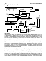
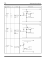
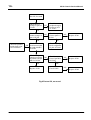
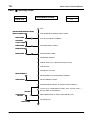
Part Ⅲ-Brief Introduction on Chassis
Nicam Option
Z141
W/Nicam
N/Nicam
K3955K
K2966
IC602
TDA8944
NICAM BD
SIF
I2C B US
RF IN
TUNE R
IF
Q101
IF AMP
Z141
SAWFILTER
IF
IC 101
TMPA8809 (M113)
X-TA L
8MHz
Hi-POT
AV INPUT
OUTPUT
IC601
NJW1136
I2C B US
IC301
V-OUTP UT
TDA8172
24C08
E2PROM
REMOTE
HANDSE T
IC801
MC44608
Q801
BUZ91A
RECE IVER
KEY MATRIX
T803
POWER
TRANS IS TOR
Q411
H DRIVE
H OUTP UT
FBT
30V
B+,
12V,9V,5VA
16V
5V
1.RF、IF AMP
The tuner receives, selects and amplifies RF signal, frequency mixes with local oscillate source, gets
38.0MHz&38.9MHz IF signal via C107 to Q101.After Q101 amplifing about 20dB,the PIF(Picture IF) and
SIF(Sound IF) are separated. Having passed sawfilter, PIF signal sent to TMPA8809 in pin 41,42.The IF
signal pass the video detect circuit to generate CVBS signal. Then the processor deals the signal with
luminance and chroma separation. The processor also deals the chroma siganl with integrated chroma
BPFs, PAL/NTSC demodulation and deals luminance signal with integrated chroma traps, black strech,
Y-gamma, so that the resolution of picture details is improved and Y signal is well timed with chroma signal.
The processor also deals the chroma signal with chroma sub-carrier recovery, color system recognition
and color signal decoding, then output R\G\B to CRT board. Via three groups dual emitter amplifiers to
drive KR\KG\KB. On the other hand, the processor separated by video detect circuit. Having passed the
horizontal & vertical frequency dividing circuit, H&V OSC signal, which be generated by H-AFC&V-AFC,
then output H&V signal which wave is sawtooth.
2.Channel Selection
The RF signal is converted into IF signal by the tuner. Then the IF signal cross the IF amplifier circuit(IF
pre-amp) to get a gain about 15dB. By the coupling capacitance(C107) and the match resistance R107,the
input resistance of the IF pre-amplifier match with the tuner. The signals pass a parallel connection circuit
with voltage NFB, which the input and output impedance is lower, of wide dynamic rage.R106 is the NFB
resistance, which is used to adjust the gain in the pass band. Having been amplified by the IF amplifier, the
IF signal pass the IF sawfilter K3955K(and C109 is the coupling cap.).Than PIF signal been sent from pin
4,pin5 of sawfilter to pin 41,pin42 of super one chip(TMPA8809).The processor deal the PIF signal with IF
4
02/12/09
TCL
M113 Chassis Service Manual
detection, PLL demodulation, IF AGC, AFC, video peak detection, and color system recognition ect, then
output a AGC signal from pin43 to the tuner to adjust the input control IF detection.R228,C227,C226
makes up picture IF PLL circuit, which is used to control IF detection.IC101 output a TV signal from
pin30,when pin30 level is high, TV-out signal is amplified by Q202,Q204,and Q203,Q205 is system switch
which controlled by Q211,Q210.
Tuning control and band switch control circuits
The processor output a tuning control signal from pin60.The control signal will pass Q004 and R/C network
to be amplified and differential circuit, then added to VT terminal to provide all channels’ tuning voltage for
the tuner to make the channel stable.
3.Vertical Output Section
TMPA8809 outputs vertical saw-tooth wave from pin 16. It come to pin1 of TDA8172 with DC coupling, and
is amplified by inner difference amplifier. Pin7 of TDA8172 is the same phase input terminal. R302 and
R303 are DC offset resistances. C304 is a filter capacitor. In application to M113, pin7 of TDA8172 is fixed
as the DC amplify ref terminal. The amplified saw tooth-wave comes out from pin5 and make the deflect
coil to generate the deflect current. R304 and C305 filtrate the inductive interference from the horizontal
deflect coil. R310 and C309 are used to eliminate spurious oscillation generated by the deflect coil and
distributed capacitance resonance. C308, R309, C307 and accessory circuit are in charge of draw AC saw
tooth wave out at the deflect coil terminal connected with R303A, and feedback to the input terminal of
TDA8172 (pin1) to correct the linearity of horizontal scan. C301 is a high frequency decoupling capacitor.
D301 and C302 make up of a voltage pump up circuit. TDA8172 output a vertical kickback impulse from
pin6 to locate the OSD characters.
4.Horizontal Output And FBT Section
The processor outputs horizontal drive impulse from pin 13(H-OUT). The drive impulse is done with
voltage division by R201 and R401, and then comes to the base of the drive triode (Q401). C401 is used to
eliminate the noise in the H drive impulse. T401 is a horizontal drive transformer. Q411 is a horizontal
output triode with a damper inside. L412 is connected with the emitter of the horizontal output diode to
eliminate the radiation and to improve the distortions at the cross of vertical and horizontal white lines.
C412 and C413 are retrace capacitors and C414 is an s-correct capacitor. L413 is horizontal linear
inductors. R441 is used to eliminate the parasitic oscillation caused by horizontal linear inductors. C421,
R421 and D421 are used to correct the M-distortion in horizontal direction.
The deflect coil and the horizontal output triode have some resistance R while they are ducting. The
resistance R will cause the non-linear distortion, which means that the right direction scanning speed of the
electron beam becomes slower, and the right of the raster is compressed to generate distortion. We use a
horizontal linear adjuster to compensate this kind of distortion. We use L414 as the H linear adjuster in
horizontal scanning section of M113 chassis. R419, which is parallel connected with L414, is a despiking
resistance for preventing the oscillation by compensating inductor and the stray capacitance. The linear
adjuster is a transductor coil with a magnetic core inside. If the current, which pass the linear adjuster coil,
increase to a certain value, the magnetic core becomes saturated to decrease the inductance of the linear
adjustment inductor. If the +B is steady, the increase speed of Iy is faster to compensate the reducing of
deflecting current by the resistance R mention above.
We can adjust the magnetic core to change the inductance of the linear compensate inductor to adjust the
H linearity.
The EW-correct signal sent from pin28 of TMPA8809,amplified with Q412,Q413 and Q414,to adjust
5
02/12/09
TCL
M113 Chassis Service Manual
horizontal output circuit.
The EHT generation circuit
The FBT supply the anode high voltage, focus voltage and screen voltage for M113 chassis. D441and
C441 are in charge of regulating the primary impulse of the transformer to output a voltage of 200V for the
video amplifiers. The ( 4 ) ~ ( 7 ) coils of the FBT supply the heater with power. To limit the beam current in
a safe range, we add a ABL(auto brightness limit) circuit in M113 chassis. When the beam current is higher
than normal,Q451 which is a emitter follower strength conductivity, the emitter gets a lower negative
voltage, so the collector of it follows a lower voltage, then gain of system brightness decreases, brightness
decrease and beam current decreases.
Also the ABL control voltage is sampled from R426 to adjust & control EW-scan.
Extension distortion and compensation
This kind of distortion is mainly caused by the structure of CRT. Due to the screen of SF CRT is not a pure
flat screen, the distances from the deflecting center to the screen are not the same. The scanning speed of
the electron beam is uniform. If the electron beam scannning the screen equally with the effect of ture
linear sawtooth current, the E-W sides of the picture are stretched. That is the extension distortion. Usually,
we add a S-correct capacitor in series with the deflecting coil to compensate this kind of distortion. The
integral character of S-correct capacitor make the current waveform S shape. So the scanning speed of
electron beam at the center of screen is faster than the one at the side. So this action can correct the
extension distortion. C414 is a S-correct capacitor. The capacitance is inverse ratio with the correcting
effection.
6
02/12/09
TCL
M113 Chassis Service Manual
PART IV. IC Pin Description
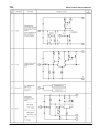
1. MC44608-High Voltage PWM Controller
Pin
Name
1
Demag
2
Isense
3
Control
Input
4
Ground
5
Driver
6
VCC
Description description
The Demag pin offers 3 different functions: Zero voltage crossing detection (50mV), 24
A current detection and 120 A current detection. The 24 A level is used to detect the
secondary reconfiguration status and the 120 A level to detect an Over Voltage status
called Quick OVP.
The Current Sense pin senses the voltage developed on the series resistor inserted in
the source of the power MOSFET. When Isense reaches 1V, the Driver output (pin 5) is
disabled. This is known as the Over Current Protection function. A 200 A current source
is flowing out of the pin 3 during the start–up phase and during the switching phase in
case of the Pulsed Mode of
operation. A resistor can be inserted between the sense resistor and the pin 3, thus a
programmable peak current detection can be performed during the SMPS stand–by
mode.
A feedback current from the secondary side of the SMPS via the opto–coupler is
injected into this pin. A resistor can be connected between this pin and GND to allow
the programming of the Burst duty cycle during the Stand–by mode.
This pin is the ground of the primary side of the SMPS.
The current and slew rate capability of this pin are suited to drive Power MOSFETs.
This pin is the positive supply of the IC. The driver output gets disabled when the
voltage becomes higher than 15V and the operating range is between 6.6V and 13V.
An intermediate voltage level of 10V creates a disabling condition called Latched Off
phase.
7
This pin is to provide isolation between the Vi pin 8 and the VCC pin 6.
8
This pin can be directly connected to a 500V voltage source for start–up function of the
IC. During the Start–up phase a 9 mA current source is internally delivered to the VCC
pin 6 allowing a rapid charge of the VCC capacitor. As soon as the IC starts–up, this
current source is disabled.
Vi
7
02/12/09
TCL
M113 Chassis Service Manual
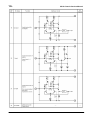
OPERATING DESCRIPTION
Regulation
The pin 3 senses the feedback current provided by the opto-coupler. During the switching phase the switch S2 is
closed and the shunt regulator is accessible by the pin 3. The shunt regulator voltage is typically 5V. The dynamic
resistance of the shunt regulator represented by the zener diode is 20 .
The gain of the Control input is given on Figure 10 which shows the duty cycle as a function of the current injected
into the pin 3.
The maximum current sense threshold is fixed at 1V. The peak
A 4KHz filter network is inserted
between the shunt regulator and the
PWM comparator to cancel the high
frequency residual noise.
The switch S3 is closed in Stand–by
mode during the Latched Off Phase
while the switch S2 remains open. (See
section PULSED MODE DUTY
CYCLE CONTROL).
The resistor Rdpulsed (Rduty cycle
burst) has no effect on the regulation
process. This resistor is used to
determine the burst duty cycle described in the chapter “Pulsed Duty Cycle Control” on page 8.
PWM Latch
The MC44608 works in voltage mode. The on–time is controlled by the PWM comparator that compares the
oscillator sawtooth with the regulation block output.
The PWM latch is initialized by the
oscillator and is reset by the PWM
comparator or by the current sense
comparator in case of an over current.
This configuration ensures that only a
single pulse appears at the circuit
output during an oscillator cycle.
Current Sense
The inductor current is converted to a
positive voltage by inserting a ground
reference sense resistor RSense in series
with the power switch.
The maximum current sense threshold is fixed at 1V. The peak current is given by the following equation:
Ipkmax = 1/Rsense( ) (A)
In stand–by mode, this current can be lowered as due to the activation of a 200 A current source:
IpkMAX-STBY
The current sense input consists of a filter (6k , 4pF) and of a leading edge blanking. Thanks to that, this pin is not
sensitive to the power switch turn on noise and spikes and practically in most applications, no filtering network is
8
02/12/09
TCL
M113 Chassis Service Manual
required to sense the current.
Finally, this pin is used:
– as a protection against over currents (Isense > I)
– as a reduction of the peak current during a Pulsed Mode switching phase.
The overcurrent propagation delay is reduced by producing a sharp output turn off (high slew rate).
This results in an abrupt output turn off in the event of an over current and in the majority of the pulsed mode
switching sequence.
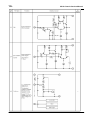
Demagnetization Section
The MC44608 demagnetization
detection consists of a
comparator designed to compare
the VCC winding voltage to a
reference that is typically equal
to 50mV.
This reference is chosen low to
increase effectiveness of the
demagnetization detection even
during start–up.
A latch is incorporated to turn
the demagnetization block
output into a low level as soon
as a voltage less than 50 mV is
detected, and to keep it in this
state until a new pulse is
generated on the output. This
avoids any ringing on the input
signal which may alter the
demagnetization detection.
For a higher safety, the
demagnetization block output is
also directly connected to the
output, which is disabled during the demagnetization phase.
The demagnetization pin is also used for the quick, programmable OVP. In fact, the demagnetization input current is
sensed so that the circuit output is latched off when this current is detected as higher than 120μA.
This function can be inhibited by grounding it but in this case, the quick and programmable OVP is also disabled.
Oscillator
The MC44608 contains a fixed frequency oscillator. It is built around a fixed value capacitor CT succesively charged
and discharged by two distinct current sources ICH and IDCH. The window comparator senses the CT voltage value
and activates the sources when the voltage is reaching the 2.4V/4V levels.
9
02/12/09
TCL
M113 Chassis Service Manual
The complete demagnetization status
DMG is used to inhibit the recharge of the
CT capacitor.
Thus in case of incomplete transformer
demagnetization the next switching cycle is
postpone until the DMG signal appears. The
oscillator remains at 2.4V corresponding to
the sawtooth valley voltage. In this way the
SMPS is working in the so called SOPS
mode (Self Oscillating Power Supply). In
that case the effective switching frequency is
variable and no longer depends on the
oscillator timing but on the external working
conditions (Refer to DMG signal in the
Figure 5).
The OSC and Clock signals are provided according to the Figure 5. The Clock signals correspond to the CT capacitor
discharge. The bottom curve represents the current flowing in the sense resistor Rcs. It starts from zero and stops
when the sawtooth value is equal to the control voltage Vcont. In this way the SMPS is regulated with a voltage mode
control.
Overvoltage Protection
The MC44608 offers two OVP functions:
– a fixed function that detects when VCC is higher than 15.4V
– a programmable function that uses the demag pin. The current flowing into the demag pin is mirrored and
compared to the reference current Iovp (120μA). Thus this OVP is quicker as it is not impacted by the VCC inertia
and is called QOVP.
In both cases, once an OVP condition is detected, the output is latched off until a new circuit
START–UP.
Start–up Management
The Vi pin 8 is directly connected to the HV DC rail Vin. This high voltage current source is
internally connected to the
VCC pin and thus is used to
charge the VCC capacitor. The
VCC capacitor charge period
corresponds to the Start–up
phase. When the VCC voltage
reaches 13V, the high voltage
9mA current source is
disabled and the device starts
working. The device enters
into the switching phase.
It is to be noticed that the maximum rating of the Vi pin 8 is 700V. ESD protection circuitry is not currently added to
this pin due to size limitations and technology constraints. Protection is limited by the drain–substrate junction in
10
02/12/09
TCL
M113 Chassis Service Manual
avalanche breakdown. To help increase the application safety against high voltage spike on that pin it is possible to
insert a small wattage 1k series resistor between the Vin rail and pin 8.
The Figure 6 shows the VCC voltage evolution in case of no external current source providing current into the VCC pin
during the switching phase. This case can be encountered in SMPS when the self supply through an auxiliary winding
is not present (strong overload on the SMPS output for example).
The Figure16 also depicts this working configuration.
In case of the hiccup mode, the duty cycle of the switching phase is in the range of 10%.
Mode Transition
The LW latch Figure
7 is the memory of
the working status at
the end of every
switching sequence.
Two different cases
must be considered
for the logic at the
termination of the
SWITCHING
PHASE:
1. No Over Current was observed
2. An Over Current was observed
These 2 cases are corresponding to the signal labeled NOC in case of “No Over Current” and “OC” in case of Over
Current. So the effective working status at the end of the ON time memorized in LW corresponds to Q=1 for no over
current and Q=0 for over current.
This sequence is repeated during the Switching phase.
Several events can occur:
1. SMPS switch OFF
2. SMPS output overload
3. Transition from Normal to Pulsed Mode
4. Transition from Pulsed Mode to Normal Mode
1. SMPS SWITCH OFF
When the mains is switched OFF, so long as the bulk electrolithic bulk capacitor provides energy to the SMPS, the
controller remains in the switching phase. Then the peak current reaches its maximum peak value, the switching
frequency decreases and all the secondary voltages are reduced. The VCC voltage is also reduced. When VCC is equal
to 10V, the SMPS stops working.
2. Overload
In the hiccup mode the 3 distinct phases are described as follows (refer to Figure 6):
The SWITCHING PHASE: The SMPS output is low and the regulation block reacts by increasing the ON time
(dmax = 80%). The OC is reached at the end of every switching cycle. The LW latch (Figure 7) is reset before the
VPWM signal appears. The SMPS output voltage is low. The VCC voltage cannot be maintained at a normal level as
11
02/12/09
TCL
M113 Chassis Service Manual
the auxiliary winding provides a voltage which is also reduced in a ratio similar to the one on the output (i.e. Vout
nominal / Vout short–circuit). Consequently the VCC voltage is reduced at an operating rate given by the combination
VCC capacitor value together with the ICC working consumption (3.2mA) according to the equation 2. When VCC
crosses 10V the WORKING PHASE gets terminated. The LW latch remains in the reset status.
The LATCHED–OFF PHASE: The VCC capacitor voltage continues to drop. When it reaches 6.5V this phase is
terminated. Its duration is governed by equation 3.
The START–UP PHASE is reinitiated. The high voltage start–up current source (–ICC1 = 9mA) is activated and the
MODE latch is reset. The VCC voltage ramps up according to the equation 1. When it reaches 13V, the IC enters into
the SWITCHING PHASE.
The NEXT SWITCHING PHASE: The high voltage current source is inhibited, the MODE latch (Q=0) activates the
NORMAL mode of operation. Figure 2 shows that no current is injected out pin 2.
The over current sense level corresponds to 1V.
As long as the overload is present, this sequence repeats. The SWITCHING PHASE duty cycle is in the range of
10%.
3. Transition from Normal to Pulsed Mode
In this sequence the secondary side is reconfigured (refer to the typical application schematic on page 13). The high
voltage output value becomes lower than the NORMAL mode regulated value. The TL431 shunt regulator is fully
OFF. In the SMPS stand–by mode all the SMPS outputs are lowered except for the low voltage output that supply the
wake–up circuit located at the isolated side of the power supply. In that mode the secondary regulation is performed
by the zener diode connected in parallel to the TL431.
The secondary reconfiguration status can be detected on the SMPS primary side by measuring the voltage level
present on the auxiliary winding Laux. (Refer to the Demagnetization Section). In the reconfigured status, the Laux
voltage is also reduced. The VCC self–powering is no longer possible thus the SMPS enters in a hiccup mode similar
to the one described under the Overload condition.
In the SMPS stand–by mode the 3 distinct phases are:
The SWITCHING PHASE: Similar to the Overload mode. The current sense clamping level is reduced according to
the equation of the current sense section, page 5. The C.S. clamping level depends on the power to be delivered to the
load during the SMPS stand–by mode. Every switching sequence ON/OFF is terminated by an OC as long as the
secondary Zener diode voltage has not been reached. When the Zener voltage is reached the ON cycle is terminated
by a true PWM action. The proper SWITCHING PHASE termination must correspond to a NOC condition. The LW
latch stores this NOC status.
The LATCHED OFF PHASE: The MODE latch is set.
The START–UP PHASE is similar to the Overload Mode. The MODE latch remains in its set status (Q=1).
The SWITCHING PHASE: The Stand–by signal is validated and the 200μA is sourced out of the Current Sense
pin 2.
4. Transition from Stand–by to Normal
The secondary reconfiguration is removed. The regulation on the low voltage secondary rail can no longer be
achieved, thus at the end of the SWITCHING PHASE, no PWM condition can be encountered. The LW latch is reset.
At the next WORKING PHASE a NORMAL mode status takes place.
In order to become independent of the recovery time SWITCHING PHASE constant on the secondary side of the
12
02/12/09
TCL
M113 Chassis Service Manual
SMPS an additional reset input R2 is provided on the MODE latch. The condition Idemag<24μA corresponds to the
activation of the secondary reconfiguration status. The R2 reset insures a return into the NORMAL mode following
the first corresponds to 1V. START–UP PHASE.
Pulsed Mode Duty Cycle Control
During the sleep mode of the SMPS the switch S3 is closed and the control input pin 3 is connected to a 4.6V voltage
source thru a 500Ωresistor. The discharge rate of the VCC capacitor is given by ICC–latch (device consumption during
the LATCHED OFF phase) in addition to the current drawn out of the pin 3. Connecting a resistor between the Pin 3
and GND (RDPULSED) a programmable current is drawn from the VCC through pin 3. The duration of the LATCHED
OFF phase is impacted by the presence of the resistor RDPULSED. The equation 3 shows the relation to the pin 3
current.
Pulsed Mode Phases
Equations 1 through 8 define and predict the effective behavior during the PULSED MODE operation. The equations
6, 7, and 8 contain K, Y, and D factors. These factors are combinations of measured parameters. They appear in the
parameter section “K factors for pulsed mode operation” page 4. In equations 3 through 8 the pin 3 current is the
current defined in the above section “Pulsed Mode Duty Cycle Control”.
2. TDA9801-Single standard VIF-PLL demodulator and FM-PLL detector
FUNCTIONAL DESCRIPTION
13
02/12/09
TCL
M113 Chassis Service Manual
SYMBOL
VIF1
VIF2
TOP
ADJ
MUTE
TPLL
CVBS
n.c.
AF
DAF
SI
TAGC
VSO
VI
AFC
VCO1
VCO2
GND
AGC
VP
PIN
1
2
3
4
5
6
7
8
9
10
11
12
13
14
15
16
17
18
19
20
DESCRIPTION
VIF differential input 1
VIF differential input 2
tuner AGC TakeOver Point (TOP) connection
phase adjust connection
sound mute switch connection
PLL time constant connection
CVBS (positive) video output
not connected
AF output
AF amplifier decoupling capacitor connection
sound intercarrier input
tuner AGC output
video and sound intercarrier output
buffer amplifier video input
AFC output
VCO1 reference circuit for 2fPC
VCO2 reference circuit for 2fPC
ground supply (0 V)
AGC detector capacitor connection
supply voltage (+5 V)
Stage IF amplifier
The VIF amplifier consists of three AC-coupled differential amplifier stages. Each differential stage comprises a
feedback network controlled by emitter degeneration.
AGC detector, IF AGC and tuner AGC
The automatic control voltage to maintain the video output signal at a constant level is generated in accordance with
the transmission standard. Since the TDA9801 is suitable for negative modulation only the peak sync pulse level is
detected.
The AGC detector charges and discharges capacitor CAGC to set the IF amplifier and tuner gain. The voltage on
capacitor CAGC is transferred to an internal IF control signal, and is fed to the tuner AGC to generate the tuner AGC
output current on pin TAGC (open-collector output). The tuner AGC takeover point level is set at pin TOP. This
allows the tuner to be matched to the SAW filter in order to achieve the optimum IF input level.
Frequency detector and phase detector
The VIF amplifier output signal is fed into a frequency detector and into a phase detector. During acquisition the
frequency detector produces a DC current proportional to the frequency difference between the input and the VCO
signal. After frequency lock-in the phase detector produces a DC current proportional to the phase difference between
the VCO and the input signal. The DC current of either frequency detector or phase detector is converted into a DC
voltage via the loop filter which controls the VCO frequency.
Video demodulator
The true synchronous video demodulator is realized by a linear multiplier which is designed for low distortion and
wide bandwidth. The vision IF input signal is multiplied with the ‘in phase’ component of the VCO output. The
demodulator output signal is fed via an integrated low-pass filter (fg = 12 MHz) for suppression of the carrier
harmonics to the video amplifier.
VCO, AFC detector and travelling wave divider
14
02/12/09
TCL
M113 Chassis Service Manual
The VCO operates with a symmetrically connected reference LC circuit, operating at the double vision carrier
frequency. Frequency control is performed by an internal variable capacitor diode.
The voltage to set the VCO frequency to the actual double vision carrier frequency is also amplified and converted
for the AFC output current.
The VCO signal is divided-by-2 with a Travelling Wave Divider (TWD) which generates two differential output
signals with a 90 degree phase difference independent of the frequency.
Video amplifier
The composite video amplifier is a wide bandwidth operational amplifier with internal feedback. A nominal positive
video signal of 1 V (p-p) is present at pin VSO.
Buffer amplifier and noise clipper
The input impedance of the 7 dB wideband CVBS buffer amplifier (with internal feedback) is suitable for ceramic
sound trap filters. Pin CVBS provides a positive video signal of 2 V (p-p). Noise clipping is provided internally.
Sound demodulation
LIMITER AMPLIFIER
The FM sound intercarrier signal is fed to pin SI and through a limiter amplifier before it is demodulated. The result
is high sensitivity and AM suppression. The limiter amplifier consists of 7 stages which areinternally AC-coupled in
order to minimizing the DC offset.
FM-PLL DETECTOR
The FM-PLL demodulator consists of an RC oscillator, loop filter and phase detector. The oscillator frequency is
locked on the FM intercarrier signal from the limiter amplifier. As a result of this locking, the RC oscillator is
frequency modulated. The modulating voltage (AF signal) is used to control the oscillator frequency. By this, the
FM-PLL operates as an FM demodulator.
AF AMPLIFIER
The audio frequency amplifier with internal feedback is designed for high gain and high common-mode rejection.
The low-level AF signal output from the FM-PLL demodulator is amplified and buffered in a low-ohmic audio
output stage. An external decoupling capacitor CDAF removes the DC voltage from the audio amplifier input.
By using the sound mute switch (pin MUTE) the AF amplifier is set in the mute state.
3. TDA9874A Digital TV sound demodulator/decoder
SYMBOL
EXTIR
EXTIL
Vref2
P2
OUTM
VSSA4
OUTL
OUTR
VDDA1
VSSA1
PIN
1
2
3
4
5
6
7
8
9
10
DESCRIPTION
external audio input right channel
external audio input left channel
analog reference voltage for DAC and operational amplifiers
second general purpose I/O pin
analog output mono
analog ground supply 4 for analog back-end circuitry
analog output left
analog output right
analog supply voltage 1; back-end circuitry 5 V
analog ground supply 1; back-end circuitry
15
02/12/09
TCL
VSSD1
VDDD1
VSSD2
TP2
NICAM
TP1
PCLK
ADDR1
XTALO
XTALI
TEST2
Iref
ADDR2
VSSA2
VDEC
TEST1
SIF2
Vref1
SIF1
CRESET
VSSA3
VDDA3
SCL
SDA
SDO
WS
SCK
SYSCLK
VDDD3
VSSD3
P1
MONOIN
M113 Chassis Service Manual
11
12
13
14
15
16
17
18
19
20
21
22
23
24
25
26
27
28
29
30
31
32
33
34
35
36
37
38
39
40
41
42
digital ground supply 1; core circuitry
digital supply voltage 1; core voltage regulator circuitry
digital ground supply 2; core circuitry
additional test pin 2; connected to VSSD for normal operation
serial NICAM data output (at 728 kHz)
additional test pin 1; connected to VSSD for normal operation
NICAM clock output (at 728 kHz)
first I2C-bus slave address modifier input
crystal oscillator output
crystal oscillator input
test pin 2; connected to VSSD for normal operation
resistor for reference current generation; front-end circuitry
second I2C-bus slave address modifier input
analog ground supply 2; analog front-end circuitry
analog front-end circuitry supply voltage decoupling
test pin 1; connected to VSSD for normal operation
sound IF input 2
reference voltage; for analog front-end circuitry
sound IF input 1
capacitor for Power-on reset
digital ground supply 3; front-end circuitry
analog front-end circuitry regulator supply voltage 3 (5 V)
I2C-bus serial clock input
I2C-bus serial data input/output
I2S-bus serial data output
I2S-bus word select input/output
I2S-bus clock input/output
system clock output
digital supply voltage 3; digital I/O pads
digital ground supply 3; digital I/O pads
first general purpose I/O pin
analog mono input
FUNCTIONAL DESCRIPTION
Description of the demodulator and decoder section
1. SIF INPUTS
Two inputs are provided, pin SIF1 and pin SIF2. For higher SIF signal levels the
SIF input can be attenuated with an internal switchable 10 dB resistor divider.
As no specific filters are integrated, both inputs have the same specification
giving flexibility in application. The selected signal is passed through
an AGC circuit and then digitized by an 8-bit ADC operating at 24.576 MHz.
2. AGC
The gain of the AGC amplifier is controlled from the ADC output by means of
a digital control loop employing hysteresis. The AGC has a fast attack behaviour
to prevent ADC overloads, and a slow decay behaviour to prevent AGC oscillations.
For AM demodulation the AGC must be switched off. When switched off, the
control loop is reset and fixed gain settings can be chosen. The AGC can be
controlled via the I2C-bus.
3. MIXER
The digitized input signal is fed to the mixers, which mix one or both input sound
16
02/12/09
TCL
M113 Chassis Service Manual
carriers down to zero IF. A 24-bit control word for each carrier sets the required frequency. Access to the mixer
control word registers is via the I2C-bus or via Easy Standard Programming (ESP). When receiving NICAM
programs, a feedback signal is added to the control word of the second carrier mixer to establish a carrier-frequency
loop.
4.FM AND AM DEMODULATION
An FM or AM input signal is fed through a switchable band-limiting filter into a demodulator that can be used for
either FM or AM demodulation. Apart from the standard (fixed) de-emphasis characteristic, an adaptive de-emphasis
is available for Wegener-Panda 1 encoded satellite programs.
5. FM DECODING
A 2-carrier stereo decoder recovers the left and right signal channels from the demodulated sound carriers. Both the
European and Korean stereo systems are supported.
Automatic FM dematrixing is also supported, which means that the FM sound mode identification (mono, stereo or
dual) switches the FM dematrix directly. No loop via the microcontroller is needed.
17
02/12/09
TCL
M113 Chassis Service Manual
For highly overmodulated signals, a high deviation mode for monaural audio sound single carrier demodulation can
be selected.
NICAM decoding is still possible in high deviation mode.
6. FM IDENTIFICATION
The identification of the FM sound mode is performed by AM synchronous demodulation of the pilot and
narrow-band detection of the identification frequencies. The result is available via the I2C-bus interface. A selection
can be made via the I2C-bus for B/G, D/K and M standards, and for three different time constants that represent
different trade-offs between speed and reliability of identification. A pilot detector allows the control software to
identify an analog 2-carrier (A2) transmission within approximately 0.1 s.
Automatic FM dematrixing, depending on the identification, is possible.
7. NICAM DEMODULATION
The NICAM signal is transmitted in a DQPSK code at a bit rate of 728 kbits/s. The NICAM demodulator performs
DQPSK demodulation and passes the resulting bitstream and clock signal to the NICAM decoder and, for evaluation
purposes, to various pins.
A timing loop controls the frequency of the crystal oscillator to lock the sampling instants to the symbol timing of the
NICAM data.
8. NICAM DECODING
The device performs all decoding functions in accordance with the “EBU NICAM 728 specification”. After locking
to the frame alignment word, the data is descrambled by applying the defined pseudo-random binary sequence. The
device then synchronizes to the periodic frame flag bit C0.
The status of the NICAM decoder can be read out from the NICAM status register by the user. The OSB bit indicates
that the decoder has locked to the NICAM data. The VDSP bit indicates that the decoder has locked to the NICAM
data and that the data is valid sound data. The C4 bit indicates that the sound conveyed by the FM mono channel is
identical to the sound conveyed by the NICAM channel.
The error byte contains the number of sound sample errors (resulting from parity checking) that occurred in the past
128 ms period. The Bit Error Rate (BER) can be calculated using the following equation:
BER = bit errors / total bits≈error byte×1.74×10⁻⁵
9. NICAM AUTO-MUTE
This function is enabled by setting bit AMUTE to logic 0. Upper and lower error limits may be defined by writing
appropriate values to two registers in the I2C-bus section. When the number of errors in a 128 ms period exceeds the
upper error limit, the auto-mute function will switch the output sound from NICAM to whatever sound is on the first
sound carrier (FM or AM) or to the analog mono input. When the error count is smaller than the lower error limit, the
NICAM sound is restored.
The auto-mute function can be disabled by setting bit AMUTE to logic 1. In this case clicks become audible when the
error count increases. The user will hear a signal of degrading quality.
If no NICAM sound is received, the outputs are switched from the NICAM channel to the 1st sound carrier.
18
02/12/09
TCL
M113 Chassis Service Manual
A decision to enable or disable the auto-mute is taken by the microprocessor based on an interpretation of the
application control bits C1, C2, C3 and C4, and possibly any additional strategy implemented by the user in the
microcontroller software. When the AM sound in NICAM L systems is demodulated in the 1st sound IF and the
audio signal connected to the mono input of the TDA9874A, the controlling microprocessor has to ensure
switching from NICAM reception to mono input, if auto-muting is desired. This can be achieved by setting bit
AMSEL = 1 and bit AMUTE = 0.
10. CRYSTAL OSCILLATOR
The digital controlled crystal oscillator (DCXO) is fully integrated. Only an external 24.576 MHz crystal is required.
11. TEST PINS
All test pins are active HIGH. In normal operation of the device they can be left open-circuit, as they have internal
pull-down resistors. Test functions are for manufacturing tests only and are not available to customers.
12. POWER FAIL DETECTOR
The power fail detector monitors the internal power supply for the digital part of the device. If the supply has
temporarily been lower than the specified lower limit, the power failure register bit PFR in subaddress 0, will be set
to logic 1. Bit CLRPFR, slave register subaddress 1, resets the Power-on reset flip-flop to logic 0. If this is detected,
an initialization of the TDA9874A has to be performed to ensure reliable operation.
13. POWER-ON RESET
The reset is active LOW. In order to perform a reset at power-up, a simple RC circuit may be used which consists of
an integrated passive pull-up resistor and an external capacitor connected to ground.
The pull-up resistor has a nominal value of 50 k , which can easily be measured
between pins CRESET and
VDDD3. Before the supply voltage has reached a certain minimum level, the state of the circuit is completely
undefined and remains in this undefined state until a reset is applied.
The reset is guaranteed to be active when:
.The power supply is within the specified limits (4.5 to
5.5 V)
.The crystal oscillator (DCXO) is functioning
.The voltage at pin CRESET is
below 0.3VDDD (1.5 V if VDDD= 5.0 V, typically
below 1.8 V).
The required capacitor value depends on the gradient of
the rising power supply voltage. The time constant of the
RC circuit should be clearly larger than the rise time of
the power supply (to make sure that the reset condition is
always satisfied), even when considering tolerance spreading. To avoid problems with a too slow discharging of the
capacitor at
power-down, it may be helpful to add a diode from pin CRESET to VDDD.
It should be noted that the internal ESD protection diode does not help here as it only conducts at higher voltages.
Under difficult power supply conditions (e.g. very slow or non-monotonic ramp-up), it is recommended to drive the
reset line from a microcontroller port or the like.
19
02/12/09
TCL
M113 Chassis Service Manual
Description of the DSP
1. LEVEL SCALING
All input channels to the digital crossbar switch are equipped with a level adjustment facility to change the signal
level in a range of ±15 dB. Adjusting the signal level is intended to compensate for the different modulation
parameters of the various TV standards. Under nominal conditions it is recommended to scale all input channels to be
15 dB below full-scale. This will create sufficient headroom to cope with overmodulation and avoids changes of the
volume impression when switching from FM to NICAM or vice versa.
2. NICAM PATH
The NICAM path has a switchable J17 de-emphasis.
3. NICAM AUTO-MUTE
If NICAM is received, the auto-mute is enabled and the signal quality becomes poor. The digital crossbar switches
automatically to FM, channel 1 or the analog mono input, as selected by bit AMSEL. This automatic switching
depends on the NICAM bit error rate. The auto-mute function can be disabled via the I2C-bus.
4. FM (AM) PATH
A high-pass filter suppresses DC offsets from the FM demodulator that may occur due to carrier Frequency offsets,
and supplies the FM monitor function with DC values, e.g. for the purpose of microprocessor controlled carrier
search or fine tuning functions.
An adaptive de-emphasis is available for Wegener-Panda 1 encoded satellite programs.
The de-emphasis stage offers a choice of settings for the supported TV standards.
The 2-channel decoder performs the dematrixing of 1¤2(L + R), R to L and R signals of 1¤2(L + R) and 1¤2(L - R) to L
and R signals or of channel 1 and channel 2 to L and R signals, as demanded by the different TV standards or user
preferences.
Automatic FM dematrixing is also supported.
Using the high deviation mode, only channel 1 (mono) can be demodulated. The scaling is -6 dB compared to
2-channel decoding.
20
02/12/09
TCL
M113 Chassis Service Manual
5. MONITOR
This function provides data words from the FM demodulator outputs and FM and NICAM signals for external use,
such as carrier search or fine tuning. The peak level of these signals can also be observed. Source selection and data
read out are performed via the I2C-bus.
6. DIGITAL CROSSBAR SWITCH
The input channels are derived from the FM and NICAM paths, while the output channels comprise I2S-bus and the
audio DACs to the analog crossbar switch. It should be noted that there is no connection from the external analog
audio inputs to the digital crossbar switch.
7. DIGITAL AUDIO OUTPUT
The digital audio output interface comprises an I2S-bus output port and a system clock output. The I2S-bus port is
equipped with a level adjustment facility that can change the signal level in a ±15 dB range in 1 dB steps. Muting is
possible, too, and outputs can be disabled to improve EMC performance.
The I2S-bus output matrix provides the functions for forced mono, stereo, channel swap, channel 1 or channel 2.
Automatic selection for TV applications is possible. In this case the microcontroller program only has to provide a
user controlled sound A or sound B selection.
8. STEREO CHANNEL TO THE ANALOG CROSSBAR PATH
A level adjustment function is provided with control positions of 0 dB, +3 dB, +6 dB and +9 dB in combination with
the audio DACs. The Automatic Volume Level (AVL) function provides a constant output level of -20 dB (full-scale)
for input levels between 0 dB (full-scale) and -26 dB (full-scale).
There are some fixed decay time constants to choose from, i.e. 2, 4 or 8 seconds.
Automatic selection for TV applications is possible. In this case the microcontroller program only has to provide a
user controlled sound A or sound B selection.
9. GENERAL
The level adjustment functions can provide signal gain at multiple locations. Great care has to be taken when using
gain with large input signals, e.g., due to overmodulation, in order not to exceed the maximum possible signal swing,
which would cause severe signal distortion. The nominal signal level of the various signal sources to the digital
crossbar switch should be 15 dB below digital full-scale (-15dB full-scale).
Description of the analog audio section
1. ANALOG CROSSBAR SWITCH AND ANALOG MATRIX
The TDA9874A has one external analog stereo input, one mono input, one 2-channel and one single-channel output
port. Analog source selector switches are employed to provide the desired analog signal routing capability, which is
done by the analog crossbar switch section.
The basic signal routing philosophy of the TDA9874A is that each switch handles two signal channels at the same
time (e.g. left and right, language A and B) directly at the source.
Each source selector switch is followed by an analog matrix to perform further selection tasks, such as putting a
signal from one input channel, say language A, to both output channels or for swapping left and right channels. The
analog matrix provides the functions given in the follow table. Automatic matrixing for TV applications is also
supported.
21
02/12/09
TCL
M113 Chassis Service Manual
2
All switches and matrices are controlled via the I C-bus.
Analog matrix functions
2. EXTERNAL AND MONO INPUTS
MATRIX OUTPUT
MODE
The external and mono inputs accept signal levels of up to 1.4 V
L OUTPUT
R OUTPUT
(RMS). By adding external series resistors to provide suitable
1
L input
R input
2
R input
L input
attenuation, the external input could be used as a SCART input.
3
L input
L input
Whenever the external or mono input is selected, the output of the
4
R input
R input
DAC is muted to improve the crosstalk performance.
3. AUDIO DACS
The TDA9874A comprises a 2-channel audio DAC and an additional single-channel audio DAC for
feeding signals from the DSP section to the analog crossbar switch. These DACs have a resolution of
15 bits and employ four-times oversampling and noise shaping.
4. AUDIO OUTPUT BUFFERS
The output buffers provide a gain of 0 dB and offer a
muting possibility. The post filter capacitors of the audio
DACs are connected to the buffer outputs.
5. STANDBY MODE
Switch diagram for the analog audio section
The standby mode (see Section 7.3.3) disables most functions and reduces power dissipation of the TDA9874A. It
provides no other function.
Internal registers may lose their information in standby mode. Therefore, the device needs to be initialized on
returning to normal operation. This can be accomplished in the same way as after a Power-on reset.
22
02/12/09
TCL
M113 Chassis Service Manual
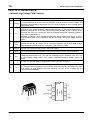
4.NJW1136 AUDIO PROCESSOR with Subwoofer Output
■ GENERAL DESCRIPTION
■ PACKAGE OUTLINE
THE NJW1136 is a sound processor with subwoofer output includes
all of functions processing audio signal for TV, such as tone control,
balance, volume, mute, and AGC function. Also the NJW1136 includes
the LPF for subwoofer output and bass boost function. The original
surround system reproduces natural surround sound and clear vocal
orientation. All of internal status and variables are controlled by IIC BUS
interface.
NJW1136D
■ FEATURES
●
●
●
●
●
●
●
●
●
Operating Voltage: 8 to 13V
3ch Output(Lch, Rch, Subwoofer ch) / 2ch Output(Lch, Rch)
LPF Filter (Adjustable cut off frequency by external parts)
AGC Circuit (It reduces volume difference among input sources.)
Adjustable AGC boost level by external parts and AGC compression level by IIC BUS
NJRC Original Surround System
Simulated Stereo
IIC BUS Interface
Bi-CMOS Technology
Package Outline
DIP32
■ BLOCK DIAGRAM
23
02/12/09
TCL
M113 Chassis Service Manual
■ PIN CONFIGURATION
No.
symbol
1
INa
2
SR-FIL
3
4
5
6
7
8
SS-FIL
TONE-Ha
TONE-La
OUTw
OUTa
AGC1
9
AUX0
10
AUX1
Function
No.
symbol
Function
Ach input terminal
17
V+
Supply voltage terminal
Surround filter terminal
18
Vref
Reference voltage terminal
19
20
21
22
23
24
CSR
CTL
CTH
CVW
CVB
CVA
DAC output terminal for surround control
DAC output terminal for tone control(bass)
DAC output terminal for tone control(treble)
Bch DAC output terminal for LPF trimmer
Bch DAC output terminal for volume and balance
Ach DAC output terminal for volume and balance
25
AGC2
AGC boost level setting terminal
26
OUTb
Bch output terminal
27
TONE-Lb
Bch tone control (bass) filter terminal
28
29
TONE-Hb
LF3
Bch tone control (treble) filter terminal
LPF filter3 terminal
11
PORT0
Simulated stereo filter terminal
Ach tone control(treble)filter terminal
Ach tome control(bass)filter terminal
Subwoofer output terminal
Ach output terminal
AGC attack and recovery time setting terminal
Auxiliary 3 values voltage output terminal
(0.0V,2.5V,5V)
Auxiliary 2 values voltage output terminal
(0.0V,5V)
Logic input terminal
12
13
PORT1
ADR
Logic input terminal
Slave address setting terminal
14
SDA
I2Cdata terminal
30
LF2
LPF filter2 terminal
15
SCL
I2C cock terminal
31
LF1
LPF filter1 terminal
16
GND
Ground terminal
32
INb
Bch input terminal
o
■ ABSOLUTE MAXIUM RATING (Ta=25 C)
Basic Structure
1. Internal Connections
TMPA8809 has two pieces of IC chip in one package, using Multi-Chip-Package(MCP)
technology. One is a micro controller (MCU) and the other one is a signal processor (SP) for a color TV.
There are some internal connections between these two ICs for handing below signals.
Functions of SP from MCU are controllable through the IIC bus of the internal connections.
24
02/12/09
TCL
M113 Chassis Service Manual
2.Power Supply
TMPA8809 has some power supplys and GND pins. Power supplies related MCU use be applied at the
first. Power supplies for H.V cc and TV D.Vcc are the second with at least 100 ms delay after MCU power
ON. The other power supplies are the last, which are recommended to be supplied from a regulator a
regulator circuit using FBP.
3.Crystal Resonator
TMPA8809 requires only crystal resonator, in stead that a conventional two-chip solution requires two
resonators at least, one for MCU and the other one for SP. An oscillation clock with the crystal resonator of
TMPA8809 is supplied for MCU operation, PIF VCO automatic alignment, alignment free AFT, of functions
work properly, so that designing the oscillation frequency accurately is required. The spec of crystal is
recommended to be within.
fosc:8 MHz+/-20 ppm
ftemp:8 MHz+/-40 ppm (-20oC to +65oC)
While RESET of MCU is active, the MCU function stops. Hardware and software initialization sequence
including power supplies control is required, because status of any hardware after the RESET period is
unknown especially horizontal oscillator which is a very basic timing generator of SP operation.
25
02/12/09
TCL
M113 Chassis Service Manual
26
02/12/09
TCL
M113 Chassis Service Manual
27
02/12/09
TCL
M113 Chassis Service Manual
28
02/12/09
TCL
M113 Chassis Service Manual
29
02/12/09
TCL
M113 Chassis Service Manual
30
02/12/09
TCL
M113 Chassis Service Manual
31
02/12/09
TCL
M113 Chassis Service Manual
32
02/12/09
TCL
M113 Chassis Service Manual
33
02/12/09
TCL
M113 Chassis Service Manual
34
02/12/09
TCL
M113 Chassis Service Manual
35
02/12/09
TCL
M113 Chassis Service Manual
36
02/12/09
TCL
M113 Chassis Service Manual
37
02/12/09
TCL
M113 Chassis Service Manual
38
02/12/09
TCL
M113 Chassis Service Manual
39
02/12/09
TCL
M113 Chassis Service Manual
40
02/12/09
TCL
M113 Chassis Service Manual
41
02/12/09
TCL
M113 Chassis Service Manual
5.TMPA8809CPAN
MCU and Signal Processor for a PAL/NTSC TV
The TMPA8809CPAN is an integrated circuit for a PAL/NTSC TV.
A MCU and a TV signal processor are integrated in a 64-pin
shrink DIP package. The MCU contains 8-bit CPU, ROM, RAM,
I/O ports, timer/counters, A/D converters, an on-screen display
Controller, remote control interfaces, IIC bus interfaces and the
Closed Caption decoder. The TV signal processor contains PIF,
SIF, Video, multi-standard chroma, Deflection, RGB processors.
MROM: TMPA8809CPAN
OTP: TMPA8807PSAN
Features
MCU
● High speed 8-bit CPU (TLC-870/X series)
● Instruction execution time: 0.5 μs (at 8 MHz)
● 48-Kbytes ROM, 2-Kbytes RAM
● ROM correction
● 12 I/O ports
● 14-bit PWM output 1 ch for a voltage synthesizer
● 7-bit PWM output 1 chan
● 8-bit A/D converter 3 ch for a touch-key input with
key ON wake-up CIRCUIT
● Remote control signal preprocessor
● Two 16-bit in
● Two 8-bit internal timer/counter 2 ch
● Time base timer, watchdog timer
● 16 interrupt sources: external 5, internal 11
● IIC bus interface (multi-master)
● STOP and IDLE power saving modes
CCD Decoder
● Digital data slicer for NTSC
OSD
● Clock generation for OSD display
● Front ROM characters: 384 characters
● Characters display: 32 columns×12 lines
● Composition: 16×18 dots
● Size of character: 3 (line by line)
● Color of character: 8 (character by character)
● Display position: H 256/V 512 steps
● BOX function
● Fringing, smoothing, Italic, underline function
● Conform to CCD REGULATION
● Jitter elimination
TV Processor IF
● Integrated PIF VCO aligned automatically
● Negative demodulation PIF
● Multi-frequency SIF demodulator without external
Tank-coil
RGB/Base-Band
● Integrated 1 H base-band delay line
● Base-band TINT control
● Internal OSD interface
● Half-tone and transparent for OSD
● External YcbCr interface for OSD
● RGB cut-off/drive controls by bus
● ABCL (ABL and ACL combined)
Video
● Integrated chroma traps
● Black stretch
● Y-gamma
Sync.
● Integrated fH×640 VCO
● DC coupled vert. ramp output (single)
● EW correction with EHT input
Chroma
● Integrated chroma BPFs
● PAL/NTSC demodulation
42
02/12/09
TCL
M113 Chassis Service Manual
43
02/12/09
TCL
M113 Chassis Service Manual
Basic Structure
2. Internal Connections
TMPA8809 has two pieces of IC chip in one package, using Multi-Chip-Package(MCP)
technology. One is a micro controller (MCU) and the other one is a signal processor (SP) for a color TV.
There are some internal connections between these two ICs for handing below signals.
Functions of SP from MCU are controllable through the IIC bus of the internal connections.
2.Power Supply
TMPA8809 has some power supplys and GND pins. Power supplies related MCU use be applied at
the first. Power supplies for H.V cc and TV D.Vcc are the second with at least 100 ms delay after MCU
power ON. The other power supplies are the last, which are recommended to be supplied from a regulator
a regulator circuit using FBP.
3.Crystal Resonator
TMPA8809 requires only crystal resonator, in stead that a conventional two-chip solution requires two
resonators at least, one for MCU and the other one for SP. An oscillation clock with the crystal resonator of
TMPA8809 is supplied for MCU operation, PIF VCO automatic alignment, alignment free AFT, of functions
work properly, so that designing the oscillation frequency accurately is required. The spec of crystal is
recommended to be within.
fosc:8 MHz+/-20 ppm
ftemp:8 MHz+/-40 ppm (-20oC to +65oC)
While RESET of MCU is active, the MCU function stops. Hardware and software initialization
sequence including power supplies control is required, because status of any hardware after the RESET
period is unknown especially horizontal oscillator which is a very basic timing generator of SP operation.
44
02/12/09
TCL
M113 Chassis Service Manual
45
02/12/09
TCL
M113 Chassis Service Manual
46
02/12/09
TCL
M113 Chassis Service Manual
47
02/12/09
TCL
M113 Chassis Service Manual
48
02/12/09
TCL
M113 Chassis Service Manual
49
02/12/09
TCL
M113 Chassis Service Manual
50
02/12/09
TCL
M113 Chassis Service Manual
51
02/12/09
TCL
M113 Chassis Service Manual
52
02/12/09
TCL
M113 Chassis Service Manual
53
02/12/09
TCL
M113 Chassis Service Manual
54
02/12/09
TCL
M113 Chassis Service Manual
55
02/12/09
TCL
M113 Chassis Service Manual
56
02/12/09
TCL
M113 Chassis Service Manual
57
02/12/09
TCL
M113 Chassis Service Manual
58
02/12/09
TCL
M113 Chassis Service Manual
59
02/12/09
TCL
M113 Chassis Service Manual
60
02/12/09
TCL
M113 Chassis Service Manual
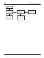
PART V. Adjusting Description
1.TMPA8827+M113 software adjustment specification(SAMPLING MODEL:2918AE)
M113 chassis is used as I2C bus control chassis for 25 inch or bigger TV in our company ,use TOSHIBA
TMPA8809 TWO IN ONE TV process chip,and software M113 designed by R&D dept. ourselves. First
production runing please use flash edition TOSHIBA TMPA8827 to be programmable,then,change to OTP
edition TOSHIBA TMPA8827,take care of this point in your production. Secondly, adopting I2C bus
structure,we can use remote handset to accomplish adjustment, also automatic adjustment instruments
can be used in some adjustment items, including pincushion distortion 、H-width、IF VCO can be
adjustment by remote handset or automatic adjustment instruments. Of course both the voltage of screen
and focus will be adjusted by hands.(remark:if it has NICAM function ,the adjustment way of this
module with TDA9874APS can be your reference.)
To solve the problems happened in production process, workers who join to assemble this model
should master its specifications. This model TV set have two modes: customer mode,factory mode. The
former is setted for customer;the latter is for production in factory and repairing in aftersales. Customer
mode can be operated with remote handset or keys in front panel, but factory mode only be operated with
remote handset.
The method to enter factory mode is as below: after power on, press“volume▼”on front panel,waiting
for the scale to“0”,then press key“DISPLAY” on the remote handset,there will be “D”displayed on
the screen shows it enters in factory mode. Now the shortcut keys on the factory adjustment remote
handset can be(remark:customer mode remote handset also can be used,it can be used in repairing
adjustment,press key“STANDBY” to exit factory mode,but system setting data”6”should be kept the
state before storing,do not to change it.)changed factory data and restored in memory.For factory
production,you can set “BIT-0” to“1”in menu “OPT”, so everytime you press the remote handset
can enter “D-MODE” directlly after open the sets in AC or DC power sets on, also it can be activated by
key “D-MODE”on the remote handset,but do not forget to set“BIT-0”to“0”in menu“OPT”and power
them on in AC or DC mode one time in the end of production,so the sets will disable factory mode.
The key “I²C”on the remote handset can interrupt the communication CPU with I2C bus, usually this
interrupt state can be used in automatic whitebalance adjustment and auto geometry distortion adjustment.
No
.
1
2
Adjustment
items
Adjusted
part
recommend
position
Input signal /mothed
condition
Setting method
Screen
voltaage
VR
Screen on
FBT
All pattern
”IRGB
cutoff”should be set to
80 , there
maybe
different
IRGB-cutoff
settings with different
CRTs)
Pree key “mute”,make vertical to
stop scan,then there will be a center
horizontal line,adjust this VR to
make the horizontal line can just
been seen(minimum visible intensity)
Fucus
voltage
VR Focus
on
FBT
Signal:cross hatch,input
port:AV&TV
Adjust VR focus,observe the center
and four sides of the picture until the
horizontal and vertical lines become
clear
61
02/12/09
TCL
3
4
5
M113 Chassis Service Manual
Key 1
(PAL)
Key 1
(NTSC
)
Key 2
(PAL)
HIT
(V-SIZE)
VP50
(V-POS)
VLIN
(V-LINE)
VSC
(VS-CORRECT)
VBLK
(V-UP-DOWN
MASK)
VCEN
(V-CENTER)
OSDH
(OSD POS)
HIT S
(V-SIZE)
VP60
(V-POS)
VLIS
(V-LINE)
VSS
(VS-CORRET)
VBLK
(V-UP-DOWN
BLANK)
VCEN
(V-CENTER)
OSDHS
(OSD POS)
HPOS
(H-CENTER)
DPC
(H-PINCUSHION
CORRCTION)
KEY
(TRAPZOID)
WID
(H-SIZE)
ECCT
(TOP CONNER
CORRCTION)
ECCB
(BOTTOM
CONNER
CORRCTION)
VEHT
(V-CURRENT
BEAM)
HEHT
(H-CURRENT
BEAM)
11
02
00
01
00
11
SIGNAL:cros
s hatch
INPUT
PORT:unlimit
ed
PAL
SYSTEM
Check
items
insequence
with
remote
handset ,observe the picture until the cross hatch in
the center and all sides/corners are in accord
V-POS:adjust vertical-center in the middle center of
the picture
OSDH:adjust OSD(50HZ) position suitable,commonly
according to commend value。
VCEN,VBLK:adjust according to commend value
1F
14
00
02
02
00
11
SIGNAL:CROSS HATCH
INPUT
PORT:UNLI
MITED
NTSC
SYSTEM
Check
items
in
sequence
with
remote
handset,observe the picture until the cross hatch in
the center and all sides/corners are in accord,v-pos
adjustment:make vertical-center in the center of the
picture
OSDHS adjustment:adjust OSD(60HZ) position is
suitable,commonly according to comment value。
VCEN,VBLK according to commend value。
SIGNAL:RE
CTAGAL
WHIT/BLAC
K
BACKGROU
ND
INPUT
PORT:UNLI
MITED
SYSTEM:
PAL
Check
items
in
sequence
with
remote
handset,observe the picture until the cross hatch in
the center and all sides/corners are in accord HPOS
data:horizontal center in the center of the picture
WID data:H-size suitable.
VEHTS and HEHTS is for the picture size stability
when changing the brightness of the screen.Receive
pattern of cross hatch with black background and then
change to white backguound,then compare the
vertical and horizontal size between black and white
background.adjust VEHT and HEHT until you get the
minimum difference of screen size.After you adjust
VEHT and HEHT,you must re-adjust vertical and
horizontal size.
1D
11
26
15
2A
0D
0C
04
07
62
02/12/09
TCL
6
7
8
9
10
M113 Chassis Service Manual
KEY 2
(NTSC)
DIGITAL
KEY ”3”
(STATIC
ADJUST)
DIGITAL
KEY ”4”
(STATIC
ADJUST)
DIGITAL
KEY “5”
( HIGH
DEFINITI
ON
ADJUST)
DIGITAL
KEY 7
(STATIC
ADJUST)
HPS
(H-CENTER)
DPCS
(PINCUSHION
COR)
KEYS
(TRAPZOID COR)
WIDS
(H-SIZE)
ECCTS
(TOP CORNNER
CORRECT)
ECCBS
(BOTTOM
CORNNER
CORRECT)
VEHTS
(V-CURRENT
BEAM)
HEHTS
(V-CURRENT
BEAM)
15
CNTX
CNTN
BRTX
BRTN
COLX
COLN
TNTX
TNTN
5A
05
20
1D
3F
00
42
28
21
10
29
12
11
INPUT
PORT:UNLIMITED
SYSTEM:NTSC
Check items in sequence with remote
handset,observe the picture until the
vertical lines in center/corner picture
are straight HPS: adjust horizontal
center in the middle center
WIDS:adjust H-width properly。
Adjust VEHT and HEHT using same
method of PAL system.Also need
readjustment of vertical and horizontal
Size.
04
07
BRTC
COLC
COLS
COLP
SCOL
SCNT
CNTC
TNTC
37
57
47
F0
04
0F
40
48
ST3
SV3
ST4
SV4
SVD
ASSH
SHPX
SHPN
20
20
20
20
15
04
3F
1A
RFAGC
SBY
SRY
BRTS
TXCS
RGCN
SECD
MUTT
STAT
SIGNAL:CROSS
HATCH
WHITE/BLACKBACKG
ROUND
26
0A
08
0D
1F
00
08
70
30
SIGNALGREY SCALE/
HALF-COLOR BAR
INPUT
PORT:UNLIMITED
SYSTEM:UNLIMITED
Adjust these items to the recommend
values
SIGNAL:GREY SCALE/
HALF-COLOR BAR
INPUT
PORT:UNLIMITED
SYSTEM:UNLIMITED
Adjust these items to the commend
values
SIGNAL:MULTIBURST
PORT:UNLIMITED
SYSTEM:UNLIMITED
Adjust these items to the commend
values
INPUT PORT:TV
SIGNAL:LADDER AND
HALF COLOR BAR
LEVEL:60dB
Adjust TXCS to 1F
Adjust RGCN to 00
RFAGC:adjust noise point in the
picture just been seen minimum
intensity
SBY and SRY:in the models have
SECAM function,adjust colorbar to
best tinge
BRTS:adjust the sceond grey bar just
to
been
seen(minimum
visible
intensity) in “standard” displayed in
the picture
63
02/12/09
TCL
11
12
13
14
DIGITAL
KEY “8”
(SOUND
STATE
ADJUST ,
SOUND
CURVE
ADJUST)
DIGITAL
KEY”8”
(SOUND
EFFICTIVE
STATE
ADJUST
B.E/WOOFE
R
CURVE
ADJUST
CALENDAR
KEY
(OTHER
ADJUSTME
NT)
NOTE
KEY
(OTHER
ADJUSTME
NT)
M113 Chassis Service Manual
V01
VOLUME
WHICH
SET ON 1
V25
VOLUME
WHICH
SET ON 1
V50
VOLUME
WHICH
SET ON 1
V100
VOLUME
WHICH
SET ON 100
BASC
BASX
TREC
WOFC
AVC
3A
B0
DC
SOUND
SIGNAL:1KHz
AV INPUT
FF
40
72
40
39
0E
NEWS
SPACES
NEWT
SPACET
WOFF
B01
B25
B50
14
5A
14
5A
00
4F
68
7F
Enrich sound
signal
AV input
SVM
SVM1
SVM2
SVM3
PYNX
PYNN
PYXS
PYNS
03
02
03
00
28
15
22
04
SIGNAL:UNLIMI
TED
INPUT
PORT:UNLIMITE
D
SYSTEM:UNLIMI
TED
CLTO
CLTM
CLVO
CLVD
ABL
DCBS
DEF
4B
4C
4D
48
27
33
01
SIGNAL:UNLIMI
TED
INPUT
PORT:UNLIMITE
D
SYSTEM:UNLIMI
TED
64
1)adjust the volume scale to”100”,using
voltage level meter and oscillator,watching
speaker level,input 5rms signal 。 Adjust
“v100” according to the requirement of
power and distortion,record the level value
Vm(dB)
2)adjust volume scale to”1”,adjust“V01”,
make speaker sound level less 67dB than
Vm。
3)adjust volume scale to”25”,adjust“V25”,
make speaker sound level less 24dB than
Vm。
4)adjust volume scale to” 50”,adjust“V50”,
make speaker sound level less 10dB than
Vm。
remark : always adjust sound curve to
commend value , using remote handset
adjust any other items in sequence until to
commend value.
Adjust these items to the commend values
Adjust these items to the commend values
Adjust these items to the commend values
02/12/09
TCL
15
GAME KEY
(OTHER ADJUSTMENT)
M113 Chassis Service Manual
OSD1
OSDF1
OSD2
OSDF2
HAFC
NOIS
UCOM
30
66
48
75
09
01
00
RB
(RED CUTOFF)
GB
(GREEN CUTOFF)
BB
(BLUE CUTOFF)
GD
(GREEN GAIN)
BD
(BLUE GAIN)
80
SIGNAL:UNLIMITED
INPUT
PORT:UNLIMITED
SYSTEM:UNLIMITED
Adjust these items to
the commend values
SIGNAL:UNLIMITED
KEY 0
(COLOR TEMPERATURE)
16
80
SIGNAL:
LADDER
SYSTEM:PAL
80
40
40
In the white balance adjustment, options R-cutoff,B-cutoff,G-cutoff used to adjust low
brightness whitebalance,and options G-gain,B-gain used to adjust high brightness white
balance.
Adjustment without instructions:
①first adjust the data of G-cutoff to “50”
②adjust BLUE data
③press V-scan to stop vertical scan.
④observe the color of the center horizontal line.
⑤back to the normal V-scan
⑥repeat step②、③、④、⑤until the color of center horizontal line change to amethyst.
⑦adjust G-cutoff data
⑧repeat steps③、④、⑤、⑦until the center horizontal line change to white.
⑨observe ladder signal,adjust G-gain and B-gain let the most bright bar change to purity
white.
remark:1. press key “channel” will let R/G/B cutoff and R/G/B gain appear in circle.
2. the adjusted i tems by automatic insturments as sample to what of instruments
system.
65
02/12/09
TCL
M113 Chassis Service Manual
2.M113 series parameter setting
OPT
BIT
0
1
2
3
4
Store in EEPROM menu 6
D-MODE:0:disable,1:enable.
0:No SYNC signal in TV, mute disable 1:No SYNC signal in TV,mute able.
0: Picture mute when change channel 1: picture mute disable when change channel.
M system 25KHz AUDIO GAIN:0:927mV,
1:500mV
NO SYNC signal: 0:NO AFT
1:AFT
5
0: AV change ,mute disable;
6
7
KOREA ( PAL50Hz picture mute ): 0:NO
1: YES
PIN64 STANDBY: 0: HIGH LEVEL STANDBY;
1: AV change ,mute .
1: LOW LEVEL
STANDBY
FLG0
BIT
0
1
2
3
4
5
Store in EEPROM menu 6
TMPA8827
PIF OVER MOD.:0:nomal,1:enable
N BUZZ CANCEL: 0: disable
1:enable
Outscreen eliminate brightpoint: 0: disable
1:enable
NC
When hotel mode abled 00:enter memory status when power on
6
1x:enter TV status when power on.01: enter AV status when power on.
Hotel mode:
0: disable
1: enable
7
Change channel VCO adjust:
0:enable
1:disable
FLG1
BIT
0
1
2
3
4,5,6
7
Store in menu 6
0: Auto search(NO.7 KEY)disable;1:
SECAM: 0: disable
1:able
LOGO:
0: disable
1:able
TINT phase polarity 0: positive 1: negative
Auto search(NO.7 KEY)enable
IF setting;001:45.75MHz, 011:38.8MHz, 100:38MHz
APC 0:APC=000
1:3.58 NTSC and 4.43 ,APC=011
TMP8827
other systems: 000
24H
D5-D7
STBY
BIT
0
1
2
3
4
5
6
7,
Store in EEPROM menu 6
When outscreen eliminate brightpoint, standby level starting time
00:Enter standby status after power on,
data byte×40μm.
01:electrify and power on .
10 or 11:After power on enter in the status of the time before power off
Auto sleep function 0:disable 1:able
NC
HD_DELAY
Start after standby,H-off time(outscreen eliminate brightpoint) data×30μm
66
02/12/09
TCL
M113 Chassis Service Manual
MODE0
BIT
0
1
2
3
4
5
6
7
MODE 0.Store in EPPROM menu 6
NICAM 0:able 1:disable
English
0:able
1:disable
Russian:
0:disable 1:disable
Vietnamese:
0:able 1:disable
Picture MUTE type 0:Y mute 1:RGB mute
Default system after auto search 100: BG
101:I 110:DK
111:M
0XX:
the
same as customer setup(X shows1or0)
MODE1
BIT
0
1
2
3
4
5
6
7
MODE1.Store in EEPROM menu 6
BG
0:OFF,1:ON
I
0:OFF,1:ON
DK
0:OFF,1:ON
M
0:OFF,1:ON
VIDEO2
0:OFF,1:ON
VIDEO3
0:OFF,1:ON
YUV
0:OFF,1:ON
NC
MODE2
BIT
0
1
2
3
4
5
6
7
OPT:Operation system. Store in EEPROM menu 6
NC
Scart mode 0:disable 1:
0:B.E,1:SuperWoofer
NC
NC
NC
NC
NC
DEF: Store in EEPROM menu
DEF
able
NOTE
Vertical AGC reference 0:depend on YC power source
1:depend on inside
TMPA8827
1DH
power source
D4
CLVD、CLTO、CLTM、CLVO
BIT
0
1
2
Store in EEPROM menu NOTE
Corresponding
Y delay 000:-40ns 001 :0ns
011:
80ns
110:
200ns
010:40ns
011: 120ns
111:
101: 160ns
15H
From D0 to D2
240ns
0
NTSC matrix 00: NTSC 93 (Japan) 01:NTSC1080(USA)
3
4
5
10: 1100 DVD
C GAMMA 0: off 1: on
6
PAL/NTSC Eliminate color identify sensitive
0 1 2/1 5 V
1 6 6/6 4 V
11:900 DVD
67
03H
From D6 to D7
02H
D7
17H
D4
02/12/09
TCL
M113 Chassis Service Manual
0:1.2/1.5mVp-p
7
1:6.6/6.4mVp-p
Eliminate color switch
0:normal
1: disable
17H
CLVD:YUV mode CLTO:audio system is not M under TV mode
D3
CLTM:audio system is M under TV mode
CLVO:Mode under VIDEL mode
ABL
BIT
0
1
2
3
4
5
6
7
ABL setting mode ,store in EEPROM menu NOTE
TMPA8827
ABL gain 00:-0.17V
16H
D4,D5
ABL starting controlled point 00:0V 01:-0.15V 10:-0.28V 11; 16H
-0.38V
YPL 0: brightness signal peak value limited 1: brightness peak
00H
value unlimited.
D6,D7
OSD ABL
NC
NC
0: able
01:-0.35V 10:-0.50V 11;-0.65V
D7
16H
1:disable
D3
DCBS
BIT
0
1
2
3
4
5
6
7
VIDEO DATA SETUP
Black
store in EEPROM menu NOTE
level extend 00:NC 01:25IRE
10:33IRE
TMPA8827
11: 16H
D3,D4
00:OFF 01:90IRE 10: 82IRE 11:75IRE
15H
D5,D6
00:96IRE 01:60IRE 10: 70IRE 11:80IRE
16H
D0,D1
0CH
D7
43IRE
Y GAMMA
OSD level
NC
Disappear switch 0:inside
1:outside
HAFC:
BIT
0
Store in EEPROM menu GAME
TV HAFC: NOIS.2=1 ,TV HAFC reference VIEDO HAFC
TMPA8827
C:NOIS.2=0, NOIS DET>NOIS the values of the 0,1bit
1
HAFC=01
NOIS
DET≤NOIS
the values of the 0,1bit
HAFC=00
BLACKING PERIOD
2,3
VIDEO
HAFC
PICTURE PERIOD
00
3
1
01
4/3
1/3
10
2
1
11
OFF
OFF
68
1CH
D4,D5
02/12/09
TCL
M113 Chassis Service Manual
NOIS:
BIT
GAME
0
NOIS reference data setup
1
2
HAFC value: 0:compare value
1:fixed value
UCOM:MCU data,Can't adjust to the bit value“00”. (Store in EPPROM menu GAME)
AVC:
BIT
Store in EEPROM menu 8
0
AVC level:
1
2
AVC:
Corresponding
00:100mVrms
01:100mVrms
10:100mVrms
11:100mVrms
0:disable
1:
05H
05H
able
69
to
NJW1136L
D1,D2
D0
02/12/09
TCL
M113 Chassis Service Manual
PART VI. Troubleshooting
Flow chart
No
No PIC,
PIC, No
No
raster,NO
raster,NO
Sound
Sound ,, Fuse
Fuse
Blown
Blown
Is
Is L801
L801 (+B)
(+B)
shorted
shorted to
to
earth
earth or
or D831
D831
open?
open?
No
Is
Is the
the drain
drain of
of
Q801
Q801 shorted
shorted to
to
earth
earth or
or
malfunction?
malfunction?
Is
Is IC801
IC801 OK?
OK?
Yes
Yes
Check
Check Q801
Q801
Check
Check IC801
IC801
and
and its
its
peripheral
peripheral
components
components
Yes
Check
Check the
the load
load
of
of +B,
+B, such
such as
as
the
the collector
collector of
of
Q401
Q401
No
No
Replace
Replace IC801
IC801
Fig.1 No picture, no raster, no sound, Fuse Blown
No
No PIC,
PIC,No
No raster,
raster,
No
No sound
sound ,abnormal
,abnormal
+B
+B voltage
voltage
Is
Is the
the +B
+Bresistance
resistance
to
earth
ok?
to earth ok?
No
Yes
Is
Is the
theworking
working
voltage
voltage of
of Q831
Q831 ok?
ok?
Yes
Check
Check IC802,
IC802,Q832
Q832
and
and their
their peripheral
peripheral
components
components
No
Check
Check the
the load
load of
of
+B
+B
Check
Check VR830
VR830 and
and
the
bias
circuit
of
the bias circuit of
Q831
Q831
Fig.2 No picture, no raster, no sound, abnormal +B voltage
70
02/12/09
TCL
M113 Chassis Service Manual
No
No PIC,
PIC,No
No
raster,No
raster,No sound
sound ,,
+B
OK
+B OK
Is
Is the
theH-out
H-out
waveform
waveformat
at
pin13
pin13 of
of IC201
IC201
OK?
OK?
Yes
OK
Check
Check Q402
Q402 and
and
FBT
FBT
NG
No
Is
Is the
the voltage
voltage of
of
pin55
pin55 of
of IC201
IC201
5V?
5V?
Check
Check the
the
waveform
waveformand
and
static
static working
working
point
point of
of Q401
Q401
Yes
Replace
Replace IC201
IC201
Replace
ReplaceQ401
Q401
and
and R411
R411
Can
Can IC803
IC803 output
output Yes
aa voltage
voltage of
of 9V?
9V?
Check
Check L802
L802
C862、C861
C862、C861
C845、C846
C845、C846
No
Is
Is the
theresistance
resistance
to
to earth
earth of
of pin55
pin55
of
of IC201
IC201 OK?
OK?
Yes
No
Replace
Replace IC201
IC201
No
Check
Check IC803
IC803 and
and
its
its peripheral
peripheral
circuit
circuit
Fig.3 No picture, no raster, no sound, +B OK
Sound
Sound OK,
OK,
Raster
Raster OK,
OK, No
No
PIC
PIC
Check
Check the
theRGB
RGB
waveform
waveformat
at
OK
point
point of
of pin51
pin51
pin52、pin53
pin52、pin53 of
of
P201
P201
Check Q501,Q502
Q503, Q504, Q505
Q506, Q507 and
their peripheral
components
NG
Check
Check the
the
waveform
waveformat
at
pin26
of
IC201
pin26 of IC201
OK
NG
Check
Check
Q202,Q203
Q202,Q203 and
and
their
their peripheral
peripheral
components
components
Check
Check the
theH
H
sync
waveform
sync waveform
at
at pin26
pin26 of
of
IC201
IC201
OK
Check
Check the
theH
H
sync
waveform
sync waveform
at
at pin26
pin26 of
of
IC201
IC201
NG
Check
Check the
the
waveform
waveformat
at pin43
pin43
of
of IC201,
IC201,pinVT
pinVT
of
of TUNER
TUNER
Check
Check the
the
waveform
waveformat
at
pin30
pin30 of
of IC201
IC201
NG
NG
Replace
Replace IC201
IC201
Fig.4 No picture, raster OK, sound OK
71
02/12/09
TCL
M113 Chassis Service Manual
No
No raster,
raster,no
no
PIC,
PIC,sound
sound OK
OK
Check
Checkthe
theheater
heater
Vo
Voltage.
ltage.IsIs itit
6.3V?
6.3V?
Replace
Replace Q411
Q411
Yes
NG
IsIs Q411
Q411 OK?
OK?
Check
Checkthe
the
horizontal
horizontalsection
section
circuit.
circuit.
NG
Replace
Replace D411
D411 &
&
D412
&
C412
D412 & C412 &
&
C413
C413
No
IsIs the
thehorizontal
horizontal
circuit
circuit OK?
OK?
Yes
OK
IsIs Q411&D412
Q411&D412
&C412&C413
&C412&C413
OK?
OK?
No
Check
Checkthe
thevideo
video
amp
amplying
lying section.
section.
NG Check
Checkthe
the R/
R/G/
G/BB
cathode
cathodevoltage.
voltage.
Check
Checkthe
the
voltage
voltageof
ofpin4
pin4
of
ofthe
theFBT
FBT
NG
Replace
Replacethe
the
FBT
FBT
OK
Check
Check R461
R461
NG
Replace
Replace R461
R461
OK
Replace
Replacethe
the CPT
CPT
OK
Check
Checkthe
thescreen
screen NG
voltage.
voltage.
Re-ad
Re-adjust
justthe
the
screen
screen knob
knob on
on
the
theFBT
FBT
OK
Replace
Replacethe
the CPT
CPT
Fig.5 No raster, no picture, sound OK
72
02/12/09
TCL
M113 Chassis Service Manual
Pic
Pic OK,
OK,No
Nosound
sound
Check
Check the
theVcc
Vcc
voltage
voltage at
at pin3
pin3 of
of
IC602
IC602
NG
OK
Check
Check the
the volume
volume
control
controlvoltage
voltage at
at
pin1
pin1 of
of IC602
IC602
NG
OK
Check
Check the
thespeakers
speakers
and
and the
the leads
leadsconnconnected
ected with
with them
them
OK
Check
Check the
the
peripheral
peripheralsupply
supply
circuits
circuits of
of pin4
pin4
of
of IC601
IC601
Check
Check the
thewavewaveform
format
at pin59
pin59 of
of
IC201
IC201
NG
Replace
Replace IC201
IC201
OK
Check
Check the
thewavewaveform
between
form between pin1
pin1
&4
&4 and
and pin14&17
pin14&17
of
of IC601
IC601
Check
Check the
the peripperipheral
components
heral components
of
of pin1
pin1 of
of IC601
IC601
NG
Check
Check the
the input
input
signal
signalwaveforms
waveforms
at
at pin6&8
pin6&8 and
and pin
pin
9&12
9&12 of
of IC601
IC601
OK
OK
Check
Check the
thewavewaveform
of
form of pin7&26
pin7&26
of
of IC601
IC601
NG
Replace
Replace IC601
IC601
OK
Replace
Replace IC601
IC601
Check
Check IC902
IC902
NG
Replace
Replace IC902
IC902
Fig.6 Picture OK, no sound
73
02/12/09
TCL
M113 Chassis Service Manual
Tuning
Tuning control
controlnot
not
work
work
Is
Is the
the voltage
voltage of
of
BM
terminal
of
BM terminal of
the
the tuner
tuner 5V?
5V?
No
Check
Check the
the 9V&
9V&
5VA
5VA power
powersupply
supply
circuit
for
the
circuit for the tuner
tuner
Yes
Can
Can the
theVT
VT voltage
voltage
vary
from
vary from00 to
to 30V
30V
while
while tuning?
tuning?
Yes
Check
Check the
the tuner,
tuner,Q
Q
101,
IC201
101, IC201 and
and IF
IF
section
section circuit.
circuit.
No
Check
Check the
thecircuit
circuit
from
frompin60
pin60 of
of IC
IC
201
to
VT
terminal
201 to VT terminal
of
of the
the tuner
tuner
Fig.7 Tuning control not work
74
02/12/09
TCL
M113 Chassis Service Manual
PART VII. BOM ( PREPARE BOM, ONLY FOR YOUR REFERENCE )
CMPITM
ITMDSC
QTY
REMARK
08-2918AE-CRY
ASS'Y - CRT BD
1
10-1N4148-ABX
DIODE 1N4148 (SWITCHING)
2
D501 D502
11-A562TM-0BX
TRANSISTOR 2SA562TM-0
1
Q507
11-SC1815-YBX
TRANSISTOR 2SC1815Y
3
Q502 Q504 Q506
11-SC4544-0AX
TRANSISTOR 2SC4544
3
Q501 Q503 Q505
18-CB0102-JNX
RES. C.F. 1K OHM 1/6W +/-5%
1
R515
18-CB0272-JNX
RES. C.F. 2.7K OHM 1/6W +/-5%
1
R514
18-CB0561-JNX
RES. C.F. 560 OHM 1/6W +/-5%
3
R501 R505 R510
18-CB0681-JNX
RES. C.F. 680 OHM 1/6W +/-5%
8
R502 R506 R509 R522 R503 R508 R513 R511
18-FE0272-JNX
RES. M.O. 2.7K OHM 1/2W +/-5%
3
R519 R520 R521
18-FG0183-JHX
RES. M.O. 18K OHM 2W +/-5%
3
R516 R517 R518
25-BLA100-M1X
CAP. ELEC 10 UF 250V +/-20%
1
C504
26-AMK102-KRX CAP. CER 1000 pF 2KV +/-10% R
1
C505
26-EBP103-ZFX
CAP. CER 0.01UF 50V +80/-20% F
2
C508 C509
26-EBP391-JCX
CAP. CER. 390PF 50V +/-5% CH
2
C501 C502
26-EBP471-JCX
CAP. CER 470PF 50V +/-5% CH
1
C503
34-R220K2-1BX
COIL CHOKE 22 UH +/-10%
1
L503
35-237250-00X
FERR. BEAD HF70
2
FOR C508 (L505 & L506)
40-02501C-CRG
P.C.B. CRT BD
1
41-WJ0050-B00
WIRE BARE JUMPER 5MM
1
41-WJ0060-B00
WIRE BARE JUMPER 6mm
3
R504 R507 R512
41-WJ0075-B00
WIRE BARE JUMPER 7.5MM
1
J503
46-10967W-01X
PIN BASE *1 TJC1-1A
1
P501 FOR CRT GROUNDING HOUS.
46-30615H-04X
HS 4P24 460 F/W TJC3-4Y/SCN-4
1
P502 FOR M.BD P421
46-37030H-05X
HS 5P 2468#24 450 TJC3-5Y/SCN
1
P503 FOR M.BD P201
10-1N4148-ABX
DIODE 1N4148 (SWITCHING)
1
L501("1" TO P501"1")
41-WJ0050-B00
WIRE BARE JUMPER 5MM
1
L502
25-BCB471-M1X
CAP. ELEC 470 UF 16V +/-20%
1
C506
47-CRT004-XX0
CRT SOCKET GZS10-2-108
1
S501
08-2918AE-FBY
ASS'Y - FRONT CTL BD
1
L504
18-CB0103-JNX
RES. C.F. 10K OHM 1/6W +/-5%
2
R087 R081
18-CB0152-JNX
RES. C.F. 1.5K OHM 1/6W +/-5%
1
R082
18-CB0182-JNX
RES. C.F. 1.8K OHM 1/6W +/-5%
1
R083
18-CB0272-JNX
RES. C.F. 2.7K OHM 1/6W +/-5%
1
R084
18-CB0432-JNX
RES. C.F. 4.3K OHM 1/6W +/-5%
1
R085
18-CB0622-JNX
RES. C.F. 6.2K OHM 1/6W +/-5%
1
R086
46-28559W-02X
PIN BASE *2 TJC1-2A
1
P801 FOR POWER CORD
46-28559W-02X
PIN BASE *2 TJC1-2A
1
P802
46-32269H-02X
HS 2P22 200 TJC1-2Y/TJC1-2Y
1
FOR F.CTL BD(P802) & M.BD(S801)
48-256460-0C0
SWITCH POWER TV8(PCB MOUNTING)
1
SW801
48-TAC002-XX0
TACT SWITCH
7
S001 S002 S003 S004 S005 S006 S007
62-310430-0HA
LED HOLDER (COMMON)
1
63-W30100-AB4
S/T SCREW W 3 X 10 AB
3
11-IRR001-1X0
IR RECEIVER MODULE HS0038A2
1
IR001
14-LED05R-XX1
LED RED FB205
1
D080
18-CB0102-JNX
RES. C.F. 1K OHM 1/6W +/-5%
1
R090
18-CB0103-JNX
RES. C.F. 10K OHM 1/6W +/-5%
1
R091
R089
MTG F.CTL BD & M.BD BKT
18-CB0470-JNX
RES. C.F. 47 OHM 1/6W +/-5%
1
41-WJ0050-B00
WIRE BARE JUMPER 5MM
3
J081 J082 J083
11-SA1015-YBX
TRANSISTOR 2SA1015Y
1
Q081
40-2918MT-FBB
P.C.B. FRONT CTL BD
1
46-27777H-05X
NOTICE:THIS P/N HAD BEEN CANCELED
1
P005 FOR 46-13541W-057
63-W30100-AB4
S/T SCREW W 3 X 10 AB
1
MTG F.CTL BD & M.BD BKT
51-DC0243-0CH01 POWER CORD VDE PLUG W/HOUSING
1
25-BCB470-M1X
1
CAP. ELEC 47 UF 16V +/-20%
C080
75
02/12/09
TCL
M113 Chassis Service Manual
11-C124ES-0BX
TRANSISTOR PDTC124ES (NPN)
1
08-2918AE-FCN
ASS'Y - FRONT CABINET
1
02-GND029-XX0
ASS'Y-CRT GND WIRE & HOUS.(29)
1
36-294960-017
DEGAUSSING COIL XC-74A-3100-TCL 29"
1
42-81608F-XX0
SPEAKER (80MMX160MM) 8 OHM 8W
Q082
2
SP601 SP602
44-29OFLW-TS4A CRT A68AGA20X99
1
CRT01
46-26514H-04X
HS 4P A/B 500/13 RBGW TJC1-4Y
1
P411H
46-27580H-02X
HS 2P22 600/7 TJC3-2Y
2
54-113970-0U0
PVC TUBE #5 L=ROLL
0.32
54-205140-000
SPACER CRT MOUNTING T=2MM
8
MTG CRT & F.CAB
54-310140-000
SPONGE 50 X 20MM (BKK)
2
FOR TEWTER HOLES
55-2918FC-0CNAB FRONT CABINET
1
55-2918FP-0HA9A FRONT PANEL
1
56-2918FB-0HAAB PUSH BUTTON
1
56-2918LE-0HCAA LENS
1
56-2918PK-0HAAB POWER KNOB
1
58-346720-1UIAA INLAY SIDE AV
1
P602H P601H
FOR SPK CONNECTORS
59-130460-00X
RUBBER PAD (25mmX7mm)
2
STICK ON F.CAB(FOOTING)
59-312160-000
SPONGE CUSHION
8
FOR SPK & F.CAB
62-10654X-00F
UNI - TIE (2.5mmX95mm)
13
62-216340-0UA
HOLDER POWER CORD
1
62-262660-0HA
POWER SW. ADAPTER
1
63-H60300-AB4
S/T SCREW H 6 X 30 AB
4
MTG CRT
63-P30060-OB3
S/T SCREW P 3 X 6 OB
1
MTG LENS & FRONT PANEL
63-W30100-AB4
S/T SCREW W 3 X 10 AB
2
MTG PUSH BUTTON & F.CAB
63-W30100-AB4
S/T SCREW W 3 X 10 AB
2
MTG SIDE AV BD & F.CAB
63-W30140-HS4
S/T SCREW W 3 X 14 HS
4
MTG SPK & F.CAB
65-A75200-20E
WASHER 7.5mmX20mmX2mm MTG CRT
4
MTG CRT
67-216790-0E0
SPRING CRT 6MMX50MMX0.6MM
2
67-250450-0E0
SPRING KNOB
1
67-2960LG-2A0AA LOGO
1
54-114000-00X
FELT TAPE (150mmX19mmX0.3mm)
3
54-314740-0X0
CRT FIBRE SHEET (22mmX22mmX0.8mm)
4
54-314740-0X0
CRT FIBRE SHEET (22mmX22mmX0.8mm)
4
08-2918AE-MAN
ASS'Y - MAIN BD
1
07-380VI5-NX1
TUNER TELE4-801A (IEC)
1
TU101
10-0BY228-F0X
DIODE BY228
1
D411
10-0FR104-FBX
DIODE FR104
4
D412 D421 D441 D431
MTG CRT TO F.CAB
10-1N4001-EBX
DIODE 1N4001 (RECTIFIER)
1
D301
10-1N4148-ABX
DIODE 1N4148 (SWITCHING)
8
D201 D203 D601 D602 D603 D202 D204 D205
10-79C5V1-DBX
DIODE ZENER 5V1 1/2W 5%
1
D001
10-79C8V2-DBX
DIODE ZENER 8V2 1/2W 5%
1
D303
11-2N3904-0A1
TRANSISTOR 2N3904
1
Q004
11-C124ES-0BX
TRANSISTOR PDTC124ES (NPN)
2
Q211
11-C124ES-0BX
TRANSISTOR PDTC124ES (NPN)
1
Q602
11-SA1015-YBX
TRANSISTOR 2SA1015Y
8
Q008 Q215 Q412 Q413 Q601 Q912 Q915 Q916
11-SC1815-YBX
TRANSISTOR 2SC1815Y
7
Q003 Q007 Q201 Q202 Q203 Q204 Q205
11-SC1815-YBX
TRANSISTOR 2SC1815Y
7
Q212 Q451 Q910 Q911 Q913 Q914 Q909
11-SC2482-0BX
TRANSISTOR 2SC2482
1
Q401
11-SC3779-DBX
TRANSISTOR 2SC3779D (RF AMPL)
1
Q101
11-SD2539-0AX
TRANSISTOR 2SD2539 (HORIZ O/P)
1
Q411
11-SK2541-0BX
TRANSISTOR 2SK2541 (N-CHANNEL)
1
Q210
13-000040-52P
IC 4052
2
IC901 IC902
13-0TDA81-72S
IC TDA8172
1
IC301
13-00M24C-08P
IC EEPROM 8K M24C08
1
IC001
13-NJW113-6LP
IC NJW1136L
1
IC601
13-TDA894-4JS
IC TDA8944J
1
IC602
18-CB0100-JNX
RES. C.F. 10 OHM 1/6W +/-5%
1
R204
18-CB0101-JNX
RES. C.F. 100 OHM 1/6W +/-5%
6
R206 R207 R213 R218 R930 R203
76
02/12/09
TCL
M113 Chassis Service Manual
18-CB0102-JNX
RES. C.F. 1K OHM 1/6W +/-5%
8
18-CB0102-JNX
RES. C.F. 1K OHM 1/6W +/-5%
8
R003 R004 R023 R031 R032 R106 R453 R904
R906 R910 R912 R923 R924 R925 R926 R931
18-CB0102-JNX
RES. C.F. 1K OHM 1/6W +/-5%
5
R944 R950 R950A R951 R951A
18-CB0562-JNX
RES. C.F. 5.6K OHM 1/6W +/-5%
2
R001 R002
18-CB0103-JNX
RES. C.F. 10K OHM 1/6W +/-5%
8
R006 R025 R026 R033 R035 R043 R227 R246
18-CB0103-JNX
RES. C.F. 10K OHM 1/6W +/-5%
7
R314 R618 R607 R605 R054 R224 R305
18-CB0104-JNX
RES. C.F. 100K OHM 1/6W +/-5%
7
R034 R210 R619 R943 R235 R236 R907
18-CB0121-JNX
RES. C.F. 120 OHM 1/6W +/-5%
1
R217
18-CB0123-JNX
RES. C.F. 12K OHM 1/6W +/-5%
2
R937 R413
18-CB0151-JNX
RES. C.F. 150 OHM 1/6W +/-5%
3
R102 R108 R228
18-CB0153-JNX
RES. C.F. 15K OHM 1/6W +/-5%
3
R933 R009 R021
18-CB0183-JNX
RES. C.F. 18K OHM 1/6W +/-5%
1
R432
18-CB0202-JNX
RES. C.F. 2K OHM 1/6W +/-5%
1
R412
18-CB0221-JNX
RES. C.F. 220 OHM 1/6W +/-5%
4
R401 R928 R929 R250
18-CB0222-JNX
RES. C.F. 2.2K OHM 1/6W +/-5%
8
R615 R903 R909 R945 R946 R946A R423 R417
18-CB0223-JNX
RES. C.F. 22K OHM 1/6W +/-5%
8
R005 R022 R208A R221 R223 R616 R905 R911
18-CB0223-JNX
RES. C.F. 22K OHM 1/6W +/-5%
7
R913 R932 R938 R939 R942 R940 R941
18-CB0224-JNX
RES. C.F. 220K OHM 1/6W +/-5%
1
R240
18-CB0271-JNX
RES. C.F. 270 OHM 1/6W +/-5%
4
R243 R244 R245 R215
18-CB0303-JNX
RES. C.F. 30K OHM 1/6W +/-5%
1
R241
18-CB0331-JNX
RES. C.F. 330 OHM 1/6W +/-5%
4
R201 R214 R608 R609
18-CB0332-JNX
RES. C.F. 3.3k OHM 1/6W +/-5%
3
R212 R216 R253
18-CB0333-JNX
RES. C.F. 33K OHM 1/6W +/-5%
4
R020 R306 R617 R225
18-CB0362-JNX
RES. C.F. 3.6K OHM 1/6W +/-5%
1
R302
18-CB0392-JNX
RES. C.F. 3.9K OHM 1/6W +/-5%
4
R007 R008 R203A R303
18-CB0394-JNX
RES. C.F. 390K OHM 1/6W +/-5%
1
R935
18-CB0470-JNX
RES. C.F. 47 OHM 1/6W +/-5%
2
R024 R927
18-CB0471-JNX
RES. C.F. 470 OHM 1/6W +/-5%
6
R036 R042 R044 R103 R208 R211
18-CB0472-JNX
RES. C.F. 4.7K OHM 1/6W +/-5%
4
R010 R315 R420 R416
18-CB0473-JNX
RES. C.F. 47K OHM 1/6W +/-5%
4
R101 R226 R610 R219
18-CB0513-JNX
RES. C.F. 51K OHM 1/6W +/-5%
1
R220
18-CB0560-JNX
RES. C.F. 56 OHM 1/6W +/-5%
1
R107
18-CB0681-JNX
RES. C.F. 680 OHM 1/6W +/-5%
1
R934
18-CB0683-JNX
RES. C.F. 68K OHM 1/6W +/-5%
2
R936 R418
18-CB0750-JNX
RES. C.F. 75 OHM 1/6W +/-5%
1
R922
18-CB0820-JNX
RES. C.F. 82 OHM 1/6W +/-5%
3
R901 R902 R908
18-CB0821-JNX
RES. C.F. 820 OHM 1/6W +/-5%
1
R307
18-CB0822-JNX
RES. C.F. 8.2K OHM 1/6W +/-5%
2
R202 R256
18-CD0479-JNX
RES. C.F. 4.7 OHM 1/4W +/-5%
1
R030
18-CD0829-JNX
RES. C.F. 8.2 OHM 1/4W +/-5%
2
R620 R613
18-CE0109-JNX
RES. C.F. 1 OHM 1/2W +/-5%
1
R304
18-CE0271-JNX
RES. C.F. 270 OHM 1/2W +/-5%
1
R209
18-EG0109-JHX
RES. FUS. 1 OHM 2W +/-5%
4
R301 R422 R431 R461
18-FE0121-JNX
RES. M.O. 120 OHM 1/2W +/-5%
1
R310
18-FE0159-JNX
RES. M.O. 1.5 OHM 1/2W +/-5%
1
R309
18-FE0472-JNX
RES. M.O. 4.7K OHM 1/2W +/-5%
1
R316
18-FF0221-JGX
RES. M.O.F 220 OHM 1W +/-5%
1
R311
18-FF0242-JGX
RES. M.O. 2.4K OHM 1W +/-5%
1
R402
18-FF0681-JGX
RES. M.O. 680 OHM 1W +/-5%
1
R419
18-FG0103-JHX
RES. M.O. 10K OHM 2W +/-5%
1
R421
18-FG0228-JHX
RES. M.O. 0.22 OHM 2W +/-5%
1
R614
18-FG0399-JHX
RES. M.O. 3.9 OHM 2W +/-5%
1
R415
18-GM0302-KTX
RES. CEMENT 3K OHM 7W +/-10%
1
R404
1
C415
C630
25-264610-M1X
25-BBB331-M1X
CAP. ELEC 330 UF 10V +/-20%
1
25-BJB479-M1X
CAP. ELEC 4.7 UF 160V +/-20%
1
C401
25-BJG101-M1X
CAP. ELEC 100 UF 160V +/-20%
1
C422
25-BKG100-M1X
CAP. ELEC 10 UF 200V +/-10%
1
C421
25-BLF100-M11
CAP. ELEC 10 UF 250V +/-20%
1
C442
77
02/12/09
TCL
M113 Chassis Service Manual
26-AIC332-KBX
CAP. CER 3300 PF 500V +/-10% B
1
C402
26-AIC391-KBX
CAP. CER 390 PF 500V +/-10% B
1
C403
26-AIE221-KB1
CAP. CER 220PF 500V +/-10% B
2
C441 C431
26-EBP100-JCX
CAP. CER 10PF 50V +/-5% CH
1
C303
26-EBP101-JCX
CAP. CER 100PF 50V +/-5% CH
1
C240
26-EBP102-KBX
CAP. CER 1000 PF 50V +/-10% B
5
C226 C109 C610 C651 C003
26-EBP103-ZFX
CAP. CER 0.01UF 50V +80/-20% F
7
C007 C022 C029 C234 C238 C244 C250
26-EBP103-ZFX
CAP. CER 0.01UF 50V +80/-20% F
7
C921 C931A C922 C923 C034 C106 C107
26-EBP103-ZFX
CAP. CER 0.01UF 50V +80/-20% F
6
C108 C214 C220 C225 C418 C913
26-EBP104-ZFX
CAP. CER 0.1UF 50V +80%/-20%
5
C004 C230 C232 C236 C622
26-EBP104-ZFX
CAP. CER 0.1UF 50V +80%/-20%
4
C611 C613 C624 C643
26-EBP152-KBX
CAP. CER 1500pF 50V +/-10% B
1
C002
26-EBP181-JCX
CAP. CER 180PF 50V +/-5% CH
1
C919
26-EBP220-JCX
CAP. CER 22PF 50V +/-5% CH
1
C252
26-EBP221-JCX
CAP. CER 220PF 50V +/-5% CH
4
C006 C009 C027 C030
26-EBP222-KBX
CAP. CER 2200PF 50V +/-10% B
3
C217 C231 C306
26-EBP270-JCX
CAP. CER 27PF 50V +/-5% CH
1
C008
26-EBP330-JCX
CAP. CER 33PF 50V +/-5% CH
1
C916
26-EBP331-JCX
CAP. CER 330PF 50V +/-5% CH
3
C020 C042 C043
26-EBP390-JCX
CAP. CER 39PF 50V +/-5% CH
2
C031 C032
26-EBP471-JCX
CAP. CER 470PF 50V +/-5% CH
1
C239
27-ALQ272-J0X
CAP. M.PP 0.0027UF 1.6KV +/-5%
1
C411
27-ALQ722-J0X
CAP. M.PP 7200 pF 1.6KV +/-5%
1
C414
27-ALQ762-J0X
CAP. M.PP 7600 PF 1.6KV +/-5%
1
C412
27-MBC103-J0X
CAP. M.P.E 0.01UF 63V+/-5%
2
C626 C628
27-MBC104-J0X
CAP. M.P.E 0.1 UF 63V +/-5%
6
C625 C633 C102 C251 C243 C242
27-MBC104-J0X
CAP. M.P.E 0.1 UF 63V +/-5%
6
C241 C602 C603 C605 C652 C253
27-MBC222-J0X
CAP. M.P.E 0.0022UF 63V +/-5%
3
C653 C604 C654
27-MBC333-J0X
CAP. M.P.E 0.033UF 63V +/-5%
1
C656
27-MBC334-J0X
CAP. M.P.E 0.33UF 63V +/-5%
1
C608
27-MBC393-J0X
CAP. M.P.E 0.039UF 63V +/-5%
1
C309
27-MBC473-J0X
CAP. M.P.E 0.047 UF 63V +/-5%
3
C629 C627 C655
27-MCB272-J0X
CAP. M.P.E 2700 PF 100V +/-5%
1
C311
27-PBC224-J0X
CAP. P.E 0.22UF 63V +/-5%
2
C005 C305
27-PBC822-J0X
CAP. P.E 0.0082UF 63V +/-5%
1
C247
27-RHQ223-J0X
CAP. PP 0.022 UF 400V +/-5%
1
C413
27-RHQ563-J0X
CAP. PP 0.056 UF 400V +/-5%
1
C451
34-A109K0-1IX
COIL CHOKE 1 UH +/-10%
1
L102
34-R100J2-0EX
COIL PL - 10 UH +/-5%
2
L002 L208
34-R220J2-0EX
COIL PL - 22 UH +/-5%
3
L201 L202 L206
34-R270J2-0EX
COIL PL - 27 UH +/-5%
1
L207
34-R470J2-0EX
COIL PL - 47 UH +/-5%
1
L101
34-R829J2-0EX
COIL PL - 8.2 UH +/-5%
1
L203
36-LIN150-XX1
COIL LINEARITY 15 UH
1
L414
37-BSC290-1650X FLYBACK BSC29-0165
1
T461
41-BF0015-3BB
WIRE UL 1007 #24 15MM
1
L411
41-WJ0065-B00
WIRE BARE JUMPER 6.5MM
1
D209
41-WJ0050-B00
WIRE BARE JUMPER 5MM
2
C215 J610
41-WJ0055-B00
WIRE BARE JUMPER 5.5 MM
1
J915
41-WJ0060-B00
WIRE BARE JUMPER 6mm
8
J004 J005 J218 J229 J301 J302 J306 J307
41-WJ0060-B00
WIRE BARE JUMPER 6mm
5
J614 J628 J909 J910 J911
41-WJ0060-B00
WIRE BARE JUMPER 6mm
4
J923 JP901 JP902 J419
41-WJ0065-B00
WIRE BARE JUMPER 6.5MM
6
J008 J023 J201 J202 J217 J602
41-WJ0065-B00
WIRE BARE JUMPER 6.5MM
6
J606 J629 J924 J925 J305 JP904
41-WJ0070-B00
WIRE BARE JUMPER 7MM
3
J919 J922 J926
41-WJ0075-B00
WIRE BARE JUMPER 7.5MM
6
J208 J210 J221 J222 J308 J413
41-WJ0075-B00
WIRE BARE JUMPER 7.5MM
6
J605 J613 J622 J623 J624 J917
41-WJ0080-B00
WIRE BARE JUMPER 8 MM
3
J006 J603 J604
41-WJ0085-B00
WIRE BARE JUMPER 8.5MM
7
J007 J025 J223 J608 J627 J902 J907
78
02/12/09
TCL
M113 Chassis Service Manual
41-WJ0090-B00
WIRE BARE JUMPER 9MM
1
J024
41-WJ0100-B00
WIRE BARE JUMPER 10MM
7
J021 J022 J216 J403 J615 J616 J818
41-WJ0100-B00
WIRE BARE JUMPER 10MM
6
J901 J912 J914 J916 J919A J921
41-WJ0115-B00
WIRE BARE JUMPER 11.5MM
1
J607
41-WJ0105-B00
WIRE BARE JUMPER 10.5MM
3
J214 J228 J617
41-WJ0110-B00
WIRE BARE JUMPER 11MM
5
J001 J002 J003 J012 J918
41-WJ0125-B00
WIRE BARE JUMPER 12.5MM
7
J203 J204 J205 J206 J227 J929 J930
41-WJ0130-B00
WIRE BARE JUMPER 13MM
4
J215 J220 J405 J207
41-WJ0140-B00
WIRE BARE JUMPER 14MM
1
J224
41-WJ0145-B00
WIRE BARE JUMPER 14.5MM
2
J625 J904
41-WJ0150-B00
WIRE BARE JUMPER 15MM
4
J411 J420 J421 J920
41-WJ0125-B00
WIRE BARE JUMPER 12.5MM
1
J209
41-WJ0165-B00
WIRE BARE JUMPER 16.5MM
3
J225 J611 J612
41-WJ0175-B00
WIRE BARE JUMPER 17.5MM
1
J212
41-WJ0185-B00
WIRE BARE JUMPER 18.5MM
8
J016 J017 J226 J618 J619 J620 J621 J626
41-WJ0190-B00
WIRE BARE JUMPER 19MM
4
J014 J015 J018 J908
41-WJ0195-B00
WIRE BARE JUMPER 19.5MM
1
J601
41-WJ0200-B00
WIRE BARE JUMPER 20MM
3
J013 J905 J913
45-OSC8M0-0Y0
CRYSTAL 8.0MHZ
1
X001
45-SAW395-5M0
SAW FILTER K3955M (38MHz)
1
Z101
45-TRA5M5-0Y0
CER TRAP TPS 5.5MHZ
1
X203
45-TRA6M0-0Y0
CER TRAP TPS 6.0MHZ
1
X202
45-TRA6M5-0Y0
CER TRAP TPS 6.5MHZ
1
X201
46-20598W-04X
PIN BASE *4 TJC1-4A
1
P411
46-33079W-02X
PIN BASE *2 TJC3-2A
2
P601(L) P602(R)
46-33079W-03X
PIN BASE *3 TJC3-3A
1
P002
46-33079W-04X
PIN BASE *4 TJC3-4A
1
P421
46-33079W-05X
PIN BASE *5 TJC3-5A
1
P001 P201(P1 TO P5)
46-33079W-07X
PIN BASE *7 TJC3-7A
1
P921
47-RCA023-XX1
RCA JACK 3PV YEL WHI RED/SW
2
P901 P904
62-2501MB-3UN
MAIN BD BRACKET
1
63-B30100-BT4
S/T SCREW B 3 X 10 BT
2
MTG M.BD & FBT
63-W30100-AB4
S/T SCREW W 3 X 10 AB
8
MTG M.BD & M.BD BKT
64-P30080-104
M/C SCREW P 3 X 8
1
FOR IC301
64-P30080-104
M/C SCREW P 3 X 8
2
FOR IC602
64-P30080-104
M/C SCREW P 3 X 8
1
FOR Q411
64-P30080-104
M/C SCREW P 3 X 8
1
FOR Q414
64-P30080-104
M/C SCREW P 3 X 8
2
FOR M.BD FBT
65-Z30050-23M
NUT M 3
2
FOR IC301 FOR Q411
66-343730-0B0
HOLLOW RIVET 1.6X3.0XL3.2
5
T461
66-382330-0B7
RIVET 2.0X3.7X3.5
2
R404
67-H27292-1A0
HEAT SINK-REGULATOR & DPC A=60
1
FOR Q414
67-H30147-0A0
HEAT SINK FOR HORIZ (2501/2909
1
FOR Q411
67-H30179-5A0
HEAT SINK
1
FOR IC301
67-H34423-4A0
HEAT SINK
1
FOR IC602
90-209770-SR1
SILICONE GREASE G-746
0.0009
90-269080-ZU0
CLEAN COATING TC-131L 14KG/BUCKET
0.0001
34-R829J2-0EX
COIL PL - 8.2 UH +/-5%
1
L204
47-RCA089-XX0
RCA SOCKET AV-3.2-3LK-N2
1
P903
41-WJ0090-B00
WIRE BARE JUMPER 9MM
2
L1102 L1103
41-WJ0065-B00
WIRE BARE JUMPER 6.5MM
2
D413 D414
41-WJ0150-B00
WIRE BARE JUMPER 15MM
1
L412
18-CB0563-JNX
RES. C.F. 56K OHM 1/6W +/-5%
1
R414
26-EBP102-KBX
CAP. CER 1000 PF 50V +/-10% B
1
C416
18-CB0820-JNX
RES. C.F. 82 OHM 1/6W +/-5%
2
R206A R207A
18-CB0220-JNX
RES. C.F. 22 OHM 1/6W +/-5%
2
R027 R028
26-EBP220-JCX
CAP. CER 22PF 50V +/-5% CH
2
C023 C024
54-128700-0X0
FIBRE WASHER 3.3 X 10 X 0.8
1
FOR FBT
18-CB0472-JNX
RES. C.F. 4.7K OHM 1/6W +/-5%
2
R602 R612
79
02/12/09
TCL
M113 Chassis Service Manual
27-AGQ474-J0X
CAP. M.PP 0.47UF 250V +/-5%
1
C419
36-WID601-XX1
COIL CHOKE 600 UH
1
L413
41-WJ0060-B00
WIRE BARE JUMPER 6mm
2
J303 J304
26-EBP221-JCX
CAP. CER 220PF 50V +/-5% CH
1
C035
40-2970ME-MAE
P.C.B. MAIN BD
1
18-DD0123-FN7
RES. M.F. 12K OHM 1/4W +/-1%
1
36-HDR001-AX1
TRANSFOR HOR. DRIVE (NEGMATIC COIL)
1
T401
11-630MFP-0AX
TRANSISTOR IRF630MFP
1
Q414
25-BCA100-M1X
CAP. ELEC 10 UF 16V +/-20%
9
C902 C903 C905 C906 C911 C912 C917 C021 C033
25-BCA101-M1X
CAP. ELEC 100 UF 16V +/-20%
8
C219 C233 C914 C930 C930A C028 C612 C210
25-BCA102-M1X
CAP. ELEC 1000 UF 16V +/-20%
1
C245
25-BCA470-M1X
CAP. ELEC 47 UF 16V +/-20%
4
C213 C901 C904 C920
25-BCB100-M1X
CAP. ELEC 10 UF 16V +/-20%
2
C228 C235
25-BCB221-M1X
CAP. ELEC 220 UF 16V +/-20%
1
C910
R308
25-BCB470-M1X
CAP. ELEC 47 UF 16V +/-20%
2
C229 C631
25-BCB479-M1X
CAP. ELEC 4.7 UF 16V +/-20%
9
C223 C304 C614 C615 C616 C617 C618 C619 C620
25-BDB100-M1X
CAP. ELEC 10 UF 25V +/-20%
1
C632
25-BDG102-M1X
CAP. ELEC 1000 UF 25V +/-20%
1
C623
25-BEA221-M1X
CAP. ELEC 220 UF 35V +/-20%
1
C302
25-BEA471-M1X
CAP. ELEC 470 UF 35V +/-20%
1
C301
25-BEG102-M1X
CAP. ELEC 1000UF 35V +/-20%
1
C432
25-BEG222-M1X
CAP. ELEC 2200 UF 35V +/-20%
1
C308
25-BFB101-M1X
CAP. ELEC 100 UF 50V +/-20%
3
C224 C105 C237
25-BFB109-M1X
CAP. ELEC 1 UF 50V +/-20%
2
C218 C221
25-BFB109-M1X
CAP. ELEC 1 UF 50V +/-20%
1
C307
25-BFB228-M1X
CAP. ELEC 0.22 UF 50V +/-20%
1
C216
25-BFB229-M1X
CAP. ELEC 2.2 UF 50V +/-20%
4
C601 C607 C650 C657
25-BFB478-M1X
CAP. ELEC 0.47 UF 50V +/-20%
5
C227 C246 C248 C918 C211
25-BFB479-M1X
CAP. ELEC 4.7 UF 50V +/-20%
1
C101
66-343730-0B0
HOLLOW RIVET 1.6X3.0XL3.2
2
FOR C411
66-343730-0B0
HOLLOW RIVET 1.6X3.0XL3.2
2
FOR C412
66-343730-0B0
HOLLOW RIVET 1.6X3.0XL3.2
2
FOR C413
66-343730-0B0
HOLLOW RIVET 1.6X3.0XL3.2
2
FOR C414
66-343730-0B0
HOLLOW RIVET 1.6X3.0XL3.2
2
FOR C419
66-343730-0B0
HOLLOW RIVET 1.6X3.0XL3.2
2
FOR L413
66-343730-0B0
HOLLOW RIVET 1.6X3.0XL3.2
2
FOR L414
66-343730-0B0
HOLLOW RIVET 1.6X3.0XL3.2
1
FOR Q411(C)
66-382330-0B7
RIVET 2.0X3.7X3.5
2
FOR D411
11-SC1815-YBX
TRANSISTOR 2SC1815Y
2
Q630 Q631
18-CB0223-JNX
RES. C.F. 22K OHM 1/6W +/-5%
4
R630 R631 R632 R633
18-CB0102-JNX
RES. C.F. 1K OHM 1/6W +/-5%
2
R604 R611
13-A20V01-TOP
IC TCL-A20V01-TO
1
IC101
41-WJ0050-B00
WIRE BARE JUMPER 5MM
1
J230
J414
41-WJ0075-B00
WIRE BARE JUMPER 7.5MM
1
08-2918AE-NIY
ASS'Y - NICAM BD
1
11-SC388A-MBX
TRANSISTOR 2SC388ATM (RF AMPL)
1
13-TDA980-1AP
IC TDA9801A
1
IC1101
13-TDA987-4AP
IC TDA9874APS
1
IC1102
18-CB0100-JNX
RES. C.F. 10 OHM 1/6W +/-5%
1
R1111
18-CB0100-JNX
RES. C.F. 10 OHM 1/6W +/-5%
1
R1109
18-CB0101-JNX
RES. C.F. 100 OHM 1/6W +/-5%
2
R1114 R1115
18-CB0102-JNX
RES. C.F. 1K OHM 1/6W +/-5%
1
R1106
18-CB0123-JNX
RES. C.F. 12K OHM 1/6W +/-5%
1
R1104
18-CB0223-JNX
RES. C.F. 22K OHM 1/6W +/-5%
2
R1107 R1108
Q1101
18-CB0331-JNX
RES. C.F. 330 OHM 1/6W +/-5%
1
R1103
18-CB0331-JNX
RES. C.F. 330 OHM 1/6W +/-5%
1
R1112
18-CB0339-JNX
RES. C.F. 3.3 OHM 1/6W +/-5%
1
R1110
18-CB0391-JNX
RES. C.F. 390 OHM 1/6W +/-5%
1
R1105
18-CB0393-JNX
RES. C.F. 39K OHM 1/6W +/-5%
1
R1101
80
02/12/09
TCL
M113 Chassis Service Manual
18-CB0563-JNX
RES. C.F. 56K OHM 1/6W +/-5%
1
R1102
18-CB0822-JNX
RES. C.F. 8.2K OHM 1/6W +/-5%
1
R1113
26-EBP102-KBX
CAP. CER 1000 PF 50V +/-10% B
4
C1101 C1107 C1122 C1124
26-EBP103-ZFX
CAP. CER 0.01UF 50V +80/-20% F
3
C1112 C1113 C1115
26-EBP104-ZFX
CAP. CER 0.1UF 50V +80%/-20%
7
C1104 C1117 C1119 C1118 C1120 C1125 C1126
26-EBP680-JZX
CAP. CER 68PF 50V +/-5% SL TUBE
1
C1108
27-MBC104-J0X
CAP. M.P.E 0.1 UF 63V +/-5%
3
C1102 C1123 C1106
34-A100K0-1IX
COIL CHOKE 10UH +/-10%
1
L1101
35-139730-00X
FERR. BEAD BF60
2
FOR L1102 & L1103
38-309820-00X
COIL I.F.T FOR VCO 76 MHz
1
T1101
41-WJ0060-B00
WIRE BARE JUMPER 6mm
5
J102 J1105 J1107 J1111 J1114
41-WJ0075-B00
WIRE BARE JUMPER 7.5MM
2
J1101 J1102
41-WJ0085-B00
WIRE BARE JUMPER 8.5MM
3
J1103 J1104 J1106
41-WJ0090-B00
WIRE BARE JUMPER 9MM
2
J103 J1110
41-WJ0100-B00
WIRE BARE JUMPER 10MM
1
J009
41-WJ0115-B00
WIRE BARE JUMPER 11.5MM
1
J1109
41-WJ0125-B00
WIRE BARE JUMPER 12.5MM
1
J1112
41-WJ0150-B00
WIRE BARE JUMPER 15MM
1
J1113
41-WJ0175-B00
WIRE BARE JUMPER 17.5MM
2
J010 J011
41-WJ0150-B00
WIRE BARE JUMPER 15MM
4
J019 J020 J101 J104
41-WJ0175-B00
WIRE BARE JUMPER 17.5MM
1
J105
45-OSC24M-5N0
CRYSTAL 24.576 MHZ
1
X1101
45-SAW926-1M0
SAW FILTER 31.5-32.0M(K9261M)
1
Z1101
46-30215H-02X
HS 1365#26 200MM TJC3-2Y/SCN-2
1
P101
46-33079W-02X
PIN BASE *2 TJC3-2A
1
P1101
25-BCB220-M1X
CAP. ELEC 22 UF 16V +/-20%
1
C1105
25-BCB470-M1X
CAP. ELEC 47 UF 16V +/-20%
1
C1111
25-BCB471-M1X
CAP. ELEC 470 UF 16V +/-20%
1
C1103
25-BFB109-M1X
CAP. ELEC 1 UF 50V +/-20%
1
C1121
08-2918AE-PAN
ASS'Y - PACKING
1
72-2918AE-E129A OPERATION MANUAL
1
74-010050-40C
POLYBAG FOR POWER (10CMX50CM)
1
74-022032-6WE
POLYBAG (22cmX32cmX0.06mm)
1
74-130130-80HAA POLYBAG W/SUFFOCATION WARNING
1
75-2918LL-CC0
POLYFOAM (LL)
1
75-2918LR-CC0
POLYFOAM (LR)
1
75-2918UL-CC0
POLYFOAM (UL)
1
75-2918UR-CC0
POLYFOAM (UR)
1
76-002918-0AT
CARTON BOX
1
08-2918AE-PWY
ASS'Y - POWER PARTS
1
10-0RU3YX-F0X
DIODE RU3YX (FAST RECTIFIER)
1
D830
10-1N4001-EBX
DIODE 1N4001 (RECTIFIER)
1
D836
10-1N4148-ABX
DIODE 1N4148 (SWITCHING)
2
D804 D805
10-79C12V-DBX
DIODE ZENER 12V 1/2W 5%
1
D838
10-CW574C-DJX
DIODE CW574CD
1
D834
10-HER108-FBX
DIODE HER108
1
D806
10-T3SB60-H7X
DIODE ZENER T3SB60 4.0A 600V
1
DB801
11-C124ES-0BX
TRANSISTOR PDTC124ES (NPN)
2
Q833 Q834
11-SC1815-YBX
TRANSISTOR 2SC1815Y
2
Q831 Q832
11-SK2996-0AX
TRANSISTOR 2SK2996 (MOS)
1
Q801
13-00KA78-05S
IC KA7805 5V 1A (REGULATOR)
1
IC804
13-00KA78-09S
IC KA7809 9V 1A (REGULATOR)
1
IC803
13-00TLP6-21P
PHOTO COUPLER TLP621(GRH)
1
IC802
13-44608P-40P
IC MC44608P40
1
IC801
18-BE0105-JN1
RES. C.C. 1M OHM 1/2W +/-5%
1
R805
18-CB0102-JNX
RES. C.F. 1K OHM 1/6W +/-5%
1
R809
18-CB0103-JNX
RES. C.F. 10K OHM 1/6W +/-5%
2
R844 R835A
18-CB0332-JNX
RES. C.F. 3.3k OHM 1/6W +/-5%
1
R834
18-CB0333-JNX
RES. C.F. 33K OHM 1/6W +/-5%
1
R838
81
02/12/09
TCL
M113 Chassis Service Manual
18-CB0392-JNX
RES. C.F. 3.9K OHM 1/6W +/-5%
1
R807
18-CB0471-JNX
RES. C.F. 470 OHM 1/6W +/-5%
1
R807A
18-CB0472-JNX
RES. C.F. 4.7K OHM 1/6W +/-5%
1
R806
18-CD0103-JNX
RES. C.F. 10K OHM 1/4W +/-5%
1
R820
18-CD0220-JNX
RES. C.F. 22 OHM 1/4W +/-5%
1
R811A
18-CD0221-JNX
RES. C.F. 220 OHM 1/4W +/-5%
1
R833
18-CD0471-JNX
RES. C.F. 470 OHM 1/4W +/-5%
1
R811
18-CE0479-JNX
RES. C.F. 4.7 OHM 1/2W +/-5%
1
R832
18-DD0102-FNX
RES. M.F. 1K OHM 1/4W +/-1%
1
VR829
18-DD0104-FNX
RES. M.F. 0.1M OHM 1/4W +/-1%
1
R804
18-DD0392-FNX
RES. M.F. 3.9K OHM 1/4W +/-1%
1
R835
18-DD0472-FNX
RES. M.F. 4.7K OHM 1/4W +/-1%
1
R804A
18-DE0823-FNX
RES. M.F. 82K OHM 1/2W +/-1%
1
R831
18-FG0223-JHX
RES. M.O. 22K OHM 2W +/-5%
1
R839
18-FG0333-JHX
RES. M.O. 33K OHM 2W +/-5%
1
R837
18-GG0228-JHX
RES WIRE ROUND 0.22 OHM 2W 5%
1
R810
18-GJ0103-KTX
RES. CEMENT 10K OHM 5W +/-10%
1
R836
18-GJ0223-KTX
RES. CEMENT 5W 22K OHM +/-10%
1
R808
22-NTC479-XX0
NTC 4.7 OHM +/-18% NTC4.7D2-14
1
RT802
22-PTC200-XX0
POSISTOR 20 OHM (25-34)
1
RT801
25-BJG221-M1X
CAP. ELEC 220 UF 160V +/-20%
1
C835
25-BMJ221-M1X
CAP. ELEC 220 UF 400V +/-20%
1
C806
26-ABC102-KBX
CAP. CER 1000 PF 50V +/-10% B
1
C804A
26-ABC104-ZFX
CAP. CER 0.1 UF 50V +80-20% F
1
C813
26-ABC221-JZX
CAP. CER 220 PF 50V +/-5% SL
1
C841
26-AGK221-KRX
CAP. CER 220 PF 250V +/-10%
1
C830
26-AIM103-KBX
CAP. CER 0.01UF 500V +/-10% B
2
C805 C834
26-AKK221-KRX
CAP. CER 220 PF 1KV +/-10% R
1
C833
26-AMK152-KRX CAP. CER 1500 pF 2KV +/-10% R
1
C818
26-AMK331-JZX
CAP. CER 330 PF 2KV +/-5% SL
1
C817
26-APK471-KBX
CAP. CER 470PF 400VAC +/-10% B
2
C803 C804
26-AQK472-ZFX
CAP. CER 4700PF 250VAC+80-20%F
2
C807
26-AQK472-ZFX
CAP. CER 4700PF 250VAC+80-20%F
1
C808
26-EBP101-JCX
CAP. CER 100PF 50V +/-5% CH
1
C814
26-EBP102-KBX
CAP. CER 1000 PF 50V +/-10% B
1
C844
26-EBP104-ZFX
CAP. CER 0.1UF 50V +80%/-20%
4
C842 C831 C846 C864
27-MBC104-J0X
CAP. M.P.E 0.1 UF 63V +/-5%
1
C820
27-MHW104-K0X CAP. M.PE 0.1 UF 400V +/-10%
1
C802A
27-RJK472-J0X
CAP. PP 4700PF 630V +/-5%
1
C809
34-R101K2-1BX
COIL CHOKE 100 UH +/-10%
2
L801 L802
35-139730-00X
FERR. BEAD BF60
3
L814 L815 L816
35-237250-00X
FERR. BEAD HF70
4
L810 L812 L811 L813
35-237250-00X
FERR. BEAD HF70
2
FOR D806
35-237250-00X
FERR. BEAD HF70
2
FOR D804
36-304090-002
LINE FILTER LCL-2826 (2501)
1
T801
36-TRF046-XX1
TRANSFORMER CONV. BCK-4201-39m
1
T803
41-WJ0065-B00
WIRE BARE JUMPER 6.5MM
1
J815
41-WJ0100-B00
WIRE BARE JUMPER 10MM
6
J805 J802G R840 L816 J804 J814
41-WJ0125-B00
WIRE BARE JUMPER 12.5MM
2
J816 J817
41-WJ0130-B00
WIRE BARE JUMPER 13MM
1
J803
41-WJ0145-B00
WIRE BARE JUMPER 14.5MM
1
J811
41-WJ0150-B00
WIRE BARE JUMPER 15MM
3
J809 J810 J812
41-WJ0175-B00
WIRE BARE JUMPER 17.5MM
2
J807 J813
41-WJ0195-B00
WIRE BARE JUMPER 19.5MM
1
J806
46-10962W-02X
PIN BASE *2
1
S803
46-28559W-02X
PIN BASE *2 TJC1-2A
1
S801
50-03150D-1GS1
FUSE 3.15AT 250VAC 5mmX20mm
1
FOR F801
64-B30100-104
M/C SCREW B 3 X 10
1
FOR Q801
64-P30080-104
M/C SCREW P 3 X 8
1
FOR IC803
TJC2-2A
82
02/12/09
TCL
M113 Chassis Service Manual
64-P30080-104
M/C SCREW P 3 X 8
1
66-20516X-0B0
FUSE HOLDER
2
FOR IC804
FOR F801
66-343730-0B0
HOLLOW RIVET 1.6X3.0XL3.2
2
FOR D830
66-343730-0B0
HOLLOW RIVET 1.6X3.0XL3.2
2
FOR C835
66-343730-0B0
HOLLOW RIVET 1.6X3.0XL3.2
4
FOR T803
66-343730-0B0
HOLLOW RIVET 1.6X3.0XL3.2
2
FOR DB801
66-382330-0B7
RIVET 2.0X3.7X3.5
2
FOR R808
66-382330-0B7
RIVET 2.0X3.7X3.5
2
FOR R836
67-H27292-3A0
HEAT SINK
1
FOR IC803
67-H27292-3A0
HEAT SINK
1
FOR IC804
71-DYP000-TZ1
HEAT SINK LABEL
1
STICK ON HEAT SINK
90-209770-SR1
SILICONE GREASE G-746
67-H35984-2A0
HEAT SINK
0.0006
1
11-SC2688-LAX
TRANSISTOR 2SC2688L (NPN)
1
Q830
10-0FR104-FBX
DIODE FR104
2
D802 D833
FOR Q801
10-HS5V6B-DBX
DIODE 500mW 5.6HSB
1
D840
10-79C8V2-DBX
DIODE ZENER 8V2 1/2W 5%
1
D841
18-KF0825-JH3
RES. H.VOLT.CC 8.2M OHM 1W +/-5%
1
R812A
26-APK222-ME4
CAP. CER 2200PF 400VAC+/-20% E
1
C816
27-AQT224-MVH
CAP. M.PP 0.22 UF 250VAC 20%
2
C801 C802
25-BCB470-M1X
CAP. ELEC 47 UF 16V +/-20%
3
C849 C845 C863
25-BCB471-M1X
CAP. ELEC 470 UF 16V +/-20%
1
C843
25-BCB479-M1X
CAP. ELEC 4.7 UF 16V +/-20%
1
C812
25-BEA102-M1X
CAP. ELEC 1000 UF 35V +/-20%
1
C832
25-BEB101-M1X
CAP. ELEC 100 UF 35V +/-20%
1
C840
66-343730-0B0
HOLLOW RIVET 1.6X3.0XL3.2
4
FOR T801
41-WJ0085-B00
WIRE BARE JUMPER 8.5MM
1
J802F
66-343730-0B0
HOLLOW RIVET 1.6X3.0XL3.2
2
FOR C801
66-343730-0B0
HOLLOW RIVET 1.6X3.0XL3.2
2
FOR C802
66-343730-0B0
HOLLOW RIVET 1.6X3.0XL3.2
1
FOR C832
10-0RU3AM-F0X
DIODE RU3AM (FAST RECOVERY)
1
D831
08-2918AE-RCN
ASS'Y - REAR CABINET
1
54-114000-00X
FELT TAPE (150mmX19mmX0.3mm)
10
55-2918RC-0CNAA REAR CABINET
1
58-2918MP-0UI9D PLATE MODEL NO.
1
STICK ON R.CAB
58-2918RI-6UI9A
INLAY REAR AV
1
59-130460-00X
RUBBER PAD (25mmX7mm)
2
STICK ON R.CAB(FOOTING)
63-B40250-AB2
S/T SCREW B 4 X 25 AB
4
MTG FRONT & R.CAB
63-B40250-AB2
S/T SCREW B 4 X 25 AB
6
MTG FRONT & R.CAB
63-F30100-BT3
S/T SCREW F 3 X 10 BT (BLACK)
2
MTG RCA JACK & R.CAB
08-2918AE-SIY
ASS'Y - SIDE AV BD
1
40-2518SM-SIB
P.C.B. SIDE AV BD
1
41-WJ0050-B00
WIRE BARE JUMPER 5MM
4
C961 C951 C954 C955
41-WJ0050-B00
WIRE BARE JUMPER 5MM
1
Q962(B) TO (E)
41-WJ0050-B00
WIRE BARE JUMPER 5MM
1
Q963(B) TO (E)
41-WJ0060-B00
WIRE BARE JUMPER 6mm
1
C962
41-WJ0060-B00
WIRE BARE JUMPER 6mm
1
R952
41-WJ0060-B00
WIRE BARE JUMPER 6mm
1
R953
41-WJ0060-B00
WIRE BARE JUMPER 6mm
1
J956
41-WJ0060-B00
WIRE BARE JUMPER 6mm
1
IC951(2) TO (4)
41-WJ0080-B00
WIRE BARE JUMPER 8 MM
1
IC951 (8) TO (11)
41-WJ0080-B00
WIRE BARE JUMPER 8 MM
1
R964
46-30951H-07X
HS UL 2468 #24 420 3C/TS 4C/TS
1
P902
47-RCA041-XX0
JACK RCA 3PH H=8MM YL WH RD/SW
1
P951
47-SVI002-XX0
Y/C SOCKET VERTICAL TYPE
1
P961
02-2918AE-RMY
ASS'Y - REMOTE HANDSET
1
83
02/12/09
TCL
M113 Chassis Service Manual
PART Ⅷ. Working Guide
DESIGN
WORKING GUIDE
VERSION
LEXUS SUN
1.0
CRT
(FRONT/S IDE BOARD FIXING)
FRONT CAB INET
GND WIRE DE GUSSSING COIL FIXING
PREPARING
PUT CRT IN FRONT CABINE T
SPEAKER
ASS’Y FIXING
PREPARING
SPEAKER ASS’Y FIXING
MAIN BOA RD
PREPARING
MAIN BOA RD FIXING
PROGRAM SEARCH
AGING TEST (TCL:15Min/Normal temperature)
W/B ADJUS T
GEOME TRY ADJUS T
REAR CAB INE T
DEGASSING FUNCTION/PURITY INSPECT
PREPARING
REAR CAB INE T FIXING
STRONG/WEAK SIGNAL & SOUND P HASE INSPECT
HI-POT (TCL S TA NDA RD: DC 3500V & 0.3~10mA/3~5 Sec. )
BACK LABEL ATTACHME NT
REPAIR
ACCESSORY
PE-BAG
2ND INSPECTION & LOGO A TTACHME NT (1/2)
PACKING (1/2)
PREPARING
84
02/12/09
TCL
M113 Chassis Service Manual
PART Ⅸ. Technical Support List
Document No.:
Date:
Technical Support List
Model No. :
Sale Destination:
□ SKD
Shipment format:
□ CKD
□ CBU
Product Safety Requirement:
ITEM
ODF No.:
OPTION
REMARK
1. BOM
【Yes □
No □ 】
2. Working Guide
【Yes □
No □ 】
3. Product Specification
【Yes □
No □ 】
4. Service manual
【Yes □
No □ 】
5. Engineering sample
1 PCS (Dismantle)
【Yes □
No □ 】
6. Cosmetic and Quality 1PCS (Not Dismantle)
【Yes □
No □ 】
【Yes □
No □ 】
8. Special Equipment/JIGS 【Yes □
No □ 】
9.Factory Remote Control Hand Set
【Yes □
No □ 】
7. Circuit Diagram
10.Alignment Procedure
【Yes □
11.Service training
【Yes □
QTY:
PCS
No □ 】
No □ 】
12.Key Component (CRT 、FBT、IC) Specification
【Yes □
No □ 】
Prepared By:
Confirmed By:
(Marketing Dept.)
(Overseas Manufacturing
Managem ent Dept.)
TCL Overseas Manufacturing Management Dept.
85
02/12/09
TCL
M113 Chassis Service Manual
TCL OVERSEAS MANUFACTURING MANAGEMENT DEPARTMENT
NAME
Dongju Wu
Duncan Zhai
Homer Xiang
Cheng Qian
Michael Fan
Zhenggui Wang
Lexus Sun
Bin Wu
Haiqiang Chen
Demei Xie(MS)
Chongjie Chen
Yueming Wang
Alice Peng(MS)
FUNCTION
OFFICE TEL
Receptionist
86-752-2604820
86-752-2607908
86-752-2607905
86-752-2603986
86-752-2607905
86-752-2607897
86-752-2605260
86-752-2607965
86-752--2607965
86-752-2612763
86-752-2605260
86-752-2612763
86-752-2607984
Office Assistant
86-752-2607897
Minister
Overseas Factory
Management
Complaint
Technical support
Spare Part
86
E-MAIL
OFFICE FAX
[email protected]
[email protected]
[email protected]
[email protected]
[email protected]
[email protected]
[email protected]
[email protected]
[email protected]
[email protected]
[email protected]
[email protected]
86-752-2608382
[email protected]
02/12/09
SERVICE MANUAL M113
(SUPER ONE CHIP)
TCL Overseas After-Sales service Deptment
Fax:+86-752-2608382
E-mail:
[email protected] (Minister) , [email protected] ([email protected])
[email protected] (Technical support ) , [email protected] (Technical support)
[email protected] (complaint ) , [email protected] (spare parts)
December 2002. Printed in China