1
YAESU
"",,-
FT -847
HF & V /UHF Band Transceiver
Technical Supplement
VERTEX STANDARD
4-8-8 Nakameguro,
CO., LTD.
Meguro-Ku,
Tokyo 153-8644,
Japan
VERTEX
STANDARD
us Headquarters
17210 Edwards
Rd., Cerritos,
CA 90703, U.S.A.
International Division
8350 N.W. 52nd Terrace,
Suite 201, Miami, FL 33166. U.S.A.
.-C)
Y AESU EUROPE B. V.
-0
-"~
Unit 12, Sun Valley Business Park, Win nail Close
Winchester, Hampshire. S023 OLB, U.K.
-,-
P.o.
Box 75525, 1118 ZN Schiphol, The Netherlands
YAESU UK LTD.
YAESU GERMANY GmbH
.'-'"
Am Kronberger
Hang 2, 0-65824
VERTEX STANDARD
Schwalbach.
Germany
HK LTD.
Unit 5. 20/F., Seaview Centre, 139-141 Hoi Bun Road,
Kwun Tong, Kowloon, Hong Kong
~~cc.""
---~~.._""~-,
,~~
"---
Contents
Introduction
1-1
Specifications
1-2
Chip Component Information
1-3
Mechanical Details (Exploded Views & Mechanical Parts)
2-1
Alignment
3-1
Block & Interconnection
Diagrams
4-1
PCB Diagrams & Parts List
AF-CNTL Unit
5A-1
PLL Unit
5B-1
RF Unit
5C-1
V /U-P A Unit
5D-1
PA Unit
5E-1
DSP Unit
5F-1
Panel Unit
5G-1
SSB-Filter-l/ -2 Unit
5H-1
Phone-Jack Unit
5 I-I
Mic Unit
5 J -1
HPF Unit
5K-1
r~
~ -
Cut out the label at the right, and place i.tbehind the:
clear plastic window in the spine of a bInder.
~
,f;;~,-o-_,-
FT -847
I
L
Technical
Supplement
-
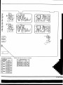
Introd uction
0
POWER
O"OX
~
5, !...!...1"' ';II,i" .~_.'iiiii""""I0'"
.-we
~
'I
!"W
~'~=--.:::
~
YAESU
U
,
M[DPJ
"oce'RANsce'"",,
FT-847
Q-O~o~
j~~la:aO~
'-J
"" ---RFPWR An RF
0
~
SOL
-'#:1110
AF
-3-RF VO"E
Jr!J~~
jf~l0
~
~~~I[ 1~~[ a
~
ID
0C
0
-"OF'L
O
c
35s
nnn,'" bRDI '"'lu 5..:JUnBnn
.U n B.UUU
.UU
D
l
-"Te~-
C!E:J @EBJ ~
$
TUNE
808FT
~~~~
~~~8
[ CD
CLMC)
0
~~~3~S~2
3
I
" 0
~N:oCH
~ -3-~~ 0
T L ~~~De5
~&~:&;cb t~~~?;
0 ~
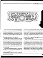
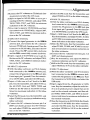
This manual provides technical information
necessary for servicing the Yaesu FT-847 HF &
Transceiver.It does not include information on installation and operation, which
are described in the FT-847 Operating Manual
provided with the transceiver, or on accessories
which are described in their manuals.
The FT-847is carefully designed to allow the
knowledgeable operator to make nearly all ad-
covered by warranty. For the major circuit
boards, each side of the board is identified byiV/
the type of the majority of components installed
on that side. In most casesone side has only chip
components, and the other has either a mixture
of both chip and lead components (trimmers,
coils, electrolytic capacitors, packaged ICs, etc.),
or lead components only.
While we believe the technical information in
justments required for various stationconditions,
modes and operator preferencessimply from the
controls on the panels, without opening the case
of the transceiver. The FT-847 Operating Manual describes these adjustments, plus certain in-
this manual is correct, Yaesu assumesno liability for damage that may occur as a result of typographical or other errors that may be present.
Your cooperation in pointing out any inconsistencies in the technical information would be
ternal settings.
Servicing this equipment requires expertisein
handling surface mount chip components. Attempts by unqualified persons to service this
equipment may result in permanent damage not
appreciated. Yaesu Musen reserves the right to
make changes in this transceiver and the alignment procedures, in the interest of technological
improvement, without notification of owners.
FT -847 Technical
SupplementI
1-1
":
c,cc",::~'f:~~;~
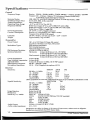
Specifications
General
Frequency Range:
Receive 100 kHz -30 MHz, 36 MHz -76 MHz, 108 MHz -174 MHz, 420 MHz -512 MHz
Transmit 160 -6 Meters, 2 Meters, 70 Centimeters (Amateur bands only)
5.1675 MHz (Alaska Emergency Channel)
USB, LSB, CW, AM, FM Fl (9600 bps Packet), F2 (1200 bps Packet) AFSK
0.1 Hz (CW, SSB), 10 Hz (AM, FM)
,
Emission Modes:
Synthesizer Steps (Min.):
Antenna Impedance:
Operating Temp. Range:
Frequency Stability:
50-0., Unbalanced
-10 °C to +50 °C (14 of to 122 OF)
Better than:f:2 ppm (0 °C to +40 °C) SSB/CW / AM/ AFSK
Better than:f:5 ppm (-10 °C to +50 °C) SSB/CW / AM/ AFSK
Better than :f: 11 kHz :f: 5 ppm} FM
DC 13.8 V = :f:l0 %, Negative Ground
Receive: 1.5 A (Squelched), 2.0 A (Max. Audio)
Transmit: 22 A (@ 100 W RF output)
260 (W) x 86 (H) x 270 (D) mm (10.24" x 3.39" x 10.63")
Approximately 7 kg (14.4lbs.)
Power Requirements:
Current Consumption:
Case Size:
Weight:
Transmitter
Power Output:
Modulation
Types:
FM Maximum Deviation:
Spurious Radiation:
Carrier Suppression:
Opp. Sideband Suppression:
3rd-Order IMD:
SSB Frequency Response:
Microphone Impedance:
160 -6 m: 100 Watts (25 Watts AM carrier)
2 m/70 cm: 50 Watts (12.5 Watts AM carrier)
SSB: Balanced Modulator
FM: Variable Reactance
AM: Early Stage (Low Level)
:f:5 kHz (:f:2.5 kHz on FM-N)
Harmonics:
At least 40 dB down (1.8 -29.7 MHz)
At least 60 dB down (50/144/430 MHz)
Non-harmonic: At least 50 dB down (1.8 -29.7 MHz)
At least 60 dB down (50/144/430 MHz)
At least 40 dB
At least 40 dB
At least 31 dB down (14 MHz, 100 W PEP output)
400 Hz -2600 Hz (-6 dB)
2000.- 10 ko. (Supplied microphone: 600 Q.)
Receiver
Sensitivity:
SSB/CW
AM-N
FM
500 kHz -1.8 MHz:
-20
JIV
1.8-28MHz:
0.25JIV
2JIV
28-30MHz:
0.25JIV
2JIV
0.5JIV
50 -54 MHz:
0.20 JIV
1 JIV
0.25 JIV
144/430 MHz:
0.125 JIV
-0.2
JIV
(Above specificationsare worst-case.SSB/CW/AM-N figures arefor 10 dB SIN, 12 dB SINAD on FM)
Squelch Sensitivity:
SSB/CW/AM
FM
500 kHz -1.8 MHz:
20 JIV
1.8-28MHz:
2pV
28 -30 MHz:
2 JIV
0.25 JIV
50 -54 MHz:
1 JIV
0.20 JIV
144/430 MHz:
0.5 JIV
0.16 JIV
Image Rejection:
Better than 60 dB
IF Rejection:
Better than 60 dB
Selectivity (-6/-60dB):
SSB/CW:
2.2 kHz/4.5 kHz
CW-N:
0.5 kHz/2.0 kHz (Optional YF-115C installed)
AM:
9 kHz/20 kHz
AM-N:
2.2kHz/4.5kHz
FM:
15 kHz/30 kHz
FM-N:
9 kHz/20 kHz
Audio Output:
At least 1.5 0. into 8 W @ 10 % THO
Audio output impedance:
40. -160.
Specifications are subject to change, in the interest of improvement, without notice or obligation.
Specifications are guaranteed only within Amateur bands.
1-2
FT -847 Technical
Supplement
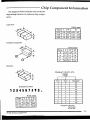
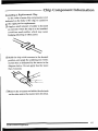
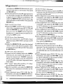
-Chip Component Information
The diagrams below indicate some of the distinguishing features of common chip components .
Capacitors
(Unit:
~
L
~
T
H
W
mm)
Type
L
H
2125
2.0
1608
1.6 0.8
0.65 ~ 0.95
1005
1.0 0.5
0.45 ~ 0.55
1.25 0.35 ~ 0.5
Tantalum Capacitors
w
L
(Unit:
-L
H
T
+
-C
mm)
Type L
W
P 2.0 1.25
A
3.2 1.6
B
3.4 2.8
5.8 3.2
H
1.2
1.6
1.9
2.3
Resistors
~
L
Marking* 100, 222, 473...
-L
473
H
T
Indicated Letters
Tens
Ones
Multiplier
0
0
100
1
2
1
2
101
102
1 2 3 4 5 & , : , 0 .::
Type
L
(Unit: mm)
W
H
1/10
2.0 1.25 0.5
1/16
1.6 0.8
1/165
1 0
0 5
035
...222==2.2kQ
0.45
~~
5
5
105
6
7
6
7
106
107
8
8
108
9
9
109
Examples:
l00==10Q
473==47kQ
1-3
FT-847 Technical Supplement
Chip Component Information
Replacfng Chip Components
Chip components are installed at the factory
by a series of robots. The first one placesa small
spot of adhesive resin at the location where each
part is to be installed, and later robots handle
and place parts using vacuum suction.
For single sided boards, solder pasteis applied
and the board is then baked to harden the resin
and flow the solder. For double sided boards, no
solder paste is applied, but the board is baked
(or exposed to ultra-violet light) to cure the resin
before dip soldering.
In our laboratories and service shops, small
quantities of chip components are mounted manually by applying a spot of resin, placing the components with tweezers, and then soldering by
very small dual streamsof hot air (without physical
by first
contact
removing
duringsolder
soldering).
using aWe
vacuum
remove
suction
parts
,j
Precautions for Chip Replacement
0 Do not disconnect a chip forcefully, or the
foil pattern may peel off the board.
0 Never re-use a chip component. Dispose of
all removed chip components immediately to avoid mixing with new parts.
0 Limit soldering time to 3 secondsor less to
avoid damaging the component and board.
Removing Chip Components
0 Remove the solder at eachjoint, one joint at a
time, using solder wick whetted with nonacidic fluxes as shown below. Avoid applying
pressure, and do not attempt to remove tinning from the chip's electrode.
,
-
~-~
~
iron, which applies a light steady vacuum at the
iron tip, and then breaking the adhesive with
tweezers.
0 Grasp the chip on both sides with tweezers,
Special vacuum/ desoldering equipment is
recommended if you expect to do a lot of chip
replacements. Otherwise, it is usually possible
to remove and replace chip components with
only a tapered, temperature-controlled soldering iron, a set of tweezers and braided copper
solder wick. Soldering iron temperature should
be below 280°C (536°F).
and gently twist the tweezers back and forth
(to break the adhesive bond) while alternately heating eachelectrode. Be careful to avoid
peeling the foil traces from the board.
.Dispose of the chip when removed.
0 After removing the chip, use the copper braid
and soldering iron to wick away any excess
solder and smooth the land for installation of
the replacement part.
C'c
f
1-4
FT -847 Technical Supplement
-Chip
Installing
Component
Information
a Replacement Chip
As the value of some chip components is not
indicated on the body of the chip, be careful to
get the right part for replacement.
0 Apply a small amount of solder to the land
on one side where the chip is to be installed.
Avoid too much solder, which may cause
bridging (shorting to other parts).
0 Hold the chip with tweezers in the desired
position, and apply the soldering iron with a
motion line as indicated by the arrow in the
diagram below. Do not apply heat for more
than 3 seconds.
0 Remove the tweezersand solder the electrode
on the other side in the manner just described.
1-5
FT -847 Technical
Supplement
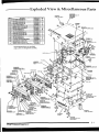
T -Exploded
View & Miscellaneous
':,
Parts
RAOO70000
S4000045
REI:::
-~
___=~De~cription
PAN HEAD SCREW
-~:~-
Y~~U00200iXI1
M2.6x6
PAN HEAD SCREWM3xB
UOO3OBOO1
14
<3>
PAN HEAD SCREW
UOO330001
4
@
PAN HEAD SCREW M4x6B
U00406007
2
<5>
SEMS SCREW ASM3x6
UO3300001
8
@
(1)
BINDING HEAD SCREWM2x4B
BINDINGHEADSCREWM3x6
U20104007
U20306001
1
3
@
TAPTITE
U24306001
83
@
TAPTITE SCREWM3xB
<8
OVAL HEAD SCREW
@
SCREW
M3x6
U243OBOO1
9
U31406007
2
OVALHEADSCREWM4x1OB
U31410007
4
@
OVAL HEAD SCREW
U31416007
2
@
TAPTITE
SCREW
U34306001
4
@
TAPTITE
SCREWM3x6
@
TOOTHED
@
HEX HEAD BOLT HSM4x16NI
@
BINDING
M4x6B
M4x16B
M3x6
LOCK WASHER
OW4NI
HEAD SCREW M3x1B
M3x2ONI
Non-designated
only as part
of
(Lot 8-)
parts
are
a designated
(Lot
3-)
9!¥-:4
<2>
M3x30
RAOO7000A
TOPCA
E
U44306001
8
U72004002
1
U9900076
1
U20318001
U20320002
4
@
R4150130
HANDLE
HOLDER
(2pcs)
t B-)
available
assembly.
@
V/U-PA Unil
D
)
RAOO6300A
RAOO63000
RUBBER
(Lot 4-)
(SP)
KNOB (MODE)
RA00651 00
KNOB (POW)
RA0065200
KNOB (MOX)
RA0063300
RA006330A (Lot 4-)
RUBBER KNOB (TU)
)
17-)
~@
@
"'"./
RA0063200
RA006320A
RUBBER
(Lot
KNOB
4-)
(ME)
AF-GNTL
Unit
RA0070100
./"
RAOO7010A (Lot. 3-)
IS\
BOTTOM
CASE
~
RA00631 00
RA006310A (Lot 4-)
RAOO72400
RUBBER KNOB (KEY)
COIL SPRING
RA0065500
ENCODER KNOB (2pcs)
RAOO63400
RAOO65600
RAOO6340A (Lol. 4-)
VOLUME KNOB
RUBBER KNOB (CL)
RAOO64800
RA0070300
KNOB MAIN ASS'Y
SHEET (SAT)
RAOO65900
KNOB
(SHUTTLE)
RA0065400
KNOB (OUT) (4pcs)
RAOO65300
RA006530A (Lol. 4-)
KNOB (IN ) (4 pcs)
R3100700
R3100700A (1.01. 12-)
FOOT (2pcs)
FT -847 Technical Supplement
2-1
'::~:;';;:~iii!L
Exploded
REF.
i
J.
i
I
View & Miscellaneous
DESCRIPTION
C 0001 AL.ELECTRO.CAP.
FNOO01 FAN
FNOO01 FAN
FNOO02 FAN
FNOO02 FAN
J 0001 CONNECTOR
J 0002 CONNECTOR
J 0003 CONNECTOR
J 0004 CONNECTOR
JPOO01 WIRE ASSY
POO01 WIREASSY
P 0002 WIRE ASSY
POO02 WIREASSY
P 0003 WIRE ASSY
P 0003 WIRE ASSY
P 0004 WIREASSY
P 0004 WIRE ASSY
POO05 WIREASSY
POO05 WIREASSY
POO05 WIREASSY
P 0006 WIRE ASSY
P 0006 WIRE ASSY
POO07 WIREASSY
P 0008 WIRE ASSY
P 0009 WIRE ASSY
PO010 WIREASSY
PO010 WIREASSY
PO011 WIREASSY
PO011 WIREASSY
P 0012 WIRE ASSY
P 0012 WIRE ASSY
PO012 WIREASSY
PO013 WIREASSY
PO013 WIREASSY
P 0013 WIRE ASSY
PO014 WIREASSY
PO014 WIREASSY
PO015 WIREASSY
P 0015 WIRE ASSY
P 0016 WIRE ASSY
P 0017 WIRE ASSY
P 0018 WIRE ASSY
P 0018 WIRE ASSY
P 0019 WIRE ASSY
PO020 WIREASSY
PO020 WIREASSY
PO021 WIREASSY
PO022 WIREASSY
P 0022 WIRE ASSY
P 0023 WIRE ASSY
P 0023 WIREASSY
P 0024 WIRE ASSY
P 0024 WIRE ASSY
P 0025 WIRE ASSY
P 0025 WIRE ASSY
PO026 WIREASSY
P 0027 WIRE ASSY
P 0028 WIRE ASSY
P 0028 WIRE ASSY
P 0028 WIRE ASSY
P 0029 WIRE ASSY
PO029 WIREASSY
PO029 WIREASSY
P 0030 WIRE ASSY
P 0032 WIRE ASSY
S 0001 ROTARY ENCODER
S 0002 ROTARY SWITCH
SPOOO1 SPEAKER
VALUE
100uF
8-ohm
V/W
TOL.
""" MAIN ASS'Y """
16V
MFR'S DESIG
RE3-16V101M 100UF
A0512 DC12V
F412R-12MB-32 DC12V
JF0625S1M-050 DC12V
JF0625S1M-050R1
DC12V
FM-MDR-MI
FM-MDR-MI
FM-MDR-MI
020-0291
GRN 280 (2)1(2)
A1179
A1179
A1179
A1179
A1179
A1179
A1179
A1179
A1179
A1179
A1179
A1179
RED 280/400V5.5
BLK 280/360 V5,5
GRA 280 TMPITMP
A1179
A1179
A1179
A1179
A1179
A1179
A1179
A1179
A1179
A1179
A1179
A1179
A1179
A1179
BRN 330 TMPITMP
YEL 210 TMPITMP
BLK 340 TMPITMP
BLK 360 TMPITMP
ORG 200 TMPITMP
A1179
A1179
A1179
BLK60TMPITMP
RED 60 TMPITMP
ORG 120 TMPITMP
GRN 110TMPITMP
BLK 140 TMPITMP
YEL 140 TMPITMP
ORG 150 TMPITMP
GRA 150 TMP/"
A1179
GRN 500 TMPITMP
RED 290 TMPITMP
RED 310 TMPITMP
RED 290 TMPITMP
A1179
A1179
A1179
A1179
A 1179
RSM20-250
SRGPVJ-E
VS-66Y 3W/8 OHM
2-2
~_.
i
Parts
IYAESU
PIN
K40129063
M2090017
M2090028
M2090023
M2090029
P1090352
P1090352
P1090352
P1090547
T51528002
T9206718
T9206702
T9206702A
T9206703
T9206703A
T9206704
T9206704A
T9206705
T9206705A
T9206705B
T9206706
T9206706A
T9318054
T9318055
T9311201
T9206707
T9206707A
T9206708
T9206708A
T9206710A
T9206710B
T9206710C
T9206709A
T9206709B
T9206709C
T9206711
T9206711A
T9206712
T9206712A
T9318041
T9318042
T9318043
T9318056
T9318044
T9206713
T9206713A
T9206714
T9318045
T9318059
T9318046
T9318060
T9318047
T9318061
T9318048
T9318065
T9206715
T9318049
T9311404
T9318058
T9311404
T9206716
T9206716A
T9206716B
T9206717
T9206757
09000631.
N0190173
M4090066
VERSo
UNITED KINGDON
LOT.
118116111181151515125121111515157157151511121151121212121112715712111-
FT-847 Technical Supplement
--I'
1-
_Alignment
Introduction
and
The following
Precautions
procedures
that are not normally
ceiver
steps do not require
cover
required
has left the factory.
adjustments
once
However,
occurs and some parts subsequently
realignment
may be required.
lem occurs
during
normal
due to component
failure;
not be done until
that more
complex
if damage
terwards.
Do not attempt
are replaced,
operation,
prob-
it is likely
realignment
should
component
has
by authorized
Yaesu service
experienced
with
equipped
contact
tions regarding
technicians
tion,
all circuits
the factory
specifications
caused
at realignment
Also,
change
circuits
f'
any alignment
function
operation
has been clearly
familiarity
complete
rized
with
pinpointed
unless
notishould
the normal
transceiver
and any faulty
are
its correct
resulting
made with
com-
they are presented.
Required
Test
by warranty.
Equipment
DC Voltmeter
(high-Z,1
MQ/V)
0 RF Millivoltmeter
0 RF St an d ar d S Igna
. 1 G enerator
w / ca l 1' b rate d
ou t pu t an d dB sca 1e, 0 dB p = 0 .p
5 V
0 AF sIgna 1 G enerator
wIt. h ca l 1b rate d output
o
o
0 T wo 50 -ummy
Q D
0 150-Q Dummy
0
Load
W attmeter
L oa d s (150 -250
(150 watts)
watts)
-watts,
2500
5 -Q )
(150
mear D e t ector
RF Att enuator (150 watts,
40 dB) or samp 1mg
.
coup 1er
A na 1yzer goo d to at 1east 1 G Hz
Alignment
Preparation
A 50-Q
dummy
load
must be connected
cedures
specified
fied
& Precautions
and
in-line
to the antenna
otherwise.
with
Correct
an antenna.
otherwise,
except
alignment
Except
the transceiver
MHz,
USB mode,
wattmeter
jack in all pro-
that call for transmission,
to 14.2000
thorough
for
of problems
from unautho-
improper
all of the steps
is not
where
should
where
speci-
be tuned
and these control~
set as indicated:
use) is necessary
Correction
by misalignment
ment is not covered
(and
all test equipment
in the order
possible
necessary.
test equipment
from
in a section
0 S pec t rum
in the
without
electrically
to
and the need for realignment
realignment.
adjustments
right
procedures
of the
to be absolutely
The following
own
the cause of the malfunction
replaced,
determined
the
a sin-
and follow
I L.
n- me
0 L.
attempts
no circumstances
be attempted
understood,
ponents
reserve
performance,
Under
and
at their
have
only
ready before beginning,
0
by the warranty
and alignment
owners.
caused
must
of improved
with
any of the following
to proceed
to perform
af-
0 Frequency C ounter
compete
by unauthorized
Yaesu
fying
informa-
after repairs.
are not covered
policy.
is
Yaesu service
compliance
be performed
isolated
Rather,
may require
0 AC Voltmeter
for mstruc-
and make
do undertake
risk. Problems
fully
If a 0fault
dealer
to ensure
are cautioned
~
steps.
listed,
0 DC Ammeter
who are
and
Authorized
checks
clearly
circuitry
the sellIng
performance
interest
technicians,
0
and alignment.
repair.
and realign
alignments
:
be performed
have the latest modification
Those who
~
the
for repair
suspected,
all other
0 Digital
that servicing
adjustments
gle step unless it is clearly
been replaced.
We recommend
of some adjustments
the trans-
If a sudden
after the faulty
the interaction
all of the equipment
test equip-
Although
most
0 MaX,
PROC/KEYER,
0 MIC & RF PWR
0 A TT, RF AMP,
fully
AGC-F,
MONt
OFF
CCW
NB OFF
0 AF as required
0 SQL
0 SHIFT
fully
CCW
12-o'clock
3-1
FT -847 Technical
Supplement
,. ,
Alignment
0 LOW CUT fully CCW
PLL Adjustments
0 HIGH CUT, RF GAIN fully CW
The transceiver's Alignment Routine is required for some procedures. If an Alignment
HF-VCO VCVadjustment
0 Connect the DC voltmeter to TP200l, and referring to table below, tune the transceiver to
Routine cannot be selected, power may have to
each frequency, then confirm or adjust the list-
be switched off then back on to re-enable menu
ed component for the required voltage.
selection.
.HF
To begin, turn the transceIver off. Press the
.une
UP, DWN and FAST keys on the mIcrophone together while turning the transceiver on again.
In the alignment procedure, each alignment
parameter is selected by rotating the SUB-TUNE
dial. The alignment is performed by pressing the
MCK/W key while injecting a signal of the re. df
d1 1
quIre requencyan
eve.
Pressing the MENU key after a setting is made
stores the entry. To exit the alignment routine,
VCO Adjustment
T
Ad . /C f .
to:
Just on Irm f or
10.495MHz adjustT2001
6.5V:t0.1V
0.100MHz
confirm
at least0.4V
21.995MHz adjustT2002
10.500MHz confirm
36.995MHz adjustT2003
22.000MHz confirm
53.995MHz adjustT2004
.
6.5V:t0.1V
at least0.4V
6.5V:t0.1V
at least0.4V
6.5V:t0.1V
54.000MHz confirm
atleastO.4V
37.000MHz
75.995MHz
confIrm
adjust T2005
at least 0.4V
6.5V:t0.1V
i
press POWER. After performing the system alignment in its entirety, individual settings can be returned to and adjusted should the need arise.
VHF- VCO VCV check!
0 Connect the DC voltmeter to TP2002, and re-
,I
Read 'each step to determine if the same test
ferring to table below, tune the transceiver to
"-'1
equipment used in the previous step will be re-
each frequency, then confirm that the required
I
!
quired. If not, remove the test equipment (except
dummy load and wattmeter, if connected) be-
voltage is present.
VHF VCO check
fore proceeding. Correct alignment requires that
Tuneto:
for
the ambient temperature be the same as that of
108.000MHz
at least0.5V
the transceiver and test equipment, and that this
temperature be held constant within 20 ~ 30°C
(68 ~ 86°F). If the transceiver is brought into the
139.995MHz lessthan7.2V
140.000MHz at least0.5V
173.995MHz lessthan7.0V
I
shop from hot or cold air, it should be allowed
UHF-VCO VCV check
1
time for thermal equalization with the environ-
0 Connect the DC voltmeter to TP2003, and re-
j
ment before alignment. Alignments
j
i
be made with oscillator shields and circuit.boards
firmly affixed in place. Also, the test equIpment
must only
ferring to table below, tune the transceiver to
each frequency. Confirm
voltage is present.
that the required
must be thoroughly warmed up before begin.UHF
rung.
..Tune
Note: Signal levels in dB referred to m alzgnmentare
VCO check
to:
for
420.000MHz at least0.5V
basedon 0 dB/l = 0.5 /lV.
Table Note: DC voltages should be within ::t:l0 % of
459.995MHz lessthan7.0V
460.000MHz at least0.5V
thoselisted in the voltage tables.
3-2
511.000MHz lessthan 7.0V
FT -847 Technical Supplement
I
-Alignment
PA
Unit
Adjustments
Pre-drive
a
section
Connect
at
"+"
14.005
2
the
the
ammeter
"-"
MHz,
load
remove
Connect
pin
Adjustment
dummy
and
lead,
meter
Current
50-.0.
jack,
J5006.
to
Idling
the
tenna
(HF)
lead).
and
0
to
the
jumper
select
J5006
the
the
an-
CW
Key
the
adjust
on
(pin
1
the
A
VHF-PA
mode.
0
a
Press
the
MaX
"Key"
switch,
line,
and
adjust
without
VR500l
closing
for
0.25
A
th
on
the
ter
and
ammeter.
Then
reinstall
the
remove
jumper
I ec
t
(:to.025
I
d
th
amme-
.
e
0
Connect
the
tenna
at
J5007.
at
Connect
2
"-"
MHz,
the
"Key"
the
the
pin
14.005
Press
remove
MaX
select
line,
the
and
adjust
CW
for
an-
the
and
ammeter.
Then
reinstall
the
remove
0
Press
t
jumper
0
section
Idling
(pin
1
the
Connect
the
tenna
.'
jack,
TP500l
the
(:to.15
A)
UHF
0
at
tween
!.
lead).
Tune
select
the
TP5002.
TP5001
:ress
on
J5007.
ter
and
the
HF
jumper
be-
TP5002
14.005
0
("-"
MHz,
without
VR5003
ammeter.
for
Then
reinstall
the
jumper
th
I ec
t
I
d
0
0.42
A
(:to.025
th
e
edge
(different
the
jack.
and
50-.0.
in
dummy
Preset
select
to
the
the
the
FT -847 Technical
each
load
RF
PM
PWR
mode.
Supplement
50
TP500l
MHz
country),
to
the
control
Connect
h e
t
"
"
I
d)
closing
0.3
A
the
(:to.03
t Ad
on
and
TP4001
and
t
'
urren
A)
ammeter
between
C
the
-
t
Jus
men
t o. 439
MH
995
z,
an
d
se-
th
high
and
50MHz
band
0
connect
an
enna
e
50
-ummy
.0. d
k
Jac.
and
R emove
TP4004,
between
th
and
TP4003
con-
("-"
lead)
lead).
MOX
switch,
and
adjust
without
VR4001
ammeter.
for
Then
reinstall
th
.
TP4003
("+"
line,
t
t
ammeter
the
the
C onnec
z
TP4004
the
closing
0.3
remove
jumper
d RX IF Ad
an
Output
Connect
A
(:to.03
the
between
the
A)
ammeter
TP4003
and
.-
.
Jus t ments
DC
0
volt-
Adjustment
the
RF
T10l0
on
RF
the
quency
counter,
(:t10
Remove
nect
the
millivoltmeter
and
the
Replace
MHz
clockwise
the
d e.
e
the
Reference
antenna
fully
mo
430MH
amme-
between
the
(
without
remove
'
between
tion
transceiver
R emove
.
CW
t
Press
TX
balance
the
k
TP4004.
0
Tune
se-
-ummy
.0. d
-ea
for
ranscelver
0
on
the
TP5002.
coupler
50
TP4001
and
mg
t
e
adjust
CM
Ldl
ton
"Key"
and
closing
remove
e
een
jumper
.
t
T
and
and
th
Jac.
tw
e
Then
PA
-sec
nect
mode.
~witch,
d
.
VR4002
the
and
ammeter
and
to
an-
between
the
lead)
adjust
the
to
Connect
transceiver
MaX
lIne,
A)
the
("+"
the
CW
,~h~
Key
and
remove
b
adjust
jumper
load
an
ammeter
Adjustment
dummy
and
and
t
0
50-.0.
t
enna
switch,
ammeter.
TP4002.
connector
Current
z,
lead).
Max
line,
oa
Final
MH
995
C onnec
er
("+"
the
mode.
the
145
t
amme
une
on
d e.
an
TP4002
reinstall
A
mo
144MHz
th
Key
closing
1.5
Adjustment
t o.
e
e
transceiver
without
VR5002
HF
J5007
the
indication!
Jumperbetw eenTP4001and TP4002,an d con-
connector
to
Tune
switch,
the
jumper
ammeter
lead).
and
to
minimum
.
th
0
and
load
microphone
J5006.
Adjustment
dummy
and
lead,
to
Current
50-.0.
jack,
"+"
0
Idling
no
Current
ranscelver
CW
t
t
section
for
Idling
t
nec
Drive
with
ground.
the
the
connector
chassis
Adjustments
e
oa
A)
and
voltmeter.
Unit
e
1
and
section
Tun
pin
TC5001
DC
V/U-P
transceiver
J5001's
transmitter,
input,
connector
to
Tune
HF
between
T1007
for
TP1002,
and
maximum
indica.
millivoltmeter.
RF
millivoltmeter
and
Hz)
to
on
the
coaxial
RF
millivoltmeter
with
adjust
the
TC1001
frequency
plug
the
for
fre.
45.25{
counter.
from
J1002
across
and
the
con
socket
3-3
e
Alignment
Adjust
RF
0
T1003
for
maximum
indication
on
the
0
Remove
millivoltmeter.
Remove
plug
the
P lu g into
RF
millivoltmeter,
and
replace
the
RX
0
Local
Connect
the
jack
TP1003.
0
V
TX
0
the
(:to.2
50-,0
V)
on
Connect
the
load
connect
the
Adjustment
RX
dummy
and
DDS
RF
the
CW
Preset
to
DC
the
HF
an-
voltmeter
to
DC
T1009
for
3.0
dBm
0
..plug
ffilllIvoltmeter
for
to
maximum
TP1004,
on
the
millivoltmeter.
the
millivoltmeter
to
TP1005,
RF
for
maximum
indication
on
0
the
signal
tenna
to
0
jack
and
TP1005.
Key
the
quency
counter.
T1016
Carrier
0
RF
DC
the
coaxial
(:t100
plug
CW
the
the
Replace
the
(:t10
frequency
livoltmeter,
T1002
Hz)
and
for
adjust
the
counter
key
maximum
the
from
~ T1019
voltmeter.
replace
J1001
across
the
and
the
to
MH
con-
socket,
TP1049.
(
d
no
mo
DC
and
.
Inject
I
t
u
vo
T1006
a
a
'
Ion
)
so
as
t
if
mInImum
...
In d Ica.
Increase
necessary,
to
the
signal
maintain
a use-
indication.
the
signal
generator,
and
replace
the
J1001.
Hz)
and
on
ad-
VHF
the
0
RX
and
the
con-
socket.
TC1002
frequency
with
counter.
the
transmitter,
indication
for
RF
RXIF
SenSltlvlty
Connect
the
and
on
the
dummy
transceiver
FM
mode.
and
the
Inject
145.995
adRF
reading
T3014,
timum
signal
jack,
4-Q
the
tone),
mil-
Adjustments
...
and
connect
load
SQl
control
signal
from
MHz
(:t3.5
adjust
on
the
the
the
T30l7,
level
meter,
T3027,
to
the
to the
145.995
to
Preset
a
generator
RF
144MHz
SINAD
meter
EXT
SPKR
MHz,
and
control
fully
and
jack.
Tune
select
the
fully
clockwise
counter-clockwise.
the
kHz
to
the
signal
generator
deviation
of
get
and
T3029,
a moderate
adjust
and
at
a 1
kHz
SINAD
T3006,
T3012,
T3031
for
op-
SINAD.
millivoltmeter.
3-4
0
I tmeter.
f or
voltmeter.
voltage
into
DC
the
an d
level,
DC
plug
0
on
DC
and
plug
on
the
Remove
fre-
and
J1003
across
and
the
on
z
generator
for
mode.
transmitter,
MHz
from
counter
T1017
millivoltmeter.
transmitter,
MHz
on
ful
~ T1014
RF
0
Connect
and
generator,
45.
T1004
antenna
frequency
the
Key
just
an-
0
wIth
the
45.580
HF
mode.
the
T1015,
voltmeter
a reading
Adjust
millivoltmeter
adjustT1012
on
Key
the
Adjustment
the
45.580
0
RF
...TX
millivoltmeter
Frequency
Select
0
to
counter.
Remove
nect
PM
and
for
frequency
the
the
indication
the
load
connect
transmitter,
Replace
just
dummy
Select
maximum
0
50-,0
modulation).
generator
705
at
tion
the
inject
TP1048.
coaxial
the
get
Adjustment
Connect
and
the
millivoltmeter.
IF
socket,
the
and.
0
FM
to
connect
Adjustment
Remove
sIgna
T1021
(no
and
J1001.
I
adjust
the
signal
Blanker
the
RF
across
T1008,
the
into
0
J1001
indication
Remove
.nect
Adjustment
Connect
the
R emove
clockwIse.
from
voltmeter
minimum
Noise
fully
MHz
T1005,
and
indication
plug
45.705
DC
for
0
RF
at
Adjust
voltmeter.
control
generator
the
adjust
RF
coaxial
connect
0
replace
J1002.
the
signal
mode.
and
the
T1020
DDS
and
Sensitivity
the
transmitter,
adjust
millivoltmeter,
.
Select
Key
RF
J1002.
Adjustment
tenna.
into
IF
0
TX
the
FT -847 Technical
Supplement
Alignment
0 Connect the DC voltmeter to TP1048 and chas-
0 Select the FM mode. Key the transmitter, and
sis ground, and select the CW mode.
0 Inject a signal at 145.995 MHz so as to get a
reading on the DC voltmeter, and adjustT3006,
adjust VR3003 for 50 Won the inline wattmeter.
430 MHz TX Adjustment
0 W .th th
1
connec
the transceiver to 129.995 MHz. Adjust T3007,
T3011, T3015, and T3018 for minimum indication on the DC voltmeter.
50 MHz RX IF Sensitivity
0 Connect the signal generator to the 50MHz
antenna jack, and connect the DC voltmeter
t
e
tt me
th
t er
an d 50 -ummy
.Q d
0
430MH
t
e
t th AF
z
t
an
.
Jac
enna
t th MIC .
k
,
e
8 ..
t .
T
th e tr anscelV.
: ffilC mpu , pm 7: groun d).une
er to 439.995 MHz, and select the USB mode.
connec
0 Now inject a signal at 129.995 MHz, and tune
d
.
oa
indication on the DC voltmeter.
t
(
d
k
1
0 Inject a 1 kHz tone at 3 m V level to the MIC jack.
Key the transmitter, and adjust TC3001, TC3003,
and TC3004 in successionseveral times for maximum indication on the inline wattmeter.
0 Select the FM mode. Key the transmitter, and
between TP1048 and chassis ground. Tune the
adjust TC4001, TC4003, and TC4005 in succes-
transceiver to 50.295 MHz, and select the CW
mode. Preset the RF control fully clockwise
sion several times for maximum indication on
the inline wattmeter.
and the SQL control fully counter-clockwise.
0 Inject a signal at 50.295 MHz so as to get de~
flection on the DC voltmeter, and adjustT3019,
f
T3021, T3025, and T3028 for minimum indica-
I..
wa
minimum
pm
for
Jac
T3031
e
and
0
T3017,
or
T3014,
genera
T3012,
. 1.me
e m
0 Connect the DC voltmeter between pin 3 of
J4007 and chassis ground.
0 Key the transmitter,
and adjust TC4004 for
minimum indication on the DC voltmeter.
,
!f
tion on the DC voltmeter.
144MH TX Ad . t
t
z
Jus men
0 Still in the FM mode, key the transmitter, and
adjust VR3002 for 50 W on the inline wattmeter.
I,
0 With the inline wattmeter and 50-.Q dummy
50 MHz TX Adjustment
load connected to the 144MHz antenna jack,
0 With the inline wattmeter and 50-.Q dummy
connect the AF generator to the MIC jack (pin
load connected to the 50MHz antenna jack,
8: mic input, pin 7: ground). Tune the transceiv-
connect the AF generator to the MIC jack. Tune
er to 145.995 MHz, and select the USB mode.
the transceiver to 50.295 MHz, and select the
0 Inject a 1 kHz tone at 3 m V level to the MIC
jack. Key the transmitter, and adjustT1002 on
the AF-CNTL
USB mode.
0 Inject a signal from the AF generator at 1 kHzl
Unit and T3005, T3008, and
tone. Key the transmitter, adjust the audio lev-
T3010 on the RF Unit in succession several
times for maximum indication on the inline
el so as to produce power output that can be
read on the external wattmeter, and then ad-
wattmeter.
0 Select the FM mode. Key the transmitter, and
just T3003, T3009, T3013, and T3016 in succession several times for maximum indication on
adjust TC4002 for maximum indication on the
the external wattmeter.
inline wattmeter.
0 Connect the DC voltmeter between pin 3 of
J4007 and chassis ground. Key the transmit-
0 Tune the transceiver to 50.295 MHz (for French
version) or 51.995 MHz (for other versions),
and select the FM mode. Key the transmitter,
ter, and adjust VR4004 for minimum indica-
and adjust VR3004 for 100 W on the external
tion on the DC voltmeter.
wattmeter.
-fT-847T..hni.al
Supp/.m.nt
3-5I
""'-':":::Y1~~.J[:tc-
Alignm en t
HF
TX Adjustment
...mg
0 WIth the mllne wattmeter and 50-0 dummy
than
4.0
A
below
that
measured
TX and RX Adjustments
Won the inline wattmeter.
0 Tune the transceiver to 1.830 MHz, and select
(Alignment
Menu Adjustments)
144 MHz Band FM-S1 Adjustment
VR3005 for 100 W on the inline wattmeter.
AFP d .145.995
a Justment
0 Preset "VR3007, VR3008, and VR3009 full y
clockwIse, and connect the ammeter between
the transceiver's 13.8VDC connector and the
:
IS less
DC power supply.
0 Tune the transceiver to 145.995 MHz and select the CW mode (with no connection to the
144MHz antenna jack). Key the transmitter,
and adjust VR1001 for 8.0 A (:to. 1 A) on the
ammeter.
0 Tune the transceiver to 439.995 MHz and select the CW mode (with no connection to the
430MHz antenna jack). Key the transmitter,
and confirm the current on the ammeter. If
over 8.0 A on the ammeter, adjust VR1001 for
8.0 A (:to. 1 A) on the ammeter. If under 8.0 A
in
the previous step, adjust VR3009 for a readth an t hat 0 f t he prevI-.
in g 4.-.ower
0 A (+0 2 A) 1
load connected to the HF antenna J"ack, tune
the transceiver to 3.505 MHz, and select the
FM mode.
0 Key the transmitter, and adjust VR3006 for 100
the PM mode. Key the transmitter, and adjust
!
..
ous step.
0 Connect ~he signal generator to the 144MHz
antenna Jack, and tune the transceiver
to
MHz. Select the PM mode.
.
0 Select alIgnment menu [FM-S1] and inject a
-6 dB
. 1 ( 3 5 kH Z d evIahon
..'
p sIgna :t.
of a 1 kHz
tone). Then press the MCK/W key
.
144 MHz Band FM-Full Scale Adjustment
0 Connect the signal generator to the 144M Hz
antenna jack, and tune the transceiver
to
145.995 MHz. Select the PM mode.
0 Select alignment menu [FM-FULL], and inject
a +20.0 dBp signal (:t3.5 kHz deviation of a 1
kHz tone). Then press the MCK/W key.
144 MHz Band Scan Discriminator
Center-Stop Adjustment
0 Connect the signal generator to the 144MHz
antenna jack, and tune the transceiver to
145.995 MHz. Select the PM mode.
on the ammeter, adjust VR3007 for 8.0 A (:to.1
0 Select alignment menu [DISC-L], and inject a
A) on the ammeter.
0 Connect the 50-0 dummy load to the HF an-
signal at 145.992 MHz, level +20.0 dBp (:t3.5
kHz deviation of a 1 kHz tone). Then press the
tenna jack. Tune the transceiver to 14.005 MHz
and select the CW mode. Key the transmitter,
MCK/W key.
0 Select alignment menu [DISC-H], and inject a
and make a note of the current on the ammeter.
0 Disconnect the 50-0 dummy load and connect
signal at 145.998 MHz, level +20.0 dBp (:t3.5
kHz deviation of a 1 kHz tone). Then press the
the 150-0 dummy load (or three 50-0 loads in
MCK/W key.
parallel) to the HF antenna jack. Key the trans-
144 MHz Band SQL Threshold Adjustment
mitter, and compare the current with the above
step. If the ammeter reading is more than 4.0
A lower than that measured in the previous
0 Tune the transceiver to 145.995 MHz, and the
select the PM mode.
0 Select alignment menu [SQL- TH-L], and in-
step, adjust VR1001 for 4.0 A (:to.2 A) lower
than the previous step. If the ammeter read-
ject no RF input. Then press the MCK/W key.
0 Press the A~B key ([SQL- TH-H] will appear
3-6
FT -847 Technical
Supplement
I
~Alignment
on the display), and apply no RF input. Then
press the MCK/W key.
44 MHz BandSQL Tight Adjustment
~ Connect the signal generator to the 144MHz
..meter.
antenna Jack,
and tune the transceIver to
0 Selectalignment menu [RX-GAIN], and select
the USB mode. Inject a signal of level-6 dBp
(no modulation), and adjust the MEMNFO CH
control for just 1 segment indication on the SThen press the MCK/W ke y.~
145.995MHz. Selectthe FM mode.
CJSelectalignment menu [SQL-TI-L], and inject
a signal at 145.995MHz, level 0 dBp (::t3.5kHz
deviation of a 1 kHz tone). Then press the
MCKIW key.
CJPressthe A~B key ([SQL-TI-H] display), and
inject a signal at 145.995MHz, level 0 dBp (::t3.5
kHz deviation of a 1 kHz tone). Then pressthe
MCKIW key.
144MHz BandSSB-S1Adjustment
0 Selectalignment menu [SSB-S1], and tune the
transceiver to 145.995MHz. Select the USB
430 MHz Band RX Gain Adjustment
.
0 Connect the signal generator to the 430MHz
antenna jack, and tune the transceiver to
439.995MHz.
0 Selectalignment menu [RX-GAIN], and select
the USB mode. Inject a signal of level-6 dBp
(no modulation), and adjust the MEMNFO CH
control for just 1 segment indication on the Smeter. If the hexadecimaldata on the transceiver's display is less than "40H", turn the MEMI
VFO CH control for just "40H" indication on
the display. Then press the MCK/W key.
mode, preset the RF control to the 2-0' clock
~
~
position, and inject no RF input. Then press
the MCK/W key.
144MHz Band SSB-S9Adjustment
0 Connect the signal generator to the 144MHz
t
. k
d t
th
t
.
t
an enna
Jac , an
une
e ransceiver
0
145.995MHz.
0 Select alignment menu [SSB-S9], select the
USB mode, and preset the RF control fully
1 k . I . t . 1 fl
1+25 dB (
c oc WIse. nJec a sIgna 0 eve
p no
modulation), then press the MCK/W key.
144MHz BandSSB-FullScaleAdjustment
0 C
t th .
1
t t th 144MH
onnec e sIgna genera or 0 e
z
..nal
antenna Jack, and tune the transceIver to
145.995MHz. Select alignment menu [SSBFULL] d .. t .
1 f 1 1+85 dB (
, an ffiJec a sIgna 0 eve
p no
d 1 t. ) Th
th MCK/W k
mo u a Ion.
en press e
ey.
144MHz Band RX Gain Adjustment
0 Connect the signal generator to the 144MHz
antenna jack, and tune the transceiver to
145.995MHz.
FT -847 Technical
Supplement
50 MHz Band RX Gain Adjustment
-
0 Connect the signal generator to the 50MHz
antennajack, and tune the transceiverto 51.995
MHz (for versoA, C, D, H) or 50.295MHz (for
versoB, ~).
o
Select
alIgnment
menu
[RX-GAIN],
and
select
the CW mode. Inject a signal of level-3 dBp
(no modulation), and adjust the MEMNFO CH
control for just 1 segment indication on the Smeter. Then press the MCK/Wkey.
.
HF Band RX Gain Adjustment
0 Connect the signal generator to the HF antenna jack, and tune the transceiver and RF siggenerator to 28.995MHz.
.
0 Selectalignment menu [RX-GAIN], and select
the USB mode. Inject a signal of level 0 dBp
(no modulation), and adjust the MEMNFO CH
control for just 1 segment indication on the Smeter. Then press the MCK/W key.
0 Tune the transceiver and RF signal generator
to 14.005MHz, and select the USB mode. Inject a signal of level 0 dBp (no modulation),
3-7
I
Alignment
and adjust the MEMNFO CH control for just 1
HF Band PO Meter Adjustment
segment indication on the S-meter. Then press
the MCK/W key.
0 Connect the 50-.0; dummy load to the HF antenna jack. Tune the transceiver to 14.005MHz,
0 Tune the transceiver and RF signal generator
to 3.505 MHz, and select the USB mode. Inject
and select the PM mode.
0 Select alignment menu [PWR-1 00]. Key the
a signal of level +3 dBp (no modulation), and
transmitter,
adjust the MEMNFO CH control for just 1 seg-
for 100 W indication on the external wattme-
mentindication
MCK/W key.
on the S-meter. Then press the
ter. Then press the MCK/W key.
0 Select alignment menu [PWR-50].
SHIFT Control Center Preset
0 Preset t he SHIFT contro 1 to the 12-0' c1oc k po.. Select a1.Ignmen t menu [SFT -,CTR] and
sition.
h
press
t
d
MCK/W
k
e
d
ure,
h
0
Aft
th
ey.
not
turn
t
turn
it,
repeat
O
er
1S
SHIFT
t
e
con
t
I
Select
.
sethng the SHIFT
the
above
procedure
0
for
con tro I.
transmitter,
from
the
USB
swItchIng
between
CK/W
the
noise
M
d
speaker
LSB
an
whIle
.0
Th
.en
k
RF
PWR
control
W
indication
on
the
external
wattme-
on the external wattmeter.
Then press the MCK/W key.
MHz Band PO Meter AdJustment
.
Connect
(for
the
jack.
50-.0;
Tune
verso
A,
or 1.840 MHz
mode.
dummy
the
load
transceiver
to
t h
to
1.910
e
HF
an-
MHz
H),
1.850
MHz
(for
verso
B,
C,
D)
(for verso E), and select the CW
0 Select alignment menu [PWR-1 00]. Key the
antenna jack, and connect the ammeter be-
transmitter,
tween the transceiver's
for 100 W indication on the external wattme-
13.8VDC connector
to 145.995 MHz, and select alignment menu
[TXC-USB].
0 Set "regular" Menu #92 and #93 to "0" if they
are not already set to that value.
ammeter.
0 Select alignment
and adjust the RF PWR control
ter. Then press the MCK/W key.
0 Select alignment
menu [PWR-50].
transmitter, and adjust the RF PWR control
for 50 W indication on the external wattme0 Select alignment menu [PWR-20]. Key the
transmitter, and adjust the RF PWR control
for 20 W indication
menu [TXC-LSB].
Key the
ter. Then press the MCK/W key.
0 Key the transmitter, and adjust the MEMNFO
CH control for minimum indication on the
Key the
i
transmitter, and adjust the MEMNFO CH con-
:
1
trol for minimum
c,i"
the
ey.
and DC power supply. Tune the transceiver
Ii
20
tenna
0 Connect the 50-.0; dummy load to the 144MHz
,I
adjust
press
TX SSB Carrier Point Adjustment
;
and
10 W indication
input.
..1.9
0 Adjust the MEMNFO CH control for Identical
the
the
0 Select alignment menu [PWR-10]. Key the
transmitter, and adjust RF PWR control for
alignment menu [RXC-PNT], and inject no RF
of
Key
ter. Then press the MCK/W key.
0 Tune the transceiver to 145.995 MHz. Select
..
[PWR-20].
pre-
RX SSB Carrier Point Adjustment
"sound"
menu
aCC1for
dentally
alignment
proce-
I rj."
J you
ro.
Key the
transmitter, and adjust the RF PWR control
for 50 W indication on the external wattmeter. Then press the MCK/W key.
o
prese
and adjust the RF PWR control
indication on the ammeter.
on the external wattme-
ter. Then press the MCK/W key.
0 Select alignment
transmitter,
menu [PWR-10].
Key the
and adjust the RF PWR control
r;/ j.
: :~
[.
,jl:
,..
3-8
FT -847 Technical
Supplement
-Alignment
for 10 W indication on the external wattmeter. Then press the MCK/W key.
for 10 W indication on the external wattmeter. Then press the MCK/W key.
50 MHz Band PO Meter Adjustment
ALC Meter Adjustment
0 Connect the 50-.0. dummy load to the 50MHz
antenna jack. Tune the transceiver to 51.995
0 With the inline wattmeter and 50-.0. dummy
load connected to the 144MHz antenna jack,
MHz (for verso A, C, D, H) or 50.295 MHz (for
connect the AF generator to the MIC jack. Tune
verso B, E), and select the CW mode.
the transceiver to 145.005 MHz, and select the
0 Select alignment menu [PWR-1 00]. Key the
transmitter, and adjust the RF PWR control
USB mode.
0 Select alignment menu [ALC-1] and inject no
for 100 W indication on the external wattme-
microphone input. Key the transmitter,
ter. Then press MCK/W key.
press the MCK/W key. Now adjust the MEMI
0 Select alignment menu [PWR-50]. Key the
transmitter, and adjust the RF PWR control
for 50 W indication
on the external wattme-
VFO CH control for a (hexadecimal data) "+4"
indication on the display.
0 Select alignment menu [ALC-9] and inject a 1
ter. Then press the MCK/W key.
0 Select alignment
menu [PWR-20].
then
kHz tone signal of level 3 m V to the MIC jack.
Key the
Key the transmitter, and adjust the MIC con-
transmitter, and adjust the RF PWR control
for 20 W indication on the external wattme-
trol for just 1 segment indication on the ALC
meter.
ter. Then press the MCK/W key.
0 Select alignment
transmitter,
menu [PWR-10].
0 Without touching the setting of the MIC conKey the
trol, inject a 1 kHz tone at 10 mV to the MIC
and adjust the RF PWR control
for 10 W indication on the external wattmeter. Then press the MCK/W key.
jack. Then press the MCK/W key.
144MH B d TXAd '
z an
Justment
W . h h . 1.
0
144/430 MHz Band PO Meter Adjustment
It t e m me wattmeter and 50-.0. dummy
load connected to the 144M Hz antenna jack,
0 Connect the 50-.0. dummy load to the 144MHz
connect the AF generator to the MIC jack (pin
antenna jack. Tune .the transceiver to 145.995
8: mic input, pin 7: ground). Tune the trans-
MHz, and select the PM mode.
ceiver to 145.995 MHz, and select the USB
FT -847 Technical Supplement
0 W th th . 1.
e m me wa tt me t er and 50 -ummy
.0.d
3-9
,
k
.
Jac
t
enna
an
z
430MH
th
'
e
ter. Then press the MCK/W key.
.1
0 Select alIgnment menu [PWR-10]. Key the
transmitter, and adjust the RF PWR control
430 MHz Band TX Adjustment
t
on the external wattme-
d
for 20 W indication
play is less than "8FH", turn the MEMNFO CH
control for just "8FH" indication on the display.
0
0 Select alignment menu [PWR-20]. Key the
transmitter, and adjust the RF PWR control
the hexadecimal data on the transceiver's dis-
t
ter. Then press the MCK/W key.
control for 25 Won the external wattmeter. If
e
on the external wattme-
d
for 50 W indication
1 kHz tone at 1 mV level to the MIC jack. Key
the transmitter, and adjust the MEMNFO CH
connec
0 Select alignment menu [PWR-50]. Key the
transmitter, and adjust the RF PWR control
0 Select alignment menu [TX-GAIN] and inject a
1
mal data) value of "FF".
mode. Preset the MIC control to the I-o'clock
position.
oa
0 Select alignment menu [PWR-1 00]. Rotate the
MEMNFO CH control to select the (hexadeci-
~
Alignment
connect the AF generator to the MIC jack (pin
8: mic input, pin 7: ground). Tune the trans-
hexadecimal data on the transceiver's display
is less than "8FH", turn the MEMNFO CH con-
ceiver to 439.995 MHz, and select the USB
trol for just "8FH" indication on the display.
mode. Preset the MIC control to the I-o'clock
0 Tune the transceiver to 14.005 MHz and inject
position.
0 Select alignment menu [TX-GAIN] and inject a
I kHz tone at 1 mV level to the MIC jack. Key
1 mV at 1 kHz tone to the MIC jack. Key the
transmitter, and adjust the MEMNFO CH control for 50 W on the inline wattmeter. If the
the transmitter, and adjust the MEMNFO CH
hexadecimal data on the transceiver's display
control for 25 W on the external wattmeter. If
the hexadecimal data on the transceiver's dis-
is less than "8FH", turn the MEMNFO CH control for just "8FH" indication on the display.
play is less than "8FH", turn the MEMNFO CH
control for just "8FH" indication on the display.
0 Tune the transceiver to 1.910 MHz (for verso
A, H), 1.850 MHz (for verso B, C, D) or 1.840
50 MHz Band TX Adjustment
0 W.
th
th
.
1
1
e
1 .
m
me
d
t
th
to
..
mic
.
ceiver
mpu
to.
,
51
995
groun
(f
z
or
antenna
th
0
d)
MH
tone
.
t
or
7
:
d
to
the
MIC
jack.
Key
the
transmitter,
and
-ummy
z
t
.
pm
0
an
e
genera
t
50
SOMH
t
AF
e
8
d
er
h
e
connec
me
d
connec
MHz (for verso E), and inject 1 m Vat 1 kHz
t
wa
t
oa
:
tt
MIC
.
Jac
e
T
.une
k
C
"
(
the
.the
MEMNFO
inline
t
e
,
adjust
CH
control
for
50
W
on
,
wattmeter.
If
the
hexadecimal
data
pm
th
A
verso
k
Jac
on
the
transceiver's
display
is
less
than
"8FH",
rans-
D
H)
turn
or
50.295 MHz (for verso B, E), and select the USB
MEMNFO
CH
control
for
just.
"8FH"
indication on the display.
mode. Preset the MIC control to the I-o'clock
5 WR Meter Adjustment
position.
0 Select alignment menu [TX-GAIN] and inject a
1 kHz tone at 1 mV level to the MIC jack. Key
0 With the in line wattmeter and 50-0 dummy
load connected to the HF antenna jack, select
the CW mode. Tune the transceiver to 14.005
the transmitter, and adjust the MEMNFO CH
control for 50 W on the external wattmeter.
the
MHz. Select alignment menu [SWR 1.5].
If
0 Key the transmitter, and adjust the RF PWR
the hexadecimal data on the transceiver's dis-
control for 10 W on the external wattmeter.
play is less than "8FH", turn the MEMNFO CH
0 Replace the 50-0 dummy load with a 100-0
control for just "8FH" indication on the display.
dummy load (two 50-0 loads in parallel) con-
HF Band TX Ad 'ustment
JOKey
0 With the inline
wattmeter and 50-0 dummy
nectedto the HF antenna jack.
the transmitter, and press the MCK/W key.
load
connected
to
the
HF
MIC
the
AF
generator
to
.0
Jack,
antenna
the
.
k
Jac
R
(
.
pm
8
.dummy
:
and
select
the
USB
mode.
Preset
MIC control to the 1-0' clock position.
.0
0 Tune the transceiver to 28.995 MHz and inject
a 1 kHz tone at 1 m V level to the MIC jack. Key
the transmitter, and adjust the MEMNFO CH
0
ey
for
50
W
on
the
inline
wattmeter.
If
connected
oa
to
the
wIt
HF
.
h
t h e
50-0
antenna
jack,
the
transmItter,
an
d
a
d
Just
.h
t
e
RF
PWR
t
e
transmItter,
an
d
press
th
e
MCK/W
k ey.
the
imj~..3-10
1 d
ummy
control
W on
the inline
Re
lacefor
the50
50-0
dummy
load wattmeter.
with the 150-0
d p
1 d(
hr 50 0 .
ummy oa or t ee -s m para IIe 1)t 0 th e
H F antenna Jack.
.
0 K
h
.
ey
control
100-0
d 1
1.
an se ect a Ignment menu [SWR 3 ..0]
K
.
miC
the
the
load
input, pin 7: ground). Select alignment menu
[TX-GAIN],
d
eplace
connect
FT-847TechnicalSupplement
1
Alignment
mode, and inject a 1 kHz tone at 1 m V level to
the MIC jack. Key the transmitter, and adjust
VRI005 for at least a 5-segment indication on
the ALC meter.
,t
:'
AF generator to the MIC jack (pin 8: mic input,
Pin 7: ground). Tune the transceiver to 145.995
MHz , and select the FM mode.
(J In Joect a 1 kHz tone at 15 mV level. Key the
transmitter, and adjust VRI004 for ::1:4.5kHz
deviation on the linear detector.
D Select the 88.5 Hz (default) subaudible tone,
and activate CTCSS Encode operation. Key the
transmitter, and adjust VRI003 for ::1:0.7kHz
deviation on the linear detector.
Speech Processor
Adjustment
Carrier
Balance
Adjustment
0 C onnec t th e RF a tt enua t or ( or 50 -~~
n d ummy.I
I d d
oa an samplmg coupler) and spectrum anal
t th 144MH
t
yzer 0 e
z an enna Jack .une
T
t he
t
.
ranscelver t o. 145 995 MH z, se I ect t he USB
d
d .. t
h
mo e, an mJec no mlcrop one mput.
0 K ey th e t ransml . tt er, an d ad Just VRI007 f or
o
o
o
0
o
m mlmum carner Iea k age (shou ld be a t I east
45 dB b I
. t
.
e ow a carrIer ranSD1ltt ed on t he same
fr equency ) as mIca
. d . ted on th e ana Iyzer.
OO'
0 Select the LSB mode, and again inject no mi-
D With the inline wattmeter and 50-0 dummy
load connected to the 144MHz antenna jack,
connect the AF generator to the MIC jack (pin
8: mic input, pin 7: ground). Tune the trans-
crophone input. Key the transmitter, and confirm that the carrier leakage is at least 45 dB
down, as indicated on the analyzer.
50 MHz
band Power
ceiver to 145.995 MHz, select the USB mode,
and leave the PROC switch off for now.
Re-adjustment
(for French
version)
0 With the inline wattmeter and 50-0 dummy
D Inject a 1 kHz tone at 1 m V level. Key the trans-
load connected to the 50MHz antenna jack,
mitter, and adjust the MIC control for 12.5 W
tune the transceiver to 50.295 MHz, and select
on the wattmeter.
D Switch PROC on, key the transmitter, and ad-
the FM mode.
0 Key the transmitter, and adjust VR3004 for 10
just VRI002 for 25 W on the wattmeter.
Won the inline wattmeter.
Carrier Level Adjustment
0 Connect the 50-0 dummy load to the HF antenna jack. Tune the transceiver to 1.910 MHz
(for verso A, H), 1.850 MHz (for verso B, C, D)
or 1.840 MHz (for versoE), select the CW mode,
Re-adjustment
(for Belgian
version)
0 With the inline wattmeter and 50-0 dummy
load connected to the HF antenna jack, tune
the transceiver to 1.850 MHz, and select the
and set PROC off. Select the TX meter to read
ALC. Preset VRI006 fully clockwise.
FM mode.
0 Key the transmitter, and adjust VR3005 for 10
0 Connect the AF generator to the MIC jack (pin
8: mic input, pin 7: ground).
1.9 MHz
band Power
Won the inline wattmeter.
Select the AM,!
3-11
FT -847 Technical
Supplement
-
~
Alignml
,'OM
..,...
"..'
..'0"
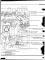
T1020 TX DDS Adjust
TP1004 TX DDS Adjust: RF Millivoltmeter
(max.)
T1021 RX DDS Adjust
TP1005 RX DDS Adjust: RF Millivoltmeter
(max.)
VR1002 Carrier Frequency Adjust
T1018. 09 RX IF Sensitivity
I
!
I
I
+ + ..+
..002
TP1048 50 MHz RX IF Sensitivity: DC Voltmeter (m&1.)
RX IF Sensitivity: DC Voltmeter (min.)
T1015. 17 RX IF Sensitivity
.
T1009 TX Local Adjust
TP1003 TX Local Adjust: DC Voltmeter (3.0 V:I:O.2 v:
T1003, 07, 10 Reference
Output AdjUst.
TP1002 Reference Output Adjust
: DC Voltmeter (minimum indication)
: Frequency Counter (45.250 MHz % 10 Hz]
TP1049 Noise Blanker Adjust: DC Voltmeter
T1004, 06 Noise Blanker Adjust
"
~
~
(min.)
~
J1001 RX IF Sensitivity: Signal Generator
Noise Blanker Adjust: Signal GeneratorI
T1005. 08 RX IF Sensitivity
TC1001 Reference Output Adjust
J1002 Reference Output Adjust: RF millivoltmeter (max.)
T1002 Carrier Frequency Adjust
0 FM IF Adjust: RF millivoltmeter (max.)
: Freq. Counter (45.580 MHz %100 Hz)
!quency Adjust: Freq. Counter (45.580 MHz %100 Hz)
: RF millivoltmeter (max)
-
-1111
--
-
L
:r
I
8
U
~
"
(]
~
~
.
i
~
0
0
;
N
n
U
:
~~
.I
'J
"~
.
..-~
(
"
~
O
\
:
G
"'.2
~
S
.
V
5
"'0
e
0
...0
c
.nm
"""
'.N
""'
c
~
;;
;
~
L'."
C'~
u..
R
~
..!
0
00'
..
.
.
VR
AF
Ad
J
C
F
A
F
1----
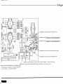
AF-CNTL Unit Alignment Points
"...
,'c',
,.-
x
00".
.!;
~-
~
~
;;~:
U
m~iv~ma"-1.,1;!.8~
--,
o~~~
;
+
.,
8
D
~.,...
...f.t
0
.w~G
0
£ ~:
~
c.~.
u
c...
..~
I
i
.0
~
,
a
c""'6)
~
8
~
,
.""'20
-~
TC1002 Carrier Frequency Adjust
VR1003, 04 FM Deviation Adjust
I WTechnical
m~.'
'.--Ok
iJ~m
..".
~ It:
~ ~
--
c.-
[
e..,lL"~
m
--"""'0
~ ~
~
c.a..
~""~""
8
"
~!
0
..,
8
~
VR1005. 06 Carrier Level Adjust
8
~
4'
~
-""
6) 8.
-int-
8
~
~
ftN
N
~
No;;;;i
!m""~
-~
00
8
..".
~r.
W
'"
'"10
.
.,'s.
J1
0
T1012, 13, 14, 16 FM IF Adjust
T1002 C.
TP1050 FM IF Adjust: R
: F:
: F
Supplement-
---
Alignment
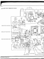
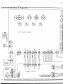
PLL Unit Alignment Points
0
;
-'
C
fM
I
c
~""
~
~
MO"'I:;
~
".
I
v,...
T2001, 02 HF-VCO VCV Adjust
,."
."'eI
'\l =
0 U=
.,..,
i"-"t
"..,
(
V
0
:;
n
;;0
;;
.""8
o
~
'.'&I ~
-~
;
0
D~
~
W~
:-c
0:
0
0""
~
~
L
:0
,0'&1."" ::
".~
s ft)D
~
C"'~
-0
-0 h
c"'~"
."'1 -h
.,.'eI
e~::
c".~
~c
~
;:
v
.",:
.,..
h;
v
:I
0
C,
~
~
8 .,., '~ 8 ~
C""~D
0
...,..,
C",
.",
.",~
..1"-"
~
~
C"'~.,.~mt
",61
8
0
cm'
"",C"'~'i",~
""oS
~
:
e
c,I:lfi.~'\l:hUh
-13
D
",.~fJE
h
D
.0 D 0
"
~
u ~ ~ C"11m!
-0
C"":]a
h L'
;;IlOl
[J
[J
;;
.""~.,,,~
13
.,...
;U
~
.~
o'
.
:
C'"
.,...
.,..
T2003, 04 HF-VCO VCV Adjust
.
:
[
T2005 HF-VCO VCV Adjust
c
c""
D
BE]
C".,
J,'"
TP2002 VHF-VCO VCV Check: DC Voltmeter
C
J""=
HF VCO Adjustment
VHF VCO check
Tune to:
for
108.000 MHz at least 0.5V
Tune to:
AdjusUConfirm
10.495 MHz adjust T2001
6.5'
0.100 MHz confirm
at ~
139.995 MHz
140.000 MHz
173.995 MHz
21.995 MHz adjust T2002
10.500 MHz confirm
36.995MHz adjust T2003
less than 7.2V
at least 0.5V
less than 7.0V
22.000 MHz
.75.995
3-14
confirm
6.5
at I
6.5
at I
53.995 MHz adjust T2004
37.000 MHz confirm
MHz adjust T2005
6.5
at I
6.S
54.000 MHz
at I
confirm
...~
.:;.'O"
,~
I WC
-!:"III
"
=
0 -0
t'W;:
~
}
~
:;§,-".,
:
0 \r;;u' ::
c~~~'" K
.(]EJ~III
~.,'"
~0
0= s."lMc""
p
} °c
"
-O
.""su
18dE
[~~""'0"
".,o"ah
00
';
}
-0
0 0
~ ~
K;U
~
0 ~-iR
.~
g.
~
-.0u
D
m
.;1r
:il
h .'no::
S Q0
-.'ll't!]h_- ~ U
@:
g
f8
i ."o
h
C" J
-::
-n
~
..s "" "
:.,,~§.'oo,
cia -~rA-,
c, "'~
-~
-'='.
=
-.IL.""
~
61
0
u
::
,~
.",,61
.".,a
II
7 I ~""
-O.
~6I.'""
~
'~."I'eo~~
}:; ';
"..
hh
-~
h
~
CU
U
~~f"jl- ~
msL7C"~
=:
°a ~o, G
Uu
h h L.!.J:;
J .,'c,
C21"
L""
;"d
;]D~~u
-.c
ill.§=::1R
~a
~
~
I 55
.U
~
~
0
a
."'~
I1.1",,'::
.I"C'
h
:;~
.""
""a
=
.Q Cm ,""
ID;
-~
:; c~-~
B
L=J ~J
""0 L'"I'
c'IJ!J'~'0
c",. ~
.~IIJ
.~
e
--
:: ~
c""
~fII:""' 7 .""
cIIJKIa.
." .0 Ima
OJ
.g ~"'!.3SGo
_8
~
05
=
h-;)j
c""
U au~
-ri"];:
.""-~
~
U l1.FJ .'I'SS3D
.
a
[I)
,;;;
m;;
h
.""':;61
0
.,~,~
hh
~ ~:
K u
~
§~1T1
U::L.!.Jo 5 ~;
C'I"
0
U
HJ:
~
V
m~L'""~
ctklSIG
.~,
~
o
0
'u o
C"1i! c~
C'I'.
h
55 -:
};K
=
°h
'I'm::
-'.r-"I
"0'
s.,o"
~~
~;h
.",",s
};-uu
c
I m~
-0
~
J
~a
c,'o,
L""
"0'.
."OI~
: c~~
~
tn1
;;
h
0
° ~
C"" ~
3D "°5' [3D
c.
,,1"-"1 .=°
~
Y
C
"
.wfJo
0
a
~;:tJh ...,
0
""u
c
:;tIc~a'""
Gl=J3"!1"lli.'I"a:::mK
""0
L'O'O ~
0
h
.,
.~
c""
~
.,,-,-, m:
J
C
~C"'O
!!I_-
.""61
"°1'
n=f11B;:HE
u:
:;L.!.J
1IJ"u,
I~,
nnnnnnn
.,,",aO
-I
~
0
,.1'"",
/:_-
~]~~~'O'"
"
~,//
vCV Adjust: DC Voltmeter
::0 Adjustment
ust/Confirm
",;
UHF VCO check
for
6.5V:t0.1V
420.000 MHz
at least 0.5V
lfirm
at least 0.4V
459.995 MHz
less than 7.0V
ust T2002
6.5V:t0.1V
460.000 MHz
at least 0.5V
lfirm
at least 0.4V
511.000 MHz
less than 7.0V
ust T2003
for
6.5V:t0.1V
lfirm
at least 0.4V
ust T2004
6.5V:t0.1V
lfirm
at least 0.4V
ust T2005
6.5V:t0.1V
lfirm
at least 0.4V
-IT
"h
TP2003 UHF-VCO VCV Check: DC Voltmeter
Tune to:
ust T2001
8"""'
'>=- E!
-847 TechnlI
-Alignmer
VR3002 430 MHz TX Adjust
VR3003 144 MHz TX Adjust
VR3004 50 MHz TX Adjust
5, 28 VHF RX IF Sensitivity
J3:I'~
.130'"
1-
III
II
I
III
ji
VR3005, 06 HF TX Adjust
.130'5
..'"
..It
~
~
~
~g mgm~m~m~
~
~.. g
~ ~ ~ ~..>..~..>
~
~
~
>
.."
~
~ ...~
~
VR3007, 08, 09 AFP Adjust
.
0$
~"o
T3028
T30~
eJ'"..'3002
~
+
T3023
<:'"
~"N
u
r!J
~.
...( r:d
..LtJ
a
0
'"
.J
T30IO
Q
"1302'
$
~
$$$
~
~$
'"
~
$ 3 $~ $T30I~$
-..'
~
.,
:I
g
","
0
::~
~
0
0
03075 of§jj-
O'O~~
030.,7
~
030"8
~
030"9~
]
3
03080
~
~~~~
03062
-=-r:=::!:r
T3005, 08, 10 144 MHz TX Adjust
5$
~$ ~;]O2S
'-30'9
o@
C3373
0
+
Q
~
S
~
Q G
L3023
.
03002
T3003, 09, 13, 16 50 MHz TX Adjust
~
s $ ~"'" ~
i -"oo~)C;]OO"f
.J'
V
.13006
3-1
8
" "
~
~
~-
RF Unit Alignment Points
13017,18,27,29,31
VHFRXIF Sensitivity
13019,21,25,28
VHF R:
J
r!lD~~
T3029
~$
'-
T30"
O J~?
+'
LtJ
ltJ
':;
~
/
~
J
C3'-02
~
T.O27
C32"V
[)
'3018
'30",
"
r-"
~
8
"'..,
0
T3G'~ ~
~
~
U
>
B
gb
~
"..~
0
0000"
m
..m
-..r-
"
.."
J
J
J
$$$$$
~~~Si
00000
..'"
JJJJJ
13006,
07VHFRXIFSensitivity
T3012
D
.,=0
~3020
T3006
""""'J
!~
Supplement--
1--
---
'"
,'I
'"
J
~$
"
b
~
0
$
[
m
m
0
0
J
"
..'"
J
J
J
$$$$$$
~~::~~$'!S2
J..~~oooo
"'"
'"
JJJJJJJ
$$
0
1'1
"'"
$$$$$$$~$$~$$$$~
~,,",~"1~~:ga~~~~~~8~
~
>
J
J
J
J
J
J
J
~~~~~~~~"~~..~~~..,,
U 1*
i$
!$
!~
U
J
J
!$
J
J
1$
J
J
!$
J
rtJ
J
C
'
r!, ..D~
LtJ ~
g
-"00" ~
J
i*
!
L1J
~
("~
W Technical
"g
LtJ~
L'O' 6
§,'I
.
r!l~
~
~
$ $ ~ $ $ $ $ $ ~ $ $ $
U
13011,12,14,15VHFRXIFSensitivity
'301'
!J
~
'"
"a
0
~$ $. ~
(/'~-
"""'~
J [==~
~
D3Oe8
t::J
0009'
t::J
!
!
)1
J3013I1
:
I
;...
19nment
: ::. .., ",;_:,.:...':.::';".,.::'::'~.
.-
V/U- PA Unit Alignment Points
TP4002
VHF-PA
Idling
TP4001
VR4004
144 MHz TX Adjust
0
~
u:J.J
G
""0218
e
CLIID
r:;p
"""
B
0
144 MHz
L
TX Adjust:
~
~~
~
DJ..OO
Co.DO~
...0
~
.J"
c
.,!
Co.D'
"
a
EJ
,CJ.o..2
"'""'"
L-D28
t
u
[E[]
0
.'"
C-039
..~o~
~
g
+
~
..-008
..1+
\
~I!I [!J
;:1
EEl
;
C4D16
B
D
~~
.
L4032
~
0
TP-OIO .:I
0
OJ
EJ
"
ua.,
I
.."-025
,
m
~1 ~
~~.'
..u
.
"-D
"-0'9i
CJ::J
"
~
.,
c..'J9I
IEJ
,~.
.~!:!J.. U
TP-OD2
.._D09:.
~
[
..
"'-~ ;0
~ '"-""-'j
*
Cio~UE!~
-L-O'
~
"-" Ie
.
.:"
-r;j:J
Cio071
Cio063u::i1 ~
C""
Pin.3
Ammeter
,t
OJ ..~..
~~
n;]l
"+" lead (0.3:t0.03
Current:
c
$
EI
R402"1
EI
~
C4~ [8]
~
I::I::::J°
~:
EI
~C-I)90'
..io023
~ 0
~
[IJ
0..
7-J
~
u rr:;n C~g
..'D20
Ammeter
Idling
J4003
R"O28 ,",,"
0
TP4011
Current:
VHF.PA
0
..~
~0
~
.:I
L-012
;j
j
t=::I I
"-031
TP4004
TP4003
J4007
TC4005
16
-
TC4004
Pin-3
430 MHz
UHF-PA
UHF-PA
Idling
430 MHz TX Adjust
430 MHz TX Adjust:
TX Adjust
Idling
Current:
Current:
Ammc
Ammeter
DC Voltmeter
(min.)
"-"
.
~,~.,..j..;:,.:'~;~:~.~~:,:;,;;;:~i..:,-:';<';"~:':'...,;;.\~~~~~-~~
-
~mmeter "+" lead (0.3~0.03A)
TC4002 144 MHz TX Adjust
ling Current: Ammeter "-" lead (003~0003A)
Pin-3 144 MHz TX Adjust: DC Voltmeter
~
VR4002 VHF-PA Idling Current
(mino)
..
.-0'J"'
!: 0\
!
~
~\U
~
.;
I
'
~,
~
0
§
I
,.
:~,
(;;::1..
L:.::r
'
I
.
-Iw
u
-~~!..I
.-,:,
I
.r-;-,
.j
~40016
~"I T
~
b
L'O'
0
r '"
~
---
.~
Iffi
c:.o39
g
rp'OO2
[.(!;J
I
'J;'
~
I-,l~
\
0,-",
a
mT~.,.~
.
I
-.~
,
I
':..0:
~
:I
C:'Oo"
00'
."
,-
W
:~~:::~:]]
TCLO),'2
~
LL'lJ
C
~---"
:)
1111
.,
I
;C:'0'2
"<1-0
g
--:"'\'3r-Tl,
I '~1! '"--,
I
0T b
;;<
g,";
,
,
'It'
J
rDl
;
~
j:j\
_0
,,(
~
.
r-;;;-
L2Jo
I;)
o:.oosffij
\,
L'Joe
-..L-O~
.,
~.co.19
..",...
...J
.,
c~o~
~
0 ~:.
0
~)
:~~
-R-i)'
~
G
"--"",
11
~oo;;:
-J
~.(I,"\
1.
0
L'-003
0'-002
!
Iii
.IB~
J'~06
C4001
~40'0
G
~
!+
I'
~)
...u.r
g
(f)
3
~
J~OS
~
0
U
00
t-
-
\
~
j;,
r-n
Nt
Dt.
3
~
[IJ
.."
L'OO~
"'
~
G
G(
'"'
0,~~"0~,
0
~
~
l;100
@.§
~
[EJ C..O2S -'
g
g
.."
~
[~~
'000::
LLO'2
~
@J
iF-PA Idling Current: Ammeter
"+" lead (0.3~0003A)
dling Current: Ammeter "-" lead (003~0003A)
Ijust
just: DC Voltmeter
OLO'"
TC4001 430 MHz TX Adjust
TC4003 430 MHz TX Adjust
VR4001 UHF PA Idling Current
(min.)
I
-FT-847
Technic
~
I
:::.
P A Unit Alignment
Points
~~
l[~~
TP,;.OO3
L
0
R
LJ
LSIJI'
TP5001 PA Unit Final Section Idling Cur
TP5002 PA Unit Final Section Idling Current: Ammel
FT -847 Technical
Supplement-1-
---
-
-Align]
..
G)
0
on
u
~
F85002
~B
~~
~~
r-==I~
~r=l
' ~~((fi\\
m"l
~
I~
CSOO2
J'
CSOOt
b!4J
~
~~
\.
~
~
~
~
~! 19I
r=l ~
(~ R ~!S
~
VR5002 PA Unit Drive Section Idling Current
([[)
r=:=-l
~~
~~
~
r=I
~
~
J5006 Pin-1 PA Unit Pre-Drive Section Idling Current
: Ammeter "+" lead (O.25:!:O.O25A)
F85001
~
1!J
(f)
5002
~
~
~
[!J
t:O
5001
TP5002
TP5001
J5006 Pin-2 PA Unit Pre-Drive Section Idling Current
: Ammeter "-" lead (O.25:!:O.O25A)
~~
Uu
C5026 GOI 5
~rnT
W
C:~=J
VR5003 PA Unit Pre-Drive Section Idling Current
§$~
U
VR5003 PA Unit Final Section Idling Current
J5005
J5007 Pin-2 PA Unit Drive Section Idling Current: Ammeter "-"lead (1.5:!:O.15A)
J5007 Pin-1 PA Unit Drive Section Idling Current: Ammeter "+" lead (1.5:!:O.15A)
05 Pin-1 CM Coupler Balance: DC Voltmeter (min.)
tion Idling Current: Ammeter"+" lead (O.42:1:O.025A)
Irrent: Ammeter "-" lead (O.42:1:0.025A)
-
IIIIIII
" ""
"."-" ".,--"--
"-""'."o-.,,
,...,
:--,.-~.,,.,
,:,:c'~"c3
'.:~~';'~
~nterconnection Diagram
~~~
.J1D15
.JlDa
STBY
@
CAT
E
~~~~«
~6_o»
0
-ill
0
\\~~p
.J1D16
iii-
~
~
[!]
0.
-m
[!) [!]
IN T -1
a-o
~
@
0
0.
.J1D17
.J1006
DATA1N/aJT
KEY
EXT. PTT
en
en
2
.J1D14
[!) [!]
HT8
VTB
.Jl009
~
.J1DII
PACKET
(!J[!J[!]
ill
.Jl003
TX IF @::
.Jl008
TtOER
0
.J1001
AX IF @::
i
2
UT8
3
a-o
4
.J1007
.Jl024
EXT. PTT
~
~
::Al
~
KEY
50
a-o
.Jl
co,
P0D01
T~71B
AF-CNTL
-UNIT
a-o
FIC]
2
3
AGC
4
BV
~
~V
B
H--ANT 7
a-o
8
a-o
BY
.J1D18
[K:+
~
.J1D19
[K:-
a-o
030
B-STB
R-CI..K
13. 8v
FANSW
.J1D13
R--5T8
T-CU(
.Jl005
.J1D20
.J1D27
.11026
~~
~
.J1D1D
.J1D29
00
>
~~~g
~~f
~~8~;~~~g~~
1234
123
1234~6789
~
g
R
~
R
i
I
~
I
~
T-5TB
-
>
~ ~
~M
'-~ N'aa
m
.q
~
T~
e
L
R-PU.
123
f
PHONE
~~~
.JACK-UNIT
.E5)6
00
i ~
~o
i i ~ ~
~1.A;502
~
~ ~ &f ~
.E5O3
~ ~
Q(A
~4
Ck8
MIC-
UNIT
eo
.J2O1D
~g8
1--
4-2
~V
M1
PTT 7
GOO6
~
-UN
I
T
~
FST 4
:
PANEL
'-"7
9'14)
T
v
~
~
,.
9'13)
g ~ ~ Iii ~ i ~ ~ i ~ 9'12)
r(i)@@0@@(!)@@@
I 9':
s0001
rBJOO63
;;,
-
-
tOO"""
F
T93,5'.'
1003...,..
F
TW315'42
1011
~
.BlOB
,;:;:
AX IF
..-3
-TQ31S)56
"'"
,",/50 AX
~.J3)08
TX IF
~
"-4
~
,",/50 TX
'-12
_12
FI~I
~
I~
~
101.
'
2
INT SP
&D
~711
1
2
..&D
'--
VTB
UTB
,-'7
TSQ87w.
1
2
.1
1
2
3
3
~
'-713
1,",2 ,*,"'C
.! LPF1
~
4
4
LPF2
S
S
LPF3
LPF.
8
8
LPF'
7
7LPFS
LPFS
B
LOF7
a
..-ANT
'"' is
~
~-
,
~~ANT
8
B
.9
'"' ANT 0
LPF7
i
'"' TB
i
&D
0
so...IZANT
LPF6
~ANT
&D
8
,",/!Oa TX
LPF3
0<1
OATA1
..KEY
""S
-eoo.
~
LPF2
-LPFS
102.
I
PA-UNIT
~
,
,",AFP1
'*""C
2
LOF1 3
HTB
2
3
3
T9318044
'-13
'-16
1
.$03
,",/!OaRX
~
~
~
~
~1
.B>O2
~?J~?J
1<
1<
--
&D
-'-
5'0001
O.
'-,4
.-7104
1
1
2
3
4
'T
4
./
GlC)6
FIO)
AGC
S
8
S
6
BV
SV
"-1
7
8
7
B
..-ANT
GIC)
3
N4O9OO6!
.-.'-71.
INT spl~
...f
2&D
3
~
-'3O1B
~
T931S1S9
"",-'400.
1A.AX
..-2
"'"
430 RX
T9318061
=.)40OB
.30 AX
-'3OOS "'"
,.. TX
T931~
"","4001
,.. TX
"3006
~
430 TX
T9317mB
,.ARX
~
'i"
2
;
~
~
V -U-P
UNIT
A-
,..
-0
"",.JA002
.30 TX
I2S
.J4OQ7
<
TA
:
RF
-UN
I
T
-'3011
3
lJ-F TB
..lJ-FALC
.S
<
1
~71S
I
2
lJ-F
GIC)
6
TA 7
.8
9
"3015
c-'"
?,?,
->
0
>
11002
EF@:=-
".J
0
-3
I
I
r
A
I
1
lJ-F TB
2
lJ-F ALC
3
lH'AFP
A lJ-FGIC)
5
6
\/H""C
7
2
\/H'
\/H'AFP
B
3
\/H'AFP
~'~~~~5~~
o~~~
GIC)
123.
SJ(8 7J(eJ(g'l~
~~~\/H'-
.J4OO9
.-.FAN
lJ-F -S
\/H' TB
o.J
A30 -0
I
9
1
_3
\/H' TB
.&D
S \/H'-
ALC
~1
I~I
GIC)
>
~
r;\1
~~
ij
I
a
"z
~
"4005
13"
~
.)4006
r;\1
~~
.i"
~
~
a
2
;;
T931-TQ31~
T9206707
T92067OB
~
T92O67OB
T9311201
SOOo
~
I
1 2 3 .8
'
MAIN
6 7J(8J(911
>?,
g >
~'~~.L55~~
~
~
~ ~0
~o
.,.J.J
~
~
..~
8
& ~
.)2001 ~
GIC) ~1
BV
~
5V
!:.)2003 ~
GIC)
1
DIAL
1 2 3 .S
B 7 e 9
>
~~8~;~~~X~~
'I
ri~
..~N
~ H
~ a
.-01
R-a.K2
e-sTB
.
R-OATA
S0002
NO180173
3h
SHUTLE
-FT
R-sTB S
T-<:LKI~
PLL-UNIT
:::LJ-J
;?;
;:,:A:!
OSP-UNIT
T~
I~
..-PI.L
I~
'--847 Technical
Supple::
17