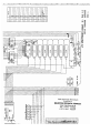
1
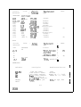
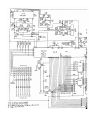
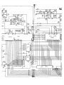
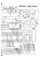
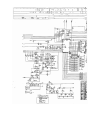
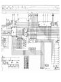
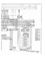
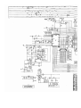
Sinclair
Spectrum 128
Service
Manual
Information within is copyright Amstrad PLC. Brought to the ZX
Spectrum World by Andy Dansby
[email protected]
SERVICING MANUAL
FOR
SPECTRUM 128
©
LIST OF CONTENTS
SECTION 1
INTRODUCTION
SECTION 2
SYSTEM DESCRIPTION
SECTION 3
SETTING UP AND SYSTEM TEST
SECTION 4
FAULT FINDING AND REPAIR
SECTION 5
PARTS LISTS
LIST OF ILLUSTRATIONS
Fig No
Spectrum 128 Block Diagram
Uncontended RAM RAS7CAS Timing
Keyboard Upper Membrane
Keyboard Lower Membrane
Spectrum 128 Logic Circuit
System 128 Analogue Circuit
|
1.1
1.2
1.3
1.4
1.5
1.6
Keypad Circuit
1.7
Test Oscillograms
Spectrum 128 PCB Component Layout
Keypad PCB Component Layout
4.1
5.1
5.2
Prepared by BRAVEMAY LTD
for SINCLAIR RESEARCH LTD
ti)
CD i A A A
SERVICE MANUAL 128
X-1223
SECTION 1
SYSTEM DESCRIPTION
Sub-Section
1
2
3
4
5
6
LIST OF CONTENTS
Introduction
Architecture
Z80A CPU
Memory Organisation
Read/Write Operations and Bus Arbitration
Input/Output
TV Picture Generation and Sound Output
Keyboard Scanning
Tape Interface
Programmable Sound Generator
RS232C/MIDI Interface
Keypad Scanning
Power Supplies
Fig
1.1
1.2
1.3
1.4
1.5
1.6
1.7
1.
Page No.
1.1
1.3
1.3
1.5
1.8
1.11
1.11
.1.13
1.16
1.17
1.18
1.19
1.22
ILLUSTRATIONS
Spectrum 128 Block_Dj_acjram
Uncontended RAM RAS/CAS Timing
Keyboard Upper Membrane
Keyboard Lower Membrane
Spectrum 128 Logic Circuit
Spectrum 128 Analogue Circuit
Keypad Circuit
1.2
1.10
1.14
1.15
1.23
1.24
1.25
INTRODUCTION
1.1
The Spectrum 128 is a derivative of the 48K Spectrum Plus
offering 128K of RAM, music quality sound, greatly improved
video quality and higher hardware reliability.
1.2
The firmware is capable of running in Spectrum 48K mode or,
alternatively in 128K mode, which will support paged memory in
the form of a RAM disk. Extended BASIC to handle the sound
facility is provded, and a full screen editor is incorporated
in the firmware.
1.1
SR1AAA
1.3
A list of the principle features appears below:
(a) 128K dynamic RAM
(b) 32K ROM
(c) Numeric keypad
(d) TV sound with composite video
(e) Elimination of dot crawl (single crystal operation)
(f) RGB output
(g) RS232 serial port
(h) Musical instrument d i g i t a l interface (MIDI)
(j) Software compatible with all previous Spectrums
(k) Edge connector compatible with Spectrum.
2.
ARCHITECTURE
2.1
The architecture of the Spectrum 128 shown in Figure 1.1 is
typical of many microcomputer systems is that it comprises a
single microprocessor chip (in this instance a Z80A or u780), a
read only memory (ROM) a paged random access memory (RAM) and
an input-output section. The latter handles the keyboard
input, tape and TV display functions using the logic gate array
(ULA ICD, and the keypad input, sound and RS232/MIDI
interfaces using the sound generator circuit IC32.
2.2
The analogue circuits (not shown) generate the 17.7 MHz master
clock, and process the RGB colour monitor and sound signals.
The resultant outputs are suitable for use with colour (RGB) or
black and white monitors, and domestic UHF television
receivers. A modulated sound carrier is output with the
composite video.
2.3
The computer is built on a single printed circuit board which
also includes a regulated power supply fed from an external 9V
power pack. The keyboard matrix is part of the upper case
assembly and is connected to the board via two ribbon cables
KB1 and K82. A digital keypad is also provided, connected via
a flexible cable. It can be used as a games controller or
calculator pad and has special function keys for use with the
full screen editor. An in-built peripheral interface
controller (PIC) performs the keypad scanning routines and
delivers an output to the Z80 on demand.
3.
Z80A CPU
3.1
The Z80A is an 8-bit single chip central processing unit (CPU).
It is clocked at 3.5 MHz from a d i v i d e of an external source
controlled by the logic gate array (ULA) and has a standard
three bus input/output arrangement. These buses are the data
Bus, Address Bus and Control Bus respectively.
1.3
SR1AAA
3.2
Data Bus. 07-00 constitutes an 8-bit bi-directional data bus
with active high, tri-state input/outputs. It is used for data
exchanges with the memory, sound chip and the ULA.
3.3
Address Bus. A15-AO constitutes a 16-bit address bus with
active high, tri-state outputs. The address bus provides the
address for memory data exchanges and for data exchanges with
the ULA. It is also used during the interrupt routine (see
below) when scanning the keyboard matrix.
3.4
Control Bus. The control bus is a collection of individual
signals which generally organise the flow of data on the
address and data buses. The block diagram only shows five of
these signals although others of minor importance are made
available at the expansion port (see Figure 1.5 for details).
3.5
Starting with memory request (MREQ), this signal is active low
indicating when the address bus holds a valid address for a
memory read or memory write operation. Input/Output request
(IORQ) is also active low but indicates when the address bus
holds a valid address for I/O read/write operations.
3.6
The read and write signals (RD and W) are active low, and one
or other is active indicating that the CPU wants to read or
write data to a memory location or I/O device. All the control
signals discussed so far are active low, tri-state outputs.
3.7
The last control signal described here is the maskable
interrupt (INT). This input is active low and is generated by
the ULA once every 20 ms. Each time it is received the CPU
'calls' the 'maskable interrupt' routine during which the
real-time clock is incremented and the keyboard and keypad
scanned.
3.8
CPU Clock. Returning to the CPU clock mentioned earlier in
this section, the ULA is able to i n h i b i t this input bringing
the CPU to a temporary halt. This mechanism gives the ULA
absolute priority, allowing it to access the contended RAM
without interference from the CPU (see RAM description).
Switching transistor TR3 ensures that the clock amplitude is
+5V rather than some arbitrary TTL level. This is essential if
the CPU is to operate effectively while executing fast machine
code programs of the 'space invader' type.
3.9
Dynamic Memory Refresh. The CPU incorporates built-in dynamic
RAM refresh circuitry. As part of the instruction OP code
fetch cycle, the CPU performs a memory request after first
placing the refresh address on the lower eight bits of the
address bus. At the end of the cycle the address is
incremented so that over 255 fetch cycles, each row of the
dynamic RAM is refreshed.
1.4
SR1AAA
4.3
The Z80 address space is allocated according to the two m.s.
bits of the address bus (ZA14.15) and the contents of the bank
register IC31 which is at address 7FFDj.| in the ZSO's I/O space.
The significance of the register bits is summarised below:
Bits
Function
B2-BO
Selects the page occupying the top 16K of the Z80
address space. Any RAM page can occupy the space.
B3
Instructs the ULA to access the display mapped in
page 5 or 7.
Bit set : screen in page 7
Bit clear : screen in page 5
B4
Determines whether instruction fetches are from ROM 0
or ROM 1*
Bit set
: fetches from the 48K
Spectrum ROM (ROM 1)
Bit clear : fetches from the 128K
Spectrum ROM (ROM 0)
85
Set to prevent further accesses to the bank register
(protection against SPECTRUM programs crashing if the
bank register is written to in error)
* see para. 4.12.2
4.4
Clearly, dependent on register bits B2-BO, the Z80 can access
page 2 at address 8000H or COOOH and the screen in page 5 at
address 4000^ or COOOu. The screen in. page 7 can only be
accessed at address COOO^. On power up, or after reset the
bank register is cleared and loads page 0 at address COOO^,
selects the 128K Spectrum ROM at address 0000H and informs the
ULA that screen accesses are from page 5.
1.6
SR1AAA
This mechanism only applies to the non-contended RAM area. An
alternative refresh method is adopted for the contended RAM.
4.
MEMORY ORGANISATION
4.1
The Spectrum 128 has 160K bytes of addressable memory - a 32K
byte ROM (IC5) and 128K bytes of dynamic RAM (IC6-IC22). The
latter is organised as eight 16K byte pages as indicated below.
contended video
RAM
ICs 6-13
uncontended 'upper1
RAM
ICs 15-22
4.2
Pages 0-3 are uncontended and are accessed solely by the Z80.
Pages 4-7 are contended in that the Z80 and ULA IC1 both
require access to pages 5 and 7 in order to generate the memory
mapped displays. The address of any page of RAM depends on
where it appears in the address space of the Z80 which is
structured as follows:
COOOH
8000H
4000H
0000H
1.5
SR1AAA
TABLE 5.1
CASE ASSEMBLY
DESCRIPTION
MANUFACTURE
Base Assembly
Final PCS Assembly - Table 5.2
Heatsink
Retractable Legs - 2 off
Leg Springs - 2 off
Bottom Case Moulding
Fixings
1/4 in self tap screw - 3 off )
Fibre washer
- 3 off )
5/16 in self tap screw
M3 x 10mm pan hd screw
M3 plain washer
M3 crinkle washer
M3 hex nut
PCB
(2 off) - heatsink
- 1 off )
- 1 off ) voltage
- 1 off ) regulator
- 1 off }
1 Keyboard Assembly
I
Keyboard Reaction Plate
Spectrum + Membrane
Bubble Mat
Upper Case Moulding
Key Set
Tai 1 Clamps - 2 off
Fixi ngs
Double sided adhesive tape
12mm wide (Tesafix 959)
1/4 in self tap screw (4 off)
- tails
- tail
clamps
5/16 in self tap screw (10 off) - reaction
plate
General Assembly Fixings
5/16 in self tap screw
1/2 in self tap screw
- 6 off) base/
- 2 off) keyboard
5.2
SR1AAA
SECTION 5
PARTS LIST
Sub-Section
LIST OF CONTENTS
Page No
1
Introduction
5.1
2
Notes to Table 5.2
5.1
Fig
ILLUSTRATIONS
5.1
Spectrum 128 PCB Component Layout
5.2
1.
1.1
2.
Keypad PCB Component Layout
5.10
5.11
INTRODUCTION
Parts lists for the SPECTRUM 128 are provided in table form; one
for the case assembly (Table 5.1), one for the main pcb assembly
(Table 5.2) and another for the keypad pcb assembly (Table 5.3).
PCB layout diagrams are given in Figures 5.1 and 5.2 ;the notes to
be found in Table 5.2 are explained below.
NOTES TO TABLE 5.2
(1) A l l RAM chips should have 150ns access time and 128 row
refresh. This includes parts from the following
manufacturers: Hitachi, Intel, Mitsibushi, Mostek, Motorola,
NEC, OKI, Panasonic, Toshiba and National.
(2)
If TR3 is type KSC839, resistor R24 should be 15KO.
(3)
Provision has been made on the pcb for a 2 to 22pF film
dialectric trimmer should the need arise.
(4) The ROM should be pin compatible with a 27256 EPROM and have
an address access time of less than 400 ns. The output enable
access time should be less than 250 ns.
(5)
The crystal is series resonant with 20pF and accurate to 10
ppm absolute, + 10 ppm 20 to 60°C, +_ 5 ppm per year.
(6)
If preferred, the 20uF capacitor used for C124 may be split
into two parallel capacitors of 10 pF +; 2% in the positions
C124 and C130.
(7)
For FTZ (German) version only.
(8) 6.0 MHz version (Type No ? } for use in the UK; 5.5 MHz
version (Type No ?) for use in most other European countries.
5.1
SRlAAA
4.5
All memory accesses are controlled by the programmable logic
array (PAL) IC29. It does this by decoding the two m.s. Z80
address bits Z15, Z14 with bits B2-BO from the bank register to
produce three pairs of supplementary address lines. They are:
(a) UA15,14 specifying the page number in the uncontended RAM
space
(b) VA15.14 specifying the page number in the contended RAM
space
(c) ULA15.14 controlling bus arbitration and Z8Q access to the
ROM and contended RAM space.
4.6
The decodes are summarised below and described in the following
paragraphs.
Z80 operation
ZA15 ZA14
R O M access
4000H -7FFF H
8000H -8FFF H
O
page
page
page
page
page
page
page
page
1 1 0 0 0
1 1 0 0 1
1 1 0 1
1 1 0 1 1
1 1 1 0
11
1 0 1
1 1 1 1
1 1 1 1
0
1
2
3
4
5
6
7
access
access
access
access
access
access
access
access
O
0 1
1
0
B2 Bl BO ULA15 ULA14 VA15 VA14 UA15 UAH
X
X
X
X
X
X
X
X
X
0
0
0
1
0
0
1
1
1
1
1
0
0
0
0
O
X
1
O
X
1
X
X
X
X
X
1
1
1
1
X
0
X
X
X
X
X
0
0
1
1
X
X
1
O
X
X
X
0
1
0
1
0
1
l
X
X
X
X
X
X
0
O
1
0
l
X
X
X
X
4.7
ZA15 = ZA14 = 0. These bits select the first 16K of Z80 address
space beginning at 0000^, and result in the PAL generating ULA15 =
ULA14 = 0. These are decoded by the ULA (ICl) to produce a signal
ROMCS enabling the ROM IC5. A13-AO on the Z80 address bus provide
the instruction address, bank register bit 4 determines whether the
upper or lower 16K of ROM is accessed.
4.8
ZA15 = 0, ZA14 = 1.
These bits select the RAM page located in the
second 16K of the Z80 address space beginning at 4000u and result
in the PAL generating ULA15 = VA15 = 0 and ULA14 = VA14 = 1. The
ULA lines signal an access of the contended RAM area and prompt ICl
to assert the DRAS, CAS and DRAMWE lines controlIrnq the read/write
operation. At the same time, ULA15 inhibits the "CAS output from
IC27 preventing any access to the uncontended RAM area.
4.9
The 2:1 data selector IC30 supplies the m.s. row and column
address bits to the contended RAM as OMA7, first selecting the row
address VA14 = 1 while DRAS is low and the column address bit
VA15 = 0 when it returns high. This combination selects the
second 16K bank of RAM in the contended area, allowing DMA6 - DMAO
to access locations in page 5 used for the standard screen display.
1.7
SR1AAA
4.10
ZA15 = 1, ZAU = 0. These bits select the RAM page appearing in
the third 16K of the Z80 address space beginning at SOOOu, and
result in the PAL generating ULA15 = UA15 = 1 and ULA14 = UAH = 0.
The ULA lines signal an access to the uncontended RAM area and
enabVe IC27 to assert the CAS line which together with RAS (MREQ)
and WR control the read/write operation. (Access control lines
for the contended RAM area generated by ICl i.e. CAS, DRAS and
DRAMWE, are not asserted at this time). VA15 and VA14 respectively
supply the m.s. row and column address bits for the uncontended RAM
area as MA7 and select the second 16K bank of RAM allowing MA6-MAO
to access locations in page 2. .
4.11
ZA15 = ZA14 = 1. These bits select the RAM page appearing in the
top 16K of the Z80 address space beginning at COOO^. The bits
together with B2-BO from the bank register IC31 are decoded by the
PAL to select any page from the RAM according to the setting of the
supplementary address line pairs. For the uncontended RAM space
ULA15 is always high allowing IC27 to control read/write operations.
UA15,14 assume one of four possible states reflecting the state of
B1,BO and select a page in the range 0-3. For contended RAM accesses
ULA15 is always low allowing ICl to control the read/write
operations, and the data selector IC30 to deliver the m.s row and
column address bits VA14.15. The latter also assume one of four
states and since B2 is set, selects a page in the range 4-7.
4.12
Read/Write Operations and Bus Arbitration
4.12.1
The following description should be read in conjunction with the
circuit diagram given in Figure 1.5
4.12.2
Read Only Memory (IC5). The physical ROM is a 32K byte device, but
appears in the Z80 address space as two separate 16K ROM's. ROM 1
is the old 48K Spectrum ROM (slightly modified) and is selected
when bank register bit 4 sets address A14. ROM 0 is the new
Spectrum 128 ROM and is selected when bit 4 is clear. _CPU accesses
occur during memory read cycles when the Z80 asserts MREQ and loads
the address bus A13-AO. MREQ enables the ROM outputs onto the data
bus D7-DO, ROMCS decoded from ZA14.15 (see para. 4.7) selects the
chip.
4.12.3
An external ROM chip select input, supplied via the expansion port
on pin 25A, selectively disables the on-board ROM by p u l l i n g the
select input high. By virtue of R33 placed on the ULA side of the
ROM the ULA ROMCS output is effectively inhibited. Interface 1
uses this mechanism, allowing the CPU to read the extension ROM in
the interface for microdrive and RS232 applications.
1.8
SR1AAA
4.12.4
Uncontended RAM (IC15-22). The uncontended RAM comprises eight 64K
dynamic RAM chips organised as a 64K byte memory with a 256 x 256
row/column matrix. When ULA15 is high (see para. 4.11) separate 8
b i t row/column addresses are supplied by IC27 as MA7-MAO. These
are derived from the Z80 address bus A13-AO with UA14 and UA15
from IC29. The low order address bits A6-AO with UA14 provide the
row address and are selected at the beginning of the memory access
cycle when i n i t i a l l y the RAS (MREQ) output from the_Z80 is low.
Later, as the row address is latched, IC27 asserts CAS selecting
the high order address bits A13-A7 with UA15.
4.12.5
Row/column address selection and RAS/CAS timing for the RAM is
decoded in IC27 in conjunction with IC28 and the associated
d_j_screte_ components. A theoretical timing diagram illustrating the
RAS /CAS waveforms is given in Figure 1.2 (A read operation is
shown when the WRL l i n e from the Z80 is high).
4.12.6
Contended RAM (IC6-13). The organisation of the contended and
uncontended RAM described above is identical. However, because
ULA15 is low during accesses to the contended area, IC27 only
sources a 7-bit row/column address DMA6-DMA7. The m.s address bit
is sourced by the 2:1 data selector IC30. At the start of the
memory access cycle Id asserts DRAS and selects the row address
as A13-A7 off the Z80 address bus with VA14 via the selector.
Later as the row address is latched Id sets DRAS and selects the
column address as A6-AO with VA15.
4.12.7
RAS/CAS timing for the contended RAM area is decoded by the ULA ICl
from MREQ and A15. OCAS is asserted a short time
after DRAS returns high, and latches the column address. ULA15
prevents IC27_generating an identical signal for the uncontended
RAM._The_ORAMWE signal, also generated by the ULA, is a decode of
the RD/WR waveforms and selects a RAM read or RAM write cycle.
4.12.8
It will be apparent from the circuit diagram that the ULA can
access the contended RAM by generating a set of addresses
independent of those generated by the CPU. The address port for
the RAM is therefore dualled by the insertion of small value series
resistors on the address lines between IC27 and the RAM. This
ensures that where there is likely to be conflict between the ULA
and CPU, the ULA address has priority. Priority is assigned on the
basis that the ULA must access screen pages 5 and 7 at set
intervals in order to build up the video for the TV display. If
the ULA is about to access the RAM and it detects either A14 or A15
(i.e the CPU is also about to access the RAM) the ULA inhibits the
CPU clock temporarily halting the CPU memory transaction until its
own transaction is completed.
1.9
SR1AAA
FIGURE 1.2 UNCONTENDEO RAM RAS/1^3" TIMING (READ CYCLE SHOWN)
l.*0
SR1AAA
4.12.9
Resistors Rl to R8, in series with the data bus lines, perform a
similar function to the address port resistors described above.
They ensure that the ULA does not 'see' CPU write data while the
ULA is accessing the contended RAM.
4.12.10
Refresh for the contended RAM is accomplished during normal read
cycles, i.e. most rows are refreshed each time the ULA accesses
screen pages during picture compilation; the remaining rows are
refreshed as a result of other read cycles also known to occur at
regular intervals within the refresh period.
4.12.11
Bank Register (IC31). The bank register is at address 7FFDn in the
Z80 address space. The register is positive edge triggered and
latches D5-DO off the data bus on the negative (trailing) edge of
the BANK output from the PAL IC29. BANK is decoded (set high) from
IORQ and W/WR active low (I/O read or write cycle) and ZA1 and
ZA15 low (address 7FFDH).
4.12.12 On selecting the 48K Spectrum mode, the Z80 writes a T into bit 5
of the register, thus preventing any further access. This action
preserves the Z80 address space, preventing erroneous calls to
address 7FFD^ crashing the SPECTRUM program. The bit can only be
cleared by using the RESET pushbutton or by interrupting the power
supply input.
5.
INPUT/OUTPUT
5.1
The input/output functions are controlled by the Z80 in conjunction
with the ULA (ICl) and the sound generator circuit IC32.. Like its
counterpart in the 48K Spectrum, the ULA handles the tape recorder
read/write functions, and generates an interrupt during which it
scans the main keyboard. It also accesses the contended RAM area
while generating the drive waveforms for the TV display and
produces a simple tone output while obeying the BEEP instruction.
5.2
The sound generator produces high quality music sound by mixing the
outputs from up to three programmable tone generators and a noise
generator. It also handles the RS232/MIDI interface and reads the
keypad status. Each of these functions and the supporting circuits
is described below.
5.3
TV Picture Generation and Sound Output
5.3.1
SR1AAA
The video compilation section of the ULA operates in conjunction
with the memory mapped picture display area in the contended RAM,
together with the colour encoder IC36 and UHF modulator. This
combination produces a high resolution 24 line x 32 character,
eight colour display suitable for use with RGB colour or black and
white monitors or a domestic TV receiver. The sound output from
the ULA or the programmable sound generator is FM modulated and
added to the composite video signal for playback through the TV
loudspeaker. If a monitor is used the sound is available through
the MIC socket.
1.11
5.3.2
From the 17.73 MHz external clock (X1/IC37) the ULA derives line
and field timing for the composite sync signal on pin 23, and a
pixel clock for timing accesses to the RAM. The ULA also generates
two 8.8 MHz clocks on pins 46, 47 from which the encoder derives
the 4.43 MHz reference and quadrature chroma sub-carriers. The
fact that the pixel and chroma carriers are derived from the same
external clock source means that dot crawl is eliminated. The dot
pattern itself is minimised by adjusting the display line length.
5.3.3
The d i g i t a l RGB and bright-up signals available from the ULA on
pins 19-22 are derived by accessing the picture information located
in page 5 or 7 of the contended RAM area at the pixel rate (para.
4.12.8). The addresses are necessarily independent of the CPU
and appear on the ULA address lines^ DMAS to DMAO and DMA7 as two
separate bytes, timed by the RAS/CAS row/col umn address select
lines. DMA7 is a decode of bit 3 (VB) loaded in the bank register
IC31 and sets the m.s row/column address bits as follows:
VB
(IC31)
0
1
5.3.4
DMA7 (LJLA)
|
ROW
COLUMN |
1
1
1
1
1
1
0
|
1
1
1
1
1
I
I
I
RAM |
PAGE
5
?
|
1
I
The RGB colour, bright-up and composite sync signals (Figure 1.6)
are coupled to the RGB output socket v i a 68 ohm resistors and are
suitable for direct input to a wide range of colour monitors. The
same signals are also applied to the encoder IC36 to produce a
composite video output at pin 6. The video comprises the following
components.
a)
Line/frame sync with colour burst, derived from the composite
sync input CS and a burst oscillator sustained by tank circuit
L3. The position of the burst relative to the line sync pulse
is determined by a threshold level set-up on the RAMP input of
IC36 by R113/C115.
b) Colour chrominance is derived by modulating the chroma
sub-carriers with the colour difference signals decoded from
the RGB and bright-up signals. The latter are first combined
using a diode matrix D20-D25 to produce six colour1 inputs for
IC36 - two for each colour, designated '0' and 'I . Without
bright-up the presence of any digital colour input at logic '!'
drives the '!' input only, producing a pixel display with the
colour intensity set for normal viewing. With bright-up
activated the '0' and '!' inputs are driven, increasing the
intensity so as to h i g h l i g h t the pixel display.
1.12
SRlAAA
c) Luminance (grey scale) derived by mixing the RGB inputs in a
fixed proportion. The signal is used to produce the colour
difference signals in (b) and in its own right to drive the
black and white monitor. The luminance is bought out at IC36
pin 7 and is applied to the RGB output socket via a
complimentary transistor pair TR13.14.
The luminance is returned to IC36 mixed with the FM modulated
sound carrier from IC38. The sound modulator operates at 6 MHz
in the UK (5.5 MHz in most other European countries) and is
tuned by L4. The modulating signal is derived either by the
ULA sourced via R112/C123 or the sound generator circuit IC32
v i a R132/C127.
5.3.5
The composite video signal at IC36 pin 6 is finally applied to an
encapsulated UHF modulator operating on European standard channel
36. The device is current driven via TRIO,11,12 to give improved
linearity thus reducing the effect of sound on vision and
vice-versa. The effect is further reduced by outputting the sound
carrier 20dB down with respect to the picture carrier.
5.4
Keyboard Scanning
5.4.1
Every 20ms (i.e. once per maskable interrupt), the CPU
systematically scans the keyboard recording which keys (if any)
have been depressed. The scanning method is described below with
the aid of Figures 1.3 and 1.4, As the figures clearly illustrate
the main keyboard consists of an upper and lower membrane. The
upper membrane is organised as an 8 x 5 matrix, the intersection of
each row and column bridged by a normally open switch contact. The
lower membrane is organised in a similar manner except that only 16
of the intersections are populated by switch contacts. The row
'outputs' and column 'inputs' are shown connected in both cases to
separate ribbon cables KBl and KB2, one to the ULA and the other to
the high order address lines A15-A8. Pull-up resistors R65 through
R69 ensure that when the address bus is in the high Z state, or
none of the switch contacts is closed, row outputs KB1-KB4 remain
high.
5.4.2
When the keyboard scanning routines are entered _th_e CPU performs
successive I/O read cycles setting the IORQ and RO lines to the
ULA, low. At the same time, the I/O port addresses placed on the
upper half of the address bus are modified with each cycle such
that each of the address lines A15 through A8 is set low in turn,
the other lines remaining high.
5.4.3
The sequence starts with I/O port address FE driving address line
AS low. The keyboard matrix also sees this potential on column 6,
applied via D6 and the ribbon cable KB2. Thus, when any of the
switches on the intersection with the column is pressed, the
corresponding row output supplying the ULA via the second ribbon
cable (KBl), is pulled low.
1.13
SR1AAA
5.4.4
The row signal (s) is subsequently buffered by the ULA and placed on
one of the five low order data bus lines. For example, if the CAPS
SHIFT key is pressed, row one output drives data bus DO high, and
so on. The sequence ends with I/O address 7F when column 8 is
addressed. In this instance, operation of the SPACE key drives DO
high. Clearly, the keyboard scanning routines make the distinction
between the CAPS SHIFT and SPACE key by knowing which address line
is being driven.
5.4.5
If one of the following keys is pressed the corresponding switch
contact on the lower membrane is closed. Additionally, the CAPS
SHIFT switch contact on the upper membrane closes.
TRUE VIDEO
EXTEND MODE
CURSOR
INV VIDEO
EDIT
CURSOR
BREAK
CAPS LOCK
CURSOR
DELETE
CURSOR
GRAPH
5.4.6
For example, pressing TRUE VIDEO closes the switch contact at row
1, column 6 on the upper membrane (CAPS SHIFT) and row 3, column 1
on the lower membrane (TRUE VIDEO).
5.4.7
Similarly, pressing any of the following keys results in the
corresponding switch contact on the lower membrane closing as well
as the SYMBOL SHIFT switch on the upper membrane:
, (comma)
. (full-stop)
; (semi-colon)
" (quotes)
5.4.7
5.5
5.5.1
For example, pressing full stop closes the switch contact at row 2,
column 8 on the upper membrane (SYMBOL SHIFT) and row 3, column 8
on the lower membrane (full stop).
Tape Interface
When LOADing or SAVEing programs using a cassette recorder, the ULA
transfers information between the MIC and EAR sockets and the data
bus, performing A/D and D/A conversions as required. During the
LOAD operation the CPU executes successive I/O read cycles to I/O
port address 254, reading the EAR input off bus line D6. When
performing a SAVE operation, the CPU executes successive I/O write
cycles to I/O port address 254, this time writing data to the MIC
output via bus line 03.
1.16
SR1AAA
5.5.2
To ensure that I/O cycles are correctly implemented, the IORQ line
supplying the ULA is gated with address line AO via TR6. Thus, if
any memory transactions occur when AO is high (i.e. not port
address 254) then the IORQ input is forced high i n h i b i t i n g any
attempt to perform the I/O cycle.
5.5.3
ULA Sound Output. It should be noted that while SAVEing, the level
of the MIC output is barely sufficient to modulate the sound
carrier to IC38. However, during the execution of a BEEP
instruction the CPU writes instead to port 254 on bus line D4.
This effectively boosts the MIC output, modulating the sound
carrier so that the 8EEP tone can be easily heard.
5.6
5.6.1
Programmable Sound Generator
The audio from the sound generator IC32 is derived from a master
clock input supplied by the ULA, controlled and shaped in
accordance with instruction codes loaded by the Z80 into 14
internal byte wide registers (see below).
* RS232/MIDI interface (see below)
5.6.2
The Z80 specifies a register by loading the data bus while writing
to address FFFDu in the I/O space. DA3-DAO supply the octal address
between 0 and 15, DA7-DA4 should be all zero. (In the address
mode, DA7-DA4 with IC32 pin 17 strapped high
externally, are
decoded in IC32 to provide a 'chip select 1 signal). The
instruction code is then written to the register by writing to
address BFFDH.
1.17
SR1AAA
BC1 and BDIR, decoded in 026,27 from PSG, AH and RDL, define the
type of write operation for the sound generator as follows:
PSG
A14
RO
BDIR
BCl
0
X
1
I/O ADDRESS
X
0
0
1
1
1
1
FFFOH
WRITE ADDRESS
1
0
1
1
0
BFFDH
WRITE DATA
1
1
0
0
1
FFFDH
READ DATA*
-
OPERATION
INACTIVE
* RS232C/MIDI interface (see below)
5.6.3
5.7
PSG is decoded in IC29 from TORQ with RD~ or WR (I/O read/write
cycle) and ZAl = 0 and ZA 15 = 1 (address FFFDH with A14 high;
address BPFD^ with A14 low).
RS232C/MIDI INTERFACE
5.7.1
The RS232C/MIDI interface is implemented using the Port A Data
Store in the sound generator chip IC32. The data store is a
special register at octal address 16 which accesses an 8-bit
bi-directional port A7-AO. The port occupies the same I/O space as
the sound generator registers and is accessed in much the same way.
The addition of a read cycle at I/O address FFFD^ allows the Z80 to
input data.
5.7.2
The port direction is determined by a control bit written to
register R7 on bus line D6. When D6 is low the port is configured
as an input and when high as an output. In this application A3-AO
are only used as outputs and A7-A4 as inputs. A3/A2 supply an
RS232C driver IC33 which converts the TT!_ outputs to RS232C levels
(+ 12V); A2 and A3 drive the CTS and RXD interface lines
respectively. A4 - A7 are supplied from an RS232C receiver IC34
which converts the RS232C inputs to TTL levels; A6 and A7 are
driven by the DTR and TXD interface lines respectively. The data
register contents are summarised as follows:
SR1AAA
5.7.3
5.8
It is evident from the signal directions that the Spectrum
128 adopts the role of a data communications equipment (DCE).
However, DTR and CIS do not perform a handshake but are the same
signal transmitted in opposite directions. The transmission format
is asynchronous, full duplex with 11-bit data frames comprising 1
start bit, eight data bits and two stop bits. Two stop bits are
always sent, but the interface can receive satisfactorily with one
Keypad Scanning
5.8.1
The keypad (Figure 1.7) comprises a 5 x 4 switch matrix and a
peripheral interface controller (PIC) with on-chip program and
scratchpad memories. The PIC operates from a +5V rail derived by a
simple stabiliser from the + 12V Spectrum supply, and is clocked
from an external LC network. The nominal clock frequency is
2.556 MHz but may vary between 1.278 MHz and 3.835 MHz dependent on
component tolerances. The master clear input (MCLR) is active for
a period after power-up or if the +12V supply is temporarily
disconnected.
5.8.2
A two part protocol first synchronises the PIC with the Z80 after
power up (or if the flex cable connection is temporarily broken)
and then supports the transfer of keystroke data. Assuming
synchronisation has been achieved (see below) the keypad scans the
keypad once every other interrupt on demand from the Z80.
5.8.3
The keypad scanning routine is much the same as the routine adopted
by the Z80 and ULA when scanning the main keyboard. The PIC
addresses each column in turn and scans the rows to determine
whether a key is pressed. The results of the scan are logged and
passed to the Z80 on a demand/response basis (see para. 5.8.9).
Each demand prompts the PIC to scan a row and report any change in
the status since the previous scan. If there is no change, the PIC
responds negatively, sending a space in response to the START
signal from the Z80. In this case the PIC and Z80 determine that
the next START signal is a call for the result of the row scan at
the next column address. If the scan indicates that there has been
a change in status since the previous scan, the PIC responds
positively by sending a mark in response to the START signal. The
Z80 responds by sending a further four START signals, prompting the
PIC to transmit a 4-bit serial code with a '!' set in the bit
position corresponding with the particular row. Since the Z80
keeps a log of the column address by counting the number of START
signals it sends and registering the PIC responses since the start
of the interrupt, it can readily identify the key code from a
look-up table.
1.19
SR1AAA
5.8.4
On a physical level, data exchanges between the PIC and the Z80 are
conducted at RS232 signal levels over a single line pair - a
transmit l i n e (TXO/RXS) from the Z80 to the PIC and a receive line
(CTS/TXS) from the PIC to the Z80. The transmit signal, originated
by the Z80, is output as bit AO from the Port A Data Store in the
sound generator IC32 during a write to I/O address SPRD^. From
IC32 the data is converted from logic to RS232 levels in IC33 and
routed from there to the PIC. A 4.3V zener diode on the keypad
receive line, l i m i t s the positive signal excursion (space) to +4.3V
and the negative signal excursion (mark) to 0V.
5.8.5
The transmit signal, originated by the PIC, follows a reciprocal
path and is input to the Z80 from the sound generator as bit A5 in
the Port A Data Store during a read from I/O address FFFDH (NOTE:
The RS232C receiver IC34 recognises a mark as 0V and a space as
any level exceeding +3V).
5.8.6
Accesses to the Port A Data Store are identical to those described
under the heading 'RS232/MIDI Interface 1 .
5.8.7
5.8.8
Reset Protocol. The synchronising sequence which runs after power
up or reconnection (as seen at the RS232 connector) is shown below:
The significant time delays are as follows:
a) The initial 3 second delay which ensures that the PIC is up and
running. During this time the keypad is inoperative.
b)
The 1ms delay between the Z80 setting TXD high (MARKS) and the
PIC responding by settting TXS high (PRESENT). If the delay is
exceeded, the Z80 assumes that some other device is connected,
and abandons the reset sequence.
1.20
SR1AAA
c)
The 0.6ms delay between the PIC returning to the idle state
(CORRECT) and the Z80 setting TXD high (GO). If the delay is
exceeded the keypad assumes that the Z80 has been reset and
resets itself (i.e. returns to the start of the sequence).
d) The 1 ms delay between the Z80 setting TXD high (SET) and the
PIC responding by putting TXS low (CORRECT). If the delay is
exceeded, the Z80 assumes that some other device is connected,
and abandons the reset sequence.
5.8.9
5.8.10
Bit Transfer Protocol. The protocol for transferring a single bit
from the PIC to the Z80 (as seen at the RS232 connector) is shown
be 1 ow:
The significant levels and time delays are are follows:
a)
At the start of the transfer the Z80 polls TXS which should be
i d l i n g low. If not the Z80 assumes that some other device is
connected and abandons the transfer.
b)
Having detected that TXS is low the Z80 sets TXD low
(ATTENTION) and waits for the PIC to respond with READY. If
READY is not received within 15 ms, the Z80 assumes that the
keypad has been disconnected and abandons the transfer.
c)
After setting READY high the PIC polls RXS waiting for START.
If not received within 0.2 ms the PIC assumes that the Z80 has
been reset, and resets itself.
d) On receiving START the PIC leaves TXS high if it wants to send
a zero data bit, or puts it low to send a '!' (STARTED).
e)
Having received the data bit the Z80 sets TXD low (STOP); the
PIC responds with TXS high, if not already so (STOPPED).
1.21
SRI AAA
f)
Having responded with STOP, the PIC waits for the Z80 to set
TXD high (STAND EASY); the PIC responds by setting TXS low
ready to transfer the next data bit. If the Z80 does not
respond with STAND EASY within 1.3 ms the PIC assumes that the
Z80 has been reset, and resets itself.
6.
POWER SUPPLIES
6.1
The on-board power supply unit receives a 9V unregulated supply
from the external Sinclair ZX power pack and derives the following
internal supply rails:
a)
regulated +5V for the 1C logic circuits, the ULA and the
sound/UHF modulators
b)
-5V for the expansion port
c)
+12V for the RS232 driver IC33 and the keypad
d)
-12V for the RS232 driver IC33 (unregulated -5V to -12V).
6.2
The external power pack incorporates a mains transformer, full wave
rectifier and capacitive smoothing. A thermal fuse is fitted at
the transformer input.
6.3
The on-board power supply unit (Figure 1.5) incorporates a 7805
regulator, deriving the +5V power rail, and an input supply for the
inverter stage TR4/TR5. The latter raises the level of the +9V
unregulated supply above +1 V. Th ' resultant square wave at the
junction "f TR4 collector and the inverter coil is subsequently
rectified and smoothed by 015/C44 producing the +12V output. The
square wave at TR4 collector also supplies a charge pump Clll/112
and 028,29 which derives the -12V rail. The -P" supply is taken
from this rail via a zener D19.
6.4
The following supplies are available on the expansion connector:
a)
b)
c)
d)
e)
f)
+5V (pin 3A)
pulsed +12V (pin 23B)
+12V (pin 23A)
-5V (pin 20B)
+9V unregulated (pin 4A)
ground (pins 6A, 7A, 14A)
1.22
SR1AAA
SECTION 2
DISASSEMBLY/ASSEMBLY
Sub-Section
LIST OF CONTENTS
Page No
1
Disassembly
2.1
2
Assembly
2.1
1.
DISASSEMBLY
1.1
Umplug all input/output connectors and turn the computer upside
down to reveal eight fixing screws. Release the screws (noting the
position of two countersunk screws for re-assembly), turn the
computer right side up and separate the case halves. To
disassociate the case halves, carefully disconnect the keyboard
ribbon cables from the pcb.
1.2
To remove the pcb from the lower case half remove the board fixing
screws and the fixings securing the voltage regulator to the finned
heatsink.
CAUTION
If the pcb is to be powered-up when separated from the
case, the pcb, with heatsink attached, should be removed
as a complete assembly. The heatsink is secured to the
case by two screws. Take care not to damage the
electrical connections to the regulator.
1.3
To change the keyboard membrane, bubble mat or any of the keys,
remove the membrane t a i l clamps followed by ten screws securing the
keyboard reaction plate. Lift the plate clear followed by the
membrane and bubble mat below. Individual keys can be removed for
cleaning by pressing the key and gently prising the retaining
sleeve off the underside of the key using a small screwdriver
inserted under the rim.
2.
ASSEMBLY
2.1
Assembly is generally carried out using the reverse procedure to
that of disassembly. Do not overtighten the self-tapping fixing
screws.
2.1
SR1AAA
2.2
When replacing the keyboard components support the upper case half
face down so that the keys are clear of the work surface. Position
the bubble mat, membrane and reaction plate so that the hole at
either end engages with the locating peg. Secure the fixing screws
starting with the centre row. Tighten fully and back-off a 1/4
turn.
2.3
When clamping the membrane tails ensure that there is good
electrical contact between the middle, upper and lower tracks.
This is achieved by correctly positioning the packing pieces
(extensions of the bubble mat) and ensuring that the ends of the
middle tracks protude 1mm beyond the clamps. On new membranes, to
prevent the possibility of short circuits, bond the upper and lower
tracks together, close to the edge connector end, using double
sided tape.
2.4
When replacing the pcb, ensure that the reset pushbutton is
correctly located in the cut-out provided in the end of the case.
2.5
Before final assembly reconnect the keyboard ribbon cables (they
should lie in an 'S' shape) and ensure that the legs and leg
springs are in position.
2.2
SR1AAA
SECTION 3
SETTING UP AND SYSTEM TEST
Sub-Section
LIST OF CONTENTS
1
Setting Up Instructions
Sound Carrier Frequency
2
System Test
1.
SETTING UP INSTRUCTIONS
TBD
2.
SYSTEM TEST
TBD
3.1
SR1AAA
Page No
SECTION 4
FAULT FINDING AND REPAIR
Sub-Section
1
2
3
LIST OF CONTENTS
Introduction
Test Equipment
Fault Diagnosis
Techniques
Power Supply Unit
Initialisation
Symptomatic Faults
Repair
Fig
4.1
1.
1.1
'
Page No
4.1
4.1
4.2
4.2
4.3
4.3
4.5
4.6
ILLUSTRATIONS
Test Oscillograms
4.7/8 <
INTRODUCTION
Test Equipment
Section 4 is intended as a guide to fault diagnosis and repair of
the SPECTRUM 128. it is assumed that users have a reasonable
knowledge of electronic servicing, theory and standard
n
fault-finding techniques and have access to the test equipment and
tools required to carry out the task. The table below contains a
list of the minimum recommended test equipment and materials.
4.1
SR1AAA
EQUIPMENT
SPECIFICATION/MANUFACTURER
Storage Oscilloscope
with xlO probe
Rise Time:
Variable power supply unit
0 to 30V d.c
0.02 us/cm
Mono cassette recorder
With RECORD and PLAYBACK
facilities
Mains extension lead
'Safebloc' type
Multimeter
General pupose
Colour Television and
Monitor
Open Market
ZX Printer
Sinclair
Test tape
Blank tape
Open Market
Double-sided adhesive tape?
12mm and 6mm wide, Tesafix 959
(B.D.F TESA) or 3M equivalent)
Engineers who are already familiar with the Sinclair SPECTRUM+ w i l l
find some similarities in the SPECTRUM 128. The SPECTRUM 128,
however, is a more sophisticated device with improved colour and
sound circuitry.
2.
FAULT DIAGNOSIS
2.1
Techniques
In a closed loop system such as a computer, because of the interdependence of numerous component parts, fault diagnosis is not
necessarily straight-forward. In addition, because of the high
speed cyclic operation, interpretation of any waveforms on
control, data and address lines as being valid depends to a large
extent on practical experience of the system. There are however,
certain checks with valid waveforms and levels that can be carried
out before substituting any integrated circuits. Experience has
shown that the best method of intially checking waveforms and
levels can be to compare with the same point in a known serviceable
board. The following pages provide a basic fault-finding procedure
and furnish a list of possible faults along with suggested ways of
curing them.
4.2
SR1AAA
With a densely populated board such as the SPECTRUM 128, a careful
physical examination of the board can sometimes indicate an obvious
fault. Burnt-out discrete components or an overheated track show
up immediately, as do the attentions of an enthusiastic amateur.
Bearing in mind the latter, short circuits caused by hairline
solder 'splatter' can be of several ohms resistance and can cause
some very misleading fault symptoms.
Provided first principles are adhered to and a common-sense
approach is adopted, it w i l l be found after a short space of time
that fixing a faulty Spectrum is very much a routine operation.
2.2
Power Supply Unit
The unstablised external power supply u n i t is a source of some
problems. The design is such that, at minimum input voltage (215V
a.c.) and 1.4A output, the voltage trough should not be less than
7.0V; at maximum input voltage (265V a.c.) and 600mA output, the
voltage peak should be less than 13V.
2.3
Initialisation
At switch-on the computer should automatically 'initialise' and
produce a clear screen with the statement.
© 1985
Sinclair Research Ltd
displayed in the lower left section of the screen. This indicates
that most of the system is working. If the SPECTRUM 128 does not
initialise, carry out the following basic checks.
Basic Checks. It is difficult to be specific in a fault-finding
guide because of the large variety of fault conditions which can
occur, but the following procedure, starting with a table of checks
set out in order of priority, w i l l however isolate the major fault
area. The osci 1 logrartts reproduced on pages 4.6 and 4.7 are
measured at points referenced on the circuit diagrams.
FUNCTION
CIRCUIT REF
VOLTAGE/WAVEFORM
Voltage regulator
input
+ve side of C50
+9V d.c +_ 2.0V. At
less than +7V the
regulator may not
operate correctly
Voltage regulator
output
+ve side of C34
and IC15 pin 8
+5V d.c +_ 0.25V; no
discernable ripple
(continued)
4.3
SR1AAA
FUNCTION
On-board power
supply outputs:
CIRCUIT REF
IC33 p i n 14
IC34 pin 1
D19 anode
VOLTAGE/WAVEFORM
+12V d.c + 0.5V
-12V d.c + 3V, -7V
-5V d.c
Check the oscillograms
at points (A) and (B)
Clock pulses:
Crystal
Z80
IC2 p i n 6
Colour
encoder
2.4
IC37 p i n 6
Id pins 46,47
17.73447 MHz with no
jitter; check the
oscillogram at point (C)
3.54689 MHz with no
jitter; check the
oscillogram at point (D)
8.8 MHz with no jitter
If the basic tests prove satisfactory check the +5V and ground
distribution to the ROM, Z80, ULA and the RAM. Also check the
followi ng:
(a)
The RCf, WR~, MREQ, DO-D7 and AO-A15 lines from the Z80.
should all be active immediately following a reset.
(b)
The R"AS/CAS lines to the uncontended RAM area IC15-IC22.
lines should be active immediately following a rest.
They
The
(c) The RAS/CA? lines to the contended RAM area IC6 to IC13.
Compare with the oscillograms at points (E) and (F). (The
RESET pushbutton should be operated to obtain a clear trace).
(d)
The ROM IC5 is enabled by an active low signal at pin 20.
(e)
The bank register IC312 is loaded with the correct values.
Immediately after reset, pins 2,5,7,10,12 and 15 should be
low.
(f)
Check the outputs on the RGB connector.
(g)
Check the picture on a domestic television and listen for
keyclicks each time the ENTER key is pressed. Also check the
following:
4.4
SR1AAA
2.5
i)
LUMO output on IC36 pin 7; compare with the oscfllogram
at point (G) on the circuit.
ii)
Sound carrier on IC38 pin 4; compare with the
oscillogram at point H on the circuit. The frequency
should be within 2. KHz of 6.0 MHz for U.K operation or
5.5 MHz for European operation. Adjust as per the
Setting Up Instructions if the tolerance is exceeded.
iii)
Drive into the modulator; compare with the oscillogram
at point (J) on the circuit. Note the d.c. level at the
bottom of the waveform (typically 185 mV).
Symptomatic Faults
As with any complex digital equipment the possible permutations are
vast, thus the following table is not intended to be an exhaustive
list of the faults that might occur on the Spectrum. It is
intended as a guide only to possible courses of action to follow
when faults show up in particular areas of the circuit. These
areas are listed in the table with sub-headings, in no particular
order of priority. It is envisaged that the ZXTP test tape has
been loaded, or an attempt has been made to load the tape, in order
to check for a faulty condition.
1
AREA
SYMPTON
ACTION
I
TBD
Authors Note:
TBD
TBD
Table details to follow when production and
in-service history is known.
4.5
SR1AAA
3.
REPAIR
3.1
Renewal of components should be carried out using recognised
desoldering/heatsinking techniques to prevent damage to the
component or to the printed circuit board. Other points to be
noted are:
(a)
When replacing a keyboard matrix, take care that the ribbon
connectors are fully inserted into the board connectors, and
are not kinked during insertion.
(b)
Make sure there is a good contact made between the voltage
regulator body and the associated heatsink in order to ensure
adequate heat conduction.
(c)
When the regulator is being replaced it is recommended that a
suitable proprietary thermal grease is applied to the rear
surface of the component body.
(d)
The modulator should be replaced as a complete unit.
(e)
When replacing p l u g - i n ICs it is advisable to use the correct
removal and insertion tools. Avoid contaminating the
connection pins by h a n d l i n g .
(f) When h a n d l i n g ICs take normal anti-static precautions. It is
recommended that only a suitably earthed, low power soldering
iron be used.
(g)
After any component has been renewed the circuit board should
be examined carefully, to ensure that there are no solder
'splatters' which may cause short circuits between tracks and
connector pins.
4.6
SR1AAA
A
(TR4 Collector)
B
(TR4 Base)
c
(IC37 Pin 6)
D
(TR3 Collector)
E
(Id Pin 42)
p
(IC1 Pin 2)
C, (IC36 Pin 7)
H
J
(JC38 Pin 4)
(TR11 Emitter)
TABLE 5.2 MAIN PCB COMPONENTS
Circuit
Reference
Value
Rating/
Tolerance
Manufacturer/
Type
CAPACITORS
(Unless otherwise stated all capacitors are axial types)
C1-C8
C9-C24
C25
C26
C27
C28
C29.31
C31
C32
C33
C34
C35
C36-C40
C41
C42
C43
C44,45
C46-C48
C49
C50
C51-C54
C55-C62
C63-C65
C66
C67
C68-C73
C74
C75
C76-C79
C80
C81-C99
C100
C101
C102.103
C104
C105
C106-C110
,C111,112
C113 114
C115
22nF
Not used
lOOuF
22nF
luF
22uF
22nF
lOOnF
lOOnF
Not used
22uF
lOnF
Not used
22nF
Not used
lOOnF
lOOuF
Not used
560pF
22uF
Not used
22nF
Not used
22nF
lOOpF
Not used
4.7uF
lOOnF
Not used
22uF
Not used
lOnF
22nF
Not used
lOOnF
ISOpF
22nF
47uF
47nF
330pF
25V, 10%
Ceramic
10V,-10%+80%
25V,10%
50V, 10%
10V,-10%+80%
25V, 10%
25V, 10%
25V, 10%
Electrolytic
Ceramic
Electrolytic
Electrolytic
Ceramic
Ceramic
Ceramic
10V,-10%+80%
25V, 10%
Electrolytic
Ceramic
25V, 10%
Ceramic
25V, 10%
10V,-10%+80%
Ceramic
Electrolytic
25V, 10%
10V,-10%+80%
Ceramic
Electrolytic
25V, 10%
Ceramic
25V, 10%
25V, 10%
Ceramic
Ceramic
5V MIN
25V, 10%
Electrolytic
Ceramic
10V,-10%+80%
Electrolytic
25V, 10%
25V, 10%
25V, 10%
25V, 10%
25V, 10%
16V,-10%+80%
25V, 10%
25V, 2%
Ceramic
Ceramic
Ceramic
Ceramic
Ceramic
Electrolytic
Ceramic
Ceramic
5.3
SRlAAA
Notes
Circuit
Reference
Value
|
j
Rating/
Tolerance
Manufacturer/
Type
Notes
CAPACITORS (continued)
CH6
C117
C118.119
C120
C121
C122
C123
C124
C125
C126
C127
C128
C129
C130
10nF
Not used
InF
lOOpF
47pF
InF
luF
20pF
lOOnF
22pF
luF
47nF
lOOpF
(Note 6}
25V, 10%
Ceramic
25V, 10%
25V, 10%
25V, 10%
25V, 10%
10V,-10%+80%
25V, 2%
25V, 10%
25V, 10%
10V,-10%+80%
25V, 10%
25V, 10%
25V, 2%
Ceramic
Ceramic
Ceramic
Ceramic
Electrolytic
Ceramic
Ceramic
Ceramic
Electrolytic
Ceramic
Ceramic
Ceramic
(3)
(6)
COILS
Circuit
Reference
COIL
Value
|
Rating/
Tolerance
Manufacturer/
Type
|
|
1
N Devon
|
I
N Devon, Toroidal/ I
2-winding
j
Toko, 7KL
I
(PF291ACS-1885Z) |
Toko, 7KL ( ? )
|
I
Taiyo, LAL04-0-101K
1
SPECTRUM
TFR
Ll/2
L3
L4
L5
16,7
Not used
lOOuH
Notes
(7)
(8)
CONNECTORS
Reference
EAR, MIC
PWR
KB1
KB2
RGB
KEYPAD,
RS232
Description
3.5mm jack socket
2.1mm co-axial socket
5-way ribbon connector
8-way ribbon connector
8-way DIN socket or
9-way D-Type connector
6-way telephone jack
socket
5.4
SR1AAA
Manufacturer/Part No
TUDA
Hoseiden
BURNDY TE - 5 - 5S1V3
BURNDY TE - 8 - 5S1V3
BICC, BT Type, 603A
1
|
I
|
|
[
I
I
|
1
1
CRYSTALS
Circuit
Reference
|
j
XI
|
1
Frequency
|
|
17.734475 MHz
Manufacturer/
Type
|
Notes
|
j
(5)
|
1
Notes
]
1
DIODES
Circuit
Reference
Device
D1-D8
D9-D12
D13
D14
D15
D16
D17
D18
D19
D20-D27
028,29
D30-034
IN4148
Not used
IN4148
Not used
BA157
Not used
BA157
Not used
BZY88C5V1
IN4148
BA157
IN4148
|
Manufacturer/
Type
Signal
Signal
Rectifier
Rectifier
Zener
Signal
Rectifier
Signal
INTEGRATED CIRCUITS
Circuit
Reference
ICl(ULA)
IC2CCPU)
IC3.4
IC5 (ROM)
IC6-IC13
IC14
IC15-IC22
IC23-IC26
IC27
IC28
IC29
IC30
IC31
IC32
IC33
IC34
IC35
IC36
IC37
IC38
Device
Manufacturer/
Type
7C001
Z80A/u780
Not used
SPECTRUM 128
4164
Not used
4164
Not used
ZX8401
74LS04
HAL10H8CN
74LS157
74LS174
AY-3-8912A
1488
1489
Not used
TEA2000
74S04
MC1376
Ferranti
Zilog/NEC
VTI
150ns
(4)
(1)
150ns
(1)
Mullard
Texas
MMI, National
Not National
General Instrument
Phillips
Motorola
5.5
SRlAAA
Notes
_--
RESISTORS (1/4W, 5% unless otherwise stated)
| Circuit
j
1 Reference j
1
1 R1-R8
j R9-R16
j R17-R23
] R24
] R25
] R26.27
R28-R30
1 R31
R32
R33
R34
R35
R36
R37
R38-R57
R58
R59
R60
R61
R62-R64
R65-R67
R68
R69
R70-R72
R73
R74-R78
R79
R80-R86
R87
R88
R89
R90
R91-R95
R96-R98
R99
R100
R101.102
R103
R104
R105
R106
R107
R108
R109
R110
Rill
Value
470R
8K2
470R
1KO
180R
470R
10KO
220K
Not used
680R
15R
10KO
680R
1KO
Not used
1KO
1KB
220R
15R
Not used
10KO
6K8
10KO
Not used
1KO
Not used
2K2
Not used
OR
1KO
8K2
1K5
68R
10KO
470R
1K5
820R
3K3
470R
1KO
820R
3K9
6K8
4K7
15KO
39KO
Rating/
Tolerance
Manufacturer/
Type
(2)
0.5W or 1W
2%
2%
5.6
SR1AAA
Notes
RESISTORS (Continued)
[Circuit
j Reference
1 R112
1 R113
I R114
I R115
1 R116
| R117-R120
| R121
I R122
I R123
| R124.1Z5
I R126
| R127
| R128
j R129
| R130,131
I tkm
J RI33
| R134
I R135
\ R13*
f R137
[ R138
1
Value
68KO
36KO
1X0
10KO
Not used
1KO
Not used
1KO
180R
47QR
330R
1K5
SK2
1KO
1K5
39KO
56R
75R
8K2
Not used
47R
470R
Rating/
Tolerance-
Manufacturer/
Type
Notes
|
2%
i
0.5W
TRANSISTORS
| Circuit
| Device
I Reference 1
TR1.2
TR3
TR4
TR5
TR6
TR7
TR8.9
TRIO
TR11-TR13
TR14
Not used
2TX313
ZTX650
ZTX2I3
ZTX3I3
Not used
Not used
BC308B
BC239B
ZTX313
|
1
Alternative
KSC839
8C2I3P/BC558B
3C184P/BC549B
S.7
SRLAAA
[
j
Hates
(Z)
|
|
TABLE 5.3 KEYPAD PCS COMPONENTS
Circuit
Reference
Value/
Descrip
Rating/
Tolerance
Manufacturer/
Type
CAPACITORS (axial types)
Cl
C2,3
luF
47pF
10V,-10%+80%
25V, 10%
Electrolytic
Ceramic
COILS
LI
68uH
+10%
Toko, 348LS 680K
CONNECTORS
Jl,2
5-way
ribbon
connector
BURNDY TE - 5 5S1V3
J3
5-way
connector
Molex, 4494-0504
DIODES
Dl
D2
BZY88C
BZY88C
5V1
4V3
Zener
Zener
INTEGRATED CIRCUITS
Id
PIC1652
General Instrument
RESISTORS (1/4W, 5%)
Rl,2
R3
R4
R5
47R
1KO
100K
1KO
5.9
SR1AAA
Notes
JC DESCRIPTION
1
J.C.
Z80A/U780
2
l.C.
.MULTIPLEXER 16 PIM
3
J.C,
JPCF 1306P CZXS401)
4
l.C.
74LS04
5
l.C
RGM-28 JPIB 256K MASKX-1154
6
l.C.
ULA 7C001
7
l.C.
RAM 4164
8
l.C.
HAL10B8CN
9
l.C.
74LS174
10 l.C. AY-3-8912A
11 I.e.
1488/MC1438P/SB 75168JT
12 I.e.
1489/SC1489P/SS 75189S
13 I.e.
TEA2000
14 l.C.
MCI37$
15 l.C.
74S04
16 T.R.
ZTX 313
17 T.R.
Bei84P/BC239B/BCa9B
18 T.R.
BC213/BC3086/BC5588
19 I.R.
ZTX 650
20 DI.
BA157
21 LI.
ZEJfER 500KV
22 DI.
IH4148
23 COIL
5 PIN HEOSYD FORMER
24 CHOKE BIFILAE WOUND
25 COIL
7KL(6omh)
26 COIL
100 uli
27 CRYSTAL 17.73447MHZ
26 SOCKET SOM 28 PO
29 SOCKET EAR/KIC 3.51OL
30 SOCKET POVEiR 3 LEG
31 SOCKET U.L.A. 48 PIN
32 SOCKET 3 WAY PIJi
33 SOCKET 6 VAY PIN
34 COMECTOR S WAY
36 CONNECTOR b VAY
KISCELLANSOUS
36 MODULATOR U.K.TYPE
37 LOVER CASE MOULDING
35 KEYBOARD AND TOP CASE SUB ASSY
39 RESET SWITCH SUB-ASSY
40 FOOT RUBBER
41 REACTION PLATE PLASTIC
ACCESORIES
42 POWER SUPPLY 9V 1.85AKP UK 1850
43 D&TA TSAKSFEB CABLE 3.5MM3.5MM IJHTO-T¥0
44 128 SUPER TEST CASSETTE
45 128 NEVER EKDING STORY CASSETTE
46 R.F.CORD
47 SERVICE Jl&NUAL
48 INTRODUCTION BOOK
49 CARTOK PLAIN + SA LABEL
50 POLY PACK SET
6.0
PART »0.
X-1151
X-1152
X-1153
X-1016
X-I155
X-1054
X-1156
X-1157
X-1158
X-1067
X-1068
X-1159
X-1160
X-1161
X-1017
X-1162
X-1163
X-1164
X-1023
X-1165
X-1022
X-1166
X-1167
X-1168
X-1169
X-1170
X-1171
X-1031
X-1172
X-1173
X-1174
X-1175
X-1176
X-1177
X-1178
X-1179
X-1180
X-1181
X-1182
X-1183
X-1220
X-1203
X-1221
X-1222
X-1100
X-1223
X-1224
X-1225
X-1226/PP