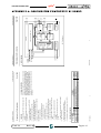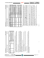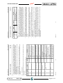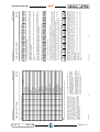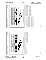
1
CAN 14
Control Area Network 1 channel, 4 type
MANUALE TECNICO
Via dell' Artigiano, 8/6
® 40016 San Giorgio di Piano
grifo
(Bologna) ITALY
E-mail: [email protected]
http://www.grifo.it
http://www.grifo.com
Tel. +39 051 892.052 (r.a.) FAX: +39 051 893.661
Edizione 3.00
Rel. 06 Novembre 1998
CAN 14
®
®
, GPC , grifo , sono marchi registrati della ditta grifo®
ITALIAN TECHNOLOGY
CAN 14
Control Area Network 1 channel, 4 type
MANUALE TECNICO
Modulo periferico di comunicazione con protocollo CAN; interfaccia per
Abaco® I/O BUS su connettore a scatolino a 26 vie; ingombro di 100x50x20
mm, (110x60x70 mm con contenitore) nel formato serie 4; contenitore per
guide ad Ω tipo DIN 46277-1 e DIN 46277-3; connettore vaschetta D a 9
vie per linea di comunicazione CAN; supporto protocollo CAN 2.0B
gestito dall'UART PHILIPS SJA 1000 a 24 MHz (compatibile con
PHILIPS PCx82C200); driver di linea PHILIPS 82C250 galvanicamente
isolato; DC/DC converter per optoisolamento della linea di comunicazione
CAN; Baud rate supportati: fino a 400 KBit/sec per linee da centinaia di
metri ed 1 MBit/sec per linee di decine di metri; spazio d'indirizzamento
occupato di soli 2 bytes consecutivi; dip switch per settare il mappagio in
I/O della scheda; generazione di interrupts in corrispondenza di eventi
definibili via software; collegamento interrupt ad /INT o /NMI selezionabile
via hardware; unica tensione di alimentazione: +5 Vdc; 93 mA.
Via dell' Artigiano, 8/6
® 40016 San Giorgio di Piano
grifo
(Bologna) ITALY
E-mail: [email protected]
http://www.grifo.it
http://www.grifo.com
Tel. +39 051 892.052 (r.a.) FAX: +39 051 893.661
Edizione 3.00
Rel. 06 Novembre 1998
CAN 14
®
®
, GPC , grifo , sono marchi registrati della ditta grifo®
ITALIAN TECHNOLOGY
Vincoli sulla documentazione
grifo® Tutti i Diritti Riservati
Nessuna parte del presente manuale può essere riprodotta, trasmessa, trascritta, memorizzata in un archivio o tradotta in altre lingue, con qualunque forma o mezzo, sia esso
elettronico, meccanico, magnetico ottico, chimico, manuale, senza il permesso scritto
della grifo®.
IMPORTANTE
Tutte le informazioni contenute sul presente manuale sono state accuratamente verificate, ciononostante grifo® non si assume nessuna responsabilità per danni, diretti o
indiretti, a cose e/o persone derivanti da errori, omissioni o dall'uso del presente manuale,
del software o dell' hardware ad esso associato.
grifo® altresi si riserva il diritto di modificare il contenuto e la veste di questo manuale
senza alcun preavviso, con l' intento di offrire un prodotto sempre migliore, senza che
questo rappresenti un obbligo per grifo®.
Per le informazioni specifiche dei componenti utilizzati sui nostri prodotti, l'utente deve
fare riferimento agli specifici Data Book delle case costruttrici o delle seconde sorgenti.
LEGENDA SIMBOLI
Nel presente manuale possono comparire i seguenti simboli:
Attenzione: Pericolo generico
Attenzione: Pericolo di alta tensione
Marchi Registrati
, GPC®, grifo® : sono marchi registrati della grifo®.
Altre marche o nomi di prodotti sono marchi registrati dei rispettivi proprietari.
grifo®
ITALIAN TECHNOLOGY
INDICE GENERALE
INTRUDIZIONE .......................................................................................................................... 1
VERSIONE SCHEDA .................................................................................................................. 1
INFORMAZIONI GENERALI .................................................................................................. 2
SEZIONE DI INTERFACCIA ED INDIRIZZAMENTO ................................................... 4
CONTROLLORE CAN .......................................................................................................... 4
INTERFACCIA DI LINEA CAN ........................................................................................... 4
SPECIFICHE TECNICHE ......................................................................................................... 5
CARATTERISTICHE GENERALI ...................................................................................... 5
CARATTERISTICHE FISICHE ........................................................................................... 5
CARATTERISTICHE ELETTRICHE ................................................................................. 5
INSTALLAZIONE ....................................................................................................................... 6
CONNESSIONI CON IL MONDO ESTERNO ................................................................... 6
CN2 - CONNETTORE PER LINEA CAN ....................................................................... 6
CN1 - CONNETTORE PER ABACO® I/O BUS .............................................................. 8
INTERFACCIAMENTO DELLA SCHEDA ...................................................................... 10
MONTAGGIO MECCANICO ............................................................................................. 10
JUMPERS............................................................................................................................... 10
JUMPERS A 2 VIE ........................................................................................................... 11
JUMPERS A 3 VIE ........................................................................................................... 11
TERMINAZIONE LINEA CAN .......................................................................................... 11
INTERRUPT .......................................................................................................................... 12
MAPPAGGI ED INDIRIZZAMENTI ...................................................................................... 13
MAPPAGGIO DELLA SCHEDA ........................................................................................ 13
INDIRIZZAMENTO REGISTRI INTERNI ...................................................................... 14
DESCRIZIONE SOFTWARE ................................................................................................... 15
CONTROLLORE CAN ........................................................................................................ 15
SCHEDE ESTERNE .................................................................................................................. 17
BIBLIOGRAFIA ........................................................................................................................ 20
APPENDICE A: DESCRIZIONE COMPONENTI DI BORDO ......................................... A-1
APPENDICE B: INDICE ANALITICO ................................................................................. B-1
CAN 14
Rel. 3.00
Pagina I
grifo®
ITALIAN TECHNOLOGY
INDICE DELLE FIGURE
FIGURA 1: SCHEMA A BLOCCHI ......................................................................................................... 3
FIGURA 2: CN2 - CONNETTORE PER LINEA CAN ............................................................................. 6
FIGURA 3: ESEMPIO COLLEGAMENTO IN RETE CON BUS CAN ......................................................... 7
FIGURA 4: CN1 - CONNETTORE PER ABACO® I/O BUS ................................................................ 8
FIGURA 5: DISPOSIZIONE CONNETTORI, JUMPER, DIP SWITCH, ECC. .................................................... 9
FIGURA 6: TABELLA RIASSUNTIVA JUMPERS ..................................................................................... 10
FIGURA 7: TABELLA JUMPERS A 2 VIE ............................................................................................. 11
FIGURA 8: TABELLA JUMPERS A 3 VIE ............................................................................................. 11
FIGURA 9: FOTO DELLA SCHEDA ..................................................................................................... 12
FIGURA 10: TABELLA INDIRIZZI DEI REGISTRI INTERNI .................................................................... 14
FIGURA 11: PIANTA COMPONENTI ................................................................................................... 14
FIGURA 12: FLOW CHART DI INIZIALIZZAZIONE ............................................................................... 16
FIGURA 13: SCHEMA DELLE POSSIBILI CONNESSIONI ........................................................................ 19
Pagina II
CAN 14
Rel. 3.00
ITALIAN TECHNOLOGY
grifo®
INTRODUZIONE
L’uso di questi dispositivi é rivolto - IN VIA ESCLUSIVA - a personale specializzato.
Scopo di questo manuale é la trasmissione delle informazioni necessarie all’uso competente e sicuro
dei prodotti. Esse sono il frutto di un’elaborazione continua e sistematica di dati e prove tecniche
registrate e validate dal Costruttore, in attuazione alle procedure interne di sicurezza e qualità
dell'informazione.
I dati di seguito riportati sono destinati - IN VIA ESCLUSIVA - ad un utenza specializzata, in grado
di interagire con i prodotti in condizioni di sicurezza per le persone, per la macchina e per l’ambiente,
interpretando un’elementare diagnostica dei guasti e delle condizioni di funzionamento anomale e
compiendo semplici operazioni di verifica funzionale, nel pieno rispetto delle norme di sicurezza e
salute vigenti.
Le informazioni riguardanti installazione, montaggio, smontaggio, manutenzione, aggiustaggio,
riparazione ed installazione di eventuali accessori, dispositivi ed attrezzature, sono destinate - e
quindi eseguibili - sempre ed in via esclusiva da personale specializzato avvertito ed istruito, o
direttamente dall’ASSISTENZA TECNICA AUTORIZZATA, nel pieno rispetto delle
raccomandazioni trasmesse dal costruttore e delle norme di sicurezza e salute vigenti.
I dispositivi non possono essere utilizzati all'aperto. Si deve sempre provvedere ad inserire i moduli
all'interno di un contenitore a norme di sicurezza che rispetti le vigenti normative. La protezione di
questo contenitore non si deve limitare ai soli agenti atmosferici, bensì anche a quelli meccanici,
elettrici, magnetici, ecc.
Per un corretto rapporto coi prodotti, é necessario garantire leggibilità e conservazione del manuale,
anche per futuri riferimenti. In caso di deterioramento o più semplicemente per ragioni di
approfondimento tecnico ed operativo, consultare direttamente l’Assistenza Tecnica autorizzata.
Al fine di non incontrare problemi nell’uso di tali dispositivi, é conveniente che l’utente - PRIMA
DI COMINCIARE AD OPERARE - legga con attenzione tutte le informazioni contenute in questo
manuale. In una seconda fase, per rintracciare più facilmente le informazioni necessarie, si può fare
riferimento all’indice generale e all’indice analitico, posti rispettivamente all’inizio ed alla fine del
manuale.
VERSIONE SCHEDA
Il presente manuale è riferito alla scheda CAN 14 versione 110498 e successive. La validità delle
informazioni riportate è quindi subordinata al numero di versione della scheda in uso e l’utente deve
quindi sempre verificare la giusta corrispondenza tra le due indicazioni. Sulla scheda il numero di
versione è riportato in più punti sia a livello di serigrafia che di stampato (ad esempio sull'angolo in
alto a sinistra nel lato componenti).
CAN 14
Rel. 3.00
Pagina 1
grifo®
ITALIAN TECHNOLOGY
INFORMAZIONI GENERALI
Il modulo CAN 14 é una potente scheda periferica in grado di gestire la comunicazione seriale
secondo lo standard industriale Control Area Network. Quest'ultimo é un protocollo standard di
comunicazione caratterizzato da: alte velocità di trasferimento dati, comunicazione anche su lunghe
distanze, gestione autonoma degli eventuali errori di comunicazione con ritrasmissione automatica;
riconoscimento autonomo degli slave in una rete di più sistemi, collegamenti in modalità multimaster
e multislave, gestione di maschere di ricezione e trasmissione, disponibilità di una vasta serie di
potenti comandi, ecc. In particolare la CAN 14 supporta completamente gli standard BasicCAN
e/o PeliCAN 2.0B a cui l'utente può fare riferimento per ogni chiarimento necessario.
Il collegamento elettrico del modulo avviene tramite una coppia di comodi connettori di cui uno per
il collegamento alle schede di controllo tramite l'Abaco® I/O BUS e l'altro per il collegamento alla
linea CAN, mentre il montaggio meccanico é facilitato dall'apposito supporto plastico provvisto
degli attacchi per le guide ad Omega tipo DIN 46277-1 e DIN 46277-3. La linea seriale CAN di
bordo é galvanicamente isolata dal resto della scheda, in modo da garantire l'immunità dagli
eventuali disturbi del campo su tutta l'elettronica di controllo.
Le applicazioni tipiche in cui il CAN 14 può essere utilizzato sono tutte quelle in cui si devono
trasferire dati tra due o più sistemi intelligenti senza doversi preoccupare di tutte le condizioni
caratteristiche della comunicazione seriale, oppure per attraversare ambienti rumorosi e/o distanti,
per gestire sistemi multimaster o quando più semplicemente, ci si deve interfacciare ad un altro
sistema che utilizza lo standard CAN.
Una ricca serie di programmi dimostrativi ed esempi di utilizzo, consentono un immediato uso della
scheda. Detti programmi sono disponibili per numerose schede di CPU presenti nel vasto carteggio
Abaco®. Gli esempi sono ampiamente commentati e sono forniti sotto forma di sorgenti nei vari
linguaggi in cui é possibile programmare le schede del carteggio Abaco®.
- Interfaccia per Abaco® I/O BUS su connettore a scatolino a 26 vie.
- Ingombro di 100x50x20 mm, (110x60x70 mm con contenitore) nel formato serie 4.
- Contenitore per guide ad Ω tipo DIN 46277-1 e DIN 46277-3.
- Connettore vaschetta D a 9 vie per linea di comunicazione CAN.
- Supporto protocollo BasicCAN
gestito dal PHILIPS PCx82C200 a 16M Hz,
oppure protocollo PeliCAN 2.0B gestito solo dal PHILIPS SJA 1000 a 24M Hz.
- Driver di linea PHILIPS 82C250 galvanicamente isolato.
- DC/DC converter per optoisolamento della linea di comunicazione CAN.
- Baud rate supportati: fino a 400 KBit/sec per linee da centinaia di metri,
1 MBit/sec per linee di decine di metri.
- Spazio d'indirizzamento occupato di soli 2 bytes consecutivi.
- Dip switch per settare il mappagio in I/O della scheda.
- Generazione di interrupts in corrispondenza di eventi definibili via software.
- Collegamento interrupt ad /INT o /NMI selezionabile via hardware.
- Unica tensione di alimentazione: +5 Vdc; 93 mA.
Viene di seguito riportata una descrizione dei blocchi funzionali della scheda, con indicate le
operazioni effettuate da ciascuno di essi. Per una più facile individuazione di tali blocchi e per una
verifica delle loro connessioni, fare riferimento alla figura 1.
Pagina 2
CAN 14
Rel. 3.00
grifo®
ITALIAN TECHNOLOGY
CN1 - ABACO ® I/O BUS
INTERFACE AND ADDRESSING SECTION
DSW1
CAN CONTROLLER
PCx82C200
or
SJA1000
DC/DC
CONVERTER
OPTO
CAN DRIVER
82C250
CN2
FIGURA 1: SCHEMA A BLOCCHI
CAN 14
Rel. 3.00
Pagina 3
grifo®
ITALIAN TECHNOLOGY
SEZIONE DI INTERFACCIA ED INDIRIZZAMENTO
Questa sezione gestisce il colloquio tra il controllore CAN e la scheda di comando di tipo GPC®; in
particolare tutti i dati di programmazione, gestione e comunicazione passano attraverso questa
sezione che inoltre provvede a gestire il mappaggio della scheda in I/O, tramite un comodo dip
switch, ed a configurare l'eventuale gestione di interrupt. Il collegamento fisico con le schede di
comando é effettuato tramite il comodo ABACO® I/O BUS ad 8 bit, ma può essere esteso anche al
BUS industriale ABACO® sfruttando appositi moduli di conversioni come l'ABB 05 o l'ABB 03.
La sezione di interfaccia ed indirizzamento é basata su una logica programmabile ed alcuni
componenti di contorno, che garantiscono il funzionamento in ogni condizione operativa ed allo
stesso tempo riducono al minimo l'ingombro.
CONTROLLORE CAN
Questa sezione é basata su uno dei controllori PCx82C200 o SJA 1000 della PHILIPS e si preoccupa
della gestione software del protocollo CAN in tutte le sue modalità ed aspetti. Le caratteristiche
fondamentali di questa sezione sono:
PCx82C200
SJA 1000
- supporto protocollo BasicCAN:
SI
SI
- supporto del protocollo PeliCAN 2.0B:
NO
SI
- gestione identificatori da:
11 bits
11 e 29 bits
- buffer di trasmissione da:
10 bytes
13 bytes
- buffer di ricezione da:
10 bytes
64 bytes
- baud rate programmabile fino a:
1M Bit/sec
1M Bit/sec
- eliminazione del comparatore di ricezione:
NO
SI
- filtri di accettazione messaggi configurabili:
SI
SI
- driver di uscita programmabile:
SI
SI
- frequenza massima di lavoro:
16M Hz
24M Hz
Il controllore SJA1000 é completamente compatibile con il PCx82C200, di cui costituisce un
aggiornamento. L'utente può quindi passare a questo nuovo controllore salvaguardando il firmware
od il software già sviluppato.
Per ogni chiarimento necessario l'utente può fare riferimento all'apposita documentazione della casa
costruttrice, oppure all'appendice A di questo manuale.
INTERFACCIA DI LINEA CAN
Dal punto di vista elettrico la scheda CAN 14 é dotata dell'apposito driver di linea 82C250 della
PHILIPS, galvanicamente isolato. Questo componente si preoccupa di soddisfare tutte le specifiche
di collegamento con il campo, definite nel protocollo CAN senza richiedere alcun intervento
software. Inoltre la linea seriale CAN di bordo é galvanicamente isolata dal resto della scheda, in
modo da garantire l'immunità agli eventuali disturbi del campo; questa caratteristica é di fondamentale
importanza soprattutto nel caso di collegamento con sistemi remoti a diversi potenziali oppure di
collegamenti con cavi che attraversano ambienti elettricamente rumorosi.
Un apposito DC/DC converter si preoccupa di generare le tensioni galvanicamente isolate richieste
dal driver di linea, mentre l'interfacciamento con le linee di comunicazionedel controllore CAN sono
effettuati tramite appositi optoisolatori per alte frequenze.
Il collegamento con il campo della linea CAN é effettuato tramite un connettore a vaschetta D a 9
vie che facilita il cablaggio e garantisce una buona trasmissione del segnale.
Pagina 4
CAN 14
Rel. 3.00
grifo®
ITALIAN TECHNOLOGY
SPECIFICHE TECNICHE
CARATTERISTICHE GENERALI
Tipo di BUS:
Numero linee di I/O:
Numero byte di indirizzamento:
Numero byte occupati:
Periferiche di bordo:
Quarzo:
Baud Rate massimo:
Protocolli gestiti:
Gestione interrupt:
ABACO® I/O BUS
1 linea seriale CAN
256
2
CAN controller PCx82C200
CAN controller SJA1000
16M Hz (PCx82C200)
24M Hz (SJA1000)
1M Bit/sec
BasicCAN (PCx82C200 e SJA1000)
PeliCAN 2.0B (solo SJA1000)
Selezionabile tra /INT e /NMI
CARATTERISTICHE FISICHE
Dimensioni (L x A x P):
Peso:
Connettori:
Range di temperatura:
Umidità relativa:
100 x 50 x 20 mm
(senza contenitore)
110 x 60 x 70 mm
(con contenitore per guide DIN)
50 g
(senza contenitore)
110 g
(con contenitore per guide DIN)
CN1:
26 vie scatolino verticale M
CN2:
9 vie vaschetta D femmina
da 0 a 50 gradi Centigradi
20% fino a 90%
(senza condensa)
CARATTERISTICHE ELETTRICHE
Tensione di alimentazione:
Corrente assorbita:
Impedenza di linea CAN:
Rete terminazione CAN:
CAN 14
Rel. 3.00
5 Vdc
93 mA
60 Ω
Resistenza da 120 Ω, disinseribile
Pagina 5
grifo®
ITALIAN TECHNOLOGY
INSTALLAZIONE
In questo capitolo saranno illustrate tutte le operazioni da effettuare per il corretto utilizzo della
scheda. A questo scopo viene riportata l’ubicazione e la funzione dei jumpers, dei connettori, dei dip
switch, ecc. presenti sulla CAN 14.
CONNESSIONI CON IL MONDO ESTERNO
Il modulo CAN 14 è provvisto di 2 connettori con cui vengono effettuati tutti i collegamenti con il
campo e con le altre schede del sistema di controllo da realizzare. Di seguito viene riportato il loro
pin out ed il significato dei segnali collegati; per una facile individuazione di tali connettori, si faccia
riferimento alla figura 5.
CN2 - CONNETTORE PER LINEA CAN
CN2 é un connettore a vaschetta D a 9 vie femmina a 90°. Tramite CN2 deve essere collegata la linea
di comunicazione seriale CAN secondo gli standard definiti dallo stesso protocollo; la disposizione
dei segnali é stata studiata in modo da ridurre al minimo le interferenze ed in modo da facilitarela
connessione con il campo.
CANL
1
N.C.
6
CANH
2
N.C.
7
N.C.
3
N.C.
8
N.C.
9
N.C.
4
N.C.
5
FIGURA 2: CN2 - CONNETTORE PER LINEA CAN
Legenda:
CANH
CANL
N.C.
Pagina 6
=
=
=
I/O
I/O
-
Linea differenziale high per CAN BUS.
Linea differenziale low per CAN BUS.
Non connesso.
CAN 14
Rel. 3.00
grifo®
ITALIAN TECHNOLOGY
System 1
System 2
CANH
Tx/Rx
CANL
120 Ω
CAN BUS
CANH
Tx/Rx
CANL
CAN 14
Unit
Any CAN
Unit
System 3
CANH
Tx/Rx
CANL
CAN 14
Unit
System n
CANH
Tx/Rx
CANL
CAN 14
Unit
FIGURA 3: ESEMPIO COLLEGAMENTO IN RETE CON BUS CAN
CAN 14
Rel. 3.00
Pagina 7
grifo®
ITALIAN TECHNOLOGY
CN1 - CONNETTORE PER ABACO® I/O BUS
CN1 è un connettore a scatolino verticale con passo 2.54 mm a 26 piedini. Tramite CN1 si effettua
la connessione tra la scheda e la serie di moduli di controllo della serie GPC®. Tale collegamento
è effettuato tramite l’ABACO® I/O BUS di cui questo connettore riporta tutti i segnali a livello TTL.
D0
1
2
D1
D2
3
4
D3
D4
5
6
D5
D6
7
8
D7
A0
9
10
A1
A2
11
12
A3
A4
13
14
A5
A6
15
16
A7
/WR
17
18
/RD
/IORQ
19
20
/RESET
N.C.
21
22
N.C.
/INT BUS
23
24
/NMI BUS
GND
25
26
+5 Vdc
FIGURA 4: CN1 - CONNETTORE PER ABACO® I/O BUS
Legenda:
A0-A7
=
D0-D7
=
/INT BUS =
/NMI BUS =
/IORQ
=
/RD
=
/WR
=
/RESET =
+5 Vdc
=
GND
=
N.C.
=
Pagina 8
I
I/O
O
O
I
I
I
I
I
- Address BUS: BUS degli indirizzi.
- Data BUS: BUS dei dati.
- Interrupt request: richiesta d’interrupt.
- Non Mascable Interrupt: richiesta d’interrupt non mascherabile.
- Input Output Request: richiesta operazione Input Output su I/O BUS.
- Read cycle status: richiesta di lettura.
- Write cycle status: richiesta di scrittura.
- Reset: azzeramento.
- Linea di alimentazione a +5 Vcc.
- Linea di massa.
- Non collegato.
CAN 14
Rel. 3.00
ITALIAN TECHNOLOGY
grifo®
CN2
J3
J2
DSW1
J1
CN1
FIGURA 5: DISPOSIZIONE CONNETTORI, JUMPER, DIP SWITCH, ECC.
CAN 14
Rel. 3.00
Pagina 9
grifo®
ITALIAN TECHNOLOGY
INTERFACCIAMENTO DELLA SCHEDA
Al fine di evitare eventuali problemi di collegamento della scheda con tutta l’elettronica del campo
e di controllo a cui la CAN 14 si deve interfacciare, si devono seguire le informazioni riportate nei
precedenti paragrafi e le relative figure che illustrano le modalità interne di connessione.
- Per i segnali che riguardano la comunicazione seriale con il protocollo CAN BUS , fare riferimento
alle specifiche standard di questo protocollo. Al fine di mantenere l'isolamento galvanico tra la
linea di comunicazione CAN e l'elettronica di controllo é conveniente che la massa di alimentazione
della CAN 14 (pin 25 di CN1) non sia direttamente o indirettamente collegata ad altri sistemi
presenti sul BUS CAN.
- Tutti i segnali a livello TTL possono essere collegati a linee dello stesso tipo riferite alla massa
digitale della scheda. Il livello 0V corrisponde allo stato logico 0, mentre il livello 5V corrisponde
allo stato logico 1. Nel caso di segnali ad alta frequenza come quelli dell'ABACO® I/O BUS é
consigliabile non superare la lunghezza di una decina di centimetri.
MONTAGGIO MECCANICO
La scheda CAN 14 normalmente é fornita senza alcun contenitore, ma a livello di opzioni esistono
alcuni articoli che facilitano notevolmente il suo montaggio meccanico. Queste soluzioni coincidono
con dei contenitori plastici predisposti per il montaggio su guide ad Ω tipo DIN 46277-1 e DIN
46277-3. In caso di accoppiamento della CAN 14 ad altre schede con ABACO® I/O BUS é possibile
ordinare un unico contenitore che contenga tutte le schede in modo da semplificare il montaggio e
da ridurre i costi. Per maggiori informazioni o per sigle dei contenitori da ordinare, rivolgersi
direttamente alla grifo®.
JUMPERS
Esistono a bordo della CAN 14 3 jumpers a cavalliere, con cui é possibile effettuare alcune selezioni
che riguardano il modo di funzionamento della stessa. Di seguito ne é riportato l'elenco, l'ubicazione
e la loro funzione nelle varie modalità di connessione.
NOME
N. VIE
UTILIZZO
J1
3
Seleziona collegamento segnale d'interrupt.
J2
2
Seleziona collegamento della resistenza di terminazione.
J3
2
Seleziona collegamento della corazza del connettore CN2.
FIGURA 6: TABELLA RIASSUNTIVA JUMPERS
Nelle sucessive tabelle é riportata una descrizione dettagliata delle possibili connessioni dei 2
jumpers con la loro relativa funzione. Per riconoscere tali connessioni sulla scheda si faccia
riferimento alla serigrafia della stessa o alla figura 10 di questo manuale, dove viene riportata la
numerazione dei pin dei jumpers, che coincide con quella utilizzata nella seguente descrizione. Per
l’individuazione dei jumpers a bordo della scheda, si utilizzi invece la figura 5. In tutte le seguenti
tabelle l'* indica la connessione di default, ovvero quella impostata in fase di collaudo, con cui la
scheda viene fornita.
Pagina 10
CAN 14
Rel. 3.00
grifo®
ITALIAN TECHNOLOGY
JUMPERS A 2 VIE
JUMPERS
CONNESSIONE
J2
non connesso
connesso
J3
UTILIZZO
Non collega la resistenza di terminazione da
120 Ω alla linea CAN.
DEF.
*
Collega la resistenza di terminazione da 120 Ω
alla linea CAN.
non connesso
Non collega la carcassa del connettore CN2
alla massa galvanicamente isolata
dell'interfaccia di linea.
connesso
Collega la carcassa del connettore CN2 alla
massa galvanicamente isolata dell'interfaccia
di linea.
*
FIGURA 7: TABELLA JUMPERS A 2 VIE
JUMPERS A 3 VIE
JUMPERS
CONNESSIONE
UTILIZZO
J1
posizione 1-2
Collega interrupt del controllore CAN al
segnale /INT BUS dell'ABACO ® I/O BUS.
posizione 2-3
Collega interrupt del controllore CAN al
segnale /NMI BUS dell'ABACO® I/O BUS.
non connesso
Interrupt del controllore CAN non collegato.
DEF.
*
FIGURA 8: TABELLA JUMPERS A 3 VIE
TERMINAZIONE LINEA CAN
Il jumper J2 ha il compito di collegare o meno l'apposita resistenza di terminazione della linea CAN
come descritto nella tabella di figura 7. Il CAN BUS deve fisicamente coincidere con una linea
differenziale con impedenza di 60 Ω e per questo le resistenze di terminazione devono essere
collegate in modo da ricreare questa impedenza. In particolare tale collegamento deve essere sempre
effettuato in caso di sistemi punto punto, mentre nel caso di sistemi multipunto, deve essere collegata
solo sulle schede che risultano essere alla maggior distanza, ovvero ai capi della linea di comunicazione
CAN (vedere esempio di figura3).
La corretta terminazione della linea CAN contribuisce notevolmente al funzionamento della
comunicazione, infatti l'interfaccia di linea della CAN 14 é in grado di sopprimere i transienti e di
essere immune ai disturbi di radio frequenza ed elettromagnetici, solo se il collegamento con il campo
é effettuato correttamente.
CAN 14
Rel. 3.00
Pagina 11
grifo®
ITALIAN TECHNOLOGY
INTERRUPT
Il modulo CAN 14 é provvisto di una comoda ed efficace circuiteria di generazione interrupt, che
provvede se collegata, a richiedere l'attenzione della scheda di controllo GPC® in corrispondenza di
stati predeterminati. Tale circuiteria tende ad ottimizzare i tempi di gestione della scheda, infatti
tramite la generazione d'interrupt, la scheda di controllo é liberata dal compito di testare continuamente
lo stato della CAN 14; in questo modo é la stessa scheda che, quando pronta, lo segnala alla scheda
di controllo che provvederà quindi all'interscambio di nuovi dati.
Il segnale d'interrupt della scheda può essere collegato in tre diverse modalità tramite il jumper J1,
come descritto nella tabella di figura 8; il segnale é in open collector e può essere quindi collegato
ad uno dei due segnali d'interrupt dell'ABACO® I/O BUS, anche se questi sono già utilizzati da altre
periferiche.
Per ulteriori informazioni sulle modalità di gestione interrupt, si faccia riferimento all'appendice A.
FIGURA 9: FOTO DELLA SCHEDA
Pagina 12
CAN 14
Rel. 3.00
grifo®
ITALIAN TECHNOLOGY
MAPPAGGI ED INDIRIZZAMENTI
In questo capitolo ci occuperemo di fornire tutte le informazioni relative all'utilizzo della scheda, dal
punto di vista della programmazione via software. Tra queste si trovano le informazioni riguardanti
il mappaggio della scheda e l'indirizzamento delle sezioni componenti.
MAPPAGGIO DELLA SCHEDA
La CAN 14 occupa un'indirizzamento di soli 2 bytes consecutivi che possono essere allocati a partire
da un indirizzo di base diverso a seconda di come viene mappata la scheda. Questa prerogativa
consente di poter utilizzare più CAN 14 sullo stesso ABACO® I/O BUS o BUS ABACO®, oppure
di montare la scheda su di un BUS su cui sono già presenti altre schede periferiche, ottenendo così
una struttura espandibile senza difficoltà e senza alcuna modifica del software già realizzato.
I 2 bytes occupati sono utilizzati sia in fase di Output che di Input, quindi permettono sia la
programmazione della scheda che la lettura del suo stato oltre alle normali operazioni di ricezione
e trasmissione.
L'indirizzo di mappaggio della CAN 14 é definibile tramite l'apposita circuiteria d'indirizzamento
ed interfaccia al BUS, presente sulla scheda; questa circuiteria utilizza il dip switch ad 8 vie DSW1,
da cui preleva lo stesso indirizzo di mappaggio impostato dall'utente. Di seguito viene riportata la
corrispondenza del dip switch con le linee d'indirizzamento dell'ABACO® I/O BUS, mentre per una
più facile individuazione di tale componente si faccia riferimento alla figura 5.
DSW1.1
DSW1.2
DSW1.3
DSW1.4
DSW1.5
DSW1.6
DSW1.7
DSW1.8
->
->
->
->
->
->
->
->
Non usato
Bit A1
Bit A2
Bit A3
Bit A4
Bit A5
Bit A6
Bit A7
Tali dip switch sono collegati con logica negata, quindi se posti in ON generano uno zero logico,
mentre se posti in OFF generano un uno logico.
A titolo di esempio, viene riportata di seguito la configurazione del DSW1, necessaria per mappare
la scheda all'indirizzo 48H:
DSW1.1
DSW1.2
DSW1.3
DSW1.4
DSW1.5
DSW1.6
DSW1.7
DSW1.8
CAN 14
Rel. 3.00
->
->
->
->
->
->
->
->
Indifferente
ON
ON
OFF
ON
ON
OFF
ON
Pagina 13
grifo®
ITALIAN TECHNOLOGY
INDIRIZZAMENTO REGISTRI INTERNI
Indicando con <indbase> l’indirizzo di mappaggio della scheda, ovvero l’indirizzo impostato
tramite il DSW1 come descritto nel paragrafo precedente, i registri interni della CAN 14 sono visti
agli indirizzi riportati nella seguente tabella.
DISP.
REG.
IND.
R/W
SIGNIFICATO
PCx82C200
ADDR
<indbase>+00H
W
Registro di settaggio indirizzo registro
SJA1000
DATA
<indbase>+01H
R/W
Registro di interscambio dati
FIGURA 10: TABELLA INDIRIZZI DEI REGISTRI INTERNI
Se si utilizzano più schede sull'ABACO® I/O BUS o BUS ABACO®, in fase di impostazione
dell'indirizzo di mappaggio delle schede, si deve fare attenzione a non allocare più schede agli stessi
indirizzi (considerare per questo indirizzo di mappaggio e numero di byte occupati). Nel caso questa
condizione non venga rispettata, si viene a creare una conflittualità sul BUS che pregiudica il
funzionamento di tutto il sistema e delle stesse schede.
Si ricorda che la precedente tabella riporta la descrizione dei soli registri disponibili a livello della
scheda CAN 14 e che per una descrizione dettagliata di tutti i registri interni dei controllori CAN e
delle relative modalità d'accesso si può fare riferimento al capitolo sucessivo ed all'appendice A.
FIGURA 11: PIANTA COMPONENTI
Pagina 14
CAN 14
Rel. 3.00
ITALIAN TECHNOLOGY
grifo®
DESCRIZIONE SOFTWARE
Nel paragrafo precedente sono stati riportati gli indirizzi di allocazione di tutte le periferiche e di
seguito viene riportata una descrizione dettagliata della funzione e del significato dei relativi registri
(al fine di comprendere le successive informazioni, fare sempre riferimento alla tabella indirizzi dei
registri interni). Qualora la documentazione riportata fosse insufficiente fare riferimento direttamente
alla documentazione tecnica della casa costruttrice del componente o all’appendice A di questo
manuale.
CONTROLLORE CAN
Per accedere ai vari registri del controlllore CAN, PCx82C200 o SJA1000, é necessario effettuare
le seguneti operazioni:
1) Scrivere all’indirizzo ADDR in numero del registro che si desidera gestire.
2) Leggere o scrivere all’indirizzo DATA per acquisire o settare il registro selezionato con la
precedente operazione.
Nell’appendice A é riportato l’elenco completo dei registri del controllore CAN e la descrizione di
tutti i bit che li compongono.
Esempio:
Facendi riferimento all’appendice A, se si deve scrivere il dato 170 nell’Acceptance code register
(registro n. 4), sarà necessario effettuare le seguenti operazioni:
1) Scrivere all’indirizzo ADDR il dato 4.
2) Scrivere all’indirizzo DATA il dato 170.
Note:
1) Il Baud Rate di comunicazione, ricavabile dalle informazioni dell’appendice A, é ottenibile dalla
seguente formula:
BAUD RATE = Freq / 2 * (BRP + 1) * (3 + TSEG1 + TSEG2)
dove:
Freq
BRP
TSEG1
TSEG2
=
=
=
=
Frequenza del quarzo della scheda CAN 14 in Hz.
Valore espresso dai bit BRP.x del Bus Timing Register 0 (BTR0, indirizzo 6).
Valore espresso dai bit TSEG1.x del Bus Timing Register 1 (BTR1, indirizzo 7).
Valore espresso dai bit TSEG2.x del Bus Timing Register 1 (BTR1, indirizzo 7).
2) Per un corretto interfacciamento fra il controllore CAN, PCx82C200 o SJA1000, ed il driver
82C250, é necessario programmare l’Output control register (OCR, indirizzo 8), con il dato
FA Hex; in questo modo si configura il dispositivo in "Normal output mode", con le uscite TX0
e TX1 in "Push-Pull".
Nelle pagina seguente viene riportata la flow chart relativa all’inizializzazione del controllore CAN,
PCx82C200 o SJA1000.
CAN 14
Rel. 3.00
Pagina 15
grifo®
ITALIAN TECHNOLOGY
Inizializzazione PCx82C200 o SJA1000
Scrittura del dato 1 nel Control register (CR, indirizzo 0):
attiva Reset request
Lettura del Control register (CR, indirizzo 0)
NO
RM (Reset mode, bit 0) del registro CR = 1
SI
Settaggio del Acceptance code register (ACR, indirizzo 4)
Settaggio del Acceptance mask register (AMR, indirizzo 5)
Settaggio del Bus Timing register 0 (BTR0, indirizzo 6)
Settaggio del Bus Timing register 1 (BTR1, indirizzo 7)
Scrittura del dato FA Hex nel l’Output control register
(OCR, indirizzo 8): Normal output mode e Push-Pull.
Scrittura del dato 0 nel Control register (CR, indirizzo 0):
disattiva Reset mode, Normal operation e nessun Interrupt.
Lettura del Control register (CR, indirizzo 0)
NO
RR (Reset request, bit 0) del registro CR = 0
SI
FINE Inizializzazione
FIGURA 12: FLOW CHART DI INIZIALIZZAZIONE
Come si può notare, questa inizializzazione non prevede l’utilizzo di Interrupt; per una loro eventuale
gestione, é necessario settare opportunamente i bit del Control Register (CR, indirizzo 0).
A questo proposito si faccia rifermento all’appendice A ed ai programmi di esempio forniti insieme
alla scheda CAN 14.
Pagina 16
CAN 14
Rel. 3.00
ITALIAN TECHNOLOGY
grifo®
SCHEDE ESTERNE
Le applicazioni caratteristiche della CAN 14 sono il trasferimento dati ad alta velocità tra sistemi
remotati usati nel settore automobilistico e del controllo di processo, l'attraversamento di ambienti
rumorosi e/o distanti, la gestione di sistemi multimaster o quando più semplicemente, ci si deve
interfacciare ad un altro sistema che utilizza lo standard CAN.
La scheda CAN 14 si interfaccia a buona parte dei moduli della serie BLOCK e di interfaccia utente.
Le risorse di bordo possono essere facilmente aumentate collegando la CAN 14 alle numerose schede
periferiche del carteggio grifo® tramite l’ABACO® I/O BUS. Anche schede in formato Europa con
BUS ABACO® possono essere collegate, sfruttando gli appositi mother boards. A titolo di esempio
ne riportiamo un elenco con una breve descrizione delle carratteristiche di massima; per maggiori
informazioni richiedere la documentazione specifica:
QTP G26
Quick Terminal Panel 26 tasti con LCD grafico
Interfaccia operatore provvista di display grafico da 240x128 pixel retroilluminato a catodo freddo;
tastiera a membrana da 26 tasti di cui 6 configurabili dall’utente; 16 LEDs di stato; alimentatore a
bordo scheda; interdaccia seriale in RS 232, RS 422-485, current loop o CAN; linea seriale ausiliaria
in RS 232 Tasti ed etichette personalizzabili dall’utente tramite serigrafie da inserire in apposite
tasche; contenitore metallico e plastico; EEPROM di set up; 256K EPROM o FLASH; Real Time
Clock; 128K RAM; buzzer. Firmware di gestione che svolge funzione di terminale con primitive
grafiche.
FBC D9 M/F
Flat Block Contact vaschetta D 9 vie Maschio/Femmina
Interfaccia tra 1 connettore a vaschetta D a 9 vie (mascio o femmina) e la filatura da campo
(morsettiere a rapida estrazione). Attacco rapido per guide tipo DIN 46277-1 e 3.
ABB 05
Abaco® Block BUS 5 slots
Mother board ABACO® da 5 slots; passo 4 TE; guidaschede; connettori normalizzati di alimentazione;
tasto di reset; LEDs per alimentazioni; interfaccia ABACO® I/O BUS; sezione alimentatrice per +5
Vdc; sezione alimentatrice per +V Opto; sezioni alimentatrici galvanicamente isolate; tre tipi di
alimentazione: da rete, bassa tensione o stabilizzata. Attacco rapido per guide Ω.
ABB 03
Abaco® Block BUS 3 slots
Mother board ABACO® da 3 slots; passo 4 TE; guidaschede; connettori normalizzati di alimentazione;
tasto di reset; LEDs per alimentazioni; interfaccia ABACO® I/O BUS. Attacco rapido per guide Ω.
GPC® 51
General Purpose Controller fam. 51
Microprocessore famiglia 51 INTEL compreso il tipo mascherato BASIC; comprende: 16 linee di
I/O TTL; dip switch; 3 Timer Counter; linea RS 232; 4 linee di A/D da 11 bit; buzzer; EPROM
programmer a bordo; RTC e 32K RAM con back up al litio; controllore display e tastiera.
CAN 14
Rel. 3.00
Pagina 17
grifo®
ITALIAN TECHNOLOGY
GPC® 553
General Purpose Controller 80C552
Microprocessore 80C552 a 22 o 30 MHz. Completa implementazione CMOS; 32K EPROM; 32 K
RAM; 32 K EEPROM o RAM; RTC; EEPROM; 1 linea RS 232 + 1 RS 232 o RS 422-485 o current
loop; 16 I/O TTL; 2 linee di PWM; timer/counter da 16 bits; watch dog; dip switch; 8 linee di
A/D da 12 bit; alimentazione in DC o AC; attacco rapido per guide DIN 46277-1 e 3.
GPC® 188F
General Purpose Controller 80C188
Microprocessore 80C188 INTEL. 1 linea RS 232 ed 1 RS 232, 422-485 o current loop; 24 linee di
I/O TTL; 256K EPROM e 256K RAM tamponate con batteria al litio; RTC; 3 timer counter; 8 linee
di A/D da 12 bit; watch dog; write protect; EEPROM; 2 LEDs di attività; dip switch.
GPC® 15A
General Purpose Controller 84C15
Microprocessore Z80 a 10 MHz. Completa implementazione CMOS; 512K EPROM o 256K
FLASH; RAM tamponata+RTC da 2K o 8KRTC ; 128K RAM; 1 linea RS 232 + 1 RS 232 o RS 422485 o current loop; 32 I/O TTL; 4 counter; 2 watch dog; dip switch; buzzer; EEPROM.
GPC® 15R
General Purpose Controller 84C15
Microprocessore Z80 a 10 MHz. Completa CMOS. 512K EPROM o FLASH; RAM tamponata+RTC
da 2K o 8KRTC ; 512K RAM tamponata da batteria esterna; EEPROM; 1 linea RS 232 + 1 RS 232
o RS 422-485 o current loop; 24 I/O TTL; 4 counter; 2 watch dog; dip switch; buzzer; 8 output a relé
3A; 16 input optoisolati NPN; alimentatore di bordo anche per I/O, galvanicamente isolato; power
failure; alimentazione da rete 220 Vac; attacco rapido per guide DIN 46277-1 e 3.
GPC® 153
General Purpose Controller 84C15
Microprocessore Z80 a 10 MHz. Completa implementazione CMOS. 512K EPROM o 256K
FLASH; RAM tamponata+RTC da 2K o 8KRTC ; 128K RAM; Back-Up con batteria al litio esterna;
1 linea RS 232 + 1 RS 232 o RS 422-485 o current loop; 16 I/O TTL; 4 counter; 2 watch dog; dip
switch; buzzer; EEPROM; 8 linee di A/D da 12 bit; alimentazione in DC o AC; attacco rapido per
guide DIN 46277-1 e 3.
GPC® 884
General Purpose Controller 80C188ES
Microprocessore AMD 80C188ES fino a 40M Hz. Completa implementazione CMOS; formato
serie 4; 512K EPROM o FLASH; 512K RAM tamponata con batteria al litio; RTC; 1 linea RS 232
+ 1 RS 232 o RS 422-485 o current loop; 16 I/O TTL; 3 timer counter; watch dog; EEPROM; 11 linee
di A/D da 12 bit; attacco rapido per guide DIN 46277-1 e 3.
GPC® 114
General Purpose Controller 68HC11
Microprocessore 68HC11A1 a 8M Hz. Completa implementazione CMOS; formato serie 4; 32K
EPROM; 32K RAM tamponata con batteria al litio; 32K EPROM, RAM, EEPROM; RTC; 1 linea
RS 232 o RS 422-485; 10 I/O TTL; 3 timer counter; watch dog; 8 linee di A/D da 8 bit; 1 linea seriale
sincrona; bassissimo assorbimento; attacco rapido per guide DIN 46277-1 e 3.
Pagina 18
CAN 14
Rel. 3.00
CAN 14
Rel. 3.00
PLC
Personal
Computer
Intelligent CAN sensor
QTP G26
Serial CAN BUS
Any system with CAN
interface
ABB 03 or
ABB 05, etc.
ANY I/O TYPE
ANY GPC® TYPE
IPC 52, UAR 24,
LAD 13, DAC 12,
JMS 34, etc.
ZBx series
GPC® 3 and 4 type
4 type peripheral card
CAN 14, ADC 812, etc.
ITALIAN TECHNOLOGY
grifo®
FIGURA 13: SCHEMA DELLE POSSIBILI CONNESSIONI
Pagina 19
ABACO ® BUS
ABACO ® I/O BUS
grifo®
ITALIAN TECHNOLOGY
BIBLIOGRAFIA
E’ riportato di seguito, un elenco di manuali e note tecniche, a cui l’utente può fare riferimento per
avere maggiori chiarimenti, sui vari componenti montati a bordo della scheda CAN 14.
Manuale PHILIPS:
Application notes and development tools for 80C51 microcontrollers
Manuale SGS-THOMSON: Programmable logic manual - GAL products
Manuale TOSHIBA:
Photo couplers Data Book
Manuale NEWPORT:
DC-DC Converters
Per reperire questi manuali fare riferimento alle case produttrici ed ai relativi distributori locali. In
alternativa si possono ricercare le medesime informazioni o gli eventuali aggiornamenti ai siti
internet delle case elencate.
Pagina 20
CAN 14
Rel. 3.00
CAN 14
FEATURES
Rel. 3.00
SO28
SJA1000T
1997 Nov 04
DIP28
SJA1000
NAME
ORDERING INFORMATION
TYPE NUMBER
3
GENERAL DESCRIPTION
PACKAGE
DESCRIPTION
plastic small outline package; 28 leads; body width 7.5 mm
3
SJA1000
Preliminary specification
SOT136-1
SOT117-1
VERSION
The SJA1000 is a stand-alone controller for the Controller
Area Network (CAN) used within automotive and general
industrial environments. It is designed to be hardware and
software compatible to the PCA82C200 CAN controller
(BasicCAN) from Philips Semiconductors. Additionally, a
new mode of operation is implemented (PeliCAN) which
supports the CAN 2.0B protocol specification with several
new features.
2
plastic dual in-line package; 28 leads (600 mil)
• Extended ambient temperature range (−40 to +125 °C).
• Programmable CAN output driver configuration
• Interfaces to a variety of microprocessors
• 24 MHz clock frequency
– Reception of ‘own’ messages (self reception request)
– Acceptance filter extension (4-byte code, 4-byte
mask)
– Hot plugging support (software driven bit rate
detection)
– Listen only mode (no acknowledge, no active error
flags)
– Single-shot transmission (no re-transmission)
– Arbitration lost interrupt with detailed bit position
– Error interrupt for each CAN-bus error
– Last error code register
– Programmable error warning limit
– Error counters with read/write access
• PeliCAN mode extensions:
• Bit rates up to 1 Mbits/s
• Supports 11-bit identifier as well as 29-bit identifier
• CAN 2.0B protocol compatibility (extended frame
passive in PCA82C200 compatibility mode)
• Extended receive buffer (64-byte FIFO)
• Software-compatibility mode to the PCA82C200
(BasicCAN mode is default)
• Electrical compatibility to the PCA82C200 stand-alone
CAN controller
• Pin compatibility to the PCA82C200 stand-alone CAN
controller
1
Stand-alone CAN controller
Philips Semiconductors
1997 Nov 04
XTAL2
XTAL1
AD7 to AD0
ALE/AS, CS,
RD/E, WR,
CLKOUT,
MODE, INT
2, 1,
28 to 23
10
9
control
7
8 address/data
3 to 7,
11, 16
BLOCK DIAGRAM
handbook, full pagewidth
4
ACCEPTANCE
FILTER
BIT
STREAM
PROCESSOR
4
Fig.1 Block diagram.
OSCILLATOR
RECEIVE
BUFFER
RECEIVE
FIFO
TRANSMIT
BUFFER
SJA1000
INTERFACE MANAGEMENT LOGIC
MESSAGE BUFFER
Stand-alone CAN controller
Philips Semiconductors
RESET
ERROR
MANAGEMENT
LOGIC
BIT TIMING
LOGIC
internal bus
MGK623
17
18
21
20
19
14
13
15
12
8
22
RST
VDD2
VSS2
RX1
RX0
TX1
TX0
VSS3
VDD3
VSS1
VDD1
SJA1000
Preliminary specification
ITALIAN TECHNOLOGY
grifo®
APPENDICE A: DESCRIZIONE COMPONENTI DI BORDO
Pagina A-1
Pagina A-2
TRANSMIT BUFFER (TXB)
RECEIVE BUFFER (RXB, RXFIFO)
ACCEPTANCE FILTER (ACF)
BIT STREAM PROCESSOR (BSP)
CAN 14
BIT TIMING LOGIC (BTL)
1997 Nov 04
The bit timing logic monitors the serial CAN-bus line and
handles the bus line-related bit timing. It is synchronized to
the bit stream on the CAN-bus on a
‘recessive-to-dominant’ bus line transition at the beginning
of a message (hard synchronization) and re-synchronized
on further transitions during the reception of a message
(soft synchronization). The BTL also provides
programmable time segments to compensate for the
propagation delay times and phase shifts (e.g. due to
6.1.6
The bit stream processor is a sequencer which controls the
data stream between the transmit buffer, RXFIFO and the
CAN-bus. It also performs the error detection, arbitration,
stuffing and error handling on the CAN-bus.
6.1.5
The acceptance filter compares the received identifier with
the acceptance filter register contents and decides
whether this message should be accepted or not. In the
event of a positive acceptance test, the complete message
is stored in the RXFIFO.
6.1.4
The receive buffer is an interface between the acceptance
filter and the CPU that stores the received and accepted
messages from the CAN-bus line. The Receive Buffer
(RXB) represents a CPU-accessible 13-byte window of the
Receive FIFO (RXFIFO), which has a total length of
64 bytes.
With the help of this FIFO the CPU is able to process one
message while other messages are being received.
6.1.3
The transmit buffer is an interface between the CPU and
the Bit Stream Processor (BSP) that is able to store a
complete message for transmission over the CAN
network. The buffer is 13 bytes long, written to by the CPU
and read out by the BSP.
6.1.2
The interface management logic interprets commands
from the CPU, controls addressing of the CAN registers
and provides interrupts and status information to the host
microcontroller.
INTERFACE MANAGEMENT LOGIC (IML)
Description of the CAN controller blocks
FUNCTIONAL DESCRIPTION
6.1.1
6.1
6
Stand-alone CAN controller
Philips Semiconductors
7
ERROR MANAGEMENT LOGIC (EML)
Detailed description of the CAN controller
PCA82C200 COMPATIBILITY
Synchronization mode
Clock divider register
The clock divider register is used to select the CAN mode
of operation (BasicCAN/PeliCAN). Therefore one of the
reserved bits within the PCA82C200 is used. Writing a
value between 0 and 7, as allowed for the PCA82C200,
will enter the BasicCAN mode. The default state is divide
by 12 for Motorola mode and divide by 2 for Intel mode.
An additional function is implemented within another of the
reserved bits. Setting of bit CBP (see Table 49) enables
the internal RX input comparator to be bypassed thereby
reducing the internal delays if an external transceiver
circuit is used.
6.2.1.2
The SYNC bit in the control register is removed (CR.6 in
the PCA82C200). Synchronization is only possible by a
recessive-to-dominant transition on the CAN-bus. Writing
to this bit has no effect. To achieve compatibility to existing
application software, a read access to this bit will reflect
the previously written value (flip-flop without effect).
6.2.1.1
In BasicCAN mode the SJA1000 emulates all known
registers from the PCA82C200 stand-alone CAN
controller. The characteristics, as described in Sections
6.2.1.1 to 6.2.1.4 are different from the PCA82C200
design with respect to software compatibility.
6.2.1
The mode of operation is selected with the CAN-mode bit
located within the clock divider register. Default mode
upon reset is the BasicCAN mode.
• PeliCAN mode; extended features.
• BasicCAN mode; PCA82C200 compatible
The SJA1000 is designed to be software and
pin-compatible to its predecessor, the PCA82C200
stand-alone CAN controller. Additionally, a lot of new
functions are implemented. To achieve the software
compatibility, two different modes of operation are
implemented:
6.2
The EML is responsible for the error confinement of the
transfer-layer modules. It receives error announcements
from the BSP and then informs the BSP and IML about
error statistics.
6.1.7
oscillator drifts) and to define the sample point and the
number of samples to be taken within a bit time.
SJA1000
Preliminary specification
Receive buffer
CAN 2.0B
DIFFERENCES BETWEEN BASICCAN AND PELICAN
MODE
1997 Nov 04
• Disable CLKOUT by hardware.
• Hot plugging supported (disturbance-free software
driven bit rate detection)
• Listen only mode (monitoring of the CAN-bus, no
acknowledge, no error flags)
• Single-shot transmission (no re-transmission on error or
arbitration lost)
• Arbitration lost interrupt with detailed bit position
• Error interrupt for each CAN-bus error
• Last error code register
• Programmable error warning limit
• Error counters with read/write access
• Single/dual acceptance filter with mask and code
register for standard and extended frame
• Receive FIFO (64-byte)
• Reception and transmission of standard and extended
frame format messages
Main new features of the SJA1000 are:
In the PeliCAN mode the SJA1000 appears with a
re-organized register mapping with a lot of new features.
All known bits from the PCA82C200 design are available
as well as several new ones. In the PeliCAN mode the
complete CAN 2.0B functionality is supported (29-bit
identifier).
6.2.2
The SJA1000 is designed to support the full CAN 2.0B
protocol specification, which means that the extended
oscillator tolerance is implemented as well as the
processing of extended frame messages. In BasicCAN
mode it is possible to transmit and receive standard frame
messages only (11-bit identifier). If extended frame
messages (29-bit identifier) are detected on the CAN-bus,
they are tolerated and an acknowledge is given if the
message was correct, but there is no receive interrupt
generated.
6.2.1.4
The dual receive buffer concept of the PCA82C200 is
replaced by the receive FIFO from the PeliCAN controller.
This has no effect to the application software except for the
data overrun probability. Now more than two messages
may be received (up to 64 bytes) until a data overrun
occurs.
6.2.1.3
Stand-alone CAN controller
Philips Semiconductors
8
BASICCAN ADDRESS LAYOUT
BasicCAN mode
The reset mode (see Table 3, control register, bit Reset
Request) is entered automatically after a hardware reset
or when the controller enters the bus-off state (see
Table 5, status register, bit Bus Status). The operating
mode is activated by resetting of the reset request bit in the
control register.
• Operating mode.
• Reset mode
For register access, two different modes have to be
distinguished:
The exchange of status, control and command signals
between the microcontroller and the SJA1000 is
performed in the control segment. The layout of this
segment is shown in Table 3. After an initial download, the
contents of the registers acceptance code, acceptance
mask, bus timing registers 0 and 1 and output control
should not be changed. Therefore these registers may
only be accessed when the reset request bit in the control
register is set HIGH.
A message, which should be transmitted, has to be written
to the transmit buffer. After a successful reception the
microcontroller may read the received message from the
receive buffer and then release it for further use.
The address area of the SJA1000 consists of the control
segment and the message buffers. The control segment is
programmed during an initialization download in order to
configure communication parameters (e.g. bit timing).
Communication over the CAN-bus is also controlled via
this segment by the microcontroller. During initialization
the CLKOUT signal may be programmed to a value
determined by the microcontroller.
The SJA1000 appears to a microcontroller as a
memory-mapped I/O device. An independent operation of
both devices is guaranteed by a RAM-like implementation
of the on-chip registers.
6.3.1
6.3
SJA1000
Preliminary specification
grifo®
ITALIAN TECHNOLOGY
Rel. 3.00
CAN 14
Rel. 3.00
bus timing 1
output control
−
−
(FFH)(2)
(FFH)(2)
test
identifier (10 to 3)
7
8
9
10
data byte 4
data byte 5
data byte 6
data byte 7
data byte 8
identifier (10 to 3)
15
16
17
18
19
20
identifier (10 to 3)
−
−
−
−
−
−
−
(FFH)(2)
(FFH)(2)
(FFH)(2)
(FFH)(2)
(FFH)(2)
(FFH)(2)
(FFH)(2)
(FFH)(2)
−
data byte 4
data byte 5
data byte 6
data byte 7
data byte 8
(FFH)(2)
clock divider
25
26
27
28
29
30
31
clock divider; note 3
data byte 7
data byte 6
data byte 5
data byte 4
data byte 3
clock divider
data byte 7
data byte 6
data byte 5
data byte 4
data byte 3
clock divider
−
data byte 8
data byte 7
data byte 6
data byte 5
data byte 4
data byte 3
data byte 2
data byte 1
identifier (2 to 0),
RTR and DLC
Pagina A-3
1997 Nov 04
9
3. Some bits are writeable in reset mode only (CAN mode and CBP).
2. During read-out of this register a zero is always given.
1. It should be noted that the registers are repeated within higher CAN address areas (the most significant bits of the
8-bit CPU address are not decoded: CAN address 32 continues with CAN address 0 and so on).
Notes
data byte 8
data byte 8
data byte 3
data byte 2
data byte 1
24
data byte 2
data byte 2
identifier (2 to 0),
RTR and DLC
identifier (10 to 3)
−
(FFH)(2)
identifier (10 to 3)
−
−
(FFH)(2)
data byte 1
data byte 1
output control
bus timing 1
bus timing 0
acceptance mask
acceptance code
−
(FFH)(2)
23
identifier (2 to 0),
RTR and DLC
identifier (10 to 3)
data byte 8
data byte 7
data byte 6
data byte 5
data byte 4
data byte 3
data byte 2
data byte 1
identifier (2 to 0),
RTR and DLC
22
identifier (2 to 0),
RTR and DLC
data byte 3
14
21
data byte 2
13
receive
buffer
data byte 1
12
identifier (2 to 0),
RTR and DLC
bus timing 0
−
(FFH)(2)
6
transmit
buffer
acceptance mask
−
(FFH)(2)
5
11
acceptance code
−
(FFH)(2)
4
−
test
interrupt
−
interrupt
3
WRITE
command
control
test
status
−
status
2
test
(FFH)(2)
READ
command
control
(FFH)(2)
WRITE
1
READ
control
control
0
SJA1000
Preliminary specification
RESET MODE
control
SEGMENT
OPERATING MODE
BasicCAN address allocation; note 1
CAN
ADDRESS
Table 1
Stand-alone CAN controller
Philips Semiconductors
RESET VALUES
SJA1000
Preliminary specification
1997 Nov 04
Interrupt
Status
Command
Control
Reset Request
reserved
reserved
reserved
RIE
RR
−
−
−
GTS
CDO
RRB
AT
TR
CR.1
CR.0
CMR.7
CMR.6
CMR.5
CMR.4
CMR.3
CMR.2
CMR.1
CMR.0
Receive Buffer Status
reserved
reserved
reserved
TS
RS
TCS
TBS
DOS
RBS
−
−
−
WUI
DOI
EI
TI
RI
SR.5
SR.4
SR.3
SR.2
SR.1
SR.0
IR.7
IR.6
IR.5
IR.4
IR.3
IR.2
IR.1
IR.0
10
Receive Interrupt
Transmit Interrupt
Error Interrupt
Data Overrun Interrupt
Wake-Up Interrupt
Data Overrun Status
Transmit Buffer Status
Transmission Complete Status
Receive Status
Transmit Status
Error Status
ES
SR.6
Bus Status
BS
SR.7
Transmission Request
Abort Transmission
Release Receive Buffer
Clear Data Overrun
Go To Sleep
Receive Interrupt Enable
Transmit Interrupt Enable
TIE
CR.2
Error Interrupt Enable
Overrun Interrupt Enable
reserved
reserved
reserved
NAME
EIE
OIE
−
−
−
SYMBOL
CR.3
CR.4
CR.5
CR.6
CR.7
BIT
Reset mode configuration; notes 1 and 2
REGISTER
Table 2
0 (reset)
0 (reset)
0 (reset)
0 (reset)
0 (reset)
1
1
1
0 (empty)
0 (absent)
1 (released)
1 (complete)
0 (idle)
0 (idle)
0 (ok)
0 (bus-on)
note 3
1 (reset mode)
X
X
X
X
1
X
0
RESET BY
HARDWARE
0 (reset)
0 (reset)
X; note 4
0 (reset)
0 (reset)
1
1
1
0 (empty)
0 (absent)
1 (released)
X
0 (idle)
0 (idle)
X
X
note 3
1 (reset mode)
X
X
X
X
1
X
0
SETTING
BIT CR.0 BY
SOFTWARE
OR DUE TO
BUS-OFF
VALUE
Detection of a ‘reset request’ results in aborting the current transmission/reception of a message and entering the reset
mode. On the ‘1-to-0’ transition of the reset request bit, the CAN controller returns to the operating mode.
6.3.2
Stand-alone CAN controller
Philips Semiconductors
ITALIAN TECHNOLOGY
grifo®
BRP.5
BRP.4
BRP.3
BRP.2
BRP.1
BRP.0
BTR0.5
BTR0.4
BTR0.3
BTR0.2
BTR0.1
BTR0.0
1997 Nov 04
TXB
11
Clock Divider Register
Receive Buffer
Transmit Buffer
OCMODE0 Output Control Mode 0
CDR
Output Control Transistor N0
Output Control Polarity 0
−
Rel. 3.00
OC.0
CAN 14
Transmit buffer
RXB
OCMODE1 Output Control Mode 1
OC.1
−
OCPOL0
OC.2
−
OCTN0
OC.3
Output Control Transistor P0
Output Control Polarity 1
Output Control Transistor N1
Output Control Transistor P1
Time Segment 1.0
OCTP0
TSEG1.0
BTR1.0
Time Segment 1.1
OC.4
TSEG1.1
BTR1.1
Time Segment 1.2
Time Segment 1.3
OCPOL1
TSEG1.2
BTR1.2
OC.5
TSEG1.3
BTR1.3
Time Segment 2.0
Time Segment 2.1
OCTP1
TSEG2.0
BTR1.4
OCTN1
TSEG2.1
BTR1.5
Time Segment 2.2
OC.7
TSEG2.2
BTR1.6
Sampling
Baud Rate Prescaler 0
Baud Rate Prescaler 1
Baud Rate Prescaler 2
Baud Rate Prescaler 3
Baud Rate Prescaler 4
Baud Rate Prescaler 5
Synchronization Jump Width 0
Synchronization Jump Width 1
Acceptance Mask
Acceptance Code
NAME
OC.6
SAM
BTR1.7
Clock divider
Output control
Bus timing 1
SJW.0
BTR0.6
Bus timing 0
AM
SJW.1
AM.7 to 0
BTR0.7
Acceptance mask
AC
AC.7 to 0
SYMBOL
Acceptance code
BIT
Receive buffer
Pagina A-4
REGISTER
Stand-alone CAN controller
Philips Semiconductors
00000000
(Intel);
00000101
(Motorola)
X; note 5
X
X
X
X
X
X
X
X
X
X
X
X
X
X
X
X
X
X
X
X
X
X
X
X
X
X
X
RESET BY
HARDWARE
X
X; note 5
X
X
X
X
X
X
X
X
X
X
X
X
X
X
X
X
X
X
X
X
X
X
X
X
X
X
X
SETTING
BIT CR.0 BY
SOFTWARE
OR DUE TO
BUS-OFF
VALUE
SJA1000
Preliminary specification
SJA1000
Preliminary specification
CONTROL REGISTER (CR)
OIE
CR.4
RIE
TIE
1997 Nov 04
CR.1
CR.2
EIE
−
−
CR.5
CR.3
−
−
CR.6
NAME
Receive Interrupt Enable
Transmit Interrupt
Enable
Error Interrupt Enable
Overrun Interrupt Enable
−
−
SYMBOL
12
0
disabled; the microcontroller receives no transmit
interrupt signal from the SJA1000
enabled; when a message has been received
without errors, the SJA1000 transmits a receive
interrupt signal to the microcontroller
disabled; the microcontroller receives no transmit
interrupt signal from the SJA1000
0
1
enabled; when a message has been successfully
transmitted or the transmit buffer is accessible
again, (e.g. after an abort transmission command)
the SJA1000 transmits a transmit interrupt signal
to the microcontroller
disabled; the microcontroller receives no error
interrupt signal from the SJA1000
0
1
enabled; if the error or bus status change, the
microcontroller receives an error interrupt signal
(see also status register; Table 5)
1
disabled; the microcontroller receives no overrun
interrupt signal from the SJA1000
0
FUNCTION
enabled; if the data overrun bit is set, the
microcontroller receives an overrun interrupt
signal (see also status register; Table 5)
reserved; note 3
reserved; note 2
reserved; note 1
1
−
−
−
VALUE
Bit interpretation of the control register (CR); CAN address 0
CR.7
BIT
Table 3
The contents of the control register are used to change the behaviour of the CAN controller. Bits may be set or reset by
the attached microcontroller which uses the control register as a read/write memory.
6.3.3
5. Internal read/write pointers of the RXFIFO are reset to their initial values. A subsequent read access to the RXB
would show undefined data values (parts of old messages). If a message is transmitted, this message is written in
parallel to the receive buffer but no receive interrupt is generated and the receive buffer area is not locked. So, even
if the receive buffer is empty, the last transmitted message may be read from the receive buffer until it is overridden
by the next received or transmitted message.
Upon a hardware reset, the RXFIFO pointers are reset to the physical RAM address ‘0’. Setting CR.0 by software or
due to the bus-off event will reset the RXFIFO pointers to the currently valid FIFO start address which is different
from the RAM address ‘0’ after the first release receive buffer command.
4. On bus-off the error interrupt is set, if enabled.
3. Reading the command register will always reflect a binary ‘11111111’.
2. Remarks in brackets explain functional meaning.
1. X means that the value of these registers or bits is not influenced.
Notes
Stand-alone CAN controller
Philips Semiconductors
grifo®
ITALIAN TECHNOLOGY
CAN 14
Rel. 3.00
RR
SYMBOL
Reset Request; note 4
NAME
present; detection of a reset request results in
aborting the current transmission/reception of a
message and entering the reset mode
absent; on the ‘1-to-0’ transition of the reset
request bit, the SJA1000 returns to the operating
mode
0
FUNCTION
SJA1000
Preliminary specification
1
VALUE
COMMAND REGISTER (CMR)
1997 Nov 04
13
A command bit initiates an action within the transfer layer of the SJA1000. The command register appears to the
microcontroller as a write only memory. If a read access is performed to this address the byte ‘11111111’ is returned.
Between two commands at least one internal clock cycle is needed to process. The internal clock is divided by two from
the external oscillator frequency.
6.3.4
b) 128 occurrences of bus-free, if the preceding reset request has been caused by a CAN controller initiated bus-off,
before re-entering the bus-on mode; it should be noted that several registers are modified if the reset request bit
was set (see also Table 2).
a) One occurrence of bus-free signal (11 recessive bits), if the preceding reset request has been caused by a
hardware reset or a CPU-initiated reset
4. During a hardware reset or when the bus status bit is set to logic 1 (bus-off), the reset request bit is set to logic 1
(present). If this bit is accessed by software, a value change will become visible and takes effect first with the next
positive edge of the internal clock which operates with 1⁄2 of the external oscillator frequency. During an external reset
the microcontroller cannot set the reset request bit to logic 0 (absent). Therefore, after having set the reset request
bit to logic 0, the microcontroller must check this bit to ensure that the external reset pin is not being held HIGH.
Changes of the reset request bit are synchronized with the internal divided clock. Reading the reset request bit
reflects the synchronized status.
After the reset request bit is set to logic 0 the SJA1000 will wait for:
3. Reading this bit will always reflect a logic 1.
2. In the PCA82C200 this bit was used to select the synchronization mode. Because this mode is not longer
implemented, setting this bit has no influence on the microcontroller. Due to software compatibility setting this bit is
allowed. This bit will not change after hardware or software reset. In addition the value written by users software is
reflected.
1. Any write access to the control register has to set this bit to logic 0 (reset value is logic 0).
Notes
CR.0
BIT
Stand-alone CAN controller
Philips Semiconductors
GTS
CMR.4
TR
CMR.0
Transmission Request;
note 5
Abort Transmission;
note 4
Release Receive Buffer;
note 3
Clear Data Overrun;
note 2
present; a message will be transmitted
absent; no action
0
absent; no action
0
1
present; if not already in progress, a pending
transmission request is cancelled
no action
0
1
released; the receive buffer, representing the
message memory space in the RXFIFO is
released
no action
1
clear; data overrun status bit is cleared
0
wake up; SJA1000 operates normal
1
0
FUNCTION
sleep; the SJA1000 enters sleep mode if no CAN
interrupt is pending and there is no bus activity
reserved
reserved
reserved
1
−
−
−
VALUE
SJA1000
Preliminary specification
Pagina A-5
1997 Nov 04
14
5. If the transmission request was set to logic 1 in a previous command, it cannot be cancelled by setting the
transmission request bit to logic 0. The requested transmission may be cancelled by setting the abort transmission
bit to logic 1.
4. The abort transmission bit is used when the CPU requires the suspension of the previously requested transmission,
e.g. to transmit a more urgent message before. A transmission already in progress is not stopped. In order to see if
the original message had been either transmitted successfully or aborted, the transmission complete status bit
should be checked. This should be done after the transmit buffer status bit has been set to logic 1 (released) or a
transmit interrupt has been generated.
3. After reading the contents of the receive buffer, the microcontroller can release this memory space of the RXFIFO
by setting the release receive buffer bit to logic 1. This may result in another message becoming immediately
available within the receive buffer. This event will force another receive interrupt, if enabled. If there is no other
message available no further receive interrupt is generated and the receive buffer status bit is cleared.
2. This command bit is used to clear the data overrun condition indicated by the data overrun status bit. As long as the
data overrun status bit is set no further data overrun interrupt is generated. It is allowed to give the clear data overrun
command at the same time as a release receive buffer command.
1. The SJA1000 will enter sleep mode if the sleep bit is set to logic 1 (sleep); there is no bus activity and no interrupt is
pending. Setting of GTS with at least one of the previously mentioned exceptions valid will result in a wake-up
interrupt. After sleep mode is set, the CLKOUT signal continues until at least 15 bit times have passed, to allow a
host microcontroller clocked via this signal to enter its own standby mode before the CLKOUT goes LOW.
The SJA1000 will wake up when one of the three previously mentioned conditions is negated: after ‘Go To Sleep’ is
set LOW (wake-up), there is bus activity or INT is driven LOW (active). On wake-up, the oscillator is started and a
wake-up interrupt is generated. A sleeping SJA1000 which wakes up due to bus activity will not be able to receive
this message until it detects 11 consecutive recessive bits (bus-free sequence). It should be noted that setting of GTS
is not possible in reset mode. After clearing of reset request, setting of GTS is possible first, when bus-free is detected
again.
Notes
AT
RRB
CMR.1
CMR.2
CDO
−
−
CMR.5
CMR.3
−
−
CMR.6
NAME
Go To Sleep; note 1
−
−
SYMBOL
Bit interpretation of the command register (CMR); CAN address 1
CMR.7
BIT
Table 4
Stand-alone CAN controller
Philips Semiconductors
ITALIAN TECHNOLOGY
grifo®
Pagina A-6
STATUS REGISTER (SR)
SJA1000
Preliminary specification
ES
TS
RS
TCS
TBS
DOS
RBS
SR.6
SR.5
SR.4
SR.3
SR.2
SR.1
SR.0
1997 Nov 04
BS
SYMBOL
Receive Buffer Status;
note 7
Data Overrun Status;
note 6
Transmit Buffer Status;
note 5
Transmission Complete
Status; note 4
Receive Status; note 3
Transmit Status; note 3
Error Status; note 2
Bus Status; note 1
NAME
15
full; one or more messages are available in the
RXFIFO
empty; no message is available
0
absent; no data overrun has occurred since the
last clear data overrun command was given
0
1
overrun; a message was lost because there was
not enough space for that message in the RXFIFO
locked; the CPU cannot access the transmit
buffer; a message is waiting for transmission or is
already in process
0
1
released; the CPU may write a message into the
transmit buffer
incomplete; the previously requested transmission
is not yet completed
0
1
complete; the last requested transmission has
been successfully completed
idle; no receive message is in progress
0
1
receive; the SJA1000 is receiving a message
1
transmit; the SJA1000 is transmitting a message
idle; no transmit message is in progress
1
ok; both error counters are below the warning limit
0
0
error; at least one of the error counters has
reached or exceeded the CPU warning limit
bus-on; the SJA1000 is involved in bus activities
1
0
FUNCTION
bus-off; the SJA1000 is not involved in bus
activities
1
VALUE
Bit interpretation of the status register (SR); CAN address 2
SR.7
BIT
Table 5
The content of the status register reflects the status of the SJA1000. The status register appears to the microcontroller
as a read only memory.
6.3.5
Stand-alone CAN controller
Philips Semiconductors
SJA1000
Preliminary specification
1997 Nov 04
16
7. After reading a message stored in the RXFIFO and releasing this memory space with the command release receive
buffer, this bit is cleared. If there is another message available within the FIFO this bit is set again with the next bit
quantum (tscl).
6. When a message that shall be received has passed the acceptance filter successfully (i.e. earliest after arbitration
field), the CAN controller needs space in the RXFIFO to store the message descriptor. Accordingly there must be
enough space for each data byte which has been received. If there is not enough space to store the message, that
message will be dropped and the data overrun condition will be indicated to the CPU only, if this received message
has no errors until the last but one bit of end of frame (message becomes valid).
5. If the CPU tries to write to the transmit buffer when the transmit buffer status bit is at logic 0 (locked), the written byte
will not be accepted and will be lost without being indicated.
4. The transmission complete status bit is set to logic 0 (incomplete) whenever the transmission request bit is set to
logic 1. The transmission complete status bit will remain at logic 0 (incomplete) until a message is transmitted
successfully.
3. If both the receive status and the transmit status bits are logic 0 (idle) the CAN-bus is idle.
2. Errors detected during reception or transmission will affect the error counters according to the CAN 2.0B protocol
specification. The error status bit is set when at least one of the error counters has reached or exceeded the CPU
warning limit of 96. An error interrupt is generated, if enabled.
1. When the transmit error counter exceeds the limit of 255 [the bus status bit is set to logic 1 (bus-off)] the
CAN controller will set the reset request bit to logic 1 (present) and an error interrupt is generated, if enabled. It will
stay in this mode until the CPU clears the reset request bit. Once this is completed the CAN controller will wait the
minimum protocol-defined time (128 occurrences of the bus-free signal). After that the bus status bit is cleared
(bus-on), the error status bit is set to logic 0 (ok), the error counters are reset and an error interrupt is generated, if
enabled.
Notes
Stand-alone CAN controller
Philips Semiconductors
grifo®
ITALIAN TECHNOLOGY
CAN 14
Rel. 3.00
CAN 14
INTERRUPT REGISTER (IR)
SJA1000
Preliminary specification
Rel. 3.00
−
−
WUI
DOI
EI
TI
RI
IR.5
IR.4
IR.3
IR.2
IR.1
IR.0
reset; this bit is cleared by any read access of the
microcontroller
0
0
reset; this bit is cleared by any read access of the
microcontroller
set; this bit is set while the receive FIFO is not
empty and the receive interrupt enable bit is set
to logic 1 (enabled)
set; this bit is set whenever the transmit buffer
status changes from logic 0 to logic 1 (released)
and transmit interrupt enable is set to logic 1
(enabled)
reset; this bit is cleared by any read access of the
microcontroller
0
1
set; this bit is set on a change of either the error
status or bus status bits if the error interrupt
enable is set to logic 1 (enabled)
reset; this bit is cleared by any read access of the
microcontroller
0
1
set; this bit is set on a ‘0-to-1’ transition of the data
overrun status bit, when the data overrun interrupt
enable is set to logic 1 (enabled)
1
reset; this bit is cleared by any read access of the
microcontroller
0
Receive Interrupt; note 3 1
Transmit Interrupt
Error Interrupt
Data Overrun Interrupt;
note 2
set; this bit is set when the sleep mode is left
reserved
reserved
reserved
FUNCTION
1
−
−
−
VALUE
Pagina A-7
1997 Nov 04
17
3. The receive interrupt bit (if enabled) and the receive buffer status bit are set at the same time.
It should be noted that the receive interrupt bit is cleared upon a read access, even if there is another message
available within the FIFO. The moment the release receive buffer command is given and there is another message
valid within the receive buffer, the receive interrupt is set again (if enabled) with the next tscl.
2. The overrun interrupt bit (if enabled) and the data overrun status bit are set at the same time.
1. A wake-up interrupt is also generated if the CPU tries to set go to sleep while the CAN controller is involved in bus
activities or a CAN interrupt is pending.
Notes
−
−
IR.6
NAME
Wake-Up Interrupt;
note 1
−
−
SYMBOL
Bit interpretation of the interrupt register (IR); CAN address 3
IR.7
BIT
Table 6
The interrupt register allows the identification of an interrupt source. When one or more bits of this register are set, the
INT pin is activated (LOW). After this register is read by the microcontroller, all bits are reset what results in a floating
level at INT. The interrupt register appears to the microcontroller as a read only memory.
6.3.6
Stand-alone CAN controller
Philips Semiconductors
TRANSMIT BUFFER LAYOUT
SJA1000
Preliminary specification
identifier byte 2
TX data 4
TX data 5
TX data 6
TX data 7
15
16
17
18
ID.2
ID.10
7
Remote Transmission Request (RTR)
Data Length Code (DLC)
1997 Nov 04
The number of bytes in the data field of a message is
coded by the data length code. At the start of a remote
frame transmission the data length code is not considered
due to the RTR bit being at logic 1 (remote). This forces
the number of transmitted/received data bytes to be
6.3.7.3
If the RTR bit is not set, a data frame will be sent including
the number of data bytes as specified by the data length
code.
18
ID.1
If this bit is set, a remote frame will be transmitted via the
bus. This means that no data bytes are included within this
frame. Nevertheless, it is necessary to specify the correct
data length code which depends on the corresponding
data frame with the same identifier coding.
6.3.7.2
6
ID.9
The identifier consists of 11 bits (ID.10 to ID.0). ID.10 is
the most significant bit, which is transmitted first on the bus
during the arbitration process. The identifier acts as the
message’s name. It is used in a receiver for acceptance
filtering and also determining the bus access priority
during the arbitration process. The lower the binary value
of the identifier the higher the priority. This is due to a
larger number of leading dominant bits during arbitration.
6.3.7.1
TX data 8
TX data 3
19
TX data 2
TX data 1
14
Identifier (ID)
data
descriptor identifier byte 1
NAME
13
12
11
10
FIELD
Layout of transmit buffer
CAN
ADDRESS
Table 7
3
DLC.3
ID.6
BITS
2
DLC.2
ID.5
transmit data byte 8
transmit data byte 7
transmit data byte 6
transmit data byte 5
transmit data byte 4
transmit data byte 3
transmit data byte 2
transmit data byte 1
RTR
ID.7
4
1
DLC.1
ID.4
0
DLC.0
ID.3
Data field
RECEIVE BUFFER
The global layout of the receive buffer is very similar to the
transmit buffer described in Section 6.3.7. The receive
buffer is the accessible part of the RXFIFO and is located
in the range between CAN address 20 and 29.
6.3.8
The number of transferred data bytes is determined by the
data length code. The first bit transmitted is the most
significant bit of data byte 1 at address 12.
6.3.7.4
For reasons of compatibility no data length code >8 should
be used. If a value >8 is selected, 8 bytes are transmitted
in the data frame with the data length code specified in
DLC.
DataByteCount = 8 × DLC.3 + 4 × DLC.2 + 2 × DLC.1 +
DLC.0
The range of the data byte count is 0 to 8 bytes and is
coded as follows:
logic 0. Nevertheless, the data length code must be
specified correctly to avoid bus errors if two
CAN controllers start a remote frame transmission with the
same identifier simultaneously.
ID.0
ID.8
5
The global layout of the transmit buffer is shown in Table 7. The buffer serves to store a message from the microcontroller
to be transmitted by the SJA1000. It is subdivided into a descriptor and data field. The transmit buffer can be written to
and read out by the microcontroller in operating mode only. In reset mode a ‘FFH’ is reflected for all bytes.
6.3.7
Stand-alone CAN controller
Philips Semiconductors
ITALIAN TECHNOLOGY
grifo®
Pagina A-8
incoming
messages
release
receive
buffer
command
64-byte
FIFO
CAN 14
AC.6
1997 Nov 04
BIT 6
AC.5
BIT 5
Table 8
AC.7
Acceptance Code Register (ACR)
ACR bit allocation; can address 4
6.3.9.1
AC.4
BIT 4
As illustrated in Fig.4 the RXFIFO has space for
64 message bytes in total. The number of messages that
can be stored in the FIFO at any particular moment
depends on the length of the individual messages. If there
is not enough space for a new message within the
RXFIFO, the CAN controller generates a data overrun
condition. A message which is partly written into the
RXFIFO, when the data overrun condition occurs, is
deleted. This situation is indicated to the microcontroller
via the status register and the data overrun interrupt, if
enabled and the frame was received without any errors
until the last but one bit of end of frame (RX message
becomes valid).
Identifier, remote transmission request bit and data length
code have the same meaning and location as described in
the transmit buffer but within the address range 20 to 29.
BIT 7
message 1
message 2
message 3
29
28
27
26
25
24
23
22
21
20
MGK618
CAN address
receive
buffer
window
19
ACCEPTANCE FILTER
SJA1000
Preliminary specification
AC.3
BIT 3
AC.2
BIT 2
AC.1
BIT 1
AC.0
BIT 0
With the help of the acceptance filter the CAN controller is
able to allow passing of received messages to the RXFIFO
only when the identifier bits of the received message are
equal to the predefined ones within the acceptance filter
registers. The acceptance filter is defined by the
acceptance code register (ACR; see Section 6.3.9.1) and
the acceptance mask register (AMR; see Section 6.3.9.2).
6.3.9
Fig.4 Example of the message storage within the RXFIFO.
Message 1 is now available in the receive buffer.
handbook, full pagewidth
Stand-alone CAN controller
Philips Semiconductors
Acceptance Mask Register (AMR)
AM.6
AM.5
BIT 5
AM.4
BIT 4
Other registers
PELICAN ADDRESS LAYOUT
PeliCAN mode
1997 Nov 04
Starting from CAN address 32 the complete internal RAM
(80-byte) is mapped to the CPU interface.
The CAN controller’s internal registers appear to the CPU
as on-chip memory mapped peripheral registers. Because
the CAN controller can operate in different modes
(operating/reset; see also Section 6.4.3), one has to
distinguish between different internal address definitions.
6.4.1
6.4
The other registers are described in Section 6.5.
6.3.9.3
This register can be accessed (read/write), if the reset
request bit is set HIGH (present). The acceptance mask
register qualifies which of the corresponding bits of the
acceptance code are ‘relevant’ (AM.X = 0) or ‘don’t care’
(AM.X = 1) for acceptance filtering.
BIT 6
AM.7
AMR bit allocation; CAN address 5
BIT 7
Table 9
6.3.9.2
• If the receive interrupt enable bit is set HIGH (enabled),
the receive interrupt is set HIGH (set).
• The receive status bit is set HIGH (full)
This register can be accessed (read/write), if the reset
request bit is set HIGH (present). When a message is
received which passes the acceptance test and there is
receive buffer space left, then the respective descriptor
and data field are sequentially stored in the RXFIFO.
When the complete message has been correctly received
the following occurs:
Stand-alone CAN controller
Philips Semiconductors
20
AM.3
BIT 3
AM.2
BIT 2
AM.1
BIT 1
AM.0
BIT 0
(ID.10 to ID.3) ≡ (AC.7 to AC.0)] ∨ (AM.7 to AM.0)
≡ 11111111
The acceptance code bits (AC.7 to AC.0) and the eight
most significant bits of the message’s identifier
(ID.10 to ID.3) must be equal to those bit positions which
are marked relevant by the acceptance mask bits
(AM.7 to AM.0). If the conditions as described in the
following equation are fulfilled, acceptance is given:
SJA1000
Preliminary specification
grifo®
ITALIAN TECHNOLOGY
Rel. 3.00
CAN 14
Rel. 3.00
error warning limit
RX error counter
TX error counter
RX frame
information
SFF; note 2
RX identifier 1 RX identifier 1 TX identifier 1
RX identifier 2 RX identifier 2 TX identifier 2
RX data 1
RX data 2
RX data 3
RX data 4
13
14
15
16
17
18
19
20
21
22
Pagina A-9
1997 Nov 04
RX data 8
error code capture
12
26
arbitration lost capture
11
RX data 7
reserved (00H)
10
RX data 6
test
9
25
output control
8
24
bus timing 1
7
RX data 5
bus timing 0
6
23
reserved (00H)
TX error counter TX error counter
−
RX data 6
RX data 5
RX data 4
RX data 3
RX data 2
TX data 8
TX data 7
TX data 6
TX data 5
TX data 4
TX data 3
21
TX data 6
TX data 5
TX data 4
TX data 3
TX data 2
TX data 1
TX identifier 4
TX identifier 3
TX identifier 2
TX identifier 1
RX error counter RX error counter
−
reserved (00H)
reserved (00H)
reserved (00H)
acceptance
mask 3
acceptance
mask 2
acceptance
mask 1
acceptance
mask 0
acceptance
code 3
acceptance
code 2
acceptance
code 1
acceptance
code 0
error warning
limit
−
RX identifier 4 TX data 2
RX data 1
TX frame
information
EFF; note 3
error code
capture
−
TX frame
information
SFF; note 2
arbitration lost
capture
−
−
−
acceptance
mask 3
acceptance
mask 2
acceptance
mask 1
acceptance
mask 0
acceptance
code 3
acceptance
code 2
acceptance
code 1
acceptance
code 0
error warning
limit
−
−
−
test
output control
bus timing 1
−
−
reserved (00H)
output control
−
bus timing 0
−
bus timing 1
−
interrupt enable
−
test
bus timing 0
−
−
−
command
mode
test
interrupt enable
reserved (00H)
interrupt enable
RX identifier 3 TX data 1
RX frame
information
EFF; note 3
interrupt enable
5
interrupt
4
status
−
interrupt
3
−
status
2
(00H)
mode
WRITE
RESET MODE
SJA1000
Preliminary specification
READ
command
(00H)
mode
mode
WRITE
1
READ
OPERATING MODE
0
CAN
ADDRESS
Table 10 PeliCAN address allocation; note 1
Stand-alone CAN controller
Philips Semiconductors
RX message counter
29
↓
↓
↓
(00H)
↓
−
−
↓
−
internal RAM
address 79
internal RAM
address 78
internal RAM
address 77
internal RAM
address 76
↓
internal RAM
address 64
internal RAM
address 63
↓
internal RAM
address 1
internal RAM
address 0
clock divider
RX buffer start
address
−
−
WRITE
1997 Nov 04
22
5. Some bits are writeable in reset mode only (CAN mode, CBP, RXINTEN and clock off).
4. These address allocations reflect the FIFO RAM space behind the current message. The contents are random after
power-up and contain the beginning of the next message which is received after the current one. If no further
message is received, parts of old messages may occur here.
3. EFF = Extended Frame Format.
2. SFF = Standard Frame Format.
1. It should be noted that the registers are repeated within higher CAN address areas (the most significant bit of the
8-bit CPU address is not decoded: CAN address 128 continues with CAN address 0 and so on).
Notes
(00H)
−
(00H)
112
127
internal RAM
address 79
internal RAM address 79 (free) −
111
(00H)
internal RAM
address 78
internal RAM address 78 (free) −
110
internal RAM
address 77
109
internal RAM address 77 (free) −
internal RAM address 76
(TX buffer)
108
internal RAM
address 64
−
internal RAM
address 76
↓
↓
internal RAM
address 63
−
↓
internal RAM address 64
(TX buffer)
96
↓
↓
internal RAM
address 1
−
internal RAM address 63
(FIFO)
95
clock divider
internal RAM
address 0
↓
↓
↓
internal RAM address 1 (FIFO) −
internal RAM address 0 (FIFO) −
33
clock divider
clock divider; note 5
RX buffer start
address
−
32
RX buffer start address
reserved (00H)
reserved (00H)
−
RESET MODE
READ
RX message
counter
TX data 8
TX data 7
WRITE
SJA1000
Preliminary specification
−
−
31
30
(FIFO RAM);
note 4
28
RX data 8
(FIFO RAM);
note 4
−
OPERATING MODE
RX data 7
READ
27
CAN
ADDRESS
Stand-alone CAN controller
Philips Semiconductors
ITALIAN TECHNOLOGY
grifo®
Pagina A-10
RESET VALUES
SJA1000
Preliminary specification
CAN 14
1997 Nov 04
Interrupt
Status
Command
Mode
REGISTER
EI
TI
IR.2
IR.1
RI
DOI
IR.3
IR.0
WUI
IR.4
RBS
SR.0
EPI
DOS
SR.1
IR.5
TBS
SR.2
ALI
TCS
SR.3
IR.6
RS
SR.4
BEI
TS
SR.5
IR.7
ES
TR
CMR.0
BS
AT
CMR.1
SR.6
RRB
CMR.2
SR.7
CDO
CMR.3
23
Receive Interrupt
Transmit Interrupt
Error Warning Interrupt
Data Overrun Interrupt
Wake-Up Interrupt
Error Passive Interrupt
Arbitration Lost Interrupt
Bus Error Interrupt
Receive Buffer Status
Data Overrun Status
Transmit Buffer Status
Transmission Complete
Status
Receive Status
Transmit Status
Error Status
Bus Status
Transmission Request
Abort Transmission
Release Receive Buffer
Clear Data Overrun
Self Reception Request
SRR
CMR.4
MOD.0
Listen Only Mode
reserved
LOM
MOD.1
Self Test Mode
Acceptance Filter Mode
Reset Mode
STM
MOD.2
−
AFM
MOD.3
Sleep Mode
reserved
RM
SM
NAME
CMR.7 to 5
−
MOD.4
SYMBOL
MOD.7 to 5
BIT
Table 11 Reset mode configuration; notes 1 and 2
0 (reset)
0 (reset)
0 (reset)
0 (reset)
0 (reset)
0 (reset)
0 (reset)
0 (reset)
0 (empty)
0 (absent)
1 (released)
1 (complete)
1 (wait idle)
1 (wait idle)
0 (ok)
0 (bus-on)
0 (absent)
0 (absent)
0 (no action)
0 (no action)
0 (absent)
0 (reserved)
1 (present)
0 (normal)
0 (normal)
0 (dual)
0 (wake-up)
0 (reserved)
RESET BY
HARDWARE
0 (reset)
0 (reset)
X; note 3
0 (reset)
0 (reset)
0 (reset)
0 (reset)
0 (reset)
0 (empty)
0 (absent)
1 (released)
X
1 (wait idle)
1 (wait idle)
X
X
0 (absent)
0 (absent)
0 (no action)
0 (no action)
0 (absent)
0 (reserved)
1 (present)
X
X
X
0 (wake-up)
0 (reserved)
SETTING
MOD.0 BY
SOFTWARE OR
DUE TO
BUS-OFF
VALUE
Detection of a set reset mode bit results in aborting the current transmission/reception of a message and entering the
reset mode. On the ‘1-to-0’ transition of the reset mode bit, the CAN controller returns to the mode defined within the
mode register.
6.4.2
Stand-alone CAN controller
Philips Semiconductors
1997 Nov 04
Bus timing 1
Bus timing 0
Interrupt
enable
REGISTER
BRP.3
BRP.2
BRP.1
BRP.0
BTR0.3
BTR0.2
BTR0.1
BTR0.0
BTR1.0
BTR1.1
BTR1.2
BTR1.3
BTR1.4
BTR1.5
BTR1.6
TSEG1.0
TSEG1.1
TSEG1.2
TSEG1.3
TSEG2.0
TSEG2.1
TSEG2.2
SAM
BRP.4
BTR1.7
BRP.5
BTR0.4
SJW.0
SJW.1
RIE
TIE
EIE
DOIE
BTR0.5
BTR0.6
BTR0.7
IER.0
IER.1
IER.2
IER.3
WUIE
EPIE
IER.5
IER.4
ALIE
BEIE
SYMBOL
IER.6
IER.7
BIT
Stand-alone CAN controller
Philips Semiconductors
X
X
X
X
X
X
X
24
Time Segment 1.0
Time Segment 1.1
Time Segment 1.2
Time Segment 1.3
Time Segment 2.0
Time Segment 2.1
Time Segment 2.2
Sampling
Baud Rate Prescaler 0
Baud Rate Prescaler 1
Baud Rate Prescaler 2
Baud Rate Prescaler 3
Baud Rate Prescaler 4
Baud Rate Prescaler 5
Synchronization Jump
Width 0
Synchronization Jump
Width 1
X
X
X
X
X
X
X
X
X
X
X
X
X
X
X
X
Receive Interrupt Enable X
Transmit Interrupt
Enable
Error Warning Interrupt
Enable
Data Overrun Interrupt
Enable
Wake-Up Interrupt
Enable
Error Passive Interrupt
Enable
Arbitration Lost Interrupt
Enable
Bus Error Interrupt
Enable
NAME
RESET BY
HARDWARE
X
X
X
X
X
X
X
X
X
X
X
X
X
X
X
X
X
X
X
X
X
X
X
X
SETTING
MOD.0 BY
SOFTWARE OR
DUE TO
BUS-OFF
VALUE
SJA1000
Preliminary specification
grifo®
ITALIAN TECHNOLOGY
Rel. 3.00
CAN 14
Rel. 3.00
OCPOL1
OCTP0
OCTN0
OCPOL0
OCMODE1
OCMODE0
ALC
ECC
EWLR
RXERR
TXERR
TXB
RXB
ACR0 to ACR3
AMR0 to AMR3
RMC
RBSA
CDR
OCR.5
OCR.4
OCR.3
OCR.2
OCR.1
OCR.0
−
−
−
−
−
−
−
−
−
−
−
−
Arbitration lost
capture
Error code
capture
Error warning
limit
RX error
counter
TX error
counter
TX buffer
RX buffer
ACR 0 to 3
AMR 0 to 3
RX message
counter
RX buffer start
address
Clock divider
1997 Nov 04
OCTN1
OCR.6
SYMBOL
OCTP1
BIT
OCR.7
Output control
REGISTER
Stand-alone CAN controller
Philips Semiconductors
X
X
X
X
25
Clock Divider Register
RX Buffer Start Address
RX Message Counter
Acceptance Mask
Registers
Acceptance Code
Registers
Receive Buffer
Transmit Buffer
Transmit Error Counter
Receive Error Counter
Error Warning Limit
Register
Error Code Capture
Arbitration Lost Capture
Output Control Mode 0
Output Control Mode 1
RESET BY
HARDWARE
00000000 Intel;
00000101
Motorola
00000000
0
X
X
X; note 5
X
0 (reset)
0 (reset)
96
0
0
X
X
Output Control Polarity 0 X
Output Control
Transistor N0
Output Control
Transistor P0
Output Control Polarity 1 X
Output Control
Transistor N1
Output Control
Transistor P1
NAME
X
X
0
X
X
X; note 5
X
X; note 4
X; note 4
X
X
X
X
X
X
X
X
X
X
X
SETTING
MOD.0 BY
SOFTWARE OR
DUE TO
BUS-OFF
VALUE
SJA1000
Preliminary specification
SJA1000
Preliminary specification
MODE REGISTER (MOD)
SM
MOD.4
STM
1997 Nov 04
MOD.2
AFM
−
−
MOD.5
MOD.3
−
−
MOD.6
NAME
Self Test Mode; note 2
Acceptance Filter Mode;
note 2
Sleep Mode; note 1
−
SYMBOL
−
MOD.7
BIT
Pagina A-11
normal; an acknowledge is required for successful
transmission
0
26
self test; in this mode a full node test is possible
without any other active node on the bus using the
self reception request command; the
CAN controller will perform a successful
transmission, even if there is no acknowledge
received
dual; the dual acceptance filter option is enabled
(two filters, each with the length of 16 bit are
active)
1
0
single; the single acceptance filter option is
enabled (one filter with the length of 32 bit is
active)
wake-up; the CAN controller wakes up if sleeping
1
0
FUNCTION
sleep; the CAN controller enters sleep mode if no
CAN interrupt is pending and if there is no bus
activity
reserved
reserved
reserved
1
−
−
−
VALUE
Table 12 Bit interpretation of the mode register (MOD); CAN address ‘0’
The contents of the mode register are used to change the behaviour of the CAN controller. Bits may be set or reset by
the CPU which uses the control register as a read/write memory. Reserved bits are read as logic 0.
6.4.3
5. Internal read/write pointers of the RXFIFO are reset to their initial values. A subsequent read access to the RXB
would show undefined data values (parts of old messages).
If a message is transmitted, this message is written in parallel to the receive buffer. A receive interrupt is generated
only if this transmission was forced by the self reception request. So, even if the receive buffer is empty, the last
transmitted message may be read from the receive buffer until it is overwritten by the next received or transmitted
message.
Upon a hardware reset, the RXFIFO pointers are reset to the physical RAM address ‘0’. Setting CR.0 by software or
due to the bus-off event will reset the RXFIFO pointers to the currently valid FIFO start address (RBSA register)
which is different from the RAM address ‘0’ after the first release receive buffer command.
4. If the reset mode was entered due to a bus-off condition, the receive error counter is cleared and the transmit error
counter is initialized to 127 to count-down the CAN-defined bus-off recovery time consisting of 128 occurrences of
11 consecutive recessive bits.
3. On bus-off the error warning interrupt is set, if enabled.
2. Remarks in brackets explain functional meaning.
1. X means that the value of these registers or bits is not influenced.
Notes
Stand-alone CAN controller
Philips Semiconductors
ITALIAN TECHNOLOGY
grifo®
Pagina A-12
RM
MOD.0
Reset Mode; note 4
Listen Only Mode;
notes 2 and 3
NAME
reset; detection of a set reset mode bit results in
aborting the current transmission/reception of a
message and entering the reset mode
normal; on the ‘1-to-0’ transition of the reset mode
bit, the CAN controller returns to the operating
mode
0
normal; the error counters are stopped at the
current value
0
1
listen only; in this mode the CAN would give no
acknowledge to the CAN-bus, even if a message
is received successfully
FUNCTION
1
VALUE
SJA1000
Preliminary specification
CAN 14
1997 Nov 04
27
b) 128 occurrences of bus-free, if the preceding reset has been caused by a CAN controller initiated bus-off, before
re-entering the bus-on mode.
a) One occurrence of bus-free signal (11 recessive bits), if the preceding reset has been caused by a hardware reset
or a CPU-initiated reset.
4. During a hardware reset or when the bus status bit is set to logic 1 (bus-off), the reset mode bit is also set to logic 1
(present). If this bit is accessed by software, a value change will become visible and takes effect first with the next
positive edge of the internal clock which operates at half of the external oscillator frequency. During an external reset
the microcontroller cannot set the reset mode bit to logic 0 (absent). Therefore, after having set the reset mode bit to
logic 1, the microcontroller must check this bit to ensure that the external reset pin is not being held HIGH. Changes
of the reset request bit are synchronized with the internal divided clock. Reading the reset request bit reflects the
synchronized status. After the reset mode bit is set to logic 0 the CAN controller will wait for:
3. This mode of operation forces the CAN controller to be error passive. Message transmission is not possible.
The listen only mode can be used e.g. for software driven bit rate detection and ‘hot plugging’.
2. A write access to the bits MOD.1 to MOD.3 is only possible, if the reset mode is entered previously.
1. The SJA1000 will enter sleep mode if the sleep mode bit is set to logic 1 (sleep); then there is no bus activity and no
interrupt is pending. Setting of SM with at least one of the previously mentioned exceptions valid will result in a
wake-up interrupt. After sleep mode is set, the CLKOUT signal continues until at least 15 bit times have passed, to
allow a host microcontroller clocked via this signal to enter its own standby mode before the CLKOUT goes LOW.
The SJA1000 will wake up when one of the three previously mentioned conditions is negated: after SM is set LOW
(wake-up), there is bus activity or INT is driven LOW (active). On wake-up, the oscillator is started and a wake-up
interrupt is generated. A sleeping SJA1000 which wakes up due to bus activity will not be able to receive this
message until it detects 11 consecutive recessive bits (bus-free sequence). It should be noted that setting of SM is
not possible in reset mode. After clearing of reset mode, setting of SM is possible first, when bus-free is detected
again.
Notes
LOM
SYMBOL
MOD.1
BIT
Stand-alone CAN controller
Philips Semiconductors
COMMAND REGISTER (CMR)
SJA1000
Preliminary specification
Transmission Request;
notes 6 and 2
Abort Transmission;
notes 5 and 2
Release Receive Buffer;
note 4
Clear Data Overrun;
note 3
Self Reception Request;
notes 1 and 2
NAME
FUNCTION
− (absent)
0
− (absent)
present; a message shall be transmitted
1
0
− (no action)
present; if not already in progress, a pending
transmission request is cancelled
0
1
released; the receive buffer, representing the
message memory space in the RXFIFO is
released
− (no action)
1
clear; the data overrun status bit is cleared
0
− (absent)
present; a message shall be transmitted and
received simultaneously
−
−
−
1
0
1
−
−
−
VALUE
1997 Nov 04
28
4. After reading the contents of the receive buffer, the CPU can release this memory space in the RXFIFO by setting
the release receive buffer bit to logic 1. This may result in another message becoming immediately available within
the receive buffer. If there is no other message available, the receive interrupt bit is reset.
3. This command bit is used to clear the data overrun condition indicated by the data overrun status bit. As long as the
data overrun status bit is set no further data overrun interrupt is generated.
2. Setting the command bits CMR.0 and CMR.1 simultaneously results in sending the transmit message once.
No re-transmission will be performed in the event of an error or arbitration lost (single-shot transmission).
Setting the command bits CMR.4 and CMR.1 simultaneously results in sending the transmit message once using the
self reception feature. No re-transmission will be performed in the event of an error or arbitration lost.
Setting the command bits CMR.0, CMR.1 and CMR.4 simultaneously results in sending the transmit message once
as described for CMR.0 and CMR.1.
The moment the transmit status bit is set within the status register, the internal transmission request bit is cleared
automatically.
Setting CMR.0 and CMR.4 simultaneously will ignore the set CMR.4 bit.
1. Upon self reception request a message is transmitted and simultaneously received if the acceptance filter is set to
the corresponding identifier. A receive and a transmit interrupt will indicate correct self reception (see also self test
mode in mode register).
Notes
TR
AT
CMR.1
CMR.0
RRB
CMR.2
SRR
CMR.4
CDO
−
CMR.5
CMR.3
reserved
−
CMR.6
reserved
reserved
SYMBOL
−
CMR.7
BIT
Table 13 Bit interpretation of the command register (CMR); CAN address 1
A command bit initiates an action within the transfer layer of the CAN controller. This register is write only, all bits will
return a logic 0 when being read. Between two commands at least one internal clock cycle is needed in order to proceed.
The internal clock is half of the external oscillator frequency.
6.4.4
Stand-alone CAN controller
Philips Semiconductors
grifo®
ITALIAN TECHNOLOGY
Rel. 3.00
CAN 14
SJA1000
Preliminary specification
Rel. 3.00
STATUS REGISTER (SR)
RS
TCS
TBS
SR.4
SR.3
SR.2
Pagina A-13
1997 Nov 04
DOS
TS
SR.5
SR.1
ES
SR.6
SYMBOL
BS
SR.7
BIT
Data Overrun Status;
note 6
Transmit Buffer Status;
note 5
Transmission Complete
Status; note 4
Receive Status; note 3
Transmit Status; note 3
Error Status; note 2
Bus Status; note 1
NAME
absent; no data overrun has occurred since the
last clear data overrun command was given
0
29
overrun; a message was lost because there was
not enough space for that message in the RXFIFO
locked; the CPU cannot access the transmit
buffer; a message is either waiting for
transmission or is in the process of being
transmitted
0
1
released; the CPU may write a message into the
transmit buffer
incomplete; previously requested transmission is
not yet completed
0
1
complete; last requested transmission has been
successfully completed
idle
0
1
receive; the CAN controller is receiving a
message
idle
0
1
transmit; the CAN controller is transmitting a
message
ok; both error counters are below the warning limit
0
1
error; at least one of the error counters has
reached or exceeded the CPU warning limit
defined by the Error Warning Limit Register
(EWLR)
1
bus-on; the CAN controller is involved in bus
activities
0
FUNCTION
bus-off; the CAN controller is not involved in bus
activities
1
VALUE
Table 14 Bit interpretation of the status register (SR); CAN address 2
The content of the status register reflects the status of the CAN controller. The status register appears to the CPU as a
read only memory.
6.4.5
6. If the transmission request was set to logic 1 in a previous command, it cannot be cancelled by setting the
transmission request bit to logic 0. The requested transmission may be cancelled by setting the abort transmission
bit to logic 1.
5. The abort transmission bit is used when the CPU requires the suspension of the previously requested transmission,
e.g. to transmit a more urgent message before. A transmission already in progress is not stopped. In order to see if
the original message has been either transmitted successfully or aborted, the transmission complete status bit
should be checked. This should be done after the transmit buffer status bit has been set to logic 1 or a transmit
interrupt has been generated.
It should be noted that a transmit interrupt is generated even if the message was aborted because the transmit buffer
status bit changes to ‘released’.
Stand-alone CAN controller
Philips Semiconductors
SYMBOL
RBS
NAME
Receive Buffer Status;
note 7
empty; no message is available
0
FUNCTION
full; one or more complete messages are
available in the RXFIFO
1
VALUE
SJA1000
Preliminary specification
1997 Nov 04
30
7. After reading all messages within the RXFIFO and releasing their memory space with the command release receive
buffer this bit is cleared.
6. When a message that is to be received has passed the acceptance filter successfully, the CAN controller needs
space in the RXFIFO to store the message descriptor and for each data byte which has been received. If there is not
enough space to store the message, that message is dropped and the data overrun condition is indicated to the CPU
at the moment this message becomes valid. If this message is not completed successfully (e.g. due to an error), no
overrun condition is indicated.
5. If the CPU tries to write to the transmit buffer when the transmit buffer status bit is logic 0 (locked), the written byte
will not be accepted and will be lost without this being indicated.
4. The transmission complete status bit is set to logic 0 (incomplete) whenever the transmission request bit or the self
reception request bit is set to logic 1. The transmission complete status bit will remain at logic 0 until a message is
transmitted successfully.
3. If both the receive status and the transmit status bits are logic 0 (idle) the CAN-bus is idle. If both bits are set the
controller is waiting to become idle again. After a hardware reset 11 consecutive recessive bits have to be detected
until the idle status is reached. After bus-off this will take 128 of 11 consecutive recessive bits.
2. Errors detected during reception or transmission will effect the error counters according to the CAN 2.0B protocol
specification. The error status bit is set when at least one of the error counters has reached or exceeded the CPU
warning limit (EWLR). An error warning interrupt is generated, if enabled. The default value of EWLR after hardware
reset is 96.
1. When the transmit error counter exceeds the limit of 255, the bus status bit is set to logic 1 (bus-off), the
CAN controller will set the reset mode bit to logic 1 (present) and an error warning interrupt is generated, if enabled.
The transmit error counter is set to 127 and the receive error counter is cleared. It will stay in this mode until the CPU
clears the reset mode bit. Once this is completed the CAN controller will wait the minimum protocol-defined time
(128 occurrences of the bus-free signal) counting down the transmit error counter. After that the bus status bit is
cleared (bus-on), the error status bit is set to logic 0 (ok), the error counters are reset and an error warning interrupt
is generated, if enabled. Reading the TX error counter during this time gives information about the status of the
bus-off recovery.
Notes
SR.0
BIT
Stand-alone CAN controller
Philips Semiconductors
ITALIAN TECHNOLOGY
grifo®
Pagina A-14
INTERRUPT REGISTER (IR)
SJA1000
Preliminary specification
EI
IR.2
CAN 14
1997 Nov 04
RI
DOI
IR.3
IR.0
WUI
IR.4
TI
EPI
IR.5
IR.1
ALI
IR.6
SYMBOL
BEI
IR.7
BIT
Receive Interrupt; note 2
Transmit Interrupt
Error Warning Interrupt
Data Overrun Interrupt
Wake-Up Interrupt;
note 1
Error Passive Interrupt
Arbitration Lost Interrupt
Bus Error Interrupt
NAME
31
0
reset; no more message is available within the
RXFIFO
set; this bit is set while the receive FIFO is not
empty and the RIE bit is set within the interrupt
enable register
reset
0
1
set; this bit is set whenever the transmit buffer
status changes from ‘0-to-1’ (released) and the
TIE bit is set within the interrupt enable register
reset
0
1
set; this bit is set on every change (set and clear)
of either the error status or bus status bits and the
EIE bit is set within the interrupt enable register
reset
0
1
set; this bit is set on a ‘0-to-1’ transition of the data
overrun status bit and the DOIE bit is set within
the interrupt enable register
reset
0
1
set; this bit is set when the CAN controller is
sleeping and bus activity is detected and the
WUIE bit is set within the interrupt enable register
reset
0
1
set; this bit is set whenever the CAN controller has
reached the error passive status (at least one
error counter exceeds the protocol-defined level of
127) or if the CAN controller is in the error passive
status and enters the error active status again and
the EPIE bit is set within the interrupt enable
register
reset
0
1
set; this bit is set when the CAN controller lost the
arbitration and becomes a receiver and the ALIE
bit is set within the interrupt enable register
1
reset
0
FUNCTION
set; this bit is set when the CAN controller detects
an error on the CAN-bus and the BEIE bit is set
within the interrupt enable register
1
VALUE
Table 15 Bit interpretation of the interrupt register (IR); CAN address 3
The interrupt register appears to the CPU as a read only memory.
The interrupt register allows the identification of an interrupt source. When one or more bits of this register are set, a CAN
interrupt will be indicated to the CPU. After this register is read by the CPU all bits are reset except for the receive interrupt
bit.
6.4.6
Stand-alone CAN controller
Philips Semiconductors
SJA1000
Preliminary specification
INTERRUPT ENABLE REGISTER (IER)
SYMBOL
RIE
TIE
EIE
DOIE
1997 Nov 04
IER.0
IER.1
IER.2
IER.3
WUIE
EPIE
IER.5
IER.4
ALIE
BEIE
IER.6
IER.7
BIT
Receive Interrupt
Enable; note 1
Transmit Interrupt
Enable
Error Warning Interrupt
Enable
Data Overrun Interrupt
Enable
Wake-Up Interrupt
Enable
Error Passive Interrupt
Enable
Arbitration Lost Interrupt
Enable
Bus Error Interrupt
Enable
NAME
disabled
0
32
enabled; when the receive buffer status is ‘full’ the
CAN controller requests the respective interrupt
disabled
1
0
enabled; when a message has been successfully
transmitted or the transmit buffer is accessible
again (e.g. after an abort transmission command),
the CAN controller requests the respective
interrupt
disabled
0
1
enabled; if the error or bus status change (see
status register; Table 14), the CAN controller
requests the respective interrupt
disabled
0
1
enabled; if the data overrun status bit is set (see
status register; Table 14), the CAN controller
requests the respective interrupt
disabled
0
1
enabled; if the sleeping CAN controller wakes up,
the respective interrupt is requested
disabled
0
1
enabled; if the error status of the CAN controller
changes from error active to error passive or vice
versa, the respective interrupt is requested
disabled
0
1
enabled; if the CAN controller has lost arbitration,
the respective interrupt is requested
disabled
1
0
FUNCTION
enabled; if an bus error has been detected, the
CAN controller requests the respective interrupt
1
VALUE
Table 16 Bit interpretation of the interrupt enable register (IER); CAN address 4
The interrupt enable register appears to the CPU as a read/write memory.
The register allows to enable different types of interrupt sources which are indicated to the CPU.
6.4.7
2. The behaviour of this bit is equivalent to that of the receive buffer status bit with the exception, that RI depends on
the corresponding interrupt enable bit (RIE). So the receive interrupt bit is not cleared upon a read access to the
interrupt register. Giving the command ‘release receive buffer’ will clear RI temporarily. If there is another message
available within the FIFO after the release command, RI is set again. Otherwise RI remains cleared.
1. A wake-up interrupt is also generated, if the CPU tries to set the sleep bit while the CAN controller is involved in bus
activities or a CAN interrupt is pending.
Notes
Stand-alone CAN controller
Philips Semiconductors
grifo®
ITALIAN TECHNOLOGY
Rel. 3.00
CAN 14
SJA1000
Preliminary specification
ARBITRATION LOST CAPTURE REGISTER (ALC)
Rel. 3.00
BITNO4
BITNO3
BITNO2
BITNO1
BITNO0
ALC.4
ALC.3
ALC.2
ALC.1
ALC.0
bit number 0
bit number 1
bit number 2
bit number 3
bit number 4
reserved
NAME
For value and function see Table 18
VALUE
FUNCTION
1997 Nov 04
extended frame
messages
00
01
02
03
04
05
13
14
16
17
18
19
20
21
22
ID.8
23
ID.7
07
24
ID.6
08
25
ID.5
09
33
Fig.5 Arbitration lost bit number interpretation.
15
06
26
ID.4
10
27
ID.3
11
28
ID.2
12
ID.28 ID.27 ID.26 ID.25 ID.24 ID.23 ID.22 ID.21 ID.20 ID.19 ID.18 SRTR IDE
start of frame
ID.17 ID.16 ID.15 ID.14 ID.13 ID.12 ID.11 ID.10 ID.9
standard frame and
extended frame messages
handbook, full pagewidth
29
ID.1
30
ID.0
MGK619
31
RTR
The corresponding interrupt flag located in the interrupt register is cleared during the read access to the interrupt register.
A new arbitration lost interrupt is not possible until the arbitration lost capture register is read out once.
On arbitration lost, the corresponding arbitration lost interrupt is forced, if enabled. At the same time, the current bit
position of the bit stream processor is captured into the arbitration lost capture register. The content within this register
is fixed until the users software has read out its contents once. The capture mechanism is then activated again.
−
SYMBOL
ALC.7 to
ALC.5
BIT
Table 17 Bit interpretation of the arbitration lost capture register (ALC); CAN address 11
This register contains information about the bit position of losing arbitration. The arbitration lost capture register appears
to the CPU as a read only memory. Reserved bits are read as logic 0.
6.4.8
1. The receive interrupt enable bit has direct influence to the receive interrupt bit and the external interrupt output INT.
If RIE is cleared, the external INT pin will become HIGH immediately, if there is no other interrupt pending.
Note
Stand-alone CAN controller
Philips Semiconductors
1997 Nov 04
RX
TX
handbook, full pagewidth
arbitration lost
34
Fig.6 Example of arbitration lost bit number interpretation; result: ALC = 08.
IDE
MGK620
SJA1000
Preliminary specification
ID.28 ID.27 ID.26 ID.25 ID.24 ID.23 ID.22 ID.21 ID.20 ID.19 ID.18 SRTR
start of frame
Stand-alone CAN controller
Philips Semiconductors
ITALIAN TECHNOLOGY
grifo®
Pagina A-15
Pagina A-16
1
1
1
1
1
1
1
0
0
0
0
0
0
0
0
1
1
1
0
0
0
0
0
0
0
1
1
1
1
1
1
1
1
1
1
1
CAN 14
1
1
1
1
0
0
0
0
1
1
1
1
0
0
0
0
1
1
1
1
0
0
0
0
1
1
1
1
0
0
0
0
ALC.2
1
1
0
0
1
1
0
0
1
1
0
0
1
1
0
0
1
1
0
0
1
1
0
0
1
1
0
0
1
1
0
0
ALC.1
1
0
1
0
1
0
1
0
1
0
1
0
1
0
1
0
1
0
1
0
1
0
1
0
1
0
1
0
1
0
1
0
ALC.0
31
30
29
28
27
26
25
24
23
22
21
20
19
18
17
16
15
14
13
12
11
10
09
08
07
06
05
04
03
02
01
00
DECIMAL
VALUE
1997 Nov 04
3. Extended frame messages only.
2. Bit RTR for standard frame messages.
35
1. Binary coded frame bit number where arbitration was lost.
Notes
1
1
0
1
0
0
1
0
0
1
0
0
1
0
0
1
0
0
1
0
0
1
0
0
1
0
0
1
ALC.3
ALC.4
BITS(1)
Table 18 Function of bits 4 to 0 of the arbitration lost capture register
Stand-alone CAN controller
Philips Semiconductors
arbitration lost in bit RTR; note 3
arbitration lost in bit 29 of identifier; note 3
arbitration lost in bit 28 of identifier; note 3
arbitration lost in bit 27 of identifier; note 3
arbitration lost in bit 26 of identifier; note 3
arbitration lost in bit 25 of identifier; note 3
arbitration lost in bit 24 of identifier; note 3
arbitration lost in bit 23 of identifier; note 3
arbitration lost in bit 22 of identifier; note 3
arbitration lost in bit 21 of identifier; note 3
arbitration lost in bit 20 of identifier; note 3
arbitration lost in bit 19 of identifier; note 3
arbitration lost in bit 18 of identifier; note 3
arbitration lost in bit 17 of identifier; note 3
arbitration lost in bit 16 of identifier; note 3
arbitration lost in bit 15 of identifier; note 3
arbitration lost in bit 14 of identifier; note 3
arbitration lost in bit 13 of identifier; note 3
arbitration lost in bit 12 of identifier; note 3
arbitration lost in bit IDE
arbitration lost in bit SRTR; note 2
arbitration lost in bit 11 of identifier
arbitration lost in bit 10 of identifier
arbitration lost in bit 9 of identifier
arbitration lost in bit 8 of identifier
arbitration lost in bit 7 of identifier
arbitration lost in bit 6 of identifier
arbitration lost in bit 5 of identifier
arbitration lost in bit 4 of identifier
arbitration lost in bit 3 of identifier
arbitration lost in bit 2 of identifier
arbitration lost in bit 1 of identifier
FUNCTION
SJA1000
Preliminary specification
ERROR CODE CAPTURE REGISTER (ECC)
SJA1000
Preliminary specification
SYMBOL
SEG0
SEG1
SEG2
SEG3
SEG4
DIR
ERRC0
ERRC1
NAME
Segment 0
Segment 1
Segment 2
Segment 3
Segment 4
Direction
Error Code 0
Error Code 1
−
−
−
−
−
−
−
−
−
−
0
1
0
1
0
0
1
1
1997 Nov 04
BIT ECC.6
BIT ECC.7
36
other type of error
stuff error
form error
bit error
FUNCTION
TX; error occurred during transmission
0
2. For bit interpretation of bits ECC.4 to ECC.0 see Table 21.
Table 20 Bit interpretation of bits ECC.7 and ECC.6
FUNCTION
RX; error occurred during reception
−
−
1
−
−
VALUE
1. For bit interpretation of bits ECC.7 and ECC.6 see Table 20.
Notes
ECC.0(2)
ECC.1(2)
ECC.2(2)
ECC.3(2)
ECC.4(2)
ECC.5
ECC.6(1)
ECC.7(1)
BIT
Table 19 Bit interpretation of the error code capture register (ECC); CAN address 12
This register contains information about the type and location of errors on the bus. The error code capture register
appears to the CPU as a read only memory.
6.4.9
Stand-alone CAN controller
Philips Semiconductors
grifo®
ITALIAN TECHNOLOGY
Rel. 3.00
CAN 14
Rel. 3.00
0
0
0
0
0
1
1
1
1
1
1
1
1
1
1
1
1
0
0
0
0
0
1
0
0
0
0
0
0
0
0
0
0
0
0
0
1
1
1
1
1
1
1
1
1
1
1
1
0
1
0
0
0
0
0
0
0
0
0
0
1
1
1
1
1
1
1
1
0
0
0
1
1
1
0
1
1
1
0
0
0
1
1
0
0
0
1
1
1
0
0
1
1
1
0
1
1
0
1
0
0
1
1
0
0
0
1
1
1
0
0
1
1
1
0
0
0
1
overload flag
error delimiter
tolerate dominant bits
passive error flag
active error flag
intermission
end of frame
acknowledge delimiter
acknowledge slot
CRC delimiter
CRC sequence
data field
data length code
reserved bit 0
reserved bit 1
bit RTR
ID.4 to ID.0
ID.12 to ID.5
ID.17 to ID.13
bit IDE
bit SRTR
ID.20 to ID.18
ID.28 to ID.21
start of frame
Pagina A-17
1997 Nov 04
The corresponding interrupt flag located in the interrupt
register is cleared during the read access to the interrupt
register. A new bus error interrupt is not possible until the
capture register is read out once.
If a bus error occurs, the corresponding bus error interrupt
is always forced, if enabled. At the same time, the current
position of the bit stream processor is captured into the
error code capture register. The content within this register
is fixed until the users software has read out its content
once. The capture mechanism is then activated again.
37
ERROR WARNING LIMIT REGISTER (EWLR)
Note, that a content change of the EWLR is only possible,
if the reset mode was entered previously. An error status
change (see status register; Table 14) and an error
warning interrupt forced by the new register content will not
occur until the reset mode is cancelled again.
The error warning limit can be defined within this register.
The default value (after hardware reset) is 96. In reset
mode this register appears to the CPU as a read/write
memory. In operating mode it is read only.
6.4.10
SJA1000
Preliminary specification
FUNCTION
1. Bit settings reflect the current frame segment to distinguish between different error events.
Note
0
0
BIT ECC.4 BIT ECC.3 BIT ECC.2 BIT ECC.1 BIT ECC.0
Table 21 Bit interpretation of bits ECC.4 to ECC.0; note 1
Stand-alone CAN controller
Philips Semiconductors
BIT 5
BIT 4
EWL.4
RX ERROR COUNTER REGISTER (RXERR)
EWL.5
BIT 3
EWL.3
BIT 2
EWL.2
BIT 1
EWL.1
EWL.0
BIT 0
SJA1000
Preliminary specification
BIT 5
BIT 4
RXERR.4
TX ERROR COUNTER REGISTER (TXERR)
RXERR.5
BIT 3
RXERR.3
BIT 2
RXERR.2
BIT 1
RXERR.1
BIT 0
RXERR.0
BIT 5
TXERR.5
BIT 4
TXERR.4
BIT 3
TXERR.3
BIT 2
TXERR.2
BIT 1
TXERR.1
BIT 0
TXERR.0
1997 Nov 04
38
If the reset mode is entered again before the end of bus-off recovery (TXERR > 0), bus-off keeps active and TXERR is
frozen.
Clearing of reset mode now will perform the protocol-defined bus-off recovery sequence (waiting for 128 occurrences of
the bus-free signal).
Writing 255 to TXERR allows to initiate a CPU-driven bus-off event. It should be noted that a CPU-forced content change
of the TX error counter is only possible, if the reset mode was entered previously. An error or bus status change (see
status register; Table 14), an error warning or an error passive interrupt forced by the new register content will not occur
until the reset mode is cancelled again. After leaving the reset mode, the new TX counter content is interpreted and the
bus-off event is performed in the same way, as if it was forced by a bus error event. That means, that the reset mode is
entered again, the TX error counter is initialized to 127, the RX counter is cleared and all concerned status and interrupt
register bits are set.
BIT 6
TXERR.6
BIT 7
TXERR.7
Table 24 Bit interpretation of the TX error counter register (TXERR); CAN address 15
If bus-off is active, a write access to TXERR in the range from 0 to 254 clears the bus-off flag and the controller will wait
for one occurrence of 11 consecutive recessive bits (bus-free) after the reset mode has been cleared.
In operating mode this register appears to the CPU as a read only memory. A write access to this register is possible
only in reset mode. After a hardware reset this register is initialized to logic 0. If a bus-off event occurs, the TX error
counter is initialized to 127 to count the minimum protocol-defined time (128 occurrences of the bus-free signal). Reading
the TX error counter during this time gives information about the status of the bus-off recovery.
The TX error counter register reflects the current value of the transmit error counter.
6.4.12
BIT 6
RXERR.6
BIT 7
RXERR.7
Table 23 Bit interpretation of the RX error counter register (RXERR); CAN address 14
Note, that a CPU-forced content change of the RX error counter is only possible, if the reset mode was entered
previously. An error status change (see status register; Table 14), an error warning or an error passive interrupt forced
by the new register content will not occur, until the reset mode is cancelled again.
If a bus-off event occurs, the RX error counter is initialized to logic 0. The time bus-off is valid, writing to this register has
no effect.
The RX error counter register reflects the current value of the receive error counter. After a hardware reset this register
is initialized to logic 0. In operating mode this register appears to the CPU as a read only memory. A write access to this
register is possible only in reset mode.
6.4.11
BIT 6
EWL.6
BIT 7
EWL.7
Table 22 Bit interpretation of the error warning limit register (EWLR); CAN address 13
Stand-alone CAN controller
Philips Semiconductors
ITALIAN TECHNOLOGY
grifo®
Pagina A-18
TRANSMIT BUFFER
Transmit buffer layout
CAN 14
TX data byte 2
TX data byte 3
TX data byte 4
TX data byte 5
TX data byte 6
TX data byte 7
TX data byte 8
unused
unused
19
20
21
22
23
24
25
26
27
28
MGK621
TX data byte 8
TX data byte 7
TX data byte 6
TX data byte 5
TX data byte 4
TX data byte 3
TX data byte 2
TX data byte 1
TX identifier 4
TX identifier 3
TX identifier 2
TX identifier 1
TX frame information
b. Extended frame format.
28
27
26
25
24
23
22
21
20
19
18
17
CAN address 16
X(3)
BIT 5
X(3)
BIT 4
BIT 3
DLC.3(4)
BIT 2
DLC.2(4)
BIT 1
DLC.1(4)
DLC.0(4)
BIT 0
SJA1000
Preliminary specification
ID.27
ID.28
ID.26
BIT 5
ID.25
BIT 4
ID.19
ID.20
ID.18
BIT 5
BIT 3
X(3)
BIT 4
X(2)
ID.24
BIT 3
X(3)
BIT 2
ID.23
BIT 2
X(3)
BIT 1
ID.22
BIT 1
X(3)
BIT 0
ID.21
BIT 0
FF(1)
X(3)
BIT 5
X(3)
BIT 4
BIT 3
DLC.3(4)
BIT 2
DLC.2(4)
BIT 1
DLC.1(4)
BIT 0
DLC.0(4)
ID.27
ID.28
1997 Nov 04
Note
BIT 6
BIT 7
ID.26
BIT 5
ID.25
BIT 4
Table 29 TX identifier 1 (EFF); CAN address 17; note 1
4. Data length code bit.
40
ID.24
BIT 3
ID.23
BIT 2
ID.22
BIT 1
ID.21
BIT 0
3. Don’t care; recommended to be compatible to receive buffer (0) in case of using the self reception facility (self test).
2. Remote transmission request.
1. Frame format.
Notes
BIT 6
RTR(2)
BIT 7
Table 28 TX frame information (EFF); CAN address 16
3. Don’t care; recommended to be compatible to receive buffer (0) in case of using the self reception facility (self test).
2. Don’t care; recommended to be compatible to receive buffer (RTR) in case of using the self reception facility (self
test).
1. ID.X means identifier bit X.
Notes
BIT 6
BIT 7
Table 27 TX identifier 2 (SFF); CAN address 18; note 1
1. ID.X means identifier bit X.
Note
BIT 6
BIT 7
Table 26 TX identifier 1 (SFF); CAN address 17; note 1
4. Data length code bit.
3. Don’t care; recommended to be compatible to receive buffer (0) in case of using the self reception facility (self test).
1997 Nov 04
39
BIT 6
RTR(2)
2. Remote transmission request.
1. Frame format.
Notes
FF(1)
BIT 7
Table 25 TX frame information (SFF); CAN address 16
Stand-alone CAN controller
Philips Semiconductors
1. ID.X means identifier bit X.
Descriptor field of the transmit buffer
Fig.7 Transmit buffer layout for standard and extended frame format configurations.
a. Standard frame format.
TX identifier 2
TX data byte 1
18
TX identifier 1
TX frame information
17
CAN address 16
Note, that a direct access to the transmit buffer RAM is
possible using the CAN address space from 96 to 108.
This RAM area is reserved for the transmit buffer.
The three following bytes may be used for general
purposes (CAN address 109, 110 and 111).
The transmit buffer has a length of 13 bytes and is located
in the CAN address range from 16 to 28.
SJA1000
Preliminary specification
The bit layout of the transmit buffer is represented in
Tables 25 to 27 for SFF and Tables 28 to 32 for EFF.
The given configuration is chosen to be compatible with
the receive buffer layout (see Section 6.4.14.1).
6.4.13.2
handbook, full pagewidth
The transmit buffer layout is subdivided into descriptor and
data fields where the first byte of the descriptor field is the
frame information byte (frame information). It describes
the frame format (SFF or EFF), remote or data frame and
the data length. Two identifier bytes for SFF or four bytes
for EFF messages follow. The data field contains up to
eight data bytes.
6.4.13.1
The global layout of the transmit buffer is shown in Fig.7.
One has to distinguish between the Standard Frame
Format (SFF) and the Extended Frame Format (EFF)
configuration. The transmit buffer allows the definition of
one transmit message with up to eight data bytes.
6.4.13
Stand-alone CAN controller
Philips Semiconductors
grifo®
ITALIAN TECHNOLOGY
Rel. 3.00
CAN 14
ID.19
ID.20
ID.18
BIT 5
ID.17
BIT 4
Rel. 3.00
ID.11
ID.12
ID.10
BIT 5
ID.9
BIT 4
ID.3
ID.4
ID.2
BIT 5
ID.1
BIT 4
ID.0
BIT 3
ID.8
BIT 3
ID.16
BIT 3
BIT 1
X(3)
X(2)
ID.6
BIT 1
ID.14
BIT 1
BIT 2
ID.7
BIT 2
ID.15
BIT 2
X(3)
BIT 0
ID.5
BIT 0
ID.13
BIT 0
SJA1000
Preliminary specification
incoming
messages
message 1
message 2
message 3
28
27
26
25
24
23
22
21
20
19
18
17
16
MGK622
CAN address
receive
buffer
window
Descriptor field of the receive buffer
FF(1)
1997 Nov 04
1997 Nov 04
2. Remote transmission request.
1. Frame format.
Notes
BIT 6
RTR(2)
BIT 7
0
BIT 5
0
BIT 4
Table 34 RX frame information (SFF); CAN address 16
42
DLC.3(3)
BIT 3
DLC.2(3)
BIT 2
DLC.1(3)
BIT 1
DLC.0(3)
BIT 0
The bit layout of the receive buffer is represented in Tables 34 to 36 for SFF and Tables 37 to 41 for EFF. The given
configuration is chosen to be compatible with the transmit buffer layout (see Section 6.4.13.2).
6.4.14.1
release
receive
buffer
command
64-byte
FIFO
RECEIVE BUFFER
SJA1000
Preliminary specification
The global layout of the receive buffer is very similar to the
transmit buffer described in the previous section.
The receive buffer is the accessible part of the RXFIFO
and is located in the range between CAN address
16 and 28. Each message is subdivided into a descriptor
and a data field.
6.4.14
Fig.8 Example of the message storage within the RXFIFO.
Message 1 is now available in the receive buffer.
handbook, full pagewidth
3. Data length code bit.
41
Data field
The number of transferred data bytes is defined by the
data length code. The first bit transmitted is the most
significant bit of data byte 1 at CAN address 19 (SFF) or
CAN address 21 (EFF).
6.4.13.5
The lower the binary value of the identifier the higher the
priority. This is due to the larger number of leading
dominant bits during arbitration.
Stand-alone CAN controller
Philips Semiconductors
DataByteCount = 8 × DLC.3 + 4 × DLC.2 + 2 × DLC.1 +
DLC.0
The range of the data byte count is 0 to 8 bytes and is
coded as follows:
Identifier (ID)
In Standard Frame Format (SFF) the identifier consists of
11 bits (ID.28 to ID.18) and in Extended Frame Format
(EFF) messages the identifier consists of 29 bits
(ID.28 to ID.0). ID.28 is the most significant bit, which is
transmitted first on the bus during the arbitration process.
The identifier acts as the message’s name, used in a
receiver for acceptance filtering, and also determines the
bus access priority during the arbitration process.
6.4.13.4
For reasons of compatibility no data length code >8 should
be used. If a value >8 is selected, 8 bytes are transmitted
in the data frame with the Data Length Code specified in
DLC.
data; data frame will be transmitted by the CAN controller
Data Length Code (DLC)
remote; remote frame will be transmitted by the CAN controller
0
SFF; standard frame format will be transmitted by the CAN controller
1
EFF; extended frame format will be transmitted by the CAN controller
0
FUNCTION
1
VALUE
The number of bytes in the data field of a message is
coded by the data length code. At the start of a remote
frame transmission the data length code is not considered
due to the RTR bit being logic 1 (remote). This forces the
number of transmitted/received data bytes to be 0.
Nevertheless, the data length code must be specified
correctly to avoid bus errors, if two CAN controllers start a
remote frame transmission with the same identifier
simultaneously.
6.4.13.3
RTR
FF
BIT
Table 33 Frame Format (FF) and Remote Transmission Request (RTR) bits
3. Don’t care; recommended to be compatible to receive buffer (0) in case of using the self reception facility (self test).
2. Don’t care; recommended to be compatible to receive buffer (RTR) in case of using the self reception facility (self
test).
1. ID.X means identifier bit X.
Notes
BIT 6
BIT 7
Table 32 TX identifier 4 (EFF); CAN address 20; note 1
1. ID.X means identifier bit X.
Note
BIT 6
BIT 7
Table 31 TX identifier 3 (EFF); CAN address 19; note 1
1. ID.X means identifier bit X.
Note
BIT 6
BIT 7
Table 30 TX identifier 2 (EFF); CAN address 18; note 1
Stand-alone CAN controller
Philips Semiconductors
ITALIAN TECHNOLOGY
grifo®
Pagina A-19
Pagina A-20
43
ID.24
ID.19
ID.20
ID.18
BIT 5
0
FF(1)
0
BIT 5
0
BIT 4
ID.27
ID.28
ID.26
BIT 5
ID.25
BIT 4
ID.19
ID.20
ID.4
BIT 7
ID.3
BIT 6
BIT 2
ID.15
BIT 2
BIT 1
ID.14
BIT 1
ID.22
BIT 1
BIT 0
BIT 0
ID.13
BIT 0
ID.21
BIT 0
DLC.0(3)
ACCEPTANCE FILTER
The acceptance filter is defined by the Acceptance Code
Registers (ACRn) and the Acceptance Mask Registers
(AMRn). The bit patterns of messages to be received are
defined within the acceptance code registers.
The corresponding acceptance mask registers allow to
define certain bit positions to be ‘don’t care’.
With the help of the acceptance filter the CAN controller is
able to allow passing of received messages to the RXFIFO
only when the identifier bits of the received message are
equal to the predefined ones within the acceptance filter
registers.
6.4.15
As described in Fig.8 the RXFIFO has space for
64 message bytes in total. It depends on the data length
how many messages can fit in it at one time. If there is not
enough space for a new message within the RXFIFO, the
CAN controller generates a data overrun condition the
moment this message becomes valid and the acceptance
test was positive. A message which is partly written into
the RXFIFO, when the data overrun situation occurs, is
deleted. This situation is indicated to the CPU via the
status register and the data overrun interrupt, if enabled.
Remark: the received data length code located in the
frame information byte represents the real sent data length
code, which may be greater than 8 (depends on sender).
Nevertheless the maximum number of received data bytes
is 8. This should be taken into account by reading a
message from the receive buffer.
ID.1
BIT 4
CAN 14
ID.11
ID.12
1997 Nov 04
1. ID.X means identifier bit X.
Note
BIT 6
BIT 7
ID.10
BIT 5
ID.9
BIT 4
ID.8
ID.7
ID.6
ID.5
1997 Nov 04
• Dual filter mode (bit AFM is logic 0).
• Single filter mode (bit AFM is logic 1)
BIT 3
ID.16
BIT 3
ID.23
BIT 2
BIT 1
DLC.1(3)
0
2. Remote transmission request.
ID.2
BIT 5
Table 41 RX identifier 4 (EFF); can address 20; note 1
Table 40 RX identifier 3 (EFF); CAN address 19; note 1
ID.17
BIT 4
BIT 2
DLC.2(3)
0
BIT 0
ID.21
BIT 0
Two different filter modes are selectable within the mode
register (MOD.3, AFM; see Section 6.4.3):
ID.18
BIT 5
ID.24
BIT 3
DLC.3(3)
0
BIT 1
ID.22
BIT 1
1. ID.X means identifier bit X.
Note
BIT 6
BIT 7
Table 39 RX identifier 2 (EFF); CAN address 18; note 1
1. ID.X means identifier bit X.
Note
BIT 6
BIT 7
Table 38 RX identifier 1 (EFF); CAN address 17; note 1
3. Data length code bit.
2. Remote transmission request.
1. Frame format.
Notes
BIT 6
RTR(2)
BIT 7
BIT 3
BIT 3
BIT 4
RTR(2)
Table 37 RX frame information (EFF); CAN address 16
2. Remote transmission request.
1. ID.X means identifier bit X.
Notes
BIT 6
BIT 7
Table 36 RX identifier 2 (SFF); CAN address 18; note 1
BIT 2
ID.23
BIT 2
1. ID.X means identifier bit X.
ID.25
BIT 3
Notes
ID.26
BIT 4
Stand-alone CAN controller
Philips Semiconductors
1. ID.X means identifier bit X.
ID.27
ID.28
BIT 5
SJA1000
Preliminary specification
Note
BIT 6
BIT 7
Table 35 RX identifier 1 (SFF); CAN address 17; note 1
Stand-alone CAN controller
Philips Semiconductors
44
0
Single filter configuration
BIT 1
BIT 2
RTR(2)
0
BIT 0
For a successful reception of a message, all single bit
comparisons have to signal acceptance.
Note, that the 4 least significant bits of AMR1 and ACR1
are not used. In order to be compatible with future products
these bits should be programmed to be ‘don’t care’ by
setting AMR1.3, AMR1.2, AMR1.1 and AMR1.0 to logic 1.
Standard frame: if a standard frame format message is
received, the complete identifier including the RTR bit and
the first two data bytes are used for acceptance filtering.
Messages may also be accepted if there are no data bytes
existing due to a set RTR bit or if there is none or only one
data byte because of the corresponding data length code.
In this filter configuration one long filter (4-bytes) could be
defined. The bit correspondences between the filter bytes
and the message bytes depend on the currently received
frame format.
6.4.15.1
ID.0
BIT 3
SJA1000
Preliminary specification
grifo®
ITALIAN TECHNOLOGY
Rel. 3.00
Rel. 3.00
1
ID.22
2
ID.23
3
ID.24
4
ID.25
5
ID.26
6
ID.27
7
ID.28
3
1
1
unused
2
Extended frame: if an extended frame format message is
received, the complete identifier including the RTR bit is
used for acceptance filtering.
1997 Nov 04
(1)
0
3
2
1
0
6
5
4
45
3
2
1
LSB
0
7
DB2.7
0
DB1.0
1
DB1.1
2
DB1.2
3
DB1.3
4
DB1.4
5
DB1.5
6
DB1.6
7
DB1.7
&
6
DB2.6
MGK624
logic 1 = accepted
logic 0 = not accepted
AMR = Acceptance Mask Register
ACR = Acceptance Code Register
0
1
2
3
4
5
DB2.5
CAN ADDRESS 23; AMR3
7
CAN ADDRESS 19; ACR3
LSB MSB
DB2.4
CAN ADDRESS 22; AMR2
4
DB2.3
unused
5
DB2.2
For a successful reception of a message, all single bit
comparisons have to signal acceptance.
It should be noted that the 2 least significant bits of AMR3
and ACR3 are not used. In order to be compatible with
future products these bits should be programmed to be
‘don’t care’ by setting AMR3.1 and AMR3.0 to logic 1.
Fig.9 Single filter configuration, receiving standard frame messages.
DBX.Y means data byte X, bit Y.
acceptance mask bit
acceptance code bit
=1
0
ID.21
message bit
4
5
6
7
ID.20
6
DB2.1
CAN ADDRESS 21; AMR1
ID.19
7
DB2.0
CAN ADDRESS 20; AMR0
RTR
ID.18
CAN ADDRESS 18; ACR2
5
4
3
2
1
0
6
5
4
3
2
1
0
5
4
=1
1
3
2
1
0
&
3
6
5
4
Standard frame: if a standard frame message is received,
the two defined filters are looking different. The first filter
compares the complete standard identifier including the
RTR bit and the first data byte of the message. The second
filter just compares the complete standard identifier
including the RTR bit.
46
3
2
1
0
unused
1
0
unused
MGK625
logic 1 = accepted
logic 0 = not accepted
AMR = Acceptance Mask Register
ACR = Acceptance Code Register
2
3
4
5
6
7
0
1
2
CAN ADDRESS 23; AMR3
7
If no data byte filtering is required for filter 1, the four least
significant bits of AMR1 and AMR3 have to be set to
logic 1 (don’t care). Then both filters are working
identically using the standard identifier range including the
RTR bit.
For a successful reception of a message, all single bit
comparisons of at least one complete filter have to signal
acceptance. In case of a set RTR bit or a data length code
of logic 0 no data byte is existing. Nevertheless a message
may pass filter 1, if the first part up to the RTR bit signals
acceptance.
Fig.10 Single filter configuration, receiving extended frame messages.
acceptance mask bit
acceptance code bit
message bit
4
5
6
7
0
1
2
3
4
5
6
7
0
1
2
3
4
5
6
Dual filter configuration
1997 Nov 04
6
CAN ADDRESS 22; AMR2
7
7
CAN ADDRESS 21; AMR1
7
In this filter configuration two short filters can be defined.
A received message is compared with both filters to
decide, whether this message should be copied into the
receive buffer or not. If at least one of the filters signals an
acceptance, the received message becomes valid. The bit
correspondences between the filter bytes and the
message bytes depends on the currently received frame
format.
6.4.15.2
6
CAN ADDRESS 20; AMR0
7
LSB
SJA1000
CAN ADDRESS 19; ACR3
LSB MSB
CAN ADDRESS 18; ACR2
LSB MSB
CAN ADDRESS 17; ACR1
LSB MSB
CAN ADDRESS 16; ACR0
MSB
handbook, full pagewidth
ID.28
0
ID.27
LSB MSB
ID.26
1
ID.25
2
ID.24
3
ID.23
4
ID.22
5
ID.21
6
ID.20
7
ID.19
CAN ADDRESS 17; ACR1
ID.18
0
ID.17
LSB MSB
ID.16
1
ID.15
2
ID.14
3
ID.13
4
ID.12
5
ID.11
6
ID.8
7
ID.7
CAN ADDRESS 16; ACR0
ID.6
MSB
handbook, full pagewidth
ID.5
Stand-alone CAN controller
ID.4
SJA1000
ID.3
Stand-alone CAN controller
ID.9
ID.10
Preliminary specification
ID.2
Philips Semiconductors
ID.1
Preliminary specification
ID.0
CAN 14
RTR
Philips Semiconductors
ITALIAN TECHNOLOGY
grifo®
Pagina A-21
CAN 14
1997 Nov 04
4
ID.25
5
ID.26
6
ID.27
7
ID.28
6
MSB
acceptance mask bit
1
0
6
5
4
5
4
=1
=1
3
2
1
LSB
0
1
1
MSB
6
5
4
&
&
2
LSB
1 0
2
LSB
1 0
= CAN Address
MGK626
1
logic 1 = accepted
logic 0 = not accepted
AMR = Acceptance Mask Register
ACR = Acceptance Code Register
CA
(1)
0
1
2
3
0
1
2
CA 23; AMR3
3
CA 19; ACR3
3
CA 21; AMR1
3
CA 17; ACR1
47
Fig.11 Dual filter configuration, receiving standard frame messages.
acceptance mask bit
acceptance code bit
message bit
2
7
3
CA 19; ACR3
4
7
5
CAN ADDRESS 18; ACR2
6
7
3
ID.24
CA 23; AMR3
2
ID.23
7
1
ID.22
CAN ADDRESS 22; AMR2
0
ID.21
acceptance code bit
DBX.Y = data byte X, bit Y.
filter 2
filter 1
filter 2
message
4
5
6
7
ID.20
CA 21; AMR1
5 4
ID.19
CAN ADDRESS 20; AMR0
6
RTR
ID.18
filter 1
7
DB1.7
CA 17; ACR1
DB1.6
MSB
DB1.5
0
DB1.4
LSB
DB1.3
1
SJA1000
Preliminary specification
1997 Nov 04
filter 2
filter 1
filter 2
message
filter 1
LSB
6
5
4
3
2
1
0
LSB
6
5
4
3
2
1
0
2
1
0
6
=1
=1
MSB
7
5
4
3
2
1
1
1
LSB
0
CAN ADDRESS 18; ACR2
3
5
4
3
2
1
0
6
MSB
7
&
&
5
4
3
1
0
1
LSB
MGK627
2
CAN ADDRESS 19; ACR3
6
7
4
CAN ADDRESS 23; AMR3
5
7
6
CAN ADDRESS 22; AMR2
0
1
2
3
4
5
6
7
0
1
2
3
4
5
6
CAN ADDRESS 21; AMR1
7
CAN ADDRESS 17; ACR1
MSB
7
CAN ADDRESS 20; AMR0
7
CAN ADDRESS 16; ACR0
MSB
logic 1 = accepted
logic 0 = not accepted
AMR = Acceptance Mask Register
ACR = Acceptance Code Register
48
Fig.12 Dual filter configuration, receiving extended frame messages.
acceptance mask bit
acceptance code bit
message bit
acceptance code bit
acceptance mask bit
handbook, full pagewidth
For a successful reception of a message, all single bit comparisons of at least one complete filter have to indicate
acceptance.
ID.28
2
ID.27
3
ID.26
4
ID.25
5
ID.24
6
ID.23
7
ID.22
CAN ADDRESS 16; ACR0
ID.21
MSB
ID.20
DB1.2
Extended frame: if an extended frame message is received, the two defined filters are looking identically. Both filters
are comparing the first two bytes of the extended identifier range only.
ID.19
DB1.1
Stand-alone CAN controller
ID.18
handbook, full pagewidth
SJA1000
ID.17
Stand-alone CAN controller
ID.16
DB1.0
Philips Semiconductors
ID.15
Preliminary specification
ID.14
Pagina A-22
ID.13
Philips Semiconductors
grifo®
ITALIAN TECHNOLOGY
Rel. 3.00
CAN 14
RX MESSAGE COUNTER (RMC)
SJA1000
Preliminary specification
(0)(1)
(0)(1)
Rel. 3.00
(0)(1)
BIT 5
RMC.4
BIT 4
RMC.3
BIT 3
RMC.2
BIT 2
RX BUFFER START ADDRESS REGISTER (RBSA)
(0)(1)
(0)(1)
BIT 5
RBSA.5
BIT 4
RBSA.4
1997 Nov 04
49
RMC.0
BIT 0
BIT 3
RBSA.3
BIT 2
RBSA.2
RBSA.1
BIT 1
RBSA.0
BIT 0
The RX buffer start address register appears to the CPU
as a read only memory in operating mode and as
read/write memory in reset mode. It should be noted that a
write access to RBSA takes effect first after the next
positive edge of the internal clock frequency, which is half
of the external oscillator frequency.
On hardware reset, this pointer is initialized to ‘00H’. Upon
a software reset (setting of reset mode) this pointer keeps
its old value, but the FIFO is cleared; this means that the
RAM contents are not changed, but the next received (or
transmitted) message will override the currently visible
message within the receive buffer window.
1. This bit cannot be written. During read-out of this register always a zero is given.
Note
BIT 6
BIT 7
RMC.1
BIT 1
The release receive buffer command is always given while
there is at least one more message available within the
FIFO. RBSA is updated to the beginning of the next
message.
Table 43 Bit interpretation of the RX buffer start address register (RBSA); CAN address 30
If a message exceeds RAM address 63, it continues at
RAM address 0.
Example: if RBSA is set to 24 (decimal), the current
message visible in the receive buffer window
(CAN address 16 to 28) is stored within the internal RAM
beginning at RAM address 24. Because the RAM is also
mapped directly to the CAN address space beginning at
CAN address 32 (equal to RAM address 0) this message
may also be accessed using CAN address 56 and the
following bytes
(CAN address = RBSA + 32 > 24 + 32 = 56).
The RBSA register (CAN address 30) reflects the currently
valid internal RAM address, where the first byte of the
received message, which is mapped to the receive buffer
window, is stored. With the help of this information it is
possible to interpret the internal RAM contents.
The internal RAM address area begins at CAN address 32
and may be accessed by the CPU for reading and writing
(writing in reset mode only).
6.4.17
1. This bit cannot be written. During read-out of this register always a zero is given.
Note
BIT 6
BIT 7
Table 42 Bit interpretation of the RX message counter (RMC); CAN address 29
The RMC register (CAN address 29) reflects the number of messages available within the RXFIFO. The value is
incremented with each receive event and decremented by the release receive buffer command. After any reset event,
this register is cleared.
6.4.16
Stand-alone CAN controller
Philips Semiconductors
BUS TIMING REGISTER 0 (BTR0)
Common registers
SJA1000
Preliminary specification
BIT 6
BIT 5
BRP.5
Baud Rate Prescaler (BRP)
SJW.0
BIT 4
BRP.4
BIT 3
BRP.3
BIT 2
BRP.2
BIT 1
BRP.1
BIT 0
BRP.0
Synchronization Jump Width (SJW)
BUS TIMING REGISTER 1 (BTR1)
BIT 6
TSEG2.2
BIT 5
BIT 4
BIT 3
BIT 2
TSEG1.2
BIT 1
TSEG1.1
BIT 0
TSEG1.0
50
single; the bus is sampled once; recommended for high speed buses (SAE class C)
FUNCTION
TSEG1.3
0
TSEG2.0
triple; the bus is sampled three times; recommended for low/medium speed buses
(class A and B) where filtering spikes on the bus line is beneficial
TSEG2.1
1
VALUE
Sampling (SAM)
1997 Nov 04
SAM
BIT
6.5.2.1
SAM
BIT 7
Table 45 Bit interpretation of bus timing register 1 (BTR1); CAN address 7
In operating mode, this register is read only, if the PeliCAN mode is selected. In BasicCAN mode a ‘FFH’ is reflected.
The contents of bus timing register 1 defines the length of the bit period, the location of the sample point and the number
of samples to be taken at each sample point. This register can be accessed (read/write) if the reset mode is active.
6.5.2
tSJW = tscl × (2 × SJW.1 + SJW.0 + 1)
To compensate for phase shifts between clock oscillators of different bus controllers, any bus controller must
re-synchronize on any relevant signal edge of the current transmission. The synchronization jump width defines the
maximum number of clock cycles a bit period may be shortened or lengthened by one re-synchronization:
6.5.1.2
1
where tCLK = time period of the XTAL frequency = ------------f XTAL
tscl = 2 × tCLK × (32 × BRP.5 + 16 × BRP.4 + 8 × BRP.3 + 4 × BRP.2 + 2 × BRP.1 + BRP.0 + 1)
The period of the CAN system clock tscl is programmable and determines the individual bit timing. The CAN system clock
is calculated using the following equation:
6.5.1.1
SJW.1
BIT 7
Table 44 Bit interpretation of bus timing register 0 (BTR0); CAN address 6
In operating mode this register is read only, if the PeliCAN mode is selected. In BasicCAN mode a ‘FFH’ is reflected.
The contents of the bus timing register 0 defines the values of the Baud Rate Prescaler (BRP) and the Synchronization
Jump Width (SJW). This register can be accessed (read/write) if the reset mode is active.
6.5.1
6.5
Stand-alone CAN controller
Philips Semiconductors
ITALIAN TECHNOLOGY
grifo®
Pagina A-23
Pagina A-24
Time Segment 1 (TSEG1) and Time Segment 2 (TSEG2)
SJA1000
Preliminary specification
SYNC
SEG
tSYNCSEG
tscl
TSEG1
sample point(s)
OUTPUT CONTROL REGISTER (OCR)
CAN 14
1997 Nov 04
BIT 6
OCTN1
BIT 7
OCTP1
BIT 5
OCPOL1
BIT 4
OCTP0
51
TSEG1
MGK628
BIT 3
OCTN0
BIT 2
OCPOL0
OCMODE1
BIT 1
OCMODE0
BIT 0
This register may be accessed (read/write) if the reset
mode is active. In operating mode, this register is read
only, if the PeliCAN mode is selected. In BasicCAN mode
a ‘FFH’ is reflected.
Table 46 Bit interpretation of the output control register (OCR); CAN address 8
The output control register allows the set-up of different
output driver configurations under software control.
6.5.3
SYNC
SEG
Fig.13 General structure of a bit period.
TSEG2
tTSEG2
Baud Rate Prescaler (BRP)
nominal bit time
tTSEG1
tCLK
Possible values are BRP = 000001, TSEG1 = 0101 and TSEG2 = 010.
CAN
XTAL
handbook, full pagewidth
tTSEG2 = tscl × (4 × TSEG2.2 + 2 × TSEG2.1 + TSEG2.0 + 1)
tTSEG1 = tscl × (8 × TSEG1.3 + 4 × TSEG1.2 + 2 × TSEG1.1 + TSEG1.0 + 1)
tSYNCSEG = 1 × tscl
TSEG1 and TSEG2 determine the number of clock cycles per bit period and the location of the sample point, where:
6.5.2.2
Stand-alone CAN controller
Philips Semiconductors
VSS
MGK629
VSS
TX1
TX0
Fig.14 Transceiver input/output control logic.
TXD
TN1
TXCLK
VDD
TP1
TRANSMIT
LOGIC
TN0
TP0
VDD
OCMODE0
OCMODE1
OCPOL0
OCTN0
OCTP0
OCPOL1
OCTN1
OCTP1
transmitter
SJA1000
Preliminary specification
0
1
1
clock output mode
normal output mode
test output mode; note 1
bi-phase output mode
DESCRIPTION
Normal output mode
1997 Nov 04
52
In normal output mode the bit sequence (TXD) is sent via TX0 and TX1. The voltage levels on the output driver pins TX0
and TX1 depend on both the driver characteristic programmed by OCTPx, OCTNx (float, pull-up, pull-down, push-pull)
and the output polarity programmed by OCPOLx.
6.5.3.1
1. In test output mode TXn will reflect the bit, detected on RX pins, with the next positive edge of the system clock.
TN1, TN0, TP1 and TP0 are configured in accordance with the setting of OCR.
Note
1
1
0
OCMODE0
0
0
OCMODE1
Table 47 Interpretation of OCMODE bits
The transmit output stage is able to operate in different modes. Table 47 shows the output control register settings.
If the SJA1000 is in the sleep mode a recessive level is output on the TX0 and TX1 pins with respect to the contents
within the output control register. If the SJA1000 is in the reset state (reset request = HIGH) or the external reset pin RST
is pulled LOW the outputs TX0 and TX1 are floating.
handbook, full pagewidth
Stand-alone CAN controller
Philips Semiconductors
grifo®
ITALIAN TECHNOLOGY
Rel. 3.00
CAN 14
Clock output mode
SJA1000
Preliminary specification
Rel. 3.00
1 bit time
Bi-phase output mode
LOW
HIGH
LOW
HIGH
1997 Nov 04
53
MGK630
During recessive bits all outputs are deactivated (floating).
Dominant bits are sent with alternating levels on TX0 and
TX1, i.e. the first dominant bit is sent on TX0, the second
is sent on TX1, and the third one is sent on TX0 again, and
so on. One possible configuration example of the bi-phase
output mode timing is shown in Fig.16.
Fig.15 Example of clock output mode.
In contrast to the normal output mode the bit
representation is time variant and toggled. If the bus
controllers are galvanically decoupled from the bus line by
a transformer, the bit stream is not allowed to contain a
DC component. This is achieved by the following scheme.
6.5.3.3
TX1
TX0
handbook, full pagewidth
For the TX0 pin this is the same as in normal output mode. However, the data stream to TX1 is replaced by the transmit
clock (TXCLK). The rising edge of the transmit clock (non-inverted) marks the beginning of a bit period. The clock pulse
width is 1 × tscl.
6.5.3.2
Stand-alone CAN controller
Philips Semiconductors
Test output mode
Fig.16 Bi-phase output mode example (output control register = F8H).
LOW
HIGH
LOW
HIGH
dominant
recessive
MGK631
SJA1000
Preliminary specification
1997 Nov 04
54
Table 48 shows the relationship between the bits of the output control register and the output pins TX0 and TX1.
f osc
In test output mode the level connected to RX is reflected at TXn with the next positive edge of the system clock -------2
corresponding to the programmed polarity in the output control register.
6.5.3.4
TX1
TX0
bitstream
handbook, full pagewidth
Stand-alone CAN controller
Philips Semiconductors
ITALIAN TECHNOLOGY
grifo®
Pagina A-25
Pagina A-26
1
1
1
1
0
1
1
1
1
1
0
0
1
1
1
1
1
0
0
0
0
1
1
1
1
0
OCTNX
1
1
0
0
1
1
0
0
1
1
0
0
X
OCPOLX
off
on
on
off
off
on
on
off
off
off
off
off
off
TPX(2)
on
off
off
on
off
off
off
off
on
off
off
on
off
TNX(3)
LOW
HIGH
HIGH
LOW
float
HIGH
HIGH
float
LOW
float
float
LOW
float
TXX(4)
SJA1000
Preliminary specification
CLOCK DIVIDER REGISTER (CDR)
CAN 14
CBP
BIT 5
RXINTEN
BIT 3
clock off
BIT 4
(0)(1)
CD.2
1997 Nov 04
55
1. This bit cannot be written. During read-out of this register always a zero is given.
Note
BIT 6
BIT 7
CAN mode
BIT 2
CD.1
BIT 1
CD.0
BIT 0
The reserved bit (CDR.4) will always reflect a logic 0.
The application software should always write a logic 0 to
this bit in order to be compatible with future features, which
may be 1-active using this bit.
On software reset (reset request/reset mode) this register
is not influenced.
selection between BasicCAN mode and PeliCAN mode is
made here. The default state of the register after hardware
reset is divide-by-12 for Motorola mode (00000101) and
divide-by-2 for Intel mode (00000000).
Table 49 Bit interpretation of the clock divider register (CDR); CAN address 31
The clock divider register controls the CLKOUT frequency
for the microcontroller and allows to deactivate the
CLKOUT pin. Additionally a dedicated receive interrupt
pulse on TX1, a receive comparator bypass and the
6.5.4
The bit sequence (TXD) is sent via TX0 and TX1.
The voltage levels on the output driver pins depends on
both the driver characteristics programmed by OCTP,
OCTN (float, pull-up, pull-down, push-pull) and the output
polarity programmed by OCPOL.
4. TXX is the serial output level on pin TX0 or TX1. It is required that the output level on the CAN-bus line is dominant
when TXD = 0 and recessive when TXD = 1.
3. TNX is the on-chip output transistor X, connected to VSS.
2. TPX is the on-chip output transistor X, connected to VDD.
1. X = don’t care.
Notes
Push-pull
1
0
1
1
0
0
0
0
1
Pull-up
0
0
0
X
OCTPX
Pull-down
TXD
Float
DRIVE
Table 48 Output pin configuration; note 1
Stand-alone CAN controller
Philips Semiconductors
CD.2 to CD.0
SJA1000
Preliminary specification
1
1
1
0
0
1
1
1
0
1
0
1
0
1
0
CD.0
fosc
f osc
-------14
f osc
-------12
f osc
-------10
f osc
-------8
f osc
-------6
f osc
-------4
f osc
-------2
Clock off
RXINTEN
1997 Nov 04
This bit allows to use the TX1 output as a dedicated
receive interrupt output. When a received message has
passed the acceptance filter successfully, a receive
interrupt pulse with the length of one bit time is always
output at the TX1 pin (during the last bit of end of frame).
The polarity and output drive are programmable via the
output control register (see also Section 6.5.3). A write
access is only possible in reset mode (the reset request bit
is set in BasicCAN mode).
6.5.4.3
Setting of this bit allows to disable the external CLKOUT
pin of the SJA1000. A write access is possible only in reset
mode (reset request bit is set in BasicCAN mode).
6.5.4.2
1. fosc is the frequency of the external oscillator (XTAL).
Note
1
1
1
0
0
0
0
0
0
CD.1
CD.2
Table 50 CLKOUT frequency selection; note 1
56
CBP
CAN mode
CDR.7 defines the CAN mode. If CDR.7 is at logic 0 the
CAN controller operates in BasicCAN mode. If set to
logic 1 the CAN controller operates in PeliCAN mode.
Write access is only possible in reset mode.
6.5.4.5
Setting of CDR.6 allows to bypass the CAN input
comparator and is only possible in reset mode. This is
useful in the event that the SJA1000 is connected to an
external transceiver circuit. The internal delay of the
SJA1000 is reduced, which will result in a longer maximum
possible bus length. If CBP is set, only RX0 is active. The
unused RX1 input should be connected to a defined level
(e.g. VSS).
6.5.4.4
CLKOUT FREQUENCY
The bits CD.2 to CD.0 are accessible without restrictions in reset mode as well as in operating mode. These bits are used
to define the frequency at the external CLKOUT pin. For an overview of selectable frequencies see Table 50.
6.5.4.1
Stand-alone CAN controller
Philips Semiconductors
grifo®
ITALIAN TECHNOLOGY
Rel. 3.00
grifo®
ITALIAN TECHNOLOGY
APPENDICE B: INDICE ANALITICO
Simboli
82C250
4
A
ABACO® I/O BUS
4, 8, 13
B
BIBLIOGRAFIA
20
C
CARATTERISTICHE
ELETTRICHE 5
FISICHE 5
GENERALI 5
COLLEGAMENTO IN RETE CON BUS CAN
CONNETTORI 6
CN1 8
CN2 6
CONSUMO 5
CONTROLLORE CAN 4, 15, A-1
7
D
DESCRIZIONE SOFTWARE 15
DIMENSIONI 5
DISPOSIZIONE CONNETTORI, JUMPER, DIP SWITCH 9
F
FLOW CHART DI INIZIALIZZAZIONE 16
FOTO 12
I
INFORMAZIONI GENERALI 2
INSTALLAZIONE 6
INTERFACCIA DI LINEA CAN 4
INTERFACCIA ED INDIRIZZAMENTO 4, 13
INTERFACCIAMENTO DELLA SCHEDA 10
INTERRUPT 12
INTRODUZIONE 1
J
JUMPERS 10
2 VIE 11
3 VIE 11
CAN 14
Rel. 3.00
Pagina B-1
grifo®
ITALIAN TECHNOLOGY
M
MAPPAGGIO DELLA SCHEDA 13
MONTAGGIO MECCANICO 10
P
PCx82C200 4, 15, A-1
PIANTA COMPONENTI 14
R
REGISTRI INTERNI 14
RETE BUS CAN 11
RETE CON BUS CAN 7
S
SCHEDE ESTERNE 17
SCHEMA A BLOCCHI 3
SCHEMA DELLE POSSIBILI CONNESSIONI
SJA1000 4, 15, A-1
SPECIFICHE TECNICHE 5
19
T
TERMINAZIONE LINEA CAN
11
V
VERSIONE SCHEDA 1
Pagina B-2
CAN 14
Rel. 3.00