1
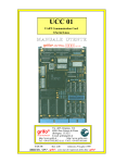
UCC 08
UART Communication Card
8 serial lines
MANUALE TECNICO
Via dell' Artigiano, 8/6
® 40016 San Giorgio di Piano
grifo
(Bologna) ITALY
E-mail: [email protected]
http://www.grifo.it
http://www.grifo.com
Tel. +39 051 892.052 (r.a.) FAX: +39 051 893.661
ITALIAN TECHNOLOGY
UCC08
Rel. 3.20
Edizione 15 Ottobre 2002
®
®
, GPC , grifo , sono marchi registrati della ditta grifo®
UCC 08
UART Communication Card
8 serial lines
MANUALE TECNICO
Modulo periferico per il BUS industriale ABACO®; formato
BLOCK da 100x160mm; SCC 2698, con oscillatore da 3,6864
MHz con protocollo e baud rate, fino a 38,4 KBaud, settabile
da software; tre Dip Switch da 8 vie leggibile da software; 8
linee seriali configurabili in RS 232, RS 422 o RS 485; 3 LEDs
per la visualizzazione delle richieste di interrupt e del modo di
indirizzamento; possibilità di generare un segnale di interrupt
collegabile all’/INT oppure al /NMI; spazio d’indirizzamento
sul BUS ABACO® di soli 64 bytes; due Dip Switch a 8 vie per
il settaggio dell’indirizzo di I/O; unica tensione di alimentazione
a 5Vdc, 160 mA (nella configurazione base a riposo).
Via dell' Artigiano, 8/6
® 40016 San Giorgio di Piano
grifo
(Bologna) ITALY
E-mail: [email protected]
http://www.grifo.it
http://www.grifo.com
Tel. +39 051 892.052 (r.a.) FAX: +39 051 893.661
ITALIAN TECHNOLOGY
UCC08
Rel. 3.20
Edizione 15 Ottobre 2002
®
®
, GPC , grifo , sono marchi registrati della ditta grifo®
Vincoli sulla documentazione
grifo® Tutti i Diritti Riservati
Nessuna parte del presente manuale può essere riprodotta, trasmessa, trascritta, memorizzata in un archivio o tradotta in altre lingue, con qualunque forma o mezzo, sia esso
elettronico, meccanico, magnetico ottico, chimico, manuale, senza il permesso scritto
della grifo®.
IMPORTANTE
Tutte le informazioni contenute sul presente manuale sono state accuratamente verificate, ciononostante grifo® non si assume nessuna responsabilità per danni, diretti o
indiretti, a cose e/o persone derivanti da errori, omissioni o dall'uso del presente manuale,
del software o dell' hardware ad esso associato.
grifo® altresi si riserva il diritto di modificare il contenuto e la veste di questo manuale
senza alcun preavviso, con l' intento di offrire un prodotto sempre migliore, senza che
questo rappresenti un obbligo per grifo®.
Per le informazioni specifiche dei componenti utilizzati sui nostri prodotti, l'utente deve
fare riferimento agli specifici Data Book delle case costruttrici o delle seconde sorgenti.
LEGENDA SIMBOLI
Nel presente manuale possono comparire i seguenti simboli:
Attenzione: Pericolo generico
Attenzione: Pericolo di alta tensione
Marchi Registrati
, GPC®, grifo® : sono marchi registrati della grifo®.
Altre marche o nomi di prodotti sono marchi registrati dei rispettivi proprietari.
ITALIAN TECHNOLOGY
grifo®
INDICE GENERALE
INTRODUZIONE ........................................................................................................................ 1
VERSIONE SCHEDA .................................................................................................................. 1
CARATTERISTICHE GENERALI DELLA SCHEDA ...................................................... 2
SPECIFICHE TECNICHE ......................................................................................................... 4
CARATTERISTICHE GENERALI ...................................................................................... 4
CARATTERISTICHE FISICHE ........................................................................................... 4
CARATTERISTICHE ELETTRICHE ................................................................................. 5
INSTALLAZIONE ....................................................................................................................... 6
SEGNALAZIONI VISIVE ..................................................................................................... 6
CONNESSIONI CON IL MONDO ESTERNO ................................................................... 6
DIP SWITCH ........................................................................................................................... 6
CN1 - CONNETTORE PER BUS ABACO® .................................................................... 8
CN2 - CONNETTORE PER LE 8 LINEE SERIALI RS 232 ...................................... 10
CN3- CONNETTORE PER RS 422/RS 485 DELLE LINEE SERIALI A÷D ............ 12
CN4- CONNETTORE PER RS 422/RS 485 DELLE LINEE SERIALI E÷H ............ 14
JUMPERS .............................................................................................................................. 16
INTERFACCIAMENTO DEGLI I/O CON IL CAMPO................................................... 25
COMUNICAZIONE SERIALE ........................................................................................... 25
INTERRUPTS ....................................................................................................................... 39
INGRESSI DI CONFIGURAZIONE .................................................................................. 39
DESCRIZIONE HARDWARE ................................................................................................. 40
MAPPAGGIO DELLA SCHEDA ........................................................................................ 40
INDIRIZZAMENTO REGISTRI INTERNI ...................................................................... 43
DESCRIZIONE SOFTWARE DELLE PERIFERICHE DI BORDO .................................. 45
INGRESSI DI CONFIGURAZIONE .................................................................................. 45
HANDSHAKE ....................................................................................................................... 46
SCHEDE ESTERNE .................................................................................................................. 47
BIBLIOGRAFIA ........................................................................................................................ 51
APPENDICE A: DATA SHEET DELL'SCC 2698B ............................................................. A-1
APPENDICE B: INDICE ANALITICO ................................................................................ B-1
UCC 08
Rel. 3.20
Pagina I
grifo®
ITALIAN TECHNOLOGY
INDICE DELLE FIGURE
FIGURA 1: SCHEMA A BLOCCHI ......................................................................................................... 3
FIGURA 2: FOTO SCHEDA .................................................................................................................. 5
FIGURA 3: TABELLA DELLE SEGNALAZIONI VISIVE ............................................................................. 6
FIGURA 4: DISPOSIZIONE CONNETTORI, LEDS, DIP SWICTH, ECC. ...................................................... 7
FIGURA 5: CN1 - CONNETTORE PER BUS ABACO® ....................................................................... 8
FIGURA 6: CN2 - CONNETTORE PER LINEE SERIALI RS 232 ........................................................... 10
FIGURA 7: MAPPA DEI COMPONENTI ................................................................................................ 11
FIGURA 8: CN3 - CONNETTORE PER RS 422/RS 485 LINEE A÷D .................................................. 12
FIGURA 9: ESEMPIO COLLEGAMENTO IN RS 232 ............................................................................. 13
FIGURA 10: ESEMPIO COLLEGAMENTO PUNTO PUNTO IN RS 485 ..................................................... 13
FIGURA 11: ESEMPIO COLLEGAMENTO PUNTO PUNTO IN RS 422 ..................................................... 13
FIGURA 12: CN4 - CONNETTORE PER RS 422/RS 485 LINEE E÷H ................................................ 14
FIGURA 14: SCHEMA DI COMUNICAZIONE SERIALE ........................................................................... 15
FIGURA 15: TABELLA RIASSUNTIVA JUMPERS - PARTE 1 .................................................................... 16
FIGURA 16: TABELLA RIASSUNTIVA JUMPERS - PARTE 2 .................................................................... 17
FIGURA 17: TABELLA JUMPERS A 2 VIE ........................................................................................... 18
FIGURA 18: ESEMPIO COLLEGAMENTO IN RETE IN RS 485 .............................................................. 19
FIGURA 19: TABELLA JUMPERS A 3 VIE - PARTE 1 ............................................................................ 20
FIGURA 20: TABELLA DISPOSIZIONE JUMPERS - PARTE 1 .................................................................. 21
FIGURA 21: TABELLA JUMPERS A 3 VIE - PARTE 2 ............................................................................ 22
FIGURA 22: TABELLA DISPOSIZIONE JUMPERS - PARTE 2 .................................................................. 23
FIGURA 23: TABELLA JUMPERS A 3 VIE - PARTE 3 ............................................................................ 24
FIGURA 24: TABELLA JUMPER A 6 VIE ............................................................................................. 24
FIGURA 25: DISPOSIZIONE DRIVER PER COMUNICAZIONE SERIALE RS 232 ....................................... 27
FIGURA 26: DISPOSIZIONE DRIVER PER COMUNICAZIONE SERIALE RS 422 LINEE A÷D..................... 29
FIGURA 27: DISPOSIZIONE DRIVER PER COMUNICAZIONE SERIALE RS 422 LINEE E÷H .................... 31
FIGURA 28: DISPOSIZIONE DRIVER PER COMUNICAZIONE SERIALE RS 485 LINEE A÷D..................... 33
FIGURA 29: DISPOSIZIONE DRIVER PER COMUNICAZIONE SERIALE RS 485 LINEE E÷H .................... 35
FIGURA 30: TABELLA INDIRIZZAMENTO DEI REGISTRI INTERNI - PARTE 1 ......................................... 43
FIGURA 31: TABELLA INDIRIZZAMENTO DEI REGISTRI INTERNI - PARTE 2 ......................................... 44
FIGURA 32: CORRISPONDENZA TRA HANDSHAKE, SEGNALI E REGISTRI DELL'SCC 2698 ................... 46
FIGURA 33: ESEMPI DI COLLEGAMENTO .......................................................................................... 49
Pagina II
UCC 08
Rel. 3.20
ITALIAN TECHNOLOGY
grifo®
INTRODUZIONE
L'uso di questi dispositivi é rivolto - IN VIA ESCLUSIVA - a personale specializzato.
Scopo di questo manuale é la trasmissione delle informazioni necessarie all’uso competente e sicuro
dei prodotti. Esse sono il frutto di un’elaborazione continua e sistematica di dati e prove tecniche
registrate e validate dal Costruttore, in attuazione alle procedure interne di sicurezza e qualità
dell'informazione.
I dati di seguito riportati sono destinati - IN VIA ESCLUSIVA - ad un utenza specializzata, in grado
di interagire con i prodotti in condizioni di sicurezza per le persone, per la macchina e per l'ambiente,
interpretando un'elementare diagnostica dei guasti e delle condizioni di funzionamento anomale e
compiendo semplici operazioni di verifica funzionale, nel pieno rispetto delle norme di sicurezza e
salute vigenti.
Le informazioni riguardanti installazione, montaggio, smontaggio, manutenzione, aggiustaggio,
riparazione ed installazione di eventuali accessori, dispositivi ed attrezzature, sono destinate - e
quindi eseguibili - sempre ed in via esclusiva da personale specializzato avvertito ed istruito, o
direttamente dall'ASSISTENZA TECNICA AUTORIZZATA, nel pieno rispetto delle
raccomandazioni trasmesse dal costruttore e delle norme di sicurezza e salute vigenti.
I dispositivi non possono essere utilizzati all'aperto. Si deve sempre provvedere ad inserire i moduli
all'interno di un contenitore a norme di sicurezza che rispetti le vigenti normative. La protezione di
questo contenitore non si deve limitare ai soli agenti atmosferici, bensì anche a quelli meccanici,
elettrici, magnetici, ecc.
Per un corretto rapporto coi prodotti, é necessario garantire leggibilità e conservazione del manuale,
anche per futuri riferimenti. In caso di deterioramento o più semplicemente per ragioni di
approfondimento tecnico ed operativo, consultare direttamente l’Assistenza Tecnica autorizzata.
Al fine di non incontrare problemi nell’uso di tali dispositivi, é conveniente che l’utente - PRIMA
DI COMINCIARE AD OPERARE - legga con attenzione tutte le informazioni contenute in questo
manuale. In una seconda fase, per rintracciare più facilmente le informazioni necessarie, si può fare
riferimento all’indice generale e all’indice analitico, posti rispettivamente all’inizio ed alla fine del
manuale.
VERSIONE SCHEDA
Il presente manuale è riferito alla scheda UCC 08 versione 111193 e successive. La validità delle
informazioni riportate è quindi subordinata al numero di versione della scheda in uso e l'utente deve
quindi sempre verificare la giusta corrispondenza tra le due indicazioni. Sulla scheda il numero di
versione è riportato in più punti sia a livello di serigrafia che di stampato (ad esempio sotto il marchio
grifo® nel lato componenti e saldature).
UCC 08
Rel. 3.20
Pagina 1
grifo®
ITALIAN TECHNOLOGY
CARATTERISTICHE GENERALI DELLA SCHEDA
La scheda UCC 08 (Uart Communication Card 8 serial lines) é un potentissimo modulo dedicato alle
comunicazioni seriali per il Bus industriale ABACO® ed offre alla CPU notevoli possibilità di
interfacciamento ad innumerevoli dispositivi esterni. La scheda é basata sul versatile SCC 2698, che
può gestire la comunicazione asincrona di ben 8 linee seriali contemporaneamente ed inoltre è capace
di generare interrupt. La UCC 08, in formato Europa da 100x160 mm, può gestire separatamente 8
linee seriali con protocollo e velocità di comunicazione settabili via software; ognuna delle 8 linee
gestisce automaticamente i 4 segnali canonici per la comunicazione seriale: TxD, RxD, CTS, RTS.
Inoltre ogni linea di comunicazione può essere configurata in RS 232, RS 422 o RS485. In fine
l'attivazione degli interrupt ed il tipo di indirizzamento selezionato sono visualizzati tramite LEDS.
Dal punto di vista del protocollo di comunicazione può essere selezionata una comunicazione
asincrona con:
- Baud rate settabile tra 50 e 38,4 KBaud, fissi o regolabili dall'utente
- Stop bit selezionabili tra 1; 1,5 e 2 bit
- Lunghezza della parola programmabile da 5 a 8 bit
- Buffer di ricezione di 4 caratteri
- Parità nessuna, pari, dispari o forzata
Cinque dip switch da 8 vie è leggibile via software e dà all'utente, la possibilità di poter settare, a
livello scheda, delle condizioni particolari quali baud rate, protocollo di comunicazione ed altro, da
gestire poi via firmware. Sono ordinabili le seguenti configurazioni:
- UCC 08
- UCC 08.8RS422
- UCC 08.8RS485
- UCC 08.4+4RS422
- UCC 08.4+4RS485
- UCC 08.8RS232
- UCC 08.4RS422
- UCC 08.4RS485
8 driver RS 232
8 driver RS 422
8 driver RS 485
4 drivers RS 232 e 4 driver RS 422
4 drivers RS 232 e 4 driver RS 485
8 driver RS 232
4 driver RS 422
4 driver RS 485
La UCC 08 occupa uno spazio di indirizzamento di 64 byte ed in tali indirizzi sono mappati tutti i
registri che consentono la programmazione e la gestione della scheda via software. Questi indirizzi
possono essere allocati nello spazio di indirizzamento del BUS ABACO® tramite due dei sopra
menzionati dip switch ad 8 vie. La scheda può generare un segnale di interrupt in corrispondenza del
verificarsi di particolari condizioni definibili sempre tramite apposita programmazione software.
- Modulo periferico per il BUS industriale ABACO®.
- Formato BLOCK da 100x160mm.
- SCC 2698, oscillatore da 3,6864 MHz, baud rate fino a 38,4 KBaud, settabile da software.
- Tre Dip Switch da 8 vie leggibile da software.
- 8 linee seriali configurabili in RS 232, RS 422 o RS 485.
- 3 LEDs per la visualizzazione delle richieste di interrupt e del modo di indirizzamento.
- Possibilità di generare un segnale di interrupt collegabile all’/INT oppure al /NMI.
- Spazio d’indirizzamento sul BUS ABACO® di soli 64 bytes.
- Due Dip Switch a 8 vie per il settaggio dell’indirizzo di I/O.
- Unica tensione di alimentazione a 5Vdc, 160 mA (nella configurazione base a riposo).
Pagina 2
UCC 08
Rel. 3.20
grifo®
ITALIAN TECHNOLOGY
CN4
CN3
CN2
Driver RS 232, RS 422 and RS 485
UART SCC 2698
DIP 3
DIP 4
DIP 5
DIP 1
DIP 2
Jumpers
Jumpers
CONTROL LOGIC
CN1 - BUS Abaco®
FIGURA 1: SCHEMA A BLOCCHI
UCC 08
Rel. 3.20
Pagina 3
grifo®
ITALIAN TECHNOLOGY
SPECIFICHE TECNICHE
CARATTERISTICHE GENERALI
Interfaccia per BUS industriale ABACO®.
Tre Dip switch a 8 vie acquisibile da software.
Due Dip switch a 8 vie per il settaggio indirizzo in I/O.
8 linee seriali Full Duplex in RS 232, RS 422 o RS 485.
Risorse della scheda:
-
UART di bordo:
SCC 2698
Frequenza clock:
3, 6864 MHz
Interfaccia BUS:
BUS a 8 bits per i dati
BUS a 8, 16 o 22 bits per gli indirizzi.
256, 64K o 4M bytes totali d’indirizzamento.
64 bytes di spazio occupato in I/O.
Comunicazione seriale:
Protocollo configurabile da software:
- BAUD RATE:
da 50 a 38, 4 KBaud
- STOP BIT:
1, 1,5 e 2 bit
- Lunghezza parola: da 5 a 8 bit
- PARITA’:
Nessuna, Pari, Dispari
CARATTERISTICHE FISICHE
Dimensioni (L x A x P):
Formato BLOCK: 100 x 160 x 17 mm
Peso:
170 g
(versione base)
Connettori:
CN1:
CN2:
CN3:
CN4:
64 pin DIN 41612 A+C corpo C 90 gradi
Scatolino 40 vie maschio 90 gradi
Scatolino 20 vie maschio 90 gradi
Scatolino 20 vie maschio dritto
Range di temperatura:
da 0 a 70 gradi Centigradi
Umidità relativa:
20% fino a 90% (senza condensa)
Pagina 4
UCC 08
Rel. 3.20
grifo®
ITALIAN TECHNOLOGY
CARATTERISTICHE ELETTRICHE
Tensione di alimentazione:
+5 Vdc
Corrente assorbita sui 5 Vdc:
160 mA nella configurazione base RS 232
250 mA nella configurazione massima
Rete terminazione RS 422-485:
Resistenza terminazione linea=
120 Ω
FIGURA 2: FOTO SCHEDA
UCC 08
Rel. 3.20
Pagina 5
grifo®
ITALIAN TECHNOLOGY
INSTALLAZIONE
In questo capitolo saranno illustrate tutte le operazioni da effettuare per il corretto utilizzo della
scheda. A questo scopo viene riportata l'ubicazione e la funzione degli strip, dei connettori, dei LEDs,
ecc. presenti sulla UCC 08.
SEGNALAZIONI VISIVE
La scheda UCC 08 é dotata di 3 LEDs con cui segnala alcune condizioni di stato, come descritto nella
seguente tabella:
LED
COLORE
FUNZIONE
LD1
Rosso
Quando è acceso indica che è in corso un accesso ad una delle
linee seriali.
LD2
Rosso
Quando è acceso indica che la UCC 08 ha inviato un interrupt
mascherabile sul BUS ABACO® (linea /INT).
LD3
Rosso
Quando è acceso indica che la UCC 08 ha inviato un interrupt
non mascherabile sul BUS ABACO® (linea /NMI).
FIGURA 3: TABELLA DELLE SEGNALAZIONI VISIVE
La funzione principale di questi LEDs é quella di fornire un’indicazione visiva dello stato della
scheda, facilitando quindi le operazioni di verifica di funzionamento di tutto il sistema.
Per una più facile individuazione di tali segnalazioni visive, si faccia riferimento alla figura 4.
CONNESSIONI CON IL MONDO ESTERNO
Il modulo UCC 08 è provvisto di 4 connettori con cui vengono effettuati tutti i collegamenti con il
campo e con le altre schede del sistema di controllo da realizzare. Di seguito viene riportato il loro
pin out ed il significato dei segnali collegati; per una facile individuazione di tali connettori, si faccia
riferimento alla figura 4, mentre per ulteriori informazioni a riguardo del tipo di connessioni, fare
riferimento alle figure successive che illustrano il tipo di collegamento effettuato a bordo scheda.
DIP SWITCH
La UCC 08 è dotata di 5 dip switch ad 8 vie. Di questi 5, 2 sono utilizzati per impostare l'indirizzo
di mappaggio della scheda e per altre funzioni di gestione, i rimanenti 3 sono acquisibili dall'utente
via software mediante accesso in lettura agli appositi registri, si veda il capitolo “DESCRIZIONE
SOFTWARE” per ulteriori informazioni.
Pagina 6
UCC 08
Rel. 3.20
ITALIAN TECHNOLOGY
DIP1
grifo®
CN1
DIP2
DIP3
LD1
DIP4
LD2
DIP5
LD3
CN2
CN4
CN3
FIGURA 4: DISPOSIZIONE CONNETTORI, LEDS, DIP SWICTH, ECC.
UCC 08
Rel. 3.20
Pagina 7
grifo®
ITALIAN TECHNOLOGY
CN1 - CONNETTORE PER BUS ABACO®
CN1 è un connettore DIN 41612 corpo C a 90 gradi da 64 piedini.
Tramite CN1 si effettua la connessione tra la scheda e la serie di moduli esterni di espansione, da
utilizzare per l'interfacciamento diretto con il campo. Tale collegamento è effettuato tramite il BUS
industriale ABACO® di cui questo connettore riporta i segnali a livello TTL. Nella figura seguente
è riportato il pin out del BUS e quindi anche del relativo connettore, con le variazioni per l'utilizzo
di CPU a 16 Bit rispetto a quelle a 8 Bit.
A
A
BUS a 16 bit BUS a 8 bit
GND
GND
+5 Vdc
+5 Vdc
D0
D0
D1
D1
D2
D2
D3
D3
D4
D4
D5
D5
D6
D6
D7
D7
A0
A0
A1
A1
A2
A2
A3
A3
A4
A4
A5
A5
A6
A6
A7
A7
A8
A8
A9
A9
A10
A10
A11
A11
A12
A12
A13
A13
A14
A14
A15
A15
A16
A17
A18
+12 Vdc
+12 Vdc
+5 Vdc
+5 Vdc
GND
GND
A
UCC 08
GND
+5 Vdc
D0
D1
D2
D3
D4
D5
D6
D7
A0
A1
A2
A3
A4
A5
A6
A7
A8
A9
A10
A11
A12
A13
A14
A15
A16
A17
A18
N.C.
+5 Vdc
GND
PIN
C
1
2
3
4
5
6
7
8
9
10
11
12
13
14
15
16
17
18
19
20
21
22
23
24
25
26
27
28
29
30
31
32
UCC 08
GND
+5 Vdc
N.C.
N.C.
N.C.
/INT
/NMI
N.C.
N.C.
/IORQ
/RD
/WR
N.C.
N.C.
N.C.
/RESET
/M1
N.C.
N.C.
N.C.
N.C.
N.C.
N.C.
N.C.
N.C.
A21
A20
A19
N.C.
N.C.
+5 Vdc
GND
C
C
BUS a 8 bit BUS a 16 bit
GND
GND
+5 Vdc
+5 Vdc
D8
D9
D10
/INT
/INT
/NMI
/NMI
/HALT
D11
/MREQ
/MREQ
/IORQ
/IORQ
/RD
/RDLDS
/WR
/WRLDS
/BUSAK
D12
/WAIT
/WAIT
/BUSRQ
D13
/RESET
/RESET
/M1
/IACK
/RFSH
D14
/MEMDIS
/MEMDIS
VDUSEL
A22
/IEI
D15
CLK
/R.T.
-12 Vdc
+5 Vdc
GND
CLK
/RDUDS
/WRUDS
A21
A20
A19
/R.T.
-12 Vdc
+5 Vdc
GND
FIGURA 5: CN1 - CONNETTORE PER BUS ABACO®
Pagina 8
UCC 08
Rel. 3.20
ITALIAN TECHNOLOGY
grifo®
Legenda:
CPU a 8 bit
A0-A15 = O - Address BUS: BUS degli indirizzi.
D0-D7
= I/O - Data BUS: BUS dei dati.
/INT
= I - Interrupt request: richiesta d’interrupt.
/NMI
= I - Non Mascherable Interrupt: richiesta d’interrupt non mascherabile.
/HALT
= O - Halt state: stao di Halt.
/MREQ = O - Memory Request: richiesta di operazione in memoria.
/IORQ
= O - Input Output Request: richiesta di operazione in Input Output.
/RD
= O - Read cycle status: richiesta di lettura.
/WR
= O - Write cycle status: richiesta di scrittura.
/BUSAK = O - BUS Acknowledge: riconoscimento della richiesta di utilizzo del BUS.
/WAIT
= I - Wait: Attesa.
/BUSRQ = I - BUS Request: richiesta di utilizzo del BUS.
/RESET = O - Reset: azzeramento.
/M1
= O - Machine cycle one: primo ciclo macchina.
/RFSH
= O - Refresh: rinfresco per memorie dinamiche.
/MEMDIS = I - Memory Display: segnale emesso dal dispositivo periferico mappato in memoria.
VDUSEL = O - VDU Selection: abilitazione per il dispositivo periferico ad essere mappato in
memoria.
/IEI
= I - Interrupt Enable Input: abilitazione interrupt da BUS in catene di priorità.
CLK
= O - Clock: clock di sistema.
/R.T.
= I - Reset Tast: tasto di reset.
+5 Vdc
= I - Linea di alimentazione a +5 Vcc.
+12 Vdc = O - Linea di alimentazione a +12 Vcc.
-12 Vdc = O - Linea di alimentazione a -12 Vcc.
GND
=
- Linea di massa per tutti i segnali del BUS.
N.C.
=
- Non Collegato
CPU a 16 bit
A0-A22
D0-D15
/RD UDS
/WR UDS
/IACK
= O - Address BUS: BUS degli indirizzi.
= I/O - Data BUS: BUD dei dati.
= O - Read Upper Data Strobe: lettura del byte superiore sul BUS dati.
= O - Write Upper Data Strobe: scrittura del byte superiore sul BUS dati.
= O - Interrupt Acknowledge: riconoscimento della richiesta d’interrupt da parte della
CPU.
/RD LDS = O - Read Lower Data Strobe: lettura del byte inferiore sul BUS dati.
/WR LDS = O - Write Lower Data Strobe: scrittura del byte inferiore sul BUS dati.
N.B.
Le indicazioni di direzionalità sopra riportate sono riferite ad una scheda di comando (CPU o GPC®)
e sono state mantenute inalterate in modo da non avere ambiguità d'interpretazione nel caso di sistemi
composti da più schede.
UCC 08
Rel. 3.20
Pagina 9
grifo®
ITALIAN TECHNOLOGY
CN2 - CONNETTORE PER LE 8 LINEE SERIALI RS 232
Il connettore per la comunicazione in RS 232, denominato CN2 sulla scheda, é del tipo scatolino a
40 vie 90 gradi. Il pin-out riportato di seguito, é stato studiato in modo da ridurre al minimo le
interferenze ed in modo da facilitare la connessione con il campo, mentre i segnali rispettano le
normative definite dal CCITT relative ad ognuno degli standard di comunicazione usati.
CTSA RS232
1
2
RTSA RS232
TxDA RS232
3
4
RxDA RS232
GND
5
6
GND
CTSB RS232
7
8
RTSB RS232
TxDB RS232
9
10
RxDB RS232
CTSC RS232
11
12
RTSC RS232
TxDC RS232
13
14
RxDC RS232
GND
15
16
GND
CTSD RS232
17
18
RTSD RS232
TxDD RS232
19
20
RxDD RS232
CTSE RS232
21
22
RTSE RS232
TxDE RS232
23
24
RxDE RS232
GND
25
26
GND
CTSF RS232
27
28
RTSF RS232
TxDF RS232
29
30
RxDF RS232
CTSG RS232
31
32
RTSG RS232
TxDG RS232
33
34
RxDG RS232
GND
35
36
GND
CTSH RS232
37
38
RTSH RS232
TxDH RS232
39
40
RxDH RS232
FIGURA 6: CN2 - CONNETTORE PER LINEE SERIALI RS 232
Pagina 10
UCC 08
Rel. 3.20
grifo®
ITALIAN TECHNOLOGY
Legenda:
RxDy RS 232
TxDy RS 232
CTSy RS 232
RTSy RS 232
= I - Receive Data: linea ricezione in RS 232 della seriale A÷H.
= O - Transmit Data: linea trasmissione in RS 232 della seriale A÷H.
= I - Clear To Send: linea di abilitazione alla trasmissione in RS 232 della
seriale A÷H.
= O - Request To Send: linea di richiesta di trasmissione in RS 232 della
seriale A÷H.
FIGURA 7: MAPPA DEI COMPONENTI
UCC 08
Rel. 3.20
Pagina 11
grifo®
ITALIAN TECHNOLOGY
CN3- CONNETTORE PER RS 422/RS 485 DELLE LINEE SERIALI A÷D
Il connettore per la comunicazione RS 422/RS 485 delle linee seriali dalla A alla D, denominato CN3
sulla scheda, é del tipo scatolino a 20 vie 90 gradi. Il pin-out riportato di seguito, é stato studiato in
modo da ridurre al minimo le interferenze ed in modo da facilitare la connessione con il campo,
mentre i segnali rispettano le normative definite dal CCITT relative ad ognuno degli standard di
comunicazione usati.
TXA- RS 422
1
2
RXA- RS 422 / RXTXA- RS485
TXA+ RS 422
3
4
RXA+ RS 422 / RXTXA+ RS485
GND
5
6
GND
TXB- RS 422
7
8
RXB- RS 422 / RXTXB- RS485
TXB+ RS 422
9
10
RXB+ RS 422 / RXTXB+ RS485
TXC- RS 422
11
12
RXC- RS 422 / RXTXC- RS485
TXC+ RS 422
13
14
RXC+ RS 422 / RXTXC+ RS485
GND
15
16
GND
TXD- RS 422
17
18
RXD- RS 422 / RXTXD- RS485
TXD+ RS 422
19
20
RXD+ RS 422 / RXTXD+ RS485
FIGURA 8: CN3 - CONNETTORE PER RS 422/RS 485 LINEE A÷D
Legenda:
RXy- RS 422
RXy+ RS 422
TXy- RS 422
TXy+ RS 422
RXTXy- RS 485
RXTXy+ RS 485
GND
Pagina 12
= I - Receive Data Negative: linea bipolare negativa di ricezione
differenziale in RS 422 della seriale A÷D.
= I - Receive Data Positive: linea bipolare positiva di ricezione differenziale
in RS 422 della seriale A÷D.
= O - Transmit Data Negative: linea bipolare negativa di trasmissione
differenziale in RS 422 della seriale A÷D.
= O - Transmit Data Positive: linea bipolare positiva di trasmissione
differenziale in RS 422 della seriale A÷D.
=I/O- Receive Transmit Data Negative: linea bipolare negativa di ricezione
e trasmissione differenziale in RS 485 della seriale A÷D.
=I/O- Receive Transmit Data Positive: linea bipolare positiva di ricezione e
trasmissione differenziale in RS 485 della seriale A÷D.
= - Linea di massa.
UCC 08
Rel. 3.20
CN2 UCC 08
CTSA ÷ CTSH
RTS
RTSA ÷ RTSH
CTS
RXA ÷ RXH
TX
TXA ÷ TXH
RX
External System
grifo®
ITALIAN TECHNOLOGY
GND
GND
RXTXA- ÷ RXTXH-
TX / RX -
RXTXA+ ÷ RXTXH+
TX / RX +
GND
GND
External System
CN3 or CN4 UCC 08
FIGURA 9: ESEMPIO COLLEGAMENTO IN RS 232
RXA- ÷ RXH-
TX -
RXA+ ÷ RXH+
TX +
TXA- ÷ TXH-
RX -
TXA+ ÷ TXH+
RX +
GND
GND
External System
CN3 or CN4 UCC 08
FIGURA 10: ESEMPIO COLLEGAMENTO PUNTO PUNTO IN RS 485
FIGURA 11: ESEMPIO COLLEGAMENTO PUNTO PUNTO IN RS 422
UCC 08
Rel. 3.20
Pagina 13
grifo®
ITALIAN TECHNOLOGY
CN4- CONNETTORE PER RS 422/RS 485 DELLE LINEE SERIALI E÷H
Il connettore per la comunicazione RS 422/RS 485 delle linee seriali dalla E alla H, denominato CN4
sulla scheda, é del tipo scatolino a 20 vie dritto. Il pin-out riportato di seguito, é stato studiato in modo
da ridurre al minimo le interferenze ed in modo da facilitare la connessione con il campo, mentre i
segnali rispettano le normative definite dal CCITT relative ad ognuno degli standard di comunicazione
usati.
TXE- RS 422
1
2
RXE- RS 422 / RXTXE- RS485
TXE+ RS 422
3
4
RXE+ RS 422 / RXTXE+ RS485
GND
5
6
GND
TXF- RS 422
7
8
RXF- RS 422 / RXTXF- RS485
TXF+ RS 422
9
10
RXF+ RS 422 / RXTXF+ RS485
TXG- RS 422
11
12
RXG- RS 422 / RXTXG- RS485
TXG+ RS 422
13
14
RXG+ RS 422 / RXTXG+ RS485
GND
15
16
GND
TXH- RS 422
17
18
RXH- RS 422 / RXTXH- RS485
TXH+ RS 422
19
20
RXH+ RS 422 / RXTXH+ RS485
FIGURA 12: CN4 - CONNETTORE PER RS 422/RS 485 LINEE E÷H
Legenda:
RXy- RS 422
RXy+ RS 422
TXy- RS 422
TXy+ RS 422
RXTXy- RS 485
RXTXy+ RS 485
GND
Pagina 14
= I - Receive Data Negative: linea bipolare negativa di ricezione
differenziale in RS 422 della seriale E÷H.
= I - Receive Data Positive: linea bipolare positiva di ricezione differenziale
in RS 422 della seriale E÷H.
= O - Transmit Data Negative: linea bipolare negativa di trasmissione
differenziale in RS 422 della seriale E÷H.
= O - Transmit Data Positive: linea bipolare positiva di trasmissione
differenziale in RS 422 della seriale E÷H.
=I/O- Receive Transmit Data Negative: linea bipolare negativa di ricezione
e trasmissione differenziale in RS 485 della seriale E÷H.
=I/O- Receive Transmit Data Positive: linea bipolare positiva di ricezione e
trasmissione differenziale in RS 485 della seriale E÷H.
= - Linea di massa.
UCC 08
Rel. 3.20
grifo®
ITALIAN TECHNOLOGY
SERIAL LINES A ÷ D
DRIVERS
CN3
RS 422
RS 485
DRIVERS
CN4
RS 422
Channel A ÷ Channel H
SCC 2698
SERIAL LINES E ÷ H
RS 485
SERIAL LINES A ÷ H
CN2
DRIVERS
RS 232
RS 232
FIGURA 14: SCHEMA DI COMUNICAZIONE SERIALE
UCC 08
Rel. 3.20
Pagina 15
grifo®
ITALIAN TECHNOLOGY
JUMPERS
Esistono a bordo della UCC 08 30 jumpers coi quali é possibile effettuare alcune selezioni che
riguardano il modo di funzionamento della stessa. Di seguito ne é riportato l’elenco, l’ubicazione e
la loro funzione nelle varie modalità di connessione.
JUMPERS
N. VIE
UTILIZZO
J1
12
Definisce l'indirizzo in caso di indirizzamento esteso potenziato e
collega il segnale /M1 proveniente dal BUS ABACO® alla scheda.
J2
3
Seleziona il tipi di indirizzamento della scheda.
J3
3
Seleziona il collegamento del segnale /INTR delle linee seriali A e
B sul BUS ABACO ® .
J4
3
Seleziona il collegamento del segnale /INTR delle linee seriali C e
D sul BUS ABACO® .
J5
3
Seleziona il collegamento del segnale /INTR delle linee seriali E e F
sul BUS ABACO® .
J6
3
Seleziona il collegamento del segnale /INTR delle linee seriali G e
H sul BUS ABACO® .
J7
3
Seleziona il funzionamento in RS 422 o RS 485 della linea seriale
H.
J8
3
Seleziona il funzionamento in RS 422 o RS 485 della linea seriale
G.
J9
3
Seleziona il funzionamento in RS 422 o RS 485 della linea seriale
F.
J10
3
Seleziona il funzionamento in RS 422 o RS 485 della linea seriale
E.
J11
3
Determina la connessione in RS 232 o RS 422/RS 485 del segnale
di ricezione della linea seriale H.
J12
3
Determina la connessione in RS 232 o RS 422/RS 485 del segnale
di ricezione della linea seriale G.
J13
3
Determina la connessione in RS 232 o RS 422/RS 485 del segnale
di ricezione della linea seriale F.
J14
3
Determina la connessione in RS 232 o RS 422/RS 485 del segnale
di ricezione della linea seriale E.
J15
3
Determina la connessione in RS 232 o RS 422/RS 485 del segnale
di ricezione della linea seriale D.
FIGURA 15: TABELLA RIASSUNTIVA JUMPERS - PARTE 1
In queste pagine é riportata una descrizione tabellare delle possibili connessioni dei 30 jumpers con
la loro relativa funzione. Per riconoscere tali connessioni sulla scheda si faccia riferimento alla
serigrafia della stessa o alla figura 7 di questo manuale, dove viene riportata la numerazione dei pin
dei jumpers, che coincide con quella utilizzata nella seguente descrizione. Per l’individuazione dei
jumpers a bordo della scheda, si utilizzino invece le figure 20 e 22. In tutte le seguenti tabelle l'* indica
la connessione di default, ovvero quella impostata in fase di collaudo, con cui la scheda viene fornita.
Pagina 16
UCC 08
Rel. 3.20
grifo®
ITALIAN TECHNOLOGY
JUMPERS
N. VIE
UTILIZZO
J16
3
Determina la connessione in RS 232 o RS 422/RS 485 del segnale
di ricezione della linea seriale C.
J17
3
Determina la connessione in RS 232 o RS 422/RS 485 del segnale
di ricezione della linea seriale B.
J18
3
Determina la connessione in RS 232 o RS 422/RS 485 del segnale
di ricezione della linea seriale A.
J19
2
Connette la terminazione RS 422/RS 485 della linea seriale H.
J20
2
Connette la terminazione RS 422/RS 485 della linea seriale G.
J21
2
Connette la terminazione RS 422/RS 485 della linea seriale F.
J22
2
Connette la terminazione RS 422/RS 485 della linea seriale E.
J23
3
Seleziona il funzionamento in RS 422 o RS 485 della linea seriale
D.
J24
3
Seleziona il funzionamento in RS 422 o RS 485 della linea seriale
C.
J25
3
Seleziona il funzionamento in RS 422 o RS 485 della linea seriale
B.
J26
3
Seleziona il funzionamento in RS 422 o RS 485 della linea seriale
A.
J27
2
Connette la terminazione RS 422/RS 485 della linea seriale D.
J28
2
Connette la terminazione RS 422/RS 485 della linea seriale C.
J29
2
Connette la terminazione RS 422/RS 485 della linea seriale B.
J30
2
Connette la terminazione RS 422/RS 485 della linea seriale A.
FIGURA 16: TABELLA RIASSUNTIVA JUMPERS - PARTE 2
UCC 08
Rel. 3.20
Pagina 17
grifo®
ITALIAN TECHNOLOGY
JUMPERS A 2 VIE
JUMPER
CONNESSIONE
UTILIZZO
DEF.
non connesso
Non collega la circuiteria di terminazione alla linea
RS 485 o alla linea di ricezione RS 422, della seriale
H.
*
connesso
Collega la circuiteria di terminazione alla linea
RS485 o alla ricezione RS 422 della seriale H.
non connesso
Non collega la circuiteria di terminazion alla linea
RS 485 o alla linea di ricezione RS 422, della seriale
G.
connesso
Collega la circuiteria di terminazione alla linea
RS485 o alla ricezione RS 422 della seriale G.
non connesso
Non collega la circuiteria di terminazion alla linea
RS 485 o alla linea di ricezione RS 422, della seriale
F.
connesso
Collega la circuiteria di terminazione alla linea
RS485 o alla ricezione RS 422 della seriale F.
non connesso
Non collega la circuiteria di terminazione alla linea
RS 485 o alla linea di ricezione RS 422, della seriale
E.
connesso
Collega la circuiteria di terminazione alla linea
RS485 o alla ricezione RS 422 della seriale E.
J19
J20
J21
J22
non connesso
J27
connesso
non connesso
J28
Non collega la circuiteria di terminazion alla linea
RS 485 o alla linea di ricezione RS 422, della seriale
D.
Collega la circuiteria di terminazione alla linea
RS485 o alla ricezione RS 422 della seriale D.
Non collega la circuiteria di terminazione alla linea
RS 485 o alla linea di ricezione RS 422, della seriale
C.
connesso
Collega la circuiteria di terminazione alla linea
RS485 o alla ricezione RS 422 della seriale C.
non connesso
Non collega la circuiteria di terminazione alla linea
RS 485 o alla linea di ricezione RS 422, della seriale
B.
connesso
Collega la circuiteria di terminazione alla linea
RS485 o alla ricezione RS 422 della seriale B.
J29
non connesso
J30
connesso
Non collega la circuiteria di terminazione alla linea
RS 485 o alla linea di ricezione RS 422, della seriale
A.
Collega la circuiteria di terminazione alla linea
RS485 o alla ricezione RS 422 della seriale A.
*
*
*
*
*
*
*
FIGURA 17: TABELLA JUMPERS A 2 VIE
Pagina 18
UCC 08
Rel. 3.20
grifo®
ITALIAN TECHNOLOGY
Master
Slave 1
+
TXRX
-
120 Ω
TXRXA ÷ H
GND
UCC 08
Unit
GND
+
Slave 2
+
TXRXA ÷ H
GND
UCC 08
Unit
-
Slave n
+
TXRXA÷
TXRXH
GND
UCC 08
Unit
-
FIGURA 18: ESEMPIO COLLEGAMENTO IN RETE IN RS 485
Da notare che in una rete RS 485, devono essere presenti due resistenze di forzatura lungo la linea
e due resitenze di terminazione (120 Ω), alle estremità della stessa, rispettivamente vicino all'unità
Master ed all'ultima unità Slave.
A bordo della UCC 08 è presente la circuiteria di terminazione ma non di forzatura, che può essere
inserita o disinserita, tramite appositi jumpers, come illutrato in seguito.
In merito alla resistenza di terminazione dell'unità Master, provvedere a collegarla solo se questa non
é già presente al suo interno (ad esempio molti convertitori RS232-RS485 ne sono già provvisti).
Per maggiori informazioni consultare il Data-Book TEXAS INSTRUMENTS, "RS 422 and RS 485
Interface Cicuits", nella parte introduttiva riguardante le reti RS 422-485.
UCC 08
Rel. 3.20
Pagina 19
grifo®
ITALIAN TECHNOLOGY
JUMPERS A 3 VIE
JUMPERS
CONNESSIONE
posizione 1-2
J2
posizione 2-3
J3
J4
J5
J6
UTILIZZO
DEF.
Abilita l'indirizzamento normale della scheda ad 8
bit. J1 deve restare disconnesso e gli switch dall'1
al 5 di DIP2 devono restare in OFF.
Abilita l'indirizzamento esteso a 16 bit della scheda
(J1 deve restare disconnesso e gli switch dall'1 al
5 di DIP2 devono restare in OFF) o esteso
potenziato a 22 bit (in tal caso gli switch dall'1 al
5 di DIP2 compongono i bit alti dell'indirizzo).
posizione 1-2
Connette l'interrupt delle linee seriali A e B al
segnale /INT del BUS ABACO® .
posizione 2-3
Connette l'interrupt delle linee seriali A e B al
segnale /NMI del BUS ABACO® .
non connesso
Le linee seriali A e B non possono generare alcun
interrupt sul BUS ABACO® .
posizione 1-2
Connette l'interrupt delle linee seriali C e D al
segnale /INT del BUS ABACO® .
posizione 2-3
Connette l'interrupt delle linee seriali C e D al
segnale /NMI del BUS ABACO® .
non connesso
Le linee seriali C e D non possono generare alcun
interrupt sul BUS ABACO® .
posizione 1-2
Connette l'interrupt delle linee seriali E e F al
segnale /INT del BUS ABACO® .
posizione 2-3
Connette l'interrupt delle linee seriali E e F al
segnale /NMI del BUS ABACO® .
non connesso
Le linee seriali E e F non possono generare alcun
interrupt sul BUS ABACO® .
posizione 1-2
Connette l'interrupt delle linee seriali G e H al
segnale /INT del BUS ABACO® .
posizione 2-3
non connesso
posizione 1-2
J7
posizione 2-3
posizione 1-2
J8
posizione 2-3
Connette l'interrupt delle linee seriali G e H al
segnale /NMI del BUS ABACO® .
Le linee seriali G e H non possono generare alcun
interrupt sul BUS ABACO® .
Seleziona la comunicazione sulla linea seriale H in
RS 422 (full duplex o half duplex a 4 fili).
Seleziona la comunicazione sulla linea seriale H in
RS 485 (half duplex a 2 fili).
Seleziona la comunicazione sulla linea seriale G in
RS 422 (full duplex o half duplex a 4 fili).
Seleziona la comunicazione sulla linea seriale G in
RS 485 (half duplex a 2 fili).
*
*
*
*
*
*
FIGURA 19: TABELLA JUMPERS A 3 VIE - PARTE 1
Pagina 20
UCC 08
Rel. 3.20
grifo®
ITALIAN TECHNOLOGY
J8
J3
J4
J1
J5
J7
J6
J11
J9
J12
J10
J28
J22
J27
J26
FIGURA 20: TABELLA DISPOSIZIONE JUMPERS - PARTE 1
UCC 08
Rel. 3.20
Pagina 21
grifo®
JUMPERS
ITALIAN TECHNOLOGY
CONNESSIONE
UTILIZZO
DEF.
posizione 1-2
Seleziona la comunicazione sulla linea seriale F in
RS 422 (full duplex o half duplex a 4 fili).
*
J9
posizione 2-3
posizione 1-2
J10
posizione 2-3
posizione 1-2
J11
posizione 2-3
posizione 1-2
J12
Seleziona la comunicazione sulla linea seriale F in
RS 485 (half duplex a 2 fili).
Seleziona la comunicazione sulla linea seriale E in
RS 422 (full duplex o half duplex a 4 fili).
Seleziona la comunicazione sulla linea seriale E in
RS 485 (half duplex a 2 fili).
Seleziona la comunicazione in RS 232 per il segnale
di ricezione della linea seriale H.
Seleziona la comunicazione in RS 422 o RS 485 per
il segnale di ricezione della linea seriale H.
Seleziona la comunicazione in RS 232 per il segnale
di ricezione della linea seriale G.
*
*
*
posizione 2-3
Seleziona la comunicazione in RS 422 o RS 485 per
il segnale di ricezione della linea seriale G.
posizione 1-2
Seleziona la comunicazione in RS 232 per il segnale
di ricezione della linea seriale F.
posizione 2-3
Seleziona la comunicazione in RS 422 o RS 485 per
il segnale di ricezione della linea seriale F.
posizione 1-2
Seleziona la comunicazione in RS 232 per il segnale
di ricezione della linea seriale E.
posizione 2-3
Seleziona la comunicazione in RS 422 o RS 485 per
il segnale di ricezione della linea seriale E.
posizione 1-2
Seleziona la comunicazione in RS 232 per il segnale
di ricezione della linea seriale D.
posizione 2-3
Seleziona la comunicazione in RS 422 o RS 485 per
il segnale di ricezione della linea seriale D.
posizione 1-2
Seleziona la comunicazione in RS 232 per il segnale
di ricezione della linea seriale C.
posizione 2-3
Seleziona la comunicazione in RS 422 o RS 485 per
il segnale di ricezione della linea seriale C.
posizione 1-2
Seleziona la comunicazione in RS 232 per il segnale
di ricezione della linea seriale B.
*
Seleziona la comunicazione in RS 422 o RS 485 per
il segnale di ricezione della linea seriale B.
Seleziona la comunicazione in RS 232 per il segnale
di ricezione della linea seriale A.
Seleziona la comunicazione in RS 422 o RS 485 per
il segnale di ricezione della linea seriale A.
*
J13
J14
J15
J16
J17
posizione 2-3
posizione 1-2
J18
posizione 2-3
*
*
*
*
FIGURA 21: TABELLA JUMPERS A 3 VIE - PARTE 2
Pagina 22
UCC 08
Rel. 3.20
grifo®
ITALIAN TECHNOLOGY
J13
J15
J17
J2
J18
J16
J19
J14
J20
J23
J21
J24
J25
J23
J30
FIGURA 22: TABELLA DISPOSIZIONE JUMPERS - PARTE 2
UCC 08
Rel. 3.20
Pagina 23
grifo®
JUMPERS
ITALIAN TECHNOLOGY
CONNESSIONE
UTILIZZO
DEF.
posizione 1-2
Seleziona la comunicazione sulla linea seriale D in
RS 422 (full duplex o half duplex a 4 fili).
*
posizione 2-3
Seleziona la comunicazione sulla linea seriale D in
RS 485 (half duplex a 2 fili).
J23
posizione 1-2
J24
posizione 2-3
posizione 1-2
J25
posizione 2-3
posizione 1-2
J26
posizione 2-3
Seleziona la comunicazione sulla linea seriale C in
RS 422 (full duplex o half duplex a 4 fili).
Seleziona la comunicazione sulla linea seriale C in
RS 485 (half duplex a 2 fili).
Seleziona la comunicazione sulla linea seriale B in
RS 422 (full duplex o half duplex a 4 fili).
Seleziona la comunicazione sulla linea seriale B in
RS 485 (half duplex a 2 fili).
Seleziona la comunicazione sulla linea seriale A in
RS 422 (full duplex o half duplex a 4 fili).
Seleziona la comunicazione sulla linea seriale A in
RS 485 (half duplex a 2 fili).
*
*
*
FIGURA 23: TABELLA JUMPERS A 3 VIE - PARTE 3
JUMPERS A 6 VIE
JUMPERS
J1
CONNESSIONE
UTILIZZO
posizione 1-2
Se collegato, il segnale /M1 entra nella decodifica
dell'indirizzamento esteso potenziato.
posizione 3-4
Se collegato, il segnale A20 entra nella
composizione dell'indirizzamento esteso potenziato
come bit 20.
posizione 5-6
Se collegato, il segnale A19 entra nella
composizione dell'indirizzamento esteso potenziato
come bit 19.
posizione 7-8
posizione 9-10
posizione 11-12
nessun jumper
connesso
DEF.
Se collegato, il segnale A18 entra nella
composizione dell'indirizzamento esteso potenziato
come bit 18.
Se collegato, il segnale A17 entra nella
composizione dell'indirizzamento esteso potenziato
come bit 17.
Se collegato, il segnale A16 entra nella
composizione dell'indirizzamento esteso potenziato
come bit 16.
Nessun segnale compone i bit più significativi
dell'indirizzamento esterso potenziato.
*
FIGURA 24: TABELLA JUMPER A 6 VIE
Pagina 24
UCC 08
Rel. 3.20
ITALIAN TECHNOLOGY
grifo®
INTERFACCIAMENTO DEGLI I/O CON IL CAMPO
Al fine di evitare eventuali problemi di collegamento della scheda con tutta l'elettronica del campo
a cui la UCC 08 si deve interfacciare, si devono seguire le informazioni riportate nei precedenti
paragrafi e le relative figure che illustrano le modalità interne di connessione.
- Per i segnali che riguardano la comunicazione seriale con i protocolli RS 232, RS 422 e RS 485
fare riferimento alle specifiche standard di ognuno di questi protocolli.
- Tutti i segnali a livello TTL possono essere collegati a linee dello stesso tipo riferite alla massa
digitale della scheda. Il livello 0V corrisponde allo stato logico 0, mentre il livello 5V corrisponde
allo stato logico 1.
COMUNICAZIONE SERIALE
La linea di comunicazione seriali della scheda UCC 08 possono essere bufferate in RS 232, RS 422
o RS 485. La selezione del tipo d’interfacciamento avviene via hardware e viene effettuata tramite
un opportuno strippaggio dei jumpers di bordo, come può essere desunto dalla lettura delle
precedenti tabelle. Dal punto di vista software sono invece definibili tutti i parametri del protocollo
fisico di comunicazione tramite la programmazione dei registri interni del SCC 2698.
Alcuni componenti necessari per le configurazioni RS 485 e RS 422 non sono montati e collaudati
sulla scheda in configurazione di default; per questo la prima configurazione delle linee seriali non
in RS 232 deve essere sempre effettuata dai tecnici grifo®. A questo punto l'utente può cambiare
autonomamente la configurazione seguendo le informazioni sotto riportate:
- LINEA SERIALE A SETTATA IN RS 422 (opzione .RS 422)
J18
=
posizione 1-2
IC18
= indifferente
J30
=
(*1)
IC25
= MAX 483 o SN75176
J26
=
posizione 1-2
IC26
= MAX 483 o SN75176
Lo stato del segnale MPOA, gestito via software, consente di abilitare o disabilitare il
trasmettitore come segue:
MPOA = livello basso = stato logico 0 -> trasmettitore attivo
MPOA = livello alto = stato logico 1 -> trasmettitore disattivo
Per sistemi punto punto, la linea MPOA può essere mantenuta sempre bassa (trasmettitore
sempre attivo), mentre per sistemi multipunto si deve attivare il trasmettitore solo in
corrispondenza della trasmissione.
- LINEA SERIALE A SETTATA IN RS 232 (configurazione default)
J18
=
posizione 2-3
IC18
= driver MAX 235
J30
=
indifferente
IC25
= indifferente
J26
=
indifferente
IC26
= indifferente
UCC 08
Rel. 3.20
Pagina 25
grifo®
ITALIAN TECHNOLOGY
- LINEA SERIALE A SETTATA IN RS 485 (opzione .RS 485)
J18
=
posizione 1-2
IC18
= indifferente
J30
=
(*1)
IC25
= MAX 483 o SN75176
J26
=
posizione 2-3
IC26
= nessun componente
In questa modalità le linee da utilizzare sono i pin 2 e 4 di CN3, che quindi diventano le linee
di trasmissione o ricezione a seconda dello stato del segnale MPOA, gestito via software, come
segue:
MPOA = livello basso = stato logico 0 -> linea in trasmissione
MPOA = livello alto = stato logico 1 -> linea in ricezione
Questa comunicazione la si utilizza sia per connessioni punto punto che multipunto con un
collegamento a 2 fili. Sempre in questa modalità é possibile ricevere quanto trasmesso, in modo
da fornire al sistema la possibilità di verificare autonomamente la riuscita della trasmissione;
infatti in caso di conflitti sulla linea, quanto trasmesso non viene ricevuto correttamente e
viceversa.
- LINEA SERIALE B SETTATA IN RS 422 (opzione .RS 422)
J17
=
posizione 1-2
IC18
= indifferente
J29
=
(*1)
IC23
= MAX 483 o SN75176
J25
=
posizione 1-2
IC24
= MAX 483 o SN75176
Lo stato del segnale MPOB, gestito via software, consente di abilitare o disabilitare il
trasmettitore come segue:
MPOB = livello basso = stato logico 0 -> trasmettitore attivo
MPOB = livello alto = stato logico 1 -> trasmettitore disattivo
Per sistemi punto punto, la linea MPOB può essere mantenuta sempre bassa (trasmettitore
sempre attivo), mentre per sistemi multipunto si deve attivare il trasmettitore solo in
corrispondenza della trasmissione.
- LINEA SERIALE B SETTATA IN RS 232 (configurazione default)
J17
=
posizione 2-3
IC18
= driver MAX 235
J29
=
indifferente
IC23
= indifferente
J25
=
indifferente
IC24
= indifferente
Pagina 26
UCC 08
Rel. 3.20
grifo®
ITALIAN TECHNOLOGY
MAX 235
MAX 235
Seriali A e B in RS 232
Seriali C e D in RS 232
MAX 235
MAX 235
Seriali E e F in RS 232
Seriali G e H in RS 232
FIGURA 25: DISPOSIZIONE DRIVER PER COMUNICAZIONE SERIALE RS 232
UCC 08
Rel. 3.20
Pagina 27
grifo®
ITALIAN TECHNOLOGY
- LINEA SERIALE B SETTATA IN RS 485 (opzione .RS 485)
J17
=
posizione 1-2
IC18
= indifferente
J29
=
(*1)
IC23
= MAX 483 o SN75176
J25
=
posizione 2-3
IC24
= nessun componente
In questa modalità le linee da utilizzare sono i pin 8 e 10 di CN3, che quindi diventano le linee
di trasmissione o ricezione a seconda dello stato del segnale MPOA, gestito via software, come
segue:
MPOB = livello basso = stato logico 0 -> linea in trasmissione
MPOB = livello alto = stato logico 1 -> linea in ricezione
Questa comunicazione la si utilizza sia per connessioni punto punto che multipunto con un
collegamento a 2 fili. Sempre in questa modalità é possibile ricevere quanto trasmesso, in modo
da fornire al sistema la possibilità di verificare autonomamente la riuscita della trasmissione;
infatti in caso di conflitti sulla linea, quanto trasmesso non viene ricevuto correttamente e
viceversa.
- LINEA SERIALE C SETTATA IN RS 422 (opzione .RS 422)
J16
=
posizione 1-2
IC17
= indifferente
J28
=
(*1)
IC21
= MAX 483 o SN75176
J24
=
posizione 1-2
IC22
= MAX 483 o SN75176
Lo stato del segnale MPOC, gestito via software, consente di abilitare o disabilitare il
trasmettitore come segue:
MPOC = livello basso = stato logico 0 -> trasmettitore attivo
MPOC = livello alto = stato logico 1 -> trasmettitore disattivo
Per sistemi punto punto, la linea MPOC può essere mantenuta sempre bassa (trasmettitore
sempre attivo), mentre per sistemi multipunto si deve attivare il trasmettitore solo in
corrispondenza della trasmissione.
- LINEA SERIALE C SETTATA IN RS 232 (configurazione default)
J16
=
posizione 2-3
IC17
= driver MAX 235
J28
=
indifferente
IC21
= indifferente
J24
=
indifferente
IC22
= indifferente
Pagina 28
UCC 08
Rel. 3.20
grifo®
ITALIAN TECHNOLOGY
MAX
483
MAX
483
MAX
483
MAX
483
Seriale A in RS 422
Seriale B in RS 422
MAX
483
MAX
483
MAX
483
MAX
483
Seriale C in RS 422
Seriale D in RS 422
FIGURA 26: DISPOSIZIONE DRIVER PER COMUNICAZIONE SERIALE RS 422 LINEE A÷D
UCC 08
Rel. 3.20
Pagina 29
grifo®
ITALIAN TECHNOLOGY
- LINEA SERIALE C SETTATA IN RS 485 (opzione .RS 485)
J16
=
posizione 1-2
IC17
= indifferente
J28
=
(*1)
IC21
= MAX 483 o SN75176
J24
=
posizione 2-3
IC22
= nessun componente
In questa modalità le linee da utilizzare sono i pin 12 e 14 di CN3, che quindi diventano le linee
di trasmissione o ricezione a seconda dello stato del segnale MPOA, gestito via software, come
segue:
MPOC = livello basso = stato logico 0 -> linea in trasmissione
MPOC = livello alto = stato logico 1 -> linea in ricezione
Questa comunicazione la si utilizza sia per connessioni punto punto che multipunto con un
collegamento a 2 fili. Sempre in questa modalità é possibile ricevere quanto trasmesso, in modo
da fornire al sistema la possibilità di verificare autonomamente la riuscita della trasmissione;
infatti in caso di conflitti sulla linea, quanto trasmesso non viene ricevuto correttamente e
viceversa.
- LINEA SERIALE D SETTATA IN RS 422 (opzione .RS 422)
J15
=
posizione 1-2
IC17
= indifferente
J27
=
(*1)
IC19
= MAX 483 o SN75176
J23
=
posizione 1-2
IC20
= MAX 483 o SN75176
Lo stato del segnale MPOD, gestito via software, consente di abilitare o disabilitare il
trasmettitore come segue:
MPOD = livello basso = stato logico 0 -> trasmettitore attivo
MPOD = livello alto = stato logico 1 -> trasmettitore disattivo
Per sistemi punto punto, la linea MPOD può essere mantenuta sempre bassa (trasmettitore
sempre attivo), mentre per sistemi multipunto si deve attivare il trasmettitore solo in
corrispondenza della trasmissione.
- LINEA SERIALE D SETTATA IN RS 232 (configurazione default)
J15
=
posizione 2-3
IC17
= driver MAX 235
J27
=
indifferente
IC19
= indifferente
J23
=
indifferente
IC20
= indifferente
Pagina 30
UCC 08
Rel. 3.20
grifo®
ITALIAN TECHNOLOGY
MAX
483
MAX
483
MAX
483
MAX
483
Seriale E in RS 422
MAX
483
MAX
483
MAX
483
MAX
483
Seriale G in RS 422
Seriale F in RS 422
Seriale H in RS 422
FIGURA 27: DISPOSIZIONE DRIVER PER COMUNICAZIONE SERIALE RS 422 LINEE E÷H
UCC 08
Rel. 3.20
Pagina 31
grifo®
ITALIAN TECHNOLOGY
- LINEA SERIALE D SETTATA IN RS 485 (opzione .RS 485)
J15
=
posizione 1-2
IC17
= indifferente
J27
=
(*1)
IC19
= MAX 483 o SN75176
J23
=
posizione 2-3
IC20
= nessun componente
In questa modalità le linee da utilizzare sono i pin 18 e 20 di CN3, che quindi diventano le linee
di trasmissione o ricezione a seconda dello stato del segnale MPOA, gestito via software, come
segue:
MPOD = livello basso = stato logico 0 -> linea in trasmissione
MPOD = livello alto = stato logico 1 -> linea in ricezione
Questa comunicazione la si utilizza sia per connessioni punto punto che multipunto con un
collegamento a 2 fili. Sempre in questa modalità é possibile ricevere quanto trasmesso, in modo
da fornire al sistema la possibilità di verificare autonomamente la riuscita della trasmissione;
infatti in caso di conflitti sulla linea, quanto trasmesso non viene ricevuto correttamente e
viceversa.
- LINEA SERIALE E SETTATA IN RS 422 (opzione .RS 422)
J14
=
posizione 1-2
IC16
= indifferente
J22
=
(*1)
IC14
= MAX 483 o SN75176
J10
=
posizione 1-2
IC13
= MAX 483 o SN75176
Lo stato del segnale MPOE, gestito via software, consente di abilitare o disabilitare il
trasmettitore come segue:
MPOE = livello basso = stato logico 0 -> trasmettitore attivo
MPOE = livello alto = stato logico 1 -> trasmettitore disattivo
Per sistemi punto punto, la linea MPOE può essere mantenuta sempre bassa (trasmettitore
sempre attivo), mentre per sistemi multipunto si deve attivare il trasmettitore solo in
corrispondenza della trasmissione.
- LINEA SERIALE E SETTATA IN RS 232 (configurazione default)
J14
=
posizione 2-3
IC16
= driver MAX 235
J22
=
indifferente
IC14
= indifferente
J10
=
indifferente
IC13
= indifferente
Pagina 32
UCC 08
Rel. 3.20
grifo®
ITALIAN TECHNOLOGY
Seriale B in RS 485
MAX
483
MAX
483
Seriale C in RS 485
MAX
483
MAX
483
Seriale A in RS 485
Seriale D in RS 485
FIGURA 28: DISPOSIZIONE DRIVER PER COMUNICAZIONE SERIALE RS 485 LINEE A÷D
UCC 08
Rel. 3.20
Pagina 33
grifo®
ITALIAN TECHNOLOGY
- LINEA SERIALE E SETTATA IN RS 485 (opzione .RS 485)
J14
=
posizione 1-2
IC16
= indifferente
J22
=
(*1)
IC14
= MAX 483 o SN75176
J10
=
posizione 2-3
IC23
= nessun componente
In questa modalità le linee da utilizzare sono i pin 2 e 4 di CN4, che quindi diventano le linee
di trasmissione o ricezione a seconda dello stato del segnale MPOA, gestito via software, come
segue:
MPOE = livello basso = stato logico 0 -> linea in trasmissione
MPOE = livello alto = stato logico 1 -> linea in ricezione
Questa comunicazione la si utilizza sia per connessioni punto punto che multipunto con un
collegamento a 2 fili. Sempre in questa modalità é possibile ricevere quanto trasmesso, in modo
da fornire al sistema la possibilità di verificare autonomamente la riuscita della trasmissione;
infatti in caso di conflitti sulla linea, quanto trasmesso non viene ricevuto correttamente e
viceversa.
- LINEA SERIALE F SETTATA IN RS 422 (opzione .RS 422)
J13
=
posizione 1-2
IC16
= indifferente
J21
=
(*1)
IC12
= MAX 483 o SN75176
J9
=
posizione 1-2
IC11
= MAX 483 o SN75176
Lo stato del segnale MPOF, gestito via software, consente di abilitare o disabilitare il
trasmettitore come segue:
MPOF = livello basso = stato logico 0 -> trasmettitore attivo
MPOF = livello alto = stato logico 1 -> trasmettitore disattivo
Per sistemi punto punto, la linea MPOF può essere mantenuta sempre bassa (trasmettitore
sempre attivo), mentre per sistemi multipunto si deve attivare il trasmettitore solo in
corrispondenza della trasmissione.
- LINEA SERIALE F SETTATA IN RS 232 (configurazione default)
J13
=
posizione 2-3
IC16
= driver MAX 235
J21
=
indifferente
IC12
= indifferente
J9
=
indifferente
IC11
= indifferente
Pagina 34
UCC 08
Rel. 3.20
grifo®
ITALIAN TECHNOLOGY
MAX
483
MAX
483
Seriale E in RS 485
MAX
483
MAX
483
Seriale G in RS 485
Seriale F in RS 485
Seriale H in RS 485
FIGURA 29: DISPOSIZIONE DRIVER PER COMUNICAZIONE SERIALE RS 485 LINEE E÷H
UCC 08
Rel. 3.20
Pagina 35
grifo®
ITALIAN TECHNOLOGY
- LINEA SERIALE F SETTATA IN RS 485 (opzione .RS 485)
J13
=
posizione 1-2
IC16
= indifferente
J21
=
(*1)
IC12
= MAX 483 o SN75176
J9
=
posizione 2-3
IC11
= nessun componente
In questa modalità le linee da utilizzare sono i pin 3 e 10 di CN4, che quindi diventano le linee
di trasmissione o ricezione a seconda dello stato del segnale MPOA, gestito via software, come
segue:
MPOF = livello basso = stato logico 0 -> linea in trasmissione
MPOF = livello alto = stato logico 1 -> linea in ricezione
Questa comunicazione la si utilizza sia per connessioni punto punto che multipunto con un
collegamento a 2 fili. Sempre in questa modalità é possibile ricevere quanto trasmesso, in modo
da fornire al sistema la possibilità di verificare autonomamente la riuscita della trasmissione;
infatti in caso di conflitti sulla linea, quanto trasmesso non viene ricevuto correttamente e
viceversa.
- LINEA SERIALE G SETTATA IN RS 422 (opzione .RS 422)
J12
=
posizione 1-2
IC15
= indifferente
J20
=
(*1)
IC10
= MAX 483 o SN75176
J8
=
posizione 1-2
IC9
= MAX 483 o SN75176
Lo stato del segnale MPOG, gestito via software, consente di abilitare o disabilitare il
trasmettitore come segue:
MPOG = livello basso = stato logico 0 -> trasmettitore attivo
MPOG = livello alto = stato logico 1 -> trasmettitore disattivo
Per sistemi punto punto, la linea MPOG può essere mantenuta sempre bassa (trasmettitore
sempre attivo), mentre per sistemi multipunto si deve attivare il trasmettitore solo in
corrispondenza della trasmissione.
- LINEA SERIALE G SETTATA IN RS 232 (configurazione default)
J12
=
posizione 2-3
IC15
= driver MAX 235
J20
=
indifferente
IC10
= indifferente
J8
=
indifferente
IC9
= indifferente
Pagina 36
UCC 08
Rel. 3.20
ITALIAN TECHNOLOGY
grifo®
- LINEA SERIALE G SETTATA IN RS 485 (opzione .RS 485)
J12
=
posizione 1-2
IC15
= indifferente
J20
=
(*1)
IC10
= MAX 483 o SN75176
J8
=
posizione 2-3
IC9
= nessun componente
In questa modalità le linee da utilizzare sono i pin 12 e 14 di CN4, che quindi diventano le linee
di trasmissione o ricezione a seconda dello stato del segnale MPOA, gestito via software, come
segue:
MPOG = livello basso = stato logico 0 -> linea in trasmissione
MPOG = livello alto = stato logico 1 -> linea in ricezione
Questa comunicazione la si utilizza sia per connessioni punto punto che multipunto con un
collegamento a 2 fili. Sempre in questa modalità é possibile ricevere quanto trasmesso, in modo
da fornire al sistema la possibilità di verificare autonomamente la riuscita della trasmissione;
infatti in caso di conflitti sulla linea, quanto trasmesso non viene ricevuto correttamente e
viceversa.
- LINEA SERIALE H SETTATA IN RS 422 (opzione .RS 422)
J11
=
posizione 1-2
IC15
= indifferente
J19
=
(*1)
IC8
= MAX 483 o SN75176
J7
=
posizione 1-2
IC7
= MAX 483 o SN75176
Lo stato del segnale MPOH, gestito via software, consente di abilitare o disabilitare il
trasmettitore come segue:
MPOH = livello basso = stato logico 0 -> trasmettitore attivo
MPOH = livello alto = stato logico 1 -> trasmettitore disattivo
Per sistemi punto punto, la linea MPOH può essere mantenuta sempre bassa (trasmettitore
sempre attivo), mentre per sistemi multipunto si deve attivare il trasmettitore solo in
corrispondenza della trasmissione.
- LINEA SERIALE H SETTATA IN RS 232 (configurazione default)
J11
=
posizione 2-3
IC15
= driver MAX 235
J19
=
indifferente
IC8
= indifferente
J7
=
indifferente
IC7
= indifferente
UCC 08
Rel. 3.20
Pagina 37
grifo®
ITALIAN TECHNOLOGY
- LINEA SERIALE H SETTATA IN RS 485 (opzione .RS 485)
J11
=
posizione 1-2
IC15
= indifferente
J19
=
(*1)
IC8
= MAX 483 o SN75176
J7
=
posizione 2-3
IC7
= nessun componente
In questa modalità le linee da utilizzare sono i pin 18 e 20 di CN4, che quindi diventano le linee
di trasmissione o ricezione a seconda dello stato del segnale MPOA, gestito via software, come
segue:
MPOH = livello basso = stato logico 0 -> linea in trasmissione
MPOH = livello alto = stato logico 1 -> linea in ricezione
Questa comunicazione la si utilizza sia per connessioni punto punto che multipunto con un
collegamento a 2 fili. Sempre in questa modalità é possibile ricevere quanto trasmesso, in modo
da fornire al sistema la possibilità di verificare autonomamente la riuscita della trasmissione;
infatti in caso di conflitti sulla linea, quanto trasmesso non viene ricevuto correttamente e
viceversa.
(*1) Nel caso si utilizzi la linea seriale in RS 422 o RS 485, con il jumper indicato é possibile
connettere la circuiteria di terminazione sulla linea. Tale circuiteria deve essere sempre presente nel
caso di sistemi punto punto, mentre nel caso di sistemi multipunto, deve essere collegata solo sulle
schede che risultano essere alla maggior distanza, ovvero ai capi della linea di comunicazione.
In fase di reset o power on, i segnali MPOA÷MPOH sono mantenuti a livello logico alto di
conseguenza in seguito ad una di queste fasi i driver RS 485 sono in ricezione o i driver di trasmissione
RS 422 sono disattivi, in modo da eliminare eventuali conflittualità sulle linee di comunicazione.
Per ulteriori informazioni relative alla comunicazione seriale fare riferimento agli esempi di
collegamento delle figure 7÷15 ed all'appendice A sull'SCC 2698.
Pagina 38
UCC 08
Rel. 3.20
grifo®
ITALIAN TECHNOLOGY
INTERRUPTS
Di seguito viene riportata una breve descrizione di quali sono i dispositivi che possono generare
interrupts e con quale modalità; per quanto riguarda la gestione di tali interrupts si faccia riferimento
al manuale tecnico della scheda GPC® in uso.
- Linee seriali SCC 2698
->
Generano un /INT o /NMI sul BUS ABACO®, a seconda del
collegamento dei jumpers J3÷J6. Per ulteriori informazioni si
veda la il capitolo sui jumpers.
Il settaggio delle possibili condizioni che generano interrupt é completamente definibile via software
tramite la programmazione dei registri dell'SCC 2698.
Da ricordare che la struttura della UCC 08 é tale per cui possono essere utilizzate più schede
contemporaneamente con interrupt attivo, ma non può essere utilizzato l'interrupt vettorizzato.
INGRESSI DI CONFIGURAZIONE
La scheda UCC 08 è provvista di tre dip switch ad 8 vie (DIP3, DIP4 e DIP5) tipicamente utilizzabili
per la configurazione del sistema, i cui valori sono sono acquisibili via software. Le applicazioni più
immediate possono essere quelle destinate al settaggio delle condizioni di lavoro od alla selezione
di parametri relativi al firmware di bordo, come ad esempio: selezione della lingua di rappresentazione,
identificazione del sistema all'interno di una rete di comunicazione seriale, selezione del protocollo
di comunicazione, selezione della modalità di test o di configurazione, ecc.
I 3 dip switch di configurazione presenti sulla UCC 08, sono collegati ad altrettante MPO (Multi
Purpose Input) dell'SCC 2689 , secondo la corrispondenza di seguito descritta:
DIP3
DIP4
DIP5
->
->
->
MPI3
MPI2
MPI1
Le modalità di acquisizione degli ingressi di configurazione sono riportate nel capitolo
"DESCRIZIONE SOFTWARE DELLE PERIFERICHE DI BORDO", mentre per una facile
individuazione della posizione dei dip switch a bordo scheda, si veda la figura 4, riportata nelle
pagine precedenti.
UCC 08
Rel. 3.20
Pagina 39
grifo®
ITALIAN TECHNOLOGY
DESCRIZIONE HARDWARE
In questo capitolo ci occuperemo di fornire tutte le informazioni relative all’utilizzo della scheda, dal
punto di vista hardware. Tra queste si trovano le informazioni riguardanti il mappaggio della scheda
in I/O del BUS ABACO® e l’indirizzamento delle varie porte seriali di bordo.
MAPPAGGIO DELLA SCHEDA
La scheda UCC 08 occupa uno spazio d’indirizzamento in I/O di 64 byte consecutivi, che possono
essere allocati a partire da un indirizzo di base diverso a seconda di come viene mappata la scheda.
Esistono tre diverse modalità di mappaggio:
- Indirizzamento normale
- Indirizzamento esteso
- Indirizzamento esteso potenziato
L'indirizzamento normale consente di collocare i 64 registri della scheda entro uno spazio di
indirizzamento di 256 bytes, pertanto per selezionare l'indirizzo si devono impostare gli switch 7 e
8 di DIP2, tenendo sempre gli switch da 1 a 6 in OFF e J1 disconnesso.
L'indirizzamento esteso permette di collocare i registri in uno spazio di 64 KBytes, pertanto, oltre
agli switch sopra indicati, usati nello stesso modo, verrano usati anche tutti quelli di DIP1.
Infine, l'indirizzamento esteso potenziato permette di utilizzare uno spazio di 16M Bytes, per cui tutti
gli switches di DIP1 e DIP2 devono essere utilizzati. Inoltre, i jumpers di J1 permettono di collegare
o escludere dalla composizione della parola di indirizzo le linee da A16 ad A20 e la linea /M1, questa
è utile se si deve far coesistere la scheda con strutture in grado di gestire interrupt vettorizzati.
Questa prerogativa consente di poter utilizzare più schede UCC 08 sullo stesso BUS ABACO®,
oppure di montare la scheda su di un BUS su cui sono presenti altre schede periferiche, ottenendo
così una struttura espandibile senza difficoltà e senza alcuna modifica del software già realizzato.
L’indirizzo di mappaggio é definibile tramite l’apposita circuiteria di interfaccia al BUS presente
sulla scheda stessa. Di seguito viene riportata la corrispondenza del dip switch e le modalità di
gestione dello spazio di indirizzamento.
- Indirizzamento normale:
DIP2.7
DIP2.8
->
->
Indirizzo A6
Indirizzo A7
- Indirizzamento esteso; quelli dell'indidizzamento normale più i seguenti:
DIP1.1
DIP1.2
DIP1.3
DIP1.4
DIP1.5
DIP1.6
DIP1.7
DIP1.8
Pagina 40
->
->
->
->
->
->
->
->
Indirizzo A8
Indirizzo A9
Indirizzo A10
Indirizzo A11
Indirizzo A12
Indirizzo A13
Indirizzo A14
Indirizzo A16
UCC 08
Rel. 3.20
grifo®
ITALIAN TECHNOLOGY
- Indirizzamento esteso potenziato; quelli dell'indidizzamento esteso più i seguenti:
DIP2.1
DIP2.2
DIP2.3
DIP2.4
DIP2.5
->
->
->
->
->
Indirizzo A16 (*)
Indirizzo A17 (*)
Indirizzo A18 (*)
Indirizzo A19 (*)
Indirizzo A20 (*)
(*) se connessa tramite J1
Tali dip switch sono collegati in logica negata, quindi se posto in ON genera uno zero logico, mentre
se posto in OFF genera un uno logico.
In fase di impostazione dell’indirizzo di mappaggio delle schede, fare attenzione a non allocare più
schede agli stessi indirizzi (considerare per questo indirizzo di mappaggio anche il numero di byte
occupati). Nel caso questa condizione non venga rispettata si viene a creare una conflittualità sul BUS
che pregiudica il funzionamento di tutto il sistema e delle stesse schede.
A titolo di esempio viene riportato di seguito un esempo di mappaggio in indirizzamento normale:
Dovendo mappare la scheda UCC 08 all’indirizzo di mappaggio 080H, la scheda deve essere
configurata come segue:
J1
J2
DIP1.x
DIP2.1
DIP2.2
DIP2.3
DIP2.4
DIP2.5
DIP2.6
DIP2.7
DIP2.8
->
->
->
->
->
->
->
->
->
->
->
Nessuna connessione
Connessione 1-2
Indifferente
OFF
OFF
OFF
OFF
OFF
OFF
ON
OFF
A titolo di esempio viene riportato di seguito un esempo di mappaggio in indirizzamento esteso:
Dovendo mappare la scheda UCC 08 all’indirizzo di mappaggio 04000H, la scheda deve essere
configurata come segue:
UCC 08
Rel. 3.20
Pagina 41
grifo®
J1
J2
ITALIAN TECHNOLOGY
->
->
Nessuna connessione
Connessione 2-3
DIP1.1
DIP1.2
DIP1.3
DIP1.4
DIP1.5
DIP1.6
DIP1.7
DIP1.8
->
->
->
->
->
->
->
->
ON
ON
OFF
ON
ON
ON
ON
ON
DIP2.1
DIP2.2
DIP2.3
DIP2.4
DIP2.5
DIP2.6
DIP2.7
DIP2.8
->
->
->
->
->
->
->
->
OFF
OFF
OFF
OFF
OFF
OFF
ON
ON
Per quanto riguarda l’individuazione a bordo scheda dei componenti qui menzionati, si faccia
riferimento alla figura 4, riportata nelle pagine precedenti.
Pagina 42
UCC 08
Rel. 3.20
grifo®
ITALIAN TECHNOLOGY
INDIRIZZAMENTO REGISTRI INTERNI
Indicando con <indbase> l’indirizzo di mappaggio della scheda, ovvero l’indirizzo impostato
tramite DIP1 e DIP2, i registri interni della UCC 08 sono visti agli indirizzi riportati in tabella.
DISP.
INDIRIZZO
In Lettura In Scrittura
SIGNIFICATO
<indbase>+00H
MR1A, 2A
MR1A, 2A Registri generali 1 e 2 seriale A
<indbase>+01H
SRA
CSRA
<indbase>+02H
Riservato
CRA
<indbase>+03H
RHRA
THRA
Dati trasmissione e ricezione seriale A
<indbase>+04H
IPCRA
ACRA
Registri ausiliario ed eventi porta A
<indbase>+05H
ISRA
IMRA
Stato e maschera interrupt porta A
<indbase>+06H
CTUA
CTURA
Registri dati alti counter/timer porta A
<indbase>+07H
CTLA
CTLRA
Registri dati bassi counter/timer porta A
<indbase>+08H
MR1B, 2B
<indbase>+09H
SRB
CSRB
Registri di stato e clock seriale B
<indbase>+0AH
Riservato
CRB
Registro comando seriale B
<indbase>+0BH
RHRB
THRB
<indbase>+0CH
Riservato
Riservato
Riservati: non accedere mai a questi registri
<indbase>+0DH Input port A
OPCRA
Stato input e output della porta A
SCC <indbase>+0EH Start C/T A
2698 <indbase>+0FH Stop C/T A
Riservato
Attivazione counter/timer porta A
Riservato
Disattivazione counter/timer porta A
Registri di stato e clock seriale A
Registro comando seriale A
MR1B, 2B Registri generali 1 e 2 seriale B
Dati trasmissione e ricezione seriale B
<indbase>+10H
MR1C, 2C
<indbase>+11H
SRC
CSRC
Registri di stato e clock seriale C
<indbase>+12H
Riservato
CRC
Registro comando seriale C
<indbase>+13H
RHRC
THRC
Dati trasmissione e ricezione seriale C
<indbase>+14H
IPCRB
ACRB
Registri ausiliario ed eventi porta C
<indbase>+15H
ISRB
IMRB
Stato e maschera interrupt porta C
<indbase>+16H
CTUB
CTURB
Registri dati alti counter/timer porta C
<indbase>+17H
CTLB
CTLRB
Registri dati bassi counter/timer porta C
<indbase>+18H
MR1D, 2D
<indbase>+19H
SRD
CSRD
<indbase>+1AH
Riservato
CRD
<indbase>+1BH
RHRD
THRD
<indbase>+1CH
Riservato
Riservato
Riservati: non accedere mai a questi registri
OPCRB
Stato input e output della porta B
<indbase>+1DH Input port B
MR1C, 2C Registri generali 1 e 2 seriale C
MR1D, 2D Registri generali 1 e 2 seriale D
Registri di stato e clock seriale D
Registro comando seriale D
Dati trasmissione e ricezione seriale D
FIGURA 30: TABELLA INDIRIZZAMENTO DEI REGISTRI INTERNI - PARTE 1
UCC 08
Rel. 3.20
Pagina 43
grifo®
DISP.
INDIRIZZO
In Lettura In Scrittura
ITALIAN TECHNOLOGY
SIGNIFICATO
<indbase>+1EH Start C/T B
Riservato
Attivazione counter/timer porta B
<indbase>+1FH Stop C/T B
Riservato
Disattivazione counter/timer porta B
<indbase>+20H
MR1E, 2E
MR1E, 2E Registri generali 1 e 2 seriale E
<indbase>+21H
SRE
CSRE
Registri di stato e clock seriale E
<indbase>+22H
Riservato
CRE
Registro comando seriale E
<indbase>+23H
RHRE
THRE
Dati trasmissione e ricezione seriale E
<indbase>+24H
IPCRC
ACRC
Registri ausiliario ed eventi porta C
<indbase>+25H
ISRC
IMRC
Stato e maschera interrupt porta C
<indbase>+26H
CTUC
CTURC
Registri dati alti counter/timer porta C
<indbase>+27H
CTLC
CTLRC
Registri dati bassi counter/timer porta C
<indbase>+28H
MR1E, 2E
<indbase>+29H
SRE
CSRE
Registri di stato e clock seriale E
<indbase>+2AH
Riservato
CRE
Registro comando seriale E
<indbase>+2BH
RHRE
THRE
<indbase>+2CH
Riservato
Riservato
Riservati: non accedere mai a questi registri
OPCRC
Stato input e output della porta C
Riservato
Attivazione counter/timer porta C
Riservato
Disattivazione counter/timer porta C
<indbase>+2DH Input port C
SCC <indbase>+2EH Start C/T C
2698 <indbase>+2FH Stop C/T C
<indbase>+30H MR1G, 2G
MR1E, 2E Registri generali 1 e 2 seriale E
Dati trasmissione e ricezione seriale E
MR1G, 2G Registri generali 1 e 2 seriale G
<indbase>+31H
SRG
CSRG
<indbase>+32H
Riservato
CRG
<indbase>+33H
RHRG
THRG
Dati trasmissione e ricezione seriale G
<indbase>+34H
IPCRD
ACRD
Registri ausiliario ed eventi porta D
<indbase>+35H
ISRD
IMRD
Stato e maschera interrupt porta D
<indbase>+36H
CTUD
CTURD
Registri dati alti counter/timer porta D
<indbase>+37H
CTLD
CTLRD
Registri dati bassi counter/timer porta D
<indbase>+38H MR1G, 2G
Registri di stato e clock seriale G
Registro comando seriale G
MR1G, 2G Registri generali 1 e 2 seriale G
<indbase>+39H
SRG
CSRG
Registri di stato e clock seriale G
<indbase>+3AH
Riservato
CRG
<indbase>+3BH
RHRG
THRG
<indbase>+3CH
Riservato
Riservato
Riservati: non accedere mai a questi registri
<indbase>+3DH Input port D
OPCRD
Stato input e output della porta D
<indbase>+3EH Start C/T D
Riservato
Attivazione counter/timer porta D
<indbase>+3FH Stop C/T D
Riservato
Disattivazione counter/timer porta D
Registro comando seriale G
Dati trasmissione e ricezione seriale G
FIGURA 31: TABELLA INDIRIZZAMENTO DEI REGISTRI INTERNI - PARTE 2
Pagina 44
UCC 08
Rel. 3.20
grifo®
ITALIAN TECHNOLOGY
DESCRIZIONE SOFTWARE DELLE PERIFERICHE DI BORDO
Nel paragrafo precedente sono stati riportati gli indirizzi di allocazione di tutte le periferiche e di
seguito viene riportata una descrizione dettagliata della funzione e del significato dei relativi registri
(al fine di comprendere le successive informazioni, fare sempre riferimento alle tabella di
indirizzamento I/O). Qualora la documentazione riportata fosse insufficiente fare riferimento
direttamente alla documentazione tecnica della casa costruttrice del componente. Nei paragrafi
successivi si usano le indicazioni D0÷D7 e .0÷.7 per fare riferimento ai bits della combinazione
utilizzata nelle operazioni di I/O ad 8 bits.
INGRESSI DI CONFIGURAZIONE
La UCC 08 dispone di 24 ingressi di configurazione settabili dall'utente ed acquisibili via software,
con le modalità di seguito riportate.
Le linee dei dip swicth DIP3, DIP4 e DIP5 sono collegate a 3 porte MPI (Multi-Purpose Input) del
SCC 2698 e possono essere accquisite via software, effettuando una semplice operazione di input
sui registri di stato delle port, con la seguente corrispondenza:
DIP3.1
DIP3.2
DIP3.3
DIP3.4
DIP3.5
DIP3.6
DIP3.7
DIP3.8
->
->
->
->
->
->
->
->
Bit 5 Input Port A
Bit 7 Input Port A
Bit 5 Input Port B
Bit 7 Input Port B
Bit 5 Input Port C
Bit 7 Input Port C
Bit 5 Input Port D
Bit 7 Input Port D
DIP4.1
DIP4.2
DIP4.3
DIP4.4
DIP4.5
DIP4.6
DIP4.7
DIP4.8
->
->
->
->
->
->
->
->
Bit 4 Input Port A
Bit 6 Input Port A
Bit 4 Input Port B
Bit 6 Input Port B
Bit 4 Input Port C
Bit 6 Input Port C
Bit 4 Input Port D
Bit 6 Input Port D
DIP5.1
DIP5.2
DIP5.3
DIP5.4
DIP5.5
DIP5.6
DIP5.7
DIP5.8
->
->
->
->
->
->
->
->
Bit 1 Input Port A
Bit 3 Input Port A
Bit 1 Input Port B
Bit 3 Input Port B
Bit 1 Input Port C
Bit 3 Input Port C
Bit 1 Input Port D
Bit 3 Input Port D
L'acquisizione è in logica diretta, ovvero il dip switch in posizione OFF ornisce lo stato logico 0 al
corrispondente bit, mentre il dip switch in posizione ON fornisce lo stato logico 1.
Per quanto riguarda le modalità di acquisizione dei registri di Input Port, riferirsi all'appendice A.
UCC 08
Rel. 3.20
Pagina 45
grifo®
ITALIAN TECHNOLOGY
HANDSHAKE
Ogni linea seriale dell'UCC 08 è caratterizzata da due linee di handshake normalmente indicate con
RTSy RS 232 e CTSy RS 232, dove y coincide con il nome della seriale (da A ad H). Di seguito viene
riportata la corrispondenza tra tali linee di controllo della comunicazione con i pin dell'UART e con
i suoi registri interni.
SEGNALE PIN SCC 2698
BIT E REGISTRO
CTSA
MPI0A
Bit 0 dell'Input Port A o Bit 0 di IPCRA
CTSB
MPI0B
Bit 2 dell'Input Port A o Bit 2 di IPCRA
CTSC
MPI0C
Bit 0 dell'Input Port B o Bit 0 di IPCRB
CTSD
MPI0D
Bit 2 dell'Input Port B o Bit 2 di IPCRB
CTSE
MPI0E
Bit 0 dell'Input Port C o Bit 0 di IPCRC
CTSF
MPI0F
Bit 2 dell'Input Port C o Bit 2 di IPCRC
CTSG
MPI0G
Bit 0 dell'Input Port D o Bit 0 di IPCRD
CTSH
MPI0H
Bit 2 dell'Input Port D o Bit 2 di IPCRD
RTSA
MPOA
Bit da 0 a 2 di OPCRA e bit da 4 a 7 di CRA
RTSB
MPOB
Bit da 4 a 6 di OPCRA e bit da 4 a 7 di CRB
RTSC
MPOC
Bit da 0 a 2 di OPCRB e bit da 4 a 7 di CRC
RTSD
MPOD
Bit da 4 a 6 di OPCRB e bit da 4 a 7 di CRD
RTSE
MPOE
Bit da 0 a 2 di OPCRC e bit da 4 a 7 di CRE
RTSF
MPOF
Bit da 4 a 6 di OPCRC e bit da 4 a 7 di CRF
RTSG
MPOG
Bit da 0 a 2 di OPCRD e bit da 4 a 7 di CRG
RTSH
MPOH
Bit da 4 a 6 di OPCRD e bit da 4 a 7 di CRH
FIGURA 32: CORRISPONDENZA TRA HANDSHAKE, SEGNALI E REGISTRI DELL'SCC 2698
Da notare che sia gli handshake in uscita (RTS) che quelli d'ingresso (CTS) possono essere gestiti
autonomamente dall'UART anche con diverse modalità definibili via software.
Per ulteriori informazioni riguardo ai segnali descritti e ai relativi registri per la gestione software
si faccia riferimento all'appendice A del manuale.
Pagina 46
UCC 08
Rel. 3.20
ITALIAN TECHNOLOGY
grifo®
SCHEDE ESTERNE
Le applicazioni caratteristiche della UCC 08 sono tutte quelle che comportano la comunicazione
centralizzata con un discreto numero di nodi esterni (come il telecontrollo di un grande edificio) o
il telecontrollo di una grande installazione industriale.
La scheda UCC 08 ha la possibilità di accettare come processori, la maggior parte di quelli presenti
sul carteggio industriale grifo® (serie GPC®), aumentando così la sua già notevole versatilità. Inoltre
le risorse di bordo possono essere facilmente aumentate, collegando la scheda alle numerose schede
periferiche del carteggio grifo® tramite il BUS ABACO®. Anche schede in formato serie 3 e 4 con
ABACO® I/O BUS possono essere collegate, sfruttando gli appositi mother boards. A titolo di
esempio ne riportiamo un elenco con una breve descrizione delle carratteristiche di massima; per
maggiori informazioni richiedere la documentazione specifica:
GPC® R/T94
General Purpose Controller Relé/Transistor 9 ingressi 4 uscite
Microprocessore 89C4051 a14 MHz. 4K FLASH; 128 Byte RAM; 256 Byte SRAM tamponata+RTC;
1K EEPROM seriale; 1 linea seriale TTL, RS 232, RS 422, RS 485 o current loop; 9 ingressi
galvanicamente isolati NPN visualizzati da LED; 4 uscite a relé (5 A) o transistor (4A 45 Vdc)
galvanicamente isolate e visualizzate; 1 counter a 16 bit; ingresso analogico da 11 bits. Connettori
a rapida estrazione; alimentazione a +5 Vdc o ampio range 8÷24 Vac; fornita in contenitore per
aggancio a guide Ω tipo DIN 46277-1 e DIN 46277-3.
GPC® 150
General Purpose Controller 84C15
Microprocessore Z80 a 16 MHz. completa implementazione CMOS; 512K EPROM o FLASH;
512K RAM; RTC; Back-Up con batteria al litio esterna; 4M FLASH seriale; 1 linea RS 232 + 1
RS 232 o RS 422-485 o current loop; 40 I/O TTL; 2 timer/counter; 2 watch dog; dip switch; EEPROM
linee di A/D da 12 bit; LED di attività.
GPC® 188F
General Purpose Controller 80C188
Microprocessore 80C188 INTEL. 1 linea RS 232 ed 1 RS 232, 422-485 o current loop; 24 linee di
I/O TTL; 256K EPROM e 256K RAM tamponate con batteria al litio; RTC; 3 timer counter; 8 linee
di A/D da 12 bit; watch dog; write protect; EEPROM; 2 LEDs di attività; dip switch.
GPC® 15A
General Purpose Controller 84C15
Microprocessore Z80 a 10 MHz. Completa implementazione CMOS. 512K EPROM o 256K
FLASH; RAM tamponata+RTC da 2K o 8KRTC ; 128K RAM; 1 linea RS 232 + 1 RS 232 o RS 422485 o current loop; 32 I/O TTL; 4 counter; 2 Watch Dog; Dip Switch; Buzzer; EEPROM.
ABB 05
Abaco® Block BUS 5 slots
Mother board ABACO® da 5 slots; passo 4 TE; guidaschede; connettori normalizzati di alimentazione;
tasto di reset; LEDs per alimentazioni; interfaccia ABACO® I/O BUS; sezione alimentatrice per +5
Vdc; sezione alimentatrice per +V Opto; sezioni alimentatrici galvanicamente isolate; tre tipi di
alimentazione: da rete, bassa tensione o stabilizzata. Attacco rapido per guide Ω.
UCC 08
Rel. 3.20
Pagina 47
grifo®
ITALIAN TECHNOLOGY
ABB 03
Abaco Block BUS 3 slots
Mother board ABACO® da 3 slots; passo 4 TE; guidaschede; connettori normalizzati di alimentazione;
tasto di reset; LEDs per alimentazioni; interfaccia ABACO® I/O BUS. Attacco rapido per guide Ω.
®
GPC® 553
General Purpose Controller 80C552
Microprocessore 80C552 a 22 MHz. Completa implementazione CMOS; 32K EPROM; 32 K RAM;
32 K EEPROM o RAM; RTC; EEPROM; 1 linea RS 232 + 1 RS 232 o RS 422-485 o current loop;
16 I/O TTL; 2 linee di PWM; timer/counter da 16 bits; watch dog; dip switch; 8 linee di A/D da 12
bit; interfaccia per ABACO® I/O BUS. Alimentazione in DC o AC; attacco rapido per guide DIN
46277-1 e 3.
GPC® 153
General Purpose Controller 84C15
Microprocessore Z80 a 10 MHz. Completa implementazione CMOS. 512K EPROM o FLASH;
RTC tamponato; 512K RAM; Back-Up con batteria al litio di bordo ed esterna; 1 linea RS 232 + 1
linea RS 232 o RS 422-485 o current loop; 16 I/O TTL; 4 counter; 2 Watch Dog; Dip Switch; Buzzer;
EEPROM; 8 linee di A/D da 12 bit; interfaccia per ABACO® I/O BUS. Alimentazione in DC o AC;
attacco rapido per guide DIN 46277-1 e 3.
GPC® 884
General Purpose Controller 80C188ES
Microprocessore AMD 80C188ES fino a 40M Hz. Completa implementazione CMOS; formato
serie 4; 512K EPROM o FLASH; 512K RAM tamponata con batteria al litio; RTC; 1 linea RS 232
+ 1 RS 232 o RS 422-485 o current loop; 16 I/O TTL; 3 timer counter; 2 canali DMA; watch dog;
EEPROM seriale; 11 linee di A/D da 12 bit; power failure; interfaccia per ABACO® I/O BUS.
GPC® 114
General Purpose Controller 68HC11
Microprocessore 68HC11A1 a 8M Hz. Completa implementazione CMOS; formato serie 4; 32K
EPROM; 32K RAM tamponata con batteria al litio; 32K EPROM, RAM, EEPROM; RTC; 1 linea
RS 232 o RS 422-485; 10 I/O TTL; 3 timer counter; watch dog; 8 linee di A/D da 8 bit; 1 linea seriale
sincrona; bassissimo assorbimento; interfaccia per ABACO® I/O BUS.
GPC® AM4
General Purpose Controller AT Mega 103
Microprocessore AVR AT Mega 103 5,5 MHz. 4+32K RAM; 128K FLASH; 4K EEPROM. BackUp con batteria al litio di bordo ed esterna; 1 linea RS 232, RS 422-485 o current loop; 16 I/O TTL;
3 timer counter in grado di generare PWM; Watch Dog; Real Time Clock tamponato; 8 linee di A/
D converter da 10 bit; interfaccia per ABACO® I/O BUS. Programmazione ISP su connettore
standard.
GPC® 154
General Purpose Controller 84C15
Microprocessore Z80 a 10 MHz. Completa implementazione CMOS. 512K EPROM o FLASH;
512K RAM; Back-Up con batteria al litio esterna; 1 linea RS 232 + 1 RS 232 o RS 422-485;
16 I/O TTL; 2 counter; Watch Dog; Real Time Clock; EEPROM; interfaccia per ABACO® I/O BUS.
Pagina 48
UCC 08
Rel. 3.20
GPC® 51
GPC® 15A
GPC® 150
ALL
TYPE
CPU
GPC® 188F
grifo®
ITALIAN TECHNOLOGY
POWER SUPPLY
+5Vdc only
(SPC 03.5S or SPC 512)
ANY MOTHERBOARD TYPE WITH ABACO® BUS
Board Configuration
Activity and status
LEDs
User Inputs
8 Hardware Serial Lines
RS-232, RS 422 or RS 485
PC like or
Macintosh
PLC
QTP terminals
FIGURA 33: ESEMPI DI COLLEGAMENTO
UCC 08
Rel. 3.20
Pagina 49
grifo®
ITALIAN TECHNOLOGY
GPC® 184
General Purpose Controller Z195
Microprocessore Z180 a 22 MHz. Completa implementazione CMOS. 512K EPROM o FLASH;
512K RAM; Back-Up con batteria al litio di bordo ed esterna; 1 linea RS 232 + 1 RS 232, RS 422485 o current loop; 18 I/O TTL;LED di attività; 2 timer e 4 timer counter; 2 Watch Dog; Real Time
Clock tamponato; power failure; 2 sezioni DMA; EEPROM; interfaccia per ABACO® I/O BUS.
GPC® 324 - GPC® 324D
General Purpose Controller 80C32, 80C320
Microprocessore 80C32 o 80C320 DALLAS a 22 MHz. 32K EPROM ; 32K RAM; 32K EPROM,
FLASH, RAM o EEPROM. Back-Up con batteria al litio di bordo ed esterna; 1 linea RS 232 + 1
RS 232, RS 422-485 o current loop; 5 I/O TTL; 3 timer counter; Watch Dog; Real Time Clock
tamponato; power failure; EEPROM seriale; interfaccia per ABACO® I/O BUS.
Pagina 50
UCC 08
Rel. 3.20
ITALIAN TECHNOLOGY
grifo®
BIBLIOGRAFIA
E’ riportato di seguito, un elenco di manuali e note tecniche, a cui l'utente può fare riferimento per
avere maggiori chiarimenti, sui vari componenti montati a bordo della scheda UCC 08.
Manuale TEXAS INSTRUMENTS:
Manuale TEXAS INSTRUMENTS:
The TTL Data Book - SN54/74 Families
RS-422 and RS-485 Interface Circuits
Manuale MAXIM:
New Releases Data Book - Volume IV
Data Sheet PHILIPS:
SCC2698B (Enhanced Octal UART)
Per avere tutti gli aggiornamenti di tali manuali e di tutti i data-sheet fare riferimento anche ai siti
INTERNET delle case madri costruttrici.
UCC 08
Rel. 3.20
Pagina 51
grifo®
Pagina 52
ITALIAN TECHNOLOGY
UCC 08
Rel. 3.20
grifo®
ITALIAN TECHNOLOGY
APPENDICE A: DATA SHEET DELL'SCC 2698B
INTEGRATED CIRCUITS
SCC2698B
Enhanced octal universal asynchronous
receiver/transmitter (Octal UART)
Product specification
Supersedes data of 1998 Sep 04
2000 Jan 31
Philips
Semiconductors
UCC 08
Rel. 3.20
Pagina A-1
Pagina A-2
Parity, framing, and overrun error detection
False start bit detection
Line break detection and generation
Programmable channel mode
– Normal (full-duplex), automatic echo, local loop back, remote
loopback
•
•
•
•
•
•
•
VCC = +5V +5%, TA = –40°C to +85°C
INDUSTRIAL
UCC 08
–0.5 to +7.0
Voltage from VDD to GND3
Voltage from any pin to ground3
VCC
VS
1
W
V
V
oC
oC
UNIT
NOTES:
1. Stresses above those listed under Absolute Maximum Ratings may cause permanent damage to the device. This is a stress rating only and
functional operation of the device at these or any other condition above those indicated in the operation section of this specification is not
implied.
2. For operating at elevated temperatures, the device must be derated based on +150°C maximum junction temperature.
3. This product includes circuitry specifically designed for the protection of its internal devices from damaging effects of excessive static
charge. Nonetheless, it is suggested that conventional precautions be taken to avoid applying any voltages larger than the rated maxima.
4. Parameters are valid over specified temperature range. See ordering information table for applicable temperature range and operating
supply range.
Power dissipation
–65 to +150
Storage temperature range
TSTG
PD
Note 4
Operating ambient temperature range2
TA
–0.5 to VCC +0.5
RATING
PARAMETER
SYMBOL
ABSOLUTE MAXIMUM RATINGS1
SOT189-3
DWG #
for each output
Receiver ready/FIFO full and transmitter ready status available on
16 multi-function pins in PLCC package
On-chip crystal oscillator
TTL compatible
Single +5V power supply with low power mode
Eight multi-purpose output pins
Sixteen multi-purpose I/O pins
Sixteen multi-purpose Input pins with pull-up resistors
• Four multi-function programmable 16-bit counter/timers
• Four interrupt outputs with eight maskable interrupting conditions
•
•
•
•
– 26 fixed rates: 50 to 38.4K baud
Non-standard rates to 115.2K baud
– User-defined rates from the programmable counter/timer
associated with each of four blocks
– External 1x or 16x clock
• Baud rate for the receiver and transmitter selectable from:
– 5 to 8 data bits plus parity
– Odd, even, no parity or force parity
– 1, 1.5 or 2 stop bits programmable in 1/16-bit increments
VCC = +5V +5%, TA = 0°C to +70°C
COMMERCIAL
SCC2698B
Product specification
FEATURES
• Eight full-duplex independent asynchronous receiver/transmitters
• Quadruple buffered receiver data register
• Programmable data format:
84-Pin Plastic Leaded Chip Carrier (PLCC)
SCC2698BC1A84
SCC2698BE1A84
NOTE: Pin Grid Array (PGA) package version is available from Philips Components Military Division.
PACKAGES
ORDERING INFORMATION
The SCC2698B is an upwardly compatible version of the 2698A
Octal UART. In PLCC packaging, it is enhanced by the addition of
receiver ready or FIFO full status outputs, and transmitter empty
status outputs for each channel on 16 multipurpose I/O pins. The
multipurpose pins of the 2698B RIO pins, thus DMA and modem
control is provided.
The UART provides a power-down mode in which the oscillator is
frozen but the register contents are stored. This results in reduced
power consumption on the order of several magnitudes. The Octal
UART is fully TTL compatible and operates from a single +5V power
supply.
The receiver is quadruple buffered to minimize the potential of
receiver overrun or to reduce interrupt overhead in interrupt driven
systems. In addition, a handshaking (RTS/CTS) capability is
provided to disable a remote UART transmitter when the receiver
buffer is full.
The operating speed of each receiver and transmitter can be
selected independently as one of 26 fixed baud rates, a 16X clock
derived from a programmable counter/timer, or an external 1X or
16X clock. The baud rate generator and counter/timer can operate
directly from a crystal or from external clock inputs. The ability to
independently program the operating speed of the receiver and
transmitter make the Octal UART particularly attractive for
dual-speed channel applications such as clustered terminal
systems.
The SCC2698B Enhanced Octal Universal Asynchronous
Receiver/Transmitter (Octal UART) is a single chip MOS-LSI
communications device that provides eight full-duplex asynchronous
receiver/transmitter channels in a single package. It is fabricated
with CMOS technology which combines the benefits of high density
and low power consumption.
DESCRIPTION
Enhanced octal universal asynchronous
receiver/transmitter (Octal UART)
Philips Semiconductors
64 RxDa
63 TxDa
X2
42 MPOh
41 Test input
40 MPOf
39 TxDf
38 MPOd
A4 24
A5 25
MP10a 26
MP10b 27
34 VCC
33 MPOb
TxDb 32
35 INTRCN
36 INTRDN
MP10d 31
MP10c 30
INTRBN 29
37 TxDd
43 TxDh
A3 23
INTRAN 28
44 RxDb
A2 22
45 RxDd
A1 21
45 RxDf
A0 20
47 RxDh
GND 18
RDN 19
48 MP10e
WRN 17
49 MP10f
51 MPOg
50 GND
52 MPOe
D6 14
CEN 16
53 MPOc
D5 12
RESET 13
D7 15
54 MPOa
56 TxDe
55 TxDg
9
NC
57 RxDg
58 MP10g
NC 11
8
D3
59 MP10h
60 RxDe
D4 10
7
NC
5
6
D2
D1
61 TxDc
D0
4
62 RxDc
X1/CLK 3
2
VCC 1
PIN CONFIGURATIONS
Pin
1
2
3
4
5
6
7
8
9
10
11
12
13
14
15
16
17
18
19
20
21
22
23
24
25
26
27
28
32
12
Function
TxDa
MPP2g
RxDa
MPP2h
VCC
X2
X1/CLK
D0
D1
D2
D3
D4
D5
MPI1a
RESET
D6
D7
CEN
WRN
GND
MPI1b
RDN
A0
MPP1a
A1
MPP1b
A2
MPP2a
Figure 1. Pin Configurations
Enhanced octal universal asynchronous
receiver/transmitter (Octal UART)
Philips Semiconductors
33
11
Pin
29
30
31
32
33
34
35
36
37
38
39
40
41
42
43
44
45
46
47
48
49
50
51
52
53
54
55
56
53
75
Function
A3
MPP2b
A4
A5
MPI0a
MPI0b
INTRAN
INTRBN
MPI0c
MPI1c
MPI0d
MPI1d
TxDb
MPP1c
MPOb
MPP1d
VCC
INTRCN
INTRDN
MPP2c
TxDd
MPP2d
MPOd
TxDf
MPOf
MPOh
TxDh
RxDb
PLCC
1
54
74
Pin
57
58
59
60
61
62
63
64
65
66
67
68
69
70
71
72
73
74
75
76
77
78
79
80
81
82
83
84
SD00184
Function
RxDd
RxDf
RxDh
MPI1e
MPI0e
MPI1f
MPI0f
MPP1e
GND
MPP1f
MPOg
MPP2e
MPOe
MPP2f
MPOc
MPOa
TxDg
TxDe
RxDg
MPI0g
MPI0h
MPI1g
RxDe
MPIh
TxDc
MPP1g
RxDc
MPP1h
SCC2698B
Product specification
grifo®
ITALIAN TECHNOLOGY
Rel. 3.20
UCC 08
Rel. 3.20
X2
X1/CLK
RESET
A0–A5
CEN
WRN
RDN
D0–D7
6
8
BLOCK DIAGRAM
TIMING
BLOCK D
(SAME AS A)
BLOCK C
(SAME AS A)
BLOCK B
(SAME AS A)
POWER-ON
LOGIC
CRYSTAL
OSCILLATOR
TIMING
R/W CONTROL
ADDRESS
DECODE
OPERATION CONTROL
CONTROL
BUS BUFFER
Figure 2. Block Diagram
INTERNAL DATA
BUS
Enhanced octal universal asynchronous
receiver/transmitter (Octal UART)
Philips Semiconductors
ISR
IMR
INTERRUPT CONTROL
CTLR
CTUR
ACR
COUNTER/
TIMER
CLOCK
SELECTORS
TIMING
OPCR
FUNCTION SELECT
LOGIC
OUTPUT PORT
ACR
IPCR
CHANGE-OFSTATE
DETECTORS (4)
INPUT PORT
CHANNEL B
(AS ABOVE)
CSR Tx
CSR Rx
SR
CR
MR1, 2
RECEIVE SHIFT
REGISTER
RECEIVE HOLD
REGISTER (3)
TRANSMIT SHIFT
REGISTER
TRANSMIT HOLD
REGISTER
CHANNEL A
2
2
2
2
2
BLOCK A
SD00185
INTRAN
MPO
MPP2
MPP1
MPIb
MPI0
RxDb
TxDb
RxDA
TxDA
SCC2698B
Product specification
72, 43,
71, 51,
69, 53,
67, 54
MPOa–MPOh
33, 34,
37, 39,
61, 63,
76, 77
1, 41,
81, 49,
74, 52,
73, 55
TxDa–TxDh
MPI0a–MPI0h
3, 56,
83, 57,
79, 58,
75, 59
6
7
35, 36,
46, 47
15
23, 25,
27, 29,
31, 32
22
19
18
8–13,
16, 17
PIN
NO.
RxDa–RxDh
X2
X1/CLK
INTRAN–
INTRDN
RESET
A0–A5
RDN
WRN
CEN
D0–D7
MNEMONIC
PIN DESCRIPTION
I
O
O
I
I
I
O
I
I
I
I
I
I/O
TYPE
NAME AND FUNCTION
SCC2698B
Product specification
Multi-Purpose Input 0: This pin (one in each UART) is programmable. Its state can always be read
through the IPCR bit 0, or the IPR bit 0.
CTSN: By programming MR2[4] to a 1, this input controls the clear-to-send function for the
transmitter. It is active low. This pin is provided with a change-of-state detector.
Transmitter Serial Data Output: The least significant bit is transmitted first. This output is held in the
marking (High) condition when the transmitter is idle or disabled and when the Octal UART is
operating in local loopback mode. If external transmitter is specified, the data is shifted on the falling
edge of the transmitter clock. If internal clock is used, the TxD output changes on the falling edge of
the TxC1x signal as seen on the MPO pin.
Multi-Purpose Output: Each of the four DUARTS has two MPO pins (one per UART). One of the
following eight functions can be selected for this output pin by programming the OPCR (output port
configuration register). Note that reset conditions MPO pins to RTSN.
RTSN – Request to send active-Low output. This output is asserted and negated via the command
register. By appropriate programming of the mode registers, (MR1[7])=1 RTSN can be programmed to
be automatically reset after the character in the transmitter is completely shifted or when the receiver
FIFO and shift register are full. RTSN is an internal signal which normally represents the condition of
the receiver FIFO not full, i.e., the receiver can request more data to be sent. However, it can also be
controlled by the transmitter empty and the commands 8h and 9h written to the CR (command
register).
C/TO – The counter/timer output.
TxC1X – The 1X clock for the transmitter.
TxC16X – The 16X clock for the transmitter.
RxC1X – The 1X clock for the receiver.
RxC16X – The 16X clock for the receiver.
TxRDY – Transmitter holding register empty signal.
RxRDY/FFULL – Receiver FIFO not empty/full signal.
Crystal 1: Crystal or external clock input. When using the crystal oscillator, this pin serves as the
connection for one side of the crystal. If a crystal is not used, an external clock is supplied at this
input. An external clock (or crystal) is required even if the internal baud rate generator is not utilized.
This clock is used to drive the internal baud rate generator, as an optional input to the timer/counter,
and to provide other clocking signals required by the chip.
Crystal 2: Connection for other side of crystal. If an external source is used instead of a crystal, this
connection should be left open (see Figure 9).
Receiver Serial Data Input: The least significant bit is received first. If external receiver clock is
specified, this input is sampled on the rising edge of the clock. If internal clock is used, the RxD input
is sampled on the rising edge of the RxC1x signal as seen on the MPO pin.
Reset: Master reset. A High on this pin clears the status register (SR), clears the interrupt mask
register (IMR), clears the interrupt status register (ISR), clears the output port configuration register
(OPCR), places the receiver and transmitter in the inactive state causing the TxD output to go to the
marking (High) state, and stops the counter/timer. Clears power-down mode and interrupts. Clears
Test Modes, sets MR pointer to MR1.
Interrupt Request: This active-Low open drain output is asserted on occurrence of one or more of
eight maskable interrupting conditions. The CPU can read the interrupt status register to determine
the interrupting condition(s). These pins require a pullup device and may be wire ORed.
Address Inputs: Active-High address inputs to select the Octal UART registers for read/write
operations.
Read Strobe: Active-Low input. A Low on this pin while CEN is Low causes the contents of the
register selected by A0–A5 to be placed on the data bus. The read cycle begins on the leading
(falling) edge of RDN.
Write Strobe: Active-Low input. A Low on this pin while CEN is Low causes the contents of the data
bus to be transferred to the register selected by A0–A5. The transfer occurs on the trailing (rising)
edge of the signal.
Chip Enable: Active-Low input. When Low, data transfers between the CPU and the Octal UART are
enabled on D0–D7 as controlled by the WRN, RDN and A0–A5 inputs. When CEN is High, the Octal
UART is effectively isolated from the data bus and D0–D7 are placed in the 3-State condition.
Data Bus: Active–High 8-bit bidirectional 3-State data bus. Bit 0 is the LSB and bit 7 is the MSB. All
data, command, and status transfers between the CPU and the Octal UART take place over this bus.
The direction of the transfer is controlled by the WRN and RDN inputs when the CEN input is low.
When the CEN input is High, the data bus is in the 3-State condition.
Enhanced octal universal asynchronous
receiver/transmitter (Octal UART)
Philips Semiconductors
ITALIAN TECHNOLOGY
grifo®
Pagina A-3
Pagina A-4
I
–
5, 45
20, 65
Test Input
VCC
GND
I
I/O
Ground
Power Supply: +5V supply input.
BLOCK D
CHANNELS g, h
BLOCK B
CHANNELS c, d
Figure 3. Channel Architecture
SD00186
BLOCK C
CHANNELS e, f
UCC 08
Rel. 3.20
–Change in MPI input
–Receive holding register ready or FIFO full for each channel
–Change in break received status for each channel
–Counter reached terminal count
A single interrupt output per DUART (INTRN) is provided which is
asserted on occurrence of any of the following internal events:
–Transmit holding register ready for each channel
Interrupt Control
The data bus buffer provides the interface between the external and
internal data buses. It is controlled by the operation control block to
allow read and write operations to take place between the controlling
CPU and the Octal UART.
Data Bus Buffer
There are four blocks (Figure 3), each containing two sets of
receiver/transmitters. In the following discussion, the description
applies to Block A which contains channels a and b. However, the
same information applies to all channel blocks.
The crystal oscillator operates directly from a 3.6864MHz crystal
connected across the X1/ CLK and X2 inputs with a minimum of
external components. If an external clock of the appropriate
frequency is available, it may be connected to X1/CLK. If an external
Crystal Clock
The timing block consists of a crystal oscillator, a baud rate
generator, a programmable 16-bit counter/timer for each block, and
two clock selectors.
Timing Circuits
Mode registers 1 and 2 are accessed via an auxiliary pointer. The
pointer is set to MR1 by RESET or by issuing a reset pointer
command via the command register. Any read or write of the mode
register while the pointer is at MR1 switches the pointer to MR2 after
the read or write. The pointer then remains at MR2 so that
subsequent accesses are to MR2. To access MR1, the command
0001 of the command register must be executed.
The operation control logic receives operation commands from the
CPU and generates appropriate signals to internal sections to
control device operation. It contains address decoding and read and
write circuits to permit communications with the microprocessor via
the data bus buffer. The functions performed by the CPU read and
write operations are shown in Table 1.
Operation Control
Associated with the interrupt system are the interrupt mask register
(IMR) and the interrupt status register (ISR). The IMR can be
programmed to select only certain conditions, of the above, to cause
INTRN to be asserted. The ISR can be read by the CPU to
determine all currently active interrupting conditions. However, the
bits of the ISR are not masked by the IMR. The transmitter ready
status and the receiver ready or FIFO full status can be provided on
MPP1a, MPP1b, MPP2a, and MPP2b by setting OPCR[7]. these
outputs are not masked by IMR.
Test Input: This pin is used as an input for test purposes at the factory while in test mode. This pin
can be treated as ‘N/C’ by the user. It can be tied high, or left open.
Multi-Purpose Pin 2: This pin (one for each UART) is programmed to be an input or an output
according to the state of OPCR[7]. (0 = input, 1 = output). The state of the multi-purpose pin can
always be determined by reading the IPR. When programmed as an input, it will be the receiver clock
(RxCLK). It will be 1x or 16x according to the clock select registers (CSR[7:4). When programmed as
an output, it will be the ISR status register RxRDY/FIFO full bit. These pins have a small pull-up
device.
Multi-Purpose Pin 1: This pin (one for each UART) is programmed to be an input or an output
according to the state of OPCR[7]. (0 = input, 1 = output). The state of the multi-purpose pin can
always be determined by reading the IPR. When programmed as an input, it will be the transmitter
clock (TxCLK). It will be 1x or 16x according to the clock select registers (CSR[3.0]). When
programmed as an output, it will be the status register TxRDY bit. These pins have a small pull-up
device.
BLOCK A
CHANNELS a, b
Channel Blocks
NAME AND FUNCTION
SCC2698B
Product specification
Multi-Purpose Input 1: This pin (one for each UART) is programmable. Its state can always be
determined by reading the IPCR bit 1 or IPR bit 1.
C/TCLK – This input will serve as the external clock for the counter/timer when ACR[5] is set to 0.
This occurs only for channels a, c, e, and g since there is one counter/timer for each DUART block.
This pin is provided with a change-of-state detector.
As shown in the block diagram, the Octal UART consists of: data
bus buffer, interrupt control, operation control, timing, and eight
receiver and transmitter channels. The eight channels are divided
into four different blocks, each block independent of each other (see
Figure 3). Figure 2 represents the DUART block.
BLOCK DIAGRAM
I
28, 30,
48, 50,
68, 70,
2, 4
MPP2a–MPP2h
I/O
24, 26,
42, 44,
64, 66,
82, 84
MPP1a–MPP1h
I
TYPE
14, 21,
38, 40,
60, 62,
78, 80
PIN
NO.
MPI1a–MPI1h
MNEMONIC
PIN DESCRIPTION (Continued)
Enhanced octal universal asynchronous
receiver/transmitter (Octal UART)
Philips Semiconductors
0
0
0
0
0
0
0
0
0
0
0
0
0
0
0
0
0
0
0
0
0
0
0
0
0
0
0
0
0
0
0
0
0
0
0
0
0
0
0
0
1
1
1
1
1
1
1
1
A3
0
0
0
0
1
1
1
1
0
0
0
0
1
1
1
1
A2
0
0
1
1
0
0
1
1
0
0
1
1
0
0
1
1
A1
0
1
0
1
0
1
0
1
0
1
0
1
0
1
0
1
A0
MR1a, MR2a
SRa
BRG Test2
RHRa
IPCRA
ISRA
CTUA
CTLA
MR1b, MR2b
SRb
1X/16X Test2
RHRb
Reserved1
Input port A
Start C/T A
Stop C/T A
READ (RDN=0)
Units A and B
Register Addressing
MR1a, MR2a
CSRa
CRa
THRa
ACRA
IMRA
CTPUA
CTPLA
MR1b, MR2b
CSRb
CRb
THRb
Reserved1
OPCRA
Reserved1
Reserved1
WRITE
(WRN=0)
1
1
1
1
1
1
1
1
1
1
1
1
1
1
1
1
A5
0
0
0
0
0
0
0
0
0
0
0
0
0
0
0
0
A4
0
0
0
0
0
0
0
0
1
1
1
1
1
1
1
1
A3
0
0
0
0
1
1
1
1
0
0
0
0
1
1
1
1
A2
0
0
1
1
0
0
1
1
0
0
1
1
0
0
1
1
A1
0
1
0
1
0
1
0
1
0
1
0
1
0
1
0
1
A0
MR1e, MR2e
SRe
Reserved1
RHRe
IPCRC
ISRC
CTUC
CTLC
MR1f, MR2f
SRf
Reserved1
RHRf
Reserved1
Input port C
Start C/T C
Stop C/T C
READ (RDN=0)
Units E and F
WRITE
(WRN=0)
MR1e, MR2e
CSRe
CRe
THRe
ACRC
IMRC
CTPUC
CTPLC
MR1f, MR2f
CSRf
CRf
THRf
Reserved1
OPCRC
Reserved1
Reserved1
other internal circuits. A clock frequency, within the limits specified in
the electrical specifications, must be supplied even if the internal
BRG is not used.
SCC2698B
Product specification
2000 J
31
The baud rate generator operates from the oscillator or external
clock input and is capable of generating 26 commonly used data
communications baud rates ranging from 50 to 115.2K baud.
Thirteen of these are available simultaneously for use by the
receiver and transmitter. Eight are fixed, and one of two sets of five
can be selected by programming ACR[7]. The clock outputs from
the BRG are at 16X the actual baud rate. The counter/timer can be
BRG
7
Counter–Timer
The four Counter/Timers are programmable 16 bit dividers that are
used for generating miscellaneous clocks or generating timeout
used as a timer to produce a 16X clock for any other baud rate by
counting down the crystal clock or an external clock. The clock
selectors allow the independent selection, by the receiver and
transmitter, of any of these baud rates or an external timing signal.
Units C and D
Units G and H
0
1
0
0
0
0
MR1c, MR2c
MR1c, MR2c
1
1
0
0
0
0
MR1g, MR2g
MR1g, MR2g
0
1
0
0
0
1
SRc
CSRc
1
1
0
0
0
1
SRg
CSRg
0
1
0
0
1
0
Reserved1
CRc
1
1
0
0
1
0
Reserved1
CRg
0
1
0
0
1
1
RHRc
THRc
1
1
0
0
1
1
RHRg
THRg
0
1
0
1
0
0
IPCRB
ACRB
1
1
0
1
0
0
IPCRD
ACRD
0
1
0
1
0
1
ISRB
IMRB
1
1
0
1
0
1
ISRD
IMRD
0
1
0
1
1
0
CTUB
CTPUB
1
1
0
1
1
0
CTUD
CTPUD
0
1
0
1
1
1
CTLB
CTPLB
1
1
0
1
1
1
CTLD
CTPLD
0
1
1
0
0
0
MR1d, MR2d
MR1d, MR2d
1
1
1
0
0
0
MR1h, MR2h
MR1h, MR2h
0
1
1
0
0
1
SRd
CSRd
1
1
1
0
0
1
SRh
CSRh
0
1
1
0
1
0
Reserved1
CRd
1
1
1
0
1
0
Reserved1
CRh
0
1
1
0
1
1
RHRd
THRd
1
1
1
0
1
1
RHRh
THRh
0
1
1
1
0
0
Reserved1
Reserved1
1
1
1
1
0
0
Reserved1
Reserved1
0
1
1
1
0
1
Input port B
OPCRB
1
1
1
1
0
1
Input port D
OPCRD
0
1
1
1
1
0
Start C/T B
Reserved1
1
1
1
1
1
0
Start C/T D
Reserved1
1
0
1
1
1
1
1
Stop C/T B
Reserved
1
1
1
1
1
1
Stop C/T D
Reserved1
NOTE:
1. Reserved registers should never be read during normal operation since they are reserved for internal diagnostics.
ACR = Auxiliary control register
SR
= Status Register
CR
= Command register
THR = Tx holding register
CSR = Clock select register
RHR = Rx holding register
CTL = Counter/timer lower
IPCR = Input port change register
CTPL = Counter/timer preset lower register
ISR = Interrupt status register
CTU = Counter/timer upper
IMR = Interrupt mask register
CTPU = Counter/timer preset upper register
OPCR = Output port configuration register
MR = Mode register
2. See Table 5 for BRG Test frequencies in this data sheet, and “Extended baud rates for SCN2681, SCN68681, SCC2691, SCC2692, SCC68681
and SCC2698B” Philips Semiconductors ICs for Data Communications, IC-19, 1994.
A4
A5
Table 1.
clock is used instead of a crystal, X1 must be driven and X2 left
floating as shown in Figure 9. The clock serves as the basic timing
reference for the baud rate generator (BRG), the counter/timer, and
Enhanced octal universal asynchronous
receiver/transmitter (Octal UART)
Philips Semiconductors
grifo®
ITALIAN TECHNOLOGY
UCC 08
Rel. 3.20
2
Clockinputfrequency
16 Baudratedesired
Pagina A-5
Registers associated with the communications channel are the
mode registers (MR1 and MR2), the clock select register (CSR), the
command register (CR), the status register (SR), the transmit
holding register (THR), and the receive holding register (RHR).
The Octal UART has eight full-duplex asynchronous
receiver/transmitters. The operating frequency for the receiver and
transmitter can be selected independently from the baud rate
generator, the counter/timer, or from an external input.
Receiver and Transmitter
One should be cautious about the assumed benign effects of small
errors since the other receiver or transmitter with which one is communicating may also have a small error in the precise baud rate. In
a ”clean” communications environment using one start bit, eight data
bits and one stop bit the total difference allowed between the transmitter and receiver frequency is approximately 4.6%. Less than
eight data bits will increase this percentage.
The frequency generated from the above formula will be at a rate 16
times faster than the desired baud rate. The transmitter and receiver state machines include divide by 16 circuits, which provide the
final frequency and provide various timing edges used in the qualifying the serial data bit stream. Often this division will result in a non–
integer value: 26.3 for example. One may only program integer
numbers to a digital divider. There for 26 would be chosen. If 26.7
were the result of the division then 27 would be chosen. This gives
a baud rate error of 0.3/26.3 or 0.3/26.7 that yields a percentage
error of 1.14% or 1.12% respectively, well within the ability of the
asynchronous mode of operation. Higher input frequency to the
counter reduces the error effect of the fractional division
NOTE: ‘n’ may not assume values of 0 and 1.
n=
For the timer mode the formula is as follows:
When these timers are selected as baud rates for receiver or transmitter via the Clock Select register their output will be configured as
a 16x clock. Therefore one needs to program the timers to generate
a clock 16 times faster than the data rate. The formula for calculating ’n’, the number loaded to the CTPU and CTPL registers, based
on a particular input clock frequency is shown below.
Baud Rate Generation
The C/T uses the numbers loaded into the Counter/Timer Lower
Register (CTPL) and the Counter/Timer Upper Register (CTPU) as
its divisor. The counter timer is controlled with six commands:
Start/Stop C/T, Read/Write Counter/Timer lower register and
Read/Write Counter/Timer upper register. These commands have
slight differences depending on the mode of operation. Please see
the detail of the commands under the CTPL/CTPU register
descriptions.
• Counter mode generates a time delay.
• Time out mode counts time between received characters.
The counter timer is a 16–bit programmable divider that operates in
one of three modes: counter, timer, and time out.
• Timer mode generates a square wave.
Counter/Timer programming
periods. These clocks may be used by any or all of the receivers
and transmitters in the OCTART or may be directed to an I/O pin for
miscellaneous use.
Enhanced octal universal asynchronous
receiver/transmitter (Octal UART)
Philips Semiconductors
Receiver
The SCC2698 is conditioned to receive data when enabled through
the command register. The receiver looks for a High–to–Low
(mark–to–space) transition of the start bit on the RxD input pin. If a
transition is detected, the state of the RxD pin is sampled each 16X
clock for 7–1/2 clocks (16X clock mode) or at the next rising edge of
The transmitter may be controlled by the CTSN input when enabled
by MR2(4). The CTSN input would be connected to RTSN output of
the receiver to which it is communicating. See further description in
the MR 1 and MR2 register descriptions.
Transmitter Flow control
The transmitter can also control the RTSN outputs, MPO via
MR2[5]. When this mode of operation is set, the meaning of the
MPO signal will usually be ‘end of message’. See description of the
MR2[5] bit for more detail.
Transmitter “RS485 turnaround”
If CTS option is enabled (MR2[4] = 1), the CTSN input at MPI0 must
be Low in order for the character to be transmitted. The transmitter
will check the state of the CTS input at the beginning of each character transmitted. If it is found to be High, the transmitter will delay
the transmission of any following characters until the CTS has returned to the low state. CTS going high during the serialization of a
character will not affect that character.
The transmitter can be reset through a software command. If it is
reset, operation ceases immediately and the transmitter must be
enabled through the command register before resuming operation.
The transmitter can be forced to send a continuous Low condition by
issuing a send break command from the command register. The
transmitter output is returned to the normal high with a stop break
command.
If the transmitter is disabled, it continues operating until the character currently being transmitted and any characters in the TxFIFO
including parity and stop bit(s) have been completed.
The transmitter converts the parallel data from the CPU to a serial
bit stream on the TxD output pin. It automatically sends a start bit
followed by the programmed number of data bits, an optional parity
bit, and the programmed number of stop bits. The least significant
bit is sent first. Following the transmission of the stop bits, if a new
character is not available in the TxFIFO, the TxD output remains
High and the TxEMT bit in the Status Register (SR) will be set to 1.
Transmission resumes and the TxEMT bit is cleared when the CPU
loads a new character into the TxFIFO.
Transmitter
The SCC2698 is conditioned to transmit data when the transmitter is
enabled through the command register. The SCC2698 indicates to
the CPU that it is ready to accept a character by setting the TxRDY
bit in the status register. This condition can be programmed to generate an interrupt request at MPO or MPP1 and INTRN. When the
transmitter is initially enabled the TxRDY and TxEMT bits will be set
in the status register. When a character is loaded to the transmit
FIFO the TxEMT bit will be reset. The TxEMT will not set until: 1)
the transmit FIFO is empty and the transmit shift register has finished transmitting the stop bit of the last character written to the
transmit FIFO, or 2) the transmitter is disabled and then re–enabled.
The TxRDY bit is set whenever the transmitter is enabled and the
TxFIFO is not full. Data is transferred from the holding register to
transmit shift register when it is idle or has completed transmission
of the previous character. Characters cannot be loaded into the
TxFIFO while the transmitter is disabled.
SCC2698B
Product specification
The parity error indicates that the receiver–generated parity was not
the same as that sent by the transmitter.
A framing error occurs when a non–zero character whose parity bit
(if used) and stop; bit are zero. If RxD remains low for one half of
the bit period after the stop bit was sampled, then the receiver operates as if the start bit of the next character had been detected.
Framing Error
This will usually require a high time of one X1 clock period or 3 X1
edges since the clock of the controller is not synchronous to the X1
clock.
If a break condition is detected (RxD is Low for the entire character
including the stop bit), a character consisting of all zeros will be
loaded into the RxFIFO and the received break bit in the SR is set to
1. The change of break bit also sets in the ISR The RxD input must
return to high for two (2) clock edges of the X1 crystal clock for the
receiver to recognize the end of the break condition and begin the
search for a start bit.
Break Detection
The ”received break” will always be associated with a zero byte in
the RxFIFO. It means that zero character was a break character
and not a zero data byte. The reception of a break condition will
always set the ”change of break” (see below) status bit in the Interrupt Status Register (ISR). The Change of break condition is reset
by a reset error status command in the command register
The received break, framing error, parity error and overrun error (if
any) are strobed into the RxFIFO at the received character boundary, before the RxRDY status bit is set. For character mode (see
below) status reporting the SR (Status Register) indicates the condition of these bits for the character that is the next to be read from the
FIFO
There are five (5) status bits that are evaluated with each byte (or
character) received: received break, framing error, parity error, overrun error, and change of break. The first three are appended to
each byte and stored in the RxFIFO. The last two are not necessarily related to the byte being received or a byte that is in the RxFIFO.
They are however developed by the receiver state machine.
Receiver Status Bits
The RxFIFO consists of a First–In–First–Out (FIFO) stack with a
capacity of 3 characters. Data is loaded from the receive shift register into the topmost empty position of the FIFO. The RxRDY bit in
the status register is set whenever one or more characters are available to be read, and a FFULL status bit is set if all three (3) stack
positions are filled with data. Either of these bits can be selected to
cause an interrupt. A read of the RxFIFO outputs the data at the top
of the FIFO. After the read cycle, the data FIFO and its associated
status bits (see below) are ‘popped’ thus emptying a FIFO position
for new data.
Receiver FIFO
the bit time clock (1X clock mode). If RxD is sampled high, the start
bit is invalid and the search for a valid start bit begins again. If RxD
is still low, a valid start bit is assumed. The receiver then continues
to sample the input at one–bit time intervals at the theoretical center
of the bit. When the proper number of data bits and parity bit (if any)
have been assembled, with one half–stop bit the character will be
considered complete. The least significant bit is received first. The
data is then transferred to the Receive FIFO and the RxRDY bit in
the SR is set to a 1. This condition can be programmed to generate
an interrupt at MPO or MPP2 and INTRN. If the character length is
less than 8 bits, the most significant unused bits in the RxFIFO are
set to zero.
Enhanced octal universal asynchronous
receiver/transmitter (Octal UART)
Philips Semiconductors
The receiver can control the deactivation of RTS. If programmed to
operate in this mode, the RTSN output will be negated when a valid
start bit was received and the FIFO is full. When a FIFO position
becomes available, the RTSN output will be re–asserted automatically. This feature can be used to prevent an overrun, in the receiver, by connecting the RTSN output to the CTSN input of the
transmitting device.
Receiver Flow Control
In addition to the data word, three status bits (parity error, framing
error, and received break) are also appended to each data character
in the FIFO (overrun is not). Status can be provided in two ways, as
programmed by the error mode control bit in the mode register. In
the ‘character’ mode, status is provided on a character–by–character basis; the status applies only to the character at the top of the
FIFO. In the ‘block’ mode, the status provided in the SR for these
three bits is the logical–OR of the status for all characters coming to
the top of the FIFO since the last ‘reset error’ command was issued.
In either mode reading the SR does not affect the FIFO. The FIFO
is ‘popped’ only when the RxFIFO is read. Therefore the status
register should be read prior to reading the FIFO.
Receiver Status Modes (block and character)
The receiver is disabled by reset or via CR commands. A disabled
receiver will not interrupt the host CPU under any circumstance in
the normal mode of operation. If the receiver is in the multi–drop or
special mode, it will be partially enabled and thus may cause an
interrupt. Refer to section on Wake–Up and the register description
for MR1 for more information.
The ”Change of break” means that either a break has been detected
or that the break condition has been cleared. This bit is available in
the ISR. The break change bit being set in the ISR and the received
break bit being set in the SR will signal the beginning of a break. At
the termination of the break condition only the change of break in
the ISR will be set. After the break condition is detected the termination of the break will only be recognized when the RxD input
has returned to the high state for two successive edges of the 1x
clock; 1/2 to 1 bit time (see above).
Note: Precaution must be taken when reading an overrun FIFO.
There will be 3 valid characters in the receiver FIFO. There will be
one character in the receiver shift register. However it will NOT be
known if more than one “over–running” character has been received
since the overrun bit was set. The 4th character is received and
read as valid but it will not be known how many characters were lost
between the two characters of the 3rd and 4th reads of the RxFIFO
The fundamental meaning of the overrun is that data has been lost.
Data in the RxFIFO remains valid. The receiver will begin placing
characters in the RxFIFO as soon as a position becomes vacant.
Overrun is cleared by a use of the “error reset” command in the
command register.
The overrun error occurs when the RxFIFO is full, the receiver shift
register is full, and another start bit is detected. At this moment the
receiver has 4 valid characters and the start bit of the 5th has been
seen. At this point the host has approximately 6/16–bit time to read
a byte from the RxFIFO or the overrun condition will be set. The 5th
character then overruns the 4th and the 6th the 5th and so on until
an open position in the RxFIFO is seen. (“seen” meaning at least
one byte was read from the RxFIFO.)
Overrun Error
The framing, parity and received break status bits are reset when
the associated data byte is read from the RxFIFO since these “error”
conditions are attached to the byte that has the error
SCC2698B
Product specification
ITALIAN TECHNOLOGY
grifo®
Pagina A-6
UCC 08
Rel. 3.20
The parity error indicates that the receiver–generated parity was not
the same as that sent by the transmitter.
A framing error occurs when a non–zero character whose parity bit
(if used) and stop; bit are zero. If RxD remains low for one half of
the bit period after the stop bit was sampled, then the receiver operates as if the start bit of the next character had been detected.
Framing Error
This will usually require a high time of one X1 clock period or 3 X1
edges since the clock of the controller is not synchronous to the X1
clock.
If a break condition is detected (RxD is Low for the entire character
including the stop bit), a character consisting of all zeros will be
loaded into the RxFIFO and the received break bit in the SR is set to
1. The change of break bit also sets in the ISR The RxD input must
return to high for two (2) clock edges of the X1 crystal clock for the
receiver to recognize the end of the break condition and begin the
search for a start bit.
Break Detection
The ”received break” will always be associated with a zero byte in
the RxFIFO. It means that zero character was a break character
and not a zero data byte. The reception of a break condition will
always set the ”change of break” (see below) status bit in the Interrupt Status Register (ISR). The Change of break condition is reset
by a reset error status command in the command register
The received break, framing error, parity error and overrun error (if
any) are strobed into the RxFIFO at the received character boundary, before the RxRDY status bit is set. For character mode (see
below) status reporting the SR (Status Register) indicates the condition of these bits for the character that is the next to be read from the
FIFO
There are five (5) status bits that are evaluated with each byte (or
character) received: received break, framing error, parity error, overrun error, and change of break. The first three are appended to
each byte and stored in the RxFIFO. The last two are not necessarily related to the byte being received or a byte that is in the RxFIFO.
They are however developed by the receiver state machine.
Receiver Status Bits
The RxFIFO consists of a First–In–First–Out (FIFO) stack with a
capacity of 3 characters. Data is loaded from the receive shift register into the topmost empty position of the FIFO. The RxRDY bit in
the status register is set whenever one or more characters are available to be read, and a FFULL status bit is set if all three (3) stack
positions are filled with data. Either of these bits can be selected to
cause an interrupt. A read of the RxFIFO outputs the data at the top
of the FIFO. After the read cycle, the data FIFO and its associated
status bits (see below) are ‘popped’ thus emptying a FIFO position
for new data.
Receiver FIFO
the bit time clock (1X clock mode). If RxD is sampled high, the start
bit is invalid and the search for a valid start bit begins again. If RxD
is still low, a valid start bit is assumed. The receiver then continues
to sample the input at one–bit time intervals at the theoretical center
of the bit. When the proper number of data bits and parity bit (if any)
have been assembled, with one half–stop bit the character will be
considered complete. The least significant bit is received first. The
data is then transferred to the Receive FIFO and the RxRDY bit in
the SR is set to a 1. This condition can be programmed to generate
an interrupt at MPO or MPP2 and INTRN. If the character length is
less than 8 bits, the most significant unused bits in the RxFIFO are
set to zero.
Enhanced octal universal asynchronous
receiver/transmitter (Octal UART)
Philips Semiconductors
The receiver can control the deactivation of RTS. If programmed to
operate in this mode, the RTSN output will be negated when a valid
start bit was received and the FIFO is full. When a FIFO position
becomes available, the RTSN output will be re–asserted automatically. This feature can be used to prevent an overrun, in the receiver, by connecting the RTSN output to the CTSN input of the
transmitting device.
Receiver Flow Control
In addition to the data word, three status bits (parity error, framing
error, and received break) are also appended to each data character
in the FIFO (overrun is not). Status can be provided in two ways, as
programmed by the error mode control bit in the mode register. In
the ‘character’ mode, status is provided on a character–by–character basis; the status applies only to the character at the top of the
FIFO. In the ‘block’ mode, the status provided in the SR for these
three bits is the logical–OR of the status for all characters coming to
the top of the FIFO since the last ‘reset error’ command was issued.
In either mode reading the SR does not affect the FIFO. The FIFO
is ‘popped’ only when the RxFIFO is read. Therefore the status
register should be read prior to reading the FIFO.
Receiver Status Modes (block and character)
The receiver is disabled by reset or via CR commands. A disabled
receiver will not interrupt the host CPU under any circumstance in
the normal mode of operation. If the receiver is in the multi–drop or
special mode, it will be partially enabled and thus may cause an
interrupt. Refer to section on Wake–Up and the register description
for MR1 for more information.
The ”Change of break” means that either a break has been detected
or that the break condition has been cleared. This bit is available in
the ISR. The break change bit being set in the ISR and the received
break bit being set in the SR will signal the beginning of a break. At
the termination of the break condition only the change of break in
the ISR will be set. After the break condition is detected the termination of the break will only be recognized when the RxD input
has returned to the high state for two successive edges of the 1x
clock; 1/2 to 1 bit time (see above).
Note: Precaution must be taken when reading an overrun FIFO.
There will be 3 valid characters in the receiver FIFO. There will be
one character in the receiver shift register. However it will NOT be
known if more than one “over–running” character has been received
since the overrun bit was set. The 4th character is received and
read as valid but it will not be known how many characters were lost
between the two characters of the 3rd and 4th reads of the RxFIFO
The fundamental meaning of the overrun is that data has been lost.
Data in the RxFIFO remains valid. The receiver will begin placing
characters in the RxFIFO as soon as a position becomes vacant.
Overrun is cleared by a use of the “error reset” command in the
command register.
The overrun error occurs when the RxFIFO is full, the receiver shift
register is full, and another start bit is detected. At this moment the
receiver has 4 valid characters and the start bit of the 5th has been
seen. At this point the host has approximately 6/16–bit time to read
a byte from the RxFIFO or the overrun condition will be set. The 5th
character then overruns the 4th and the 6th the 5th and so on until
an open position in the RxFIFO is seen. (“seen” meaning at least
one byte was read from the RxFIFO.)
Overrun Error
The framing, parity and received break status bits are reset when
the associated data byte is read from the RxFIFO since these “error”
conditions are attached to the byte that has the error
SCC2698B
Product specification
In general, when it is desired to disable the transmitter before the
last character is sent AND the TxEMT bit is set in the status register
This is sometimes the condition when the RS485 automatic “turnaround” is enabled . It will also occur when only one character is to
be sent and it is desired to disable the transmitter immediately after
the character is loaded.
When the TxEMT bit is set the sequence of instructions: enable
transmitter — load transmit holding register — disable transmitter
will often result in nothing being sent. In the condition of the TxEMT
being set do not issue the disable until the TxRDY bit goes active
again after the character is loaded to the TxFIFO. The data is not
sent if the time between the end of loading the transmit holding register and the disable command is less that 3/16 bit time in the 16x
mode. One bit time in the 1x mode.
This pin can be programmed to serve as a request-to-send output,
the counter/timer output, the output for the 1X or 16X transmitter or
receiver clocks, the TxRDY output or the RxRDY/FFULL output (see
OPCR [2:0] and OPCR [6:4] – MPO Output Select).
MULTI-PURPOSE OUTPUT PIN
The multi-purpose pins (MPP) can be programmed as inputs or
outputs using OPCR[7]. When programmed as inputs, the functions
of the pins are selected by programming the appropriate control
registers. When programmed as outputs, the two MPP1 pins (per
block) will provide the transmitter ready (TxRDY) status for each
channel and the MPP2 pins will provide the receiver ready or FIFO
full (RxRDY/FFULL) status for each channel.
MULTI-PURPOSE I/O PINS
The input port pulse detection circuitry uses a 38.4KHz sampling
clock, derived from one of the baud rate generator taps. This
produces a sampling period of slightly more than 25µs (assuming a
3.6864MHz oscillator input). The detection circuitry, in order to
guarantee that a true change in level has occurred, requires two
successive samples be observed at the new logic level. As a
consequence, the minimum duration of the signal change is 25µs if
the transition occurs coincident with the first sample pulse. (The
50µs time refers to the condition where the change-of-state is just
missed and the first change of state is not detected until after an
additional 25µs.)
RTS can also be controlled by the commands 1000 and 1001 in the
command register. RTS is expressed at the MP0 pin which is still an
output port. Therefore, the state of MP0 should be set low (either by
commands of the CR register or by writing to the Output Port Configuration Register) for the receiver to generate the proper RTS signal. The logic at the output is basically a NAND of the MP0 bit
register and the RTS signal as generated by the receiver. When the
RTS flow control is selected via the MR1(7) bit the state of the MP0
register is not changed. Terminating the use of “Flow Control” (via
the MR registers) will return the MP0 pin to the control of the MP0
register.
Transmitter Disable Note
The MPI pin can be programmed as an input to one of several Octal
UART circuits. The function of the pin is selected by programming
the appropriate control register. Change-of-state detectors are
provided for MPI0 and MPI1 for each channel in each block. A
High-to-Low or Low-to-High transition of the inputs lasting longer
than 25 to 50µs sets the MPI change-of-state bit in the interrupt
status register. The bit is cleared via a command. The
change-of-state can be programmed to generate an interrupt to the
CPU by setting the corresponding bit in the interrupt mask register.
The inputs to this unlatched 8-bit port for each block can be read by
the CPU, by performing a read operation as shown in Table 1. A
High input results in a logic one, while a Low input results in a logic
zero. When the input port pins are read on the 84-pin LLCC, they
will appear on the data bus in alternating pairs (i.e., DB0 = MP10a,
DB1 = MPI1a, DB2 = MPI0b, DB3 = MPI1b, DB4 = MPP1a, DB5 =
MPP2a, DB6 = MPP1b, DB7 = MPP2b. Although this example is
shown for input port ‘A’, all ports will have a similar order).
MULTI-PURPOSE INPUT PIN
be sure the TxRDY bit is active immediately before issuing the
transmitter disable instruction. (TxEMT is always set if the transmitter has underrun or has just been enabled), TxRDY sets at the end
of the “start bit” time. It is during the start bit that the data in the
transmit holding register is transferred to the transmit shift register.
SCC2698B
Product specification
MR1(7) is the bit that allows the receiver to control MPO. When
MPO is controlled by the receiver, the meaning of that pin will be
RTS. However, a point of confusion arises in that MPO may also be
controlled by the transmitter. When the transmitter is controlling this
pin, its meaning is not RTS at all. It is, rather, that the transmitter
has finished sending its last data byte. Programming the MPO pin
to be controlled by the receiver and the transmitter at the same time
is allowed, but would usually be incompatible.
MR2(4) is the bit that allows the transmitter to be controlled by the
CTS pin ( MPI0). When this bit is set to one AND the CTS input is
driven high, the transmitter will stop sending data at the end of the
present character being serialized. It is usually the RTS output of
the receiver that will be connected to the transmitter’s CTS input.
The receiver will set RTS high when the receiver FIFO is full AND
the start bit of the fourth character is sensed. Transmission then
stops with four valid characters in the receiver. When MR2(4) is set
to one, CTSN must be at zero for the transmitter to operate. If
MR2(4) is set to zero, the MPI0 pin will have no effect on the operation of the transmitter.
receiver indicating that the receiver is ready to receive data. It is
also active low and is, thus, called RTSN. RTSN is on pin MPO. A
receiver’s RTS output will usually be connected to the CTS input of
the associated transmitter. Therefore, one could say that RTS and
CTS are different ends of the same wire!
Enhanced octal universal asynchronous
receiver/transmitter (Octal UART)
Philips Semiconductors
grifo®
ITALIAN TECHNOLOGY
UCC 08
Rel. 3.20
MR2 is accessed when the channel MR pointer points to MR2,
which occurs after any access to MR1. Accesses to MR2 do not
change the pointer.
MR2 – Mode Register 2
MR1[1:0] – Bits Per Character Select
This field selects the number of data bits per character to be
transmitted and received. The character length does not include the
start, parity, and stop bits.
MR1[2] – Parity Type Select
This bit selects the parity type (odd or even) if the ‘with parity’ mode
is programmed by MR1[4:3], and the polarity of the forced parity bit
if the ‘force parity’ mode is programmed. It has no effect if the ‘no
parity’ mode is programmed. In the special ‘wake-up’ mode, it
selects the polarity of the transmitted A/D bit.
MR1[4:3] – Parity Mode Select
If ‘with parity’ or ‘force parity’ is selected, a parity bit is added to the
transmitted character and the receiver performs a parity check on
incoming data. MR1[4:3] = 11 selects the channel to operate in the
special wake-up mode.
MR1[5] – Error Mode Select
This bit selects the operating mode of the three FIFOed status bits
(FE, PE, received break). In the character mode, status is provided
on a character-by-character basis; the status applies only to the
character at the top of the FIFO. In the block mode, the status
provided in the SR for these bits is the accumulation (logical-OR) of
the status for all characters coming to the top of the FIFO since the
last reset error command was issued.
MR1[6] – Receiver Interrupt Select
This bit selects either the receiver ready status (RxRDY) or the FIFO
full status (FFULL) to be used for CPU interrupts.
MR1[7] – Receiver Request-to-Send Control
This bit controls the deactivation of the RTSN output (MPO) by the
receiver. This output is manually asserted and negated by
commands applied via the command register. MR1[7] = 1 causes
RTSN to be automatically negated upon receipt of a valid start bit if
the receiver FIFO is full. RTSN is reasserted when an empty FIFO
position is available. This feature can be used to prevent overrun in
the receiver by using the RTSN output signal to control the CTS
input of the transmitting device.
MR1 is accessed when the MR pointer points to MR1. The pointer is
set to MR1 by RESET or by a set pointer command applied via the
CR. After reading or writing MR1, the pointers are set at MR2.
MR1 – Mode Register 1
The bit formats of the Octal UART registers are depicted in Table 2.
These are shown for block A. The bit format for the other blocks is
the same.
The operation of the Octal UART is programmed by writing control
words into the appropriate registers. Operational feedback is
provided via status registers which can be read by the CPU.
Addressing of the registers is described in Table 1.
REGISTERS
Enhanced octal universal asynchronous
receiver/transmitter (Octal UART)
Philips Semiconductors
The user must exercise care when switching into and out of the
various modes. The selected mode will be activated immediately
upon mode selection, even if this occurs in the middle of a received
or transmitted character. Likewise, if a mode is deselected, the
device will switch out of the mode immediately. An exception to this
is switching out of autoecho or remote loopback modes; if the
deselection occurs just after the receiver has sampled the stop bit
(indicated in autoecho by assertion of RxRDY), and the transmitter
is enabled, the transmitter will remain in autoecho mode until the
entire stop bit has been retransmitted.
The second diagnostic mode is the remote loopback mode, selected
by MR2[7:6] = 11. In this mode:
1. Received data is re-clocked and retransmitted on the TXD
output.
2. The receive clock is used for the transmitter.
3. Received data is not sent to the local CPU, and the error status
conditions are inactive.
4. The received parity is not checked and is not regenerated for
transmission, i.e., the transmitted parity bit is as received.
5. The receiver must be enabled, but the transmitter need not be
enabled.
6. Character framing is not checked, and the stop bits are
retransmitted as received.
7. A received break is echoed as received until the next valid start
bit is detected.
Two diagnostic modes can also be selected. MR2[7:6] = 10 selects
local loopback mode. In this mode:
1. The transmitter output is internally connected to the receiver
input.
2. The transmit clock is used for the receiver.
3. The TxD output is held high.
4. The RxD input is ignored.
5. The transmitter must be enabled, but the receiver need not be
enabled.
6. CPU to transmitter and receiver communications continue
normally.
MR2[7:6] – Mode Select
The Octal UART can operate in one of four modes. MR2[7:6] = 00 is
the normal mode, with the transmitter and receiver operating
independently. MR2[7:6] = 01 places the channel in the automatic
echo mode, which automatically re-transmits the received data. The
following conditions are true while in automatic echo mode:
1. Received data is re-clocked and retransmitted on the TxD output.
2. The receive clock is used for the transmitter.
3. The receiver must be enabled, but the transmitter need not be
enabled.
4. The TxRDY and TxEMT status bits are inactive.
5. The received parity is checked, but is not regenerated for
transmission, i.e., transmitted parity bit is as received.
6. Character framing is checked, but the stop bits are retransmitted as
received.
7. A received break is echoed as received until the next valid start bit
is detected.
8. CPU-to-receiver communication continues normally, but the
CPU-to-transmitter link is disabled.
SCC2698B
Product specification
1 = FFULL
1 = Yes
1 = Block
0 = Char
Error Mode*
Bit 5
Parity Mode
Bit 3
Bit 0
10 = 7
11 = 8
01 = 6
00 = 5
Bits per Character
Bit 1
10 = No parity
1 = Odd
0 = Even
Parity Type
Bit 2
11 = Special mode
01 = Force parity
00 = With parity
Bit 4
SCC2698B
Product specification
3 = 0.750
Enable Tx
0 = No
1 = Yes
Disable Tx
0 = No
1 = Yes
7 = 1.000
6 = 0.938
5 = 0.875
1 = Yes
0 = No
1 = Yes
0 = No
Enable Rx
F = 2.000
E = 1.938
C = 1.875
C = 1.813
Disable Rx
B = 1.750
A = 1.688
9 = 1.625
8 = 1.563
Stop Bit Length*
4 = 0.813
0 = No
1 = Yes
0 = No
1 = Yes
1 = Yes
0 = No
Parity Error*
1 = Yes
0 = No
Overrun Error
1 = Yes
0 = No
TxEMT
1 = Yes
0 = No
TxRDY
1 = Yes
0 = No
FFULL
1 = Yes
0 = No
RxRDY
NOTE: *These status bits are appended to the corresponding data character in the receive FIFO. A read of the status register provides these
bits [7:5] from the top of the FIFO together with bits [4:0]. These bits are cleared by a reset error status command. In character mode, they
must be reset when the corresponding data character is read from the FIFO. In block error mode, block error conditions must be cleared by
using the error reset command (command 4x) or a receiver reset.
Framing
Error*
Rec’d Break*
SR (Status Register)
NOTE: Access to the upper four bits of the command register should be separated by three (3) edges of the X1 clock. A disabled transmitter
cannot be loaded
See text
Miscellaneous Commands
CR (Command Register)
NOTE: *Add 0.5 to values shown above for 0–7, if channel is programmed for 5 bits/char.
11 = Remote loop
2 = 0.688
1 = Yes
10 = Local loop
1 = Yes
1 = 0.625
0 = No
0 = No
01 = Auto-echo
CTS Enable
Tx
0 = 0.563
TxRTS
Control
00 = Normal
Channel Mode
MR2 (Mode Register 2)
NOTE: *In block error mode, block error conditions must be cleared by using the error reset command (command 4x) or a receiver reset.
0 = RxRDY
RxINT Select
Bit 6
0 = No
RxRTS
Control
MR1 (Mode Register 1)
Bit 7
Table 2. Register Bit Formats
Enhanced octal universal asynchronous
receiver/transmitter (Octal UART)
Philips Semiconductors
ITALIAN TECHNOLOGY
grifo®
Pagina A-7
Pagina A-8
Bit 6
Bit 2
Bit 1
Bit 0
SCC2698B
Product specification
0 = No
1 = Yes
0 = No
1 = Yes
0 = No
1 = Yes
0 = No
1 = Yes
0 = off
1 = on
0 = off
1 = on
UCC 08
C/T[14]
C/T[6]
C/T[5]
C/T[13]
0 = off
1 = on
Rel. 3.20
Delta
MPI1bINT
MPP2a
0 = Low
1 = High
0 = Low
1 = High
MPP1a
C/T[4]
C/T[12]
0 = off
1 = on
TxRDYb INT
0 = No
1 = Yes
TxRDYb
0 = No
1 = Yes
Delta MPI0a
0 = Low
1 = High
MPI1b
C/T[3]
C/T[11]
0 = off
1 = on
Counter
Ready INT
0 = No
1 = Yes
Counter
Ready
0 = Low
1 = High
MPI1b
0 = off
1 = on
Delta
MPI0bINT
0 = Low
1 = High
MPI0b
C/T[2]
C/T[10]
0 = off
1 = on
Delta BREAKa
INT
0 = No
1 = Yes
Delta BREAKa
0 = Low
1 = High
MPI0b
0 = off
1 = on
0 = Low
1 = High
MPI1a
C/T[1]
C/T[9]
0 = off
1 = on
RxRDY/
FFULLa INT
0 = No
1 = Yes
RxRDY/
FFULLa
0 = Low
1 = High
MPI1a
0 = off
1 = on
Delta
MPI1aINT
0 = Low
1 = High
MPI0a
C/T[0]
C/T[8]
0 = off
1 = on
TxRDYa INT
0 = No
1 = Yes
TxRDYa
0 = Low
1 = High
MPI0a
0 = off
1 = on
Delta
MPI0aINT
NOTE: When TxEMT and TxRDY bits are at one just before a write to the Transmit Holding register, a command to disable the transmitter
should be delayed until the TxRDY is at one again. TxRDY will set to one at the end of the start bit time.
MPP1b
0 = Low
1 = High
MPP2b
0 = Low
1 = High
IPR (Input Port Register) MPP and MPI Pins
C/T[7]
CTPU (Counter/Timer Lower Register)
C/T[15]
0 = No
1 = Yes
RxRDY/
FFULLb
0 = No
1 = Yes
RxRDY/
FFULLb INT
CTPU (Counter/Timer Upper Register)
Delta BREAKb
INT
MPI Port
Change INT
IMR (Interrupt Mask Register)
Delta BREAKb
MPI Port
Change
ISR (Interrupt Status Register)
Delta MPI0b
Delta MPI1b
Delta MPI1a
See Text
0 = set 1
1 = set 2
IPCR (Input Port Change Register)
Counter/Timer Mode and Source
BRG Select
ACR (Auxiliary Control Register)
NOTE: *Only OPCR[3] in block A controls the power-down mode.
110 = TxRDY
111 = RxRDY/FF
110 = TxRDY
100 = RxC (1X)
101 = RxC (16X)
101 = RxC (16X)
111 = RxRDY/FF
011 = TxC (16X)
001 = C/TO
000 = RTSN
100 = RxC (1X)
1 = On
MPOa Pin Function Select
011 = TxC (16X)
001 = C/TO
1 = output
0 = Off
Power-Down
Mode*
010 = TxC (1X)
000 = RTSN
0 = input
010 = TxC (1X)
MPOb Pin Function Select
MPP Function
Select
OPCR (Output Port Configuration Register) This register controls the MPP I/O pins and the MPO multi-purpose output pins.
* See Table 5 for BRG Test frequencies in this data sheet, and “Extended baud rates for SCN2681, SCN68681, SCC2691, SCC2692,
SCC68681 and SCC2698B” Philips Semiconductors ICs for Data Communications, IC-19, 1994.
See text
Bit 3
Transmitter Clock Select
Bit 4
See text
Bit 5
Receiver Clock Select
CSR (Clock Select Register)
Bit 7
Table 2. Register Bit Formats (Continued)
Enhanced octal universal asynchronous
receiver/transmitter (Octal UART)
Philips Semiconductors
MR2[3:0] – Stop Bit Length Select
This field programs the length of the stop bit appended to the
transmitted character. Stop bit lengths of 9/16 to 1 and 1–9/16 to 2
bits, in increments of 1/16 bit, can be programmed for character
lengths of 6, 7, and 8 bits. For a character length of 5 bits, 1–1/16 to
2 stop bits can be programmed in increments of 1/16 bit. In all
cases, the receiver only checks for a mark condition at the center of
the first stop bit position (one bit time after the last data bit, or after
the parity bit if parity is enabled). If an external 1X clock is used for
the transmitter, MR2[3] = 0 selects one stop bit and MR2[3] = 1
selects two stop bits to be transmitted.
MR2[4] – Clear-to-Send Control
The sate of this bit determines if the CTSN input (MPI) controls the
operation of the transmitter. If this bit is 0, CTSN has no effect on the
transmitter. If this bit is a 1, the transmitter checks the sate of CTSN
each time it is ready to send a character. If it is asserted (Low), the
character is transmitted. If it is negated (High), the TxD output
remains in the marking state and the transmission is delayed until
CTSN goes Low. Changes in CTSN, while a character is being
transmitted do not affect the transmission of that character. This
feature can be used to prevent overrun of a remote receiver.
NOTE: The transmitter is in an underrun condition when both the
TxRDY and the TxEMT bits are set. This condition also exists
immediately after the transmitter is enabled from the disabled or
reset state. When using the above procedure with the transmitter in
the underrun condition, the issuing of the transmitter disable must be
delayed from the loading of a single, or last, character until the
TxRDY becomes active again after the character is loaded.
This bit allows deactivation of the RTSN output by the transmitter.
This output is manually asserted and negated by the appropriate
commands issued via the command register. MR2[5] set to 1
caused the RTSN to be reset automatically one bit time after the
character(s) in the transmit shift register and in the THR (if any) are
completely transmitted (including the programmed number of stop
bits) if a previously issued transmitter disable is pending. This
feature can be used to automatically terminate the transmission as
follows:
1. Program the auto-reset mode: MR2[5]=1
2. Enable transmitter, if not already enabled
3. Assert RTSN via command
4. Send message
5. Disable the transmitter after the last byte of the message is
loaded to the TxFIFO. At the time the disable command is
issued, be sure that the transmitter ready bit is on and the
transmitter empty bit is off. If the transmitter empty bit is on
(indicating the transmitter is underrun) when the disable is
issued, the last byte will not be sent.
6. The last character will be transmitted and the RTSN will be reset
one bit time after the last stop bit is sent.
MR2[5] – Transmitter Request-to-Send Control
CAUTION: When the transmitter controls the OP pin (usually used
for the RTSN signal) the meaning of the pin is not RTSN at all!
Rather, it signals that the transmitter has finished the transmission
(i.e., end of block).
Enhanced octal universal asynchronous
receiver/transmitter (Octal UART)
Philips Semiconductors
50
110
134.5
200
300
600
1,200
1,050
2,400
4,800
7,200
9,600
38.4k
Timer
MP2 – 16X
MP2 – 1X
ACR[7] = 0
75
110
38.4k
150
300
600
1,200
2,000
2,400
4,800
1,800
9,600
19.2k
Timer
MP2 – 16X
MP2 – 1X
ACR[7] = 1
0100
0011
0010
0000
0001
No command.
Reset MR pointer. Causes the MR pointer to point to
MR1.
Reset receiver. Resets the receiver as if a hardware
reset had been applied. The receiver is disabled and the
FIFO pointer is reset to the first location.
Reset transmitter. Resets the transmitter as if a hardware
reset had been applied.
Reset error status. Clears the received break, parity
error, framing error, and overrun error bits in the status
register (SR[7:4]}. Used in character mode to clear OE
status (although RB, PE, and FE bits will also be
cleared), and in block mode to clear all error status after
a block of data has been received.
NOTE: Access to the upper four bits of the command register
should be separated by three (3) edges of the X1 clock.
CR[7:4] – Miscellaneous Commands
The encoded value of this field can be used to specify a single
command as follows:
CR is used to write commands to the Octal UART.
CR – Command Register
CSR[3:0]
ACR[7] = 0
ACR[7] = 1
1110
MPP1 – 16X
MPP1 – 16X
1111
MPP1 – 1X
MPP1 – 1X
When MPP1 is selected as the input, MPP1a is for channel a and
MPP1b is for channel b.
CSR[3:0] – Transmitter Clock Select
This field selects the baud rate clock for the transmitter. The field
definition is as shown in Table 3, except as follows:
CSR[7:4] – Receiver Clock Select
When using a 3.6864MHz crystal or external clock input, this field
selects the baud rate clock for the receiver as shown in Table 3.
The receiver clock is always a 16X clock, except for CSR[7:4] =
1111. When MPP2 is selected as the input, MPP2a is for channel a
and MPP2b is for channel b. See Table 5.
0000
0001
0010
0011
0100
0101
0110
0111
1000
1001
1010
1011
1100
1101
1110
1111
CSR[7:4]
Table 3. Baud Rate
CSR – Clock Select Register
SCC2698B
Product specification
grifo®
ITALIAN TECHNOLOGY
UCC 08
Rel. 3.20
Reset break change interrupt. Causes the break detect
change bit in the interrupt status register (ISR[2 or 6]) to
be cleared to zero.
Start break. Forces the TxD output low (spacing). If the
transmitter is empty, the start of the break condition will
be delayed up to two bit times. If the transmitter is active,
the break begins when transmission of the character is
completed. If a character is in the THR, the start of break
is delayed until that character or any others loaded after
it have been transmitted (TxEMT must be true before
break begins). The transmitter must be enabled to start a
break
Stop break. The TxD line will go high (marking) within
two bit times. TxD will remain high for one bit time before
the next character, if any, is transmitted.
Assert RTSN. Causes the RTSN output to be asserted
(Low).
Negate RTSN. Causes the RTSN output to be negated
(High).
Set Timeout Mode On. The register in this channel will
restart the C/T as each receive character is transferred
from the shift register to the RHR. The C/T is placed in
the counter mode, the START/STOP counter commands
are disabled, the counter is stopped, and the Counter
Ready Bit, ISR[3], is reset.
Reserved.
Disable Timeout Mode. This command returns control of
the C/T to the regular START/STOP counter commands.
It does not stop the counter, or clear any pending
interrupts. After disabling the timeout mode, a ‘Stop
Counter’ command should be issued.
Reserved.
Reserved for testing.
SR[7] – Received Break
This bit indicates that an all zero character of the programmed
length has been received without a stop bit. Only a single FIFO
position is occupied when a break is received; further entries to the
FIFO are inhibited until the RxDA line returns to the marking state
for at least one-half bit time two successive edges of the internal or
SR – Channel Status Register
CR[0] – Enable Receiver
Enables operation of the receiver. If not in the special wake-up
mode, this also forces the receiver into the search for start bit state.
CR[1] – Disable Receiver
This command terminates operation of the receiver immediately – a
character being received will be lost. The command has no effect on
the receiver status bits or any other control registers. If the special
wake–up mode is programmed, the receiver operates even if it is
disabled (see Wake-up Mode).
CR[2] – Enable Transmitter
Enables operation of the transmitter. The TxRDY status bit will be
asserted.
CR[3] – Disable Transmitter
This command terminates transmitter operation and resets the
TxRDY and TxEMT status bits. However, if a character is being
transmitted or if a character is in the THR when the transmitter is
disabled, the transmission of the character(s) is completed before
assuming the inactive state.
1101
111x
1011
1100
1010
1001
1000
0111
0110
0101
Enhanced octal universal asynchronous
receiver/transmitter (Octal UART)
Philips Semiconductors
SR[0] – Receiver Ready (RxRDY)
This bit indicates that a character has been received and is waiting
in the FIFO to be read by the CPU. It is set when the character is
transferred from the receive shift register to the FIFO and reset
when the CPU reads the RHR, and no more characters are in the
FIFO.
SR[1] – FIFO Full (FFULL)
This bit is set when a character is transferred from the receive shift
register to the receive FIFO and the transfer causes the FIFO to
become full, i.e., all three FIFO positions are occupied. It is reset
when the CPU reads the FIFO and there is no character in the
receive shift register. If a character is waiting in the receive shift
register because the FIFO is full, FFULL is not reset after reading
the FIFO once.
SR[2] – Transmitter Ready (TxRDY)
This bit, when set, indicates that the THR is empty and ready to be
loaded with a character. This bit is cleared when the THR is loaded
by the CPU and is set when the character is transferred to the
transmit shift register. TxRDY is reset when the transmitter is
disabled and is set when the transmitter is first enabled, e.g.,
characters loaded in the THR while the transmitter is disabled will
not be transmitted.
SR[3] – Transmitter Empty (TxEMT)
This bit will be set when the transmitter underruns, i.e., both the
transmit holding register and the transmit shift register are empty. It
is set after transmission of the last stop bit of a character, If no
character is in the THR awaiting transmission. It is reset when the
THR is loaded by the CPU, or when the transmitter is disabled.
SR[4] – Overrun Error (OE)
This bit, when set, indicates that one or more characters in the
received data stream have been lost. It is set upon receipt of a new
character when the FIFO is full and a character is already in the
receive shift register waiting for an empty FIFO position. When this
occurs, the character in the receive shift register (and its break
detect, parity error and framing error status, if any) is lost. This bit is
cleared by a reset error status command.
SR[5]– Parity Error (PE)
This bit is set when the ‘with parity’ or ‘force parity’ mode is
programmed and the corresponding character in the FIFO was
received with incorrect parity. In special ‘wake-up mode’, the parity
error bit stores the received A/D bit.
SR[6] – Framing Error (FE)
This bit, when set, indicates that a stop bit was not detected when
the corresponding data character in the FIFO was received. The
stop bit check is made in the middle of the first stop bit position.
When this bit is set, the change in break bit in the ISR (ISR[6 or 2])
is set. ISR[6 or 2] is also set when the end of the break condition, as
defined above, is detected. The break detect circuitry is capable of
detecting breaks that originate in the middle of a received character.
However, if a break begins in the middle of a character, it must last
until the end of the next character in order for it to be detected.
external 1x clock. This will usually require a high time of one X1
clock period or 3 X1 edges since the clock of the controller is
not synchronous to the X1 clock.
SCC2698B
Product specification
The 16X clock for the transmitter. This is the clock
selected by CSR[3:0], and is a 1X clock if CSR[3:0] =
1111.
The 1X clock for the receiver, which is the clock that
samples the received data. If data is not being received,
a non-synchronized 1X clock is output.
The 16X clock for the receiver. This is the clock selected
by CSR[7:4], and is a 1X clock if CSR[7:4] = 1111.
The transmitter register ready signal, which is the same
as SR[2].
The receiver ready or FIFO full signal.
011
100
101
110
111
50, 110, 134.5, 200, 300, 600, 1.05k, 1.2k, 2.4k, 4.8k, 7.2k,
9.6k, and 38.4k baud.
75, 110, 150, 300, 600, 1.2k, 1.8k, 2.0k, 2.4k, 4.8k, 9.6k,
19.2k, and 38.4k baud.
Set 1:
Set 2:
ACR[7] – Baud Rate Generator Set Select
This bit selects one of two sets of baud rates generated by the BRG.
ACR – Auxiliary Control Register
OPCR[2:0] – MPOa Output Select
This field programs the MPOa output pin to provide one of the same
functions as described in OPCR[6:4].
OPCR[3] – Power Down Mode Select
This bit, when set, selects the power-down mode. In this mode, the
2698B oscillator is stopped and all functions requiring this clock are
suspended. The contents of all registers are saved. It is
recommended that the transmitter and receiver be disabled prior to
placing the 2698B in this mode. This bit is reset with RESET
asserted. Note that this bit must be set to a logic 1 after power up.
Only OPCR[3] in block A controls the power-down mode.
The 1X clock for the transmitter, which is the clock that
shifts the transmitted data. If data is not being
transmitted, a non-synchronized 1X clock is output.
The counter/timer output. In the timer mode, this output is
a square wave with a period of twice the value (in clock
periods) of the contents of the CTPU and CTPL. In the
counter mode, the output remains high until the terminal
count is reached, at which time it goes low. The output
returns to the High state when the counter is stopped by
a stop counter command.
010
001
OPCR[6:4] – MPOb Output Select
This field programs the MPOb output pin to provide one of the
following:
000
Request-to-send active-Low output (RTSN). This output
is asserted and negated via the command register. Mode
RTSN can be programmed to be automatically reset after
the character in the transmitter is completely shifted out
or when the receiver FIFO and receiver shift register are
full using MR2[5] and MR1[7], respectively.
OPCR[7] – MPP Function Select
When this bit is a zero, the MPP pins function as inputs, to be used
as general purpose inputs or as receiver or transmitter external
clock inputs. When this bit is set, the MPP pins function as outputs.
MPP1 will be a TxRDY indicator, and MPP2 will be an
RxRDY/FFULL indicator.
OPCR – Output Port Configuration Register
Enhanced octal universal asynchronous
receiver/transmitter (Octal UART)
Philips Semiconductors
Counter
Counter
0 1 0
0 1 1
Timer
Timer
1 1 0
1 1 1
Clock Source
Crystal or MPI pin (X1/CLK) divided by 16
Crystal or external clock (X1/CLK)
MPI1a pin divided by 16
MPI1a pin
Crystal or MPI pin (X1/CLK) divided by 16
TxC–1XA clock of the transmitter
MPI1a pin divided by 16
MPI1a pin
This register provides the status of all potential interrupt sources.
The contents of this register are masked by the interrupt mask
register (IMR). If a bit in the ISR is a ‘1’ and the corresponding bit in
the IMR is also a ‘1’, the INTRN output is asserted (Low). If the
corresponding bit in the IMR is a zero, the state of the bit in the ISR
has no effect on the INTRN output. Note that the IMR does not mask
the reading of the ISR; the true status is provided regardless of the
contents of the IMR.
ISR – Interrupt Status Register
IPCR[3:0] – MPI1b, MPI0b, MPI1a, MPI0a Change-of-State
These bits provide the current state of the respective inputs. The
information is unlatched and reflects the state of the inputs pins
during the time the IPCR is read.
IPCR[7:4] – MPI1b, MPI0b, MPI1a, MPI0a Change-of-State
These bits are set when a change of state, as defined in the Input
Port section of this data sheet, occurs at the respective pins. They
are cleared when the IPCR is read by the CPU. A read of the IPCR
also clears ISR[7], the input change bit in the interrupt status
register. The setting of these bits can be programmed to generate
an interrupt to the CPU.
IPCR – Input Port Change Register
ACR[3:0] – MPI1b, MPI0b, MPI1a, MPI0a Change-of-State
Interrupt Enable
This field selects which bits of the input port change register (IPCR)
cause the input change bit in the interrupt status register, ISR[7], to
be set. If a bit is in the ‘on’ state, the setting of the corresponding bit
in the IPCR will also result in the setting of ISR[7], which results in
the generation of an interrupt output if IMR[7] = 1. If a bit is in the
‘off’ state, the setting of that bit in the IPCR has no effect on ISR[7].
NOTE: The timer mode generates a squarewave.
Timer
1 0 1
Timer
Counter
0 0 1
1 0 0
Mode
Counter
[6:4]
0 0 0
Table 4. ACR[6:4] Operating Mode
The MPI1 pin available as the Counter/Timer clock source is MPI1
a,c,e, and g only.
ACR[6:4] – Counter/Timer Mode and Clock Source Select
This field selects the operating mode of the counter/timer and its
clock source (see Table 4).
The selected set of rates is available for use by the receiver and
transmitter.
SCC2698B
Product specification
ITALIAN TECHNOLOGY
grifo®
Pagina A-9
Pagina A-10
UCC 08
Rel. 3.20
The programming of this register selects which bits in the ISR cause
an interrupt output. If a bit in the ISR is a ‘1’ and the corresponding
IMR – Interrupt Mask Register
ISR[0] – Transmitter Ready Channel a
This bit is a duplicate of TxRDY (SR[2]).
ISR[1] – Receiver Ready or FIFO Full Channel a
The function of this bit is programmed by MR1[6]. If programmed as
receiver ready, it indicates that a character has been received and is
waiting in the FIFO to be ready by the CPU. It is set when the
character is transferred from the receive shift register to the FIFO
and reset when the CPU reads the receiver FIFO. If the FIFO
contains more characters, the bit will be set again after the FIFO is
read. If programmed as FIFO full, it is set when a character is
transferred from the receive holding register to the receive FIFO and
the transfer causes the FIFO to become full, i.e., all three FIFO
positions are occupied. It is reset when FIFO is read and there is no
character in the receiver shift register. If there is a character waiting
in the receive shift register because the FIFO is full, the bit is set
again when the waiting character is transferred into the FIFO.
ISR[2] – Channel a Change in Break
This bit, when set, indicates that the receiver has detected the
beginning or the end of a received break. It is reset when the CPU
issues a reset break change interrupt command.
In the timer mode, this bit is set once each cycle of the generated
square wave (every other time the C/T reaches zero count). The bit
is reset by a stop counter command. The command, however, does
not stop the C/T.
ISR[3] – Counter Ready
In the counter mode of operation, this bit is set when the counter
reaches terminal count and is reset when the counter is stopped by
a stop counter command. It is initialized to ‘0’ when the chip is reset.
ISR[4] – Transmitter Ready Channel b
This bit is a duplicate of TxRDY (SR[2]).
If programmed as FIFO full, it is set when a character is transferred
from the receive holding register to the receive FIFO and the
transfer causes the FIFO to become full, i.e., all three FIFO
positions are occupied. It is reset when FIFO is read and there is no
character in the receiver shift register. If there is a character waiting
in the receive shift register because the FIFO is full, the bit is set
again when the waiting character is transferred into the FIFO.
ISR[5] – Receiver Ready or FIFO Full Channel b
The function of this bit is programmed by MR1[6]. If programmed as
receiver ready, it indicates that a character has been received and is
waiting in the FIFO to be read by the CPU. It is set when the
character is transferred from the receive shift register to the FIFO
and reset when the CPU reads the receiver FIFO. If the FIFO
contains more characters, the bit will be set again after the FIFO is
read.
ISR[6] – Channel b Change in Break
This bit, when set, indicates that the receiver has detected the
beginning or the end of a received break. It is reset when the CPU
issues a reset break change interrupt command.
ISR[7] – MPI Change-of-State
This bit is set when a change-of-state occurs at the MPI1b, MPI0b,
MPI1a, MPI0a input pins. It is reset when the CPU reads the IPCR.
Enhanced octal universal asynchronous
receiver/transmitter (Octal UART)
Philips Semiconductors
C T Clock Frequency
2 x 16 Baud rate desired
In the counter mode, the current value of the upper and lower eight
bits of the counter (CTU, CTL) may be read by the CPU. It is
recommended that the counter be stopped when reading to prevent
potential problems which may occur if a carry from the lower eight
bits to the upper eight bits occurs between the times that both
halves of the counter is read. However, note that a subsequent start
counter command will cause the counter to begin a new count cycle
using the values in CTPU and CTPL.
In the counter mode, the C/T counts down the number of pulses
loaded in CTPU and CTPL by the CPU. Counting begins upon
receipt of a start counter command. Upon reaching the terminal
count H‘0000’, the counter ready interrupt bit (ISR[3]) is set. The
counter continues counting past the terminal count until stopped by
the CPU. If MPO is programmed to be the output of the C/T, the
output remains High until the terminal count is reached, at which
time it goes Low. The output returns to the High state and ISR[3] is
cleared when the counter is stopped by a stop counter command.
The CPU may change the values of CTPU and CTPL at any time,
but the new count becomes effective only on the next start counter
command. If new values have not been loaded, the previous values
are preserved and used for the next count cycle.
The counter ready status bit (ISR[3]) is set once each cycle of the
square wave. The bit is reset by a stop counter command read with
A3–A0 = H‘F’). The command, however, does not stop the C/T. The
generated square wave is output on MPO if it is programmed to be
the C/T output.
If the value in CTPU or CTPL is changed, the current half-period will
not be affected, but subsequent half-periods will be. The C/T will not
be running until it receives an initial ‘Start Counter’ command (read
at address A3–A0 = 1110). After this, while in timer mode, the C/T
will run continuously. Receipt of a subsequent start counter
command causes the C/T to terminate the current timing cycle and
to begin a new cycle using the values in the CTPU and CTPL.
Often this division will result in a non-integer number; 26.3, for
example. One can only program integer numbers in a digital divider.
Therefore, 26 would be chosen. This gives a baud rate error of
0.3/26.3 which is 1.14%; well within the ability asynchronous mode
of operation.
n
In the timer (programmable divider) mode, the C/T generates a
square wave with a period of twice the value (in clock periods) of
the CTPU and CTPL. The waveform so generated is often used for
a data clock. The formula for calculating the divisor n to load to the
CTPU and CTPL for a particular 1X data clock is shown below:
The CTPU and CTPL hold the eight MSBs and eight LSBs,
respectively, of the value to be used by the counter/timer in either
the counter or timer modes of operation. The minimum value which
may be loaded into the CTPU/CTPL registers is H‘0002’. Note that
these registers are write-only and cannot be read by the CPU.
CTPU and CTPL – Counter/Timer Registers
bit in the IMR is a ‘1’, the INTRN output is asserted (Low). If the
corresponding bit in the IMR is a zero, the state of the bit in the ISR
has no effect on the INTRN output. Note that the IMR does not mask
reading of the ISR.
SCC2698B
Product specification
grifo®
ITALIAN TECHNOLOGY
ITALIAN TECHNOLOGY
grifo®
APPENDICE B: INDICE ANALITICO
SIMBOLI
/INT 20, 39
/NMI 20, 39
B
BIBLIOGRAFIA 51
BUS ABACO® 4, 6, 8, 20, 39
C
CARATTERISTICHE ELETTRICHE 5
CARATTERISTICHE FISICHE 4
CARATTERISTICHE GENERALI 4
CCITT 10, 12, 14
CN4 14
CONFIGURAZIONE MAPPAGGIO 40
CONFIGURAZIONE SERIALE 25
CONFIGURAZIONE UTENTE 39, 45
CONNETTORI
CN1 8
CN2 10
CN3 12
CTS 46
D
DIP SWITCH 4, 6
DIP1 40
DIP2 40
DIP3 39, 45
DIP4 39, 45
DIP5 39, 45
F
FORZATURA
18
H
HANDSHAKE 46
I
INDIRIZZAMENTO REGISTRI INTERNI
INTERRUPTS 39
UCC 08
Rel. 3.20
43
Pagina B-1
grifo®
ITALIAN TECHNOLOGY
J
JUMPERS 16
JUMPERS A 2 VIE
JUMPERS A 3 VIE
JUMPERS A 6 VIE
18
20
24
L
LEDS
6
M
MAPPAGGIO 40
R
RS 232 10, 25
RS 422 12, 14, 18, 20, 22, 24, 25, 38
RS 485 12, 14, 18, 20, 22, 24, 25, 38
RTS 46
S
SCC 2698 4, 25, 39
SCHEDE ESTERNE 47
SPECIFICHE TECNICHE 4
T
TERMINAZIONE 38
TTL 25
V
VERSIONE SCHEDA 1
Pagina B-2
UCC 08
Rel. 3.20