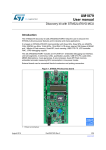
1
Anexo 1: Grafica Distancia VS Voltaje del sensor de ultrasonido. Anexo 2: Plano del EDF55 Anexo 3: Batería de polímero de litio: Turnigy nano-tech A-SPEC G2 2200mah 3S 65~130C Lipo Pack Especificaciones: Capacidad: 2200mAh (mili amperio hora) Voltaje: 3S1P / 3 Celdas / 11.1V Descarga: 65C Constante / 130C Golpe Máximo ratio de carga: 8C Peso: 192g (incluye cables, conector y carcaza) Dimensiones: 103x34x26mm Conector de inspección: JST-XH Conector de descarga: XT60 Connector Anexo 4: Programador de ESC: TURNIGY BESC Programming Card Facilita la programación de la ESC con una serie de indicadores LED. Posee botones para la navegación de las opciones, seleccionar la característica deseada y cambiarla. Simple y más fácil que escuchar los sonidos emitidos por los ESC para la programación. Anexo 5: Electronic Speed Controler (ESC): Q Brain 4 x 25A Brushless Quadcopter ESC 2-4S 3A SBEC Integra 4 ESC en un solo integrado, cada uno controlado por su propia señal de control. Ahorra espacio y peso en la aplicación. Características: - Conveniente todo-en-uno diseño de ESC Salida de 4 x 25 amperios. Protección de bajo voltaje regulable. Completamente programable. Especificaciones: Voltaje de entrada: 7.4~14.8V (2~4S lipoly) Corriente: 25 A x 4 (constante) Corriente de golpe: 30 A x 4 por 10 segundos Tipo de BEC*: conmutación Salida de BEC: 5.25 V @ 3 A Longitud de cable de motor: 250mm Dimensiones: 69x62x11 mm Peso: 112 gramos Este ESC es compatible con la tarjeta de programación Turnigy BESC Programming Card. *Nota: El circuito de eliminación de batería (BEC, por sus siglas en inglés) es un circuito electrónico diseñado para entregar energía eléctrica a otro circuito sin necesidad de una batería. Anexo 6: Cargador de batería: IMAX B6-AC Charger/Discharger 1-6 Cells (GENUINE) Features: •AC 100~240v or 12V DC input •Microprocessor controlled •Delta-peak sensitivity •Individual cell balancing •Li-ion, LiPo and LiFe capable •Ni-Cd and NiMH capable •Large range of charge currents •Store function, allows safe storage current •Time limit function •Input voltage monitoring. (Protects car batteries at the field) •Data storage (Store up to 5 packs in memory) •Battery break in and cycling. ESPECIFICACIONES: Voltaje de operación: …………………………………De 11 a 18 Voltios, Corriente Continua. AC 125 240 voltios 50HZ. Potencia: ……………………………………………….Máxima en Carga: 50 Vatios. Máxima en Descarga: 5 Vatios. Corriente de carga: …………………………………...0.1 a 5 Amperios. Corriente de descarga: ……………………………….0.1 a 1 Amperio. Corriente drenaje para equilibrar baterías LiPos: …300 mAh/célula. Número de células de baterías de NiCd/NiMH: ……1 a 15 células. Número de células de Li-íon/Polímero: …………….1 a 6 en serie. Voltaje para baterías de Plomo: ……………………..2 a 20 Voltios. Peso: ……………………………………………………220 gramos. Dimensiones: ………………………………………….133 x 87 x 33 mm. Anexo 7: Control remoto Futaba 14SG 14-Channel 2.4GHz Computer Radio System 2.4GHz FASSTest Fetures: • Channels: 12 proportional, 2 switched • Compatible with FASSTest, FASST and S-FHSS protocols • FASSTest telemetry – compatible with Futaba telemetry sensors (sold separately) • Free user-updatable software • 30-model memory • 10-character user naming • 10-character model naming • Airplane, helicopter and glider programming • Large, 1.75” x 3” backlit LCD screen with 128 x 64 resolution • SensorTouch™ programming • Compatible with secure digital memory cards for external storage of model setups and software • updates (32MB-2GB or HC (High-Capacity) 4GB-32GB) • Left and right assignable slider switches • Two assignable rotary knobs • Six assignable three-position switches • One assignable momentary two-position switch • One assignable two-position switch • Comfortable rubber grips on the sides and back • Wide top switch spacing • Adjustable stick tension • Dual ball bearing gimbals • 4 vibration warning types • Home/Exit; User Menu/Servo Monitor buttons • Audio earphone jack (for telemetry alarms) • 6V 1800mAh NiMH battery pack • User stick calibration • Trainer system • Servo speed adjust • 5 programmable mixes • V-tail, Ailvator, winglet, motor mixing • Trim mix • Logic switch (condition switch only) • Internal programmer for S.Bus servos • User menu • Servo monitor (neutral and moving tests) • 2 count up/countdown timers • Integral timer • Model timer • Quick model select Anexo 8: Receptor RF R7008SB FASSTest Telemetry Receiver Dimensiones: 24.9 x 47.3 x 14.3 mm Peso: 10.9 gramos Frecuencia: 2.4 GHz Canales: 8 Voltaje de alimentación: 3.7 – 7.4 voltios Anexo 9: Tabla de coeficientes cinéticos y estáticos Superficies en contacto s k Cobre sobre acero 0.53 0.36 Acero sobre acero 0.74 0.57 Aluminio sobre acero 0.61 0.47 Caucho sobre concreto 1.0 0.8 Madera sobre madera 0.25-0.5 0.2 Madera encerada sobre nieve húmeda 0.14 0.1 Teflón sobre teflón 0.04 0.04 Articulaciones sinoviales en humanos 0.01 0.003 Fuente: Serway R. A.. Física. Editorial McGraw-Hill. (1992) Anexo 10: Cálculos de la fuerza de agarre 1) Cuando el móvil se encuentra en una pared 𝑓𝑟 = 𝜇 ∗ 𝑁, 4𝑁 = 𝐹𝑡ℎ, 𝑁= 𝐹𝑡ℎ , 4 4 ∗ 𝑓𝑟 − 𝑤 = 𝑚 ∗ 𝑎, 4 ∗ (𝜇 ∗ 𝑁) − 𝑚 ∗ 𝑔 = 𝑚 ∗ 𝑎, 4 ∗ (𝜇 ∗ 𝐹𝑡ℎ ) − 𝑚 ∗ 𝑔 = 𝑚 ∗ 𝑎, 4 𝐹𝑡ℎ = 𝑚∗𝑎 𝑚∗𝑔 + , 𝜇 𝜇 𝐹𝑡ℎ = 𝑚 ∗ (𝑎 + 𝑔). 𝜇 Reemplazando los valores: m = masa del móvil = 0.750 kg, μ = coeficiente de fricción cinética entre caucho y concreto = 0.8, a = aceleración del móvil = 0.164 m/s2, g = aceleración de la gravedad = 9.81 m/s2, 𝐹𝑡ℎ = 0.750 ∗ (0.164 + 9.81) = 9.35 𝑁. 0.8 La fuerza que de la que se dispone es: 𝐹𝑟𝑒𝑎𝑙 = 4 ∗ 0.490 ∗ 9.81 = 19.23 𝑁. Como Freal > Fth, el agarre del móvil a la pared es posible. Si la masa fuera m = 1kg (0.250 kg adicionales): 𝐹𝑡ℎ = 1 ∗ (0.164 + 9.81) = 12.47 𝑁. 0.8 La nueva fuerza Fth necesaria para adherir el móvil a la pared sigue siendo menor a la suministrada, por ende, adicionarle un sensor de 0.250 kg es posible. 2) Cuando el móvil se encuentra en un techo 𝑤 + 4 ∗ 𝑁 = 𝐹𝑡ℎ, 𝑓𝑟 = 𝜇 ∗ 𝑁, 4 ∗ 𝑓𝑟 = 𝑚 ∗ 𝑎, 𝜇 ∗ (𝐹𝑡ℎ − 𝑚𝑔) = 𝑚𝑎, 𝜇 ∗ 𝐹𝑡ℎ = 𝑚 ∗ (𝑎 + 𝜇 ∗ 𝑔), 𝐹𝑡ℎ = 𝑚 ∗ (𝑎 + 𝜇 ∗ 𝑔). 𝜇 Reemplazando los valores: Reemplazando los valores: m = masa del móvil = 0.750 kg, μ = coeficiente de fricción entre caucho y concreto = 0.8, a = aceleración del móvil = 0.164 m/s2, g = aceleración de la gravedad = 9.81 m/s2, 𝐹𝑡ℎ = 0.750 ∗ (0.164 + 0.8 ∗ 9.81) = 7.51 𝑁. 0.8 La fuerza que de la que se dispone es; 𝐹𝑟𝑒𝑎𝑙 = 4 ∗ 0.490 ∗ 9.81 = 19.23 𝑁, Como Freal > Fth, el agarre del móvil a la pared es posible. Si la masa fuera m = 1kg (0.250 kg adicionales) 𝐹𝑡ℎ = 1 ∗ (0.164 + 0.8 ∗ 9.81) = 10.01 𝑁. 0.8 La nueva fuerza Fth necesaria para adherir el móvil a la pared sigue siendo menor a la suministrada, por ende, adicionarle un sensor de 0.250 kg es posible. Como se puede observar de los resultados, el caso más crítico se presenta cuando el móvil se encuentra en una superficie vertical, pues depende de la fuerza de fricción para su movimiento y su agarre. Anexo 11: Calculo de torque para movimiento de las ruedas Se quiere hallar el torque que el micro motor DC necesita entregar para hacer girar la rueda, y así que el móvil escalador pueda desplazarse. 𝑀 = 𝑓𝑟 ∗ 𝑟 = 𝜇 ∗ 𝐹𝑡ℎ ∗ 𝑟. M = torque del motor DC, fr = friccion de la rueda con el concreto, μ = coeficiente de fricción estático del caucho con concreto = 1 (Ver Anexo 9) Fth = Fuerza del EDF = 0.490 kgf, r = radio de la rueda = 3.5 cm. 𝑀 = (0.490 ∗ 1) ∗ 3.5 = 1.715 𝑘𝑔𝑓 ∗ 𝑐𝑚. Por lo tanto, el torque necesario para girar la rueda a una velocidad constante es 1.7 kgf.cm. Con este dato, se escoje el 298:1 Micro Gearmotor HP, especificado en el documento. Anexo 12: Calculo del torque del servomotor para movimiento de las extremidades Dado que la extremidad se moverá a una velocidad constante, es necesario calcular el torque necesario para cambiar su estado inercial del reposo a imponerle una velocidad. 𝑇 = 𝑇𝑐 + 𝐽𝛼 + 𝑓𝜔. T = toque deseado, Tc = torque de la carga (= 0 N*m), J = momento de inercia respecto al eje de giro (Ixx = 0.402 kg*cm2, dato calculado desde el modelo en Autodesk Inventor 2014), α = aceleración angular, f = coeficiente de rozamiento, ω = velocidad angular. Para la aceleración angular, se requiere que el servomotor gire π/4 radianes en 1 segundo, y que pase del reposo a dicha velocidad angular en 0.09 segundos. Por ende, se tiene que: 𝑟𝑎𝑑 𝜔 0.25𝜋 𝑠 𝑟𝑎𝑑 𝛼= = = 8.73 2 . 𝑡 0.09 𝑠 𝑠 Despreciando el valor de la fricción, se calcula: 𝑇 = (0.404 𝑘𝑔 ∗ 𝑐𝑚 2) 𝑘𝑔 ∗ 𝑐𝑚2 𝑟𝑎𝑑 = 3.53𝑥10−3 𝑘𝑔𝑓 ∗ 𝑐𝑚 . ∗ (8.73 2 ) = 3.53 𝑠2 𝑠 Con este dato, se comprueba que el servomotor elegido (Power HD High-Speed Digital Micro Servo DSM44) brinda el torque necesario (1.2 kgf*cm) para girar la extremidad. Pololu AltIMU-10 v4 Gyro, Accelerometer, Compass, and Altimeter (L3GD20H, LSM303D, and LPS25H Carrier) ©2014 Pololu Corporation www.pololu.com VIN VDD COU1 LDO 3.3V 1 PIU101 COC1 C1 1 uF PIC102 PIC101 PIC202 COC2 C2 PIC201 0.1 uF IN OUT 3 PIU103 ON/OFF NC 2 PIU102 GND 5 PIU105 4 PIU104 PIC302 PIC402 COC3 C3 4.7 uF PIC301 COC4 C4 4.7 uF PIC401 VDD 2 PIU402 NLSDALV SDALV PIU404 SA0 5 PIU405 4 6 PIU406 3 1 2 3 4 5 PIU403 SCL SDA PIJP102 PIJP101 PIJP103 VIN PIC502 PIC501 COC6 C6 0.1 uF PIC602 PIC601 COC7 C7 0.1 uF PIC702 PIC701 COC8 C8 0.1 uF SCL/SPC SDA/SDI/SDO SDO/SA0 CS PIU4010 VDD_IO PIU401 INT1 PIU407 7 RES(GND) 8 GND 9 PIU409 GND VIN PIJP104 VDD PIJP105 PIQ102 VDD 3 COU2 LSM303D COC10 C10 0.22 uF PIC10 2 PIC10 1 2 PIU202 15 PIU2015 COC11 C11 4.7 uF PIC1 02 PIC1 01 SETP PIQ103 SETC C1 PIU2014 Vdd_IO 1 PIU201 PIU204 SDA/SDI/SDO PIU206 SDO/SA0 CS 10 PIU2010 5 PIU205 12 PIU2012 13 PIU2013 16 PIU2016 RES(GND) GND GND GND GND PIR302 COR3 R3 10k PIR301 4 SCLLV SCL/SPC PIR402 PIR401 COR4 R4 10k PIR502 PIR501 2 3 SA0 9 4 PIU304 5 PIU305 8 PIU308 11 PIU209 NLSCL SCL PIQ203 NLSDA SDA COU3 L3GD20H PIU303 8 PIU208 INT2 PIR201 COR2 R2 10k COR5 R5 10k PIU302 7 SA0 PIU207 PIU2011 PIR202 PIQ201 PIQ202 6 SDALV INT1 COR1 R1 10k COQ2 Q2 14 Vdd PIR102 PIR101 COQ1 Q1 VDD PIC902 PIC901 1 PIU408 VDD COC9 C9 0.1 uF 10 VDD PIQ101 PIU203 PIC802 PIC801 VDD COU4 LPS25H NLSCLLV SCLLV COJP1 COC5 C5 1 uF NLSA0 PIJP20SA0 1 COJP2 9 PIU309 10 PIU3010 11 PIU3011 SCL/SPC VDD RES(VDD) SDA/SDI/SDO VDD_IO SDO/SA0 INT1 CS DRDY/INT2 DEN CAP RES(GND) RES(GND) RES(GND) 12 GND 13 PIU3013 GND PIU3012 VDD 16 15 PIU3015 PIU3016 1 PIU301 7 PIU307 6 PIU306 14 PIU3014 PIC1202 PIC1201 C12 COC12 10 nF CARGADORES: iMAX B6 LiPro, ICHARGER IC6, Y E-STATION BC6 Traducción: Tecnocarp INTRODUCION: Gracias por comprar el Cargador Balanceador iMAX B6 LiPro. Este producto es un cargador rápido, con un microprocesador de alto rendimiento, y un software especializado de operación. Por favor lea este manual de instrucciones, completamente y con atención, antes de usar este producto, describe una amplia gama de información, sobre el funcionamiento y de seguridad. O por favor haga uso de este producto, con un conocedor de este Cargador. ESPECIFICACIONES: Voltaje de operación: …………………………………De 11 a 18 Voltios, Corriente Continua. AC 125 240 voltios 50HZ. Potencia: ……………………………………………….Máxima en Carga: 50 Vatios. Máxima en Descarga: 5 Vatios. Corriente de carga: …………………………………...0.1 a 5 Amperios. Corriente de descarga: ……………………………….0.1 a 1 Amperio. Corriente drenaje para equilibrar baterías LiPos: …300 mAh/célula. Número de células de baterías de NiCd/NiMH: ……1 a 15 células. Número de células de Li-íon/Polímero: …………….1 a 6 en serie. Voltaje para baterías de Plomo: ……………………..2 a 20 Voltios. Peso: ……………………………………………………220 gramos. Dimensiones: ………………………………………….133 x 87 x 33 mm. 1 Crumbuino-Mega Infosheet Crumbuino-Mega Arduino-compatible OEM module with ATmega2560 controller and CP2102 USB UART converter. AVAILABLE OPTIONS Module Processor RAM EEPROM Flash Peripherals Crumbuino-Mega ATmega2560 8kB SRAM 4kB EEPROM 256kB Flash - CP2102 USB-UART converter - MAX3221 RS232 transceiver - SN75ALS176 RS485 transceiver - mini USB B 5pin connector - status LED and tiny reset button ARDUINO BOOTLOADER The Crumbuino-Mega module comes preloaded with the Arduino ATmega2560 bootloader. Also actived is the auto-reset function, providing a seamless integration to the Arduino IDE for uploading of a program without the need to reset the module in advance. AUTO RESET FEATURE Jumper J7 (on the bottom of the module) is closed by default, thus enabling the automatic reset of the ATmega2560 by the Arduino IDE before connecting the bootloader and upload a program. USB INTERFACE A USB UART converter CP2102 by Silabs is connected to the MCU's USART0 RXD/PE0 and TXD/PE1. A standard 5pin mini USB B connector is available onboard and allows for easy connection to a host PC. The CP2102 is always powered from USB bus. FEATURES High Performance – 16MHz operating frequency – single 5V power supply Familiar Integrated AVR Peripherals – up to 83 IO pins available – two 8 bit, four 16 bit timer/counter – 4 PWM channels (8 bit resolution) – 12 PWM channels (2 to 16 bit resolution) – input capture and output compare functions – real time clock counter – four programmable UARTs – master/slave SPI interface – two wire interface (I²C comp.) – analog comparator – 16 channel 10 bit ADC – watchdog timer – ISP and JTAG interface Enhanced Onboard Peripherals – CP2102 USB to UART converter at USART0 (PE0, PE1) – MAX3221 RS232 transceiver at USART2 (PH0, PH1) – SN75ALS176 RS485 transceiver at USART3 (PJ0, PJ1, PJ2) – 16MHz XTAL crystal – 32768Hz clock crystal preinstalled – standard 6 pin Atmel AVR ISP connector – status LED (connected to PJ7) Expansion Headers – standard 2.54mm headers with all controller signals and signals from onboard peripherals – auxiliary 3pin screw terminal (connected to RS485 signals for direct cable connection, RS485 signals are also available at pin headers, see below pinout) SCOPE OF DELIVERY This module is being shipped with preloaded Arduino bootloader, mounted 16MHz crystal and a set of headers/receptacles (each 2x 48 pin + ISP header) added to the module separately (not mounted). Crumbuino-Mega © chip45 GmbH & Co. KG • Am Pfad 8 • 35440 Linden • Germany • http://www.chip45.com Better Embedded. Crumbuino-Mega Infosheet BUS INTERFACES USB INTERFACE A USB UART converter CP2102 by Silabs is connected to the MCU's USART0. A standard 5pin mini USB B connector is available onboard and allows for easy connection to a host PC. The CP2102 is always powered from USB bus. The USB driver for the CP2102 is available at http://www.silabs.com/products/interface/usbtouart. RS232 INTERFACE USART2 is connected to an industry standard RS232 transceiver MAX3221. When you want to use the RS232 port, you have to enable it by setting solder jumper J2 to 1-2. If not used, the jumper should be set to 2-3 to fully disable the transceiver. RS232 can be used not only with 5V supply, but with 3.3V supply, too. RS485 INTERFACE USART3 is connected to an industry standard RS485 transceiver SN75ALS176. By closing all four jumpers J3 to J6, the RS485 transceiver is connected to the MCU and to VCC. If not used, all four jumper should be left open. The RS485 is available with 5V supply only. STATUS LED A green low-current status LED is connected low-active to the MCU's signal PJ7, i.e. Arduino Digital Pin 83. Setting this pin to output and low will turn on the LED. ISP CONNECTOR An ISP header with Atmel's standard 6-pin pinout is available on the module, see pictures below for location and pinout. POWER SUPPLY OPTIONS The module can be power either externally (VCC pin on the expansion headers) or from USB bus 5V. J1 selects between these options: • open: external power supply (1.8V – 5.5V) • close: USB bus powered (approx. 5V) ARDUINO PIN MAPPING The Crumbuino-Mega can be used in the Arduino software environment (Arduino IDE) either as Arduino-MEGA 2560 or as Crumbuino-Mega. The next section and picture shows the mapping of the Arduino signal names (Digital Pin xx, Analog Pin yy, etc.) to the Crumbuino-Mega module pins, when used as dedicated Crumbuino-Mega device. If you want to use the module as Crumbuino-Mega in the Arduino IDE, make sure to download the latest Arduino software extension from our homepage (http://download.chip45.com/chip45-arduino-extension.zip) and unzip it into your original Arduino installation. If you want to use the module as Arduino-Mega 2560, you don't have to install anything. The signal / pin mapping is shown in a separate section below. As Arduino-Mega 2560 not all ATmega2560 signals are available as Arduino pin names, since not all of them have been used on the original Arduino-Mega 2560. If you run out of IOs or want a more intuitive pin mapping on the module, you should consider using it as Crumbuino-Mega, see above. Crumbuino-Mega © chip45 GmbH & Co. KG • Am Pfad 8 • 35440 Linden • Germany • http://www.chip45.com Better Embedded. Crumbuino-Mega Infosheet CRUMBUINO-MEGA PIN MAPPING The following table shows the mapping of the Arduino pin names on the Crumbuino-Mega module pins. PHYSICAL DIMENSIONS Values are [mm] unless otherwise noted. PIN CONFIGURATION (ATMEGA2560 SIGNALS) Crumbuino-Mega © chip45 GmbH & Co. KG • Am Pfad 8 • 35440 Linden • Germany • http://www.chip45.com Better Embedded. Crumbuino-Mega Infosheet ATMEGA2560/Crumb2560 ↔ ARDUINO MEGA 2560 PIN MAPPING The following table shows the mapping of the original ATmega2560 pin names from the Atmel data sheet to the pin names of the Arduino development environt when used as Arduino-Mega 2560. For pin location on the module, also check the picture “pin configuration” above. Atmega2560 Pin Name Arduino Pin Name Atmega2560 Pin Name Arduino Pin Name PA7 ( AD7 ) Digital Pin 29 PF7 ( ADC7/PCINT15 ) Analog Pin 7 PA6 ( AD6 ) Digital Pin 28 PF6 ( ADC6/PCINT14 ) Analog Pin 6 PA5 ( AD5 ) Digital Pin 27 PF5 ( ADC5/TMS ) Analog Pin 5 PA4 ( AD4 ) Digital Pin 26 PF4 ( ADC4/TMK ) Analog Pin 4 PA3 ( AD3 ) Digital Pin 25 PF3 ( ADC3 ) Analog Pin 3 PA2 ( AD2 ) Digital Pin 24 PF2 ( ADC2 ) Analog Pin 2 PA1 ( AD1 ) Digital Pin 23 PF1 ( ADC1 ) Analog Pin 1 PA0 ( AD0 ) Digital Pin 22 PF0 ( ADC0 ) Analog Pin 0 PB0 ( SS/PCINT0 ) Digital Pin 53 (PWM)(RX1) PG0 ( WR ) Digital Pin 41 PB1 ( SCK/PCINT1 ) Digital Pin 52 (PWM)(SDA) PG1 ( RD ) Digital Pin 40 PB2 ( MOSI/PCINT2 ) Digital Pin 51 (PWM)(SCL) PG2 ( ALE ) Digital Pin 39 PB3 ( MISO/PCINT3 ) Digital Pin 50 PH0 ( RXD2 ) Digital Pin 17 (PWM) PB4 ( OC2A/PCINT4 ) Digital Pin 10 (PWM) PH1 ( TXD2 ) Digital Pin 16 (PWM) PB5 ( OC1A/PCINT5 ) Digital Pin 11 (PWM) PH2 ( XCK2 ) (TX3) PB6 ( OC1B/PCINT6 ) Digital Pin 12 (PWM) PH3 ( OC4A ) Digital Pin 6 (PWM)(RX3 ) PB7 ( OC0A/OC1C/PCINT7 ) Digital Pin 13 (PWM) PH4 ( OC4B ) Digital Pin 7 (PWM)(TX2) PC0 ( A8 ) Digital Pin 37 PH5 ( OC4C ) Digital Pin 8 (PWM)(RX2 ) PC1 ( A9 ) Digital Pin 36 PH6 ( OC2B ) Digital Pin 9 (PWM)(TX1) PC2 ( A10 ) Digital Pin 35 PH7 ( T4 ) PC3 ( A11 ) Digital Pin 34 PJ0 ( RXD3/PCINT9 ) Digital Pin 15 PC4 ( A12 ) Digital Pin 33 PJ1 ( TXD3/PCINT10 ) Digital Pin 14 PC5 ( A13 ) Digital Pin 32 PJ2 ( XCK3/PCINT11 ) PC6 ( A14 ) Digital Pin 31 PJ3 ( PCINT12 ) PC7 ( A15 ) Digital Pin 30 PJ4 ( PCINT13 ) PD0 ( SCL/INT0 ) Digital Pin 21 (SCL) PJ5 ( PCINT14 ) PD1 ( SDA/INT1 ) Digital Pin 20 (SDA) PJ6 ( PCINT 15 ) PD2 ( RXDI/INT2 ) Digital Pin 19 PK7 ( ADC15/PCINT23 ) Analog Pin 15 PD3 ( TXD1/INT3 ) Digital Pin 18 PK6 ( ADC14/PCINT22 ) Analog Pin 14 PD4 ( ICP1 ) PK5 ( ADC13/PCINT21 ) Analog Pin 13 PD5 ( XCK1 ) PK4 ( ADC12/PCINT20 ) Analog Pin 12 PD6 ( T1 ) PK3 ( ADC11/PCINT19 ) Analog Pin 11 PD7 ( T0 ) Digital Pin 38 PK2 ( ADC10/PCINT18 ) Analog Pin 10 PE0 ( RXD0/PCINT8 ) Digital Pin 0 (PWM) (RX0) PK1 ( ADC9/PCINT17 ) Analog Pin 9 PE1 ( TXD0 ) Digital Pin 1 (PWM) (TX0) PK0 ( ADC8/PCINT16 ) Analog Pin 8 PE3 ( OC3A/AIN1 ) Digital Pin 5 (PWM) AREF Analog Reference PE4 ( OC3B/INT4 ) Digital Pin 2 (PWM) GND GND PE5 ( OC3C/INT5 ) Digital Pin 3 (PWM) AVCC VCC RESET RESET PE2 ( XCK0/AIN0 ) PE6 ( T3/INT6 ) PE7 ( CLKO/ICP3/INT7 ) Crumbuino-Mega © chip45 GmbH & Co. KG • Am Pfad 8 • 35440 Linden • Germany • http://www.chip45.com Better Embedded. Crumbuino-Mega Infosheet OPERATING CHARACTERISTICS Symbol Parameter Condition Min Vcc Supply Voltage 16 MHz 4.5 Icc Power Supply Current Active 16MHz Vcc = 5V 22 mA USB bus active +26 mA (Icc strongly depends on CPU activity, like frequency, power saving modes, etc. as well as external circuitry, io pin input and output current, etc. The values denoted here are for reference only and can differ from final application vallues.) T Typ Max Units 5.5 V (power is drawn from USB bus) Operating Temperature (industrial temperature range on request) -20 +70 °C DESIGN AND HANDLING GUIDELINES This module – just like any other semiconductor devices – is susceptible to damage by ESD. Suitable precautions should be taken when handling and transporting devices. The possible damage to devices depends on the circumstances of the handling and transporting, and the nature of the device. The extent of damage can vary from immediate functional or parametric malfunction to degradation of function or performance in use over time. Devices suspected of being affected should be replaced. DEVELOPMENT TOOLS As an Arduino-compatible module, the Crumbuino-Mega is indendet to be used with the Arduino IDE as development environment. – – – Arduino Homepage: Getting Started Page: Arduino Software Page: http://arduino.cc/en/ http://arduino.cc/en/Guide/HomePage http://arduino.cc/en/Main/Software – chip45 Arduino Extensions: http://download.chip45.com/chip45-arduino-extension.zip – Crumbuino-Mega LED blink example sketch: http://download.chip45.com/Blink_Crumbuino-Mega.zip WHAT ELSE DO YOU NEED? The only thing you really need, is a USB cable to connect the Crumbuino-Mega to a PC or Mac: – Cable mini-USB-B to USB-A: Crumbuino-Mega http://go.chip45.com/KAB-USB-A-miniB-1.5 © chip45 GmbH & Co. KG • Am Pfad 8 • 35440 Linden • Germany • http://www.chip45.com Better Embedded. Crumbuino-Mega Infosheet Declaration of Electro Magnetic Conformity of the CHIP45 „Crumbuino-2560“ CHIP45 embedded microcontroller modules (henceforce products) are designed for installation in electrical appliances or as dedicated evaluation boards (i.e.: for use as a test and prototype platform for hardware/software development) in laboratory environments. Caution: CHIP45 products lacking protective enclosures are subject to damage by ESD and, hence, may only be unpacked, handled or operated in environments in which sufficient precautionary measures have been taken in respect to ESD-dangers. It is also necessary that only appropriately trained personnel (such as electricians, technicians and engineers) handle and/or operate these products. Moreover, CHIP45 products should not be operated without protection circuitry if connections to the product's pin header rows are longer than 3m. CHIP45 products fulfill the norms of European Union's Directive for Electro Magnetic Conformity only in accordance to the descriptions and rules of usage indicated in this document (particularly in respect to the pin header row connectors, power connector and serial interface to a host-PC). Implementation of CHIP45 products into target devices, as well as user modifications and extensions of CHIP45 products, is subject to renewed establishment of conformity to, and certification of, Electro Magnetic Directives. Users should ensure conformance following any modifications to the products as well as implementation of the products into target systems DISCLAIMER In this manual are descriptions for copyrighted products that are not explicitly indicated as such. The absence of the trademark (™) and copyright (©) symbols does not imply that a product is not protected. Additionally, registered patents and trademarks are similarly not expressly indicated in this manual. The information in this document has been carefully checked and is believed to be entirely reliable. However, chip45 GmbH & Co. KG assumes no responsibility for any inaccuracies. chip45 GmbH & Co. KG neither gives any guarantee nor accepts any liability whatsoever for consequential damages resulting from the use of this manual or its associated product. chip45 GmbH & Co. KG reserves the right to alter the information contained herein without prior notification and accepts no responsibility for any damages which might result. Additionally, chip45 GmbH & Co. KG offers no guarantee nor accepts any liability for damages arising from the improper usage or improper installation of the hardware or software. chip45 GmbH & Co. KG further reserves the right to alter the layout and/or design of the hardware without prior notification and accepts no liability for doing so. © Copyright 2011 chip45 GmbH & Co. KG, D-35440 Linden. Rights - including those of translation, reprint, broadcast, photomechanical or similar reproduction and storage or processing in computer systems, in whole or in part - are reserved. No reproduction may occur without the express written consent from chip45 GmbH & Co. KG. CONTACT INFORMATION Address: chip45 GmbH & Co. KG Am Pfad 8 D-35440 Linden Germany Ordering Information: +49 (6403) 9299-406 [email protected] Technical Support: +49 (6403) 9299-406 [email protected] Fax: +49 (6403) 9253-50 Web Site: http://www.chip45.com Crumbuino-Mega © chip45 GmbH & Co. KG • Am Pfad 8 • 35440 Linden • Germany • http://www.chip45.com Better Embedded. 1. 使用環境條件 : Apply Environmental Condition 项目 item No. 1-1 保存溫度 -20 Storage Temperature Range 1-2 操作溫度 ℃~50℃ -10 Operating Temperature Range 1-3 ℃~60℃ 规格 standard 操作電壓 4.8V~6.0V Operating Voltage Range 2. 測試環境 : Standard Test Environment 每一个检查必须是正常的温度和湿度进行测量,温 度 25 ± 5℃,相对湿度 65 ± 10%,在按照本规范的 标准测试条件下判断特征。 2-1 測試環境 Standard Test Environment Every characteristic of the inspect must be normal temperature and humidity carry out the test , temperature 25±5 and relative % humidity 65±10 of judgment made in accordance with this specification standard testing conditions. 3. 外觀檢查 : Appearance Inspection 项目 item No. 3-1 尺寸见附件 外觀尺寸 Dimension see the attachment Outline Drawing 3-2 规格 standard 无损坏,不允许影响功能 外觀 No damage which affects functions allowed Appearance Product Name 数字伺服器 数字伺服器 Digital Servo Model No. DSM44 Version V1 Page 1/3 4. 電氣特性 : Electrical Specification (Function of the Performance) 项目 item No. 4-1 4.8V 0° 空載轉速 0° 0.09 sec/6 0.07 sec/6 <100 mA <100 mA 1.2 kg-cm 1.6 kg-cm 600 mA 700 mA <50 mA <50 mA Operating speed (at no load) 4 2 6.0V 空載電流 Running current (at no load) 4-3 停止扭力 Stall torque (at locked) 4-4 停止電流 Stall current (at locked) 4-5 待機電流 Idle current (at stopped) 4-2 定义平均值时,伺服器无负荷运行 Note: Item 4-2 definition is average value when the servo running with no load 注:项目 5. 機械特性 : Mechanical Specification 项目 item No. 5-1 外觀尺寸 Overall Dimensions 5-2 機構極限角度 Limit angle 5-3 重量 规格 standard 见附件 See the drawing ° ° 180 ± 10 5.8 ± 0.2 (grams without servo horn) Weight 5-4 導線規格 Connector wire gauge 5-5 導線長度 OD0.8mm/16 x 0.08mm 3p x 160mm "J" type 160 ± 5 mm Connector wire length 5-6 舵片規格 5-7 舵片種類 Cross , Disk, Double Flat Horn type 5-8 ψ 十字,圆盘,条型 25T/ 5.77 Horn gear spline 減速比 1/400 Reduction ratio Product Name 数字伺服器 数字伺服器 Model No. Digital Servo DSM44 Version V1 Page 2/3 6. 控制特性 : Control Specification 项目 No. 6-1 控制系統 Control system 6-2 放大器種類 Amplifier type 6-3 操作角度 改变脉冲宽度 Pulse Width Modification 数字控制器 Digital Controller ° (在 1000→2000 μsec) 90 Operating travel 6-4 中立位置 Neutral position 6-5 脈波訊號虛位 Dead band width 6-6 旋轉方向 Rotating direction 6-7 脈波寬度範圍 Pulse width range 6-8 可作動角度範圍 Maximum travel Product Name 规格 1500 μsec 4 μsec 顺时针 (在 1500→2000 μsec) Counterclockwise (when1500→2000 μsec) 900→2100 μsec 大约 125°(when900→2100 μsec) Approx 125°(when900→2100 μsec) 数字伺服 数字伺服 Digital Servo Model No. DSM44 Version V1 Page 3/3 DRV8833 www.ti.com SLVSAR1C – JANUARY 2011 – REVISED JANUARY 2013 DUAL H-BRIDGE MOTOR DRIVER Check for Samples: DRV8833 FEATURES 1 • 2 • • Dual-H-Bridge Current-Control Motor Driver – Capable of Driving Two DC Motors or One Stepper Motor – Low MOSFET On-Resistance: HS + LS 360 mΩ Output Current (at VM = 5 V, 25°C) – 1.5-A RMS, 2-A Peak per H-Bridge in PWP and RTY Package Options – 500-mA RMS, 2-A Peak per H-Bridge in PW Package Option Outputs Can Be Paralleled for – 3-A RMS, 4-A Peak (PWP and RTY) – 1-A RMS, 4-A Peak (PW) • • • Wide Power Supply Voltage Range: 2.7 V – 10.8 V PWM Winding Current Regulation/Limiting Thermally Enhanced Surface Mount Packages (PWP and RTY) APPLICATIONS • • • • • • Battery-Powered Toys POS Printers Video Security Cameras Office Automation Machines Gaming Machines Robotics DESCRIPTION The DRV8833 provides a dual bridge motor driver solution for toys, printers, and other mechatronic applications. The device has two H-bridge drivers, and can drive two DC brush motors, a bipolar stepper motor, solenoids, or other inductive loads. The output driver block of each H-bridge consists of N-channel power MOSFET’s configured as an H-bridge to drive the motor windings. Each H-bridge includes circuitry to regulate or limit the winding current. Internal shutdown functions with a fault output pin are provided for over current protection, short circuit protection, under voltage lockout and overtemperature. A low-power sleep mode is also provided. The DRV8833 is packaged in a 16-pin HTSSOP or QFN package with PowerPAD™ (Eco-friendly: RoHS & no Sb/Br) as well as a 16-pin TSSOP package. ORDERING INFORMATION (1) ORDERABLE PART NUMBER PACKAGE (2) PowerPAD™ (HTSSOP) - PWP (TSSOP) - PW PowerPAD™ (QFN) - RTY (1) (2) Reel of 2000 DRV8833PWPR Tube of 90 DRV8833PWP Reel of 2000 DRV8833PWR Tube of 90 DRV8833PW Reel of 3000 DRV8833RTYR Reel of 250 DRV8833RTYT TOP-SIDE MARKING DRV8833 8833PW DRV8833 For the most current packaging and ordering information, see the Package Option Addendum at the end of this document, or see the TI web site at www.ti.com. Package drawings, thermal data, and symbolization are available at www.ti.com/packaging. 1 2 Please be aware that an important notice concerning availability, standard warranty, and use in critical applications of Texas Instruments semiconductor products and disclaimers thereto appears at the end of this data sheet. PowerPAD is a trademark of Texas Instruments. PRODUCTION DATA information is current as of publication date. Products conform to specifications per the terms of the Texas Instruments standard warranty. Production processing does not necessarily include testing of all parameters. Copyright © 2011–2013, Texas Instruments Incorporated DRV8833 www.ti.com SLVSAR1C – JANUARY 2011 – REVISED JANUARY 2013 Table 1. TERMINAL FUNCTIONS PIN (RTY) I/O (1) 13 PPAD (PWP only) 11 PPAD - Device ground Both the GND pin and device PowerPAD must be connected to ground VM 12 10 - Device power supply Connect to motor supply. A 10-µF (minimum) ceramic bypass capacitor to GND is recommended. VINT 14 12 - Internal supply bypass Bypass to GND with 2.2-μF, 6.3-V capacitor VCP 11 9 IO High-side gate drive voltage Connect a 0.01-μF, 16-V (minimum) X7R ceramic capacitor to VM AIN1 16 14 I Bridge A input 1 Logic input controls state of AOUT1. Internal pulldown. AIN2 15 13 I Bridge A input 2 Logic input controls state of AOUT2. Internal pulldown. BIN1 9 7 I Bridge B input 1 Logic input controls state of BOUT1. Internal pulldown. BIN2 10 8 I Bridge B input 2 Logic input controls state of BOUT2. Internal pulldown. nSLEEP 1 15 I Sleep mode input Logic high to enable device, logic low to enter low-power sleep mode and reset all internal logic. Internal pulldown. 8 6 OD Fault output Logic low when in fault condition (overtemp, overcurrent) AISEN 3 1 IO Bridge A ground / Isense Connect to current sense resistor for bridge A, or GND if current control not needed BISEN 6 4 IO Bridge B ground / Isense Connect to current sense resistor for bridge B, or GND if current control not needed AOUT1 2 16 O Bridge A output 1 AOUT2 4 2 O Bridge A output 2 BOUT1 7 5 O Bridge B output 1 BOUT2 5 3 O Bridge B output 2 NAME PIN (PWP or PW) EXTERNAL COMPONENTS OR CONNECTIONS DESCRIPTION POWER AND GROUND GND CONTROL STATUS nFAULT OUTPUT (1) Connect to motor winding A Connect to motor winding B Directions: I = input, O = output, OZ = tri-state output, OD = open-drain output, IO = input/output Submit Documentation Feedback Copyright © 2011–2013, Texas Instruments Incorporated Product Folder Links: DRV8833 3 DRV8833 SLVSAR1C – JANUARY 2011 – REVISED JANUARY 2013 www.ti.com ELECTRICAL CHARACTERISTICS TA = 25°C (unless otherwise noted) PARAMETER TEST CONDITIONS MIN TYP MAX UNIT POWER SUPPLY IVM VM operating supply current VM = 5 V, xIN1 = 0 V, xIN2 = 0 V 1.7 3 mA IVMQ VM sleep mode supply current VM = 5 V 1.6 2.5 μA VUVLO VM undervoltage lockout voltage VM falling 2.6 V VHYS VM undervoltage lockout hysteresis 90 mV LOGIC-LEVEL INPUTS VIL Input low voltage VIH Input high voltage VHYS Input hysteresis RPD Input pull-down resistance IIL Input low current IIH Input high current tDEG Input deglitch time nSLEEP 0.5 All other pins 0.7 nSLEEP All other pins 2.5 V 2 0.4 nSLEEP 500 All except nSLEEP 150 VIN = 0 V kΩ 1 VIN = 3.3 V, nSLEEP VIN = 3.3 V, all except nSLEEP V 6.6 13 16.5 33 450 μA μA ns nFAULT OUTPUT (OPEN-DRAIN OUTPUT) VOL Output low voltage IO = 5 mA IOH Output high leakage current VO = 3.3 V 0.5 V 1 μA H-BRIDGE FETS VM = 5 V, I O = 500 mA, TJ = 25°C HS FET on resistance 200 VM = 5 V, IO = 500 mA, TJ = 85°C 325 VM = 2.7 V, I O = 500 mA, TJ = 25°C 250 VM = 2.7 V, IO = 500 mA, TJ = 85°C RDS(ON) 350 VM = 5 V, I O = 500 mA, TJ = 25°C LS FET on resistance 160 VM = 5 V, IO = 500 mA, TJ = 85°C 275 VM = 2.7 V, I O = 500 mA, TJ = 25°C 200 VM = 2.7 V, IO = 500 mA, TJ = 85°C IOFF Off-state leakage current VM = 5 V, TJ = 25°C, VOUT = 0 V mΩ 300 –1 1 μA MOTOR DRIVER fPWM Current control PWM frequency Internal PWM frequency 50 kHz tR Rise time VM = 5 V, 16 Ω to GND, 10% to 90% VM 180 ns tF Fall time VM = 5 V, 16 Ω to GND, 10% to 90% VM 160 ns tPROP Propagation delay INx to OUTx VM = 5 V 1.1 µs tDEAD Dead time (1) VM = 5 V 450 ns PROTECTION CIRCUITS IOCP Overcurrent protection trip level 3.3 A tDEG OCP Deglitch time 2.25 µs tOCP Overcurrent protection period 1.35 ms tTSD Thermal shutdown temperature (1) 6 2 Die temperature 150 160 180 °C Internal dead time. External implementation is not necessary. Submit Documentation Feedback Copyright © 2011–2013, Texas Instruments Incorporated Product Folder Links: DRV8833 L3GD20H MEMS motion sensor: three-axis digital output gyroscope Datasheet - production data Applications • Gaming and virtual reality input devices • Motion control with MMI (man-machine interface) • GPS navigation systems • Appliances and robotics LGA-16 (3x3x1 mm) Description Features The L3GD20H is a low-power three-axis angular rate sensor. • Wide supply voltage, 2.2 V to 3.6 V • Wide extended operating temperature range (from -40 °C to 85 °C) • Low voltage compatible IOs, 1.8 V • Low power consumption It includes a sensing element and an IC interface able to provide the measured angular rate to the external world through digital interface (I2C/SPI). The sensing element is manufactured using a dedicated micromachining process developed by ST to produce inertial sensors and actuators on silicon wafers. • Embedded power-down • Sleep mode • Fast turn-on and wake-up • Three selectable full scales up to 2000 dps • 16 bit rate value data output • 8 bit temperature data output • I2C/SPI digital output interface • 2 dedicated lines (1 interrupt, 1 data ready) • User enable integrated high-pass filters • Embedded temperature sensor • Embedded 32 levels of 16 bit data output FIFO • High shock survivability The IC interface is manufactured using a CMOS process that allows a high level of integration to design a dedicated circuit which is trimmed to better match the sensing element characteristics. The L3GD20H has a full scale of ±245/±500/±2000 dps and is capable of measuring rates with a user selectable bandwidth. The L3GD20H is available in a plastic land grid array (LGA) package and can operate within a temperature range from -40 °C to +85 °C. • ECOPACK® RoHS and “Green” compliant Table 1. Device summary Order code Temperature range (°C) Package Packing L3GD20H -40 to +85 LGA-16 (3x3x1) Tray L3GD20HTR -40 to +85 LGA-16 (3x3x1) Tape and reel March 2013 This is information on a product in full production. DocID023469 Rev 2 1/52 www.st.com 52 Block diagram and pin description 1 L3GD20H Block diagram and pin description Figure 1. Block diagram +Ω x,y,z X+ CHARGE AMP Y+ MIXER LOW-PASS FILTER D I G I T A L Z+ Z- A D C 1 M U X YX- T E M P E R A T U R E DRIVING MASS Feedback loop REFERENCE TRIMMING CIRCUITS FIFO S E N S O R F I L T E R I N G I2C SPI CS SCL/SPC SDA/SDI/SDO SDO/SA0 A D C 2 CONTROL LOGIC & INTERRUPT GEN. CLOCK & PHASE GENERATOR INT1 DEN DRDY/INT2 AM12689V1 The vibration of the structure is maintained by a drive circuitry in a feedback loop. The sensing signal is filtered and appears as digital signal at the output. 1.1 Pin description +Ω 14 Y GND GND RES RES RES X (TOP VIEW) DIRECTIONS OF THE DETECTABLE ANGULAR RATE Vdd Cap +Ω 16 13 1 BOTTOM VIEW 9 5 8 Vdd_IO SCL/SPC SDA/SDI/SDO SDO/SA0 CS 6 DRDY/INT2 X INT1 1 Z DEN +Ω RES Figure 2. Pin connection AM12690V1 8/52 DocID023469 Rev 2 L3GD20H 2.2 Mechanical and electrical specifications Electrical characteristics @ Vdd =3.0 V, T=25 °C unless otherwise noted(b). Table 4. Electrical characteristics Symbol Vdd Vdd_IO Idd Parameter Test condition Supply voltage I/O pins supply voltage (2) Min. Typ.(1) Max. Unit 2.2 3.0 3.6 V Vdd+0.1 V 1.71 Supply current 5.0 mA IddSL Supply current in sleep mode(3) Selectable by digital interface 2.5 mA IddPdn Supply current in powerdown mode Selectable by digital interface 1 μA VIH Digital high level input voltage VIL Digital low level input voltage Ton Turn-on time(4) Top Operating temperature range 0.8*Vdd_I O V 0.2*Vdd_I O LPF2 disabled ODR = 190 Hz 50 -40 V ms +85 °C 1. Typical specifications are not guaranteed. 2. It is possible to remove Vdd maintaining Vdd_IO without blocking the communication busses, in this condition the measurement chain is powered off. 3. Sleep mode introduces a faster turn-on time related to power down mode. 4. Time to obtain stable sensitivity (within ±5% of final value) after exiting power-down mode. It is guaranteed by design. b. The product is factory calibrated at 3.0 V. DocID023469 Rev 2 11/52 L3GD20H Application hints Figure 5. L3GD20H electrical connections and external components values +Ω 1 Z X Vdd +Ω 100nF Y 10nF(25V)* C1 GND 10µF GND +Ω X 16 Vdd_IO 14 1 (TOP VIEW) DIRECTIONS OF THE DETECTABLE ANGULAR RATES 13 SCL/SPC SDA/SDI/SDO TOP VIEW SDO CS 9 5 100nF 8 6 DEN INT1 GND DRDY/INT2 3 Application hints GND * C1 must guarantee 1nF value under 12V bias condition Vdd I2C bus Rpu Rpu = 10kOhm SCL/SPC SDA_SDI_SDO Pull-up to be added when I2C interface is used GAMS080220130927FSR Power supply decoupling capacitors (100 nF + 10 μF) should be placed as near as possible to the device (common design practice). If Vdd and Vdd_IO are not connected together, 100 nF and 10 μF decoupling capacitors must be placed between Vdd and common ground while 100 nF between Vdd_IO and common ground. Capacitors should be placed as near as possible to the device (common design practice). DocID023469 Rev 2 17/52 LPS25H MEMS pressure sensor: 260-1260 hPa absolute digital output barometer Datasheet - production data Applications Altimeter and barometer for portable devices GPS applications Weather Station Equipment Sport Watches Description HCLGA-10L (2.5 x 2.5 x 1.0 mm) The LPS25H is an ultra compact absolute piezoresistive pressure sensor. It includes a monolithic sensing element and an IC interface able to take the information from the sensing element and to provide a digital signal to the external world. Features 260 to 1260 hPa absolute pressure range High-resolution mode: 1 Pa RMS Low power consumption: – Low resolution mode: 4 µA – High resolution mode: 25 µA High overpressure capability: 20x full scale Embedded temperature compensation Embedded 24-bit ADC The sensing element consists of a suspended membrane realized inside a single mono-silicon substrate. It is capable to detect the absolute pressure and is manufactured with a dedicated process developed by ST. The membrane is very small compared to the traditionally built silicon micromachined membranes. Membrane breakage is prevented by an intrinsic mechanical stopper. The IC interface is manufactured using a standard CMOS process that allows a high level of integration to design a dedicated circuit which is trimmed to better match the sensing element characteristics. Selectable ODR from 1 Hz to 25 Hz SPI and I²C interfaces Embedded FIFO Supply voltage: 1.7 to 3.6 V The LPS25H is available in a cavity holed LGA package (HCLGA). It is guaranteed to operate over a temperature range extending from -30 °C to +105 °C. The package is holed to allow external pressure to reach the sensing element. High shock survivability: 10,000 g Small and thin package ECOPACK® lead-free compliant Table 1. Device summary Order codes Temperature range [°C] Package Packing HCLGA-10L HCLGA-10L Tape and reel -30 to +105 LPS25HTR LPS25H January 2014 This is information on a product in full production. DocID023722 Rev 3 Tray 1/46 www.st.com LPS25H Mechanical and electrical specifications 2 Mechanical and electrical specifications 2.1 Mechanical characteristics VDD = 2.5 V, T = 25 °C, unless otherwise noted. Table 3. Mechanical characteristics Symbol Parameter Test condition Min. Typ.(1) Max. Unit -30 105 °C Top Operating temperature range Tfull Full accuracy temperature range 0 80 °C Pop Operating pressure range 260 1260 hPa Pbits Pressure output data Psens Pressure sensitivity Paccrel Relative accuracy over pressure(2) PaccT Pnoise Absolute accuracy pressure over temperature(3) Pressure noise(4) 24 bits 4096 LSB/ hPa P = 800 to 1100 hPa T = 25°C 0.1 hPa P = 260 to 1260 hPa T = 20 +60 °C 0.2 P = 260 to 1260 hPa T = 0 +80 °C ±1 without embedded filtering 0.03 with embedded filtering 0.01 hPa hPa RMS Tbits Temperature output data 16 bits Tsens Temperature sensitivity 480 LSB/°C Tacc Absolute accuracy temperature T= 0 ~ +65 °C 2 °C 1. Typical specifications are not guaranteed. 2. Characterization data. Parameter not tested at final test 3. Embedded quadratic compensation. 4. Pressure noise RMS evalueted in a controlled environment,based on the average standard deviation of 32 measurements at highest ODR. DocID023722 Rev 3 7/46 46 Mechanical and electrical specifications 2.2 LPS25H Electrical characteristics VDD = 2.5 V, T = 25 °C, unless otherwise noted. Table 4. Electrical characteristics Symbol VDD Parameter Test condition Supply voltage VDD_IO IO supply voltage Idd IddPdn Max. Unit 1.7 3.6 V 1.7 3.6 V Supply current @ ODR 1 Hz, highest resolution 25 µA Supply current in power-down mode T = 25 °C 0.5 µA 1. Typical specifications are not guaranteed. 8/46 Min. Typ.(1) DocID023722 Rev 3 Application hints 4 LPS25H Application hints Figure 5. LPS25H electrical connection VDD C1 C2 4.7 µF GND 100 µF VDD_IO GND VDD GND GND VDD GND 10 9 8 1 7 INT 1 6 CS TOP VIEW 3 4 5 SDA/SDI/SDO SDO/SAO 2 RES SCL/SPC GND The device core is supplied through the VDD line. Power supply decoupling capacitors (100 nF, 4.7 µF) should be placed as near as possible to the supply pad of the device (common design practice). The functionality of the device and the measured data outputs are selectable and accessible through the I²C/SPI interface. When using the I²C, CS must be tied high (i.e. connected to VDD_IO). 4.1 Soldering information The HCLGA package is compliant with the ECOPACK® standard and it is qualified for soldering heat resistance according to JEDEC J-STD-020. 14/46 DocID023722 Rev 3 LSM303D Ultra compact high performance e-Compass 3D accelerometer and 3D magnetometer module Datasheet — preliminary data Features ■ 3 magnetic field channels and 3 acceleration channels ■ ±2/±4/±8/±12 gauss dynamically selectable magnetic full-scale ■ ±2/±4/±6/±8/±16 g dynamically selectable linear acceleration full-scale ■ 16-bit data output ■ SPI / I2C serial interfaces ■ Analog supply voltage 2.16 V to 3.6 V ■ Power-down mode / low-power mode ■ Programmable interrupt generators for freefall, motion detection and magnetic field detection Description ■ Embedded temperature sensor ■ Embedded FIFO ■ ECOPACK®, RoHS and “Green” compliant Applications The LSM303D is a system-in-package featuring a 3D digital linear acceleration sensor and a 3D digital magnetic sensor. The LSM303D has linear acceleration full-scales of ±2g / ±4g / ±6g / ±8g / ±16g and a magnetic field full-scale of ±2 / ±4 / ±8 / ±12 gauss. All fullscales available are fully selectable by the user. The LSM303D includes an I2C serial bus interface that supports standard and fast mode 100 kHz and 400 kHz and SPI serial standard interface. The system can be configured to generate an interrupt signal for free-fall, motion detection and magnetic field detection. Thresholds and timing of interrupt generators are programmable by the end user on the fly. ■ Tilt compensated compass ■ Map rotation ■ Position detection ■ Motion activated functions ■ Free-fall detection ■ Click/double click recognition ■ Pedometer ■ Intelligent power saving for handheld devices ■ Display orientation ■ Gaming and virtual reality input devices ■ Impact recognition and logging ■ Vibration monitoring and compensation June 2012 LGA-16 (3x3x1 mm) Magnetic and accelerometer parts can be enabled or put into power-down mode separately. The LSM303D is available in plastic land grid array package (LGA) and is guaranteed to operate over an extended temperature range from -40 °C to +85 °C. Table 1. Device summary Part number Temperature Package Packaging range [°C] LSM303D -40 to +85 LGA-16 Tray LSM303DTR -40 to +85 LGA-16 Tape and reel Doc ID 023312 Rev 1 This is preliminary information on a new product now in development or undergoing evaluation. Details are subject to change without notice. 1/54 www.st.com 54 Block diagram and pin description LSM303D 1 Block diagram and pin description 1.1 Block diagram Figure 1. Block diagram Sensing Block Sensing Interface Control Logic A/D converter X+ Y+ CHARGE AMPLIFIER Z+ I (a) + CS MUX - SCL/SPC DI SPI / I2C ZYX- SDA/SDI/SDO SDO/SA0 X+ INT1 CHARGE AMPLIFIER Y+ Z+ I (M) INT2 + MUX ZYX- INTERRUPT GEN. FIFO REFERENCE TRIMMING CIRCUITS OFFSET CIRCUITS BUILT-IN SET/RESET CIRCUITS CLOCK TEMPERATURE SENSOR AM12676V1 1.2 Pin description Figure 2. Pin connection Z X DIRECTION OF DETECTABLE ACCELERATIONS Pin 1 indicator 13 1 9 5 Y TOP VIEW Z X 1 (BOTTOM VIEW) DIRECTION OF DETECTABLE MAGNETIC FIELDS Y TOP VIEW AM12677V1 8/54 Doc ID 023312 Rev 1 Module specifications 2.3 LSM303D Electrical characteristics @ Vdd = 2.5 V, T = 25 °C unless otherwise noted. Table 5. Symbol Electrical characteristics Test conditions Parameter Min. Vdd Supply voltage 2.16 Vdd_IO Module power supply for I/O 1.71 Idd eCompass(2) current consumption in normal mode(3) IddSL Current consumption in power-down(4) Top Operating temperature range LR setting CTRL5 (M_RES [1,0]) = 00b, see Table 45 -40 Typ.(1) 1.8 Max. Unit 3.6 V Vdd+0.1 300 µA 1 µA +85 1. Typical specifications are not guaranteed. 2. eCompass: accelerometer - magnetic sensor. 3. Magnetic sensor setting ODR =6.25 Hz, accelerometer sensor ODR = 50 Hz and magnetic high resolution setting. 4. Linear accelerometer and magnetic sensor in power-down mode. 12/54 Doc ID 023312 Rev 1 °C LSM303D 2.5 Module specifications Absolute maximum ratings Stresses above those listed as “absolute maximum ratings” may cause permanent damage to the device. This is a stress rating only and functional operation of the device under these conditions is not implied. Exposure to maximum rating conditions for extended periods may affect device reliability. Table 8. Absolute maximum ratings Symbol Vdd Vdd_IO Vin Note: Ratings Maximum value Unit Supply voltage -0.3 to 4.8 V I/O pins supply voltage -0.3 to 4.8 V -0.3 to Vdd_IO +0.3 V 3,000 for 0.5 ms g 10,000 for 0.1 ms g 3,000 for 0.5 ms g 10,000 for 0.1 ms g Input voltage on any control pin (SCL/SPC, SDA/SDI/SDO, SDO/SA0, CS) APOW Acceleration (any axis, powered, Vdd = 2.5 V) AUNP Acceleration (any axis, unpowered) TOP Operating temperature range -40 to +85 °C TSTG Storage temperature range -40 to +125 °C Supply voltage on any pin should never exceed 4.8 V. This is a mechanical shock sensitive device, improper handling can cause permanent damage to the part This is an ESD sensitive device, improper handling can cause permanent damage to the part Doc ID 023312 Rev 1 15/54 LSM303D 5 Application hints Application hints Figure 5. LSM303D electrical connection Vdd C1= 4.7µF C3= 10µF 16 Vdd_IO 14 1 C2=0.22µF 13 TOP VIEW INT 1 C4 = 100nF 9 5 SDO/SA0 SDA/SDI/SDO SCL/SPC INT 2 CS 8 6 GND Digital signal from/to signal controller. Signal’s levels are defined by proper selection of Vdd_IO AM12678V1 5.1 External capacitors The C1 and C2 external capacitors should be low SR value ceramic type construction (typ. suggested value 200 mΩ). Reservoir capacitor C1 is nominally 4.7 µF in capacitance, with the set/reset capacitor C2 nominally 0.22 µF in capacitance. The device core is supplied through the Vdd line. Power supply decoupling capacitors (C4=100 nF ceramic, C3=10 µF Al) should be placed as near as possible to the supply pin of the device (common design practice). All the voltage and ground supplies must be present at the same time to have proper behavior of the IC (refer to Figure 5). The functionality of the device and the measured acceleration/magnetic field data is selectable and accessible through the I2C/SPI interfaces. The functions, the threshold and the timing of the two interrupt pins (INT1 and INT2) can be completely programmed by the user through the I2C/SPI interfaces. 5.2 Pull-up resistors If an I2C interface is used, pull-up resistors (suggested value 10 kΩ) must be placed on the two I2C bus lines. Doc ID 023312 Rev 1 19/54 Lima 31 de Octubre de 2014 SOLICITUD DE COTIZACIÓN Estimado Jose Alvarado Ref. Impresión 3d de piezas en plástico ABS Lima.- NOMBRE / EMPRESA Jose Alvarado PIEZA Cuerpo frontal Cuerpo trasero Extremidad Pin Pin EDF TOTAL S/. 76.1 S/. 43.51 S/. 32 S/. 2 S/. 0.50 MATERIAL / IMPRESORA MAKER/ABS MAKER/ABS MAKER/ABS MAKER/ABS MAKER/ABS Montos expresados en nuevos soles (PEN), no incluye IGV. Forma de pago - Adelantado - Tesorería de la Pontificia Universidad Católica del Perú Atentamente, Jennifer Wong Poggi Responsable del área de impresión 3D Pontificia Universidad Católica del Perú Pontificia Universidad Católica del Perú | Av. Universitaria 1801, San Miguel, Lima 32, Perú | Teléfono (511) 626-2000 Anexo 3945 | Correo: [email protected]