1
ME-33
May. 2001
SERVICE NOTES
First Edition
Issued by RJA
SPECIFICATIONS
主な仕様
ME-33: Guitar Multiple Effects
ME-33:ギター・マルチプル・エフェクツ
• AD Conversion
AF Method (*)
● AD 変換
AF 方式(※)
• DA Conversion
Method 24-bit DAC
● DA 変換
ΔΣ方式 24 bit DAC
TABLE OF CONTENTS
目次
SPECIFICATIONS .............................................................
主な仕様
...............................................................................................
1
• Sampling Frequency
44.1 kHz
● サンプリング周波数
44.1k Hz
LOCATION OF CONTROLS ..............................................
EXPLODED VIEW .............................................................
パネル配置図
...............................................................................................
分解図
...............................................................................................
3
4
• Patches
● パッチ
PARTS LIST .......................................................................
IDENTIFYING THE VERSION NUMBER ..........................
パーツリスト
...............................................................................................
バージョンナンバーの確認方法
...............................................................................................
5
6
FACTORY RESET .............................................................
TEST MODE ......................................................................
ファクトリーリセットの方法
...............................................................................................
テストモード
...............................................................................................
6
7
BLOCK DIAGRAM .............................................................
CIRCUIT BOARD (MAIN BOARD 1/4) ...............................
ブロック図
............................................................................................... 13
基板図
...............................................................................................
(MAIN BOARD 1/4)
14
CIRCUIT BOARD (MAIN BOARD 2/4) ...............................
CIRCUIT BOARD (MAIN BOARD 3/4) ...............................
基板図
(MAIN BOARD 2/4)
...............................................................................................
15
基板図
...............................................................................................
(MAIN BOARD 3/4)
16
CIRCUIT BOARD (MAIN BOARD 4/4) ...............................
CIRCUIT DIAGRAM (MAIN BOARD 1/2) ...........................
基板図
(MAIN BOARD 4/4)
...............................................................................................
17
...............................................................................................
18
回路図
(MAIN BOARD 1/2)
CIRCUIT DIAGRAM (MAIN BOARD 2/2) ...........................
回路図
(MAIN BOARD 2/2)
...............................................................................................
19
Page
60 (User) + 30 (Preset)
• Effects
ギター・シミュレーター
コンプレッサー
Overdrive / Distortion
Auto Wah
オーバードライブ/ディストーション
オート・ワウ
T-Wah
Phaser
T ワウ
フェイザー
Equalizer
Humanizer
イコライザー
ヒューマナイザー
Guitar Amp Simulator
Chorus
ギターアンプ・シミュレーター
コーラス
Flanger
Tremolo / Pan
フランジャー
トレモロ/パン
Pitch Shifter
Harmonist
ピッチ・シフター
ハーモニスト
Auto Riff
Delay
オート・リフ
ディレイ
Reverb
Noise Suppressor
リバーブ
ノイズ・サプレッサー
< Effects for Expression Pedal >
<エクスプレッション・ペダル用エフェクト>
Volume Pedal
Pedal Wah
ボリューム・ペダル
ペダル・ワウ
Pitch Bender
Ring Modulator
ピッチ・ベンダー
リング・モジュレーター
INPUT : -20 dBu
AUX IN : -10 dBu
• Input Impedance
INPUT: 1M ohms
● 入力インピーダンス
INPUT : 1M Ω
• Nominal Output Level
OUTPUT: -20 dBu
17059084
Printed in Japan (900) (CM)
● 規定入力レベル
INPUT: -20 dBu
AUX IN: -10 dBu
AUX IN: 47k ohms
All rights reserved. No part of this publication may be reproduced in any form without the written permission of ROLAND CORPORATION.
© 2001 ローランド 本書の一部、もくしは全部を無断で複写・転載することを禁じます。
● エフェクト
Guitar Simulator
Compressor
• Nominal Input Level
Copyright © 2001 ROLAND CORPORATION
60(ユーザー)+30(プリセット)
AUX IN : 47k Ω
● 規定出力レベル
OUTPUT : -20 dBu
• Output Impedance
OUTPUT: 2k ohms
● 出力インピーダンス
OUTPUT : 2k Ω
• Display
7 segments, 1 character LED
● ディスプレイ
7 セグメント 1 桁 LED
Backlit Custom LCD
カスタム LCD(バック・ライト付き)
1
ME-33
• Jacks
May. 2001
● 接続端子
INPUT Jack
AUX IN Jack (Stereo Mini Type)
インプット・ジャック
AUX IN ジャック(ステレオ・ミニ・タイプ)
OUTPUT Jacks L (MONO) / R
PHONES Jack (Stereo Mini Type)
アウトプット・ジャック L(MONO)/R
ヘッドホン・ジャック(ステレオ・ミニ・タイプ)
AC Adaptor Jack
AC アダプター・ジャック
• Power Supply
DC 9 V: Dry batteries (R6/LR6 (AA) type) x 6, AC Adaptor
(PSAseries: Optional)
• Current Draw
160 mA
* Expected battery life under continuous use:
● 電源
DC 9 V :
単3乾電池 x6、ACアダプター(BOSS PSA-100:別売)
● 消費電流
160 mA
※ 連続使用時の電池の寿命(使用状態によって異なりま
Carbon: 3.5 hours
Alkaline: 12 hours
す)
マンガン電池 約 3.5 時間
These figures will vary depending on the actual conditions
of use.
アルカリ電池 約 12 時間
• Dimensions
397.5 (W) x 212 (D) x 67 (H) mm
15-11/16 (W) x 8-3/8 (D) x 2-11/16 (H) inches
● 外形寸法
397.5(幅)x 212(奥行)x 67(高さ)mm
● 重量
1.8 kg(乾電池を含む)
• Weight
1.8 kg / 4 lbs (including batteries)
• Accessories
Owner's Manual (#SE000160)
Dry Batteries Alkaline: LR6 (AA) type x6 (#********)
Roland Service (information Sheet)
● 付属品
取扱説明書・和文(#SE000159)
単 3 アルカリ乾電池 x 6(#********)
保証書 (#40016489)
● オプション
AC アダプター : BOSS PSA-100
• Options
AC Adaptor (PSA series)
※ 0 dBu = 0.775 Vrms
※ 製品の仕様および外観は、改良のため予告なく変更す
* 0 dBu = 0.775 Vrms
* In the interest of product improvement, the specifications
and/or appearance of this unit are subject to change without
prior notice.
* AF Method (Adaptive Focus method)
This is a proprietary method from Roland that vastly
improves the signal-to-noise (S/N) ratio of the A/D and D/A
converters.
2
ることがあります。
※ AF 方式(Adaptive Focus method)
AD コンバーターや DA コンバータの S/N を飛躍的に
向上させるローランド独自の方式です。
ME-33
A
B
C
D
E
F
G
H
I
J
K
L
M
N
O
P
Q
R
S
T
U
V
May. 2001
LOCATION OF CONTROLS / パネル配置図
[Parts]
No.
1
2
3
4
5
6
7
8
9
10
11
12
13
14
Part Code
Part Name
01238178
SE000174
SE000208
SE000202
SE000203
SE000290
SE000170
SE000185
17048630
17048631
SE000171
SE000172
22180605
SE000077
SE000162
SE000161
22360712
13449717
SE000096
13449440
SE000173
SE000165
7SEG. LED LN514RA
LCD
KAKUSAN-SHEET
BACKLIGHT PLATE
LCD CONNECTOR
WHITE-SHEET
VR KNOB
POT.RV110T-40E1-125A-B54
VR ACCESSORY NUT M9
VR ACCESSORY WASHER M9
RUBBER SWITCH
TACT SWITCH SKQKAKD010
SWITCH PEDAL
RUBBER PLATE
VR PEDAL
TOP CASE
CORD HOOK
ADAPTOR JACK HEC2392-01-150
SWITCH HSW-2022-010010
JACK HSJ0857-01-210
PHONE JACK HTJ-064-121
PANEL
Description
#U00056462500
#U00056350100
#U00056333200
#U00056338700
#U00056352300
#U00056330800
#U00056458100
#U00056335400
#U00053696200
#U00056336500
#U00056321800
#U00056320700
#MA25000830
#U00056460300
#U00056340000
Q'ty
1
1
1
1
2
1
6
6
6
6
1
5
5
1
1
1
1
1
1
2
3
1
1
2
3
4
5
6
7
14
13
11
9
8
12
10
3
ME-33
A
B
C
D
E
F
G
H
I
J
K
L
M
N
O
P
Q
R
S
T
U
V
4
May. 2001
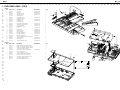
EXPLODED VIEW / 分解図
[Parts]
No.
1
2
3
4
7
8
9
10
11
12
13
14
15
16
17
18
19
20
22
23
24
25
28
29
30
Part Code
Part Name
Description
Q'ty
SE000161
SE000162
SE000163
SE000164
22180605
SE000202
22360712
SE000171
SE000169
22350313
SE000077
SE000078
SE000203
22350171
SE000174
SE000166
SE000167
SE000168
SE000204
SE000205
SE000089
22170103
SE000208
SE000209
SE000127
TOP CASE
VR PEDAL
BATTERY CASE B
BATTERY COVER
SWITCH PEDAL
BACKLIGHT PLATE
CORD HOOK 236-712
RUBBER SWITCH
RUBBER PLATE
FOOT MKS 235-313
VR PEDAL CUSHION FRONT
VR PEDAL CUSHION REAR
LCD CONNECTOR
RUBBER FOOT 235-171
LCD
REAR PANEL
BOTTOM COVER
PEDAL HOLDER
BATTERY TERMINAL +/BATTERY TERMINAL +
BATTERY TERMINAL C
SUPPORT SPRING (FOR SWITCH PEDAL)
KAKUSAN-SHEET
WHITE-SHEET
VR PEDAL REFLECT SEAL
#U00056320700
#U00056321800
#U00056322000
#U00029512100
1
1
1
1
5
1
1
1
1
5
1
1
2
5
1
1
1
5
2
1
1
5
1
1
1
#U00056333200
#U00056335400
#U00056336500
#U00029566100
#U00029567200
#U00056338700
#U00056462500
#U00056341100
#U00056342200
#U00056343300
#U00056344400
#U00056345500
#MA34002570
#U00056350100
#U00056352300
#U00052149300
14
30
16
f
13
11
25
7
2
a
1
e
g
h
29
27
10
[Screws]
No. Part Cord
a
b
c
d
e
f
g
h
i
j
k
l
40011278
40011323
40127689
40016590
SE000196
40016001
40016067
40348223
40123545
SE000156
40016445
40016456
a
15
Part Name
SCREW 3x8 BINDING TAPTITE P FE ZC
SCREW 3x10 BINDING TAPTITE P FE BZC
SCREW 3x10 BINDING TAPTITE S FE BZC
NYLON RIVET NRP-345 BLACK
HEXAGON SOCKET BOLT M6x60 BZC
LOCK NUT M6 U BZC
PLAIN WASHER 6x13x1 BZC
SPRING WASER M6 NO2 SWRH BZC
JACK NUT M9x11x2 HLJ0999-01-240
INTERNAL TOOTH WASHER M9.1x13 Ni
MINI JK NUT HSJ0999-01-190
MINI JK WASHER HSJ0999-01-210
Description
#U00056406300
Q'ty
20
28
17
12
1
1
1
1
1
2
3
3
2
2
8
23
24
17
4
19
22
b
12
j
9
c
3
i
k
l
18
d
ME-33
May. 2001
PARTS LIST / パーツリスト
SAFETY PRECAUTION:*1
The parts marked have safetyrelated characteristics.
Use only listed parts for
replacement.
The parts marked #
are new (initial
parts). *2
#の付いた部品は新
規部品です。*2
安全上の注意:*1
が付いている部品は、安全
上特別な規格でつくられたも
のです。
交換の際は、指定された部品
番号以外の部品は使わないよ
うにして下さい。
#
CONSIDERATIONS ON PARTS ORDERING
When ordering any parts listed in the parts list, please specify the following items in the order sheet.
QTY
PART NUMBER
DESCRIPTION
MODEL NUMBER
10
22575241
Sharp key
C-20/50
Ex.
15
2247017300
Knob (orange)
DAC-15D
Failure to completely fill the above items with correct number and description will result in delayed or even
undelivered replacement.
パーツ発注に関するお願い
オーダーシートには、必ず下記の4項目は正確に記入して下さい。(例外は除く)
必要数
パーツナンバー
品名
使用機種
10
22575241
Sharp key
C-20/50
例)
15
2247017300
Knob (orange)
DAC-15D
もし記入洩れ、誤記等が有る場合、必要部品が発送できなかったり、大幅な遅れの原因になりま
す。御協力をお願いします。
#
#
#
#
#
MB -> MAIN BOARD ASSY, PB -> PEDAL BOARD ASSY
*1
↓
*2
↓
CASING / ケース
SE000163
BATTERY CASE B
SE000164
BATTERY COVER
SE000167
BOTTOM COVER
SE000165
PANEL
SE000168
PEDAL HOLDER
SE000166
REAR PANEL
22350171
RUBBER FOOT
SE000169
RUBBER PLATE
22180605
SWITCH PEDAL
SE000161
TOP CASE
SE000162
VR PEDAL
SE000077
VR PEDAL CUSHION FRONT
SE000078
VR PEDAL CUSHION REAR
#
#
#
#
#
#
#
#
#
#
#
CHAISS / シャーシ
SE000207
JACK HOLDER
SE000201
LED HOLDER
#
#
KNOB, BUTTON / つまみ、 ボタン
SE000170
KNOB
SE000171
RUBBER SWITCH
#
SWITCH / スイッチ
SE000096
SWITCH HSW-2022-010010
SE000172
TACT SWITCH SKQKAKD010
#U00056320700
#U00056321800
#U00029566100
#U00029567200
Q'ty
1
1
1
1
1
1
5
1
5
1
1
1
1
#U00056347700
#U00056331000
1
5
#U00056322000
#U00029512100
#U00056342200
#U00056340000
#U00056343300
#U00056341100
for SWITCH PEDAL
#U00056336500
#
#
#
#
#
#U00056330800
#U00056335400
HD6433847RA26H
RA0A-101 (TC223C080AF-101)
AK4552VT
IC (EEPROM) CAT24WC32J
IC (DRAM) GM71VS18163CLT-6
BU2090FS-E2
HD74HC4052FPEL
HD74HC574FPEL
IC (OP AMP) NJM2100V-TE1
M5216FP-600D
M5218AFP
SPI-336-99-C-T1
01569601
01906156
M51955AFP
S-8520E33MC-BJS-T2
IC (CPU)
IC (DSP)
IC (AD/DA)
#U00051867000
#U00056450200
IC (LED DRIVER)
IC (CMOS)
IC (CMOS)
#U00052321400
IC (OP AMP)
IC (OP AMP)
IC (PHOTO INTERRUPTER)
#U00051870300
IC (RESET)
IC (DC-DC REGULATOR)
IC14 on MB
IC15 on MB
IC7 on MB
IC16 on MB
IC18 on MB
IC11 on MB
IC4 on MB
IC12 on MB
IC21 on MB
IC10 on MB
IC1 on MB
1
1
1
1
1
1
1
1
1
1
4
IC20 on PB
IC13 on MB
IC6 on MB
1
1
1
TRANSISTOR / トランジスター
15309104
2SA1586-GR(TE85R)
15129426
2SC2235Y
15319119
2SC4213A
15329523
RN1307
15139130
2SK184-GR
15329105
2SK208Y(TE85L)
SE000180
FET TRANSISTOR CPH6302-TL
TRANSISTOR
TRANSISTOR
TRANSISTOR
TRANSISTOR
FET TRANSISTOR
FET TRANSISTOR
#U00051444000
Q8, Q13 on MB
Q2 on MB
Q9, Q10, Q11, Q12 on MB
Q3, Q6 on MB
Q1 on MB
Q4, Q5 on MB
Q7 on MB
2
1
4
2
1
2
1
DIODE / ダイオード
15339122
1SS301
DIODE
15339119T0 1SS352(TPH3)
SWITCHING DIODE
SE000181
02780401
00902978
SE000183
00785856
#U00051038800
SCHOTTKY DIODE
SCHOTTKY DIODE
#U00052965000
LED (RED)
D3, D12-D16, D18-D21,
D25 on MB
D5, D17, D22-D24, D32,
D33 on MB
D26-D31 on MB
D4 on MB
D1 on MB
D26-D31 on MB
D7-D11 on MB
MTL.FILM RESISTOR
#U00052352800
R54, R59 on MB
2
POTENTIOMETER / ボリューム
SE000185
POT. RV110T-40E1-125A-B54
#U00056458100
VR1-VR6 on MB
6
CAPACITOR / コンデンサー
13549129M0 ECQ-B1H104JF
CAPACITOR
C1 on MB
1
DIODE 1SR154-400 TE25
MA720-TX
SB07-03N-AA
LED (GREEN) SML-110MT T86-2
SLR-342VR3F
RESISTOR / 抵抗
SE000184
ERJ12ZYJ330U
6
1
#
#MA25000830
#U00053696200
IC
02455489
02231767
02451434
SE000176
SE000177
02453056
01783589
01677701
SE000179
15289109
15289148
SE000178
SW19 on MB
1
SW9, SW13, SW17, SW18,
SW20 on MB
5
#
JACK, EXT TERMINAL / ジャック、外部接続端子
13449717
HEC2392-01-150
13449440
HSJ0857-01-210
SE000173
PHONE JACK HTJ-064-121
ADAPTOR JACK
MINI JACK
#U00056460300
JK6 on MB
JK2, JK5 on MB
JK1, JK3, JK4 on MB
1
2
3
#
#
DISPLAY UNIT / 表示ユニット
SE000174
LCD
01238178
LN514RA
#U00056462500
7SEG. LED
D6 on MB
1
1
#
#
#
#
INDUCTOR, COIL, FILTER / インダクター、コイル、 フィルター
00907856
BLM21A601SPT
FERRITE-BEAD
SE000187
CHOKE COIL CR54-470LC 47UH
#U00051449500
SE000186
CHOKE COIL CR54-4R7MC 4.7UH
#U00051450600
13529246
DSS310-91D223S-50ATL12-134
EMI FILTER
L1-L7, L10-L14 on MB
L9 on MB
L8 on MB
FL1 on MB
CRYSTAL, RESONATOR / クリスタル、 発振子
SE000188
CRYSTAL MA-406 10MHZ
SE000189
CRYSTAL SG-8002DC 67.7376MHZ
X1 on MB
X2 on MB
#U00051051300
#U00051052400
11
7
1
1
1
6
5
12
1
1
1
1
1
PWB ASSY / 基板完成品
#
E
SE000175
********
********
MAIN SHEET ASSY (EXG)
#U00054515200
NOTE : 'MAIN SHEET ASSY' includes the following parts.
注 意 : 補修用 MAIN SHEET ASSY は、下記の部品を含みます。
MAIN BOARD ASSY
PEDAL BOARD ASSY
1
WIRING, CABLE / ワイヤリング,ケーブル
5
ME-33
#
#
#
#
#
#
#
#
#
#
#
#
#
#
#
#
#
#
#
#
#
#
#
6
May. 2001
SE000194
SE000193
SE000191
SE000192
SE000190
WIRING L=4+240+4MM AWG24/BLACK
WIRING L=4+280+4MM AWG24/RED
WIRING L=4+80+4MM AWG26/BLUE
WIRING L=4+80+4MM AWG26/GRAY
WIRING L=4+80+4MM AWG26/YELLOW
SCREWS / ねじ類
40011278
SCREW 3x8
40011323
SCREW 3x10
40127689
SCREW 3x10
SE000196
HEXAGON SOCKET BOLT M6x60 BZC
40016001
LOCK NUT M6
40016067
PLAIN WASHER 6x13x1
40348223
SPRING WASER M6
SE000197
VR NUT
40123545
JACK NUT M9x11x2 HLJ0999-01-240
40016445
MINI JK NUT HSJ0999-01-190
40016456
MINI JK WASHER HSJ0999-01-210
SE000156
INTERNAL TOOTH WASHER M9.1x13
40016590
NYLON RIVET NRP-345 BLACK
PACKING / 梱包材
SE000210
PACKING CASE
SE000200
PACKING C
SE000198
PACKING L
SE000199
PACKING R
MISCELLANEOUS / その他
SE000202
BACKLIGHT PLATE
SE000205
BATTERY TERMINAL +
SE000204
BATTERY TERMINAL +/SE000089
BATTERY TERMINAL C
22360712
CORD HOOK
22350313
FOOT MKS
SE000208
KAKUSAN-SHEET
SE000203
LCD CONNECTOR
22170103
SUPPORT SPRING
SE000127
VR PEDAL REFLECT SEAL
SE000209
WHITE-SHEET
#U00056464700
#U00056463600
#U00056466000
#U00056467100
#U00056465800
to BATTERY CASE
to BATTERY CASE
to PEDAL BOARD
to PEDAL BOARD
to PEDAL BOARD
BINDING TAPTITE P FE ZC
BINDING TAPTITE P FE BZC
BINDING TAPTITE S FE BZC
#U00056406300
U BZC
BZC
NO2 SWRH BZC
#U00056428700
Ni
INPUT/OUTPUT JACK
#U00056410700
#U00056418600
#U00056411800
#U00056412000
#U00056333200
#U00056345500
#U00056344400
#U
236-712
235-313
#U00056350100
#U00056338700
(FOR SWITCH PEDAL)
#U00052149300
#U00056352300
ACCESSORIES (Standard) / 標準付属品
SE000159
OWNER'S MANUAL JAPANESE
#U00056780800
SE000160
OWNER'S MANUAL ENGLISH
#U00056789800
********
BATTERY LR6X/2ST
NOTE : The above part (LR6G/2ST) does not supply as replacement parts,because it is options.
注 意 : 上記の部品(LR6G/2ST)は商品のため、補修用部品としては供給できません。
40016489
WARRANTY CARD
(JAPAN ONLY)
1
1
1
1
1
17
12
1
1
1
1
2
6
3
2
2
3
1
1
1
1
1
1
1
2
1
1
5
1
2
5
1
1
1
1
1
IDENTIFYING THE VERSION
NUMBER
バージョンナンバーの確認方法
1. Turn the main unit on while holding the [GROUP SELECT]
and [PHRASE TRAINER] buttons down.
1. [GROUP SELECT], [PHRASE TRAINER] キーを同時に押
しながら電源を入れます。
2. The version number will appear on the LCD screen.
2. LCD にバージョンナンバーが表示されます。
3. Terminate the procedures by turning the main unit off.
3. 電源を切って終了します。
FACTORY RESET
ファクトリー・リセットの方法
Note:
注意:
ME-33 user data cannot be saved in other sequencers using
MIDI.
ME-33 のユーザーデータは他のシーケンサーに MIDI を使
用して保存することが出来ません。
Advice your customers of this when requests for repair are made.
予め修理を依頼されたお客様に、その旨を連絡して下さる
様お願い致します。
1. Turn the main unit on while holding the [EFFECT_R] and [EZ
TONE] buttons down.
1. [EFFECT_R], [EZ TONE] キーを同時に押しながら、本体
の電源を入れます。
2. "F RST" will appear on the LCD screen.
2. LCD に "F RST" と表示されます。
3. When you push the [WRITE] button, the letters "WRITE" will
flash on the LCD Screen for a while.
Upon completion of initialization, the system will enter the
same state as that at normal power-on.
3. [WRITE] キーを押すと LCD に "WRITE" の文字がしばら
く点滅します。
初期化が終了すると、通常の電源投入時と同じ状態にな
ります。
Note:
Don't turn the power off while "WRITE" is flashing.
To abort initialization, turn the power off without depressing the
[WRITE] button.
注意:
"WRITE" が点滅中は、電源を切らないでください。
初期化を中止する時は、[WRITE] キーを押さずに、電源を
切って下さい。
ME-33
TEST MODE
May. 2001
テストモード
How to enter test mode:
テストモードの入り方
To initiate test mode, turn the main unit on while depressing
[EFFECT ON/OFF], [EFFECT L], [EFFECT R] キー 3 ケ所を同
[EFFCT ON/OFF], [EFFECT L] and [EFFECT R] buttons.
Then, EEPROM check will start.
時に押しながら、電源を入れるとテストモードが起動し、
EEPROM チェックが始まります。
Five different test modes from Mode 1 to Mode 5 are available
using the ME-33.
ME-33 のテストモードには、モード 1 からモード 5 までの、
5 通りのテストモードがあります。
Use them to suit your circumstances.
状況に応じて使い分けて下さい。
If there is no problem, the LCD will light up fully.
How to select a mode under fully lit conditions is as shown below:
問題がなければ、LCD が全点灯します。
LCD 全点灯の状態でのモードの選択方法は次の様になります。
Note:
注意:
Mode 1
モード 1
*
*
*
*
ME-33 user data cannot be saves in other sequencers using
MIDI.
※ ME-33 のユーザーデータは他のシーケンサーに MIDI を
使用して保存することが出来ません。
When the No.1 foot switch is depressed, the mode will start from
(2. LCD/LED check).
NO.1 フット SW を押すと、(2. LCD/LED チェック)から
スタートします。
Advise your customers of this when requests for repair are
made.
予め修理を依頼されたお客様に、その旨を連絡して下さ
る様お願い致します。
The following mode will check each operation after checking
DSP operation.
以下のモードは、DSP 動作確認を行ってから、各動作
チェックに移ります。
If the test mode is defective, you cannot go to the next step.
So be sure to repair it.
※ テストモードで不良があれば次のステップに進むことが
できませんので、修理を行って下さい。
After repairing the test mode, repeat it from the start.
If only one jack is used in Lch for the OUTPUT test, a normal
また修理後は、最初から再度テストモードを行って下さ
い。
waveform may not be obtained, as the Lch/Rch signal is
mixed.
※ OUTPUT のテストでジャックを Lch 単体で使用した場
合、Lch/Rch の信号は内部でミキシングされるため正常
To obtain a normal waveform, be sure to insert an empty plug
into the Rch when measuring the Lch only.
な波形が得られません。
正常な波形を得るため、Lch 単体での測定時には、必ず
When making an OUTPUT check, connect a noise meter or
oscilloscope to the OUTPUT jack as necessary.
Rch に空プラグを挿入して下さい。
※ OUTPUT チェックを行う際は、必要に応じてノイズ
メーターとオシロスコープを OUTPUT ジャックに接続
します。
Mode 2
When the No.2 foot switch is depressed, the mode will start from
(5. Special check of output section frequency response).
Mode 3
When the No.3 foot switch is depressed, the mode will start from
(7. Special check of input section frequency response).
Mode 4
When the BANK DOWN foot switch is depressed, the mode will
start from (10. Residual noise check).
Mode 5
モード 2
NO.2 フット SW を押すと、(5. 出力部 f 特チェック)か
らスタートします。
モード 3
NO.3 フット SW を押すと、(7.入力部 f 特チェック)から
スタートします。
モード4
BANK DOWN フット SW を押すと、(10.残留ノイズ
チェック)からスタートします。
モード 5
Test items
テスト項目
1. EEPROM check
2. LCD/LED check
1. EEPROM チェック
2. LCD/LED チェック
3. SW/VR check
4. DSP check
3. SW/VR チェック
4. DSP チェック
5. Special check of output section frequency response
6. Special check of mute circuit operation in the output section
5. 出力部 f 特チェック
6. 出力部ミュート回路動作チェック
7. Special check of input section frequency response
8. Check of AFAD circuit operation
7. 入力部 f 特チェック
8. AFAD 回路動作チェック
Read/write test
If the result is 'NG', you cannot go to the next step.
読み出し、書き込みテスト
結果が 'NG' の場合、次のステップに進むことができません。
9. Check of AUX circuit operation
10. Residual noise check
9. AUX 回路動作チェック
10. 残留ノイズチェック
Stop in the state where nothing is displayed.
If the result is 'OK', go to the next step without displaying
なにも表示しない状態で停止します。
結果が 'OK' であれば、何も表示せずに次のステップに進
11. High gain residual noise check
12. Pedal setting and operation check
11. 高ゲイン残留ノイズ・ショックノイズチェック
12. ペダル設定&動作チェック
anything.
みます。
When the BANK UP foot switch is depressed, the mode will start
from (12. Pedal setting and operation check).
How to exit test mode:
テストモードの抜け方
Turn the main unit off.
本体の電源を切ります。
1. EEPROM check
1. EEPROM チェック
2. LCD/LED check
When the No.1 foot switch is depressed, the LCD display
Equipment items
必要な機材
•
•
Audio Generater
Oscilloscope
・ 発信器
・ オシロスコープ
•
•
Noise Meter
Empty plug
・ ノイズメーター
・ 空プラグ
BANK UP フット SW を押すと、(12.ペダル設定&動作
チェック)からスタートします。
2. LCD/LED チェック
NO.1 フット SW を押すと、LCD 表示パターンがスタート
pattern will start.
Check that each segment lights up normally.
します。
各セグメントが正常に点灯するか確認します。
Depress any button will cause the 7-segment LED display
pattern to come on.
どれかキーを押すと、7SEG, LED 表示パターンがスター
トしますので、各 LED が正常に点灯するか確認します。
Check the each LED lights up normally.
7
ME-33
May. 2001
3. SW/VR check
Depressing any button following the 7-segment LED display
3. SW/VR チェック
7SEG, LED 表示パターンに続いてどれかキーを押すと、
pattern causes the switch name to appear on the LCD screen.
Depress the button following the display and check that the
LCD にスイッチ名が表示されます。
表示に従ってキーを押し、これに対応して LCD の表示が
display on the LCD screen changes accordingly.
Upon completion of checking all buttons, the VR names will
変化することを確認して下さい。
全てのキーの確認が終わると、LCD には VR の名称が表
appear on the LCD screen.
While "0" is displayed on the 7-segment screen, operate each
示されます。
7SEG に "0" が表示されている時は左に、1 が表示されて
VR to the left.
While "1" is displayed, operate each one to the right.
いる時は右に、それぞれの VR を操作してください。
確認が終わると自動的に次の VR へ移動します。
Upon completion of check, moving to the next VR takes place
automatically.
最後の VR が操作され、チェックが正常に終了しますと、
自動的に次のステップへ進みます。
When the last VR has been operated and the check is
successfully concluded, moving to the next step takes place
この時、異常があれば次の SW/VR チェック及び次のス
テップに進む事が出来ません。
automatically.
If something is found to be wrong during this process, you
cannot go to the next SW/VR check or step.
4. DSP check
The following check will be made automatically.
4. DSP チェック
以下の検査を自動的に処理します。
4-1. Initialization test
4-1. 初期化のテスト
When the result is 'NG', "ERROR 1" will appear on the LCD
screen and you will not be able to go to the next step.
結果が 'NG' の場合、LCD に "ERROR 1" が表示され、次
のステップに進む事が出来ません。
If the result is 'OK', go to the next step without displaying
anything.
結果が 'OK' であれば、何も表示せずに次のステップに進
みます。
4-2. Internal RAM read/write test
When the result is 'NG', "ERROR 2" will appear on the LCD
screen and you will not be able to go to the next step.
結果が 'NG' の場合、LCD に "ERROR 2" が表示され、次
のステップに進む事が出来ません。
If the result is 'OK', go to the next step without displaying
anything.
結果が 'OK' であれば、何も表示せずに次のステップに進
みます。
4-3. External RAM read/write test
8
4-2. 内部 RAM 読み込み、書き込みテスト
4-3. 外部 RAM 読み込み、書き込みテスト
When the result is 'NG', "ERROR 3" will appear on the LCD
screen and you will not be able to go to the next step.
結果が 'NG' の場合、LCD に "ERROR 3" が表示され、次
のステップに進む事が出来ません。
If the result is 'OK', go to the next step without displaying
anything.
結果が 'OK' であれば、何も表示せずに次のステップに進
みます。
ME-33
May. 2001
5. Special check of output section frequency response.
5. 出力部 f 特チェック
Return to the previous check using the [EFFECT L] button.
[EFFECT L] キーで前の検査に戻ります。
Go to the next check using the [EFFECT R] button.
[EFFECT R] キーで次の検査に進みます。
"TEST 1" will appear on the LCD screen.
Sine waves of 20 Hz, 1 kHz, 5 kHz and 15 kHz will be output at
LCD に "TEST 1" と表示されます。
0.8 秒間隔で、20 Hz, 1K Hz, 5K Hz, 15K Hz のサイン波が
0.8-second intervals.
(DSP internal oscillation, automatic loop)
出力されます。
( DSP 内部発振、自動ループ)
Switch the noise meter to "FLAT".
Check the level using the noise meter.
ノイズメーターを 'FLAT' に切り換えます。
ノイズメーターでレベルを確認します。
Switch the noise meter to 'FLAT'.
Check the level using the noise meter.
ノイズメーターを 'FLAT' に切り換えます。
ノイズメーターでレベルを確認します。
Check the output waveform of OUTPUT L/R and PHONES L/
R for distortion using an oscilloscope.
オシロスコープで OUTPUT L/R, PHONES L/R の出力波形
が、歪んでいないか確認します。
OUTPUT L and R at or below -65.0 dBu (FLAT)
PHONES L and R at or below -40.0 dBu (FLAT)
OUTPUT L, R -65.0 dBu(FLAT)以下
PHONES L, R -40.0 dBu(FLAT)以下
Check Lch (MONO) and Rch individually.
Set the level difference between Lch and Rch to +1 dBu or -1 dBu.
Lch (MONO), Rch を個別にチェックを行って下さい。
Lch, Rch のレベル差は '+1 dBu or -1 dBu' とします。
Check Lch (MONO) and Rch on individually.
Set the level difference between Lch and Rch to +1 dBu or -1 dBu.
Lch (MONO) , Rch を個別にチェックを行って下さい。
Lch, Rch のレベル差は '+1 dBu or -1 dBu' とします。
Return to the previous check using the [EFFECT L] button.
[EFFECT L] キーで前の検査に戻ります。
Go to the next check using the [EFFECT R] button.
[EFFECT R] キーで次の検査に進みます。
Frequency
20 Hz
1K Hz
5K Hz
15K Hz
level 1
-20 dBu +3, -1 dBu
-20 dBu +3, -1 dBu
-20 dBu +3, -1 dBu
-20 dBu +3, -1 dBu
周波数
20 Hz
1K Hz
5K Hz
15K Hz
レベル1
-20 dBu +3, -1 dBu
-20 dBu +3, -1 dBu
-20 dBu +3, -1 dBu
-20 dBu +3, -1 dBu
6. Special check of mute circuit operation in the output section.
"TEST 2" will appear on the LCD screen.
7. Special check of input section frequency response.
"TEST 3" will appear on the LCD screen.
6. 出力部ミュート回路動作チェック
LCD に "TEST 2" と表示されます。
7. 入力部 f 特チェック
LCD に "TEST 3" と表示されます。
Enter a 200 Hz (200 mVp-p) rectangular wave in the INPUT.
Check the output waveform of OUTPUT L/R and PHONES L/
INPUT に 200 Hz(200 mVp-p) 矩形波を入力します。
オシロスコープで OUTPUT L/R, PHONES L/R の出力波形
R using an oscilloscope.
Check Lch (MONO) and Rch on individually.
を確認します。
Lch (MONO) , Rch を個別にチェックを行って下さい。
Return to the previous check using the [EFFECT L] button.
Go to the next check using the [EFFECT R] button.
[EFFECT L] キーで前の検査に戻ります。
[EFFECT R] キーで次の検査に進みます。
8. Check of AFAD circuit operation.
8. AFAD 回路動作チェック
"TEST 4" will appear on the LCD screen.
Enter a 200 Hz (20 mVp-p) rectangular wave in the INPUT.
LCD に "TEST 4" と表示されます。
INPUT に 200 Hz (20 mVp-p) 矩形波を入力します。
Check the output waveform of OUTPUT L/R using an
oscilloscope.
オシロスコープで OUTPUT L/R の出力波形を確認しま
す。
Return to the previous check using the [EFFECT L] button.
[EFFECT L] キーで前の検査に戻ります。
[EFFECT R] キーで次の検査に進みます。
Go to the next check using the [EFFECT R] button.
9
ME-33
9. Check of AUX circuit operation.
"TEST 5" will appear on the LCD screen.
May. 2001
9. AUX 回路動作チェック
LCD に "TEST 5" と表示されます。
Enter a 200 Hz (200 mVp-p) rectangular wave in AUX IN (both
L and R).
AUX IN(L, R 片方ずつ)に 200 Hz (200 mVp-p) 矩形波を
入力します。
Three different waveforms are output at 0.5-second intervals
(Automatic loop).
0.5 秒間隔で、3 種類の波形が出力されます。(自動ルー
プ)
Check the output waveform of OUTPUT L/R using an
oscilloscope.
オシロスコープで OUTPUT L/R の出力波形を確認しま
す。
Check Lch (MONO) and Rch on individually.
Lch (MONO), Rch を個別にチェックを行って下さい。
Return to the previous check using the [EFFECT L] button.
Go to the next check using the [EFFECT R] button.
10. Residual noise check
[EFFECT L] キーで前の検査に戻ります。
[EFFECT R] キーで次の検査に進みます。
10. 残留ノイズチェック
"TEST 6" will appear on the LCD screen.
Switch the noise meter to 'JIS-A' or 'IHF' mode.
Check the output of OUTPUT L/R without connecting INPUT
LCD に "TEST 6" と表示されます。
ノイズメーターを 'JIS-A' または 'IHF' のモードに切り換え
ます。
and AUX IN (short circuited input, the state of short-circuited
signal and GND lines) using a noise meter.
INPUT, AUX IN は無接続で(入力短絡、信号ラインと
GND ラインがショートされた状態)、OUTPUT L/R の出
OUTPUT L and R at or below -84.0 dBu (JIS-A) or at or below84.0 dBu (IHF)
力をノイズメーターで確認して下さい。
OUTPUT L, R -84.0 dBu (JIS-A) 以下 又は、-84.0 dBu (IHF)
Check Lch (MONO) and Rch on individually.
Set the level difference between Lch and Rch to +1 dBu or -1
以下
Lch (MONO), Rch を個別にチェックを行って下さい。
dBu.
Lch, Rch のレベル差は '+1 dBu or -1 dBu' とします。
Return to the previous check using the [EFFECT L] button.
Go to the next check using the [EFFECT R] button.
[EFFECT L] キーで前の検査に戻ります。
[EFFECT R] キーで次の検査に進みます。
11. High gain residual noise and shock noise check
11. 高ゲイン残留ノイズ、ショック・ノイズチェック
"TEST 7" will appear on the LCD screen.
Check the output of OUTPUT L/R using a noise meter.
LCD に "TEST 7" と表示されます。
OUTPUT L/Rの出力をノイズメーターで確認して下さい。
OUTPUT L and R at or below -39.0 dBu (JIS-A) or at or below
-39.0 dBu (IHF).
OUTPUT L/R -39.0 dBu(JIS-A)以下、叉は-39.0 dBu
(IHF)以下。
Remove the noise meter, connect a high gain amplifier to
OUTPUT L and R, and check for abnormal noise through a
ノイズメーターを外し、ハイゲインのアンプを OUTPUT
L, R に接続し、スピーカーで聴いて異音がないかどうか、
speaker.
Apply shock to the main unit and check for shock noise.
確認して下さい。
また 本体に衝撃を与え、ショック・ノイズが無いか確認
Check Lch (MONO) and Rch on individually.
して下さい。
Lch (MONO), Rch を個別にチェックを行って下さい。
Return to the previous check using the [EFFECT L] button.
Go to the next check using the [EFFECT R] button.
[EFFECT L] キーで前の検査に戻ります。
[EFFECT R] キーで次の検査に進みます。
10
ME-33
May. 2001
12. Setting the Expression Pedal and Checking Its Operation
Make the expression pedal settings and check its operation here.
12. エクスプレッション・ペダル設定&動作チェック
エクスプレッション・ペダルの設定と動作確認を行ないます。
The LCD displays "MAX".
Step on the toe side of the pedal lightly. (This is the 'MAX'
LCD に "MAX" と表示されます。
ペダルを ‘つま先側’ に軽く踏み込んだ状態('MAX' の位
position. The cushion on the back of the toe side of the pedal
touches the case lightly.)
置。ペダルのつま先側の裏にあるクッションがケースに
軽く当たった状態。)にします。
Press the [EFFECT R] key, and the LCD blinks and the 'MAX'
position is adjusted.
[EFFECT R] キーを押すと点滅表示になり、'MAX' の位置
調整が行なわれます。
After the adjustment is completed, the LCD displays the value
of the position after adjustment (refer to the table below).
'MAX' の位置調整が終了すると LCD に調整後の値(下表
参照。)が表示されます。
Press the [EFFECT R] key again.
再び、[EFFECT R] キーを押します。
Next, move the pedal back to the heel side (This is the 'MIN'
position. The cushion on the back of the heel side of the pedal
次にペダルを 'かかと側'( 'MIN' の位置。ペダルのかかと
側の裏にあるクッションがケースに軽く当たった状
touches the case lightly.)
Check that the value shown on the LCD increases to near the
態。)まで戻します。
LCD 数値が、下表の参考値近辺まで増加することを確認
reference value in the table below.
Step on the pedal again with strength until the cushion on the
します。
次に再度ペダルを踏み込み、つま先側の裏のクッション
back of the toe side is compressed and the pedal touches the
case (to adjust the SW operation).
が潰れて、ペダルが直接ケース本体に当たるまで強く踏
み込みます。( SW 動作の調整。)
Check that the value shown on the LCD decreases to near the
reference value shown below:
LCD 数値が、下記参考値近辺まで減少することを確認し
ます。
Pedal
When the pedal is
lightly depressed
('MAX' position)
When the pedal is
moved toward the heel
('MIN' position)
When the pedal is
strongly depressed
Figures displayed on LCD
In the region of 000700
In the region of 001900
ペダル
軽く踏み込んだ時
('MAX' の位置)
LCD 表示数値
かかと側にした時
('MIN' の位置)
001900 近辺
強く踏み込んだ時
000200 近辺
000700 近辺
In the region of 000200
Pressing the [EFFECT R] key again completes the setting and
[EFFECT R] キーを再度、押すと設定は終了し、"END" 表
"END" appears on the LCD.
If the 'MAX' or 'MIN' position is clearly abnormal, adjustment
示となります。
'MAX' の位置と 'MIN' の位置に明らかな異常がある場合
cannot be completed.
は、この調整は終了できません。
(Checking Operation)
Turn on the power to put the machine into normal operation.
(動作確認)
電源を入れ直し、通常の動作状態にします。
Connect a tuner, such as a TU-12, and a monitoring speaker to
OUTPUT.
OUTPUT に TU-12 等のチューナーとモニタースピーカー
を接続します。
Connect an oscillator to INPUT, and input the oscillator's
signals.
INPUT に発振器を接続し、信号を入力します。
全エフェクトを 'OFF ' に設定します。
Set all the effects to ‘OFF’.
Press the PEDAL KEY several times to set the PEDAL to
PEDAL KEY を数回押して、ペダル設定を "BEND 2" に設
定します。(エクスプレッション・ペダルで、ピッチが 2
"BEND 2". (This setting causes a 2-octave pitch change.)
Move the pedal back to the heel side.
オクターブ変化する設定です。)
ペダルを 'かかと側' に戻します。
Adjust the frequency of the signals from the oscillator so that
the pointer of the tuner is in the center when a 1k Hz or so signal
発振器の信号の周波数を調整して、適当な音程( 1k Hz 近
辺が望ましい。)でチューナーの針表示が中央の位置に
is output.
Move the pedal to the position where its toe side touches the
ある様にします。
ペダルを 'つま先側' が軽く当たる状態にします。
case lightly.
Listen to the monitor to check that the output tone goes up 2
この時 音が確実に 2 オクターブ上がることをモニターで
聴いて確認すると共に、チューナーの針表示が中央の位
octaves and the tuner's pointer is in the center (indicating that 2octave higher tone was output).
置であること(確実に 2 オクターブ上昇したこと。)を
確認します。
Then check that the PEDAL icon is turned off and on each time
you strongly step on the toe side of the pedal (this checks the on/
次に、ペダルを 'つま先側' を強く踏み込む度に、PEDAL
のアイコンが消灯・点灯する(エフェクトの 'ON/OFF ' を
off of the effect).
確認する。)ことを確認します。
This completes the test mode.
以上でテストモードは終了です。
11
ME-33
May. 2001
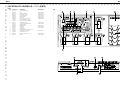
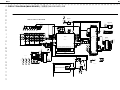
A BLOCK DIAGRAM / ブロック図
B
C
D
BUFFER
GUITAR IN
(MONO)
E
AUX IN
F
(STEREO)
G
OUTPUT
(STEREO)
H
I
PHONES
J
K
MUTE
L
M
AMP
N
PEDAL BOARD
PHOTO
O
AMP
P
Q
IC11
R
LED DRIVER
S
7SEG LED &LED
T
U
V
POWER SW
IC1
PRE ENPH
IC3
AMP
MAIN BOARD
IC4
MULTI
PLEXER
-
IC2
PRE ENPH
.
.
IC9
DE ENPH
AMP
.
.
IC8
LPF
IC14
CPU
H8/3847R
IC13
RESET
IC15
DSP
ESP4
BUS
INTERRUPTOR
12
IC17,18
DRAM
SWITCH
VR x 6
. .
..
A +9
. .
+8VA +4VIN +4VOUT
A
DC-DC CNV
IC7
AD/DA
-
IC16
EEPROM
LCD
ADAPTOR IN
POWER
D +3
D
BATTERY
ME-33
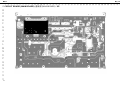
A CIRCUIT BOARD (MAIN BOARD) /基板図 (MAIN BOARD)
B
C
D
E
F
G
H
I
J
K
L
M
N
O
P
Q
R
S
T
U
V
May. 2001
1/2
13
ME-33
A CIRCUIT BOARD (MAIN BOARD) /基板図 (MAIN BOARD)
B
C
D
E
F
G
H
I
J
K
L
M
N
O
P
Q
R
S
T
U
V
14
May. 2001
2/2
ME-33
May. 2001
D
R71
4.7K
1
D
R70
10K
D
D
7
1
3
5
VCC
C52
22/16
IN
NC
NC
NC
R34
100
6
OUT
8
NC
EEPROM
GND
2
2
D
R72
4.7K
C83 C84 C85 C86 C87 C88
0.1 0.1 0.1 0.1 0.1 0.1
C94
0.1
D7
D6
D5
D4
D3
D2
D1
D0
99
100
102
103
104
105
106
107
---D +3
4.7K
C95
0.1
---D +3
---D +3
34
35
36
37
A2
A1
A0
81
82
83
84
86
87
88
89
91
92
94
95
96
97
A3
R73
C96
0.1
C97
10/25
R91
47
R121
10K
R28
47
D
D
TRR5
TRR4
TRR3
TRR2
TRR1
TRR0
TRCKIN
RST2
RST1
VPOUT
TRS5
TRS4
TRS3
TRS2
TRS1
TRS0
TRCKO
CARBON
KSI1
SKQKAK
3
2 2
1SS301
1
3
CARBON
ON/OFF
D15-2
SW6
2 2
1
1SS301
3
CARBON
RIGHT
D18-2
SW7
2 2
1
1SS301
CARBON
3
PEDAL
D20-2
SW8
2 2
1
1SS301
CARBON
KSI2
1
D25-1
3
2
SW20
1 2
1SS301
D13-1
1
SKQKAK
3
SW9
1 2
1SS301
1
3
SKQKAK
WRITE
D16-1
SW10
1 2
1
1SS301
EXIT
D19-1
3
CARBON
SW11
1 2
1SS301
1
CARBON
3
1SS301
CARBON
R130
R131
R132
R133
100
100
100
100
96
97
98
99
BATT
D +3
R138
R139
R140
R141
TUNER
D21-1
SW12
1 2
1
10K
10K
10K
10K
KSI0
KSI1
KSI2
KSI3
KSI0
KSI1
KSI2
KSI3
KSI3
1
3
SKQKAK
MANUAL
D16-2
SW14
2 2
1
1SS301
3
CARBON
EZ TONE
D19-2
SW15
2 2
1
1SS301
CARBON
3
---D +3
R163
R166
R165
20
9
8
7
6
5
4
3
2
D7
D6
D5
D4
D3
D2
D1
D0
A4
A3
A2
A1
A0
SAMPLER
AUX
MUTE
10
8
31
30
84
24
---D +3
1
2
3
4
5
6
7
CA
CF
COMA
NC
NC
NC
CE
---D +3
COMA
CB
NC
CG
CC
CDP
CD
14
13
12
11
10
9
8
4
5
6
7
R126 680
R127 680
8
LCD BACKLIGHT
9
10
R128 680
11
A +9
14
R68
680
15
P11
P12
P43
VSS
VSS
AVSS
23
22
21
20
19
18
17
16
R149
R150
R151
R152
R153
R154
R155
R156
47
47
47
47
47
47
47
47
D7
D6
D5
D4
D3
D2
D1
D0
4
R169
47
5
6
7
R167
R168
R170
47
47
47
OSC1
X1
X2
TEST
PWM
77
78
79
D +3
L10
BLM21A601SPT
8
D
4
C98
12P
D
X1
10MHz
D
13
3
DOWN
OUT
C99
5
C53
0.0022
DADATA
129
130
R104 47 132
133
D
ADDATA R105 47 134
135
BCK
MCK
LCD1
VSS
D
30
118
119
121
122
123
R103 47 125
126
127
D
12P
65
66
67
68
69
70
71
CD7
CD6
CD5
CD4
CD3
CD2
CD1
CD0
SYO
SYI
INT1
INT0
DSP
CS
WR
RD
IC15
TC223C08AF-101
DIRECT
CTYPE
EAMPX
RFRSH
PWRSAV
GRAMC
SHRMD
LRCK
R106 47 137
138
139
141
R107 47
D +3
76
131
31
EA9
EA8
EA7
EA6
EA5
EA4
EA3
EA2
EA1
EA0
ED23
ED22
ED21
ED20
ED19
ED18
ED17
ED16
ED15
ED14
ED13
ED12
ED11
ED10
ED9
ED8
ED7
ED6
ED5
ED4
ED3
ED2
ED1
ED0
OSC
BLM21A601SPT
LCD
1
DA7
DA6
DA5
DA4
DA3
DA2
DA1
DA0
AD3
AD2
AD1
AD0
LRCK1
LRCK0
BCK1
BCK0
WE
CAS
RAS
MCK1
MCK0
NC
5
6
SDA
SCL
VSS
D +3
8
7
D
63
62
61
60
58
57
56
C102
0.1
4
D
D +3
52
53
RES
C103 C104 C105 C106 C107 C108 C109 C110 C111
0.1
0.1
0.1
0.1
0.1
0.1
0.1
0.1
220/16
54
C54
0.0022
110
111
112
113
114
115
117
D
D
142
143
28
27
25
24
23
21
20
19
17
16
50
49
48
47
46
45
43
42
41
40
39
38
35
34
33
32
10
9
8
7
5
4
3
2
EA9
EA8
EA7
EA6
EA5
EA4
EA3
EA2
EA1
EA0
DRAM
IC18
GM71VS18163CLT-6
EA9
EA8
EA7
EA6
EA5
EA4
EA3
EA2
EA1
EA0
32
31
30
29
28
27
24
23
22
21
11
15
16
19
20
36
40
ED7
ED6
ED5
ED4
ED3
ED2
ED1
ED0
18
34
35
17
33
D
12
13
14
A9
A8
A7
A6
A5
A4
A3
A2
A1
A0
NC
NC
NC
NC
NC
NC
NC
RAS
UCAS
LCAS
WE
OE
DQ15
DQ14
DQ13
DQ12
DQ11
DQ10
DQ9
DQ8
DQ7
DQ6
DQ5
DQ4
DQ3
DQ2
DQ1
DQ0
D +3
R110
R111
R112
R113
R114
R115
R116
R117
49
48
47
46
44
43
42
41
10
9
8
7
5
4
3
2
10K
10K
10K
10K
10K
10K
10K
10K
ED7
ED6
ED5
ED4
ED3
ED2
ED1
ED0
D +3
VCC
VCC
VCC
VSS
VSS
VSS
1
6
25
26
45
50
D
C113 C114 C115
0.1
0.1
0.1
XTESTT
XTESTS
TESTB
D
D
Q4
Q5
D +3
Q6
C13
Q8
D +3
DATA
CK
D +3
R119 100K
D +3
Q13
2SA1586GR
Q9
Q10
12P
R35
10K
Q7
R80
100K
R78
100
2
3
-
1 7
+
D
---D +3
R74 100K
D +3
6
5
D +3
L100
BLM21A601SPT
C16
0.1
IC21B
NJM2100V
D
C117 C118 C120
10/25 10/25 10/25
R120
12K
D
C300 C116*
100/16 10/25
1
1
1
1
2
GND
1
X2
67.7376MHz (for 3.3V)
9
10
14
R118
10K
D7
D9
D11
SLR-342VR3F
SLR-342VR3F
SLR-342VR3F
D8
D10
SLR-342VR3F
SLR-342VR3F
1
OE
D +3
L13
15
12
R79
220
D
VDD
D
XXX
Q11
74
75
C89
0.1
Q2
Q3
A4
A3
A2
A1
A0
R27
1M
R171 R172
10K
10K
2
2
2
2
R67
680
2
R32
220
D
R66
680
VDD
47
47
47
47
47
C90
0.1
D +3
16
Q1
R142
R143
R144
R145
R148
D +3
1
R87
220
R65
680
2
1 2
R64
680
D30
SML-110MT
2
D27
SML-110MT
2
D29
SML-110MT
13
D31
SML-110MT
1 2
D28
SML-110MT
1 2
D26
SML-110MT
12
1
1
A +9
1
A +9
Q0
OSC2
P40
P42
P10
A4
IC11
BU2090FS
29
28
27
26
25
C101
0.1
RES
43
44
45
46
47
48
49
50
51
52
53
54
55
56
57
58
59
60
61
62
63
64
65
66
67
68
69
70
71
72
73
74
75
76
77
78
79
80
81
82
---D +3
R174
10K
680
680
680
680
680
P14
P15
P16
P17
P37
P36
P41
R173
10K
D
D +3
100
100
100
83
85
1
---D +3
1
11
OE
CK
D
R122
R123
R124
R125
R129
IC14
HD6433847RA26H
42
41
40
39
38
37
36
35
34
33
32
31
30
29
28
27
26
25
24
23
22
21
20
19
18
17
16
15
14
13
12
11
10
9
8
7
6
5
Q7
Q6
Q5
Q4
Q3
Q2
Q1
Q0
VCC
12
13
14
15
16
17
18
19
GND
100
100
100
100
100
IC12
74HC574FP
D6
LN514RA
P13
CARBON
R134
R135
R136
R137
R90
KSO0
KSO1
KSO2
KSO3
KSO4
CPU
PC0
PC1
PC2
PC3
BYPASS
D21-2
SW16
2 2
1
1SS301
P27
P26
P25
P24
P23
P22
P21
P20
SEG1
SEG2
SEG3
SEG4
SEG5
SEG6
SEG7
SEG8
SEG9
SEG10
SEG11
SEG12
SEG13
SEG14
SEG15
SEG16
SEG17
SEG18
SEG19
SEG20
SEG21
SEG22
SEG23
SEG24
SEG25
SEG26
SEG27
SEG28
SEG29
SEG30
SEG31
SEG32
SEG33
SEG34
SEG35
SEG36
SEG37
SEG38
SEG39
SEG40
SW13
2 2
1SS301
P35
P34
P33
P32
P31
42
41
40
39
38
37
36
35
34
33
32
31
30
29
28
27
26
25
24
23
22
21
20
19
18
17
16
15
14
13
12
11
10
9
8
7
6
5
3
D13-2
3
AN0
AN1
AN2
AN3
AN4
AN5
AN6
AN7
VCC
VSS
VSS
VSS
VSS
VSS
VSS
VSS
VSS
VSS
VSS
VSS
VSS
VSS
VSS
VSS
VSS
VSS
1SS301
LEFT
SW5
D12-2
1
88
89
90
91
92
93
94
95
D +3
*S/No. AO76100-Up
100/16
C34
0.1
D
UP
PEDAL BOARD ASSY
C126 NC
D
IC20
SPI-336-99-C
1
3
2
4
CN7
1
2
3
1
2
3
R86 33K
D +3
CN8
1
2
3
1
2
3
R92
2.2K
2
R77
-
3 +
D +3
R84
12K
1
IC21A
NJM2100V
100K
C122
0.1
D +3
D
8
SW18
2 2
680
680
680
680
680
680
100
10K
A13
A14
A15
R85
47K
-
IC21C
NJM2100V
+
D
4
UP
D14-2
3
R157
R158
R159
R160
R161
R162
R81
R83
R76
10K
1
2
3
6
15
22
29
36
44
55
64
72
80
85
98
108
116
124
136
144
1SS301
AN0
AN1
AN2
AN3
AN4
AN5
2
CARBON
PHRASE TRAINER
D20-1
SW4
1 2
1
1
1SS301
3
2
CARBON
LINE/G.AMP
D18-1
SW3
1 2
1
3
1SS301
3
COM1
COM2
COM3
COM4
CARBON
COPY/EXCHG
D15-1
SW2
1 2
1
42
41
40
39
1SS301
3
1
2
3
4
SKQKAK
GROUP SELECT
D12-1
SW1
1 2
1
1
2
3
4
1SS301
3
V3
V2
V1
V0
DOWN
D14-1
SW17
1 2
1
CVCC
VCC
AVCC
KSI0
3
R75
10K
18
59
93
128
CA13
CA12
CA11
CA10
CA9
CA8
CA7
CA6
CA5
CA4
CA3
CA2
CA1
CA0
IC16
CAT24WC32J
D +3
VDD3
VDD3
VDD3
VDD3
1
11
26
37
51
73
90
101
109
120
140
VDD5
VDD5
VDD5
VDD5
VDD5
VDD5
VDD5
VDD5
VDD5
VDD5
VDD5
C93
0.1
D
VR6
50KB
D +3
D +3
D
86
1
2
VR5
50KB
D +3 IC13
M51955AFP
R69
12K
2
3
3
3
3
D
VR4
50KB
C92
0.1
2
1
D
VR3
50KB
D +3
D22
1SS352
11
33
100
D
VR2
50KB
RESET
D
D +3
AN0
AN1
AN2
AN3
AN4
AN5
---D +3
2
C100
0.1
S/No. AO76100-Up
32
38
87
D
---D +3
2
1
2
1
1
2
VR1
50KB
---D +3
3
---D +3
3
---D +3
3
---D +3
D +3
4
R157-R162
1/2
1
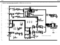
A CIRCUIT DIAGRAM (MAIN BOARD) / 回路図 (MAIN BOARD)
B
C
D
DIGITAL CIRCUIT DIAGRAM
E
F
G
H
I
J
K
L
M
N
O
P
Q
R
S
T
U
V
D
15
ME-33
May. 2001
A CIRCUIT DIAGRAM (MAIN BOARD) / 回路図 (MAIN BOARD)
B
C
D
E
F
G
H
I
J
K
L
M
N
O
P
Q
R
S
T
U
V
+8VA
Q1
2SK184GR
C2
R5
0.0022
10K +4VIN
3 +
R3
10K
IC1A
M5218AFP
C32 12P
R23 10K_1%
A
C30
22/16
fc=7.2KHz
+4VIN
R9
47K
L2
BLM21A601SPT
R7
220
C6
R10
0.0022
10K +4VIN
2 -
L
L3
BLM21A601SPT
C4
220P
or
R8
100K
A
D33 1SS352
D23 1SS352
1
D32 1SS352
D24 1SS352
IC2A
M5219FP
+4VIN
16
C33
0.1
VEE
R99 100K
R100 100K
8
7
A TC74HC4052AF
A
1 2
1
1
2 1
2
+8VA
R24
47K
L8
R21 150K_1%
6 -
R14
47K
R16 18K
+4VIN
R15
0.0022
10K +4VIN
R13
100K
L9
4
1
SAMPLER
5
D
C21
22/16
D
C23
0.1
M5218AFP
D
D
C22
220/16
C40
100/16
+4VIN
2
R29 100K
R31 100K
-
+
+4VOUT
4
+8VA
A
+8VA
2
3
1
2
1
3
Q6
RN1307
2
1
1
+
-
IC9C
M5219FP
+
IC10C
M5216FP
A
1
Q5
2SK208Y
AUX
2
C37
0.1
A
A
R97 100K
R98 100K
ADDA
C38
22/16
A
C39
22/16
IC7
AK4552VT
A
L
2
3
1
L6
BLM21A601SPT
+8VA
R46
1K
+4VIN
1
-
+
+
Q9
2SC4213A
7
5 +
A
A
IC1C
M5218FP
IC2C
M5219FP
C66
22/16
A
A
A
C18
220/16
C19
0.1
L11
D +3 BLM21A601SPT
R40
100K
R48
1K
C64
220P
R38 12K
R36 68K
-
1
R108
4.7K
A
IC1B
M5218AFP
R18
12K
12K
R82
2
+4VOUT R50 4.7K
+ 3
C72
150P
IC10A
M5216FP
2
3 +4VOUT
C59
0.0022
IC9A
M5219FP
R37 12K
C45
10/25
C46
0.1
C44
0.1
+
1
C58
22/16
+4VOUT
D
LOUT
MCLK
SDTO
BCLK
LRCK
SDTI
ROUT
PDN
RIN
10
5
R51
47K
R47
1K
1
6 -
R39
4
3
R17
10K
4
-
16
LIN
3
C47
10/25
D
DEM0
DEM1
VA
11
8
12
10
9
MCK
ADDATA
BCK
LRCK
DADATA
13
RES
6
7
C48
0.0022
D
VD
VSS
VCOM
14
D
C50
10/25
C49
0.1
D
D
or
M5218AFP
R53
330
A
R300 100
A
R49
1K
C136
0.0022
R33
10K
R44
A
12K
D
3
8
+8VA
8
+8VA
L7
BLM21A601SPT
4
A
2
22/16
C128
0.1
A
R
22/16
C55
15
R30
10K
A
2
0.1
10/25
C12
A
C127
220/16
JK5
HSJ0857-01-1210
C51
R94
12K
C135
0.0022
D
C43
0.1
R26
47K
L5
BLM21A601SPT
A
HEADPHONES
C42
220/16
R93
10K
C14
-20dBm OUT R
D3
1SS301 R25
1M
3
3
+8VA
+4VOUT
IC3C
M5219FP
D
+8VA
Q4
2SK208Y
3
8
8
+8VA
4
+8VA
A
8
L4
BLM21A601SPT
JK4
HTJ-064-121
VOUT
DC-DC CNV
M5218AFP
4
2
3
1
VSS
D +3
D
3
C7 22/16
JK3
HTJ-064-121
-20dBm OUT L
D4
MA720
D
IC2B
M5219FP
A
D
ON/OFF
2
or
A
1
D
C41
0.1
7
5 +
IC6
S-8520E33MC-BJS
4
VIN
EXT
47uH
1
S
or
C3 22/16
6 -
4.7uH
7
5 +
IC3B
M5219FP
C10
Q7
CPH6302
A +9
Q3
RN1307
R20 33K_1%
C9
22/16
C8
220P
2
C31
12P
M5218AFP
A
R12
220
R
3
13
+8VA
VCC
B
A
INH
3 +
or
A
YCOM
XCOM
M5218AFP
C5
22/16
2
3
1
-10dBm AUX IN
C20
22/16
IC3A
M5219FP
R11 18K
9
10
6
1
3 +
3Y
2Y
1Y
0Y
3X
2X
1X
0X
GND
R22 33K_1%
2 -
JK2
HSJ0857-01-1210
IC4
4
2
5
1
11
15
14
12
1
3
A
+4VIN
C28
22/16
2 -
1
R2
1M
3
2
+4VIN
R96 R95
100K 100K
R6 47K
2
2
3
1
-20dBm GUITAR IN
R146 R147
100K 100K
C29
22/16
R4
47K
+4VIN
3
C1
0.1_FILM
1
L1
R1
BLM21A601SPT 10K
3
JK1
HTJ-064-121
2/2
1
Q2
2SC2235Y
2
1
R19
680
D2
1SR154-400
C27
0.1
C130
220P
2
A
A
A
A
A
1
1
L12
BLM21A601SPT
+8VA
A
Q11
2SC4213A
R101
1K
R60
100K_1%
D17
1SS352
3
C132
220P
A
R58
330
A
A
A
Q12
2SC4213A
R102
1K
6
+
5 +4VOUT
IC9B
M5219FP
R42 12K
C61
22/16
L14 BLM21A601SP
C62
0.0022
+4VOUT
or
M5218AFP
D +3
D5
1SS352
A
C70
R62
100
1
47/16
D
Q8
2SA1586GR
R89
1M
1
2
R61
43K_1%
R43 12K
-
7
MUTE
R63
10K
R59
33 1/2W
BATT
16
C74
150P
IC10B
M5216FP
D +3
1
A
5 +4VOUT R55 4.7K
R45
100K
3
CN2
TP
6
1
2
A
C25 C26
0.1 470/16
3
C24
470/16
+
3
1.5V x 6
1
BATTERY
A
7
R54
33 1/2W
1
A
CN1
TP
1
1
C67
220P
R41 68K
1
2
D1
SB07-03N-AA
2
+8VA
C119
10/25
R56
47K
C69
22/16
2
SW19
HSW2022-010010
R109
4.7K
A
2
A +9
3
AC ADAPTOR
Q10
2SC4213A
2
JK6
HEC2392-01-150
4
5
1
FL1
DSS310-91D223S
3
2
1
A
D
ANALOG CIRCUIT DIAGRAM
A
D
*S/No. AO76100-Up