1
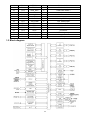
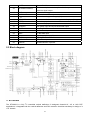
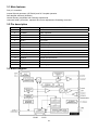
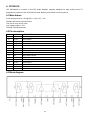
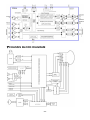
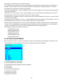
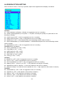
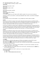
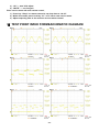
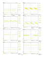
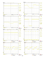
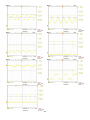
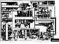
COLOR TELEVISION
SERVICE
MANUAL
21” T2S08 CHASSIS
WITH NICAM&TELETEXT
CONTENTS
ⅠSAFETY PRECAUTION ………………………………………………… 1
ⅡSPECIFICATION ………………………………………………………… 2
Ⅲ IC’S GENERAL DESCRIPTION ……………………………………… 3
Ⅳ SPECIAL IC INTRODUCTION ………………………………………… 3
Ⅴ CHASSIS BLOCK DIAGRAM ………………………………………… 12
Ⅵ SERVICE MODE&ADJUSTMENT …………………………………… 13
Ⅶ TEST POINT WAVE FORM&SCHEMATIC DIAGRAM …………… 18
-1-
ⅠSAFETY PRECAUTION
1. X-RAY RADIATION PRECAUTION
1.1 Excessive high voltage can produce potentially hazardous X-RAY RADIATION. To avoid such hazards
the high voltage must be specified limit. The normal value of the high voltage of this receiver is 27KV±
500V under 230V AC power source. The high voltage must not exceed 30KV.
1.2 Each time a receiver requires servicing the high voltage should be checked following the HIGH
VOLTAGE CHECK procedure in this manual. It is recommended the reading of the high voltage be
recorded as a part of the service record. It is important to use an accurate and reliable high voltage meter.
1.3 The primary source of X -RAY RADIATION in this TV receiver is the picture tube. For continued X-RAY
RADIATION protection, the replacement tube must be exactly the same type tube as used in this TV
receiver.
1.4 Some parts in this receiver have special safety-related characteristics for X-RAY RADIATION protection.
For continued safety, parts replacement should be undertaken only after referring the PRODUCT SAFETY
NOTICE below.
2. GENERAL SAFETY PRECAUTION
The following are the necessary precautions to be observed before servicing this chassis
WARNING: Service should not be attempted by anyone unfamiliar with the necessary
2.1 Since the power supply circuit of this receiver is directly connected to the AC power line. An isolation
transformer should be used during any dynamic service to avoid possible shock hazard.
2.2 Always discharge the picture tube anode to the CRT conductive coating before handling the picture
tube. The picture tube is highly evacuated and if broken, glass fragments will be violently expelled. Use
shatterproof goggles and keep picture tube away from the unprotected body while handling.
2.3 When replacing a chassis in the cabinet, always be certain that all the protective devices are put back
in place, such as: nonmetallic control; knobs, insulating covers, shields, isolation resistor-capacitor,
network, etc.
2.4 Connection wires must be kept away from components with high voltage or high temperature.
2.5 When replacing parts or circuit boards, disconnect the power cord.
2.6 When replacing a high voltage resistor (metal oxide resistor) on circuit board, keep the resistor APP.
10mm (1/2 in.) away from circuit board.
2.7 If any fuse in this TV receiver is broken, replace it with the FUSE specified in the chassis parts list.
2.8 The receiver is designed to operate with 230V (50Hz) AC mains.
3. PRODUCT SAFETY NOTICE
Many electrical and mechanical parts in this chassis have special safety-related characteristics are often
passed unnoticed by a visual inspection and the X-RAY RADIATON protection afforded by them cannot
necessarily be obtained by using replacement components rated for higher voltage. The use of substitute
replacement parts that do not have the same safety characteristics as specified in the parts list may create
shock, fire, X-RAY RADIATION or other hazards.
Warning!
There are no any repairable components in this TV set. Do not try to make any change to it. High voltage
inside may cause danger.
-1-
ⅡSPECIFICATION
RF SYSTEM
COLOR SYSTEM: PAL SECAM
SOUND SYSTEM:B/G D/K I NICAM STEREO
VIDEO SYSTEM
PAL SECAM NTSC4.43
TUNING SYSTEM
VOLTAGE SYNTHESIZER TUNING
RECEIVING CHANNEL
VHF-L: E2~S6
48.25 MHz~140.25MHz
VHF-H: S7~S36
147.25 MHz~423.25MHz
UHF: S37~DS57 431.25 MHz~863.25MHz
PROGRAM PRESET
99
AV JACKS
1 SIDE RCA AV IN
1 FULL SCART AND 1 AV SCART
TELETEXT
1PAGE
ANTENNA INPUT
75Ω(UNBALANCE)
AUDIO OUTPUT
≥2.5W
MAIN POWER
170-260V AC 50/60Hz
POWER CONSUMPTION
100W
ⅢCHIP GENERAL DESCRIPTION
1. MAIN BOARD PART
IC001
ST92195
IC002
24C08
IC101
STV2246
IC301
STV9306A/B
IC601
H11A817C
OPTOCOUPLERS
IC603
MC7808CT
+8V VOLTAGE REGULATOR
MC7805CT
+5V VOLTAGE REGULATOR
IC606
MC7812CT
+12V VOLTAGE REGULATOR
IC701
CD7522CS
3W AUDIO AMPLIFIER
IC801
STV8216
IC604
IC605
MCU With ON SCREEN DISPLAY and TELETEXT Decoder
8 Kbit Serial I2C Bus EEPROM
I²C BUS-Controlled Multistandard Single Chip TV Processor
BUS-Controlled VERTICAL DEFLECTION W.E/W CORRECTION CIRCUIT
Multi-standard TV Audio Processor and Digital Sound Demodulator
ⅣCHIP INTRODUCTION
1. ST92195
The ST92195 microcontrollers are developed and manufactured by STMicroelectronics using a proprietary
n-well HCMOS process. Their performance derives from the use of flexible 256-register programming model
for ultra-fast context switching and real-time event response. The intelligent on-chip peripherals offload the
ST9 core from I/O and data management processing tasks allowing critical application tasks to get the
maximum use of core resources. TheST92195 MCU support low power consumption and low voltage
operation for power-efficient and low-cost embedded systems.
1.1 Main features
28 fully-programmable I/Os
4 channels Analog/Digital Converter
-2-
Built in I2C bus interface
Built in OSD and Teletext decoder
14-bit Voltage Synthesis PWM output for VS tuning system
1.2 Pin description
Pin No.
1
2
3
4
5
6
7
8
9
10
11
12
13
14
15
16
17
18
19
20
21
22
23
24
25
26
27
28
29
30
31
32
33
34
35
36
37
38
39
40
Pin Name
P2.0
RESET
P0.7
P0.6
P0.5
P0.4
P0.3
P0.2
P0.1
P0.0
P3.7
P3.6
P3.5
P3.4
B
G
R
BLANK
P5.1
P5.0
VDD
JTDO
WSCF
WSCR
AVDD3
TEST0
MCFM
JTCK
TXCF
CVBSO
AVDD2
JTMS
CVBS2
CVBS1
AGND
GND
JTRST0
PXFM
AVDD1
HSYNC
Signal Name
IRIN
RESET
NC
MUTE
NC
ON/OFF
DESIGN
SCART1
SCART2
AV SEL
S0
S1
TV/DVD
DFD
B
G
R
BLANK
SDA
SCL
VDD
JTDO
WSCF
WSCR
AVDD3
TEST0
MCFM
JTCK
TXCF
CVBSO
AVDD2
JTMS
CVBS2
CVBS1
AGND
GND
JTRST0
PXFM
AVDD1
HSYNC
I/O
I
I
I/O
O
I/O
O
I
I
I
O
O
O
O
O
O
O
O
O
I/O
O
I
Function
IR Input
Hardware Reset
Not Used
Mute Output PIN
Not Used
Standby Output
Service menu control
Identify scart entering Design
Identify scart entering Design
AV Selection
AV/TV
AV/TV
TV/DVD
Default data control
OSD Blue colour Signal Output
OSD Green colour Signal Output
OSD Red colour Signal Output
OSD Blanking Output
I2C data line
I2C clock line
+5 V Digital Supply
Test Pin
Analog Pin For VPS / WPP slicer line PLL
Analog Pin For VPS / WPP slicer line PLL
+5V Analog VDD For PLL
Test Pin
Analog Pin for display pixel freq. multiplier
Test Pin
Analog pin for VPS /WSS line PLL
Test Pin
Analog Power supply
Test Pin
CVBS In for VPS / WSS
CVBS In for Teletext Slicer
Analog ground
Digital ground
Test Pin
Analog Pin for display pixel freq. multiplier
Analog Power Supply
Horizontal Sync Input
41
VSYNC
VSYNC
I
Vertical Sync Input
I
I
-3-
42
43
44
45
46
47
48
49
50
51
52
53
54
55
56
P4.0
P4.1
P4.2
P4.3
P4.4
P4.5
P4.6
P4.7
XTAL
XTAL
P2.5
P2.4
P2.3
P2.2
P2.1
BSW1
BSW2
SAW_SW1
NC
SAW_SW2
NC
Vlin PWM
VOL PWM
XTAL
XTAL
LED2
LED1
VS
NC
KB INPUT
O
O
O
I/O
O
I/O
O
O
O
O
O
I/O
I
1.3 Block diagram
-4-
Band switch 1
Band switch 2
SAW Filter switch 1
Not connected
SAW Filter switch 2
Not connected
V-linearity PWM output
VOL PWM output
Clock oscillator
Clock oscillator
LED driver
LED driver
VST Voltage ouput
Not connected
KEY Input
1.4 General application description
BAND SWITCH OUTPUT (Pin42 Pin43)
Pin42 BSW1
Pin43 BSW2
SELECTED BAND
0
0
NOT USED
0
1
VHF-L
1
0
VHF-H
1
1
UHF
KEYBOARD INPUT LEVEL (Pin56)
KEY IN (Pin 56)
KEY PRESSED
0.285 ~ 0.587V
Volume – (1 K ohm)
0.706 ~ 1.098V
Volume + (2.2 K ohm)
1.204~ 1.596V
Program- (3.9 K ohm)
1.704 ~ 2.096V
Program+ (6.2 K ohm)
2.194 ~ 2.586V
MENU (9.1 Kohm)
2.704 ~ 3.096V
TV/DVD (13.8 Kohm)
3.205 ~ 3.606V
AV/TV(22 Kohm)
3.745 ~ 4.145V
Analog (37.4 Kohm)
4.282 ~ 4.682V
OK (86.5 K ohm)
Note:The pull up resistor of Pin56 is 10K.
TV/AV SELECTION (Pin11/Pin12)
S0-Pin11
0
1
0
1
S1-Pin12
0
0
1
1
TV
AV1/RGB
AV2
S-VHS
TV/AV MODE
STANDBY OUTPUT (Pin6)
STD-BY (Pin 6)
Mode
0
Standby
1
Operating
2. STV2246H
The STV224XH is fully bus-controlled IC for TV that include PIF, SIF, Luma, Chroma and Deflection
processing functions. Used with a vertical frame booster (TDA8174A for a 90° chassis, STV9306 for a 110°
chassis), they allow multi-standard (BG/DK/I/MN/LL’, PAL/SECAM/NTSC) sets to be designed with very few
external components and no manual adjustments.
2.1 Main features
I²C Bus Control
PIF Circuit with PLL Demodulation (Positive and Negative Video)
SIF Circuit with QSS Structure, FM Demodulation and AM Demodulation for France
Intercarrier Capability and Built-in Sound Band pass
Sound Subcarrier Output for Stereo Chassis (FM, NICAM)
Integrated Chroma Filters and Luma Delay Line and Integrated Chroma Delay Line
3 channels input Video Switch and 2 channels CVBS output
OSD RGB Inputs and external RGB Inputs Interface
PAL/SECAM/NTSC Chroma Demodulators
Black Stretch and peaking Circuit
-5-
Automatic Cut-off Current Loop, manual Cut-off possible for low-cost applications
Two Horizontal Deflection PLLs
APR (Automatic RGB Peak Regulation) or RGB Peak Limitation Function
2.2 Pin description
PIN NO.
SYMBOL
DESCRIPTION
1
SIFIN1
SIF input
2
SIFIN2
SIF input
3
AGCSIFCAP
AGC SIF capacitor
4
VREFIF
Voltage reference filter
5
AGCPIFCAP
AGC PIF capacitor
6
PIFIN1
PIF input
7
PININ2
PIF input
8
TUNERAGCOUT
AGC Tuner output
9
IFPLL
IF PLL filter
10
GNDIF
IF Ground
11
AM/FMOUT/SC
AM/FM Mono sound or stereo carriers output
12
VCCIF
5V IF Supply
13
INTCVBSOUT
Internal CVBS output
14
EXTAUDIOIN
External audio input
15
PIFLC1
LC input
16
PIFLC2
LC input
17
VCC2
Video/LUMA Supply voltage (8V)
18
CVBSIN1
Internal video input
19
GND2
Video/LUMA ground
20
CVBSIN2
External video input
21
BS
Black stretch capacitor
22
Y/CVBSIN3
Y(SVHS) or CVBS3 external input
23
CHR
Chroma(SVHS) input
24
APR
Automatic RGB peak regulation
25
BEXT/Cb
External blue input or Cb input
26
GEXT/Y
External green input or Y input
27
REXT/Cr
External red input or Cr input
28
FBEXT
External fast blanking input
29
NC/CVBSOUT1
Not connected or CVBS output1
30
BOUT
Blue output
31
GOUT
Green output
32
ROUT
Red output
33
ICATH
Cathode current measurement input
34
BOSD
OSD Blue input
35
GOSD
OSD Green input
36
ROSD
OSD Red input
37
FBOSD/HC
OSD Fast blanking input/half contrast
38
XTAL3/BTUN
3.5x MHz Crystal or bell filter tuning capacitor
39
XTAL2
3.5x MHz Crystal
40
XTAL1
4.43/3.5x MHz Crystal
-6-
41
CLPF
Chroma PLL filter
42
X1/VAMP/CHROUT
XTAL1 control pin, vertical amplitude DAC output and chroma
reference signal output
43
GND1
Chroma/scanning ground
44
CVBSOUT2
Second video switch output
45
VCC1
Chroma/scanning power supply (8V)
46
BCL/SAF
Beam current limiter control voltage and safety input(X-ray)
47
VERT
Vertical output pulse
48
HOUT
Horizontal output pulse
49
LFB/SSC
Line flyback input and super-sandcastle output
50
SLPF
Scanning PLL filter
51
SCL
I2C Bus clock input
52
SDA
I2C Bus data input
53
VCCD
Digital supply voltage(5V)
54
GNDD
Digital ground
55
AUDIOOUT
Main audio output
56
FMCAP
FM demodulation capacitor
2.3 Block diagram
3. STV9306A
The STV9306 is a fully I2C controlled vertical deflection IC designed forusein110°, 4/3 or 16/9 CRT
applications. It integrates both the vertical deflection and E/W correction circuitries necessary in design of a
110° chassis.
-7-
3.1 Main features
Fully I2C controlled
Internal flyback generator (UPTO60V) and DC Coupled operation
Self adapted sawtooth (50/60Hz)
Vertical linearity, amplitude and centering adjustments.
Horizontal width, pincushion, trapezoid and corner adjustments. Breathing correction.
3.2 Pin description
PIN NO.
SYMBOL
DESCRIPTION
2
1
SCL
I C Bus clock
2
CRAMP
Ramp capacitor
3
SDA
I2C Bus data
4
CHOLD
Hold capacitor
5
SYNC
Sync input
6
VS
Supply voltage
7
FLYBACK
Flyback output
8
GND
Vertical output
9
OUT
Vertical output
10
VOPS
Vertical output Power Supply
11
EWOUT
EW output
12
SENS2
Vertical current sense2
13
EWFB
EW feedback
14
SENS1
Vertical current sense1
15
BREATHING
Breathing input
3.3 Block diagram
-8-
4. CD7522CS
The CD7522CS is a stereo 2×3W BTL audio amplifier, specially designed for high quality sound TV
applications. Features of the CD7522CS include Stand-by and Volume control functions.
4.1 Main feature
2×3W output power RL = 8Ω @THD = 0.5% VCC = 10V
Standby and volume control function
Low turn-on turn-off pop noise
Low voltage supply ≤ 14V
Thermal overload protection
4.2 Pin description
Pin NO.
SYMBOL
DESCRIPTION
1
VCC
Power supply
2
OUT1+
Ch1 output +
3
GND
Gnd (output ch1)
4
OUT1-
Ch1 output -
5
ST-BY
Standby control
6
Ch1 In
Ch1 audio output
7
GND
Gnd (Input)
8
Ch2 In
Ch2 audio output
9
Vol
DC volume control
10
OUT2-
Ch2 output -
11
GND
Gnd (output ch2)
12
OUT2+
Ch2 output +
4.3 Block diagram
-9-
5. STV8216
This chip included three main parts:
TV Sound Demodulator: provides all the necessary circuitry for the demodulation of audio transmissions of
European and Asian terrestrial TV broadcasts. The various transmission standards are automatically
detected and demodulated without user intervention.
Audio Processor: based on DSP technology independently controls loudspeaker, subwoofer and
headphone signals. It offers basic and advanced features, such as a ST Wide Surround, Equalizer, Automatic
Loudness and Smart Volume Control for television viewer comfort. The STV8226/36 versions can perform
additionally the SRS 3D Surround for stereo and mono signals.
Audio Matrix: 3 stereo and 1 mono external analog audio inputs to loudspeakers and headphone, with 2
stereo external analog audio outputs (SCART compatible).
5.1 Main features
NICAM, AM, FM Mono and FM 2 carrier stereo demodulators for all sound carriers between 4.5 and 7MHz
Mono input provided for optimum AM demodulation performances
Demodulation controlled by automatic standard recognition system
Sound IF AGC with wide range, over modulation and carrier offset recovery,
Smart volume control, smart volume control, 5-band equalizer bass/treble control, automatic loudness control
Loudspeaker and Headphone outputs with volume/balance controls and beeper
Subwoofer output with volume control and programmable bandwidth, spatial Sound Effects (ST Wide
Surround and Pseudo-Stereo), low-noise audio mutes and switches
I²C Bus-controlled, single and standard 27 MHz crystal oscillator,
Power supplies: 3.3V Digital, 5V or 8V Analog, embedded 3.3V regulators
5.2 Pin description
Pin NO.
SYMBOL
Pin TYPE
DESCRIPTION
1
SIF
Analog
Sound IF input
2
VTOP
Analog
ADC VTOP decoupling pin
3
VREF IF
Analog
AGC Voltage reference decoupling Pin
4
VDDIF
Analog power supply
3.3V Power supply for IF AGC & ADC
5
GNDIF
Analog power supply
Ground for IF AGC & ADC
6
MONOIN
Analog
Mono Input
7
AO1L
Analog
Left SCART1 audio output
8
AO1R
Analog
Right SCART1 audio output
9
VDDC
Analog power supply
3.3V Power supply for audio DAC/ADC
10
GNDC
Analog power supply
Ground for audio DAC/ADC
11
AI1L
Analog
Left SCART1 audio input
12
AI1R
Analog
Right SCART1 audio input
13
VMC1
Analog
Switched VREF decoupling Pin for audio converters (VMCP)
14
VMC2
Analog
VREF decoupling Pin for audio converters (VMC)
15
AI2L
Analog
Left SCART2 audio input
16
AI2R
Analog
Right SCART2 audio input
17
VDDA
Analog power supply
3.3 V power supply for audio buffers, matrix & bias
18
GNDAH
Analog power supply
Ground for audio buffers and SCART
19
AO2L
Analog
Left SCART2 Audio output
-10-
20
AO2R
Analog
Right SCART2 Audio output
21
VDDH
Analog power supply
8V/5V power supply for SCART and audio buffers
22
VREFA
Analog
Voltage reference for audio buffers
23
AI3L
Analog
Left SCART3 audio input
24
AI3R
Analog
Right SCART3 audio input
25
BGAP
Analog
Bandgap voltage source decoupling
26
LSL
Analog
Left loudspeaker output
27
LSR
Analog
Right loudspeaker output
28
SW
Analog
Subwoofer output
29
HPL
Analog
Left headphone output
30
HPR
Analog
Right headphone output
31
GNDSA
Analog power supply
Substrate analog/digital shield
32
HPD
Bidirectional
Headphone detection input (active low)
33
ADR
Input
Hardware I²C chip address control
34
SCL
Open drain
I²C serial clock
35
SDA
Open drain
I²C serial data
36
REG
Analog
5V power regulator control
37
RESET
Input
Hardware reset (active low)
38
SYSCK
Bidirectional
System clock output
39
MCK
Bidirectional
I²S master clock output
40
VDD1
Digital power supply
3.3V Power supply for digital core & IO cells
41
GND1
Digital power supply
Ground for digital core & IO cells
42
GNDSP
Analog power supply
Substrate analog/digital shield for clock-PLL
43
XTI
Input
Crystal oscillator Input
44
XTO
Output
Crystal oscillator output
45
VDDP
Analog power supply
3.3V power supply for analog PLL clock
46
GNDP
Analog power supply
Ground for analog PLL clock
47
GND2
Digital power supply
Ground for digital core, DSPs & IO cells
48
VDD2
Digital power supply
3.3V power supply for digital core, DSPs & IO cells
49
CKTST
Input
Must be connected to ground
50
SDO
Bidirectional
I²S bus data output
51
ST/SDI
Bidirectional
Stereo detection output / I²S bus data input
52
WS
Bidirectional
I²S bus word select output
53
SCK
Bidirectional
I²S bus clock output
54
BUS1
Bidirectional
I²C bus expander output1
55
BUS0
Bidirectional
I²C bus expander output2
56
IRQ
Bidirectional
I²C status read request
5.3 Block diagram
-11-
ⅤCHASSIS BLOCK DIAGRAM
-12-
Ⅵ SERVICE MODE&ADJUSTMENT
The Service-1 mode is entered by pressing the “SERVICE” key on
remote control when the TV is in ON condition and not in any Menu
mode. In service mode, by pressing “OK” key, Service-2 is accessed. by
pressing “OK” key again, Serivice-3 is accessed. By pressing “PP” key,
exit Service mode.
6.1 WHITE BALANCE ADJUSTMENT
The items within the Service-1 mode can be accessed using P+/P- keys
and the selected item can be modified by using V+/V- keys. The
parameters controlled in the Service-1 menu
are :
a) Red Gain ( 0 ... 63 )
b) DC Red ( 0 .... 127)
c) Green Gain ( 0 .... 63)
d) DC Green ( 0 .... 127)
e) Blue Gain ( 0 .... 63)
f) DC Blue ( 0 .... 127)
g) APR_threshold (0….15)
h) LOGO ( the first show the length of logo, and the followed is the
logo)
i) R-Cutoff (0…63)
j) G-Cutoff (0…63)
The display of Service-1 menu is showed as follows:
6.2 VIF ADJUSTMENT
When in Service-1 menu ,if “OK” key is pressed , Service-2 menu appears and the display
is as follows.The parameters controlled in the Service-2 menu are :
a) Tuner AGC ( 0 ... 63 )
b) Horizontal position 50 Hz( 0 ... 63)
c) Vertical position 50 Hz (0…15)
d) Vertical amplitude 50Hz (0…63)
e) Vertical linearity 50Hz (0…63)
f) Horizontal position 60 Hz( 0 ... 63)
g) Vertical position 60 Hz (0…15)
h) Vertical amplitude 60 Hz (0…63)
i) Vertical linearity 60 Hz (0…63)
j) Sub-Bright Maximum (0…63)
k) Sub-Bright Minimum (0…63)
l) Sub Tint (0…63)
m) VCO Coarse ( 0 ... 15)
n) VCO Fine ( 0 ... 127 )
o) VCO Coarse L1( 0 ... 15)
p) VCO Fine L1( 0 ... 127 )
-13-
The display of Service-2 menu is showed as shown:
The VCO status bar at the bottom of the screen appears only if either VCO Coarse item or VCO Fine item is
selected. The VCO status is read from the Read register of STV223X/4X and guides whether to Increase /
Decrease the VCO registers to attain VCO OK Status.
For doing VCO adjustment , Feed a 38.9MHZ Carrier as IF input and adjust VCO Coarse and fine parameters
to get VCO OK Status.
If the cursor is in VCO Coarse or Fine, and the display shows VCO OK status, then pressing of AV” key will
automatically put VCO fine to the Centre of the +60 to -60 KHz window.
For doing VCO L1 adjustment ,Feed a 33.9 MHZ carrier as IF input and adjust VCO Coarse L1 and VCO Fine
L1 to get VCO OK Status.
If the cursor is in VCO Coarse L1 or Fine L1 , and the display shows VCO OK status, then pressing of “AV” key
will automatically put VCO fine for L1 to the Centre of the +60 to -60 KHz window.
Another fast way of adjustment of VCO is to put the selection bar to either VCO Coarse or fine and press the
“AV” key. The VCO adjustment is done automatically. Similarly if you put the selection bar to VCO Coarse L1
or Fine L1 and press the “AV” key , the VCO L1 adjustment will be done automatically.
NOTE:Below items are not used in this chassis:
Vertical position 50 Hz
Vertical amplitude 50Hz
Vertical linearity 50Hz
Vertical position 60 Hz
Vertical amplitude 60 Hz
Vertical linearity 60 Hz
6.3 STV9306 ADJUSTMENT
When in Service-2 menu, if “OK” key is pressed, Service-3 menu appears and the display is as follows, if the
IC STV9306 has not been detected, then Service-4 (design menu) menu will appear.
1) Vertical amplitude for 50Hz signal.
2) Vertical amplitude for 60Hz signal.
3) Vertical shift (internal separated by 50Hz and 60Hz)
4) S Correction.
5) C Correction.
6) Horizontal width adjustment.
7) Pincushion Correction.
8) E/W Sharp Correction.
9) Trapezium Correction.
-14-
6.4 DESIGN OPTION SETTING
When in Service-3 menu, if “OK” key is pressed, Option menu appears and the display is as follows:
OPTION1
b7 = Over modulation (0=Disable, 1=Enable, it’s suggested to set it to 0 normally.)
b5 = P/N/S crystals application (0=2 Crystals, 1= 1 Crystals, according the quantity of crystal used for color
decoding in chassis.)
b4 = Cutoff Loop (0= OFF, 1=ON, it’s suggested to set it to 1 normally)
b3 = Safety Reset (0=Active, 1=Non, it’s suggested to set it to 0 normally)
b2 = MONO IN (0 = OFF, 1= ON, Depend on the sound decoding solution used in chassis. )
b1 = Sound Demodulation (0 = Intercarrier/MONO, 1 =QSS/NICAM, depend on the sound decoding solution
used in chassis.)
b0 = logo display (0 =OFF, 1= ON, it’s suggested to set it to 0 normally.)
OPTION2 (set to 0 by default)
b5 = HALF_CONTRAST (0 = OFF, 1=ON)
b4 = Color 6dB (0 = OFF, 1 = ON)
b3 = APR Feature (0 = ON, 1= OFF)
b2 = Black Stretch (0 = ON, 1= OFF)
b1 = Auto Flesh (0 = ON, 1= OFF)
b0 = Coring (0 = ON, 1 = OFF)
OPTION3
b7 =SMART (0 = OFF, 1=ON, it’s suggested to set it to 1 normally)
b5 = AVL (0 = OFF, 1=ON, it’s suggested to set it to 0 normally.)
b4 = PIF overmodulation (0 = OFF, 1= ON, it’s suggested to set it to 0 normally.)
b3 = Market_France --- secam LL (0 = OFF, 1 = ON, depend on the solution of chassis.)
b2 = Manual/Auto cutoff (0 = Manual, 1 = Auto cutoff, depend on the CRT for chassis.)
b1 = Mute pin low/high –to control the mute of speaker (0 = low, 1 = high, depend on the solution of chassis.)
OPTION4
b6 = WIDE MODE (0 = OFF, 1=ON, it’s suggested to set it to 0 normally.)
b4 = SCART2 (0 = OFF, 1=ON, depend on the solution of chassis.)
b3 = RGB (0 = OFF, 1= ON, depend on the solution of chassis.)
b2 = SVHS (0 = OFF, 1= ON, depend on the solution of chassis.)
b1 = AV2 (0 = OFF, 1= ON, depend on the solution of chassis.)
-15-
b0 = AV1 (0 = OFF, 1= ON, depend on the solution of chassis.)
OPTION5
There are 8 bits used in OPTION 5. They are b0, b1, b2, b3, b4, b5, b6 and b7.
For b0, normally, ST suggests to set it to 0.
For b1, b2, they are used to select teletext languages.
For b3, it’s used to enable AV3 and SVHS. When b3 is set to 0, SVHS is enabled. When b3 is set to 1 in
binary, the value is 8 in decimal. AV3 is enabled.
For b4, b5, b6 and b7 of OPTION 5 are also used to set the brightness of background in teletext mode. When
b4 b5 b6 and b7 are all set to 0, the brightness of teletext background is the same as brightness of TV
background. When b4, b5, b6 and b7 are all set to 1, it’s the maximum brightness of teletext background. It’s
the minimum brightness of teletext background when b4 is set to 1, and b5, b6 and b7 are all set to 0. you can
set these 4 bits according to your favorite brightness of teletext background.
A. for 11 OSD languages CPU ST92195C7B1/MNS and ST92195C7B1/MTH for east Europe, the setting of
the b1 and b2 is listed as below.
1. If b1 = b2 = 0, then the TEXT languages like “ENGLISH, FRENCH, SWEDISH, CZECH, GERMAN,
PORTUGUESE (SPANISH), ITALIAN, RUMANIAN” can be decoded;
2. If b1=1, b2=0, then the TEXT languages like “ENGLISH, RUSSIAN (BULGARIAN), HUNGARIAN,
TURKISH, GERMAN, PORTUGUESE (SPANISH), ITALIAN, RUMANIAN” can be decoded.
3. If b1=0, b2=1, then the TEXT languages like “POLISH, RUSSIAN (BULGARIAN), SWEDISH, SLOVAK,
GERMAN, SLOVENIAN, LITHUANIAN, RUMANIAN” can be decoded.
4. If b1 = b2 =1, then the TEXT languages like “POLISH, RUSSIAN (BULGARIAN), SWEDISH, CZECH,
GERMAN, CROATIAN, LETTISH, RUMANIAN” can be decoded.
B. for 12 OSD languages CPU ST92195C7B1/MNU and ST92195C7B1/MOK (SHRINK VERSION) for
Western Europe, the setting of the b1 and b2 is as below.
1. If b1 = b2 = 0, then the TEXT languages like “ENGLISH, FRENCH, FINNISH, CZECH, GERMAN,
PORTUGUESE (SPANISH), ITALIAN, GREEK” can be decoded;
2. If b1=1, b2=0, then the TEXT languages like “ENGLISH, FRENCH, DANISH, NORWEGIAN, GERMAN,
PORTUGUESE (SPANISH), ITALIAN, GREEK” can be decoded.
3. If b1=0, b2=1, then the TEXT languages like “POLISH, FRENCH, SWEDISH, CZECH, HOLLAND,
SERBIAN, ITALIAN, RUMANIAN” can be decoded.
4. If b1 = b2 =1, then the TEXT languages like “POLISH, FRENCH, SWEDISH, CZECH, GERMAN,
PORTUGUESE (SPANISH), LETTISH, RUMANIAN” can be decoded.
ST Text
b0 is used to change the process for adjusting Auto gain.
1) When CPU ST92195C7B1/MOK is used, the b0 is suggested to set to 0, the gain table for shrink version
should be selected.
2) When CPU ST92195C7B1/MNU is used, the b0 is suggested to set to 1, the gain table for normal version
will be selected.
b1, b2, b3 = select the correct process, only for ST engineer adjustment.
ROM_M6_P_valid | OSDEPROM_M6_R_valid | ROM_M6_R_valid | EPROM_M6_R_valid
EPROM_M6_R_valid | ROMLESS_H5_P_valid | ROM_H5_P_valid | EPROM_M6_A_valid
/* note: ROMLESS_M6_R_valid == ROM_M6_R_valid*/
b4 = Color transition for SVHS of STV224XX (0 = b5 is available, 1 = b5 is not available, and “SHARPNESS”
is no feature.)
b5 = (0 = STV224XH, 1 = STV224XC/D/E).
-16-
b6 = Tuner Drift Correction (0 = OFF, 1 = ON.)
b7 = RGB/DVD display on screen (0 = RGB, 1 = DVD.)
HPOS OSD,
Adjust horizontal position of OSD.
VPOS OSD,
Adjust vertical position of OSD.
HPOS TXT,
Adjust horizontal position of teletext.
VPOS TXT,
Adjust vertical position of teletext.
HOTEL MODE,
To set HOTEL MODE ON or OFF. When HOTEL MODE is enabled. The end user can not make any
adjustment of items in menu INSTALL, AUDIO and ORGANIZE. Menu INSTALL and AUDIO will disappear
automatically.
Volume Limit,
To set maximum volume of HOTEL MODE. It’s only available when HOTEL MODE is enabled.
SndSt 1
b0, b1, b2, b3 of SndSt 1 are used to set the sound output level at pin 26 and pin 27 of STV8216 with RF
signal. When b0, b1, b2, b3 of SndSt 1 are all set 0, the minimum sound output level will be got at pin 26 and
pin 27 of STV8216 with RF signal. When b0, b1, b2, b3 of SndSt 1 are all set 1, it’s 15 in decimal. The
maximum sound output level will be got at pin 26 and pin 27 of STV8216 with RF signal.
b4, b5, b6, b7 of SndSt 1 are used to set the “SURROUND” gain at pin 26 and pin 27 of STV8216 with RF &
AV signal. When b4, b5, b6, b7 of SndSt 1 are all set 0, the minimum “SURROUND” gain will be got at pin 26
and pin 27 of STV8216 with RF & AV signal. When b4, b5, b6, b7 of SndSt 1 are all set 1, it’s 240 in decimal.
The maximum “SURROUND” gain will be got at pin 26 and pin 27 of STV8216 with RF signal.
SndSt 2
b0, b2, b2, b3 of SndSt 2 are used to set the sound output level at pin 26 and pin 27 of STV8216 with AV
signal. When b0, b2, b2, b3 of SndSt 1 are all set 0, the minimum sound output level will be got at pin 26 and
pin 27 of STV8216 with AV signal. When b0, b2, b2, b3 of SndSt 1 are all set 1, it’s 15 in decimal. The
maximum sound output level will be got at pin 26 and pin 27 of STV8216 with AV signal.
b4, b5, b6, b7 of SndSt 2 are used to set the “EQUALIZER” gain at pin 26 and pin 27 of STV8216 with RF &
AV signal. When b4, b5, b6, b7 of SndSt 1 are all set 0, the maximum “EQUALIZER” gain will be got at pin 26
and pin 27 of STV8216 with RF & AV signal. When b4, b5, b6, b7 of SndSt 1 are all set 1, it’s 240 in decimal.
The minimum “EQUALIZER” gain will be got at pin 26 and pin 27 of STV8216 with RF & AV signal.
LL1 MAGC,
Just for SECAM LL1 SIF AGC setting purpose in STV8216. No available for PAL and NTSC system.
When the item “LL1 MAGC” is set to OFF, the SIF AGC of STV8216 is set by software.
When the item “LL1 MAGC” is set to ON, the SIF AGC of STV8216 can be set manually. The following steps
can be followed when set this item.
1) To get a RF SECAM LL1 signal without sound modulation, only sound carrier is available. And put the
signal to input of tuner in CTV 5 chassis.
2) To press “SERVICE” key on remote control to enter service menu. And select the item “LL1 MAGC” by
P+ or P- key on remote control.
Set the item “LL1 MAGC” from “OFF” to “ON” by V+ or V- key on remote control.
service command,
1) “PP”----exit
2) “OK”---- switch between the service menu
-17-
3) “AV”---- auto VCO adjust
4) “MUTE” ---- one line gain
Enter service menu with user remote control,
1) Press key “Sleep” on remote control to set sleep time to “00:50”.
2) Within 5 seconds, press local key “V+” in TV set to enter service menu.
3) Adjust expecting item as the same as service remote control.
Ⅶ TEST POINT WAVE FORM&SCHEMATIC DIAGRAM
-18-
-19-
-20-
-21-
HPR
5
6
7
8
9
10
4
3
2
SCART1 ID
BI
GI
FBI
RI
V IN1
V OUT1
L403 15uH
L402 15uH
L404 15uH
L401 15uH
100K
1
C423 1u/50V
R414
220
330p
5
C417 100K
6
C418
330p
C421
330p
7
C422
L406 15uH
R413 10K
C413
1u/50V
L408 15uH
R417 220
L405 15uH
R412 10K
C424
1u/50V
C414
1u/50V
AI1L
AO1L
AI1R
AO1R
OUT2+
GND2
OUT2-
VOL
IN2
GND
IN1
STDBY
OUT1-
GND1
R708 2.2
11
R257
1K
TP5
TP6
R501
1u/50V
C412
C409
1u/50V
R521
KR
2.2K
R519
1.2K
AO2R
2
2
R520
10K
R522 10K
XP502
2
Q507
BF423
R523 10K
AI2R
AO2L
KG
2.2K TP23
1.2K
R513
1.2K
R405 220
R402 10K
R406 220
R401 10K
R407 100K
C410
1u/50V
AI2L
CRT
KB
TP22
R515
C516 D506
680p 1N4007
Q504
BF423
R524 10K
G OUT
ICAT
R240
560
R230
470
C511 D504
680p 1N4007
BF423
B OUT
+15V
SCART2 ID
V IN2
V OUT2
D701
1N4148
R OUT
TXT
+
C701
220u
16V
R703
100K
Q207
2SC1815
2.2K
680p
XS302
D202
TP4
R244
56K
ABL
H OUT
SC
VSYNC
TP3
R702
4.7K
C830
2200p
OSD B
R811
4.7K
R506
Q502
C411
1u/50V
+
R809 18K
IF
VCC
BL
4
8
D501
1N4007
C517
Q701
2SA1015
Q702
2SC1815
OSD G
OUT R
C818 0.1u
C816
0.1u
R409
68
R701
4.7K
C702
47u/16V
C829
2200p
1N4148
3
9
330p 330p 330p 330p
330p
L407 15uH
TP21
R810 18K
R812
4.7K
+5V-1
2
BH
BU
VT
AGC
1
21 20 19 18 17 16 15 14 13 12 11 10
C415 C420 C416 C419
330p 330p 330p 330p
OUT L
28
TU201
AGC
VT
1
RO
C708 0.1u
OSD R
27
+
C815
10u/16V
L803
10uH
XS702
R408 100K
SW
LSR
26
C817 C819
10u/16V 10u/16V
+
C403 C408 C404 C407
C709
0.1u
OSD FB
25
330p 330p 330p 330p
SPK L
V OUT2
HPD
24
2
R416
RI
LO
R SPK
LSL
BGAP
AL3R
23
C707
0.1u
MUTE
22
C814
0.1u
AI3L
VERFA
21
C401 C406 C402 C405
C706
0.1u
29
+8V
20
3
R419
68
R709 2.2
30
HPL
31
GNDSA
32
ADR
SCL
33
+8V
C813
10u/16V
R803
330
SAD
REG
RESET
VDDH
AO2R
MCK
SYSCK
AO2L
19
+
C808 C811
34
XS701
0.1u
0.1u 10u/16V 0.1u 10u/16V
35
OUT R
+
AI1L
AI1R
AO1R
AO1L
+5V
18
C812
36
C809
+
C806
10u/16V
TP2
TP1
GNDAH
VDD1
17
37
OUT L
C810
16
38
SDA
SCL
15
39
VDDA
GND1
GNDSP
AI2L
14
40
AI2R
XTI
13
41
R705 3.3K
+
12
42
VMC2
AI1R
VMC1
VDDP
XTO
43
AI2L
AI2R
+8V
22
SIF
44
+
L802
10uH
R802
11
C807
0.1u
0.22u 0.1u
C802
56p
GNDP
10
C805
0.1u
C803 C804
GND2
9
45
AI1L
VDCC
8
46
GNDC
VDD2
CKTST
7
47
+
C703
470u/25V
0.47u/16V
AO2L
AO2R
+8V
6
48
AO1R
AO1L
MONOIN
5
49
SD0
ST
WS
4
50
OUT1+
VCC
D801
270K
1N4148
+
3
51
GNDIF
BUS1
2
52
VDDIF
VERFIF
IRQ
VTOP
IC801
STV8216
SIF
1
53
SCK
54
BUS0
55
4
LI
BI
XS401
+
56
0.1u
0.1u
2
R704
10K
R806
4.7K
5
+
0.1u
R805
100
6
GI
CD7522CS
+
+
R804
100
7
SW
RI
+
C821
22p
8
FBI
VO
R707 0.47
+12V-1
Q801
2SA1015
9
VI
RO
+
C824
R808
220K
C820
RI
LO
+
47u/16V
C827 +
27MHz
C822
LI
BI
+
C826
C521
2200p/2KV
R507
47K
R514 10K
R505 10K
TP7
5.6V
ZD501
11
13
R128
OSD G
1K R129 1K
R127
OSD R
1K R131 1K
R126
OSD FB
1K R133 1K
15
16
17
18
S1
NC
DATA PRT
NC
SIF SW
NC
PIF SW
BSW2
19
20
4MHz
46
C115
39p
BSW2
43
1N4148
42
OSD R
40 TP19
H SYNC
OSD FB
AVDD1
C105 0.22u
D104
411N4148
39
24
+
38
JTD0
WSCF
ESCR
AGND
TXT VIN
C136
36
WSS
33
26
AVDD3
JTMS
R118 5.6K
27
28
TEST0
AVDD2
MCFM
CVBS0
JTCK
TXCF
R218
C229
470
470
NC
B OUT
G OUT
FB EXT
R EXT
G EXT
R OUT
B EXT
OSD B
ICAT
APR
CHR
Y/CVBS IN3
OSD G
OSD R
OSD FB
CVBS IN2
XTAL3
GND2
CVBS IN1
BS
4700p
XTAL2
0.1u
1u/50V
ABL-V
+12V
75
R301
100
SCL
SDA
2SC1815
1
R302
100
3
4
C303
C304
0.68u
0.1u
R317 1K
5
6
7
8
9
10
11
C305
12
13
14
R322
100
BREATH
SENS1
EWSENS
SENS2
EWOUT
VOPS
OUT
GND
FLYBACK
VCC
SDA
2
SYNC
R253
75
R423 R422 R421
75
75
75
CHOLD
IC301 STV9306
R228
330K
CRAMP
R420
75
FBI
RI
GI
BI
0.1u
C225
C425
1u/50V
R418
V SYNC
+24V
+12V
R311
R313
15K
R314 R335 R324
10K
100 68K
C307
+
1
+
2
ZD301
43V
0.56
C306
C308
1000u/16V 0.033u
R329 10
C310
4.7u/160V
R320
2.2K
1000p
R323
2
TP24
R312
100K
15 220K
100u/35V
D302
1N4007
R331 10
C210 C211
47u/16V 0.1u
R336
470
TP25
C312
C602
C119
0.47u/50V
C601
0.22u 250V
R124 1.5K
TXT
C121
82p
R130
1.5K
31
0.1u
30
R121 15K
+
R141 10
C111
47u/16V
C123
2200p
R625
6.8
C309
1u/250V
0.01uF
C311
0.22uF
L301 31uH
1
R308
R611
5.6K
9
17
C616
1000p 2KV
XS603
XP601
R624
39
DEGAUSSING COIL
AC230V
50Hz
V in
C658
220u/16V
V out
C614
0.1u
16
8
2
R626
2.7K
D616
1N4148
13
C617
0.015u
10K
R312 1K
D305
RGP15J
C661
100u/16V
7805
D308
RGP15J
V out
HV
D101
1N4148
C106
1u/50V
RST
+
D631
RG2
TP17
2
VR631
2K
R637
R639
D636
15K
1N4148
STD BY
150K
D641
6.2V
C629
2200p 400V
R629
8.2M 1/2W
1. IS MARK OF CRITICAL COMPONENT
2.SUBJECT TO CHANGE WITHOUT NOTICE
R636
10K
H OUT
+
C326
0.1u
C638
0.22uF
D309
1N4148
D303
RGP15J
Q301
2SC2383
R318 1K
1
+
C320
1000u/35V
R310
1
C322
470p/500V
FOCUS
R307
2
1
D311
1N4007
R306
220
C324
2200p
C321
22u/160V
R303
150
TP29
R325
8.2K
+24V
ABL-V
ABL
TP28
SCREEN
+
+15V
C659
1uF/50V
TP18
Q682
2SC1815
1
+24V
+33V
+
15K
IC602
uPC574
R635
150K
+
D304
1N4148
+140V
+12V-1
+140V
R640
C330
47p
D310
1N4007
TP16
Q631 2SC1815
1
R316
SC
TP15
R113
100K
R114
4.7K
270
3
T302 ***
+5V-1
+5V
Q102
2SA1015
TP26
R399 ***
+
GND
R115
470
R326 220K
C319
10u/250V
TP14
C632
47u/16V
C671
0.1u
ZD101
3.9V
+
+8V
C639
470u/16V
R655
1K
C641
47u/160V
3
V in
+
+
470p/500V
+
IC604 7805
V out
GND
9
R623
2.7K
V out
C318
C674
0.1u
5
V in
C675
47u/16V
GND
R633 22
C645 470u/25V
D635
RU4YX
C631
470P
Q612
2SC3807
R617
2.2K
15K
C635
1000u/25V
2
V in
+
TP13
IC603
7808
C657
0.1u
R116
Q613
ST1802
C615 R615
0.015u 22K
L601
SW601
TP12
IC606
7812
C651
0.1u
R685
C637
470P
Q611
2SA1015
11V
+5V
XS601
R619
22
D617
RGP15J
C608
0.1u 400V
XS602
TP11
IC605
5
0.22u 250V
T601
UF-LB-1604
22p
R622
15K
D614
1N4148
C613
4700p
D634
RU3YX
C634
470P
C606 D606 D604 C604
+5V
R143 10
C134
47u/16V
C135
4700p
32
29
28
0.1u
GND
15
R621
180K
35
34
27
0.1u
R638 3.3K
T604
R602
5D11
R139 5.6K
37
C122
C112
0.1u
C113
22p
V SYNC
SC
R149 5.6K
TP20
C133
0.1u
+
23
TP10
R620
180K
F601
22
25
+
ZD102
5.1V
R190 1K
R119 6.8K
R117 10
C103
4700p
GND
+
C506
100u/16V
2
C108
0.1u
C104
220p R111 5.6K
VDD
680p
R526 22
ICAT
R518
330
C515
680p
Q203
2SC1815
C607
100u/400V
+
T3.15A 250V
21
C109
100u/16V
D603-D607
RM11C
C603 D603 D605 C605
BSW1
+5V
D105
V SYNC
PXFM
C603-C606
1000p 1KV
VT
44
OSD G
JTRET0
C114
39p
45
BSW1
SCL
+
Q683
B892
R104 33K
SIF SW
OSD B
SDA
C510
680p
+
2.7K
R512
330
2
47
R134 1K
+
+
+
OSD B
S0
26
R516 100
L302
1mH
560
2
14
TV /AV
+
IC601
H11A817
R103
33K
C102
0.1u
48
ZD601
IC102
24C08
R123 10K
C110
47u/16V
C205
0.1u
C207
0.1u
C101 0.1u
49
25
R OUT
29
+15V
VLIN PWM
1K
+33V
R101
33K
Q101
2N3904
24
30
+12V
VOL PWM
SCART2 ID
R212
470
R213
RT601
MZ72-18
R106 12K
SCL
A2
10
12
GND SDA
SDA
SCL
+5V
R107 12K
9
R108 2.7K
WC
SCART1 ID
R112 33K
51
50
R211
X101
R109 2.7K
VCC
OSC
31
10uH
10K
R214
22K
23
32
+
V OUT1
8
OSC
SERVICE
Q202
C233
470u/16V
L202
SF203
5.5MHz
R215
2.2K 6.8K 2.2K
R102 10K
22
C426 C217
R223
1K
R224
1K
+8V
R105 6.8K
STD BY
52
XTAL1
CLPF
T201
7K011 C219
10uH
+5V-1
SCART2 ID
R125
1N41
48
47p
AGC
SIF
7
STDBY LED
C131
VCC2
PIF LC1
L203
L201
10uH
2
IF
6
R160 6.8K
NC
53
+8V
R110 4.7K
SCART1 ID
A1
R137 39K
54
0.1u
+5V
STDBY LED
C204
5
A0
VT
MUTE
IF
4.7K
R136 6.8K
STD BY
NC
C221
47u/16V
K3953M
4.7K
4
1 SF202
SIF SW
3
NC
2
21
33
R504
330
C429 C428 C427
+
0.1u
3
R216
R120
R122
MUTE
RESET
D201
R217
RST
1
55
34
Q501
2SC1815
R509
100
C505
V CIOL
R171 10K
2
20
C218
4
+5V
Q201
2SC1815
19
35
+
C203
0.1u
3
56
36
R510 100
+
KB IN
18
+
IR IN
37
TP9
+
IC101 ST92195
1
17
R219
150
SF201
K9650M
+5V
C238
0.1u
R236 27KC237
56K
R229
V AMP
GND1
EXTAUDIAIN
INTCVBSOUT CVBSOUT
VCC1
+
16
38
G OUT
SCL
0.33u
5
15
39
R234
47K
R502 100
Q504
BF422
Q501
BF422
XP501R508 4.7K
B OUT
H COIL
4
14
4.43
MHz
40
XS101
+8V
2
5
VCC IF
AM/FM OUT
L801
10uH
XS101
+8V
12
13
C801
47p TP8
41
R231
470
V IN2
C206
C222 C223 C224 C209
1u/50V 10u/16V 0.022u 1u/50V
11
42
PIF LC2
R239
2.2K
R246
10
470u
16V
43
44
R801560
R074 R074 R074 R075 R072 R073
3.9K 3.9K 3.9K 6.2K 1K 2.2K
45
BCL
VERT
H OUT
9
R221
150
+
GND IF
IF PLL
8
R168 10
C127
0.1u
+
D203
8.2K
R238
LFB
SCL
7
46
1K
R235 R233 R232
C228 C227 C226
0.1u 0.1u 0.1u
V IN1
+
6
47
X202
1u/50V
5
C231
C261
15p
+8V
+
4
4.7u
1u/50V
3
Q503
2SA1015
1u/50V
2
48
C239
0.1u
C241
0.1u
C208
1000p
1
49
AGC OUT
R015
1K
50
PIF IN1
R170
510
SIF IN1
IR
SW3 SW3 SW3 SW4 SW5 SW6
PPPP+
VV+
SIF IN2
IC201
STV2248
D111
HFT505M
IC103
HS0038
51
SDA
BSW2
BSW1
52
1N4148
15K 2.2K 2.2K
100 100
100u
16V
53
54
VCC D
FM CAP
10uH
55
AUDIO OUT
+5V-1
56
VREF IF
+
L206
+
C235
1u/50V
R247
C232
AGCPIFCAP
C213
47u/16V
GND D
+
AGCSIFCAP
+
C214
47u/16V
R248
C234
0.1u
R245
C243
4700p
C242
L204
10uH
R237
R201
100
C212
47u/16V
SLPF
+
27K 0.1u
PIF IN2
R203
4.7K
L205
10uH
R243
2.2K
C245
+
+
+
R202 C216
2.2u/50V
IF
C220
22u/16V
+5V
GI
+
R807 X801 C823 22p
C825
10u/16V
L101
10uH
SW
RI
21 20 19 18 17 16 15 14 13 12 11 10
IC701
R813 33
SDA
SCL
FBI
VO
XS402
R415
VI
T2S08 CHASSIS SCHEMATIC DIAGRAM
SCL
SDA
+5V-1
T301
JDT1924
TP27
C317
0.039u
L303
0.2uH
Q302
2SC5296
D301
BY228
C313
7500p
1.6KV
C316
220p
2KV
R321
8.2K
R319
R249 22K
10K
C314
+
4700p
C315
0.018uF
D302
RGP15J
C246
4.7u/50V
Title: T2S08 CHASSIS SCHEMATIC DIAGRAM
Number:
Revision: 1
Date: 20-May-2007
Described:
Sheet: 1 of 1
Checked:
Approved: