1
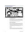
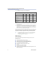
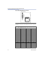
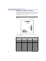
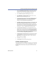
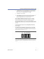
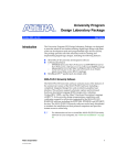
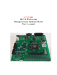
University Program Design Laboratory Package User Guide
MOUSE
+
FLEX_EXPAN_
VGA
FLEX_DIGIT
CONF_D TCK POWER
– DC +
EPC1
P1
P2
D2
D3
EPM7128S
P4
D4
D5
D10
D6
D11
D7
D12
D8
P8
P10
MAX_PB2
P6 P9
MAX_SW2
MAX_PB1
MAX_SW1
P5
D13
D14
FLEX_SWITCH
D15
D16
JTAG_OUT
P3
EPF10K20
or
EPF10K70
FLEX_PB1
FLEX_PB2
P7 D1
MAX_DIGIT
D9
FLEX_EXPAN_
C2 TDI TDO
BOARD
C19
U5
RAW
–
R2
R1
DC_IN
DEVICE
MAX_EXPANSION
JTAG_IN
Figure 1. UP Education Board Block Diagram
FLEX_EXPAN_
DC_IN & RAW Power Input
The DC_IN power input accepts a 2.5-mm × 5.55-mm female connector.
The acceptable DC input is 7 to 9 V DC at a minimum of 350 mA. The
RAW power input consists of two holes for connecting an unregulated
power source. The hole marked with a plus sign (+) is the positive input;
the hole marked with a minus sign (–) is board-common.
On-Board Voltage Regulator
The on-board voltage regulator, an LM340T, regulates the DC positive
input at 5 V. The DC input consists of two holes for connecting a 5-V DC
regulated power source. The hole marked with a plus sign (+) is the
positive input; the hole marked with a minus sign (–) is board-common.
A green light-emitting diode (LED) labeled POWER is illuminated when
current is flowing from the 5-V DC regulated power source.
Oscillator
The UP Education Board contains a 25.175-MHz crystal oscillator. The
output of the oscillator drives a global clock input on the EPM7128S
device (pin 83) and a global clock input on the FLEX 10K device (pin 91).
4
Altera Corporation