1
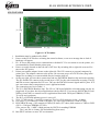
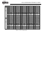
ELAN MICROELECTRONICS CORP.
ICE568 user manual
FOR
EM78568
Version 2.2
2005/1/19
ELAN MICROELECTRONICS CORP.
No. 12, Innovation 1st RD., Science-Based Industrial Park
Hsin Chu City, Taiwan.
TEL: (03) 5639977
FAX: (03) 5780617
ELAN MICROELECTRONICS CORP.
ICE TOP VIEW
56.5mm
86.5mm
Figure 1.1 ICE Outline
1.
2.
Installation must be authorized by EMC.
Power on the E8 ICE before executing the control software, or an error message due to lack of
hardware will appear.
3. E8 - ICE uses the printer port to communicate with host PC. If a user wants to use the printer, it is
recommended to install another printer port.
4. Power on switch located on the left side of ICE box. By switching left or right side to turn off or
turn on the ICE power.
5. Printer port and the adapter locate on the right side. The ICE connects to personal computer by
printer port. The adapter connects to the power. Be sure turn power off of ICE before plug in the
adapter for avoiding over current which may be burn the chip off.
6. On the top sight, we have three connections and one EM78R568 Romless chip and some switches.
The JP1 and the JP2 connect to the second layer of ICE for the code instruction accessing. The JP3
and JP4 are more important for ICE user. They are the EM78568 control signal and I/O ports. ICE
user can connect these connections to user's application board.
The connections are list in Table 1.1.
7. The U1 is EM78R568 Romless chip. The U2 is a 32K bytes ROM for on board testing one day by
piggyback. If user have developed application code by this ICE. User can use PIGGYBACK (user
can buy from EMC) to connect to user's application board with 32K bytes EPROM (27c256).
To verify user's program.
8. The D1 is a LED that indicates power is on or off.
9. X1 is 32.768k crystal. C1and C2 is capacitor 27p.C4 is PLL capacitor.(0.01u .. 0.044u)
10. ICE setup: (1) J5 connect to VDD (2)J6 short (3)J7 open (4)J8 connect to VDD or GND
11. PIGGYBACK setup: (1)J5 connect to GND (2)J6 short (3)J7 short (4)J8 connect to VDD or GND
(5)U2=> 32k bytes EPROM (27C256).
(User can use file “*.MIX” which generate by WICE for masking EPROM.
The *.mix file is a binary file and addressing from zero.)
12. Run WICE software to enter ICE environment.
ELAN MICROELECTRONICS CORP.
pin
1
2
3
4
JP3 5
6
7
8
9
10
JP4
Name
COM0
COM1
COM2
COM3
SEG0
SEG1
SEG2
SEG3
SEG4
SEG5
pin
11
12
13
14
15
16
17
18
19
20
Name
SEG6
SEG7
SEG8
SEG9
SEG10/P55
SEG11/P56
SEG12/P57
SEG13/P97
SEG14/P96
SEG15/P95
pin
21
22
23
24
25
26
27
28
29
30
Name
SEG16/P94
SEG17/P93
SEG18/P92
SEG19/P91
SEG20/P90
SEG21/PB7
SEG22/PB6
SEG23/PB5
SEG24/PB4
SEG25/PB3
Name
SEG26/PB2
SEG27/PB1
SEG28/PB0
SEG29/PC7
SEG30/PC6
SEG31/PC5
RXI
RXO
MICI
MICO
pin
41
42
43
44
45
46
47
48
49
50
Name
NC
TONE
NC
ALC
NC
NC
NC
NC
NC
NC
1
VDD
12 AURX/P65 23
P80
34 SEG17/P93
2
GND
13 MTX/P66 24
P81
35 SEG16/P94
3
/RESET
14 DAO/P67 25
P82
36 SEG15/P95
4 SEG10/P55 15 INT0/P70 26
P83
37 SEG14/P96
5 SEG11/P56 16 INT1/P71 27
P84
38 SEG13/P97
6 SEG12/P57 17 INT2/P72 28
P85
39 SEG28/P97
7
P60
18 INT3/P73 29
P86
40 SEG27/PB1
8
P61
19
P74
30
P87
41 SEG26/PB2
9 CMP1/P62 20
P75
31 SEG20/P90 42 SEG25/PB3
10 CMP2/P63 21
P76
32 SEG19/P91 43 SEG24/PB4
11 CMP3/P64 22
P77
33 SEG18/P92 44 SEG23/PB5
45
46
47
48
49
50
51
52
53
54
SEG22/PB6
SEG21/PB7
PC0
PWM1/PC1
PWM2/PC2
PC3
PC4
SEG31/PC5
SEG30/PC6
SEG29/PC7
NC
Table 1.2 ICE Connections
pin
31
32
33
34
35
36
37
38
39
40