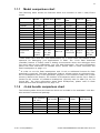
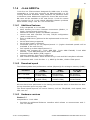
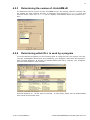
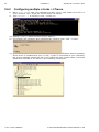
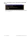
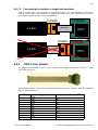
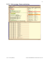
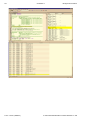
1
J-Link / J-Trace
ARM
User guide of the JTAG emulators
for ARM Cores
Manual Rev. 73
Date: July 3, 2009
Document: UM08001
A product of SEGGER Microcontroller GmbH & Co. KG
www.segger.com
2
Disclaimer
Specifications written in this document are believed to be accurate, but are not guaranteed to be entirely free of error. The information in this manual is subject to
change for functional or performance improvements without notice. Please make sure
your manual is the latest edition. While the information herein is assumed to be
accurate, SEGGER Microcontroller GmbH & Co. KG (the manufacturer) assumes no
responsibility for any errors or omissions. The manufacturer makes and you receive
no warranties or conditions, express, implied, statutory or in any communication with
you. The manufacturer specifically disclaims any implied warranty of merchantability
or fitness for a particular purpose.
Copyright notice
You may not extract portions of this manual or modify the PDF file in any way without
the prior written permission of the manufacturer. The software described in this document is furnished under a license and may only be used or copied in accordance
with the terms of such a license.
© 2009 SEGGER Microcontroller GmbH & Co. KG, Hilden / Germany
Trademarks
Names mentioned in this manual may be trademarks of their respective companies.
Brand and product names are trademarks or registered trademarks of their respective holders.
Contact address
SEGGER Microcontroller GmbH & Co. KG
In den Weiden 11
D-40721 Hilden
Germany
Tel.+49 2103-2878-0
Fax.+49 2103-2878-28
Email: [email protected]
Internet: http://www.segger.com
Revisions
This manual describes the J-Link and J-Trace device.
J-Link / J-Trace (UM08001)
© 2004-2009 SEGGER Microcontroller GmbH & Co. KG
3
For further information on topics or routines not yet specified, please contact us.
Revision
Date
By
73
090701
KN
72
090618
AG
71
090616
AG
70
090605
AG
69
090515
AG
68
090428
AG
67
090402
AG
66
090327
AG
65
090320
AG
64
090313
AG
63
090212
AG
62
090211
AG
61
090120
TQ
J-Link / J-Trace (UM08001)
Explanation
Chapter "Introduction"
* Section "J-Link and J-Trace models" added
* Sections "Model comparison chart" &
"J-Link bundle comparison chart"added
Chapter "J-Link and J-Trace models" removed
Chapter "Hardware" renamed to
"Target interfaces & adapters"
* Section "JTAG Isolator" added
Chapter "Target interfaces and adapters"
* Section "Target board design" updated
Several corrections
Chapter "Working with J-Link"
* Section "J-Link control panel" updated.
Chapter "Flash download and flash breakpoints"
* Section "Supported devices" updated.
Chapter "Device specifics"
* Section "NXP" updated.
Chapter "Device specifics"
* Section "NXP" updated.
Chapter "Introduction"
* Section "Common features of the J-Link
product family" updated.
Chapter "Working with J-Link"
* Section "Reset strategies" updated.
* Section "Indicators" updated.
Chapter "Flash download and flash breakpoints"
* Section "Supported devices" updated.
Chapter "J-Link and J-Trace related software"
* Section "J-Link STM32 Commander" added.
Chapter "Working with J-Link"
* Section "Reset strategies" updated.
Chapter "Working with J-Link"
* Section "Reset strategies" updated.
Chapter "Background information"
* Section "Embedded Trace Macrocell (ETM)"
updated.
Chapter "J-Link and J-Trace related software"
* Section "Dedicated flash programming
utilities for J-Link" updated.
Several changes in the manual structure.
Chapter "Working with J-Link"
* Section "Indicators" added.
Chapter "Hardware"
* Several corrections.
* Section "Hardware Versions" Version 8.0 added.
Chapter "Working with J-Link and J-Trace"
* Section "Reset strategies" updated.
Chapter J-Link and J-Trace related software
* Section "J-Link STR91x Commander
(Command line tool)" updated.
Chapter "Device specifics"
* Section "ST Microelectronics" updated.
Chapter "Hardware" updated.
Chapter "Working with J-Link"
* Section "Cortex-M3 specific reset strategies"
© 2004-2009 SEGGER Microcontroller GmbH & Co. KG
4
Revision
Date
By
60
090114
AG
59
090108
KN
58
090105
AG
57
081222
AG
56
081219
AG
55
081218
AG
54
081217
AG
53
081216
AG
52
081212
AG
51
081202
KN
50
081030
AG
49
081029
AG
48
080916
AG
47
080910
AG
46
080904
AG
45
080902
AG
44
080827
AG
43
080826
AG
42
080820
AG
41
080811
AG
J-Link / J-Trace (UM08001)
Explanation
Chapter "Working with J-Link"
* Section "Cortex-M3 specific reset strategies"
Chapter Hardware
* Section "Target board design for JTAG"
updated.
* Section "Target board design for SWD" added.
Chapter "Working with J-Link Pro"
* Section "Connecting J-Link Pro the first time"
updated.
Chapter "Working with J-Link Pro"
* Section "Introduction" updated.
* Section "Configuring J-Link Pro
via web interface" updated.
Chapter "Introduction"
* Section "J-Link Pro overview" updated.
Chapter "Working with J-Link Pro"
* Section "FAQs" added.
Chapter "Support and FAQs"
* Section "Frequently Asked Questions" updated.
Chapter "Hardware" updated.
Chapter "Working with J-Link and J-Trace"
* Section "Command strings" updated.
Chapter "Working with J-Link Pro" updated.
Chapter "Working with J-Link Pro" added.
Chapter "Licensing"
* Section "Original SEGGER products" updated.
Several corrections.
Chapter "Flash download and flash breakpoints"
* Section "Supported devices" corrected.
Several corrections.
Chapter "Working with J-Link and J-Trace"
* Section "Connecting multiple J-Links /
J-Traces to your PC" updated.
Chapter "Licensing" updated.
Chapter "Licensing" added.
Chapter "Hardware"
Section "J-Link OEM versions" moved to chapter
"Licensing"
Chapter "Hardware"
Section "JTAG+Trace connector" JTAG+Trace
connector pinout corrected.
Section "J-Link OEM versions" updated.
Chapter "J-Link control panel" moved to chapter
"Working with J-Link".
Several corrections.
Chapter "Flash download and flash breakpoints"
Section "Supported devices" updated.
Chapter "Flash download and flash breakpoints"
Section "Supported devices" updated.
Chapter "Flash download and flash breakpoints"
updated.
Chapter "Flash download and flash breakpoints",
section "Supported devices" updated.
© 2004-2009 SEGGER Microcontroller GmbH & Co. KG
5
Revision
Date
By
40
080630
AG
39
080627
AG
38
080618
AG
37
080617
AG
36
080530
AG
35
080215
AG
34
080212
AG
33
080207
AG
32
0080129
SK
31
0080103
SK
30
071211
AG
J-Link / J-Trace (UM08001)
Explanation
Chapter "Flash download and flash breakpoints"
updated.
Chapter "J-Link status window" renamed to "J-Link
control panel"
Various corrections.
Chapter "Flash download and flash breakpoints"
Section "Licensing" updated.
Section "Using flash download and flash
breakpoints with different debuggers" updated.
Chapter "J-Link status window" added.
Chapter "Support and FAQs"
Section "Frequently Asked Questions" updated
Chapter "Reset strategies"
Section "Cortex-M3 specific reset strategies"
updated.
Chapter "Reset strategies"
Section "Cortex-M3 specific reset strategies"
updated.
Chapter "Hardware"
Section "Differences between different versions"
updated.
Chapter "Working with J-Link and J-Trace"
Section "Cortex-M3 specific reset strategies"
added.
Chapter "J-Link and J-Trace related software"
Section "J-Link software and documentation
package in detail" updated.
Chapter "J-Link and J-Trace related software"
Section "J-Link TCP/IP Server (Remote J-Link /
J-Trace use)" updated.
Chapter "Working with J-Link and J-Trace"
Section "Command strings" updated.
Chapter "Flash download and flash breakpoints"
Section "Introduction" updated.
Section "Licensing" updated.
Section "Using flash download and flash
breakpoints with different debuggers" updated.
Chapter "Flash download and flash breakpoints"
added
Chapter "Device specifics:"
Section "ATMEL - AT91SAM7 - Recommended init
sequence" added.
Chapter "Device specifics":
Section "NXP - LPC - Fast GPIO bug" list of
device enhanced.
Chapter "Device specifics":
Section "NXP - LPC - Fast GPIO bug" updated.
Chapter "Device specifics":
Section "Analog Devices" updated.
Section "ATMEL" updated.
Section "Freescale" added.
Section "Luminary Micro" added.
Section "NXP" updated.
Section "OKI" added.
Section "ST Microelectronics" updated.
Section "Texas Instruments" updated.
Chapter "Related software":
Section "J-Link STR91x Commander" updated
© 2004-2009 SEGGER Microcontroller GmbH & Co. KG
6
Revision
Date
By
29
070912
SK
28
070912
SK
28
070912
AG
27
070827
TQ
26
070710
SK
25
070516
SK
24
070323
SK
23
070320
SK
22
070316
SK
21
070312
SK
20
070307
SK
19
070226
SK
18
070221
SK
17
070131
SK
16
061222
SK
J-Link / J-Trace (UM08001)
Explanation
Chapter "Hardware", section "Target board design"
updated.
Chapter "Related software":
Section "J-LinkSTR91x Commander" added.
Chapter "Device specifics":
Section "ST Microelectronics" added.
Section "Texas Instruments" added.
Subsection "AT91SAM9" added.
Chapter "Working with J-Link/J-Trace":
Section "Command strings" updated.
Chapter "Working with J-Link/J-Trace":
Section "Command strings" updated.
Chapter "Introduction":
Section "Features of J-Link" updated.
Chapter "Background Information":
Section "Embedded Trace Macrocell" added.
Section "Embedded Trace Buffer" added.
Chapter "Working with J-Link/J-Trace":
Section "Reset strategies in detail"
- "Software, for Analog Devices ADuC7xxx
MCUs" updated
- "Software, for ATMEL AT91SAM7 MCUs"
added.
Chapter "Device specifics"
Section "Analog Devices" added.
Section "ATMEL" added.
Chapter "Setup":
"Uninstalling the J-Link driver" updated.
"Supported ARM cores" updated.
Chapter "Hardware":
"Using the JTAG connector with SWD" updated.
Chapter "Hardware":
"Using the JTAG connector with SWD" added.
Chapter "Hardware":
"Differences between different versions"
supplemented.
Chapter "J-Link / J-Trace related software":
"J-Link GDB Server" licensing updated.
Chapter "J-Link / J-Trace related software" updated
and reorganized.
Chapter "Hardware"
"List of OEM products" updated
Chapter "Device specifics" added
Subchapter "Command strings" added
Chapter "Hardware":
"Version 5.3": Current limits added
"Version 5.4" added
Chapter "Setup":
"Installating the J-Link USB driver" removed.
"Installing the J-Link software and documentation
pack" added.
Subchapter "List of OEM products" updated.
"OS support" updated
Chapter "Preface": "Company description" added.
J-Link picture changed.
© 2004-2009 SEGGER Microcontroller GmbH & Co. KG
7
Revision
Date
By
15
060914
OO
14
060818
TQ
13
060711
OO
12
060628
OO
11
060607
SK
10
060526
SK
9
060324
OO
8
060117
OO
7
051208
OO
6
051118
OO
5
051103
TQ
4
051025
OO
3
2
1
051021
051011
050818
TQ
TQ
TW
J-Link / J-Trace (UM08001)
Explanation
Subchapter 1.5.1: Added target supply voltage and
target supply current to specifications.
Subchapter 5.2.1: Pictures of ways to connect JTrace.
Subchapter 4.7 "Using DCC for memory reads"
added.
Subchapter 5.2.2: Corrected JTAG+Trace connector pinout table.
Subchapter 4.1: Added ARM966E-S to List of supported ARM cores.
Subchapter 5.5.2.2 changed.
Subchapter 5.5.2.3 added.
ARM9 download speed updated.
Subchapter 8.2.1: Screenshot "Start sequence"
updated.
Subchapter 8.2.2 "ID sequence" removed.
Chapter "Support" and "FAQ" merged.
Various improvements
Chapter "Literature and references" added.
Chapter "Hardware":
Added common information trace signals.
Added timing diagram for trace.
Chapter "Designing the target board for trace"
added.
Chapter "Related Software": Added JLinkARM.dll.
Screenshots updated.
Chapter Working with J-Link: Sketch added.
Chapter Working with J-Link: "Connecting multiple
J-Links to your PC" added.
Chapter Working with J-Link: "Multi core debugging" added.
Chapter Background information: "J-Link firmware" added.
Chapter Setup: "JTAG Speed" added.
Chapter Background information: "Flash programming" added.
Chapter Setup: "Scan chain configuration" added.
Some smaller changes.
Performance values updated.
Chapter "Working with J-Link" added.
Initial version.
© 2004-2009 SEGGER Microcontroller GmbH & Co. KG
8
J-Link / J-Trace (UM08001)
© 2004-2009 SEGGER Microcontroller GmbH & Co. KG
9
About this document
This document describes J-Link and J-Trace. It provides an overview over the major
features of J-Link and J-Trace, gives you some background information about JTAG,
ARM and Tracing in general and describes J-Link and J-Trace related software packages available from Segger. Finally, the chapter Support and FAQs on page 187 helps
to troubleshoot common problems.
For simplicity, we will refer to J-Link ARM as J-Link in this manual.
For simplicity, we will refer to J-Link ARM Pro as J-Link Pro in this manual.
Typographic conventions
This manual uses the following typographic conventions:
Style
Used for
Body
Body text.
Keyword
Text that you enter at the command-prompt or that appears on the
display (that is system functions, file- or pathnames).
Reference
Reference to chapters, tables and figures or other documents.
GUIElement
Buttons, dialog boxes, menu names, menu commands.
Table 1.1: Typographic conventions
J-Link / J-Trace (UM08001)
© 2004-2009 SEGGER Microcontroller GmbH & Co. KG
10
SEGGER Microcontroller GmbH & Co. KG develops
and distributes software development tools and ANSI
C software components (middleware) for embedded
systems in several industries such as telecom, medical technology, consumer electronics, automotive
industry and industrial automation.
SEGGER’s intention is to cut software developmenttime for embedded applications by offering compact flexible and easy to use middleware,
allowing developers to concentrate on their application.
Our most popular products are emWin, a universal graphic software package for embedded applications, and embOS, a small yet efficient real-time kernel. emWin, written
entirely in ANSI C, can easily be used on any CPU and most any display. It is complemented by the available PC tools: Bitmap Converter, Font Converter, Simulator and
Viewer. embOS supports most 8/16/32-bit CPUs. Its small memory footprint makes it
suitable for single-chip applications.
Apart from its main focus on software tools, SEGGER develops and produces programming
tools for flash microcontrollers, as well as J-Link, a JTAG emulator to assist in development, debugging and production, which has rapidly become the industry standard for
debug access to ARM cores.
Corporate Office:
http://www.segger.com
EMBEDDED SOFTWARE
(Middleware)
United States Office:
http://www.segger-us.com
SEGGER TOOLS
emWin
Flasher
Graphics software and GUI
emWin is designed to provide an efficient, processor- and display controller-independent graphical user
interface (GUI) for any application that
operates with a graphical display.
Starterkits, eval- and trial-versions are
available.
Flash programmer
Flash Programming tool primarily for microcontrollers.
J-Link
embOS
JTAG emulator with trace
USB driven JTAG interface for ARM cores with
Trace memory. supporting the ARM ETM (Embedded Trace Macrocell).
Real Time Operating System
embOS is an RTOS designed to offer
the benefits of a complete multitasking
system for hard real time applications
with minimal resources. The profiling
PC tool embOSView is included.
emFile
JTAG emulator for ARM cores
USB driven JTAG interface for ARM cores.
J-Trace
J-Link / J-Trace Related Software
Add-on software to be used with SEGGER’s industry standard JTAG emulator, this includes flash
programming software and flash breakpoints.
File system
emFile is an embedded file system with
FAT12, FAT16 and FAT32 support.
emFile has been optimized for minimum memory consumption in RAM and
ROM while maintaining high speed.
Various Device drivers, e.g. for NAND
and NOR flashes, SD/MMC and CompactFlash cards, are available.
emUSB
USB device stack
A USB stack designed to work on any
embedded system with a USB client
controller. Bulk communication and
most standard device classes are supported.
J-Link / J-Trace (UM08001)
© 2004-2009 SEGGER Microcontroller GmbH & Co. KG
11
Table of Contents
1 Introduction ....................................................................................................................17
1.1
1.1.1
1.1.2
1.1.3
1.1.4
1.1.5
1.1.6
1.1.7
1.2
1.3
1.3.1
1.4
J-Link / J-Trace models ............................................................................ 18
Comparison chart .................................................................................... 18
J-Link ARM ............................................................................................. 19
J-Link ARM Pro ........................................................................................ 22
J-Trace ARM ........................................................................................... 23
Flasher ARM............................................................................................ 24
J-Link ColdFire ........................................................................................ 24
J-Trace for Cortex-M3 .............................................................................. 25
Common features of the J-Link product family ............................................. 26
Supported ARM cores ............................................................................... 27
Upcoming supported cores ........................................................................ 27
Requirements.......................................................................................... 28
2 Licensing........................................................................................................................29
2.1
2.2
2.3
2.3.1
2.3.2
2.3.3
2.4
2.4.1
2.5
2.5.1
2.5.2
2.5.3
2.5.4
2.6
2.6.1
2.6.2
2.6.3
2.6.4
2.6.5
2.7
2.8
Introduction............................................................................................ 30
Software components requiring a license .................................................... 31
License types .......................................................................................... 32
Built-in license ........................................................................................ 32
Key-based license.................................................................................... 32
Device-based license................................................................................ 33
Legal use of SEGGER J-Link software.......................................................... 35
Use of the software with 3rd party tools...................................................... 35
Original SEGGER products......................................................................... 36
J-Link .................................................................................................... 36
J-Link Pro ............................................................................................... 36
J-Trace................................................................................................... 37
Flasher ARM............................................................................................ 37
J-Link OEM versions ................................................................................. 38
mIDASLink (Analog Devices) ..................................................................... 38
SAM-ICE (Atmel) ..................................................................................... 38
Digi JTAG Link (Digi International) ............................................................. 39
IAR J-Link / IAR J-Link KS (IAR) ................................................................ 39
IAR J-Trace............................................................................................. 40
J-Link OBs .............................................................................................. 41
Illegal Clones .......................................................................................... 42
3 Setup..............................................................................................................................43
3.1
3.1.1
3.2
3.2.1
3.3
3.4
3.4.1
3.4.2
3.4.3
Installing the J-Link ARM software and documentation pack .......................... 44
Setup procedure...................................................................................... 44
Setting up the USB interface ..................................................................... 47
Verifying correct driver installation ............................................................. 47
Uninstalling the J-Link USB driver .............................................................. 49
Setting up the IP interface ........................................................................ 50
Connecting the first time .......................................................................... 50
Configuring the J-Link .............................................................................. 51
FAQs...................................................................................................... 53
4 J-Link and J-Trace related software...............................................................................55
4.1
J-Link related software ............................................................................. 56
J-Link / J-Trace (UM08001)
© 2004-2009 SEGGER Microcontroller GmbH & Co. KG
12
4.1.1
4.1.2
4.2
4.2.1
4.2.2
4.2.3
4.2.4
4.2.5
4.2.6
4.2.7
4.2.8
4.3
4.3.1
4.3.2
4.3.3
4.3.4
4.3.5
purposes
4.3.6
4.4
4.4.1
4.4.2
4.4.3
4.5
4.5.1
4.5.2
4.5.3
4.5.4
J-Link software and documentation package ............................................... 56
List of additional software packages........................................................... 57
J-Link software and documentation package in
detail..................................................................................................... 58
J-Link Commander (Command line tool) ..................................................... 58
J-Link STR91x Commander (Command line tool) ......................................... 59
J-Link STM32 Commander (Command line tool) .......................................... 60
J-Link TCP/IP Server (Remote J-Link / J-Trace use) ..................................... 61
J-Mem Memory Viewer............................................................................. 62
J-Flash ARM (Program flash memory via JTAG) ........................................... 63
J-Link RDI (Remote Debug Interface)......................................................... 64
J-Link GDB Server ................................................................................... 65
Dedicated flash programming utilities for J-Link........................................... 66
Introduction ........................................................................................... 66
Supported Eval boards ............................................................................. 66
Supported flash memories ........................................................................ 67
How to use the dedicated flash programming utilities ................................... 67
Using the dedicated flash programming utilities for production and commercial
67
F.A.Q..................................................................................................... 68
Additional software packages in detail ........................................................ 69
JTAGLoad (Command line tool) ................................................................. 69
J-Link Software Developer Kit (SDK) .......................................................... 69
J-Link Flash Software Developer Kit (SDK).................................................. 69
Using the J-LinkARM.dll............................................................................ 70
What is the JLinkARM.dll?......................................................................... 70
Updating the DLL in third-party programs................................................... 70
Determining the version of JLinkARM.dll ..................................................... 71
Determining which DLL is used by a program .............................................. 71
5 Working with J-Link and J-Trace....................................................................................73
5.1
5.1.1
5.1.2
5.1.3
5.2
5.2.1
5.2.2
5.2.3
5.3
5.3.1
5.3.2
5.3.3
5.3.4
5.4
5.4.1
5.5
5.5.1
5.5.2
5.5.3
5.6
5.6.1
5.6.2
5.6.3
5.7
5.7.1
5.8
5.8.1
5.8.2
5.9
5.9.1
Connecting the target system ................................................................... 74
Power-on sequence ................................................................................. 74
Verifying target device connection ............................................................. 74
Problems................................................................................................ 74
Indicators .............................................................................................. 75
Main indicator ......................................................................................... 75
Input indicator ........................................................................................ 77
Output indicator ...................................................................................... 77
JTAG interface ........................................................................................ 78
Multiple devices in the scan chain .............................................................. 78
Sample configuration dialog boxes............................................................. 78
Determining values for scan chain configuration .......................................... 81
JTAG Speed............................................................................................ 82
SWD interface ........................................................................................ 83
SWO ..................................................................................................... 83
Multi-core debugging ............................................................................... 85
How multi-core debugging works............................................................... 85
Using multi-core debugging in detail .......................................................... 86
Things you should be aware of .................................................................. 87
Connecting multiple J-Links / J-Traces to your PC ........................................ 89
How does it work? ................................................................................... 89
Configuring multiple J-Links / J-Traces ....................................................... 90
Connecting to a J-Link / J-Trace with non default USB-Address...................... 91
J-Link control panel ................................................................................. 92
Tabs...................................................................................................... 92
Reset strategies ...................................................................................... 98
Strategies for ARM 7/9 devices ................................................................. 98
Strategies for Cortex-M3 devices ..............................................................100
Using DCC for memory access .................................................................101
What is required? ...................................................................................101
J-Link / J-Trace (UM08001)
© 2004-2009 SEGGER Microcontroller GmbH & Co. KG
13
5.9.2
5.9.3
5.10
5.10.1
5.10.2
5.11
5.12
5.12.1
5.12.2
5.12.3
5.12.4
Target DCC handler ............................................................................... 101
Target DCC abort handler ....................................................................... 101
Command strings .................................................................................. 102
List of available commands ..................................................................... 102
Using command strings .......................................................................... 108
Switching off CPU clock during debug ....................................................... 110
Cache handling...................................................................................... 111
Cache coherency ................................................................................... 111
Cache clean area ................................................................................... 111
Cache handling of ARM7 cores................................................................. 111
Cache handling of ARM9 cores................................................................. 111
6 Flash download and flash breakpoints.........................................................................113
6.1
6.2
6.3
6.4
6.4.1
6.4.2
6.4.3
6.4.4
Introduction.......................................................................................... 114
Licensing .............................................................................................. 115
Supported devices ................................................................................. 117
Using flash download and flash breakpoints with different debuggers ............ 124
IAR Embedded Workbench ...................................................................... 124
Keil MDK .............................................................................................. 125
J-Link GDB Server ................................................................................. 127
J-Link RDI ............................................................................................ 127
7 Device specifics ...........................................................................................................129
7.1
7.1.1
7.2
7.2.1
7.2.2
7.3
7.3.1
7.4
7.4.1
7.4.2
7.4.3
7.4.4
7.4.5
7.4.6
7.4.7
7.4.8
7.4.9
7.5
7.5.1
7.6
7.6.1
7.7
7.7.1
7.7.2
7.7.3
7.7.4
7.7.5
7.8
7.8.1
Analog Devices...................................................................................... 130
ADuC7xxx ............................................................................................ 130
ATMEL ................................................................................................. 132
AT91SAM7............................................................................................ 132
AT91SAM9............................................................................................ 134
Freescale.............................................................................................. 135
MAC71x ............................................................................................... 135
Luminary Micro ..................................................................................... 136
Stellaris LM3S100 Series ........................................................................ 137
Stellaris LM3S300 Series ........................................................................ 137
Stellaris LM3S600 Series ........................................................................ 137
Stellaris LM3S800 Series ........................................................................ 137
Stellaris LM3S2000 Series....................................................................... 137
Stellaris LM3S6100 Series....................................................................... 137
Stellaris LM3S6400 Series....................................................................... 137
Stellaris LM3S6700 Series....................................................................... 137
Stellaris LM3S6900 Series....................................................................... 137
NXP ..................................................................................................... 138
LPC...................................................................................................... 139
OKI ..................................................................................................... 141
ML67Q40x ............................................................................................ 141
ST Microelectronics ................................................................................ 142
STR 71x ............................................................................................... 143
STR 73x ............................................................................................... 143
STR 75x ............................................................................................... 143
STR91x ................................................................................................ 143
STM32 ................................................................................................. 143
Texas Instruments................................................................................. 145
TMS470................................................................................................ 145
8 Target interfaces and adapters ....................................................................................147
8.1
8.1.1
8.1.2
8.2
8.2.1
8.2.2
20-pin JTAG/SWD connector ................................................................... 148
Pinout for JTAG ..................................................................................... 148
Pinout for SWD...................................................................................... 150
38-pin Mictor JTAG and Trace connector ................................................... 153
Connecting the target board.................................................................... 153
Pinout .................................................................................................. 154
J-Link / J-Trace (UM08001)
© 2004-2009 SEGGER Microcontroller GmbH & Co. KG
14
8.2.3
8.2.4
8.3
8.3.1
8.4
8.4.1
8.4.2
8.4.3
Assignment of trace information pins between ETM architecture versions .......156
Trace signals .........................................................................................156
19-pin JTAG/SWD and Trace connector .....................................................158
Target power supply ...............................................................................159
Adapters ...............................................................................................160
JTAG isolator .........................................................................................160
JTAG 14 pin adapter ...............................................................................161
5 Volt adapter........................................................................................162
9 Background information ...............................................................................................165
9.1
9.1.1
9.1.2
9.1.3
9.1.4
9.2
9.2.1
9.2.2
9.2.3
9.3
9.3.1
9.3.2
9.4
9.4.1
9.4.2
9.4.3
9.5
9.6
9.6.1
9.6.2
9.6.3
9.6.4
9.7
9.7.1
9.7.2
JTAG ....................................................................................................166
Test access port (TAP) ............................................................................166
Data registers........................................................................................166
Instruction register.................................................................................166
The TAP controller ..................................................................................167
The ARM core ........................................................................................169
Processor modes ....................................................................................169
Registers of the CPU core ........................................................................169
ARM / Thumb instruction set....................................................................170
EmbeddedICE ........................................................................................171
Breakpoints and watchpoints ...................................................................171
The ICE registers ...................................................................................172
Embedded Trace Macrocell (ETM) .............................................................173
Trigger condition ....................................................................................173
Code tracing and data tracing ..................................................................173
J-Trace integration example - IAR EWARM .................................................173
Embedded Trace Buffer (ETB) ..................................................................177
Flash programming ................................................................................178
How does flash programming via J-Link / J-Trace work? ..............................178
Data download to RAM ............................................................................178
Data download via DCC...........................................................................178
Available options for flash programming ....................................................178
J-Link / J-Trace firmware.........................................................................180
Firmware update ....................................................................................180
Invalidating the firmware ........................................................................180
10 Designing the target board for trace ..........................................................................183
10.1
10.1.1
10.1.2
10.1.3
10.1.4
10.2
10.2.1
10.3
Overview of high-speed board design........................................................184
Avoiding stubs .......................................................................................184
Minimizing Signal Skew (Balancing PCB Track Lengths) ...............................184
Minimizing Crosstalk ...............................................................................184
Using impedance matching and termination ...............................................184
Terminating the trace signal ....................................................................185
Rules for series terminators .....................................................................185
Signal requirements ...............................................................................186
11 Support and FAQs .....................................................................................................187
11.1
11.1.1
11.2
11.2.1
11.2.2
11.3
11.3.1
11.3.2
11.4
11.5
Measuring download speed ......................................................................188
Test environment ...................................................................................188
Troubleshooting .....................................................................................189
General procedure..................................................................................189
Typical problem scenarios .......................................................................189
Signal analysis.......................................................................................191
Start sequence ......................................................................................191
Troubleshooting .....................................................................................191
Contacting support .................................................................................192
Frequently Asked Questions.....................................................................193
12 Glossary.....................................................................................................................195
J-Link / J-Trace (UM08001)
© 2004-2009 SEGGER Microcontroller GmbH & Co. KG
15
13 Literature and references...........................................................................................201
J-Link / J-Trace (UM08001)
© 2004-2009 SEGGER Microcontroller GmbH & Co. KG
16
J-Link / J-Trace (UM08001)
© 2004-2009 SEGGER Microcontroller GmbH & Co. KG
17
Chapter 1
Introduction
This chapter gives a short overview about J-Link and J-Trace.
J-Link / J-Trace (UM08001)
© 2004-2009 SEGGER Microcontroller GmbH & Co. KG
18
CHAPTER 1
1.1
Introduction
J-Link / J-Trace models
J-Link / J-Trace is available in different variations, each designed for different purposes / target devices. Currently, the following models of J-Link / J-Trace are available:
•
•
•
•
•
•
J-Link ARM
J-Link ARM Pro
J-Trace ARM
Flasher ARM
J-Link ColdFire
J-Trace for Cortex-M3
In the following, the different J-Link / J-Trace models are described and the changes
between the different hardware versions of each model are listed. To determine the
hardware version of your J-Link / J-Trace, the first step should be to look at the label
at the bottom side of the unit. J-Links / J-Traces have the hardware version printed
on the back label.
If this is not the case with your J-Link / J-Trace, start JLink.exe. As part of the initial
message, the hardware version is displayed.
J-Link / J-Trace (UM08001)
© 2004-2009 SEGGER Microcontroller GmbH & Co. KG
19
1.1.1
Model comparison chart
The following table shows the features which are included in each J-Link/J-Trace
model.
J-Link
J-Link Pro
J-Trace
Flasher
ARM
J-Link CF
J-Trace
CM-3
FlashDL 1
yes(opt)
yes
yes(opt)
yes(opt)
yes
yes(opt)
FlashBP2
yes(opt)
yes
yes(opt)
yes(opt)
yes
yes(opt)
GDB Server
RDI
J-Flash
JTAG
yes(opt)
yes(opt)
yes(opt)
yes
yes
yes
yes
yes
yes(opt)
yes(opt)
yes(opt)
yes
yes(opt)
yes(opt)
yes
yes
no
no
yes(opt)
no
yes(opt)
yes(opt)
yes(opt)
yes
SWD
yes
yes
no
yes
no
yes
SWO
yes
yes
no
no
ARM7/9/
11, Cortex-M0/
M1/M3
yes
no
no
no
no
yes
yes
no
ARM7/9/
11, Cortex-M0/
M1/M3
yes
no
yes
yes
no
no
yes
no
no
ARM 7/9
ARM 7/9, ColdFire
Cortex-M3 V2/3/4
yes
no
yes
ARM 7/9
(no tracing), Cortex-M3
USB
Ethernet
Trace
Supported
cores
1
Most IDEs come with their own flashloaders, so in most cases this feature is not
essential for debugging your applications in flash. The J-Link flash download
(FlashDL) feature is mainly used in debug environments where the debugger does
not come with an own flashloader (e.g. the GNU Debugger). For more information
about how flash download via FlashDL works, please refer to Flash download and
flash breakpoints on page 113.
2
In order to use the flash breakpoints with J-Link no additional license for flash
download is required. The flash breakpoint feature allows setting an unlimited number of breakpoints even if the application program is not located in RAM, but in flash
memory. Without this feature, the number of breakpoints which can be set in flash is
limited to the number of hardware breakpoints (typically two for ARM 7/9, six for
Cortex-M3) For more information about flash breakpoints, please refer to Flash
download and flash breakpoints on page 113.
1.1.2
J-Link bundle comparison chart
The following table shows the features which are included in the available J-Link bundles and Non-commercial package
Flash DL
Flash BP
GDB Server
RDI
J-Flash
J-Link / J-Trace (UM08001)
J-Link NCU
(non commercial use)
yes
yes
yes
no
no
J-Link
RDI bundle
J-Link
RDI Pro
J-Link
J-Flash
J-Link
GDB Server
no
no
no
yes
yes
yes
yes
no
yes
yes
no
no
no
yes(opt)
yes
no
no
yes
no
no
© 2004-2009 SEGGER Microcontroller GmbH & Co. KG
20
CHAPTER 1
1.1.3
Introduction
J-Link ARM
J-Link is a JTAG emulator designed for ARM cores. It connects
via USB to a PC running Microsoft Windows 2000, Windows XP,
Windows 2003 or Windows Vista. J-Link has a built-in 20-pin
JTAG connector, which is compatible with the standard 20-pin
connector defined by ARM.
1.1.3.1 Additional features
•
•
•
•
•
Serial Wire Debug supported *
Serial Wire Viewer supported *
Download speed up to 720 KBytes/second **
DCC speed up to 800 Kbytes/second **
RDI interface available, which allows using J-Link with RDI
compliant software
* = Supported by J-Link hardware version 6
** = Measured with J-Link Rev.5, ARM7 @ 50 MHz, 12MHz JTAG
speed.
1.1.3.2 Specifications*
Power Supply
USB powered <50mA if target power is
off.
USB 2.0, full speed
JTAG 20-pin (14-pin adapter available)
USB Interface
Target Interface
Serial Transfer Rate between J-Link and Tarup to 12 MHz
get
Supported Target Voltage
1.2 - 3.3 V, 5V tolerant
Target supply voltage
4.5V .. 5V (if powered with 5V on USB)
Target supply current
Max. 300mA
Operating Temperature
+5°C ... +60°C
Storage Temperature
-20°C ... +65 °C
Relative Humidity (non-condensing)
<90% rH
Size (without cables)
100mm x 53mm x 27mm
Weight (without cables)
70g
Electromagnetic Compatibility (EMC)
EN 55022, EN 55024
Microsoft Windows 2000
Microsoft Windows XP
Microsoft Windows XP x64
Supported OS
Microsoft Windows 2003
Microsoft Windows 2003 x64
Microsoft Windows Vista
Microsoft Windows Vista x64
Table 1.1: J-Link specifications
* = J-Link hardware revision 5 and up.
J-Link / J-Trace (UM08001)
© 2004-2009 SEGGER Microcontroller GmbH & Co. KG
21
1.1.3.3 Download speed
The following table lists performance values (Kbytes/s) for writing to memory (RAM):
ARM7
via JTAG
ARM9
via JTAG
Cortex-M3
via SWD
720 Kbytes/s
(12MHz JTAG)
550 Kbytes/s
(12MHz JTAG)
180 Kbytes/s
(12 MHz SWD)
Hardware
J-Link Rev. 6 — 8
Table 1.2: Download speed differences between hardware revisions
All tests have been performed in the testing environment which is described on Measuring download speed on page 188.
The actual speed depends on various factors, such as JTAG/SWD, clock speed, host
CPU core etc.
1.1.3.4 Hardware versions
Versions 1-3
These J-Links use a 16-bit CISC CPU. Maximum download speed is approximately 150
Kbytes/second.
JTAG speed
Maximum JTAG frequency is 4 MHz; possible JTAG speeds are:
16 MHz / n, where n is 4, 5, ..., resulting in speeds of:
4.000 MHz (n = 4)
3.200 MHz (n = 5)
2.666 MHz (n = 6)
2.285 MHz (n = 7)
2.000 MHz (n = 8)
1.777 MHz (n = 9)
1.600 MHz (n = 10)
Adaptive clocking is not supported.
Target Interface
nTRST is open drain + 4K7 pull up
RESET is open drain
Version 4
Identical to version 3.0 with the following exception:
Target Interface
nTRST is push-pull type
RESET is push-pull type
Version 5.0
Uses a 32-bit RISC CPU.
Maximum download speed (using DCC) is over 700 Kbytes/second.
JTAG speed
Maximum JTAG frequency is 12 MHz; possible JTAG speeds are:
48 MHz / n, where n is 4, 5, ..., resulting in speeds of:
12.000 MHz (n = 4)
9.600 MHz (n = 5)
8.000 MHz (n = 6)
6.857 MHz (n = 7)
J-Link / J-Trace (UM08001)
© 2004-2009 SEGGER Microcontroller GmbH & Co. KG
22
CHAPTER 1
Introduction
6.000 MHz (n = 8)
5.333 MHz (n = 9)
4.800 MHz (n = 10)
Adaptive clocking is supported.
Target Interface
nTRST is push-pull type
RESET is push-pull type
Version 5.2
Identical to version 5.0 with the following exception:
Target Interface
nTRST is push-pull type
RESET is open drain
Version 5.3
Identical to version 5.2 with the following exception:
•
5V target supply current limited
5V target supply (pin 19) of Kick-Start versions of J-Link is current monitored
and limited. J-Link automatically switches off 5V supply in case of over-current to
protect both J-Link and host computer. Peak current (<= 10 ms) limit is 1A,
operating current limit is 300mA.
Version 5.4
Identical to version 5.3 with the following exception:
•
JTAG interface is 5V tolerant.
Version 6.0
Identical to version 5.4 with the following exception:
•
•
Outputs can be tristated (Effectively disabling the JTAG interface)
J-Link supports SWV (Speed limited to 500 kHz)
Version 7.0
•
Uses an additional pin to the UART unit of the target hardware for SWV support
(Speed limited to 6 MHz).
Version 8.0
•
SWD support for non-3.3V targets.
J-Link / J-Trace (UM08001)
© 2004-2009 SEGGER Microcontroller GmbH & Co. KG
23
1.1.4
J-Link ARM Pro
J-Link Pro is a JTAG emulator designed for ARM cores. It is fully
compatible to J-Link and connects via Ethernet/USB to a PC
running Microsoft Windows 2000, Windows XP, Windows 2003
or Windows Vista. Additional support for Cortex-R4 and CortexR8 cores will be available in the near future. J-Link Pro comes
with licenses for all J-Link related SEGGER software products
which allows using J-Link Pro "out-of-the-box".
1.1.4.1 Additional features
•
•
•
•
•
•
•
•
•
•
•
•
•
Fully compatible to J-Link ARM
More memory for future firmware extensions (ARM11, XScale, Cortex R4 and Cortex A8)
Additional LEDs for power and RESET indication
Comes with web interface for easy TCP/IP configuration
(built-in web server)
Built-in GDB Server (planned to be implemented in the near
future)
Serial Wire Debug supported
Serial Wire Viewer supported
Download speed up to 720 KBytes/second ** (higher download speeds will be
available in the near future)
DCC speed up to 800 Kbytes/second **
Comes with licenses for: J-Link ARM RDI, J-Link ARM FlashBP, J-Link ARM
FlashDL, J-Link ARM GDB Server and J-Flash ARM.
Embedded Trace Buffer (ETB) support
Galvanic isolation from host via Ethernet
RDI interface available, which allows using J-Link with RDI compliant software
** = Measured with J-Link Pro Rev. 1.1, ARM7 @ 50 MHz, 12MHz JTAG speed.
1.1.4.2 Download speed
The following table lists performance values (Kbytes/s) for writing to memory (RAM):
ARM7
via JTAG
ARM9
via JTAG
Cortex-M3
via SWD
720 Kbytes/s
(12 MHz JTAG)
720 Kbytes/s
(12 MHz JTAG)
550 Kbytes/s
(12 MHz JTAG)
550 Kbytes/s
(12 MHz JTAG)
190 Kbytes/s
(12 MHz SWD)
190 Kbytes
(12 MHz SWD)
Hardware
Rev. 1 via USB
Rev. 1 via TCP/IP
Table 1.3: Download speed differences between hardware revisions
All tests have been performed in the testing environment which is described on Measuring download speed on page 188.
The actual speed depends on various factors, such as JTAG/SWD, clock speed, host
CPU core etc.
1.1.4.3 Hardware versions
Version 1.1
Compatible to J-Link ARM.
•
Provides an additional Ethernet interface which allows to communicate with JLink via TCP/IP.
J-Link / J-Trace (UM08001)
© 2004-2009 SEGGER Microcontroller GmbH & Co. KG
24
CHAPTER 1
1.1.5
Introduction
J-Trace ARM
J-Trace is a JTAG emulator designed for ARM cores which
includes trace (ETM) support. It connects via USB to a PC running Microsoft Windows 2000, Windows XP, Windows 2003 or
Windows Vista. J-Trace has a built-in 20-pin JTAG connector and
a built in 38-pin JTAG+Trace connector, which are compatible to
the standard 20-pin connector and 38-pin connector defined by
ARM.
1.1.5.1 Additional features
•
•
•
Supports tracing on ARM7/9 targets
Download speed up to 420 Kbytes/second *
DCC speed up to 600 Kbytes/second *
* = Measured with J-Trace, ARM7 @ 50 MHz, 12MHz JTAG
speed.
1.1.5.2 Specifications for J-Trace
Power Supply
USB Interface
Target Interface
Serial Transfer Rate between J-Trace and
Target
Supported Target Voltage
Operating Temperature
Storage Temperature
Relative Humidity (non-condensing)
Size (without cables)
Weight (without cables)
Electromagnetic Compatibility (EMC)
Supported OS
USB powered < 300mA
USB 2.0, full speed
JTAG 20-pin (14-pin adapter available)
JTAG+Trace: Mictor, 38-pin
up to 12 MHz
3.0 - 3.6 V (5V adapter available)
+5°C ... +40°C
-20°C ... +65 °C
<90% rH
123mm x 68mm x 30mm
120g
EN 55022, EN 55024
Microsoft Windows 2000
Microsoft Windows XP
Microsoft Windows XP x64
Microsoft Windows 2003
Microsoft Windows 2003 x64
Microsoft Windows Vista
Microsoft Windows Vista x64
Table 1.4: J-Trace specifications
J-Link / J-Trace (UM08001)
© 2004-2009 SEGGER Microcontroller GmbH & Co. KG
25
1.1.5.3 Download speed
The following table lists performance values (Kbytes/s) for writing to memory (RAM):
Hardware
J-Trace Rev. 1
ARM7 via JTAG
420.0 Kbytes/s
(12MHz JTAG)
ARM9 via JTAG
280.0 Kbytes/s
(12MHz JTAG)
Table 1.5: Download speed differences between hardware revisions
All tests have been performed in the testing environment which is described on Measuring download speed on page 188.
The actual speed depends on various factors, such as JTAG, clock speed, host CPU
core etc.
1.1.5.4 Hardware versions
Version 1
This J-Trace uses a 32-bit RISC CPU. Maximum download speed is approximately 420
KBytes/second (600 KBytes/second using DCC).
1.1.6
Flasher ARM
Flasher ARM is a programming tool for microcontrollers with onchip or external Flash memory and ARM core. Flasher ARM is
designed for programming flash targets with the J-Flash software or stand-alone. In addition to that Flasher ARM has all of
the J-Link functionality. For more information about Flasher
ARM, please refer to UM08007, Flasher ARM User’s Guide.
1.1.7
J-Link ColdFire
J-Link ColdFire is a BDM emulator designed for ColdFire® cores.
It connects via USB to a PC running Microsoft Windows 2000,
Windows XP, Windows 2003, or Windows Vista. J-Link ColdFire
has a built-in 26-pin BDM connector, which is compatible to the
standard 26-pin connector defined by Freescale. For more information about J-Link ColdFire BDM 26, please refer to UM08009,
J-Link ColdFire BDM26 User’s Guide.
J-Link / J-Trace (UM08001)
© 2004-2009 SEGGER Microcontroller GmbH & Co. KG
26
CHAPTER 1
1.1.8
Introduction
J-Trace for Cortex-M3
J-Trace for Cortex-M3 is a JTAG/SWD emulator designed for
Cortex-M3 cores which includes trace (ETM) support. J-Trace for
Cortex-M3 can also be used as a J-Link and it also supports
ARM7/9 cores. Tracing on ARM7/9 targets is not supported.
1.1.8.1 Additional features
•
•
Has all the J-Link functionality
Supports tracing on Cortex-M3 targets
1.1.8.2 Download speed
The following table lists performance values (Kbytes/s) for writing to memory (RAM):
Hardware
J-Trace Rev. 1
Cortex-M3 via SWD
190 Kbytes/s (12MHz SWD)
Table 1.6: Download speed differences between hardware revisions
The actual speed depends on various factors, such as JTAG, clock speed, host CPU
core etc.
J-Link / J-Trace (UM08001)
© 2004-2009 SEGGER Microcontroller GmbH & Co. KG
27
1.2
Common features of the J-Link product family
•
•
•
•
•
•
•
•
•
•
•
•
•
•
•
•
•
•
•
•
•
•
•
USB 2.0 interface
Any ARM7/9/11 (including thumb mode), Cortex-M0/M1/M3 core supported
Automatic core recognition
Maximum JTAG speed 12 MHz
Seamless integration into the IAR Embedded Workbench® IDE
No power supply required, powered through USB
Support for adaptive clocking
All JTAG signals can be monitored, target voltage can be measured
Support for multiple devices
Fully plug and play compatible
Standard 20-pin JTAG connector, standard 38-pin JTAG+Trace connector
USB and 20-pin ribbon cable included
Memory viewer (J-Mem) included
TCP/IP server included, which allows using J-Trace via TCP/IP networks
RDI interface available, which allows using J-Link with RDI compliant software
Flash programming software (J-Flash) available
Flash DLL available, which allows using flash functionality in custom applications
Software Developer Kit (SDK) available
Full integration with the IAR C-SPY® debugger; advanced debugging features
available from IAR C-SPY debugger.
14-pin JTAG adapter available
Adapter for 5V JTAG targets available
Optical isolation adapter for JTAG/SWD interface available
Target power supply via pin 19 of the JTAG/SWD interface (up to 300 mA to target with overload protection)
J-Link / J-Trace (UM08001)
© 2004-2009 SEGGER Microcontroller GmbH & Co. KG
28
CHAPTER 1
1.3
Introduction
Supported ARM cores
J-Link / J-Trace has been tested with the following cores, but should work with any
ARM7/ARM9 and Cortex-M3 core. If you experience problems with a particular core,
do not hesitate to contact Segger.
•
•
•
•
•
•
•
•
•
•
•
•
1.3.1
•
•
•
ARM7TDMI (Rev 1)
ARM7TDMI (Rev 3)
ARM7TDMI-S (Rev 4)
ARM720T
ARM920T
ARM922T
ARM926EJ-S
ARM946E-S
ARM966E-S
Cortex-M0
Cortex-M1
Cortex-M3
Upcoming supported cores
Cortex-A8/A9
Cortex-R4
X-Scale
If you need support for any of these cores you should get in touch with us ([email protected]).
J-Link / J-Trace (UM08001)
© 2004-2009 SEGGER Microcontroller GmbH & Co. KG
29
1.4
Requirements
Host System
To use J-Link or J-Trace you need a host system running Windows 2000, Windows XP,
Windows 2003, or Windows Vista.
Target System
An ARM7/ARM9/ARM11 or Cortex-M3 target system is required. The system should
have a standardized 20-pin connector as defined by ARM Ltd. for a simple JTAG connection. The individual pins are described in section 20-pin JTAG/SWD connector on
page 148. Note that Segger offers an optional adapter to use J-Link and J-Trace with
targets using 14 pin 0.1" mating JTAG connectors.
To use tracing with J-Trace, you need a 38-pin connector on your target board as
defined by ARM Ltd. and described under 38-pin Mictor JTAG and Trace connector on
page 153. The individual pins are described in section Pinout on page 154.
J-Link / J-Trace (UM08001)
© 2004-2009 SEGGER Microcontroller GmbH & Co. KG
30
J-Link / J-Trace (UM08001)
CHAPTER 1
Introduction
© 2004-2009 SEGGER Microcontroller GmbH & Co. KG
29
Chapter 2
Licensing
This chapter describes the different license types of J-Link related software and the
legal use of the J-Link software with original SEGGER and OEM products.
J-Link / J-Trace (UM08001)
© 2004-2009 SEGGER Microcontroller GmbH & Co. KG
30
2.1
CHAPTER 2
Licensing
Introduction
J-Link functionality can be enhanced by the features J-Flash, RDI, flash download (JLink ARM FlashDL) and flash breakpoints (FlashBP). These features do not come
with J-Link and need additional licenses. In the following the licensing options of the
software will be explained.
J-Link / J-Trace (UM08001)
© 2004-2009 SEGGER Microcontroller GmbH & Co. KG
31
2.2
Software components requiring a license
There are four software components which need an additional license:
•
•
•
•
J-Flash
J-Link RDI
Flash download (J-Link ARM FlashDL)
Flash breakpoints (FlashBP)
For more information about J-Link RDI licensing procedure / license types, please
refer to the J-Link RDI User Guide (UM08004), chapter Licensing.
For more information about J-Flash licensing procedure / license types, please refer
to the J-Flash User Guide (UM08003), chapter Licensing.
In the following the licensing procedure and license types of J-Link ARM FlashDL
and FlashBP are explained
J-Link / J-Trace (UM08001)
© 2004-2009 SEGGER Microcontroller GmbH & Co. KG
32
CHAPTER 2
2.3
Licensing
License types
For each of the software components J-Link ARM FlashDL and FlashBP which require
an additional license, there are three types of licenses:
Built-in License
This type of license is easiest to use. The customer does not need to deal with a
license key. The software automatically finds out that the connected J-Link contains
the built-in license(s). This is the type of license you get if you order J-Link and the
license at the same time, typically in a bundle.
Key-based license
This type of license is used if you already have a J-Link, but want to enhance its functionality by using J-Link ARM FlashDL and FlashBP. In addition to that, the keybased license is used for trial licenses. To enable this type of license you need to
obtain a license key from SEGGER. Free trial licenses are available upon request from
www.segger.com This license key has to be added to the J-Link license management.
How to enter a license key is described in detail in Licensing on page 115. Every
license can be used on different PCs, but only with the J-Link the license is for. This
means that if you want to use J-Link ARM FlashDL and FlashBP with other J-Links,
every J-Link needs a license.
Device-based license
The device-based license comes with the J-Link software and is available for some
devices. For a complete list of devices which have built-in licenses, please refer to
Device list on page 33. The device-based license has to be activated via the debugger. How to activate a device-based license is described in detail in the section Activating a device-based license on page 33.
2.3.1
Built-in license
This type of license is easiest to use. The customer does not need to deal with a
license key. The software automatically finds out that the connected J-Link contains
the built-in license(s). To check what licenses the used J-Link have, simply open the
J-Link commander (JLink.exe). The J-Link commander finds and lists all of the JLink’s licenses automatically, as can be seen in the screenshot below.
This J-Link for example, has built-in licenses for RDI, J-Link
FlashBP.
2.3.2
ARM
FlashDL and
Key-based license
When using a key-based license, a license key is required in order to enable the JLink features J-Link ARM FlashDL and FlashBP. License keys can be added via the
license manager. How to enter a license via the license manager is described in
Licensing on page 115. Like the built-in license, the key-based license is only valid
for one J-Link, so if another J-Link is used it needs a separate license.
J-Link / J-Trace (UM08001)
© 2004-2009 SEGGER Microcontroller GmbH & Co. KG
33
2.3.3
Device-based license
The device-based license is a free license, available for some devices. It’s already
included in J-Link, so no keys are necessary to enable this license type. To activate a
device based license, the debugger needs to select a supported device.
2.3.3.1 Activating a device-based license
In order to activate a device-based license, the debugger needs to select a supported
device. To check if the debugger has selected the right device, simply open the J-Link
control panel and check the device section in the General tab.
2.3.3.2 Device list
The following list contains all devices which are supported by the device-based
license
Manufacturer
Name
NXP
LPC2101
NXP
LPC2102
NXP
LPC2103
NXP
LPC2104
NXP
LPC2105
NXP
LPC2106
NXP
LPC2109
NXP
LPC2114
NXP
LPC2119
NXP
LPC2124
NXP
LPC2129
NXP
LPC2131
Licenses
RDI, J-Link ARM FlashDL,
Link ARM FlashBP
RDI, J-Link ARM FlashDL,
Link ARM FlashBP
RDI, J-Link ARM FlashDL,
Link ARM FlashBP
RDI, J-Link ARM FlashDL,
Link ARM FlashBP
RDI, J-Link ARM FlashDL,
Link ARM FlashBP
RDI, J-Link ARM FlashDL,
Link ARM FlashBP
RDI, J-Link ARM FlashDL,
Link ARM FlashBP
RDI, J-Link ARM FlashDL,
Link ARM FlashBP
RDI, J-Link ARM FlashDL,
Link ARM FlashBP
RDI, J-Link ARM FlashDL,
Link ARM FlashBP
RDI, J-Link ARM FlashDL,
Link ARM FlashBP
RDI, J-Link ARM FlashDL,
Link ARM FlashBP
JJJJJJJJJJJJ-
Table 2.1: Device list
J-Link / J-Trace (UM08001)
© 2004-2009 SEGGER Microcontroller GmbH & Co. KG
34
CHAPTER 2
Manufacturer
Name
NXP
LPC2132
NXP
LPC2134
NXP
LPC2136
NXP
LPC2138
NXP
LPC2141
NXP
LPC2142
NXP
LPC2144
NXP
LPC2146
NXP
LPC2148
NXP
LPC2194
NXP
LPC2212
NXP
LPC2214
NXP
LPC2292
NXP
LPC2294
NXP
LPC2364
NXP
LPC2366
NXP
LPC2368
NXP
LPC2378
NXP
LPC2468
NXP
LPC2478
Licensing
Licenses
RDI, J-Link ARM FlashDL,
Link ARM FlashBP
RDI, J-Link ARM FlashDL,
Link ARM FlashBP
RDI, J-Link ARM FlashDL,
Link ARM FlashBP
RDI, J-Link ARM FlashDL,
Link ARM FlashBP
RDI, J-Link ARM FlashDL,
Link ARM FlashBP
RDI, J-Link ARM FlashDL,
Link ARM FlashBP
RDI, J-Link ARM FlashDL,
Link ARM FlashBP
RDI, J-Link ARM FlashDL,
Link ARM FlashBP
RDI, J-Link ARM FlashDL,
Link ARM FlashBP
RDI, J-Link ARM FlashDL,
Link ARM FlashBP
RDI, J-Link ARM FlashDL,
Link ARM FlashBP
RDI, J-Link ARM FlashDL,
Link ARM FlashBP
RDI, J-Link ARM FlashDL,
Link ARM FlashBP
RDI, J-Link ARM FlashDL,
Link ARM FlashBP
RDI, J-Link ARM FlashDL,
Link ARM FlashBP
RDI, J-Link ARM FlashDL,
Link ARM FlashBP
RDI, J-Link ARM FlashDL,
Link ARM FlashBP
RDI, J-Link ARM FlashDL,
Link ARM FlashBP
RDI, J-Link ARM FlashDL,
Link ARM FlashBP
RDI, J-Link ARM FlashDL,
Link ARM FlashBP
JJJJJJJJJJJJJJJJJJJJ-
Table 2.1: Device list
J-Link / J-Trace (UM08001)
© 2004-2009 SEGGER Microcontroller GmbH & Co. KG
35
2.4
Legal use of SEGGER J-Link software
The software consists of proprietary programs of SEGGER, protected under copyright
and trade secret laws. All rights, title and interest in the software are and shall
remain with SEGGER. For details, please refer to the license agreement which needs
to be accepted when installing the software. The text of the license agreement is also
available as entry in the start menu after installing the software.
Use of software
SEGGER J-Link software may only be used with original SEGGER products and authorized OEM products. The use of the licensed software to operate SEGGER product
clones is prohibited and illegal.
2.4.1
Use of the software with 3rd party tools
For simplicity, some components of the J-Link software are also distributed from
partners with software tools designed to use J-Link. These tools are primarily debugging tools, but also memory viewers, flash programming utilities but also software
for other purposes. Distribution of the software components is legal for our partners,
but the same rules as described above apply for their usage: They may only be used
with original SEGGER products and authorized OEM products. The use of the licensed
software to operate SEGGER product clones is prohibited and illegal.
J-Link / J-Trace (UM08001)
© 2004-2009 SEGGER Microcontroller GmbH & Co. KG
36
CHAPTER 2
2.5
Licensing
Original SEGGER products
The following products are original SEGGER products for which the use of the J-Link
software is allowed:
2.5.1
J-Link
J-Link is a JTAG emulator designed for ARM cores. It connects
via USB to a PC running Microsoft Windows 2000, Windows XP,
Windows 2003 or Windows Vista. J-Link has a built-in 20-pin
JTAG connector, which is compatible with the standard 20-pin
connector defined by ARM.
Licenses
Comes with built-in licenses for J-Link ARM FlashDL and
FlashBP for some devices. For a complete list of devices which
are supported by the built-in licenses, please refer to Device
list on page 33.
2.5.2
J-Link Pro
J-Link Pro is a JTAG emulator designed for ARM cores. It connects via USB or Ethernet to a PC running Microsoft Windows
2000, Windows XP, Windows 2003 or Windows Vista. J-Link has
a built-in 20-pin JTAG connector, which is compatible with the
standard 20-pin connector defined by ARM.
Licenses
Comes with built-in licenses for all J-Link related software products: J-Link ARM FlashDL, FlashBP, RDI, J-Link GDB Server and
J-Flash.
J-Link / J-Trace (UM08001)
© 2004-2009 SEGGER Microcontroller GmbH & Co. KG
37
2.5.3
J-Trace
J-Trace is a JTAG emulator designed for ARM cores which
includes trace (ETM) support. It connects via USB to a PC running Microsoft Windows 2000, Windows XP, Windows 2003 or
Windows Vista. J-Trace has a built-in 20-pin JTAG connector and
a built in 38-pin JTAG+Trace connector, which is compatible
with the standard 20-pin connector and 38-pin connector
defined by ARM.
2.5.4
Flasher ARM
Flasher ARM is a programming tool for microcontrollers with onchip or external Flash memory and ARM core. Flasher ARM is
designed for programming flash targets with the J-Flash software or stand-alone. In addition to that Flasher ARM has all of
the J- Link functionality. Flasher ARM connects via USB or via
RS232 interface to a PC, running Microsoft Windows 2000, Windows XP, Windows 2003 or Windows Vista. Flasher ARM has a
built-in 20-pin JTAG connector, which is compatible with the
standard 20-pin connector defined by ARM.
J-Link / J-Trace (UM08001)
© 2004-2009 SEGGER Microcontroller GmbH & Co. KG
38
CHAPTER 2
2.6
Licensing
J-Link OEM versions
There are several different OEM versions of J-Link on the market. The OEM versions
look different, but use basically identical hardware. Some of these OEM versions are
limited in speed, some of these can only be used with certain chips and some of
these have certain add-on features enabled, which normally requires license. In any
case, it should be possible to use the J-Link software with these OEM versions. However, proper function cannot be guaranteed for OEM versions. SEGGER Microcontroller does not support OEM versions; support is provided by the respective OEM.
2.6.1
mIDASLink (Analog Devices)
mIDASLink is an OEM version of J-Link, sold by Analog Devices.
Limitations
mIDASLink works with Analog Devices chips only. This limitation
can NOT be lifted; if you would like to use J-Link with a device
from an other manufacturer, you need to buy a separate J-Link.
Licenses
Licenses for RDI, J-Link ARM FlashDL and FlashBP are included.
Other licenses can be added.
2.6.2
SAM-ICE (Atmel)
SAM-ICE is an OEM version of J-Link, sold by Atmel.
Limitations
SAM-ICE works with Atmel devices only. This limitation can NOT
be lifted; if you would like to use J-Link with a device from an
other manufacturer, you need to buy a separate J-Link.
Licenses
Licenses for RDI and GDB Server are included. Other licenses can
be added.
J-Link / J-Trace (UM08001)
© 2004-2009 SEGGER Microcontroller GmbH & Co. KG
39
2.6.3
Digi JTAG Link (Digi International)
Digi JTAG Link is an OEM version of J-Link, sold by Digi International.
Limitations
Digi JTAG Link works with Digi devices only. This limitation can
NOT be lifted; if you would like to use J-Link with a device from an
other manufacturer, you need to buy a separate J-Link.
Licenses
License for GDB Server is included. Other licenses can be added.
2.6.4
IAR J-Link / IAR J-Link KS (IAR)
IAR J-Link / IAR J-Link KS are OEM versions of J-Link, sold by IAR.
Limitations
IAR J-Link / IAR J-Link KS can not be used with Keil MDK. This limitation can NOT be lifted; if you would like to use J-Link with Keil
MDK, you need to buy a separate J-Link. IAR J-Link does not support kickstart power.
Licenses
No licenses are included. All licenses can be added.
J-Link / J-Trace (UM08001)
© 2004-2009 SEGGER Microcontroller GmbH & Co. KG
40
CHAPTER 2
2.6.5
Licensing
IAR J-Trace
IAR J-Trace is an OEM version of J-Trace, sold by IAR.
Limitations
IAR J-Trace can not be used with Keil MDK. This limitation can NOT
be lifted; if you would like to use J-Trace with Keil MDK, you need
to buy a separate J-Trace.
Licenses
No licenses are included. All licenses can be added.
J-Link / J-Trace (UM08001)
© 2004-2009 SEGGER Microcontroller GmbH & Co. KG
41
2.7
J-Link OBs
J-Link OBs (J-Link On Board) are single chip versions of J-Link which are used on various eval boards. It is legal to use J-Link software with these boards, provided that
the eval board manufacturer has obtained a license from SEGGER. The following list
shows the eval board manufacturer which are allowed to use J-Link OBs:
•
•
IAR Systems
Embedded Artists
J-Link / J-Trace (UM08001)
© 2004-2009 SEGGER Microcontroller GmbH & Co. KG
42
2.8
CHAPTER 2
Licensing
Illegal Clones
Clones are copies of SEGGER products which use the copyrighted SEGGER Firmware
without a license. It is strictly prohibited to use SEGGER J-Link software with illegal
clones of SEGGER products. Manufacturing and selling these clones is an illegal act
for various reasons, amongst them trademark, copyright and unfair business practise
issues.
The use of illegal J-Link clones with this software is a violation of US, European and
other international laws and is prohibited.
If you are in doubt if your unit may be legally used with SEGGER J-Link software,
please get in touch with us.
End users may be liable for illegal use of J-Link software with clones.
J-Link / J-Trace (UM08001)
© 2004-2009 SEGGER Microcontroller GmbH & Co. KG
43
Chapter 3
Setup
This chapter describes the setup procedure required in order to work with J-Link / JTrace. Primarily this includes the installation of the J-Link software and documentation package, which also includes a kernel mode J-Link USB driver in your host system.
J-Link / J-Trace (UM08001)
© 2004-2009 SEGGER Microcontroller GmbH & Co. KG
44
CHAPTER 3
Setup
3.1 Installing the J-Link ARM software and documentation pack
J-Link is shipped with a bundle of applications, corresponding manuals and some
sample projects and the kernel mode J-Link USB driver. Some of the applications
require an additional license, free trial licenses are available upon request from
www.segger.com.
Refer to chapter J-Link and J-Trace related software on page 55 for an overview
about the J-Link software and documentation pack.
3.1.1
Setup procedure
To install the J-Link ARM software and documentation pack, follow this procedure:
Note:
We recommend to check if a newer version of the J-Link software and documentation pack is available for download before starting the installation. Check
therefore the J-Link related download section of our website:
http://www.segger.com/download_jlink.html
1.
Before you plug your J-Link / J-Trace into your computer's USB port, extract the
setup tool Setup_JLinkARM_V<VersionNumber>.zip. The setup wizard will
install the software and documentation pack that also includes the certified JLink USB driver. Start the setup by double clicking Setup_JLinkARM_V<VersionNumber>.exe. The license Agreement dialog box will be opened. Accept the
terms with the Yes button.
2.
The Welcome dialog box is opened. Click Next > to open the Choose Destination Location dialog box.
J-Link / J-Trace (UM08001)
© 2004-2009 SEGGER Microcontroller GmbH & Co. KG
45
3.
Accept
the
default
installation
path
C:\Program
Files\SEGGER\JLinkARM_V<VersionNumber> or choose an alternative location. Confirm
your choice with the Next > button.
4.
The Choose options dialog is opened. The Create entry in start menu and the
Add shortcuts to desktop option are preselected. Accept or deselect the
options and confirm the selection with the Next > button.
5.
The installation process will be started.
J-Link / J-Trace (UM08001)
© 2004-2009 SEGGER Microcontroller GmbH & Co. KG
46
CHAPTER 3
6.
7.
Setup
The Installation Complete dialog box appears after the copy process. Close the
installation wizard with the Finish > button.
The J-Link software and documentation pack is successfully installed on your PC.
Connect your J-Link via USB with your PC. The J-Link will be identified and after
a short period the J-Link LED stops rapidly flashing and stays on permanently.
J-Link / J-Trace (UM08001)
© 2004-2009 SEGGER Microcontroller GmbH & Co. KG
47
3.2
Setting up the USB interface
After installing the J-Link ARM software and documentation package it should not be
necessary to perform any additional setup sequences in order to configure the USB
interface of J-Link.
3.2.1
Verifying correct driver installation
To verify the correct installation of the driver, disconnect and reconnect J-Link / JTrace to the USB port. During the enumeration process which takes about 2 seconds,
the LED on J-Link / J-Trace is flashing. After successful enumeration, the LED stays
on permanently.
Start the provided sample application JLink.exe, which should display the compilation time of the J-Link firmware, the serial number, a target voltage of 0.000V, a
complementary error message, which says that the supply voltage is too low if no
target is connected to J-Link / J-Trace, and the speed selection. The screenshot below
shows an example.
In addition you can verify the driver installation by consulting the Windows device
manager. If the driver is installed and your J-Link / J-Trace is connected to your computer, the device manager should list the J-Link USB driver as a node below "Universal Serial Bus controllers" as shown in the following screenshot:
J-Link / J-Trace (UM08001)
© 2004-2009 SEGGER Microcontroller GmbH & Co. KG
48
CHAPTER 3
Setup
Right-click on the driver to open a context menu which contains the command Properties. If you select this command, a J-Link driver Properties dialog box is opened
and should report: This device is working properly.
If you experience problems, refer to the chapter Support and FAQs on page 187 for
help. You can select the Driver tab for detailed information about driver provider,
version, date and digital signer.
J-Link / J-Trace (UM08001)
© 2004-2009 SEGGER Microcontroller GmbH & Co. KG
49
3.3
Uninstalling the J-Link USB driver
If J-Link / J-Trace is not properly recognized by Windows and therefore does not enumerate, it make sense to uninstall the J-Link USB driver.
This might be the case when:
•
•
The LED on the J-Link / J-Trace is rapidly flashing.
The J-Link / J-Trace is recognized as Unknown Device by Windows.
To have a clean system and help Windows to reinstall the J-Link driver, follow this
procedure:
1.
2.
Disconnect J-Link / J-Trace from your PC.
Open the Add/Remove Programs dialog (Start > Settings > Control Panel
> Add/Remove Programs) and select Windows Driver Package - Segger
(jlink) USB and click the Change/Remove button.
3.
Confirm the uninstallation process.
J-Link / J-Trace (UM08001)
© 2004-2009 SEGGER Microcontroller GmbH & Co. KG
50
CHAPTER 3
3.4
Setup
Setting up the IP interface
Some emulators of the J-Link family have (or future members will have) an additional
Ethernet interface, to communicate with the host system. These emulators will also
come with a built-in web server which allows configuration of the emulator via web
interface. In addition to that, you can set a default gateway for the emulator which
allows using it even in large intranets. For simplicity the setup process of J-Link Pro
(referred to as J-Link) is described in this section.
3.4.1
Connecting the first time
When connecting J-Link the first time, it attempts to acquire an IP address via DHCP.
To get information about which IP address is acquired, you have to possibilities:
•
•
Connecting J-Link via USB and via Ethernet and read out the IP address via
JLink.exe.
Connecting J-Link only via Ethernet and read out the IP via the DHCP IP Assignment table of your DHCP Server.
In the following, both ways to get the IP address assigned to J-Link via DHCP, are
explained.
3.4.1.1 Connecting via USB and Ethernet
When using JLink.exe in order to read out the IP address, J-Link has to be connected to your host system via Ethernet and via USB. When starting JLink.exe, it
will show information about the IP address (static / dynamic) when connecting to JLink.
To get more detailed information about the current configuration of the J-Link (such
as subnet mask and MAC address), you can use the conf command in JLink.exe.
After reading out the IP address you can connect to J-Link via Ethernet, using the IP
address.
J-Link / J-Trace (UM08001)
© 2004-2009 SEGGER Microcontroller GmbH & Co. KG
51
3.4.1.2 Connecting via Ethernet only
This way of reading out the IP address of J-Link can be used for example if you do
not have administrator rights on the host system in order to install the USB driver
which is necessary to connect to J-Link via USB. To get the IP address which has
been assigned to J-Link via DHCP, you have to read it out from the DHCP IP Assignment table of your DHCP Server:
You can easily identify your J-Link by its host ID (in this case JLINK23) and by its
MAC addr which always starts with: 00-22-C7-01-XX-XX where XX depends on the
serial number of your J-Link. In this case the serial number of the connected J-Link is
23 (0x0017), so its IP address is: 00-22-C7-01-00-17.
3.4.2
Configuring the J-Link
By default, J-Link is configured to receive an IP address and a subnet mask via DHCP.
It is also possible to assign a fixed IP address to it. Setting up J-Link can be done via
JLink.exe or via web interface. In the following, both configuration methods are
described.
3.4.2.1 Configuring J-Link via JLink.exe
Configuring J-Link via JLink.exe is very simple because only one command (in different variations) is necessary to choose between automatic IP address and dynamic
IP address assignment.
Note:
If you want to configure J-Link via JLink.exe and J-Link is connected to
your host-system via Ethernet only, you have to type in the ip <IPAddr> command.
Example
ip 192.168.199.29
Assigning an IP address via DHCP
By default, J-Link is configured to acquire an IP address via DHCP, so it should not be
necessary to configure this. But, if you change the IP address to a fixed one, DHCP is
disabled from this point. To re-enable DHCP you should use the ipaddr DHCP command in JLink.exe. The ipaddr command will be explained in the following.
J-Link / J-Trace (UM08001)
© 2004-2009 SEGGER Microcontroller GmbH & Co. KG
52
CHAPTER 3
Setup
Assigning an IP address manually
If you do not want J-Link to be configured via DHCP, you can assign an IP address
and a subnet mask (optional) manually. This is done via the ipaddr command in
JLink.exe. This command can be used in four different ways, which are explained in
the table below:
Command
ipaddr
ipaddr <IP>
ipaddr <IP> <Subnet mask>
ipaddr DHCP
Explanation
If no additional parameter is specified, the current
IP and subnet mask of J-Link are shown.
If an IP is given as an additional parameter the
given IP address is set as the IP address for J-Link.
A default 16-bit subnet mask (255.255.0.0) is used.
From this time J-Link uses this static IP, DHCP is
disabled from this point.
If an IP and a subnet mask is given as an additional
parameter, the given IP and the given subnet mask
are used. From this time J-Link uses this static IP
and subnet mask, DHCP is disabled from this point.
If DHCP is given as an additional parameter the use
of DHCP is enabled the next time J-Link boots up.
This especially makes sense if a static IP address
was previously used and now an IP address given
by the DHCP Server shall be used.
Table 3.1: ipaddr command description
Example ipaddr
J-Link>ipaddr
DHCP assigned network configuration
IP-Addr:
192.168.199.29
Subnetmask: 255.255.0.0
Example ipaddr <IP>
J-Link>ipaddr 192.168.87.115
IP address successfully changed to '192.168.87.115'.
Subnetmask successfully changed to '255.255.0.0'.
Example ipaddr <IP> <Subnet mask>
J-Link>ipaddr 192.168.87.116 255.255.0.0
IP address successfully changed to '192.168.87.116'.
Subnetmask successfully changed to '255.255.0.0'.
Example ipaddr DHCP
J-Link>ipaddr DHCP
Configuration successfully changed to DHCP.
J-Link / J-Trace (UM08001)
© 2004-2009 SEGGER Microcontroller GmbH & Co. KG
53
3.4.2.2 Configuring J-Link via web interface
J-Link comes with a web server, which provides a web interface for configuration.
This enables you to configure J-Link without additional tools, just with a simple web
browser. The Home page of the web interface shows the serial number, the current
IP address and the MAC address of the J-Link.
The Network configuration page allows you to configure the IP address, the subnet
mask and the default gateway of J-Link. You can choose between automatic IP
assignment and manual IP assignment by selecting the appropriate radio button. If
you choose manual, you can change the IP address, the subnet mask and the
default gateway by entering the desired values in the appropriate fields and clicking
change. So, you do not have to care about any command syntax in order to change
the IP address/subnet mask/default gateway.
3.4.3
Q:
A:
FAQs
How can I use J-Link with GDB and Ethernet?
You have to use the J-Link ARM GDB Server in order to connect to J-Link via GDB
and Ethernet.
J-Link / J-Trace (UM08001)
© 2004-2009 SEGGER Microcontroller GmbH & Co. KG
54
J-Link / J-Trace (UM08001)
CHAPTER 3
Setup
© 2004-2009 SEGGER Microcontroller GmbH & Co. KG
55
Chapter 4
J-Link and J-Trace related software
This chapter describes Segger’s J-Link / J-Trace related software portfolio, which covers nearly all phases of the development of embedded applications. The support of
the remote debug interface (RDI) and the J-Link GDBServer allows an easy J-Link
integration in all relevant toolchains.
J-Link / J-Trace (UM08001)
© 2004-2009 SEGGER Microcontroller GmbH & Co. KG
56
CHAPTER 4
4.1
J-Link and J-Trace related software
J-Link related software
4.1.1
J-Link software and documentation package
J-Link is shipped with a bundle of applications. Some of the applications require an
additional license, free trial licenses are available upon request from www.segger.com.
Software
Description
JLinkARM.dll
DLL for using J-Link / J-Trace with third-party programs.
JLink.exe
Free command-line tool with basic functionality for target analysis.
JLinkSTR91x
Free command-line tool to configure the ST STR91x cores. For
more information please refer to J-Link STR91x Commander
(Command line tool) on page 59
JLinkSTM32
Free command-line tool for STM32 devices. Can be used to disable the hardware watchdog and to unsecure STM32 devices
(override read-protection).
J-Link TCP/IP
Server
Free utility which provides the possibility to use J-Link / J-Trace
remotely via TCP/IP.
J-Mem memory
viewer
Free target memory viewer. Shows the memory content of a
running target and allows editing as well.
J-Flash
Stand-alone flash programming application. Requires an additional license. For more information about J-Flash please refer
to J-Flash ARM User’s Guide (UM08003).
Provides Remote Debug Interface (RDI) support. Flash breakRDI support with
points provide the ability to set an unlimited number of softFlash download and ware breakpoints in flash memory areas. Flash download
Flash breakpoints. allows an arbitrary debugger to write into flash memory. Each
additional feature requires an own additional license.
J-Link GDB Server
The J-Link GDB Server is a remote server for the GNU Debugger (GDB). Requires an additional license. For more information about J-Link GDB Server, please refer to J-Link GDB Server
User’s Guide (UM08005).
Dedicated flash
programming utilities
Free dedicated flash programming utilities for the following
eval boards: Cogent CSB737, ST MB525, Toshiba TOPAS 910.
Table 4.1: J-Link / J-Trace related software
J-Link / J-Trace (UM08001)
© 2004-2009 SEGGER Microcontroller GmbH & Co. KG
57
4.1.2
List of additional software packages
The software packages listed below are available upon request from www.segger.com.
Software
Description
JTAGLoad
Command line tool that opens an svf file and sends the data in
it via J-Link / J-Trace to the target.
J-Link Software
Developer Kit
(SDK)
The J-Link Software Developer Kit is needed if you want to
write your own program with J-Link / J-Trace.
J-Link Flash Software Developer Kit
(SDK)
An enhanced version of the JLinkARM.DLL, which contains
additional API functions for flash programming.
Table 4.2: J-Link / J-Trace additional software packages
J-Link / J-Trace (UM08001)
© 2004-2009 SEGGER Microcontroller GmbH & Co. KG
58
CHAPTER 4
4.2
J-Link and J-Trace related software
J-Link software and documentation package in
detail
The J-Link / J-Trace software documentation package is shipped together with J-Link
/ J-Trace and may also be downloaded from www.segger.com.
4.2.1
J-Link Commander (Command line tool)
J-Link Commander (JLink.exe) is a tool that can be used for verifying proper installation of the USB driver and to verify the connection to the ARM chip, as well as for
simple analysis of the target system. It permits some simple commands, such as
memory dump, halt, step, go and ID-check, as well as some more in-depths analysis
of the state of the ARM core and the ICE breaker module.
J-Link / J-Trace (UM08001)
© 2004-2009 SEGGER Microcontroller GmbH & Co. KG
59
4.2.2
J-Link STR91x Commander (Command line tool)
J-Link STR91x Commander (JLinkSTR91x.exe) is a tool that can be used to configure
STR91x cores. It permits some STR9 specific commands like:
•
•
•
•
•
Set the configuration register to boot from bank 0 or 1
Erase flash sectors
Read and write the OTP sector of the flash
Write-protect single flash sectors by setting the sector protection bits
Prevent flash from communicate via JTAG by setting the security bit
All of the actions performed by the commands, excluding writing the OTP sector and
erasing the flash, can be undone. This tool can be used to erase the flash of the controller even if a program is in flash which causes the ARM core to stall.
When starting the STR91x commander, a command sequence will be performed
which brings MCU into Turbo Mode.
"While enabling the Turbo Mode, a dedicated test mode signal is set and controls the
GPIOs in output. The IOs are maintained in this state until a next JTAG instruction is
send." (ST Microelectronics)
Enabling Turbo Mode is necessary to guarantee proper function of all commands in
the STR91x Commander.
J-Link / J-Trace (UM08001)
© 2004-2009 SEGGER Microcontroller GmbH & Co. KG
60
CHAPTER 4
4.2.3
J-Link and J-Trace related software
J-Link STM32 Commander (Command line tool)
J-Link STM32 Commander (JLinkSTM32.exe) is a free command line tool which can
be used to disable the hardware watchdog of STM32 devices which can be activated
by programming the option bytes. Moreover the J-Link STM32 Commander unsecures
a read-protected STM32 device by re-programming the option bytes.
Note:
memory.
Unprotecting a secured device or will cause a mass erase of the flash
J-Link / J-Trace (UM08001)
© 2004-2009 SEGGER Microcontroller GmbH & Co. KG
61
4.2.4
J-Link TCP/IP Server (Remote J-Link / J-Trace use)
The J-Link TCP/IP Server allows using J-Link / J-Trace remotely via TCP/IP. This
enables you to connect to and fully use a J-Link / J-Trace from another computer.
Performance is just slightly (about 10%) lower than with direct USB connection.
The J-Link TCP/IP Server also accepts commands which are passed to the J-Link TCP/
IP Server via the command line.
4.2.4.1 List of available commands
The table below lists the commands accepted by the J-Link TCP/IP Server
Command
port
usb
Description
Selects the IP port on which the J-Link TCP/IP Server is
listening.
Selects a usb port for communication with J-Link.
Table 4.3: Available commands
4.2.4.2 port
Syntax
-port <Portno.>
Example
To start the J-Link TCP/IP Server listening on port 19021 the command should look
as follows:
-port 19021
4.2.4.3 usb
Syntax
-usb <USBIndex>
Example
Currently usb 0-3 are supported, so if the J-Link TCP/IP Server should connect to the
J-Link on usb port 2 the command should look as follows:
-usb 2
J-Link / J-Trace (UM08001)
© 2004-2009 SEGGER Microcontroller GmbH & Co. KG
62
CHAPTER 4
4.2.5
J-Link and J-Trace related software
J-Mem Memory Viewer
J-Mem displays memory contents of ARM-systems and allows modifications of RAM
and SFRs (Special Function Registers) while the target is running. This makes it possible to look into the memory of an ARM chip at run-time; RAM can be modified and
SFRs can be written. You can choose between 8/16/32-bit size for read and write
accesses. J-Mem works nicely when modifying SFRs, especially because it writes the
SFR only after the complete value has been entered.
J-Link / J-Trace (UM08001)
© 2004-2009 SEGGER Microcontroller GmbH & Co. KG
63
4.2.6
J-Flash ARM (Program flash memory via JTAG)
J-Flash ARM is a software running on Windows 2000, Windows XP, Windows 2003 or
Windows Vista systems and enables you to program your flash EEPROM devices via
the JTAG connector on your target system.
J-Flash ARM works with any ARM7/9 system and supports all common external
flashes, as well as the programming of internal flash of ARM microcontrollers. It
allows you to erase, fill, program, blank check, upload flash content, and view memory functions of the software with your flash devices.
J-Flash requires a additional license from Segger. Even without a license key you can
still use J-Flash ARM to open project files, read from connected devices, blank check
target memory, verify data files and so on. However, to actually program devices via
J-Flash ARM and J-Link / J-Trace you are required to obtain a license key from us.
Evaluation licenses are available free of charge. For further information go to our
website or contact us directly.
Features
•
•
•
•
•
•
•
Works with any ARM7/ARM9 chip
ARM microcontrollers (internal flash) supported
Most external flash chips can be programmed
High-speed programming: up to 300 Kbytes/second (depends on flash device)
Very high-speed blank check: Up to 16 Mbytes/sec (depends on target)
Smart read-back: Only non-blank portions of flash transferred and saved
Easy to use, comes with projects for standard eval boards.
J-Link / J-Trace (UM08001)
© 2004-2009 SEGGER Microcontroller GmbH & Co. KG
64
CHAPTER 4
4.2.7
J-Link and J-Trace related software
J-Link RDI (Remote Debug Interface)
The J-Link RDI software is an remote debug interface for J-Link. It makes it possible
to use J-Link with any RDI compliant debugger. The main part of the software is an
RDI-compliant DLL, which needs to be selected in the debugger. There are two additional features available which build on the RDI software foundation. Each additional
features requires an RDI license in addition to its own license. Evaluation licenses are
available free of charge. For further information go to our website or contact us
directly.
Note:
The RDI software (as well as flash breakpoints and flash downloads) do
not require a license if the target device is an LPC2xxx. In this case the software verifies that the target device is actually an LPC 2xxx and have a device-based license.
4.2.7.1 Flash download and flash breakpoints
Flash download and flash breakpoints are supported by J-Link RDI. For more information about flash download and flash breakpoints, please refer to J-Link RDI User’s
Guide (UM08004), chapter Flash download and chapter Breakpoints in flash memory.
J-Link / J-Trace (UM08001)
© 2004-2009 SEGGER Microcontroller GmbH & Co. KG
65
4.2.8
J-Link GDB Server
GDB Server is a remote server for the GNU Debugger GDB. GDB and GDB Server
communicate via a TCP/IP connection, using the standard GDB remote serial protocol. The GDB Server translates the GDB monitor commands into J-Link commands.
The GNU Project Debugger (GDB) is a freely available debugger, distributed under
the terms of the GPL. It connects to an emulator via a TCP/IP connection. It can connect to every emulator for which a GDB Server software is available. The latest Unix
version of the GDB is freely available from the GNU committee under:
http://www.gnu.org/software/gdb/download/
J-Link GDB Server is distributed as "free for evaluation and non commercial use". The
software can be used free of charge for educational and nonprofit purposes without
additional license. Without additional license, only 32 KBytes may be downloaded. To
download bigger programs or to use the software for other, especially commercial
purposes, a license is required. With such a license, the download size is not limited.
Free 30 days limited license are available upon request. For further information go to
our website or contact us directly.
J-Link / J-Trace (UM08001)
© 2004-2009 SEGGER Microcontroller GmbH & Co. KG
66
CHAPTER 4
4.3
J-Link and J-Trace related software
Dedicated flash programming utilities for J-Link
The SEGGER J-Link comes with dedicated flash programming utilities (DFPU) for a
number of popular Eval boards. These utilities are designed to program a .bin file into
the flash memory of the target hardware, with J-Link. Each dedicated flash programming utility works only with the Eval board it was designed for.
Target
PC
4.3.1
J-Link
Data
File
USB
JTAG
CPU
Flash
Memory
Introduction
Using the dedicated flash programming utilities which come with J-Link, is permitted
for development purposes only. As long as the dedicated flash programming tools are
used for development purposes only, no additional license is required. If you want to
use the dedicated flash programming utilities for commercial and production purposes, you need to obtain a license from SEGGER. SEGGER also offers to create dedicated flash programming utilities for custom hardware. When starting a dedicated
flash programming utility, a message box appears which tells the user about the purpose of the dedicated flash programming utility:
4.3.2
Supported Eval boards
The list below shows the Eval boards for which dedicated flash programming utilities
have been already developed. Simple flash programming utilities for other, popular
Eval boards are on the schedule.
CPU / MCU
Eval board
manufacturer
Eval board
name
Atmel AT91SAM9263
Cogent
CSB737
ST STM32F103RBT6
ST MicroelectronMB525
ics
Toshiba
TMPA910CRXBG
Toshiba
TOPAS910
NXP LPC3250
Phytec
PCM-967
Flash memory
Typically 65 MB external
NOR flash
Typically 128 KB internal
flash
Typically 32 MB external
NOR flash
Typically 32 MB external
NAND flash (ST
NAND256R3A)
Table 4.4:
J-Link / J-Trace (UM08001)
© 2004-2009 SEGGER Microcontroller GmbH & Co. KG
67
4.3.3
Supported flash memories
The dedicated flash programming utilities for J-Link can be created for the following
flash memories:
•
•
•
•
•
External NOR flash
Internal flash
NAND flash
Data flash
SPI flash
In order to use external NOR flash, a CFI compliant flash memory has to be used
because the flash programming utilities use the CFI information to detect the flash
size and sectorization.
4.3.4
How to use the dedicated flash programming utilities
The dedicated flash programming utilities are very simple to use. Every tool expects
a path to a data file (*.bin) passed as a command line parameter, on startup. If no
path is passed the flash programming utility searches for a data in the Samples\
directory. This .bin file has to be named as shown in the table above. For example,
for the Cogent CSB737 Eval board this file is named: CogentCSB737.bin.
4.3.5 Using the dedicated flash programming utilities for production and commercial purposes
If you want to use dedicated flash programming utilities for production and commercial purposes you need to obtain a license from SEGGER. In order to obtain a license
for a dedicated flash programming utility, there are two options:
•
•
Purchasing the source code of an existing dedicated flash programming utility
Purchasing the source code of a dedicated flash programming utility for custom
hardware
The source code can be compiled using a Microsoft Visual C++ V6 or newer compiler.
It contains code which is executed on the target device (RAMCODE). This RAMCODE
may not be used with debug probes other than J-Link.
4.3.5.1 Purchasing the source code of an existing dedicated flash programming utility
Purchasing the source code of an existing dedicated flash programming utility
(described above) allows you to use the dedicated flash programming utility for production and commercial purposes. Making the resulting executable publicly available
is not permitted.
For more information about the pricing for the source code of existing dedicated flash
programming utilities, please refer to the price list on our website http://www.segger.com/pricelist_jlink.html#8.20.01.
J-Link / J-Trace (UM08001)
© 2004-2009 SEGGER Microcontroller GmbH & Co. KG
68
CHAPTER 4
J-Link and J-Trace related software
4.3.5.2 Purchasing the source code of a dedicated flash programming
utility for custom hardware
SEGGER also offers to design dedicated flash programming utilities for custom hardware for which you will also need to obtain a license. The resulting executable may
be used for organization internal purposes only.
4.3.6
Q:
A:
Q:
A:
F.A.Q.
Q: Can the dedicated flash programming utilities be used for commercial purposes?
A: Yes, you can buy the source code of one or more of the flash programming utilities which makes it possible to use them for commercial and production purposes.
Q: I want to use the dedicated flash programming utilities with my own hardware.
Is that possible?
A: The free dedicated flash programming utilities which come with J-Link do not
support custom hardware.mIn order to use your own hardware with a dedicated
flash programming utility, SEGGER offers to create dedicated flash programming
utilities for custom hardware
Q:
A:
Q: Do I need a license to use the dedicated flash programming utilities?
A: As long as you use the dedicated flash programming utilities, which come with
J-Link, for development purposes only, you do not need an additional license. In
order to use them for commercial and/or production purposes you need to obtain a
license from SEGGER.
Q:
A:
Q: Which file types are supported by the dedicated flash programming utilities?
A: Currently, the dedicated flash programming utilities support *.bin files.
Q:
Q: Can I use the dedicated flash programming utilities with other debug probes
than J-Link?
A: No, the dedicated flash programming utilities only work with J-Link
A:
J-Link / J-Trace (UM08001)
© 2004-2009 SEGGER Microcontroller GmbH & Co. KG
69
4.4
Additional software packages in detail
The packages described in this section are not available for download. If you wish to
use one of them, contact SEGGER Microcontroller Systeme directly.
4.4.1
JTAGLoad (Command line tool)
JTAGLoad is a tool that can be used to open an svf (Serial vector format) file. The
data in the file will be sent to the target via J-Link / J-Trace.
4.4.2
J-Link Software Developer Kit (SDK)
The J-Link Software Developer Kit is needed if you want to write your own program
with J-Link / J-Trace. The J-Link DLL is a standard Windows DLL typically used from C
programs (Visual Basic or Delphi projects are also possible). It makes the entire
functionality of J-Link / J-Trace available through its exported functions, such as halting/stepping the ARM core, reading/writing CPU and ICE registers and reading/writing memory. Therefore it can be used in any kind of application accessing an ARM
core. The standard DLL does not have API functions for flash programming. However,
the functionality offered can be used to program flash. In this case, a flash loader is
required. The table below lists some of the included files and their respective purpose.
Files
Contents
Header files that must be included to use the DLL functions.
These files contain the defines, typedef names, and function declarations.
JLinkARM.lib
A Library that contains the exports of the JLink DLL.
JLinkARM.dll
The DLL itself.
Main.c
Sample application, which calls some JLinkARM DLL functions.
JLink.dsp
Project files of the sample application. Double click JLink.dsw to
JLink.dsw
open the project.
JLinkARMDLL.pdf Extensive documentation (API, sample projects etc.).
GLOBAL.h
JLinkARMDLL.h
Table 4.5: J-Link SDK
4.4.3
J-Link Flash Software Developer Kit (SDK)
This is an enhanced version of the JLinkARM.DLL which contains additional API functions
for
flash
programming.
The
additional
API
functions
(prefixed
JLINKARM_FLASH_) allow erasing and programming of flash memory. This DLL comes
with a sample executable, as well as with source code of this executable and a
Microsoft Visual C/C++ project file. It can be an interesting option if you want to
write your own programs for production purposes.
J-Link / J-Trace (UM08001)
© 2004-2009 SEGGER Microcontroller GmbH & Co. KG
70
CHAPTER 4
4.5
J-Link and J-Trace related software
Using the J-LinkARM.dll
4.5.1
What is the JLinkARM.dll?
The J-LinkARM.dll is a standard Windows DLL typically used from C or C++, but also
Visual Basic or Delphi projects. It makes the entire functionality of the J-Link / JTrace available through the exported functions.
The functionality includes things such as halting/stepping the ARM core, reading/
writing CPU and ICE registers and reading/writing memory. Therefore, it can be used
in any kind of application accessing an ARM core.
4.5.2
Updating the DLL in third-party programs
The JLinkARM.dll can be used by any debugger that is designed to work with it. Some
debuggers, like the IAR C-SPY® debugger, are usually shipped with the JLinkARM.dll
already installed. Anyhow it may make sense to replace the included DLL with the
latest one available, to take advantage of improvements in the newer version.
4.5.2.1 Updating the JLinkARM.dll in the IAR Embedded Workbench
(EWARM)
It’s recommended to use the J-Link DLL updater to update the JLinkARM.dll in the
IAR Embedded Workbench. The IAR Embedded Workbench IDE is a high-performance
integrated development environment with an editor, compiler, linker, debugger. The
compiler generates very efficient code and is widely used. It comes with the JLinkARM.dll in the arm\bin subdirectory of the installation directory. To update this
DLL, you should backup your original DLL and then replace it with the new one.
Typically, the DLL is located in C:\Program Files\IAR Systems\Embedded Workbench 4.0\arm\bin\.
After updating the DLL, it is recommended to verify that the new DLL is loaded as
described in Determining which DLL is used by a program on page 71.
J-Link DLL updater
The J-Link DLL updater is a tool which comes with the J-Link software and allows the
user to update the JLinkARM.dll in all installations of the IAR Embedded Workbench, in a simple way. The updater is automatically started after the installation of a
J-Link software version and asks for updating old DLLs used by IAR. The J-Link DLL
updater can also be started manually. Simply enable the checkbox left to the IAR
installation which has been found. Click Ok in order to update the JLinkARM.dll
used by the IAR installation.
J-Link / J-Trace (UM08001)
© 2004-2009 SEGGER Microcontroller GmbH & Co. KG
71
4.5.3
Determining the version of JLinkARM.dll
To determine which version of the JLinkARM.dll you are facing, the DLL version can
be viewed by right clicking the DLL in explorer and choosing Properties from the
context menu. Click the Version tab to display information about the product version.
4.5.4
Determining which DLL is used by a program
To verify that the program you are working with is using the DLL you expect it to use,
you can investigate which DLLs are loaded by your program with tools like Sysinternals’ Process Explorer. It shows you details about the DLLs, used by your program,
such as manufacturer and version.
Process Explorer is - at the time of writing - a free utility which can be downloaded
from www.sysinternals.com.
J-Link / J-Trace (UM08001)
© 2004-2009 SEGGER Microcontroller GmbH & Co. KG
72
J-Link / J-Trace (UM08001)
CHAPTER 4
J-Link and J-Trace related software
© 2004-2009 SEGGER Microcontroller GmbH & Co. KG
73
Chapter 5
Working with J-Link and J-Trace
This chapter describes functionality and how to use J-Link and J-Trace.
J-Link / J-Trace (UM08001)
© 2004-2009 SEGGER Microcontroller GmbH & Co. KG
74
CHAPTER 5
5.1
Working with J-Link and J-Trace
Connecting the target system
5.1.1
Power-on sequence
In general, J-Link / J-Trace should be powered on before connecting it with the target
device. That means you should first connect J-Link / J-Trace with the host system via
USB and then connect J-Link / J-Trace with the target device via JTAG. Power-on the
device after you connected J-Link / J-Trace to it.
5.1.2
Verifying target device connection
If the USB driver is working properly and your J-Link / J-Trace is connected with the
host system, you may connect J-Link / J-Trace to your target hardware. Then start
JLink.exe which should now display the normal J-Link / J-Trace related information
and in addition to that it should report that it found a JTAG target and the target’s
core ID. The screenshot below shows the output of JLink.exe. As can be seen, it
reports a J-Link with one JTAG device connected.
5.1.3
Problems
If you experience problems with any of the steps described above, read the chapter
Support and FAQs on page 187 for troubleshooting tips. If you still do not find appropriate help there and your J-Link / J-Trace is an original Segger product, you may
contact Segger support via e-mail. Provide the necessary information about your target processor, board etc. and we will try to solve your problem. A checklist of the
required information together with the contact information can be found in chapter
Support and FAQs on page 187 as well.
J-Link / J-Trace (UM08001)
© 2004-2009 SEGGER Microcontroller GmbH & Co. KG
75
5.2
Indicators
J-Link uses indicators (LEDs) to give the user some information about the current
status of the connected J-Link. All J-Links feature the main indicator. Some newer JLinks such as the J-Link PRO come with additional input/output Indicators. In the following, the meaning of these indicators will be explained.
5.2.1
Main indicator
For J-Links up to V7, the main indicator is single color (Green). J-Link V8 comes with
a bi-color indicator (Green & Red LED), which can show multiple colors: green, red
and orange.
J-Link / J-Trace (UM08001)
© 2004-2009 SEGGER Microcontroller GmbH & Co. KG
76
CHAPTER 5
Working with J-Link and J-Trace
5.2.1.1 Single color indicator (J-Link V7 and earlier)
Indicator status
Meaning
GREEN, flashing at 10 Hz Emulator enumerates.
GREEN, flickering
Emulator is in operation. Whenever the emulator is executing a command, the LED is switched off temporarily.
Flickering speed depends on target interface speed. At
low interface speeds, operations typically take longer and
the "OFF" periods are typically longer than at fast
speeds.
GREEN, constant
Emulator has enumerated and is in Idle mode.
GREEN, switched off for
10ms once per second
J-Link heart beat. Will be activated after the emulator
has been in idle mode for at least 7 seconds.
GREEN, flashing at 1 Hz
Emulator has a fatal error. This should not normally happen.
Table 5.1: J-Link single color main indicator
5.2.1.2 Bi-color indicator (J-Link V8)
Indicator status
Meaning
GREEN, flashing at 10 Hz Emulator enumerates.
GREEN, flickering
Emulator is in operation. Whenever the emulator is executing a command, the LED is switched off temporarily.
Flickering speed depends on target interface speed. At
low interface speeds, operations typically take longer and
the "OFF" periods are typically longer than at fast
speeds.
GREEN, constant
Emulator has enumerated and is in Idle mode.
GREEN, switched off for
10ms once per second
J-Link heart beat. Will be activated after the emulator
has been in idle mode for at least 7 seconds.
ORANGE
Reset is active on target.
RED, flashing at 1 Hz
Emulator has a fatal error. This should not normally happen.
Table 5.2: J-Link single color LED main color indicator
J-Link / J-Trace (UM08001)
© 2004-2009 SEGGER Microcontroller GmbH & Co. KG
77
5.2.2
Input indicator
Some newer J-Links such as the J-Link PRO come with additional input/output Indicators. The input indicator is used to give the user some information about the status
of the target hardware.
5.2.2.1 Bi-color input indicator
Indicator status
Meaning
GREEN
Target voltage could be measured. Target is connected.
ORANGE
Target voltage could be measured. RESET is pulled low
(active) on target side.
RED
RESET is pulled low (active) on target side. If no target is
connected, reset will be also active on target side.
Table 5.3: J-Link bi-color input indicator
5.2.3
Output indicator
Some newer J-Links such as the J-Link PRO come with additional input/output Indicators. The output indicator is used to give the user some information about the emulator-to-target connection.
5.2.3.1 Bi-color output indicator
Indicator status
Meaning
OFF
Target power supply via Pin 19 is not active.
GREEN
Target power supply via Pin 19 is active.
ORANGE
Target power supply via Pin 19 is active. Emulator pulls
RESET low (active).
RED
Emulator pulls RESET low (active).
Table 5.4: J-Link bi-color output indicator
J-Link / J-Trace (UM08001)
© 2004-2009 SEGGER Microcontroller GmbH & Co. KG
78
CHAPTER 5
5.3
Working with J-Link and J-Trace
JTAG interface
By default, only one ARM device is assumed to be in the JTAG scan chain. If you have
multiple devices in the scan chain, you must properly configure it. To do so, you have
to specify the exact position of the ARM device that should be addressed. Configuration of
the scan is done by the target application. A target application can be a debugger
such as the IAR C-SPY® debugger, ARM’s AXD using RDI, a flash programming application such as SEGGER’s J-Flash, or any other application using J-Link / J-Trace. It is
the application’s responsibility to supply a way to configure the scan chain. Most
applications offer a dialog box for this purpose.
5.3.1
Multiple devices in the scan chain
J-Link / J-Trace can handle multiple devices in the scan chain. This applies to hardware where multiple chips are connected to the same JTAG connector. As can be seen
in the following figure, the TCK and TMS lines of all JTAG device are connected, while
the TDI and TDO lines form a bus.
TDO
TRST
TCK
TRST
TMS
TCK
TDI
Device 0
TDI
TMS
TDO
TRST
Device 1
TMS
TCK
TDI
TDO
JTAG
Currently, up to 8 devices in the scan chain are supported. One or more of these
devices can be ARM cores; the other devices can be of any other type but need to
comply with the JTAG standard.
5.3.1.1 Configuration
The configuration of the scan chain depends on the application used. Read JTAG
interface on page 78 for further instructions and configuration examples.
5.3.2
Sample configuration dialog boxes
As explained before, it is responsibility of the application to allow the user to configure the scan chain. This is typically done in a dialog box; some sample dialog boxes
are shown below.
J-Link / J-Trace (UM08001)
© 2004-2009 SEGGER Microcontroller GmbH & Co. KG
79
SEGGER J-Flash configuration dialog
This dialog box can be found at Options|Project settings.
J-Link / J-Trace (UM08001)
© 2004-2009 SEGGER Microcontroller GmbH & Co. KG
80
CHAPTER 5
Working with J-Link and J-Trace
SEGGER J-Link RDI configuration dialog box
This dialog can be found under RDI|Configure for example in IAR Embedded Workbench®. For detailed information check the IAR Embedded Workbench user guide.
IAR J-Link configuration dialog box
This dialog can be found under Project|Options.
J-Link / J-Trace (UM08001)
© 2004-2009 SEGGER Microcontroller GmbH & Co. KG
81
5.3.3
Determining values for scan chain configuration
When do I need to configure the scan chain?
If only one device is connected to the scan chain, the default configuration can be
used. In other cases, J-Link / J-Trace may succeed in automatically recognizing the
devices on the scan chain, but whether this is possible depends on the devices
present on the scan chain.
How do I configure the scan chain?
2 values need to be known:
•
•
The position of the target device in the scan chain
The total number of bits in the instruction registers of the devices before the target device (IR len).
The position can usually be seen in the schematic; the IR len can be found in the
manual supplied by the manufacturers of the others devices.
ARM7/ARM9 have an IR len of four.
Sample configurations
The diagram below shows a scan chain configuration sample with 2 devices connected to the JTAG port.
TCK
TRST
TMS
TCK
TDI
Device 0
TDO
TRST
TDI
TMS
TDO
TRST
Device 1
TMS
TCK
TDI
TDO
JTAG
Examples
The following table shows a few sample configurations with 1,2 and 3 devices in different configurations.
Device 0
Device 1
Device 2
Chip(IR len) Chip(IR len) Chip(IR len)
Position
IR len
Xilinx(8)
ARM(4)
Xilinx(8)
0
0
1
2
0
0
8
16
ARM(4)
ARM(4)
Xilinx(8)
Xilinx(8)
ARM(4)
Table 5.5: Example scan chain configurations
J-Link / J-Trace (UM08001)
© 2004-2009 SEGGER Microcontroller GmbH & Co. KG
82
CHAPTER 5
Working with J-Link and J-Trace
Device 0
Device 1
Device 2
Chip(IR len) Chip(IR len) Chip(IR len)
Position
IR len
Xilinx(8)
Xilinx(8)
ARM(4)
0
2
1
0
12
8
ARM(4)
ARM(4)
Xilinx(8)
ARM(4)
ARM(4)
Xilinx(8)
Table 5.5: Example scan chain configurations
The target device is marked in blue.
5.3.4
JTAG Speed
There are basically three types of speed settings:
•
•
•
Fixed JTAG speed
Automatic JTAG speed
Adaptive clocking.
These are explained below.
5.3.4.1 Fixed JTAG speed
The target is clocked at a fixed clock speed. The maximum JTAG speed the target can
handle depends on the target itself. In general ARM cores without JTAG synchronization logic (such as ARM7-TDMI) can handle JTAG speeds up to the CPU speed, ARM
cores with JTAG synchronization logic (such as ARM7-TDMI-S, ARM946E-S,
ARM966EJ-S) can handle JTAG speeds up to 1/6 of the CPU speed.
JTAG speeds of more than 10 MHz are not recommended.
5.3.4.2 Automatic JTAG speed
Selects the maximum JTAG speed handled by the TAP controller.
Note:
On ARM cores without synchronization logic, this may not work reliably,
because the CPU core may be clocked slower than the maximum JTAG speed.
5.3.4.3 Adaptive clocking
If the target provides the RTCK signal, select the adaptive clocking function to synchronize the clock to the processor clock outside the core. This ensures there are no
synchronization problems over the JTAG interface.
If you use the adaptive clocking feature, transmission delays, gate delays, and synchronization requirements result in a lower maximum clock frequency than with nonadaptive clocking.
J-Link / J-Trace (UM08001)
© 2004-2009 SEGGER Microcontroller GmbH & Co. KG
83
5.4
SWD interface
The J-Link support ARMs Serial Wire Debug (SWD). SWD replaces the 5-pin JTAG port
with a clock (SWDCLK) and a single bi-directional data pin (SWDIO), providing all the
normal JTAG debug and test functionality. SWDIO and SWCLK are overlaid on the
TMS and TCK pins. In order to communicate with a SWD device, J-Link sends out
data on SWDIO, synchronous to the SWCLK. With every rising edge of SWCLK, one
bit of data is transmitted or received on the SWDIO.
5.4.1
SWO
Serial Wire Output (SWO) support means support for a single pin output signal from
the core. The Instrumentation Trace Macrocell (ITM) and Serial Wire Output (SWO)
can be used to form a Serial Wire Viewer (SWV). The Serial Wire Viewer provides a
low cost method of obtaining information from inside the MCU.
Usually it should not be necessary to configure the SWO speed because this is usually
done by the debugger.
5.4.1.1 Max. SWO speeds
The supported SWO speeds depend on the connected emulator. They can be retrieved
from the emulator. Currently, the following are supported:
Emulator
Speed formula
J-Link V6
J-Link V7/V8
J-Link Pro
6MHz/n, n >= 12
6MHz/n, n >= 1
6MHz/n, n >= 1
Resulting max. speed
500kHz
6MHz
6MHz
Table 5.6: J-Link supported SWO input speeds
5.4.1.2 Configuring SWO speeds
The max. SWO speed in practice is the max. speed which both, target and J-Link can
handle. J-Link can handle the frequencies described in SWO on page 83 whereas the
max. deviation between the target and the J-Link speed is about 3%.
The computation of possible SWO speeds is typically done in the debugger. The SWO
output speed of the CPU is determined by TRACECLKIN, which is normally the same
as the CPU clock.
Example1
Target CPU running at 72 MHz. n is be between 1 and 8192.
Possible SWO output speeds are:
72MHz, 36MHz, 24MHz, ...
J-Link V7: Supported SWO input speeds are: 6MHz / n, n>= 1:
6MHz, 3MHz, 2MHz, 1.5MHz, ...
Permitted combinations are:
SWO output
6MHz, n = 12
3MHz, n = 24
...
2MHz, n = 36
...
SWO input
6MHz, n = 1
3MHz, n = 2
...
2MHz, n = 3
...
Deviation percent
0
0
<= 3
0
...
Table 5.7: Permitted SWO speed combinations
J-Link / J-Trace (UM08001)
© 2004-2009 SEGGER Microcontroller GmbH & Co. KG
84
CHAPTER 5
Working with J-Link and J-Trace
Example 2
Target CPU running at 10 MHz.
Possible SWO output speeds are:
10MHz, 5MHz, 3.33MHz, ...
J-Link V7: Supported SWO input speeds are: 6MHz / n, n>= 1:
6MHz, 3MHz, 2MHz, 1.5MHz, ...
Permitted combinations are:
SWO output
2MHz, n = 5
1MHz, n = 10
769kHz, n = 13
...
SWO input
2MHz, n = 3
1MHz, n = 6
750kHz, n = 8
...
Deviation percent
0
0
2.53
...
Table 5.8: Permitted SWO speed combinations
J-Link / J-Trace (UM08001)
© 2004-2009 SEGGER Microcontroller GmbH & Co. KG
85
5.5
Multi-core debugging
J-Link / J-Trace is able to debug multiple cores on one target system connected to the
same scan chain. Configuring and using this feature is described in this section.
5.5.1
How multi-core debugging works
Multi-core debugging requires multiple debuggers or multiple instances of the same
debugger. Two or more debuggers can use the same J-Link / J-Trace simultaneously.
Configuring a debugger to work with a core in a multi-core environment does not
require special settings. All that is required is proper setup of the scan chain for each
debugger. This enables J-Link / J-Trace to debug more than one core on a target at
the same time.
The following figure shows a host, debugging two ARM cores with two instances of
the same debugger.
Host (PC)
Debugger
Debugger
Instance 1
Instance 2
USB
J-Link
JTAG
ARM1
Target hardware
ARM2
Both debuggers share the same physical connection. The core to debug is selected
through the JTAG-settings as described below.
J-Link / J-Trace (UM08001)
© 2004-2009 SEGGER Microcontroller GmbH & Co. KG
86
CHAPTER 5
5.5.2
Working with J-Link and J-Trace
Using multi-core debugging in detail
1.
2.
3.
Connect your target to J-Link / J-Trace.
Start your debugger, for example IAR Embedded Workbench for ARM.
Choose Project|Options and configure your scan chain. The picture below
shows the configuration for the first ARM core on your target.
4.
5.
Start debugging the first core.
Start another debugger, for example another instance of IAR Embedded Workbench for ARM.
J-Link / J-Trace (UM08001)
© 2004-2009 SEGGER Microcontroller GmbH & Co. KG
87
6.
Choose Project|Options and configure your second scan chain. The following
dialog box shows the configuration for the second ARM core on your target.
7.
Start debugging your second core.
Example:
Core #1
Core #2
Core #3
TAP number TAP number
debugger #1 debugger #2
ARM7TDMI ARM7TDMI-S ARM7TDMI 0
ARM7TDMI ARM7TDMI ARM7TDMI
0
ARM7TDM
ARM7TDMI-S ARM7TDMI-S 1
I-S
1
2
2
Table 5.9: Multicore debugging
Cores to debug are marked in blue.
5.5.3
Things you should be aware of
Multi-core debugging is more difficult than single-core debugging. You should be
aware of the pitfalls related to JTAG speed and resetting the target.
5.5.3.1 JTAG speed
Each core has its own maximum JTAG speed. The maximum JTAG speed of all cores
in the same chain is the minimum of the maximum JTAG speeds.
For example:
Core #1:
2MHz maximum JTAG speed
Core #2:
4MHz maximum JTAG speed
Scan chain: 2MHz maximum JTAG speed
J-Link / J-Trace (UM08001)
© 2004-2009 SEGGER Microcontroller GmbH & Co. KG
88
CHAPTER 5
Working with J-Link and J-Trace
5.5.3.2 Resetting the target
All cores share the same RESET line. You should be aware that resetting one core
through the RESET line means resetting all cores which have their RESET pins connected to the RESET line on the target.
J-Link / J-Trace (UM08001)
© 2004-2009 SEGGER Microcontroller GmbH & Co. KG
89
5.6
Connecting multiple J-Links / J-Traces to your PC
You can connect up to 4 J-Links / J-Traces to your PC. In this case, all J-Links / JTraces must have different USB-addresses. The default USB-address is 0.
In order to do this, 3 J-Links / J-Traces must be configured as described below. Every
J-Link / J-Trace need its own J-Link USB driver which can be downloaded from
www.segger.com.
This feature is supported by J-Link Rev. 5.0 and up and by J-Trace.
5.6.1
How does it work?
USB devices are identified by the OS by their product id, vendor id and serial number.
The serial number reported by J-Links / J-Traces is always the same. The product id
depends on the configured USB-address.
•
•
•
The vendor id (VID) representing SEGGER is always 1366
The product id (PID) for J-Link / J-Trace #1 is 101
The product id (PID) for J-Link / J-Trace #2 is 102 and so on.
A different PID means that J-Link / J-Trace is identified as a different device, requiring a new driver. The driver for a new J-Link device will be installed automatically.
The sketch below shows a host, running two application programs. Each application
communicates with one ARM core via a separate J-Link.
Host (PC)
J-Link / J-Trace (UM08001)
Application
Application
Instance 1
Instance 2
USB
USB
J-Link
1
J-Link
2
JTAG
JTAG
ARM1
ARM2
Target hardware 1
Target hardware 2
© 2004-2009 SEGGER Microcontroller GmbH & Co. KG
90
CHAPTER 5
5.6.2
8.
9.
Working with J-Link and J-Trace
Configuring multiple J-Links / J-Traces
Start JLink.exe to view your hardware version. Your J-Link needs to be V5.0 or
up to continue. For J-Trace the Version does not matter.
Type usbaddr = 1 to set the J-Link / J-Trace #1.
10. Unplug J-Link / J-Trace and then plug it back in.
11. The system will recognize and automatically install a new J-Link / J-Trace.
12. you can verify the driver installation by consulting the Windows device manager.
If the driver is installed and your J-Link / J-Trace is connected to your computer,
the device manager should list the J-Link USB drivers as a node below "Universal
Serial Bus controllers" as shown in the following screenshot:
J-Link / J-Trace (UM08001)
© 2004-2009 SEGGER Microcontroller GmbH & Co. KG
91
5.6.3 Connecting to a J-Link / J-Trace with non default USBAddress
Restart JLink.exe and type usb 1 to connect to J-Link / J-Trace #1.
You may connect other J-Links / J-Traces to your PC and connect to them as well. To
connect to an unconfigured J-Link / J-Trace (with default address "0"), restart
JLink.exe or type usb 0.
J-Link / J-Trace (UM08001)
© 2004-2009 SEGGER Microcontroller GmbH & Co. KG
92
CHAPTER 5
5.7
Working with J-Link and J-Trace
J-Link control panel
Since software version V3.86 J-Link the J-Link control panel window allows the user
to monitor the J-Link status and the target status information in real-time. It also
allows the user to configure the use of some J-Link features such as J-Link ARM
FlashDL, FlashBP and ARM instruction set simulation. The J-Link control panel window can be accessed via the J-Link tray icon in the tray icon list. This icon is available
when the debug session is started.
To open the status window, simply click on the tray icon.
5.7.1
Tabs
The J-Link status window supports different features which are grouped in tabs. The
organization of each tab and the functionality which is behind these groups will be
explained in this section
5.7.1.1 General
In the General section, general information about J-Link and the target hardware
are shown. Moreover the following general settings can be configured:
•
•
•
Show tray icon: If this checkbox is disabled the tray icon will not show from the
next time the DLL is loaded.
Start minimized: If this checkbox is disabled the J-Link status window will show
up automatically each time the DLL is loaded.
Always on top: if this checkbox is enabled the J-Link status window is always
visible even if other windows will be opened.
The general information about target hardware and J-Link which are shown in this
section, are:
•
•
•
•
•
•
•
Process: Shows the path of the file which loaded the DLL.
J-Link: Shows OEM of the connected J-Link, the hardware version and the Serial
number. If no J-Link is connected it shows "not connected" and the color indicator is red.
Target interface: Shows the selected target interface (JTAG/SWD) and the current JTAG speed. The target current is also shown. (Only visible if J-Link is connected)
Endian: Shows the target endianess (Only visible if J-Link is connected)
Device: Shows the selected device for the current debug session.
License: Opens the J-Link license manager.
About: Opens the about dialog.
J-Link / J-Trace (UM08001)
© 2004-2009 SEGGER Microcontroller GmbH & Co. KG
93
5.7.1.2 Settings
In the Settings section project- and debug-specific settings can be set. It allows the
configuration of the use of FlashBP, J-Link ARM FlashDL and some other target specific settings which will be explained in this topic. Settings are saved in the configuration file. This configuration file needs to be set by the debugger. If the debugger does
not set it, settings can not be saved. All settings can only the changed by the user
himself. All settings which are modified during the debug session have to be saved by
pressing Save settings, otherwise they are lost when the debug session is closed.
Section: Flash download
In this section, settings for the use of the J-Link ARM FlashDL feature and related
settings can be configured. When a license for J-Link ARM FlashDL is found, the
color indicator is green and "License found" appears right to the J-Link ARM
FlashDL usage settings.
•
•
•
•
•
Auto: This is the default setting of J-Link ARM FlashDL usage. If a license is
found J-Link ARM FlashDL is enabled. Otherwise J-Link ARM FlashDL will be
disabled internally.
On: Enables the J-Link ARM FlashDL feature. If no license has been found an
error message appears.
Off: Disables the J-Link ARM FlashDL feature.
Skip download on CRC match: J-Link checks the CRC of the flash content to
determine if the current application has already been downloaded to the flash. If
a CRC match occurs, the flash download is not necessary and skipped. (Only
available if J-Link ARM FlashDL usage is configured as Auto or On)
Verify download: If this checkbox is enabled J-Link verifies the flash content
after the download. (Only available if J-Link ARM FlashDL usage is configured
as Auto or On)
Section: Flash breakpoints:
In this section, settings for the use of the FlashBP feature and related settings can
be configured. When a license for FlashBP is found, the color indicator is green and
"License found" appears right to the FlashBP usage settings.
•
•
•
•
Auto: This is the default setting of FlashBP usage. If a license has been found
the FlashBP feature will be enabled. Otherwise FlashBP will be disabled internally.
On: Enables the FlashBP feature. If no license has been found an error message
appears.
Off: Disables the FlashBP feature.
Show window during program: When this checkbox is enabled the "Programming flash" window is shown when flash is re-programmed in order to set/clear
flash breakpoints.
J-Link / J-Trace (UM08001)
© 2004-2009 SEGGER Microcontroller GmbH & Co. KG
94
CHAPTER 5
Working with J-Link and J-Trace
FlashDL and FlashBP independent settings
These settings do not belong to the J-Link ARM FlashDL or FlashBP settings section. They can be configured without any license needed.
•
•
•
•
•
•
•
Log file: Shows the path where the J-Link log file is placed. It is possible to
override the selection manually by enabling the Override checkbox. If the Override checkbox is enabled a button appears which let the user choose the new
location of the log file.
Settings file: Shows the path where the configuration file is placed. This configuration file contains all the settings which can be configured in the Settings tab.
Override device selection: If this checkbox is enabled, a dropdown list
appears, which allows the user to set a device manually. This especially makes
sense when J-Link can not identify the device name given by the debugger or if a
particular device is not yet known to the debugger, but to the J-Link software.
Allow caching of flash contents: If this checkbox is enabled, the flash contents are cached by J-Link to avoid reading data twice. This speeds up the transfer between debugger and target.
Allow instruction set simulation: If this checkbox is enabled, ARM instructions
will be simulated as far as possible. This speeds up single stepping, especially
when FlashBPs are used.
Save settings: When this button is pushed, the current settings in the Settings
tab will be saved in a configuration file. This file is created by J-Link and will be
created for each project and each project configuration (e.g. Debug_RAM,
Debug_Flash). If no settings file is given, this button is not visible.
Modify breakpoints during execution: This dropdown box allows the user to
change the behavior of the DLL when setting breakpoints if the CPU is running.
The following options are available:
Allow: Allows settings breakpoints while the CPU is running. If the CPU needs to
be halted in order to set the breakpoint, the DLL halts the CPU, sets the breakpoints and restarts the CPU.
Allow if CPU does not need to be halted: Allows setting breakpoints while the
CPU is running, if it does not need to be halted in order to set the breakpoint. If
the CPU has to be halted the breakpoint is not set.
Ask user if CPU needs to be halted: If the user tries to set a breakpoint while
the CPU is running and the CPU needs to be halted in order to set the breakpoint,
the user is asked if the breakpoint should be set. If the breakpoint can be set
without halting the CPU, the breakpoint is set without explicitly confirmation by
the user.
Do not allow: It is not allowed to set breakpoints while the CPU is running.
J-Link / J-Trace (UM08001)
© 2004-2009 SEGGER Microcontroller GmbH & Co. KG
95
5.7.1.3 Break/Watch
In the Break/Watch section all breakpoints and watchpoints which are in the DLL
internal breakpoint and watchpoint list are shown.
Section: Code
Lists all breakpoints which are in the DLL internal breakpoint list are shown.
•
•
•
•
•
Handle: Shows the handle of the breakpoint.
Address: Shows the address where the breakpoint is set.
Mode: Describes the breakpoint type (ARM/THUMB)
Permission: Describes the breakpoint implementation flags.
Implementation: Describes the breakpoint implementation type. The breakpoint types are: RAM, Flash, Hard. An additional TBC (to be cleared) or TBS (to
be set) gives information about if the breakpoint is (still) written to the target or
if it’s just in the breakpoint list to be written/cleared.
Note:
It is possible for the debugger to bypass the breakpoint functionality of
the J-Link software by writing to the debug registers directly. This means for ARM7/
ARM9 cores write accesses to the ICE registers, for Cortex-M3 devices write accesses
to the memory mapped flash breakpoint registers and in general simple write
accesses for software breakpoints (if the program is located in RAM). In these cases,
the J-Link software can not determine the breakpoints set and the list is empty.
Section: Data
In this section, all data breakpoints which are listed in the DLL internal breakpoint
list are shown.
•
•
•
•
•
•
•
•
Handle: Shows the handle of the data breakpoint.
Address: Shows the address where the data breakpoint is set.
AddrMask: Specifies which bits of Address are disregarded during the comparison for a data breakpoint match. (A 1 in the mask means: disregard this bit)
Data: Shows on which data to be monitored at the address where the data
breakpoint is set.
Data Mask: Specifies which bits of Data are disregarded during the comparison
for a data breakpoint match. (A 1 in the mask means: disregard this bit)
Ctrl: Specifies the access type of the data breakpoint (read/write).
CtrlMask: Specifies which bits of Ctrl are disregarded during the comparison for
a data breakpoint match.
5.7.1.4 Log
In this section the log output of the DLL is shown. The user can determine which
function calls should be shown in the log window.
J-Link / J-Trace (UM08001)
© 2004-2009 SEGGER Microcontroller GmbH & Co. KG
96
CHAPTER 5
Working with J-Link and J-Trace
Available function calls to log: Register read/write, Memory read/write, set/clear
breakpoint, step, go, halt, is halted.
5.7.1.5 CPU Regs
In this section the name and the value of the CPU registers are shown.
5.7.1.6 Target Power
In this section currently just the power consumption of the target hardware is shown.
J-Link / J-Trace (UM08001)
© 2004-2009 SEGGER Microcontroller GmbH & Co. KG
97
5.7.1.7 SWV
In this section SWV information are shown.
•
•
•
•
•
•
Status: Shows the encoding and the baudrate of the SWV data received by the
target (Manchester/UART, currently J-Link only supports UART encoding).
Bytes in buffer: Shows how many bytes are in the DLL SWV data buffer.
Bytes transferred: Shows how many bytes have been transferred via SWV,
since the debug session has been started.
Refresh counter: Shows how often the SWV information in this section has
been updated since the debug session has been started.
Host buffer: Shows the reserved buffer size for SWV data, on the host side.
Emulator buffer: Shows the reserved buffer size for SWV data, on the emulator
side.
J-Link / J-Trace (UM08001)
© 2004-2009 SEGGER Microcontroller GmbH & Co. KG
98
CHAPTER 5
5.8
Working with J-Link and J-Trace
Reset strategies
J-Link / J-Trace supports different reset strategies. This is necessary because there is
no single way of resetting and halting an ARM core before it starts to execute instructions. For example reset strategies which use the reset pin can not succeed on targets where the reset pin of the CPU is not connected to the reset pin of the JTAG
connector. Reset strategy 0 is always the recommended one because it has been
adapted to work on every target even if the reset pin (Pin 15) is not connected.
What is the problem if the core executes some instructions after RESET?
The instructions executed can cause various problems. Some cores can be completely
"confused", which means they can not be switched into debug mode (CPU can not be
halted). In other cases, the CPU may already have initialized some hardware components, causing unexpected interrupts or worse, the hardware may have been initialized with illegal values. In some of these cases, such as illegal PLL settings, the CPU
may be operated beyond specification, possibly locking the CPU.
5.8.1
Strategies for ARM 7/9 devices
5.8.1.1 Type 0: Hardware, halt after reset (normal)
The hardware reset pin is used to reset the CPU. After reset release, J-Link continuously tries to halt the CPU. This typically halts the CPU shortly after reset release;
the CPU can in most systems execute some instructions before it is halted. The number of instructions executed depends primarily on the JTAG speed: the higher the
JTAG speed, the faster the CPU can be halted.
Some CPUs can actually be halted before executing any instruction, because the start
of the CPU is delayed after reset release. If a pause has been specified, J-Link waits
for the specified time before trying to halt the CPU. This can be useful if a bootloader
which resides in flash or ROM needs to be started after reset.
This reset strategy is typically used if nRESET and nTRST are coupled. If nRESET and
nTRST are coupled, either on the board or the CPU itself, reset clears the breakpoint,
which means that the CPU can not be stopped after reset with the BP@0 reset strategy.
5.8.1.2 Type 1: Hardware, halt with BP@0
The hardware reset pin is used to reset the CPU. Before doing so, the ICE breaker is
programmed to halt program execution at address 0; effectively, a breakpoint is set
at address 0. If this strategy works, the CPU is actually halted before executing a single instruction.
This reset strategy does not work on all systems for two reasons:
•
•
If nRESET and nTRST are coupled, either on the board or the CPU itself, reset
clears the breakpoint, which means the CPU is not stopped after reset.
Some MCUs contain a bootloader program (sometimes called kernel), which
needs to be executed to enable JTAG access.
5.8.1.3 Type 2: Software, for Analog Devices ADuC7xxx MCUs
This reset strategy is a software strategy. The CPU is halted and performs a sequence
which causes a peripheral reset. The following sequence is executed:
•
•
•
•
The CPU is halted
A software reset sequence is downloaded to RAM
A breakpoint at address 0 is set
The software reset sequence is executed.
This sequence performs a reset of CPU and peripherals and halts the CPU before executing instructions of the user program. It is the recommended reset sequence for
Analog Devices ADuC7xxx MCUs and works with these chips only.
J-Link / J-Trace (UM08001)
© 2004-2009 SEGGER Microcontroller GmbH & Co. KG
99
5.8.1.4 Type 3: No reset
No reset is performed. Nothing happens.
5.8.1.5 Type 4: Hardware, halt with WP
The hardware RESET pin is used to reset the CPU. After reset release, J-Link continuously tries to halt the CPU using a watchpoint. This typically halts the CPU shortly
after reset release; the CPU can in most systems execute some instructions before it
is halted.
The number of instructions executed depends primarily on the JTAG speed: the
higher the JTAG speed, the faster the CPU can be halted. Some CPUs can actually be
halted before executing any instruction, because the start of the CPU is delayed after
reset release
5.8.1.6 Type 5: Hardware, halt with DBGRQ
The hardware RESET pin is used to reset the CPU. After reset release, J-Link continuously tries to halt the CPU using the DBGRQ. This typically halts the CPU shortly after
reset release; the CPU can in most systems execute some instructions before it is
halted.
The number of instructions executed depends primarily on the JTAG speed: the
higher the JTAG speed, the faster the CPU can be halted. Some CPUs can actually be
halted before executing any instruction, because the start of the CPU is delayed after
reset release.
5.8.1.7 Type 6: Software
This reset strategy is only a software reset. "Software reset" means basically no
reset, just changing the CPU registers such as PC and CPSR. This reset strategy sets
the CPU registers to their after-Reset values:
•
•
•
•
•
PC = 0
CPSR = 0xD3 (Supervisor mode, ARM, IRQ / FIQ disabled)
All SPSR registers = 0x10
All other registers (which are unpredictable after reset) are set to 0.
The hardware RESET pin is not affected.
5.8.1.8 Type 7: Reserved
Reserved reset type.
5.8.1.9 Type 8: Software, for ATMEL AT91SAM7 MCUs
The reset pin of the device is disabled by default. This means that the reset strategies which rely on the reset pin (low pulse on reset) do not work by default. For this
reason a special reset strategy has been made available.
It is recommended to use this reset strategy. This special reset strategy resets the
peripherals by writing to the RSTC_CR register. Resetting the peripherals puts all
peripherals in the defined reset state. This includes memory mapping register, which
means that after reset flash is mapped to address 0. It is also possible to achieve the
same effect by writing 0x4 to the RSTC_CR register located at address 0xfffffd00.
5.8.1.10 Type 9: Hardware, for NXP LPC MCUs
After reset a bootloader is mapped at address 0 on ARM 7 LPC devices. This reset
strategy performs a reset via reset strategy Type 1 in order to reset the CPU. It also
ensures that flash is mapped to address 0 by writing the MEMMAP register of the LPC.
This reset strategy is the recommended one for all ARM 7 LPC devices.
J-Link / J-Trace (UM08001)
© 2004-2009 SEGGER Microcontroller GmbH & Co. KG
100
CHAPTER 5
5.8.2
Working with J-Link and J-Trace
Strategies for Cortex-M3 devices
J-Link supports different specific reset strategies for the Cortex-M3 core. All of the
following reset strategies are available in JTAG and in SWD mode. All three reset
strategies halt the CPU after the reset.
5.8.2.1 Type 0: Normal
This reset strategy is the default strategy and should usually be used to reset the
target. When using this strategy, J-Link sets the VC_CORERESET bit before reset,
which causes the CPU to halt before execution of the first instruction. In addition to
that the SYSRESETREQ bit and the VECTRESET bit are also set in order to guarantee
that the core and the peripherals are reset even on targets where the CPU RESET pin
is not connected to Pin 15 (RESET) of the JTAG/SWD connector.
5.8.2.2 Type 1: Core
Only the core is reset via the VECTRESET bit. The peripherals are not affected. After
setting the VECTRESET bit, J-Link waits for the S_RESET_ST bit in the Debug Halting
Control and Status Register (DHCSR) to first become high and then low afterwards.
The CPU does not start execution of the program because J-Link sets the
VC_CORERESET bit before reset, which causes the CPU to halt before execution of
the first instruction.
5.8.2.3 Type 2: ResetPin
J-Link pulls its RESET pin low to reset the core and the peripherals. This normally
causes the CPU RESET pin of the target device to go low as well, resulting in a reset
of both CPU and peripherals. This reset strategy will fail if the RESET pin of the target
device is not pulled low. The CPU does not start execution of the program because JLink sets the VC_CORERESET bit before reset, which causes the CPU to halt before
execution of the first instruction.
J-Link / J-Trace (UM08001)
© 2004-2009 SEGGER Microcontroller GmbH & Co. KG
101
5.9
Using DCC for memory access
The ARM7/9 architecture requires cooperation of the CPU to access memory when the
CPU is running (not in debug mode). This means that memory can not normally be
accessed while the CPU is executing the application program. The normal way to read
or write memory is to halt the CPU (put it into debug mode) before accessing memory. Even if the CPU is restarted after the memory access, the real time behavior is
significantly affected; halting and restarting the CPU costs typically multiple milliseconds. For this reason, most debuggers do not even allow memory access if the CPU is
running.
Fortunately, there is one other option: DCC (Direct communication channel) can be
used to communicate with the CPU while it is executing the application program. All
that is required is that the application program calls a DCC handler from time to
time. This DCC handler typically requires less than 1 µs per call.
The DCC handler, as well as the optional DCC abort handler, is part of the J-Link software package and can be found in the "Samples\DCC\IAR" directory of the package.
5.9.1
•
•
•
What is required?
An application program on the host (typ. debugger) that uses DCC
A target application program that regularly calls the DCC handler
The supplied abort handler should be installed (optional)
An application program that uses DCC is JLink.exe.
5.9.2
Target DCC handler
The target DCC handler is a simple C-file taking care of the communication. The function DCC_Process() needs to be called regularly from the application program or
from an interrupt handler. If a RTOS is used, a good place to call the DCC handler is
from the timer tick interrupt. In general, the more often the DCC handler is called,
the faster memory can be accessed. On most devices, it is also possible to let the
DCC generate an interrupt which can be used to call the DCC handler.
5.9.3
Target DCC abort handler
An optional DCC abort handler (a simple assembly file) can be included in the application. The DCC abort handler allows data aborts caused by memory reads/writes via
DCC to be handled gracefully. If the data abort has been caused by the DCC communication, it returns to the instruction right after the one causing the abort, allowing
the application program to continue to run. In addition to that, it allows the host to
detect if a data abort occurred.
In order to use the DCC abort handler, 3 things need to be done:
•
•
•
Place a branch to DCC_Abort at address 0x10 ("vector" used for data aborts)
Initialize the Abort-mode stack pointer to an area of at least 8 bytes of stack
memory required by the handler
Add the DCC abort handler assembly file to the application
J-Link / J-Trace (UM08001)
© 2004-2009 SEGGER Microcontroller GmbH & Co. KG
102
CHAPTER 5
Working with J-Link and J-Trace
5.10 Command strings
The behavior of the J-Link can be customized via command strings passed to the
JLinkARM.dll which controls J-Link. Applications such as the J-Link Commander, but
also the C-SPY debugger which is part of the IAR Embedded Workbench, allow passing one or more command strings. Command line strings can be used for passing
commands to J-Link (such as switching on target power supply), as well as customize
the behavior (by defining memory regions and other things) of J-Link. The use of
command strings enables options which can not be set with the configuration dialog
box provided by C-SPY.
5.10.1 List of available commands
The table below lists and describes the available command strings.
Command
device
DisableFlashBPs
DisableFlashDL
EnableFlashBPs
EnableFlashDL
map exclude
map indirectread
map ram
map reset
SetAllowSimulation
SetCheckModeAfterRead
SetResetPulseLen
SetResetType
SetRestartOnClose
SetDbgPowerDownOnClose
SetSysPowerDownOnIdle
SupplyPower
SupplyPowerDefault
Description
Selects the target device.
Disables the FlashPB feature.
Disables the J-Link ARM FlashDL feature.
Enables the FlashPB feature.
Enables the J-Link ARM FlashDL feature.
Ignore all memory accesses to specified area.
Specifies an area which should be read indirect.
Specifies location of target RAM.
Restores the default mapping, which means all memory accesses are permitted.
Enable/Disable instruction set simulation.
Enable/Disable CPSR check after read operations.
Defines the length of the RESET pulse in milliseconds.
Selects the reset strategy
Specifies restart behavior on close.
Used to power-down the debug unit of the target CPU
when the debug session is closed.
Used to power-down the target CPU, when there are
no transmissions between J-Link and target CPU, for a
specified timeframe.
Activates/Deactivates power supply over pin 19 of the
JTAG connector.
Activates/Deactivates power supply over pin 19 of the
JTAG connector permanently.
Table 5.10: Available command line options
J-Link / J-Trace (UM08001)
© 2004-2009 SEGGER Microcontroller GmbH & Co. KG
103
5.10.1.1 device
This command selects the target device.
Syntax
device = <DeviceID>
DeviceID has to be a valid device identifier. For a list of all available device identifiers please refer to chapter Supported devices on page 117.
Example
device = AT91SAM7S256
5.10.1.2 DisableFlashBPs
Syntax
DisableFlashBPs
This command disables the FlashBP feature.
5.10.1.3 DisableFlashDL
Syntax
DisableFlashDL
This command disables the J-Link ARM FlashDL feature.
5.10.1.4 EnableFlashBPs
Syntax
EnableFlashBPs
This command enables the FlashBP feature.
5.10.1.5 EnableFlashDL
Syntax
EnableFlashDL
This command enables the J-Link ARM FlashDL feature.
5.10.1.6 map exclude
This command excludes a specified memory region from all memory accesses. All
subsequent memory accesses to this memory region are ignored.
Memory mapping
Some devices do not allow access of the entire 4GB memory area. Ideally, the entire
memory can be accessed; if a memory access fails, the CPU reports this by switching
to abort mode. The CPU memory interface allows halting the CPU via a WAIT signal.
On some devices, the WAIT signal stays active when accessing certain unused memory areas. This halts the CPU indefinitely (until RESET) and will therefore end the
debug session. This is exactly what happens when accessing critical memory areas.
Critical memory areas should not be present in a device; they are typically a hardware design problem. Nevertheless, critical memory areas exist on some devices.
To avoid stalling the debug session, a critical memory area can be excluded from
access: J-Link will not try to read or write to critical memory areas and instead
ignore the access silently. Some debuggers (such as IAR C-SPY) can try to access
J-Link / J-Trace (UM08001)
© 2004-2009 SEGGER Microcontroller GmbH & Co. KG
104
CHAPTER 5
Working with J-Link and J-Trace
memory in such areas by dereferencing non-initialized pointers even if the debugged
program (the debuggee) is working perfectly. In situations like this, defining critical
memory areas is a good solution.
Syntax
map exclude <SAddr>-<EAddr>
Example
This is an example for the map
LPC2148 MCU.
exclude command in combination with an NXP
Memory map
0x00000000-0x0007FFFF
0x00080000-0x3FFFFFFF
0x40000000-0x40007FFF
0x40008000-0x7FCFFFFF
0x7FD00000-0x7FD01FFF
0x7FD02000-0x7FD02000
0x7FFFD000-0x7FFFFFFF
0x80000000-0xDFFFFFFF
0xE0000000-0xEFFFFFFF
0xF0000000-0xFFFFFFFF
On-chip flash memory
Reserved
On-chip SRAM
Reserved
On-chip USB DMA RAM
Reserved
Boot block (remapped from on-chip flash memory)
Reserved
VPB peripherals
AHB peripherals
The "problematic" memory areas are:
0x00080000-0x3FFFFFFF
0x40008000-0x7FCFFFFF
0x7FD02000-0x7FD02000
0x80000000-0xDFFFFFFF
Reserved
Reserved
Reserved
Reserved
To exclude these areas from being accessed through J-Link the map exclude command should be used as follows:
map
map
map
map
exclude
exclude
exclude
exclude
0x00080000-0x3FFFFFFF
0x40008000-0x7FCFFFFF
0x7FD02000-0x7FD02000
0x80000000-0xDFFFFFFF
5.10.1.7 map indirectread
This command can be used to read a memory area indirectly. Indirectly reading
means that a small code snippet is downloaded into RAM of the target device, which
reads and transfers the data of the specified memory area to the host. Before map
indirectread can be called a RAM area for the indirectly read code snippet has to be
defined. Use therefor the map ram command and define a RAM area with a size of >=
256 byte.
Typical applications
Refer to chapter Fast GPIO bug on page 139 for an example.
Syntax
map indirectread <StartAddressOfArea>-<EndAddress>
Example
map indirectread 0x3fffc000-0x3fffcfff
J-Link / J-Trace (UM08001)
© 2004-2009 SEGGER Microcontroller GmbH & Co. KG
105
5.10.1.8 map ram
This command should be used to define an area in RAM of the target device. The area
must be 256-byte aligned. The data which was located in the defined area will not be
corrupted. Data which resides in the defined RAM area is saved and will be restored if
necessary. This command has to be executed before map indirectread will be
called.
Typical applications
Refer to chapter Fast GPIO bug on page 139 for an example.
Syntax
map ram <StartAddressOfArea>-<EndAddressOfArea>
Example
map ram 0x40000000-0x40003fff;
5.10.1.9 map reset
This command restores the default memory mapping, which means all memory
accesses are permitted.
Typical applications
Used with other "map" commands to return to the default values. The map reset
command should be called before any other "map" command is called.
Syntax
map reset
Example
map reset
5.10.1.10SetAllowSimulation
This command can be used to enable or disable the instruction set simulation. By
default the instruction set simulation is enabled.
Syntax
SetAllowSimulation = 0 | 1
Example
SetAllowSimulation 1
// Enables instruction set simulation
5.10.1.11SetCheckModeAfterRead
This command is used to enable or disable the verification of the CPSR (current processor status register) after each read operation. By default this check is enabled.
However this can cause problems with some CPUs (e.g. if invalid CPSR values are
returned). Please note that if this check is turned off (SetCheckModeAfterRead = 0),
the success of read operations cannot be verified anymore and possible data aborts
are not recognized.
Typical applications
This verification of the CPSR can cause problems with some CPUs (e.g. if invalid CPSR
values are returned). Note that if this check is turned off (SetCheckModeAfterRead =
0), the success of read operations cannot be verified anymore and possible data
aborts are not recognized.
J-Link / J-Trace (UM08001)
© 2004-2009 SEGGER Microcontroller GmbH & Co. KG
106
CHAPTER 5
Working with J-Link and J-Trace
Syntax
SetCheckModeAfterRead = 0 | 1
Example
SetCheckModeAfterRead = 0
5.10.1.12SetResetPulseLen
This command defines the length of the RESET pulse in milliseconds. The default for
the RESET pulse length is 20 milliseconds.
Syntax
SetResetPulseLen = <value>
Example
SetResetPulseLen = 50
5.10.1.13SetResetType
This command changes the reset strategy.
Typical applications
Refer to chapter Reset strategies on page 98 for additional informations about the
different reset strategies.
Value
Description
Hardware, halt after reset (normal).
Hardware, halt with BP@0.
Software, for Analog Devices ADuC7xxx MCUs.
0
1
2
Table 5.11: List of possible value for command SetResetType
Syntax
SetResetType = <value>
Example
SetResetType = 0
5.10.1.14SetRestartOnClose
This command specifies whether the J-Link restarts target execution on close. The
default is to restart target execution. This can be disabled by using this command.
Syntax
SetRestartOnClose = 0 | 1
Example
SetRestartOnClose = 1
5.10.1.15SetDbgPowerDownOnClose
When using this command, the debug unit of the target CPU is powered-down when
the debug session is closed.
Note:
This command works only for Cortex-M3 devices
J-Link / J-Trace (UM08001)
© 2004-2009 SEGGER Microcontroller GmbH & Co. KG
107
Typical applications
This feature is useful to reduce the power consumption of the CPU when no debug
session is active.
Syntax
SetDbgPowerDownOnClose = <value>
Example
SetDbgPowerDownOnClose = 1 // Enables debug power-down on close.
SetDbgPowerDownOnClose = 0 // Disables debug power-down on close.
5.10.1.16SetSysPowerDownOnIdle
When using this command, the target CPU is powered-down when no transmission
between J-Link and the target CPU was performed for a specific time. When the next
command is given, the CPU is powered-up.
Note:
This command works only for Cortex-M3 devices.
Typical applications
This feature is useful to reduce the power consumption of the CPU.
Syntax
SetSysPowerDownOnIdle = <value>
Note:
A 0 for <value> disables the power-down on idle functionality.
Example
SetSysPowerDownOnIdle = 10; // The target CPU is powered-down when there is no
// transmission between J-Link and target CPU for at least
10ms
5.10.1.17SupplyPower
This command activates power supply over pin 19 of the JTAG connector. The KS
(Kickstart) versions of J-Link have the V5 supply over pin 19 activated by default.
Typical applications
This feature is useful for some eval boards that can be powered over the JTAG connector.
Syntax
SupplyPower = 0 | 1
Example
SupplyPower = 1
5.10.1.18SupplyPowerDefault
This command activates power supply over pin 19 of the JTAG connector permanently. The KS (Kickstart) versions of J-Link have the V5 supply over pin 19 activated
by default.
Typical applications
This feature is useful for some eval boards that can be powered over the JTAG connector.
Syntax
SupplyPowerDefault = 0 | 1
J-Link / J-Trace (UM08001)
© 2004-2009 SEGGER Microcontroller GmbH & Co. KG
108
CHAPTER 5
Working with J-Link and J-Trace
Example
SupplyPowerDefault = 1
5.10.2 Using command strings
5.10.2.1 J-Link Commander
The J-Link command strings can be tested with the J-Link Commander. Use the command exec supplemented by one of the command strings.
Example
exec SupplyPower = 1
exec map reset
exec map exclude 0x10000000-0x3FFFFFFF
5.10.2.2 IAR Embedded Workbench
The J-Link command strings can be supplied using the C-SPY debugger of the IAR
Embedded Workbench. Open the Project options dialog box and select Debugger.
J-Link / J-Trace (UM08001)
© 2004-2009 SEGGER Microcontroller GmbH & Co. KG
109
On the Extra Options page, select Use command line options.
Enter --jlink_exec_command "<CommandLineOption>" in the textfield, as shown in
the screenshot below. If more than one command should be used separate the commands with semicolon.
J-Link / J-Trace (UM08001)
© 2004-2009 SEGGER Microcontroller GmbH & Co. KG
110
CHAPTER 5
Working with J-Link and J-Trace
5.11 Switching off CPU clock during debug
We recommend not to switch off CPU clock during debug. However, if you do, you
should consider the following:
Non-synthesizable cores (ARM7TDMI, ARM9TDMI, ARM920, etc.)
With these cores, the TAP controller uses the clock signal provided by the emulator,
which means the TAP controller and ICE-Breaker continue to be accessible even if the
CPU has no clock.
Therefore, switching off CPU clock during debug is normally possible if the CPU clock
is periodically (typically using a regular timer interrupt) switched on every few ms for
at least a few us. In this case, the CPU will stop at the first instruction in the ISR
(typically at address 0x18).
Synthesizable cores (ARM7TDMI-S, ARM9E-S, etc.)
With these cores, the clock input of the TAP controller is connected to the output of a
three-stage synchronizer, which is fed by clock signal provided by the emulator,
which means that the TAP controller and ICE-Breaker are not accessible if the CPU
has no clock.
If the RTCK signal is provided, adaptive clocking function can be used to synchronize
the JTAG clock (provided by the emulator) to the processor clock. This way, the JTAG
clock is stopped if the CPU clock is switched off.
If adaptive clocking is used, switching off CPU clock during debug is normally possible if the CPU clock is periodically (typically using a regular timer interrupt) switched
on every few ms for at least a few us. In this case, the CPU will stop at the first
instruction in the ISR (typically at address 0x18).
J-Link / J-Trace (UM08001)
© 2004-2009 SEGGER Microcontroller GmbH & Co. KG
111
5.12 Cache handling
Most ARM systems with external memory have at least one cache. Typically, ARM7
systems with external memory come with a unified cache, which is used for both
code and data. Most ARM9 systems with external memory come with separate caches
for the instruction bus (I-Cache) and data bus (D-Cache) due to the hardware architecture.
5.12.1 Cache coherency
When debugging or otherwise working with a system with processor with cache, it is
important to maintain the cache(s) and main memory coherent. This is easy in systems with a unified cache and becomes increasingly difficult in systems with hardware architecture. A write buffer and a D-Cache configured in write-back mode can
further complicate the problem.
ARM9 chips have no hardware to keep the caches coherent, so that this is the
responsibility of the software.
5.12.2 Cache clean area
J-Link / J-Trace handles cache cleaning directly through JTAG commands. Unlike
other emulators, it does not have to download code to the target system. This makes
setting up J-Link / J-Trace easier. Therefore, a cache clean area is not required.
5.12.3 Cache handling of ARM7 cores
Because ARM7 cores have a unified cache, there is no need to handle the caches during debug.
5.12.4 Cache handling of ARM9 cores
ARM9 cores with cache require J-Link / J-Trace to handle the caches during debug. If
the processor enters debug state with caches enabled, J-Link / J-Trace does the following:
When entering debug state
J-Link / J-Trace performs the following:
•
•
it stores the current write behavior for the D-Cache
it selects write-through behavior for the D-Cache.
When leaving debug state
J-Link / J-Trace performs the following:
•
•
it restores the stored write behavior for the D-Cache
it invalidates the D-Cache.
Note:
The implementation of the cache handling is different for different cores.
However, the cache is handled correctly for all supported ARM9 cores.
J-Link / J-Trace (UM08001)
© 2004-2009 SEGGER Microcontroller GmbH & Co. KG
112
J-Link / J-Trace (UM08001)
CHAPTER 5
Working with J-Link and J-Trace
© 2004-2009 SEGGER Microcontroller GmbH & Co. KG
113
Chapter 6
Flash download and flash breakpoints
This chapter describes how flash download and flash breakpoints with J-Link work. In
addition to that it contains a list of supported microcontrollers for J-Link.
J-Link / J-Trace (UM08001)
© 2004-2009 SEGGER Microcontroller GmbH & Co. KG
114
6.1
CHAPTER 6
Flash download and flash breakpoints
Introduction
The JLinkARM.dll is able to use the flash download and flash breakpoints features
which were just available in the RDI software, until now. Both features require an
additional license. For more information about flash download and flash breakpoints,
please refer to J-Link RDI User’s Guide (UM08004), chapter Flash download and
chapter Breakpoints in flash memory.
J-Link / J-Trace (UM08001)
© 2004-2009 SEGGER Microcontroller GmbH & Co. KG
115
6.2
Licensing
Some J-Links are available with device-based licenses for flash download (J-Link
ARM FlashDL) or flash breakpoints (FlashBP), but the standard J-Link does not come
with a built-in license. You will need to obtain a license for every J-Link. For more
information about the different license types, please refer to License types on
page 32.
For a complete list of devices which are supported by the device-based licenses,
please refer to Device list on page 33.
To purchase a key-based license, please contact [email protected].
Entering a license
The easiest way to enter a license is the following:
Open the J-Link control panel window, go to the General tab and choose License.
Now the J-Link ARM license manager will open and show all licenses, both key-based
and built-in licenses of J-Link.
J-Link / J-Trace (UM08001)
© 2004-2009 SEGGER Microcontroller GmbH & Co. KG
116
CHAPTER 6
Flash download and flash breakpoints
Now choose Add license to add one or more new licenses. Enter your license(s) and
choose OK. Now the licenses should have been added.
J-Link / J-Trace (UM08001)
© 2004-2009 SEGGER Microcontroller GmbH & Co. KG
117
6.3
Supported devices
The following lists the microcontrollers for which flash download and flash breakpoints are available.
Note:
Only the devices listed below are currently supported with the flash breakpoint and flash download features. Both features currently work on the internal flash
of the devices only. It is customer’s responsibility to make sure that the device he
wants to use flash programming with is supported. In case of doubt, you should contact SEGGER and ask for a trial license.
The device is selected by its device identifier.
Manufacturer
Analog Devices
Analog Devices
Analog Devices
Analog Devices
Analog Devices
Analog Devices
Analog Devices
Analog Devices
Analog Devices
Analog Devices
Analog Devices
Analog Devices
Analog Devices
Analog Devices
Analog Devices
Analog Devices**
Analog Devices
Analog Devices
Analog Devices**
Analog Devices**
Analog Devices
Analog Devices
Analog Devices
Atmel**
Atmel
Atmel**
Atmel**
Atmel**
Atmel**
Atmel**
Atmel
Atmel**
Atmel**
Atmel
Atmel
Atmel
Atmel
Atmel
Atmel
Atmel
Device ID
ADuC7020x62
ADuC7021x32
ADuC7021x62
ADuC7022x32
ADuC7022x62
ADuC7024x62
ADuC7025x32
ADuC7025x62
ADuC7026x62
ADuC7027x62
ADuC7028x62
ADuC7030
ADuC7031
ADuC7032
ADuC7033
ADuC7034
ADuC7038
ADuC7060
ADuC7061
ADuC7062
ADuC7128
ADuC7129
ADuC7229x126
AT91FR40162
AT91SAM3U1C
AT91SAM3U2C
AT91SAM3U4C
AT91SAM3U1E
AT91SAM3U2E
AT91SAM3U4E
AT91SAM7A3
AT91SAM7L64
AT91SAM7L128
AT91SAM7S32
AT91SAM7S321
AT91SAM7S64
AT91SAM7S128
AT91SAM7S256
AT91SAM7S512
AT91SAM7SE32
Devices
ADuC7020x62
ADuC7021x32
ADuC7021x62
ADuC7022x32
ADuC7022x62
ADuC7024x62
ADuC7025x32
ADuC7025x62
ADuC7026x62
ADuC7027x62
ADuC7028x62
ADuC7030
ADuC7031
ADuC7032
ADuC7033
ADuC7034
ADuC7038
ADuC7060
ADuC7061
ADuC7062
ADuC7128
ADuC7129
ADuC7229x126
AT91FR40162
AT91SAM3U1C
AT91SAM3U2C
AT91SAM3U4C
AT91SAM3U1E
AT91SAM3U2E
AT91SAM3U4E
AT91SAM7A3
AT91SAM7L64
AT91SAM7L128
AT91SAM7S32
AT91SAM7S321
AT91SAM7S64
AT91SAM7S128
AT91SAM7S256
AT91SAM7S512
AT91SAM7SE32
Table 6.1: Supported microcontrollers
J-Link / J-Trace (UM08001)
© 2004-2009 SEGGER Microcontroller GmbH & Co. KG
118
CHAPTER 6
Manufacturer
Atmel
Atmel
Atmel
Atmel
Atmel
Atmel
Atmel
Atmel
Atmel**
Atmel**
Atmel**
Freescale*
Freescale*
Freescale*
Freescale*
Freescale*
Freescale*
Freescale*
Freescale*
Freescale*
Freescale*
Freescale*
Freescale*
Luminary
Luminary
Luminary
Luminary
Luminary
Luminary
Luminary
Luminary
Luminary
Luminary
Luminary
Luminary
Luminary
Luminary
Luminary
Luminary
Luminary
Luminary
Luminary
Luminary
Luminary
Luminary
Luminary
Luminary
Luminary
Luminary
Luminary
Flash download and flash breakpoints
Device ID
AT91SAM7SE256
AT91SAM7SE512
AT91SAM7X128
AT91SAM7X256
AT91SAM7X512
AT91SAM7XC128
AT91SAM7XC256
AT91SAM7XC512
AT91SAM9XE128
AT91SAM9XE256
AT91SAM9XE512
MAC7101
MAC7106
MAC7111
MAC7112
MAC7116
MAC7121
MAC7122
MAC7126
MAC7131
MAC7136
MAC7141
MAC7142
LM3S101
LM3S102
LM3S301
LM3S310
LM3S315
LM3S316
LM3S317
LM3S328
LM3S601
LM3S610
LM3S611
LM3S612
LM3S613
LM3S615
LM3S617
LM3S618
LM3S628
LM3S801
LM3S811
LM3S812
LM3S815
LM3S817
LM3S818
LM3S828
LM3S2110
LM3S2139
LM3S2410
Devices
AT91SAM7SE256
AT91SAM7SE512
AT91SAM7X128
AT91SAM7X256
AT91SAM7X512
AT91SAM7XC128
AT91SAM7XC256
AT91SAM7XC512
AT91SAM9XE128
AT91SAM9XE256
AT91SAM9XE512
MAC7101
MAC7106
MAC7111
MAC7112
MAC7116
MAC7121
MAC7122
MAC7126
MAC7131
MAC7136
MAC7141
MAC7142
LM3S101
LM3S102
LM3S301
LM3S310
LM3S315
LM3S316
LM3S317
LM3S328
LM3S601
LM3S610
LM3S611
LM3S612
LM3S613
LM3S615
LM3S617
LM3S618
LM3S628
LM3S801
LM3S811
LM3S812
LM3S815
LM3S817
LM3S818
LM3S828
LM3S2110
LM3S2139
LM3S2410
Table 6.1: Supported microcontrollers
J-Link / J-Trace (UM08001)
© 2004-2009 SEGGER Microcontroller GmbH & Co. KG
119
Manufacturer
Luminary
Luminary
Luminary
Luminary
Luminary
Luminary
Luminary
Luminary
Luminary
Luminary
Luminary
Luminary
Luminary
Luminary
Luminary
Luminary
Luminary
Luminary
Luminary
Luminary
Luminary
Luminary
Luminary
Luminary
Luminary
NXP**
NXP**
NXP**
NXP**
NXP**
NXP**
NXP**
NXP**
NXP**
NXP**
NXP**
NXP**
NXP**
NXP**
NXP**
NXP
NXP
NXP
NXP
NXP
NXP
NXP
NXP
NXP
NXP
Device ID
LM3S2412
LM3S2432
LM3S2533
LM3S2620
LM3S2637
LM3S2651
LM3S2730
LM3S2739
LM3S2939
LM3S2948
LM3S2950
LM3S2965
LM3S6100
LM3S6110
LM3S6420
LM3S6422
LM3S6432
LM3S6610
LM3S6633
LM3S6637
LM3S6730
LM3S6918
LM3S6938
LM3S6952
LM3S6965
LPC1111
LPC1113
LPC1311
LPC1313
LPC1342
LPC1343
LPC1751
LPC1752
LPC1754
LPC1756
LPC1758
LPC1764
LPC1765
LPC1766
LPC1768
LPC2101
LPC2102
LPC2103
LPC2104
LPC2105
LPC2106
LPC2109
LPC2114
LPC2119
LPC2124
Devices
LM3S2412
LM3S2432
LM3S2533
LM3S2620
LM3S2637
LM3S2651
LM3S2730
LM3S2739
LM3S2939
LM3S2948
LM3S2950
LM3S2965
LM3S6100
LM3S6110
LM3S6420
LM3S6422
LM3S6432
LM3S6610
LM3S6633
LM3S6637
LM3S6730
LM3S6918
LM3S6938
LM3S6952
LM3S6965
LPC1111
LPC1113
LPC1311
LPC1313
LPC1342
LPC1343
LPC1751
LPC1752
LPC1754
LPC1756
LPC1758
LPC1764
LPC1765
LPC1766
LPC1768
LPC2101
LPC2102
LPC2103
LPC2104
LPC2105
LPC2106
LPC2109
LPC2114
LPC2119
LPC2124
Table 6.1: Supported microcontrollers
J-Link / J-Trace (UM08001)
© 2004-2009 SEGGER Microcontroller GmbH & Co. KG
120
CHAPTER 6
Manufacturer
NXP
NXP
NXP
NXP
NXP
NXP
NXP
NXP
NXP
NXP
NXP
NXP
NXP
NXP
NXP
NXP
NXP
NXP*
NXP
NXP*
NXP
NXP*
NXP
NXP
NXP
NXP
NXP
NXP**
NXP**
NXP**
NXP**
NXP*
NXP*
NXP*
OKI
OKI
OKI
OKI
OKI
OKI
Samsung*
ST
ST
ST
ST
ST
ST
ST
ST
ST
Device ID
LPC2129
LPC2131
LPC2132
LPC2134
LPC2136
LPC2138
LPC2141
LPC2142
LPC2144
LPC2146
LPC2148
LPC2194
LPC2212
LPC2214
LPC2292
LPC2294
LPC2364
LPC2365
LPC2366
LPC2367
LPC2368
LPC2377
LPC2378
LPC2387
LPC2388
LPC2468
LPC2478
LPC2917
LPC2919
LPC2927
LPC2929
PCF87750
SJA2010
SJA2510
ML67Q4002
ML67Q4003
ML67Q4050
ML67Q4051
ML67Q4060
ML67Q4061
S3F445HX
STM32F101C6
STM32F101C8
STM32F101CB
STM32F101R6
STM32F101R8
STM32F101RB
STM32F101RC
STM32F101RD
STM32F101RE
Flash download and flash breakpoints
Devices
LPC2129
LPC2131
LPC2132
LPC2134
LPC2136
LPC2138
LPC2141
LPC2142
LPC2144
LPC2146
LPC2148
LPC2194
LPC2212
LPC2214
LPC2292
LPC2294
LPC2364
LPC2365
LPC2366
LPC2367
LPC2368
LPC2377
LPC2378
LPC2387
LPC2388
LPC2468
LPC2478
LPC2917
LCP2919
LPC2927
LPC2929
PCF87750
SJA2010
SJA2510
ML67Q4002
ML67Q4003
ML67Q4050
ML67Q4051
ML67Q4060
ML67Q4061
S3F445HX
STM32F101C6
STM32F101C8
STM32F101CB
STM32F101R6
STM32F101R8
STM32F101RB
STM32F101RC
STM32F101RD
STM32F101RE
Table 6.1: Supported microcontrollers
J-Link / J-Trace (UM08001)
© 2004-2009 SEGGER Microcontroller GmbH & Co. KG
121
Manufacturer
ST
ST
ST
ST
ST
ST
ST
ST
ST
ST
ST
ST
ST
ST
ST
ST
ST
ST
ST
ST
ST
ST
ST
ST
ST
ST
ST
ST
ST
ST
ST
ST
ST
ST
ST
ST
ST
ST
ST
ST
ST
ST
ST
ST
ST
ST
ST
ST
ST
ST
Device ID
STM32F101T6
STM32F101T8
STM32F101V8
STM32F101VB
STM32F101VC
STM32F101VD
STM32F101VE
STM32F101ZC
STM32F101ZD
STM32F101ZE
STM32F102C6
STM32F102C8
STM32F102CB
STM32F103C6
STM32F103C8
STM32F103CB
STM32F103R6
STM32F103R8
STM32F103RB
STM32F103RC
STM32F103RD
STM32F103RE
STM32F103T6
STM32F103T8
STM32F103V8
STM32F103VB
STM32F103VC
STM32F103VD
STM32F103VE
STM32F103ZC
STM32F103ZD
STM32F103ZE
STR710FZ1
STR710FZ2
STR711FR0
STR711FR1
STR711FR2
STR712FR0
STR712FR1
STR712FR2
STR715FR0
STR730FZ1
STR730FZ2
STR731FV0
STR731FV1
STR731FV2
STR735FZ1
STR735FZ2
STR736FV0
STR736FV1
Devices
STM32F101T6
STM32F101T8
STM32F101V8
STM32F101VB
STM32F101VC
STM32F101VD
STM32F101VE
STM32F101ZC
STM32F101ZD
STM32F101ZE
STM32F102C6
STM32F102C8
STM32F102CB
STM32F103C6
STM32F103C8
STM32F103CB
STM32F103R6
STM32F103R8
STM32F103RB
STM32F103RC
STM32F103RD
STM32F103RE
STM32F103T6
STM32F103T8
STM32F103V8
STM32F103VB
STM32F103VC
STM32F103VD
STM32F103VE
STM32F103ZC
STM32F103ZD
STM32F103ZE
STR710FZ1
STR710FZ2
STR711FR0
STR711FR1
STR711FR2
STR712FR0
STR712FR1
STR712FR2
STR715FR0
STR730FZ1
STR730FZ2
STR731FV0
STR731FV1
STR731FV2
STR735FZ1
STR735FZ2
STR736FV0
STR736FV1
Table 6.1: Supported microcontrollers
J-Link / J-Trace (UM08001)
© 2004-2009 SEGGER Microcontroller GmbH & Co. KG
122
CHAPTER 6
Manufacturer
ST
ST
ST
ST
ST
ST
ST
ST
ST
ST
ST
ST
ST
ST
ST
ST
ST
ST
ST
ST
ST
ST
ST
ST
ST
ST
ST
ST
ST
ST
ST
ST
ST
ST
ST
ST
ST
ST
ST
ST
ST
ST
ST
ST
ST
ST
ST
ST
TI
TI
Device ID
STR736FV2
STR750FV0
STR750FV1
STR750FV2
STR751FR0
STR751FR1
STR751FR2
STR752FR0
STR752FR1
STR752FR2
STR755FR0
STR755FR1
STR755FR2
STR755FV0
STR755FV1
STR755FV2
STR910FAM32
STR910FAW32
STR910FAZ32
STR911FAM42
STR911FAM44
STR911FAM46
STR911FAM47
STR911FAW42
STR911FAW44
STR911FAW46
STR911FAW47
STR911FM32
STR911FM42
STR911FM44
STR911FW32
STR911FW42
STR911FW44
STR912FAW32
STR912FAW42
STR912FAW44
STR912FAW46
STR912FAW47
STR912FAZ42
STR912FAZ44
STR912FAZ46
STR912FAZ47
STR912FM32
STR912FM42
STR912FM44
STR912FW32
STR912FW42
STR912FW44
TMS470R1A64
TMS470R1A128
Flash download and flash breakpoints
Devices
STR736FV2
STR750FV0
STR750FV1
STR750FV2
STR751FR0
STR751FR1
STR751FR2
STR752FR0
STR752FR1
STR752FR2
STR755FR0
STR755FR1
STR755FR2
STR755FV0
STR755FV1
STR755FV2
STR910FAM32
STR910FAW32
STR910FAZ32
STR911FAM42
STR911FAM44
STR911FAM46
STR911FAM47
STR911FAW42
STR911FAW44
STR911FAW46
STR911FAW47
STR911FM32
STR911FM42
STR911FM44
STR911FW32
STR911FW42
STR911FW44
STR912FAW32
STR912FAW42
STR912FAW44
STR912FAW46
STR912FAW47
STR912FAZ42
STR912FAZ44
STR912FAZ46
STR912FAZ47
STR912FM32
STR912FM42
STR912FM44
STR912FW32
STR912FW42
STR912FW44
TMS470R1A64
TMS470R1A128
Table 6.1: Supported microcontrollers
J-Link / J-Trace (UM08001)
© 2004-2009 SEGGER Microcontroller GmbH & Co. KG
123
Manufacturer
TI
TI
TI
TI
TI
TI
TI
TI
TI
Toshiba**
Device ID
TMS470R1A256
TMS470R1A288
TMS470R1A384
TMS470R1B512
TMS470R1B768
TMS470R1B1M
TMS470R1VF288
TMS470R1VF688
TMS470R1VF689
TMPM330FDFG
Devices
TMS470R1A256
TMS470R1A288
TMS470R1A384
TMS470R1B512
TMS470R1B768
TMS470R1B1M
TMS470R1VF288
TMS470R1VF688
TMS470R1VF689
TMPM330FDFG
Table 6.1: Supported microcontrollers
*Supported by J-Flash only.
**Not supported by J-Link ARM RDI
J-Link / J-Trace (UM08001)
© 2004-2009 SEGGER Microcontroller GmbH & Co. KG
124
CHAPTER 6
Flash download and flash breakpoints
6.4 Using flash download and flash breakpoints with
different debuggers
The J-Link ARM FlashDL and FlashBP features can be used by different debuggers,
such as IAR Embedded Workbench and GDB. For different debuggers there are different steps required to enable J-Link ARM FlashDL and FlashBP which will be
explained in this section.
6.4.1
IAR Embedded Workbench
To use the J-Link ARM FlashDL and FlashBP features with the IAR Embedded Workbench is quite simple:
First, choose the right device in the project settings if not already done. The device
settings can be found at Project->Options->General Options->Target.
To use J-Link ARM FlashDL the IAR flashloader has to be disabled (the FlashBP feature can also be used when IAR flashloader is enabled). To disable the IAR flashloader the checkbox Use flash loader(s) at Project->Options->Debugger>Download has to be disabled, as shown below.
J-Link / J-Trace (UM08001)
© 2004-2009 SEGGER Microcontroller GmbH & Co. KG
125
If you use the IAR project for the first time, the use of J-Link ARM FlashDL and
FlashBPs is set to Auto, which is the default value. For more information about different configurations for J-Link ARM FlashDL and FlashBPs please refer to Settings
on page 93. Now you can start the debug session. If you run this project for the first
time a settings file is created in which the configuration of J-Link ARM FlashDL and
FlashBPs is saved. This settings file is created for every project configuration (e.g.
Debug_RAM, Debug_FLASH), so you can save different J-Link ARM FlashDL and
FlashBP configurations for different project configurations. When the debug session
starts, you should see the selected target in the Device tab of the J-Link status window. When the debug session is running you can modify the settings regarding JLink ARM FlashDL and FlashBPs, in the Settings tab and save them to the settings
file.
Currently changes in this tab, will take effect next time the debug session is started.
6.4.2
Keil MDK
To use the J-Link ARM FlashDL and FlashBP features with the Keil MDK is quite simple:
First, choose the device in the project settings if not already done. The device settings can be found at Project->Options for Target->Device.
J-Link / J-Trace (UM08001)
© 2004-2009 SEGGER Microcontroller GmbH & Co. KG
126
CHAPTER 6
Flash download and flash breakpoints
Then J-Link / J-Trace has to be selected as debugger. To select J-Link / J-Trace as
debugger simply choose J-Link / J-Trace from the list box which can be found at
Project->Options for Target->Debug.
To use J-Link ARM FlashDL the J-Link flashloader has to be selected (the FlashBP
feature can also be used when J-Link flashloader is disabled). To enable the J-Link
flashloader J-Link / J-Trace at Project->Options for Target->Utilities has to be
selected.
If you use the MDK project for the first time, the J-Link ARM FlashDL and FlashBPs
settings are configured to Auto, which is the default value. For more information
about different configurations for J-Link ARM FlashDL and FlashBPs please refer to
chapter Settings on page 93. Now you can start the debug session. If you run this
project for the first time a settings file is created in which the configuration of J-Link
ARM FlashDL and FlashBPs is saved. This settings file is created for every project
configuration (e.g. Debug_RAM, Debug_FLASH), so you can save different J-Link
ARM FlashDL and FlashBP configurations for different project configurations. When
the debug session starts, you should see the selected target in the General tab of
J-Link / J-Trace (UM08001)
© 2004-2009 SEGGER Microcontroller GmbH & Co. KG
127
the J-Link status window. When the debug session is running you can modify the settings regarding J-Link ARM FlashDL and FlashBPs, in the Settings tab and save
them in the settings file.
6.4.3
J-Link GDB Server
The configuration for the J-Link GDB Server is done by the .gdbinit file. The following commands has to be added to the .gdbinit file to enable J-Link ARM FlashDL and
FlashBPs:
monitor flash device <DeviceID>
monitor flash download = 1
monitor flash breakpoints = 1
For more information about these three commands please refer to the J-Link GDB
Server User Guide chapter Supported remote commands.
6.4.4
J-Link RDI
The configuration for J-Link RDI is done via the J-Link RDI configuration dialog. For
more information about the J-Link RDI configuration dialog please refer to the J-Link
RDI User Guide, chapter Configuration dialog. If you use the J-Link ARM FlashDL
and/or FlashBP feature with RDI disable them in the J-Link status window or leave
the default settings.
J-Link / J-Trace (UM08001)
© 2004-2009 SEGGER Microcontroller GmbH & Co. KG
128
J-Link / J-Trace (UM08001)
CHAPTER 6
Flash download and flash breakpoints
© 2004-2009 SEGGER Microcontroller GmbH & Co. KG
129
Chapter 7
Device specifics
This chapter gives some additional information about specific devices.
J-Link / J-Trace (UM08001)
© 2004-2009 SEGGER Microcontroller GmbH & Co. KG
130
CHAPTER 7
7.1
Device specifics
Analog Devices
J-Link has been tested with the following MCUs from Analog Devices, but should work
with any ARM7/9 and Cortex-M3 device:
•
•
•
•
•
•
•
•
•
•
•
•
•
•
•
•
•
•
•
•
•
•
•
•
•
•
•
•
ADuC7020x62
ADuC7020x62
ADuC7021x32
ADuC7021x32
ADuC7021x62
ADuC7021x62
ADuC7022x32
ADuC7022x32
ADuC7022x62
ADuC7022x62
ADuC7024x62
ADuC7024x62
ADuC7025x32
ADuC7025x32
ADuC7025x62
ADuC7025x62
ADuC7026x62
ADuC7026x62
ADuC7027x62
ADuC7027x62
ADuC7030
ADuC7031
ADuC7032
ADuC7033
ADuC7060
ADuC7128
ADuC7129
ADuC7229x126
If you experience problems with a particular device, do not hesitate to contact Segger.
7.1.1
ADuC7xxx
All devices of this family are supported by J-Link.
7.1.1.1 Software reset
A special reset strategy has been made available for Analog Devices ADuC7xxx
MCUs. This special reset strategy is a software reset. "Software reset" means basically no reset, just changing the CPU registers such as PC and CPSR.
The software reset for Analog Devices ADuC7xxxx executes the following sequence:
•
•
•
•
The CPU is halted
A software reset sequence is downloaded to RAM
A breakpoint at address 0 is set
The software reset sequence is executed.
It is recommended to use this reset strategy. This sequence performs a reset of CPU
and peripherals and halts the CPU before executing instructions of the user program.
It is the recommended reset sequence for Analog Devices ADuC7xxx MCUs and works
with these devices only.
This information is applicable to the following devices:
•
•
•
•
Analog
Analog
Analog
Analog
ADuC7020x62
ADuC7021x32
ADuC7021x62
ADuC7022x32
J-Link / J-Trace (UM08001)
© 2004-2009 SEGGER Microcontroller GmbH & Co. KG
131
•
•
•
•
•
•
•
•
•
•
•
•
•
Analog
Analog
Analog
Analog
Analog
Analog
Analog
Analog
Analog
Analog
Analog
Analog
Analog
ADuC7022x62
ADuC7024x62
ADuC7025x32
ADuC7025x62
ADuC7026x62
ADuC7027x62
ADuC7030
ADuC7031
ADuC7032
ADuC7033
ADuC7128
ADuC7129
ADuC7229x126
J-Link / J-Trace (UM08001)
© 2004-2009 SEGGER Microcontroller GmbH & Co. KG
132
CHAPTER 7
7.2
Device specifics
ATMEL
J-Link has been tested with the following ATMEL devices, but should work with any
ARM7/9 and Cortex-M3 device:
•
•
•
•
•
•
•
•
•
•
•
•
•
•
•
•
•
•
•
•
•
AT91SAM7A3
AT91SAM7S32
AT91SAM7S321
AT91SAM7S64
AT91SAM7S128
AT91SAM7S256
AT91SAM7S512
AT91SAM7SE32
AT91SAM7SE256
AT91SAM7SE512
AT91SAM7X128
AT91SAM7X256
AT91SAM7X512
AT91SAM7XC128
AT91SAM7XC256
AT91SAM7XC512
AT91RM9200
AT91SAM9260
AT91SAM9261
AT91SAM9262
AT91SAM9263
If you experience problems with a particular device, do not hesitate to contact Segger.
7.2.1
AT91SAM7
All devices of this family are supported by J-Link.
7.2.1.1 Reset strategy
The reset pin of the device is per default disabled. This means that the reset strategies which rely on the reset pin (low pulse on reset) do not work per default. For this
reason a special reset strategy has been made available.
It is recommended to use this reset strategy. This special reset strategy resets the
peripherals by writing to the RSTC_CR register. Resetting the peripherals puts all
peripherals in the defined reset state. This includes memory mapping register, which
means that after reset flash is mapped to address 0. It is also possible to achieve the
same effect by writing 0x4 to the RSTC_CR register located at address 0xfffffd00.
This information is applicable to the following devices:
•
•
•
•
•
AT91SAM7S (all devices)
AT91SAM7SE (all devices)
AT91SAM7X (all devices)
AT91SAM7XC (all devices)
AT91SAM7A (all devices)
7.2.1.2 Memory mapping
Either flash or RAM can be mapped to address 0. After reset flash is mapped to
address 0. In order to map RAM to address 0, a 1 can be written to the RSTC_CR register. Unfortunately, this remap register is a toggle register, which switches between
RAM and flash with every time bit zero is written.
In order to achieve a defined mapping, there are two options:
1.
2.
Use the software reset described above.
Test if RAM is located at 0 using multiple read/write operations and testing the
J-Link / J-Trace (UM08001)
© 2004-2009 SEGGER Microcontroller GmbH & Co. KG
133
results.
Clearly 1. is the easiest solution and is recommended.
This information is applicable to the following devices:
•
•
•
•
•
AT91SAM7S (all devices)
AT91SAM7SE (all devices)
AT91SAM7X (all devices)
AT91SAM7XC (all devices)
AT91SAM7A (all devices)
7.2.1.3 Recommended init sequence
In order to work with an ATMEL AT91SAM7 device, it has to be initialized. The following paragraph describes the steps of an init sequence. An example for different software tools, such as J-Link GDB Server, IAR Workbench and RDI, is given.
•
•
•
•
•
•
Set JTAG speed to 30kHz
Reset target
Perform peripheral reset
Disable watchdog
Initialize PLL
Use full JTAG speed
Samples
GDB Sample
# connect to the J-Link gdb server
target remote localhost:2331
monitor flash device = AT91SAM7S256
monitor flash download = 1
monitor flash breakpoints = 1
# Set JTAG speed to 30 kHz
monitor endian little
monitor speed 30
# Reset the target
monitor reset 8
monitor sleep 10
# Perform peripheral reset
monitor long 0xFFFFFD00 = 0xA5000004
monitor sleep 10
# Disable watchdog
monitor long 0xFFFFFD44 = 0x00008000
monitor sleep 10
# Initialize PLL
monitor long 0xFFFFFC20 = 0x00000601
monitor sleep 10
monitor long 0xFFFFFC2C = 0x00480a0e
monitor sleep 10
monitor long 0xFFFFFC30 = 0x00000007
monitor sleep 10
monitor long 0xFFFFFF60 = 0x00480100
monitor sleep 100
# Setup GDB for faster downloads
#set remote memory-write-packet-size 1024
set remote memory-write-packet-size 4096
set remote memory-write-packet-size fixed
monitor speed 12000
break main
load
continue
J-Link / J-Trace (UM08001)
© 2004-2009 SEGGER Microcontroller GmbH & Co. KG
134
CHAPTER 7
Device specifics
IAR Sample
/*******************************************************************
*
*
_Init()
*/
_Init() {
__emulatorSpeed(30000);
// Set JTAG speed to 30 kHz
__writeMemory32(0xA5000004,0xFFFFFD00,"Memory");
// Perform peripheral reset
__sleep(20000);
__writeMemory32(0x00008000,0xFFFFFD44,"Memory");
// Disable Watchdog
__sleep(20000);
__writeMemory32(0x00000601,0xFFFFFC20,"Memory");
// PLL
__sleep(20000);
__writeMemory32(0x10191c05,0xFFFFFC2C,"Memory");
// PLL
__sleep(20000);
__writeMemory32(0x00000007,0xFFFFFC30,"Memory");
// PLL
__sleep(20000);
__writeMemory32(0x002f0100,0xFFFFFF60,"Memory");
// Set 1 wait state for
__sleep(20000);
// flash (2 cycles)
__emulatorSpeed(12000000);
// Use full JTAG speed
}
/*******************************************************************
*
*
execUserReset()
*/
execUserReset() {
__message "execUserReset()";
_Init();
}
/*******************************************************************
*
*
execUserPreload()
*/
execUserPreload() {
__message "execUserPreload()";
_Init();
}
RDI Sample
SetJTAGSpeed(30);
Reset(0, 0);
Write32(0xFFFFFD00, 0xA5000004);
Write32(0xFFFFFD44, 0x00008000);
Write32(0xFFFFFC20, 0x00000601);
Delay(200);
Write32(0xFFFFFC2C, 0x00191C05);
Delay(200);
Write32(0xFFFFFC30, 0x00000007);
Write32(0xFFFFFF60, 0x00320300);
SetJTAGSpeed(12000);
7.2.2
// Set JTAG speed to 30 kHz
// Perform peripheral reset
// Disable watchdog
// Set PLL
// Set PLL and divider
// Select master clock and processor clock
// Set flash wait states
AT91SAM9
These devices are based on ARM926EJ-S core. All devices of this family are supported by J-Link.
7.2.2.1 JTAG settings
We recommend using adaptive clocking.
This information is applicable to the following devices:
•
•
•
•
•
AT91RM9200
AT91SAM9260
AT91SAM9261
AT91SAM9262
AT91SAM9263
J-Link / J-Trace (UM08001)
© 2004-2009 SEGGER Microcontroller GmbH & Co. KG
135
7.3
Freescale
J-Link has been tested with the following Freescale devices, but should work with any
ARM7/9 and Cortex-M3 device:
•
•
•
•
•
•
•
•
•
•
•
•
MAC7101
MAC7106
MAC7111
MAC7112
MAC7116
MAC7121
MAC7122
MAC7126
MAC7131
MAC7136
MAC7141
MAC7142
If you experience problems with a particular device, do not hesitate to contact Segger.
7.3.1
MAC71x
All devices of this family are supported by J-Link.
J-Link / J-Trace (UM08001)
© 2004-2009 SEGGER Microcontroller GmbH & Co. KG
136
CHAPTER 7
7.4
Device specifics
Luminary Micro
J-Link has been tested with the following Luminary Micro devices, but should work
with any ARM7/9 and Cortex-M3 device:
•
•
•
•
•
•
•
•
•
•
•
•
•
•
•
•
•
•
•
•
•
•
•
•
•
•
•
•
•
•
•
•
•
•
•
•
•
•
•
•
•
•
•
•
•
•
•
•
•
•
•
LM3S101
LM3S102
LM3S301
LM3S310
LM3S315
LM3S316
LM3S317
LM3S328
LM3S601
LM3S610
LM3S611
LM3S612
LM3S613
LM3S615
LM3S617
LM3S618
LM3S628
LM3S801
LM3S811
LM3S812
LM3S815
LM3S817
LM3S818
LM3S828
LM3S2110
LM3S2139
LM3S2410
LM3S2412
LM3S2432
LM3S2533
LM3S2620
LM3S2637
LM3S2651
LM3S2730
LM3S2739
LM3S2939
LM3S2948
LM3S2950
LM3S2965
LM3S6100
LM3S6110
LM3S6420
LM3S6422
LM3S6432
LM3S6610
LM3S6633
LM3S6637
LM3S6730
LM3S6938
LM3S6952
LM3S6965
If you experience problems with a particular device, do not hesitate to contact Segger.
J-Link / J-Trace (UM08001)
© 2004-2009 SEGGER Microcontroller GmbH & Co. KG
137
7.4.1
Stellaris LM3S100 Series
These device are Cortex-M3 based.
All devices of this family are supported by J-Link.
7.4.2
Stellaris LM3S300 Series
These device are Cortex-M3 based.
All devices of this family are supported by J-Link.
7.4.3
Stellaris LM3S600 Series
These device are Cortex-M3 based.
All devices of this family are supported by J-Link.
7.4.4
Stellaris LM3S800 Series
These device are Cortex-M3 based.
All devices of this family are supported by J-Link.
7.4.5
Stellaris LM3S2000 Series
These device are Cortex-M3 based.
All devices of this family are supported by J-Link.
7.4.6
Stellaris LM3S6100 Series
These device are Cortex-M3 based.
All devices of this family are supported by J-Link.
7.4.7
Stellaris LM3S6400 Series
These device are Cortex-M3 based.
All devices of this family are supported by J-Link.
7.4.8
Stellaris LM3S6700 Series
These device are Cortex-M3 based.
All devices of this family are supported by J-Link.
7.4.9
Stellaris LM3S6900 Series
These device are Cortex-M3 based.
All devices of this family are supported by J-Link.
J-Link / J-Trace (UM08001)
© 2004-2009 SEGGER Microcontroller GmbH & Co. KG
138
CHAPTER 7
7.5
Device specifics
NXP
J-Link has been tested with the following NXP devices, but should work with any
ARM7/9 and Cortex-M3 device:
•
•
•
•
•
•
•
•
•
•
•
•
•
•
•
•
•
•
•
•
•
•
•
•
•
•
•
•
•
•
•
•
•
•
•
•
•
•
•
•
•
•
•
•
•
•
•
•
•
•
•
•
•
•
•
•
•
LPC1111
LPC1113
LPC1311
LPC1313
LPC1342
LPC1343
LPC1751
LPC1751
LPC1752
LPC1754
LPC1756
LPC1758
LPC1764
LPC1765
LPC1766
LPC1768
LPC2101
LPC2102
LPC2103
LPC2104
LPC2105
LPC2106
LPC2109
LPC2114
LPC2119
LPC2124
LPC2129
LPC2131
LPC2132
LPC2134
LPC2136
LPC2138
LPC2141
LPC2142
LPC2144
LPC2146
LPC2148
LPC2194
LPC2212
LPC2214
LPC2292
LPC2294
LPC2364
LPC2366
LPC2368
LPC2378
LPC2468
LPC2478
LPC2880
LPC2888
LPC2917
LPC2919
LPC2927
LPC2929
PCF87750
SJA2010
SJA2510
J-Link / J-Trace (UM08001)
© 2004-2009 SEGGER Microcontroller GmbH & Co. KG
139
If you experience problems with a particular device, do not hesitate to contact Segger.
7.5.1
LPC
7.5.1.1 Fast GPIO bug
The values of the fast GPIO registers can not be read direct via JTAG from a debugger. The direct access to the registers corrupts the returned values. This means that
the values in the fast GPIO registers normally can not be checked or changed from a
debugger.
Solution / Workaround
J-Link supports command strings which can be used to read a memory area indirect.
Indirectly reading means that a small code snippet will be written into RAM of the
target device, which reads and transfers the data of the specified memory area to the
debugger. Indirectly reading solves the fast GPIO problem, because only direct register access corrupts the register contents.
Define a 256 byte aligned area in RAM of the LPC target device with the J-Link command map ram and define afterwards the memory area which should be read indirect
with the command map indirectread to use the indirectly reading feature of J-Link.
Note that the data in the defined RAM area is saved and will be restored after using
the RAM area.
This information is applicable to the following devices:
•
•
•
•
•
•
•
LPC2101
LPC2102
LPC2103
LPC213x/01
LPC214x (all devices)
LPC23xx (all devices)
LPC24xx (all devices)
Example
J-Link commands line options can be used for example with the C-Spy debugger of
the IAR Embedded Workbench. Open the Project options dialog and select Debugger. Select Use command line options in the Extra Options tap and enter in the
textfield --jlink_exec_command "map ram 0x40000000-0x40003fff; map indirectread 0x3fffc000-0x3fffcfff; map exclude 0x3fffd000-0x3fffffff;" as shown
in the screenshot below.
J-Link / J-Trace (UM08001)
© 2004-2009 SEGGER Microcontroller GmbH & Co. KG
140
CHAPTER 7
Device specifics
With these additional commands are the values of the fast GPIO registers in the CSpy debugger correct and can be used for debugging. For more information about JLink command line options refer to subchapter Command strings on page 102.
7.5.1.2 Reset (Cortex-M3 based devices)
For Cortex-M3 based NXP LPC devices the reset itself does not differ from the one for
other Cortex-M3 based devices: After the device has been reset, the core is halted
before any instruction is performed. For the Cortex-M3 based LPC devices this means
the CPU is halted before the bootloader which is mapped at address 0 after reset.
The user should write the memmap register after reset, to ensure that user flash is
mapped at address 0. Moreover, the user have to correct the Stack pointer (R13) and
the PC (R15) manually, after reset in order to debug the application.
LPC288x flash programming
In order to use the LPC288x devices in combination with J-Link FlashDL the application you are trying to debug, should be linked to the original flash @ addr
0x10400000. Otherwise it is user’s responsibility to ensure that flash is re-mapped to
0x0 in order to debug the application from addr 0x0.
J-Link / J-Trace (UM08001)
© 2004-2009 SEGGER Microcontroller GmbH & Co. KG
141
7.6
OKI
J-Link has been tested with the following OKI devices, but should work with any
ARM7/9 and Cortex-M3 device:
•
•
•
•
•
•
ML67Q4002
ML67Q4003
ML67Q4050
ML67Q4051
ML67Q4060
ML67Q4061
If you experience problems with a particular device, do not hesitate to contact Segger.
7.6.1
ML67Q40x
All devices of this family are supported by J-Link.
J-Link / J-Trace (UM08001)
© 2004-2009 SEGGER Microcontroller GmbH & Co. KG
142
CHAPTER 7
7.7
Device specifics
ST Microelectronics
J-Link has been tested with the following ST Microelectronics devices, but should
work with any ARM7/9 and Cortex-M3 device:
•
•
•
•
•
•
•
•
•
•
•
•
•
•
•
•
•
•
•
•
•
•
•
•
•
•
•
•
•
•
•
•
•
•
•
•
•
•
•
•
•
•
•
•
•
•
•
•
•
•
•
•
•
•
•
•
STR710FZ1
STR710FZ2
STR711FR0
STR711FR1
STR711FR2
STR712FR0
STR712FR1
STR712FR2
STR715FR0
STR730FZ1
STR730FZ2
STR731FV0
STR731FV1
STR731FV2
STR735FZ1
STR735FZ2
STR736FV0
STR736FV1
STR736FV2
STR750FV0
STR750FV1
STR750FV2
STR751FR0
STR751FR1
STR751FR2
STR752FR0
STR752FR1
STR752FR2
STR755FR0
STR755FR1
STR755FR2
STR755FV0
STR755FV1
STR755FV2
STR911FM32
STR911FM44
STR911FW32
STR911FW44
STR912FM32
STR912FM44
STR912FW32
STR912FW44
STM32F101C6
STM32F101C8
STM32F101R6
STM32F101R8
STM32F101RB
STM32F101V8
STM32F101VB
STM32F103C6
STM32F103C8
STM32F103R6
STM32F103R8
STM32F103RB
STM32F103V8
STM32F103VB
J-Link / J-Trace (UM08001)
© 2004-2009 SEGGER Microcontroller GmbH & Co. KG
143
If you experience problems with a particular device, do not hesitate to contact Segger.
7.7.1
STR 71x
These devices are ARM7TDMI based.
All devices of this family are supported by J-Link.
7.7.2
STR 73x
These devices are ARM7TDMI based.
All devices of this family are supported by J-Link.
7.7.3
STR 75x
These devices are ARM7TDMI-S based.
All devices of this family are supported by J-Link.
7.7.4
STR91x
These device are ARM966E-S based.
All devices of this family are supported by J-Link.
7.7.4.1 Flash erasing
The devices have 3 TAP controllers built-in. When starting J-Link.exe, it reports 3
JTAG devices. A special tool, J-Link STR9 Commander (JLinkSTR91x.exe) is available
to directly access the flash controller of the device. This tool can be used to erase the
flash of the controller even if a program is in flash which causes the ARM core to
stall. For more information about the J-Link STR9 Commander, please refer to J-Link
STR91x Commander (Command line tool) on page 59.
When starting the STR91x commander, a command sequence will be performed
which brings MCU into Turbo Mode.
"While enabling the Turbo Mode, a dedicated test mode signal is set and controls the
GPIOs in output. The IOs are maintained in this state until a next JTAG instruction is
send." (ST Microelectronics)
Enabling Turbo Mode is necessary to guarantee proper function of all commands in
the STR91x Commander.
7.7.5
STM32
These device are Cortex-M3 based.
All devices of this family are supported by J-Link.
7.7.5.1 Option byte programming
we suggest to perform the programming of the option bytes directly from the target
application. J-Link (or an additional software tool like J-Flash) does not support programming of the option bytes.
7.7.5.2 Read-protection
The user area internal flash of the STM32 devices can be protected against read by
untrusted code. In order to unsecure a read-protected STM32 device, SEGGER offers
a free command line tool which overrides the read-protection of a STM32 device. For
more information about the J-Link STM32 Commander, please refer to J-Link STM32
Commander (Command line tool) on page 60.
Note:
J-Flash ARM supports securing and unsecuring a STM32 device, too.
J-Link / J-Trace (UM08001)
© 2004-2009 SEGGER Microcontroller GmbH & Co. KG
144
CHAPTER 7
Device specifics
7.7.5.3 Hardware watchdog
The hardware watchdog of a STM32 device can be enabled by programming the
option bytes. If the hardware watchdog is enabled the device is reset periodically if
the watchdog timer is not refreshed and reaches 0. If the hardware watchdog is
enabled by an application which is located in flash and which does not refresh the
watchdog timer, the device can not be debugged anymore.
Disabling the hardware watchdog
In order to disable the hardware watchdog the option bytes have to be re-programmed. SEGGER offers a free command line tool which reprograms the option
bytes in order to disable the hardware watchdog. For more information about the
STM32 commander, please refer to J-Link STM32 Commander (Command line tool)
on page 60.
Note:
In order to re-program the option bytes they have to be erased first. Erasing the option bytes will read-protect the flash of the STM32. The STM32 commander
will also override the read-protection of the STM32 device after disabling the watchdog. Please also note that unsecuring a read-protected device will cause a mass
erase of the flash memory.
J-Link / J-Trace (UM08001)
© 2004-2009 SEGGER Microcontroller GmbH & Co. KG
145
7.8
Texas Instruments
J-Link has been tested with the following Texas Instruments devices, but should work
with any ARM7/9 and Cortex-M3 device:
•
•
•
•
•
•
•
•
•
•
•
TMS470R1A64
TMS470R1A128
TMS470R1A256
TMS470R1A288
TMS470R1A384
TMS470R1B512
TMS470R1B768
TMS470R1B1M
TMS470R1VF288
TMS470R1VF688
TMS470R1VF689
If you experience problems with a particular device, do not hesitate to contact Segger.
7.8.1
TMS470
All devices of this family are supported by J-Link.
J-Link / J-Trace (UM08001)
© 2004-2009 SEGGER Microcontroller GmbH & Co. KG
146
J-Link / J-Trace (UM08001)
CHAPTER 7
Device specifics
© 2004-2009 SEGGER Microcontroller GmbH & Co. KG
147
Chapter 8
Target interfaces and adapters
This chapter gives an overview about J-Link / J-Trace specific hardware details, such
as the pinouts and available adapters.
J-Link / J-Trace (UM08001)
© 2004-2009 SEGGER Microcontroller GmbH & Co. KG
148
CHAPTER 8
8.1
Target interfaces and adapters
20-pin JTAG/SWD connector
8.1.1
Pinout for JTAG
J-Link and J-Trace have a JTAG connector compatible to ARM’s Multi-ICE. The JTAG connector is a 20
way Insulation Displacement Connector (IDC) keyed
box header (2.54mm male) that mates with IDC
sockets mounted on a ribbon cable.
The following table lists the J-Link / J-Trace JTAG
pinout.
PIN
SIGNAL
TYPE
VTref
1
2
NC
nTRST
TDI
3
5
4
6
GND
GND
TMS
TCK
7
9
8 GND
10 GND
RTCK
11
12 GND
TDO
RESET
13
15
14 GND
16 GND
DBGRQ
17
5V-Supply 19
18 GND
20 GND
Description
1
VTref
Input
This is the target reference voltage. It is used to check if
the target has power, to create the logic-level reference for
the input comparators and to control the output logic levels
to the target. It is normally fed from Vdd of the target board
and must not have a series resistor.
2
Not connected
NC
This pin is not connected in J-Link.
3
nTRST
Output
5
TDI
Output
7
TMS
Output
9
TCK
Output
11
RTCK
Input
13
TDO
Input
15
RESET
I/O
17
DBGRQ
NC
19
5V-Supply
Output
JTAG Reset. Output from J-Link to the Reset signal of the
target JTAG port. Typically connected to nTRST of the target
CPU. This pin is normally pulled HIGH on the target to avoid
unintentional resets when there is no connection.
JTAG data input of target CPU.- It is recommended that this
pin is pulled to a defined state on the target board. Typically
connected to TDI of the target CPU.
JTAG mode set input of target CPU. This pin should be
pulled up on the target. Typically connected to TMS of the
target CPU.
JTAG clock signal to target CPU. It is recommended that this
pin is pulled to a defined state of the target board. Typically
connected to TCK of the target CPU.
Return test clock signal from the target. Some targets must
synchronize the JTAG inputs to internal clocks. To assist in
meeting this requirement, you can use a returned, and
retimed, TCK to dynamically control the TCK rate. J-Link
supports adaptive clocking, which waits for TCK changes to
be echoed correctly before making further changes. Connect to RTCK if available, otherwise to GND.
JTAG data output from target CPU. Typically connected to
TDO of the target CPU.
Target CPU reset signal. Typically connected to the RESET
pin of the target CPU, which is typically called "nRST",
"nRESET" or "RESET".
This pin is not connected in J-Link. It is reserved for compatibility with other equipment to be used as a debug
request signal to the target system. Typically connected to
DBGRQ if available, otherwise left open.
This pin can be used to supply power to the target hardware. Older J-Links may not be able to supply power on this
pin. For more information about how to enable/disable the
power supply, please refer to Target power supply on
page 150.
Table 8.1: J-Link / J-Trace pinout
J-Link / J-Trace (UM08001)
© 2004-2009 SEGGER Microcontroller GmbH & Co. KG
149
Pins 4, 6, 8, 10, 12, 14, 16, 18, 20 are GND pins connected to GND in J-Link. They
should also be connected to GND in the target system.
8.1.1.1 Target board design
We strongly advise following the recommendations given by the chip manufacturer.
These recommendations are normally in line with the recommendations given in the
table Pinout for JTAG on page 148. In case of doubt you should follow the recommendations given by the semiconductor manufacturer.
You may take any female header following the specifications of DIN 41651.
For example:
Harting
Molex
Tyco Electronics
part-no. 09185206803
part-no. 90635-1202
part-no. 2-215882-0
Typical target connection for JTAG
Target board
JTAG connector
5V supply
19
Voltage
Regulator
1
1
3*
3
nTRST
TDI
5
5
TDI
TMS
7
7
TMS
TCK
9
9
TCK
VTref
nTRST
J-Link
19**
11*
11
RTCK
TDO
13
13
TDO
RESET
15
15
nRST
GND
20
20
RTCK
VCC
VCC
CPU
GND
* NTRST and RTCK may not be available on some CPUs.
** Optional to supply the target board from J-Link.
8.1.1.2 Pull-up/pull-down resistors
Unless otherwise specified by developer’s manual, pull-ups/pull-downs are recommended to be between 2.2 kOhms and 47 kOhms.
J-Link / J-Trace (UM08001)
© 2004-2009 SEGGER Microcontroller GmbH & Co. KG
150
CHAPTER 8
Target interfaces and adapters
8.1.1.3 Target power supply
Pin 19 of the connector can be used to supply power to the target hardware. Supply
voltage is 5V, max. current is 300mA. The output current is monitored and protected
against overload and short-circuit.
Power can be controlled via the J-Link commander. The following commands are
available to control power:
Command
power
power
power
power
Explanation
Switch target power on
Switch target power off
Set target power supply default to "on"
Set target power supply default to "off"
on
off
on perm
off perm
Table 8.2: Command List
8.1.2
Pinout for SWD
The J-Link and J-Trace JTAG connector is also compatible to ARM’s Serial Wire Debug (SWD).
The following table lists the J-Link / J-Trace SWD
pinout.
PIN
SIGNAL
TYPE
VTref
1
2
NC
Not used
Not used
3
5
4
6
GND
GND
SWDIO
SWCLK
7
9
8 GND
10 GND
12 GND
Not used
11
SWO
RESET
13
15
Not used
5V-Supply
17
19
14 GND
16 GND
18 GND
20 GND
Description
1
VTref
Input
This is the target reference voltage. It is used to check if
the target has power, to create the logic-level reference for
the input comparators and to control the output logic levels
to the target. It is normally fed from Vdd of the target board
and must not have a series resistor.
2
Not connected
NC
This pin is not connected in J-Link.
3
5
7
9
11
13
This pin is not used by J-Link. If the device may also be
accessed via JTAG, this pin may be connected to nTRST,
otherwise leave open.
This pin is not used by J-Link. If the device may also be
Not used NC
accessed via JTAG, this pin may be connected to TDI, otherwise leave open.
Single bi-directional data pin. A pull-up resistor is required.
SWDIO
I/O
ARM recommends 100 kOhms.
Clock signal to target CPU.
It is recommended that this pin is pulled to a defined state
SWCLK
Output
on the target board. Typically connected to TCK of target
CPU.
This pin is not used by J-Link when operating in SWD mode.
Not used NC
If the device may also be accessed via JTAG, this pin may
be connected to RTCK, otherwise leave open.
Serial Wire Output trace port. (Optional, not required for
SWO
Output
SWD communication.)
Not Used NC
Table 8.3: J-Link / J-Trace SWD pinout
J-Link / J-Trace (UM08001)
© 2004-2009 SEGGER Microcontroller GmbH & Co. KG
151
PIN
15
17
19
SIGNAL
TYPE
Description
Target CPU reset signal. Typically connected to the RESET
pin of the target CPU, which is typically called "nRST",
"nRESET" or "RESET".
Not used NC
This pin is not connected in J-Link.
This pin can be used to supply power to the target hardware. Older J-Links may not be able to supply power on this
5V-SupOutput pin. For more information about how to enable/disable the
ply
power supply, please refer to Target power supply on
page 152.
RESET
I/O
Table 8.3: J-Link / J-Trace SWD pinout
Pins 4, 6, 8, 10, 12, 14, 16, 18, 20 are GND pins connected to GND in J-Link. They
should also be connected to GND in the target system.
J-Link / J-Trace (UM08001)
© 2004-2009 SEGGER Microcontroller GmbH & Co. KG
152
CHAPTER 8
Target interfaces and adapters
8.1.2.1 Target board design
We strongly advise following the recommendations given by the chip manufacturer.
These recommendations are normally in line with the recommendations given in the
table Pinout for SWD on page 150. In case of doubt you should follow the recommendations given by the semiconductor manufacturer.
Typical target connection for SWD
Target board
JTAG connector
5V supply
J-Link
19*
Voltage
Regulator
19
1
1
SWDIO
7
7
SWCLK
9
9
SWO
13
13
SWO
RESET
15
15
nRST
100 k
VTref
SWDIO
SWCLK
VCC
VCC
CPU
GND
GND
20
20
* Optional to supply the target board from J-Link.
8.1.2.2 Pull-up/pull-down resistors
A pull-up resistor is required on SWDIO on the target board. ARM recommends 100
kOhms.
In case of doubt you should follow the recommendations given by the semiconductor
manufacturer.
8.1.2.3 Target power supply
Pin 19 of the connector can be used to supply power to the target hardware. Supply
voltage is 5V, max. current is 300mA. The output current is monitored and protected
against overload and short-circuit.
Power can be controlled via the J-Link commander. The following commands are
available to control power:
Command
power
power
power
power
on
off
on perm
off perm
Explanation
Switch target power on
Switch target power off
Set target power supply default to "on"
Set target power supply default to "off"
Table 8.4: Command List
J-Link / J-Trace (UM08001)
© 2004-2009 SEGGER Microcontroller GmbH & Co. KG
153
8.2
38-pin Mictor JTAG and Trace connector
J-Trace provides a JTAG+Trace connector. This connector is a 38-pin mictor plug. It
connects to the target via a 1-1 cable.
The connector on the target board should be "TYCO type 5767054-1" or a compatible
receptacle. J-Trace supports 4, 8, and 16-bit data port widths with the high density
target connector described below.
Target board trace connector
38 37
Target
system
Pin 1
chamfer
2 1
J-Trace can capture the state of signals PIPESTAT[2:0], TRACESYNC and
TRACEPKT[n:0] at each rising edge of each TRACECLK or on each alternate rising or
falling edge.
8.2.1
Connecting the target board
J-Trace connects to the target board via a 38-pin trace cable. This cable has a receptacle on the one side, and a plug on the other side. Alternatively J-Trace can be connected with a 20-pin JTAG cable.
Warning: Never connect trace cable and JTAG cable at the same time because
this may harm your J-Trace and/or your target.
J-Trace
JTAG
+
Trace
J-Trace
ARM
Target board
J-Link / J-Trace (UM08001)
ARM
Target board
JTAG
connector
Target board
Trace
connector
Target board
JTAG
JTAG cable
Target board
Trace
connector
Trace cable
Target board
Trace
connector
JTAG
+
Trace
JTAG cable
Target board
JTAG
connector
JTAG
Trace cable
JTAG
JTAG
+
Trace
J-Trace
ARM
Target board
JTAG
connector
Target board
© 2004-2009 SEGGER Microcontroller GmbH & Co. KG
154
CHAPTER 8
8.2.2
Target interfaces and adapters
Pinout
The following table lists the JTAG+Trace connector pinout. It is compatible to the
"Trace Port Physical Interface" described in [ETM], 8.2.2 "Single target connector
pinout".
PIN
SIGNAL
1
2
3
4
5
6
7
NC
NC
NC
NC
GND
TRACECLK
DBGRQ
8
DBGACK
9
RESET
10
EXTTRIG
11
TDO
12
VTRef
13
RTCK
14
VSupply
15
TCK
16
Trace signal 12
17
TMS
18
Trace signal 11
19
TDI
20
Trace signal 10
21
nTRST
Description
No connected.
No connected.
No connected.
No connected.
Signal ground.
Clocks trace data on rising edge or both edges.
Debug request.
Debug acknowledge from the test chip, high when in
debug state.
Open-collector output from the run control to the target
system reset.
Optional external trigger signal to the Embedded trace
Macrocell (ETM). Not used. Leave open on target system.
Test data output from target JTAG port.
Signal level reference. It is normally fed from Vdd of the
target board and must not have a series resistor.
Return test clock from the target JTAG port.
Supply voltage. It is normally fed from Vdd of the target
board and must not have a series resistor.
Test clock to the run control unit from the JTAG port.
Trace signal. For more information, please refer to
Assignment of trace information pins between ETM architecture versions on page 156.
Test mode select from run control to the JTAG port.
Trace signal. For more information, please refer to
Assignment of trace information pins between ETM architecture versions on page 156.
Test data input from run control to the JTAG port.
Trace signal. For more information, please refer to
Assignment of trace information pins between ETM architecture versions on page 156.
Active-low JTAG reset
Table 8.5: JTAG+Trace connector pinout
J-Link / J-Trace (UM08001)
© 2004-2009 SEGGER Microcontroller GmbH & Co. KG
155
PIN
22
23
24
25
26
27
28
29
30
31
32
33
34
35
36
37
38
SIGNAL
Trace
Trace
Trace
Trace
Trace
Trace
Trace
Trace
Trace
Trace
Trace
Trace
Trace
Trace
Trace
Trace
Trace
signal
signal
signal
signal
signal
signal
signal
signal
signal
signal
signal
signal
signal
signal
signal
signal
signal
9
20
8
19
7
18
6
17
5
16
4
15
3
14
2
13
1
Description
Trace signals. For more information, please refer to
Assignment of trace information pins between ETM architecture versions on page 156.
Table 8.5: JTAG+Trace connector pinout
J-Link / J-Trace (UM08001)
© 2004-2009 SEGGER Microcontroller GmbH & Co. KG
156
CHAPTER 8
Target interfaces and adapters
8.2.3 Assignment of trace information pins between ETM
architecture versions
The following table show different names for the trace signals depending on the ETM
architecture version.
Trace signal
Trace
Trace
Trace
Trace
Trace
Trace
Trace
Trace
Trace
Trace
Trace
Trace
Trace
Trace
Trace
Trace
Trace
Trace
Trace
Trace
signal
signal
signal
signal
signal
signal
signal
signal
signal
signal
signal
signal
signal
signal
signal
signal
signal
signal
signal
signal
1
2
3
4
5
6
7
8
9
10
11
12
13
14
15
16
17
18
19
20
ETMv1
PIPESTAT[0]
PIPESTAT[1]
PIPESTAT[2]
TRACESYNC
TRACEPKT[0]
TRACEPKT[1]
TRACEPKT[2]
TRACEPKT[3]
TRACEPKT[4]
TRACEPKT[5]
TRACEPKT[6]
TRACEPKT[7]
TRACEPKT[8]
TRACEPKT[9]
TRACEPKT[10]
TRACEPKT[11]
TRACEPKT[12]
TRACEPKT[13]
TRACEPKT[14]
TRACEPKT[15]
ETMv2
PIPESTAT[0]
PIPESTAT[1]
PIPESTAT[2]
PIPESTAT[3]
TRACEPKT[0]
TRACEPKT[1]
TRACEPKT[2]
TRACEPKT[3]
TRACEPKT[4]
TRACEPKT[5]
TRACEPKT[6]
TRACEPKT[7]
TRACEPKT[8]
TRACEPKT[9]
TRACEPKT[10]
TRACEPKT[11]
TRACEPKT[12]
TRACEPKT[13]
TRACEPKT[14]
TRACEPKT[15]
ETMv3
TRACEDATA[0]
TRACECTL
Logic 1
Logic 0
Logic 0
TRACEDATA[1]
TRACEDATA[2]
TRACEDATA[3]
TRACEDATA[4]
TRACEDATA[5]
TRACEDATA[6]
TRACEDATA[7]
TRACEDATA[8]
TRACEDATA[9]
TRACEDATA[10]
TRACEDATA[11]
TRACEDATA[12]
TRACEDATA[13]
TRACEDATA[14]
TRACEDATA[15]
Table 8.6: Assignment of trace information pins between ETM architecture versions
8.2.4
Trace signals
Data transfer is synchronized by TRACECLK.
8.2.4.1 Signal levels
The maximum capacitance presented by J-Trace at the trace port connector,
including the connector and interfacing logic, is less than 6pF. The trace port lines
have a matched impedance of 50.
The J-Trace unit will operate with a target board that has a supply voltage range of
3.0V-3.6V.
8.2.4.2 Clock frequency
For capturing trace port signals synchronous to TRACECLK, J-Trace supports
a TRACECLK frequency of up to 200MHz. The following table shows the TRACECLK
frequencies and the setup and hold timing of the trace signals with respect to TRACECLK.
Parameter
Tperiod
Fmax
Tch
Tcl
Min.
5ns
1MHz
2.5ns
2.5ns
Max.
1000ns
200MHz
-
Explanation
Clock period
Maximum trace frequency
High pulse width
Low pulse width
Table 8.7: Clock frequency
J-Link / J-Trace (UM08001)
© 2004-2009 SEGGER Microcontroller GmbH & Co. KG
157
Parameter
Tsh
Thh
Tsl
Thl
Min.
2.5ns
1.5ns
2.5ns
1.5ns
Max.
-
Explanation
Data
Data
Data
Data
setup high
hold high
setup low
hold low
Table 8.7: Clock frequency
The diagram below shows the TRACECLK frequencies and the setup and hold timing
of the trace signals with respect to TRACECLK.
Tperiod
Full
TRACECLK
Tch
Tcl
DATA
Tsh
Thh
Tsl
Thl
Half-rate
TRACECLK
Note:
J-Trace supports half-rate clocking mode. Data is output on each edge of
the TRACECLK signal and TRACECLK (max) <= 100MHz. For half-rate clocking, the
setup and hold times at the JTAG+Trace connector must be observed.
J-Link / J-Trace (UM08001)
© 2004-2009 SEGGER Microcontroller GmbH & Co. KG
158
CHAPTER 8
8.3
Target interfaces and adapters
19-pin JTAG/SWD and Trace connector
J-Trace provides a JTAG/SWD+Trace connector. This
connector is a 19-pin connector. It connects to the
target via an 1-1 cable.
VTref
1
2
SWDIO/TMS
GND
GND
3
5
4
6
SWCLK/TCK
SWO/TDO
--NC
7
9
8 TDI
10 nRESET
5V-Supply
11
12 TRACECLK
5V-Supply
GND
13
15
14 TRACEDATA[0]
16 TRACEDATA[1]
GND
GND
17
19
18 TRACEDATA[2]
20 TRACEDATA[3]
The following table lists the J-Link / J-Trace SWD pinout.
PIN
SIGNAL
TYPE
1
VTref
Input
2
SWDIO/
TMS
I/O /
output
4
SWCLK/TCK Output
6
SWO/TDO
Input
---
---
---
8
TDI
Output
9
NC
NC
10
nRESET
I/O
11
5V-Supply
Output
12
TRACECLK
Input
13
5V-Supply
Output
14
16
18
20
TRACEDATA[0]
TRACEDATA[1]
TRACEDATA[2]
TRACEDATA[3]
Description
This is the target reference voltage. It is used to check if
the target has power, to create the logic-level reference
for the input comparators and to control the output logic
levels to the target. It is normally fed from Vdd of the
target board and must not have a series resistor.
JTAG mode set input of target CPU. This pin should be
pulled up on the target. Typically connected to TMS of the
target CPU.
JTAG clock signal to target CPU. It is recommended that
this pin is pulled to a defined state of the target board.
Typically connected to TCK of the target CPU.
JTAG data output from target CPU. Typically connected to
TDO of the target CPU.
This pin (normally pin 7) is not existent on the 19-pin
JTAG/SWD and Trace connector.
JTAG data input of target CPU.- It is recommended that
this pin is pulled to a defined state on the target board.
Typically connected to TDI of the target CPU.
Not connected inside J-Link. Leave open on target hardware.
Target CPU reset signal. Typically connected to the RESET
pin of the target CPU, which is typically called "nRST",
"nRESET" or "RESET".
This pin can be used to supply power to the target hardware. For more information about how to enable/disable
the power supply, please refer to Target power supply on
page 159.
Input trace clock. Trace clock = 1/2 CPU clock.
This pin can be used to supply power to the target hardware. For more information about how to enable/disable
the power supply, please refer to Target power supply on
page 159.
Input
Input Trace data pin 0.
Input
Input Trace data pin 0.
Input
Input Trace data pin 0.
Input
Input Trace data pin 0.
Table 8.8: 19-pin JTAG/SWD and Trace pinout
J-Link / J-Trace (UM08001)
© 2004-2009 SEGGER Microcontroller GmbH & Co. KG
159
Pins 3, 5, 15, 17, 19 are GND pins connected to GND in J-Trace CM3. They should
also be connected to GND in the target system.
8.3.1
Target power supply
Pin 19 of the connector can be used to supply power to the target hardware. Supply
voltage is 5V, max. current is 300mA. The output current is monitored and protected
against overload and short-circuit.
Power can be controlled via the J-Link commander. The following commands are
available to control power:
Command
power
power
power
power
on
off
on perm
off perm
Explanation
Switch target power on
Switch target power off
Set target power supply default to "on"
Set target power supply default to "off"
Table 8.9: Command List
J-Link / J-Trace (UM08001)
© 2004-2009 SEGGER Microcontroller GmbH & Co. KG
160
CHAPTER 8
8.4
Target interfaces and adapters
Adapters
8.4.1
JTAG isolator
J-Link JTAG Isolator can be connected between J-Link and any ARM target that uses
the standard 20-pin JTAG-ARM connector to provide electrical isolation. This is essential when the development tools are not connected to the same ground as the application. It is also useful to protect the development tools from electrical spikes that
often occur in some applications, such as motor control applications.
A 20-pin flat cable (supplied with J-Link) is needed to connect the target.
8.4.1.1 Power supply
Both sides, target and emulator, are totally isolated and separately powered. The target side draws power from pins 1 or 2, the emulator side draws power from pin 19.
Reset LED
Target
side
Emulator
Side
(J-Link)
Power LED
Power LED
J-Link / J-Trace (UM08001)
© 2004-2009 SEGGER Microcontroller GmbH & Co. KG
161
8.4.1.2 Connecting the isolator to target and emulator
The Emulator side of the Isolator is plugged directly into the Emulator. The target
side is connected to the target via a 20-pin flat cable. For more information about JLink JTAG isolator, please refer to UM08010 .
Isolator
Target
J-Link
Flat cable
Isolator
J-Link
8.4.2
Flat cable
CPU
Target
CPU
JTAG 14 pin adapter
An adapter is available to use J-Link / J-Trace with targets using this 14 pin 0.1" mating JTAG connector.
The following table shows the mapping between the 14 pin adapter and the standard
20 pin JTAG interface.
PIN
1
2
3
4
5
6
7
8
9
10
Signal
VTref
GND
nTRST
GND
TDI
GND
TMS
GND
TCK
GND
Pin no. on 20 pin JTAG
1
GND
3
GND
5
GND
7
GND
9
GND
Table 8.10: Mapping between the JTAG 14 pin adapter and 20 pin JTAG interface
J-Link / J-Trace (UM08001)
© 2004-2009 SEGGER Microcontroller GmbH & Co. KG
162
CHAPTER 8
PIN
11
12
13
14
Signal
TDO
RESET
VTref
GND
Target interfaces and adapters
Pin no. on 20 pin JTAG
13
15
1
GND
Table 8.10: Mapping between the JTAG 14 pin adapter and 20 pin JTAG interface
8.4.3
5 Volt adapter
The 5V adapter extends the voltage range of J-Link / J-Trace (and other, pin-compatible JTAG probes) to 5V. Most targets have JTAG signals at voltage levels between
1.2V and 3.3V for J-Link and 3.0V up to 3.6V for J-Trace. These targets can be used
with J-Link / J-Trace without a 5V adapter. Higher voltages are common primarily in
the automotive sector.
8.4.3.1 Technical data
•
•
•
•
•
•
20 pin connector, female (plugs into J-Link / J-Trace)
20 pin connector male, for target ribbon cable
LED shows power status
Adapter is powered by target
Power consumption < 20 mA Target supply voltage: 3.3V - 5V
Maximum JTAG-frequency: 10 MHz
8.4.3.2 Compatibility note
The J-Link 5V adapter is compatible to J-Link revisions 4 or newer and J-Trace. Using
an older revision of J-Link together with a 5V adapter will not output a reset signal to
your target, because older J-Link versions were not able to drive high level on Reset
and TRST to target. To actually determine if your J-Link is compatible to the 5V
adapter, you may check whether J-Link outputs a reset signal (active high) to your
target CPU.
8.4.3.3 Connecting the adapter to J-Link and target
The 5 Volt adapter should be plugged directly into J-Link / J-Trace with the 20-pin
female connector. The target ribbon cable is then attached to the 20-pin male connector of the adapter. The picture below shows a J-Link with a connected 5-Volt
adapter
J-Link / J-Trace (UM08001)
© 2004-2009 SEGGER Microcontroller GmbH & Co. KG
163
.
Adapter
J-Link
Target
Flat cable
Adapter
J-Link
J-Link / J-Trace (UM08001)
Flat cable
CPU
Target
CPU
© 2004-2009 SEGGER Microcontroller GmbH & Co. KG
164
J-Link / J-Trace (UM08001)
CHAPTER 8
Target interfaces and adapters
© 2004-2009 SEGGER Microcontroller GmbH & Co. KG
165
Chapter 9
Background information
This chapter provides background information about JTAG and ARM. The ARM7 and
ARM9 architecture is based on Reduced Instruction Set Computer (RISC) principles.
The instruction set and the related decode mechanism are greatly simplified compared with microprogrammed Complex Instruction Set Computer (CISC).
J-Link / J-Trace (UM08001)
© 2004-2009 SEGGER Microcontroller GmbH & Co. KG
166
CHAPTER 9
9.1
Background information
JTAG
JTAG is the acronym for Joint Test Action Group. In the scope of this document,
"the JTAG standard" means compliance with IEEE Standard 1149.1-2001.
9.1.1
Test access port (TAP)
JTAG defines a TAP (Test access port). The TAP is a general-purpose port that can
provide access to many test support functions built into a component. It is composed
as a minimum of the three input connections (TDI, TCK, TMS) and one output connection (TDO). An optional fourth input connection (nTRST) provides for asynchronous initialization of the test logic.
PIN
Type
Explanation
TCK
Input
The test clock input (TCK) provides the clock for the test
logic.
TDI
Input
Serial test instructions and data are received by the test
logic at test data input (TDI).
TMS
Input
The signal received at test mode select (TMS) is
decoded by the TAP controller to control test operations.
TDO
Output
Test data output (TDO) is the serial output for test
instructions and data from the test logic.
nTRST
Input
(optional)
The optional test reset (nTRST) input provides for asynchronous initialization of the TAP controller.
Table 9.1: Test access port
9.1.2
Data registers
JTAG requires at least two data registers to be present: the bypass and the boundary-scan register. Other registers are allowed but are not obligatory.
Bypass data register
A single-bit register that passes information from TDI to TDO.
Boundary-scan data register
A test data register which allows the testing of board interconnections, access to
input and output of components when testing their system logic and so on.
9.1.3
Instruction register
The instruction register holds the current instruction and its content is used by the
TAP controller to decide which test to perform or which data register to access. It
consist of at least two shift-register cells.
J-Link / J-Trace (UM08001)
© 2004-2009 SEGGER Microcontroller GmbH & Co. KG
167
9.1.4
The TAP controller
The TAP controller is a synchronous finite state machine that responds to changes at
the TMS and TCK signals of the TAP and controls the sequence of operations of the
circuitry.
TAP controller state diagram
Reset
tm s=1
tm s=0
Idle
tm s=1
tm s=1
DR-Scan
tm s=0
tm s=0
tm s=1
tm s=0
tm s=1
Capture-DR
Capture-IR
tm s=0
tm s=0
Shift-DR
tm s=1
tm s=1
IR-Scan
Shift-IR
tm s=0
tm s=1
Exit1-DR
tm s=0
Exit1-IR
tm s=1
tm s=1
tm s=0
tm s=0
Pause-DR
tm s=1
tm s=0
Pause-IR
tm s=0
Exit2-DR
tm s=1
tm s=0
Exit2-IR
tm s=1
tm s=1
Update-DR
Update-IR
tm s=1
tm s=0
tm s=0
tm s=1
tm s=0
9.1.4.1 State descriptions
Reset
The test logic is disabled so that normal operation of the chip logic can continue
unhindered. No matter in which state the TAP controller currently is, it can change
into Reset state if TMS is high for at least 5 clock cycles. As long as TMS is high, the
TAP controller remains in Reset state.
Idle
Idle is a TAP controller state between scan (DR or IR) operations. Once entered, this
state remains active as long as TMS is low.
DR-Scan
Temporary controller state. If TMS remains low, a scan sequence for the selected
data registers is initiated.
IR-Scan
Temporary controller state. If TMS remains low, a scan sequence for the instruction
register is initiated.
Capture-DR
Data may be loaded in parallel to the selected test data registers.
Shift-DR
The test data register connected between TDI and TDO shifts data one stage towards
the serial output with each clock.
J-Link / J-Trace (UM08001)
© 2004-2009 SEGGER Microcontroller GmbH & Co. KG
168
CHAPTER 9
Background information
Exit1-DR
Temporary controller state.
Pause-DR
The shifting of the test data register between TDI and TDO is temporarily halted.
Exit2-DR
Temporary controller state. Allows to either go back into Shift-DR state or go on to
Update-DR.
Update-DR
Data contained in the currently selected data register is loaded into a latched parallel
output (for registers that have such a latch). The parallel latch prevents changes at
the parallel output of these registers from occurring during the shifting process.
Capture-IR
Instructions may be loaded in parallel into the instruction register.
Shift-IR
The instruction register shifts the values in the instruction register towards TDO with
each clock.
Exit1-IR
Temporary controller state.
Pause-IR
Wait state that temporarily halts the instruction shifting.
Exit2-IR
Temporary controller state. Allows to either go back into Shift-IR state or go on to
Update-IR.
Update-IR
The values contained in the instruction register are loaded into a latched parallel output from the shift-register path. Once latched, this new instruction becomes the current one. The parallel latch prevents changes at the parallel output of the instruction
register from occurring during the shifting process.
J-Link / J-Trace (UM08001)
© 2004-2009 SEGGER Microcontroller GmbH & Co. KG
169
9.2
The ARM core
The ARM7 family is a range of low-power 32-bit RISC microprocessor cores. Offering
up to 130MIPs (Dhrystone2.1), the ARM7 family incorporates the Thumb 16-bit
instruction set. The family consists of the ARM7TDMI, ARM7TDMI-S and ARM7EJ-S
processor cores and the ARM720T cached processor macrocell.
The ARM9 family is built around the ARM9TDMI processor core and incorporates the
16-bit Thumb instruction set. The ARM9 Thumb family includes the ARM920T and
ARM922T cached processor macrocells.
9.2.1
Processor modes
The ARM architecture supports seven processor modes.
Processor mode
User
System
Supervisor
Abort
Undefined
Interrupt
Fast interrupt
Description
usr
sys
svc
abt
und
irq
Normal program execution mode.
Runs privileged operating system tasks.
A protected mode for the operating system.
Implements virtual memory and/or memory protection.
Supports software emulation of hardware coprocessors.
Used for general-purpose interrupt handling.
fiq
Supports a high-speed data transfer or channel process.flash
Table 9.2: ARM processor modes
9.2.2
Registers of the CPU core
The CPU core has the following registers:
User/
System
R0
R1
R2
R3
R4
R5
R6
R7
R8
R9
R10
R11
R12
R13
R14
PC
Supervisor
Abort
Undefined
Interrupt
Fast
interrupt
R13_svc
R14_svc
R13_abt
R14_abt
R13_und
R14_und
R13_irq
R14_irq
R8_fiq
R9_fiq
R10_fiq
R11_fiq
R12_fiq
R13_fiq
R14_fiq
SPSR_svc
SPSR_abt
SPSR_und
SPSR_irq
SPSR_fiq
CPSR
Table 9.3: Registers of the ARM core
= indicates that the normal register used by User or System mode has been
replaced by an alternative register specific to the exception mode.
J-Link / J-Trace (UM08001)
© 2004-2009 SEGGER Microcontroller GmbH & Co. KG
170
CHAPTER 9
Background information
The ARM core has a total of 37 registers:
•
•
31 general-purpose registers, including a program counter. These registers are
32 bits wide.
6 status registers. These are also 32 bits wide, but only 12 bits are allocated or
need to be implemented.
Registers are arranged in partially overlapping banks, with a different register bank
for each processor mode. At any time, 15 general-purpose registers (R0 to R14), one
or two status registers, and the program counter are visible.
9.2.3
ARM / Thumb instruction set
An ARM core starts execution in ARM mode after reset or any type of exception. Most
(but not all) ARM cores come with a secondary instruction set, called the Thumb
instruction set. The core is said to be in Thumb mode if it is using the thumb instruction set. The Thumb instruction set consists of 16-bit instructions, whereas the ARM
instruction set consists of 32-bit instructions. Thumb mode improves code density by
approximately 35%, but reduces execution speed on systems with high memory
bandwidth (because more instructions are required). On systems with low memory
bandwidth, Thumb mode can actually be as fast or faster than ARM mode. Mixing
ARM and Thumb code (interworking) is possible.
J-Link / J-Trace fully supports debugging of both modes without limitation.
J-Link / J-Trace (UM08001)
© 2004-2009 SEGGER Microcontroller GmbH & Co. KG
171
9.3
EmbeddedICE
EmbeddedICE is a set of registers and comparators used to generate debug exceptions (such as breakpoints).
EmbeddedICE is programmed in a serial fashion using the ARM core controller. It
consists of two real-time watchpoint units, together with a control and status register. You can program one or both watchpoint units to halt the execution of instructions by ARM core. Two independent registers, debug control and debug status,
provide overall control of EmbeddedICE operation.
Execution is halted when a match occurs between the values programmed into
EmbeddedICE and the values currently appearing on the address bus, data bus, and
various control signals. Any bit can be masked so that its value does not affect the
comparison.
Either of the two real-time watchpoint units can be configured to be a watchpoint
(monitoring data accesses) or a breakpoint (monitoring instruction fetches). You can
make watchpoints and breakpoints data-dependent.
EmbeddedICE is additional debug hardware within the core, therefore the EmbeddedICE debug architecture requires almost no target resources (for example, memory, access to exception vectors, and time).
9.3.1
Breakpoints and watchpoints
Breakpoints
A "breakpoint" stops the core when a selected instruction is executed. It is then possible to examine the contents of both memory (and variables).
Watchpoints
A "watchpoint" stops the core if a selected memory location is accessed. For a watchpoint (WP), the following properties can be specified:
•
•
•
Address (including address mask)
Type of access (R, R/W, W)
Data (including data mask).
Software / hardware breakpoints
Hardware breakpoints are "real" breakpoints, using one of the 2 available watchpoint
units to breakpoint the instruction at any given address. Hardware breakpoints can
be set in any type of memory (RAM, ROM, flash) and also work with self-modifying
code. Unfortunately, there is only a limited number of these available (2 in the
EmbeddedICE). When debugging a program located in RAM, another option is to use
software breakpoints. With software breakpoints, the instruction in memory is modified. This does not work when debugging programs located in ROM or flash, but has
one huge advantage: The number of software breakpoints is not limited.
J-Link / J-Trace (UM08001)
© 2004-2009 SEGGER Microcontroller GmbH & Co. KG
172
CHAPTER 9
9.3.2
Background information
The ICE registers
The two watchpoint units are known as watchpoint 0 and watchpoint 1. Each contains
three pairs of registers:
•
•
•
address value and address mask
data value and data mask
control value and control mask
The following table shows the function and mapping of EmbeddedICE registers.
Register
Width
Function
0x00
3
Debug control
0x01
5
Debug status
0x04
6
Debug comms control register
0x05
32
Debug comms data register
0x08
32
Watchpoint 0 address value
0x09
32
Watchpoint 0 address mask
0x0A
32
Watchpoint 0 data value
0x0B
32
Watchpoint 0 data mask
0x0C
9
Watchpoint 0 control value
0x0D
8
Watchpoint 0 control mask
0x10
32
Watchpoint 1 address value
0x11
32
Watchpoint 1 address mask
0x12
32
Watchpoint 1 data value
0x13
32
Watchpoint 1 data mask
0x14
9
Watchpoint 1 control value
0x15
8
Watchpoint 1 control mask
Table 9.4: Function and mapping of EmbeddedICE registers
For more information about EmbeddedICE, see the technical reference manual of
your ARM CPU. ( www.arm.com )
J-Link / J-Trace (UM08001)
© 2004-2009 SEGGER Microcontroller GmbH & Co. KG
173
9.4
Embedded Trace Macrocell (ETM)
Embedded Trace Macrocell (ETM) provides comprehensive debug and trace facilities
for ARM processors. ETM allows to capture information on the processor's state without affecting the processor's performance. The trace information is exported immediately after it has been captured, through a special trace port.
Microcontrollers that include an ETM allow detailed program execution to be recorded
and saved in real time. This information can be used to analyze program flow and
execution time, perform profiling and locate software bugs that are otherwise very
hard to locate. A typical situation in which code trace is extremely valuable, is to find
out how and why a "program crash" occurred in case of a runaway program count.
A debugger provides the user interface to J-Trace and the stored trace data. The
debugger enables all the ETM facilities and displays the trace information that has
been captured. J-Trace is seamlessly integrated into the IAR Embedded Workbench®
IDE. The advanced trace debugging features can be used with the IAR C-SPY debugger.
9.4.1
Trigger condition
The ETM can be configured in software to store trace information only after a specific
sequence of conditions. When the trigger condition occurs the trace capture stops
after a programmable period.
9.4.2
Code tracing and data tracing
Code trace
Code tracing means that the processor outputs trace data which contain information
about the instructions that have been executed at last.
Data trace
Data tracing means that the processor outputs trace data about memory accesses
(read / write access to which address and which data has been read / stored). In
general, J-Trace supports data tracing, but it depends on the debugger if this option
is available or not. Note that when using data trace, the amount of trace data to be
captured rises enormously.
9.4.3
J-Trace integration example - IAR EWARM
In the following a sample integration of J-Trace and the trace functionality on the
debugger side is shown. The sample is based on IAR’s EWARM integration of J-Trace.
J-Link / J-Trace (UM08001)
© 2004-2009 SEGGER Microcontroller GmbH & Co. KG
174
CHAPTER 9
Background information
9.4.3.1 Code coverage - Disassembly tracing
J-Link / J-Trace (UM08001)
© 2004-2009 SEGGER Microcontroller GmbH & Co. KG
175
9.4.3.2 Code coverage - Source code tracing
J-Link / J-Trace (UM08001)
© 2004-2009 SEGGER Microcontroller GmbH & Co. KG
176
J-Link / J-Trace (UM08001)
CHAPTER 9
Background information
© 2004-2009 SEGGER Microcontroller GmbH & Co. KG
177
9.5
Embedded Trace Buffer (ETB)
The ETB is a small, circular on-chip memory area where trace information is stored
during capture. It contains the data which is normally exported immediately after it
has been captured from the ETM. The buffer can be read out through the JTAG port of
the device once capture has been completed. No additional special trace port is
required, so that the ETB can be read via J-Link. The trace functionality via J-Link is
limited by the size of the ETB. While capturing runs, the trace information in the
buffer will be overwritten every time the buffer size has been reached.
The result of the limited buffer size is that not more data can be traced than the
buffer can hold. Through this limitation is an ETB not in every case an fully-fledged
alternative to the direct access to an ETM via J-Trace.
J-Link / J-Trace (UM08001)
© 2004-2009 SEGGER Microcontroller GmbH & Co. KG
178
CHAPTER 9
9.6
Background information
Flash programming
J-Link / J-Trace comes with a DLL, which allows - amongst other functionalities reading and writing RAM, CPU registers, starting and stopping the CPU, and setting
breakpoints. The standard DLL does not have API functions for flash programming.
However, the functionality offered can be used to program the flash. In that case, a
flashloader is required.
9.6.1
How does flash programming via J-Link / J-Trace work?
This requires extra code. This extra code typically downloads a program into the RAM
of the target system, which is able to erase and program the flash. This program is
called RAM code and "knows" how to program the flash; it contains an implementation of the flash programming algorithm for the particular flash. Different flash chips
have different programming algorithms; the programming algorithm also depends on
other things such as endianess of the target system and organization of the flash
memory (for example 1 * 8 bits, 1 * 16 bits, 2 * 16 bits or 32 bits). The RAM code
requires data to be programmed into the flash memory. There are 2 ways of supplying this data: Data download to RAM or data download via DCC.
9.6.2
Data download to RAM
The data (or part of it) is downloaded to an other part of the RAM of the target system. The Instruction pointer (R15) of the CPU is then set to the start address of the
Ram code, the CPU is started, executing the RAM code. The RAM code, which contains the programming algorithm for the flash chip, copies the data into the flash
chip. The CPU is stopped after this. This process may have to be repeated until the
entire data is programmed into the flash.
9.6.3
Data download via DCC
In this case, the RAM code is started as described above before downloading any
data. The RAM code then communicates with the host computer (via DCC, JTAG and
J-Link / J-Trace), transferring data to the target. The RAM code then programs the
data into flash and waits for new data from the host. The WriteMemory functions of JLink / J-Trace are used to transfer the RAM code only, but not to transfer the data.
The CPU is started and stopped only once. Using DCC for communication is typically
faster than using WriteMemory for RAM download because the overhead is lower.
9.6.4
Available options for flash programming
There are different solutions available to program internal or external flashes connected to ARM cores using J-Link / J-Trace. The different solutions have different
fields of application, but of course also some overlap.
9.6.4.1 J-Flash - Complete flash programming solution
J-Flash is a stand-alone Windows application, which can read / write data files and
program the flash in almost any ARM system. J-Flash requires an extra license from
SEGGER.
J-Link / J-Trace (UM08001)
© 2004-2009 SEGGER Microcontroller GmbH & Co. KG
179
9.6.4.2 JLinkArmFlash.dll - A DLL with flash programming capabilities
An enhanced version of the JLinkARM.DLL, which has add. API functions. The additional API functions allow loading and programming a data file. This DLL comes with
a sample executable, as well as the source code of this executable and a project file.
This can be an interesting option if you want to write your own programs for production purposes. This DLL also requires an extra license from SEGGER; contact us for
more information.
Output of Sample program:
SEGGER JLinkARMFlash for ST STR710FR2T6 V1.00.00
Compiled 11:16:22 on May 4 2005.
This program and the DLL are (c) Copyright 2005 SEGGER, www.segger.com
Connecting to J-Link
Resetting target
Loading data file... 1060 bytes loaded.
Erasing required sectors... O.K. - Completed after 0.703 sec
Programming... O.K. - Completed after 0.031 sec
Verifying... O.K. - Completed after 0.031 sec
9.6.4.3 RDI flash loader: Allows flash download from any RDI-compliant
tool chain
RDI, (Remote debug interface) is a standard for "debug transfer agents" such as JLink. It allows using J-Link from any RDI compliant debugger. RDI by itself does not
include download to flash. To debug in flash, you need to somehow program your
application program (debuggee) into the flash. You can use J-Flash for this purpose,
use the flash loader supplied by the debugger company (if they supply a matching
flash loader) or use the flash loader integrated in the J-Link RDI software. The RDI
software as well as the RDI flash loader require licenses from SEGGER.
9.6.4.4 Flash loader of compiler / debugger vendor such as IAR
A lot of debuggers (some of them integrated into an IDE) come with their own flash
loaders. The flash loaders can of course be used if they match your flash configuration, which is something that needs to be checked with the vendor of the debugger.
9.6.4.5 Write your own flash loader
Implement your own flash loader using the functionality of the JLinkARM.dll as
described above. This can be a time consuming process and requires in-depth knowledge of the flash programming algorithm used as well as of the target system.
J-Link / J-Trace (UM08001)
© 2004-2009 SEGGER Microcontroller GmbH & Co. KG
180
CHAPTER 9
9.7
Background information
J-Link / J-Trace firmware
The heart of J-Link / J-Trace is a microcontroller. The firmware is the software executed by the microcontroller inside of the J-Link / J-Trace. The J-Link / J-Trace firmware sometimes needs to be updated. This firmware update is performed
automatically as necessary by the JLinkARM.dll.
9.7.1
Firmware update
Every time you connect to J-Link / J-Trace, JLinkARM.dll checks if its embedded firmware is newer than the one used the J-Link / J-Trace. The DLL will then update the
firmware automatically. This process takes less than 3 seconds and does not require
a reboot.
It is recommended that you always use the latest version of JLinkARM.dll.
In the screenshot:
•
•
9.7.2
The red box identifies the new firmware.
The green box identifies the old firmware which has been replaced.
Invalidating the firmware
Downdating J-Link / J-Trace is not performed automatically through an old
JLinkARM.dll.
J-Link / J-Trace will continue using its current, newer firmware when
using older versions of the JLinkARM.dll.
Note:
risk!
Downdating J-Link / J-Trace is not recommended, you do it at your own
Note:
Note also the firmware embedded in older versions of JLinkARM.dll might
not execute properly with newer hardware versions.
To downdate J-Link / J-Trace, you need to invalidate the current J-Link / J-Trace firmware, using the command exec InvalidateFW.
In the screenshot, the red box contains information about the formerly used J-Link /
J-Trace firmware version.
J-Link / J-Trace (UM08001)
© 2004-2009 SEGGER Microcontroller GmbH & Co. KG
181
Use an application (for example JLink.exe) which uses the desired version of
JLinkARM.dll. This automatically replaces the invalidated firmware with its embedded
firmware.
In the screenshot:
•
•
The red box identifies the new firmware.
The green box identifies the old firmware which has been replaced.
J-Link / J-Trace (UM08001)
© 2004-2009 SEGGER Microcontroller GmbH & Co. KG
182
J-Link / J-Trace (UM08001)
CHAPTER 9
Background information
© 2004-2009 SEGGER Microcontroller GmbH & Co. KG
183
Chapter 10
Designing the target board for
trace
This chapter describes the hardware requirements which have to be met by the target board.
J-Link / J-Trace (UM08001)
© 2004-2009 SEGGER Microcontroller GmbH & Co. KG
184
CHAPTER 10
Designing the target board for trace
10.1 Overview of high-speed board design
Failure to observe high-speed design rules when designing a target system containing an ARM Embedded Trace Macrocell (ETM) trace port can result in incorrect data
being captured by J-Trace.You must give serious consideration to high-speed signals
when designing the target system.
The signals coming from an ARM ETM trace port can have very fast rise and fall
times, even at relatively low frequencies.
Note:
These principles apply to all of the trace port signals (TRACEPKT[0:15],
PIPESTAT[0:2], TRACESYNC), but special care must be taken with TRACECLK.
10.1.1 Avoiding stubs
Stubs are short pieces of track that tee off from the main track carrying the signal to,
for example, a test point or a connection to an intermediate device. Stubs cause
impedance discontinuities that affect signal quality and must be avoided.
Special care must therefore be taken when ETM signals are multiplexed with other
pin functions and where the PCB is designed to support both functions with differing
tracking requirements.
10.1.2 Minimizing Signal Skew (Balancing PCB Track Lengths)
You must attempt to match the lengths of the PCB tracks carrying all of TRACECLK,
PIPESTAT, TRACESYNC, and TRACEPKT from the ASIC to the mictor connector to
within approximately 0.5 inches (12.5mm) of each other. Any greater differences
directly impact the setup and hold time requirements.
10.1.3 Minimizing Crosstalk
Normal high-speed design rules must be observed. For example, do not run dynamic
signals parallel to each other for any significant distance, keep them spaced well
apart, and use a ground plane and so forth. Particular attention must be paid to the
TRACECLK signal. If in any doubt, place grounds or static signals between the
TRACECLK and any other dynamic signals.
10.1.4 Using impedance matching and termination
Termination is almost certainly necessary, but there are some circumstances where it
is not required. The decision is related to track length between the ASIC and the
JTAG+Trace connector, see Terminating the trace signal on page 185 for further reference.
J-Link / J-Trace (UM08001)
© 2004-2009 SEGGER Microcontroller GmbH & Co. KG
185
10.2 Terminating the trace signal
To terminate the trace signal, you can choose between three termination options:
•
•
•
Matched impedance
Series (source) termination
DC parallel termination.
Matched impedance
Where available, the best termination scheme is to have the ASIC manufacturer
match the output impedance of the driver to the impedance of the PCB track on your
board. This produces the best possible signal.
Series (source) termination
This method requires a resistor fitted in series with signal. The resistor value plus the
output impedance of the driver must be equal to the PCB track impedance.
DC parallel termination
This requires either a single resistor to ground, or a pull-up/pull-down combination of
resistors (Thevenin termination), fitted at the end of each signal and as close as possible to the JTAG+Trace connector. If a single resistor is used, its value must be set
equal to the PCB track impedance. If the pull-up/pull-down combination is used, their
resistance values must be selected so that their parallel combination equals the PCB
track impedance.
Caution:
At lower frequencies, parallel termination requires considerably more drive capability
from the ASIC than series termination and so, in practice, DC parallel termination is
rarely used.
10.2.1 Rules for series terminators
Series (source) termination is the most commonly used method. The basic rules are:
1.
2.
3.
The series resistor must be placed as close as possible to the ASIC pin (less than
0.5 inches).
The value of the resistor must equal the impedance of the track minus the output
impedance of the output driver. So for example, a 50 PCB track driven by an output with a 17 impedance, requires a resistor value of 33.
A source terminated signal is only valid at the end of the signal path. At any point
between the source and the end of the track, the signal appears distorted
because of reflections. Any device connected between the source and the end of
the signal path therefore sees the distorted signal and might not operate correctly. Care must be taken not to connect devices in this way, unless the distortion does not affect device operation.
J-Link / J-Trace (UM08001)
© 2004-2009 SEGGER Microcontroller GmbH & Co. KG
186
CHAPTER 10
Designing the target board for trace
10.3 Signal requirements
The table below lists the specifications that apply to the signals as seen at the
JTAG+Trace connector.
Signal
Fmax
Ts setup time (min.)
Th hold time (min.)
TRACECLK high pulse width (min.)
TRACECLK high pulse width (min.)
Value
200MHz
2.0ns
1.0ns
1.5ns
1.5ns
Table 10.1: Signal requirements
J-Link / J-Trace (UM08001)
© 2004-2009 SEGGER Microcontroller GmbH & Co. KG
187
Chapter 11
Support and FAQs
This chapter contains troubleshooting tips together with solutions for common problems which might occur when using J-Link / J-Trace. There are several steps you can
take before contacting support. Performing these steps can solve many problems and
often eliminates the need for assistance. This chapter also contains a collection of
frequently asked questions (FAQs) with answers.
J-Link / J-Trace (UM08001)
© 2004-2009 SEGGER Microcontroller GmbH & Co. KG
188
CHAPTER 11
Support and FAQs
11.1 Measuring download speed
11.1.1 Test environment
JLink.exe has been used for measurement performance. The hardware consisted of:
•
•
•
•
•
PC with 2.6 GHz Pentium 4, running Win2K
USB 2.0 port
USB 2.0 hub
J-Link
Target with ARM7 running at 50MHz.
Below is a screenshot of JLink.exe after the measurement has been performed.
J-Link / J-Trace (UM08001)
© 2004-2009 SEGGER Microcontroller GmbH & Co. KG
189
11.2 Troubleshooting
11.2.1 General procedure
If you experience problems with J-Link / J-Trace, you should follow the steps below to
solve these problems:
1.
2.
3.
4.
5.
6.
7.
8.
9.
10.
11.
12.
13.
14.
15.
Close all running applications on your host system.
Disconnect the J-Link / J-Trace device from USB.
Disable power supply on the target.
Re-connect J-Link / J-Trace with the host system (attach USB cable).
Enable power supply on the target.
Try your target application again. If the problem remains continue the following
procedure.
Close all running applications on your host system again.
Disconnect the J-Link / J-Trace device from USB.
Disable power supply on the target.
Re-connect J-Link / J-Trace with the host system (attach the USB cable).
Enable power supply on the target.
Start JLink.exe.
If JLink.exe displays the J-Link / J-Trace serial number and the target processor’s core ID, the J-Link / J-Trace is working properly and cannot be the cause of
your problem.
If JLink.exe is unable to read the target processor’s core ID you should analyze
the communication between your target and J-Link / J-Trace with a logic analyzer
or oscilloscope. Follow the instructions in section 11.3.
If the problem persists and you own an original product (not an OEM version),
see section Contacting support on page 192.
11.2.2 Typical problem scenarios
J-Link / J-Trace LED is off
Meaning:
The USB connection does not work.
Remedy:
Check the USB connection. Try to re-initialize J-Link / J-Trace by disconnecting and
reconnecting it. Make sure that the connectors are firmly attached. Check the cable
connections on your J-Link / J-Trace and the host computer. If this does not solve the
problem, check if your cable is defect. If the USB cable is ok, try a different host
computer.
J-Link / J-Trace LED is flashing at a high frequency
Meaning:
J-Link / J-Trace could not be enumerated by the USB controller.
Most likely reasons:
a.) Another program is already using J-Link / J-Trace.
b.) The J-Link USB driver does not work correctly.
Remedy:
a.) Close all running applications and try to reinitialize J-Link / J-Trace by disconnecting and reconnecting it.
b.) If the LED blinks permanently, check the correct installation of the J-Link USB
driver. Deinstall and reinstall the driver as shown in chapter Setup on page 43.
J-Link / J-Trace (UM08001)
© 2004-2009 SEGGER Microcontroller GmbH & Co. KG
190
CHAPTER 11
Support and FAQs
J-Link/J-Trace does not get any connection to the target
Most likely reasons:
a.) The JTAG cable is defective.
b.) The target hardware is defective.
Remedy:
Follow the steps described in section 11.2.1.
J-Link / J-Trace (UM08001)
© 2004-2009 SEGGER Microcontroller GmbH & Co. KG
191
11.3 Signal analysis
The following screenshots show the data flow of the startup and ID communication
between J-Link / J-Trace and the target device.
11.3.1 Start sequence
This is the signal sequence output by J-Link / J-Trace at start of JLink.exe. It should
be used as reference when tracing potential J-Link / J-Trace related hardware problems.
The sequence consists of the following sections:
•
•
•
•
•
•
•
5 clocks: TDI low, TMS high. Brings TAP controller into RESET state
1 clock: TDI low, TMS low: Brings TAP controller into IDLE state
2 clocks: TDI low, TMS high: Brings TAP controller into IR-SCAN state
2 clocks: TDI low, TMS low: Brings TAP controller into SHIFT-IR state
32 clocks: TMS low, TDI: 0x05253000 (lsb first): J-Link Signature as IR data
240 clocks: TMS low, last clock high, TDI high: Bypass command
1 clock: TDI low, TMS high: Brings TAP controller into UPDATE-IR state.
J-Link / J-Trace checks the output of the device (output on TDO) for the signature to
measure the IR length. For ARM7 / ARM9 chips, the IR length is 4, which means TDO
shifts out the data shifted in on TDI with 4 clock cycles delay. If you compare the
screenshot with your own measurements, the signals of TCK, TMS, TDI, and TDO
should be identical.
Note that the TDO signal is undefined for the first 10 clocks, since the output is usually tristated and the signal level depends on external components connected to TDO,
such as pull-up or pull-down.
Zoom-in
The next screenshot shows the first 6 clock cycles of the screenshot above. For the
first 5 clock cycles, TMS is high (Resulting in a TAP reset). TMS changes to low with
the falling edge of TCK. At this time the TDI signal is low. Your signals should be
identical. Signal rise and fall times should be shorter than 100ns.
11.3.2 Troubleshooting
If your measurements of TCK, TMS and TDI (the signals output by J-Link / J-Trace)
differ from the results shown, disconnect your target hardware and test the output of
TCK, TMS and TDI without a connection to a target, just supplying voltage to JLink’s/J-Trace’s JTAG connector: VCC at pin 1; GND at pin 4.
J-Link / J-Trace (UM08001)
© 2004-2009 SEGGER Microcontroller GmbH & Co. KG
192
CHAPTER 11
Support and FAQs
11.4 Contacting support
Before contacting support, make sure you tried to solve your problem by following
the steps outlined in section General procedure on page 189. You may also try your
J-Link / J-Trace with another PC and if possible with another target system to see if it
works there. If the device functions correctly, the USB setup on the original machine
or your target hardware is the source of the problem, not J-Link / J-Trace.
If you need to contact support, send the following information to
[email protected]:
•
•
•
•
•
A detailed description of the problem
J-Link/J-Trace serial number
Output of JLink.exe if available
Your findings of the signal analysis
Information about your target hardware (processor, board, etc.).
J-Link / J-Trace is sold directly by SEGGER or as OEM-product by other vendors. We
can support only official SEGGER products.
J-Link / J-Trace (UM08001)
© 2004-2009 SEGGER Microcontroller GmbH & Co. KG
193
11.5 Frequently Asked Questions
Supported CPUs
Q:
A:
Which CPUs are supported?
J-Link / J-Trace should work with any ARM7/9 and Cortex-M3 core. For a list of
supported cores, see section Supported ARM cores on page 27.
Maximum JTAG speed
Q:
A:
What is the maximum JTAG speed supported by J-Link / J-Trace?
J-Link’s/J-Trace’s maximum supported JTAG speed is 12MHz.
Maximum download speed
Q:
A:
What is the maximum download speed?
The maximum download speed is currently about 720 Kbytes/second when downloading into RAM; Communication with a RAM-image via DCC can be still faster.
However, the actual speed depends on various factors, such as JTAG, clock speed,
host CPU core etc.
ICE register access
Q:
A:
Can I access individual ICE registers via J-Link / J-Trace?
Yes, you can access all individual ICE registers via J-Link / J-Trace.
Using J-Link in my application
Q:
A:
I want to write my own application and use J-Link / J-Trace. Is this possible?
Yes. We offer a dedicated Software Developer Kit (SDK). See section J-Link Software Developer Kit (SDK) on page 69 for further information.
Using DCC with J-Link
Q:
A:
Can I use J-Link / J-Trace to communicate with a running target via DCC?
Yes. The DLL includes functions to communicate via DCC. However, you can also
program DCC communication yourself by accessing the relevant ICE registers
through J-Link / J-Trace.
Read status of JTAG pins
Q:
A:
Can J-Link / J-Trace read back the status of the JTAG pins?
Yes, the status of all pins can be read. This includes the outputs of J-Link / J-Trace
as well as the supply voltage, which can be useful to detect hardware problems on
the target system.
Advantage of more expensive JTAG probes
Q:
A:
J-Link / J-Trace is quite inexpensive. What is the advantage of some more expensive JTAG probes?
Some of the more expensive JTAG probes offered by other manufacturers support
higher download speeds or an ethernet interface. The functionality is similar, there
is no real advantage of using more expensive probes. J-Link / J-Trace is a suitable
solution for the majority of development tasks as well as for production purposes.
Some features that are available for J-Link / J-Trace, such as a DLL, exposing the
full functionality of the emulator, flash download and flash breakpoints are not
available for most of these emulators.
J-Link support of ETM
Q:
A:
Does J-Link support the Embedded Trace Macrocell (ETM)?
No. ETM requires another connection to the ARM chip and a CPU with built-in ETM.
Most current ARM7 / ARM9 chips do not have ETM built-in.
J-Link support of ETB
Q:
A:
Does J-Link support the Embedded Trace Buffer (ETB)?
Yes. J-Link supports ETB. Most current ARM7 / ARM9 chips do not have ETB builtin.
Q:
Why does J-Link / J-Trace - in contrast to most other JTAG emulators for ARM
cores - not require the user to specify a cache clean area?
J-Link / J-Trace (UM08001)
© 2004-2009 SEGGER Microcontroller GmbH & Co. KG
194
A:
CHAPTER 11
Support and FAQs
J-Link / J-Trace handles cache cleaning directly through JTAG commands. Unlike
other emulators, it does not have to download code to the target system. This
makes setting up J-Link / J-Trace easier. Therefore, a cache clean area is not
required.
Registers on ARM 7 / ARM 9 targets
Q:
A:
I’m running J-Link.exe in parallel to my debugger, on an ARM 7 target. I can read
memory okay, but the processor registers are different. Is this normal?
If memory on an ARM 7/9 target is read or written the processor registers are
modified. When memory read or write operations are performed, J-Link preserves
the register values before they are modified. The register values shown in the
debugger’s register window are the preserved ones. If now a second instance, in
this case J-Link.exe , reads the processor registers, it reads the values from the
hardware, which are the modified ones. This is why it shows different register values.
J-Link / J-Trace (UM08001)
© 2004-2009 SEGGER Microcontroller GmbH & Co. KG
195
Chapter 12
Glossary
This chapter describes important terms used throughout this manual.
J-Link / J-Trace (UM08001)
© 2004-2009 SEGGER Microcontroller GmbH & Co. KG
196
CHAPTER 12
Glossary
Adaptive clocking
A technique in which a clock signal is sent out by J-Link / J-Trace. J-Link / J-Trace
waits for the returned clock before generating the next clock pulse. The technique
allows the J-Link / J-Trace interface unit to adapt to differing signal drive capabilities
and differing cable lengths.
Application Program Interface
A specification of a set of procedures, functions, data structures, and constants that
are used to interface two or more software components together.
Big-endian
Memory organization where the least significant byte of a word is at a higher address
than the most significant byte. See Little-endian.
Cache cleaning
The process of writing dirty data in a cache to main memory.
Coprocessor
An additional processor that is used for certain operations, for example, for floatingpoint math calculations, signal processing, or memory management.
Dirty data
When referring to a processor data cache, data that has been written to the cache
but has not been written to main memory is referred to as dirty data. Only write-back
caches can have dirty data because a write-through cache writes data to the cache
and to main memory simultaneously. See also cache cleaning.
Dynamic Linked Library (DLL)
A collection of programs, any of which can be called when needed by an executing
program. A small program that helps a larger program communicate with a device
such as a printer or keyboard is often packaged as a DLL.
Embedded Trace Macrocell (ETM)
ETM is additional hardware provided by debuggable ARM processors to aid debugging
with trace functionality.
Embedded Trace Buffer (ETB)
ETB is a small, circular on-chip memory area where trace information is stored during
capture.
EmbeddedICE
The additional hardware provided by debuggable ARM processors to aid debugging.
Halfword
A 16-bit unit of information. Contents are taken as being an unsigned
unless otherwise stated.
integer
Host
A computer which provides data and other services to another computer. Especially, a
computer providing debugging services to a target being debugged.
ICache
Instruction cache.
ICE Extension Unit
A hardware extension to the EmbeddedICE logic that provides more breakpoint units.
J-Link / J-Trace (UM08001)
© 2004-2009 SEGGER Microcontroller GmbH & Co. KG
197
ID
Identifier.
IEEE 1149.1
The IEEE Standard which defines TAP. Commonly (but incorrectly) referred to as
JTAG.
Image
An executable file that has been loaded onto a processor for execution.
In-Circuit Emulator (ICE)
A device enabling access to and modification of the signals of a circuit while that circuit is operating.
Instruction Register
When referring to a TAP controller, a register that controls the operation of the TAP.
IR
See Instruction Register.
Joint Test Action Group (JTAG)
The name of the standards group which created the IEEE 1149.1 specification.
Little-endian
Memory organization where the least significant byte of a word is at a lower address
than the most significant byte. See also Big-endian.
Memory coherency
A memory is coherent if the value read by a data read or instruction fetch is the
value that was most recently written to that location. Obtaining memory coherency is
difficult when there are multiple possible physical locations that are involved, such as
a system that has main memory, a write buffer, and a cache.
Memory management unit (MMU)
Hardware that controls caches and access permissions to blocks of memory, and
translates virtual to physical addresses.
Memory Protection Unit (MPU)
Hardware that controls access permissions to blocks of memory. Unlike an MMU, an
MPU does not translate virtual addresses to physical addresses.
Multi-ICE
Multi-processor EmbeddedICE interface. ARM registered trademark.
RESET
Abbreviation of System Reset. The electronic signal which causes the target system
other than the TAP controller to be reset. This signal is also known as "nSRST"
"nSYSRST", "nRST", or "nRESET" in some other manuals. See also nTRST.
nTRST
Abbreviation of TAP Reset. The electronic signal that causes the target system TAP
controller to be reset. This signal is known as nICERST in some other manuals. See
also nSRST.
Open collector
A signal that may be actively driven LOW by one or more drivers, and is otherwise
passively pulled HIGH. Also known as a "wired AND" signal.
J-Link / J-Trace (UM08001)
© 2004-2009 SEGGER Microcontroller GmbH & Co. KG
198
CHAPTER 12
Glossary
Processor Core
The part of a microprocessor that reads instructions from memory and executes
them, including the instruction fetch unit, arithmetic and logic unit, and the register
bank. It excludes optional coprocessors, caches, and the memory management unit.
Program Status Register (PSR)
Contains some information about the current program and some information about
the current processor state. Often, therefore, also referred to as Processor Status
Register.
Also referred to as Current PSR (CPSR), to emphasize the distinction to the Saved
PSR (SPSR). The SPSR holds the value the PSR had when the current function was
called, and which will be restored when control is returned.
Remapping
Changing the address of physical memory or devices after the application has started
executing. This is typically done to make RAM replace ROM once the initialization has
been done.
Remote Debug Interface (RDI)
RDI is an open ARM standard procedural interface between a debugger and the
debug agent. The widest possible adoption of this standard is encouraged.
RTCK
Returned TCK. The signal which enables Adaptive Clocking.
RTOS
Real Time Operating System.
Scan Chain
A group of one or more registers from one or more TAP controllers connected
between TDI and TDO, through which test data is shifted.
Semihosting
A mechanism whereby the target communicates I/O requests made in the application
code to the host system, rather than attempting to support the I/O itself.
SWI
Software Interrupt. An instruction that causes the processor to call a programerspecified subroutine. Used by ARM to handle semihosting.
TAP Controller
Logic on a device which allows access to some or all of that device for test purposes.
The circuit functionality is defined in IEEE1149.1.
Target
The actual processor (real silicon or simulated) on which the application program is
running.
TCK
The electronic clock signal which times data on the TAP data lines TMS, TDI, and
TDO.
TDI
The electronic signal input to a TAP controller from the data source (upstream). Usually, this is seen connecting the J-Link / J-Trace Interface Unit to the first TAP controller.
J-Link / J-Trace (UM08001)
© 2004-2009 SEGGER Microcontroller GmbH & Co. KG
199
TDO
The electronic signal output from a TAP controller to the data sink (downstream).
Usually, this is seen connecting the last TAP controller to the J-Link / J-Trace Interface Unit.
Test Access Port (TAP)
The port used to access a device's TAP Controller. Comprises TCK, TMS, TDI, TDO,
and nTRST (optional).
Transistor-transistor logic (TTL)
A type of logic design in which two bipolar transistors drive the logic output to one or
zero. LSI and VLSI logic often used TTL with HIGH logic level approaching +5V and
LOW approaching 0V.
Watchpoint
A location within the image that will be monitored and that will cause execution to
stop when it changes.
Word
A 32-bit unit of information. Contents are taken as being an unsigned integer unless
otherwise stated.
J-Link / J-Trace (UM08001)
© 2004-2009 SEGGER Microcontroller GmbH & Co. KG
200
J-Link / J-Trace (UM08001)
CHAPTER 12
Glossary
© 2004-2009 SEGGER Microcontroller GmbH & Co. KG
201
Chapter 13
Literature and references
This chapter lists documents, which we think may be useful to gain deeper understanding of technical details.
J-Link / J-Trace (UM08001)
© 2004-2009 SEGGER Microcontroller GmbH & Co. KG
202
CHAPTER 13
Reference
Title
Literature and references
Comments
[ETM]
Embedded Trace Macrocell™
Architecture Specification,
ARM IHI 0014J
[RVI]
RealView® ICE and RealView
Trace User Guide, ARM DUI
0155C
This document defines the ETM
standard, including signal protocol
and physical interface.
It is publicly available from ARM
( www.arm.com ).
This document describes ARM’s
realview ice emulator and requirements on the target side.
It is publicly available from ARM
( www.arm.com ).
Table 13.1: Literature and References
J-Link / J-Trace (UM08001)
© 2004-2009 SEGGER Microcontroller GmbH & Co. KG
203
Index
Numerics
J
5 volt adapter ................................... 162
Cache cleaning .................................. 196
Coprocessor ...................................... 196
J-Flash ARM ....................................... 63
J-Link
Adapters ........................................160
Developer Pack DLL .......................... 69
Supported chips .......................114–115
J-Link ARM Flash DLL ........................... 69
J-Link Commander .............................. 58
J-Link GDB Server ............................... 65
J-Link RDI .......................................... 64
J-Link STR9 Commander ...................... 59
J-Link TCP/IP Server ............................ 61
J-Mem Memory Viewer ......................... 62
Joint Test Action Group (JTAG) .............197
JTAG ................................................166
TAP controller ..................................167
JTAG 14 pin adapter ...........................161
JTAGLoad ........................................... 69
D
L
A
Adaptive clocking ............................... 196
Application Program Interface .............. 196
ARM
Processor modes ............................. 169
Registers ........................................ 169
Thumb instruction set ...................... 170
B
Big-endian ........................................ 196
C
Dirty data ......................................... 196
Dynamic Linked Library (DLL) .............. 196
Little-endian ......................................197
E
Embedded Trace Buffer (ETB) .......177, 196
Embedded Trace Macrocell (ETM) ..173, 196
EmbeddedICE ............................171, 196
Memory coherency .............................197
Memory management unit (MMU) ........197
Memory Protection Unit (MPU) .............197
Multi-ICE ..........................................197
H
N
M
Halfword ........................................... 196
Host ................................................. 196
nTRST ...................................... 148, 197
I
Open collector ...................................197
ICache ............................................. 196
ICE Extension Unit ............................. 196
ID ................................................... 197
IEEE 1149.1 ...................................... 197
Image .............................................. 197
In-Circuit Emulator ............................ 197
Instruction Register ............................ 197
IR .................................................... 197
J-Link / J-Trace (UM08001)
O
P
Processor Core ..................................198
Program Status Register (PSR) ............198
R
RDI Support ....................................... 64
© 2004-2009 SEGGER Microcontroller GmbH & Co. KG
204
Remapping .......................................
Remote Debug Interface (RDI) ............
RESET .............................................
RTCK ...............................................
RTOS ...............................................
Index
198
198
197
198
198
S
Scan Chain .......................................
Semihosting .....................................
SetDbgPowerDownOnClose .................
SetSysPowerDownOnIdle ....................
Support .................................... 187,
Supported flash devices .............. 117,
SWI .................................................
198
198
106
107
195
124
198
T
Tabs .................................................. 92
TAP Controller ................................... 198
Target .............................................. 198
TCK .......................................... 148, 198
TDI .......................................... 148, 198
TDO ......................................... 148, 199
Test Access Port (TAP) ........................ 199
Transistor-transistor logic (TTL) ........... 199
W
Watchpoint ................................ 171, 199
Word ............................................... 199
J-Link / J-Trace (UM08001)
© 2004-2009 SEGGER Microcontroller GmbH & Co. KG