1
Spartan-3A/3AN
Starter Kit Board
User Guide
UG334 (v1.0) May 28, 2007
R
R
Xilinx is disclosing this Document and Intellectual Property (hereinafter “the Design”) to you for use in the development of designs to operate
on, or interface with Xilinx FPGAs. Except as stated herein, none of the Design may be copied, reproduced, distributed, republished,
downloaded, displayed, posted, or transmitted in any form or by any means including, but not limited to, electronic, mechanical,
photocopying, recording, or otherwise, without the prior written consent of Xilinx. Any unauthorized use of the Design may violate copyright
laws, trademark laws, the laws of privacy and publicity, and communications regulations and statutes.
Xilinx does not assume any liability arising out of the application or use of the Design; nor does Xilinx convey any license under its patents,
copyrights, or any rights of others. You are responsible for obtaining any rights you may require for your use or implementation of the Design.
Xilinx reserves the right to make changes, at any time, to the Design as deemed desirable in the sole discretion of Xilinx. Xilinx assumes no
obligation to correct any errors contained herein or to advise you of any correction if such be made. Xilinx will not assume any liability for the
accuracy or correctness of any engineering or technical support or assistance provided to you in connection with the Design.
THE DESIGN IS PROVIDED “AS IS” WITH ALL FAULTS, AND THE ENTIRE RISK AS TO ITS FUNCTION AND IMPLEMENTATION IS
WITH YOU. YOU ACKNOWLEDGE AND AGREE THAT YOU HAVE NOT RELIED ON ANY ORAL OR WRITTEN INFORMATION OR
ADVICE, WHETHER GIVEN BY XILINX, OR ITS AGENTS OR EMPLOYEES. XILINX MAKES NO OTHER WARRANTIES, WHETHER
EXPRESS, IMPLIED, OR STATUTORY, REGARDING THE DESIGN, INCLUDING ANY WARRANTIES OF MERCHANTABILITY, FITNESS
FOR A PARTICULAR PURPOSE, TITLE, AND NONINFRINGEMENT OF THIRD-PARTY RIGHTS.
IN NO EVENT WILL XILINX BE LIABLE FOR ANY CONSEQUENTIAL, INDIRECT, EXEMPLARY, SPECIAL, OR INCIDENTAL DAMAGES,
INCLUDING ANY LOST DATA AND LOST PROFITS, ARISING FROM OR RELATING TO YOUR USE OF THE DESIGN, EVEN IF YOU
HAVE BEEN ADVISED OF THE POSSIBILITY OF SUCH DAMAGES. THE TOTAL CUMULATIVE LIABILITY OF XILINX IN CONNECTION
WITH YOUR USE OF THE DESIGN, WHETHER IN CONTRACT OR TORT OR OTHERWISE, WILL IN NO EVENT EXCEED THE
AMOUNT OF FEES PAID BY YOU TO XILINX HEREUNDER FOR USE OF THE DESIGN. YOU ACKNOWLEDGE THAT THE FEES, IF
ANY, REFLECT THE ALLOCATION OF RISK SET FORTH IN THIS AGREEMENT AND THAT XILINX WOULD NOT MAKE AVAILABLE
THE DESIGN TO YOU WITHOUT THESE LIMITATIONS OF LIABILITY.
The Design is not designed or intended for use in the development of on-line control equipment in hazardous environments requiring failsafe controls, such as in the operation of nuclear facilities, aircraft navigation or communications systems, air traffic control, life support, or
weapons systems (“High-Risk Applications”). Xilinx specifically disclaims any express or implied warranties of fitness for such High-Risk
Applications. You represent that use of the Design in such High-Risk Applications is fully at your risk.
© 2007 Xilinx, Inc. All rights reserved. XILINX, the Xilinx logo, and other designated brands included herein are trademarks of Xilinx,
Inc. PCI Express is a registered trademark of PCI-SIG. All other trademarks are the property of their respective owners.
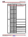
Revision History
The following table shows the revision history for this document.
Date
Version
05/28/07
1.0
Revision
Initial Xilinx release.
Spartan-3A/3AN Starter Kit Board User Guide
www.xilinx.com
UG334 (v1.0) May 28, 2007
Table of Contents
Preface: About This Guide
Acknowledgments . . . . . . . . . . . . . . . . . . . . . . . . . . . . . . . . . . . . . . . . . . . . . . . . . . . . . . . . . . 10
Guide Contents . . . . . . . . . . . . . . . . . . . . . . . . . . . . . . . . . . . . . . . . . . . . . . . . . . . . . . . . . . . . . 10
Additional Resources . . . . . . . . . . . . . . . . . . . . . . . . . . . . . . . . . . . . . . . . . . . . . . . . . . . . . . . 11
Chapter 1: Introduction and Overview
Getting Started . . . . . . . . . . . . . . . . . . . . . . . . . . . . . . . . . . . . . . . . . . . . . . . . . . . . . . . . . . . . . . 13
Operating the Default Demonstration Design . . . . . . . . . . . . . . . . . . . . . . . . . . . . . . . 15
VGA Display . . . . . . . . . . . . . . . . . . . . . . . . . . . . . . . . . . . . . . . . . . . . . . . . . . . . . . . . . . . . .
Rotary Knob/Push-Button Menu System . . . . . . . . . . . . . . . . . . . . . . . . . . . . . . . . . . . .
Select MultiBoot Configuration Image . . . . . . . . . . . . . . . . . . . . . . . . . . . . . . . . . . . . . . .
Scroll or Rotate Graphic . . . . . . . . . . . . . . . . . . . . . . . . . . . . . . . . . . . . . . . . . . . . . . . . . . .
Scroll or Scale Graphic. . . . . . . . . . . . . . . . . . . . . . . . . . . . . . . . . . . . . . . . . . . . . . . . . . . . .
Restart AutoPilot, Speaker Volume Control . . . . . . . . . . . . . . . . . . . . . . . . . . . . . . . . . .
LCD Screen Control Option . . . . . . . . . . . . . . . . . . . . . . . . . . . . . . . . . . . . . . . . . . . . . . . .
Power-Saving Suspend Mode . . . . . . . . . . . . . . . . . . . . . . . . . . . . . . . . . . . . . . . . . . . . . .
RS-232 Serial Port Control Option . . . . . . . . . . . . . . . . . . . . . . . . . . . . . . . . . . . . . . . . . . .
15
15
16
17
17
17
18
18
19
Key Components and Features . . . . . . . . . . . . . . . . . . . . . . . . . . . . . . . . . . . . . . . . . . . . . . 19
Design Trade-Offs . . . . . . . . . . . . . . . . . . . . . . . . . . . . . . . . . . . . . . . . . . . . . . . . . . . . . . . . . . 21
Configuration Methods Galore! . . . . . . . . . . . . . . . . . . . . . . . . . . . . . . . . . . . . . . . . . . . . . 21
Voltages for all Applications . . . . . . . . . . . . . . . . . . . . . . . . . . . . . . . . . . . . . . . . . . . . . . . 21
Spartan-3A/3AN Starter Kit Design Examples . . . . . . . . . . . . . . . . . . . . . . . . . . . . . . . 21
Choose a Spartan-3 Generation Starter Kit Board for your Needs . . . . . . . . . . . . . 22
Spartan-3A/3AN FPGA Features and Embedded Processing Functions . . . . . . . . . . 22
Other Spartan-3 Generation Development Boards . . . . . . . . . . . . . . . . . . . . . . . . . . . . . 23
Spartan-3A and Spartan-3AN FPGAs . . . . . . . . . . . . . . . . . . . . . . . . . . . . . . . . . . . . . . . . 23
Related Resources . . . . . . . . . . . . . . . . . . . . . . . . . . . . . . . . . . . . . . . . . . . . . . . . . . . . . . . . . . . 24
Chapter 2: Switches, Buttons, and Rotary Knob
Slide Switches . . . . . . . . . . . . . . . . . . . . . . . . . . . . . . . . . . . . . . . . . . . . . . . . . . . . . . . . . . . . . . 25
Locations and Labels . . . . . . . . . . . . . . . . . . . . . . . . . . . . . . . . . . . . . . . . . . . . . . . . . . . . . . 25
Operation. . . . . . . . . . . . . . . . . . . . . . . . . . . . . . . . . . . . . . . . . . . . . . . . . . . . . . . . . . . . . . . . 25
UCF Location Constraints. . . . . . . . . . . . . . . . . . . . . . . . . . . . . . . . . . . . . . . . . . . . . . . . . . 25
SUSPEND Switch . . . . . . . . . . . . . . . . . . . . . . . . . . . . . . . . . . . . . . . . . . . . . . . . . . . . . . . . . . . 26
Push-Button Switches . . . . . . . . . . . . . . . . . . . . . . . . . . . . . . . . . . . . . . . . . . . . . . . . . . . . . . . 27
Locations and Labels . . . . . . . . . . . . . . . . . . . . . . . . . . . . . . . . . . . . . . . . . . . . . . . . . . . . . .
Operation. . . . . . . . . . . . . . . . . . . . . . . . . . . . . . . . . . . . . . . . . . . . . . . . . . . . . . . . . . . . . . . .
PROG_B Push-Button Switch . . . . . . . . . . . . . . . . . . . . . . . . . . . . . . . . . . . . . . . . . . . . . . .
UCF Location Constraints. . . . . . . . . . . . . . . . . . . . . . . . . . . . . . . . . . . . . . . . . . . . . . . . . .
27
27
28
28
Rotary Push-Button Switch . . . . . . . . . . . . . . . . . . . . . . . . . . . . . . . . . . . . . . . . . . . . . . . . . . 28
Locations and Labels . . . . . . . . . . . . . . . . . . . . . . . . . . . . . . . . . . . . . . . . . . . . . . . . . . . . . . 28
Operation. . . . . . . . . . . . . . . . . . . . . . . . . . . . . . . . . . . . . . . . . . . . . . . . . . . . . . . . . . . . . . . . 28
Push-Button Switch . . . . . . . . . . . . . . . . . . . . . . . . . . . . . . . . . . . . . . . . . . . . . . . . . . . . 28
Spartan-3A/3AN Starter Kit Board User Guide
UG334 (v1.0) May 28, 2007
www.xilinx.com
3
R
Rotary Shaft Encoder . . . . . . . . . . . . . . . . . . . . . . . . . . . . . . . . . . . . . . . . . . . . . . . . . . . 29
UCF Location Constraints. . . . . . . . . . . . . . . . . . . . . . . . . . . . . . . . . . . . . . . . . . . . . . . . . . 30
Discrete LEDs . . . . . . . . . . . . . . . . . . . . . . . . . . . . . . . . . . . . . . . . . . . . . . . . . . . . . . . . . . . . . . . 30
Locations and Labels . . . . . . . . . . . . . . . . . . . . . . . . . . . . . . . . . . . . . . . . . . . . . . . . . . . . . . 30
Operation. . . . . . . . . . . . . . . . . . . . . . . . . . . . . . . . . . . . . . . . . . . . . . . . . . . . . . . . . . . . . . . . 31
UCF Location Constraints. . . . . . . . . . . . . . . . . . . . . . . . . . . . . . . . . . . . . . . . . . . . . . . . . . 31
Optional Discrete LEDs . . . . . . . . . . . . . . . . . . . . . . . . . . . . . . . . . . . . . . . . . . . . . . . . . . . . . 31
AWAKE LED . . . . . . . . . . . . . . . . . . . . . . . . . . . . . . . . . . . . . . . . . . . . . . . . . . . . . . . . . . . . 32
INIT_B LED . . . . . . . . . . . . . . . . . . . . . . . . . . . . . . . . . . . . . . . . . . . . . . . . . . . . . . . . . . . . . . 32
UCF Location Constraints. . . . . . . . . . . . . . . . . . . . . . . . . . . . . . . . . . . . . . . . . . . . . . . . . . 32
Chapter 3: Clock Sources
Overview . . . . . . . . . . . . . . . . . . . . . . . . . . . . . . . . . . . . . . . . . . . . . . . . . . . . . . . . . . . . . . . . . . .
Clock Connections . . . . . . . . . . . . . . . . . . . . . . . . . . . . . . . . . . . . . . . . . . . . . . . . . . . . . . . . . .
50 MHz On-Board Oscillator . . . . . . . . . . . . . . . . . . . . . . . . . . . . . . . . . . . . . . . . . . . . . . . .
Auxiliary Clock Oscillator Socket . . . . . . . . . . . . . . . . . . . . . . . . . . . . . . . . . . . . . . . . . . .
SMA Clock Input or Output Connector . . . . . . . . . . . . . . . . . . . . . . . . . . . . . . . . . . . . . .
UCF Constraints . . . . . . . . . . . . . . . . . . . . . . . . . . . . . . . . . . . . . . . . . . . . . . . . . . . . . . . . . . . .
33
34
34
34
34
34
Location . . . . . . . . . . . . . . . . . . . . . . . . . . . . . . . . . . . . . . . . . . . . . . . . . . . . . . . . . . . . . . . . . 34
Clock Period Constraints . . . . . . . . . . . . . . . . . . . . . . . . . . . . . . . . . . . . . . . . . . . . . . . . . . 35
Related Resources . . . . . . . . . . . . . . . . . . . . . . . . . . . . . . . . . . . . . . . . . . . . . . . . . . . . . . . . . . . 35
Chapter 4: FPGA Configuration Options
Configuration Mode Jumpers . . . . . . . . . . . . . . . . . . . . . . . . . . . . . . . . . . . . . . . . . . . . . . .
Xilinx Platform Flash Configuration PROM(s) . . . . . . . . . . . . . . . . . . . . . . . . . . . . . . .
PROG Push-Button Switch . . . . . . . . . . . . . . . . . . . . . . . . . . . . . . . . . . . . . . . . . . . . . . . . . .
DONE Pin LED . . . . . . . . . . . . . . . . . . . . . . . . . . . . . . . . . . . . . . . . . . . . . . . . . . . . . . . . . . . . .
Programming the FPGA or Platform Flash PROM via USB . . . . . . . . . . . . . . . . . . .
39
40
40
41
41
Connecting the USB Cable . . . . . . . . . . . . . . . . . . . . . . . . . . . . . . . . . . . . . . . . . . . . . . . . . 41
Platform Flash Programming Example in Spartan-3 Generation Configuration
User Guide . . . . . . . . . . . . . . . . . . . . . . . . . . . . . . . . . . . . . . . . . . . . . . . . . . . . . . . . . . . . 42
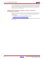
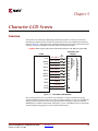
Chapter 5: Character LCD Screen
Overview . . . . . . . . . . . . . . . . . . . . . . . . . . . . . . . . . . . . . . . . . . . . . . . . . . . . . . . . . . . . . . . . . . .
Character LCD Interface Signals . . . . . . . . . . . . . . . . . . . . . . . . . . . . . . . . . . . . . . . . . . . . .
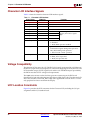
Voltage Compatibility. . . . . . . . . . . . . . . . . . . . . . . . . . . . . . . . . . . . . . . . . . . . . . . . . . . . . . .
UCF Location Constraints . . . . . . . . . . . . . . . . . . . . . . . . . . . . . . . . . . . . . . . . . . . . . . . . . . .
LCD Controller . . . . . . . . . . . . . . . . . . . . . . . . . . . . . . . . . . . . . . . . . . . . . . . . . . . . . . . . . . . . .
Memory Map . . . . . . . . . . . . . . . . . . . . . . . . . . . . . . . . . . . . . . . . . . . . . . . . . . . . . . . . . . . .
DD RAM . . . . . . . . . . . . . . . . . . . . . . . . . . . . . . . . . . . . . . . . . . . . . . . . . . . . . . . . . . . . .
CG ROM . . . . . . . . . . . . . . . . . . . . . . . . . . . . . . . . . . . . . . . . . . . . . . . . . . . . . . . . . . . . .
CG RAM . . . . . . . . . . . . . . . . . . . . . . . . . . . . . . . . . . . . . . . . . . . . . . . . . . . . . . . . . . . . .
Command Set . . . . . . . . . . . . . . . . . . . . . . . . . . . . . . . . . . . . . . . . . . . . . . . . . . . . . . . . . . . .
Disabled . . . . . . . . . . . . . . . . . . . . . . . . . . . . . . . . . . . . . . . . . . . . . . . . . . . . . . . . . . . . .
Clear Display . . . . . . . . . . . . . . . . . . . . . . . . . . . . . . . . . . . . . . . . . . . . . . . . . . . . . . . . .
Return Cursor Home . . . . . . . . . . . . . . . . . . . . . . . . . . . . . . . . . . . . . . . . . . . . . . . . . . .
Entry Mode Set . . . . . . . . . . . . . . . . . . . . . . . . . . . . . . . . . . . . . . . . . . . . . . . . . . . . . . . .
4
www.xilinx.com
43
44
44
44
45
45
45
46
47
48
49
49
49
49
Spartan-3A/3AN Starter Kit Board User Guide
UG334 (v1.0) May 28, 2007
R
Display On/Off . . . . . . . . . . . . . . . . . . . . . . . . . . . . . . . . . . . . . . . . . . . . . . . . . . . . . . .
Cursor and Display Shift . . . . . . . . . . . . . . . . . . . . . . . . . . . . . . . . . . . . . . . . . . . . . . . .
Function Set . . . . . . . . . . . . . . . . . . . . . . . . . . . . . . . . . . . . . . . . . . . . . . . . . . . . . . . . . .
Set CG RAM Address . . . . . . . . . . . . . . . . . . . . . . . . . . . . . . . . . . . . . . . . . . . . . . . . . . .
Set DD RAM Address . . . . . . . . . . . . . . . . . . . . . . . . . . . . . . . . . . . . . . . . . . . . . . . . . . .
Read Busy Flag and Address . . . . . . . . . . . . . . . . . . . . . . . . . . . . . . . . . . . . . . . . . . . . .
Write Data to CG RAM or DD RAM . . . . . . . . . . . . . . . . . . . . . . . . . . . . . . . . . . . . . . . .
Read Data from CG RAM or DD RAM . . . . . . . . . . . . . . . . . . . . . . . . . . . . . . . . . . . . . .
50
50
51
51
51
51
51
52
Operation . . . . . . . . . . . . . . . . . . . . . . . . . . . . . . . . . . . . . . . . . . . . . . . . . . . . . . . . . . . . . . . . . . . 52
Four-Bit Data Interface . . . . . . . . . . . . . . . . . . . . . . . . . . . . . . . . . . . . . . . . . . . . . . . . . . . .
Transferring Eight-Bit Data over the Four-Bit Interface . . . . . . . . . . . . . . . . . . . . . . . . .
Initializing the Display . . . . . . . . . . . . . . . . . . . . . . . . . . . . . . . . . . . . . . . . . . . . . . . . . . . .
Power-On Initialization . . . . . . . . . . . . . . . . . . . . . . . . . . . . . . . . . . . . . . . . . . . . . . . . .
Display Configuration . . . . . . . . . . . . . . . . . . . . . . . . . . . . . . . . . . . . . . . . . . . . . . . . . .
Writing Data to the Display . . . . . . . . . . . . . . . . . . . . . . . . . . . . . . . . . . . . . . . . . . . . . . . .
Disabling the Unused LCD . . . . . . . . . . . . . . . . . . . . . . . . . . . . . . . . . . . . . . . . . . . . . . . . .
52
53
53
54
54
54
55
Related Resources . . . . . . . . . . . . . . . . . . . . . . . . . . . . . . . . . . . . . . . . . . . . . . . . . . . . . . . . . . . 55
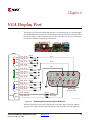
Chapter 6: VGA Display Port
Signal Timing for a 60 Hz, 640x480 VGA Display . . . . . . . . . . . . . . . . . . . . . . . . . . . .
VGA Signal Timing . . . . . . . . . . . . . . . . . . . . . . . . . . . . . . . . . . . . . . . . . . . . . . . . . . . . . . . .
UCF Location Constraints . . . . . . . . . . . . . . . . . . . . . . . . . . . . . . . . . . . . . . . . . . . . . . . . . . .
Related Resources . . . . . . . . . . . . . . . . . . . . . . . . . . . . . . . . . . . . . . . . . . . . . . . . . . . . . . . . . . .
58
60
61
61
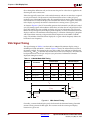
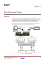
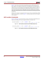
Chapter 7: RS-232 Serial Ports
Overview . . . . . . . . . . . . . . . . . . . . . . . . . . . . . . . . . . . . . . . . . . . . . . . . . . . . . . . . . . . . . . . . . . . 63
UCF Location Constraints . . . . . . . . . . . . . . . . . . . . . . . . . . . . . . . . . . . . . . . . . . . . . . . . . . . 64
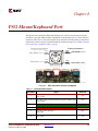
Chapter 8: PS/2 Mouse/Keyboard Port
Keyboard . . . . . . . . . . . . . . . . . . . . . . . . . . . . . . . . . . . . . . . . . . . . . . . . . . . . . . . . . . . . . . . . . . .
Mouse . . . . . . . . . . . . . . . . . . . . . . . . . . . . . . . . . . . . . . . . . . . . . . . . . . . . . . . . . . . . . . . . . . . . . .
Voltage Supply . . . . . . . . . . . . . . . . . . . . . . . . . . . . . . . . . . . . . . . . . . . . . . . . . . . . . . . . . . . . .
Adding a Second PS/2 Port Using a Y-Splitter Cable . . . . . . . . . . . . . . . . . . . . . . . . .
UCF Location Constraints . . . . . . . . . . . . . . . . . . . . . . . . . . . . . . . . . . . . . . . . . . . . . . . . . . .
Related Resources . . . . . . . . . . . . . . . . . . . . . . . . . . . . . . . . . . . . . . . . . . . . . . . . . . . . . . . . . . .
66
68
69
69
70
70
Chapter 9: Analog Capture Circuit
Digital Outputs from Analog Inputs . . . . . . . . . . . . . . . . . . . . . . . . . . . . . . . . . . . . . . . . . 72
Programmable Pre-Amplifier . . . . . . . . . . . . . . . . . . . . . . . . . . . . . . . . . . . . . . . . . . . . . . . . 73
Interface . . . . . . . . . . . . . . . . . . . . . . . . . . . . . . . . . . . . . . . . . . . . . . . . . . . . . . . . . . . . . . . . .
Programmable Gain . . . . . . . . . . . . . . . . . . . . . . . . . . . . . . . . . . . . . . . . . . . . . . . . . . . . . . .
SPI Control Interface . . . . . . . . . . . . . . . . . . . . . . . . . . . . . . . . . . . . . . . . . . . . . . . . . . . . . .
UCF Location Constraints. . . . . . . . . . . . . . . . . . . . . . . . . . . . . . . . . . . . . . . . . . . . . . . . . .
73
73
74
75
Analog-to-Digital Converter (ADC). . . . . . . . . . . . . . . . . . . . . . . . . . . . . . . . . . . . . . . . . . 75
Interface . . . . . . . . . . . . . . . . . . . . . . . . . . . . . . . . . . . . . . . . . . . . . . . . . . . . . . . . . . . . . . . . . 75
SPI Control Interface . . . . . . . . . . . . . . . . . . . . . . . . . . . . . . . . . . . . . . . . . . . . . . . . . . . . . . 75
UCF Location Constraints. . . . . . . . . . . . . . . . . . . . . . . . . . . . . . . . . . . . . . . . . . . . . . . . . . 76
Spartan-3A/3AN Starter Kit Board User Guide
UG334 (v1.0) May 28, 2007
www.xilinx.com
5
R
Connecting Analog Inputs . . . . . . . . . . . . . . . . . . . . . . . . . . . . . . . . . . . . . . . . . . . . . . . . . . 77
Related Resources . . . . . . . . . . . . . . . . . . . . . . . . . . . . . . . . . . . . . . . . . . . . . . . . . . . . . . . . . . . 77
Chapter 10: Digital-to-Analog Converter (DAC)
SPI Communication . . . . . . . . . . . . . . . . . . . . . . . . . . . . . . . . . . . . . . . . . . . . . . . . . . . . . . . . . 79
Interface Signals . . . . . . . . . . . . . . . . . . . . . . . . . . . . . . . . . . . . . . . . . . . . . . . . . . . . . . . . . . 80
SPI Communication Details . . . . . . . . . . . . . . . . . . . . . . . . . . . . . . . . . . . . . . . . . . . . . . . . 80
Communication Protocol . . . . . . . . . . . . . . . . . . . . . . . . . . . . . . . . . . . . . . . . . . . . . . . . . . 81
Specifying the DAC Output Voltage . . . . . . . . . . . . . . . . . . . . . . . . . . . . . . . . . . . . . . . . . 82
UCF Location Constraints . . . . . . . . . . . . . . . . . . . . . . . . . . . . . . . . . . . . . . . . . . . . . . . . . . . 82
Related Resources . . . . . . . . . . . . . . . . . . . . . . . . . . . . . . . . . . . . . . . . . . . . . . . . . . . . . . . . . . . 82
Chapter 11: Parallel NOR Flash PROM
Flash Connections . . . . . . . . . . . . . . . . . . . . . . . . . . . . . . . . . . . . . . . . . . . . . . . . . . . . . . . . . . . 84
Shared SPI Flash and Platform Flash Data Line . . . . . . . . . . . . . . . . . . . . . . . . . . . . . . . 86
UCF Location Constraints . . . . . . . . . . . . . . . . . . . . . . . . . . . . . . . . . . . . . . . . . . . . . . . . . . . 87
Address . . . . . . . . . . . . . . . . . . . . . . . . . . . . . . . . . . . . . . . . . . . . . . . . . . . . . . . . . . . . . . . . . 87
Data . . . . . . . . . . . . . . . . . . . . . . . . . . . . . . . . . . . . . . . . . . . . . . . . . . . . . . . . . . . . . . . . . . . . 88
Control . . . . . . . . . . . . . . . . . . . . . . . . . . . . . . . . . . . . . . . . . . . . . . . . . . . . . . . . . . . . . . . . . . 88
Setting the FPGA Mode Select Pins . . . . . . . . . . . . . . . . . . . . . . . . . . . . . . . . . . . . . . . . . . 88
Creating and Programming Configuration Images for Parallel Flash . . . . . . . . . 89
Related Resources . . . . . . . . . . . . . . . . . . . . . . . . . . . . . . . . . . . . . . . . . . . . . . . . . . . . . . . . . . . 89
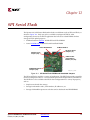
Chapter 12: SPI Serial Flash
SPI Flash PROM Select Jumpers (J1) . . . . . . . . . . . . . . . . . . . . . . . . . . . . . . . . . . . . . . . . . 93
Shared SPI Flash and Platform Flash Data Line . . . . . . . . . . . . . . . . . . . . . . . . . . . . . . . 94
Jumper Settings to Configure FPGA from Selected SPI Flash PROM . . . . . . . . . . . . . 94
UCF Location Constraints . . . . . . . . . . . . . . . . . . . . . . . . . . . . . . . . . . . . . . . . . . . . . . . . . . . 95
Creating and Programming Configuration Images for SPI Serial Flash . . . . . . . 95
SPI Flash PROM Programming Options . . . . . . . . . . . . . . . . . . . . . . . . . . . . . . . . . . . . . 95
Direct Programming Method . . . . . . . . . . . . . . . . . . . . . . . . . . . . . . . . . . . . . . . . . . . . . . . 96
Using Embedded USB JTAG Programmer . . . . . . . . . . . . . . . . . . . . . . . . . . . . . . . . . . . 96
Using a Separate JTAG Parallel Programming Cable (Optional) . . . . . . . . . . . . . . . . . . 97
Direct SPI Flash Programming Using iMPACT . . . . . . . . . . . . . . . . . . . . . . . . . . . . . . . 98
Indirect Programming Method . . . . . . . . . . . . . . . . . . . . . . . . . . . . . . . . . . . . . . . . . . . . 101
Jumper Settings . . . . . . . . . . . . . . . . . . . . . . . . . . . . . . . . . . . . . . . . . . . . . . . . . . . . . . . 101
Indirect SPI Flash Programming Using iMPACT . . . . . . . . . . . . . . . . . . . . . . . . . . . . . 102
Related Resources . . . . . . . . . . . . . . . . . . . . . . . . . . . . . . . . . . . . . . . . . . . . . . . . . . . . . . . . . . 106
Chapter 13: DDR2 SDRAM
DDR2 SDRAM Connections . . . . . . . . . . . . . . . . . . . . . . . . . . . . . . . . . . . . . . . . . . . . . . . 110
UCF Location Constraints . . . . . . . . . . . . . . . . . . . . . . . . . . . . . . . . . . . . . . . . . . . . . . . . . . 112
Address . . . . . . . . . . . . . . . . . . . . . . . . . . . . . . . . . . . . . . . . . . . . . . . . . . . . . . . . . . . . . . . .
Data . . . . . . . . . . . . . . . . . . . . . . . . . . . . . . . . . . . . . . . . . . . . . . . . . . . . . . . . . . . . . . . . . . .
Control . . . . . . . . . . . . . . . . . . . . . . . . . . . . . . . . . . . . . . . . . . . . . . . . . . . . . . . . . . . . . . . . .
Reserve FPGA VREF Pins . . . . . . . . . . . . . . . . . . . . . . . . . . . . . . . . . . . . . . . . . . . . . . . . .
112
113
113
114
Special Layout Recommendations . . . . . . . . . . . . . . . . . . . . . . . . . . . . . . . . . . . . . . . . . . 114
6
www.xilinx.com
Spartan-3A/3AN Starter Kit Board User Guide
UG334 (v1.0) May 28, 2007
R
Related Resources . . . . . . . . . . . . . . . . . . . . . . . . . . . . . . . . . . . . . . . . . . . . . . . . . . . . . . . . . . 114
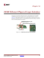
Chapter 14: 10/100 Ethernet Physical Layer Interface
Ethernet PHY Connections . . . . . . . . . . . . . . . . . . . . . . . . . . . . . . . . . . . . . . . . . . . . . . . . .
MicroBlaze Ethernet IP Cores . . . . . . . . . . . . . . . . . . . . . . . . . . . . . . . . . . . . . . . . . . . . . .
UCF Location Constraints . . . . . . . . . . . . . . . . . . . . . . . . . . . . . . . . . . . . . . . . . . . . . . . . . .
Related Resources . . . . . . . . . . . . . . . . . . . . . . . . . . . . . . . . . . . . . . . . . . . . . . . . . . . . . . . . . .
118
119
120
120
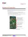
Chapter 15: Expansion Connectors
Hirose 100-Pin FX2 Edge Connector (J17) . . . . . . . . . . . . . . . . . . . . . . . . . . . . . . . . . . . 122
Expansion Connector Compatibility . . . . . . . . . . . . . . . . . . . . . . . . . . . . . . . . . . . . . . . .
Voltage Supplies to the Connector . . . . . . . . . . . . . . . . . . . . . . . . . . . . . . . . . . . . . . . . .
Connector Pinout and FPGA Connections . . . . . . . . . . . . . . . . . . . . . . . . . . . . . . . . . . .
FX2-Connector Compatible Boards . . . . . . . . . . . . . . . . . . . . . . . . . . . . . . . . . . . . . . . . .
Mating Receptacle Connectors . . . . . . . . . . . . . . . . . . . . . . . . . . . . . . . . . . . . . . . . . . . . .
UCF Location Constraints. . . . . . . . . . . . . . . . . . . . . . . . . . . . . . . . . . . . . . . . . . . . . . . . .
122
122
123
124
124
125
Differential I/O Connectors . . . . . . . . . . . . . . . . . . . . . . . . . . . . . . . . . . . . . . . . . . . . . . . . 126
Using Differential Inputs . . . . . . . . . . . . . . . . . . . . . . . . . . . . . . . . . . . . . . . . . . . . . . . . .
Using Differential Outputs . . . . . . . . . . . . . . . . . . . . . . . . . . . . . . . . . . . . . . . . . . . . . . . .
Differential Trace Layout Considerations . . . . . . . . . . . . . . . . . . . . . . . . . . . . . . . . . . .
34-Conductor Cable Assemblies (2x17) . . . . . . . . . . . . . . . . . . . . . . . . . . . . . . . . . . . . .
UCF Location Constraints. . . . . . . . . . . . . . . . . . . . . . . . . . . . . . . . . . . . . . . . . . . . . . . . .
127
128
128
130
130
Six-Pin Accessory Headers . . . . . . . . . . . . . . . . . . . . . . . . . . . . . . . . . . . . . . . . . . . . . . . . . 131
J18 Header . . . . . . . . . . . . . . . . . . . . . . . . . . . . . . . . . . . . . . . . . . . . . . . . . . . . . . . . . . . . . .
J19 Header . . . . . . . . . . . . . . . . . . . . . . . . . . . . . . . . . . . . . . . . . . . . . . . . . . . . . . . . . . . . . .
J20 Header . . . . . . . . . . . . . . . . . . . . . . . . . . . . . . . . . . . . . . . . . . . . . . . . . . . . . . . . . . . . . .
Digilent Peripheral Modules . . . . . . . . . . . . . . . . . . . . . . . . . . . . . . . . . . . . . . . . . . . . . .
UCF Location Constraints. . . . . . . . . . . . . . . . . . . . . . . . . . . . . . . . . . . . . . . . . . . . . . . . .
131
131
132
132
133
Connectorless Debugging Port Landing Pads (J34) . . . . . . . . . . . . . . . . . . . . . . . . . . 133
Chapter 16: Miniature Stereo Audio Jack
Supported Audio Devices . . . . . . . . . . . . . . . . . . . . . . . . . . . . . . . . . . . . . . . . . . . . . . . . . . 135
FPGA Connections . . . . . . . . . . . . . . . . . . . . . . . . . . . . . . . . . . . . . . . . . . . . . . . . . . . . . . . . . 136
UCF Location Constraints. . . . . . . . . . . . . . . . . . . . . . . . . . . . . . . . . . . . . . . . . . . . . . . . . 136
Related Resources . . . . . . . . . . . . . . . . . . . . . . . . . . . . . . . . . . . . . . . . . . . . . . . . . . . . . . . . . . 136
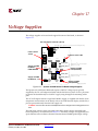
Chapter 17: Voltage Supplies
Measuring Power Across Voltage Supply Jumpers . . . . . . . . . . . . . . . . . . . . . . . . . . 139
I2C Voltage Adjustment Interface . . . . . . . . . . . . . . . . . . . . . . . . . . . . . . . . . . . . . . . . . . 140
Possible Applications . . . . . . . . . . . . . . . . . . . . . . . . . . . . . . . . . . . . . . . . . . . . . . . . . . . . 140
Restoring Default Voltages . . . . . . . . . . . . . . . . . . . . . . . . . . . . . . . . . . . . . . . . . . . . . . . . 141
UCF Location Constraints. . . . . . . . . . . . . . . . . . . . . . . . . . . . . . . . . . . . . . . . . . . . . . . . . 141
Related Resources . . . . . . . . . . . . . . . . . . . . . . . . . . . . . . . . . . . . . . . . . . . . . . . . . . . . . . . . . . 141
Spartan-3A/3AN Starter Kit Board User Guide
UG334 (v1.0) May 28, 2007
www.xilinx.com
7
R
8
www.xilinx.com
Spartan-3A/3AN Starter Kit Board User Guide
UG334 (v1.0) May 28, 2007
R
Preface
About This Guide
This user guide provides basic information on the Spartan™-3A/3AN Starter Kit board
capabilities, functions, and design. It includes general information on how to use the
various peripheral functions included on the board. For detailed reference designs,
including VHDL or Verilog source code, please visit the following web link.
•
Spartan-3A/3AN Starter Kit Board Web Page
http://www.xilinx.com/s3astarter and http://www.xilinx.com/s3anstarter
There are multiple versions of the Spartan-3A/3AN Starter Kit. This document describes
the three kits that include the “Revision D” Spartan-3A/3AN Starter Kit Board, which is an
updated version of the “Revision C” Spartan-3A Starter Kit Board. The following table
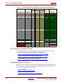
describes the different kits.
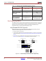
Feature
Spartan-3AN
Starter Kit
Part
Number
HW-SPAR3AN-SK-UNI-G
Device
XC3S700AN
Spartan-3A DDR2 SDRAM Spartan-3A Starter Spartan-3A Starter Kit,
Interface Development Kit
Kit, Revision D
Revision C
HW-SPAR3ADDR2-DKUNI-G
HW-SPAR3A-SK-UNI-G
XC3S700A
Board
Revision
Revision D
Revision C
DDR2
Memory
Supported with 133 MHz crystal oscillator in auxiliary socket
Requires board
modification for
improved performance
User
Guide
UG334 (this document)
UG330
Web Page
www.xilinx.com/s3anstarter
www.xilinx.com/s3addr2
www.xilinx.com/s3astarter
Almost all functionality is identical between the Revision C and Revision D boards,
although the silkscreen changes make the two boards look different. The pictures used in
this document are from the Revision D board. If you are using the original Revision C
version of the board, refer to UG330 for pictures and documentation. The following figure
highlights where to find the board revision code on a Revision C board.
Spartan-3A/3AN Starter Kit Board User Guide
UG334 (v1.0) May 28, 2007
www.xilinx.com
9
R
Preface: About This Guide
Board Revision Code
REV C
UG334_01_052707
Acknowledgments
Xilinx wishes to thank the following companies for their support of the Spartan-3A/3AN
Starter Kit board:
•
STMicroelectronics for the 32 Mbit parallel NOR Flash and 16 Mbit SPI serial Flash
memories
•
Atmel for the 16 Mbit SPI serial DataFlash memory
•
Linear Technology for the SPI-compatible A/D and D/A converters and the
programmable pre-amplifier
•
SMSC for the 10/100 Ethernet PHY
•
National Semiconductor for the four-rail voltage regulators that power the FPGA and
and all peripheral components
•
Xilinx, Inc. Configuration Solutions Division for the XCF04S Platform Flash PROM
and support for the embedded USB programmer
Guide Contents
This manual contains the following chapters:
10
•
Chapter 1, “Introduction and Overview,” provides an overview of the key features of
the Spartan-3A/3AN Starter Kit board.
•
Chapter 2, “Switches, Buttons, and Rotary Knob,” defines the switches, buttons, and
knobs present on the Spartan-3A/3AN Starter Kit board.
•
Chapter 3, “Clock Sources,” describes the various clock sources available on the
Spartan-3A/3AN Starter Kit board.
•
Chapter 4, “FPGA Configuration Options,” describes the configuration options for
the FPGA on the Spartan-3A/3AN Starter Kit board.
•
Chapter 5, “Character LCD Screen,” describes the functionality of the character LCD
screen.
•
Chapter 6, “VGA Display Port,” describes the functionality of the VGA port.
•
Chapter 7, “RS-232 Serial Ports,” describes the functionality of the RS-232 serial ports.
•
Chapter 8, “PS/2 Mouse/Keyboard Port,” describes the functionality of the PS/2
mouse and keyboard port.
•
Chapter 10, “Digital-to-Analog Converter (DAC),” describes the functionality of the
D/A converter.
www.xilinx.com
Spartan-3A/3AN Starter Kit Board User Guide
UG334 (v1.0) May 28, 2007
R
Additional Resources
•
Chapter 9, “Analog Capture Circuit,” describes the functionality of the A/D converter
with a programmable gain pre-amplifier.
•
Chapter 11, “Parallel NOR Flash PROM,” describes the functionality of the
STMicroelectronics parallel NOR PROM.
•
Chapter 12, “SPI Serial Flash,” describes the functionality of the SPI Serial Flash
memory interface.
•
Chapter 13, “DDR2 SDRAM,” describes the functionality of the DDR2 SDRAM
memory interface.
•
Chapter 14, “10/100 Ethernet Physical Layer Interface,” describes the functionality of
the 10/100Base-T Ethernet physical layer interface.
•
Chapter 15, “Expansion Connectors,” describes the various connectors available on
the Spartan-3A/3AN Starter Kit board.
•
Chapter 16, “Miniature Stereo Audio Jack,” describes the audio interface.
•
Chapter 17, “Voltage Supplies,” describes the board’s power distribution system.
Additional Resources
To find additional documentation, see the Xilinx website at:
http://www.xilinx.com/literature.
To search the Answer Database of silicon, software, and IP questions and answers, or to
create a technical support WebCase, see the Xilinx website at:
http://www.xilinx.com/support.
Spartan-3A/3AN Starter Kit Board User Guide
UG334 (v1.0) May 28, 2007
www.xilinx.com
11
R
Preface: About This Guide
12
www.xilinx.com
Spartan-3A/3AN Starter Kit Board User Guide
UG334 (v1.0) May 28, 2007
R
Chapter 1
Introduction and Overview
Thank you for purchasing the Xilinx Spartan™-3A/3AN Starter Kit. The board is
invaluable to develop a Spartan-3A or Spartan-3AN FPGA application.
Getting Started
The Spartan-3A/3AN Starter Kit board is ready for use, right out of the box. The design
stored in external Flash exercises the various I/O devices, such as the VGA display and
serial ports. In addition it demonstrates new FPGA features, such as selectable MultiBoot
and the power-saving Suspend mode.
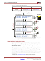
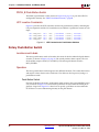
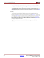
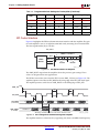
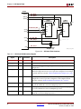
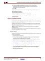
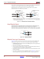
To start using the board, follow the simple steps outlined in Figure 1-1.
1 CHECK JUMPER SETTINGS!
2 Optional: Connect VGA display.
3 Optional: Connect headphones
5 Connect AC wall adapter.
or amplified speakers
PS/2 RS-232
9
10
6 Turn on power switch.
4
Set SUSPEND switch
to RUN position.
8
Control operation using
rotary / push-button switch.
7 See messages and
instructions on LCD
character display.
UG334_c1_01_052407
Figure 1-1:
Powering Up the Starter Kit Board
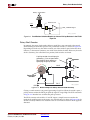
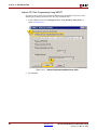
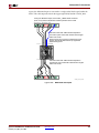
1.
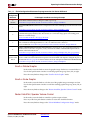
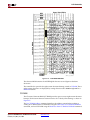
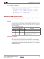
Double-check the position of the board jumpers, as shown in Figure 1-2, page 14.
These settings are required for the demonstration design to configure correctly.
2.
Optionally connect a VGA display device. The display device can be a CRT, a flatpanel, or even a projector.
3.
Optionally connect headphones or amplified speakers to the audio jack.
4.
Set the SUSPEND switch to the “RUN” position.
5.
Connect the included AC adapter to wall power and also to the board. The AC adapter
also includes attachments to support worldwide locals.
Spartan-3A/3AN Starter Kit Board User Guide
UG334 (v1.0) May 28, 2007
www.xilinx.com
13
R
Chapter 1: Introduction and Overview
6.
Turn on the power switch.
7.
The character LCD and VGA display, if connected, display various informational
messages and instructions. If an audio device is connected, the board offers words of
welcome in a variety of languages.
8.
Use the rotary/push-button switch to control various board functions.
9.
Optionally connect a PS/2-style keyboard to support one of the included
demonstrating designs.
10. Optionally connect a PC directly to the board using a standard 9-pin serial cable.
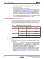
SPI Flash Select Jumpers
(both jumpers installed, vertically)
Platform Flash Jumper
(jumper removed)
J1
DONE
CE
PROM
GND
J46
Power Supply Jumpers
(all jumpers installed)
J42
J13
J12
J10
J41
J40
J11
J9
M0
M1
M2
J26
FPGA Mode Select Jumpers
(bottom two jumpers installed)
(SPI Mode)
Figure 1-2:
UG334_c1_02_052707
Default Jumper Settings for Starter Kit Board
For more information on the demonstration design, visit the Design Examples web page:
14
•
Spartan-3A/3AN Starter Kit Demo Design Overview
www.xilinx.com/products/boards/s3astarter/reference_designs.htm#demo
•
Restoring the “Out of the Box” Flash Programming
www.xilinx.com/products/boards/s3astarter/reference_designs.htm#out
www.xilinx.com
Spartan-3A/3AN Starter Kit Board User Guide
UG334 (v1.0) May 28, 2007
R
Operating the Default Demonstration Design
Operating the Default Demonstration Design
The demonstration design programmed onto the Spartan-3A/3AN Starter Kit board
provides various output information, depending on what I/O or display devices are
connected. The VGA and audio ports provide the richest experience.
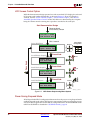
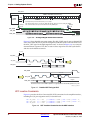
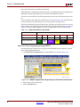
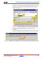
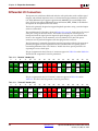
VGA Display
If a VGA display is connected to the board, then the Starter Kit board displays graphics
similar to that shown in Figure 1-3.
Until one of the four push buttons around the rotary knob (Figure 2-5, page 27) is pressed,
the display automatically rotates a graphic image and zooms in and out around the image.
This is called “AutoPilot” mode. A brief text overview describing the board appears along
the left edge. Blue text at the bottom of the screen presents the menu system.
Text Description
Rotating and Zooming Graphics
Rotary/Push-Button Menu System
Figure 1-3:
UG330_c1_03_032207
Rotating/Zooming Graphics, Menu System Displayed on VGA Screen
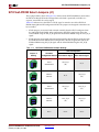
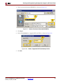
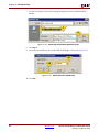
Rotary Knob/Push-Button Menu System
The Spartan-3A/3AN Starter Kit board demonstration design uses the rotary knob and
surrounding push-button switches, shown in Figure 2-5, page 27, to implement a menu
system. The menu display appears in blue text at the bottom of the VGA output. The menu
functions are highlighted in Table 1-1 and Figure 1-4.
Spartan-3A/3AN Starter Kit Board User Guide
UG334 (v1.0) May 28, 2007
www.xilinx.com
15
R
Chapter 1: Introduction and Overview
Table 1-1:
Function of Each Menu Control
Press Knob
Rotate Knob
Press Push Button
Move to next menu selection,
next mode.
Depends on current mode, as
shown in Figure 1-4.
Depends on current mode, as
shown in Figure 1-4.
Start Demonstration Design
Power-up board
Press PROG_B button
Select MultiBoot
Select FPGA
Configuration
MultiBoot
MultiBoot
Load Configuration 1.
Select Configuration.
More Options ...
MultiBoot
Buttons:
Knob Spin:
Knob Push:
Config. 4
MultiBoot
Scroll/Rotate Graphic
Config. 1
Config. 2
Config. 3
Press Knob
Scroll Image.
Rotate Image.
More Options ...
Scroll/Scale Graphic
Buttons:
Knob Spin:
Knob Push:
Scale
Scroll Image.
Scale Image.
More Options ...
Press Knob
AutoPilot/Volume
AutoPilot
Restart AutoPilot.
Adjust Volume.
More Options ...
Volume
AutoPilot
Buttons:
Knob Spin:
Knob Push:
Press Knob
AutoPilot
Press Knob
Rotate
Buttons:
Knob Spin:
Knob Push:
AutoPilot
UG334_c1_04_052707
Figure 1-4:
Rotary Knob/Push-Button Menu System
Select MultiBoot Configuration Image
Spartan-3A/3AN FPGAs support a selectable MultiBoot configuration interface. If the
FPGA configures in one of its Master configuration modes, then the FPGA always loads
the configuration image stored at address 0 in Flash at power-up, or whenever the
PROG_B button is pressed.
Spin the rotary knob to select a new FPGA configuration image. The blue text at the bottom
of the display updates with each click of the rotary knob. For example, the application
displays “Buttons: Load Configuration x” where ‘x’ corresponds to the bitstream image
listed in Table 1-2. Table 1-2 describes the bitstreams preloaded on the board.
After selecting the desired image, press one of the four push-button switches that surround
the rotary knob. This action causes the FPGA to load the selected image from external
Flash memory.
To change to the “Scroll or Rotate Graphic” mode, press the rotary knob.
16
www.xilinx.com
Spartan-3A/3AN Starter Kit Board User Guide
UG334 (v1.0) May 28, 2007
R
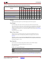
Table 1-2:
Operating the Default Demonstration Design
FPGA Configuration Bitstreams Preprogrammed on the Starter Kit Board
FPGA
Configuration
Bitstream
0
(default)
FPGA Application/Reference Design Example
Starter Kit board demonstration design. Loaded at power-up.
www.xilinx.com/products/boards/s3astarter/reference_designs.htm#demo
Device DNA Reader: Reads the FPGA’s unique Device ID value and displays it on the character LCD
screen.
1
www.xilinx.com/products/boards/s3astarter/reference_designs.htm#dna_reader
Fractal Generator: Computes fractal images in real time and displays on the VGA port. A usercontributed design by Matthias Alles. Rotate knob to zoom fractal image; press surrounding push
buttons to scroll the image.
2
www-user.rhrk.uni-kl.de/~alles/fpga/files.htm
ASCII Terminal: Implements a text terminal using an attached VGA display and PS/2 keyboard and
will communicate with HyperTerminal on a PC via an RS-232 serial connection.
3
Source included in www.xilinx.com/products/boards/s3astarter/reference_designs.htm#out.
STMicro M29DW323DT Parallel Flash Programmer: Communicates to a PC using HyperTerminal via
an RS-232 serial connection. Programs, erases, and reads the STMicro M29DW323DT parallel Flash
PROM on the Starter Kit board.
4
www.xilinx.com/products/boards/s3astarter/reference_designs.htm#parallel_flash_programmer
Spartan-3AN
FPGA
Internal Flash Paint Application: Use a mouse to create drawings and read or write them to In-System
Flash. Loaded from internal SPI Flash in Spartan-3AN Starter Kit Board. Requires setting Mode pins as
described in Table 4-1, page 39 for Internal Master SPI mode. For Spartan-3AN Starter Kit Board only.
www.xilinx.com/products/boards/s3astarter/reference_designs.htm#paint.
Scroll or Rotate Graphic
In this mode, rotate the knob to rotate the graphic image clockwise or counterclockwise.
Use the four push-button switches to scroll the graphic image up, down, left, or right.
Press the rotary knob to change to the “Scroll or Scale Graphic” mode.
Scroll or Scale Graphic
In this mode, rotate the knob to scale the size of the graphic image, zooming in and out.
Use the four push-button switches to scroll the resulting graphic image up, down, left, or
right.
Press the rotary knob to change to the “Restart AutoPilot, Speaker Volume Control” mode.
Restart AutoPilot, Speaker Volume Control
In this mode, rotate the knob to control the speaker output volume.
Press any of the four push-button switches to restart the AutoPilot function.
Press the rotary knob to change to the “Select MultiBoot Configuration Image” mode.
Spartan-3A/3AN Starter Kit Board User Guide
UG334 (v1.0) May 28, 2007
www.xilinx.com
17
R
Chapter 1: Introduction and Overview
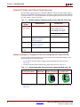
LCD Screen Control Option
While the demonstration design operates best with an attached VGA display, the on-board
LCD screen tracks similar functionality, as shown in Figure 1-5. If no VGA display is
attached, then the “Scroll or Rotate Graphic”, “Scroll or Scale Graphic”, and “Restart
AutoPilot, Speaker Volume Control” modes offer little to no functionality, the exception
being the volume control assuming that a speaker is attached to the audio jack.
Start Demonstration Design
Power-up board
Press PROG_B button
Welcome to XLNX
S3A Starter Kit
Wait 1 second
Select FPGA
Configuration
Select MultiBoot
MultiBoot
MultiBoot
MultiBoot
Btns: Load Cfg 1
Spin: Select Cfg
Config. 4
MultiBoot
Scroll/Rotate Graphic
Config. 1
Config. 2
Config. 3
Press Knob
Press Knob
Rotate
Press Knob 3x
For Boot Menu
Scroll/Scale Graphic
Press Knob
Scale
Press Knob 2x
For Boot Menu
AutoPilot
Volume
AutoPilot
Press Knob 1x
For Boot Menu
Press Knob
AutoPilot
AutoPilot/Volume
AutoPilot
UG334_c1_05_052707
Figure 1-5:
LCD Screen Output using Menu System
Power-Saving Suspend Mode
All of the preloaded FPGA configuration bitstreams have the power-saving Suspend mode
enabled. Suspend mode reduces FPGA power consumption while preserving the present
state of the FPGA application and the FPGA’s configuration data. Set the SUSPEND switch
to RUN or SUSPEND as described in “SUSPEND Switch,” page 26.
18
www.xilinx.com
Spartan-3A/3AN Starter Kit Board User Guide
UG334 (v1.0) May 28, 2007
R
Key Components and Features
Using one or two external multimeters, measure the corresponding difference in current
consumption, as described in “Measuring Power Across Voltage Supply Jumpers,” page
139.
Caution! Do not set the SUSPEND switch to “SUSPEND” while programming the parallel NOR
Flash PROM using configuration bitstream #4, as described in Table 1-2.
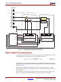
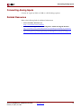
RS-232 Serial Port Control Option
Optionally, control the demonstration design using a serial port connection to a PC or
workstation. On a PC, use the HyperTerminal program to communicate to the FPGA
application, as shown in Figure 1-6. Using a standard, straight-through 9-pin serial cable,
connect the PC’s 9-pin RS-232 port to the board’s DCE connector (see Figure 7-1, page 63).
UG334_c1_06_052707
Figure 1-6:
Use HyperTerminal and a Standard Serial Cable to Connect to Board
When the demonstration design begins operating, it transmits a message using the serial
port.
Press a number key on the PC to load the associated MultiBoot bitstream listed in Table 1-2.
Key Components and Features
The key features of the Spartan-3A Starter Kit board or the Spartan-3AN Starter Kit board
are:
•
Spartan-3A Starter Kit Board: Xilinx 700K-gate XC3S700A Spartan-3A FPGA in the
Pb-free 484-ball BGA package (FGG484)
•
Spartan-3AN Starter Kit Board: Xilinx 700K-gate XC3S700AN Spartan-3AN
nonvolatile FPGA in the Pb-free 484-ball BGA package (FGG484)
♦
Internal 8 Mbit In-System Flash memory
♦
Store FPGA configuration bitstream or nonvolatile data
•
4 Mbit Xilinx Platform Flash configuration PROM
•
64 MByte (512 Mbit) of DDR2 SDRAM, 32Mx16 data interface
•
4 MByte (32 Mbit) of parallel NOR Flash
Spartan-3A/3AN Starter Kit Board User Guide
UG334 (v1.0) May 28, 2007
www.xilinx.com
19
R
Chapter 1: Introduction and Overview
•
♦
FPGA configuration storage
♦
MicroBlaze™ code storage/shadowing
♦
x8 or x16 data interface after configuration
Two 16 Mbit SPI serial Flash
♦
STMicroelectronics and Atmel DataFlash serial architectures
♦
FPGA configuration storage
-
♦
Nonvolatile data storage
♦
MicroBlaze code shadowing
•
Two-line, 16-character LCD screen
•
PS/2 port
♦
Supports PS/2-compatible mouse or keyboard
♦
Supports both mouse and keyboard using a Y-splitter cable (not included)
•
VGA display port, 12-bit color
•
10/100 Ethernet PHY (requires Ethernet MAC in FPGA)
•
Two nine-pin RS-232 ports (DTE- and DCE-style)
•
On-board USB-based programming solution
♦
FPGA download/debug
♦
SPI serial Flash in-system direct programming
•
50 MHz clock oscillator
•
8-pin DIP socket for second oscillator
•
SMA connector for clock inputs or outputs
•
100-pin Hirose FX2 expansion connector with up to 43 FPGA user I/Os
♦
•
20
Supports single configuration bitstream or multiple MultiBoot configuration
bitstreams
Compatible with Digilent FX2 add-on cards
High-speed differential I/O connectors
♦
Receiver: Six data channels or five data channels plus clock
♦
Transmitter: Six data channels or five data channels plus clock
♦
Supports multiple differential I/O standards, including LVDS, RSDS, mini-LVDS
♦
Also supports up to 24 single-ended I/O
♦
Uses widely available 34-conductor cables
•
Two six-pin expansion connectors for Digilent Peripheral Modules
•
Four-output, SPI-based Digital-to-Analog Converter (DAC)
•
Two-input, SPI-based Analog-to-Digital Converter (ADC) with programmable-gain
pre-amplifier
•
Stereo audio jack using digital I/O pins
•
ChipScope™ SoftTouch debugging port
•
Rotary-encoder with push-button shaft
•
Eight discrete LEDs
•
Four slide switches
•
Four push-button switches
www.xilinx.com
Spartan-3A/3AN Starter Kit Board User Guide
UG334 (v1.0) May 28, 2007
R
Design Trade-Offs
Design Trade-Offs
A few system-level design trade-offs were required in order to provide the Spartan3A/3AN Starter Kit board with the most functionality.
Configuration Methods Galore!
A typical FPGA application uses a single, nonvolatile memory to store configuration
images. A typical Spartan-3AN nonvolatile FPGA application would not require any
external memory. To demonstrate new Spartan-3A and Spartan-3AN FPGA capabilities,
the starter kit board has four different configuration memory sources that all must function
well together. The extra configuration functions make the starter kit board more complex
than typical FPGA applications.
The starter kit board also includes an on-board USB-based JTAG programming interface.
The on-chip circuitry simplifies the device programming experience. In typical
applications, the JTAG programming hardware resides off-board or in a separate
programming module, such as the Xilinx Platform USB cable.
Voltages for all Applications
The Spartan-3A/3AN FPGA typically operates with two supply rails, 1.2V and 3.3V. The
Spartan-3A/3AN Starter Kit board showcases a quadruple-output regulator developed by
National Semiconductor specifically to power Spartan-3 Generation FPGAs. This regulator
is sufficient for most standalone FPGA applications.
Spartan-3A/3AN Starter Kit Design Examples
Visit the Spartan-3A/3AN Starter Kit Design Examples web page to download and use the
latest applications that specifically target the starter kit board:
•
Spartan-3A/3AN Starter Kit Design Examples Web Page
www.xilinx.com/products/boards/s3astarter/reference_designs.htm
The list of designs is ever growing and the applications are often updated to the latest
software releases. The following list provides a sample of design examples:
•
Spartan-3A/3AN Starter Kit Demo Design Overview
www.xilinx.com/products/boards/s3astarter/reference_designs.htm#demo
This describes the out-of-the box demo design shipped with the board. Includes how
to set up and operate the demonstration, evaluate MultiBoot and Suspend, and
provides demo technical details.
•
Restoring the “Out of the Box” Flash Programming
www.xilinx.com/products/boards/s3astarter/reference_designs.htm#out
Provides a short overview of what the starter kit board does “out of the box” and
includes instructions on how to restore the board to the original “out of the box” state.
The ZIP file includes the “golden” MCS files that are pre-programmed into Flash
memory before the board is shipped. The PDF file contains instructions for restoring
the board to its original settings using these MCS files in case any of the configuration
memories were overwritten during normal use.
Spartan-3A/3AN Starter Kit Board User Guide
UG334 (v1.0) May 28, 2007
www.xilinx.com
21
R
Chapter 1: Introduction and Overview
•
Spartan-3A/3AN Starter Kit Board Verification Design
www.xilinx.com/products/boards/s3astarter/reference_designs.htm#test
This example includes the board test specification and the board test design. This
design was used during initial board verification and some functions are used during
production test. It is provided to test out a board if something is not working as
expected. The design files may also be of general interest. The ZIP file has the design
source, a script to run them, and the resulting compiled files.
•
Programmer for the STMicroelectronics M29DW323DT Parallel NOR Flash
www.xilinx.com/products/boards/s3astarter/reference_designs.htm#parallel_flash
_programmer
This design transforms the Spartan-3A or Spartan-3AN FPGA into a programmer for
the 32Mbit STMicroelectronics M29DW323DT parallel NOR Flash memory. This
memory optionally holds configuration images for the FPGA and provides general
non-volatile storage for other applications implemented within the FPGA. Using a
simple terminal program, this application provides the following capabilities:
•
♦
Erase the memory in part or in full
♦
Read the memory to verify contents
♦
Download complete configuration images using standard MCS files
♦
Manually program individual bytes
♦
Display the device identifier and 64-bit unique device numbers
Spartan-3A/3AN “Device DNA” Reader
www.xilinx.com/products/boards/s3astarter/reference_designs.htm#dna_reader
This design uses a PicoBlaze™ processor to read the unique “Device DNA” identifier
embedded in each Spartan-3A/3AN FPGA and then display it on the LCD screen.
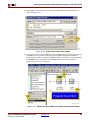
Choose a Spartan-3 Generation Starter Kit Board for your Needs
The Spartan-3A and Spartan-3AN Starter Kit boards are best for prototyping
Spartan-3A/3AN FPGA applications. Depending on specific requirements, however,
Xilinx and third-party companies offer development boards that better suit other needs.
Spartan-3A/3AN FPGA Features and Embedded Processing Functions
The Spartan-3A/3AN Starter Kit board highlights the unique features of the Spartan-3A
and Spartan-3AN FPGA families and provides a convenient development board for
embedded processing applications. The board highlights these features:
•
Spartan-3AN specific features
♦
•
•
Spartan-3A/3AN specific features
♦
Parallel NOR Flash configuration
♦
SPI serial Flash configuration using either the STMicroelectronics or Atmel
DataFlash architectures
♦
MultiBoot FPGA configuration from both Parallel NOR and SPI serial Flash
PROMs
Embedded development
♦
22
Nonvolatile configuration from internal SPI Flash
MicroBlaze 32-bit embedded RISC processor
www.xilinx.com
Spartan-3A/3AN Starter Kit Board User Guide
UG334 (v1.0) May 28, 2007
R
Spartan-3A and Spartan-3AN FPGAs
♦
PicoBlaze eight-bit embedded controller
•
Power management using the Suspend mode feature
•
DDR2 SDRAM memory interfaces
Other Spartan-3 Generation Development Boards
The Spartan-3A/3AN Starter Kit board demonstrates the full capabilities of the
Spartan-3A and Spartan-3AN FPGA families and the Xilinx ISE™ development software.
For a development board specific to the Spartan-3E FPGA family, consider the Spartan-3E
Starter Kit board. There are multiple ordering codes, depending on the included power
supply.
•
Spartan-3E Starter Kit Board (HW-SPAR3E-SK_xx)
www.xilinx.com/s3estarter
For MicroBlaze development, consider the XC3S1600E Embedded Development board.
•
XC3S1600E Embedded Development Board (DO-SP3E1600E-DK-UNI-G)
www.xilinx.com/sp3e1600e
For PCI Express® applications, consider the Spartan-3 PCI Express Starter Kit.
•
Spartan-3 PCI Express Starter Kit (HW-S3PCIE-DK)
www.xilinx.com/s3pcie
For simple Spartan-3 FPGA applications, consider the fairly basic Spartan-3 Starter Kit
board.
•
Spartan-3 Starter Kit (HW-SPAR3-SK-UNI-G)
www.xilinx.com/s3starter
Also consider the capable boards offered by Xilinx partners:
•
Spartan-3 and Spartan-3E Board Interactive Search
www.xilinx.com/products/devboards/index.htm
Spartan-3A and Spartan-3AN FPGAs
The Spartan-3AN FPGA platform offers nonvolatile pin-compatible versions of the
Spartan-3A FPGA platform. The Spartan-3AN FPGAs support the same external
programming sources as Spartan-3A FPGAs, but add an additional internal SPI Flash
programming mode. The internal SPI Flash can also be used for user data. The
Spartan-3A/3AN Starter Kit Board supports both external and Spartan-3AN internal
configuration options.
Spartan-3AN FPGAs require VCCAUX to be 3.3V while Spartan-3A FPGAs allow VCCAUX
to be either 2.5V or 3.3V. The Spartan-3A/3AN Starter Kit Board uses a default VCCAUX of
3.3V.
Spartan-3A and Spartan-3AN FPGAs have different documentation and availability. Verify
the latest version of the appropriate documentation on xilinx.com.
Spartan-3A/3AN Starter Kit Board User Guide
UG334 (v1.0) May 28, 2007
www.xilinx.com
23
R
Chapter 1: Introduction and Overview
•
•
Spartan-3A FPGAs
♦
Web page
www.xilinx.com/spartan3a
♦
Data sheet
www.xilinx.com/bvdocs/publications/ds529.pdf
♦
Errata
www.xilinx.com/xlnx/xweb/xil_publications_display.jsp?category=-1212251
♦
Additional documentation
www.xilinx.com/xlnx/xweb/xil_publications_display.jsp?category=-1212246
Spartan-3AN FPGAs
♦
Web page
www.xilinx.com/spartan3an
♦
Data sheet
www.xilinx.com/bvdocs/publications/ds557.pdf
♦
Errata
www.xilinx.com/xlnx/xweb/xil_publications_display.jsp?category=-1212871
♦
Additional documentation
www.xilinx.com/xlnx/xweb/xil_publications_display.jsp?category=-1212828
Related Resources
Refer to the following links for additional information:
•
•
Spartan-3A/3AN Starter Kit
www.xilinx.com/s3astarter and www.xilinx.com/s3anstarter
♦
Spartan-3A/3AN Rev D Starter Kit user guide
www.xilinx.com/bvdocs/userguides/ug334.pdf
♦
Spartan-3A Rev C Starter Kit user guide
www.xilinx.com/bvdocs/userguides/ug330.pdf
♦
Example User Constraints File (UCF)
www.xilinx.com/products/boards/s3astarter/files/s3astarter.ucf
♦
Board schematics (annotated)
www.xilinx.com/products/boards/s3astarter/s3astarter_schematic.pdf
♦
Bill of materials (BOM) list
www.xilinx.com/products/boards/s3astarter/s3astarter_bom.xls
♦
Link to design examples
www.xilinx.com/products/boards/s3astarter/reference_designs.htm
Xilinx MicroBlaze Soft Processor
www.xilinx.com/microblaze
•
Xilinx PicoBlaze Soft Processor
www.xilinx.com/picoblaze
24
•
Xilinx Embedded Development Kit
www.xilinx.com/ise/embedded_design_prod/platform_studio.htm
•
Xilinx Software Tutorials
www.xilinx.com/support/techsup/tutorials/
•
Xilinx Technical Support
www.xilinx.com/support
www.xilinx.com
Spartan-3A/3AN Starter Kit Board User Guide
UG334 (v1.0) May 28, 2007
R
Chapter 2
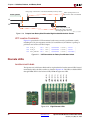
Switches, Buttons, and Rotary Knob
Slide Switches
Locations and Labels
The Spartan-3A/3AN Starter Kit board has four slide switches, as shown in Figure 2-1. The
slide switches are located in the lower right corner of the board and are labeled SW3
through SW0. Switch SW3 is the left-most switch, and SW0 is the right-most switch.
HIGH, ‘1’
LOW, ‘0’
SW3
(T9)
SW2
(U8)
SW1
(U10)
Figure 2-1:
SW0
(V8)
UG330_c2_01_021507
Four Slide Switches
Operation
When in the UP or ON position, a switch connects the FPGA pin to 3.3V, a logic High.
When DOWN or in the OFF position, the switch connects the FPGA pin to ground, a logic
Low. The switches typically exhibit about 2 ms of mechanical bounce. There is no active
debouncing circuitry, although such circuitry could easily be added to the FPGA design
programmed on the board.
UCF Location Constraints
Figure 2-2 provides the UCF constraints for the four slide switches, including the I/O pin
assignment and the I/O standard used. The PULLUP resistor is not required, but it defines
the input value when the switch is in the middle of a transition.
Spartan-3A/3AN Starter Kit Board User Guide
UG334 (v1.0) May 28, 2007
www.xilinx.com
25
R
Chapter 2: Switches, Buttons, and Rotary Knob
NET
NET
NET
NET
"SW<0>"
"SW<1>"
"SW<2>"
"SW<3>"
LOC
LOC
LOC
LOC
=
=
=
=
"V8" |
"U10"|
"U8" |
"T9" |
Figure 2-2:
IOSTANDARD
IOSTANDARD
IOSTANDARD
IOSTANDARD
=
=
=
=
LVTTL
LVTTL
LVTTL
LVTTL
|
|
|
|
PULLUP
PULLUP
PULLUP
PULLUP
;
;
;
;
UCF Constraints for Slide Switches
SUSPEND Switch
The SUSPEND slide switch, shown in Figure 2-3, connects directly to the FPGA’s
SUSPEND input pin. If Suspend mode is enabled in the FPGA application, then the FPGA
enters Suspend mode whenever the switch is set to “SUSPEND.” If the switch is then
changed back to “RUN,” then the FPGA resumes operation from the state before it entered
Suspend mode. Likewise, if Suspend mode is enabled, then the AWAKE pin is reserved to
indicate when the FPGA is in Suspend mode. See “AWAKE LED,” page 32.
RUN
SUSPEND
UG334_c2_03_052407
Figure 2-3: Suspend Switch
To enable Suspend mode, add the configuration string shown in Figure 2-4 to the user
constraints file (UCF). If Suspend mode is not enabled in the application, then the
SUSPEND switch has no affect on the design and the AWAKE pin is available as a generalpurpose I/O.
CONFIG ENABLE_SUSPEND = “FILTERED” ;
Figure 2-4:
UCF Constraints to Enable Suspend Mode
For more information on Suspend mode, see the following application note:
•
26
XAPP480: Using Suspend Mode in Spartan-3 Generation FPGAs
www.xilinx.com/bvdocs/appnotes/xapp480.pdf
www.xilinx.com
Spartan-3A/3AN Starter Kit Board User Guide
UG334 (v1.0) May 28, 2007
R
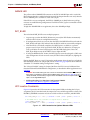
Push-Button Switches
Push-Button Switches
Locations and Labels
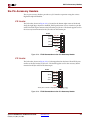
The Spartan-3A/3AN Starter Kit board has four momentary-contact push-button
switches, shown in Figure 2-5. The push buttons are located in the lower right corner of the
board and are labeled BTN_NORTH, BTN_EAST, BTN_SOUTH, and BTN_WEST. The
FPGA pins that connect to the push buttons appear in parentheses in Figure 2-5, and the
associated UCF is listed in Figure 2-7.
Rotary Push Button Switch
BTN_NORTH
(T14)
ROT_A: (T13)
ROT_B: (R14)
ROT_CENTER: (R13)
BTN_WEST
(U15)
Requires an internal pull-up
Requires an internal pull-up
Requires an internal pull-down
BTN_EAST
(T16)
BTN_SOUTH
(T15)
UG334_c2_05_052407
Notes:
1. All BTN_* push-button inputs require an internal pull-down resistor.
Figure 2-5:
Four Push-Button Switches Surround the Rotary Push-Button Switch
Operation
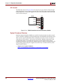
Pressing a push button connects the associated FPGA pin to 3.3V, as shown in Figure 2-6.
Use an internal pull-down resistor within the FPGA pin to generate a logic Low when the
button is not pressed. Figure 2-7 shows how to specify a pull-down resistor within the
UCF. There is no active debouncing circuitry on the push button.
3.3V
Push Button
FPGA I/O Pin
BTN_* Signal
UG230_c2_03_021206
Figure 2-6:
Push-Button Switches Require an Internal Pull-Down Resistor in the
FPGA Input Pin
Spartan-3A/3AN Starter Kit Board User Guide
UG334 (v1.0) May 28, 2007
www.xilinx.com
27
R
Chapter 2: Switches, Buttons, and Rotary Knob
PROG_B Push-Button Switch
The PROG_B push-button switch, shown in Figure 2-14, page 31, is part of the FPGA’s
configuration circuitry. See “PROG Push-Button Switch,” page 40.
UCF Location Constraints
Figure 2-7 provides the UCF constraints for the four push-button switches, including the
I/O pin assignment and the I/O standard used, and defines a pull-down resistor on each
input.
NET
NET
NET
NET
"BTN_EAST"
"BTN_NORTH"
"BTN_SOUTH"
"BTN_WEST"
LOC
LOC
LOC
LOC
Figure 2-7:
=
=
=
=
"T16"
"T14"
"T15"
"U15"
|
|
|
|
IOSTANDARD
IOSTANDARD
IOSTANDARD
IOSTANDARD
=
=
=
=
LVTTL
LVTTL
LVTTL
LVTTL
|
|
|
|
PULLDOWN
PULLDOWN
PULLDOWN
PULLDOWN
;
;
;
;
UCF Constraints for Push-Button Switches
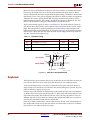
Rotary Push-Button Switch
Locations and Labels
The rotary push-button switch is located in the center of the four individual push-button
switches, as shown in Figure 2-5, page 27. The switch produces three outputs. The two
shaft encoder outputs are ROT_A and ROT_B. The center push-button switch is
ROT_CENTER.
Operation
The rotary push-button switch integrates two different functions. The switch shaft rotates
and outputs values whenever the shaft turns. The shaft can also be pressed, acting as a
push-button switch.
Push-Button Switch
Pressing the knob on the rotary/push-button switch connects the associated FPGA pin to
3.3V, as shown in Figure 2-8. Use an internal pull-down resistor within the FPGA pin to
generate a logic Low. Figure 2-11 shows how to specify a pull-down resistor within the
UCF. There is no active debouncing circuitry on the push button.
28
www.xilinx.com
Spartan-3A/3AN Starter Kit Board User Guide
UG334 (v1.0) May 28, 2007
R
Rotary Push-Button Switch
Rotary / Push Button
FPGA I/O Pin
3.3V
ROT_CENTER Signal
UG230_c2_05_021206
Figure 2-8:
Push-Button Switches Require an Internal Pull-up Resistor in the FPGA
Input Pin
Rotary Shaft Encoder
In principal, the rotary shaft encoder behaves much like a cam connected to the central
shaft. Rotating the shaft then operates two push-button switches, as shown in Figure 2-9.
Depending on which way the shaft is rotated, one of the switches opens before the other.
Likewise, as the rotation continues, one switch closes before the other. However, when the
shaft is stationary, also called the detent position, both switches are closed.
A pull-up resistor in each input pin
generates a ‘1’ for an open switch.
See the UCF file for details on
specifying the pull-up resistor.
FPGA
Vcco
A=‘0’
Vcco
Rotary Shaft
Encoder
B=‘1’
GND
Figure 2-9:
UG230_c2_06_030606
Basic Example of Rotary Shaft Encoder Circuitry
Closing a switch connects it to ground, generating a logic Low. When the switch is open, a
pull-up resistor within the FPGA pin pulls the signal to a logic High. The UCF constraints
in Figure 2-11 describe how to define the pull-up resistor.
The FPGA circuitry to decode the ‘A’ and ‘B’ inputs is simple but must consider the
mechanical switching noise on the inputs, also called chatter. As shown in Figure 2-10, the
chatter can falsely indicate extra rotation events or even indicate rotations in the opposite
direction!
Spartan-3A/3AN Starter Kit Board User Guide
UG334 (v1.0) May 28, 2007
www.xilinx.com
29
R
Chapter 2: Switches, Buttons, and Rotary Knob
Rising edge on ‘A’ when ‘B’ is Low indicates RIGHT (clockwise) rotation
Rotating RIGHT
Switch opening chatter on ‘A’
injects false “clicks” to the RIGHT
Detent
B
Detent
A
Switch closing chatter on ‘B’
injects false “clicks” to the LEFT
(’B’ rising edge when ‘A’ is Low)
Figure 2-10:
UG230_c2_07_030606
Outputs from Rotary Shaft Encoder Might Include Mechanical Chatter
UCF Location Constraints
Figure 2-11 provides the UCF constraints for the rotary encoder/push-button switch,
including the I/O pin assignment and the I/O standard used, and defines a pull-up or
pull-down resistor for each FPGA input.
NET "ROT_A"
LOC = "T13" | IOSTANDARD = LVTTL | PULLUP
;
NET "ROT_B"
LOC = "R14" | IOSTANDARD = LVTTL | PULLUP
;
NET "ROT_CENTER" LOC = "R13" | IOSTANDARD = LVTTL | PULLDOWN ;
Figure 2-11:
UCF Constraints for Rotary Push-Button Switch
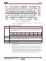
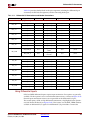
Discrete LEDs
Locations and Labels
LED0: (R20)
LED1: (T19)
LED2: (U20)
LED3: (U19)
LED4: (V19)
LED5: (V20)
LED6: (Y22)
LED7: (W21)
The Spartan-3A/3AN Starter Kit board has eight individual surface-mount LEDs located
immediately above the slide switches as shown in Figure 2-12. The LEDs are labeled LED7
through LED0. LED7 is the left-most LED, LED0 the right-most LED.
UG334_c2_12_052407
Figure 2-12:
30
www.xilinx.com
Eight Discrete LEDs
Spartan-3A/3AN Starter Kit Board User Guide
UG334 (v1.0) May 28, 2007
R
Optional Discrete LEDs
Operation
Each LED has one side connected to ground and the other side connected to a pin on the
device via a 390Ω current limiting resistor. To light an individual LED, drive the associated
FPGA control signal High.
If the FPGA is not yet configured, the LEDs may be dimly lit because pull-up resistors are
enabled during configuration. The FPGA’s PUDC_B pin is connected to GND on the
board.
UCF Location Constraints
Figure 2-13 provides the UCF constraints for the four push-button switches, including the
I/O pin assignment, the I/O standard used, the output slew rate, and the output drive
current.
NET
NET
NET
NET
NET
NET
NET
NET
"LED<7>"
"LED<6>"
"LED<5>"
"LED<4>"
"LED<3>"
"LED<2>"
"LED<1>"
"LED<0>"
LOC
LOC
LOC
LOC
LOC
LOC
LOC
LOC
=
=
=
=
=
=
=
=
"W21"
"Y22"
"V20"
"V19"
"U19"
"U20"
"T19"
"R20"
Figure 2-13:
|
|
|
|
|
|
|
|
IOSTANDARD
IOSTANDARD
IOSTANDARD
IOSTANDARD
IOSTANDARD
IOSTANDARD
IOSTANDARD
IOSTANDARD
=
=
=
=
=
=
=
=
LVTTL
LVTTL
LVTTL
LVTTL
LVTTL
LVTTL
LVTTL
LVTTL
|
|
|
|
|
|
|
|
SLEW
SLEW
SLEW
SLEW
SLEW
SLEW
SLEW
SLEW
=
=
=
=
=
=
=
=
QUIETIO
QUIETIO
QUIETIO
QUIETIO
QUIETIO
QUIETIO
QUIETIO
QUIETIO
|
|
|
|
|
|
|
|
DRIVE
DRIVE
DRIVE
DRIVE
DRIVE
DRIVE
DRIVE
DRIVE
=
=
=
=
=
=
=
=
4
4
4
4
4
4
4
4
;
;
;
;
;
;
;
;
UCF Constraints for Eight Discrete LEDs
Optional Discrete LEDs
The Spartan-3A/3AN Starter Kit board provides two optional LEDs, shown in Figure 2-14.
Depending on which features are used by an application, these LED connections may be
also used as user-I/O pins.
FPGA PROG_B Pin
(Press to reset/reprogram FPGA)
FPGA_INIT_B
(W21)
FPGA_AWAKE
(AB15)
RED
YELLOW
FPGA DONE Pin
(Lit when FPGA is configured)
GREEN
UG334_c2_14_052407
Figure 2-14:
Spartan-3A/3AN Starter Kit Board User Guide
UG334 (v1.0) May 28, 2007
AWAKE and INIT_B LEDs
www.xilinx.com
31
R
Chapter 2: Switches, Buttons, and Rotary Knob
AWAKE LED
The yellow-colored AWAKE LED connects to the FPGA’s AWAKE pin and is used if the
FPGA Suspend mode is enabled in the bitstream. If the Suspend mode is not used, then the
FPGA’s AWAKE pin is available as a full user-I/O pin.
If the FPGA is not yet configured, the FPGA’s AWAKE pin is dimly lit because pull-up
resistors are enabled during configuration. The FPGA’s PUDC_B pin is connected to GND
on the board.
To light the AWAKE LED in an application, drive the AWAKE pin High.
INIT_B LED
The red-colored INIT_B LED serves multiple purposes:
•
At power-up or when the PROG_B button is pressed, the LED flashes momentarily
while the FPGA clears its configuration memory.
•
If configuration fails for any reason, then the FPGA’s DONE LED will be unlit and the
INIT_B LED will light. This indicates that the FPGA could not successfully configure.
•
After the FPGA successfully completes, the INIT_B pin is available as a generalpurpose user-I/O pin. If no signal drives INIT_B, then it is defined as an input pin
with a pull-down resistor. It might appear that the LED dimly glows. Drive the
INIT_B pin High to turn off the LED or Low to light the LED.
•
If using the Readback CRC feature, the INIT_B pin is reserved and signals a CRC error
after configuration. If such an error occurs, the FPGA drives INIT_B Low, lighting the
LED.
If using the INIT_B pin as a user-I/O pin after configuration, drive the pin Low to light the
LED and High to shut it off. Jumper J46, shown in Table 4-2, page 40, must be in either the
“Disabled” or “Enabled during Configuration” setting.
The “Always Enabled” setting for Jumper J46 allows the FPGA to read additional data
from the Platform Flash PROM after configuration, as described in Xilinx application note
XAPP694.
Caution! The FPGA’s INIT_B pin also connects to the Platform Flash PROM’s OE/RESET pin.
If the jumper controlling the Platform Flash PROM, jumper J46 in Table 4-2, page 40, is set to
“Always Enabled,” then the INIT_B signal controls the PROM’s active-Low output-enable (OE)
input or active-High RESET input.
•
XAPP694: Reading User Data from Configuration PROMs
www.xilinx.com/bvdocs/appnotes/xapp694.pdf
UCF Location Constraints
Figure 2-15 provides the UCF constraints for the optional LEDs, including the I/O pin
assignment, the I/O standard used, the output slew rate, and the output drive current. The
ENABLE_SUSPEND constraint must be set to NO in order to use FPGA_AWAKE LED.
NET "FPGA_INIT_B" LOC = "V13" | IOSTANDARD = LVTTL | SLEW = QUIETIO | DRIVE = 4 ;
# The AWAKE LED is only available if Suspend mode is disabled
CONFIG ENABLE_SUSPEND = NO ;
NET "FPGA_AWAKE" LOC = "AB15" | IOSTANDARD = LVTTL | SLEW = QUIETIO | DRIVE = 4 ;
Figure 2-15:
32
UCF Constraints for Optional Discrete LEDs
www.xilinx.com
Spartan-3A/3AN Starter Kit Board User Guide
UG334 (v1.0) May 28, 2007
R
Chapter 3
Clock Sources
Overview
The Spartan-3A/3AN Starter Kit board supports three primary clock input sources, as
shown in Figure 3-1.
•
The board includes an on-board 50 MHz clock oscillator.
•
Clocks can be supplied off-board via an SMA-style connector. Alternatively, the FPGA
can generate clock signals or other high-speed signals on the SMA-style connector.
•
A 133 MHz clock oscillator is installed in the CLK_AUX socket. Optionally substitute
a separate eight-pin DIP-style clock oscillator in the provided socket.
CLK_50MHZ
(E12)
CLK_AUX
(V12)
CLK_SMA
(U12)
Figure 3-1:
Spartan-3A/3AN Starter Kit Board User Guide
UG334 (v1.0) May 28, 2007
UG334_c3_01_052407
Clock Sources on Starter Kit Board
www.xilinx.com
33
R
Chapter 3: Clock Sources
Clock Connections
Each of the clock inputs connect directly to a global buffer input. As shown in Table 3-1,
each of the clock inputs also optimally connects to an associated DCM.
Only the CLK_AUX or the CLK_SMA input can use the associated DCM at any time.
However, both inputs are available as clock inputs.
Table 3-1:
Clock Inputs and Associated Global Buffers and DCMs
Clock Input
FPGA Pin
I/O Bank
Global Buffer
Associated DCM
LOC
CLK_50MHZ
E12
0
GCLK5
Top Right
DCM_X2Y3
CLK_AUX
V12
2
GCLK2
Bottom Right
DCM_X2Y0
CLK_SMA
U12
2
GCLK3
50 MHz On-Board Oscillator
The board includes a 50 MHz oscillator with a 40% to 60% output duty cycle. The oscillator
is accurate to ±2500 Hz or ±50 ppm.
Auxiliary Clock Oscillator Socket
A 133 MHz clock oscillator is installed in the auxiliary clock oscillator socket. The provided
eight-pin socket accepts clock oscillators that fit the eight-pin DIP (8DIP) footprint.
Substitute the oscillator in this socket if the FPGA application requires a frequency other
than 50 MHz or 133 MHz. Alternatively, use the FPGA’s Digital Clock Manager (DCM) to
generate or synthesize other frequencies from the on-board 50 MHz or 133 MHz oscillator.
Caution! Be aware of the pin 1 orientation on the crystal oscillator when installing it in the
associated socket.
SMA Clock Input or Output Connector
To provide a clock from an external source, connect the input clock signal to the SMA
connector. The FPGA can also generate a single-ended clock output or other high-speed
signal on the SMA clock connector for an external device.
UCF Constraints
The clock input sources require two different types of constraints. The location constraints
define the I/O pin assignments and I/O standards. The period constraints define the clock
period—and consequently the clock frequency—and the duty cycle of the incoming clock
signal.
Location
Figure 3-2 provides the UCF constraints for the three clock input sources, including the
I/O pin assignment and the I/O standard used.
34
www.xilinx.com
Spartan-3A/3AN Starter Kit Board User Guide
UG334 (v1.0) May 28, 2007
R
Related Resources
NET "CLK_50MHZ" LOC = "E12"| IOSTANDARD = LVCMOS33 ;
NET "CLK_AUX"
LOC = "V12"| IOSTANDARD = LVCMOS33 ;
NET "CLK_SMA"
LOC = "U12"| IOSTANDARD = LVCMOS33 ;
Figure 3-2:
UCF Location Constraints for Clock Sources
Clock Period Constraints
The Xilinx ISE development software uses timing-driven logic placement and routing. Set
the clock PERIOD constraint as appropriate. An example constraint appears in Figure 3-3
for the on-board 50 MHz clock oscillator. The CLK_50MHZ frequency is 50 MHz, which
equates to a 20 ns period. The output duty cycle from the oscillator ranges between 40% to
60%.
# Define clock period for 50 MHz oscillator
NET "CLK_50MHZ" PERIOD = 20.0ns HIGH 40%;
Figure 3-3: UCF Clock PERIOD Constraint
Related Resources
Refer to the following links for additional information:
•
Epson SG-8002JF Series Oscillator Data Sheet (50 MHz Oscillator)
www.eea.epson.com/go/Prod_Admin/Categories/EEA/QD/Crystal_Oscillators/prog_oscillators/go/
Resources/TestC2/SG8002JF
Spartan-3A/3AN Starter Kit Board User Guide
UG334 (v1.0) May 28, 2007
www.xilinx.com
35
R
Chapter 3: Clock Sources
36
www.xilinx.com
Spartan-3A/3AN Starter Kit Board User Guide
UG334 (v1.0) May 28, 2007
R
Chapter 4
FPGA Configuration Options
The Spartan-3A/3AN Starter Kit board supports a variety of FPGA configuration options:
•
Program the Spartan-3AN internal SPI Flash memory, then configure the FPGA at
power-up. This option is not available in the Spartan-3A Starter Kit.
•
Download FPGA designs directly to the Spartan-3A/3AN FPGA via JTAG, using the
on-board USB interface. The on-board USB-JTAG logic also provides in-system
programming for the on-board Platform Flash PROM. SPI serial Flash and StrataFlash
programming are performed separately.
•
Program the on-board 4 Mbit Xilinx XCF04S serial Platform Flash PROM, then
configure the FPGA from the image stored in the Platform Flash PROM using Master
Serial mode.
•
Program the on-board 16 Mbit STMicroelectronics SPI serial Flash PROM or the
16 Mbit Atmel SPI-based DataFlash PROM, then configure the FPGA from the image
stored in the SPI serial Flash PROM using SPI mode. Further, an FPGA application
can dynamically load different FPGA configurations using the FPGA’s MultiBoot
mode. See UG332: Spartan-3 Generation Configuration User Guide for additional details
on the MultiBoot feature. See Chapter 12, “SPI Serial Flash,” for more information on
using SPI serial Flash memory.
•
Program the on-board 32 Mbit STMicroelectronics parallel NOR Flash PROM, then
configure the FPGA from the image stored in the Flash PROM using BPI Up
configuration mode. Further, an FPGA application can dynamically load different
FPGA configurations using the FPGA’s MultiBoot mode. See UG332: Spartan-3
Generation Configuration User Guide for additional details on the MultiBoot feature. See
Chapter 11, “Parallel NOR Flash PROM,” for more information on using parallel
Flash memory.
Spartan-3A/3AN Starter Kit Board User Guide
UG334 (v1.0) May 28, 2007
www.xilinx.com
37
R
Chapter 4: FPGA Configuration Options
Figure 4-1 indicates the position of the USB download/programming interface and the
on-board non-volatile memories that potentially store FPGA configuration images.
16 Mbit Atmel DataFlash SPI Serial Flash
16 Mbit ST Micro SPI Serial Flash
PROGRAM Button
4 Mbit Platform Flash
PROM
DONE LED
USB-based Download/
Debugging Port
In-System SPI Flash
(Spartan-3AN Starter Kit board only)
Uses standard USB cable
32 Mbit STMicro Flash
Parallel NOR Flash memory
Byte Peripheral Interface (BPI) mode
FPGA Mode Select
Jumpers
UG334_c4_01_052407
Figure 4-1:
Starter Kit FPGA Configuration Options
The configuration mode jumpers determine which configuration mode the FPGA uses
when power is first applied, or whenever the PROG button is pressed.
The DONE pin LED lights when the FPGA successfully finishes configuration.
Pressing the PROG button forces the FPGA to restart its configuration process.
The Xilinx Platform Flash PROM provides easy, JTAG-programmable configuration
storage for the FPGA. The FPGA configures from the Platform Flash using Master Serial
mode.
38
www.xilinx.com
Spartan-3A/3AN Starter Kit Board User Guide
UG334 (v1.0) May 28, 2007
R
Configuration Mode Jumpers
Configuration Mode Jumpers
As shown in Table 4-1, the J26 jumper block settings control the FPGA’s configuration
mode. Inserting a jumper grounds the associated mode pin. Insert or remove individual
jumpers to select the FPGA’s configuration mode and associated configuration memory
source. The J26 jumper block is shown in Figure 4-1.
Table 4-1:
Configuration Mode Jumper Settings
Mode Pins
Configuration Mode M2:M1:M0
Internal Master SPI
Master Serial
0:1:1
0:0:0
FPGA Configuration Image Source
Spartan-3AN Starter Kit Board only! This
mode configures a Spartan-3AN FPGA
using the internal In-System Flash memory.
This mode is not supported on the
Spartan-3A Starter Kit board.
J26 Jumper
Settings
J46 Jumper
Setting
M0
M1
M2
J26
Platform Flash PROM
Set the J46 jumper per Table 4-2
M0
DONE
M1
CE
PROM
M2
GND
J26
Master SPI
(see Chapter 12,
“SPI Serial Flash”)
0:0:1
Select SPI Serial Flash PROM starting at
address 0
M0
Select specific SPI Flash PROM using
Jumper J1 (Table 12-2, page 93).
M1
DISABLE
M2
J26
Disable the Platform Flash PROM via J46
jumper per Table 4-2.
Master BPI Up
(see Chapter 11,
“Parallel NOR Flash
PROM”)
0:1:0
Parallel NOR Flash PROM, starting at
address 0 and incrementing through address
space.
DONE
CE
PROM
GND
J46
M0
M1
M2
Disable the Platform Flash PROM via J46
jumper per Table 4-2.
JTAG
J46
1:0:1
J26
Downloaded from host via USB-JTAG port
M0
M1
M2
J26
Spartan-3A/3AN Starter Kit Board User Guide
UG334 (v1.0) May 28, 2007
www.xilinx.com
39
R
Chapter 4: FPGA Configuration Options
Xilinx Platform Flash Configuration PROM(s)
The Spartan-3A/3AN Starter Kit board includes a Xilinx Platform Flash configuration
interface. A single 4 Mbit XCF04S Platform Flash PROM appears in the JTAG chain with
the FPGA.
Caution! The J46 jumper, shown in Table 4-2, page 40, enables or disables the Platform Flash
PROM on the board. Be aware of potential data contention issues with the SPI serial Flash and
the D0 line of the parallel NOR Flash, depending on the current FPGA “Configuration Mode
Jumpers”, shown in Table 4-1.
Caution! If the J46 jumper shown in Table 4-2, page 40 is set for “Always Enabled”, then the
FPGA’s INIT_B pin controls the Platform Flash PROM’s OE/RESET input. The INIT_B pin must
be High to read any data, other than from the Platform Flash PROM.
When using the Platform Flash PROM to configure the FPGA, the configuration mode
jumpers must be set for Master Serial mode, as shown in Table 4-2. If using any other
configuration mode, the Platform Flash PROM must be disabled.
Table 4-2:
Platform Flash Enable Jumper (J46)
Platform Flash
Mode
Platform Flash
Allowed FPGA
Enable (J46) Configuration Mode
DONE
Disabled
CE
PROM
(no jumper)
GND
Any
(see Table 4-1)
J46
DONE
Enabled during
FPGA
Configuration
CE
PROM
Master Serial
GND
or JTAG
J46
DONE
CE
PROM
Always
Enabled
GND
J46
Master Serial
or JTAG
Precautions/
Contention
None. Platform Flash disabled.
The FPGA application has full
access to SPI serial Flash and
parallel NOR Flash PROMs after
configuration.
None. Platform Flash enabled
during configuration and
disabled after configuration. The
FPGA application has full access
to SPI serial Flash and parallel
NOR Flash PROMs after
configuration.
Platform Flash continuously
enabled. The FPGA application
can read additional data from
Platform Flash after
configuration as described in
application note XAPP694:
Reading User Data from
Configuration PROMs. The FPGA
application has no read access to
SPI Flash or parallel NOR Flash.
PROG Push-Button Switch
The PROG push-button switch, labeled in Figure 4-1, forces the FPGA to reconfigure from
the configuration memory source selected by the “Configuration Mode Jumpers,” page 39.
Press and release this button to restart the FPGA configuration process at any time.
40
www.xilinx.com
Spartan-3A/3AN Starter Kit Board User Guide
UG334 (v1.0) May 28, 2007
R
DONE Pin LED
DONE Pin LED
The DONE pin LED, labeled in Figure 4-1, lights whenever the FPGA is successfully
configured. If this LED is not lit, then the FPGA is not configured.
Programming the FPGA or Platform Flash PROM via USB
The Spartan-3A/3AN Starter Kit includes embedded USB-based programming logic and a
USB endpoint with a Type B connector. Via a USB cable connection with the host PC, the
iMPACT programming software directly programs the FPGA, the Platform Flash PROM,
or the on-board CPLD. Direct programming of the parallel or serial Flash PROMs is not
presently supported.
Connecting the USB Cable
The kit includes a standard USB Type A/Type B cable, similar to the one shown in
Figure 4-2. The actual cable color might vary from the picture.
USB Type B Connector
Connects to Starter Kit's USB connector
USB Type A Connector
Connects to computer's USB connector
UG230_c4_04_030306
Figure 4-2:
Standard USB Type A/Type B Cable
The wider and narrower Type A connector fits the USB connector at the back of the
computer.
After installing the Xilinx software, connect the square Type B connector to the Spartan3A/3AN Starter Kit board, as shown in Figure 4-3. The USB connector is on the left side of
the board, immediately next to the Ethernet connector. When the board is powered on, the
Windows operating system automatically recognizes and installs the associated driver
software.
UG334_c4_03_052407
Figure 4-3:
Connect the USB Type B Connector to the Starter Kit Board Connector
Spartan-3A/3AN Starter Kit Board User Guide
UG334 (v1.0) May 28, 2007
www.xilinx.com
41
R
Chapter 4: FPGA Configuration Options
When the USB cable driver is successfully installed and the board is correctly connected to
the PC, a green LED lights up, indicating that the programming cable is ready. The USB
connection also has a red LED, which only lights if the Xilinx software is programming
firmware updates to the USB interface.
Platform Flash Programming Example in Spartan-3 Generation
Configuration User Guide
The Spartan-3 Generation Configuration User Guide includes step-by-step instructions, some
including screen shots, on how to prepare the FPGA bitstream and download it to the
FPGA or PROM.
•
UG332: Spartan-3 Generation Configuration User Guide
www.xilinx.com/bvdocs/userguides/ug332.pdf
For formatting and programming Platform Flash PROMs, please refer to the “Master Serial
Mode” chapter.
42
www.xilinx.com
Spartan-3A/3AN Starter Kit Board User Guide
UG334 (v1.0) May 28, 2007
R
Chapter 5
Character LCD Screen
Overview
The Spartan-3A/3AN Starter Kit board prominently features a 2-line by 16-character
liquid crystal display (LCD). The FPGA controls the LCD via the eight-bit data interface
shown in Figure 5-1. The Spartan-3A/3AN Starter Kit board also supports the four-bit data
interface to remain compatible with other Xilinx development boards.
Caution! When using four-bit mode, the FPGA must drive the LCD_DB<3:0> signals High.
(Y15)
(AB16)
(Y16)
(AA12)
(AB12)
(AB17)
(AA13)
(Y13)
LCD_DB<6>
LCD_DB<5>
LCD_DB<4>
LCD_DB<3>
LCD_DB<2>
LCD_DB<1>
LCD_DB<0>
LCD_E
(AB4)
LCD_RS
(Y14)
LCD_RW
(W13)
DB7
DB6
DB5
DB4
DB3
DB2
DB1
Eight-bit data interface
All
LCD_DB<7> 390Ω
Character LCD
Display
Four-bit data
interface
FPGA
DB0
E
RS
R/W
UG334_c5_01_052407
Figure 5-1:
Character LCD Interface
Once mastered, the LCD is a practical way to display a variety of information using
standard ASCII and custom characters. However, these displays are not fast. Scrolling the
display at half-second intervals tests the practical limit for clarity. Compared with the
50 MHz clock available on the board, the display is slow. A PicoBlaze processor efficiently
controls display timing plus the actual content of the display.
Spartan-3A/3AN Starter Kit Board User Guide
UG334 (v1.0) May 28, 2007
www.xilinx.com
43
R
Chapter 5: Character LCD Screen
Character LCD Interface Signals
Table 5-1 shows the interface character LCD interface signals.
Table 5-1:
Character LCD Interface
Signal Name
FPGA Pin
Function
LCD_DB<7>
Y15
Data bit DB7
LCD_DB<6>
AB16
Data bit DB6
LCD_DB<5>
Y16
Data bit DB5
LCD_DB<4>
AA12
Data bit DB4
LCD_DB<3>
AB12
Data bit DB3
LCD_DB<2>
AB17
Data bit DB2
LCD_DB<1>
AB18
Data bit DB1
LCD_DB<0>
Y13
Data bit DB0
LCD_E
AB4
Read/Write Enable Pulse
When using the four-bit
interface, drive these signals
High.
0: Disabled
1: Read/Write operation enabled
LCD_RS
Y14
Register Select
0: Instruction register during write operations.
Busy Flash during read operations
1: Data for read or write operations
LCD_RW
W13
Read/Write Control
0: Write, LCD accepts data
1: Read, LCD presents data
Voltage Compatibility
The character LCD is power by +5V. The FPGA I/O signals are powered by 3.3V. However,
the FPGA’s output levels are recognized as valid Low or High logic levels by the LCD. The
LCD controller accepts 5V TTL signal levels and the 3.3V LVCMOS outputs provided by
the FPGA meet the 5V TTL voltage level requirements.
The 390Ω series resistors on the data lines prevent overstressing on the FPGA and
StrataFlash I/O pins when the character LCD drives a High logic value. The character LCD
drives the data lines when LCD_RW is High. Most applications treat the LCD as a writeonly peripheral and never read from the display.
UCF Location Constraints
Figure 5-2 provides the UCF constraints for the Character LCD, including the I/O pin
assignment and the I/O standard used.
44
www.xilinx.com
Spartan-3A/3AN Starter Kit Board User Guide
UG334 (v1.0) May 28, 2007
R
LCD Controller
NET "LCD_E"
LOC = "AB4" | IOSTANDARD = LVCMOS33 | DRIVE = 4 | SLEW = QUIETIO ;
NET "LCD_RS" LOC = "Y14" | IOSTANDARD = LVCMOS33 | DRIVE = 4 | SLEW = QUIETIO ;
NET "LCD_RW" LOC = "W13" | IOSTANDARD = LVCMOS33 | DRIVE = 4 | SLEW = QUIETIO ;
NET
NET
NET
NET
NET
NET
NET
NET
"LCD_DB<7>"
"LCD_DB<6>"
"LCD_DB<5>"
"LCD_DB<4>"
"LCD_DB<3>"
"LCD_DB<2>"
"LCD_DB<1>"
"LCD_DB<0>"
LOC
LOC
LOC
LOC
LOC
LOC
LOC
LOC
Figure 5-2:
=
=
=
=
=
=
=
=
"Y15"
"AB16"
"Y16"
"AA12"
"AB12"
"AB17"
"AB18"
"Y13"
|
|
|
|
|
|
|
|
IOSTANDARD
IOSTANDARD
IOSTANDARD
IOSTANDARD
IOSTANDARD
IOSTANDARD
IOSTANDARD
IOSTANDARD
=
=
=
=
=
=
=
=
LVCMOS33
LVCMOS33
LVCMOS33
LVCMOS33
LVCMOS33
LVCMOS33
LVCMOS33
LVCMOS33
|
|
|
|
|
|
|
|
DRIVE
DRIVE
DRIVE
DRIVE
DRIVE
DRIVE
DRIVE
DRIVE
=
=
=
=
=
=
=
=
4
4
4
4
4
4
4
4
|
|
|
|
|
|
|
|
SLEW
SLEW
SLEW
SLEW
SLEW
SLEW
SLEW
SLEW
=
=
=
=
=
=
=
=
QUIETIO
QUIETIO
QUIETIO
QUIETIO
QUIETIO
QUIETIO
QUIETIO
QUIETIO
;
;
;
;
;
;
;
;
UCF Location Constraints for the Character LCD
LCD Controller
The 2 x 16 character LCD has an internal Sitronix ST7066U graphics controller that is
functionally equivalent with the following devices.
•
Samsung S6A0069X or KS0066U
•
Hitachi HD44780
•
SMOS SED1278
Memory Map
The controller has three internal memory regions, each with a specific purpose: DD RAM,
CG ROM, and CG RAM. The display must be initialized before accessing any of these
memory regions.
DD RAM
The Display Data RAM (DD RAM) stores the character code to be displayed on the screen.
Most applications interact primarily with DD RAM. The character code stored in a DD
RAM location references a specific character bitmap stored either in the predefined CG
ROM character set or in the user-defined CG RAM character set.
Figure 5-3 shows the default address for the 32 character locations on the display. The
upper line of characters is stored between addresses 0x00 and 0x0F. The second line of
characters is stored between addresses 0x40 and 0x4F.
Undisplayed
Addresses
Character Display Addresses
1
00
01
02
03
04
05
06
07
08
09
0A
0B
0C
0D
0E
0F
10
…
27
2
40
41
42
43
44
45
46
47
48
49
4A
4B
4C
4D
4E
4F
50
…
67
1
2
3
4
5
6
7
8
9
10
11
12
13
14
15
16
17
…
40
Figure 5-3:
DD RAM Hexadecimal Addresses (No Display Shifting)
Physically, there are 80 total character locations in DD RAM with 40 characters available
per line. Locations 0x10 through 0x27 and 0x50 through 0x67 can be used to store other
non-display data. Alternatively, these locations can also store characters that can only be
displayed using controller’s display shifting functions.
Spartan-3A/3AN Starter Kit Board User Guide
UG334 (v1.0) May 28, 2007
www.xilinx.com
45
R
Chapter 5: Character LCD Screen
The Set DD RAM Address command initializes the address counter before reading or
writing to DD RAM. Write DD RAM data using the Write Data to CG RAM or DD RAM
command, and read DD RAM using the Read Data from CG RAM or DD RAM command.
The DD RAM address counter either remains constant after read or write operations, or
auto-increments or auto-decrements by one location, as defined by the I/D set by the Entry
Mode Set command.
CG ROM
The Character Generator ROM (CG ROM) contains the font bitmap for each of the
predefined characters that the LCD screen can display, shown in Figure 5-4. The character
code stored in DD RAM for each character location subsequently references a position with
the CG ROM. For example, a hexadecimal character code of 0x53 stored in a DD RAM
location displays the character ‘S’. The upper nibble of 0x53 equates to DB[7:4] = 0101
binary and the lower nibble equates to DB[3:0] = 0011 binary. As shown in Figure 5-4, the
character ‘S’ appears on the screen.
English/Roman characters are stored in CG ROM at their equivalent ASCII code
addresses.
46
www.xilinx.com
Spartan-3A/3AN Starter Kit Board User Guide
UG334 (v1.0) May 28, 2007
R
LCD Controller
Upper Data Nibble
DB3
DB2
DB1
DB0
Lower Data Nibble
DB7
DB6
DB5
DB4
Figure 5-4:
UG230_c5_02_030306
LCD Character Set
The character ROM contains the ASCII English character set and Japanese katakana
characters.
The controller also provides for eight custom character bitmaps, stored in CG RAM. These
eight custom characters are displayed by storing character codes 0x00 through 0x07 in a
DD RAM location.
CG RAM
The Character Generator RAM (CG RAM) provides space to create eight custom character
bitmaps. Each custom character location consists of a 5-dot by 8-line bitmap, as shown in
Figure 5-5.
The Set CG RAM Address command initializes the address counter before reading or
writing to CG RAM. Write CG RAM data using the Write Data to CG RAM or DD RAM
command, and read CG RAM using the Read Data from CG RAM or DD RAM command.
Spartan-3A/3AN Starter Kit Board User Guide
UG334 (v1.0) May 28, 2007
www.xilinx.com
47
R
Chapter 5: Character LCD Screen
The CG RAM address counter either remains constant after read or write operations, or
auto-increments or auto-decrements by one location, as defined by the I/D set by the Entry
Mode Set command.
Figure 5-5 provides an example that creates a special checkerboard character. The custom
character is stored in the fourth CG RAM character location, which is displayed when a
DD RAM location is 0x03. To write the custom character, the CG RAM address is first
initialized using the Set CG RAM Address command. The upper three address bits point to
the custom character location. The lower three address bits point to the row address for the
character bitmap. The Write Data to CG RAM or DD RAM command is used to write each
character bitmap row. A ‘1’ lights a bit on the display. A ‘0’ leaves the bit unlit. Only the
lower five data bits are used; the upper three data bits are don’t care positions. The eighth
row of bitmap data is usually left as all zeros to accommodate the cursor.
Upper Nibble
Lower Nibble
Write Data to CG RAM or DD RAM
A5
A4
A3
Character Address
A2
A1
A0
D7
Row Address
D6
D5
D4
Don’t Care
D3
D2
D1
D0
Character Bitmap
0
1
1
0
0
0
-
-
-
0
1
0
1
0
0
1
1
0
0
1
-
-
-
1
0
1
0
1
0
1
1
0
1
0
-
-
-
0
1
0
1
0
0
1
1
0
1
1
-
-
-
1
0
1
0
1
0
1
1
1
0
0
-
-
-
0
1
0
1
0
0
1
1
1
0
1
-
-
-
1
0
1
0
1
0
1
1
1
1
0
-
-
-
0
1
0
1
0
0
1
1
1
1
1
-
-
-
0
0
0
0
0
Figure 5-5:
Example Custom Checkerboard Character with Character Code 0x03
Command Set
Table 5-2 summarizes the available LCD controller commands and bit definitions. Because
the display is set up for four-bit operation, each eight-bit command is sent as two four-bit
nibbles. The upper nibble is transferred first, followed by the lower nibble.
LCD Character Display Command Set (4-bit mode)
DB7
DB6
DB5
DB4
DB3
DB2
DB1
DB0
Lower Nibble
LCD_RW
Upper Nibble
LCD_RS
Table 5-2:
Clear Display
0
0
0
0
0
0
0
0
0
1
Return Cursor Home
0
0
0
0
0
0
0
0
1
-
Entry Mode Set
0
0
0
0
0
0
0
1
I/D
S
Display On/Off
0
0
0
0
0
0
1
D
C
B
Cursor and Display Shift
0
0
0
0
0
1
S/C
R/L
-
-
Function
48
www.xilinx.com
Spartan-3A/3AN Starter Kit Board User Guide
UG334 (v1.0) May 28, 2007
R
LCD Character Display Command Set (4-bit mode) (Continued)
DB7
DB6
DB5
DB4
DB3
DB2
DB1
DB0
Lower Nibble
LCD_RW
Upper Nibble
LCD_RS
Table 5-2:
LCD Controller
Function Set
0
0
0
0
1
0
1
0
-
-
Set CG RAM Address
0
0
0
1
A5
A4
A3
A2
A1
A0
Set DD RAM Address
0
0
1
A6
A5
A4
A3
A2
A1
A0
Read Busy Flag and Address
0
1
BF
A6
A5
A4
A3
A2
A1
A0
Write Data to CG RAM or DD RAM
1
0
D7
D6
D5
D4
D3
D2
D1
D0
Read Data from CG RAM or DD RAM
1
1
D7
D6
D5
D4
D3
D2
D1
D0
Function
Disabled
If the LCD_E enable signal is Low, all other inputs to the LCD are ignored.
Clear Display
Clears the display and returns the cursor to the home position, the top-left corner.
This command writes a blank space (ASCII/ANSI character code 0x20) into all DD RAM
addresses. The address counter is reset to 0, location 0x00 in DD RAM. Clears all option
settings. The I/D control bit is set to 1 (increment address counter mode) in the Entry Mode
Set command.
Execution Time: 82 μs – 1.64 ms
Return Cursor Home
Returns the cursor to the home position, the top-left corner. DD RAM contents are
unaffected. Also returns the display being shifted to the original position, shown in
Figure 5-3.
The address counter is reset to 0, location 0x00 in DD RAM. The display is returned to its
original status if it was shifted. The cursor or blink move to the top-left character location.
Execution Time: 40 μs – 1.6 ms
Entry Mode Set
Sets the cursor move direction and specifies whether or not to shift the display.
These operations are performed during data reads and writes.
Execution Time: 40 μs
Bit DB1: (I/D) Increment/Decrement
0
Auto-decrement address counter. Cursor/blink moves to left.
1
Auto-increment address counter. Cursor/blink moves to right.
This bit either auto-increments or auto-decrements the DD RAM and CG RAM address
counter by one location after each Write Data to CG RAM or DD RAM command or Read
Spartan-3A/3AN Starter Kit Board User Guide
UG334 (v1.0) May 28, 2007
www.xilinx.com
49
R
Chapter 5: Character LCD Screen
Data from CG RAM or DD RAM command. The cursor or blink position moves
accordingly.
Bit DB0: (S) Shift
0
Shifting disabled
1
During a DD RAM write operation, shift the entire display value in the direction
controlled by Bit DB1 (I/D). It appears as though the cursor position remains constant
and the display moves.
Display On/Off
The display is turned on or off, controlling all characters. The cursor and cursor position
character (underscore) blink.
Execution Time: 40 μs
Bit DB2: (D) Display On/Off
0
No characters displayed. However, data stored in DD RAM is retained.
1
Display characters stored in DD RAM
Bit DB1: (C) Cursor On/Off
The cursor uses the five dots on the bottom line of the character. The cursor appears as a
line under the displayed character.
0
No cursor
1
Display cursor
Bit DB0: (B) Cursor Blink On/Off
0
No cursor blinking
1
Cursor blinks on and off approximately every half second
Cursor and Display Shift
Moves the cursor and shifts the display without changing DD RAM contents. Shift cursor
position or display to the right or left without writing or reading display data.
This function positions the cursor in order to modify an individual character, or to scroll
the display window left or right to reveal additional data stored in the DD RAM, beyond
the 16th character on a line. The cursor automatically moves to the second line when it
shifts beyond the 40th character location of the first line. The first and second line displays
shift at the same time.
When the displayed data is shifted repeatedly, both lines move horizontally. The second
display line does not shift into the first display line.
Execution Time: 40 μs
50
www.xilinx.com
Spartan-3A/3AN Starter Kit Board User Guide
UG334 (v1.0) May 28, 2007
R
LCD Controller
Table 5-3:
Shift Patterns According to S/C and R/L Bits
DB3 DB2
(S/C) (R/L)
Operation
0
0
Shift the cursor position to the left. The address counter is decremented by one.
0
1
Shift the cursor position to the right. The address counter is incremented by one.
1
0
Shift the entire display to the left. The cursor follows the display shift. The
address counter is unchanged.
1
1
Shift the entire display to the right. The cursor follows the display shift. The
address counter is unchanged.
Function Set
Sets the interface data length, the number of display lines, and the character font.
The Starter Kit board supports a single function set with value 0x28.
Execution Time: 40 μs
Set CG RAM Address
Sets the initial CG RAM address.
After this command, all subsequent read or write operations to the display are to or from
CG RAM.
Execution Time: 40 μs
Set DD RAM Address
Sets the initial DD RAM address.
After this command, all subsequent read or write operations to the display are to or from
DD RAM. The addresses for displayed characters appear in Figure 5-3.
Execution Time: 40 μs
Read Busy Flag and Address
Reads the Busy flag (BF) to determine if an internal operation is in progress, and reads the
current address counter contents.
BF = 1 indicates that an internal operation is in progress. The next instruction is not
accepted until BF is cleared or until the current instruction is allowed the maximum time to
execute.
This command also returns the present value of the address counter. The address counter
is used for both CG RAM and DD RAM addresses. The specific context depends on the
most recent Set CG RAM Address or Set DD RAM Address command issued.
Execution Time: 1 μs
Write Data to CG RAM or DD RAM
Writes data into DD RAM if the command follows a previous Set DD RAM Address
command, or writes data into CG RAM if the command follows a previous Set CG RAM
Address command.
Spartan-3A/3AN Starter Kit Board User Guide
UG334 (v1.0) May 28, 2007
www.xilinx.com
51
R
Chapter 5: Character LCD Screen
After the write operation, the address is automatically incremented or decremented by 1
according to the Entry Mode Set command. The entry mode also determines display shift.
Execution Time: 40 μs
Read Data from CG RAM or DD RAM
Reads data from DD RAM if the command follows a previous Set DD RAM Address
command, or reads data from CG RAM if the command follows a previous Set CG RAM
Address command.
After the read operation, the address is automatically incremented or decremented by 1
according to the Entry Mode Set command. However, a display shift is not executed
during read operations.
Execution Time: 40 μs
Operation
The board has an eight-bit data interface to the character LCD. Other Xilinx boards use a
four-bit interface. As shown in Figure 5-1, the Spartan-3A/3AN Starter Kit board supports
both an eight-bit and a four-bit interface for compatibility reasons. Many existing reference
designs are already built around a four-bit interface.
Four-Bit Data Interface
Figure 5-6 illustrates a write operation to the LCD, showing the minimum times allowed
for setup, hold, and enable pulse length relative to the 50 MHz clock (20 ns period)
provided on the board.
52
www.xilinx.com
Spartan-3A/3AN Starter Kit Board User Guide
UG334 (v1.0) May 28, 2007
R
Operation
CLOCK
0 = Command, 1 = Data
LCD_RS
Valid Data
LCD_DB<7:4>
LCD_RW
LCD_E
230 ns
40 ns
Upper
4 bits
10 ns
Lower
4 bits
LCD_RS
LCD_DB<7:4>
LCD_RW
LCD_E
1 μs
40 μs
UG330_c5_03_072106
Figure 5-6:
Character LCD Interface Timing
The data values on LCD_DB<7:4>, and the register select (LCD_RS) and the read/write
(LCD_RW) control signals must be set up and stable at least 40 ns before the enable LCD_E
goes High. The enable signal must remain High for 230 ns or longer—the equivalent of 12
or more clock cycles at 50 MHz.
In many applications, the LCD_RW signal can be tied Low permanently because the FPGA
generally has no reason to read information from the display.
Transferring Eight-Bit Data over the Four-Bit Interface
After initializing the display and establishing communication in four-bit mode, all
commands and data transfers to the character display are via eight bits, transferred using
two sequential four-bit operations. Each eight-bit transfer must be decomposed into two
four-bit transfers, spaced apart by at least 1 μs, as shown in Figure 5-6. The upper nibble is
transferred first, followed by the lower nibble. An eight-bit write operation must be spaced
least 40 μs before the next communication. This delay must be increased to 1.64 ms
following a Clear Display command.
Initializing the Display
After power-on, the display must be initialized to establish the required communication
protocol. The initialization sequence is simple and ideally suited to the highly-efficient
eight-bit PicoBlaze embedded controller. After initialization, the PicoBlaze controller is
available for more complex control or computation beyond simply driving the display.
Spartan-3A/3AN Starter Kit Board User Guide
UG334 (v1.0) May 28, 2007
www.xilinx.com
53
R
Chapter 5: Character LCD Screen
Power-On Initialization
The initialization sequence first establishes that the FPGA application wishes to use the
four-bit data interface to the LCD as follows:
1.
Wait 15 ms or longer, although the display is generally ready when the FPGA finishes
configuration. The 15 ms interval is 750,000 clock cycles at 50 MHz.
2.
Write LCD_DB<7:4> = 0x3, and pulse LCD_E High for 12 clock cycles.
3.
Wait 4.1 ms or longer, which is 205,000 clock cycles at 50 MHz.
4.
Write LCD_DB<7:4> = 0x3, and pulse LCD_E High for 12 clock cycles.
5.
Wait 100 μs or longer, which is 5,000 clock cycles at 50 MHz.
6.
Write LCD_DB<7:4> = 0x3, and pulse LCD_E High for 12 clock cycles.
7.
Wait 40 μs or longer, which is 2,000 clock cycles at 50 MHz.
8.
Write LCD_DB<7:4> = 0x2, and pulse LCD_E High for 12 clock cycles.
9.
Wait 40 μs or longer, which is 2,000 clock cycles at 50 MHz.
Display Configuration
After the power-on initialization is completed, the four-bit interface is established. The
next part of the sequence configures the display:
1.
Issue a Function Set command, 0x28, to configure the display for operation on the
Spartan-3A/3AN Starter Kit board.
2.
Issue an Entry Mode Set command, 0x06, to set the display to automatically increment
the address pointer.
3.
Issue a Display On/Off command, 0x0C to turn the display on and disable the cursor
and blinking.
4.
Finally, issue a Clear Display command. Allow at least 1.64 ms (82,000 clock cycles)
after issuing this command.
Writing Data to the Display
To write data to the display, specify the start address, followed by one or more data values.
Before writing any data, issue a Set DD RAM Address command to specify the initial
seven-bit address in the DD RAM. See Figure 5-3 for DD RAM locations.
Write data to the display using a Write Data to CG RAM or DD RAM command. The eightbit data value represents the look-up address into the CG ROM or CG RAM, shown in
Figure 5-4. The stored bitmap in the CG ROM or CG RAM drives the 5 x 8 dot matrix to
represent the associated character.
If the address counter is configured to auto-increment, as described earlier, the application
can sequentially write multiple character codes, and each character is automatically stored
and displayed in the next available location.
Continuing to write characters, however, eventually falls off the end of the first display
line. The additional characters do not automatically appear on the second line because the
DD RAM map is not consecutive from the first line to the second.
54
www.xilinx.com
Spartan-3A/3AN Starter Kit Board User Guide
UG334 (v1.0) May 28, 2007
R
Related Resources
Disabling the Unused LCD
If the FPGA application does not use the character LCD screen, drive the LCD_E pin Low
to disable it. Also drive the LCD_RW pin Low to prevent the LCD screen from presenting
data.
Related Resources
Refer to the following links for additional information:
•
PowerTip PC1602-D Character LCD (Basic Electrical and Mechanical Data)
www.powertipusa.com/pdf/pc1602d.pdf
•
Sitronix ST7066U Character LCD Controller
www.sitronix.com.tw/sitronix/product.nsf/Doc/ST7066U?OpenDocument
•
Samsung S6A0069X Character LCD Controller
www.samsung.com/Products/Semiconductor/DisplayDriverIC/MobileDDI/
BWSTN/S6A0069X/S6A0069X.htm
•
Design Example: Device DNA Reader and LCD Display Controller
www.xilinx.com/products/boards/s3astarter/reference_designs.htm#dna_reader
Spartan-3A/3AN Starter Kit Board User Guide
UG334 (v1.0) May 28, 2007
www.xilinx.com
55
R
Chapter 5: Character LCD Screen
56
www.xilinx.com
Spartan-3A/3AN Starter Kit Board User Guide
UG334 (v1.0) May 28, 2007
R
Chapter 6
VGA Display Port
The Spartan-3A/3AN Starter Kit board includes a VGA display port via a standard highdensity HD-DB15 female connector. Connect this port directly to most PC monitors or flatpanel LCDs using a standard monitor cable. As shown in Figure 6-1, the VGA connector is
the left-most connector along the top of the board.
FPGA
RED
(C8)
(B8 )
(B3)
(A3)
GREEN
(D6)
(C6)
(D5)
(C5)
BLUE
(C9)
(B9)
(D7)
(C7)
(B11)
SYNC
(C11)
VGA_R<3> 510 Ω
1 kΩ
VGA_R<2>
VGA_R<1>
Red
2 kΩ
Green
4 kΩ
VGA_R<0>
Blue
VGA_G<3> 510 Ω
1 kΩ
VGA_G<2>
VGA_G<1>
2 kΩ
5
VGA_G<0>
3
15
1 kΩ
VGA_B<2>
9
10
VGA_B<3> 510 Ω
VGA_B<1>
4
2
1
4 kΩ
14
8
13
7
12
6
11
2 kΩ
VGA_B<0>
HD-DB15 VGA Connector
(front view)
(not VGA cable)
4 kΩ
82.5 Ω Vertical
82.5 Ω Horizontal
VGA_VSYNC
VGA_HSYNC
UG334_c6_01_052407
Figure 6-1:
VGA Connections from the Starter Kit Board
The FPGA directly drives the five VGA signals via resistors. Each red, green, and blue
signal has four outputs from the FPGA that feed a resistor-divider tree. This approach
Spartan-3A/3AN Starter Kit Board User Guide
UG334 (v1.0) May 28, 2007
www.xilinx.com
57
R
Chapter 6: VGA Display Port
provides 4-bit resolution per color, generating 12-bit color, or 4,096 possible colors. The
series resistor, in combination with the 75Ω termination built into the VGA cable, ensures
that the color signals remain in the VGA-specified 0V to 0.7V range.
The VGA_HSYNC and VGA_VSYNC signals use LVTTL or LVCMOS33 I/O standard
drive levels.
Drive the VGA_R[3:0], VGA_G[3:0], and VGA_B[3:0] signals High or Low to generate the
desired colors. The scaled analog output is generated by a resistor-divider that converts the
FPGA’s digital outputs for an individual color. Each individual color output supports 16
possible values, as described by Equation 6-1. The three separate controls for red, green,
and blue support a maximum of 12-bit color, or 4,096 values.
VGA [ 3:0 ]
COLOR OUT = --------------------------- × COLOR
15
Equation 6-1
For simplicity, the FPGA application can also treat the VGA port as a three-bit interface by
driving all four color outputs with the same digital value. The corresponding eight basic
color values are shown in Table 6-1.
Table 6-1:
Example Display Color Codes
VGA_R[3:0]
VGA_G[3:0]
VGA_B[4:0]
Resulting Color
0000
0000
0000
Black
0000
0000
1111
Blue
0000
1111
0000
Green
0000
1111
1111
Cyan
1111
0000
0000
Red
1111
0000
1111
Magenta
1111
1111
0000
Yellow
1111
1111
1111
White
Signal Timing for a 60 Hz, 640x480 VGA Display
VGA signal timing is specified, published, copyrighted, and sold by the Video Electronics
Standards Association (VESA). The following VGA system and timing information is
provided as an example of how the FPGA might drive the VGA monitor in 640 by 480
mode. For more precise information or for information on higher VGA frequencies, refer to
documents available on the VESA website or other electronics websites (see “Related
Resources,” page 61). Standard VGA support is part of the factory demonstration designs,
but several extended VGA modes including SVGA are also achievable with faster timing
controllers.
CRT-based VGA displays use amplitude-modulated, moving electron beams (or cathode
rays) to display information on a phosphor-coated screen. LCDs use an array of switches
that can impose a voltage across a small amount of liquid crystal, thereby changing light
permittivity through the crystal on a pixel-by-pixel basis. Although the following
description is limited to CRT displays, LCDs have evolved to use the same signal timings
as CRT displays. Consequently, the following discussion pertains to both CRTs and LCDs.
58
www.xilinx.com
Spartan-3A/3AN Starter Kit Board User Guide
UG334 (v1.0) May 28, 2007
R
Signal Timing for a 60 Hz, 640x480 VGA Display
Within a CRT display, current waveforms pass through the coils to produce magnetic fields
that deflect electron beams to transverse the display surface in a raster pattern, horizontally
from left to right and vertically from top to bottom. As shown in Figure 6-2, information is
only displayed when the beam is moving in the forward direction—left to right and top to
bottom—and not during the time the beam returns back to the left or top edge of the
display. Much of the potential display time is therefore lost in blanking periods when the
beam is reset and stabilized to begin a new horizontal or vertical display pass.
pixel 0,0
pixel 0,639
640 pixels are displayed each
time the beam traverses the screen
VGA Display
Current
through the
horizontal
deflection
coil
pixel 479,0
pixel 479,639
Retrace: No
information
is displayed
during
this time
Stable current ramp: Information is
displayed during this time
Total horizontal time
Horizontal display time
time
"front porch"
retrace time
"front porch"
HS
Horizontal sync signal
sets the retrace frequency
"back porch"
UG230_c6_02_021706
Figure 6-2:
CRT Display Timing Example
The display resolution defines the size of the beams, the frequency at which the beam
traces across the display, and the frequency at which the electron beam is modulated.
Modern VGA displays support multiple display resolutions, and the VGA controller
dictates the resolution by producing timing signals to control the raster patterns. The
controller produces TTL-level synchronizing pulses that set the frequency at which current
Spartan-3A/3AN Starter Kit Board User Guide
UG334 (v1.0) May 28, 2007
www.xilinx.com
59
R
Chapter 6: VGA Display Port
flows through the deflection coils, and it ensures that pixel or video data is applied to the
electron guns at the correct time.
Video data typically comes from a video refresh memory with one or more bytes assigned
to each pixel location. The Spartan-3A/3AN Starter Kit board uses 12 bits per pixel,
producing one of the 4,096 possible colors. The controller indexes into the video data buffer
as the beams move across the display. The controller then retrieves and applies video data
to the display at precisely the time the electron beam is moving across a given pixel.
As shown in Figure 6-2, the VGA controller generates the horizontal sync (HS) and vertical
sync (VS) timing signals and coordinates the delivery of video data on each pixel clock. The
pixel clock defines the time available to display one pixel of information. The VS signal
defines the refresh frequency of the display, or the frequency at which all information on the
display is redrawn. The minimum refresh frequency is a function of the display’s phosphor
and electron beam intensity, with practical refresh frequencies in the 60 Hz to 120 Hz
range. The number of horizontal lines displayed at a given refresh frequency defines the
horizontal retrace frequency.
VGA Signal Timing
The signal timings in Table 6-2 are derived for a 640-pixel by 480-row display using a
25 MHz pixel clock and 60 Hz ± 1 refresh. Figure 6-3 shows the relation between each of
the timing symbols. The timing for the sync pulse width (TPW) and front and back porch
intervals (TFP and TBP) is based on observations from various VGA displays. The front and
back porch intervals are the pre- and post-sync pulse times. Information cannot be
displayed during these times.
Table 6-2:
640x480 Mode VGA Timing
Vertical Sync
Symbol
Horizontal Sync
Parameter
Time
Clocks
Lines
Time
Clocks
Sync pulse time
16.7 ms
416,800
521
32 µs
800
TDISP
Display time
15.36 ms
384,000
480
25.6 µs
640
TPW
Pulse width
64 µs
1,600
2
3.84 µs
96
TFP
Front porch
320 µs
8,000
10
640 ns
16
TBP
Back porch
928 µs
23,200
29
1.92 µs
48
TS
TS
Tfp
Tdisp
Tbp
Tpw
UG230_c6_03_021706
Figure 6-3:
VGA Control Timing
Generally, a counter clocked by the pixel clock controls the horizontal timing. Decoded
counter values generate the HS signal. This counter tracks the current pixel display
location on a given row.
60
www.xilinx.com
Spartan-3A/3AN Starter Kit Board User Guide
UG334 (v1.0) May 28, 2007
R
UCF Location Constraints
A separate counter tracks the vertical timing. The vertical-sync counter increments with
each HS pulse, and decoded values generate the VS signal. This counter tracks the current
display row. These two continuously running counters form the address into a video
display buffer. For example, the on-board DDR2 SDRAM provides an ideal display buffer.
No time relationship is specified between the onset of the HS pulse and the onset of the VS
pulse. Consequently, the counters can be arranged to easily form video RAM addresses or
to minimize decoding logic for sync pulse generation.
UCF Location Constraints
Figure 6-4 provides the UCF constraints for the VGA display port, including the I/O pin
assignment, the I/O standard used, the output slew rate, and the output drive current.
NET
NET
NET
NET
NET
NET
NET
NET
NET
NET
NET
NET
NET
NET
"VGA_R<3>"
LOC = "C8"
"VGA_R<2>"
LOC = "B8"
"VGA_R<1>"
LOC = "B3"
"VGA_R<0>"
LOC = "A3"
"VGA_G<3>"
LOC = "D6"
"VGA_G<2>"
LOC = "C6"
"VGA_G<1>"
LOC = "D5"
"VGA_G<0>"
LOC = "C5"
"VGA_B<3>"
LOC = "C9"
"VGA_B<2>"
LOC = "B9"
"VGA_B<1>"
LOC = "D7"
"VGA_B<0>"
LOC = "C7"
"VGA_HSYNC" LOC = "C11"
"VGA_VSYNC" LOC = "B11"
Figure 6-4:
|
|
|
|
|
|
|
|
|
|
|
|
|
|
IOSTANDARD
IOSTANDARD
IOSTANDARD
IOSTANDARD
IOSTANDARD
IOSTANDARD
IOSTANDARD
IOSTANDARD
IOSTANDARD
IOSTANDARD
IOSTANDARD
IOSTANDARD
IOSTANDARD
IOSTANDARD
=
=
=
=
=
=
=
=
=
=
=
=
=
=
LVTTL
LVTTL
LVTTL
LVTTL
LVTTL
LVTTL
LVTTL
LVTTL
LVTTL
LVTTL
LVTTL
LVTTL
LVTTL
LVTTL
|
|
|
|
|
|
|
|
|
|
|
|
|
|
DRIVE
DRIVE
DRIVE
DRIVE
DRIVE
DRIVE
DRIVE
DRIVE
DRIVE
DRIVE
DRIVE
DRIVE
DRIVE
DRIVE
=
=
=
=
=
=
=
=
=
=
=
=
=
=
8
8
8
8
8
8
8
8
8
8
8
8
8
8
|
|
|
|
|
|
|
|
|
|
|
|
|
|
SLEW
SLEW
SLEW
SLEW
SLEW
SLEW
SLEW
SLEW
SLEW
SLEW
SLEW
SLEW
SLEW
SLEW
=
=
=
=
=
=
=
=
=
=
=
=
=
=
FAST
FAST
FAST
FAST
FAST
FAST
FAST
FAST
FAST
FAST
FAST
FAST
FAST
FAST
;
;
;
;
;
;
;
;
;
;
;
;
;
;
UCF Constraints for VGA Display Port
Related Resources
Refer to the following links for additional information:
•
VESA
www.vesa.org
•
VGA timing information
www.epanorama.net/documents/pc/vga_timing.html
Spartan-3A/3AN Starter Kit Board User Guide
UG334 (v1.0) May 28, 2007
www.xilinx.com
61
R
Chapter 6: VGA Display Port
62
www.xilinx.com
Spartan-3A/3AN Starter Kit Board User Guide
UG334 (v1.0) May 28, 2007
R
Chapter 7
RS-232 Serial Ports
Overview
As shown in Figure 7-1, the Spartan-3A/3AN Starter Kit board has two RS-232 serial ports:
a female DB9 DCE connector and a male DB9 DTE connector. The DCE-style port connects
directly to the serial port connector available on most personal computers and
workstations via a standard straight-through serial cable. For typical applications, the
board does not require null modem cables, gender changers, or crossover cables.
Use the DTE-style connector to control other RS-232 peripherals, such as modems or
printers, or perform simple loopback testing with the DCE connector.
Computer
Standard
9-pin serial cable
Standard
9-pin serial cable
RS-232 Peripheral
RS CS TR RD TD CD
DCE
DTE
DCE
Female DB9
5
J36
4
9
3
8
DTE
Male DB9
2
7
TALK/DATA
TALK
1
5
4
9
6
3
8
2
7
1
6
J27
GND
GND
(E16) (F15)
RS232_DTE_TXD
RS232_DTE_RXD
RS232_DCE_TXD
RS232_DCE_RXD
RS-232 Voltage Translator (IC3)
(F16) (E15)
FPGA
UG334_c7_01_052407
Figure 7-1:
Spartan-3A/3AN Starter Kit Board User Guide
UG334 (v1.0) May 28, 2007
www.xilinx.com
RS-232 Serial Ports
63
R
Chapter 7: RS-232 Serial Ports
Figure 7-1 shows the connection between the FPGA and the two DB9 connectors. The
FPGA supplies serial output data using LVTTL or LVCMOS levels to the Maxim device,
which in turn, converts the logic value to the appropriate RS-232 voltage level. Likewise,
the Maxim device converts the RS-232 serial input data to LVTTL levels for the FPGA. A
series resistor between the Maxim output pin and the FPGA’s RXD pin protects against
inadvertent logic conflicts such as accidentally connecting the board using a null-modem
cable. In this example, both the FPGA and the external serial device are driving data on the
transmit line.
Hardware flow control is not supported on the connector. The port’s DCD, DTR, and DSR
signals connect together, as shown in Figure 7-1. Similarly, the port’s RTS and CTS signals
connect together.
UCF Location Constraints
Figure 7-2 and Figure 7-3 provide the UCF constraints for the DTE and DCE RS-232 ports,
respectively, including the I/O pin assignment and the I/O standard used.
NET "RS232_DTE_RXD" LOC = "F16" | IOSTANDARD = LVTTL ;
NET "RS232_DTE_TXD" LOC = "E15" | IOSTANDARD = LVTTL | DRIVE = 4 | SLEW = SLOW ;
Figure 7-2:
UCF Location Constraints for DTE RS-232 Serial Port
NET "RS232_DCE_RXD" LOC = "E16" | IOSTANDARD = LVTTL ;
NET "RS232_DCE_TXD" LOC = "F15" | IOSTANDARD = LVTTL | DRIVE = 4 | SLEW = SLOW ;
Figure 7-3:
64
UCF Location Constraints for DCE RS-232 Serial Port
www.xilinx.com
Spartan-3A/3AN Starter Kit Board User Guide
UG334 (v1.0) May 28, 2007
R
Chapter 8
PS/2 Mouse/Keyboard Port
The Spartan-3A/3AN Starter Kit board includes a PS/2 mouse/keyboard port and the
standard six-pin mini-DIN connector, labeled J28 on the board. Figure 8-1 shows the PS/2
connector, and Table 8-1 shows the signals on the connector. Use the primary connections
indicated to connect a mouse or keyboard directly to the board. Also see “Adding a Second
PS/2 Port Using a Y-Splitter Cable,” page 69.
Secondary Connection
Primary Connection
(requires Y-splitter cable)
270Ω
270Ω
PS2_DATA1: (V11)
PS2_DATA2: (Y12)
1
2
4
270Ω
6
3
5
PS2_CLK2: (U11)
270Ω
PS2_CLK1: (W12)
UG334_c8_01_052407
Figure 8-1:
Table 8-1:
PS/2 Connector Location and Signals
PS/2 Connector Pinout
PS/2 DIN Pin
Signal
FPGA Pin
1
Primary data connection
PS2_DATA1
V11
2
Secondary data connection when using PS/2 splitter cable
PS2_DATA2
Y12
3
GND
GND
4
+5V
No Connection
5
Primary clock connection
PS2_CLK1
W12
6
Secondary data connection with using PS/2 splitter cable
PS2_CLK2
U11
Spartan-3A/3AN Starter Kit Board User Guide
UG334 (v1.0) May 28, 2007
www.xilinx.com
65
R
Chapter 8: PS/2 Mouse/Keyboard Port
Both a PC mouse and keyboard use the two-wire PS/2 serial bus to communicate with a
host device, the FPGA in this case. The PS/2 bus includes both clock and data. Both a
mouse and keyboard drive the bus with identical signal timings, and both use 11-bit words
that include a start, a stop, and an odd parity bit. However, the data packets are organized
differently for a mouse and keyboard. Both the keyboard and mouse interfaces allows
bidirectional data transfers. For example, the FPGA host design can illuminate the state
LEDs on the keyboard or change the communicate rate with the mouse.
The PS/2 bus timing appears in Table 8-2 and Figure 8-2. The clock and data signals are
only driven when data transfers occur; otherwise they are held in the idle state at a logic
High. The timing defines signal requirements for mouse-to-host communications and
bidirectional keyboard communications. As shown in Figure 8-2, the attached keyboard or
mouse writes a bit on the data line when the clock signal is High, and the host reads the
data line when the clock signal is Low.
Table 8-2:
Symbol
PS/2 Bus Timing
Parameter
Min
Max
TCK
Clock High or Low Time
30 μs
50 μs
TSU
Data-to-clock Setup Time
5 μs
25 μs
THLD
Clock-to-data Hold Time
5 μs
25 μs
Edge 0
TCK TCK
Edge 10
CLK (PS2C)
THLD
TSU
DATA (PS2D)
'0' start bit
'1' stop bit
UG230_c8_02_021806
Figure 8-2:
PS/2 Bus Timing Waveforms
Keyboard
The keyboard uses open-collector drivers so that either the device or the host can drive the
two-wire bus. If the host never sends data, then the host can use simple input pins.
A PS/2-style keyboard uses scan codes to communicate key-press data. Each key has a
single, unique scan code that is sent whenever the corresponding key is pressed. The scan
codes for most keys appear in Figure 8-3.
If the key is pressed and held, the keyboard repeatedly sends the scan code every 100 ms or
so. When a key is released, the keyboard sends an “F0” key-up code, followed by the scan
code of the released key. The keyboard sends the same scan code, regardless if a key has
different shift and non-shift characters and regardless whether the Shift key is pressed or
not. The host determines which character is intended.
Some keys, called extended keys, send an “E0” ahead of the scan code, and furthermore,
they might send more than one scan code. When an extended key is released, an “E0 F0”
key-up code is sent, followed by the scan code.
66
www.xilinx.com
Spartan-3A/3AN Starter Kit Board User Guide
UG334 (v1.0) May 28, 2007
R
ESC
76
`~
0E
1!
16
TA B
0D
Keyboard
F1
05
F2
06
2@
1E
3#
26
Q
15
Caps Lock
58
Shift
12
W
1D
A
1C
F3
04
4$
25
E
24
S
1B
Z
1Z
Ctrl
14
F4
0C
X
22
F5
03
5%
2E
R
2D
D
23
6^
36
T
2C
F
2B
C
21
F6
0B
7&
3D
Y
35
G
34
V
2A
F7
83
8*
3E
U
3C
H
33
B
32
Alt
11
F8
0A
9(
46
I
43
J
3B
N
31
0)
45
O
44
K
42
M
3A
F10
09
-_
4E
=+
55
P
4D
L
4B
,<
41
F9
01
[{
54
;:
4C
>.
49
Space
29
'"
52
/?
4A
Alt
E0 11
F11
78
F12
07
E0 75
Back Space
E0 74
66
]}
5B
\|
5D
E0 6B
Enter
5A
E0 72
Shift
59
Ctrl
E0 14
UG230_c8_03_021806
Figure 8-3:
PS/2 Keyboard Scan Codes
The host can also send commands and data to the keyboard. Table 8-3 provides a short list
of some often-used commands.
Table 8-3:
Common PS/2 Keyboard Commands
Command
Description
ED
Turn on/off Num Lock, Caps Lock, and Scroll Lock LEDs. The keyboard acknowledges receipt of an
“ED” command by replying with an “FA”, after which the host sends another byte to set LED status. The
bit positions for the keyboard LEDs are shown below. Write a ‘1’ to the specific bit to illuminate the
associated keyboard LED.
7
6
5
4
Ignored
3
2
1
0
Caps Lock
Num Lock
Scroll Lock
EE
Echo. Upon receiving an echo command, the keyboard replies with the same scan code “EE”.
F3
Set scan code repeat rate. The keyboard acknowledges receipt of an “F3” by returning an “FA”, after
which the host sends a second byte to set the repeat rate.
FE
Resend. Upon receiving a resend command, the keyboard resends the last scan code.
FF
Reset. Resets the keyboard.
The keyboard sends commands or data to the host only when both the data and clock lines
are High, the Idle state.
Because the host is the bus master, the keyboard checks whether the host is sending data
before driving the bus. The clock line can be used as a clear to send signal. If the host pulls
the clock line Low, the keyboard must not send any data until the clock is released.
The keyboard sends data to the host in 11-bit words that contain a ‘0’ start bit, followed by
eight bits of scan code (LSB first), followed by an odd parity bit and terminated with a ‘1’
stop bit. When the keyboard sends data, it generates 11 clock transitions at around 20 to
30 kHz, and data is valid on the falling edge of the clock as shown in Figure 8-2.
Spartan-3A/3AN Starter Kit Board User Guide
UG334 (v1.0) May 28, 2007
www.xilinx.com
67
R
Chapter 8: PS/2 Mouse/Keyboard Port
Mouse
PS/2-compatible mice potentially support two modes. In polled mode, the host controller
interrogates the mouse for activity. In streaming mode, the mouse reports any movement
or key presses. Streaming mode is the default operating mode.
To specifically enter streaming mode, the FPGA host must transmit a “Set Stream Mode”
command (0xEA) to the mouse. The mouse then generates a clock and data signal when
moved or when one or more keys are pressed; otherwise, these signals remain High,
indicating the Idle state. Each time the mouse is moved, the mouse sends three 11-bit
words to the host. Each of the 11-bit words contains a ‘0’ start bit, followed by 8 data bits
(LSB first), followed by an odd parity bit, and terminated with a ‘1’ stop bit. Each data
transmission contains 33 total bits, where bits 0, 11, and 22 are ‘0’ start bits, and bits 10, 21,
and 32 are ‘1’ stop bits. The three eight-bit data fields contain movement data as shown in
Figure 8-4. Data is valid at the falling edge of the clock, and the clock period is 20 to 30 kHz.
Mouse status byte
1
0
L
R
X direction byte
1
C 1 XS YS XV YV P
Start bit
Stop bit
Idle state
Y direction byte
0 X0 X1 X2 X3 X4 X5 X6 X7 P
1
0 Y0 Y1 Y2 Y3 Y4 Y5 Y6 Y7 P
Stop bit
Start bit
1
Stop bit
Idle state
Start bit
UG330_c8_04_032007
Figure 8-4:
PS/2 Mouse Transaction
A PS/2-style mouse employs a relative coordinate system (see Figure 8-5), wherein
moving the mouse to the right generates a positive value in the X field, and moving to the
left generates a negative value. Likewise, moving the mouse up generates a positive value
in the Y field, and moving it down represents a negative value. The XS and YS bits in the
status byte define the sign of each value, where a ‘1’ indicates a negative value.
+Y values (YS=0)
-X values
(XS=1)
+X values
(XS=0)
-Y values (YS=1)
Figure 8-5:
UG230_c8_05_021806
The Mouse Uses a Relative Coordinate System to Track Movement
The magnitude of the X and Y values represents the rate of mouse movement. The larger
the value, the faster the mouse is moving. The XV and YV bits in the status byte indicate
when the X or Y values exceed their maximum value, an overflow condition. A ‘1’
indicates when an overflow occurs. If the mouse moves continuously, the 33-bit
transmissions repeat every 50 ms or so.
68
www.xilinx.com
Spartan-3A/3AN Starter Kit Board User Guide
UG334 (v1.0) May 28, 2007
R
Voltage Supply
The L, R, and C fields in the status byte correspond to Left, Right, and Center button
presses. A ‘1’ indicates that the associated mouse button is being pressed.
Voltage Supply
The PS/2 port on the Spartan-3A/3AN Starter Kit board is powered by 5V. Although the
Spartan-3A/3AN FPGA is not a 5V-tolerant device, it can communicate with a 5V device
using 270Ω series current-limiting resistors, as shown in Figure 8-1, page 65.
Adding a Second PS/2 Port Using a Y-Splitter Cable
Most applications that use the PS/2 port will connect a mouse or a keyboard directly to the
Spartan-3A/3AN Starter Kit board connector. These applications use the primary FPGA
connections to the PS/2 port, as shown in Figure 8-1, page 65.
However, it is possible to include a second PS/2 port by connecting a PS/2 Y-splitter cable
to the PS/2 connector on the board. Figure 8-6 shows an example of such a cable. The
Spartan-3A/3AN Starter Kit does not include such a cable but one can be purchased from
a local electronics supply store or via the web. Some example vendors and part numbers
are listed below. Check various vendors and suppliers as prices vary greatly!
•
StarTech PS/2 Keyboard/Mouse Y-splitter Cable, KYC1MF
•
American Power Conversion (APC) Mouse and Keyboard Splitter Cable, 62305-1
•
Belkin Pro Series Notebook Y Cable, F3G117-01
•
Tripp Lite, P230-001
•
QVS CC321Y
•
ComputerCableStore.com, 8-1718Y-00.5
•
CablesToGo, 08017
UG330_c8_02_012507
Figure 8-6:
Example PS/2 Y-Splitter Cable
When using the splitter cable, use both sets of FPGA connections listed in Figure 8-1,
page 65 and Table 8-1, page 65. The primary connections appear at one side of the
Y-splitter while the secondary connections appear at the other side of the Y-splitter.
Spartan-3A/3AN Starter Kit Board User Guide
UG334 (v1.0) May 28, 2007
www.xilinx.com
69
R
Chapter 8: PS/2 Mouse/Keyboard Port
UCF Location Constraints
Figure 8-7 provides the UCF constraints for the PS/2 port connecting, including the I/O
pin assignment and the I/O standard used.
# Primary connection
NET "PS2_CLK1" LOC = "W12" | IOSTANDARD = LVTTL | DRIVE = 8 | SLEW = SLOW ;
NET "PS2_DATA1" LOC = "V11" | IOSTANDARD = LVTTL | DRIVE = 8 | SLEW = SLOW ;
# Secondary connection (requires Y-splitter cable)
NET "PS2_CLK2" LOC = "U11" | IOSTANDARD = LVTTL | DRIVE = 8 | SLEW = SLOW ;
NET "PS2_DATA2" LOC = "Y12" | IOSTANDARD = LVTTL | DRIVE = 8 | SLEW = SLOW ;
Figure 8-7:
UCF Location Constraints for PS/2 Port
Related Resources
Refer to the following links for additional information:
70
•
PS/2 Mouse/Keyboard Protocol
www.computer-engineering.org/ps2protocol
•
PS/2 Keyboard Interface
www.computer-engineering.org/ps2keyboard
•
PS/2 Mouse Interface
www.computer-engineering.org/ps2mouse
www.xilinx.com
Spartan-3A/3AN Starter Kit Board User Guide
UG334 (v1.0) May 28, 2007
R
Chapter 9
Analog Capture Circuit
The Spartan-3A/3AN Starter Kit board includes a two-channel analog capture circuit,
consisting of a programmable scaling pre-amplifier and an analog-to-digital converter
(ADC), as shown in Figure 9-1.
Linear Tech LTC1407A-1 Dual A/D
SPI_SCK: (AA20)
AD_CONV: (Y6)
AD_DOUT: (D16)
Linear Tech LTC6912-1 Dual Amp
SPI_MOSI: (AB14)
AMP_CS: (W6)
SPI_SCK: (AA20)
AMP_SHDN: (W15)
AMP_DOUT: (T7)
6-pin ADC Header (J22)
UG334_c9_01_052407
Figure 9-1:
Analog Capture Circuit and Associated Stake Pin Header (J22)
The analog capture circuit consists of a Linear Technology LTC6912-1 programmable preamplifier that scales the incoming analog signal on the J22 header. The output of the preamplifier connects to a Linear Technology LTC1407A-1 ADC. Both the pre-amplifier and
the ADC are serially programmed or controlled by the FPGA.
Spartan-3A/3AN Starter Kit Board User Guide
UG334 (v1.0) May 28, 2007
www.xilinx.com
71
R
Chapter 9: Analog Capture Circuit
Header J22
DAC_REF_AB
(3.3V)
DAC_REF_CD reference voltage is nominally 3.3V.
The reference is supplied by the LP3906 adjustable regulator, IC18.
The voltage is adjustable using the regulator’s I2C interface.
LTC 6912-1 AMP
DAC_REF_CD
(3.3V)
VINA
A
VINB
LTC 1407A-1 ADC
A/D
Channel 0
B
14
A/D
Channel 1
GND
VCC
(3.3V)
14
REF = 1.65V
FPGA
(D16)
(T7)
(AB14)
(W6)
(AA20)
(W15)
(Y6)
SPI_MOSI
DIN
DOUT
AMP_CS
0 1 2 3 0 1 2 3
B GAIN
CS/LD A GAIN
SPI_SCK
SCK SPI Control Interface
SCK SPI Control Interface
SHDN
CONV
AMP_SHDN
0
...
13
0
...
13
SDO
CHANNEL 1 CHANNEL 0
AD_CONV
AMP_DOUT
AD_DOUT
UG334_c9_02_052407
Figure 9-2:
Detailed View of Analog Capture Circuit
Digital Outputs from Analog Inputs
The analog capture circuit converts the analog voltage on VINA or VINB and converts it to
a 14-bit digital representation, D[13:0], as expressed by Equation 9-1.
( V IN – 1.65V )
D [ 13:0 ] = GAIN × ------------------------------------ × 8192
1.25V
Equation 9-1
The GAIN is the current setting loaded into the programmable pre-amplifier. The various
allowable settings for GAIN and allowable voltages applied to the VINA and VINB inputs
appear in Table 9-2.
The reference voltage for the amplifier and the ADC is 1.65V, generated via a voltage
divider shown in Figure 9-2. Consequently, 1.65V is subtracted from the input voltage on
VINA or VINB.
The maximum range of the ADC is ±1.25V, centered around the reference voltage, 1.65V.
Hence, 1.25V appears in the denominator to scale the analog input accordingly.
72
www.xilinx.com
Spartan-3A/3AN Starter Kit Board User Guide
UG334 (v1.0) May 28, 2007
R
Programmable Pre-Amplifier
Finally, the ADC presents a 14-bit, two’s complement digital output. A 14-bit, two’s
complement number represents values between -213 and 213-1. Therefore, the quantity is
scaled by 8192, or 213.
See “Programmable Pre-Amplifier” to control the GAIN settings on the programmable
pre-amplifier.
The reference design files provide more information on converting the voltage applied on
VINA or VINB to a digital representation (see “Related Resources,” page 77).
Programmable Pre-Amplifier
The LTC6912-1 provides two independent, inverting amplifiers with programmable gain.
The purpose of the amplifier is to scale the incoming voltage on VINA or VINB so that it
maximizes the conversion range of the DAC, namely 1.65 ± 1.25V.
Interface
Table 9-1 lists the interface signals between the FPGA and the amplifier. The SPI_MOSI
and SPI_SCK signals are shared with other devices on the SPI bus. The AMP_CS signal is
the active-Low slave select input to the amplifier.
Table 9-1:
AMP Interface Signals
Signal
FPGA Pin
Direction
Description
SPI_MOSI
AB14
FPGAÆAMP
Serial data: Master Output, Slave Input.
Presents eight-bit programmable gain
settings, as defined in Table 9-2.
AMP_CS
W6
FPGAÆAMP
Active-Low chip select. The amplifier gain is
set when the signal returns High.
SPI_SCK
AA20
FPGAÆAMP
Clock
AMP_SHDN
W15
FPGAÆAMP
Active-High shutdown, reset
AMP_DOUT
T7
FPGAÅAMP
Serial data. Echoes previous amplifier gain
settings. Can be ignored in most applications.
Programmable Gain
Each analog channel has an associated programmable gain amplifier (see Figure 9-2).
Analog signals presented on the VINA or VINB inputs on the J7 header are amplified
relative to 1.65V. The 1.65V reference is generated using a voltage divider of the 3.3V
voltage supply.
The gain of each amplifier is programmable from -1 to -100, as shown in Table 9-2.
Table 9-2:
Programmable Gain Settings for Pre-Amplifier
A3
A2
A1
A0
Input Voltage Range
B3
B2
B1
B0
Minimum
Maximum
0
0
0
0
0
-1
0
0
0
1
0.4
2.9
-2
0
0
1
0
1.025
2.275
Gain
Spartan-3A/3AN Starter Kit Board User Guide
UG334 (v1.0) May 28, 2007
www.xilinx.com
73
R
Chapter 9: Analog Capture Circuit
Table 9-2:
Programmable Gain Settings for Pre-Amplifier (Continued)
A3
A2
A1
A0
Input Voltage Range
B3
B2
B1
B0
Minimum
Maximum
-5
0
0
1
1
1.4
1.9
-10
0
1
0
0
1.525
1.775
-20
0
1
0
1
1.5875
1.7125
-50
0
1
1
0
1.625
1.675
-100
0
1
1
1
1.6375
1.6625
Gain
SPI Control Interface
Figure 9-3 highlights the SPI-based communications interface with the amplifier. The gain
for each amplifier is sent as an eight-bit command word, consisting of two four-bit fields.
The most-significant bit, B3, is sent first.
AMP_DOUT
Slave: LTC2624-1
0
SPI_MOSI
7
A0 A1 A2 A3 B0 B1 B2 B3
AMP_CS
FPGA
Master
SPI_SCK
A Gain
B Gain
UG334_c9_03_052407
Figure 9-3:
SPI Serial Interface to Amplifier
The AMP_DOUT output from the amplifier echoes the previous gain settings. These
values can be ignored for most applications.
The SPI bus transaction starts when the FPGA asserts AMP_CS Low (see Figure 9-4). The
amplifier captures serial data on SPI_MOSI on the rising edge of the SPI_SCK clock signal.
The amplifier presents serial data on AMP_DOUT on the falling edge of SPI_SCK.
AMP_CS
30
50
50
SPI_SCK
30
SPI_MOSI
7
6
5
4
3
2
(from FPGA)
85 max
AMP_DOUT
Previous 7
6
5
4
3
2
(from AMP)
All timing is minimum in nanoseconds unless otherwise noted.
Figure 9-4:
UG230_c10_04_022306
SPI Timing When Communicating with Amplifier
The amplifier interface is relatively slow, supporting only about a 10 MHz clock frequency.
74
www.xilinx.com
Spartan-3A/3AN Starter Kit Board User Guide
UG334 (v1.0) May 28, 2007
R
Analog-to-Digital Converter (ADC)
UCF Location Constraints
Figure 9-5 provides the User Constraint File (UCF) constraints for the amplifier interface,
including the I/O pin assignment and I/O standard used.
NET
NET
NET
NET
NET
"SPI_MOSI"
"AMP_CS"
"SPI_SCK"
"AMP_SHDN"
"AMP_DOUT"
Figure 9-5:
LOC
LOC
LOC
LOC
LOC
=
=
=
=
=
"AB14"|
"W6" |
"AA20"|
"W15" |
"T7" |
IOSTANDARD
IOSTANDARD
IOSTANDARD
IOSTANDARD
IOSTANDARD
=
=
=
=
=
LVTTL
LVTTL
LVTTL
LVTTL
LVTTL
|
|
|
|
;
SLEW
SLEW
SLEW
SLEW
=
=
=
=
SLOW
SLOW
SLOW
SLOW
|
|
|
|
DRIVE
DRIVE
DRIVE
DRIVE
=
=
=
=
8 ;
4 ;
12 ;
4 ;
UCF Location Constraints for the Pre-amplifier Interface (AMP)
Analog-to-Digital Converter (ADC)
The LTC1407A-1 provides two ADCs. Both analog inputs are sampled simultaneously
when the AD_CONV signal is applied.
Interface
Table 9-3 lists the interface signals between the FPGA and the ADC. The SPI_SCK signal is
shared with other devices on the SPI bus. The active-High AD_CONV signal is the activeLow slave select input to the DAC. The DAC_CLR signal is the active-Low, asynchronous
reset input to the DAC.
Table 9-3:
Signal
ADC Interface Signals
FPGA Pin
SPI_SCK
AA20
AD_CONV
Y6
ADC_OUT
D16
Direction
Description
FPGAÆADC Clock
FPGAÆADC Active-High, initiates conversion process.
FPGAÅADC Serial data. Presents the digital representation of the
sample analog values as two 14-bit two’s
complement binary values.
SPI Control Interface
Figure 9-6 provides an example SPI bus transaction to the ADC.
When the AD_CONV signal goes High, the ADC simultaneously samples both analog
channels. The results of this conversion are not presented until the next time AD_CONV is
asserted, a latency of one sample. The maximum sample rate is approximately 1.5 MHz.
The ADC presents the digital representation of the sampled analog values as a 14-bit, two’s
complement binary value.
Spartan-3A/3AN Starter Kit Board User Guide
UG334 (v1.0) May 28, 2007
www.xilinx.com
75
R
Chapter 9: Analog Capture Circuit
ADC_OUT
Slave: LTC1407A-1 A/D Converter
D0 D1 D2 D3 D4 D5 D6 D7 D8 D9 D10 D11 D12 D13
AD_CONV
FPGA
Master
SPI_SCK
Z
Sample
point
D0 D1 D2 D3 D4 D5 D6 D7 D8 D9 D10 D11 D12 D13
Z
Z
Channel 1
Channel 0
Converted data is presented with a latency of one sample.
The sampled analog value is converted to digital data 32 SPI_SCK cycles after asserting AD_CONV.
The converted values is then presented after the next AD_CONV pulse.
Sample
point
AD_CONV
SPI_SCK
Channel 0
13
ADC_OUT
Channel 1
13
0
Channel 0
13
0
UG334_c9_06_052407
Figure 9-6:
Analog-to-Digital Conversion Interface
Figure 9-7 shows detailed transaction timing. The AD_CONV signal is not a traditional SPI
slave select enable. Be sure to provide enough SPI_SCK clock cycles so that the ADC leaves
the ADC_OUT signal in the high-impedance state. As shown in Figure 9-6, use a 34-cycle
communications sequence. The ADC 3-states its data output for two clock cycles before
and after each 14-bit data transfer.
4ns min
AD_CONV
19.6ns min
3ns
SPI_SCK
1
4
3
2
6
5
8ns
ADC_OUT
Channel 0
High-Z
13
12
11
AD_CONV
45ns min
SPI_SCK
30
31
32
33
34
6ns
Channel 1
3
ADC_OUT
2
1
0
High-Z
The A/D converter sets its SDO output line to high impedance after 33 SPI_SCK clock cycles
UG330_c10_06_032007
Figure 9-7:
Detailed SPI Timing to ADC
UCF Location Constraints
Figure 9-8 provides the User Constraint File (UCF) constraints for the amplifier interface,
including the I/O pin assignment and I/O standard used.
NET "AD_CONV"
NET "SPI_SCK"
NET "AD_DOUT"
LOC = "Y6"
| IOSTANDARD = LVTTL | SLEW = SLOW | DRIVE = 4 ;
LOC = "AA20" | IOSTANDARD = LVTTL | SLEW = SLOW | DRIVE = 12 ;
LOC = "D16" | IOSTANDARD = LVTTL ;
Figure 9-8:
76
UCF Location Constraints for the ADC Interface
www.xilinx.com
Spartan-3A/3AN Starter Kit Board User Guide
UG334 (v1.0) May 28, 2007
R
Connecting Analog Inputs
Connecting Analog Inputs
Connect AC signals to VINA or VINB via a DC blocking capacitor.
Related Resources
Refer to the following links for additional information:
•
Xilinx PicoBlaze Soft Processor
http://www.xilinx.com/picoblaze
•
LTC6912 Dual Programmable Gain Amplifiers with Serial Digital Interface
http://www.linear.com/pc/downloadDocument.do?navId=H0,C1,C1154,C1009,C1121,P7596,D5359
•
LTC1407A-1 Serial 14-bit Simultaneous Sampling ADCs with Shutdown
http://www.linear.com/pc/downloadDocument.do?navId=H0,C1,C1155,C1001,C1158,P2420,D1295
Spartan-3A/3AN Starter Kit Board User Guide
UG334 (v1.0) May 28, 2007
www.xilinx.com
77
R
Chapter 9: Analog Capture Circuit
78
www.xilinx.com
Spartan-3A/3AN Starter Kit Board User Guide
UG334 (v1.0) May 28, 2007
R
Chapter 10
Digital-to-Analog Converter (DAC)
The Spartan-3A/3AN Starter Kit board includes an SPI-compatible, four-channel, serial
Digital-to-Analog Converter (DAC). The DAC device is a Linear Technology LTC2624
quad DAC with 12-bit unsigned resolution. The four outputs from the DAC appear on the
J21 header, which uses the Digilent six-pin Peripheral Module format. The DAC and the
header are located immediately below the Ethernet RJ-45 connector, as shown in
Figure 10-1.
Linear Tech LTC2624 Quad DAC
SPI_MOSI: (AB14)
SPI_SCK: (AA20)
DAC_CS: (W7)
DAC_CLR: (AB13)
DAC_OUT: (V7)
6-pin DAC Header (J21)
Figure 10-1:
UG334_c10_01_052407
DAC and Associated Stake Pin Header (J21)
SPI Communication
As shown in Figure 10-2, the FPGA uses a Serial Peripheral Interface (SPI) to communicate
digital values to each of the four DAC channels. The SPI bus is a full-duplex, synchronous,
character-oriented channel employing a simple four-wire interface. A bus master—the
FPGA in this example—drives the bus clock signal (SPI_SCK) and transmits serial data
(SPI_MOSI) to the selected bus slave—the DAC in this example. At the same time, the bus
slave provides serial data (SPI_MISO) back to the bus master.
Spartan-3A/3AN Starter Kit Board User Guide
UG334 (v1.0) May 28, 2007
www.xilinx.com
79
R
Chapter 10: Digital-to-Analog Converter (DAC)
LTC 2624 DAC
Header J5
REF A
3.3V
DAC A
VOUTA
A
DAC B
VOUTB
B
DAC C
VOUTC
C
DAC D
VOUTD
D
12
REF B
12
REF C
3.3V by default.
Programmable reference
supplied by adjustable
LP3906 regulator, IC18.
12
REF D
12
FPGA
(V7)
SPI_MOSI
(AB14)
DAC_CS
(W7)
SPI_SCK
(AA20)
DAC_CLR
(AB13)
SDI
CS/LD
SCK
VCC
SPI Control Interface
(3.3V)
CLR
DAC_OUT
Figure 10-2:
GND
SDO
UG334_c10_02_052407
Digital-to-Analog Connection Schematics
Interface Signals
Table 10-1 lists the interface signals between the FPGA and the DAC. The SPI_MOSI,
DAC_OUT, and SPI_SCK signals are shared with other devices on the SPI bus. The
DAC_CS signal is the active-Low slave select input to the DAC. The DAC_CLR signal is
the active-Low, asynchronous reset input to the DAC.
Table 10-1:
Signal
DAC Interface Signals
FPGA Pin
Direction
Description
SPI_MOSI
AB14
FPGAÆDAC
Serial data: Master Output, Slave Input
DAC_CS
W7
FPGAÆDAC
Active-Low chip-select. Digital-to-analog
conversion starts when this signal returns
High.
SPI_SCK
AA20
FPGAÆDAC
Clock
DAC_CLR
AB13
FPGAÆDAC
Asynchronous, active-Low reset input
DAC_OUT
V7
FPGAÅDAC
Serial data from the DAC
The serial data output from the DAC is primarily used to cascade multiple DACs. This
signal can be ignored in most applications although it does demonstrate full-duplex
communication over the SPI bus.
SPI Communication Details
Figure 10-3 shows a detailed example of the SPI bus timing. Each bit is transmitted or
received relative to the SPI_SCK clock signal. The bus is fully static and supports clock
rates up to the maximum of 50 MHz. However, check all timing parameters using the
LTC2624 data sheet if operating at or close to the maximum speed.
80
www.xilinx.com
Spartan-3A/3AN Starter Kit Board User Guide
UG334 (v1.0) May 28, 2007
R
SPI Communication
DAC_CS
31
SPI_MOSI
30
29
SPI_SCK
DAC_OUT
Previous 31
Previous 30
Previous 29
UG330_c9_03
_071906
Figure 10-3:
SPI Communication Waveforms
After driving the DAC_CS slave select signal Low, the FPGA transmits data on the
SPI_MOSI signal, MSB first. The LTC2624 captures input data (SPI_MOSI) on the rising
edge of SPI_SCK; the data must be valid for at least 4 ns relative to the rising clock edge.
The LTC2624 DAC transmits its data on the DAC_OUT signal on the falling edge of
SPI_SCK. The FPGA captures this data on the next rising SPI_SCK edge. The FPGA must
read the first DAC_OUT value on the first rising SPI_SCK edge after DAC_CS goes Low.
Otherwise, bit 31 is missed.
After transmitting all 32 data bits, the FPGA completes the SPI bus transaction by
returning the DAC_CS slave select signal High. The High-going edge starts the actual
digital-to-analog conversion process within the DAC.
Communication Protocol
Figure 10-4 shows the communications protocol required to interface with the LTC2624
DAC. The DAC supports both 24-bit and 32-bit protocol. The 32-bit protocol is shown.
Inside the DAC, the SPI interface is formed by a 32-bit shift register. Each 32-bit command
word consists of a command and an address, followed by a data value. As a new command
enters the DAC, the previous 32-bit command word is echoed back to the master. The
response from the DAC can be ignored although it is a useful to confirm correct
communication.
DAC_OUT
SPI_MOSI
0
31
Slave: LTC2624 DAC
x x x x 0 1 2 3 4 5 6 7 8 9 10 11 a0 a1 a2 a3 c0 c1 c2 c3 x x x x x x x x
DAC_CS
Master
FPGA
SPI_SCK
lsb
msb
Don’t Care
Don’t Care
12-bit Unsigned
DATA
a3
0
0
0
0
1
Figure 10-4:
a2
0
0
0
0
1
a1
0
0
1
1
1
COMMAND
a0
0
1
0
1
1
ADDRESS
DAC A
DAC B
DAC C
DAC D
All
UG334_c10_04_052407
SPI Communications Protocol to LTC2624 DAC
Spartan-3A/3AN Starter Kit Board User Guide
UG334 (v1.0) May 28, 2007
www.xilinx.com
81
R
Chapter 10: Digital-to-Analog Converter (DAC)
The FPGA first sends eight dummy or don’t care bits, followed by a four-bit command. The
most commonly used command with the board is COMMAND[3:0] = 0011 binary, which
immediately updates the selected DAC output with the specified data value. Following the
command, the FPGA selects one or all the DAC output channels via a four-bit address
field. Following the address field, the FPGA sends a 12-bit unsigned data value that the
DAC converts to an analog value on the selected output(s). Finally, four additional dummy
or don’t care bits pad the 32-bit command word.
Specifying the DAC Output Voltage
As shown in Figure 10-2, each DAC output level is the analog equivalent of a 12-bit
unsigned digital value, D[11:0], written by the FPGA to the DAC via the SPI interface.
The voltage on a specific output is generally described in Equation 10-1. The reference
voltage, VREFERENCE, is different between the four DAC outputs. Channels A and B use a
3.3V reference voltage. Channels C and D have a separate reference voltage, nominally also
3.3V, supplied by the LP3906 regulator designated as IC18. The reference voltage for
Channels C and D can be modified, as described in “I2C Voltage Adjustment Interface,”
page 140.
The reference voltages themselves have a ±5% tolerance, so there are slight corresponding
variances in the output voltage.
D [ 11:0 ]
V OUT = --------------------- × V REFERENCE
4, 096
Equation 10-1
UCF Location Constraints
Figure 10-5 provides the UCF constraints for the DAC interface, including the I/O pin
assignment and the I/O standard used.
NET
NET
NET
NET
NET
"SPI_MOSI"
"SPI_SCK"
"DAC_CS"
"DAC_CLR"
"DAC_OUT"
LOC
LOC
LOC
LOC
LOC
Figure 10-5:
=
=
=
=
=
"AB14"
"AA20"
"W7"
"AB13"
"V7"
|
|
|
|
|
IOSTANDARD
IOSTANDARD
IOSTANDARD
IOSTANDARD
IOSTANDARD
=
=
=
=
=
LVTTL
LVTTL
LVTTL
LVTTL
LVTTL
|
|
|
|
;
SLEW
SLEW
SLEW
SLEW
=
=
=
=
SLOW
SLOW
SLOW
SLOW
|
|
|
|
DRIVE
DRIVE
DRIVE
DRIVE
=
=
=
=
4
4
4
4
;
;
;
;
UCF Location Constraints for the DAC Interface
Related Resources
Refer to the following links for additional information:
•
LTC2624 Quad DAC Data Sheet
http://www.linear.com/pc/downloadDocument.do?navId=H0,C1,C1155,C1005,C1156,P2048,D2170
•
Xilinx PicoBlaze Soft Processor
http://www.xilinx.com/picoblaze
•
Digilent, Inc. Peripheral Modules
http://www.digilentinc.com/Products/Catalog.cfm?Nav1=Products&Nav2=Peripheral&Cat=Peripheral
82
www.xilinx.com
Spartan-3A/3AN Starter Kit Board User Guide
UG334 (v1.0) May 28, 2007
R
Chapter 11
Parallel NOR Flash PROM
As shown in Figure 11-1, the Spartan-3A/3AN Starter Kit board includes a 32 Mbit
(4 Mbyte) parallel NOR Flash PROM.
STMicro
M29DW323DT
FPGA
NF_CE
LDC0
NF_OE
LDC1
NF_WE
HDC
NF_BYTE
LDC2
NF_STS
User-I/O
NF_RP
User-I/O
User-I/O
User-I/O
D[7:1]
D[0]
A[21:1]
NF_WP
NF_D<14:8>
NF_D<7:1>
SPI_MISO
NF_A<21:1>
A[0]
NF_A<0>
E
G
W
BYTE
RB
32 Mbit
RP
WP
DQ[14:8]
DQ[7:1]
DQ[0]
A[20:0]
D15/A-1
A[25:22]
UG334_c11_01_052407
Figure 11-1:
Connections to 32 Mbit Parallel NOR Flash Memory
The parallel NOR Flash PROM provides various functions:
•
Stores a single FPGA configuration in the Flash memory.
•
Stores various, different FPGA configurations in the Flash memory and dynamically
switches between the various images using the FPGA’s MultiBoot feature.
•
Stores and executes MicroBlaze processor code directly from the Flash memory.
•
Stores MicroBlaze processor code in the Flash memory and shadows the code into the
DDR2 SDRAM memory before executing the code.
•
Stores non-volatile user data from the FPGA application.
Spartan-3A/3AN Starter Kit Board User Guide
UG334 (v1.0) May 28, 2007
www.xilinx.com
83
R
Chapter 11: Parallel NOR Flash PROM
Flash Connections
Table 11-1 shows the connections between the FPGA and the Flash memory device.
Although the XC3S700A/AN FPGA only requires just slightly over 2.6 Mbits per
uncompressed configuration image, the FPGA-to-Flash interface on the board supports up
to a 256 Mbit Flash. The Spartan-3A/3AN Starter Kit board ships with a 32 Mbit device.
Address lines SF_A<25:22> are not used.
In general, the Flash memory device connects to the FPGA to support Byte Peripheral
Interface (BPI) configuration, as described in Table 11-1.
Table 11-1:
Address
Category
84
FPGA-to-Flash Connections
NOR Flash
Signal Name
FPGA Pin
Number
NF_A25
G17
NF_A24
G18
NF_A23
B21
NF_A22
B22
NF_A21
C21
NF_A20
C22
NF_A19
F21
NF_A18
F22
NF_A17
H20
NF_A16
H21
NF_A15
G22
NF_A14
H22
NF_A13
J20
NF_A12
J21
NF_A11
J22
NF_A10
K22
NF_A9
N17
NF_A8
N18
NF_A7
N19
NF_A6
N20
NF_A5
N21
NF_A4
N22
NF_A3
P18
NF_A2
R19
NF_A1
T18
NF_A0
T17
www.xilinx.com
Function
The upper four Flash addresses are not used
on the board. The board only has a 32 Mbit
parallel NOR Flash PROM.
Connects to FPGA pins A[21:0] to support
the BPI configuration.
Spartan-3A/3AN Starter Kit Board User Guide
UG334 (v1.0) May 28, 2007
R
Flash Connections
Table 11-1:
Data
Category
FPGA-to-Flash Connections (Continued)
NOR Flash
Signal Name
FPGA Pin
Number
NF_D15
(NF_A0)
T17
NF_D14
R21
NF_D13
T22
NF_D12
U22
NF_D11
U21
NF_D10
V22
NF_D9
W22
NF_D8
T20
NF_D7
Y9
NF_D6
AB9
NF_D5
Y11
NF_D4
AB11
NF_D3
U13
NF_D2
AA17
NF_D1
Y17
NF_D0
(SPI_MISO)
AB20
Spartan-3A/3AN Starter Kit Board User Guide
UG334 (v1.0) May 28, 2007
www.xilinx.com
Function
Upper 8 bits of a 16-bit halfword when Flash is
configured for x16 data (NF_BYTE=High). The
Flash does not have a dedicated D15 pin.
Instead, this function is shared with the leastsignificant address pin. On the Flash memory
component, this pin is named D15/A-1, which
connects to the FPGA’s A0 address pin. After
configuration, if the FPGA application asserts
NF_BYTE-High, use NF_A0 to carry the D15
signal. Connect the other higher-order data
lines to FPGA user I/Os.
Upper 7 bits of a data byte or lower 8 bits of a
16-bit halfword. Connects to FPGA pins D[7:1]
to support the BPI configuration.
Bit 0 of a data byte and a 16-bit halfword.
Connects to FPGA pin D0/DIN to support the
BPI configuration. Shared with other SPI
peripherals and Platform Flash PROM.
85
R
Chapter 11: Parallel NOR Flash PROM
Table 11-1:
Category
FPGA-to-Flash Connections (Continued)
NOR Flash
Signal Name
FPGA Pin
Number
NF_BYTE
Y21
Function
Active-Low Flash Byte Enable. Connects to
FPGA pin LDC2 to support the BPI
configuration.
0: x8 data
1: x16 data
NF_CE
W20
Active-Low Flash Chip Enable. Connects to
FPGA pin LDC0 to support the BPI
configuration.
0: Enabled
1: Disabled
NF_OE
W19
Active-Low Flash Chip Enable. Connects to
FPGA pin LDC1 to support the BPI
configuration.
Control
0: Enable data outputs to read Flash data
1: Disabled
NF_RP
R22
Active-Low Flash Reset. Connects to FPGA
user-I/O pin.
0: Reset
1: Flash active
NF_STS
P22
Flash Status signal. Optional input to FPGA
open-drain output from Flash.
NF_WE
AA22
Active-Low Flash Write Enable. Connects to
FPGA pin HDC to support the BPI
configuration.
0: Enable Flash data write operations
1: Disabled
NF_WP
E14
Active-Low Hardware Write Protect. Connects
to FPGA user-I/O pin.
0: Protect two outermost Flash boot blocks
against all program and erase operations.
1: Hardware protection disabled.
Shared SPI Flash and Platform Flash Data Line
The least-significant Flash data line, NF_D<0>, is shared with data output signals from the
serial SPI serial Flash PROMs and the serial output from the Platform Flash PROM as
shown in Table 11-2, page 87. To avoid contention, the FPGA application must ensure that
only one data source is active at any time.
86
www.xilinx.com
Spartan-3A/3AN Starter Kit Board User Guide
UG334 (v1.0) May 28, 2007
R
UCF Location Constraints
Table 11-2:
Possible Potential Competing Devices on SPI_MISO (NF_D<0>) Data
Signal or
Jumper
Jumper J46
Disabled Device
Platform Flash PROM.
FPGA_INIT_B
Disable Value
Set to “Disabled” or “Enable
during Configuration” as
shown in Table 4-2, page 40.
FPGA_INIT_B has no effect.
If set to “Always Enabled,” then
FPGA_INIT_B must be 1
SPI_SS_B
SPI Flash PROM selected by
Jumper J1, as shown in
Table 12-2, page 93.
1
ALT_SS_B
SPI Flash PROM selected by
Jumper J1, as shown in
Table 12-2, page 93.
1
UCF Location Constraints
Address
Figure 11-2 provides the UCF constraints for the Flash address pins, including the I/O pin
assignment and the I/O standard used.
NET "NF_A<24>" LOC = "A11" | IOSTANDARD = LVCMOS33 | DRIVE = 4 |
NET "NF_A<23>" LOC = "N11" | IOSTANDARD = LVCMOS33 | DRIVE = 4 |
NET "NF_A<22>" LOC = "V12" | IOSTANDARD = LVCMOS33 | DRIVE = 4 |
NET "NF_A<21>" LOC = "C21" | IOSTANDARD = LVCMOS33 | DRIVE = 4 |
NET "NF_A<20>" LOC = "C22" | IOSTANDARD = LVCMOS33 | DRIVE = 4 |
NET "NF_A<19>" LOC = "F21" | IOSTANDARD = LVCMOS33 | DRIVE = 4 |
NET "NF_A<18>" LOC = "F22" | IOSTANDARD = LVCMOS33 | DRIVE = 4 |
NET "NF_A<17>" LOC = "H20" | IOSTANDARD = LVCMOS33 | DRIVE = 4 |
NET "NF_A<16>" LOC = "H21" | IOSTANDARD = LVCMOS33 | DRIVE = 4 |
NET "NF_A<15>" LOC = "G22" | IOSTANDARD = LVCMOS33 | DRIVE = 4 |
NET "NF_A<14>" LOC = "H22" | IOSTANDARD = LVCMOS33 | DRIVE = 4 |
NET "NF_A<13>" LOC = "J20" | IOSTANDARD = LVCMOS33 | DRIVE = 4 |
NET "NF_A<12>" LOC = "J21" | IOSTANDARD = LVCMOS33 | DRIVE = 4 |
NET "NF_A<11>" LOC = "J22" | IOSTANDARD = LVCMOS33 | DRIVE = 4 |
NET "NF_A<10>" LOC = "K22" | IOSTANDARD = LVCMOS33 | DRIVE = 4 |
NET "NF_A<9>" LOC = "N17" | IOSTANDARD = LVCMOS33 | DRIVE = 4 |
NET "NF_A<8>" LOC = "N18" | IOSTANDARD = LVCMOS33 | DRIVE = 4 |
NET "NF_A<7>" LOC = "N19" | IOSTANDARD = LVCMOS33 | DRIVE = 4 |
NET "NF_A<6>" LOC = "N20" | IOSTANDARD = LVCMOS33 | DRIVE = 4 |
NET "NF_A<5>" LOC = "N21" | IOSTANDARD = LVCMOS33 | DRIVE = 4 |
NET "NF_A<4>" LOC = "N22" | IOSTANDARD = LVCMOS33 | DRIVE = 4 |
NET "NF_A<3>" LOC = "P18" | IOSTANDARD = LVCMOS33 | DRIVE = 4 |
NET "NF_A<2>" LOC = "R19" | IOSTANDARD = LVCMOS33 | DRIVE = 4 |
NET "NF_A<1>" LOC = "T18" | IOSTANDARD = LVCMOS33 | DRIVE = 4 |
NET "NF_A<0>" LOC = "T17" | IOSTANDARD = LVCMOS33 | DRIVE = 4 |
# Upper four address lines, NF_A<25:22>, are unconnected using a
# They are available as user I/Os but do not connect to anything
CONFIG PROHIBIT = B22;
CONFIG PROHIBIT = B21;
CONFIG PROHIBIT = G18;
CONFIG PROHIBIT = G17;
Figure 11-2:
Spartan-3A/3AN Starter Kit Board User Guide
UG334 (v1.0) May 28, 2007
SLEW =
SLEW =
SLEW =
SLEW =
SLEW =
SLEW =
SLEW =
SLEW =
SLEW =
SLEW =
SLEW =
SLEW =
SLEW =
SLEW =
SLEW =
SLEW =
SLEW =
SLEW =
SLEW =
SLEW =
SLEW =
SLEW =
SLEW =
SLEW =
SLEW =
32Mbit
on the
SLOW ;
SLOW ;
SLOW ;
SLOW ;
SLOW ;
SLOW ;
SLOW ;
SLOW ;
SLOW ;
SLOW ;
SLOW ;
SLOW ;
SLOW ;
SLOW ;
SLOW ;
SLOW ;
SLOW ;
SLOW ;
SLOW ;
SLOW ;
SLOW ;
SLOW ;
SLOW ;
SLOW ;
SLOW ;
Flash
board
UCF Location Constraints for Flash Address Signals
www.xilinx.com
87
R
Chapter 11: Parallel NOR Flash PROM
Data
Figure 11-3 provides the UCF constraints for the Flash data pins, including the I/O pin
assignment and the I/O standard used.
# NET "NF_D<15>" -->
NET "NF_D<14>" LOC =
NET "NF_D<13>" LOC =
NET "NF_D<12>" LOC =
NET "NF_D<11>" LOC =
NET "NF_D<10>" LOC =
NET "NF_D<9>" LOC =
NET "NF_D<8>" LOC =
NET "NF_D<7>" LOC =
NET "NF_D<6>" LOC =
NET "NF_D<5>" LOC =
NET "NF_D<4>" LOC =
NET "NF_D<3>" LOC =
NET "NF_D<2>" LOC =
NET "NF_D<1>" LOC =
NET "SPI_MISO" LOC =
Figure 11-3:
use NF_A<0> on pin T17 when NF_BYTE = High
"R21" | IOSTANDARD = LVCMOS33 | DRIVE = 4 |
"T22" | IOSTANDARD = LVCMOS33 | DRIVE = 4 |
"U22" | IOSTANDARD = LVCMOS33 | DRIVE = 4 |
"U21" | IOSTANDARD = LVCMOS33 | DRIVE = 4 |
"V22" | IOSTANDARD = LVCMOS33 | DRIVE = 4 |
"W22" | IOSTANDARD = LVCMOS33 | DRIVE = 4 |
"T20" | IOSTANDARD = LVCMOS33 | DRIVE = 4 |
"Y9"
| IOSTANDARD = LVCMOS33 | DRIVE = 4 |
"AB9" | IOSTANDARD = LVCMOS33 | DRIVE = 4 |
"Y11" | IOSTANDARD = LVCMOS33 | DRIVE = 4 |
"AB11" | IOSTANDARD = LVCMOS33 | DRIVE = 4 |
"U13" | IOSTANDARD = LVCMOS33 | DRIVE = 4 |
"AA17" | IOSTANDARD = LVCMOS33 | DRIVE = 4 |
"Y17" | IOSTANDARD = LVCMOS33 | DRIVE = 4 |
"AB20" | IOSTANDARD = LVCMOS33 | DRIVE = 6 |
SLEW
SLEW
SLEW
SLEW
SLEW
SLEW
SLEW
SLEW
SLEW
SLEW
SLEW
SLEW
SLEW
SLEW
SLEW
=
=
=
=
=
=
=
=
=
=
=
=
=
=
=
SLOW
SLOW
SLOW
SLOW
SLOW
SLOW
SLOW
SLOW
SLOW
SLOW
SLOW
SLOW
SLOW
SLOW
SLOW
;
;
;
;
;
;
;
;
;
;
;
;
;
;
;
UCF Location Constraints for Flash Data I/O Pins
Control
Figure 11-4 provides the UCF constraints for the Flash control pins, including the I/O pin
assignment and the I/O standard used.
NET
NET
NET
NET
NET
NET
NET
"NF_BYTE"
"NF_CE"
"NF_OE"
"NF_RP"
"NF_STS"
"NF_WE"
"NF_WP"
LOC
LOC
LOC
LOC
LOC
LOC
LOC
=
=
=
=
=
=
=
"Y21"
"W20"
"W19"
"R22"
"P22"
"AA22"
"E14"
|
|
|
|
|
|
|
IOSTANDARD
IOSTANDARD
IOSTANDARD
IOSTANDARD
IOSTANDARD
IOSTANDARD
IOSTANDARD
=
=
=
=
=
=
=
LVCMOS33
LVCMOS33
LVCMOS33
LVCMOS33
LVCMOS33
LVCMOS33
LVCMOS33
|
|
|
|
|
|
|
DRIVE = 4
DRIVE = 4
DRIVE = 4
DRIVE = 4
PULLUP ;
DRIVE = 4
DRIVE = 4
|
|
|
|
SLEW
SLEW
SLEW
SLEW
=
=
=
=
SLOW
SLOW
SLOW
SLOW
;
;
;
;
| SLEW = SLOW ;
| SLEW = SLOW ;
Figure 11-4: UCF Location Constraints for Flash Control Pins
Setting the FPGA Mode Select Pins
To configure the FPGA from NOR Flash, set the FPGA configuration mode pins for BPI Up
mode, as shown in Table 11-3. The Spartan-3A/3AN FPGA families do not support the BPI
Down mode that is available in the Spartan-3E FPGA family.
Also be sure to disable the Platform Flash PROM by removing jumper J46, as shown in
Table 11-3.
Table 11-3:
Selecting BPI-Up Configuration Mode (J26)
Configuration
Mode
BPI Up
Mode Pins
M2:M1:M0
0:1:0
FPGA Configuration Image in
Flash
FPGA starts at address 0 and
increments through address space.
Mode Select Jumper
Settings (J26)
Platform Flash
Enable (J46)
M0
DONE
M1
CE
PROM
M2
GND
J26
88
www.xilinx.com
J46
Spartan-3A/3AN Starter Kit Board User Guide
UG334 (v1.0) May 28, 2007
R
Creating and Programming Configuration Images for Parallel Flash
Creating and Programming Configuration Images for Parallel
Flash
Refer to the “Master BPI Mode” chapter in the Spartan-3 Generation Configuration User Guide
for information on how to create and format FPGA configuration images for parallel Flash.
To program the parallel Flash memory, see the associated design example.
•
UG332: Spartan-3 Generation Configuration User Guide
www.xilinx.com/bvdocs/userguides/ug332.pdf
•
Design Example: Programmer for the STMicroelectronics M29DW323DT Parallel
NOR Flash
www.xilinx.com/products/boards/s3astarter/reference_designs.htm#parallel_flash
_programmer
Related Resources
Refer to the following links for additional information:
•
STMicroelectronics M29DW323DT 32 Mbit Parallel NOR Flash PROM
www.st.com/stonline/products/literature/ds/8516.pdf
•
Design Example: Programmer for the STMicroelectronics M29DW323DT Parallel
NOR Flash
www.xilinx.com/products/boards/s3astarter/reference_designs.htm#parallel_flash
_programmer
Spartan-3A/3AN Starter Kit Board User Guide
UG334 (v1.0) May 28, 2007
www.xilinx.com
89
R
Chapter 11: Parallel NOR Flash PROM
90
www.xilinx.com
Spartan-3A/3AN Starter Kit Board User Guide
UG334 (v1.0) May 28, 2007
R
Chapter 12
SPI Serial Flash
The Spartan-3A/3AN Starter Kit board includes two different styles of SPI serial Flash, as
shown in Figure 12-1. Only one style is available to configure the FPGA. After
configuration, however, the FPGA application has full access to both PROMs for data
storage or Flash update purposes.
•
STMicroelectronics M25P16 16 Mbit SPI serial Flash PROM
•
Atmel AT45DB161D 16 Mbit SPI serial DataFlash PROM
Atmel AT45DB161D
STMicro M25P16
SPI Flash Select
Jumpers (J1)
Platform Flash
Jumper (J46)
JTAG and SPI
Programming
Blocks (J23, J25)
FPGA Mode Select
Jumpers (J26)
UG334_c12_01_052407
Figure 12-1:
SPI Serial Flash PROMs and Associated Jumpers
The SPI serial Flash is useful in a variety of applications. The SPI Flash provides a possible
means to configure the FPGA—a new feature in Spartan-3E and Spartan-3A/3AN FPGAs.
The SPI Flash is also available to the FPGA after configuration for a variety of purposes,
such as:
•
Simple non-volatile data storage
•
Storage for identifier codes, serial numbers, IP addresses, etc.
•
Storage of MicroBlaze processor code that can be shadowed into DDR SDRAM.
Spartan-3A/3AN Starter Kit Board User Guide
UG334 (v1.0) May 28, 2007
www.xilinx.com
91
R
Chapter 12: SPI Serial Flash
FPGA
SPI_MISO
(AB20)
SPI_MOSI
(AB14)
SPI_SCK
(AA20)
16Mbit
AT45DB161D
SO
SI
(C14)
(C15)
DATAFLASH_WP
DATAFLASH_RST
16Mbit
M25P16
10Ω
C
WP
W
RST
‘1’
CS
(C13)
HLD
S
ST_SPI_WP
(Y5)
(Y4)
= 4.7kΩ to 3.3V
ALT_SS_B
ROM-CS0
CSO-SEL
CSO-B
ROM-CS1
SPI_SS_B
SPI Flash Select
Jumpers (J1)
Figure 12-2:
Table 12-1:
Q
D
SCK
10Ω
UG334_c12_02_052407
SPI Serial Flash Interface
SPI Flash PROM Interface Signals
Signal
FPGA
Pin
Direction
SPI_MISO
AB20
FPGAÅPROM
Serial data: Master Input, Slave Output
SPI_MOSI
AB14
FPGAÆPROM
Serial data: Master Output, Slave Input
SPI_SCK
AA20
FPGAÆPROM
Clock. Actively toggles during configuration. User I/O pin after
configuration.
SPI_SS_B
Y4
FPGAÆPROM
Asynchronous, active-Low slave select signal. Actively drives Low during
SPI Flash configuration mode. User I/O pin after configuration. Drive High
if unused. Steered to selected “SPI Flash PROM Select Jumpers (J1),” page
93.
ALT_SS_B
Y5
FPGAÆPROM
Second, asynchronous, active-Low slave select signal. Pulled High during
configuration. User I/O pin after configuration. Drive High if unused.
Steered to selected “SPI Flash PROM Select Jumpers (J1),” page 93.
DATAFLASH_WP
C14
FPGAÆPROM
Write-protect input to Atmel AT45DB161D PROM. Must be High to
program the PROM. Has external 4.7kΩ pull-up resistor.
DATAFLASH_RST
C15
FPGAÆPROM
Reset input to Atmel AT45DB161D PROM. Must be High to read, program,
or erase the PROM. Has external 4.7kΩ pull-up resistor.
ST_SPI_WP
C13
FPGAÆPROM
Write-protect input to ST M25P16 PROM. Must be High to program the
PROM. Has external 4.7kΩ pull-up resistor.
92
Description
www.xilinx.com
Spartan-3A/3AN Starter Kit Board User Guide
UG334 (v1.0) May 28, 2007
R
SPI Flash PROM Select Jumpers (J1)
SPI Flash PROM Select Jumpers (J1)
The J1 jumper block, shown in Figure 12-1, defines which SPI Flash PROM is connected to
the FPGA for Master SPI mode configuration and which is optionally available via a
separate, second SPI slave select signal.
Table 12-2 indicates how the FPGA’s CSO_B signal is steered to one of the SPI Flash
PROMs during Master SPI configuration mode. The jumpers are designed so that there can
be no conflict.
•
If both jumpers are inserted and oriented vertically, then the FPGA configures from
the Atmel SPI Flash PROM. After configuration, the FPGA application selects the
Atmel PROM using the SPI_SS_B signal and the STMicro PROM using the ALT_SS_B
signal.
•
If both jumpers are inserted and oriented horizontally, then the FPGA configures from
the STMicro SPI Flash PROM. After configuration, the FPGA application selects the
STMicro PROM using SPI_SS_B signal and the Atmel PROM using the ALT_SS_B
signal.
Table 12-2:
SPI Flash PROM Select Jumper Settings
After Configuration
Jumper J1
Setting
J1
J1
J1
J1
SPI Mode
Atmel AT45DB161D
Configuration Source Slave Select Signal
STMicro M25P16
Slave Select Signal
Atmel
AT45DB161D
SPI_SS_B
(Y4)
N/A
STMicro
M25P16
N/A
SPI_SS_B
(Y4)
Atmel
AT45DB161D
SPI_SS_B
(Y4)
ALT_SS_B
(Y5)
STMicro
M25P16
ALT_SS_B
(Y5)
SPI_SS_B
(Y4)
None
None
None
J1
Spartan-3A/3AN Starter Kit Board User Guide
UG334 (v1.0) May 28, 2007
www.xilinx.com
93
R
Chapter 12: SPI Serial Flash
Shared SPI Flash and Platform Flash Data Line
The SPI_MISO signal from the two SPI Flash PROMs is shared with data output signals
from the parallel NOR Flash PROM and the serial output from the Platform Flash PROM
as shown in Table 12-3. To avoid contention, the FPGA application must ensure that only
one data source is active at any time.
Table 12-3:
Possible Potential Competing Devices on SPI_MISO (NF_D<0>) Data
Signal or
Jumper
Disabled Device
Jumper J46
Disable Value
Platform Flash PROM.
Set to “Disabled” or “Enable
during Configuration” as
shown in Table 4-2, page 40.
FPGA_INIT_B has no effect.
FPGA_INIT_B
If set to “Always Enabled,” then
FPGA_INIT_B must be 1
SPI_SS_B
SPI Flash PROM selected by
Jumper J1, as shown in
Table 12-2, page 93.
1
ALT_SS_B
SPI Flash PROM selected by
Jumper J1, as shown in
Table 12-2, page 93.
1
NF_CE
Parallel Flash PROM
NF_CE = 1 or NF_OE = 1
NF_OE
Jumper Settings to Configure FPGA from Selected SPI Flash PROM
To successfully configure the FPGA from the selected external SPI Flash PROM, set the
following jumpers as described below.
•
Set the FPGA configure mode, using the Jumper J26 jumper header, shown in
Table 12-4.
•
Disable the Platform Flash PROM using Jumper J46, shown in Table 12-4.
Table 12-4:
Configuration Mode Jumper Settings for Master SPI Mode (J26, J46)
Configuration Mode
Mode Pins
M2:M1:M0
Master SPI
0:0:1
Jumper J26 Settings
Platform Flash
Enable (J46)
M0
DONE
M1
CE
PROM
GND
M2
J26
•
94
J46
Select one of the SPI serial Flash PROMs as the SPI configuration source, as shown in
Table 12-2.
www.xilinx.com
Spartan-3A/3AN Starter Kit Board User Guide
UG334 (v1.0) May 28, 2007
R
UCF Location Constraints
UCF Location Constraints
Figure 12-3 provides the UCF constraints for the SPI serial Flash PROM, including the I/O
pin assignment and the I/O standard used.
# some connections shared with
NET "SPI_MISO" LOC = "AB20" |
NET "SPI_MOSI" LOC = "AB14" |
NET "SPI_SCK"
LOC = "AA20" |
NET "SPI_SS_B" LOC = "Y4"
|
NET "ALT_SS_B" LOC = "Y5"
|
SPI Flash,
IOSTANDARD
IOSTANDARD
IOSTANDARD
IOSTANDARD
IOSTANDARD
DAC, ADC,
= LVTTL ;
= LVTTL |
= LVTTL |
= LVTTL |
= LVTTL |
and AMP
SLEW
SLEW
SLEW
SLEW
=
=
=
=
SLOW
SLOW
SLOW
SLOW
|
|
|
|
DRIVE
DRIVE
DRIVE
DRIVE
=
=
=
=
4 ;
12 ;
4 ;
4 ;
# write-protect and reset controls for Atmel AT45DB161D PROM
NET "DATAFLASH_WP"
LOC = "C14"
| IOSTANDARD = LVTTL | SLEW = SLOW | DRIVE = 4 ;
NET "DATAFLASH_RST" LOC = "C15"
| IOSTANDARD = LVTTL | SLEW = SLOW | DRIVE = 4 ;
# write-protect control for ST M25P16 PROM
NET "ST_SPI_WP"
LOC = "C13"
| IOSTANDARD = LVTTL | SLEW = SLOW | DRIVE = 4 ;
Figure 12-3:
UCF Location Constraints for SPI Flash Connections
Creating and Programming Configuration Images for SPI Serial
Flash
Refer to the “Master SPI Mode” chapter in the Spartan-3 Generation Configuration User Guide
for information on how to create and format FPGA configuration images for SPI serial
Flash and how to program SPI Flash using the Xilinx iMPACT software.
•
UG332: Spartan-3 Generation Configuration User Guide
www.xilinx.com/bvdocs/userguides/ug332.pdf
SPI Flash PROM Programming Options
Starting with ISE 9.1i, Service Pack 2 and later, the iMPACT programming software
supports two different methods to program an attached SPI Flash PROM, as summarized
in Table 12-5.
Using the Direct Programming Method, the programming cable communicates directly to
the SPI Flash PROM. The FPGA is not involved in the programming process and the FPGA
I/O pins that connect to the PROM must be in their high-impedance state (Hi-Z) during
programming. Hold the FPGA’s PROG_B input Low using jumper J16 to place the I/Os in
Hi-Z; the FPGA’s DONE pin remains Low.
Using the Indirect Programming Method, the programming cable connects to the FPGA’s
JTAG port. The iMPACT software first programs the FPGA with a special design that
performs the SPI PROM programming and uses the JTAG interface as a serial
communications port. During the process, the FPGA’s DONE output is High and the
DONE LED is lit because the FPGA is configured with the programming logic. All pins
that are not connected to the SPI Flash PROM or the JTAG interface have an internal
pull-up resistor to the VCCO voltage supply associated with the pin.
Spartan-3A/3AN Starter Kit Board User Guide
UG334 (v1.0) May 28, 2007
www.xilinx.com
95
R
Chapter 12: SPI Serial Flash
Table 12-5:
Summary of SPI Flash PROM Programming Options
Direct Method
Indirect Method
ISE 9.1i or later
ISE 9.1i, Service Pack 2 or
later
Directly to SPI PROM
FPGA’s JTAG Port
Low
High
(FPGA is configured with
special programming design)
PROG_B = Low
N/A
High-impedance because
PROG_B = Low
Pulled High using internal
pull-up resistor to associated
VCCO supply input
ISE Version Required
Interface/Cable Connection
DONE Pin Status during
Programming
Required PROG_B Control
Status of non-SPI Pins
during Programming
Direct Programming Method
The iMPACT software supports direct programming of select SPI serial Flash. The Spartan3A/3AN Starter Kit board primarily supports direct programming using the embedded
USB JTAG programmer included on the board. Optionally, the SPI Flash can be
programmed using a separate programming cable, as well.
Using Embedded USB JTAG Programmer
Follow these steps to prepare the board for direct SPI Flash programming using the
embedded USB JTAG programmer included on the board.
1.
Disconnect power to the board.
2.
Connect either a USB cable between the board and the PC, or connect a separate JTAG
cable as described in “Using a Separate JTAG Parallel Programming Cable (Optional),”
page 97.
3.
Locate the J1, J23, and J25 jumpers in the upper right corner of the board, using
Figure 12-1 as a guide. Figure 12-4 also provides a reference diagram.
STMicro PROM
Atmel PROM
J1
J1
CSO-B
ROM-CS1
VCC
ROM-CS1
GND
CSO-B
TCK
CSO-SEL
TDO
ROM-CS0
TDI
CSO-SEL
TMS
ROM-CS0
VCC
GND
SCK
J23
SDO
SPI Header
SDI
J25
CSO-B
JTAG Header
PROG_B
GND
PROG_B
Figure 12-4:
96
J16
UG330_c15_05_032907
Jumper Settings for Direct SPI Flash Programming
www.xilinx.com
Spartan-3A/3AN Starter Kit Board User Guide
UG334 (v1.0) May 28, 2007
R
Creating and Programming Configuration Images for SPI Serial Flash
4.
Insert a jumper in jumper block J1, as shown in Figure 12-4. The figure shows the
setting to program the STMicro M25P16 PROM. Alternatively, set the jumper to
program the Atmel AT45DB161D DataFlash PROM.
5.
Insert four jumpers between jumper blocks J25 and J23, as shown in Figure 12-4. These
jumpers connect the embedded USB JTAG programmer on the J25 jumper pins to the
SPI PROM via the J23 jumper pins.
6.
Set the FPGA mode select pins for Master SPI mode using jumper J26, as shown in
Table 12-4. The location of the J26 jumper appears in Figure 12-1.
7.
Disable the Platform Flash PROM by removing jumper J46, shown in Figure 12-1 and
Table 12-4.
8.
For direct programming, the FPGA’s PROG_B pin must be held Low. Insert a jumper
in jumper J16, as shown in Figure 12-4. This holds all the FPGA’s I/O in three-state to
allow the JTAG programmer full access to the SPI PROM pins.
9.
Re-apply power to the board.
Using a Separate JTAG Parallel Programming Cable (Optional)
Using Embedded USB JTAG Programmer is the preferred programming method. With the
jumpers installed between the J23 and J25 headers, the embedded USB programmer
communicates directly to the SPI Flash PROM. However, it is possible to communicate
directly to the SPI Flash PROM using another a programming cable, such as:
•
Xilinx Parallel Cable IV with flying leads
•
Digilent JTAG3 or JTAG-USB programming cable
Connect the cable directly to the J23 header block, as illustrated in Figure 12-5. These cables
are not provided with the Spartan-3A/3AN Starter Kit board but can be purchased
separately.
a) JTAG3 Parallel Connector
b) Parallel Cable III or Parallel Cable IV
with Flying Leads
UG334_c12_05_052407
Figure 12-5:
Spartan-3A/3AN Starter Kit Board User Guide
UG334 (v1.0) May 28, 2007
Attaching a JTAG Parallel Programming Cable to the Board
www.xilinx.com
97
R
Chapter 12: SPI Serial Flash
First, turn off the power on the Starter Kit board.
If the USB cable is attached to the board, disconnect it. Simultaneously connecting both the
USB cable and the parallel cable to the PC confuses the iMPACT software.
Connect one end of the JTAG parallel programming cable to the parallel printer port of the
PC.
Connect the JTAG end of the cable to Header J23, as shown in Figure 12-5a. The J23 header
connects directly to the SPI Flash pins; it is not connected to the JTAG chain.
The JTAG3 cable directly mounts to Header J23. The labels on the JTAG3 cable face toward
the J11 jumpers. If using flying leads, they must be connected as shown in Figure 12-5b and
Table 12-6. Note the color coding for the leads. The gray INIT lead is left unconnected.
Table 12-6:
Cable Connections to J23 Header
Cable and Labels
Connections
J23 Header Label
SEL
SDI
SDO
SCK
GND
VCC
JTAG3 Cable Label
TMS
TDI
TDO
TCK
GND
VCC
Flying Leads Label
TMS/
PROG
TDI/
DIN
TDO/
DONE
TCK/
CCLK
GND/
GND
VREF/
VREF
Direct SPI Flash Programming Using iMPACT
The following steps describe how to program the SPI PROM using the iMPACT software
and a Xilinx programming cable.
1.
Click Direct SPI Configuration from within iMPACT, as shown in Figure 12-6.
3
1
2
UG332_c4_03_101006
Figure 12-6:
98
iMPACT Supports Direct Programming for SPI Serial Flash Memories
2.
Right-click in the area indicated.
3.
Select Add SPI Device.
www.xilinx.com
Spartan-3A/3AN Starter Kit Board User Guide
UG334 (v1.0) May 28, 2007
R
Creating and Programming Configuration Images for SPI Serial Flash
4.
Select a previously formatted PROM file, as shown in Figure 12-7.
4
5
UG332_c4_04_101006
Figure 12-7:
Select a Previously Formatted PROM File
5.
Click Open.
6.
Select the Part Name for a supported SPI serial Flash, as shown in Figure 12-8.
6
7
UG332_c4_05_101006
Figure 12-8:
7.
Select a Supported SPI Flash Memory Device
Click OK.
Spartan-3A/3AN Starter Kit Board User Guide
UG334 (v1.0) May 28, 2007
www.xilinx.com
99
R
Chapter 12: SPI Serial Flash
8.
The iMPACT software displays the selected SPI Flash PROM, as shown in Figure 12-9.
8
9
14
UG332_c4_06_101006
Figure 12-9:
9.
Directly Program Supported SPI Flash PROM
Click Program.
Note: Step 14 occurs later.
10. Click the Programming Properties option under Category, as shown in Figure 12-10.
10
11
12
13
UG332_c4_07_101006
Figure 12-10:
SPI PROM Programming Options
11. Check Verify. Unchecking Verify reduces programming time but the iMPACT
software can only guarantee correct programming for a verified PROM.
100
www.xilinx.com
Spartan-3A/3AN Starter Kit Board User Guide
UG334 (v1.0) May 28, 2007
R
Creating and Programming Configuration Images for SPI Serial Flash
12. Check Erase Before Programming. Unchecking the Erase option reduces
programming time. However, Xilinx recommends erasing the PROM when
downloading a new FPGA bitstream.
13. Click OK.
14. The iMPACT software indicates successful programming, as shown in Figure 12-9.
After programming completes:
15. Turn off power to the board.
16. Remove Jumper J16 to release the FPGA’s PROG_B pin.
17. Remove the four jumpers connecting jumper blocks J23 and J25.
18. Reapply power.
Indirect Programming Method
Indirect programming support is available starting with Xilinx ISE 9.1i, Service Pack 2 and
later releases. In Indirect mode, the iMPACT software programs the memory attached to
the FPGA through the FPGA’s JTAG port.
During the programming process, the FPGA is configured with a special programming
application. Consequently, the FPGA’s DONE pin is High and the DONE LED remains lit
throughout the programming process.
Note: Any information displayed on the LCD screen remains on the screen throughout the
programming process.
If it appears that programming was successful but that the DONE pin did not go High at
the end, double-check the mode pin settings.
Jumper Settings
To program the attached and selected SPI PROM using the Indirect method, configure the
board as described below.
1.
Disconnect power to the board.
2.
Insert a jumper in jumper block J1, as shown in Figure 12-4. The figure shows the
setting to program the STMicro M25P16 PROM. Alternatively, set the jumper to
program the Atmel AT45DB161D DataFlash PROM.
3.
Set the FPGA mode select pins for Master SPI mode using jumper J26, as shown in
Table 12-4. The location of the J26 jumper appears in Figure 12-1.
4.
Disable the Platform Flash PROM by removing jumper J46, shown in Figure 12-1 and
Table 12-4.
5.
The PROG_B pin is not used by the Indirect programming mode. Be sure that jumper
J16 is removed (PROG_B is left floating).
6.
Connect the included USB cable to both the Starter Kit board and the computer
running iMPACT.
7.
Re-apply power to the board.
Spartan-3A/3AN Starter Kit Board User Guide
UG334 (v1.0) May 28, 2007
www.xilinx.com
101
R
Chapter 12: SPI Serial Flash
Indirect SPI Flash Programming Using iMPACT
To program the attached and selected SPI PROM using the iMPACT software and the
Indirect programming method, follow the steps outlined below.
1.
Invoke iMPACT and select Configure devices using Boundary Scan (JTAG), as
shown in Figure 12-11.
1
2
UG332_c4_22_032807
Figure 12-11:
2.
102
Indirect Programming Method Uses JTAG
Select Finish.
www.xilinx.com
Spartan-3A/3AN Starter Kit Board User Guide
UG334 (v1.0) May 28, 2007
R
Creating and Programming Configuration Images for SPI Serial Flash
3.
Select the FPGA bitstream file (*.bit) to be programmed into the FPGA, as shown in
Figure 12-12. This step is superfluous but required for iMPACT 9.1i. This step will be
eliminated starting in iMPACT 9.2i. This file is not the special FPGA-based SPI
programming application.
3
5
4
UG332_c4_23_032807
Figure 12-12:
Select the FPGA Bitstream File and Enable SPI Programming
4.
Select Enable Programming of SPI Flash Device Attached to this FPGA.
5.
Click Open.
6.
The iMPACT software warns that it changed the Startup clock source over to the JTAG
clock pin, TCK. The SPI Flash image is not affected. This warning is safely ignored.
6
UG332_c4_24_032807
Figure 12-13:
iMPACT Uses the JTAG Clock Input TCK for Startup Clock when Programming via JTAG
Spartan-3A/3AN Starter Kit Board User Guide
UG334 (v1.0) May 28, 2007
www.xilinx.com
103
R
Chapter 12: SPI Serial Flash
7.
As shown in Figure 12-14, select the programming file for the attached SPI Flash
PROM.
7
8
UG332 c4 26 032907
Figure 12-14: Select the SPI PROM Programming FIle
8.
Click Open.
9.
Select the part number for the attached SPI Flash PROM, as shown in Figure 12-15.
9
10
UG332_c4_27_032907
Figure 12-15:
Select SPI Flash PROM Type
10. Click OK.
104
www.xilinx.com
Spartan-3A/3AN Starter Kit Board User Guide
UG334 (v1.0) May 28, 2007
R
Creating and Programming Configuration Images for SPI Serial Flash
11. Select Bypass when prompted for the Platform Flash PROM programming file, as
shown in Figure 12-16.
11
UG332_c4_28_032907
Figure 12-16:
Bypass the Platform Flash PROM
12. As shown in Figure 12-17, the iMPACT software then displays the JTAG chain for the
XC3S700A Spartan-3A FPGA followed by the XCF04S Platform Flash PROM. A
similar display will be seen for the XC3S700AN Spartan-3AN FPGA. Click to highlight
the FLASH memory attached to the XC3S700A FPGA. This action enables the
command options shown in Step 13.
12
18
13
UG332_c4_25_032907
Figure 12-17:
Spartan-3A/3AN Starter Kit Board User Guide
UG334 (v1.0) May 28, 2007
iMPACT Presents JTAG Chain, Shows Attached Flash PROM
www.xilinx.com
105
R
Chapter 12: SPI Serial Flash
13. Double-click Program.
Note: Step 18 occurs later.
14. Click the Programming Properties option under Category, as shown in Figure 12-18.
14
15
16
17
UG332_c4_29_032907
Figure 12-18:
SPI PROM Programming Options
15. Check Verify. Unchecking Verify reduces programming time but the iMPACT
software can only guarantee correct programming for a verified PROM.
16. Check Erase Before Programming. Unchecking the Erase option reduces
programming time. However, Xilinx recommends erasing the PROM when
downloading a new FPGA bitstream.
17. Click OK.
18. The iMPACT software indicates successful programming, as shown in Figure 12-18.
The FPGA is configured with the new programming file.
Related Resources
Refer to the following links for additional information:
•
Xilinx Parallel Cable IV with Flying Leads
www.xilinx.com/onlinestore/program_solutions.htm#pc
•
Digilent JTAG3 Programming Cable
www.digilentinc.com/Products/Catalog.cfm?Nav1=Products&Nav2=Cables&Cat=Cable
106
•
Atmel AT45DB161D DataFlash Data Sheet
www.atmel.com/dyn/resources/prod_documents/doc3500.pdf
•
STMicroelectronics M25P16 SPI Serial Flash Data Sheet
www.st.com/stonline/books/pdf/docs/10027.pdf
•
AN1579: Compatibility between the SO8 Package and the MLP Package for the
M25Pxx in Your Application
www.st.com/stonline/products/literature/an/9540.pdf
•
Atmel SPI Serial Flash Programmer, via RS-232 (Reference Design)
www.xilinx.com/products/boards/s3astarter/reference_designs.htm#
atmel_spi_flash_programmer
www.xilinx.com
Spartan-3A/3AN Starter Kit Board User Guide
UG334 (v1.0) May 28, 2007
R
Related Resources
•
Universal Scan SPI Flash Programming via JTAG Training Video
www.ricreations.com/JTAG-Software-Downloads.htm
Spartan-3A/3AN Starter Kit Board User Guide
UG334 (v1.0) May 28, 2007
www.xilinx.com
107
R
Chapter 12: SPI Serial Flash
108
www.xilinx.com
Spartan-3A/3AN Starter Kit Board User Guide
UG334 (v1.0) May 28, 2007
R
Chapter 13
DDR2 SDRAM
The Spartan-3A/3AN Starter Kit board includes a 512 Mbit (32M x 16) Micron Technology
DDR2 SDRAM (MT47H32M16) with a 16-bit data interface, as shown in Figure 13-1.
5.0V
SW2
LDO2
National
Semiconductor
LP3906
Regulator
(SSTL_18 Termination Voltage)
1.8V
(DDR2 SDRAM Supply Voltage)
1.8V
(SSTL_18 Reference Voltage)
0.9V
FPGA
See Table
(H7)
See Table
(J1)
See Table
(L8)
(N1)
VREF_3
(J8)
(R6)
(T1)
RAS#
(M4)
CAS#
(N4)
SD_WE
(E3)
SD_UDM
(K2)
(K3)
(M5)
(N3)
(M2)
(M1)
(P1)
SD_UDQS_N
SD_UDQS_P
SD_LDM
SD_LDQS_N
SD_LDQS_P
SD_CS
SD_CKE
SD_CK_N
SD_CK_P
SD_ODT
VREF
VDD
BA[1:0]
SD_CAS
(J3)
(H4)
DQ[15:0]
SD_BA<2:0>
(M3)
(K6)
VCCO_3
SD_DQ<15:0>
SD_RAS
(J5)
(T6)
Micron 512Mb
DDR2 SDRAM
A[12:0]
SD_A<15:0>
VDDQ
WE#
UDM
UDQS#
UDQS
LDM
LDQS#
M T47H32M16
(32Mx16)
REG2
0.9V
SSTL_18 Termination
SW1
LDQS
CS#
CKE
CK#
CK
ODT
(H3)
SD_LOOP
UG334_c13_01_052407
Figure 13-1:
FPGA Interface to Micron 512 Mbit DDR2 SDRAM
Spartan-3A/3AN Starter Kit Board User Guide
UG334 (v1.0) May 28, 2007
www.xilinx.com
109
R
Chapter 13: DDR2 SDRAM
All DDR2 SDRAM interface pins connect to the FPGA’s I/O Bank 3 on the FPGA. I/O
Bank 3 and the DDR2 SDRAM are both powered by 1.8V, supplied by a second National
Semiconductor LP3906 regulator from the board’s 5V supply input. The 0.9V reference
voltage, common to the FPGA and DDR2 SDRAM, is also supplied by the National
Semiconductor regulator. See “Voltage Regulators” in the Starter Kit Schematic.
All DDR2 SDRAM interface signals are terminated. See “DDR2 SDRAM Termination
Network” in the Starter Kit Schematic for information on the SSTL18 termination scheme
used on the board.
DDR2 SDRAM Connections
Table 13-1 shows the connections between the FPGA and the DDR2 SDRAM. Also see
“32Mx16 DDR2 SDRAM” in the Starter Kit Schematic.
Table 13-1:
Address
Category
110
FPGA-to-DDR2 SDRAM Connections
DDR2 SDRAM
Signal Name
FPGA Pin
Number
SD_A15
W3
SD_A14
V4
SD_A13
V3
SD_A12
Y2
SD_A11
V1
SD_A10
T3
SD_A9
W2
SD_A8
W1
SD_A7
Y1
SD_A6
U1
SD_A5
U4
SD_A4
U2
SD_A3
U3
SD_A2
R1
SD_A1
T4
SD_A0
R2
www.xilinx.com
Function
Unused on 512 Mbit DDR2 SDRAM device
but provided for potential future upgrades
Address inputs
Spartan-3A/3AN Starter Kit Board User Guide
UG334 (v1.0) May 28, 2007
R
DDR2 SDRAM Connections
Table 13-1:
Control
Data
Category
FPGA-to-DDR2 SDRAM Connections (Continued)
DDR2 SDRAM
Signal Name
FPGA Pin
Number
SD_DQ15
F3
SD_DQ14
G3
SD_DQ13
F1
SD_DQ12
H5
SD_DQ11
H6
SD_DQ10
G1
SD_DQ9
G4
SD_DQ8
F2
SD_DQ7
H2
SD_DQ6
K4
SD_DQ5
L1
SD_DQ4
L5
SD_DQ3
L3
SD_DQ2
K1
SD_DQ1
K5
SD_DQ0
H1
SD_BA2
P5
SD_BA1
R3
SD_BA0
P3
SD_RAS
M3
SD_CAS
M4
SD_WE
N4
SD_CK_N
M2
SD_CK_P
M1
SD_CKE
N3
Active-High clock enable input
SD_CS
M5
Active-Low chip select input
SD_UDM
E3
Data Mask. Upper and Lower data masks.
SD_LDM
J3
SD_UDQS_N
J5
SD_UDQS_P
K6
SD_LDQS_N
K2
SD_LDQS_P
K3
Spartan-3A/3AN Starter Kit Board User Guide
UG334 (v1.0) May 28, 2007
www.xilinx.com
Function
Data input/output. Outputs defined for
compatibility with the Xilinx Memory
Interface Generator (MIG) software.
Bank address inputs
Command inputs
Differential clock input
Upper differential data strobe
Lower differential data strobe
111
R
Chapter 13: DDR2 SDRAM
Table 13-1:
Miscellaneous
Category
FPGA-to-DDR2 SDRAM Connections (Continued)
DDR2 SDRAM
Signal Name
FPGA Pin
Number
SD_LOOP_IN
H4
SD_LOOP_OUT
H3
I/O self-calibration loop. Direction can be
reversed if more convenient in the FPGA
application.
SD_ODT
P1
DDR2 SDRAM on-device termination control
Function
UCF Location Constraints
Address
Figure 13-2 provides the User Constraint File (UCF) constraints for the DDR2 SDRAM
address pins, including the I/O pin assignment and the I/O standard used.
NET
NET
NET
NET
NET
NET
NET
NET
NET
NET
NET
NET
NET
NET
NET
NET
"SD_A<15>"
"SD_A<14>"
"SD_A<13>"
"SD_A<12>"
"SD_A<11>"
"SD_A<10>"
"SD_A<9>"
"SD_A<8>"
"SD_A<7>"
"SD_A<6>"
"SD_A<5>"
"SD_A<4>"
"SD_A<3>"
"SD_A<2>"
"SD_A<1>"
"SD_A<0>"
Figure 13-2:
112
LOC
LOC
LOC
LOC
LOC
LOC
LOC
LOC
LOC
LOC
LOC
LOC
LOC
LOC
LOC
LOC
=
=
=
=
=
=
=
=
=
=
=
=
=
=
=
=
"W3"
"V4"
"V3"
"Y2"
"V1"
"T3"
"W2"
"W1"
"Y1"
"U1"
"U4"
"U2"
"U3"
"R1"
"T4"
"R2"
|
|
|
|
|
|
|
|
|
|
|
|
|
|
|
|
IOSTANDARD
IOSTANDARD
IOSTANDARD
IOSTANDARD
IOSTANDARD
IOSTANDARD
IOSTANDARD
IOSTANDARD
IOSTANDARD
IOSTANDARD
IOSTANDARD
IOSTANDARD
IOSTANDARD
IOSTANDARD
IOSTANDARD
IOSTANDARD
=
=
=
=
=
=
=
=
=
=
=
=
=
=
=
=
SSTL18_II
SSTL18_II
SSTL18_II
SSTL18_II
SSTL18_II
SSTL18_II
SSTL18_II
SSTL18_II
SSTL18_II
SSTL18_II
SSTL18_II
SSTL18_II
SSTL18_II
SSTL18_II
SSTL18_II
SSTL18_II
;
;
;
;
;
;
;
;
;
;
;
;
;
;
;
;
UCF Location Constraints for DDR2 SDRAM Address Inputs
www.xilinx.com
Spartan-3A/3AN Starter Kit Board User Guide
UG334 (v1.0) May 28, 2007
R
UCF Location Constraints
Data
Figure 13-3 provides the User Constraint File (UCF) constraints for the DDR2 SDRAM data
pins, including the I/O pin assignment and I/O standard used.
NET
NET
NET
NET
NET
NET
NET
NET
NET
NET
NET
NET
NET
NET
NET
NET
"SD_DQ<15>"
"SD_DQ<14>"
"SD_DQ<13>"
"SD_DQ<12>"
"SD_DQ<11>"
"SD_DQ<10>"
"SD_DQ<9>"
"SD_DQ<8>"
"SD_DQ<7>"
"SD_DQ<6>"
"SD_DQ<5>"
"SD_DQ<4>"
"SD_DQ<3>"
"SD_DQ<2>"
"SD_DQ<1>"
"SD_DQ<0>"
Figure 13-3:
LOC
LOC
LOC
LOC
LOC
LOC
LOC
LOC
LOC
LOC
LOC
LOC
LOC
LOC
LOC
LOC
=
=
=
=
=
=
=
=
=
=
=
=
=
=
=
=
"F3"
"G3"
"F1"
"H5"
"H6"
"G1"
"G4"
"F2"
"H2"
"K4"
"L1"
"L5"
"L3"
"K1"
"K5"
"H1"
|
|
|
|
|
|
|
|
|
|
|
|
|
|
|
|
IOSTANDARD
IOSTANDARD
IOSTANDARD
IOSTANDARD
IOSTANDARD
IOSTANDARD
IOSTANDARD
IOSTANDARD
IOSTANDARD
IOSTANDARD
IOSTANDARD
IOSTANDARD
IOSTANDARD
IOSTANDARD
IOSTANDARD
IOSTANDARD
=
=
=
=
=
=
=
=
=
=
=
=
=
=
=
=
SSTL18_II
SSTL18_II
SSTL18_II
SSTL18_II
SSTL18_II
SSTL18_II
SSTL18_II
SSTL18_II
SSTL18_II
SSTL18_II
SSTL18_II
SSTL18_II
SSTL18_II
SSTL18_II
SSTL18_II
SSTL18_II
;
;
;
;
;
;
;
;
;
;
;
;
;
;
;
;
UCF Location Constraints for DDR2 SDRAM Data I/O Pins
Control
Figure 13-4 provides the User Constraint File (UCF) constraints for the DDR2 SDRAM
control pins, including the I/O pin assignment and the I/O standard used.
NET
NET
NET
NET
NET
NET
NET
NET
NET
NET
NET
NET
NET
NET
NET
NET
NET
NET
NET
"SD_BA<2>" LOC =
"SD_BA<1>" LOC =
"SD_BA<0>" LOC =
"SD_RAS"
LOC =
"SD_CAS"
LOC =
"SD_WE"
LOC =
"SD_CK_N"
LOC =
"SD_CK_P"
LOC =
"SD_CKE"
LOC =
"SD_CS"
LOC =
"SD_UDM"
LOC =
"SD_UDQS_N" LOC =
"SD_UDQS_P" LOC =
"SD_LDM"
LOC =
"SD_LDQS_N" LOC =
"SD_LDQS_P" LOC =
"SD_ODT"
LOC =
"SD_LOOP_IN" LOC
"SD_LOOP_OUT" LOC
Figure 13-4:
Spartan-3A/3AN Starter Kit Board User Guide
UG334 (v1.0) May 28, 2007
"P5" |
"R3" |
"P3" |
"M3" |
"M4" |
"N4" |
"M2" |
"M1" |
"N3" |
"M5" |
"E3" |
"J5" |
"K6" |
"J3" |
"K2" |
"K3" |
"P1" |
= "H4"
= "H3"
IOSTANDARD =
IOSTANDARD =
IOSTANDARD =
IOSTANDARD =
IOSTANDARD =
IOSTANDARD =
IOSTANDARD =
IOSTANDARD =
IOSTANDARD =
IOSTANDARD =
IOSTANDARD =
IOSTANDARD =
IOSTANDARD =
IOSTANDARD =
IOSTANDARD =
IOSTANDARD =
IOSTANDARD =
| IOSTANDARD
| IOSTANDARD
SSTL18_II ;
SSTL18_II ;
SSTL18_II ;
SSTL18_II ;
SSTL18_II ;
SSTL18_II ;
SSTL18_II ;
SSTL18_II ;
SSTL18_II ;
SSTL18_II ;
SSTL18_II ;
SSTL18_II ;
SSTL18_II ;
SSTL18_II ;
SSTL18_II ;
SSTL18_II ;
SSTL18_II ;
= SSTL18_II ;
= SSTL18_II ;
UCF Location Constraints for DDR2 SDRAM Control Pins
www.xilinx.com
113
R
Chapter 13: DDR2 SDRAM
Reserve FPGA VREF Pins
Five pins in I/O Bank 3 are dedicated as voltage reference inputs, VREF. These pins cannot
be used for general-purpose I/Os in a design. Prohibit the software from using these pins
with the constraints provided in Figure 13-5.
5i
# Prohibit VREF
CONFIG PROHIBIT
CONFIG PROHIBIT
CONFIG PROHIBIT
CONFIG PROHIBIT
CONFIG PROHIBIT
CONFIG PROHIBIT
CONFIG PROHIBIT
CONFIG PROHIBIT
pins on FPGA I/O Bank 3
= H7;
= J1;
= J8;
= L8;
= N1;
= R6;
= T1;
= T6;
Figure 13-5:
UCF Location Constraints for FPGA VREF Pins
Special Layout Recommendations
The Xilinx Memory Interface Generator (MIG) tool, version 1.7 and later, generates DDR2
SDRAM interfaces for Spartan-3A and Spartan-3AN FPGAs. The MIG implementation
leverages the FPGA’s local clocking resources to capture the DDR2 SDRAM read data.
Consequently, there is a close relationship between the memory data pins (SD_DQ<15:8>,
SD_DQ_<7:0>) and their associated strobe signals. The MIG software automatically
assigns pins based on this requirement and the Spartan-3A/3AN Starter Kit board is
designed accordingly.
The MIG core for Spartan-3A/3AN FPGAs includes a loopback signal to calibrate the read
strobe timing. The loopback signal uses two FPGA pins, labeled SD_LOOP_IN and
SD_LOOP_OUT. For best performance, the length of the loop back trace must be equal to
the clock delay from the FPGA to the memory, plus the strobe delay from the memory back
to the FPGA. Put another way, the loopback trace must be one round trip time to and from
the memory. Also, the loopback signal should be in the center of the data interface pins for
best results, not near the edge or in another FPGA I/O bank. The Spartan-3A/3AN Starter
Kit board was designed accordingly.
The Xilinx Memory Interface Generator (MIG) User Guide provides additional layout
recommendations in Appendix A: “Memory Implementation Guidelines”.
The board layout has been optimized for reaching frequencies above 133 MHz and
167 MHz. It can actually achieve the DDR400 performance level of 200 MHz or 400 Mbps
per I/O, with an optimized memory interface controller. It is recommended to get the
latest updates of the MIG tool that integrates the latest performance enhancements.
•
Memory Interface Generator (MIG)
http://www.xilinx.com/xlnx/xil_sw_updates_home.jsp
(now included with the CORE Generator™ system)
•
UG086: Xilinx Memory Interface Generator (MIG) User Guide
(included with MIG)
Related Resources
Refer to the following links for additional information:
114
www.xilinx.com
Spartan-3A/3AN Starter Kit Board User Guide
UG334 (v1.0) May 28, 2007
R
Related Resources
•
Xilinx Embedded Development Kit (EDK)
www.xilinx.com/ise/embedded_design_prod/platform_studio.htm
•
MT47H32M16 (32M x 16) DDR2 SDRAM Data Sheet
download.micron.com/pdf/datasheets/dram/ddr2/512MbDDR2.pdf
•
Multi-Channel OPB DDR2 Controller Xilinx IP Core
www.xilinx.com/bvdocs/ipcenter/data_sheet/mch_opb_ddr2.pdf
•
Memory Interface Generator (MIG), Version 1.7 or later
www.xilinx.com/memory
Spartan-3A/3AN Starter Kit Board User Guide
UG334 (v1.0) May 28, 2007
www.xilinx.com
115
R
Chapter 13: DDR2 SDRAM
116
www.xilinx.com
Spartan-3A/3AN Starter Kit Board User Guide
UG334 (v1.0) May 28, 2007
R
Chapter 14
10/100 Ethernet Physical Layer Interface
The Spartan-3A/3AN Starter Kit board includes a Standard Microsystems LAN8700
10/100 Ethernet physical layer (PHY) interface and an RJ-45 connector, as shown in
Figure 14-1. With an Ethernet Media Access Controller (MAC) implemented in the FPGA,
the board can optionally connect to a standard Ethernet network. All timing is controlled
from an on-board 25 MHz crystal oscillator.
RJ-45 Ethernet Connector (J32)
(integrated magnetics)
SMSC LAN8700 10/100 Ethernet PHY
25 MHz Crystal
UG334_c14_01_052407
Figure 14-1:
Spartan-3A/3AN Starter Kit Board User Guide
UG334 (v1.0) May 28, 2007
10/100 Ethernet PHY with RJ-45 Connector
www.xilinx.com
117
R
Chapter 14: 10/100 Ethernet Physical Layer Interface
Ethernet PHY Connections
The FPGA connects to the LAN8700 Ethernet PHY using a standard Media Independent
Interface (MII), as shown in Figure 14-2. A more detailed description of the interface
signals, including the FPGA pin number, appears in Table 14-1.
SMSC LAN8700
10/100 Ethernet PHY
FPGA
E_TXD<3:0>
See Table
(D8)
(B2)
(E11)
E_TX_EN
E_TXD<4>
E_TX_CLK
E_RXD<3:0>
See Table
E_RX_DV
(H10)
E_RXD<4>
(G10)
E_RX_CLK
(C12)
(H12)
(G12)
E_CRS
E_COL
E_MDC
(D10)
TXD[3:0]
TX_EN
TXD4/TX_ER/nINIT
TX_CLK
RJ-45
RXD[3:0]
Connector
(integrated
magnetics)
RX_DV
RXD4/RX_ER
RX_CLK
CRS/PHYAD4
25.000 MHz
COL_MII_CRS-DV
MDC
(E10)
E_MDIO
MDIO
(D15)
E_NRST
nRST
UG334_c14_02_052407
Figure 14-2:
Table 14-1:
118
FPGA Connects to Ethernet PHY via MII
FPGA Connections to the LAN83C185 Ethernet PHY
Signal Name
FPGA Pin
Number
E_TXD<4>
B2
E_TXD<3>
F7
E_TXD<2>
E6
E_TXD<1>
E7
E_TXD<0>
F8
E_TX_EN
D8
Transmit Enable
E_TX_CLK
E11
Transmit Clock. 25 MHz in 100Base-TX mode and 2.5 MHz in
10Base-T mode.
E_RXD<4>
G10
Receive Data from the PHY
E_RXD<3>
H9
E_RXD<2>
G9
E_RXD<1>
G8
E_RXD<0>
G7
Function
Transmit Data to the PHY. E_TXD<4> is also the MII
Transmit Error.
www.xilinx.com
Spartan-3A/3AN Starter Kit Board User Guide
UG334 (v1.0) May 28, 2007
R
MicroBlaze Ethernet IP Cores
Table 14-1:
FPGA Connections to the LAN83C185 Ethernet PHY (Continued)
Signal Name
FPGA Pin
Number
E_RX_DV
H10
Receive Data Valid
E_RX_CLK
C12
Receive Clock. 25 MHz in 100Base-TX mode and 2.5 MHz in
10Base-T mode.
E_CRS
H12
Carrier Sense
E_COL
G12
MII Collision Detect
E_MDC
D10
Management Clock. Serial management clock.
E_MDIO
E10
Management Data Input/Output
E_NRST
D15
Active-Low Reset
Function
MicroBlaze Ethernet IP Cores
The Ethernet PHY is primarily intended for use with MicroBlaze applications. As such, an
Ethernet MAC is part of the EDK Platform Studio’s Base System Builder. Both the full
Ethernet MAC and the Lite version are available for evaluation. The Ethernet Lite MAC
controller core uses fewer FPGA resources and is ideal for applications that do not require
support for interrupts, back-to-back data transfers, and statistics counters.
The Ethernet MAC core requires design constraints to meet the required performance.
Refer to the OPB Ethernet MAC data sheet (v1.02) for details. The OPB clock frequency
must be 65 MHz or higher for 100 Mbps Ethernet operations and 6.5 MHz or faster for
10 Mbps Ethernet operations.
The hardware evaluation versions of the Ethernet MAC cores operate for approximately
eight hours in silicon before timing out. To order the full version of the core, visit the Xilinx
website at:
www.xilinx.com/ipcenter/processor_central/processor_ip/10-100emac/
10-100emac_order_register.htm
Spartan-3A/3AN Starter Kit Board User Guide
UG334 (v1.0) May 28, 2007
www.xilinx.com
119
R
Chapter 14: 10/100 Ethernet Physical Layer Interface
UCF Location Constraints
Figure 14-3 provides the UCF constraints for the 10/100 Ethernet PHY interface, including
the I/O pin assignment and the I/O standard used.
NET
NET
NET
NET
NET
NET
NET
NET
NET
NET
NET
NET
NET
NET
NET
NET
NET
NET
"E_COL"
"E_CRS"
"E_MDC"
"E_MDIO"
"E_NRST"
"E_RX_CLK"
"E_RX_DV"
"E_RXD<0>"
"E_RXD<1>"
"E_RXD<2>"
"E_RXD<3>"
"E_RXD<4>"
"E_TX_CLK"
"E_TX_EN"
"E_TXD<0>"
"E_TXD<1>"
"E_TXD<2>"
"E_TXD<3>"
LOC
LOC
LOC
LOC
LOC
LOC
LOC
LOC
LOC
LOC
LOC
LOC
LOC
LOC
LOC
LOC
LOC
LOC
=
=
=
=
=
=
=
=
=
=
=
=
=
=
=
=
=
=
"G12"
"H12"
"D10"
"E10"
"D15"
"C12"
"H10"
"G7"
"G8"
"G9"
"H9"
"G10"
"E11"
"D8"
"F8"
"E7"
"E6"
"F7"
NET "E_TXD<4>" LOC = "B2"
;
Figure 14-3:
|
|
|
|
|
|
|
|
|
|
|
|
|
|
|
|
|
|
IOSTANDARD
IOSTANDARD
IOSTANDARD
IOSTANDARD
IOSTANDARD
IOSTANDARD
IOSTANDARD
IOSTANDARD
IOSTANDARD
IOSTANDARD
IOSTANDARD
IOSTANDARD
IOSTANDARD
IOSTANDARD
IOSTANDARD
IOSTANDARD
IOSTANDARD
IOSTANDARD
=
=
=
=
=
=
=
=
=
=
=
=
=
=
=
=
=
=
LVCMOS33
LVCMOS33
LVCMOS33
LVCMOS33
LVCMOS33
LVCMOS33
LVCMOS33
LVCMOS33
LVCMOS33
LVCMOS33
LVCMOS33
LVCMOS33
LVCMOS33
LVCMOS33
LVCMOS33
LVCMOS33
LVCMOS33
LVCMOS33
|
;
|
|
|
;
;
|
|
|
|
;
;
|
|
|
|
|
PULLDOWN ;
SLEW = SLOW
SLEW = SLOW
SLEW = SLOW
PULLUP
PULLUP
PULLUP
PULLUP
;
;
;
;
SLEW
SLEW
SLEW
SLEW
SLEW
FAST
FAST
FAST
FAST
FAST
=
=
=
=
=
| DRIVE = 4;
| DRIVE = 4;
| DRIVE = 4;
|
|
|
|
|
DRIVE
DRIVE
DRIVE
DRIVE
DRIVE
=
=
=
=
=
4;
4;
4;
4;
4;
| IOSTANDARD = LVCMOS33 | SLEW = FAST | DRIVE = 4 | PULLUP
UCF Location Constraints for 10/100 Ethernet PHY Inputs
Related Resources
Refer to the following links for additional information:
•
Standard Microsystems SMSC LAN8700 10/100 Ethernet PHY
http://www.smsc.com/main/catalog/lan8700.html
•
Xilinx OPB Ethernet Media Access Controller (EMAC) (v1.02a)
http://www.xilinx.com/bvdocs/ipcenter/data_sheet/opb_ethernet.pdf
•
Xilinx OPB Ethernet Lite Media Access Controller (v1.01a)
The Ethernet Lite MAC controller core uses fewer FPGA resources and is ideal for
applications the do not require support for interrupts, back-to-back data transfers, and
statistics counters.
http://www.xilinx.com/bvdocs/ipcenter/data_sheet/opb_ethernetlite.pdf
•
120
EDK Documentation
http://www.xilinx.com/ise/embedded/edk_docs.htm
www.xilinx.com
Spartan-3A/3AN Starter Kit Board User Guide
UG334 (v1.0) May 28, 2007
R
Chapter 15
Expansion Connectors
The Spartan-3A/3AN Starter Kit board provides a variety of expansion connectors for easy
interface flexibility to other off-board components. The board includes the I/O expansion
headers shown in Figure 15-1.
•
A Hirose 100-pin edge connector with 43 associated FPGA user-I/O pins
•
Two stake pin headers, each that supports up to five differential data channels plus a
differential clock or 12 single-ended I/O signals.
•
Two six-pin Peripheral Module connections, plus mounting holes for a third module.
•
Landing pads for an Agilent or Tektronix connectorless probe
Differential “Receive” Header, J2
6 differential pairs, high-performance
Optionally, 12 single-ended I/O
Hirose 100-pin FX2 Connector, J17
43 I/O connections, high-performance
Connectorless Probe Landing Pads
For logic analyzer or oscilloscope
Differential “Transmit” Header, J15
6 differential pairs, high-performance
Optionally, 12 single-ended I/O
6-pin Accessory Header, J19
Mounting holes only
6-pin Accessory Header, J20
6-pin Accessory Header, J18
UG334_c15_01_052407
Figure 15-1:
Spartan-3A/3AN Starter Kit Board User Guide
UG334 (v1.0) May 28, 2007
www.xilinx.com
Expansion Headers
121
R
Chapter 15: Expansion Connectors
Hirose 100-Pin FX2 Edge Connector (J17)
A 100-pin edge connector is located along the right edge of the board. This connector is a
Hirose FX2-100P-1.27DS header with 1.27 mm pitch. Throughout the documentation, this
connector is called the FX2 connector.
As shown in Figure 15-2, 43 FPGA I/O pins interface to the FX2 connector.
Hirose 100-pin Expansion
Connector (J17)
FPGA
FX2_IO<40:1>
(See Table)
(M22)
FX2_CLKIN
(L22)
FX2_CLKOUT
(L21)
FX2_CLKIO
(See Table)
(B.46)
(A.47)
(B.48)
VCCO_012 (3.3V)
5.0V
GND
UG334_c15_02_052407
Figure 15-2:
FPGA Connections to the Hirose 100-Pin Edge Connector
Three signals are reserved primarily as clock signals between the board and FX2 connector,
although all three connect to full I/O pins.
Expansion Connector Compatibility
For the majority of applications, the FX2 connector on the Spartan-3A/3AN Starter Kit
board is compatible with the other Xilinx development boards. The Spartan-3E Starter Kit
board and XC3S1600E Starter Kit board optionally provide limited differential I/O
capability on the FX2 connector. The Spartan-3A/3AN Starter Kit board provides
enhanced differential I/O support using the “Differential I/O Connectors,” page 126.
•
Spartan-3E Starter Kit board
www.xilinx.com/s3estarter
•
XC3S1600E MicroBlaze Embedded Development Board
www.xilinx.com/sp3e1600e
Furthermore, the Spartan-3A/3AN Starter Kit board supports the other “FX2-Connector
Compatible Boards,” page 124.
Voltage Supplies to the Connector
The Spartan-3A/3AN Starter Kit board provides power to the Hirose 100-pin FX connector
and any attached board via two supplies (see Figure 15-2). The 5.0V supply provides a
voltage source for any 5V logic on the attached board or alternately provides power to any
voltage regulators on the attached board.
122
www.xilinx.com
Spartan-3A/3AN Starter Kit Board User Guide
UG334 (v1.0) May 28, 2007
R
Hirose 100-Pin FX2 Edge Connector (J17)
A separate supply provides the same voltage as that applied to the FPGA’s I/O Banks 0, 1,
and 2 called VCCO_012. This supply is 3.3V by default. All FPGA I/Os that interface to the
Hirose connector are in Bank 0 or Bank 1.
For improved signal integrity, a majority of pins on the B side of the FX2 connector are tied
to GND.
Connector Pinout and FPGA Connections
Table 15-1 shows the pinout for the Hirose 100-pin FX2 connector and the associated FPGA
pin connections. The FX2 connect has two rows of connectors, both with 50 connections
each, shown in the table using light yellow shading.
The pin assignment for the connector is identical to that used on the Spartan-3E Starter Kit
board, although the Spartan-3E board pinout includes a few input-only pins. The Spartan3A/3AN Starter Kit board pin assignment uses only full I/O pins and are backwards
compatible with the Spartan-3E Starter Kit board.
a
Table 15-1:
Hirose 100-Pin FX2 Connector Pinout and FPGA Connections (J17)
Shared
FX2 Connector
A (top)
B
(bottom)
VCCO_012
1
1
VCCO_012
2
2
TMS_B
3
3
TDO_XC2C
JTSEL
4
4
TCK_B
Signal Name
FPGA Pin
Supply to FPGA
I/O Banks 0, 1, 2
J34
FPGA
Pin
Signal Name
SHIELD
GND
GND
5
5
GND
GND
A13
6
6
GND
GND
FX2_IO2
B13
7
7
GND
GND
FX2_IO3
A14
8
8
GND
GND
FX2_IO4
B15
9
9
GND
GND
FX2_IO5
A15
10
10
GND
GND
FX2_IO6
A16
11
11
GND
GND
FX2_IO7
A17
12
12
GND
GND
FX2_IO8
B17
13
13
GND
GND
FX2_IO9
A18
14
14
GND
GND
FX2_IO10
C18
15
15
GND
GND
FX2_IO11
A19
16
16
GND
GND
FX2_IO12
B19
17
17
GND
GND
FX2_IO13
A20
18
18
GND
GND
FX2_IO14
B20
19
19
GND
GND
FX2_IO15
C19
20
20
GND
GND
FX2_IO16
D19
21
21
GND
GND
FX2_IO17
D18
22
22
GND
GND
FX2_IO18
E17
23
23
GND
GND
FX2_IO19
D20
24
24
GND
GND
FX2_IO20
D21
25
25
GND
GND
FX2_IO21
D22
26
26
GND
GND
FX2_IO22
E22
27
27
GND
GND
TDO_FX2
FX2_IO1
Spartan-3A/3AN Starter Kit Board User Guide
UG334 (v1.0) May 28, 2007
www.xilinx.com
123
R
Chapter 15: Expansion Connectors
Table 15-1:
Hirose 100-Pin FX2 Connector Pinout and FPGA Connections (J17)
Shared
FX2 Connector
A (top)
B
(bottom)
FPGA
Pin
Signal Name
F18
28
28
GND
GND
FX2_IO24
F19
29
29
GND
GND
FX2_IO25
F20
30
30
GND
GND
FX2_IO26
E20
31
31
GND
GND
FX2_IO27
G20
32
32
GND
GND
FX2_IO28
G19
33
33
GND
GND
FX2_IO29
H19
34
34
GND
GND
FX2_IO30
J18
35
35
GND
GND
FX2_IO31
K18
36
36
GND
GND
FX2_IO32
K17
37
37
GND
GND
FX2_IO33
K19
38
38
GND
GND
FX2_IO34
K20
39
39
GND
GND
FX2_IO35
L19
40
40
GND
GND
FX2_IO36
L18
41
41
GND
GND
FX2_IO37
M20
42
42
GND
GND
FX2_IO38
M18
43
43
GND
GND
FX2_IO39
L20
44
44
GND
GND
FX2_IO40
P20
45
45
GND
GND
GND
GND
46
46
M22
FX2_CLKIN
FX2_CLKOUT
L22
47
47
GND
GND
GND
GND
48
48
L21
FX2_CLKIO
5.0V
49
49
5.0V
5.0V
50
50
SHIELD
Signal Name
FPGA Pin
FX2_IO23
J34
FX2-Connector Compatible Boards
The following boards are compatible with the FX2 connector on the starter kit board.
•
Digilent FX2 Wirewrap Board (FX2WW) from Digilent, Inc.
http://www.digilentinc.com/Products/Detail.cfm?Prod=FX2WW
•
Digilent FX2 Breadboard (FX2BB) from Digilent, Inc.
http://www.digilentinc.com/Products/Detail.cfm?Prod=FX2BB
•
Video Decoder Board (VDEC1) from Digilent, Inc.
http://www.digilentinc.com/Products/Detail.cfm?Prod=VDEC1
Mating Receptacle Connectors
The Spartan-3A/3AN Starter Kit board uses a Hirose FX2-100P-1.27DS header connector.
The header mates with any compatible 100-pin receptacle connector, including boardmounted and non-locking cable connectors.
124
•
Hirose connectors
http://www.hirose-connectors.com/
•
FX2 Series Connector Data Sheet
http://www.hirose.co.jp/cataloge_hp/e57220088.pdf
www.xilinx.com
Spartan-3A/3AN Starter Kit Board User Guide
UG334 (v1.0) May 28, 2007
R
Hirose 100-Pin FX2 Edge Connector (J17)
UCF Location Constraints
Figure 15-3 provides the UCF constraints for the FX2 connector, including the I/O pin
assignment and the I/O standard used, assuming that all connections use single-ended
I/O standards.
# ==== FX2 Connector
NET "FX2_CLKIN" LOC
NET "FX2_CLKIO" LOC
NET "FX2_CLKOUT" LOC
NET "FX2_IO<1>" LOC
NET "FX2_IO<2>" LOC
NET "FX2_IO<3>" LOC
NET "FX2_IO<4>" LOC
NET "FX2_IO<5>" LOC
NET "FX2_IO<6>" LOC
NET "FX2_IO<7>" LOC
NET "FX2_IO<8>" LOC
NET "FX2_IO<9>" LOC
NET "FX2_IO<10>" LOC
NET "FX2_IO<11>" LOC
NET "FX2_IO<12>" LOC
NET "FX2_IO<13>" LOC
NET "FX2_IO<14>" LOC
NET "FX2_IO<15>" LOC
NET "FX2_IO<16>" LOC
NET "FX2_IO<17>" LOC
NET "FX2_IO<18>" LOC
NET "FX2_IO<19>" LOC
NET "FX2_IO<20>" LOC
NET "FX2_IO<21>" LOC
NET "FX2_IO<22>" LOC
NET "FX2_IO<23>" LOC
NET "FX2_IO<24>" LOC
NET "FX2_IO<25>" LOC
NET "FX2_IO<26>" LOC
NET "FX2_IO<27>" LOC
NET "FX2_IO<28>" LOC
NET "FX2_IO<29>" LOC
NET "FX2_IO<30>" LOC
NET "FX2_IO<31>" LOC
NET "FX2_IO<32>" LOC
NET "FX2_IO<33>" LOC
NET "FX2_IO<34>" LOC
NET "FX2_IO<35>" LOC
NET "FX2_IO<36>" LOC
NET "FX2_IO<37>" LOC
NET "FX2_IO<38>" LOC
NET "FX2_IO<39>" LOC
NET "FX2_IO<40>" LOC
Figure 15-3:
Spartan-3A/3AN Starter Kit Board User Guide
UG334 (v1.0) May 28, 2007
(FX2) ====
= "M22" | IOSTANDARD = LVCMOS33 ;
= "L21" | IOSTANDARD = LVCMOS33 | SLEW
= "L22" | IOSTANDARD = LVCMOS33 | SLEW
= "A13" | IOSTANDARD = LVCMOS33 | SLEW
= "B13" | IOSTANDARD = LVCMOS33 | SLEW
= "A14" | IOSTANDARD = LVCMOS33 | SLEW
= "B15" | IOSTANDARD = LVCMOS33 | SLEW
= "A15" | IOSTANDARD = LVCMOS33 | SLEW
= "A16" | IOSTANDARD = LVCMOS33 | SLEW
= "A17" | IOSTANDARD = LVCMOS33 | SLEW
= "B17" | IOSTANDARD = LVCMOS33 | SLEW
= "A18" | IOSTANDARD = LVCMOS33 | SLEW
= "C18" | IOSTANDARD = LVCMOS33 | SLEW
= "A19" | IOSTANDARD = LVCMOS33 | SLEW
= "B19" | IOSTANDARD = LVCMOS33 | SLEW
= "A20" | IOSTANDARD = LVCMOS33 | SLEW
= "B20" | IOSTANDARD = LVCMOS33 | SLEW
= "C19" | IOSTANDARD = LVCMOS33 | SLEW
= "D19" | IOSTANDARD = LVCMOS33 | SLEW
= "D18" | IOSTANDARD = LVCMOS33 | SLEW
= "E17" | IOSTANDARD = LVCMOS33 | SLEW
= "D20" | IOSTANDARD = LVCMOS33 | SLEW
= "D21" | IOSTANDARD = LVCMOS33 | SLEW
= "D22" | IOSTANDARD = LVCMOS33 | SLEW
= "E22" | IOSTANDARD = LVCMOS33 | SLEW
= "F18" | IOSTANDARD = LVCMOS33 | SLEW
= "F19" | IOSTANDARD = LVCMOS33 | SLEW
= "F20" | IOSTANDARD = LVCMOS33 | SLEW
= "E20" | IOSTANDARD = LVCMOS33 | SLEW
= "G20" | IOSTANDARD = LVCMOS33 | SLEW
= "G19" | IOSTANDARD = LVCMOS33 | SLEW
= "H19" | IOSTANDARD = LVCMOS33 | SLEW
= "J18" | IOSTANDARD = LVCMOS33 | SLEW
= "K18" | IOSTANDARD = LVCMOS33 | SLEW
= "K17" | IOSTANDARD = LVCMOS33 | SLEW
= "K19" | IOSTANDARD = LVCMOS33 | SLEW
= "K20" | IOSTANDARD = LVCMOS33 | SLEW
= "L19" | IOSTANDARD = LVCMOS33 | SLEW
= "L18" | IOSTANDARD = LVCMOS33 | SLEW
= "M20" | IOSTANDARD = LVCMOS33 | SLEW
= "M18" | IOSTANDARD = LVCMOS33 | SLEW
= "L20" | IOSTANDARD = LVCMOS33 | SLEW
= "P20" | IOSTANDARD = LVCMOS33 | SLEW
=
=
=
=
=
=
=
=
=
=
=
=
=
=
=
=
=
=
=
=
=
=
=
=
=
=
=
=
=
=
=
=
=
=
=
=
=
=
=
=
=
=
FAST
FAST
FAST
FAST
FAST
FAST
FAST
FAST
FAST
FAST
FAST
FAST
FAST
FAST
FAST
FAST
FAST
FAST
FAST
FAST
FAST
FAST
FAST
FAST
FAST
FAST
FAST
FAST
FAST
FAST
FAST
FAST
FAST
FAST
FAST
FAST
FAST
FAST
FAST
FAST
FAST
FAST
|
|
|
|
|
|
|
|
|
|
|
|
|
|
|
|
|
|
|
|
|
|
|
|
|
|
|
|
|
|
|
|
|
|
|
|
|
|
|
|
|
|
DRIVE
DRIVE
DRIVE
DRIVE
DRIVE
DRIVE
DRIVE
DRIVE
DRIVE
DRIVE
DRIVE
DRIVE
DRIVE
DRIVE
DRIVE
DRIVE
DRIVE
DRIVE
DRIVE
DRIVE
DRIVE
DRIVE
DRIVE
DRIVE
DRIVE
DRIVE
DRIVE
DRIVE
DRIVE
DRIVE
DRIVE
DRIVE
DRIVE
DRIVE
DRIVE
DRIVE
DRIVE
DRIVE
DRIVE
DRIVE
DRIVE
DRIVE
=
=
=
=
=
=
=
=
=
=
=
=
=
=
=
=
=
=
=
=
=
=
=
=
=
=
=
=
=
=
=
=
=
=
=
=
=
=
=
=
=
=
8
8
8
8
8
8
8
8
8
8
8
8
8
8
8
8
8
8
8
8
8
8
8
8
8
8
8
8
8
8
8
8
8
8
8
8
8
8
8
8
8
8
;
;
;
;
;
;
;
;
;
;
;
;
;
;
;
;
;
;
;
;
;
;
;
;
;
;
;
;
;
;
;
;
;
;
;
;
;
;
;
;
;
;
UCF Location Constraints for 100-Pin Hirose FX2 Connector
www.xilinx.com
125
R
Chapter 15: Expansion Connectors
Differential I/O Connectors
The Spartan-3A/3AN Starter Kit board includes stake pin headers with excellent signal
integrity and matched impedance traces to demonstrate high-performance differential
I/O. Each differential pair supports approximately 600 Mbits per second (Mbps) data
rates. All I/O pairs support differential input termination (DIFF_TERM) as described in
the Spartan-3A and Spartan-3AN data sheets.
The board is primarily designed to support loopback operations using a standard 34-pin
socket-to-socket cable.
The two differential I/O headers, shown in Figure 15-1, page 121, consist of a 2x17 array of
stake pins arrange on 0.1-inch centers. The headers are not keyed. Ground pins are
interspersed with the signal pins for improved signal integrity over any attached cable.
Power is also supplied, via the nominally 3.3V rail, labeled VCCO_012. The power
connectors are for potential daughter cards that plug into the connector.
The J15 connector is primarily designed to transmit output data while the J2 connector is
primarily designed to receive input data. However, both headers are equally good at
transmitting differential data. The “Receive” header does have special provisions for
capturing the receive clock input.
The pin assignment for the J2 “Receive” connector appears in Table 15-2 and in Table 15-4.
The FPGA ball assignment is listed in parentheses.
Table 15-2:
2
6
8
10
12
14
GND GND
RXN_0
(B4)
GND
RXN_1
(A5)
GND
RXN_2
(A6)
GND GND
RXP_0
(A4)
GND
RXP_1
(B6)
GND
RXP_2
(A7)
5
7
9
11
13
1
4
Receive” Header (J2)
3
16
22
24
26
28
30
3.3V 3.3V 3.3V
RXN_3
(A8)
GND
RXN_4
(C10)
GND
RX_
CLK_N
(A11)
GND GND
3.3V 3.3V 3.3V
RXP_3
(A9)
GND
RXP_4
(A10)
GND
RX_
CLK_P
(A12)
GND GND
21
23
25
27
29
15
18
17
20
19
32
31
34
33
The pin assignment for the J15 “Transmit” connector appears in Table 15-3 and in
Table 15-4. The FPGA ball assignment is listed in parentheses.
Table 15-3:
2
6
8
10
12
14
GND GND
TXN_0
(AA3)
GND
TXN_1
(AA4)
GND
TXN_2
(AB6)
GND GND
TXP_0
(AB2)
GND
TXP_1
(AB3)
GND
TXP_2
(AA6)
5
7
9
11
13
1
126
4
Transmit” Header (J15)
3
16
22
24
26
28
30
3.3V 3.3V 3.3V
TXN_3
(AB7)
GND
TXN_4
(AB8)
GND
TX_
CLK_N
(AB10)
GND GND
3.3V 3.3V 3.3V
TXP_3
(Y7)
GND
TXP_4
(AA8)
GND
TX_
CLK_P
(AA10)
GND GND
21
23
25
27
29
15
18
17
20
19
www.xilinx.com
32
31
34
33
Spartan-3A/3AN Starter Kit Board User Guide
UG334 (v1.0) May 28, 2007
R
Differential I/O Connectors
Table 15-4 provides further detail on the pin assignment, including the differential pair
association, the FPGA ball assignment, and the connecting header pin.
Table 15-4:
Differential I/O Connections and Header Connections
Differential Pair
Signal Name
FPGA Ball
FPGA Pin Name
Signal Direction
Header.Pin
RXN_<0>
B4
IO_L31N_0
I/O
J2.6
RXP_<0>
A4
IO_L31P_0
I/O
J2.5
RXN_<1>
A5
IO_L28N_0
I/O
J2.10
RXP_<1>
B6
IO_L28P_0
I/O
J2.9
RXN_<2>
A6
IO_L26N_0
I/O
J2.14
RXP_<2>
A7
IO_L26P_0
I/O
J2.13
RXN_<3>
A8
IO_L22N_0
I/O
J2.22
RXP_<3>
A9
IO_L22P_0
I/O
J2.21
RXN_<4>
C10
IO_L21N_0
I/O
J2.26
RXP_<4>
A10
IO_L21P_0
I/O
J2.25
RX_CLK_N
A11
IO_L18N_0
GLK7
I/O
J2.30
RX_CLK_P
A12
IO_L18P_0
GCLK8
I/O
J2.29
TXN_<0>
AA3
IO_L03N_2
I/O
J1..6
TXP_<0>
AB2
IO_L03P_2
I/O
J1.5
TXN_<1>
AA4
IO_L04N_2
I/O
J1.10
TXP_<1>
AB3
IO_L04P_2
I/O
J1.9
TXN_<2>
AB6
IO_L08N_2
I/O
J1.14
TXP_<2>
AA6
IO_L08P_2
I/O
J1.13
TXN_<3>
AB7
IO_L10N_2
I/O
J1.22
TXP_<3>
Y7
IO_L10P_2
I/O
J1.21
TXN_<4>
AB8
IO_L12N_2
I/O
J1.26
TXP_<4>
AA8
IO_L12P_2
I/O
J1.25
TX_CLK_N
AB10
IO_L15N_2
I/O
J1.30
TX_CLK_P
AA10
IO_L15P_2
I/O
J1.29
“Receive” Header, J2 (Top Header)
RX_<0>
RX_<1>
RX_<2>
RX_<3>
RX_<4>
RX_CLK
“Transmit” Header J15 (Bottom Header)
TX_<0>
TX_<1>
TX_<2>
TX_<3>
TX_<4>
TX_CLK
Using Differential Inputs
LVDS and RSDS differential inputs require input termination. Two options are generally
available. The first option is to use external termination resistors, as shown in Figure 15-4a.
External input termination resistors are not provided on the differential I/O pins.
The second option, called on-chip differential termination, is highlighted on the Spartan3A/3AN Starter Kit board (see Figure 15-4b). This feature uses the DIFF_TERM attribute
available on differential I/O signals. Each differential I/O pin includes a circuit that
Spartan-3A/3AN Starter Kit Board User Guide
UG334 (v1.0) May 28, 2007
www.xilinx.com
127
R
Chapter 15: Expansion Connectors
behaves like an internal termination resistor of approximately 100Ω. On-chip differential
termination is only available on full I/O pairs, not on Input-only pairs.
Differential inputs are powered by the VCCAUX supply, which is 3.3V by default.
Differential inputs are available in any I/O bank.
LxxP_0
Pads for 100Ω
surface-mount resistor
FPGA
IBUFDS or
PAD
BUFGDS
Signal
LxxN_0
PAD
LxxP_0
LxxN_0
a) External 100Ω termination resistor
Differential termination
(~100Ω)
FPGA
IBUFDS or
BUFGDS
Signal
b) On-chip differential input termination
(not provided on the Starter Kit)
Figure 15-4:
UG334_c15_04_052407
Differential Input Termination Options
Using Differential Outputs
Differential inputs are supported within any I/O bank. However, with Spartan-3A and
Spartan-3AN FPGAs, differential outputs are only supported on I/O Bank 0 or 2.
Differential outputs are powered by the respective I/O bank output voltage, VCCO. On the
Spartan-3A/3AN Starter Kit board, I/O Banks 0, 1, and 2 are all powered by a 3.3V supply.
I
FPGA
OBUFDS
Signal
PAD
LxxP_2
LxxN_2
UG330_c12_06_072706
Figure 15-5:
Differential Outputs
Differential Trace Layout Considerations
Figure 15-6 shows board layout extracted from the Starter Kit board that highlights the
differential I/O signal traces. These traces were routed for optimal signal integrity.
128
•
All differential pairs are routed with matched 100Ω impedance on the top board layer
for maximum performance.
•
The traces were routed to avoid via where possible.
•
The trace lengths for differential pairs routed to a specific header (either the “Receive”
or “Transmit” header) were matched to within 0.25 inches.
•
The differential signals connections on the FPGA use the outer two ball rings to avoid
breakout congestion.
•
The “Receive” differential clock pair, highlighted in blue in Figure 15-6, connects to a
differential global clock input pair, GCLK7 and GCLK8. Using these global clock
www.xilinx.com
Spartan-3A/3AN Starter Kit Board User Guide
UG334 (v1.0) May 28, 2007
R
Differential I/O Connectors
inputs, the differential input is converted to a single-ended clock signal within the
FPGA. This clock input then feeds the upper-right DCM, labeled as DCM_X2Y3.
If using for differential inputs, set the DIFF_TERM=TRUE constraint.
There are no external termination resistors provided on the board.
“Receive” Header (J2)
2
1
34
33
All traces routed with 100Ω matched impedance.
All “receive” pairs routed with matched trace lengths
within 0.25 inches.
Receive clock pair connects to global clock inputs
GCLK7 and GCLK8 that feed the top-right DCM
labeled DCM_X2Y3.
Bank 0
Bank 2
FPGA
All traces routed with 100Ω matched impedance.
All “transmit” pairs routed with matched trace lengths
within 0.25 inches.
2
1
34
33
“Transmit” Header (J15)
Figure 15-6:
Spartan-3A/3AN Starter Kit Board User Guide
UG334 (v1.0) May 28, 2007
www.xilinx.com
UG330_c12_15_012407
Differential I/O Layout
129
R
Chapter 15: Expansion Connectors
34-Conductor Cable Assemblies (2x17)
The J2 and J15 headers were designed specifically to connect to 34-conductor flat ribbon
cable assemblies that use a 2x17, 0.1-inch form factor.
Table 15-5:
Example 34-Conductor Cable Assemblies
Distributor
Digi-Key
Manufacturer
Distributor
Part Number
3M
M3AAK-3420K-ND
Flat ribbon cable, multi-color, twisted
pair, gold finish
50.80 cm
(20 inch)
C3AAG-3406G-ND
Flat ribbon cable, gray, gold finish
C3AAG-3406M-ND
Flat ribbon cable, multi-color, gold finish
15.24 cm
(6 inch)
C3AAG-3418G-ND
Flat ribbon cable, gray, gold finish
C3AAG-3418M-ND
Flat ribbon cable, multi-color, gold finish
CW Industries
www.digikey.com
CW Industries
Type
Length
45.72 cm
(18 inch)
UCF Location Constraints
Figure 15-7 provides the User Constraint File (UCF) constraints for the “Receive” and
“Transmit” headers, including the I/O pin assignment and the I/O standard used.
# High-Speed LVDS “Receive”
NET "RX_CLK_N" LOC = "A11"
NET "RX_CLK_P" LOC = "A12"
NET "RX_N<0>" LOC = "B4"
NET "RX_P<0>" LOC = "A4"
NET "RX_N<1>" LOC = "A5"
NET "RX_P<1>" LOC = "B6"
NET "RX_N<2>" LOC = "A6"
NET "RX_P<2>" LOC = "A7"
NET "RX_N<3>" LOC = "A8"
NET "RX_P<3>" LOC = "A9"
NET "RX_N<4>" LOC = "C10"
NET "RX_P<4>" LOC = "A10"
LVDS_33
LVDS_33
LVDS_33
LVDS_33
LVDS_33
LVDS_33
LVDS_33
LVDS_33
LVDS_33
LVDS_33
LVDS_33
LVDS_33
;
;
;
;
;
;
;
;
;
;
;
;
# High-Speed LVDS “Transmit” Connector (TX)
NET "TX_CLK_N" LOC = "AB10" | IOSTANDARD = LVDS_33
NET "TX_CLK_P" LOC = "AA10" | IOSTANDARD = LVDS_33
NET "TX_N<0>" LOC = "AA3" | IOSTANDARD = LVDS_33
NET "TX_P<0>" LOC = "AB2" | IOSTANDARD = LVDS_33
NET "TX_N<1>" LOC = "AA4" | IOSTANDARD = LVDS_33
NET "TX_P<1>" LOC = "AB3" | IOSTANDARD = LVDS_33
NET "TX_N<2>" LOC = "AB6" | IOSTANDARD = LVDS_33
NET "TX_P<2>" LOC = "AA6" | IOSTANDARD = LVDS_33
NET "TX_N<3>" LOC = "AB7" | IOSTANDARD = LVDS_33
NET "TX_P<3>" LOC = "Y7"
| IOSTANDARD = LVDS_33
NET "TX_N<4>" LOC = "AB8" | IOSTANDARD = LVDS_33
NET "TX_P<4>" LOC = "AA8" | IOSTANDARD = LVDS_33
;
;
;
;
;
;
;
;
;
;
;
;
Figure 15-7:
130
Connector (RX)
| IOSTANDARD =
| IOSTANDARD =
| IOSTANDARD =
| IOSTANDARD =
| IOSTANDARD =
| IOSTANDARD =
| IOSTANDARD =
| IOSTANDARD =
| IOSTANDARD =
| IOSTANDARD =
| IOSTANDARD =
| IOSTANDARD =
UCF Location Constraints for “Receive” and “Transmit” Headers
www.xilinx.com
Spartan-3A/3AN Starter Kit Board User Guide
UG334 (v1.0) May 28, 2007
R
Six-Pin Accessory Headers
Six-Pin Accessory Headers
The six-pin accessory headers provide easy I/O interface expansion using the various
Digilent Peripheral Modules.
J18 Header
The J18 header, shown in Figure 15-8, is located in the bottom right corner of the board,
along the right edge, adjacent to the BTN_EAST push button. It uses a female six-pin 90°
socket. Four FPGA pins connect to the J18 header, J18_IO<4:1>. The board supplies 3.3V to
the accessory board mounted in the J18 socket on the bottom pin.
J18
FPGA
(AA21)
(AB21)
(AA19)
(AB19)
J18_IO1
J18_IO2
J18_IO3
J18_IO4
GND
3.3V
UG334_c15_08_052407
Figure 15-8:
FPGA Connections to the J18 Accessory Header
J19 Header
The J19 header, shown in Figure 15-9, is left unpopulated on the board. Four FPGA pins
connect to the J19 header, J19_IO<4:1>. The board supplies 3.3V to the accessory board
mounted in the J19 socket on the bottom pin.
J19
FPGA
(Y18)
(W18)
(V17)
(W17)
J19_IO1
J19_IO2
J19_IO3
J19_IO4
GND
3.3V
These pins connect to unpopulated mounting holes.
UG334_c15_09_052407
Figure 15-9:
Spartan-3A/3AN Starter Kit Board User Guide
UG334 (v1.0) May 28, 2007
FPGA Connections to the J19 Accessory Header
www.xilinx.com
131
R
Chapter 15: Expansion Connectors
J20 Header
The J20 header, shown in Figure 15-10, is the top-most six-pin connector along the right
edge of the board. It uses a female six-pin 90° socket. Four FPGA pins connect to the J20
header, J20_IO<4:1>. The board supplies 3.3V to the accessory board mounted in the J20
socket on the bottom pin.
J20
FPGA
(V14)
(V15)
(W16)
(V16)
J20_IO1
J20_IO2
J20_IO3
J20_IO4
GND
3.3V
UG334_c15_10_052407
Figure 15-10:
FPGA Connections to the J20 Accessory Header
Digilent Peripheral Modules
Digilent Peripheral Modules (PMODs) are small I/O interface boards that offer an ideal
way to extend the capabilities of programmable logic and embedded control boards. They
allow sensitive signal conditioning circuits and high-power drive circuits to be placed
where they are most effective - near sensors and actuators. PMODs communicate with
system boards using six-wire cables that can carry up to four digital control signals,
including SPI and other serial protocols. PMODs allow more effective design partitions by
routing analog signals and power supplies only where they are needed and away from
digital controller boards.
•
132
Digilent, Inc. Peripheral Modules
http://www.digilentinc.com/Products/Catalog.cfm?Cat=Peripheral
www.xilinx.com
Spartan-3A/3AN Starter Kit Board User Guide
UG334 (v1.0) May 28, 2007
R
Connectorless Debugging Port Landing Pads (J34)
UCF Location Constraints
Figure 15-11 provides the User Constraint File (UCF) constraints for the accessory headers,
including the I/O pin assignment and the I/O standard used.
# ==== 6-pin header J18 ====
# These four connections are
NET "J18_IO<1>" LOC = "AA21"
NET "J18_IO<2>" LOC = "AB21"
NET "J18_IO<3>" LOC = "AA19"
NET "J18_IO<4>" LOC = "AB19"
shared with the FX2 connector
| IOSTANDARD = LVTTL | SLEW =
| IOSTANDARD = LVTTL | SLEW =
| IOSTANDARD = LVTTL | SLEW =
| IOSTANDARD = LVTTL | SLEW =
# ==== 6-pin header J19 ====
# These four connections are shared with the FX2 connector
# These four connections go to through-hole pads, not to a
NET "J19_IO<1>" LOC = "Y18" | IOSTANDARD = LVTTL | SLEW =
NET "J19_IO<2>" LOC = "W18" | IOSTANDARD = LVTTL | SLEW =
NET "J19_IO<3>" LOC = "V17" | IOSTANDARD = LVTTL | SLEW =
NET "J19_IO<4>" LOC = "W17" | IOSTANDARD = LVTTL | SLEW =
# ==== 6-pin header J20 ====
# These four connections are
NET "J20_IO<1>" LOC = "V14"
NET "J20_IO<2>" LOC = "V15"
NET "J20_IO<3>" LOC = "W16"
NET "J20_IO<4>" LOC = "V16"
shared with
| IOSTANDARD
| IOSTANDARD
| IOSTANDARD
| IOSTANDARD
SLOW
SLOW
SLOW
SLOW
DRIVE
DRIVE
DRIVE
DRIVE
=
=
=
=
8
8
8
8
;
;
;
;
connector.
SLOW | DRIVE
SLOW | DRIVE
SLOW | DRIVE
SLOW | DRIVE
=
=
=
=
8
8
8
8
;
;
;
;
=
=
=
=
8
8
8
8
;
;
;
;
the FX2 connector
= LVTTL | SLEW = SLOW
= LVTTL | SLEW = SLOW
= LVTTL | SLEW = SLOW
= LVTTL | SLEW = SLOW
|
|
|
|
|
|
|
|
DRIVE
DRIVE
DRIVE
DRIVE
Figure 15-11: UCF Location Constraints for Six-Pin Accessory Headers
Connectorless Debugging Port Landing Pads (J34)
Landing pads for a connectorless debugging port are provided as the J34 header. There is
no physical connector on the board. Instead a connectorless probe, such as those available
from Agilent, provides an interface to a logic analyzer. This debugging port is intended
primarily for the Xilinx ChipScope Pro software with the Agilent FPGA Dynamic Probe. It
can, however, be used with either the Agilent or Tektronix probes, without the ChipScope
software, using FPGA Editor’s probe command.
•
Xilinx ChipScope Pro Tool
www.xilinx.com/ise/optional_prod/cspro.htm
•
Agilent B4655A FPGA Dynamic Probe for Logic Analyzer
www.home.agilent.com/USeng/nav/-536902581.0/pc.html
•
Agilent 5404A/6A Pro Series Soft Touch Connector
www.home.agilent.com/cgi-bin/pub/agilent/Product/cp_Product.jsp?NAV_ID=-536898227.0.00
•
Tektronix P69xx Probe Modules with D-Max Technology
www.tek.com/products/accessories/logic_analyzers/p6800_p6900.html
Spartan-3A/3AN Starter Kit Board User Guide
UG334 (v1.0) May 28, 2007
www.xilinx.com
133
R
Chapter 15: Expansion Connectors
Table 15-6 provides the connector pinout. Only 18 FPGA pins attach to the connector; the
remaining connector pads are unconnected. All 18 FPGA pins are shared with the FX2
connector (J17). See Table 15-1, page 123 for more information on how these pins are
shared.
Table 15-6:
134
Connectorless Debugging Port Landing Pads (J34)
Connectorless
Landing Pads
Signal Name
FPGA Pin
FPGA Pin
Signal Name
FX2_IO1
A13
A1
B1
GND
GND
FX2_IO2
B13
A2
B2
A14
FX2_IO3
GND
GND
A3
B3
B15
FX2_IO4
FX2_IO5
A15
A4
B4
GND
GND
FX2_IO6
A16
A5
B5
A17
FX2_IO7
GND
GND
A6
B6
B17
FX2_IO8
FX2_IO9
A18
A7
B7
GND
GND
FX2_IO10
C18
A8
B8
A19
FX2_IO11
GND
GND
A9
B9
B19
FX2_IO12
FX2_IO13
A20
A10
B10
GND
GND
FX2_IO14
B20
A11
B11
C19
FX2_IO15
GND
GND
A12
B12
D19
FX2_IO16
FX2_IO17
D18
A13
B13
GND
GND
FX2_IO18
E17
A14
B14
A15
B15
A16
B16
A17
B17
A18
B18
A19
B19
A20
B20
A21
B21
A22
B22
A23
B23
A24
B24
A25
B25
A26
B26
A27
B27
www.xilinx.com
Spartan-3A/3AN Starter Kit Board User Guide
UG334 (v1.0) May 28, 2007
R
Chapter 16
Miniature Stereo Audio Jack
The Spartan-3A/3AN Starter Kit board includes a miniature stereo audio jack plug, as
highlighted in Figure 16-1. The jack plug is located in the upper right corner of the board,
immediately above the SUSPEND slide switch.
Stereo audio
miniature jack
(1/8”, 3.5 mm)
Connect headphones
or amplified speakers
3.3V digital outputs
UG334_c16_01_052407
Figure 16-1:
Stereo Miniature Jack
Supported Audio Devices
The port provides simple audio tones to an attached set of headphones or to amplified
speakers. The audio device must use a 1/8th-inch or 3.5 mm audio jack, as shown in
Figure 16-2. A stereo connector is highly recommended. The FPGA signal definition
appears in Table 16-1.
A monophonic connector will function, but with the following limitations. Only drive
signals on the AUD_L signal. Drive the AUD_R output to high-impedance (Hi-Z, threestate) so that it does not compete with the AUD_L channel.
Spartan-3A/3AN Starter Kit Board User Guide
UG334 (v1.0) May 28, 2007
www.xilinx.com
135
R
Chapter 16: Miniature Stereo Audio Jack
1/8”
(3.5 mm)
1/4”
(6.3 mm)
2.5 mm
Monophonic
(one insulator band)
(left channel only)
Figure 16-2:
Stereophonic
(two insulator bands)
UG330_c16_02_021507
Examples of Miniature Stereo Jacks
FPGA Connections
The FPGA drives a 3.3V digital signal to each side of the audio jack, as indicated in
Table 16-1. A monophonic connector only uses the left-side channel
Table 16-1:
Digital Outputs to Stereo Minijack
Signal Name
FPGA Pins
Stereo Jack
Mono Jack
AUD_L
Y10
Left-side audio
Audio channel
AUD_R
V10
Right-side audio
Drive to Hi-Z
UCF Location Constraints
Figure 16-3 provides the UCF constraints for the audio connector.
# Controls VCCAUX supply rail (IC19)
NET "AUD_L" LOC = "Y10" | IOSTANDARD = LVTTL | DRIVE = 8 | SLEW = QUIETIO ;
NET "AUD_R" LOC = "V10" | IOSTANDARD = LVTTL | DRIVE = 8 | SLEW = QUIETIO ;
Figure 16-3:
UCF Constraints for Audio Connector
Related Resources
The demonstration design shipped with the board includes an audio example.
136
•
Spartan-3A/3AN Starter Kit Demo Design Overview
www.xilinx.com/products/boards/s3astarter/reference_designs.htm#demo
•
Restoring the “Out of the Box” Flash Programming
www.xilinx.com/products/boards/s3astarter/reference_designs.htm#out
www.xilinx.com
Spartan-3A/3AN Starter Kit Board User Guide
UG334 (v1.0) May 28, 2007
R
Chapter 17
Voltage Supplies
The voltage supplies are located in the upper left corner of the board, as shown in
Figure 17-1.
AC wall adapter connector (5V DC)
Through-hole option to power the board (5V DC)
ON
OFF
Supply to FPGA
I/O Bank 3,
DDR2 SDRAM
J42
J41
LP3906
(IC18)
REG2_SCL
REG2_SDA
J40
J13
External I2C control input
option to IC18
Supply to FPGA
core (VCCAUX)
J11
J12
LP3906
(IC19)
Supply to FPGA
I/O Banks 0, 1, 2
POWER
Power-on status LED
POWER
Power control
switch
J10
REG1_SCL
REG1_SDA
External I2C control input
option to IC19
J9
Supply to FPGA
core (VCCINT)
UG330_cx_01_021507
Figure 17-1:
Spartan-3A/3AN Starter Kit Board Voltage Supplies
The Spartan-3A/3AN Starter Kit board requires a 5.0V DC voltage input, typically
supplied by the AC wall adapter included with the kit. However, there is also a provision
to connect the board directly to a 5.0V DC supply using through-hole mounting solder
pads.
The AC wall adapter must be a regulated 5.0V DC supply, as supplied with the kit. Some
components and interfaces on the board, such as the LCD character display and the PS/2
port are powered directly from the 5.0V supply rail.
Caution! Connect either the AC wall adapter OR use the through-hole mounting pads, but not
both.
The 5.0V input voltage is then converted to the other supply voltages required by the
board components, as summarized in Table 17-1. All non-5V voltages are supplied by two
space-efficient and cost-effective National Semiconductor LP3906 Quad-Output voltage
Spartan-3A/3AN Starter Kit Board User Guide
UG334 (v1.0) May 28, 2007
www.xilinx.com
137
R
Chapter 17: Voltage Supplies
regulators. Each regulator incorporates two high-current switching (buck) regulators and
two low-drop out (LDO) linear regulators.
Table 17-1:
Voltage Regulators and Supply Rails
Voltage
Regulator
National
Semiconductor
LP3906
Regulator
Output
Voltage Level
Series
Jumper
Control
SW1
1.2V
J9
FPGA internal core voltage,
VCCINT
SW2
3.3V
J10
FPGA I/O Banks 0, 1, and 2
(VCCO_0, VCCO_1, and
VCCO_2). All 3.3V
components.
LDO1
3.3V
J11
FPGA internal auxiliary
voltage, VCCAUX
LDO2
1.8V
J12
Embedded USB programmer
SW1
0.9V
J40
DDR2 SDRAM termination
network
SW2
1.8V
J13
DDR2 SDRAM component,
FPGA I/O Bank 3 (VCCO_3)
LDO1
3.3V
J41
Voltage reference to D/A
converter channels C and D.
LDO2
1.8V
(voltage divided
to 0.9V)
J42
DDR2 SDRAM voltage
reference, FPGA I/O Bank 3
VREF inputs (VREF_3)
(IC19)
National
Semiconductor
LP3906
(IC18)
Components Supplied
The board exploits all four regulator outputs for testing and evaluation purposes.
However, a typical Spartan-3A/3AN FPGA application uses far fewer rails.
•
•
138
The board uses a separate supply for VCCAUX and sets it to 3.3V by default. In a
typical application, the FPGA’s VCCAUX supply could connect directly to the 3.3V
supply used for FPGA I/O Banks 0, 1, and 2.
♦
By default, the VCCAUX supply is set to 3.3V
♦
Using the I2C interface on regulator IC19, VCCAUX can be reduced to 2.5V to
reduce overall power consumption or to verify operation with VCCAUX = 2.5V.
The DDR2 SDRAM interface uses multiple regulator outputs to test voltage
margining.
♦
One high-current 1.8V rail supports the DDR2 SDRAM component itself, and
supplies the FPGA’s I/O Bank 3, which connects to the DDR2 SDRAM.
♦
One high-current 0.9V supplies the DDR2 SDRAM termination network.
♦
A low-current 1.8V supply is voltage divided with resistors to provide a highaccuracy 0.9V voltage reference for the DDR2 SDRAM component and to supply
the VREF inputs on FPGA I/O Bank 3.
♦
See Chapter 13, “DDR2 SDRAM” for additional information.
www.xilinx.com
Spartan-3A/3AN Starter Kit Board User Guide
UG334 (v1.0) May 28, 2007
R
Measuring Power Across Voltage Supply Jumpers
Measuring Power Across Voltage Supply Jumpers
All regulator output supplies have an associated series jumper, as indicated in Table 17-1
and shown in Figure 17-1. This allows for simple and easy current monitoring using just a
multimeter.
For example, to measure the Suspend mode current on the FPGA’s VCCAUX or VCCINT
supplies, follow these steps.
Caution! The Suspend feature must first be enabled in the actual FPGA application. All the
example designs initially shipped with the board have the Suspend feature enabled.
•
Disconnect power to the board.
•
Remove the series jumper associated with the supply to be measured, shown in
Table 17-2. Locate jumper indicated in Figure 17-1.
Table 17-2:
•
FPGA Supply Rails and Associated Voltage Supply Jumper
FPGA Supply Rail
Associated Voltage
Supply Jumper
Default Voltage
VCCINT
J9
1.2V
VCCAUX
J11
3.3V
Connect a digital multimeter across the jumper, as highlighted in Figure 17-2. If the
resulting current is negative, simply reverse the connections to the jumpers.
Measured Current
(mA)
VCCINT (1.2V)
Set Current Range
(Jumper J9)
VCCAUX (3.3V)
(200 mA DC)
(Jumper J11)
UG330_c17_02_032207
Figure 17-2:
•
Measuring Current (Power) Using a Multimeter
Set the meter to measure DC Amperes. Initially set the meter to the Ampere range. If
appropriate, switch to a lower range (for example, 200 mA) after initially measuring
current in the Ampere range.
Spartan-3A/3AN Starter Kit Board User Guide
UG334 (v1.0) May 28, 2007
www.xilinx.com
139
R
Chapter 17: Voltage Supplies
Caution! If the meter offers various current ranges, always start with the largest range first.
Passing too large a current through a meter may damage it.
•
Reapply power to the board.
•
Record the current measurements across the jumper.
•
If the FPGA design supports the power-saving Suspend mode, measure the current
with the SUSPEND switch (see “SUSPEND Switch,” page 26) set in both the “RUN”
and “SUSPEND” positions. The default FPGA application shipped with the Starter
Kit board does use the Suspend mode. For additional information on the Suspend
mode, see the “Power Management Solutions” chapter in UG331: Spartan-3 Generation
FPGA User Guide.
•
Convert the current measurement (Amperes or mA) to a power measurement (Watts
or mW), by multiplying the measured result by the supply voltage.
I2C Voltage Adjustment Interface
Each LP3906 regulator has an two-wire, I2C serial interface that optionally controls various
functions, such as the regulator output voltage. As indicated in Table 17-3, the I2C interface
can be controlled by the FPGA application using the I/O pins indicated or by some
external controller using the through-hole mounting pads provided on the board, shown
in Figure 17-1.
Table 17-3:
I2C Voltage Adjustment Interface to Regulator
Regulator
I2C Control Input
FPGA Connection
Through-Hole
Connection
SCL
REG2_SCL
(D11)
REG2-SCL
SDA
REG2_SDA
(F13)
REG2-SDA
SCL
REG1_SCL
(E13)
REG1-SCL
SDA
REG1_SDA
(D13)
REG1-SDA
IC18
IC19
Possible Applications
For experimentation purposes only, Xilinx only recommends adjusting the two supplies
listed below:
140
•
By default, the VCCAUX supply to the FPGA is set to 3.3V, as required for Spartan-3AN
FPGAs. On Spartan-3A FPGAs, VCCAUX can be either 2.5V or 3.3V, with potentially
lower power consumption at 2.5V. Consequently, VCCAUX can be reduced to 2.5V by
adjusting the LDO1 output on the LP3906 regulator designated IC19. The
corresponding I2C control signals are REG1_SCL and REG1_SDA.
•
By default, the reference voltage to Channels C and D on the D/A converter is 3.3V.
However, this voltage can be adjusted to between 1.0V and 3.3V by controlling the
LDO1 output on IC18. The corresponding I2C control signals are REG2_SCL and
REG2_SDA. See Chapter 10, “Digital-to-Analog Converter (DAC)” for additional
information.
www.xilinx.com
Spartan-3A/3AN Starter Kit Board User Guide
UG334 (v1.0) May 28, 2007
R
Related Resources
Restoring Default Voltages
Any voltage adjustments are temporary and apply only as long as the 5.0V supply is
connected. To restore the original regulator output voltages, remove and then reconnect
the 5.0V supply input.
Caution! Simply toggling the power switch will not restore the original regulator output voltage!
Remove and reconnect the external 5.0V supply input.
UCF Location Constraints
Figure 17-3 provides the UCF constraints for the I2C control signals to the regulators.
# Controls VCCAUX supply rail (IC19)
NET "REG1_SCL" LOC = "E13" | IOSTANDARD = LVTTL | DRIVE = 8 | SLEW = QUIETIO ;
NET "REG1_SDA" LOC = "D13" | IOSTANDARD = LVTTL | DRIVE = 8 | SLEW = QUIETIO ;
# Control D/A Converter reference voltage for Channels C and D (IC18)
NET "REG2_SCL" LOC = "D11" | IOSTANDARD = LVTTL | DRIVE = 8 | SLEW = QUIETIO ;
NET "REG2_SDA" LOC = "F13" | IOSTANDARD = LVTTL | DRIVE = 8 | SLEW = QUIETIO ;
Figure 17-3:
UCF Constraints for Regulator I2C Control Signals
Related Resources
Refer to the following link for additional information:
•
National Semiconductor LP3906 Dual High-Current Step-Down DC/DC and Dual
Linear Regulator with I2C Compatible Interface
www.national.com/pf/LP/LP3906.html
Spartan-3A/3AN Starter Kit Board User Guide
UG334 (v1.0) May 28, 2007
www.xilinx.com
141