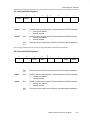
1
User’s Guide
Extract
2005
Mixed Signal Products
SLAU169
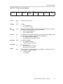
IMPORTANT NOTICE
Texas Instruments Incorporated and its subsidiaries (TI) reserve the right to make corrections, modifications,
enhancements, improvements, and other changes to its products and services at any time and to discontinue
any product or service without notice. Customers should obtain the latest relevant information before placing
orders and should verify that such information is current and complete. All products are sold subject to TI’s terms
and conditions of sale supplied at the time of order acknowledgment.
TI warrants performance of its hardware products to the specifications applicable at the time of sale in
accordance with TI’s standard warranty. Testing and other quality control techniques are used to the extent TI
deems necessary to support this warranty. Except where mandated by government requirements, testing of all
parameters of each product is not necessarily performed.
TI assumes no liability for applications assistance or customer product design. Customers are responsible for
their products and applications using TI components. To minimize the risks associated with customer products
and applications, customers should provide adequate design and operating safeguards.
TI does not warrant or represent that any license, either express or implied, is granted under any TI patent right,
copyright, mask work right, or other TI intellectual property right relating to any combination, machine, or process
in which TI products or services are used. Information published by TI regarding third-party products or services
does not constitute a license from TI to use such products or services or a warranty or endorsement thereof.
Use of such information may require a license from a third party under the patents or other intellectual property
of the third party, or a license from TI under the patents or other intellectual property of TI.
Reproduction of information in TI data books or data sheets is permissible only if reproduction is without
alteration and is accompanied by all associated warranties, conditions, limitations, and notices. Reproduction
of this information with alteration is an unfair and deceptive business practice. TI is not responsible or liable for
such altered documentation.
Resale of TI products or services with statements different from or beyond the parameters stated by TI for that
product or service voids all express and any implied warranties for the associated TI product or service and
is an unfair and deceptive business practice. TI is not responsible or liable for any such statements.
Following are URLs where you can obtain information on other Texas Instruments products and application
solutions:
Products
Applications
Amplifiers
amplifier.ti.com
Audio
www.ti.com/audio
Data Converters
dataconverter.ti.com
Automotive
www.ti.com/automotive
DSP
dsp.ti.com
Broadband
www.ti.com/broadband
Interface
interface.ti.com
Digital Control
www.ti.com/digitalcontrol
Logic
logic.ti.com
Military
www.ti.com/military
Power Mgmt
power.ti.com
Optical Networking
www.ti.com/opticalnetwork
Microcontrollers
microcontroller.ti.com
Security
www.ti.com/security
Telephony
www.ti.com/telephony
Video & Imaging
www.ti.com/video
Wireless
www.ti.com/wireless
Mailing Address:
Texas Instruments
Post Office Box 655303 Dallas, Texas 75265
Copyright 2005, Texas Instruments Incorporated
Related Documentation From Texas Instruments
Preface
Read This First
About This Manual
This manual is an extract of the MSP430x1xx Family User’s Guide
(SLAU049).
Related Documentation From Texas Instruments
For related documentation see the web site http://www.ti.com/msp430.
FCC Warning
This equipment is intended for use in a laboratory test environment only. It generates, uses, and can radiate radio frequency energy and has not been tested
for compliance with the limits of computing devices pursuant to subpart J of
part 15 of FCC rules, which are designed to provide reasonable protection
against radio frequency interference. Operation of this equipment in other environments may cause interference with radio communications, in which case
the user at his own expense will be required to take whatever measures may
be required to correct this interference.
Notational Conventions
Program examples, are shown in a special typeface.
iii
Glossary
Glossary
ACLK
Auxiliary Clock
See Basic Clock Module
ADC
Analog-to-Digital Converter
BOR
Brown-Out Reset
See System Resets, Interrupts, and Operating Modes
BSL
Bootstrap Loader
See www.ti.com/msp430 for application reports
CPU
Central Processing Unit
See RISC 16-Bit CPU
DAC
Digital-to-Analog Converter
DCO
Digitally Controlled Oscillator
See Basic Clock Module
dst
Destination
See RISC 16-Bit CPU
FLL
Frequency Locked Loop
See FLL+ in MSP430x4xx Family User’s Guide
GIE
General Interrupt Enable
See System Resets Interrupts and Operating Modes
INT(N/2) Integer portion of N/2
I/O
Input/Output
ISR
Interrupt Service Routine
LSB
Least-Significant Bit
LSD
Least-Significant Digit
LPM
Low-Power Mode
MAB
Memory Address Bus
MCLK
Master Clock
MDB
Memory Data Bus
MSB
Most-Significant Bit
MSD
Most-Significant Digit
NMI
(Non)-Maskable Interrupt
See System Resets Interrupts and Operating Modes
PC
Program Counter
See RISC 16-Bit CPU
POR
Power-On Reset
See System Resets Interrupts and Operating Modes
PUC
Power-Up Clear
See System Resets Interrupts and Operating Modes
RAM
Random Access Memory
SCG
System Clock Generator
SFR
Special Function Register
SMCLK
Sub-System Master Clock
See Basic Clock Module
SP
Stack Pointer
See RISC 16-Bit CPU
SR
Status Register
See RISC 16-Bit CPU
src
Source
See RISC 16-Bit CPU
TOS
Top-of-Stack
See RISC 16-Bit CPU
WDT
Watchdog Timer
See Watchdog Timer
iv
See Digital I/O
See System Resets Interrupts and Operating Modes
See Basic Clock Module
See System Resets Interrupts and Operating Modes
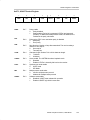
Register Bit Conventions
Register Bit Conventions
Each register is shown with a key indicating the accessibility of the each
individual bit, and the initial condition:
Register Bit Accessibility and Initial Condition
Key
Bit Accessibility
rw
Read/write
r
Read only
r0
Read as 0
r1
Read as 1
w
Write only
w0
Write as 0
w1
Write as 1
(w)
No register bit implemented; writing a 1 results in a pulse.
The register bit is always read as 0.
h0
Cleared by hardware
h1
Set by hardware
−0,−1
Condition after PUC
−(0),−(1) Condition after POR
v
vi
Contents
Contents
1
Introduction . . . . . . . . . . . . . . . . . . . . . . . . . . . . . . . . . . . . . . . . . . . . . . . . . . . . . . . . . . . . . . . . . . . .
1.1
Architecture . . . . . . . . . . . . . . . . . . . . . . . . . . . . . . . . . . . . . . . . . . . . . . . . . . . . . . . . . . . . . . .
1.2
Flexible Clock System . . . . . . . . . . . . . . . . . . . . . . . . . . . . . . . . . . . . . . . . . . . . . . . . . . . . . .
1.3
Embedded Emulation . . . . . . . . . . . . . . . . . . . . . . . . . . . . . . . . . . . . . . . . . . . . . . . . . . . . . . .
1.4
Address Space . . . . . . . . . . . . . . . . . . . . . . . . . . . . . . . . . . . . . . . . . . . . . . . . . . . . . . . . . . . .
1.4.1 Flash/ROM . . . . . . . . . . . . . . . . . . . . . . . . . . . . . . . . . . . . . . . . . . . . . . . . . . . . . . . .
1.4.2 RAM . . . . . . . . . . . . . . . . . . . . . . . . . . . . . . . . . . . . . . . . . . . . . . . . . . . . . . . . . . . . . .
1.4.3 Peripheral Modules . . . . . . . . . . . . . . . . . . . . . . . . . . . . . . . . . . . . . . . . . . . . . . . . .
1.4.4 Special Function Registers (SFRs) . . . . . . . . . . . . . . . . . . . . . . . . . . . . . . . . . . . .
1.4.5 Memory Organization . . . . . . . . . . . . . . . . . . . . . . . . . . . . . . . . . . . . . . . . . . . . . . . .
1-1
1-2
1-2
1-3
1-4
1-4
1-4
1-5
1-5
1-5
2
System Resets, Interrupts, and Operating Modes . . . . . . . . . . . . . . . . . . . . . . . . . . . . . . . . . .
2.1
System Reset and Initialization . . . . . . . . . . . . . . . . . . . . . . . . . . . . . . . . . . . . . . . . . . . . . . .
2.2
Principles for Low-Power Applications . . . . . . . . . . . . . . . . . . . . . . . . . . . . . . . . . . . . . . . . .
2.3
Connection of Unused Pins . . . . . . . . . . . . . . . . . . . . . . . . . . . . . . . . . . . . . . . . . . . . . . . . . .
2-1
2-2
2-4
2-4
3
RISC 16-Bit CPU . . . . . . . . . . . . . . . . . . . . . . . . . . . . . . . . . . . . . . . . . . . . . . . . . . . . . . . . . . . . . . . .
3.1
CPU Introduction . . . . . . . . . . . . . . . . . . . . . . . . . . . . . . . . . . . . . . . . . . . . . . . . . . . . . . . . . .
3.1.1 Status Register (SR) . . . . . . . . . . . . . . . . . . . . . . . . . . . . . . . . . . . . . . . . . . . . . . . .
3.1.2 Constant Generator Registers CG1 and CG2 . . . . . . . . . . . . . . . . . . . . . . . . . . .
3-1
3-2
3-4
3-5
4
Basic Clock Module . . . . . . . . . . . . . . . . . . . . . . . . . . . . . . . . . . . . . . . . . . . . . . . . . . . . . . . . . . . . . 4-1
4.1
Basic Clock Module Introduction . . . . . . . . . . . . . . . . . . . . . . . . . . . . . . . . . . . . . . . . . . . . . 4-2
4.2
Basic Clock Module Registers . . . . . . . . . . . . . . . . . . . . . . . . . . . . . . . . . . . . . . . . . . . . . . . 4-4
5
Flash Memory Controller . . . . . . . . . . . . . . . . . . . . . . . . . . . . . . . . . . . . . . . . . . . . . . . . . . . . . . . .
5.1
Flash Memory Introduction . . . . . . . . . . . . . . . . . . . . . . . . . . . . . . . . . . . . . . . . . . . . . . . . . .
5.2
Flash Memory Segmentation . . . . . . . . . . . . . . . . . . . . . . . . . . . . . . . . . . . . . . . . . . . . . . . .
5.3
Flash Memory Registers . . . . . . . . . . . . . . . . . . . . . . . . . . . . . . . . . . . . . . . . . . . . . . . . . . . .
6
Supply Voltage Supervisor . . . . . . . . . . . . . . . . . . . . . . . . . . . . . . . . . . . . . . . . . . . . . . . . . . . . . . 6-1
6.1
SVS Introduction . . . . . . . . . . . . . . . . . . . . . . . . . . . . . . . . . . . . . . . . . . . . . . . . . . . . . . . . . . . 6-2
6.2
SVS Registers . . . . . . . . . . . . . . . . . . . . . . . . . . . . . . . . . . . . . . . . . . . . . . . . . . . . . . . . . . . . . 6-4
7
Hardware Multiplier . . . . . . . . . . . . . . . . . . . . . . . . . . . . . . . . . . . . . . . . . . . . . . . . . . . . . . . . . . . . . 7-1
7.1
Hardware Multiplier Introduction . . . . . . . . . . . . . . . . . . . . . . . . . . . . . . . . . . . . . . . . . . . . . . 7-2
7.2
Hardware Multiplier Registers . . . . . . . . . . . . . . . . . . . . . . . . . . . . . . . . . . . . . . . . . . . . . . . . 7-3
8
DMA Controller . . . . . . . . . . . . . . . . . . . . . . . . . . . . . . . . . . . . . . . . . . . . . . . . . . . . . . . . . . . . . . . . . 8-1
8.1
DMA Introduction . . . . . . . . . . . . . . . . . . . . . . . . . . . . . . . . . . . . . . . . . . . . . . . . . . . . . . . . . . 8-2
8.2
DMA Registers . . . . . . . . . . . . . . . . . . . . . . . . . . . . . . . . . . . . . . . . . . . . . . . . . . . . . . . . . . . . 8-4
5-1
5-2
5-3
5-4
vii
Contents
9
Digital I/O . . . . . . . . . . . . . . . . . . . . . . . . . . . . . . . . . . . . . . . . . . . . . . . . . . . . . . . . . . . . . . . . . . . . . . 9-1
9.1
Digital I/O Introduction . . . . . . . . . . . . . . . . . . . . . . . . . . . . . . . . . . . . . . . . . . . . . . . . . . . . . . 9-2
9.2
Digital I/O Registers . . . . . . . . . . . . . . . . . . . . . . . . . . . . . . . . . . . . . . . . . . . . . . . . . . . . . . . 9-3
10 Watchdog Timer . . . . . . . . . . . . . . . . . . . . . . . . . . . . . . . . . . . . . . . . . . . . . . . . . . . . . . . . . . . . . . . 10-1
10.1 Watchdog Timer Introduction . . . . . . . . . . . . . . . . . . . . . . . . . . . . . . . . . . . . . . . . . . . . . . . 10-2
10.2 Watchdog Timer Registers . . . . . . . . . . . . . . . . . . . . . . . . . . . . . . . . . . . . . . . . . . . . . . . . . 10-4
11 Timer_A . . . . . . . . . . . . . . . . . . . . . . . . . . . . . . . . . . . . . . . . . . . . . . . . . . . . . . . . . . . . . . . . . . . . . . . 11-1
11.1 Timer_A Introduction . . . . . . . . . . . . . . . . . . . . . . . . . . . . . . . . . . . . . . . . . . . . . . . . . . . . . . 11-2
11.2 Timer_A Registers . . . . . . . . . . . . . . . . . . . . . . . . . . . . . . . . . . . . . . . . . . . . . . . . . . . . . . . . 11-4
12 Timer_B . . . . . . . . . . . . . . . . . . . . . . . . . . . . . . . . . . . . . . . . . . . . . . . . . . . . . . . . . . . . . . . . . . . . . . .
12.1 Timer_B Introduction . . . . . . . . . . . . . . . . . . . . . . . . . . . . . . . . . . . . . . . . . . . . . . . . . . . . . .
12.1.1 Similarities and Differences From Timer_A . . . . . . . . . . . . . . . . . . . . . . . . . . . .
12.2 Timer_B Registers . . . . . . . . . . . . . . . . . . . . . . . . . . . . . . . . . . . . . . . . . . . . . . . . . . . . . . . .
12-1
12-2
12-2
12-4
13 USART Peripheral Interface, UART Mode . . . . . . . . . . . . . . . . . . . . . . . . . . . . . . . . . . . . . . . . 13-1
13.1 USART Introduction: UART Mode . . . . . . . . . . . . . . . . . . . . . . . . . . . . . . . . . . . . . . . . . . . 13-2
13.2 USART Registers: UART Mode . . . . . . . . . . . . . . . . . . . . . . . . . . . . . . . . . . . . . . . . . . . . . 13-4
14 USART Peripheral Interface, SPI Mode . . . . . . . . . . . . . . . . . . . . . . . . . . . . . . . . . . . . . . . . . . . 14-1
14.1 USART Introduction: SPI Mode . . . . . . . . . . . . . . . . . . . . . . . . . . . . . . . . . . . . . . . . . . . . . 14-2
14.2 USART Registers: SPI Mode . . . . . . . . . . . . . . . . . . . . . . . . . . . . . . . . . . . . . . . . . . . . . . . 14-4
15 USART Peripheral Interface, I2C Mode . . . . . . . . . . . . . . . . . . . . . . . . . . . . . . . . . . . . . . . . . . . 15-1
15.1 I2C Module Introduction . . . . . . . . . . . . . . . . . . . . . . . . . . . . . . . . . . . . . . . . . . . . . . . . . . . . 15-2
15.2 I2C Module Registers . . . . . . . . . . . . . . . . . . . . . . . . . . . . . . . . . . . . . . . . . . . . . . . . . . . . . . 15-4
16 Comparator_A . . . . . . . . . . . . . . . . . . . . . . . . . . . . . . . . . . . . . . . . . . . . . . . . . . . . . . . . . . . . . . . . . 16-1
16.1 Comparator_A Introduction . . . . . . . . . . . . . . . . . . . . . . . . . . . . . . . . . . . . . . . . . . . . . . . . . 16-2
16.2 Comparator_A Registers . . . . . . . . . . . . . . . . . . . . . . . . . . . . . . . . . . . . . . . . . . . . . . . . . . . 16-4
17 ADC12 . . . . . . . . . . . . . . . . . . . . . . . . . . . . . . . . . . . . . . . . . . . . . . . . . . . . . . . . . . . . . . . . . . . . . . . . 17-1
17.1 ADC12 Introduction . . . . . . . . . . . . . . . . . . . . . . . . . . . . . . . . . . . . . . . . . . . . . . . . . . . . . . . 17-2
17.2 ADC12 Registers . . . . . . . . . . . . . . . . . . . . . . . . . . . . . . . . . . . . . . . . . . . . . . . . . . . . . . . . . 17-4
18 ADC10 . . . . . . . . . . . . . . . . . . . . . . . . . . . . . . . . . . . . . . . . . . . . . . . . . . . . . . . . . . . . . . . . . . . . . . . . 18-1
18.1 ADC10 Introduction . . . . . . . . . . . . . . . . . . . . . . . . . . . . . . . . . . . . . . . . . . . . . . . . . . . . . . . 18-2
18.2 ADC10 Registers . . . . . . . . . . . . . . . . . . . . . . . . . . . . . . . . . . . . . . . . . . . . . . . . . . . . . . . . . 18-4
19 DAC12 . . . . . . . . . . . . . . . . . . . . . . . . . . . . . . . . . . . . . . . . . . . . . . . . . . . . . . . . . . . . . . . . . . . . . . . . 19-1
19.1 DAC12 Introduction . . . . . . . . . . . . . . . . . . . . . . . . . . . . . . . . . . . . . . . . . . . . . . . . . . . . . . . 19-2
19.2 DAC12 Registers . . . . . . . . . . . . . . . . . . . . . . . . . . . . . . . . . . . . . . . . . . . . . . . . . . . . . . . . . 19-4
viii
Chapter 1
Introduction
This chapter describes the architecture of the MSP430.
Topic
Page
1.1
Architecture . . . . . . . . . . . . . . . . . . . . . . . . . . . . . . . . . . . . . . . . . . . . . . . . . . 1-2
1.2
Flexible Clock System . . . . . . . . . . . . . . . . . . . . . . . . . . . . . . . . . . . . . . . . . 1-2
1.3
Embedded Emulation . . . . . . . . . . . . . . . . . . . . . . . . . . . . . . . . . . . . . . . . . . 1-3
1.4
Address Space . . . . . . . . . . . . . . . . . . . . . . . . . . . . . . . . . . . . . . . . . . . . . . . 1-4
Introduction
1-1
Architecture
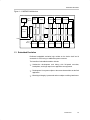
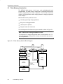
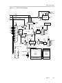
1.1 Architecture
The MSP430 incorporates a 16-bit RISC CPU, peripherals, and a flexible clock
system that interconnect using a von-Neumann common memory address
bus (MAB) and memory data bus (MDB). Partnering a modern CPU with
modular memory-mapped analog and digital peripherals, the MSP430 offers
solutions for demanding mixed-signal applications.
Key features of the MSP430x1xx family include:
- Ultralow-power architecture extends battery life
J
0.1-µA RAM retention
J
0.8-µA real-time clock mode
J
250-µA / MIPS active
- High-performance analog ideal for precision measurement
J
12-bit or 10-bit ADC — 200 ksps, temperature sensor, VRef
J
12-bit dual-DAC
J
Comparator-gated timers for measuring resistive elements
J
Supply voltage supervisor
- 16-bit RISC CPU enables new applications at a fraction of the code size.
J
Large register file eliminates working file bottleneck
J
Compact core design reduces power consumption and cost
J
Optimized for modern high-level programming
J
Only 27 core instructions and seven addressing modes
J
Extensive vectored-interrupt capability
- In-system programmable Flash permits flexible code changes, field
upgrades and data logging
1.2 Flexible Clock System
The clock system is designed specifically for battery-powered applications. A
low-frequency auxiliary clock (ACLK) is driven directly from a common 32-kHz
watch crystal. The ACLK can be used for a background real-time clock self
wake-up function. An integrated high-speed digitally controlled oscillator
(DCO) can source the master clock (MCLK) used by the CPU and high-speed
peripherals. By design, the DCO is active and stable in less than 6 µs.
MSP430-based solutions effectively use the high-performance 16-bit RISC
CPU in very short bursts.
- Low-frequency auxiliary clock = Ultralow-power stand-by mode
- High-speed master clock = High performance signal processing
1-2
Introduction
Embedded Emulation
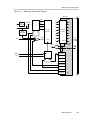
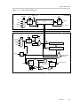
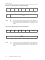
Figure 1−1. MSP430 Architecture
ACLK
Clock
System
SMCLK
Flash/
ROM
RAM
Peripheral
Peripheral
Peripheral
RISC CPU
16-Bit
JTAG/Debug
MCLK
MAB 16-Bit
MDB 16-Bit
Bus
Conv.
MDB 8-Bit
JTAG
ACLK
SMCLK
Watchdog
Peripheral
Peripheral
Peripheral
Peripheral
1.3 Embedded Emulation
Dedicated embedded emulation logic resides on the device itself and is
accessed via JTAG using no additional system resources.
The benefits of embedded emulation include:
- Unobtrusive development
and debug with full-speed execution,
breakpoints, and single-steps in an application are supported.
- Development is in-system subject to the same characteristics as the final
application.
- Mixed-signal integrity is preserved and not subject to cabling interference.
Introduction
1-3
Address Space
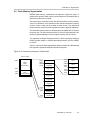
1.4 Address Space
The MSP430 von-Neumann architecture has one address space shared with
special function registers (SFRs), peripherals, RAM, and Flash/ROM memory
as shown in Figure 1−2. See the device-specific data sheets for specific
memory maps. Code access are always performed on even addresses. Data
can be accessed as bytes or words.
The addressable memory space is 64 KB with future expansion planned.
Figure 1−2. Memory Map
Access
0FFFFh
Interrupt Vector Table
Word/Byte
Flash/ROM
Word/Byte
RAM
Word/Byte
0FFE0h
0FFDFh
0200h
01FFh
16-Bit Peripheral Modules
Word
8-Bit Peripheral Modules
Byte
Special Function Registers
Byte
0100h
0FFh
010h
0Fh
0h
1.4.1
Flash/ROM
The start address of Flash/ROM depends on the amount of Flash/ROM
present and varies by device. The end address for Flash/ROM is 0FFFFh.
Flash can be used for both code and data. Word or byte tables can be stored
and used in Flash/ROM without the need to copy the tables to RAM before
using them.
The interrupt vector table is mapped into the upper 16 words of Flash/ROM
address space, with the highest priority interrupt vector at the highest
Flash/ROM word address (0FFFEh).
1.4.2
RAM
RAM starts at 0200h. The end address of RAM depends on the amount of RAM
present and varies by device. RAM can be used for both code and data.
1-4
Introduction
Address Space
1.4.3
Peripheral Modules
Peripheral modules are mapped into the address space. The address space
from 0100 to 01FFh is reserved for 16-bit peripheral modules. These modules
should be accessed with word instructions. If byte instructions are used, only
even addresses are permissible, and the high byte of the result is always 0.
The address space from 010h to 0FFh is reserved for 8-bit peripheral modules.
These modules should be accessed with byte instructions. Read access of
byte modules using word instructions results in unpredictable data in the high
byte. If word data is written to a byte module only the low byte is written into
the peripheral register, ignoring the high byte.
1.4.4
Special Function Registers (SFRs)
Some peripheral functions are configured in the SFRs. The SFRs are located
in the lower 16 bytes of the address space, and are organized by byte. SFRs
must be accessed using byte instructions only. See the device-specific data
sheets for applicable SFR bits.
1.4.5
Memory Organization
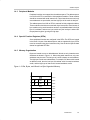
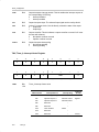
Bytes are located at even or odd addresses. Words are only located at even
addresses as shown in Figure 1−3. When using word instructions, only even
addresses may be used. The low byte of a word is always an even address.
The high byte is at the next odd address. For example, if a data word is located
at address xxx4h, then the low byte of that data word is located at address
xxx4h, and the high byte of that word is located at address xxx5h.
Figure 1−3. Bits, Bytes, and Words in a Byte-Organized Memory
xxxAh
15
14
. . Bits . .
9
8
xxx9h
7
6
. . Bits . .
1
0
xxx8h
Byte
xxx7h
Byte
xxx6h
Word (High Byte)
xxx5h
Word (Low Byte)
xxx4h
xxx3h
Introduction
1-5
Chapter 2
System Resets, Interrupts,
and Operating Modes
This chapter describes the MSP430x1xx system resets, interrupts, and
operating modes.
Topic
Page
2.1
System Reset and Initialization . . . . . . . . . . . . . . . . . . . . . . . . . . . . . . . . . 2-2
2.2
Principles for Low-Power Applications . . . . . . . . . . . . . . . . . . . . . . . . . 2-4
2.3
Connection of Unused Pins . . . . . . . . . . . . . . . . . . . . . . . . . . . . . . . . . . . . 2-4
System Resets, Interrupts, and Operating Modes
2-1
System Reset and Initialization
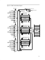
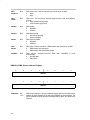
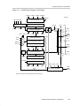
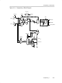
2.1 System Reset and Initialization
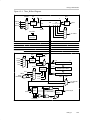
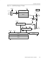
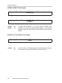
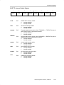
The system reset circuitry shown in Figure 2−1 sources both a power-on reset
(POR) and a power-up clear (PUC) signal. Different events trigger these reset
signals and different initial conditions exist depending on which signal was
generated.
Figure 2−1. Power-On Reset and Power-Up Clear Schematic
VCC
VCC
VCC
Brownout
Reset‡
POR
Detect
Detect#
POR
Delay#
0V
0V
~ 50us
S
S
R
POR
Latch
POR
0V
Delay
SVS_POR §
RST/NMI
WDTNMI†
WDTSSEL†
WDTQn†
WDTIFG†
EQU†
KEYV
(from flash module)
S
S
Resetwd1
Resetwd2
S
PUC
S Latch
S
PUC
R
MCLK
† From watchdog timer peripheral module
‡ Devices with BOR only
# Devices without BOR only
§ Devices with SVS only
A POR is a device reset. A POR is only generated by the following three
events:
- Powering up the device
- A low signal on the RST/NMI pin when configured in the reset mode
- An SVS low condition when PORON = 1.
A PUC is always generated when a POR is generated, but a POR is not
generated by a PUC. The following events trigger a PUC:
- A POR signal
- Watchdog timer expiration when in watchdog mode only
- Watchdog timer security key violation
- A Flash memory security key violation
2-2
System Resets, Interrupts, and Operating Modes
System Reset and Initialization
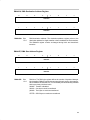
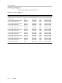
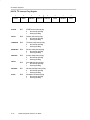
Figure 2−2. MSP430x1xx Operating Modes For Basic Clock System
RST/NMI
Reset Active
VCC On
POR
WDT
Time Expired, Overflow
WDTIFG = 1
WDTIFG = 0
PUC
WDTIFG = 1
RST/NMI is Reset Pin
WDT is Active
RST/NMI
NMI Active
WDT Active,
Security Key Violation
Active Mode
CPU Is Active
Peripheral Modules Are Active
CPUOFF = 1
SCG0 = 0
SCG1 = 0
CPUOFF = 1
OSCOFF = 1
SCG0 = 1
SCG1 = 1
LPM0
CPU Off, MCLK Off,
SMCLK On, ACLK On
LPM4
CPU Off, MCLK Off, DCO
Off, ACLK Off
CPUOFF = 1
SCG0 = 1
SCG1 = 0
LPM1
CPU Off, MCLK Off,
SMCLK On, ACLK On
DC Generator Off if DCO
not used in active mode
SCG1
SCG0 OSCOFF
CPUOFF
CPUOFF = 1
SCG0 = 0
SCG1 = 1
CPUOFF = 1
SCG0 = 1
SCG1 = 1
LPM2
CPU Off, MCLK Off, SMCLK
Off, DCO Off, ACLK On
Mode
DC Generator Off
LPM3
CPU Off, MCLK Off, SMCLK
Off, DCO Off, ACLK On
DC Generator Off
CPU and Clocks Status
0
0
0
0
Active
CPU is active, all enabled clocks are active
0
0
0
1
LPM0
CPU, MCLK are disabled
SMCLK , ACLK are active
0
1
0
1
LPM1
CPU, MCLK, DCO osc. are disabled
DC generator is disabled if the DCO is not used for
MCLK or SMCLK in active mode
SMCLK , ACLK are active
1
0
0
1
LPM2
CPU, MCLK, SMCLK, DCO osc. are disabled
DC generator remains enabled
ACLK is active
1
1
0
1
LPM3
CPU, MCLK, SMCLK, DCO osc. are disabled
DC generator disabled
ACLK is active
1
1
1
1
LPM4
CPU and all clocks disabled
System Resets, Interrupts, and Operating Modes
2-3
Principles for Low-Power Applications
2.2 Principles for Low-Power Applications
Often, the most important factor for reducing power consumption is using the
MSP430’s clock system to maximize the time in LPM3. LPM3 power
consumption is less than 2 µA typical with both a real-time clock function and
all interrupts active. A 32-kHz watch crystal is used for the ACLK and the CPU
is clocked from the DCO (normally off) which has a 6-µs wake-up.
- Use interrupts to wake the processor and control program flow.
- Peripherals should be switched on only when needed.
- Use low-power integrated peripheral modules in place of software driven
functions. For example Timer_A and Timer_B can automatically generate
PWM and capture external timing, with no CPU resources.
- Calculated branching and fast table look-ups should be used in place of
flag polling and long software calculations.
- Avoid frequent subroutine and function calls due to overhead.
- For longer software routines, single-cycle CPU registers should be used.
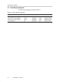
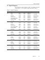
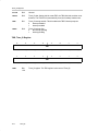
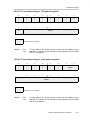
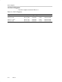
2.3 Connection of Unused Pins
The correct termination of all unused pins is listed in Table 2−1.
Table 2−1. Connection of Unused Pins
2-4
Pin
Potential
AVCC
DVCC
AVSS
DVSS
VREF+
Open
VeREF+
DVSS
VREF−/VeREF−
DVSS
XIN
DVCC
XOUT
Open
XT2IN
DVSS
13x, 14x, 15x and 16x devices
XT2OUT
Open
13x, 14x, 15x and 16x devices
Px.0 to Px.7
Open
Switched to port function, output direction
RST/NMI
DVCC or VCC
Pullup resistor 47 kΩ
Test/VPP
DVSS
P11x devices
Test
DVSS
Pulldown resistor 30K 11x1 devices
Open
11x1A, 11x2, 12x, 12x2 devices
TDO
Open
TDI
Open
TMS
Open
TCK
Open
Comment
System Resets, Interrupts, and Operating Modes
Chapter 3
This chapter describes the MSP430 CPU, addressing modes, and instruction
set.
Topic
3.1
Page
CPU Introduction . . . . . . . . . . . . . . . . . . . . . . . . . . . . . . . . . . . . . . . . . . . . . . 3-2
RISC 16-Bit CPU
3-1
CPU Introduction
3.1 CPU Introduction
The CPU incorporates features specifically designed for modern
programming techniques such as calculated branching, table processing and
the use of high-level languages such as C. The CPU can address the complete
address range without paging.
The CPU features include:
- RISC architecture with 27 instructions and 7 addressing modes.
- Orthogonal architecture with every instruction usable with every
addressing mode.
- Full register access including program counter, status registers, and stack
pointer.
- Single-cycle register operations.
- Large 16-bit register file reduces fetches to memory.
- 16-bit address bus allows direct access and branching throughout entire
memory range.
- 16-bit data bus allows direct manipulation of word-wide arguments.
- Constant generator provides six most used immediate values and
reduces code size.
- Direct memory-to-memory transfers without intermediate register holding.
- Word and byte addressing and instruction formats.
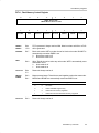
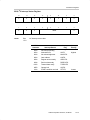
The block diagram of the CPU is shown in Figure 3−1.
3-2
RISC 16-Bit CPU
CPU Introduction
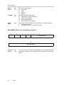
Figure 3−1. CPU Block Diagram
MDB − Memory Data Bus
Memory Address Bus − MAB
15
0
R0/PC Program Counter
0
R1/SP Stack Pointer
0
R2/SR/CG1 Status
R3/CG2 Constant Generator
R4
General Purpose
R5
General Purpose
R6
General Purpose
R7
General Purpose
R8
General Purpose
R9
General Purpose
R10
General Purpose
R11
General Purpose
R12
General Purpose
R13
General Purpose
R14
General Purpose
R15
General Purpose
16
16
Zero, Z
Carry, C
Overflow, V
Negative, N
dst
src
16−bit ALU
MCLK
RISC 16-Bit CPU
3-3
CPU Introduction
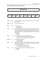
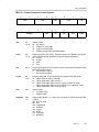
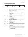
3.1.1
Status Register (SR)
The status register (SR/R2), used as a source or destination register, can be
used in the register mode only addressed with word instructions. The remaining combinations of addressing modes are used to support the constant generator. Figure 3−2 shows the SR bits.
Figure 3−2. Status Register Bits
9
15
Reserved
8
V
7
SCG1
0
OSC CPU
SCG0
GIE
OFF OFF
N
Z C
Table 3−1 describes the status register bits.
Table 3−1. Description of Status Register Bits
3-4
Bit
Description
V
Overflow bit. This bit is set when the result of an arithmetic operation
overflows the signed-variable range.
ADD(.B),ADDC(.B)
Set when:
Positive + Positive = Negative
Negative + Negative = Positive,
otherwise reset
SUB(.B),SUBC(.B),CMP(.B)
Set when:
Positive − Negative = Negative
Negative − Positive = Positive,
otherwise reset
SCG1
System clock generator 1. This bit, when set, turns off the SMCLK.
SCG0
System clock generator 0. This bit, when set, turns off the DCO dc
generator, if DCOCLK is not used for MCLK or SMCLK.
OSCOFF
Oscillator Off. This bit, when set, turns off the LFXT1 crystal oscillator,
when LFXT1CLK is not use for MCLK or SMCLK
CPUOFF
CPU off. This bit, when set, turns off the CPU.
GIE
General interrupt enable. This bit, when set, enables maskable
interrupts. When reset, all maskable interrupts are disabled.
N
Negative bit. This bit is set when the result of a byte or word operation
is negative and cleared when the result is not negative.
Word operation:
N is set to the value of bit 15 of the
result
Byte operation:
N is set to the value of bit 7 of the
result
Z
Zero bit. This bit is set when the result of a byte or word operation is 0
and cleared when the result is not 0.
C
Carry bit. This bit is set when the result of a byte or word operation
produced a carry and cleared when no carry occurred.
RISC 16-Bit CPU
CPU Introduction
3.1.2
Constant Generator Registers CG1 and CG2
Six commonly-used constants are generated with the constant generator
registers R2 and R3, without requiring an additional 16-bit word of program
code. The constants are selected with the source-register addressing modes
(As), as described in Table 3−2.
Table 3−2. Values of Constant Generators CG1, CG2
Register
As
Constant
Remarks
R2
00
−−−−−
Register mode
R2
01
(0)
Absolute address mode
R2
10
00004h
+4, bit processing
R2
11
00008h
+8, bit processing
R3
00
00000h
0, word processing
R3
01
00001h
+1
R3
10
00002h
+2, bit processing
R3
11
0FFFFh
−1, word processing
The constant generator advantages are:
- No special instructions required
- No additional code word for the six constants
- No code memory access required to retrieve the constant
The assembler uses the constant generator automatically if one of the six
constants is used as an immediate source operand. Registers R2 and R3,
used in the constant mode, cannot be addressed explicitly; they act as
source-only registers.
Constant Generator − Expanded Instruction Set
The RISC instruction set of the MSP430 has only 27 instructions. However, the
constant generator allows the MSP430 assembler to support 24 additional,
emulated instructions. For example, the single-operand instruction:
CLR
dst
is emulated by the double-operand instruction with the same length:
MOV
R3,dst
where the #0 is replaced by the assembler, and R3 is used with As=00.
INC
dst
is replaced by:
ADD
0(R3),dst
RISC 16-Bit CPU
3-5
CPU Introduction
Table 3−3. MSP430 Instruction Set
Mnemonic
V
N
Z
ADC(.B)†
dst
Description
Add C to destination
dst + C → dst
*
*
*
C
*
ADD(.B)
src,dst
Add source to destination
src + dst → dst
*
*
*
*
ADDC(.B)
src,dst
Add source and C to destination
src + dst + C → dst
*
*
*
*
AND(.B)
src,dst
AND source and destination
src .and. dst → dst
0
*
*
*
BIC(.B)
src,dst
Clear bits in destination
.not.src .and. dst → dst
−
−
−
−
BIS(.B)
src,dst
Set bits in destination
src .or. dst → dst
−
−
−
−
BIT(.B)
src,dst
Test bits in destination
src .and. dst
0
*
*
*
BR†
dst
Branch to destination
dst → PC
−
−
−
−
CALL
dst
Call destination
PC+2 → stack, dst → PC
−
−
−
−
CLR(.B)†
dst
Clear destination
0 → dst
−
−
−
−
CLRC†
Clear C
0→C
−
−
−
0
CLRN†
Clear N
0→N
−
0
−
−
CLRZ†
Clear Z
0→Z
−
−
0
−
*
CMP(.B)
src,dst
Compare source and destination
dst − src
*
*
*
DADC(.B)†
dst
Add C decimally to destination
dst + C → dst (decimally)
*
*
*
*
DADD(.B)
src,dst
Add source and C decimally to dst.
src + dst + C → dst (decimally)
*
*
*
*
DEC(.B)†
dst
Decrement destination
dst − 1 → dst
*
*
*
*
DECD(.B)†
dst
Double-decrement destination
dst − 2 → dst
*
*
*
*
Disable interrupts
0 → GIE
−
−
−
−
−
DINT†
Enable interrupts
1 → GIE
−
−
−
INC(.B)†
dst
Increment destination
dst +1 → dst
*
*
*
*
INCD(.B)†
dst
Double-increment destination
dst+2 → dst
*
*
*
*
.not.dst → dst
EINT†
INV(.B)†
dst
Invert destination
JC/JHS
label
Jump if C set/Jump if higher or same
*
*
*
*
−
−
−
−
JEQ/JZ
label
Jump if equal/Jump if Z set
−
−
−
−
JGE
label
Jump if greater or equal
−
−
−
−
JL
label
Jump if less
JMP
label
Jump
PC + 2 x offset → PC
−
−
−
−
−
−
−
−
JN
label
Jump if N set
−
−
−
−
JNC/JLO
label
Jump if C not set/Jump if lower
−
−
−
−
JNE/JNZ
label
Jump if not equal/Jump if Z not set
MOV(.B)
src,dst
Move source to destination
POP(.B)†
dst
PUSH(.B)
src
NOP†
−
−
−
−
src → dst
−
−
−
−
−
−
−
−
Pop item from stack to destination
@SP → dst, SP+2 → SP
−
−
−
−
No operation
Push source onto stack
SP − 2 → SP, src → @SP
−
−
−
−
RET†
Return from subroutine
@SP → PC, SP + 2 → SP
−
−
−
−
RETI
Return from interrupt
*
*
*
*
*
RLA(.B)†
dst
Rotate left arithmetically
*
*
*
RLC(.B)†
dst
Rotate left through C
*
*
*
*
RRA(.B)
dst
Rotate right arithmetically
0
*
*
*
RRC(.B)
dst
Rotate right through C
*
*
*
*
SBC(.B)†
dst
Subtract not(C) from destination
dst + 0FFFFh + C → dst
*
*
*
*
SETC†
Set C
1→C
−
−
−
1
SET†
Set N
1→N
−
1
−
−
SETZ†
Set Z
1→C
−
−
1
−
SUB(.B)
src,dst
Subtract source from destination
dst + .not.src + 1 → dst
*
*
*
*
SUBC(.B)
src,dst
Subtract source and not(C) from dst.
dst + .not.src + C → dst
*
*
*
*
−
SWPB
dst
Swap bytes
−
−
−
SXT
dst
Extend sign
0
*
*
*
TST(.B)†
dst
Test destination
dst + 0FFFFh + 1
0
*
*
1
XOR(.B)
src,dst
Exclusive OR source and destination
src .xor. dst → dst
*
*
*
*
† Emulated Instruction
3-6
RISC 16-Bit CPU
Chapter 4
The basic clock module provides the clocks for MSP430x1xx devices. This
chapter describes the operation of the basic clock module. The basic clock
module is implemented in all MSP430x1xx devices.
Topic
Page
4.1
Basic Clock Module Introduction . . . . . . . . . . . . . . . . . . . . . . . . . . . . . . 4−2
4.2
Basic Clock Module Registers . . . . . . . . . . . . . . . . . . . . . . . . . . . . . . . . 4−4
Basic Clock Module
4-1
Basic Clock Module Introduction
4.1 Basic Clock Module Introduction
The basic clock module supports low system cost and ultralow-power
consumption. Using three internal clock signals, the user can select the best
balance of performance and low power consumption. The basic clock module
can be configured to operate without any external components, with one
external resistor, with one or two external crystals, or with resonators, under
full software control.
The basic clock module includes two or three clock sources:
- LFXT1CLK: Low-frequency/high-frequency oscillator that can be used
either with low-frequency 32768-Hz watch crystals, or standard crystals
or resonators in the 450-kHz to 8-MHz range.
- XT2CLK: Optional high-frequency oscillator that can be used with
standard crystals, resonators, or external clock sources in the 450-kHz to
8-MHz range.
- DCOCLK: Internal digitally controlled oscillator (DCO) with RC-type
characteristics.
Three clock signals are available from the basic clock module:
- ACLK: Auxiliary clock. The ACLK is the buffered LFXT1CLK clock source
divided by 1, 2, 4, or 8. ACLK is software selectable for individual
peripheral modules.
- MCLK: Master clock. MCLK is software selectable as LFXT1CLK,
XT2CLK (if available), or DCOCLK. MCLK is divided by 1, 2, 4, or 8. MCLK
is used by the CPU and system.
- SMCLK: Sub-main clock. SMCLK is software selectable as LFXT1CLK,
XT2CLK (if available on-chip), or DCOCLK. SMCLK is divided by 1, 2, 4,
or 8. SMCLK is software selectable for individual peripheral modules.
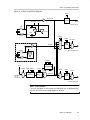
The block diagram of the basic clock module is shown in Figure 4−1.
4-2
Basic Clock Module
Basic Clock Module Introduction
Figure 4−1. Basic Clock Block Diagram
DIVAx
LFXT1CLK
Divider
/1/2/4/8
OSCOFF XTS
ACLK
Auxillary Clock
0V
XIN
12pF
LF
12pF
XOUT
XT
LFOff
XT1Off
0V
SELMx
LFXT1 Oscillator
DIVMx
CPUOFF
00
XT2CLK
01
10
Divider
/1/2/4/8
0
1
11
XT2OFF
XT2IN
MCLK
Main System Clock
XT
XT2OUT
XT2 Oscillator
MODx
VCC
Modulator
DCOR
SCG0 RSELx
DCOx
SELS
DIVSx
SCG1
0
1
off
DC
Generator
n
DCO
n+1
0
1
DCOCLK
0
1
Divider
/1/2/4/8
0
1
P2.5/Rosc
SMCLK
Sub System Clock
Note: XT2 Oscillator
The XT2 Oscillator is not present on MSP430x11xx or MSP430x12xx
devices. The LFXT1CLK is used in place of XT2CLK.
Basic Clock Module
4-3
Basic Clock Module Registers
4.2 Basic Clock Module Registers
The basic clock module registers are listed in Table 4−1:
Table 4−1. Basic Clock Module Registers
Register
Short Form
Register Type Address
Initial State
DCO control register
DCOCTL
Read/write
056h
060h with PUC
Basic clock system control 1
BCSCTL1
Read/write
057h
084h with PUC
Basic clock system control 2
BCSCTL2
Read/write
058h
Reset with POR
SFR interrupt enable register 1
IE1
Read/write
000h
Reset with PUC
SFR interrupt flag register 1
IFG1
Read/write
002h
Reset with PUC
4-4
Basic Clock Module
Basic Clock Module Registers
DCOCTL, DCO Control Register
7
6
5
4
3
DCOx
rw−0
rw−1
2
1
0
rw−0
rw−0
MODx
rw−1
rw−0
rw−0
rw−0
DCOx
Bits
7-5
DCO frequency select. These bits select which of the eight discrete DCO
frequencies of the RSELx setting is selected.
MODx
Bits
4-0
Modulator selection. These bits define how often the fDCO+1 frequency is
used within a period of 32 DCOCLK cycles. During the remaining clock
cycles (32−MOD) the fDCO frequency is used. Not useable when DCOx=7.
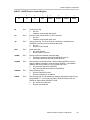
BCSCTL1, Basic Clock System Control Register 1
7
6
XT2OFF
XTS
rw−(1)
rw−(0)
5
4
DIVAx
rw−(0)
3
2
1
XT5V
rw−(0)
rw−0
0
RSELx
rw−1
rw−0
rw−0
XT2OFF
Bit 7
XT2 off. This bit turns off the XT2 oscillator
0
XT2 is on
1
XT2 is off if it is not used for MCLK or SMCLK.
XTS
Bit 6
LFXT1 mode select.
0
Low frequency mode
1
High frequency mode
DIVAx
Bits
5-4
Divider for ACLK
00 /1
01 /2
10 /4
11 /8
XT5V
Bit 3
Unused. XT5V should always be reset.
RSELx
Bits
2-0
Resistor Select. The internal resistor is selected in eight different steps.
The value of the resistor defines the nominal frequency. The lowest
nominal frequency is selected by setting RSELx=0.
Basic Clock Module
4-5
Basic Clock Module Registers
BCSCTL2, Basic Clock System Control Register 2
7
6
5
SELMx
rw−(0)
4
DIVMx
rw−(0)
rw−(0)
3
2
SELS
rw−(0)
rw−0
1
DIVSx
rw−0
0
DCOR
rw−0
rw−0
SELMx
Bits
7-6
Select MCLK. These bits select the MCLK source.
00 DCOCLK
01 DCOCLK
10 XT2CLK when XT2 oscillator present on-chip. LFXT1CLK when XT2
oscillator not present on-chip.
11 LFXT1CLK
DIVMx
BitS
5-4
Divider for MCLK
00 /1
01 /2
10 /4
11 /8
SELS
Bit 3
Select SMCLK. This bit selects the SMCLK source.
0
DCOCLK
1
XT2CLK when XT2 oscillator present on-chip. LFXT1CLK when XT2
oscillator not present on-chip.
DIVSx
BitS
2-1
Divider for SMCLK
00 /1
01 /2
10 /4
11 /8
DCOR
Bit 0
DCO resistor select
0
Internal resistor
1
External resistor
4-6
Basic Clock Module
Basic Clock Module Registers
IE1, Interrupt Enable Register 1
7
6
5
4
3
2
1
0
OFIE
rw−0
OFIE
Bits
7-2
These bits may be used by other modules. See device-specific datasheet.
Bit 1
Oscillator fault interrupt enable. This bit enables the OFIFG interrupt.
Because other bits in IE1 may be used for other modules, it is recommended
to set or clear this bit using BIS.B or BIC.B instructions, rather than MOV.B
or CLR.B instructions.
0
Interrupt not enabled
1
Interrupt enabled
Bits 0
This bit may be used by other modules. See device-specific datasheet.
IFG1, Interrupt Flag Register 1
7
6
5
4
3
2
1
0
OFIFG
rw−1
OFIFG
Bits
7-2
These bits may be used by other modules. See device-specific datasheet.
Bit 1
Oscillator fault interrupt flag. Because other bits in IFG1 may be used for other
modules, it is recommended to set or clear this bit using BIS.B or BIC.B
instructions, rather than MOV.B or CLR.B instructions.
0
No interrupt pending
1
Interrupt pending
Bits 0
This bit may be used by other modules. See device-specific datasheet.
Basic Clock Module
4-7
Chapter 5
This chapter describes the operation of the MSP430 flash memory controller.
Topic
Page
5.1
Flash Memory Introduction . . . . . . . . . . . . . . . . . . . . . . . . . . . . . . . . . . . . 5-2
5.2
Flash Memory Segmentation . . . . . . . . . . . . . . . . . . . . . . . . . . . . . . . . . . . 5-3
5.3
Flash Memory Registers . . . . . . . . . . . . . . . . . . . . . . . . . . . . . . . . . . . . . . . 5-4
Flash Memory Controller
5-1
Flash Memory Introduction
5.1 Flash Memory Introduction
The MSP430 flash memory is bit-, byte-, and word-addressable and
programmable. The flash memory module has an integrated controller that
controls programming and erase operations. The controller has three
registers, a timing generator, and a voltage generator to supply program and
erase voltages.
MSP430 flash memory features include:
- Internal programming voltage generation
- Bit, byte or word programmable
- Ultralow-power operation
- Segment erase and mass erase
The block diagram of the flash memory and controller is shown in Figure 5−1.
Note: Minimum VCC During Flash Write or Erase
The minimum VCC voltage during a flash write or erase operation is 2.7 V.
If VCC falls below 2.7 V during a write or erase, the result of the write or erase
will be unpredictable.
Figure 5−1. Flash Memory Module Block Diagram
MAB
FCTL1
FCTL2
MDB
Address Latch
Enable
Address
Latch
FCTL3
Timing
Generator
Programming
Voltage
Generator
5-2
Flash Memory Controller
Data Latch
Flash
Memory
Array
Enable
Data Latch
Flash Memory Segmentation
5.2 Flash Memory Segmentation
MSP430 flash memory is partitioned into segments. Single bits, bytes, or
words can be written to flash memory, but the segment is the smallest size of
flash memory that can be erased.
The flash memory is partitioned into main and information memory sections.
There is no difference in the operation of the main and information memory
sections. Code or data can be located in either section. The differences
between the two sections are the segment size and the physical addresses.
The information memory has two 128-byte segments (MSP430F1101 devices
have only one). The main memory has two or more 512-byte segments. See
the device-specific datasheet for the complete memory map of a device.
The segments are further dividing into blocks. A block is 64 bytes, starting at
0xx00h, 0xx40h, 0xx80h, or 0xxC0h, and ending at 0xx3Fh, 0xx7Fh, 0xxBFh,
or 0xxFFh.
Figure 5−2 shows the flash segmentation using an example of 4-KB flash that
has eight main segments and both information segments.
Figure 5−2. Flash Memory Segments, 4-KB Example
4 KB + 256 byte
FFFFh
4-kbyte
Flash
Main Memory
Segment0
FDFFh
FC00h
Segment1
xx80h
xx7Fh
Segment2
xx40h
xx3Fh
Segment3
xx00h
F000h
10FFh
1000h
xxFFh
FFFFh
FE00h
256-byte
Flash
Information Memory
xxC0h
xxBFh
Block
Block
Block
Block
Segment4
Segment5
Segment6
F000h
Segment7
10FFh
SegmentA
1000h
SegmentB
Flash Memory Controller
5-3
Flash Memory Registers
5.3 Flash Memory Registers
The flash memory registers are listed in Table 5−1.
Table 5−1. Flash Memory Registers
Register
Short Form
Register Type Address
Initial State
Flash memory control register 1
FCTL1
Read/write
0128h
09600h with PUC
Flash memory control register 2
FCTL2
Read/write
012Ah
09642h with PUC
Flash memory control register 3
FCTL3
Read/write
012Ch
09618h with PUC
Interrupt Enable 1
IE1
Read/write
000h
Reset with PUC
5-4
Flash Memory Controller
Flash Memory Registers
FCTL1, Flash Memory Control Register
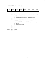
15
14
13
12
11
10
9
8
FRKEY, Read as 096h
FWKEY, Must be written as 0A5h
7
6
5
4
3
2
1
0
BLKWRT
WRT
Reserved
Reserved
Reserved
MERAS
ERASE
Reserved
rw−0
rw−0
r0
r0
r0
rw−0
rw−0
r0
FRKEY/
FWKEY
Bits
15-8
FCTLx password. Always read as 096h. Must be written as 0A5h or a PUC
will be generated.
BLKWRT
Bit 7
Block write mode. WRT must also be set for block write mode. BLKWRT is
automatically reset when EMEX is set.
0
Block-write mode is off
1
Block-write mode is on
WRT
Bit 6
Write. This bit is used to select any write mode. WRT is automatically reset
when EMEX is set.
0
Write mode is off
1
Write mode is on
Reserved
Bits
5-3
Reserved. Always read as 0.
MERAS
ERASE
Bit 2
Bit 1
Mass erase and erase. These bits are used together to select the erase mode.
MERAS and ERASE are automatically reset when EMEX is set.
MERAS
Reserved
Bit 0
ERASE
Erase Cycle
0
0
No erase
0
1
Erase individual segment only
1
0
Erase all main memory segments
1
1
Erase all main and information memory segments
Reserved. Always read as 0.
Flash Memory Controller
5-5
Flash Memory Registers
FCTL2, Flash Memory Control Register
15
14
13
12
11
10
9
8
2
1
0
rw−0
rw-1
rw−0
FWKEYx, Read as 096h
Must be written as 0A5h
7
6
5
4
3
FSSELx
rw−0
FNx
rw−1
rw-0
rw-0
rw-0
FWKEYx
Bits
15-8
FCTLx password. Always read as 096h. Must be written as 0A5h or a PUC
will be generated.
FSSELx
Bits
7−6
Flash controller clock source select
00 ACLK
01 MCLK
10 SMCLK
11 SMCLK
FNx
Bits
5-0
Flash controller clock divider. These six bits select the divider for the flash
controller clock. The divisor value is FNx + 1. For example, when FNx=00h,
the divisor is 1. When FNx=03Fh the divisor is 64.
5-6
Flash Memory Controller
Flash Memory Registers
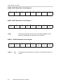
FCTL3, Flash Memory Control Register FCTL3
15
14
13
12
11
10
9
8
FWKEYx, Read as 096h
Must be written as 0A5h
7
6
5
4
3
2
1
0
Reserved
Reserved
EMEX
LOCK
WAIT
ACCVIFG
KEYV
BUSY
r0
r0
rw-0
rw-1
r-1
rw−0
rw-(0)
r(w)−0
FWKEYx
Bits
15-8
FCTLx password. Always read as 096h. Must be written as 0A5h or a PUC
will be generated.
Reserved
Bits
7-6
Reserved. Always read as 0.
EMEX
Bit 5
Emergency exit
0
No emergency exit
1
Emergency exit
LOCK
Bit 4
Lock. This bit unlocks the flash memory for writing or erasing. The LOCK bit
can be set anytime during a byte/word write or erase operation and the
operation will complete normally. In the block write mode if the LOCK bit is set
while BLKWRT=WAIT=1, then BLKWRT and WAIT are reset and the mode
ends normally.
0
Unlocked
1
Locked
WAIT
Bit 3
Wait. Indicates the flash memory is being written to.
0
The flash memory is not ready for the next byte/word write
1
The flash memory is ready for the next byte/word write
ACCVIFG
Bit 2
Access violation interrupt flag
0
No interrupt pending
1
Interrupt pending
KEYV
Bit 1
Flash security key violation. This bit indicates an incorrect FCTLx password
was written to any flash control register and generates a PUC when set. KEYV
must be reset with software.
0
FCTLx password was written correctly
1
FCTLx password was written incorrectly
BUSY
Bit 0
Busy. This bit indicates the status of the flash timing generator.
0
Not Busy
1
Busy
Flash Memory Controller
5-7
Flash Memory Registers
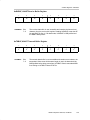
IE1, Interrupt Enable Register 1
7
6
5
4
3
2
1
0
ACCVIE
rw−0
ACCVIE
5-8
Bits
7-6,
4-0
These bits may be used by other modules. See device-specific datasheet.
Bit 5
Flash memory access violation interrupt enable. This bit enables the
ACCVIFG interrupt. Because other bits in IE1 may be used for other modules,
it is recommended to set or clear this bit using BIS.B or BIC.B instructions,
rather than MOV.B or CLR.B instructions.
0
Interrupt not enabled
1
Interrupt enabled
Flash Memory Controller
Chapter 6
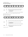
This chapter describes the operation of the SVS. The SVS is implemented in
MSP430x15x and MSP430x16x devices.
Topic
Page
6.1
SVS Introduction . . . . . . . . . . . . . . . . . . . . . . . . . . . . . . . . . . . . . . . . . . . . . 6−2
6.2
SVS Registers . . . . . . . . . . . . . . . . . . . . . . . . . . . . . . . . . . . . . . . . . . . . . . . 6−4
Supply Voltage Supervisor
6-1
SVS Introduction
6.1 SVS Introduction
The supply voltage supervisor (SVS) is used to monitor the AVCC supply
voltage or an external voltage. The SVS can be configured to set a flag or
generate a POR reset when the supply voltage or external voltage drops below
a user-selected threshold.
The SVS features include:
- AVCC monitoring
- Selectable generation of POR
- Output of SVS comparator accessible by software
- Low-voltage condition latched and accessible by software
- 14 selectable threshold levels
- External channel to monitor external voltage
The SVS block diagram is shown in Figure 6−1.
6-2
Supply Voltage Supervisor
SVS Introduction
Figure 6−1. SVS Block Diagram
VCC
AVCC
Brownout
Reset
D
AVCC
G S
SVSIN
~ 50us
1111
1101
−
SVS_POR
+
1100
tReset ~ 50us
0011
0010
SVSOUT
1.25V
0001
D
G S
Set SVSFG
Reset
VLD
PORON
SVSON
SVSOP
SVSFG
SVSCTL Bits
Supply Voltage Supervisor
6-3
SVS Registers
6.2 SVS Registers
The SVS registers are listed in Table 6−1.
Table 6−1. SVS Registers
Register
Short Form
Register Type Address
Initial State
SVS Control Register
SVSCTL
Read/write
Reset with BOR
055h
SVSCTL, SVS Control Register
7
6
5
4
VLDx
rw−0†
†
rw−0†
rw−0†
rw−0†
3
2
1
0
PORON
SVSON
SVSOP
SVSFG
rw−0†
r
r
rw−0†
Reset by a brownout reset only, not by a POR or PUC.
VLDx
Bits
7-4
Voltage level detect. These bits turn on the SVS and select the nominal SVS
threshold voltage level. See the device−specific datasheet for parameters.
0000 SVS is off
0001 1.9 V
0010 2.1 V
0011 2.2 V
0100 2.3 V
0101 2.4 V
0110 2.5 V
0111 2.65 V
1000 2.8 V
1001 2.9 V
1010 3.05
1011 3.2 V
1100 3.35 V
1101 3.5 V
1110 3.7 V
1111 Compares external input voltage SVSIN to 1.2 V.
PORON
Bit 3
POR on. This bit enables the SVSFG flag to cause a POR device reset.
0
SVSFG does not cause a POR
1
SVSFG causes a POR
SVSON
Bit 2
SVS on. This bit reflects the status of SVS operation. This bit DOES NOT turn
on the SVS. The SVS is turned on by setting VLDx > 0.
0
SVS is Off
1
SVS is On
SVSOP
Bit 1
SVS output. This bit reflects the output value of the SVS comparator.
0
SVS comparator output is high
1
SVS comparator output is low
SVSFG
Bit 0
SVS flag. This bit indicates a low voltage condition. SVSFG remains set after
a low voltage condition until reset by software or a brownout reset.
0
No low voltage condition occurred
1
A low condition is present or has occurred
6-4
Supply Voltage Supervisor
Chapter 7
Hardware Multiplier
This chapter describes the hardware multiplier. The hardware multiplier is
implemented in MSP430x14x and MSP430x16x devices.
Topic
Page
7.1
Hardware Multiplier Introduction . . . . . . . . . . . . . . . . . . . . . . . . . . . . . . . 7-2
7.2
Hardware Multiplier Registers . . . . . . . . . . . . . . . . . . . . . . . . . . . . . . . . . . 7-3
Hardware Multiplier
7-1
Hardware Multiplier Introduction
7.1 Hardware Multiplier Introduction
The hardware multiplier is a peripheral and is not part of the MSP430 CPU.
This means, its activities do not interfere with the CPU activities. The multiplier
registers are peripheral registers that are loaded and read with CPU
instructions.
The hardware multiplier supports:
- Unsigned multiply
- Signed multiply
- Unsigned multiply accumulate
- Signed multiply accumulate
- 16×16 bits, 16×8 bits, 8×16 bits, 8×8 bits
The hardware multiplier block diagram is shown in Figure 7−1.
Figure 7−1. Hardware Multiplier Block Diagram
15
rw
0
MPY 130h
15
MPYS 132h
OP1
rw
0
OP2 138h
MAC 134h
MACS 136h
16 x 16 Multipiler
Accessible
Register
MPY = 0000
MACS MPYS
32−bit Adder
MAC
MPY, MPYS
Multiplexer
32−bit Multiplexer
SUMEXT 13Eh
15
7-2
r
MAC, MACS
C
0
Hardware Multiplier
S
RESHI 13Ch
RESLO 13Ah
31
rw
rw
0
Hardware Multiplier Registers
7.2 Hardware Multiplier Registers
The hardware multiplier registers are listed in Table 7−1.
Table 7−1. Hardware Multiplier Registers
Register
Short Form
Register Type Address
Initial State
Operand one - multiply
MPY
Read/write
0130h
Unchanged
Operand one - signed multiply
MPYS
Read/write
0132h
Unchanged
Operand one - multiply accumulate
MAC
Read/write
0134h
Unchanged
Operand one - signed multiply accumulate MACS
Read/write
0136h
Unchanged
Operand two
OP2
Read/write
0138h
Unchanged
Result low word
RESLO
Read/write
013Ah
Undefined
Result high word
RESHI
Read/write
013Ch
Undefined
Sum Extension register
SUMEXT
Read
013Eh
Undefined
Hardware Multiplier
7-3
Chapter 8
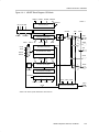
The DMA controller module transfers data from one address to another
without CPU intervention. This chapter describes the operation of the DMA
controller. The DMA controller is implemented in MSP430x15x and
MSP430x16x devices.
Topic
Page
8.1
DMA Introduction . . . . . . . . . . . . . . . . . . . . . . . . . . . . . . . . . . . . . . . . . . . . . 8-2
8.2
DMA Registers . . . . . . . . . . . . . . . . . . . . . . . . . . . . . . . . . . . . . . . . . . . . . . . . 8-4
8-1
8.1 DMA Introduction
The direct memory access (DMA) controller transfers data from one address
to another, without CPU intervention, across the entire address range. For
example, the DMA controller can move data from the ADC12 conversion
memory to RAM.
Using the DMA controller can increase the throughput of peripheral modules.
It can also reduce system power consumption by allowing the CPU to remain
in a low-power mode without having to awaken to move data to or from a
peripheral.
The DMA controller features include:
- Three independent transfer channels
- Configurable DMA channel priorities
- Requires only two MCLK clock cycles
- Byte or word and mixed byte/word transfer capability
- Block sizes up to 65535 bytes or words
- Configurable transfer trigger selections
- Selectable edge or level-triggered transfer
- Four addressing modes
- Single, block, or burst-block transfer modes
The DMA controller block diagram is shown in Figure 8−1.
8-2
Figure 8−1. DMA Controller Block Diagram
DMA0TSELx
JTAG Active
4
DMAREQ
TACCR2_CCIFG
TBCCR2_CCIFG
USART0 data received
USART0 transmit ready
DAC12_0IFG
ADC12IFGx
TACCR0_CCIFG
TBCCR0_CCIFG
USART1 data received
USART1 transmit ready
Multiplier ready
No trigger
No trigger
DMA2IFG
DMAE0
0000
0001
0010
0011
0100
0101
0110
0111
1000
1001
1010
1011
NMI Interrupt Request
ENNMI
Halt
ROUNDROBIN
2
DMADSTINCRx
DMADSTBYTE
DMADTx
3
DMA Channel 0
DMA0SA
DT
DMA0DA
−−−
DMA0SZ
1110
1111
2
DMASRSBYTE
DMASRCINCRx
DMAEN
DMA1TSELx
4
0000
0001
0010
0011
0100
0101
0110
0111
1000
1001
1010
1011
DMA Priority And Control
DMAREQ
TACCR2_CCIFG
TBCCR2_CCIFG
USART0 data received
USART0 transmit ready
DAC12_0IFG
ADC12IFGx
TACCR0_CCIFG
TBCCR0_CCIFG
USART1 data received
USART1 transmit ready
Multiplier ready
No trigger
No trigger
DMA0IFG
DMAE0
2
DMA Channel 1
DMA1SA
2
1110
1111
0000
0001
0010
0011
0100
0101
0110
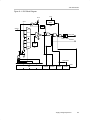
0111
1000
1001
1010
1011
−−−
1110
1111
Address
Space
DMA1SZ
DMA2TSELx
DMAREQ
TACCR2_CCIFG
TBCCR2_CCIFG
USART0 data received
USART0 transmit ready
DAC12_0IFG
ADC12IFGx
TACCR0_CCIFG
TBCCR0_CCIFG
USART1 data received
USART1 transmit ready
Multiplier ready
No trigger
No trigger
DMA1IFG
DMAE0
DT
DMA1DA
−−−
4
DMADSTINCRx DMADTx
DMADSTBYTE
3
2
DMASRSBYTE
DMASRCINCRx
DMAEN
DMADSTINCRx DMADTx
DMADSTBYTE
3
DMA Channel 2
DMA2SA
DT
DMA2DA
DMA2SZ
2
DMASRSBYTE
DMASRCINCRx
DMAEN
DMAONFETCH
Halt CPU
8-3
8.2 DMA Registers
The DMA registers are listed in Table 8−1:
Table 8−1. DMA Registers
Register
Short Form
Register Type Address
Initial State
DMA control 0
DMACTL0
Read/write
0122h
Reset with POR
DMA control 1
DMACTL1
Read/write
0124h
Reset with POR
DMA channel 0 control
DMA0CTL
Read/write
01E0h
Reset with POR
DMA channel 0 source address
DMA0SA
Read/write
01E2h
Unchanged
DMA channel 0 destination address
DMA0DA
Read/write
01E4h
Unchanged
DMA channel 0 transfer size
DMA0SZ
Read/write
01E6h
Unchanged
DMA channel 1 control
DMA1CTL
Read/write
01E8h
Reset with POR
DMA channel 1 source address
DMA1SA
Read/write
01EAh
Unchanged
DMA channel 1 destination address
DMA1DA
Read/write
01ECh
Unchanged
DMA channel 1 transfer size
DMA1SZ
Read/write
01EEh
Unchanged
DMA channel 2 control
DMA2CTL
Read/write
01F0h
Reset with POR
DMA channel 2 source address
DMA2SA
Read/write
01F2h
Unchanged
DMA channel 2 destination address
DMA2DA
Read/write
01F4h
Unchanged
DMA channel 2 transfer size
DMA2SZ
Read/write
01F6h
Unchanged
8-4
DMACTL0, DMA Control Register 0
15
14
13
12
11
10
9
8
DMA2TSELx
Reserved
rw−(0)
rw−(0)
rw−(0)
rw−(0)
rw−(0)
rw−(0)
rw−(0)
rw−(0)
7
6
5
4
3
2
1
0
rw−(0)
rw−(0)
DMA1TSELx
rw−(0)
rw−(0)
rw−(0)
DMA0TSELx
rw−(0)
rw−(0)
rw−(0)
Reserved
Bits
15−12
Reserved
DMA2
TSELx
Bits
11−8
DMA trigger select. These bits select the DMA transfer trigger.
0000 DMAREQ bit (software trigger)
0001 TACCR2 CCIFG bit
0010 TBCCR2 CCIFG bit
0011 URXIFG0 (UART/SPI mode), USART0 data received (I2C mode)
0100 UTXIFG0 (UART/SPI mode), USART0 transmit ready (I2C mode)
0101 DAC12_0CTL DAC12IFG bit
0110 ADC12 ADC12IFGx bit
0111 TACCR0 CCIFG bit
1000 TBCCR0 CCIFG bit
1001 URXIFG1 bit
1010 UTXIFG1 bit
1011 Multiplier ready
1100 No action
1101 No action
1110 DMA0IFG bit triggers DMA channel 1
DMA1IFG bit triggers DMA channel 2
DMA2IFG bit triggers DMA channel 0
1111 External trigger DMAE0
DMA1
TSELx
Bits
7−4
Same as DMA2TSELx
DMA0
TSELx
Bits
3–0
Same as DMA2TSELx
8-5
DMACTL1, DMA Control Register 1
15
14
13
12
11
10
9
8
0
0
0
0
0
0
0
0
r0
r0
r0
r0
r0
r0
r0
r0
7
6
5
4
3
2
1
0
0
0
0
0
0
DMA
ONFETCH
ROUND
ROBIN
ENNMI
r0
r0
r0
r0
r0
rw−(0)
rw−(0)
rw−(0)
Reserved
Bits
15−3
Reserved. Read only. Always read as 0.
DMA
ONFETCH
Bit 2
DMA on fetch
0
The DMA transfer occurs immediately
1
The DMA transfer occurs on next instruction fetch after the trigger
ROUND
ROBIN
Bit 1
Round robin. This bit enables the round-robin DMA channel priorities.
0
DMA channel priority is DMA0 − DMA1 − DMA2
1
DMA channel priority changes with each transfer
ENNMI
Bit 0
Enable NMI. This bit enables the interruption of a DMA transfer by an NMI
interrupt. When an NMI interrupts a DMA transfer, the current transfer is
completed normally, further transfers are stopped, and DMAABORT is set.
0
NMI interrupt does not interrupt DMA transfer
1
NMI interrupt interrupts a DMA transfer
8-6
DMAxCTL, DMA Channel x Control Register
15
14
13
12
DMADTx
Reserved
11
10
DMADSTINCRx
9
8
DMASRCINCRx
rw−(0)
rw−(0)
rw−(0)
rw−(0)
rw−(0)
rw−(0)
rw−(0)
rw−(0)
7
6
5
4
3
2
1
0
DMA
DSTBYTE
DMA
SRCBYTE
DMALEVEL
DMAEN
DMAIFG
DMAIE
DMA
ABORT
DMAREQ
rw−(0)
rw−(0)
rw−(0)
rw−(0)
rw−(0)
rw−(0)
rw−(0)
rw−(0)
Reserved
Bit 15
Reserved
DMADTx
Bits
14−12
DMA Transfer mode.
000 Single transfer
001 Block transfer
010 Burst-block transfer
011 Burst-block transfer
100 Repeated single transfer
101 Repeated block transfer
110 Repeated burst-block transfer
111 Repeated burst-block transfer
DMA
DSTINCRx
Bits
11−10
DMA destination increment. This bit selects automatic incrementing or
decrementing of the destination address after each byte or word transfer.
When DMADSTBYTE=1, the destination address increments/decrements by
one.
When
DMADSTBYTE=0,
the
destination
address
increments/decrements by two. The DMAxDA is copied into a temporary
register and the temporary register is incremented or decremented. DMAxDA
is not incremented or decremented.
00 Destination address is unchanged
01 Destination address is unchanged
10 Destination address is decremented
11 Destination address is incremented
DMA
SRCINCRx
Bits
9−8
DMA source increment. This bit selects automatic incrementing or
decrementing of the source address for each byte or word transfer. When
DMASRCBYTE=1, the source address increments/decrements by one.
When DMASRCBYTE=0, the source address increments/decrements by
two. The DMAxSA is copied into a temporary register and the temporary
register is incremented or decremented. DMAxSA is not incremented or
decremented.
00 Source address is unchanged
01 Source address is unchanged
10 Source address is decremented
11 Source address is incremented
DMA
DSTBYTE
Bit 7
DMA destination byte. This bit selects the destination as a byte or word.
0
Word
1
Byte
8-7
DMA
SRCBYTE
Bit 6
DMA source byte. This bit selects the source as a byte or word.
0
Word
1
Byte
DMA
LEVEL
Bit 5
DMA level. This bit selects between edge-sensitive and level-sensitive
triggers.
0
Edge sensitive (rising edge)
1
Level sensitive (high level)
DMAEN
Bit 4
DMA enable
0
Disabled
1
Enabled
DMAIFG
Bit 3
DMA interrupt flag
0
No interrupt pending
1
Interrupt pending
DMAIE
Bit 2
DMA interrupt enable
0
Disabled
1
Enabled
DMA
ABORT
Bit 1
DMA Abort. This bit indicates if a DMA transfer was interrupt by an NMI.
0
DMA transfer not interrupted
1
DMA transfer was interrupted by NMI
DMAREQ
Bit 0
DMA request. Software-controlled
automatically.
0
No DMA start
1
Start DMA
DMA
start.
DMAREQ
is
reset
DMAxSA, DMA Source Address Register
15
14
13
12
11
10
9
8
DMAxSAx
rw
rw
rw
rw
rw
rw
rw
rw
7
6
5
4
3
2
1
0
rw
rw
rw
rw
DMAxSAx
rw
DMAxSAx
8-8
rw
Bits
15−0
rw
rw
DMA source address. The source address register points to the DMA source
address for single transfers or the first source address for block transfers. The
source address register remains unchanged during block and burst-block
transfers.
DMAxDA, DMA Destination Address Register
15
14
13
12
11
10
9
8
DMAxDAx
rw
rw
rw
rw
rw
rw
rw
rw
7
6
5
4
3
2
1
0
rw
rw
rw
rw
DMAxDAx
rw
DMAxDAx
rw
Bits
15−0
rw
rw
DMA destination address. The destination address register points to the
destination address for single transfers or the first address for block transfers.
The DMAxDA register remains unchanged during block and burst-block
transfers.
DMAxSZ, DMA Size Address Register
15
14
13
12
11
10
9
8
DMAxSZx
rw
rw
rw
rw
rw
rw
rw
rw
7
6
5
4
3
2
1
0
rw
rw
rw
rw
DMAxSZx
rw
DMAxSZx
rw
Bits
15−0
rw
rw
DMA size. The DMA size register defines the number of byte/word data per
block transfer. DMAxSZ register decrements with each word or byte transfer.
When DMAxSZ decrements to 0, it is immediately and automatically reloaded
with its previously initialized value.
00000h Transfer is disabled
00001h One byte or word is transferred
00002h Two bytes or words are transferred
:
0FFFFh 65535 bytes or words are transferred
8-9
Chapter 9
Digital I/O
This chapter describes the operation of the digital I/O ports. Ports P1-P2 are
implemented in MSP430x11xx devices. Ports P1-P3 are implemented in
MSP430x12xx devices. Ports P1-P6 are implemented in MSP430x13x,
MSP430x14x, MSP430x15x, and MSP430x16x devices.
Topic
Page
9.1
Digital I/O Introduction . . . . . . . . . . . . . . . . . . . . . . . . . . . . . . . . . . . . . . . . 9-2
9.2
Digital I/O Registers . . . . . . . . . . . . . . . . . . . . . . . . . . . . . . . . . . . . . . . . . . . 9-3
Digital I/O
9-1
Digital I/O Introduction
9.1 Digital I/O Introduction
MSP430 devices have up to 6 digital I/O ports implemented, P1 - P6. Each port
has eight I/O pins. Every I/O pin is individually configurable for input or output
direction, and each I/O line can be individually read or written to.
Ports P1 and P2 have interrupt capability. Each interrupt for the P1 and P2 I/O
lines can be individually enabled and configured to provide an interrupt on a
rising edge or falling edge of an input signal. All P1 I/O lines source a single
interrupt vector, and all P2 I/O lines source a different, single interrupt vector.
The digital I/O features include:
- Independently programmable individual I/Os
- Any combination of input or output
- Individually configurable P1 and P2 interrupts
- Independent input and output data registers
9-2
Digital I/O
Digital I/O Registers
9.2 Digital I/O Registers
Seven registers are used to configure P1 and P2. Four registers are used to
configure ports P3 - P6. The digital I/O registers are listed in Table 9−1.
Table 9−1. Digital I/O Registers
Port
Register
Short Form
Address
Register Type
P1
Input
P1IN
020h
Read only
Output
P1OUT
021h
Read/write
Unchanged
Direction
P1DIR
022h
Read/write
Reset with PUC
Interrupt Flag
P1IFG
023h
Read/write
Reset with PUC
Interrupt Edge Select
P1IES
024h
Read/write
Unchanged
Interrupt Enable
P1IE
025h
Read/write
Reset with PUC
Port Select
P1SEL
026h
Read/write
Reset with PUC
Input
P2IN
028h
Read only
Output
P2OUT
029h
Read/write
Unchanged
Direction
P2DIR
02Ah
Read/write
Reset with PUC
Interrupt Flag
P2IFG
02Bh
Read/write
Reset with PUC
Interrupt Edge Select
P2IES
02Ch
Read/write
Unchanged
Interrupt Enable
P2IE
02Dh
Read/write
Reset with PUC
Port Select
P2SEL
02Eh
Read/write
Reset with PUC
Input
P3IN
018h
Read only
Output
P3OUT
019h
Read/write
Unchanged
Direction
P3DIR
01Ah
Read/write
Reset with PUC
Port Select
P3SEL
01Bh
Read/write
Reset with PUC
Input
P4IN
01Ch
Read only
Output
P4OUT
01Dh
Read/write
Unchanged
Direction
P4DIR
01Eh
Read/write
Reset with PUC
Port Select
P4SEL
01Fh
Read/write
Reset with PUC
Input
P5IN
030h
Read only
Output
P5OUT
031h
Read/write
Unchanged
Direction
P5DIR
032h
Read/write
Reset with PUC
Port Select
P5SEL
033h
Read/write
Reset with PUC
Input
P6IN
034h
Read only
Output
P6OUT
035h
Read/write
Unchanged
Direction
P6DIR
036h
Read/write
Reset with PUC
Port Select
P6SEL
037h
Read/write
Reset with PUC
P2
P3
P4
P5
P6
Initial State
−
−
−
−
−
−
Digital I/O
9-3
Chapter 10
The watchdog timer is a 16-bit timer that can be used as a watchdog or as an
interval timer. This chapter describes the watchdog timer. The watchdog timer
is implemented in all MSP430x1xx devices.
Topic
Page
10.1 Watchdog Timer Introduction . . . . . . . . . . . . . . . . . . . . . . . . . . . . . . . . 10-2
10.2 Watchdog Timer Registers . . . . . . . . . . . . . . . . . . . . . . . . . . . . . . . . . . 10-4
Watchdog Timer
10-1
Watchdog Timer Introduction
10.1 Watchdog Timer Introduction
The primary function of the watchdog timer (WDT) module is to perform a
controlled system restart after a software problem occurs. If the selected time
interval expires, a system reset is generated. If the watchdog function is not
needed in an application, the module can be configured as an interval timer
and can generate interrupts at selected time intervals.
Features of the watchdog timer module include:
- Four software-selectable time intervals
- Watchdog mode
- Interval mode
- Access to WDT control register is password protected
- Control of RST/NMI pin function
- Selectable clock source
- Can be stopped to conserve power
The WDT block diagram is shown in Figure 10−1.
Note: Watchdog Timer Powers Up Active
After a PUC, the WDT module is automatically configured in the watchdog
mode with an initial ~32-ms reset interval using the DCOCLK. The user must
setup or halt the WDT prior to the expiration of the initial reset interval.
10-2
Watchdog Timer
Watchdog Timer Introduction
Figure 10−1. Watchdog Timer Block Diagram
WDTCTL
4
Int.
Flag
MSB
Q6
0
Q9
WDTQn
Y
3
2
1
Q13
0
Q15
1
Pulse
Generator
MDB
1
16−bit
Counter
1
A
B
Password
Compare
0
16−bit
1
Clear
PUC
CLK
(Asyn)
0
EQU
Write Enable
Low Byte
EQU
SMCLK
1
WDTHOLD
ACLK
1
WDTNMIES
R/W
WDTNMI
A
EN
WDTTMSEL
WDTCNTCL
WDTSSEL
WDTIS1
WDTIS0
LSB
Watchdog Timer
10-3
Watchdog Timer Registers
10.2 Watchdog Timer Registers
The watchdog timer module registers are listed in Table 10−1.
Table 10−1.Watchdog Timer Registers
†
Register
Short Form
Register Type Address
Initial State
Watchdog timer control register
WDTCTL
Read/write
0120h
06900h with PUC
SFR interrupt enable register 1
IE1
Read/write
0000h
Reset with PUC
SFR interrupt flag register 1
IFG1
Read/write
0002h
Reset with PUC†
WDTIFG is reset with POR
10-4
Watchdog Timer
Watchdog Timer Registers
WDTCTL, Watchdog Timer Register
15
14
13
12
11
10
9
8
1
0
Read as 069h
WDTPW, must be written as 05Ah
7
6
5
4
3
2
WDTHOLD
WDTNMIES
WDTNMI
WDTTMSEL
WDTCNTCL
WDTSSEL
rw−0
rw−0
rw−0
rw−0
r0(w)
rw−0
WDTISx
rw−0
rw−0
WDTPW
Bits
15-8
Watchdog timer password. Always read as 069h. Must be written as 05Ah, or
a PUC will be generated.
WDTHOLD
Bit 7
Watchdog timer hold. This bit stops the watchdog timer. Setting WDTHOLD
= 1 when the WDT is not in use conserves power.
0
Watchdog timer is not stopped
1
Watchdog timer is stopped
WDTNMIES
Bit 6
Watchdog timer NMI edge select. This bit selects the interrupt edge for the
NMI interrupt when WDTNMI = 1. Modifying this bit can trigger an NMI. Modify
this bit when WDTNMI = 0 to avoid triggering an accidental NMI.
0
NMI on rising edge
1
NMI on falling edge
WDTNMI
Bit 5
Watchdog timer NMI select. This bit selects the function for the RST/NMI pin.
0
Reset function
1
NMI function
WDTTMSEL Bit 4
Watchdog timer mode select
0
Watchdog mode
1
Interval timer mode
WDTCNTCL Bit 3
Watchdog timer counter clear. Setting WDTCNTCL = 1 clears the count value
to 0000h. WDTCNTCL is automatically reset.
0
No action
1
WDTCNT = 0000h
WDTSSEL
Bit 2
Watchdog timer clock source select
0
SMCLK
1
ACLK
WDTISx
Bits
1-0
Watchdog timer interval select. These bits select the watchdog timer interval
to set the WDTIFG flag and/or generate a PUC.
00 Watchdog clock source /32768
01 Watchdog clock source /8192
10 Watchdog clock source /512
11 Watchdog clock source /64
Watchdog Timer
10-5
Watchdog Timer Registers
IE1, Interrupt Enable Register 1
7
NMIIE
WDTIE
10-6
6
5
4
3
2
1
0
NMIIE
WDTIE
rw−0
rw−0
Bits
7-5
These bits may be used by other modules. See device-specific datasheet.
Bit 4
NMI interrupt enable. This bit enables the NMI interrupt. Because other bits
in IE1 may be used for other modules, it is recommended to set or clear this
bit using BIS.B or BIC.B instructions, rather than MOV.B or CLR.B
instructions.
0
Interrupt not enabled
1
Interrupt enabled
Bits
3-1
These bits may be used by other modules. See device-specific datasheet.
Bit 0
Watchdog timer interrupt enable. This bit enables the WDTIFG interrupt for
interval timer mode. It is not necessary to set this bit for watchdog mode.
Because other bits in IE1 may be used for other modules, it is recommended
to set or clear this bit using BIS.B or BIC.B instructions, rather than MOV.B
or CLR.B instructions.
0
Interrupt not enabled
1
Interrupt enabled
Watchdog Timer
Watchdog Timer Registers
IFG1, Interrupt Flag Register 1
7
NMIIFG
WDTIFG
6
5
4
3
2
1
0
NMIIFG
WDTIFG
rw−(0)
rw−(0)
Bits
7-5
These bits may be used by other modules. See device-specific datasheet.
Bit 4
NMI interrupt flag. NMIIFG must be reset by software. Because other bits in
IFG1 may be used for other modules, it is recommended to clear NMIIFG by
using BIS.B or BIC.B instructions, rather than MOV.B or CLR.B instructions.
0
No interrupt pending
1
Interrupt pending
Bits
3-1
These bits may be used by other modules. See device-specific datasheet.
Bit 0
Watchdog timer interrupt flag. In watchdog mode, WDTIFG remains set until
reset by software. In interval mode, WDTIFG is reset automatically by
servicing the interrupt, or can be reset by software. Because other bits in IFG1
may be used for other modules, it is recommended to clear WDTIFG by using
BIS.B or BIC.B instructions, rather than MOV.B or CLR.B instructions.
0
No interrupt pending
1
Interrupt pending
Watchdog Timer
10-7
Chapter 11
Timer_A
Timer_A is a 16-bit timer/counter with three capture/compare registers. This
chapter describes Timer_A. Timer_A is implemented in all MSP430x1xx
devices.
Topic
Page
11.1 Timer_A Introduction . . . . . . . . . . . . . . . . . . . . . . . . . . . . . . . . . . . . . . . . . 11-2
11.2 Timer_A Registers . . . . . . . . . . . . . . . . . . . . . . . . . . . . . . . . . . . . . . . . . . . 11-4
Timer_A
11-1
Timer_A Introduction
11.1 Timer_A Introduction
Timer_A is a 16-bit timer/counter with three capture/compare registers.
Timer_A can support multiple capture/compares, PWM outputs, and interval
timing. Timer_A also has extensive interrupt capabilities. Interrupts may be
generated from the counter on overflow conditions and from each of the
capture/compare registers.
Timer_A features include:
- Asynchronous 16-bit timer/counter with four operating modes
- Selectable and configurable clock source
- Three configurable capture/compare registers
- Configurable outputs with PWM capability
- Asynchronous input and output latching
- Interrupt vector register for fast decoding of all Timer_A interrupts
The block diagram of Timer_A is shown in Figure 11−1.
Note: Use of the Word Count
Count is used throughout this chapter. It means the counter must be in the
process of counting for the action to take place. If a particular value is directly
written to the counter, then an associated action will not take place.
11-2
Timer_A
Timer_A Introduction
Figure 11−1. Timer_A Block Diagram
TASSELx
IDx
Timer Block
Timer Clock
MCx
15
TACLK
00
ACLK
01
SMCLK
10
INCLK
11
0
16−bit Timer
TAR
Divider
1/2/4/8
Clear
Count
Mode
RC
EQU0
Set TAIFG
TACLR
CCR0
CCR1
CCR2
CCISx
CMx
CCI2A
00
CCI2B
01
Capture
Mode
GND
10
VCC
11
logic
COV
SCS
Timer Clock
15
0
0
Sync
TACCR2
1
Compararator 2
CCI
EQU2
SCCI
Y
A
EN
CAP
0
1
Set TACCR2
CCIFG
OUT
EQU0
Output
Unit2
D Set Q
Timer Clock
OUT2 Signal
Reset
POR
OUTMODx
Timer_A
11-3
Timer_A Registers
11.2 Timer_A Registers
The Timer_A registers are listed in Table 11−1:
Table 11−1. Timer_A Registers
Register
Short Form
Register Type Address
Initial State
Timer_A control
TACTL
Read/write
0160h
Reset with POR
Timer_A counter
TAR
Read/write
0170h
Reset with POR
Timer_A capture/compare control 0
TACCTL0
Read/write
0162h
Reset with POR
Timer_A capture/compare 0
TACCR0
Read/write
0172h
Reset with POR
Timer_A capture/compare control 1
TACCTL1
Read/write
0164h
Reset with POR
Timer_A capture/compare 1
TACCR1
Read/write
0174h
Reset with POR
Timer_A capture/compare control 2
TACCTL 2
Read/write
0166h
Reset with POR
Timer_A capture/compare 2
TACCR2
Read/write
0176h
Reset with POR
Timer_A interrupt vector
TAIV
Read only
012Eh
Reset with POR
11-4
Timer_A
Timer_A Registers
TACTL, Timer_A Control Register
15
14
13
12
11
10
9
8
TASSELx
Unused
rw−(0)
rw−(0)
rw−(0)
rw−(0)
rw−(0)
rw−(0)
rw−(0)
rw−(0)
7
6
5
4
3
2
1
0
Unused
TACLR
TAIE
TAIFG
rw−(0)
w−(0)
rw−(0)
rw−(0)
IDx
rw−(0)
MCx
rw−(0)
rw−(0)
rw−(0)
Unused
Bits
15-10
Unused
TASSELx
Bits
9-8
Timer_A clock source select
00 TACLK
01 ACLK
10 SMCLK
11 INCLK
IDx
Bits
7-6
Input divider. These bits select the divider for the input clock.
00 /1
01 /2
10 /4
11 /8
MCx
Bits
5-4
Mode control. Setting MCx = 00h when Timer_A is not in use conserves
power.
00 Stop mode: the timer is halted
01 Up mode: the timer counts up to TACCR0
10 Continuous mode: the timer counts up to 0FFFFh
11 Up/down mode: the timer counts up to TACCR0 then down to 0000h
Unused
Bit 3
Unused
TACLR
Bit 2
Timer_A clear. Setting this bit resets TAR, the TACLK divider, and the count
direction. The TACLR bit is automatically reset and is always read as zero.
TAIE
Bit 1
Timer_A interrupt enable. This bit enables the TAIFG interrupt request.
0
Interrupt disabled
1
Interrupt enabled
TAIFG
Bit 0
Timer_A interrupt flag
0
No interrupt pending
1
Interrupt pending
Timer_A
11-5
Timer_A Registers
TAR, Timer_A Register
15
14
13
12
11
10
9
8
TARx
rw−(0)
rw−(0)
rw−(0)
rw−(0)
rw−(0)
rw−(0)
rw−(0)
rw−(0)
7
6
5
4
3
2
1
0
rw−(0)
rw−(0)
rw−(0)
rw−(0)
TARx
rw−(0)
TARx
11-6
rw−(0)
Bits
15-0
Timer_A
rw−(0)
rw−(0)
Timer_A register. The TAR register is the count of Timer_A.
Timer_A Registers
TACCTLx, Capture/Compare Control Register
15
14
13
12
CCISx
CMx
11
10
9
8
SCS
SCCI
Unused
CAP
rw−(0)
rw−(0)
rw−(0)
rw−(0)
rw−(0)
r−(0)
r−(0)
rw−(0)
7
6
5
4
3
2
1
0
CCIE
CCI
OUT
COV
CCIFG
rw−(0)
r
rw−(0)
rw−(0)
rw−(0)
OUTMODx
rw−(0)
rw−(0)
rw−(0)
CMx
Bit
15-14
Capture mode
00 No capture
01 Capture on rising edge
10 Capture on falling edge
11 Capture on both rising and falling edges
CCISx
Bit
13-12
Capture/compare input select. These bits select the TACCRx input signal.
See the device-specific datasheet for specific signal connections.
00 CCIxA
01 CCIxB
10 GND
11 VCC
SCS
Bit 11
Synchronize capture source. This bit is used to synchronize the capture input
signal with the timer clock.
0
Asynchronous capture
1
Synchronous capture
SCCI
Bit 10
Synchronized capture/compare input. The selected CCI input signal is
latched with the EQUx signal and can be read via this bit
Unused
Bit 9
Unused. Read only. Always read as 0.
CAP
Bit 8
Capture mode
0
Compare mode
1
Capture mode
OUTMODx
Bits
7-5
Output mode. Modes 2, 3, 6, and 7 are not useful for TACCR0 because EQUx
= EQU0.
000 OUT bit value
001 Set
010 Toggle/reset
011 Set/reset
100 Toggle
101 Reset
110 Toggle/set
111 Reset/set
Timer_A
11-7
Timer_A Registers
CCIE
Bit 4
Capture/compare interrupt enable. This bit enables the interrupt request of
the corresponding CCIFG flag.
0
Interrupt disabled
1
Interrupt enabled
CCI
Bit 3
Capture/compare input. The selected input signal can be read by this bit.
OUT
Bit 2
Output. For output mode 0, this bit directly controls the state of the output.
0
Output low
1
Output high
COV
Bit 1
Capture overflow. This bit indicates a capture overflow occurred. COV must
be reset with software.
0
No capture overflow occurred
1
Capture overflow occurred
CCIFG
Bit 0
Capture/compare interrupt flag
0
No interrupt pending
1
Interrupt pending
TAIV, Timer_A Interrupt Vector Register
15
14
13
12
11
10
9
8
0
0
0
0
0
0
0
0
r0
r0
r0
r0
r0
r0
r0
r0
7
6
5
4
3
2
1
0
0
0
0
0
r0
r0
r0
r0
TAIVx
Bits
15-0
Timer_A
r−(0)
0
r−(0)
r−(0)
r0
Timer_A Interrupt Vector value
TAIV Contents
11-8
TAIVx
Interrupt Source
Interrupt Flag
00h
No interrupt pending
02h
Capture/compare 1
TACCR1 CCIFG
04h
Capture/compare 2
TACCR2 CCIFG
06h
Reserved
−
08h
Reserved
−
0Ah
Timer overflow
0Ch
Reserved
−
0Eh
Reserved
−
Interrupt
Priority
−
Highest
TAIFG
Lowest
Chapter 12
Timer_B
Timer_B is a 16-bit timer/counter with multiple capture/compare registers. This
chapter describes Timer_B. Timer_B3 (three capture/compare registers) is
implemented in MSP430x13x and MSP430x15x devices. Timer_B7 (seven
capture/compare registers) is implemented in MSP430x14x and
MSP430x16x devices.
Topic
Page
12.1 Timer_B Introduction . . . . . . . . . . . . . . . . . . . . . . . . . . . . . . . . . . . . . . . . 12-2
12.2 Timer_B Registers . . . . . . . . . . . . . . . . . . . . . . . . . . . . . . . . . . . . . . . . . . 12-4
Timer_B
12-1
Timer_B Introduction
12.1 Timer_B Introduction
Timer_B is a 16-bit timer/counter with three or seven capture/compare
registers. Timer_B can support multiple capture/compares, PWM outputs, and
interval timing. Timer_B also has extensive interrupt capabilities. Interrupts
may be generated from the counter on overflow conditions and from each of
the capture/compare registers.
Timer_B features include :
- Asynchronous 16-bit timer/counter with four operating modes and four
selectable lengths
- Selectable and configurable clock source
- Three or seven configurable capture/compare registers
- Configurable outputs with PWM capability
- Double-buffered compare latches with synchronized loading
- Interrupt vector register for fast decoding of all Timer_B interrupts
The block diagram of Timer_B is shown in Figure 12−1.
Note: Use of the Word Count
Count is used throughout this chapter. It means the counter must be in the
process of counting for the action to take place. If a particular value is directly
written to the counter, then an associated action does not take place.
12.1.1 Similarities and Differences From Timer_A
Timer_B is identical to Timer_A with the following exceptions:
-
The length of Timer_B is programmable to be 8, 10, 12, or 16 bits.
- Timer_B TBCCRx registers are double-buffered and can be grouped.
- All Timer_B outputs can be put into a high-impedance state.
- The SCCI bit function is not implemented in Timer_B.
12-2
Timer_B
Timer_B Introduction
Figure 12−1. Timer_B Block Diagram
TBSSELx
IDx
Timer Block
Timer Clock
MCx
15
TBCLK
00
ACLK
01
SMCLK
10
Divider
1/2/4/8
0
16−bit Timer
RC
TBR
8 10 12 16
Clear
Count
Mode
EQU0
CNTLx
11
TBCLR
00
TBCLGRPx
01
Set TBIFG
10
Group
Load Logic
11
CCR0
CCR1
CCR2
CCR3
CCR4
CCR5
CCISx
CMx
CCI6A
00
CCI6B
01
Capture
Mode
GND
10
VCC
11
logic
CCR6
COV
SCS
15
Sync
Timer Clock
VCC
Load
Group
Load Logic
Compare Latch TBCL6
00
01
EQU0
UP/DOWN
TBCCR6
1
CLLDx
CCI
TBR=0
0
0
10
11
Compararator 6
CCR5
EQU6
CCR4
CAP
CCR1
0
1
Set TBCCR6
CCIFG
OUT
EQU0
Output
Unit6
D Set Q
Timer Clock
OUT6 Signal
Reset
POR
OUTMODx
Timer_B
12-3
Timer_B Registers
12.2 Timer_B Registers
The Timer_B registers are listed in Table 12−1:
Table 12−1.Timer_B Registers
Register
Short Form
Register Type Address
Initial State
Timer_B control
TBCTL
Read/write
0180h
Reset with POR
Timer_B counter
TBR
Read/write
0190h
Reset with POR
Timer_B capture/compare control 0
TBCCTL0
Read/write
0182h
Reset with POR
Timer_B capture/compare 0
TBCCR0
Read/write
0192h
Reset with POR
Timer_B capture/compare control 1
TBCCTL1
Read/write
0184h
Reset with POR
Timer_B capture/compare 1
TBCCR1
Read/write
0194h
Reset with POR
Timer_B capture/compare control 2
TBCCTL 2
Read/write
0186h
Reset with POR
Timer_B capture/compare 2
TBCCR2
Read/write
0196h
Reset with POR
Timer_B capture/compare control 3
TBCCTL3
Read/write
0188h
Reset with POR
Timer_B capture/compare 3
TBCCR3
Read/write
0198h
Reset with POR
Timer_B capture/compare control 4
TBCCTL4
Read/write
018Ah
Reset with POR
Timer_B capture/compare 4
TBCCR4
Read/write
019Ah
Reset with POR
Timer_B capture/compare control 5
TBCCTL5
Read/write
018Ch
Reset with POR
Timer_B capture/compare 5
TBCCR5
Read/write
019Ch
Reset with POR
Timer_B capture/compare control 6
TBCCTL6
Read/write
018Eh
Reset with POR
Timer_B capture/compare 6
TBCCR6
Read/write
019Eh
Reset with POR
Timer_B Interrupt Vector
TBIV
Read only
011Eh
Reset with POR
12-4
Timer_B
Timer_B Registers
Timer_B Control Register TBCTL
15
14
13
12
TBCLGRPx
Unused
11
CNTLx
10
9
Unused
8
TBSSELx
rw−(0)
rw−(0)
rw−(0)
rw−(0)
rw−(0)
rw−(0)
rw−(0)
rw−(0)
7
6
5
4
3
2
1
0
Unused
TBCLR
TBIE
TBIFG
rw−(0)
w−(0)
rw−(0)
rw−(0)
IDx
rw−(0)
MCx
rw−(0)
rw−(0)
rw−(0)
Unused
Bit 15
Unused
TBCLGRP
Bit
14-13
TBCLx group
00 Each TBCLx latch loads independently
01 TBCL1+TBCL2 (TBCCR1 CLLDx bits control the update)
TBCL3+TBCL4 (TBCCR3 CLLDx bits control the update)
TBCL5+TBCL6 (TBCCR5 CLLDx bits control the update)
TBCL0 independent
10 TBCL1+TBCL2+TBCL3 (TBCCR1 CLLDx bits control the update)
TBCL4+TBCL5+TBCL6 (TBCCR4 CLLDx bits control the update)
TBCL0 independent
11 TBCL0+TBCL1+TBCL2+TBCL3+TBCL4+TBCL5+TBCL6
(TBCCR1 CLLDx bits control the update)
CNTLx
Bits
12-11
Counter Length
00 16-bit, TBR(max) = 0FFFFh
01 12-bit, TBR(max) = 0FFFh
10 10-bit, TBR(max) = 03FFh
11 8-bit, TBR(max) = 0FFh
Unused
Bit 10
Unused
TBSSELx
Bits
9-8
Timer_B clock source select.
00 TBCLK
01 ACLK
10 SMCLK
11 Inverted TBCLK
IDx
Bits
7-6
Input divider. These bits select the divider for the input clock.
00 /1
01 /2
10 /4
11 /8
MCx
Bits
5-4
Mode control. Setting MCx = 00h when Timer_B is not in use conserves
power.
00 Stop mode: the timer is halted
01 Up mode: the timer counts up to TBCL0
10 Continuous mode: the timer counts up to the value set by TBCNTLx
11 Up/down mode: the timer counts up to TBCL0 and down to 0000h
Timer_B
12-5
Timer_B Registers
Unused
Bit 3
Unused
TBCLR
Bit 2
Timer_B clear. Setting this bit resets TBR, the TBCLK divider, and the count
direction. The TBCLR bit is automatically reset and is always read as zero.
TBIE
Bit 1
Timer_B interrupt enable. This bit enables the TBIFG interrupt request.
0
Interrupt disabled
1
Interrupt enabled
TBIFG
Bit 0
Timer_B interrupt flag.
0
No interrupt pending
1
Interrupt pending
TBR, Timer_B Register
15
14
13
12
11
10
9
8
TBRx
rw−(0)
rw−(0)
rw−(0)
rw−(0)
rw−(0)
rw−(0)
rw−(0)
rw−(0)
7
6
5
4
3
2
1
0
rw−(0)
rw−(0)
rw−(0)
rw−(0)
TBRx
rw−(0)
TBRx
12-6
rw−(0)
Bits
15-0
Timer_B
rw−(0)
rw−(0)
Timer_B register. The TBR register is the count of Timer_B.
Timer_B Registers
TBCCTLx, Capture/Compare Control Register
15
14
13
12
CCISx
CMx
11
10
SCS
9
CLLDx
8
CAP
rw−(0)
rw−(0)
rw−(0)
rw−(0)
rw−(0)
rw−(0)
r−(0)
rw−(0)
7
6
5
4
3
2
1
0
CCIE
CCI
OUT
COV
CCIFG
rw−(0)
r
rw−(0)
rw−(0)
rw−(0)
OUTMODx
rw−(0)
rw−(0)
rw−(0)
CMx
Bit
15-14
Capture mode
00 No capture
01 Capture on rising edge
10 Capture on falling edge
11 Capture on both rising and falling edges
CCISx
Bit
13-12
Capture/compare input select. These bits select the TBCCRx input signal.
See the device-specific datasheet for specific signal connections.
00 CCIxA
01 CCIxB
10 GND
11 VCC
SCS
Bit 11
Synchronize capture source. This bit is used to synchronize the capture input
signal with the timer clock.
0
Asynchronous capture
1
Synchronous capture
CLLDx
Bit
10-9
Compare latch load. These bits select the compare latch load event.
00 TBCLx loads on write to TBCCRx
01 TBCLx loads when TBR counts to 0
10 TBCLx loads when TBR counts to 0 (up or continuous mode)
TBCLx loads when TBR counts to TBCL0 or to 0 (up/down mode)
11 TBCLx loads when TBR counts to TBCLx
CAP
Bit 8
Capture mode
0
Compare mode
1
Capture mode
OUTMODx
Bits
7-5
Output mode. Modes 2, 3, 6, and 7 are not useful for TBCL0 because EQUx
= EQU0.
000 OUT bit value
001 Set
010 Toggle/reset
011 Set/reset
100 Toggle
101 Reset
110 Toggle/set
111 Reset/set
Timer_B
12-7
Timer_B Registers
CCIE
Bit 4
Capture/compare interrupt enable. This bit enables the interrupt request of
the corresponding CCIFG flag.
0
Interrupt disabled
1
Interrupt enabled
CCI
Bit 3
Capture/compare input. The selected input signal can be read by this bit.
OUT
Bit 2
Output. For output mode 0, this bit directly controls the state of the output.
0
Output low
1
Output high
COV
Bit 1
Capture overflow. This bit indicates a capture overflow occurred. COV must
be reset with software.
0
No capture overflow occurred
1
Capture overflow occurred
CCIFG
Bit 0
Capture/compare interrupt flag
0
No interrupt pending
1
Interrupt pending
12-8
Timer_B
Timer_B Registers
TBIV, Timer_B Interrupt Vector Register
15
14
13
12
11
10
9
8
0
0
0
0
0
0
0
0
r0
r0
r0
r0
r0
r0
r0
r0
7
6
5
4
3
2
1
0
0
0
0
0
r0
r0
r0
r0
TBIVx
Bits
15-0
TBIVx
r−(0)
0
r−(0)
r−(0)
r0
Timer_B interrupt vector value
TBIV Contents
†
Interrupt Source
Interrupt
Priority
Interrupt Flag
00h
No interrupt pending
−
02h
Capture/compare 1
TBCCR1 CCIFG
04h
Capture/compare 2
TBCCR2 CCIFG
06h
Capture/compare 3†
TBCCR3 CCIFG
08h
Capture/compare 4†
TBCCR4 CCIFG
0Ah
Capture/compare
5†
TBCCR5 CCIFG
0Ch
Capture/compare
6†
TBCCR6 CCIFG
0Eh
Timer overflow
TBIFG
Highest
Lowest
MSP430x14x, MSP430x16x devices only
Timer_B
12-9
Chapter 13
The universal synchronous/asynchronous receive/transmit (USART)
peripheral interface supports two serial modes with one hardware module.
This chapter discusses the operation of the asynchronous UART mode.
USART0 is implemented on the MSP430x12xx, MSP430x13xx, and
MSP430x15x devices. In addition to USART0, the MSP430x14x and
MSP430x16x devices implement a second identical USART module,
USART1.
Topic
Page
13.1 USART Introduction: UART Mode . . . . . . . . . . . . . . . . . . . . . . . . . . . . 13-2
13.2 USART Registers: UART Mode . . . . . . . . . . . . . . . . . . . . . . . . . . . . . . . 13-4
USART Peripheral Interface, UART Mode
13-1
USART Introduction: UART Mode
13.1 USART Introduction: UART Mode
In asynchronous mode, the USART connects the MSP430 to an external
system via two external pins, URXD and UTXD. UART mode is selected when
the SYNC bit is cleared.
UART mode features include:
- 7- or 8-bit data with odd, even, or non-parity
- Independent transmit and receive shift registers
- Separate transmit and receive buffer registers
- LSB-first data transmit and receive
- Built-in
idle-line and
multiprocessor systems
address-bit
communication
protocols
for
- Receiver start-edge detection for auto-wake up from LPMx modes
- Programmable baud rate with modulation for fractional baud rate support
- Status flags for error detection and suppression and address detection
- Independent interrupt capability for receive and transmit
Figure 13−1 shows the USART when configured for UART mode.
13-2
USART Peripheral Interface, UART Mode
USART Introduction: UART Mode
Figure 13−1. USART Block Diagram: UART Mode
SWRST URXEx* URXEIE URXWIE
SYNC= 0
URXIFGx*
Receive Control
FE PE OE BRK
Receive Status
Receiver Buffer UxRXBUF
LISTEN
0
RXERR
RXWAKE
MM
1
Receiver Shift Register
1
SSEL1 SSEL0 SP
CHAR
PEV
0
PENA
UCLKS
UCLKI
00
ACLK
01
SMCLK
10
SMCLK
11
SYNC
1
SOMI
0
1
URXD
0
Baud−Rate Generator
STE
Prescaler/Divider UxBRx
Modulator UxMCTL
SP
CHAR
PEV
UTXD
PENA
1
WUT
Transmit Shift Register
TXWAKE
Transmit Buffer UxTXBUF
1
SIMO
0
0
UTXIFGx*
Transmit Control
SYNC CKPH CKPL
SWRST UTXEx*
TXEPT
STC
UCLKI
UCLK
Clock Phase and Polarity
* Refer to the device-specific datasheet for SFR locations
USART Peripheral Interface, UART Mode
13-3
USART Registers: UART Mode
13.2 USART Registers: UART Mode
Table 13−1 lists the registers for all devices implementing a USART module.
Table 13−2 applies only to devices with a second USART module, USART1.
Table 13−1.USART0 Control and Status Registers
Register
†
Short Form
Register Type Address
Initial State
USART control register
U0CTL
Read/write
070h
001h with PUC
Transmit control register
U0TCTL
Read/write
071h
001h with PUC
Receive control register
U0RCTL
Read/write
072h
000h with PUC
Modulation control register
U0MCTL
Read/write
073h
Unchanged
Baud rate control register 0
U0BR0
Read/write
074h
Unchanged
Baud rate control register 1
U0BR1
Read/write
075h
Unchanged
Receive buffer register
U0RXBUF
Read
076h
Unchanged
Transmit buffer register
U0TXBUF
Read/write
077h
Unchanged
SFR module enable register 1†
ME1
Read/write
004h
000h with PUC
SFR interrupt enable register 1†
IE1
Read/write
000h
000h with PUC
SFR interrupt flag register 1†
IFG1
Read/write
002h
082h with PUC
Does not apply to ’12xx devices. Refer to the register definitions for registers and bit positions for these devices.
Table 13−2.USART1 Control and Status Registers
Register
Short Form
Register Type Address
Initial State
USART control register
U1CTL
Read/write
078h
001h with PUC
Transmit control register
U1TCTL
Read/write
079h
001h with PUC
Receive control register
U1RCTL
Read/write
07Ah
000h with PUC
Modulation control register
U1MCTL
Read/write
07Bh
Unchanged
Baud rate control register 0
U1BR0
Read/write
07Ch
Unchanged
Baud rate control register 1
U1BR1
Read/write
07Dh
Unchanged
Receive buffer register
U1RXBUF
Read
07Eh
Unchanged
Transmit buffer register
U1TXBUF
Read/write
07Fh
Unchanged
SFR module enable register 2
ME2
Read/write
005h
000h with PUC
SFR interrupt enable register 2
IE2
Read/write
001h
000h with PUC
SFR interrupt flag register 2
IFG2
Read/write
003h
020h with PUC
Note: Modifying SFR bits
To avoid modifying control bits of other modules, it is recommended to set
or clear the IEx and IFGx bits using BIS.B or BIC.B instructions, rather than
MOV.B or CLR.B instructions.
13-4
USART Peripheral Interface, UART Mode
USART Registers: UART Mode
UxCTL, USART Control Register
7
6
5
4
3
2
1
0
PENA
PEV
SPB
CHAR
LISTEN
SYNC
MM
SWRST
rw−0
rw−0
rw−0
rw−0
rw−0
rw−0
rw−0
rw−1
PENA
Bit 7
Parity enable
0
Parity disabled.
1
Parity enabled. Parity bit is generated (UTXDx) and expected
(URXDx). In address-bit multiprocessor mode, the address bit is
included in the parity calculation.
PEV
Bit 6
Parity select. PEV is not used when parity is disabled.
0
Odd parity
1
Even parity
SPB
Bit 5
Stop bit select. Number of stop bits transmitted. The receiver always
checks for one stop bit.
0
One stop bit
1
Two stop bits
CHAR
Bit 4
Character length. Selects 7-bit or 8-bit character length.
0
7-bit data
1
8-bit data
LISTEN
Bit 3
Listen enable. The LISTEN bit selects loopback mode.
0
Disabled
1
Enabled. UTXDx is internally fed back to the receiver.
SYNC
Bit 2
Synchronous mode enable
0
UART mode
1
SPI Mode
MM
Bit 1
Multiprocessor mode select
0
Idle-line multiprocessor protocol
1
Address-bit multiprocessor protocol
SWRST
Bit 0
Software reset enable
0
Disabled. USART reset released for operation
1
Enabled. USART logic held in reset state
USART Peripheral Interface, UART Mode
13-5
USART Registers: UART Mode
UxTCTL, USART Transmit Control Register
7
6
Unused
CKPL
rw−0
rw−0
5
4
SSELx
rw−0
3
2
1
0
URXSE
TXWAKE
Unused
TXEPT
rw−0
rw−0
rw−0
rw−1
rw−0
Unused
Bit 7
Unused
CKPL
Bit 6
Clock polarity select
0
UCLKI = UCLK
1
UCLKI = inverted UCLK
SSELx
Bits
5-4
Source select. These bits select the BRCLK source clock.
00 UCLKI
01 ACLK
10 SMCLK
11 SMCLK
URXSE
Bit 3
UART receive start-edge. The bit enables the UART receive start-edge
feature.
0
Disabled
1
Enabled
TXWAKE
Bit 2
Transmitter wake
0
Next character transmitted is data
1
Next character transmitted is an address
Unused
Bit 1
Unused
TXEPT
Bit 0
Transmitter empty flag
0
UART is transmitting data and/or data is waiting in UxTXBUF
1
Transmitter shift register and UxTXBUF are empty or SWRST=1
13-6
USART Peripheral Interface, UART Mode
USART Registers: UART Mode
UxRCTL, USART Receive Control Register
7
6
5
4
3
2
1
0
FE
PE
OE
BRK
URXEIE
URXWIE
RXWAKE
RXERR
rw−0
rw−0
rw−0
rw−0
rw−0
rw−0
rw−0
rw−0
FE
Bit 7
Framing error flag
0
No error
1
Character received with low stop bit
PE
Bit 6
Parity error flag. When PENA = 0, PE is read as 0.
0
No error
1
Character received with parity error
OE
Bit 5
Overrun error flag. This bit is set when a character is transferred into
UxRXBUF before the previous character was read.
0
No error
1
Overrun error occurred
BRK
Bit 4
Break detect flag
0
No break condition
1
Break condition occurred
URXEIE
Bit 3
Receive erroneous-character interrupt-enable
0
Erroneous characters rejected and URXIFGx is not set
1
Erroneous characters received will set URXIFGx
URXWIE
Bit 2
Receive wake-up interrupt-enable. This bit enables URXIFGx to be set
when an address character is received. When URXEIE = 0, an address
character will not set URXIFGx if it is received with errors.
0
All received characters set URXIFGx
1
Only received address characters set URXIFGx
RXWAKE
Bit 1
Receive wake-up flag
0
Received character is data
1
Received character is an address
RXERR
Bit 0
Receive error flag. This bit indicates a character was received with error(s).
When RXERR = 1, on or more error flags (FE,PE,OE, BRK) is also set.
RXERR is cleared when UxRXBUF is read.
0
No receive errors detected
1
Receive error detected
USART Peripheral Interface, UART Mode
13-7
USART Registers: UART Mode
UxBR0, USART Baud Rate Control Register 0
7
6
5
4
3
2
1
0
27
26
25
24
23
22
21
20
rw
rw
rw
rw
rw
rw
rw
rw
UxBR1, USART Baud Rate Control Register 1
7
6
5
4
3
2
1
0
215
214
213
212
211
210
29
28
rw
rw
rw
rw
rw
rw
rw
rw
The valid baud-rate control range is 3 ≤ UxBR < 0FFFFh, where UxBR =
{UxBR1+UxBR0}. Unpredictable receive and transmit timing occurs if
UxBR <3.
UxBRx
UxMCTL, USART Modulation Control Register
7
6
5
4
3
2
1
0
m7
m6
m5
m4
m3
m2
m1
m0
rw
rw
rw
rw
rw
rw
rw
rw
UxMCTLx
13-8
Bits
7−0
Modulation bits. These bits select the modulation for BRCLK.
USART Peripheral Interface, UART Mode
USART Registers: UART Mode
UxRXBUF, USART Receive Buffer Register
7
6
5
4
3
2
1
0
27
26
25
24
23
22
21
20
r
r
r
r
r
r
r
r
UxRXBUFx
Bits
7−0
The receive-data buffer is user accessible and contains the last received
character from the receive shift register. Reading UxRXBUF resets the
receive-error bits, the RXWAKE bit, and URXIFGx. In 7-bit data mode,
UxRXBUF is LSB justified and the MSB is always reset.
UxTXBUF, USART Transmit Buffer Register
7
6
5
4
3
2
1
0
27
26
25
24
23
22
21
20
rw
rw
rw
rw
rw
rw
rw
rw
UxTXBUFx
Bits
7−0
The transmit data buffer is user accessible and holds the data waiting to be
moved into the transmit shift register and transmitted on UTXDx. Writing to
the transmit data buffer clears UTXIFGx. The MSB of UxTXBUF is not
used for 7-bit data and is reset.
USART Peripheral Interface, UART Mode
13-9
USART Registers: UART Mode
ME1, Module Enable Register 1
†
7
6
UTXE0†
URXE0†
rw−0
rw−0
5
4
3
2
1
0
UTXE0†
Bit 7
USART0 transmit enable. This bit enables the transmitter for USART0.
0
Module not enabled
1
Module enabled
URXE0†
Bit 6
USART0 receive enable. This bit enables the receiver for USART0.
0
Module not enabled
1
Module enabled
Bits
5-0
These bits may be used by other modules. See device-specific datasheet.
Does not apply to MSP430x12xx devices. See ME2 for the MSP430x12xx USART0 module enable bits
ME2, Module Enable Register 2
7
‡
6
5
4
UTXE1
rw−0
3
2
1
0
URXE1
UTXE0‡
URXE0‡
rw−0
rw−0
rw−0
Bits
7-6
These bits may be used by other modules. See device-specific datasheet.
UTXE1
Bit 5
USART1 transmit enable. This bit enables the transmitter for USART1.
0
Module not enabled
1
Module enabled
URXE1
Bit 4
USART1 receive enable. This bit enables the receiver for USART1.
0
Module not enabled
1
Module enabled
Bits
3-2
These bits may be used by other modules. See device-specific datasheet.
UTXE0‡
Bit 1
USART0 transmit enable. This bit enables the transmitter for USART0.
0
Module not enabled
1
Module enabled
URXE0‡
Bit 0
USART0 receive enable. This bit enables the receiver for USART0.
0
Module not enabled
1
Module enabled
MSP430x12xx devices only
13-10
USART Peripheral Interface, UART Mode
USART Registers: UART Mode
IE1, Interrupt Enable Register 1
†
7
6
UTXIE0†
URXIE0†
rw−0
rw−0
5
4
3
2
1
0
UTXIE0†
Bit 7
USART0 transmit interrupt enable. This bit enables the UTXIFG0 interrupt.
0
Interrupt not enabled
1
Interrupt enabled
URXIE0†
Bit 6
USART0 receive interrupt enable. This bit enables the URXIFG0 interrupt.
0
Interrupt not enabled
1
Interrupt enabled
Bits
5-0
These bits may be used by other modules. See device-specific datasheet.
Does not apply to MSP430x12xx devices. See IE2 for the MSP430x12xx USART0 interrupt enable bits
IE2, Interrupt Enable Register 2
7
‡
6
5
4
UTXIE1
rw−0
3
2
1
0
URXIE1
UTXIE0‡
URXIE0‡
rw−0
rw−0
rw−0
Bits
7-6
These bits may be used by other modules. See device-specific datasheet.
UTXIE1
Bit 5
USART1 transmit interrupt enable. This bit enables the UTXIFG1 interrupt.
0
Interrupt not enabled
1
Interrupt enabled
URXIE1
Bit 4
USART1 receive interrupt enable. This bit enables the URXIFG1 interrupt.
0
Interrupt not enabled
1
Interrupt enabled
Bits
3-2
These bits may be used by other modules. See device-specific datasheet.
UTXIE0‡
Bit 1
USART0 transmit interrupt enable. This bit enables the UTXIFG0 interrupt.
0
Interrupt not enabled
1
Interrupt enabled
URXIE0‡
Bit 0
USART0 receive interrupt enable. This bit enables the URXIFG0 interrupt.
0
Interrupt not enabled
1
Interrupt enabled
MSP430x12xx devices only
USART Peripheral Interface, UART Mode
13-11
USART Registers: UART Mode
IFG1, Interrupt Flag Register 1
†
7
6
5
UTXIFG0†
URXIFG0†
rw−1
rw−0
4
3
2
1
0
UTXIFG0†
Bit 7
USART0 transmit interrupt flag. UTXIFG0 is set when U0TXBUF is empty.
0
No interrupt pending
1
Interrupt pending
URXIFG0†
Bit 6
USART0 receive interrupt flag. URXIFG0 is set when U0RXBUF has received
a complete character.
0
No interrupt pending
1
Interrupt pending
Bits
5-0
These bits may be used by other modules. See device-specific datasheet.
Does not apply to MSP430x12xx devices. See IFG2 for the MSP430x12xx USART0 interrupt flag bits
IFG2, Interrupt Flag Register 2
7
6
5
4
UTXIFG1
rw−1
3
2
1
0
URXIFG1
UTXIFG0‡
URXIFG0‡
rw−0
rw−1
rw−0
Bits
7-6
These bits may be used by other modules. See device-specific datasheet.
UTXIFG1
Bit 5
USART1 transmit interrupt flag. UTXIFG1 is set when U1TXBUF empty.
0
No interrupt pending
1
Interrupt pending
URXIFG1
Bit 4
USART1 receive interrupt flag. URXIFG1 is set when U1RXBUF has received
a complete character.
0
No interrupt pending
1
Interrupt pending
Bits
3-2
These bits may be used by other modules. See device-specific datasheet.
13-12
USART Peripheral Interface, UART Mode
USART Registers: UART Mode
‡
UTXIFG0‡
Bit 1
USART0 transmit interrupt flag. UTXIFG0 is set when U0TXBUF is empty.
0
No interrupt pending
1
Interrupt pending
URXIFG0‡
Bit 0
USART0 receive interrupt flag. URXIFG0 is set when U0RXBUF has received
a complete character.
0
No interrupt pending
1
Interrupt pending
MSP430x12xx devices only
USART Peripheral Interface, UART Mode
13-13
Chapter 14
USART Peripheral Interface, SPI Mode
The universal synchronous/asynchronous receive/transmit (USART)
peripheral interface supports two serial modes with one hardware module.
This chapter discusses the operation of the synchronous peripheral interface
or SPI mode. USART0 is implemented on the MSP430x12xx, MSP430x13xx,
and MSP430x15x devices. In addition to USART0, the MSP430x14x and
MSP430x16x devices implement a second identical USART module,
USART1.
Topic
Page
14.1 USART Introduction: SPI Mode . . . . . . . . . . . . . . . . . . . . . . . . . . . . . . . 14-2
14.2 USART Registers: SPI Mode . . . . . . . . . . . . . . . . . . . . . . . . . . . . . . . . . 14-4
USART Peripheral Interface, SPI Mode
14-1
USART Introduction: SPI Mode
14.1 USART Introduction: SPI Mode
In synchronous mode, the USART connects the MSP430 to an external
system via three or four pins: SIMO, SOMI, UCLK, and STE. SPI mode is
selected when the SYNC bit is set and the I2C bit is cleared.
SPI mode features include:
- 7- or 8-bit data length
- 3-pin and 4-pin SPI operation
- Master or slave modes
- Independent transmit and receive shift registers
- Separate transmit and receive buffer registers
- Selectable UCLK polarity and phase control
- Programmable UCLK frequency in master mode
- Independent interrupt capability for receive and transmit
Figure 14−1 shows the USART when configured for SPI mode.
14-2
USART Peripheral Interface, SPI Mode
USART Introduction: SPI Mode
Figure 14−1. USART Block Diagram: SPI Mode
SWRST USPIEx* URXEIE URXWIE
SYNC= 1
URXIFGx*
Receive Control
FE PE OE BRK
Receive Status
Receiver Buffer UxRXBUF
LISTEN
0
RXERR
RXWAKE
MM
1
Receiver Shift Register
1
SSEL1 SSEL0 SP
CHAR
PEV
0
PENA
UCLKS
UCLKI
00
ACLK
01
SMCLK
10
SMCLK
11
SYNC
1
SOMI
0
1
URXD
0
Baud−Rate Generator
STE
Prescaler/Divider UxBRx
Modulator UxMCTL
SP
CHAR
PEV
UTXD
PENA
1
WUT
Transmit Shift Register
TXWAKE
Transmit Buffer UxTXBUF
0
1
SIMO
0
UTXIFGx*
Transmit Control
SYNC CKPH CKPL
SWRST USPIEx* TXEPT
STC
UCLKI
UCLK
Clock Phase and Polarity
* Refer to the device-specific datasheet for SFR locations
USART Peripheral Interface, SPI Mode
14-3
USART Registers: SPI Mode
14.2 USART Registers: SPI Mode
The USART registers, shown in Table 14−1 and Table 14−2, are byte
structured and should be accessed using byte instructions.
Table 14−1.USART0 Control and Status Registers
Register
Short Form
Register Type Address
Initial State
USART control register
U0CTL
Read/write
070h
001h with PUC
Transmit control register
U0TCTL
Read/write
071h
001h with PUC
Receive control register
U0RCTL
Read/write
072h
000h with PUC
Modulation control register
U0MCTL
Read/write
073h
Unchanged
Baud rate control register 0
U0BR0
Read/write
074h
Unchanged
Baud rate control register 1
U0BR1
Read/write
075h
Unchanged
Receive buffer register
U0RXBUF
Read
076h
Unchanged
Transmit buffer register
U0TXBUF
Read/write
077h
Unchanged
SFR module enable register 1†
ME1
Read/write
004h
000h with PUC
IE1
Read/write
000h
000h with PUC
IFG1
Read/write
002h
082h with PUC
SFR interrupt enable register
SFR interrupt flag register
†
1†
1†
Does not apply to MSP430x12xx devices. Refer to the register definitions for registers and bit positions for these devices.
Table 14−2.USART1 Control and Status Registers
Register
Short Form
Register Type Address
Initial State
USART control register
U1CTL
Read/write
078h
001h with PUC
Transmit control register
U1TCTL
Read/write
079h
001h with PUC
Receive control register
U1RCTL
Read/write
07Ah
000h with PUC
Modulation control register
U1MCTL
Read/write
07Bh
Unchanged
Baud rate control register 0
U1BR0
Read/write
07Ch
Unchanged
Baud rate control register 1
U1BR1
Read/write
07Dh
Unchanged
Receive buffer register
U1RXBUF
Read
07Eh
Unchanged
Transmit buffer register
U1TXBUF
Read/write
07Fh
Unchanged
SFR module enable register 2
ME2
Read/write
005h
000h with PUC
SFR interrupt enable register 2
IE2
Read/write
001h
000h with PUC
SFR interrupt flag register 2
IFG2
Read/write
003h
020h with PUC
Note: Modifying the SFR bits
To avoid modifying control bits for other modules, it is recommended to set
or clear the IEx and IFGx bits using BIS.B or BIC.B instructions, rather than
MOV.B or CLR.B instructions.
14-4
USART Peripheral Interface, SPI Mode
USART Registers: SPI Mode
UxCTL, USART Control Register
†
7
6
5
4
3
2
1
0
Unused
Unused
I2C†
CHAR
LISTEN
SYNC
MM
SWRST
rw−0
rw−0
rw−0
rw−0
rw−0
rw−0
rw−0
rw−1
Unused
Bits
7−6
Unused
I2C†
Bit 5
I2C mode enable. This bit selects I2C or SPI operation when SYNC = 1.
0
SPI mode
1
I2C mode
CHAR
Bit 4
Character length
0
7-bit data
1
8-bit data
LISTEN
Bit 3
Listen enable. The LISTEN bit selects the loopback mode
0
Disabled
1
Enabled. The transmit signal is internally fed back to the receiver
SYNC
Bit 2
Synchronous mode enable
0
UART mode
1
SPI mode
MM
Bit 1
Master mode
0
USART is slave
1
USART is master
SWRST
Bit 0
Software reset enable
0
Disabled. USART reset released for operation
1
Enabled. USART logic held in reset state
Applies to USART0 on MSP430x15x and MSP430x16x devices only.
USART Peripheral Interface, SPI Mode
14-5
USART Registers: SPI Mode
UxTCTL, USART Transmit Control Register
7
6
CKPH
CKPL
rw−0
rw−0
5
4
SSELx
rw−0
rw−0
3
2
1
0
Unused
Unused
STC
TXEPT
rw−0
rw−0
rw−0
rw−1
CKPH
Bit 7
Clock phase select. Controls the phase of UCLK.
0
Normal UCLK clocking scheme
1
UCLK is delayed by one half cycle
CKPL
Bit 6
Clock polarity select
0
The inactive level is low; data is output with the rising edge of UCLK;
input data is latched with the falling edge of UCLK.
1
The inactive level is high; data is output with the falling edge of
UCLK; input data is latched with the rising edge of UCLK.
SSELx
Bits
5-4
Source select. These bits select the BRCLK source clock.
00 External UCLK (valid for slave mode only)
01 ACLK (valid for master mode only)
10 SMCLK (valid for master mode only)
11 SMCLK (valid for master mode only)
Unused
Bit 3
Unused
Unused
Bit 2
Unused
STC
Bit 1
Slave transmit control.
0
4-pin SPI mode: STE enabled.
1
3-pin SPI mode: STE disabled.
TXEPT
Bit 0
Transmitter empty flag. The TXEPT flag is not used in slave mode.
0
Transmission active and/or data waiting in UxTXBUF
1
UxTXBUF and TX shift register are empty
14-6
USART Peripheral Interface, SPI Mode
USART Registers: SPI Mode
UxRCTL, USART Receive Control Register
7
6
5
4
3
2
1
0
FE
Unused
OE
Unused
Unused
Unused
Unused
Unused
rw−0
rw−0
rw−0
rw−0
rw−0
rw−0
rw−0
rw−0
FE
Bit 7
Framing error flag. This bit indicates a bus conflict when MM = 1 and STC
= 0. FE is unused in slave mode.
0
No conflict detected
1
A negative edge occurred on STE, indicating bus conflict
Undefined
Bit 6
Unused
OE
Bit 5
Overrun error flag. This bit is set when a character is transferred into
UxRXBUF before the previous character was read. OE is automatically
reset when UxRXBUF is read, when SWRST = 1, or can be reset by
software.
0
No error
1
Overrun error occurred
Unused
Bit 4
Unused
Unused
Bit 3
Unused
Unused
Bit 2
Unused
Unused
Bit 1
Unused
Unused
Bit 0
Unused
USART Peripheral Interface, SPI Mode
14-7
USART Registers: SPI Mode
UxBR0, USART Baud Rate Control Register 0
7
6
5
4
3
2
1
0
27
26
25
24
23
22
21
20
rw
rw
rw
rw
rw
rw
rw
rw
UxBR1, USART Baud Rate Control Register 1
7
6
5
4
3
2
1
0
215
214
213
212
211
210
29
28
rw
rw
rw
rw
rw
rw
rw
rw
UxBRx
The baud-rate generator uses the content of {UxBR1+UxBR0} to set the
baud rate. Unpredictable SPI operation occurs if UxBR < 2.
UxMCTL, USART Modulation Control Register
7
6
5
4
3
2
1
0
m7
m6
m5
m4
m3
m2
m1
m0
rw
rw
rw
rw
rw
rw
rw
rw
UxMCTLx
14-8
Bits
7−0
The modulation control register is not used for SPI mode and should be set
to 000h.
USART Peripheral Interface, SPI Mode
USART Registers: SPI Mode
UxRXBUF, USART Receive Buffer Register
7
6
5
4
3
2
1
0
27
26
25
24
23
22
21
20
r
r
r
r
r
r
r
r
UxRXBUFx
Bits
7−0
The receive-data buffer is user accessible and contains the last received
character from the receive shift register. Reading UxRXBUF resets the OE
bit and URXIFGx flag. In 7-bit data mode, UxRXBUF is LSB justified and
the MSB is always reset.
UxTXBUF, USART Transmit Buffer Register
7
6
5
4
3
2
1
0
27
26
25
24
23
22
21
20
rw
rw
rw
rw
rw
rw
rw
rw
UxTXBUFx
Bits
7−0
The transmit data buffer is user accessible and contains current data to be
transmitted. When seven-bit character-length is used, the data should be
MSB justified before being moved into UxTXBUF. Data is transmitted MSB
first. Writing to UxTXBUF clears UTXIFGx.
USART Peripheral Interface, SPI Mode
14-9
USART Registers: SPI Mode
ME1, Module Enable Register 1
7
6
5
4
3
2
1
0
USPIE0†
rw−0
USPIE0†
†
Bit 7
This bit may be used by other modules. See device-specific datasheet.
Bit 6
USART0 SPI enable. This bit enables the SPI mode for USART0.
0
Module not enabled
1
Module enabled
Bits
5-0
These bits may be used by other modules. See device-specific datasheet.
Does not apply to MSP430x12xx devices. See ME2 for the MSP430x12xx USART0 module enable bit
ME2, Module Enable Register 2
7
USPIE1
USPIE0‡
‡
6
5
4
2
1
0
USPIE1
USPIE0‡
rw−0
rw−0
Bits
7-5
These bits may be used by other modules. See device-specific datasheet.
Bit 4
USART1 SPI enable. This bit enables the SPI mode for USART1.
0
Module not enabled
1
Module enabled
Bits
3-1
These bits may be used by other modules. See device-specific datasheet.
Bit 0
USART0 SPI enable. This bit enables the SPI mode for USART0.
0
Module not enabled
1
Module enabled
MSP430x12xx devices only
14-10
3
USART Peripheral Interface, SPI Mode
USART Registers: SPI Mode
IE1, Interrupt Enable Register 1
†
7
6
UTXIE0†
URXIE0†
rw−0
rw−0
5
4
3
2
1
0
UTXIE0†
Bit 7
USART0 transmit interrupt enable. This bit enables the UTXIFG0 interrupt.
0
Interrupt not enabled
1
Interrupt enabled
URXIE0†
Bit 6
USART0 receive interrupt enable. This bit enables the URXIFG0 interrupt.
0
Interrupt not enabled
1
Interrupt enabled
Bits
5-0
These bits may be used by other modules. See device-specific datasheet.
Does not apply to MSP430x12xx devices. See IE2 for the MSP430x12xx USART0 interrupt enable bits
IE2, Interrupt Enable Register 2
7
6
5
4
UTXIE1
rw−0
3
2
1
0
URXIE1
UTXIE0‡
URXIE0‡
rw−0
rw−0
rw−0
Bits
7-6
These bits may be used by other modules. See device-specific datasheet.
UTXIE1
Bit 5
USART1 transmit interrupt enable. This bit enables the UTXIFG1 interrupt.
0
Interrupt not enabled
1
Interrupt enabled
URXIE1
Bit 4
USART1 receive interrupt enable. This bit enables the URXIFG1 interrupt.
0
Interrupt not enabled
1
Interrupt enabled
Bits
3-2
These bits may be used by other modules. See device-specific datasheet.
USART Peripheral Interface, SPI Mode
14-11
USART Registers: SPI Mode
‡
UTXIE0‡
Bit 1
USART0 transmit interrupt enable. This bit enables the UTXIFG0 interrupt.
0
Interrupt not enabled
1
Interrupt enabled
URXIE0‡
Bit 0
USART0 receive interrupt enable. This bit enables the URXIFG0 interrupt for
USART0.
0
Interrupt not enabled
1
Interrupt enabled
MSP430x12xx devices only
14-12
USART Peripheral Interface, SPI Mode
USART Registers: SPI Mode
IFG1, Interrupt Flag Register 1
†
7
6
5
UTXIFG0†
URXIFG0†
rw−1
rw−0
4
3
2
1
0
UTXIFG0†
Bit 7
USART0 transmit interrupt flag. UTXIFG0 is set when U0TXBUF is empty.
0
No interrupt pending
1
Interrupt pending
URXIFG0†
Bit 6
USART0 receive interrupt flag. URXIFG0 is set when U0RXBUF has received
a complete character.
0
No interrupt pending
1
Interrupt pending
Bits
5-0
These bits may be used by other modules. See device-specific datasheet.
Does not apply to MSP430x12xx devices. See IFG2 for the MSP430x12xx USART0 interrupt flag bits
IFG2, Interrupt Flag Register 2
7
‡
6
5
4
UTXIFG1
rw−1
3
2
1
0
URXIFG1
UTXIFG0‡
URXIFG0‡
rw−0
rw−1
rw−0
Bits
7-6
These bits may be used by other modules. See device-specific datasheet.
UTXIFG1
Bit 5
USART1 transmit interrupt flag. UTXIFG1 is set when U1TXBUF is empty.
0
No interrupt pending
1
Interrupt pending
URXIFG1
Bit 4
USART1 receive interrupt flag. URXIFG1 is set when U1RXBUF has received
a complete character.
0
No interrupt pending
1
Interrupt pending
Bits
3-2
These bits may be used by other modules. See device-specific datasheet.
UTXIFG0‡
Bit 1
USART0 transmit interrupt flag. UTXIFG0 is set when U0TXBUF is empty.
0
No interrupt pending
1
Interrupt pending
URXIFG0‡
Bit 0
USART0 receive interrupt flag. URXIFG0 is set when U0RXBUF has received
a complete character.
0
No interrupt pending
1
Interrupt pending
MSP430x12xx devices only
USART Peripheral Interface, SPI Mode
14-13
Chapter 15
The universal synchronous/asynchronous receive/transmit (USART)
peripheral interface supports I2C communication in USART0. This chapter
describes the I2C mode. The I2C mode is implemented on the MSP430x15x
and MSP430x16x devices.
Topic
Page
15.1 I2C Module Introduction . . . . . . . . . . . . . . . . . . . . . . . . . . . . . . . . . . . . . 15-2
15.2 I2C Module Registers . . . . . . . . . . . . . . . . . . . . . . . . . . . . . . . . . . . . . . . . 15-4
USART Peripheral Interface, I2C Mode
15-1
I2C Module Introduction
15.1 I2C Module Introduction
The inter-IC control (I2C) module provides an interface between the MSP430
and I2C-compatible devices connected by way of the two-wire I2C serial bus.
External components attached to the I2C bus serially transmit and/or receive
serial data to/from the USART through the 2-wire I2C interface.
The I2C module has the following features:
- Compliance to the Philips Semiconductor I2C specification v2.1
J Byte/word format transfer
J 7-bit and 10-bit device addressing modes
J General call
J START/RESTART/STOP
J Multi-master transmitter/slave receiver mode
J Multi-master receiver/slave transmitter mode
J Combined master transmit/receive and receive/transmit mode
J Standard mode up to100 kbps and fast mode up to 400 kbps support
- Built-in FIFO for buffered read and write
- Programmable clock generation
- 16-bit wide data access to maximize bus throughput
- Automatic data byte counting
- Designed for low power
- Slave receiver START detection for auto-wake up from LPMx modes
- Extensive interrupt capability
- Implemented on USART0 only
The I2C block diagram is shown in Figure 15−1.
15-2
USART Peripheral Interface, I2C Mode
I2C Module Introduction
Figure 15−1. USART Block Diagram: I 2C Mode
I2CEN
I2CSSELx
SYNC = 1
I2C = 1
I2CBUSY
No clock
00
ACLK
01
SMCLK
10
SMCLK
11
I2C Clock Generator
I2CIN
I2CPSC
I2CSCLLOW
I2CSCLL
I2CCLK
SCL
1
I2CSCLH
R/W
MST
I2CTRX
LISTEN
I2CRXOVR
0
Receive Shift Register
I2CSTP
1
I2CSTT
I2CSTB
0
Transmit Shift Register
I2CWORD
SDA
1
I2CSBD
I2CTXUDF
I2CDRW
I2COA
I2CNDATx
I2CRM
I2CSA
XA
USART Peripheral Interface, I2C Mode
15-3
I2C Module Registers
15.2 I2C Module Registers
The I2C module registers are listed in Table 15−1.
Table 15−1.I 2C Registers
Register
Short Form
Register Type Address
Initial State
I2C
interrupt enable
I2CIE
Read/write
050h
Reset with PUC
I2C
interrupt flag
I2CIFG
Read/write
051h
Reset with PUC
I2C data count
I2CNDAT
Read/write
052h
Reset with PUC
USART control
U0CTL
Read/write
070h
001h with PUC
I2C
I2CTCTL
Read/write
071h
Reset with PUC
I2C data control
transfer control
I2CDCTL
Read only
072h
Reset with PUC
I2C
I2CPSC
Read/write
073h
Reset with PUC
I2C SCL high
prescaler
I2CSCLH
Read/write
074h
Reset with PUC
I2C
SCL low
I2CSCLL
Read/write
075h
Reset with PUC
I2C
data
I2CDRW/I2CDRB Read/write
076h
Reset with PUC
I2C own address
I2COA
Read/write
0118h
Reset with PUC
I2C
slave address
I2CSA
Read/write
011Ah
Reset with PUC
I2C
interrupt vector
I2CIV
Read only
011Ch
Reset with PUC
15-4
USART Peripheral Interface, I2C Mode
I2C Module Registers
U0CTL, USART0 Control Register-I2C Mode
7
6
5
4
3
2
1
0
RXDMAEN
TXDMAEN
I2C
XA
LISTEN
SYNC
MST
I2CEN
rw−0
rw−0
rw−0
rw−0
rw−0
rw−0
rw−0
rw−1
RXDMAEN
Bit 7
Receive DMA enable. This bit enables the DMA controller to be used to
transfer data from the I2C module after the I2C modules receives data. When
RXDMAEN = 1, RXRDYIE is ignored.
0
Disabled
1
Enabled
TXDMAEN
Bit 6
Transmit DMA enable. This bit enables the DMA controller to be used to
provide data to the I2C module for transmission. When TXDMAEN = 1,
TXRDYIE, is ignored.
0
Disabled
1
Enabled
I2C
Bit 5
I2C mode enable. This bit select I2C or SPI operation when SYNC = 1.
0
SPI mode
1
I2C mode
XA
Bit 4
Extended Addressing
0
7-bit addressing
1
10-bit addressing
LISTEN
Bit 3
Listen. This bit selects loopback mode. LISTEN is only valid when MST = 1
and I2CTRX = 1 (master transmitter).
0
Normal mode
1
SDA is internally fed back to the receiver (loopback).
SYNC
Bit 2
Synchronous mode enable
0
UART mode
1
SPI or I2C mode
MST
Bit 1
Master. This bit selects master or slave mode. The MST bit is automatically
cleared when arbitration is lost or a STOP condition is generated.
0
Slave mode
1
Master mode
I2CEN
Bit 0
I2C enable. The bit enables or disables the I2C module. The initial condition
for this bit is set, and SWRST function for UART or SPI. When the I2C and
SYNC bits are first set after a PUC, this bit becomes I2CEN function and is
automatically cleared.
0
I2C operation is disabled
1
I2C operation is enabled
USART Peripheral Interface, I2C Mode
15-5
I2C Module Registers
I2CTCTL, I2C Transmit Control Register
7
6
I2CWORD
I2CRM
rw−0
rw−0
5
4
I2CSSELx
rw−0
rw−0
3
2
1
0
I2CTRX
I2CSTB
I2CSTP
I2CSTT
rw−0
rw−0
rw−0
rw−0
Modifiable only when I2CEN = 0
I2CWORD
Bit 7
I2C word mode. Selects byte or word mode for the I2C data register.
0
Byte mode
1
Word mode
I2CRM
Bit 6
I2C repeat mode
0
I2CNDAT defines the number of bytes transmitted.
1
Number of bytes transmitted is controlled by software. I2CNDAT is
unused.
I2CSSELx
Bits
5−4
I2C clock source select. When MST = 1 and arbitration is lost, the external SCL
signal is automatically used.
00 No clock − I2C module is inactive
01 ACLK
10 SMCLK
11 SMCLK
I2CTRX
Bit 3
I2C transmit. This bit selects the transmit or receive function for the I2C
controller when MST = 1. When MST = 0, the R/W bit of the address byte
defines the data direction. I2CTRX must be reset for proper slave mode
operation.
0
Receive mode. Data is received on the SDA pin.
1
Transmit mode. Data transmitted on the SDA pin.
I2CSTB
Bit 2
Start byte. Setting the I2CSTB bit when MST = 1 initiates a start byte when
I2CSTT = 1. After the start byte is initiated, I2CSTB is automatically cleared.
0:
No action
1:
Send START condition and start byte (01h), but no STOP condition.
I2CSTP
Bit 1
STOP bit. This bit is used to generate STOP condition. After the STOP
condition, the I2CSTP is automatically cleared.
0:
No action
1:
Send STOP condition
I2CSTT
Bit 0
START bit. This bit is used to generate a START condition. After the start
condition the I2CSTT is automatically cleared.
0:
No action
1:
Send START condition
15-6
USART Peripheral Interface, I2C Mode
I2C Module Registers
I2CDCTL, I2C Data Control Register
7
6
5
4
3
2
1
0
Unused
Unused
I2CBUSY
I2C
SCLLOW
I2CSBD
I2CTXUDF
I2CRXOVR
I2CBB
r0
r0
r−0
r−0
r−0
r−0
r−0
r−0
Unused
Bits
7−6
Unused. Always read as 0.
I2CBUSY
Bit 5
I2C busy
0
I2C module is idle
1
I2C module is not idle
I2C
SCLLOW
Bit 4
I2C SCL low. This bit indicates if a slave is holding the SCL line low while the
MSP430 is the master and is unused in slave mode.
0
SCL is not being held low
1
SCL is being held low
I2CSBD
Bit 3
I2C single byte data. This bit indicates if the receive register I2CDRW holds
a word or a byte. I2CSBD is valid only when I2CWORD = 1.
0
A complete word was received
1
Only the lower byte in I2CDR is valid
I2CTXUDF
Bit 2
I2C transmit underflow
0
No underflow occurred
1
Transmit underflow occurred
I2CRXOVR
Bit 1
I2C receive overrun
0
No receive overrun occurred
1
Receiver overrun occurred
I2CBB
Bit 0
I2C bus busy bit. A START condition sets I2CBB to 1. I2CBB is reset by a
STOP condition or when I2CEN=0.
0
I2C bus not busy
1
I2C bus busy
USART Peripheral Interface, I2C Mode
15-7
I2C Module Registers
I2CDRW, I2CDRB, I2C Data Register
15
14
13
12
11
10
9
8
I2CDRW High Byte
rw−0
rw−0
rw−0
rw−0
rw−0
rw−0
rw−0
rw−0
7
6
5
4
3
2
1
0
rw−0
rw−0
rw−0
I2CDRW Low Byte
I2CDRB
rw−0
I2CDRW/
I2CDRB
rw−0
Bits
15−8
rw−0
rw−0
rw−0
I2C Data. When I2CWORD = 1, the register name is I2CDRW. When
I2CWORD = 0, the name is I2CDRB. When I2CWORD = 1, any attempt to
modify the register with a byte instruction will fail and the register will not be
updated.
I2CNDAT, I2C Transfer Byte Count Register
7
6
5
4
3
2
1
0
rw−0
rw−0
rw−0
rw−0
I2CNDATx
rw−0
I2CNDATx
15-8
rw−0
Bits
7−0
rw−0
rw−0
I2C number of bytes. This register supports automatic data byte counting for
master mode. In word mode, I2CNDATx must be an even value.
USART Peripheral Interface, I2C Mode
I2C Module Registers
I2CPSC, I2C Clock Prescaler Register
7
6
5
4
3
2
1
0
rw−0
rw−0
rw−0
rw−0
I2CPSCx
rw−0
rw−0
rw−0
rw−0
Modifiable only when I2CEN = 0
I2CPSCx
Bits
7−0
I2C clock prescaler. The I2C clock input I2CIN is divided by the I2CPSCx value
to produce the internal I2C clock frequency. The division rate is I2CPSCx+1.
I2CPSCx values > 4 are not recommended. The I2CSCLL and I2CSCLH
registers should be used to set the SCL frequency.
000h Divide by 1
001h Divide by 2
:
0FFh Divide by 256
USART Peripheral Interface, I2C Mode
15-9
I2C Module Registers
I2CSCLH, I2C Shift Clock High Register
7
6
5
4
3
2
1
0
rw−0
rw−0
rw−0
rw−0
I2CSCLHx
rw−0
rw−0
rw−0
rw−0
Modifiable only when I2CEN = 0
I2CSCLHx
I2C shift clock high. These bits define the high period of SCL when the I2C
controller is in master mode. The SCL high period is (I2CSCLH+2) x (I2CPSC
+ 1).
000h SCL high period = 5 x (I2CPSC + 1)
001h SCL high period = 5 x (I2CPSC + 1)
002h SCL high period = 5 x (I2CPSC + 1)
003h SCL high period = 5 x (I2CPSC + 1)
004h SCL high period = 6 x (I2CPSC + 1)
:
0FFh SCL high period = 257 x (I2CPSC + 1)
Bits
7−0
I2CSCLL, I2C Shift Clock Low Register
7
6
5
4
3
2
1
0
rw−0
rw−0
rw−0
rw−0
I2CSCLLx
rw−0
rw−0
rw−0
rw−0
Modifiable only when I2CEN = 0
I2CSCLLx
15-10
Bits
7−0
I2C shift clock low. These bits define the low period of SCL when the I2C
controller is in master mode. The SCL low period is (I2CSCLL+2) x (I2CPSC
+ 1).
000h SCL low period = 5 x (I2CPSC + 1)
001h SCL low period = 5 x (I2CPSC + 1)
002h SCL low period = 5 x (I2CPSC + 1)
003h SCL low period = 5 x (I2CPSC + 1)
004h SCL low period = 6 x (I2CPSC + 1)
:
0FFh SCL low period = 257 x (I2CPSC + 1)
USART Peripheral Interface, I2C Mode
I2C Module Registers
I2COA, I2C Own Address Register, 7-Bit Addressing Mode
15
14
13
12
11
10
9
8
0
0
0
0
0
0
0
0
r0
r0
r0
r0
r0
r0
r0
r0
7
6
5
4
3
2
1
0
rw−0
rw−0
rw−0
0
r0
I2COAx
rw−0
rw−0
rw−0
rw−0
Modifiable only when I2CEN = 0
I2COAx
I2C own address. The I2COA register contains the local address of the
MSP430 I2C controller. The I2COA register is right-justified. Bit 6 is the MSB.
Bits 15-7 are always 0.
Bits
15-0
I2COA, I2C Own Address Register, 10-Bit Addressing Mode
15
14
13
12
11
10
9
8
0
0
0
0
0
0
r0
r0
r0
r0
r0
r0
rw−0
rw−0
7
6
5
4
3
2
1
0
rw−0
rw−0
rw−0
rw−0
I2COAx
I2COAx
rw−0
rw−0
rw−0
rw−0
Modifiable only when I2CEN = 0
I2COAx
Bits
15-0
I2C own address. The I2COA register contains the local address of the
MSP430 I2C controller. The I2COA register is right-justified. Bit 9 is the MSB.
Bits 15-10 are always 0.
USART Peripheral Interface, I2C Mode
15-11
I2C Module Registers
I2CSA, I2C Slave Address Register, 7-Bit Addressing Mode
15
14
13
12
11
10
9
8
0
0
0
0
0
0
0
0
r0
r0
r0
r0
r0
r0
r0
r0
7
6
5
4
3
2
1
0
rw−0
rw−0
rw−0
0
r0
I2CSAx
I2CSAx
rw−0
rw−0
rw−0
rw−0
I2C slave address. The I2CSA register contains the slave address of the
external device to be addressed by the MSP430. It is only used in master
mode. The I2CSA register is right-justified. Bit 6 is the MSB. Bits 15-7 are
always 0.
Bits
15-0
I2CSA, I2C Slave Address Register, 10-Bit Addressing Mode
15
14
13
12
11
10
9
8
0
0
0
0
0
0
r0
r0
r0
r0
r0
r0
rw−0
rw−0
7
6
5
4
3
2
1
0
rw−0
rw−0
rw−0
rw−0
I2CSAx
I2CSAx
rw−0
I2CSAx
15-12
rw−0
Bits
15-0
rw−0
rw−0
I2C slave address. The I2CSA register contains the slave address of the
external device to be addressed by the MSP430. It is only used in master
mode. The I2CSA register is right-justified. Bit 9 is the MSB. Bits 15-10 are
always 0.
USART Peripheral Interface, I2C Mode
I2C Module Registers
I2CIE, I2C Interrupt Enable Register
7
6
5
4
3
2
1
0
STTIE
GCIE
TXRDYIE
RXRDYIE
ARDYIE
OAIE
NACKIE
ALIE
rw−0
rw−0
rw−0
rw−0
rw−0
rw−0
rw−0
rw−0
STTIE
Bit 7
START detect interrupt enable
0
Interrupt disabled
1
Interrupt enabled
GCIE
Bit 6
General call interrupt enable
0
Interrupt disabled
1
Interrupt enabled
TXRDYIE
Bit 5
Transmit ready interrupt enable. When TXDMAEN = 1, TXRDYIE is ignored
and TXRDYIFG will not generate an interrupt.
0
Interrupt disabled
1
Interrupt enabled
RXRDYIE
Bit 4
Receive ready interrupt enable. When RXDMAEN = 1, RXRDYIE is ignored
and RXRDYIFG will not generate an interrupt.
0
Interrupt disabled
1
Interrupt enabled
ARDYIE
Bit 3
Access ready interrupt enable
0
Interrupt disabled
1
Interrupt enabled
OAIE
Bit 2
Own address interrupt enable
0
Interrupt disabled
1
Interrupt enabled
NACKIE
Bit 1
ALIE
Bit 0
No acknowledge interrupt enable
0
Interrupt disabled
1
Interrupt enabled
Arbitration lost interrupt enable
0
Interrupt disabled
1
Interrupt enabled
USART Peripheral Interface, I2C Mode
15-13
I2C Module Registers
I2CIFG, I2C Interrupt Flag Register
7
6
5
4
3
2
1
0
STTIFG
GCIFG
TXRDYIFG
RXRDYIFG
ARDYIFG
OAIFG
NACKIFG
ALIFG
rw−0
rw−0
rw−0
rw−0
rw−0
rw−0
rw−0
rw−0
STTIFG
Bit 7
START detect interrupt flag
0
No interrupt pending
1
Interrupt pending
GCIFG
Bit 6
General call interrupt flag
0
No interrupt pending
1
Interrupt pending
TXRDYIFG
Bit 5
Transmit ready interrupt flag
0
No interrupt pending
1
Interrupt pending
RXRDYIFG
Bit 4
Receive ready interrupt flag
0
No interrupt pending
1
Interrupt pending
ARDYIFG
Bit 3
Access ready interrupt flag
0
No interrupt pending
1
Interrupt pending
OAIFG
Bit 2
Own address interrupt flag
0
No interrupt pending
1
Interrupt pending
NACKIFG
Bit 1
ALIFG
Bit 0
No acknowledge interrupt flag
0
No interrupt pending
1
Interrupt pending
Arbitration lost interrupt flag
0
No interrupt pending
1
Interrupt pending
15-14
USART Peripheral Interface, I2C Mode
I2C Module Registers
I2CIV, I2C Interrupt Vector Register
15
14
13
12
11
10
9
8
0
0
0
0
0
0
0
0
r0
r0
r0
r0
r0
r0
r0
r0
7
6
5
4
3
2
1
0
0
0
0
r0
r0
r0
I2CIVx
Bits
15-0
I2CIVx
r−0
r−0
0
r−0
r−0
r0
I2C interrupt vector value
I2CIV
Contents
Interrupt Source
Interrupt
Flag
000h
No interrupt pending
002h
Arbitration lost
ALIFG
004h
No acknowledgement
NACKIFG
006h
Own address
OAIFG
008h
Register access ready
ARDYIFG
00Ah
Receive data ready
RXRDYIFG
00Ch
Transmit data ready
TXRDYIFG
00Eh
General call
GCIFG
010h
START condition received
STTIFG
Interrupt
Priority
−
Highest
Lowest
USART Peripheral Interface, I2C Mode
15-15
Chapter 16
Comparator_A
Comparator_A is an analog voltage comparator. This chapter describes
Comparator_A. Comparator_A is implemented in MSP430x11x1,
MSP430x12x, MSP430x13x, MSP430x14x, MSP430x15x and MSP430x16x
devices.
Topic
Page
16.1 Comparator_A Introduction . . . . . . . . . . . . . . . . . . . . . . . . . . . . . . . . . . 16-2
16.2 Comparator_A Registers . . . . . . . . . . . . . . . . . . . . . . . . . . . . . . . . . . . . 16-4
Comparator_A
16-1
Comparator_A Introduction
16.1 Comparator_A Introduction
The comparator_A module supports precision slope analog-to-digital
conversions, supply voltage supervision, and monitoring of external analog
signals.
Features of Comparator_A include:
- Inverting and non-inverting terminal input multiplexer
- Software selectable RC-filter for the comparator output
- Output provided to Timer_A capture input
- Software control of the port input buffer
- Interrupt capability
- Selectable reference voltage generator
- Comparator and reference generator can be powered down
The Comparator_A block diagram is shown in Figure 16−1.
16-2
Comparator_A
Comparator_A Introduction
Figure 16−1. Comparator_A Block Diagram
VCC 0V
P2CA0
CAEX
1
0
CAON
0
CA0
1
1
0
CA1
CAF
0
CCI1B
++
0
0
−−
1
1
CAOUT
0
1
1
Set_CAIFG
Tau ~ 2.0ms
P2CA1
0V
1
0
CAREFx
CARSEL
0.5x VCC
00
0
1
VCAREF
01
10
0.25x VCC
11
G
D
S
Comparator_A
16-3
Comparator_A Registers
16.2 Comparator_A Registers
The Comparator_A registers are listed in Table 16−1:
Table 16−1.Comparator_A Registers
Register
Short Form
Register Type Address
Initial State
Comparator_A control register 1
CACTL1
Read/write
Reset with POR
059h
Comparator_A control register 2
CACTL2
Read/write
05Ah
Reset with POR
Comparator_A port disable
CAPD
Read/write
05Bh
Reset with POR
16-4
Comparator_A
Comparator_A Registers
CACTL1, Comparator_A Control Register 1
7
6
CAEX
CARSEL
rw−(0)
rw−(0)
5
4
CAREFx
rw−(0)
rw−(0)
3
2
1
0
CAON
CAIES
CAIE
CAIFG
rw−(0)
rw−(0)
rw−(0)
rw−(0)
CAEX
Bit 7
Comparator_A exchange. This bit exchanges the comparator inputs and
inverts the comparator output.
CARSEL
Bit 6
Comparator_A reference select. This bit selects which terminal the VCAREF
is applied to.
When CAEX = 0:
0
VCAREF is applied to the + terminal
1
VCAREF is applied to the – terminal
When CAEX = 1:
0
VCAREF is applied to the – terminal
1
VCAREF is applied to the + terminal
CAREF
Bits
5-4
Comparator_A reference. These bits select the reference voltage VCAREF.
00 Internal reference off. An external reference can be applied.
01 0.25*VCC
10 0.50*VCC
11 Diode reference is selected
CAON
Bit 3
Comparator_A on. This bit turns on the comparator. When the comparator
is off it consumes no current. The reference circuitry is enabled or disabled
independently.
0
Off
1
On
CAIES
Bit 2
Comparator_A interrupt edge select
0
Rising edge
1
Falling edge
CAIE
Bit 1
Comparator_A interrupt enable
0
Disabled
1
Enabled
CAIFG
Bit 0
The Comparator_A interrupt flag
0
No interrupt pending
1
Interrupt pending
Comparator_A
16-5
Comparator_A Registers
CACTL2, Comparator_A, Control Register
7
6
5
4
Unused
rw−(0)
rw−(0)
rw−(0)
rw−(0)
3
2
1
0
P2CA1
P2CA0
CAF
CAOUT
rw−(0)
rw−(0)
rw−(0)
r−(0)
Unused
Bits
7-4
Unused.
P2CA1
Bit 3
Pin to CA1. This bit selects the CA1 pin function.
0
The pin is not connected to CA1
1
The pin is connected to CA1
P2CA0
Bit 2
Pin to CA0. This bit selects the CA0 pin function.
0
The pin is not connected to CA0
1
The pin is connected to CA0
CAF
Bit 1
Comparator_A output filter
0
Comparator_A output is not filtered
1
Comparator_A output is filtered
CAOUT
Bit 0
Comparator_A output. This bit reflects the value of the comparator output.
Writing this bit has no effect.
CAPD, Comparator_A, Port Disable Register
7
6
5
4
3
2
1
0
CAPD7
CAPD6
CAPD5
CAPD4
CAPD3
CAPD2
CAPD1
CAPD0
rw−(0)
rw−(0)
rw−(0)
rw−(0)
rw−(0)
rw−(0)
rw−(0)
rw−(0)
CAPDx
16-6
Bits
7-0
Comparator_A port disable. These bits individually disable the input buffer
for the pins of the port associated with Comparator_A. For example, if CA0
is on pin P2.3, the CAPDx bits can be used to individually enable or
disable each P2.x pin buffer. CAPD0 disables P2.0, CAPD1 disables P2.1,
etc.
0
The input buffer is enabled.
1
The input buffer is disabled.
Comparator_A
Chapter 17
ADC12
The ADC12 module is a high-performance 12-bit analog-to-digital converter.
This chapter describes the ADC12. The ADC12 is implemented in the
MSP430x13x, MSP430x14x, MSP430x15x, and MSP430x16x devices.
Topic
Page
17.1 ADC12 Introduction . . . . . . . . . . . . . . . . . . . . . . . . . . . . . . . . . . . . . . . . . 17-2
17.2 ADC12 Registers . . . . . . . . . . . . . . . . . . . . . . . . . . . . . . . . . . . . . . . . . . . . 17-4
ADC12
17-1
ADC12 Introduction
17.1 ADC12 Introduction
The ADC12 module supports fast, 12-bit analog-to-digital conversions. The
module implements a 12-bit SAR core, sample select control, reference
generator and a 16 word conversion-and-control buffer. The
conversion-and-control buffer allows up to 16 independent ADC samples to be
converted and stored without any CPU intervention.
ADC12 features include:
- Greater than 200 ksps maximum conversion rate
- Monotonic 12-bit converter with no missing codes
- Sample-and-hold with programmable sampling periods controlled by
software or timers.
- Conversion initiation by software, Timer_A, or Timer_B
- Software selectable on-chip reference voltage generation (1.5 V or 2.5 V)
- Software selectable internal or external reference
- Eight individually configurable external input channels
- Conversion channels for internal temperature sensor, AVCC, and external
references
- Independent channel-selectable reference sources for both positive and
negative references
- Selectable conversion clock source
- Single-channel, repeat-single-channel, sequence, and repeat-sequence
conversion modes
- ADC core and reference voltage can be powered down separately
- Interrupt vector register for fast decoding of 18 ADC interrupts
- 16 conversion-result storage registers
The block diagram of ADC12 is shown in Figure 17−1.
17-2
ADC12
ADC12 Introduction
Figure 17−1. ADC12 Block Diagram
REFON
INCHx=0Ah
REF2_5V
Ve REF+
on
1.5 V or 2.5 V
Reference
VREF+
VREF− / Ve REF−
AVCC
INCHx
AVSS
4
A0
A1
A2
A3
A4
A5
A6
A7
0000
0001
0010
0011
0100
0101
0110
0111
1000
1001
1010
1011
1100
1101
1110
1111
SREF2
1
Ref_x
SREF1
SREF0
11 10 01 00
0
AVCC
ADC12OSC
ADC12SSELx
ADC12ON
ADC12DIVx
VR−
Sample
and
Hold
VR+
00
Divider
/1 .. /8
12−bit SAR
S/H
Convert
ADC12CLK
01
ACLK
10
MCLK
11
SMCLK
BUSY
SHP
SHSx
ISSH
SHT0x
ENC
4
1
SAMPCON
AVCC
0
Sample Timer
/4 .. /1024
SHI
0
1
Sync
4
SHT1x
00
ADC12SC
01
TA1
10
TB0
11
TB1
MSC
INCHx=0Bh
Ref_x
R
R
AVSS
CSTARTADDx
CONSEQx
ADC12MEM0
ADC12MCTL0
−
16 x 12
Memory
Buffer
−
−
16 x 8
Memory
Control
−
ADC12MEM15
ADC12MCTL15
ADC12
17-3
ADC12 Registers
17.2 ADC12 Registers
The ADC12 registers are listed in Table 17−1:
Table 17−1.ADC12 Registers
Register
Short Form
Register Type Address
Initial State
ADC12 control register 0
ADC12CTL0
Read/write
Reset with POR
01A0h
ADC12 control register 1
ADC12CTL1
Read/write
01A2h
Reset with POR
ADC12 interrupt flag register
ADC12IFG
Read/write
01A4h
Reset with POR
ADC12 interrupt enable register
ADC12IE
Read/write
01A6h
Reset with POR
ADC12 interrupt vector word
ADC12IV
Read
01A8h
Reset with POR
ADC12 memory 0
ADC12MEM0
Read/write
0140h
Unchanged
ADC12 memory 1
ADC12MEM1
Read/write
0142h
Unchanged
ADC12 memory 2
ADC12MEM2
Read/write
0144h
Unchanged
ADC12 memory 3
ADC12MEM3
Read/write
0146h
Unchanged
ADC12 memory 4
ADC12MEM4
Read/write
0148h
Unchanged
ADC12 memory 5
ADC12MEM5
Read/write
014Ah
Unchanged
ADC12 memory 6
ADC12MEM6
Read/write
014Ch
Unchanged
ADC12 memory 7
ADC12MEM7
Read/write
014Eh
Unchanged
ADC12 memory 8
ADC12MEM8
Read/write
0150h
Unchanged
ADC12 memory 9
ADC12MEM9
Read/write
0152h
Unchanged
ADC12 memory 10
ADC12MEM10
Read/write
0154h
Unchanged
ADC12 memory 11
ADC12MEM11
Read/write
0156h
Unchanged
ADC12 memory 12
ADC12MEM12
Read/write
0158h
Unchanged
ADC12 memory 13
ADC12MEM13
Read/write
015Ah
Unchanged
ADC12 memory 14
ADC12MEM14
Read/write
015Ch
Unchanged
ADC12 memory 15
ADC12MEM15
Read/write
015Eh
Unchanged
ADC12 memory control 0
ADC12MCTL0
Read/write
080h
Reset with POR
ADC12 memory control 1
ADC12MCTL1
Read/write
081h
Reset with POR
ADC12 memory control 2
ADC12MCTL2
Read/write
082h
Reset with POR
ADC12 memory control 3
ADC12MCTL3
Read/write
083h
Reset with POR
ADC12 memory control 4
ADC12MCTL4
Read/write
084h
Reset with POR
ADC12 memory control 5
ADC12MCTL5
Read/write
085h
Reset with POR
ADC12 memory control 6
ADC12MCTL6
Read/write
086h
Reset with POR
ADC12 memory control 7
ADC12MCTL7
Read/write
087h
Reset with POR
ADC12 memory control 8
ADC12MCTL8
Read/write
088h
Reset with POR
ADC12 memory control 9
ADC12MCTL9
Read/write
089h
Reset with POR
ADC12 memory control 10
ADC12MCTL10
Read/write
08Ah
Reset with POR
ADC12 memory control 11
ADC12MCTL11
Read/write
08Bh
Reset with POR
ADC12 memory control 12
ADC12MCTL12
Read/write
08Ch
Reset with POR
ADC12 memory control 13
ADC12MCTL13
Read/write
08Dh
Reset with POR
ADC12 memory control 14
ADC12MCTL14
Read/write
08Eh
Reset with POR
ADC12 memory control 15
ADC12MCTL15
Read/write
08Fh
Reset with POR
17-4
ADC12
ADC12 Registers
ADC12CTL0, ADC12 Control Register 0
15
14
13
12
11
10
SHT1x
9
8
SHT0x
rw−(0)
rw−(0)
rw−(0)
rw−(0)
rw−(0)
rw−(0)
rw−(0)
rw−(0)
7
6
5
4
3
2
1
0
MSC
REF2_5V
REFON
ADC12ON
ADC12OVIE
ADC12
TOVIE
ENC
ADC12SC
rw−(0)
rw−(0)
rw−(0)
rw−(0)
rw−(0)
rw−(0)
rw−(0)
rw−(0)
Modifiable only when ENC = 0
SHT1x
Bits
15-12
Sample-and-hold time. These bits define the number of ADC12CLK cycles in
the sampling period for registers ADC12MEM8 to ADC12MEM15.
SHT0x
Bits
11-8
Sample-and-hold time. These bits define the number of ADC12CLK cycles in
the sampling period for registers ADC12MEM0 to ADC12MEM7.
SHTx Bits
ADC12CLK cycles
0000
4
0001
8
0010
16
0011
32
0100
64
0101
96
0110
128
0111
192
1000
256
1001
384
1010
512
1011
768
1100
1024
1101
1024
1110
1024
1111
1024
ADC12
17-5
ADC12 Registers
MSC
Bit 7
Multiple sample and conversion. Valid only for sequence or repeated modes.
0
The sampling timer requires a rising edge of the SHI signal to trigger
each sample-and-conversion.
1
The first rising edge of the SHI signal triggers the sampling timer, but
further sample-and-conversions are performed automatically as soon
as the prior conversion is completed.
REF2_5V
Bit 6
Reference generator voltage. REFON must also be set.
0
1.5 V
1
2.5 V
REFON
Bit 5
Reference generator on
0
Reference off
1
Reference on
ADC12ON
Bit 4
ADC12 on
0
ADC12 off
1
ADC12 on
ADC12OVIE Bit 3
ADC12MEMx overflow-interrupt enable. The GIE bit must also be set to
enable the interrupt.
0
Overflow interrupt disabled
1
Overflow interrupt enabled
ADC12
TOVIE
Bit 2
ADC12 conversion-time-overflow interrupt enable. The GIE bit must also be
set to enable the interrupt.
0
Conversion time overflow interrupt disabled
1
Conversion time overflow interrupt enabled
ENC
Bit 1
Enable conversion
0
ADC12 disabled
1
ADC12 enabled
ADC12SC
Bit 0
Start conversion. Software-controlled sample-and-conversion start.
ADC12SC and ENC may be set together with one instruction. ADC12SC is
reset automatically.
0
No sample-and-conversion-start
1
Start sample-and-conversion
17-6
ADC12
ADC12 Registers
ADC12CTL1, ADC12 Control Register 1
15
14
13
12
11
CSTARTADDx
10
SHSx
9
8
SHP
ISSH
rw−(0)
rw−(0)
rw−(0)
rw−(0)
rw−(0)
rw−(0)
rw−(0)
rw−(0)
7
6
5
4
3
2
1
0
ADC12DIVx
rw−(0)
rw−(0)
ADC12SSELx
rw−(0)
rw−(0)
rw−(0)
ADC12
BUSY
CONSEQx
rw−(0)
rw−(0)
r−(0)
Modifiable only when ENC = 0
CSTART
ADDx
Bits
15-12
Conversion start address. These bits select which ADC12
conversion-memory register is used for a single conversion or for the first
conversion in a sequence. The value of CSTARTADDx is 0 to 0Fh,
corresponding to ADC12MEM0 to ADC12MEM15.
SHSx
Bits
11-10
Sample-and-hold source select
00 ADC12SC bit
01 Timer_A.OUT1
10 Timer_B.OUT0
11 Timer_B.OUT1
SHP
Bit 9
Sample-and-hold pulse-mode select. This bit selects the source of the
sampling signal (SAMPCON) to be either the output of the sampling timer or
the sample-input signal directly.
0
SAMPCON signal is sourced from the sample-input signal.
1
SAMPCON signal is sourced from the sampling timer.
ISSH
Bit 8
Invert signal sample-and-hold
0
The sample-input signal is not inverted.
1
The sample-input signal is inverted.
ADC12DIVx
Bits
7-5
ADC12 clock divider
000 /1
001 /2
010 /3
011 /4
100 /5
101 /6
110 /7
111 /8
ADC12
17-7
ADC12 Registers
ADC12
SSELx
Bits
4-3
ADC12 clock source select
00 ADC12OSC
01 ACLK
10 MCLK
11 SMCLK
CONSEQx
Bits
2-1
Conversion sequence mode select
00 Single-channel, single-conversion
01 Sequence-of-channels
10 Repeat-single-channel
11 Repeat-sequence-of-channels
ADC12
BUSY
Bit 0
ADC12 busy. This bit indicates an active sample or conversion operation.
0
No operation is active.
1
A sequence, sample, or conversion is active.
ADC12MEMx, ADC12 Conversion Memory Registers
15
14
13
12
11
10
9
8
0
0
0
0
r0
r0
r0
r0
rw
rw
rw
rw
7
6
5
4
3
2
1
0
rw
rw
rw
Conversion Results
Conversion Results
rw
rw
Conversion
Results
17-8
Bits
15-0
ADC12
rw
rw
rw
The 12-bit conversion results are right-justified. Bit 11 is the MSB. Bits 15-12
are always 0. Writing to the conversion memory registers will corrupt the
results.
ADC12 Registers
ADC12MCTLx, ADC12 Conversion Memory Control Registers
7
6
EOS
rw−(0)
5
4
3
2
SREFx
rw−(0)
rw−(0)
1
0
rw−(0)
rw−(0)
INCHx
rw−(0)
rw−(0)
rw−(0)
Modifiable only when ENC = 0
EOS
Bit 7
End of sequence. Indicates the last conversion in a sequence.
0
Not end of sequence
1
End of sequence
SREFx
Bits
6-4
Select reference
000 VR+ = AVCC and VR− = AVSS
001 VR+ = VREF+ and VR− = AVSS
010 VR+ = VeREF+ and VR− = AVSS
011 VR+ = VeREF+ and VR− = AVSS
100 VR+ = AVCC and VR− = VREF−/ VeREF−
101 VR+ = VREF+ and VR− = VREF−/ VeREF−
110 VR+ = VeREF+ and VR− = VREF−/ VeREF−
111 VR+ = VeREF+ and VR− = VREF−/ VeREF−
INCHx
Bits
3-0
Input channel select
0000 A0
0001 A1
0010 A2
0011
A3
0100 A4
0101 A5
0110
A6
0111
A7
1000 VeREF+
1001 VREF− /VeREF−
1010 Temperature sensor
1011
(AVCC – AVSS) / 2
1100
(AVCC – AVSS) / 2
1101
(AVCC – AVSS) / 2
1110
(AVCC – AVSS) / 2
1111
(AVCC – AVSS) / 2
ADC12
17-9
ADC12 Registers
ADC12IE, ADC12 Interrupt Enable Register
15
14
13
12
11
10
9
8
ADC12IE15
ADC12IE14
ADC12IE13
ADC12IE12
ADC12IE11
ADC12IE10
ADC12IE9
ADC12IE8
rw−(0)
rw−(0)
rw−(0)
rw−(0)
rw−(0)
rw−(0)
rw−(0)
rw−(0)
7
6
5
4
3
2
1
0
ADC12IE7
ADC12IE6
ADC12IE5
ADC12IE4
ADC12IE3
ADC12IE2
ADC12IE1
ADC12IE0
rw−(0)
rw−(0)
rw−(0)
rw−(0)
rw−(0)
rw−(0)
rw−(0)
rw−(0)
ADC12IEx
Bits
15-0
Interrupt enable. These bits enable or disable the interrupt request for the
ADC12IFGx bits.
0
Interrupt disabled
1
Interrupt enabled
ADC12IFG, ADC12 Interrupt Flag Register
15
14
13
12
11
10
9
8
ADC12
IFG15
ADC12
IFG14
ADC12
IFG13
ADC12
IFG12
ADC12
IFG11
ADC12
IFG10
ADC12
IFG9
ADC12
IFG8
rw−(0)
rw−(0)
rw−(0)
rw−(0)
rw−(0)
rw−(0)
rw−(0)
rw−(0)
7
6
5
4
3
2
1
0
ADC12
IFG7
ADC12
IFG6
ADC12
IFG5
ADC12
IFG4
ADC12
IFG3
ADC12
IFG2
ADC12
IFG1
ADC12
IFG0
rw−(0)
rw−(0)
rw−(0)
rw−(0)
rw−(0)
rw−(0)
rw−(0)
rw−(0)
ADC12IFGx
17-10
Bits
15-0
ADC12
ADC12MEMx Interrupt flag. These bits are set when corresponding
ADC12MEMx is loaded with a conversion result. The ADC12IFGx bits are
reset if the corresponding ADC12MEMx is accessed, or may be reset with
software.
0
No interrupt pending
1
Interrupt pending
ADC12 Registers
ADC12IV, ADC12 Interrupt Vector Register
15
14
13
12
11
10
9
8
0
0
0
0
0
0
0
0
r0
r0
r0
r0
r0
r0
r0
r0
7
6
5
4
3
2
1
0
0
0
r0
r0
ADC12IVx
Bits
15-0
ADC12IVx
r−(0)
r−(0)
r−(0)
0
r−(0)
r−(0)
r0
ADC12 interrupt vector value
ADC12IV
Contents
Interrupt Source
Interrupt Flag
000h
No interrupt pending
−
002h
ADC12MEMx overflow
−
004h
Conversion time overflow
−
006h
ADC12MEM0 interrupt flag
ADC12IFG0
008h
ADC12MEM1 interrupt flag
ADC12IFG1
00Ah
ADC12MEM2 interrupt flag
ADC12IFG2
00Ch
ADC12MEM3 interrupt flag
ADC12IFG3
00Eh
ADC12MEM4 interrupt flag
ADC12IFG4
010h
ADC12MEM5 interrupt flag
ADC12IFG5
012h
ADC12MEM6 interrupt flag
ADC12IFG6
014h
ADC12MEM7 interrupt flag
ADC12IFG7
016h
ADC12MEM8 interrupt flag
ADC12IFG8
018h
ADC12MEM9 interrupt flag
ADC12IFG9
01Ah
ADC12MEM10 interrupt flag
ADC12IFG10
01Ch
ADC12MEM11 interrupt flag
ADC12IFG11
01Eh
ADC12MEM12 interrupt flag
ADC12IFG12
020h
ADC12MEM13 interrupt flag
ADC12IFG13
022h
ADC12MEM14 interrupt flag
ADC12IFG14
024h
ADC12MEM15 interrupt flag
ADC12IFG15
Interrupt
Priority
Highest
Lowest
ADC12
17-11
Chapter 18
ADC10
The ADC10 module is a high-performance 10-bit analog-to-digital converter.
This chapter describes the ADC10. The ADC10 is implemented in the
MSP430x11x2, MSP430x12x2 devices.
Topic
Page
18.1 ADC10 Introduction . . . . . . . . . . . . . . . . . . . . . . . . . . . . . . . . . . . . . . . . . 18-2
18.2 ADC10 Registers . . . . . . . . . . . . . . . . . . . . . . . . . . . . . . . . . . . . . . . . . . . . 18-4
ADC10
18-1
ADC10 Introduction
18.1 ADC10 Introduction
The ADC10 module supports fast, 10-bit analog-to-digital conversions. The
module implements a 10-bit SAR core, sample select control, reference
generator, and data transfer controller (DTC).
The DTC allows ADC10 samples to be converted and stored anywhere in
memory without CPU intervention. The module can be configured with user
software to support a variety of applications.
ADC10 features include:
- Greater than 200 ksps maximum conversion rate
- Monotonic10-bit converter with no missing codes
- Sample-and-hold with programmable sample periods
- Conversion initiation by software or Timer_A
- Software selectable on-chip reference voltage generation (1.5 V or 2.5 V)
- Software selectable internal or external reference
- Eight external input channels
- Conversion channels for internal temperature sensor, VCC, and external
references
- Selectable conversion clock source
- Single-channel, repeated single-channel, sequence, and repeated
sequence conversion modes
- ADC core and reference voltage can be powered down separately
- Data transfer controller for automatic storage of conversion results
The block diagram of ADC10 is shown in Figure 18−1.
18-2
ADC10
ADC10 Introduction
Figure 18−1. ADC10 Block Diagram
REFOUT
REFBURST
Ve REF+
0
on
1.5 V or 2.5 V
Reference
VREF+
1
REFON
INCHx=0Ah
REF2_5V
ADC10SR
VREF−/ Ve REF−
INCHx
VCC
Ref_x
VCC
4
Auto
A0
A1
A2
A3
A4
A5
A6
A7
CONSEQx
0000
0001
0010
0011
0100
0101
0110
0111
1000
1001
1010
1011
1100
1101
1110
1111
SREF2
VSS
1
11 10 01 00
0
SREF1
SREF0
ADC10OSC
ADC10SSELx
ADC10ON
ADC10DIVx
Sample
and
Hold
VR−
S/H
Convert
VR+
00
Divider
/1 .. /8
10−bit SAR
ADC10CLK
01
ACLK
10
MCLK
11
SMCLK
SHSx
ISSH
BUSY
ENC
SAMPCON
VCC
Sample Timer
/4/8/16/64
ADC10DF
SHI
0
1
Sync
00
ADC10SC
01
TA1
10
TA0
11
TA2
ADC10SHTx MSC
INCHx=0Bh
ADC10MEM
Ref_x
R
Data Transfer
Controller
n
RAM, Flash, Peripherials
ADC10SA
R
VSS
Halt CPU
ADC10CT
ADC10TB
ADC10B1
ADC10
18-3
ADC10 Registers
18.2 ADC10 Registers
The ADC10 registers are listed in Table 18−1.
Table 18−1.ADC10 Registers
Register
Short Form
Register Type Address
Initial State
ADC10 Input enable register
ADC10AE
Read/write
04Ah
Reset with POR
ADC10 control register 0
ADC10CTL0
Read/write
01B0h
Reset with POR
ADC10 control register 1
ADC10CTL1
Read/write
01B2h
Reset with POR
ADC10 memory
ADC10MEM
Read
01B4h
Unchanged
ADC10 data transfer control register 0 ADC10DTC0
Read/write
048h
Reset with POR
ADC10 data transfer control register 1 ADC10DTC1
Read/write
049h
Reset with POR
ADC10 data transfer start address
Read/write
01BCh
0200h with POR
18-4
ADC10
ADC10SA
ADC10 Registers
ADC10CTL0, ADC10 Control Register 0
15
14
13
12
SREFx
11
ADC10SHTx
10
9
8
ADC10SR
REFOUT
REFBURST
rw−(0)
rw−(0)
rw−(0)
rw−(0)
rw−(0)
rw−(0)
rw−(0)
rw−(0)
7
6
5
4
3
2
1
0
MSC
REF2_5V
REFON
ADC10ON
ADC10IE
ADC10IFG
ENC
ADC10SC
rw−(0)
rw−(0)
rw−(0)
rw−(0)
rw−(0)
rw−(0)
rw−(0)
rw−(0)
Modifiable only when ENC = 0
SREFx
Bits
15-13
Select reference
000 VR+ = VCC and VR− = VSS
001 VR+ = VREF+ and VR− = VSS
010 VR+ = VeREF+ and VR− = VSS
011 VR+ = VeREF+ and VR− = VSS
100 VR+ = VCC and VR− = VREF−/ VeREF−
101 VR+ = VREF+ and VR− = VREF−/ VeREF−
110 VR+ = VeREF+ and VR− = VREF−/ VeREF−
111 VR+ = VeREF+ and VR− = VREF−/ VeREF−
ADC10
SHTx
Bits
12-11
ADC10 sample-and-hold time
00 4 x ADC10CLKs
01 8 x ADC10CLKs
10 16 x ADC10CLKs
11 64 x ADC10CLKs
ADC10SR
Bit 10
ADC10 sampling rate. This bit selects the reference buffer drive capability for
the maximum sampling rate. Setting ADC10SR reduces the current
consumption of the reference buffer.
0
Reference buffer supports up to ~200 ksps
1
Reference buffer supports up to ~50 ksps
REFOUT
Bit 9
Reference output
0
Reference output off
1
Reference output on
REFBURST
Bit 8
Reference burst. REFOUT must also be set.
0
Reference buffer on continuously
1
Reference buffer on only during sample-and-conversion
ADC10
18-5
ADC10 Registers
MSC
Bit 7
Multiple sample and conversion. Valid only for sequence or repeated modes.
0
The sampling requires a rising edge of the SHI signal to trigger each
sample-and-conversion.
1
The first rising edge of the SHI signal triggers the sampling timer, but
further sample-and-conversions are performed automatically as soon
as the prior conversion is completed
REF2_5V
Bit 6
Reference-generator voltage. REFON must also be set.
0
1.5 V
1
2.5 V
REFON
Bit 5
Reference generator on
0
Reference off
1
Reference on
ADC10ON
Bit 4
ADC10 on
0
ADC10 off
1
ADC10 on
ADC10IE
Bit 3
ADC10 interrupt enable
0
Interrupt disabled
1
interrupt enabled
ADC10IFG
Bit 2
ADC10 interrupt flag. This bit is set if ADC10MEM is loaded with a conversion
result. It is automatically reset when the interrupt request is accepted, or it may
be reset by software. When using the DTC this flag is set when a block of
transfers is completed.
0
No interrupt pending
1
Interrupt pending
ENC
Bit 1
Enable conversion
0
ADC10 disabled
1
ADC10 enabled
ADC10SC
Bit 0
Start conversion. Software-controlled sample-and-conversion start.
ADC10SC and ENC may be set together with one instruction. ADC10SC is
reset automatically.
0
No sample-and-conversion start
1
Start sample-and-conversion
18-6
ADC10
ADC10 Registers
ADC10CTL1, ADC10 Control Register 1
15
14
13
12
11
INCHx
10
SHSx
9
8
ADC10DF
ISSH
rw−(0)
rw−(0)
rw−(0)
rw−(0)
rw−(0)
rw−(0)
rw−(0)
rw−(0)
7
6
5
4
3
2
1
0
ADC10DIVx
rw−(0)
rw−(0)
ADC10SSELx
rw−(0)
rw−(0)
rw−(0)
ADC10
BUSY
CONSEQx
rw−(0)
rw−(0)
r−0
Modifiable only when ENC = 0
INCHx
Bits
15-12
Input channel select. These bits select the channel for a single-conversion or
the highest channel for a sequence of conversions.
0000 A0
0001 A1
0010 A2
0011
A3
0100 A4
0101 A5
0110
A6
0111
A7
1000 VeREF+
1001 VREF− /VeREF−
1010 Temperature sensor
1011
(VCC – VSS) / 2
1100
(VCC – VSS) / 2
1101
(VCC – VSS) / 2
1110
(VCC – VSS) / 2
1111
(VCC – VSS) / 2
SHSx
Bits
11-10
Sample-and-hold source select
00 ADC10SC bit
01 Timer_A.OUT1
10 Timer_A.OUT0
11 Timer_A.OUT2
ADC10DF
Bit 9
ADC10 data format
0
Straight binary
1
2’s complement
ISSH
Bit 8
Invert signal sample-and-hold
0
The sample-input signal is not inverted.
1
The sample-input signal is inverted.
ADC10
18-7
ADC10 Registers
ADC10DIVx
Bits
7-5
ADC10 clock divider
000 /1
001 /2
010 /3
011 /4
100 /5
101 /6
110 /7
111 /8
ADC10
SSELx
Bits
4-3
ADC10 clock source select
00 ADC10OSC
01 ACLK
10 MCLK
11 SMCLK
CONSEQx
Bits
2-1
Conversion sequence mode select
00 Single-channel-single-conversion
01 Sequence-of-channels
10 Repeat-single-channel
11 Repeat-sequence-of-channels
ADC10
BUSY
Bit 0
ADC10 busy. This bit indicates an active sample or conversion operation
0
No operation is active.
1
A sequence, sample, or conversion is active.
ADC10AE, Analog (Input) Enable Control Register
7
6
5
4
3
2
1
0
ADC10AE7
ADC10AE6
ADC10AE5
ADC10AE4
ADC10AE3
ADC10AE2
ADC10AE1
ADC10AE0
rw−(0)
rw−(0)
rw−(0)
rw−(0)
rw−(0)
rw−(0)
rw−(0)
rw−(0)
ADC10AEx
18-8
Bits
7-0
ADC10
ADC10 analog enable
0
Analog input disabled
1
Analog input enabled
ADC10 Registers
ADC10MEM, Conversion-Memory Register, Binary Format
15
14
13
12
11
10
9
8
0
0
0
0
0
0
r0
r0
r0
r0
r0
r0
r
r
7
6
5
4
3
2
1
0
r
r
r
Conversion Results
Conversion Results
r
Conversion
Results
r
Bits
15-0
r
r
r
The 10-bit conversion results are right justified, straight-binary format. Bit 9
is the MSB. Bits 15-10 are always 0.
ADC10MEM, Conversion-Memory Register, 2’s Complement Format
15
14
13
12
11
10
9
8
Conversion Results
r
r
r
r
r
r
r
r
7
6
5
4
3
2
1
0
0
0
0
0
0
0
r0
r0
r0
r0
r0
r0
Conversion Results
r
Conversion
Results
r
Bits
15-0
The 10-bit conversion results are left-justified, 2’s complement format. Bit 15
is the MSB. Bits 5-0 are always 0.
ADC10
18-9
ADC10 Registers
ADC10DTC0, Data Transfer Control Register 0
7
6
5
4
Reserved
r0
r0
r0
3
2
1
0
ADC10TB
ADC10CT
ADC10B1
ADC10
FETCH
rw−(0)
rw−(0)
rw−(0)
rw−(0)
r0
Reserved
Bits
7-4
Reserved. Always read as 0.
ADC10TB
Bit 3
ADC10 two-block mode.
0
One-block transfer mode
1
Two-block transfer mode
ADC10CT
Bit 2
ADC10 continuous transfer.
0
Data transfer stops when one block (one-block mode) or two blocks
(two-block mode) have completed.
1
Data is transferred continuously. DTC operation is stopped only if
ADC10CT cleared, or ADC10SA is written to.
ADC10B1
Bit 1
ADC10 block one. This bit indicates for two-block mode which block is filled
with ADC10 conversion results. ADC10B1 is valid only after ADC10IFG has
been set the first time during DTC operation. ADC10TB must also be set
0
Block 2 is filled
1
Block 1 is filled
ADC10
FETCH
Bit 0
This bit should normally be reset.
18-10
ADC10
ADC10 Registers
ADC10DTC1, Data Transfer Control Register 1
7
6
5
4
3
2
1
0
rw−(0)
rw−(0)
rw−(0)
DTC Transfers
rw−(0)
DTC
Transfers
rw−(0)
Bits
7-0
rw−(0)
rw−(0)
rw−(0)
DTC transfers. These bits define the number of transfers in each block.
0
DTC is disabled
01h-0FFh Number of transfers per block
ADC10SA, Start Address Register for Data Transfer
15
14
13
12
11
10
9
8
ADC10SAx
rw−(0)
rw−(0)
rw−(0)
rw−(0)
rw−(0)
rw−(0)
rw−(1)
rw−(0)
7
6
5
4
3
2
1
0
ADC10SAx
rw−(0)
rw−(0)
rw−(0)
rw−(0)
0
rw−(0)
rw−(0)
rw−(0)
r0
ADC10SAx
Bits
15-1
ADC10 start address. These bits are the start address for the DTC. A write
to register ADC10SA is required to initiate DTC transfers.
Unused
Bit 0
Unused, Read only. Always read as 0.
ADC10
18-11
Chapter 19
DAC12
The DAC12 module is a 12-bit, voltage output digital-to-analog converter. This
chapter describes the DAC12. Two DAC12 modules are implemented in the
MSP430x15x and MSP430x16x devices.
Topic
Page
19.1 DAC12 Introduction . . . . . . . . . . . . . . . . . . . . . . . . . . . . . . . . . . . . . . . . . 19-2
19.2 DAC12 Registers . . . . . . . . . . . . . . . . . . . . . . . . . . . . . . . . . . . . . . . . . . . . 19-4
DAC12
19-1
DAC12 Introduction
19.1 DAC12 Introduction
The DAC12 module is a 12-bit, voltage output DAC. The DAC12 can be
configured in 8- or 12-bit mode and may be used in conjunction with the DMA
controller. When multiple DAC12 modules are present, they may be grouped
together for synchronous update operation.
Features of the DAC12 include:
- 12-bit monotonic output
- 8- or 12-bit voltage output resolution
- Programmable settling time vs power consumption
- Internal or external reference selection
- Straight binary or 2’s compliment data format
- Self-calibration option for offset correction
- Synchronized update capability for multiple DAC12s
Note: Multiple DAC12 Modules
Some devices may integrate more than one DAC12 module. In the case
where more than one DAC12 is present on a device, the multiple DAC12
modules operate identically.
Throughout this chapter, nomenclature appears such as DAC12_xDAT or
DAC12_xCTL to describe register names. When this occurs, the x is used
to indicate which DAC12 module is being discussed. In cases where
operation is identical, the register is simply referred to as DAC12_xCTL.
The block diagram of the two DAC12 modules in the MSP430F15x/16x
devices is shown in Figure 19−1.
19-2
DAC12
DAC12 Introduction
Figure 19−1. DAC12 Block Diagram
Ve REF+
VREF+
To ADC12 module
2.5V or 1.5V reference from ADC12
DAC12SREFx
DAC12AMPx
DAC12IR
3
00
01
/3
10
11
AV SS
VR−
DAC12LSELx
VR+
DAC12_0OUT
DAC12_0
00
Latch Bypass
01
TA1
10
TB2
11
x3
0
1
1
DAC12_0Latch
0
DAC12GRP
ENC
DAC12RES
DAC12DF
DAC12_0DAT
DAC12_0DAT Updated
Group
Load
Logic
DAC12SREFx
DAC12AMPx
DAC12IR
3
00
01
/3
10
11
AV SS
VR−
DAC12LSELx
VR+
DAC12_1OUT
DAC12_1
00
01
TA1
10
TB2
11
x3
Latch Bypass
0
1
DAC12GRP
1
0
ENC
DAC12_1Latch
DAC12RES
DAC12DF
DAC12_1DAT
DAC12_1DAT Updated
DAC12
19-3
DAC12 Registers
19.2 DAC12 Registers
The DAC12 registers are listed in Table 19−1:
Table 19−1.DAC12 Registers
Register
Short Form
Register Type Address
Initial State
DAC12_0 control
DAC12_0CTL
Read/write
01C0h
Reset with POR
DAC12_0 data
DAC12_0DAT
Read/write
01C8h
Reset with POR
DAC12_1 control
DAC12_1CTL
Read/write
01C2h
Reset with POR
DAC12_1 data
DAC12_1DAT
Read/write
01CAh
Reset with POR
19-4
DAC12
DAC12 Registers
DAC12_xCTL, DAC12 Control Register
15
14
Reserved
13
DAC12SREFx
12
11
DAC12RES
10
DAC12LSELx
9
8
DAC12
CALON
DAC12IR
rw−(0)
rw−(0)
rw−(0)
rw−(0)
rw−(0)
rw−(0)
rw−(0)
rw−(0)
7
6
5
4
3
2
1
0
DAC12DF
DAC12IE
DAC12IFG
DAC12ENC
DAC12
GRP
rw−(0)
rw−(0)
rw−(0)
rw−(0)
rw−(0)
DAC12AMPx
rw−(0)
rw−(0)
rw−(0)
Modifiable only when DAC12ENC = 0
Reserved
Bit 15
Reserved
DAC12
SREFx
Bits
14-13
DAC12 select reference voltage
00 VREF+
01 VREF+
10 VeREF+
11 VeREF+
DAC12
RES
Bit 12
DAC12 resolution select
0
12-bit resolution
1
8-bit resolution
DAC12
LSELx
Bits
11-10
DAC12 load select. Selects the load trigger for the DAC12 latch. DAC12ENC
must be set for the DAC to update, except when DAC12LSELx = 0.
00 DAC12 latch loads when DAC12_xDAT written (DAC12ENC is ignored)
01 DAC12 latch loads when DAC12_xDAT written, or, when grouped,
when all DAC12_xDAT registers in the group have been written.
10 Rising edge of Timer_A.OUT1 (TA1)
11 Rising edge of Timer_B.OUT2 (TB2)
DAC12
CALON
Bit 9
DAC12 calibration on. This bit initiates the DAC12 offset calibration sequence
and is automatically reset when the calibration completes.
0
Calibration is not active
1
Initiate calibration/calibration in progress
DAC12IR
Bit 8
DAC12 input range. This bit sets the reference input and voltage output range.
0
DAC12 full-scale output = 3x reference voltage
1
DAC12 full-scale output = 1x reference voltage
DAC12
19-5
DAC12 Registers
DAC12
AMPx
Bits
7-5
DAC12 amplifier setting. These bits select settling time vs. current
consumption for the DAC12 input and output amplifiers.
DAC12AMPx
Input Buffer
Output Buffer
000
Off
DAC12 off, output high Z
001
Off
DAC12 off, output 0 V
010
Low speed/current
Low speed/current
011
Low speed/current
Medium speed/current
100
Low speed/current
High speed/current
101
Medium speed/current
Medium speed/current
110
Medium speed/current
High speed/current
111
High speed/current
High speed/current
DAC12DF
Bit 4
DAC12 data format
0
Straight binary
1
2’s compliment
DAC12IE
Bit 3
DAC12 interrupt enable
0
Disabled
1
Enabled
DAC12IFG
Bit 2
DAC12 Interrupt flag
0
No interrupt pending
1
Interrupt pending
DAC12
ENC
Bit 1
DAC12 enable conversion. This bit enables the DAC12 module when
DAC12LSELx > 0. when DAC12LSELx = 0, DAC12ENC is ignored.
0
DAC12 disabled
1
DAC12 enabled
DAC12
GRP
Bit 0
DAC12 group. Groups DAC12_x with the next higher DAC12_x. Not used for
DAC12_1 on MSP430x15x and MSP430x16x devices.
0
Not grouped
1
Grouped
19-6
DAC12
DAC12 Registers
DAC12_xDAT, DAC12 Data Register
15
14
13
12
11
0
0
0
0
r(0)
r(0)
r(0)
r(0)
rw−(0)
7
6
5
4
10
9
8
rw−(0)
rw−(0)
rw−(0)
3
2
1
0
rw−(0)
rw−(0)
rw−(0)
rw−(0)
DAC12 Data
DAC12 Data
rw−(0)
Unused
rw−(0)
Bits
15-12
DAC12 Data Bits
rw−(0)
rw−(0)
Unused. These bits are always 0 and do not affect the DAC12 core.
DAC12 data
11-0
DAC12 Data Format
DAC12 Data
12-bit binary
The DAC12 data are right-justified. Bit 11 is the MSB.
12-bit 2’s complement
The DAC12 data are right-justified. Bit 11 is the MSB
(sign).
8-bit binary
The DAC12 data are right-justified. Bit 7 is the MSB.
Bits 11-8 are don’t care and do not effect the DAC12
core.
8-bit 2’s complement
The DAC12 data are right-justified. Bit 7 is the MSB
(sign). Bits 11-8 are don’t care and do not effect the
DAC12 core.
DAC12
19-7