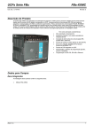
1
FBs-PLC User’s Manual【Hardware】 Contents Chapter 1:Introduction of FATEK FBs Series PLC 1.1 Appearance of Main Unit ................................................................................................................. H1-1 1.2 Appearance of Expansion Unit/Module.......................................................................................... H1-2 1.3 Appearance of Communication Expansion Module ..................................................................... H1-4 1.4 List of FBs-PLC Models ................................................................................................................... H1-5 1.5 Specifications of Main Unit............................................................................................................... H1-8 1.6 Environmental Specifications .......................................................................................................... H1-9 1.7 Connection Diagrams of Various Models ...................................................................................... H1-10 1.7.1 NC Control Main Unit (MN) ........................................................................................................................... H1-10 1.7.2 Basic/Advanced Main Unit (MA/MC) ........................................................................................................... H1-11 1.7.3 Digital I/O Expansion Unit .............................................................................................................................. H1-13 1.7.4 Digital I/O Expansion Module........................................................................................................................ H1-14 1.7.5 High-Density Digital I/O Expansion Module ................................................................................................ H1-15 1.7.6 Numeric I/O Expansion Module.................................................................................................................... H1-15 1.7.7 Analog I/O Expansion Module ...................................................................................................................... H1-15 1.7.8 Temperature Input Module............................................................................................................................ H1-16 1.7.9 AI/AO/Temperature Combo Module .......................................................................................................... H1-17 1.7.10 Expansion Power Module ......................................................................................................................... H1-17 1.7.11 Voice Output Module ................................................................................................................................... H1-17 1.7.12 Potential Meter Module .............................................................................................................................. H1-17 1.7.13 Load Cell Module ....................................................................................................................................... H1-17 1.7.14 Communication Module (CM) .................................................................................................................... H1-18 1.7.15 Communication Board (CB)........................................................................................................................ H1-19 1.7.16 Analog Expansion Board ........................................................................................................................... H1-20 1.7.17 Simple HMI.................................................................................................................................................... H1-20 1.8 Drawings with External Dimensions ............................................................................................... H1-21 Chapter 2:System Configuration 2.1 Single-Unit System of FBs-PLC...................................................................................................... H2-1 2.2 Formation of Multi-Unit System....................................................................................................... H2-2 2.2.1 Connection of Multiple FBs-PLC (CPU Link) .............................................................................................. H2-2 2.2.2 Connection of FBs-PLC with Host Computer or Intelligent Peripherals................................................... H2-3 Chapter 3:Expansion of FBs-PLC 3.1 I/O Expansion ................................................................................................................................... H3-1 3.1.1 Digital I/O Expansion and I/O Numbering.................................................................................................... H3-1 3.1.2 Numeric I/O Expansion and I/O Channel Mapping.................................................................................... H3-3 3.2 Expansion of Communication Port ................................................................................................. H3-5 Chapter 4:Installation Guide 4.1 Installation Environment................................................................................................................... H4-1 4.2 PLC Installation Precautions ........................................................................................................... H4-1 4.2.1 Placement of PLC .......................................................................................................................................... H4-1 4.2.2 Ventilation Space............................................................................................................................................ H4-2 4.3 Fixation by DIN RAIL........................................................................................................................ H4-3 4.4 Fixation by Screws ........................................................................................................................... H4-4 4.5 Precautions on Construction and Wiring........................................................................................ H4-6 Chapter 5:Power Supply Wiring, Power Consumption Calculation, and Power Sequence Requirements 5.1 Specifications and Wiring of AC Power Sourced Power Supply ................................................. H5-1 5.2 Specifications and Wiring of DC Power Sourced Power Supply ................................................. H5-2 5.3 Residual Capacity of Main/Expansion Unit and Current Consumption of Expansion Module ………........................................................................................................................................................ H5-4 5.3.1 Residual Capacity of Main/Expansion Unit ................................................................................................. H5-4 5.3.2 Maximum Current Consumption of Expansion Module ............................................................................ H5-5 5.3.3 Calculation Example of Power Capacity .................................................................................................... H5-7 5.4 Requirement of Power Sequence in Main Unit and Expansion Unit/Module ........................... H5-9 Chapter 6:Digital Input (DI) Circuit 6.1 Specifications of Digital Input (DI) Circuit........................................................................................ H6-1 6.2 Structure and Wiring of 5VDC Ultra High Speed Differential Input Circuit .................................. H6-2 6.3 24VDC Single-End Input Circuit and Wiring for SINK/SOURCE Input ....................................... H6-3 Chapter 7:Digital Output (DO) Circuit 7.1 Specifications of Digital Output Circuit ............................................................................................ H7-2 7.2 5VDC Ultra High Speed Line-Driver Differential Output Circuit and its Wiring ........................... H7-3 7.3 Single-End Output Circuit ................................................................................................................ H7-3 7.3.1 Structure and Wiring of Single-End Relay Output Circuit .......................................................................... H7-3 7.3.2 Structure and Wiring of Single-End Transistor SINK & SOURCE Output Circuit................................... H7-4 7.4 Speed up the Single-End Transistor Output Circuit (only applicable to high and medium-speed) ......................................................................................................................................................... H7-6 7.5 Output Device Protection and Noise Suppression in DO Circuit ............................................... H7-6 7.5.1 Protection of Relay Contacts and Noise Suppression ............................................................................... H7-6 7.5.2 Protection of Transistor Output and Noise Suppression............................................................................ H7-8 Chapter 8:Test Run, Monitoring and Maintenance 8.1 Inspection After Wiring and Before First Time Power on.............................................................. H8-1 8.2 Test Run and Monitoring ................................................................................................................. H8-1 8.3 LED Indications on PLC Main Unit and Troubleshooting ............................................................. H8-2 8.4 Maintenance ..................................................................................................................................... H8-4 8.5 The Charge of Battery & Recycle of Used Battery........................................................................ H8-4 【Instruction】 Contents Chapter 1: PLC Ladder Diagram and the Coding Rules of Mnemonic 1.1 The Operation Principle of Ladder Diagram ............................................................. 1-1 1.1.1 Combination Logic ............................................................................................................ 1-1 1.1.2 Sequential Logic ............................................................................................................... 1-2 1.2 Differences Between Conventional and PLC Ladder Diagram ................................ 1-3 1.3 Ladder Diagram Structure and Terminology ............................................................ 1-5 1.4 The Coding Rules of Mnemonic ............................................................................... 1-8 1.5 The De-Composition of a Network ........................................................................... 1-11 1.6 Using Temporary Relays .......................................................................................... 1-12 1.7 Program Simplification Techniques .......................................................................... 1-13 Chapter 2: FBS-PLC Memory Allocation 2.1 FBS-PLC Memory Allocation .................................................................................... 2-1 2.2 Digital and Register Allocations................................................................................ 2-2 2.3 Special Relay Details ............................................................................................... 2-3 2.4 Special Registers Details ......................................................................................... 2-7 Chapter 3: FBS-PLC Instruction Lists 3.1 Sequential Instructions ............................................................................................. 3-1 3.2 Function Instructions ................................................................................................ 3-2 Chapter 4: Sequential Instructions 4.1 Valid Operand of Sequential Instructions ................................................................. 4-1 4.2 Element Description ................................................................................................. 4-2 4.2.1 Characteristics of A, B, TU and TD Contacts ................................................................... 4-2 4.2.2 OPEN and SHORT Contact.............................................................................................. 4-3 4.2.3 Output Coil and Inverse Output Coil ................................................................................. 4-4 4.2.4 Retentive Output Coil ........................................................................................................ 4-4 4.2.5 Set Coil and Reset Coil ..................................................................................................... 4-5 4.3 Node Operation Instructions..................................................................................... 4-5 Chapter 5: Description of Function Instructions 5.1 The Format of Function Instructions......................................................................... 5-1 5.1.1 Input Control .......................................................................................................... 5-1 5.1.2 Instruction Number and Derivative Instructions ......................................................... 5-2 5.1.3 Operand ................................................................................................................ 5-3 5.1.4 Functions Output (FO) ............................................................................................ 5-6 5.2 Use Index Register(XR) for Indirect Addressing ...................................................... 5-6 5.3 Numbering System ................................................................................................... 5-9 5.3.1 Binary Code and Related Terminologies .................................................................. 5-9 5.3.2 The Coding of Numeric Numbers for FBS-PLC .......................................................... 5-10 5.3.3 Range of Numeric Value ......................................................................................... 5-10 5.3.4 Representation of Numeric Value ............................................................................ 5-10 5.3.5 Representation of Negative Number ........................................................................ 5-11 5.3.6 Representation of Floating Point Number ................................................................. 5-11 5.4 Overflow and Underflow of Increment(+1) or Decrement(-1) ................................. 5-12 5.5 Carry and Borrow in Addition/Subtraction ................................................................ 5-13 Chapter 6: Basic Function Instructions z T (Timer) ....................................................... 6-2 z C (Counter) ..................................................... 6-5 z Set (SET) ......................................................... 6-8 z Reset (RESET) .................................................... 6-10 z Master control loop start (FUN0) ....................................................... 6-12 z Master control loop end (FUN01) ..................................................... 6-14 z Skip start (FUN02) ..................................................... 6-15 z Skip end (FUN03) ..................................................... 6-17 z Differential up (FUN04) ..................................................... 6-18 z Differential down (FUN05) ..................................................... 6-19 z Bit shift (FUN06) ..................................................... 6-20 z Up/down counter (FUN07) ..................................................... 6-21 z Move (FUN08) ..................................................... 6-23 z Move inverse (FUN09) ..................................................... 6-24 z Toggle switch (FUN10) ..................................................... 6-25 z Addition (FUN11) ..................................................... 6-26 z Subtraction (FUN12) ..................................................... 6-27 z Multiplication (FUN13) ............................................... ......6-28 z Division (FUN14) .................................................... 6-30 z Increment (FUN15) .................................................... 6-32 z Decrement (FUN16) .................................................... 6-33 z Compare (FUN17) .................................................... 6-34 z Logical and (FUN18) .................................................... 6-35 z Logical or (FUN19) .................................................... 6-36 z Binary to bcd conversion (FUN20) .................................................... 6-37 z Bcd to binary conversion (FUN21) .................................................... 6-38 Chapter 7:Advanced Function Instructions z Flow Control Instructions I (FUN22) ......................................................... 7-1 z Arithmetical Operation Instructions (FUN23~33) ....................................... 7-2 ~ 7-18 z Multiple Linear Conversion (FUN34) ............................................. 7-19 ~ 7-24 z Logical Operation Instructions (FUN35~36) .................................... 7-25 ~ 7-26 z Comparison Instruction (FUN37) ....................................................... 7-27 z Data Movement Instructions I (FUN40~50) ...................................... 7-28 ~ 7-38 z Shifting/Rotating Instructions (FUN51~54) .................................... 7-39 ~ 7-42 z Code Conversion Instructions (FUN55~64) .................................... 7-43 ~ 7-59 z Flow Control Instructions II (FUN65~71) .................................... 7-60 ~ 7-67 z I/O Instructions I (FUN74~86) .................................... 7-68 ~ 7-84 z Cumulative Timer Instructions (FUN87~89) .................................... 7-85 ~ 7-86 z Watchdog Timer Instructions (FUN90~91) .................................... 7-87 ~ 7-88 z High Speed Counting/Timing (FUN92~93) .................................... 7-89 ~ 7-90 z Report Printing Instructions (FUN94) ............................................ 7-91 ~ 7-92 z Slow Up/Slow Down Instructions (FUN95~98) .................................... 7-93 ~ 7-98 z Table Instructions (FUN100~114) ................................. 7-99 ~ 7-117 z Matrix Instructions (FUN120~130) ..............................7-118 ~ 7-129 z I/O Instruction II (FUN139) ....................................... 7-130 ~ 7-131 z NC Positioning Instructions I (FUN140~143) ............................. 7-132 ~ 7-135 z Enable/Disable Instructions (FUN145~146) ..............................7-136 ~ 7-137 z NC Positioning Instructions II (FUN147~148) ............................. 7-138 ~ 7-139 z Communication Instructions (FUN150~151) ..............................7-140 ~ 7-141 z Data Movement Instructions II (FUN160~162) ...............................7-142 ~ 7-147 z In Line Comparison Instructions (FUN170~175) ..............................7-148 ~ 7-153 z Other Instructions (FUN190) .......................................7-154 ~ 7-155 z Floating Point Instructions (FUN200~220) ................................7-156 ~ 7-177 Chapter 8: Step Instruction Description 8.1 The Operation Principle of Step Ladder Diagram ................................................... 8-1 8.2 Basic Formation of Step Ladder Diagram ................................................................ 8-2 8.3 Instruction of Step Instructions: STP, FROM, TO, and STPEND ............................. 8-5 8.4 Notes for Writing a Step Ladder Diagram ................................................................ 8-11 8.5 Application Examples ............................................................................................... 8-15 8.6 Syntax Check Error Codes for Step Instruction........................................................ 8-22 【Appendix I】FBs-PACK Operation Instruction 1.1 Write Ladder Program and Register Data to FBs-PACK with WinProladder ............ …-1 1.2 Write Ladder Program and Register Data to FBs-PACK with Special Register Operation............................................................................................................................. …-4 1.3 Assigning the Retrieval of Register Stored FBs-PACK ................................................ …-6 1.4 Read and Write FBs-PACK by Function Instruction ..................................................... …-7 【 Hardware】 Chapter 1 Introduction of FATEK FBS Series PLC The FATEK FBS Series PLC is a new generation of micro PLC equipped with excellent functions comparable to medium or large PLC, with up to five communication ports. The maximum I/O numbers are 256 points for Digital Input (DI) and Digital Output (DO), 64 words for Numeric Input (NI) and Numeric Output (NO). The Main Units of FBS are available in three types: MA (Economy Type), MC (High-Performance Type), and MN (High-Speed NC Type). With the combination of I/O point ranges from 10 to 60, a total of 17 models are available. Fifteen DI/DO and 19 NI/NO models are available for Expansion Units/Modules. With interface options in RS232, RS485, USB, Ethernet, CANopen, Zigbee and GSM, the communication peripherals are available with 15 boards and modules. 1.1 Appearance of Main Unit All the Main Units of FBS-PLC have the same physical structure. The only difference is the case width. There are four different case sizes, which are 60mm, 90mm, 130mm, and 175mm. The figure below will use the Main Unit case of the FBS-24MC as an example for illustration: 3 8 4 9 1 max. 400mA 24V OUT S/S X0 X2 X1 X4 X3 X6 X5 0 4 8 I2 X10 X8 X7 12 X12 X11 X9 max. 400mA X13 18 15 16 24V OUT S/S X0 X4 X2 X1 X3 20 X6 X5 POW RUN RUN ERR TX RX PORT0 Y1 Y0 C0 6 5 Y4 Y2 C2 Y3 OUT ( Y ) OUT ( Y ) 0 I 2 3 4 5 6 7 8 9 Y5 C4 FBs-24MCR2-AC Y6 C6 2 7 IN Y9 C0 11 3 10 17 max. 400mA 24V OUT S/S X0 X2 X1 TX TX RX RX X4 X3 X6 X5 0 4 8 I2 PROGRAMMABLE CONTROLLER X10 X8 X7 I 2 3 5 6 7 9 I0 I I I3 IN ( X ) POW 5 ○ RX IN 0 I 2 3 4 5 6 7 8 9 PORT0 Y1 Y0 Y2 C2 Y5 Y4 Y3 C4 Y6 C6 Y6 C6 Y8 Y7 Y9 19 Terminals of main power input and digital output 6 Standard cover plate (without communication ○ FBs-24MCR2-AC AC100~240V C0 Y5 C4 (Pitch 7.62mm) OUT ( Y ) PORT1 Y4 Y3 (Pitch 7.62mm) ERR PORT2 15 Y2 C2 1 35mm-width DIN RAIL ○ 2 DIN RAIL tab ○ 3 Hole for screw fixation (ψ4.5×2) ○ 4 Terminals of 24VDC power input and digital input ○ X13 RUN TX Y0 蓋板掀開之正視圖 ) (Front (view with cover plate removed) X12 X11 X9 FBs-24MCR2-AC AC100~240V Y1 Y8 Y7 ( 未裝通訊板之正視圖 (Front view without Communication) Board) 13 RX 0 I 2 3 4 5 6 7 8 9 AC100~240V IN X13 IN ( X ) POW ERR TX X12 X11 X9 I 2 3 5 6 7 9 I0 I I I3 IN ( X ) PROGRAMMABLE CONTROLLER X10 X8 X7 0 4 8 I2 I 2 3 5 6 7 9 I0 I I I3 board) Y8 Y7 Y9 14 7 Cover plate of built-in communication port (Port 0) ○ (Front view with CB-22 Board installed) H1-1 8 ○ 9 ○ 10 ○ 11 ○ 12 ○ Indicators for transmit (TX) and receive (RX) status of built-in communication port (Port0). Indicator for Digital Input (Xn). Indicator for Digital Output (Yn). Indicator for system status (POW, RUN, ERR). I/O output expansion header cover [units of 20 points or beyond only], with esthetic purpose and capable of securing expansion cable. 13 ○ 14 ○ 15 ○ 16 ○ FBS-CB22 Communication Board (CB). FBS-CB22 CB cover plate (each CB has its own specific cover plate) Screw holes of communication board. Connector for communication board (for 7 types CB of CB2, CB22, CB5, CB55, CB25, CBE, CBCAN , 3 types AIO of B2DA, B2AD, B4AD, and 2 types DAP of BDAP and BPEP) 17 Left side (communication) expansion header (only available in MC/MN model, for CM22, CM25, CM55, CM25E, ○ CM55E, and CMGSM connection). 18 ○ 19 ○ 20 ○ Connector for Memory Pack. Connector for built-in communication port (Port 0) (With USB and RS232 optional, shown in the figure is for RS232) Right side (I/O) output expansion header (only available in units with 20 points or beyond), for connecting with cables from expansion units/modules. 1.2 Appearance of Expansion Unit/Module There are three types of cases for expansion units/modules. One type uses the same case as main unit that of the 90mm, 130mm, and 175mm, while the other two have thinner 40mm and 60mm cases, which are for expansion modules. All expansion cables (left) of expansion units/modules are flat ribbon cables (5cm long), which were soldered directly on the PCB, and the expansion header (right) is a 14Pin Header, with this to connect the right adjacent expansion units/modules. In the following, each of the three types of expansion units/modules is described as an example: z Expansion unit/module with 90mm, 130mm, or 175mm width case: [ -24XY◇–◎, -40XY◇–◎, -60XY◇–◎, -16TC, -16RTD] Input status indicator Digital input terminal block Screw hole ψ4.5 × 2 Output expansion header cover plate Front view of output expansion header with cover plate removed Expansion cable connector 24V IN S/S X1 X3 X2 X5 X4 X7 X6 X9 I 5 9 I3 X11 X10 X8 X13 X12 X14 2 3 4 6 7 8 I0 I I I2 I4 IN ( X ) PROGRAMMABLE CONTROLLER POW OUT ( Y ) I 2 3 4 5 6 7 8 9 I0 Y2 C1 Y1 Y5 Y3 C3 Y4 FBs-24XYR Y7 Y6 C5 C7 Y9 Y8 Y10 Output expansion Digital output terminal block and Main power input (for XY- ) Output status indicator DIN RAIL tab H1-2 z Expansion unit/module with 60mm width case: [-16XY◇, -16Y◇, -20X ] Output expansion cover plate I/O terminal block Screw hole ψ4.5 × 2 Output expansion slot Front view of output expansion slot with cover plate removed S/S X1 X5 X3 X2 Output status indicator X4 X7 X6 X8 I 2 3 4 5 6 7 8 IN ( X ) POW OUT ( Y ) I 2 3 4 5 6 7 8 FBs-16XYR Y3 Y1 C1 Y5 Y4 Y2 C3 Y7 Y6 C5 Y8 Output expansion slot Expansion cable connector z DIN RAIL tab I/O terminal block Expansion module with 40mm width case: [ -8XY◇, -8Y◇, -8X, -6AD, -2DA, -4DA, -4A2D, -2A4TC, -2A4RTD,-7SG1, -7SG2, -2TC, -6TC, -6RTD, -CM5H, -6NTC, -4PT, -1LC, -1HLC, -VOM ] Screw hole ψ4.5 × 2 I/O terminal block Input status indicator Output expansion header cover plate Front view of output expansion slot with cover plate removed S/S X1 X3 X2 Output status indicator X4 I 2 3 4 IN ( X ) POW OUT ( Y ) I 2 3 4 FBs-8XYR Y1 Y2 C1 Y3 C3 Y4 Output expansion head Expansion cable connector I/O terminal block DIN RAIL tab H1-3 z Expansion module with 40mm width case: [ -24X, -24YT, -24YJ, -32DGI ] Output expansion header cover plate Screw hole ψ4.5 × 2 I 2 3 4 5 6 7 8 9 I0 I I I2 I3 I4 I5 I6 I7 I8 I9 20 2I 22 23 24 Input status indicator Front view of output expansion header with cover plate IN ( X ) POW FBs-24X Expansion cable connector S/S1 X1 X2 X3 X5 X4 X6 X7 X8 FG S/S2 X9 X10 X11 X13 X12 X14 X15 X16 FG S/S3 X18 X17 X19 X21 X20 X22 X23 X24 FG Output expansion I/O Header socket DIN RAIL tab 1.3 Appearance of Communication Expansion Module The Communication Module (CM) of FBS-PLC has a 25mm-width case, which can be used in the following seven modules: -CM22, -CM25, -CM55, -CM25E, -CM55E, -CM25C, -CM5R. 螺絲固定孔 Screw hole ψ4.5 ×2 φ 4.5×2 通訊插座 PORT4 (RS485) Port 4 Port4 Communication Socket ETHERNET Ethernet network 乙太網路 (Port 4) (Port4) DINRAIL卡鉤 RAIL tab DIN LNK 1 TX 2 RX + TX RX Port4 Port4 通訊指示燈 Communication indicator Terminator Switch Terminator 附加開關 (T:(T:ON, ON, N:OFF) N:OFF) G PORT3 (RS232) Port3 Port 3 Communication 通訊插座 RUN 3 6 T 通訊模組擴充扁平排線接頭 Communication module expansion cable 17 ) (插於主機之通訊模組連接插座 connector (to be plugged in main unit ○ 17 N TX RX FBs-CM25E Port3 通訊指示燈 Port3 Communication H1-4 1.4 List of FBs-PLC Models Module Name FBs-10MA◇∆–◎–C FBs-14MA◇∆–◎–C FBs-20MA◇∆–◎–C Basic Main Units FBs-24MA◇∆–◎–C FBs-32MA◇∆–◎–C FBs-32MB◇∆–◎–C FBs-40MA◇∆–◎–C FBs-40MB◇∆–◎–C FBs-60MA◇∆–◎–C FBs-60MB◇∆–◎–C FBs-10MC◇∆–◎ Main FBs-14MC◇∆–◎ Units FBs-20MC◇∆–◎ Advanced Main Units FBs-24MC◇∆–◎ FBs-32MC◇∆–◎ FBs-40MC◇∆–◎ FBs-60MC◇∆–◎ FBs-20MN◇∆–◎ NC Positioning Main Units FBs-32MN◇∆–◎ FBs-44MN◇∆–◎ Expansion Power Supply Right Side Expansion Modules DIO Expansion Units DIO Expansion Modules FBs-EPW–AC/D24 Specifications 6 points 24VDC digital input (4 points medium speed 20KHz, 2 points medium speed total 5KHz); 4 points relay or transistor output (4 points medium speed 20KHz); 1 RS232 or USB port (expandable up to 3); I/O is not expandable 8 points 24VDC digital input (4 points medium speed 20KHz, 4 points medium speed total 5KHz); 6 points relay or transistor output (6 points medium speed 20KHz); 1 RS232 or USB port (expandable up to 3); I/O is not expandable 12 points 24VDC digital input (6 points medium speed 20KHz, 6 points medium speed total 5KHz); 8 points relay or transistor output (8 points medium speed 20KHz); 1 RS232 or USB port (expandable up to 3) 14 points 24VDC digital input (8 points medium speed 20KHz, 6 points medium speed total 5KHz); 10 points relay or transistor output (8 points medium speed 20KHz); 1 RS232 or USB port (expandable up to 3) 20 points 24VDC digital input (8 points medium speed 20KHz, 8 points medium speed total 5KHz); 12 points relay or transistor output (8 points medium speed 20KHz); 1 RS232 or USB port (expandable up to 3); (MB is detachable terminal block) 24 points 24VDC digital input (8 points medium speed 20KHz, 8 points medium speed total 5KHz); 16 points relay or transistor output (8 points medium speed 20KHz); 1 RS232 or USB port (expandable up to 3); (MB is detachable terminal block) 36 points 24VDC digital input (8 points medium speed 20KHz, 8 points medium speed total 5KHz); 24 points relay or transistor output (8 points medium speed 20KHz); 1 RS232 or USB port (expandable up to 3); (MB is detachable terminal block) 6 points 24VDC digital input (2 points high speed 200KHz, 2 points medium speed 20KHz, 2 points medium speed total 5KHz); 4 points relay or transistor output (2 points high speed 200KHz, 2 points medium speed 20KHz); 1 RS232 or USB port (expandable up to 5); built-in RTC; I/O is not expandable 8 points 24VDC digital input (2 points high speed 200KHz, 2 points medium speed 20KHz, 4 points medium speed total 5KHz); 6 points relay or transistor output (2 points high speed 200KHz, 4 points medium speed 20KHz); 1 RS232 or USB port (expandable up to 5); built-in RTC; I/O is not expandable 12 points 24VDC digital input (4 points high speed 200KHz, 2 points medium speed 20KHz, 6 points medium speed total 5KHz); 8 points relay or transistor output (4 points high speed 200KHz, 4 points medium speed 20KHz); 1 RS232 or USB port (expandable up to 5); built-in RTC; detachable terminal block 14 points 24VDC digital input (4 points high speed 200KHz, 4 points medium speed 20KHz, 6 points medium speed total 5KHz); 10 points relay or transistor output (4 points high speed 200KHz, 4 points medium sped 20KHz); 1 RS232 or USB port (expandable up to 5); built-in RTC; detachable terminal block 20 points 24VDC digital input (6 points high speed 200KHz, 2 points medium speed 20KHz, 8 points medium speed total 5KHz); 12 points relay or transistor output (6 points high speed 200KHz, 2 points medium speed 20KHz); 1 RS232 or USB port (expandable up to 5); built-in RTC; detachable terminal block 24 points 24VDC digital input (6 points high speed 200KHz, 2 points medium speed 20KHz, 8 points medium speed total 5KHz); 16 points relay or transistor output (6 points high speed 200KHz, 2 points medium speed 20KHz); 1 RS232 or USB port (expandable up to 5); built-in RTC; detachable terminal block 36 points 24VDC digital input (8 points high speed 200KHz, 8 points medium speed total 5KHz); 24 points relay or transistor output (8 points high speed 200KHz); 1 RS232 or USB port (expandable up to 5); built-in RTC; detachable terminal block 2 sets (1 axis) 920KHz 5VDC digital differential input, 10 points 24VDC digital input (4 points high speed 200KHz, 6 points medium speed total 5KHz); 2 sets (1 axis) 920KHz 5VDC digital differential output, 6 points relay or transistor output (average high speed 200KHz); 1 RS232 or USB port (expandable up to 5); built-in RTC; detachable terminal block 4 sets (2 axes) 920KHz 5VDC digital differential input, 16 points 24VDC digital input (4 points high speed 200KHz, 8 points medium speed total 5KHz); 4 sets (2 axes) 920KHz 5VDC digital differential output, 8 points relay or transistor output (4 points high speed 200KHz); 1 RS232 or USB port (expandable up to 5); built-in RTC; detachable terminal block 8 sets (4 axes) 920KHz 5VDC digital differential input, 20 points 24VDC digital input (8 points medium speed total 5KHz); 8 sets (4 axes) 920KHz 5VDC digital differential output, 8 points relay or low speed transistor output; 1 RS232 or USB port (expandable up to 5); built-in RTC; detachable terminal block Power supply of 100~240VAC or 24VDC input for expansion module; 3 sets output power with 5VDC, 24VDC, and 24VDC, 14W capacity FBs-24XY◇–◎ FBs-40XY◇–◎ FBs-60XY◇–◎ FBs-8X FBs-8Y◇ FBs-8XY◇ FBs-16Y◇ FBs-16XY◇ FBs-20X FBs-24XY◇ FBs-40XY◇ FBs-60XY◇ 14 points 24VDC digital input, 10 points relay or transistor output, built-in power supply 24 points 24VDC digital input, 16 points relay or transistor output, built-in power supply 36 points 24VDC digital input, 24 points relay or transistor output, built-in power supply 8 points 24 VDC digital input 8 points relay or transistor output 4 points 24VDC digital input, 4 points relay or transistor output 16 points relay or transistor output 8 points 24VDC digital input, 8 points relay or transistor output 20 points 24VDC digital input 14 points 24VDC digital input, 10 points relay or transistor output 24 points 24VDC digital input, 16 points relay or transistor output 36 points 24VDD digital input, 24 points relay or transistor output FBs-24X 24 points high-density 24VDC digital input, 30 pins header with latch FBs-24YT/J 24 points high-density transistor SINK(T) or SOURCE(J) output (0.1A max.),30 pins header with latch H1-5 Module Name Thumbwheel switch FBs-32DGI module 16/7 Segment LED display modules AIO modules Specifications 8 sets 4 digits (total 32 digits) thumbwheel switch (or 128 points independent switch) multiplex input module, 30 pins header connector FBs-2DA 1 set 8 digits 7-segment/4 digits 16-segment LED display (or 64 points independent LED) output display module, 16 pins header connector 2 sets 8 digits 7-segment/4 digits 16-segment LED display (or 128 points independent LED) output display module, 16 pins header connector 2 channels, 14-bit analog output module (-10~10V, 0~10V or -20~20mA, 0~20mA) FBs-4DA 4 channels, 14-bit analog output module (-10~10V, 0~10V or -20~20mA, 0~20mA) FBs-4A2D 4 channels, 14-bit analog input (same specification as 6AD)+2 channels, 14-bit analog output (same specification as 2DA) combo module FBs-7SG1 FBs-7SG2 Voice modules FBs-VOM Load Cell Module FBs-1LC 6 channels, 14-bit analog input module (-10~10V, 0~10V or -20~20mA, 0~20mA) 2 channels, thermocouple temperature input module with 0.1°C resolution. 6 channels, thermocouple temperature input module with 0.1°C resolution. 16 channels, thermocouple temperature input module with 0.1°C resolution. 6 channels, RTD temperature input module with 0.1°C resolution. 16 channels, RTD temperature input module with 0.1°C resolution. 6 channels, NTC temperature input module with 0.1°C resolution. 2 channels, 14-bit analog input (same specifications as 6AD)+ 4 channels thermocouple temperature input (same specifications as 6TC) combo module 2 channels, 14-bit analog input (same specifications as 6AD) + 4 channels RTD temperature input (same specifications as 6RTD) combo module Built-in 1MB memory (play continuously up to 2 minutes), extendable 4GB SD card(play continuously up to 8,000 minutes) voice module, 245 messages, output 2W 1 channel, load cell measurement module with 16-bit resolution (including sign bit) Potential Meter Module FBs-4PT 4 channels, 14-bit potential meter input module (Impedance range: 1~10K Ω) FBs-CM22 FBs-CM55 FBs-CM25 2 ports RS232 (Port3 +Port 4) communication module 2 ports RS485 (Port3 +Port 4) communication module 1 port RS232 (Port3) + 1 port RS485 (port 4) communication module FBs-CM25E 1 port RS232 (Port3) + 1 port RS485 (port 4) + Ethernet network interface communication module FBs-CM55E 1 port RS485 (Port3) + 1 port RS485 (port 4) + Ethernet network interface communication module FBs-CMZB FBs-CMZBR FBs-CMGSM FBs-CM25C FBs-CM5R ZigBee communication module ZigBee communication repeater GSM wireless communication module General purpose RS232 to RS485/RS422 communication interface converter with photocouple isolation General purpose RS485 repeater with photocouple isolation General purpose 4 ports RS485 HUB with photocouple isolation, RS485 can be connected as star connection 1 port RS232 (Port 2) communication board 2 ports RS232 (Port 1+ Port 2) communication board 1 port RS485 (Port 2) communication board 2 ports RS485 (Port 1+ Port 2) communication board 1 port RS232 (Port 1) + 1 port RS485 (Port 2) communication board 1 port 10 Base T Ethernet communication board 1 port 100 Base T Ethernet communication board 1 port CANopen communication board 2 channels, 12-bit analog output board (0~10V or 0~20mA) 2 channels, 12-bit analog input + 1 channel, 12-bit analog output combo analog board (0~10V or 0~20mA) Temperature measurement modules AI + Temperature Measurement combo modules Communication modules FBs-6AD FBs-2TC FBs-6TC FBs-16TC FBs-6RTD FBs-16RTD FBs-6NTC FBs-2A4TC FBs-2A4RTD Left Side Expansion Modules FBs-CM5H Communication boards AIO boards FBs-CB2 FBs-CB22 FBs-CB5 FBs-CB55 FBs-CB25 FBs-CBE FBs-CBEH FBs-CBCAN FBs-B2DA FBs-B2A1D FBs-B4AD 4 channels, 12-bit analog input board (0~10V or 0~20mA) Precision Load Cell Module FBs-1HLC 1 channel, high precision weighing control module with 24-bit resolution 3-Axis Motion Control Module FBs-30GM 3-Axis with linear and circular interpolation advanced motional control module, 3 sets of 200KHz high speed pulse input, 3 sets of 500KHz high speed pulse output, 14 points main unit, 16M Bytes program capacity, 20K Words retentive file register, built-in RS485 and Ethernet, 7.62mm detachable terminal block FBs-BDAP FBs-BPEP FBs-PEP/PEPR Board type Data Access Panel Board type Parameter Entry Panel Multi characters with graphics-based Parameter Entry Panel, built-in RFID Read/Write module with PEPR FBs-DAP-B/BR 16 X 2 LCD character display, 20 keys keyboard, 24VDC power supply, RS485 communication interface, built-in RFID Read/Write module with BR FBs-DAP-C/CR 16 X 2 LCD character display, 20 keys keyboard, 5VDC power supply, RS232 communication interface, built-in RFID Read/Write module with CR Simple HMI H1-6 Module Name CARD-H Read / Write wireless card (for FBs-DAP-BR/CR and FBs-PEPR) Programming Devices FP-08 FBs- Series PLC handheld programmer Winproladder FATEK-PLC Winproladder Programming software Memory Pack FBs-PACK FBs-PLC program memory pack with 20K Words program, 20K Words register, write protection switch PWMDA module PWMDA 10-bit single channel pulse width modulation(PWM) 0~10V analog output (AO) module USB- RS232 Converter Cable FBs-U2C-MD-180 RFID Card FBs-232P0-9F-150 Peripheral and Accessory Communication cables High density DIO cable 16/7-Segment LED display FBs-232P0-9M-400 FBs-232P0-MD-200 Training Box 3. Communication converter cable with standard USB AM connector to RS232 MD4M connector (used in standard PC USB to FBs main unit Port 0 RS232), length 180cm MD4M to DB9F communication cable (FBs main unit Port 0 RS232 connect to standard DB9M), length 150cm MD4M to DB9M communication cable (FBs main unit Port 0 RS232 connect to DB9F), length 400cm MD4M to MD4M communication cable (FBs main unit Port 0 RS232 connect to FBs-PEP/PEPR), length 200cm FBs-232P0-MDR-200 MD4M to 90˚ MD4M communication cable (FBs main unit Port 0 RS232 connect to FBs-PEP/PEPR), length 200cm HD30-22AWG-200 High density modules(FBs-24X, FBs-24YT/J, FBs-32DGI) connector,30pin Socket, 22AWG I/O cable, length200cm DBAN.8-nR 0.8” 4-digit 16-segment LED display, n means R(Red) 16-segment LED characters display installed, can be 1~4 DBAN.2.3-nR 2.3” 4-digit 16-segment LED display, n means R(Red) 16-segment LED characters display installed, can be 1~4 DB.56-nR DB.8-nR DB2.3-nR DB4.0-nR 1. 2. Specifications FBs-TBOX 0.56" 8-digit 7-segment display, n means R(Red) 7-segment LED characters display installed, can be 1~8 0.8" 8-digit 7-segment display, n means R(Red) 7-segment LED characters display installed, can be 1~8 2.3" 8-digit 7-segment display, n means R(Red) 7-segment LED characters display installed, can be 1~8 4.0" 4-digit 7-segment display, n means R(Red) 7-segment LED characters display installed, can be 1~4 46cm x 32 cm x 16cm suitcase, containing FBs-24MCT main unit. FBs-CM25E communication module (RS232 + RS485 + Ethernet network), 14 simulated input switches, 10 external relay output, Doctor terminal outlet I/O, peripherals such as stepping motor, encoder, 7-segment display, 10 of 10mm LED indicator, thumbwheel switch, and 16 key keyboard. ◇:R ─ Relay output;T ─ Transistor SINK(NPN) output; J ─ Transistor SOURCE (PNP) output ∆:2 ─ built-in RS232 port;U ─ built-in USB port (non-standard) ◎:AC ─ 100~240VAC power supply; D12 ─ 12VDC power supply;D24 ─ 24VDC power supply 4. –C:Blank ─ Standard;–C ─ add in RTC 5. The unmarked frequencies of Digital Input (DI) or Digital Output (DO) are low speed. H1-7 1.5 Specifications of Main Unit Item Specification Execution Speed Note 0.33uS/per Sequence Command Space of Control Program 20K Words Program Memory FLASH ROM or SRAM+Lithium battery for Back-up Sequence Command 36 Application Command 326 (126 types) Flow Chart (SFC) Command 4 Include Derived Commands Corresponding to External Digital Input Point Corresponding to External Digital Output Point ︽ Single Point X Output Contact(DI) X0~X255 (256) Y Output Relay(DO) Y0~Y255 (256) TR Temporary Relay TR0~TR39 (40) M0~M799 (800)* M Non-retentive Internal Relay ︾ BIT Status Retentive Special Relay S Non-retentive Step Relay Retentive M1400~M1911 (512) M800~M1399 (600)* M1912~M2001 (90) S0~S499 S500~S999 T0~T255 (256) C Counter ”Count Up” Status Contact C0~C255 (256) Current 0.01S Time base Time 0.1S Time base Value Register 1STime base T0~T49 16-Bit 32-Bit (50)* T50~T199 (150)* T200~T255 (56)* ︽ WORD Data ︾ Register HR ROR IR OR ^ SR T0 ~ T255 Numbers for each time base can be flexibly adjusted. C0~C139 (140)* Non-retentive C140~C199 (60)* Can be configured as retentive type Retentive C200~C239 (40)* Can be configured as non-retentive type Non-retentive C240~C255 (16)* Can be configured as retentive type Can be configured as non-retentive type R0~R2999 (3000)* D0~D3999 (4000) Non-retentive R3000~R3839 Data Register Can be configured as non-retentive type Retentive Retentive HR DR S20~S499 can be configured as retentive type (500)* Timer ”Time Up” Status Contact Current Counter CTR Value Register Can be configured as non-retentive type (500)* T TMR Can be configured as retentive type Can be configured as non-retentive type (840)* Can be configured as retentive type Retentive R5000~R8071 Read-only Register R5000~R8071 can be configured as ROR, default setting is (0)* File Register F0~F8191 Input register (3072)* (8192)* R3840~R3903 (64) Corresponding to external numeric input (64) Corresponding to external numeric output Output Register R3904~R3967 Special System Register R3968~R4167 (197) R4000~R4095 (96) (3) ﹀ Special Register 0.1mSHigh Speed Timer register R4152~R4154 Real Time Calendar Register (Not available in MA model) XR Index Register V、Z (2), P0~P9 (10) External Interrupt Control 32 (16 point input positive/negative edges) Internal Interrupt Control 8 (1, 2 3, 4, 5, 10, 50, 100mS) Interrupt Control High Speed Counter Register Hardware(4 sets) DR4096~DR4110 (4×4) Software (4 sets) (4×4) 0.1mS High Speed Timer (HST) When not configured as ROR, it can serve as normal register (for read/Write) ROR is stored in special ROR area and not consume program space Must save/retrieved via special commands DR4112~DR4126 R4128 (sec) R4128 (min) R4130 (hour) R4131 (day) R4132 (month) R4133 (year) R4134 (week) 1 (16bits), 4 (32bits, derived from HHSC) H1-8 Optional for MA module High Speed Counter Hardware High Speed Counter (HHSC) /32 bits Channels Up to 4 Counting mode Counting frequency 8 (U/D, U/D×2, K/R K/R×2, A/B, A/B×2, A/B×3 A/B×4) Up to 200KHz (single-end input) or 920KHz y Total number of HHSC and SHSC is (differential input) 8. y HHSC can change into High Speed Up to 4 Timer with 32 bits/0.1mS Time base. 3 (U/D、K/R、A/B) Channels Software High Speed Counter (SHSC) /32 bits Counting mode Counting frequency Communication Interface Port0 (RS232 or USB) Port1~Port4 (RS232, RS485 or Ethernet) Maximum Connections Number of Axes Communication Speed 4.8Kbps~921.6Kbps (9.6Kbps)* Communication Speed 4.8Kbps~921.6Kbps (9.6Kbps)* 254 200KHz single output (single) 100KHZ ( A/B way) 920KHz(single way) and 460KHz(A/B way) differential output. 3 (U/D、K/R、A/B) Positioning Language Special Positioning Programming Language Number of Points Up to 4 Output Frequency 72Hz~18.432KHz (with 0.1﹪resolution) 720Hz~184.32KHz ( with 1﹪resolution) Points Captured input Captured pulse width Max.36 points (all of main units have the feature) > 10μS(super high speed/high speed input) > 47μS(medium speed input) > 470μS(mid/low speed input) Frequency 14KHz ~ 1.8MHz Setting of Digital Filter Port1~4 talk FATEK or Modbus RTU Master/Slave Communication Protocol Up to 4 NC Positioning Output Frequency Output Output Pulse Mode (PSO) HSPWM Output Maximum sum up to 5KHz Chosen by frequency at high frequencies X0~X15 Tine constant 0 ~ 1.5mS/0 ~ 15mS,adjustable by step Chosen by time constant at low frequencies of 0.1mS/1mS X16~X35 Time constant 1mS~15mS,adjustable by step of 1mS Maximum expandable module 32 1.6 Environmental Specifications Item Operating Ambient Temperature Specification Enclosure Minimum 5°C equipment Maximum 40°C Open Minimum 5°C equipment Maximum 55°C Storage Temperature -25°C~+70°C Relative Humidity (non-condensing, RH-2) 5%~95% Pollution Level Degree II Corrosion Resistance By IEC-68 Standard Altitude ≦2000m Vibration Fixated by DIN RAIL 0.5G, for 2 hours each along the 3 axes Secured by screws 2G, for 2 hours each along the 3 axes Shock 10G, 3 times each along the 3 axes Noise Suppression 1500Vp-p, width 1us Withstand Voltage 1500VAC, 1 minute Note Permanent Installation L, N to any terminal Warning The listed environmental specifications are for FBS-PLC under normal operation. Any operation in environment not conform to above conditions should be consulted with FATEK. H1-9 1.7 Connection Diagrams of Various Models 1.7.1 z NC Control Main Unit [7.62mm Detachable Terminal Block] 20 point digital I/O main unit (12 points IN, 8 points OUT) X0+ 24V OUT S/S max. 400mA X1+ X2 X0- X1- X4 X6 X5 X3 X10 X8 X7 X11 X9 AC FBS-20MN◇△-AC Power AC100~240V IN Y0Y0+ SG0 X0+ 24V OUT S/S max. 400mA Y1- Y2 Y1+ X1+ X2 X0- X1- Y4 X4 X3 Y6 Y5 Y3 C2 X6 X5 Y7 X10 X8 X7 X11 X9 DC Power FBS-20MN◇△-D24/D12 24VDC / 12VDC IN Y0Y0+ SG0 z Y1- Y2 Y1+ Y4 Y6 Y5 Y3 C2 Y7 32 point digital I/O main unit (20 points IN, 12 points OUT) X0+ 24V OUT S/S max. 400mA X1+ X0- X4+ X2 X1- X5+ X6 X5- X4- X3 X9 X14 X12 X10 X8 X7 X11 X13 Y7 C8 X16 X15 X18 X17 X19 AC Power FBS-32MN◇△-AC AC100~240V IN Y0Y0+ X0+ 24V OUT S/S max. 400mA Y1Y1+ Y2Y2+ SG0 X1+ X0- Y3- X4+ X2 X1- Y4 Y3+ X5+ X4- X3 X6 X5- Y6 Y5 C4 X9 Y10 Y9 X14 X12 X10 X8 X7 Y8 X11 X13 Y7 C8 Y11 X16 X15 X18 X17 X19 DC Power FBS-32MN◇△-D24/D12 24VDC / 12VDC IN Y0Y0+ z Y1+ Y1SG0 Y2Y2+ Y3- Y4 Y3+ Y6 Y5 C4 Y8 Y10 Y9 Y11 44 point digital I/O main unit (28 points IN, 16 points OUT) max. 400mA X0+ 24V OUT S/S X1+ X0- X5+ X4+ X2 X1- X4- X3 X8+ X6 X5- X7 X10 X14 X16 X18 X20 X22 X24 X26 X9+ X12+ X13+ X11 X15 X17 X19 X21 X23 X25 X27 X8X9X12- X13- AC FBS-44MN◇△-AC Power IN AC100~240V Y0Y0+ max. 400mA Y1+ Y1SG0 X0+ 24V OUT S/S X1+ X0- Y2Y2+ Y4Y4+ X4+ X2 X1- Y3Y3+ X5+ X4- X3 X8+ X6 X5- Y5Y5+ X7 Y6SG4 Y6+ Y7Y7+ Y8 Y10 Y9 C8 Y12 Y11 Y14 Y13 C12 Y15 X10 X14 X16 X18 X20 X22 X24 X26 X9+ X12+ X13+ X11 X15 X17 X19 X21 X23 X25 X27 X8X9X12- X13- DC Power FBS-44MN◇△-D24/D12 IN 24VDC / 12VDC Y0Y0+ Y1+ Y1SG0 Y2Y2+ Y3Y3+ Y4Y4+ Y5+ Y5SG4 H1-10 Y6Y6+ Y7Y7+ Y8 C8 Y10 Y9 Y12 Y11 C12 Y14 Y13 Y15 1.7.2 Basic/Advanced Main Unit [7.62mm Terminal Block, fixed in model MA, detachable in models MB/MC] z 10 point digital I/O main unit (6 points IN, 4 points OUT) max. 400mA 24V OUT S/S X0 X2 X1 X4 X3 Power IN max. 400mA DC Power Power IN Y1 Y0 24V OUT S/S X0 Y1 X2 X3 Y1 Y0 24V OUT S/S max. 400mA X5 X0 X0 X2 X4 X3 X1 Y0 X6 X5 X10 X8 X7 X11 X9 FBS-20MA◇△-AC FBS-20MC◇△-AC AC Power AC100~240V Y1 C0 max. 400mA Y0 24V OUT S/S Y2 X0 Y4 Y3 C2 X2 X4 X3 X1 Y5 C4 Y6 Y7 C6 X6 X5 X10 X8 X7 X11 X9 DC FBS-20MA◇△-D24/D12 FBS-20MC◇△-D24/D12 Power IN 24VDC / 12VDC Y1 C0 z Y0 Y2 Y4 Y3 C2 Y5 C4 Y6 Y7 C6 24 point digital I/O main unit (14 points IN, 10 points OUT) max. 400mA 24V OUT S/S X0 X2 X1 X4 X6 X5 X3 X10 X8 X7 X12 X11 X9 X13 FBS-24MA◇△-AC FBS-24MC◇△-AC AC Power IN AC100~240V Y1 C0 max. 400mA Y0 24V OUT S/S Y2 X0 X2 X1 Y5 Y4 Y3 C2 C4 X4 X6 X5 X3 Y6 Y8 Y7 C6 X10 X8 X7 Y9 X12 X11 X9 DC FBS-24MA◇△-D24/D12 FBS-24MC◇△-D24/D12 Power IN X2 Y1 C0 24V OUT S/S 24VDC / 12VDC Y1 C0 Y0 Y2 C2 Y5 Y4 Y3 H1-11 C4 X7 Y4 Y3 X1 20 point digital I/O main unit (12 points IN, 8 points OUT) IN Y2 C2 Y5 X4 X3 X6 X5 24VDC / 12VDC IN Y3 max. 400mA X6 X5 FBS-14MA◇△-D24/D12 FBS-14MC◇△-D24/D12 DC Power Y2 C2 Y0 C0 X4 X1 X4 X3 AC100~240V Y3 24VDC / 12VDC C0 X2 X1 Y2 C2 FBS-10MA◇△-D24/D12 FBS-10MC◇△-D24/D12 IN X0 FBS-14MA◇△-AC FBS-14MC◇△-AC AC AC100~240V C0 24V OUT S/S max. 400mA X5 FBS-10MA◇△-AC FBS-10MC◇△-AC AC z z 14 point digital I/O main unit (8 points IN, 6 points OUT) Y6 C6 Y8 Y7 Y9 X13 Y2 C2 Y4 Y3 Y5 X7 z 32 point digital I/O main unit (20 points IN, 12 points OUT) 24V OUT S/S max. 400mA X0 X2 X4 X1 X6 X3 X10 X8 X5 X7 X12 X11 X9 X14 X16 X13 X15 X18 X17 X19 FBS-32MA◇△-AC FBS-32MB◇△-AC FBS-32MC◇△-AC AC Power AC100~240V IN Y1 Y5 Y4 Y3 C2 24V OUT S/S max. 400mA Y2 Y0 C0 X0 X2 X6 X3 Y8 Y7 C6 X4 X1 Y6 C4 X10 X8 X5 X7 Y10 Y9 C8 X12 X11 X9 Y11 X14 X13 X16 X15 X18 X17 X19 DC FBS-32MA◇△-D24/D12 FBS-32MB◇△-D24/D12 FBS-32MC◇△-D24/D12 Power 24VDC / 12VDC IN Y1 z Y2 Y0 C0 Y4 Y5 Y3 C2 Y6 C4 Y8 Y7 C6 Y10 Y9 C8 Y11 40 point digital I/O main unit (24 points IN, 16 points OUT) 24V OUT S/S max. 400mA X0 X2 X4 X1 X6 X10 X8 X5 X3 X7 X12 X11 X9 X14 X16 X13 X20 X18 X15 X17 Y11 C12 X22 X19 X21 X23 FBS-40MA◇△-AC FBS-40MB◇△-AC FBS-40MC◇△-AC AC Power AC100~240V IN Y1 Y0 C0 24V OUT S/S max. 400mA Y2 X0 Y4 Y3 C2 X2 Y5 X4 X1 Y6 X6 X3 Y8 Y7 C6 C4 X10 X8 X5 X7 Y10 Y9 C8 X12 X11 X9 Y12 X14 X13 X18 X16 X15 Y14 Y13 X17 Y15 X22 X20 X19 X21 X23 DC FBS-40MA◇△-D24/D12 FBS-40MB◇△-D24/D12 FBS-40MC◇△-D24/D12 Power 24VDC / 12VDC IN Y1 Y0 C0 z Y2 Y5 Y4 Y3 C2 Y6 Y8 Y7 C6 C4 Y10 Y12 Y11 Y9 C8 Y14 Y13 C12 Y15 60 point digital I/O main unit (36 points IN, 24 points OUT) max. 400mA 24V OUT S/S X0 X2 X1 X4 X3 X6 X5 X10 X8 X7 X12 X11 X9 X14 X13 X16 X15 X18 X17 X20 X19 X22 X21 X26 X24 X23 X25 X28 X27 X30 X29 X34 X32 X31 X33 X35 FBS-60MA◇△-AC FBS-60MB◇△-AC FBS-60MC◇△-AC AC Power IN AC100~240V Y2 Y1 C0 max. 400mA Y0 24V OUT S/S C2 X0 X2 X1 Y5 Y4 Y3 C4 X4 X3 Y6 X6 X5 C8 X10 X8 X7 Y10 Y8 Y7 C6 X9 Y9 X12 X11 Y12 Y11 X14 X13 C12 X16 X15 Y14 Y13 X18 X17 Y16 Y15 X20 X19 C16 X22 X21 Y18 Y17 X26 X24 X23 Y20 Y19 X25 C20 X28 X27 Y22 Y21 X30 X29 Y23 X34 X32 X31 X33 DC Power FBS-60MA◇△-D24/D12 FBS-60MB◇△-D24/D12 FBS-60MC◇△-D24/D12 IN 24VDC / 12VDC Y2 Y1 C0 Y0 C2 Y5 Y4 Y3 C4 Y8 Y6 C6 Y7 C8 Y10 Y9 H1-12 Y12 Y11 C12 Y14 Y13 Y16 Y15 C16 Y18 Y17 Y20 Y19 C20 Y22 Y21 Y23 X35 1.7.3 Digital I/O Expansion Unit z [7.62mm fixed terminal block] 24 point I/O expansion unit (14 points IN, 10 points OUT) 24V OUT S/S max. 400mA X1 X5 X3 X2 AC X7 X11 X9 X6 X4 X13 X10 X8 X14 X12 FBS-24XY◇-AC Power AC100~240V IN Y2 max. 400mA Y6 Y4 C3 24V OUT S/S Y5 Y3 Y1 C1 X1 X3 X4 Y9 Y8 C7 X5 X2 Y7 C5 X7 Y10 X11 X9 X6 X13 X12 X10 X8 X14 DC Power FBS-24XY◇-D24/D12 24VDC / 12VDC IN Y2 z Y5 Y3 Y1 C1 Y4 C3 Y6 Y7 C5 Y9 Y10 Y8 C7 40 point I/O expansion unit (24 points IN, 16 points OUT) 24V OUT S/S max. 400mA X1 X3 X2 X5 X4 X7 X11 X9 X6 X10 X8 X13 X15 X12 X14 X17 X16 X19 X18 X21 X20 X23 X22 X24 FBS-40XY◇-AC AC Power AC100~240V IN Y2 Y4 C3 24V OUT S/S max. 400mA Y5 Y3 Y1 C1 X1 X3 X2 Y6 C5 X5 X4 Y7 Y9 Y8 C7 X7 X11 X9 X6 X10 X8 Y11 Y10 C9 X13 Y13 Y12 X15 X12 X14 X17 X16 Y15 Y14 C13 X19 X18 Y16 X21 X20 X23 X22 X24 DC FBS-40XY◇-D24/D12 Power 24VDC / 12VDC IN Y2 z Y5 Y3 Y1 C1 Y4 C3 Y6 C5 Y7 Y9 Y8 C7 Y11 Y10 C9 Y13 Y12 Y15 Y14 C13 Y16 60 point I/O expansion unit (36 points IN, 24 points OUT) max. 400mA 24V OUT S/S X1 X3 X2 X5 X4 X7 X6 X11 X9 X10 X8 X13 X12 X15 X14 AC X17 X16 X19 X18 X21 X20 X23 X22 X25 X24 X27 X26 X29 X28 X33 X31 X30 X32 X35 X34 X36 FBS-60XY◇-AC Power IN AC100~240V Y2 C1 max. 400mA Y1 24V OUT S/S Y5 Y3 Y4 C3 X1 X3 X2 Y6 C5 X5 X4 Y7 X7 X6 Y9 Y8 C7 X11 X9 X8 X10 Y11 Y10 C9 X13 X12 Y13 Y12 X15 X14 X17 X16 Y15 Y14 C13 X19 X18 X21 X20 Y19 Y17 Y16 X23 X22 X25 X24 Y21 Y20 Y18 C17 X27 X26 X31 X29 X28 Y23 Y22 C21 X30 Y24 X33 X32 X35 X34 DC Power FBS-60XY◇-D24/D12 IN 24VDC / 12VDC Y2 C1 Y1 Y5 Y3 C3 Y4 Y6 C5 Y7 C7 Y9 Y8 C9 Y11 Y10 H1-13 Y13 Y12 C13 Y15 Y14 Y17 Y16 C17 Y21 Y19 Y18 Y20 C21 Y23 Y22 Y24 X36 1.7.4 z Digital I/O Expansion Module [7.62mm fixed terminal block] z 8 point digital I/O module (4 points IN, 4 points OUT) S/S X1 8 point digital input module (8 points IN ) X3 S/S X2 X1 X4 FBS-8XY◇ Y1 Y2 X5 Y4 C3 C1 z S/S Y3 X1 X2 z X1 X3 X7 z X4 C1 X10 X8 X13 X12 z X15 X14 Y7 Y8 Y6 C5 Y2 C3 Y1 Y6 C5 Y3 Y5 Y4 Y8 Y7 FBS-16Y◇ X17 X16 Y5 C3 FBS-20X X11 X8 16 point digital output module (16 points OUT) X9 X6 Y4 Y2 C1 X5 X2 Y3 Y1 Y8 C7 20 point digital input module (20 points IN) S/S X7 X6 X4 FBS-16XY◇ Y7 Y6 C5 X5 X3 Y4 FBS-8Y◇ Y5 X8 16 point digital I/O module (8 points IN, 8 points OUT) C3 Y2 X7 X6 8 point digital output module (8 points OUT) Y1 X4 FBS-8X Y3 C1 z X3 X2 X19 X18 Y9 X20 Y12 Y11 Y10 C9 C11 Y15 Y13 Y14 C13 Y16 24 point digital I/O module (14 points IN, 10 points OUT) X1 S/S X5 X3 X2 X4 X7 X11 X9 X6 X10 X8 X13 X12 X14 FBS-24XY◇ Y2 Y1 C1 z Y5 Y3 Y4 C3 Y6 Y7 C5 Y9 Y10 Y8 C7 40 point digital I/O module (24 points IN, 16 points OUT) X1 X5 X3 S/S X2 X4 X7 X11 X9 X6 X10 X8 X15 X13 X12 X14 X17 X16 X19 X18 X21 X20 X23 X22 X24 FBS-40XY◇ Y2 z Y5 Y3 Y1 C1 Y4 C3 Y6 Y7 Y9 Y8 C7 C5 Y11 Y10 C9 Y15 Y13 Y12 Y14 C13 Y16 60 point digital I/O module (36 points IN, 24 points OUT) X1 S/S X3 X2 X7 X5 X4 X6 X11 X9 X8 X10 X13 X12 X15 X14 X17 X16 X19 X18 X21 X20 X23 X22 X25 X24 X27 X26 X29 X28 X33 X31 X30 X32 X35 X34 FBS-60XY◇ Y2 C1 Y1 Y5 Y3 C3 Y4 Y6 C5 Y7 C7 Y9 Y8 C9 Y11 Y10 Y13 Y12 H1-14 C13 Y15 Y14 Y17 Y16 C17 Y19 Y18 Y21 Y20 C21 Y23 Y22 Y24 X36 1.7.5 z High-Density Digital I/O Expansion Module 24 point high-density input module z (24 points IN) S/S1 X2 X4 X6 X8 S/S2 X10 X12 X14 X16 S/S3 X18 X20 X22 X24 z 24 point high-density transistor output module (24 points OUT) I 2 29 30 V1+ Y2 Y4 Y6 Y8 V2+ Y10 Y12 Y14 Y16 V3+ Y18 Y20 Y22 Y24 X1 X3 X5 X7 FG X9 X11 X13 X15 FG X17 X19 X21 X23 FG Numeric I/O Expansion Module 7 segment LED display module FBS-24YJ FBS-24YT FBS-24X 1.7.6 [30Pin/2.54mm Header connector] I 2 29 30 V1+ Y2 Y4 Y6 Y8 V2+ Y10 Y12 Y14 Y16 V3+ Y18 Y20 Y22 Y24 Y1 Y3 Y5 Y7 V1Y9 Y11 Y13 Y15 V2Y17 Y19 Y21 Y23 V3- z [16 pin/2.54mm Header connector] [30Pin/2.54mm Header connector] FBS-32DGI FBS-7SG1 / 2 CH1 6 channel A/D analog input module AG V I FG 24VS1 S3 S5 S7 D0 D2 D4 D6 D8 D10 D12 D14 NC CH0 z 29 30 Thumbwheel switch multiplex input module (4 digits×8) Analog I/O Expansion Module 2 [2.54mm Header connector] (8 digits/-7SG1, 16 digits/-7SG2) 1.7.7 I 2 29 30 24V+ NC S2 S4 S6 S8 D1 D3 D5 D7 D9 D11 D13 D15 NC [7.62mm fixed terminal block] z 2 channel D/A output module I0+ I1+ I0- I1- AG V I U B 5V 10V FBS-6AD O0+ O1+ O0O1- I U B 5V 10V FBS-2DA I2+ I3+ I4+ I5+ I2- I3- I4- I5- H1-15 Y1 Y3 Y5 Y7 V1Y9 Y11 Y13 Y15 V2Y17 Y19 Y21 Y23 V3- z z 4 channel D/A output module AG V 4 channel A/D input, 2 channel D/A output module O0+ O1+ O0O1- AG V I U B 5V 10V I U B 5V 10V FBS-4A2D FBS-4DA I0+ I1+ I2+ I3+ I0- I1- I2- I3- O2+ O3+ O2O3- 1.7.8 z Temperature Input Module [7.62mm fixed terminal block] z 2/6 channel thermocouple input module + - + T0 16 channel thermocouple input module T0+ - T1+ T0- T1 FBS-2TC T8+ T7- - T2+ T1- T3+ T2- T5+ T4+ T3- T4- T6+ T5- T6- FBS-16TC T7+ + O1+ O0+ O1O0- + T9+ T9- T8- T10+ T11+ T12+ T13+ T14+ T15+ T14T15T10- T11- T12- T13- - T1 T0 FBS-6TC T2 + z T3 - + T4 - + T5 - + - z 6 channel RTD input module P0+ P0+ P1+ P0- COM 16 channel RTD input module COM P1- P3+ P2- P4+ P3- P7+ P5+ P4- R0+ R1+ R1- FBS-6NTC R3+ R2- R4+ R3- R5+ R4- P8+ P7- P5- R0- R2+ P2+ P1- P3+ P2- P5+ P4+ P3- P4- P6+ P5- FBS-16RTD FBS-6RTD P2+ P1+ P0- R5- H1-16 P9+ P8- P9- P13+ P14+ P15+ P10+ P11+ P12+ P14P15P10- P11- P12- P13- P6- 1.7.9 z Analog/Temperature Combo Module 2 channel A/D analog input & 4 channel thermocouple input module [7.62mm fixed terminal block] z 2 channel A/D analog input & 4 channel RTD input module I0+ I1+ I0- I1- I0+ I1+ I0- I1- COM COM V V I U B 5V 10V I U B 5V 10V FBS-2A4RTD FBS-2A4TC T1+ T0+ T0- 1.7.10 P0- Expansion Power Module 24V OUT 24V OUT max. 250mA FBS-EPW-AC 1.7.11 FBS-EPW-D24 DC Power Power 24VDC IN AC100~240V IN P2+ P3+ P2P3P1- [7.62mm fixed terminal block] max. 250mA AC P1+ P0+ T2+ T3+ T2T3T1- Voice Output Module [7.62mm fixed terminal block] SD CARD FBS-VOM AUDIO OUT SG 1.7.12 + - SP+ SP- 1.7.13 Potential Meter Module [7.62mm fixed terminal block] + - Load Cell Module [7.62mm fixed terminal block] + AG CH0 CH1 FBS-4PT CH3 CH2 + - - + CH1 FBS-1LC +EXC CH0+ -EXC CH0- - H1-17 1.7.14 z Communication Module (CM) [DB-9F connector/3Pin or 4Pin spring terminal block] z 2 RS232 ports 2 RS485 ports PORT4 (RS485) PORT4 (RS232) TX RX PORT3 (RS485) PORT3 (RS232) TX RX + TX G T N + TX G RX T FBs-CM22 z RX N FBs-CM55 z 1 RS232+1 RS485 ports 1 RS232+1 RS485+Ethernet RUN ETHERNET 1 TX 2 RX RX T N + T z RUN RS232 RS485 /RS222 Converter ETHERNET 24V + 3 LNK 24V 1 TX FG 2 RX POW TX + PORT4 (RS485) 4 TX 2 2 RX+ TX D+ 4 8 5 D RX RX G G T TX RX FBs-CM25E 2 RS485 ports+Ethernet + N PORT3 (RS232) PORT3 (RS232) TX RX 6 TX RX G FBs-CM25 z LNK 6 TX G PORT4 (RS485) PORT4 (RS485) + 3 RX N T N 422 485 RS-232 to RS-485 Converter PORT3 (RS485) + TX G RX RX T N FBs-CM25C FBs-CM55E H1-18 z RS485 Repeater z GSM/GPRS z RS485 HUB [7.62mm fixed terminal block] POW 24V + CH1+ CH1- GND2 GND1 CH2+ CH2- GSM IN IO1 24V JP2 4 ports IO2 I/O 24V FG RS485 HUB IO3 + Tx ON RX G T N S1 0 RS-485 FBS-CM5H Rx OFF A 1 B FBS-CMGSM Repeater CH3+ CH3- GND4 GND3 CH4+ CH4- COMMUNICATION GSM MODULE + G T TX JP1 RX USB N S2 0 Tx Rx 1 A B FBs-CM5R 1.7.15 Communication Board (CB) [DB9F/3Pin spring terminal block](Below are outlooks of CB and the corresponding cover plates) z z 1 RS232 port 2 RS232 ports TX TX TX TX RX RX RX RX PROGRAMMABLE CONTROLLER PORT2 PROGRAMMABLE CONTROLLER PORT2 PORT1 FB S -CB2 z FB S -CB22 z 1 RS485 port TX TX RX RX PORT2 PROGRAMMABLE CONTROLLER PORT1 2 RS485 ports TX TX RX RX PORT2 FB S -CB5 z PORT1 PROGRAMMABLE CONTROLLER PORT1 FB S -CB55 1 RS232 + 1 RS485 ports z 1 Ethernet port TX RX TX RX LINK TX RX PROGRAMMABLE CONTROLLER PROGRAMMABLE CONTROLLER PORT2 ETHERNET PORT1 FB S -CBE FB S -CB25 H1-19 z C ANopen ERR RUN PROGRAMMABLE CONTROLLER CAN-H CAN-L GND FBs-CBCAN 1.7.16 z Analog Expansion Board [5Pin European terminal block] 4 channel A/D analog input board z 2 channel D/A analog output board PROGRAMMABLE CONTROLLER PROGRAMMABLE CONTROLLER VI0+ VI2+ VO0+ II0+ II2+ IO0+ VI1+ VI3+ VO1+ II1+ II3+ IO1+ Gnd Gnd Gnd FB S - B2D A FB S - B4AD z 2 channel A/D analog input & 1 channel D/A analog output board PROGRAMMABLE CONTROLLER VI0+ VO0+ II0+ IO0+ VI1+ II1+ Gnd Gnd FB S - B2A1D 1.7.1 7 z S i mpl e H MI Board- type z Stand-alone ESC OK FB S - PEP FB S - BD AP FB S - BPEP H1-20 + 1.8 Drawings with External Dimensions (1) Outlook I: Main Unit:FBS-10M△, FBS-14M△ Expansion Module:FBS-16Y,FBs-16XY, FBS-20X * (Main Unit and Expansion Module have the same type of base, with different top cover, as shown in the figure) 4 4 90 90 PROGRAMMABLE CONTROLLER 2 - 4.5 7.5 80 60 units:mm (2) Outlook II: Main Unit:FBS-20M△, FBS-24M△, FBS-32M△, FBS-40M△, FBS-60M△ Expansion Module:FBS-24XY(◎), FBS-40XY(◎), FBS-60XY(◎), FBS-16TC, FBS-16RTD PROGRAMMABLE CONTROLLER 90 90 4 4 2 - 4.5 21 80 W 7.5 units:mm W Model 90mm FBS-20M△, FBS-24M△, FBS-24XY(◎ ), FBS-16TC, FBS-16RTD 130mm FBS-32M△, FBS-40M△, FBS-40XY(◎) 175mm FBS-60M△, FBS-60XY(◎) H1-21 (3) Outlook III: 1 FBS-8X, FBs-8Y, FBs-8XY, FBS-7SG1, FBs-7SG2, FBS-6AD, FBS-2DA, FBS-4DA, Expansion Module:○ FBS-4A2D, FBS-2TC, FBS-6TC,FBS-6RTD, FBS-CM5H, FBs-2A4TC, FBs-2A4RTD, FBs-4PT, FBs-1LC, FBs-1HLC, FBs-6NTC, FBs-VOM 2 FBS-24X, FBS-24YT, FBs-24YJ, FBS-32DGI ○ 1 and ○ 2 have the same type of base, with different top cover. Top cover of Module ○ 1 is shown in *(Modules ○ the following figure) 20 90 90 FATEK 2 - 4.5 3.8 21 40 80 7.5 units:mm Outlook IV: Communication Module:FBS-CM22, FBS-CM55, FBS-CM25, FBS-CM25E, FBS-CM55E, FBS-CM25C, FBS-CM5R * (All modules have the same type of base, with different top cover. Top cover of Module -CM25E is shown in the figure) 90 90 25 3.8 (4) 2 - 4.5 21 25 73 7.5 units:mm H1-22 (5) Outlook V: 55.5 Programming Panel:FP-08 188 4 53.25 4 32 90 units:mm Outlook VI: Data Access Panel:FB-DAP 112 98 7 14.8 7 12 H1-23 17.6 9.98 14.75 22.43 148 6.5 (6) (7) Outlook VII: 7-segment / 16-segment LED display board : DB.56-8R/DB.8-8R/DB2.3-8R/DB4.0-4R/DBAN.8-4R/DBAN2.3-4R 102.86 10.16 41.27 41.27 5.08 31.75 3.2ψ× 8 41.91 5.08 5.08 6 7 5 3 4 2 1 5.08 8 D B.5 6-8R 158.12 68.9 10.16 68.9 5.08 38.1 3.2ψ × 8 48.26 5.08 5.08 8 6 5 3 4 2 1 5.08 7 D B .8- 8R 385.28 48.16 81.84 5.08 4ψ× 64 7 6 5 8.58 8 5.08 109.16 5.08 8.58 5.08 D B2 .3- 8R H1-24 4 3 2 1 364.46 78.53 12.98 12.98 78.18 78.63 12.98 78.18 6 133.92 4ψ× 64 3 4 2 1 6 D B4 .0-4R 79.8 6.03 33.91 33.90 38.1 48.26 5.08 2.97 5.08 D BAN .8- 4R 192.02 37.85 10.16 37.85 10.16 37.85 10.16 37.85 82.80 91.44 5.08 4.32 145.92 6 6 D BAN2 .3 -4R H1-25 Chapter 2 2.1 System Configuration Single-Unit System of FBS-PLC Intelligent Peripherals Digital I/O Expansion Unit/Module HMI Load Cell BASE Bar-code Reader Digital Input(DI) FBS-1HLC FBS-CMGSM FBS-CM25E FBS-CM55E Port4 FBS-CM22 FBS-CM55 FBS-CM25 Port3 FBs-30GM Communication Module SCADA Ethernet (Port4) Cell Phone Port4 Port3 PorPort0 t0 Port2 USB or RS232 FP-08 Port1 Data Access Port2 F B S -10MA/MC F B S -14MA/MC F B S -20MA/MC F B S -24MA/MC F B S -32MA/MC F B S -40MA/MC F B S -60MA/MC F B S -20MN F B S -32MN F B S -44MN AO F B S -2A4TC F B S -2A4RTD F B S -2TC F B S -6TC F B S -6RTD F B S -16TC F B S -16RTD F Bs - 6NTC S er v er TC RTD AIO Digital Output (DO) 6 7 8 9 Numeric I/O Expansion F Bs - V OM Voice Output Module F Bs- 1LC AI AI Temperature Input Module F B S -C BE F B S - B4 AD F B S - B2D A F B S - B2 A1D DO F B S -6AD F B S -2D A F B S -4D A F B S -4A2D F B S -7SG1 F B S -7SG2 F B S - 3 2 D GI F Bs-C BC AN DI Analog I/O Expansion Module CB FBs-DAP(R) Port1 Ethernet (Port1,2) FBs-PEP F B S - BD A P F B S - BPEP F B S -C B2 F B S -C B22 F B S -C B5 F B S -C B55 F B S -C B25 Main Unit FBS-24XY FBS-40XY FBS-60XY FBS-8XY FBS-8X FBS-8Y FBS-16XY FBS-16Y FBS-20X FBS-24X FBS-24YT FBS-24YJ AO Load Cell Module RFID Card H2-1 Load cell The Single-Unit system means a system built only by a single FBs-PLC and its expansion unit/modules and communication boards/modules. Such system have a limited capability (refer), beyond that capability can incorporate CPU communication via LINK function for expansions (please refer to the next paragraph). The figure below shows the block diagram of the Single-Unit system of FBs-PLC, where, besides the available main units , the available communication peripherals resources and I/O expansion resources are depict on the left and the right respectively. For the I/O of FBS-PLC, it can achieve a maximum of 256 point digital input (DI), 256 point digital output (DO), 64 word numeric input (NI), and 64 word numeric output (NO). Combined with various special interface modules, it can directly connect with devices such as Thermocouple, RTD, 7-segment LED display, and the Thumbwheel switch, which are shown on the right in the above figure. Regarding communication resources, the FBs-PLC hardware can accommodate up to 5 communication ports (with a maximum speed of 921.6Kbps). In addition to providing the standard FATEK communication protocol, it also supports the Modbus master/slave protocol or any user-defined protocol. This functionality easily renders the connections with intelligent peripherals such as electronic scale, bar code reader, and various meters and gauges. 2.2 Formation of Multi-Unit System By connections through communication ports and specific communication drivers, multiple Single-Unit PLC systems can be integrated to achieve resources sharing among multiple PLC or PLCs and its host computer. It is described as follows: 2.2.1 Connection of Multiple FBs-PLC (CPU Link) RS-485 網路 RS-485 Network FB S-PLC FBs-PLC Main Unit 主機 週邊 Peripherals I/O FB S-PLC FBs-PLC Main Unit 主機 FBs-PLC FB S-PLC Main Unit 主機 週邊 Peripherals 週邊 Peripherals I/O I/O As shown in the figure, through the usage of high-speed RS-485 network, can easily establish the connections of 2~254 main units (each PLC with its own station number). All need to do is to write and execute CPU Link commands in one of the main units, which makes it the Master of the CPU Link network. No other command is necessary for other Slave units. The Master CPU will automatically collect the information or data in the specific areas of all units (including the Master) and put it into the Common Data areas(CDM) of all units. Thus all the units connected by network can share the data for each other and turning the finite Single-Unit system with limited I/O into a huge system. H2-2 Telephone line MODEM MODEM MODEM FBS-PLC Main Unit FBS-PLC Main Unit FBS-PLC Main Unit Besides the above area network connection, FBs-PLC can also be connected using MODEM via the phone line (either leased line or public phone line) to form remote multiple PLC Link. (When using a public phone line, the Master PLC will perform consecutive dialing for all its Slave PLC.) 2.2.2 Connection of FBs-PLC with Host Computer or Intelligent Peripherals Any one of the five communication ports on FBs-PLC can be used to connect to an upper-level computer or other systems, with this architecture, the FBs-PLC is playing the Slave role. FBs-PLC supports the FATEK and Modbus protocol. Connection can be established as long as the upper-level computer or intelligent peripherals use either one of the two protocols. In the application, in which driver for FATEK or Modbus is not available, FATEK also provide standard DDE communication server, which enables FBs-PLC to connect with any computer system supporting DDE. The following is the block diagram. Host 上 位 Computer 電腦 FBS-PLC FBS-PLC 1 FATEK communication driver party) (third party) 永宏通訊驅動程式(third 1 Modbus 通訊驅動程式(third communication driver (third party) Modbus party) 1 DDE (FATEK Communication Sever) DDE(FATEK Communication Sever) FBS-PLC H2-3 FBS-PLC FBS-PLC Chapter 3 Expansion of FBS-PLC If the I/O point of the. Main unit of the applied FBS-PLC is not enough for a specific application, then can expand it with the additional expansion units/modules. Besides I/O point there also have the requirements to expand the communication port in some occasions. 3.1 I/O Expansion The expansion of FBS-PLC I/O consists of Digital I/O ( DI/O, which status is represented by a single bit) and the Numeric I/O (NI/O , which status is represented by a 16-bit Word). Either the DI/O or the NI/O expansion is realized through expansion units or modules cascaded thru the usage of the “I/O Output Expansion Connector” located at the right side of FBS-PLC or expansion unit/ module. The I/O points of FBS-PLC system are limited to 512 points of DI/O (256 points for DI and DO, respectively), 128 words 1 . A maximum of NI/O (64 words for NI and NO, respectively). Besides this there are two limits imposed by hardware: ○ 2 . The total length of the expansion cables cannot number of 32 units or modules can be used in the expansion. ○ exceed 5 meters. Caution 1. If the I/O points of the application system exceed one of the limitations(256 DI,256 DO,64 NI, 64 NO), while startup the main unit of FBS-PLC will treat this as an illegal I/O configuration, which in return will flag as an error situation by turn on the “ERR” LED and put the error code in Y0~Y3 LED(refer the page 8-2, Chapter 8). The corresponding error code will also be indicated in the CPU status register (R4049). 2. The maximum number of expansion units/modules of FBS-PLC is 32. Beyond this numbers will be treated as an invalid I/O configuration and the main unit will stop its operation, which in return will flag as an error situation by turn on the “ERR” LED and put the error code in Y0~Y3 LED(refer the page 8-2, Chapter 8). The corresponding error code will also be indicated in the CPU status register (R4049). Warning 1. The maximum length of the I/O expansion cable for FBS-PLC is 5 meters. Cables longer than that will cause incorrect I/O operation because of excess signal delay in hardware or noise pickup, resulting in damage to equipment or posing hazard to operating personnel. Since this kind of situation cannot be detected by the PLC main unit, users are advised to take extra cautions and necessary measures. 3.1.1 Digital I/O Expansion and I/O Numbering Digital I/O means I/O with the discrete type status, including digital input (with initial X in DI numbering) and digital output (with initial with Y in DO numbering). The DI and DO of FBS-PLC can both be expanded up to 256 points (numbered as X0~X255 and Y0~Y255, each with 256 points). The status of input contacts (X0~X255) of PLC come from the input signal connected to the digital input terminal block on main unit or expansion unit/module; while the status appears at digital output terminal block of main unit and expansion unit/module reflects the digital output relay (Y0~Y255) status inside PLC. On FBs-PLC main unit, at the position below the digital input terminal block and the position above the output terminal block, there have labels indicate the corresponding signal name. They label each terminal with numbers representing the corresponding digital input contact Xn and digital output relay Yn. In the example of the main unit in FBS-24MCR, the corresponding digital input contacts on the input terminal block are labeled X0~13, and the corresponding digital output relays on the output terminal block Y0~Y9. Users only need to locate the printed label for each terminal to find out its I/O number. The LED status display region also indicates the ON/OFF status for all DI(X0~X13) and DO(Y0~Y9) H3-1 on the main unit. Users can easily find each terminal with its I/O number and LED status indication, as shown in the figure below using X10 and Y6 as an example: 24V OUT S/S max. 400mA X0 X2 X1 X4 X6 X5 X3 X10 X8 X7 X12 X11 X9 X13 X10 0 I 2 3 4 5 6 7 8 9 I0 I I I2 I3 IN ( X ) POW PROGRAMMABLE CONTROLLER RUN ERR TX RX OUT ( Y ) 0 I 2 3 4 5 6 7 8 9 PORT0 Y6 FBs-24MCR2-AC AC100~240V IN Y1 C0 Y0 Y2 Y4 Y3 C2 Y5 C4 Y6 C6 Y8 Y7 Y9 While the various expansion units/modules other than the main units have the same printed labels on the input/output terminals as the main units do, these labels are only relative I/O numbers, different from the absolute I/O numbers on main units. The number of a terminal only represents its order on the expansion unit/module. For example, the first contact is X1 or Y1, the second X2 or Y2, etc. All numbers on the expansion unit/module begin with 1. The actual number of digital input contact or the output replay, however, is determined by summing the numbers on all previous expansion units/modules and the main unit. See the following figure and its calculation. X49 X0 X0 X1 X23 • • • • • • • • • • • • • • X23 FBS-40M△ (主機 ) X37 X24 X1 X2 • • • • • • • • X14 X61 X38 X1 X2 • • • • • • Y0 • • • • • • • • • • • • Y15 Y15 Y1 Y2 • • • • • • • • Y10 Y25 Y16 X24 unit/module unit/module Y0 Y1 • • • • • • FBS-40XYR nd (第2個擴充機/模組 2 expansion ) FBS-24XYR st (第1個擴充機/模組 1 expansion ) Main Unit X12 Y1 Y2 Y26 • • • • • • • • • • • • Y16 Y41 As shown in the above figure, because the top X numbers of the previous two units are 23 and 14, respectively, the number of input contact X12 on second expansion unit should be: X (23+14+12) = X49 H3-2 3.1.2 Numeric I/O Expansion and I/O Channel Mapping The numeric I/O in FBs-PLC treat 16 single-bit data as one 16-bit numeric data (Word) ranging from the 0~65535. Since all numeric data of FBs-PLC are stored in the register inside PLC (16-bit width), therefore numeric I/O is also called register I/O. The Input Register (IR) has 64 Word (R3840 ~ R3903) for inputs from external numeric input (NI) module, and the Output Register (OR) also has 64 Word (R3904 ~ R3967) for outputs to external numeric output (NO) module. Analog Input Module, Temperature Module, and Thumbwheel switch multiplex input module are of Numeric input (NI) modules which use input register (IR) to convey the status. Analog Output Module, 7 Segments Display Module are of Numeric output (NO) modules which output is directly from the Output register (OR). The Analog Input, Temperature Input, and Analog Output is of analog voltage or current, while the Thumbwheel switch Input or 7 Segments Display Output uses user-friendly BCD number signal. Either the magnitude of voltage or current or the value of BCD number is represented by the 16-bit value of the corresponding register. The corresponding current/voltage signal or BCD value of any IR or OR on the NI/O module is named as a Channel (CH). The channels on the NI module are called numeric input channels (NI channels) and those on NO module numeric output channels (NO channels). The number of IR/OR used by NI and NO channels on each module varies depending on the module type or working mode. The following table lists the numbers of IR and OR used by NI and NO channels on each NI/O module: NI/O Module Name FBs-6AD NO NI Channel Label Channel Label FBs-B4AD FBs-B2DA (Word) 1 CH1 CH2 CH3 CH4 CH5 1 1 1 1 1 FBs-4DA Number of IR occupied OR occupied CH0 FBs-2DA FBs-4A2D Number of CH0 1 CH1 CH0 1 1 CH1 CH2 CH3 1 1 1 CH0 1 CH1 CH2 CH3 1 1 1 CH0 1 CH1 1 VI0(V) II0(I) VI1(V) II1(I) VI2(V) II2(I) VI3(V) II3(I) 1 The voltage and current inputs can’t be used at the same time in the same channel. It only one (V or I) available. 1 1 1 VO0(V) I O 0 ( I) VO1(V) I O 1 ( I) H3-3 Note (Word) 1 1 Both voltage and current will be outputted at the same time. VI0(V) II0(I) VI1(V) 1 1 II1(I) FBs-B2A1D VO0(V) 1 I O 0 ( I) FBs-32DGI Unlabeled 8 FBs-7SG1 CH0 3(D) 4(ND) CH0 3(D) 4(ND) CH1 2(D) 4(ND) FBs-7SG2 CH0 CH1 CH0~CH5 CH0~CH15 FBS-2TC FBs-6TC/6RTD FBs-16TC/16RTD FBs-6NTC FBs-1LC FBs-4PT 1 CH only 1 1 1 CH only 1 CH only CH0 CH1 1 1 4TC CH0 CH1 CH2 CH3 2 2A CH0 CH1 1 1 4TC CH0 CH1 CH2 CH3 2 FBs-2A4RTD CH0~CH5 CH0 CH0 CH1 CH2 CH3 D:decode mode ND : non-decode mode 1 2A FBs-2A4TC The voltage and current inputs can’t be used at the same time in the same channel. It only one (V or I) available. Both voltage and current will be outputted at the same time. 1 CH only 1 1 1 1 1 1 1 Or unused The corresponding IR or OR number calculation of the NI/O module starts from the first expansion unit/module(main unit itself does not have any NI/O). The first NI channel corresponds to the first IR register (R3840). Adding R3840 with the number of IR used by the first NI channel gives the IR number of the second NI channel. Adding the IR number of the second NI channel with the number of IR used by the second NI channel gives the IR number of the third NI channel. All other numbers can be obtained accordingly. Similarly, the first NO channel corresponds to the first OR (R3904). Adding R3904 with the number of OR used by the first NO channel gives the OR number of the second NO channel. (In the cumulative calculation of NI channels, care only for NI channels and disregard DI/O and NI. Similarly, in the case of NO channels, disregard DI/O and NI channels.) The following figure helps users find out the relation between NI/O channels and PLC’s IR and OR. H3-4 OR IR 24V IN AG FBs-32DGI I 2 3 5 6 7 9 I0 I I I3 V I0+ I1+ I0I1- I U B 5V 10V O0+ 24V IN AG V O1+ O0- S/S X1 O1- Decode mode POW X13 Non-Decode mode 0 4 8 I2 X11 X9 CH0 (R3904) X7 X12 X10 X8 X6 X5 CH1 (R3905) CH1 (R3849) CH0 (R3848) X4 (R3906~8) CH0 or (R3906~9) OR X3 X2 X4 CH0 I U B 5V 10V I 2 3 4 EXT POW IN ( X ) IN ( X ) V 0 V 1 POW RUN ERR RX POW POW POW I 2 3 4 0 I 2 3 4 5 6 7 8 9 Y4 Y3 Y5 C4 FBs-7SG2 I4+ I5+ I2+ I3+ I4I5I2I3- Y8 Y7 FBs-2DA FBs-6AD FBs-24MCR2-AC Y6 C6 POW OUT ( Y ) OUT ( Y ) Y9 Y1 Y2 C1 CH1 Y3 C3 Y4 CH1 CH5 (R3853) (R3909~10) | (R3910~13) CH4 (R3852) CH3 (R3851) CH2 (R3850) (R3840) | (R3847) IR FBs-8XYR IR OR During the startup stage, FBs-PLC will automatically detect the types and CH numbers of expansion units/modules. While operation, the FBs-PLC will read the CH input values from the NI module and stores them into corresponding IR(R3804 ~ R3903) and outputs OR values (R3904~R3967) to channels on the NO module. No pre-configuration or setting by users is required. 3.2 Expansion of Communication Port The main unit of FBs-PLC has one built-in communication port (port 0, with optional USB or RS232 interface). Expansion of communication ports can be achieved by employing Communication Board (CB) or Communication Module (CM). The available models of CB and CM for FBs are: Model Number Specifications (CB) Communication Board FBs-CB2 1 RS232 (port2) communication board FBs-CB22 2 RS232 (port1 & port2) communication boards FBs-CB5 1 RS485 (port2) communication board FBs-CB55 2 RS485 (port1 & port2) communication boards FBs-CB25 1 RS232 (port1) + 1 RS485 (port2) communication board FBs-CBE 1 Ethernet communication board FBs-CBCAN 1 CANopen® communication board H3-5 Module (CM) Communication FBs-CM22 2 RS232 (port3 & port4) communication modules FBs-CM55 2 RS485 (port3 & port4) communication modules FBs-CM25 1 RS232 (port3) + 1 RS485 (port4) communication expansion module FBs-CM25E 1 RS232 (port3) + 1 RS485 (port4) communication module with Ethernet FBs-CM55E 1 RS485 (port3) + 1 RS485 (port4) communication module with Ethernet Communication boards, which can be directly installed on FBs main units, are employed for expansion of communication ports port1 and port2. Communication modules are independent modules used for the expansion of communication ports port3 and port4 and need to be mounted against the left side of FBs main unit and connected to the main unit via a 14pin connector. The labels of communication ports are marked on the cover plate of communication boards and modules, from which users can easily identify each port. Except that the built-in communication port (Port0) can only be used for USB or RS 232 interface, all the other ports (Port 1~4) can be used for RS232 or RS 485 interface in CB and CM. The following figure shows an example of expansion of 5 (maximum allowed number) communication ports (CB22+CM25E): The most expansion of communication port diagram RUN PORT4 (RS485) PORT4 ETHERNET ETHERNET (PORT4) 3 LNK 6 1 TX 2 RX + 24V OUT S/S max. 400mA TX TX TX RX RX X0 X2 X4 X3 X1 X6 X5 0 4 8 I2 RX G T X12 X11 X9 X13 I 2 3 5 6 7 9 I0 I I I3 IN ( X ) PROGRAMMABLE CONTROLLER N X10 X8 X7 POW RUN ERR TX PORT3 (RS232) PORT3 RX OUT ( Y ) TX PORT2 0 I 2 3 4 5 6 7 8 9 PORT1 RX PORT0 FBs-24MCR2-AC AC100~240V IN Y1 C0 Y0 Y2 C2 Y4 Y3 FBs-CM25E PORT2 H3-6 PORT1 PORT0 Y5 C4 Y6 C6 Y8 Y7 Y9 Chapter 4 Installation Guide Danger 1. Turn off all power during installation of FBS-PLC or related equipments to prevent electric shock or damage to equipment. 2. Upon completion of all installation wiring, put the protective cover back on the terminal block before turning on the power to avoid electrical shock. 3. During installation, never remove the dust cover sheet that were surrounded the PLC before wiring is completed to avoid complications such as fire hazards, breakdown, or malfunction caused by drill dust or wire shreds falling inside PLC. 4. Upon completion of installation and wiring, remember to remove the dust cover sheet to avoid fire, breakdown or malfunction, caused by overheating. 4.1 Installation Environment Caution 1. Environmental specifications of FBS-PLC cannot exceed those listed in this manual. In addition, do not operate this equipment in environments with oil smoke, conductive dust, high temperatures, high humidity, corrosion gases, inflammable gases, rain or condensation, and high vibrations and shock. 2. This product has to be housed appropriately whether it’s used in a system or standalone. The choice and installation of housing must comply with local national standards. 4.2 PLC Installation Precautions To avoid interference, the PLC should be installed to keep from noise sources such as high- voltage or high-current lines and high power switches. Other precautions are: 4.2.1 Placement of PLC Fixation of FBS-PLC, which can be fixed by DIN RAIL or screws, should place vertically and start from the main unit on the left to the expansion unit on the right. A typical figure of placement is shown below: max. 400mA 24V OUT S/S X0 X2 X1 X4 X3 X6 X5 X10 X8 X7 X12 X11 X9 X1 X13 S/S X3 X2 X5 X4 X7 X11 X9 X10 X8 X6 0 I 2 3 4 5 6 7 8 9 I0 I I I2 I3 S/S X14 Y1 Suggested arrangement multiple unit expansion Y2 C2 X11 X10 X13 X12 X14 IN ( X ) POW POW RX Y4 Y3 Y5 C4 max. 400mA Y8 Y7 Y2 Y9 Y1 C1 24V OUT S/S X1 0 I 2 3 4 5 6 7 8 9 0 I 2 3 4 5 6 7 8 9 FBs-24MCR2-AC Y6 C6 OUT ( Y ) OUT ( Y ) 0 I 2 3 4 5 6 7 8 9 AC100~240V Y0 X8 I2 I3 PROGRAMMABLE CONTROLLER OUT ( Y ) C0 X9 X7 X6 IN ( X ) PROGRAMMABLE CONTROLLER ERR PORT0 IN X5 X4 I2 I3 IN ( X ) RUN TX X2 0 I 2 3 4 5 6 7 8 9 I0 I I POW PROGRAMMABLE CONTROLLER X3 X1 X13 X12 0 I 2 3 4 5 6 7 8 9 I0 I I X3 X2 X5 X4 X7 X11 X9 X8 X6 X10 Y3 C3 Y5 Y4 Y6 C5 Y7 C7 Y2 Y9 Y8 X1 X14 S/S X5 X3 X2 X4 X7 X6 X9 X8 X12 IN ( X ) IN ( X ) PROGRAMMABLE CONTROLLER POW POW OUT ( Y ) OUT ( Y ) 0 I 2 3 4 5 6 7 8 9 0 I 2 3 4 5 6 7 8 9 FBs-24XYR FBs-24XYR AC100~240V Y2 C1 Y1 Y3 C3 Y5 Y4 Y6 C5 X14 I2 I3 I2 I3 IN X13 X11 X10 Y7 C7 Y2 Y9 Y8 Y10 H4-1 C1 Y1 Y3 C3 Y5 Y4 Y6 C5 Y7 C7 Y9 Y8 Y10 Y5 Y3 C3 0 I 2 3 4 5 6 7 8 9 I0 I I 0 I 2 3 4 5 6 7 8 9 I0 I I PROGRAMMABLE CONTROLLER Y1 C1 Y10 X13 X12 FBs-24XYR FBs-24XYR Y4 Y6 C5 Y7 C7 Y9 Y8 Y10 4.2.2 Ven tilation Sp ace The heat in FBS-PLC is ventilated via air circulation. There should reserve more than 20mm space, both below and above PLC, and with vertical installation, for ventilation. as shown in the figure below: Y9 Y6 C6 C4 Y5 OUT ( Y ) 0 I 2 3 4 5 6 7 8 9 IN ( X ) POW RUN ERR Y0 Y4 Y3 Y5 C4 Y6 C6 Y8 Y7 Y4 Y2 Y1 AC100~240V Y2 C2 PROGRAMMABLE CONTROLLER Y1 C0 24V OUT S/S FBs-24MCR2-AC AC100~240V Y9 max. 400mA IN X0 OUT( Y ) 0 I 2 3 4 5 6 7 8 9 PORT0 C2 X1 RX TX X2 ERR Y3 PORT0 X4 X3 RUN TX Y8 X13 X8 X7 X6 X5 IN (X ) POW PROGRAMMABLE CONTROLLER Y7 X13 X12 Hanged X12 X11 Y0 X9 C0 X10 X8 X7 0 I 2 3 4 5 6 7 8 9 I0 I I I2 I3 RX X6 X5 X11 X4 X3 X10 X2 X1 X9 X0 I 2 3 5 6 7 9 I0 I I I3 24V OUT S/S 0 4 8 I2 max. 400mA FBs-24MCR2-AC Heat ventilation IN On floor Vertical with front facing out Horizontal Wiring slot Distance ≧ 50mm max. 400mA 24V OUT S/S X0 X2 X1 X4 X3 X6 X5 0 4 8 I2 X10 X8 X7 X9 X12 X11 X13 I 2 3 5 6 7 9 I0 I I I3 IN ( X ) POW PROGRAMMABLE CONTROLLER RUN ERR TX RX OUT ( Y ) 0 I 2 3 4 5 6 7 8 9 PORT0 IN FBs-24MCR2-AC AC100~240V Y1 C0 Y0 Y2 C2 Y4 Y3 Y5 C4 Y6 C6 Y8 Y7 Y9 Distance ≧ 50mm Wiring slot H4-2 4.3 Fixation by DIN RAIL In an environment with slight vibration (less than 0.5G), this is the most convenient way of fixation and is easy for maintenance. Please use DIN EN50022 DIN RAIL, as shown in the figure below. 35mm (1.38 in.) 1.0mm (0.039 in.) 7.5mm (0.29 in.) Mount 以 Hold PLC facing its front, press it down with a 15 degree tilt onto the DIN RAIL. Swing it down until the upper edge of DIN RAIL groove on PLC back touches the upper tab of DIN RAIL. Then use this locked-in point as a pivot to press the PLC forward on the bottom and lock it in position. The procedure is illustrated below: 1 Make sure the tab is pressed in, or it cannot be locked into position. 2 Dismount 以 Use a long screwdriver to reach in the hole on the DIN RAIL tab. Pull out the tab to “pulled out” position to remove PLC, as shown in the figure below. Tab in “pulled out” position 2 1 H4-3 4.4 Fixation by Screws In environments with larger vibration (more than 0.5G), the unit must be secured by M3 or M4 screws. Positions and sizes of screw holes in various models of FBS-PLC are illustrated in the following: 尺寸 : SizeAA: 60mm (2.362in) 4mm (0.157in) 90mm (3.543in) 2 - 4.5 mm (0.177 in) 21mm (0.827in) 尺寸 : SizeB B: 90mm (3.543in) 4mm (0.157in) 90mm (3.543in) 2 - 4.5 mm (0.177 in) 21mm (0.827in) 尺寸 C: C: Size 130mm (5.118in) 4mm (0.157in) 90mm (3.543in) 2 - 4.5 mm (0.177 in) 21mm (0.827in) H4-4 尺寸 D: D: Size 1750mm (6.890in) 4mm (0.157in) 90mm (3.543in) 2 - 4.5 mm (0.177 in) 21mm (0.827in) 尺寸 E E: : Size 20mm (0.787in) 40mm (1.575in) 90mm (3.543in) 3.8mm (0.150in) 2 - 4.5 mm (0.177 in) 21mm (0.827in) 尺寸 F :F: Size 3.8mm (0.150in) 25mm (0.984in) 90mm (3.543in) 2 - 4.5 mm (0.177 in) 21mm (0.827in) H4-5 4.5 Precautions on Construction and Wiring 1. During the wiring of FBS–PLC, please follow local national standards or regulations for installation 2. Please choose the wires with proper wire gauge for I/O wiring according to the current loads. 3. Shorter wires are preferred. It is advised that the length of I/O wiring does not exceed 100m (10m for high-speed input). 4. Input wiring should be separated from output or power wiring (at least 30~50mm apart). In case separation is not possible, adopt vertical crossing, no parallel wiring is allow. 5. The pitch of FBS-PLC terminal block is 7.62mm. The torque for screw and suggested terminal is shown below: terminal block M3 M3 7.62 mm < 6mm < 6mm H4-6 torque: 6~8kg-cm 5.2~6.9 In/lbs Chapter 5 Power Supply Wiring, Power Consumption Calculation, and Power Sequence Requirements FBS-PLC internally has three kinds of circuit: a 5VDC logic circuit, a 24VDC driver circuit (driver output devices, for example: relay, transistor, and etc), and a 24VDC input circuit. Only the 5VDC logic circuit and 24VDC output circuit are powered by the built-in power supply for main/expansion units or powered by expansion power supply modules (FBs-EPW-AC, FBs-EPW-D24), and the 24VDC input circuit can be choose to powered by the external power supply or the built-in power supply of main/expansion units or 24VDC sensor of FBs-EPW-AC/D12/D24. Expansion modules other than main/expansion units do not contain any power supply and are powered by the power supply inside the main/expansion units or expansion power supply (FBS-EPW-AC, FBs-EPW-D24). Main/expansion units or expansion power supply with their model numbers suffixed with “-D12/-D24” means is operated by DC power source. Otherwise, AC power source is used. Caution In industrial environments, main power may irregularly experience a surge current or high voltage pulse caused by the start or shut down of high power equipment. Users are advised to take necessary measures (for example, the use of isolation transformer or other MOV suppression devices) for the protection of PLC and its peripherals. 5.1 Specifications and Wiring of AC Power Sourced Power Supply The available AC power supplies of FBS-PLC are the 14 Watt (SPW14-AC) supply for 10/14 PTs main unit, the 24 Watt (SPW24-AC) supply for 20~60PTs main/expansion unit, and the 14 Watt expansion supply (FBS-EPW-AC) for expansion modules. Except that the FBS-EPW-AC is an independent module, SPW14-AC and SPW24-AC are to be installed on a main unit or inside an expansion unit, where their appearances are invisible. The following table lists the specifications: Sp e c Model SPW14-AC SPW24-AC FBS-EPW-AC Item Voltage 100 ~ 240VAC, -15% / +10% Frequency 50 / 60HZ ±5% Input Range Max. Power Consumption 21W / 14W 36W / 24W 21W / 14W Inrush Current 20A@264VAC Allowable Power Interrupt <20ms Fuse Spec. 2A,250V Isolation Type Transformer/Photocouple Isolation, 1500VAC/minute Power* 1 Output 5VDC (logic circuit) N/A*2 5V, ±5%, 1A(max) 5V, ±5%, 0.4A(max) 24VDC (output circuit) 24V±10%, 200mA(max)*3 24V, ±10%, 400mA(max) 24V, ±1%, 250mA(max) 24VDC (input circuit) 24V,±10%, 400mA(max) 24V, ±10%, 400mA(max) 24V, ±10%, 250mA(max) 1 Note * :The 5VDC (for logic circuit) output power and the 24VDC (for output circuit) power can be accessed from the “I/O expansion output header” located on the right side of the main/expansion units for expansion modules. And the 5VDC power is also used by communication board (CBxx) or communication module (CMxx). The 24VDC power for input circuits is provided from the farthest 2 upper left terminals (labeled “+24V OUT-”) on the input terminal block of main/expansion unit to input circuit in expansion module or other sensors. H5-1 2 Note * :The 5VDC power of 10/14PTs main unit is generated from the 24VDC power in the output circuit, with specifications of 5VDC±10% and 400mA (max) (Circuit is located on the I/O board of 10/14PTs main unit). 3 Note * :Without any I/O expansion interface, the 24VDC power in 10/14PTs main unit is for its output circuit alone and cannot be used for other purposes. Caution The schematic diagram of AC power supply wiring in main/expansion units is shown below. Also be cautious about the following: Please follow the wiring schemes regulated by local national standards to use single-pole switch(break hot wire 〝L〞), or double-pole switch(break both〝L〞and〝N〞), to turn on or off the AC input power. In wiring, hot wire〝L〞must be connected to the L N terminal on unit, while the ground line〝N〞connected to the 2 terminal. Please use wires with diameters 1mm ~2mm2. All G terminals on main unit and expansion unit/module have to be connected to the EG (Earth Ground) terminal of main power system as shown in the figure below, with wire diameters larger than 2mm2. Warning Output of power for sensor cannot be connected in parallel with other powers, in which the conflict between two sets of power will decrease their lifetime or cause immediate damage. This will induce unexpected malfunction of PLC and cause serious or even deadly damage to people or equipment. 24VDC output (for Input/Sensor) input / Sensor input / Sensor OR input / Sensor OUT Input Input CPU control 24V AC-DC Power 5V Supply 0V 24V AC-DC Power Supply 24V 0V 0V 5V AC-DC Power Supply 0V 24V 5V control 0V 24V F Output Output Main unit (FBS- M ) SW CONVERTER (DC-DC) control F 100-240VAC main power IN OUT Input SPOW24 -AC 0V 24VDC external power OR OUT SPOW24 -AC 24V 24VDC output (for Sensor) 24VDC output (for Sensor) 24VDC external power Output Expansion module (FBS) Expansion unit (FBS- XY AC) F AI Expansion Expansion module power supply (FBS-6AD, 2DA, (FBS-EPW AC) 6TC,6RTD...) L N PE 5.2 Specifications and Wiring of DC Power Sourced Power Supply The available DC power sourced power supplies of FBS-PLC are the 14 Watt (SPW14-D12/D24) supply for 10/14PTs main unit, the 24 Watt (SPW24-D/12D24) supply for 20~60PTs main/expansion unit, and the 14 Watt expansion supply (FBS-EPW-D24) for expansion modules. Besides the FBS-EPW-D24 is an independent module, SPW14-D12/D24 and SPW24-D12/D24 are to be installed on a main unit or inside an expansion unit, where their appearances are invisible. The following table lists the specifications: H5-2 Model Sp e c . SPW14-D12/D24 SPW24-D12/D24 FBS-EPW-D24 Item Rated Voltage 12 or 24VAC, -15%/+20% Max. Power Consumption 21W / 14W Inrush Current 24VAC, -15%/+20% 26W / 24W 21W / 14W 20A @ 12 or 24VDC 20A@24VDC <20ms Allowable Power Interrupt Fuse Spec. 3A(D12)/1.5A(D24), 125V Isolation Type 5A(D12)/2.5A(D24), 125V 1.5A, 125V Transformer/Photo Coupler Isolation, 500VDC/minute 2 Power*1 Output 5VDC(logic circuit) N/A* 5V, ±5%, 1A(max) 5V, ±5%, 0.4A(max) 24VDC(output circuit) 24V±10%, 200mA(max)*3 24V, ±10%, 400mA(max) 24V, ±10%, 250mA(max) 24VDC(input circuit) 24V±10%, 400mA(max) 24V, ±10%, 400mA(max) 24V, ±10%, 250mA(max) 1 Note * :The 5VDC (for logic circuit) output power and the 24VDC (for output circuit) power can be accessed from the “I/O expansion output header” located on the right side of main/expansion units for expansion modules. The 24VDC power for input circuit is provided from the farthest 2 upper left terminals (labeled “+24V OUT-”) on the input terminal block of main/expansion unit to input circuit in expansion module or other sensors. 2 Note * :The 5VDC power of 10/14PTs main unit is generated by the oscillations of the 24VDC power in the output circuit, with specifications of 5VDC±10% and 400mA (max) (Circuit is located on the I/O board of 10/14PTs main unit) 3 Note * :Without any I/O expansion interface, the 24VDC power in 10/14PTs main unit is for its output circuit alone and cannot be used for other purposes. Caution The schematic diagram of DC power supply in main/expansion unit is shown below. Also be cautious about the following: Please follow the wiring schemes regulated by local national standards to choose single-pole switch (break 24V+) or double-pole switch (break both 24V+ and 24V−) in order to turn on or off DC input power. Wiring of 24V+ input power must be connected to the terminal labeled by the – terminal, Please use wires with diameters of 1mm2~2mm2. The G , while the 24V− end is connected to + terminals on main unit and all digital expansion units/modules must be connected to the EG (Earth Ground) terminal on main power system according to the scheme shown in the following figure, using wire diameters 2 larger than 2mm . Warning Output of 24VDC power for input circuit cannot be connected in parallel with other powers, in which the conflict between two sets of power will decrease their lifetime or cause immediate damage. This will induce unexpected malfunction of PLC and cause serious or even deadly damage to people or equipment. 24VDC output (for Sensor) 24VDC external power input / Sensor OR input / Sensor input / Sensor OUT SPOW24 -D24 Input CPU control SPOW24 -D24 F Output Main unit (FBS- M -D) SW OUT Output F Expansion module (FBS) 24V 0V control PE H5-3 DC-DC Power Supply 5V control 0V 24V Output Expansion unit (FBS- XY-D24) 12 or 24VDC power IN CONVERTER (DC-DC) Input 24V 0V DC-DC 5V Power Supply 0V 24V 24VDC external power OR OUT Input 24V 0V DC-DC Power 5V Supply 0V 24V 24VDC output (for Sensor) 24VDC output (for Sensor) AI F Expansion power supply (FBS-EPW-D24) Expansion module (FBS-6AD, 2DA, 6TC,6RTD...) 5.3 Residual Capacity of Main/Expansion Unit & Current Consumption of Expansion Module Besides its own circuits usage, the residual capacities of three sets of built-in power supply of main/expansion unit are big enough for other expansion modules usage. In addition, the expansion power (FBS-EPW) module can also provides the power for expansion modules usage. As each model of the main/expansion unit has AC/DC power or modules, it has different residual capacity, various models of expansion modules also consume different amounts of current. In practice, one has to consider the match between the two to avoid overload in any of the three sets of output power. In the following, the worst case of the available residual capacity in each main/expansion unit and the maximum power consumption of expansion modules are described below spare. 5.3.1 Residual Capacity of Main/Expansion Unit Extra Capacity Output Power 5VDC(logic circuit) -output communication block Model AC P O W E R or expansion cable- Main Unit O W E R Main Unit -output expansion cable- -output terminal block- 300mA - 340mA FBS-20MA 753 mA 335mA 310mA FBS-24MA 722 mA 325mA 295mA FBS-32MA 712 mA 315mA 262mA FBS-40MA 688 mA 295mA 244mA FBS-60MA 644 mA 255mA 190mA FBS-10/14MC 300 mA - 340mA FBS-20MC 753 mA 335mA 310mA FBS-24MC 722 mA 325mA 295mA FBS-32MC 712 mA 315mA 262mA FBS-40MC 688 mA 295mA 244mA FBS-60MC 644 mA 255mA 190mA FBS-20MN 710mA 310mA 325 mA* FBS-32MN 670mA 297mA 280 mA* FBS-44MN 627 mA 276 mA 250 mA* 948 mA 350mA 337mA 918 mA 320mA 292mA 880 mA 280mA 238mA - 270mA FBS-20MA-D24 300mA 753mA FBS-24MA-D24 722mA FBS-32MA-D24 712mA To t a l 2 2 7 m A FBS-40MA-D24 688mA To t a l 1 8 9 m A FBS-60MA-D24 644mA FBS-10/14MC-D24 300mA FBS-20MC-D24 753mA To t a l 2 9 5 m A FBS-24MC-D24 722mA To t a l 2 7 0 m A FBS-32MC-D24 712mA To t a l 2 2 7 m A FBS-40MC-D24 688mA To t a l 1 8 9 m A FBS-60MC-D24 644mA FBS-10/14MA-D24 P 24VDC(input circuit) FBS-10/14MA FBS-24XY-◎ Expansion FBS-40XY-◎ Unit FBS-60XY-◎ DC 24VDC(output circuit) H5-4 To t a l 2 9 5 m A To t a l 2 7 0 m A To t a l 9 5 m A - 270mA To t a l 9 5 m A FBS-20MN-D24 710mA To t a l 2 8 5 m A * FBS-32MN-D24 670mA To t a l 2 2 7 m A * FBS-44MN-D24 627mA To t a l 1 7 6 m A * Expansion F B S - 2 4 X Y –◎ Unit F B S - 4 0 X Y –◎ 948mA To t a l 3 3 7 m A 918mA To t a l 2 6 2 m A F B S - 6 0 X Y –◎ 880mA To t a l 1 6 8 m A z In the above table, the residual capacity is calculated according to the most power-consuming model (for example, MCT) of in each main/expansion unit by its I/O point number, under the maximum load condition (with both DI and DO ON). The basic units for calculation are 7.5mA /PT for high/medium speed DI, 4.5mA/PT for low speed DI (Ultra high speed DI does not use the 24VDC power in input circuit), 10mA/PT for high speed DO, 7.5mA/PT for medium speed DO, and 5mA for low speed DO and relay output. (excluding the SSR model). z See Sections 5.1 and 5.2 for the residual capacity of expansion power (-EPW-AC and -EPW-D24) Warning Either for the built-in power supply of the main/expansion unit or the expansion power supply for the expansion unit, the total amount of current cannot exceed the value listed in the above table. Any violation will cause a voltage drop by overloading the power supply, or intermittent powered with the supply in protection mode, either of which will result in unexpected action of PLC and cause harm to people or damage to equipment. 5.3.2 Maximum Current Consumption of Expansion Module Without its own power supply, expansion modules must be supported by the main/expansion unit, expansion power, or external power supply (24VDC input circuit alone). The following table lists the maximum consumption current of each expansion module. Current 5VDC Logic Circuit 24VDC Output Circuit 24VDC Input Circuit Model -input expansion cableDigital I/O Expansion Module Numeric I/O Expansion Module FBS-24XY FBS-40XY FBS-60XY FBS-8XY FBS-8X FBS-8Y FBS-16XY FBS-16Y FBS-20X FBS-24X FBS-24YT FBS-32DGI FBS-7SG1 FBS-7SG2 FBS-6AD FBS-2DA FBS-4DA FBS-4A2D FBS-2TC FBs-6TC FBS-6RTD FBS-16TC FBS-16RTD FBs-6NTC 54 mA 83 mA 119 mA 30 mA 30 mA 29 mA 40 mA 40 mA 35 mA 54 mA 66 mA 14 mA 24 mA 24 mA 25 mA 33 mA 35 mA 35 mA 30 mA 30 mA 32 mA 30 mA 32 mA 33 mA --input terminal block--- 85mA 136mA 124mA 34mA - 68mA 68mA 136mA - - - - - - - - - - - - - - - - H5-5 63mA 108mA 162mA 18mA 36mA - 36mA - 90mA 108mA - 36mA 213 mA 396 mA 53 mA 90 mA 137 mA 103 mA 21 mA 29 mA 16 mA 58 mA 19 mA 16 mA 39 mA 39 mA 25 mA 223 mA 158 mA - - - - - 52 mA 32 mA - - - 500 mA - - FBS-CB2 25 mA 32 mA 13 mA - - - 82 mA 48 mA - FBS-CB22 26 mA - - FBS-CB5 51 mA - - FBS-CB55 95 mA - - FBS-CB25 55 mA - - FBs-CBE FBS-CM22 FBS-CM55 FBS-CM25 FBS-CM25E FBS-CM55E FBS-CM25C FBS-CM5R FBS-CM5H FBs-BDAP 50 mA 18 mA 95 mA 70 mA 110 mA 120 mA - - - - - - - - - - - - - - - - - FBs-BPEP 58 mA - - - - FBS-DAPC 193 mA - 75 mA - FP-08 125 mA - - FBs-2A4TC FBs-2A4RTD FBs-B4AD FBs-B2DA FBs-B2A1D Voice Output FBs-VOM Module Special FBs-4PT Modules FBs-1LC Board (CB) Communication Module (CM) Communication Others z FBS-DAPB 47 mA 41 mA 26 mA 135 mA - The above table lists the required current for the maximum consumption in each expansion module. The 24VDC input circuit consumes 4.5mA less per point of OFF state DI in DI/O module, while the 24VDC output circuit consumes 5mA less per point of OFF state DO. The effect of power consumption variation regarding the ON/OFF state of DI/DO of expansion modules other than DI/O are less significant and can be neglected. z The effect of residual capacity variation regarding the ON/OFF state of DI/DO for 5VDC logic circuit can be neglected. H5-6 5.3.3 Calculation Example of Power Capacity Power module selection is depending on the sum of current consumption of all modules. Therefore, user must know the current consumption of each module. Please refer to Table II, which has the maximum current consumption of each expansion module. Before power module selection, we need to calculate the total current consumptions. Calculations need to be divided into two sections, DC5V (Bus Power) current consumption and DC24V (Bus Power) current consumption. User must consider the match between power and expansion modules cannot cause BusPower output power of any one group of overload use. Example 1: The below diagram is a system modules, try to calculate the power supply used of the system. FBs- FBs- CM55E B2DA F B s24MC FBs- FBs- FBs- FBs- 60XYR 16YR 16YR 6AD Un it : mA Result Internal 5VDC logic power -120 -150 +722 -120 -39 -39 -30 +244 (OK) - - +325 -120 -80 -80 - +45 (OK) - - +295 -162 - - -45 +88 (OK) supply Internal 24VDC logic power supply External 24VDC Sensor power supply R e s u l t : ( 1 ) F i r s t c a l c u l a t e c u r r e n t c o n s u m p t i o n o f i n t e r n a l 5 V D C l o g i c p o we r s u p p l y +722mA - 120mA - 150mA - 120mA - 39mA - 39mA - 30mA = +244 mA (OK) ( 2 ) A n d t h e n c a l c u l a t e c u r r e n t c o n s u m p t i o n o f i n t e r n a l 2 4 V D C l o g i c p o we r s u p p l y +325mA - 120mA - 80mA - 80mA = +45 mA (OK) ( 3 ) C a l c u l a t e c u r r e n t c o n s u m p t i o n o f e x t e r n a l 2 4 V D C S e n s o r p o we r s u p p l y +295mA - 162mA - 45mA = +88 mA (OK) In conclusion, the total current consumption of the above six modules cannot exceed the total current consumption of the main unit, so do not need to expand any power supply module. Example 2: The below diagram is a system modules, try to calculate the power supply used of the system. FBs- FBs- CM55E B2DA F B s24MC FBs- FBs- FBs- FBs- FBs- 60XYR 16YR 16YR 6AD 16YR Un it : mA Result Internal 5VDC logic -120 -150 +722 -120 -39 -39 -30 -39 +195 (OK) - - +325 -120 -80 -80 - -80 -35 (overload) - - +295 -162 - - -45 - +88 (OK) power supply Internal 24VDC logic power supply External 24VDC Sensor power supply H5-7 R e s u l t : ( 1 ) F i r s t c a l c u l a t e c u r r e n t c o n s u m p t i o n o f i n t e r n a l 5 V D C l o g i c p o we r s u p p l y +722mA - 120mA - 150mA - 120mA - 39mA - 39mA - 30mA - 39mA = +195 mA (OK) ( 2 ) A n d t h e n c a l c u l a t e c u r r e n t c o n s u m p t i o n o f i n t e r n a l 2 4 V D C l o g i c p o we r s u p p l y +325mA - 120mA - 80mA - 80mA - 80mA = -35 mA (overload) ( 3 ) C a l c u l a t e c u r r e n t c o n s u m p t i o n o f e x t e r n a l 2 4 V D C S e n s o r p o we r s u p p l y +295mA - 162mA - 45mA = +88 mA (OK) In conclusion, the total current consumption of internal 24VDC logic power supply of above seven expansions exceeds power capacity of the main unit, so needs to expand power supply module as in example 3. Example 3: The below diagram is a system modules, try to calculate the power supply used of the system. FBs- FBs- CM55E B2DA F B s24MC FBs- FBs- FBs- FBs- FBs- FBs- 60XYR 16YR 16YR 6AD EPW-AC 16YR (1) Internal 5VDC logic power -120 -150 +722 -120 -39 -39 -30 - - +325 -120 -80 -80 - - - +295 -162 - - -45 supply Internal 24VDC logic power supply External 24VDC Sensor power (2) Result supply +244 (OK) +45 (OK) +88 (OK) Un it : mA Result 400 -39 +361(OK) 250 -80 +170 (OK) 250 - +250 (OK) R e s u l t : ( 1 ) F i r s t c a l c u l a t e t h e c u r r e n t c o n s u m p t i o n o f e x pa n s i o n m o d u l e s wh i c h p r o v i d e d f r o m the main unit. c u r r e n t c o n s u m p t i o n o f i n t e r n a l 5 V D C l o g i c p o we r s u p p l y +722mA - 120mA - 150mA - 120mA - 39mA - 39mA - 30mA = 244 mA (OK) c u r r e n t c o n s u m p t i o n o f i n t e r n a l 2 4 V D C l o g i c p o we r s u p p l y +325mA - 120mA - 80mA - 80mA = 45 mA (OK) c u r r e n t c o n s u m p t i o n o f e x t e r n a l 2 4 V D C S e n s o r p o we r s u p p l y +295mA - 162mA - 45mA = 88 mA (OK) (2) then calcu la te th e curr en t consu mp tion of expan s ion mo du les which prov id ed f ro m expan s ion pow er supp ly mo du le c u r r e n t c o n s u m p t i o n o f i n t e r n a l 5 V D C l o g i c p o we r s u p p l y +400 mA - 39 mA = +361 mA (OK) c u r r e n t c o n s u m p t i o n o f i n t e r n a l 2 4 V D C l o g i c p o we r s u p p l y +250 mA - 80 mA = +170 mA (OK) c u r r e n t c o n s u m p t i o n o f e x t e r n a l 2 4 V D C S e n s o r p o we r s u p p l y +250 mA - 0mA = +250 mA (OK) In conclusion, add one expansion power supply(FBs-EPW-AC),in this way it can satisfy the total current consumption of seven expansion modules. H5-8 5.4 Requirement of Power Sequence in Main Unit & Expansion Unit/Module When the power is on, the FBS-PLC main unit first detects the type and number of expansion unit/module attached to its expansion interface and get the actual I/O configuration. Therefore, while the main unit performs detection, the power in expansion unit/module should be already UP, otherwise, the detected I/O configuration will not correct. Namely, the power of expansion unit/module should be ON simultaneously or even earlier. There will be no time sequence error when main unit/expansion unit/module are connected together to one power. If the expansion unit and main unit powered by different powers (or the same power but different switches), or external power supply is used for expansion modules, time sequence of both powers should be considered. To solve the problem of the expansion unit/module power not get ready before main unit power does, FBS-PLC provides a special R4150 register which can delay the detection time of I/O configuration. The time base of R4150 is 0.01sec with a default value of 100 (namely a 1sec delay), which can be set from 100~500 (1~5sec), as shown in the figure below. If the expansion unit power cannot be UP within 1sec after main unit power is ON, the R4150 time needs to be set longer to delay the detection by CPU. It cannot exceed 5sec, however, otherwise the configuration of expansion interface cannot be detected. 0 1 5 s秒 ec sec 秒 s秒 ec Main主機電源 Unit Power Expansion Unit 擴充機(模組)電源 (Module) Power 無需調整 No adjustment 需調整R4150 Adjustment required requiredR4150 H5-9 無法偵測 Unable to detect Chapter 6 Digital Input (DI) Circuit The FBS-PLC provides the ultra high speed differential double end 5VDC inputs (i.e., single input with two terminals without common) and the single-end 24VDC inputs which use the common terminal to save terminals. The response speeds of single-end common input circuits are available in high, medium and low. Because the double end input circuit has two independent terminals, it can be connected either in SINK or SOURCE for input or in differential input wiring for line driver source. The single-end input circuit can be set to SINK or SOURCE type by varying the wiring of the common terminals S/S inside PLC and external common wire of input circuits (see Sec. 6.3 for details). 6.1 Specifications of Digital Input (DI) Circuit Item Specifications 5VDC Differential Input 24VDC Single-end Input Note Ultra High Speed(HSC) Maximum input frequency*/ accumulated time 920KHz Input Signal Voltage 5VDC±10% Input Current Threshold ON Current OFF Current Maximum Input current High Speed (HSC) 200KHz Medium Speed(HSC) 20KHz (HHSC) Total 5KHz (SHSC) 0.47 mS* >11 mA >8 mA <2 mA 20mA 10.5mA 1 4.7 mS >4mA >2.3mA <1.5mA <0.9mA 7.6mA 4.5 mA *: Half of maximum frequency while A/B phase input Displayed by LED: Lit when “ON”, dark when “OFF” Isolation Type Photocoupler signal isolation Independent Wiring Via variation of internal common terminal S/S and external common wiring FBS-20MNR/T/J X0,1 X4, 5, 8, 9 X2,3,6,7,10,11 FBS-32MNR/T/J X0,1,4,5 X8, 9, 12, 13 X2,3,6,7,10,11,14,15 X16~19 FBS-44MNR/T/J X0,1,4,5,8,9, 12,13 X2,3,6,7,10,11,14,15 X16~27 List of Input Response Speed for Various Models FBS-10MCR/T/J X0,1 X4,5 X2,3 FBS-14MCR/T/J X0,1 X4,5 X2,3,6,7 FBS-20MCR/T/J X0,1,4,5 X8,9 X2,3,6,7,10,11 FBS-24MCR/T/J X0,1,4,5 X8,9.12,13 X2,3,6,7,10,11 FBS-32MCR/T/J X0,1,4,5,8,9 X12,13 X2,3,6,7,10,11,14,15 X16~19 FBS-40MCR/T/J X0,1,4,5,8,9 X12,13 X2,3,6,7,10,11,14,15 X16~23 FBS-60MCR/T/J X0,1,4,5,8,9,12,13 X2,3,6,7,10,11,14,15 X16~35 FBS-10MAR/T/J X0,1,4,5 X2,3 FBS-14MAR/T/J X0,1,4,5 X2,3,6,7 FBS-20MAR/T/J X0,1,4,5,8,9 X2,3,6,7,10,11 FBS-24MAR/T/J X0,1,4,5,8,9,12,13 X2,3,6,7,10,11 FBS-32MAR/T/J X0,1,4,5,8,9,12,13 X2,3,6,7,10,11,14,15 X16~19 FBS-40MAR/T/J X0,1,4,5,8,9,12,13 X2,3,6,7,10,11,14,15 X16~23 FBS-60MAR/T/J X0,1,4,5,8,9,12,13 X2,3,6,7,10,11,14,15 X16~35 Expansion Unit/Module R/T/J Noise Filtering Time 3 Constant* Low Speed 24VDC±10% Input Status Indication SINK/SOURCE Wiring Mid/Low Speed 1 * :Limit of input speed in MA model is 10KHz All Input Points DHF(0 ~ 15mS) +AHF(0.47µs) DHF(0 ~ 15mS) +AHF(4.7µs) H6-1 DHF(0 ~ 15mS) +AHF(0.47µs) AHF(4.7ms) DHF:Digital Hardware Filter AHF:Analog Hardware Filter 6.2 Structure and Wiring of 5VDC Ultra High Speed Differential Input Circuit Only the MN main unit of FBs provides the 5VDC ultra high speed differential input circuit, which is mainly used for the input of hardware high speed counter (HHSC) with a maximum working frequency up to 920 KHz. In practice, to ensure the high speed and high noise immunity, please use Line-Driver for differential line driving. In environments with small noise and medium working frequency (<200KHz), however, it can be changed to the 5VDC single-end SINK or SOURCE input or to the 24VDC single-end SINK or SOURCE input by connecting a 3KΩ/0.5W resistor in series, as shown in the figure below. (A) Wiring of 5VDC differential input for Line-Driver driving(with frequency up to 920KHz for high speed and environments with large noise) FBS-MN 主機 unit FBs-MN main 感應器輸出 External differential output A Dual-end雙端輸入 input (Encoder) Line-Driver輸出 Twisted-pair 隔離雙絞線 B (B) Wiring of 5VDC differential input to 5VDC single SINK or SOURCE input FBS-MN main unit R1 X0+ SINK input SINK 輸入 R2 NPN SENSOR X0 5VDC R1 X1+ PNP SENSOR SOURCE input SOURCE輸入 R2 X1 (C) Method of converting 5VDC differential input to 24VDC single-end SOURCE input FBSFBs-MN -MN主機main unit R1 X0+ SINK input SINK 輸入 R2 NPN SENSOR X0 3KΩ/0.5W R1:100Ω R2:1.2KΩ 24VDC 3KΩ/0.5W R1 X1+ SOURCE SOURCE input 輸入 R2 X1 H6-2 PNP SENSOR 6.3 24VDC Single-End Input Circuit and Wiring for SINK/SOURCE Input The 24VDC single-end digital input circuits of FBS-PLC are available for high, medium and low speed. They all have the similar circuit structures but with different response speeds. To save input terminals, the circuit of single-end input is implemented by connecting one end of all input points (photo coupler) inside the PLC to the same internal common point labeled as S/S. The other end of each input circuit is connected to corresponding terminals such as X0, X1, X2, etc. The S/S common terminal and N single-end inputs comprise of N digital inputs (i.e., only N+1 terminals are used for N terminals). Therefore, we call this type of input structure the single-end input. The user also needs to do the same thing when making the connection of external digital input devices. Namely, the one end of all input devices (e.g., buttons, switches) are connected together and called the external common wire, while the other ends of input circuits are connected to the input terminals X0, X1, X2, etc., of PLC. Then finish it by connecting the external common wiring and internal common terminal S/S to the positive/negative terminals of the 24VDC power. When connect the internal common terminal S/S to 24V+(positive) and the external common wire to 24V- (negative), then the circuit serve as SINK input. On the contrary, while exchange the wiring of the above internal and external common will serve as a SOURCE input. The above wiring schemes can illustrated below: Wiring of single-end common SINK input z External Common Wiring 外部共線 External 外部 Power 電源 NPN Sensor 24VDC 24V- 24V+ S/S X0 Internal 內部共點 Common 端子 Terminal FBS X1 X3 X2 R1 R1 R1 Low speed R1 R1:5.6K R2 | PLC 輸入元件 Input devices R2 R2 R2 R2:1KΩ 24VDC Middle speed (擴充模組無) (not available in expansion modules) R1:3.3KΩ R2:1.2KΩ X0 X1 X3 X2 z Wiring of single-end common SOURCE input External Common Wiring 外部共線 External 外部 Power 電源 PNP Sensor 24VDC 24V- 24V+ PLC S/S X0 Internal 內部共點 Common 端子 Terminal FBS | Input Circuit 輸入元件 X1 R2 R1 R1 R1 R1 R2 R2 R2 X3 X2 24VDC (擴充模組無) (not available in expansion modules) X0 H6-3 X1 X2 X3 Chapter 7 Digital Output (DO) Circuit The digital outputs of FBS-PLC are available in the following two structures: the 5VDC ultra high speed Line-driver type differential output (i.e., one output occupying two terminals), and the single-end output circuit for saving terminals. There are three kinds of output device for the single-end output, which are relays, TRIAC and transistors. Since the relay and TRIAC are bilateral, even when used in single-end output, they can serve as SINK or SOURCE output. The transistor, however, because of its polarities, after being used as single-end common output, its SINK and SOURCE polarities are exactly the opposite (common point Cn of SINK output must connect to negative end of DC power). Therefore, the product model of transistor output of FBS-PLC for SINK and SOURCE is distinct. At the right side of terminal block of FBS-PLC, there is a place for making SINK or SOURCE label. Warning No over current protection is available in the FBS series PLC. Except for the 5V differential output circuit, all other output circuits have to be added with over current or short circuit protections externally, such as fuses, in applications with safety concern. Terminals labeled by〝●〞on the terminal block are empty contacts, which cannot be connected with any wire to maintain the required safety clearance and to avoid damage to the unit. In situations where simultaneous operations of outputs(such as reverse/forward action of motor) pose safety concerns, besides the interlock in PLC programs, additional interlock circuits are needed outside PLC, as shown below: PLC PLC Forward 正轉輸出 output Forward 正轉極 limit switch Interlock Magnetic 電磁開關或 switch or Relay A 繼電器A 限開關 互鎖接點 contact (NC) (NC) Reverse 反轉極 Limit 限開關 switch Magnetic 電磁開關或 Interlock 互鎖接點 switch or contact 繼電器B (NC) Relay B (NC) Output 輸出 Output 輸出 PLC PLC Reverse 反轉輸出 output H7-1 7.1 Specifications of Digital Output Circuit Item Specification Differential Output Ultra High Speed Maximum output frequency* 920KHz Working Voltage 5VDC±10% Single-End Transistor Output (T, J ) High Medium Low Speed Speed Speed 200KHz 20KHz ─ Single-End Relay Output For ON/OFF, not for frequent exchange <250VAC, 30VDC 5~30VDC 50mA 0.5A 0.5A 0.5A 0.1A (24YT/J) Maximum Voltage Drop/conducing resistance - 0.6V 2.2V 2.2V Minimum Load - - 2mA/DC power Leakage Current - <0.1 mA/30VDC - Maximum Load Current Maximum Output Delay Time Resistive Inductive 0.06V(initial) 80VA(AC)/24VA(DC) 15μS ON→OFF OFF→ON 2A/single, 4A/common 200nS 2μS 10mS 30μS Output Status Indication LED is bit when〝ON〞, dark when〝OFF〞 Over Current Protection N/A Isolation Type SINK/SOURCE Output Type Photocoupler Isolation, 500VAC, 1 minute Electromagnetic Isolation, 1500VAC, 1 minute Independent Dual Terminals Choose SINK/SOURCE by models Bilateral device, can be arbitrarily set to and non-exchangeable for arbitrary SINK/SOURCE output connection FBS-20MNR/T/J Y0~1 Y2~7 FBS-32MNR/T/J Y0~3 Y4~7 FBS-44MNR/T/J Y0~7 Y2~7 Y8~11 Y4~11 Y8~15 Y8~15 List of Input Response Speed for Various Models FBS-10MCR/T/J Y0,1 Y2,3 FBS-14MCR/T/J Y0,1 Y2~5 FBS-20MCR/T/J Y0~3 Y4~7 FBS-24MCR/T/J Y0~3 Y4~7 Y8~9 FBS-32MCR/T/J Y0~5 Y6,7 Y8~11 FBS-40MCR/T/J Y0~5 Y6,7 Y8~15 FBS-60MCR/T/J Y0~7 Y8~23 FBS-10MAR/T/J Y0~3 FBS-14MAR/T/J Y0~5 FBS-20MAR/T/J Y0~7 FBS-24MAR/T/J Y0~7 Y8,9 FBS-32MAR/T/J Y0~7 Y8~11 FBS-40MAR/T/J Y0~7 Y8~15 FBS-60MAR/T/J Y0~7 Y8~23 Expansion Units/Modules(R/T/J) All output points All output points *Half of the maximum frequency while A/B phase output H7-2 7.2 5VDC Ultra High Speed Line-Driver Differential Output Circuit and its Wiring The 5VDC ultra high speed Line-Driver differential output circuit of FBS-PLC is only available for the main unit of the MN model. Its output can connect to general photo coupler circuit or Line-Receiver input circuit, with the connection shown in the figure below. To improve noise immunity and maintain signal quality, please use twisted pair with shield (or aluminum foils) for connection and connect the shield with SG of PLC and FG of the driver. Please also operate in 2-phase driving mode (because 2-phase driving can automatically cancel interferences from noise pulses). FBS-MN Main Unit Load FBS-MN 主機 負載 FBS-XXMN Photocouple Photocouple input 輸入之範例 Line-Driver Line-Driver 輸 出 Output Twisted-pair 雙絞線 Line-Receiver Line-Receiver input 輸入之範例 With frequency up to 920KHz, for high speed or high noise environments 7.3 Single-End Output Circuit Except that the 5VDC ultra high speed output circuit has independent dual terminal outputs, all other output circuits such as relays, transistors or TRIAC are single-end output structure. A single-end output in each digital output (DO) takes up only one terminal. But since any output device has two ends, the one end of several output devices have to be connected together to one common point (called output common) for single-end output. Then each output point can output via this common point. The more output device share a same common points, the more terminals are saved, while relatively increasing the current running through the common point. Combination of any output common with its individual single-end outputs are called a Common Output Block, which is available in 2, 4 and 8PTs (high-density module) in FBS-PLC. Each Common Output Block is separated from one another. The common terminal has a label initiated with letter “C”, while its numbering is determined by the minimum Yn number which comprise the output block. In the example of the figure below, the number of common terminal of output block Y2 and Y3 is C2, while the number of common terminal of output Block Y4, Y5, Y6 and Y7 is C4. The various single-end common output circuits are described below: 7.3.1 Structure and Wiring of Single-End Relay Output Circuit Because relay contacts have no polarity, it can be applied for AC or DC load power. Each relay can provide current up to 2A. The maximum rated current in all output commons of FBS-PLC is 4A. Its mechanical lifetime can reach up to 2 million times, while the contacts have a shorter lifetime. The lifetime also varies depending on working voltage, load type (power factor cosψ) and contact current. The relation between them is plotted in the figure below. In the case of pure resistive load (cosψ=1.0) at 120VAC and 2A, the lifetime of contacts is about 250 thousand times. While for high inductive or capacitive load with cosψup to 0.2 and current within 1A, the lifetime decreases rapidly to about 50 thousand times (AC200V) or 80 thousand times (AC120V). H7-3 FBS-PLC AC/DC AC/DC 電源 power AC/DC AC/DC 電源 power 4A FUSE 4A FUSE co Times of Action (ten thousand) co 動 作 次 數 co co sϕ =0 sϕ sϕ =1 sϕ =0 .7 .0 =0 .4 .2 萬 次 接點電流(A) Contact Current (A) 7.3.2 A. Structure and Wiring of Single-End Transistor SINK and SOURCE Output Circuit Transistor Single-End SINK Output FBS-PLC Y2 C2 Y3 1A FUSE Y4 C4 Y5 Y6 2A FUSE 共點輸出區塊 2PTs Common Output Block 共點輸出區塊 4PTs Common Output Block H7-4 Y7 B. Transistor Single-End SOURCE Output FBS-PLC 3 Y 2 Y 2 C C4 1A FUSE Y4 Y5 Y7 2A FUSE DC 電源 power 共點輸出區塊 2PTs Common Output Block 共點輸出區塊 4PTs Common Output Block The figure above uses output block s of 2PTs common and 4PTs common as an example to explain the differences in structural and wiring for SINK and SOURCE output circuits, respectively.(8PTs common has the same block structure and wiring, except with different point number) The single-end SINK output and SOURCE transistor output in FBS-PLC are different models. The user must check whether it is SINK output model or SOURCE output model when purchasing. H7-5 7.4 Speed up the Single-End Transistor Output Circuit (only applicable to high and medium-speed) Either with the SINK or SOURCE structure in single-end output transistor circuit, when the transistor switches from ON to OFF, the junction capacitor between transistor CE electrodes should be charged to near the load voltage VDD before it can stop the current running through the photocoupler inside the load, which increase the OFF time and decrease the response speed. This problem can be solved by adding a Dummy load to accelerate charging rate and speed up the working frequency of transistor output. For the transistor output in FBS-PLC, Dummy load that are added to the highand medium-speed transistor output and generate a load current of 20~50mA is adequate. For low speed transistor where its driving capability (0.5A) but speed is concerned, adding a Dummy load only decreases its driving capability without any significant improvement and hence is not recommended. The following diagram shows how to add a Dummy load to SINK and SOURCE transistor output. FB S -PLC FB S -PLC Load Load VD D 5~30 VD C R I R I SINK output VDD I = =20~50mA R SR C E output 7.5 Output Device Protection and Noise Suppression in DO Circuit Since the digital output circuits are mainly used for the ON/OFF switching operation, the output components such as relays, transistors and TRIAC can be deemed as kinds of switch components. Normally, surge currents or counter-electromotive force voltages are generated during the ON/OFF operation of these switch components. The effect of surge currents or counter-electromotive force voltages is particularly serious when heavy capacitive or inductive loads are incorporated, which may cause damage to the output components or generate noises in other electronic circuits and equipment. Among those three FBS-PLC output components, where TRIAC require no special treatment because of their features of smaller rated current, zero cross in ON/OFF, and built-in protection circuits, special consideration should be given to relays and transistors when they are used in high power applications or connected with capacitive or inductive loads and are described in the following: 7.5.1 Protection of Relay Contacts and Noise Suppression Because the relay contacts are used to contact switch components having extremely low resistance, the surge current IR generated instantly upon turning on the relay is normally pretty strong (even if the steady load current is very small). Under such strong surge, the contact tends to melt and stick due to extreme temperature in such a way that the relay cannot trip when it is disconnected. In addition, when the relay connections are OFF, large di/dt is generated because of the instantaneous change from low resistance to open circuit (∞) soon after following the tripping of contact. As a result, an extremely strong counter-electromotive force voltage is induced, which creates sparks between the electrodes of two relay contacts and results in poor contact due to carbon deposits. Among those three output components, either in ON or OFF state, very serious interference can be caused by the surge current or the counter-electromotive of the relay. The solutions to this problem are listed as follows: H7-6 VD D 5~30 VD C A. Suppression of Surge Current 以 Connect a small resistor R in series to lower the surge current, but note that too large R will affect the driving capability or cause too much voltage drop. PLC 輸出 output PLC relay 繼電器 Load Load R IIss I Irr Electronic Circuits 電子 電路 Surge current welds contacts 湧浪電流使接點熔化黏住 R V VDD C VDD R≧ (note power dissipation P=Is2R and voltage drop V=IsR) Ir max Ir max of relay in FBS-PLC =5A B. Suppression of Counter-Electromotive Force For the inductive load, whether in AC or DC power, suppression devices must be connected in parallel to both its ends to protect the relay contacts and lower noise interference. The schematic diagrams for AC and DC powers are shown below, respectively: PLC Relay output Inductive load R R : 100 ~ 120Ω R:100~120Ω R C : 0.1 ~ 0.24uF C:0.1~0.24uF C Scheme of AC power load PLC Relay output Inductive load D : 1N4001 diode or R VDC D equivalent device Suppress by a diode in DC power load (for low power) PLC Relay output Inductive load D : 1N4001 diode or R ZD D VDC equivalent device ZD : 9V Zener, 5W Suppress by a diode + Zener in DC power load (for high power and frequent ON/OFF) H7-7 7.5.2 Protection of Transistor Output and Noise Suppression The transistor output in FBS-PLC already includes Zener diode for counter-electromotive force, which is sufficient for low power inductive load and medium frequency of ON/OFF application. In conditions of high power or frequent ON/OFF, please construct another suppression circuit to lower noise interference and prevent voltage from exceeding the limit or overheating that may damage the transistor output circuit. PLC Relay output Inductive load D : 1N4001 diode or VDC D equivalent device Suppress by a diode (for low power) PLC Relay output Inductive load D : 1N4001 diode or ZD D VDC equivalent device ZD : 9V Zener, 5W Suppress by a diode + Zener (high power and frequent ON/OFF) H7-8 Chapter 8 Test Run, Monitoring and Maintenance Warning During maintenance, be sure to turn off the input power of PLC in case the actions to touch any terminal on PLC, or insert and extract accessories (e.g., expansion ribbon cables) is required. Otherwise, electric shock, short circuit, damaged PLC or PLC malfunction will be caused if the power is on. 8.1 Inspection After Wiring and Before First Time Power on 1. Before power on, clean all unnecessary objects such as iron chippings and screws, and remove the dust cover sheet that surround the FBS-PLC. 2. Make sure that the input power and PLC required power is of the same type. When input power is AC power, please pay attention to connect the hot wire (L) to the “L” terminal on PLC and the ground wire (N) to the “N” terminal. Mistakenly connect to DC powered PLC or to terminals other than “L” and “N” will result in electric shock, serious damage or malfunction. 3. Make sure the load power and PLC output circuits are consistent. Connection of AC power to transistor output or 4. Make sure the DC24V input and polarities of SINK/SOURCE in transistor output are consistent with those of your DC power to TRIAC output will damage PLC or result in malfunction. existing wiring. Any mismatch will result in failure of PLC input and damage to the output circuit. 8.2 Test Run and Monitoring The FBS-PLC provides a convenient feature to Disable/Enable the I/O points by whole or individually. Namely, while PLC performs the normal logic scan operation and I/O refreshment, it does not update the status of the disabled input points according to the actual external input. For the disabled output points, the result of logic scan can’t override the disable status of outputs, only the user can force the state to ‘on’ or ‘off’ in order to simulate its operation. The user only needs to utilize the disable function combined with Monitor to achieve simulating the input or output via FP-08 or WINPROLADDER and observe the result. Upon the finish the simulation, revert all the inputs or outputs to Enable state will bring back normal operation. Refer the instructions of WINPROLADDER or FP-08 for the operation of RUN/STOP PLC, Disable/Enable I/O and monitoring of I/O status and content of register. Warning The disable function is to let the input or output status out of PLC program control and switched to the control of the user (tester) to freely set the disabled input or output to be ON or OFF. In normal PLC operation, when dealing with input or output with safety issues (such as upper/lower limit of detected input or output emergency stop), the user must make sure whether it can be disabled or overridden to ON/OFF before starting the disable or override control, to avoid damage to equipment or harm to people. H8-1 8.3 LED Indicators on PLC Main Unit and Troubleshooting 輸入狀態指示 "Xn" Input Status Indicator “Xn” max. 400mA 24V OUT S/S X0 X2 X1 X4 X3 X6 X5 0 4 8 I2 Receive Indicator “RX” 接收指示 "RX" X10 X8 X7 X9 X12 X11 X13 I 2 3 5 6 7 9 I0 I I I3 電源指示 "POW" Power Indicator “POW” IN ( X ) POW PROGRAMMABLE CONTROLLER 運轉指示Indicator "RUN" “RUN” Operation RUN ERR Transmit Indicator “TX” 傳送指示 " TX" TX RX OUT ( Y ) 0 I 2 3 4 5 6 7 8 9 PORT0 IN Error Indicator “ERR” 錯誤指示 "ERR" FBs-24MCR2-AC AC100~240V Y1 C0 Y0 Y2 C2 Y4 Y3 Y5 C4 Y6 C6 Y8 Y7 Y9 Output Status Indicator “Yn” or 輸出狀態指示 "Yn" “ERR” error Indicator (when 或錯誤碼指示 occurs) (當有"ERR"發生時) Power Indicator〝POW〞 After the PLC is power on, with correct power source and wiring, the〝POW〞LED indicator in the middle of the PLC nameplate will turn on, indicating that power supply is normal. If the indicator is not on, please try to temporarily remove the wiring of 24VDC output power for Sensor. If the LED is back to normal, it means that the load on the power for the 24VDC input circuit is too large so that PLC enters overload low voltage protection mode. (When PLC enters overload low voltage protection mode, “POW” LED is off and there are slight and intermittent low frequency hissing sounds, from which one can tell if the 24VDC power is overloaded or shorted.) When the above method still cannot turn on the〝POW〞LED, if it is confirmed that correct power input exists between PLC power input L/N terminals or +/- (DC power), please send the unit to your local distributor for repair. Operation Indicator〝RUN〞 As long as the CPU is working properly, in the STOP state, this indicator will go on and off for 2 seconds, respectively. When it’s in the RUN state, the indicator will go on and off for 0.25 seconds, respectively. To make PLC enter into Run state, or switch from RUN to STOP state, it has to be done through the programmer (FP-08 or WINPROLADDER). Once PLC is set to RUN or STOP, it will keep that state even after power off. The only exception is, when using the ROM PACK, no matter if it’s running or stopped before power off, PLC will automatically enter RUN state (with correct ROM PACK syntax check) when power is back. In normal operation of PLC upon errors (e.g., errors in WDT timer and program), PLC will automatically switch to STOP state and light the〝ERR〞error indicator. If it is a minor error, the RUN state can be resumed as long as the power is back after an outage. In case of serious errors, the PLC cannot be operated again with the programmer until the problem is solved. If PLC cannot be resumed to RUN state after all, please send it to your local distributor for repair. Error Indicator〝ERR〞 In normal PLC operation, either in RUN or STOP state, this indicator will not show any signal (off). If it is on, it means that the system has an error (e.g., WDT time-out, program error, communication error, etc.) If it is constantly on, please reset the power. If the situation is still the same, it implies a hardware failure in CPU and has to be sent to the distributor for repair. When the ERR indicator flashes with a 0.5 sec interval, it means that some anomaly occurs to PLC. At the same time, status indicators Y0~Y3 switch to serve as indications of 15 error codes (the corresponding outputs are disabled), which H8-2 are described in the following: Y3 Y2 Y1 Y0 Error Code Description 0 0 0 1 1 Application program contains the functions not supported by this CPU 0 0 1 0 2 Mismatch of PLC ID VS. program ID 0 0 1 1 3 Checksum error in LADDER program 0 1 0 0 4 System STACK abnormal 0 1 0 1 5 Watch-Dog occurs 0 1 1 0 6 Exceed main unit I/O 0 1 1 1 7 Syntax check error occurs 1 0 0 0 8 Expansion I/O modules over limit 1 0 0 1 9 Expansion I/O points over limit 1 0 1 0 10 System FLASH ROM CRC error 1 0 1 1 11 Reserved 1 1 0 0 12 Reserved 1 1 0 1 13 Reserved 1 1 1 0 14 Reserved 1 1 1 1 15 Reserved Indicator on Transmit/Receive of Built-In Communication Port (Port0) “TX”、“RX” These two LED indicators are used for the status of transmit/receive of the built-in communication port (Port0). The RX indicator (green) is for indication when PLC receives external signals, while the TX indicator (red) is for indication when PLC transmits signals, both of which are very helpful in monitoring communication condition and debugging. When PLC communicates with external equipment (computer, programmer, intelligent peripherals, etc.), Port0 in FBS-PLC can only be used in slave mode (Port1~4 can be used in master mode). Therefore, during its operation, PLC must first receive external signals (RX on) before it can transmit signals back to external equipment (TX on now). When the communication is fail, one can tell if it’s PLC is not receiving signals or PCL is not replying by looking at the these two indicators. The currents in these two LED are constant and their lighting duration is proportional to the reception or transmission time. The more received/transmitted data or the slower (bps) reception/transmission, the longer the reception/transmission time and so is the indication time (brighter visually). If in high speed but small amount of data, only short and dim brightness is observed. Therefore, the communication condition can be easily distinguished by these two indicators. Indicator of Input Status〝Xn〞 When external input Xn is ON, the corresponding LED indicator Xn will be on, otherwise it will be off. If it fails to respond to external input, please check if the terminal wiring is securely connected, or measure the voltage between〝Xn〞and common〝C〞to see if it has a change of 0V/22V with ON/OFF of input. If it does, it means that an error occurs in PLC input circuit or LED indicator. Or you can locate the problem by using the monitor mode of the programmer to check if this input status works correspondingly with the external input state. Indicator of Output Status〝Yn〞 When the Yn output of PLC is ON, its corresponding output indicator will also be on and its external load will be ON. If ON/OFF condition of external load is inconsistent with output indicator, please check the wiring of the load, power, and terminal for secure connection. If the connection is good, then it should be the PLC output component failure. The main reasons to cause the output component failure are: 1. Overload or short circuit that burns output component and results in permanent open or short circuit. H8-3 2. Not overloaded, but Inrush current from capacitive load welds relay contacts at〝ON〞, resulting in permanent ON, or burns transistor or TRIAC, resulting in permanent ON or OFF. 3. Not overloaded, but the inductive load without proper Snubber circuit causes high voltage sparks between relay contact at〝OFF〞and generate carbon deposition, which separates contacts and causes permanent OFF or intermittent ON/OFF, or punches through transistor or TRIAC with high voltage, resulting in permanent ON or OFF. 8.4 Maintenance FBS-PLC itself has no user serviceable parts and all maintenance has to be conducted by professional personnel. During use, in case of any defective unit, please first try to find out the defect from the above error codes on the main unit, followed by performing maintenance over the entire unit or on the Board level. Send the unit that is still not functioning well to local distributors. 8.5 The Charge of Battery & Recycle of Used Battery Every FBs –PLC main units have inside one re-chargeable lithium battery to safely maintain program and data during main power shut down. Each lithium battery was fully charged when the FBs-PLC ship out from the factory capable to retain program and data at least 6 months. There is risk to miss program and data when battery exhaust over 6 months, the users should mind the date marked on each FBs-PLC. In case exceeding 6 months, users can do battery re-charging by themselves through keeping FBs-PLC be powered for over 12 hours then more 6 months can work smoothly on the data saving. Warning Any recharge, disassembly, heating, burning on defective or discarded battery is prohibited. Otherwise may cause danger of explosion or fire. The chemical material of battery will lead to environment pollution, easily throw away or treat as normal garbage is prohibited. Please follow after the local or government’s regulation to make proper treatment on discard battery. H8-4