1
ACORN COMPUTERS LTD.
ACW 443
SERVICE MANUAL
0420,001
Issue 1
January 1987
ACW SERVICE MANUAL
Title:
Reference:
Issue:
Replaces:
Applicability:
Distribution:
Status:
Author:
Date:
ACW SERVICE MANUAL
0420,001
1
0.56
Product Support
Authorised Service Agents
for publication
C.Watters, J.Wilkins and Others
7 January 1987
Published by: Acorn Computers Ltd, Fulbourn Road, Cherry Hinton, Cambridge, CB1 4JN, England
Within this publication the term 'BBC' is used as an abbreviation for 'British Broadcasting Corporation'.
Copyright ACORN Computers Limited 1985
Neither the whole or any part of the information contained in, or the product described in, this manual may be
adapted or reproduced in any material form except with the prior written approval of ACORN Computers Limited (
ACORN Computers).
The product described in this manual and products for use with it, are subject to continuous development and
improvement. All information of a technical nature and particulars of the product and its use (including the
information and particulars in this manual) are given by ACORN Computers in good faith. However, it is
acknowledged that there may be errors or omissions in this manual. A list of details of any amendments or
revisions to this manual can be obtained upon request from ACORN Computers Technical Enquiries. ACORN
Computers welcome comments and suggestions relating to the product and this manual.
All correspondence should be addressed to:Technical Enquiries
ACORN Computers Limited
Newmarket Road
Cambridge
CB5 8PD
All maintenance and service on the product must be carried out by ACORN Computers' authorised service agents.
ACORN Computers can accept no liability whatsoever for any loss or damage caused by service or maintenance by
unauthorised personnel. This manual is intended only to assist the reader in the use of this product, and therefore
ACORN Computers shall not be liable for any loss or damage whatsoever arising from the use of any information
or particulars in, or any error or omission in, this manual, or any incorrect use of the product.
This manual is for the sole use of ACORN Computers' authorised service agents and must only be used by them in
connection with the product described within.
ACW SERVICE MANUAL
Third Party Copyright Notice
Some sections of this manual are copyright of MICROVITEC PLC and are subject to the following
copyright notice:
COPYRIGHT
© 1986 MICROVITEC PLC
The copyright in this work is vested in MICROVITEC PLC and this document is issued for the purpose only for which it
is supplied. No licence is implied for the use of any patent literature. It must not be reproduced in whole or in part, or
used for tendering or manufacturing purposes except under an agreement or with the consent in writing of
MICROVITEC PLC and then only on the condition that this notice is included in any such reproduction: Information
furnished is believed to be accurate but no liability in respect of any use of it is accepted by MICROVITEC PLC.
2
ACW SERVICE MANUAL
WARNING
THE COMPUTER MUST BE EARTHED
IMPORTANT
The wires in the mains lead for the apparatus are coloured in accordance with the following code:
Green & Yellow Earth
Blue
Neutral
Brown
Live
The moulded plug must be used with the fuse and fuse carrier firmly in place.
The fuse carrier is of the same basic colour (though not necessarily the same shade of that colour) as the coloured
insert in the base of the plug. Different manufacturers' plugs and fuse carriers are not interchangeable. In the event
of loss of the fuse carrier, the moulded plug MUST NOT be used. Either replace the moulded plug with another
conventional plug wired as detailed below, or obtain a replacement fuse carrier from an authorised ACORN
dealer. In the event of the fuse blowing it should be replaced, after clearing any faults, with a 5 amp fuse that is
ASTA approved to BS1362.
If the socket outlet available is not suitable for the plug supplied, the plug should be cut off and the appropriate
plug fitted and wired as previously noted. The moulded plug which was cut off must be disposed of as it would be
a potential shock hazard if it were to be plugged in with the cut off end of the mains cord exposed.
As the colours of the wires may not correspond with the coloured markings identifying the terminals in your plug,
proceed as follows:
The wire which is coloured green and yellow must be connected to the terminal in the plug which is marked by
the letter E, or by the safety earth symbol ,or coloured either green or green and yellow.
The wire which is coloured blue must be connected to the terminal which is marked with the letter N, or coloured
black.
The wire which is coloured brown must be connected to the terminal which is marked with the letter L, or
coloured red.
Protecting the Winchester Disc
Winchester disc drives are fragile to avoid damage or data loss, do not move or knock the Acorn Cambridge
Workstation (ACW) while it is running. The ACW must always be moved gently, and not tilted rapidly, or turned
on its side.
After using the ACW, the heads should be moved to the parking zone BEFORE switching off the mains power.
The exact command that needs to be used to park the heads will depend on which program is in control. For
instance:
(1) From PANOS (-> or user defined prompt:
-> Logoff ADFS: (RTN)
-> .Quit (RTN)
Turn off Power.
(2) From PANDORA (* prompt)
*ADFS (RTN)
*BYE (RTN)
ACW SERVICE MANUAL
3
Turn off Power.
(3) From BASIC (> prompt)
> *ADFS (RTN)
> *BYE (RTN)
Turn off Power
(4) From UNKNOWN or IF IN DOUBT
(CTRL) and (BREAK) together
will return to a prompt, then follow one of the above depending on which
prompt it is.
If anything is typed after parking the Winchester heads, in particular (BREAK) or *ADFS there will be a pause
while the Winchester mechanisim winds back in the heads.
Transportation
Before switching off prior to transporting the ACW the Winchester disc head mechanisim must be "Parked" as
described above in the section "Protecting the Winchester Disc".
If you need to transport the ACW, pack the original protective expanded polystyrene around the sides of the
machine, keeping the ACW in the upright position. Lower the combined package carefully into the cardboard box
in which the machine was supplied, again, making sure that the ACW remains upright.
The Service Card supplied with each unit and specific to that unit should always travel with it. User
Registration
User Registration Card is supplied with the hardware. It is in your interest to complete and return the card. Please
notify Acorn Computers Limited if this card is missing.
4
ACW SERVICE MANUAL
1. Introduction
1.1 Function of this manual
This manual is intended to provide the information required to diagnose and repair faults on the Acorn Cambridge
Workstation (ACW) series microcomputers. It gives the complete overview of the ACW system for Acorn dealers
and service engineers. It is assumed that the reader is familiar with the ACW operating system and has access to
the user-guide documentation and utility software including the supplied users' test routines.
1.2 Conventions observed in this guide
The following conventions are observed:
(1) (BREAK) (RETURN) (ESCAPE) (SHIFT) and (CTRL) signify
the corresponding keyboard keys rather than
the actual words. It is assumed that command lines are terminated by (RETURN) . Refer to the keyboard
diagram for actual symbols used on these keys.
(2) In examples where commands have to be typed in response to a prompt (e.g. the Panos prompt '->'), both the
command and the prompt are shown; for example:
-> cat -help
(3) References to left and right hand apply when the unit is viewed from the FRONT unless otherwise stated.
Abrieviations
The following abrieviations are used in this manual:
N = Active low signal (eg. NCAS)
LSB = A0,D0 etc.
MSB = A23,D15 etc.
Word = two bytes = 16 bits
Double Word = four bytes = 32 bits
Quad = eight bytes = 64 bits NYA =
Not yet available
RSVD = Reserved for future (Acorn) use
HHHHHH = Hex = Hexadecimal notation
BBBBBB = Bin = Binary notation
1.2.1 ACW documentation
The ACW 443 comes complete with the following documentation:
•
ACW welcome guide
•
•
Terminal emulator user guide
BBC BASIC IV reference manual
•
ACW function keycard booklet
•
Panos documentation pack (A seperate package)
Documentation titles, together with their Acorn part numbers, are shown in the appendix.
ACW SERVICE MANUAL Issue 1
5
Chapter 1
1.3 Hardware overview
1.3.1 ACW 443
The ACW uses the National Semiconductor 32000 chip set, including the NS32016 Central Processing Unit (
CPU),the NS32081 Floating Point Unit (FPU) and the 32201 timing and control unit (TCU). These have a 32-bit
internal architecture and use a 16-bit external data bus. The Workstation also contains a 6512 processor (an
enhanced version of the 6502 processor), which acts as an input/output (I/0) processor and can also be used
independently. In this case the Workstation acts as a BBC model B+ microcomputer with 64 Kbytes of memory.
The ACW is supplied with the PANOS operating system kernel (PANDORA) installed on the 32016 card. This
provides PANOS with an access mechanism to the various BBC filing systems in the I/0 processor.
4M bytes of internal RAM memory are provided as standard on the 32016 processor card, and a 700Kbyte 80track floppy disc and a 20Mbyte hard disc storage is fitted on the model 443. Keyboard activity, the screen output,
disc interface, network interface and other general I/O tasks are all handled by the 6512A processor, which has its
own 64Kbytes of local RAM.
An integral 12" medium-resolution colour monitor and a stand-alone keyboard complete the standard
specification. A mouse controller, which fits inside the main case, is available as dealer installed optional upgrade.
1.3.2 Main unit
The upper case, including the plastic screen surround moulding, or bezel, is removable. The chassis is of modular
construction and opens to reveal a number of surfaces which can be easily serviced (See the section on
disassembly for instructions) Field servicing should be on a module replacement basis, though socketed ICs may
be changed whenever their breakdown is detected. The disc drives (floppy and Winchester) and the power supply
module should always be replaced as a complete unit in the field. Note that the replacement of the monitor tube
represents an implosion hazard and should not be undertaken in the field.
1.3.3 Power supply
+5V output voltage 4.9 to 5.2V +12V
output voltage 11.4 to 12.6V
1.3.4 Environmental
Minimum operating temperature 0 degrees C Maximum
operating temperature +37 degrees C Minimum storage
temperature -30 degrees C Maximum storage temperature
+60 degrees C Maximum operating humidity 80% RH at 35
degrees C Maximum storage humidity 80% RH at 55
degrees C Operating altitude 0 to 1800 metres above sea
level Storage altitude 0 to 3500 metres above sea level
Thermal gradient 10 degrees C per hour
6
ACW SERVICE MANUAL Issue I
Introduction
1.3.5 The keyboard
The keyboards of the ACW and the BBC Microcomputer Master are similar, differing only in layout. The
features of the keyboards are outlined in the Cambridge Workstation Welcome Guide Part No. 0420,000.
1.3.6 Auto-Repetition
Most keys auto-repeat; the exceptions are (ESCAPE) , (CTRL) , (SHIFT), (CAPS LOCK) , (SHIFT LOCK) and
the function keys. The auto-repeat rate and the delay before auto-repetition can be set by the Panos Configure
utility.
1.3.7 Caps Lock
The state of (CAPS LOCK) on entering Panos can be set by the configure utility.
1.3.8 The BREAK Button or Key
This will force a return to the Pandora operating system kernel. The (BREAK) button is useful if a program gets
stuck in a loop that cannot be left by pressing the (ESCAPE) key.
Pressing the (BREAK) button alone gives a 'soft reset' which neither clears the definitions of the user-defined keys,
nor resets the system clock. Pressing ( CTRL) (BREAK) gives a 'hard reset' which clears these.
1.4 Function Keys
By default these have no effect, but the function keys may be programmed to produce either a string of characters,
or a single code. For some functions, the (BREAK) key, the (COPY) key and the cursor movement keys can be
considered 'soft' keys. In this case, these keys may be treated as function keys numbered from 10 to 15, as
follows:
BREAK
COPY
f12
-->
f10
f 11
f13
f14
f15
1.5 ACW Keypad
The ACW's separate numeric keypad forms part of the keyboard. Normally these keys return the same codes as
the equivalent keys on the main keyboard. However, it is possible to map the codes onto different values. See the
110 Processor User Guide.
1.5.1 The TUBE Switch
The two ACW processors (32016 and 6512) communicate across the Acorn TUBE. For normal operation, the
TUBE rocker switch on the back of the keyboard unit is set to dual processor mode. The TUBE indicator light
comes on when the ACW is powered up, confirming that both the 32016 and 6512 processors are operating. If the
TUBE switch is moved to single processor mode, only the 6512 processor will operate.
1.6 Software overview
ACW SERVICE MANUAL Issue 1
7
Chapter 1
1.6.1 Single processor mode
In this mode, the I/O processor operates independently of the 32016 processor, and all the facilities
described in the BBC B+ Microcomputer System User Guide or I/O Processor Guide are available.
Examples
>*FREE
>*CAT
>RUN
A list of * commands is given in the appendix.
1.6.2 Dual Processor Mode
With the TUBE switched on the 32016 processor is active and PANDORA running.
Pandora Commands
The * commands described in the BBC Microcomputer user guides are handed to the I/O processor by
PANDORA for execution by the I/O processor. execution.
Examples
*FREE
*CAT
*DIR :0
*PANOS
32000 BASIC
32000 BASIC is BASIC version IV which is based on an earlier version, BASIC I, the language supplied
with BBC Microcomputers. Unlike most of the systems software provided with the equipment, 32000
BASIC runs directly from Pandora, the firmware kernel, instead of from Panos, the disc-based operating
system for the Cambridge Series computers.
32000 BASIC contains several improvements on BASIC I: a built-in screen editor and faster execution (
especially in real arithmetic), new statements are provided, and much greater memory is available. For
some users, the most significant difference between the two versions of BASIC will be the fact that 6502
assembly language cannot be incorporated into 32000 BASIC programs. However, object files prepared
with the 32000 Assembler may be loaded and called by BBC BASIC programs, and useful MOS routines
may still be accessed with the CALL statement. The enhancements and differences between the
implementations are detailed in the BBC BASIC Reference Manual supplied.
Examples
>*FREE
>*CAT
>RUN
1.6.3 Panos
Various Panos utilities are available for handling filing systems and other functions. In addition, the star
utility can be used to transmit commands to the I/O processor's MOS.
For details of how to use PANOS and the utilites that run under PANOS refer to Panos Guide to
Operations Acorn part number 0410,001.
8
ACW SERVICE MANUAL Issue 1
Introduction
1.6.4 Programs Running under Panos
All the languages have built-in features for handling the keyboard, display and files; sometimes as part of a
library. Additionally, a library of operating system procedures (similar to system calls) is accessible from most
languages. These are described in the Panos Programmer's Reference Manual. They include facilities for input,
output and file handling, setting and reading the internal clock and handling asynchronous events (interrupts). In
addition, functions are available which simulate the BBC OSByte, OSWord and OSFile functions.
Examples
->
->
->
->
->
->
->
copy files -to fileb
edit filec, filed, filee
show time
logon Matters
cat nfs:
star free
star fx 238,128
1.7 Filing systems
The following systems are available to the I/O processor:
DFS:
This uses floppy discs with single density format. A major purpose of the DFS is to maintain
compatibility with earlier systems. Distribution software for the ACW and Co-Processor is
supplied in this format (except for the ADFS utilities disc, which is supplied in ADFS format).
ADFS:
The Advanced Disc Filing System. For use with Winchester and floppy discs formatted using
Modified Frequency Modulation (MFM) format which provides double density storage.
NFS:
The Network Filing System. This enables a number of stations to share a filing system
operated by a special station (the 'file server'), using the Econet network.
ADFS, NFS and DFS are supported by Panos. The following additional filing systems are also available, but
normally only via star commands:
*IEEE
The IEEE488 filing system
•TAPE or
The 1200 Baud cassette filing system
*TAPE12
*TAPE3
The 300 Baud cassette filing system
*TELESOFT
The Teletext filing system
*ROM
The sideways ROM cartridge system
The various filing systems are described in more detail in the I/O Processor Guide Acorn part number 0410,004.
A list of I/O processor ROMs installed in a particular ACW may be obtained by typing *ROMS RTN
For each of the filing systems, 'help' information – in the form of a command list with syntax – may be elicited by
using the filing system name, as in the following examples:
ACW SERVICE MANUAL Issue 1
9
Chapter 1
10
*
*
*
*
HELP
HELP DFS
HELP DNFS
HELP ADFS
*
HELP DDFS
ACW SERVICE MANUAL Issue 1
2. Assembly, Packaging and Installation
2.1 Packaging
ACW models are packaged in a single cardboard box within moulded polystyrene foam and air bubble
cushioning. It is recommended that the packing materials be retained if there is any likelyhood of the ACW
computer being transported by third-party carriers.
The box contains the following:
•
User registration card, guarantee card, service information card, instruction sheet, Panos welcome disc
and ACW user guide, packed in a polythene bag.
•
ADFS utilities disc, terminal manual and BBC BASIC IV reference manual, packed in a polythene
bag.
Function keycard booklet.
Processor/VDU unit., with integral mains lead and plug.
The keyboard unit, with integral coiled lead fitted with a 'D-type' keyboard connector.
•
•
•
Shipping
IMPORTANT
Before switching off prior to transporting the ACW the Winchester disc head mechanisim must be "Parked"
as described in section 6.3 and the preface "Protecting the Winchester Disc".
Prior to repacking, the floppy disc drive should be protected by refitting the cardboard insert if it is
available.
Precautions for shipping involve the repacking of the main unit and the keyboard in the specially moulded
polystyrene side pieces. In the absence of the original packing materials, the ACW should be securely
packed in a rigid polystyrene harness with polystyrene chips or air bubble cushion sheeting used to protect
sensitive areas such as the monitor screen and the keyboard keys. The package should be handled gently as
befits equipment containing a VDU and a Winchester drive.
2.2 Installation
At installation or after a bench service the ACW should be sited in accordance with the following notes:
•
A strong and rigid worksurface should be provided with adequate room to tilt and swivel the ACW
on its base.
•
The worksurface should not be covered with any loose cloth or mat which might impare the
efficiency of the air intake within the swivel base.
•
The working environment should be clean, away from direct sunlight or direct heat sources.
•
Adequate space must be left surrounding the machine for a free flow of air and a minimum of
150mm (six inches) of free space above the machine is advised. Ventilation slots should not be
covered.
•
The power outlet used for the ACW should not be shared by equipment containing electric motors or
thermostatically-controlled circuits since these tend to generate electrical noise.
•
Sources of strong magnetic fields (such as powerful loudspeakers) should be kept clear of the floppy
drive and the floppy disc storage area.
ACW SERVICE MANUAL I s s u e 1
11
Chapter 2
• Local printers and other peripherals should be sited within easy reach of the ACW where they can be connected
by means of interconnecting cables.
2.2.1 Rear panel connectors
A range of peripherals may be connected to the rear of the ACW. A diagram of the rear panel connectors and
their individual pin designation is shown in appendix E. The connectors are:
(1) Composite Video output to an external monochrome or PAL colour monitor, via a BNC connector.
(2) RGB output to a suitable external colour monitor. 270 degree 6-pin DIN socket.
(3) RS423 standard serial interface. 5-pin domino DIN socket. The baud rate is software selectable between 75
and 9600 baud.
(4) Cassette recorder interface. 270 degree DIN socket. Standard CUTS tones are used at 300 or 1200 baud.
(5) Analogue interface providing four 8-bit ADC input channels capable of reading analogue voltages in the range
0 to 2.5V. The conversion time is 10mS. A 1.8V reference voltage is also available on the pins of the 15way D-type female connector.
(6) ECONET network connector. 180 degree 5-pin DIN socket.
(7) Keyboard socket. 25-pin D-type female connector.
(8) Printer 8-bit parallel port (Centronics standard). 24-way DELTA IDC connector.
(9) 1MHz BUS 37-way D-type female connector.
(10) Mouse interface socket (optional) 9 Way D-type.
WARNING
It is possible to plug the ECONET system into the CASSETTE socket. This will not harm either the ECONET or
the ACW but the entire ECONET system will be rendered inoperative until the error is rectified.
2.3 Disassembly and re-assembly
2.3.1 Safety considerations
WARNING — HIGH VOLTAGE HAZARD
The ACW's video monitor generates potentially dangerous high voltages. These voltages can remain within the
monitor circuits for several hours after the mains supply has been disconnected.
OBSERVE FULL SAFETY PRECAUTIONS WHENEVER THE UPPER PLASTIC CASE OF THE ACW HAS
BEEN REMOVED. DISCONNECT THE ACW AND ALL PERIPHERAL EQUIPMENT FROM THE MAINS
SUPPLY. UNDER NO CIRCUMSTANCES SHOULD AN UNCASED MACHINE BE LEFT UNATTENDED
IN THE PRESENCE OF UNQUALIFIED PERSONNEL.
When working on the ACW it is important to ensure that the surrounding surfaces are dry and isolated from earth.
Avoid contact with any metal objects which may be earthed, such as piping or heating equipment.
12
ACW SERVICE MANUAL Issue 1
Assembly, Packaging and Installation
2.3.2 Access to components
The upper case assembly is plastic and is held in place by two lugs at the front of the machine (which cannot be
seen when the case is in place) and two plastic case clips at the rear. Each rear clip is covered by a metal safety
clips.
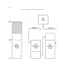
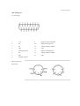
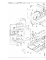
Removing the Top Case : Refer to Figure 2.3.2 (a) & (b).
(1) Remove any floppy disc from the machine and move the floppy disc lever to the horizontal position.
(2) Unscrew the two Phillips headed screws holding the rear metal safety clips, remove and store the clips and
screws.
(3) Unhook the two plastic case clips by pulling the bottom of the clips away from the case and unhook the top of
the clips from the case top.
DO NOT ATTEMPT TO SEPARATE THE BEZEL FROM THE UPPER CASE: IT IS FIXED
(4) Pull the bottom edge of the black front plastic bezel away from the lower edge of the disc drives so that it sits
on the front face of the disc drives just below the floppy disc lever.
(5) Separate the case at the rear and gently raise the upper case vertically sliding the bezel front gently over the
floppy disc lever.
(6) The rear fan should now be adjacent to the internal rear upper bracket so that by gentle movement the fan will
slide past the rear cross member. The fan can be viewed through the front VDU aperture.
(7) DISCONNECT THE FAN POWER LEAD AT THE REAR BY SQUEEZING THE MATING PLUG CLIP.
(8) Keep the upper case level and remove it from the machine.
On each side tray there are two quarter-turn captive screws which hold the side trays to the main chassis. Towards
the rear of the metal chassis are two more that hold down the main chassis which is pivoted at the front. See
Figure 2.3.2 (c).
ACW SERVICE MANUAL Issue 1
13
Chapter 2
Figure 2.3.2 (a) 2.3.2 (b)
14
ACV SERVICE MANUAL Issue 1
Assembly, Packaging and Installation
Figure 2.3.2 (c)
ACW SERVICE MANUAL Issue 1
15
Chapter 2
To lower a side trays:
(1) Using a large flat-bladed screwdriver undo the two screws that hold down the tray to the chassis, a quarter
turn anti-clockwise will cause them to spring out and release the tray.
(2) The tray can now be eased upwards a few inches and then turned on its lower-edge hinge downwards into a
horizonal position. The right hand tray contains the 32016 processor board, while the left hand tray contains
the Winchester drive interface boards and the optional mouse controller board.
(3) If necessary, the trays may be removed from the ACW by easing the hinge-pins out of the main chassis.
Access to the bottom of the ACW:
(1) BOTH side trays must be lowered as described above.
(2) Both remaining quarter-turn screws should be loosened.
(3) The rear of the cradle assembly should be moved steadily upwards until two metal stays (the scissors
mechanism) are seen to unfold. The stays should be swung fully open and this will raise the cradle assembly
further.
(4) Allow the stays to travel past their fully open position so that they become locked into the support position.
The cradle assembly is now safely supported in its intermediate open position. To open it further, the "scissors
bolts" of the two stays must be unscrewed. This need only be done when major servicing (such as whole unit
replacements) is being performed on the 6512A processor board, the Winchester drive and the floppy disc drive.
2.3.3 Re-assembling the ACW
(1) Before closing the upper unit ensure that the ribbon and power cables will not be trapped when the unit closes.
Push the scissors mechanism on both sides and allow the top unit to close.
DO NOT USE EXCESSIVE FORCE
(2) Using a large flat point screwdriver push the rear lower quarter-turn screw into the locating hole in the upper
unit and locate the slot in the quarter-turn screw body over the mating bar.
DO NOT TURN THE QUARTER-TURN SCREW UNLESS IT IS CORRECTLY MATED
(3) Turn the quarter-turn screw until it locks.
(4) Carry out the same operation on the opposite side of the ACW.
(5) Replace a side tray vertically into its supports on both sides and then press the tray down checking that no
cables are being trapped.
(6) Locate the tray's locking quarter-turn screws into the upper unit and then gently rotate the quarter-turn screws
until they lock.
(7) Carry out the same operation on the other tray.
Replacing the Upper Case
(1) Lower the upper case vertically over the ACW with the fan power lead on the OUTSIDE of the rear upper
bracket and reconnect the lead to the fan power socket.
(2) Ease the fan under the bracket while lowering the case. The fan can be viewed through the front VDU aperture.
DO NOT TRAP THE 40 WAY RIBBON CABLE, FIXED TO THE OUTSIDE OF
THE RIGHTHAND TRAY, BETWEEN THE TOP AND BOTTOM CASES.
16
ACW SERVICE MANUAL Issue 1
Assembly, Packaging and Installation
(3) Tilt the upper case slightly forward and ease the bottom edge of the black front bezel gently over the floppy
disc locking lever which should be in the horozontal position.
(4) Manoeuvure the bottom front edge of the upper unit until it begins to mate with the lower case.
(5) Keep the front mated and start to close the UPPER case whilst at the same time flexing it's side which will
allow it to clip into the LOWER case.
(6) Clip the rear interconnection panel into the upper case.
(7) Fasten the unit together with the rear plastic clips and seal the unit by replacing the metal safety clips together
with their Phillips headed screws.
(8) Check that the fan works.
2.4 Removing and installing assemblies
DISCONNECT THE ACW FROM THE MAINS POWER SUPPLY.
WARNING
The DC power supply is connected to the PCB boards using Faston connectors and identical posts are used for the
positive and the 0V supply. All Faston connectors must therefore be checked for correct polarity connection
before the DC power is supplied to the various PCBs.
The wires are colour coded as follows:
RED +5V BLACK
0V PURPLE —5V
ORANGE +12V
The RED/BLUE pair provides a nominal 12V for the lower cooling fan.
2.4.1 The power supply
Remove the upper case as detailed in section 2.3.2
Unplug the 11-wire Molex DC connector and the 2-wire Molex 240V connector.
While supporting the PSU, remove the four countersunk Philips screws securing it the the cradle. Take care to
avoid skin contact with the heat conducting compound between the PSU and chassis.
Installation is in reverse order, and a new supply of heating compound should be liberally applied to entire
surface of the power supply unit where it attaches to the VDU cradle.
2.4.2 Colour monitor CRT
BEWARE
— IMPLOSION HAZARD —
HIGH VOLTAGES REMAIN EVEN AFTER MAINS DISCONNECTION
CRT replacement should only be undertaken as a bench repair and whilst exercising extreme caution. If possible,
enlist the help of a second person when unscrewing the CRT from the cradle.
Proceed strictly in the order given, and refer to Figures 2.4.2 (a) and (b).
(1) Remove the upper case as detailed in section 2.3.2, Leave the cradle in the normal operating position.
(2) Disconnect the EHT connector on the left hand side of the CRT.
WARNING DO NOT TOUCH THE CENTRE CLIP
ACW SERVICE MANUAL Issue 1
17
Chapter 2
(3) Earth the EHT connector centre clip against the chassis metalwork to ensure that the tripler is fully discharged.
(4) Discharge the CRT final anode. Use a long shafted screwdriver with a high voltage insulated handle, rest the
metal shaft on the top of the chassis and touch the tip of the shaft into the CRT final anode EHT socket (
from where the EHT connector was removed).
(5) Disconnect the CRT earth connector from the earth tag on the CRT PCB.
(6) Remove the CRT PCB from the CRT neck.
(7) Unclip and remove the (8 way) scan coil plug from the main PCB.
(8) Unclip and remove the (6 way) degausing coil plug from the main PCB.
(9) The CRT is secured by four 5mm bolts, one at each corner of the CRT face. Slacken off the two lower CRT
mounting bolts until they are almost at the end of their threads. Slacken off the two top bolts until they are
accessible between finger and thumb.
(10) Whilst supporting the bottom of the CRT face with one hand, remove the lower bolts and then the top two
bolts and withdraw the CRT carefully from the front of the cradle assembly.
(11) Retain the degausing coil and the earth braid assembly for fitting to the new CRT.
Assembly is in reverse order
Notes:
(1) Make sure the tube is the correct way up.
(2) As a guide to centralising the CRT within the chassis, the four corner mounting bracket washers should be
aligned to the rounded part of the brackets.
IMPORTANT
Check that the CRT earth to CRT PCB lead is connected. Damage to the monitor can occur if this is not fitted.
2.4.3 Colour monitor PCB
BEWARE OF HIGH VOLTAGES EVEN AFTER MAINS DISCONNECTION.
Access to the monitor PCB is difficult unless the CRT has been removed as described above. The following
assumes that the CRT has NOT been removed and so can be undertaken on an installed ACW.
Proceed strictly in the order given and refer to Figures 2.4.2 (a) and (b).
(1) Remove the upper case as detailed in section 2.3.2. Leave the cradle in the normal operating position.
(2) Unplug the 3-wire 240V power, the contrast control and video cable connectors from the main PCB.
(3) Disconnect the EHT connector on the left hand side of the CRT.
WARNING DO NOT TOUCH THE CENTRE CLIP
(4) Earth the EHT connector centre clip against the chassis metalwork to insure that the tripler is fully discharged
(5) Discharge the CRT final anode. Use a long shafted screwdriver with a high voltage insulated handle, rest the
metal shaft on the top of the chassis and touch the tip of the shaft into the CRT final anode EHT socket (
from where the EHT connector was removed).
(6) Disconnect the CRT earth connector from the earth tag on the CRT PCB
(7) Remove the CRT PCB from the CRT neck.
18
ACW SERVICE MANUAL Issue 1
Assembly, Packaging and Installation
(8) Remove the earthing tag from the main PCB, located next to the tripler module on the chassis.
(9) Unclip and remove the (8 way) scan coil plug from the main PCB.
(10) Unclip and remove the (6 way) degausing coil plug from the main PCB.
(11) Desolder the leads from the PCB to the tripler (The tripler is screwed to the cradle metalwork on production
versions of the ACW). Do not use excessive or prolonged heat.
(12) Gently prise the monitor PCB off the six nylon PCB support studs, taking care not to use any instrument (
such as a screwdriver) which might harm the PCB tracks.
Installation is essentially in reverse order but note:
A new monitor PCB will be supplied with the tripler mounted on the PCB. The correct installation sequence is.
(1) Unsolder the tripler to line output transformer wire without using excessive or prolonged heat, as the solder
tag on the line output transformer is fragile.
(2) Unsolder the focus control eanh and the EHT tripler earth from the monitor PCB.
(3) Remove the tripler from the PCB. It is secured using two M3 screws and nuts.
(4) Extend the focus control earth to 16cm using l/0,6mm PVC wire (single core black) and the EHT tripler earth
to 8cm using 16/0,6mm PVC wire (16 strand black). Resolder the two earth wires to the PCB and rest the
tripler on the PCB. Do NOT resolder the tripler EHT wire at this stage.
(5) Install the PCB into the chassis on the six nylon pillars.
(6) Remount the tripler on the chassis (with the tripler. EHT close to the line output transformer) using the same
two screws and nuts.
(7) Resolder the tripler EHT wire to the tag on the line output transformer, without excessive or prolonged heat.
Ensure that this wire is not under tension.
Continue with the installation following the instructions for removal, but in reverse order.
IMPORTANT
Check that the CRT earth to CRT PCB lead is connected. Damage to the monitor can occur if this is not
fitted.
2.4.4 The 32016 processor PCB
(1) Remove the upper case as detailed in section 2.3.2
(2) Release the quarter-turn screw and lift and swing the side tray into the horizontal position.
(3) Disconnect the Faston DC supply (4 connections), the IDC ribbon cable connector and the keyboard
wire on PL9 from the PCB.
(4) Remove the 6 nylon screws holding the PCB and insulation sheet to the tray.
Installation is in reverse order. Take care not to overtighten the nylon screws holding down the PCB.
ACW SERVICE MANUAL Issue I
19
Assembly, Packaging and Installation
2.4.5 ADAPTEC PCB
(1) Remove the upper case as detailed in section 2.3.2
(2) Release the quarter-turn screw and lift and swing the side tray into the horizontal position.
(3) Disconnect the Molex 4-wire DC supply and the 3 IDC ribbon cable connectors.
(4) Prise the PCB from its four nylon PCB support pillars.
Installation is in reverse order.
2.4.6 Winchester host adapter PCB
(1) Remove the upper case as detailed in section 2.3.2
(2) Release the quarter-turn screw and lift and swing the side tray into the horizontal position.
(3) Disconnect the 2 Faston DC supply connectors and the 2 IDC ribbon cable connectors.
(4) Prise the PCB from its four nylon PCB support pillars.
Installation is in reverse order.
2.4.7 Mouse interface PCB
(1) Remove the upper case as detailed in section 2.3.2
(2) Release the quarter-turn screw and lift and swing the side tray into the horizontal position.
(3) Disconnect the 2 Faston DC supply connectors and the 3 IDC ribbon cable connectors.
(4) Prise the PCB and insulation sheet from its four nylon PCB support pillars.
Installation is in reverse order.
2.4.8 Disc drives
To service the disc drives it is recommended that the cradle assembly is pivotted beyond its intermediate
position.
To do this ensure that a piece of soft material such as a block of sponge rubber 150mm thick is placed in
front of the ACW to act as a supporting bed for the CRT as it swings over into an upright position. A 6mm
spanner, box spanner or small adjustable wrench will be needed to unscrew the self-locking nut from the
middle of each stay. Keep the two nuts and the two nylon washers in a safe place ready for re-assembly.
Each drive can be removed from the ACW individually.
WARNINGS
The Winchester drive must be carefully removed and installed. Do not subject it to rough handling or
vibration.
The Winchester drive contains STATIC SENSITIVE components, observe normal precautions for handling
such devices.
Winchester disc drive
(1) Disconnect both ribbon cables from the drive. Disconnect the power lead at the disc drive end.
(2) The Winchester disc drive is held down to the disc tray by four 6/32 UNC 3/8" screws. Remove these
taking care to support the drive from the front to prevent it falling through the
ACW SERVICE MANUAL Issue 1
21
Chapter 2
front aperture.
(3) Keep these screws seperate from any others removed as they are non-standard.
(4) Still supporting the drive from the front, partially lower the main chassis taking care not to trap any
cables. The drive can then be removed through the front aperture.
Installation is in reverse order. Make sure that cables are not trapped or pinched by the chassis stays.
Floppy disc drive
(1) Disconnect the ribbon cable from the drive. Disconnect the power lead at the disc drive end.
(2) The floppy disc drive is held down to the disc tray by four Philips M3 screws. Remove these taking care
to support the drive from the front to prevent it falling through the front aperture.
(3) Still supporting the drive from the front, partially lower the main chassis taking care not to trap any
cables. The drive can then be removed through the front aperture.
Installation is in reverse order. Make sure that cables are not trapped or pinched by the chassis stays. 2.4.9
110 Processor PCB
To service the 6512A PCB it is recommended that the cradle assembly is pivotted beyond its intermediate
position in the manner descibed in subsection 2.3.2 above.
(1) Remove the 7 Faston plugs carrying the DC power lines. Remove the 5 IDC plugs from the furthest
edge (viewed from the rear) of the PCB. It is possible that on some models the middle IDC socket may
be vacant. Remove the keyboard plug which is approximately in the centre of the PCB. Remove the
loudspeaker and volume control plugs (2 and 3 wires). Remove the monitor plug (5 wires).
(2) Remove the 4 Philips-head screws securing the PCB, and, moving the ribbon cable to one side as
necessary, withdraw the PCB from the base of the ACW.
Installation is in reverse order. 2.
4.10 Plastic base assembly
A plastic base assembly holds the monitor contrast potentiometer, the volume control potentiometer, the
loudspeaker and the Winchester cooling fan. To service components on this tray it is recommended that the
cradle assembly is pivotted beyond its intermediate position.
(1) To do this ensue that a piece of soft material such as a block of sponge rubber 150mm thick is placed in
front of the ACW to act as a supporting bed for the CRT as it swings over into an upright position.
(2) A 6mm spanner, box spanner or small adjustable wrench will be needed to unscrew the self-locking nut
from the middle of each stay. Keep the two nuts and the two nylon washers in a safe place ready for
re-assembly.
(3) The components on the plastic base assembly can now be reached. Depending on the components to be
replaced or repaired the task may be made easier by removing the tray from the case. Four selftapping Philips screws hold the tray down into the case.
(4) Place a sheet of card or similar material over the I/O processor to prevent solder splash damage.
(5) Note the colour coding and polarity of the wiring loom to the faulty component Unsolder these wires.
(6) Remove the faulty item. The loudspeaker is held down with silicon rubber adhesive and can be prised
out of the tray with a screwdriver. The lower cooling fan is held down by four Philips screws. The
volume and brightness potentiometers are held in by 3/8" or M10 thin nuts and
22
ACW SERVICE MANUAL Issue 1
Assembly, Packaging and Installation
removal must be preceded by the removal of the fan.
Installation is in reverse order.
ACW SERVICE MANUAL Issue 1
23
24
ACW SERVICE MANUAL Issue I
3. The monitor
3.1 Introduction
The ACW uses a medium resolution Microvitec Cub colour monitor which comprises of the CRT, two PCBs
(main PCB and CRT PCB). High voltages are present at the CRT and associated PCBs, and these voltages
can be retained in the circuits for many hours after the equipment has been disconnected from the mains. It is
recommended that the monitor is checked for electrical safety after any repair or replacement has been
carried out. This chapter covers the preset adjustments and user adjustments and a circuit description.
3.2 Removal and installation
This is done in accordance with the instruction given in sections 2.4.2 and 2.4.3.
3.3 Servicing
All servicing should be carried out in accordance with the instructions contained in the MICROVITEC
SERVICE MANUAL Number GP0019AAO. A copy of this may be obtained from the address given in the
appendix. The following sections should be used for reference only and if in any doubt refer to the
Microvitec Manual.
3.4 Adjustments
3.4.1 User adjustments
The user may only make adjustments to VDU contrast, using the left-hand control knob positioned at the
front of the ACW under the Winchester drive position.
3.4.2 Factory preset adjustments
Adjustments to certain presets can be made from above or below the main panel. Adjustments are best
made with a symetrical test pattern showing on the screen.
(1) Set HT VR4
IMPORTANT This is adjusted actuately at the factory to give 124V with a dark picture showing. This
is a CRITICAL SAFETY ADJUSTMENT and should NOT be adjusted.
WARNING
FAILURE TO COMPLY WITH THE ABOVE WILL INVALIDATE THE WARRANTY.
(2) Line frequency VR218
A. Set free running oscillator frequency to almost the frequency of incoming line syncs.
B. Adjust VR218 while supplying an RGB video and interrupt the mixed sync information to the line
oscillator by removing the sync information on PL101.
C. Adjust VR218 until the picture almost stabilises, then re-connect sync information via PL101 as
required. The result should be a stable picture lock.
(3) Field frequency VR307
A. The control of the free running field oscillator frequency is achieved by VR307 being
ACW SERVICE MANUAL Issue 1
25
Chapter 3
adjusted to give a stable picture lock. For an effective lock, VR307 should be set to the centre of the
locked picture range.
(4) Line Phase VR220
A. VR220 controls the positioning of the video information relative to the raster in the line scan
direction.
B. Ensure that the following operations have been carried out:
(1) The line frequency has been set by VR218
(2) The picture width has been set by L202
(3) The monitor is positioned in its place of use.
Note: VR220 will shift the picture right or left.
(5) Width L202
CAUTION: Care should be taken when adjusting this component as high voltages are in close
proximity to it (in particular at the tripler and line output transformer.)
A. Using a non-metalic trimming tool, adjust L202 to give the correct picture width.
(6) Height VR306
A. Raster under scan and over scan is adjusted by VR306
(7) Field linearity VR312
A. Adjust VR312 to give a linear picture in the vertical direction.
Note. Use a cross hatch grid test generator to obtain best results.
(8) Field shift VR321
A. The raster position in the field scan direction is adjusted by VR321
(9) East-West correction VR328
A. Adjustments of VR328 will acheive straight verticals on the left and right hand sides of the picture.
(10) Focus
Located on the end of the tripler module. Set the brightness control to the normal viewing level, then
make the focus adjustment.
(11) Adjust colour background control (black level)
Note: An AVO 8 multimeter and/or an oscilloscope are required for these adjustments.
(A) Prepare to adjust background colour controls.
(1) Set user contrast (VR111), brightness (VR134) and Al (VR932) fully anti-clockwise
(2) Disconnect RGB sync inputs
(B) Adjust red, green and blue
(1) Adjust VR906 for red cathode (black level) volts
(2) Adjust VR914 for green cathode (black level) volts
(3) Adjust VR921 for blue cathode (black level) volts
(4) The voltages are 140V for the 14 inch monitor.:
(C) Adjust Al voltage:
(l) Adjust VR932 until a raster is just visible
26
ACW SERVICE MANUAL Issue 1
The monitor
(2) The raster colour may be neutral, but it is more likely to be shaded towards the red, green or
blue or to a combination of any two colours.
(3) Establish raster colour shading as follows:
(a) Red and green — yellow
(b) Red and blue — magenta
(c) Blue and green — cyan
(4) Reduce the black level of the remaining one or two guns by adjusting VR906, VR914,
VR921 or a combination until a neutral raster is acheived.
(5) Re-adjust VR932 to just extinguish the raster
(6) Input RGB and sync signals, then adjust VR111 clockwise
(7) If the correct white balance has not been acheived, repeat this section. (12)
Adjust colour gain controls
CAUTION: Make the following adjustments using a DC coupled oscilloscope only.
(A) Prepare to adjust colour gain controls.
(1) Disable beam current limit circuit, by removing TL901 in series with CRT heaters on tube
base panel
(2) Provide a test pattern with peak white and blank level information on red, green and blue
(3) Ensure VRl11 is fully clockwise to provide maximum drive voltages to the video output
stages.
(B) Adjust red, green and blue gain controls
(1) Adjust VR903 for red peak to peak drive volts at R926
(2) Adjust VR910 for green peak to peak volts at R925
(3) Adjust VR916 for blue peak to peak volts at R924
(4) The voltages arc 70v p-p for 14" TTL monitor.
3.5 Circuit description
3.5.1 Technical specifications
ACW SERVICE MANUAL Issue I
27
Chapter 3
System
Supply
Timebase (line)
Frame frequency
Positional error
Convergence error
EHT
EHT regulation
Line frequency
Degausing
Bandwidth
Resolution
Dot pitch
CRT
: 625 lines, 50 fields interlaced
: 240V 50Hz
: Pull-in range 15 to 16KHz
: 50Hz – Pull-in range 45 to 65Hz
: + or –3%
: 0.6mm screen centre 1.
6mm screen edge
: 24KV approx
: + or – 1KV
: 15.625KHz
: Automatic at switch on
: 18MHz
: 452(H)x585(V) elements
: 0.64mm
: 90 degree deflection, vertical stripe screen
3.5.2 Video input
TTL mode is used. The contrast of the video information is tracked by varying the available potential across
the open collector load resistors, Rll4, 115 and 116 which are supplied by TR101 from +12V, the base being
driven from the contrast control slider VR111. R112, C101 form a low pass filter and ensure smooth
operation of the contrast control.
CRT Beam current. The information is fed to Dll7, 118, from a constant current source derived from the
main HT rail. As the CRT beam current increases the D117/118 junctions become more negative and thus
D117 conducts more heavily causing the voltage to TR106 base to decrease. R136, C105 filter the signal,
the derived voltage is emitter followed and supplies the TR103, 104 and 105 emmitters directly. Hence any
increases in CRT beam current above a preset limit causes an automatic reduction in picture brightness.
The brightness of the display is adjusted by VR134 enabling parallel adjustment of RGB and black levels
within a + or –20V range from a 700µA nominal.
TR102 is a fast switching transistor used to derive mixed blanking pulses for the flyback blanking of video
information. The base is driven from a potential divider/mixer network, from a line flyback pulse and from a
frame flyback pulse. Line flyback is advanced in phase with C225, to allow for transistor switching delays.
D107 holds TR102 in a semi-saturated state.
IC101 is also used to provide the following sync options:
(1) TL102 is in its non-active position: Composite negative sync.
Composite negative sync is fed in on PL101, pin 7, allowing pin 2 of IC101 to be pulled high, where
upon IC101 performs a sync inversion and provides an attenuated positive sync waveform for driving
sync separators of IC201, via R201 and TL106.
(2) TL102 is in a non-active position: Separate negative line and field sync pulses.
Line sync pulses are fed in on pin PL101, pin 5. IC101 performs an exclusive OR function, the output
being an inverted composite sync waveform.
(3) TL106 is switched to inverse field option: Separate positive line and field syncs. These are fed in on
PL101; pin 7 is in its grounded position. IC101 provides an attenuated and buffered line sync feed for
IC201 via R201. Positive field sync information is fed directly to PL10I, pin 3 "sync 3" input, by
TLl06(B) and R202.
(4) TL102 is in its grounded position: Compositive positive sync.
The sync is fed in on PL101, pin 7. IC101 now provides an output in phase with the input and of a
suitable amplitude for driving lC201 directly, via R201 and TL106.
28
ACW SERVICE MANUAL Issue I
The monitor
3.5.3 Line timebase
A. Line oscillator function is based on IC201, providing three outputs:
(1) Horizontal drive pulses for control of line output stage.
(2) Vertical sync pulses compatible with synchronisation of IC301 field output IC.
(3) A sandcastle pulse providing burst gate and clamping information. Sync
Separator
A. TDA 1180P incorporates separate noise gate sync separators for line/field syncs, which accepts positive
going sync pulses (or negative going composite video) on pins 8 and 9.
B. Output pulses from the line sync separator are used in conjunction with a sync gate to synchronise the
line oscillator in a phase locked loop circuit.
Line oscillator – phase detectors
A. The line oscillator is timed by a network of resistors and capacitors on pins 14 and 15 of IC201, used to
derive a pulse of suitable mark space ratio for driving line output stages.
B. IC201 contains two basic control loops, each containing a phase detector.
(1) The first phase detector compares the output of the line oscillator with the incoming line sync pulse.
Phase detector output on pin 13 is filtered and fed to the voltage control input of the oscillator on pin
15.
(2) The second phase detector, compensating for delays introduced by the line output stage and compares
line flyback pulses at pin 6 with the oscillator output. Phase detector output consists of a bi-directional
current source used to charge/discharge C213 on pin 5. The voltage derived from C213 is used to
control a phase shifter, which regulates the phase of the output pulse on pin 3. Pin 5 also provides a
line-shift function, by offseting the voltage developed across C213, charged from VR220, R221 and
R222 allowing a phase shift of + or –1µS, between the line scan and the video information.
(3) A 7uS gate pulse from the line oscillator, the phase position of which is centred around the horizontal
sync pulse. The gated pulse is used to control the arrival of sync pulses at the sync phase detector for a
duration of 7uS, allowing latching and de-latching of the line oscillator, obtained by a coincidence
detector which compares the phase gate pulse with that of incoming syncs.
(4) When the two signals are not aligned, the coincidence detector is used to switch a p.1.1. filter into a short
time constant mode, giving a high imput impedance at pin 12, thus increasing sensitivity and loop gain
of the oscillator. The phase locked loop now has a low noise immunity but has a very wide capture
range. When aligned, the coincidence detector activates the time constant switch, causing a low
impedance to appear on pin 12 and achieving a lower sensitivity and loop gain, but providing a high
degree of noise immunity. During the locked condition, the p.1.1. operates with a long time constant.
Line driver stage
A. Horizontal drive pulses from pin 3 of IC201 are DC coupled to TR201 and used to control the driver
transformer T201, providing the impedance conversion to supply the 600mA forward base current which is
required to saturate the line output transistor TR202. Ringing is damped by R225 and C214 at TR201 turn
off, thus limiting its Vice to a safe value. The HT supply to the line driver comes from the main HT supply
rail, prior to R231 and HT scan interlock (PL201 pins 5 and 6), allowing its operation to be checked
independently of the line output stage.
Vertical sync output
ACW SERVICE MANUAL Issue 1
29
Chapter 3
A. The output of the field sync separator is used to drive the vertical sync output stage on pin 10 of
IC201.
B. The pulse is also used internally to inhibit the first phase detector during the field sync period,
thus preventing top flutter resulting from equalising pulses.
3.5.4 Line output
A. Line ouput
(1) L202, L203 and T202 primary are tuned during the flyback period by C222. This lasts for 11.8 —
11.1µS.
(2) The line output transistor TR202 is driven directly from the secondary winding of T201. The on
current is controlled by R227, while turn off dissipation is minimised by L204.
(3) Line linearity correction is provided by L203, which is damped by C217 and R230. S correction is
provided by C218.
(4) The field timebase +25V is acheived by rectifying a negative going flyback voltage from the
secondary winding of the line output transformer. A fusable resistor provides CRT protection
under possible fault conditions.
3.5.5 Field timebase
The field timebase function is carried out by IC301. The oscillator frequency is determined by
VR307, R308 and C303. A 100µS output pulse is produced on pin 12. Field sawtooth is derived from
the potential across C305 and C306 as they charge towards the +25V supply via resistors R304,
R305, VR306 and R301. When the field scan is completed the 100µS pulse discharges C305 and
C306, ready for the charging cycle to be restarted.
Field Linearity
A. A sawtooth output should exist on pin I of IC301.
Field flyback
A. In order to achieve a short field flyback time, a supply voltage which is larger that that required
during the scan must be applied to the field deflector coils during the flyback period. This is made
possible by the use of a separate field flyback generator within IC301.
B. The main HT supply for IC301 is suppled to pin 5 via D302. During flyback the generator
doubles the supply on pin 5 and the potential on pin 3 is switched from 0V during scan to +25V
during flyback.
C. D302 isolates pin 5 from the +25V supply. When the deflection coil field has collapsed and the
potential across the field scan coils has fallen below +25V, pin 3 is switched back to 0V and the scan
cycle is resumed.
D. Synchronisation of IC301 is achieved by feeding a positive going field sync pulse to pin 8 of
IC301.
HT supply for IC301
A. This supply is derived via C305, C306 and VR306 with associated components R303, C301 and
D301 minimising picture bounce and "breathing" effects.
Field output
A. The sawtooth is applied to the output stage within IC301 and the scan output is available on pin
4. The current within the coils is sampled by R323 then fed back via R317 to the virtual earth input
of IC301 (pin 10).
30
ACW SERVICE MANUAL Issue I
The monitor
B. The gain of the output amplifier is set by the ratio of R314 and R317. The DC operating point is set by
the ratio of R318 and R316.
Picture geometry
A. CRT E-W pincushion distortion is corrected by the modulation of the line deflection current in transducer
T202. AC gain from the amplifying driver is used to control the amount of correction applied to the CRT.
3.5.6 CRT tube base panel
(1) All CRT electrodes are protected by a resistor, a capacitor and a spark gap.
The spark gaps on all electrodes with the exception of focus are formed by a 1-2kV ring trap gap
positioned within the base socket assembly. The high focus voltage has a separate 10kV spark gap
contained within the tube base socket.
(2) The CRT electrodes are separated from the video outputs by 220 ohm resistors, the 100K resistor of the
grid and the 820K resistor of Al.
(3) Decoupling of the grid and Al is performed by C910 and C911.
(4) The focus voltage is provided by a potential divider located within the tripler module, providing an
adjustable voltage of 5-8KV.
(5) The Al voltage is adjusted by VR932, offering a range of 350-820 volts.
(6) The CRT heaters may be disconnected by removing TL901. This is to enable video adjustments to be
made.
(7) The CRT cathodes arc directly driven from the video output stages mounted on the CRT panel. Video
output stages
Since the red, green and blue video output stages are identical, the description given here is for the red stage
only.
(1) TR902 forms a class A amplifier with AC gain derived from the ratio of R935, R902 and VR903 and DC
gain derived from a DC offset current set by the ratio of R905 and VR906.
(2) R904 forms a video output load.
(3) When in conduction, the CRT input capacitance sees TR902 as a low impedance drive source.
(4) Video compensation, which helps maintain a constant amplifier response curve over the full range of
VR903, is achieved by the split capacitances of C902 and C903.
(5) The video black level voltage is set by a DC reference of approximately 7.5V connected to the emitters
of TR902, TR904 and TR906.
(6) TR907 performs line and field blanking.
TR907 is driven by negative going mixed blanking pulses from TR102. A 7.5V black level reference
is provided by the conducting TR907.
TR907 is turned off during line and field flyback, thereby forcing video outputs off.
(7) R937, D117 and D118 are responsible for sensing beam current.
ACW SERVICE MANUAL Issue 1
31
32
ACW SERVICE MANUAL Issue I
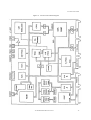
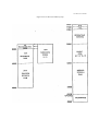
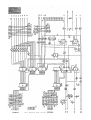
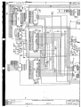
4.I/0 Processor board
The ACW's uses the 6512A as its I/O processor. The PCB board is the same as that used in the BBC Model
B+ microcomputer except for a small number of ommissions, the most noticable of which is the UHF
Modulator and associated components.
4.1 Specification
4.1.1 The microcomputer
Internal loudspeaker driven from a 4-channel sound synthesis circuit with ADSR envelope control.
A BNC connector supplies a composite video output to drive a black and white or PAL colour monitor.
6-pin DIN connector provides separate RGB and sync outputs at TTL levels. RGB are all high true, and sync
is link selectable as high or low true, pulse duration 4.0 microseconds.
A standard audio cassette recorder can be used to record computer programs and data at 300 or 1200 baud
using the Computer Users' Tape Standard tones. The cassette recorder is under automatic motor control and
is connected to the computer via a 7-pin DIN connector.
An interrupt driven elapsed time clock (user settable).
6512A processor running at 2MHz.
64K of read/write Random Access Memory (RAM), allowing a shadow screen mode, and 12K paged RAM
in any mode.
Read Only Memory (ROM) integrated circuit containing the Machine Operating System and a fast BASIC
interpreter. The interpreter includes a 6502/6512 assembler which enables BASIC statements to be freely
mixed with 6502/6512 assembly language. Code generated using the BASIC assembler can be run on a
machine with a 6512 microprocessor, or a machine with a 6502 microprocessor.
Up to five 32K sideways ROMs may be plugged into the machine at any time, having the effect of ten 16K
ROM slots (eleven including BASIC). These ten 16K ROM slots are paged and may include Pascal, word
processing, computer aided design software, disc and ECONET and WINCHESTER filing systems or
TELETEXT acquisition software.
The full-colour Teletext display of 40 characters by 25 lines, known as mode 7, has character rounding, with
double height, flashing, coloured background and text plus pixel graphics - all to the Teletext standard.
The non-Teletext display modes (modes 0 to 6) provide user-definable characters in addition to the standard
upper and lower case alpha-numeric font. In these modes, graphics may be mixed freely with text.
ACW SERVICE MANUAL Issue I
33
Chapter 4
The following screen modes are available:
Mode
Mode
Mode
Mode
Mode
Mode
Mode
0/Mode
1/Mode
2/Mode
3/Mode
4/Mode
5/Mode
6/Mode
128:
129:
130:
131:
132:
133:
134:
640
320
160
80 x
320
160
40 x
x 256 2-colour graphics
x 256 4-colour graphics
x 256 16-colour graphics
25 2-colour text only
x 256 2-colour graphics
x 256 4-colour graphics
25 2-colour text only
and 80 x 32 text
and 40 x 32 text
and 20 x 32 text
and 40 x 32 text
and 20 x 32 text
Mode 7/Mode 135: 40 x 25 Teletext display
All screen access is via the I/O processor operating system.
Shadow mode gives 32K BASIC program RAM (less workspace) to the user in any screen mode.
The shadow screen mode offers equivalent display sizes to the standard mode 0 to 7 screens, but using an
auxiliary memory area, the "shadow" RAM. In shadow display modes (modes 128 to 135) BASIC or a user
program is free to use all memory between OSHWM (PAGE) and &7FFF, plus the 12K bytes of sideways (
paged) RAM.
The 12K paged RAM is available to the user in any screen mode, shadow or non-shadow. The
ACW starts up in shadow mode.
Serial interface to RS423 standard. The new standard has been designed to be inter-operable with RS232C
equipment. Baud rates are software selectable between 75 baud and 19200 baud (guaranteed up to 9600
baud).
An 8-bit input/output port with 2 control bits.
Four analogue input channels. Each channel has an input voltage range of 0V to 1.8V. The conversion time
for each channel is 10 milliseconds. The resolution of the ADC chip is 10 bits.
1 MHz buffered extension bus for connection to the Winchester PCB, the mouse PCB, and to a variety of
external hardware such as a TELETEXT acquisition unit and IEEE 488 interface.
Buffered interface for connection via the TUBE to the 32016 processor PCB.
CENTRONICS compatible printer interface.
A dedicated floppy disc interface using the 1770 controller IC.
A dedicated network interface, the Acorn ECONET.
A speech upgrade is available using the 5220 speech IC to generate predefined words and sounds through
the built-in speaker.
34
ACW SERVICE MANUAL Issue 1
I/O Processor board
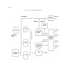
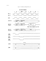
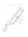
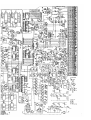
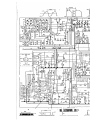
Figure 4.1.1 I/O Processor Block Diagram.
ACW SERVICE MANUAL Issue 1
35
Chapter 4
4.1.2 Power requirements
+5V voltage
+5V DC +/-0.1V
+12V voltage
+12V DC +/-10%
-5V voltage
-5V DC +1-10%
4.1.3 Display outputs
Colour monitor (marked RGB)
RGB signals
TTL type levels
CSYNC signal
TTL type level +ve/-ve going (link selectable)
4.1.4 RS423
Line length
1200m maximum
Input impedance
> 4k ohms
Baud rate
19200 maximum (
guaranteed up to 9600) 4.1.5
Cassette
interface
Output impedance
Less than lk ohms
Input impedance
Greater than 100k ohms
Output level
Nominal 200mV peak to peak, 70mV RMS
Dynamic input range
Nominal 50mV to 5V peak to peak, -25 to +15dB
0dB = 350mV RMS
Motor control
By miniature relay within computer
Contact rating lA at 24V DC
Baud rate
300 or 1200 baud using standard CUTS tones (
1200 and 2400 Hz tones)
4.1.6 Analogue to digital convertor
Resolution
10 bit
Full scale input voltage
VREF
VREF
1.8V typical
Accuracy (with respect to VREF)
36
full scale error
0.5% typical
zero scale error
0.5% typical
Non-linearity
0.1% typical
Temp coefficient
-6mV/degree C typical
Conversion speed
10.0ms per channel typical
Input impedance
> 1M ohms
ACW SERVICE MANUAL Issue 1
I/O Processor board
4.1.7 ECONET
Line voltages
0.25V and 3V typical into 50 ohms
4.1.8 CENTRONICS compatible printer interface Data strobe
4us pulse
4.1.9 Audio output
Output power
Speaker impedance
0.5W
8 ohms
4.1.10 Environment Air
temperature
system on
0 to 35 degrees C
system off
-20 to 70 degrees C
system on
85% relative humidity at 35 degrees C
system off
95% relative humidity at 35 degrees C
Humidity
Storage conditions
air temperature
-20 to 70 degrees C
humidity 95% relative humidity at 55 degrees C
4.2 Circuit description
This circuit description has been kept as simple as possible as the detailed fault finding section (section 4.7)
should prove to be of more use for servicing.
4.2.1 General
The microcomputer uses the 6512 CPU (IC42) which allows more accurate timing of the logic circuitry than
did the 6502, see subsection 4.2.2. The 6512 requires two clock signals at 'MOS' voltage levels, in all other
respects it functions in the same way as the 6502.
The computer clocks are derived from a 16MHz crystal controlled oscillator circuit (X1 and half of IC26),
and divider circuitry in the video processor ULA (IC53).
The 6512 accesses 31 1/4Kbytes of ROM, 3/4Kbyte of memory mapped input/output, and up to 44Kbytes of
RAM. 64Kbytes of RAM are installed on the PCB, the extra 20Kbytes being used for the screen memory in
shadow mode.
The memory mapped I/0 is located in pages &FC, &FD, and &FE of the CPU address space.
There are five sideways ROM sockets installed on the PCB, each capable of taking an 8, 16, or 32Kbyte
ROM or EPROM (ICs 35 44 57 62 68). When used with a 32K ROM, each sideways ROM socket is
decoded as two 16K sideways ROM slots. A sixth ROM socket IC71 holds a 32Kbyte ROM which contains
the operating system and BASIC. The number of the ROM currently in use is held in the ROM select latch (
1C45).
64Kbytes of RAM are installed on the board in eight 64K by 1 bit DRAM chips, (ICs 55 56 60 61 64 65 66
67). Of this RAM, 32Kbytes are always accessible to the CPU, 12Kbytes can be paged into the sideways (
paged) ROM space, and the remaining 20Kbytes are used as screen memory in shadow
ACW SERVICE MANUAL Issue 1
37
Chapter 4
mode. Both CPU (IC42) and 6845 cathode ray tube controller (1C78) have access to the RAM. Each can
access the RAM at full 2MHz clock speed by interleaving the accesses on alternate phases of the 2MHz
clock. The RAM is thus being accessed at 4MHz. The 6845 accesses the RAM sufficiently to perform the
refresh function.
Screen display is provided through the 6845 (IC78), video processor (IC53), and various encoding circuits.
Three display outputs are available:
RGB consists of CSYNC and RED GREEN BLUE at TM voltage levels. Each colour is either on, off, or
flashing, giving sixteen displayable colour effects, ie eight static colours and eight flashing colours.
VIDEO output is a summation of RGB to give a grey scale (luminance only). If link S26 is made the
chrominance component (colour information) is added to the VIDEO output.
Serial input/output is provided by the cassette port and RS423 port. Both are controlled by the 6850
asynchronous communications interface adapter (IC82) and a ULA called the serial processor (IC85).
Analogue input is fed to the four-channel 10 bit ADC chip (IC84).
A local area network facility is provided by the ECONET circuitry, centred on the 68B54 advanced datalink controller (IC81).
The floppy disc controller is the 1770, IC16. The 1770 operates in either single density (FM) or double
density (MFM) mode, and includes a data separator and disc speed decision logic. ICs 1, 2, 3, 4, 9 and 15 are
not required with a 1770.
The CENTRONICS compatible printer interface is based on half (the A port) of a 6522 versatile interface
adapter (IC10). IC5 buffers data sent to the printer.
The User Port is connected directly to the B port of the same 6522 (IC10).
The 1MHz extension bus is a fully buffered interface to the CPU, operating with lus transfer cycles. The bus
appears as a 512 byte address block in the processor I/O space at pages &FC and &FD.
The TUBE interface provides buffered address and data lines for connection to the 32016 processor. The
TUBE itself is a fast parallel bidirectional FIFO and is resident on the 32016 PCB.
The keyboard is read through half (the A port) of a 6522 versatile interface adapter (IC20).
Sound is produced by the 76489 (1C38), a four-channel sound generator chip. Speech may be generated
using an optional 5220 speech processor (IC29) and 6100 word PHROM (IC37).
4.2.2 CPU timing
A 16MHz crystal controlled oscillator (X1 and half of IC26) generates clock pulses which are divided by
circuitry within the video processor ULA (IC53). Pins 4, 5, 6, and 7 of the video processor provide 1MHz,
2MHz, 4MHz, and 8MHz outputs respectively. 8MHz, 4MHz and 2MHz are used to generate RAS and CAS
for the DRAMs, and 6MHz for the TELETEXT chip IC59. 2MHz is used to generate the main system clock,
2E. 1MHz is used directly by the TELETEXT chip, and also in conjunction with 2MHz to generate the phase
shifted 1MHz system clock, 1E from IC25.
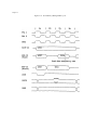
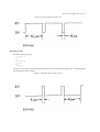
The CPU is normally clocked at 2MHz. The 6512 (IC42) requires a two phase non-overlapping clock on
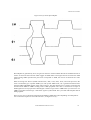
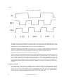
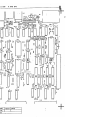
inputs phil (pin 3) and phi2 (pin 37), see figure 4.2.2 (a).
38
ACW SERVICE MANUAL Issue 1
1/O Processor board
Figure 4.2.2 (a) Clocks phil and phi2.
Phil and phi2 are generated by IC33, two gates of which are used to build an R-S latch. Not2M from IC26 is
used to set and reset the R-S latch which toggles at 2MHz unless a third gate from IC33 blocks the N2M
signal. During 2MHz operation the phi2 clock corresponds to N2M, the inverse of 2M from the video
processor.
When accessing slow devices (1MHz extension bus, ADC, VIAs, 6845, ACIA, and serial processor) the
clock is stretched to give a pseudo 1MHz cycle. The system 1MHz clock, 1E, is generated in half of IC25
from the 1MHz and 2MHz outputs of the video processor. The other half of IC 25 is used to synchronise the
transition from 2MHz to 1MHz clocking. Each 1 MHz peripheral select line is connected to an input of
NAND gate IC41. If any input of this NAND gate is taken to logic 0 then a 1MHz CPU cycle will occur. For
1MHz cycles phi2 is held at logic 1 until the E signal is synchronised. The cycle ends with both phi2 and 1E
falling together.
There are two ways in which the transition from 2MHz to 1MHz takes place depending on which phase E
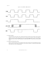
was on when the request was received from IC41, see Figure 4.2.2 (b).
ACW SERVICE MANUAL Issue 1
39
Chapter 4
Figure 4.2.2 (b) 2MHz to 1MHz transition
4.2.3 Reset circuitry
The system has two reset circuits, one is a general reset from a 555 timer (IC43), the other is an RC network
which just resets the system VIA (IC20) on power-up. This allows the software to detect the difference
between a power-on reset and a BREAK key reset. The keyboard BREAK key connects via S10 (a PCB
made link) to the 555 timer. The 555 generates reset pulse RS which is inverted to give the CPU NRS
signal.
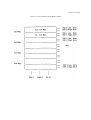
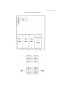
4.2.4 Address decoding and memory
Figure 4.2.4 shows the memory map. At the heart of the memory selection is the programmable array logic (
PAL) chip IC36. It selects which screen RAM is in use (normal or shadow); it controls the sideways ROM
select latch IC45; it selects the paged RAM.
40
ACW SERVICE MANUAL Issue I
1/O Processor board
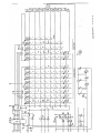
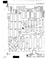
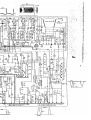
Figure 4.2.4 I/O Processor Memory map
Chapter 4
4.2.5 ROM operation
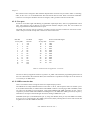
Any ROM socket on the PCB can either hold an 8K, 16K or 32K BYTE device. 8K or 16K IC's are paged
into the memory map from &8000-&9FFF or from &8000-&BFFF respectively, a 32K device provides two
16K banks of memory paged into the memory map from &8000-&BFFF. The extra address line A14 (QA
from IC45) required by 32K devices is available to each ROM slot when the appropriate molex link is
altered. The ROM socket IC numbers, their corresponding ROM select numbers and their corresponding link
numbers are shown in table 1.
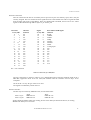
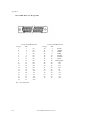
IC No ROM Nos Link No Notes
IC35
IC44
IC57
IC62
IC68
IC71
2/3
4/5
6/7
8/9
10/11
0/1 or
14/15
S9
S11
S12
S15
S18
S19
Molex link made W as standard for 8K/16K use
"
"
"
"
"
"
"
"
"
"
"
"
PCB cuttable link made E as standard for 32K
(16K operating system and I/O and 16K BASIC)
Table I: ROM Sockets
As can be seen from table 1, ROM numbers range from 0 to 15. ROM priority is directly proportional to the
socket number it is in. The highest ROM number language and filing system will be selected after a 'hard'
reset. 15 has the highest priority, 0 the lowest. So if two or more sideways ROMs are language ROMs, then
the computer will start up in the language in the highest number ROM slot. Similarly for filing system
ROMS.
IC35, 44, 57, 62, and 68 we shall call "user ROMs". Each user ROM socket is functionally identical and can
contain language or service ROMs. IC71 we shall call the "system ROM".
The system ROM contains the operating system. The operating system is always in the memory map from
&C000-&FFFF and must always be fitted in IC71. As an option the computer can accept a 32K ROM for
IC71 containing the operating system and the BASIC language. In this case link S19 is East in the 32K
position.
The BASIC part of the system ROM occupies one of four sideways ROM numbers. As standard, any call
made to ROM 14 or 15 selects BASIC, and any call to ROM 0 or I is ignored. Hence BASIC occupies the
highest priority ROM slot and the computer will start up in BASIC. If molex link S13 is moved from South
to North then any call made to ROM 0 or 1 will select BASIC, and any call to ROM 14 or 15 will be
ignored. This allows the user to select an alternative language at power-on (the language entered at start-up
will be the one with the highest socket number when more than one language ROM is fitted).
Address decoding is carried out by the PAL (IC36) and this then selects either the operating system (if the
address is in the range &C000-&FFFF) or the current sideways ROM (if the address is in the range &8000&BFFF). Part of IC40 disables the ROM output drivers when an I/O address occurs (&F000-&FEFF).
42
ACW SERVICE MANUAL Issue 1
I/O Processor board
The currently selected ROM number (0-15) is held in the ROM select latch IC45. The ROM select latch is
mapped into the memory at address &FE30 via the PAL IC36. When writing to this address, the four data
lines DO-D3 provide the ROM number which is latched into IC45, see also 5.4.2.
When the PAL decodes an address from &8000-&BFFF, IC36 pin 18 goes low and enables IC46. IC46 is a
three line to eight line decoder which selects the particular IC socket allocated to the ROM number, in IC45.
The least significant bit held in IC45 is fed to the relevant ROM socket only if the link for that socket is
made E for a 32K device. The correct half of the 32K device is then selected to be placed in the memory
map.
4.2.6 Paged RAM operation
The 12K paged RAM is selected with a ROM number between 128 and 255 (D7 set). The top bit of the data
bus D7 is available to the PAL IC36. Writing to the ROM select latch at address &FE30 as described in 5.4.
1, will save D7 in the PAL. DO-D3 are stored as normal in IC45. If D7 is set (logic 1) then the PAL selects
the 12K paged RAM when the CPU address is in the range &8000 to &AFFF. If the ROM selected by DOD3 is present then the top 4K of that ROM will also appear in the memory map, above the 12K paged RAM,
from &B000-&BFFF. As ROM 0 is not allocated as standard (it is BASIC if S13 is changed), writing 128 to
the ROM select latch will merely place the 12K paged RAM into the memory map and &B000-&BFFF will
be vacant.
4.2.7 RAM access
There is 64K of installed RAM.
RAM access is dependent on whether the computer is in normal mode or shadow mode, and the differences
are shown in Figure 4.2.7.
ACW SERVICE MANUAL Issue 1
43
Chapter 4
Figure 4.2.7 RAM access in normal and shadow modes
I/O Processor board
In normal mode the RAM can be thought of as 44K from address &0000-&AFFF. The top 12K of this RAM
from address &8000-&AFFF is paged into the memory map when required in place of the bottom 12K of the
sideways ROM space, see 5.4.2. The remaining 20K of RAM is set aside for the shadow screen memory,
while it always exists, it is not available to the system in normal mode. The bank of 44K RAM we shall call "
normal RAM". In normal mode, VDUSEL (IC36 pin 17) is always zero.
Any code executing anywhere within normal RAM in normal mode will always access normal RAM, it
cannot access shadow RAM.
In shadow mode the RAM can be thought of as 44K from address &0000-&AFFF, plus a parallel bank of
20K RAM from address &3000-&7FFF which we shall call "shadow RAM". As in normal mode, the top
12K of normal RAM is paged into the memory when required. In the address range &3000-&7FFF the PAL (
IC36) is able to switch between shadow RAM and normal RAM. It selects access to the shadow memory if
a) shadow mode is on b) it detects a VDU driver and c) the operand address is between &3000 and &7FFF,
the part of the memory map used by the screen. Otherwise it selects access to normal RAM. The machines
logic is set to shadow mode when logic 1 is written to D7 at address &FE34, this causes pin 17 (VDUSEL) to
go high. &FE34 is the address of a register in the PAL and when D7 is set any screen access through the
VDU drivers will cause the PAL to switch in the shadow memory by making pin 12 (CPUSEL) high. In
shadow mode, VDUSEL is always set, and CPUSEL is low to access normal RAM and high to access
shadow RAM.
When the paged RAM is selected in shadow mode, the top 4K, &A000 to &AFFF, is programmed by the
PAL (IC36) to have the attributes of VDU drivers.
Any code executing between &0000-&9FFF in shadow mode will always access normal RAM.
Any code executing from sideways RAM between &A000-&AFFF will access the shadow RAM (if
selected) when the operand address is between &3000-&7FFF. This special attribute is not available to any
other sideways memory, ROM or RAM.
RAM circuitry
The 64K installed RAM is provided by eight 64K by 1 dynamic memory devices ICs 55, 56, 60, 61, 64, 65,
66, and 67. Figure 4.2.8 shows the RAM timing diagram.
ACW SERVICE MANUAL Issue 1
45
Chapter 4
Figure 4.2.8 RAM timing diagram
The RAM control circuit is designed to work with either 128 or 256 refresh cycle DRAMs, refresh being
provided by the 6845 CRTC (IC78) in conjunction with two ex-OR gates of IC63 and an AND gate of IC34.
The RAM is accessed at 4MHz, the CPU and VDU each having 2MHz access.
The address multiplexers for the VDU cycle are ICs 72, 73, 74, and 75. Various combinations of the inputs
of these ICs are used depending on the screen mode in use. In particular, TELETEXT mode 7, with its own
character generator (IC59) is markedly different from the other seven bit-mapped modes 0-6.
The address multiplexers for the CPU cycle are ICs 50 and 51.
RAM is working (being addressed and strobed) the whole time, both during CPU and VDU phases, even
when not required (except for the purpose of refresh). But data to or from the RAM is only available to the
CPU, when the data buffer IC49 is enabled. This occurs when any input to the NAND gate in half of IC40
goes low, that is when A15 is low (address between &0000-& /1-1+) or if the paged RAM signal from IC36
is low (address between &8000-&AFFF and paged RAM selected), or if the video processor (VIDPROC) is
enabled (address &FE20). RAM is disabled when the VIDPROC is written to, by holding NCAS at logic 1 (
see IC23).
4.2.8 Disc interface
A 1770 operates in either Frequency Modulation (FM) or Modified Frequency Modulation (MFM) mode.
Since MFM results in increased storage density FM is refered to as "single" density and MFM as "double"
density. The 1770 has a data separator and disc speed decision logic built in. No drive select logic is
incorporated in a 1770 so IC17 is fitted for this function. IC17 also latches two contol signals which are
used to select between FM and MFM operation and to reset the 1770, both under
46
ACW SERVICE MANUAL Issue 1
1/O Processor board
program control.
The control register IC17 is a write only device which occupies the address space &FE80 to &FE83. IC23
gates the decoded address signal with NW (IC27 pin 6) to form the control register clock.
All 1770 registers are addressed in the range &FE84 to &FE87.
Two interrupt signals come from a 1770, pins 27 and 28. The two interrupts are inverted and wire NORed on
to the NNMI line by two parts of IC7 (quad NAND gate). Link S8 selects between the single interrupt of an
8271 and dual interrupt of a 1770. When a 1770 is fitted S8 must be made. For the 1770 option link S7 is
made East, this incorporates N2M into the chip select signals and so defines the timing of data transfers
between the disc controller and the CPU. Link S5 is available to allow program controlled suppression of
1770 disc controller interrupts (IC17 is not present when the 8271 is fitted). The disable function is not used
at present so S5 is not fitted.
4.2.9 Display circuitry
Red, green and blue signals are produced by the video processor and are then buffered by Ql, Q2, and Q3 to
be fed to the DIN socket (SK3) at TTL type levels. The fourth signal required at the RGB output is a
composite SYNC (CSYNC) generated from horizontal sync and vertical sync of the 6845. CSYNC polarity
can be altered using link S27. The 0V and +5V power supply also appears on SK3.
4.2.10 CENTRONICS compatible printer interface
The computer can drive a centronics compatible printer through ICIO, a 6522 VIA. Port A of the VIA is
configured as an 8-bit output port which is buffered by IC5 and fed to PL9. Printer strobe pulses are
generated by a program sequence which toggles CA2 (IC10 pin 39) high-low-high. Strobe pulses are
typically 4us wide. ACK from the printer is connected to CA1 (IC10 pin 40). ACK is pulsed low for
approximately Sus by the printer when it is ready for the next character/byte transfer.
A 24-way 'Delta' or IEEE 488 style connector is provided. The connections are shown in Table 2 together
with those of the standard 36-way connector with which printers are usually provided.
Signal
strobe
Data 0
Data 1
Data 2
Data 3
Data 4
Data 5
Data 6
Data 7
Acknowledge
No connection
Ground
I/O PCB
26–way
1
3
5
7
9
11
13
15
17
19
21,23,25,26
2,4,6...,24
Connector Pin
Rear Pnl
24–way
1
2
3
4
5
6
7
8
9
10
11,12
13 to 24
Printer
36–way
1
2
3
4
5
6
7
8
9
10
11 to 17
18 to 29
Table 2: Connections for ACW Parallel Printer Port
ACW SERVICE MANUAL Issue 1
47
Chapter 4
The connections are arranged so that insulation displacement connectors may be used to make a connecting
cable; in this case it is recommended that 'flat and twisted' cable be used. With conventional solderable
connectors a twisted pair should be used for each signal, with a ground connection at both ends.
4.2.11 User port
Port B of IC10 offers eight individually programmable input/output lines, and two programmable control
lines. The connector pins go directly to a 6522 Versatile Interface Adaptor (VIA). The VIA contains two
fully programmable bi-directional 8-bit I/O ports.
The ACW uses a 25-way 'D-type' connector, see Table 3 for the rear panel connections. Also shown in the
table is the pin-out of the 42 way IDC connector on the I/O Processor.
Rear Pnl
25-way IDC
1
1
2
3
3
5
4
7
5
9
6
11
7
13
8
15
9
17
10
19
11
21
12
23
13
I/O PCB
function
+5V
+5V
0V
0V
0V
0V
0V
OV
0V
0V
N/C
N/C
N/C
Signal
25-way IDC
14
2
15
4
16
6
17
8
18
10
19
12
20
14
21
16
22
18
23
20
24
22
25
24
Rear Pnl I/O PCB Signal
function
CB1
CB2
PB0
PB1
PB2
PB3
PB4
PB5
PB6
PB7
N/C
N/C
Table 3: Connector Pin Assignments - User Port
The VIA is memory mapped at locations 16_FE40 to 16_FE6F. The method of programming the function of
the VIA is described in the 6522 Data Sheet; this information is reproduced in Chapter 22 of the Advanced
User Guide for the BBC Micro.
4.2.12 1MHz extension bus
This is an extension of the bus signals of the 6512 Input/Output processor.
The 1MHz bus is a fully buffered interface to the CPU via PL11, which operates with I us transfer cycles.
IC12 (bidirectional buffer) is enabled when either FRED or JIM is accessed (pages &FC and &FD). These
two pages are decoded by IC22 and IC28, with signals NFRED and NJIM appearing on pins 4 and 5
respectively of IC28. When either NFRED or NJIM goes low, the 1MHz bus enable goes low (IC34 pin11),
and takes low an input of the NAND gate IC41 thus causing a 1MHz CPU cycle.
NotFRED (IC28 pin 4) and NJIM (IC28 pin 5), along with R/NW (IC24 pin 10) and 1MHz bus enable (
IC34 pin 11) are synchronised to the 1MHz system clock (1M) by latching them in IC32. This ensures that
no glitches occur on the 1MHz bus interface.
48
ACW SERVICE MANUAL Issue 1
1/O Processor board
External Connections
Devices connected to the bus are accessed by the I/O processor as part of its memory space, that is, they are
'memory mapped'. The bus contains the least significant 8-bits of the address bus and two signals decoded
from the high order 8-bits of the address. These are labelled NFC and NFD, and are 'active low'. These
signals are decoded from high address bytes 16_FC and 16_FD.
Rear Pnl
37-way IDC
1
1
2
3
3
5
4
7
5
9
6
11
7
13
8
15
9
17
10
19
11 21
12
23
13
25
14
27
15
29
16 31
17
33
18
35
19
37
I/0 PCB
function
0V
0V
0V
OV
OV
0V
OV
OV
0V
D1
D3
D5
D7
A0
A2
A4
A6
N/C
N/C
Signal
37-way IDC
20
2
21
4
22
6
23
8
24
10
25
12
26
14
27
16
28
18
29
20
30
22
31
24
32
26
33
28
34
30
35
32
36
34
37
36
Rear Pnl I/O PCB Signal
function
R/NW
1MHzE
NNMI
NIRQ
NPGFC
NPGFD
NRST
Analog Input
D0
D2
D4
D6
0V
A1
A3
A5
A7
N/C
N/C = No connection
Table 4: Connections for 1 MHz Bus
The bus connections are shown in Table 4. For a detailed description reference should be made to the 1
MHz Bus Application Note Acorn No. 0407,000 available from the Customer Services Dept. Acorn
Computers.
On the ACW a 37-way 'D' type connector is used.
The signals are buffered by LSTTL devices.
Software Interface
The bus may be accessed by OSBYTE calls, as in the table below:
Assert 16_FC
Assert 16_FD
Read
OSBYTE 146
OSBYTE 148
Write
OSBYTE 147
OSBYTE 149
Param1 holds the address offset. For reading, Result1 is the data byte taken from the bus; for writing,
Param2 is the data byte to be written.
ACW SERVICE MANUAL Issue 1
49
Chapter 4
Some system peripherals are connected to the 1 MHz bus, and are assigned parts of the address space as
shown in Table 5.
16_FC00 to 16_FC0F
16_FC1D to 16_FC13
16_FC14 to 16_FC1F
16_FC20 to 16_FC27
16_FC28 to 16_FC2F
16_FC30 to 16_FC3F
16_FC40 to 16_FC47
16_FC48 to 16_FC7F
16_FC80 to 16_FC8F
16_FC90 to 16_FCBF
16_FCC0 to 16_FCFE
16_FCFF
16_FD00 to 16_FD7F
16_FD80 to 16_FDFF
Test hardware
Teletext interface
Prestel interface
IEEE 488 interface
Reserved for use by Acorn
Cambridge ring interface
Winchester disc interface
Reserved for use by Acorn
Test hardware
Reserved for use by Acorn
Available for user applications
Paging register for memory expansion
Reserved for use by Acorn
Available for user applications.
Table 5: 1MHz Bus Address Assignments
50
ACW SERVICE MANUAL Issue I
1/O Processor board
ACW SERVICE MANUAL Issue 1
51
Chapter 4
4.2.13 TUBE interface
The TUBE interface connects to the 32016 second processor via PL12. The signals present are the eight
data lines, five address lines A0 to A4, R/NW, 2E, NRS and N1RQ. The data lines are buffered by 1C14,
and the address lines, R/NW and 2E are buffered by 1C13. The data buffer IC14 is enabled when a TUBE
address (&FEE0-&FEFF) is decoded by 1C21, this enable signal (NTUBE) being fed also to the TUBE
connector, PL12.
R11 is fitted so the computer OS can detect when there is no second processor present (or powered on).
4.2.14 ECONET
ECONET is based around the 68B54 (IC81) advanced data link controller. IC81 performs the conversions
between serial and parallel data, and generates the interrupt requests which are connected to NMI. Each byte
transfer between network and CPU is requested by an NMI. Interrupts can be disabled by making pin 4
1C23 low thereby setting the D-type (half of 1C69), which is achieved by a read of &FE18. Reading this
address returns the station ID number which is set up on the links S23. Interrupts are enabled when pin 2
1C69 goes low (a read of &FE20), which, when clocked by N2E, resets the D-type.
Transmit data from the 68B54 is fed to a differential line driver circuit IC91, and then through SK7 on to
the twisted pair network cable. The differential drive voltages are, typically, 0.25V and 3V. A monostable (
half of IC88) is used to time-out the ECONET line driver by taking pin 9 IC91 low after approximately 4.5s
(longer than the time required to transmit a maximum length data packet). This is designed to prevent a
single computer holding its driver on and thereby bringing the whole network down.
Receive data is decoded by a comparator circuit 1C92 and fed into the 68B54. 1C93, collision detect
ciruitry is not fitted. Before transmission, the line is sampled to see if it is in use. If it is, the transmission is
held up until a certain time after the line is first free again. This time is dependent on the station 1D and so
will be different for every station on the line. When required collision detect may be installed by fitting
components as shown on the circuit diagram, and breaking the link S29, a PCB copper link.
4.2.15 Cassette and RS423 ports
For both the cassette (SK5) and RS423 (SK4) interfaces, a 6850 asynchronous communications interface
adaptor (AC1A) 1C82 is used to buffer and serialise or deserialise the data. The serial processor 1C85
contains two programmable baud rate generators, a cassette data/clock separator, switching to select either
RS423 or cassette operations, and also a circuit to synthesise a sinewave to be fed out to the cassette
recorder.
Note that the receive bit rate for cassette operations is derived from the FSK signal not from the serial
processor control register bits used when RS423 operation is selected.
1C18 divides the 16MHz clock signal by 13 (1.23 MHz) and this signal is divided further within the serial
processor to produce the synthesised 2400/1200Hz cassette record signal, and the bit rate clocks. Automatic
motor control of an audio cassette recorder is achieved by using a small relay driven by transistor Q7 from
the serial processor.
R66 and C30 provide the necessary timing elements for delay between receiving the high tone run-in signal
and asserting the data carrier detect signal to the 6850.
The signal coming from the cassette recorder is buffered, filtered and shaped by three stages of the LM324
amplifier IC89.
The RS423 data in and data out signals and the request to send output RTS and clear to send input CTS
signals are interfaced by ICs 94 and 95 which translate between TTL and standard RS423 signal
52
ACW SERVICE MANUAL Issue 1
I/O Processor board
levels +5V and -5V.
RS423 signals are compatible with the RS232 signals common in computer related equipment.
Selection of the cassette or RS423 for input and output is by bit 6 of the serial processor control register, bit
7 is for cassette motor control. Bits 0 to 2 control the transmit bit rate, while bits 3 to 5 set the RS423 receive
bit rate.
External Connections
Table 6 shows how the ACW should be connected to the 25-way D-type connector with which most serial
interfaces are provided. The ACW is classed at Digital Computer Equipment (DCE) so can easily be
connected to, for example plotters which are usually classed as Digital Terminal Equipment (DTE).
Connection to other DCE classed systems, such as a second ACW or main-frame computer, will require a "
crossed" cable. The standard is open to interpretation so some experimenting may be required to find the
correct connections.
ACW 5-pin Domino Din
Canon 25-way connector
Function
Data in
Pin
Function
Pin
A/1 connect to
B/2 connect to
D/4 connect to
E/5 connect to
Ca connect to
Transmitted data
Received data
Request to send
Clear to send
Signal ground
2
3
4
5
7
Data out
CTS
RTS
GND (OV)
Table 6: Connections for RS423 ACW to DTE
The signal levels conform to the specifications of the Electronic Industries Association standard RS422A
and RS423A. The protocol used by the ACW is as follows:
(a) The I/O Processor will transmit while CTS is asserted.
(b) The I/O Processor will assert RTS when it is ready to receive.
Serial printers
For driving printers the connections shown in Table 7 should be made:
ACW SERVICE MANUAL Issue 1
53
Chapter 4
RS423 connector
Function
Pin
data out
CTS
B/2
D/4
ground
C/3
printer 25-way connector
to
to
OR
to
Function
Receive data
data terminal ready
request to send
signal ground
Pin
3
20
4
7
Table 7: Serial Printer Connections
Software Interface
The Panos configure utility may be used to select the parallel or the serial port, and to set the baud rate and
other parameters for the serial port.
Note that unless configure is run when Panos is installed, or re-installed, attempts to print to other than a
parallel printer will fail.
The network printer, or a 'user supplied' printer interface, may also be selected. The procedure for using a
printer which does not conform to the standard parallel or serial interface is described in Section 10.6 of the
Advanced User Guide for the BBC Micro (the user print vector).
4.2.16 Analogue to digital convertor
The A to D circuit is based on a uPD7002 1C84, which can accept upto four analogue inputs, from SK6.
The voltage reference is set by three silicon diodes, D9, D10, and D11, which gives a typical full scale
voltage of 1.8V. When a conversion is complete, the CPU is interrupted via CB1 of the 6522 (IC20 pin 18)
which generates an IRQ (1C20 pin 21).
External Connections
The connections are shown in Table 8. See the technical description and circuit diagram in the appropriate
user guide or service manual.
Pin Function
1
+5v
2
OV
3
0V
4
CH3
5
Analogue Gnd
6
0V
7
CH1
8
Analogue Gnd
Pin Function
9
LPSTB
10
PBI
11
VREF
12
CH2
13
PBO
14
VREF
15
CH0
Table 8: Connections for Analogue Port
Note that the input voltages should be within the range 0V to +1.8V; voltages outside this range may
54
ACW SERVICE MANUAL Issue I
I/O Processor board
cause damage to the ADC. Although an internal reference voltage is provided, for the greatest accuracy an
external temperature compensated reference should be used. If the full 12-bit accuracy is required, great care
must be taken with screening the leads and securing analogue ground connections. For further details of the
ADC, refer to the manufacturer's data sheet.
Transduction factor
The digital output varies from 0 to 65520 in steps of 16, to correspond to voltages between 0V and +1.
8V.
Conversion time:
10 milliseconds per channel.
Associated digital inputs:
The digital inputs may be used to interface to a switch, to ground, or to a TTL signal.
Software Interface
BASIC:
the ADVAL ('analogue to digital conversion value') function is provided.
PANOS:
OSBYTE 16 selects the number of active channels.
Param1=0 will disable all channels
Param1=1 will enable channel I only
Param1=2 will enable channels 1 and 2
Param1=3 will enable channels 1,2 and 3
Param1=4 will enable all four channels
The converter repeatedly cycles through the selected channels, converting each in turn. It stores the last
value obtained from each channel.
OSBYTE 17 will override this free-running mode, forcing the ADC to start a conversion on the channel
indicated by the value in Param1.
OSBYTE 128 can be used to read a particular ADC channel, or to discover which channel last completed a
conversion operation. It also reads the digital inputs. Param1 selects the number of the channel to be read.
The value is returned in two bytes: the most significant is in Result1, the least significant is in Result2.
If Param1 is zero then Result2 will contain the number of the last channel to have had a conversion
completed. If no channels have completed a conversion since an OSBYTE 16 or OSBYTE 17 call, then zero
will be returned. The two least significant bits of Result1 record the status of the digital inputs.
Completion of conversion can be notified by causing an interrupt (asynchronous event number 3). The
Panos library procedures may be used both to enable and to handle this event.
4.2.17 Audio circuitry
IC38 is a four-channel sound generator which can be programmed to vary the frequency and volume of three
independent tone generators and the amplitude of a single noise generator. The sound signal is DC "restored"
by mixing in a signal derived from the sound envelope. An inverting peak detector (IC47 D4 C15 etc.)
derives the inverted sound envelope which is then summed with the sound signal in the ratio of 2:1. Part of
1C47 forms a virtual earth summing amplifier which mixes the sound, its envelope, the external audio input
and an optional speech signal into one audio channel. The audio is then filtered through a second order low
pass filter (approximately 7kHz bandwidth) and applied to
ACW SERVICE MANUAL Issue I
55
Chapter 4
the volume control before final amplification by IC77 an LM386. 1C77 drives the internal 8 ohm speaker
via S20.
The audio output of the optional speech system is filtered by an operational amplifier second order filter (
cut-off frequency of 7kHz) before mixing in with the other audio signals. Speech is generated by an optional
TMS5220 with TMS6100 (or equivalent) vocabulary "PHROM" (IC numbers 29 and 37 respectively).
4.2.18 Keyboard
The keyboard circuit is given in the Appendix. The keyboard connects to the main PCB via PL13.
A 1MHz clock signal 1E is fed via an 74LS245 (1C3) buffer to a 74LS163 (IC1 binary counter, the outputs
of which are decoded by two 74LS 138 (IC5 main keyboard and 106 numeric keypad) decoder drivers.
These outputs drive the columns of the keyboard matrix, each column being driven in turn. If any key is
depressed, an 8 input NAND (1C4 on keyboard) will produce an output when that column is strobed and
this will interrupt the CPU through line CA2, pin 39 of 1C20 on the main computer board. The interrupt
tells the computer to enter the key reading software. In order to discover which key was pressed, the CPU
loads directly into the 74LS163 (IC1) the address of a key matrix column, allowing it to interrogate each
column in turn. Also, the CPU drives the 74LS251 data selector (IC2) with the row of a single key on the
selected column. In this way, the processor can interrogate each individual key in turn until it discovers
which one was depressed and caused the interrupt. Once read, the keyboard assumes its free running mode.
The TUBE switch either permanently resets the TUBE (32016 OFF) or connects it to the I/O processor
reset line (32016 ON).
The Pull-up resistor (Possibly R16 depending on the PCB issue number) connected to one side of the break
key and pin 2 of the keyboard cable (NRST) should NOT be fitted, if the I/O processor does not come out of
reset on first switching on the machine.
4.3 Internal Clock and Timer
The I/O Processor contains both an internal clock and an internal timer which measures time in units of 0.01
seconds (centi-seconds). The clock and timer run continuously while the ACW is powered on; a hard reset,
i.e. [CTRL) (BREAK), or mains power switch will reset the clock and times to zero. Both the clock and the
timer values arc held as binary numbers in five consecutive bytes, giving a range of approximately 1012.
The clock may be accessed as follows:
PANOS: set and show utilities are used to set and read the clock. After a hard reset, the clock is in an unset
state. Programs running under Panos may use various Panos library functions.
BASIC:
T1ME is a pseudo-variable which sets or reads the lower four bytes of the internal clock.
LISP:
The function (timeofday) returns a string giving the time of day; (date) returns a string giving
the date.
The timer may accessed by programs running under Panos as follows:
OSWORD 4 sets the timer to the value in the five byte parameter block. The timer counts upwards and can
initiate an interrupt (i.e., asynchronous event 5) when it reaches zero. Programs running under Panos can
respond to this event. For BAS1C, *FX14,5 and *FX13,5 enable and disable this event respectively.
56
ACW SERVICE MANUAL Issue 1
I/O Processor board
4.4 Upgrading the PCB
4.4.1 Inserting
or changing ROMs
Refer to the I/O Processor PCB overlay in the Appendix.
The six I/O Processor ROMS arc located in the top lefthand corner / North West as part of a group of eight
28 way I.C. sockets. The sockets bear the numbers IC29, IC37, IC35, IC44, IC57, IC62, IC68 and IC71.
THE OPERATING SYSTEM ROM CAN ONLY WORK IN IC 71 SOCKET
TWO SEPARATE SOCKETS 1C 29 AND 37 ARE FOR SPEECH UPGRADE ROMS ONLY See
next subsection.
ROM selection: Each of the six sockets can hold either a 8Kbyte(64Kbit), 16Kbyte(128Kbit) or a 32Kbyte(
256Kbit) ROM. The correct size for each individual socket is selected by the row of Molex links near the
board edge. A link made between the centre and West pin will access 8k or 16Kbyte devices ONLY whilst
the link made to the East will give 8K,16K or 32Kbyte ROMS.
The operating system sees the ROM's as a maximum size of 16Kbyte so that when selected as a 32Kbyte size
socket the operating system will access the BOTTOM 16Kbyte as one ROM and the TOP as another separate
16Kbyte ROM. The bottom ROM has the highest priority. This means that each socket can represent TWO
ROMS. The O.S. can deal with 15 ROM's with number 15 having the highest priority.
If a 256Kbit ROM is fitted but the corresponding Molex link is set WEST the OS will see it as a 128Kbit
device and access only the **TOP** ROM ie the part having the **LOWER** ROM number.
I.C. No. Bottom /
1C35
1C44
1057
1062
1068
Link No.
Comments.
2
4
6
8
10
S9
S11
S12
S15
S18
Molex
Molex
Molex
Molex
Molex
a. 15
14
S13
Molex South ( S19 EAST)
or b. 1
0
S13
Molex North ( S19 EAST)
3
5
7
9
11
Top ROM
West
West
West
West
West
for
for
for
for
for
8K/16Kbyte
8K/16Kbyte
8K/16Kbyte
8K/16Kbyte
8K/16Kbyte
System ROM:
1C71
Table 9: ROM Sockets
The machine operating system is a 16Kbyte (128Kbit) program which can be supplied in either a 128 or
256Kbit EPROM / ROM.
If a 256Kbit device is used then the other half of the ROM will be the User Language/Filing system that will
be selected at switch on or (CTRL) (BREAK)
ACW SERVICE MANUAL Issue 1
57
Chapter 4
To allow another ROM to be selected at switch on a second Molex switch S13 is also tested. If S13 is North
the co-habiting User ROM of 1C71 is reduced to the lowest ROM priority. The operating system is not
affected.
4.4.2 Speech
This section gives instructions for adding extra hardware to upgrade the PCB for speech. IC 29 and 37 are
for speech upgrade ONLY. Dealers and service centres performing these upgrades must also conform to
upgrade procedures and requirements as notified by their supplier, and should refer to any available
information updates for latest details.
All 1Cs are inserted with their pin 1 facing the back of the computer.
The following parts are required:
1C29
1C37
5220
6100 PHROM
Insert 1C29 and 1C37 into their sockets on the PCB.
Turn the computer on and type:
REPEAT SOUND-1,GET,0,0:UNTIL0
and press the RETURN key.
Any key now pressed should cause the system to utter a word or sound.
Adjust VR1 until the speech is at the correct pitch. This can be measured by connecting a frequency meter
to pin 3 IC29. Adjust VR I until the meter reads 160kHz +/-100Hz.
4.5 Selection links
This section describes the function of each of the links on the PCB, the type of link, and its position as
standard.
S1 PCB track, made West: West for 5 1/4" disc drive, East for 8".
S2 PCB track, made North: North for 5 1/4" disc drive, South for 8".
S3 PCB track, made South: South for 5 1/4" disc drive, North for 8".
S4 PCB track, made South: South for 5 1/4" disc drive, North for 8".
S5 wire link, not fitted: allows disc filing system to disable NMI. This feature is not supported by current
disc software.
S6 PCB track, made South: South for 5 1/4" disc drive, North for 8".
S7 plug, made East: East for 1770 floppy disc controller, West for 8271.
S8 plug, fitted: fitted for 1770 floppy disc controller, removed for 8271.
S9 plug, made West: West for 8K/16K ROM/EPROM in IC35, East for 32K ROM/EPROM in IC35.
S10 PCB track, made East: East enables keyboard BREAK key, West forces permanent reset, broken (
neither East nor West) disables BREAK key.
S11 plug, made West: West for 8K/16K ROM/EPROM in 1C44, East for 32K ROM/EPROM in IC44.
S12 plug, made West: West for 8K/16K ROM/EPROM in IC57, East for 32K ROM/EPROM in IC57.
S13 plug, made South: South causes BAS1C to take high priority ROM numbers 14/15, North causes
BASIC to take low priority ROM numbers 0/1.
58
ACW SERVICE_ MANUAL Issue I
1/O Processor board
S 14 plug, made North: North gives white on black video, South gives black on white video. Beware
monitor performance in the latter configuration.
S15 plug, made West: West for 8K/16K ROM/EPROM in IC62, East for 32K ROM/EPROM in IC62.
S16 - test link not present on issue 2 or later PCB.
S17 PCB track, made North: North configures 1MHz bus audio for input, South for output.
S18 plug, made West: West for 8K/16K ROM/EPROM in IC68, East for 32K ROM/EPROM in IC68.
S19 PCB track, made East: East enables BASIC part of OS/BASIC, West disables BASIC and leaves just
the operating system.
S20 plug, made South: South gives full volume on audio. Remove if VR2 fitted.
S21 - optional audio output prior to volume control.
S22 S23 eight plugs, seven shunts: ECONET ID number set up as binary number by user. Only fitted if
ECONET interface fitted.
S24 wire link, not fitted: optional termination resistor for RS423. Should not be fitted for correct operation
of RS423.
S25 wire link, not fitted: optional termination resistor for RS423. Should not be fitted for correct operation
of RS423.
S26 wire link, not fitted: made adds chrominance component to composite video output.
S27 plug, made South: South gives negative-going CSYNC for RGB, North gives positive-going CSYNC.
S28 PCB track, made North: North for PAL video circuitry, South for NTSC. Note: for NTSC operation R92
must be cut out. The modulator may need changing for TVs which cannot receive channel 36.
S29 PCB track, made: made for operating ECONET without collision detect hardware. Collisions are
detected by software protocols.
S30 PCB link, made: always made for 6512 CPU.
4.6 Test equipment
A PORT tester is available for the microcomputer. It will check the DRAMs, and all the I/O ports on the
microcomputer disc, printer, user, 1MHz bus, TUBE, video, ROB, RS423, cassette, A to D, and ECONET.
To use this tester, the microcomputer must at least have the CPU running and the MOS/BASIC ROM
working and some of the RAM working.
Full operating instructions are supplied with the equipment.
4.7 Fault finding
This section goes step by step through fault finding in each section of hardware. It should be studied in
conjunction with the circuit diagram and block diagram in the Appendix.
ACW SERVICE MANUAL Issue 1
59
Chapter 4
4.7.1 Visual Check
First perform a visual inspection of the printed circuit board, check that all external connections ( TUBE
ribbon cable and the power leads) are secure and in good condition. Check that no foreign objects (washers
etc.) have found their way onto the board. Also check that the EPROMs and Molex links are inserted
correctly.
Check specifically that:
(1) There are no loose connectors and broken cables.
(2) There are no broken or shorting tracks.
(3) The ICs plugged into their sockets correctly.
(4) The power supply is working and reaching the components concerned
(5) All digital signals are at clean TTL logic levels (greater than 2.4V for 1, less than .5V for 0). On timed
signals this must be true for the period 150ns before phi2 on read cycles and 300ns before phi2 on
write cycles.
The following items of test equipment arc required for fault finding:
(1) PORT tester
(2) 10A Multimeter
(3) logic probe
(4) 20MHz dual beam oscilloscope
(5) composite monitor, colour monitor
(6) cassette player
(7) disc drive
(8) frequency counter
4.7.2 Switch on
Connect the mains supply and switch on. Use the TUBE switch to turn off the 32016 processor. One of the
following will happen.
Situation (a)
There is noise on the monitor screen (no signal from computer). There is no power-on beep sound (there
may be a continuous noise), and the keyboard LEDs do not light, or light incorrectly.
Results: either power supply is dead, or there is a fault in the heart of the microcomputer.
Follow the sequence of checks shown below.
(1) If there is no noise on power-up, and no LEDs light up then check the power supply.
(2) If a PET tester is available then use it. The PET tester will work on the 6512A processor board providing
the CPU is running and it can access the ROM, although it may give strange screen output, and some
of the tests will fail. Please refer to the information manual supplied to dealers for details of the
operation of the PET tester when used with the 6512A. If PET will not work at all then either the CPU
isn't running or it cannot access the ROM.
(3) Check HS and VS signals (pin 39 and pin 40 IC78) using an oscilloscope. HS and VS should be clean
TTL voltage levels, HS pulsing every 64 us and VS pulsing every 20ms.
Results: if they are stuck or floating then carry on with the checks below. If they are working then the
CPU must have programmed the 6845 and so must have gained access to the OS ROM. Check using
PET (see information manual supplied to dealers). If the signals are there
60
ACW SERVICE MANUAL Issue 1
.
I/O Processor board
but are not pulsing at the correct intervals then look for a data line fault to CRTC.
(4) Check that the NRS pin of the CPU (pin 40 IC42) is high when the computer is switched on. It should
pulse low on power-up and when the BREAK key is pressed. If it is stuck low then look for shorts or
damaged components around the 555.
(5) Check that there is activity on the SYNC (pin 7 IC42) and the R/NW (pin 34 IC42) lines of the CPU. If
SYNC is stuck then the CPU has stalled, and R/NW won't be working anyway. Check for address and
data bus short or open circuit, or a complete failure to select the OS ROM.
(6) Check the CPU clocks. Phil and phi2 should be as shown in figure 1. If not then check the 2M circuitry
from the video processor IC53. IC33 pin 3 should be low. If not then check SYNC 1M at pin 8 IC41
which should also be low. If SYNC 1M is high then check IC25. If SYNC 1M is stuck high then find
which one of the inputs to IC41 is stuck low. The 1MHz device attached to this input must be checked.
(7) Check activity on the CPU address lines. If after a BREAK the activity starts and then stops, this suggests
that the CPU cannot read the OS ROM. Check the OS ROM by replacing it with a known good one.
Check that it is enabled and that all address lines are present. Check following BREAK that NOE
pulses low at 2MHz (inverse of phi2), and NCS goes low and stays low for a time.
(8) Check all clocks from video processor 8M 4M 2M 1M.
(9) After BREAK check CRTC NCS pin pulses low (pin 25 IC78).
(10) If all the above checks pass then the machine should do more than exhibit the symptoms stated in
situation (a).
Situation (b)
The screen synchronises (no noise) but there is only a flashing cursor in the top left corner.
Results: usually caused by a keyboard fault.
Check that the keyboard is connected correctly.
Situation (c)
The banner message appears, but is incorrect or incomplete.
The correct banner message after (CTRL) (BREAK) is:
Cambridge Workstation
Acorn ADFS
>
The correct banner message after (CTRL) D (BREAK) is:
Cambridge Workstation
ACW DFS
>
Results: the CPU is running and is accessing the OS. Use a PET tester if available (see information manual
supplied to dealers). If the banner message is fragmented then check the CRTC address lines for shorts. If the
message gives the prompt
ACW SERVICE MANUAL Issue 1
61
Chapter 4
Language?
where BASIC is fitted in the example above check S13 and also check the Pg latch.
Situation (d)
The machine does a start-up beep, and the caps lock LED comes on, but there is no display.
Results: the video circuitry is faulty.
Situation (e) There is no fault on power-up.
Results: most I/O faults will not stop the computer and display from working. Use a PORT tester to find out
which I/O circuit is faulty.
4.7.3 Power supply
With the power supply turned off, unplug the three red +5V leads and the single purple -5V lead from the
PCB.
Set the multimeter to a 10A DC scale and connect it between one of the connectors on the PCB marked
VCC (+5V) and all three red wires together. Turn on the power supply just long enough to measure the
current (any length of time may heat up the PCB tracks excessively in the event of a fault). The board
should draw from 1.5 to 2.2A, depending on its upgrade state.
Repeat the test for each of the three +5V connectors on the PCB in turn.
Results: if the current at any one connector is zero or very low then look for a fault in the loom, a faulty
connector, or broken PCB track. If all results are zero then there is either a short circuit and the power
supply has cut out (likely) or the whole power network has gone open circuit (unlikely). This can be
checked by measuring the +5V voltage across the board. Zero voltage means short circuit, +5V means open
circuit.
Replace all the power supply leads in their correct positions, red to VCC, black to 0V, and the purple lead
to -5V.
As a final check, measure the voltage across the power supply pins of a few ICs around the board and
check that it is 5v +1- 5%.
4.7.4 Oscillator and divider circuitry
Using the oscilloscope, check that 8MHz, 4MHz, 2MHz, and 1MHz are available from pins 7, 6, 5, and 4
respectively of the video processor IC53.
Results: if these signals are not present then check that 16MHz is available at pin 8 IC53. If it is then
replace IC53. If not then check the crystal controlled oscillator circuit formed by half of IC26 and XI.
Check that the CPU has two non-overlapping 2MHz clock inputs on pins 3 (phil) and 37 (phi2) of IC42, as
shown in figure 1.
Check that 1E is available at pin 6 1C25. This signal should be phase shifted in relation to 1M at pin 4 IC53
as shown in Figure 4.7.4.
62
ACW SERVICE MANUAL Issue
1/O Processor board
Figure 4.7.4 1M/1E
4.7.5 CPU
Test pin 40 IC42 (reset pin) and check that it is high. Press the BREAK key and make sure that pin 40 goes
low for a reset and then high again on release.
Results: if pin 40 is stuck low then check for a short circuit on the main PCB, the keyboard, BREAK key,
keyboard connectors or the resistors and capacitors of the 555 reset circuitry. If it is stuck high then check
the 555 timer circuit (IC43), the keyboard ribbon cable and connectors, and the BREAK key itself.
Check that NIRQ (pin 4) and R/NW (pin 34) are wobbling. If not then test SYNC (pin 7). If SYNC is stuck
either high or low then the processor is stalled.
Results: if CPU is stalled then check that ROMs are plugged in their sockets correctly. Check for address
and data bus short or open circuit.
4.7.6 ROM
If ROM circuitry is not functioning then the CPU will not operate. Check that all ROMs are inserted with
all the pins correctly in their sockets.
Use a PET tester if available (See information manual supplied to dealers Acorn Part No. 003,009 ). If this
runs then the CPU is functioning correctly.
If the CPU cannot access the OS, check that the OS ROM is enabled and that all address lines are present.
Check following BREAK that NOE pulses low at 2MHz (inverse of phi2), and NCS goes low and stays low
for a time. Replace the OS/BASIC ROM with a known good one. Make sure that S19 is made East.
If machine works, but sideways ROM selection is faulty, then run the following program to test the ROM
select latch.
ACW SERVICE MANUAL Issue 1
63
Chapter 4
10
20
30
40
50
60
70
80
90
100
romsel% = &FE30
INPUT romnumber%
DIM P% 100
[
.start%
LDA romnumber%
STA romsel%
RTS
]
CALL start%
Run the program and type in a number between 0 and 15 (&0 and &F). Check using a logic probe or
oscilloscope that the binary representation of this number appears on pins 11 (most significant), 12, 13, and
14 (least significant) of IC45.
Results: if the ROM numbers are not getting through to the ROM latch then alter line 80 of the program to
80 JMP start%
and re-run the program.
Check with an oscilloscope that NPGLD from pin 13 IC36 is wobbling. If not then check for shorted track.
If NPGLD is working then replace IC45.
If ROM latch contains correct ROM number but sideways ROMs still do not work then check decoder IC46.
4.7.7 DRAMs
Use a PORT tester to carry out a RAM check.
Check that RAS and CAS (pins 4 and 15 respectively of the eight DRAM ICs) are wobbling.
Results: if RAS is stalled low then the DRAM ICs may be destroyed. Check the circuitry for generating
RAS and CAS (the video processor IC53 8M, 4M, and 2M, half of IC31, and various gates). Check that
RAS and CAS timing is as shown in figure 6.
Check that RAM data lines are wobbling.
Check that the data bus buffer is being enabled, pin 19 IC49.
4.7.8 Video
Look at the displays from the ACW monitor and/or the external composite video monitor and see which of
the following, (1), (2), (3), or (4) best describes them.
(1) None of the monitors operate.
Results: there are incorrect signals coming from the video processor. Replace the video processor
IC53.
Run the following program and check that video processor is being selected (pin 3 IC53 is wobbling).
64
ACW SERVICE MANUAL Issue 1
I/O Processor
10
20
30
40
50
60
board
vidproc% = &FE20
DIM P% 100
[
.start%
STA vidproc%
JMP start%
70 ]
80 CALL start%
(2) The RGB picture is distorted.
Results: either the DIN plug is incorrectly fitted to the monitor socket, or CSYNC must be inverted by
altering S27.
4.7.9 Cassette interface and RS423
These two interfaces are examined together because they share two major components, the UART or ACIA
1C82 and the serial processor or SERPROC IC85.
If both the cassette interface and RS423 fail (shown up by the PORT tester) then it is likely that the fault is
with one of the above ICs or its address decoding.
Cassette interface
Use a PORT tester to verify that the cassette interface is faulty.
All tests on the cassette interface must be carried out using a known WORKING cassette recorder and tape.
The commonest fault is the user's cassette recorder and the azimuth adjustment should be checked. The tape
recorder's volume control should be set for an output of 300mV peak to peak.
Test pin 25 1C85 (the serial processor) and check that 16MHz/13 (812ns period) is arriving at that pin. This
signal must be stable and accurate. If not, the divide by 13 circuitry formed by 1C18 is faulty.
If the cassette fails to LOAD, look at the following pins while attempting to LOAD:
1C89 pin 8 should show high and low tones of equal amplitude, symetrical about 0V. If there is a marked
displacement then replace 1C89.
IC89 pin 14 should be similar to pin 8, with maximum 50mV displacement.
1C89 pin 1 should show a I.4V peak to peak square wave with an even mark/space ratio. Reduce the
volume of the cassette recorder until this is so. Maximum 50mV displacement.
Check that pins 2 and 3 of 1C82 arc wobbling.
Check that both 1C82 and 1C85 can be selected by running the following program.
10
20
30
40
50
60
70
80
100
acia% = &FE08
serproc% = &FE10
DIM P% 100
[
.start%
LDA acia%
LDA serproc%
JMP start% 90
CALL start%
ACW SERVICE MANUAL Issue 1
65
Chapter 4
Monitor the two chip selects, pin 9 IC82 and pin 9 IC85. These should be wobbling. If one is faulty then
check the address decoding IC21 and IC39, and the connections from pin 5 and pin 6 IC39.
If the cassette fails to SAVE, then SAVE a section of ROM and check that there is a synthesised sine-wave
signal from IC85 pin 27 of around 1.8V peak to peak. If not then replace IC85. If there is then replace the
LM324 IC89.
RS423
Use a PORT tester to verify that the RS423 is faulty.
One way of checking the operation of the RS423 is to connect the SUSPECT microcomputer to a known
working microcomputer via their RS423 ports. The connections must be made as follows
Din to Dout
Dout to Din
OV to OV
CTS to RTS
RTS to CTS
pin
pin
pin
pin
pin
A
B
C
D
to
to
to
to
E to
pin
pin
pin
pin
pin
B
A
C
E
D
Once the two machines are connected, switch on the power for both, and configure the known WORKING
microcomputer to accept RS423 as input by typing
*FX2,2
This command will cause the microcomputer to accept input from both the keyboard and RS423, so
keyboard commands will still work.
Now type the following BASIC program into the SUSPECT microcomputer
10
20
30
40
*FX3,5
REPEAT
PRINT "U";
UNTIL 0
This program configures the SUSPECT microcomputer to give output to the RS423 and to the screen. It then
prints the character "U", whose ASCII code is &55. &55 is a good number for testing the RS423 because it
consists of alternating bits 01010101.
RUN the program.
If the known WORKING microcomputer starts printing UUUUUUUUUUUUUUU etc across the screen
then the RS423 is working as a transmitter. If it works then go on to test it as a receiver.
If no output appears then test the SUSPECT RS423 circuit as follows.
Check the Dout line either side of the driver, pins 2 and 15 of IC95. Pin 2 should be oscillating at normal
TTL logic levels 0V/+5V. Pin 15 should be oscillating in phase with pin 2 but at RS423 logic levels 5V/+5V. If pin 2 is active but pin 15 is not then replace the driver IC95.
Check that the SERPROC IC85 is sending the transmit clock TXCK and receiving transmit data TXD from
the 6850 IC82. These signals arc on pins 26 and 22 respectively of IC85. If these signals are inactive then it
is likely that the SERPROC is faulty or cannot be addressed. Use the test program given in the cassette
section above to check that the address decoding for the SERPROC and 6850 is working.
Now press CTRL BREAK on each microcomputer and swap the configurations, so that the known
WORKING computer is the transmitter and the SUSPECT computer is the receiver.
66
ACW SERVICE MANUAL Issue 1
I/O Processor board
If "U" characters are output on to the monitor by the SUSPECT computer then its RS423 is working as a
receiver.
If no output appears then test the SUSPECT RS423 circuit as follows.
Check the Din line either side of the receiver, pins 4 and 7 of IC94. Pin 4 should be oscillating at RS423
logic levels -5V/+5V. Pin 7 should be oscillating in phase with pin 4 but at normal TTL logic levels 0V/+5V.
If pin 4 is active but pin 7 is not then replace the receiver IC94.
Check that the SERPROC IC85 is sending the receive clock RXCK and receive data RXD to the 6850 IC82.
These signals are on pins 26 and 22 respectively of IC85. If these signals are inactive then it is likely that the
SERPROC is faulty or cannot be addressed. Use the test program given in the cassette section above to
check that the address decoding for the SERPROC and 6850 is working.
The alternative way of testing RS423 without using another microcomputer is to connect RTS to CTS and
Dout to Din. Then if the BASIC program above is used to transmit data its path can be followed from the
data bus through the 6850, SERPROC, drivers, out through the connector and back again through the
receivers, SERPROC and through RXD back to the 6850. This loop allows all the components of the RS423
circuit to be checked as above.
4.7.10 Keyboard
Keyboard problems either show up as a single key which won't work reliably, or a whole group of keys
which refuses to operate.
The single key fault is caused by that particular switch having worn out, or the track becoming broken by
excess force. Replace the key or solder the track.
For multiple key problems, the first thing to check is that the connectors are inserted correctly. If the
connections are good then check that one of the wires in the cable itself hasn't been broken, Try replacing
the whole keyboard assembly with a good one. If it still doesn't work then the fault might be in the internal
cable between rear panel and I/O Processor. Replace the cable with a good one. If the fault persists, suspect
the computer and use a PORT tester.
4.7.11 Disc interface
The floppy disc interface is on the I/O processor board. The Winchester disc interface is not, and so the
Winchester will be considered later, in chapter 6.
Check all links are in correct position for the 1770 chip:
S3 South (PCB LINK)
S4 South (PCB LINK)
S5 broken
S7 East
S8 made
Check that all ICs and passives are fitted and inserted correctly.
The ACW floppy disc drive should be electrically isolated from the ACW by unplugging its data and DC
power cables. Use a PORT tester to check that the disc interface is the problem. If it proves satisfactory,
then the floppy disc drive itself is at fault and should be replaced.
A known working 80 track drive should be connected to the ACW disc drive ribbon cable. If the test drive is
not a mains-operated unit, then it will also need connecting to the DC power distribution board of the ACW.
Turn the microcomputer on and check that the operating system recognises the disc filing system, to the
prompt type:
ACW SERVICE MANUAL Issue 1
67
Chapter 4
*ROMS
The display should indicate:
ROM <number> : (a letter) <a filing system>
ROM
ROM
eg.
ROM (05) : (S ) DFS
The "DFS" indicates that the Disc filing system ROM is present.
Results: if the message fails to say DFS then check the ROM socket and the ROM. If the ROM works OK
then check that the data, address and control signals are reaching the 1770, IC16. Check for pulses on pin 1
of IC15 after a break. If there are none, check the address decoding logic.
Press (SHIFT) ID (BREAK). Drive 0 should start (the LED on the front of the drive comes on).
if drive doesn't come on then check using an oscilloscope or logic probe that MO (pin 20 IC16) is
high, NMOTOR (pin 10 IC8) is low. Check that S0 (pin 7 IC17) is high, NS0 (pin 8 IC7) is low. If the
above signals are correct then check the connection from IC7 and IC8 to connector PL8. If the above
signals are wrong then try a good 1770 and check IC17. Check that IC17 is reset after a BREAK (all
outputs low). Check IC17 function by poking values between 0 and 64 into location &FE80. Check that the
correct bit pattern appears on the outputs.
Results:
If drive does come on with (SHIFT) D (BREAK) then insert a known good 80 track disc into drive 0. Use a disc
which has a number of files on it, and make sure that a write protect tab is fitted. Shut the drive door.
Try *CAT to get a catalogue of the disc. If no catalogue appears then check that S7 is fitted East. If an
incorrect catalogue is obtained then check that S8 is fitted. This fault is unlikely if the disc system has
worked before.
Check that after a BREAK a chip select (NCS) pulse occurs on pin 1 IC16. If not then check decoder IC28.
Use an oscilloscope to monitor read data (NRD) on pin 19 IC16, or the signal end of R7. The data should be
negative-going pulses of period 4us or 8us. If not then check connections to PL8. Replace 1770.
4.7.12 Printer port
Use a PORT tester to check that the printer port is faulty.
Test the VIA (IC10) by writing values to it and testing the outputs. First configure all the data lines as
outputs by writing &FF to the data direction register A (DDRA)
?&FE63=&FF
Then write &00 to the output register
?&FE61-&00
All the data lines to the printer connector PL9 should now be low, pins 3 5 7 9 11 13 15 and 17. If they are
not all zero then check them at the VIA itself, pins 2 3 4 5 6 7 8 and 9 of IC10. If these are all low then the
buffer IC5 is faulty. Otherwise check for open circuit tracks on data lines on both the printer side and the
CPU side of the VIA.
Now write &FF to the output register
68
ACW SERVICE MANUAL Issue 1
I/O Processor board
?&FE61=&FF
All the data lines to the printer connector PL9 should now be high, pins 3 5 7 9 11 13 15 and 17. If they are
not all 1 then check them at the VIA itself, pins 2 3 4 5 6 7 8 and 9 of IC10. If these are all high then the
buffer IC5 is faulty. Otherwise check for short circuit tracks on data lines on both the printer side and the
CPU side of the VIA.
A better test is to use the binary configuration 10101010 on the outputs, and then change it to 01010101.
These correspond to the values &AA and &55. This way short circuits are more likely to give the wrong
value in the tests.
Connect a known good printer to the microcomputer. Check that the printer strobe output from the VIA pin
39 IC10 gives a 4us negative going pulse when the computer is instructed to print. If it does then check this
pulse at pin 14 IC13. If the printer interface is working correctly then there should be regular strobe pulses
until the printer buffer is full. If there is only a single pulse then check the printer ACK input pin 40 IC10.
These two lines together (strobe and ACK) perform the data control handshake and, on being instructed to
print, the two signals ought to alternate until the printer buffer is full. If the computer is sending a strobe
pulse but no ACK is coming back from the printer then the connections to the edge connector PL9 arc faulty.
If the strobe pulse is not being sent then the fault is either a broken track or the VIA chip itself.
4.7.13 User port
Use a PORT tester to check that the user port is faulty.
Test the VIA (IC10) by writing values to it and testing the outputs. First configure all the data lines as
outputs by writing &FF to the data direction register B (DDRB)
?&FE62=&FF
Then write &00 to the output register
?&FE60=&00
All the data lines to the user connector PL10 should now be low, pins 6, 8, 10, 12, 14, 16, 18 and 20. If they
are not all zero then check for open circuit tracks on data lines on both the printer side and the CPU side of
the VIA.
Now write &FF to the output register
?&FE60=&FF
All the data lines to the user connector PL 10 should now be high. If they are not all 1 then check for short
circuit tracks on data lines on both the printer side and the CPU side of the VIA.
A better test is to use the binary configuration 10101010 on the outputs, and then change it to 01010101.
These correspond to the values &AA and &55. This way short circuits are more likely to give the wrong
value in the tests.
4.7.14 1MHz extension bus
Use a PORT tester. If the 1MHz extension bus is faulty then the PORT tester may show up all kinds of errors,
because it is driven through the 1MHz bus.
Use the following program to exercise the FRED and JIM address decoding.
ACW SERVICE MANUAL Issue 1
69
Chapter 4
10 fred% = &FC00
20 jim% = &FD00
30 DIM P% 100
40 [
50 .start%
60 LDA &00
70 .loop%
80 STA fred%
90 STA jim%
100 JMP loop%
110 ]
120 CALL start%
RUN the program and test pins 4 and 5 IC28 for the FRED and JIM signals, which should be pulsing low
for lus or l.5µs (depending on the CPU's synchronisation to 1M). If not then replace IC28. If the signals are
good then test them at pins 16 and 14 IC6.
Check that the ROM output enable pin 6 IC40 is high (ROM disabled) when either FRED or JIM is low.
Check that SYNC 1M pin 8 IC41 is high when either FRED or JIM is low.
Check that the data bus buffer enable pin 19 IC12 is low (enabled) when either FRED or JIM is low. All
the above three signals come indirectly from pin 11 IC34.
Check that the data bus DO-D7 goes low both sides of the buffer at some point after the buffer is enabled (
pin 19 IC12 goes low).
IMPORTANT
The 1Mhz bus must be terminated. Termination resistors (RP2, RP3, and RP4 ) are located on the
Winchester Host Adaptor PCB and arc fined if the Winchester is the only peripheral on the 1MHz bus. If
external peripherals arc attatchcd to the 1Mhz Bus then the terminators in the host adaptor should be
removed and retained.
4.7.15 TUBE interface
Use a PORT tester to check that the TUBE interface is faulty.
Run the following test program
10
20
30
40
50
60
70
80
90
100
tube% = &FEE0
DIM P% 100
[
.start%
LDA &00
.loop%
STA tube%
JMP loop%
]
CALL start%
Test the enable pin 19 IC14 with an oscilloscope and check that the signal is wobbling. If not then check
the address decoding performed by 1C21 and IC22.
Check that all data lines both sides of the buffer pins 11-18 and pins 9-2 of IC14 (DO-D7) go low at some
point after the enable pin 19 IC14 goes low.
70
ACW SERVICE MANUAL Issue 1
1/O Processor board
Change line 50 of the program to
50 LDA &FF
and check that all the buffered data lines go high at some point after the enable pin 19 1C14 goes low.
If these tests do not give correct results then check the data bus buffer IC14 and the PCB tracks and
connections to PL12.
50 LDA &AA
and
50 LDA 655
can also be tried. These correspond to output bit patterns 10101010 and 01010101.
A0-A4, R/NW, and 2E can be looked for on pins 12 9 7 5 3 16 and 18 of 1C13. These signals should be the
same as the system signals, but delayed by 10-15ns.
4.7.16 Analogue to digital conversion
Use a PORT tester to verify that the ADC circuit is faulty.
Check VREF by measuring the voltage between pin 8 IC84 and ground. This voltage should be
approximately 1.8V. Look for shorted or broken tracks if it is not.
Connect two known working analogue joysticks to the D-type connector SK6 used for the ADC. Type in and
RUN the following program.
10
20
30
40
50
60
70
80
VDU 23,1,0;0;0;0;
CLS
REPEAT
PRINT TAB(0,0); ADVAL(1);
PRINT TAB(0,2); ADVAL(2);
PRINT TAB(0,4); ADVAL(3);
PRINT TAB(0,6); ADVAL(4);
UNTIL 0
SPC(4)
SPC(4)
SPC(4)
SPC(4)
Move the joysticks and see if you can get numbers in the range 0 to 65520 on each of the 4 channels. (In
practice it may well not be possible to get near either one or both of the end values, but a good range of
numbers on each channel is sufficient to show that the converter is working.)
If this experiment does not work then check that the ADC IC can be accessed by running the following
program.
10
20
30
40
50
60
adc% = &FEC0
DIM P% 100
[
.start%
LDA adc%
JMP start%
70 ]
80 CALL start%
Check that pin 23 IC84 is active. If not then check the address decoding and connections from pin 9 IC21.
ACW SERVICE MANUAL Issue 1
71
Chapter 4
Press (CTRL) (BREAK) and look at the signal on pin 28 IC84. This line signals the end of a conversion and
should be pulsing low approximately once every 10ms. If it is, but there is still a problem with A to D
conversion, then check that the EOC signal is reaching pin 18 IC20.
4.7.17 ECONET
ECONET can only be serviced properly by ECONET service centres, who will have the necessary test
equipment to check the system thoroughly. However, there are a few simple things which can be checked
without the test equipment.
Check that all the ECONET components arc installed and have been fitted correctly.
Check that NNMI on the CPU pin 6 IC42 is not being held low.
To display the station number type (SHIFT) Ci (BREAK) together.
If the system will not give a correct ID number then use the shunts S23 to find which track is broken or
shorting.
4.8 IC description
IC1
74LS123
Dual monostable
Required only by 8271 disc interface.
(NOT FITTED ON ACW I/O PROCESSOR)
IC2
74LS393
Dual divide by 16
Required only by 8271 disc interface.
(NOT FITTED ON ACW I/O PROCESSOR)
IC3
4013
CMOS dual J-K flip-flop
Required only by 8271 disc interface.
(NOT FITTED ON ACW I/O PROCESSOR)
IC4
4521
CMOS 24 stage binary divider
Required only by 8271 disc interface.
(NOT FITTED ON ACW I/O PROCESSOR)
IC5
74L5244
Octal buffer
Permanently enabled buffer for the CENTRONICS compatible printer interface data lines.
106
74LS244
Octal buffer
Permanently enabled buffer for the 1MHz extension bus. Buffered lines are four address lines LA0 to LA3,
NPAGEFD, NPAGEFC, IMHzE, and RNW.
1C7
7438
Quad 2 input o/c NAND
(1) o/p pin 6 is drive select 1. Gates motor control and drive select from controller circuitry to form the
external drive select. Must be able to drive a 150 ohm pull-up resistor hence cannot be LS TTL.
72
ACW SERVICE MANUAL Issue I
I/O Processor board
(2) o/p pin 8 is drive select 0 (see above).
(3) o/p pin 11 is used to buffer and invert the disc controller interrupt signal on to the wire-NOR NNMI
interrupt line.
(4) o/p pin 3 gates the 1770 DRQ on to the interrupt line. Used only with 1770 hence link S8 used to select
1770 (made) or 8271 (broken) option.
If IC7 is fitted and the disc controller is not, then IC7 pin 13 or pin 2 (or R14) must be pulled low to avoid
NNMI being held low permanently which would stop the ECONET hardware from working.
IC8
7416
Hex o/c inverter
Converts active high signals from disc control circuitry into the active low signals required by the disc drive.
Also gives increased signal drive capability.
1C9 74LS00 Quad 2 input NAND Required
only by 8271 disc interface.
(NOT FITTED ON ACW I/O PROCESSOR)
IC10
6522
Printer/user VIA
This is a versatile interface adapter (VIA) IC. Half of it (A) provides a CENTRONICS compatible printer
interface buffered via IC5. Handshaking is carried out via CA2 (strobe output buffered in IC13) and CAI (
ACK input). The (B) half is connected directly to PL10 and is called the User Port.
IC11
74LS374
Octal latch
This IC latches the low address signals A0 to A7. These are used by 1MHz peripherals. The main function of
the latch is to buffer the lines, but it also synchronises the lines so that changes can occur only while E is
inactive (low). The latch is clocked by 1M, see also IC32.
1C12
74LS245
Octal bi-directional buffer
Used to buffer the 8 data lines from the data bus to the 1MHz expansion bus. Data direction is controlled by
the de-glitched R/NW signal.
1C13
74LS244
Octal buffer
Used to buffer five address lines A0-A4, R/NW, and N2M for the TUBE interface. Also buffers the strobe
handshake line for the CENTRONICS compatible printer interface.
1C14
74LS245
Octal bi-directional buffer
Used to buffer 8 data lines from the data bus to the TUBE interface. Is enabled only when TUBE is
addressed.
IC15
8271
FM floppy disc controller
Required only by 8271 disc interface.
(NOT FITTED ON ACW I/O PROCESSOR)
IC16
1770
FM/MFM floppy disc controller
Driven by either the ACORN 1770 disc filing system software (for FM - single density recording) or by the
ACORN advanced disc filing system software (for MFM - double density recording) to control 40 track or
80 track 5.25 inch disc drives (or any compatible alternative). The 1770 disc controller
ACW SERVICE MANUAL Issue 1
73
Chapter 4
cannot be used in conjunction with 8" disc drives.
1C17
74LS174
Hex D-type
This hex D-type latch is used for the disc control signals not generated by the 1770. Motor on/off, two drive
select signals, and one side select signal are held in the latch. Also the disc format mode (single/double
density) and a 1770 master reset signal are held in this latch. All these signals are under direct program
control. The latch is addressed at &FE80.
1C18
74LS163
Presettable 4-bit counter
Configured as a divide by 13 to give 16MHz/13 clock for cassette and RS423 baud rate generation and disc
speed detection.
1C19
74LS00
Quad 2 input NAND
(1) o/p pin 11 detects a count of 12 on IC18 and generates a synchronous load pulse so that IC18 divides
by 13.
(2) o/p pin 8 is used as an inverter to generate NW for the system RAM.
(3) o/p pins 3 and 6 are part of the decoder that converts the 2-bit code for display RAM size (from the
addressable latch IC30) to the 4-bit code fed to the adder 1C76.
1C20
6522
System VIA
This is a versatile interface adapter (VIA) IC. The A data lines are used for communication with the
keyboard, speech system, and sound. CAI is VSYNC from the CRTC, which interrupts the CPU every
20ms. CA2 generates an interrupt when a key is pressed. PB0-PB3 drive the addressable latch IC30. PB4
and PB5 are inputs from the joystick fire buttons. PB6 and PB7 arc inputs from the speech processor. CB1
is the end of conversion signal from the analogue to digital convertor 1C84. CB2 is the light pen strobe
signal from pin 9 of the 15-way D-type connector (SK6) used for analogue in.
1C21
74LS138
3 to 8 line decoder
This IC is enabled for address values &FE** (page FE), the Sheila 1/0 space. It is enabled when A8 is low
and A9-A15 are high. The Sheila space is decoded into 8 blocks of 16 bytes. Each block is enabled when
the corresponding decoder output is low.
1C22
74LS30
8 input NAND
Detects address values of &FC00 and greater. It forms the first stage of the 1/0 space address decoder logic.
IC23
74LS32
Quad 2 input OR
(1) o/p pin 3 gates NW with the NFDC enable (address &FE80) to form the disc control latch clock.
(2) o/p pin 6 gates NINTOFF/NSTATID with N2E to give a glitch-free active low preset signal for the
ECONET NMI control latch.
(3) o/p pin 8 gates the 2M clock with NVIDPROC to form CAS enable signal which can only be active (
high) during CPU RAM access (phi2 high).
(4) o/p pin 11 gates NDEN with the latched D6 RAM data. So "D6" received by the teletext generator chip
1059 will be forced high during display blanking.
IC24
74
74LS04
Hex inverter
ACW SERVICE MANUAL Issue I
110 Processor board
Used for inverting various signals around the board.
1C25
74LS109
Dual J-K flip-flop
(1) o/p pin 6 is a flip-flop clocked at 2M and samples the 1M signal to form the internal 1E and NE clocks.
(2) o/p pin 10 is used as a state machine to process 1 MHz cycle requests. When pin 10 is high it holds phi2
high until phi2 and 1E syncronise.
1C26
74S04
Hex inverter
Three parts are used in a ring of two, plus buffer, 16 MHz oscillator. The remaining three are used where
inversion is needed on time critical signals.
1C27
74LS00
Quad NAND
(1) o/p pin 3 is used to gate 2M with R/NW to form NR, a syncronous read enable used by the ADC and
8271 disc controller (if fitted).
(2) o/p pin 6 is used to gate 2M with NR/W to form NW, a syncronous write signal used by the ADC and
the 8271 disc controller (if fiWed).
(3) o/p pin 8 is used as an inverter to generate NRS, the system master reset.
(4) o/p pin 11 is a spare gate. Inputs are tied to +5V.
1C28
74LS139
Dual 2 to 4 line decoder
(1) o/p pins 10 and 12 split the FDC address space into two parts. Uses A2 and NFDC so that o/p 10 is low
for address values &FE84 to &FE87 and o/p 12 is low for &FE80 to &FE83. The o/p's repeat in
blocks of 4 up to address &FE9F. When S7 is East (1770 disc controller) 2M is used to enable the
device o/p's so the enable signals are effectively synchronous with phi2.
(2) o/p pins 4,5 and 6 decode the I/O pages FRED JIM and SHEILA. The decoder uses the I/O enable from
IC22 and A8 and A9 to detect the 256 byte I/O blocks.
o/p 4 is FRED &FC** o/p 5
is JIM
&FD**
o/p 6 is SHEILA &FE**
1C29
TMS5220
Speech synthesiser (optional) (
NOT FITTED ON ACW I/O PROCESSOR)
1C30
74LS259
Octal addressable latch
This device expands the number of output bits available for system contol functions. It is driven by the
operating system through the system VIA (1C20).
1C31
74S74
Dual D-type flip-flop
(1) o/p pin 6 disables the addressable latch 1C30 during a CPU access of the system VIA, to avoid VIA o/p
glitches disturbing the latch (IC30) contents. The function does not need schottky speed.
(2) o/p pins 8 and 9 generate timing for RAS, the RAM row address clock. RAS is a delayed 4M clock, the
delay being nominally 62.5ns (half period of 8M). This device is schottky to minimise device delay
uncertainty.
ACW SERVICE MANUAL Issue 1
75
Chapter 4
IC32
74LS374
Octal D-type
This device is used to sychronise and de-glitch the 1MHz device control signals. By using 1M to clock the
register, signal changes can only occur while E is low (inactive).
1C33
74S02
Quad 2 input NOR
(1) o/p pins 1,4 and 10 form the CPU clock generator. Outputs 4 and 10 are connected as an R-S flip-flop,
which generates a non-overlapping two phase clock. Schottky is used for minimum gate delays and to
allow low value pull-up resistors to be used. The pull-ups (R20 and R21) ensure the MOS logic 1
voltages needed by the 6512A CPU.
(2) o/p pin 13 inverts the RAS timing signal to form NRAS, the RAM row address clock. The delayed RAS
signal (RSL) is used to modify the high/low ratio of NRAS. NotRAS is held low for an extra 10ns (
approx) to meet the longest known Trsh spec of 120ns DRAMs. RSL controls the ROW/COLUMN
address switching. The small delay between NRAS and RSL helps ensure the minimum RAM RAS
address hold time is exceeded.
1C34
74LS08
Quad 2 input AND
(1) o/p pin 3 combines the operating system enable with the BASIC language enable, so either will select
the 32Kbyte ROM IC71. Logic 0 active.
(2) o/p pin 6 combines two "NMI" signals (NNMI and NINT) to form the complete NNMI interrupt for the
CPU.
(3) o/p pin 8 operates with 2 EX-OR gates (IC63) to reduce the refresh address cycle time when in display
mode 7.
(4) o/p pin 11 combines the JIM and FRED enables. This signal, active low, indicates a 1MHz bus cycle is
in progress.
IC35
various
64K, 128K or 256Kbit paged ROM
A 32Kbyte device in this socket appears in sideways ROM slots 2 and 3 (link S9 East). Link S9 West allows
8 or 16Kbyte EPROMs/ROMs to be fitted. IC35 can be any ROM or EPROM with a NCE access time less
than 250ns.
IC36
16R4
Programmable array logic (PAL) IC
(ACORN no 0201,880)
This device generates 4 enable signals:
(1) A14 and A15 are decoded to form NOS, which is low when A14 AND A15 are logic 1.
(2) A14 (low) AND Al5 (high) arc decoded to form NPG, the current sideways ROM enable. If sideways
RAM is enabled (SRAM=1) then NPG is forced high while Al2 OR A13 is low.
(3) [Al2 (low) OR Al3 (low)] AND A14 (low) AND A15 (high) are decoded. The address decoded is
ANDed with the sideways RAM enable bit (SRAM) to form NPGRAM. NotPGRAM will be low (
active) if sideways RAM enable (SRAM) is logic 1 and the current address is between &8000 and
&AFFF.
(4) NPGLD is formed by decoding NROMSEL and A2. NotPGLD is low (active) when NROMSEL is low
AND A2 is low.
The PAL contains two addressable 1 bit latches (write only):
(1) VDUSEL is addressed at &FE34, and latches the value of D7. VDUSEL is the hardware SHADOW
mode switch. Logic 0 is normal mode, which emulates the standard model B microcomputer VDU
operation.
76
ACW SERVICE MANUAL Issue 1
I/O Processor board
(2) SRAM is addressed at &FE30. SRAM is an extension to the ROM select latch and holds the value of D7.
This bit is the sideways RAM select flag. The signal is labelled "Qh" in the PAL spec (0201,880).
The PAL monitors the state of VDUSEL to determine if a shadow display mode is active. When VDUSEL is
high (shadow active), the PAL checks the address of each CPU opcode fetch. If the opcode address is in the
VDU driver code space then a temporary 1-bit flag is set (in the PAL). The flag remains set until an opcode
outside the VDU driver code space is read. While the flag is set, all CPU access to memory between &30(X)
and &7FFF is redirected to the shadow RAM. The redirection is achieved by manipulating the "A15" RAM
address line. The RAM A15 address is generated by the PAL, and is the signal CPUSEL. Normally CPUSEL
is the same as the CPU A15 address signal. When the flag is set, the PAL tests each CPU address and forces
CPUSEL high if the address is in the range &3000 to &7FFF. So in shadow mode the CPU will access the
shadow screen RAM for VDU operations and normal RAM for all other operations. VDU driver code is
identified by its memory address. All code between address &C000 and &DFFF is treated as a VDU driver.
Also, code in the paged RAM between &A000 and &AFFF is treated as a VDU driver (but not in paged
ROM).
From the above it is apparent that any program code in the VDU code spaces must not address RAM
between &3000 and &7FFF unless it intends to write to the shadow RAM (screen).
IC37
TMS6100
Speech PHROM (optional)
A serial ROM which contains the speech vocabulary data, used by IC29.
IC38
SN76489
Sound generator
This IC contains three sound channels and one noise channel. The sound pitch, attack, sustain, decay, and
release are independently programmable from BASIC or machine code. Control is exercised through the
system VIA IC20.
IC39
74LS139
Dual 2 to 4 line decoder
(1) o/p pins 4,5,6 and 7. This decoder is enabled by 1C21, for I/O address values between &FE00 and
&FEIF. The IC uses address lines A3 and A4 to complete the I/O address decoding for the CRTC (
&FE00/1), ACIA (&FE08/9), SERPROC (&FE10) and the ECONET control signal
NINTOFF/NSTATID (&FE18).
(2) o/p pins 9,10,11 and 12 decode address values &FE20 to &FE3F into 2 write only blocks and 2 read only
blocks (only one is used). At &FE20 (WR) is the VIDPROC. &FE20 (RD) is INTON, an ECONET
control. &FE30 to &FE3F (WR) is "ROMSEL" space, see PAL 1C36.
1C40
74LS20
Dual 4 input NAND
(1) o/p pin 6 controls the paged ROM NOE signal. All paged ROMs are disabled during CPU write cycles
by this gate (R/NW i/p). ROMs are also disabled for the 1/0 address space (FRED, JIM and SHEILA).
The N2M clock ensures ROMs can only drive the data bus during phi2 which avoids bus drive conflicts
during address changes.
(2) o/p pin 8 "ORs" three active low signals to form an active high RAM data request signal. A15 low OR
NPGRAM low OR NVIDPROC low will enable the RAM data buffer IC49, see IC48 o/p 12.
1C41
74LS30
8 input NAND
ORs five I/O enable signals to form the active high 1MHz cycle signal SYNC IM. This signal is used by
IC25 to trigger 1 E and phi2 clock syncronisation. The five input signals correspond to the
ACW SERVICE MANUAL Issue 1
77
Chapter 4
various I/O devices which operate with 1MHz (1E) interface timing.
IC42
6512A
CPU
The 6512A is a member of the NMOS 6500 processor family. This IC is functionally similar to a 6502A, the
only significant difference being the clock drive. A 6512A uses MOS level clocks (phil and phi2) and so
gives more precise system timing than is possible with the TTL "phi in" clock of the 6502A.
THE TWO PROCESSOR TYPES ARE NOT INTERCHANGEABLE.
This microcomputer can use 2,3 or 4 MHz CPU parts (6512A/B/C)
IC43
NE555
Monostable IC
The 555 is used as a monostable for generation of the microprocessor system reset pulse. It is triggered at
power-on or by the keyboard BREAK key. A logic 1 active output pulse is generated and part of IC27
inverts RS to form NRS, the CPU reset.
IC44
various
64K,128K or 256Kbit paged ROM
A 32Kbyte device in this socket appears in sideways ROM slots 4 and 5 (link S11 East). Link S11 West
allows 8 or 16Kbyte EPROMs/ROMs to be fitted. This device can be any ROM or EPROM with a NCE
access time less than 250ns.
IC45
74LS163
Synchronous divide by 16 counter
Used as a 4-bit latch which holds the paged ROM ID. The IC is clocked by N2E. When the latch is
addressed, at &FE30, its LD enable is taken low (active) and the write data on the CPU data lines D0 to D3
is latched. The load event is effectively when phi2 falls. The QA output (latched DO) is used as a pseudo
address line for 32Kbyte ROMs/EPROMs and so splits these devices into two 16Kbyte pages.
IC46
74LS138
3 to 8 line decoder
This decoder is enabled by the NPG signal from the PAL (IC36). When enabled the decoder selects one of
the ROM sockets, according to the code held in IC45. Each enable output is active for 2 paged ROM IDs as
the decoder uses the latched values of D1 to D3. S13 is used to select the page number for the "language"
half of IC71 (normally BASIC II). S13 North selects page 0/1. South selects page 14/15.
IC47
LM324
Quad operational amplifier
The four parts of this IC are used to filter and amplify the speech and sound signals before they reach the
volume control.
(1) o/p pin 1 is the final filter stage, nominal bandwidth of 7kHz.
(2) o/p pin 7 is the speech audio filter stage, approximately 7kHz bandwidth.
(3) o/p pin 8 is the summing stage, mixes sound, speech, speech envelope and user audio inputs into one
channel.
(4) o/p pin 14 extracts the sound channel envelope. The op amp inverts the sound signal and charges C15
through D4. R34 discharges C15 "slowly", so C15 holds the sound envelope voltage (inverted). When
the envelope is added to the sound audio, the resulting signal is "AC", that is symmetric about OV.
78
ACW SERVICE MANUAL Issue 1
I/O Processor board
IC48
74LS10
Triple 3 input NAND
(1) o/p pins 6 and 8 are part of the hardware scroll wrap around logic. With parts of IC19 they decode the
screen size code, C0 and Cl from IC30, to drive the offset adder IC76.
(2) o/p pin 12 enables the RAM data bus buffer IC49 and the RAM write signal. The logic 1 request input
from 1C40 pin 8 is gated with N2M to form NENM, the 0 active RAM enable signal. Not2M is used to
ensure the enable is only active during the CPU phase, ie while phi2 is high. This avoids bus conflicts
during phil. Also it forces the RAM to be "read only" during VDU cycles. Note the buffer is active for
RAM or VIDPROC access. During a VIDPROC write the RAM is disabled by holding NCAS at logic
1 (see IC23 and IC52).
IC49
74LS245
Octal buffer
The RAM and VIDPROC data bus buffer. This IC isolates the RAM data bus from the CPU data bus to
allow VDU read cycles to occur without interference' from the CPU data bus, particularly during 1MHz
device cycles. Another important function of the buffer is to reduce the CPU data bus loading by isolating
the RAM and VIDPROC etc.
IC50 and IC51
74LS257
Quad two to one data selector
These two ICs select the RAS and CAS address signals from the CPU address lines. The CPU A15 is not
used. The "A15" input is the CPUSEL signal from the PAL 1C36. The CPU address is only valid during
phi2 high because IC50 and IC51 arc disabled (held tristate) while phi2 is low. phi2 low is the VDU RAM
access period. 2M is used as an enable to avoid loading the phi clocks.
IC52 74S00 Quad 2 input NAND
(1) o/p pins 3 and 6 connected as an R-S flip-flop. The set and reset signals are the inverted and delayed 4M
and 8M clocks respectively. The output signal on pin 3 is the precursor of the 6MHz clock used by the
TELETEXT display circuit. See IC63 o/p 3.
(2) o/p pin 8 is used to drive the RAM NCAS clock. NotCAS is timed from the system 4M clock. NCAS is
held high, if the CPU cycle is a VIDPROC write, by a logic low from IC23 pin 8.
(3) o/p pin 11 is used to modify the duty cycle of the 16MHz clock to suit the needs of the Ferranti ULA (
IC53). Note the passives R36,R37,R38 C14,D5,D6,D7 may also be needed for the Ferranti IC.
IC53
ULA
Video processor IC
This component contains a 4-bit divider which generates the 8/4/2 and 1MHz system clocks. It also selects
the RGB signals, internal for modes 0 to 6 and external, from IC 59, for mode 7. The RGB can be inverted if
link S14 is made South. The main function of the IC is parallel to serial conversion of the display data read
from RAM and the logical translation of the pixel code to the 3-bit RGB "code" of each display pixel. The
translation process varies with screen resolution (mode). A pixel may be represented in RAM by 1,2 or 4 bits
of data.
1054
74LS273
Octal D-type
This IC latches the RAM data at the end of alternate VDU phases. It is needed to hold the data for the
teletext IC which has long data setup and hold times. The latch is clocked 500ns before the SAA5050 IC59,
giving equal setup and hold times of 500ns.
IC55,56,60,61,64,65,66,67
4164
641:x1 bit 120ns access DRAMs
These eight ICs are the system memory. The RAM appears as a 32Kbyte block from &0000 to &7FFF. A
further 20Kbytes are used for a "SHADOW" screen memory. The remaining 12Kbytes is
ACW SERVICE MANUAL Issue 1
79
Chapter 4
PAGED in under program control as a sideways RAM. Note IC96, a DRAM SIL pack, may be supplied
instead of these ICs.
IC57
various
64K,128K or 256Kbit paged ROM
A 32Kbyte device in this socket appears in sideways ROM slots 6 and 7 (link S12 East). Link S12 West
allows 8 or 16Kbyte EPROMs/ROMs to be fitted. This device can be any ROM or EPROM with a NCE
access time less than 250ns.
IC58
74LS02
Quad 2 input NOR
(1) o/p pin 1 mixes the video display sync pulses HS and VS to form NCSYNC. The HS pulse is nominally
4us long. VS is nominally 132us (2 TV rasters) long.
(2) o/p pin 4 gates the buffered CPU R/NW with NENM to form the DRAM W signal, which is buffered
and inverted by IC19 to form NDW.
(3) o/p pin 10 gates NDEN and RA3 (from the CRTC) to form the DIS EN signal. DIS EN high enables the
VIDPROC generated RGB signals. It does not affect mode 7. This signal is used to blank the display:
NDEN is high for periods outside the display window and so blanks the graphic mode borders. RA3 is
only active for the text only "graphic" screen modes (modes 3,6,131 and 134), when the signal causes
a 2 raster space between each text row. In modes 3,6,131 and 134 the CRTC RA lines count from 0 to
9. The other modes have only 8 raster lines per character row so the RA lines count from 0 to 7,
therefore RA3 only goes high for modes 3,6,131 and 134.
(4) o/p pin 13 is part of the colour burst monostable. The o/p signal enables the colour subcarrier during the
colour burst interval. R76 and C32 determine the pulse duration which is set at manufacture to be in
the range 4 to bus. Dl5 is used to discharge C32 quickly during the HS pulse period. The monostable
is "triggered" at the end of the HS pulse.
IC59
SAA5050
The Teletext display generator
The SAA5050 contains the character look up ROM, the raster counter and general control logic needed to
generate the pixel information for mode 7. The IC receives character data codes from IC54, at a rate of
1MHz. VS is used to reset the IC at the start of each TV field and so maintain display synchronisation,
particularly with the internal raster counter. Character rounding is permanently on. The NRA0 line, from the
CRTC via IC24, gives the SAA5050 information on the current TV display field, odd or even, to allow
character rounding.
IC62
various
64K,128K or 256Kbit paged ROM
A 32Kbyte device in this socket appears in sideways ROM slots 8 and 9 (link S15 East). Link S15 West
allows 8 or 16Kbyte EPROMs/ROMs to be fitted. This device can be any ROM or EPROM with a NCE
access time less than 250ns.
IC63
74LS86
Quad 2 input EX OR
(1) o/p pin 3 is part of the 6MHz clock circuit.
(2) o/p pins 6 and 8 are used to modify the CRTC address during the unused read cycle of mode 7 VDU
cycles. Along with 1C34 o/p pin 8 these gates form a circuit which reduces the time taken to cycle
through the refresh address sequence when in mode 7.
(3) o/p pin 11 is a spare gate, inputs tied to +5V. IC68
various 64K,128K or 256Kbit paged ROM
80
ACW SERVICE
MANUAL Issue 1
1/0 Processor board
A 32Kbyte device in this socket appears in sideways ROM slots 10 and 11 (link S18 East). Link S18 West
allows 8 or 16Kbyte EPROMs/ROMs to be fiWed. This device can be any ROM or EPROM with a NCE
access time less than 250ns.
1069
74LS74
Dual D-type flip-flop
(1) o/p pin 6; this flip-flop holds the ECONET NMI enable signal. The flip-flop is used as an R-S latch.
When address &FE18 is read/written, the latch is set (o/p 6 low), which disables ECONET NMIs.
IC23 o/p 6 gates N2E with the decoded address to give a glitch-free preset pulse. To enable the NMIs,
address &FE20 is read. The decoded address signal appears as logic 0 on the D i/p and is clocked
through by the rising edge of N2E (eg when phi2 falls). This clears the D-type (pin 6 high) and by the
feedback action of Q connected to NCL locks the D-type in the reset state (ie NINTON high will not
cause the D-type to become set). Note as NPR (pin 4) acts directly on the Q o/p it can defeat the NCL
i/p and set the device.
(2) o/p pin 9 generates the alternate line signal which is used by the PAL encoding logic to encode the
chroma signal. The D-type is clocked by HS and so changes state at the start of each TV raster line (
divides the line frequency by two). Link S28 (made with a PCB track) allows the alternating line
signal to be disconnected, for NTSC operation. Note: for NTSC R92 should be removed and an
appropriate colour subcarrier crystal fitted. X2 should be four times the colour subcarrier frequency.
The RF modulator must also be chosen to suit the destination country.
1C70
74LS132
Quad 2 input schmitt trigger NAND (ECONET only)
Note: when collision detect is not used (IC93 not fitted) IC70 can be the cheaper 74LS00.
(1) o/p pin 3 inverts NRTS. If the collision detect circuit is fitted, this gate buffers IC93 to give a true "no
collision" signal. Its main purpose is to give clean TTL level signals with normal TTL transition times.
(2) o/p pin 6 forms the NCTS signal used by IC81 to check for network collisions. Input 5 ensures the signal
is always false if the network clock is not present.
(3) o/p pin 8 gates the network NMI enable with the true "INT" signal to form NINT. NotINT is the
ECONET NNMI signal which is passed to the CPU via IC34. R56 is only needed on machines built
without an ECONET interface.
(4) o/p pin 11 inverts NIRQ from IC81 to form IRQ. This signal is treated as an NMI by the system (when
enabled by IC69). NotINT is an open drain o/p so R59 is needed as a logic high pull-up.
1C71
OS EPROM
A 32Kbyte ROM. The top half addressed from &C000 to &FFFF (except for 0.75Kbyte I/O) contains the
machine operating system program. The bottom half on the ACW is not used but in the BBC B+ and
possibly future versions of the ACW could be a paged ROM containing BBC BASIC II. In this case Link
S13
selects the BASIC ROM slot number: South selects slots 14/15 (standard configuration, high priority), North
selects slots 0/1 (low priority). Link S19 is permanently made East for CPU address A14 to pin 27 of ROM
IC.
1C72,73,74,75
74LS253
Dual 4 to I data selector
These four ICs select the DRAM address signals according to the current display mode and RAS/CAS state.
Not2M enables the four ICs (luring the VDU RAM read phase. RSL drives pin 14 to select the RAS or CAS
address signals, RSL low selects the row address (NRAS clock). MA13 from the CRTC IC78 selects the
mode 7 address group when high. MA13 is low during all the "graphics"
ACW SERVICE MANUAL Issue 1
81
Chapter 4
screen modes. The VDUSEL signal from 1C36 is low for normal screen modes and high for all shadow
screen modes.
1C76
74LS283
4-bit adder
The adder is used to modify the natural display address from the CRTC IC78. Take mode 0 as an example.
Mode 0 uses 20Kbytes of RAM from &3000 to &7FFF. If the CRTC display is scrolled (in hardware) then
the address from the CRTC will be, say, &4000 to &8FFF (assumes a scroll step of &1000). The display
memory must still be &3000 to &7FFF. To keep the CRTC address, as seen by the RAM multiplexer,
correct, an offset is conditionally added to the actual CRTC address. The offset is 12K. As the address logic
does not generate an address above &8000 there is no use for address line A15 (MA11). Thus when the
CRTC scrolls above &8000 it appears to address &0000 upwards. By adding "12K" the RAM address
becomes &3000 upwards. So although the CRTC outputs an address outside the allowed RAM address, the
adder causes the true address to remain in the allowed range of &3000 to &7FFF. This principle is used for
all graphic screen modes (ie all but mode 7).
There are four different graphic screen sizes, 8/10/16/20Kbytes. The adder therefore needs to "add" an offset
of 24K/22K/16K/12K respectively. The operating system gives a 2-bit code labelled CO,C1 which is
decoded to give the adder offset for the current screen mode.
C1
0
C0
0
0
1
1
1
0
1
1C77
Offset
16K
8K
20K
10K
LM386
adder input B4
0
1
0
B3 B2 B1
1 1 1
0 1 1
1 0 1
1 0 1 0
Audio power amplifier
This IC is a low-cost amplifier with a fixed voltage gain of about 26db. C24 and R58 are needed to give
load independant output stability (freedom from parasitic oscillation).
1C78
6845
CRTC controller
The CRTC is responsible for all VDU address generation. It is a programmable device which, once set up,
independently generates the RAM address sequence for a wide range of display formats. The IC can "scroll"
the display by responding to a change in the value of the display start address. A programmable cursor and
the horizontal and vertical sync pulses are also generated by this IC. Included in the IC is an address latch
which is used with the "light pen" input to save the character address at the time of a trigger event on pin 3
of the IC. The device is accessed at 1MHz by the CPU at &FE00/1. A character clock of 1 or 2MHz is
supplied by the VIDPROC, depending on the VDU mode.
1C79
74S74
Dual schottky D-type flip-flop
The two parts of this IC are used in a ring counter which is clocked at four times the colour subcarrier
frequency (17.734475MHz). Each D-type generates an output at the colour subcarrier frequency (4.
43361875MHz). The two signals are in phase quadrature (90 degrees apart) and form the master signals for
the PAL chroma encoding logic. The signal on pin 8 is set to 4.4336MHz +/- 100Hz by adjustment of VC1.
1C80
74LS244
Octal 3-state buffer
The 8 buffers in this IC arc used to drive the CPU data bus with the ECONET station ID. The buffers are
enabled when the CPU reads address &FE18. A write to &FE18 will result in a data bus drive conflict and
should not be attempted. Link S23 sets the station ID. Each link has a binary value
82
ACW SERVICE MANUAL Issue 1
I/O Processor board
with the largest, 128 (decimal), at the North end of the row. A broken link (shunt removed) adds the link
value to the station ID eg all links fitted gives 0.
1C81
68B54
Serial data link controller (ECONET only)
This IC is an ADLC (advanced data link controller). It is responsible for transmitting and receiving serial
data to and from the ECONET. Each byte of an ECONET transfer is under interrupt control, and is managed
by a network filing system. The NRTS signal is controlled by software. It enables the ECONET line driver
IC91. NotDCD is driven by a clock detection circuit to allow a program to detect the network clock.
NotCTS is tested to check for network data packet collisions, see comments on collision detection under
IC93. NotIRQ is used as an NMI interrupt, which is enabled/disabled under program control (see IC69 and
IC70). A 4k7 pull-up resistor R59 is fitted when IC81 is present, as NIRQ is an open drain output.
IC82
6850
ACIA (UART)
A UART is a serial asyncronous interface circuit which can both transmit and receive data. The 6850 is used
for parallel to serial data conversion for either the cassette interface or the RS423 interface. Three handshake
signals arc available, NDCD, NRTS, and NCTS. These can be tested by the controlling program to
determine interface status. Two clock inputs allow the transmit and receive bit rates to be set independently.
The two clocks are generated in the SERPROC IC85.
IC83
74LS86
Quad two input EXOR
(1) o/p pin 3 is part of the TV colour (PAL) encoder circuit. One of four EXORs is used to select the phase
of the colour subcarrier reference needed to synthesise the colour subcarrier for a particular colour.
(2) o/p pin 6 see above (o/p pin 3).
(3) o/p pin 8 is used to select the polarity of the CSYNC signal on the RGB connector SK3. With link S27
set North, positvc syncs are generated. S27 South (the normal setting) gives negative syncs.
(4) o/p pin 11; this gate is driven by the alternate line divider IC69 and shifts one of the master colour
subcarrier references by 180 degrees to give the phase alternating line (PAL) subcarrier. PAL can be
disabled by making S28 South.
1C84
upD7002
4-channel analogue to digital converter
Analogue signals input via SK6 arc converted (about 10ms per channel) to a 12-bit digital value. The ADC
informs the processor of a completed conversion by interrupting it (IRQ). Interrupts are generated by the
system VIA 1C20 when it receives an active NEOC signal. Three diodes (D9 D10 D11) in series are used
for the voltage reference which is typically 1.8 volts with a -6mV per degree C temperature coefficient. Note
that the accuracy of the ADC part is equivalent to a resolution of about 8 bits.
IC85
ULA
Serial processor IC
The SERPROC handles the RS423 and cassette interface circuits. Built into the IC are programmable clock
generators which set the serial bit rate. Signals from the selected interface (RS423 or cassette) are routed
to/from the 6850 1C82 by this IC. The replay cassette signals are demodulated in IC85 and a bit clock signal
is recovered. A preamble tone is timed to initialise data reception. When fitted, R66 and C30 are used to
time the preamble tone. Motor control of a cassette recorder is managed by the SERPROC. A control bit in
the IC controls the relay RL1. The control signal on pin 11 is buffered by Q7 which switches the relay coil (
50 ohm).
ACW SERVICE MANUAL Issue 1
83
Chapter 4
IC86
74LS86
Quad two input EXOR
(1) o/p pin 3 generates a colour subcarricr reference component according to the current display colour.
(2) o/p pin 6 is one of three gates which generate control signals to gate the subcarrier component signals
into the resistor matrix, by enabling or disabling NAND gates in IC90.
(3) o/p pin 8 see o/p pin 6
(4) o/p pin 11 see o/p pin 6
IC87
74LS00
Quad two input NAND
(1) o/p pin 3 buffers the colour reference oscillator to ensure TTL levels.
(2) ofp pin 6 is used as an inverter. It drives the colour burst timing components R76 and C32 with NHS,
see IC58 o/p pin 13.
(3) o/p pin 8 is one of two gates which drive the colour subcarrier resistor matrix with the colour burst
subcarrier components. Input pin 10 receives an enable pulse from the colour burst monostable.
(4) o/p pin 11 is the second gate of the colour burst generator.
IC88
74LS123
Dual monostable
(1) o/p pin 5 determines the maximum allowed transmission period for an ECONET data packet. The
monostable's duration is set to about 4.5s and is triggered by the inverted ECONET controller NRTS
signal (which previously directly enabled the line driver). While triggered the monostable enables the
line driver IC91. At the end of a transmission the monostable is cleared. Normally the monostable
output (pin 4) appears logically to follow the RTS signal. The real purpose of this circuit is to stop a
micro from permanently driving the ECONET line as a result of, say, a user program crash.
(2) o/p pins 4,13; this monostable is triggered by the received clock from an ECONET line. While the clock
is present the monostable remains triggered, o/p pin 4 low. If the clock is not present or is very slow,
then o/p pin 4 will oscillate or stay set. The state of the monostable can be checked directly, by the
ECONET tiling system testing the 68854 NDCD signal.
IC89
LM324
Quad operational amplifier
(1) o/p pins 1,8,14 give two stages of filtering and one limiting amplifier stage for the received cassette
audio signal. When the audio is present, a 1.2 volt (approx.) square wave will be presented to the
SERPROC.
(2) o/p pin 7 buffers the audio output to the cassette recorder.
IC90
74LS00
Quad two input NAND
o/p pins 3,6,8,11 are four gates which arc selectively enabled to drive the colour subcarrier resistor mixing
matrix, to generate the colour subcarrier phase for the current display colour. Li, C40 and R113 in parallel
with R114 form a simple low Q band pass filter tuned to the colour subcarrier frequency (4.43MHz), which
reduces the harmonics of the chroma (colour) signal.
IC91
75159
Dual RS422 line driver
(I) o/p pin 2 used as an inverter. Forms a true RTS signal to trigger/clear the ECONET timer monostable.
(2) o/p pins 12,13 drive the ECONET data lines with an RS422 differential signal. An RS422 signal has
nominal TTL logic levels; two lines are driven to opposite logic states, to give
84
ACW SERVICE MANUAL Issue 1
I/O Processor board
differential signal transmission. The gate is capable of driving a 50 ohm load tied to 2.5 volts. When
the ECONET interface is inactive (not transmitting) the driver is in a high impedance state. A logic 1
on pin 9 enables the driver.
IC92
LM319
Dual analogue comparator
(1) o/p pin 7 senses the ECONET clock signal. R78 introduces a small amount of hysteresis to avoid selfoscillation of the comparator when no signal is present (which would result in permanent clock
present indication). R63 is a pull-up, the comparator has an open collector output. The comparator
receives an attenuated clock signal which is also positively biased. R125,134,140,141 form an
attenuator (approximately 10:1). R147 with R148 sets a bias of about 2 volts so the comparator input
signals stay within the supply voltage (5 volts).
(2) o/p pin 12; this comparator receives data from the ECONET line. R73 is a pull-up and R79 gives the
comparator hysteresis. R106,110,142,143 form an attenuator (approximately 10:1). Again the inputs
are biased to nominally 2 volts. The comparator converts the differential ECONET data signal to
single ended TTL which is decoded in IC81, the ADLC. The LM319 comparator is sufficiently
sensitive to allow high impedance attenuators to be used while still detecting the ECONET idle line
state. An idle line has a differential voltage of about 0.6 volts impressed on it by the ECONET line
termination networks (not part of the micro).
IC93
LM319
Dual analogue comparator (special fitting)
This comparator circuit is not normally fitted. When fitted its purpose is to detect data packet collisions on
the ECONET. Collisions are normally avoided by the network filing system protocol, and so are rare. When
a collision occurs it will result in data corruption (detected by the filing system error checks when collision
detection hardware is not fitted). If collision detection should be required then link S29 should be broken
and IC93 and its associated components fitted.
IC94
88LS120
Dual RS423 receiver circuit
(1) o/p pin 7 receives the RS423 port data signal. This input is also compatible with RS232 data. To reduce
the voltage swing the signal is attenuated by R124,118. C31 reduces the signal bandwith and so
reduces the risk of glitches in the received signal presented to the SERPROC.
(2) o/p pin 9 receives the RS423 NCTS control signal. R149,152 attenuate the voltage levels while C35 "
filters" the signal.
S24 and S25 are optional links which connect internal termination resistors to ground. These links should
not be fitted.
IC95
3691
Dual RS423 line driver
(I) o/p pin 10 drives the NRTS control line with an RS423 compatible signal. C45 slew limits the signal to
reduce electromagnetic radiation which might cause interference to other equipment. Note in most
applications this line can interface to an RS232 device.
(2) o/p pin 15 drives the data line of an RS423 interface. C44 slew limits the signal.
IC96
4164EK8
SIL pack 64Kbyte DRAM. 120ns access
(NOT FITTED ON ACW I/O PROCESSOR)
This device can be fitted as an alternative to 8 off 64Kx1 DRAM integrated circuits ICs 55,56,60,61,64,65,
66,67.
ACW SERVICE MANUAL Issue 1
85
86
ACW SERVICE MANUAL Issue I
5. 32016 Processor PCB
5.1 Introduction
The 4M byte 32016 processor is installed in the right-hand side tray of the ACW. The circuit is based
arround the National Semiconductors 32016 series of processors and support devices which together provide
a performance comparable with modern mini-computers. The circuit has been designed to allow operation at
a processor clock rate of 10Mhz, when using memory devices with a 150nS access time and a single wait
state.
5.1.1 Disassembly and assembly
Removal and re-assembly of the 32016 processor card is explained in section 2.4.
5.2 General circuit description
5.2.1 Main Components
A block diagram of the circuit is shown in Figure 5.2.1 (a).
A number of main component blocks can be identified, these are:
Central processor unit
(CPU)
NS32016
Timing and Control unit
(TCU)
NS32201
Floating Point unit
(FPU)
NS32081
Tube (R)
Memory Driver Bank
74LS24x Series devices
Dynamic Memory array
256K bit DRAMs
EPROM
2 off 16K*8
ACW SERVICE MANUAL Issue 1
87
Chapter 5
Figure 5.2.1 (a) 32016 Block Diagram
32016 Processor PCB
Figure 5.2.1 (b) 4 M BYTE 32016 Memory Banks
Chapter 5
The main bus connecting these components together is the 24/16 bit A/D bus, this is a bidirectional
multiplexed address/data bus.
The CPU is responsible for instruction fetch, decode, operand fetch and the execution of integer arithmetic.
Floating point instructions together with the required operands are passed to the FPU for execution.
The TCU provides a number of system clocks at half the crystal frequency. In addition it controls memory
access cycles in conjunction with some additional TTL based circuitry.
The TUBE (R) is a communications channel to the host or I/O processor. Data passes through the tube under
program control, an interrupt scheme is used on the 32016 side of the TUBE and polling is used on the Host
side.
The memory drive banks provide multiple buffered copies of the timing signals required by the DRAM array
(ie. A0->A8,RAS,CAS,WE). Buffering is required because of the high loading presented by the memory
array.
The socketed memory array is organised as four 1/2 M Word sections. Each section is further divided into
low and high byte banks.
The Configuration links are read by software and indicate the presence or absence of an optional hardware
like the FPU.
5.3 Detailed Circuit Description
Refer to the circuit diagram in the appendix while reading the following sections. 5.3.
1 Clock scheme
The NS32201 Timing amd Control unit produces a two phase MOS compatible clock (PHI1 and PHI2).
These are used internally by the NS32000 family only. For general use throughout the remainder of the
circuit the TCU provides CTTL which is a TTL compatable replica of PHI1 clock. All the above mentioned
clocks run a half the crystal frequency.
In order to reduce the probability of syncronisation failure occuring the crystal oscillator input to the TCU is
paused (low) if both the host BBC Micro. and the 32016 access the tube simultaneously.
5.3.2 Reset and Booting
Pressing BREAK on the keyboard causes a reset to occur in the host processor, this causes NHRST on the
host side of the Tube to go low and this in turn causes NPRST on the 32016 side. NPRST is connected to the
TCU reset in (NRSTI). The TCU produces a system reset (NRSTO) and it is this signal that resets the 32000
series devices.
During the reset recovery sequence (BOOTING) the CPU starts execution at location Hex 000000 (Zero),
however it also expects to find a module table at location zero during program execution. This causes a
problem as this first instruction must be held in EPROM and the module table must be in RAM. The
problem has been solved using a technique known widely as "RAM-FLIP". During BOOTING the address
decoding logic causes the EPROMs to appear at multiple locations including zero and the RAM is disabled.
The first instruction held in EPROM at Hex 0000 is an unconditional branch into a high order copy of the
EPROM (Typically address Hex F00010). Execution continues with a Write instruction (to no particular
address) and this causes the address decoding logic to switch out low order copies of the EPROMs and
enable the RAM.
The BOOTING sequence is controlled by an S-R latch formed by two cross-coupled NAND gates (IC19,
IC4). The output NBOOTING is set low by a reset from the TUBE (NPRST) and reset high by NWR.
NBOOTING low forces the EPROM chip select (NCS) active causing the EPROM to respond
90
ACW SERVICE MANUAL Issue 1
32016 Processor PCB
to all addresses (ie it replicates at 16k word intervals)
5.3.3 Address map - general
The address map is not fully decoded which means that some devices (ie the TUBE) could be addressed at
more than one location. The locations that software must use are described below.
5.3.4 Address map - during Booting
The EPROMs replicate from address Hex 000000 to Hex FFFFFF at 32k byte intervals but Pandora and
other software should only addresses the EPROMS at:
Hex 000000 - one instruction
and
Hex F00000 - normal base address
5.3.5 Address map - after Booting
After booting software must address:
RAM
Hex 000000) to Hex 3FFFFF
EPROM
Hex F00000 to Hex F3FFFF
Configuration
Switches
TUBE
Hex F90000
TR1 Status Hex FFFFF0
TR1 Data Hex FFFFF2
TR2 Status Hex FFFFF4
TR2 Data Hex FFFFF6
TR3 Status Hex FFFFF8
TR3 Data Hex FFFFFA
TR4 Status Hex FFFFFC
TR4 Data Hex FFFFFE
Except during Booting no hardware exists between addresses Hex 400000 and Hex EFFFFF (4 and 15 M
bytes). This space is reserved (by Acorn) for:
Hex 400000 - Hex 7FFFFF (4 - 12 M bytes) RAM Expansion
Hex 800000 - Hex EFFFFF (12 - 15 M bytes)
I/O Expansion
ACW SERVICE MANUAL Issue 1
91
Chapter 5
5.3.6 Address decoding Logic
Multiplexed addresses from the processor or memory manager on AD0-AD15 are latched into 1C8 and 1C9
and remain stable throughout a bus cycle. Address lines A16 to A23 do not require latching as they are not
multiplexed.
The data bus (D0-D15) from the DRAM array is buffered onto the processor bus (AD0-AD15) by two
bidirectional buffers (1C12 and 1C13 - 74LS245). The enable signal NBE is a function of address bits A22
and A23, and only enables the bufers when A22 and A23 are both zero (ie. for addresses in the bottom 4 M
bytes). A22 and A23 are also used in the same way to enable/disable NCAS to the memory chips preventing
unwanted write access outside the bottom 4 M bytes.
Address decoding within the bottom 4 M bytes is performed by allowing NCAS to selected banks only. This
is performed by IC14 and IC27 and address bits A17 to A21 according to the following table. With 64k(
256k) bit DRAMs installed:
A17(A19) A18(A20) A19(A21)
0
0
0
0
1
1
1
1
0
0
1
1
0
0
1
1
NCAS Selected
0
1
0
1
0
CAS
CAS
CAS
CAS
CAS
CAS
CAS
CAS
1
0
1
0
1
2
3
4
5
6
7
High+Low
High+Low
High+Low
High+Low
High+Low
High+Low
High+Low
High+Low
The High and low byte NCAS signals are further conditioned by address bit A0 and High
Byte Enable (NHBE). NHBE is used when accessing Bytes and Words located at ODD addresses (Note. An
ODD word requires two memory cycles).
The following categories apply:
Category
NHIIE
A0
NCAS's enabled
Even Byte
Odd Byte
Even Word
1
0
0
0
1
0
Low byte enabled
High byte enabled
Both bytes enabled
Odd Byte
Followed by
0
1
High byte enabled
Even Byte
1
0
Low byte enabled
Odd Word:
Other categories for Even/Odd Double Word and Quad accesses exist but are merely a repetition of the
above acceses. For more information sec NS data sheets for the 32016.
NRAS plays no part in the address decoding scheme and all RAM devices are RASed on every access. Note
this has no effect on the RAMs other than causeing the addressed location to be refreshed.
The top 1 M byte is loosely decoded by 1C7 to provide chip select signals for the tube (NTUBE), The
configuration links (NCONFIG), and the EPROM (NHPROM). See the previous section on the address map
for the correct addresses.
92
ACW SERVICE MANUAL Issue 1
32016 Processor PCB
5.3.7 Memory driver Bank
In order to drive the large number of DRAMs (128) an array of buffers is required in this design the buffers
also multiplex RAS, CAS and Refresh address bits onto the DRAM address pins. Each 1 M byte bank has
been provided with it s own set of buffers (ie RAS1,CAS1, and RFSH1). RAS addresses are taken from bits
Al to A8, CAS addresses are taken from bits A9 to A16 and refresh addresses are supplied by an eight bit
counter - 1C45. Line termination resistors (33 Ohms) are used to reduce reflections on the address lines
caused by the high capacitance of the Drams and long length of these tracks. The 9th row and column address
bit required by 256k bit DRAMs is provided by IC28 and is A18 during RAS and All during CAS.
5.3.8 Refresh
Refresh is performed by inserting wait states into the memory cycle, enabling. the refresh address counter (
IC45) onto the bus and giving RAS (Known as "RAS only" refresh). IC33 is a binary counter which counts
CTTL cycles and generates a refresh cycle every 16µS approximatly. The RAS timing for this cycle is
provided by the sequencer/shift-register based around IC20 and IC34. If a memory cycle is in progress when
the refresh access starts it is delayed by NCWAIT and restarted when the refresh cycle ends.
5.3.9 Interrupts
The only source of interrupts is the TUBE so there was no need to use an Interrupt Control Unit (ICU
NS32202) in this design.
Additional protection against synchronisation failure is provided by latching NPIRQ and NPNMI on the
rising edge of CTTL in IC183 before feeding the interrupts to the processor.
IC182 is a programable device which implements a simple state machine and is used to prevent interrupts
from occuring during and just after certain instruction sequences. This device is only necessary when some
revisions of the Memory Manager are used and is bypassed by links LK CNM and LK NMI when not
required.
5.4 Memory access cycles
5.4.1 Memory access cycle without MMU
Non memory managed bus cycles arc shown in Figure 5.4.1.
A memory cycle is initiated by the processor putting an address on the AD bus and pulling ADdress Strobe (
NADS) low. While NADS is low the address de-multiplexing latch (IC8,9 -LS373) is transparent and the
address passed through to address decoding logic (IC7 -LS138) and memory driver banks. When NADS
returns high the address is held in the de-multiplexing latch.
Note: It is not necessary to latch the top eight address bits as they remain valid during the entire bus cycle.
ACW SERVICE MANUAL Issue 1
93
Chapter 5
Figure 5.4.1. Non-Memory Managed Bus Cycle
32016 Processor PCB
5.4.2 Row address (RAS Cycle)
While NRAS is false (HI) the RAS driver bank is enabled and the upper 9bits are supplied to the DRAMs. In
response to NADS going low the TCU after one cycle generates NTSO. This in turn causes NRAS to go low
and the row address is strobed into the DRAMs.
5.4.3 Column address (CAS Cycle)
NRAS going low turns off the row address buffers (=2122,25,26) and turns on the column address buffers (
IC35,36,37,38). The delay through 1050 (Pins 1,2,3) and IC24 (Pins 11,10) provides the necessary 15ns Row
address hold time required by the DRAMs. NTSO low releases the set input of IC15 and allows the next
CTTL edge to generate CASTIME. If the address is within the bottom 4 M bytes (A22,A23 = 0) then NCAS
is pulled low and the Column address is strobed into the DRAMs.
5.4.4 Read/write
The direction of the memory access (Read or Write) is signaled to the TCU by Data Direction In (NDDIN)
and it is the TCU that generates READ (NRD) or WRITE (NWR) accordingly. NWR is buffered and
distributed to all DRAMs by IC40. NDDIN is used to select the direction of the data bus bufers IC12 and
IC13, and NRD is used to drive the TUBE and EPROM.
5.4.5 Data validity
During a read cycle the processor expects the data returned from memory to be valid before the end of PHI2
during NTSO low.
During a write cycle the processor provides valid data during NWR low. 5.4.
6 Memory access cycles with MMU.
Memory managed cycles are shown in Figure 5.4.6.
In this case the processor places a VIRTUAL address on the AD bus and NADS from the processor is used to
strobe the address into the MMU. The MMU uses an internal translation table to "look-up" the coresponding
PHYSICAL address which it places on the AD bus one cycle later. NPAV from the MMU looks to the TCU
like NADS from the processor and the memory access then continues in the same way as the non-memory
managed case but one cycle late.
The memory manager maintains its internal translation table (Cache) without intervention from the processor.
If the table entry required is not held in the MMU it is fetched from the larger page table in main memory. In
this case the CPU memory cycle is paused while the MMU updates its table entry using a normal memory
access cycle. If the MMU detects an illegal access or an access to an address which does not reside in RAM a
trap will occur and the trap handling mechanism of the 32016 will be invoked. For a more detailed
description of the MMU and its function refer to NS32082 data sheets.
ACW SERVICE MANUAL Issue 1
95
Chapter 5
Figure 5.4.6 Memory Managed Bus Cycle
32016 Processor PCB
5.5 Links
5.5.1 Configuration
These are read by software on power-up and indicate the presence or absence of optional hardware (ie FPU
or MMU). The links have one side connected to 0V the other side is pulled high by resistors and can be read
onto the AD bus through 1C30. A link installed indicates:
S1
S2
S3
S4
No FPU
No MMU
RSVD
RSVD
S5
S6
S7
S8
RSVD
RSVD
RSVD
RSVD
5.5.2 Other links
The printed circuit board should be viewed with the TUBE ribbon cable socket at the BOTTOM LEFT
while reading this subsection.
LK1
LK2
ML1
Tube power (Maybe replaced by wire mod.) [Link Ctr. & RH pins]
Reset [Links reset back to host processor.Not installed in ACW]
MMU NADS->NPAV (Link if MMU not installed]
ML2
MMU NHLDAI->NHLDAO [Link if MMU not installed]
C1RC1R PAL bypass [Link if TBP24510 1C182 not installed]
CNM
CNM PAL bypass [Link if TBP24510 IC182 not installed]
MLW1A
Wait state on all RAM cycles [Link if Xtal is > 16Mhz]
MLW1B
Wait state on all EPROM/ROM cycles [No link required]
S12 Refresh rate [Link "b" = 4mS (normal) at 8 Mhtz]
S13 EPROM size [Link middle & lower pins for 16K byte EPROMs]
S14 RAM Chip size [Right hand pair = 64k , Left hand pair = 256k]
S15 RAM Chip size [Right hand pair = 64k , Left hand pair = 256k]
S16 RAM CHIP size [Left hand pair = 64k , Right hand pair = 256k] PL3
&
PL3A
Alternative positions for TUBE disable wire from Keyboard
5.6 Expansion instructions
5.6.1 Memory
All PRODUCTION ACW443s are supplied with 4 M Bytes RAM installed.
The memory upgrade kit contains sixteen 256k bit DRAMs which have an access time of 150nS.
The memory must be expanded contiguously, there must be no gaps in the address map. To do this the
upgrade kits must he inserted in the order shown in Figure 5.6.1 - The first 512K upgrade inserted into
sockets "1" in the figure. (This corresponds to 1C83 - IC98 on an Issue 1 board).
ACW' SERVICE MANUAL Issue 1
97
Chapter 5
IMPORTANT
It is strongly advised that DRAMs from different manufacturers are NOT mixed within the same 1 M byte
bank, as the noise imunity of some makes of DRAM can be impaired.
98
ACW SERVICE MANUAL Issue I
32016 Processor PCB
Figure 5.6.1 Memory Upgrade Order
Chapter 5
5.6.2 Changing ROMS
Pandora ROMS are fitted in two 28 way sockets next to the 40 way 1DC cable. The
new ROMS must be fitted in the same direction as the old.
The H1GH Pandora ROM is fitted next to the 40 way TUBE connector.
5.6.3 Memory manager
Not yet available.
5.7 Fault finding
WARNING
Be extremely careful when extracting the 32016 Processor from its socket; it is easy to crack the ceramic
package and this 1C is expensive.
The 32016 5V power supply must be 5.00V and no less, as measured on BOTH sets of Faston connectors.
The DC power supply to this PCB should always be checked before and after servicing. If less than 5.00V it
is essential that the power supply be adjusted. In so doing, it is possible that a +12V supply related to the
processor's +5V supply will slightly exceed 12V. This will not matter, since the particular 12V supply in
question powers the stepper motors of the disc drives and does not supply any voltage-sensitive components.
5.7.1 Equipment Required.
The 4M byte 32016 processor is the main processor of the ACW; however a BBC Microcomputer can be
used as a test station if it is not convenient to test the board using the ACW.
In this case the following equipment is required:
(a) U.K. BBC Micro Model B (with disc interface).
(b) An 80 track single disc drive.
(c) A 40 way ribbon cable.
(d) Colour/Monochrome monitor.
(e) A regulated bench power supply (5V,10A).
The minimum test equipment needed in order to trace a fault is a digital multimeter and an oscilloscope. The
oscilloscope should have at least two traces and two timebases, and should have a bandwidth of around
50MHz or higher.
5.7.2 Fault Isolation
There are a number of simple tests which you can use to establish whether the hardware is working at all.
5.7.3 Visual Check
First perform a visual inspection of the printed circuit board, check that all external connections ( TUBE
ribbon cable and the power leads) arc secure and in good condition. Check that no foreign objects (washers
etc.) have found their way onto the board. Also check that the EPROMs and Molex links are inserted
correctly.
100
ACW SERVICE MANUAL Issue 1
32016 Processor PCB
5.7.4 Power Supply
Make sure that power is getting to the hoard by checking the +5v supply line using a DVM across the
Faston connectors).
5.7.5 Timing Signals
NOTE: The program found in the appendix will be invaluable as an aid to fault finding when using an
oscilloscope.
CLOCKS: Check for the presence of the clock signals XCTL1, PH1I, PHI2 and MTh (pins 13, 11, 10 and
16 on the TCU). These may be checked against the Fig.2.
The TCU generates all system clocks from the double frequency crystal XCTL (FCLK is a buffered version
of XCTL). The two clocks PHI I and PHI2 should have rising edges on alternate rising edges of FCLK. CI
FL is just a TTL compatible version of PHI1.
Check that these key clock signals arrive at the CPU and FPU where appropriate.
RESET: Check that the system reset is functional by following the sequence of events described in the
preceeding text as follows. While allternatly pressing and releasing the break key check for activity on:
HRST
IC1
PRST
IC1
RSTI
IC32
RSTO
IC32
RSTO
RSTO
- Host Reset -
Pin
20,
- Parasite Reset -
Pin
37,
- Reset in (TCU) -
Pin
7,
- Reset out (TCU) -
Pin
8,
-
- Pin 34,
- Pin 15,
IC31
IC2
All these signals should go low and rise again when the BREAK key is released.
5.7.6 Processor Signals
NADS: The lower sixteen lines of the bus arc multiplexed address/data lines.
The address strobe line, ADS, goes low for approx. a half cycle of PHI1 at the beginning of each bus cycle indicating a valid address is present on A0-A15. For example when the CPU is executing reads there will be
a pulse on ADS (pin 6 of the TCU) approximatly every four clock cycles. The activity on the ADS pin
should be checked for as it indicates that the CPU is attempting to access the outside world and is not be
completly dead.
NDDIN: This indicates to the TCU the direction of data on the data bus (ie low indicates data in -read, hi
indicates data out - write). Check for activity on this pin. In response to NDDIN the TCU generates Read NRD Pin 3, 1C4 and Write - NWR Pin 4, 1C4. Check for activity on these pins.
NPFS: Program Flow Status. This pin (active low) gives a pulse every time a new instruction begins
execution. A stream of pulses on PFS (pin 39) is a good indication that the processor is executing
instructions. If not, check the reset and clock signals and if these are satisfactory then the processor is
probably at fault.
NIRQ: The maskable interrupt line is used whenever information is passed down the tube. It is a bit difficult
to get this line active during testing unless you have special test software to run on the 32016 and the
machine is in a fit stale to run it.
WR/RD: On starting-up Pandora the processor attempts to work out the memory size which is then wriWen
out through the tube with a start-up message. All this activity should be detectable by
monitoring WR and RD at various points on the board.
ACW SERVICE MANUAL Issue 1
101
Chapter 5
5.7.7 Boot (start-up) Sequence
The Boot sequence is described in the preceeding text. Having checked that the reset system is operational it
is worth examining the signal "BOOT1NG" which can be found on Pin 6, 1C15. This signal is low for a very
short period after reset ( one or two instructions) and then remains high until the next reset. If this signal is
correct it indicates that the processor is able to fetch and execute the first few instructions in the EPROM,
and usually the fault is elsewhere.
5.7.8 Tube Signals
After reset the processor should output a message similar to:
PANDORA 32016 version X.XX
Memory size a 4096 kilobytes
Acorn ADFS
*
OR
PANDORA 32000 2.00
4096 KB
Acorn ADFS
*
This message is passed through the TUBE by the processor. While this message is being transferal there
should be activity on the TUBE chip select Pin 21, 1CI. If this message is displayed there is a good chance
that the tube and processor are functioning.
5.7.9 Floating Point Faults
If the floating point chip is faulty it will usually show up in one of two ways: It will either not respond when
asked to perform floating point arithmetic, or will (more rarely) give the wrong answer.
In the first case the processor may appear dead because PANDORA checks for the presence of an FPU if the
configuration links say there should he one. A quick test would be to remove the FPU configuration link and
press BREAK. If the Coprocessor now works the FPU is at Fault.
The second case is difficult to diagnose as the symptoms can appear unrelated to the FPU. The best method
of identifying this type of fault it by replacing the suspect FPU with a known good device.
The FPU test supplied with some versions of the program is very simple and unlikely to detect faults of the
second kind.
5.7.10 Memory Faults
Most common faults will be concerned with memory and/or the incorrect installation of memory upgrade
kits. To aid fault finding an EPROM or 80 TRACK DISC based memory test program is available to
authorised service agents and production sites (See appendix H for the reference number). This program is
designed to help quickly identify faults in the memory system, and can be used to check that memory
upgrades have been installed correctly.
The symptoms of memory failure are varied and include
102
ACW SERVICE MANUAL Issue 1
32016 Processor PCB
(a) Pandora's start-up message incorrectly states the memory size.
(b) Some small programs will run but not other larger ones.
(c) A program will not run with an editor loaded.
(d) Random corruption of files loaded into memory.
The disc based version can be run by inserting the disc in the drive and pressing SH1FT+D while pressing
and releasing BREAK. ( A !Boot file is provided). The disc version requires some 32016 memory itself and
so is only useful for testing the memory of an assembled ACW where it is inconvenient to change the 32016
card ROMs.
The program is also available on two EPROMs which are temporarily inserted in place of the two Pandora
EPROMs installed during manufacture. This must be done with the power to the unit switched off or
disconnected, and with some care as damage will result from incorrect insertion.
The program writes a fixed pattern into memory and then reads it back checking each word in turn. The
pattern written into memory is cycled Hex 21 times because memory faults are often "pattern-sensitive".
This is the main reason that all memory test programs take a long time to run, in this case approximatly 20
mins to test 4 Mbytes (Proportionaly less for smaller machines).
On start-up a menu similar to Table 10 should be displayed:
You should then press a key between 0 and 7 according to the size of memory installed. Eg. pressing "2" for
1.5 M byte produces:
Select: Testing 1.5 M Bytes
Cycle - XX
The "Cycle - XX" message gives an indication of how far the test program has got. The test takes Hex 21
cycles. If a mistake is made in selecting the memory size, then it is quite in order to press BREAK and restart the program.
Examples of various faults and their corresponding error reports are given in the appendix.
ACW SERVICE MANUAL Issue 1
103
Chapter 5
32016 Test Programs (V2.0)
Key
Test
0
Walking 16 bit memory test (0.5 M bytes)
1
Walking 16 bit memory test (1 M bytes)
2
Walking 16 bit memory test (1.5 M bytes)
3
Walking 16 bit memory test (2 M bytes)
4
Walking 16 bit memory test (2.5 M bytes)
5
Walking 16 bit memory test (3 M bytes)
6
Walking 16 bit memory test (3.5 M bytes)
7
Walking 16 bit memory test (4 M bytes)
8
Refresh test
9
Floating Point Unit (FPU) test
Select:
Table 1O: 32000 Memory Test Program
104
ACW SERVICE MANUAL Issue 1
6. Winchester and Floppy Disc Systems
6.1 Introduction
A 20Mbyte Winchester half-height disc unit and a doubly-sided 80-track 5.25 floopy disc unit are fitted to
the ACW443.
The use of the disc drives is introduced in the ACW Welcome Guide, supplied with the machine, and details
for formatting both the floppy discs and the Winchester disc are given in the appendix.
To ensure trouble-free operation of the disc drives, the ACW should not be exposed to excessive heat,
moisture, direct sunlight or very dusty conditions.
WARNING
A number of components within the left-hand tray of the ACW (ADAPTEC PCB and Host Adaptor PCB)
are STAT1C SENS1T1VE. It is possible that these components may be damaged if subjected to a static
discharge. To minimise this risk please ensure that the ACW is isolated from the mains power supply before
attempting to access the components tray. Avoid contact with the components of the PCBs except where
necessary to perform the exchange of faulty components.
6.2 Floppy Disc Drive
The floppy disc unit is not a servicable item, and in the event of its failure it should be replaced by a new or
reconditioned unit. The floppy disc interface is contained on the I/O processor board, and the relevant
section of the manual should be consulted if the interface is suspected to be faulty.
Mitsubushi drives arc fitted with an adaptor plate which should be removed from a faulty drive and refitted
to its replacement.
6.3 Winchester Drive
The Winchester unit consists of a 20 Mbyte hard disc drive, an ADAPTEC ACB-4000 Winchester Disc
Controller, and an Acorn Host Adapter Board which is an interface between the ACB-4000 and the ACW
control PCB's 1 MHz expansion bus to provide storage and retrieval of data and programs on a nonremovable magnetic disc.
The Winchester Disc Unit is to the left of the ACW floppy disc drive, viewed from the front. The control
electronics are accommodated in the left-hand side-tray assembly.
IMPORTANT
After using the ACW, the heads should be moved to the Landing zone before switching off the mains power.
The exact command that needs to be used to park the heads will depend on which program is in control.
ACW SERVICE MANUAL Issue 1
105
Chapter 6
For instance:
(1) From PANOS (-> or user defined prompt:
-> Logoff ADFS: (RTN)
-> .Quit
Turn off Power.
(2) From PANDORA (* prompt)
*ADFS (RTN)
*BYE RTN
Turn off Power.
(3) From BAS1C (> prompt)
> *ADFS (RTN) >
*BYE (RTN) Turn
off Power
(4) From UNKNOWN or IF 1N DOUBT
Pressing (CTRL) (BREAK)
together, will return to a prompt then follow one of the above depending on the prompt.
If anything is typed after parking the Winchester heads, in particular (BREAK) or *ADFS there will be a
pause while the Winehester mechanisim winds in the heads.
106
ACW SERVICE MANUAL Issue 1
Winchester and Floppy Disc Systems
Figure 6.3.0 Winehester Disc System
Chapter 6
6.3.1 Servicable parts
The only dealer-serviceable part of the Winchester Disc unit is the Host Adapter printed cireuit board.
Faults deteeted in the dise drive, disc controller board, mean that the faulty part must either be returned for
repair or replaeed. Dealers may hold stock of these items and should refer to information provided by their
supplier for service procedures for these units.
6.4 Specification
6.4.1 Disc drive
Capaeity
20M formatted
Format
ADAPTEC 33 sectors of 256 bytes
Cylinders
612
Heads
4
Disc rpm
3600
6.4.2 ADAPTEC ACB-4000/A Winchester disc controller
Disc interface ST-412
Host interfaee SCS1
6.4.3 Host Adapter
SCSI to 1 MHz expansion bus
6.4.4 Disassembly and assembly
Removal and re-assembly of the Winchester drive is explained in section 2.4.
WARNING
When the ACW Winchester Dise drive is removed for serviee work, great eare must be taken not to
drop, jar or shoek the unit in any way. Under no circumstanees should the drive itself be opened to expose
the head meehanisim, this can only be done by the manufacturer in a special ultra clean room.
6.5 Circuit description
The only part of the Winchester Disc system which is serviceable by Acorn dealers is the Host Adapter
PCB (see appendix for circuit diagram) and its connectors and eables etc. This is an interface between the
asynehronous SCSI interface to the disc controller board, and the synchronous 1MHz expansion bus
interface on the host microcomputer used by the Winchester Disc filing system. The following eircuit
description will provide enough information about the dise eontroller board and the 1MHz expansion bus to
allow a full understanding of the operation of the Host Adapter board. For the full specifieation of the SCS1
interlace see the relevant literature.
6.5.1 The disc controller board
The disc controller used in the Winchester Disc unit is a device which will send or accept parallel (byte)
data to or from the host microcomputer (via 1MHz bus and Host Adapter), and will read or write this data
serially to or from the hard disc. It contains a 256 byte cache memory (hereafter referred to as the "sector
memory" because 1 disc sector = 256 bytes). A connection diagram for the dise eontroller board is given in
figure 3 below.
108
ACW SERVICE MANUAL Issue 1
Winchester and Floppy Disc Systems
In the following deseription, the Host Adapter is known as the "initiator", and the dise controller is known
as the "target".
6.5.2 SCSI control and data lines
The 8 control and 8 data lines on the SCS1 side of the controller (shown on the right side of the Host
Adapter circuit diagram in the appendix) arc all active-low open collector, and are as follows:
SELECT (SEL, pin 44) is an open collector signal which is asserted by the initiator as the first step in any
transfer of data through the interface.
BUSY (BSY, pin 36) is an open collector signal which is asserted by the target to indicate that the data bus is
in use. This is the first response of the target to the initiator's assertion of SEL, and the SEL/BSY handshake
is the first communication in any Winchester filing system operation.
CONTROL/DATA (C/D, pin 46) is asserted by the target when the bus carries control information, and is
deasserted when the bus carries data.
1NPUT/OUTPUT (I/O, pin 50) controls the direction of data flow, and is asserted by the target to indicate
input to the initiator (disc to computer), and is deasserted to indicate output to the target (eomputer to dise).
REQUEST (REQ, pin 48) is asserted by the target to indicate a request for a REQ/ACK data transfer
handshake.
ACKNOWLEDGE (ACK, pin 38) is asserted by the initiator to indicate aeknowledgement of a REQ/ACK
data transfer handshake. The REQ/ACK handshake provides the asynehronous timing of all data transfer
between initiator and target.
RESET (RST, pin 40) is asserted by the initiator on power-up and when the host mieroeomputer's BREAK
key is pressed. It causes the "reset condition" (see 5.1.3) which immediately elears the bus and resets the
system.
MESSAGE (MSG, pin 42) is asserted by the target when it issues a message byte to notify completion of a
command, see 5.1.2.
DATA BUS (DB0 to DB7, pins 2 4 6 8 10 12 14 and 16) is a parallel data bus consisting of 8 signals from
DB0 (least significant) to DB7 (most significant). 1 byte of information is transferred across the bus with
each REQ/ACK handshake. It is important to remember that the data lines are aetive-low and therefore are
inverted in both direetions when eommunieating with the host microeomputer.
All odd numbered pins are 0V, and pin 34 is +5V.
ACW SERVICE MANUAL Issue 1
109
Chapter 6
SCSI connector pinout (PL2 and J4)
Pin no.
0V
0V
0V
0V
0V
0V
0V
0V
0V
0V
0V
0V
0V
0V
0V
0V
0V
0V
0V
0V
0V
0V
0V
0V
0V
1
3
5
7
9
11
13
15
17
19
21
23
25
27
29
31
33
35
37
39
41
43
45
47
49
2 DB0
4 DB1
6 DB2
8 DB3
10 DB4
12 DB5
14 DB6
16 DB7
18 }
20 }
22 }
24 } For future expansion
26 }
28 }
30 }
32 }
34 +5V to supply test equipment
36 BSY
38 ACK
40 RST
42 MSG
44 SEL
46 C/D
48 REQ
50 I/O
6.5.3 Bus phases
The bus has several distinet operational phases and eannot be in more than one of these phases at any given
time.
Bus phases occur in a prescribed sequence. The reset condition can interrupt any phase and is always
followed by bus free. Any other phase can also be followed by the bus free phase.
The prescribed sequence is from bus free to selection to one or more of the information transfer phases to
bus free again.
There are no restrietions on the order of information transfer phases, and a phase will often follow itself, eg
two data phases one after the other.
A typieal sequenee would he:
bus free
select controller - selection phase
transfer command bytes - command phase
transfer data bytes (if neeessary) - data in/out phase
status phase
message phase
The phases are as follows:
Bus free phase: indicates that the bus is available for use. The bus free phase is indieated by all control
signals described in section 6.5.2 being deasserted. If SEL and BSY and RST are not asserted, that is
sufficient to guarantee bus free.
110
ACW SERVICE MANUAL Issue 1
Winchester and Floppy Disc Systems
Selection phase: allows the initiator to select the target. After detecting bus free, the initiator asserts SEL.
The target deteets SEL asserted, and BSY and I/O deasserted, and responds by asserting BSY. The initiator
deasserts SEL and may then change the data signals.
Information transfer phases: allow transfer of information across the bus. There are several different types of
information transfer phase, and the type is determined by MSG, C/D and I/O. Table 1 shows the information
transfer phases:
SIGNALS
MSG C/D I/O PHASE NAME
DIRECTION OF
INFORMATION TRANSFER
1
1
1
1
1
1
0
0
1
0
1
0
data out phase
data in phase
command phase
status phase
initiator
target to
initiator
target to
to target
initiator
to target
initiator
0
0
0
0
1
0
message out phase initiator to target (not used)
message in phase
target to initiator
All signals active-low: 0=assertion
1=deassertion
Table II: Information Transfer Phases
The information transfer phases use the REQ/ACK handshake to eontrol information transfer: eaeh
REQ/ACK allows the transfer of I byte. The handshake sequence is:
(1) Target asserts REQ to request data transfer
(2) Initiator asserts ACK when data is valid on bus
(3) Target deasserts REQ when data has been transferred
(4) Initiator deasserts ACK ready for next handshake
Prior to and during information transfer, the I/O signal determines the direction of the transfer as can be
seen in Table I I.
Before each information transfer phase the target will set up the MSG, C/D and I/O lines in such a way that
these control signals are stable for 450ns before the REQ of the first handshake, and remain valid until the
deassertion of ACK at the end of the last handshake.
During eaeh information transfer phase the BSY line remains asserted and SEL deasserted.
Each information transfer phase is as follows:
Command phase: allows the initiator to direct the subsequent action of the target by transferring command
bytes. The target asserts C/D and &asserts MSG and I/O.
Status phase: allows the initiator to read the target's status information. The target asserts C/D and I/O and
deasserts MSG.
ACW' SERVICE MANUAL Issue 1
111
Chapter 6
Data out phase: allows data to be transferred from initiator to target. The target deasserts MSG, C/D and I/O.
Data in phase: allows data to be transferred from target to initiator. The target asserts I/O and deasserts
MSG and C/D.
Message out phase: not used by the system - available for future expansion.
Message in phase: allows the target to send a message byte to notify completion of a eommand. 6.5.4
The reset condition
The reset eondition is caused by the assertion of RST, and immediately clears the bus and resets the system.
Regardless of the prior bus phase, the bus resets to the bus free phase. The Winehester controller reads the
drive's parameters off the dise.
Reset ean oceur at any time and takes precedence over all other phases and eonditions. In praetiee it oeeurs
on power-up or when the BREAK key is pressed.
6.5.5 The ST-412 disc interface connector pinouts (J2 and JO)
The dise controller board communicates with the Winehester dise via two eonnectors: J2 earries control
information, and J0 carries data. J I is not used in this implementation, but is electrically identieal to JO.
112
ACW SERVICE MANUAL Issue
Winchester and Floppy Disc Systems
J2 Pin no
0V 1
0V 3
0V 5
0V 7
0V 9
0V 11
0V 13
0V 15
0V 17
0V 19
0V 21
0V 23
0V 25
0V 27
0V 29
0V 31
0V 33
2
4
6
8
0
2
4
6
8
0
2
4
6
8
0
2
4
READ/WRITE CURRENT HEAD 2^3
HEAD SELECT 2^2
WRITE GATE
SEEK COMPLETE
TRACK 0
WRITE FAULT
HEAD SELECT 2^0
RESERVED
HEAD SELECT 2^1
INDEX
READY
STEP
DRIVE SELECT 1
DRIVE SELECT 2
DRIVE SELECT 3
DRIVE SELECT 4
D1RECTION IN
J0 Pin no
DRIVE SELECTED 1
RESERVED 3
RESERVED 5
RESERVED 7
RESERVED 9
0V 11
+MFM .WRI TE DATA 13
0V 15
+MFM READ DATA 17
0V 19
2 0V
4 0V
6 0V
8 0V
10 RESERVED
12 0V
14 -MFM WRITE DATA
16 0V
18 -MFM READ DATA
20 0V
The read and write MFM data lines (pins 13 14 17 and 18 of JO) are differential signals.
6.6 The 1MHz expansion bus
The following is a description of the 1 MHz expansion bus signals used by the Winchester Disc Host
Adapter, and their funetion as applied to the Winchester Disc system. For a full deseription of the 1MHz
expansion bus see "138C Microcomputer Application Note Number 1 - 1MHz Bus", part number 0407,000,
published by Acorn Computers Limited.
6.6.1 Control, address and data lines
1MHzE (system 1MHz, pin 4) is a continuously running 1MHz timing signal. During aecess to the 1MHz
bus, the proeessor elock (normally 2MHz) is stretched so that the trailing edges of 1MHzE and the processor
clock are synchronised.
R/NW (read/not-write, pin 2) is the system read/write line.
N1RQ (not-IRQ, pin 8) is the interrupt request line which is open collector and asserted by a deviee pulling
it low. 1RQ is level triggered active-low.
ACW SERVICE MANUAL Issue 1
113
Chapter 6
NRST (not-reset, pin 14) is output only active-low system reset line. It is aetive on power-up and when the
BREAK key is pressed.
NPGFC (not-page &FC, pin 10) is a signal decoded from the top 8 system address lines (A8 to A15).
NPGFC is an aetive-low signal which is low when the address high byte is &FC, ie when the full address is
&FC00 to &FCFF. Four locations in this range are used by the Winchester system: &FC40 to &FC43
inelusive, see Table 5 in section 4.2.12.
A0 to A7 (address low, pins 27 to 34) arc the bottom 8 system address lines.
D0 to D7 (system data bus) are the bi-directional data lines. Direction determined by R/NW. The data lines
are buffered, and the buffer enabled only when NPGFC is aetive.
Pins 1 3 5 7 9 11 13 15 17 and 26 are 0V.
6.6.2 1/0 Processor 1MHz Bus Connector pinout
Pin No
0V
0V
0V
OV
0V
0V
0V
0V
0V
D1
D3
D5
D7
A0
A2
A4
A6
1
3
5
7
9
11
13
15
17
19
21
23
25
27
29
31
33
2
4
6
8
10
12
14
16
18
20
22
24
26
28
30
32
34
R/NW
1MHzE
For other applications
NIRQ
NPGFC
For other applications
NRST
For other applications
D0
D2
D4
D6
0V
A1
A3
A5
A7
6.7 Winchester Disc Host Adapter
In conjunction with the following description, reference should be made to the Winchester Disc Host
Adapter circuit diagram in the Appendix.
The Winehester Disc Host Adapter is an interface between the SASI/SCS1 interfaee and the 1MHz
expansion bus. It consists of address decoding and handshake control, buffering of the signals in either
direction, and termination.
6.7.1 Address decoding and handshaking
The Host Adapter deeodes 4 locations in the host microcomputer's page FC I/O spaee. These four locations
are as follows:
114
ACW SERVICE MANUAL Issue 1
Winchester and Floppy Disc Systems
Address Read Write
&FC40
&FC41
&FC42
&FC43
data
data
(direction determined by R/NW)
status —
select
enable IRQ
Page FC is deeoded in the host microcomputer and this is available to the Host Adapter as NPGFC (not-page
FC). NPGFC is synchronised with 1MHzE by the de-glitch circuit (half of IC10) and the clean signal is
labelled CNPGFC (pin 5, IC10).
The low order address lines A0 to A7 are buffered through 1C5.
IC6, a 3 to 8 line decoder with three enable inputs, decodes the low order addresses &40 to &43, ie output
pin 15 goes low when the low order address is &40, &41, &42 or &43.
1C7 is another 3 to 8 line decoder which takes the output from 106 and CNPGFC and 1MHzE as enable
inputs. The 2 least significant address bits AO and A1 are deeoded along with R/NW into the required 5
separate signals shown above.
Y0 (pin 15) is read data (R/NW = 1) Y4
(pin 11) is write data (R/NW = 0) Y1 (
pin 14) is status
Y6 (pin 9) is select
Y7 (pin 7) is enable 1RQ
All these outputs are active-low.
When either of the two data transfer paths is selected (Y0 or Y4) an ACK signal is generated by clocking a
D-type flip-flop (half of IC11). This flip-flop is cleared direct from the REQ line, and thus the REQ/ACK
handshake is facilitated.
The other half of 1C11 facilitates the SEL/BSY handshake. The D-type is clocked by Y6 to generate seleet
and is cleared by BSY.
When Y7 is selected, the least significant bit on the data bus (DO) is clocked into a D-type flip-flop (half of
1C10). If this value is a I then the latch (2 NANDs of IC12) is enabled and an IRQ will be generated at the
next falling edge of REQ. To disable interrupts Y7 is selected with a 0 on DO. IRQs are enabled only for a
very short time (around 10ms) when ensuring a sequential file buffer.
6.7.2 Buffering
The data bus (D0 to D7 of host microcomputer, DB0 to DB7 of SCSI interface) is buffered in the write
direction by an octal 3-state buffer ICI and an octal transparent latch (IC2). 1C2 is enabled by Y4 of 1C7
which is the write data signal, see 5.3.1. Because 1C2 is a transparent latch, data will remain valid on the
output side when the enable is deasserted. The outputs from 1C2 are gated through 8 open eollector NAND
buffers which are enabled from the I/O control line of the SCS11 interface and which invert the bus signals.
To write data across the Host Adapter requires that both R/NW = 0 and I/0 = 1.
The data bus is buffered and inverted in the read direction by an octal 3-state inverting buffer which is
enabled by Y0 of 1C7 which is the read data signal, see previous subsection.
The eontrol signals used by the SCSI interface are available for reading by the host microeomputer. They
can be latehed into 1C4, an octal transparent latch, when it is enabled by Y1 of 1C7. The control signals
appear on the data bus in the following positions:
ACW' SERVICE MANUAL Issue 1
115
Chapter 6
D0
D1
D2
D3
D4
D5
D6
D7
MSG
BSY
0
0
NIRQ (see 5.3.1)
REQ
I/O
C/D
All these control signals are inverted either by IC15 or 1C9 prior to being latched, so all values read from
the data bus are active high.
6.7.3 Termination
The Host Adapter PCB carries 4 resistor packs, RP1 to RP4, which are used for terminating the various
buses and eontrol lines.
RP1 terminates the SCS1 lines from the disc controller board.
IMPORTANT
RP2, RP3, and RP4 terminate the 1MHz bus lines and are fitted if the Winehester is the only peripheral on the
1MHz bus. if external peripherals are attatched to the 1Mhz Bus then these terminators should be removed
and retained.
6.8 Test equipment and formatting
A BBC microeomputer system or ACW can be used as a test station.
IMPORTANT
The Winchester MUST be operated in a horizonal position.
Test Equipment
The test equipment which may be required is:
(a) BBC Microcomputer model B or B+ (ACW I/0 Processor), fitted with ADFS ROM.
(b) Video Monitor
(c) Floppy Disc Drive (see below)
(d) Winehester Dise unit Under Test
(e) Host adaptor PCB
(f) Power supply
6.8.1 Formatting Drives
Before shipment, each Winchester Disc unit has a suite of utility programs stored on it, including a two
copies of the formatter entitled "Superform", these can be found in directory FORMAT and are
SUPERFORM and SUPERFORM I. Copies of this software are also supplied with the unit on a floppy disc
called ACW Utilities Disc Acorn No. 2201,238.
Details on formatting are given in the appendix.
116
ACW' SERVICE MANUAL Issue 1
Winchester and Floppy Disc Systems
6.9 Fault finding
When the Winchester Dise unit is powered-up, the hard disc will spin up to speed in about 10 seconds. This
process produces a rising pitch humming noise which means that the hard disc is spinning. Note that there is
also noise from the ACW's cooling fans, but this noise is lower in piteh and does not take time to build up. if
the disc is not spinning then eheck the power supply and connections.
6.9.1 Power supply
The three major eomponents of the Winchester Disc unit - the disc drive, the disc controller board, and the
Host Adapter board - are each powered from the ACW switch-mode power supply unit via the DC power
distribution hoard.
black
ground
red
+5V
orange
+12V
The power supply can be tested by measuring the +5 voltage between the black and red cables, and the +12
voltage between the black and orange cables. The allowable voltage ranges are as follows:
+5V (blaek and red) 4.9V to 5.2V
+12V (black and orange)
11.4V to 12.6V
These measurements should be made with all connectors in place.
Next measure the current drawn by each of the three components specified above from the +5V and +12V
supplies. Two of the components are each supplied via a four-way plug-in connector, and the current
measurement should be made in series with either the red eable (+5V) or the orange eable (+12V). The
eonnections to the meter to do this must be made with the power switch off. The measurements must be
made alter power-up as some of the eircuitry, when working correetly, will alter its current consumption
with time as shown below. The current drawn by each eomponent from each voltage rail should be as
follows:
ACW SERVICE MANUAL Issue 1
117
Chapter 6
Winchester hard dise unit.
+5V around I to 1.5A
+12V up to 4.5A
Falling to around 2A when up to speed
Dise eontroller board.
+5V around 1.5A
+12V around 250mA
Host Adapter board.
+5V around 500mA
+12V zero (not used)
The above figures are approximate and will enable cheeks to be made for open/short eireuits and
malfunetioning components.
6.9.2 Address decoding
The easiest way to test the address decoding is to execute a program whieh accesses the relevant memory
location.
&FC40 read data
Run the following program:
10
20
30
90
50
60
70
DIM P% 10
[
.a
LDA &FC90
JMP a
]
CALL a
Test pin 1 1C3 with a scope and check that the waveform is not stuck either high or low. It should look like
the one shown in figure 6.9.2(a).
118
ACW SERVICE, MANUAL Issue 1
Winchester and Floppy Disc Systems
Figure 6.9.2(a) Waveform on Pin 1 IC3.
&FC40 write data
Run the following program:
10
20
30
40
50
60
70
DIM P% 10
[
.a
STA &FC40
JMP a
]
CALL a
Test pin 11 IC2 with a scope and cheek that the waveform is not stuck either high or low. It should look like
the one shown in figure 6.9.2(b).
Figure 6.9.2(b) Waveform on Pin 11 1C2.
Chapter 6
&FC41 read status
Run the following program:
10 DIM P% 10
20 [
30 .a
40 LDA &FC41 50
JMP a
60 ]
70 CALL a
Test pin 1 1C4 with a scope and check that the waveform is not stuck either high or low. It should look like
the one shown in figure 6.9.2(a).
&FC42 write select
Run the following program:
10 DIM P% 10
20 [
30 .a
40 STA &FC42 50
JMP a
60 ]
70 CALL a
Test pin 11 ICI1 with a scope and check that the waveform is not stuck either high or low. It should look
like the one shown in figure 6.9.2(a).
&FC43 write IRQ enable
Run the following program:
10 DIM P% 10
20 [
30 .a
40 LDA #0
50 .b
60 STA &FC43
70 JMP b
80 ]
90 CALL a
Test pin 11 1C10 with a scope and check that the waveform is not stuck either high or low. It should look
like the one shown in figure 6.9.2(a).
Pin 9 1C10 should be logic 0.
Now run the following program:
120
ACW SERVICE MANUAL Issue 1
Winchester and Floppy Disc Systems
10
20
30
40
50
60
70
80
90
DIM P% 10
[
.a
LDA #1
.b
STA &FC43
JMP b
]
CALL a
and pin 9 1C10 should now be logie 1.
6.9.3 Handshaking
To test the SEL/BSY handshake use the following program:
10
20
30
40
50
60
70
80
90
100
110
120
DIM P% 20
[
.a
LDA #1
STA &FC40
STA &FC42
.b
LDA &FC41
BEQ b
RTS
]
PRINT -USR(a) AND &FF
Press the BREAK key followed by OLD and RUN the program. The LED on the dise controller board
should illuminate, and the result 2 should be printed on the screen after the assembler listing. (The result is
the contents of the status register, and BSY is bit D1 which eorresponds to 2.)
If nothing happens and the program is typed in correctly then there is either a loose connection or a fault in
the disc controller board.
The system can be deseleeted by pressing BREAK.
The REQ/ACK handshake operates only during data transfer. If the hardware for this handshake is faulty
then there can be no data transfer.
6.9.4 Bus lines
When the buses are not being asserted either by the SCS11 interfaee or the host microcomputer, ie in the
bus free phase, all bus lines will float according to the values of their terminating resistors.
Measure the voltage of each bus line in turn and make sure that none of them is stuek at +5V, which would
indicate a short circuit, or at V which would indicate either that one of the buffers was enabled or that there
was a short circuit. The correct voltages are as follows:
1 MHz expansion bus D0 to D7 and A0 to A7 should all be 2.5V.
SCSI DB0 to DB7 should all be 3V.
If, for example, D0 to D7 are all ()V or a mixture of 0V and 2.5V then one of the buffers is probably enabled.
ACW SERVICE MANUAL Issue 1
121
122
ACW SERVICE MANUAL Issue I
Appendix A. ACW ADFS Utilities discs
The utilities perform the various housekeeping funetions neeessary for a disc filing system. The package
includes a 'help' facility for each utility.
The Disc Utilities
The utilities are divided into three eategories:
ADFS Floppy utilities
ADFS Winehester utilities
ADFS General utilities
One of these groups may be selected from the first menu. Subsequent menus allow the selection of a
particular utility and give detailed information about each one, if required. A brief description of eaeh utility
is given below.
ADFS Floppy Utilities
Alarm
Formats single- or double-sided, 40- or 80-track discs to the ADFS (double density) format.(
See the Appendix on Formatting Dises)
Backup
Makes an identical copy of an ADFS floppy disc.
Verify
Cheeks that there are no errors on an ADFS floppy disc.
ADFS Winchester Utilities
Archiva1 to DFS
Transfers files and directories from ADFS winchester to DFS floppy dise.
Archive1 Recover
Returns files and directories from DFS floppy to ADFS Winchester.
Worm Formats a Winchester disc. This operation erases the entire contents of a hard disc and is
COMPLETELY IRREVERS1BLE; there is no way that files lost by reformatting ean be retrieved — you have been warned! (See the Appendix on
FormaWing Discs)
Checks a Winchester disc for defects.
Werify
ADFS General Utilities
Catall
Lists the contents of all the directories on a dise (floppy or Winchester).
Copyfiles
Copies files from one filing system to another.
Dircopy
Duplieates part or all of an ADFS directory strueture in another part of the ADFS directory
structure.
Exall
Lists the contents of all the directories on a dise. (Similar to Cattail).
Harderror Removes a sector of a Winchester disc containing a hard error from the free-space map.
Recover
Enables accidentally deleted tiles to be recovered.(Can NOT recover after Formatting)
Weditor
Enables the data in any sector of the Winchester dise to be displayed and, if neeessary,
changed.
ACW SERVICE MANUAL Issue 1
123
Appendix A
Using the Utilities
The utilities are written in BBC BASIC and run on the 6502 I/O processor. They make use of 6502
assembler routines and will not run under 32000 BAS1C. The programs may be used direetly from the
floppy disc, or they may be installed onto the Winchester disc. To run the utilities from the floppy disk:
(1) Select the single processor mode by using the 'TUBE' rocker switeh on the rear of the keyboard, the '
TUBE' LED on the top left of the keyboard should be OFF.
(2)
Insert the utilities dise into the floppy drive.
(3) Type:
>*ADFS (RTN)
>*D1R :4 (RTN)
>CHAIN "UTILS.MENU" (RTN)
(4) A menu will then appear on the screen.
To install the utilities.
The ADFS utilities can be installed on the winchester as follows:
(1) Start the Utilities as above.
(2) Seleet "General Utilities" type (f2)
(3) A seeond menu will appear. Select "dircopy" type
(4) Wait for the banner "Logieal Copier.... "
(5) In reply to the question "Source Drive" type 4 (RTN)
(6) In reply to the question "Destination Drive" type 0 (RTN)
(7) Press (RTN) when ready.
(8) In reply to "Please input sub-directories NOT to be copied" type (RTN) whieh will cause all files and
directories to be eopied.
(9) In reply to the question "Begin at which Entry?" type (RTN) Installation will now begin.
(10) Installation will be finished when the messages "Copy eomplete" and "Press (SPACE) to return to menu"
Compacting Winchester Disc Files
During a period of typieal use, a large capacity Winchester disc will provide for the creation, reorganisation
and deletion of a great many disc files. In so doing, differrent parts of the disc are called into use and then
freed. It is therefore recommended, as part of normal 'housekeeping' duties, that the user compacts the files
periodically. This consolidates the files and causes free space on the disc to be gathered into larger
contiguous sections. The aetion, whieh also often improves file aeeess times and releases further free space
on the disc, is earried out by using the COMPACT eommand supplied in the ADFS filing system ROM.
To COMPACT the Winchester:
(1) Turn off the 32016 co-processor using the TUBE switch on the back of the keyboard. The TUBE LED
on the keyboard should he OFF.
(2) Select BASIC (> Prompt) by typing *Basic (RTN)
124
ACW SERVICE MANUAL Issue I
ACW ADFS Utilities discs
(3) Select Shadow Screen Mode by typing *SHADOW 1 (RTN) This speeds up the eompaetion by allocating
more memory space as a buffer.
(4) Select the ADFS filing system by typing *ADFS (RTN)
(5) Select DR1VE 0 by typing *DIR :0 (RTN)
(6) Type *FREE (RTN) This displays the amount of both used and free spaee left on the dise. Check that they
are not nearly equal, as no amount of compaction will create more spaee on a full disc!
(7) Run the compaction program by typing *COMPACT 30 50 (RTN)
WARNING
IF the compaction program is interrupted, for example by pressing (BREAK) or by a power cut, then the
file that was being moved at the time may be LOST or CORRUPTED. It is good praetiee to backup
important data on floppy discs or ECONET File Server.
The two numbers after the *COMPACT command are the reeommended values of the start page (
16_30), and the length in pages (16_50) of the sereen memory used as a work area. In shadow mode
this will not be displayed.
Note that eompacting the hard disc may take several minutes, and that during the process the disc
aecess light will flash on and off.
(8) When the first pass compaction is complete, the prompt will reappear.
(9) The Compaction algorithum used is not perfect and some free spaee will remain as fractional bloeks.
Type *MAP (RTN) and a list of free spaces on the disc is displayed. This list will get shorter each time
the compaction program is run. It is usually worth compacting until the list of free spaces contains only
between half a dozen and a dozen entries. This will usually involve running *COMPACT two or three,
times.
(10) Compaction is required more frequently if the dise is nearly full.
ACW SERVICE MANUAL Issue 1
125
126
ACW SERVICE MANUAL Issue 1
Appendix B. Formatting Discs
WARNING
Formatting Discs erases all data and is NOT reversible.
The Floppy Disc Drive
The floppy disc drive is designed for use with 5 1/4 " soft seetored, double sided, 80 traek dises. The storage
capacity of a floppy disc depends on the modulation system used for recording. On the ACW, the Advanced
Disc Filing System uses 'modified frequency modulation' (MFM). This is often referred to as 'double density'
storage. MFM allows a capacity of 640 kilobytes for an 80 track, double sided disc. ADFS treats MFM
floppy disc SIDES as one contiguous SURFACE refered to as DRIVE 4 in the ACW configuration.
The ACW ean also use the Acorn Disc Filing System. The DFS employs standard frequeney modulation (
FM, loosely referred to as 'single density' storage), resulting in a capaeity of 400 kilobytes per disc (200
kilobytes per side). DFS treats FM floppy dise S1DES as two seperate SURFACES refered to as DRIVES 0
and 2 in the ACW configuration.
FM (DFS) Format Floppy Discs
The format program is supplied in the Disc filing system (DFS) ROM. This program only runs on the I/O
Proeessor.
(1) Turn off the 32016 co-processor using the TUBE switch on the back of the keyboard. The TUBE LED
on the keyboard should be OFF.
(2) Select BAS1C (> Prompt) by typing *Basic (RTN)
(3) Select the DFS filing system type *DISC (RTN)
(4) Insert dise to be formatted into disc drive.
(5) Run formatter by typing *FORM80 (RTN)
(6) In reply to the message "Format Which Drive?" reply 0 (RTN) for the top side OR 2 (RTN) for the bottom
side.
(7) In reply to the message "CO (Y/N)" reply Y if you wish to proeeed.
(8) Formatting is finished when the BASIC prompt (>) reappears.
To format BOTH sides the format program will have to be run TW1CE.
MFM (ADFS) Format Floppy Discs
The format program is supplied on the ACW ADFS Utilities Disc (See appendix). This dise contains a suite
of programs that run on the I/O Processor.
(1) Turn off the 32016 co-processor using the TUBE switch on the back of the keyboard. The TUBE LED on
the keyboard should he OFF.
(2) Select BASIC (> Prompt) by typing *Basic (RTN)
(3) Select the ADFS filing system type *ADFS (RTN)
(4) Insert the ACW ADFS Utilities disc.
(5) Select the floppy disc drive, type *DIR :4 (RTN)
ACW SERVICE MANUAL Issue 1
127
Appendix B
(6) Start up the utilities disc by typing CHAIN "UTILS.MENU" (RTN) A menu of utilities will be displayed.
(7) Select the Floppy dise utilities suite type [f0]
(8) Seleet the Floppy dise formatter (AFORM) type [f0] and wait until the message: "ADFS Floppy
Formatter Ver..." appears then:
(9) Remove ACW ADFS Utilities Disc and insert disc to be formatted.
(10) To the question "Format which drive?" reply 4 (RTN)
(11) To the question "Size of disc?" reply [L] (RTN) for a double sided dise or [S] (RTN) for a single sided
disc. (RTN)
(12) To the question "Format drive 4, Large, OK?" reply YES (RTN) The program will format and then
verify the dise.
(13) Formatting is complete when the messages "Verification Complete" and "Format which drive" are
displayed.
(14) Press (SPACE) to return to menu.
(15) Replace utilities dise in the drive if other utilities are required.
Winchester (ADFS) Formatting
The Winehester hard disc should only rarely need to be reformatted usually in one of the following
circumstances:
(1) Installation of a new Winchester.
(2) Following corruption of the Winchester.
Before formatting a winchester locate the ACW Service Card shipped with every ACW. The Service card
contains the defect list for the installed winchester and should be ammended when the winchester is replaced
or repaired.
If a new winchester is being installed the defect list marked on the drive case together with the serial
number must be copied onto a new Service card (or sheet of paper ) and left with the machine.
The format program is supplied on the ACW ADFS Utilities Dise (See appendix). This dise contains a suite
of programs that run on the I/O Processor.
(1) Turn off the 32016 co-processor using the TUBE switch on the back of the keyboard. The TUBE LED
on the keyboard should he OFF.
(2) Seleet BASIC (> Prompt) by typing *Basic (RTN)
(3) Select the ADFS filing system type *ADFS (RTN)
(4) Insert the ACW ADFS Utilities disc.
(5) Select the Floppy disc drive, type *DIR :4 (RTN)
(6) Start up the utilities disc by typing CHAIN "UTILS.MENU" (RTN) A menu of utilities will be displayed.
(7) Select the winchester utilities suite type [f1]
(8) Seleet the Winchester disc formatter (WFORM) type [f2] and wait until the message banner "Super
Winchester Formatter V..." followed by the "ACTION :" prompt appears.
128
ACW SERVICE
MANUAL Issue 1
Formatting Discs
(9) Press (RTN) for a list of command options.
(10) Select option "C-Change drive parameters" to check drive parameters whieh should be for an NEC
5126 drive:
Heads = 4
Cylinders = 615
Step rate code = 2
RWCC = 128
Landing zone = 49
Format Drive : 0
(II) IF the drive parameters are CORRECT and agree with the Service card then to the question "Change
drive number only (Y/N)?" type Y (RTN) and to the question "Format drive number?" type 0 (RTN)
(12) 1F the drive parameters arc INCORRECT then to the question "Change drive number only (Y/N)?" type
N (RTN) and enter the correct parameters. Recheck by using option "C" again.
(13) Return to the command option menu.
(14) Seleet option "T-Type defect list" this will list the current defeet list contained on the drive, check that
this is the same as recorded on the Service card. Any additional defects in the list should be recorded
on the Service card. Two alternate methods are available for adding defeets to the list these are
command options: "A-Add defects as sector number" and "B-Add defeets as Cylinder, Head, Byte".
Option "13" is normally used as this is the format most manufacturers record defects. Option "A" is
used to add defective sectors reported by the ADFS filing system which used this format.
(15) Format the Winchester using command option "F-Format". To the question "Do You really want to
format drive 0?" reply YES (RTN) only if this is the case.
(16) To the question "Fill byte (Return for default)" type (RTN) Formatting then begins. This takes Approx.
2 min. and is followed by verification whieh takes approx. 4 mins. If a NEW defect is found on
verification the following is displayed "Defect <number> at <sector number>", verification continues
until the last sector. The NEW defects are added to the defect list and the drive is automatically
reformatted and verified until no new defeets are found.
NOTE: The defect error number displayed is offset by 80 Hex if the address found is valid. ie error
numbers 19 and 99 are equivalent. See appendix for ADFS Error numbers.
(17) Formatting is complete when the messages:
"No defects found"
"Writing map"
"Writing root"
"Save defeet list"
"New defects file saved"
"Superform saved"
"Superform1 saved"
"<A Hex number> Sec tors = <A decimal number> Bytes Free"
"<A Hex number> Sectors = <A decimal number> Bytes Used"
M7W' SERVICE, MANUAL Issue 1
129
Appendix B
are displayed followed by the ACTION prompt.
(18) Again cheek the defect list using comand option "T" against the serviee card.
(19) Type command "Q" to exit the formtter and return to the Winchester Utilities Menu.
(20) Type [f9] to return to the basic prompt.
130
ACW SERVICE MANUAL Issue I
Appendix C. "*" Command Summary
Filing System Commands
The table is a summary of the more important filing system "*" commands.
Function
DFS
ADFS
select filing system
lock or unlock a file
select previous directory
create text file from keyboard
close all files and park heads or log off
display a disc or directory catalogue
create a new directory
re-organise physical storage on disc
copy files from a drive/directory to another
remove a single named file
remove specified files
select current drive/directory
select current drive
execute list of "*" commands in file
display amount of free space on disc
display list of commands
select current library
load file into memory (e.g. machine code)
specify auto-start option
change a file name
execute a machine code program
save memory image into a file
specify disc or directory title
display text file on screen
remove specified files with confirmation
*DISC
*ADFS
*NFS
*ACCESS *ACCESS *ACCESS
*BACK
*BUILD
*BYE
*BYE
*CAT
*CAT
*CAT
*CDIR
*CDIR
*COMPACT *COMPACT *COPY
*COPY
* DELETE * DELETE *DELETE
*DESTROY *DESTROY *DESTROY
*DIR
*DIR
*DIR
*DRIVE
*EXEC
*EXEC
*EXEC
*FREE
*FREE
*HELP
*HELP
*HELP
*LIB
*LIB
*LIB
*LOAD
*LOAD
*LOAD
*OPT 4
*OPT 4
*OPT 4
*RENAME *RENAME *RENAME
*RUN
*RUN
*RUN
*SAVE
*SAVE
*SAVE
*TITLE
*TITLE
*TYPE
*WIPE
-
ACW SERVICE MANUAL Issue 1
NFS
131
Appendix C
For a full list of filing system commands applicable to the particular model of I/O Proeessor' in use, type
*help DFS
*help ADFS
*help NFS
or eonsult the appropriate User Guide.
Most commands can be abbreviated, but a full stop must be appended to the abbreviation, e.g. *h.
means *Help.
132
ACW SERVICE MANUAL Issue I
Appendix D. Guide To Documentation
The publications referred to in this Guide are listed below.
Cambridge Workstation Technical Description and Service Manual
Acorn Computers Ltd.
Part Number
This doeument.
ACW Welcome Guide
Aeorn Computers Ltd.
Part Number 0420,000
ACW Function Key Card Booklet
Acorn Computers
Part Number 2201,206
Cambridge Series I/O Processor Guide
Acorn Computers Ltd.
Part Number 0410,004
A description of the ACW I/0 Processor, (also applicable to users
of the Cambridge Co-Processor) it explains the features of the I/O
processor.
Panos Guide to Operations:
Acorn Computers Ltd. Part
Number 0410,011
This gives a comprehensive description of the Panos operating system,
both for the user and for the high-level language programmer.
Panos Programmers Reference Manual:
Aeorn Computers Ltd.
Part Number 0410,012
Of interest to users who wish to write programs which interfaee
with Panos at a low level.
ACW Terminal Emulator Guide
Acorn Computers Ltd
Part Number 0420,010
Cambridge Co-Processor Thchnical Description and Service Manual
Aeorn Computers Ltd.
Part Number 0410,000
to be published — describes the hardware
Language Manuals
ACW SERVICE MANUAL Issue 1
133
Appendix D
32000 Assembler Reference Manual
Part Number 0410,005
32000 BBC BASIC Reference Manual
Part Number 0410,006
FORTRAN 77 Reference Manual
Part Number 0410,008
ISO Pascal Reference Manual
Part Number 0410,010
C Reference Manual
Part Number 0410,007
Cambridge LISP Reference Manual
Part Number 0410,009
The language manuals describe the implementation dependent features of the languages, the compilation
control parameters, and diagnostic facilities. The guides are not intended to serve as referenee manuals to
the standard features of the languages.
BBC Microcomputer Related Documentation
Expert or speeialist users may need access to particular manuals written for the BBC Microcomputer.
BBC B+ Microcomputer System User Guide
Part Number 0433,000
Issue 1, Oetober 1984
Disc Filing System User Guide
Part Number 0403,700
Issue 2, 1983
Winchester Disc Filing System User Guide
Part Number 0427,00(1
Issue 1, 1984
Econet Level 2 File Server User Guide
Part Number 0412,018
Issue 1, 1983
Econet Level 2 File Server Manager's Guide Part
Number 0412 017 .
Issue 1, 1983
134
ACW SERVICE, MANUAL Issue 1
Guide To Documentation
BBC Microcomputer Application Notes
The following hardware application notes are available
1 Mhz Bus Application note
Customer Serviees Dept.
Acorn Computers Ltd.
Third Party Documentation
In addition, the following items of 'third party' doeumentation may prove useful:
Microvitec Service Manual
Microvitec plc
Futures Way
Bolling Road
Bradford BD4 7TU
Tel. (0274) 390011
6512A Microprocessor Handbook
7002 (ADC) Data Sheet
6522 (VIA) Data Sheet
6845 Video Controller Data Sheet
6850 (ACIA) Data Sheet
32000 Series Data Sheets
National Semieonductors.
The Advanced User Guide for the BBC Micro
Bray, Dickens and Holmes.
Cambridge Mieroeomputer Centre, 1983.
ACW SERVICE MANUAL Issue 1
135
Appendix E. Glossary
ACK
ACKnowledge line on the printer port
ACIA
Asynchronous Communications Interface Adaptor - serial to
parallel and parallel to serial converter (6850)
ADC
Analogue to Digital Converter
ADLC
Advanced Data Link Controller - ECONET control 1C (68B54)
ADSR
Attack, Decay, Sustain, Release - defining the envelope of a sound
ASCII
American Standard Code for Information Interchange - binary
code for representing alphanumerie characters.
BASIC
Beginners All-purpose Symbolic Instruction Code
BBC
British Broadcasting Corporation
BNC
Bayonet-Neill-Concelman - the type of bayonet connector used for
the video output
CA1/2
Control lines associated with the PA port on a VIA
CAS
Column Address Strobe - control line for the DRAM
CB1/2
Control lines associated with the PB port on a VIA
CPU
Central Processor Unit (6512)
CR
Capacitor Resistor network
CRT
Cathode Ray Tube
CRTC
Cathode Ray Tube Controller IC (6845)
CSYNC
Composite SYNChronisation pulse train for video/TV display
CTS
Clear To Send - control input on the RS423 port
CUTS
Computer Users Tape Standard
DIN
European standard connector family used for the cassette socket,
RGB socket etc
DRAM
Dynamic Random Access Memory
EPROM
Erasable Programmable Read Only Memory
F1T
Final Inspection Tester
FDC
Floppy Disc Controller (1770 or 8271)
IC
Integrated Circuit
ID
1Dentity - refers to the unique number of a given ECONET station
or paged ROM
1DC
Insulation Displacement Connectors - parallel cable connectors
underneath the computer
136
ACW SERVICE MANUAL Issue 1
Glossary
IEEE488
A parallel interface usually associated with automatically
controlled test instruments
I/O
Input Output
IRQ
Interrupt ReQuest - control line on the 6512 processor
MOS/OS
Machine Operating System or OS
MPU
NMI
MicroProcessor Unit - same as CPU
Non-Maskable Interrupt - eontrol line on the 6512 processor
PA
Port A - One of the two ports of a VIA
PAL
i) A feature of the British television colour system where colour
information phase is varied on alternate lines. Hence Phase
Alternate Line
PAL
ii) Abbreviation for a type of logic integrated circuit (IC) which
is programmed by fusing microscopic links in the 1C.
Programmable Array Logic circuits are used to reduce the
number of ICs needed on a circuit board
PB
Port B - The other port of a VIA
PCB
PET
Printed Circuit Board
Test device designed for use with BBC Mierocomputer Model B.
Will work on the B+/ACW I/O Processor but with different
results, see information manual supplied to dealers
PHI1
CPU clock input - non-overlapping with PHI2
PHI2
CPU clock input
PL
Header PLug
PORT
Test device for use with BBC Microcomputer Model B+
PSU
Power Supply Unit
Q1 etc
Transistor numbers
QWERTY
Signifies a standard typewriter key layout
RAM
Random Access read/write Memory
RAS
Row Address Strobe - control line for the DRAM
RC
Resistor Capacitor network
RGB
Red Green Blue - individual colour signals for the VDU
ROM
Read Only Memory
ROMSEL
ROM SELect latch
RS423
An internationally defined convention for serial transmission of
data
RTS
Ready To Send - control output on RS423 port
S1-30
PCB links
ACW SERVICE MANUAL Issue 1
137
Appendix E
SK
Socket
TTL
Tranistor Transistor Logic - a standard type of digital IC (74series)
ULA
Uncommitted Logic Array - semi-custom 1C
VC
Variable Capacitor
VDU
Visual Display Unit
V1A
Versatile Interface Adaptor (6522)
VR
Variable Resistor
E
A synchronous enable or cloek for 65xx/68xx family peripheral
1Cs. 1E is a continuous 1MHz square wave
1M
1 MegaHertz from video processor
2E
A synchronous enable or clock for 65xx/68xx family peripheral
1Cs. 2E may have two or three half cycles suppressed to
synchronise it to E
138
2M
2 MegaHertz from video proeessor
4M
4 MegaHertz from video processor
8M
8 MegaHertz from video processor
ACW SERVICE MANUAL Issue 1
Appendix F. Connector pinouts
ACW rear panel connections
SK1 UHF Out
This is not fitted on the ACW
SK2 Video Out
BNC
outer: ground
inner: video
ACW SERVICE MANUAL Issue 1
139
Appendix F
SK3 RGB
6-pin DIN 45322
SK4 RS423
5-pin DIN 45327
SK5 Cassette
7-pin DIN 45328
Connector pinouts
SK6 Analogue In
15-way D-type
1
+5V
9
light pen strobe (NLPSTB)
2
0V
10
digital switch input (I1)
3
0V
11
voltage reference (VREF)
4
CH3
12
CH2
5
analogue ground
13
digital switch input (JO)
6
0V
14
voltage reference (VREF)
7
CH1
15
CH0
8
analogue ground
SK7 Econet 5-pin
DIN 41524
Appendix F
PL9 Printer Port
24-way DELTA IDC
Signal
Connector pin
I/O PCB
strobe
Data 0
Data 1
Data 2
Data 3
Data 4
Data 5
Data 6
Data 7
Acknowledge
No conneetion
Ground
142
26-way
1
3
5
7
9
11
13
15
17
19
21,23,25,26
2,4,6...,24
Panel
Printer
24-way
1
2
3
4
5
6
7
8
9
10
11,12
13 to 24
36-way
1
2
3
4
5
6
7
8
9
10
11 to 17
18 to 29
ACW SERVICE MANUAL Issue 1
Connector pinouts
PL10 User Port
25-way D Type IDC
25-way I/O PCB Function
D type
IDC
1
1
2
3
3
5
4
7
5
9
6
11
7
13
8
15
9
17
10
19
11
21
12
23
13
+5V
+5V
0V
0V
0V
0V
OV
0V
0V
0V
N/C
N/C
N/C
25-way I/O PCB Function
D type
IDC
14
2
CB 1
15
4
CB2
16
6
PB0
17
8
PB 1
18
10
PB2
19
12
PB3
20
14
PB4
21
16
PBS
22
18
PB6
23
20
PB7
24
22
N/C
25
24
N/C
ACW SERVICE MANUAL Issue 1
143
Appendix F
PL11 1MHz Bus37 way D Type IDC
37-way I/O PCB Function
D type
1
2
3
4
5
6
7
8
9
10
11
12
13
14
15
16
17
18
19
IDC
1
3
5
7
9
11
13
15
17
19
21
23
25
27
29
31
33
35
37
0V
0V
0V
0V
0V
0V
0V
0V
0V
D1
D3
D5
D7
A0
A2
A4
A6
N/C
N/C
37-way I/O PCB Function
D type
20
21
22
23
24
25
26
27
28
29
30
31
32
33
34
35
36
37
IDC
2
4
6
8
10
12
14
16
18
20
22
24
26
28
30
32
34
36
R/NW
1MHzE
NNMI
NIRQ
NPGFC
NPGFD
NRST
Analog Input
DO
D2
D4
D6
0V
Al
A3
A5
A7
N/C
N/C = No connection
149
ACW SERVICE MANUAL Issue 1
Connector pinouts
PL13 Keyboard
25-pin D Type IDC
Pin
Function
1
2
3
4
5
6
7
8
9
10
11
12
13
14
15
16
17
0V
BREAK
1E
keyboard enable
SD4
SD5
SD6
SD0
SD1
SD2
SD3
SD7
cassette LED
CA2 (to generate 1RQ)
+5V
shift lock LED
caps lock LED
ACW SERVICE MANUAL Issue 1
145
Appendix G. 32016 Memory Chip/Address Map
Address
IC Numbers
High byte
Low byte
D15............... D8
D7................. D0
000000..07FFFF
59
66
51
080000..0FFFFF
75
82
67
74
100000..17FFFF
91
98
82
90
180000..1FFFFF
107
114
99
106
200000..27FFFF
123
130
115
122
280000..2FFFFF
139
146
131
138
300000..37FFFF
155
162
147
154
380000..3FFFFF
171
178
163
170
1st. M Byte.
to
to
58
2nd. M Byte.
3rd. M Byte.
4th. M Byte.
146
ACW SERVICE MANUAL Issue 1
Appendix H. Osilloscope Sync. Aid for 32016
The bus activity during execution of any program (incl. Pandora) will be very random and difficult or
impossible to follow with an oscilloscope. The following program when run in the BBC Micro or ACW,
resets the processor at a few hundred Hertz. This causes the processor to repeat the start up sequences
rapidly, and provides a triggering mechanisim for an oscilloscope.
The program is written in BBC BAS1C.
10 ?&FEE0 = &7F
20 REPEAT ?&FEE0 = &A0 : ?&FEE0 = &20 : UNTIL 0
This should be entered as follows.
(1) Turn off the Coprocessor.
(2) Press BREAK.
(3) Enter the program above exactly as shown.
(4) RUN the program.
(5) Turn on the Coprocessor again.
The 32016 is now reseting about 500 times a second. Note that nothing will be displayed on the screen to
indieate this.
It is now possible to follow the start up sequence, triggering the oscilloscope on the RIS1NG edge of one of
the reset signals ie. NRSTO. First look for this signal on the reset pin of the CPU (pin 34).
It will not be possible to obtain a perfectly stable signal because for various reasons the BBC 6502 does not
always execute line 20 in the same amount of time, and the execution of the start-up sequence in the 32016 is
disturbed by memory refresh cycles.
ACW SERVICE MANUAL Issue 1
147
Appendix I. Test Software Numbers
Title
Media
Code
32016 Memory test/DISC
80 Track
32016 Memory test/EPROM
EPROM/ROM Low. 2201,229
DISC. 2201,257
High. 2201,230
148
ACW SERVICE MANUAL Issue
Appendix J. Test program fault reports
Faults reported by the Romtest programs take the following format.
— This
Error addr: HHHHHH
Written: BBBBBBBB BBBBBBBB — This
is the hex address of the fault.
is the binary data written
into memory at the faulty address (
D15...D8 D7...D0).
— This
is the binary data read back from
the faulty address
(D15...D8 D7...D0).
Read: BBBBBBBB BBBBBBBB
Some examples will illustrate how this information ean be used to identify a variety of faults.
Example 1.- A faulty DRAM
In this example bit D5 is "stuck-at-1" but only at a small number of addresses. To find out which DRAM
contains this bit at this address use the tables in Appendix B. In this example the fault is in IC90.
Example 2. - Faulty PCB (Data bit) or faulty DRAM
At first glance this looks similar to example one but note that ALL addresses are failing one bit, this could
indicate a faulty DRAM, a DRAM in the wrong way around, or a fault on the PCB (ie a short circuit ).
Example 3. - Faulty PCB (Address bit)
Because each memory bank has its own set of address buffers a faulty address line may not show up as a
fault at all addresses. A typical fault report is shown, note that the pattern read from the memory appears
correct but shifted up or down in memory. It is impossible to write a test program that will fully identify
faults of this kind.
Example 4. - Refresh fault
If a random or semi-random pattern is read from the memory, you should suspect a fault in the refresh
circuitry. The act of writing or reading refreshes the dynamic memory so this is unlikley to be the cause of a
fault reported while testing small amoumts of memory (ie. < 1.5M byte). A refresh test program option is
provided.
ACW SERVICE MANUAL Issue 1
149
Appendix
MEMORY TEST PROGRAM FAULT EXAMPLES
a) Faulty DRAM
Error
Error
Error
Error
Error
Error
Error
addr:
addr:
addr:
addr:
addr:
addr:
addr:
000087B4
00008BB4
000097B4
0000ABB4
0000CBB4
00000734
0000EBB4
Written: 11111111 11111101 Read: 11111111 11111100
Written: 10111111 11111111 Read: 10111111 11111110
Written: 00000000 00000001 Read: 00000000 00000000
Written: 11011111 11111111 Read: 11011111 11111110
Written: 11101111 11110111 Read: 11101111 11111110
Written: 11111111 11111111 Read: 11111111 11111110
Written: 11110111 11111111 Read: 11110111 11111110
A
Stuck bit
b) Faulty PCB (Bit D9) or DRAM
Error
Error
Error
Error
Error
Error
Error
Error
Error
Error
Error
Error
addr:
addr:
addr:
addr:
addr:
addr:
addr:
addr:
addr:
addr:
addr:
addr:
00100000
00100002
00100004
00100006
00100008
0010000A
0010000C
0010000E
00100010
00100012
00100014
00100016
Written: 00000000 00000000 Read: 00000010 00000000
Written: 10000000 00000000 Read: 10000010 00000000
Written: 01000000 00000000 Read: 01000010 00000000
Written: 00100000 00000000 Read: 00100010 00000000
Written: 00010000 00000000 Read: 00010010 00000000
Written: 00001000 00000000 Read: 00001010 00000000
Written: 00000100 00000000 Read: 00000110 00000000
Written: 00000010 00000000 Read: 00000010 00000000
Written: 00000001 00000000 Read: 00000011 00000000
Written: 00000000 10000000 Read: 00000010 10000000
Written: 00000000 01000000 Read: 00000010 01000000
Written: 00000000 00100000 Read: 00000010 00100000
ETC...All even addresses up to 001FFFFE
Stuck bit
c) Faulty address line
Error
Error
Error
Error
Error
Error
Error
Error
Error
Error
Error
Error
addr:
addr:
addr:
addr:
addr:
addr:
addr:
addr:
addr:
addr:
addr:
addr:
00100000
00100002
00100004
00100006
00100008
0010000A
0010000C
0010000E
00100010
00100012
00100014
00100016
Written: 00000000 10000000 Read: 00000000 00010000
Written: 00000000 01000000 Read: 00000000 00001000
Written: 00000000 00100000 Read: 00000000 00000100
Written: 00000000 00010000 Read: 00000000 00000010
Written: 00000000 00001000 Read: 00000000 00000000
Written: 00000000 00000100 Read: 11111111 11111111
Written: 00000000 00000010 Read: 01111111 11111111
Written: 00000000 00000001 Read: 10111111 11111111
Written: 00000000 00000000 Read: 11011111 11111111
Written: 11111111 11111111 Read: 11101111 11111111
Written: 01111111 11111111 Read: 11110111 11111111
Written: 00111111 11111111 Read: 11111011 11111111
ETC...All even addresses
150
Pattern shifted up/down
ACW SERVICE MANUAL Issue 1
Test program fault reports
d) Refresh fault
Error
Error
Error
Error
Error
Error
Error
Error
Error
Error
Error
addr:
addr:
addr:
addr:
addr:
addr:
addr:
addr:
addr:
addr:
addr:
00000002
00000004
00000006
00000008
0000000A
0000000C
0000000E
00000010
00000012
00000014
00000016
Written:
Written:
Written:
Written:
Written:
Written:
Written:
Written:
Written:
Written:
Written:
01000000
00100000
00010000
00001000
00000100
00000010
00000001
00000000
00000000
00000000
00000000
00000000 Read: 00000000 00001000
00000000 Read: 11001001 10010010
00000000 Read: 00101010 01001101
00000000 Read: 00101000 11100010
00000000 Read: 00101010 11001010
00000000 Read: 01011011 01101101
00000000 Read: 10010101 01010010
10000000 Read: 00000100 11011111
01000000 Read: 11000000 00000111
00100000 Read: 10001001 00100101
00010000 Read: 11011011 11100111
ETC....A11 even addresses
ACW SERVICE MANUAL Issue 1
151
Appendix K. MOUSE ASSEMBLY
Mouse installation
If the mouse PCB is being fitted for the first time, ensure that the ACW Mouse Adaptor kit contains the
following:
•
ACW Mouse Adaptor PCB
•
•
An insulation sheet
Four PCB mounting pillars
•
A 34way 850mm long ribbon cable
•
•
A 34way 60mm long ribbon cable
A 9way 520mm long ribbon cable
•
Two M3 screws, nuts and washers
•
A mouse
To install the mouse card proceed as follows.
(1) Switch off and disconnect the ACW (and any attached peripherals) from the mains supply.
(2) Disassemble the ACW until the left-hand component tray (looking at the front of the computer) is lying
in its horizontal position. Section 2.3 of this manual eovers disassembly and reassembly.
(3) Remove the 1 MHz bus ribbon from the ACW. This can be identified by the legend on the rear panel.
Working from the rear of the unit remove the two screws, nuts and washers that hold the 1 MHz bus
D-type connector to the rear panel. Put these to one side as they will be required later. Disconnect the
cable from the I/O Processor board and follow it round to the "host adaptor" PCB on the left-hand
components tray. Note the position of this cable run. Release any clamps securing the cable and
diconnect it from the host adaptor board. The complete 1 MHz cable can now be removed. It will no
longer be required.
(4) The Mouse Adaptor PCB ean now be installed, using the host adaptor PCB as an example of the style of
fitting. Its position is between the host adaptor PCB and the front edge of the component tray. It will
bridge over ribbon cable going to the "adaptec" PCB. Place the four PCB pillars in the pre-drilled
holes in the metalwork and place the insulation sheet on the pillars, over the ribbon cable. Fit the
mouse PCB. Its orientation is such that the edge with the two connectors (labelled PL2 and SKI) is
closest the the I/O Processor.
(5) Using the 34way 60mm ribbon cable, connect the mouse PCB to the host adaptor PCB. This is the short
1 MHz bus link, it connects to plug PL3 on the mouse PCB.
(6) The new 1 MHz bus cable can now be installed. The 34way IDC connector at one end connects to PL2
on the mouse PCB, the 1DC in the middle connects to the I/O Processor board, and the D-type
connector at the other end fits into the rear panel. Use the original screws to fit the D-type connector.
The folds in the cable should be similar to those of the original, and it should follow the same cable
run from the PCB tray to the rear panel.
(7) The 9way mouse ribbon cable can now be installed. The IDC connector at one end is connected to SKI
of the mouse PCB and the D-type connector at the other is mounted on the rear panel using the fitting
screws provided. It will be necessary to push out the blanking label covering the mouse D-type
mounting hole.
152
ACW SERVICE MANUAL Issue 1
MOUSE ASSEMBLY
(8) Connect the DC power supply to the mouse PCB Faston connectors. Two spare connectors are available
on the DC loom on the components tray. Connect BLACK to the 0V Faston and RED to the +5V
Faston on the mouse adaptor PCB.
(9) The ACW should now be re-assembled aecording to the instructions given in section 2.3 in the service
manual.
Testing
If the ACW will not start up correctly, suspect a faulty eonnection on one or more of the 1 MHz bus cable
IDC connectors. Recheck all 1DC fittings.
There is a BBC BAS1C program which checks the operation of the mouse. Switch off the TUBE using the
switch on the back of the keyboard (The TUBE LED should go out) so the 32016 proeessor is not running
and load the test program from disc.
The program moves an arrow over the screen correcponding to the mouse's movement. The mouse has
three "click" buWons. Holding down the right button while moving the mouse draws a line on the screen.
The centre button clears the screen and the left button produces a BEEP from the ACW loudspeaker.
If the program fails to work, then both mouse and mouse PCB are equally suspect. Check the 9way ribbon
cable and its connections first. Next try a known working mouse (of the same type) with the same program.
If the screen drawing program still doesn't work then the mouse PCB itself is likely to be faulty and should
be replaced.
Field replacements
A mouse which develops a fault after extensive use should be examined for wear and physieal damage. The
hand-held mouse is not a field-repairable item. Suspect cable damage and loose conneetions and rectify if
these are found to be the problem. If the mouse PCB is faulty, that too should be replaced by a new PCB
card.
ACW SERVICE MANUAL Issue 1
153
Host Adapter PCB circuit diagram