1
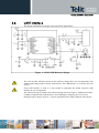
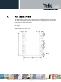
SL869 Hardware User Guide 1vv0301001 Rev.2 – 2013-12-17 SL869 Hardware User Guide 1vv0301001 Rev.2 – 2013-12-7 APPLICABILITY TABLE PRODUCT SL869 Reproduction forbidden without written authorization from Telit Communications S.p.A. - All Rights Reserved. Mod. Rev Page 2 of 28 SL869 Hardware User Guide 1vv0301001 Rev.2 – 2013-12-7 SPECIFICATIONS SUBJECT TO CHANGE WITHOUT NOTICE Notice While reasonable efforts have been made to assure the accuracy of this document, Telit assumes no liability resulting from any inaccuracies or omissions in this document, or from use of the information obtained herein. The information in this document has been carefully checked and is believed to be entirely reliable. However, no responsibility is assumed for inaccuracies or omissions. Telit reserves the right to make changes to any products described herein and reserves the right to revise this document and to make changes from time to time in content hereof with no obligation to notify any person of revisions or changes. Telit does not assume any liability arising out of the application or use of any product, software, or circuit described herein; neither does it convey license under its patent rights or the rights of others. It is possible that this publication may contain references to, or information about Telit products (machines and programs), programming, or services that are not announced in your country. Such references or information must not be construed to mean that Telit intends to announce such Telit products, programming, or services in your country. Copyrights This instruction manual and the Telit products described in this instruction manual may be, include or describe copyrighted Telit material, such as computer programs stored in semiconductor memories or other media. Laws in the Italy and other countries preserve for Telit and its licensors certain exclusive rights for copyrighted material, including the exclusive right to copy, reproduce in any form, distribute and make derivative works of the copyrighted material. Accordingly, any copyrighted material of Telit and its licensors contained herein or in the Telit products described in this instruction manual may not be copied, reproduced, distributed, merged or modified in any manner without the express written permission of Telit. Furthermore, the purchase of Telit products shall not be deemed to grant either directly or by implication, estoppel, or otherwise, any license under the copyrights, patents or patent applications of Telit, as arises by operation of law in the sale of a product. Computer Software Copyrights The Telit and 3rd Party supplied Software (SW) products described in this instruction manual may include copyrighted Telit and other 3rd Party supplied computer programs stored in semiconductor memories or other media. Laws in the Italy and other countries preserve for Telit and other 3rd Party supplied SW certain exclusive rights for copyrighted computer programs, including the exclusive right to copy or reproduce in any form the copyrighted computer program. Accordingly, any copyrighted Telit or other 3rd Party supplied SW computer programs contained in the Telit products described in this instruction manual may not be copied (reverse engineered) or reproduced in any manner without the express written permission of Telit or the 3rd Party SW supplier. Furthermore, the purchase of Telit products shall not be deemed to grant either directly or by implication, estoppel, or otherwise, any license under the copyrights, patents or patent applications of Telit or other 3rd Party supplied SW, except for the normal non-exclusive, royalty free license to use that arises by operation of law in the sale of a product. Reproduction forbidden without written authorization from Telit Communications S.p.A. - All Rights Reserved. Mod. Rev Page 3 of 28 SL869 Hardware User Guide 1vv0301001 Rev.2 – 2013-12-7 Usage and Disclosure Restrictions License Agreements The software described in this document is the property of Telit and its licensors. It is furnished by express license agreement only and may be used only in accordance with the terms of such an agreement. Copyrighted Materials Software and documentation are copyrighted materials. Making unauthorized copies is prohibited by law. No part of the software or documentation may be reproduced, transmitted, transcribed, stored in a retrieval system, or translated into any language or computer language, in any form or by any means, without prior written permission of Telit High Risk Materials Components, units, or third-party products used in the product described herein are NOT fault-tolerant and are NOT designed, manufactured, or intended for use as on-line control equipment in the following hazardous environments requiring fail-safe controls: the operation of Nuclear Facilities, Aircraft Navigation or Aircraft Communication Systems, Air Traffic Control, Life Support, or Weapons Systems (High Risk Activities"). Telit and its supplier(s) specifically disclaim any expressed or implied warranty of fitness for such High Risk Activities. Trademarks TELIT and the Stylized T Logo are registered in Trademark Office. All other product or service names are the property of their respective owners. Copyright © Telit Communications S.p.A. Reproduction forbidden without written authorization from Telit Communications S.p.A. - All Rights Reserved. Mod. Rev Page 4 of 28 SL869 Hardware User Guide 1vv0301001 Rev.2 – 2013-12-7 Contents 1. Introduction .......................................................................................................... 7 1.1. Scope ........................................................................................................................ 7 1.2. Audience ................................................................................................................... 7 1.3. Contact Information, Support................................................................................... 7 1.4. Document Organization ............................................................................................ 8 1.5. Text Conventions ...................................................................................................... 8 1.6. Related Documents .................................................................................................. 8 2. Powering the SL869 .............................................................................................. 9 2.1. 3.3V Supply Voltage .................................................................................................. 9 2.2. Battery Back-up ....................................................................................................... 9 3. Updating the Firmware ...................................................................................... 10 4. Communications ................................................................................................. 11 4.1. Main Serial Interface .............................................................................................. 11 4.2. Secondary Serial Interface ..................................................................................... 11 4.3. Tertiary Serial Interface/USB Interface ................................................................. 11 5. RF Front End Design ........................................................................................... 12 5.1. RF Signal Requirements ........................................................................................ 13 5.2. GPS/Glonass Antenna Polarization ........................................................................ 14 5.3. GPS/Glonass Antenna Gain .................................................................................... 14 5.4. System Noise Floor ................................................................................................ 15 5.5. Active versus Passive Antenna............................................................................... 15 5.6. RF Trace Losses ..................................................................................................... 16 5.7. External LNA Gain and Noise Figure ..................................................................... 16 5.8. Powering the External LNA (active antenna) ......................................................... 17 5.9. RF Interference ...................................................................................................... 18 5.10. 6. Shielding.............................................................................................................. 18 Reference Designs .............................................................................................. 19 Reproduction forbidden without written authorization from Telit Communications S.p.A. - All Rights Reserved. Mod. Rev Page 5 of 28 SL869 Hardware User Guide 1vv0301001 Rev.2 – 6.1. UART Interface ....................................................................................................... 19 6.1.1. 6.2. 7. 2013-12-7 Host Serial Interface..................................................................................................... 20 UART Interface ....................................................................................................... 21 Advanced Features ............................................................................................. 22 7.1. CW Jamming Detection .......................................................................................... 22 7.2. SBAS ....................................................................................................................... 22 7.3. DGPS ....................................................................................................................... 22 8. Handling and soldering ....................................................................................... 23 8.1. Moisture Sensitivity ................................................................................................ 23 8.2. ESD ......................................................................................................................... 24 8.3. Reflow ..................................................................................................................... 24 8.4. Assembly Issues ..................................................................................................... 25 9. PCB Layout Details ............................................................................................. 26 10. Safety Recommendations .................................................................................... 27 11. Document History ............................................................................................... 28 Reproduction forbidden without written authorization from Telit Communications S.p.A. - All Rights Reserved. Mod. Rev Page 6 of 28 SL869 Hardware User Guide 1vv0301001 Rev.2 – 1. Introduction 1.1. Scope 2013-12-7 The Jupiter SL869 is a 12.2mm by 16.0mm integrated GPS/Glonass receiver module using a state of the art 32-channel multi-constellation receiver. This document expands upon the product specification to highlight particular areas to allow the hardware engineer to achieve a successful design implementation. This document only covers the standard and timing variants of the SL869. A separate hardware user guide is provided for the DR variant of the SL869. 1.2. Audience This document is intended for helping customer in the integration of the Telit SL869 GPS/Glonass module 1.3. Contact Information, Support For general contact, technical support, to report documentation errors and to order manuals, contact Telit Technical Support Center (TTSC) at: [email protected] [email protected] [email protected] [email protected] Alternatively, use: http://www.telit.com/en/products/technical-support-center/contact.php For detailed information about where you can buy the Telit modules or for recommendations on accessories and components visit: http://www.telit.com To register for product news and announcements or for product questions contact Telit Technical Support Center (TTSC). Our aim is to make this guide as helpful as possible. Keep us informed of your comments and suggestions for improvements. Telit appreciates feedback from the users of our information. Reproduction forbidden without written authorization from Telit Communications S.p.A. - All Rights Reserved. Mod. Rev Page 7 of 28 SL869 Hardware User Guide 1vv0301001 Rev.2 – 1.4. 2013-12-7 Document Organization “Chapter 1: “Introduction” provides a scope for this document, target audience, contact and support information, and text conventions. “Chapter 2: “Powering the SL868” gives an overview about power supply. “Chapter 3: “Updating Firmware” describes the SW updating procedure for Flash version. “Chapter 4: “Serial interface” describes the three serial interfaces. “Chapter 5: “RF Front End Design” describes in details the characteristics of the Front end. “Chapter 6: “Reference Design” gives an overview about the reference design. “Chapter 7: “Handling and soldering” describes packaging and soldering of the module. “Chapter 8: “PCB layout details” describes the mechanical design of the module. “Chapter 9: “Safety recommendations” provides some safety recommendations that must be followed by the customer in the design of the application that makes use of the SL868. “Chapter 10: “Document History” describes the history of the present product. 1.5. Text Conventions Danger – This information MUST be followed or catastrophic equipment failure or bodily injury may occur. Caution or Warning – Alerts the user to important points about integrating the module, if these points are not followed, the module and end user equipment may fail or malfunction. Tip or Information – The information provides advice and suggestions that may be useful when integrating the module. All dates are in ISO 8601 format, i.e. YYYY-MM-DD. 1.6. Related Documents SL869 Product Description, 80405ST10105a SL869 EVK User Guide, 1VV0301004 SL869 Software User Guide, 1VV0301002 SL869 Timing Software User Guide, 1VV0301094 Reproduction forbidden without written authorization from Telit Communications S.p.A. - All Rights Reserved. Mod. Rev Page 8 of 28 SL869 Hardware User Guide 1vv0301001 Rev.2 – 2. 2.1. 2013-12-7 Powering the SL869 3.3V Supply Voltage The SL869 is powered by applying 3.3 volts DC to the VCC_IN pin of the module. Internal linear and switching regulators generate all of the necessary internal voltages for the module. The supply voltage must be within specification (3.3 volts DC ± 0.3 volts) within 10 milliseconds of initial application. Slow ramping up of the main supply voltage may cause the SL869 not to start up. Figure 1 VCC_IN Ramp The powerup sequence must not be interrupted during the first second or the module may fail to start up. In many designs, an LDO with enable driven by a host microcontroller is used to provide main power to the SL869. Make sure that during initial startup of the host microcontroller the LDO enable line is maintained at the proper state. Many microcontrollers set GPIO lines to tri-state or input during initial bootup. If an LDO enable is tied to this GPIO, it is possible for the LDO to turn on during the boot process and then be shut down. This can cause the SL869 to fail to initialize properly. If this happens, a full power cycle of both VCC_IN and VBATT would be required on the SL869. 2.2. Battery Back-up VBATT is applied to the module to keep the RTC running and battery backed RAM alive whenever main power is removed. This allows for faster startup upon reapplication of main power. Internal diode OR’ing provides an internal source for VBATT even if this pin is not used. The internal reset of the SL869 is generated upon removal and reapplication of VBATT, not VCC_IN. If the module does not initialize properly due to improper application of VCC_IN, the module can only be reset if both supplies are removed and then reapplied in the proper manner. Reproduction forbidden without written authorization from Telit Communications S.p.A. - All Rights Reserved. Mod. Rev Page 9 of 28 SL869 Hardware User Guide 1vv0301001 Rev.2 – 3. 2013-12-7 Updating the Firmware During normal operations, the low true BOOT signal should be left floating. This will ensure the SL869 module executes the code out of the internal flash memory. However, if the internal flash memory needs to be updated, the following steps should be performed to place the SL869 module into a state suitable for programming the internal flash memory. 1. 2. 3. 4. 5. 6. 7. 8. Remove all power to the module. Pull the low true BOOT signal low through a 1K pull down resistor to ground. Apply main power. Run the software utility to re-flash the SL869 module. Clearing the entire flash memory is strongly recommended prior to programming. Upon successful completion of re-flashing, remove main power to the module for a minimum of 10 seconds. Remove the pull down resistor on the low true BOOT signal. Apply main power to the SL869. Verify the SL869 has returned to the normal operating state. The Low True Boot signal is different than the BOOT signal on the JN3 product. Reprogramming the SL869 using the USB interface is not supported. When the receiver is placed into BOOT mode, the data can be transferred on any of the three serial UARTs without user intervention. Reproduction forbidden without written authorization from Telit Communications S.p.A. - All Rights Reserved. Mod. Rev Page 10 of 28 SL869 Hardware User Guide 1vv0301001 Rev.2 – 4. Communications 4.1. Main Serial Interface 2013-12-7 Upon power up, the SL869 will communicate using a standard asynchronous 8 bit protocol (UART) with messages appearing on the TX line (pin 20), and commands and data being entered on the RX line (pins 21). There is no parity bit, and no flow control operations are performed. Upon initial application of power all I/O on the SL869 are initially inputs, with the TX2 pin serving as an auxiliary low true BOOT pin. Internally, this pin has a 10K pullup to VCC_IN to allow the SL869 to properly start up. This pin must not be grounded or pulled low at any time for normal operation. 4.2. Secondary Serial Interface The SL869 implements a secondary UART on pins 14 and 15. Normally these pins are not used but may be used to provide RTCM-104 differential corrections into the receiver. Upon initial application of power all I/O on the SL869 are initially inputs, with the TX2 pin serving as the main low true BOOT pin. Internally, this pin has a 10K pullup to VCC_IN to allow the SL869 to properly start up. This pin must not be grounded or pulled low at any time. 4.3. Tertiary Serial Interface/USB Interface The SL869 implements a tertiary UART which is multiplexed with the USB interface on pins 5 and 6. If the USB_Detect pin is left floating or is pulled low, the interface is a tertiary UART normally used to output debug messages. If the USB_Detect pin is connected to a 3.3 volt supply voltage (not a pullup), the port is then configured as a USB port and serial data that was previously on the main serial interface will be routed to the USB port. Reproduction forbidden without written authorization from Telit Communications S.p.A. - All Rights Reserved. Mod. Rev Page 11 of 28 SL869 Hardware User Guide 1vv0301001 Rev.2 – 5. 2013-12-7 RF Front End Design The SL869 contains an integrated LNA and post-select SAW filter. This allows the SL869 to work well with a passive GPS/Glonass antenna. If the antenna cannot be located near the SL869, then an active antenna (that is, an antenna with a low noise amplifier built in) can be used. The following items will be discussed in turn to assist in designing the “RF front end”. 1. 2. 3. 4. 5. 6. 7. 8. 9. 10. 11. RF signal requirements GPS/Glonass antenna polarization GPS/Glonass antenna gain System noise floor Active versus passive antenna RF trace losses Implications of the pre-select SAW filter External LNA gain and Noise Figure Powering the external LNA (active antenna) RF interference Shielding Reproduction forbidden without written authorization from Telit Communications S.p.A. - All Rights Reserved. Mod. Rev Page 12 of 28 SL869 Hardware User Guide 1vv0301001 Rev.2 – 5.1. 2013-12-7 RF Signal Requirements The SL869 can achieve Cold Start acquisition with a signal level of -147 dBm at its input. This means the SL869 can find the necessary satellites, download the necessary ephemeris data and compute the location within a 5 minute period. In the GPS and Glonass signal acquisition process, downloading and decoding the data is the most difficult task, which is why Cold Start acquisition requires a higher signal level than navigation or tracking signal levels. For the purposes of this discussion, autonomous operation is assumed, which makes the Cold Start acquisition level the important design constraint. If assistance data in the form of time or ephemeris aiding is available, then even lower signal levels can be used to compute a navigation solution. The GPS signal is defined by IS-GPS-200E. This document states that the signal level received by a linearly polarized antenna having 3 dBi gain will be a minimum of -130 dBm when the antenna is in the worst orientation and the satellite is 5 degrees or more above the horizon. The Glonass signal is defined by ICD L1 L2 Glonass Edition 5.1 2008. This document has similar power levels as compared to the GPS signal for a similar antenna. The SL869 will display a reported C/No of 40 dB-Hz for a signal level of -130 dBm into the RF input. Each GPS and Glonass satellite presents its own signal to the SL869, and best performance is obtained when the signal levels are between -125 dBm and -117 dBm. These received signal levels are determined by GPS and Glonass satellite transmit power GPS and Glonass satellite elevation and azimuth Free space path loss Extraneous path loss such as rain Partial or total path blockage such as foliage or building Multipath caused by signal reflection GPS/Glonass antenna Signal path after the GPS/Glonass antenna The GPS/Glonass signal is relatively immune to rainfall attenuation and does not really need to be considered. However, the GPS/Glonass signal is heavily influenced by attenuation due to foliage such as tree canopies, etc., as well as outright blockage caused by building, terrain or other items in the line of sight to the specific GPS or Glonass satellite. This variable attenuation is highly dependent upon GPS or Glonass satellite location. If enough satellites are blocked, say at a lower elevation, or all in a general direction, the geometry of the remaining satellites will result is a lower accuracy of position. The SL869 reports this geometry in the form of PDOP, HDOP and VDOP. For example, in a vehicular application, the GPS/Glonass antenna may be placed embedded into the dashboard or rear package tray of an automobile. The metal roof of the vehicle will Reproduction forbidden without written authorization from Telit Communications S.p.A. - All Rights Reserved. Mod. Rev Page 13 of 28 SL869 Hardware User Guide 1vv0301001 Rev.2 – 2013-12-7 cause significant blockage, plus any thermal coating applied to the vehicle glass can attenuate the GPS/Glonass signal by as much as 15 dB. Again, both of these factors will affect the performance of the receiver. Multipath is a phenomena where the signal from a particular satellite is reflected and is received by the GPS/Glonass antenna in addition to or in place of the original line of sight signal. The multipath signal has a path length that is longer than the original line of sight path and can either attenuate the original signal, or if received in place of the original signal add additional error in determining a solution because the distance to the particular GPS or Glonass satellite is actually longer than expected. It is this phenomena that makes GPS/Glonass navigation in urban canyons (narrow roads surround by high rise buildings) so challenging. In general, the reflecting of the GPS or Glonass signal causes the polarization to reverse. The implications of this are covered in the next section. The advantage of combine GPS/Glonass operation is more satellites are directly visible in the challenging urban canyon environments. 5.2. GPS/Glonass Antenna Polarization The GPS signal and the Glonass signal as broadcast are right hand circularly polarized signals. The best antenna to receive the GPS/Glonass signal is a right hand circularly (RHCP) polarized antenna. Remember that IS-GPS-200E specifies the receive power level with a linearly polarized antenna. A linearly polarized antenna will have 3 dB loss as compared to an RHCP antenna assuming the same antenna gain (specified in dBi and dBic respectively). An RHCP antenna is better at rejecting multipath than a linearly polarized antenna. This is because the reflected signal changes polarization to LHCP, which would be rejected by the RHCP antenna by typically 20 dB or so. If the multipath signal is attenuating the line of sight signal, then the RHCP antenna would show a higher signal level than a linearly polarized antenna because the interfering signal is rejected. However, in the case where the multipath signal is replacing the line of sight signal, such as in an urban canyon environment, then the number of satellites in view could drop below that needed to determine a 3D solution. This is a case where a bad signal may be better than no signal. The system designer needs to make tradeoffs in their application to determine the better choice. 5.3. GPS/Glonass Antenna Gain Antenna gain is defined as the extra signal power from the antenna as compared to a theoretical isotropic antenna (equally sensitive in all directions). For example, a 25mm by 25m square patch antenna on a reference ground plane (usually 70mm by 70mm) will give an antenna gain at zenith of 5 dBic for a GPS signal. A smaller 18mm by 18mm square patch on a reference ground plane (usually 50mm by 50mm) will give an antenna gain at zenith of 2 dBic. While an antenna vendor will specify a nominal antenna gain (usually at zenith, or directly overhead) they should supply antenna pattern curves specifying gain as a function of elevation, and gain at a fixed elevation as a function of azimuth. Pay careful attention to the Reproduction forbidden without written authorization from Telit Communications S.p.A. - All Rights Reserved. Mod. Rev Page 14 of 28 SL869 Hardware User Guide 1vv0301001 Rev.2 – 2013-12-7 requirement to meet these specifications, such as ground plane required and any external matching components. Failure to follow these requirements could result in very poor antenna performance. It is important to note that GPS/Glonass antenna gain is not the same thing as external LNA gain. Most antenna vendors will specify these numbers separately, but some combine them into a single number. It is important to know both numbers when designing and evaluating the front end of a GPS/Glonass receiver. For example, antenna X has an antenna gain of 5 dBiC at azimuth and an LNA gain of 20 dB for a combined total of 25 dB. Antenna Y has an antenna gain of -5 dBiC at azimuth and an LNA gain of 30 dB for a combined total of 25 dB. However, in the system, antenna X will outperform antenna Y by about 10 dB (refer to Section 7.4 for more details on system noise floor). An antenna with higher gain will generally outperform an antenna with lower gain. Once the signals are above about -130 dBm for a particular satellite, no improvement in performance would be gained. However, for those satellites that are below about -125 dBm, a higher gain antenna would improve the gain and improve the performance of the GPS receiver. In the case of really weak signals, a good antenna could mean the difference between being able to use a particular satellite signal or not. 5.4. System Noise Floor As mentioned earlier, the SL869 will display a reported C/No of 40 dB-Hz for an input signal level of -130 dBm. The C/No number means the carrier (or signal) is 40 dB greater than the noise floor measured in a one Hz bandwidth. This is a standard method of measuring GPS receiver performance. Thermal noise is -174 dBm/Hz at around room temperature. From this we can compute a system noise figure of 4 dB for the SL869. This noise figure consists of the loss of the preselect SAW filter, the noise figure of the LNA as well as implementation losses within the digital signal processing unit. If a good quality external LNA is used with the SL869, then the noise figure of that LNA (typically better than 1dB) could reduce the overall system noise figure of the SL869 from 4 dB to around 2 dB. Some of the factors in the system noise figure are implementation losses due to quantization and other factors and do not scale with improved front end noise figure. 5.5. Active versus Passive Antenna If the GPS/Glonass antenna is placed near the SL869 and the RF traces losses are not excessive (nominally 1 dB), then a passive antenna can be used. This would normally be the lowest cost option and most of the time the simplest to use. However, if the antenna needs to be located away from the SL869 then an active antenna may be required to obtain the best system performance. The active antenna has its own built in low noise amplifier to overcome RF trace or cable losses after the active antenna. Reproduction forbidden without written authorization from Telit Communications S.p.A. - All Rights Reserved. Mod. Rev Page 15 of 28 SL869 Hardware User Guide 1vv0301001 Rev.2 – 2013-12-7 However, an active antenna has a low noise amplifier (LNA) with associated gain and noise figure. In addition, many active antennas have either a pre-select filter, a post-select filter, or both. 5.6. RF Trace Losses RF Trace losses are difficult to estimate on a PCB without having the appropriate tables or RF simulation software to estimate what the losses would be. A good rule of thumb would be to keep the RF traces as short as possible, make sure they are 50 ohms impedance and don’t contain any sharp bends. 5.7. External LNA Gain and Noise Figure The SL869 can be used with an external LNA such as what might be found in an active antenna. Because of the internal LNA, the overall gain (including signal losses past the external LNA) should not exceed 35 dB. Levels higher than that can affect the jamming detection capability of the SL869. The external LNA should have a noise figure (NF1) better than 1 dB. This will give an overall system noise figure of around 2 dB assuming the LNA gain is 14 dB. The formula below is the simplified version of the cascaded Noise Figure formula. Any losses added before the LNA (NF1) add directly to the NFtotal, losses after the LNA are added to the next stage NF2 and are reduced by the gain of the LNA as shown in the formula. The effect of additional losses and or external LNA on the overall system Noise Figure can be determined by applying this formula. Overall System noise figure affects the sensitivity of the receiver. Figure 2: Cascaded Noise Figure formula The external LNA, if having no pre-select filter, needs to be able to handle other signals other than the GPS/Glonass signal. These signals are typically at much higher levels. The amplifier needs to stay in the linear region when presented with these other signals. Again, the system designer needs to determine all of the unintended signals and their possible levels that can be presented and make sure the external LNA will not be driven into compression. If this were to happen, the GPS/Glonass signal itself would start to be attenuated and the GPS/Glonass performance would suffer. Reproduction forbidden without written authorization from Telit Communications S.p.A. - All Rights Reserved. Mod. Rev Page 16 of 28 SL869 Hardware User Guide 1vv0301001 Rev.2 – 5.8. 2013-12-7 Powering the External LNA (active antenna) The external LNA needs a source of power. Many of the active antennas accept a 3 volt or 5 volt DC voltage that is impressed upon the RF signal line. This voltage is not supplied by the SL869, but can be easily supplied by the host design. Two approaches can be used. The first is to use an inductor to tie directly to the RF trace. This inductor should be at self-resonance at L1 (1.6 GHz) and should have good Q for low loss – the higher the Q, the lower the loss. The side of the inductor connecting to the antenna supply voltage should be bypassed to ground with a good quality RF capacitor, again operating at self-resonance at the L1 frequency. The second approach is to use a quarter-wave stub in place of the inductor. The length of the stub is designed to be exactly a quarter-wavelength, which has the effect of making an RF short at L1 at one end of the stub to appear as an RF open. The RF short is created by the good quality RF capacitor operating at self-resonance. The choice between the two would be determined by: RF path loss introduced by either the inductor or quarter wave stub. Cost of the inductor. Space availability for the quarter wave stub. Simulations done by Telit show the following: Murata LQG15HS27NJ02 Inductor 27 nH, SRF=1.7GHz, Q approx. 20 at L1 0.65 dB of additional signal loss Quarter wave stub on FR4 0.59 dB of additional signal loss Coilcraft B09TJLC Inductor (used in ref. design) 0.37 dB of additional signal loss 35.5 nH, SRF=1.5GHz, Q approx. 40 at L1 This additional loss occurs after the LNA in the active antenna, so it is generally not significant unless the circuit is being designed to work with either an active or a passive antenna. Reproduction forbidden without written authorization from Telit Communications S.p.A. - All Rights Reserved. Mod. Rev Page 17 of 28 SL869 Hardware User Guide 1vv0301001 Rev.2 – 5.9. 2013-12-7 RF Interference RF Interference into the GPS/Glonass receiver tends to be the biggest problem when determining why the system performance is not meeting expectations. As mentioned earlier, the GPS and Glonass signals are at -130 dBm and lower. If signal higher than this are presented to the receiver it can be overwhelmed. The SL869 can reject a CW in-band jamming signals, but would still be affected by non-CW signals. The most common source of interference is digital noise. This is created by the fast rise and fall times and high clock speeds of modern digital circuitry. For example, a popular netbook computer uses an Atom processor clocked at 1.6 GHz. This is only 25 MHz away from the GPS signal and virtually at the same frequency as the Glonass signal. Because of the nature of the address and data lines, this would be broadband digital noise at a relatively high level. Such devices are required to adhere to a regulatory standard for emissions such as FCC Part 15 Subpart J Class B or CISPR 22. However, these regulatory emission levels are far higher than the GPS/Glonass signal. 5.10. Shielding Shielding the RF circuitry generally is ineffective because the interference is getting into the GPS/Glonass antenna itself, the most sensitive portion of the RF path. The antenna cannot be shielded because then it can’t receive the GPS/Glonass signals. There are two solutions, one is to move the antenna away from the source of interference or the second is to shield the digital interference to prevent it from getting to the antenna. Reproduction forbidden without written authorization from Telit Communications S.p.A. - All Rights Reserved. Mod. Rev Page 18 of 28 SL869 Hardware User Guide 1vv0301001 Rev.2 – 6. 2013-12-7 Reference Designs Below are two different reference designs, one utilizing the serial UART and the second utilizing USB. 6.1. UART Interface The SL869 Serial UART Reference Design is presented in the figure below . Figure 3 – SL869 Serial UART Reference Design The CAN and I2C interfaces shown in the reference design above are not supported in the standard and timing product variants of the SL869. The USB interface is covered in the next section. Reproduction forbidden without written authorization from Telit Communications S.p.A. - All Rights Reserved. Mod. Rev Page 19 of 28 SL869 Hardware User Guide 1vv0301001 Rev.2 – 2013-12-7 The minimum number of connections required to operate the SL869 properly are: VCC_IN to provide main power. GND to provide a DC return for VCC_IN and an RF return for RF_IN. RF_IN to provide the received GNSS signal. TX to provide the serial data stream output from the receiver. If battery backup of receiver settings, current satellite data, position, time and date information are desired, then VBATT is required to power the receiver when VCC_IN is removed. If command and control of the SL869 is desired, then the RX signal is also required to be connected. If in-circuit firmware updates are desired, then the BOOT and RX signals must be connected. The RF input can be connected directly to a GPS/Glonass antenna. The reference design shows a DC power feed for an active antenna. C5 is used to block the DC voltage from entering the SL869. The inductor L1 is chosen to be self-resonant at the GPS/Glonass frequency, 1.6 GHz, to minimize loading on the RF trace. Capacitor C6 is chosen to be selfresonant at the GPS/Glonass frequency such that is looks pretty close to an RF short at that frequency. V_ANT is the supply voltage for the external active antenna. TX is the normal digital output and is a serial UART with a default bit rate of 9600 bps, 1 stop bit and 8 data bits. This is a 3.3 volt logic level signal. As is the case with all serial data, the idle state is logic one. RX is the normal digital input and is a serial UART with a default bit rate of 9600 bps, 1 stop bit and 8 data bits. This is a 1.8 volt logic level signal, but is tolerant to 3.6 volts. As is the case with all serial data, the idle state is logic one. If the RX signal is used, it is important that it be either logic low or high impedance whenever VCC_IN has been removed from the device. Failure to follow this requirement can lead to improper receiver operation upon next powerup. 6.1.1. Host Serial Interface As mentioned above in Section 5, the host serial interface is a UART. The UART can operate at bps rates of 4800, 9600, 19200, 38400, 57600 and 115200 bps. The SL869 currently only implements NMEA protocol. The lower UART bps rates are typically used for NMEA protocol. Note should be taken however of the bandwidth limitation at 9600 bps. By default, the SL869 module communicates using NMEA at 9600 bps, with the periodic output messages limited to the GPGGA, GPGSA, GLGSA and GPRMC messages at once per second and the GPGSV and GLGSV messages once every five seconds. Reference the SL869 SW User Guide for additional message details. Reproduction forbidden without written authorization from Telit Communications S.p.A. - All Rights Reserved. Mod. Rev Page 20 of 28 SL869 Hardware User Guide 1vv0301001 Rev.2 – 6.2. 2013-12-7 UART Interface The SL869 USB Reference Design is presented in the figure below. Figure 4 – SL869 USB Reference Design The CAN and I2C interfaces shown in the reference design above are not supported in the standard and timing product variants of the SL869. The USB interface is covered in the next section. If the USB interface is used, it is not possible to reprogram the SL869 using the USB interface as it is not supported. The reference design is similar to the reference design shown in Figure 3. Additional circuitry is added to implement the USB interface. The USB supply voltage on pin 1 of J2 is fed through a LDO to drop it down to 3 volts for application to the VDD_USB pin of the SL869. Reproduction forbidden without written authorization from Telit Communications S.p.A. - All Rights Reserved. Mod. Rev Page 21 of 28 SL869 Hardware User Guide 1vv0301001 Rev.2 – 7. Advanced Features 7.1. CW Jamming Detection 2013-12-7 The SL869 module detects, tracks and removes a narrow-band interfering signal (CW jammer) without the need for external components or tuning. 7.2. SBAS The SL869 receiver is capable of using Satellite-Based Augmentation System (SBAS) satellites as a source of both differential corrections and satellite range measurements. These systems (WAAS, EGNOS, MSAS) use geostationary satellites to transmit regional differential corrections via a GPS-compatible signal. The use of SBAS corrections can improve typical position accuracy to 3m or less in open-sky applications. 7.3. DGPS Differential corrections can also be supplied to the SL869 using an RTCM beacon receiver. Only RTCM SC-104 messages 1 and 9 are supported. The use of DGPS corrections can improve typical position accuracy to 1.5m or less in open-sky applications. Reproduction forbidden without written authorization from Telit Communications S.p.A. - All Rights Reserved. Mod. Rev Page 22 of 28 SL869 Hardware User Guide 1vv0301001 Rev.2 – 8. Handling and soldering 8.1. Moisture Sensitivity 2013-12-7 The SL869 module has a moisture sensitivity level rating of 3 as defined by IPC/JEDEC JSTD-020. This rating is assigned due to some of the components used within the SL869. The SL869 is supplied in trays or tape and reel and is hermetically sealed with desiccant and humidity indicator card. The SL869 parts must be placed and reflowed within 48 hours of first opening the hermetic seal provided the factory conditions are less than 30°C and less than 60% and the humidity indicator card indicates less than 10% relative humidity. If the package has been opened or the humidity indicator card indicates above 10%, then the parts will need to be baked prior to reflow. The parts may be baked at +125°C ± 5°C for 48 hours. However, the trays, nor the tape and reel can withstand that temperature. Lower temperature baking is feasible if the humidity level is low and time is available. Please see IPC/JEDEC J-STD-033 for additional information. Additional information can be found on the MSL tag affixed to the outside of the hermetical seal bag. Note: JEDEC standards are available for free from the JEDEC website http://www.jedec.org. Reproduction forbidden without written authorization from Telit Communications S.p.A. - All Rights Reserved. Mod. Rev Page 23 of 28 SL869 Hardware User Guide 1vv0301001 Rev.2 – 2013-12-7 Figure 5 – Label for Moisture Sensitive Devices 8.2. ESD The SL869 is an electrostatic discharge sensitive device and should be handled in accordance with JESD625-A requirements for Handling Electrostatic Discharge Sensitive (ESDS) Devices. Although the SL869 is a module, the expecting handling of the SL869 during assembly and test is identical to that of a semiconductor device. Note: JEDEC standards are available for free from the JEDEC website http://www.jedec.org. 8.3. Reflow The SL869 is compatible with lead free soldering processes as defined in IPC/JEDEC J-STD020. The reflow profile must not exceed the profile given IPC/JEDEC J-STD-020 Table 5-2, “Classification Reflow Profiles”. Although IPC/JEDEC J-STD-020 allows for three reflows, the assembly process for the SL869 uses one of those profiles. Thus the SL869 is limited to two reflows. Note: JEDEC standards are available for free from the JEDEC website http://www.jedec.org. When reflowing a dual-sided SMT board, it is important to reflow the side containing the SL869 module last. This prevents heavier components within the SL869 becoming dislodged if the solder reaches liquidus temperature while the module is inverted. Reproduction forbidden without written authorization from Telit Communications S.p.A. - All Rights Reserved. Mod. Rev Page 24 of 28 SL869 Hardware User Guide 1vv0301001 Rev.2 – 8.4. 2013-12-7 Assembly Issues Due to the piezo-electric components within the SL869, the component should be placed close to the end of the assembly process to minimize shock to the module. During board singulation, pay careful attention to unwanted vibrations and resonances introduced into the board assembly by the board router. For boards using dual sided SMT processes, it is strongly recommended to place the SL869 on the top side of the board. Reproduction forbidden without written authorization from Telit Communications S.p.A. - All Rights Reserved. Mod. Rev Page 25 of 28 SL869 Hardware User Guide 1vv0301001 Rev.2 – 9. 2013-12-7 PCB Layout Details The PCB footprint on the receiving board should match the SL869 pad design shown below. The solder mask opening is generally determined by the component geometry of other parts on the board and can be followed here. Standard industry practice is to use a paste mask stencil opening the same dimensions as the pad design. All dimensions shown are in mm. Pin 1 Figure 6 – SL869 Pad Design for PCB Reproduction forbidden without written authorization from Telit Communications S.p.A. - All Rights Reserved. Mod. Rev Page 26 of 28 SL869 Hardware User Guide 1vv0301001 Rev.2 – 10. 2013-12-7 Safety Recommendations READ CAREFULLY Be sure the use of this product is allowed in the country and in the environment required. The use of this product may be dangerous and has to be avoided in the following areas: Where it can interfere with other electronic devices in environments such as hospitals, airports, aircrafts, etc. Where there is risk of explosion such as gasoline stations, oil refineries, etc. It is responsibility of the user to enforce the country regulation and the specific environment regulation. Do not disassemble the product; any mark of tampering will compromise the warranty validity. We recommend following the instructions of the hardware user guides for a correct wiring of the product. The product has to be supplied with a stabilized voltage source and the wiring has to be conforming to the security and fire prevention regulations. The product has to be handled with care, avoiding any contact with the pins because electrostatic discharges may damage the product itself. The system integrator is responsible for the functioning of the final product; therefore, care has to be taken to the external components of the module, as well as of any project or installation issue, because of the risk of disturbing external networks or devices or having impact on the security. Should there be any doubt, please refer to the technical documentation and the regulations in force. Every module has to be equipped with a proper antenna with specific characteristics. The antenna has to be installed with care in order to avoid any interference with other electronic devices. The European Community provides some Directives for the electronic equipment introduced to the market. All the relevant information’s are available on the European Community website: http://ec.europa.eu/enterprise/sectors/rtte/documents/ The text of the Directive 99/05 regarding telecommunication equipment is available. The applicable Directives (Low Voltage and EMC) are available at: http://ec.europa.eu/enterprise/sectors/electrical/ Reproduction forbidden without written authorization from Telit Communications S.p.A. - All Rights Reserved. Mod. Rev Page 27 of 28 SL869 Hardware User Guide 1vv0301001 Rev.2 – 11. 2013-12-7 Document History Revision Issue #0 Issue #1 Date 2012-03-12 2012-07-25 Issue #2 2103-12-17 Changes First issue §4.3 and §6 : Updated USB availability in SL869 variants Additional information on usage of USB, powering the module, the using the three UART ports and timing diagram. Reproduction forbidden without written authorization from Telit Communications S.p.A. - All Rights Reserved. Mod. Rev Page 28 of 28